

Page 1

Instruction Manual
DAS 92DM927
Am29205 Microprocessor Support
070-8786-00
Warning
The servicing instructions are for use by qualified
personnel only. To avoid personal injury, do not
perform any servicing unless you are qualified to
do so. Refer to the Safety Summary prior to
performing service.
Please check for change information at the rear
of this manual.
First Printing: June 1993
Online Version: April 1997
Page 2

Instrument Serial Numbers
Each instrument manufactured by Tektronix has a serial number on a panel insert or tag, or stamped on the
chassis. The first letter in the serial number designates the country of manufacture. The last five digits of the
serial number are assigned sequentially and are unique to each instrument. Those manufactured in the
United States have six unique digits. The country of manufacture is identified as follows:
B010000 Tektronix, Inc., Beaverton, Oregon, USA
E200000 Tektronix United Kingdom, Ltd., London
J300000 Sony/Tektronix, Japan
H700000 Tektronix Holland, NV, Heerenveen, The Netherlands
Instruments manufactured for Tektronix by external vendors outside the United States are assigned a two digit
alpha code to identify the country of manufacture (e.g., JP for Japan, HK for Hong Kong, IL for Israel, etc.).
Tektronix, Inc., P.O. Box 500, Beaverton, OR 97077
Printed in U.S.A.
CopyrightETektronix, Inc., 1993. All rights reserved. T ektronix products are covered by U .S. and foreign
patents, issued and pending. The following are registered trademarks: TEKTRONIX, TEK, TEKPROBE,
SCOPEĆMOBILE, DAS, PRISM, TekDB, and KlipChip.
Page 3
HARDWARE WARRANTY
Tektronix warrantsthat this product will be free from defects in materials and workmanship for a period of one (1) year from the
date of shipment. If any such product proves defective during this warranty period, Tektronix, at its option, either will repair the
defective product without charge for parts and labor, or will provide a replacement in exchange for the defective product.
In order to obtain service under this warranty,Customer must notify Tektronix of the defect before the expiration of the warranty
period and make suitable arrangements for the performance of service. Tektronix will provide such service at Customer's site
without charge during the warranty period, if the service is performed within the normal onĆsite service area. Tektronix will
provide onĆsite service outside the normal onĆsite service area only upon prior agreement and subject to payment of all travel
expenses by Customer. When or where onĆsite service is not available, Customer shall be responsible for packaging and
shipping the defective product to the service center designated by Tektronix, with shipping charges prepaid. Tektronix shall
pay for the return of the product to Customer if the shipment is to a location within the country in which the Tektronix service
center is located. Customer shall be responsible for paying all shipping charges, duties, taxes, and any other charges for
products returned to any other locations.
This warranty shall not apply to any defect, failure or damage caused by improper use or improper or inadequate maintenance
and care. Tektronix shall not be obligated to furnish service under this warranty a) to repair damage resulting from attempts by
personnel other than Tektronix representatives to install, repair or service the product; b) to repair damage resulting from
improper use or connection to incompatible equipment; or c) to service a product that has been modified or integrated with
other products when the effect of such modification or integration increases the time or difficulty of servicing the product.
THIS WARRANTY IS GIVEN BY TEKTRONIX WITH RESPECT TO THIS PRODUCT IN LIEU OF ANY OTHER
WARRANTIES, EXPRESSED OR IMPLIED. TEKTRONIX AND ITS VENDORS DISCLAIM ANY IMPLIED WARRANTIES OF
MERCHANTABILITY OR FITNESS FOR A PARTICULAR PURPOSE. TEKTRONIX' RESPONSIBILITY TO REPAIR OR
REPLACE DEFECTIVE PRODUCTS IS THE SOLE AND EXCLUSIVE REMEDY PROVIDED TO THE CUSTOMER FOR
BREACH OF THIS WARRANTY. TEKTRONIX AND ITS VENDORS WILL NOT BE LIABLE FOR ANY INDIRECT, SPECIAL,
INCIDENTAL, OR CONSEQUENTIAL DAMAGES IRRESPECTIVE OF WHETHER TEKTRONIX OR THE VENDOR HAS
ADVANCE NOTICE OF THE POSSIBILITY OF SUCH DAMAGES.
SOFTWARE WARRANTY
Tektronix warrants that the media on which this software product is furnished and the encoding of the programs on the media
will be free from defects in materials and workmanship for a period of three (3) months from date of shipment. If any such
medium or encoding proves defective during the warranty period, Tektronix will provide a replacement in exchange for the
defective medium. Except as to the media on which this software product is furnished, this software product is provided as is"
without warranty of any kind, either express or implied. Tektronix does not warrant that the functions contained in this software
product will meet Customer's requirements or that the operation of the programs will be uninterrupted or errorĆfree.
In order to obtain service under this warranty,Customer must notify Tektronix of the defect before the expiration of the warranty
period. If Tektronix is unable to provide a replacement that is free from defects in materials and workmanship within a
reasonable time thereafter, Customer may terminate the license for this software product and return this software product and
any associated materials for credit or refund.
THIS WARRANTY IS GIVEN BY TEKTRONIX WITH RESPECT TO THIS PRODUCT IN LIEU OF ANY OTHER
WARRANTIES, EXPRESS OR IMPLIED. TEKTRONIX AND ITS VENDORS DISCLAIM ANY IMPLIED WARRANTIES OF
MERCHANTABILITY OR FITNESS FOR A PARTICULAR PURPOSE. TEKTRONIX' RESPONSIBILITY TO REPLACE
DEFECTIVE MEDIA OR REFUND CUSTOMER'S PAYMENT IS THE SOLE AND EXCLUSIVE REMEDY PROVIDED TO
THE CUSTOMER FOR BREACH OF THIS WARRANTY. TEKTRONIX AND ITS VENDORS WILL NOT BE LIABLE FOR ANY
INDIRECT, SPECIAL, INCIDENTAL, OR CONSEQUENTIAL DAMAGES IRRESPECTIVE OF WHETHER TEKTRONIX OR
THE VENDOR HAS ADVANCE NOTICE OF THE POSSIBILITY OF SUCH DAMAGES.
Page 4

Table of Contents
Preface: GUIDE TO DAS 9200 DOCUMENTATION
GENERAL SAFETY SUMMARY/ MICROPROCESSOR SUPPORT vi
Section 1: OVERVIEW
DAS 9200 SYSTEM SOFTWARE COMPATIBILITY 1-2. . . . . . . . . . . . .
DAS 9200 CONFIGURATION 1-2. . . . . . . . . . . . . . . . . . . . . . . . . . . . . . .
REQUIREMENTS AND RESTRICTIONS 1-3. . . . . . . . . . . . . . . . . . . . .
ABOUT THIS MANUAL 1-4. . . . . . . . . . . . . . . . . . . . . . . . . . . . . . . . . . .
Manual Conventions 1-4. . . . . . . . . . . . . . . . . . . . . . . . . . . . . . . . . . . .
Section 2: INSTALLATION AND CONNECTIONS
INSTALLING SOFTWARE 2-1. . . . . . . . . . . . . . . . . . . . . . . . . . . . . . . . . .
CONFIGURING THE DAS 9200 2-2. . . . . . . . . . . . . . . . . . . . . . . . . . . . .
CONFIGURING THE PROBE ADAPTER 2-3. . . . . . . . . . . . . . . . . . . . .
CONNECTING TO THE SYSTEM UNDER TEST 2-4. . . . . . . . . . . . . . .
Section 3: SETTING UP SUPPORT SOFTWARE
LOADING SUPPOR T SOFTWARE 3-1. . . . . . . . . . . . . . . . . . . . . . . . . . .
CHANNEL GROUPS AND ASSIGNMENTS 3-1. . . . . . . . . . . . . . . . . . .
CHANGES THAT AFFECT THE DATA DISPLAY 3-2. . . . . . . . . . . . . .
CUSTOM CLOCKING 3-2. . . . . . . . . . . . . . . . . . . . . . . . . . . . . . . . . . . . .
SYMBOLS 3-4. . . . . . . . . . . . . . . . . . . . . . . . . . . . . . . . . . . . . . . . . . . . . . .
TRIGGERING 3-8. . . . . . . . . . . . . . . . . . . . . . . . . . . . . . . . . . . . . . . . . . . .
Section 4: ACQUIRING AND VIEWING DATA
ACQUIRING DATA 4-1. . . . . . . . . . . . . . . . . . . . . . . . . . . . . . . . . . . . . . .
VIEWING STATE DATA 4-1. . . . . . . . . . . . . . . . . . . . . . . . . . . . . . . . . . . .
Displaying Channel Groups Symbolically 4-2. . . . . . . . . . . . . . . . . . .
Searching Through Data 4-3. . . . . . . . . . . . . . . . . . . . . . . . . . . . . . . . .
PRINTING DATA 4-5. . . . . . . . . . . . . . . . . . . . . . . . . . . . . . . . . . . . . . . . .
REFERENCE MEMORY 4-5. . . . . . . . . . . . . . . . . . . . . . . . . . . . . . . . . . . .
Section 5: GENERAL PURPOSE ANALYSIS
CLOCKING 5-1. . . . . . . . . . . . . . . . . . . . . . . . . . . . . . . . . . . . . . . . . . . . . .
Custom Clocking 5-2. . . . . . . . . . . . . . . . . . . . . . . . . . . . . . . . . . . . . . .
Internal Clocking 5-2. . . . . . . . . . . . . . . . . . . . . . . . . . . . . . . . . . . . . . .
External Clocking 5-2. . . . . . . . . . . . . . . . . . . . . . . . . . . . . . . . . . . . . .
TRIGGERING 5-3. . . . . . . . . . . . . . . . . . . . . . . . . . . . . . . . . . . . . . . . . . . .
ACQUIRING DAT A 5-3. . . . . . . . . . . . . . . . . . . . . . . . . . . . . . . . . . . . . . .
DISPLAYING DAT A 5-3. . . . . . . . . . . . . . . . . . . . . . . . . . . . . . . . . . . . . . .
Timing Menu 5-3. . . . . . . . . . . . . . . . . . . . . . . . . . . . . . . . . . . . . . . . . .
State Menu 5-4. . . . . . . . . . . . . . . . . . . . . . . . . . . . . . . . . . . . . . . . . . . .
SEARCHING THROUGH DATA 5-5. . . . . . . . . . . . . . . . . . . . . . . . . . . . .
PRINTING DATA 5-5. . . . . . . . . . . . . . . . . . . . . . . . . . . . . . . . . . . . . . . . .
92DM927 Am29205 Instruction Manual
Online Version
i
Page 5

Appendix A: ERROR MESSAGES AND ACQUISITION PROBLEMS
MODULE ERROR MESSAGES A-1. . . . . . . . . . . . . . . . . . . . . . . . . . . . . .
ACQUISITION PROBLEMS A-2. . . . . . . . . . . . . . . . . . . . . . . . . . . . . . . .
Appendix B: HOW DATA IS ACQUIRED
92A96 CUSTOM CLOCKING B-1. . . . . . . . . . . . . . . . . . . . . . . . . . . . . . .
ROM, PIA, or DMA Access B-1. . . . . . . . . . . . . . . . . . . . . . . . . . . . . .
Parallel Port Access B-2. . . . . . . . . . . . . . . . . . . . . . . . . . . . . . . . . . . . .
DRAM Access B-2. . . . . . . . . . . . . . . . . . . . . . . . . . . . . . . . . . . . . . . . .
CLOCKING OPTIONS B-3. . . . . . . . . . . . . . . . . . . . . . . . . . . . . . . . . . . . .
DRAM Refresh Cycles Excluded B-3. . . . . . . . . . . . . . . . . . . . . . . . . .
DRAM Refresh Cycles Included B-3. . . . . . . . . . . . . . . . . . . . . . . . . . .
ALTERNATE MICROCONTROLLER CONNECTIONS B-3. . . . . . . . . .
Signals On the Probe Adapter B-3. . . . . . . . . . . . . . . . . . . . . . . . . . . . .
Signals Not On the Probe Adapter B-4. . . . . . . . . . . . . . . . . . . . . . . . .
Extra 92A96 Channels B-4. . . . . . . . . . . . . . . . . . . . . . . . . . . . . . . . . . .
Appendix C: SERVICE INFORMATION
SERVICING SAFETY INFORMATION C-1. . . . . . . . . . . . . . . . . . . . . . .
PROBE ADAPTER DESCRIPTION C-2. . . . . . . . . . . . . . . . . . . . . . . . . . .
Configuring the Probe Adapter C-3. . . . . . . . . . . . . . . . . . . . . . . . . . . .
Probe Adapter Circuit Description C-3. . . . . . . . . . . . . . . . . . . . . . . . .
CARE AND MAINTENANCE C-3. . . . . . . . . . . . . . . . . . . . . . . . . . . . . . .
SPECIFICATIONS C-5. . . . . . . . . . . . . . . . . . . . . . . . . . . . . . . . . . . . . . . . .
Channel Assignments C-6. . . . . . . . . . . . . . . . . . . . . . . . . . . . . . . . . . .
DISCONNECTING PROBES C-11. . . . . . . . . . . . . . . . . . . . . . . . . . . . . . . .
REMOVING AND REPLACING PROBE PODLETS C-13. . . . . . . . . . . . .
Removing Probe Podlets from the Interface Housing C-13. . . . . . . . . . .
Replacing a Clock Probe C-14. . . . . . . . . . . . . . . . . . . . . . . . . . . . . . . . .
Removing Probe Podlets from the Podlet Holder C-14. . . . . . . . . . . . . .
Replacing 8-Channel Probe Podlets C-15. . . . . . . . . . . . . . . . . . . . . . . .
REMOVING AND REPLACING SOCKETS C-16. . . . . . . . . . . . . . . . . . . .
Appendix D: REPLACEABLE PARTS LIST
Index
ii
92DM927 Am29205 Instruction Manual
Online Version
Page 6

List of Figures
Figure 1-1. DAS 9200 connected to a typical probe adapter. 1-3. . . . . . . . . . . . . . . . . . . . .
Figure 2-1. Applying slot number labels. 2-3. . . . . . . . . . . . . . . . . . . . . . . . . . . . . . . . . . . .
Figure 2-2. Jumper location on the probe adapter. 2-3. . . . . . . . . . . . . . . . . . . . . . . . . . . . .
Figure 2-3. Connecting the podlets to a typical PQFP probe adapter. 2-5. . . . . . . . . . . . . .
Figure 2-4. Seating the converter clip on the probe adapter. 2-6. . . . . . . . . . . . . . . . . . . . .
Figure 2-5. Placing a typical PQFP probe adapter onto the SUT. 2-7. . . . . . . . . . . . . . . . . .
Figure 3-1. Clock menu. 3-3. . . . . . . . . . . . . . . . . . . . . . . . . . . . . . . . . . . . . . . . . . . . . . . . .
Figure 4-1. Am29205 data in the State display using Custom clocking. 4-2. . . . . . . . . . . .
Figure 4-2. State Search Definition overlay. 4-3. . . . . . . . . . . . . . . . . . . . . . . . . . . . . . . . . .
Figure 5-1. Timing data using the 29205_96 T iming Format file. 5-4. . . . . . . . . . . . . . . . .
Figure B-1. Am29205 bus timing (ROM, PIA, and DMA accesses). B-1. . . . . . . . . . . . . .
Figure B-2. Am29205 bus timing (parallel port accesses). B-2. . . . . . . . . . . . . . . . . . . . . .
Figure B-3. Am29205 bus timing (DRAM accesses). B-2. . . . . . . . . . . . . . . . . . . . . . . . . .
Figure B-4. Square pin grid location on the probe adapter. B-4. . . . . . . . . . . . . . . . . . . . . .
Figure C-1. Overview of the standard probe and probe adapter. C-2. . . . . . . . . . . . . . . . . .
Figure C-2. Minimum clearance of the probe adapter with castle extension. C-5. . . . . . . .
Figure C-3. Disconnecting clock and 8-channel probes. C-12. . . . . . . . . . . . . . . . . . . . . . . .
Figure C-4. Removing a clock or probe podlet from the interface housing. C-13. . . . . . . . .
Figure C-5. Ganging together the 8-channel probe podlets. C-14. . . . . . . . . . . . . . . . . . . . . .
List of Tables
T able 3-1 29205_CTRL Symbol Table Definitions 3-4. . . . . . . . . . . . . . . . . . . . . . . . . . . .
T able 3-2 29205_ACCS Symbol Table Definitions 3-5. . . . . . . . . . . . . . . . . . . . . . . . . . . .
T able B-1 Am29205 Signals On Square Pin Grid B-4. . . . . . . . . . . . . . . . . . . . . . . . . . . . .
T able C-1 92DM927 Address Group Channel Assignments C-7. . . . . . . . . . . . . . . . . . . . .
T able C-2 92DM927 Data Group Channel Assignments C-8. . . . . . . . . . . . . . . . . . . . . . . .
T able C-3 92DM927 Control Group Channel Assignments C-9. . . . . . . . . . . . . . . . . . . . . .
T able C-4 92DM927 Access Group Channel Assignments C-9. . . . . . . . . . . . . . . . . . . . . .
T able C-5 92DM927 Intr Group Channel Assignments C-10. . . . . . . . . . . . . . . . . . . . . . . . .
T able C-6 92DM927 PrgrmIO Group Channel Assignments C-10. . . . . . . . . . . . . . . . . . . . .
T able C-7 92DM927 Misc Group Channel Assignments C-11. . . . . . . . . . . . . . . . . . . . . . . .
T able C-8 92DM927 Clock Channel Assignments C-11. . . . . . . . . . . . . . . . . . . . . . . . . . . . .
T able C-9 Podlet-to-Channel Color Code C-15. . . . . . . . . . . . . . . . . . . . . . . . . . . . . . . . . . . .
92DM927 Am29205 Instruction Manual
Online Version
iii
Page 7

Preface: GUIDE TO DAS 9200 DOCUMENTATION
The Digital Analysis System (DAS) 9200 documentation package
provides the information necessary to install, operate, maintain, and
service the DAS 9200. The DAS 9200 documentation consists of the
following:
S
a series of microprocessor-specific microprocessor support
instructions that describe the various microprocessor support
packages.
S
a system user manual that includes a beginning user’s orientation,
a discussion of DAS 9200 system-level operation, and reference
information such as installation procedures, specifications, error
messages, and a complete system glossary.
S
a series of module user manuals that describe each of the
DAS 9200 acquisition, pattern generation, and optional I/O modules.
S
an on-line documentation package that includes context-sensitive
technical notes.
S
a programmatic command language user manual that describes
the set of programmatic commands available for remotely
controlling the DAS 9200.
S
a series of application software user manuals that describe the
various application software packages.
S
a technician’s reference manual that helps a qualified technician
isolate DAS 9200 problems to the individual module level and
determine corrective action (including on-site removal and
replacement of modules).
S
a verification and adjustment procedures manual that allows a
qualified technician to make necessary adjustments and verify
specifications of the mainframe and modules.
S
a series of workbooks that teach concepts about the DAS 9200
acquisition modules and pattern generation modules.
iv
92DM927 Am29205 Instruction Manual
Online Version
Page 8

Preface
GENERAL SAFETY SUMMARY/
MICROPROCESSOR SUPPORT
The general safety information in this summary is for operating and
servicing personnel. Specific warnings and cautions can be found
throughout the manual where they apply and may not appear in this
summary. While using this product you may need to access parts of the
mainframe system; if so, read the General Safety Summary in your
system user manual for warnings and cautions related to operating the
mainframe system.
TERMS IN THIS MANUAL
CAUTION statements identify conditions or practices that could result
in damage to the equipment or other property.
WARNING statements identify conditions or practices that could result
in personal injury or loss of life.
TERMS AS MARKED ON EQUIPMENT
CAUTION
CAUTION indicates a hazard to property, including the equipment
itself, and could cause minor personal injury.
WARNING
WARNING indicates solely a personal injury hazard not immediately
accessible as you read the marking.
DANGER indicates a personal injury hazard immediately accessible as
you read the marking.
SYMBOLS AS MARKED ON EQUIPMENT
DANGER
High Voltage
Protective
ground (earth)
terminal
A TTENTION
Refer to
manual
USE CARE WITH COVERS REMOVED
To avoid personal injury, remove jewelry such as rings, watches, and
other metallic objects before removing the cover. Do not touch exposed
connections and components within the product while the power cord is
connected.
92DM927 Am29205 Instruction Manual
Online Version
v
Page 9

Preface
REMOVE FROM OPERATION
If you have reason to believe that the instrument has suffered a
component failure, do not operate the instrument until the cause of the
failure has been determined and corrected.
USE THE PROPER FUSE
To avoid fire hazard, use only a fuse of the correct type, voltage rating,
and current rating.
REMOVE LOOSE OBJECTS
During disassembly or installation procedures, screws or other small
objects may fall to the bottom of the mainframe. To avoid shorting out
the power supply, do not power on the instrument until such objects
have been removed.
DO NOT OPERATE IN EXPLOSIVE ATMOSPHERES
To avoid explosion, do not operate this product in an explosive
atmosphere unless it has been specifically certified for such operation.
vi
92DM927 Am29205 Instruction Manual
Online Version
Page 10

Section 1: OVERVIEW
The 92DM900 series of support products are developed by third parties
to support buses, microprocessors, microcontrollers, and digital signal
processors for specific Tektronix customers. The products are currently
being successfully used by these customers. If you need assistance in
using this product, contact your local Tektronix Application Engineer.
This section provides basic information on the following:
S
the 92DM927 Microprocessor Support product
S
software compatibility
S
DAS 9200 configuration
S
your Am29205 system requirements
S
92DM927 restrictions
S
this manual
The 92DM927 Microprocessor Support product displays data from
systems that are based on the AMD Am29205 microcontroller. The
92DM927 product runs on a DAS 9200 logic analyzer equipped with at
least one 92A96 Acquisition Module.
This product consists of software on a floppy disk, a probe adapter, and
this manual. The software includes setup files, a demonstration
reference memory, and symbol tables. A complete list of accessories
and options is provided at the end of the mechanical parts list in
Appendix D: Replaceable Parts List.
A demonstration reference memory is provided so you can see an
example of state data. You can view the reference memory without
connecting the DAS 9200 to your system under test. The reference
memory is automatically installed on the DAS 9200 when you install the
support software. Directions for viewing this file can be found in
Section 4: Acquiring and Viewing Data.
92DM927 Am29205 Instruction Manual
Online Version
1-1
Page 11

Overview
To use this product efficiently, you need to have the following:
S
knowledge of your DAS 9200 configuration and its operation
S
knowledge of your Am29205 system
S
this manual
S
the DAS 9200 System User Manual
S
the 92A96 Module User Manual, Tektronix, Inc. 1992
S
a user manual for your Am29205 microcontroller
S
LA-LINK (if you want to download symbols from your high-level
development system)
DAS 9200 SYSTEM SOFTWARE COMPATIBILITY
The 92DM927 Microprocessor Support Product is compatible with
DAS 9200 System Software Release 3, Version 1.3 or higher,
DAS 92XTerm System Software Release 3, Version 1.3 or higher, and
DAS 9202XT System Software Release 3, Version 1.3 or higher.
DAS 9200 CONFIGURATION
To use the microcontroller support product, your DAS 9200 must be
equipped with at least one 92A96 Module and four standard data
acquisition probes.
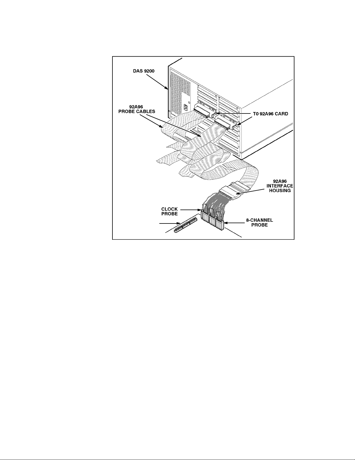
Figure 1-1 shows an overview of a DAS 9200 connected to a typical
probe adapter.
1-2
92DM927 Am29205 Instruction Manual
Online Version
Page 12
Overview
PROBE
ADAPTER
Figure 1-1. DAS 9200 connected to a typical probe adapter.
REQUIREMENTS AND RESTRICTIONS
This section describes requirements and restrictions of the
microcontroller support product.
Probe Adapter Clearance. Your Am29205 system must have a
minimum amount of clear space surrounding the Am29205
microcontroller to accommodate the probe adapter. Figure C-2 in
Appendix C: Service Information gives these dimensions.
Probe Adapter Loading. Any electrical connection to your system
adds an additional AC and DC load. The probe adapter was carefully
designed to add a minimum load to your system. However, this
additional load may affect the operation of the Am29205
microcontroller in systems with extremely tight timing margins.
92DM927 Am29205 Instruction Manual
Online Version
1-3
Page 13
Overview
Am29205 System and Probe Adapter Cooling. You must be sure to
retain the original level of cooling for your Am29205 system after you
install the probe adapter. To maintain the required operating
temperature, you may need to provide additional cooling for the probe
adapter.
ABOUT THIS MANUAL
This manual is based on the assumption that you are familiar with the
operation of the DAS 9200 mainframe and the 92A96 Acquisition
Module. Therefore, details about system software and how to move
through the menu structure are not provided. An overview of those
functions is provided so that you do not need to consult another manual.
This manual provides detailed information on how to do the following:
S
install application software
S
connect to your system under test
S
setup the software and use it
S
view acquired data
S
maintain the probe adapter
Read Section 5: General Purpose Analysis if you are going to acquire
and view data using Internal or External clocking.
Manual Conventions
The following conventions are used in this manual:
S
The terms application software and support software are used
interchangeably in reference to the 92DM927 software that displays
the bus cycle data.
S
The term SUT (system under test) is used to refer to the
microcontroller system from which data is being acquired.
S
References to 92A96 Modules include all versions of those modules
unless otherwise noted.
S
A signal that is active low has an asterisk (*) following its name.
1-4
92DM927 Am29205 Instruction Manual
Online Version
Page 14

Section 2: INSTALLATION AND CONNECTIONS
This section describes how to do the following:
S
install the application software onto the hard disk
S
configure the DAS 9200
S
configure the probe adapter
S
connect the DAS 9200 to the SUT (system under test)
INSTALLING SOFTWARE
Before installing the microcontroller application software, you should
be aware that there are three different versions of DAS 9200 system
software: the 9201T version, the 92XTerm, and the 9202XT version.
The 9201T version allows you to operate the DAS 9200 from a 9201T
terminal. The 92XTerm version allows you to operate the DAS 9200 in
an X window on a workstation. The 9202XT version allows you to
operate the DAS 9200 in an X window from a 9202XT terminal.
NOTE
To use the microcontroller support package, you must
install application software that is compatible with your
DAS 9200 mainframe configuration and system software.
If you have any two types of DAS 9200 system software (9201T,
92XTerm, 9202XT), and you switch between the two, you must install
compatible application software on each system.
If you try to install application software onto an incompatible system or
terminal using DAS 9200 System Software Release 3, V1.1 or greater,
an error message displays.
If you try to install application software onto an incompatible system or
terminal using DAS 9200 System Software Release 3, V1.0 or lower,
the system will install the software but it will not operate properly when
you try to use it.
Install the application software onto the DAS 9200 as follows:
1. Power on the DAS 9200 mainframe.
2. Insert the appropriate disk into the DAS 9200’s floppy drive.
3. Press the Select Menu key, and select the Disk Services menu.
4. Select Install Application in the Operation field of the menu.
92DM927 Am29205 Instruction Manual
Online Version
2-1
Page 15

Installation and Connections
5. Press F8: EXECUTE OPERATION, and follow the on-screen
prompts.
NOTE
After each install and load operation, a message appears
on the screen informing you the operation succeeded or
failed. If the message tells you the operation failed, you
may need to remove applications or files from the hard disk
and try installing or loading again. If the operation fails
again, refer to Appendix A: Error Messages and
Acquisition Problems.
If there is inadequate disk free space available on the hard disk, you
must use the Remove Application or Delete File function of the Disk
Services menu to free up enough disk space to install the support
software. The approximate space required to install the software is
listed on the label of the floppy disk.
CONFIGURING THE DAS 9200
When there are two or three 92A96 Modules in adjacent slots, they are
automatically formed into a variable-width module by the system
software at power up. If you need to use one 92A96 Module from a
variable-width module, you must reconfigure the DAS 9200 prior to
selecting software support in the 92A96 Configuration menu. Refer to
the discussion of the System Configuration menu in the DAS 9200
System User Manual for details on how to reconfigure variable-width
modules.
Refer to your module user manual for additional information about
connecting probe cables, and positioning and installing 92A96
Modules.
In a system with many modules, it is easier to identify which modules
are connected to the probe adapter if slot number labels are applied to
the 92A96 probe interface housings and DAS 9200 mainframe.
Figure 2-1 shows where to apply slot number labels.
2-2
92DM927 Am29205 Instruction Manual
Online Version
Page 16
Installation and Connections
Apply slot number labels here.
Figure 2-1. Applying slot number labels.
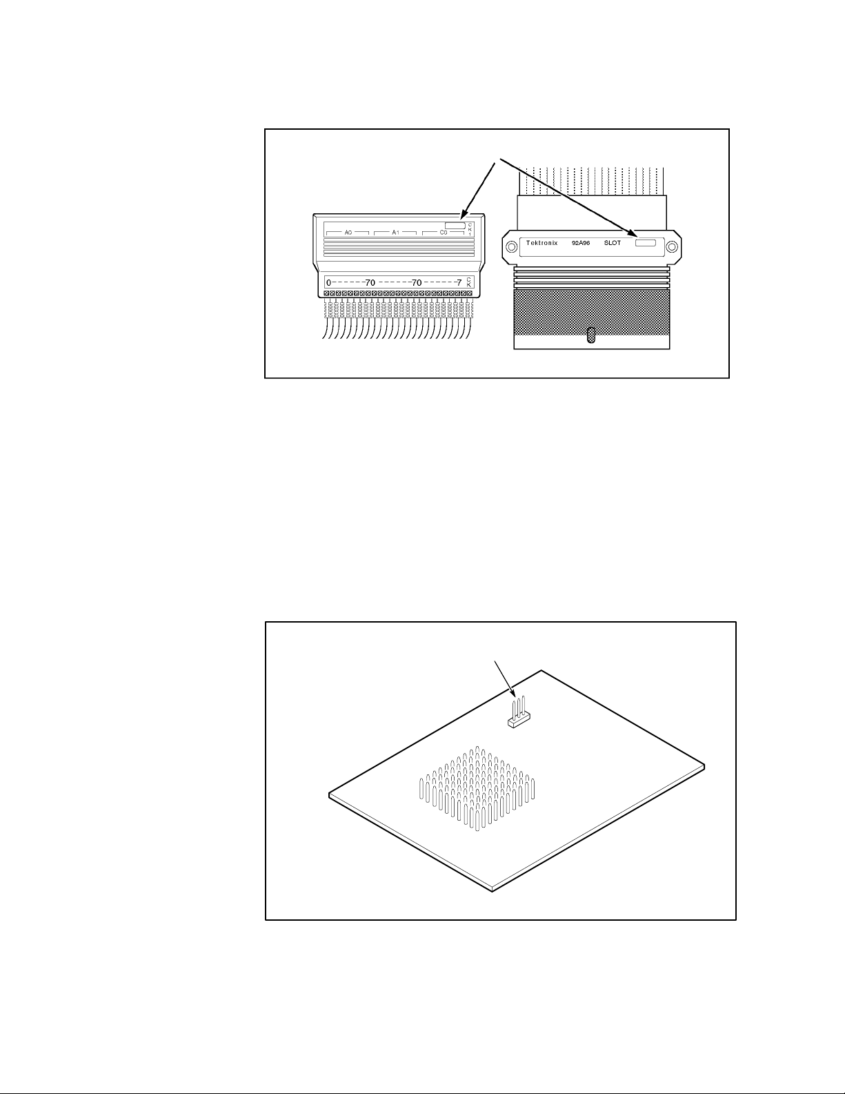
CONFIGURING THE PROBE ADAPTER
The Normal/Timing jumper (J1220) configures the probe adapter for
either normal operation or to acquire timing data. It should be placed in
the DISASM position to acquire state data, and in the TIMING position
to acquire timing data. (When acquiring timing data, the multiplexers
on the probe are held in “straight-through” mode; addresses are logged
with address bit A0 logged on A0:0, A1 logged on A0:1, A2 on A0:2,
and so on, regardless of what type of access is taking place.) Figure 2-2
shows the location of J1220 on the probe adapter.
J1220
Figure 2-2. Jumper location on the probe adapter.
92DM927 Am29205 Instruction Manual
Online Version
2-3
Page 17

Installation and Connections
CONNECTING TO THE SYSTEM UNDER TEST
Before you connect to the SUT, you must connect the standard probes
to the 92A96 Module card. Your SUT must also have a minimum
amount of clear space surrounding the microcontroller to accommodate
the probe adapter. Refer to Appendix C: Service Information for the
required clearances.
To connect the probe adapter to the SUT, do the following:
1. Turn off power to your SUT. It is not necessary to turn off the
DAS 9200.
CAUTION
Static discharge can damage the microcontroller, probe
adapter, podlets, or the 92A96 Module. To prevent static
damage, handle all the above only in a static-free
environment.
Always wear a grounding wrist strap, or a similar device,
while handling the microcontroller and probe adapter.
2. To discharge your stored static electricity, touch the ground jack
located on the back of the DAS 9200. Then, touch any of the
ground pins of the probe adapter to discharge stored static
electricity from the probe adapter.
3. Place the probe adapter onto the antistatic shipping foam to
support the probe as shown in Figure 2-3. This prevents the
circuit board from flexing.
4. Connect the clock and 8-channel probes to the probe adapter as
shown in Figure 2-3. Match the channel groups and numbers on
the interface housing to the corresponding pins on the probe
adapter.
2-4
92DM927 Am29205 Instruction Manual
Online Version
Page 18
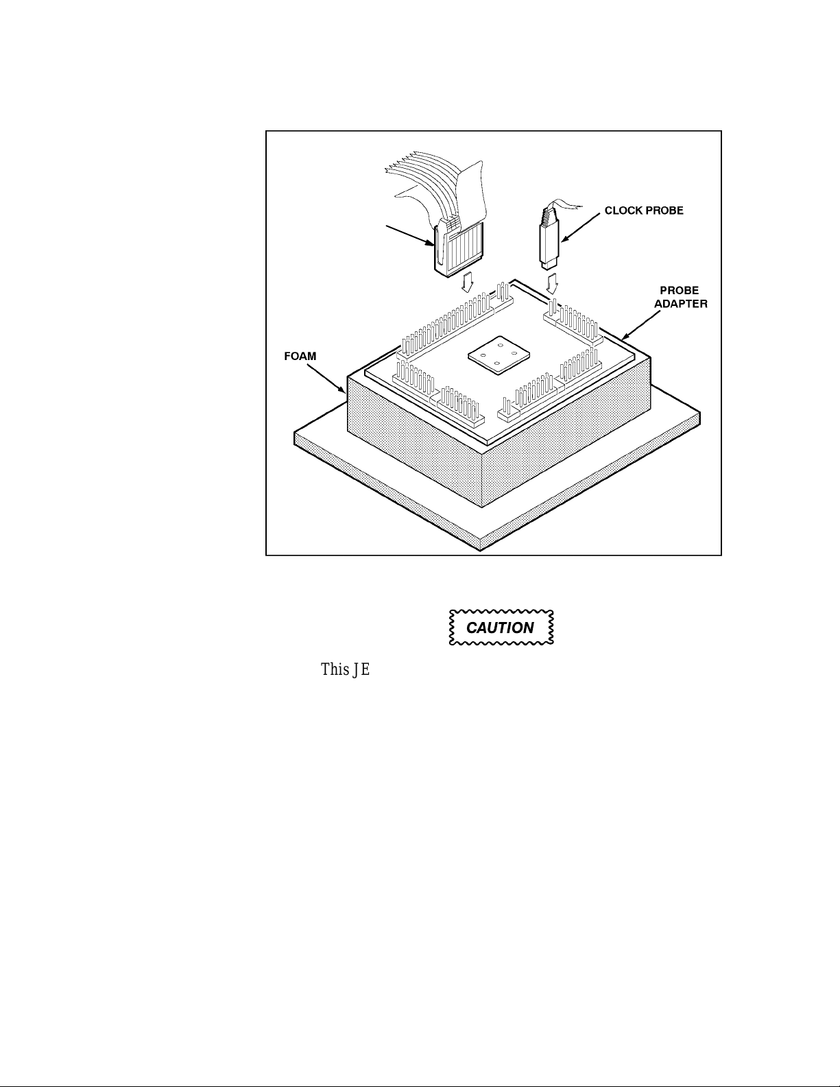
8-CHANNEL PROBE
Hold the 8-Channel Probes by
the podlet holder when connecting them to the probe
adapter. Do not hold them by
the cables or necks of the
podlets.
Installation and Connections
Figure 2-3. Connecting the podlets to a typical PQFP probe adapter.
CAUTION
This JEDEC PQFP (Plastic Quad Flat Pack) probe
adapter is equipped with a clip that has been designed for
tight tolerances.
The clip supports only Plastic Quad Flat Pack devices that
conform to the JEDEC M0-069 October 1990
specification. Attaching the clip to a device that does not
conform to this JEDEC standard can easily damage the
clip’s connection pins and/or the microcontroller, causing
the probe adapter to malfunction.
Please contact your IC manufacturer to verify that the
microcontroller you are targeting conforms to the JEDEC
specification.
For best performance and long probe life, exercise extreme
care when connecting the probe to the microcontroller.
92DM927 Am29205 Instruction Manual
Online Version
2-5
Page 19
Installation and Connections
5. Remove the probe adapter from the shipping foam and carefully
seat the PQFP100 converter clip on it, as shown in Figure 2-4.
Refer to the PQFP100 Converter Clip Instructions included with
the product for more information about the converter clip.
Hold the probe adapter in one
hand, align the PQFP converter
clip with the pins, and press on by
applying even pressure on all
sides of the clip; be sure clip is
completely seated.
PQFP100
CONVERTER
CLIP
Figure 2-4. Seating the converter clip on the probe adapter.
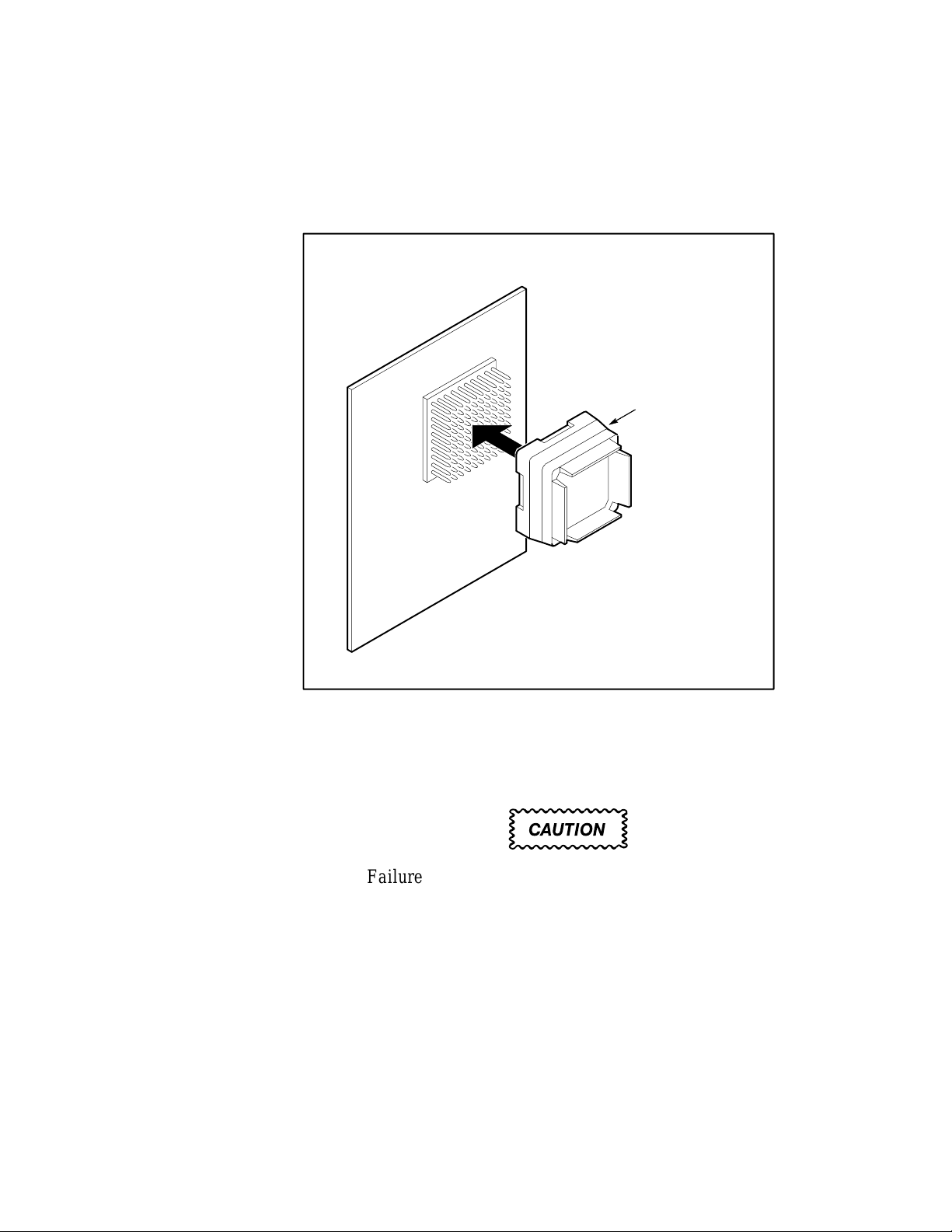
6. Line up the pin 1 indicator on the target head of the circuit board
(a white triangle) with the pin 1 indicator on the microcontroller.
CAUTION
Failure to correctly place the probe adapter onto the
microcontroller may permanently damage all electrical
components when power is applied.
Center the clip on the microcontroller and apply an equal
downward force on all four sides of the clip, slightly
rocking the adapter in a clockwise circle.
Do not leverage the probe adapter when installing or
removing the probe.
7. Place the probe adapter onto the SUT as shown in Figure 2-5.
2-6
92DM927 Am29205 Instruction Manual
Online Version
Page 20
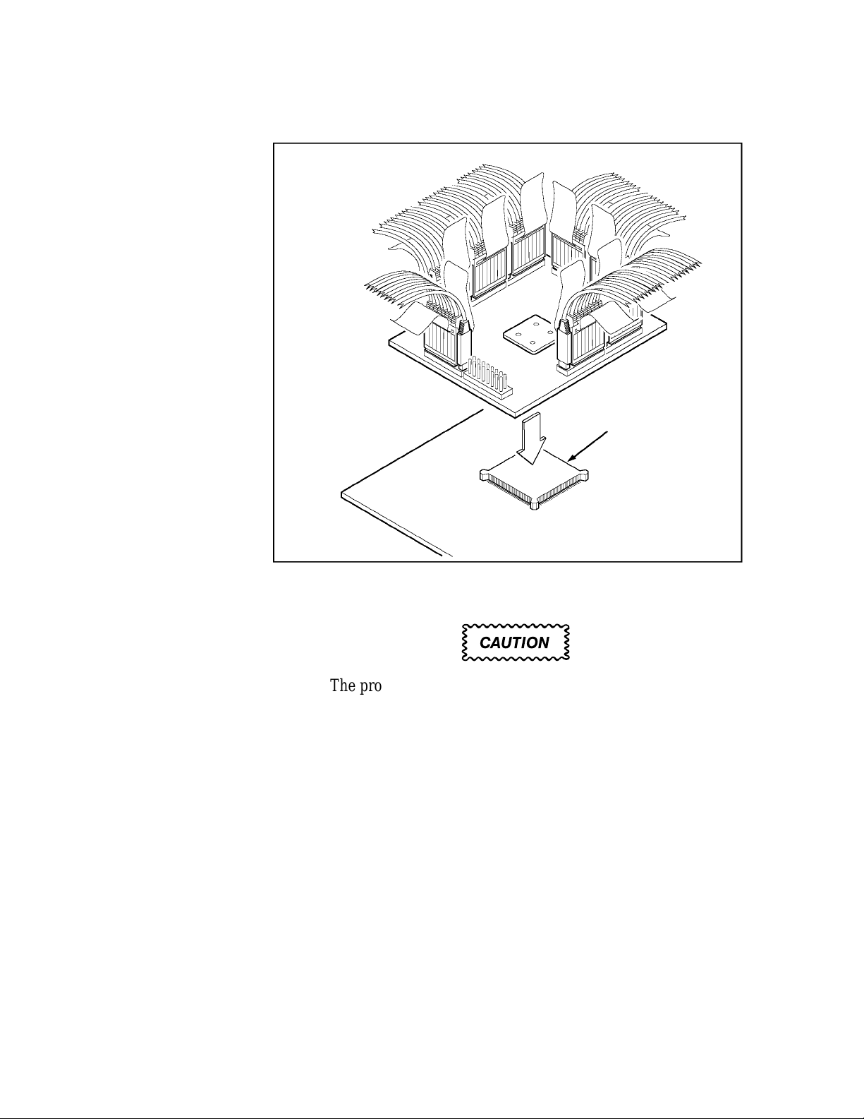
Installation and Connections
MICROCONTROLLER
Figure 2-5. Placing a typical PQFP probe adapter onto the SUT.
CAUTION
The probe adapter board may slip off or slip to one side
of the microcontroller because of the extra weight of the
podlets. This can damage the microcontroller and the
SUT. To prevent this from occurring, stabilize the probe
adapter by placing a nonconductive object (such as
foam) between the adapter and the SUT.
92DM927 Am29205 Instruction Manual
Online Version
2-7
Page 21

Section 3: SETTING UP SUPPORT SOFTWARE
This section provides information on preparing the support software for
acquiring data. The section discusses the following:
S
load support software
S
channel groups and assignments
S
changes that affect the data display
S
clocking options
S
symbols
S
triggering
Before you acquire and display data, you need to load support software
and specify setups for clocking, triggering, and using symbols. The
software provides default values for each of these setup controls, but
you can change them as needed.
LOADING SUPPORT SOFTWARE
To load the Am29205 support software, follow these steps:
1. Press the Menu Select key, select the appropriate 92A96 Module,
select its Configuration menu, and press Return.
2. Select 29205 in the Software Support field.
3. Press F8: EXECUTE OPERATION.
When you load the support software, the Channel, Clock, and Trigger
menus are automatically set up to acquire data from your Am29205
system. You can change the setups in the Clock and Trigger menus as
needed. Refer to Channel Groups and Assignments for information on
what can be changed in the Channel menu.
CHANNEL GROUPS AND ASSIGNMENTS
The support software automatically defines the channel groups for the
microcontroller. The channel groups for the Am29205 microcontroller
are the following:
ACCESS ADDRESS CONTROL DATA INTR MISC PRGRMIO
92DM927 Am29205 Instruction Manual
Online Version
3-1
Page 22

Setting Up Support Software
These channel groups cannot be changed nor can the channels be reused
in another group; however, you can define and display additional
groups. If you want to know which signal is in which group, refer to the
channel assignment tables in Appendix C: Service Information. Channel
assignments are also shown in the 92A96 Channel setup menu.
CHANGES THAT AFFECT THE DATA DISPLAY
You can change part of the default setups for the 92A96 Module.
However, keep in mind that if you change the threshold voltage or
display polarity, the displayed data will be affected.
CUSTOM CLOCKING
You can use the Clock menu to set clocking choices to control data
sampling. The 92DM927 support software offers a customized clocking
selection for the Am29205 microcontroller. This clocking choice
(Custom) is the default selection whenever you select 29205 Software
Support in the Configuration menu.
The 92DM927 support software provides two modes for acquiring
Am29205 data: DRAM Refresh Cycles Included or DRAM Refresh
Cycles Not Included. The default is DRAM Refresh Cycles Not
Included. You can change the clocking mode by changing the DRAM
Refresh Cycles option field in the Clock menu.
DRAM Refresh Cycle. A DRAM Refresh Cycle is defined as any RAS
signal before a CAS signal (implicit) Refresh that is not in the
background of another memory access.
Figure 3-1 shows the Clock menu. A description of how cycles are
sampled by the support software, probe adapter, and 92A96 is found in
Appendix B: How Data is Acquired.
3-2
92DM927 Am29205 Instruction Manual
Online Version
Page 23

Setting Up Support Software
Figure 3-1. Clock menu.
Refer to Section 5: General Purpose Analysis for a description of using
these other clock selections with this microcontroller support package.
To select the clocking mode, do the following:
1. Press the Select Menu key.
2. Select the Clock menu for the module you want to use.
3. Move the cursor to the DRAM Refresh Cycles field and select
one of the following types of clocking:
S
DRAM Refresh Cycles Not Included
S
DRAM Refresh Cycles Included
92DM927 Am29205 Instruction Manual
Online Version
3-3
Page 24

Setting Up Support Software
Á
Á
Á
Á
Á
Á
Á
Á
SYMBOLS
Symbols can be used to represent a specific channel group value or a
range of channel group values (defined by upper and lower bounds).
You can use symbol tables to display channel group information
symbolically in the State menu and to control triggering. There is a
symbol table file (named 29205_CTRL) supplied by the support
software that replaces specific Control channel group values.
Table 3-1 shows the name, bit pattern, and meaning for the symbols in
the 29205_CTRL file, the Control group symbol table.
Table 3-1
29205_CTRL Symbol Table Definitions
ÁÁÁÁÁББББББББББББББ
Control Group Value
PWE* PIAOE*
RESET* RSWE* CAS2*
ÁÁÁÁ
Symbol
ÁÁÁÁ
RESET
READ
WRITE
PARPRT_RD
PARPRT_WR
ББББББББББББББ
R_W* ROMOE* CAS3*
POE* PIAWE* RAS_D*
ББББББББББББББ
0 X X X X X X X X X X
1 1 1 1 X X X X X X X
1 0 1 1 X X X X X X X
1 X 0 1 1 1 1 1 1 1 1
1 X 1 0 1 1 1 1 1 1 1
X represents Don’t Care character.
ББББББББББ
ББББББББББ
Meaning
ББББББББББ
Reset
A ROM, DRAM, PIA, or DMA read
A ROM, DRAM, PIA, or DMA write
A parallel port read
A parallel port write
3-4
92DM927 Am29205 Instruction Manual
Online Version
Page 25

БББББББББББББ
ÁÁÁÁ
Á
Á
Á
Á
Á
Á
БББББББББББББ
Á
Á
Á
БББББББББББББ
БББББББББББББ
БББББББББББББ
БББББББББББББ
БББББББББББББ
БББББББББББББ
БББББББББББББ
БББББББББББББ
БББББББББББББ
Á
Á
БББББББББББББ
Á
БББББББББББББ
БББББББББББББ
БББББББББББББ
БББББББББББББ
БББББББББББББ
БББББББББББББ
БББББББББББББ
БББББББББББББ
БББББББББББББ
Á
Á
БББББББББББББ
Á
БББББББББББББ
БББББББББББББ
БББББББББББББ
БББББББББББББ
БББББББББББББ
ÁÁÁÁ
Symbol
ÁÁÁÁ
DMA1
DMA1_RFB3
DMA1_RFB2
DMA1_RFB1
DMA1_RFB0
Table 3-2 shows the name, bit pattern, and meaning for the symbols in
the 29205_ACCS file, the Access group symbol table.
Table 3-2
29205_ACCS Symbol T able Definitions
Access Group Value
ББББББББББББББ
RAS3* ROMCS2* PIACS0*
ББББББББББББББ
RAS2* ROMCS1* DACK1*
RAS1* ROMCS0* CAS_L*
ББББББББББББББ
1 1 1 1 1 1 1 X X 0 X
0 1 1 1 1 1 1 X X 0 0
1 0 1 1 1 1 1 X X 0 0
1 1 0 1 1 1 1 X X 0 0
1 1 1 0 1 1 1 X X 0 0
RAS0* PIACS1*
Setting Up Support Software
ББББББББББББ
ББББББББББББ
Meaning
ББББББББББББ
DMA access
DMA with DRAM bank 3 refresh
DMA with DRAM bank 2 refresh
DMA with DRAM bank 1 refresh
DMA with DRAM bank 0 refresh
PIA0
PIA0_RFB3
PIA0_RFB2
PIA0_RFB1
PIA0_RFB0
ÁÁÁÁ
PIA1
PIA1_RFB3
PIA1_RFB2
PIA1_RFB1
PIA1_RFB0
ROM0
ROM0_RFB3
ROM0_RFB2
ROM0_RFB1
ROM0_RFB0
ÁÁÁÁ
ROM1
ROM1_RFB3
ROM1_RFB2
ROM1_RFB1
ROM1_RFB0
1 1 1 1 1 1 1 1 0 1 X
0 1 1 1 1 1 1 1 0 1 0
1 0 1 1 1 1 1 1 0 1 0
1 1 0 1 1 1 1 1 0 1 0
1 1 1 0 1 1 1 1 0 1 0
ББББББББББББББ
1 1 1 1 1 1 1 0 1 1 X
0 1 1 1 1 1 1 0 1 1 0
1 0 1 1 1 1 1 0 1 1 0
1 1 0 1 1 1 1 0 1 1 0
1 1 1 0 1 1 1 0 1 1 0
1 1 1 1 1 1 0 1 1 1 X
0 1 1 1 1 1 0 1 1 1 0
1 0 1 1 1 1 0 1 1 1 0
1 1 0 1 1 1 0 1 1 1 0
1 1 1 0 1 1 0 1 1 1 0
ББББББББББББББ
1 1 1 1 1 0 1 1 1 1 X
0 1 1 1 1 0 1 1 1 1 0
1 0 1 1 1 0 1 1 1 1 0
1 1 0 1 1 0 1 1 1 1 0
1 1 1 0 1 0 1 1 1 1 0
PIA bank 0 access
PIA bank 0 with DRAM bank 3 refresh
PIA bank 0 with DRAM bank 2 refresh
PIA bank 0 with DRAM bank 1 refresh
PIA bank 0 with DRAM bank 0 refresh
ББББББББББББ
PIA bank 1 access
PIA bank 1 with DRAM bank 3 refresh
PIA bank 1 with DRAM bank 2 refresh
PIA bank 1 with DRAM bank 1 refresh
PIA bank 1 with DRAM bank 0 refresh
ROM bank 0 access
ROM bank 0 with DRAM bank 3 refresh
ROM bank 0 with DRAM bank 2 refresh
ROM bank 0 with DRAM bank 1 refresh
ROM bank 0 with DRAM bank 0 refresh
ББББББББББББ
ROM bank 1 access
ROM bank 1 with DRAM bank 3 refresh
ROM bank 1 with DRAM bank 2 refresh
ROM bank 1 with DRAM bank 1 refresh
ROM bank 1 with DRAM bank 0 refresh
X represents Don’t Care character.
92DM927 Am29205 Instruction Manual
Online Version
3-5
Page 26

Setting Up Support Software
БББББББББББББ
Á
Á
Á
Á
БББББББББББББ
Á
Á
БББББББББББББ
БББББББББББББ
БББББББББББББ
Á
Á
БББББББББББББ
Á
БББББББББББББ
БББББББББББББ
БББББББББББББ
БББББББББББББ
БББББББББББББ
БББББББББББББ
БББББББББББББ
БББББББББББББ
БББББББББББББ
Á
Á
БББББББББББББ
Á
ÁÁÁÁ
ÁÁÁÁ
Symbol
RAS3* ROMCS2* PIACS0*
ББББББББББББББ
RAS2* ROMCS1* DACK1*
ББББББББББББББ
RAS1* ROMCS0* CAS_L*
Table 3-2 (continued)
29205_ACCS Symbol T able Definitions
Access Group Value
RAS0* PIACS1*
ББББББББББББ
ББББББББББББ
Meaning
ROM2
ROM2_RFB3
ROM2_RFB2
ROM2_RFB1
ÁÁÁÁ
ROM2_RFB0
DRAM_BNK3
DRAM_BNK2
DRAM_BNK1
DRAM_BNK0
REFRESH_3
REFRESH_2
REFRESH_1
REFRESH_0
IDLE_ADDR
ÁÁÁÁ
1 1 1 1 0 1 1 1 1 1 X
0 1 1 1 0 1 1 1 1 1 0
1 0 1 1 0 1 1 1 1 1 0
1 1 0 1 0 1 1 1 1 1 0
ББББББББББББББ
1 1 1 0 0 1 1 1 1 1 0
0 1 1 1 1 1 1 1 1 1 1
1 0 1 1 1 1 1 1 1 1 1
1 1 0 1 1 1 1 1 1 1 1
1 1 1 0 1 1 1 1 1 1 1
0 1 1 1 1 1 1 1 1 1 0
1 0 1 1 1 1 1 1 1 1 0
1 1 0 1 1 1 1 1 1 1 0
1 1 1 0 1 1 1 1 1 1 0
1 1 1 1 1 1 1 1 1 1 X
ББББББББББББББ
X represents Don’t Care character.
Refer to Triggering in this section and Displaying Channel Groups
Symbolically in Section 4 for more information on using and displaying
symbolic values. Refer also to Searching Through Data in Section 4 for
information on how to use symbol table values for data searches.
ROM bank 2 access
ROM bank 2 with DRAM bank 3 refresh
ROM bank 2 with DRAM bank 2 refresh
ROM bank 2 with DRAM bank 1 refresh
ББББББББББББ
ROM bank 2 with DRAM bank 0 refresh
DRAM bank 3 access
DRAM bank 2 access
DRAM bank 1 access
DRAM bank 0 access
DRAM bank 3 refresh
DRAM bank 2 refresh
DRAM bank 1 refresh
DRAM bank 0 refresh
No access to ROM, DRAM, DMA, or
ББББББББББББ
PIA address space during this cycle
3-6
92DM927 Am29205 Instruction Manual
Online Version
Page 27

Setting Up Support Software
Copying and Editing the Predefined Symbol Tables. You cannot
directly edit any symbol tables supplied by microcontroller support. But
you can make a copy of a predefined symbol table and then edit the
copy for your specific use.
To create a new symbol table, follow these steps:
1. Select the Symbol Editor menu from the Menu Selection overlay.
2. Press F2: FILE FUNCTIONS.
3. Select Open File in the Function field, and press Return.
4. Select New File in the Edit Status field, and press Return.
5. Enter a new symbol table file name in the New File Name field.
6. Select Pattern or Range in the Table Type field to match the
symbol table you are copying, and press Return.
7. Press F5: EXECUTE FUNCTION.
8. Select Merge Files in the Function field, and press Return.
9. Select the file to base your new symbol table on, such as the
29205_CTRL file.
10. Press F5: EXECUTE FUNCTION.
11. Press F8: EXIT & SAVE.
12. Edit the file as desired keeping the following in mind:
S
If the new symbol has fewer don’t cares than an existing
symbol, it must be placed ahead of the existing symbol.
S
If the new symbol has more don’t cares than an existing
symbol, it must be placed after the existing symbol.
S
Do not duplicate symbol names.
Also refer to your DAS 9200 System User Manual for more
information on editing the symbol table.
13. Select the Channel menu from the Menu Selection overlay.
14. Change the file name of the symbol table for the Control group
(or whichever group’s symbol table you are replacing) to the one
that you specified in step 5.
92DM927 Am29205 Instruction Manual
Online Version
3-7
Page 28

Setting Up Support Software
TRIGGERING
All the Trigger menu selections available for use with your 92A96
Module are also available for use with state data analysis. Refer to your
module user manual for a list and description of these selections.
You can use the Home key to quickly clear the word recognizer field of
any channel group with a symbolic radix. To clear a word recognizer,
open the field, press the Home key, and close the field. The first entry
on the list is blank.
The DAS 9200 makes it possible to cross-trigger with other modules or
to an external instrument. You may want to consider sending or
receiving a signal to or from another module, or to the Sync Out SMB
connector on the module. You should refer to your DAS 9200 System
User Manual for an in-depth description of defining and using signals,
and to specific module user manuals for a description of using the Sync
Out SMB connector.
3-8
92DM927 Am29205 Instruction Manual
Online Version
Page 29

Section 4: ACQUIRING AND VIEWING DATA
This section describes how to acquire data and view it in the State
display. This section explains:
S
acquiring data
S
viewing data
S
displaying groups symbolically
S
searching through data
S
printing data
S
viewing the demonstration reference memory
ACQUIRING DATA
Once you load the Am29205 support, choose a clocking mode and
specify the trigger, you are ready to acquire data. Press the F1: START
acquisition key to begin the acquisition. You can press the F1: STOP
key at any time to stop acquisition.
If you have any problems acquiring data, refer to Appendix A: Error
Messages and Acquisition Problems.
VIEWING STATE DATA
The 92A96 Module displays state data in the State display. This display
shows the bus cycles with addresses, data, and other channel group
values if selected. Figure 4-1 shows an example of Am29205 data.
92DM927 Am29205 Instruction Manual
Online Version
4-1
Page 30

Acquiring and Viewing Data
Figure 4-1. Am29205 data in the State display using Custom clocking.
You can select a display format and tailor it for your application using
the State Format Definition overlay. Refer to your 92A96 Module User
Manual for a detailed description of the selections available in this
overlay, such as adding the Timestamp group.
Displaying Channel Groups Symbolically
Any channel group can be displayed as symbolic values in the State
menu similar to the way the Control group can be displayed as
symbolic values in the State menu. You can use the Symbol Editor
menu to create symbol tables in which symbols are assigned to various
channel group values (ranges or patterns). You can then change the
radix of the channel group in the State menu using the State Format
Definition overlay, and select the symbol table you created to use for
display or triggering purposes.
4-2
92DM927 Am29205 Instruction Manual
Online Version
Page 31

Acquiring and Viewing Data
Searching Through Data
You can define data patterns you want to search for in the State display
by using the State Search Definition overlay. To access this overlay,
press F6: DEFINE SEARCH from the State menu.
To define and execute a search, follow these steps:
1. Press F6: DEFINE SEARCH from the State display menu to
access the State Search Definition overlay.
2. Define the type of search and values on which to search.
3. Press F8: EXIT & SAVE.
4. Press either F8: SEARCH FORWARD or F7: SEARCH
BACKWARD to start the search.
5. To abort a search, press the Break key.
Figure 4-2 shows the State Search Definition overlay.
1
2
3
Figure 4-2. State Search Definition overlay.
92DM927 Am29205 Instruction Manual
Online Version
4-3
Page 32

Acquiring and Viewing Data
1
Search Type. Selects the type of search you want to perform; to
search for data values, use the Value selection.
2
Search Value. Specifies the value for which you want to search.
You cannot search by symbol names for any group with a symbol
table. For the Control group, you should search on binary values.
Refer to the Control group symbol table in Section 3 to see the
symbols for the Control group and their binary values.
3
Search Range. Specifies the lower- and upper-bound sequences
of the range you want to search. The default value is the entire
acquisition memory.
Function Keys
F1: ESCAPE & CANCEL. Closes the overlay and discards any
changes you have made since entering it.
F4: LOAD FROM CURSOR. Loads the data values from the
sequence the cursor is on (corresponding to the main module) to the
search value fields for the channel groups. Don’t care (Xs) mask entries
are not retained.
F5: LOAD MASK CURSOR. Loads the data values (including mask
entries) from the sequence the cursor is on (corresponding to the main
module) to the search value fields for the channel groups. Don’t care
(Xs) mask entries are retained.
F8: EXIT & SAVE. Exits the overlay and executes or saves any
changes made.
4-4
92DM927 Am29205 Instruction Manual
Online Version
Page 33

Acquiring and Viewing Data
PRINTING DATA
To print state data, use the State Table Print overlay. To access this
overlay, press the Shift and Print keys at the same time from the State
menu. Refer to your DAS 9200 System User Manual for a detailed
description of the selections available in this overlay.
REFERENCE MEMORY
A demonstration reference memory file is provided so you can see an
example of how your Am29205 microcontroller instruction mnemonics
look when they are displayed. A symbol table for the Address group of
the demonstration reference memory is also provided so you can see an
example of range symbols. Viewing the reference memory is not a
requirement for preparing the 92A96 Module for use. You can view the
reference memory file without connecting the DAS 9200 to your SUT.
To view the 29205_Demo Refmem, follow these steps:
1. Press the Select Menu key and select the 29205_Demo file from
the Refmem column.
2. Select the State menu, and press Return.
92DM927 Am29205 Instruction Manual
Online Version
4-5
Page 34

Section 5: GENERAL PURPOSE ANALYSIS
You may need to perform general purpose (timing) analysis on your
Am29205 system prior to, during, and after attempting to integrate your
software with the Am29205 system hardware. When performing
hardware analysis, you will want to use the data acquisition module to
acquire data with a finer resolution. When more data samples are taken
in a given period of time, the resolution in the Timing display increases,
letting you see signal activity that would otherwise go undetected.
This section provides information on the following:
S
clocking
S
triggering
S
displaying data
S
supplied Timing Format Definition file
To acquire and display timing data, you need to change the clocking
selection and trigger program, acquire data, and view it in the Timing
menu. A predefined Timing Format Definition overlay file called
29205_96 can be used to view Am29205 timing data. A description of
these files and how to use them can be found later in this section.
There often is a need to view data in a split screen display with state
data in one half and timing data in the other. Do not disconnect any of
the 92A96 probe cables or interface housings if you are analyzing data
in this manner. Instead, use the extra channels available from the 92A96
Module to make other Am29205 system connections.
CLOCKING
To change the data sampling rate, use the Clock menu.
The Normal/Timing jumper, J1220, on the probe adapter should be set
in the Timing position to acquire timing data. For more information on
the Normal/Timing jumper, refer to Section 2.
When using the 92A96 Module for timing analysis, you will want to
use the Internal or External clocking modes. The Internal clock
selection can sample data up to 100 MHz, which has a 10 ns resolution
between samples. The External clock selection samples data on every
active clock edge on the 92A96 clock inputs up to 100 MHz.
92DM927 Am29205 Instruction Manual
Online Version
5-1
Page 35

General Purpose Analysis
The Clock menu is shown in Figure 3-1. The default clocking mode is
Custom when microcontroller support is used; you will need to change
it to either Internal or External. Your 92A96 Module User Manual
contains an in-depth description of Internal and External clocking.
Custom Clocking
Custom clocking only stores one data sample for each bus transaction,
which can take one or more clock cycles. Custom clocking also
time-aligns certain signals that otherwise would be skewed relative to
the current bus transaction. This clocking selection is generally
unproductive for timing analysis. Refer to Appendix B for a more
in-depth description of how Custom clocking is used with the probe
adapter to acquire data.
Internal Clocking
When you select Internal as the clocking mode, the 92A96 Module
stores one data sample as often as every 10 ns (100 MHz). This
clocking selection is commonly referred to as asynchronous.
Two typical uses of Internal clocking might be to verify that all the
Am29205 signals are transitioning as expected or to measure timing
relationship between signal transitions.
It is possible to acquire asynchronous data at rates of 200 MHz and
400 MHz. The faster the 92A96 Module acquires data, the fewer
channels it can acquire data on. A single 92A96 Module can acquire
data on 24 channels at 400 MHz or 2.5 ns resolution. Refer to your
92A96 Module User Manual for information on sampling data at speeds
faster than 100 MHz.
External Clocking
When you select External as the clocking mode, the 92A96 Module
acquires and stores data based on the clock channel up to 100 MHz.
This clocking selection is commonly referred to as synchronous.
By selecting the rising edge of CLK: 3 on the acquisition module as the
clock channel, and turning off the remaining three clocks, the module
will sample data on every rising edge of the clock. No data is acquired
on the falling clock edge unless you select both edges.
You can also use the other three clock channels as qualifiers or clocks to
further modify the clocking in of information from your Am29205
system.
5-2
92DM927 Am29205 Instruction Manual
Online Version
Page 36

General Purpose Analysis
TRIGGERING
All the Trigger menu selections available for use with the 92A96
Module are still available for use with timing analysis. Refer to your
module user manual for a list and description of the selections.
ACQUIRING DATA
You can acquire data as described in the Acquiring Data description in
Section 4. The Normal/Timing jumper, J1220, on the probe adapter
should be set in the Timing position to acquire timing data. For more
information on the Normal/Timing jumper, refer to Section 2.
DISPLAYING DATA
General purpose analysis requires that you view data in either the State
or Timing menus. The following discussion describes these menus.
Timing Menu
In the Timing menu, every channel is shown as a waveform, and groups
of channels are shown as bus forms.
A predefined Timing Format Definition overlay file, part of the
Am29205 microcontroller support, is available for you to use when
displaying data in the Timing format. The 29205_96 file is installed on
the DAS 9200 with the support software.
The 29205_96 Timing Format file places the Am29205 system clock
first followed by the Address and Data groups displayed as bus forms
containing bus values instead of as individual timing waveforms. These
groups are followed by other important control signals. Figure 5-1
shows data displayed using the 29205_96 file.
To select the supplied Timing Format Definition file, follow these steps:
1. Select the Timing menu and press F5: DEFINE FORMAT.
2. Press F5: RESTORE FORMAT.
3. Select 29205_96, and press the Return key. A message tells you
the format file is selected.
4. Press F8: EXIT & SAVE to return to the Timing menu.
Refer to the channel assignment tables in Appendix C for the lists of
individual channels and their Am29205 signal names.
92DM927 Am29205 Instruction Manual
Online Version
5-3
Page 37

General Purpose Analysis
Figure 5-1. Timing data using the 29205_96 Timing Format file.
State Menu
In the State menu, all channel group values are shown based on the
selected radix in the Channel menu or the State Format Definition
overlay. This menu shows the bus cycles with addresses, data, and other
group values if selected.
If you want to display other channel groups (such as Misc), access the
State Format Definition overlay and change the radix for the group
from Off to Hex, Bin, or Oct. This overlay also allows you to add the
Timestamp group (and change the radix) to the data display.
5-4
92DM927 Am29205 Instruction Manual
Online Version
Page 38

General Purpose Analysis
SEARCHING THROUGH DATA
To search through data, you can use either the Timing Search Definition
overlay or the State Search Definition overlay. You can use these
overlays and search through data as described in your 92A96 Module
User Manual.
Before performing a search in the Timing menu, be sure to check the
State Format Definition overlay and make sure the channels on which
you want to conduct the search will be displayed (radix is not Off).
Channels in the TIming menu cannot be searched on unless they can
also be displayed in the State menu.
PRINTING DATA
To print state data, you can use the State Table Print overlay. To access
this overlay, press the Shift and Print keys at the same time from the
State menu.
To print timing data, you can use the Timing Print overlay. To access
this overlay, press the Shift and Print keys at the same time from the
Timing menu.
For detailed information on the State Table Print overlay or the Timing
Print overlay, refer to your 92A96 Module User Manual.
92DM927 Am29205 Instruction Manual
Online Version
5-5
Page 39

Appendix A: ERROR MESSAGES AND ACQUISITION
PROBLEMS
This appendix describes error messages and problems that you may
encounter while acquiring data.
MODULE ERROR MESSAGES
These error messages will appear in the Module Monitor menu when
there are problems with acquiring data or satisfying the trigger
program. The error messages are listed in alphabetical order; a
description of the error message and the recommended solution follow
the error message.
Slow Clock. This message appears when the active clock channel (or
channels) is not changing, is typically changing at 1 ms or slower
intervals, or one of the clock qualifiers is held in the wrong state. Check
for the following:
1. The Am29205 system is powered on and running. Be sure the
system is not halted.
2. 29205 Support is selected in the appropriate 92A96
Configuration menu.
3. Custom is selected in the Clock menu.
4. The connections between the 92A96 Module and the probe
adapter are correct.
S
The clock and 8-channel probe connections between the
interface housings and probe adapter are correct (module
name, clock, section names, and channel numbers match), are
properly oriented (GND connects to ground), and are fully
engaged.
S
The connections between the interface housings and 92A96
probe cables have matched color labels, matched slot
numbers, and are properly keyed.
S
The connections between the 92A96 probe cables and probe
connectors have matched color labels, matched slot numbers,
and are properly keyed.
5. The orientation of pin 1 on the microcontroller, the probe
adapter, and SUT are correct
6. No bent or missing pins on the Am29205 microcontroller or on
either of the probe adapter sockets.
7. The Normal/Timing jumper is in the DISASM position.
92DM927 Am29205 Instruction Manual
Online Version
A-1
Page 40

Error Messages and Acquisition Problems
Waiting for Stop. This message appears when the trigger condition is
satisfied and memory is full but the Manual Stop mode is selected in
the Cluster Setup menu. The solution is to manually stop the DAS 9200
by pressing F1: STOP.
This message can also appear when other modules in the cluster have
not filled their memories. Wait for the other modules to fill their
memories. If the message does not disappear in a short time, press
F1: STOP.
Waiting for Stop-Store. This message appears when the trigger
condition is satisfied but the amount of post-fill memory specified in
the trigger position field is not yet filled. Press F1: STOP to view the
acquired data, then check for the following:
1. The trigger program in the Trigger menu is correct.
2. The storage qualification in the Trigger menu is correct.
3. The system or the module does not have an exception or fault.
The Am29205 system or acquisition module might have
experienced a hardware or software exception or fault after the
trigger condition was satisfied.
Waiting for Trigger. This message appears when the trigger condition
does not occur. Check for the following:
1. The Am29205 system is powered on and running. Be sure the
system is not halted.
2. The trigger conditions are not being satisfied. The Module
Monitor menu shows which state events are not occurring. Press
F1: STOP, access the Trigger menu, and redefine the conditions
for that state. Also refer to the description on Triggering in
Section 3.
ACQUISITION PROBLEMS
There may be problems for which no error messages are displayed.
Some of these problems and their recommended solutions follow.
Incorrect Data. If the data acquired is obviously incorrect, check the
following:
1. 29205 Support is selected in the 92A96 Configuration menu.
2. Custom is selected in the Clock menu.
3. The Normal/Timing jumper is in the DISASM position.
A-2
92DM927 Am29205 Instruction Manual
Online Version
Page 41

Error Messages and Acquisition Problems
4. The connections between the 92A96 Module and the probe
adapter are correct.
S
The clock and 8-channel probe connections between the
interface housings and probe adapter are correct (module
name, clock, section names, and channel numbers match), are
properly oriented (GND connects to ground), and are fully
engaged.
S
The connections between the interface housings and 92A96
probe cables have matched color labels, matched slot
numbers, and are properly keyed.
S
The connections between the 92A96 probe cables and probe
connectors have matched color labels, matched slot numbers,
and are properly keyed.
5. The orientation of pin 1 on the microcontroller, the probe
adapter, and SUT are correct.
6. No bent or missing pins on the Am29205 microcontroller or on
either of the probe adapter sockets.
Other Suggestions. If the previous suggestions do not fix the problem
with acquiring data, try the following:
1. Reload the module setup; select 29205 Support in the 92A96
Configuration menu to restore the DAS 9200 to a known state.
2. Possible AC and DC loading problems may be remedied by
removing one or both of the protective sockets from the probe
adapter. These sockets may add enough additional inductance to
your Am29205 system to affect it. Refer to Appendix C for a
description to remove sockets from the probe adapter.
If the DAS 9200 still is not acquiring data after trying these solutions,
there may be a problem with your Am29205 system. Try performing
hardware analysis with your DAS 9200 system to ensure that the
Am29205 signals are valid at the time the probe adapter samples them.
Refer to Section 5: General Purpose Analysis for information on data
sampling rates using either the Internal or External clocking selections
in the Clock menu. Also refer to Appendix B: How Data is Acquired to
see when the support software, probe adapter, and 92A96 Module
sample the various Am29205 system signals.
92DM927 Am29205 Instruction Manual
Online Version
A-3
Page 42

Appendix B: HOW DATA IS ACQUIRED
This appendix explains how the 92A96 Module acquires Am29205
signals using the 92DM927 probe adapter and software. This appendix
also provides additional information on microcontroller signals
accessible on or not accessible on the probe adapter, and on extra
92A96 channels available for you to use for additional connections.
92A96 CUSTOM CLOCKING
A special clocking program (called Custom) is loaded to the 92A96
Module every time the Am29205 Software Support is selected in the
Configuration menu. With Custom clocking, the module logs in signals
from multiple groups of channels at different times when they are valid
on the Am29205 bus. The module then sends all the logged-in signals
to the trigger machine and to the acquisition memory of the module for
storage.
In Custom clocking, the module’s clocking state machine (CSM)
generates one master sample for each Am29205 bus cycle, no matter
how many clock cycles are contained in that cycle.
ROM, PIA, or DMA Access
ROM, PIA, and DMA accesses can be extended by the WAIT* signal
and can be of different lengths depending on the WSx, IOWAITx, and
DMAWAITx bits in the internal registers. Because of this, the CSM
waits until the control signal disappears to identify the end of the cycle.
Figure B-1 shows the strobe points and the master sample for ROM,
PIA, and DMA accesses.
MEMCLKMEMCLK
PIAOE*,
PIAWE*,
ROMOE*,
OR RSWE*
STROBE ALL CHANNELS
MASTER
SAMPLE
Figure B-1. Am29205 bus timing (ROM, PIA, and DMA accesses).
92DM927 Am29205 Instruction Manual
Online Version
B-1
Page 43

How Data is Acquired
Parallel Port Access
The CSM creates a master strobe after the first rising edge of
MEMCLK after POE* or PWE* are asserted. Figure B-2 shows the
master sample for parallel port accesses.
MEMCLKMEMCLK
FIRST RISING EDGE
POE*
OR PWE*
STROBE ALL CHANNELS
AND MASTER SAMPLE
Figure B-2. Am29205 bus timing (parallel port accesses).
DRAM Access
Because DRAM accesses are fixed at four cycles, the CSM creates a
master strobe after the third rising edge of MEMCLK while a RASx*
signal is asserted. Figure B-3 shows the master sample for DRAM
accesses.
MEMCLKMEMCLK
THIRD RISING EDGE
RAS3*,
RAS2*,
RAS1*,
OR RAS0*
STROBE ALL CHANNELS
AND MASTER SAMPLE
Figure B-3. Am29205 bus timing (DRAM accesses).
B-2
92DM927 Am29205 Instruction Manual
Online Version
Page 44

How Data is Acquired
CLOCKING OPTIONS
The 92A96 clocking algorithm for the Am29205 microcontroller has
two variations: DRAM Refresh Cycles Excluded, and DRAM Refresh
Cycles Included.
DRAM Refresh Cycles Excluded
DRAM Refresh cycles are not acquired or displayed.
DRAM Refresh Cycles Included
All bus cycles, including DRAM refresh cycles, are logged in.
ALTERNATE MICROCONTROLLER CONNECTIONS
You can connect to microcontroller signals that are not required by the
support software so you can do more advanced timing analysis. These
signals may or may not be accessible on the probe adapter board. The
following paragraphs and tables list signals that are accessible on or are
not accessible on the probe adapter board.
For a list of signals required or not required by the support software,
refer to the channel assignment tables in Appendix C.
Signals On the Probe Adapter
The probe adapter board contains pins for microcontroller signals that
are not acquired by the 92DM927 software. You can connect extra
podlets to these pins, because they can be useful for general purpose
analysis. However, these signals are not defined in the Channel setup
menu; you must enter the Channel setup menu and assign those signals
to a new channel group.
Table B-1 shows the microcontroller signals available on the probe
adapter’s square pin grid; the rest of the microcontroller signals on the
grid are connected to the probe adapter. Refer to the PQFP100
Converter Chip Instructions included with this product for a pin
number locator diagram.
92DM927 Am29205 Instruction Manual
Online Version
B-3
Page 45

How Data is Acquired
Table B-1
Am29205 Signals On Square Pin Grid
Pin No.
4 INCLK
76 PAUTOFD
93 PSYNC
92 VDAT
99 VCLK
100 LSYNC
26 RXD
28 TXD
27 UCLK
Signal Name
Figure B-4 shows the square pin grid on the probe adapter.
SQUARE PIN GRID
B-4
Figure B-4. Square pin grid location on the pr obe adapter.
Signals Not On the Probe Adapter
All Am29205 microcontroller signals are accessible on the probe
adapter.
Extra 92A96 Channels
After connecting the 92A96 probes to the probe adapter, there are no
extra 92A96 channels available for you to use to make alternate SUT
connections. However, you can disconnect channels not required by the
support software to make alternate connections. The channel
assignment tables in Appendix C indicate channels not required by the
support software.
92DM927 Am29205 Instruction Manual
Online Version
Page 46

WARNING
The following servicing instructions are for use only by qualified
personnel. To avoid personal injury, do not perform any servicing
other than that contained in the operating instructions unless you
are qualified to do so. Refer to the General Safety Summary and the
Servicing Safety Summary prior to performing any service.
Page 47

Appendix C: SERVICE INFORMATION
This appendix contains the following information:
S
safety summary
S
brief description of the probe adapter and how it works
S
care and maintenance procedures
S
channel assignment tables
S
dimensions of the probe adapter
S
removing and replacing individual signal leads
S
removing and replacing sockets
SERVICING SAFETY INFORMATION
The following servicing safety information is for service technicians.
Follow these safety precautions, along with the general precautions
outlined in your DAS 9200 System User Manual, while installing or
servicing this product.
Do Not Service Alone. Do not perform internal service or adjustment
on this product unless another person is present and able to give first
aid and resuscitation.
Use Care When Servicing With Power On. To avoid personal injury
from dangerous voltages, remove jewelry such as rings, watches, and
other metallic objects before servicing. Do not touch the product’s
exposed connections and components while power is on.
92DM927 Am29205 Instruction Manual
Online Version
C-1
Page 48

Service Information
PROBE ADAPTER DESCRIPTION
The probe adapter is a nonintrusive piece of hardware that allows the
92A96 to acquire data from an Am29205 microcontroller in its own
operating environment with little affect, if any, on that system. Refer to
Figure C-1 while reading the following discussion.
C-2
PROBE
ADAPTER
Figure C-1. Overview of the standard probe and probe adapter.
The probe adapter consists of a circuit board and a socket for the
Am29205 microcontroller. The probe adapter connects to the SUT.
Signals from the Am29205 system flow from the probe adapter to the
podlet groups. The signals flow through the probe signal leads to the
92A96 Module.
All circuitry on the probe adapter is powered from the SUT (system
under test).
The probe adapter accommodates the AMD Am29205 microcontroller
in a 100-pin PQFP package.
92DM927 Am29205 Instruction Manual
Online Version
Page 49

Service Information
Configuring the Probe Adapter
The Normal/Timing jumper (J1220) should be placed in the DISASM
position to acquire state data, and in the TIMING position to acquire
timing data. (When acquiring timing data, the multiplexers on the probe
are held in “straight-through” mode; addresses are logged with address
bit A0 logged on A0:0, A1 logged on A0:1, A2 on A0:2, and so on,
regardless of what type of access is taking place.)
Probe Adapter Circuit Description
The probe adapter uses a 74F373 to latch 8 bits of the RAS address
during a DRAM access, and three 74F157As to demultiplex the DRAM
(RAS and CAS) address onto the 92A96 address podlets. During any
other access, the multiplexers are set to pass the signals straight
through.
Two 16L8s funnel the control signals down into 8 Clocks/Quals and
generate the latch enable signal (RAS_D*). They also latch the 19th
and 21st bits of the RAS address, demultiplex the 23rd bit of the RAS
address, generate the mux-select signal, and distinguish a refresh from a
real access by latching the logical value of (CAS2* or CAS3*) when
RASx goes low.
The probe adapter supports both page-mode and static-column DRAM
access by latching the upper address (RAS) in hardware and logging
these cycles with their proper addresses. The acquired data’s timestamp
is the only indication, in a static column or page block mode, that the
read was a single read or a group of reads.
Jumper J1220 on the probe adapter holds the multiplexer chips in
“straight through” mode. This allows asynchronous clocking to capture
the actual address regardless of the type of access.
The PDT jumper provides support for the PDT reset line; pin 1 is
ground and pin 2 is the RESET* signal.
CARE AND MAINTENANCE
The probe adapter does not require scheduled or periodic maintenance.
To maintain good electrical contact, keep the probe adapter free of dirt,
dust, and contaminants. Also, ensure that any electrically conductive
contaminants are removed.
Dirt and dust can usually be removed with a soft brush. For more
extensive cleaning, use only a damp cloth. Abrasive cleaners and
organic solvents should never be used.
92DM927 Am29205 Instruction Manual
Online Version
C-3
Page 50

Service Information
CAUTION
The semiconductor devices contained on the probe adapter
are susceptible to static-discharge damage. To prevent
damage, service the probe adapter only in a static-free
environment.
If the probe adapter is connected to your system, grasp the
ground lug on the back of the DAS 9200 mainframe to
discharge your stored static electricity. If the probe adapter
is not connected, touch any of the ground pins (row of
square pins closest to the edge of the probe adapter circuit
board labeled GND) to discharge stored static electricity
from the probe adapter.
Always wear a grounding wrist strap, or similar device,
while servicing the instrument.
Exercise care when soldering on a multilayer circuit board.
Excessive heat can damage the through-hole plating or lift
a run or pad and damage the board beyond repair. Do not
apply heat for longer than three seconds. Do not apply
heat consecutively to adjacent leads. Allow a moment for
the board to cool between each operation.
If you must replace an electrical component on a circuit board, exercise
extreme caution while desoldering or soldering the new component.
Use a pencil-type soldering iron of less than 18 watts and an approved
desoldering tool. Ensure that the replacement is an equivalent part by
comparing the description as listed in the replaceable parts list.
C-4
92DM927 Am29205 Instruction Manual
Online Version
Page 51

Service Information
SPECIFICATIONS
These specifications are for a probe adapter connected to a 92A96
Acquisition Module and the system under test (SUT). Figure C-2 shows
the dimensions of the probe adapter with the podlet holders attached.
2.650 in
(67 mm)
.700 in
(18 mm)
.750 in
(19 mm)
2.240 in
(57 mm)
.900 in
(23 mm)
PIN 1
3.450 in
(87 mm)
Figure C-2. Minimum clearance of the probe adapter with castle extension.
92DM927 Am29205 Instruction Manual
Online Version
C-5
Page 52

Service Information
Channel Assignments
Channel assignments shown in Table C-1 to Table C-8 use the
following conventions:
S
all signals are required by the support software unless indicated
otherwise
S
an asterisk (*) following a signal name indicates an active low signal
S
a _D following a signal name indicates a derived signal (not a
microcontroller output)
S
a _L following a signal name indicates a latched signal (not a
microcontroller output)
S
an = (equal sign) following a signal name indicates that it is double
probed
C-6
92DM927 Am29205 Instruction Manual
Online Version
Page 53

Service Information
Á
БББББББ
Á
БББББББ
БББББББ
БББББББ
БББББББ
БББББББ
БББББББ
БББББББ
Á
БББББББ
Á
БББББББ
БББББББ
БББББББ
БББББББ
БББББББ
БББББББ
БББББББ
БББББББ
БББББББ
БББББББ
БББББББ
БББББББ
БББББББ
Á
БББББББ
БББББББ
БББББББ
Table C-1 shows the 92A96 section and channel assignments for the
Address group and the microcontroller signal to which each channel
connects. The channels are shown starting with the most significant bit
(MSB) descending to the least significant bit (LSB). The default radix
is HEX.
Table C-1
92DM927 Address Group Channel Assignments
Bit
Á
Order
MSB
92A96
ÁÁÁ
Channel
A2:7
A2:6
A2:5
A2:4
A2:3
A2:2
ÁÁÁÁÁ
ÁÁÁÁÁ
A2:1
A2:0
A1:7
A1:6
A1:5
A1:4
A1:3
A1:2
A1:1
A1:0
A0:7
A0:6
A0:5
A0:4
ÁÁÁÁÁ
A0:3
A0:2
A0:1
LSB
A0:0
Am29205
ББББББ
Signal Name
A23_M
A22_M
A21_M
A20_M
A19_M
A18_M
A17_M
ББББББ
A16_M
ББББББ
A15_M
A14_M
A13_M
A12_M
A11_M
A10_M
[
[
]
]
]
]
]
]
]
]
]
]
]
]
A9
A8
A7
A6
A5
A4
A3
ББББББ
A2
A1
A0
92DM927 Am29205 Instruction Manual
Online Version
[
Signal valid only when Normal/Timing jumper is in DISASM
position and DRAM access is taking place.
]
Signal demultiplexed only when Normal/Timing jumper is in
DISASM position and DRAM access is taking place.
C-7
Page 54

Service Information
Á
БББББББ
Á
БББББББ
БББББББ
БББББББ
БББББББ
БББББББ
БББББББ
БББББББ
БББББББ
БББББББ
БББББББ
БББББББ
БББББББ
БББББББ
БББББББ
БББББББ
БББББББ
Table C-2 shows the 92A96 section and channel assignments for the
Data group and the microcontroller signal to which each channel
connects. The channels are shown starting with the most significant bit
(MSB) descending to the least significant bit (LSB). The default radix
is HEX.
Table C-2
92DM927 Data Group Channel Assignments
Bit
Order
Á
MSB
LSB
92A96
Channel
ÁÁÁ
D1:7
D1:6
D1:5
D1:4
D1:3
D1:2
D1:1
D1:0
D0:7
D0:6
D0:5
D0:4
D0:3
D0:2
D0:1
D0:0
Am29205
Signal Name
ББББББ
ID31
ID30
ID29
ID28
ID27
ID26
ID25
ID24
ID23
ID22
ID21
ID20
ID19
ID18
ID17
ID16
C-8
92DM927 Am29205 Instruction Manual
Online Version
Page 55

Service Information
Á
БББББББ
Á
БББББББ
БББББББ
БББББББ
БББББББ
БББББББ
БББББББ
БББББББ
БББББББ
БББББББ
БББББББ
БББББББ
Á
БББББББ
Á
БББББББ
БББББББ
БББББББ
БББББББ
БББББББ
БББББББ
БББББББ
БББББББ
БББББББ
БББББББ
Table C-3 shows the 92A96 section and channel assignments for the
Control group and the microcontroller signal to which each channel
connects. The channels are shown starting with the most significant bit
(MSB) descending to the least significant bit (LSB). The default radix
is SYM.
Table C-3
92DM927 Control Group Channel Assignments
Bit
Order
Á
MSB
LSB
92A96
Channel
ÁÁÁ
C2:4
C3:4
C2:2
A3:4
C2:1
A3:3
A3:2
A3:1
C3:6
C2:0
C2:3
Am29205
Signal Name
ББББББ
CAS3*
CAS2*
PIAOE*
PIAWE*
ROMOE*
RSWE*
PWE*
POE*
R_W*
RESET*
RAS_D*
Table C-4 shows the 92A96 section and channel assignments for the
Access group and the microcontroller signal to which each channel
connects. The channels are shown starting with the most significant bit
(MSB) descending to the least significant bit (LSB). The default radix
is SYM.
92DM927 Am29205 Instruction Manual
Online Version
Table C-4
92DM927 Access Group Channel Assignments
Bit
Order
Á
MSB
LSB
92A96
Channel
ÁÁÁ
C3:7
C2:7
C2:6
C3:5
A3:7
A3:6
A3:5
C3:3
C3:2
C3:1
Am29205
Signal Name
ББББББ
CAS_L*
DACK1*
PIACSO*
PIACS1*
ROMCSO*
ROMCS1*
ROMCS2*
RAS0*
RAS1*
RAS2*
C-9
Page 56

Service Information
Á
БББББББ
Á
БББББББ
БББББББ
Á
БББББББ
Á
БББББББ
БББББББ
БББББББ
БББББББ
БББББББ
БББББББ
Á
БББББББ
БББББББ
Table C-5 shows the 92A96 section and channel assignments for the
Intr group and the microcontroller signal to which each channel
connects. The channels are shown starting with the most significant bit
(MSB) descending to the least significant bit (LSB). The default radix
is BIN.
Table C-5
92DM927 Intr Group Channel Assignments
Bit
Á
Order
MSB
LSB
[
These signals are not required by support software.
92A96
ÁÁÁ
Channel
D2:5
D2:3
Am29205
ББББББ
Signal Name
[
INTR3*
INTR2*
Table C-6 shows the 92A96 section and channel assignments for the
PrgrmIO group and the microcontroller signal to which each channel
connects. The channels are shown starting with the most significant bit
(MSB) descending to the least significant bit (LSB). The default radix
is OFF.
Table C-6
92DM927 PrgrmIO Group Channel Assignments
Bit
Á
Order
MSB
Á
ÁÁÁÁÁ
LSB
92A96
ÁÁÁ
Channel
D2:2
D2:1
D2:0
D3:7
D3:6
ÁÁÁ
D3:5
D3:4
D3:3
Am29205
ББББББ
Signal Name
[
PIO8
PIO9
PIO10
PIO11
PIO12
ББББББ
PIO13
ББББББ
PIO14
PIO15
C-10
[
These signals are not required by support software.
92DM927 Am29205 Instruction Manual
Online Version
Page 57

Service Information
Á
БББББББ
Á
БББББББ
БББББББ
БББББББ
БББББББ
БББББББ
БББББББ
Á
БББББББ
Á
Á
Á
Á
Á
Table C-7 shows the 92A96 section and channel assignments for the
Misc group and the microcontroller signal to which each channel
connects. The channels are shown starting with the most significant bit
(MSB) descending to the least significant bit (LSB). The default radix
is OFF.
Table C-7
92DM927 Misc Group Channel Assignments
Bit
Á
Order
MSB
LSB
Á
[
These signals are not required by support software.
92A96
ÁÁÁ
Channel
D2:7
D2:6
D2:4
D3:2
D3:1
D3:0
C2:5
ÁÁÁ
Am29205
ББББББ
Signal Name
[
MEMCLK
WAIT*
DREQ1*
PBUSY*
PACK
PSTROBE
WE*
ББББББ
Table C-8 shows the 92A96 section and channel assignments for the
clock channels (not part of any group) and the microcontroller signal to
which each channel connects. These channels are used only to clock in
data; they are not acquired or displayed.
Table C-8
92DM927 Clock Channel Assignments
92A96
ÁÁ
Channel
Am29205
ББББББ
Signal Name
92DM927 Am29205 Instruction Manual
Online Version
CK:0
CK:1
CK:2
CK:3
ÁÁ
WE_D*
PARPORT_D*
CAS_L*=
MEMCLK=
ББББББ
= This channel is double probed.
DISCONNECTING PROBES
You may need to disconnect the clock and 8-channel probes from the
probe adapter to use them on another application, to connect individual
podlets to other signals in your Am29205 system, or to replace
defective clock or probe channels (podlets). Refer to Figure C-3 and the
following procedure to disconnect the clock and 8-channel probes from
the probe adapter. Use the antistatic shipping material to support the
probe adapter while disconnecting the clock and 8-channel probes.
C-11
Page 58

Service Information
Squeeze the pull tabs together,
being careful not to pinch any
podlet cables between them,
and pull.
Grasp the body of the clock
probe and pull to remove.
Do not pull on the cable or top
of the probe body.
Figure C-3. Disconnecting clock and 8-channel probes.
1. Power off the SUT. It is not necessary to power off the
DAS 9200.
CAUTION
Pulling on the cables, or on the neck of the clock probe, or
pinching the cables between the pull tabs can damage the
probes. Always handle the probes by their bodies.
2. Firmly grasp the body of a clock probe and gently pull it off of
the square pins.
3. Squeeze the pull tabs on the podlet holder together; be careful
not to pinch any podlet cables between them.
4. Gently pull the 8-channel probe off of the square pins.
C-12
92DM927 Am29205 Instruction Manual
Online Version
Page 59

Service Information
REMOVING AND REPLACING PROBE PODLETS
Each 8-channel probe consists of 8 single-channel podlets ganged
together in a podlet holder. You may need to remove these podlets from
the 8-channel probe to use for alternate connections to Am29205
system signals.
Refer to the discussions on Alternate Microcontroller Connections in
Appendix B and Channel Assignments in this appendix for information
about which channels you can use to make alternate connections
between the DAS 9200 and system under test without disturbing the
channel connections required by support software.
You can also use these procedures to replace a defective clock probe or
a defective podlet from an 8-channel probe.
Removing Probe Podlets from the Interface Housing
Refer to Figure C-4 and the following procedure to remove a clock
probe or an 8-channel probe podlet from the interface housing.
1. Power off the SUT. It is not necessary to power off the
DAS 9200.
2. Use a small pointed tool such as a ballpoint pen, pencil, or
straightened paper clip to press down on the latch detent of the
podlet through an opening on the interface housing.
3. Gently pull the podlet connector out of the housing with one
hand while pressing down on the latch detent with the pointed
tool.
PAPER CLIP
Press down on the
detent latch while
pulling out the
podlet.
Gently pull
out the podlet.
Figure C-4. Removing a clock or probe podlet from the interface housing.
92DM927 Am29205 Instruction Manual
Online Version
C-13
Page 60

Service Information
Replacing a Clock Probe
To replace a clock probe, insert a new clock probe into the same clock
channel position on the interface housing. Insert the clock probe into
the interface housing with the detent latch oriented to the label side of
the housing. Refer to Figure C-4.
Removing Probe Podlets from the Podlet Holder
Refer to Figure C-5 and the following procedure to remove the
8-channel probe podlets from the podlet holder.
CAUTION
Excessive pulling on the sides of the holder can damage
the podlet holder. Spread the holder open wide enough to
clear and remove the podlets.
1. To remove podlets from the podlet holder, grasp the plastic pull
tab on each side of the podlet holder and gently spread the sides
of the holder open just enough to clear a podlet.
2. Remove the middle two podlets from the podlet holder by
pushing up on the metal pin receptacles.
3. Release the tabs on the podlet holder.
4. Remove the remaining podlets by turning and extracting each
one at a time.
Gently pull the tabs apart
just enough to clear the
two center podlets.
C-14
Figure C-5. Ganging together the 8-channel probe podlets.
92DM927 Am29205 Instruction Manual
Online Version
Page 61

Service Information
Á
Á
Replacing 8-Channel Probe Podlets
The channel podlets must retain the same channel order on both the
interface housing and in the podlet holder. Be sure to replace the old
podlet with a podlet of the same color. Table C-9 shows the color code
and channel number of each podlet for an 8-channel probe.
Table C-9
Podlet-to-Channel Color Code
Podlet Color
Black
ÁÁÁÁ
Brown
Red
Orange
Yellow
Green
Blue
Violet
Channel
0
ÁÁÁÁ
1
2
3
4
5
6
7
Refer to Figure C-5 and the following procedure to replace an
8-channel probe podlet.
1. Insert the appropriately colored podlet into the interface housing
with the detent latch oriented to the label side of the housing.
2. If you are replacing a single podlet, orient the podlet connector
marked GND towards the side of the podlet holder labeled
GROUND.
3. Grasp the plastic pull tab on each side of the holder and gently
spread the sides of the holder open just enough to clear the
podlet.
4. Hold the podlet body with the other hand and place it in the
5. If you are reganging all the podlets of an 8-channel probe, begin
92DM927 Am29205 Instruction Manual
Online Version
holder in the correct channel order. Do not grasp and turn the
podlet cable.
ganging the podlets together starting with either channel 0 or
channel 7. Orient the podlet channel marked GND towards the
side of the podlet holder labeled GROUND.
C-15
Page 62

Service Information
CAUTION
Avoid twisting the podlet cables between the interface
housing and the podlet holder. To prevent damage to the
podlets, keep the podlet cables parallel to each other when
ganging them into the holder.
6. Hold the podlet body, turn the podlet body parallel to the sides of
the holder, move it into the holder, and use your fingers to press
it into place perpendicular to the sides of the holder. Be sure to
gang the podlets in the correct channel order according to the
channel label on the podlet holder and podlet color code, with all
ground channels toward the Ground side of the holder. Do not
place the podlet into the holder by grasping the podlet cable.
7. Continue placing the next two podlets, one at a time, in channel
order, in the podlet holder. Orient all ground channels toward the
Ground side of the holder.
8. The fourth podlet should be either channel 0 or 7, whichever one
is not already placed in the holder. Place this podlet in the other
end of the podlet holder and orient the ground channel correctly.
9. Continue placing the next two podlets, one at a time, in channel
order, in the podlet holder. Continue orienting the ground
channels correctly.
CAUTION
Excessive pulling on the sides can break the podlet holder.
Spread the holder open only wide enough to clear the
podlet.
10. Grasp the plastic pull tab on each side of the holder and gently
spread the sides of the holder open just enough to clear a podlet.
11. Place the last pair of podlets (channels 3 and 4) in the podlet
holder in proper channel order, orienting the ground channels to
the Ground side of the holder.
REMOVING AND REPLACING SOCKETS
C-16
The probe adapter board contains sockets designed to protect the probe
adapter and to make it easy to insert and remove the microcontroller.
The socket on top of the probe adapter board is soldered and cannot be
removed. The protective socket on the bottom of the probe adapter
board can be removed.
92DM927 Am29205 Instruction Manual
Online Version
Page 63

Appendix D: Replaceable Parts List
Parts Ordering
Information
List of Assemblies
Cross IndexĆMfr.
Code Number to
Manufacturer
Replacement parts are available from or through your local Tektronix,
Inc. Field Office or representative.
When ordering parts, include the following information in your order:
part number, instrument type or number, serial number, and
modification number if applicable.
If a part you have ordered has been replaced with a new or improved
part, your local Tektronix, Inc. Field Office or representative will
contact you concerning any change in part number.
Change information, if any, is located at the rear of this manual.
A list of assemblies can be found at the beginning of the electrical parts
list. The assemblies are listed in numerical order. When the complete
component number of a part is known, this list will identify the
assembly in which the part is located.
The Mfg. Code Number to Manufacturer Cross Index for the electrical
parts list is located immediately after this page. The cross index
provides codes, names, and addresses of manufacturers of components
listed in the electrical parts list.
Abbreviations
Component Number
(column 1 of the parts list)
92DM927 Am29205 Instruction Manual
Online Version
Abbreviations conform to American National Standard Y1.1.
Example a. component number
A23R1234 A23 R1234
Assembly number
Read: Resistor 1234 of Assembly 23
Example b. component number
A23A2R1234 A23 R1234
Assembly number Circuit number
Read: Resistor 1234 of Subassembly 2 of Assembly 23
A2
Subassembly number
Circuit number
D-1
Page 64

Replaceable Parts List
The circuit component’s number appears on the diagrams and circuit
board illustrations. Each diagram and circuit board illustration is clearly
marked with the assembly number. Assembly numbers are also marked
on the mechanical exploded views located in the mechanical parts list.
The component number is obtained by adding the assembly number
prefix to the circuit number.
The electrical parts list is divided and arranged by assemblies in
numerical sequence (e.g., assembly A1 with its subassemblies and
parts, precedes assembly A2 with its subassemblies and parts).
Chassis-mounted parts have no assembly number prefix and are located
at the end of the electrical parts list.
Tektronix Part No.
(column 2 of the parts list)
Serial No.
(columns 3 & 4
of the parts list)
Name & Description
(column five of the parts list)
Mfr. Code
(column 6 of the parts list)
Indicates part number to be used when ordering replacement part from
Tektronix.
Column three (3) indicates the serial number at which the part was first
used. Column four (4) indicates the serial number at which the part was
removed. No serial number entered indicates part is good for all serial
numbers.
In the parts list, an item name is separated from the description by a
colon (:). Because of space limitations, an item name may sometimes
appear as incomplete. For further item name identification, the U.S.
Federal Catalog handbook H6-1 can be utilized where possible.
Indicates the code number of the actual manufacturer of the part. (Code
to name and address cross reference can be found immediately after this
page.)
Mfr. Part No.
(column 7 of the parts list)
D-2
Indicates actual manufacturer’s part number.
92DM927 Am29205 Instruction Manual
Online Version
Page 65

Replaceable Parts List
CROSS INDEX - MFR. CODE NUMBER TO MANUFACTURER
Mfr.
Code
00779
26742 METHODE ELECTRONICS INC 7447 W WILSON AVE CHICAGO IL 60656-4548
63058 MCKENZIE TECHNOLOGY 44370 OLD WARMS SPRINGS BLVD FREMONT CA 94538
80009 TEKTRONIX INC 14150 SW KARL BRAUN DR
Manufacturer Address City, State, Zip Code
AMP INC 2800 FULLING MILL
PO BOX 3608
PO BOX 500
HARRISBURG PA 17105
BEAVERTON OR 97077-0001
Fig. &
Index
No.
1-0
-1 671-2858-00 1 CIRCUIT BD ASSY:29205,PROBE ADAPTER,
-2 131-5267-00 3 CONN,HDR:PCB,;MALE,STR,2 X 40,0.1 CTR,0.235
-3 131-4530-00 1 CONN,HDR:PCB,;MALE,STR,1 X 3,0.1 CTR,0.230
-4 131-4356-00 1 CONN,BOX:SHUNT/SHORTING,;FEMALE,1 X 2,0.1
-5 136-0940-00 1 SOCKET,PGA:PCB,;132 OIA, 14 X 14,O.1
Tektronix
Part No.
010-0566-00 1 PROBE ADAPTER:29205,PQFP100,SOLDERED;
Serial No.
Effective Dscont
Qty 12345 Name & Description Mfr.
32/92DM927
PQFP100,SOLDERED;
MLG X 0.110 TAIL,30GOLD
(J1110,J1130,J1230,J1530,J1540)
MLG X 0.120 TAIL,30 GOLD,BD RETENTION
(J1220)
CTR,0.630 H,BLK,W/HANDLE,JUMPER
(P1220)
CTR,0.170 H X 0.170 TAIL, OPEN CTR,
SYMMETRICAL, PAT 1415 DISKETTE,32DM927
STANDARD ACCESSORIES
070-8786-00
063-1541-00
11MANUAL,TECH:92DM927,INSTRUCTION,29205,
SOFTWARE PKG:29205,SUPPORT,3.5
Code
80009 010056600
80009 671285800
80009 131526700
00779 104344-1
26742 9618-302-50
63058 132H101B1-1414F
80009
80009
Mfr. Part No.
070-8786-00
063-1541-00
92DM927 Am29205 Instruction Manual
Online Version
DĆ3
Page 66

Replaceable Parts List
4
3
2
1
D-4
5
Figure 1. Exploded view.
92DM927 Am29205 Instruction Manual
Online Version
Page 67

A
about this manual, 1-4
Access group, channel assignments,
C-9
acquiring data, 4-1
acquisition difficulties, A-1
acquisition problems, A-2
Address group, channel assign-
ments, C-7
alternate signal connections, B-3
application disk, 2-1
B
bus forms, 5-3
bus timing, B-1, B-2, B-4
C
channel assignments
Access group, C-9
Address group, C-7
clocks, C-11
Control group, C-9
Data group, C-8
Intr group, C-10
Misc group, C-11
PrgrmIO group, C-10
channel groups, 3-1
displaying symbolically, 4-2
Channel setup menu, 3-1
channels, extra for alternate con-
nections, B-4
clock channel assignments, C-11
clocking
Custom, 3-2, 5-2
how data is acquired, B-1
External, 5-2
Internal, 5-2
connections
other microcontroller signals,
B-3
probe adapter to SUT, PQFP, 2-4
JEDEC clip, 2-5
Control group, channel assign-
ments, C-9
cooling requirements, 1-4
Custom clocking, 3-2, B-1
D
DAS 9200
configuration, 1-2
software compatibility, 1-2
data
acquiring, 4-1
how it is acquired, B-1
Data group, channel assignments,
C-8
default changes, affect on display,
3-2
demonstration reference memory,
1-1, 4-5
disconnecting probes, C-11
display, changes that affect it, 3-2
display formats, 4-1
E
error messages, A-1
ESCAPE & CANCEL function key,
4-4
EXIT & SAVE function key, 4-4
External clocking, 5-2
F
function keys
ESCAPE & CANCEL, 4-4
EXIT & SAVE, 4-4
LOAD FROM CURSOR, 4-4
LOAD MASK CURSOR, 4-4
G
general purpose analysis, 5-1
I
installing hardware. See connec-
tions
installing software, 2-1
Internal clocking, 5-2
Intr group, channel assignments,
C-10
L
labels, slot number, 2-2
leads (podlets). See connections
LOAD FROM CURSOR function
key, 4-4
LOAD MASK CURSOR function
key, 4-4
loading, electrical, 1-3
loading support software, 3-1
logic analyzer
configuring, 2-2
extra channels, B-4
M
manual
conventions, 1-4
how to use, 1-4
menus
State, 5-4
Timing, 5-3
microcontroller, signals not accessi-
ble on probe adpter, B-4
Misc group, channel assignments,
C-11
module setup, 3-2
P
podlets, removing and replacing,
C-13
92DM927 Am29205 Instruction Manual
Online Version
IĆ1
Page 68

Index
polarity, 3-2
PrgrmIO group, channel assign-
ments, C-10
printing data
state, 5-5
timing, 5-5
probe adapter
alternate connections, B-3
circuit description, C-3
cleaning, C-3
clearance, 2-4
dimensions, C-5
configuring, 2-3, C-3
connecting leads, 2-4
cooling, 1-4
electrical loading, 1-3
hardware description, C-2
jumper positions, 2-3, C-3
probes, disconnecting, C-11
R
reference memory, demonstration,
1-1, 4-5
S
Search Range field, 4-4
Search T ype field, 4-4
Search Value field, 4-4
searching through data, 4-3
state, 5-5
timing, 5-5
service information, C-1
setups, software, 3-1
signals
active low sign, 1-4
alternate connections, B-3
slot number labels, 2-2
sockets, removing and replacing,
C-16
software
installation, 2-1
setup, 3-1
Software Support field, 3-1
specifying the trigger, 3-8
state data, viewing, 4-1
State menu, 5-4
State Search Defintion overlay, 4-3
state/timing split-screen display, 5-1
SUT, definition, 1-4
symbol tables, 3-4
copying and editing, 3-7
T
terminology, 1-4
timing analysis, 5-2
Timing Format file, supplied, 5-3
Timing menu, 5-3
timing/state split-screen display, 5-1
V
viewing state data, 4-1
IĆ2
92DM927 Am29205 Instruction Manual
Online Version
 Loading...