

Page 1

Instruction Manual
DAS 92DM923
88110 Microprocessor Support
070-8794-00
Warning
The servicing instructions are for use by qualified
personnel only. To avoid personal injury, do not
perform any servicing unless you are qualified to
do so. Refer to the Safety Summary prior to
performing service.
Please check for change information at the rear
of this manual.
First Printing: April 1993
Revised Printing: December 1993
Online Version: April 1997
Page 2

Instrument Serial Numbers
Each instrument manufactured by T ektronix has a serial number on a panel insert or tag, or stamped on the
chassis. The first letter in the serial number designates the country of manufacture. The last five digits of the
serial number are assigned sequentially and are unique to each instrument. Those manufactured in the
United States have six unique digits. The country of manufacture is identified as follows:
B010000 T ektronix, Inc., Beaverton, Oregon, USA
E200000 T ektronix United Kingdom, Ltd., London
J300000 Sony/T ektronix, Japan
H700000 T ektronix Holland, NV , Heerenveen, The Netherlands
Instruments manufactured for T ektronix by external vendors outside the United States are assigned a two digit
alpha code to identify the country of manufacture (e.g., JP for Japan, HK for Hong Kong, IL for Israel, etc.).
T ektronix, Inc., P .O . Box 500, Beaverton, OR 97077
Printed in U.S.A.
CopyrightET ektronix, Inc., 1993. All rights reserved. T ektronix products are covered by U.S. and foreign
patents, issued and pending. The following are registered trademarks: TEKTRONIX, TEK, TEKPROBE,
SCOPEĆMOBILE, DAS, PRISM, TekDB, KlipChip, and FasT rak.
Page 3

WARRANTY
Tektronix warrants that this product will be free from defects in materials and workmanship for a period of one (1) year from the
date of shipment. If any such product proves defective during this warranty period, Tektronix, at its option, either will repair the
defective product without charge for parts and labor, or will provide a replacement in exchange for the defective product.
In order to obtain service under this warranty,Customermustnotify Tektronixofthedefectbefore the expiration of the warranty
period and make suitable arrangements for the performance of service. Tektronix will provide such service at Customer's site
without charge during the warranty period, if the service is performed within the normal onĆsite service area. Tektronix will
provide onĆsite service outside the normal onĆsite service area only upon prior agreement and subject to payment of all travel
expenses by Customer. When or where onĆsite service is not available, Customer shall be responsible for packaging and
shipping the defective product to the service center designated by Tektronix, with shipping charges prepaid. Tektronix shall
pay for the return of the product to Customer if the shipment is to a location within the country in which the Tektronix service
center is located. Customer shall be responsible for paying all shipping charges, duties, taxes, and any other charges for
products returned to any other locations.
This warranty shall not apply to any defect, failure or damage caused by improper use or improper or inadequate maintenance
and care. Tektronix shall not be obligated to furnish service under this warranty a) to repair damage resulting from attempts by
personnel other than Tektronix representatives to install, repair or service the product; b) to repair damage resulting from
improper use or connection to incompatible equipment; or c) to service a product that has been modified or integrated with
other products when the effect of such modification or integration increases the time or difficulty of servicing the product.
THIS WARRANTY IS GIVEN BY TEKTRONIX WITH RESPECT TO THIS PRODUCT IN LIEU OF ANY OTHER
WARRANTIES, EXPRESSED OR IMPLIED. TEKTRONIX AND ITS VENDORS DISCLAIM ANY IMPLIED WARRANTIES OF
MERCHANTABILITY OR FITNESS FOR A PARTICULAR PURPOSE. TEKTRONIX' RESPONSIBILITY TO REPAIR OR
REPLACE DEFECTIVE PRODUCTS IS THE SOLE AND EXCLUSIVE REMEDY PROVIDED TO THE CUSTOMER FOR
BREACH OF THIS WARRANTY. TEKTRONIX AND ITS VENDORS WILL NOT BE LIABLE FOR ANY INDIRECT, SPECIAL,
INCIDENTAL, OR CONSEQUENTIAL DAMAGES IRRESPECTIVE OF WHETHER TEKTRONIX OR THE VENDOR HAS
ADVANCE NOTICE OF THE POSSIBILITY OF SUCH DAMAGES.
SOFTWARE WARRANTY
Tektronix warrants that the media on which this software product is furnished and the encoding of the programs on the media
will be free from defects in materials and workmanship for a period of three (3) months from date of shipment. If any such
medium or encoding proves defective during the warranty period, Tektronix will provide a replacement in exchange for the
defective medium. Except as to the media on which this software product is furnished, this software product is provided as is"
without warranty of any kind, either express or implied. Tektronixdoes not warrant that the functions contained in this software
product will meet Customer's requirements or that the operation of the programs will be uninterrupted or errorĆfree.
In order to obtain service under this warranty,Customermustnotify Tektronixofthedefectbefore the expiration of the warranty
period. If Tektronix is unable to provide a replacement that is free from defects in materials and workmanship within a
reasonable time thereafter, Customer may terminate the license for this software product and return this software product and
any associated materials for credit or refund.
THIS WARRANTY IS GIVEN BY TEKTRONIX WITH RESPECT TO THIS PRODUCT IN LIEU OF ANY OTHER
WARRANTIES, EXPRESS OR IMPLIED. TEKTRONIX AND ITS VENDORS DISCLAIM ANY IMPLIED WARRANTIES OF
MERCHANTABILITY OR FITNESS FOR A PARTICULAR PURPOSE. TEKTRONIX' RESPONSIBILITY TO REPLACE
DEFECTIVE MEDIA OR REFUND CUSTOMER'S PAYMENT IS THE SOLE AND EXCLUSIVE REMEDY PROVIDED TO
THE CUSTOMER FOR BREACH OF THIS WARRANTY. TEKTRONIX AND ITS VENDORS WILL NOT BE LIABLE FOR ANY
INDIRECT, SPECIAL, INCIDENTAL, OR CONSEQUENTIAL DAMAGES IRRESPECTIVE OF WHETHER TEKTRONIX OR
THE VENDOR HAS ADVANCE NOTICE OF THE POSSIBILITY OF SUCH DAMAGES.
Page 4

Table of Contents
Preface:
GENERAL SAFETY SUMMARY/
MICROPROCESSOR SUPPORT -3. . . . . . . . . . . . . . . . . . . . . . . . . .
Section 1:
DAS 9200 SYSTEM SOFTWARE COMPATIBILITY 1-2. . . . . . . . . . . . .
DAS 9200 CONFIGURATION 1-2. . . . . . . . . . . . . . . . . . . . . . . . . . . . . . .
REQUIREMENTS AND RESTRICTIONS 1-3. . . . . . . . . . . . . . . . . . . . .
ABOUT THIS MANUAL 1-4. . . . . . . . . . . . . . . . . . . . . . . . . . . . . . . . . . .
Manual Conventions 1-4. . . . . . . . . . . . . . . . . . . . . . . . . . . . . . . . . . . .
Section 2:
INSTALLING SOFTWARE 2-1. . . . . . . . . . . . . . . . . . . . . . . . . . . . . . . . . .
CONFIGURING THE DAS 9200 2-3. . . . . . . . . . . . . . . . . . . . . . . . . . . . .
CONFIGURING THE PROBE ADAPTER 2-4. . . . . . . . . . . . . . . . . . . . .
CONNECTING TO THE SYSTEM UNDER TEST 2-5. . . . . . . . . . . . . . .
Section 3:
LOADING DISASSEMBLER SOFTWARE 3-1. . . . . . . . . . . . . . . . . . . . .
CHANNEL GROUPS AND ASSIGNMENTS 3-2. . . . . . . . . . . . . . . . . . .
CHANGES THAT AFFECT DISASSEMBLY 3-2. . . . . . . . . . . . . . . . . . .
CLOCKING 3-2. . . . . . . . . . . . . . . . . . . . . . . . . . . . . . . . . . . . . . . . . . . . . .
SYMBOLS 3-3. . . . . . . . . . . . . . . . . . . . . . . . . . . . . . . . . . . . . . . . . . . . . . .
TRIGGERING 3-5. . . . . . . . . . . . . . . . . . . . . . . . . . . . . . . . . . . . . . . . . . . .
Section 4:
ACQUIRING DATA 4-1. . . . . . . . . . . . . . . . . . . . . . . . . . . . . . . . . . . . . . .
VIEWING DISASSEMBLED DATA 4-1. . . . . . . . . . . . . . . . . . . . . . . . . .
Hardware Display Format 4-2. . . . . . . . . . . . . . . . . . . . . . . . . . . . . . . .
Software Display Format 4-4. . . . . . . . . . . . . . . . . . . . . . . . . . . . . . . .
Control Flow Display Format 4-4. . . . . . . . . . . . . . . . . . . . . . . . . . . . .
Subroutine Display Format 4-5. . . . . . . . . . . . . . . . . . . . . . . . . . . . . . .
Disassembly Format Definition Overlay 4-5. . . . . . . . . . . . . . . . . . . . .
Displaying the Address Group Symbolically 4-8. . . . . . . . . . . . . . . . .
Exception Vectors 4-8. . . . . . . . . . . . . . . . . . . . . . . . . . . . . . . . . . . . . .
Searching Through Data 4-9. . . . . . . . . . . . . . . . . . . . . . . . . . . . . . . . .
PRINTING DATA 4-11. . . . . . . . . . . . . . . . . . . . . . . . . . . . . . . . . . . . . . . . .
REFERENCE MEMORY 4-12. . . . . . . . . . . . . . . . . . . . . . . . . . . . . . . . . . . .
92DM923 88110 Instruction Manual
Online Version
i
Page 5

Section 5:
CLOCKING 5-1. . . . . . . . . . . . . . . . . . . . . . . . . . . . . . . . . . . . . . . . . . . . . .
Custom Clocking 5-2. . . . . . . . . . . . . . . . . . . . . . . . . . . . . . . . . . . . . . .
Internal Clocking 5-2. . . . . . . . . . . . . . . . . . . . . . . . . . . . . . . . . . . . . . .
External Clocking 5-2. . . . . . . . . . . . . . . . . . . . . . . . . . . . . . . . . . . . . .
TRIGGERING 5-3. . . . . . . . . . . . . . . . . . . . . . . . . . . . . . . . . . . . . . . . . . . .
ACQUIRING DATA 5-3. . . . . . . . . . . . . . . . . . . . . . . . . . . . . . . . . . . . . . .
DISPLAYING DATA 5-3. . . . . . . . . . . . . . . . . . . . . . . . . . . . . . . . . . . . . . .
Timing Menu 5-3. . . . . . . . . . . . . . . . . . . . . . . . . . . . . . . . . . . . . . . . . .
State Menu 5-4. . . . . . . . . . . . . . . . . . . . . . . . . . . . . . . . . . . . . . . . . . . .
SEARCHING THROUGH DATA 5-5. . . . . . . . . . . . . . . . . . . . . . . . . . . . .
PRINTING DATA 5-5. . . . . . . . . . . . . . . . . . . . . . . . . . . . . . . . . . . . . . . . .
Appendix A: ERROR MESSAGES AND DISASSEMBLY PROBLEMS
MODULE ERROR MESSAGES A-1. . . . . . . . . . . . . . . . . . . . . . . . . . . . . .
OTHER DISASSEMBLY PROBLEMS A-2. . . . . . . . . . . . . . . . . . . . . . . .
Appendix B: HOW DATA IS ACQUIRED
CUSTOM CLOCKING B-1. . . . . . . . . . . . . . . . . . . . . . . . . . . . . . . . . . . . .
ALTERNATE MICROPROCESSOR CONNECTIONS B-1. . . . . . . . . . . .
Signals On the Probe Adapter B-2. . . . . . . . . . . . . . . . . . . . . . . . . . . . .
Signals Not On the Probe Adapter B-2. . . . . . . . . . . . . . . . . . . . . . . . .
Extra 92A96 Channels B-2. . . . . . . . . . . . . . . . . . . . . . . . . . . . . . . . . . .
Appendix C: SERVICE INFORMATION
SERVICING SAFETY INFORMATION C-1. . . . . . . . . . . . . . . . . . . . . . .
PROBE ADAPTER DESCRIPTION C-1. . . . . . . . . . . . . . . . . . . . . . . . . . .
Probe Adapter Circuit Description C-2. . . . . . . . . . . . . . . . . . . . . . . . .
CARE AND MAINTENANCE C-3. . . . . . . . . . . . . . . . . . . . . . . . . . . . . . .
SPECIFICATIONS C-4. . . . . . . . . . . . . . . . . . . . . . . . . . . . . . . . . . . . . . . . .
Channel Assignments C-6. . . . . . . . . . . . . . . . . . . . . . . . . . . . . . . . . . .
DISCONNECTING PROBES C-15. . . . . . . . . . . . . . . . . . . . . . . . . . . . . . . .
REMOVING AND REPLACING PROBE PODLETS C-16. . . . . . . . . . . . .
Removing Probe Podlets from the Interface Housing C-16. . . . . . . . . . .
Replacing a Clock Probe C-17. . . . . . . . . . . . . . . . . . . . . . . . . . . . . . . . .
Removing Probe Podlets from the Podlet Holder C-17. . . . . . . . . . . . . .
Replacing 8-Channel Probe Podlets C-18. . . . . . . . . . . . . . . . . . . . . . . .
REMOVING AND REPLACING SOCKETS C-20. . . . . . . . . . . . . . . . . . . .
Index:
ii
92DM923 88110 Instruction Manual
Online Version
Page 6

List of Figures
Figure 1-1. DAS 9200 connected to a typical probe adapter. 1-3. . . . . . . . . . . . . . . . . . . . .
Figure 2-1. Sys Config menu with a variable–width module defined. 2-3. . . . . . . . . . . . . .
Figure 2-2. Applying slot number labels. 2-4. . . . . . . . . . . . . . . . . . . . . . . . . . . . . . . . . . . .
Figure 2-3. Placing the microprocessor into a typical PGA probe adapter. 2-6. . . . . . . . . .
Figure 2-4. Connecting the podlets to a typical PGA probe adapter. 2-7. . . . . . . . . . . . . . .
Figure 2-5. Placing a typical PGA probe adapter onto the SUT. 2-8. . . . . . . . . . . . . . . . . .
Figure 4-1. Hardware display. 4-3. . . . . . . . . . . . . . . . . . . . . . . . . . . . . . . . . . . . . . . . . . . . .
Figure 4-2. Disassembly Format Definition overlay. 4-6. . . . . . . . . . . . . . . . . . . . . . . . . . .
Figure 4-3. Disassembly and State split-screen display.
Figure 5-1. Timing data using the 88110_96 Timing Format file. 5-4. . . . . . . . . . . . . . . . .
Figure 5-2. State data. 5-5. . . . . . . . . . . . . . . . . . . . . . . . . . . . . . . . . . . . . . . . . . . . . . . . . . .
Figure B-1. 88110 bus timing. B-1. . . . . . . . . . . . . . . . . . . . . . . . . . . . . . . . . . . . . . . . . . . . .
Figure C-1. Overview of the standard probe and probe adapter. C-2. . . . . . . . . . . . . . . . . . .
Figure C-2. Minimum clearance of the probe adapter. C-5. . . . . . . . . . . . . . . . . . . . . . . . . .
Figure C-3. Disconnecting clock and 8-channel probes. C-15. . . . . . . . . . . . . . . . . . . . . . . . .
Figure C-4. Removing a clock or probe podlet from the interface housing. C-17. . . . . . . . . .
Figure C-5. Ganging together the 8-channel probe podlets. C-18. . . . . . . . . . . . . . . . . . . . . .
Figure C-6. Removing a protective socket from a typical PGA probe adapter board. C-20. .
You can use this method to perform searches. 4-11. . . . . . . . . . . . . . . . . . . . . . . . . . .
92DM923 88110 Instruction Manual
Online Version
iii
Page 7

List of Tables
T able 2-1 Choosing the Correct Floppy Disk 2-2. . . . . . . . . . . . . . . . . . . . . . . . . . . . . . . .
T able 3-1 88110_TCOD Symbol Table Definitions 3-3. . . . . . . . . . . . . . . . . . . . . . . . . . .
T able 3-2 88110_RL Symbol Table Definitions 3-3. . . . . . . . . . . . . . . . . . . . . . . . . . . . . .
T able 3-3 88110_TSIZ Symbol Table Definitions 3-4. . . . . . . . . . . . . . . . . . . . . . . . . . . . .
T able 4-1 Cycle Type Definitions 4-2. . . . . . . . . . . . . . . . . . . . . . . . . . . . . . . . . . . . . . . . .
T able 4-2 Interrupt/Exception Labels 4-9. . . . . . . . . . . . . . . . . . . . . . . . . . . . . . . . . . . . . .
T able B-1 Extra 92A96 Channels B-2. . . . . . . . . . . . . . . . . . . . . . . . . . . . . . . . . . . . . . . . . .
T able B-2 92DM923 AUX1 HI Group Channel Assignment B-3. . . . . . . . . . . . . . . . . . . .
T able B-3 92DM923 AUX1 LO Group Channel Assignment B-3. . . . . . . . . . . . . . . . . . . .
T able B-4 92DM923 AUX0 Group Channel Assignment B-3. . . . . . . . . . . . . . . . . . . . . . .
T able C-1 Electrical Specifications C-4. . . . . . . . . . . . . . . . . . . . . . . . . . . . . . . . . . . . . . . .
T able C-2 Environmental Specifications C-6. . . . . . . . . . . . . . . . . . . . . . . . . . . . . . . . . . . .
T able C-3 92DM923 Address Group Channel Assignments C-7. . . . . . . . . . . . . . . . . . . . .
T able C-4 92DM923 Hi_Data Group Channel Assignments C-8. . . . . . . . . . . . . . . . . . . . .
T able C-5 92DM923 Lo_Data Group Channel Assignments C-9. . . . . . . . . . . . . . . . . . . . .
T able C-6 92DM923 TSTATEA Group Channel Assignments C-10. . . . . . . . . . . . . . . . . . .
T able C-7 92DM923 TCOD Group Channel Assignments C-10. . . . . . . . . . . . . . . . . . . . . .
T able C-8 92DM923 DataSize Group Channel Assignments C-11. . . . . . . . . . . . . . . . . . . .
T able C-9 92DM923 RL Group Channel Assignments C-11. . . . . . . . . . . . . . . . . . . . . . . . .
T able C-10 92DM923 BP Group Channel Assignment C-11. . . . . . . . . . . . . . . . . . . . . . . . . .
T able C-11 92DM923 CACHE Group Channel Assignments C-12. . . . . . . . . . . . . . . . . . . . .
T able C-12 92DM923 SNOOP Group Channel Assignment C-12. . . . . . . . . . . . . . . . . . . . . .
T able C-13 92DM923 ARBTR Group Channel Assignments C-13. . . . . . . . . . . . . . . . . . . . .
T able C-14 92DM923 CLK Group Channel Assignment C-13. . . . . . . . . . . . . . . . . . . . . . . .
T able C-15 92DM923 PSTAT Group Channel Assignments C-13. . . . . . . . . . . . . . . . . . . . . .
T able C-16 92DM923 INTR Group Channel Assignment C-14. . . . . . . . . . . . . . . . . . . . . . . .
T able C-17 92DM923 JTAG Group Channel Assignment C-14. . . . . . . . . . . . . . . . . . . . . . . .
T able C-18 92DM923 Clock Channel Assignments C-14. . . . . . . . . . . . . . . . . . . . . . . . . . . . .
T able C-19 Podlet-to-Channel Color Code C-18. . . . . . . . . . . . . . . . . . . . . . . . . . . . . . . . . . . .
iv
92DM923 88110 Instruction Manual
Online Version
Page 8

Preface: GUIDE TO DAS 9200 DOCUMENTATION
The Digital Analysis System (DAS) 9200 documentation package
provides the information necessary to install, operate, maintain, and
service the DAS 9200. The DAS 9200 documentation consists of the
following:
S
a series of microprocessor-specific microprocessor support
instructions that describe the various microprocessor support
packages.
S
a system user manual that includes a beginning user’s orientation,
a discussion of DAS 9200 system-level operation, and reference
information such as installation procedures, specifications, error
messages, and a complete system glossary.
S
a series of module user manuals that describe each of the
DAS 9200 acquisition, pattern generation, and optional I/O modules.
S
an on-line documentation package that includes context-sensitive
technical notes.
S
a programmatic command language user manual that describes
the set of programmatic commands available for remotely
controlling the DAS 9200.
S
a series of application software user manuals that describe the
various application software packages.
S
a technician’s reference manual that helps a qualified technician
isolate DAS 9200 problems to the individual module level and
determine corrective action (including on-site removal and
replacement of modules).
S
a verification and adjustment procedures manual that allows a
qualified technician to make necessary adjustments and verify
specifications of the mainframe and modules.
S
a series of workbooks that teach concepts about the DAS 9200
acquisition modules and pattern generation modules.
92DM923 88110 Instruction Manual
Online Version
v
Page 9

GENERAL SAFETY SUMMARY/
MICROPROCESSOR SUPPORT
The general safety information in this summary is for operating and
servicing personnel. Specific warnings and cautions can be found
throughout the manual where they apply and may not appear in this
summary. While using this product you may need to access parts of the
mainframe system; if so, read the General Safety Summary in your
system user manual for warnings and cautions related to operating the
mainframe system.
TERMS IN THIS MANUAL
CAUTION statements identify conditions or practices that could result
in damage to the equipment or other property.
WARNING statements identify conditions or practices that could result
in personal injury or loss of life.
TERMS AS MARKED ON EQUIPMENT
CAUTION
CAUTION indicates a hazard to property, including the equipment
itself, and could cause minor personal injury.
WARNING
WARNING indicates solely a personal injury hazard not immediately
accessible as you read the marking.
DANGER indicates a personal injury hazard immediately accessible as
you read the marking.
SYMBOLS AS MARKED ON EQUIPMENT
DANGER
High Voltage
Protective
ground (earth)
terminal
A TTENTION
Refer to
manual
USE CARE WITH COVERS REMOVED
To avoid personal injury, remove jewelry such as rings, watches, and
other metallic objects before removing the cover. Do not touch exposed
connections and components within the product while the power cord is
connected.
vi
92DM923 881 10 Instruction Manual
Online Version
Page 10

REMOVE FROM OPERATION
If you have reason to believe that the instrument has suffered a
component failure, do not operate the instrument until the cause of the
failure has been determined and corrected.
USE THE PROPER FUSE
To avoid fire hazard, use only a fuse of the correct type, voltage rating,
and current rating.
REMOVE LOOSE OBJECTS
During disassembly or installation procedures, screws or other small
objects may fall to the bottom of the mainframe. To avoid shorting out
the power supply, do not power on the instrument until such objects
have been removed.
DO NOT OPERATE IN EXPLOSIVE ATMOSPHERES
To avoid explosion, do not operate this product in an explosive
atmosphere unless it has been specifically certified for such operation.
92DM923 88110 Instruction Manual
Online Version
vii
Page 11

Section 1: OVERVIEW
The 92DM900 series of support products are developed by third parties
to support buses, microprocessors, microcontrollers, and digital signal
processors for specific Tektronix customers. The products are currently
being successfully used by these customers. If you need assistance in
using this product, contact a Tektronix Technical Support Specialist.
This section provides basic information on the following:
S
the 92DM923 Microprocessor Support product
S
software compatibility
S
DAS 9200 configuration
S
your 88110 system requirements
S
92DM923 restrictions
S
this manual
The 92DM923 Microprocessor Support product disassembles data from
systems that are based on the Motorola 88110 microprocessor. The
92DM923 product runs on a DAS 9200 logic analyzer equipped with
two 92A96 Acquisition Modules in adjacent slots.
The 92DM923 package support the 88110 microprocessor in a 299-pin
PGA package.
This product consists of software on a floppy disk, a probe adapter, and
this manual. The software includes setup files, a demonstration
reference memory, symbol tables, and a disassembler program. A
complete list of accessories and options is provided at the end of the
mechanical parts list in Appendix D: Parts Lists.
A demonstration reference memory is provided so you can see an
example of disassembled instruction mnemonics. You can view the
reference memory without connecting the DAS 9200 to your system
under test. The reference memory is automatically installed on the
DAS 9200 when you install the disassembler software. Directions for
viewing this file are in Section 4: Acquiring and Viewing Disassembled
Data.
92DM923 88110 Instruction Manual
Online Version
REV DEC 1993
1-1
Page 12

Overview
To use this product efficiently, you need to have the following:
S
knowledge of your DAS 9200 configuration and its operation
S
knowledge of your 88110 system
S
this manual
S
the DAS 9200 System User Manual
S
the 92A96 Module User Manual, Tektronix, Inc. 1992
S
a user manual for your 88110 microprocessor
S
LA-LINK (if you want to download symbols from your high-level
development system)
DAS 9200 SYSTEM SOFTWARE COMPATIBILITY
The 92DM923 Microprocessor Support Product is compatible only with
DAS 9200 System Software Release 3, Version 1.3 or higher,
DAS 92XTerm System Software Release 3, Version 1.3 or higher, and
DAS 9202XT System Software Release 3, Version 1.3 or higher.
DAS 9200 CONFIGURATION
To use the microprocessor support product, your DAS 9200 must be
equipped with two 92A96 Modules in adjacent slots and four standard
data acquisition probes.
Figure 1-1 shows a standard probe connected to a DAS 9200.
1-2
92DM923 88110 Instruction Manual
Online Version
Page 13

Overview
PROBE
ADAPTER
Figure 1-1. DAS 9200 connected to a typical probe adapter.
REQUIREMENTS AND RESTRICTIONS
You should review all electrical, environmental, and mechanical
specifications in Appendix C as they pertain to your system under test.
The remainder of this section describes other requirements and
restrictions of the microprocessor support product.
System Clock Rate. The microprocessor support product supports the
88110 microprocessor at speeds of up to 50 MHz
Probe Adapter Clearance. Your 88110 system must have a minimum
amount of clear space surrounding the 88110 microprocessor to
accommodate the probe adapter. Figure C-2 in Appendix C: Service
Information gives these dimensions.
1
.
1
Specification at time of printing. Contact your DAS 9200 sales representative for current information on the fastest devices sup-
ported.
92DM923 88110 Instruction Manual
Online Version
1-3
Page 14

Overview
Probe Adapter Loading. Any electrical connection to your system
adds an additional ac and dc load. The probe adapter was carefully
designed to add a minimum load to your system. However, this
additional load may affect the operation of the 88110 microprocessor in
systems with extremely tight timing margins. Appendix C contains
specifications on how the probe adapter affects your system.
88110 System and Probe Adapter Cooling. You must be sure to retain
the original level of cooling for your 88110 system after you install the
probe adapter. To maintain the required operating temperature, you may
need to provide additional cooling for the probe adapter.
ABOUT THIS MANUAL
This manual is based on the assumption that you are familiar with the
operation of the DAS 9200 mainframe and the 92A96 Acquisition
Module. Therefore, details about system software and how to move
through the menu structure are not provided. An overview of those
functions is provided so that you do not need to consult another manual.
This manual provides detailed information on how to do the following:
S
connect to your system under test
S
setup disassembler software and use it
S
view acquired data
S
maintain disassembler hardware
Read Section 5: General Purpose Analysis if you are going to acquire
and view timing or state data for purposes other than disassembly.
Manual Conventions
The following conventions are used in this manual:
S
the terms disassembler and disassembler software are used
interchangeably in reference to the 92DM923 software that
disassembles bus cycles into instruction mnemonics and cycle types.
S
the term SUT (system under test) is used to refer to the
microprocessor system from which data is being acquired.
S
references to 92A96 Modules include all versions of those modules
unless otherwise noted.
1-4
S
a signal that is active low has a tilde (~) following its name.
92DM923 88110 Instruction Manual
Online Version
Page 15

Section 2: INSTALLATION AND CONNECTIONS
This section describes how to do the following:
S
install the disassembler software
S
configure the probe adapter
S
connect the DAS 9200 to the SUT (system under test)
INSTALLING SOFTWARE
Before installing the microprocessor application software, you should
be aware that there are three different versions of DAS 9200 system
software: the 9201T version, the 92XTerm version, and the 9202XT
version. The 9201T version allows you to operate the DAS 9200 from a
9201T terminal. The 92XTerm version allows you to operate the
DAS 9200 in an X window on a workstation. The 9202XT version
allows you to operate the DAS 9200 in an X window on a 9202XT
terminal.
NOTE
To use the microprocessor support package, you must
install application software that is compatible with your
DAS 9200 mainframe configuration and system software.
Two floppy disks are shipped with the 92DM923 support. To determine
which floppy disk contains compatible application software, follow
these steps:
1. Note the terminal type that will display the DAS 9200 user
interface.
2. Power on the DAS 9200 mainframe or system, and press the
Select Menu key.
3. Select the HW/SW Version menu in the Utilities menu column,
and press Return.
4. Look at the System Software line to find the version of system
software loaded. Use Table 2-1 to choose the correct floppy disk
to install. If your system software is an older version than the one
listed in the table, you should update your system software before
installing the application.
92DM923 88110 Instruction Manual
Online Version
2-1
Page 16

Installation and Connections
T erminal Type
9200T/9201T Release 3, Version 1.30[DAS 9201T Application Software - 92DM923
X window on a
workstation or
a 9202XT
*Version numbers shown are the lowest supported; higher versions within the
same release are also supported.
[
The 9201T version of this application should operate properly with DAS
9200 system software Release 2, Version 1.20. However, you should be
aware that this application was actually tested using Release 3, Version 1.3,
the currently supported version.
Table 2-1
Choosing the Correct Floppy Disk
System Software Line
Information*
Release 3, Version 1.30[DAS 92XTERM Application SW - 92DM923
Install Floppy Disk Labelled
If you have any two types of DAS 9200 system software,
(9201T, 92XTerm, 9202XT), and you switch between the two, you
must install compatible application software on each system.
If you try to install application software onto an incompatible system or
terminal using DAS 9200 System Software Release 3, V1.1 or greater,
an error message displays.
If you try to install application software onto an incompatible system or
terminal using DAS 9200 System Software Release 3, V1.0 or lower,
the system will install the software but it will not operate properly when
you try to use it.
Install the disassembler software onto the DAS 9200 as follows:
1. Power up the DAS 9200 mainframe.
2. Insert the appropriate disk into the DAS 9200’s floppy drive.
3. Press the Select Menu key, and select the Disk Services menu.
4. Select Install Application in the Operation field of the menu.
5. Press F8: EXECUTE OPERATION, and follow the on-screen
prompts.
NOTE
After each install and load operation, a message appears
on the screen informing you the operation succeeded or
failed. If the message tells you the operation failed, you
may need to remove applications or files from the hard disk
and try installing or loading again. If the operation fails
again, refer to Appendix A: Error Messages and
Disassembly Problems.
2-2
92DM923 88110 Instruction Manual
Online Version
Page 17

Installation and Connections
CONFIGURING THE DAS 9200
To acquire data from an 88110 microprocessor, two 92A96 Modules are
required. They must be configured into one variable-width module.
When using a variable-width module, both 92A96 Modules must be
positioned in adjacent DAS 9200 slots. The module in the
higher-numbered slot is referred to as the HI module; the module in the
lower-numbered slot is referred to as the LO module. You cannot use
slots 1 or 8 when creating a variable-width module. The modules do not
need to have the same memory depth.
You should check the System Configuration menu to verify that the
variable-width module is defined correctly. Figure 2-1 shows how the
Sys Config menu looks when two 92A96 Modules are combined into a
variable-width module.
Probe connections on the probe adapter board are labeled to identify
which module and which probe group connects to them. For example,
LO_A0 indicates the A0 group from the LO Module.
Figure 2-1. Sys Config menu with a variable–width module defined.
Refer to your module user manual for additional information about
variable-width modules, connecting probe cables, and positioning and
installing 92A96 Modules.
92DM923 88110 Instruction Manual
Online Version
2-3
Page 18

Installation and Connections
In a system with multiple modules, it is easier to identify which
modules are connected to the probe adapter if slot number labels are
applied to the 92A96 probe interface housings and DAS 9200
mainframe. Figure 2-2 shows how to apply slot number labels.
Apply slot number labels here.
Figure 2-2. Applying slot number labels.
CONFIGURING THE PROBE ADAPTER
You need to set a jumper on the probe adapter before connecting the
probe adapter to the SUT. This jumper can be used to disable the
microprocessor’s internal cache by pulling the DBUG pin to an active
low state.
The normal position does not pull the DBUG pin low. DBUG position
pulls the signal low. If the jumper is placed in the debug position the
DBUG pin should be disconnected from the user SUT. You can
disconnect the DBUG pin by removing the W6 pin from the sacrifice
socket.
2-4
92DM923 88110 Instruction Manual
Online Version
Page 19

Installation and Connections
CONNECTING TO THE SYSTEM UNDER TEST
Before you connect to the SUT, you must connect the standard probes
to the 92A96 Module card. Your SUT must also have a minimum
amount of clear space surrounding the microprocessor to accommodate
the probe adapter. Refer to Appendix C: Service Information for the
required clearances.
To connect the DAS 9200 to the SUT, do the following:
1. Turn off power to your SUT. It is not necessary to turn off power
to the DAS 9200.
CAUTION
Static discharge can damage the microprocessor, the probe
adapter, the podlets, or the 92A96 Module. To prevent
static damage, handle the microprocessor only in a
static-free environment.
Always wear a grounding wrist strap or similar device
while handling the microprocessor and probe adapter.
2. To discharge your stored static electricity, touch the ground jack
located on the back of the DAS 9200. Then, touch any of the
ground pins of the probe adapter to discharge stored static
electricity from the probe adapter.
3. Place the probe adapter onto the antistatic shipping foam to
support the probe as shown Figure 2-3. This prevents the circuit
board from flexing and the socket pins from bending.
4. Remove the 88110 microprocessor from your SUT.
5. Line up the pin A1 indicator on the microprocessor with the pin
A1 indicator on the probe adapter board.
CAUTION
Failure to correctly place the microprocessor into the
probe adapter may permanently damage the
microprocessor once power is applied.
6. Place the microprocessor into the probe adapter as shown in
92DM923 88110 Instruction Manual
Online Version
Figure 2-3.
2-5
Page 20

Installation and Connections
Figure 2-3. Placing the microprocessor into a typical PGA probe adapter.
7. Connect the clock and 8-channel probes to the probe adapter as
shown in Figure 2-4. Match the channel groups and numbers on
the interface housing to the corresponding pins on the probe
adapter.
2-6
92DM923 88110 Instruction Manual
Online Version
Page 21

8-CHANNEL PROBE
Hold the 8-Channel Probes
by the podlet holder when
connecting them to the
probe adapter. Do not hold
them by the cables or
necks of the podlets.
Installation and Connections
Figure 2-4. Connecting the podlets to a typical PGA probe adapter.
8. Line up the pin A1 indicator on the probe adapter board with the
pin A1 indicator on your SUT.
9. Place the probe adapter onto the SUT as shown in Figure 2-5.
NOTE
You may need to stack one or more replacement sockets
between the SUT and the probe adapter to provide
sufficient vertical clearance from adjacent components.
However, keep in mind this may increase loading, which
can reduce the electrical performance of your probe
adapter.
92DM923 88110 Instruction Manual
Online Version
2-7
Page 22

Installation and Connections
SUT SOCKET
Figure 2-5. Placing a typical PGA probe adapter onto the SUT.
2-8
92DM923 88110 Instruction Manual
Online Version
Page 23

Section 3: SETTING UP DISASSEMBLER
SOFTWARE
This section tells how to prepare the disassembler software to acquire
data and discusses the following:
S
loading support software
S
channel groups and assignments
S
changes that affect disassembly
S
clocking options
S
symbols
S
triggering
Before you acquire and disassemble data, you need to load support
software, and specify setups for clocking, triggering, and using
symbols. The disassembly software provides default values for each of
these setup controls, but you can change them as needed.
LOADING DISASSEMBLER SOFTWARE
To load the 88110 support, follow these steps:
1. Press the Menu Select key, select the appropriate 92A96 Module,
select its Configuration menu, and press Return.
2. Select 88110 in the Software Support field.
3. Press F8: EXECUTE OPERATION.
When you load the support software, the Channel, Clock, and Trigger
menus are automatically set up to acquire data from your 88110 system.
You can change the setups in the Clock and Trigger menus as needed.
Refer to Channel Groups and Assignments for information on what can
be changed in the Channel menu.
92DM923 88110 Instruction Manual
Online Version
3-1
Page 24

Setting Up Disassembler Software
CHANNEL GROUPS AND ASSIGNMENTS
The disassembler software automatically defines the channel groups for
the microprocessor. The following list describes the channel groups
defined for this microprocessor:
ADDRESS BP INTR RL TSIZ
ARBTR CACHE JTAG SNOOP TSTATEA
AUX0 CLK LO_DATA TCOD
AUX1 HI_DATA PSTAT
These groups cannot be changed; however, you can define and display
additional groups. If you want to know which signal is in which group,
refer to the channel assignment table in Appendix C: Service
Information. Channel assignments are also shown in the 92A96
Channel setup menu.
CHANGES THAT AFFECT DISASSEMBLY
You can change part of the default setups for the 92A96 Module.
However, keep in mind that if you change any of the following items,
the disassembled data will be affected:
S
threshold voltage
S
display polarity
CLOCKING
The 92DM923 software offers a customized clocking selection for the
88110 microprocessor. This clocking choice (Custom) is the default
selection.
The 92DM923 software acquires all terminated cycles. No clock
options are available. A description of how cycles are sampled by the
disassembler is found in Appendix B.
Disassembly will not be correct with the Internal or External clocking
modes. Refer to Section 5: General Purpose Analysis for a description
of using these other clock selections with this microprocessor support
package.
3-2
92DM923 88110 Instruction Manual
Online Version
Page 25

Setting Up Disassembler Software
Á
Á
Á
SYMBOLS
Symbols can be used to represent a specific channel group value or a
range of channel group values (defined by upper and lower bounds).
You can use symbol tables to display channel group information
symbolically in the State and Disassembly menus and to control
triggering. There is a symbol table file (named 88110_TCOD) supplied
by the disassembler software that replaces specific TCOD channel
group values.
Table 3-1 shows the names, bit patterns, and meaning for the symbols
in the file 88110_TCOD, the TCOD group symbol table.
Table 3-1
88110_TCOD Symbol Table Definitions
TCOD Group Value
Symbol
TC_3 TC_2 TC_1 TC_0
Meaning
USR_D_AC
ÁÁÁÁ
USR_T,F,A
D_MMU_TW
REP_CPB
SUP_D_AC
SUP_T,F,A
SN_CPB
USR_IN_AC
IN_MMU_TW
SUP_IN_AC
0001
ББББББ
0010
0011
0100
0101
0110
0111
1001
1011
1101
User data access
ББББББББББ
User touch, flush, allocate
Data MMU tablewalk
Replace copyback
Supervisor data access
Supervisor touch, flush, allocate
Snoop copyback
User instruction access
Instruction MMU tablewalk
Supervisor instruction access
Table 3-2 shows the names, bit patterns, and meaning for the symbols
in the file 88110_RL, the RL group symbol table.
Table 3-2
88110_RL Symbol Table Definitions
RL Group Value
Symbol
READ
WRITE
LK_READ
LK_WRITE
R/W LK
11
01
10
00
Meaning
Read
Write
Locked read
Locked write
92DM923 88110 Instruction Manual
Online Version
3-3
Page 26
Setting Up Disassembler Software
Á
Á
Á
Table 3-3 shows the names, bit patterns, and meaning for the symbols
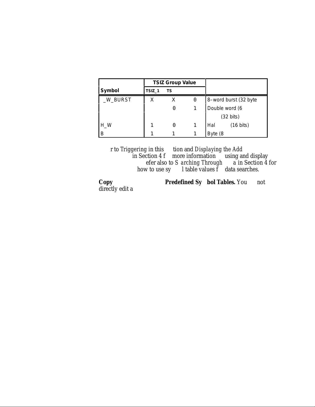
in the file 88110_TSIZ, the TSIZ group symbol table.
Symbol
Table 3-3
88110_TSIZ Symbol Table Definitions
TSIZ Group Value
TSIZ_1 TSIZ_0 TBST
Meaning
8_W_BURST
БББББ
D_W
W
H_W
B
XX0
ББББББ
001
011
101
111
8–word burst (32 bytes)
БББББББ
Double word (64 bits)
Word (32 bits)
Half word (16 bits)
Byte (8 bits)
Refer to Triggering in this section and Displaying the Address Group
Symbolically in Section 4 for more information on using and displaying
symbolic values. Refer also to Searching Through Data in Section 4 for
information on how to use symbol table values for data searches.
Copying and Editing the Predefined Symbol Tables. You cannot
directly edit any symbol tables supplied by microprocessor support.
You can make a copy of a predefined symbol table and then edit the
copy for your specific use.
To create a new symbol table, follow these steps:
1. Select the Symbol Editor menu from the Menu Selection overlay.
2. Press F2: FILE FUNCTIONS.
3. Select Open File in the Function field, and press Return.
3-4
4. Select New File in the Edit Status field, and press Return.
5. Enter a new symbol table file name in the New File Name field.
6. Select Pattern or Range in the Table Type field to match the
symbol table you are copying, and press Return.
7. Press F5: EXECUTE FUNCTION.
8. Select Merge Files in the Function field, and press Return.
9. Select the file to base your new symbol table on, such as the
88110_TCOD file.
10. Press F5: EXECUTE FUNCTION.
11. Press F8: EXIT & SAVE.
92DM923 88110 Instruction Manual
Online Version
Page 27

Setting Up Disassembler Software
12. Edit the file as desired keeping the following in mind:
S
If the new symbol has fewer don’t cares than an existing
symbol, it must be placed ahead of the existing symbol.
S
If the new symbol has more don’t cares than an existing
symbol, it must be placed after the existing symbol.
S
Do not duplicate symbol names.
Also refer to your DAS 9200 System User Manual for more
information on editing the symbol table.
13. Select the Channel menu from the Menu Selection overlay.
14. Change the file name of the symbol table for the TCOD group
(or whichever group’s symbol table you are replacing) to the one
that you specified in step 5.
TRIGGERING
All the Trigger menu selections available for use with your 92A96
Module are still valid for disassembly. Refer to your module user
manual for a list and description of these selections.
You can use the Home key to quickly clear the word recognizer field of
any channel group with a symbolic radix. To clear a word recognizer,
open the field, press the Home key, and close the field. The first entry
on the list is blank.
The DAS 9200 makes it possible to cross-trigger with other modules or
to an external instrument. You may want to consider sending or
receiving a signal to or from another module, or to the Sync Out SMB
connector on the module. You should refer to your DAS 9200 System
User Manual for an in-depth description of defining and using signals,
and to specific module user manuals for a description of using the Sync
Out SMB connector.
92DM923 88110 Instruction Manual
Online Version
3-5
Page 28

Section 4: ACQUIRING AND VIEWING
DISASSEMBLED DATA
This section describes how to acquire data and view it disassembled in
the Disassembly display. This section explains:
S
acquiring data
S
viewing disassembled data in various formats
S
functions of the Disassembly Format Definition overlay
S
displaying groups symbolically
S
restoring and viewing the demonstration reference memory
S
searching through data
S
printing data
ACQUIRING DATA
Once you load the 88110 support, choose a clocking mode, and specify
the trigger, you are ready to acquire data. Press the F1: START
acquisition key to begin the acquisition. You can press the F1: STOP
key at any time to stop acquisition.
If you have any problems acquiring data, refer to Appendix A: Error
Messages and Disassembly Problems.
VIEWING DISASSEMBLED DATA
Disassembled data is displayed in the Disassembly menu in four
different formats: Hardware, Software, Control Flow, and Subroutine.
To select a format, follow these steps:
1. Press the Select Menu key, and select the Disasm menu.
2. Press F5: DEFINE FORMAT.
3. Select the desired format in the Display Mode field.
4. Press F1: ESCAPE & CANCEL.
92DM923 88110 Instruction Manual
Online Version
4-1
Page 29
Acquiring and Viewing Disassembled Data
Hardware Display Format
The Hardware display format shows the Address, Data, and Control
channel values for each sample of acquired data in the order they
occurred. In Hardware data format, the disassembler displays certain
cycle type labels in parentheses. Table 4-1 shows these cycle type labels
and gives a definition of the cycle they represent. Reads to interrupt and
exception vectors will be labeled with the vector name.
Table 4-1
Cycle Type Definitions
Cycle Type
** RESERVED ** Reserved
(TCH/FLSH/ALLOC <CYCLESIZE>) Touch, flush, or allocate
(DATA MMU TBLWLK) Data MMU tablesearch
(RLMNT COPYBACK) Replacement copyback
(SNOOP COPYBACK) Snoop copyback
(INST MMU TBLWLK) Instruction MMU tablesearch
(FLUSH) Flush
(UNUSED PREFETCH) Unused prefetch
(TRANSFER ERROR CYCLE) Transfer error cycle
(TRANSFER RETRY CYCLE) Transfer retry cycle
(RD DA TA <CYCLESIZE>) Read data <cyclesize>
(WR DA TA <CYCLESIZE>) Write data <cyclesize>
(LWR DATA <CYCLESIZE>) Locked write data <cyclesize>
(LRD DA TA <CYCLESIZE>) Locked read data <cyclesize>
(U) = User mode.
(S) = Supervisor mode.
Definition
Figure 4-1 shows an example of the Hardware display.
4-2
92DM923 88110 Instruction Manual
Online Version
Page 30

Acquiring and Viewing Disassembled Data
3 4 5
2
1
Figure 4-1. Hardware display.
1
Cursor. Shows the DAS 9200 sequence number on which the
cursor is positioned.
2
Sequence Column. Lists DAS 9200 memory locations for the
acquired data.
3
Address Group. Lists data from channels connected to the 88110
Address bus.
4
Mnemonics Column. Lists the instructions that have been
disassembled.
5
Timestamp Column. Lists the timestamp values when a
timestamp selection is made in the Disassembly Format
Definition overlay.
Asterisks in the Mnemonics column indicate that there is insufficient
data available for complete disassembly of the instruction. The number
of asterisks shows the width of the data that is not available. Two
asterisks (**) represent a byte.
Gaps in the acquired data, caused by data qualification specified in the
Trigger menu, are indicated by a gray background behind the Address,
Hi_Data, and Lo_Data groups.
92DM923 88110 Instruction Manual
Online Version
4-3
Page 31
Acquiring and Viewing Disassembled Data
Software Display Format
The Software data format displays only the first fetch of executed
instructions. Flushed cycles and extensions are not shown, even though
they are part of the executed instruction. The display is designed to
resemble assembly language listings.
Control Flow Display Format
The Control Flow display format displays any instruction that changes
the flow of control, such as the following:
S
the first fetch of instructions that cause a branch in the address;
branches not taken are not displayed
S
conditional jumps actually taken
S
unconditional branches
S
instructions that cause traps
S
instructions that cause interrupts
S
“UNKNOWN” (“** RESERVED **”) cycles
S
exception cycles
Instructions that generate a change in the flow of control in the 88110
microprocessor are as follows:
BBO BSR RTE TCND
BB1 ILLOP TB0
BCND JMP TB1
BR JSR TBND
4-4
92DM923 88110 Instruction Manual
Online Version
Page 32

Acquiring and Viewing Disassembled Data
Subroutine Display Format
The Subroutine display format displays the first fetch of subroutine
calls and return instructions. Instructions that generate a subroutine call
or a return in the 88110 microprocessor are as follows:
BSR RTE TBND UNKNOWN OPCODE
ILLOP TBO TCND
JSR TB1 EXCEPTION CYCLES
Disassembly Format Definition Overlay
The Disassembly Format Definition overlay allows you to make
optional display selections for the Disassembly menu and tailor it for
your applications. To access this overlay, press F5: DEFINE FORMAT.
You can use this overlay to do the following:
S
choose the format (mode) in which the Disassembly menu displays
disassembled data
S
set the interval in which the data cursor will scroll through
disassembled data
S
display and define the format of the timestamp
S
highlight various types of disassembled cycles
S
change the position of any channel group in the display
S
change the radix for any channel group
S
choose which symbol tables are to be used when channel groups are
displayed symbolically
S
specify the size and starting address of the vector table
The Disassembly Format Definition overlay is shown in Figure 4-2.
92DM923 88110 Instruction Manual
Online Version
4-5
Page 33

Acquiring and Viewing Disassembled Data
1
2
3
4
5
6
9
10
11
7 8
Figure 4-2. Disassembly Format Definition overlay.
1
Display Mode. You can select either Hardware, Software,
Control Flow, or Subroutine format.
2
Timestamp. You can display the timestamp as an Absolute,
Relative, or Delta value. You can also set the timestamp display to
Off.
Timestamp values show the amount of time that has elapsed
between data samples. An Absolute timestamp shows the amount
of time elapsed between when the acquisition was started (after
pressing F1: START) and each subsequent data sample. A
Relative timestamp shows the amount of time elapsed between
successive samples. A Delta timestamp shows the amount of time
between the sample with the delta user mark and each previous or
subsequent data sample.
3
Scroll By. You can scroll by Sequence, Instruction, Control Flow,
or Subroutine.
4-6
92DM923 88110 Instruction Manual
Online Version
Page 34

Acquiring and Viewing Disassembled Data
4
Highlight. You can highlight Instructions, Control Flow, or
Subroutines. With highlighting on, only the selected type of
samples are shown as white text with a black background; all
other samples are shown as gray text with a black background.
You can also set the highlighting to Off.
5
Highlight Gaps. You can choose to highlight or not to highlight
gaps. Gaps are caused by qualifying data storage in the Trigger
menu and are indicated by a gray background behind the address
values.
6
Disasm Across Gaps. You can choose to continue or not to
continue to disassemble data across gaps. Disassembling data
across gaps causes the disassembler to disassemble data as if no
gap existed. Disassembled data will be invalid if the last sample
before the gap does not logically match the sample immediately
following the gap.
7
Vector Base Address. If your SUT has had its vector table
relocated, you must use this field to inform the disassembler of
the new base address. If the value in the Vector Base Address
field is incorrect, the disassembler will not interpret interrupts or
exceptions correctly.
8
Vector Table Size. Use this field to specify the size of the vector
table.
9
Group Name. You can specify the name of the group that
displays in the column in which the cursor is positioned. When
you move a group, the group is inserted in the new column
position and removed from its old position. The remaining
groups move either one column position to the left or one column
position to the right.
10
Group Radix. You can select the radix in which each group
displays. The radix selections for most groups are Binary, Octal,
Hexadecimal, Decimal, ASCII, Symbol, and Off. The only
selections for the Hi_Data and Lo_Data groups are Hexadecimal
or Off. The only selections for Mnemonics group are ASCII or
Off. You should only select the symbolic radix when a symbol
table is available for that group. The timestamp value always
displays in decimal.
11
Symbol Table. You can specify a symbol table to use for each
group where symbolic is the selected radix.
Function Keys
F1: ESCAPE & CANCEL. Closes the overlay and discards any
changes you have made since entering it.
92DM923 88110 Instruction Manual
Online Version
4-7
Page 35

Acquiring and Viewing Disassembled Data
F5: RESTORE FORMAT. Displays a list of saved disassembly
formats for the current module or cluster setup. Use the cursor keys to
select the desired format to restore and press the Open/Close key.
F6: SAVE FORMAT. Saves the current selections for the Disassembly
Format Definition overlay in a file on disk. You can enter a file name
up to ten characters long.
F7: DELETE FORMAT. Displays a list of saved disassembly format
files for the current module or cluster setup. Use the cursor keys to
select the desired format to delete and press the Open/Close key. You
cannot delete the Default format.
F8: EXIT & SAVE. Exits the overlay and executes or saves any
changes made.
Displaying the Address Group Symbolically
The Address group can be displayed as symbolic values in the
Disassembly menu similar to the way the TCOD group can be
displayed as symbol values in the State menu. You can use the Symbol
Editor menu to create symbol tables in which symbols are assigned to
various address ranges or patterns. You can then change the radix of the
Address group in the Disassembly menu using the Disassembly Format
Definition overlay. If an address appears in the operand field of a
mnemonic, it also will be displayed symbolically.
Exception Vectors
The 88110 microprocessor initially places the exception vector table at
address 00000000 (the default value). However, you can relocate the
table using the Processor Support submenu by entering the address in
the Vector Base Addr field. The Vector Base Addr field provides the
disassembler with the offset address; enter an eight-digit hexadecimal
value corresponding to the offset of the base address of the exception
table. The Vector Table Size field lets you specify a three-digit
hexadecimal size for the table.
Table 4-2 lists the 88110 exception vectors (exception cycle types).
Interrupt cycle types are computed cycle types and cannot be used to
control triggering. When the 88110 microprocessor processes an
exception, the disassemble software displays the type of exception, if
known.
4-8
If you defined the address of the exception table in the FORMAT
OVERLAY menu, the exception vector reads are labelled and displayed
in parentheses when disassembly is performed.
92DM923 88110 Instruction Manual
Online Version
Page 36

Acquiring and Viewing Disassembled Data
Table 4-2
Interrupt/Exception Labels
Number
0 RESET EXCEPTION
1 INTERRUPT EXCEPTION
2 INSTRUCTION ACCESS
3 DA TA ACCESS
4 MISALIGNED ACCESS
5 UNIMPLEMENTED OPCODE
6 PRIVILEGE VIOLA TION
7 BOUNDS CHK VIOLA TION
8 ILLEGAL INTEGER DIV
9 INTEGER OVERFLOW
10 ERROR EXCEPTION
11 NONMASKABLE INTERRUPT
12 DATA MMU READ MISS
13 DATA MMU WRITE MISS
14 INSTR MMU ATC MISS
15-113 RESERVED
114 SFU 1 ILLEGAL OPCODE
115 RESERVED
116 SFU 2 ILLEGAL OPCODE
117 RESERVED
118 SFU 3 ILLEGAL OPCODE
119 RESERVED
120 SFU 4 ILLEGAL OPCODE
121 RESERVED
122 SFU 5 ILLEGAL OPCODE
123 RESERVED
124 SFU 6 ILLEGAL OPCODE
125 RESERVED
126 SFU 7 ILLEGAL OPCODE
127 RESERVED
128-51 1 USER DEFINED
Exception
Searching Through Data
The disassembler does not have a Disassembly Search Definition
overlay. However, you can effectively search through disassembled data
by following these steps:
1. Press F2: SPLIT DISPLAY to use the split-screen display.
92DM923 88110 Instruction Manual
Online Version
4-9
Page 37

Acquiring and Viewing Disassembled Data
2. Press F5: SPLIT HORIZ to split the screen into two horizontal
displays.
3. Press F2: LOCK CURSOR. A list of selections appears.
4. Select lock cursors at the same sequence, and press Return.
5. Press F8: EXIT & SAVE to display the menus in a split screen.
6. If the active window is the Disassembly menu, press
F3: SWITCH WINDOWS to make the State menu active. The
cursor and Cursor field are yellow in the active window.
7. Press F6: DEFINE SEARCH to use the search function of the
State menu to search for the desired sequence.
To search on TCOD group values, change the radix to binary and refer
to Table 3-1 to find the binary equivalent values for the cycles you want
to locate.
When searching for data in a clustered module setup in the State menu,
the searches are conducted only for the master module. You can,
however, define either module to be the master module. Refer to the
description of the State Search Definition overlay in your 92A96
Module User Manual for a description of how to search through state
data. Also refer to that manual for a description of how to return to a
full screen display.
To abort a search, press the Esc (escape) key.
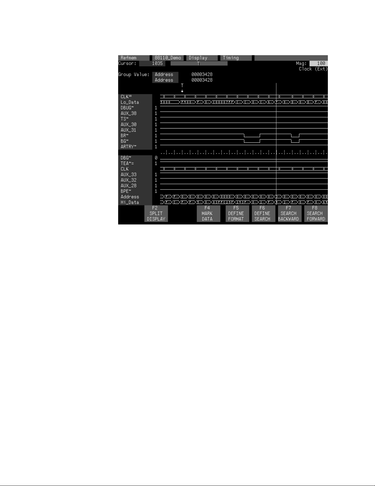
Figure 4-3 shows the screen split into Disassembly and State windows
with the cursors locked on the same bus cycle.
4-10
92DM923 88110 Instruction Manual
Online Version
Page 38

Acquiring and Viewing Disassembled Data
Figure 4-3. Disassembly and State split-screen display. You can use this method to
perform searches.
PRINTING DATA
To print disassembled data, use the Disassembly Print overlay. To
access this overlay, press the Shift and Print keys at the same time from
the Disassembly menu. The Disassembly Print overlay is exactly the
same as the State Table Print overlay. Refer to your 92A96 Module
User Manual for a description of this overlay.
92DM923 88110 Instruction Manual
Online Version
4-11
Page 39

Acquiring and Viewing Disassembled Data
REFERENCE MEMORY
A demonstration reference memory file is provided so you can see an
example of how your 88110 microprocessor mnemonics look when
they are disassembled. In this discussion, you will view the reference
memory. Viewing the reference memory is not a requirement for
preparing the 92A96 Module for use. You can view the reference
memory file without connecting the DAS 9200 to your SUT.
To view the 88110_Demo Refmem, follow these steps:
1. Press the Select Menu key, and select the 88110_Demo file from
the Refmem column.
2. Select the Disasm menu, and press Return.
You can affect the display of the disassembled data from the
Disassembly Format Definition overlay, which you can access through
the Disassembly menu. Displaying all disassembled instructions and
cycle types is the default format.
If there is not enough free space on the hard disk, you can delete the
88110_Demo file. It is not necessary to the operation of the
disassembler.
4-12
92DM923 88110 Instruction Manual
Online Version
Page 40

Section 5: GENERAL PURPOSE ANALYSIS
You may need to perform general purpose (timing) analysis on your
88110 system prior to, during, and after attempting to integrate your
software with the 88110 system hardware. When performing hardware
analysis, you will want to use the data acquisition module to acquire
data with a finer resolution. When more data samples are taken in a
given period of time, the resolution in the Timing display increases,
letting you see signal activity that would otherwise go undetected.
This section provides information on the following:
S
clocking
S
triggering
S
displaying data
S
supplied Timing Format Definition file
To acquire and display timing data, you need to change the clocking
selection and trigger program, acquire data, and view it in the Timing
menu. A predefined Timing Format Definition overlay file called
88110_96 can be used to view 88110 timing data. A description of this
file and how to use it can be found later in this section.
Keep in mind when you view data in the State display that it uses the
default channel grouping setup with all groups visible and will look
different than the Disassembly display.
There often is a need to view data in a split screen display with state
data in one half and timing data in the other. Do not disconnect any of
the 92A96 probe cables or interface housings if you are analyzing data
in this manner. Instead, use the extra channels available from the 92A96
Module to make other 88110 system connections.
CLOCKING
To change the data sampling rate, use the Clock menu.
When using the 92A96 Module for timing analysis, you will want to
use the Internal or External clocking modes. The Internal clock
selection can sample data up to 100 MHz, which has a 10 ns resolution
between samples. The External clock selection samples data on every
active clock edge on the 92A96 clock inputs up to 100 MHz.
92DM923 88110 Instruction Manual
Online Version
5-1
Page 41

General Purpose Analysis
The default clocking mode is Custom when microprocessor support is
used; you will need to change it to either Internal or External. Your
92A96 Module User Manual contains an in-depth description of
Internal and External clocking.
Custom Clocking
Custom clocking only stores one data sample for each bus transaction,
which can take one or more clock cycles. Custom clocking also
time-aligns certain signals that otherwise would be skewed relative to
the current bus transaction. This clocking selection is generally
unproductive for timing analysis. Refer to Appendix B for a more
in-depth description of how Custom clocking is used with the probe
adapter to acquire data.
Internal Clocking
When you select Internal as the clocking mode, the 92A96 Module
stores one data sample as often as every 10 ns (100 MHz). This
clocking selection is commonly referred to as asynchronous.
Two typical uses of Internal clocking might be to verify that all the
88110 signals are transitioning as expected or to measure timing
relationship between signal transitions.
It is possible to acquire asynchronous data at rates of 200 MHz and
400 MHz. The faster the 92A96 Module acquires data, the fewer
channels it can acquire data on. A single 92A96 Module can acquire
data on 24 channels at 400 MHz or 2.5 ns resolution. Refer to your
92A96 Module User Manual for information on sampling data at speeds
faster than 100 MHz.
External Clocking
When you select External as the clocking mode, the 92A96 Module
acquires and stores data based on the clock channel up to 100 MHz.
This clocking selection is commonly referred to as synchronous.
By selecting the rising edge of CLK: 3 on the acquisition module as the
clock channel, and turning off the remaining three clocks, the module
will sample data on every rising edge of the clock. No data is acquired
on the falling clock edge unless you select both edges.
You can also use the other three clock channels as qualifiers or clocks to
further modify the clocking in of information from your 88110 system.
5-2
92DM923 88110 Instruction Manual
Online Version
Page 42

General Purpose Analysis
TRIGGERING
All the Trigger menu selections available for use with the 92A96
Module are still valid for timing analysis. Refer to your module user
manual for a list and description of the selections.
ACQUIRING DATA
You can acquire data as described in the Acquiring Data description in
Section 4.
DISPLAYING DATA
General purpose analysis requires that you view data in either the State
or Timing menus. The following discussion describes these menus.
Timing Menu
In the Timing menu, every channel is shown as a waveform, and groups
of channels are shown as bus forms.
A predefined Timing Format Definition overlay file, part of the 88110
microprocessor support, is available for you to use when displaying
data in the Timing format. The 88110_96 file is installed on the
DAS 9200 with the support software.
The 88110_96 Timing Format file places the CLK= signal first
followed by the Lo_Data group displayed as bus forms containing bus
values instead of as individual timing waveforms. These groups are
followed by the 88110 system clock and other important control
signals. The Address and Hi_Data groups are also displayed as bus
forms at the bottom of the display. Figure 5-1 shows data displayed
using the 88110_96 file.
To select the supplied Timing Format Definition file, follow these steps:
1. Select the Timing menu, and press F5: DEFINE FORMAT.
2. Press F5: RESTORE FORMAT.
3. Select 88110_96, and press the Return key. A message tells you
the format file is selected.
4. Press F8: EXIT & SAVE to return to the Timing menu.
Refer to the channel assignment tables in Appendix C for the lists of
individual channels and their 88110 signal names.
92DM923 88110 Instruction Manual
Online Version
5-3
Page 43
General Purpose Analysis
Figure 5-1. Timing data using the 88110_96 Timing Format file.
State Menu
In the State menu, all channel group values are shown based on the
selected radix in the Channel menu or the State Format Definition
overlay. No disassembly occurs. Figure 5-2 shows State data.
If you want to display other channel groups, access the State Format
Definition overlay and change the radix from Off to Hex, Bin, or Oct.
This overlay also allows you to add the Timestamp group (and change
the radix) to the data display.
5-4
92DM923 88110 Instruction Manual
Online Version
Page 44

General Purpose Analysis
Figure 5-2. State data.
SEARCHING THROUGH DATA
To search through data, you can use either the Timing Search Definition
overlay or the State Search Definition overlay. You can use these
overlays and search through data as described in your 92A96 Module
User Manual.
PRINTING DATA
To print state data, you can use the State Print overlay. To access this
overlay, press the Shift and Print keys at the same time from the State
menu.
To print timing data, you can use the Timing Print overlay. To access
this overlay, press the Shift and Print keys at the same time from the
Timing menu.
For detailed information on the State Print overlay or the Timing Print
overlay, refer to your 92A96 Module User Manual.
92DM923 88110 Instruction Manual
Online Version
5-5
Page 45

Appendix A: ERROR MESSAGES AND
DISASSEMBLY PROBLEMS
This appendix describes error messages and disassembly problems that
you may encounter while acquiring data.
MODULE ERROR MESSAGES
These error messages will appear in the Module Monitor menu when
there are problems with acquiring data or satisfying the trigger
program. The error messages are listed in alphabetical order; a
description of the error message and the recommended solution follow
the error message.
Slow Clock. This message appears when the active clock channel (or
channels) is not changing, is typically changing at 1 ms or slower
intervals, or one of the clock qualifiers is held in the wrong state. Check
for the following:
1. The 88110 system is powered on and running. Be sure the system
is not halted.
2. 88110 Support is selected in the appropriate 92A96
Configuration menu.
3. Custom is selected in the Clock menu.
4. The connections between the 92A96 Module and the probe
adapter are correct.
S
The clock and 8-channel probe connections between the
interface housings and probe adapter are correct (module
name, clock, section names, and channel numbers match), are
properly oriented (GND connects to ground), and are fully
engaged.
S
The connections between the interface housings and 92A96
probe cables have matched color labels, matched slot
numbers, and are properly keyed.
S
The connections between the 92A96 probe cables and probe
connectors have matched color labels, matched slot numbers,
and are properly keyed.
5. The orientation of pin A1 on the microprocessor, the probe
adapter, and SUT are correct.
6. No pins are bent or missing on the 88110 microprocessor or on
either of the probe adapter sockets.
7. The DBUG jumper is in the Normal position.
92DM923 88110 Instruction Manual
Online Version
A-1
Page 46

Error Messages and Disassembly Problems
Waiting for Stop. This message appears when the trigger condition is
satisfied and memory is full but the Manual Stop mode is selected in
the Cluster Setup menu. The solution is to manually stop the DAS 9200
by pressing F1: STOP.
This message can also appear when other modules in the cluster have
not filled their memories. Wait for the other modules to fill their
memories. If the message does not disappear in a short time, press
F1: STOP.
Waiting for Stop-Store. This message appears when the trigger
condition is satisfied but the amount of post-fill memory specified in
the trigger position field is not yet filled. Press F1: STOP to view the
acquired data, then check for the following:
1. The trigger program in the Trigger menu is correct.
2. The storage qualification in the Trigger menu is correct.
3. The system or the module does not have an exception or fault.
The 88110 system or acquisition module might have experienced
a hardware or software exception or fault after the trigger
condition was satisfied.
Waiting for Trigger. This message appears when the trigger condition
does not occur. Check for the following:
1. The 88110 system is powered on and running. Be sure the system
is not halted.
2. The trigger conditions are not being satisfied. The Module
Monitor menu shows which state events are not occurring. Press
F1: STOP, access the Trigger menu, and redefine the conditions
for that state. Also refer to the description on Triggering in
Section 3.
OTHER DISASSEMBLY PROBLEMS
There may be problems with disassembly for which no error messages
are displayed. Some of these problems and their recommended
solutions follow.
Incorrect Data. If the data acquired is obviously incorrect, check the
following:
1. 88110 Support is selected in the 92A96 Configuration menu.
2. Custom is selected in the Clock menu.
A-2
3. The DBUG jumper is in the Normal position.
92DM923 88110 Instruction Manual
Online Version
Page 47

Error Messages and Disassembly Problems
4. The connections between the 92A96 Module and the probe
adapter are correct.
S
The clock and 8-channel probe connections between the
interface housings and probe adapter are correct (module
name, clock, section names, and channel numbers match), are
properly oriented (GND connects to ground), and are fully
engaged.
S
The connections between the interface housings and 92A96
probe cables have matched color labels, matched slot
numbers, and are properly keyed.
S
The connections between the 92A96 probe cables and probe
connectors have matched color labels, matched slot numbers,
and are properly keyed.
5. The orientation of pin A1 on the microprocessor, the probe
adapter, and SUT are correct.
6. No pins are bent or missing on the 88110 microprocessor or on
either of the probe adapter sockets.
Other Suggestions. If the previous suggestions do not fix the problem
with acquiring disassembled bus cycles or instruction mnemonics, try
the following:
1. Reload the module setup by selecting the 88110 Support in the
92A96 Configuration menu to restore the DAS 9200 to a known
state.
2. Possible ac and dc loading problems may be remedied by
removing one or both of the protective sockets from the probe
adapter. These sockets may add enough additional inductance to
your 88110 system to affect it. Refer to Appendix C for a
description to remove sockets from the probe adapter.
If the DAS 9200 still is not acquiring data after trying these solutions,
there may be a problem with your 88110 system. Try performing
hardware analysis with your DAS 9200 system to ensure that the 88110
signals are valid at the time the probe adapter samples them.
Refer to Section 5: General Purpose Analysis for information on data
sampling rates using either the Internal or External clocking selections
in the Clock menu. Also refer to Appendix B: How Data is Acquired to
see when the disassembler samples the various 88110 system signals.
92DM923 88110 Instruction Manual
Online Version
A-3
Page 48
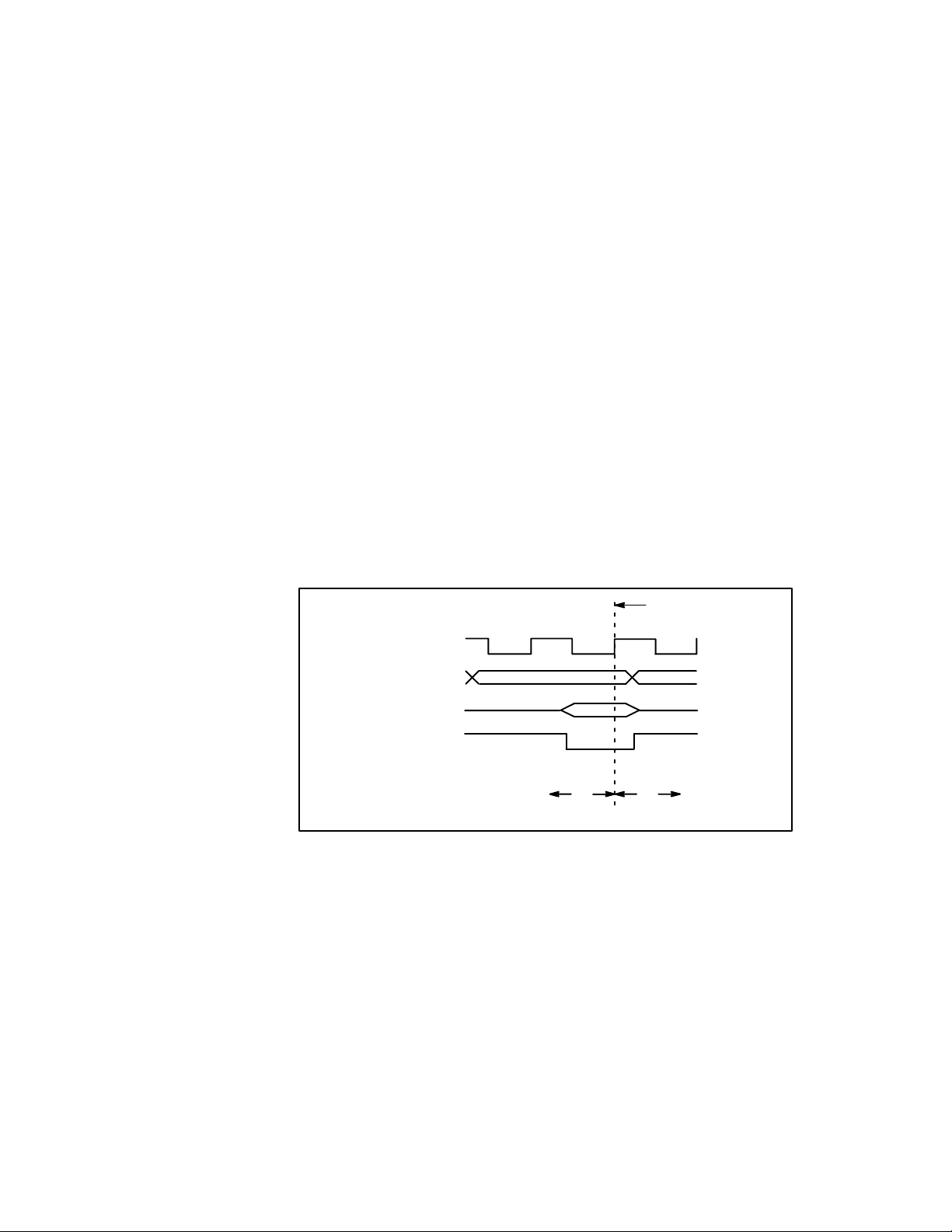
Appendix B: HOW DATA IS ACQUIRED
This appendix explains how the 92A96 Module acquires 88110 signals
using the 92DM923 probe adapter and software. This appendix also
provides additional information on microprocessor signals accessible on
or not accessible on the probe adapter, and on extra 92A96 channels
available for you to use for additional connections.
CUSTOM CLOCKING
A special clocking program (called Custom) is loaded to the 92A96
Module every time the 88110 Support is selected in the Configuration
menu. With Custom clocking, the module logs in signals from multiple
groups of channels when they are valid on the 88110 bus. The module
then sends all the logged-in signals to the trigger machine and to the
acquisition memory of the module for storage.
Signals are acquired on the rising edge of CLK where TA~, TEA~, or
TRTRY~ are active low. All signals are logged in, as shown in
Figure B-1.
LOG IN ALL SIGNALS
CLK
ADDRESS
DATA
TA~/TEA~/TRTRY~
T
h
Figure B-1. 88110 bus timing.
T
s
ALTERNATE MICROPROCESSOR CONNECTIONS
You can connect to microprocessor signals that are not required for
disassembly so you can do more advanced timing analysis. These
signals may or may not be accessible on the probe adapter board. The
following paragraphs and tables list signals that are accessible on or are
not accessible on the probe adapter board.
For a list of signals required or not required for disassembly, refer to the
channel connections tables in Appendix C.
92DM923 88110 Instruction Manual
Online Version
B-1
Page 49

How Data is Acquired
Signals On the Probe Adapter
The probe adapter board contains pins for microprocessor signals that
are not acquired by the support software. You can connect extra podlets
to these pins because they can be useful for general purpose analysis.
However, these signals are not defined in the Channel setup menu; you
must enter the Channel setup menu and assign those signals to a new
channel group.
There are three 2-pin groups of square pins on the probe adapter with
printed 88110 signal names. These pins connect to the UPA1~, UPA0~,
and DEBUG~ signals.
Signals Not On the Probe Adapter
All microprocessor signals are accessible on the probe adapter.
Extra 92A96 Channels
Table B-1 shows the extra 92A96 channels available for you to use to
make alternate microprocessor connections. You can also disconnect
channels not required for disassembly to make alternate connections.
The channel assignment tables in Appendix C indicate channels not
required for disassembly.
Table B-1
Extra 92A96 Channels
92A96 Section: Channel
HI_C1:7 HI_C0:7 LO_A0:7 LO_C1:7 LO_C0:7
HI_C1:6 HI_C0:6 LO_A0:6 LO_C1:6 LO_C0:6
HI_C1:5 HI_C0:5 LO_A0:5 LO_C1:5 LO_C0:5
HI_C1:4 HI_C0:4 LO_A0:4 LO_C1:4 LO_C0:4
HI_C1:3 HI_C0:3 LO_A0:3 LO_C1:3 LO_C0:3
HI_C1:2 HI_C0:2 LO_A0:2 LO_C1:2 LO_C0:2
HI_C1:1 HI_C0:1 LO_A0:1 LO_C1:1 LO_C0:1
HI_C1:0 HI_C0:0 LO_A0:0 LO_C1:0 LO_C0:0
If you use extra channels to make alternate connections to your SUT,
then these signals will be logged in at the same time as the signals
normally sampled (see Figure B-1).
B-2
The extra channels have already been assigned to three channel groups:
AUX1 HI, AUX1 LO, and AUX0. If you use extra channels, you can
use these channel groups as defined or remove channels from these
groups to create new channel groups.
92DM923 88110 Instruction Manual
Online Version
Page 50
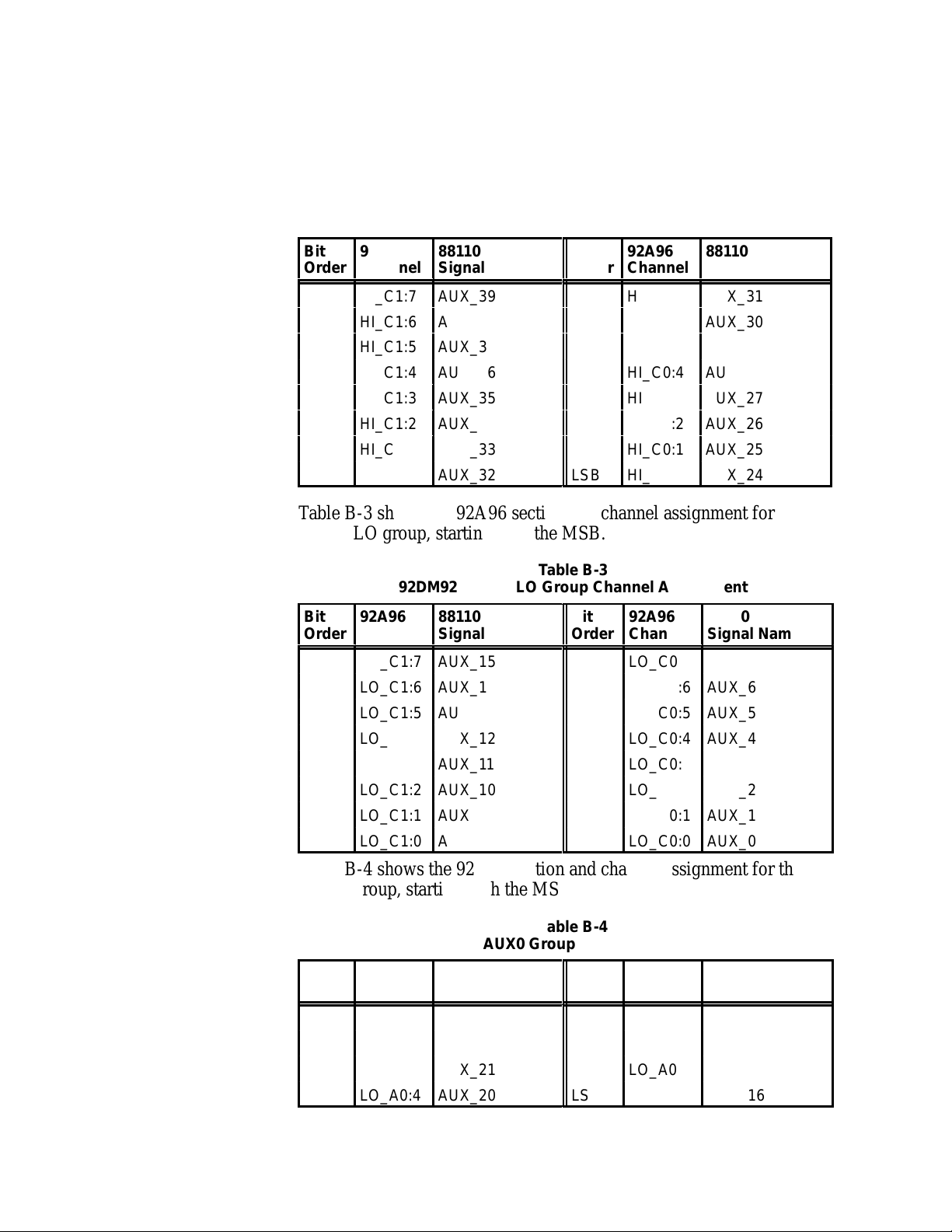
How Data is Acquired
Á
Á
Á
Á
ÁÁÁÁ
Á
Á
Á
ÁÁÁÁ
ÁÁÁÁ
Á
Á
Á
ÁÁÁÁ
Á
Á
Á
ÁÁÁÁ
ÁÁÁÁ
ÁÁÁÁ
ÁÁÁÁ
ÁÁÁÁ
Á
Á
Á
Á
Á
Á
Á
Á
Á
Á
Á
Table B-2 shows the 92A96 section and channel assignment for the
AUX1 HI group, starting with the MSB.
Table B-2
92DM923 AUX1 HI Group Channel Assignment
Bit
Á
Order
MSB
ÁÁÁÁÁ
92A96
ÁÁÁ
Channel
HI_C1:7
HI_C1:6
HI_C1:5
HI_C1:4
HI_C1:3
HI_C1:2
HI_C1:1
HI_C1:0
88110
ÁÁÁÁ
Signal Name
AUX_39
AUX_38
AUX_37
ÁÁÁÁ
AUX_36
AUX_35
AUX_34
AUX_33
AUX_32
Bit
ÁÁ
Order
ÁÁ
LSB
92A96
ÁÁ
Channel
HI_C0:7
HI_C0:6
HI_C0:5
ÁÁ
HI_C0:4
HI_C0:3
HI_C0:2
HI_C0:1
HI_C0:0
88110
ÁÁÁÁ
Signal Name
AUX_31
AUX_30
AUX_29
ÁÁÁÁ
AUX_28
AUX_27
AUX_26
AUX_25
AUX_24
Table B-3 shows the 92A96 section and channel assignment for the
AUX1 LO group, starting with the MSB.
Table B-3
92DM923 AUX1 LO Group Channel Assignment
Bit
Order
Á
MSB
92A96
Channel
ÁÁÁ
LO_C1:7
LO_C1:6
LO_C1:5
LO_C1:4
LO_C1:3
LO_C1:2
LO_C1:1
LO_C1:0
88110
Signal Name
ÁÁÁÁ
AUX_15
AUX_14
AUX_13
AUX_12
AUX_11
AUX_10
AUX_9
AUX_8
Bit
Order
ÁÁ
LSB
92A96
Channel
ÁÁ
LO_C0:7
LO_C0:6
LO_C0:5
LO_C0:4
LO_C0:3
LO_C0:2
LO_C0:1
LO_C0:0
88110
Signal Name
ÁÁÁÁ
AUX_7
AUX_6
AUX_5
AUX_4
AUX_3
AUX_2
AUX_1
AUX_0
Table B-4 shows the 92A96 section and channel assignment for the
AUX0 group, starting with the MSB.
Bit
Order
MSB
Á
92DM923 88110 Instruction Manual
Online Version
92DM923 AUX0 Group Channel Assignment
92A96
Channel
LO_A0:7
ÁÁÁ
LO_A0:6
LO_A0:5
LO_A0:4
88110
Signal Name
AUX_23
ÁÁÁÁ
AUX_22
AUX_21
AUX_20
Table B-4
Bit
Order
ÁÁÁÁÁ
LSB
92A96
Channel
LO_A0:3
LO_A0:2
LO_A0:1
LO_A0:0
88110
Signal Name
AUX_19
ÁÁÁÁ
AUX_18
AUX_17
AUX_16
B-3
Page 51

WARNING
The following servicing instructions are for use only by qualified
personnel. To avoid personal injury, do not perform any servicing
other than that contained in the operating instructions unless you
are qualified to do so. Refer to the General Safety Summary and the
Servicing Safety Summary prior to performing any service.
Page 52
Appendix C: SERVICE INFORMATION
This appendix contains the following information:
S
safety summary
S
brief description of the probe adapter and how it works
S
care and maintenance procedures
S
specification tables
S
channel assignment tables
S
dimensions of the probe adapter
S
removing and replacing individual signal leads
S
removing and replacing sockets
SERVICING SAFETY INFORMATION
The following servicing safety information is for service technicians.
Follow these safety precautions, along with the general precautions
outlined in your 92A96 Module User Manual, while installing or
servicing this product.
Do Not Service Alone. Do not perform internal service or adjustment
on this product unless another person is present and able to give first
aid and resuscitation.
Use Care When Servicing With Power On. To avoid personal injury
from dangerous voltages, remove jewelry such as rings, watches, and
other metallic objects before servicing. Do not touch the product’s
exposed connections and components while power is on.
PROBE ADAPTER DESCRIPTION
The probe adapter is a nonintrusive piece of hardware that allows the
92A96 Module to acquire data from an 88110 microprocessor in its
own operating environment with little affect, if any, on that system.
Refer to Figure C-1 while reading the following discussion.
92DM923 88110 Instruction Manual
Online Version
C-1
Page 53

Service Information
PROBE
ADAPTER
Figure C-1.Overview of the standard probe and probe adapter.
The probe adapter consists of a circuit board and a socket for the 88110
microprocessor. The probe adapter connects to the SUT. Signals from
the 88110 system flow from the probe adapter to the podlet groups. The
signals flow through the probe signal leads to the 92A96 Module.
The probe adapter accommodates the Motorola 88110 microprocessor
in a 299-pin PGA package.
Probe Adapter Circuit Description
The probe adapter contains no active circuitry.
C-2
92DM923 88110 Instruction Manual
Online Version
Page 54

Service Information
CARE AND MAINTENANCE
The probe adapter does not require scheduled or periodic maintenance.
To maintain good electrical contact, keep the probe adapter free of dirt,
dust, and contaminants. Also, ensure that any electrically conductive
contaminants are removed.
Dirt and dust can usually be removed with a soft brush. For more
extensive cleaning, use only a damp cloth. Abrasive cleaners and
organic solvents should never be used.
CAUTION
Exercise care when soldering on a multilayer circuit board.
Excessive heat can damage the through-hole plating or lift
a run or pad and damage the board beyond repair. Do not
apply heat for longer than three seconds. Do not apply
heat consecutively to adjacent leads. Allow a moment for
the board to cool between each operation.
If you must replace an electrical component on a circuit board, exercise
extreme caution while unsoldering or soldering the new component.
Use a pencil-type soldering iron of less than 18 watts and an approved
desoldering tool. Ensure that the replacement is an equivalent part by
comparing the description as listed in the replaceable parts list.
92DM923 88110 Instruction Manual
Online Version
C-3
Page 55

Service Information
SPECIFICATIONS
These specifications are for a probe adapter connected to a 92A96
Acquisition Module and the SUT. Table C-1 shows the electrical
requirements the SUT must produce for the disassembler to acquire
correct data. Table C-2 shows environmental specifications.
Table C-1
Electrical Specifications
Characteristics
SUT Clock
Clock Rate 50 MHz
Minimum Setup Time Required
All Signals 5 ns
Minimum Hold Time Required
All Signals 0 ns
Measured Typical SUT Signal
Loading
CLK
TEA
TA~
TRTRY~
DBB~
ABB~
TS~
ALL OTHERS
Requirements
Specification, DC Load
3 podlets
3 podlets
3 podlets
2 podlets
2 podlets
2 podlets
2 podlets
1 podlet
C-4
92DM923 88110 Instruction Manual
Online Version
Page 56

Service Information
Figure C-2 shows the dimensions of the PGA probe adapter with the
podlet holders attached.
3.870 in
(98 mm)
PIN A1
4.150 in
(125 mm)
1.150 in
(29 mm)
Figure C-2.Minimum clearance of the probe adapter.
.775 in
(20 mm)
2.100 in
(53 mm)
.300 in (8 mm)
92DM923 88110 Instruction Manual
Online Version
C-5
Page 57

Service Information
Á
Á
Á
Á
Table C-2
Environmental Specifications
Characteristic
Description
Temperature
Max. Operating
Min. Operating
Nonoperating
Humidity
ББББББ
+50°C (122°F)*
0°C (+32°F)
–55°C to +75°C (–67° to +167°F)
10 to 95% relative humidity
БББББББББББ
[
Altitude
Operating
Nonoperating
Electrostatic Immunity
ББББББ
4.5 km (15,000 ft) maximum
15 km (50,000 ft) maximum
The probe adapter contains no static-
sensitive components.
БББББББББББ
* Not to exceed 88110 thermal considerations.
Forced air cooling may be required across the CPU.
[
Tested to Tektronix standard 062-2847-00 class 5.
Channel Assignments
Table C-3 shows the 92A96 section and channel assignments for the
Address group and the microprocessor signal to which each channel
connects, starting with the most significant bit (MSB).
When using these tables, keep in mind that the 92DM923 support
requires a variable-width module. The module in the higher-numbered
slot is referred to as the HI module; the module in the lower-numbered
slot is referred to as the LO module.
C-6
92DM923 88110 Instruction Manual
Online Version
Page 58
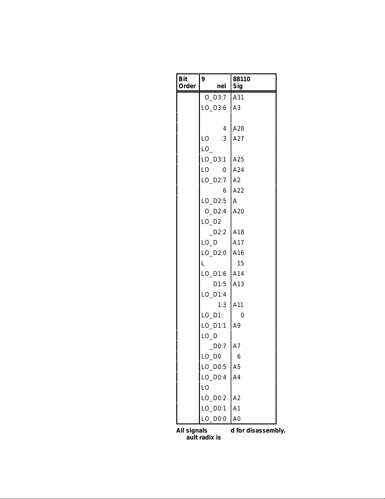
Service Information
Á
Á
Á
Á
Á
Á
Á
Á
Á
Table C-3
92DM923 Address Group Channel Assignments
Bit
Order
MSB
Á
92A96
ÁÁ
Channel
LO_D3:7
LO_D3:6
LO_D3:5
LO_D3:4
LO_D3:3
LO_D3:2
LO_D3:1
ÁÁÁÁ
LO_D3:0
ÁÁÁÁ
LO_D2:7
LO_D2:6
LO_D2:5
LO_D2:4
LO_D2:3
LO_D2:2
LO_D2:1
LO_D2:0
LO_D1:7
LO_D1:6
LO_D1:5
LO_D1:4
LO_D1:3
ÁÁÁÁ
LO_D1:2
LO_D1:1
LO_D1:0
LO_D0:7
LO_D0:6
LO_D0:5
LO_D0:4
LO_D0:3
LO_D0:2
LO_D0:1
LSB
LO_D0:0
88110
ÁÁÁÁ
Signal Name
A31
A30
A29
A28
A27
A26
A25
ÁÁÁÁ
A24
ÁÁÁÁ
A23
A22
A21
A20
A19
A18
A17
A16
A15
A14
A13
A12
A11
ÁÁÁÁ
A10
A9
A8
A7
A6
A5
A4
A3
A2
A1
A0
92DM923 88110 Instruction Manual
Online Version
All signals required for disassembly.
Default radix is HEX.
C-7
Page 59
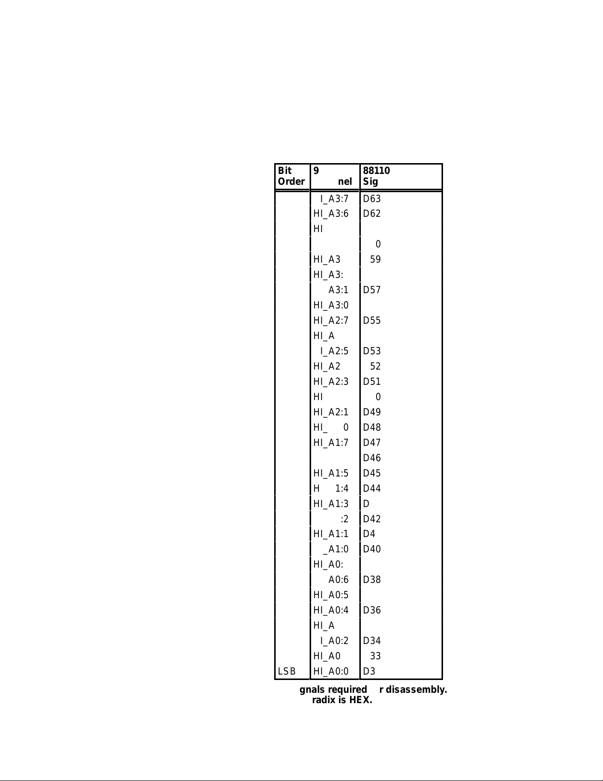
Service Information
Á
Á
Á
Table C-4 shows the 92A96 section and channel assignments for the
Hi_Data group and the microprocessor signal to which each channel
connects, starting with the most significant bit (MSB).
Table C-4
92DM923 Hi_Data Group Channel Assignments
Bit
Á
Order
MSB
LSB
92A96
ÁÁ
Channel
HI_A3:7
HI_A3:6
HI_A3:5
HI_A3:4
HI_A3:3
HI_A3:2
HI_A3:1
HI_A3:0
HI_A2:7
HI_A2:6
HI_A2:5
HI_A2:4
HI_A2:3
HI_A2:2
HI_A2:1
HI_A2:0
HI_A1:7
HI_A1:6
HI_A1:5
HI_A1:4
HI_A1:3
HI_A1:2
HI_A1:1
HI_A1:0
HI_A0:7
HI_A0:6
HI_A0:5
HI_A0:4
HI_A0:3
HI_A0:2
HI_A0:1
HI_A0:0
88110
БББББ
Signal Name
D63
D62
D61
D60
D59
D58
D57
D56
D55
D54
D53
D52
D51
D50
D49
D48
D47
D46
D45
D44
D43
D42
D41
D40
D39
D38
D37
D36
D35
D34
D33
D32
C-8
All signals required for disassembly.
Default radix is HEX.
92DM923 88110 Instruction Manual
Online Version
Page 60

Service Information
Á
Á
Á
Table C-5 shows the 92A96 section and channel assignments for the
Lo_Data group and the microprocessor signal to which each channel
connects, starting with the most significant bit (MSB).
Table C-5
92DM923 Lo_Data Group Channel Assignments
Bit
Á
Order
MSB
LSB
92A96
ÁÁ
Channel
HI_D3:7
HI_D3:6
HI_D3:5
HI_D3:4
HI_D3:3
HI_D3:2
HI_D3:1
HI_D3:0
HI_D2:7
HI_D2:6
HI_D2:5
HI_D2:4
HI_D2:3
HI_D2:2
HI_D2:1
HI_D2:0
HI_D1:7
HI_D1:6
HI_D1:5
HI_D1:4
HI_D1:3
HI_D1:2
HI_D1:1
HI_D1:0
HI_D0:7
HI_D0:6
HI_D0:5
HI_D0:4
HI_D0:3
HI_D0:2
HI_D0:1
HI_D0:0
88110
БББББ
Signal Name
D31
D30
D29
D28
D27
D26
D25
D24
D23
D22
D21
D20
D19
D18
D17
D16
D15
D14
D13
D12
D11
D10
D9
D8
D7
D6
D5
D4
D3
D2
D1
D0
92DM923 88110 Instruction Manual
Online Version
All signals required for disassembly.
Default radix is HEX.
C-9
Page 61

Service Information
Á
Á
Á
Á
Á
Á
Á
Á
Table C-6 shows the 92A96 section and channel assignments for the
TSTATEA group channels and the microprocessor signal to which each
channel connects, starting with the most significant bit (MSB).
Table C-6
92DM923 TSTATEA Group Channel Assignments
Bit
Order
MSB
LSB
92A96
Á
ÁÁ
Channel
HI_C2:3
HI_C2:6
HI_C2:7
HI_C2:0
LO_A2:7
ÁÁÁÁ
LO_A2:6
LO_A2:4
88110
ББББББ
Signal Name
TS~
[
T A=~
[
TEA=~
[
TRTRY~*
PTA~
[
ББББББ
AACK~
ARTRY~
[
[
*This signal required for disassembly.
[
This signal is not required for disassembly.
Default radix is OFF.
Table C-7 shows the 92A96 section and channel assignments for the
TCOD group and the microprocessor signal to which each channel
connects, starting with the most significant bit (MSB).
Table C-7
92DM923 TCOD Group Channel Assignments
Bit
Order
Á
92A96
ÁÁ
Channel
88110
ББББББ
Signal Name
C-10
MSB
LSB
LO_C3:3
LO_C3:2
LO_C3:1
LO_C3:0
TC_3
TC_2
TC_1
TC_0
All signals are required for disassembly.
Default radix is SYM.
92DM923 88110 Instruction Manual
Online Version
Page 62
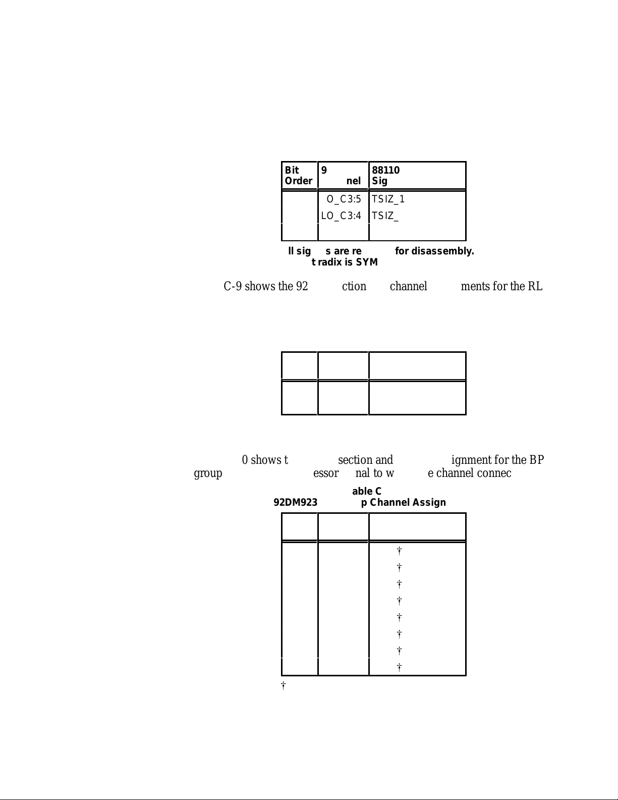
Service Information
Á
Á
Á
Á
Á
Á
Á
Á
Á
Table C-8 shows the 92A96 section and channel assignments for the
DataSize group and the microprocessor signal to which each channel
connects, starting with the most significant bit (MSB).
Table C-8
92DM923 DataSize Group Channel Assignments
Bit
Order
MSB
LSB
Á
92A96
Channel
ÁÁ
LO_C3:5
LO_C3:4
LO_C3:6
88110
Signal Name
ББББББ
TSIZ_1
TSIZ_O
TBST~
All signals are required for disassembly.
Default radix is SYM.
Table C-9 shows the 92A96 section and channel assignments for the RL
group and the microprocessor signal to which each channel connects,
starting with the most significant bit (MSB).
Table C-9
92DM923 RL Group Channel Assignments
Bit
Order
MSB
LSB
Á
92A96
ÁÁ
Channel
LO_C3:7
HI_C3:6
88110
ББББББ
Signal Name
R/W~
LK~
All signals are required for disassembly.
Default radix is SYM.
Table C-10 shows the 92A96 section and channel assignment for the BP
group and the microprocessor signal to which the channel connects.
92DM923 88110 Instruction Manual
Online Version
Table C-10
92DM923 BP Group Channel Assignment
Bit
Order
MSB
LSB
[
This signal is not required for disassembly.
Á
92A96
Channel
LO_A1:7
ÁÁ
LO_A1:6
LO_A1:5
LO_A1:4
LO_A1:3
LO_A1:2
LO_A1:1
LO_A1:0
88110
Signal Name
BP_7
[
ББББББ
BP_6
[
BP_5
[
BP_4
[
BP_3
[
BP_2
[
BP_1
[
BP_0
[
Default radix is OFF.
C-11
Page 63
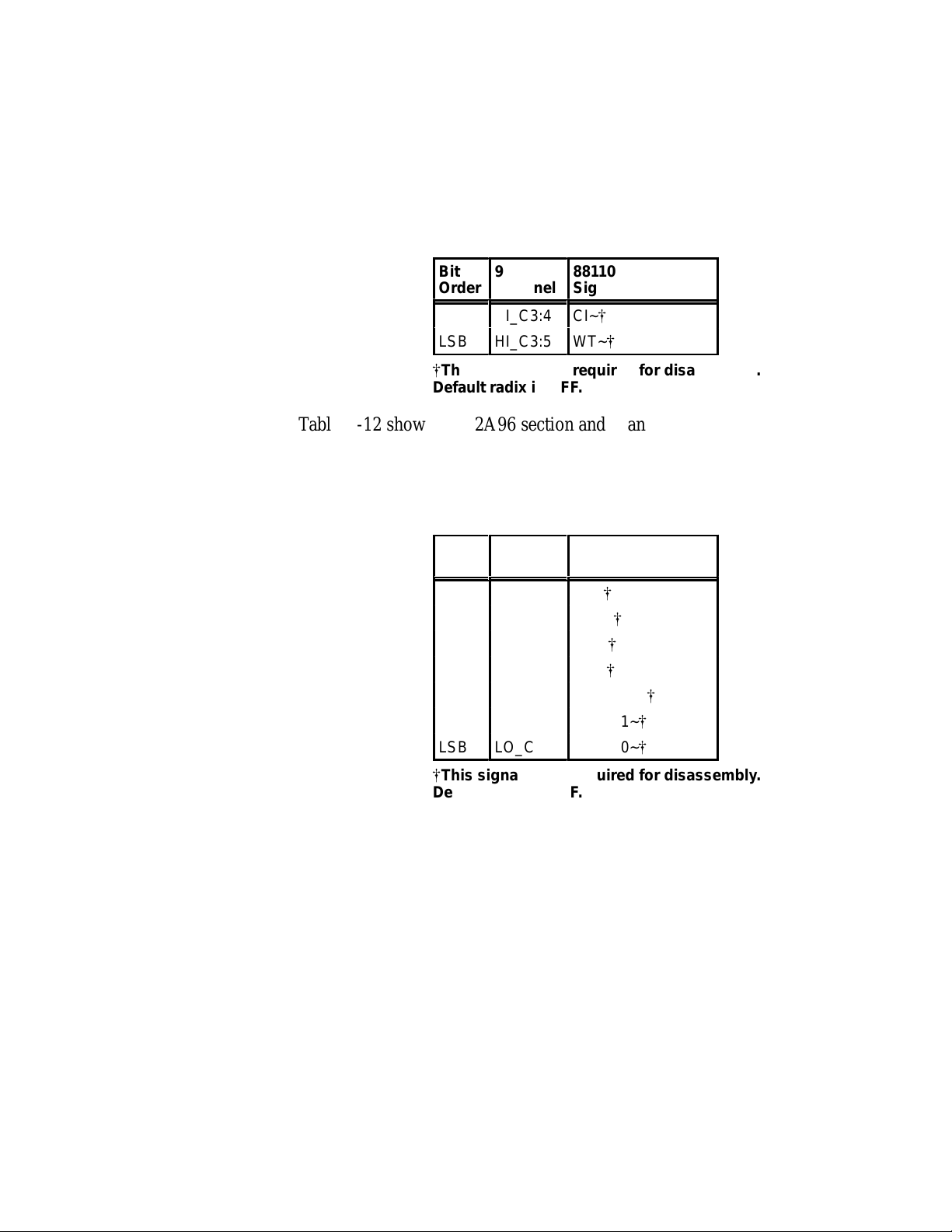
Service Information
Á
Á
Á
Á
Á
Á
Table C-11 shows the 92A96 section and channel assignments for the
CACHE group channels and the microprocessor signal to which each
channel connects, starting with the most significant bit (MSB).
Table C-11
92DM923 CACHE Group Channel Assignments
Bit
Order
MSB
LSB
[
This signal is not required for disassembly.
Á
92A96
ÁÁ
Channel
HI_C3:4
HI_C3:5
88110
ББББББ
Signal Name
CI~
[
WT~
[
Default radix is OFF.
Table C-12 shows the 92A96 section and channel assignment for the
SNOOP group and the microprocessor signal to which the channel
connects, starting with the most significant bit (MSB).
Table C-12
92DM923 SNOOP Group Channel Assignment
Bit
Order
MSB
LSB
Á
92A96
Channel
ÁÁ
HI_C2:5
LO_C2:6
HI_C3:2
HI_C3:7
LO_C2:7
LO_C2:5
LO_C2:4
88110
Signal Name
ББББББ
SR~
[
GBL~
[
INV~
[
MC~
[
SHARED~
SSTAT1~
SSTAT0~
[
[
[
C-12
[
This signal is not required for disassembly.
Default radix is OFF.
92DM923 88110 Instruction Manual
Online Version
Page 64
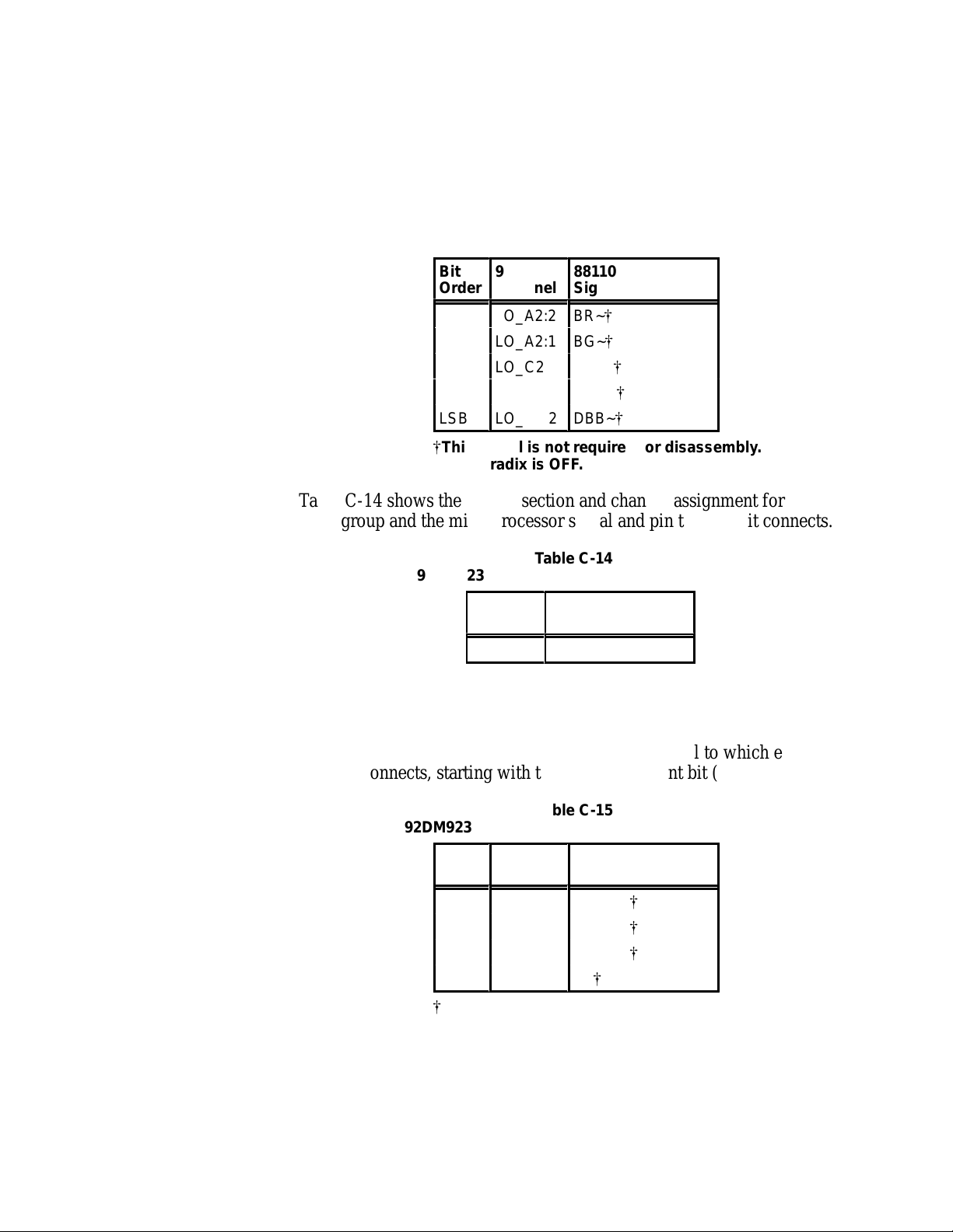
Service Information
Á
Á
Á
Á
Á
Á
Á
Á
Á
Á
Á
Table C-13 shows the 92A96 section and channel assignments for the
ARBTR group channels and the microprocessor signal to which each
channel connects, starting with the most significant bit (MSB).
Table C-13
92DM923 ARBTR Group Channel Assignments
Bit
Order
MSB
LSB
[
This signal is not required for disassembly.
Á
Á
92A96
ÁÁ
Channel
LO_A2:2
LO_A2:1
LO_C2:1
LO_A2:0
LO_C2:2
ÁÁ
88110
ББББББ
Signal Name
BR~
[
BG~
[
ABB~
[
DBG~
[
DBB~
[
ББББББ
Default radix is OFF.
Table C-14 shows the 92A96 section and channel assignment for the
CLK group and the microprocessor signal and pin to which it connects.
Table C-14
92DM923 CLK Group Channel Assignment
92A96
ÁÁ
Channel
LO_A2:5
This signal is required for disassembly.
Default radix is OFF.
88110
ББББББ
Signal Name
CLK=
Table C-15 shows the 92A96 section and channel assignments for the
PSTAT group channels and the microprocessor signal to which each
channel connects, starting with the most significant bit (MSB).
92DM923 88110 Instruction Manual
Online Version
Table C-15
92DM923 PSTA T Group Channel Assignments
Bit
Order
MSB
LSB
[
This signal is not required for disassembly.
Á
92A96
Channel
ÁÁ
LO_A3:2
LO_A3:1
LO_A3:0
HI_C3:3
88110
Signal Name
ББББББ
PSTAT2
PSTAT1
PSTAT0
CL
[
[
[
[
Default radix is OFF.
C-13
Page 65

Service Information
Á
Á
Á
Á
Á
Á
Á
Á
Á
Á
Table C-16 shows the 92A96 section and channel assignment for the
INTR (Interrupt) group and the microprocessor signal to which the
channel connects, starting with the most significant bit (MSB).
Table C-16
92DM923 INTR Group Channel Assignment
Bit
Order
MSB
LSB
[
This signal is not required for disassembly.
Á
92A96
ÁÁ
Channel
HI_C3:1
HI_C3:0
HI_C2:4
LO_A2:3
88110
ББББББ
Signal Name
NMI~
[
INT~
[
RST~
[
BPE~
[
Default radix is OFF.
Table C-17 shows the 92A96 section and channel assignment for the
JTAG group and the microprocessor signal to which the channel
connects, starting with the most significant bit (MSB).
Table C-17
92DM923 JTAG Group Channel Assignment
Bit
Order
MSB
LSB
Á
92A96
Channel
LO_A3:7
ÁÁ
LO_A3:6
LO_A3:5
LO_A3:4
LO_A3:3
88110
Signal Name
TDO~
[
ББББББ
TRST~
TMS~
TCK~
TDI~
[
[
[
[
C-14
[
This signal is not required for disassembly.
Default radix is OFF.
Table C-18 shows the 92A96 section and channel assignments for the
clock channels (not part of any group) and the microprocessor signal to
which each channel connects.
Table C-18
92DM923 Clock Channel Assignments
92A96
ÁÁ
Channel
CLK3
CLK2
CLK1
ÁÁ
All signals are required for disassembly.
]
This channel is double probed so that it will be
stored in the acquisition.
88110
ББББББ
Signal Name
CLK
]
TEA~
]
TA~
]
ББББББ
92DM923 88110 Instruction Manual
Online Version
Page 66
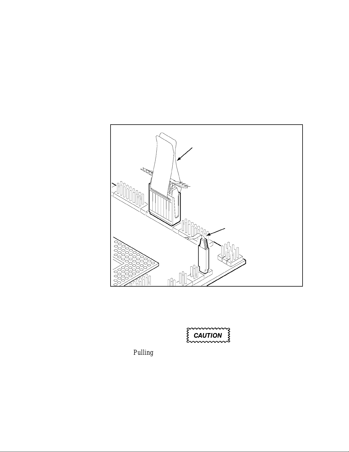
Service Information
DISCONNECTING PROBES
You may need to disconnect the clock and 8-channel probes from the
probe adapter to use them on another application, to connect individual
podlets to other signals in your 88110 system, or to replace defective
clock or probe channels (podlets). Refer to Figure C-3 and the
following procedure to disconnect the clock and 8-channel probes from
the probe adapter. Use the antistatic shipping material to support the
probe adapter while disconnecting the clock and 8-channel probes.
Squeeze the pull tabs together,
being careful not to pinch any
podlet cables between them,
and pull.
Grasp the body of the clock
probe and pull to remove.
Do not pull on the cable or top
of the probe body.
Figure C-3.Disconnecting clock and 8-channel probes.
1. Power off the SUT. It is not necessary to power off the
DAS 9200.
CAUTION
Pulling on the cables, on the neck of the clock probe, or
pinching the cables between the pull tabs can damage the
probes. Always handle the probes by their bodies.
2. Firmly grasp the body of a clock probe and gently pull it off of
the square pins.
92DM923 88110 Instruction Manual
Online Version
C-15
Page 67

Service Information
3. Squeeze the pull tabs on the podlet holder together; be careful
not to pinch any podlet cables between them.
4. Gently pull the 8-channel probe off of the square pins.
REMOVING AND REPLACING PROBE PODLETS
Each 8-channel probe consists of 8 single-channel podlets ganged
together in a podlet holder. You may need to remove these podlets from
the 8-channel probe to use for alternate connections to 88110 system
signals.
Refer to the discussions on Alternate Microprocessor Connections in
Appendix B and Channel Assignments in Appendix C for information
about which channels you can use to make alternate connections
between the DAS 9200 and system under test without disturbing the
channel connections required for disassembly.
You can also use these procedures to replace a defective clock probe or
a defective podlet from an 8-channel probe.
Removing Probe Podlets from the Interface Housing
Refer to Figure C-4 and the following procedure to remove a clock
probe or an 8-channel probe podlet from the interface housing.
1. Power off the SUT. It is not necessary to power off the
DAS 9200.
2. Use a small pointed tool such as a ballpoint pen, pencil, or
straightened paper clip to press down on the latch detent of the
podlet through an opening on the interface housing.
3. Gently pull the podlet connector out of the housing with one
hand while pressing down on the latch detent with the pointed
tool.
C-16
92DM923 88110 Instruction Manual
Online Version
Page 68

Service Information
PAPER CLIP
Press down on the
detent latch while
pulling out the
podlet.
Gently pull
out the podlet.
Figure C-4.Removing a clock or probe podlet from the interface housing.
Replacing a Clock Probe
To replace a clock probe, insert a new clock probe into the same clock
channel position on the interface housing. Insert the clock probe into
the interface housing with the detent latch oriented to the label side of
the housing. Refer to Figure C-4.
Removing Probe Podlets from the Podlet Holder
Refer to Figure C-5 and the following procedure to remove the
8-channel probe podlets from the podlet holder.
CAUTION
Excessive pulling on the sides of the holder can damage
the podlet holder. Spread the holder open wide enough to
clear and remove the podlets.
1. To remove podlets from the podlet holder, grasp the plastic pull
tab on each side of the podlet holder and gently spread the sides
of the holder open just enough to clear a podlet.
2. Remove the middle two podlets from the podlet holder by
pushing up on the metal pin receptacles.
3. Release the tabs on the podlet holder.
4. Remove the remaining podlets by turning and extracting each
92DM923 88110 Instruction Manual
Online Version
one at a time.
C-17
Page 69
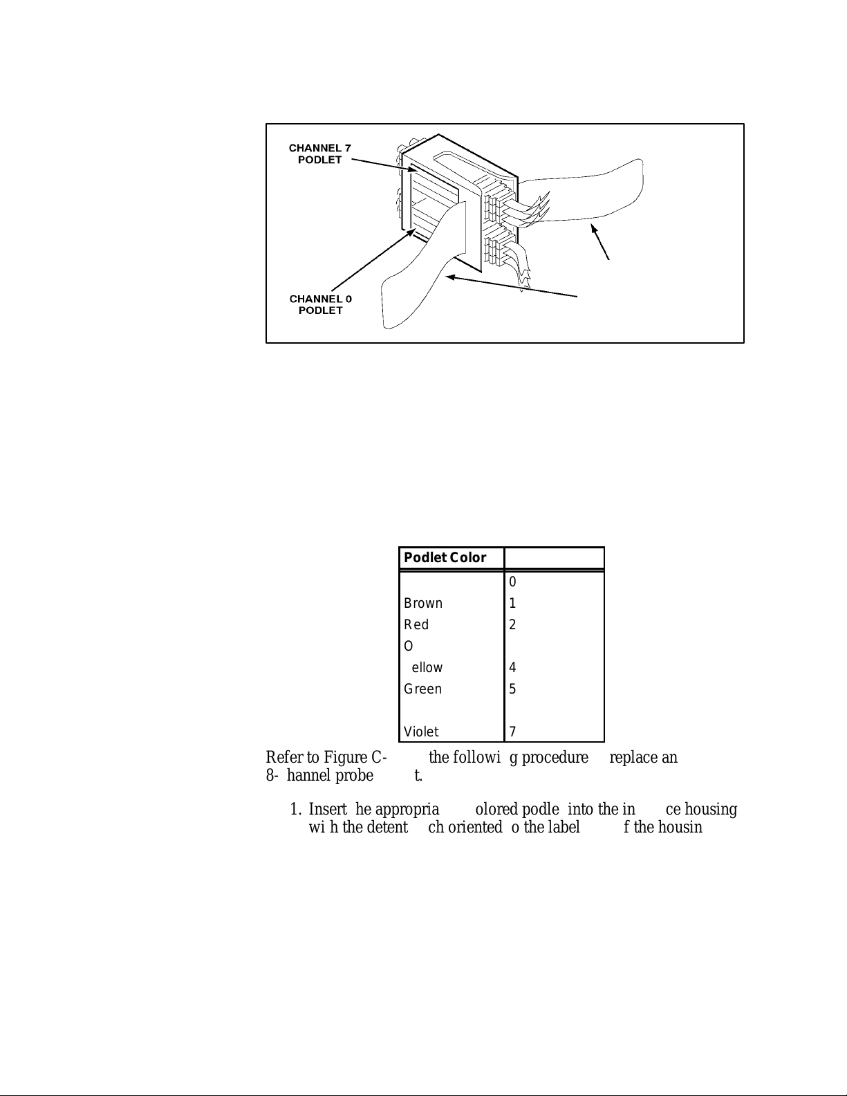
Service Information
Gently pull the tabs apart
just enough to clear the
two center podlets.
Figure C-5.Ganging together the 8-channel probe podlets.
Replacing 8-Channel Probe Podlets
The channel podlets must retain the same channel order on both the
interface housing and in the podlet holder. Be sure to replace the old
podlet with a podlet of the same color. Table C-19 shows the color code
and channel number of each podlet for an 8-channel probe.
Table C-19
Podlet-to-Channel Color Code
Podlet Color
Black
Brown
Red
Orange
Yellow
Green
Blue
Violet
Channel
0
1
2
3
4
5
6
7
Refer to Figure C-5 and the following procedure to replace an
8-channel probe podlet.
1. Insert the appropriately colored podlet into the interface housing
with the detent latch oriented to the label side of the housing.
2. If you are replacing a single podlet, orient the podlet connector
marked GND towards the side of the podlet holder labeled
GROUND.
3. Grasp the plastic pull tab on each side of the holder and gently
spread the sides of the holder open just enough to clear the
podlet.
C-18
92DM923 88110 Instruction Manual
Online Version
Page 70
Service Information
4. Hold the podlet body with the other hand and place it in the
holder in the correct channel order. Do not grasp and turn the
podlet cable.
5. If you are reganging all the podlets of an 8-channel probe, begin
ganging the podlets together starting with either channel 0 or
channel 7. Orient the podlet channel marked GND towards the
side of the podlet holder labeled GROUND.
CAUTION
Avoid twisting the podlet cables between the interface
housing and the podlet holder. To prevent damage to the
podlets, keep the podlet cables parallel to each other when
ganging them into the holder.
6. Hold the podlet body, turn the podlet body parallel to the sides of
the holder, move it into the holder, and use your fingers to press
it into place perpendicular to the sides of the holder. Be sure to
gang the podlets in the correct channel order according to the
channel label on the podlet holder and podlet color code, with all
ground channels toward the Ground side of the holder. Do not
place the podlet into the holder by grasping the podlet cable.
7. Continue placing the next two podlets, one at a time, in channel
order, in the podlet holder. Orient all ground channels toward the
Ground side of the holder.
8. The fourth podlet should be either channel 0 or 7, whichever one
is not already placed in the holder. Place this podlet in the other
end of the podlet holder and orient the ground channel correctly.
9. Continue placing the next two podlets, one at a time, in channel
order, in the podlet holder. Continue orienting the ground
channels correctly.
CAUTION
Excessive pulling on the sides can break the podlet holder.
Spread the holder open only wide enough to clear the
podlet.
10. Grasp the plastic pull tab on each side of the holder and gently
spread the sides of the holder open just enough to clear a podlet.
11. Place the last pair of podlets (channels 3 and 4) in the podlet
holder in proper channel order, orienting the ground channels to
the Ground side of the holder.
92DM923 88110 Instruction Manual
Online Version
C-19
Page 71

Service Information
REMOVING AND REPLACING SOCKETS
The probe adapter board contains sockets designed to protect the probe
adapter, and to make it easy to insert and remove the microprocessor.
The socket on top of the probe adapter board is soldered and cannot be
removed. The protective socket on the bottom of the probe adapter
board can be removed.
You should not have to remove the replaceable protective socket on the
probe adapter unless the pins on the socket are damaged. To remove the
protective socket, refer to Figure C-6 and follow these steps:
1. Place a proper (nonmetallic) socket removal tool between the
socket and the probe adapter board. Figure C-6 shows an AMP
PGA removal tool.
CAUTION
Do not use a screwdriver to remove the protective socket
from the probe adapter board. You can easily damage the
etched runs on the board.
C-20
Figure C-6.Removing a protective socket from a typical PGA probe adapter
board.
2. Push down on the handle of the tool until the socket begins to
separate from the probe adapter board pins.
92DM923 88110 Instruction Manual
Online Version
Page 72

Service Information
CAUTION
Do not completely pry off one side of the protective socket
and then the other. Applying uneven pressure can damage
the socket’s pins. Do not use board components as leverage
to remove the socket.
3. Perform step 2 on all sides of the socket. Use even pressure
alternately on all sides until the socket is loose.
4. Remove the socket from the board.
To replace the protective socket, follow these steps:
1. Spray an electrical contact lubricant on the probe adapter socket
so the replacement socket can be easily inserted.
2. Check that the new socket’s pins are straight.
3. Place the socket on the pins of the probe adapter board aligning
pin A1 with pin A1; make sure that all pins line up correctly.
4. Press the socket onto the board by applying equal pressure on
two opposed sides of the socket.
92DM923 88110 Instruction Manual
Online Version
C-21
Page 73

A
about this manual, 1-4
acquiring data, 4-1
acquisition difficulties, A-1
Address group
channel assignments, C-7
display column, 4-3
displaying symbolically, 4-8
alternate signal connections, B-1
application disk, 2-1
ARBTR group, channel assign-
ments, C-13
AUX groups, channel assignments,
B-2
B
BP group, channel assignments,
C-11
bus cycles, displayed cycle types,
4-2
bus forms, 5-3
bus timing, B-1
PSTAT group, C-13
RL group, C-11
SNOOP group, C-12
TCOD group, C-10
TSTATEA group, C-10
channel groups, 3-2
Channel setup menu, 3-2
channels, extra for alternate con-
nections, B-2
CLK group, channel assignment,
C-13
clock channel assignments, C-14
clock rate, 1-3
clocking
Custom, 3-2, 5-2
how data is acquired, B-1
External, 5-2
Internal, 5-2
Cond_Intr group, channel assign-
ments, B-3
conditional jumps, 4-4
connections
other microprocessor signals, B-1
probe adapter to SUT, PGA, 2-5
Control Flow display format, 4-4
cooling requirements, 1-4
Custom clocking, 3-2, B-1
cycle types, 4-2
selecting display formats, 4-1,
4-6
DataSize group, channel assign-
ments, C-11
default changes, affect on disassem-
bly, 3-2
DELETE FORMAT function key,
4-8
demonstration reference memory,
1-1, 4-12
Disasm Across Gaps field, 4-7
disassembled data
cycle type definitions, 4-2
viewing, 4-1
disassembler
changes that affect it, 3-2
DAS 9200 configuration, 1-2
loading software, 3-1
setup, 3-1
terms, 1-4
Disassembly Format Definition
overlay , 4-5
disassembly problems, A-2
disconnecting probes, C-15
display formats
Control Flow, 4-4
Hardware, 4-2
Software, 4-4
Subroutine, 4-5
Display Mode field, 4-6
C
CACHE group, channel assign-
ments, C-12
channel assignments
Address group, C-7
ARBTR group, C-13
AUX groups, B-2
BP group, C-11
CACHE group, C-12
CLK group, C-13
clocks, C-14
Cond_Intr group, B-3
DataSize group, C-11
Hi_Data group, C-8
INTR group, C-14
JTAG group, C-14
Lo_Data group, C-9
92DM923 88110 Instruction Manual
Online Version
D
DAS 9200
choosing correct floppy, 2-1
configuration for disassembler,
1-2
configuring, 2-3
software compatibility, 1-2
data
acquiring, 4-1
display formats
Control Flow, 4-4
Hardware, 4-2
Software, 4-4
Subroutine, 4-5
how it is acquired, B-1
E
electrical specifications, C-4
environmental specifications, C-6
error messages, A-1
ESCAPE & CANCEL function key,
4-7
exception vectors, 4-8
EXIT & SAVE function key, 4-8
External clocking, 5-2
IĆ1
Page 74

Index
F
floppy disk, compatability with sys-
tem software, 2-2
function keys
DELETE FORMAT, 4-8
ESCAPE & CANCEL, 4-7
EXIT & SAVE, 4-8
RESTORE FORMAT, 4-8
SAVE FORMAT, 4-8
G
gaps
disassembly across, 4-7
highlighting, 4-7
general purpose analysis, 5-1
Group Name field, 4-7
Group Radix field, 4-7
H
Hardware display format, 4-2
cycle type definitions, 4-2
Hi_Data group, channel assign-
ments, C-8
Highlight field, 4-7
Highlight Gaps field, 4-7
highlighting
disassembled data, 4-7
gaps, 4-7
I
installing hardware. See connec-
tions
installing software, 2-1
Internal clocking, 5-2
interrupt exception labels, 4-8
INTR group, channel assignments,
C-14
J
JTAG group, channel assignments,
C-14
L
labels, slot number, 2-4
leads (podlets). See connections
Lo_Data group, channel assign-
ments, C-9
loading, electrical, 1-4
loading support software, 3-1
logic analyzer, extra channels, B-2
M
Main bus, configuring DAS 9200
for 128-bit wide, 2-3
manual
conventions, 1-4
how to use, 1-4
menus
Disassembly, 4-1
State, 5-4
Timing, 5-3
microprocessor, package types sup-
ported, 1-1
Mnemonics display column, 4-3
module setup, 3-2
P
podlets, removing and replacing,
C-16
polarity, 3-2
printing data
disassembled, 4-11
state, 5-5
timing, 5-5
probe adapter
alternate connections, B-2
circuit description, C-2
cleaning, C-3
clearance, 2-5
adding sockets, 2-7
dimensions, C-5
configuring, 2-4
cooling, 1-4
electrical loading, 1-4
hardware description, C-1
placing the microprocessor in,
2-6
probes, disconnecting, C-15
protective socket, C-20
PSTAT group, channel assignments,
C-13
R
reference memory, demonstration,
1-1, 4-12
replaceable socket. See protective
socket
RESTORE FORMAT function key,
4-8
RL group, channel assignments,
C-11
S
SAVE FORMAT function key, 4-8
Scroll By field, 4-6
searching through data
disassembly, 4-9
state, 5-5
timing, 5-5
service information, C-1
setups, disassembler, 3-1
signals
active low sign, 1-4
alternate connections, B-2
IĆ2
92DM923 88110 Instruction Manual
Online Version
Page 75

Index
slot number labels, 2-4
SNOOP group, channel assign-
ments, C-12
sockets, removing and replacing,
C-20
software
compatability with system soft-
ware, 2-1
disassembler setup, 3-1
installation, 2-1
Software display format, 4-4
Software Support field, 3-1
specifications
electrical, C-4
environmental, C-6
specifying the trigger, 3-5
State menu, 5-4
state/timing split-screen display, 5-1
Subroutine display format, 4-5
SUT, definition, 1-4
Symbol T able field, 4-7
symbol tables, 3-3
copying and editing, 3-4
T
TCOD group, channel assignments,
C-10
terminology, 1-4
timestamp
definition of selections, 4-6
Timestamp field, 4-6
Timestamp column, 4-3
timing analysis, 5-2
Timing Format file, supplied, 5-3
Timing menu, 5-3
timing/state split-screen display, 5-1
TSTATEA group, channel assign-
ments, C-10
V
variable-width module, DAS 9200
configuration, 2-3
viewing disassembled data, 4-1
92DM923 88110 Instruction Manual
Online Version
IĆ3
 Loading...