


DAS-800 Series
Register-Level Programming
User’s Guide
Revision A - October 1993
Part Number: 86890

The information contained in this manual is believed to be accurate and reliable. However, Keithley
Instruments, Inc., assumes no responsibility for its use; nor for any infringements or patents or other
rights of third parties that may result from its use. No license is granted by implication or otherwise
under any patent rights of Keithley Instruments, Inc.
KEITHLEY INSTRUMENTS, INC., SHALL NOT BE LIABLE FOR ANY SPECIAL, INCIDENTAL,
OR CONSEQUENTIAL DAMAGES RELATED TO THE USE OF THIS PRODUCT. THIS
PRODUCT IS NOT DESIGNED WITH COMPONENTS OE 4 LEVEL OF RELIABILITY THAT IS
SUITED FOR USE IN LIFE SUPPORT OR CRITICAL APPLICATIONS.
Refer to your Keithley Instruments license agreement and Conditions of Sale document for specific
warranty and liability information.
All brand and product names ax trademarks or registered trademarks of theirrespective companies.
0 Copyright Keithley Instruments, Inc., 1993.
All rights reserved. Reproduction or adaptation of any part of this documentation beyond that permitted
by Section 117 of the 1976 United States Copyright Act without permission of the Copyright owner is
unlawful.
Keithley Instruments, Data Acquisition Division
440 Myles Standish Blvd. Taunton, MA 02780
Telephone: (508) X80-3000. FAX: (508) x80-0179

Table of Contents
Preface
1
Hardware Registers
A/D Conversion Registers
(Base Address + 0, Base Address + 1, Write). .
A/D Conversion Registers
(Base Address + 0, Base Address + 1, Read). . . . . . . .
Control Register (Base Address + 2, Write) . . . . .
Control Register 1 (Base Address + 2, Write) . . .
Conversion Control Register (Base Address + 2, Write)
Scan Limits Register (Base Address + 2, Write) . .
Status Register 1 (Base Address + 2, Read) . .
Gain / Control Select Register (Base Address + 3, Write).
Gain / Channel Status Register (Base Address + 3, Read)
Status Register (Base Address + 7, Read)
Status Register 2 (Base Address + 7, Read) . . . .
ID Register (Base Address + 7, Read) . . . . . . . . . . . . .
l-4
1-s
. 1-x
1-x
i-11
l-15
1-17
1-19
1-21
1-23
1-23
l-25
2 Programming Guidelines
Performing a S&ware-Initiated A/D Conversion.
Performing a Hardware-Initiated AD Conversion
Setting Up the Internal Clock
Setting Up an Analog Trigger
A Summary of Registers
B
Converting Binary Code to Voltage
..........................
..........................
.......... .2-l
.......... .2-2
.2-5
.2-8
111

List of Figures
Figure l-1.
A/D Conversion Registers (Write) . . .
Figure 1-2. A/D Conversion Registers (Read). . . .
Figure 1-3.
Control Register 1 . . . . . . . . . . . .
Figure 1-4. Conversion Control Register. . . . . . . .
Figure l-5. ScanLimits Register
Figure 1-6. Status Register 1 (Read) . .
Figure 1-7. Gaiu / Control Select Register (Write)
Figure 1-8. Gaiu/ Channel Status Register (Read)
Figure 1-9. Status Register 2 . . . . . . . . . . . . . . . . .
Figure l-10. ID Register. . . . . . . . . . . . . . . . . . . . . .
Figure A-l. DAS-800 Series Write Registers . . . . .
Figure A-2. DAS-800 Series Read Registers . . . . .
List of Tables
Table l-l. DA+800 Series Registers. .........
Tablo 1-2. Analog Multiplexer Address Selection
Table l-3.
Table l-4.
Range Selection Bits ..............
Register Selection Bits. ............
Table l-5. Identification Bits ................
Table A-l. Summary of Register I/O Bits. ......
. . . . . l-4
. . . . . l-6
. . l-9
. . . . l-11
l-16
. . l-17
1-19
. . . . .
. . . . . l-22
. . . ..l-24
1-26
. . . . .
. . . . . A-2
. . . . . A-3
..l-1
. . . . . . 1-9
. . . . . l-20
1-21
. .
. .1-26
A-4
iv

Preface
The
DA.5800 Series Register
the DAS-800 Series hardware registers.
The manual is intended for experienced programmers who want to gain
direct access to the DAS-800 Series registers to perform analog input,
digital I/O, or counter/timer I/O operations. It is assumed that users have
read
the DA&800 Series User’s Guide
boards’ functions, that they have completed the appropriate hardware
installalion and configuration, and that they are familiar with data
acquisition principles.
Note: This manual is not intended for application programmers who are
using the DAS-800 Function Call Driver or a menu-driven software
package. If you are using the DAS-800 Function Call Driver, refer to the
DAM00 Function Call Driver User’s Guide.
menu-driven software package, refer to the documentation supplied with
the package.
I10 User’s
to familiarize themselves with the
Guide
provides a description of
If you are using a
The
DAS-800 Series Register
. Chapter 1 contains a description of the DAS-800 Series hardware
registers.
. Chapter 2 contains guidelines you should follow when programming
certain functions of DAS-800 Series boards.
. Appendix A contains a summary of the bits in the DAS-800 Series
registers.
II0
User’s Guide
is organized as follows:
v

. Appendix B contains instructions for converting binary code to
voltage.
Throughout the manual, keep in mind that references to DAS-800 Series
boards apply to the DAS-800, DAS-801, and DAS-802 boards. When a
feature applies to a particular board, that board’s name is used.
vi

Hardware Re.gisters
The DAS-800 hardware registers require eight consecutive g-bit
locations. You assign the base address by setting switches on the
DAS-800 Series board; refer to the
more information on setting the base address. Since the
variable, the addresses of the individual registers are described as offsets
from the selected base address.
Each register has both a write function and a read function. Table l-l lists
the hardware registers and their write and read functions.
Table 1-l. DAS-800 Series Registers
DAS-800 Series User’s Guide for
base
address is
Address
Register
A/D Conversion
(LSB)
Write Function
Initiates an analog-to-digital
(A/D) conversion through
software. Refer to page 1-4.
Read Function
Contah. the four least
significant bits of data
converted by the
analog-to-digital converter
(ADC); determines the
statns of the FIFO. Refer to

Table l-l. DAS-800 Series Registers (cont.)
4ddress 3egister
:ontro1 (write)’
ltatus 1 (Read)
Write Function
Control Renister 1
Specifies an analog input
channel, enables interrupts,
and specifies digital output
values. Refer to page 1-8.
Qwwsion Control Reeister
Specifies the clock soume,
enables a digital trigger,
specifies when to generate an
interrupt, enables automatic
channel scanning, enables a
digital gate, and enables
hardware conversions. Refer
topage l-11.
$can Limits Reeister
Specifies the first and last
channels used in automatic
channel scanning. Refer to
page l-1,5.
3ead Function
Contains the currently
,elected analog input
:hannel, the state of the
ligital input lines, and the
,tatus of the ADC. Refer to
rage
l-17.
1-2
;254CjT02
Loads counter/timer0 (C/TO)
on the 8254
counter/timer
circuitry,
Contains the status of C/r0
mthe8254.

Table 1-l. DAS-800 Series Registers (cont.)
Address Register
I I
Base + 6
8254C/T2'
I I
Notes
’ An indirect addressing technique is used to determine which of three Control registers is accessed.
Refer to page l-8 for more information.
‘The 8254 counter/timer registers ax not described in this chapter. Refer to the DAS-800 Series User’s
Guide
for a list of companies that provide documentation describing how to program the 8254
counter/timer registers. Refer to page 2-5 for a programming procedure to follow when using the 8254
counter/timers as an internal clock source.
3 An indirect addressing technique is used to determine which of two Status registers is accessed. Refer
to page l-23 for more information.
/ Write Function 1 Read Function I
Loads C/T2 on the 8254
counter/timer circuitry.
Contains the status of C/T2
onthe8254.
Notes:
compatible with the DAS-8 Series registers. (On DAM Series boards,
only Control register 1 is available at Base Address + 2, Write, and no
register is available at Base Address
programs written to support the DAS-8 with the DAS-800, application
programs written to support the DAS-8 PGA with the DAS-801, and
application programs written to support the DAS-8 PGA/G2 with the
DAS-802.
Whenever the board is powered up or reset, all output (write) register bits
are set to 0.
The remainder of this chapter describes the hardware registers in detail.
On power-up or system reset, the DAS-800 Series registers are
+ 7, Read.) You can use application
1-3

A/D Conversion Registers
(Base Address + 0, Base Address + 1, Write)
The A/D Conversion (LSB) register (Base Address + 0, Write) and the
A/D Conversion (MSB) register (Base Address + 1, Write), shown in
Figure l-l, allow you to initiate an A/D conversion through software.
Writing any value to either of these registers initiates an A/D conversion;
the actual value written is irrelevant.
Base Address + 0
Write
Base Address + 1
wrae
Notes:
To initiate conversions through software, you must disable
hardware conversions by setting the HCEN bit of the Conversion Control
register to 0. Refer to page 1-11 for more information.
Refer to page 2-l for programming guidelines to follow when initiating
A/D conversions through software.
Bit 7 6 6 4
Bit 7
lYxNw
6
6 4
Figure 1-l. A/D Conversion Registers (Write)
3 2 1 0
3
2
1 0
1-4

A/D Conversion Registers
(Base Address + 0, Base Address + 1, Read)
The AiD Conversion (LSB) register (Base Address + 0, Read) and the
A/D Conversion (MSB) register (Base Address + 1, Read), shown in
Figure l-2, contain the result of an A/D conversion. The four least
significant bits are stored in the A/D Conversion (LSB) register: the eight
most significant bits are stored in the AD Conversion (MSB) register.
The A/D Conversion (LSB) register also contains the status of the data in
the FIFO.
Notes: Bits 0 and 1 of the AD Conversion (LSB) register (FIFO Empty
and FIFO OVF) are used only when conversions are initiated by
hardware (the HCEN bit of the Conversion Control register is set to 1).
Refer to page l-l 1 for more information about the HCEN bit. When
conversions are initiated through software, FIFO Empty and FIFO OVF
are always set to 0.
Bits 2 and 3 of the A/D Conversion (LSBI register are alwavs set to 0.
l-5

Basg Address + 0
Read
0 I No data overflow
1 = Data overflow
0 = Data In FIFO
1 I FIFO empty -
A/D ConversIon (MSB)
Base Address + 1
Read
811 7
Dll
WW
u I ‘I I I I I
6
DIO D6
5 4 3
D6
2
D7 D6 D.5 04
1 0
Figure l-2. A/D Conversion Registers (Read)
Notes:
To ten&e proper operation of the FIFO, always read both A/D
Conversion registers. Read the A/D Conversion (LSB) register first,
followed by the A/D Conversion (MSB) register.
If you are acquiring multiple data samples, make sure that you read the
A/D Conversion registers once more than the number of samples you are
acquiring tc ensure that a FIF’O overflow did not occur on the last data
sample.
I-6
Hardware Registers

The bits in the A/D Conversion registers are described as follows:
T FIFO Empty - Determines the status of the data in the FIFO.
If FIFO Empty = 0, the FIFO contains data.
If FIFO Empty = 1, the FIFO is empty. If you read either of the A/D
Conversion registers when FIFO Empty = 1, the value read is the last
value stored in the FIFO.
. FIFO OVF (FIFO Overflow) - Determines the stahts of the data in
the FJlFO.
If FIFO OVF = 0, no data in the FIFO was overwritten,
If FIFO OVF = 1, data in the FIFO has been overwritten and one or
more samples were lost.
To restore normal operations after a FIFO overflow condition occurs
(FIFO OVF = 1). you must disable conversions by setting the HCEN
bit of the Conversion Control register to 0, and then restart the board
and set up your operation again.
. DO through Dll (Data) A/D conversion data.
When you initiate an A/D conversion lhrough software, the data is
read directly from the ADC and represents the result of the most
recent conversion. When you initiate A/D conversions through
hardware, the FIFO control logic selects the appropriate sample.
When reading data in a bipolar input range, data is represented in
offset binary format: a code of 0000 0000 0000 represents negative
full scale, a code of 1111 1111 1111 represents positive full scale, and
a code of 1000 0000 0000 represents 0 V. When reading data in a
unipolar input range, the data represents the magnitude of the
measured value; a code of 0000 0000 0000 represents 0 V and a code
of 1111 1111 I1 11 represents positive full scale.
Refer to Appendix B for more information on converting the binary
code to voltage.
1-7

Control Register (Base Ad:dress + 2, Write)
The Control register is actually a group of three different Control registers
that are accessed through a common port address (Base Address + 2,
Write). An mdirect addressing technique determines which of the three
Control registers is accessed. The addressing technique uses the register
select bits (CSl and CSO) of the Gain/Control Select register as a pointer
to the appropriate register. Refer to page l-20 for more information about
CSl
and CSO.
The three Control registers are described as follows:
l
Control register 1
interrupts, and specifies digital output values. Control register 1 is
accessed when CSl = 0 and CSO = 0.
register; it is selected whenever the board is powered up or reset.
Specifies an analog input channel, enables
This
is the default Control
. Conversion Control register
- Specifies the clock source, enables a
digital trigger, specifies when to generate an interrupt, enables
automatic channel scanning, enables a digital gate, and enables
hardware conversions. The Conversion Control register is accessed
when CSl = 0 and CSO = 1.
. Scan Limits register
- Specifies the first channel and the last channel
used in automatic channel scanning. The ScanLimits register is
accessed when CSl = 1 and CSO = 0.
Note:
If yo~u write to the Control register when CSl / CSO = 11, the
results are unpredictable,
The Control registers are described in the following sections.
Control Register 1 (Base Address + 2, Write)
Control register 1, shown in Figure 1-3, is accessed when
CSl / cso ::= 00.
l-8
Hardware Registers

Base Address + 2
write
csl /cso.oo
Bit 7 6 5 4 3 2 1 0
OP4 OP3
Dlgltal Ouiput Data
OP2 OPl
- v
0 = Dlsabled Channel 2 .OlO
1 i: Enabled Channel 3 =Oll
INTE
MA2
Channel 0 ~000
Channel 1 ~001
Channel 4 I 100
Channel 5 I 101
Channel 5 D 110
Channel 7 E 111
MAI
MAO
Figure 1-3. Control Register 1
The bits in Control register 1 are described as follows:
. MAO through MA2 (Analog Multiplexer Address Selection) -
Select the single analog input channel on which to perform an A/D
conversion. as shown in Table 1-2.
Table 1-2. Analog Multiplexer Address Selection
m,-,,,
1-9

Note:
When you are using automatic channel
scanning (the
EACS
bit of the Conversion Control register is set to l), the values written to
these bits are ignored. Refer to page 1-15 for more information about
the
EACS
bit.
. INTE (Interrupt Enable)
- Enables and disables interrupts on the
host’s PC bus.
If
INTEi
= 0, interrupts are disabled.
If
INTEL
= 1, interrupts are enabled.
Notes:
The condition that causes an interrupt to occur is determined
by the I,EOC bit of the Conversion Control register. When the
interrupt occurs, the IRQ bit of Status register 1 is set to 1. If
INTE :: 1 when IRQ is set to 1, the host receives the interrupt. Refer
to page 1-14 for more information about the IEOC bit. Refer to page
1-18 for more information about the IRQ bit.
If interrnpts are enabled, you must specify an interrupt level in the
configuration file and by setting a jumper on the board. Refer to the
DAS-800
. OPl (Digital Output 1 Data)
Series User’s Guide for more information.
- Value written to the digital output
line associated with the OPl pin on the main I/O connector.
. OP2 (Digital Output 2 Data)
- Value written to the digital output
line associated with the OP2 pin on the main I/O connector.
l-10
. OP3 (Digital Output 3 Data)
- Value written to the digital output
line associated with the OP3 pin on the main I/O connector.
l
OP4 (Digital Output 4 Data)
- Value written to the digital output
line associated with the OP4 pin on the main I/O connector.
-..
Note:
Par all digital output data bits, a value of 1 forces the output
high; a value of 0 forces the output low.
Hardware Registers

Conversion Control ,Register (Base Address + 2, Write)
The Conversion Control register, shown in Figure l-4, is accessed when
cs1/cso=o1.
Base Address + 2
write
csl /csO.OI
0 = Disabled 0 = Disabled 0 = Disabled 0 q External
1 i: Enabled 1 = Enabled 1 c Enabled 1 q Internal
Note:
If you write to bit 6 of the Conversion Control register, the results
are unpredictable.
sit 7 0 5
7 7 7
-l-Source
0 q Disabled 0 E External 0 q Normal
1 = Enabled ,.EOC 1 s Cascaded
Figure 1-4. Conversion Control Register
4
3
2
1
0
The bits in the Conversion Control register are described as follows:
. HCEN (Hardware Conversion Enable)
- Enables and disables
hardware conversions.
If
HCEN
= 0, hardware conversions are disabled. If a conversion is in
progress when you set HCEN to 0, the conversion process stops.
l-11

Note: lli you are
using
an
internal clock and you stop the conversion
process at any time, you must reload the 8254 counter/timer(s) with
the desired count before restarting conversions. This ensures that the
timing
between
conversions remains consistent.
If HCEN = 1, hardware conversions start. The ITE bit determines
whether conversionsbegin immediately (internal clock) or are armed,
waiting :for the next falling edge of the external clock. In addition, the
DTEN bit determines whether conversions wait for the digital trigger
condition to occur.
You can modify the remaining bits of the Conversion Control register
only if IICEN = 0. If you write to the Conversion Control register
with HCEN set to 1 ,,the conversion process starts; all other bits in the
Conversion Control register retain their previous settings, regardless
of the values written, to them.
Caution:
To ensure,that the board works properly when initiating
conversions under hardware control, you must follow a particular
programming sequence. This sequence is described on page 2-2.
. ITE (Internal Time Base Enabled) - Selects the clock source for
A/D cortversions. This bit affects board operation only if hardware
conversions are enabled (HCEN = 1).
If ITE := 0, the falling edge of an external clock attached to the
INT-IN pin on the main I/O connector initiates each conversion. (The
external clock frequqncy cannot exceed 40 kHz.)
If ITE =: 1, the interhal clock (the 8254 counter/timer circuitry)
determines the time interval between conversions.
l-12
Hardware Registers

Note: If you are using an internal clock, the counter/timer(s) you are
using (C/r2 or C/T1 and Clr2) must be programmed for rate
generator mode (Mode 2). Refer to page 2-5 and to your 8254
documentation for inrormation on programming a counter/timer
mode. The
DAS-800 Series User’s Guide
provides a list of companies
that provide documentation describing how to program the 8254
counter/timers.
. CASC (Internal Clock Mode) - Determines the use of C/r2 and
C/r1 of the 8254 counter/timer circuitry when using the internal
clock. This bit affects board operation only if the internal clock is
enabled (ITE = 1).
If CASC = 0, only C/T2 of the 8254 counter/timer circuitry is used
(normal mode). C/r2 is loaded with the number of 1 ~.ls clock ticks
between conversions.
If CASC = 1, both C/r2 and C/T1 of the X254 counter/timer circuitry
are used (cascaded mode). C/T2 and C/T1 are both loaded with a
count value. When C/r2 reaches terminal count, CD1 decrements by
1. When both C/r2 and C/r1 reach terminal count, a conversion
occurs.
Refer to page 2-5 and to your 8254 documentation for information on
loading C/r2 and C!/Tl. The
DAS-800
Series User’s
Guide
provides a
list of companies that provide documentation describing how to
program the 8254 counter/timers.
. DTEN (Digital Trigger Enable) -Enables and disables a digital
trigger. This bit affects board operation only if hardware conversions
are enabled (HCEN = 1).
If DTEN = 0, the digital trigger is disabled. If HCEN = 1, A/D
conversions begin immediately (if using an internal clock source) or
at the next falling edge detected on the INTJN pin on the main I/O
connector (if using an external clock source).
If DTEN = 1, the digital trigger is enabled. If HCEN = 1, A/D
conversions begin when the board detects a rising edge on the IPl pin
on the main I/O connector (if using an internal clock source) or at the
1-13

next falling.edge detected on the INT-IN pm after the board detects a
rising edge on the lP1 pin (if using an external clocli source).
Notes:
To enable the digital trigger, DTEN must be set to 1 AND
GTEN must be set to 0. If both these bits are set to 1, the hardware
gate is enabled, but the digital trigger is disabled. Refer to page 1-15
for information about the GTEN bit.
To reset the digital trigger detection logic after the desired number of
sample:; has been acquired, write any value to the Conversion Control
register.
You can use software to perform an analog trigger function. Refer to
page 2-g for programming guidelines to follow when setting up an
analog ,trigger.
. IEOC (Interrapt Select) - Determines when an interrupt occurs.
This bit; affects board operation only if interrupts are enabled
(INTE := 1).
If IEOC = 0, an interrupt occurs when a rising edge is detected on the
INT-IN pin on the main I/O connector.
If IEOC = 1, an interrupt occurs at the end of every conversion.
I-14
When the interrupt occurs, the IRQ bit of Status register 1 is set to 1.
If the INTE bit of Control register 1 is set to 1 when IRQ is set to 1,
the hos~t receives the interrupt. Refer to page l-10 for more
information about the INTE bit. Refer to page 1-18 for more
information about the IRQ bit.
Caution:
The IEOC bit affects the operation of the interrupt
generation logic. When changing the state of this bit, you may
generate a spurious interrupt. Therefore, before changing the state of
IEOC, you should always disable interrupts by setting the INTE bit
of Control register 1 to 0. Refer to page l-10 for more information
about the INTE bit.
Hardware Registers

. EACS (Automatic Channel Scan Enable) - Enables and disables
automatic channel scanning. This bit affects board operation only if
hardware conversions are enabled (HCEN = 1).
If EACS = 0, automatic channel scanning is disabled. If HCEN = 1,
conversions are performed on the single channel specified by the
MAO through MA2 bits of Control register 1. Refer to page 1-9 for
more information about the MAO through MA2 bits.
If EACS = 1, automatic channel scanning is enabled. If HCEN = 1,
conversions are performed on the range of channels specified by the
Scan Limits register; the hardware increments the address shortly
after the start of each conversion. Refer to the next section for more
information about the Scan Limits register.
Note:
Make sure that you specify the start and end channels before
you set EACS to 1.
. GTEN (Gate Enable) - Enables and disables the hardware gate. This
bit affects board operation only if hardware conversions are enabled
(HCEN = 1).
If GTEN = 0, the hardware gate is disabled.
If GTEN = 1, the hardware gate is enabled.
Note:
To enable the hardware gate, both GTEN sod DTEN must be
set to 1. Refer to page l-13 for more information about the DTEN bit.
Scan Limits Register (Base Address + 2, Write)
The Scan Limits register, shown in Figure l-5, is accessed when
CSl / cso = 10.
Note:
If you write to bits 6 and 7 of the Scan Limits register, the results
are unpredictable.
l-15

sit 7 6
BaseAddress+
WI110 EC1 EC0 SC2 SC1 SC0
c!s1/cs0=10
5 4 3 2 1 0
!3Lumiu
GhannelO.OOO
Channell -001
Channel2 ~010
Channe13.011
dhanne14.100
dhannel5 ~101
Channel6 ml10
Qhannel, =I11
z!tGw&d
ChannelO=OOO
Channel1.001
Channe12.010
Channe13.011
Channe14.100
Channel5=101
Channe16.110
Channel,.,,,
Figure 1-5. Scan Limits Register
The bits in the Scan Limits register are described as follows:
. SC0 through SC2 (Start Channel Selection) -
Select the
channel used in automatic channel scanning.
. EC0 through EC2 (Fnd Channel Selection)
- Seledt the last channel
used in automatic channel scanning.
Note:
The litart channel :can be higher or lower than the end channel.
fist
1-16
Make sure that you select the start and end channel before you enable
automatic channel scanning by setting the
EACS
bit of the Conversion
Control register to 1. Refer to page 1-15 for more information about the
EACS bit.
Hardware Registers

Status Register 1 (Base Address + 2, Read)
Status register 1 (Base Address +2, Read), shown in Figure 1-6, contains
the currently selected analog input channel, the interrupt status, the state
of the digital input lines, and the status of the ADC.
Blt 7 6
Base Address + 2
Read
2 1 0
MA2 MA1 MAO
v
Analoa Multl~lexer Addresg
Channel 0 I 000
Channel 1 E 001
Channel 2 D 010
Channel 3 i 011
Channel 4 I 100
Channel 6 E 101
Channel 6 = 110
Channel 7 = 111
-EOC IP3
0 = Not busy
1 = Busy
6 4 3
IP2 IPI
v-
DIgItal Input Data
lnfrtrru~t
0 = InaCtIVe
1 q
IRQ
Flip,-FIILB
Active
Figure 1-6. Status Register 1 (Read)
The bits in Status register 1 are described as follows:
. MAO through MA2 (Analog Multiplexer Address Status) -
Indicate the analog input channel specified in the
bits of Control register 1. Note that this represents the next channel to
be converted. Refer to Table 1-2 on page l-9 for more information on
the meaning of the bits.
MAO through MA2
Note:
These bits have the same meaning as the
MAO through MA2
bits in the Gain / Channel Status register. Refer to page 1-22 for more
information.
1-17

l
IRQ (Interrupt Fliti-Flop Status) - Contains the status of the
interrupt flip-flop.
If IRQ := 0, the interrupt flip-flop is inactive, indicating that the
interrupt condition has not occurred since this bit was last cleared.
If IRQ := 1, the intermpt flip-flop is active, indicating that the
interrupt condition occurred.
Note:
The condition that causes the interrupt to occur is determined
by the YEOC bit of @e Conversion Control register. If the INTE bit
of ConWol register 1 is set to 1 when the interrupt occurs (IRQ = l),
the host receives the,interrupt. Refer to page l-14 for more
information about the IEOC bit. Refer to page l-10 for more
information about the INTE bit.
You can clear this bit by writing any value to Control register 1.
. IPl (Digital Input 1 Data) - State of the digital input line associated
with the IPl pin on the main I/O connector.
. IP2 (Digital Input 2 Data) - State of the digital input line associated
with th: IP2 pin on *e main I/O connector.
. IP3 (Digital Input 3 Data) - State of the digital input line associated
with the IP3 pin on the main I/O connector.
Note:
For all digital input data bits, a value of 1 indicates that the
input is high, a valuq of 0 indicates that the input is low.
l-16
. -EOC .. Contains the status of the ADC End-of-Conversion (-EOC)
bit.
If -EOC = 0, the ADC is not performing a conversion. You can read
the result of the last conversion from the A/D Conversion registers.
If -EOC = 1, the ADC is performing a conversion and data is not
available. Any data read while -EOC = 1 is undefined.
Hardware Registers
Note:
Only.
The -EOC bit is valid for.software-initiated A/D conversions
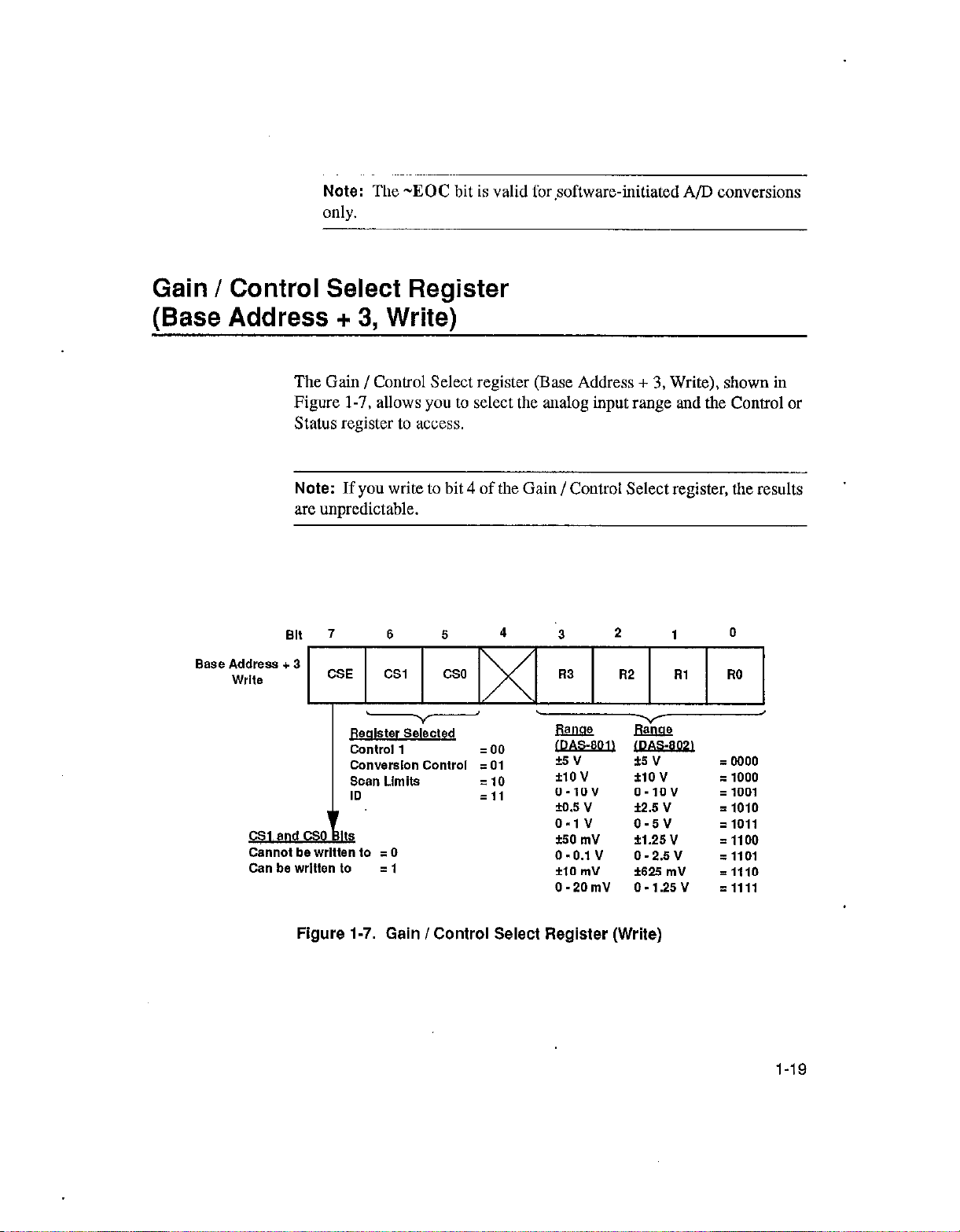
Gain / Control Select Register
(Base Address + 3, Write)
The Gain /Control Select register (Base Address + 3, Write), shown in
Figure l-7, allows you to select the analog input range and the Control or
Status register to access.
El11 7
Base Address + 3
Wlite
Cannot be written lo q 0
Can be wrItten to = 1
Note:
If you write lo bit 4 of the Gain/Control Select register, the results
are unpredictable.
6 6
v
~eqister Selected
Control 1 .oo
Conversion Control GE 01
Scan Limits =I0
ID =I1
4
3
FlmB2
F”““”
*1ov
o-1ov
M.5 v f2.5 v
O-IV 0.5v
%O mv fl.25 V
o.o.iv
f10 mv i626 mV z 1110
0-20mV 0.1.25V
Figure 1-7. Gain /Control Select Register (Write)
2
v
Bimss
i6 V ii woo
uov
o-iov = 1001
0-2.6V z 1101
1
0
q 1000
q 1010
q
1011
= 1100
rllll
1-19

The bits in ihe Gain / Control Select register are described as follows:
.
RO
through R3 (Rabge
Selection)
- Select the analqg input range for
DAS-801 and DAS-802 boards, as shown in Table 1-3.
Table 1-3. Range Selection Bits
I
t-
f5 v Isir IO
I
IO IO IO
Note: Since DAS-800 boards always have a f5 V analog inputrange,
these bits have no meaning for DAS-800 boards.
. CSl and CSO (Register Selection)
- Determine the Control register
that is accessed when you write data to Base Address + 2, Write, and
the Status register that is accessed when you read from Base
Address + 7, Read. The meaning of these bits is shown in Table 1-4.
i-20
Hardware Registers

Table I-4. Register Selection Bits
l
CSE (Register Selection Enable)
selection bits
If
CSE
written to; writing to the range selection bits (RO through R3) does
not affect the state of
If
CSE
to; writing to
(CSl
and CSO) can be written to.
= 0, the register selection bits
CSl
and CSO.
= 1, the register selection bits
CSl
and CSO does not affect the state of
Determines whether the register
(CSl and CSO)
(CSl
and CSO) can be written
cannot be
RO through
R3.
Gain / Channel Status Register
(Base Address + 3, Read)
The Gain I Channel Status register (Base Address + 3, Read), shown in
Figure 1-8, contains the currently selected analog input range, the
currently selected analog input channel, and the status of automatic
channel scanning.
l-21

Bl, 7 6 5 4
3 2 1
0
Base Address + 3
Read
AW Ghan Sc+a
0 E Disabled
1 q Enabled
Figure 1-8. Gain I Channel Status Register (Read)
The bits in tiae Gain / Channel Status register are described as follows:
.
MAO
.- ’
J
RO
A[@loa Multiolexer Address
Channel 0 = 000
Channel 1 ii 001
Ctlannel2
Ctlannel3 q 011
Channel4 q 100
ct,anliet 5 z 101
Channel 6 q 110
Channel7 = Ill
through
q 010
R3 (Range Status)
i5v
ii0 v
0.IOV
fO.5 v
o-,v
f50 mV
0 -,O.l v
f10 mv
0.20mV
- Indicate the state of the
Ecioa
LDAS-‘WI
%V
HOV
0.IOV
f2.5 v
0.5v
kl.25 v
0.2.5V
625 mv
o-1.25v
RO
R3 bits of the Gain/Control Select register. Refer to Table 1-3 on
page l-20 for more information on the meaning of the bits.
through
1-22
. MAO through MA2 (Analog Multiplexer Address Status) -
Indicate the state of the MAO through MA2 bits of Control register 1.
Refer to Table l-2 on page l-9 for more information on the meaning
of these bits.
Note:
bits in Status register 1. Refer to page 1-17 for more,mformation.
. EACS (Automatic
EACS bit of the Conversion Control register. Refer to page 1-15 for
more information about the meaning of this bit.
These bits haye the same meaning as the MAO through MA2
Channel Scan Status)
- Indicates the state of the
Hardware Registers

Status Register (Base Address + 7, Read)
The Status register is actually a group of two different Status registers that
are accessed through a common port address (Base Address + 7, Read).
An indirect addressing technique determines which of the two Status
registers is accessed. The addressing technique uses the register select bits
(CSl and CSO) of the Gain / Control Select register as a pointer to the
appropriate register. Refer to page l-20 for more information about CSl
and CSO.
The two Status registers are described as follows:
l
Status register 2 Contains the clock source, the status of the digital
trigger, and the interrupt status. Status register 2 is accessed when
CSl / CSO = 00, 01, or 10. This is the default Status register; it is
selected whenever the board is powered up or reset.
. ID register - Contains the board type. The ID register is accessed
when CSl = 1 and CSO = 1.
The Status registers are described in tjle following sections.
Status Register 2 (Base Address + 7, Read)
Status register 2, shown in Figure l-9, is accessed when CSl / CSO = 00,
01. or 10.
l-23

Base Address + 7
cm / cso q 00,
Bll 7 ,i 5 4 3
2 1 0
0 z Disabled 0 = External
1 / Enabled I,= EOC
0 q
Disabled 0 ii External
1 q Enabled 1
q Internal
Figure 1-9. Status Register 2
The bits in Status register 2 are described as follows:
. ITE (Internal Time Base Status)
-Indicates the state
of the ITE
of the Conversion Control register. Refer to page 1-12 for more
information about tb~ meaning of this bit.
. CASC @ternal
Clock
Mode Status)
- Indicates the state of the
CASC bit of the Conversion Control register. Refer to page 1-13 for
more information about the meaning of this bit.
. DTEN (Digital Trigger Status)
- Indicates the state of the
DTEN
of the Conversion C&r01 register. Refer to page 1-13 for more
information about the meaning of this bit.
. DT (Digital ‘Ikigger Detect)
Indicates whether the digital trigger
event occurred.
bit
bit
1-24
If DT :: 0, the digital trigger circuitry is armed and waiting for the
digital trigger event to occur.
If DT = 1, the digital trigger event occurred.
Hardware Registers

This bit is meaningful only if the digital trigger is enabled (the DTEN
bit of the Conversion Control register is set to 1). Refer to page 1-13
for more information about the DTEN bit.
. IEOC (Interrupt Source)
Conversion Control register. Refer to page 1-14 for more information
about the meaning of (his bit.
l
INTE (Interrupt Status)
Control register 1. Refer to page l-10 for more information about the
meaning of this bit.
s GTEN
Conversion Control register. Refer to page 1-15 for more information
about the meaning of this bit.
(Gate Status)
- Indicates the state of the IEOC bit of the
Indicates the state of the
- Indicates the state of the GTEN bit of the
. HCEN (Hardware Conversion Status) - Indicates the state of the
HCEN
more information about the meaning of this bit.
bit of the Conversion Control register. Refer to page l-11 for
ID Register (Base Address + 7, Read)
The ID register, shown in Figure l-10, is accessed when
cso = 1.
INTE
bit of
CSl = 1 and
Note:
The values of bits 2 through 7 of the ID register are meaningless.
1-25

Base Address + 7
Read
cs1/cso=11
Bll 7 6
5 4 3
2 1 0
ID0
,
DA%02 D 1,
Figure I-IO. ID Register
The identification bits (ID1 and IDO) indicate the DAS-800 Series board
type, as sl~own in Table 1-5.
Table 1-5. Identification Bits
1 Board Type 1 ID1 1 ID0 1
1-26
Hardware Registers

Programming Guidelines ’
This chapter contains guidelines you should follow when programming
various functions of DAS-800 Series boards.
Performing a Software-Initiated A/D Conversion
To perform a software-initiated A/D conversion, perform the following
steps:
1. In the Gain/Control Select register, set RO through R3 to 0000 to
specify a gain of f5 V (DAS-801 and DAS-802 only) and set CSE to
1 and CSl / CSO to 01 to access the Conversion Control register.
2
Note:
recommended that you initially specify a gain of f5 V. You can set the
desired gain (if different) at a later point (step 5).
2. Write to the Conversion Control register with all bits set to 0.
3. In the Gain / Control Select register, set CSl / CSO to 00 to access
Control register 1.
4. In Control register 1, select the analog input channel using the MAO
through MA2 bits. Refer to page 1-9 for more information.
5. In the Gain / Control Select register, set RO through R3 to the desired
gain. Refer to page l-20 for more information.
6. Wait at least 50 us for the amplifier circuitry to settle.
To prevent the internal amplifier circuitry from saturating, it is
2-1

7. Initiate a software conversion by writing any value to either of the
A/D Ccnversion registers.
8. Continue to read the -EOC bit of Status register 1 until it equals 0.
9. Read the four least slgnificsnt bits of the last conversion from the
A/D Conversion (LSB) register.
10. Read the eight most significant bits of the last conversion from the
A/D Ccnversion (MSB) register.
11. Shift the resulting 16-bit value right by four bits to obtain the
magnitude of the conversion (0 to 4095).
Performing a Hardware-lnqtiated A/D Conversion
To perform a hardware-initiated A/D conversion, perform the following
steps:
1. In the Gain / Control Select register, set CSE to 1 and set CSl / CSO
to 01 to access the Conversion Control register.
2-2
2. Write to the Conversion Control register, making sure that HCEN and
EACS iare set to 0.
3. If you are using a single analog input channel, go to step 4.
If you are using automatic channel scanning, go to step 6.
4. In the Gain / Control Select register, set CSl / CSO to 00 to access
Control register 1.
5. In Control register li select the analog input channel using MAO
through MA2. Refer to page l-9 for more information. Continue at
step 8.
6. In the G~in/Control~Select register, set CSl / CSO to 10 to invoke the
Scan Limits register.
Programming Guidelines

7. In the.Scan Limits register, specify the range of channels using the
start channel bits (SC0 through SC2) and the end channel bits (EC0
through EC2). Refer to page 1-16 for more information. Continue at
step 8.
8. In the Gain/Control Select register, set CSl / CSO to 01 to invoke the
Conversion Control register.
9. In the Conversion Control register, specify the appropriate hardware
conversion options. Refer to page I- 11 for more information.
Note:
If you intend to read data as a background task, make sure that
you set IEOC to 1.
10. If you are using the internal clock, set the counter/timer mode for
C/T2 and C/r 1 of the 8254 counter/timer circuitry to Mode 2 and
specify the initial count value. Refer to page 2-5 for additional
information.
11. With CSl / CSO still set to 01, write to the Conversion Control
register again, making sure that HCEN and EACS (if applicable) are
set to 1.
Note: When you write to the Conversion Control register with
HCEN set to 1, all the other bits retain their prior settings, regardless
of the value written at this time. This allows you to initialize the
conversion control hardware to a known state before you initiate the
first conversion and saves you from having to keep track of which
bits were ureviouslv set when starting an oneration.
12. If you specified a digital trigger in step 9 (DTEN = l), the board
waits for the trigger condition to be satisfied and then starts
conversions.
13. If you want to read data as a foreground task, go to step 14.
If you want to read data as a background task, go to step 15.
2-3

14. Continue to read the A/D Conversion registers, storing data only
when
Fl,FO Empty
number of samples has been acquired, set the
Conversion Control register to 0 and return to your application
program.
15. Make sure that the hardware is set to generate an interrupt at the end
of a conversion (IEOC = 1 and
16. When the end-of-conversion interrupt occurs, your Interrupt Service
Routine (ISR) must continue to read the A/D Convetsion registers,
storing data only whpn
F 0 and
FIFO OVF
INTE = 1).
FIFO Empty = 0
= 0. When the appropriate
HCEN
and
FIFO, OVF = 0.
bit of the
17. When
18. The process continues from step 16 until the required number of
FIFO Empty
read. At this point, the ISR can return to your application program.
Notes:
normal operations after a FIFO overflow condition occurs, you must
disable conversions by setting the
Control register to 0, and then restart the board and set up your
operation again, usiqg a slower sample rate.
It is possible to read the least significant byte of a data sample before
the FIFO overflows, but have the most significant byte of the same
data ssmple overwritten. Therefore, it is recommended that you
discard the last data byte read before the FIFO overflowed.
-.
samples has been ac(luired. At this point, set the
bits of the Conversion Control register and
register 1 to 0.
If
FIFO OVF
= 1, the FIFO is empty and all data has been
= 1, one or more samples were lost. To restore
HCEN
bit of the Conversion
HCEN
the INTE
and
IEOC
bit of Control
2-4
Programming Guidelines

Setting Up the Internal Clock
To set up the 8254 counter/timer circuitry for use as an internal clock
source, perform the following steps:
1. In the Gain / Control Select register, set CSE to 1 and set CSl / CSO
to 01 to access the Conversion Control register.
2. Write to the Conversion Control register, making sure that HCEN is
set to 0. This disables any hardware conversions already in progress.
3. Write to the Conversion Control register again, specifying the
appropriate hardware conversion options. Refer to page l-l 1 for more
information.
Note:
mode, make sure that you set CASC to 1.
4. Decide which counter/timer(s) you want to use and the count you
want to load into each, as follows:
- For normal mode (CASC = O), you use only C/r2. The count
Make sure that you set ITE to 1. If you want to use cascaded
value you load into C/r2 equals the number of microseconds
between conversions. For example, if you want to initiate a
conversion every 100 ns (10 kHz), you load a count of 100.
If you want to initiate conversions at rates of 15.25 Hz (one
conversion every 65.536 ms) to 40 kHz (one conversion every
25 us), it is recommended that you use normal mode. Since the
maximum conversion rate of the ADC is 40 kHz, do not load a
count value less than 25.
2-5

-
For cascaded mode (CASC = 1). you use C/T2 and C/IL C/r2 is
clocked once every microsecond and acts as a prescaler to C/II.
A conversion is initiated each time both CD’2 and C/I1 reach
terminal count. You load C/I2 and C/I1 so that the count in C/I2
multiplied by the count in C/I1 equals the number of
microseconds between conversions. For example, if you want to
initiate one conversion every 5 ms or 5,000 us (2 kHz), you could
load C/r2 with a count of 1,000 and C/H with a count of 5; you
could also load C/I2 with a count of 100 and C/I1 with a count
of 50.
Note that cascaded mode may not provide the same degree of
resolution as normal mode, since the conversion rate must be an
integer divisible without a remainder. For example, you cannot
initiate a conversion every 29 ns in cascaded mode, since 29 is a
prime number.
Also
note that you cannot load CR2 or CD”1 with
a count value less than 2.
5. If you are using normal mode, perform step 6 and step 7 and then go
to step IO.
If you are using cascaded mode, perform step 6 through step 9 and
then go to step 10.
2-6
6. Specify rate generator mode (Mode 2) for CR2 by writing
B4 hexadecimal (10110100) to the 8254 Control register
(Base Address + 7).
7. Specify the count value for C/I2 by writing a 16-bit value to
Base Address + 6.
You load the 16-bit value as two g-bit values. Write the eight least
significant bits first, followed by the eight most significant bits. For
example, to load C/I2 with a count value of 511 (OlFF hexadecimal),
write FF hexadecimal to Base Address + 6, and then write 01
hexadecimal to Base Address + 6. Continue at step 10.
8. Specify rate generator mode (Mode 2) for C/I1 by writing
74 hexadecimal (01110100) to the 8254 Control register
(Base A.ddress + 7).
Programming Guidelines

9. Specify the count value for C/T1 by writing a 16-bit value to
Base Address + 5.
You load the 16-bit value as two g-bit values. Write the eight least
significant bits first, followed by the eight most significant bits. For
example, to load C/T1 with a count value of 20 (0014 hexadecimal),
write 14 hexadecimal to Base Address + 6, and then write 00
hexadecimal to Base Address + 6. Continue at step 10.
Note:
Writing to the 8254 Control register resets the internal 8254
logic so that the next two writes set the appropriate count value.
Therefore, for each counter/timer, write to the 8254 Control register
first, then immediately write to the counter/timer register twice.
You can program Clrl first, if desired. If you do, make sure that you
first write to the 8254 Control register first with the code for C/rl,
then write to Base Address + 5 twice, then write to the 8254 Control
register with the code for Cn2, and finally write to Base Address + 6
twice.
10. Once the 8254 is initialized, you can start hardware-initiated
conversions by writing to the Conversion Control register with
HCEN set to 1.
Refer to your 8254 documentation for additional information on
programming the 8254 counter/timer circuitry. The
User’s
Guide
provides a list of companies that provide documentation
DAS-800 Series
describing how to program the 8254 counter/t&ers.
2-7

Setting Up an Analog Trigger
To set up an analog trigger, perform the following steps:
1. In the Gain / Control Select register, set CSE to 1 and set CSl / CSO
to 01 to access the Conversion Control register.
2. Write to the Conversion Control register, making sure that HCEN and
EACS are set to 0.
3. In the Gain / Control, Select register, set CSl / CSO to 00 to access
Control register 1.
4. In Conaol register 1, specify the address of the channel you want to
use as the analog trigger using MAO through MAZ. Refer to page 1-9
for more information.
5. Periodic.ally, initiate a software A/D conversion by writing any value
to either of the A/D Conversion registers.
6. After each conversion, read the data from the AiD Conversion
registers.
2-8
7. When the desired analog value is reached, set up the board to perform
hardware-initiated cpnversions. Begin at step 3 on page 2-2.
Programming Guidelines

A
Summary of Registers
Figure A-l shows a summary of the DAS-800 Series write registers.
Figure A-2 shows a summaq of the DAS-800 Series read registers.
Table A-l contains an alphabetical list of all the bits provided in the
DAS-800 Series registers, a brief description of the bits, and the pages
you can refer to for additional information.
A-l

7 6 6 4
I30
3 2 1 0
Base Address + 0
Base Address + 1
Base Address + 2
w1/ceJl=oo
Base Address + 2
CSI I cso IO1
Base Address + 2
CSl/CSO=10
Base Address + 3
Base Address + 4
Base Address + 5
Base Address + 6
Inlllaleq Software A/D ConversIons
-_
lnltlatw Software A/D ConversIons
6264 C/TO Control Register
6264 C/T, Control Register
6264 C/T2 Control Register
Base Address + 7
A-2
--
6264 CovnWTlmer Clrcullty Control Regfster
--
Figure A-l. DAS-800 Series Write Registers
Summary of Registers

Base Address + 0
Base Address + 1
Base Address + 2
Base Address + 3
Bit 7
6
6
4
3
2
1
0
Base Address + 4
Base Address + 5
Base Address + 6
Base Address + 7
cs, I ceo = 00,
01, or 10
Base Address + 7
cBl/CBo.11
6264 c/To status Register
I
Figure A-2. DAS-800 Series Read Registers
I
A-3

Table A-l. Summary of Register I/O Bits
1 ;;,“,“me 1 Descript!on
Specifies/c~ontains internal clock mode (normal
CSE
DT
EACS
Enables register select bits.
Indicates whether digital trigger condition was page 1-24
I.
Enables /contains status of automatic channel page 1-15
Page References
pa&l-13
or
I
HCEN
Enables /contains status of hardware-initiated page l-11
conversions.
Specifics /contains interrupt soone. page 1-14
IF1 through II’3
Contains digital input data. page 1-18
ITE Specifies/contains internal clock SOUTCB.
A-4
page l-25
oaae 1-25
page 1-12
page 1-24
Summary of Registers
I
I
I
I

Table A-l. Summarv of Register I/O Bits (cont.)
Bit Name 1 Description
Page References
A-5

appx-b-.frm Black 1
Converting Binary Code to
B
Voltage
Analog input data is stored in binary code in the upper four bits of the
A/D Conversion (LSB) register and in the eight bits of the A/D
Conversion (MSB) register. You may want to convert this binary code to a
more meaningful voltage value.
To convert the binary code to voltage, use one of the following equations,
where count is the count value stored in the A/D Conversion registers
converted to decimal lormat (0 to 4095), 10 V is the span of the analog
input range, 4096 is the number of counts available in 12 bits, gain is the
gain of the analog input channel, and 2048 is the offset value:
DA&800
Always bipolar input runge type:
Voltage = (count - 2048) x _
DAS-801/ DAS-802
For unipolar input range tqpe:
Voltzdge =
count x _
4096
10
4096
+ gain
I
10
B-1

appx-b-.frm Black 2
For bipolar input range type:
Voltage =
(count - 2048) x _
10
4096
+ gain
For example, assume that you are reading analog input data from a
channel on a DAS-801 board configured for a unipolar input range type;
the channel collects the data at a gain of 10. The count value stored in the
A/D Conversion registers (converted to decimal format) is 3072. The
voltage is determined as follows:
3072 x _
10
4096
t 10 = 0.75 v
As another example, assume that you are reading analog input data from a
channel on a DAS-802 board configured for a bipolar input range type;
the channel collects the data al a gain of 2. The count value stored in the
A/D Conversion regisl,crs (converted to decimal format) is 1024. The
voltage is determined as hollows:
( 1024 - 2048) x &
t2 = -1.25 v
B-2
Converting Binary Code to Voltage
 Loading...