

Tektronix DAS-4300 Series Users Guide

D AS-4300 Series
USER’S GUIDE

DAS-4300 Series User’s Guide
Revision A - June 1995
Part Number: 94520

New Contact Information
Keithley Instruments, Inc.
28775 Aurora Road
Cleveland, OH 44139
Technical Support: 1-888-KEITHLEY
Monday – Friday 8:00 a.m. to 5:00 p.m (EST)
Fax: (440) 248-6168
Visit our website at http://www.keithley.com

The information contained in this manual is believed to be accurate and reliable. However, Keithley
Instruments, Inc., assumes no responsibility for its use or for any infringements of patents or other rights
of third parties that may result from its use. No license is granted by implication or otherwise under any
patent rights of Keithley Instruments, Inc.
KEITHLEY INSTRUMENTS, INC., SHALL NO T BE LIABLE FOR ANY SPECIAL, INCIDENT AL,
OR CONSEQUENTIAL DAMAGES RELATED TO THE USE OF THIS PRODUCT. THIS
PRODUCT IS NOT DESIGNED WITH COMPONENTS OF A LEVEL OF RELIABILITY
SUITABLE FOR USE IN LIFE SUPPORT OR CRITICAL APPLICATIONS.
Refer to your Keithley Instruments license agreement for specific warranty and liability information.
MetraByte, Visual Test Extensions, and VTX are trademarks of Keithley Instruments, Inc. All other
brand and product names are trademarks or registered trademarks of their respective companies.
© Copyright Keithley Instruments, Inc., 1995.
All rights reserved. Reproduction or adaptation of any part of this documentation beyond that permitted
by Section 117 of the 1976 United States Copyright Act without permission of the Copyright owner is
unlawful.
Keithley MetraByte Division
Keithley Instruments, Inc.
440 Myles Standish Blvd. Taunton, MA 02780
FAX: (508) 880-0179
Telephone: (508) 880-3000
●

Preface
The DAS-4300 Series User’s Guide provides the information needed to
install and use the DAS-4301/8K high-speed analog input board.
The manual is intended for data acquisition system designers, engineers,
technicians, scientists, and other users responsible for setting up and
installing DAS-4301/8K boards. It is assumed that users are familiar with
data acquisition principles, with their computer, and with their particular
application.
The DAS-4300 Series User’s Guide is organized as follows:
●
Chapter 1 provides an overview of the features of the DAS-4301/8K
board, including a description of supported software and accessories.
●
Chapter 2 provides a technical description of the features of the
DAS-4301/8K board.
Chapter 3 describes how to unpack, set up, and install a
●
DAS-4301/8K board.
Chapter 4 describes how to use the scope and test program to test the
●
functions of the DAS-4301/8K board.
Chapter 5 provides troubleshooting information.
●
●
Appendix A lists the specifications for DAS-4301/8K boards.
●
Appendix B describes the Keithley Memory Manager.
Appendix C presents bandwidth charts for the supported input ranges.
●
An index completes this manual.
vii

Not all features of the DAS-4301/8K board are currently supported
Note:
by all software packages. Refer to the documentation provided with your
software package to determine which features are supported.
viii

Table of Contents
Preface
1
Overview
Features . . . . . . . . . . . . . . . . . . . . . . . . . . . . . . . . . . . . . . . . . . . .1-1
Supporting Software. . . . . . . . . . . . . . . . . . . . . . . . . . . . . . . . . . .1-2
Accessories. . . . . . . . . . . . . . . . . . . . . . . . . . . . . . . . . . . . . . . . . .1-3
Functional Description
2
Channels. . . . . . . . . . . . . . . . . . . . . . . . . . . . . . . . . . . . . . . . . . . .2-3
Input Ranges . . . . . . . . . . . . . . . . . . . . . . . . . . . . . . . . . . . . . . . .2-3
Memory . . . . . . . . . . . . . . . . . . . . . . . . . . . . . . . . . . . . . . . . . . . .2-4
Onboard Memory . . . . . . . . . . . . . . . . . . . . . . . . . . . . . . . . . .2-4
Host Computer Memory . . . . . . . . . . . . . . . . . . . . . . . . . . . . .2-5
I/O Address Space . . . . . . . . . . . . . . . . . . . . . . . . . . . . . . .2-5
Memory Address Space . . . . . . . . . . . . . . . . . . . . . . . . . . .2-5
Bus Interface . . . . . . . . . . . . . . . . . . . . . . . . . . . . . . . . . . . . . . . .2-7
Pacer Clock . . . . . . . . . . . . . . . . . . . . . . . . . . . . . . . . . . . . . . . . .2-7
Internal Pacer Clock . . . . . . . . . . . . . . . . . . . . . . . . . . . . . . . .2-7
External Pacer Clock. . . . . . . . . . . . . . . . . . . . . . . . . . . . . . . .2-8
Triggers . . . . . . . . . . . . . . . . . . . . . . . . . . . . . . . . . . . . . . . . . . . .2-9
Trigger Sources. . . . . . . . . . . . . . . . . . . . . . . . . . . . . . . . . . . .2-9
Internal Trigger. . . . . . . . . . . . . . . . . . . . . . . . . . . . . . . . . .2-9
External Analog Trigger. . . . . . . . . . . . . . . . . . . . . . . . . .2-10
External Digital Trigger. . . . . . . . . . . . . . . . . . . . . . . . . .2-11
Trigger Acquisition . . . . . . . . . . . . . . . . . . . . . . . . . . . . . . . .2-12
Post-Trigger Acquisition . . . . . . . . . . . . . . . . . . . . . . . . .2-12
About-Trigger Acquisition . . . . . . . . . . . . . . . . . . . . . . . .2-13
Equivalent Time Sampling (ETS) . . . . . . . . . . . . . . . . . . . . . . .2-14
Random Interleave Sampling (RIS). . . . . . . . . . . . . . . . . . . . . .2-18
3
Setup and Installation
Unpacking the Board . . . . . . . . . . . . . . . . . . . . . . . . . . . . . . . . . .3-1
Installing the Software . . . . . . . . . . . . . . . . . . . . . . . . . . . . . . . . .3-2
Installing the DAS-4300 Series Standard Software Package .3-2
iii

Installing the ASO-4300 Software Package . . . . . . . . . . . . . .3-3
DOS Installation. . . . . . . . . . . . . . . . . . . . . . . . . . . . . . . . .3-3
Windows Installation . . . . . . . . . . . . . . . . . . . . . . . . . . . . .3-4
Configuring the Board . . . . . . . . . . . . . . . . . . . . . . . . . . . . . . . . .3-5
Creating a Configuration File . . . . . . . . . . . . . . . . . . . . . . . . .3-8
Setting Jumpers on the Board . . . . . . . . . . . . . . . . . . . . . . . .3-10
Setting the Base I/O Address . . . . . . . . . . . . . . . . . . . . . .3-12
Setting the Memory Address . . . . . . . . . . . . . . . . . . . . . .3-14
Setting the Interrupt . . . . . . . . . . . . . . . . . . . . . . . . . . . . .3-15
Acquiring Data from Channel B or
Calibrating the Board. . . . . . . . . . . . . . . . . . . . . . . . . . .3-16
Selecting AC or DC Coupling . . . . . . . . . . . . . . . . . . . . .3-17
Setting the Input Impedance of Ch A Signal . . . . . . . . . .3-17
Setting the Input Impedance of the
Analog Trigger Input Signal. . . . . . . . . . . . . . . . . . . . . .3-18
Setting the 50
Ω
Termination Resistor for the
Clock Input Signal . . . . . . . . . . . . . . . . . . . . . . . . . . . . .3-18
Setting the 50
Termination Resistor for the
Ω
Trigger Input Signal. . . . . . . . . . . . . . . . . . . . . . . . . . . .3-19
Setting the 100
Ω
Pull-Up to +5 V for the
Trigger Input Signal. . . . . . . . . . . . . . . . . . . . . . . . . . . .3-20
Setting Grounds . . . . . . . . . . . . . . . . . . . . . . . . . . . . . . . .3-20
Installing the Board . . . . . . . . . . . . . . . . . . . . . . . . . . . . . . . . . .3-21
Initializing the Board . . . . . . . . . . . . . . . . . . . . . . . . . . . . . . . . .3-22
Scope and Test Program
4
Control Keys for D4300.EXE . . . . . . . . . . . . . . . . . . . . . . . . . . .4-1
Scope and Test Program Menus. . . . . . . . . . . . . . . . . . . . . . . . . .4-4
A/D Menu . . . . . . . . . . . . . . . . . . . . . . . . . . . . . . . . . . . . . . . .4-4
Display Menu . . . . . . . . . . . . . . . . . . . . . . . . . . . . . . . . . . . . .4-7
Options Menu . . . . . . . . . . . . . . . . . . . . . . . . . . . . . . . . . . . . .4-8
EEPROM Menus. . . . . . . . . . . . . . . . . . . . . . . . . . . . . . . . . . .4-9
DAS-4301/8K Board Calibration. . . . . . . . . . . . . . . . . . . . . . . .4-10
Parameter Files. . . . . . . . . . . . . . . . . . . . . . . . . . . . . . . . . . . . . .4-10
Waveform Data File Format. . . . . . . . . . . . . . . . . . . . . . . . . . . .4-11
5
Troubleshooting
Identifying Symptoms and Possible Causes . . . . . . . . . . . . . . . .5-1
Testing Board and Host Computer. . . . . . . . . . . . . . . . . . . . . . . .5-3
Testing Accessory Slot and I/O Connections. . . . . . . . . . . . . . . .5-3
Technical Support. . . . . . . . . . . . . . . . . . . . . . . . . . . . . . . . . . . . .5-4
iv

v
Specifications
A
B
Keithley Memory Manager
Installing and Setting Up the KMM. . . . . . . . . . . . . . . . . . . . . . B-2
Using KMMSETUP.EXE . . . . . . . . . . . . . . . . . . . . . . . . . . . B-2
Using a Text Editor . . . . . . . . . . . . . . . . . . . . . . . . . . . . . . . . B-3
Removing the KMM . . . . . . . . . . . . . . . . . . . . . . . . . . . . . . . . . B-4
C
Bandwidth Charts for Input Voltage Ranges
Index
List of Figures
Figure 2-1. Block Diagram of the DAS-4301/8K . . . . . . . . . .2-2
Figure 2-2. Host Computer Memory Address Space . . . . . . . .2-6
Figure 2-3. Equivalent Time Sampling (ETS) . . . . . . . . . . . .2-15
Figure 2-4. ETS Delay . . . . . . . . . . . . . . . . . . . . . . . . . . . . . .2-17
Figure 2-5. Random Interleave Sampling. . . . . . . . . . . . . . . .2-19
Figure 3-1. Jumper Placement on DAS-4301/8K Board . . . .3-11
Figure 3-2. Analog Input Circuitry. . . . . . . . . . . . . . . . . . . . .3-17
Figure 3-3. Clock I/O and Trigger I/O Circuitry . . . . . . . . . .3-19
Figure C-1. ±0.2 V Input Range (Gain Code 0) . . . . . . . . . . . C-1
Figure C-2. ±0.25 V Input Range (Gain Code 1) . . . . . . . . . . C-2
Figure C-3. ±0.5 V Input Range (Gain Code 2) . . . . . . . . . . . C-2
Figure C-4. ±1 V Input Range (Gain Code 3). . . . . . . . . . . . . C-3
Figure C-5. ±0.125 V Input Range (Gain Code 4) . . . . . . . . . C-3
Figure C-6. ±0.15625 V Input Range (Gain Code 5) . . . . . . . C-4
Figure C-7. ±0.3125 V Input Range (Gain Code 6) . . . . . . . . C-4
Figure C-8. ±0.625 V Input Range (Gain Code 7) . . . . . . . . . C-5
Figure C-9. ±0.1 V Input Range (Gain Code 8) . . . . . . . . . . . C-5
Figure C-10. ±0.125 V Input Range (Gain Code 9) . . . . . . . . . C-6
Figure C-11. ±0.25 V Input Range (Gain Code 10) . . . . . . . . . C-6
Figure C-12. ±0.5 V Input Range (Gain Code 11) . . . . . . . . . . C-7
Figure C-13. ±0.025 V Input Range (Gain Code 12) . . . . . . . . C-7
Figure C-14. ±0.03125 V Input Range (Gain Code 13) . . . . . . C-8
Figure C-15. ±0.0625 V Input Range (Gain Code 14) . . . . . . . C-8
Figure C-16. ±0.125 V Input Range (Gain Code 15) . . . . . . . . C-9

List of Tables
Table 2-1. Analog Input Ranges . . . . . . . . . . . . . . . . . . . . . . .2-4
Table 2-2. Available Conversion Rates Using Internal Clock 2-8
Table 3-1. Configuring DAS-4301/8K Boards . . . . . . . . . . . .3-6
Table 3-2. Base I/O Address . . . . . . . . . . . . . . . . . . . . . . . . .3-12
Table 3-3. Memory Address . . . . . . . . . . . . . . . . . . . . . . . . .3-14
Table 3-4. Interrupt Selection . . . . . . . . . . . . . . . . . . . . . . . .3-16
Table 3-5. Grounds on the DAS-4301/8K Board . . . . . . . . .3-20
Table 4-1. Control Keys . . . . . . . . . . . . . . . . . . . . . . . . . . . . .4-2
Table 4-2. Suffixes . . . . . . . . . . . . . . . . . . . . . . . . . . . . . . . . .4-4
Table 4-3. A/D Menu . . . . . . . . . . . . . . . . . . . . . . . . . . . . . . .4-4
Table 4-4. Display Menu. . . . . . . . . . . . . . . . . . . . . . . . . . . . .4-7
Table 4-5. Options Menu . . . . . . . . . . . . . . . . . . . . . . . . . . . .4-8
Table 4-6. Configure EEPROM Menu . . . . . . . . . . . . . . . . . .4-9
Table 4-7. Waveform Data File Format . . . . . . . . . . . . . . . .4-11
Table 5-1. Troubleshooting Information. . . . . . . . . . . . . . . . .5-1
Table A-1. DAS-4301/8K Specifications . . . . . . . . . . . . . . . A-1
vi

Table 2-1. Analog Input Ranges . . . . . . . . . . . . . . . . . . . . . . .2-4
Table 2-2. Available Conversion Rates Using Internal Clock 2-8
Table 3-1. Configuring DAS-4301/8K Boards . . . . . . . . . . . .3-6
Table 3-2. Base I/O Address . . . . . . . . . . . . . . . . . . . . . . . . .3-12
Table 3-3. Memory Address . . . . . . . . . . . . . . . . . . . . . . . . .3-14
Table 3-4. Interrupt Selection . . . . . . . . . . . . . . . . . . . . . . . .3-16
Table 3-5. Grounds on the DAS-4301/8K Board . . . . . . . . .3-20
Table 4-1. Control Keys . . . . . . . . . . . . . . . . . . . . . . . . . . . . .4-2
Table 4-2. Suffixes . . . . . . . . . . . . . . . . . . . . . . . . . . . . . . . . .4-4
Table 4-3. A/D Menu . . . . . . . . . . . . . . . . . . . . . . . . . . . . . . .4-4
Table 4-4. Display Menu. . . . . . . . . . . . . . . . . . . . . . . . . . . . .4-7
Table 4-5. Options Menu . . . . . . . . . . . . . . . . . . . . . . . . . . . .4-8
Table 4-6. Configure EEPROM Menu . . . . . . . . . . . . . . . . . .4-9
Table 4-7. Waveform Data File Format . . . . . . . . . . . . . . . .4-11
Table 5-1. Troubleshooting Information. . . . . . . . . . . . . . . . .5-1
Table A-1. DAS-4301/8K Specifications . . . . . . . . . . . . . . . A-1

Figure 2-1. Block Diagram of the DAS-4301/8K . . . . . . . . . .2-2
Figure 2-2. Host Computer Memory Address Space . . . . . . . .2-6
Figure 2-3. Equivalent Time Sampling (ETS) . . . . . . . . . . . .2-15
Figure 2-4. ETS Delay . . . . . . . . . . . . . . . . . . . . . . . . . . . . . .2-17
Figure 2-5. Random Interleave Sampling. . . . . . . . . . . . . . . .2-19
Figure 3-1. Jumper Placement on DAS-4301/8K Board . . . .3-11
Figure 3-2. Analog Input Circuitry. . . . . . . . . . . . . . . . . . . . .3-17
Figure 3-3. Clock I/O and Trigger I/O Circuitry . . . . . . . . . .3-19
Figure C-1. ±0.2 V Input Range (Gain Code 0) . . . . . . . . . . . C-1
Figure C-2. ±0.25 V Input Range (Gain Code 1) . . . . . . . . . . C-2
Figure C-3. ±0.5 V Input Range (Gain Code 2) . . . . . . . . . . . C-2
Figure C-4. ±1 V Input Range (Gain Code 3). . . . . . . . . . . . . C-3
Figure C-5. ±0.125 V Input Range (Gain Code 4) . . . . . . . . . C-3
Figure C-6. ±0.15625 V Input Range (Gain Code 5) . . . . . . . C-4
Figure C-7. ±0.3125 V Input Range (Gain Code 6) . . . . . . . . C-4
Figure C-8. ±0.625 V Input Range (Gain Code 7) . . . . . . . . . C-5
Figure C-9. ±0.1 V Input Range (Gain Code 8) . . . . . . . . . . . C-5
Figure C-10. ±0.125 V Input Range (Gain Code 9) . . . . . . . . . C-6
Figure C-11. ±0.25 V Input Range (Gain Code 10) . . . . . . . . . C-6
Figure C-12. ±0.5 V Input Range (Gain Code 11) . . . . . . . . . . C-7
Figure C-13. ±0.025 V Input Range (Gain Code 12) . . . . . . . . C-7
Figure C-14. ±0.03125 V Input Range (Gain Code 13) . . . . . . C-8
Figure C-15. ±0.0625 V Input Range (Gain Code 14) . . . . . . . C-8
Figure C-16. ±0.125 V Input Range (Gain Code 15) . . . . . . . . C-9

1
Overview
Features
The DAS-4300 Series consists of the DAS-4301/8K board. The
DAS-4301/8K is an 8-bit data acquisition board available for IBM
PC A T
1 Gsamples/s. This chapter describes the features of the DAS-4301/8K
board, the software that supports it, and available accessories.
Note:
by all software packages. Refer to the documentation provided with your
software package to determine which features are supported.
The major features of the DAS-4301/8K board are as follows:
●
●
or compatible computers, with a conversion rate of up to
Not all features of the DAS-4301/8K board are currently supported
Supports high-speed data acquisition on one of two analog input
channels accessed through standard BNC connectors.
Provides an analog bandwidth at
true 1 Gsamples/s conversion rate.
3 dB of 250 MHz combined with a
−
Provides a flash converter with a resolution of 8 bits.
●
Provides 16 software-selectable input voltage ranges from
●
±0.025 V to ±1 V.
●
Provides onboard autocalibration to ensure accurate digitization.
●
Stores digitized data in an onboard 8K byte memory buffer.
Provides zero wait-state operations to transfer data off the board at up
●
to 5M byte/s via the ISA bus.
Features 1-1

Supports jumper-selectable AC or DC signal coupling.
●
Provides jumper-selectable 50
●
●
Provides a wide variety of trigger options, including internal and
external triggering and post-trigger delay, which you can use to tailor
the operation of the board to the specific requirements of your
application.
●
Supports Equivalent Time Sampling (ETS) and Random Interleaved
Sampling (RIS) for repetitive waveforms; ETS and RIS provide
conversion rates of up to 20 Gsamples/s.
●
Provides a Synchro-Link digital signal processing (DSP) port to
transfer data from onboard memory at up to 25 Msamples/s.
Supporting Software
The following software is available for operating the DAS-4301/8K
board:
DAS-4300 Series standard software package - This package, which
●
comes with the board, is provided on 3.5-inch high-density disks. The
package includes utility programs that allow you to configure, test,
and calibrate the DAS-4301/8K board.
Ω
or 1 M
Ω
input impedance.
ASO-4300 software package - The optional Advanced Software
●
Option for DAS-4301/8K boards is provided on 3.5-inch high-density
disks. The package includes function libraries for writing application
programs using Microsoft C/C++, Borland
Visual Basic
for Windows. The package also includes support files,
®
C/C++, or Microsoft
utility programs, and language-specific example programs. Refer to
the DAS-4300 Series Function Call Driver User’s Guide for more
information.
DAS-4300 Series configuration utility - The configuration utility
●
(CFG4300.EXE), provided as part of both the DAS-4300 Series
standard software package and the ASO-4300 software package, runs
under DOS and allows you to create or modify a configuration file.
The configuration file provides information about the board; this
information is used by the DAS-4300 Series Function Call Dri ver and
other software packages to perform the board’s operations. Refer to
page 3-8 for more information.
1-2 Overview

)
DAS-4300 Series scope and test program - The scope and test
●
program (D4300.EXE) allows you to test the hardware features of a
DAS-4301/8K board, calibrate the analog input circuitry of the board,
and perform basic oscilloscope functions on the board. This program
runs under DOS and is provided as part of both the DAS-4300 Series
standard software package and the ASO-4300 software package.
Refer to Chapter 4 for more information.
Accessories
Visual Test Extensions
●
(VTX
- These optional custom controls
for Visual Basic for W indo ws help you write application programs for
the DAS-4301/8K board. Refer to the V isual Test Extensions
User’s
Guide and the VTX online help for more information.
VisualSCOPE - This optional software package runs under Windows
●
and emulates a stand-alone oscilloscope on your host computer. Refer
to the VisualSCOPE documentation for more information.
The SDC-5600 DSP board is an accessory for the DAS-4301/8K board.
The SDC-5600 uses the optional DSP port on the DAS-4301/8K board to
transfer data at 25M byte/s for digital signal processing applications. This
accessory is available from Sonix Inc., 8700 Morrissette Drive,
Springfield, VA 22152 (703-440-0222).
Accessories 1-3

2
Functional Description
This chapter describes the features of the DAS-4301/8K board from a
functional point of view. The intent of these descriptions is to familiarize
you with the operating options and to enable you to make the best use of
your board. Figure 2-1 shows a block diagram of the DAS-4301/8K
board.
2-1

Channel A
Channel B
DAC
(12-bit)
Clock
Relay
DAC
(12 bit)
−10 V to +10 V
Threshold T rigger
Comparator (Ch B)
Clock
Divider
−FS to +FS
Comparator
(Ch A)
DAC (12
bit)
Offset
DC to
250 MHz
Amp
100 MHz
Oscillator
DAC
(12 bit)
In
Clock
Vernier Gain
Ref
A/D Converter
Data
8K byte
FIFO
Memory
DSP
Port
Data
Trigger
Trigger
Control
ETS
Delay
Data
ISA Bus Interface (16 bits)
RIS
Delay
Clock
Counters
Enable
Status
Data
Figure 2-1. Block Diagram of the DAS-4301/8K
2-2 Functional Description

Channels
The DAS-4301/8K board can acquire data from one of two analog input
channels at a time: Channel A, accessed from the Ch A connector, or
Channel B, accessed from the Trg/Ch B connector.
You use software to specify Channel A. To specify Channel B, leave a
jumper installed in positions 1 and 2 of jumper block J103 (the
factory-default configuration), and use software to select Channel B.
Channel A is terminated with a 50
select an input impedance of 50
information.
The Trg/Ch B connector is also used for triggering; refer to page 2-10 for
more information on triggering using this connector and selecting the
input impedance for the signal attached to this connector.
Input Ranges
DAS-4301/8K boards support 16 bipolar, factory-calibrated analog input
ranges. Through software, you specify the input range of the analog input
channel.
T able 2-1 lists the analog input ranges supported by D AS-4301/8K boards
and their corresponding gain codes. The gain code is used in software to
determine the input voltage range. The choice of gain code affects the
bandwidth on the DAS-4301/8K board; Appendix C shows the effect of
the input ranges and gain code choices on the bandwidth of the
DAS-4301/8K board.
impedance. Using a jumper, you can
Ω
or 1 M
Ω
. Refer to page 3-17 for more
Ω
Channels 2-3
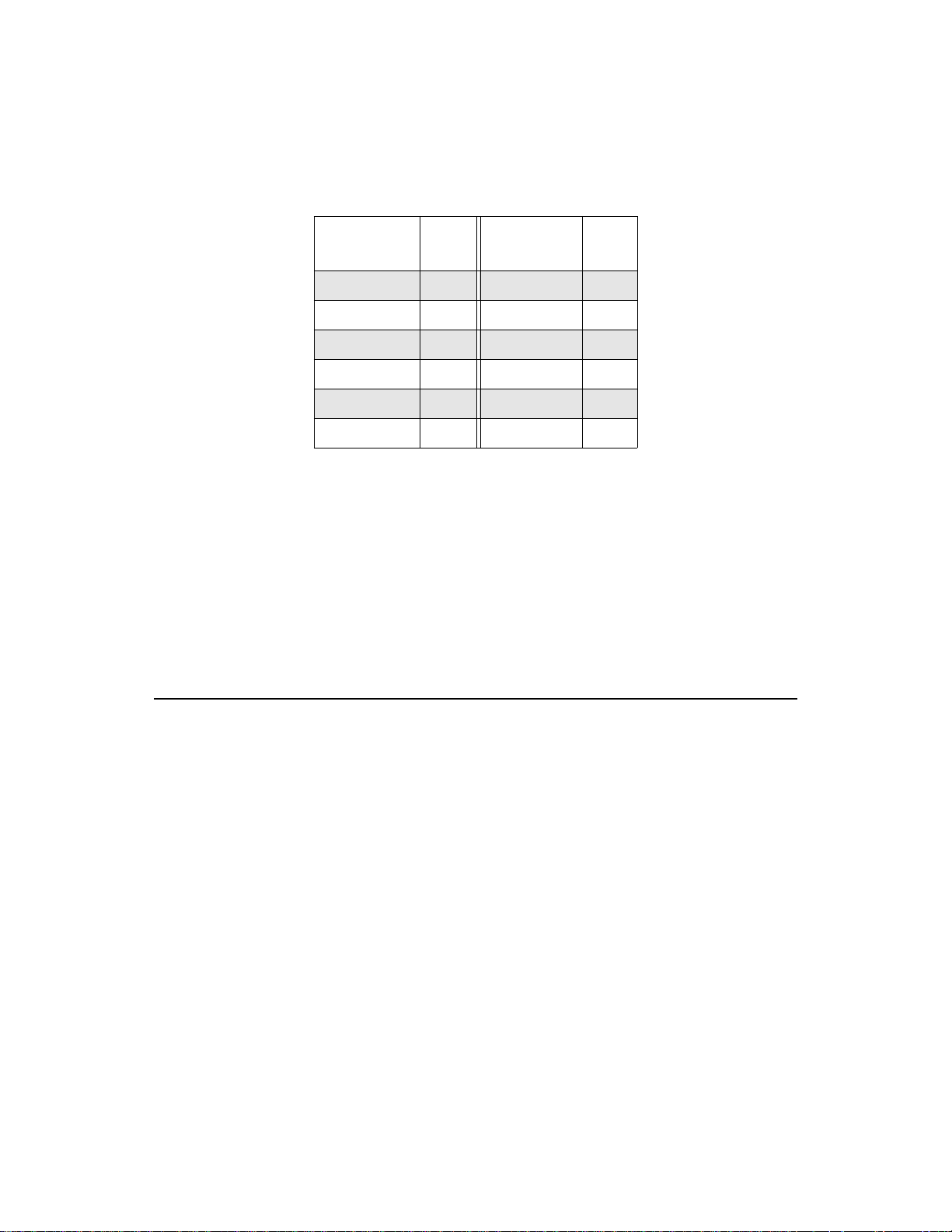
Table 2-1. Analog Input Ranges
Memory
Analog
Input Range
±25 mV 12 ±200 mV 0
±31.25 mV 13 ±250 mV 1, 10
±62.5 mV 14 ±312.5 mV 6
±100 mV 8 ±0.5 V 2, 11
±125 mV 4, 9, 15 ±0.625 V 7
±156.25 mV 5 ±1.0 V 3
Gain
Code
Analog
Input Range
Gain
Code
The DAS-4301/8K board uses a 4096-step DC signal of fset v oltage and a
4096-step fine gain control to calibrate the voltage input ranges.
The scope and test program supports binary, twos complement, and
absolute value data coding of the digitized analog input values. The
DAS-4300 Series Function Call Driver and VTX use twos complement
data coding only.
This section describes memory on the DAS-4301/8K board and on the
host computer.
Onboard Memory
The DAS-4301/8K board contains an 8K byte (8,192 samples) memory
buffer for storing digitized data as well as a nonvolatile EEPROM
memory location for storing calibration values.
Whenever a D AS-4301/8K board is idle, the host computer can access the
data in the onboard memory buffer, download it into its own main
memory, and process it.
2-4 Functional Description

Host Computer Memory
DAS-4301/8K boards require part of both the host computer I/O address
space and the host computer memory address space.
I/O Address Space
The DAS-4301/8K board uses a block of 16 bytes (ports) in the I/O
address space of the host computer to set up the board’s parameters.
These ports can be located anywhere below 400h, provided that they are
not used by your host computer. The default I/O address space for these
ports is 250h to 25Fh.
You select the base address for the I/O address space by setting jumpers
on the board; refer to page 3-12 for information.
Memory Address Space
The memory address space of the host computer is used for reading the
acquired data from the DAS-4301/8K onboard memory buffer. The host
computer accesses the onboard memory using the decoding logic on the
DAS-4301/8K.
The onboard 8,192 byte buffer memory is mapped into a 16K byte
window within the 1M byte address space in the host computer’s upper
memory (above the 640K byte user memory area). You select the base
address for the memory address space by setting jumpers on the board;
refer to page 3-14 for information. Figure 2-2 illustrates the memory
address space of a host computer.
The memory map must fall on a 16K byte boundary; this memory
Note:
area must not be in use by other boards or devices.
Memory 2-5
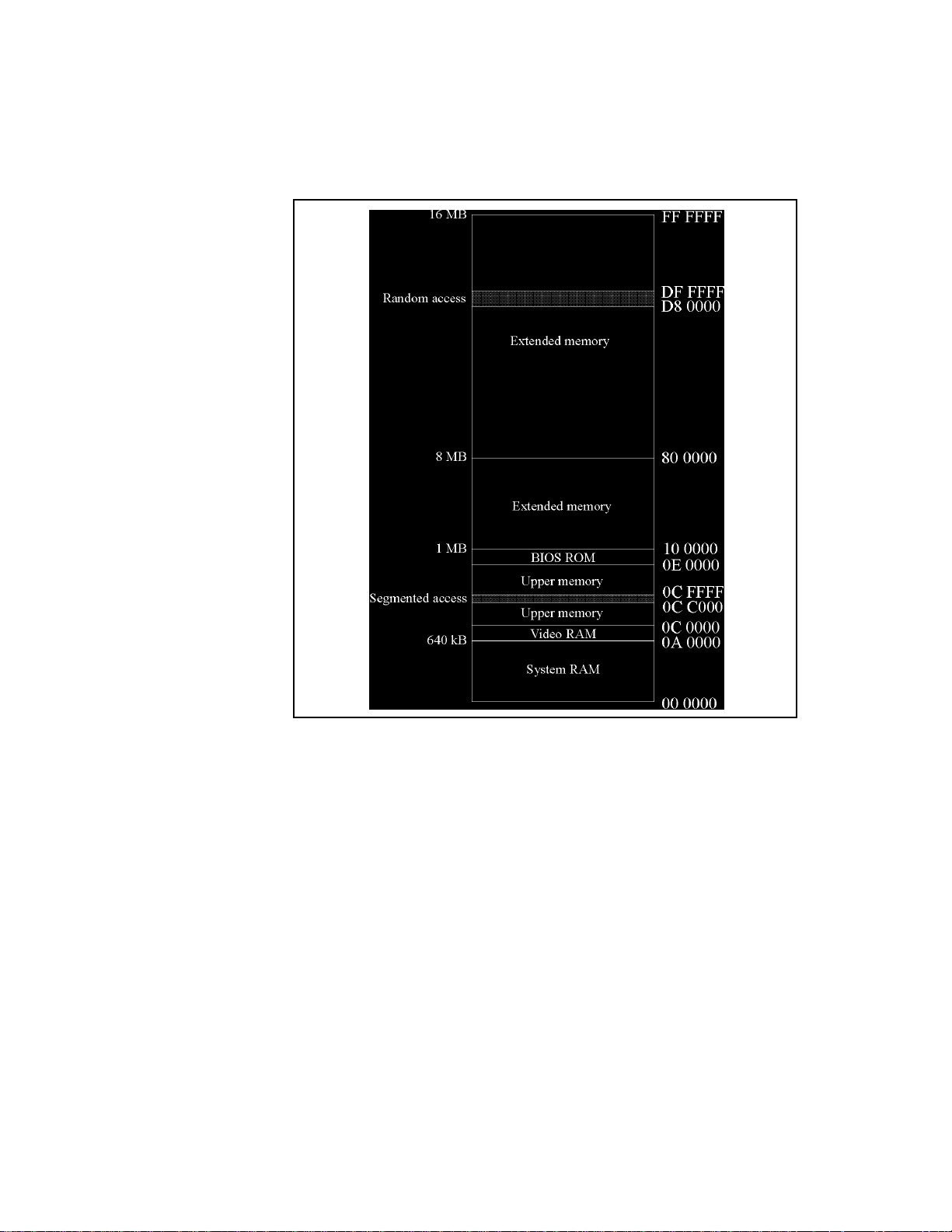
Figure 2-2. Host Computer Memory Address Space
2-6 Functional Description

Bus Interface
The ISA bus interface provides 16-bit data transfers and allows the host
computer to initialize all onboard parameters, read from and write to
onboard memory, and trigger the board.
As mentioned in the previous section, the bus interface uses two distinct
address spaces of the host computer: a 16 byte consecutive segment in the
I/O address space for control information and a 16K byte segment in the
memory address space for data exchange. Both the I/O base address and
memory address are jumper selectable; refer to page 3-12 and page 3-14
for more information.
The bus also provides a zero wait state, which allows data to be
transferred off the board at a rate of 5M byte/s. You enable or disable the
zero wait-state option through the configuration file; refer to page 3-8 for
more information.
An interrupt can be generated to signal the host computer at the end of a
data acquisition. You select the interrupt by setting jumpers on the board.
Refer to page 3-15 for more information.
Pacer Clock
Through software, you select either an internal or external pacer clock to
determine when each A/D conversion is initiated.
Internal Pacer Clock
The internal pacer clock circuit is composed of the onboard 100 MHz
crystal oscillator, a 2000
locked loop) circuit to generate an effective conversion rate of
1 Gsamples/s. The clock signal is fed through a driver circuit to the
Clk IO connector.
The available conversion rates and sample periods using the internal
pacer clock are shown in Table 2-2.
Ω
pull-up resistor to +5 V, and a PLL (phased
Bus Interface 2-7
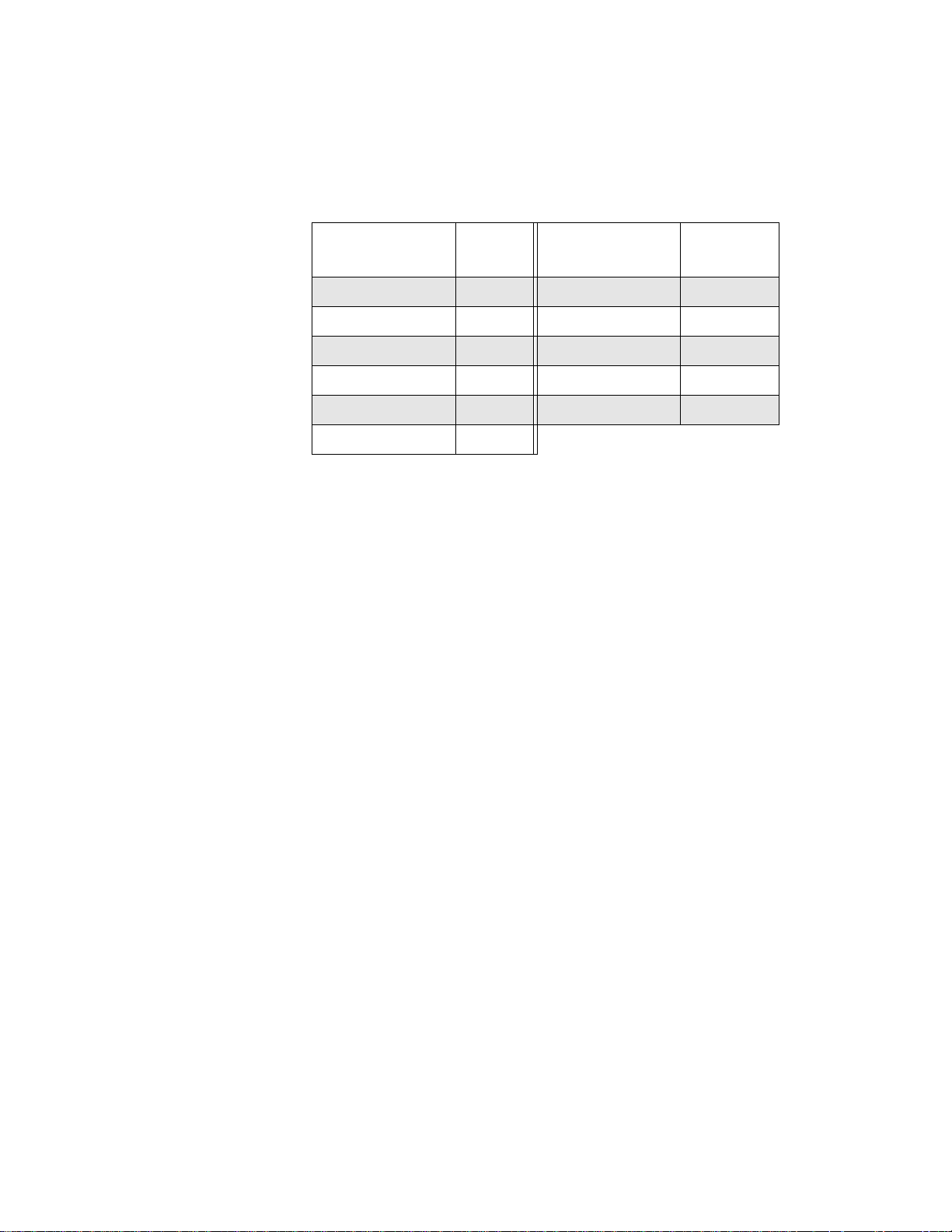
Table 2-2. Available Conversion Rates Using Internal Clock
Conversion Rate
1 Gsamples/s 1 ns 12.5 Msamples/s 80 ns
500 Msamples/s 2 ns 6.25 Msamples/s 160 ns
250 Msamples/s 4 ns 3.125 Msamples/s 320 ns
100 Msamples/s 10 ns 1.5625 Msamples/s 640 ns
50 Msamples/s 20 ns 0.78250 Msamples/s 1280 ns
25 Msamples/s 40 ns
You can also use the Clk IO connector as an output. When the board is
configured for an internal pacer clock source, a TTL-level output signal is
provided on the Clk IO connector that has the same frequency as the
crystal oscillator.
External Pacer Clock
An external pacer clock is an externally generated TTL-le v el clock signal
of at least 100 MHz, with a duty cycle of 50/50 ±20%, applied to the
Clk IO connector. When you start an analog input operation, the board is
armed. At the ne xt rising edge (and at every subsequent rising edge of the
external pacer clock), a conversion is initiated.
Sample
Period Conversion Rate
Sample
Period
A 20
The 20
74ABT series TTL input with a 2 k
appear as approximately 50
You can use a jumper-selectable 50
series protection resistor is provided on the clock input signal.
Ω
resistor combined with the output resistance of the driver IC (a
Ω
pull-up resistor) makes the output
Ω
Ω
.
Ω
termination resistor on the clock
input signal; this resistor is particularly useful when working with a signal
driving a long line or a line that is driving many devices (where the
DAS-4301/8K is at the end of the line). Refer to page 3-18 for more
information on this jumper.
2-8 Functional Description

Notes:
−
0.7 V.
Due to excessive loading of the signal, do not use the jumper-selectable
50
Triggers
A trigger is an event that determines when a DAS-4301/8K board
responds to either an internal or an external pacer clock. Depending on
the type of acquisition and setup parameters, the trigger event can occur
before, during, or after the actual sampling of data. The trigger signal can
originate from a variety of sources.
This section describes trigger sources, types of trigger acquisition, and
trigger synchronization on DAS-4301/8K boards.
Trigger Sources
A diode on the input limits signal excursions to +5.7 V and
termination resistor when using the clock output signal.
Ω
The DAS-4301/8K board supports internal triggers, external analog
triggers, and external digital triggers.
Internal T rigger
An internal trigger (or software trigger) event occurs when a particular
instruction is executed by the host computer. When the trigger event
occurs, a signal is output on the Trg IO connector. At the end of data
acquisition, the signal on the Tr g IO connector returns to its inactive state.
Using the test and scope program, you can program the edge polarity of
the trigger output signal. Using the DAS-4300 Series Function Call
Driver or VTX, you cannot program the trigger polarity; it is always
positive.
Triggers 2-9

External Analog Trigger
An external analog trigger (or threshold trigger) event occurs when one of
the following conditions is met by an analog input signal:
The analog input signal rises above a programmable threshold
●
(positive-edge trigger).
The analog input signal falls below a programmable threshold
●
(negative-edge trigger).
A TTL-level signal is output on the Trg IO connector when the trigger
event occurs. At the end of data acquisition, the signal on the Trg IO
connector returns to its inactive state.
Using the test and scope program, you can program the polarity of the
trigger output signal. Using the DAS-4300 Series Function Call Dri v er or
VTX, you cannot program the polarity of the trigger output signal; it is
always positive.
You can use an external analog trigger in the following ways:
You can trigger the D AS-4301/8K board using the analog input signal
●
from the Ch A connector or from the Trg/Ch B connector on the
board. When using the analog input signal as the trigger source, the
trigger channel and the data acquisition channel must be the same.
For example, if you are using the signal from the Ch A connector as
the trigger source, you must use Channel A as the data acquisition
channel. You specify the trigger channel and the data acquisition
channel in software.
Using the test and scope program, you can program the trigger
threshold in 4096 steps. Using the DAS-4300 Series Function Call
Driver or VTX, you can program the trigger threshold in 256 steps.
You can trigger the DAS-4301/8K board using the ±10 V analog
●
input trigger signal from the Trg/Ch B connector. When using the
±10 V trigger signal, you can acquire data from either Channel A or
Channel B. You specify the trigger channel and data acquisition
channel using software.
2-10 Functional Description

Using the test and scope program, you can program the threshold in
4096 steps from
10 V to +9.995 V; the resolution is 12 bits. Using
−
the DAS-4300 Series Function Call Dri ver or VTX, you can program
the threshold in 256 steps from
−
10 V to +9.922 V; the resolution is 8
bits.
Using a jumper, you can select the input impedance (50
of the ±10 V trigger signal from the Trg/Ch B connector. Refer to
page 3-18 for more information.
External Digital Trigger
A digital trigger event occurs when an externally generated TTL-level
signal of programmable polarity (positive edge or negative edge) is
detected as an input on the Trg IO connector.
A 20
Ω
the Trg IO connector. The 20
resistance of the driver IC (a 74ABT series TTL input with a 2 k
resistor) makes the output appear as approximately 50
jumper-selectable 50
this resistor is particularly useful when working with a signal driving a
long line or a line that is driving many devices (where the DAS-4301/8K
is at the end of the line). Refer to page 3-19 for more information on this
jumper.
Notes:
0.7 V.
−
Ω
or 5600
Ω)
series protection resistor is provided on the trigger input signal of
Ω
resistor combined with the output
pull-up
Ω
. You can use a
Ω
Ω
termination resistor on the trigger input signal;
A diode on the input limits signal excursions to +5.7 V and
When you are not using the Trg IO connector for external digital
triggering, you can use the Tr g IO connector to output a TTL-le vel signal.
If you use the trigger output signal, however, do not use the
jumper-selectable 50
termination resistor due to the excessive loading
Ω
of the signal.
Triggers 2-11

Trigger Acquisition
Depending on your application, you can sample data before and/or after a
trigger event occurs. If you want to collect data after a specific trigger
event, use post-trigger acquisition. If you want to collect data before or
before and after a specific trigger event, use about-trigger acquisition.
The maximum number of samples you can collect for each trigger event
is 8,192. The minimum number of samples you can collect for each
trigger event depends on the conversion rate as follows:
●
Conversion rate of 100 Msamples/s and slower : minimum of 1
sample in increments of 1 sample.
●
Conversion rate of 250 Msamples/s and faster : minimum of 10
samples in increments of 10 samples.
Post-Trigger Acquisition
Use post-trigger acquisition to store data samples after a trigger event
occurs. You can also use a programmable post-trigger delay. The delay is
the number of samples after the trigger and before data acquisition starts.
At a conversion rate of 100 Msamples/s or slower, the post-trigger delay
can range from 0 to 65,536 samples (in increments of 1); at a conversion
rate of 250 Msamples/s or faster, the post-trigger delay can range from 0
to 655,360 samples (in increments of 10).
Note:
VTX does not support post-trigger delay.
To start a post-trigger acquisition, perform the following steps:
1. Set up all board parameters, such as the data acquisition channel,
voltage input range, conversion rate, trigger source, trigger polarity,
the number of samples to acquire after the trigger event, and the
post-trigger delay , as appropriate. You need to set up these parameters
only once unless your application requires a change.
2. Using software, arm the board to accept the next valid trigger event.
Arming the board requires about 10
s.
µ
2-12 Functional Description

Once the board is armed, the next valid trigger e vent starts the acquisition.
When the trigger event occurs, the post-trigger length, which includes the
post-trigger delay and the number of samples to acquire (defined by the
buffer length), is decremented until it reaches zero, at which point
acquisition stops. Using software, you can poll a status bit or use an
interrupt to determine if the acquisition is finished.
For example, assume the conversion rate is 50 Msample/s, the
post-trigger delay is 10 samples and the buffer length is 190 samples.
When a valid trigger event occurs, the first 10 samples are ignored, the
remaining 190 post-trigger samples are collected, then the acquisition
operation stops.
About-Trigger Acquisition
Use about-trigger acquisition to store data samples before a trigger event
occurs or before and after a trigger event occurs.
To start an about-trigger acquisition, perform the following steps:
1. Set up all board parameters, such as the data acquisition channel,
voltage input range, conversion rate, trigger source, trigger polarity,
and the number of samples to acquire after the trigger occurs. You
need to set up these parameters only once unless your application
requires a change.
2. Using software, arm the board to accept the next valid trigger event.
Arming the board requires about 10
s.
µ
Once armed, the board continuously acquires data and stores it in the
onboard 8K byte memory buffer. The memory buffer must fill up with
data at least once before the board can accept a trigger event. When a
valid trigger event occurs, the specified number of post-trigger samples
(defined by the buffer length) is collected.
For example, suppose you set the buffer length to 4,160 and start the
about-trigger operation. Pre-trigger data is collected and begins to fill the
8K byte buffer. Once the buffer is filled, the board can accept a trigger;
pre-trigger data continues to be collected and overwrites the data in the
buffer until the trigger event occurs. When a valid trigger event occurs,
the board collects 4,160 post-trigger samples then stops the acquisition.
The number of pre-trigger samples in the buffer is 8,192 minus 4,160 or
4,032.
Triggers 2-13

The minimum number of pre-trigger samples is 1; the maximum number
of pre-trigger samples is 8,192.
Notes:
The term pre-trigger acquisition is often used for an about-trigger
acquisition when only the samples before the trigger event are significant.
The DAS-4300 Series Function Call Driver differentiates between
pre-trigger acquisition (where the number of post-trigger samples is zero)
and about-trigger acquisition (where you specify the number of
post-trigger samples); refer to the DAS-4300 Series Function Call Driver
User’s Guide for information. The DAS-4300 scope and test program
uses the term pre-trigger mode for both pre-trigger acquisition and
about-trigger acquisition.
You cannot specify a post-trigger delay for an about-trigger acquisition.
VTX does not support about-trigger acquisition.
Equivalent Time Sampling (ETS)
Equivalent time sampling (ETS) is an adv anced feature that allo ws you to
digitize high-frequency analog input signals and achieve f aster conv ersion
rates than 1 Gsamples/s. The advantage of ETS is that the total number of
acquisitions needed to collect a waveform is deterministic; therefore, ETS
is ideal for scanning repetitive waveforms quickly.
On the DAS-4301/8K board, ETS is implemented through a patented
circuit (U.S. Patent No. 4,595,908). The analog signal to be digitized
must be repetitive and coherent with a TTL-level trigger out signal on the
Trg IO connector of the DAS-4301/8K board.
Using ETS, the board samples a repetitive signal several times with the
pacer clock shifted relative to the input signal by a fraction of the sample
period. With N acquisitions and a pacer clock shifted by the fraction of
the sample period 1/(N * f
conversion rate is N * f
) between the acquisitions, the effective
clock
. N is called the ETS factor. The maximum
clock
ETS factor is 20, corresponding to an effective conversion rate of
20 Gsamples/second. Other supported ETS factors are as follows: 2, 4, 5,
2-14 Functional Description
 Loading...