

Page 1

D AS-4300 Series
USER’S GUIDE
Page 2

DAS-4300 Series User’s Guide
Revision A - June 1995
Part Number: 94520
Page 3

New Contact Information
Keithley Instruments, Inc.
28775 Aurora Road
Cleveland, OH 44139
Technical Support: 1-888-KEITHLEY
Monday – Friday 8:00 a.m. to 5:00 p.m (EST)
Fax: (440) 248-6168
Visit our website at http://www.keithley.com
Page 4

The information contained in this manual is believed to be accurate and reliable. However, Keithley
Instruments, Inc., assumes no responsibility for its use or for any infringements of patents or other rights
of third parties that may result from its use. No license is granted by implication or otherwise under any
patent rights of Keithley Instruments, Inc.
KEITHLEY INSTRUMENTS, INC., SHALL NO T BE LIABLE FOR ANY SPECIAL, INCIDENT AL,
OR CONSEQUENTIAL DAMAGES RELATED TO THE USE OF THIS PRODUCT. THIS
PRODUCT IS NOT DESIGNED WITH COMPONENTS OF A LEVEL OF RELIABILITY
SUITABLE FOR USE IN LIFE SUPPORT OR CRITICAL APPLICATIONS.
Refer to your Keithley Instruments license agreement for specific warranty and liability information.
MetraByte, Visual Test Extensions, and VTX are trademarks of Keithley Instruments, Inc. All other
brand and product names are trademarks or registered trademarks of their respective companies.
© Copyright Keithley Instruments, Inc., 1995.
All rights reserved. Reproduction or adaptation of any part of this documentation beyond that permitted
by Section 117 of the 1976 United States Copyright Act without permission of the Copyright owner is
unlawful.
Keithley MetraByte Division
Keithley Instruments, Inc.
440 Myles Standish Blvd. Taunton, MA 02780
FAX: (508) 880-0179
Telephone: (508) 880-3000
●
Page 5

Preface
The DAS-4300 Series User’s Guide provides the information needed to
install and use the DAS-4301/8K high-speed analog input board.
The manual is intended for data acquisition system designers, engineers,
technicians, scientists, and other users responsible for setting up and
installing DAS-4301/8K boards. It is assumed that users are familiar with
data acquisition principles, with their computer, and with their particular
application.
The DAS-4300 Series User’s Guide is organized as follows:
●
Chapter 1 provides an overview of the features of the DAS-4301/8K
board, including a description of supported software and accessories.
●
Chapter 2 provides a technical description of the features of the
DAS-4301/8K board.
Chapter 3 describes how to unpack, set up, and install a
●
DAS-4301/8K board.
Chapter 4 describes how to use the scope and test program to test the
●
functions of the DAS-4301/8K board.
Chapter 5 provides troubleshooting information.
●
●
Appendix A lists the specifications for DAS-4301/8K boards.
●
Appendix B describes the Keithley Memory Manager.
Appendix C presents bandwidth charts for the supported input ranges.
●
An index completes this manual.
vii
Page 6

Not all features of the DAS-4301/8K board are currently supported
Note:
by all software packages. Refer to the documentation provided with your
software package to determine which features are supported.
viii
Page 7

Table of Contents
Preface
1
Overview
Features . . . . . . . . . . . . . . . . . . . . . . . . . . . . . . . . . . . . . . . . . . . .1-1
Supporting Software. . . . . . . . . . . . . . . . . . . . . . . . . . . . . . . . . . .1-2
Accessories. . . . . . . . . . . . . . . . . . . . . . . . . . . . . . . . . . . . . . . . . .1-3
Functional Description
2
Channels. . . . . . . . . . . . . . . . . . . . . . . . . . . . . . . . . . . . . . . . . . . .2-3
Input Ranges . . . . . . . . . . . . . . . . . . . . . . . . . . . . . . . . . . . . . . . .2-3
Memory . . . . . . . . . . . . . . . . . . . . . . . . . . . . . . . . . . . . . . . . . . . .2-4
Onboard Memory . . . . . . . . . . . . . . . . . . . . . . . . . . . . . . . . . .2-4
Host Computer Memory . . . . . . . . . . . . . . . . . . . . . . . . . . . . .2-5
I/O Address Space . . . . . . . . . . . . . . . . . . . . . . . . . . . . . . .2-5
Memory Address Space . . . . . . . . . . . . . . . . . . . . . . . . . . .2-5
Bus Interface . . . . . . . . . . . . . . . . . . . . . . . . . . . . . . . . . . . . . . . .2-7
Pacer Clock . . . . . . . . . . . . . . . . . . . . . . . . . . . . . . . . . . . . . . . . .2-7
Internal Pacer Clock . . . . . . . . . . . . . . . . . . . . . . . . . . . . . . . .2-7
External Pacer Clock. . . . . . . . . . . . . . . . . . . . . . . . . . . . . . . .2-8
Triggers . . . . . . . . . . . . . . . . . . . . . . . . . . . . . . . . . . . . . . . . . . . .2-9
Trigger Sources. . . . . . . . . . . . . . . . . . . . . . . . . . . . . . . . . . . .2-9
Internal Trigger. . . . . . . . . . . . . . . . . . . . . . . . . . . . . . . . . .2-9
External Analog Trigger. . . . . . . . . . . . . . . . . . . . . . . . . .2-10
External Digital Trigger. . . . . . . . . . . . . . . . . . . . . . . . . .2-11
Trigger Acquisition . . . . . . . . . . . . . . . . . . . . . . . . . . . . . . . .2-12
Post-Trigger Acquisition . . . . . . . . . . . . . . . . . . . . . . . . .2-12
About-Trigger Acquisition . . . . . . . . . . . . . . . . . . . . . . . .2-13
Equivalent Time Sampling (ETS) . . . . . . . . . . . . . . . . . . . . . . .2-14
Random Interleave Sampling (RIS). . . . . . . . . . . . . . . . . . . . . .2-18
3
Setup and Installation
Unpacking the Board . . . . . . . . . . . . . . . . . . . . . . . . . . . . . . . . . .3-1
Installing the Software . . . . . . . . . . . . . . . . . . . . . . . . . . . . . . . . .3-2
Installing the DAS-4300 Series Standard Software Package .3-2
iii
Page 8

Installing the ASO-4300 Software Package . . . . . . . . . . . . . .3-3
DOS Installation. . . . . . . . . . . . . . . . . . . . . . . . . . . . . . . . .3-3
Windows Installation . . . . . . . . . . . . . . . . . . . . . . . . . . . . .3-4
Configuring the Board . . . . . . . . . . . . . . . . . . . . . . . . . . . . . . . . .3-5
Creating a Configuration File . . . . . . . . . . . . . . . . . . . . . . . . .3-8
Setting Jumpers on the Board . . . . . . . . . . . . . . . . . . . . . . . .3-10
Setting the Base I/O Address . . . . . . . . . . . . . . . . . . . . . .3-12
Setting the Memory Address . . . . . . . . . . . . . . . . . . . . . .3-14
Setting the Interrupt . . . . . . . . . . . . . . . . . . . . . . . . . . . . .3-15
Acquiring Data from Channel B or
Calibrating the Board. . . . . . . . . . . . . . . . . . . . . . . . . . .3-16
Selecting AC or DC Coupling . . . . . . . . . . . . . . . . . . . . .3-17
Setting the Input Impedance of Ch A Signal . . . . . . . . . .3-17
Setting the Input Impedance of the
Analog Trigger Input Signal. . . . . . . . . . . . . . . . . . . . . .3-18
Setting the 50
Ω
Termination Resistor for the
Clock Input Signal . . . . . . . . . . . . . . . . . . . . . . . . . . . . .3-18
Setting the 50
Termination Resistor for the
Ω
Trigger Input Signal. . . . . . . . . . . . . . . . . . . . . . . . . . . .3-19
Setting the 100
Ω
Pull-Up to +5 V for the
Trigger Input Signal. . . . . . . . . . . . . . . . . . . . . . . . . . . .3-20
Setting Grounds . . . . . . . . . . . . . . . . . . . . . . . . . . . . . . . .3-20
Installing the Board . . . . . . . . . . . . . . . . . . . . . . . . . . . . . . . . . .3-21
Initializing the Board . . . . . . . . . . . . . . . . . . . . . . . . . . . . . . . . .3-22
Scope and Test Program
4
Control Keys for D4300.EXE . . . . . . . . . . . . . . . . . . . . . . . . . . .4-1
Scope and Test Program Menus. . . . . . . . . . . . . . . . . . . . . . . . . .4-4
A/D Menu . . . . . . . . . . . . . . . . . . . . . . . . . . . . . . . . . . . . . . . .4-4
Display Menu . . . . . . . . . . . . . . . . . . . . . . . . . . . . . . . . . . . . .4-7
Options Menu . . . . . . . . . . . . . . . . . . . . . . . . . . . . . . . . . . . . .4-8
EEPROM Menus. . . . . . . . . . . . . . . . . . . . . . . . . . . . . . . . . . .4-9
DAS-4301/8K Board Calibration. . . . . . . . . . . . . . . . . . . . . . . .4-10
Parameter Files. . . . . . . . . . . . . . . . . . . . . . . . . . . . . . . . . . . . . .4-10
Waveform Data File Format. . . . . . . . . . . . . . . . . . . . . . . . . . . .4-11
5
Troubleshooting
Identifying Symptoms and Possible Causes . . . . . . . . . . . . . . . .5-1
Testing Board and Host Computer. . . . . . . . . . . . . . . . . . . . . . . .5-3
Testing Accessory Slot and I/O Connections. . . . . . . . . . . . . . . .5-3
Technical Support. . . . . . . . . . . . . . . . . . . . . . . . . . . . . . . . . . . . .5-4
iv
Page 9

v
Specifications
A
B
Keithley Memory Manager
Installing and Setting Up the KMM. . . . . . . . . . . . . . . . . . . . . . B-2
Using KMMSETUP.EXE . . . . . . . . . . . . . . . . . . . . . . . . . . . B-2
Using a Text Editor . . . . . . . . . . . . . . . . . . . . . . . . . . . . . . . . B-3
Removing the KMM . . . . . . . . . . . . . . . . . . . . . . . . . . . . . . . . . B-4
C
Bandwidth Charts for Input Voltage Ranges
Index
List of Figures
Figure 2-1. Block Diagram of the DAS-4301/8K . . . . . . . . . .2-2
Figure 2-2. Host Computer Memory Address Space . . . . . . . .2-6
Figure 2-3. Equivalent Time Sampling (ETS) . . . . . . . . . . . .2-15
Figure 2-4. ETS Delay . . . . . . . . . . . . . . . . . . . . . . . . . . . . . .2-17
Figure 2-5. Random Interleave Sampling. . . . . . . . . . . . . . . .2-19
Figure 3-1. Jumper Placement on DAS-4301/8K Board . . . .3-11
Figure 3-2. Analog Input Circuitry. . . . . . . . . . . . . . . . . . . . .3-17
Figure 3-3. Clock I/O and Trigger I/O Circuitry . . . . . . . . . .3-19
Figure C-1. ±0.2 V Input Range (Gain Code 0) . . . . . . . . . . . C-1
Figure C-2. ±0.25 V Input Range (Gain Code 1) . . . . . . . . . . C-2
Figure C-3. ±0.5 V Input Range (Gain Code 2) . . . . . . . . . . . C-2
Figure C-4. ±1 V Input Range (Gain Code 3). . . . . . . . . . . . . C-3
Figure C-5. ±0.125 V Input Range (Gain Code 4) . . . . . . . . . C-3
Figure C-6. ±0.15625 V Input Range (Gain Code 5) . . . . . . . C-4
Figure C-7. ±0.3125 V Input Range (Gain Code 6) . . . . . . . . C-4
Figure C-8. ±0.625 V Input Range (Gain Code 7) . . . . . . . . . C-5
Figure C-9. ±0.1 V Input Range (Gain Code 8) . . . . . . . . . . . C-5
Figure C-10. ±0.125 V Input Range (Gain Code 9) . . . . . . . . . C-6
Figure C-11. ±0.25 V Input Range (Gain Code 10) . . . . . . . . . C-6
Figure C-12. ±0.5 V Input Range (Gain Code 11) . . . . . . . . . . C-7
Figure C-13. ±0.025 V Input Range (Gain Code 12) . . . . . . . . C-7
Figure C-14. ±0.03125 V Input Range (Gain Code 13) . . . . . . C-8
Figure C-15. ±0.0625 V Input Range (Gain Code 14) . . . . . . . C-8
Figure C-16. ±0.125 V Input Range (Gain Code 15) . . . . . . . . C-9
Page 10

List of Tables
Table 2-1. Analog Input Ranges . . . . . . . . . . . . . . . . . . . . . . .2-4
Table 2-2. Available Conversion Rates Using Internal Clock 2-8
Table 3-1. Configuring DAS-4301/8K Boards . . . . . . . . . . . .3-6
Table 3-2. Base I/O Address . . . . . . . . . . . . . . . . . . . . . . . . .3-12
Table 3-3. Memory Address . . . . . . . . . . . . . . . . . . . . . . . . .3-14
Table 3-4. Interrupt Selection . . . . . . . . . . . . . . . . . . . . . . . .3-16
Table 3-5. Grounds on the DAS-4301/8K Board . . . . . . . . .3-20
Table 4-1. Control Keys . . . . . . . . . . . . . . . . . . . . . . . . . . . . .4-2
Table 4-2. Suffixes . . . . . . . . . . . . . . . . . . . . . . . . . . . . . . . . .4-4
Table 4-3. A/D Menu . . . . . . . . . . . . . . . . . . . . . . . . . . . . . . .4-4
Table 4-4. Display Menu. . . . . . . . . . . . . . . . . . . . . . . . . . . . .4-7
Table 4-5. Options Menu . . . . . . . . . . . . . . . . . . . . . . . . . . . .4-8
Table 4-6. Configure EEPROM Menu . . . . . . . . . . . . . . . . . .4-9
Table 4-7. Waveform Data File Format . . . . . . . . . . . . . . . .4-11
Table 5-1. Troubleshooting Information. . . . . . . . . . . . . . . . .5-1
Table A-1. DAS-4301/8K Specifications . . . . . . . . . . . . . . . A-1
vi
Page 11

Table 2-1. Analog Input Ranges . . . . . . . . . . . . . . . . . . . . . . .2-4
Table 2-2. Available Conversion Rates Using Internal Clock 2-8
Table 3-1. Configuring DAS-4301/8K Boards . . . . . . . . . . . .3-6
Table 3-2. Base I/O Address . . . . . . . . . . . . . . . . . . . . . . . . .3-12
Table 3-3. Memory Address . . . . . . . . . . . . . . . . . . . . . . . . .3-14
Table 3-4. Interrupt Selection . . . . . . . . . . . . . . . . . . . . . . . .3-16
Table 3-5. Grounds on the DAS-4301/8K Board . . . . . . . . .3-20
Table 4-1. Control Keys . . . . . . . . . . . . . . . . . . . . . . . . . . . . .4-2
Table 4-2. Suffixes . . . . . . . . . . . . . . . . . . . . . . . . . . . . . . . . .4-4
Table 4-3. A/D Menu . . . . . . . . . . . . . . . . . . . . . . . . . . . . . . .4-4
Table 4-4. Display Menu. . . . . . . . . . . . . . . . . . . . . . . . . . . . .4-7
Table 4-5. Options Menu . . . . . . . . . . . . . . . . . . . . . . . . . . . .4-8
Table 4-6. Configure EEPROM Menu . . . . . . . . . . . . . . . . . .4-9
Table 4-7. Waveform Data File Format . . . . . . . . . . . . . . . .4-11
Table 5-1. Troubleshooting Information. . . . . . . . . . . . . . . . .5-1
Table A-1. DAS-4301/8K Specifications . . . . . . . . . . . . . . . A-1
Page 12

Figure 2-1. Block Diagram of the DAS-4301/8K . . . . . . . . . .2-2
Figure 2-2. Host Computer Memory Address Space . . . . . . . .2-6
Figure 2-3. Equivalent Time Sampling (ETS) . . . . . . . . . . . .2-15
Figure 2-4. ETS Delay . . . . . . . . . . . . . . . . . . . . . . . . . . . . . .2-17
Figure 2-5. Random Interleave Sampling. . . . . . . . . . . . . . . .2-19
Figure 3-1. Jumper Placement on DAS-4301/8K Board . . . .3-11
Figure 3-2. Analog Input Circuitry. . . . . . . . . . . . . . . . . . . . .3-17
Figure 3-3. Clock I/O and Trigger I/O Circuitry . . . . . . . . . .3-19
Figure C-1. ±0.2 V Input Range (Gain Code 0) . . . . . . . . . . . C-1
Figure C-2. ±0.25 V Input Range (Gain Code 1) . . . . . . . . . . C-2
Figure C-3. ±0.5 V Input Range (Gain Code 2) . . . . . . . . . . . C-2
Figure C-4. ±1 V Input Range (Gain Code 3). . . . . . . . . . . . . C-3
Figure C-5. ±0.125 V Input Range (Gain Code 4) . . . . . . . . . C-3
Figure C-6. ±0.15625 V Input Range (Gain Code 5) . . . . . . . C-4
Figure C-7. ±0.3125 V Input Range (Gain Code 6) . . . . . . . . C-4
Figure C-8. ±0.625 V Input Range (Gain Code 7) . . . . . . . . . C-5
Figure C-9. ±0.1 V Input Range (Gain Code 8) . . . . . . . . . . . C-5
Figure C-10. ±0.125 V Input Range (Gain Code 9) . . . . . . . . . C-6
Figure C-11. ±0.25 V Input Range (Gain Code 10) . . . . . . . . . C-6
Figure C-12. ±0.5 V Input Range (Gain Code 11) . . . . . . . . . . C-7
Figure C-13. ±0.025 V Input Range (Gain Code 12) . . . . . . . . C-7
Figure C-14. ±0.03125 V Input Range (Gain Code 13) . . . . . . C-8
Figure C-15. ±0.0625 V Input Range (Gain Code 14) . . . . . . . C-8
Figure C-16. ±0.125 V Input Range (Gain Code 15) . . . . . . . . C-9
Page 13

1
Overview
Features
The DAS-4300 Series consists of the DAS-4301/8K board. The
DAS-4301/8K is an 8-bit data acquisition board available for IBM
PC A T
1 Gsamples/s. This chapter describes the features of the DAS-4301/8K
board, the software that supports it, and available accessories.
Note:
by all software packages. Refer to the documentation provided with your
software package to determine which features are supported.
The major features of the DAS-4301/8K board are as follows:
●
●
or compatible computers, with a conversion rate of up to
Not all features of the DAS-4301/8K board are currently supported
Supports high-speed data acquisition on one of two analog input
channels accessed through standard BNC connectors.
Provides an analog bandwidth at
true 1 Gsamples/s conversion rate.
3 dB of 250 MHz combined with a
−
Provides a flash converter with a resolution of 8 bits.
●
Provides 16 software-selectable input voltage ranges from
●
±0.025 V to ±1 V.
●
Provides onboard autocalibration to ensure accurate digitization.
●
Stores digitized data in an onboard 8K byte memory buffer.
Provides zero wait-state operations to transfer data off the board at up
●
to 5M byte/s via the ISA bus.
Features 1-1
Page 14

Supports jumper-selectable AC or DC signal coupling.
●
Provides jumper-selectable 50
●
●
Provides a wide variety of trigger options, including internal and
external triggering and post-trigger delay, which you can use to tailor
the operation of the board to the specific requirements of your
application.
●
Supports Equivalent Time Sampling (ETS) and Random Interleaved
Sampling (RIS) for repetitive waveforms; ETS and RIS provide
conversion rates of up to 20 Gsamples/s.
●
Provides a Synchro-Link digital signal processing (DSP) port to
transfer data from onboard memory at up to 25 Msamples/s.
Supporting Software
The following software is available for operating the DAS-4301/8K
board:
DAS-4300 Series standard software package - This package, which
●
comes with the board, is provided on 3.5-inch high-density disks. The
package includes utility programs that allow you to configure, test,
and calibrate the DAS-4301/8K board.
Ω
or 1 M
Ω
input impedance.
ASO-4300 software package - The optional Advanced Software
●
Option for DAS-4301/8K boards is provided on 3.5-inch high-density
disks. The package includes function libraries for writing application
programs using Microsoft C/C++, Borland
Visual Basic
for Windows. The package also includes support files,
®
C/C++, or Microsoft
utility programs, and language-specific example programs. Refer to
the DAS-4300 Series Function Call Driver User’s Guide for more
information.
DAS-4300 Series configuration utility - The configuration utility
●
(CFG4300.EXE), provided as part of both the DAS-4300 Series
standard software package and the ASO-4300 software package, runs
under DOS and allows you to create or modify a configuration file.
The configuration file provides information about the board; this
information is used by the DAS-4300 Series Function Call Dri ver and
other software packages to perform the board’s operations. Refer to
page 3-8 for more information.
1-2 Overview
Page 15

)
DAS-4300 Series scope and test program - The scope and test
●
program (D4300.EXE) allows you to test the hardware features of a
DAS-4301/8K board, calibrate the analog input circuitry of the board,
and perform basic oscilloscope functions on the board. This program
runs under DOS and is provided as part of both the DAS-4300 Series
standard software package and the ASO-4300 software package.
Refer to Chapter 4 for more information.
Accessories
Visual Test Extensions
●
(VTX
- These optional custom controls
for Visual Basic for W indo ws help you write application programs for
the DAS-4301/8K board. Refer to the V isual Test Extensions
User’s
Guide and the VTX online help for more information.
VisualSCOPE - This optional software package runs under Windows
●
and emulates a stand-alone oscilloscope on your host computer. Refer
to the VisualSCOPE documentation for more information.
The SDC-5600 DSP board is an accessory for the DAS-4301/8K board.
The SDC-5600 uses the optional DSP port on the DAS-4301/8K board to
transfer data at 25M byte/s for digital signal processing applications. This
accessory is available from Sonix Inc., 8700 Morrissette Drive,
Springfield, VA 22152 (703-440-0222).
Accessories 1-3
Page 16

2
Functional Description
This chapter describes the features of the DAS-4301/8K board from a
functional point of view. The intent of these descriptions is to familiarize
you with the operating options and to enable you to make the best use of
your board. Figure 2-1 shows a block diagram of the DAS-4301/8K
board.
2-1
Page 17

Channel A
Channel B
DAC
(12-bit)
Clock
Relay
DAC
(12 bit)
−10 V to +10 V
Threshold T rigger
Comparator (Ch B)
Clock
Divider
−FS to +FS
Comparator
(Ch A)
DAC (12
bit)
Offset
DC to
250 MHz
Amp
100 MHz
Oscillator
DAC
(12 bit)
In
Clock
Vernier Gain
Ref
A/D Converter
Data
8K byte
FIFO
Memory
DSP
Port
Data
Trigger
Trigger
Control
ETS
Delay
Data
ISA Bus Interface (16 bits)
RIS
Delay
Clock
Counters
Enable
Status
Data
Figure 2-1. Block Diagram of the DAS-4301/8K
2-2 Functional Description
Page 18

Channels
The DAS-4301/8K board can acquire data from one of two analog input
channels at a time: Channel A, accessed from the Ch A connector, or
Channel B, accessed from the Trg/Ch B connector.
You use software to specify Channel A. To specify Channel B, leave a
jumper installed in positions 1 and 2 of jumper block J103 (the
factory-default configuration), and use software to select Channel B.
Channel A is terminated with a 50
select an input impedance of 50
information.
The Trg/Ch B connector is also used for triggering; refer to page 2-10 for
more information on triggering using this connector and selecting the
input impedance for the signal attached to this connector.
Input Ranges
DAS-4301/8K boards support 16 bipolar, factory-calibrated analog input
ranges. Through software, you specify the input range of the analog input
channel.
T able 2-1 lists the analog input ranges supported by D AS-4301/8K boards
and their corresponding gain codes. The gain code is used in software to
determine the input voltage range. The choice of gain code affects the
bandwidth on the DAS-4301/8K board; Appendix C shows the effect of
the input ranges and gain code choices on the bandwidth of the
DAS-4301/8K board.
impedance. Using a jumper, you can
Ω
or 1 M
Ω
. Refer to page 3-17 for more
Ω
Channels 2-3
Page 19
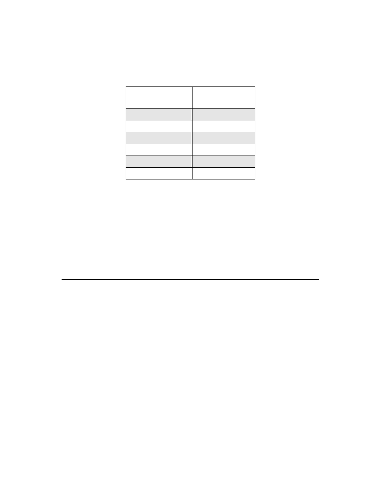
Table 2-1. Analog Input Ranges
Memory
Analog
Input Range
±25 mV 12 ±200 mV 0
±31.25 mV 13 ±250 mV 1, 10
±62.5 mV 14 ±312.5 mV 6
±100 mV 8 ±0.5 V 2, 11
±125 mV 4, 9, 15 ±0.625 V 7
±156.25 mV 5 ±1.0 V 3
Gain
Code
Analog
Input Range
Gain
Code
The DAS-4301/8K board uses a 4096-step DC signal of fset v oltage and a
4096-step fine gain control to calibrate the voltage input ranges.
The scope and test program supports binary, twos complement, and
absolute value data coding of the digitized analog input values. The
DAS-4300 Series Function Call Driver and VTX use twos complement
data coding only.
This section describes memory on the DAS-4301/8K board and on the
host computer.
Onboard Memory
The DAS-4301/8K board contains an 8K byte (8,192 samples) memory
buffer for storing digitized data as well as a nonvolatile EEPROM
memory location for storing calibration values.
Whenever a D AS-4301/8K board is idle, the host computer can access the
data in the onboard memory buffer, download it into its own main
memory, and process it.
2-4 Functional Description
Page 20

Host Computer Memory
DAS-4301/8K boards require part of both the host computer I/O address
space and the host computer memory address space.
I/O Address Space
The DAS-4301/8K board uses a block of 16 bytes (ports) in the I/O
address space of the host computer to set up the board’s parameters.
These ports can be located anywhere below 400h, provided that they are
not used by your host computer. The default I/O address space for these
ports is 250h to 25Fh.
You select the base address for the I/O address space by setting jumpers
on the board; refer to page 3-12 for information.
Memory Address Space
The memory address space of the host computer is used for reading the
acquired data from the DAS-4301/8K onboard memory buffer. The host
computer accesses the onboard memory using the decoding logic on the
DAS-4301/8K.
The onboard 8,192 byte buffer memory is mapped into a 16K byte
window within the 1M byte address space in the host computer’s upper
memory (above the 640K byte user memory area). You select the base
address for the memory address space by setting jumpers on the board;
refer to page 3-14 for information. Figure 2-2 illustrates the memory
address space of a host computer.
The memory map must fall on a 16K byte boundary; this memory
Note:
area must not be in use by other boards or devices.
Memory 2-5
Page 21
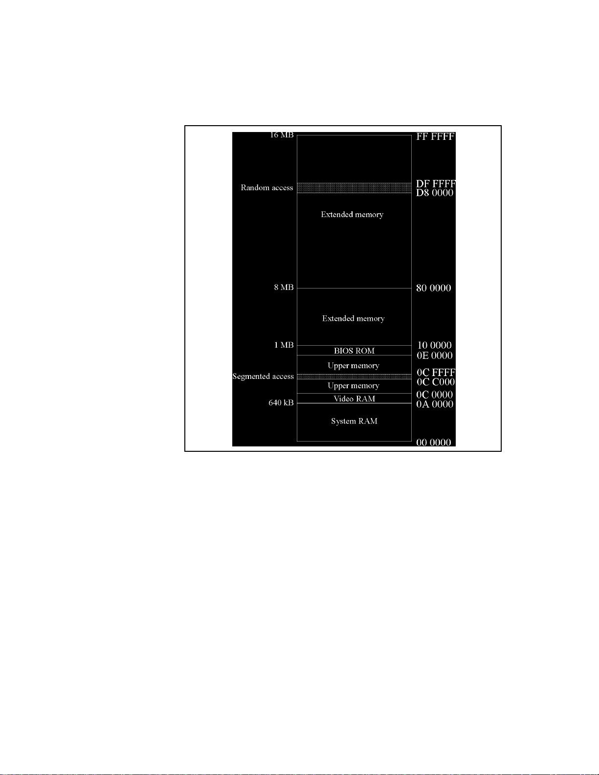
Figure 2-2. Host Computer Memory Address Space
2-6 Functional Description
Page 22

Bus Interface
The ISA bus interface provides 16-bit data transfers and allows the host
computer to initialize all onboard parameters, read from and write to
onboard memory, and trigger the board.
As mentioned in the previous section, the bus interface uses two distinct
address spaces of the host computer: a 16 byte consecutive segment in the
I/O address space for control information and a 16K byte segment in the
memory address space for data exchange. Both the I/O base address and
memory address are jumper selectable; refer to page 3-12 and page 3-14
for more information.
The bus also provides a zero wait state, which allows data to be
transferred off the board at a rate of 5M byte/s. You enable or disable the
zero wait-state option through the configuration file; refer to page 3-8 for
more information.
An interrupt can be generated to signal the host computer at the end of a
data acquisition. You select the interrupt by setting jumpers on the board.
Refer to page 3-15 for more information.
Pacer Clock
Through software, you select either an internal or external pacer clock to
determine when each A/D conversion is initiated.
Internal Pacer Clock
The internal pacer clock circuit is composed of the onboard 100 MHz
crystal oscillator, a 2000
locked loop) circuit to generate an effective conversion rate of
1 Gsamples/s. The clock signal is fed through a driver circuit to the
Clk IO connector.
The available conversion rates and sample periods using the internal
pacer clock are shown in Table 2-2.
Ω
pull-up resistor to +5 V, and a PLL (phased
Bus Interface 2-7
Page 23
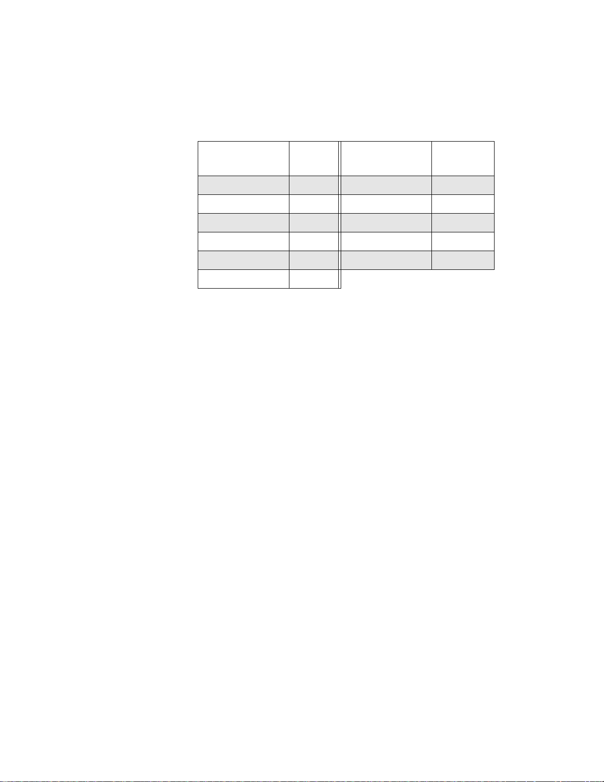
Table 2-2. Available Conversion Rates Using Internal Clock
Conversion Rate
1 Gsamples/s 1 ns 12.5 Msamples/s 80 ns
500 Msamples/s 2 ns 6.25 Msamples/s 160 ns
250 Msamples/s 4 ns 3.125 Msamples/s 320 ns
100 Msamples/s 10 ns 1.5625 Msamples/s 640 ns
50 Msamples/s 20 ns 0.78250 Msamples/s 1280 ns
25 Msamples/s 40 ns
You can also use the Clk IO connector as an output. When the board is
configured for an internal pacer clock source, a TTL-level output signal is
provided on the Clk IO connector that has the same frequency as the
crystal oscillator.
External Pacer Clock
An external pacer clock is an externally generated TTL-le v el clock signal
of at least 100 MHz, with a duty cycle of 50/50 ±20%, applied to the
Clk IO connector. When you start an analog input operation, the board is
armed. At the ne xt rising edge (and at every subsequent rising edge of the
external pacer clock), a conversion is initiated.
Sample
Period Conversion Rate
Sample
Period
A 20
The 20
74ABT series TTL input with a 2 k
appear as approximately 50
You can use a jumper-selectable 50
series protection resistor is provided on the clock input signal.
Ω
resistor combined with the output resistance of the driver IC (a
Ω
pull-up resistor) makes the output
Ω
Ω
.
Ω
termination resistor on the clock
input signal; this resistor is particularly useful when working with a signal
driving a long line or a line that is driving many devices (where the
DAS-4301/8K is at the end of the line). Refer to page 3-18 for more
information on this jumper.
2-8 Functional Description
Page 24

Notes:
−
0.7 V.
Due to excessive loading of the signal, do not use the jumper-selectable
50
Triggers
A trigger is an event that determines when a DAS-4301/8K board
responds to either an internal or an external pacer clock. Depending on
the type of acquisition and setup parameters, the trigger event can occur
before, during, or after the actual sampling of data. The trigger signal can
originate from a variety of sources.
This section describes trigger sources, types of trigger acquisition, and
trigger synchronization on DAS-4301/8K boards.
Trigger Sources
A diode on the input limits signal excursions to +5.7 V and
termination resistor when using the clock output signal.
Ω
The DAS-4301/8K board supports internal triggers, external analog
triggers, and external digital triggers.
Internal T rigger
An internal trigger (or software trigger) event occurs when a particular
instruction is executed by the host computer. When the trigger event
occurs, a signal is output on the Trg IO connector. At the end of data
acquisition, the signal on the Tr g IO connector returns to its inactive state.
Using the test and scope program, you can program the edge polarity of
the trigger output signal. Using the DAS-4300 Series Function Call
Driver or VTX, you cannot program the trigger polarity; it is always
positive.
Triggers 2-9
Page 25

External Analog Trigger
An external analog trigger (or threshold trigger) event occurs when one of
the following conditions is met by an analog input signal:
The analog input signal rises above a programmable threshold
●
(positive-edge trigger).
The analog input signal falls below a programmable threshold
●
(negative-edge trigger).
A TTL-level signal is output on the Trg IO connector when the trigger
event occurs. At the end of data acquisition, the signal on the Trg IO
connector returns to its inactive state.
Using the test and scope program, you can program the polarity of the
trigger output signal. Using the DAS-4300 Series Function Call Dri v er or
VTX, you cannot program the polarity of the trigger output signal; it is
always positive.
You can use an external analog trigger in the following ways:
You can trigger the D AS-4301/8K board using the analog input signal
●
from the Ch A connector or from the Trg/Ch B connector on the
board. When using the analog input signal as the trigger source, the
trigger channel and the data acquisition channel must be the same.
For example, if you are using the signal from the Ch A connector as
the trigger source, you must use Channel A as the data acquisition
channel. You specify the trigger channel and the data acquisition
channel in software.
Using the test and scope program, you can program the trigger
threshold in 4096 steps. Using the DAS-4300 Series Function Call
Driver or VTX, you can program the trigger threshold in 256 steps.
You can trigger the DAS-4301/8K board using the ±10 V analog
●
input trigger signal from the Trg/Ch B connector. When using the
±10 V trigger signal, you can acquire data from either Channel A or
Channel B. You specify the trigger channel and data acquisition
channel using software.
2-10 Functional Description
Page 26

Using the test and scope program, you can program the threshold in
4096 steps from
10 V to +9.995 V; the resolution is 12 bits. Using
−
the DAS-4300 Series Function Call Dri ver or VTX, you can program
the threshold in 256 steps from
−
10 V to +9.922 V; the resolution is 8
bits.
Using a jumper, you can select the input impedance (50
of the ±10 V trigger signal from the Trg/Ch B connector. Refer to
page 3-18 for more information.
External Digital Trigger
A digital trigger event occurs when an externally generated TTL-level
signal of programmable polarity (positive edge or negative edge) is
detected as an input on the Trg IO connector.
A 20
Ω
the Trg IO connector. The 20
resistance of the driver IC (a 74ABT series TTL input with a 2 k
resistor) makes the output appear as approximately 50
jumper-selectable 50
this resistor is particularly useful when working with a signal driving a
long line or a line that is driving many devices (where the DAS-4301/8K
is at the end of the line). Refer to page 3-19 for more information on this
jumper.
Notes:
0.7 V.
−
Ω
or 5600
Ω)
series protection resistor is provided on the trigger input signal of
Ω
resistor combined with the output
pull-up
Ω
. You can use a
Ω
Ω
termination resistor on the trigger input signal;
A diode on the input limits signal excursions to +5.7 V and
When you are not using the Trg IO connector for external digital
triggering, you can use the Tr g IO connector to output a TTL-le vel signal.
If you use the trigger output signal, however, do not use the
jumper-selectable 50
termination resistor due to the excessive loading
Ω
of the signal.
Triggers 2-11
Page 27

Trigger Acquisition
Depending on your application, you can sample data before and/or after a
trigger event occurs. If you want to collect data after a specific trigger
event, use post-trigger acquisition. If you want to collect data before or
before and after a specific trigger event, use about-trigger acquisition.
The maximum number of samples you can collect for each trigger event
is 8,192. The minimum number of samples you can collect for each
trigger event depends on the conversion rate as follows:
●
Conversion rate of 100 Msamples/s and slower : minimum of 1
sample in increments of 1 sample.
●
Conversion rate of 250 Msamples/s and faster : minimum of 10
samples in increments of 10 samples.
Post-Trigger Acquisition
Use post-trigger acquisition to store data samples after a trigger event
occurs. You can also use a programmable post-trigger delay. The delay is
the number of samples after the trigger and before data acquisition starts.
At a conversion rate of 100 Msamples/s or slower, the post-trigger delay
can range from 0 to 65,536 samples (in increments of 1); at a conversion
rate of 250 Msamples/s or faster, the post-trigger delay can range from 0
to 655,360 samples (in increments of 10).
Note:
VTX does not support post-trigger delay.
To start a post-trigger acquisition, perform the following steps:
1. Set up all board parameters, such as the data acquisition channel,
voltage input range, conversion rate, trigger source, trigger polarity,
the number of samples to acquire after the trigger event, and the
post-trigger delay , as appropriate. You need to set up these parameters
only once unless your application requires a change.
2. Using software, arm the board to accept the next valid trigger event.
Arming the board requires about 10
s.
µ
2-12 Functional Description
Page 28

Once the board is armed, the next valid trigger e vent starts the acquisition.
When the trigger event occurs, the post-trigger length, which includes the
post-trigger delay and the number of samples to acquire (defined by the
buffer length), is decremented until it reaches zero, at which point
acquisition stops. Using software, you can poll a status bit or use an
interrupt to determine if the acquisition is finished.
For example, assume the conversion rate is 50 Msample/s, the
post-trigger delay is 10 samples and the buffer length is 190 samples.
When a valid trigger event occurs, the first 10 samples are ignored, the
remaining 190 post-trigger samples are collected, then the acquisition
operation stops.
About-Trigger Acquisition
Use about-trigger acquisition to store data samples before a trigger event
occurs or before and after a trigger event occurs.
To start an about-trigger acquisition, perform the following steps:
1. Set up all board parameters, such as the data acquisition channel,
voltage input range, conversion rate, trigger source, trigger polarity,
and the number of samples to acquire after the trigger occurs. You
need to set up these parameters only once unless your application
requires a change.
2. Using software, arm the board to accept the next valid trigger event.
Arming the board requires about 10
s.
µ
Once armed, the board continuously acquires data and stores it in the
onboard 8K byte memory buffer. The memory buffer must fill up with
data at least once before the board can accept a trigger event. When a
valid trigger event occurs, the specified number of post-trigger samples
(defined by the buffer length) is collected.
For example, suppose you set the buffer length to 4,160 and start the
about-trigger operation. Pre-trigger data is collected and begins to fill the
8K byte buffer. Once the buffer is filled, the board can accept a trigger;
pre-trigger data continues to be collected and overwrites the data in the
buffer until the trigger event occurs. When a valid trigger event occurs,
the board collects 4,160 post-trigger samples then stops the acquisition.
The number of pre-trigger samples in the buffer is 8,192 minus 4,160 or
4,032.
Triggers 2-13
Page 29

The minimum number of pre-trigger samples is 1; the maximum number
of pre-trigger samples is 8,192.
Notes:
The term pre-trigger acquisition is often used for an about-trigger
acquisition when only the samples before the trigger event are significant.
The DAS-4300 Series Function Call Driver differentiates between
pre-trigger acquisition (where the number of post-trigger samples is zero)
and about-trigger acquisition (where you specify the number of
post-trigger samples); refer to the DAS-4300 Series Function Call Driver
User’s Guide for information. The DAS-4300 scope and test program
uses the term pre-trigger mode for both pre-trigger acquisition and
about-trigger acquisition.
You cannot specify a post-trigger delay for an about-trigger acquisition.
VTX does not support about-trigger acquisition.
Equivalent Time Sampling (ETS)
Equivalent time sampling (ETS) is an adv anced feature that allo ws you to
digitize high-frequency analog input signals and achieve f aster conv ersion
rates than 1 Gsamples/s. The advantage of ETS is that the total number of
acquisitions needed to collect a waveform is deterministic; therefore, ETS
is ideal for scanning repetitive waveforms quickly.
On the DAS-4301/8K board, ETS is implemented through a patented
circuit (U.S. Patent No. 4,595,908). The analog signal to be digitized
must be repetitive and coherent with a TTL-level trigger out signal on the
Trg IO connector of the DAS-4301/8K board.
Using ETS, the board samples a repetitive signal several times with the
pacer clock shifted relative to the input signal by a fraction of the sample
period. With N acquisitions and a pacer clock shifted by the fraction of
the sample period 1/(N * f
conversion rate is N * f
) between the acquisitions, the effective
clock
. N is called the ETS factor. The maximum
clock
ETS factor is 20, corresponding to an effective conversion rate of
20 Gsamples/second. Other supported ETS factors are as follows: 2, 4, 5,
2-14 Functional Description
Page 30

and 10 for effective conversion rates of 2, 4, 5, and 10 Gsamples/s,
respectively. Figure 2-3 illustrates an ETS factor of 2.
Input signal
Pacer clock
acquisition 1 (x)
Pacer clock
acquisition 2 (y)
y
y
x
2
3
3
x
2
y
1
x
1
x
4
x
6
y
4
y
5
x
5
y
x
x
y
7
7
6
8
y
8
x
10
x
y
9
9
y
x
x
11
12
11
y
10
y
12
Figure 2-3. Equivalent Time Sampling (ETS)
On the DAS-4301/8K board, individual samples are stored in standard
sequential format. Continuing with the previous example, the data is
stored as follows:
x
x
x
x
... x
y
y
y
y
1
2
3
4
n
1
2
... y
3
4
n
To reconstruct the correct sequence of samples, the host computer
deinterleaves the data of the individual waveforms when transferring the
data off the board. For the two waveforms (x and y) described previously,
the data is transferred as follows:
x
y
x
y
x
y
x
y
1
1
2
2
3
3
4
... xn y
4
n
The ETS process is started by an internal (software) trigger that is
generated by the DAS-4301/8K board. Note that when using ETS, the
DAS-4301/8K board waits for an internal trigger only; external analog
triggers and digital triggers cannot be used. When the trigger event
occurs, an internal trigger signal is generated synchronously to the
internal pacer clock, which performs an A/D conversion. The
synchronous trigger signal is then delayed by a programmable fraction of
Equivalent Time Sampling (ETS) 2-15
Page 31

the pacer clock and output on the Trg I/O connector; this delay is called
the ETS delay. The trigger output signal then generates the input signal,
and the entire process repeats.
The effect of ETS is that samples are digitized at progressiv ely increasing
time intervals until the entire waveform is characterized. Since the ADC
only digitizes one sample when a trigger is received, acquisition is not
limited by the conversion rate of the ADC, but eventually by the total
analog input circuitry of the board.
Figure 2-4 illustrates how ETS works. In this example, the delayed start
of the input signal causes the DAS-4301/8K board to sample the signal at
different points in the two acquisitions described previously. During
acquisition 1 with a larger ETS delay shift, the pacer clock occurs earlier
with respect to the input signal; therefore, the data from this acquisition is
sorted into the even-numbered samples of the combined data set: 0, 2, 4,
and so on. The data from acquisition 2 is sorted into the odd-numbered
samples: 1, 3, 5, and so on.
2-16 Functional Description
Page 32

Software trigger
Synchronized trigger
Pacer clock
ETS delay 1
Trigger I/O output 1
Input signal 1
ETS delay 2
Trigger I/O output 2
Input signal 2
Figure 2-4. ETS Delay
Note: The DAS-4300 Series Function Call Driver and VTX do not
support ETS.
Equivalent Time Sampling (ETS) 2-17
Page 33

Random Interleave Sampling (RIS)
In addition to ETS, the DAS-4301/8K board provides Random Interleave
Sampling (RIS). Like ETS, RIS allows the DAS-4301/8K board to
sample a repetitive signal at rates above 1 Gsamples/s. Unlike ETS,
however, the signal does not have to be coherent with the pacer clock.
This feature is particularly convenient in scope-type applications where
you may not be overly concerned about the time it takes to complete the
acquisition but you want to watch the screen filling with data.
One advantage of RIS over ETS is the ability to acquire and display
pre-trigger data at sampling rates of up to 20 Gsamples/s. RIS also offers
more trigger source options than ETS. The trigger for the signal can be
derived from the signal (external software analog trigger), external
hardware analog trigger, or e xternal digital trigger. If the trigger source is
external analog or digital, the trigger needs to be synchronized with the
signal.
RIS offers the same sampling rates as ETS: 2, 4, 5, 10, and
20 Gsamples/s. During each acquisition, an entire waveform is collected.
Ideally, at 20 Gsamples/s, 20 waveforms sampled at 1 Gsamples/s are
required to reconstruct a waveform equivalently sampled at
20 Gsamples/s. However, because the waveforms fall randomly, many
waveforms are usually required. The DAS-4300 scope and test program
updates the waveform as each is acquired.
Figure 2-5 illustrates how RIS works.
2-18 Functional Description
Page 34

1 GHz Clock
First Acquisition (x)
Measured T rigger
First Acquisition
1 GHz Clock
Second Acquisition (y)
Measured T rigger
Second Acquisition
1 GHz Clock
Third Acquisition
(z)
Measured T rigger
Third Acquisition
Threshold Level
Sampled Wav eform
z
2
y
2
x
2
z
1
y
1
x
1
x
3
y
3
z
3
x
4
y
4
z
4
z
5
y
5
x
5
z
6
y
6
x
6
Figure 2-5. Random Interleave Sampling
Note: The DAS-4300 Series Function Call Driver and VTX do not
support RIS.
Random Interleave Sampling (RIS) 2-19
Page 35

3
Setup and I
This chapter contains the information you need to set up and install your
DAS-4301/8K board.
Unpacking the Board
Caution:
damage certain electrical components on any circuit board. It is
recommended that you use wrist strap grounds when handling a board. If
wrist strap grounds are not available, make sure that you discharge static
electricity from yourself by touching a grounded conductor such as your
computer chassis (your computer must be turned OFF).
Whenever you handle a board, hold it by the edges and avoid touching
any board components. Avoid touching the gold edge connector as this
may leave fingerprints that can degrade the electrical connections.
A discharge of static electricity from your hands can seriously
nstallation
To prevent any damage to your DAS-4301/8K board, perform the
following steps when unpacking the board:
1. Remove the wrapped DAS-4301/8K board from its outer shipping
carton.
2. Carefully remove the board from its antistatic wrapping material.
(You may wish to store the wrapping material for future use.)
Note:
Do not remove the pink foam pad. Leav e the board on the pink
foam pad until you are ready to install the board in the computer.
Unpacking the Board 3-1
Page 36

3. Inspect the board for signs of damage. If any damage is apparent,
arrange to return the board to the factory; refer to page 5-4 for more
information.
4. Check the remaining contents of your package against the packing
list to ensure that your order is complete. Report any missing items
immediately.
5. Once you have determined that the board is acceptable, install the
software and configure the board. Refer to the following sections for
information.
Installing the Software
This section describes how to install the DAS-4300 Series standard
software package and how to install the ASO-4300 software package
from both DOS and W indo ws. To install other software packages, refer to
the documentation supplied with the software package.
Installing the DAS-4300 Series Standard Software Package
To install the DAS-4300 Series standard software package, perform the
following steps:
1. Make a backup copy of the supplied disks. Use the copies as your
working disks and store the originals as backup disks.
2. Insert disk #1 into the disk drive.
3. Assuming that you are using disk drive A, enter the following at the
DOS prompt:
A:install
The installation program prompts you for your installation
preferences, including the drive and directory you want to copy the
software to. It also prompts you to insert additional disks, as
necessary.
4. Continue to insert disks and respond to prompts, as appropriate.
When the installation program prompts you for a drive designation,
enter a designation of your choosing or accept the default drive C.
3-2 Setup and Installation
Page 37

When the installation program prompts you for a directory name,
enter a name of your choosing or accept the default name.
The installation program creates a directory on the specified drive and
copies all files, expanding any compressed files.
5. When the installation program notifies you that the installation is
complete, review the following files:
– FILES.TXT lists and describes all the files copied to the hard disk
by the installation program.
– README.TXT contains information that was not available when
this manual was printed.
Installing the ASO-4300 Software Package
DOS Installation
The ASO-4300 software package contains software for both the DOS and
Windows environments. This section describes how to install both the
DOS version and the Windows version of the ASO-4300 software
package.
To install the DOS version of the ASO-4300 software package, perform
the following steps:
1. Make a backup copy of the supplied disks. Use the copies as your
working disks and store the originals as backup disks.
2. Insert disk #1 into the disk drive.
3. Assuming that you are using disk drive A, enter the following at the
DOS prompt:
A:install
The installation program prompts you for your installation
preferences, including the drive and directory you want to copy the
software to. It also prompts you to insert additional disks, as
necessary.
4. Continue to insert disks and respond to prompts, as appropriate.
When the installation program prompts you for a drive designation,
enter a designation of your choosing or accept the default drive C.
Installing the Software 3-3
Page 38

When the installation program prompts you for a directory name,
enter a name of your choosing or accept the default name.
The installation program creates a directory on the specified drive and
copies all files, expanding any compressed files.
5. When the installation program notifies you that the installation is
complete, review the following files:
– FILES.TXT lists and describes all the files copied to the hard disk
– README.TXT contains information that was not available when
Windows Installation
by the installation program.
this manual was printed.
To install the Windows version of the ASO-4300 software package,
perform the following steps:
1. Make a backup copy of the ASO-W indo ws disk. Use the cop y as your
working disk and store the original as a back up.
2. Insert the ASO-Windows disk into the disk drive.
3. Start Windo ws.
4. From the Program Manager menu, select File and then select Run.
5. Assuming that you are using disk drive A, type the following at the
command line in the Run dialog box, and then choose OK:
A:SETUP
The installation program prompts you for your installation
preferences, including the drive and directory you want to copy the
software to. It also prompts you to insert additional disks, as
necessary.
6. Continue to insert disks and respond to prompts, as appropriate.
When the installation program prompts you for a drive designation,
enter a designation of your choosing or accept the default drive C.
When the installation program prompts you for a directory name,
enter a name of your choosing or accept the default name.
The installation program creates a directory on the specified drive and
copies all files, expanding any compressed files.
3-4 Setup and Installation
Page 39

The installation program also creates a DAS-4300 family group; this
group includes example Windows programs and help files.
7. When the installation program notifies you that the installation is
complete, review the following files:
– FILES.TXT lists and describes all the files copied to the hard disk
by the installation program.
– README.TXT contains information that was not available when
this manual was printed.
Configuring the Board
You configure the following items for DAS-4300 Series boards by setting
jumpers on the board and/or by specifying the configuration in a
configuration file:
●
Base I/O address
●
Memory address
●
Interrupt
Zero wait-state option
●
AC/DC couplings
●
●
Acquire data from Channel B or calibrate input ranges
●
Input impedance for signal into Ch A connector
50
●
●
●
●
termination resistor for clock input signal
Ω
50
Ω
termination resistor for trigger input signal
Ω
100
pull-up resistor to +5 V for trigger input signal
Ground connections
Table 3-1 lists the items that are configurable for DAS-4301/8K boards,
the available options, the default settings in the configuration file, and the
default jumper settings.
Configuring the Board 3-5
Page 40

Table 3-1. Configuring DAS-4301/8K Boards
Attribute Options
J
Where Option
is Set
File Board
Default
Default Jumper
Settings
1
Base I/O address
Memory address
Interrupt
AC/DC coupling AC, DC
Zero wait state
Channel B/
Calibration
1
2
&H200 to &H3FF
1
C 000 to D C00
2, 5, 7, 10, 11, 12,
15
3
Enabled, Disabled
Acquire data from
Channel B or
calibrate input
ranges
✔
✔
✔
✔
✔
✔
✔
✔
✔
&H250 J400
1: OUT
2: IN
3: IN
4: OUT
5: IN
6: OUT
C C00 J401
1: OUT
2: IN
3: IN
None J402
1 to 7: OUT
DC J106 IN
Enabled Not applicable
Acquire data from
Channel B
J103
1-2: IN
3-4: OUT
Input impedance
for Ch A signal
Input impedance
for analog trigger
signal from
Trg/Ch B
Clock input 50 Ω
termination
Trigger input 50 Ω
termination
3-6 Setup and Installation
50 Ω or 1 M Ω
50 Ω or 5600 Ω
Terminated or not
terminated
Terminated or not
terminated
✔
✔
✔
✔
50 Ω
50 Ω
Not terminated J500: OUT
Not terminated J502: OUT
105: ΙΝ
J901: IN
Page 41

Table 3-1. Configuring DAS-4301/8K Boards (cont.)
Attribute Options
Where Option
is Set
File Board
Default
Default Jumper
Settings
1
Trigger input
100 Ω pull-up to
Pulled up or not
pulled up
✔
Not pulled-up J501: OUT
+5 V
Analog-to-digital
ground to A/D
Analog-to-digital
ground to DC
Grounded or not
grounded
Grounded or not
grounded
✔
✔
Grounded J102: IN
Grounded J202: IN
converter
Bracket-to-analog
ground
DSP ground
4
Grounded or not
grounded
J302, location 19
✔
✔
Grounded J104: IN
Grounded J301:
grounded or not
DSP connector
grounded
4
DSP connector or
✔
DSP connector J302: None
2-3: IN
no connector
DSP I/O
Notes
1
jumper is inserted in the specified jumper position.
2
The setting in the configuration file must match the settings of the jumpers on the board.
3
The default setting is appropriate for most computers. If you are using an older computer, you may
want to try changing the setting.
4
These jumper settings are provided for completeness; unless you are using the SDC-5600 DSP board,
4
OUT indicates that a jumper is not inserted in the specified jumper position and IN indicates that a
None or Spare I/O
✔
Spare I/O J300: None
you do not need to change these jumper settings.
Refer to page 3-10 for information on setting the jumpers. Refer to the
next section for information on creating a configuration file.
Configuring the Board 3-7
Page 42

Creating a Configuration File
A configuration file is required by the DAS-4300 Series Function Call
Driver and other software packages to perform operations on the
DAS-4301/8K board. A def ault configuration file called DAS4300.CFG is
provided in both the DAS-4300 Series standard softw are package and the
AS0-4300 software package. The factory-default settings in
DAS4300.CFG are shown in Table 3-1.
If the default settings in the configuration file are appropriate for your
application, refer to the following section to ensure that the jumper
settings on the board match the settings in the configuration file.
If the default settings are not appropriate for your application, you must
create a new configuration file or modify an existing configuration file to
specify the correct configuration options. The CFG4300.EXE
configuration utility, shipped with both the DAS-4300 Series standard
software package and the ASO-4300 software package, is provided for
this purpose.
T o create a ne w configuration file or modify an existing configuration file,
perform the following steps:
1. Invoke the configuration utility from DOS or Windows, as follows:
– If you are running under DOS , from the directory containing the
CFG4300.EXE configuration utility, enter the following at the
DOS prompt:
CFG4300
filename
where filename is the name of the configuration file you wish to
create or modify.
– If you are running under Windows , select Run from the Program
Manager File menu, enter the following in the box, and choose
OK:
CFG4300
filename
where filename is the name of the configuration file you wish to
create or modify. Make sure that you enter the correct path to
CFG4300.EXE, or use the Browse button to find this file.
3-8 Setup and Installation
Page 43

If the utility finds a configuration file named filename , it displays the
opening menu screen with filename shown; this file contains the
configuration options found in filename . If the utility does not find a
configuration file named filename , it displays the opening menu
screen with filename shown; this file contains the default
configuration options. If you do not enter a file name, the utility
displays the opening menu screen of the default configuration file
DAS4300.CFG.
Note:
The example programs, provided with the ASO-4300 software
package, use the default configuration file DAS4300.CFG. If you
intend to use the example programs, make sure that DAS4300.CFG
exists and that the settings in DAS4300.CFG match the jumper
settings of your board.
2. On the opening menu screen, enter the number of DAS-4301/8K
boards you plan to configure (1 or 2).
The utility displays the configuration options for the first board
(board 0). The number of the board is shown in the upper-left corner
of the top menu box.
3. To modify any of the configuration options, use the arrow keys to
highlight the option you want to change, press Enter to display a list
of available settings, use the arrow keys to highlight the appropriate
setting, and press Enter . These instructions are summarized in the
Commands/Status box at the bottom of the screen.
When the configuration options for this board are correct, press N to
display the configuration options for the next board.
4. After you modify the appropriate configuration options for all boards,
press Esc. The utility asks if you want to save the new settings to the
specified configuration file.
5. Press Y to save the new settings and exit. Press N to exit without
saving the new settings.
When you finish creating or modifying the configuration file, refer to the
following section to ensure that the jumper settings on the board match
the settings in the configuration file.
Configuring the Board 3-9
Page 44

Setting Jumpers on the Board
The locations of the jumpers required for configuring DAS-4300 Series
boards are shown in Figure 3-1.
3-10 Setup and Installation
Page 45

Ch A
Trg/Ch B
Clk IO
Trg IO
Note that jumpers
J103, J104, J105,
J106, and J901 are
underneath the metal
cover; to change the
settings of these
jumpers, you first must
unscrew the metal
cover.
J104
J106
Pin 1
J105
J103
J901
J102
Pin 1
J200
J400
J402
Pin 1
J501
J502
J500
J401
Pin 1
Pin 1
J403
J404
J202
J300
J301
Pin 1
Pin 1
J302
Pin 1
Pin 1
J201
Figure 3-1. Jumper Placement on DAS-4301/8K Board
Configuring the Board 3-11
Page 46

Setting the Base I/O Address
The DAS-4301/8K board requires 16 consecuti ve bytes in the I/O address
space of the host computer. The board is shipped with a base I/O address
of 250h. If your application requires a different setting, use jumper block
J400 to set the base I/O address. Each board must have a unique base I/O
address.
Note: If you change the default base I/O address of the board and you
plan on using the DAS-4300 scope and test program, you must change the
base I/O address setting in the D4300.ADC file. See Chapter 4 for more
information.
Table 3-2 lists the settings of J400 for base I/O addresses in the range of
200h to 3FFh.
Table 3-2. Base I/O Address
Base I/O
Address
Position 1 Position 2 Position 3 Position 4 Position 5 Position 6
Jumper J400
200 to 20F OUT IN IN IN IN IN
210 to 21F OUT IN IN IN IN OUT
220 to 22F OUT IN IN IN OUT IN
230 to 23F OUT IN IN IN OUT OUT
240 to 24F OUT IN IN OUT IN IN
1
250 to 25F
260 to 26F OUT IN IN OUT OUT IN
270 to 27F OUT IN IN OUT OUT OUT
280 to 28F OUT IN OUT IN IN IN
290 to 29F OUT IN OUT IN IN OUT
2A0 to 2AF OUT IN OUT IN OUT IN
2B0 to 2BF OUT IN OUT IN OUT OUT
3-12 Setup and Installation
OUT IN IN OUT IN OUT
Page 47

Table 3-2. Base I/O Address (cont.)
Jumper J400
Base I/O
Address
2C0 to 2CF OUT IN OUT OUT IN IN
2D0 to 2DF OUT IN OUT OUT IN OUT
2E0 to 2EF OUT IN OUT OUT OUT IN
2F0 to 2FF OUT IN OUT OUT OUT OUT
300 to 30F OUT OUT IN IN IN IN
310 to 31F OUT OUT IN IN IN OUT
320 to 32F OUT OUT IN IN OUT IN
330 to 33F OUT OUT IN IN OUT OUT
340 to 34F OUT OUT IN OUT IN IN
350 to 35F OUT OUT IN OUT IN OUT
360 to 36F OUT OUT IN OUT OUT IN
370 to 37F OUT OUT IN OUT OUT OUT
Position 1 Position 2 Position 3 Position 4 Position 5 Position 6
380 to 38F OUT OUT OUT IN IN IN
390 to 39F OUT OUT OUT IN IN OUT
3A0 to 3AF OUT OUT OUT IN OUT IN
3B0 to 3BF OUT OUT OUT IN OUT OUT
3C0 to 3CF OUT OUT OUT OUT IN IN
3D0 to 3DF OUT OUT OUT OUT IN OUT
3E0 to 3EF OUT OUT OUT OUT OUT IN
3F0 to 3FF OUT OUT OUT OUT OUT OUT
Notes
1
Default base I/O address.
Configuring the Board 3-13
Page 48

Setting the Memory Address
The onboard 8K byte memory on the DAS-4301/8K board is mapped into
a 16K byte window in upper memory (above 640K bytes). The
DAS-4301/8K board is shipped with a memory address of CC00:0000. If
your application requires a different setting, use jumper block J401 to set
the memory address, as shown in Table 3-3.
Note: Note that no other boards or devices can share the selected
memory address. If you change the default memory address of the board
and you plan on using the DAS-4300 scope and test program, you must
change the memory address setting in the D4300.ADC file. See Chapter 4
for more information.
Table 3-3. Memory Address
Memory
Address
C 0000 OUT OUT OUT
C 4000 OUT OUT IN
C 8000 OUT IN OUT
C C000
D 0000 IN OUT OUT
D 4000 IN OUT IN
D 8000 IN IN OUT
D C000 IN IN IN
Notes
1
Default factory setting.
Position 1 Position 2 Position 3
1
OUT IN IN
Jumper J401
3-14 Setup and Installation
Page 49

The host computer must leave room for the onboard memory of the
DAS-4301/8K board in its memory address map. To ensure that the host
computer is configured to leave room in its memory address map, you
must exclude the memory area of 16K bytes (CC00:0000 to CFFF:000F
or your memory address setting) from the memory available for the EMS
manager of your system (for example, QEMM or EMM386).
For QEMM, your C:\CONFIG.SYS file should contain a line similar to
the following:
DEVICE = C:\QEMM\QEMM386.EXE X=CC00-CFFF
For EMM386, your C:\CONFIG.SYS file should contain a line similar to
the following:
DEVICE = C:\DOS\EMM386.EXE X=CC00-CFFF
Note that the examples assume a certain directory structure on the disk;
you may have to modify these commands.
Setting the Interrupt
If enabled in software, the DAS-4301/8K board can generate an interrupt
at the end of a data acquisition operation to notify the host computer that
the operation is completed. Selecting an interrupt connects the interrupt
line to a tristate driver on the board; this feature allows the interrupt to
remain selected while allowing other devices to use the interrupt line.
The DAS-4301/8K board is shipped with no interrupt selected. If your
application requires a different setting, select the interrupt by inserting the
jumper into one of the positions of jumper block J402. Make sure that you
insert a jumper into only one of the positions of J402; refer to Table 3-4.
Configuring the Board 3-15
Page 50

Interrupt
Table 3-4. Interrupt Selection
Jumper J402
Position1Position2Position3Position4Position5Position6Position
7
1
None
2 IN OUT OUT OUT OUT OUT OUT
5 OUT IN OUT OUT OUT OUT OUT
7 OUT OUT IN OUT OUT OUT OUT
10 OUT OUT OUT IN OUT OUT OUT
11 OUT OUT OUT OUT IN OUT OUT
12 OUT OUT OUT OUT OUT IN OUT
15 OUT OUT OUT OUT OUT OUT IN
Notes
1
Default setting.
OUT OUT OUT OUT OUT OUT OUT
Acquiring Data from Channel B or Calibrating the Board
If you want to acquire analog input data from Channel B, you must
specify Channel B in software and leave the default jumper setting of
jumper J103 in its factory-default configuration (jumper installed in
positions 1 and 2).
Positions 3 and 4 of jumper block J103 are provided for calibrating the
board. However, it is strongly recommended that you return the board to
Keithley Metrabyte if calibration is required; refer to page 5-4 for more
information on returning a board.
Jumper block J103 is underneath the metal cover on the top right of the
board. To change the jumper setting, you first must unscrew this metal
cover.
Figure 3-2 illustrates the analog input circuitry.
3-16 Setup and Installation
Page 51

CHA 5
V
rms
TRG CHB
(±10 V)
1
2
J105
1
4 5 7 8 9 1032
4 5 7 8 9 1032
R101
150
1
2
2
J100
1
6
J900
1
6
R900
150
1
2
1
R102
150
3
4
1
2
1
J103
R100
51.1
2
R938
150
2
2
1
C150
.01
R103
150
J901
1
2
1
1
1
J106
C152
.001
C153
1 µF
1
R939
150
2
2
R940
51.1
6
7
2
2
1
9
R901
4.87 k
1
2
C900
2
1
Figure 3-2. Analog Input Circuitry
Top Bracket Hole
±1.25
R902
698
1
2
MTG101
J104
Analog
Trigger In
C901
To Input
8
Buffer
4
3
CAL2-L
+5R
CAL/CHB
CAL
+5 VS
2
D900
1N4149
1
2
2
1
−5 VS
D900
1N4149
1
2
Selecting AC or DC Coupling
AC or DC coupling is determined by jumper block J106. If a jumper is
installed in jumper block J106 (the default condition), DC coupling is
selected. Removing the jumper from jumper block J106 selects AC
coupling.
Jumper block J106 is underneath the metal cover on the top right of the
board. To change the jumper setting, you first must unscrew this metal
cover.
Setting the Input Impedance of Ch A Signal
The input impedance of the signal coming into the Ch A connector is
determined by jumper block J105. If a jumper is installed in jumper block
J105 (the default condition), the input impedance is 50
jumper from jumper block J105, selects an input impedance of
approximately 1 M
Configuring the Board 3-17
Ω.
Ω. Removing the
Page 52

Jumper block J105 is underneath the metal cover on the top right of the
board. To change the jumper setting, you first must unscrew this metal
cover.
Setting the Input Impedance of the Analog Trigger Input Signal
The input impedance of the trigger input signal from the Trg/Ch B
connector is determined by jumper block J901. If a jumper is installed in
jumper block J901 (the default condition), the input impedance is 50
you remove the jumper from jumper block J901, the input impedance is
approximately 5600
Ω.
Jumper block J901 is underneath the metal cover on the top right of the
board. To change the jumper setting, you first must unscrew this metal
cover.
Setting the 50 Ω Termination Resistor for the Clock Input Signal
The clock input signal of the Clk IO connector has a jumper-selectable
50
Ω termination to ground for signals driving long lines or lines that are
driving many devices. Insert a jumper into jumper block J500 to provide
the 50
Ω termination resistor. The 50 Ω resistor is provided in the
solderless component jack, R503. By default, the jumper is removed.
Ω. If
Note: To prevent excessive loading of the signal, do not use the 50 Ω
termination resistor when the board is providing the clock output signal
on the Clk IO connector.
Figure 3-3 illustrates the clock I/O and trigger I/O circuitry.
3-18 Setup and Installation
Page 53

Clock
In/Out
(TTL)
+5 V
1
R501
2.00 k
2
J507
1
6
4 5 7 8 9 1032
1
J500
1
2
2
ENEXTCLK-L
R502
20
1
R503
49.9
D500
1N4149
2
+5 V
2
1
D501
1N4149
+5 V
U514
74ABT125
10
U514
74ABT125
8
12
9
2
1
1
14
VCC
GND
U513
100 MHz
7
Out
8
U514
74ABT125
2
1
3
Master 100
MHz Clock
Trigger
In/Out
(TTL)
13
U514
74ABT125
+5 V
1
R504
100
2
J501
J508
1
6
4 5 7 8 9 1032
2
J502
1
2
R506
2.00 k
1
2
1
+5 V
1
2
R505
20
R507
49.9
+5 V
2
1
D503
1N4149
D502
1N4149
2
1
U515
74ABT125
6
4
U515
74ABT125
6
4
3
1
5
5
U515
2
74ABT125
9
8
10
ENINTCLK-L
Trigger Out
ENTRIGOUT-L
Trigger In
Figure 3-3. Clock I/O and Trigger I/O Circuitry
Setting the 50 Ω Termination Resistor for the Trigger Input Signal
The trigger input signal of the Trg IO connector has a jumper-selectable
50
Ω termination to ground for signals driving long lines or lines that are
driving many devices. Insert a jumper into jumper block J502 to provide
the 50
Ω termination resistor. The 50 Ω resistor is provided in the
solderless component jack, R507. By default, the jumper is removed.
Note: To prevent excessive loading of the signal, do not use the 50 Ω
termination resistor when the board is providing the trigger output signal
on the Trg IO connector.
Configuring the Board 3-19
Page 54

Setting the 100 Ω Pull-Up to +5 V for the Trigger Input Signal
The trigger input signal of the Trg IO connector has a jumper-selectable
100
Ω pull-up to +5 V to float the tristate output high. Insert a jumper into
jumper block J501 to provide the 100
Ω pull-up to +5 V. The 100 Ω
pull-up to +5 V is provided in the solderless component jack, R504. By
default, the jumper is removed.
Setting Grounds
The DAS-4301/8K board provides several jumper-selectable grounds. By
default, each of these grounds is selected (a jumper is inserted in the
appropriate jumper block). Table 3-5 lists the grounds that are
jumper-selectable on the DAS-4301/8K board and their default
configurations. If you want to remove the grounds, remove the jumpers
from their respective locations.
Table 3-5. Grounds on the DAS-4301/8K Board
Ground Type Jumper
Used
Analog-to-digital ground
to A/D
Analog-to-digital ground
to DC converter
Bracket-to-analog ground J104 IN
J102 IN
J202 IN
Default
Setting
Jumper block J104 is underneath the metal cover on the top right of the
board. To change the jumper setting, you first must unscrew this metal
cover.
3-20 Setup and Installation
Page 55

Installing the Board
You can avoid many problems by providing the proper operating
environment for the DAS-4301/8K board.
The following suggestions will help ensure an optimal environment that
includes adequate space, cooling, and power:
● Place the DAS-4301/8K board next to a half-length or half-height
Circuit Card Assembly (CCA), if possible.
● Do not place another CCA next to the component side of the
DAS-4301/8K board, if possible.
● Ensure that your computer has adequate cooling air flow in the
card-nest.
● Make sure that the power supply fan filter is clean.
● Make sure that ribbon cables are not impeding the air flow.
● Make sure that the rear cutouts of all unused expansion slots are
sealed with a cover plate.
● Ensure that your computer has an adequate power supply rating. The
DAS-4301/8K board requires the following power from the
computer's power supply:
– +5 volt; 11.5 Watts
– +12 volt; 0.9 Watts
−12 volt; 2.2 Watts
–
To install the DAS-4301/8K board in your host computer, perform the
following steps:
1. TURN OFF SYSTEM POWER AND UNPLUG THE AC POWER
CORD.
2. Remove the cover from the computer and locate a free e xpansion slot.
3. Remove the cover plate from the slot by remo ving its mounting scre w
and lifting the cover plate from its location. Sav e the mounting screws
and cover plate for later use.
Installing the Board 3-21
Page 56

4. Insert the BNC connector side first, pushing the BNCs through the
slot at the back of the computer. Bring the opposite side down into
the card edge guide. The lower left side of the board has a slight
bevel to facilitate insertion.
5. Push the board's connector strip into the expansion slot. Make sure
that the board is firmly placed into the bus.
6. Secure the board to the computer at the board's back bracket with the
cover plate screw. Some computer chassis and motherboards are
made with very loose dimension tolerances. Make sure when you
tighten the screw, the left side of the gold edge connector on the
DAS-4301/8K does not pull up and out of the expansion slot.
7. Once the board is firmly in place, attach the signal and trigger
connections to the BNC connectors at the back of the board.
Initializing the Board
To initialize the DAS-4301/8K board, locate the AUTO4300.EXE file on
the disk. AUTO4300 should be included in the AUTOEXEC.BAT file of
the root directory if the board is plugged into the bus.
AUTO4300.EXE initializes the DAS-4301/8K during power-up since the
board's setup parameters are random when the computer is powered on.
In some cases, the random analog offset and gain values could cause an
undesirable current drain in the analog section. AUTO4300.EXE pre vents
this drain from occurring.
If you are using the default base I/O address setting of 250h, no
parameters are required. Include the following command line in the
AUTOEXEC.BAT file:
AUTO4300
If you are using some other base I/O address, include the base I/O address
(in hexadecimal notation) on the command line. For example, if you are
using a base I/O address of 258h, include the following command in the
AUTOEXEC.BAT file:
AUTO4300 258
If you are using multiple boards, you must initialize each board separately
because each board must use a different base I/O address.
3-22 Setup and Installation
Page 57

4
Scope and Test Program
The DAS-4300 Series scope and test program (D4300.EXE) is a utility
program that allows you to test the hardware features available on the
DAS-4301/8K board, to recalibrate the analog input section of the board,
and to perform basic oscilloscope functions, such as saving and recalling
waveforms to disk.
D4300 is a menu-based, keyboard-controlled DOS program that requires
a VGA compatible display. It has one support file, D4300.ADC, which is
shipped with both the DAS-4300 Series standard software package and
the ASO-4300 software package.
To run the scope and test program, enter the following at the DOS
prompt:
D4300
Use the control keys, described in the following section, to use the scope
and test program.
Control Keys for D4300.EXE
Table 4-1 lists the keys that control the D4300.EXE scope and test
program. In addition, several function group menus are listed at the top of
the oscilloscope screen; press the first letter in the title of a menu to
change to the menu. Note that D4300.EXE is case-insensitive.
Control Keys for D4300.EXE 4-1
Page 58

Table 4-1. Control Keys
Key Description
A Selects the A/D menu as the currently displayed menu at the
bottom of the screen. From the A/D menu, you can modify most of
the hardware features of the board.
C Selects the Configure/EEPROM menu as the currently displayed
menu at the bottom of the screen. The Configure/EEPROM menu
allows you to display and overwrite the calibration values in
EEPROM.
D Selects the Display menu as the currently displayed menu at the
bottom of the screen. The Display menu controls operations such
as waveform accumulation and averaging.
E Allows direct entry of a number. This is not valid for all
parameters. See Table 4-2 for a list of suffixes you can use with
some entries.
H Displays a help screen, which lists these control keys.
L Loads a parameter file. Refer to page 4-10 for more information
about parameter files.
M Toggles measurement cursors on or off. If the measurement
cursors are currently on, they are turned off. Otherwise, you are
prompted to select measurement of voltage or time. The
measurement readouts are displayed above the main scope display;
the currently selected cursor values are displayed in white above
the screen. The two measurement cursors are identical. See also
the descriptions of the 1, 2, 3, <, and > keys.
O Selects the Options menu as the currently displayed menu at the
bottom of the screen. The Options menu controls the printer type
and allows you to create a file with the current setup.
P Prints the currently displayed screen. The printer type is controlled
through the Options menu.
Q Quits the program, unless a waveform recall is currently active. If
recalling a waveform, Q returns D4300 to normal real-time
acquisition.
R Redraws the screen. This is useful for clearing the scope display
after accumulating waveforms.
4-2 Scope and Test Program
Page 59

−
Table 4-1. Control Keys (cont.)
Key Description
S Saves a parameter file. Refer to page 4-10 for more information
about parameter files.
T Takes a single shot. This k ey is valid only if the single-shot switch
on the A/D menu is turned on.
W Displays a prompt asking whether to save or recall waveforms. If
saving, you are prompted for the number of waveforms to sa v e and
a file name to save them in. Only 64K bytes of waveform data can
be saved. If recalling, you are prompted for a D4300-generated
waveform file. You can scroll through the waveforms saved in this
file with the Pg Up and Pg Down keys (see the Display menu).
Pressing Q exits waveform recall mode and returns to normal
operation.
Arrows Moves the highlight within the current menu.
SP ACE T oggles between setting and not setting the mov e factor. The move
factor controls the rate at which the + and - keys increment the
current selection.
ESC Toggles the highlight cursor to or from the Command menu at the
top of the screen. Commands are selected using Pg Up and
Pg Down , and then pressing the Enter key.
Pg Up Displays next waveform.
Pg Down Displays previous waveform.
+ Increments the current selection to the next value.
Decrements the current selection to its previous value.
> Moves the current measure cursor to the right (for time cursors) or
up (for voltage cursors).
< Moves the current measure cursor left (for time cursors) or down
(for voltage cursors).
1 Selects the first measure cursor. The < and > keys change the
position of the first cursor.
2 Selects the second measure cursor. The < and > keys change the
position of the second cursor.
3 Selects both measure cursors simultaneously. The < and > keys
move both cursors in tandem.
Control Keys for D4300.EXE 4-3
Page 60

T able 4-2 lists the suf fix es that you can use on entered numbers. Note that
not all suffixes are allowed on all entries.
Table 4-2. Suffixes
Suffix Description
h Hexadecimal
n Nanoseconds
u Microseconds
m Milliseconds
s Seconds
v Voltage
Scope and Test Program Menus
The following sections describe the parameters on the scope and test
program menus.
A/D Menu
Table 4-3 lists the parameters on the A/D menu. You can access the A/D
menu at any time by pressing the A key.
Table 4-3. A/D Menu
Parameter Description
Sampling Rate Changes the conversion rate for the board. The conversion
rate can range from 0.78125 Msamples/second to
20 Gsamples/second. Conversion rates above
1 Gsamples/s are achieved through ETS or RIS.
ETS Wait Not implemented at this time.
4-4 Scope and Test Program
Page 61

Table 4-3. A/D Menu (cont.)
Parameter Description
Single shot Turns single-shot mode on or off. If single-shot mode is
off, the waveforms are updated in real time. If single-shot
mode is on, waveform collection is suspended until the T
key is pressed; this causes one waveform to be taken.
Post-trigger delay Specifies the number of samples to wait after the trigger
event occurs before starting to collect data. You cannot
change this parameter if about-trigger mode (pre-trigger
mode) is on; it is automatically set to zero. For conversion
rates of 100 Msamples/s or slower, the post-trigger delay
ranges from 0 to 65,536 minus the buffer length; for
conversion rates of more than 250 Msamples/s, the
post-trigger delay ranges from 0 to 655,360 minus the
buffer length.
You can use the h, n, u, m, and s suffixes with this entry.
Buffer length Specifies the amount of data that is saved after the trigger
pulse is accepted. The post-trigger delay setting does not
affect the buffer length.
This number ranges from 0 to 8,190 and is independent of
the conversion rate. The buffer length is limited to a
multiple of 10 for conversion rates of 250 Msamples/s and
faster.
You can use the h, n, u, m, and s suffixes with this entry.
Clock Switches between an internal and an external pacer clock.
An internal pacer clock is the onboard 100 MHz clock.
The external pacer clock is an externally generated clock
signal of any frequency up to 100 MHz applied to the Clk
IO connector.
Voltage level Sets the voltage input level of the board. This can range
from ±50 mV to ±2.0 V.
Voltage offset Sets the offset voltage. This parameter is calibrated in the
factory, but may require minor adjustments, depending on
the input signal. The zero point of the waveform should be
centered on the oscilloscope display.
You can use the h suffix with this entry.
Scope and Test Program Menus 4-5
Page 62

Table 4-3. A/D Menu (cont.)
Parameter Description
Vernier gain Sets the vernier gain. This parameter is calibrated in the
factory, but may require minor adjustments, depending on
the input signal. The signal should stretch over the full
height of the scope
You can use the h suffix with this entry.
Pre-trigger Turns pre-trigger mode (about-trigger mode) on or off. If
the display start parameter on the Display menu is
negative, you can view the pre-trigger data.
Trigger type Selects the trigger source. The supported options are
software, analog, and digital. Refer to Chapter 2 for
information on triggers.
Trigger logic Not used in this version of the program.
Trigger Phase In For an external analog or digital trigger, specifies whether
a rising or falling edge triggers the board.
Trigger Phase Out If +, specifies that the trigger output signal on the Trg IO
connector will be low during normal operations and go
high while the board is digitizing; otherwise, specifies that
the trigger output signal on the Trg IO connector will be
high during normal operation and and go low while the
board is digitizing.
Interrupts Not implemented at this time.
Channel threshold Specifies the threshold level at which the trigger will occur
for an external analog trigger . You can use the h suf fix with
this entry.
Analog threshold Specifies the threshold lev el at which the trigger will occur
for an external analog trigger . You can use the h suf fix with
this entry.
A/D base port Specifies the base address of the DAS-4301/8K board
being used. You can also use this parameter to switch
between multiple DAS-4301/8K boards. When a new
board is selected, all current parameters are set on the
board.
4-6 Scope and Test Program
Page 63

Display Menu
Table 4-4 lists the parameters on the Display menu. You can access this
menu at any time by pressing the D key.
Table 4-4. Display Menu
Parameter Description
Disp start Displays the collected data, except in single-shot mode. If
about-trigger mode (pre-trigger mode) is on, the display
start is relative to the trigger point (a display start of 0
starts the waveform display at the trigger point); you can
enter a negative number for the display start to display
pre-trigger data. Scrolling past the end of the collected data
is not possible.
You can use the h, n, u, m, and s suffixes with this entry.
Time / points Specifies whether the time-based entries (post-trigger
delay, b uffer length, and display start) are displayed in raw
data points or in terms of microseconds calculated from
the current conversion rate.
Oscope width Specifies the number of data points displayed across the
scope. This can range from 31 points to 8000 points,
changing by powers of two. A one-to-one pixel-to-point
ratio is achieved with a scope width of 500. If the scope
width is less than 500, pixels are interpolated between the
true data points. If the scope width is greater than 500
points, only the maximum value within a group is
displayed.
Accumulate Turns waveform accumulation on or off. To clear the
display of accumulated waveforms, press the R key.
Number to
average
Tolerance Not implemented at this time.
Specifies the number of waveforms to average before
displaying the final averaged waveform. This may also be
applied in ETS and RIS waveform sampling; in these
cases, the final interleaved waveforms are averaged.
Scope and Test Program Menus 4-7
Page 64

Options Menu
Table 4-4. Display Menu (cont.)
Parameter Description
Data type Specifies the data format of the display as either twos
complement, binary, or absolute value.
Zero wait Turns the synchronous ready bus signal on or off. If
synchronous ready is on and the DAS-4301/8K board and
the host computer motherboard are synchronized correctly,
data transfer takes place at high speed. However, if
synchronous ready is on and the DAS-4301/8K board and
the motherboard are not synchronized correctly, errors will
appear in the waveform.
Table 4-6 lists the miscellaneous parameters of the Options menu. You
can access the Options menu at any time by pressing the O key.
Table 4-5. Options Menu
Parameter Description
Make D4300.ADC When Yes, creates a special parameter file called
D4300.ADC with the current settings in the program. At
program startup, D4300.EXE automatically loads
D4300.ADC with the initial values for all the menu
entries. The program displays No if the file has already
been created.
Printer type/
resolution/port
Show debug Not currently implemented.
DSP Transfers the currently visible portion of the displayed
Specifies the type of printer that is used if the P key is
pressed.
waveform over the Synchro-Link bus. On-screen
waveform updates cease but triggers remain active.
4-8 Scope and Test Program
Page 65

EEPROM Menus
The C-EEPRM menu provides configuration information on how the base
drivers work. However, most of the entries in this menu are not
functional; they are provided for informational purposes only. Table 4-6
lists the parameters on the C-EEPRM menu. You can access this menu at
any time by pressing C . The G-EEPRM menu is provided for restoring
EEPROM values. You can access this menu at any time by pressing G .
Caution:
Reprogramming the EEPROM is not covered under warranty.
Table 4-6. Configure EEPROM Menu
Parameter Description
Write EEPROM Permanently changes the calibration values stored in the
board’s EEPROM. Two sets of calibration values are
provided: one is for the voltage calibration, the other is
for stabilizing the trigger point at high conversion rates
with an external trigger. Make sure both sets of
calibration values are correct before overwriting the
EEPROM values.
A double confirmation is required. The first is yes / no;
the second asks for a password, which is hardcoded as
Keithley (case insensitive).
Serial number Displays the board’s serial number. This parameter
cannot be changed.
5.00 V true Displays the +5 VDC reference voltage measured during
factory calibration. This parameter cannot be changed.
2.50 V true Displays the +2.5 VDC reference voltage measured
during factory calibration. This parameter cannot be
changed.
Load calib. Not implemented at this time.
Scope and Test Program Menus 4-9
Page 66

Table 4-6. Configure EEPROM Menu
Parameter Description
DSP works Indicates the availability of a functional Synchro-Link
port.
Calib. offsets Not implemented at this time.
DAS-4301/8K Board Calibration
DAS-4301/8K boards are calibrated at the factory prior to shipment;
however, over time, the analog section of the board can drift, slightly
distorting the calibration. Unless jitter larger than ±1 point is experienced,
the board does not require calibration.
If calibration is required, it is recommended that you return the board to
Keithley Metrabyte; refer to page 5-4 for more information.
Parameter Files
The D4300 program creates a parameter file called PROG_END.PAR
when the program is exited. PROG_END.PAR allows you to
automatically restore the D4300 program to its operating state just before
program termination. This file contains both the current calibration data
and the current settings of all the menu entries. You can examine a
parameter file using any text editor.
To load the parameter file, enter L and specify the file name (wildcards
are permitted); if you enter a wildcard, the program displays a file
selection menu containing all directory entries accessible from the current
directory; any extensions are ignored. Press Enter when the correct file is
highlighted.
To save the parameter file, enter S ; the program prompts you for a file
name. The extension of the file name is forced to .PAR; this cannot be
changed. Do not use the filename PROG_END.PAR or the original file
will be overwritten.
4-10 Scope and Test Program
Page 67

Waveform Data File Format
Waveform data is saved in a binary file with a .WAV extension. The
format of the data file is described in Table 4-7.
Table 4-7. Waveform Data File Format
Byte
Position Description
0 to 3 "4300"
4 to 5 Integer saying how many waveforms exist
in total
6 to 7 Integer saying how many bytes are in each
waveform
8 to 11 Data type that waveform was saved as:
0: twos complement
1: binary
2: absolute value
12 to 15 Conversion rate at which waveforms were
saved:
0: 0.78250 Msamples/s
1: 1.5625 Msamples/s
2: 3.125 Msamples/s
3: 6.25 Msamples/s
4: 12.5 Msamples/s
5: 25 Msamples/s
6: 50 Msamples/s
7: 100 Msamples/s
8: 250 Msamples/s
9: 500 Msamples/s
10: 1 Gsamples/s
11: 2 Gsamples/s
12: 4 Gsamples/s
13: 5 Gsamples/s
14: 10 Gsamples/s
15: 20 Gsamples/s
16 to 19 Post-trigger delay of saved waveforms
Waveform Data File Format 4-11
Page 68

Table 4-7. Waveform Data File Format
Byte
Position Description
20 to 23 Display start of saved waveforms (how far
into collected data the first saved point is)
24 to 27 Pre-trigger (about-trigger) on or off:
0: Pre-trigger off
1: Pre-trigger on
28 to 31 Number of points being displayed in D4300
when waveforms were saved:
5: 31
6: 62
7: 125
8: 250
9: 500
10: 1000
11: 2000
12: 4000
13: 8000
32 to EOF Actual waveform data with no separators
between the waveforms
4-12 Scope and Test Program
Page 69

5
Troubleshooting
If your DAS-4301/8K board is not operating properly, use the information
in this chapter to isolate the problem. If the problem appears serious
enough to warrant technical support, refer to page 5-4 for information on
how to contact an applications engineer.
Identifying Symptoms and Possible Causes
Table 5-1 lists general symptoms and possible solutions for problems
with DAS-4301/8K boards.
Table 5-1. Troubleshooting Information
Symptom Possible Cause Possible Solution
Board does not respond Base I/O address is unacceptable. Make sure that no other system
resource is using the base I/O
address specified by the I/O
address jumper. Reconfigure the
base I/O address, if necessary.
Refer to page 3-12 for
instructions.
Memory address is unacceptable. Make sure that no other system
resource is using the memory
address specified by the memory
address jumper. Reconfigure the
memory address, if necessary.
Refer to page 3-14 for
instructions.
Identifying Symptoms and Possible Causes 5-1
Page 70

Table 5-1. Troubleshooting Information (cont.)
Symptom Possible Cause Possible Solution
Board does not respond
(cont.)
Interrupt is unacceptable. Make sure that no other system
resource is using the interrupt
specified by the interrupt jumper.
Reconfigure the interrupt, if
necessary. Refer to page 3-15 for
instructions.
The board configuration is
unacceptable.
The board is incorrectly aligned
in the accessory slot.
The board is damaged. Contact the Keithley MetraByte
The I/O bus speed is in excess of
8 MHz.
Check the settings in the
configuration file. Make sure that
they match the settings of the
jumpers on the board, where
appropriate.
Check installation.
Applications Engineering
Department; refer to page 5-4.
Reduce I/O bus speed to a
maximum of 8 MHz. To change
the I/O bus speed, run BIOS
setup; refer to your computer
documentation for instructions on
running BIOS setup.
Intermittent operation Vibrations or loose connections
exist.
The board is overheating. Check environmental and
Electrical noise exists. Provide better shielding or
The I/O bus speed is in excess of
8 MHz.
System lockup A timing error occurred. Press Ctrl + Break .
5-2 Troubleshooting
Cushion source of vibration and
tighten connections.
ambient temperature.
reroute wiring.
Reduce I/O bus speed to a
maximum of 8 MHz. To change
the I/O bus speed, run BIOS
setup; refer to your computer
documentation for instructions on
running BIOS setup.
Page 71

If you cannot identify the problem using the information in Table 5-1,
refer to the next section to determine whether the problem is in the host
computer or in the DAS-4301/8K board.
Testing Board and Host Computer
To determine whether the problem is in the host computer or in the
DAS-4301/8K board, perform the following steps:
1. Remove power connections to the host computer.
2. Unplug any cables from the DAS-4301/8K board.
3. Remove the DAS-4301/8K board from the computer and visually
check for damage. If a board is obviously damaged, refer to page 5-4
for information on returning the board.
4. With the DAS-4301/8K board out of the computer, check the
computer for proper operation. Power up the computer and perform
any necessary diagnostics.
If you have another DAS-4301/8K board that you know is functional,
refer to the next section to determine whether the problem is in the
accessory slot or in the I/O connections. If you do not have another board,
refer to page 5-4 for information on how to contact an applications
engineer.
Testing Accessory Slot and I/O Connections
To determine whether the problem is in the accessory slot or in the I/O
connections, perform the following steps:
1. When you are sure that the computer is operating properly, remove
computer power again, and install a DAS-4301/8K board that you
know is functional. Do not make any I/O connections.
2. Apply computer power and check operation with the functional
DAS-4301/8K board in place. This test checks the computer
accessory slot. If you are using more than one DAS-4301/8K board,
check the other slots you are using.
Testing Board and Host Computer 5-3
Page 72

3. If the accessory slots are functional, check the I/O connections.
Connect any devices, one at a time, and check operation.
4. If operation is normal, the problem is in the DAS-4301/8K board
originally in the computer. Try the DAS-4301/8K boards one at a
time in the computer to determine which is faulty.
5. If you cannot isolate the problem, refer to the next section for
instructions on getting technical support.
Technical Support
Before returning any equipment for repair, call the Keithley MetraByte
Applications Engineering Department at:
(508) 880-3000
Monday - Friday, 8:00
A.M.
- 6:00
, Eastern Time
P.M.
An applications engineer will help you diagnose and resolve your
problem over the telephone.
5-4 Troubleshooting
Page 73

Please make sure that you have the follo wing information av ailable before
you call:
DAS-4301/8K
board
Serial # _____________________
Revision code _____________________
Base I/O address _____________________
Memory address _____________________
Interrupt _____________________
Computer
Manufacturer _____________________
CPU type 286 386 486 Pentium
Clock speed (MHz) 20 25 33 66 100 ____
Math coprocessor Yes No
Amount of RAM _____________________
Video system VGA SVGA
BIOS type _____________________
Memory manager _____________________
Operating system DOS version _____________________
Windows version 3.0 3.1 _____________
Windows mode Standard Enhanced
Software package Name _____________________
Serial # _____________________
Version _____________________
Invoice/order # _____________________
Compiler
(if applicable)
Language _____________________
Manufacturer _____________________
Version _____________________
Technical Support 5-5
Page 74

If a telephone resolution is not possible, the applications engineer will
issue you a Return Material Authorization (RMA) number and ask you to
return the equipment. Include the RMA number with any documentation
regarding the equipment.
When returning equipment for repair, include the following information:
●
Your name, address, and telephone number.
The invoice or order number and date of equipment purchase.
●
A description of the problem or its symptoms.
●
●
The RMA number on the outside of the package.
Repackage the equipment, using the original antistatic wrapping, if
possible, and handling it with ground protection. Ship the equipment to:
ATTN: RMA #_______
Repair Department
Keithley MetraByte
440 Myles Standish Boulevard
Taunton, Massachusetts 02780
Telephone (508) 880-3000
Telex 503989
FAX 508/880-0179
Note:
If you are submitting your equipment for repair under warranty,
you must include the invoice number and date of purchase.
5-6 Troubleshooting
Page 75

A
Specifications
Table A-1 lists the analog input specifications for DAS-4301/8K board.
Table A-1. DAS-4301/8K Specifications
Feature Attribute Specifications
Channels Number Two (single channel and calibration voltages, or dual
channel relay selectable between signal connector and
trigger connector)
Bandwidth DC to − 3 dB of 250 MHz
Channel-to-channel
switching time
Input coupling AC or DC, jumper selectable
Input impedance 50 Ω or 1 M Ω , jumper selectable
Input ranges
ADC Type Flash
Resolution 8-bit
2
Onboard
memory buffer
Output coding
Size 8,192 bytes
1 ms with both channels set for DC coupling and
identical level
15 ms with both channels set at opposite extremes for
worst-case switching
16 full-scale ranges from ±0.025 V to ±1 V
Binary
Twos complement
Absolute
1
A-1
Page 76

−
Table A-1. DAS-4301/8K Specifications (cont.)
Feature Attribute Specifications
Pacer clock Internal Internal 100 MHz oscillator
External TTL-level signal of at least 100 MHz
Duty cycle: 50/50 ±20%
Sampling rate for internal
Sampling rate (MHz) Sampling period (ns)
clock
1000 1
500 2
250 4
100 10
50 20
25 40
12.5 80
6.25 160
3.125 320
1.5625 640
0.78250 1280
Trigger Sources Internal software
External software analog; positive or negative
threshold crossing; 4096 levels
External hardware analog on Trg/Ch B connector:
positive or negative threshold crossing;
10 V to +9.995 V, 4096 levels (12-bit resolution)
External digital: positive or negative TTL input signal
on Trg IO connector
3
Number of samples per
trigger (length)
Minimum: 1 @ 100 MHz and slower (increment of 1)
10 @ 250 MHz and faster
(increment of 10)
Maximum: 8,192
Post-trigger delay Minimum: 0
Maximum: 65,536 @ 100 MHz and slower
(increment = 1)
655,360 @ 250 MHz and faster
(increment = 10)
Pre-trigger data Minimum: 1 sample
Maximum: 8,192 samples
A-2 Specifications
Page 77

−
Table A-1. DAS-4301/8K Specifications (cont.)
Feature Attribute Specifications
Trigger (cont.) Trigger output signal Programmable phase on Trg IO connector, except
4
Equivalent
time sampling
(ETS) and
Random
Interleave
Sampling
(RIS)
Synchro-Link
when used as external digital trigger source
Maximum rate 20 Gsamples/second
Sampling period 2000 Msamples/s = 500 ps
4000 Msamples/s = 250 ps
5000 Msamples/s = 200 ps
10000 Msamples/s = 100 ps
20000 Msamples/s = 50 ps
Transfer speed Conversion rate / 4 (25 Msamples/second)
DSP Bus
Bus interface Bus type PC ISA bus (8.0 or 8.33 MHz)
I/O map address size 16 consecutive bytes
I/O data transfer size 16 bits
Memory map address size 16K bytes in upper memory
Zero wait-state Programmable (transfer rate up to 5M byte/s)
General Size Full-size AT extension board
Power consumption 2.3 A at +5.0 V, typical; tolerance = ±5%
0.75 mA at +12.0 V, typical; tolerance = ±5%
0.185 mA at − 12.0 V, typical; tolerance = ±5%
Operating temperature 0 to + 50 ° C (ambient)
Storage temperature
Notes
1
Calibration voltages provided by a digital-to-analog converter for software autocalibration of all
voltage ranges.
2
The DAS-4300 Function Call Driver and VTX support twos complement data coding only.
3
The DAS-4300 Function Call Driv er and VTX support up to 256 steps from − 10 V to +9.922 V, with a
resolution of 8 bits.
4
The DAS-4300 Function Call Driver and VTX use positive edge polarity for the trigger output signal.
20 to +70 ° C
A-3
Page 78

B
Keithley Memory Manager
The process that Windows uses to allocate memory can limit the amount
of memory available to Keithley DAS products operating in Windows
Enhanced mode. To reserve a memory heap that is adequate for the needs
of your product, you can use the Keithley Memory Manager (KMM),
included in the ASO software package.
The reserved memory heap is part of the total physical memory available
in your system. When you start up Windows, the KMM reserves the
memory heap. Then, whenever your application program requests
memory, the memory buffer is allocated from the reserved memory heap
instead of from the Windows global heap. The KMM is DAS product
independent and can be used by multiple Keithley DAS Windows
application programs simultaneously.
Note:
The memory allocated with the KMM can be used by a DMA
controller, if applicable.
The following are supplied with the KMM:
●
VDMAD.386 - Customized version of Microsoft’s Virtual DMA
Driver . This file consists of a copy of Microsoft’s V irtual DMA Dri ver
and a group of functions that is added to perform the KMM functions.
When you use the KMM to reserve a memory heap, Microsoft’s
Virtual DMA Driver is replaced by the VDMAD.386 file.
Note:
recommended that you install the latest version; to determine which
version is the latest version, refer to the time stamp of the file.
If you have multiple versions of VDMAD.386, it is
B-1
Page 79

KMMSETUP.EXE - Windows program that helps you set up the
●
VDMAD.386 parameters and then modifies your SYSTEM.INI file
accordingly.
Installing and Setting Up the KMM
T o install and set up the KMM whene v er you start up Windows, you must
modify the SYSTEM.INI file. You can modify the SYSTEM.INI file
using either the KMMSETUP.EXE program or a text editor.
Using KMMSETUP.EXE
Using the KMMSETUP.EXE program, you can modify your Windows
SYSTEM.INI file as follows:
1. Invoke KMMSETUP.EXE in one of the following ways:
– From the Program Manager menu, choose File and then Run, and
then type the complete path and program name for KMMSETUP.
– Select the KMMSETUP icon, if installed.
2. In the New VDMAD.386 box, enter the path and name of the
VDMAD.386 file, as follows:
C:\WINDOWS\VDMAD.386
The string you enter replaces
*vdmad
in the
device=*vdmad
line in
your SYSTEM.INI file.
Note:
Normally, the VDMAD.386 file is stored in the WINDOWS
directory. If it is stored elsewhere, enter the correct path and name or
use the Browse button to find the file.
3. Notice the Current Setting box. The value specified reflects the
current size of the reserved memory heap in Kbytes.
4. In the Desired Setting box, enter the desired size of the reserved
memory heap in Kbytes.
The value you enter replaces the
KEIDMAHEAPSIZE=
line in the
[386Enh] section of your SYSTEM.INI file.
B-2 Keithley Memory Manager
Page 80

Notes:
Windows. For example, if your computer has 8M bytes of memory
installed and you specify
Windows can only see and use 7M bytes.
If you specify a value less than 128, a 128K byte minimum heap size
is assumed. The maximum heap size is limited only by the physical
memory installed in your system and by Windows itself.
5. Select the Update button to update the SYSTEM.INI file with the
changes you have made.
6. Restart Windows to ensure that the system changes take effect.
Using a Text Editor
Using a text editor, you can modify your Windows SYSTEM.INI file in
the [386Enh] section, as follows:
1. Replace the line
The memory size you specify is no longer available to
KEIDMAHEAPSIZE=1000
device=*vdmad
device=c:\windows\vdmad.386
with the following:
(1M byte),
Note:
Normally, the VDMAD.386 file is stored in the WINDOWS
directory. If it is stored elsewhere, enter the correct path and name.
2. Add the following line:
KEIDMAHEAPSIZE=<
size
>
where size indicates the desired size of the reserved memory heap in
Kbytes.
B-3
Page 81

Notes:
Windows. For example, if your computer has 8M bytes of memory
installed and you specify
Windows can only see and use 7M bytes.
If you do not add the
specify is less than 128, a 128K byte minimum heap size is assumed.
The maximum heap size is limited only by the physical memory
installed in your system and by Windows itself.
3. Restart Windows to ensure that the system changes take effect.
Removing the KMM
If you make changes to the SYSTEM.INI file, you can always remove the
updated information from the SYSTEM.INI file and return all previously
reserved memory to Windows.
If you are using KMMSETUP.EXE, select the Remove button to remove
the updated information. If you are using a text editor, modify and/or
delete the appropriate lines in SYSTEM.INI. In both cases, make sure
that you restart Windows to ensure that the system changes take effect.
The memory size you specify is no longer available to
KEIDMAHEAPSIZE=1000
KEIDMAHEAPSIZE
keyword or if the size you
(1M byte),
B-4 Keithley Memory Manager
Page 82

C
Bandwidth Charts for Input
Voltage Ranges
The following figures show the effect of input voltage ranges on the
bandwidth of the DAS-4301/8K board. These figures are useful in
determining the best input voltage range for a particular application. Note
that the number in parentheses indicates the gain code used.
±0.2 V Input Range (Gain Code 0)
Figure C-1. ±0.2 V Input Range (Gain Code 0)
C-1
Page 83

±0.25 V Input Range (Gain Code 1)
Figure C-2. ±0.25 V Input Range (Gain Code 1)
±0.5 V Input Range (Gain Code 2)
Figure C-3. ±0.5 V Input Range (Gain Code 2)
2
C-2 Bandwidth Charts for Input Voltage Ranges
Page 84

±1 V Input Range (Gain Code 3)
Figure C-4. ±1 V Input Range (Gain Code 3)
±0.125 V Input Range (Gain Code 4)
Figure C-5. ±0.125 V Input Range (Gain Code 4)
C-3
Page 85

±0.15625 V Input Range (Gain Code 5)
Figure C-6. ±0.15625 V Input Range (Gain Code 5)
±0.3125 V Input Range (Gain Code 6)
Figure C-7. ±0.3125 V Input Range (Gain Code 6)
C-4 Bandwidth Charts for Input Voltage Ranges
Page 86

±0.625 V Input Range (Gain Code 7)
Figure C-8. ±0.625 V Input Range (Gain Code 7)
±0.1 V Input Range (Gain Code 8)
Figure C-9. ±0.1 V Input Range (Gain Code 8)
C-5
Page 87

±0.125 V Input Range (Gain Code 9)
Figure C-10. ±0.125 V Input Range (Gain Code 9)
±0.25 V Input Range (Gain Code 10)
Figure C-11. ±0.25 V Input Range (Gain Code 10)
C-6 Bandwidth Charts for Input Voltage Ranges
Page 88

±0.5 V Input Range (Gain Code 11)
Figure C-12. ±0.5 V Input Range (Gain Code 11)
±0.025 V Input Range (Gain Code 12)
Figure C-13. ±0.025 V Input Range (Gain Code 12)
C-7
Page 89

±0.03125 V Input Range (Gain Code 13)
Figure C-14. ±0.03125 V Input Range (Gain Code 13)
±0.0625 V Input Range (Gain Code 14)
Figure C-15. ±0.0625 V Input Range (Gain Code 14)
C-8 Bandwidth Charts for Input Voltage Ranges
Page 90

±0.125 V Input Range (Gain Code 15)
Figure C-16. ±0.125 V Input Range (Gain Code 15)
C-9
Page 91

Index
Numerics
2.50 V true parameter
5.00 V true parameter
A
A/D base port parameter
A/D menu
about-trigger acquisition
AC/DC coupling
accessories
SDC-5600 Digital Signal Processing
Accumulate parameter
acquiring data from Channel B
analog input
channels
impedance
ranges
analog input circuitry
analog input trigger
input impedance
Analog threshold parameter
analog trigger
Applications Engineering Department
ASO-4300 software package
AUTO4300
AUTOEXEC.BAT
4-4
1-3
board
2-3
3-17
2-3
2-10
3-22
4-9
4-9
4-6
2-13
3-6, 3-17
1-3
4-7
3-17
3-18
3-22
4-6
1-2
3-16
,
3-3
5-4
B
bandwidth charts
base I/O address
configuring
block diagram
board
calibration
configuration
initialization
inspection
installation
Buffer length parameter
bus interface
2-2
3-1
2-7
C-1
4-6
3-6
3-16
3-5
3-22
3-21
,
3-12
,
4-10
4-5
C
,
2-7
3-19
3-16
3-8
3-17
,
3-5
4-10
2-3
2-8
4-10
,
,
3-18
4-6
3-6
3-18
,
Calib. offsets parameter
calibrating the board
calibration program: see scope and test
program
CFG4300.EXE
Ch A connector
Channel A
input impedance
Channel B
Channel threshold parameter
channels, analog input
circuitry
analog input
clock I/O
trigger I/O
Clk IO connector
clock I/O circuitry
clock input termination resistor
Clock parameter
configuration
file
3-5
options
utility
configuring a board
1-2
2-3
2-3
2-3, 3-16
3-17
3-19
3-19
4-5
,
3-8
3-5
3-6
,
,
1-2
3-8
X-1
Page 92

connectors
Ch A
2-3
2-7
2-8
Clk IO
Trg IO
Trg/Ch B
control keys (D4300.EXE)
conversion rate
coupling, configuring
creating a configuration file
2-9
2-3
,
,
2-11
2-8
3-18
,
,
2-16
,
4-4
3-6, 3-17
,
3-19, 3-20
4-2
3-8
D
D4300.ADC
D4300.EXE
DAS-4300 Series configuration utility: see
configuration utility
DAS-4300 Series scope and test program: see
scope and test program
DAS-4300 Series standard software package
1-2
DAS4300.CFG
data format, waveforms
Data type parameter
DC/AC coupling
default configuration file
settings 3-6
digital signal processing port 1-2
digital trigger 2-11
Disp start parameter 4-7
Display menu 4-7
DSP jumper settings 3-7
DSP parameter 4-8
DSP port 1-2
DSP works parameter 4-10
,
4-1
1-3
3-2
,
4-8
,
4-1
3-8
4-8
3-6, 3-17
4-11
3-8
E
EEPROM menus 4-9
external analog trigger 2-10
external pacer clock 2-8
external digital trigger 2-11
F
file format, waveform data 4-11
G
ground connections 3-7, 3-20
H
handling a board 3-1
hardware analog trigger 2-10
hardware digital trigger 2-11
host computer
I/O address space
memory address space 2-5
2-5
I
I/O address space 2-5
initializing the board 3-22
input impedance 3-6
Ch A signal 3-17
trigger input signal 3-18
input ranges 2-3
bandwidth charts C-1
inspecting a board 3-1
installing software 3-2
installing the board 3-21
internal pacer clock 2-7
internal trigger 2-9
X-2 Index
Page 93

interrupts 2-7, 3-6, 3-15
Interrupts parameter 4-6
K
Keithley Memory Manager B-1
keys (D4300.EXE) 4-2
L
Load calib parameter 4-9
M
Make D4300.ADC parameter 4-8
memory
onboard
host computer 2-5
memory address space 2-5
configuring 3-6, 3-14
memory manager B-1
menus (D4300.EXE)
A/D
C-EEPROM 4-9
Display 4-7
G-EEPROM 4-9
Options 4-8
modifying a configuration file 3-8
2-4
4-4
N
O
Options menu 4-8
oscillator 2-7
Oscope width parameter 4-7
P
pacer clock 2-7, 4-5
port
DSP
1-2
I/O address 2-5
post-trigger
acquisition
delay 2-12
length 2-13
Post-trigger delay parameter 4-5
power 3-21
pre-trigger acquisition: see about-trigger
acquisition
Pre-trigger parameter
Printer type / resolution / port parameter 4-8
problem isolation 5-1
pull-up for trigger input signal 3-7, 3-20
2-12
4-6
R
random interleave sampling 2-18
ranges 2-3
bandwidth charts C-1
repairing equipment 5-4
returning equipment 5-4
RIS 2-18
Number to average parameter 4-7
X-3
Page 94

S
Sampling Rate parameter 4-4
sampling rate: see conversion rate
scope and test program
SDC-5600 Digital Signal Processing board
1-3, 4-1
1-3
selecting Channel B 3-16
Serial number parameter 4-9
Show debug parameter 4-8
Single-shot parameter 4-5
software supported 1-2
software trigger 2-9
specifications A-1
standard software package: see DAS-4300
Series standard software package
suffixes (D4300.EXE)
Synchro-Link DSP port 1-2
4-4
T
technical support 5-4
termination resistor
clock input
trigger input 3-6, 3-19
test program: see scope and test program
Time / points parameter
Tolerance parameter 4-7
Trg IO connector 2-9, 2-11, 2-16, 3-19,
3-20
Trg/Ch B connector 2-3
trigger 2-9
acquisitions 2-12
external analog 2-10
external digital 2-11
input impedance 3-18
internal 2-9
sources 2-9, 4-6
threshold 2-10
trigger I/O circuitry 3-19
trigger input pull-up 3-7, 3-20
3-6, 3-18
4-7
trigger input termination resistor 3-6, 3-19
Trigger logic parameter 4-6
Trigger Phase In parameter 4-6
Trigger Phase Out parameter 4-6
Trigger type parameter 4-6
troubleshooting 5-1
U
unpacking a board 3-1
utilities
configuration
scope and test program 1-3, 4-1
1-2, 3-8
V
Vernier gain parameter 4-6
Visual Test Extensions: see VTX
VisualSCOPE
voltage input ranges 2-3
bandwidth charts C-1
Voltage level parameter 4-5
Voltage offset parameter 4-5
VTX 1-3
1-3
W
warranty repairs 5-4
waveform data file format 4-11
Write EEPROM parameter 4-9
Z
Zero wait parameter 4-8
zero wait state, configuring 3-6, 4-8
X-4 Index
 Loading...