

Page 1

DAS-1800HC Series
User’s Guide
A GREATER MEASURE OF CONFIDENCE
Page 2

WARRANTY
Hardware
Keithley Instruments, Inc. warrants that, for a period of one (1) year from the date of shipment (3 years for Models 2000,
2001, 2002, 2010 and 2700), the Keithley Hardware product will be free from defects in materials or workmanship. This
warranty will be honored provided the defect has not been caused by use of the Keithley Hardware not in accordance with
the instructions for the product. This warranty shall be null and void upon: (1) any modification of Keithley Hardware that
is made by other than Keithley and not approved in writing by Keithley or (2) operation of the Keithley Hardware outside
of the environmental specifications therefore.
Upon receiving notification of a defect in the Keithley Hardware during the warranty period, Keithley will, at its option,
either repair or replace such Keithley Hardware. During the first ninety days of the warranty period, Keithley will, at its
option, supply the necessary on site labor to return the product to the condition prior to the notification of a defect. Failure
to notify Keithley of a defect during the warranty shall relieve Keithley of its obligations and liabilities under this
warranty.
Other Hardware
The portion of the product that is not manufactured by Keithley (Other Hardware) shall not be covered by this warranty,
and Keithley shall have no duty of obligation to enforce any manufacturers' warranties on behalf of the customer. On those
other manufacturers’ products that Keithley purchases for resale, Keithley shall have no duty of obligation to enforce any
manufacturers’ warranties on behalf of the customer.
Software
Keithley warrants that for a period of one (1) year from date of shipment, the Keithley produced portion of the software or
firmware (Keithley Software) will conform in all material respects with the published specifications provided such Keithley
Software is used on the product for which it is intended and otherwise in accordance with the instructions therefore.
Keithley does not warrant that operation of the Keithley Software will be uninterrupted or error-free and/or that the Keithley
Software will be adequate for the customer's intended application and/or use. This warranty shall be null and void upon any
modification of the Keithley Software that is made by other than Keithley and not approved in writing by Keithley.
If Keithley receives notification of a Keithley Software nonconformity that is covered by this warranty during the warranty
period, Keithley will review the conditions described in such notice. Such notice must state the published specification(s)
to which the Keithley Software fails to conform and the manner in which the Keithley Software fails to conform to such
published specification(s) with sufficient specificity to permit Keithley to correct such nonconformity. If Keithley determines that the Keithley Software does not conform with the published specifications, Keithley will, at its option, provide
either the programming services necessary to correct such nonconformity or develop a program change to bypass such
nonconformity in the Keithley Software. Failure to notify Keithley of a nonconformity during the warranty shall relieve
Keithley of its obligations and liabilities under this warranty.
Other Software
OEM software that is not produced by Keithley (Other Software) shall not be covered by this warranty, and Keithley shall
have no duty or obligation to enforce any OEM's warranties on behalf of the customer.
Other Items
Keithley warrants the following items for 90 days from the date of shipment: probes, cables, rechargeable batteries, diskettes,
and documentation.
Items not Covered under Warranty
This warranty does not apply to fuses, non-rechargeable batteries, damage from battery leakage, or problems arising from
normal wear or failure to follow instructions.
Limitation of Warranty
This warranty does not apply to defects resulting from product modification made by Purchaser without Keithley's express
written consent, or by misuse of any product or part.
Page 3

Disclaimer of Warranties
EXCEPT FOR THE EXPRESS WARRANTIES ABOVE KEITHLEY DISCLAIMS ALL OTHER WARRANTIES,
EXPRESS OR IMPLIED, INCLUDING WITHOUT LIMITATION, ALL IMPLIED WARRANTIES OF MERCHANTABILITY AND FITNESS FOR A PARTICULAR PURPOSE. KEITHLEY DISCLAIMS ALL WARRANTIES WITH
RESPECT TO THE OTHER HARDWARE AND OTHER SOFTWARE.
Limitation of Liability
KEITHLEY INSTRUMENTS SHALL IN NO EVENT, REGARDLESS OF CAUSE, ASSUME RESPONSIBILITY FOR
OR BE LIABLE FOR: (1) ECONOMICAL, INCIDENTAL, CONSEQUENTIAL, INDIRECT, SPECIAL, PUNITIVE OR
EXEMPLARY DAMAGES, WHETHER CLAIMED UNDER CONTRACT, TORT OR ANY OTHER LEGAL THEORY,
(2) LOSS OF OR DAMAGE TO THE CUSTOMER'S DATA OR PROGRAMMING, OR (3) PENALTIES OR PENALTY
CLAUSES OF ANY DESCRIPTION OR INDEMNIFICATION OF THE CUSTOMER OR OTHERS FOR COSTS, DAMAGES, OR EXPENSES RELATED TO THE GOODS OR SERVICES PROVIDED UNDER THIS WARRANTY.
Keithley Instruments, Inc.
Sales Offices: BELGIUM: Bergensesteenweg 709 • B-1600 Sint-Pieters-Leeuw • 02-363 00 40 • Fax: 02/363 00 64
CHINA: Yuan Chen Xin Building, Room 705 • 12 Yumin Road, Dewai, Madian • Beijing 100029 • 8610-6202-2886 • Fax: 8610-6202-2892
FINLAND: Tietäjäntie 2 • 02130 Espoo • Phone: 09-54 75 08 10 • Fax: 09-25 10 51 00
FRANCE: 3, allée des Garays • 91127 Palaiseau Cédex • 01-64 53 20 20 • Fax: 01-60 11 77 26
GERMANY: Landsberger Strasse 65 • 82110 Germering • 089/84 93 07-40 • Fax: 089/84 93 07-34
GREAT BRITAIN: Unit 2 Commerce Park, Brunel Road • Theale • Berkshire RG7 4AB • 0118 929 7500 • Fax: 0118 929 7519
INDIA: Flat 2B, Willocrissa • 14, Rest House Crescent • Bangalore 560 001 • 91-80-509-1320/21 • Fax: 91-80-509-1322
ITALY: Viale San Gimignano, 38 • 20146 Milano • 02-48 39 16 01 • Fax: 02-48 30 22 74
JAPAN: New Pier Takeshiba North Tower 13F • 11-1, Kaigan 1-chome • Minato-ku, Tokyo 105-0022 • 81-3-5733-7555 • Fax: 81-3-5733-7556
KOREA: 2FL., URI Building • 2-14 Yangjae-Dong • Seocho-Gu, Seoul 137-888 • 82-2-574-7778 • Fax: 82-2-574-7838
NETHERLANDS: Postbus 559 • 4200 AN Gorinchem • 0183-635333 • Fax: 0183-630821
SWEDEN: c/o Regus Business Centre • Frosundaviks Allé 15, 4tr • 169 70 Solna • 08-509 04 679 • Fax: 08-655 26 10
SWITZERLAND: Kriesbachstrasse 4 • 8600 Dübendorf • 01-821 94 44 • Fax: 01-820 30 81
TAIWAN: 1FL., 85 Po Ai Street • Hsinchu, Taiwan, R.O.C. • 886-3-572-9077• Fax: 886-3-572-9031
28775 Aurora Road • Cleveland, Ohio 44139 • 440-248-0400 • Fax: 440-248-6168
1-888-KEITHLEY (534-8453) • www.keithley.com
4/02
Page 4

DAS-1800HC Series
User’s Guide
Revision F - August 2000
Part Number: 77150
Page 5

The information contained in this manual is believed to be accurate and reliable. However, the
manufacturer assumes no responsibility for its use; nor for any infringements of patents or other rights
of third parties that may result from its use. No license is granted by implication or otherwise under any
patent rights of the manufacturer.
THE MANUFACTURER SHALL NOT BE LIABLE FOR ANY SPECIAL, INCIDENTAL, OR
CONSEQUENTIAL DAMAGES RELATED TO THE USE OF THIS PRODUCT. THIS PRODUCT IS
NOT DESIGNED WITH COMPONENTS OF A LEVEL OF RELIABILITY THAT IS SUITED FOR
USE IN LIFE SUPPORT OR CRITICAL APPLICATIONS.
DriverLINX, SSTNET, and LabOBJX are registered trademarks and DriverLINX/VB is a trademark of
Scientific Software Tools, Inc.
Microsoft and Windows are registered trademarks and Visual C++ and Visual Basic are trademarks of
Microsoft Corporation.
Borland is a registered trademark and Borland C++, Delphi, and Turbo Pascal are trademarks of
Borland International, Inc.
IBM is a registered trademark of International Business Machines Corporation.
Acrobat is a registered trademark of Adobe Systems Incorporated.
All other brand and product names are trademarks or registered trademarks of their respective
companies.
Copyright © Keithley Instruments, Inc., 1999, 1995, 1994, 1993.
All rights reserved. Reproduction or adaptation of any part of this documentation beyond that permitted
by Section 117 of the 1979 United States Copyright Act without permission of the Copyright owner is
unlawful.
Page 6

S
The following safety precautions should be observed before using this product and any associated instrumentation.
Although some instruments and accessories would normally be used with non-hazardous voltages, there are situations
where hazardous conditions may be present.
This product is intended for use by qualified personnel who recognize shock hazards and are familiar with the safety
precautions required to avoid possible injury. Read and follow all installation, operation, and maintenance information
carefully before using the product. Refer to the manual for complete product specifications.
If the product is used in a manner not specified, the protection provided by the product may be impaired.
The types of product users are:
Responsible body
the equipment is operated within its specifications and operating limits, and for ensuring that operators are adequately
trained.
Operators
of the instrument. They must be protected from electric shock and contact with hazardous live circuits.
Maintenance personnel
the line voltage or replacing consumable materials. Maintenance procedures are described in the manual. The procedures explicitly state if the operator may perform them. Otherwise, they should be performed only by service personnel.
Service personnel are trained to work on live circuits, and perform safe installations and repairs of products. Only
properly trained service personnel may perform installation and service procedures.
Keithley products are designed for use with electrical signals that are rated Installation Category I and Installation
Category II, as described in the International Electrotechnical Commission (IEC) Standard IEC 60664. Most measurement, control, and data I/O signals are Installation Category I and must not be directly connected to mains voltage
or to voltage sources with high transient over-voltages. Installation Category II connections require protection for high
transient over-voltages often associated with local AC mains connections. Assume all measurement, control, and data
I/O connections are for connection to Category I sources unless otherwise marked or described in the Manual.
Exercise extreme caution when a shock hazard is present. Lethal voltage may be present on cable connector jacks or
test fixtures. The American National Standards Institute (ANSI) states that a shock hazard exists when voltage levels
greater than 30V RMS, 42.4V peak, or 60VDC are present.
age is present in any unknown circuit before measuring.
Operators of this product must be protected from electric shock at all times. The responsible body must ensure that
operators are prevented access and/or insulated from every connection point. In some cases, connections must be exposed to potential human contact. Product operators in these circumstances must be trained to protect themselves from
the risk of electric shock. If the circuit is capable of operating at or above 1000 volts,
may be exposed.
Do not connect switching cards directly to unlimited power circuits. They are intended to be used with impedance
limited sources. NEVER connect switching cards directly to AC mains. When connecting sources to switching cards,
install protective devices to limit fault current and voltage to the card.
Before operating an instrument, make sure the line cord is connected to a properly grounded power receptacle. Inspect
the connecting cables, test leads, and jumpers for possible wear, cracks, or breaks before each use.
is the individual or group responsible for the use and maintenance of equipment, for ensuring that
use the product for its intended function. They must be trained in electrical safety procedures and proper use
perform routine procedures on the product to keep it operating properly, for example, setting
afety Precautions
A good safety practice is to expect that hazardous volt-
no conductive part of the circuit
5/02
Page 7

When installing equipment where access to the main power cord is restricted, such as rack mounting, a separate main
input power disconnect device must be provided, in close proximity to the equipment and within easy reach of the
operator.
For maximum safety, do not touch the product, test cables, or any other instruments while power is applied to the circuit under test. ALWAYS remove power from the entire test system and discharge any capacitors before: connecting
or disconnecting cables or jumpers, installing or removing switching cards, or making internal changes, such as installing or removing jumpers.
Do not touch any object that could provide a current path to the common side of the circuit under test or power line (earth)
ground. Always make measurements with dry hands while standing on a dry, insulated surface capable of withstanding the
voltage being measured.
The instrument and accessories must be used in accordance with its specifications and operating instructions or the
safety of the equipment may be impaired.
Do not exceed the maximum signal levels of the instruments and accessories, as defined in the specifications and operating information, and as shown on the instrument or test fixture panels, or switching card.
When fuses are used in a product, replace with same type and rating for continued protection against fire hazard.
Chassis connections must only be used as shield connections for measuring circuits, NOT as safety earth ground con-
nections.
If you are using a test fixture, keep the lid closed while power is applied to the device under test. Safe operation re-
quires the use of a lid interlock.
If or is present, connect it to safety earth ground using the wire recommended in the user documentation.
!
The symbol on an instrument indicates that the user should refer to the operating instructions located in the manual.
The symbol on an instrument shows that it can source or measure 1000 volts or more, including the combined
effect of normal and common mode voltages. Use standard safety precautions to avoid personal contact with these
voltages.
The
WARNING
associated information very carefully before performing the indicated procedure.
The
CAUTION
the warranty.
Instrumentation and accessories shall not be connected to humans.
Before performing any maintenance, disconnect the line cord and all test cables.
To maintain protection from electric shock and fire, replacement components in mains circuits, including the power
transformer, test leads, and input jacks, must be purchased from Keithley Instruments. Standard fuses, with applicable
national safety approvals, may be used if the rating and type are the same. Other components that are not safety related
may be purchased from other suppliers as long as they are equivalent to the original component. (Note that selected parts
should be purchased only through Keithley Instruments to maintain accuracy and functionality of the product.) If you
are unsure about the applicability of a replacement component, call a Keithley Instruments office for information.
To clean an instrument, use a damp cloth or mild, water based cleaner. Clean the exterior of the instrument only. Do
not apply cleaner directly to the instrument or allow liquids to enter or spill on the instrument. Products that consist
of a circuit board with no case or chassis (e.g., data acquisition board for installation into a computer) should never
require cleaning if handled according to instructions. If the board becomes contaminated and operation is affected,
the board should be returned to the factory for proper cleaning/servicing.
heading in a manual explains dangers that might result in personal injury or death. Always read the
heading in a manual explains hazards that could damage the instrument. Such damage may invalidate
Page 8

Table of Contents
Preface
Overview
1
Supporting Software . . . . . . . . . . . . . . . . . . . . . . . . . . . . . . . . . .1-2
Accessories . . . . . . . . . . . . . . . . . . . . . . . . . . . . . . . . . . . . . . . . . 1-3
Functional Description
2
Analog Input Features . . . . . . . . . . . . . . . . . . . . . . . . . . . . . . . . .2-3
Differential/Single-Ended Selection . . . . . . . . . . . . . . . . . . . .2-3
Unipolar/Bipolar Selection . . . . . . . . . . . . . . . . . . . . . . . . . . . 2-3
Channel-Gain Selection . . . . . . . . . . . . . . . . . . . . . . . . . . . . .2-4
Gains and Ranges. . . . . . . . . . . . . . . . . . . . . . . . . . . . . . . . 2-4
Maximum Achievable Throughput Rates. . . . . . . . . . . . . . 2-5
Data Conversion Modes . . . . . . . . . . . . . . . . . . . . . . . . . . . . .2-9
Clock Sources . . . . . . . . . . . . . . . . . . . . . . . . . . . . . . . . . . . . 2-10
Pacer Clock . . . . . . . . . . . . . . . . . . . . . . . . . . . . . . . . . . .2-11
Burst Mode Conversion Clock. . . . . . . . . . . . . . . . . . . . .2-12
Triggers . . . . . . . . . . . . . . . . . . . . . . . . . . . . . . . . . . . . . . . . . 2-12
Pre-Trigger Acquisition . . . . . . . . . . . . . . . . . . . . . . . . . .2-14
About-Trigger Acquisition . . . . . . . . . . . . . . . . . . . . . . . . 2-14
Post-Trigger Acquisition . . . . . . . . . . . . . . . . . . . . . . . . . 2-15
Gates . . . . . . . . . . . . . . . . . . . . . . . . . . . . . . . . . . . . . . . . . . . 2-15
Data Transfer Modes. . . . . . . . . . . . . . . . . . . . . . . . . . . . . . . 2-16
Analog Output Features . . . . . . . . . . . . . . . . . . . . . . . . . . . . . . . 2-17
Digital I/O Features . . . . . . . . . . . . . . . . . . . . . . . . . . . . . . . . . . 2-18
Using Digital Inputs and Outputs . . . . . . . . . . . . . . . . . . . . . 2-18
Using Digital Control Signal DOSTB . . . . . . . . . . . . . . . . . 2-18
Using Digital Control Signal TGOUT . . . . . . . . . . . . . . . . . 2-19
Using Digital Control Signal SSHO . . . . . . . . . . . . . . . . . . .2-20
Assigning an Interrupt . . . . . . . . . . . . . . . . . . . . . . . . . . . . . . . . 2-21
Power . . . . . . . . . . . . . . . . . . . . . . . . . . . . . . . . . . . . . . . . . . . . .2-22
iii
Page 9

3
Setup and Installation
Unwrapping and Inspecting Your Board . . . . . . . . . . . . . . . . . . . 3-1
Installing the Software. . . . . . . . . . . . . . . . . . . . . . . . . . . . . . . . . 3-2
Installing the DAS-1800HC Series Standard
Software Package . . . . . . . . . . . . . . . . . . . . . . . . . . . . . . . . . .3-2
Before Installing DriverLINX . . . . . . . . . . . . . . . . . . . . . .3-2
Selecting the DriverLINX Components to Install . . . . . . . 3-3
Installing DriverLINX. . . . . . . . . . . . . . . . . . . . . . . . . . . . . . .3-3
Setting the Base Address. . . . . . . . . . . . . . . . . . . . . . . . . . . . .3-5
Installing the Board . . . . . . . . . . . . . . . . . . . . . . . . . . . . . . . . . . .3-6
Configuring the DAS-1800HC Board with DriverLINX. . . . . . .3-6
4
Cabling and Wiring
Attaching an STA-1800HC . . . . . . . . . . . . . . . . . . . . . . . . . . . . .4-1
Attaching the CJC Circuit of an STA-1800HC . . . . . . . . . . . . . . 4-5
Attaching a CONN-1800HC . . . . . . . . . . . . . . . . . . . . . . . . . . . .4-6
Attaching an SSH-8 . . . . . . . . . . . . . . . . . . . . . . . . . . . . . . . . . . .4-7
Attaching MB01 Backplanes. . . . . . . . . . . . . . . . . . . . . . . . . . . . 4-8
Attaching an STP-100 . . . . . . . . . . . . . . . . . . . . . . . . . . . . . . . . .4-9
Connecting Signals . . . . . . . . . . . . . . . . . . . . . . . . . . . . . . . . . .4-10
Precautions . . . . . . . . . . . . . . . . . . . . . . . . . . . . . . . . . . . . . .4-10
Precautions for Using DAS-1801HC Boards
at High Gain. . . . . . . . . . . . . . . . . . . . . . . . . . . . . . . . . . . 4-10
Additional Precautions. . . . . . . . . . . . . . . . . . . . . . . . . . .4-11
Connecting a Signal to a Single-Ended Analog Input. . . . . .4-12
Connecting a Signal to a Differential Analog Input . . . . . . .4-12
Common Connection Schemes for Differential Inputs . .4-12
Avoiding Ground Loops with Differential Inputs . . . . . .4-14
Connecting Analog Output Signals. . . . . . . . . . . . . . . . . . . .4-15
Connecting Digital I/O Signals. . . . . . . . . . . . . . . . . . . . . . .4-15
Connecting Digital Control Signals . . . . . . . . . . . . . . . . . . . 4-15
Connecting and Synchronizing Multiple Boards . . . . . . . . .4-16
5
Testing the Board
DriverLINX Analog I/O Panel. . . . . . . . . . . . . . . . . . . . . . . . . . .5-1
Test Panel Application . . . . . . . . . . . . . . . . . . . . . . . . . . . . . . . . .5-2
Calibration
6
Equipment Requirements. . . . . . . . . . . . . . . . . . . . . . . . . . . . . . .6-1
Potentiometers and Test Points . . . . . . . . . . . . . . . . . . . . . . . . . .6-1
DriverLINX Calibration Utility. . . . . . . . . . . . . . . . . . . . . . . . . . 6-2
iv
Page 10

7
Troubleshooting
Problem Isolation. . . . . . . . . . . . . . . . . . . . . . . . . . . . . . . . . . . . .7-1
Using the DriverLINX Event Viewer . . . . . . . . . . . . . . . . . . .7-1
Device Initialization Error Messages . . . . . . . . . . . . . . . . . . .7-2
Identifying Symptoms and Possible Causes . . . . . . . . . . . . . .7-3
Testing the Board and Host Computer . . . . . . . . . . . . . . . . . .7-5
Testing the Accessory Slot and I/O Connections . . . . . . . . . .7-6
Technical Support . . . . . . . . . . . . . . . . . . . . . . . . . . . . . . . . . . . .7-6
A
Specifications
B
Connector Pin Assignments
I/O Connector Pin Assignments. . . . . . . . . . . . . . . . . . . . . . . . . B-1
STA-1800HC and CONN-1800HC 37-Pin D Connectors. . . . . B-4
C
DriverLINX Configuration Notes
Configuration . . . . . . . . . . . . . . . . . . . . . . . . . . . . . . . . . . . . . . . C-1
Model . . . . . . . . . . . . . . . . . . . . . . . . . . . . . . . . . . . . . . . . . . C-2
Address . . . . . . . . . . . . . . . . . . . . . . . . . . . . . . . . . . . . . . . . . C-3
Calibrate . . . . . . . . . . . . . . . . . . . . . . . . . . . . . . . . . . . . . . . . C-3
A/D Channels . . . . . . . . . . . . . . . . . . . . . . . . . . . . . . . . . . . . C-3
A/D Volts. . . . . . . . . . . . . . . . . . . . . . . . . . . . . . . . . . . . . . . . C-3
D/A Volts. . . . . . . . . . . . . . . . . . . . . . . . . . . . . . . . . . . . . . . . C-3
AI IRQ. . . . . . . . . . . . . . . . . . . . . . . . . . . . . . . . . . . . . . . . . . C-4
AI DMA 1, AO DMA 1 . . . . . . . . . . . . . . . . . . . . . . . . . . . . C-4
Clock. . . . . . . . . . . . . . . . . . . . . . . . . . . . . . . . . . . . . . . . . . . C-4
Special Device Settings . . . . . . . . . . . . . . . . . . . . . . . . . . . . . . . C-4
Common-mode reference . . . . . . . . . . . . . . . . . . . . . . . . . . . C-4
Number of EXP-1800s . . . . . . . . . . . . . . . . . . . . . . . . . . . . . C-5
Simultaneous sample and hold configuration . . . . . . . . . . . . C-5
Disable AO recycle mode . . . . . . . . . . . . . . . . . . . . . . . . . . . C-5
Implementation Notes . . . . . . . . . . . . . . . . . . . . . . . . . . . . . . . . C-6
Analog Input Subsystem . . . . . . . . . . . . . . . . . . . . . . . . . . . . . . C-8
Analog Input Initialization . . . . . . . . . . . . . . . . . . . . . . . . . . C-8
Internal Clocking. . . . . . . . . . . . . . . . . . . . . . . . . . . . . . . . . . C-9
Burst Mode Sampling . . . . . . . . . . . . . . . . . . . . . . . . . . . . . . C-9
Repeat Mode Sampling. . . . . . . . . . . . . . . . . . . . . . . . . . . . . C-9
External Clocking . . . . . . . . . . . . . . . . . . . . . . . . . . . . . . . . C-10
External Triggering. . . . . . . . . . . . . . . . . . . . . . . . . . . . . . . C-10
External Gating . . . . . . . . . . . . . . . . . . . . . . . . . . . . . . . . . . C-10
Simultaneous Sampling. . . . . . . . . . . . . . . . . . . . . . . . . . . . C-10
v
Page 11

Analog Input Multiplexer . . . . . . . . . . . . . . . . . . . . . . . . . . C-11
Data Coding . . . . . . . . . . . . . . . . . . . . . . . . . . . . . . . . . . . . C-13
A/D Conversion Delay . . . . . . . . . . . . . . . . . . . . . . . . . . . . C-15
A/D Data Lost. . . . . . . . . . . . . . . . . . . . . . . . . . . . . . . . . . . C-15
Analog Output Subsystem . . . . . . . . . . . . . . . . . . . . . . . . . C-15
Analog Output Initialization . . . . . . . . . . . . . . . . . . . . . . . . C-17
Internal Clocking. . . . . . . . . . . . . . . . . . . . . . . . . . . . . . . . . C-17
Synchronous Analog Input/Output Clocking . . . . . . . . . . . C-17
External Clocking . . . . . . . . . . . . . . . . . . . . . . . . . . . . . . . . C-18
External Triggering. . . . . . . . . . . . . . . . . . . . . . . . . . . . . . . C-18
Data Coding . . . . . . . . . . . . . . . . . . . . . . . . . . . . . . . . . . . . C-19
D/A Conversion Delay . . . . . . . . . . . . . . . . . . . . . . . . . . . . C-20
D/A Data Lost . . . . . . . . . . . . . . . . . . . . . . . . . . . . . . . . C-21
Digital Input and Output Subsystems . . . . . . . . . . . . . . . . . . . C-21
Logical Channels. . . . . . . . . . . . . . . . . . . . . . . . . . . . . . . . . C-21
Digital Input Initialization. . . . . . . . . . . . . . . . . . . . . . . . . . C-22
Digital Output Initialization . . . . . . . . . . . . . . . . . . . . . . . . C-22
Digital I/O Conversion Delay . . . . . . . . . . . . . . . . . . . . . . . C-22
Digital I/O Data Lost. . . . . . . . . . . . . . . . . . . . . . . . . . . . . . C-23
Counter/Timer Subsystem . . . . . . . . . . . . . . . . . . . . . . . . . . . . C-23
Counter/Timer Initialization . . . . . . . . . . . . . . . . . . . . . . . . C-23
Counter/Timer Interrupt . . . . . . . . . . . . . . . . . . . . . . . . . . . C-23
Index
List of Figures
Figure 2-1. Block Diagram of DAS-1800HC Series Board. . .2-2
Figure 2-2. Timing of Conversion Modes
for a Queue of Channels 4 to 7 . . . . . . . . . . . . . . 2-10
Figure 2-3. Enabling Conversions with Software
Triggering/Gating and With Internal
and External Clock Sources. . . . . . . . . . . . . . . . .2-13
Figure 2-4. Enabling Conversions with a Hardware Trigger .2-14
Figure 2-5. Hardware Gate. . . . . . . . . . . . . . . . . . . . . . . . . . .2-16
Figure 2-6. Timing Relationship between Data
from DO0 to DO7 and Latch Strobe DOSTB . . . 2-19
Figure 2-7. Timing for the Generation of TGOUT . . . . . . . .2-20
Figure 2-8. Timing for SSHO Generation
When Not Used for SSH Hardware. . . . . . . . . . .2-21
Figure 3-1. Location of Base Address Switch . . . . . . . . . . . . .3-5
vi
Page 12

Figure 4-1. Pin Assignments for the Main I/O Connector
of the DAS-1800HC Series Boards. . . . . . . . . . . . 4-2
Figure 4-2. Pin Assignments for the Main I/O Connector
of the STA-1800HC. . . . . . . . . . . . . . . . . . . . . . . . 4-3
Figure 4-3. Cabling and Connections for Attaching an
STA-1800HC. . . . . . . . . . . . . . . . . . . . . . . . . . . . .4-4
Figure 4-4. CJC Circuit Schematic. . . . . . . . . . . . . . . . . . . . . . 4-5
Figure 4-5. Location of CJC Circuit Screw
Terminals (TB11) . . . . . . . . . . . . . . . . . . . . . . . . .4-5
Figure 4-6. Cabling and Connections for Attaching a
CONN-1800HC to a DAS-1800HC
Series Board. . . . . . . . . . . . . . . . . . . . . . . . . . . . . .4-6
Figure 4-7. Cabling and Connections for Attaching SSH-8
Accessories to a DAS-1800HC Series Board . . . .4-7
Figure 4-8. Cabling and Connections for Attaching MB01
Backplanes to an STA-1800HC or a
CONN-1800HC. . . . . . . . . . . . . . . . . . . . . . . . . . . 4-8
Figure 4-9. Attaching an STP-100 . . . . . . . . . . . . . . . . . . . . . .4-9
Figure 4-10. Connections for Wiring a Signal Source to a
DAS-1800HC Series Board Configured for
Single-Ended Inputs. . . . . . . . . . . . . . . . . . . . . . .4-12
Figure 4-11. Three Types of Connections for Wiring a Signal
Source to a DAS-1800HC Series Board
Configured for Differential Inputs. . . . . . . . . . . .4-13
Figure 4-12. A Differential Input Configuration that Avoids
a Ground Loop. . . . . . . . . . . . . . . . . . . . . . . . . . .4-14
Figure 4-13. Differential Input Configuration with a
Ground Loop . . . . . . . . . . . . . . . . . . . . . . . . . . . . 4-14
Figure 4-14. Two Connection Schemes for
Synchronizing Multiple Boards. . . . . . . . . . . . . .4-16
Figure 6-1. Potentiometers and Test Points on the
DAS-1800HC Series Boards . . . . . . . . . . . . . . . . .6-2
Figure B-1. Pin Assignments for the Main I/O Connector
of DAS-1800HC Series Boards. . . . . . . . . . . . . . B-2
Figure B-2. Pin Assignments for the Main I/O Connectors
of the STA-1800HC, STP-100, and
CONN-1800HC. . . . . . . . . . . . . . . . . . . . . . . . . . B-3
Figure B-3. Connector J1 . . . . . . . . . . . . . . . . . . . . . . . . . . . . B-4
Figure B-4. Connector J2 . . . . . . . . . . . . . . . . . . . . . . . . . . . . B-4
Figure B-5. Connector J3 . . . . . . . . . . . . . . . . . . . . . . . . . . . . B-5
Figure B-6. Accessory Connector J4 . . . . . . . . . . . . . . . . . . . B-5
vii
Page 13

List of Tables
Table 2-1. DAS-1801HC Gains and Ranges for
Unipolar and Bipolar Modes . . . . . . . . . . . . . . . . . 2-4
Table 2-2. DAS-1802HC Gains and Ranges for
Unipolar and Bipolar Modes . . . . . . . . . . . . . . . . . 2-4
Table 2-3. Throughput for Channel-to-Channel
Sampling in Bipolar Mode with Fixed Gain . . . . .2-6
Table 2-4. Throughput for Channel-to-Channel
Sampling in Unipolar Mode with Fixed Gain . . . .2-7
Table 2-5. Maximum Throughput for DAS-1801HC
in Bipolar Mode. . . . . . . . . . . . . . . . . . . . . . . . . . .2-7
Table 2-6. Maximum Throughput for DAS-1801HC
in Unipolar Mode. . . . . . . . . . . . . . . . . . . . . . . . . . 2-8
Table 2-7. Maximum Throughput for DAS-1802HC
in Bipolar Mode. . . . . . . . . . . . . . . . . . . . . . . . . . .2-8
Table 2-8. Maximum Throughput for DAS-1802HC
in Unipolar Mode. . . . . . . . . . . . . . . . . . . . . . . . . . 2-9
Table 3-1. I/O Address Map (000H to 3FFH). . . . . . . . . . . . .3-7
Table 7-1. Troubleshooting Information. . . . . . . . . . . . . . . . .7-3
Table A-1. Analog Input Specifications . . . . . . . . . . . . . . . . A-1
Table A-2. Analog Output Specifications . . . . . . . . . . . . . . . A-4
Table A-3. Digital I/O Specifications . . . . . . . . . . . . . . . . . . A-4
Table A-4. Power Supply Specifications. . . . . . . . . . . . . . . . A-5
Table C-1. Modes Supported by DAS-1800 Models. . . . . . . C-6
Table C-2. Allowed Operations and Events for
Supported Subsystem Modes. . . . . . . . . . . . . . . . C-7
Table C-3. Table of logical channel numbers for eight
external EXP-1800 Multiplexers. . . . . . . . . . . . C-12
Table C-4. Input Voltage and A/D Binary Value . . . . . . . . C-14
Table C-5. Input Voltage and A/D Binary Value . . . . . . . . C-14
Table C-6. Input Voltage and A/D Binary Value . . . . . . . . C-15
Table C-7. Binary Values and D/A Voltage . . . . . . . . . . . . C-20
Table C-8. Logical Channels and Physical Digital I/O . . . . C-21
viii
Page 14

Preface
This guide is for persons needing to understand the installation, interface
requirements, functions and operation of the DAS-1801HC and
DAS-1802HC boards. The two models differ only in gain. Unless this
manual refers specifically to the DAS-1801HC board or the
DAS-1802HC board, it refers to the two models collectively as the
DAS-1800HC Series boards.
This guide focuses primarily on describing the DAS-1800HC Series
boards and their capabilities, setting up the boards and their associated
software, making typical hookups, and operating the DriverLINX
software. There are also sections on calibration and troubleshooting. To
follow the information and instructions contained in this manual, you
must be familiar with the operation of an IBM PC or compatible in the
Windows 95/98 or Windows NT environment. You must also be familiar
with data acquisition principles and their applications.
The
DAS-1800HC Series User’s Guide
●
Section 1 describes features, accessories, and software options of the
boards.
is organized as follows:
●
Section 2 describes operating features of the boards in more detail.
This section contains a block diagram and brief descriptions of the
features as they relate to your options for setting up and using the
boards.
●
Section 3 contains instructions for inspection, software installation,
configuration, and board installation.
●
Section 4 shows the preferred methods for making I/O (Input/Output)
connections, using the available accessories and cables.
Section 5 briefly describes the DriverLINX Analog I/O program and
●
Test program.
ix
Page 15

●
Section 6 describes calibration requirements and gives instructions
for starting the DriverLINX calibration program.
●
Section 7 contains information on isolating and determining the
source of operating problems. This section also contains instructions
for obtaining technical support.
●
Appendix A lists the specifications for DAS-1800HC Series boards.
●
Appendix B lists the pin assignments for the main I/O connectors of
DAS-1800HC Series boards and for the four 37-pin accessory
connectors of the STA-1800HC and CONN-1800HC accessories.
●
Appendix C contains DriverLINX configuration information for the
DAS-1800 Series boards.
●
An index completes this manual.
x
Page 16

1
Overview
The DAS-1800HC Series boards are high-performance data acquisition
boards that operate with DriverLINX software that requires:
an IBM PC or compatible AT (386 or Pentium CPU) with a minimum
●
of 2 MB of memory
●
at least one CD ROM drive, one fixed disk drive, and one floppy disk
drive
●
Microsoft Windows 95/98, or Windows NT 4.0 or higher
●
a compiler supporting Microsoft Windows development
a mouse is highly recommended.
●
The DAS-1801HC is a high-gain board, while the DAS-1802HC is a
low-gain board. Major features of these boards are as follows:
The boards make 16-bit data transfers on the AT bus.
●
●
The boards are software-configurable for 64 single-ended or 32
differential analog input channels.
Channels are individually software-configurable for gain.
●
●
The boards measure inputs at up to 333 ksamples/s with 12-bit
resolution.
●
A 1024-location FIFO (First In First Out) data buffer ensures data
integrity at all sampling rates.
●
A 64-location channel/gain queue supports high-speed sampling at
the same or different gains and in sequential or non-sequential
channel order.
●
Burst-mode data acquisition emulates simultaneous-sample-and-hold
(SSH) capability.
●
The boards support external SSH hardware.
1-1
Page 17

Single- or dual-DMA (Direct Memory Access) operation is
●
software-configurable.
●
Interrupt levels are software-configurable.
●
Pulsed interrupts allow multiple DAS-1800 Series boards to share
interrupt levels.
Hardware A/D (analog-to-digital) trigger and gate have
●
software-selectable polarity.
Triggering capabilities support pre-, post-, and about-trigger
●
acquisitions.
Dual 12-bit DAC (digital-to-analog converter) outputs have
●
simultaneous updates.
The boards have four digital inputs.
●
The boards have eight digital outputs with latch strobe.
●
●
A 100-pin I/O connector requires only one slot on rear panel of the
PC A T.
For more information on these features, refer to the functional description
in Section 2.
Supporting Software
The following software is available for operating DAS-1800HC Series
boards:
●
DAS-1800HC Series standard software package
DAS-1800HC Series boards. Includes DriverLINX for Microsoft
Windows 95/98 or Windows NT and function libraries for writing
application programs under W indows in a high-le vel language such as
Microsoft Visual C++, Microsoft Visual Basic, Borland Delphi
support files, LabVIEW, utility programs, and language-specific
example programs.
●
DriverLINX —
the high-performance real-time data-acquisition
device drivers for Windows application development include:
–
DriverLINX API DLLs
and drivers supporting the DAS-1800HC
Series hardware
1-2 Overview
— Shipped with
Page 18

–
Analog I/O Panel —
A DriverLINX program that verifies the
installation and configuration of DriverLINX to your
DAS-1800HC Series board and demonstrates several virtual
bench-top instruments
–
Learn DriverLINX —
an interactive learning and demonstration
program for DriverLINX that includes a Digital Storage
Oscilloscope
–
Source Code —
–
DriverLINX Application Programming Interface files —
for the sample programs
application programming interface files for the DAS-1800HC
Series
–
LabVIEW support for DriverLINX —
application programming
interface files for the DAS-1800HC Series
–
DriverLINX On-line Help System —
provides immediate help as
you operate DriverLINX
–
Supplemental Documentation —
on DriverLINX installation and
configuration, analog and digital I/O programming, counter/timer
programming, technical reference, and information specific to the
DAS-1800HC Series hardware.
●
DAS-1800HC Series utilities —
The following utilities are provided
as part of the DAS-1800HC Series standard software package:
–
Analog I/O Utility —
DriverLINX utility used for data acquisition
and testing board operation.
–
Test Utility —
DriverLINX utility used for testing board
operation.
–
Calibration Utility —
DriverLINX utility used for calibration.
Accessories
The following accessories are available for use with the DAS-1800HC
Series boards:
●
STA-1800HC is a screw terminal accessory. This accessory connects
to the DAS-1800HC Series main I/O connector through a CAB-1800
cable to bring all the I/O signals out to labeled screw terminals for
easy access. Refer to Section 4 for connections.
Accessories 1-3
Page 19

CONN-1800HC
●
is a connector panel. This accessory connects to the
DAS-1800HC Series main I/O connector through a CAB-1800 Series
cable to provide a 4-connector interface for SSH-8s, MB modules, or
custom hookups.
●
STP-100
is a screw terminal panel. This accessory provides
general-purpose screw-terminal connections in a compact form
factor.
RMT-04
●
●
SSH-8 is an 8-channel simultaneous-sample-and-hold accessory for
is a rack mount enclosure for the STA-1800HC.
the DAS-1800HC Series boards.
●
MB Series modules and MB01 backplanes
are plug-in, isolated,
signal-conditioning modules and the backplanes that hold them.
●
C-16MB1
is a cable for connecting an STA-1800HC to an MB01
signal-conditioning backplane.
●
CAB-1800 Series
are cables for connecting a DAS-1800HC Series
board to an STA-1800HC, STP-100, or CONN-1800HC. This series
consists of the following cable models:
–
●
CAB-1800
–
CAB-1801
–
CAB-1800/S
–
CAB-1801/S
C-1800
is an 18-inch ribbon cable with two 37-pin female type D
is an 18-inch ribbon cable.
is a 36-inch ribbon cable.
is an 18-inch shielded, ribbon cable.
is a 36-inch shielded, ribbon cable.
connectors for connecting an STA-1800HC to an SSH-8.
1-4 Overview
Page 20

2
Functional Description
This section describes features of the following DAS-1800HC Series
board components: the analog input, the analog output, and the digital
I/O. These descriptions are offered to familiarize you with the operating
options and to enable you to make the best use of your board. The block
diagram in Figure 2-1 represents both the DAS-1801HC and the
DAS-1802HC.
2-1
Page 21

Chan. 0/0
Inputs
Analog
or
32 Diff.
64 S.E.
Chan. 31/63
DAC 0 Out
DAC 1 Out
Uni./Bip. Select
Inst.
Amp.
Sampling
12-bit ADC
32 or 64
Channel
Input MUX
Gain
Select
Control
Burst Mode
T rigger/Gate and
64 x 8
QRAM
FIFO
1K x 16
Select
Diff./S.E.
DAC 0 (12 Bits)
QRAM
Gain/Chan.
Control
Address
Local Control Bus
Status
Control and
+15V
-15V
DAC 1 (12 Bits)
Interrupt
Registers
DC/DC
Converter
Control
and DMA
+5V
ISA PC/AT Bus (16-bit)
Select
Address
Decode &
SSHO
TGOUT
TGIN/DI1
XPCLK/DI0
16-Bit
Counter 0
16-Bit
Counter 1
16-Bit
Counter 2
82C54
Timer/Counter
Prescaler
Buffer
Xtall Osc.
DI [3:0]
Latch
DOSTB
DO [7:0]
Figure 2-1. Block Diagram of DAS-1800HC Series Board
2-2 Functional Description
Page 22

Analog Input Features
The analog input section of a DAS-1800HC Series board multiplexes all
the active input channels (up to 64 single-ended or 32 differential) down
to a single, 12-bit sampling ADC (analog-to-digital converter). Other
features of this section include software-configurable input modes, a
channel-gain queue, data conversion modes, data transfer modes, and
trigger and gate control. These features are described in the following
subsections.
Differential/Single-Ended Selection
Using DriverLINX software, you can set DAS-1800HC Series boards to
operate at either differential or single-ended inputs (see “DriverLINX
Configuration Notes” on page C-1). Differential inputs measure the
difference between two signals. Single-ended inputs are referred to a
common ground, also called
you want to use differential inputs for low-level signals whose noise
component is a significant part of the signal or if the signal has a
non-ground common mode. You want to use single-ended inputs for
high-level signals whose noise component is not significant.
common-mode ground reference.
Generally,
There is no specific level at which one of these input configurations
becomes more effective than the other. However, you should generally
use differential inputs for voltage ranges of 100mV and below.
Unipolar/Bipolar Selection
Using DriverLINX, you can set the DAS-1800HC Series boards to
operate in either unipolar or bipolar input mode (see “DriverLINX
Configuration Notes” on page C-1). A unipolar signal is always positive
(0 to 5V, for example), while a bipolar signal can swing up and down
between positive and negative peak values (±5V, for example).
The DAS-1800HC Series boards use positive magnitude to represent
unipolar signals and 2’s complement for bipolar signals. In a given input
range with the same peak-voltage capacity for both modes, the unipolar
mode doubles the converter’s resolution.
Analog Input Features 2-3
Page 23

Channel-Gain Selection
The channel-gain queue is a RAM storage circuit for a 64-position queue.
Each of the 64 queue positions holds your choice of a channel number
and a corresponding gain. You can enter multiple channels sequentially or
non-sequentially and with the same or different gain codes. Available
gains and input ranges for both DAS-1800HC Series boards are listed in
the following subsection.
Gains and Ranges
The available gains and their corresponding input ranges are listed in
Table 2-1 for the DAS-1801HC and Table 2-2 for the DAS-1802HC.
Table 2-1. DAS-1801HC Gains and Ranges for Unipolar and
Gain Unipolar Range Bipolar Range
Bipolar Modes
1 0 to 5V
5 0 to 1V
50 0 to 100mV
250 0 to 20mV
−
5.0 to +5.0V
−
1.0 to +1.0V
−
100 to +100mV
−
20 to +20mV
Table 2-2. DAS-1802HC Gains and Ranges for Unipolar and
Bipolar Modes
Gain Unipolar Range Bipolar Range
1 0.0 to +10.0V
2 0.0 to +5.0V
4 0 to 2.5V
8 0 to 1.25V
−
10 to +10V
−
5.0 to +5.0V
−
2.5 to + 2.5V
−
1.25 to +1.25V
2-4 Functional Description
Page 24

Maximum Achievable Throughput Rates
Because you can change input ranges on a per-channel basis, throughput
is likely to drop if you group channels with varying gains in sequence.
The drop occurs because the channels with low-level inputs (magnitude
of 100mV or less) are slower than those with high-level inputs and
because the channels with low-level inputs must drive out the residual
signals left by the high-level inputs. The best way to maximize
throughput is to use a combination of sensible channel grouping and
external signal conditioning. When using the channel-gain queue,
consider the following suggestions:
Put all channels that use the same range in the same group, even if
●
you have to arrange the channels out of sequence.
If your application requires high-speed scanning of low-lev el signals,
●
use external signal conditioning to amplify the signal to the
maximum input range of the board. This method offers the
advantages of increasing total system throughput and reducing noise.
●
In the common case where the low-level inputs are relatively
slow-speed and the high-level inputs are high-speed, you should
maintain two channel lists: one for low-speed inputs, the other for
high-speed inputs.
If you are not using all the channels, you can make a particular
●
channel-gain entry twice to allow for settling time. In this case, you
want to ignore the results of the first entry.
You must give special consideration to the direct measurement of
low-level signals with the DAS-1801HC. When using the ±20mV, 0 to
20mV, ±100mV, or 0 to 100mV ranges, measurement throughput drops
for two reasons:
●
The amplifier cannot settle quickly enough (particularly the ±20mV
and 0 to 20mV ranges).
●
Noise in the measurements is higher and thus requires
post-acquisition filtering (averaging) to achieve accurate results.
The DAS-1801HC would ha ve better noise performance if presented with
a perfect signal in these ranges, but perfect signals are virtually
non-existent in the real world. Since the DAS-1801HC has very high
bandwidth (bandwidth for low-level signals is about 8 to 10MHz) any
Analog Input Features 2-5
Page 25

noise is amplified and digitized. As a result, you must carry out the
measurement of low-level signals carefully to minimize noise effects.
Low-lev el transducers are best used with signal conditioning. Always use
the ±20mV, 0 to 20mV, ±100mV, and 0 to 100mV ranges with the
differential input mode.
The tables below show throughput for various configurations. Note that
these throughputs are based on driving the input with an ideal voltage
source. The output impedance and drive of the source is far more critical
when making large gain changes between two channels whose inputs are
at opposite extremes of their input ranges, as when a signal near −20mV
is measured after a signal at near +5V. You will get better performance
driving adjacent channels at the same gain. The source needs to be able to
drive both the capacitance of the cable and the RC (resistor-capacitor
product of the multiplexer resistance and the output capacitance) of the
multiplexer and board. The multiplexer is typically about 360Ω (1kΩ
maximum) in series with 90pF output capacitance.
The maximum throughput for sampling one channel at one gain (any
gain) is 333 ksamples/s. The throughput for channel-to-channel sampling
with fixed gain in bipolar mode (0.024% maximum error) is as shown in
Table 2-3.
Table 2-3. Throughput for Channel-to-Channel Sampling in Bipolar Mode with
Fixed Gain
DAS-1801HC Range DAS-1802HC Range Throughput
— ±10.0V 312.5 ksamples/s
±5.00V ±5.00V 312.5 ksamples/s
— ±2.50V 312.5 ksamples/s
— ±1.25V 312.5 ksamples/s
±1.00V — 312.5 ksamples/s
±100mV — 312.5 ksamples/s
±20mV — 75 ksamples/s
2-6 Functional Description
Page 26

The throughput for channel-to-channel sampling with fixed gain in
unipolar mode (0.024% maximum error) is as shown in Table 2-4.
Table 2-4. Throughput for Channel-to-Channel Sampling in Unipolar Mode with
Fixed Gain
DAS-1801HC Range DAS-1802HC Range Throughput
— 0 to 10.0V 312.5 ksamples/s
0 to 5.00V 0 to 5.00V 312.5 ksamples/s
— 0 to 2.50V 312.5 ksamples/s
— 0 to 1.25V 312.5 ksamples/s
0 to 1.00V — 312.5 ksamples/s
0 to 100mV — 200 ksamples/s
0 to 20mV — 60 ksamples/s
The maximum throughput for a DAS-1801HC, operating in bipolar mode
and having less than 1 LSB of error when driven from an ideal voltage
source, is as shown in Table 2-5.
Table 2-5. Maximum Throughput for DAS-1801HC in Bipolar Mode
Maximum Throughput
Range
From ±5.0V
From ±1.0V
From ±100mV
From ±20mV
Analog Input Features 2-7
To ±5V To ±1.0V To ±100mV To ±20mV
312.5 ksamples/s 250 ksamples/s 200 ksamples/s 70 ksamples/s
250 ksamples/s 312.5 ksamples/s 312.5 ksamples/s 70 ksamples/s
200 ksamples/s 312.5 ksamples/s 312.5 ksamples/s 70 ksamples/s
70 ksamples/s 70 ksamples/s 70 ksamples/s 75 ksamples/s
Page 27

The maximum throughput for a DAS-1801HC, operating in unipolar
mode and having less than 1 LSB of error when driven from an ideal
voltage source, is as shown in Table 2-6.
Table 2-6. Maximum Throughput for DAS-1801HC in Unipolar Mode
Maximum Throughput
Range
From 0 to 5.0V
From 0 to 1.0V
From 0 to 100mV
From 0 to 20mV
To 0 to 5V To 0 to 1.0V To 0 to 100mV To 0 to 20mV
312.5 ksamples/s 200 ksamples/s 200 ksamples/s 50 ksamples/s
200 ksamples/s 312.5 ksamples/s 250 ksamples/s 60 ksamples/s
200 ksamples/s 250 ksamples/s 250 ksamples/s 60 ksamples/s
50 ksamples/s 60 ksamples/s 60 ksamples/s 60 ksamples/s
The maximum throughput for a DAS-1802HC, operating in bipolar mode
and having less than 1 LSB of error when driven from an ideal voltage
source, is as shown in Table 2-7.
Table 2-7. Maximum Throughput for DAS-1802HC in Bipolar Mode
Maximum Throughput
Range
From ±10.0V
To ±10.0V To ±5.0V To ±2.50V To ±1.25V
312.5 ksamples/s 312.5 ksamples/s 312.5 ksamples/s 312.5 ksamples/s
From ±5.0V
From ±2.50V
From ±1.25V
2-8 Functional Description
312.5 ksamples/s 312.5 ksamples/s 312.5 ksamples/s 312.5 ksamples/s
312.5 ksamples/s 312.5 ksamples/s 312.5 ksamples/s 312.5 ksamples/s
312.5 ksamples/s 312.5 ksamples/s 312.5 ksamples/s 312.5 ksamples/s
Page 28

The maximum throughput for a DAS-1802HC, operating in unipolar
mode and having less than 1 LSB of error when driven from an ideal
voltage source, is as shown in Table 2-8.
Table 2-8. Maximum Throughput for DAS-1802HC in Unipolar Mode
Maximum Throughput
Range
From 0 to 10.0V
From 0 to 5.0V
From 0 to 2.5V
From 0 to 1.25V
To 0 to 10.0V To 0 to 5.0V To 0 to 2.5V To 0 to 1.25V
312.5 ksamples/s 312.5 ksamples/s 250 ksamples/s 200 ksamples/s
312.5 ksamples/s 312.5 ksamples/s 250 ksamples/s 200 ksamples/s
250 ksamples/s 250 ksamples/s 312.5 ksamples/s 200 ksamples/s
200 ksamples/s 200 ksamples/s 200 ksamples/s 312.5 ksamples/s
Data Conversion Modes
DAS-1800HC Series boards support two modes of data con v ersion: paced
and burst. The conversion rate for each of these two modes is controlled
by its own clock: the pacer clock for paced mode and the burst mode
conversion clock for burst mode. Other differences between the two data
conversion modes are as follows:
●
Paced mode
is the mode best-suited for continuous scanning of a queue of
channels at a constant rate. In the paced mode, the conversion rate
equals the pacer clock rate. The sample rate, which is the rate at
which a single channel is sampled, is the pacer clock rate divided by
the number of channels in the queue. The internal pacer clock is
programmable from 0.0012Hz to 333kHz.
— Paced mode is the default data conversion mode and
Burst mode
●
— In the burst mode, each pulse from the pacer clock
starts a scan of an entire queue of channels. The conversion rate
during a burst mode scan is equal to the rate of the burst mode
conversion clock. The sample rate, which is the rate at which a single
channel is sampled, is equal to the pacer clock rate.
Analog Input Features 2-9
Page 29

Pacer Clock
Burst mode can also be used for pseudo-simultaneous
sample-and-hold (SSH) in conjunction with DMA or interrupt
operations.
Figure 2-2 shows the timing relationships of the paced and burst modes
for a queue of channel 4 to channel 7.
Paced Mode Conversions
Burst Mode Conversions
Burst Mode Conversions
(with SSH)
Burst Clock
Figure 2-2. Timing of Conversion Modes for a Queue of Channels 4 to 7
Clock Sources
CH4
CH4
CH5
CH4Hold
CH6
CH5
CH7
CH6
CH5
CH4 CH5
CH4
HoldCH7
CH6
CH5
CH7
CH6
CH7
DAS-1800HC Series boards provide tw o clocks: a pacer clock and a burst
mode conversion clock. In paced mode, the pacer clock works alone to
time interrupt-mode and DMA-mode operations, as shown in Figure 2-2.
In burst mode and burst mode with SSH, the pacer clock and the burst
mode conversion clock work together to time interrupt-mode and
DMA-mode operations, as shown in Figure 2-2. These clock sources are
described in the following subsections.
2-10 Functional Description
Page 30

Pacer Clock
In paced mode, the pacer clock determines the conversion rate. The
following clock sources are available for paced mode conversions on
DAS-1800HC Series boards:
●
Software
— DAS-1800HC Series boards allo w you to acquire single
samples under program control.
Hardware (internal clock sour ce)
●
— The internal pace clock source
uses the onboard 82C54 counter/timer and a crystal-controlled 5MHz
time base. The internal pacer clock uses two cascaded counters of the
82C54 and is programmable between a maximum allowable rate of
333kHz and a minimum available rate of 0.0012Hz. When not used to
pace the analog input, the internal clock source can serve to pace
other events such as the digital I/O and analog outputs through the use
of interrupts.
Hardware (external clock source)
●
— The external pacer clock
source must be an externally applied TTL-compatible signal attached
to the DI0/XPCLK pin (B39) of the main I/O connector, J1. The
active edge for this clock is programmable.
An external clock source is useful if you want to pace at rates not
available with the 82C54 counter/timer, if you want to pace at uneven
intervals, or if you want to pace on the basis of an external event. An
external clock also allows you to synchronize multiple boards with a
common timing source.
The ADC acquires samples at a maximum of 333 ksamples/s (one
Note:
sample every 3.0µs). If using an external clock, mak e sure that it does not
initiate conversions at a faster rate than the ADC can handle.
If acquiring samples from multiple channels, the maximum sampling rate
for each channel is equal to 333 ksamples/s divided by the number of
channels.
Analog Input Features 2-11
Page 31

Burst Mode Conversion Clock
In burst mode and burst mode with SSH, the burst mode conversion clock
determines the conversion rate, while the pacer clock determines the rate
at which bursts occur. In this manual, the conversion rate during burst
mode conversion is referred to as the burst mode conversion rate , and the
rate at which bursts occur is referred to as the scan rate .
DAS-1800 Series software utilities allow you to program the pacer clock
to adjust the interval between burst mode scans. This software also allows
you to adjust the burst mode conversion rate. The burst mode conversion
clock frequency is programmable for a range of 15.625Hz to 333kHz.
Without SSH hardware attached to the DAS-1800HC Series board, the
sample rate (pacer clock rate) should be set for no more than the burst
mode conversion clock rate divided by the number of channels in the
burst. The maximum burst mode conversion clock rate is gain-sensitive,
as explained in “Maximum Achievable Throughput Rates” on page 2-5.
Triggers
With SSH hardware attached to the DAS-1800HC Series board, the
sample rate (pacer clock rate) can be no more than the burst mode
conversion rate divided by the sum of one plus the number of channels in
the burst. For information on the signal interface between a DAS-1800HC
Series board and SSH hardware, refer to “Using Digital Control Signal
SSHO” on page 2-20.
A trigger starts an analog input operation. The polarity of external triggers
in the DAS-1800HC Series boards is software-selectable. You can use one
of the following trigger sources to start an analog input operation:
●
Internal — When you enable the analog input operation, conversions
begin immediately.
External Analog — While an analog trigger is not a hardware
●
function of the DAS-1800HC Series boards, you can program an
analog trigger using one of the analog input channels as the trigger
channel. The DAS-1800HC Series DriverLINX software provides
functions for an analog trigger; refer to “DriverLINX Configuration
Notes” on page C-1 and the DriverLINX on-line documentation
provided with the DAS-1800HC Series board.
2-12 Functional Description
Page 32

External Digital
●
— Connect the digital trigger to the digital input
DI1 pin (B40) of the 100-pin connector, J1. Trigger types are as
follows:
–
P ositive-edg e trigger
- Triggering occurs on the rising edge of the
trigger signal.
–
Negative-edge trigger
- Triggering occurs on the falling edge of
the trigger signal.
The actual points at which conversions begin depend on whether the
clock source is internal or external, as follows:
Internal clock source
●
— The 82C54 counter/timer is idle until the
trigger occurs. Within 400ns, the first conversion begins. Subsequent
conversions are synchronized to the internal clock.
External clock source
●
— Conversions are armed when the trigger
occurs; they begin with the next active edge of the external clock
source and continue with subsequent active edges.
Figure 2-3 illustrates conversions enabled with softw are triggering/gating
and with internal and external clock sources. In the diagram, the delay
between the start of the conversion process by software and the start of
the onboard clock is less than 1µs. Figure 2-4 illustrates the enabling of
conversions with a hardware trigger.
Software enables
conversion process
External clock source
Internal clock source
idle state
count
Conversions begin with
external source (programmed
for negative edge)
count
count
count
Conversions begin with
internal clock source
Figure 2-3. Enabling Conversions with Software Triggering/Gating
and with Internal and External Clock Sources
Analog Input Features 2-13
Page 33

Trigger occurs (on positive edge)
TGIN input
TGOUT output
External clock
source
Internal clock
source
Conversions begin with
internal clock source
Figure 2-4. Enabling Conversions with a Hardware Trigger
Pre-Trigger Acquisition
In pre-trigger acquisition, the data of interest appears before a specific
digital trigger. Acquisition starts on an internal, analog, or digital trigger
event and continues until the digital trigger. Pre-trigger acquisition is
available with DMA-mode operations only.
idle state
count
Conversions begin with
external source (programmed
for negative edge)
count
count
count
About-Trigger Acquisition
In about-trigger acquisition, the data of interest appears both before and
after a specific digital trigger. Acquisition starts on an internal, analog, or
digital trigger and continues until a specified number of samples has been
acquired after the digital trigger. About-trigger acquisition is available
with DMA-mode operations only.
2-14 Functional Description
Page 34

Post-Trigger Acquisition
In post-trigger acquisition, the data of interest appears after a specific
event. Acquisition starts on an internal, analog, or digital trigger and
continues until a specified number of samples has been acquired or until
the operation is stopped by software.
Gates
A gate in the active state allows conversions to proceed. You can use
software to select a signal on the digital input DI1 pin (B40) of the main
I/O connector as a hardware gate.
The way conv ersions are synchronized depends on whether you are using
an internal or an external clock, as follows:
●
With internal clocking
signal goes inactive. When the gate signal goes active, the 82C54 is
reloaded with its initial count value and starts counting again;
therefore, with internal clocking, conversions are synchronized to the
gate signal.
— The 82C54 stops counting when the gate
With external clocking
●
— The signal from the external clock
continues uninterrupted while the gate signal is inactive; therefore,
with external clocking, conversions are synchronized to the external
clock.
Figure 2-5 illustrates the use of the hardware gate with both an external
clock and an internal clock. For information on the TGIN and TGOUT
signals, refer to “Digital I/O Features” on page 2-18.
Analog Input Features 2-15
Page 35

Digital trigger
and gate
source
gate active;
conversions on
gate inactive;
conversions off
gate active
External clock
source
Internal clock
source
1st conversion
Data T ransfer Modes
You can transfer data from the DAS-1800HC Series boards to the
computer using the following data transfer modes:
Interrupt
●
events such as
occurs after the FIFO accumulates 512 12-bit samples for transfer to
computer memory. FIFO Not Empty occurs anytime the FIFO buffer
contains data.
1st conversion
2nd conversion
3rd conversion
2nd conversion
no conversion
4th conversion
3rd conversion
Figure 2-5. Hardware Gate
— You can program the board to generate an interrupt for
FIFO Half Full
or
FIFO Not Empty
. FIFO Half Full
An interrupt occurs in the background, allowing the CPU to execute
other instructions. The interrupt level is software-selectable.
Unpredictable interrupt latencies in the W indo ws en vironment tend to
make maximum board speeds unachievable in the interrupt mode.
When in the Windows environment, you are advised to use single- or
dual-channel DMA instead of an interrupt.
2-16 Functional Description
Page 36

DMA
●
— DMA is a method of bypassing the CPU to transfer data
directly between an I/O device and computer memory. In the IBM PC
family , DMA is directed by one or more controllers and can run in the
background while the CPU is executing other instructions. The ability
to run independent of the CPU and at high-transfer rates makes DMA
an attractive method for transferring data in data acquisition systems.
DAS-1800HC Series boards use DMA channels 5, 6, and 7 to
perform single- or dual-channel DMA transfers of A/D data from the
board to memory. When you set up your configuration file, you can
specify these channels singly for single-channel DMA or in pairs for
dual-channel DMA.
Each DMA channel can transfer up to 65,536 A/D samples before it
has to be reprogrammed with a new memory address. When more
than 65,536 samples are required by an application, the software
driver automatically uses the FIFO to buffer the samples while the
DMA channel is being re-programmed for another address. In most
situations, this FIFO buffering capability allows you to acquire and
load large amounts of
gap-free
data into multiple buffers at up to
maximum board speed using a single DMA channel.
Generally, if you are programming operation in the Windows
Enhanced Mode, you should use dual-channel DMA to acquire data
reliably at maximum board speeds.
Analog Output Features
The analog output section of DAS-1800HC Series boards consists of two
DACs with 12-bit resolution. Both DACs have a fixed voltage range of
±10V, and they power up to 0V at reset. The two DACs have a capacitive
load drive of 100µF and an output current drive of ±5mA.
The analog output can be “paced” with interrupts generated by the
onboard pacer clock when the analog inputs are either disabled or timed
by an external pacer clock. Single values can be written to the DACs.
Analog Output Features 2-17
Page 37

Digital I/O Features
DAS-1800HC Series boards contain four digital inputs (DI0 to DI3) and
eight digital outputs (DO0 to DO7). Logic 1 on an I/O line indicates that
the input/output is high (greater than 2.0V); logic 0 on an I/O line
indicates that the input/output is low (less than 0.8V). The digital inputs
are compatible with TTL-level signals. These inputs are provided with
10k
Ω pull-up resistors to +5V; therefore, the inputs appear high (logic 1)
with no signal connected.
Using Digital Inputs and Outputs
You can use the digital inputs and outputs for any general-purpose task,
except as follows:
● If using an external digital trigger and gate, you must use digital input
line DI1/TGIN to attach the trigger/gate signal; in this case, you
cannot use DI1/TGIN for general-purpose digital input.
● If using an external pacer clock, you must use digital input line
DI0/XPCLK to attach the external pacer clock signal; in this case,
you cannot use DI0/XPCLK for general-purpose digital input.
When the analog inputs are either disabled or timed by an external pacer
clock, the digital I/O can be “paced” with interrupts generated by the
onboard pacer clock.
Using Digital Control Signal DOSTB
The DAS-1800HC Series boards provide a strobe signal (DOSTB) for the
purpose of strobing data through the digital outputs and latching the data
into a register in other equipment. Where D AS-1800HC Series boards use
the positive edge of the strobe to strobe data out, you must use the
negative edge to strobe data into other equipment because the negative
edge gives you a 300ns lag to allo w for delays. Data is v alid until the ne xt
strobe, as shown in Figure 2-6.
2-18 Functional Description
Page 38

300ns Strobe
DOSTB
DO[7:0] Data
Figure 2-6. Timing Relationship between Data from DO0 to DO7 and
Latch Strobe DOSTB
Using Digital Control Signal TGOUT
When using the onboard pacer clock only, you can use the trigger/gate
output (TGOUT) signal to synchronize other DAS-1800HC Series boards
or to trigger or gate user-specific events as follows:
● When using digital control signal TGIN as a trigger, as shown in
Figure 2-7a, note that TGOUT does not retrigger and thus cannot be
used with about-trigger acquisitions. Note also, there is a delay of
about 200ns between the active edge of TGIN and the starting edge of
TGOUT .
Strobe
● When using digital control signal TGIN as a gate, as shown in Figure
2-7b, note that there is a delay of about 200ns between the active edge
of TGIN and the starting edge of TGOUT.
● When using an internal trigger/gate, shown in Figure 2-7c, note that
the delay between the active edge of the internal trigger/gate and the
starting edge of TGOUT is less than 1µs.
Digital I/O Features 2-19
Page 39

TGIN
TGOUT
200ns typical
a. TGIN as a Trigger
remains active until
conversions are
disabled by software
TGIN
TGOUT
software enables
conversions
Internal
Trigger/Gate
TGOUT
200ns typical
b. TGIN as a Gate
< 1µs
c. Internal Trigger/Gate
Figure 2-7. Timing for the Generation of TGOUT
Using Digital Control Signal SSHO
The SSHO digital control signal is normally generated by DAS-1800HC
Series boards to accommodate an SSH hardware interface. The SSHO
signal is generated by either the onboard counter/timer clock or a
user-supplied external clock. Characteristics of the SSHO signal when
used for SSHO hardware control are as follows:
software disables
conversions
● SSHO is normally low, signifying that the SSH hardware is in sample
mode.
● SSHO goes high (into the Hold mode) about 50ns after an active edge
of the pacer clock and remains there until 200ns after the ADC starts
conversion of the last channel in the burst.
● SSHO remains low until another active edge of the pacer clock. To
ensure adequate sample time for the SSH hardware, the pacer clock
period should be as follows:
Pacer Clock Period ≥ (Number of Channels + 1) × (Burst Period)
2-20 Functional Description
Page 40

The Burst Period can be 3.0 to 64µs. A/D conversion begins one burst
period after an active edge of the sample clock. Burst mode must be
used when SSH hardware is connected to DAS-1800HC Series
boards.
When not generating SSHO for SSH hardware control, you can use
SSHO as a converter clock output signal. SSHO becomes active only
when software enables A/D con versions. The timing for SSHO generation
when the DAS-1800HC Series boards are not used for SSH hardware
control is shown in Figure 2-8.
active edge
External Clock
300ns typical
SSHO
a. SSHO with External Pacer Clock
Internal Clock
300ns typical
SSHO
b. SSHO with Internal Pacer Clock
Figure 2-8. Timing for SSHO Generation when not used
for SSH Hardware
Assigning an Interrupt
You assign an interrupt level to a DAS-1800 Series board through the
DriverLINX software configuration (see “DriverLINX Configuration
Notes” on page C-1). When you install more than one board in a
computer, assign interrupt levels to the boards in one of the following
ways:
● Assign a different interrupt level to each board (if enough levels are
available).
● Assign the same interrupt level to some boards and dif ferent interrupt
levels for each of the remaining boards.
Assigning an Interrupt 2-21
Page 41

Power
Note: Some computers can accept as many as three DAS-1800
Series boards.
● Assign one interrupt level to be shared by all boards.
If a DAS-1800 Series board is sharing an interrupt le v el with one or more
other DAS-1800 Series boards and requests an interrupt, the DriverLINX
software determines the source of the request by scanning each board
until the interrupt request flag is located. DriverLINX then signals the
computer to respond accordingly.
DAS-1800HC Series boards use the +5V and the +12V provided by your
computer. An onboard DC/DC converter develops ±15V at a maximum
current draw of 30mA for external use. In addition to the ±15V, the
DAS-1800HC Series boards supply the +5V from the computer to a pin
on the main I/O connector.
2-22 Functional Description
Page 42

Setup and Installation
This section describes inspection, software installation, configuration,
and hardware installation for the DAS-1800HC Series boards. Read this
section before you attempt to install and use your DAS-1800HC Series
board.
Unwrapping and Inspecting Your Board
3
Remove the wrapped board from its outer shipping carton and proceed as
follows:
1. The board is packaged at the factory in an anti-static wrapper that
must not be removed until you have discharged any static electricity
by either of the following methods:
– If equipped with a grounded wrist strap, you discharge static
electricity as soon as you hold the wrapped board.
– If not equipped with a grounded wrist strap, discharge static
electricity by holding the wrapped board in one hand while
placing your other hand firmly on a metal portion of the computer
chassis (your computer must be turned off but grounded).
2. Carefully unwrap your board from its anti-static wrapping material.
(You may store the wrapping material for future use.)
3. Inspect the board for signs of damage. If damage is apparent, arrange
to return the board to the factory (see “Technical Support” on page
7-6).
4. Check the remaining contents of your package against the packing
list to be sure your order is complete. Report any missing items
immediately.
Unwrapping and Inspecting Your Board 3-1
Page 43

5. When satisfied with the inspection, proceed with the software and
hardware setup instructions.
Note:
further adjustment prior to installation. If at a later time you decide to
re-calibrate the board, refer to Section 6 for instructions.
DAS-1800HC Series boards are factory calibrated and require no
Installing the Software
Caution:
new hardware, exit all other programs. If you are using a disk cache,
disable write caching. If the system does crash and you are using disk
compression software or a disk cache utility, run the utility that checks the
directory structures.
Installing the DAS-1800HC Series Standard Software Package
Important:
DAS-1800HC, read the DriverLINX Installation and Configuration
Guide and the Appendix F: Configuration and Implementation Notes—for
Keithley DAS-1800
software. They are accessed from the DriverLINX CD-ROM after you
have installed Adobe Acrobat.
To prevent a system crash the first time you install and test any
Before you begin installing any hardware or software for the
manuals that are packaged with the DriverLINX
Before Installing DriverLINX
1. Inventory your DAS-1800HC board’s configuration settings.
2. Determine the resources your DAS-1800HC Series board requires.
3. Inventory your computer’s resources already allocated to other
installed devices.
4. Determine whether your computer has sufficient resources for your
DAS-1800HC board.
3-2 Setup and Installation
Page 44

5. Determine whether your DAS-1800HC board can use your
computer’s free resources.
6. Set any jumpers/switches to configure your DAS-1800HC board to
use your computer’s free resources.
7. Set any other jumpers/switches to configure your DAS-1800HC
board the way you want it to operate. Make a note of the switch and
jumper settings in order to configure the board using DriverLINX.
Selecting the DriverLINX Components to Install
For convenience in installing and uninstalling just the DriverLINX
components you need, the DriverLINX CD Browser will assist you in
selecting the components to install:
Install Drivers — This required component installs only the files you
●
need for configuring your hardware and running third–party
data–acquisition applications that require DriverLINX.
Install Interfaces — This optional component installs the files and
●
example programs you will need to develop custom applications for
DriverLINX using C/C++, Visual Basic, Delphi, and LabVIEW.
Install LabVIEW — This component installs the files and programs
●
you will need to develop applications for DriverLINX using
LabVIEW.
Install Documentation — This optional component installs
●
electronic documentation for DriverLINX that you can read, search,
and print using the Adobe Acrobat Reader.
Install Acrobat — This optional component installs the Adobe
●
Acrobat Reader for the DriverLINX electronic documentation.
Installing DriverLINX
1. Insert the DriverLINX CD-ROM into your computer’s CD-ROM
drive.
2. Start the DriverLINX setup program. On most systems, wait a few
seconds for automatic startup. Otherwise, run the setup.exe program
from the CD-ROM.
Installing the Software 3-3
Page 45

3. The DriverLINX CD-ROM Browser Map window appears on the
screen. Click ‘Install Drivers,’ and follow the series of on-screen
instructions.
Note:
To display an explanation of a menu option on the DriverLINX CD
browser map that appears next and on subsequent setup screens, place the
mouse pointer over the menu item. A star next to a menu item means that
the item was selected previously.
4. Select ‘Read Me First,’ and follow the instructions.
5. Select ‘Install Documentation.’ If you do not have Adobe Acrobat
installed on your computer, install it by selecting ‘Install Adobe
Acrobat.’
6. Open the manuals appropriate to the DAS-1800 installation and read
them before installing your DAS-1800 board or configuring
DriverLINX:
Installation and Configuration
●
Appendix F: Configuration and Implementation Notes—for
●
Keithley DAS-1800.
●
DriverLINX Technical Reference Manual
●
DriverLINX Analog I/O Programming Guide
DriverLINX Digital I/O Programming Guide
●
DriverLINX Counter/Timer Programming Guide
●
●
Appendix, I/O Port, Interrupt, and DMA Channel Usage
●
Other manuals appropriate to your installation.
7. Following the DriverLINX prompts, turn off your computer and
install your DAS-1800HC board into an appropriate free slot in your
computer.
3-4 Setup and Installation
Page 46

Setting the Base Address
The base address switch is preset at the factory for a hexadecimal value of
300 (768 decimal). If this address appears to conflict with the address of
another device in the computer (including other DAS-1800HC Series
boards), you must reset the base address switch.
The base address switch is a 7-position DIP switch located as shown in
Figure 3-1. To reset this switch for another address, use DriverLINX
software configuration (see “DriverLINX Configuration Notes” on page
C-1), to determine the new switch settings. The settings for the base
address switch must match the settings in the DriverLINX program.
Note:
The settings for the base address switch must match the settings
shown in DriverLINX.
DAS-1800HC Series Board
Hex value when switch
is in down position:
200
80 20 8
100
40 10
Installing the Software
Value of Hex 300
(768 decimal) shown
Figure 3-1. Location of Base Address Switch
Installing the Software 3-5
Page 47

Installing the Board
Caution:
your computer.
Use the following steps to install a DAS-1800HC Series board in an
accessory slot of your computer:
1. Turn off power to the computer and all attached equipment.
2. Remove the computer chassis cover.
3. Select an unoccupied accessory slot and remove the corresponding
4. Make sure the settings of the base address switch match the settings
5. Insert and secure the board in the selected slot.
6. Replace the computer cover.
You can use the DriverLINX Analog I/O Panel (see Section 5) to check
board operation.
Installing or removing a board while power is on can damage
blank plate from the I/O connector panel.
shown in the configuration-utility switch diagram.
Configuring the DAS-1800HC Board with DriverLINX
Note:
installations for Windows NT and Windows 95/98.
Be sure to make note of the configuration of all switches and jumpers on
the board. You will use this information to enter the correct configuration
parameters using DriverLINX. Also locate any information or notes about
the interrupt and DMA channels used by the other hardware devices in
your computer system.
3-6 Setup and Installation
Be sure to note and follow all programming differences between
Page 48

Table 3-1 lists I/O addresses commonly used by IBM PC/XT, AT, and
compatible computers. Determine an even boundary of eight I/O
addresses within the range of 000H to 3F8H that are not being used by
another resource in your system (including another DAS-1800 Series
board), and set the switches to the appropriate base address.
Table 3-1. I/O Address Map (000H to 3FFH)
Address Range Use
000H to 00FH 8237 DMA #1
020H to 021H 8259 PIC #1
040H to 043H 8253 Timer
060H to 063H 8255 PPI (XT)
060H to 064H 8742 Controller (AT)
060H to 06FH 8042 Keyboard controller
070H to 071H CMOS RAM and NMI mask register (AT)
080H to 08FH DMA page registers
0A0H to 0A1H 8259 PIC #2 (AT)
0A0H to 0AFH NMI mask register (XT)
0C0H to 0DFH 8237 DMA #2 (AT - word-mapped)
0F0H to 0FFH 80287 Numeric processor (AT)
170H to 177H Hard disk controller #1
1F0H to 1F8H Hard disk controller #2
1F0H to 1FFH Hard disk controller (AT)
200H to 2FFH Game/control
210H to 21FH Expansion unit (XT)
238H to 23BH Bus mouse
23CH to 23FH Alternate bus mouse
278H to 27FH Parallel printer
2B0H to 2DFH EGA
2E0H to 2EFH GPIB (AT)
Configuring the DAS-1800HC Board with DriverLINX 3-7
Page 49

Table 3-1. I/O Address Map (000H to 3FFH) (cont.)
Address Range Use
2E8H to 2EFH Serial port
2F8H to 2FFH Serial port
300H to 31FH Prototype card
320H to 32FH Hard disk (XT)
370H to 377H Floppy disk controller #2
378H to 37FH Parallel printer
380H to 38FH SDLC
3A0H to 3AFH SDLC
3B0H to 3BBH MDA
3BCH to 3BFH Parallel printer
3C0H to 3CFH VGA EGA
3D0H to 3DFH CGA
3E8H to 3EFH Serial port
3F0H to 3F7H Floppy disk controller #1
3F8H to 3FFH Serial port
The Expansion Board Configuration for Keithley DAS-1800 Series dialog
in DriverLINX allows you to record the settings of your analog input
multiplexers and enable the expansion channels. Make sure that the
switch settings match the settings you define in DriverLINX. Refer to the
DriverLINX Appendix F: Configuration and Implementation Notes—
Keithley DAS-1800 manual.
After you have successfully installed the DAS-1800HC Series board in
your computer, start Windows.
Run “Learn DriverLINX”
(LearnDL.exe)
from the DriverLINX program
group to tell DriverLINX how you configured your DAS-1800HC Series
board and to verify that everything is properly installed and configured.
3-8 Setup and Installation
Page 50

1. Start Windows as you normally would and select the Program
Manager window.
2. Either select the “Learn DriverLINX” icon created when you
installed DriverLINX or enter “<drive>:/DRVLNX/LEARNDL” in
the
Command Line
by selecting the
edit box. The Command Line edit box is activated
Run...
option. <drive> is the letter of the hard disk
drive where DriverLINX is installed.
3. Immediately after loading Learn DL, the Open DriverLINX DLL
dialog box appears. Select the name of the hardware–specific DLL
from the list for your DAS-1800 Series board. The name is an
abbreviation of the board’s model number.
4. From the main menu bar of Learn DL, select the
choose
Select...
.
Device
menu and
5. Select the Logical Device you wish to configure and then click on the
OK
button.
6. Again select the
Device
menu and then choose the
Configure...
option
to display the Device Configuration Dialog Box.
7. From the
Model
list, select the model name for the DAS-1800 Series
board you are configuring.
8. If the value displayed in the
Address
edit box is not correct, type the
correct value into the box. You may enter the address in decimal or
hexadecimal using the c–notation for hex, (that is, 768 decimal =
0x300 hexadecimal).
9. Choose the correct options for the
Counter/Timer Sections
by first clicking on the appropriate radio
Analog, Digital,
and
button in the middle of the dialog box and then completing the group
of dialog fields in the lower third of the dialog box. Be sure to click
on both the
Input
and
Output
radio buttons for the
Analog
and
Digital
groups to see all the dialog fields.
10. After you have made all your selections, save the configuration
parameters by clicking on the OK button. This will create or update
the configuration file, <device>.INI, in the Windows directory.
11. Repeat the preceding steps starting at step 5, for each Logical Device
you want to configure.
Configuring the DAS-1800HC Board with DriverLINX 3-9
Page 51

You can use DriverLINX to verify board operation.
1. To physically initialize the DAS-1800HC, select Device/Initialize
from the main menu in Learn DriverLINX.
2. The first time the DAS-1800HC is initialized, or after a configuration
change, DriverLINX runs a diagnostic program to verify the
operation and accuracy of the configuration settings.
You are now ready to make I/O connections. Refer to Section 4 for
descriptions of common I/O accessories and connections for
DAS-1800HC Series boards.
3-10 Setup and Installation
Page 52

Cabling and Wiring
This section describes the cabling and wiring required for attaching
accessories and I/O lines to your DAS-1800HC Series boards.
4
Caution:
any attached accessories before making connections to DAS-1800HC
Series boards.
To avoid electrical damage, turn off power to the computer and
Attaching an STA-1800HC
The STA-1800HC screw terminal accessory is an interface for I/O
connections to DAS-1800HC Series boards. This accessory contains the
following components:
A 100-pin female connector for cabling to the main I/O connector of
●
a DAS-1800HC Series board.
●
120 labeled screw terminals for connecting sensor outputs and test
equipment to the main I/O connector.
●
A CJC (Cold Junction Compensation) temperature circuit for
determining correction values for thermocouple inputs.
●
Four 37-pin male connectors for cabling to MB01 backplanes and
SSH accessories.
●
A breadboard area for user-installed circuitry.
Pin assignments for the main I/O connector of a STA-1800HC are a
mirror image of those for the 100-pin, main I/O connector of a
DAS-1800HC Series board, as shown in Figure 4-1 and Figure 4-2.
Attaching an STA-1800HC 4-1
Page 53

A Side B Side
AGND
CH16 HI
CH16 LO/ CH48 HI
CH17 HI
CH17 LO/CH49 HI
CH18 HI
CH18 LO/ CH50 HI
CH19 HI
CH19 LO/CH51 HI
CH20 HI
CH20 LO/CH52 HI
CH21 HI
CH21 LO/CH53 HI
CH22 HI
CH22 LO/CH54 HI
CH23 HI
CH23 LO/CH55 HI
AGND
CH24 HI
CH24 LO/CH56 HI
CH25 HI
CH25 LO/CH57 HI
CH26 HI
CH26 LO/CH58 HI
CH27 HI
CH27 LO/CH59 HI
CH28 HI
CH28 LO/CH60 HI
CH29 HI
CH29 LO/CH61 HI
CH30 HI
CH30 LO/CH62 HI
CH31 HI
CH31 LO/CH63 HI
AGND
DAC1 Output
-15V
DGND
NC
SSHO
TGOUT
DOSTB
DO4
DO5
DO6
DO7
+5V
+5V
DGND
DGND
01
02
03
04
05
06
07
08
09
10
11
12
13
14
15
16
17
18
19
20
21
22
23
24
25
26
27
28
29
30
31
32
33
34
35
36
37
38
39
40
41
42
43
44
45
46
47
48
49
50
AGND
CH00 HI
CH00 LO/CH32 HI
CH01 HI
CH01 LO/CH33 HI
CH02 HI
CH02 LO/CH34 HI
CH03 HI
CH03 LO/CH35 HI
CH04 HI
CH04 LO/CH36 HI
CH05 HI
CH05 LO/CH37 HI
CH06 HI
CH06LO/CH38 HI
CH07 HI
CH07 LO/CH39 HI
AGND
CH08 HI
CH08 LO/CH40 HI
CH09 HI
CH09 LO/CH41 HI
CH10 HI
CH10 LO/CH42 HI
CH11 HI
CH11 LO/CH43 HI
CH12 HI
CH12 LO/CH44 HI
CH13 HI
CH13 LO/CH45 HI
CH14 HI
CH14 LO/CH46 HI
CH15 HI
CH15 LO/CH47 HI
AGND
DAC0 Output
+15V
DGND
DI0/XPCLK
DI1/TGIN
DI2
DI3
DO0
DO1
DO2
DO3
+5V
+5V
DGND
DGND
DAS-1800HC Series Board
I/O Connector
Figure 4-1. Pin Assignments for the Main I/O Connector of the
DAS-1800HC Series Boards
4-2 Cabling and Wiring
Page 54

B Side
AGND
CH00 HI
CH00 LO/ CH32 HI
CH01 HI
CH01 LO/CH33 HI
CH02 HI
CH02 LO/ CH34 HI
CH03 HI
CH03 LO/CH35 HI
CH04 HI
CH04 LO/CH36 HI
CH05 HI
CH05 LO/CH37 HI
CH06 HI
CH06 LO/CH38 HI
CH07 HI
CH07 LO/CH39 HI
AGND
CH08 HI
CH08 LO/CH40 HI
CH09 HI
CH09 LO/CH41 HI
CH10 HI
CH10 LO/CH42 HI
CH11 HI
CH11 LO/CH43 HI
CH12 HI
CH12 LO/CH44 HI
CH13 HI
CH13 LO/CH45 HI
CH14 HI
CH14 LO/CH46 HI
CH15 HI
CH15 LO/CH47 HI
AGND
DAC0 Output
+15V
DGND
D10/XPCLK
DI1/TGIN
DI2
DI3
DO0
DO14
DO2
DO3
+5V
+5V
DGND
DGND
01
02
03
04
05
06
07
08
09
10
11
12
13
14
15
16
17
18
19
20
21
22
23
24
25
26
27
28
29
30
31
32
33
34
35
36
37
38
39
40
41
42
43
44
45
46
47
48
49
50
A Side
AGND
CH16 HI
CH16 LO/CH48 HI
CH17 HI
CH17 LO/CH49 HI
CH18 HI
CH18 LO/CH50 HI
CH19 HI
CH19 LO/CH51 HI
CH20 HI
CH20 LO/CH52 HI
CH21 HI
CH21 LO/CH53 HI
CH22 HI
CH22 LO/CH54 HI
CH23 HI
CH23 LO/CH55 HI
AGND
CH24 HI
CH24 LO/CH56 HI
CH25 HI
CH25 LO/CH57 HI
CH26 HI
CH26 LO/CH58 HI
CH27 HI
CH27 LO/CH59 HI
CH28 HI
CH28 LO/CH60 HI
CH29 HI
CH29 LO/CH61 HI
CH30 HI
CH30 LO/CH62 HI
CH31 HI
CH31 LO/CH63 HI
AGND
DAC1 Output
−15V
DGND
NC
SSHO
TGOUT
DOSTB
DO4
DO5
DO6
DO7
+5V
+5V
DGND
DGND
STA-1800HC and CONN-1800HC
I/O Connector
Figure 4-2. Pin Assignments for the Main I/O Connector of the
STA-1800HC
Attaching an STA-1800HC 4-3
Page 55
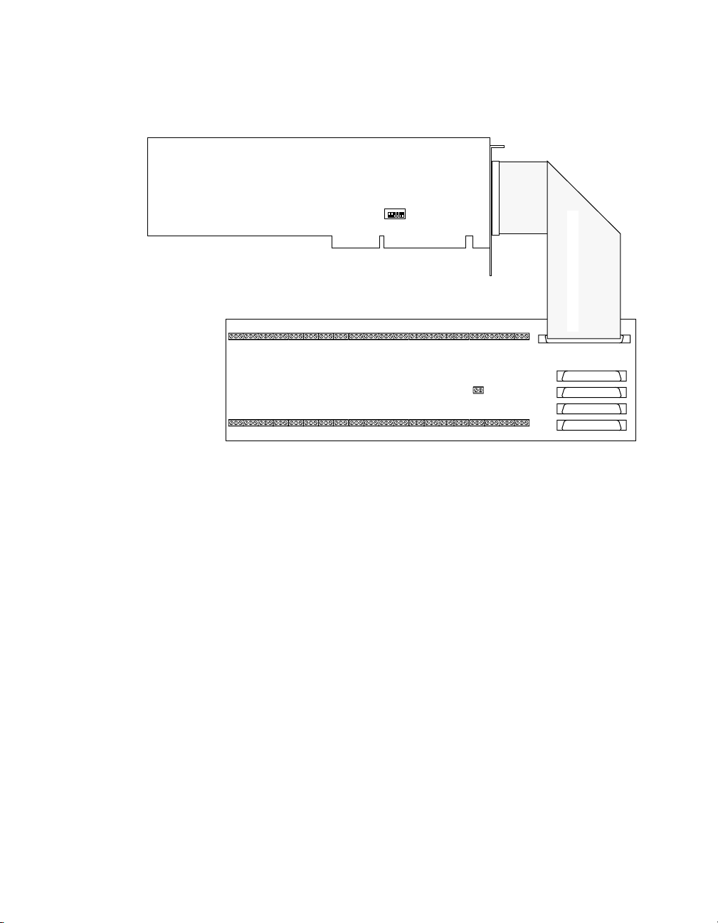
Use a CAB-1800 Series cable to connect an STA-1800HC and
DAS-1800HC Series board together as shown in Figure 4-3.
DAS-1800HC Series Board
CAB-1800 Series Cable
STA-1800HC
Figure 4-3. Cabling and Connections for Attaching an STA-1800HC
The CAB-1800 Series of cables includes the following models:
CAB-1800 — an 18-inch, 100-wire ribbon cable.
●
●
CAB-1801 — a 36-inch, 100-wire ribbon cable.
●
CAB-1800/S — an 18-inch, 100-wire, shielded, ribbon cable.
CAB-1801/S — a 36-inch, 100-wire, shielded, ribbon cable.
●
The red wire on the CAB-1800 Series cables runs between pin 1 of each
cable connector. Be sure to mate pin 1 of each cable connector to pin 1 of
a board connector.
4-4 Cabling and Wiring
Page 56

Attaching the CJC Circuit of an STA-1800HC
The STA-1800HC contains a CJC circuit that develops a voltage directly
proportional to the temperature of the STA-1800HC screw-terminal
blocks. At 0˚C, the CJC circuit output is 0V; the output changes at the rate
of 10mV per ˚C. The CJC circuit is represented by the schematic in
Figure 4-4.
TB11
CJC
Out
CJC
GND
+15V
0mV = 0˚C
10mV/˚C
27Ω
1 2
0.1µF
LM35DZ
3
Figure 4-4. CJC Circuit Schematic
As Figure 4-4 shows, the CJC circuit output appears across the TB11
screw terminals. TB11 is located as shown in Figure 4-5.
Terminal block TB11 for
CJC circuit
STA-1800HC Accessory
Figure 4-5. Location of CJC Circuit Screw Terminals (TB11)
You can determine the CJC temperature by wiring TB11 to the screw
terminals of an unused analog input channel and reading the CJC circuit
voltage. Convert this reading to a temperature value you can use to offset
thermal error introduced to thermocouple readings at the STA-1800HC
screw terminals.
Attaching the CJC Circuit of an STA-1800HC 4-5
Page 57

Attaching a CONN-1800HC
The CONN-1800HC connector panel is an interface for cabling SSH-8s
and MB modules to DAS-1800HC Series boards. You can also use the
CONN-1800HC for custom hookups. This accessory is essentially an
STA-1800HC without screw terminals or CJC circuit. Components are as
follows:
●
A 100-pin female connector for cabling to the main I/O connector of
a DAS-1800HC Series board.
●
Four 37-pin male connectors for cabling to MB01 backplanes, SSH
accessories, or custom hookups.
Pin assignments for the main I/O connector of a CONN-1800HC are the
same as those for the STA-1800HC, as shown in Figure 4-2 on page 4-3.
Use a CAB-1800 Series cable (a list of these cables appears on page 4-4)
to connect a CONN-1800HC to a DAS-1800HC Series board, as sho wn in
Figure 4-6.
DAS-1800HC Series Board
CAB-1800 Series Cable
CONN-1800HC
Figure 4-6. Cabling and Connections f or Attac hing a CONN-1800HC
to a DAS-1800HC Series Board
4-6 Cabling and Wiring
Page 58

Attaching an SSH-8
The SSH-8 is a simultaneous-sample-and-hold accessory. This accessory
can serve as a front-end analog interface for DAS-1800HC Series boards
when connected through an ST A-1800HC or a CONN-1800HC. Note that
the attached SSH-8 accessories must be set as slaves. Attach the SSH-8
accessories to the STA-1800HC or CONN-1800HC as shown in Figure
4-7. Refer to the
STA-1800HC Accessory
Note: cabling between an SSH-8
and a CONN-1800HC is exactly as
shown in this diagram for the
STA-1800HC
SSH-8 User’s Guide
for more information.
To DAS-1800HC Series board
C-1800
Cable
SSH-8
Accessory
Figure 4-7. Cabling and Connections for Attaching SSH-8 Accessories to a
DAS-1800HC Series Board
Attaching an SSH-8 4-7
Page 59

Attaching MB01 Backplanes
Use an STA-1800HC or a CONN-1800HC to connect MB01 backplanes
to a DAS-1800HC Series board, as sho wn in Figure 4-8. For details of the
MB modules, refer to the
MB Series User’s Guide
.
To J1 of an
STA-1800HC or
CONN-1800HC
To J2 of an
STA-1800HC or
CONN-1800HC
To J3 of an
STA-1800HC or
CONN-1800HC
To J4 of an
STA-1800HC or
CONN-1800HC
Figure 4-8. Cabling and Connections for Attaching MB01
C-16MB1
Cable
C-16MB1
Cable
C-16MB1
Cable
C-16MB1
Cable
#0 #1 #15
MBXXMB
XX
#0 #1 #15
MBXXMB
XX
#0 #1 #15
MBXXMB
XX
#0 #1 #15
MBXXMB
XX
MB01
MB
XX
MB01
MB
XX
MB01
MB
XX
MB01
MB
XX
Using C-16MB1
cables, you can
connect up to two
MB01 backplanes
to an ST A-1800HC
or up to four MB01
backplanes to a
CONN-1800HC
Backplanes to an STA-1800HC or a CONN-1800HC
Note:
Caution:
If you are programming an application requiring references to
channel numbering on connectors J1 to J4 of an STA-1800HC or
CONN-1800HC, you can obtain the correct channel numbering from the
pin assignments for these connectors, as shown in Appendix B.
4-8 Cabling and Wiring
Page 60

Attaching an STP-100
The STP-100 screw terminal accessory is an interface for I/O connections
to DAS-1800HC Series boards. Use a CAB-1800 Series cable to connect
the STP-100 and DAS-1800HC Series boards together as sho wn in Figure
4-9. Pin assignments for screw terminals of the STP-100 are the same as
those for the main I/O connector on the STA-1800HC (see Figure 4-2 on
page 4-3).
DAS-1800HC Series Board
TP1
P1A
TP2
STP-100
Accessory
P1B
CAB-1800
Series Cable
Figure 4-9. Attaching an STP-100
Attaching an STP-100 4-9
Page 61

Connecting Signals
This section contains precautionary advice to consider before making I/O
connections. The section also shows some circuits for wiring signal
sources to input channels of DAS-1800HC Series boards.
While the circuit diagrams show direct connections to channel input pins
of the main I/O connector, you must make actual connections through
corresponding inputs of an STA-1800HC or STP-100. Refer to Appendix
B for a list of these inputs and their descriptions.
The circuit diagrams represent a single signal source wired to a single
channel (channel n). In reality , you can wire 32 separate signal sources to
32 differential inputs or 64 separate signal sources to 64 single-ended
inputs.
DAS-1800HC Series boards contain separate grounds for analog and
digital signals. An analog ground (AGND) is for analog signals and
analog power; a digital ground (DGND) is for digital signals and other
power-supply returns.
Precautions
If you expect to use DAS-1801HC boards at high gain, read the
precautionary information in the following subsection. Other
considerations for I/O connections are offered under “Additional
Precautions” on page 4-11.
Precautions for Using DAS-1801HC Boards at High Gain
Operating a DAS-1801HC at a gain of 250 can lead to problems if your
application is unable to cope with noise. At a gain of 250, each bit of A/D
output corresponds to 10µV of analog input. Thus, with the high speed
and bandwidth of this board, analog noise and performance degradation
come easily unless you take precautions to avoid them. The following
collection of ideas and suggestions is aimed at avoiding these problems.
Operate a DAS-1801HC in 32-channel differential mode. Using the
●
board in 64-channel, single-ended mode at high gains introduces
enough ground-loop noise to produce large fluctuations in readings.
4-10 Cabling and Wiring
Page 62

Minimize noise from crosstalk and induced-voltage pickup in the flat
●
cables and screw-terminal accessories by using shielded cable.
Connect the shield to AGND and the inner conductors to Channel LO
and HI. Channel LO and AGND should have a DC return (or
connection) at some point; this return should be as close to the signal
source as possible. Induced noise from RF and magnetic fields can
easily exceed tens of microvolts, even on one- or two-foot cables;
shielded cable eliminates this problem.
●
Avoid bi-metallic junctions in the input circuitry. For example, the
kovar leads, used on reed relays, typically have a thermal emf to
copper of 40µV/˚C. Thermals can introduce strange random
variations caused by air currents, and so on.
Consider filtering. This approach can use hardware (resistors,
●
capacitors, and so on) but is often accomplished more easily with
software. Instead of reading the channel once, read it 10 or more
times in quick succession and average the readings. If the noise is
random and gaussian, it will be reduced by the square-root of the
number of readings.
Additional Precautions
Do NOT mix data acquisition inputs with the AC line, or you risk damaging the computer. Data acquisition systems give users access to inputs of
the computer. An inadvertent short between data and power lines can
cause extensive and costly damage to your computer. The manufacturer
can accept no liability for this type of accident. To prevent this problem,
use the following precautions:
●
Avoid direct connections to the AC line.
●
Make sure all connections are tight and sound so signal wires will not
come loose and short to high voltages.
●
Use isolation amplifiers and transformers where necessary.
Connecting Signals 4-11
Page 63

Connecting a Signal to a Single-Ended Analog Input
Figure 4-10 shows the connections between a signal source and a channel
of a DAS-1800HC Series board configured for single-ended input mode.
Signal
+
Source
-
Figure 4-10. Connections for Wiring a Signal Source to a DAS-1800HC Series Board
Note:
Channel n High
DAS-1800HC Series Board
AGND
Configured for Single-Ended Inputs
When you wire signals to the analog input channels, you are
advised to wire all unused channels to AGND. This action prevents the
input amplifiers from saturating, and it ensures the accuracy of your data.
Connecting a Signal to a Differential Analog Input
This section describes common connection schemes for differential
inputs. The section also discusses the principles for avoiding ground
loops.
Common Connection Schemes for Differential Inputs
Figure 4-11 on page 4-13 shows three connection schemes for wiring a
signal source to a channel of a DAS-1800HC Series board configured for
differential input mode.
4-12 Cabling and Wiring
Page 64

The upper two circuits of the diagram require the addition of resistors to
provide a bias-current return. You can determine the value of the bias
return resistors (Rb) from the value of the source resistance (Rs), using the
following relationships:
●
When Rs is greater than 100Ω, use the connections in the upper
circuit. The resistance of each of the two bias return resistors must
equal 2000 R
When Rs is less than 100Ω, use the connections in the middle circuit.
●
.
s
The resistance of the bias return resistor must be greater than 1000 Rs.
In the lower circuit, bias current return is inherently provided by the
source. The circuit requires no bias resistors.
Signal
Source
Signal
Source
+
R
s
Where Rs > 100Ω
Rb = 2000 R
R
s
Where Rs < 100Ω
Rb = 1000 R
Bridge
R
v
R
s
DC
Supply
+
-
s
+
-
s
-
R
R
Where Rv is a
variable resistor for
balancing the
bridge
b
b
Channel n High
Channel n Low
R
b
AGND
Channel n High
Channel n Low
AGND
Channel
High
Channel n Low
AGND
DAS-1800HC Series Board
DAS-1800HC Series Board
n
DAS-1800HC Series Board
Figure 4-11. Three Types of Connections for Wiring a Signal Source to a DAS-1800HC
Series Board Configured for Differential Inputs
Connecting Signals 4-13
Page 65

Avoiding Ground Loops with Differential Inputs
Frequently, the signal-source ground and the DAS-1800HC Series board
ground are not at the same voltage level because of the distances between
equipment wiring and the building wiring. This dif ference is referred to as
a
common-mode voltage
sides of a differential input (it appears between each side and ground).
Since a differential input responds only to the difference in the signals at
its high and low inputs, its common-mode voltages cancel out and leave
only the signal. However, if your input connections contain a ground
loop, your input could see the sum of the signal-source and
common-mode voltages. Figure 4-12 shows the proper way to connect a
differential input while Figure 4-13 illustrates the effect of a ground loop.
(V
) because it is normally common to both
cm
Signal
Source
Signal Source
Ground V
+
E
s
-
g 1
Channel n High
Channel n Low
V
c m
R
wire
V
= V
c m
g 1
- V
AGND
V
g 2
g 2
E
s
DAS-1800HC Series Board
Do not join Low
to AGND at the
computer
Figure 4-12. A Differential Input Configuration that Avoids a Ground Loop
Signal
Source
Signal Source
Ground V
+
E
s
-
g 1
Channel n High
Channel n Low
V
c m
R
wire
V
= V
g 1
- V
c m
Es + V
AGND
V
g 2
g 2
c m
DAS-1800HC Series Board
This diagram is included
only to illustrate an
incorrectly wired input; do
not use this configuration.
NOTE
Figure 4-13. Differential Input Configuration with a Ground Loop
4-14 Cabling and Wiring
Page 66

Connecting Analog Output Signals
DAS-1800HC Series boards have outputs for each of the two DACs.
Refer to Table A-2 in Appendix A for voltages, current limits, and other
loading information. Make your connections to the DAC output terminals
through corresponding screw terminals of an STA-1800HC or STP-100.
The screw terminals are labeled as follows:
● DAC0 OUT — is the screw terminal labeling for the DAC #0 output.
● DAC1 OUT — is the screw-terminal labeling for the DAC #1 output.
Connecting Digital I/O Signals
DAS-1800HC Series boards have four digital inputs and eight digital
outputs, as described in “Digital I/O Features” on page 2-18. Make your
connections to the digital I/O terminals through corresponding screw
terminals of an STA-1800HC or STP-100. The terminals are labeled as
follows:
● DI0 to DI3 — are the screw-terminal labels for the digital input.
● DO0 to DO7 — are the screw-terminal labels for the digital output.
Connecting Digital Control Signals
DAS-1800HC Series boards use five digital control signals. Make your
connections to the digital control terminals through corresponding screw
terminals of an STA-1800HC or STP-100. The terminals are labeled as
follows:
● SSHO — is the simultaneous-sample-and-hold output terminal. This
signal is described in “Using Digital Control Signal SSHO” on page
2-20. Use the SSHO terminal for connecting this signal.
● TGIN — is the trigger/gate input, described in the next section and in
“Using Digital Control Signal TGOUT” on page 2-19. Refer also to
“Triggers” on page 2-12 and to “Gates” on page 2-15. Use the
digital-input terminal DI1/TGIN for connecting a TGIN signal.
● TGOUT — is the trigger/gate output, described in the next section
and in “Using Digital Control Signal TGOUT” on page 2-19. Use the
TGOUT terminal for connecting this signal.
Connecting Signals 4-15
Page 67

● XPCLK — is the external pacer clock input, described in the next
section and in “Clock Sources” on page 2-10. Use the digital-input
terminal DI0/XPCLK for connecting this signal.
● DOSTB — is the digital output strobe, described in “Using Digital
Control Signal DOSTB” on page 2-18. Use the DOSTB terminal for
connecting this signal.
Connecting and Synchronizing Multiple Boards
You can synchronize up to three DAS-1800 Series boards using trigger
and gate signals from the main I/O connectors. Each board can run at the
same or a different conversion rate as the other boards in the system.
The onboard pacer clock is designed to be tightly coupled with trigger
and gate operations. After each board receives the trigger or gate,
conversions begin within a defined period of time. If each board is
programmed for a different conversion rate, the first conversion on each
board occurs after this time period and subsequent conversions occur at
the programmed rate.
Figure 4-14 shows two connection schemes for synchronizing multiple
boards. Both schemes are using the onboard pacer clock to time
acquisitions.
Board 0
Rate a
Board 1
Rate b
Board 2
Rate c
a. Scheme 1
TGIN
TGIN
TGIN
Trigger or
Gate
Board 0
Rate a
Board 1
Rate b
Board 2
Rate c
TGIN
TGOUT
TGIN
TGIN
b. Scheme 2
Trigger or
Gate
(optional)
Figure 4-14. Two Connection Schemes for Synchronizing Multiple Boards
4-16 Cabling and Wiring
Page 68

In Scheme 1, you connect the trigger/gate inputs of the three boards
together and supply the trigger or gate input. A/D conversions on each
board start 400 ±100ns from the active edge of the trigger input. All
conversions start within 100 ±100ns of each other from board to board.
When using scheme 1, you can use the onboard pacer clock or an external
pacer clock.
In Scheme 2, you can start conversions in either of two ways: by a
hardware trigger/gate input or by software. The board connections are in a
master/slave relationship; board 0 is the master, and boards 1 and 2 are
the slaves.
If you use a software enable for board 0 of scheme 2, the board 0 pacer
clock starts and triggers conversions in the slave boards. However, board
0 conversions do not begin until after conversions begin in the the slave
boards. The delay of board 0 conv ersions is caused by a protection feature
built into the register that creates software-triggered conversions; the
function of the protection feature is to prevent false conversions.
If you use a hardware trigger for board 0 of scheme 2, board 0 triggers
conversions in all three boards immediately. Note that TGOUT is an
active, high-going signal. Therefore, you must program the slave-board
TGIN inputs for a positive-going trigger or gate.
Connecting Signals 4-17
Page 69

Testing the Board
This section describes how to use DriverLINX to test functions of
DAS-1800HC Series boards.
DriverLINX Analog I/O Panel
The DriverLINX Analog I/O Panel is an application that demonstrates
analog input/output using DriverLINX. With the Analog I/O Panel you
can:
Analyze analog signals using the two-channel Oscilloscope.
●
●
Measure analog voltages using the Digital Volt Meter.
●
Generate Sine, Square and Triangle waves using the SST Signal
Generator.
5
●
Output DC Level voltages using the Level Control.
The Analog I/O Panel is useful for:
●
Testing the DAS-1800HC DriverLINX installation and configuration.
Verifying signal inputs to your DAS-1800HC board.
●
Sending test signals to external devices.
●
To access this DriverLINX Analog I/O Panel:
1. Start the Analog I/O P anel with the “AIO Panel” item on the Windo ws
start menu.
2. Click the [...] button in the Driver Selection section.
3. Select the driver for your board using the
4. Click
DriverLINX Analog I/O Panel 5-1
OK.
Open DriverLINX
dialog.
Page 70

5. Select the Logical Device you want to operate by dragging the pointer
in the Device Selection section. The Analog I/O Panel displays the
Scope, Meter, SST, and Level control tabs, depending on the
capabilities of your DAS-1800HC board.
6. The Scope uses two analog input channels referred to as ChA and
ChB. Drag the channel selectors in the AI Channel Mapping section
to map them to different channel numbers.
7. The SST Signal Generator uses two analog output channels referred
to as ChA and ChB. Drag the channel selectors in the AO Channel
Mapping section to map them to different channel numbers.
You can now select the Scope, Meter, SST, and Level Control tabs to
operate your DAS-1800HC board.
Test Panel Application
Depending upon the DriverLINX drivers you have installed on your
system, you will have one or more of the following example applications:
●
Single–Value AI
for analog input.
●
Single–Value AO
PIO Panel
●
CTM Test Bench
●
for analog output.
for digital input and output.
for counter/timer applications.
To access this DriverLINX Test Panel, select Test Panel with the “Test
Panel” item on the Windows start menu.
5-2 Testing the Board
Page 71

Your DAS-1800 Series board is initially calibrated at the factory. You are
advised to check the calibration of a board every six months and to
calibrate again when necessary . This section pro vides the information you
need to calibrate a DAS-1800 Series board.
Equipment Requirements
The equipment requirements for calibrating a DAS-1800HC Series board
are as follows:
●
A digital voltmeter accurate to 6½ digits, such as a Keithley
Instruments Model 196 or 2001
6
Calibration
●
An adjustable ±10V voltage calibrator, such as a Keithley
Instruments Model 236
●
A CAB-1800 Series cable and a STA-1800HC, STP-100, or
CONN-1800HC, or a user-designed interface
Potentiometers and Test Points
Figure 6-1 shows the locations of the potentiometers and test points
involved with the calibration of a DAS-1800HC Series board. The
potentiometers are labeled R5 to R8, R12 and R13, R15 and R16, and
R20. The test points are TP1 to TP5. The calibration utility, described in
the next section, directs you to these components and explains what to do
with them during the calibration process.
Equipment Requirements 6-1
Page 72

DAC1 Gain
DAC1 Offset
DAC0 Gain
DAC0 Offset
ADC Offset
ADC Gain
R5
R6
R7
R8
Voltage Out
(Instrumentation
Amplifier)
R12
TP3
R13
TP4
Output Offset
(DAS-1801H
C only)
TP1
TP5
Unipolar
Offset
R16R15
Analog
Ground
TP2
R20
Offset
(referred to
input)
A/D Strobe
A/D Status
Digital Ground
Base
Address
Switch
Figure 6-1. Potentiometers and Test Points on the DAS-1800HC Series Boards
DriverLINX Calibration Utility
DriverLINX Calibration Utility will guide you through the calibration
procedure. Before calibration, specify the following parameters in the
setup panel to get the correct instructions:
●
Logical Device
Accessory
●
calibration stimulus.
Shorted channel
●
Voltage Channel
●
calibration voltage levels.
— Board’s device number, model, and address.
— Connection method used to connect the board to the
— Input channel to be “shorted” high to low.
— Input channel to use to apply the various
●
Calibration range
— Input range to be calibrated.
6-2 Calibration
Page 73

If your DAS-1800HC Series board is not operating properly, use the
information in this section to isolate the problem. If the problem appears
serious enough to warrant technical support, refer to “Technical Support”
on page 7-6 for information on how to contact an applications engineer.
Problem Isolation
If you encounter a problem with a DAS-1800HC Series board, use the
instructions in this section to isolate the cause of the problem before
calling Keithley.
7
Troubleshooting
Using the DriverLINX Event Viewer
The DriverLINX Event Viewer displays the Windows system event log.
Applications and hardware drivers make entries in the system e v ent log to
assist in predicting and troubleshooting hardware and software problems.
DriverLINX uses the event log to report problems during driver loading
or unexpected system errors. The event log can assist in troubleshooting
resource conflicts and DriverLINX configuration errors. If you are having
trouble configuring or initializing a Logical Device, check the event log
for information from the DriverLINX driver.
Using the DriverLINX Event Viewer , you can view and save Driv erLINX
event log entries under Windows 95/98 or Windows NT. DriverLINX
event log entries can help you or technical support troubleshoot
data-acquisition hardware and software problems.
Problem Isolation 7-1
Page 74

Device Initialization Error Messages
During device initialization, DriverLINX performs a thorough test of all
possible subsystems on the DAS-1800HC Series board as well as the
computer interface. If DriverLINX detects any problems or unexpected
responses, it reports an error message to help isolate the problem. The
device initialization error messages fall into three basic categories:
“Device not found”
●
— Board address does not match hardware
setting or conflicts with another board. Verify the board’s address
settings. Also, don’t confuse hexadecimal with decimal addresses in
the DriverLINX
●
“Invalid IRQ level”
Device Configure
or
“Invalid DMA level”
dialog box.
— Selected level does
not match hardware setting, conflicts with another board’ s IRQ/DMA
levels, or is dedicated to the computer’ s internal functions (COM port,
disk drive controller, network adapter, etc.)
“Hardware does not match configuration”
●
— Operating
mode/range switch or jumper setting does not match selection(s)
made in the DriverLINX
Device Configuration
dialog box.
7-2 Troubleshooting
Page 75

Identifying Symptoms and Possible Causes
Use the troubleshooting information in Table 7-1 to try to isolate the
problem. Table 7-1 lists general symptoms and possible solutions for
problems with DAS-1800HC Series boards.
Table 7-1. Troubleshooting Information
Symptom Possible Cause Possible Solution
Board does not respond Base address is incorrect or not
consistent with what the program
is addressing.
The interrupt level is incorrect or
not consistent with what the
program is addressing.
The board configuration is
incorrect.
The board is incorrectly aligned
in the accessory slot.
The board is damaged. Contact Keithley Technical
Check the base-address-switch
setting on the board against the
setting shown in the configuration
utility. If the base address is set
correctly, make sure no other
computer device is using any of
the I/O locations beginning at the
specified base address. If
necessary, reconfigure the base
address. Refer to page 3-5 for
instructions on setting the base
address.
Make sure no other device is
using the interrupt level specified
in your program. If necessary,
reset the interrupt level.
Check the remaining settings in
the configuration file.
Check the board seating.
Support; see page 7-6.
Problem Isolation 7-3
Page 76

Table 7-1. Troubleshooting Information (cont.)
Symptom Possible Cause Possible Solution
Intermittent operation The most common cause of this
problem is that the I/O bus speed
is in excess of 8MHz.
Vibrations or loose connections
exist.
The board is overheating. Check environmental and
Data appears to be invalid The most common cause of this
problem is that the I/O bus speed
is in excess of 8MHz.
An open connection exists. Check wiring to screw terminal.
Another system resource is using
the specified base address.
Reduce I/O bus speed to a
maximum of 8MHz (to change
the I/O bus speed, run BIOS
setup). See your computer
documentation for instructions on
running BIOS setup.
Cushion source of vibration and
tighten connections.
ambient temperature. See the
documentation for your computer.
Reduce I/O bus speed to a
maximum of 8MHz (to change
the I/O bus speed, run BIOS
setup). See the documentation for
your computer for instructions on
running BIOS setup.
Reconfigure the base address of
the DAS-1800HC Series board;
refer to page 3-5 for more
information. Check the I/O
assignments of other system
resources and reconfigure, if
necessary.
System Lockup A timing error occurred. Restart your computer.
Computer does not boot. Board not seated properly. Check the installation of the
board.
The base address setting of the
DAS-1800ST/HR Series board
conflicts with that of another
system resource.
The power supply of the host
computer is too small to handle
all the system resources.
7-4 Troubleshooting
Check the base address settings of
your system resources; each
address must be unique.
Check the needs of all system
resources and obtain a larger
power supply.
Page 77

If your board is not operating properly after using the information in
Table 7-1, continue with the next two sections to further isolate the
problem.
Testing the Board and Host Computer
To isolate the problem to the DAS-1800HC Series board or to the host
computer, use the following steps:
Caution:
your board and/or computer.
1. Turn the power to the host computer OFF, and remove power
2. While keeping connections to accessory board intact, unplug the
3. Remove the DAS-1800HC Series board from the computer and
4. With the DAS-1800HC Series board out of the computer, check the
At this point, if you have another DAS-1800HC Series board that you
know is functional, you can test the slot and I/O connections using the
instructions in the next section. If you do not have another board, refer to
the instructions on page 7-1 before calling Keithley Technical Support.
Removing a board with the power ON can cause damage to
connections to the computer.
accessory connector or cable from the DAS-1800HC Series board.
visually check for damage. If a board is obviously damaged, refer to
“Technical Support” on page 7-6 for information on returning the
board.
computer for proper operation. Power up the computer and perform
any necessary diagnostics.
Problem Isolation 7-5
Page 78

Testing the Accessory Slot and I/O Connections
When you are sure that the computer is operating properly, test the
computer accessory slot and I/O connections using another DAS-1800HC
Series board that you know is functional. To test the computer accessory
slot and the I/O connections, follow these steps:
1. Remove computer power again, and install a DAS-1800HC Series
board that you know is functional. Do not make any I/O connections.
2. Turn computer power ON and check operation with the functional
board in place. This test checks the computer accessory slot. If you
were using more than one DAS-1800HC Series board when the
problem occurred, use the functional board to test the other slot, as
well.
3. If the accessory slots are functional, use the functional board to check
the I/O connections. Reconnect and check the operation of the I/O
connections, one at a time.
4. If operation fails for an I/O connection, check the individual inputs
one at a time for shorts and opens.
5. If operation remains normal to this point, the problem is in the
DAS-1800HC Series board originally in the computer. If you were
using more than one board, try each board one at a time in the
computer to determine which is faulty.
6. If you cannot isolate the problem, refer to the next section for
instructions on obtaining assistance.
Technical Support
Before returning any equipment for repair, call Keithley for technical
support at:
1-888-KEITHLEY
Monday - Friday, 8:00 a.m. - 5:00 p.m., Eastern Time
7-6 Troubleshooting
Page 79

An applications engineer will help you diagnose and resolve your
problem over the telephone. Please make sure that you hav e the follo wing
information available before you call:
DAS-1800HC Series
Board Configuration
Computer
Operating System
Software package
Model
Serial #
Revision code
Base address setting
Interrupt level setting
Number of channels
Input (S.E. or Diff.)
Mode (uni. or bip.)
DMA chan(s)
Number of SSH-8s
Manufacturer
CPU type
Clock speed (MHz)
KB of RAM
Video system
BIOS type
DOS version
Windows version
Windows mode
Name
Serial #
Version
Invoice/Order #
___________________
___________________
___________________
___________________
___________________
___________________
___________________
___________________
___________________
___________________
___________________
___________________
___________________
___________________
___________________
___________________
___________________
___________________
___________________
___________________
___________________
___________________
___________________
Compiler
(if applicable)
Accessories
Technical Support 7-7
Language
Manufacturer
Version
Type
Type
Type
Type
Type
Type
Type
Type
___________________
___________________
____________________
___________________
___________________
___________________
___________________
___________________
___________________
___________________
___________________
Page 80

If a telephone resolution is not possible, the applications engineer will
issue you a Return Material Authorization (RMA) number and ask you to
return the equipment. Include the RMA number with any documentation
regarding the equipment.
When returning equipment for repair, include the following information:
Your name, address, and telephone number.
●
The invoice or order number and date of equipment purchase.
●
●
A description of the problem or its symptoms.
●
The RMA number on the
outside
of the package.
Repackage the equipment, using the original anti-static wrapping, if
possible, and handle it with ground protection. Ship the equipment to:
ATTN.: RMA# _______
Repair Department
Keithley Instruments, Inc.
28775 Aur ora Road
Cleveland, Ohio 44139-1891
Telephone 1-888-KEITHLEY
FAX (440) 248-6168
Note:
If you are submitting your equipment for repair under warranty,
you must include the invoice number and date of purchase.
To enable Keithley to respond as quickly as possible, you must include
the RMA number on the outside of the package.
7-8 Troubleshooting
Page 81

Specifications
Tables A-1 to A-4 list specifications for the DAS-1800HC Series boards.
Table A-1. Analog Input Specifications
Feature DAS-1801HC DAS-1802HC
Number of channels Software-selectable as 32 differential or 64 single-ended
Input mode Software-selectable as unipolar or bipolar
Resolution 12-bit (1 part in 4096)
Data format 16-bit 2’s complement, right-justified
FIFO size 1024 word
Channel-gain QRAM size 64 locations
A
Range and gain
Absolute accuracy
Maximum error
Unipolar
Bipolar
Typical
0.0 to +5.0V for gain = 1
0.0 to +1.0V for gain = 5
0.0 to 100mV for gain = 50
0.0 to +20mV for gain = 250
±5.0V for gain = 1
±1.0V for gain = 5
±100mV for gain = 50
±20mV for gain = 250
0.01% of reading ±1 LSB for all ranges
• 0.02% of reading ±1 LSB max @ 25˚C for gain < 250
• 0.03% of reading ±1 LSB max @ 25˚C for gain = 250
0.0 to +10V for gain = 1
0.0 to +5.0V for gain = 2
0.0 to +2.5V for for gain = 4
0.0 to 1.25V for gain = 8
±10V for gain = 1
±5.0V for gain = 2
±2.5V for gain = 4
±1.25V for gain = 8
A-1
Page 82

Table A-1. Analog Input Specifications (cont.)
Feature DAS-1801HC DAS-1802HC
Temperature coefficient of
accuracy (includes ADC)
Offset
• Bipolar: ±20µV/˚C ±(12µV/˚C ÷ gain) maximum
• Unipolar: ±20µV/˚C ±(14µV/˚C ÷ gain) maximum
Gain
• ±20 ppm/˚C for gain < 50
• ±30 ppm/˚C for gain = 50
• ±35 ppm/˚C for gain = 250
Linearity
1
Integral
Differential
±½ LSB typical, ±1 LSB maximum
±1 LSB
Throughput Refer to “Maximum Achievable Throughput Rates” on page 2-5
Dynamic parameters
Acquisition time
Aperture delay
Aperture uncertainty
Conversion time
0.3µs
13.0ns
150ps rms
3.0µs max. (includes acquisition time)
Input bias current ±40nA max. @ 25˚C
±60nA max. over operating range
Common mode rejection
ratio
74 dB for gain = 1
80 dB for gain = 5
100 dB for gain = 50
100 dB for gain = 250
74 dB for gain = 1
80 dB for gain = 2
80 dB for gain = 4
86 dB for gain = 8
Input overvoltage ±15V continuous powered
±15V continuous unpowered
A-2 Specifications
Page 83

Table A-1. Analog Input Specifications (cont.)
Feature DAS-1801HC DAS-1802HC
2
Noise
Bipolar electrical noise
(in counts)
• p-p = 1, rms = 0.1 for gain = 1
• p-p = 1, rms = 0.1 for gain = 5
• p-p = 4, rms = 0.5 for gain = 50
• p-p = 8, rms = 1.0 for gain = 250
• p-p = 1, rms = 0.1 for gain = 1
• p-p = 1, rms = 0.1 for gain = 2
• p-p = 1, rms = 0.1 for gain = 4
• p-p = 1, rms = 0.1 for gain = 8
Unipolar electrical noise
(in counts)
• p-p = 1, rms = 0.1 for gain = 1
• p-p = 1, rms = 0.1 for gain = 5
• p-p = 6, rms = 0.9 for gain = 50
• p-p = 9, rms = 1.4 for gain = 250
• p-p = 1, rms = 0.1 for gain = 1
• p-p = 1, rms = 0.1 for gain = 2
• p-p = 1, rms = 0.1 for gain = 4
• p-p = 1, rms = 0.1 for gain = 8
DMA levels 5, 6, and 7
Interrupt levels 3, 5, 7, 10, 11, and 15
Internal pacer clock rate Programmable between 0.0012Hz and 333kHz
Minimum external pacer
10ns
clock pulse width
Maximum external pacer
333kHz
clock rate
Minimum hardware trigger
10ns
pulse width
1
Monotonicity is guaranteed over the operating range.
2
The figures in the table show the electrical noise introduced by the analog front end
the uncertainty inherent in the quantization pr ocess
. The inherent quantization noise introduced by any
but do not include
ADC is due to uncertainty at code boundaries and adds a peak-to-peak value of 1 LSB to the electrical
noise; it also makes the rms level 0.5 LSBs.
A-3
Page 84

Table A-2. Analog Output Specifications
Attribute DAS-1800HC Series Boards
Resolution 12-bit (one part in 4096 or 224 ppm)
Data format Right justified, offset binary
Range ±10.00V
Linearity
1
Integral
Differential
±¼ LSB typical; ±½ LSB max.
±1 LSB
Output current drive ±5mA max.
Capacitive load drive 100µF
Gain accuracy Adjustable to 0
Offset accuracy Adjustable to 0
Glitch energy 300nV * seconds
Power up DACs power up to 0.0V at reset
Settling time 6µs typical, 30µs maximum to ½ LSB
1
Monotonicity is guaranteed over the operating range.
Table A-3. Digital I/O Specifications
Attributes DAS-1800HC Series Boards
Digital output (including
SSHO, DOSTB, and
• VOH (min.) = 2.7V @ IOH = −400µA
• VOL (max.) = 0.5V @ IOL = 8mA
TGOUT)
Digital input • VIH (min.) = 2.0V; IIH (max.) = 20µA
• VIL (max.) = 0.8V; IIL (max.) = −0.2mA
Digital output strobe pulse
300ns typical; data is latched on the rising edge of DOSTB
width
A-4 Specifications
Page 85

Table A-4. Power Supply Specifications
Feature DAS-1800HC Series Boards
+5VDC input 430mA typical; 870mA maximum
+12VDC input 400mA typical; 550mA maximum
Maximum current available
at the ±15V outputs
Maximum current available
at the +5V output
30mA
1.0A
A-5
Page 86

Connector Pin Assignments
This appendix contains pin layouts and assignments for I/O connectors of
the DAS-1800HC Series boards and the STA-1800HC, STP-100, and
CONN-1800HC accessories and for the four 37-pin D connectors of the
STA-1800HC accessory.
I/O Connector Pin Assignments
The I/O connectors for the DAS-1800HC Series boards, the
STA-1800HC, STP-100, and CONN-1800HC each contain 100 pins
arranged in two banks of 50: bank A and bank B. All are female
connectors. The STA-1800HC, STP-100 and CONN-1800HC connectors
are a mirror image of the DAS-1800HC Series board connector. Figure
B-1 shows pin assignments for the main I/O connector of DAS-1800HC
Series boards; Figure B-2 shows pin assignments for the main I/O
connectors of the STA-1800HC, STP-100, and CONN-1800HC
accessories.
B
I/O Connector Pin Assignments B-1
Page 87

A Side B Side
AGND
CH16 HI
CH16 LO/ CH48 HI
CH17 HI
CH17 LO/CH49 HI
CH18 HI
CH18 LO/ CH50 HI
CH19 HI
CH19 LO/CH51 HI
CH20 HI
CH20 LO/CH52 HI
CH21 HI
CH21 LO/CH53 HI
CH22 HI
CH22 LO/CH54 HI
CH23 HI
CH23 LO/CH55 HI
AGND
CH24 HI
CH24 LO/CH56 HI
CH25 HI
CH25 LO/CH57 HI
CH26 HI
CH26 LO/CH58 HI
CH27 HI
CH27 LO/CH59 HI
CH28 HI
CH28 LO/CH60 HI
CH29 HI
CH29 LO/CH61 HI
CH30 HI
CH30 LO/CH62 HI
CH31 HI
CH31 LO/CH63 HI
AGND
DAC1 Output
-15V
DGND
NC
SSHO
TGOUT
DOSTB
DO4
DO5
DO6
DO7
+5V
+5V
DGND
DGND
01
02
03
04
05
06
07
08
09
10
11
12
13
14
15
16
17
18
19
20
21
22
23
24
25
26
27
28
29
30
31
32
33
34
35
36
37
38
39
40
41
42
43
44
45
46
47
48
49
50
AGND
CH00 HI
CH00 LO/CH32 HI
CH01 HI
CH01 LO/CH33 HI
CH02 HI
CH02 LO/CH34 HI
CH03 HI
CH03 LO/CH35 HI
CH04 HI
CH04 LO/CH36 HI
CH05 HI
CH05 LO/CH37 HI
CH06 HI
CH06LO/CH38 HI
CH07 HI
CH07 LO/CH39 HI
AGND
CH08 HI
CH08 LO/CH40 HI
CH09 HI
CH09 LO/CH41 HI
CH10 HI
CH10 LO/CH42 HI
CH11 HI
CH11 LO/CH43 HI
CH12 HI
CH12 LO/CH44 HI
CH13 HI
CH13 LO/CH45 HI
CH14 HI
CH14 LO/CH46 HI
CH15 HI
CH15 LO/CH47 HI
AGND
DAC0 Output
+15V
DGND
DI0/XPCLK
DI1/TGIN
DI2
DI3
DO0
DO1
DO2
DO3
+5V
+5V
DGND
DGND
DAS-1800HC Series Board
I/O Connector
Figure B-1. Pin Assignments for the Main I/O Connector of
DAS-1800HC Series Boards
B-2 Connector Pin Assignments
Page 88

B Side
AGND
CH00 HI
CH00 LO/ CH32 HI
CH01 HI
CH01 LO/CH33 HI
CH02 HI
CH02 LO/ CH34 HI
CH03 HI
CH03 LO/CH35 HI
CH04 HI
CH04 LO/CH36 HI
CH05 HI
CH05 LO/CH37 HI
CH06 HI
CH06 LO/CH38 HI
CH07 HI
CH07 LO/CH39 HI
AGND
CH08 HI
CH08 LO/CH40 HI
CH09 HI
CH09 LO/CH41 HI
CH10 HI
CH10 LO/CH42 HI
CH11 HI
CH11 LO/CH43 HI
CH12 HI
CH12 LO/CH44 HI
CH13 HI
CH13 LO/CH45 HI
CH14 HI
CH14 LO/CH46 HI
CH15 HI
CH15 LO/CH47 HI
AGND
DAC0 Output
+15V
DGND
D10/XPCLK
DI1/TGIN
DI2
DI3
DO0
DO14
DO2
DO3
+5V
+5V
DGND
DGND
01
02
03
04
05
06
07
08
09
10
11
12
13
14
15
16
17
18
19
20
21
22
23
24
25
26
27
28
29
30
31
32
33
34
35
36
37
38
39
40
41
42
43
44
45
46
47
48
49
50
A Side
AGND
CH16 HI
CH16 LO/CH48 HI
CH17 HI
CH17 LO/CH49 HI
CH18 HI
CH18 LO/CH50 HI
CH19 HI
CH19 LO/CH51 HI
CH20 HI
CH20 LO/CH52 HI
CH21 HI
CH21 LO/CH53 HI
CH22 HI
CH22 LO/CH54 HI
CH23 HI
CH23 LO/CH55 HI
AGND
CH24 HI
CH24 LO/CH56 HI
CH25 HI
CH25 LO/CH57 HI
CH26 HI
CH26 LO/CH58 HI
CH27 HI
CH27 LO/CH59 HI
CH28 HI
CH28 LO/CH60 HI
CH29 HI
CH29 LO/CH61 HI
CH30 HI
CH30 LO/CH62 HI
CH31 HI
CH31 LO/CH63 HI
AGND
DAC1 Output
−15V
DGND
NC
SSHO
TGOUT
DOSTB
DO4
DO5
DO6
DO7
+5V
+5V
DGND
DGND
STA-1800HC, STP-100, and
CONN-1800HC I/O Connectors
Figure B-2. Pin Assignments for the Main I/O Connectors of the
STA-1800HC, STP-100, and CONN-1800HC
I/O Connector Pin Assignments B-3
Page 89

STA-1800HC and CONN-1800HC 37-Pin D Connectors
The ST A-1800HC and CONN-1800HC each contain four 37-pin, male, D
connectors: J1, J2, J3, and J4. Pin layouts and assignments for these
connectors are shown in Figure B-3, Figure B-4, Figure B-5, and Figure
B-6.
SSHO - 20
NC - 21
DO2 - 22
DO0 - 23
DI2 - 24
DI0/XPCLK - 25
NC - 26
DAC1 - 27
AGND - 28
AGND - 29
CH07 HI - 30
CH06 HI - 31
CH05 HI - 32
CH04 HI - 33
CH03 HI - 34
CH02 HI - 35
CH01 HI - 36
CH00 HI - 37
Figure B-3. Connector J1
SSHO - 20
NC - 21
DO2 - 22
DO0 - 23
DI2 - 24
DI0/XPCLK - 25
NC - 26
DAC1 - 27
AGND - 28
AGND - 29
CH15 HI - 30
CH14 HI - 31
CH13 HI - 32
CH12 HI - 33
CH11 HI - 34
CH10 HI - 35
CH09 HI - 36
CH08 HI - 37
01 - +5V
02 - TGOUT
03 - DO3
04 - DO1
05 - DI3
06 - DI1/TGIN
07 - DGND
08 - NC
09 - DAC0
10 - NC
11 - CH07 LO/CH39 HI
12 - CH06 LO/CH38 HI
13 - CH05 LO/CH37 HI
14 - CH04 LO/CH36 HI
15 - CH03 LO/CH35 HI
16 - CH02 LO/CH34 HI
17 - CH01 LO/CH33 HI
18 - CH00 LO/CH32 HI
19 - AGND
01 - +5V
02 - TGOUT
03 - DO3
04 - DO1
05 - DI3
06 - DI1/TGIN
07 - DGND
08 - NC
09 - DAC0
10 - NC
11 - CH15 LO/CH47 HI
12 - CH14 LO/CH46 HI
13 - CH13 LO/CH45 HI
14 - CH12 LO/CH44 HI
15 - CH11 LO/CH43 HI
16 - CH10 LO/CH42 HI
17 - CH09 LO/CH41 HI
18 - CH08 LO/CH40 HI
19 - AGND
Figure B-4. Connector J2
B-4 Connector Pin Assignments
Page 90

SSHO - 20
NC - 21
DO6 - 22
DO4 - 23
DI2 - 24
DI0/XPCLK - 25
NC - 26
DAC1 - 27
AGND - 28
AGND - 29
CH23 HI - 30
CH22 HI - 31
CH21 HI - 32
CH20 HI - 33
CH19 HI - 34
CH18 HI - 35
CH17 HI - 36
CH16 HI - 37
Figure B-5. Connector J3
01 - +5V
02 - TGOUT
03 - DO7
04 - DO5
05 - DI3
06 - DI1/TGIN
07 - DGND
08 - NC
09 - DAC0
10 - NC
11 - CH23 LO/CH55 HI
12 - CH22 LO/CH54 HI
13 - CH21 LO/CH53 HI
14 - CH20 LO/CH52 HI
15 - CH19 LO/CH51 HI
16 - CH18 LO/CH50 HI
17 - CH17 LO/CH49 HI
18 - CH16 LO/CH48 HI
19 - AGND
SSHO - 20
NC - 21
DO6 - 22
DO4 - 23
DI2 - 24
DI0/XPCLK - 25
NC - 26
DAC1 - 27
AGND - 28
AGND - 29
CH31 HI - 30
CH30 HI - 31
CH29 HI - 32
CH28 HI - 33
CH27 HI - 34
CH26 HI - 35
CH25 HI - 36
CH24 HI - 37
01 - +5V
02 - TGOUT
03 - DO7
04 - DO5
05 - DI3
06 - DI1/TGIN
07 - DGND
08 - NC
09 - DAC0
10 - NC
11 - CH31 LO/CH63 HI
12 - CH30 LO/CH62 HI
13 - CH29 LO/CH61 HI
14 - CH28 LO/CH60 HI
15 - CH27 LO/CH59 HI
16 - CH26 LO/CH58 HI
17 - CH25 LO/CH57 HI
18 - CH24 LO/CH56 HI
19 - AGND
Figure B-6. Accessory Connector J4
STA-1800HC and CONN-1800HC 37-Pin D Connectors B-5
Page 91

C
DriverLINX Configuration
Notes
This appendix contains the following sections:
●
Configuration — describes how DriverLINX works with
DAS-1800HC boards.
Special Device Settings — describes settings used specifically for
●
the DAS-1800HC boards.
●
●
●
●
●
Configuration
The following section describes detailed information about how
DriverLINX implements features of the Keithley DAS-1800HC A/D
boards.
Implementation Notes — describes how DriverLINX implements
features of the DAS-1800HC boards.
Analog Input Subsystem — describes how to configure
DAS-1800HC analog inputs.
Analog Output Subsystem — describes how DriverLINX is used to
configure analog outputs.
Digital Input and Output Subsystems — describes how
DriverLINX is used for configuring digital inputs and outputs.
Counter/Timer Subsystem — describes some of DriverLINX
counter/timer functions.
Configuration C-1
Page 92

Model
Note:
DAS-1800HC Series. “DAS-1801” refers to the models with low range
analog input, while “DAS-1802” refers to the models with high range
analog input. A suffix, such as “HC,” designates models with certain
features. The suffix “XX-DA” refers to both the ST-DA and HR-DA
models.
DriverLINX for the Keithley DAS-1800HC supports the following
models:
DAS-1801ST DAS-1801AO
DAS-1802ST DAS-1802AO
DAS-1802HR DAS-1801ST-DA
DAS-1801HC
DAS-1802HC
The primary differences among these boards are number of input
channels, A/D resolution, and analog output implementation. All
DAS-1800 models are fully software programmable except for the base
address. You must select the base address with a DIP switch. All 12-bit
versions share the same maximum A/D conversion rate of 333kHz. The
16-bit versions (DAS-1802HR and DAS-1802HR-DA) have a maximum
A/D conversion rate of 100kHz. All DAS-1800 models include a 1K
sample FIFO buffer and support burst mode sampling, software
programmable analog input gain and have a hardware channel/gain
queue. The channel/gain queue supports out-of-sequence channels and
different input channel gains.
In this section, “DAS-1800HC” refers to all models in the
DAS-1802ST-DA
DAS-1802HR-DA
The DAS-1801 boards have gains of 1, 5, 50, and 250 with unity gain
input range of ±5V. The DAS-1802 boards have gains of 1, 2, 4, and 8
with unity gain input range of ±10V. The DAS-1800ST has 16
single-ended or 8 differential analog input channels with 12-bit
resolution, 4 digital input lines, and 4 digital output lines. The
DAS-1802HR has 16-bit A/D resolution with a maximum sampling rate
of 100kHz and is otherwise the same as the ST. The DAS-1800HC is the
same as the ST except for 64 single-ended or 32 differential input
channels, two 12-bit DAC’s, and 8 digital outputs. The DAS-1800AO
features DMA data transfer and a 2K sample FIFO buffer for two 12-bit
DACs and is otherwise the same as the ST. The DAS-1800ST-DA has
four 12-bit DACs and the DAS-1802HR-DA has two 16-bit DACs.
C-2 DriverLINX Configuration Notes
Page 93

Address
Calibrate
A/D Channels
The default address used by all DAS-1800 boards is 768 decimal or
0 × 300 hex. If you have more the one Keithley board or another peripheral
card at the same address, you will have to change the DIP switch settings
for the device address on the board.
The DAS-1800 does not support auto-calibration. The Device
Configuration dialog box displays this setting as disabled.
On the DAS-1800HC, A/D channel configuration is software
programmable for 64 single-ended or 32 differential analog inputs. On
other DAS-1800 boards, A/D channel configuration is software
programmable for 16 single-ended or 8 differential analog inputs.
A/D Volts
You must specify the minimum and maximum analog input, full-scale
voltages at unity gain. For the DAS-1801 boards, the minimum voltage is
-5V and the maximum voltage is +4.9976V. For the DAS-1802 boards,
the minimum voltage is -10V. The maximum voltage is +9.9951V (12-bit
A/D) and +9.9997V (16-bit DAS-1802HR).
D/A Volts
You must specify the minimum and maximum analog output, full-scale
voltages at unity gain. Only the HC, AO, and XX-DA boards provide
analog output. The output range for the HC and XX-DA boards is bipolar
only and is fixed at ±10 volts. For these boards, the minimum voltage is
-10V. The maximum voltage is +9.9951V (12-bit DACs) and +9.9997V
(16-bit DAS-1802HR-DA). The output range for the DAS-1800HC
boards is bipolar only and is software programmable for ±10 volts or ±5
volts. For this board, unity gain minimum voltage is -5V and maximum
voltage is +4.9976V.
Configuration C-3
Page 94

AI IRQ
You must select an interrupt request level to support IRQ or DMA mode
data transfer. Valid IRQ levels are: 3, 5, 7, 10, 11, or 15. Two devices can
share interrupt lines only if not used simultaneously.
AI DMA 1, AO DMA 1
You must select DMA and IRQ levels to support DMA mode data transfer
for analog input. The DAS-1800AO also supports DMA operation for
analog output. Valid DMA levels are: 5, 6, or 7. Two devices can share
DMA levels only if not used simultaneously.
Clock
The counter/timer input from the master clock for analog input (and
output for DAS-1800AO) has a fixed frequency of 5MHz.
Special Device Settings
The DAS-1800 series driver has special settings. To specify these settings,
you click the Special button on the Device property page and enter them
in the Configure DAS-1800 Options dialog box.
Common-mode reference
The DAS-1800 has two options for the grounding single-ended analog
inputs. They determine the ground reference for the A/D input amplifier.
LL GND — references the analog ground
●
●
U_CM MD — references the user-common ground
Use the U_CM MD setting to eliminate ground-loops.
C-4 DriverLINX Configuration Notes
Page 95

Number of EXP-1800s
You can expand the number of single-ended analog input channels
connected to your DAS-1800 board by using one to sixteen EXP-1800
expansion boards. Each EXP-1800 is a 1-to-16 multiplexer that replaces
one onboard channel with sixteen expansion channels. Configure your
DriverLINX Logical Device to use the additional channels by entering the
number of EXP-1800s here. See “Analog Input Multiplexer” on page
C-11 for details on accessing multiplexer channels.
Simultaneous sample and hold configuration
You can connect one to two external Simultaneous-Sample-and-Hold
(SSH-8) units to the DAS-1800 analog input subsystem. Enter the number
of SSH-8s connected in the Configure DAS-1800 Options dialog box.
For each SSH-8 unit, select the number in the SSH # list box and enter the
following configuration parameters:
●
Base channel — specify which A/D input channel connects to an
SSH-8 unit.
Channel gain — click on the channel and then select its SSH-8
●
external amplifier gain.
●
Channel offset — click on the channel and then select its channel
offset.
Disable AO recycle mode
For the DAS-1800AO hardware, DriverLINX can automatically promote
AO tasks meeting certain criteria to run from the DAC FIFO buffer in
recycle mode. If the Disable AO recycle mode box is checked,
DriverLINX will not use recycle mode. If the box is not checked,
DriverLINX will use recycle mode for applicable tasks. See “Analog
Output Subsystem” on page C-15 for details.
Special Device Settings C-5
Page 96

Implementation Notes
The following section describes how DriverLINX implements features of
the Keithley DAS-1800 A/D boards.
The following table summarizes the data acquisition modes that each
subsystem on the Keithley DAS-1800 supports.
Table C-1. Modes Supported by DAS-1800 Models
Subsystem Polled Interrupt DMA Other
Analog Input X X X X
Analog Output X X
Digital Input X X X
Digital Output X X X
Counter/Timer X
Device X
1
Only the DAS-1800AO boards support DMA transfer of data for Analog Output tasks.
1
X
X
The following table summarizes the operations implemented for each of
the supported modes of the DriverLINX subsystem using the Keithley
DAS-1800 boards.
C-6 DriverLINX Configuration Notes
Page 97

Table C-2. Allowed Operations and Events for Supported Subsystem Modes
Subsystem
Mode Timing Start Stop
Operation
1
Events
Analog Input
Polled Start rate, dig, null cmd, dig, null null, TC, dig
Interrupt Start, Stop, Status rate, dig cmd, dig cmd, TC, dig
DMA Start, Stop, Status rate, dig cmd, dig cmd, TC, dig
Other Initialize
Analog Output
Polled Start null null null
Polled (1800AO) Start rate, dig, null cmd, dig, null null, TC, dig
Interrupt
2
Start, Stop, Status rate, dig cmd, dig, null cmd, TC, dig,
null
DMA (1800AO) Start, Stop, Status rate, dig cmd, dig cmd, TC, dig
Other Initialize
Digital Input
Polled Start null null null
Interrupt Start, Stop, Status rate cmd, dig cmd, TC, dig
Other Initialize
Digital Output
Polled
Start, Stop, Status rate cmd, dig cmd, TC, dig
Interrupt Start, Stop, Status rate cmd, dig cmd, TC, dig
Other Initialize
Counter/Timer
Other
Initialize
Device
Other
Initialize, Configure,
Capabilities,
Request, Release
1
All subsystems allow the MESSAGE operation and the Analog I/O subsystems allows the CONVERT operation
which are not shown in the table.
2
The DAS-1800AO does not support single value transfers in Interrupt mode; therefore null Start and
null Stop Events are not valid.
Implementation Notes C-7
Page 98

The following list explains the Event abbreviations in the preceding table:
null — Null or None Event when a Service Request doesn’t require an
event.
cmd — Command Event when DriverLINX starts or stops a task on
software command.
— Terminal Count Event when DriverLINX processes all data buffers
once.
rate — Rate Event specifies how DriverLINX paces or clocks data
transfer.
dig — Digital Event specifies a trigger, clock, or other control signal to
pace, start, or stop a task.
Analog Input Subsystem
The DAS-1800HC boards contain one A/D converter and a 64-channel
multiplexer. You can configure the A/D inputs as 64 single-ended or 32
differential channels. The input channels, labeled CH00HI [B2] and
CH00LO/CH32 HI [B3], etc., are located on the 100-pin
Centronics-style male connector that projects through the rear panel of
the computer.
TC
The other DAS-1800 models contain one A/D converter and a 16-channel
multiplexer. You can configure the A/D inputs as 16 single-ended or 8
differential channels. The input channels, labeled
CH00LO/H08 HI
male connector that projects through the rear panel of the computer.
All models provide software programmable input channel gain and a 256
location channel/gain queue (64 locations for DAS-1800HC). The
hardware channel/gain queue enables high-speed sampling up to the
maximum rate of channels out of sequence with different gain. You can
also use it to sample the same channel more than once at different gains.
[2], etc., are located on the 50-pin Centronics-style
CH00HI
[26] and
Analog Input Initialization
Initialization of the analog input subsystem aborts any active DMA or
interrupt data acquisition tasks and stops the clock. Also, the driver
checks for the presence of hardware and agreement with the configuration
parameters.
C-8 DriverLINX Configuration Notes
Page 99

Internal Clocking
Specify internal clocking using a Rate Timing Event as a rate generator
(RATEGEN) on Logical Channel 0 with an internal source. For hardware
independence, the application may specify the clock channel using the
symbolic constant, DEFAULTTIMER, which always uses the Logical
Channel assigned by hardware for analog input. With a 5MHz master
clock, each tic is 200 ns.
Burst Mode Sampling
All DAS-1800 boards support burst mode sampling. To setup burst mode
sampling, specify the
period
the time in clock tics between successive samples within a burst, and
pulses
a burst must equal the number of channels scanned in the burst.
INTERRUPT
exceeding the maximum sustainable acquisition rate in each mode will
cause loss of data. Also, the duration specified in the
be within the range of 6µs (30 tics) minimum (20µs for DAS-1800HR) to
64µs (320 tics) maximum.
field is the time in clock tics between bursts. The
specifies the number of samples in a burst. The number of pulses in
, and
mode
field of a Rate Event as BURSTGEN. The
DMA
modes can support burst mode sampling, but
onCount
onCount
POLLED
field must
field is
,
Repeat Mode Sampling
The DAS-1802HR-DA provides an option to sample the same channel 1
to 4095 times before advancing to the next channel in the channel/gain
queue. To setup repeat mode sampling, choose a rate or burst timing event
as described above. Bit-wise OR the pulses field with
PULSE_REPEAT_COUNT_FLAG to set the MSB. Specify the number
of pulses in each burst in the low-order word of the
bit-wise AND with PULSE_COUNT_MASK. Specify the repeat count in
the high-order word by using a bit-wise AND with
PULSE_REPEAT_COUNT_MASK.
Analog Input Subsystem C-9
pulses
field by using a
Page 100

External Clocking
Specify external clocking using a Rate Timing Event on channel 0 with an
external clock source specified. For hardware-independence, you can
specify the hardware external clock channel by the symbolic constant,
DI_EXTCLK. Connect the external clock source to XPCLK [44]. The
hardware external clocking feature of the DAS-1800 supports positive or
negative active edge clocking. Note that the DAS-1800HC models use DI
0/XPCLK for both external clocking and digital input. BE SURE that
external clock source is TTL compatible, 0V minimum to +5V
maximum!
External Triggering
Specify external triggering using a Digital Start Event reading from the
4-bit digital input port (channel 0) or external trigger input (channel 2).
For hardware-independence, you can specify the hardware external
trigger channel by the symbolic constant, DI_EXTTRG. Digital Start
Events contain mask, pattern, and match fields. The mask is logically
AND with the digital input data on the Logical Channel and then
compared against the pattern for a match/mismatch. DriverLINX will use
hardware triggering if the Digital Start Event corresponds to a positive or
negative edge at trigger input, DI 1/TGIN [B40] for DAS-1800HC and
TGIN [46] for other DAS-1800 models.
External Gating
DriverLINX implements external gates using a Timing Event with the
Generator Gated by the TGIN[46] input. Acquisition is active while the
TGIN input is at TTL high. Use DI 1/TGIN [B40] for DAS-1800HC and
TGIN [46] for other DAS-1800 models.
Simultaneous Sampling
The DAS-1800 hardware and DriverLINX support simultaneous
sampling through the SSH-8 accessory. Specify the A/D channels
connected to the SSH-8 and the SSH-8 amplifier gain values in the
Configure DAS-1800 Options dialog box. See “Special Device Settings”
on page C-4.
C-10 DriverLINX Configuration Notes
 Loading...