

Page 1

CTM-10 and CTM-05/A
User’s Guide
A GREATER MEASURE OF CONFIDENCE
Page 2

WARRANTY
Hardware
Keithley Instruments, Inc. warrants that, for a period of one (1) year from the date of shipment (3 years for Models 2000,
2001, 2002, 2010 and 2700), the Keithley Hardware product will be free from defects in materials or workmanship. This
warranty will be honored provided the defect has not been caused by use of the Keithley Hardware not in accordance with
the instructions for the product. This warranty shall be null and void upon: (1) any modification of Keithley Hardware that
is made by other than Keithley and not approved in writing by Keithley or (2) operation of the Keithley Hardware outside
of the environmental specifications therefore.
Upon receiving notification of a defect in the Keithley Hardware during the warranty period, Keithley will, at its option,
either repair or replace such Keithley Hardware. During the first ninety days of the warranty period, Keithley will, at its
option, supply the necessary on site labor to return the product to the condition prior to the notification of a defect. Failure
to notify Keithley of a defect during the warranty shall relieve Keithley of its obligations and liabilities under this
warranty.
Other Hardware
The portion of the product that is not manufactured by Keithley (Other Hardware) shall not be covered by this warranty,
and Keithley shall have no duty of obligation to enforce any manufacturers' warranties on behalf of the customer. On those
other manufacturers’ products that Keithley purchases for resale, Keithley shall have no duty of obligation to enforce any
manufacturers’ warranties on behalf of the customer.
Software
Keithley warrants that for a period of one (1) year from date of shipment, the Keithley produced portion of the software or
firmware (Keithley Software) will conform in all material respects with the published specifications provided such Keithley
Software is used on the product for which it is intended and otherwise in accordance with the instructions therefore.
Keithley does not warrant that operation of the Keithley Software will be uninterrupted or error-free and/or that the Keithley
Software will be adequate for the customer's intended application and/or use. This warranty shall be null and void upon any
modification of the Keithley Software that is made by other than Keithley and not approved in writing by Keithley.
If Keithley receives notification of a Keithley Software nonconformity that is covered by this warranty during the warranty
period, Keithley will review the conditions described in such notice. Such notice must state the published specification(s)
to which the Keithley Software fails to conform and the manner in which the Keithley Software fails to conform to such
published specification(s) with sufficient specificity to permit Keithley to correct such nonconformity. If Keithley determines that the Keithley Software does not conform with the published specifications, Keithley will, at its option, provide
either the programming services necessary to correct such nonconformity or develop a program change to bypass such
nonconformity in the Keithley Software. Failure to notify Keithley of a nonconformity during the warranty shall relieve
Keithley of its obligations and liabilities under this warranty.
Other Software
OEM software that is not produced by Keithley (Other Software) shall not be covered by this warranty, and Keithley shall
have no duty or obligation to enforce any OEM's warranties on behalf of the customer.
Other Items
Keithley warrants the following items for 90 days from the date of shipment: probes, cables, rechargeable batteries, diskettes,
and documentation.
Items not Covered under Warranty
This warranty does not apply to fuses, non-rechargeable batteries, damage from battery leakage, or problems arising from
normal wear or failure to follow instructions.
Limitation of Warranty
This warranty does not apply to defects resulting from product modification made by Purchaser without Keithley's express
written consent, or by misuse of any product or part.
Page 3

Disclaimer of Warranties
EXCEPT FOR THE EXPRESS WARRANTIES ABOVE KEITHLEY DISCLAIMS ALL OTHER WARRANTIES,
EXPRESS OR IMPLIED, INCLUDING WITHOUT LIMITATION, ALL IMPLIED WARRANTIES OF MERCHANTABILITY AND FITNESS FOR A PARTICULAR PURPOSE. KEITHLEY DISCLAIMS ALL WARRANTIES WITH
RESPECT TO THE OTHER HARDWARE AND OTHER SOFTWARE.
Limitation of Liability
KEITHLEY INSTRUMENTS SHALL IN NO EVENT, REGARDLESS OF CAUSE, ASSUME RESPONSIBILITY FOR
OR BE LIABLE FOR: (1) ECONOMICAL, INCIDENTAL, CONSEQUENTIAL, INDIRECT, SPECIAL, PUNITIVE OR
EXEMPLARY DAMAGES, WHETHER CLAIMED UNDER CONTRACT, TORT OR ANY OTHER LEGAL THEORY,
(2) LOSS OF OR DAMAGE TO THE CUSTOMER'S DATA OR PROGRAMMING, OR (3) PENALTIES OR PENALTY
CLAUSES OF ANY DESCRIPTION OR INDEMNIFICATION OF THE CUSTOMER OR OTHERS FOR COSTS, DAMAGES, OR EXPENSES RELATED TO THE GOODS OR SERVICES PROVIDED UNDER THIS WARRANTY.
Keithley Instruments, Inc.
Sales Offices: BELGIUM: Bergensesteenweg 709 • B-1600 Sint-Pieters-Leeuw • 02-363 00 40 • Fax: 02/363 00 64
CHINA: Yuan Chen Xin Building, Room 705 • 12 Yumin Road, Dewai, Madian • Beijing 100029 • 8610-6202-2886 • Fax: 8610-6202-2892
FINLAND: Tietäjäntie 2 • 02130 Espoo • Phone: 09-54 75 08 10 • Fax: 09-25 10 51 00
FRANCE: 3, allée des Garays • 91127 Palaiseau Cédex • 01-64 53 20 20 • Fax: 01-60 11 77 26
GERMANY: Landsberger Strasse 65 • 82110 Germering • 089/84 93 07-40 • Fax: 089/84 93 07-34
GREAT BRITAIN: Unit 2 Commerce Park, Brunel Road • Theale • Berkshire RG7 4AB • 0118 929 7500 • Fax: 0118 929 7519
INDIA: Flat 2B, Willocrissa • 14, Rest House Crescent • Bangalore 560 001 • 91-80-509-1320/21 • Fax: 91-80-509-1322
ITALY: Viale San Gimignano, 38 • 20146 Milano • 02-48 39 16 01 • Fax: 02-48 30 22 74
JAPAN: New Pier Takeshiba North Tower 13F • 11-1, Kaigan 1-chome • Minato-ku, Tokyo 105-0022 • 81-3-5733-7555 • Fax: 81-3-5733-7556
KOREA: 2FL., URI Building • 2-14 Yangjae-Dong • Seocho-Gu, Seoul 137-888 • 82-2-574-7778 • Fax: 82-2-574-7838
NETHERLANDS: Postbus 559 • 4200 AN Gorinchem • 0183-635333 • Fax: 0183-630821
SWEDEN: c/o Regus Business Centre • Frosundaviks Allé 15, 4tr • 169 70 Solna • 08-509 04 679 • Fax: 08-655 26 10
SWITZERLAND: Kriesbachstrasse 4 • 8600 Dübendorf • 01-821 94 44 • Fax: 01-820 30 81
TAIWAN: 1FL., 85 Po Ai Street • Hsinchu, Taiwan, R.O.C. • 886-3-572-9077• Fax: 886-3-572-9031
28775 Aurora Road • Cleveland, Ohio 44139 • 440-248-0400 • Fax: 440-248-6168
1-888-KEITHLEY (534-8453) • www.keithley.com
4/02
Page 4

CTM-10 and CTM-05/A
User’s Guide
Revision D - June 2002
Part Number: 87570
Page 5

S
The following safety precautions should be observed before using this product and any associated instrumentation.
Although some instruments and accessories would normally be used with non-hazardous voltages, there are situations
where hazardous conditions may be present.
This product is intended for use by qualified personnel who recognize shock hazards and are familiar with the safety
precautions required to avoid possible injury. Read and follow all installation, operation, and maintenance information
carefully before using the product. Refer to the manual for complete product specifications.
If the product is used in a manner not specified, the protection provided by the product may be impaired.
The types of product users are:
Responsible body
the equipment is operated within its specifications and operating limits, and for ensuring that operators are adequately
trained.
Operators
of the instrument. They must be protected from electric shock and contact with hazardous live circuits.
Maintenance personnel
the line voltage or replacing consumable materials. Maintenance procedures are described in the manual. The procedures explicitly state if the operator may perform them. Otherwise, they should be performed only by service personnel.
Service personnel
properly trained service personnel may perform installation and service procedures.
Keithley products are designed for use with electrical signals that are rated Installation Category I and Installation
Category II, as described in the International Electrotechnical Commission (IEC) Standard IEC 60664. Most measurement, control, and data I/O signals are Installation Category I and must not be directly connected to mains voltage
or to voltage sources with high transient over-voltages. Installation Category II connections require protection for high
transient over-voltages often associated with local AC mains connections. Assume all measurement, control, and data
I/O connections are for connection to Category I sources unless otherwise marked or described in the Manual.
Exercise extreme caution when a shock hazard is present. Lethal voltage may be present on cable connector jacks or
test fixtures. The American National Standards Institute (ANSI) states that a shock hazard exists when voltage levels
greater than 30V RMS, 42.4V peak, or 60VDC are present.
age is present in any unknown circuit before measuring.
Operators of this product must be protected from electric shock at all times. The responsible body must ensure that
operators are prevented access and/or insulated from every connection point. In some cases, connections must be exposed to potential human contact. Product operators in these circumstances must be trained to protect themselves from
the risk of electric shock. If the circuit is capable of operating at or above 1000 volts,
may be exposed.
Do not connect switching cards directly to unlimited power circuits. They are intended to be used with impedance
limited sources. NEVER connect switching cards directly to AC mains. When connecting sources to switching cards,
install protective devices to limit fault current and voltage to the card.
Before operating an instrument, make sure the line cord is connected to a properly grounded power receptacle. Inspect
the connecting cables, test leads, and jumpers for possible wear, cracks, or breaks before each use.
is the individual or group responsible for the use and maintenance of equipment, for ensuring that
use the product for its intended function. They must be trained in electrical safety procedures and proper use
perform routine procedures on the product to keep it operating properly, for example, setting
are trained to work on live circuits, and perform safe installations and repairs of products. Only
afety Precautions
A good safety practice is to expect that hazardous volt-
no conductive part of the circuit
5/02
Page 6

When installing equipment where access to the main power cord is restricted, such as rack mounting, a separate main
input power disconnect device must be provided, in close proximity to the equipment and within easy reach of the
operator.
For maximum safety, do not touch the product, test cables, or any other instruments while power is applied to the circuit under test. ALWAYS remove power from the entire test system and discharge any capacitors before: connecting
or disconnecting cables or jumpers, installing or removing switching cards, or making internal changes, such as installing or removing jumpers.
Do not touch any object that could provide a current path to the common side of the circuit under test or power line (earth)
ground. Always make measurements with dry hands while standing on a dry, insulated surface capable of withstanding the
voltage being measured.
The instrument and accessories must be used in accordance with its specifications and operating instructions or the
safety of the equipment may be impaired.
Do not exceed the maximum signal levels of the instruments and accessories, as defined in the specifications and operating information, and as shown on the instrument or test fixture panels, or switching card.
When fuses are used in a product, replace with same type and rating for continued protection against fire hazard.
Chassis connections must only be used as shield connections for measuring circuits, NOT as safety earth ground connections.
If you are using a test fixture, keep the lid closed while power is applied to the device under test. Safe operation requires the use of a lid interlock.
If or is present, connect it to safety earth ground using the wire recommended in the user documentation.
!
The symbol on an instrument indicates that the user should refer to the operating instructions located in the manual.
The symbol on an instrument shows that it can source or measure 1000 volts or more, including the combined
effect of normal and common mode voltages. Use standard safety precautions to avoid personal contact with these
voltages.
The
WARNING
associated information very carefully before performing the indicated procedure.
The
CAUTION
the warranty.
Instrumentation and accessories shall not be connected to humans.
Before performing any maintenance, disconnect the line cord and all test cables.
To maintain protection from electric shock and fire, replacement components in mains circuits, including the power
transformer, test leads, and input jacks, must be purchased from Keithley Instruments. Standard fuses, with applicable
national safety approvals, may be used if the rating and type are the same. Other components that are not safety related
may be purchased from other suppliers as long as they are equivalent to the original component. (Note that selected parts
should be purchased only through Keithley Instruments to maintain accuracy and functionality of the product.) If you
are unsure about the applicability of a replacement component, call a Keithley Instruments office for information.
To clean an instrument, use a damp cloth or mild, water based cleaner. Clean the exterior of the instrument only. Do
not apply cleaner directly to the instrument or allow liquids to enter or spill on the instrument. Products that consist
of a circuit board with no case or chassis (e.g., data acquisition board for installation into a computer) should never
require cleaning if handled according to instructions. If the board becomes contaminated and operation is affected,
the board should be returned to the factory for proper cleaning/servicing.
heading in a manual explains dangers that might result in personal injury or death. Always read the
heading in a manual explains hazards that could damage the instrument. Such damage may invalidate
Page 7

The information contained in this manual is believed to be accurate and reliable. However, the
manufacturer assumes no responsibility for its use; nor for any infringements of patents or other rights
of third parties that may result from its use. No license is granted by implication or otherwise under any
patent rights of the manufacturer.
THE MANUFACTURER SHALL NOT BE LIABLE FOR ANY SPECIAL, INCIDENTAL, OR
CONSEQUENTIAL DAMAGES RELATED TO THE USE OF THIS PRODUCT. THIS PRODUCT IS
NOT DESIGNED WITH COMPONENTS OF A LEVEL OF RELIABILITY THAT IS SUITED FOR
USE IN LIFE SUPPORT OR CRITICAL APPLICATIONS.
DriverLINX, SSTNET, and LabOBJX are registered trademarks and DriverLINX/VB is a trademark of
Scientific Software Tools, Inc.
Microsoft and Windows are registered trademarks and Visual C++ and Visual Basic are trademarks of
Microsoft Corporation.
Borland is a registered trademark and Borland C++, Delphi, and Turbo Pascal are trademarks of
Borland International, Inc.
IBM is a registered trademark of International Business Machines Corporation.
Acrobat is a registered trademark of Adobe Systems Incorporated.
All other brand and product names are trademarks or registered trademarks of their respective
companies.
© Copyright Keithley Instruments, Inc., 1999, 1996, 1994.
All rights reserved. Reproduction or adaptation of any part of this documentation beyond that permitted
by Section 117 of the 1979 United States Copyright Act without permission of the Copyright owner is
unlawful.
Keithley Instruments, Inc.
28775 Aurora Road, Cleveland, OH 44139
Telephone: (440) 248-0400 • FAX: (440) 248-6168
http://www.keithley.com
Page 8

Table of Contents
Preface
Overview
1
Features . . . . . . . . . . . . . . . . . . . . . . . . . . . . . . . . . . . . . . . . . . . 1-1
Applications . . . . . . . . . . . . . . . . . . . . . . . . . . . . . . . . . . . . . . . 1-3
Supporting Software . . . . . . . . . . . . . . . . . . . . . . . . . . . . . . . . . 1-4
Accessories . . . . . . . . . . . . . . . . . . . . . . . . . . . . . . . . . . . . . . . . 1-5
Functional Description
2
Am9513A System Timing Controller . . . . . . . . . . . . . . . . . . . . 2-4
Digital I/O Ports . . . . . . . . . . . . . . . . . . . . . . . . . . . . . . . . . . . . 2-4
Programmable Interrupt Logic . . . . . . . . . . . . . . . . . . . . . . . . . 2-5
3
Setup and Installation
Unpacking and Inspecting a Board . . . . . . . . . . . . . . . . . . . . . . 3-1
Installing and Configuring DriverLINX for CTM-10 and
CTM-05/A Boards . . . . . . . . . . . . . . . . . . . . . . . . . . . . . . . . . 3-2
Installing the CTM-10 and CTM-05/A
Standard Software Package . . . . . . . . . . . . . . . . . . . . . . . . . . 3-4
Before Installing DriverLINX . . . . . . . . . . . . . . . . . . 3-4
Selecting the DriverLINX components to Install . . . . 3-5
Installing DriverLINX . . . . . . . . . . . . . . . . . . . . . . . . . . . . . 3-5
Configuration with DriverLINX . . . . . . . . . . . . . . . . . . . . . . 3-6
Configuring a Board . . . . . . . . . . . . . . . . . . . . . . . . . . . . . . . . . 3-7
Setting the Base Address . . . . . . . . . . . . . . . . . . . . . . . . . . . 3-9
Base Address Requirements for the CTM-10 . . . . . . . . . . 3-10
Base Address Requirements for the CTM-05/A . . . . . . . . 3-10
Setting the Board Interrupt Level . . . . . . . . . . . . . . . . . . . . 3-11
Installing the Board . . . . . . . . . . . . . . . . . . . . . . . . . . . . . . . . . 3-12
Using the DriverLINX Configuration Panel . . . . . . . . . . . . . . 3-14
Cabling and Wiring
4
Attaching the STA-50 (CTM-10 Board Only) . . . . . . . . . . . . . 4-1
Attaching the STA-U . . . . . . . . . . . . . . . . . . . . . . . . . . . . . . . . . 4-3
Attaching the STA-U to the CTM-10 . . . . . . . . . . . . . . . . . . 4-3
Attaching the STA-U to the CTM-05/A . . . . . . . . . . . . . . . . 4-4
Connecting Signals . . . . . . . . . . . . . . . . . . . . . . . . . . . . . . . . . . 4-5
iii
Page 9

5
Using DriverLINX CTM Test Panel for Hardware Testing
6
I/O Addresses and Registers
I/O Address and Register Locations . . . . . . . . . . . . . . . . . . . . . 6-1
Register Formats . . . . . . . . . . . . . . . . . . . . . . . . . . . . . . . . . . . . 6-2
Interrupt Control Register Format . . . . . . . . . . . . . . . . . . . . 6-3
Interrupt Status Register Format . . . . . . . . . . . . . . . . . . . . . 6-4
Using DriverLINX
7
DriverLINX Counter/Timer Model . . . . . . . . . . . . . . . . . . . . . . 7-1
Clocks . . . . . . . . . . . . . . . . . . . . . . . . . . . . . . . . . . . . . . . . . . 7-3
Gates . . . . . . . . . . . . . . . . . . . . . . . . . . . . . . . . . . . . . . . . . . . 7-4
Outputs . . . . . . . . . . . . . . . . . . . . . . . . . . . . . . . . . . . . . . . . . 7-5
Modes . . . . . . . . . . . . . . . . . . . . . . . . . . . . . . . . . . . . . . . . . . 7-6
DriverLINX Task Model . . . . . . . . . . . . . . . . . . . . . . . . . . . . . . 7-7
Hardware Sharing . . . . . . . . . . . . . . . . . . . . . . . . . . . . . . . . . 7-7
Creating Tasks . . . . . . . . . . . . . . . . . . . . . . . . . . . . . . . . . . . 7-7
Monitoring and Stopping Tasks . . . . . . . . . . . . . . . . . . . . . . 7-8
DriverLINX Events . . . . . . . . . . . . . . . . . . . . . . . . . . . . . . . 7-8
DriverLINX Operations . . . . . . . . . . . . . . . . . . . . . . . . . . . 7-10
DriverLINX Modes . . . . . . . . . . . . . . . . . . . . . . . . . . . . . . 7-10
Individual and Group Tasks . . . . . . . . . . . . . . . . . . . . . . . . 7-11
Mapping Logical Channels to Counter/Timer
Hardware Channels . . . . . . . . . . . . . . . . . . . . . . . . . . . . . . . . 7-12
Digital I/O Hardware . . . . . . . . . . . . . . . . . . . . . . . . . . . . . . . 7-12
Mapping Logical Channels to Digital Hardware Channels . . 7-13
Properties of Logical Channels . . . . . . . . . . . . . . . . . . . . . 7-13
Combining or Splitting Logical Channels . . . . . . . . . . . . . 7-14
Implementation Notes . . . . . . . . . . . . . . . . . . . . . . . . . . . . 7-15
8
Troubleshooting
Problem Isolation . . . . . . . . . . . . . . . . . . . . . . . . . . . . . . . . . . . 8-1
Using the DriverLINX Event Viewer . . . . . . . . . . . . . . . . . . 8-1
Device Initialization Error Messages . . . . . . . . . . . . . . . . . . 8-2
Identifying Symptoms and Possible Causes . . . . . . . . . . . . 8-2
Testing the Board and Host Computer . . . . . . . . . . . . . . . . . 8-5
Testing the Accessory Slot and I/O Connections . . . . . . . . . 8-6
Technical Support . . . . . . . . . . . . . . . . . . . . . . . . . . . . . . . . . . . 8-7
A
Specifications
iv
Page 10

B
Connector Pin Assignments
C
Am9513A Counter/Timer
Functional Description . . . . . . . . . . . . . . . . . . . . . . . . . . . . . . . C-1
Internal Register Selection . . . . . . . . . . . . . . . . . . . . . . . . . . . . C-3
Master Mode Register . . . . . . . . . . . . . . . . . . . . . . . . . . . . . . . . C-6
Counter Mode Registers . . . . . . . . . . . . . . . . . . . . . . . . . . . . . C-10
Operating Mode Descriptions . . . . . . . . . . . . . . . . . . . . . . . . . C-12
Mode A: Software-Triggered Strobe
with No Hardware Gating . . . . . . . . . . . . . . . . . . . . . . . . C-15
Mode B: Software-Triggered Strobe with Level Gating . . C-15
Mode C: Hardware-Triggered Strobe . . . . . . . . . . . . . . . . C-15
Mode D: Rate Generator with No Hardware Gating . . . . . C-16
Mode E: Rate Generator with Level Gating . . . . . . . . . . . . C-16
Mode F: Non-Retriggerable One-Shot . . . . . . . . . . . . . . . . C-16
Mode G: Software-Triggered, Delayed-Pulse One-Shot . . C-16
Mode H: Software-Triggered, Delayed-Pulse
One-Shot with Hardware Gating . . . . . . . . . . . . . . . . . . . C-17
Mode I: Hardware-Triggered, Delayed-Pulse Strobe . . . . C-17
Mode J: Variable-Duty-Cycle Rate Generator
with No Hardware Gating . . . . . . . . . . . . . . . . . . . . . . . . C-18
Mode K: Variable-Duty-Cycle Rate Generator
with Level Gating . . . . . . . . . . . . . . . . . . . . . . . . . . . . . . C-18
Mode L: Hardware-Triggered, Delayed-Pulse One-Shot . C-18
Mode N: Software-Triggered Strobe
with Level Gating and Hardware Retriggering . . . . . . . . C-19
Mode O: Software-Triggered Strobe
with Edge Gating and Hardware Retriggering . . . . . . . . C-19
Mode Q: Rate Generator with Synchronization
(Event Counter with Auto-Read/Reset) . . . . . . . . . . . . . . C-20
Mode R: Retriggerable One-Shot . . . . . . . . . . . . . . . . . . . C-20
Mode S: Reload Source or TC Using Input Gate . . . . . . . . C-21
Mode V: Frequency-Shift Keying . . . . . . . . . . . . . . . . . . . C-21
CE Mark Information for the CTM-05/A Board
D
Limitation of Certification . . . . . . . . . . . . . . . . . . . . . . . . . . . . D-1
Declaration of Conformity . . . . . . . . . . . . . . . . . . . . . . . . . . . . D-2
v
Page 11

List of Illustrations
Figure 2-1. CTM-10 Block Diagram . . . . . . . . . . . . . . . . . . . 2-2
Figure 2-2. CTM-05/A Block Diagram . . . . . . . . . . . . . . . . . 2-3
Figure 3-1. CTM-10 Board Layout . . . . . . . . . . . . . . . . . . . . 3-8
Figure 3-2. CTM-05/A Board Layout . . . . . . . . . . . . . . . . . . 3-8
Figure 3-3. Preset Base Address for the CTM-10 . . . . . . . . 3-10
Figure 3-4. Preset Base Address for the CTM-05/A . . . . . . 3-10
Figure 3-5. Normal Interrupt-Level Setting for the
CTM-10 and CTM-05/A . . . . . . . . . . . . . . . . 3-11
Figure 3-6. Cable for Digital I/O Port B
of the CTM-10 Board . . . . . . . . . . . . . . . . . . . 3-13
Figure 4-1. Attaching an STA-50 to a CTM-10 Board . . . . . 4-1
Figure 4-2. CTM-10 Main I/O Connector (J2)
and STA-50 Connectors J1 and J5 . . . . . . . . . . 4-2
Figure 4-3. Attaching the STA-U to the CTM-10 Board . . . 4-3
Figure 4-4. CAB-4037 Cable Pin Assignments . . . . . . . . . . 4-4
Figure 4-5. Attaching an STA-U Board to the CTM-05/A . . 4-4
Figure 4-6. Pin Assignments for Main I/O
Connector (J1) of a CTM-05/A Board . . . . . . . 4-5
Figure 4-7. Typical Event Counting Connection . . . . . . . . . 4-6
Figure 4-8. Typical Frequency Measurement Connection . . 4-6
Figure 4-9. Typical Single Pulse Output Connection . . . . . . 4-6
Figure 4-10. Typical Counted Pulse Output Connection . . . . 4-7
Figure 4-11. Typical Interval Measurement Connection . . . . 4-7
Figure B-1. Pin Assignments for the CTM-10
Main I/O Connector (J2) . . . . . . . . . . . . . . . . . B-1
Figure B-2. CAB-4037 Cable Pin Assignments . . . . . . . . . . . B-2
Figure B-3. Pin Assignments for Main I/O Connector (J1)
of a CTM-05/A Board . . . . . . . . . . . . . . . . . . . B-3
Figure C-1. Crystal Oscillator Scaler . . . . . . . . . . . . . . . . . . . C-9
vi
Page 12

List of Tables
Table 3-1. Address Switch Values . . . . . . . . . . . . . . . . . . . . 3-9
Table 6-1. I/O Address Map . . . . . . . . . . . . . . . . . . . . . . . . . 6-2
Table 6-2. Interrupt Control Register . . . . . . . . . . . . . . . . . . 6-3
Table 6-3. Interrupt Status Register . . . . . . . . . . . . . . . . . . . 6-4
Table 7-1. Allowed Values for Rate Event
Clock Property . . . . . . . . . . . . . . . . . . . . . . . . . 7-3
Table 7-2. Allowed Values for Rate
Event Gate Property . . . . . . . . . . . . . . . . . . . . 7-4
Table 7-3. Allowed Values for Rate
Event Output Property . . . . . . . . . . . . . . . . . . . . 7-5
Table 7-4. Allowed Values for Rate
Event Mode Property . . . . . . . . . . . . . . . . . . . . 7-6
Table 7-5. DriverLINX Messages . . . . . . . . . . . . . . . . . . . . 7-8
Table 7-6. Map of Logical Channels to
Counter/Timer Hardware Channels . . . . . . . . 7-12
Table 7-7. Map of Logical Channels to
Digital Hardware Channels . . . . . . . . . . . . . . 7-13
Table 7-8. Field Layout of an Extended
Logical Channel Address . . . . . . . . . . . . . . . 7-14
Table 7-9. Size Codes for Extended
Logical Channel Address . . . . . . . . . . . . . . . 7-14
Table 7-10. Channel Bit Groups . . . . . . . . . . . . . . . . . . . . . 7-15
Table 8-1. Troubleshooting Information . . . . . . . . . . . . . . . 8-3
Table A-1. CTM-10 and CTM-05/A Specifications . . . . . . . A-1
Table C-1. Acceptable Command Register Codes . . . . . . . . C-2
Table C-2. Load Data Pointer Commands . . . . . . . . . . . . . . C-5
Table C-3. Counter Control Interaction . . . . . . . . . . . . . . . C-13
Table C-4. Counter Control Interaction . . . . . . . . . . . . . . . C-14
vii
Page 13

viii
Page 14

Preface
The
CTM-10 and CTM-05/A User’s Guide
install, program, and use the CTM-10 and CTM-05/A counter/timer
boards.
The CTM-10 and CTM-05/A boards with DriverLINX software require:
●
an IBM PC or compatible AT (386, or Pentium CPU) with a
minimum of 16 MB of memory
●
at least one floppy disk drive, and one fixed disk drive
Microsoft Windows 95/98, or Windows NT
●
●
a compiler supporting Microsoft Windows development
●
a mouse is highly recommended.
This guide serves data acquisition system designers, engineers,
programmers, and other users responsible for setting up, cabling, and
wiring signals to CTM-10 and CTM-05A boards in an IBM PC/XT,
Pentium, or equivalent computer in the Windows 95/98, or Windows NT
environments. The guide assumes you are familiar with data acquisition
principles and with programming in a language suitable for your
application.
describes how to set up,
The
CTM-10 and CTM-05/A User’s Guide
Section 1 provides an overview of the hardware features, describes
●
is organized as follows:
typical applications for the CTM-10 and CTM-05/A boards, and
describes the software and accessories available for the boards.
Section 2 provides a functional description of the CTM-10 and
●
CTM-05/A boards, including block diagrams.
Section 3 describes how to set up and install the boards.
●
ix
Page 15

Section 4 describes how to connect accessories and signals to the
●
boards.
●
Section 5 describes how to test your board.
●
Section 6 describes the registers and their locations in the I/O space.
●
Section 7 describes DriverLINX and the board operating modes that
are available using DriverLINX.
Section 8 explains how to troubleshoot problems that may arise with
●
the boards and provides information on obtaining technical support.
Appendix A lists the specifications for the CTM-10 and CTM-05/A
●
boards.
Appendix B lists the pin assignments of the I/O connectors on the
●
CTM-10 and CTM-05/A boards.
Appendix C describes how the Am9513A counter/timer is used in the
●
CTM-10 and CTM-05/A.
●
Appendix D describes the limitation of certification, the declaration
of conformity, and the cabling instructions required for the CE Mark
configuration.
●
An index completes this manual.
x
Page 16

Features
1
Overview
This section presents an overview of the CTM-10 and CTM-05/A
counter/timer boards. The information in this section is divided into the
following segments:
Features
●
Applications
●
●
Supporting software
●
Accessories
The CTM-10 and CTM-05/A are multi-function, counter/timer boards for
the IBM PC/XT and Pentium, and compatibles. The boards use the
AM9513A System Timing Controller from Advanced Micro Devices to
perform event counting, pulse measurement, frequency measurement, and
pulse generation. The CTM-10 uses
A and B. The CTM-05/A uses
The CTM-10 board offers the following major features:
10 independent, 16-bit, up/down, counter/timer channels
●
●
16 digital input lines with latch (configured as two 8-bit digital input
ports)
16 digital output lines with latch (configured as two 8-bit digital
●
output ports)
Features 1-1
two
AM9513As, designated as units
one
AM9513A, designated as unit A.
Page 17

The CTM-05/A board is a scaled-down version of the CTM-10 and offers
these major features:
●
five independent, 16-bit, up/down, counter/timer channels
●
eight digital input lines with latch
eight digital output lines with latch
●
●
fully meets CE certification
Note:
The CTM-05/A board is an enhanced version of the CTM-05.
DriverLINX may be used to configure and program CTM-05 boards that
are already installed in your system.
The following features are offered by both the CTM-10 and the
CTM-05/A boards:
7 MHz maximum input frequency
●
Up/down, binary, or BCD (binary coded decimal) counting
●
●
1 MHz or 5 MHz crystal time base with divider
Programmable frequency output
●
Time-Of-Day option
●
●
Alarm comparators on Counters 1 and 2
●
Complex duty-cycle outputs
One-shot or continuous outputs
●
●
Programmable count gate/source selection
●
Programmable input and output polarities
●
Programmable gate functions
Software-selectable interrupt levels in addition to jumper-selectable
●
interrupt levels for backward compatibility
Software-selectable interrupt source
●
●
Wait-state generation circuitry ensuring proper hardware operation in
fast machines
●
The CTM-05/A and the lower half of the CTM-10 power up as a
CTM-05 and can perform existing CTM-05 applications
1-2 Overview
Page 18

Applications
CTM-10 or CTM-05/A applications are as follows:
Event counting for pulse output devices
●
●
Programmed frequency synthesis
●
Coincidence alarms
Frequency and rate measurements
●
Voltage-to-frequency pulse accumulation
●
Period measurements
●
●
Time delay generation
Periodic interrupt generation
●
Frequency Shift Keying (FSK)
●
●
Time interval measurements (DOS only)
●
Burst waveform generation for clocking DAS boards
Applications 1-3
Page 19

Supporting Software
The following software is available for operating CTM-10 and
CTM-05/A boards:
CTM-10 and CTM-05/A standard software package
●
— Shipped
with CTM-10 and CTM-05/A boards. Includes DriverLINX for
Microsoft Windows 95/98 or Windows NT and function libraries for
writing application programs under Windows in a high-level language
such as Microsoft Visual C++, Microsoft Visual Basic; Borland
Delphi support files; utility programs; and language-specific example
programs.
DriverLINX —
●
the high-performance real-time data-acquisition
device drivers for Windows application development including:
DriverLINX API DLLs
●
and drivers supporting the CTM-10 and
CTM-05/A hardware
●
CTM Test Panel —
A DriverLINX program that verifies the
installation and configuration of DriverLINX to your CTM-10
and CTM-05/A board and demonstrates several virtual bench-top
instruments
Analog I/O Panel —
●
A DriverLINX program that verifies the
installation and configuration of DriverLINX to your CTM-10
and CTM-05/A board and demonstrates several virtual bench-top
instruments
●
Learn DriverLINX —
an interactive learning and demonstration
program for DriverLINX that includes a Digital Storage
Oscilloscope
●
Source Code —
DriverLINX Application Programming Interface files —
●
for the sample programs
for the
CTM-10 and CTM-05/A compiler
DriverLINX On-line Help System —
●
provides immediate help as
you operate DriverLINX
Supplemental Documentation —
●
on DriverLINX installation and
configuration; analog and digital I/O programming; counter/timer
programming; technical reference; and information specific to the
CTM-10 and CTM-05/A hardware.
1-4 Overview
Page 20

CTM-10 and CTM-05/A Utilities
●
●
DriverLINX CTM Test Panel Utility —
board and monitor aboard operations. Refer to online help for
more information.
allows you to test your
Accessories
Note:
Unless otherwise noted, references to DriverLINX include both
the 16-bit and 32-bit drivers.
To simplify complex I/O connections, the following optional accessories
are available for the CTM-10 and the CTM-05/A boards:
STA-50 (CTM-10 only)
●
— Screw-terminal accessory board. This
accessory connects to a CTM-10 board through a CACC-2000 cable
to make all I/O signals accessible through screw terminals labeled
with signal names.
●
STA-U
— Universal screw-terminal accessory, used as follows:
– With the CTM-05/A, this accessory enables all signals of the
CTM-05/A to be accessible through screw-terminal connections.
Use a C-1800 cable to connect this accessory to the main I/O
connector of the CTM-05/A.
– With the CTM-10, this accessory connects to an auxiliary I/O
connector with a CAB-4037 cable and a C-1800 cable to provide
access to both digital I/O ports (the upper four bits of port A and
all eight bits of port B). This port can handle signals that are not
available through the main I/O connector.
●
STC-37 (CTM-05/A only)
— Screw-terminal connector panel for
37-pin connectors. This accessory attaches directly the the main I/O
connector of a CTM-05/A board to provide general-purpose,
screw-terminal connections in a compact form factor.
●
STP-37
— Screw-terminal panel for 37-pin cables. This accessory
provides general-purpose screw-terminal connections in a compact
form factor.
Accessories 1-5
Page 21

STP-50 (CTM-10 only)
●
— Screw-terminal panel for 50-pin cables.
This accessory connects to a CTM-10 board through a CACC-2000
cable and provides general-purpose screw-terminal connections in a
compact form factor.
●
C-1800
— An 18-inch ribbon cable with two 37-pin, female, type D
connectors for connecting a CTM-05/A to an STA-U or STP-37.
●
S-1800
— A shielded version of the C-1800 cable for connecting a
CTM-05/A to an STA-U.
●
CACC-2000
— A 24-inch ribbon cable for connecting a CTM-10
board to an STA-50 or STP-50.
●
CAB-4037
— One of two cables required to attach an STA-U to a
CTM-10; the other cable is a C-1800. The CAB-4037 is a ribbon
cable that connects to the auxiliary connector (J5) of the CTM-10.
The other end of the CAB-4037 is terminated with a DB-37M
connector mounted in a computer slot panel. The C-1800 connects
the DB-37M connector to an STA-U. An STC-37 can also be used.
For detailed information on connecting your boards to the proper cables
and accessories, refer to Section 4.
1-6 Overview
Page 22

2
Functional Description
This section details features of the CTM-10 and CTM-05/A boards to
familiarize you with the operating options and enable you to make the
best use of your boards. Figure 2-1 shows the block diagram of the
CTM-10 board; Figure 2-2 shows a block diagram of the CTM-05/A
board. In the block diagrams, counter/timer unit A refers to the first
Am9513A on a CTM-10 and the only Am9513A on a CTM-05/A;
counter/timer unit B refers to the second Am9513A on a CTM-10 board.
2-1
Page 23

Por t B
In:
BIN0
to
BIN7
Port B
Out:
BOUT0
to
BOUT7
BSTROBE
8-Bit
Data
Latch
8-Bit
Data
Latch
Data Bus
AEnable
1 MHz/5 MHz
Dual Frequency
Time Base
AInterrupt
Programmable
Divider
#1 16-Bit
Up/Down
Counter
#2 16-Bit
Up/Down
Counter
#3 16-Bit
Up/Down
Counter
#4 16-Bit
Up/Down
Counter
#5 16-Bit
Up/Down
Counter
Am9513A Unit B
BFOUT
BCIN1
BGATE1
BTOUT1
BCIN2
BGATE2
BTOUT2
BCIN3
BGATE3
BTOUT3
BCIN4
BGATE4
BTOUT4
BCIN5
BGATE5
BTOUT5
Por t A
In:
AIN0
to
AIN7
Port A
Out:
AOUT0
to
AOUT7
ASTROBE
8-Bit
Data
Latch
8-Bit
Data
Latch
Address
Address
Select
Buffer
Data
IBM PC Expansion Bus
Programmable
Interrupt Logic
Control
Programmable
Divider
#1 16-Bit
Up/Down
Counter
#2 16-Bit
Up/Down
Counter
#3 16-Bit
Up/Down
Counter
#4 16-Bit
Up/Down
Counter
#5 16-Bit
Up/Down
Counter
Am9513A Unit A
Outputs from
Counters
AFOUT
ACIN1
AGATE1
ATOUT1
ACIN2
AGATE2
ATOUT2
ACIN3
AGATE3
ATOUT3
ACIN4
AGATE4
ATOUT4
ACIN5
AGATE5
ATOUT5
Figure 2-1. CTM-10 Block Diagram
2-2 Functional Description
Page 24

1 MHz/5 MHz
Dual Frequency
Time Base
AEnable AInterrupt
Por t A
In:
AIN0
to
AIN7
Port A
Out:
AOUT0
to
AOUT7
ASTROBE
8-Bit
Data
Latch
8-Bit
Data
Latch
Address
Address
Select
Data Bus
Buffer
Data
IBM PC Expansion Bus
Programmable
Interrupt Logic
Control
Programmable
Divider
#1 16-Bit
Up/Down
Counter
#2 16-Bit
Up/Down
Counter
#3 16-Bit
Up/Down
Counter
#4 16-Bit
Up/Down
Counter
#5 16-Bit
Up/Down
Counter
Am9513A Unit A
Outputs from
Counters
AFOUT
ACIN1
AGATE1
ATOUT1
ACIN2
AGATE2
ATOUT2
ACIN3
AGATE3
ATOUT3
ACIN4
AGATE4
ATOUT4
ACIN5
AGATE5
ATOUT5
Figure 2-2. CTM-05/A Block Diagram
2-3
Page 25

Am9513A System Timing Controller
All data transfers to an Am9513A system timing controller unit use two
I/O ports. Data transfer, such as loading and reading counters and counter
mode registers, uses the port at the specified base address.
The port at Base Address +1h carries addressing, command, control, and
status information. The many internal registers of the Am9513A require
an indirect system of access using a Data Pointer register, which is
accessed through the Command register. The Command register also
performs other functions such as loading and enabling the counters,
latching counter contents, and so on. For more information on base
addresses and how to set them, see Section 6.
Note:
Appendix C.
Digital I/O Ports
The CTM-10 board has four 8-bit digital I/O ports with latches while the
CTM-05/A board has two 8-bit digital I/O ports with latches. Latches are
electronic gates that hold data in position for a specific operation and
duration.
The digital I/O ports are totally independent of the Am9513A
counter/timer circuitry. You can use these I/O ports for any purpose
regardless of the counter’s operation.
The port A input (at Base Address +2h) provides eight digital input lines
(AIN0 to AIN7) for both the CTM-05/A and CTM-10. On the CTM-10,
the port B input (at Base Address +6h) provides eight additional digital
input lines (BIN0 to BIN7). The LSTTL-compatible (low-power Schottky
transistor-transistor logic) input ports use a transparent 8-bit latch
(74LS373); while the Strobe line is high, data passes through the latch.
Data present when the Strobe line is taken low is latched and held as long
as the Strobe line remains low.
For detailed information on programming the Am9513A, refer to
2-4 Functional Description
Page 26

The gate signal for the latches is available at the digital input
Note:
connector (AENB, BENB).
The port A output (at Base Address +3h) provides eight digital output
lines for both the CTM-05/A and the CTM-10. On the CTM-10, the port
B output (at Base Address +7h) provides an additional eight digital output
lines. On the CTM-10, the four least significant bits of the port A input
(AIN0 to AIN3) and port A output (AOUT0 to AOUT3) are wired to the
50-pin main I/O connector; the four most significant bits of the port A
input (AIN4 to AIN7) and port A output (AOUT4 to AOUT7) are wired to
the 37-pin auxiliary connector. Also on the CTM-10, all eight bits of the
port B input (BIN0 to BIN7) and port B output (BOUT0 to BOUT7) are
wired to the 37-pin auxiliary connector. Refer to Appendix B for the pin
assignments of these connectors.
Each digital output can sink up to 8 mA and drive five standard TTL
(transistor-transistor logic) loads or 20 low-power Schottky TTL loads.
For more information on base addresses and how to set them, see
Section 6.
Programmable Interrupt Logic
The programmable interrupt logic contains a flip-flop that sets on a rising
edge (0 to 1 transition) of the selected interrupt source. The interrupt
source is software-selectable and can be set to any one of the five
Am9513A counter outputs or to an external interrupt input. The CTM-10
contains independent interrupt logic for Am9513A units A and B.
The state of the interrupt flip-flop can be determined by reading the unit A
Interrupt Status register at Base Address +3h (for the CTM-05/A or
CTM-10) or the unit B Interrupt Status register at Base Address +7h (for
the CTM-10 only). Reading these registers automatically resets the
interrupt flip-flop and interrupt request signal, if they are set.
In applications that “poll” the state of the interrupt request bit (as opposed
to responding to a hardware interrupt request), software must execute a
redundant read of the Status register whenever an interrupt request is set.
Programmable Interrupt Logic 2-5
Page 27

This read is necessary to ensure proper resetting of the interrupt request
bit.
The interrupt flip-flop can be set to initiate an interrupt on levels 3, 5, 7,
10, 11, or 15 of the host computer. Selection of an interrupt source, level,
and enable/disable is made through the unit A Interrupt Control register at
Base Address 2h (for the CTM-05/A and CTM-10) or through the unit B
Interrupt Control register at Base Address +6h (for the CTM-10 only).
For compatibility with existing CTM-05 applications, unit A of the
CTM-05/A and CTM-10 provides jumper-selectable interrupts. This
feature allows a signal applied to the external interrupt input to drive the
interrupt-request signal selected by a 7-position jumper (for levels 2 to 7
plus a
disable
signal in this mode; when AENB
position). The AENB
is driven to logic 0, the signal applied to
external input functions as an enable
AINT drives the corresponding interrupt input (AINT = 1 drives the
interrupt active when AENB
= 0). Note that when any of the
software-selectable interrupt levels is selected, the jumper-selected
interrupt feature is disabled.
2-6 Functional Description
Page 28

Setup and Installation
This section describes how to:
●
Unpack and inspect the board
●
Configure the board by selecting a base address and interrupt level
Install the software
●
Install the board
●
Install additional CTM-10s and CTM-05/As in the system, if desired
●
Unpacking and Inspecting a Board
3
Caution:
performing the following procedure.
After you remove the wrapped board from its outer shipping carton,
proceed as follows:
1. The board is packaged at the factory in an anti-static wrapper that
Unpacking and Inspecting a Board 3-1
Your computer must be turned off and grounded before
must not be removed until you have discharged any static electricity
by either of the following methods:
– If you are equipped with a wrist grounding strap, you discharge
static electricity as soon as you hold the wrapped board.
– If you are not equipped with a wrist grounding strap, you can
discharge static electricity by holding the wrapped board in one
hand while placing your other hand firmly on a metal portion of
the computer chassis.
Page 29

2. Carefully unwrap the board from its anti-static wrapping material.
(Store the wrapping material for future use.)
3. Inspect the board for signs of damage. If any damage is apparent,
return the board to the factory; refer to Section 8 for more
information.
4. Check the contents of your package against its packing list to be sure
the order is complete. Report any missing items to the factory
immediately.
When you have determined that the board is acceptable, you can
configure the board, as described in the following section.
Installing and Configuring DriverLINX for CTM-10 and
CTM-05/A Boards
Important:
As a precaution against a system crash the first time you
install and test any new hardware, you should exit all other programs and,
if you use a disk cache, disable write caching. If the system does crash
and you’re using disk compression software or a disk cache utility, as a
precaution after any crash, run the utility that checks the directory
structures.
This section describes how to install the CTM-10 and CTM-05/A
standard software package. The contents of these software packages are
described as follows:
●
CTM-10 and CTM-05/A standard software package
— shipped
with CTM-10 and CTM-05/A boards. Includes DriverLINX for
Microsoft Windows 95/98 or Windows NT and function libraries for
writing application programs under Windows in a high-level language
such as Microsoft Visual C++, Microsoft Visual Basic; Borland
Delphi support files; utility programs; and language-specific example
programs.
●
DriverLINX API DLLs
and drivers supporting the CTM-10 and
CTM-05/A hardware
3-2 Setup and Installation
Page 30

CTM Test Panel — a
●
DriverLINX program that verifies the
installation and configuration of DriverLINX to your CTM-10
and CTM-05/A board and demonstrates several virtual bench-top
instruments
●
Analog I/O Panel — a
DriverLINX program that verifies the
installation and configuration of DriverLINX to your CTM-10
and CTM-05/A board and demonstrates several virtual bench-top
instruments
Learn DriverLINX —
●
program for DriverLINX that includes a Digital Storage
Oscilloscope
●
Source Code —
DriverLINX Application Programming Interface files —
●
for the sample programs
CTM-10 and CTM-05/A compiler
DriverLINX On-line Help System —
●
you operate DriverLINX
●
Supplemental Documentation —
configuration; analog and digital I/O programming; counter/timer
programming; technical reference; and information specific to the
CTM-10 and CTM-05/A hardware.
CTM-10 and CTM-05/A Utilities
●
DriverLINX CTM Test Panel Utility —
●
board and monitor aboard operations. Refer to online help for
more information.
an interactive learning and demonstration
for the
provides immediate help as
on DriverLINX installation and
allows you to test your
Installing and Configuring DriverLINX for CTM-10 and CTM-05/A Boards 3-3
Page 31

Installing the CTM-10 and CTM-05/A Standard Software Package
Important:
CTM-10 or CTM-05/A, read the
Configuration Guide
Guide
accessed from the DriverLINX CD-ROM after you have installed Adobe
Acrobat.
Before Installing DriverLINX
1. Inventory your CTM-10 and CTM-05/A board’s configuration
settings.
2. Determine the resources your CTM-10 and CTM-05/A boards
require.
3. Inventory your computer’s resources already allocated to other
installed devices.
4. Determine whether your computer has sufficient resources for your
CTM-10 and CTM-05/A boards.
5. Determine whether your CTM-10 and CTM-05/A boards can use
your computer’s free resources.
Before you begin installing any hardware or software for the
DriverLINX Installation and
and the
manuals that are packaged with the DriverLINX software. They are
DriverLINX Counter/Timer Programming
6. Set any jumpers/switches to configure your CTM-10 and CTM-05/A
boards to use your computer’s free resources.
7. Set any other jumpers/switches to configure your CTM-10 and
CTM-05/A boards as desired.
8. Install your CTM-10 and CTM-05/A boards into an appropriate free
slot in your computer.
3-4 Setup and Installation
Page 32

Selecting the DriverLINX components to Install
For your convenience in installing and uninstalling just the DriverLINX
components you need, the DriverLINX CD Browser will assist you in
selecting the components to install:
Install Drivers —
●
need for configuring your hardware and running third-party
data-acquisition applications that require DriverLINX.
Install Interfaces —
●
example programs that you will need to develop custom applications
for DriverLINX using C/C++, Visual Basic, Delphi, and LabVIEW.
Install Documentation —
●
electronic documentation for DriverLINX that you can read, search,
and print using Adobe Acrobat Reader.
Install Acrobat —
●
Reader for the DriverLINX electronic documentation.
Installing DriverLINX
1. Insert the DriverLINX CD-ROM into your computer’s CD-ROM
Drive.
2. Start the DriverLINX setup program. On most systems, wait a few
seconds for automatic startup. Otherwise, run the setup.exe program
from the CD-ROM.
3. The DriverLINX CD-ROM Browser Map window appears on the
screen. Click Install Drivers, and follow the series of on-screen
instructions.
This required component installs only the files you
This optional component installs the files and
This optional component installs
This optional component installs Adobe Acrobat
Note:
To display an explanation of a menu option on the DriverLINX CD
browser map that appears next and on subsequent setup screens, place the
mouse pointer over the menu item. A star next to a menu item means that
the item was selected previously.
4. Select Read Me First, and follow the instructions.
Installing the CTM-10 and CTM-05/A Standard Software Package 3-5
Page 33

5. Select Install Documentation. If you do not have Adobe Acrobat
installed on your computer, install it by selecting Install Adobe
Acrobat.
6. Open the manuals appropriate to the CTM-10/05A installation and
read them before installing your CTM-10 and CTM-05/A boards or
configuring DriverLINX:
Installation and Configuration
●
DriverLINX Counter/Timer Programming Guide
●
●
DriverLINX Technical Reference Manual
DriverLINX Analog I/O Programming Guide
●
DriverLINX Digital I/O Programming Guide
●
●
Appendix, I/O Port, Interrupt, and DMA Channel Usage
●
Other manuals appropriate to your installation
Configuration with DriverLINX
Follow the DriverLINX on-screen instructions for installation of drivers
and interfaces. Refer to the
Guide
and
DriverLINX Counter/Timer Programming Guide
DriverLINX Installation and Configuration
manuals.
Note:
Be sure to note and follow all programming differences between
installations for Windows NT and Windows 95/98.
Before configuring DriverLINX for operation with the CTM-10 and
CTM-05/A boards, specify the base address and interrupt level
configuration by setting switches on the board.
3-6 Setup and Installation
Page 34

Configuring a Board
The mode software package supports up to two CTM-10 boards or up to
four CTM-05/A boards in one system, while the 16-bit and 32-bit
packages support up to ten CTM-05/A boards or up to five CTM-10
boards. DriverLINX supports up to three CTM-10 boards or up to six
CTM-05/A boards in one system. The number of CTM-10 and
CTM-05/A boards you can use also depends on the hardware and
memory requirements of your system. If you are not sure of your system
requirements, refer to the documentation shipped with your computer.
To use a CTM-10 or CTM-05/A board, you need to set a base address and
interrupt level (if interrupts are used) unique to each board in your
system. Use switch S1 to set the base address, and use jumper block J3 to
set the interrupt level.
Figure 3-1 shows the physical layout of the CTM-10 board, and Figure
3-2 shows the physical layout of the CTM-05/A board. These diagrams
show the locations of switch S1 and jumper block J3. Refer to
Base Address
page 3-11 for instructions on setting these components.
on page 3-9 and to
Setting the
Setting the Board Interrupt Level
on
Be sure to make note of the configuration of all switches and jumpers on
the board. You will use this information to enter the correct configuration
parameters using DriverLINX. Also locate any information or notes about
the interrupt and DMA channels used by the other hardware devices in
your computer system.
Configuring a Board 3-7
Page 35
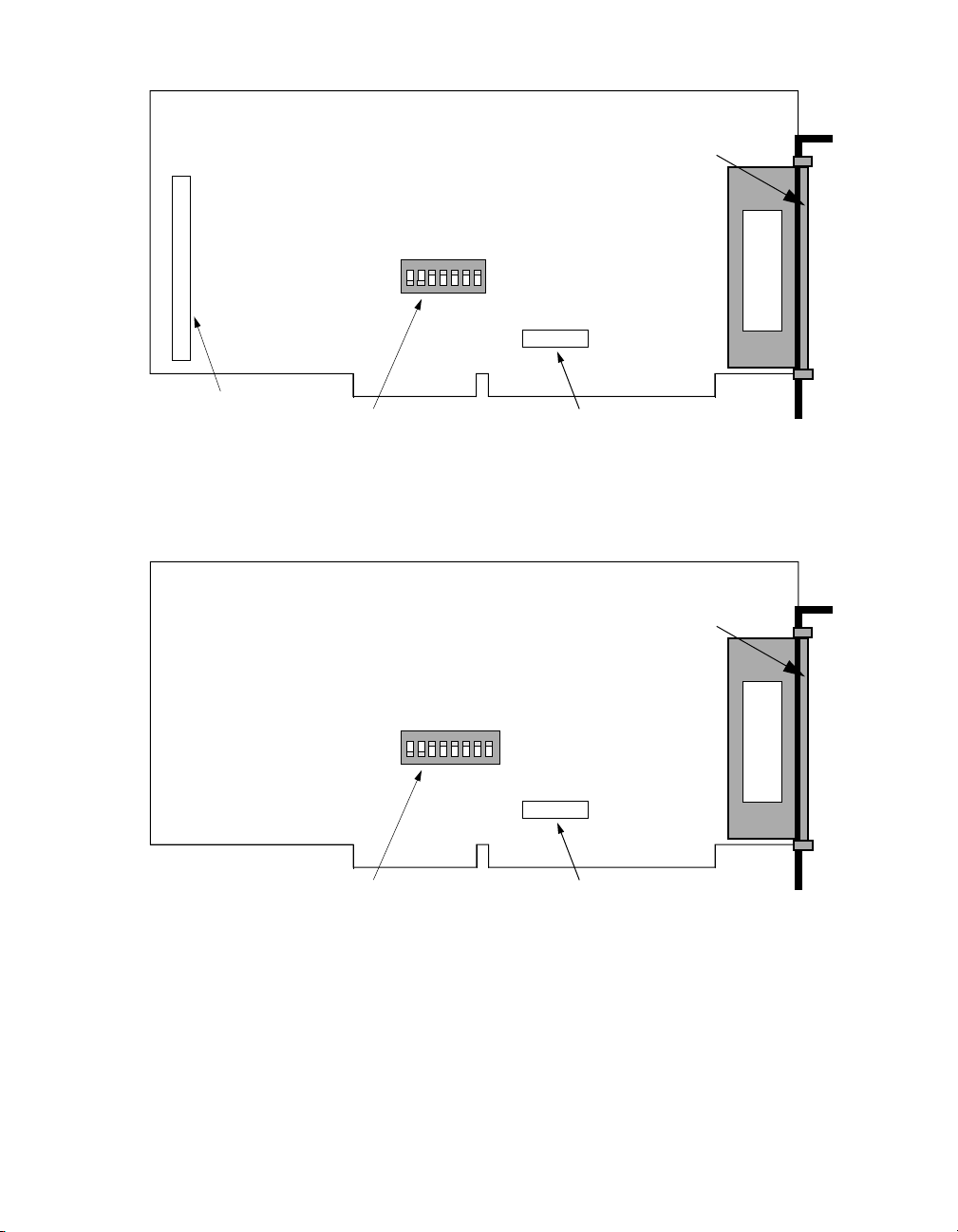
Auxiliary
I/O
Connector
J4
Base Address Switch
S1
Jumper Block J3
Figure 3-1. CTM-10 Board Layout
J2 Main
I/O
Connector
IRQ Level
J1 Main
I/O
Connector
Base Address Switch
S1
IRQ Level Jumper
Block J3
Figure 3-2. CTM-05/A Board Layout
3-8 Setup and Installation
Page 36

The next segments describe how to set the base address and interrupt level
on the CTM-10 and CTM-05/A boards. Once you have configured the
boards, you can install them in your computer by following the procedure
described on page 3-12.
For more complete information on cabling and wiring your boards,
Note:
refer to Section 4.
Setting the Base Address
The default base address settings in the DriverLINX configuration
Note:
file is 300h for board 0. Make sure the switch settings for each board
match the settings in the DriverLINX configuration file.
The base address switch block contains seven switches, labeled 1 through
7. Switch 1 corresponds to the Most Significant Bit (MSB) of the base
address; switch 7 corresponds to the LSB of the base address. You place a
switch in the ON position (logic 0) by sliding the switch toward the top
(numbered side) of the switch block. You place a switch in the OFF
position (logic 1) by sliding the switch toward the bottom (unnumbered
side) of the switch block. Figures 3-3 and 3-4 illustrate the setting for a
base address of 300h (786 decimal); switches 1 and 2 are in the OFF
position and switches 3, 4, 5, 6, and 7 are in the ON position.
Table 3-1. Address Switch Values
Switch Position Hex Value (OFF) Decimal Value (OFF)
1 200 512
2 100 256
3 80 128
44064
52032
61016
788
Configuring a Board 3-9
Page 37

Base Address Requirements for the CTM-10
A CTM-10 is preset at the factory for a base address of 300h, as shown in
Figure 3-3.
O
1 2 3 4 5 6 7
N
Figure 3-3. Preset Base Address for the CTM-10
If the preset base address of 300h conflicts with the base address of
another CTM-10 or other resource in the computer, you must assign the
board a new base address. Base addresses for the CTM-10 are set on
8-byte boundaries that range from 100h to 3F8h. Refer to the I/O address
space mapping in your computer’s documentation to determine available
addresses.
Base Address Requirements for the CTM-05/A
A CTM-05/A is preset at the factory for a base address of 300h, as shown
in Figure 3-4.
O
1 2 3 4 5 6 7 8
N
Figure 3-4. Preset Base Address for the CTM-05/A
If the preset base address of 300h conflicts with the base address of
another CTM-05/A or other resource in the computer, you must assign the
board a new base address. Base addresses for the CTM-05/A are set on
4-byte boundaries that range from 100h to 3FCh. Refer to the I/O address
space mapping in your computer’s documentation to determine available
addresses.
3-10 Setup and Installation
Page 38

Setting the Board Interrupt Level
On both a CTM-10 and CTM-05/A, you normally set the interrupt-level
jumper to position X on jumper block J3 (as shown in Figure 3-5) and use
software to select an interrupt level. Using software, you can select from
interrupt levels 3, 5, 7, 10, 11, and 15, while the jumper is at the X
position.
2
Figure 3-5. Normal Interrupt-Level Setting for the CTM-10 and
With the jumper at position X, no interrupt level is selected at power-up;
you must, therefore, write your application program to make the
selection. You can then program the CTM-10 and CTM-05/A boards to
generate interrupts in response to the selected interrupt level. Note that
the CTM-10 has separate, independent interrupt logic for units A and B.
Jumper Block J3
34567 X
Jumper Set to X
(disable) Position
CTM-05/A
You use jumper block J3 to select an interrupt level from levels 2 to 7 only
when you want your CTM-10 or CTM-05/A to be backward-compatible
with an existing CTM-05 application. You must use the jumper-select
feature in conjunction with the external interrupt input/interrupt enable,
as described in
Programmable Interrupt Logic
on page 2-5. On the
CTM-10, only unit A supports jumper selection.
If you use the jumper-select feature, avoid using a level already in use by
another device.
When using the jumper-select feature, you can enable the tristate driver
that drives the jumper-selected interrupt line by taking the Interrupt
Enable signal (pin 2 of the auxiliary connector on the CTM-10; pin 2 on
Configuring a Board 3-11
Page 39

the CTM-05/A) to a logic-0 level. The output of this driver drives the
interrupt request line selected by the jumper.
A logic 1 on the Interrupt Input signal (pin 1 of the auxiliary connector on
the CTM-10; pin 1 on the CTM-05/A) generates an interrupt after the
8259 Interrupt Controller is enabled.
Installing the Board
Caution:
you perform the following procedure. Any attempt to insert or remove any
board with computer power ON could damage your computer.
To install the CTM-10 or CTM-05/A in your computer, proceed as
follows:
1. Remove the cover of your computer as follows:
2. Choose an available option slot.
3. Loosen and remove the screw at the top of the blank adapter plate,
4. Hold the CTM-10 or CTM-05/A board in one hand, placing your
Your computer and all attached accessories must be OFF before
a. Remove the cover-mounting screws from the rear panel of the
computer.
b. Slide the cover of the computer about 3/4 of the way forward.
c. Tilt the cover upwards and remove.
then slide the plate up and out to remove.
other hand on any metallic part of the computer chassis (but not on
any components), to safely discharge any static electricity from your
body.
5. Check the board base address switch and interrupt jumper for proper
settings, as described in the previous sections.
6. Align the board connector with the desired accessory slot and with
the corresponding rear-panel slot, gently press the board downward
into the socket, and secure the board in place by inserting the
rear-panel, adapter-plate screw.
3-12 Setup and Installation
Page 40

7. If you need to connect to the remainder of the digital I/O ports of the
CTM-10, proceed as follows:
a. Connect the auxiliary connector of the CAB-4037 cable to the J4
connector on the CTM-10 board.
b. Place the DB-37M connector of the CAB-4037 cable in an
adjacent slot of the computer chassis.
Figure 3-6 illustrates the cable for digital I/O port B on the CTM-10.
DB-37M connector;
mounts in slot of
computer adjacent
CAB-4037
cable
J2 Main I/O
Connector
to CTM-10 board
Upper bits (4 to 7) of
digital I/O port A and
all bits of digital I/O
port B
Auxiliary
Connector
J4
Figure 3-6. Cable for Digital I/O Port B of the CTM-10 Board
8. Replace the computer cover, as follows:
a. Tilt the cover up and slide it onto the system’s base, ensuring that
the front of the cover is under the rail along the front of the frame.
b. Replace the mounting screws.
Once you have installed the board, you can connect an accessory board
and wire connections to the CTM-10 or CTM-05/A, as described in
Section 4.
Installing the Board 3-13
Page 41

Using the DriverLINX Configuration Panel
After you have successfully installed the CTM-10 and CTM-05/A
board(s) in your computer, start Windows to install DriverLINX. For
detailed instructions on installing DriverLINX, see the documentation
provided on the DriverLINX CD-ROM; especially the
Installation and Configuration Guide
Programming Guide
To configure a CTM-10 or CTM-05/A board (logical device), use the
DriverLINX icon in the Windows Control Panel application. The
DriverLINX Configuration Panel displays a tree list of all the installed
DriverLINX drivers on your system and the configured Logical Devices
under each driver.
manuals.
and
DriverLINX
DriverLINX Counter/Timer
Note:
require that users installing or configuring device drivers log on under an
administrative account.
Use the Configuration Panel to tell DriverLINX the model of the board
you’ve installed, its base I/O address, and the interrupt channel you’ve
assigned to the board, if it has one. You can also instruct DriverLINX to
initialize the hardware into a custom configuration of input and output
ports and default output values. This may be useful if you connect your
hardware’s outputs to external devices that expect high logic signals,
rather than the default low logic signals, as their starting state.
Pushing the Setup button on the DriverLINX Configuration Panel
displays a
the selected Logical Device. The tabbed dialog box has a page for each
Logical Subsystem that your board supports. Select and complete each
property page to configure the Logical Device.
If you are running Windows NT, Windows NT’s security features
Configure DriverLINX Device
property page for configuring
3-14 Setup and Installation
Page 42

1. On the Device Property Page, enter the following required fields:
●
Model
— select the model name that matches the installed board.
Address
●
jumpers or dip switch. This address must
— enter the base I/O address that you set on the board’s
not
conflict with any
other device in your system.
Detect
●
●
— (use default value only)
Calibrate
— (use default value only)
2. At this point, you may select OK and accept default initialization,
select the Special Properties dialog, or select another Property Page.
3. If you select the Special Properties Dialog, you may configure
features unique to the installed hardware board:
●
Frequency Scaler —
this switches the frequency divider for the
master oscillator prescaler between binary and Binary Coded
Decimal (BCD) counting modes.
●
FOUT — this specifies the clock source, prescaler value, and
output (gate) option for the AM9513’s FOUT line.
Note: DriverLINX uses the same values for all AM9513 chips on the
counter/timer. To set different characteristics for each AM9513 on the
CTM-10 board, configure the hardware as two individual Logical
Devices.
4. If you select the Counter/Timer Property page, you may select the
master internal clock frequency that the hardware inputs to the
prescaler for the counter/timer channels and to define the interrupt
channel, if any, for the counter/timers. Enter selections for the
following fields:
● Resolution — specifies the master internal clock frequency that
the counter/timers use.
● Interrupt — specifies the interrupt channel you have assigned to
your hardware. If you are not using interrupts, select “none.”
Using the DriverLINX Configuration Panel 3-15
Page 43

5. If you select the Digital Input Property page, you may assign an
interrupt channel to your board, if it supports interrupts for digital
input, and to modify DriverLINX’s default hardware initialization.
DriverLINX disables options not supported by your hardware. Enter
the selections for the following fields:
● Channels — shows the available Logical Channels for digital
input and selects the Logical Channel for the Configuration
properties.
● Interrupt — specifies the interrupt channel you have assigned to
your hardware. If you are not using interrupts, select “none.”
● DMA level — specifies the DMA channel you have assigned to
your hardware. Most counter/timer boards do not use DMA.
Note: DriverLINX disables the Configuration group if the board’s digital
channels do not support software reprogramming as inputs or outputs.
6. If you select the Digital Output Property page, you may define output
values for initializing the ports. You are allowed to define interrupt
resources if you did not define them on the Digital Input Property
Page. By default, DriverLINX sets output values to zero. To change
the defaults, modify the following fields:
● Channels — shows the available Logical Channels for digital
output and selects the Logical Channel for the Initialization
properties.
● Value — specifies the output value DriverLINX uses to initialize
the port selected in the Channels list box. DriverLINX ignores
this property if Initialize is not checked.
● Initialize — when checked, this property indicates that
DriverLINX should automatically initialize this channel as
specified in the Value property.
3-16 Setup and Installation
Page 44

7. To Statistically Initialize Digital Output Ports (initialize Logical
Channel 0 with all bits at logic high), on the Digital Output Property
page:
● Select “0 (bits 0 - 7)” in the Channels list box.
● Enter “255” (DEC) or “0xFF:” (Hex) in the Initialization Value
edit box.
● Click the Initialize check box.
● Repeat this procedure for every Logical Channel that requires
user-defined initialization.
8. After completing all Property Pages, press OK to save your
configuration.
For programming your counter/timers with DriverLINX, refer to
DriverLINX Counter/Timer Programming Guide on the DriverLINX
CD-ROM.
You can use DriverLINX to verify board operation.
1. To physically initialize the CTM-10 or CTM-05/A, select
Device/Initialize from the main menu in Learn DriverLINX.
2. The first time the CTM-10 or CTM-05/A is initialized, or after a
configuration change, DriverLINX runs a diagnostic program to
verify the operation and accuracy of the configuration settings.
You are now ready to make I/O connections. Refer to Section 4 for
descriptions of common I/O accessories and connections for CTM-10 and
CTM-05/A boards.
Using the DriverLINX Configuration Panel 3-17
Page 45

4
Cabling and Wiring
This section describes how to attach accessory boards and wire signals to
the CTM-10 and CTM-05/A boards.
Note:
board, turn off power to your computer and any attached accessories.
Before you make any connections to a CTM-10 or CTM-05/A
Attaching the STA-50 (CTM-10 Board Only)
The STA-50 screw terminal accessory (used by the CTM-10 board only)
attaches to the 50-pin, main I/O connector on the CTM-10 through a
CACC-2000 cable, as shown in Figure 4-1. The STA-50 gives you access
to all counter I/O signals and to bits 0 to 3 of Digital I/O port A.
J2 Main
I/O
Connector
CACC-2000 Cable
J1
Digital I/O
Por t A
. . . . . . .
. . . . . . .
. . . . . . .
. . . . . . .
STA-50 Accessory
Figure 4-1. Attaching an STA-50 to a CTM-10 Board
Attaching the STA-50 (CTM-10 Board Only) 4-1
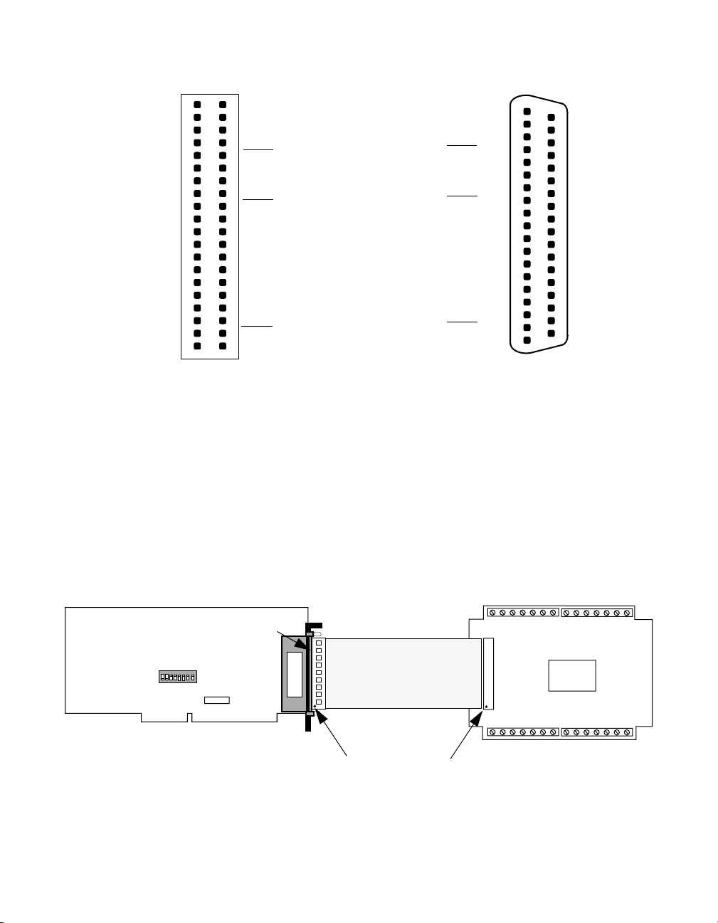
Page 46

Connect field wiring directly to the screw terminals of the STA-50. These
terminals are labeled from 1 to 50; their functions correspond directly to
the functions of the pins on the main I/O connector of the CTM-10 board.
Pin assignments for the main I/O connectors of the CTM-10 and of the
STA-50 are shown in Figure 4-2.
BCIN5 - 01
BCIN3 - 03
BCIN1 - 05
BGATE5 - 07
BGATE3 - 09
BTOUT4 - 11
BGATE2 - 13
BTOUT2 - 15
BGATE1 - 17
BFOUT - 19
AGATE1 - 21
ACIN1 - 23
ACIN3 - 25
AGATE3 - 27
ACIN4 - 29
ATOUT3 - 31
ATOUT2 - 33
ATOUT1 - 35
AGATE5 - 37
AFOUT - 39
AOUT0 - 41
AOUT1 - 43
AOUT2 - 45
AOUT3 - 47
ASTB - 49
02 - GND
04 - BCIN4
06 - BCIN2
08 - GND
10 - BGATE4
12 - BTOUT5
14 - GND
16 - BTOUT3
18 - BTOUT1
20 - GND
22 - ACIN2
24 - AGATE2
26 - GND
28 - ATOUT5
30 - ATOUT4
32 - GND
34 - AGATE4
36 - ACIN5
38 - GND
40 - AIN0
42 - AIN1
44 - GND
46 - AIN2
48 - AIN3
50 - +5V
Figure 4-2. CTM-10 Main I/O Connector (J2) and STA-50 Connectors
J1 and J5
4-2 Cabling and Wiring
Page 47

Attaching the STA-U
The STA-U screw terminal accessory is available for both the CTM-10
and the CTM-05/A boards. The following sections describe how to attach
the STA-U to each board.
Attaching the STA-U to the CTM-10
To attach the STA-U to the CTM-10, use the CAB-4037 and the C-1800
cables, as shown in Figure 4-3.
DB-37M
Connector
CAB-4037
Cable
Auxiliary
Connector
J4
J2 Main I/O
Connector
CTM-10 Board
C-1800 Cable
Upper bits (4 to 7) of
Digital I/O Port A and
all bits of Digital I/O
STA-U Accessory
Por t B
Figure 4-3. Attaching the STA-U to the CTM-10 Board
You can connect field wiring directly to the screw terminals on the STA-U
screw terminal connector. The screw terminals are labeled and correspond
directly to the functions of the pins on the DB-37M I/O connector and
auxiliary connector of the CAB-4037 cable, as shown in Figure 4-4.
Attaching the STA-U 4-3
Page 48
40 - NC
38 - NC
36 - BIN0
34 - BIN1
32 - BIN2
30 - BIN3
28 - BIN4
26 - BIN5
24 - BIN6
22 - BIN7
20 - AOUT4
18 - AOUT5
16 - AOUT6
14 - AOUT7
12 - AIN4
10 - AIN5
08 - AIN6
06 - AIN7
04 - GND
02 - +5V
Top of Board
NC - 39
GND - 37
+5 V - 35
GND - 33
BSTB - 31
GND - 29
BINT - 27
GND - 25
BENB - 23
GND - 21
BOUT0 - 19
BOUT1 - 17
BOUT2 - 15
BOUT3 - 13
BOUT4 - 11
BOUT5 - 09
BOUT6 - 07
BOUT7 - 05
AENB - 03
AINT - 01
GND - 19
+5 V - 18
GND - 17
BSTB - 16
GND - 15
BINT - 14
GND - 13
BENB - 12
GND - 11
BOUT0 - 10
BOUT1 - 09
BOUT2 - 08
BOUT3 - 07
BOUT4 - 06
BOUT5 - 05
BOUT6 - 04
BOUT7 - 03
AENB - 02
AINT - 01
Top of Panel
37 - BIN0
36 - BIN1
35 - BIN2
34 - BIN3
33 - BIN4
32 - BIN5
31 - BIN6
30 - BIN7
29 - AOUT4
28 - AOUT5
27 - AOUT6
26 - AOUT7
25 - AIN4
24 - AIN5
23 - AIN6
22 - AIN7
21 - GND
20 - +5V
To CTM-10 Auxiliary Connector J4
Figure 4-4. CAB-4037 Cable Pin Assignments
Attaching the STA-U to the CTM-05/A
The STA-U screw terminal accessory attaches to the 37-pin, main I/O
connector on the CTM-05/A using the C-1800 or S-1800 cable. Figure
4-5 illustrates the connection of an STA-U to a CTM-05/A board.
C-1800 or S-1800
Cable
CTM-05/A
J1 Main I/O
Connector
Pin 1
CAB-4037 DB-37M Connector
J1
Pin 1
. . . . . . .
. . . . . . .
. . . . . . .
. . . . . . .
STA-U Accessory
Figure 4-5. Attaching an STA-U Board to the CTM-05/A
4-4 Cabling and Wiring
Page 49

You can connect field wiring directly to the screw terminals on the
STA-U. The screw terminals are labeled to correspond directly to the pins
on the main I/O connector of the CTM-05/A, as shown in Figure 4-6.
Top of Board (Rear View)
Figure 4-6. Pin Assignments for Main I/O Connector (J1) of a
Connecting Signals
This information illustrates typical signal wiring to CTM-10 and
CTM-05/A boards.
ACIN2 - 19
AGATE2 - 18
ACIN3 - 17
AGATE3 - 16
ACIN4 - 15
AGATE4 - 14
ACIN5 - 13
AGATE5 - 12
GND - 11
AOUT0 - 10
AOUT1 - 09
AOUT2 - 08
AOUT3 - 07
AOUT4 - 06
AOUT5 - 05
AOUT6 - 04
AOUT7 - 03
AENB - 02
AINT - 01
CTM-05/A Board
37 - AGATE1
36 - ACsIN1
35 - ATOUT1
34 - ATOUT2
33 - ATOUT3
32 - ATOUT4
31 - ATOUT5
30 - AFOUT
29 - AIN0
28 - AIN1
27 - AIN2
26 - AIN3
25 - AIN4
24 - AIN5
23 - AIN6
22 - AIN7
21 - ASTB
20 - +5V
Although the illustrations in this section show a direct connection
Note:
to a pin on the main I/O connector, you actually wire your signal to a
screw terminal on an accessory board.
Connecting Signals 4-5
Page 50
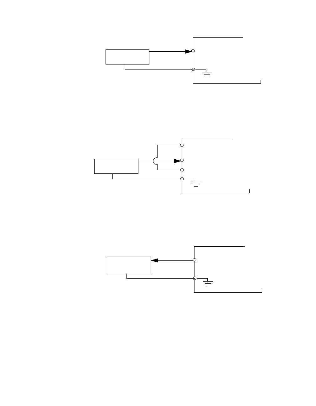
CTM-10 or CTM-05/A
Signal Source
Counter 0 Input
Digital Ground
Figure 4-7. Typical Event Counting Connection
CTM-10 or CTM-05/A
Counter 4 Output
Signal Source
Counter X Input (X = CLK 1, 2, 3, or 5)
Counter X Gate
Digital Ground
Figure 4-8. Typical Frequency Measurement Connection
CTM-10 or CTM-05/A
Stepper Motor
Driver
Counter 2 Output
Digital Ground
Figure 4-9. Typical Single Pulse Output Connection
4-6 Cabling and Wiring
Page 51

CTM-10 or CTM-05/A
Counter 2 Output
Stepper Motor
Driver
Digital Ground
Counter 3 Input
Figure 4-10. Typical Counted Pulse Output Connection
CTM-10 or CTM-05/A
Counter 4 Output
Signal Source
Counter X Input (X = CLK 1, 2, 3, or 5)
Counter X Gate
Digital Ground
Figure 4-11. Typical Interval Measurement Connection
Connecting Signals 4-7
Page 52

5
Using DriverLINX CTM Test
Panel for Hardware Testing
The DriverLINX CTM Test Panel is an application that allows you to
apply inputs to and observe outputs from the CTM board. With the CTM
Test Panel you can:
Generate Sine, Square, and Triangle waves using the SST Signal
●
Generator.
●
Output pulse and strobe.
The CTM Test Panel is useful for:
Testing the CTM-10 or CTM-05/A DriverLINX installation and
●
configuration.
Verifying signal inputs to your CTM-10 and CTM-05/A boards.
●
●
Sending test signals to external devices.
●
Providing a realistic example of a working CTM-10 or CTM-05/A for
study.
To start up and use the DriverLINX CTM Test Panel, perform the
following steps:
1. At the Windows Start Program menu, select DriverLINX.
2. From the DriverLINX menu, select Utilities.
3. From the Utilities menu, select Test Panels.
4. From the Test Panels, select CTM Panel.
5. After the test panel starts, perform the necessary setup for the CTM
board.
6. To set up and perform an operation, click the appropriate inputs and
output panels.
5-1
Page 53

7. To obtain information on the setup and performance of an operation,
use the online help.
8. When you finish using the test panel, select File Exit to terminate the
program.
5-2 Using DriverLINX CTM Test Panel for Hardware Testing
Page 54

I/O Addresses and Registers
This section provides information about the I/O addresses and registers of
the CTM-10 and CTM-05/A boards. It contains the following segments:
I/O address and register locations
●
●
Register formats
I/O Address and Register Locations
The CTM-10 uses eight consecutive address locations in the computer’s
I/O address space. The CTM-05/A uses only four consecutive address
locations in the computer’s I/O address space.
6
You set the base address using DIP switches on the board, as described in
Section 3. The base address automatically falls within an 8-byte boundary
for the CTM-10 and a 4-byte boundary for the CTM-05/A. Once the base
address is set, the eight consecutive locations are used, as described in
Table 6-1.
I/O Address and Register Locations 6-1
Page 55

Table 6-1. I/O Address Map
I/O Address
(Hexadecimal)
Counter/Timer
1
Unit
Write Read
Function
Base Address +0h A Am9513A Unit A
data out
Base Address +1h A Am9513A Unit A
Command register
Base Address +2h A Unit A Interrupt
Control register
Base Address +3h A Digital output lines
AOUT0 to AOUT7
Base Address +4h B AM9513A Unit B
data out
Base Address +5h B Am9513A Unit B
Command register
Base Address +6h B Unit B Interrupt
Control register
Base Address +7h B Digital output lines
BOUT 0 to 7
Am9513A Unit A
data in
Am9513A Unit A
Status register
Digital input lines
AIN0 toAIN7
Unit A Interrupt
Status register/Clear
Interrupt
AM9513A Unit B
data in
Am9513A Unit B
Control Status
register
Digital input lines
BIN 0 to 7
Unit B Interrupt
Status register/Clear
Interrupt
1
Counter/timer unit A refers to the first Am9513A on a CTM-10 and the only Am9513A
on a CTM-05/A; counter/timer unit B refers to the second Am9513A on a CTM-10
board.
Register Formats
The formats of the following registers are described in this segment:
●
Interrupt Control register
Interrupt Status register
●
6-2 I/O Addresses and Registers
Page 56

Interrupt Control Register Format
The Interrupt Control registers for units A and B are write only. The unit
A Interrupt Control register is located at Base Address +2h. The unit B
Interrupt Control register is located at Base Address +6h. The format of
these registers is shown in Table 6-2.
Table 6-2. Interrupt Control Register
7 6 5 4 3 2 1 0
FREQ ISRC2 ISRC1 ISRC0 IENAB IL2 IL1 IL0
The bits are described as follows:
FREQ determines the output frequency of the Dual Frequency Time
●
Base select (directed to unit A at Base Address +2h only on both the
CTM-10 and the CTM-05/A), as follows:
– 0 = 1 MHz (power-up default)
– 1 = 5 MHz
Note:
While the FREQ bit of the Interrupt Control register of unit A
(at Base Address +2h) controls the output frequency of the Dual
Frequency Time Base on both the CTM-05/A and CTM-10, unit B of
the CTM-10 receives the same output frequency.
●
ISRC2 to ISRC0 determine the interrupt source selection. The values
for ISRC2 to ISRC0 are described as follows:
– 0 = External (power-up default) qualified by AENB
or BENB
– 1 = Timer 1 Output
– 2 = Timer 2 Output
– 3 = Timer 3 Output
– 4 = Timer 4 Output
– 5 = Timer 5 Output
– 6 = None
– 7 = None
Register Formats 6-3
Page 57

IENAB determines whether interrupts are enabled or disabled. The
●
values for IENAB are as follows:
– 0 = Disable (Power-up default; setting IENAB to 0 forces the
interrupt latch to 0 and will not allow the interrupt latch to set.)
– 1 = Enable
IL2 to IL0 determine the interrupt level selection. The values for IL2
●
to IL0 are encoded as follows:
– 0 = None (power-up default)
– 1 = IRQ3
– 2 = IRQ5
– 3 = IRQ7
– 4 = IRQ10
– 5 = IRQ11
– 6 = IRQ15
– 7 = None
Interrupt Status Register Format
The Interrupt Status registers for units A and B are read only. The unit A
Interrupt Status register is located at Base Address +3h, while the unit B
Interrupt Status register is located at Base Address +7h. The format of
these registers is shown in Table 6-3.
Table 6-3. Interrupt Status Register
7 6 5 4 3 2 1 0
IRQ-------
The Interrupt Status Register is cleared automatically when the
Note:
interrupt status is read.
6-4 I/O Addresses and Registers
Page 58

The IRQ bit reflects the state of the interrupt latch, as follows:
●
0 = Not present
1 = Present - event occurred
●
A 0-to-1 transition of the signal selected by ISRC0 to ISRC2 (Interrupt
Control register) is latched on the board and is cleared by a read of this
register (bit automatically resets after a read). Note that IENAB must be
set to 1 for the latch to set. IL2 to IL0 must be set to values in the range of
1 to 6 to generate an interrupt in the host computer.
Note:
If you are polling this bit (reading it repetitively) to determine
when the selected condition occurs, read the bit once more after it is set to
1 to ensure proper clearing.
Register Formats 6-5
Page 59

Using DriverLINX
DriverLINX is a language and hardware independent application
programming interface designed to support Keithley’s analog, digital, and
counter/timer boards in Windows. DriverLINX is a multi-user and
multi-tasking data-acquisition resource manager providing more than 100
services for foreground and background data acquisition tasks.
DriverLINX simplifies the writing of data acquisition and control
programs for the CTM-10 and CTM-05/A boards.
DriverLINX Counter/Timer Model
DriverLINX abstracts all counter/timer hardware chips as an array of
three terminal devices. The terminals of an individual counter/timer are:
●
Clock —
for counting external events.
the source input for dividing down to a lower frequency or
7
Gate —
●
counter/timer operation.
●
Output —
DriverLINX associates four operating properties with each counter/timer
channel:
Mode —
●
Period —
●
channel.
●
OnCount —
output trains or pulses.
●
Pulses —
DriverLINX Counter/Timer Model 7-1
the control input for triggering, re-triggering, or gating the
the counter/timer output frequency, pulse, or strobe.
defines the operational task for the counter/timer channel.
defines the cycle period or divider for the counter/timer
defines high duration of the period for asymmetrical
defines the number of periods to generate.
Page 60

By selecting values for these seven properties and, when necessary,
making the appropriate connections between counters, the application can
program DriverLINX to execute one of the counter/timer’s basic
operating modes or the following counter/timer operations and tasks:
●
Event counting —
16-,32-,and 64-bit counters for signals at the
Clock input.
Frequency measurement —
●
●
Interval measurement —
16- and 32-bit frequency measurement.
Measure time between two consecutive
pulses at a single input or two pulses at separate inputs.
●
Period and pulse width measurement —
Measure duration of each
cycle or half cycle.
●
Pulse generation —
Generate periodic pulse trains, variable duty
cycle waveforms, square waves, or input-modulated waveforms.
Applications may program and operate counter/timers independently, or
they may configure the operating mode for several counter/timers and
start or stop them synchronously. For hardware boards that support
interrupts, applications may program a list of timers whose current value
DriverLINX will read into a buffer on each interrupt.
The following tables show the legal values for the Clock, Gate, Output,
and Mode fields of a DriverLINX logical counter channel.
7-2 Using DriverLINX
Page 61

Clocks
The Clock property, Table 7-1, specifies the source input for the abstract
counter/timer of a Logical Channel.
Table 7-1.
Clock Description
Internal1...Internal5 Internal clock frequency prescaled at 1 of 5 taps
Source1...Source5 Use channel 1...5 source (clock) input
Gate1...Gate5 Use channel 1...5 gate input
External External clock frequency (usually positive edge)
ExternalPE External clock frequency (positive edge clocking)
ExternalNE External clock frequency (negative edge clocking)
TCNm1 Use channel N-1 terminal count output
You may also request that the clock input use the falling edge of the
●
Allowed Values for Rate Event Clock Property
clock input rather than the rising edge.
Internal1 always designates the onboard hardware clock.
●
Internal2...Internal5 designate lower frequency taps of the master
clock if the hardware supports this capability.
If the application uses an Internal1 clock with a Period value greater
●
than the hardware counter/timer supports, DriverLINX will
automatically select available hardware prescalers to obtain the
closest value to the requested Period.
DriverLINX Counter/Timer Model 7-3
Page 62

Gates
The Gate property, Table 7-2, selects how the abstract counter/timer uses
the gate input of a Logical Channel. Generally, this input gates the
counting or measuring process or triggers the counter/timer operation.
Table 7-2.
Gate Description
Enabled Enable gate
Disabled Enable gate
NoConnect No connection
LoLevelGateN Logic low level at gate input N
LoEdgeGateN Negative edge at gate input N
HiLevelGateN Logic High level at gate input N
HiLevelGateNp1 Logic high level at gate input N+1
HiLevelGateNm1 Logic high level at gate input N-1
HiTcNm1 Positive edge at terminal count output N-1
HiEdgeGateN Positive edge at gate input N
Allowed Values for Rate Event Gate Property
7-4 Using DriverLINX
Page 63

Outputs
The Output property, Table 7-3, programs the polarity and duty cycle of
the abstract counter/timer’s output port.
Table 7-3.
Output Description
Default Depends on operation
LoToggled Start low; toggle to TC
LoActive Active low pulse at TC
LoZ Inactive low impedance output
Toggled Toggle at TC
HiToggled Start high; toggle at TC
HiActive Active high pulse at TC
HiZ Inactive high impedance output
Allowed Values for Rate Event Output Property
DriverLINX automatically selects an output type if the application
requests Default. Depending on hardware capabilities, DriverLINX
chooses the output option based on the requested Mode.
DriverLINX Counter/Timer Model 7-5
Page 64

Modes
The Mode property, Table 7-4, selects the type of rate generator or task
the abstract/counter timer will perform. Mode values fall into two general
groups — pulse and waveform generators and measurement tasks.
Note:
The waveform-oriented (for example, RateGen, SqWave, etc.)
generators program a single Logical Channel of an abstract counter/timer
while the task-oriented modes (for example, Frequency, Interval, etc.)
may program multiple Logical Channels.
Table 7-4.
Generator Description
RateGen Periodic rate generator
SqWave Square wave generator
VDCGen Variable duty cycle rate generator
Divider Frequency divider
Freq Frequency counter
Interval Interval counter
Count Event counter
PulseWd Pulse width measurement
FskGen Frequency-shift keying
PulseGen Pulse generator
RetrigRateGen Retriggerable rate generator
RetrigSqWave Retriggerable square wave generator
Count32 32-bit event counter
Count64 64-bit event counter
Freq32 32-bit frequency counter
OneShot One-shot pulse or strobe
RetrigOneShot Retriggerable one-shot pulse or strobe
Allowed Values for Rate Event Mode Property
Some of the above mode field options (for example, BurstGen)
●
specify features that require external connections that need to be
pre-wired into the board.
Other options, such as frequency measurement modes, require
●
external user connections between counter/timer terminals.
7-6 Using DriverLINX
Page 65

DriverLINX Task Model
To manage a user application’s data-acquisition requests, DriverLINX
creates tasks. A DriverLINX task consists of the set of hardware and
system resources and the board-specific protocols required to execute the
data-acquisition request. Applications can start tasks, monitor tasks, and
stop tasks by submitting Service Requests to DriverLINX.
Hardware Sharing
DriverLINX allows multiple applications to share a data-acquisition
device or allows multiple tasks to run on a device if the hardware can
support concurrent operations. To support hardware sharing and
concurrency, DriverLINX assigns resources to each task and then
compares the resource requirements of a new task with the in-use
resources of all current tasks. If the new requirements don’t conflict with
the current in-use resources, DriverLINX updates the in-use resources
and starts the task. Otherwise, DriverLINX rejects the newly requested
task.
Creating Tasks
User applications create data-acquisition tasks by setting the properties of
a Service Request to values that specify the task. The application then
submits the Service Request to DriverLINX that transforms each Service
Request into a procedure for performing the task on the requested
hardware subsystem.
If DriverLINX detects any errors in the Service Request or in the
hardware during the task, it aborts the task and returns an error code to the
application. If the application requests hardware resources that are
already in use by another thread or process, DriverLINX also stops the
task and notifies the application.
DriverLINX Task Model 7-7
Page 66

Monitoring and Stopping Tasks
Applications may also check the status of a task or terminate a task by
modifying the operation property of the Service Request used to create
the task. To check status, change the operation property to “status.” To
terminate a task, change the operation property to “stop.”
DriverLINX Events
Applications can request that DriverLINX notify the application of
significant events during execution of a task. By designing a
data-acquisition task to use events, an application can overlap data
processing with data collection. Events allow the application to
coordinate these two activities without the overhead associated with
polling for the status of the data collection task and without the
scheduling problem of coordinating data processing with partial data
collection.
DriverLINX posts events to an application through the Windows
messaging mechanism. DriverLINX supports messages found in
Table 7-5:
Table 7-5.
Message Description
ServiceStart Task is starting
ServiceDone Task is complete
BufferFilled Buffer processing complete
DataLost Data over/underrun
TimeTic Timer interrupt occurred
StartEvent Start event detected
StopEvent Stop event detected
Critical Error Hardware error
The most useful events for applications are
and
DataLost.
●
The
ServiceDone
event notifies the application that DriverLINX
DriverLINX Messages
ServiceDone, BufferFilled,
terminated the task. Tasks may end because the application stopped it,
the stop event condition in a Service Request was satisfied, or
DriverLINX detected a run-time error and stopped the task.
7-8 Using DriverLINX
Page 67

The
●
BufferFilled
event notifies the application that DriverLINX has
read or written the current buffer. Applications can use this message
with multiple data buffers to eliminate polling the driver for the status
of the task and to overlap data processing with data acquisition.
●
The
DataLost
event notifies the application that DriverLINX detected
that the hardware was filling or emptying buffers faster than the
application or driver could process the buffers.
The other DriverLINX events are useful for special cases.
●
The
ServiceStart
event notifies the application that DriverLINX is
starting the task. An application might use this event to provide visual
feedback to the user interface that the task is starting.
●
The
TimerTic
event notifies the application that DriverLINX has
processed a clock interrupt. DriverLINX only reports this event for
the counter/timer subsystem when the task is not using data buffers.
●
The
StartEvent
notifies the application that DriverLINX detected the
logical condition the application specified in the Service Request’s
Start Event as true. DriverLINX can only report this event if the
hardware generates an interrupt associated with the Start Event.
The
●
StopEvent
notifies the application that DriverLINX detected the
logical condition the application specified in the Service Request’s
Stop Event as true. DriverLINX can only report this event if the
hardware generates an interrupt associated with the Stop Event.
The
●
CriticalError
detected an unexpected critical error other than
event notifies the application that DriverLINX
DataLost.
This
usually indicates either the hardware or software is malfunctioning
and needs repair or re-configuration.
DriverLINX Task Model 7-9
Page 68

DriverLINX Operations
For most counter/timer hardware, applications can select one of five
operations for a task. The basic counter/timer task operations are:
Initialize —
●
hardware.
Configure —
●
task.
●
Start —
and Mode properties determine when the hardware starts counting.
Status —
●
the application.
●
Stop —
available for new tasks.
The
Initialize, Configure,
task. The task that DriverLINX creates for the first two operations exists
only briefly during the application’s function call to DriverLINX. For a
Start
operation, however, DriverLINX creates a task that may exist
indefinitely until the application explicitly ends the task with a
operation or DriverLINX ends the task because the Stop Event has
become true.
DriverLINX Modes
resets the counter/timer subsystem software and/or
sets up a counter/timer for a task, but doesn’t start the
sets and arms a counter/timer for a task. The Gate, Clock,
returns the current counter/timer count value and status to
disarms the counter/timer task and makes the task resources
and
Start
operations all create a DriverLINX
Stop
For most counter/timer hardware, DriverLINX supports three task modes,
OTHER, POLLED,
●
When an application uses
and
INTERRUPT.
OTHER
mode, DriverLINX initializes the
subsystem or configures a Logical Channel without starting the
counter.
●
When an application uses
POLLED
mode, DriverLINX starts the
counter/timer hardware running, but it does not automatically report
any status information about the task to the application.
●
When an application uses
INTERRUPT
mode, DriverLINX starts the
counter/timer hardware running with a hardware interrupt enabled. At
each interrupt, DriverLINX either sends a
TimerTic event to the
application or saves the current count of the requested counter/timers
into a data buffer.
7-10 Using DriverLINX
Page 69

When using polled mode counter/timer operations, DriverLINX returns
control to the application after starting the counter/timer hardware.
Applications must use the Status operation to read the current count value
of a counter/timer. The counter/timer task will run until the application
ends it with a Stop operation.
When using interrupt mode counter/timer operations, DriverLINX also
returns control to the application after starting the counter/timer
hardware. However, if the application specified data buffers in the Service
Request, DriverLINX will automatically read and store the current
counter value(s) into the buffer. The application may request that
DriverLINX read the next Logical Channel into the Channel list at each
interrupt or that DriverLINX read all Logical Channels at each interrupt.
If the application is not using buffers, then DriverLINX sends a TimerTic
event to the application at each interrupt.
Individual and Group Tasks
Applications can control individual counter/timer channels as separate
tasks or they can synchronize the starting and stopping of multiple
channels. To collect multiple channels into a group, the application first
performs Configure operations on each channel in the group to set up the
hardware. Then the application can start the channels in the group by
executing a Service Request with a Start operation that lists the group’s
channels in the Service Request’s channel list. By using a Stop operation
instead, the application can simultaneously stop all channels in the group.
DriverLINX Task Model 7-11
Page 70

Mapping Logical Channels to Counter/Timer Hardware Channels
DriverLINX maps the hardware’s counter/timer channels to consecutive
Logical Channels. Table 7-6 shows the correspondence between the
hardware channels and Logical Channels.
Note: DriverLINX uses zero-based numbering for Logical Channels.
Logical
Channels
CTM-05/A 12345
CTM-10 1A 2A 3A 4A 5A 1B 2B 3B 4B 5B
Digital I/O Hardware
The CTM-10 and CTM-05/A counter/timer boards support one or more
digital I/O ports. The CTM-05/A board has one 8-bit digital input port
with latch and one 8-bit digital output port with latch. The CTM-10 board
has two 8-bit digital input ports with latches and two 8-bit digital output
ports with latches. A strobe line input at each input port controls whether
the input data passes through the latch or is held by the latch. There is no
software control over this strobe line.
These digital ports are physically independent of the counter/timers and
do not have any internal connections to the counter/timers. Also, the
digital I/O ports do not generate any hardware interrupts. Applications
can read or write the digital ports independently of the counter/timers.
DriverLINX does not support reading a digital input port at each
counter/timer interrupt to start or stop a counter/timer task.
Table 7-6.
Counter/Timer Hardware Channels
0123456789
Map of Logical Channels to
The CTM-10 and CTM-05/A boards also have a digital input line that
generates a hardware interrupt. DriverLINX models this line as a 1-bit
digital input channel. Associated with the interrupt input line is another
external input line that enables or disables the interrupt input line.
DriverLINX has no direct hardware control over this gating line.
7-12 Using DriverLINX
Page 71

Mapping Logical Channels to Digital Hardware Channels
DriverLINX maps the hardware’s digital channels to consecutive Logical
Channels. Table 7-7 shows the correspondence between the hardware
channels and Logical Channels.
Note: DriverLINX always uses zero-based numbering for Logical
Channels.
Table 7-7.
Logical Channel 0 1 2
CTM-05/A Port A I/O external interrupt
CTM-10 Port A I/O Port B I/O external interrupt
To support writing hardware-independent applications, DriverLINX
assigns special fixed Logical Channel numbers as aliases for the Logical
Channel of an external interrupt line.
Map of Logical Channels to Digital Hardware Channels
Properties of Logical Channels
The hardware design of the digital channels on the CTM-10 and
CTM-05/A boards does not support reading back the last value written to
a digital output port. Writing Logical Channel 90 outputs data to a
physically different latch than when an application reads Logical Channel
0. If needed, applications must maintain their own shadow copies of the
values written to a digital output port.
Applications that want to share an output port with another thread or
process can do so without knowing the current output value of the port.
Use either bit-level I/O or extended Logical Channel addressing. See
DriverLINX manual, DriverLINX Counter/Timer Programming Guide,
accessed from the DriverLINX CD.
Mapping Logical Channels to Digital Hardware Channels 7-13
Page 72

Combining or Splitting Logical Channels
DriverLINX supports a software extension to Logical Channel addressing
that allows applications to combine adjacent Logical Channels into a
single channel or split a Logical Channel into smaller addressable parts.
For instance, applications can address individual bits on the digital I/O
board or read and write multiple channels with a single operation.
To use the Logical Channel addressing extensions for a 16-bit Logical
Channel address, combine the channel number of an addressable unit
with a size field as shown in Table 7-8.
Table 7-8.
Bits 15 14 to 12 11 to 0
Range 0 to 1 0 to 7 0 to 4095
Field Layout of an Extended Logical Channel Address
Always 0 Size Channel
Table 7-9 specifies the 3-bit size codes:
Table 7-9. Size Codes for Extended Logical Channel Address
Size Code Unit Bits
0 native varies with hardware
1 bit 1
2 half nibble 2
3 nibble 4
4 byte 8
5* word 16
*CTM-05/A does not support 16-bit digital I/O.
7-14 Using DriverLINX
Page 73

“Native” units refer to the hardware-defined digital channel size. For most
boards, this is the same as an 8-bit byte. When using extended Logical
Channel addressing, DriverLINX groups digital bits in units defined by
the size code and then assigns consecutive channel numbers starting from
zero. For instance, a CTM-10 with two 8-bit ports would have the
following channel addresses for each size code. See Table 7-10.
Unit Channels Address (dec) Address (hex)
native 0 to 1 0 to 1 0 to 1
bit 0 to 15 4096 to 4111 1000 to 100F
half nibble 0 to 3 8192 to 8195 2000 to 2003
nibble 0 to 2 12288 to 12290 3000 to 3002
byte 0 to 1 16384 to 16385 4000 to 4001
word 0 20480 5000
Implementation Notes
● For extended Logical Channel addressing of unit sizes less than the
native size, DriverLINX only supports single-value transfers.
Table 7-10. Channel Bit Groups
● For block I/O transfers, DriverLINX only allows Logical Channel
addressing at unit sizes equal to or larger than the native size. Note
that extended Logical Channels may not map to consecutive physical
channels. Because DriverLINX uses the CPU’s block I/O instructions
for polled, block I/O transfers, some bytes won’t represent I/O ports.
● When using size codes larger than the native addressing unit, you
may not be able to address all hardware ports if the number of
available digital I/O lines is not an integral multiple of the size unit.
Mapping Logical Channels to Digital Hardware Channels 7-15
Page 74

If your CTM-10 or CTM-05/A board is not operating properly, use the
information in this chapter to isolate the problem. If the problem appears
serious enough to require technical support, refer to
page 8-7 for information on how to contact an applications engineer.
Problem Isolation
If you encounter a problem with CTM-10 and CTM-05/A boards, use the
instructions in this section to isolate the cause of the problem before
calling Keithley for technical support.
8
Troubleshooting
Technical Support
on
Using the DriverLINX Event Viewer
The DriverLINX Event Viewer displays the Windows system event log.
Applications and hardware drivers make entries in the system event log to
assist in predicting and troubleshooting hardware and software problems.
DriverLINX uses the event log to report problems during driver loading
or unexpected system errors. The event log can assist in troubleshooting
resource conflicts and DriverLINX configuration errors. If you are having
trouble configuring or initializing a Logical Device, check the event log
for information from the DriverLINX driver.
Using the DriverLINX Event Viewer, you can view, save, and e-mail
DriverLINX event log entries under Windows 95/98 or Windows NT.
DriverLINX event log entries can help you or technical support
troubleshoot data-acquisition hardware and software problems.
Problem Isolation 8-1
Page 75

Device Initialization Error Messages
During device initialization, DriverLINX performs a thorough test of all
possible subsystems on the CTM-10 and CTM-05/A boards as well as the
computer interface. If DriverLINX detects any problems or unexpected
responses, it reports an error message to help isolate the problem. The
device initialization error messages fall into three basic categories:
Device not found —
●
Board address does not match hardware setting
or conflicts with another board. Verify the board’s address settings.
Also, don’t confuse hexadecimal with decimal addresses in the
DriverLINX
●
Invalid IRQ level
Device Configure
or
Invalid DMA level —
dialog box.
match hardware setting, conflicts with another board’s IRQ/DMA
levels, or is dedicated to the computer’s internal functions (COM
port, disk drive controller, network adapter, etc.)
Hardware does not match configuration —
●
switch or jumper setting does not match selection(s) made in the
DriverLINX
Device Configuration
dialog box.
Identifying Symptoms and Possible Causes
Table 8-1 lists general symptoms and possible solutions for problems
with CTM-10 or CTM-05/A boards. Use the troubleshooting information
in Table 8-1 to try to isolate the problem.
Selected level does not
Operating mode/range
8-2 Troubleshooting
Page 76

Table 8-1. Troubleshooting Information
Symptom Possible Cause Possible Solution
Board does not
respond
Intermittent
operation
Base address is incorrect. Make sure the base address switch on
the board is set correctly and that your
program references the same base
address. If the base address is set
correctly, ensure that no other computer
accessory is using any of the eight I/O
locations beginning at the specified base
address. If necessary, reconfigure the
base address. Refer to Section 3 for
instructions on setting the base address.
The interrupt level is incorrect. Make sure no other computer accessory
is using the interrupt level specified in
your program. If another board is using
this interrupt level, change the interrupt
level and reboot your computer.
The board is incorrectly aligned
in the accessory slot.
The board is damaged. Contact Keithley for technical support;
The I/O bus speed is in excess of
8 MHz.
Check installation.
see page 8-7.
Reduce I/O bus speed to a maximum of
8 MHz (to change the I/O bus speed, run
BIOS setup). See the documentation for
your computer for instructions on
running BIOS setup.
Vibrations or loose connections
are apparent.
The board is overheating. Check the ambient temperature and the
Electrical noise is present. Provide better shielding or reroute
Problem Isolation 8-3
Cushion source of vibration and tighten
connections to external hardware.
system. Also check power draw from the
computer and from external signal
sources.
wiring.
Page 77

Table 8-1. Troubleshooting Information (cont.)
Symptom Possible Cause Possible Solution
Data appears
invalid.
Computer does not
boot.
The I/O bus speed is in excess of
8 MHz.
An open connection exists. Check wiring to screw terminal.
Another system resource is using
the specified base address.
Board not seated properly. Check that the board is properly
The base address setting of the
CTM-10 or CTM-05/A
conflicts with that of another
system resource.
The power supply of the host
computer is too small to handle
all the system resources.
board
Reduce I/O bus speed to a maximum of
8 MHz (to change the I/O bus speed, run
BIOS setup). See the documentation for
your computer for instructions on
running BIOS setup.
Reconfigure the base address of the
CTM-10 or CTM-05/A
Chapter 3 for more information. Check
the I/O assignments of other system
resources and reconfigure, if necessary.
installed.
Make sure the base address setting of
each system resource is unique.
Obtain a larger power supply, or try
removing any extra boards from your
system (modems, fax boards, sound
cards, etc.).
board; refer to
System lockup A timing error has occurred or a
program is calling boards at the
incorrect address.
Reboot the computer, or correct the
program.
If board is not operating properly after using the information in
Table 8-1, continue with the next two sections to further isolate the
problem.
8-4 Troubleshooting
Page 78

Testing the Board and Host Computer
To isolate the problem to the CTM-10 or CTM-05/A board or to the host
computer, follow the steps below.
1. Turn the power to the host computer OFF, and remove power
connections to the computer.
Caution:
your board and/or computer.
2. While keeping the connections intact on the accessory board(s),
unplug the accessory connector(s) or cable(s) from the CTM-10 or
CTM-05/A board(s).
3. Remove the CTM-10 or CTM-05/A board(s) from the computer and
visually check for damage. If a board is obviously damaged, refer to
Technical Support
4. With the CTM-10 or CTM-05/A board(s) out of the computer, check
the computer for proper operation. Power up the computer and
perform any necessary diagnostics.
At this point, if you have another CTM-10 or CTM-05/A board that you
know is functional, you can test the slot and I/O connections using the
instructions in the next section. If you do not have another board, refer to
the instructions in
for technical support.
Removing a board with the power ON can cause damage to
on page 8-7 for information on returning the board.
Technical Support
on page 8-7 before calling Keithley
Problem Isolation 8-5
Page 79

Testing the Accessory Slot and I/O Connections
When you are sure that the computer is operating properly, test the
computer accessory slot and I/O connections using another CTM-10 or
CTM-05/A board that you know is functional. To test the computer
accessory slot and the I/O connections, follow these steps:
1. Remove computer power again, and install a CTM-10 or CTM-05/A
board that you know is functional. Do not make any I/O connections.
2. Turn computer power ON and check operation with the functional
board in place. This test checks the computer accessory slot. If you
were using more than one CTM-10 or CTM-05/A board when the
problem occurred, use the functional board to test the other slot(s) as
well.
3. If the accessory slots are functional, use the functional board to check
the I/O connections. Reconnect and check the operation of the I/O
connections, one at a time.
4. If operation fails for an I/O connection, check the individual inputs
one at a time for shorts and opens.
5. If operation remains normal to this point, the problem is in the
CTM-10 or CTM-05/A board(s) originally in the computer. If you
were using more than one board, try each board one at a time in the
computer to determine which is faulty.
6. If you cannot isolate the problem, refer to the next section for
instructions on obtaining assistance.
8-6 Troubleshooting
Page 80

Technical Support
Before returning any equipment for repair, call Keithley for technical
support at:
1-888-KEITHLEY
Monday - Friday, 8:00 a.m
An applications engineer will help you diagnose and resolve your
problem over the telephone. Please make sure that you have the following
information available before you call:
– 5:00 p.m., Eastern Time
.
CTM-10 and CTM-05/A
boards configuration
Computer Manufacturer
Operating system Windows version
Software package Name
Compiler (if applicable) Language
Model
Serial Number
Revision Code
Base address setting
Interrupt level setting
Number of channels
Input (S.E. or Diff.)
Mode (uni. or bip.)
DMA chan(s)
Number SSH-8 boards
Number EXP boards
CPU type
Clock speed (MHz)
KB of RAM
Video system
BIOS type
Windows mode
Serial Number
Version
Invoice/Order Number
Manufacturer
Version
Technical Support 8-7
Page 81

Accessories Type
Type
Type
Type
Type
Type
Type
Type
Type
If a telephone resolution is not possible, the applications engineer will
issue you an RMA (Return Material Authorization) number and ask you
to return the equipment. Include the RMA number with any
documentation regarding the equipment.
When returning equipment for repair, include the following information:
Your name, address, and telephone number.
●
●
The invoice or order number and date of equipment purchase.
●
A description of the problem or its symptoms.
The RMA number on the
●
outside
of the package.
Repackage the equipment, using the original anti-static wrapping, if
possible, and handle it with ground protection. Ship the equipment to:
ATTN.: RMA# _______
Repair Department
Keithley Instruments, Inc.
28775 Aurora Road
Cleveland, Ohio 44139
Telephone 1-888-KEITHLEY
FAX (440) 248-6168
Note:
If you are submitting your equipment for repair under warranty,
you must include the invoice number and date of purchase.
To enable Keithley to respond as quickly as possible, you must include
the RMA number on the outside of the package.
8-8 Troubleshooting
Page 82

Specifications
Table A-1 lists the specifications of the CTM-10 and CTM-05/A.
Table A-1. CTM-10 and CTM-05/A Specifications
Specification
A
Feature Attribute
Counter/timer Type of counter Am9513A (Advanced Micro
Number of
counters
Input rate
(maximum)
Pulse width
(minimum)
Cycle time
(minimum)
Input logic low
(Inputs have
5.6kΩ pull-up
resistors to
+5V)
Input logic high
(Inputs have
5.6kΩ pull-up
resistors to
+5V)
CTM-10 CTM-05/A
Devices) × 2
10 5
7MHz 7MHz
70ns 70ns
145ns 145ns
0.8V at 1mA 0.8V at 1mA
2.2V at 10µA 2.2V at 10µA
Am9513A (Advanced Micro
Devices) × 1
A-1
Page 83

Table A-1. CTM-10 and CTM-05/A Specifications (cont.)
Specification
Feature Attribute
Counter/timer
(cont.)
Output logic
low
Output logic
high
Onboard time
base clock
Output logic
low
Onboard
pull-up
resistors
Programmable
options
CTM-10 CTM-05/A
0.4V (maximum) at 3.2mA 0.4V (maximum) at 3.2mA
2.4V (minimum) at − 200µA 2.4 V (minimum) at −200µA
1.00MHz/5MHz (±0.01%
from 0 to 70°C)
0.4V (maximum) at 3.2mA 0.4V (maximum) at 3.2mA
Gate: 5.6k
Clock: 5.6k
Output: none
Independent or cascaded
counters
Up or down counters in
either binary of binary coded
decimal (BCD)
Count on positive or negative
edge
Ω
Ω
1.00MHz/5MHz (±0.01%
from 0 to 70°C)
Gate: 5.6k
Clock: 5.6k
Output: none
Independent or cascaded
counters
Up or down counters in
either binary of binary coded
decimal (BCD)
Count on positive or negative
edge
Ω
Ω
Output polarity Output polarity
Gating on either logic level
or edge
Selectable counter input
clock
A-2 Specifications
Gating on either logic level
or edge
Selectable counter input
clock
Page 84

Table A-1. CTM-10 and CTM-05/A Specifications (cont.)
Specification
Feature Attribute
Parallel digital I/O
(Inputs have 10kΩ
pull-up resistors to
+5V)
External interrupt Type LSTTL and Schmitt Trigger LSTTL and Schmitt Trigger
ISA Interrupts Bus selection 3, 5, 7, 10, 11, or 15 by way
Type LSTTL LSTTL
Input/output
lines
Output logic
high
Output logic
low
Input logic high 0.8V at −0.4mA 0.8V at −0.4mA
Input logic low 2.0V at 20µA 2.0V at 20µA
Interrupt
inputs/enables
(Inputs have
5.6kΩ pull-up
resistors to
+5V)
CTM-10 CTM-05/A
16 input; 16 output 8 input; 8 output
2.4V at −400µA 2.4V at −400µA
0.5V at 8mA 0.5V at 8mA
2/2 1/1
3, 5, 7, 10, 11, or 15 by way
of software
of software
2 to 7 by way of hardware for
compatibility with the
CTM-05
Source
selection
Environmental Operating
temperature
Storage
temperature
Dimensions 9-in. (22.86 cm) by
Power 1A typical
External signal or output 1, 2,
3, 4, or 5
0 to 50°C 0 to 50°C
−
20 to 70°C
4.5-in. (11.43 cm)
1.7A maximum
2 to 7 by way of hardware for
compatibility with the
CTM-05
External signal or output 1, 2,
3, 4, or 5
−
20 to 70°C
9-in. (22.86 cm) by
4.5-in. (11.43 cm)
800mA typical
1.3A maximum
A-3
Page 85

B
Connector Pin Assignments
CTM-10 connectors include a 50-pin, right-angle, boxed-header type for
main I/O and a 40-pin, boxed-header type for auxiliary I/O. Auxiliary I/O
is cabled from the 40-pin, boxed header to a 37-pin, D connector at the
rear panel of the computer using a CAB-4037 cable. Pin assignments for
the main I/O connector are shown in Figure B-1. Pin assignments for the
CAB-4037 cable are shown in Figure B-2.
ASTB - 49
AOUT3 - 47
AOUT2 - 45
AOUT1 - 43
AOUT0 - 41
AFOUT - 39
AGATE5 - 37
ATOUT1 - 35
ATOUT2 - 33
ATOUT3 - 31
ACIN4 - 29
AGATE3 - 27
ACIN3 - 25
ACIN1 - 23
AGATE1 - 21
BFOUT - 19
BGATE1 - 17
BTOUT2 - 15
BGATE2 - 13
BTOUT4 - 11
BGATE3 - 09
BGATE5 - 07
BCIN1 - 05
BCIN3 - 03
BCIN5 - 01
50 - +5V
48 - AIN3
46 - AIN2
44 - GND
42 - AIN1
40 - AIN0
38 - GND
36 - ACIN5
34 - AGATE4
32 - GND
30 - ATOUT4
28 - ATOUT5
26 - GND
24 - AGATE2
22 - ACIN2
20 - GND
18 - BTOUT1
16 - BTOUT3
14 - GND
12 - BTOUT5
10 - BGATE4
08 - GND
06 - BCIN2
04 - BCIN4
02 - GND
Figure B-1. Pin Assignments for the
CTM-10 Main I/O Connector (J2)
B-1
Page 86

Top of Board
Top of Panel
NC - 39
GND - 37
+5V - 35
GND - 33
BSTB - 31
GND - 29
BINT - 27
GND - 25
BENB - 23
GND - 21
BOUT0 - 19
BOUT1 - 17
BOUT2 - 15
BOUT3 - 13
BOUT4 - 11
BOUT5 - 09
BOUT6 - 07
BOUT7 - 05
AENB - 03
AINT - 01
40 - NC
38 - NC
36 - BIN0
34 - BIN1
32 - BIN2
30 - BIN3
28 - BIN4
26 - BIN5
24 - BIN6
22 - BIN7
20 - AOUT4
18 - AOUT5
16 - AOUT6
14 - AOUT7
12 - AIN4
10 - AIN5
08 - AIN6
06 - AIN7
04 - GND
02 - +5V
To CTM-10 Auxiliary Connector J4
Figure B-2. CAB-4037 Cable Pin Assignments
The mating connector for the 50-pin, main I/O connector must be a
50-pin, dual-row IDC socket. The auxiliary I/O from the 37-pin,
rear-panel connector is cabled to external accessories through a C-1800
cable. Wiring and cabling for the main I/O and the auxiliary I/O are
discussed in Section 4.
GND - 19
+5V - 18
GND - 17
BSTB - 16
GND - 15
BINT - 14
GND - 13
BENB - 12
GND - 11
BOUT0 - 10
BOUT1 - 09
BOUT2 - 08
BOUT3 - 07
BOUT4 - 06
BOUT5 - 05
BOUT6 - 04
BOUT7 - 03
AENB - 02
AINT - 01
37 - BIN0
36 - BIN1
35 - BIN2
34 - BIN3
33 - BIN4
32 - BIN5
31 - BIN6
30 - BIN7
29 - AOUT4
28 - AOUT5
27 - AOUT6
26 - AOUT7
25 - AIN4
24 - AIN5
23 - AIN6
22 - AIN7
21 - GND
20 - +5V
CAB-4037 DB-37M Connector
The CTM-05/A main I/O connector is a 37-pin, male, D-type. The mate
for this connector must be a 37-pin, D, female. Specifically, the connector
must be a solder-cup type ITT/Cannon DC-37S (or #SFC-37 from the
manufacturer). Cabling must be flat-cable type Amp #745242-1. Pin
assignments for the CTM-05/A main I/O connector are shown in
Figure B-3.
B-2 Connector Pin Assignments
Page 87

Top of Board (Rear View)
ACIN2 - 19
AGATE2 - 18
ACIN3 - 17
AGATE3 - 16
ACIN4 - 15
AGATE4 - 14
ACIN5 - 13
AGATE5 - 12
GND - 11
AOUT0 - 10
AOUT1 - 09
AOUT2 - 08
AOUT3 - 07
AOUT4 - 06
AOUT5 - 05
AOUT6 - 04
AOUT7 - 03
AENB - 02
AINT - 01
37 - AGATE1
36 - ACIN1
35 - ATOUT1
34 - ATOUT2
33 - ATOUT3
32 - ATOUT4
31 - ATOUT5
30 - AFOUT
29 - AIN0
28 - AIN1
27 - AIN2
26 - AIN3
25 - AIN4
24 - AIN5
23 - AIN6
22 - AIN7
21 - ASTB
20 - +5V
Figure B-3. Pin Assignments for Main I/O Connector (J1) of a
CTM-05/A Board
B-3
Page 88

Am9513A Counter/Timer
This appendix provides general information on how the Am9513A
counter/timer is used in the CTM-10 and CTM-05/A.
Functional Description
All data transfers to the Am9513A counter/timer use two I/O ports. Data
transfer uses the port at the base address; for example, loading and
reading counters and counter mode registers. The port at Base Address
+1h carries addressing, command, control, and status. The many internal
registers of the Am9513A require an indirect system of access using a
Data Pointer register, which is reached via the Command register. The
Command register also performs other functions such as loading and
enabling the counters, latching counter contents, etc. Acceptable
Command register codes are listed in Table C-1, on the following page.
C
Functional Description C-1
Page 89

Table C-1. Acceptable Command Register Codes
Command Register Code
C7 C6 C5 C4 C3 C2 C1 C0
0 0 0 E2 E1 G4 G2 G1 Load Data Pointer register with the E and G
bits. Refer to
page C-3 for information on how to use these
bits.
0 0 1 S5 S4 S3 S2 S1 Arm counting for selected counters (S = 1).
0 1 0 S5 S4 S3 S2 S1 Load source into specified counter.
0 1 1 S5 S4 S3 S2 S1 Load and arm selected counters.
1 0 0 S5 S4 S3 S2 S1 Disarm and save all selected counters.
1 0 1 S5 S4 S3 S2 S1 Save selected counters in hold registers.
1 1 0 S5 S4 S3 S2 S1 Disarm all selected counters.
11100N4N2N1Clear output bit (001 ≤ N ≤ 101).
1 1 1 0 1 N4 N2 N1 Set output bit N (001 ≤ N ≤ 101).
11110N4N2N1Step counter N (001≤ N ≤ 101).
Function
Internal Register Selection
on
11100000Enable Data Pointer sequencing (clear MM14).
1 1 1 0 0 1 1 0 Gate FOUT on (clear MM12).
11100111Enter 8-bit bus mode (clear MM13).
1 1 1 0 1 0 0 0 Disable Data Pointer sequencing (set MM14).
11101110Gate FOUT off (set MM12).
1 1 1 0 1 1 1 1 Enter 16-bit bus mode (set MM13).
11111111Master reset.
C-2 Am9513A Counter/Timer
Page 90

Note the following logical structure in the Command register codes:
●
All codes beginning with 000: reference Data Pointer register.
Codes from 001 to 110: reference counter operations.
●
Codes beginning with 111 and ending with 001-101: perform
●
single-bit counter functions.
●
Codes beginning with 111 and ending with 000 or 110-111: perform
master control functions (all these functions can also be activated by
writing the Master Mode register).
Those codes that reference counter operations use a linear select S5 to S1.
Only the counters with the appropriate S bit set are affected. This is a
powerful feature that allows simultaneous loading, latching, enabling, etc.
of any combination of the Am9513A internal counters.
Internal Register Selection
Returning to command codes that commence with 000, these codes select
the internal registers according to E and G fields that set the Data Pointer
register. The Am9513A has one Master Mode register that controls the
operation of all counters and the scaler. The Master Mode register must be
set in the initialization sequence of your program. In addition, each
counter has its own Mode, Load, and Hold registers. These registers are
accessed through the data port at the base address after setting the Data
Pointer register to address the desired register. The data format of the
Data Pointer register is as follows:
E2 E1 G4 G2 G1 BP
Byte Pointer
Group Pointer
Element Pointer
Internal Register Selection C-3
Page 91

These pointers of the Data Pointer register are defined as follows:
●
Byte Pointer (BP):
– 1 = Least significant byte transferred next.
– 0 = Most significant byte transferred next.
●
Group Pointer (G4, G2, and G1):
– 000 = Illegal
– 001 = Counter Group 1
– 010 = Counter Group 2
– 011 = Counter Group 3
– 100 = Counter Group 4
– 101 = Counter Group 5
– 110 = Illegal
– 111 = Always for Control Group
Element Pointer (Counter Group E2 and E1):
●
– 00 = Mode register
– 01 = Load register
– 10 = Hold register
– 11 = Hold register (Hold Cycle increment)
Element Pointer (Control Group E2 and E1):
●
– 00 = Alarm Register 1
– 01 = Alarm Register 2
– 10 = Master Mode register
– 11 = Status Register (No increment)
The Data Pointer consists of a 2-bit Element Pointer (E), a 3-bit Group
Pointer (G), and a 1-bit Byte Pointer (B). The Byte Pointer bit indicates
which byte of a 16-bit register transfers on the next access through the
data port. Whenever the Data Pointer is loaded, the Byte Pointer (B) is set
to 1, indicating that a least significant byte of data is expected next. With
an 8-bit data bus (as used on the IBM PC), the Byte Pointer toggles after
each 8-bit data transfer (Master Mode bit MM13 = 0). The Element and
Group Pointers work together to select the internal register that is
C-4 Am9513A Counter/Timer
Page 92

accessible through the data port. Although the Element and Group
Pointers in the Data Pointer register cannot be read, the Byte Pointer is
available as a bit in the Status register.
Random access to any internal location can be achieved by loading the
Data Pointer (through Base Address +1) using the command shown in
Table C-2 and then reading or writing to the location through the data port
(at base address) as appropriate.
Table C-2. Load Data Pointer Commands
Element Cycle Hold Cycle
Counter 1
Counter 2
Counter 3
Counter 4
Counter 5
Master Mode register = 17
Alarm 1 register = 07
Alarm 2 register = 0F
Status register = 1F
Mode
Register
(Hex)
01
02
03
04
05
Load
Register
(Hex)
09
0A
0B
0C
0D
Hold
Register
(Hex)
11
12
13
14
15
Hold
Register
(Hex)
19
1A
1B
1C
1D
The Counter registers are all 16-bit and after loading the pointer, data is
transferred in low-byte/high-byte sequence. The following example
shows loading the Counter 3 Load register (using BASIC):
xxx10 OUT BASE + 1, &H13 'write 000 10 011 to command reg.
xxx20 OUT BASE, 0 'low byte = 0
xxx30 OUT BASE, &H80 'high byte = 128 register loaded
'with 32,768
Internal Register Selection C-5
Page 93

Many programs contain a pattern of loading the Counter Mode register,
the Load register, and the Hold register in sequence or setting Alarm
Register 1, Alarm Register 2, and the Master Mode register. The Element
Pointers are arranged to increment on each 2-byte data transfer if Master
Mode bit 14 (MM14) = 0. This arrangement saves writing to the
Command register between items of data and, depending on your
preferences, also is a feature that you may wish to use for brevity of code
or to ignore for clarity of code.
In general, most programs consist of an initialization section that sets the
overall operation of the Am9513A through the Master Mode register, then
sets each counter operating configuration through its individual mode
register, and finally loads initial data into the counters through the Load or
Hold registers. Following the initialization, the counters are usually
enabled using the Command register, possibly latched and read using the
Command and Hold registers, or disabled, re-loaded, and re-enabled, and
so on. Most of the
subsequent reading and writing operations are much simpler.
Master Mode Register
heavy
work in programming is in the initialization;
The Master Mode register controls the overall operation of the Am9513A
and should be the first register initialized by your program. The 16-bit
register functions as follows:
MM0MM1MM2MM3MM4MM5MM6MM7MM8MM9MM10MM11MM12MM13MM14MM15
Scaler
Control
Pointer
Control
Data
Data
Bus
Width
FOUT
Gate
FOUT
Divider
FOUT
Source
Compare
2 Enable
Time of
Day
Model
Compare
1 Enable
These bits function as follows:
Scaler Control:
●
– 0 = Binary division
– 1 = BCD division
C-6 Am9513A Counter/Timer
Page 94

Data Pointer Control:
●
– 0 = Enable increment
– 1 = Disable increment
Data Bus Width:
●
– 0 = 8-Bit data bus
– 1 = 16-Bit data bus
FOUT Gate:
●
– 0 = FOUT on
– 1 = FOUT off (low to ground)
FOUT Divider:
●
– 0000 = Divide By 16
– 0001 = Divide By 1
– 0010 = Divide By 2
– 0011 = Divide By 3
– 0100 = Divide By 4
– 0101 = Divide By 5
– 0110 = Divide By 6
– 0111 = Divide By 7
– 1000 = Divide By 8
– 1001 = Divide By 9
– 1010 = Divide By 10
– 1011 = Divide By 11
– 1100 = Divide By 12
– 1101 = Divide By 13
– 1110 = Divide By 14
– 1111 = Divide By 15
Master Mode Register C-7
Page 95

FOUT Source:
●
0000 = F1
0001 = Source 1
0010 = Source 2
0011 = Source 3
0100 = Source 4
0101 = Source 5
0110 = Gate 1
0111 = Gate 2
1000 = Gate 3
1001 = Gate 4
1010 = Gate 5
1011 = F1
1100 = F2
1101 = F3
1110 = F4
1111 = F5
Compare 2 Enable:
●
– 0 = Disabled
– 1 = Enabled
Compare 1 Enable:
●
– 0 = Disabled
– 1 = Enabled
Time Of Day Mode:
●
– 00 = TOD Disabled
– 01 = TOD Enabled /5 Input
– 10 = TOD Enabled /6 Input
– 11 = TOD Enabled /10 Input
MM15 selects the dividers for the four counters in the crystal oscillator
scaler. The scaler stages can divide by either 10 or 16 (BCD or binary)
according to whether MM15 is 1 or 0. The fundamental crystal frequency
F1 (1MHz) and each of the scaler outputs F2, F3, F4, and F5 can be
routed to any of the counters and the FOUT divider by software control.
C-8 Am9513A Counter/Timer
Page 96

For instance when MM15 = 1 (BCD), the frequencies are as follows:
●
F1 = 1MHz
F2 = 100kHz
●
F3 = 10kHz
●
●
F4 = 1kHz
●
F5 = 100Hz
The structure of the crystal oscillator scaler is shown in Figure C-1.
F1
F2
F3
F4
E1
E2
Oscillator Four Bits Four Bits Four Bits Four Bits
Frequency Scaler
Figure C-1. Crystal Oscillator Scaler
MM14 selects automatic incrementing of the Data Pointer register.
MM14 can also be individually controlled through the Command register.
MM13 selects the Data Bus Width and, for IBM PC operation, should
always be zero (8-bit bus). MM13 can also be individually controlled by
the Command register.
MM12 controls operation of AFOUT (pin 30 on the CTM-05). When
MM12 is low, AFOUT is enabled. When MM12 is high, AFOUT is at a
logic low (note this is not a tri-state output). MM12 can also be
individually controlled through the Command register.
MM11 through MM8 set the divider modulus for the AFOUT divider (not
to be confused with the oscillator scaler). This is a 4-bit divider counter
ahead of the AFOUT output. Any modulus from 1 to 1 is possible.
F5
Master Mode Register C-9
Page 97

MM7 through MM4 set the input source of the AFOUT divider. This can
be any of the oscillator scaler outputs F1 to F5, any of the counter gate
inputs GATE 1 to 5, or any of the external source inputs SOURCE 1 to 5.
MM3 and MM2 set the comparison modes for counters 2 and 1. If these
bits are set, the comparator outputs are substituted for the normal counter
outputs on counter out 1 and 2 (Pins 35 and 34). The comparator output is
active high if the output control field of the Counter Mode register is 001
or 010 and active low for a code of 101. Once the compare output is true,
it will remain so until the count changes and the comparison therefore
goes false.
Finally, MM1 and MM0 set the optional Time Of Day Mode for counters
1 and 2. When both these bits are zero, counters 1 and 2 operate in exactly
the same way as all the other counters. For other combinations of these
bits, the counter division ratios are set so that the most significant byte of
counter 2 is hours, the less significant byte is minutes and the most
significant byte of counter 1 is seconds. The least significant byte section
of counter 1 becomes a pre-scaler in this mode and can divide by 50, 60,
or 100 for 50Hz, 60Hz, or 100Hz (crystal) input frequencies.
Counter Mode Registers
Each counter has its own mode-register controls to control its operation.
The Counter Mode registers should be initialized after the Master Mode
register. Each register is 16 bits, as follows.
CM0CM1CM2CM3CM4CM5CM6CM7CM8CM9CM10CM11CM12CM13CM14CM15
Gating
Control
Count
Source
Selection
C-10 Am9513A Counter/Timer
Count
Control
Output
Control
Page 98

The groups of bits function as follows:
●
CM2 to CM0 control the terminal count output characteristics, using
the following counts:
– 000 = Inactive, output low
– 001 = Active high terminal count pulse
– 010 = TC (terminal count; refer to
Counter Control Interaction
on page C-13) toggled
– 011 = Illegal
– 100 = Inactive, output high impedance
– 101 = Active low terminal count pulse
– 110 = Illegal
– 111 = Illegal
●
CM7 to CM3 control how the counter operates, using the following
counts:
– 0XXXX = Disable special gate
– 1XXXX = Enable special gate
– X0XXX = Reload from Load
– X1XXX = Reload from Load or Hold
– XX0XX = Count once
– XX1XX = Count repetitively
– XXX0X = Binary count
– XXX1X = BCD count
– XXXX0 = Count down
– XXXX1 = Count up
●
CM12 to CM8 control the clock input source for the counter, using
the following counts:
– 0XXXX = Count on rising edge
– 1XXXX = Count on falling edge
– X0000 = TCN - 1
– X0001 = SRC 1
Counter Mode Registers C-11
Page 99

– X0010 = SRC 2
– X0011 = SRC 3
– X0100 = SRC 4
– X0101 = SRC 5
– X0110 = Gate 1
– X0111 = Gate 2
– X1000 = Gate 3
– X1001 = Gate 4
– X1010 = Gate 5
– X1011 = F1
– X1100 = F2
– X1101 = F3
– X1110 = F4
– X1111 = F5
CM15 to CM13 control the effect of the gate inputs on the selected
●
counter, using the following counts:
– 000 = No gating
– 001 = Active high level TCN - 1
– 010 = Active high level Gate N + 1
– 011 = Active high level Gate N - 1
– 100 = Active high level Gate N
– 101 = Active low level Gate N
– 110 = Active high edge Gate N
– 111 = Active low edge Gate N
Operating Mode Descriptions
Counter Mode register bits CM15 to CM13 and CM7 to CM5 select the
operating mode for each counter, as shown in Table C-3 and Table C-4.
C-12 Am9513A Counter/Timer
Page 100

Table C-3. Counter Control Interaction
Operating Mode ABCDEFGH I
Special Gate (CM7) 0 0 0 0 0 0 0 0 0
Reload Source (CM6) 000000111
Repetition (CM5) 0 0 0 1 1 1 0 0 0
Gate Control (CM15 to CM13) 000 Level Edge 000 Level Edge 000 Level Edge
Count to TC1 once, then disarm X X X
Count to TC twice, then disarm X X X
Count to TC repeatedly X X X
Gate input does not gate counter
XXX
input
Count only during active gate level X X X
Start count on active gate edge and
XX
stop count on next TC
Start count on active gate edge and
X
stop count on second TC
No hardware retriggering XXXXXXXXX
Reload counter from Load register
X X X X X X
on TC
Reload counter on each TC,
XXX
alternating reload source between
Load and Hold registers
Transfer Load register into counter
on each TC that gate is low.
Transfer Hold register into counter
on each TC that gate is high.
On active gate edge, transfer
counter into Hold register and then
reload counter from Load register
1
TC = Terminal count. TC is an output form of the Counter Mode register representing the period that
the counter reaches an equivalent value of zero.
Operating Mode Descriptions C-13
 Loading...