

Page 1

Service Manual
CSA7000B Series
Communication Signal Analyzers &
TDS7000B Series
Digital Phosphor Oscilloscopes
(CSA7404B, TDS7704B, TDS7404B,
TDS7254B, & TDS7154B)
071-1227-04
Revision A
This document applies to firmware version 3.0.0
and above.
Warning
The servicing instructions are for use by qualified
personnel only. To avoid personal injury, do not
perform any servicing unless you are qualified to
do so. Refer to all safety summaries prior to
performing service.
www.tektronix.com
Page 2

Copyright © Tektronix, Inc. All rights reserved. Licensed software products are owned by Tektronix or its subsidiaries or
suppliers, and are protected by national copyright laws and int ernational treaty provisions.
Tektronix products are covered by U.S. and foreign patents, issued and pending. Information in this publication supercedes
that in all previously published material. Specifications and price change privileges reserved.
TEKTRONIX and TEK are registered trademarks of Tektronix, Inc.
Contacting Tektronix
Tektronix, Inc.
14200 SW Karl Braun Drive
P.O. Box 500
Beaverton, OR 97077
USA
For product information, sales, service, and technical support:
H In North America, call 1-800-833-9200.
H Worldwide, visit www.tektronix.com to find contacts in your area.
Page 3

Warranty 2
Tektronix warrants that this product will be free from defects in materials and workmanship for a period of one (1)
year from the date of shipment. If any such product proves defective during this warranty period, Tektronix, at its
option, either will repair the defective product without charge for parts and labor, or will provide a replacement in
exchange for the defective product. Parts, modules and replacement products used by Tektronix for warranty work
may be new or reconditioned to like new performance. All replaced parts, modules and products become the
property of Tektronix.
In order to obtain service under this warranty, Customer must notify Tektronix of the defect before the expiration
of the warranty period and make suitable arrangements for the performance of service. Custom er shall be
responsible for packaging and shipping the defective product to the service center designated by Tektronix, with
shipping charges prepaid. Tektronix shall pay for the return of the product to Customer if the shipment is to a
location within the country in which the Tektronix service center is located. Customer shall be responsible for
paying all shipping charges, duties, taxes, and any other charges for products returned to any other locations.
This warranty shall not apply to any defect, failure or damage caused by improper use or improper or inadequate
maintenance and care. Tektronix shall not be obligated to furnish service under this warranty a) to repair damage
resulting from attempts by personnel other than Tektronix representatives to install, repair or service the product;
b) to repair damage resulting from improper use or connection to incompatible equipment; c) to repair any
damage or malfunction caused by the use of non-Tektronix supplies; or d) to service a product that has been
modified or integrated with other products when the effect of such modification or integration increases the time
or difficulty of servicing the product.
THIS WARRANTY IS GIVEN BY TEKTRONIX WITH RESPECT TO THE PRODUCT IN LIEU OF ANY
OTHER WARRANTIES, EXPRESS OR IMPLIED. TEKTRONIX AND ITS VENDORS DISCLAIM ANY
IMPLIED WARRANTIES OF MERCHANTABILITY OR FITNESS FOR A PAR TICULAR PURPOSE.
TEKTRONIX’ RESPONSIBILITY TO REPAIR OR REPLACE DEFECTIVE PRODUCTS IS THE SOLE AND
EXCLUSIVE REMEDY PROVIDED TO THE CUSTOMER FOR BREACH OF THIS W ARRANTY.
TEKTRONIX AND ITS VENDORS WILL NOT BE LIABLE FOR ANY INDIRECT, SPECIAL, INCIDENTAL,
OR CONSEQUENTIAL DAMAGES IRRESPECTIVE OF WHETHER TEKTRONIX OR THE VENDOR HAS
ADVANCE NOTICE OF THE POSSIBILITY OF SUCH DAMAGES.
Page 4

Page 5

Table of Contents
Specifications
Operating Information
General Safety Summary xi...................................
Service Safety Summary xiii....................................
Environmental Considerations xv...............................
Preface xvii...................................................
Manual Structure xvii................................................
Manual Conventions xvii..............................................
Related Documentation xviii...........................................
Product and Feature Description 1--2....................................
Acquisition Features 1--2..........................................
Signal Processing Features 1--3.....................................
Display Features 1--3.............................................
Measurement Features 1--3.........................................
Trigger Features 1--4..............................................
Convenience Features 1--4.........................................
Specification Tables 1--5..............................................
Certifications and Compliances 1--28.....................................
Operating Information 2--1.....................................
Installation 2--1.....................................................
Before You Start 2--1.............................................
Environmental Considerations 2--1..................................
Connect the Peripherals 2--1........................................
Power On the Instrument 2--4.......................................
Powering Off the Instrument 2--5....................................
Software Installation 2--5..........................................
Operating Information 2--7............................................
Back Up User Files 2--7...........................................
User Interface Map 2--7...........................................
Front Panel Controls Map 2--9......................................
Front Panel I/O Map 2--10..........................................
Instrument Diagnostics 2--11........................................
Signal Path Compensation 2--11.....................................
Using the Online Help 2--11.........................................
CSA7404B, TDS7704B , TDS7404B, TDS7254B & TDS7154B Service Manual
i
Page 6

Table of Contents
Theory of Operation
Theory of Operation 3--1.......................................
Logic Conventions 3--1...............................................
Module Overviews 3--1...............................................
Performance Verification
Performance Verification 4--1...................................
Conventions 4--2....................................................
Brief Procedures 4--5...........................................
Self Tests 4--5.......................................................
Functional Tests 4--6.................................................
Performance Tests 4--17.........................................
Prerequisites 4--17....................................................
Equipment Required 4--18..............................................
CSA7000B & TDS7000B Test Record 4--21...............................
Signal Acquisition System Checks 4--45...................................
Time Base System Checks 4--92.........................................
Trigger System Checks 4--98............................................
Output Signal Checks 4--106.............................................
Serial Trigger Checks (TDS7000B Series Option ST and CSA7000B Series
Optical-to-Electrical Converter Checks (CSA7000B Series Only) 4--125..........
Input Signal Path 3--1.............................................
Display Panel 3--2................................................
Front Panel 3--2..................................................
Rear Panel 3--3..................................................
Low Voltage Power Supply 3--3.....................................
Fans 3--3.......................................................
Verify Internal Adjustment, Self Compensation, and Diagnostics 4--5.......
Verify All Input Channels 4--7......................................
Verify the Time Base 4 --10..........................................
Verify the A (Main) and B (Delayed) Trigger Systems 4--12...............
Verify the File System 4--14.........................................
Check DC Voltage Measurement Accuracy 4--45........................
Check DC Gain Accuracy 4--49......................................
Check Offset Accuracy 4--68........................................
Check Maximum Input Voltage 4--73.................................
Check Analog Bandwidth 4--77......................................
Check Delay Between Channels 4--82.................................
Check Channel Isolation (Crosstalk) 4--86.............................
Check Input Impedance 4--90.......................................
Check Long-Term Sample Rate and Delay Time Accuracy and Reference 4--92
Check Delta Time Measurement Accuracy 4--95........................
Check Time Accuracy for Pulse, Glitch, Timeout, and Width Triggering 4--99.
Check Sensitivity, Edge Trigger, DC Coupled 4--101......................
Check Outputs — CH 3 Signal Out and Aux Trigger Out 4--107.............
Check Probe Compensation Output 4--110..............................
Only) 4--114......................................................
Check Serial Trigger Baud Rate Limits and Word Recognizer Position
Accuracy 4--114............................................
Check Serial Trigger Clock Recovery Range 4--121.......................
ii
CSA7404B, TDS7704B , TDS7404B, TDS7254B & TDS7154B Service Manual
Page 7

Adjustment Procedure
Maintenance
Table of Contents
Check Dark Level Calibration 4--125..................................
Check Maximum Optical-to-Electrical Noise 4--127......................
Check Optical-to-Electrical Gain 4--129................................
Check Optical-to-Electrical System Bandwidth 4--131.....................
Sine Wave Generator Leveling Procedure 4--137.............................
Adjustment Procedures 5--1.....................................
Adjustment Interval 5--1..............................................
Adjustment After Repair 5--1..........................................
Adjustment 5--1.....................................................
Maintenance 6-- 1..............................................
Preventing ESD 6--1.................................................
Inspection and Cleaning 6--2...........................................
General Care 6--2................................................
Cleaning Optical Connectors 6--2...................................
Interior Cleaning 6--3.............................................
Exterior Cleaning 6--4............................................
Flat Panel Display Cleaning 6--4....................................
Removal and Installation Procedures 6--9.........................
Preparation 6--9.....................................................
Procedures for External Modules 6--11....................................
Procedures for Modules 6--23...........................................
Troubleshooting 6--65...........................................
Service Level 6--65...................................................
Check for Common Problems 6--65......................................
Equipment Required 6--67..............................................
Fault Isolation Procedure 6--67..........................................
PPC and MicroATX PC Diagnostics 6--72.................................
Software Updates 6--75................................................
After Repair 6--75....................................................
BIOS Error Messages 6--76.............................................
BIOS Beep Codes 6--81................................................
Dip Switch Controls 6--82..............................................
Diagnostic LED 6--83.................................................
Troubleshooting Using Reset Circuits 6--84................................
Update/Restore the MicroATX Board CMOS 6--86..........................
Installing an Authorization Key 6--87.....................................
Hard Disk Drive Maintenance 6--87......................................
Repackaging Instructions 6--89...................................
Packaging 6--89......................................................
Shipping to the Service Center 6--89......................................
CSA7404B, TDS7704B , TDS7404B, TDS7254B & TDS7154B Service Manual
iii
Page 8

Table of Contents
Options
Electrical Parts List
Diagrams
Mechanical Parts List
Options 7--1........................................................
Accessories 7--3.....................................................
Electrical Parts List 8--1........................................
Symbols 9--1.......................................................
Parts Ordering Information 10--1.........................................
Module Servicing 10--1............................................
Using the Replaceable Parts List 10--2....................................
Abbreviations 10--2...............................................
Mfr. Code to Manufacturer Cross Index 10--2...........................
iv
CSA7404B, TDS7704B , TDS7404B, TDS7254B & TDS7154B Service Manual
Page 9

List of Figures
Table of Contents
Figure 2--1: Locations of peripheral connectors on rear panel 2--3.....
Figure 2--2: Line fuse and power cord connector locations,
rear panel 2-- 4.............................................
Figure 2 --3: On/Standby switch location 2--5.......................
Figure 4 --1: Toolbar and menu bar 4-- 3...........................
Figure 4--2: Universal test hookup for functional
tests -- CH 1 shown 4--8.....................................
Figure 4 --3: Channel button location 4-- 9..........................
Figure 4--4: Setup for time base test 4--11...........................
Figure 4--5: Setup for trigger test 4--13.............................
Figure 4--6: Setup for the file system test 4--14.......................
Figure 4--7: Initial test hookup 4--46...............................
Figure 4--8: Measurement of DC accuracy at maximum
offset and position 4--48......................................
Figure 4--9: Initial test hookup 4--50...............................
Figure 4--10: Measurement of DC gain accuracy 4--67................
Figure 4--11: Initial test hookup 4--69..............................
Figure 4--12: Measurement of offset accuracy 4--72...................
Figure 4--13: Initial test hookup 4--74..............................
Figure 4 --14: Check of maximum input voltage 4-- 76.................
Figure 4--15: Initial test hookup 4--78..............................
Figure 4--16: Measurement of analog bandwidth 4--80................
Figure 4--17: Initial test hookup 4--83..............................
Figure 4--18: Measurement of channel delay 4--84...................
Figure 4--19: Initial test hookup 4--86..............................
Figure 4--20: Initial test hookup 4--91..............................
Figure 4--21: Initial test hookup 4--92..............................
Figure 4--22: Initial test hookup 4--93..............................
Figure 4--23: Final test hookup 4--94...............................
Figure 4--24: Delta time accuracy test hookup 4--96..................
Figure 4--25: Initial test hookup 4--99..............................
Figure 4--26: Measurement of time accuracy for pulse
and glitch triggering 4--100....................................
Figure 4--27: Initial test hookup 4--102..............................
Figure 4--28: Measurement of trigger sensitivity -- 50 MHz
results shown 4--103..........................................
CSA7404B, TDS7704B , TDS7404B, TDS7254B & TDS7154B Service Manual
v
Page 10

Table of Contents
Figure 4--29: Initial test hookup 4--107..............................
Figure 4--30: Measurement of trigger ou t limits 4--109.................
Figure 4--31: Initial test hookup 4--110..............................
Figure 4--32: Measurement of probe compensator frequency 4--111......
Figure 4 --33: Subsequent test hookup 4-- 112.........................
Figure 4--34: Measurement of probe compensator amplitude 4--113......
Figure 4--35: Initial test hookup 4--114..............................
Figure 4--36: Isolated 0 triggering 4--116............................
Figure 4--37: Isolated 1 triggering 4--118............................
Figure 4--38: N modulo 3 triggering 4--120...........................
Figure 4--39: Initial test hookup 4--121..............................
Figure 4--40: Clock recovery 4--124.................................
Figure 4--41: Initial test hookup 4--125..............................
Figure 4--42: Initial test hookup 4--127..............................
Figure 4--43: Initial test hookup 4--129..............................
Figure 4--44: Optical bandwidth hookup 4--134......................
Figure 4--45: Proper positioning of the impulse 4--135.................
Figure 4--46: Optical impulse response 4--136........................
Figure 4--47: Equipment setup for maximum amplitude 4--138.........
Figure 6--1: Line fuse and line cord removal 6--12...................
Figure 6--2: Knob removal 6--13..................................
Figure 6--3: Trim removal 6--15...................................
Figure 6--4: Bottom cover removal 6--16............................
Figure 6--5: Cover removal 6--18..................................
Figure 6--6: Cover removal 6--19..................................
Figure 6--7: External modules 6--20................................
Figure 6 --8: Internal modules 6-- 21................................
Figure 6--9: Front-panel assembly removal 6--24.....................
Figure 6--10: J1 flex cable connector removal 6--25...................
Figure 6--11: Front panel board and keyboard removal 6--26..........
Figure 6--12: Display removal 6--28................................
Figure 6--13: Touch panel and L CD assembly removal 6--29...........
Figure 6--14: Display adaptor board removal 6--30...................
Figure 6--15: Power flex circuit removal 6--31.......................
Figure 6--16: Floppy disk drive assembly removal 6--32...............
Figure 6--17: Floppy disk drive removal 6--33.......................
Figure 6--18: Hard disk drive removal 6--34.........................
Figure 6--19: Separating the halves of the drive cartridge 6--34.........
Figure 6--20: Hard disk drive removal from cartridge 6--35............
vi
CSA7404B, TDS7704B , TDS7404B, TDS7254B & TDS7154B Service Manual
Page 11

Table of Contents
Figure 6--21: CD drive assembly removal 6--36......................
Figure 6--22: CD drive and bracket removal 6--37....................
Figure 6--23: Front and rear power distribution and
PA bus boards removal 6--39..................................
Figure 6 --24: Low-voltage power supply removal 6--40................
Figure 6--25: Micro ATX battery removal 6--41......................
Figure 6--26: Drive frame and ATX assembly removal 6--43...........
Figure 6--27: ATX assembly troubleshooting position 6--44............
Figure 6--28: Cables 6--45........................................
Figure 6--29: Micro ATX assembly removal 6--45....................
Figure 6--30: Cables 6--46........................................
Figure 6--31: Micro ATX board removal 6--47.......................
Figure 6--32: Microprocessor removal 6--49.........................
Figure 6--33: Fan assembly removal 6--51...........................
Figure 6--34: Processor board cables 6--53..........................
Figure 6--35: PPC Processor board removal 6--54....................
Figure 6--36: Bridge board removal 6--55...........................
Figure 6--37: Acquisition circuit board removal 6--57.................
Figure 6--38: Front panel combination assembly removal 6--58.........
Figure 6 --39: TekConnect board and TekConnect
bucket removal 6--59........................................
Figure 6--40: Acquisition circuit board removal 6--62.................
Figure 6--41: Front panel combination assembly removal 6--63.........
Figure 6 --42: TekConnect board and TekConnect
bucket removal 6--64........................................
Figure 6--43: Primary troubleshooting tree 6--68.....................
Figure 6--44: Location of power-on and over current LEDs 6--69.......
Figure 6--45: Connectors J1 and J2 6--70...........................
Figure 6--46: The three PCI busses 6--84...........................
Figure 6--47: PCI and MicroATX video connectors 6--85..............
Figure 6--48: Location of jumpers and reset button 6--86..............
Figure 9--1: Instrument block diagram 9--2........................
Figure 10--1: External parts 10--7.................................
Figure 10--2: Front panel and drives 10--10..........................
Figure 10--3: Power supply 10--13..................................
Figure 10--4: Acquisition assembly, CSA7000B Series 10--15............
Figure 10--5: Acquisition assembly, TDS7000B Series 10--17............
Figure 10--6: Accessories 10--18....................................
CSA7404B, TDS7704B , TDS7404B, TDS7254B & TDS7154B Service Manual
vii
Page 12

Table of Contents
List of Tables
Table 1--1: Instrument models 1-- 2...............................
Table 1--2: Channel input and vertical specifications 1-- 5............
T able 1--3: Horizontal and acquisition system specifications 1--11......
Table 1--4: Trigger specifications 1--15.............................
Table 1--5: Serial Trigger specifications (optional on
TDS7000B Series) 1--19......................................
Table 1--6: Display specifications 1--19.............................
Table 1--7: Input/output port specifications 1--20....................
Table 1--8: O/E converter (CSA7000B Series only) 1--23..............
Table 1--9: Data storage specifications 1--25........................
Table 1--10: Power source specifications 1--25.......................
T able 1--11: Mechanical specifications 1--26........................
Table 1--12: Environmental specifications 1--27.....................
Table 2--1: Additional accessory connection information 2--2.........
Table 2--2: Line fuses 2 --4......................................
Table 4--1: Vertical settings 4--9.................................
Table 4--2: Test equipment 4--18..................................
T able 4--3: DC Voltage measurement accuracy 4--47.................
T able 4--4: Gain accuracy 4--51...................................
T able 4--5: Offset accuracy 4--70..................................
Table 4--6: Maximum input voltage limit 4-- 75......................
Table 4--7: Analog bandwidth 4--79...............................
T able 4--8: Delay between channels worksheet 4--85.................
Table 4--9: Delta time measurement 4--98..........................
Table 4--10: Serial pattern data 4--115..............................
Table 4--11: Word recognizer data 4--117............................
Table 4--12: Clock recovery input frequencies and baud rates 4-- 123....
Table 4--13: Dark level 4--126.....................................
Table 4--14: Optical noise limits 4--128.............................
Table 4--15: O/E gain 4--130......................................
Table 4--16: O/E system bandwidth 4-- 135..........................
viii
T able 6--1: External inspection check list 6--4......................
T able 6--2: Internal inspection check list 6--5......................
Table 6--3: Tools required for module removal 6--10.................
CSA7404B, TDS7704B , TDS7404B, TDS7254B & TDS7154B Service Manual
Page 13

Table of Contents
Table 6--4: Failure symptoms and possible causes 6--65...............
Table 6--5: Power supply voltages 6--70............................
Table 6--6: Power-on diagnostic tests 6--72.........................
Table 6--7: Action required for module replaced 6-- 76................
Table 6--8: BIOS Error messages 6--76............................
Table 6--9: POST codes 6--77.....................................
Table 6--10: Different bus routines upper-nibble
high-byte functions 6--81.....................................
T able 6--11: Beep codes 6--81.....................................
Table 6--12: DIP switch functions 6--82............................
Table 6--13: Diagnostic LED 6--83................................
Table 7--1: Options 7--1........................................
T able 7--2: Standard accessories 7--3.............................
Table 7--3: Optional accessories 7--4..............................
CSA7404B, TDS7704B , TDS7404B, TDS7254B & TDS7154B Service Manual
ix
Page 14

Table of Contents
x
CSA7404B, TDS7704B , TDS7404B, TDS7254B & TDS7154B Service Manual
Page 15

General Safety Summary
Review the following safety precautions to avoid injury and prevent damage to
this product or any products connected to it.
To avoid potential hazards, use this product only as specified.
Only qualified personnel should perform service procedures.
While using this product, you may need to access other parts of a larger system.
Read the safety sections of the other component manuals for warnings and
cautions related to operating the system.
ToAvoidFireor
Personal Injury
Use Proper Power Cord. Use only the power cord specified for this product and
certified for the country of use.
Connect and Disconnect Properly. Do not connect or disconnect probes or test
leads while they are connected to a voltage source.
Ground the Product. This product is grounded through the grounding conductor
of the power cord. To avoid electric shock, the grounding conductor must be
connected to earth ground. Before making connections to the input or output
terminals of the product, ensure that the product is properly grounded.
Observe All Terminal Ratings. To avoid fire or shock hazard, observe all ratings
and markings on the product. Consult the product manual for further ratings
information before making connections to the product.
The inputs are not rated for connection to mains or Category II, III, or IV
circuits.
Connect the probe reference lead to earth ground only.
Do not apply a potential to any terminal, including the common terminal, that
exceeds the maximum rating of that terminal.
Power Disconnect. The power switch disconnects the product from the power
source. See instructions for the location. Do not block the power switch; it must
remain accessible to the user at all times.
Do Not Operate Without Covers. Do not operate this product with covers or panels
removed.
Do Not Operate With Suspected Failures. If you suspect there is damage to this
product, have it inspected by qualified service personnel.
Avoid Exposed Circuitry. Do not touch exposed connections and components
when power is present.
Use Proper Fuse. Use only the fuse type and rating specified for this product.
CSA7404B, TDS7704B , TDS7404B, TDS7254B & TDS7154B Service Manual
xi
Page 16
General Safety Summary
Wear Eye Protection. Wear eye protection if exposure to high-intensity rays or
laser radiation exists.
Do Not Operate in Wet/Damp Conditions.
Do Not Operate in an Explosive Atmosphere.
Keep Product Surfaces Clean and Dry.
Provide Proper Ventilation. Refer to the manual’s installation instructions for
details on installing the product so it has proper ventilation.
Terms in this Manual
Symbols and Terms
on the Product
These terms may appear in this manual:
WARNING. Warning statements identify conditions or practices that could result
in injury or loss of life.
CAUTION. Caution statements identify conditions or practices that could result in
damage to this product or other property.
These terms may appear on the product:
H DANGER indicates an injury hazard immediately accessible as you read the
marking.
H WARNING indicates an injury hazard not immediately accessible as you
read the marking.
H CAUTION indicates a hazard to property including the product.
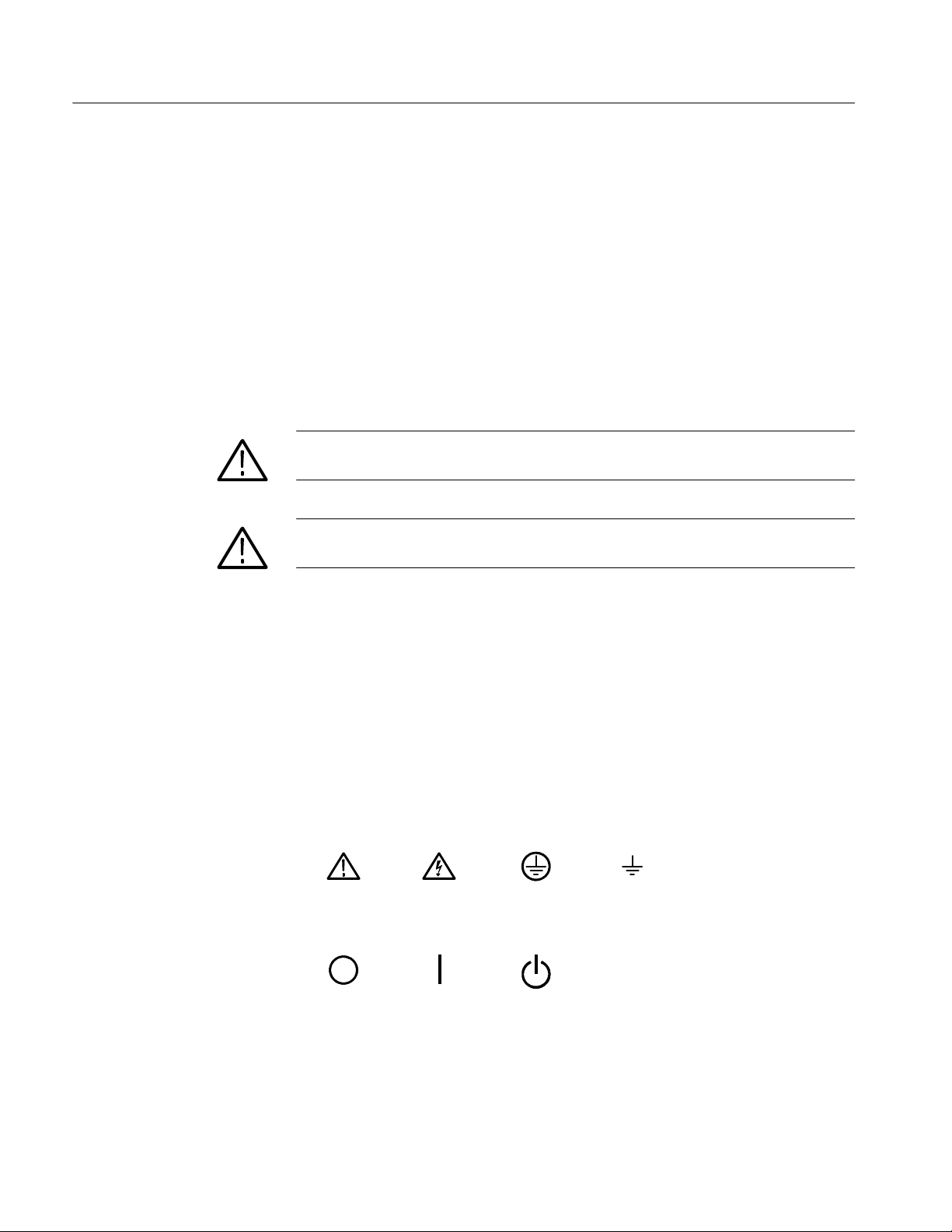
The following symbols may appear on the product:
xii
CAUTION
Refer to Manual
Mains Disconnected
OFF (Power)
WARNING
High Voltage
Mains Connected
ON (Power)
Protective Ground
(Earth) Terminal
Standby
Earth Terminal
CSA7404B, TDS7704B , TDS7404B, TDS7254B & TDS7154B Service Manual
Page 17

Service Safety Summary
Only qualified personnel should perform service procedures. Read this Service
Safety Summary and the General Safety Summary before performing any service
procedures.
Do Not Service Alone. Do not perform internal service or adjustments of this
product unless another person capable of rendering first aid and resuscitation is
present.
Disconnect Power. To avoid electric shock, switch off the instrument power, then
disconnect the power cord from the mains power.
Use Care When Servicing With Power On. Dangerous voltages or currents may
exist in this product. Disconnect power, remove battery (if applicable), and
disconnect test leads before removing protective panels, soldering, or replacing
components.
To avoid electric shock, do not touch exposed connections.
CSA7404B, TDS7704B , TDS7404B, TDS7254B & TDS7154B Service Manual
xiii
Page 18

Service Safety Summary
xiv
CSA7404B, TDS7704B , TDS7404B, TDS7254B & TDS7154B Service Manual
Page 19

Environmental Considerations
This section provides information about the environmental impact of the
product.
Product End-of-Life
Handling
Observe the following guidelines when recycling an instrument or component:
Equipment Recycling. Production of this equipment required the extraction and
use of natural resources. The equipment may contain substances that could be
harmful to the environment or human health if improperly handled at the
product’s end of life. In order to avoid release of such substances into the
environment and to reduce the use of natural resources, we encourage you to
recycle this product in an appropriate system that will ensure that most of the
materials are reused or recycled appropriately.
The symbol shown to the left indicates that this product
complies with the European Union’s requirements
according to Directive 2002/96/EC on waste electrical and
electronic equipment (WEEE). For information about
recycling options, check the Support/Service section of the
Tektronix Web site (www.tektronix.com).
Mercury Notification. This product uses an LCD backlight lamp that contains
mercury. Disposal may be regulated due to environmental considerations. Please
contact your local authorities or, within the United States, the Electronics
Industries Alliance (www.eiae.org) for disposal or recycling information.
Restriction of Hazardous
Substances
CSA7404B, TDS7704B , TDS7404B, TDS7254B & TDS7154B Service Manual
This product has been classified as Monitoring and Control equipment, and is
outside the scope of the 2002/95/EC RoHS Directive. This product is known to
contain lead, cadmium, mercury, and hexavalent chromium.
xv
Page 20

Environmental Considerations
xvi
CSA7404B, TDS7704B , TDS7404B, TDS7254B & TDS7154B Service Manual
Page 21

Preface
Manual Structure
Manual Conventions
This is the service manual for the CSA7000B Communications Signal Analyzer
products and the TDS7000B Digital Oscilloscope products. Read this preface to
learn how this manual is structured, what conventions it uses, and where you can
find other information related to servicing this product. Read the Introduction
following this preface for safety and other important background information
needed before using this manual for servicing this product.
This manual is divided into chapters, which are made up of related subordinate
topics. These topics can be cross referenced as sections.
Be sure to read the introductions to all procedures. These introductions provide
important information needed to do the service correctly, safely, and efficiently.
This manual uses certain conventions that you should become familiar with
before attempting service.
Modules
Replaceable Parts
Safety
Throughout this manual, any replaceable component, assembly, or part is
referred to by the term module. A module is composed of electrical and
mechanical assemblies, circuit cards, interconnecting cables, and user-accessible
controls.
This manual refers to any field-replaceable assembly or mechanical part
specifically by its name or generically as a replaceable part. In general, a
replaceable part is any circuit board or assembly, such as the hard disk drive, or a
mechanical part, such as the I/O port connectors, that is listed in the replaceable
parts list of Chapter 10.
Symbols and terms related to safety appear in the General Safety Summary found
at the beginning of this manual.
CSA7404B, TDS7704B , TDS7404B, TDS7254B & TDS7154B Service Manual
xvii
Page 22

Preface
Related Documentation
The following related manuals are available for this instrument:
H CSA7000B & TDS7000B User manual. Tektronix part number
071-1227-XX.
H CSA7000B & TDS7000B Reference manual. Tektronix part number
071-0880-XX.
H CSA7000, TDS7000, TLA600 & OTS9000 Series Rackmount Kit
(Option 1R) Instructions. Tektronix part number 071-0716-XX.
xviii
CSA7404B, TDS7704B , TDS7404B, TDS7254B & TDS7154B Service Manual
Page 23

Specifications
Page 24

Page 25

Specifications
This chapter contains the specifications for the CSA7000B Series Communications Signal Analyzers and the TDS7000B Series Digital Phosphor Oscilloscopes. All specifications are guaranteed unless labeled “typical.” Typical
specifications are provided for your convenience but are not guaranteed.
Specifications that are marked with the n symbol are checked in chapter four,
Performance Verification, of the service manual.
All specifications apply to all models unless noted otherwise. To meet specifications, the following conditions must be met:
H The instrument must have been calibrated in an ambient temperature
between 20 °C and 30 °C(68°F and 86 °F).
H The instrument must be operating within the environmental limits listed in
Table 1--12 on page 1--27.
H The instrument must be powered from a source that meets the specifications
listedinTable1--10onpage1--25.
H The instrument must have been operating continuously for at least 20 min-
utes within the specified operating temperature range.
H You must perform the S ignal Path Compensation procedure after the
20-minute warm-up period, and the ambient temperature must not change
more than 5 °C without first repeating the procedure. See Run the signal
path compensation routine on page 4--6 for instructions to perform this
procedure.
H You must perform the S ignal Path Compensation procedure after the
20-minute warm-up period, and if the ambient temperature changes more
than 5 °C(41°F), repeat the procedure.
CSA7404B, TDS7704B , TDS7404B, TDS7254B & TDS7154B Service Manual
1- 1
Page 26

Specifications
Product and Feature Description
Your instrument is shown in Table 1--1.
Table 1- 1: Instrument models
Acquisition Features
Number of
Model
TDS7704B 4 7GHz 20 GS/s
CSA7404B 4 4GHz 20 GS/s
TDS7404B 4 4GHz 20 GS/s
TDS7254B 4 2.5 GHz 20 GS/s
TDS7154B 4 1.5 GHz 20 GS/s
channels
Bandwidth
Maximum sample
rate (real time)
Separate Digitizers. Ensure accurate timing measurements with separate digitizers
for each channel. Acquisition on multiple channels is always concurrent. The
digitizers can also be combined to yield a higher sample rate on a single channel.
Fast Acquisition. Acquire up to 400,000 waveforms per second to see rapidly
changing signals or intermittent signal irregularities.
Long Record Lengths. Choose record lengths from 500 points up to
500,000 points per channel (up 2,000,000 points on a single channel). Extend the
maximum record length up to a maximum of 64,000,000 points with memory
options.
1- 2
Peak Detect Acquisition Mode. See pulses as narrow as 400 ps even at the slower
time base settings. Peak detect helps you see noise and glitches in your signal.
Acquisition Control. Acquire continuously or set up to capture single shot
acquisitions. Enable or disable optional acquisition features such as equivalent
time or roll mode. Use Fast Frame acquisition to capture and time stamp many
events in a rapid sequence.
Horizontal Delay. Use delay when you want to acquire a signal at a significant
time interval after the trigger point. Toggle delay on and off to quickly compare
the signal at two different points in time.
CSA7404B, TDS7704B , TDS7404B, TDS7254B & TDS7154B Service Manual
Page 27

Specifications
Optical-to-Electrical Converter. CSA7000B Series only. Test optical signals using
the integrated optical-to-electrical converter and a fully calibrated signal path.
Recovered clock and data signals are available. Optical reference receivers are
available for selected optical communications standards.
Signal Processing
Features
Display Features
Average, Envelope, and Hi Res Acquisition. Use Average acquisition mode to
remove uncorrelated noise from your signal. Use Envelope to capture and
display the maximum variation of the signal. Use Hi Res to increase vertical
resolution for lower bandwidth signals.
Waveform Math. Set up simple math waveforms using the basic arithmetic
functions or create more advanced math waveforms using the math expression
editor. Waveform expressions can even contain measurement results and other
math waveforms.
Spectral Analysis. Display spectral magnitude and phase waveforms based on
your time-domain acquisitions. Control the instrument using the traditional
spectrum analyzer controls such as span and center frequency.
Color LCD Display. Identify and differentiate waveforms easily with color coding.
Waveforms, readouts, and inputs are color matched to increase productivity and
reduce operating errors. Enhance visualization of waveforms with color grading.
Digital Phosphor. The instrument can clearly display intensity modulation in your
signals. The instrument automatically overlays subsequent acquisitions and then
decays them to simulate the writing and decay of the phosphor in an analog
instrument CRT. The feature results in an intensity-graded or color-graded
waveform display that shows the information in the intensity modulation.
Fit to Screen. The Digital Phosphor technology performs the compression
required to represent all record points on the screen, even at the maximum record
length settings.
MultiView Zoom. To take advantage of the full resolution of the instrument you
can zoom in on a waveform to see the fine details. Both vertical and horizontal
zoom functions are available. Zoomed waveforms can be aligned, locked, and
automatically scrolled.
Measurement Features
CSA7404B, TDS7704B , TDS7404B, TDS7254B & TDS7154B Service Manual
Cursors. Use cursors to take simple voltage, time, and frequency measurements.
1- 3
Page 28

Specifications
Automatic Measurements. Choose from a large palette of amplitude, time, and
histogram measurements. You can customize the measurements by changing
reference levels or by adding measurement gating.
Mask Testing. Optional on TDS7000B Series. Provides mask testing for verifying
compliance to optical (CSA7000B Series only) and electrical standards. Optical
mask testing uses integrated reference receivers.
Trigger Features
Convenience Features
Simple and Advanced Trigger Types. Choose simple edge trigger or choose from
eight advanced trigger types to help you capture a specific signal fault or event.
Dual Triggers. Use the A (main) trigger system alone or add the B trigger to
capture more complex events. You can use the A and B triggers together to set
up a delay-by-time or delay-by-events trigger condition.
Comm Triggers. Optional on TDS7000B Series. Use comm triggers to trigger on
communication signals.
Serial Triggers. Optional on TDS7000B Series. Use serial triggers to trigger on
serial pattern data.
Recovered Clock and Data Triggers. Use recovered clock and data internally to
trigger your waveforms. They are also available externally (CSA7000B Series
only).
Autoset. Use Autoset to quickly set up the vertical, horizontal, and trigger
controls for a usable display. If a standard mask is active (optional on TDS7000B
Series), Autoset adjusts the selected waveform to match the mask, if possible.
1- 4
Touch Screen Interface. You can operate all instrument functions (except the
power switch and the touch screen enable/disable switch) from the touch screen
interface. If convenient, you can also install a mouse and keyboard to use the
interface.
Toolbar or Menu Bar. You can choose a toolbar operating mode that is optimized
for use with the touch screen, or a PC-style menu bar operating mode that is
optimized for use with a mouse.
CSA7404B, TDS7704B , TDS7404B, TDS7254B & TDS7154B Service Manual
Page 29
Specifications
Open Desktop. The instrument is built on a Microsoft Windows software
platform; the instrument application program starts automatically when you
apply power to the instrument. You can minimize the instrument application and
take full advantage of the built-in PC to run other applications. Moving
waveform images and data into other applications is as simple as a copy/paste
operation.
Dedicated Front Panel Controls. The front panel contains knobs and buttons to
provide immediate access to the most common instrument controls. Separate
vertical controls are provided for each channel. The same functions are also
available through the screen interface.
Data Storage and I/O. The instrument has a removeable hard disk drive, a
CD-RW, and a floppy disk drive that can be used for storage and retrieval of
data. The instrument has GPIB, USB, Centronics, and Ethernet ports for input
and output to other devices.
Online Help. The instrument has a complete online help system that covers all
features. The help system is context sensitive; help for the displayed control
window is automatically shown if you touch the help button. Graphical aids in
the help windows assist you in getting to the information you need. You can also
access the help topics through a table of contents or index.
Specification Tables
Table 1- 2: Channel input and vertical specifications
Characteristic Description
Input channels Four
Input coupling Channel input is disconnected from input termination when using GND coupling.
DC 50 Ω and GND
nInput impedance, DC coupled
50 Ω ±2.5% at 25 _C(77_F), ±0.2% over 0 to 50 _C (122 _F)
VSWR, typical
CSA7404B, TDS7404B, CSA7154, &
TDS7154B
TDS7704B
1.5 for fin<1 GHz
1.7 for f
2.0 for f
<100 mV/div ≥100 mV/div
1.5 for f
2forf
2.5 for f
<2.5 GHz
in
<4 GHz
in
<2 GHz 1.1 for fin<2 GHz
in
<3 GHz 1.2 for fin<3 GHz
in
<6 GHz 1.3 for fin<6 GHz
in
CSA7404B, TDS7704B , TDS7404B, TDS7254B & TDS7154B Service Manual
1- 5
Page 30
Specifications
Table 1- 2: Channel input and vertical specifications (Cont.)
Characteristic Description
nMaximum input voltage, <1 V
CSA7404B, TDS7404B, CSA7154, &
<5 V
TDS7154B
for <100 mV/division settings and
RMS
for ≥100 mV settings
RMS
TDS7704B
<6.5 V
<6.0 V
for ≥100 mV settings for temperatrues ≤45 °C
RMS
for ≥100 mV settings for temperatrues >45 °C
RMS
Number of digitized bits 8bits
Sensitivity range Fine adjustment available with ≥1% resolution
2 mV/div to 1 V/division, in a 1-2-5 sequence
nDC gain accuracy Net offset is the nominal voltage that must be applied to the channel to bring the
trace to center screen. Net offset = offset -- (position × volts/division) and is
expressed in volts
TDS7704B 2mV/divto3.98mV/div (3% +(6% × | net offset/1V | ))
4 mV/div to 99.5 mV/div (2.5% +(2% × | net offset/1V | ))
100 mV/div to 1 V/div (2.5% +(2% × | net offset/10V | ))
1- 6
CSA7404B, TDS7704B , TDS7404B, TDS7254B & TDS7154B Service Manual
Page 31

Table 1- 2: Channel input and vertical specifications (Cont.)
a
Characteristic Description
CSA7404B, TDS7404B, TDS7254B, &
TDS7154B
2mV/divto3.98mV/div (2.5% +(6% × | net offset/1V | ))
4 mV/div to 99.5 mV/div
100 mV/div to 1 V/div (2% +(2% × | net offset/10V | ))
Specifications
(2% +(2% × | net offset/1V | ))
n DC voltage measurement accuracy
CSA7404B, TDS7404B, TDS7254B, &
TDS7154B
Average acquisition mode (≥16 averages)
Delta voltage measurement between any
two averages of ≥16 waveforms
acquired under the same setup and
mbientconditions
Measurement type DC accuracy (in volts)
2mV/divto3.98mV/div ±[(2.5% +(6% × | net offset/1V | )) ×
| reading -- net offset | + offset accuracy
+ 0.08 division × V/division]
4 mV/div to 99.5 mV/div ±[(2% +(2% × | net offset/1V | )) × |
reading -- net offset | + offset accuracy
+ 0.08 division × V/division]
≥100 mV/div ±[(2% +(2% × | net offset/10V | )) ×
| reading -- net offset | + offset accuracy
+ 0.08 division × V/division]
2mV/divto3.98mV/div ±[(2.5% +(6% × | net offset/1V | )) × |
reading | + 0.16 division × V/division
setting]
4 mV/div to 99.5 mV/div
100 mV/div to 1 V/div ±[(2% +(2% × | net offset/10V | )) ×
Net offset is the nominal voltage that must be applied to the channel to bring the
trace to center screen. Net offset = offset -- ( position × volts/division) and is
expressed in volts
±[(2% +(2% × | net offset/1V | )) ×
| reading | + 0.16 division ×
V/division setting]
| reading | + 0.16 division ×
V/division setting]
n DC voltage measurement accuracy,
TDS7704B
Average acquisition mode
(≥16 averages)
CSA7404B, TDS7704B , TDS7404B, TDS7254B & TDS7154B Service Manual
Measurement type DC accuracy (in volts)
2mV/divto3.98mV/div ±[(3% +(6% × | net offset/1V | )) ×
| reading -- net offset | + offset accuracy
+ 0.08 division × V/division]
4 mV/div to 99.5 mV/div ±[(2.5% +(2% × | net offset/1V | )) ×
| reading -- net offset | + offset accuracy
+ 0.08 division × V/division]
100 mV/div to 1 V/div ±[(2.5% +(2% × | net offset/10V | ))
× | reading -- net offset | + offset
accuracy + 0.08 division × V/division]
1- 7
Page 32

Specifications
a
Nonl
inearity,t
ypica
l<1digitizationlevel(DL),dif
f
tia
l
2DL
int
a
l,ind
tlybased
1
5°C(0°C
forTDS7154
B,andCSA7154)
to5
0°C(5
9°F
to122°F
),dera
tedby
Table 1- 2: Channel input and vertical specifications (Cont.)
Characteristic Description
Delta voltage measurement between any
two averages of ≥16 waveforms
acquired under the same setup and
mbientconditions
n Analog bandwidth DC 50 Ω coupling, Full bandwidth, TCA-SMA or TCA-N adapter, operating ambient
2mV/divto3.98mV/div ±[(3% +(6% × | net offset/1V | )) ×
| reading | + 0.16 division × V/division
setting]
4 mV/div to 99.5 mV/div
100 mV/div to 1 V/div ±[(2.5% +(2% × | net offset/10V | )) ×
Net offset is the nominal voltage that must be applied to the channel to bring the
trace to center screen. Net offset = offset -- ( position × volts/division) and is
expressed in volts
eren
°
°
30 MHz/°C below 15 °C(59°F)
±[(2.5% +(2% × | net offset/1V | )) ×
| reading | + 0.16 division ×
V/division setting]
| reading | + 0.16 division ×
V/division setting]
; ≤
egr
°
ependen
°
°
Analog bandwidth with P7240 active probe or
TCA-BNC adapter, typical
CSA7404B & TDS7404B
SCALE range Bandwidth
2mV/divto3.9mV/div DC to ≥1GHz
4mV/divto9.9mV/div DC to ≥1.25 GHz
≥10 mV/div TDS7704B
DC to 7 GHz,
DC to 7.25 GHz, typical
CSA7404B,& TDS7404B:
DC to 4 GHz
TDS7254B:
DC to ≥ 2.5 GHz
TDS7154B:
DC to 1.5 GHz
DC 50 Ω coupling, Full bandwidth, operating ambient 15 °Cto30°C(59°Fto
86 °F), derated by 20 MHz/°C above 30 °C(86°F)
SCALE range
2mV/divto3.9mV/div DC to 1 GHz
4mV/divto9.9mV/div DC to 1.25 GHz
≥10 mV/div DC to 4 GHz
Bandwidth
1- 8
CSA7404B, TDS7704B , TDS7404B, TDS7254B & TDS7154B Service Manual
Page 33

Table 1- 2: Channel input and vertical specifications (Cont.)
Characteristic Description
Analog bandwidth with P7330 active probe,
typical
CSA7404Band TDS7404B
DC 50 Ω coupling, Full bandwidth, operating ambient 15 °Cto30°C, derated by
20 MHz/°C above 30 °C
SCALE range
2mV/divto3.9mV/div DC to 1 GHz
4mV/divto9.9mV/div DC to 1.25 GHz
≥10 mV/div DC to 3.5 GHz
Specifications
Bandwidth
Analog bandwidth with P7260 active probe or
TCA-BNC adapter, typical
TDS7704B
Calculated rise time, typical
TDS7704B 62 ps
CSA7404B & TDS7404B 100 ps
CSA7154 130 ps
TDS7154B 200 ps
Step response settling errors, typical Full bandwidth
1
Operating ambient 15 °Cto30°C(59°Fto86°F) at V/div ≥10 mV/div, derated by
20 MHz/°C above 30 °C(86°F)
SCALE range
2mV/divto3.9mV/div DC to 1 GHz
4mV/divto9.9mV/div DC to 1.25 GHz
≥10 mV/div DC to 6 GHz
SCALE range and step amplitude Settling error at time after step
2 mV/div to 99.5 mV/div,
with ≤ 1.5 V step
100 mV/div to 1 V/div,
with ≤ 3Vstep
Bandwidth
20 ns: ≤ 2%
1ms:≤ 0.1%
20 ns: ≤ 2%
1ms:≤ 0.2%
CSA7404B, TDS7704B , TDS7404B, TDS7254B & TDS7154B Service Manual
1- 9
Page 34

Specifications
Table 1- 2: Channel input and vertical specifications (Cont.)
Characteristic Description
Pulse response, peak detect, or envelope mode Sample rate setting Minimum pulse width
2.5 GS/s or less 400 ps
Position range ± 5 divisions
Offset range
SCALE range Offset range
2mV/divto50mV/div ±0.50 V
50.5 mV/div to 99.5 mV/div ±0.25 V
100 mV/div to 500 mV/div ±5V
505 mV/div to 1 V/div ±2.5 V
n Offset accuracy Net offset is the nominal voltage that must be applied to the channel to bring the trace
to center screen. Net offset = offset -- ( position × volts/divisi on). Offset accuracy is
the accuracy of this voltage level.
CSA7404B, TDS7404B, CSA7154, &
TDS7154B
TDS7704B SCALE range Offset accuracy
SCALE range Offset accuracy
2mV/divto9.95mV/div
10 mV/div to 99.5 mV/div ±(0.35% ×| net offset | + 1.5 mV +
100 mV/div to 1 V/div ±(0.35% ×| net offset | + 15 mV +
2mV/divto9.95mV/div ±(0.35% ×| net offset | + 1.5 mV +
10 mV/div to 99.5 mV/div ±(0.5% ×| net offset | + 1.5 mV +
100 mV/div to 1 V/div ±(0.5% ×| net offset | + 15 mV + 0.1 div
±(0.2% ×| net offset | + 1.5 mV +
0.1 div ×V/div setting)
0.1 div ×V/div setting)
0.1 div ×V/div setting)
0.1 div ×V/div setting)
0.1 div ×V/div setting)
×V/div setting)
1- 10
CSA7404B, TDS7704B , TDS7404B, TDS7254B & TDS7154B Service Manual
Page 35

Table 1- 2: Channel input and vertical specifications (Cont.)
Characteristic Description
Effective bits, typical
Specifications
CSA7404B, TDS7704B, TDS7404B,
CSA7154, & TDS7154B
n Delay between channels ≤ 30 ps between any two channels with the same scale and coupling settings
n Channel-to-channel crosstalk
Nine division sine wave input at the indicated f requency, sampled at 50 mV/division
and 20 GS/s
Input frequency Effective bits
1MHz 6.0 bits
1GHz 5.7 bits
1.5 GHz 5.5 bits
2 GHz, CSA7404B, TDS7404B,
TDS7704B & CSA7154 only
2.5 GHz, CSA7404B, TDS7704B,
TDS7404B & CSA7154 only
3 GHz, CSA7404B, TDS7704B &
TDS7404B only
4 GHz, CSA7404B, TDS7704B &
TDS7404B only
5 GHz, TDS7704B only 4.5 bits
6 GHz, TDS7704B only 3.5 bits
7 GHz, TDS7704B only 3.0 bits
5.3 bits
5.2 bits
5.1 bits
4.9 bits
≥15:1 at rated bandwidth (CSA7404B, TDS7704B, TDS7404B & CSA7154 only),
and
≥ 80:1 at ≤1.5 GHz or the rated bandwidth, whichever is less.
Assumes two channels with the same scale settings
1
Rise time calculation: A simple formula relating these times to bandwidth for all instruments is not available. The
instruments have been characterized with the typical rise times listed.
Table 1- 3: Horizontal and acquisition system specifications
Characteristic Description
Real-time sample rate range Number of channels acquired Sample rate range
1 5 S/s to 20GS/s
2 5 S/s to 10GS/s
3or4 5 S/s to 5GS/s
CSA7404B, TDS7704B , TDS7404B, TDS7254B & TDS7154B Service Manual
1- 11
Page 36

Specifications
1,000,000points(
1or2ch
a
ly)
Table 1- 3: Horizontal and acquisition system specifications (Cont.)
Characteristic Description
Equivalent-time sample rate or interpolated
waveform rate range
Acquisition modes Sample, Peak detect, Hi Res, Average, Envelope, and Waveform database
Minimum record length 500 points
Maximum record length, sample mode Depends on the number of active channels and the record length options installed.
Standard 500,000 points (3 or 4 channels)
Option 2M installed 2, 000,000 points (3 or 4 channels)
Option 3M installed 4, 000,000 points (3 or 4 channels)
Equivalent-time acquisition can be enabled or disabled. When disabled, waveforms
are interpolated at the fastest time base settings.
10GS/s to 1TS/s
Maximum record length is less in serial trigger mode
nnelson
2,000,000 points (1 channel only)
4,000,000 points (1 or 2 channels onl y)
8,000,000 points (1 channel only)
8,000,000 points (1 or 2 channels onl y)
16,000,000 points (1 channel only)
Option 4M installed 8, 000,000 points (3 or 4 channels)
16,000,000 points (1 or 2 channels onl y)
32,000,000 points (1 channel only)
Option 5M installed 16, 000,000 points (3 or 4 channels)
32,000,000 points (1 or 2 channels onl y)
64,000,000 points (1 channel only)
1- 12
CSA7404B, TDS7704B , TDS7404B, TDS7254B & TDS7154B Service Manual
Page 37

Specifications
dependingonmemoryoptioninstalle
d
Table 1- 3: Horizontal and acquisition system specifications (Cont.)
Characteristic Description
Maximum record length, HiRes mode, sample
rate ≤1.25 GS/s
Seconds/division range 50 ps/div to 10 s/div
Maximum FastFrame update rate, nominal 265,000 frames per second
Frame length and maximum number of frames Maximum number of frames for Sample or Peak Detect acquisition mode,
2,000,000 points (1, 2, 3, or 4 channels)
Frame length Maximum number of frames
50 points Standard: 648--5872
Option 2M: 2660--24088
Option 3M: 5321--48192
Option 4M: 5321--48192
Option 5M: 10644--96408
500 points Standard: 580--3560
Option 2M: 2381--14632
Option 3M: 4765--29272
Option 4M: 4765--29272
Option 5M: 9531--58552
5000 points Standard: 163--720
Option 2M: 669--2968
Option 3M: 1339--5936
Option 4M: 1339--5936
Option 5M: 2679--11880
50,000 points Standard: 19--80
Option 2M: 81--328
Option 3M: 163--656
Option 4M: 163--656
Option 5M: 327--1320
500,000 points Standard: 2--8
Option 2M: 8--32
Option 3M: 16--64
Option 4M: 16--64
Option 5M: 32--128
CSA7404B, TDS7704B , TDS7404B, TDS7254B & TDS7154B Service Manual
1- 13
Page 38

Specifications
Table 1- 3: Horizontal and acquisition system specifications (Cont.)
Characteristic Description
Update rate, maximum Fast Acquisition on: 400,000 waveforms per second
Fast Acquisition off: 60 waveforms per second
n Internal time-base reference frequency 10 MHz 2.5 ppm over any ≥100 ms interval. Aging <1 ppm per year
n Long term sample rate and del ay time
±2.5 ppm over any ≥100 ms interval. Aging <1 ppm per year
accuracy
Aperture uncertainty, typical Short term:
≤2 ps rms, records having duration ≤100 ms.
≤800 fs rms, records having duration ≤10 s
Long term:
≤15 parts per trillion rms, records having duration ≤1 minute
Time base delay time range 5nsto250s
n Delta time measurement accuracy For a single channel, with signal amplitude > 5 divisions, reference level set at 50%,
interpolation set to sin(x)/x, with risetime >1.4×T
is greater) and acquired ≥10 mV/Div, where T
and <4×Tsor 150 ps (whichever
s
is the sample period. RMS
s
specification is typical.
Conditions Accuracy
Single shot signal, Sample acquisition
mode, Full bandwidth
± (0.06/sample rate +2.5 ppm ×
| reading | ) RMS
± (0.3/sample rate +2.5 ppm ×
| reading |) peak
Average acquisition mode, >100 aver-
± (4 ps +2.5 ppm × | reading | ) peak
ages, Full bandwidth
1- 14
CSA7404B, TDS7704B , TDS7404B, TDS7254B & TDS7154B Service Manual
Page 39

Table 1- 4: Trigger specifications
c
c
a
Characteristic Description
Trigger jitter, typical
TDS7704B 1.2 ps rms for low frequency, fast rise time signal
CSA7404B & TDS7404B 1.5 ps rms for low frequency, fast rise time signal
CSA7154, & TDS7154B 2 ps rms for low frequency, fast rise time signal
n Edge Trigger Sensitivity All sources, for vertical scale settings ≥10 mV/div and ≤1V/div
Trigger Source Sensitivity
Main trigger, DC coupled ≤0.5 div from DC to 50 MHz
CSA7404B, TDS7704B, TDS7404B
≤1.5 div at 3 GHz
TDS7254B:
≤1 div at 2.5 GHz
TDS7154B
≤1 div at 1.5 GHz
Specifications
Edge Trigger Sensitivity, either slope, DC
oupled, typi
l
Delayed trigger, DC coupled ≤0.5 div from DC to 50 MHz
CSA7404B, TDS7704B, TDS7404B
≤1.5 div at 3 GHz
TDS7254B:
≤1 div at 2.5 GHz
TDS7154B
≤1 div at 1.5 GHz
Auxiliary input, DC coupled ≤150 mV from DC to 50 MHz, increas-
ing to 500 mV at 2.5 GHz (typical
between 2 and 2.5 GHz)
All sources, for vertical scale settings ≥10 mV/div and ≤1V/div
Trigger coupling
DC ≤0.5 div from DC to 50 MHz
NOISE REJ 3×the DC-coupled limits
AC Same as DC-coupled limits for frequen-
HF REJ Same as DC-coupled limits for frequen-
Sensitivity
≤1 div at 1.25 GHz
cies >100 Hz, attenuates signals
<100 Hz
cies <20 kHz, attenuates signals
>20 kHz
LF REJ Same as DC-coupled limits for frequen-
cies >200 kHz, attenuates signals
<200 kHz
CSA7404B, TDS7704B , TDS7404B, TDS7254B & TDS7154B Service Manual
1- 15
Page 40

Specifications
Table 1- 4: Trigger specifications (Cont.)
Characteristic Description
Edge trigger sensitivity, 4 GHz, typical
CSA7404B, TDS7704B, TDS7404B CH1 — CH4
Trigger coupling Sensitivity
Main trigger, DC coupled 2.7 divisions at 4 GHz
Edge trigger sensitivity, not DC coupled, typical All sources, for vertical scale settings ≥10 mV/div and ≤1V/div
Trigger coupling Sensitivity
NOISE REJ 3×the DC-coupled limits
AC Same as DC-coupled limits for frequen-
cies >100 Hz, attenuates signals
<100 Hz
HF REJ Same as DC-coupled limits for frequen-
cies <20 kHz, attenuates signals
>20 kHz
LF REJ Same as DC-coupled limits for frequen-
cies >200 kHz, attenuates signals
<200 kHz
Auxiliary trigger input characteristics, typical 50 Ω ±10%, ±5 V (DC + peak AC)
Lowest frequency for Set Level to 50%, typical 50 Hz
Advanced trigger sensitivity, typical For vertical scale settings 10 mV/div and 1 V/div
Advanced triggers: 1.0 div, from DC to 1 GHz at the TekConnect connector
Advanced trigger timing For vertical scale settings 10 mV/div and 1 V/div
Minimum recognizable event width or
time
Glitch type Minimum glitch width = 225 ps
(170 ps on the TDS7704B)
Runt type Minimum runt width = 225 ps 250 ps
Time-qualified runt type Minimum runt width = 340 ps 450 ps
Width type Minimum difference between upper and
lower limits = 225 ps
Window type 225 ps 300 ps
Minimum rearm time to recognize next
event
250 ps
250 ps
1- 16
CSA7404B, TDS7704B , TDS7404B, TDS7254B & TDS7154B Service Manual
Page 41

Table 1- 4: Trigger specifications (Cont.)
Characteristic Description
Transition type Minimum transition time = 0 ps 225 ps
Timeout type Minimum timeout time = 340 ps 450 ps
Logic or state type, typical Minimum event width = 100 ps 500 ps
Specifications
Setup/Hold type, typical Minimum clock pulse width from active
edge to inactive edge
500 ps + hold time setting for times ≥0
1.5 ns + hold time setting for times <0
Advanced trigger timer ranges Limits
Glitch type 340 ps to 1 s
Runt type, time qualified 340 ps to 1 s
Width type 340 ps to 10 s
Timeout type 340 ps to 1 s
Transition type 340 ps to 1 s
Pattern type 340 ps to 1 s
Window type 340 ps to 1 s
Setup/Hold type Setup and Hold timers Limits
Setup time (time from data transition to
clock edge)
Hold time (time from clock edge to data
transition)
Setup time + Hold time (algebraic sum of
the two settings)
Minimum clock pulse width from inactive
edge to active edge
500 ps
--100 ns to +100 ns
--1 ns to +102 ns
500 ps
Logic-qualified pulse-type trigger minimum
timing requirements
Glitch 100 ps 40 ps 60 ps
Runt Runt width + 150 ps 160 ps --16 ps
Time-qualified runt Runt width + 330 ps 160 ps 175 ps
Width 190 ps 40 ps 175 ps
Transition 330 ps 225 ps 175 ps
Window 190 ps --20 ps 0 ps
Minimum event duration Setup time Hold time
CSA7404B, TDS7704B , TDS7404B, TDS7254B & TDS7154B Service Manual
1- 17
Page 42

Specifications
Table 1- 4: Trigger specifications (Cont.)
Characteristic Description
n Time-qualified trigger timer accuracy For Glitch, Timeout, or Width types
Time range Accuracy
340 ps to 1.5 s
(360 ps to 1.8 ns typical)
1.5 sto1s ±91 ns
Trigger level or threshold range Trigger Source Sensitivity
Any channel ±12 divisions from center of screen
Auxiliary input ±5V
Line ±0 V, not settable
Trigger level or threshold accuracy, typical Edge trigger, DC coupling, for signals having rise and fall times ≤1ns
Trigger Source Accuracy
Any channel ± [(2% × | setting -- net offset | ) +
Auxiliary Not specified
where, net offset = offset -- ( position × volts/division)
B Event (Delayed) trigger Trigger After Time Trigger on nthEvent
Range Delay time = 5 ns to 250 s Event count = 1 to 10
Minimum pulse width, typical — 250 ps
Minimum time between events, typical — 1ns
±5% of setting
(0.35 div × volts/div setting) + offset
accuracy] (≥ 10 mV/div only)
7
Trigger position error, typical Edge trigger, DC coupling, for signals having a slew rate at the trigger point of ≥ 0.5
division/ns
Acquisition mode Error
Sample, Average ± (1 waveform interval + 200 ps)
Peak Detect, Envelope ± (2 waveform interval + 200 ps)
Trigger holdoff range 250 ns to 12 s plus random holdoff, if enabled.
Minimum resolution is 8 ns for settings ≤1.2 s. A dither of 800 ps is added to the
holdoff setting
1- 18
CSA7404B, TDS7704B , TDS7404B, TDS7254B & TDS7154B Service Manual
Page 43

Table 1- 5: Serial Trigger specifications (optional on TDS7000B Series)
Characteristic Description
Serial trigger number of bits 64
Serial trigger encoding types NRZ
nSerial trigger baud rate limits Up to 1.25 GBd
Specifications
Serial trigger, serial word recognizer position
accuracy
Clock recovery frequency range 1.5 MBd to 3.125 GBd. Above 1250 MHz the clock is only available internally as a
Clock recovery jitter, typical <0.25% bit period + 2 ps rms for PRBS data patterns.
Clock recovery tracking/acquisition range, typical ±2% of requested baud
Minimum signal amplitude needed for clock
recovery, typical
Edge trigger, DC coupling, for signals having a slew rate at the trigger point of ≥ 0.5
division/ns
Acquisition mode Error
Sample, Average ± (1 waveform interval + 200 ps)
Peak Detect, Envelope ± (2 waveform interval + 200 ps)
trigger source. Below 1250 MHz the cl ock is also available at the Recovered Clock
output along with regenerated data (CSA7000B Series only).
<0.25% bit period + 1.2 ps rms for repeating 01 data patterns.
1 division p-p up to 1.25 GBd
1.5 divisions p-p above 1.25 GBd
Table 1- 6: Display specifications
Characteristic Description
Display type 210.4 mm (8.3 in) (W)× 157.8 mm (6.2 in) (H), 263 mm (10.4 in) diagonal, liquid
crystal active-matrix color display
Display resolution 1024 horizontal × 768 vertical pixels
Pixel pitch 0.2055 mm horizontal, 0.2055 mm vertical
Response time, typical 15 ms, white to black
Display refresh rate 59.94 frames per second
Viewing angle, typical Horizontal: 60 degrees left, 60 degrees right
Vertical: 60 degrees up, 45 degrees down
Displayed intensity levels Each R-G-B input is 6 bits, giving 64 int ensity levels of each color component
CSA7404B, TDS7704B , TDS7404B, TDS7254B & TDS7154B Service Manual
1- 19
Page 44

Specifications
Table 1- 7: Input/output port specifications
Characteristic Description
Rear-panel I/O ports Ports located on the rear panel
Video output port Upper video port, DB-15 female connector, connect a second monitor to use
dual-monitor display mode. Video is DDC2B compliant.
Scope XGA video port Lower video port, DB-15 female connector, 31.6 kHz sync, EIA RS-343A
compliant, connect to show the instrument display, including live waveforms,
on an external monitor
Parallel port (IEEE 1284) DB-25 connector, supports the following modes:
standard (output only)
bidirectional (PS-2 compatible)
bidirectional enhanced parallel port (IEEE 1284
standard, mode 1 or mode 2, v 1.7)
bidirectional high-speed extended capabilities port (ECP)
Serial port DB-9 COM1 port, uses NS16C550-compatible UARTS, transfer speeds up to
115.2 kb/s
Keyboard port PS-2 compatible, instrument must be powered down to make connection
Mouse port PS-2 compatible, instrument must be powered down to make connection
LAN port RJ-45 connector, supports 10 base-T and 100 base-T
Audio ports Miniature phone jacks for stereo microphone input and stereo line output
USB ports, two Allows connection or disconnection of USB keyboard and/or mouse while
instrument power is on
GPIB port IEEE 488.2 st andard interface
1- 20
CSA7404B, TDS7704B , TDS7404B, TDS7254B & TDS7154B Service Manual
Page 45

Specifications
2
0mV/div±20%
intoa1MΩloa
d
Ana
logS
ignalOutputbandwidt
h,t
ypical1.8GHzintoa50Ωloa
d
Table 1- 7: Input/output port specifications (Cont.)
Characteristic Description
n Probe Compensator Output Front-panel BNC connector, requires Probe Cal Deskew Fixture for probe
attachment
Note: During probe calibration only, a relay switches a DC calibration voltage
to this output in place of the 1 kHz square wave. This voltage varies from
--10 V to +10 V with a source impedance less than 1 Ω and short circuit
current as high as 300 mA.
Output voltage Frequency
500 mV (from base to top) ± 20% into a 50 Ω
1 kHz ± 5%
load (Vol = --500 mV, Voh = 0 V typical)
1V(frombasetotop)± 20% into a 1 ΜΩ
load (Vol = --1.0 V, Voh = 0 V typical)
n Analog Signal Output amplitude BNC connector, provides a buffered version of the signal that is attached to
the channel 3 input when channel 3 is the trigger source
10 mV/div ± 20% into a 50 Ω load
Offset: between --100 mV and --170 mV into 50 Ω
n Auxiliary Output levels BNC connector, provides a TTL-compatible pulse (polarity selectable) for
each A or B trigger (selectable)
V
high V
out
≥2.5 V into open circuit,
≥1.0 V into 50 Ω load
low (true)
out
≤0.7 V with ≤4masink,
≤0.25 V into 50 Ω load
CSA7404B, TDS7704B , TDS7404B, TDS7254B & TDS7154B Service Manual
1- 21
Page 46

Specifications
Table 1- 7: Input/output port specifications (Cont.)
Characteristic Description
Auxiliary Output pulse width, typical Pulse width varies, 1 s minimum
External reference Run SPC whenever the external reference is more than 2000 ppm different
than the internal reference or the reference at which SPC was last run.
Frequency range 9.8 MHz to 10.2 MHz
nInput sensitivity ≥200 mV
Input voltage, maximum 7V
p-p
for frequencies between 9.8 MHz to 10.2 MHz
p-p
Input impedance 1.5 kΩ,Cin= 40 pF, measured at >100 kHz
nInternal reference output
Frequency 10 MHz 2.5 ppm over any ≥100 ms interval. Aging <1 ppm per year
Output voltage V
Serial data output baud rate range (CSA7000B Series
only)
Serial clock output frequency range (CSA7000B Series
only)
high V
out
≥2.5 V into open circuit,
≥1.0 V into 50 Ω load
low (true)
out
≤0.7 V with ≤4masink,
≤0.25 V into 50 Ω load
Fbaud <1250 MBd. Output swing of 1010 repeating pattern at this baud will
be at least 200 mV into 50 Ω.
Peak-to-peak output swing at 625 MHz is at least 200 mV p-p into 50 Ω.
Higher frequencies are further attenuated by approxim ately 6 dB per octave
above 625 MHz.
Use AC or DC coupled 50 Ω termination; AC coupling the clock provides
about 10% more amplitude.
Serial data and clock output voltages, typical
(CSA7000B Series only)
Voh=--1.0V
Vol = - -1.7 V
Assumes a load impedance greater than 1 kΩ.(50Ω source termination.)
If a 50 Ω or 75 Ω load is used, either use a DC blocking capacitor in series
with the signal or reference the termination to about --1.3 V. The signal
amplitude will be correspondingly reduced.
Serial data output latency, typical (CSA7000B Series
only)
1- 22
CSA7404B, TDS7704B , TDS7404B, TDS7254B & TDS7154B Service Manual
11 ns ±4 ns plus 35.5 clock cycles
Page 47

Table 1- 8: O/E converter (CSA7000B Series only)
W+(
fW/div
g
)
≤
1.1W+(
6.5%ofW/divsetting)
8
0
Specifications
Characteristic
Optical input connector Rifocs universal connector
O/E wavelength range 700 nm to 1650 nm
nO/E gain ≥0.27 V/mW (0.35 V/mW typical) at 780 nm ±20 nm
Optical Channel DC measurement accuracy, typical ±((2% +(2% ¢ net offset/1 mW)) ¢reading +(Position ¢ W/div) -- Offset
nOptical Channel Bandwidth (includes O/E,
O/E-to-TekConnect adaptor, and instrument)
DC conversion gain linearity <4mV/div: ±(4.5% + (6% × net offset))
1
Description
≥0.33 V/mW (0.40 V/mW typical) at 850 nm ±20 nm
≥0.64 V/mW (0.75 V/mW typical) at 1310 nm ±20 nm
≥0.64 V/mW (0.75 V/mW typical) at 1550 nm ±20 nm
Applies to graded index multimode fiber with core diamet er 62.5 m or smaller
at the input and O/E Electrical-to-CH1 Input adapter
+0.35% ¢ |Net Offset +3 W +0. 18 div ¢ W/div) only between 10 W/div
and 50 W/div inclusive. Average of ≥16 waveforms
The delta between any two averages of ≥16 waveforms acquired under the
same setup and ambient conditions:
±((2% +(2% × net offset/1 mW)) × reading +0.16 div × W/div)
Excludes normal variations due to fiber connection to the front of the instrument
5 _Cto25_C:
2.4 GHz
4 mV/div to 99.5 mV/div: ±(4% + (2% × net offset))
100 mV/div to 1.0 V/div: ±(4% + (2% × net offset/10))
Absolute maximum nondestructive optical input
Maximum nonsaturating linear response to transient
input, typical
Output zero (Dark level) ±(1.6 W +0.1 division × W/div) from 10 Wto50W per division vertical
nMaximum noise output, rms CSA7404B:
5 mW average;
10 mW peak at the wavelength with the highest relative responsivity
The transient optical signal response is linear (±6%) for <170 Waverage
input (340 W p) at 850 nm
<120 W average input (240 W p) at 1310 and 1550 nm
scale setting
1310 nm and 1550 nm
≤1.1
850 nm
≤2.1 W + (6.5% of W/div setting)
780 nm
≤2.6 W + (6.5% of W/div setting)
O/E converter alone
≤0.85 W
6.5% o
settin
CSA7404B, TDS7704B , TDS7404B, TDS7254B & TDS7154B Service Manual
1- 23
Page 48

Specifications
Table 1- 8: O/E converter (CSA7000B Series only) (Cont.)
Characteristic
1
Description
Optical return loss, typical With 50 m or 62.5 m core multimode fiber (CPC6):
>14 dB for 780 nm ±20 nm
>14 dB for 850 nm ±20 nm
With 9 m core singlemode fiber (SMF-28):
>28 dB for 1310 nm ±20 nm
>28 dB for 1550 nm ±20 nm
The return loss includes optical reflection contributions from the device under
test’s SC-SPC connector interface with the user’s PC style connector as well as
all other optical reflections from that interface up to and including the device
under test’s final photo diode termination.
Peak-to-peak aberrations in
response to falling edge, typical
Maximum falling edge 10% to 2% settling time
(ORR disabled), typical
Smallest average power for mask test (sensitivity),
typical
11% peak-to-peak total aberration (system including O/E-to-CH1 input adapter,
and instrument)
The step response to a fast opt ical square OFF edge reaches toc within 2% of
the final 0% level within 2 ns after the 10% transition point.
1310 nm and 1550 nm:
40 W peak-to-peak. 20 W (--17 dBm) average power assuming 50% average
duty cycle
780 nm and 850 nm:
80 W peak-to-peak. 40 W (--14 dBm) average power assuming 50% average
duty cycle
Assumes the scale factor is set to minimum W/div settings and signal is at
least 2 divisions peak-to-peak
Optical scale factor range 10 W per division to 500 W per division
Optical reference receiver typically available from the following scale factors:
1310 nm and 1550 nm:
13.5 W per division to 66 W per division
850 nm:
25 W per division to 125 W per division
780 nm:
28 W per division to 142 W per division
1
All specifications are with the O/E electrical out-to-CH1 input adapter installed.
1- 24
CSA7404B, TDS7704B , TDS7404B, TDS7254B & TDS7154B Service Manual
Page 49

Table 1- 9: Data storage specifications
Characteristic Description
Nonvolatile memory retention time, typical ≥ 5 years
Floppy disk 3.5 in floppy disk drive, 1.44 MB capacity
Hard disk Removeable hard disk drive, ≥ 20 GB capacity
CD-RW CD-RW drive
Windows memory 1GB
Table 1- 10: Power sour ce specifications
Characteristic Description
Power consumption ≤600 Watts (900 VA)
Source voltage and frequency 100 to 240 V 10%,50Hzto60Hz
Specifications
115 V 10%, 400 Hz
CAT II
Fuse rating Either one of the following sizes can be used, each size requires a different fuse
cap. Both fuses must be the same type. Line and Neutral are fused.
0.25 in × 1.25 in size UL198G and CSA C22.2, No. 59, fast acting: 8 A, 250 V
(Tektronix part number 159-0046-00, Bussman ABC-8, Littelfuse 314008)
5mm× 20 mm size IEC127, sheet 1, fast acting “F”, high breaking capacity: 6.3 A, 250 V (Tektronix part
number 159-0381-00, Bussman GDA 6.3, Littelfuse 21606.3)
CSA7404B, TDS7704B , TDS7404B, TDS7254B & TDS7154B Service Manual
1- 25
Page 50

Specifications
Table 1- 11: Mechanical specifications
Characteristic Description
Weight
Benchtop configuration 17.7 kg (39 lbs) instrument only
19.1 kg (42 lbs) with fully accessorized pouch
38.8 kg (85.5 lbs) when packaged for domestic shipment
Rackmount kit 18.6 kg (41 lbs) rackmounted instrument
5.6 kg (12.5 lbs) kit packaged f or domestic shipment
Dimensions
Benchtop configuration With front cover Without front cover
278 mm (10.95 in) height
330 mm (13 in) with feet extended
455 mm (17.9 in) width
435 mm (17.13 in) depth
Rackmount configuration (Option 1R) With rack handles Without rack handles
267 mm (10.5 in) height
502 mm (19.75 in) width
486 mm (19.13 in) depth
Cooling Fan-forced air circulation with no air fil ter
Required clearances To p 0mm(0in)
Bottom 19 mm (0.75 in) minimum or
Left side 76 mm (3 in)
Right side 76 mm (3 in)
Front 0mm(0in)
Rear 0 mm (0 in) on rear feet
Construction material Chassis parts are constructed of aluminum alloy, front panel is constructed of plastic
laminate, circuit boards are constructed of glass laminate, and the outer shell is
molded and textured from a polycarbonate/ABS blend
277 mm (10.9 in) height
330 mm (13 in) with feet extended
455 mm (17.9 in) width
426 mm (16.75 in) depth
267 mm (10.5 in) height
482 mm (19 in) width
435 mm (17.13 in) depth
0 mm (0 in) when standing on feet, flip
stands down
1- 26
CSA7404B, TDS7704B , TDS7404B, TDS7254B & TDS7154B Service Manual
Page 51

Specifications
Table 1- 12: Environmental specifications
Characteristic Description
Temperature, operating +5 °Cto+50 °C(41 °F to +122 °F), excluding floppy disk and compact disk drives
+10 °Cto+45 °C(50°Fto+113°F), including floppy disk and compact disk drives
Nonoperating -- 2 2 °Cto+60°C(71°F to +140 °F)
Humidity, operating 20% to 90% relative humidity with a maximum wet bulb temperature of +29 °C
(+84 °F) at or below +50 °C (+122 °F), noncondensing
Upper limit derates to 25% relative humidity at +50 °C (+122 °F)
Nonoperating With no diskette in floppy disk drive
20% to 90% relative humidity with a maximum wet bulb temperature of +29 °C
(+84 °F) at or below +60 °C (+140 °F), noncondensing
Upper limit derates to 20% relative humidity at +60 °C (+140 °F)
Altitude, operating 3,048 m (10,000 ft.)
Nonoperating 12,190 m (40,000 ft.)
Random vibration, operating 0.24 g
with floppy disk and compact disk installed
Nonoperating 2.28 g
from 5 Hz to 500 Hz, 10 minutes on each axis, 3 axis, 30 minutes total ,
RMS
from 5 Hz to 500 Hz, 10 minutes on each axis, 30 minutes total, 3 axi s
RMS
CSA7404B, TDS7704B , TDS7404B, TDS7254B & TDS7154B Service Manual
1- 27
Page 52

Specifications
Certifications and Compliances
EC Declaration of
Conformity - EMC
Meets intent of Directive 89/336/EEC for Electromagnetic Compatibility.
Compliance was demonstrated to the following specifications as listed in the
Official Journal of the European Communities:
EN 61326. EMC requirements for Class A electrical equipment for measurement,
control, and laboratory use. Annex D.
12
H IEC 61000--4--2. Electrostatic discharge immunity
H IEC 61000--4--3. RF electromagnetic field immunity
3
H IEC 61000--4--4. Electrical fast transient / burst immunity
H IEC 61000--4--5. Power line surge immunity
H IEC 61000--4--6. Conducted RF Immunity
3
H IEC 61000--4--11. Voltage dips and interruptions immunity
EN 61000- 3- 2. AC power line harmonic emissions
EN 61000- 3- 3. Voltage changes, fluctuations, and flicker
Australia / New Zealand
Declaration of Conformity
-EMC
Complies with EMC provision of Radiocommunications Act per these standard(s):
H AS/NZS 2064.1/2. Industrial, Scientific, and Medical Equipment: 1992
1
Emissions which exceed the levels required by this standard may occur when this
equipment is connected to a test object.
2
If interconnect cables are used, they must be low-EMI shielded cables such as the
following Tektronix part numbers or their equivalents: 012-0991-00, 012-0991-01,
012-0991-02 or 012-0991-03 GPIB Cable; 012-1213-00 (or CA part number 0294-9)
RS-232 Cable; 012-1214-00 Centronics Cable; or LCOM part number CTL3VGAMM-5 VGA
Cable.
3
Under these conditions, the specifications are amended as follows:
10 mV/division to 1 V/division: ≤0.4 division waveform displacement or ≤0.8 division
increase in peak-to-peak noise
5 mV/division and 2 mV/division, typical: ≤8 mV increase in peak-to-peak noise
1- 28
CSA7404B, TDS7704B , TDS7404B, TDS7254B & TDS7154B Service Manual
Page 53

Specifications
EC Declaration of
Conformity - Low Voltage
U.S. Nationally
Recognized Testing
Laboratory Listing
Canadian Certification
Additional Compliance
Equipment Type
Safety Class
Compliance was demonstrated to the following specification as listed in the
Official Journal of the European Communities:
Low Voltage Directive 73/23/EEC, amended by 93/68/EEC.
H EN 61010-1:2001. Safety requirements for electrical equipment for
measurement control and laboratory use.
H UL 61010B--1:2003. Standard for electrical measuring and test equipment.
H CAN/CSA C22.2 No. 1010.1:1997. Particular requirements for electrical
equipment for measurement, control, and laboratory use. Part 1.
H IEC 61010--1:2001. Safety requirements for electrical equipment for
measurement, control, and laboratory use.
Test and measuring equipment.
Class 1 -- grounded product
Pollution Degree
Descriptions
Pollution Degree
A measure of the contaminates that could occur in the environment around and
within a product. Typically the internal environment inside a product is
considered to be the same as the external. Products should be used only in the
environment for which they are rated.
H Polution Degree 1. No pollution or only dry, nonconductive pollution occurs.
Products in this category are generally encapsulated, hermetically sealed, or
located in clean rooms.
H Polution Degree 2. Normally only dry, nonconductive pollution occurs.
Occasionally a temporary conductivity that is caused by condensation must
be expected. This location is a typical office/home environment. Temporary
condensation occurs only when the product is out of service.
H Polution Degree 3. Conductive pollution, or dry, nonconductive pollution
that becomes conductive due to condensation. These are sheltered locations
where neither temperature nor humidity is controlled. The area is protected
from direct sunshine, rain, or direct wind.
H Polution Degree 4. Pollution that generates persistent conductivity through
conductive dust, rain, or snow. Typical outdoor locations.
Pollution Degree 2 (as defined in IEC 61010-1). Note: Rated for indoor use only.
CSA7404B, TDS7704B , TDS7404B, TDS7254B & TDS7154B Service Manual
1- 29
Page 54

Specifications
Installation (Overvoltage)
Category Descriptions
Overvoltage Category
Terminals on this product may have different installation (overvoltage) category
designations. The installation categories are:
H Measurement Category IV. For measurements performed at the source of
low-voltage installation.
H Measurement Category III. For measurements performed in the building
installation.
H Measurement Category II. For measurements performed on circuits directly
connected to the low-voltage installation.
H Measurement Category I. For measurements performed on circuits not
directly connected to MAINS.
Overvoltage Category II (as defined in IEC 61010-1)
1- 30
CSA7404B, TDS7704B , TDS7404B, TDS7254B & TDS7154B Service Manual
Page 55

Operating Information
Page 56

Page 57

Operating Information
This chapter covers installation information and basic operation instructions.
Installation
The basic operating software is already installed on the hard disk. Refer to
Software Installation on page 2--5 for instructions on reinstalling the software.
Before You Start
Environmental
Considerations
Verify that all parts and accessories for the instrument are available. Use the
graphical packing list that came with the oscilloscope to determine the necessary
parts and accessories. Y ou should also verify that the following items are
available:
H The correct power cords
H The product-software CD set that includes installation copies of the software
installed on the instrument
H All the accessories necessary to operate the instrument
The instrument is designed to operate on a bench or on a cart in the normal
position (on the bottom feet). For proper cooling, at least three inches (7.62 cm)
of clearance is required on both sides of the instrument, and the bottom requires
the clearance provided by the instrument feet.
If you operate the instrument while it is resting on the rear feet, make sure that
you properly route any cables coming out of the rear of the instrument to avoid
damaging them.
CAUTION. Keep the bottom and sides of the instrument clear of obstructions to
ensure proper cooling.
Tables 1--10 and 1--12 on pages 1--25 and 1--27 list the operating requirements
for the instrument. Power source, temperature, humidity, and altitude are listed.
Connect the Peripherals
CSA7404B, TDS7704B , TDS7404B, TDS7254B & TDS7154B Service Manual
The peripheral connections are the same as those you would make on a personal
computer. The connection points are shown in Figure 2--1 on page 2--3. See
Table 2--1 for additional connection information.
2- 1
Page 58

Operating Information
Table 2- 1: Additional accessory connection information
Item Description
Monitor If you use a non-standard monitor, you may need to change the
the display settings to achieve the proper resolution for your
monitor.
Printer Connect the printer to the EPP (enhanced parallel port)
connector directly. If your printer has a DB-25 connector, use
the adapter cable that came with your printer to connect to the
EPP connector. For information on printer usage, see Printing
Waveforms in your user instrument manual.
Rackmount Refer to the CSA7000 & TDS7000B Series Rackmount
Installation Instructions for information on installing the
rackmount kit.
Other Refer to the Application release notes on your product CD set
for possible additional accessory installation information not
covered in this manual.
WARNING. Before installing accessories to connectors (mouse, keyboard, etc.),
power off the instrument. See Powering Off the Instrument on page 2--5.
2- 2
CSA7404B, TDS7704B , TDS7404B, TDS7254B & TDS7154B Service Manual
Page 59

Description Icon/Label Locations
Mouse.................
Keyboard ................
RS-232..........
Printer.............
XVGA Out (PC only,
for dual display
operation) .........
Compactdiskdrive.......
USB..................
Operating Information
Mic......... .... ....
Audio line out.............
Audio line in .............
Removable hard drive or
floppy ...................
Instrument monitor
(large-screen instrument
display)...........
GPIB........
Network................
Figure 2- 1: Locations of peripheral connectors on rear panel
CSA7404B, TDS7704B , TDS7404B, TDS7254B & TDS7154B Service Manual
2- 3
Page 60

Operating Information
Power On the Instrument
Follow these steps to power on the instrument.
1. Check that the line fuses are correct for your application. Both fuses must be
the same rating and type. Fuse types require a unique cap and fuseholder. See
Table 2--2 and Figure 2--2.
Table 2- 2: Line fuses
Cap & fuseholder
Fuse type Rating Fuse part number
0.25 x 1.250 inch 8 A, fast blow, 250 V 159-0046-00 200-2264-00
5x20mm 6.3 A, fast blow, 250 V 159-0381-00 200-2265-00
Fuses AC powerPower switch
part number
Figure 2- 2: Line fuse and power cord connector locations, rear panel
CAUTION. Connect the keyboard, mouse, and other accessories before applying
power to the product.
2. Connect the power cord.
3. If you have an external monitor, connect the power cord and power on the
monitor.
4. Turn the Power switch on at the rear panel. (See Figure 2--2 for switch
location.)
5. If the instrument does not power on, press the On/Standby switch to power
on the instrument (see Figure 2--3 for the switch location).
6. Wait for the boot routine and low-level self test to complete.
2- 4
CSA7404B, TDS7704B , TDS7404B, TDS7254B & TDS7154B Service Manual
Page 61

On/Standby
switch
Operating Information
Figure 2- 3: On/Standby switch location
Powering Off the
Instrument
Software Installation
The instrument has a built-in On/Standby function that removes power from
most circuitry in the instrument when you press the On/Standby switch.
To completely remove power to the instrument, perform the shutdown just
described, and then set the power switch on the rear panel to off.
This section describes how to install the system software found on the productsoftware CD that accompanies this product. The instrument ships with the
product software installed, so only perform these procedures if reinstallation
becomes necessary .
Software Release Notes. Read the software release notes README.TXT ASCII
file on the product-software CD before performing installation procedures. This
file contains additional installation and operation information that supercedes
other product documentation.
To view the README.TXT file, open the Notepad Windows accessory and open
the file on the product-software CD. After installation, you can also read the
copy from a directory on the product:
C:\Program Files\TekScope\ReadMe.txt
Operating System Restoration. Use the procedure that accompanies your
Operating System Restore CD should reinstalling system software become
necessary.
The compact disc contains the files necessary to restore the Windows operating
system and necessary drivers for the instrument.
The Windows operating system and drivers are factory installed on the instrument hard disk. The compact disc serves as a backup in the event that you have
to rebuild the hard drive. You must restore the Windows operating system before
you can install the oscilloscope firmware and other product software.
CSA7404B, TDS7704B , TDS7404B, TDS7254B & TDS7154B Service Manual
2- 5
Page 62

Operating Information
Application Installation. Use the procedures that accompany your Product
Software CD should reinstalling the instrument application software become
necessary.
The compact disc contains the files necessary to restore the instrument application and other software for the instrument.
Software Lock for Upgrades. You can use the LockUpgrades utility to prevent
users from installing unauthorized firmware upgrades on the instrument. This
utility requires that a user enter a password before an upgrade can be installed.
To use the utility, run the LockUpgrades.exe file, and follow the on-screen
instructions. The LockUpgrades.exe file is in the following directory:
C:\Program Files\Tektronix\TekScope
NOTE. Using the OS Restore CD to reinstall the operating system resets the
LockUpgrades utility to the default setting and allows firmware upgrades.
2- 6
CSA7404B, TDS7704B , TDS7404B, TDS7254B & TDS7154B Service Manual
Page 63

Operating Information
Operating Information
This section covers basic operation information so that you can operate and
prepare to service the instrument.
Back Up User Files
User Interface Map
You should always back up your user files on a regular basis. Use the Microsoft
Backup tool to back up files stored on the hard disk. The Backup tool is located
in the System Tools folder in the Accessories folder.
1. Minimize the instrument application by selecting Minimize from the File
menu.
2. Select the Windows Start button, point to Programs, Accessories, System
Tools, and then click Backup.
3. Use the Microsoft Backup tool to select your backup media and to select the
files and folders that you want to back up. Use the online help for information on using the Backup tool. You can back up to the floppy drive, or to a
third-party storage device over the printer port (rear panel).
This section shows the main parts of the user interface.
The following illustration shows the instrument in the Menu bar mode. All
features of the instrument can be accessed through the menus using a mouse or
the touch screen.
When the instrument is in the Tool bar mode, most of the control windows can
be accessed by touching buttons at the top of the display.
CSA7404B, TDS7704B , TDS7404B, TDS7254B & TDS7154B Service Manual
2- 7
Page 64

Operating Information
Menu Bar: Access to data I/O,
printing, online help system, and
oscilloscope functions here
Status Bar: Display of
acquisition status, mode, and
number of acquisitions; trigger
status; date; and time
Waveform Handle: Touch and drag
to change vertical position of
waveform. Touch the handle and
change the position and scale using
the multipurpose knobs
Display: Live, reference, & math
waveforms display here, along
with cursors
Controls Status: Quick reference to
vertical, horizontal, and trigger
selections, scale, and parameters
Buttons/Menu. Touch to
toggle between tool-bar
and menu-bar modes
Multipurpose Knob
Readouts. Adjust
parameters controlled by
multipurpose knobs
Readouts: Display
cursor readouts and
measurement
readouts in this area,
selectable from the
menu bar or tool bar
2- 8
CSA7404B, TDS7704B , TDS7404B, TDS7254B & TDS7154B Service Manual
Page 65

Operating Information
Front Panel Controls Map
Many of the instrument functions can be controlled directly from the front panel
controls or in conjunction with the touch-screen interface.
Use these buttons to start and stop acquisition or start a single
acquisition sequence. The ARM, READY, and TRIG’D lights
Turn knob to adjust waveform intensity.
Press button to turn Fast Acquisition on or off.
Use these knobs and buttons to set the trigger parameters. Push
ADVANCED to display additional trigger functions.
Press to return settings to default values.
Horizontally scale, position, delay, and set record length
Press to automatically set up the vertical, horizontal, and trigger
controls based on selected channels.
show the acquisition status.
Press to turn cursors on or off.
Press to make a hard copy.
(resolution) of selected waveform.
Turn the multipurpose knobs to adjust parameters selected from
the screen interface. Press a Fine button to toggle between
normal and fine adjustment with its multipurpose knob.
Press to turn the touch screen on and off.
Press ZOOM to add a magnified graticule to the display. Press
Turn channel displays on and off. Adjust the vertical scale and
HORIZ or VERT to select the axis to magnify.
position.
CSA7404B, TDS7704B , TDS7404B, TDS7254B & TDS7154B Service Manual
2- 9
Page 66

Operating Information
Front Panel I/O Map
Probe compensation
output
Recovered clock output
Recovered data output
O/E converter electrical output
The following illustration shows the input/output connectors and floppy disk
drive location.
CSA7000B Series
Floppy disk drive
Ground terminal
Optical input
Channel
inputs
Probe compensation
output
Auxiliary trigger input
TDS7000B Series
Auxiliary trigger output
CH 3 SIGNAL
OUTPUT; scale and
offset controlled by
CH3 controls
Floppy disk drive
Ground terminal
Channel
inputs
2- 10
CSA7404B, TDS7704B , TDS7404B, TDS7254B & TDS7154B Service Manual
Page 67

Operating Information
Instrument Diagnostics
Signal Path Compensation
Do the following steps to verify the instrument passes the internal diagnostics.
1. Display the diagnostics menu:
H If the oscilloscope is in tool bar mode, touch the MENU button to put
the instrument into the menu bar mode.
H Select Instrument Diagnostics . . . from the Utilities menu.
2. Run the diagnostics.
H First disconnect any input signals from all four channels.
H Touch the Run button in the diagnostics control window.
3. Wait for the diagnostics to complete.
The internal diagnostics do an exhaustive verification of proper
oscilloscope function. This verification may take several minutes to
complete. When the verification is finished, the resulting status will
appear in the diagnostics control window.
4. Verify that no failures are found.
Run the Signal Path Compensation.
Using the Online Help
1. Select Instrument Calibration . . . from the Utilities menu.
2. Verify that the instrument has had a twenty-minute warm-up before
continuing.
3. Touch the Calibrate button to start the routine.
4. Wait for the test to complete (the test may take several minutes to complete).
5. Verify that the word Pass appears under the Status label in the control
window.
The user manual represents only part of the assistance available to you — the
online help system, integrated as part of the instrument user interface, provides
quick-to-access support for operating this instrument.
Two types of online help are available, the instrument online help and the GPIB
online programmer’s help. The instrument online help provides information on
all of the instrument controls and procedures for doing typical tasks. The GPIB
online programmer’s help is normally installed on a remote PC and provides
information for controlling the instrument via the GPIB. This section mainly
discusses the online help for the instrument.
CSA7404B, TDS7704B , TDS7404B, TDS7254B & TDS7154B Service Manual
2- 11
Page 68

Operating Information
Accessing Help in the Tool Bar Mode. When the instrument is in the tool bar
mode, touch the Help button in the upper right corner of the screen to display
help on whatever control window is displayed. From within the Help window,
you can access other help through tabs, links, or buttons. You can also touch the
Help Topics button to display the standard Windows Contents, Index, and Find
tabs.
Accessing Help in the Menu Bar Mode. When the instrument is in the menu bar
mode, you can access the help system from the drop-down help menu. Select
Help on Window to display help on the current control window. Select Contents
and Index to display the standard Windows Contents, Index, and Find tabs. You
can also select other topics from the Help menu such as information on Technical
Support or product specifications.
Moving the Help Topics to View the Instrument Display. You may temporarily move
any displayed help out of the way while you change control window settings.
Touch the Minimize button in the help window to shrink the help window to a
button that displays in the upper right corner of the display (with the label
Restore Help). Touch the Restore Help button to restore the help window to its
normal size.
2- 12
CSA7404B, TDS7704B , TDS7404B, TDS7254B & TDS7154B Service Manual
Page 69

Theory of Operation
Page 70

Page 71

Theory of Operation
This section describes the electrical operation of the instrument. Figure 9--1 on
page 9--2 shows the module interconnections.
Logic Conventions
The instrument contains many digital logic circuits. This manual refers to these
circuits with standard logic symbols and terms. Unless otherwise stated, all logic
functions are described using the positive-logic convention: the more positive of
the two logic levels is the high (1) state, and the more negative level is the low
(0) state. Signal states may also be described as “true” meaning their active state
or “false” meaning their nonactive state. The specific voltages that constitute a
high or low state vary among the electronic devices.
Module Overviews
Module overviews describes the basic operation of each functional circuit block
asshowninFigure9--1onpage9--2.
Input Signal Path
A dual-processor system controls the instrument. The instrument features an
XGA resolution flat-panel display, a transparent touch screen, and a front-panel
with direct access to commonly used instrument functions. You can also use the
instrument with a mouse pointing device or keyboard.
A signal enters the instrument through a direct coaxial connection to the input
connector, or a probe connected to the front panel.
Acquisition Board. The acquisition board conditions the input signals, samples
them, converts them to digital signals, and controls the acquisition process under
direction of the processor system. The acquisition system includes the multisource trigger, acquisition timebase, and acquisition mode generation and control
circuitry. The acquisition board is located in the bottom compartment of the
instrument. Four vertical channels are accommodated. All channels feature a
TekConnect interface for additional front-end signal conditioning functions.
O/E Converter Board. The optical-to-electrical converter (CSA7000B Series only)
board converts optical signals at its input to electrical signals. The electrical
signals are connected to the CH1 input using an adapter.
CSA7404B, TDS7704B , TDS7404B, TDS7254B & TDS7154B Service Manual
3- 1
Page 72

Theory of Operation
Processor System. The processor system contains two processor boards with
microprocessors that control the entire instrument. The basic configuration
supports four input channels labeled Ch1 through Ch 4, provides an external
trigger input, a trigger output, a Ch3 signal output, and a probe compensation
output.
Each acquisition channel is equipped with a processor that uses its own host
interface to interface to the GCS which in turn communicates with the command
interface processor over the multiplexed address/data nibble bus.
Display Panel
Front Panel
Waveforms and menus are displayed on a color, active-matrix LCD display with
touch panel.
Display System. Text and waveforms are processed by different parts of the
display circuitry. The display system (display adapter board and inverter board)
sends the text and waveform information to the display panel.
Touch Panel. The display board sends information from the touch panel to the
processor. Any changes in settings are reported to the processor system.
The ATX board reads the front-panel switches and encoders. Any changes in
their settings are reported to the processor system. The ATX board also turns the
LEDs on and off.
Menu Switches. Front-panel menu switches are also read by the ATX board. The
touch screen processor sends any changes in menu selections to the ATX
processor system. The ON/STBY switch passes through the CPU board to the
ATX board. The ATX board creates the signal sent to the power supply to toggle
power.
3- 2
Floppy Drive. The floppy drive provides access to stored waveform data and
software to customize your instrument.
CPU Board. The CPU board provides fast access to the Acquisition board and the
display system. The ATX board reads the front-panel switches and encoders and
implements any changes requested by their settings. The CPU board provides a
GPIB interface through a rear panel connector.
ATX Board. The ATX board provides standard Windows functionality and I/O
port interfaces to the rear panel.
CSA7404B, TDS7704B , TDS7404B, TDS7254B & TDS7154B Service Manual
Page 73

Theory of Operation
Bridge Board. Both processor systems and the display system are connected
together by, and communicate through, the bridge board.
Rear Panel
Low Voltage Power Supply
The hard drive and CD provide access to stored waveform data and software to
customize your instrument with your measurement needs. The GPIB allows for
external control of the instrument.
You can make hardcopies on the GPIB, RS-232, and Centronics ports. Another
port from the CPU board: cal adjust lock.
The ATX board has two USB ports and one serial port on the rear panel. The
ATX has 2 USB channels, but one is used internally and is not available for use.
The ATX has one serial port, which is routed to the rear panel. A microphone
input and earphone output exist on the ATX rear panel. Ethernet connector is
RJ-45. Keyboard and mouse are both PS/2.
The low voltage power supply is a switching power converter with active power
factor control. It supplies power to all of the circuitry in the instrument.
The principal POWER switch, located on the rear panel, controls all power to
the instrument including the Low Voltage Power Supply. The ON/STBY switch,
located on the front panel, also controls all of the power to the instrument except
for part of the circuitry in the standby power supply.
The power supply sends a power fail (~PF) warning to the processor system if
the power is going down.
Fans
Power is distributed throughout the instrument through the front and rear power
distribution bus boards.
The fan assembly provides forced air cooling for the instrument. The fans are
controlled by the CPU and microprocessor.
CSA7404B, TDS7704B , TDS7404B, TDS7254B & TDS7154B Service Manual
3- 3
Page 74

Theory of Operation
3- 4
CSA7404B, TDS7704B , TDS7404B, TDS7254B & TDS7154B Service Manual
Page 75

Performance Verification
Page 76

Page 77

Performance Verification
Two types of Performance Verification procedures can be performed on this
product: Brief Procedures and Performance Tests. You may not need to perform
all of these procedures, depending on what you want to accomplish.
H To rapidly confirm that the instrument functions and was adjusted properly,
just do the brief procedures under Self Tests, which begin on page 4--5.
Advantages. These procedures are quick to do, require no external equipment
or signal sources, and perform extensive functional and accuracy testing to
provide high confidence that the instrument will perform properly. They can
be used as a quick check before making a series of important measurements.
H To further check functionality, first do the Self Tests just mentioned; then do
the brief procedures under Functional Tests that begin on page 4--6.
Advantages. These procedures require minimal additional time to perform,
require no additional equipment other than a BNC cable and BNC-to-SMA
adapter or a TCA-BNC adapter, and these procedures more completely test
the internal hardware of the instrument. They can be used to quickly
determine if the instrument is suitable for putting into service, such as when
it is first received.
H If more extensive confirmation of performance is desired, do the Perform-
ance Tests, beginning on page 4--17, after doing the Functional and Self Tests
mentioned above.
Advantages. These procedures add direct checking of the warranted
specifications that are marked with the n symbol. These procedures require
specific test equipment. (See Table 4--2: Test equipment on page 4--18).
If you are not familiar with operating this instrument, read the instrument
reference or user manuals or explore the online help.
CSA7404B, TDS7704B , TDS7404B, TDS7254B & TDS7154B Service Manual
4- 1
Page 78

Performance Verification
Conventions
Throughout these procedures the following conventions apply:
H Each test procedure uses the following general format:
Title of Test
Equipment Required
Prerequisites
Procedure
H Each procedure consists of as many steps, substeps, and subparts as required
to do the test. Steps, substeps, and subparts are sequenced as follows:
1. First Step
a. First Substep
H First Subpart
H Second Subpart
b. Second Substep
2. Second Step
H In steps and substeps, the lead-in statement in italics instructs you what to
do, while the instructions that follow tell you how to do it, as in the example
step below:
Initialize the instrument: Push the front-panel DEFAULT SETUP button.
STOP.TheSTOP notation at the left is accompanied by information you must
read to do the procedure properly.
H The term “toolbar” refers to a row of buttons at the top of the display. The
term “menu bar” refers to a row of menus at the top of the display. You can
switch between toolbar and menu bar operating modes by pushing the button
near the top right corner of the display. See Figure 4--1.
4- 2
CSA7404B, TDS7704B , TDS7404B, TDS7254B & TDS7154B Service Manual
Page 79

Toolbar
Menu bar
Click here to change to
Figure 4- 1: Toolbar and menu bar (CSA7000B Ser ies shown)
H The procedures assume you have connected a mouse to the instrument so
you can click on the screen controls. If you have not connected a mouse, you
can use the touch screen to operate all the screen controls.
Performance Verification
Click here to change to
menu bar mode
toolbar mode
CSA7404B, TDS7704B , TDS7404B, TDS7254B & TDS7154B Service Manual
4- 3
Page 80

Performance Verification
4- 4
CSA7404B, TDS7704B , TDS7404B, TDS7254B & TDS7154B Service Manual
Page 81

Brief Procedures
Self Tests
The Self Tests use internal routines to confirm basic functionality and proper
adjustment. No test equipment is required to do these test procedures.
The Functional Tests utilize the probe-compensation output at the front panel as
a test-signal source for further verifying that the instrument functions properly. A
BNC cable and a BNC-to-SMA adaptor or a TCA-BNC adapter are required to
do these test procedures.
This procedure uses internal routines to verify that the instrument functions and
was adjusted properly. No test equipment or hookups are required.
Verify Internal Adjustment,
Self Compensation, and
Diagnostics
Equipment
required
Prerequisites Power on the instrument and allow a 20 minute warm-up before doing
1. Verify that internal diagnostics pass: Do the following substeps to verify
passing of internal diagnostics.
a. Display the System diagnostics menu:
H If the instrument is in toolbar mode, click the MENU button to put
the instrument into menu bar mode.
H Pull down the Utilities menu and select Instrument Diagnos-
tics.... This displays the diagnostics control window.
b. Run the System Diagnostics:
H First disconnect any input signals from all four channels.
H Click the Run button in the diagnostics control window.
c. Wait: The internal diagnostics do an exhaustive verification of proper
instrument function. This verification may take several minutes. When
the verification is finished, the resulting status will appear in the
diagnostics control window.
None
this procedure.
CSA7404B, TDS7704B , TDS7404B, TDS7254B & TDS7154B Service Manual
4- 5
Page 82

Brief Procedures
NOTE. If diagnostic error message 512 is displayed, run signal-path compensation and then rerun Instrument Diagnostics.
d. Verify that no failures are found and reported on-screen. All tests should
pass.
e. Run the signal-path compensation routine:
H Pull down the Utilities menu and select Instrument Calibra-
tion.... This displays the instrument calibration control window.
H If required because the instrument is in service mode, select the
Signal Path button under Calibration Area.
H Click the Calibrate button to start the routine.
f. Wait: Signal-path compensation may take five to fifteen minutes to run.
g. Confirm signal-path compensation returns passed status: Verify that the
word Pass appears in the instrument calibration control window.
Functional Tests
2. Return to regular service: Click the Close button to exit the instrument
calibration control window.
The purpose of these procedures is to confirm that the instrument functions
properly. The only equipment required is a P7240 probe (P7260 probe with
TDS7704B), a probe calibration and deskew fixture, a BNC cable, BNC-to-SMA
adapter or TCA-BNC adapter, and, to check the file system, a 3.5 inch,
1.44 Mbyte, formatted floppy disk.
STOP. These procedures verify functions; that is, they verify that the instrument
features operate. They do not verify that they operate within limits.
Therefore, when the instructions in the functional tests that follow call for you to
verify that a signal appears on-screen “that is about five divisions in amplitude”
or “has a period of about six horizontal divisions,” etc., do NOT interpret the
quantities given as limits. Operation within limits is checked in Performance
Tests, which begin on page 4--17.
4- 6
CSA7404B, TDS7704B , TDS7404B, TDS7254B & TDS7154B Service Manual
Page 83

Brief Procedures
STOP. DO NOT make changes to the front-panel settings that are not called out
in the procedures. Each verification procedure will require you to set the
instrument to certain default settings before verifying functions. If you make
changes to these settings, other than those called out in the procedure, you may
obtain invalid results. In this case, just redo the procedure from step 1.
When you are instructed to press a front-panel or screen button, the button may
already be selected (its label will be highlighted). If this is the case, it is not
necessary to press the button.
Verify All Input Channels
Equipment
required
Prerequisites None
One P7240 probe (P7260 probe for TDS7704B)
One 067-0405-xx (067-0484-xx for TDS7704B) probe calibration and
deskew fixture
One BNC cable, such as Tektronix part number 012-0076-xx or the
cable that came with the deskew fixture (012-0208-xx)
1. Initialize the instrument:Push the front-panel DEFAULT SETUP button.
2. Hook up the signal source: Connect the equipment as shown in Figure 4--2
to the channel input you want to test (beginning with CH 1).
NOTE. If a probe is not available, connect the probe compensation output to the
channel input using a BNC cable and adapters.
CSA7404B, TDS7704B , TDS7404B, TDS7254B & TDS7154B Service Manual
4- 7
Page 84

Brief Procedures
NOTE. If a probe is not
available, connect the probe
compensation output to the
channel input using a BNC
cable and adapters.
BNC cable from the
PROBE COMPENSATION
output to the GAIN CAL
SIG input on the fixture.
BNC cable from PROBE
COMPENSATION output to
the A input of the Probe
Calibration and Deskew
TDS7704B
Fixture
CSA7404B, TDS7404B, TDS7254B, & TDS7154B
Connect the probe tip to
probe ground to the long
067-0405-xx
NOTE. If a probe is not
available, connect the probe
A
067-0484-xx
Remove
the jumper
compensation output to the
channel input using a BNC
cable and adapters.
the short pin and the
pin as shown.
4- 8
GAIN CAL connections
Figure 4- 2: Universal test hookup for functional tests - CH 1 shown
3. Turn off all channels:If any of the front-panel channel buttons are lighted,
push those buttons to turn off the displayed channels. See Figure 4--3.
CSA7404B, TDS7704B , TDS7404B, TDS7254B & TDS7154B Service Manual
Page 85

Brief Procedures
Channel buttons
Figure 4- 3: Channel button location
4. Select the channel to test: Push the channel button for the channel you are
currently testing. The button lights and the channel display comes on.
5. Set up the instrument:
H Push the front panel AUTOSET button. This sets the horizontal and
vertical scale and vertical offset for a usable display and sets the trigger
source to the channel you are testing.
H Pull down the Vert menu, select Vertical Setup, and then touch Offset.
Confirm that the Ch1 Offset is about --0.18 to --0.54 V, depending on the
probe used (0.0 V if not using a probe).
6. Verify that the channel is operational: Confirm that the following statements
are true.
H Verify that the vertical scale readout and the waveform amplitude for the
channel under test are as shown in Table 4--1.
Table 4- 1: Vertical settings
CSA7404B, TDS7404B, TDS7254B, TDS7154B, & TDS7704B
Setting
Scale 200 mV 200 mV
Waveform amplitude 5.2 divisions --2.5 divisions
With P7240 or P7260
Without probe
H The front-panel vertical POSITION knob (for the channel you are
testing) moves the signal up and down the screen when rotated.
CSA7404B, TDS7704B , TDS7404B, TDS7254B & TDS7154B Service Manual
4- 9
Page 86

Brief Procedures
H Turning the vertical SCALE knob counterclockwise (for the channel you
are testing) decreases the amplitude of the waveform on-screen, turning
the knob clockwise increases the amplitude, and returning the knob to
the original scale setting returns the amplitude to that shown in
Table 4--1 for that scale setting.
7. Verify that the channel acquires in all acquisition modes: Pull down the
Horiz/Acq menu to select Horizontal/Acquisition Setup. . . . Click the
Acquisition tab in the control window that displays. Click each of the
acquisition modes and confirm that the following statements are true.
H Sample mode displays an actively acquiring waveform on-screen. (Note
that there is a small amount of noise present on the square wave).
H Peak Detect mode displays an actively acquiring waveform on-screen
with the noise present in Sample mode “peak detected.”
H Hi Res mode displays an actively acquiring waveform on-screen with the
noise that was present in Sample mode reduced.
Verify the Time Base
H Average mode displays an actively acquiring waveform on-screen with
the noise reduced.
H Envelope mode displays an actively acquiring waveform on-screen with
the noise displayed.
H Waveform Database mode displays an actively acquiring waveform
on-screen with the noise displayed.
8. Test all channels: Repeat steps 2 through 7 until all four input channels are
verified.
9. Remove the test hookup: Disconnect the equipment from the channel input
and the probe compensation output.
Equipment
required
Prerequisites None
One BNC cable, such as Tektronix part number 012-0076-00
One TCA-BNC adapter
1. Initialize the instrument:Push the front-panel DEFAULT SETUP button.
2. Hook up the signal source: Connect the BNC cable from the probe com-
pensation output to the CH 1 input through a TCA-BNC adapter as shown in
Figure 4--4.
4- 10
CSA7404B, TDS7704B , TDS7404B, TDS7254B & TDS7154B Service Manual
Page 87

Brief Procedures
Instrument under test
BNC cable from PROBE
COMPENSATION output to
CH 1 input
Figure 4- 4: Setup for time base test
3. Set up the instrument: Push the front panel AUTOSET button.
4. Pull down the Vert menu, select Vertical Setup, and then touch Offset.
Adjust the Ch1 Offset to --0.25 V using the multipurpose knob.
5. Set the Vertical SCALE to 100 mV per division.
6. Set the time base: Set the horizontal SCALE to 200 s/div. The time-base
readout is displayed at the bottom of the graticule.
7. Verify that the time base operates: Confirm the following statements.
H One period of the square-wave probe-compensation signal is about five
horizontal divisions on-screen for the 200 s/div horizontal scale setting.
H Rotating the horizontal SCALE knob clockwise expands the waveform
on-screen (more horizontal divisions per waveform period), counterclockwise rotation contracts it, and returning the horizontal scale to
200 s/div returns the period to about five divisions.
H The horizontal POSITION knob positions the signal left and right
on-screen when rotated.
8. Verify horizontal delay:
a. Center a rising edge on screen:
H Set the horizontal POSITION knob so that the rising edge where the
waveform is triggered is lined up with the center horizontal
graticule.
H Change the horizontal SCALE to 20 s/div. The rising edge of the
waveform should remain near the center graticule and the falling
edge should be off screen.
b. Turn on and set horizontal delay:
CSA7404B, TDS7704B , TDS7404B, TDS7254B & TDS7154B Service Manual
4- 11
Page 88

Brief Procedures
H Pull down the Horiz/Acq menu to select Horizontal/Acquisition
Setup. . . .
H Click the Horizontal tab in the control window that displays.
H Click the Delay Mode button to turn delay on.
H Double click the Horiz Delay control in the control window to
display the pop-up keypad. Click the keypad buttons to set the
horizontal delay to 1 ms andthenclicktheENTER key.
c. Verify the waveform: Verify that a rising edge of the waveform is within
a few divisions of center screen.
d. Adjust the horizontal delay: Rotate the upper multipurpose knob to
change the horizontal delay setting. Verify that the rising edge shifts
horizontally. Rotate the front-panel horizontal POSITION knob. Verify
that this knob has the same effect (it also adjusts delay, but only when
delay mode is on).
e. Verify the delay toggle function:
Verify the A (Main) and B
(Delayed) Trigger Systems
H Rotate the front-panel horizontal POSITION knob to center the
falling edge horizontally on the screen.
H Change the horizontal SCALE to 40 ns/div. The rising edge of the
waveform should remain near the center graticule.
H Readjust the delay setting to position the rising edge 2 divisions to
the right of the center graticule line.
H Push the front-panel DELAY button several times to toggle delay off
and on and back off again. Verify that the display switches quickly
between two different points in time (the rising edge shifts horizontally on the display).
9. Remove the test hookup: Disconnect the BNC cable from the channel input
and the probe compensation output.
Equipment
required
Prerequisites None
One BNC cable, such as Tektronix part number 012-0076-00
One TCA-BNC adapter
1. Initialize the instrument: Push the front-panel DEFAULT SETUP button.
4- 12
2. Hook up the signal source: Connect the BNC cable from the probe com-
pensation output to the CH 1 input through a TCA-BNC adapter as shown in
Figure 4--5.
CSA7404B, TDS7704B , TDS7404B, TDS7254B & TDS7154B Service Manual
Page 89

Brief Procedures
Instrument under test
BNC cable from PROBE
COMPENSATION output to
CH 1 input
Figure 4- 5: Setup for trigger test
3. Set up the instrument: Push the front-panel AUTOSET button.
4. Pull down the Vert menu, select Vertical Setup, and then touch Offset.
Adjust the Ch1 Offset to --0.25 V using the multipurpose knob.
5. Set the Vertical SCALE to 100 mV per division.
6. Verify that the main trigger system operates: Confirm that the following
statements are true.
H The trigger level readout for the A (main) trigger system changes with
the trigger-LEVEL knob.
H The trigger-LEVEL knob can trigger and untrigger the square-wave
signal as you rotate it. (Leave the signal untriggered).
H Pushing the front-panel trigger LEVEL knob sets the trigger level to the
50% amplitude point of the signal and triggers the signal that you just
left untriggered. (Leave the signal triggered.)
7. Verify that the delayed trigger system operates:
a. Set up the delayed trigger:
H Pull down the Trig menu and select A — B Trigger Sequence. . . .
This displays the A→B Sequence tab of the trigger setup control
window.
H Click the Trig After Time button under A Then B.
H Click the B Trig Level control in the control window.
H Set the front-panel trigger mode to NORM.
b. Confirm that the following statements are true:
H The trigger-level readout for the B trigger system changes as you
turn the lower multipurpose knob.
CSA7404B, TDS7704B , TDS7404B, TDS7254B & TDS7154B Service Manual
4- 13
Page 90

Brief Procedures
H As you rotate the lower multipurpose knob, the square-wave
probe-compensation signal can become triggered and untriggered.
(Leave the signal triggered.)
c. Verify the delayed trigger counter:
H Double click the Trig Delay control to pop up a numeric keypad for
that control.
H Click the keypad to enter a trigger delay time of 1 second and then
click Enter.
H Verify that the trigger READY indicator on the front panel flashes
about once every second as the waveform is updated on-screen.
8. Remove the test hookup: Disconnect the BNC cable from the channel input
and the probe compensation output.
Verify the File System
Equipment
required
Prerequisites None
One BNC cable, such as Tektronix part number 012-0076-00
One TCA-BNC adapter
One 1.44 Mbyte, 3.5 inch DOS-compatible formatted disk.
1. Initialize the instrument:Push the front-panel DEFAULT SETUP button.
2. Hook up the signal source: Connect the BNC cable from the probe com-
pensation output to the CH 1 input through a TCA-BNC adapter as shown in
Figure 4--6.
Instrument under test
BNC cable from PROBE
COMPENSATION output to
CH 1 input
4- 14
Figure 4- 6: Setup for the file system test
3. Insert the test disk: Insert the floppy disk in the floppy disk drive.
4. Set up the instrument: Push the front panel AUTOSET button.
CSA7404B, TDS7704B , TDS7404B, TDS7254B & TDS7154B Service Manual
Page 91

Brief Procedures
5. Pull down the Vert menu, select Vertical Setup, and then touch Offset.
Adjust the Ch1 Offset to --0.25 V using the multipurpose knob.
6. Set the Vertical SCALE to 100 mV per division.
7. Set the time base: Set the horizontal SCALE to 1ms/div. The time-base
readout is displayed at the bottom of the graticule.
8. Save the settings:
a. Pull down the File menu to select Instrument Setup. . . . This displays
the instrument setups control window.
b. Click the Save button under Save settings to file in the control window.
This displays a familiar Windows dialog box for choosing a destination
folder naming the file.
c. In the Save Instrument Setups As dialog box, select the 3
1
/2Floppy (A:)
icon in the Save in: drop-down list to set the save destination to the
floppy disk.
d. Note the default file name and then click the Save buttontosavethe
setup to the default file name.
9. Change the settings again: Set the horizontal SCALE to 200 s/div.
10. Verify the file system works:
a. Click the Recall Setups tab in the control window.
b. Click the Recall button under Recall settings from file in the control
window. This displays a familiar Windows dialog box for locating the
settings file that you want to recall.
c. In the Recall Instrument Setup dialog box, select the 3
1
/2Floppy (A:)
icon in the Look in: drop-down list.
d. Locate and then double click in the dialog box on the setup file that you
previously stored.
e. Verify that the instrument retrieved the saved setup from the disk. Do
this by noticing the horizontal SCALE is again 1 ms and the waveform
shows ten cycles just as it did when you saved the setup.
11. Remove the test hookup:
a. Disconnect the BNC cable and adapter from the channel input and the
probe compensation output.
b. Remove the floppy disk from the floppy disk drive.
CSA7404B, TDS7704B , TDS7404B, TDS7254B & TDS7154B Service Manual
4- 15
Page 92

Brief Procedures
4- 16
CSA7404B, TDS7704B , TDS7404B, TDS7254B & TDS7154B Service Manual
Page 93

Performance Tests
This section contains a collection of manual procedures for checking that
instrument performs as warranted.
The procedures are arranged in logical groupings: Signal Acquisition System
Checks, Time Base System Checks, Triggering System Checks, Output Ports
Checks, Serial Trigger Checks, and Optical-to-Electrical Converter Checks.
They check all the characteristics that are designated as checked in Specifications. (The characteristics that are checked appear with a n in Specifications).
STOP. These procedures extend the confidence level provided by the basic
procedures described on page 4--5. The basic procedures should be done first,
then these procedures performed if desired.
Prerequisites
The tests in this section comprise an extensive, valid confirmation of performance and functionality when the following requirements are met:
H The cabinet must be installed on the instrument.
H You must have performed and passed the procedures under Self Tests, found
on page 4--5, and those under Functional Tests, found on page 4--6.
H A signal-path compensation must have been done within the recommended
calibration interval and at a temperature within ±5 _C of the present
operating temperature. (If at the time you did the prerequisite Self Tests, the
temperature was within the limits just stated, consider this prerequisite met).
A signal-path compensation must have been done at an ambient humidity
within 25% of the current ambient humidity and after having been at that
humidity for at least 4 hours.
H The instrument must have been last adjusted at an ambient temperature
between +20 _C and +30 _C, must have been operating for a warm-up
period of at least 20 minutes, and must be operating at an ambient temperature as listed in Table 1--12. (The warm-up requirement is usually met in the
course of meeting the Self Tests and Functional Tests prerequisites listed
above).
CSA7404B, TDS7704B , TDS7404B, TDS7254B & TDS7154B Service Manual
4- 17
Page 94

Performance Tests
Equipment Required
Table 4- 2: Test equipment
Item number and
description
Procedures starting on page 4--45, use external, traceable signal sources to
directly check warranted characteristics. Table 4--2 lists the required equipment.
Minimum requirements Example Purpose
1. Attenuator,10X
(two required)
2. Attenuator, 5X Ratio: 5X; impedance 50 Ω; connec-
3. Termination, 50 Ω (three
required)
4. Cable, Precision 50 Ω
Coaxial (three required)
5. Connector, Dual-Banana
(two required)
6. Connector, BNC “T” Male BNC-to-dual female BNC Tektronix part number
7. Probe A P7240 probe
Ratio: 10X; impedance 50 Ω; connectors: female input, male output
tors: female input, male output
Impedance 50 Ω; connectors: female
BNC input, male BNC output
50 Ω, 36 in, male-to-male BNC
connectors
Female BNC-to-dual banana Tektronix part number
A P7260 probe (TDS7704B)
BNC ≤2GHz
Tektronix part number
011-0059-02
SMA ≤18 GHz
Tektronix part number
015-1003-00
BNC ≤2GHz
Tektronix part number
011-0060-02
SMA ≤18 GHz
Tektronix part number
015-1002-01
Tektronix part number
011-0049-02
Tektronix part number
012-0482-00
103-0090-00
103-0030-00
Tektronix part number P7240
Tektronix part number P7260
(TDS7704B)
Signal attenuation
Signal attenuation
Signal termination for
channel delay test
Signal interconnection
Various accuracy tests
Checking trigger sensitivity
Signal interconnection
8. Floppy disk 3.5 inch 1.44 Mbyte, DOS-compatible
floppy disk
9. Generator, DC Calibration
10. Generator, Calibration 500 mV square wave calibrator
11. Timer-counter 25 MHz, 1 s gate Advantest R5360 Checking long--term sample
4- 18
Variable amplitude to ±7 V; accuracy
to 0.1%
amplitude; accuracy to 0.25%
CSA7404B, TDS7704B , TDS7404B, TDS7254B & TDS7154B Service Manual
Standard IBM PC-compatible
disk
Fluke 9500B
Fluke 9500B
1
1
Checking file system basic
functionality
Checking DC offset, gain,
measurement accuracy, and
maximum input voltage
To check accuracy of signal
out
rate and delay time accuracy
Page 95

Table 4- 2: Test equipment (Cont.)
Item number and
description
Performance Tests
PurposeExampleMinimum requirements
12. Generator, Sine-Wave3Instrument bandwidth ≤6 GHz:
5 kHz to at least the instrument
Rohde & Schwarz SMT06
with options 01 and 02
bandwidth. Variable amplitude from
60mVto2V
into 50 Ω. Frequency
p-p
error <2.0%
Instrument bandwidth >6 GHz:
10 MHz to at least the instrument
bandwidth. Variable amplitude from
60 mV to 1.8 V
into 50 Ω. Frequen-
p-p
Anritsu MG3692A Synthe-
sized CW Generator with
options 2x, 4, and 15
cy error <2.0%
13. Meter, Level and Power
Sensor
14. Split ter, Power Frequency range: DC to 4 GHz.
Frequency range: 10 MHz to the
instrument bandwidth. Amplitude
range: 6 mV
p-p
to2V
p-p
Tracking: >2.0%
Rohde & Schwarz NRVS and
NRV-Z102
Tektronix part number
015-0565-00
15. Adapter (four required) Male N-to-female BNC Tektronix part number
103-0045-00
16. Adapter Female N-to-male BNC Tektronix part number
103-0058-00
17. Adapter (three required) SMA female-to-female Tekt ronix part number
015-1012-00
18. Adapter (three required) SMA male-to-female BNC Tektronix part number
015-1018-00
19. Adapter
(four required)
SMA male-to-BNC female TCA-BNC or TCA-SMA and
SMA male-to-BNC female
adapter (Tektronix part
number 015-0554-00 or
015-1018-00)
20. Pulse Generator 2 MHz, ≤150 ps rise time, 5 V out Fluke 9500B
21. Cable, Coaxial
(two required)
50 Ω, 20 in, male-to-male SMA
connectors
Tektronix part number
174-1427-00
1,2
22. Adapter SMA “T”, male to 2 SMA female Tektronix part number
015-1016-00
23. Adapter SMA female to BNC male Tektronix part number
015-0572-00
24. Adapter BNC male to female elbow Tektronix part number
103-0031-00
25. Termination (two required)
Short circuit, SMA connector, female Tektronix part number
015-1021-00
Checking analog bandwidth,
trigger sensitivity, samplerate, external clock, and
delay-time accuracy
Checking analog bandwidth
and Trigger Sensitivity
Checking delay between
channels
Checking analog bandwidth
Checking analog bandwidth
Checking the delay between
channels
Checking the delay between
channels
Signal interconnection
Used to test delta time measurement accuracy
Used to test delta time measurement accuracy
Used to test delta time measurement accuracy
Used to test delta time measurement accuracy
Used to test delta time measurement accuracy
Used to test delta time measurement accuracy
CSA7404B, TDS7704B , TDS7404B, TDS7254B & TDS7154B Service Manual
4- 19
Page 96

Performance Tests
Table 4- 2: Test equipment (Cont.)
Item number and
description
PurposeExampleMinimum requirements
26. Attenuator, 2X Ratio: 2X; impedance 50 Ω; connectors: female BNC input, male BNC
output
Tektronix part number
011-0069-02
Used to test delta time measurement accuracy and pulse
trigger accuracy
27. Digit al Multimeter Ohms: <60 Ohms Keithley 2000 Checking input impedance
28. Optical Impulser 1550 nm impulse IMRA Femtolite B-4-FC
Optical Tests
Optical Impulser
29. CW laser source 780 nm, 850 nm , 1310 nm, and
1550 nm
JDS Uniphase 420B laser
transmitter and Rifocs 716R
Optical tests
with 702RT8.5 controller
30. Optical attenuator, vari-
able
31. Optical power meter 780 nm, 850 nm, 1310 nm, and
Multimode input and output, 0 to
60 dB
1550 nm
Tektronix OA5022 Optical
Attenuator
Agilent 8163A with 81618A
optical head interface,
Optical tests
Optical tests
81625B InGaAs optical head
and 81000FA FC/PC/SPC/
APC connector adapter
32. Adapter O/E electrical out to CH1 input Tektronix part number
Used to test O/E converter
013-0327-00
33. Adapter O/E electrical out to SMA Tektronix part number
Used to test O/E converter
013-0326-00
34. Cable, fiber-optic
(two required)
35. Attenuator, optical 30mm, 10 dB, FC to FC, female to
36. Cable, coaxial 50 Ω, 39.37 in (1.0m), male-to-male
multimode, 2 m, FC/PC to FC/PC Tektronix part number
174-2322-00
Tektronix part number
male
119-5118-00
Tektronix part number
SMA connectors
174-1341-00
Tektronix part number
174-1910-00
Tektronix part number
119-5118-00
Checking analog bandwidth
50 Ω, 60 in (1.5m), male-to-male
SMA connectors
Tektronix part number
174-1428-00
37. Termination 50 Ω, coaxial termination, K male Anritsu-Wiltron 28K50 Anritsu-Wiltron 28K50
38. Dust cap No l ight transmission Dust cap provided with optical
input
39. Probe calibration and
deskew fixture
Standard accessory Tektronix part number
067-0405-xx (067-0848-xx for
Dark level calibration and
optical noise check
Functional tests
TDS7704B)
1
Fluke 9500B/1100, 9500B/3200, or 9500B/2200 and an output head (9510, 9530, or 9560) appropriate for the bandwidth of
the instrument being tested.
2
For Delta Time Measurement Accuracy, use a Fluke 9500B or a pulse generator with a rise time as shown in Table 4- 9 on
page 4- 98.
3
On Instruments with a bandwidth ≤3 GHz, items 12, 13, and 14 may be replaced with a Fluke 9500B and an appropriate
output head.
4- 20
CSA7404B, TDS7704B , TDS7404B, TDS7254B & TDS7154B Service Manual
Page 97

Performance Tests
CSA7000B & TDS7000B Test Record
Photocopy this table and use it to record the performance test results for your
instrument.
CSA7000B & TDS7000B Test Record
Instrument Serial Number: Certificate Number:
Temperature: RH %:
Date of Calibration: Technician:
Instrument performance test Minimum Incoming Outgoing Maximum
DC voltage measurement accuracy (averaged), CSA7404B, TDS7404B, TDS7254B, & TDS7154B
CH1 2 mV Vert scale setting,
--5 Div position sett ing, +0.5 V offset
CH1 2 mV Vert scale setting,
+5 Div position setting, --0.5 V offset
CH1 50 mV Vert scale setting,
--5 Div position sett ing, +0.5 V offset
CH1 50 mV Vert scale setting,
+5 Div position setting, --0.5 V offset
CH1 100 mV Vert scale setting,
--5 Div position sett ing, +4.8 V offset
CH1 100 mV Vert scale setting,
+5 Div position setting, --4.8 V offset
CH1 1.0 V Vert scale setting,
--5 Div position sett ing, +2.5 V offset
CH1 1.0 V Vert scale setting,
+5 Div position setting, --2.5 V offset
CH2 2 mV Vert scale setting,
--5 Div position sett ing, +0.5 V offset
CH2 2 mV Vert scale setting,
+5 Div position setting, --0.5 V offset
CH2 50 mV Vert scale setting,
--5 Div position sett ing, +0.5 V offset
CH2 50 mV Vert scale setting,
+5 Div position setting, --0.5 V offset
CH2 100 mV Vert scale setting,
--5 Div position sett ing, +4.8 V offset
CH2 100 mV Vert scale setting,
+5 Div position setting, --4.8 V offset
CH2 1.0 V Vert scale setting,
--5 Div position sett ing, +2.5 V offset
CH3 1.0 V Vert scale setting,
+5 Div position setting, --2.5 V offset
+ 512.79 mV __________ __________ + 519.21 mV
-- 519.21 mV __________ __________ -- 512.79 mV
+ 881.63 mV __________ __________ + 918.38 mV
-- 918.38 V __________ __________ -- 881.63 mV
+ 4.9393 V __________ __________ + 5.0607 V
-- 5.0607 V __________ __________ -- 4.9393 V
+ 4.1738 V __________ __________ + 4.8263 V
-- 4.8263 V __________ __________ -- 4.1738 V
CSA7404B, TDS7704B , TDS7404B, TDS7254B & TDS7154B Service Manual
4- 21
Page 98

Performance Tests
CSA7000B & TDS7000B Test Record (cont.)
Instrument Serial Number: Certificate Number:
Temperature: RH %:
Date of Calibration: Technician:
Instrument performance test MaximumOutgoingIncomingMinimum
CH3 2 mV Vert scale setting,
--5 Div position sett ing, +0.5 V offset
CH3 2 mV Vert scale setting,
+5 Div position setting, --0.5 V offset
CH3 50 mV Vert scale setting,
--5 Div position sett ing, +0.5 V offset
CH3 50 mV Vert scale setting,
+5 Div position setting, --0.5 V offset
CH3 100 mV Vert scale setting,
--5 Div position sett ing, +4.8 V offset
CH3 100 mV Vert scale setting,
+5 Div position setting, --4.8 V offset
CH3 1.0 V Vert scale setting,
--5 Div position sett ing, +2.5 V offset
CH3 1.0 V Vert scale setting,
+5 Div position setting, --2.5 V offset
CH4 2 mV Vert scale setting,
--5 Div position sett ing, +0.5 V offset
CH4 2 mV Vert scale setting,
+5 Div position setting, --0.5 V offset
CH4 50 mV Vert scale setting,
--5 Div position sett ing, +0.5 V offset
CH4 50 mV Vert scale setting,
+5 Div position setting, --0.5 V offset
CH4 100 mV Vert scale setting,
--5 Div position sett ing, +4.8 V offset
CH4 100 mV Vert scale setting,
+5 Div position setting, --4.8 V offset
CH4 1.0 V Vert scale setting,
--5 Div position sett ing, +2.5 V offset
CH4 1.0 V Vert scale setting,
+5 Div position setting, --2.5 V offset
+ 512.79 mV __________ __________ + 519.21 mV
-- 519.21 mV __________ __________ -- 512.79 mV
+ 881.63 mV __________ __________ + 918.38 mV
-- 918.38 V __________ __________ -- 881.63 mV
+ 4.9393 V __________ __________ + 5.0607 V
-- 5.0607 V __________ __________ -- 4.9393 V
+ 4.1738 V __________ __________ + 4.8263 V
-- 4.8263 V __________ __________ -- 4.1738 V
4- 22
CSA7404B, TDS7704B , TDS7404B, TDS7254B & TDS7154B Service Manual
Page 99

CSA7000B & TDS7000B Test Record (cont.)
Instrument Serial Number: Certificate Number:
Temperature: RH %:
Date of Calibration: Technician:
Instrument performance test MaximumOutgoingIncomingMinimum
DC voltage measurement accuracy (averaged), TDS7704B
CH1 2 mV Vert scale setting,
--5 Div position sett ing, +0.5 V offset
CH1 2 mV Vert scale setting,
+5 Div position setting, --0.5 V offset
CH1 50 mV Vert scale setting,
--5 Div position sett ing, +0.5 V offset
CH1 50 mV Vert scale setting,
+5 Div position setting, --0.5 V offset
CH1 100 mV Vert scale setting,
--5 Div position sett ing, +4.8 V offset
CH1 100 mV Vert scale setting,
+5 Div position setting, --4.8 V offset
CH1 1.0 V Vert scale setting,
--5 Div position sett ing, +2.5 V offset
CH1 1.0 V Vert scale setting,
+5 Div position setting, --2.5 V offset
CH2 2 mV Vert scale setting,
--5 Div position sett ing, +0.5 V offset
CH2 2 mV Vert scale setting,
+5 Div position setting, --0.5 V offset
CH2 50 mV Vert scale setting,
--5 Div position sett ing, +0.5 V offset
CH2 50 mV Vert scale setting,
+5 Div position setting, --0.5 V offset
CH2 100 mV Vert scale setting,
--5 Div position sett ing, +4.8 V offset
CH2 100 mV Vert scale setting,
+5 Div position setting, --4.8 V offset
CH2 1.0 V Vert scale setting,
--5 Div position sett ing, +2.5 V offset
CH2 1.0 V Vert scale setting,
+5 Div position setting, --2.5 V offset
CH3 2 mV Vert scale setting,
--5 Div position sett ing, +0.5 V offset
CH3 2 mV Vert scale setting,
+5 Div position setting, --0.5 V offset
+511.99mV __________ __________ + 520.01 mV
-- 520.01 mV __________ __________ -- 511.99 mV
+ 879.75 mV __________ __________ + 920.25 mV
-- 920.25 V __________ __________ -- 879.75 mV
+ 4.9298 V __________ __________ + 5.0702 V
-- 5.0702 V __________ __________ -- 4.9298 V
+ 4.1475 V __________ __________ + 4.8525 V
-- 4.8525 V __________ __________ -- 4.1475 V
+511.99mV __________ __________ + 520.01 mV
-- 520.01 mV __________ __________ -- 511.99 mV
Performance Tests
CSA7404B, TDS7704B , TDS7404B, TDS7254B & TDS7154B Service Manual
4- 23
Page 100

Performance Tests
CSA7000B & TDS7000B Test Record (cont.)
Instrument Serial Number: Certificate Number:
Temperature: RH %:
Date of Calibration: Technician:
Instrument performance test MaximumOutgoingIncomingMinimum
CH3 50 mV Vert scale setting,
--5 Div position sett ing, +0.5 V offset
CH3 50 mV Vert scale setting,
+5 Div position setting, --0.5 V offset
CH3 100 mV Vert scale setting,
--5 Div position sett ing, +4.8 V offset
CH3 100 mV Vert scale setting,
+5 Div position setting, --4.8 V offset
CH3 1.0 V Vert scale setting,
--5 Div position sett ing, +2.5 V offset
CH3 1.0 V Vert scale setting,
+5 Div position setting, --2.5 V offset
CH4 2 mV Vert scale setting,
--5 Div position sett ing, +0.5 V offset
CH4 2 mV Vert scale setting,
+5 Div position setting, --0.5 V offset
CH4 50 mV Vert scale setting,
--5 Div position sett ing, +0.5 V offset
CH4 50 mV Vert scale setting,
+5 Div position setting, --0.5 V offset
CH4 100 mV Vert scale setting,
--5 Div position sett ing, +4.8 V offset
CH4 100 mV Vert scale setting,
+5 Div position setting, --4.8 V offset
CH4 1.0 V Vert scale setting,
--5 Div position sett ing, +2.5 V offset
CH4 1.0 V Vert scale setting,
+5 Div position setting, --2.5 V offset
+ 879.75 mV __________ __________ + 920.25 mV
-- 920.25 V __________ __________ -- 879.75 mV
+ 4.9298 V __________ __________ + 5.0702 V
-- 5.0702 V __________ __________ -- 4.9298 V
+ 4.1475 V __________ __________ + 4.8525 V
-- 4.8525 V __________ __________ -- 4.1475 V
+511.99mV __________ __________ + 520.01 mV
-- 520.01 mV __________ __________ -- 511.99 mV
+ 879.75 mV __________ __________ + 920.25 mV
-- 920.25 V __________ __________ -- 879.75 mV
+ 4.9298 V __________ __________ + 5.0702 V
-- 5.0702 V __________ __________ -- 4.9298 V
+ 4.1475 V __________ __________ + 4.8525 V
-- 4.8525 V __________ __________ -- 4.1475 V
4- 24
CSA7404B, TDS7704B , TDS7404B, TDS7254B & TDS7154B Service Manual
 Loading...