

Page 1
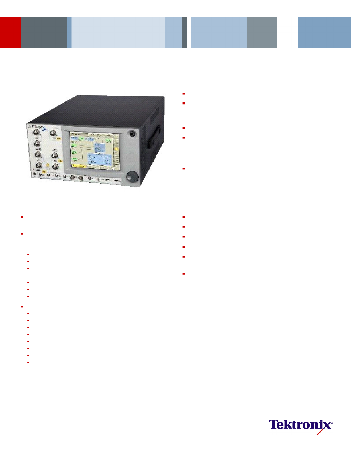
Bit Error Rate Tester
BERTScope®BSA Series Data Sheet
Jitter Tolerance Compliance Template Testing with Margin Testing
Physical Layer Test Suite with Mask Testing, Jitter Peak, BER Contour,
and Q-factor Analysis for Comprehensive Testing with Standard or
User-defined Libraries of Jitter Tolerance Templates
Integrated Eye Diagram Analysis with BER Correlation
Optional Jitter Map Comprehensive Jitter Decomposition – with Long
Pattern (i.e. PRBS-31) Jitter Triangulation to Extend BER-based Jitter
Decomposition Beyond the Limitations of Dual Dirac TJ, DJ, and RJ for a
Comprehensive Breakdown of Jitter Subcomponents
Patented Error Location Analysis™ enables Rapid Understanding of
your BER Performance Limitations and Assess Deterministic versus
Random Erro
Perform Error Burst Analysis, or Error-free Interval Analysis
rs, Perform Detailed Pattern-dep enden t Error Analysis,
Features & Benefits
Pattern Generation and Error Analysis, High-speed BER Measurements
up to 26 Gb/s
Integrated, Calibrated Stress Generation to Address the Stressed
Receiver Sensitivity and Clock Recovery Jitter Tolerance Test
Requirements for a Wide Range of Standards
Sinusoidal Jitter to 100 MHz
Random J
Bounded, Uncorrelated Jitter
Sinusoidal Interference
Spread Spectrum Clocking
PCIe 2.0 Receiver Testing
F/2 Jitter Generation for 8xFC and 10GBASE-KR Testing
Electrical Stressed Eye Testing for:
PCI Express
10/40/100 Gb Ethernet
SFP+/SFI
XFP/XF
OIF/CEI
Fibre Channel
SATA
USB 3.0
itter
I
Applications
Design Ver
Design Characterization for High-speed, Sophisticated Designs
Certification Testing of Serial Data Streams for In dustry Standards
Design/Verification of High-speed I/O Components and Systems
Signal Integrity Analysis – Mask Testing, Jitter Peak, BER Con tour, Jitter
Map, and Q-factor Analysis
Design/Verification of Optical Transceivers
ification including Signal Integrity, Jitter, and Timing Analysis
Page 2
Data Sheet
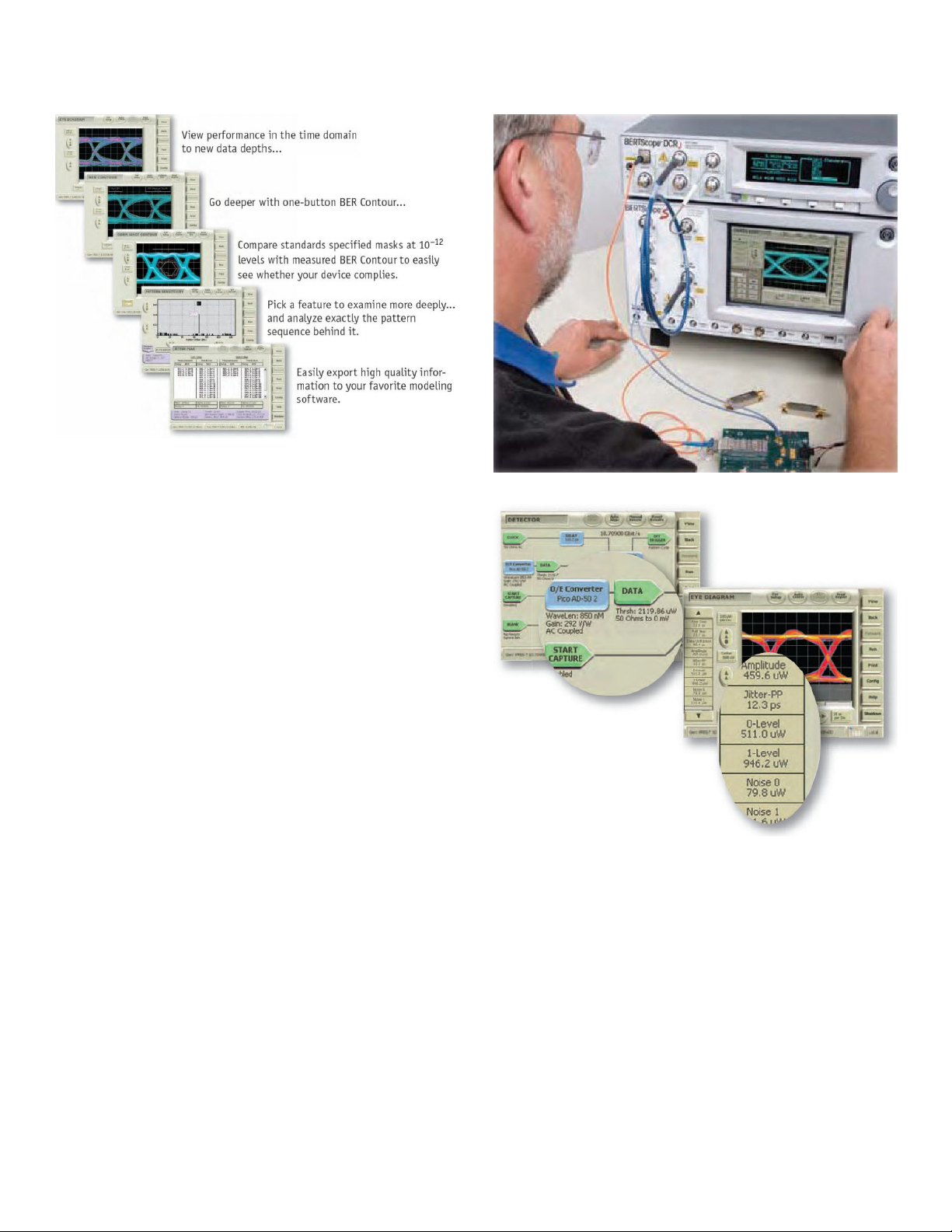
Linking D
Eye diagrams have always provided an easy and intuitive view of digital
perform
as the instruments that provide views of each have been architected in
fundamentally different ways. Eye diagrams have been composed of
shallow amounts of data that have not easily uncovered rarer events.
BERTs have counted every bit and so have provided measurements based
on vastly deeper data sets, but have lacked the intuitive presentation of
informa
The BERTScope removes this gap allowing you to quickly and easily view
an eye di
conventional eyes. Seeing a feature that looks out of the ordinary, you
are able to place cursors on the item of interest and by simply moving the
sampling point of the BERT, use the powerful error analysis capabilities
to gain more insight into the feature of interest. For example, check for
pattern sensitivity of the latest rising edges. Alternatively, use one-button
measur
bounded or likely to cause critical failures in the field. In each case,
information is readily available to enhance modeling or aid troubleshooting,
and is available for patterns up to 2
omains
ance. It has been harder to tie this directly with BER performance,
tion to aid troubleshooting.
agram based on at least two orders of magnitude more data than
ement of BER C on tour to see whether performance issues are
31
–1PRBS.
Data-rich Eye Diagrams
As shown pre viously, there is an impressive difference in data depth
between conventional eye diagrams and those take n with a BERTScope.
So what
going on – more of the world of low-probability events that is present every
time you run a long pattern through a dispersive system of any kind, have
does that mean? It means that you see more of what is really
Testing optical transmitters with BERTScope mask testing and a BERTScope CR.
The BERTScope shown with optical units enabled. In this example measurements are
converted to the optical domain automatically.
random noise or random jitter from a VCO – a world that is waiting to catch
you out when your design is deployed. Adding to this the deeper knowledge
mes from the one -butto n measurements of BER Contour, Jitter Peak,
that co
and Q-factor, and you can be confident that you are seeing the complete
picture.
2 www.tektronix.com
Page 3
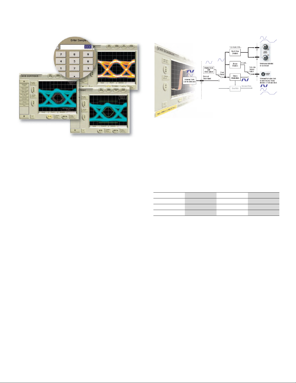
Bit Error Rate Tester — BERTScope®BSA Series
Clock path in BERTScope Option STR models.
With the ab
which give
measurem
are from t
set to onl
in only 1 s
measurem
produced
Here the m
ility to vary sample depth, it is very easy to move between deep measurements
a more accurate view of the real system performance, and shallow
ents that match those of a sampling scope. The measurements shown here
he eye diagram of an optical transmitter. With the BERTScope sample depth
y 3000 waveforms, the BERTScope generates the diagram shown in the middle
econd. The measured mask margin of 20% exactly correlates to the same
ent made on a sampling oscilloscope. The lower diagram shows the eye
by the same device, using Compliance Contour measured at a BER of 1×10
ask margin is reduced to 17%.
–6
Deep Mask Testing
The depth advantage gained for eye diagrams is at least 10 times greater
for mask testing. Unlike pseudo-mask testing offered by so me BERTs,
a BERTScope mask test samples every point on the perimeter of an
industry-standard mask, including th e regions above and below the eye. Not
only that, but each point is tested to a depth unseen before. This means
n for a test lasting a few seconds using a mask from the library o f
that eve
standard masks or from a mask you have created yourself, you can be sure
that your device has no lurking problems.
Accura
Testing w ith long or short patterns, the most accurate jitter measurement is
likely
get its result. W ith the BERTScope, you can quickly measure to levels of
1×10
1×10
are compliant to the MJSQ jitter methodology, and because the underlying
delay control is the best available on any BERT you can be sure that the
measur
(TJ), Random Jitter (RJ), and Deterministic Jitter (DJ), or easily export the
data and use your own fa vorite jitter model.
te Jitter Testing to Industry Standards
to come from the methodology that uses little or no extrapolation to
–9
–10
(1×10
–12
ements are accurate. Use the built-in calculations for Total Jitter
at high data rates), or wait for the instrument to measure
directly. Either way, the BERTScope’s one-button measurements
Mask Compliance Contour Testing
Many standards such as XFP/XFI and OIF CEI now specify mask tests
intended to assure a specified 1×10
–12
eye opening. Compliance Contour
view makes this easy by taking a mask, and overlaying it on your measured
BER contours – so you can immediately see whether you have passed the
mask at whatever BER level you decide.
.
Quick Selection Guide
Model Max Bit Rate
BSA260C/CPG 26 Gb/s Opt. STR
BSA175C/CPG 17.5 Gb/s Opt. STR
BSA125C/CPG 12.5 Gb/s Opt. STR
BSA85C/CPG 8.5 Gb/s Opt. STR
Stressed Eye –
SJ, RJ, BUJ, SI
Flexible Clocking
The generator clock path features in the BERTScope provides the test
flexibility needed for emerging real-world devices. Whether computer cards
or disk drives, it is often necessary to be able to provide a sub-rate system
clock, such as 100 MHz for PCI Express
running may require a differential clock signal with a particular amplitude
and offset; this is easily accomplished with the BERTScope architecture,
with many flexible divide ratios available.
Spread Spectrum Clocking (SSC) is commonly used in electrical serial
data systems to reduce EMI energy by dispersing the power spectrum.
Adjustable modulation amplitude, frequency, and a choice of triangle or sine
tion wave shape allow testing receivers to any compliance standard
modula
which utilize SSC. An additional modulator and source allows users to
stress the clock with h igh-amp litude, low-frequency Sinusoidal Jitter (SJ).
®
(PCIe). To get the target card
Generator/Analyzer
Both
Both
Both
Both
www.tektronix.com 3
Page 4
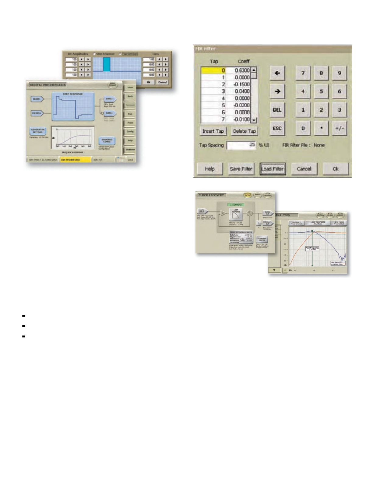
Data Sheet
In keeping with the BERTScope philosophy, the graphical user interface presents the
control functionality in a logical, easy-to-follow format. A time domain representation of
the response shows the effects of tap weight settings. The frequency domain Bode plot
shows how the filter will compensate for the channel losses.
PatternVu
WorkingwithClosedEyes
With the need to push eve r-increasing data rates t hrough electrical
channels, the frequency-dependent losses often result in eye closure at the
receiver end. Engineers use equalization to compensate for these losses
and “open the eyes” in the r eal system. Tektronix offers powerful tools
that allow designers to characterize and test compliance of receiver and
transmitter components used in these systems.
For receiver testing, the DPP125 Digital Pre-emphasis Processor adds
calibrated pre-emphasis to the BERTScope pattern generator outputs,
emulating pre-emphasis applied at the transmitter. Pre-emphasis is
currently used in 10GBASE-KR, PCIe, SAS, DisplayPort
other standards.
Features:
1-12.5 Gb/s clock rates
3- or 4-tap versions
Flexible cursor placement allowing pre-cursor or post-cursor
PatternVu
The PatternVu option includes a software-implemented FIR filter which can
be inserted before the eye pattern display. In systems employing receiver
equalization, this allows you to view the eye diagram and perform physical
measurements on the eye as the receiver’s detector would see it, after the
effect of the equalizer. Equalizers with up to 32 taps can be implemented,
and the user can select the tap resolution per UI.
PatternVu also includes CleanEye, a pattern-locked averaging system
which removes the nondeterministic jitter components from the eye.
This allows you to clearly see pattern-dependent effects such as ISI
®
, USB 3.0, and
The intuitive user interface provides easy control of all operating parameters. A unique
Loop Response view shows the loop characteristics – actually measured, not just the
settings value.
(Inter-Symbol Interference) which are normally obscured by the presence of
high amounts of random jitter.
Single Value Waveform export is a component in the PatternVu option.
This allows you to capture a pattern-locked waveform showing single bits,
similar to a single-shot capture in a real-time oscilloscope. Once captured,
veform can be exported in a variety of formats for further analysis in
the wa
an external program.
Add Clock Recovery
The Tektronix CR125A, CR175A, and CR286A add new levels of flexibility
in compliant clock recovery. Most standards requiring jitter measurement
ify the use of clock recovery, and exactly which loop bandwidth must
spec
be used. Using a different or unknown loop bandwidth will almost certainly
give you the wrong jitter measurement. The new clock recovery instrument
enables easy and accurate measurements to be made to all of the common
standards.
4 www.tektronix.com
Page 5
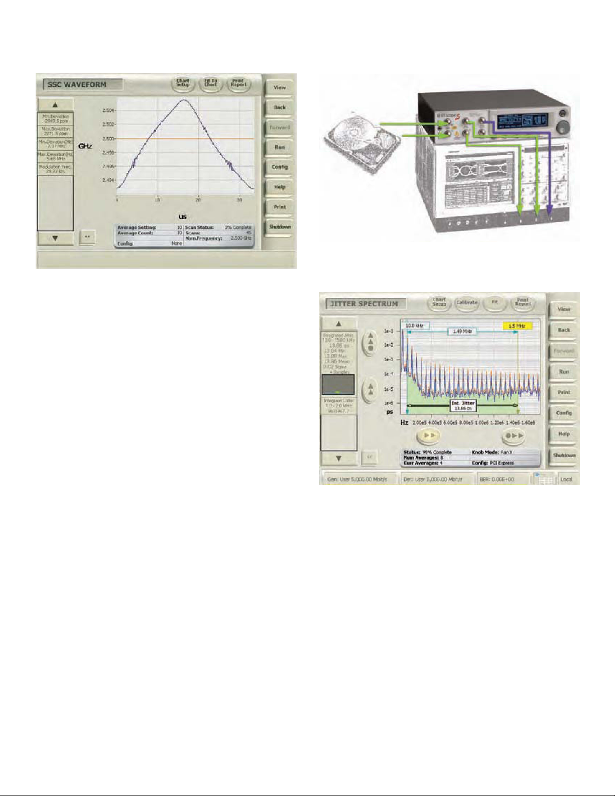
SSC Wavefo
rm Measurement
Display and Measure SSC Modulation
Waveforms
Spread Spectrum Clocking (SSC) is used by many of the latest serial
busses including SATA, PCI Express, and next-generation SAS in order
to reduce EMI issue s in new board and s
CR Family provides spread spectrum clock recovery together with the
display and measurement of the SSC modulation waveform. Automated
measurements include minimum and m aximum frequency deviation (in ppm
or ps), modulation rate of change (dF/dT), and modulation frequency. Also
included are display of the nominal data frequency and easy-to-use vertical
and horizontal cursors.
ystem designs. The Tektronix
Bit Error Rate Tester — BERTScope®BSA Series
The usefulness of the BERTScope CRs is not just confined to BERTScope
measurements. Use them stand-alone in the lab with your sampling oscilloscopes, or with
existing BERT equipment. Compliant measurements are available to you by pairing either
of these versatile instruments with your existing investments.
Add Jitter Analysis
Combine a Tektronix CR125A, CR175A, or CR286A with Option GJ with
your sampling scope or BERTScope for variable clock recovery from 1.2 to
Gb/s, Duty Cycle Distortion (DCD) measurem ent, and real-time jitter
11.2
spectral analysis. Display jitter spectral co mponents from 200 Hz to 90 MHz
with cursor measurements of jitter and frequency. Measure band-limited
integrated jitter with user-settable frequency-gated measurements (preset
r Spectrum Measurement
Jitte
band limits and integ rated jitter measurement for PCI Express 2.0 jitter
spectrum in this example).
www.tektronix.com 5
Page 6
Data Sheet
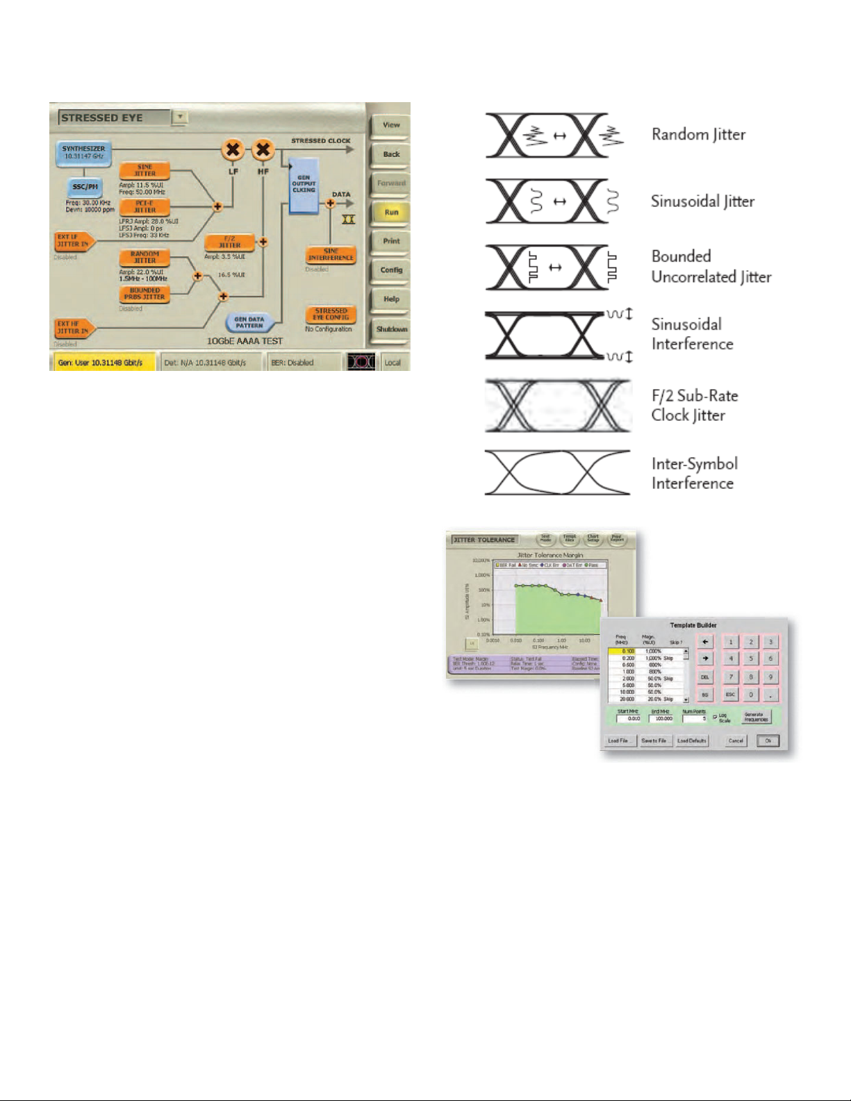
Creating the stress recipe for receiver testing to a complicated standard such as PCIe
2.0 used to require "racking and stacking" several instruments, then spending hours
calibrating the setup. With BERTScope, an easy-to-understand graphical view gives you
control of all of the calibrated stress sources you need – inside the same instrument.
Eliminating the need for external cabling, mixers, couplers, modulators, etc. simplifies
stress calibration.
Taking the Stress out of Receiver Testing
As networks have changed, so have the challeng es of testing receivers.
While tests such as BER and receiver sensitivity are still important, receiver
jitter tolerance has evolved to be more real-world for jitter-limited systems
such as 1
Stressed Eye testing is becoming increasingly common as a compliance
measurement in many standards. In addition, engineers are using it to
explore the limits of their receiver performance to check margins in design
and manufacturing.
Flexible Stress Impairments
The BERTScope has high-quality, calibrated sources of stress built-in,
including RJ, SJ, BUJ, and SI.
ISI is also a common ingredient in many standards. The BSA12500ISI
differential ISI board provides a wide variety of path lengths, free from
switching suck-outs and anomalies.
0 Gb/s da ta over back planes and new high-speed buses.
Flexible Stress Impairments
Many standards call for SJ to be stepped through a template with different SJ amplitudes
at particular modulation frequencies. This is easy with the built-in Jitter Tolerance function
which automatically steps through a template that you designed, or one of the many
standard templates in the library.
6 www.tektronix.com
Page 7
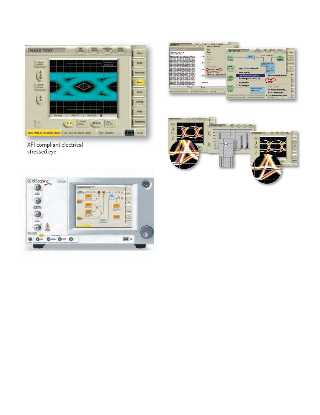
Pattern Capture
Bit Error Rate Tester — BERTScope®BSA Series
Stressed E
BERTScope Pattern Generator
ye Option
BERTScope Pattern Generator Family
The BSA125CPG, BSA175CPG, and BSA260CPG Family of pattern
generators provide a full range of PRBS patterns, common standards-based
erns, and user-defined patterns. Option STR provides full integrated,
patt
calibrated stress generation which is an ea sy-to-use alternative to a rack full
of manually calibrated instruments needed to provide a stressed pattern.
Using the Power of Error Analysis – In this example eye diagram views were linked with
BER to identify and solve a design issue in a memory chip controller. The eye diagram
(top left) shows a feature in the crossing region that is unexpected and appearing less
frequently than the main eye. Moving the BER decision point to explore the infrequent
events is revealing. Error Analysis shows that the features are related in some way to the
number 24. Further investigation traced the anomaly to clock breakthrough within the IC;
the system clock was at 1/24th of the output data rate. Redesigning the chip with greater
clock path isolation gave the clean waveform of the t op right eye diagram.
Uses include receiver testing of devices with internal BER measurement
ability such as D isplayPort, or adding stress capability to legacy BERT
instruments.
Pattern Capture
There are several methods for dealing with unknown incoming dat a. In
addition to Live Data Analysis discussed above, a useful standard feature
on all BERTScope analyzers is pattern capture. This allows the user to
specify the length of a repeating pattern and then allow the analyzer to grab
specified incoming data using the detector’s 128 Mb RAM memory. This
the
can then be used as the new detector reference pattern, or edited and
saved for later use.
www.tektronix.com 7
Page 8
Data Sheet
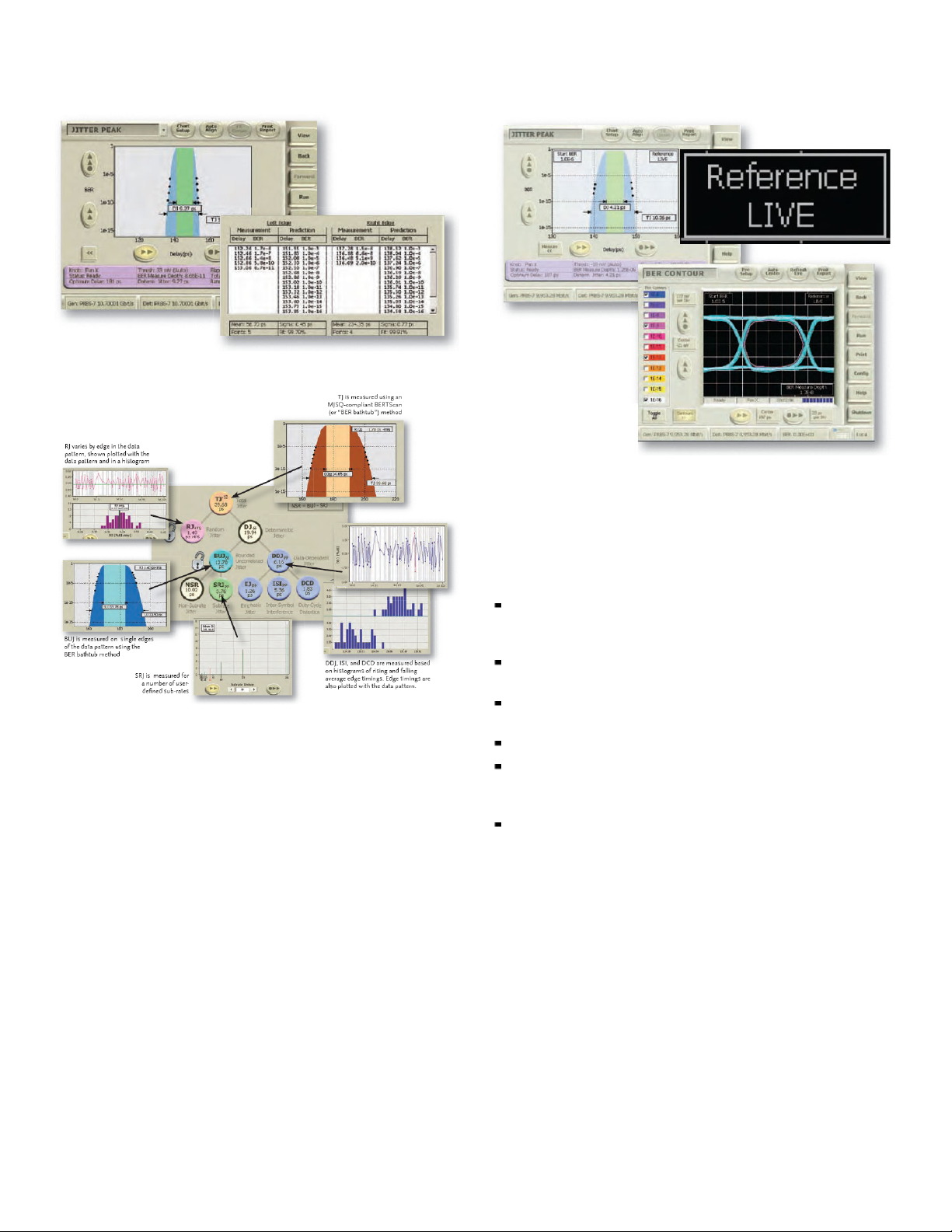
MJSQ-compliant Dual Dirac jitter measurement.
Jitter Peak and BER Contour measurements made on live data.
Jitter Map
Jitter Measurements
Multi-gigabit serial data channels have eye openings only a couple hundred
picoseconds wide – or less. In systems where only a few picoseconds of
jitter count, accurate measurement of jitter is essential for managing tight
jitter budgets. The BERTScope has two sets of tools which perform these
critical measurements.
The Physical Layer Test Suite option includes measurement of Total Jitter
(TJ) along with breakdown into Random Jitter (RJ) and Deterministic
Jitter (DJ), using the well-accepted Dual Dirac method. The deep,
BERT-collected measurements use several ord ers of magnitude less
extrapolation, or in some cases no extrapolation, than oscilloscopes use as
a basis for the jitter measurements. This produces inherently more accurate
results than measurements made on other instruments which rely on high
levels of extrapolation.
The optional Jitter Map is the latest suite of jitter measurements available
for the BERTScope. It provides a compreh ensive set of subcomponent
ysis beyond RJ and DJ, including many measurements compliant with
anal
higher data rate standards. Jitter Map can also measure and decompose
jitter on extremely long patterns, such as PRBS-31, as well as live data
(requires Live Data Analysis option) p roviding that it can first run on a
shorter s
Features include:
ynchronized data pattern.
DJ breakdown into Bounded Uncorrelated Jitter (BUJ), Data Dependent
Jitter (DDJ), Inter-S ymbol Interference (ISI), Duty Cycle Distortion
(DCD), and Sub-Rate Jitter (SRJ) including F/2 (or F2) Jitter
BER-based for direct (non-extrapolated) Total Jitter (TJ) measurement
–12
BER and beyond
to 10
Separation of correlated and non-correlated jitter components eliminates
mistaking long pattern DDJ for RJ
Can measure jitter with minimum eye opening
Additional levels of b reakdown not available from other instruments such
as: E mphasis Jitter (EJ), Uncorrelated Jitter (UJ), Data Dependent Pulse
Width Shrinkage (DDPW S), and Non-ISI
Intuitive, easy-to-navigate jitter tree
Testing Interface Cards
Finally a solution to the age-old problem of making physical layer
measurements on high-speed line cards, motherboards, and live traffic
– the BERTScope Live Data Analysis option. Through novel use of the
dual-decision point architecture, the instrument is able to make parame tric
urements such as Jitter, BER Contour, and Q-factor in addition to
meas
the eye and mask measurements that are usable as standard – all that is
required is a clock signal. A dd the Jitter Map option to see even more layers
of jitter deco m position on live data. No more frustration because the pattern
is not known, is unpredictable, or involves rate-matching word inse rtions.
Troubleshooting is so much easier now that the one-button physical layer
s can be employed to provide unique insight.
test
8 www.tektronix.com
Page 9

Figure 1. Amplitude range.
Characteristics
Bit Error Rate Tester — BERTScope®BSA Series
Pattern Generator*
1
Input/Output Specifications
Clock Outputs
Characteristic
Description
Frequency Range
BSA85C, CPG 0.1-8.5 GHz
BSA125C, CPG 0.1-12.5 GHz*
BSA175C, CPG 0.5-17.5 GHz*
BSA260C, CPG 1-26 GHz*
Phase Noise
< –90 dBc/Hz at 10 kHz offset (typical)
2
2
2
Clock Output Divide Ratios Option STR only
*1Rise times are measured 20% to 80% unless otherwise stated. Specifications are following a 20-minute
warm-up period. Specifications subject to change.
2
Output at data rate ÷2 above 11.2 Gb/s.
*
Data Outputs
Characteristic
Description
Date Rate Range
BSA85C 0.1-8.5 Gb/s
BSA125C, CPG 0.1-12.5 Gb/s
BSA175C, CPG 0.5-17.5 Gb/s
BSA260C, CPG 1-26 Gb/s
Format NRZ
Polarity Normal or Inverted
Variable Crossover 25 to 75%
Patterns
Hardware patterns
Industry-standard Pseudo-random (PRBS) of the
following types: 2
n
– 1 where n = 7, 11, 15, 20, 23,
31
RAM patterns
BSA85C
BSA125C, CPG
BSA175C, CPG
128bitsto128Mbtotal,allocatedin32Mbportions
to each of two A/B pages. Single page max is
128 Mb
BSA260C, CPG
Library
Wide variety including SONET/SDH, Fibre Channel
basedsuchask28.5,CJTPAT;2
=3,4,5,6,7,9;MarkDensitypatternsfor2
n
patterns where n
n
where
n = 7, 9, 23; and many more
Error Insertion
Length 1,2,4,8,16,32,64bitbursts
Frequency
Single or repetitive
Figure 2. Allowable combinations of termination and offset. Amplitude swings between
0.25 and 2 V allowed; should fit inside shaded area of graph. For example, SCFL uses a
0 V termination, and operates between approximately 0 and –0.9 V; as shown with dotted
arrow, it falls within the operating range.
Data, Clock Amplitudes and Offsets
Characteristic
Description
Configuration Differential outputs, each side of pair individually
settable for termination, amplitude, offset
Interface DC coupled, 50 Ω reverse terminated, APC-3.5
connector. Calibration into 75 Ω selectable, other
impedances by keypad entry. User-replaceable
Planar Crown
®
adapter allows change to other
connector types
Preset Logic Families
LVPECL,LVDS,LVTTL,CML,ECL,SCFL
Terminations Variable, –2 to +2 V
Presets: +1.5, +1.3, +1, 0, –2 V, AC coupled
Allowable Amplitudes,
SeeFigures1and2
Terminations, and Offsets
Data, Clock Waveform Performance
Model Rise Time Jitter
BSA85C
BSA125C, CPG
BSA175C, CPG
BSA260C, CPG
25 ps max, 23 ps typical
(10-90%)
<10 ps p-p (typical, for
data rates ≥1Gb/s)
<0.025 UI (typical, for data
rates <1 G b/s)
8 ps p-p (typical at
25.78 Gb/s data rate)
Clock/Data Delay
Characteristic
Range
Up to 1.1 GHz
Above 1.1 GHz
Resolution
Description
(Greater than 1 bit period in all cases)
30 ns
3ns
100 fs
Self Calibration At time of measurement, when t emperature or bit
rate are changed, instrument will recommend a self
calibration. Operation takes less than 10 seconds
www.tektronix.com 9
Page 10

Data Sheet
Pattern Generator Ancillary Connection s
Front-panel Pattern Generator Co nnections
External Clock Input
Characteristic
Allows use of an external clock source to cloc k the BERTScope.
Models equipped with stress are able to add impairments to incoming clock,
including when external signal has Spread Spectrum Clocking (SSC) in excess of
5000 ppm imposed on it.
Frequency Range
BSA85C 0.1 to 8.5 GHz
BSA125C, CPG 0.1 to 12.5 GHz
BSA175C, CPG 0.5 to 17.5 GHz
BSA260C, CPG 1 to 26 GHz
Nominal Power
Maximum Power
Return Loss Better than –6 dB
Interface 50 Ω SMA female, DC coupled into selectable
HF Jitter (Option STR Only)
Characteristic
One of two jitter insertion inputs. Can be used to insert SJ, RJ, BUJ if desired.
Frequency Range
Jitter Amplitude Range Up to 0.5 UI max
Input Voltage Range
Data Rate Range
Interface SMA female, 50 Ω, DC coupled into 0 V
Sub-rate Clock Output
Characteristic
BERTScope standard models have clock divided by 4.
BERTScope Option STR models have additional capabilities.
Frequency Range
Amplitude Range 1 V
Transition Time <500 ps
Interface SMA female, 50 Ω, DC coupled into 0 V
Trigger Output
Characteristic
Provides a pulse trigger to external test equipment. It has two modes:
1. Divided Clock Mode: Pulses at 1/256th of the clock rate
2. Pattern Mode: Pulse at a programmable position in the pattern (PRBS), or fixed
location (RAM patterns)
Stress modulation added on models so equipped, when enabled.
Minimum Pulse Width
Transition Time <500 ps
Jitter (p-p, data to trigger) <10 ps, typical (BSA175C/CPG, BSA260C/CPG)
Output Levels
Interface 50 Ω SMA female
Description
900 mV
2.0 V
(+3 dBm)
p-p
(+10 dBm)
p-p
termination voltage
Description
DC to 1.0 GHz
(+10 dBm) for normal operation
0-2 V
p-p
6.3 V
(+20 dBm) max nondestructive input
p-p
Up to 8.5, 11.2 (BSA125C, CPG, only), 17.5, or
22 Gb/s
Description
0.125 to 3.125 GHz (12.5 GHz with Option STR)
, nominal, centered around 0 V
p-p
Description
128 Clock Periods (Mode 1)
512 Clock Periods (Mode 2)
>300 mV
,centerat650mV
p-p
Rear-panel Pattern Generator Connections
Pattern Start Input
Characteristic
Description
For users wanting to synchronize patterns of multiple data streams from multiple
instruments simultaneously.
Logic Levels
Threshold +1.2 V typic
Max Nondist
ructible Input
LVTTL (<0.5 V Low, >2.5 V High)
al
–0.5 V to +5.
0V
Range
Minimum Pulse Width 128 serial clock periods
Maximum Repetition Rate 512 serial clock periods
Interface SMA female, >1 k Ω impedance into 0 V
Page Select Input
Characteristic
Description
In A-B Page Select mode, allows external control of pattern. Software control over
rising or falling edge trigger, continuous Pattern B after completion of Pattern A, or
runBonlyoncebeforerevertingbacktoA.
Logic Levels
<0.5 V Low, >2.5 V High)
LVTTL (
Threshold +1.2 V typical
Max Nondistructible Input
–0.5Vto+5.0V
Range
Minimum Pulse Width 1 pattern length
Interface SMA female, >1 k Ω impedance into 0 V
Sinusoidal Interference Output (Option STR Only)
Chara
cteristic
Description
SI output from internal generator. Can be used to apply SI after external ISI
channel.
Frequency Range
Output Voltage
Interface
Low-frequency Jitter Input (Option STR Only)
Characteristic
0.1-2.5 GHz
0-3 V
p-p
0-3 V
p-p
Description
Allows use of external low-frequency jitter source to modulate th e stressed pattern
generator output.
Frequency Range
DC to 100 MHz
Jitter Amplitude Range Up to 1.1 ns, can be combined with other internal
low-frequency modulation
Input Voltage Range
Data Rate Range
(+10 dBm) for normal operation 6.3 V
0-2 V
p-p
(+20 dBm) max nondestructive input
Up to 8.5 Gb/s (BSA85C/CPG), 12.5 Gb/s
p-p
(BSA125C/CPG), 17.5 Gb/s (BSA175C/CPG), and
22 Gb/s (BSA260C/CPG)
Interface SMA female 50 Ω, DC coupled into 0 V
Low-frequency Sinusoidal Jitter Output
(Option STR Only)
Characteristic
Description
To allow phasing of two BERTScopes together, in-phase or anti-phase.
Frequency
Amplitude 2 V
As set for internal SJ from GUI
,centeredat0V
p-p
Interface SMA female
10 www.tektronix.com
Page 11

Reference Input
Bit Error Rate Tester — BERTScope®BSA Series
Characteristic
Description
To lock the B ERTScope to an external frequency reference from of another piece
of equipment.
Frequency 10, 100, 106.25, 133.33, 156.25, 166.67, or
200 MHz
Amplitude
0.325 to 1.25 V
(–6to+6dBm)
p-p
Interface 50 Ω SMA female, AC coupled
Reference Output
Characteristic
Description
Provides a frequency reference for other instruments to lock to.
Configuration Single Ended (Ref-Out not used) (BSA125C, CPG)
Differential
Frequenc
y
10, 100, 1
06.25, 133.33, 156.25, 166.67, or
200 MHz
Amplitude
1V
(+4 dBm) nominal, each output, (2 V
p-p
differential)
p-p
Interface 50 Ω SMA female, AC coupled
Clock P
ath Details
BSA85C, CPG
Available divide ratios from clock-related output, by bit rate, using the internal clock,
BSA85C***.
BSA125C, CPG, BSA175C, CPG, and BSA260C, CPG
Functional block diagram of the clock path for models with stress capability,
BSA85C/CPG.
Functional block diagram of the clock path for models with stress capability,
BSA85C/CPG, BSA125C/CPG, BSA175C/CPG, BSA260C/CPG.
utput can also provide a full-rate jittered clock.
*Thiso
** Stress may be added to an external clock on appropriate models. Stress operating range is from 1.5 to
11.2 Gb/s. External clock must have a duty cycle of 50% ±2%.
*** All listed ratios available for an external clock input over entire bit rate range, limitations for internal
clock only. Minimum specified frequency of the clock output is 100 MHz. Operation below this rate will
be uncalibrated.
A125, BSA175, and BSA260 models use an internal Double Data Rate
The BS
(DDR) architecture to operate at data rates ≥11.2 Gb/s. When operating at 11.2 Gb/s
or higher data rate, the clock output will be 1/2 the data rate.
External clock can be specified to be either full or half data rate. When full rate is
selected, the pattern generator will operate in DDR mode when the input clock
ency is 11.2 GHz or higher.
frequ
These ratios apply to operation from internal clock only. External clock will be output
2 rate when half rate is selected, or when full rate is selected and clock rate
at 1/
is ≥11.2 GH z.
inimum data rate specified for the main clock output is 500 Mb/s. Output will be
The m
uncalibrated when operated at divided rates lower than 500 Mb/s.
www.tektronix.com 11
Page 12

Data Sheet
Available Multi-rate and Sub-rate Divider Ratios for Main Clock Output, BSA125C,
CPG, BSA175C, CPG, and BSA260C, CPG Models
Data Rate (Gb/s) Ratios for Main
500-750 Mb/s
0.75-1.5 Gb/s
1.5-3 Gb/s
3-6 Gb/s
6-11.2 Gb/s
11. 2-12 G b/s
12-26 Gb/s
*3Sub-rate clock connector can also output a full-rate stressed clock up to 11.2 Gb/s, or half-rate stressed
clock at rates ≥11.2 Gb/s.
Clock Out
1, 2, 4, 5, 6, 7, 8, 9, 10, 12,
14, 16, 18, 20, 24, 32, 36
1, 2, 4, 5, 6, 7, 8, 9, 10, 12,
14, 16, 18, 20, 24, 25, 28,
30, 32, 35, 36, 40, 42, 45,
48, 54, 56, 64, 72, 81
1, 2, 4, 5, 6, 7, 8, 9, 10, 12,
14, 16, 18, 20, 24, 30, 32,
32, 35, 36, 36, 40, 42, 45,
48, 50, 54, 56, 60, 64, 70,
72, 80, 81, 84, 90, 98, 108,
112, 126, 128, 144, 162
1, 2, 4, 5, 6, 7, 8, 9, 10,
12, 14, 16, 18, 20, 24, 30,
32, 32, 35, 36, 36, 40, 42,
45, 48, 50, 54, 56, 60, 64,
70, 72, 80, 81, 84, 90, 98,
100, 108, 112, 120, 126,
128, 140, 144, 160, 162,
168, 180, 192, 196, 216,
224, 252, 256, 288, 324
1, 2, 4, 5, 6, 7, 8, 9, 10,
12, 14, 16, 18, 20, 24,
30, 32, 32, 35, 36, 36, 40,
42, 45, 48, 50, 54, 56, 60,
64, 70, 72, 80, 81, 84, 90,
98,108,112,126,128,
140, 144, 144, 160, 162,
162, 168, 180, 192, 196,
200, 216, 224, 240, 252,
256, 280, 288, 320, 324,
360, 384, 392, 432, 448,
504, 512, 576, 648
2, 4, 8, 10, 12, 14, 16, 18,
20, 24, 28, 32, 36, 40, 48,
60, 64, 64, 70, 72, 72, 80,
84, 90, 96, 100, 108, 112,
120, 128, 140, 144, 160,
162, 168, 180, 196, 200,
216, 224, 240, 252, 256,
280, 288, 320, 324, 336,
360, 384, 392, 432, 448,
504, 512, 576, 648
2, 4, 8, 10, 12, 14, 16,
18, 20, 24, 28, 32, 36, 40,
48, 60, 64, 64, 70, 72, 72,
80, 84, 90, 96, 100, 108,
112, 120, 128, 140, 144,
160, 162, 168, 180, 196,
216, 224, 252, 256, 280,
288, 288, 320, 324, 324,
336, 360, 384, 392, 400,
432, 448, 480, 504, 512,
560, 576, 640, 648, 720,
768, 784, 864, 896, 1008,
1024, 1152, 1296
Ratios for Sub-rate
Clock Out*
1, 2, 4, 8
1, 2, 4, 8, 16
1, 2, 4, 8, 16, 32
1, 2, 4, 8, 16, 32, 64
2, 4, 8, 16, 32, 64
2, 4, 8, 16, 32, 64, 128
3
1, 2, 4
Pattern Generator Stressed Eye
Flexible, integrated stressed eye impairment addition to the internal or
an external clock
Easy setup, with complexity hidden from the user with no loss of flexibility
Verify compliance to multiple standards using the BERTScope and
external ISI filters. Standards such as:
OIF CEI
6GbSATA
PCI Express
®
XFI
USB 3.0
SONET
SAS 2
XAUI
10 and 100 Gb Ethernet
DisplayPort
Sinusoidal interference may be inserted in-phase or in anti-phase, or
sent externally to be summed after an external ISI reference channel
Sinusoidal jitter may be locked between two B ERTScopes in-phase or
anti-phase, as required by OIF CEI
Flexible External Jitter Interfaces
Front Panel External High Frequency Jitter Input Connector – Jitter from
DC to 1.0 GHz up to 0.5 UI (max) may be added, of any type that keeps
within amplitude and frequency boundaries
Rear Panel External SJ Low F reque ncy Jitter Input Connector – Jitter
from DC to 100 MHz up to 1 ns ( max) may be added
Rear Panel SJ Ou
tput
Sinusoidal Interference Output Rear Panel Connector
Note: Internal RJ, BUJ, and external high-frequency jitter input limited to 0.5 UI,
combined, further limited to 0.25 UI each when both are enabled. Rear-panel
low-frequency jitter input can be used to impose additional jitter; sum of external
low-frequency jitter, internal low-frequency SJ to 10 MHz, PCIe LFRJ and PCIe LFSJ
(with Option XS) is limited to 1.1 ns. This limit does not apply to Phase Modulation
(PM) from Option XSSC.
Amplitude and ISI Impairments
ISI
Add externally: For example, long coax cable length, or Bessel-Thompson 4th Order
Filter with –3 dB point at 0.75 of bit rate, etc.
For applications requiring circuit board dispersion, the BSA12500ISI differential ISI
accessory board may be used.
Sinusoidal Interference
Supports full data rate range of BERTScope
100 MHz to 2.5 GHz
Adjustable in 100 kHz steps
12 www.tektronix.com
Adjustable from 0 to 400 mV
Commonmodeordifferential
Available from rear-panel 50 Ω SMA connector, single ended with data
amplitude from 0 to 3 V adjustable from GUI, same frequency range and
step size as internal adjustment
Page 13

Sinusoidal Jitter
Bit Error Rate Tester — BERTScope®BSA Series
Phase Modulation Range with Option XSSC.
Maximum SSC Modulation with Option XSSC.
Jitter Impairments
Bounded Uncorrelated Jitter
Supports data rates from 1.5 to 8.5 Gb/s (BSA85C), to 11.2 Gb/s
(BSA125C/CPG), 17. 5 Gb/s (BSA175C/CPG), and 26 Gb/s
(BSA260C/CPG), with limited performance to 622 Mb/s (BSA260C/ CPG
excluded)
Internal PRBS-7 Ge nerator
Variableupto0.5UI
100Mb/sto2.0Gb/s
Band-limited by selected filters (see table below)
BUJ Rate Filter
100 to 499 25 MHz
500 to 999 50 MHz
1,000 to 1,999 100 MHz
2,000 200 MHz
Random Jitter
Supports data rates from 1.5 to 8.5 Gb/s (BSA85C), to 11.2 Gb/s
(BSA125C/CPG), 17. 5 Gb/s (BSA175C/CPG), and 26 Gb/s
(BSA260C/CPG), with limited performance to 622 Mb/s (BSA260C/ CPG
excluded)
Variableupto0.5UI
Band-limited 10 MHz to 1 GHz
Crest factor of 16 (Gaussian to at least 8 standard deviation or ~1×10
probability)
–16
Data Rate
Up to 11.2 (BSA85C,
BSA125C) or 17.5 Gb/s
17.5-26 Gb/s
*4Can be combined with other low-frequency modulation.
SJ adjustable from 0 to levels greater than or equal to range in table. See Additional
Stress Options (next) for more SJ capabilities.
Additional S
Enhanced Spread Spectrum Clock Option (Option STR and/or
Option XSSC)
Characteristic
Adds a modulator directly to the synthesizer clock output – modulation affects main
and sub-rate clock output (regardless of the state of sub-rate output select), Data
Output, and Trigger Output.
Modes
Data Rate Range
SSC Wave Shape Triangle or Sine
SSC Frequency Range
SSC Modulation Range 12,500 ppm at 6 Gb/s
SSC Modulation Resolution
SSC Modulation Type Down Spread, Center Spread, Up Spread
PM Frequency Range 10 Hz - 160 kHz
PM Frequency Resolution 1 Hz
PM Modulation Range – For modulation frequency 10 Hz - 2 kHz
Data Rate Maximum Modulation
>6 Gb/s
3to6Gb/s
1.5 to 3 Gb/s
0.75 to 1.5 Gb/s
375to750Mb/s
187to375Mb/s
100to187Mb/s
Reduced for modulation frequencies >2 kHz. See Phase Modulation Range graph.
F/2 Jitter Generation Option (Option F2, also requires Option
STR)
Characteristic
F/2 or sub-rate jitter is found in high data rate systems which multiplex up 2 or more
lower data rate streams. The jitter results for lack of symmetry in the multiplexing
clock, giving all of the even bits different pulse width than the odd bits. Unlike
conventional DCD, F/2 jitter is independent of the logic state of the bit. F/2 jitter is
part of the stress recipe used in testing compliance to some of the newer standards
such as 802.3ap (10 Gb backplane Ethernet).
Supported Data Rates 8.0 and 10.3125 Gb/s
Modulation Range
tress Options
Internal SJ
Frequency
1kHzto10MHz*
10 MHz to 100 MHz 200 ps
1kHzto100MHz 84ps
Description
SSC or Phase Modulation (sinusoidal)
Full range of BERTScope
20kHzto40kHz
6,200 ppm at 12 Gb/s
6,000 ppm at 12.5 Gb/s and above
See Maximum SSC Modulation graph for range at
lower clock rates
1ppm
6000 UI
3000 UI
1500 UI
750 UI
375 UI
187.5 UI
93.75 UI
Description
0-5.0% UI
Maximum Internal
4
SJ Amplitude
110 0 ps
www.tektronix.com 13
Page 14

Data Sheet
Extended Stress Generation Option (Option PCISTR)
Characteristic
Description
This option adds additional stress generators required for compliance testing
receivers to PCIe 2.0 specifications, internal to the BERTScope.
Clock Frequency Range Up to 11.2 Gb/s
LFRJ Modulation Range
LFRJ Frequency Range
4
0-1.1 ns*
Band-limited to 10 kHz - 1.5 MHz, with roll off to
PCIe 2.0 specifications
LFSJ Modulation Range 0-368 ps*4at 5 Gb/s
LFSJ Frequency Range
*4Can be combined with other low-frequency modulation.
Characteristic
1-100 kHz
Description
The Extended Stress option also adds selectable bandwidth-limiting to the normal,
broadband RJ generator.
RJ Frequency, Normal Mode
Band-limited to 10 MHz - 1 GHz
RJ Frequency, PCIE Mode Band-limited to 1.5-100 MHz with roll off to PCIe 2.0
specifications
Error Detector
Clock and Data Inputs
Clock Input
Characteris
tic
Configuration Single ended
Frequency Range
BSA85C 0.1-8.5 GHz
BSA125C 0.1-12.5 GHz
BSA175C 0.5-17.5 GHz*
BSA260C 1-26 GHz*
*5A full- or half-rate clock may be used for data rates above 11.2 Gb/s.
Data and Clock Interfaces
Characteristic
Connector APC-3.5 Planar Crown
Impedance
Threshold Voltage –2 to +3.5 V
Threshold Presets
Terminations Variable, –2 V to +3 V
Max Nondistructible Input –3 V
Clock/Data Delay
Characteristic
Range
Up to 1.1 GHz
Above 1.1 GHz
Resolution
Self Calibration Supported – At time of measurement, when
Description
5
5
Description
®
50 Ω
LVPECL,LVDS,LVTTL,CML,ECL,SCFL
Presets: +1.5, +1.3, +1, 0, –2 V, AC coupled
,+4V
peak
Description
, applied to any connector
peak
(Greater than 1 bit period in all cases)
30 ns
3ns
100 fs
temperature or bit rate are c hanged, instrument will
recommend a self calibration. Operation takes less
than 10 seconds
Data Inputs
Characteristic
Description
Date Rate Range
BSA85C 0.1-8.5 Gb/s
BSA125C 0.1-12.5 Gb/s
BSA175C 0.5-17.5 Gb/s
BSA260C 1-26 Gb/s
Configuration Differential
Format NRZ
Polarity Normal or Inverted
Threshold Alignment
Can auto-align to differential crossing point
Sensitivity
Single ended 100 mV
Differential 50 mV
Maximum input signal
swing
Intrinsic Transition Time
2V
16 ps typical, 10/90%, single ended (equivalent to
(typical)
p-p
(typical)
p-p
p-p
>20 GHz detector bandwidth). Measured at input,
ECL levels
Patterns
Hardware patterns
Industry-standard Pseudo-random (PRBS) of the
following types: 2
n
– 1 where n = 7, 11, 15, 20, 23,
31
RAM patterns
User defined
Library
128 bits to 128 Mb, 128-bit increments
Wide variety including SONET/SDH, Fibre Channel
basedsuchask28.5,CJTPAT;2
=3,4,5,6,7,9;MarkDensitypatternsfor2
n
patterns where n
n
where
n = 7, 9, 23; and many more
RAM Pattern Capture Capture incoming data up to 128 Mb in length. Edit
captured data, send to pattern generator, error
detector, or both
Capture modes
Capture by length 1 to 1,048,576 words. 1-word default. Words 128 bit
in length
Capture by triggers Captures when “Detector Start” on rear panel goes
high, to maximum allowable length or until input
goes low
Capture by length from
trigger
Capture by length initiated from “Detector Start”
input, to pre-specified length
Synchronization
Auto-resync
User-specified number of 128 bit words containing 1
or more errors per word initiates a re-sync attempt
Manual User initiates re-sync
Pattern matching
Grab ‘n’ Go Error detector captures specified pattern length
and compares next instances to find match (Fast
method, but susceptible to ignoring logical errors)
Shift-to-Sync
Error detector compares incoming pattern with
reference RAM pattern, looks for match, if none
found shifts pattern by one bit and compares again
(Slower but most accurate method)
Error Detector Basic
Measurements
BER, Bits Received, Re-syncs, Measured Pattern
Generator and Error Detector Clock Frequencies
14 www.tektronix.com
Page 15

Error Detector Ancillary Connections
Front-panel Error Detector Connections
Error Correlation Marker Input (Error Analysis)
Bit Error Rate Tester — BERTScope®BSA Series
Characteristic
Allows an exte
rnal signal to provide a time-tagged marker to be placed in the error
Description
data set.
Logic Family
LVTTL (<0.5 V Low, >2.5 V High)
Threshold +1.2 V
Minimum Pulse Width 128 clock periods
Maximum Repetition Rate 512 serial clock periods
Maximum Frequency
<4000 markers/s recommended
Interface BNC female, >1 kΩ impedance into 0 V
Blank Input
Characteristic
Description
Useful for recirculating loop fiber experiments or during channel training sequences.
Causes errors to be ignored when active. Bit count, error count, and BER not
counted. No re-sync occurs when counting is re-enabled.
Logic Family
LVTTL (<0.5 V Low, >2.5 V High)
Threshold +1.2 V
Minimum Pulse Width 128 clock periods
Maximum Repetition Rate 512 serial clock periods
Interface BNC female, >1 kΩ impedance into 0 V
Error Output
Characteristic
Description
Provides a pulse when an error is detected. Useful for triggering an alarm while
doing long-term monitoring, etc.
Minimum Pulse Width 128 clock periods
Transition Time <500 ps
Output Levels 1000 mV nominal (0 V to 1 V low-high)
Interface SMA female
BERTScope Burst Analysis Timing – BERTScope word size is 128 bits. An example
timing diagram is shown here for a PRBS payload. Counting of bits will not start until a
128-bit word boundary occurs, meaning that after the blanking pulse transitions, up to
127 bits may pass before synchronization begins. For a PRBS, synchronization typically
takes 5 words, or 640 bits. Similarly, bit measurement will continue for up to 127 bits after
the blanking signal transitions again. RAM-based patterns take longer to synchronize.
Trigger Output
Characteristic
a pulse trigger to external test equipment. It has two modes:
Provides
d Clock Mode: Pulses at 1/256th of the clock rate.
1. Divide
n Mode: Pulse at a programmable position in the pattern (PRBS), or fixed
2. Patter
(RAM patterns).
location
Minimum Pulse Width
Descripti
128 clock periods (Mode 1)
on
512 clock periods (Mode 2)
Transition Time <500 ps
Outpu
Inter
tLevels
face
V amplitude, 650 mV offset
>300 m
A female
50 Ω SM
Rear-panel Error Detector Connections
Detector Start Input*
Characteristic
6
Description
Used to trigger the acquisition of incoming data into the error detector reference
pattern memory. High level starts capture.
Amplitude
LVTTL (<0.5 V Low, >2.5 V High)
Threshold +1.2 V
Minimum Pulse Width 128 serial clock periods
Maximum Repetition Rate 512 serial clock periods
Interface SMA female, >1 k Ω impedance into 0 V
*6Not present for BERTScope CPG models.
www.tektronix.com 15
Page 16

Data Sheet
UI Setup Screens
creen
Editor S
User Interfaces
Taking Usability to New Heights
Easy navigation
Logical layout and operation
Multiple ways of moving between screens
Relevant information right where you need it
Color coding to alert you to the presence of nonstandard conditions
Editor Screen
Used for pattern editing of standard and AB Page Select patterns, also
mask editing
Views in Binary, Decimal, or Hexadecimal
Support for variable assignments, repeat loops, seeding of PRBS
erns
patt
ure and editing of incoming data – for example, to make a repeating
Capt
pattern out of real-world traffic
Capture is available by trigger, by length, or by length following a
gger
tri
Capture is by number or words, 1 word is 128 bits. F or example, a
PRBS-7 (127 bits long) would be captured as 127 words, and would
e overall length of 16,256 bits
hav
BERTScope Built-in Parametric Measurements
All BERTScopes come with eye diagrams and mask test capabi
along with error analysis.
Eye Diagram
lities as standard,
280×350 pixel waveform display
Deep acquisition
Automatic Measurements include:
Rise Time
Fall Time
Unit Interval (Data, and a lso Clock)
Eye Amplitude
Noise Level of 1 or 0
Eye Width
Eye Height
Eye Jitter (p-p and RMS)
0 Level, 1 Level
Extinction Ratio
Vertical Eye Closu re Penalty (VECP)
Dark Calibration
Signal-to-Noise Ratio
V
p-p,Vmax,Vmin
, Crossing Levels
Rising and Falling Crossing Level (picoseconds)
Overshoot 0 Level and 1 Level
Average Voltage/Power
Cross Amplitude, Noise Level 1 or 0, Voltage
Optical Modulation Amplitude (OMA)
Sample Count
Offset Voltage
De-emphasis Ratio
Mask Testing
Library of standard masks (e.g. XFP, or edit custom masks)
Addition of positive or negative mask margin
Import of measured BER Contour to become process control mask
At least 1000x the sample depth of traditional sampling oscilloscope
masks is ide al for ensuring the absence of rare event phenomena
Optical Units
An external optical receiver may be added to the input of the BERTScope detector.
Through the user interface it is easy to input and save the characteristics of the
receiver. Once accomplished, relevant units on physical layer displays are changed
to optical power in dBm, μW, or mW. Coupling may be AC or DC, and the software
steps the user through dark calibration.
For electrical signals, attenuation values can be entered to properly scale eye
diagrams and measurements when external attenuators are used.
Variable-depth Eye and Mask Testing
eye diagrams and mask testing, the depth of test may be varied in manual mode;
For
the instrument will take the specified number of waveforms then stop. The range is
2,000 to 1,000,000 bits (complete waveforms). Alternatively, the default mode is
ntinuous, and the eye or mask test increases in depth over time.
Co
16 www.tektronix.com
Page 17

Bit Error Rate Tester — BERTScope®BSA Series
Physical Layer Test Opt ion
BER Contour Testing
Executed with same acquisition circuitry as eye diagram measurements
for maximum correlation
As-needed delay calibration for accurate points
Automatic scaling, one-button measurement
Extrapolates contours fr
om measured data, increasing measurement
depth with run time and repeatedly updating cu rve fits
Easy export of fitteddatainCSVformat
Contours available from 10–6to 10
Basic Jitter Measurements
–16
in decade steps
Testing to T11.2 MJSQ BERTScan methodology (also called ‘Bathtub
Jitter’)
Deep measurements for quick and accu
rate extrapolation of Total Jitter
at user-specified level, or direct measurement
Separation of Random a nd Deterministic components, as defined in
MJSQ
As-needed delay calibration for accurate points
Easy export of points in CSV format
Easy one-button measurement
User-specified amplitude threshold level, or automatic selection
Selectable starting BER to increase accuracy when using long patterns,
as defined in MJSQ
Q-factor Measurement
One-button measurement of a vertical cross section through the m iddle
of the eye
Easy visualization of system noise effects
Export of data in CSV format
Compliance Contour
Validation of transmitter eye performance to standards such as XFP/XFI
and OIF CEI
Overlay compliance masks onto m easured BER contours and easily see
ther devices pass the BER performance level specified
whe
Live Data Analysis Option
TheLiveDataop
either unknown or non-repeating. This can include trafficwithidlebitsinsertedsuch
as in systems with clock rate matching. It is also suitable for probing line cards, etc.
The option uses one of the two front-end decision circuits to decide whether each
bit is a one or zero by placing it in the center of the eye. The other is then used to
probe the peri
powerful for physical layer problems, but will not identify logical problems due to
protocol issues, where a zero was sent when it was intended to be a one.
Live data measurements can be made using BER Contour, Jitter Peak, Jitter Map,
and Q-factor. Eye diagram measurements can be made on live data without the use
of this optio
TheLiveDataAnalysisoptionrequires the Physical Layer Test option and must
be used with
PatternVu E
PatternVu*7adds several powerful processing functions to the BERTScope:
CleanEye is an eye diagram display mode, which averages waveform data to
present an eye diagram with the non-data-dependent jitter removed. This allows the
user to vie
giving an intuitive idea of the compensatable jitter present, for example. It is effective
on any repeating pattern up to 32,768 bits long.
Single Value Waveform Export is a utility which converts the CleanEye output to an
export file in Comma Separated Vector (CSV) format. The output file,ofupto10
points, c
tools such as Stateye or MATLAB
data and the implementation of standards-based processing such as Transmitter
Waveform
MultiMode (LRM) 10 Gb Ethernet standard.
The FIR F
channel to view and measure the eye as the detector in the receiver would, by
applying a software linear filter to the data before it is displayed. For example, the
FIR Filt
alternatively, emulate the receiver’s equalization filter, facilitating the design and
characterization of receiver-side equalization.
The filter characteristics are controlled by entering the individual weighting
coefficients of a series of taps in the FIR filter. Upto32tapswithtapspacingfrom
0.1to1
shape. The FIR Filter can be applied to repeating p atterns up to 32,768 bits long.
Single
to be applied t o individual data edges at data rates above 3 Gb/s. The Single Edge
Jitter Peak measurement function enables computation of jitter on a user-selectable
e edge in the pattern, for repeating patterns up to 32,768 bits long. The resulting
singl
jitter measurement excludes data-dependent effects, showing only the uncorrelated
jitter components such as Random Jitter (RJ), Bounded Uncorrelated Jitter (BUJ),
riodic Jitter (PJ).
and Pe
Flexible Measurements enables users to specify exactly the portion of the
nEye waveform to use for accurate measurement of amplitude, rise and fall
Clea
time, and de-emphasis ratio. Preprogrammed formulas for standards such as PCI
Express and USB 3.0 are included.
tternVu operates at data rates of 900 Mb/s and higher.
*7Pa
tion is designed to measure parametric performance of trafficthatis
phery of the eye to judge parametric performance. This method is
n, providing a synchronous clock is available.
a full-rate clock.
qualization Processing Option
w and measure data-dependent jitter such as Inter-Symbol Inference,
5
an then be imported into Microsoft Excel or software analysis and simulation
Dispersion Penalty (TWDP) required by 802.3aq, the recent Long Reach
ilter equalization processor a llows the emulation of the communication
er can be used t o emulate the lossy effects of a backplane channel, or
.0 unit intervals (UI) can be programmed to allow fine resolution of the filter
Edge Jitter Measurement allows truly deep BER-based jitter measurements
®
. This allows offline filtering of real captured
bit
www.tektronix.com 17
Page 18

Data Sheet
Error Statistics view showing link performance in terms of bit and burst occurrences.
Strip Chart view showing bit and burst error performance over time. This can useful while
temperature cycling as part of troubleshooting, for example.
Error Analysis
Error analysis is a powerful series of views that associate error occurrences so that
underlying patterns can be easily seen. It is easy to focus in on a particular part of an
eye diagram, move the sampling point of the BERTScope there, and then probe the
pattern sensitivity occurring at that precise location. For example, it is straightforward
to examine which patterns are responsible for late or early edges.
Many views come standard with the BERTScope Family.
The Pattern Sensitivity view is a powerful way of examining whether error events are
pattern related. It shows which pattern sequences are the most problematic, and operates
on PRBS and user-defined patterns.
Analysis Views
Error Statistics: A tabular display of bit and bu rst error counts and rates
Strip Chart: A strip chart graph of bit and burst error rates
Burst Length: A histogram of the number of occurrences of errors of
different lengths
Error Free Interval: A histogram of the number of occurrences of
different error-free intervals
Correlation: A histogram showing how error locations correlate to
user-set block sizes or external marker signal inputs
Pattern Sensitivity: A histogram of the number of errors at each
position of the bit sequence used as the test patt ern
Block Errors: A histogram showing the number of occurrenc
es of data
intervals (of a user-set block size) with varying numbers of errors in them
Error Location Capture
iption
Characteristic
nalysis
Live A
Error Logging Capacity Max. 2 G B file size
Error Events/Second
mum Burst Length
Maxi
Descr
Continuous
0
10,00
32 kb
18 www.tektronix.com
Page 19

Bit Error Rate Tester — BERTScope®BSA Series
Error Analysis Options
Forward Error Correctio n Emulation
Because of the patented error location ability of the BERTScope, it knows exactly
where each error occurs during a test. By emulating the memory blocks typical of
block error correcting codes such as Reed-Solomon architectures, bit error rate data
from uncorrected data channels can be passed through hypothetical error correctors
to find out what a proposed FEC approach would yield. Users can set up error
correction strengths, interleave depths, and erasure capabilities to match popular
hardware correction architectures.
2-D Error Mapping
This analysis creates a two-dimensional image of error locations from errors found
during the test. Error mapping based on packet size or multiplexer width can show
if errors are more prone to particular locations in the packet or particular bits in the
parallel bus connected to the multiplexer. This visual tool allows for human eye
correlation, which can often illuminate error correlations that are otherwise very
difficult to find – even with all the other error analysis techniques.
Jitter Tolerance Template Option
Many standards call for SJ to be stepped
amplitudes at particular modulation frequencies. This is easy with the built-in Jitter
Tolerance function which automatically steps through a template that you designed,
or one of the many standard templates i
Standard Library of Templates
through a template with different SJ
n the library.
10GBASE LX4 802.3ae 3.125 Gb /s
10 GbE 802.3ae 10.3125 Gb/s
40 GbE 802.3ba LR4 10.3125 Gb/s
100 GbE 802.3ba LR4/ER4 25.7 8125 Gb/s
CEI 11G Datacom Rx Ingress (D) 11 Gb/s
CGE Telecom Rx Egress (Re) 11 Gb/s*
CEI 11G Telecom Rx Ingress (Ri) 11 Gb/s*
8
8
CEI 11G Total Wander 11.1 Gb/s
CEI 11G Total Wander 9.95 Gb/s
CEI 6G Total Wander 4.976 Gb/s
CEI 6G Total Wander 6.375 Gb/s
CEI 25G Total Wander 25.78125 Gb/s
MM1 3.2 Gb/s
FBB DI
FBB DIMM1 4.0 Gb/s
FBB DIMM1 4.8 Gb/s
FBB DIMM2 3.2 Gb/s
FBB DIMM2 4.0 Gb/s
FBB DIMM2 4.8 Gb/s
Fibre Channel 1.0625 Gb/s
Fibre Channel 2.125 Gb/s
Fibre Channel 4.25 Gb/s
Fibre Channel 8G 8.5 Gb/s
Fibre Channel 16G 14.025 Gb/s
OTN OTU-1 2.666G*
8
OTN OTU-2 10.709 Gb/s
OTN(10BASE-R)
11.1 Gb/s
SAS (SCSI) 1.5 Gb/s
SAS (SCSI) 3 Gb/s
8
SDH 0.172 STM-
SDH 0.172 STM-16 2.4832 Gb/s*
SDH 0.172 STM-4 622 Mb/s*
SDH 0.172 STM
SDH STM-16 2.48832 Gb/s*
SDH STM-64 9.9532 Gb/s*
SONET OC-48
SONET OC12 622 Mb/s*
SONET OC192 9.9532 Gb/s*
SONET OC19
SONET OC3 155 Mb/s*
SONET OC48 2.4832 Gb/s*
USB 3.0 5 G
1 155M*
-64 9.956 Gb/s*
2.48832 Gb/s*
29.95Gb/s*
b/s
8
8
8
8
8
8
8
8
8
8
8
XAUI 3.125 Gb/s
XFI ASIC Rx In Datacom (D) 10.3125 Gb/s
XFI ASIC
Rx In Datacom (D) 10.519 Gb/s
XFI ASIC Rx In Telecom (D) 10.70 Gb/s
XFI ASIC Rx In Telecom (D) 9.95328 Gb/s*
t Rx In Datacom (C) 10. 3125 Gb/s
XFI Hos
8
XFI Host Rx In Datacom (C) 10.519 Gb/s
XFI Host Rx In Telecom (C) 10.70 Gb/s*
t Rx In Telecom (C) 9.95328 Gb/s*
XFI Hos
8
8
XFI Module Tx In Datacom (B’) 10.3125 Gb/s
XFI Module Tx In Datacom (B’) 10.519 Gb/s
dule Tx In Telecom (B’) 10.70 Gb/s*
XFI Mo
XFI Module Tx In Telecom (B’) 9.95328 Gb /s*
Some of the areas of adjustment include:
onfidence level
BER c
8
8
Test duration per point
BER threshold
t device relaxation time
Tes
Imposition of percentage margin onto template
Test precision
ntrol over A/B Pattern switch behavior
Co
Also included is the ability to test beyond the template to device failure at each
osen point, and the ability to export data either as screen images or CSV files.
ch
*8Requires Option XSSC.
www.tektronix.com 19
Page 20

Data Sheet
Jitter Map Option
Automated Jitter Decomposition with Long Pattern Jitter
Triangulation
9
xtends BER-based jitter decomposition beyond Dual Dirac
Jitter Map*
measurement of Total Jitter (TJ), Random Jitter (RJ), and Deterministic Jitter (DJ)
to a comprehensive set of subcomponents. It can also measure and decompose
jitter on extr
on a shorter synchronized data pattern.
Features include:
e
emely long patterns, such as PRBS-31, providing that it can first run
DJ breakdown into Bounded Uncorrelated Jitter (BUJ), Data Dependent
Jitter (DDJ), Inter-Symbol Interference (ISI), Duty Cycle Distortion
(DCD), and S
BER based fo
–12
to 10
BER and beyond
ub-Rate Jitter (SRJ)*
r direct (non-extrapolated) Total Jitter (TJ) measurement
10
including F/2 (or F2) Jitter
Separation of correlated and uncorrelated jitter com ponents eliminates
mistaking long pattern DDJ for RJ
Visualization of RJ RMS measured on individual edges of the data
pattern
J2 and J9 ji
Addition
tter measurements for 100 GbE applications
al levels of breakdown not available from other instruments such
as: Emphasis Jitter (EJ), Uncorrelated Jitter (UJ), Data Dependent Pulse
Width Shrinkage (DDPWS), and Non-ISI
Intuitive, easy-to-navigate jitter tree
Map operates at data rates of 900 Mb/s and higher.
*9Jitter
10
*
SRJ and F/2 Jitter operate up to 8.5 Gb/s (BSA85C), 11.2 Gb/s (BSA125C, BSA175C, BSA260C).
Stressed Live Data Option
The BERT
various types of stress to real data traffic in order to stress devices with bit sequences
representative of the environment they will encounter once deployed. Using live
traffic
confidence to designs before they are shipped.
Scope Stressed Live Data software option e nables engineers to add
with added stress tests the boundaries of device performance and lends added
Pull range of calibrated stress available on the BERTScope, including
Sinusoidal Jitter (SJ), Random Jitter (RJ), Bounded Uncorrelated Jitter
Sinusoidal Interference (SI), F/2 Jitter, and Spread Spectrum
(BUJ),
Clocking (SSC)
Data rate support up to the maximum of the BERTScope
Full-rate clock required up to 11.2 Gb/s, half-rate clock required above
11.2 Gb/s
Symbol Filtering Option (Included in Option STR)
Symbol filtering enables asynchronous BER testing, including Jitter Tolerance
testing, on incoming data streams that have a nondeterministic number of clock
ensation symbols inserted into the bit stream, as is common in 8b/10b encoded
comp
systems when placed in loopback for receiver testing.
Supports asynchronous receiver testing for USB 3.0, SATA, and PCI
Express
User-specified symbols are automatically filtered from the incoming data
aintain synchronization
to m
error detector maintains a count of filtered bits for accurate BER
The
measurement
Operates at data rates up to 11.2 Gb/s
General
PC Related
Characteristic
Display
Touch Sensor
Processor
Hard Disk
DRAM
Operating System Windows XP Professional
Remote Control Interfaces IEEE-488 (GPIB) or TCP/IP
Supported In
terfaces
Description
TFT touch screen 640×480 VGA
Analog resistive
®
Pentium
40 GB or greater
1GB
P4 1.5 GHz or greater
DVI/VGA display
USB 2.0 (4 to tal, 2 front, 2 rear on BSA175; 1 front, 1 rear on other
BERTScope models)
100BASE-T Ethernet LAN
IEEE-488 (GPIB)
Parallel printer
Serial RS-232
PS-2 mouse/keyboard combined connector
Physical
Dimension
Height 220 8.75
Width 394 15.5
Depth 520 20.375
Weight kg lb.
Instrument Only
Shipping
Other
Power <450 W
Voltage
Environmental
Characteristic
Warm-up Time 20 minutes
Operating Temperature
Range
Humidity
Certifications EU EMC Directive (CE-Marked)
Support
Characteristic
Period
Calibration Interval
90to240VAC,50to60Hz
mm
25
34.5 76
Description
10 to 40 °C
Noncondensing at 40 °C, 15 to 95%
UL: Underwriters Labs (US) Certification CSA
(Canada)
Description
1 year (extendable to 3 years with orderable option)
1year
in.
55
20 www.tektronix.com
Page 21

Ordering Information
Bit Error Rate Tester
BERTScope BSA Series.
Models
Model Description
BSA85C Single Channel, BERTScope 8.5 Gb/s Bit Error
BSA85CPG BERTScope 8.5 Gb/s Pattern Generator
BSA125C BERTScope 12.5 Gb/s Bit Error Ratio Analyzer
BSA125CPG BERTScope 12.5 Gb/s Pattern Generator
BSA175C BERTScope 17.5 Gb/s Bit Error Ratio Analyzer
BSA175CPG BERTScope 17.5 Gb/s Pattern Generator
BSA260C BERTScope 26.0 Gb/s Bit Error Ratio Analyzer
BSA260CPG BERTScope 26.0 Gb/s Pattern Generator
All Models Include: Quick Start Guide, power cord, mouse, PS2 "Y" cable, three
(3) short low-loss cables, DVI adapter.
Options
Option
F2
STR Stressed Signal Generation
XSSC Extended Spread Spectrum
PCISTR AddPCIeExtendedStress
J-MAP
ECC Add Er ror Correction Coding
JTOL
LDA
MAP Add Error Mapping Analysis
PL
PVU Add PatternVu Equalization
SF Add Symbol Filtering option
SLD Add Stressed Live Data
CA1
C3 Calibration Service 3 Years
R3
-R3DW
*11Option STR is mandatory on BSA85CPG.
Descript
F/2 Jitter Generation at
8G/10.3125G (requires STR)
(includes option ECC, MAP,
PL, XSSC, JTOL, SF)
Clocking (SSC)
(includedinSTR)
Generation
Add Jitter Decomposition SW
Emulation SW
(includedinSTR)
Add Jitter Tolerance
Temp la tes SW
(includedinSTR)
AddLiveDataAnalysisSW
(includedinSTR)
SW (included in STR)
Add Physical Layer Test Suite
SW (included in STR)
Processing SW
SW (included in STR)
option SW
Provides a single calibration
event or coverage
Repair Service 3 Years
(including warranty)
Repair Service Coverage
3 Years (includes product
warranty period). 3-year
period starts at time of
customer instrument purchase
Ratio Analyzer
ion
BSA85C BSA85CPG BSA125C BSA125CPG BS A175C BSA175CPG BSA260C BSA260CPG
XXXXXXXX
X
XXXXXXXX
XXX XXX X
XXXX
XXXX
XXXX
XXXX
XXXX
XXXX
XXXX
XXXX
XXXX
XXXXXXXX
XXXXXXXX
XXXXXXXX
XXXXXXXX
11
X*
Bit Error Rate Tester — BERTScope®BSA Series
XXXXXX
www.tektronix.com 21
Page 22

Data Sheet
Recommended Accessories
Clock Recovery Instruments
Accessory Description
CR125A 12.5 Gb/s Clock Recovery Instrument
CR175A 17.5 Gb/s Clock Recovery Instrument
CR286A 28.6 Gb/s Clock Recovery Instrument
Clock Recovery Instrumen t Options
Option
PCIE PCIe PLL analysis (requires 12GJ, operates
HS Add High Sensitivity Clock Recovery
XLBW Add Extend
12GJ Add Jitter Spectrum Analysis
17GJ Add 17.5 G Clock Recovery with Jitter Analysis
28GJ Add 28.6 G Clock Recovery with Jitter Analysis
CA1
C3 Calibration Service 3 Years
R3
-R3DW
Provides a single calibration event or coverage X X X
Repair Service 3 Years (including warranty)
Repair Service Coverage 3 Years (includes product
warranty period). 3-year period starts at time
Description
at 2.5G and 5G only)
ed Loop Bandwidth in the
Clock Reco
of customer instrument purchase
very
CR125A CR175A CR286A
XXX
XX
XXX
X
X
X
XXX
XXX
XXX
Digital Pre-emphasis Processors
Accessory Description
DPP125
1-12.5 Gb/s 3-Tap and optional 4-Tap Digital
Pre-emphasis Processor
Digital Pre-emphasis Processor Options
Option
4T 4-Tap Digital Pre-emphasis Processor
CA1
C3 Calibration Service 3 Years
R3
-R3DW
Description
Provides a single calibration event or coverage
Repair Service 3 Years (including warranty)
Repair Service Coverage 3 Years (includes product
warranty period). 3-year period starts at time of
customer instrument purchase
Accessories
Accessory Description
CR125ACBL High-performance Delay Matched Cable Set
100PSRTFILTER
BSA12500ISI Differential ISI Board
PMCABLE1M Precision Phase Matched Cable Pair, 1 m
SMAPOWERDIV SMA Power Dividers
BSASATATEE BSA-SATA-Tee for OOB Signaling
SATATESTSW Serial ATA Interop Test Suite Automation Software
BSARACK BSA-Rackmount K i ts
(required for BERTScope and CRU in SSC
applications)
100psRiseTimeFilter
22 www.tektronix.com
Page 23

Bit Error Rate Tester — BERTScope®BSA Series
www.tektronix.com 23
Page 24

Data Sheet
Contact Tektronix:
ASEAN / Australa
Balkans, Israel, South Africa and other ISE Countries +41 52 675 3777
Central East Eu
Mexico, Central/South America & Caribbean (52) 56 04 50 90
* European toll-free number. If not accessible, call: +41 52 675 3777
rope, Ukraine, and the Baltics +41 52 675 3777
Central Europe & Greece +41 52 675 3777
Middle East,
Asia, and North Africa +41 52 675 3777
The Netherlands 00800 2255 4835*
People’s Rep
Republic of
United Kingdom & Ireland 00800 2255 4835*
sia (65) 6356 3900
Austria 00800 2255 4835*
Belgium 00800 22
Brazil +55(11)37597600
Canada 1 800 833 9200
Denmark +4580881401
Finland +41526
France 00800 2255 4835*
Germany 00800 2255 4835*
Hong Kong 400 8
India 000 800 650 1835
Italy 00800 2255 4835*
Japan 81 (3) 67
Luxembourg +41526753777
ublic of China 400 820 5835
Poland +41 52 675 3777
Korea 001 800 8255 2835
Russia & CIS +7 (495) 7484900
South Africa +41526753777
Spain 00800
Sweden 00800 2255 4835*
Switzerland 00800 2255 4835*
Tai wan 886 (
55 4835*
75 3777
20 5835
14 3010
Norway 800 16098
Portugal 80 08 12370
2255 4835*
2) 2722 9622
USA 1 800 83 3 9200
Updated 25 May 2010
www.tektronix.com
For Further Information. Tektronix maintains a comprehensive, constantly expanding
collection of application notes, technical briefs and other resources to help engineers working
on the cutting edge of technology. Please visit www.tektronix.com
t © Tektronix, Inc. All rights reserved. Tektronix products are covered by U.S. a nd foreign patents,
Copyrigh
d pending. Information in this publication supersedes that in all previously published material.
issued an
tion and price change privileges reserved. TEKTRONIX and TEK are registered trademarks of
Specifica
x, Inc. All other trade names referenced are the service marks, trademarks, or registered trademarks
Tek tro ni
espective companies.
of their r
15 Jul 2010 65W-25444-2
 Loading...