

Features & Benefits
4.0 GS/s Sample Rate
Simulates Real-world Signals
Up To 2.0 GHz
2 Markers With 1.6 ps
RMS
Jitter
Deliver Ultra-stable Timing to
the Device-under-test (DUT)
16 M or 32 M Point Record
Length Provide Longer
Serial or Rotational Media
Data Streams
8-bit Vertical Resolution for
Precise Signal Replication
Analog Bandwidth to 2 GHz
(Option 02, Calculated Based
on Rise Time) Provides the
Highest Signal Fidelity of All
High-speed AWGs
EZ Function Generator Mode
Allows Quick Creation and
Edit of Sine, Square, Triangle,
Ramp, Pulse and DC
Waveforms
Waveform Quick Editor
with 300 fs Edge Timing
Resolution Delivers Output
Edge Control with Near
Real-time Precision
Real-time Sequencing
Creates Infinite Waveform
Loops, Jumps, Patterns
and Conditional Branches
GPIB and LAN (10/100Base-T)
Interfaces
Applications
Disk Drive Read/Write
Design and Test
Communications Design
and Test
– Arbitrary IF Baseband Signals
– Standard Waveforms for
Communications
Pulse Generation
– High-speed, Low-jitter
Data and Clock Source
Mixed Signal Design and Test
Real-world Simulations
– Corruption and Enhancement
of Ideal Waveforms
– Timing and Amplitude
Signal Impairments
– Waveforms Imported from
MathCad, MATLAB, Excel
and Others
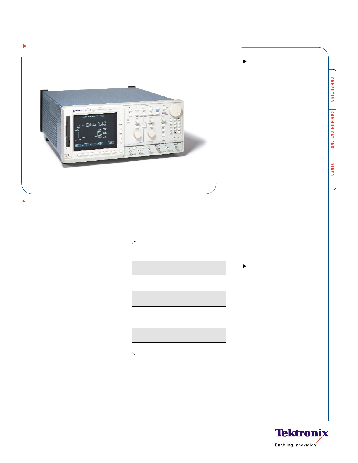
Arbitrary Waveform Generator
AWG710
The AWG710 Arbitrary Waveform Generator
Delivers World-class Signal Fidelity at 4.0 GS/s to
Solve Ever-increasing Measurement Challenges
The AWG710 combines world-class signal
fidelity with ultra high-speed mixed signal
simulation, a powerful sequencing capability
and graphical user interface with flexible
waveform editor, to solve the toughest
measurement challenges in the disk drive,
communications and semiconductor
design/test industries.
Waveform Generators
•
www.tektronix.com
1
Standard Waveforms
for Communications
ITU-T
STM1E, E5 CEPT, E4, E3, E2, E1
TI.102
STS-3, STS-1, DS4NA, DS3, DS2, DS1/1C/1A
Fibre Channel
FC1063E, FC531E, FC266E, FC133E
SDH/SONET
OC-48/STM-16, OC-36, OC-24, OC-18,
OC-12/STM-4, OC-3/STM-1, OC-1/STM-0
Other
D2, D1, FDD-1, 100Base-TX, Gigabit Ethernet
AWG710.
Characteristics
Arbitrary Waveforms
Waveform Length – 960 to 16,200,000 points
(or 32,400,000 points, option 01) in multiples of four.
Sequence Length – 1 to 8,000 steps.
Sequence Repeat Counter – 1 to 65,536 or infinite.
Function Generator Waveforms
Operation Mode – Continuous mode only.
Waveform Shape – Sine,Triangle, Square, Ramp,
Pulse or DC.
Frequency – 1.000 Hz to 400.0 MHz.
Amplitude –
Range: 0.020V
p-p
to 2 V
p-p
into 50 Ω.
Resolution: 1 mV.
Offset –
Range: –0.500 V to +0.500 V into 50 Ω.
Resolution: 1 mV.
DC Level – DC waveform only.
Range: –0.500 V to +0.500 V into 50 Ω.
Resolution: 1 mV.
Polarity – Normal, Invert.
Duty Cycle –
Range: 0.1% to 99.9%,Pulse waveform only.
Resolution:
1.000 Hz to 4.000 MHz: 0.1% step.
4.001 MHz to 20.00 MHz: 0.5% step.
20.01 MHz to 40.00 MHz: 1% step.
40.01 MHz to 80.00 MHz: 2% step.
80.01 MHz to 100.0 MHz: 2.5% step.
100.1 MHz to 160.00 MHz: 4% step.
160.1 MHz to 200.0 MHz: 5% step.
200.1 MHz to 400.0 MHz: 10% step.
Marker Out –
Marker1 Pulse Width:
Hi/Lo: 20%/80% of Period.
Marker2 Pulse Width:
Hi/Lo: 50%/50% of Period,except 100.1 MHz
to 160.0 MHz.
Hi/Lo: 52%/48% of Period,at 100.1 MHz
to 160.0 MHz.
Marker Level:
Hi Level: 2V into 50 Ω.
Lo Level: 0V into 50 Ω.
Clock Generator
Sampling Frequency – 50.000000 kHz
to 4.0000000 GHz.
Resolution – 8 digits.
Internal Clock – Accuracy: ±1 ppm.
Phase Noise – (data clock is 1/4th of the output
sample rate)
At 1 GS/s, 10 kHz offset: –80 dBc/Hz.
At 1 GS/s, 100 kHz offset: –100 dBc/Hz.
Operating Modes
Continuous – Waveform is iteratively output. If a
sequence is defined, the sequence order and repeat
functions are applied.
Trigger ed– Waveform is output only once when
an external, internal, GPIB, LAN or manual trigger
is received.
Gated – Waveform begins output when gate is true
and resets to beginning when false.
Enhanced – Waveform is output as defined by
the sequence.
Internal Trigger Generator
Internal Trigger Rate –
Range: 1.0 µs to 10.0 s.
Resolution: 3 digits,0.1 µs minimum.
Accuracy: ±0.1%.
Main Output
Output Signal – Complementary; CH1 and channel
inverse.
Digital to Analog Converter –
Resolution: 8-bits.
Differential Non-linearity: ±1/2-LSB.
Integral Non-linearity: ±1-LSB.
Output Connector – Front Panel SMA.
Normal Out*
1
Amplitude –
Output Voltage:–1.5 V to +1.5 V into 50 Ω.
Amplitude: 20 mV to 2.0 V into 50 Ω.
Resolution: 1 mV.
DC Accuracy:±(2.0% of Amplitude + 2 mV) at
offset = 0 V.
Offset –
Range: –0.500V to +0.500V into 50 Ω.
Resolution: 1 mV.
Accuracy: ±1.5% of offset ±10 mV at 20 mV
amplitude.
Pulse Response – (–1 and 1 waveform data,
0 V offset, through filter at 1 V
p-p
, clock 1 GS/s):
Rise Time:(10% to 90%): ≤480 ps.
Fall Time:(10% to 90%): ≤480 ps.
Aberrations:At 1.0 V
p-p
.
Amplitude: ±6%.
Flatness: (after 20 ns from rise/fall edge) ±3%.
Sine Wave Characteristics (4.0GS/s clock,
32 waveform points, 125 MHz signal frequency,
1.0 V amplitude,0V offset,through filter) –
Harmonics: ≤-40 dBc, DC to 1000 MHz.
Noise: ≤-50 dBc, DC to 1000 MHz.
Phase Noise: ≤–85 dBc/Hz at 10 kHz offset.
Filter*
1
Type– 20,50,100,200 MHz Bessel low-pass.
Rise Time (10% to 90%)– 20 MHz, 17 ns; 50 MHz,
7.0 ns; 100 MHz,3.7 ns; 200 MHz, 2.0 ns.
Group Delay – 20 MHz,18 ns; 50 MHz, 8 ns;
100 MHz, 4.7 ns; 200 MHz, 3 ns.
Direct D/A Out*
1
Amplitude – 20 mV
p-p
to 1.0 V
p-p
into 50 Ω.
Resolution – 1mV.
DC Accuracy – ±(2% of Amplitude + 2 mV).
Offset – no function.
DC Offset Accuracy– 0V ±10 mV at 20 mV
amplitude (waveform data = 0).
Pulse Response (–1 and 1 waveform data,
at 0.5 V
p-p
)–
Rise Time (10% to 90%):≤280 ps.
Fall Time (10% to 90%):≤280 ps.
Output Impedance – 50 Ω.
*1Option 02 eliminates the ability to switch between normal
and direct D/A out, as well as filter and offset control.
Waveform Generators
•
www.tektronix.com
2
Arbitrary Waveform Generator
AWG710
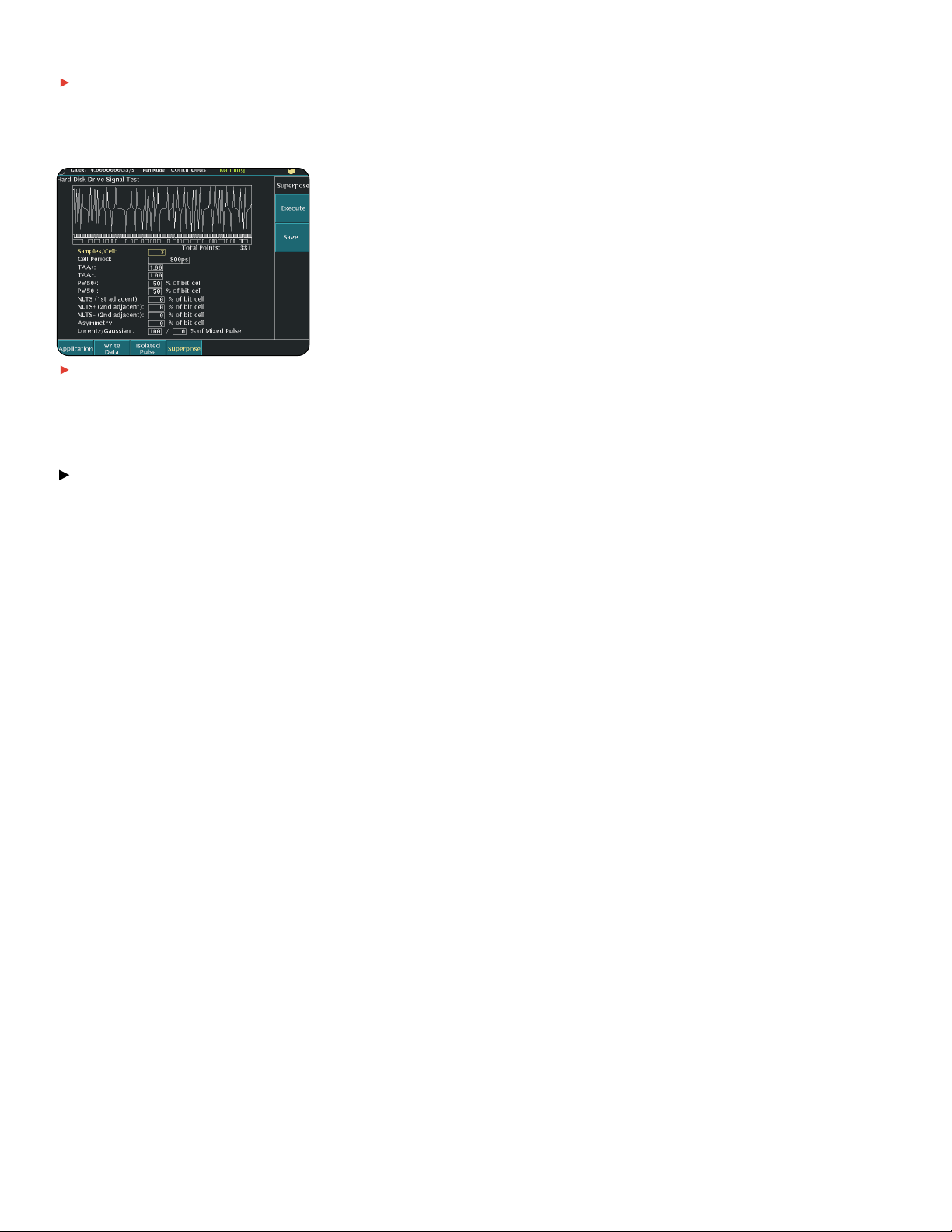
The built-in signal applications enable you
to easily create standard waveforms for disk
drive, communications and semiconductor
applications.A disk drive read channel is
shown here.

Extended Bandwidth Output
(Option 02)
Amplitude – 500 mV
p-p
to 1.0 V
p-p
into 50 Ω.
Resolution – 1mV.
DC Accuracy – ±(2.0% of amplitude + 2 mV).
Offset – No function.
Filter – No function.
DC Offset Accuracy– 0V ±10mV
(waveform data = 0).
Pulse Response – (–1 and 1 waveform data,
at 1.0 V
p-p
).
Rise Time – (10% to 90%): <
175 ps.
Fall Time – (10% to 90%): <175 ps.
Output Impedance – 50 Ω.
Auxiliary Outputs
Marker
Number – 2 (complementary).
Level –
Hi/Lo: –1.1V to 3.0V into 50 Ω (Max. 2.5 V
p-p
).
-2.2 V to 6.0V into 1 MΩ. (Max. 2.5V
p-p
).
Amplitude: 2.5V
p-p
max. into 50 Ω.
Resolution – 0.05 V.
DC Accuracy – Within ±0.1 V ±5% of setting
into 50 Ω.
Rise/Fall Time (20% to 80%)– 150 ps
(2 V
p-p
, Hi +1 V,Lo –1 V) into 50 Ω.
Period Jitter –
At 4 GS/s 1.6 ps
RMS
.
At 2 GS/s 1.9 ps
RMS
.
At 1 GS/s 2.5 ps
RMS
.
Cycle-to-Cycle Jitter –
At 4 GS/s 3.1 ps
RMS
.
At 2 GS/s 3.2 ps
RMS
.
At 1 GS/s 3.1 ps
RMS
.
Delay (between analog output and
marker output) -
Marker Level: 2V
p-p
(Hi +1 V/Lo –1 V).
Analog Output:At 1 V
p-p
.
Normal Output: 3 ns (Offset 0 V,Filter = “Through.”)
Direct Output, –500 ps.
Marker Skew – 70 ps (typical).
Connector – Front-panel SMA.
10 MHz Reference Clockout
Amplitude – 1.2 V
p-p
into 50 Ω. Max 2.5 V
p-p
open.
Impedance – 50 Ω,AC coupling.
Connector – Rear-panel BNC.
1/4 Clock Out
Level – ECL 100 K compatible.
Period Jitter –
At 4 GS/s 2.6 ps
RMS
.
At 2 GS/s 2.4 ps
RMS
.
At 1 GS/s 1.9 ps
RMS
.
Cycle-to-Cycle Jitter –
At 4 GS/s 4.8 ps
RMS
.
At 2 GS/s 3.7 ps
RMS
.
At 1 GS/s 3.1 ps
RMS
.
Connector – Rear-panel BNC.
Trigger In
Impedance: 1 kΩ or 50 Ω.
Polarity: POS or NEG.
Connector: Rear-panel BNC.
Input Voltage Range –
1 kΩ:±10V.
50 Ω:±5V.
Threshold –
Level: –5.0 V to 5.0 V.
Resolution: 0.1V.
Accuracy: ±5% of level + 0.1 V.
Trigger Mode–
Minimum Pulse Width:10 ns, 0.2 V amplitude.
Trigger Holdoff:≥109.5 clocks + 500 ns.
Delay to Analog Out:211.5 clocks + 17 ns (Normal
Output, Filter “Through”).
Gate Mode –
Minimum Pulse Width (0.2V amplitude): 1152 clocks +
10 ns.
Gate Hold Off: ≤1920 clocks + 20 ns.
Delay to Analog Out:1355 to 1499.5 clocks + 9 ns
(Normal Output, Filter “Through”).
Event Trigger Input –
Number of Events: 4-bits.
Input Signals: 4 event bits, strobe.
Threshold:TTL level.
Maximum Input: 0V to +5V (DC + peakAC).
Impedance 1 kΩ, pull-up to +3.3 V.
Connector: Rear-panel 9-Pin D-sub.
Enhanced Mode –
Minimum Pulse Width:320 clocks + 10 ns.
Event Hold Off: ≤896 clocks + 20 ns.
Delay to Analog Out (Jump timing:Async):
Strobe: ON,1627.5 clocks + 7 ns.
Strobe: OFF, 1883.5 clocks + 5 ns.
Event Input to Strobe Input:
Setup Time:192 clocks + 10 ns.
Hold Time:192 clocks + 10 ns.
Reference 10 MHz Clock IN –
Input Voltage Range:0.2 V to 3.0 V
p-p
,
±10 V maximum.
Impedance: 50 Ω,AC coupled.
Frequency Range: 10 MHz ±0.1 MHz.
Connector: Rear-panel BNC.
General Characteristics
Display – Color TFT LCD.
Display Area – Horizontal: 13.06 cm (5.14 in.),
Vertical:9.70 cm (3.81 in.)
Resolution – 640x480.
Data Storage
Internal Hard Disk – 10.0 GB.
Flash Disk – 256 MB.
Floppy Disk – 3.5", 1.44 MB.
Environment
Temper ature–
Operating: 10 °C to +40 °C.
Nonoperating: –20 °C to +60 °C.
Humidity –
Operating: 20% to 80%.
Nonoperating: 5% to 90%.
Altitude (Hard Disk Restriction)-
Operating: Up to 3,000 m (10,000 ft.).
Nonoperating: Up to 12,000 m (40,000 ft.).
Random Vibration –
Operating: 0.27 G
RMS
, 5 Hz to 500 Hz, 10 minutes.
Nonoperating: 2.28 G
RMS
, 5 Hz to 500 Hz, 10 minutes.
Shock – Nonoperating: 294 m/s2(30 G), half-sine,
11 ms duration (three times each axis, in each
direction, 18 total).
EMC Compliance – EC Council Directive 89/336/EEC
(EC-92),AS/NZS2064-1/2.
Safety – UL 3111-1, CSA C22.2 No. 1010.1,
EN61010-1, IEC61010-1.
Waveform Generators
•
www.tektronix.com
3
Arbitrary Waveform Generator
AWG710

Arbitrary Waveform Generator
AWG710
Power Supply
Rating – 100 to 240 VAC.
Range – 90 to 250 VAC.
Maximum Power and Current – 220 VA and 5 A.
Frequency – 48 to 63 Hz.
Physical Characteristics
Dimensions mm in.
Height 193 7.60
Width 433 17.05
Depth 508 20.00
Weight kg lbs.
Without package 14.1 31.10
With package 24.5 54.00
Interfaces – GPIB, Ethernet: 10/100Base-T,RJ-45.
PC Keyboard – 6-Pin mini-DIN, rear.
Ordering Information
AWG710
4.0 GS/s, 8-bit, 16 M point, single-channel arbitrary
waveform generator.
Includes: User manual (070-A828-00), programmer’s
manual (070-A829-00), GPIB programming examples
(062-A258-00), sample waveform library disk
(062-A271-00), performance verification
(062-A273-00), Certificate of Calibration (no charge),
Arb-Link
™
software utility (062-A270-00), 50 Ω SMA
male terminators (2) (015-1022-01), power cable.
Please specify power plug when ordering.
Options
Opt. 01 – 32 M points waveform memory.
Opt. 02 – Extends analog bandwidth to 2 GHz
(calculated based on rise time).
Opt. 10 – Flash disk and standby switch (alternative
for standard hard disk drive).
Opt. 1R – Rackmount.
Service
Opt. C3 – Calibration Service 3 years.
Opt. D1 – Calibration Data Report.
Opt. D3 – Calibration Data Report 3 years
(with Option C3).
Opt. R3 – Repair Service 3 years.
Recommended Accessories
Service Manual – Order 070-A830-00.
Protective Cover – Order 200-3696-01.
Power Cord Options
Opt. A0 – U.S. plug,115 V,60 Hz.
Opt. A1 – Euro plug, 220V,50 Hz.
Opt. A2 – UK plug, 240V,50 Hz.
Opt. A3 – Australian plug, 240V,50 Hz.
Opt. A5 – Swiss plug, 220V,50 Hz.
Opt. A99 – No power cord.
Opt. AC – China plug, 50 Hz.
Software
Arb-Link – (062-A270-01) PC-based waveform
creation utility.
Warranty
One year parts and labor.
Waveform Generators
•
www.tektronix.com
4
Contact Tektronix:
ASEAN / Australasia / Pakistan (65) 6356 3900
Austria +43 2236 8092 262
Belgium +32 (2) 715 89 70
Brazil & South America 55 (11) 3741-8360
Canada 1 (800) 661-5625
Central Europe & Greece +43 2236 8092 301
Denmark +45 44 850 700
Finland +358 (9) 4783 400
France & North Africa +33 (0) 1 69 86 80 34
Germany +49 (221) 94 77 400
Hong Kong (852) 2585-6688
India (91) 80-2275577
Italy +39 (02) 25086 1
Japan 81 (3) 3448-3010
Mexico, Central America & Caribbean 52 (55) 56666-333
The Netherlands +31 (0) 23 569 5555
Norway +47 22 07 07 00
People’s Republic of China 86 (10) 6235 1230
Poland +48 (0) 22 521 53 40
Republic of Korea 82 (2) 528-5299
Russia, CIS & The Baltics +358 (9) 4783 400
South Africa +27 11 254 8360
Spain +34 (91) 372 6055
Sweden +46 8 477 6503/4
Taiwan886 (2) 2722-9622
United Kingdom & Eire +44 (0) 1344 392400
USA 1 (800) 426-2200
USA (Export Sales) 1 (503) 627-1916
For other areas contact Tektronix,Inc. at: 1 (503) 627-7111
Updated 20 September 2002
Our most up-to-date product information is available at:
www.tektronix.com
Copyright © 2002,Tektronix,Inc.All rights reserved.Tektronix products are covered
by U.S. and foreign patents, issued and pending. Information in this publication
supersedes that in all previously published material.Specification and price change
privileges reserved. TEKTRONIX and TEK are registered trademarks of Tektronix,
Inc.All other trade names referenced are the service marks, trademarks or registered trademarks of their respective companies.
11/02 HB/XBS 76W-14865-2
 Loading...