

Page 1

Service Manual
AWG5000 Series
Arbitrary Waveform Generators
071-2083-00
Revision A
Warning
The servicing instructions are for use by qualified
personnel only. To avoid personal injury, do not
perform any servicing unless you are qualified to
do so. Refer to all safety summaries prior to
performing service.
www.tektronix.com
Page 2

Copyright © Tektronix. All rights reserved. Licensed software products are owned by Tektronix or its suppliers and
are protected by United States copyright laws and international treaty provisions.
Tektronix products are covered by U.S. and foreign patents, issued and pending. Information in this publication
supercedes that in all previously published material. Specifications and price change privileges reserved.
TEKTRONIX and TEK are registered trademarks of T ektronix, Inc.
Contacting Tektronix
Tektronix, Inc.
14200 SW Karl Braun Drive or P.O. Box 500
Beaverton, OR 97077
USA
For product information, sales, service, and technical support:
In North America, call 1-800-833-9200.
Worldwide, visit www.tektronix.com to find contacts in your area.
Page 3

Warranty 2
Tektronix warrants that this product will be free from defects in materials and workmanship for a period of one (1)
year from the date of shipment. If any such product proves defective during this warranty period, Tektronix, at its
option, either will repair the defective product without charge for parts and labor, or will provide a replacement in
exchange for the defective product. Parts, modules and replacement products used by Tektronix for warranty work may
be new or reconditioned to like new performance. All replaced parts, modules and products become the property of
Tektronix.
In order to obtain service under this warranty, Customer must notify Tektronix of the defect before the expiration of
the warranty period and make suitable arrangements for the performance of service. Customer shall be responsible for
packaging and shipping the defective product to the service center designated by Tektronix, with shipping charges
prepaid. Tektronix shall pay for the return of the product to Customer if the shipment is to a location within the country
in which the Tektronix service center is located. Customer shall be responsible for paying all shipping charges, duties,
taxes, and any other charges for products returned to any other locations.
This warranty shall not apply to any defect, failure or damage caused by improper use or improper or inadequate
maintenance and care. Tektronix shall not be obligated to furnish service under this warranty a) to repair damage
resulting from attempts by personnel other than Tektronix representatives to install, repair or service the product; b) to
repair damage resulting from improper use or connection to incompatible equipment; c) to repair any damage or
malfunction caused by the use of non-Tektronix supplies; or d) to service a product that has been modified or integrated
with other products when the effect of such modification or integration increases the time or difficulty of servicing the
product.
THIS WARRANTY IS GIVEN BY TEKTRONIX WITH RESPECT TO THE PRODUCT IN LIEU OF ANY
OTHER WARRANTIES, EXPRESS OR IMPLIED. TEKTRONIX AND ITS VENDORS DISCLAIM ANY
IMPLIED WARRANTIES OF MERCHANTABILITY OR FITNESS FOR A PARTICULAR PURPOSE.
TEKTRONIX' RESPONSIBILITY TO REPAIR OR REPLACE DEFECTIVE PRODUCTS IS THE SOLE AND
EXCLUSIVE REMEDY PROVIDED TO THE CUSTOMER FOR BREACH OF THIS WARRANTY.
TEKTRONIX AND ITS VENDORS WILL NOT BE LIABLE FOR ANY INDIRECT, SPECIAL, INCIDENTAL,
OR CONSEQUENTIAL DAMAGES IRRESPECTIVE OF WHETHER TEKTRONIX OR THE VENDOR HAS
ADVANCE NOTICE OF THE POSSIBILITY OF SUCH DAMAGES.
Page 4

Page 5

Table of Contents
Operating Information
Theory of Operation
Adjustment Procedures
General Safety Summary . . . . . . . . . . . . . . . . . . . . . . . . . . . . . . . . . . . . . . . . . . . . . . vii
Service Safety Summary . . . . . . . . . . . . . . . . . . . . . . . . . . . . . . . . . . . . . . . . . . . . . . . ix
Environmental Considerations . . . . . . . . . . . . . . . . . . . . . . . . . . . . . . . . . . . . . . . . . xi
Preface . . . . . . . . . . . . . . . . . . . . . . . . . . . . . . . . . . . . . . . . . . . . . . . . . . . . . . . . . . . . xiii
Manual Structure . . . . . . . . . . . . . . . . . . . . . . . . . . . . . . . . . . . . . . . . . . . . . . . . . . . . . xiii
Manual Conventions . . . . . . . . . . . . . . . . . . . . . . . . . . . . . . . . . . . . . . . . . . . . . . . . . . xiii
General Features . . . . . . . . . . . . . . . . . . . . . . . . . . . . . . . . . . . . . . . . . . . . . . . . . . . . . 1-1
Overview . . . . . . . . . . . . . . . . . . . . . . . . . . . . . . . . . . . . . . . . . . . . . . . . . . . . . . . . . . . 2-1
Module Overviews. . . . . . . . . . . . . . . . . . . . . . . . . . . . . . . . . . . . . . . . . . . . . . . . . . . . 2-3
Adjustment Interval . . . . . . . . . . . . . . . . . . . . . . . . . . . . . . . . . . . . . . . . . . . . . . . . . . . 3-1
Adjustment After Repair . . . . . . . . . . . . . . . . . . . . . . . . . . . . . . . . . . . . . . . . . . . . . . . 3-1
Required Equipment . . . . . . . . . . . . . . . . . . . . . . . . . . . . . . . . . . . . . . . . . . . . . . . . . . 3-2
Adjustment Overview . . . . . . . . . . . . . . . . . . . . . . . . . . . . . . . . . . . . . . . . . . . . . . . . . 3-2
Calibration Procedure . . . . . . . . . . . . . . . . . . . . . . . . . . . . . . . . . . . . . . . . . . . . . . . . . 3-5
Maintenance
Preparation . . . . . . . . . . . . . . . . . . . . . . . . . . . . . . . . . . . . . . . . . . . . . . . . . . . . . . . . . . 4-1
Preventing ESD . . . . . . . . . . . . . . . . . . . . . . . . . . . . . . . . . . . . . . . . . . . . . . . . . . . . . . 4-1
Inspection and Cleaning. . . . . . . . . . . . . . . . . . . . . . . . . . . . . . . . . . . . . . . . . . . . . . . . 4-2
Removal and Installation Procedures . . . . . . . . . . . . . . . . . . . . . . . . . . . . . . . . . . . 4-7
Preparation . . . . . . . . . . . . . . . . . . . . . . . . . . . . . . . . . . . . . . . . . . . . . . . . . . . . . . . . . . 4-7
Summary of Procedures . . . . . . . . . . . . . . . . . . . . . . . . . . . . . . . . . . . . . . . . . . . . . . . . 4-8
Required Equipment . . . . . . . . . . . . . . . . . . . . . . . . . . . . . . . . . . . . . . . . . . . . . . . . . . 4-9
Procedures for External Modules. . . . . . . . . . . . . . . . . . . . . . . . . . . . . . . . . . . . . . . . 4-10
Procedures for Internal Modules (Upper) . . . . . . . . . . . . . . . . . . . . . . . . . . . . . . . . . 4-17
Procedures for Internal Modules (Lower) . . . . . . . . . . . . . . . . . . . . . . . . . . . . . . . . . 4-26
Troubleshooting . . . . . . . . . . . . . . . . . . . . . . . . . . . . . . . . . . . . . . . . . . . . . . . . . . . . 4-37
Equipment Required . . . . . . . . . . . . . . . . . . . . . . . . . . . . . . . . . . . . . . . . . . . . . . . . . 4-37
Fault Isolation Procedure . . . . . . . . . . . . . . . . . . . . . . . . . . . . . . . . . . . . . . . . . . . . . . 4-37
Instrument Diagnostics . . . . . . . . . . . . . . . . . . . . . . . . . . . . . . . . . . . . . . . . . . . . . . . 4-44
Calibration Error . . . . . . . . . . . . . . . . . . . . . . . . . . . . . . . . . . . . . . . . . . . . . . . . . . . . 4-51
Hardware Error . . . . . . . . . . . . . . . . . . . . . . . . . . . . . . . . . . . . . . . . . . . . . . . . . . . . . 4-53
After Repair . . . . . . . . . . . . . . . . . . . . . . . . . . . . . . . . . . . . . . . . . . . . . . . . . . . . . . . . 4-55
Returning the Instrument for Service. . . . . . . . . . . . . . . . . . . . . . . . . . . . . . . . . . . . . 4-56
AWG5000 Series Service Manual i
Page 6

Table of Contents
Replaceable Parts
Parts Ordering Information . . . . . . . . . . . . . . . . . . . . . . . . . . . . . . . . . . . . . . . . . . . . . . 5-1
Using the Replaceable Parts List. . . . . . . . . . . . . . . . . . . . . . . . . . . . . . . . . . . . . . . . . . 5-3
ii AWG5000 Series Service Manual
Page 7

List of Figures
List of Figures
Figure 2-1: AWG5000 Series block diagram . . . . . . . . . . . . . . . . . . . . . . . 2-2
Figure 3-1: Service UI menu . . . . . . . . . . . . . . . . . . . . . . . . . . . . . . . . . . . . 3-3
Figure 3-2: 10 MHz Reference clock calibration test hookup . . . . . . . . . 3-5
Figure 3-3: 10 MHz Reference Calibration dialog box . . . . . . . . . . . . . . . 3-6
Figure 4-1: Disassembly procedures for external modules and internal
modules (top) . . . . . . . . . . . . . . . . . . . . . . . . . . . . . . . . . . . . . . . . . . . . . . . 4-8
Figure 4-2: Disassembly procedures for internal modules (bottom) . . . . 4-9
Figure 4-3: Handle, snaps, cosmetic covers, and front-trim unit
removal . . . . . . . . . . . . . . . . . . . . . . . . . . . . . . . . . . . . . . . . . . . . . . . . . . 4-11
Figure 4-4: EMI covers removal . . . . . . . . . . . . . . . . . . . . . . . . . . . . . . . . 4-13
Figure 4-5: Fan tray unit removal . . . . . . . . . . . . . . . . . . . . . . . . . . . . . . 4-14
Figure 4-6: Disassembly of front-panel assembly . . . . . . . . . . . . . . . . . . 4-16
Figure 4-7: Location of the cable ties . . . . . . . . . . . . . . . . . . . . . . . . . . . . 4-17
Figure 4-8: Drive module removal . . . . . . . . . . . . . . . . . . . . . . . . . . . . . . 4-18
Figure 4-9: Removing the clamp cover . . . . . . . . . . . . . . . . . . . . . . . . . . . 4-19
Figure 4-10: Multi-Input/Output board removal . . . . . . . . . . . . . . . . . . 4-20
Figure 4-11: Processor board removal . . . . . . . . . . . . . . . . . . . . . . . . . . . 4-22
Figure 4-12: Secondary power supply, power supply, and RFI filter
removal . . . . . . . . . . . . . . . . . . . . . . . . . . . . . . . . . . . . . . . . . . . . . . . . . . 4-24
Figure 4-13: Power board removal . . . . . . . . . . . . . . . . . . . . . . . . . . . . . . 4-25
Figure 4-14: Front Connector board, CLK1G module, AWG1G board,
and OUT1G boards removal (4-channel model) . . . . . . . . . . . . . . . . . 4-27
Figure 4-15: Disassembly of the CLK1G module . . . . . . . . . . . . . . . . . . 4-29
Figure 4-16: Location of the cable clamps on the AWG1G board . . . . . 4-30
Figure 4-17: Location of the cable clamp on the AWG1G board . . . . . 4-32
Figure 4-18: Location of the cable ties . . . . . . . . . . . . . . . . . . . . . . . . . . . 4-34
Figure 4-19: Location of the cable ties . . . . . . . . . . . . . . . . . . . . . . . . . . . 4-35
Figure 4-20: Primary troubleshooting tree (1) . . . . . . . . . . . . . . . . . . . . 4-38
Figure 4-21: Primary troubleshooting tree (2) . . . . . . . . . . . . . . . . . . . . 4-39
Figure 4-22: PWR board test points (J104) . . . . . . . . . . . . . . . . . . . . . . . 4-40
Figure 4-23: Secondary power supply test points (CN51 and CN61) . . 4-41
Figure 4-24: AWG1G board test points (J2000) . . . . . . . . . . . . . . . . . . . 4-42
Figure 4-25: OUT1G board test points (J7000) . . . . . . . . . . . . . . . . . . . . 4-43
AWG5000 Series Service Manual iii
Page 8

List of Figures
Figure 4-26: Diagnostics dialog box . . . . . . . . . . . . . . . . . . . . . . . . . . . . . 4-44
Figure 4-27: Calibration dialog box . . . . . . . . . . . . . . . . . . . . . . . . . . . . . 4-51
Figure 5-1: Exploded diagram - Cosmetics . . . . . . . . . . . . . . . . . . . . . . . . 5-5
Figure 5-2: Exploded diagram - EMI Covers . . . . . . . . . . . . . . . . . . . . . . . 5-6
Figure 5-3: Exploded diagram - Chassis assembly . . . . . . . . . . . . . . . . . . 5-7
Figure 5-4: Exploded diagram - Front-panel assembly . . . . . . . . . . . . . . . 5-9
Figure 5-5: Exploded diagram - Drive module . . . . . . . . . . . . . . . . . . . . 5-11
Figure 5-6: Exploded diagram - Processor module . . . . . . . . . . . . . . . . . 5-13
Figure 5-7: Exploded diagram - Power supply assembly . . . . . . . . . . . . 5-15
Figure 5-8: Exploded diagram - PCI/power interface module . . . . . . . . 5-17
Figure 5-9: Exploded diagram - Fan tray assembly . . . . . . . . . . . . . . . . 5-18
Figure 5-10: Exploded diagram - USB module . . . . . . . . . . . . . . . . . . . . 5-19
Figure 5-11: Exploded diagram - AWG1G/CLK1G/OUT1G modules . 5-21
Figure 5-12: Exploded diagram - CLK1G module . . . . . . . . . . . . . . . . . 5-22
Figure 5-13: Exploded diagram - AWG1G module . . . . . . . . . . . . . . . . . 5-23
Figure 5-14: Exploded diagram - BNC bracket . . . . . . . . . . . . . . . . . . . . 5-25
Figure 5-15: Exploded diagram - Rear connectors . . . . . . . . . . . . . . . . . 5-26
iv AWG5000 Series Service Manual
Page 9

List of Tables
List of Tables
Table 1-1: General features . . . . . . . . . . . . . . . . . . . . . . . . . . . . . . . . . . . . . 1-1
Table 1-2: Combination of instrument options . . . . . . . . . . . . . . . . . . . . . 1-2
Table 3-1: Test equipment . . . . . . . . . . . . . . . . . . . . . . . . . . . . . . . . . . . . . . 3-2
Table 4-1: External inspection checklist . . . . . . . . . . . . . . . . . . . . . . . . . . . 4-3
Table 4-2: Internal inspection checklist . . . . . . . . . . . . . . . . . . . . . . . . . . . 4-5
Table 4-3: Tools required for module removal and reinstall . . . . . . . . . . 4-9
Table 4-4: Test points voltage (J104) . . . . . . . . . . . . . . . . . . . . . . . . . . . . 4-40
Table 4-5: Test points voltage (CN51 and CN61) . . . . . . . . . . . . . . . . . . 4-41
Table 4-6: Test points voltage (J2000) . . . . . . . . . . . . . . . . . . . . . . . . . . . 4-42
Table 4-7: Test points voltage (J7000 or J6000) . . . . . . . . . . . . . . . . . . . 4-43
Table 4-8: Diagnostics error . . . . . . . . . . . . . . . . . . . . . . . . . . . . . . . . . . . 4-45
Table 4-9: Calibration error . . . . . . . . . . . . . . . . . . . . . . . . . . . . . . . . . . . 4-51
Table 4-10: Hardware error . . . . . . . . . . . . . . . . . . . . . . . . . . . . . . . . . . . 4-53
AWG5000 Series Service Manual v
Page 10

List of Tables
vi AWG5000 Series Service Manual
Page 11

General Safety Summary
Review the following safety precautions to avoid injury and prevent damage to this
product or any products connected to it.
To avoid potential hazards, use this product only as specified.
Only qualified personnel should perform service procedures.
To Avoid Fire or Personal
Injury
Use Proper Power Cord. Use only the power cord specified for this product and
certified for the country of use.
Connect and Disconnect Properly. Do not connect or disconnect probes or test
leads while they are connected to a voltage source.
Ground the Product. This product is grounded through the grounding conductor of
the power cord. To avoid electric shock, the grounding conductor must be
connected to earth ground. Before making connections to the input or output
terminals of the product, ensure that the product is properly grounded.
Observe All Terminal Ratings. To avoid fire or shock hazard, observe all ratings and
markings on the product. Consult the product manual for further ratings
information before making connections to the product.
The inputs are not rated for connection to mains or Category II, III, or IV circuits.
Do not apply a potential to any terminal, including the common terminal, that
exceeds the maximum rating of that terminal.
Power Disconnect. The power cord disconnects the product from the power source.
Do not block the power cord; it must remain accessible to the user at all times.
Do Not Operate Without Covers. Do not operate this product with covers or panels
removed.
Do Not Operate With Suspected Failures. If you suspect there is damage to this
product, have it inspected by qualified service personnel.
Avoid Exposed Circuitry. Do not touch exposed connections and components when
power is present.
Do Not Operate in Wet/Damp Conditions.
Do Not Operate in an Explosive Atmosphere.
AWG5000 Series Service Manual vii
Page 12
General Safety Summary
Keep Product Surfaces Clean and Dry.
Provide Proper Ventilation. Refer to the manual’s installation instructions for
details on installing the product so it has proper ventilation.
Symbols and Terms
Terms in this Manual. These terms may appear in this manual:
WAR N I NG. Warning statements identify conditions or practices that could result
in injury or loss of life.
CAUTION. Cautions statements identify conditions or practices that could result in
damage to this or other property.
Terms on the Product. These terms may appear on the product:
DANGER indicates an injury hazard immediately accessible as you read the
marking.
WARNING indicates an injury hazard not immediately accessible as you read the
marking.
CAUTION indicates a hazard to property including the product.
Symbols on the Product. The following symbols may appear on the product:
WARNING
High Voltage
Protective Ground
(Earth) Terminal
CAUTION
Refer to Manual
Double
Insulated
viii AWG5000 Series Service Manual
Page 13

Service Safety Summary
Only qualified personnel should perform service procedures. Read this Service
Safety Summary and the General Safety Summary before performing any service
procedures.
Do Not Service Alone. Do not perform internal service or adjustments of this
product unless another person capable of rendering first aid and resuscitation is
present.
Disconnect Power. To avoid electric shock, switch off the instrument power, then
disconnect the power cord from the mains power.
Use Care When Servicing With Power On. Dangerous voltages or currents may exist
in this product. Disconnect power, remove battery (if applicable), and disconnect
test leads before removing protective panels, soldering, or replacing components.
To avoid electric shock, do not touch exposed connections.
AWG5000 Series Service Manual ix
Page 14

Service Safety Summary
x AWG5000 Series Service Manual
Page 15
Environmental Considerations
This section provides information about the environmental impact of the product.
Product End-of-Life
Handling
Observe the following guidelines when recycling an instrument or component:
Equipment Recycling. Production of this equipment required the extraction and use
of natural resources. The equipment may contain substances that could be harmful
to the environment or human health if improperly handled at the product's end of
life. In order to avoid release of such substances into the environment and to reduce
the use of natural resources, we encourage you to recycle this product in an
appropriate system that will ensure that most of the materials are reused or recycled
appropriately.
The symbol shown to the left indicates that this product
complies with the European Union's requirements according to
Directive 2002/96/EC on waste electrical and electronic
equipment (WEEE). For information about recycling options,
check the Support/Service section of the Tektronix Web site
(www.tektronix.com).
Mercury Notification. This product uses an LCD backlight lamp that contains
mercury. Disposal may be regulated due to environmental considerations. Please
contact your local authorities or, within the United States, the Electronics
Industries Alliance (www.eiae.org) for disposal or recycling information.
Restriction of Hazardous
Substances
AWG5000 Series Service Manual xi
This product has been classified as Monitoring and Control equipment, and is
outside the scope of the 2002/95/EC RoHS Directive. This product is known to
contain lead, cadmium, mercury, and hexavalent ch romium.
Page 16

Environmental Considerations
xii AWG5000 Series Service Manual
Page 17

Preface
Manual Structure
Manual Conventions
This manual contains service information for your instrument. Read this preface to
learn how this manual is structured, the conventions it uses, and where to find
additional supplemental information related to servicing this product.
You should also read the General and Service safety summaries before servicing
the product.
This manual is divided into chapters, which are made up of related subordinate
topics. These topics can be cross referenced as sections.
Be sure to read the introductions to all procedures. These introductions provide
important information needed to do the service correctly, safely, and efficiently.
This manual uses certain conventions that you should become familiar with before
attempting service.
Modules
Replaceable Parts
Safety
Throughout this manual, any replaceable component, assembly, or part is referred
to by the term module. A module is composed of electrical and mechanical
assemblies, circuit boards, interconnecting cables, and user-accessible controls.
This manual refers to any field-replaceable assembly or mechanical part
specifically by its name or generically as a replaceable part. In general, a
replaceable part is any circuit board or assembly, such as the hard disk drive, or a
mechanical part, such as the I/O port connectors, that is listed in the replaceable
parts list of this manual.
Symbols and terms related to safety appear in the Service Safety Summary found at
the beginning of this manual.
AWG5000 Series Service Manual xiii
Page 18

Preface
xiv AWG5000 Series Service Manual
Page 19

Operating Information
Page 20

Page 21
Operating Information
For information on installing, operating, and networking the instrument, refer to
the AWG5000 Series Arbitrary Waveform Generators Quick Start User Manual.
This manual is available on the Document CD that came with your instrument, and
on the Tektronix Web site (www.tektronix.com/manuals).
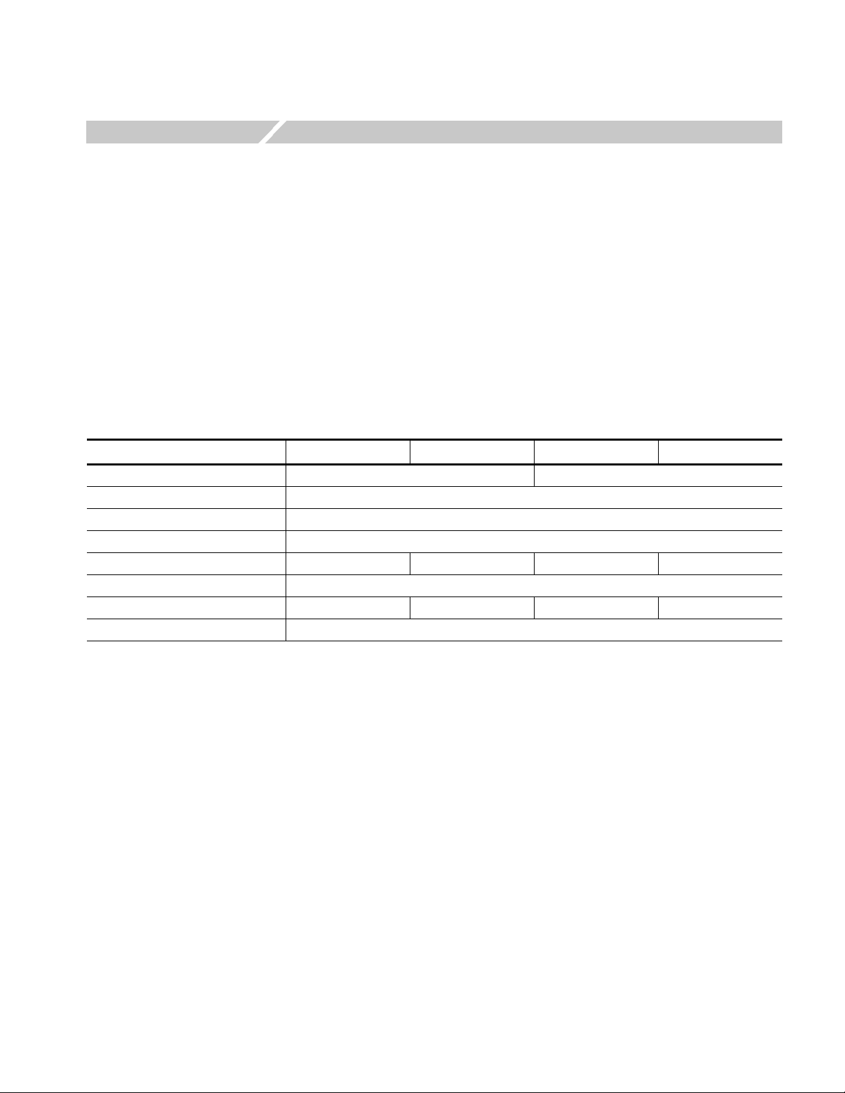
General Features
The following table and bulleted list describe the general features of the AWG5000
Series Arbitrary Waveform Generators.
Table 1-1: General features
Feature AWG5012 AWG5014 AWG5002 AWG5004
Maximum sample rate 1.2 GS/s 600 MS/s
D/A resolution 14 bits
Memory length 16,200,000 or 32,400,000 (Option 01)
Analog bandwidth 250 MHz (2 V
Analog output 2424
Maximum amplitude 4.5 V
Marker output 4848
Digital data output 28 bits (Option 03)
) or 370 MHz (0.6 V
p-p
p-p
, direct)
p-p
Windows XP Professional operating system
Up to 32,400,000 memory length (Option 01)
28 bits digital data outputs (Option 03)
A large 10.4 inch (264.2 mm) high resolution XGA color display
An intuitive, graphical user interface (UI), with built-in online help
80 GB removable hard disk drive
CD-RW/DVD drive
Supports USB 2.0 interface
LAN (1000/100/10 Base-T)
Touch screen user interface
AWG5000 Series Service Manual 1-1
Page 22
Operating Information
Options
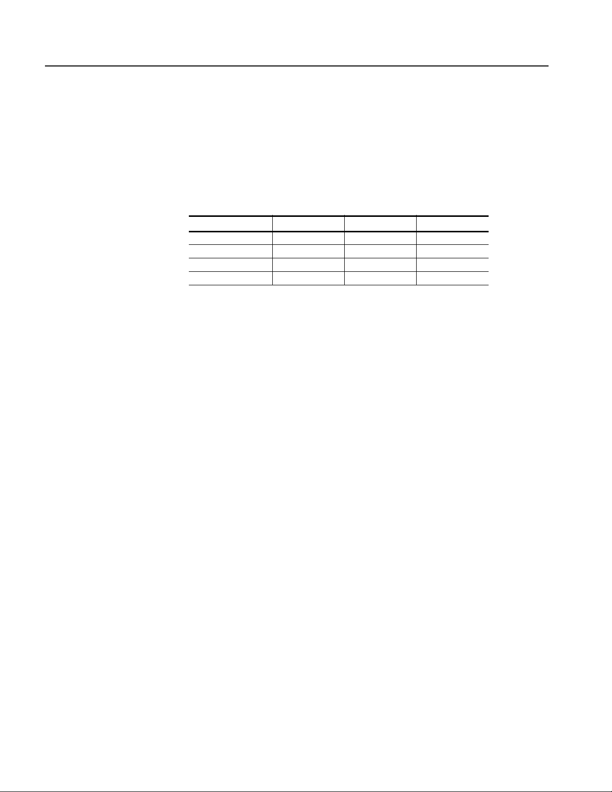
The following options are available for the instrument:
Option 01: Memory expansion to 32 MB
Option 03: 28 bits digital data outputs
Table 1-2 indicates the available combinations of instrument options.
Table 1-2: Combination of instrument options
Option 01 Option 03 Option 01, 03
AWG5014 X
AWG5012 X X X
AWG5004 X
AWG5002 X X X
Option C3: Calibration service 3 years
Option C5: Calibration service 5 years
Option D1: Calibration data report
Option D3, with Option C3: Calibration data report 3 years
Option D5, with Option C5: Calibration data report 5 years
Option R3: Repair service 3 years (including warranty)
Option R5: Repair service 5 years (including warranty)
AWG50UP Option M02: AWG5002 Field upgrade for waveform length
expansion from 16 M to 32 M points
AWG50UP Option M04: AWG5004 Field upgrade for waveform length
expansion from 16 M to 32 M points
AWG50UP Option M12: AWG5012 Field upgrade for waveform length
expansion from 16 M to 32 M points
AWG50UP Option M14: AWG5014 Field upgrade for waveform length
expansion from 16 M to 32 M points
AWG50UP Option D03: AWG5002 Field upgrade for digital data outputs
AWG50UP Option D13: AWG5012 Field upgrade for digital data outputs
1-2 AWG5000 Series Service Manual
Page 23

Theory of Operation
Page 24

Page 25

Theory of Operation
This section describes the electrical operation of the AWG5000 Series Arbitrary
Waveform Generators.
Overview
The AWG5000 Series Arbitrary Waveform Generators provide four models with
different frequency and numbers of channels. Each model consists of two major
sections: the platform section and generator section. The platform section is
common to each model.
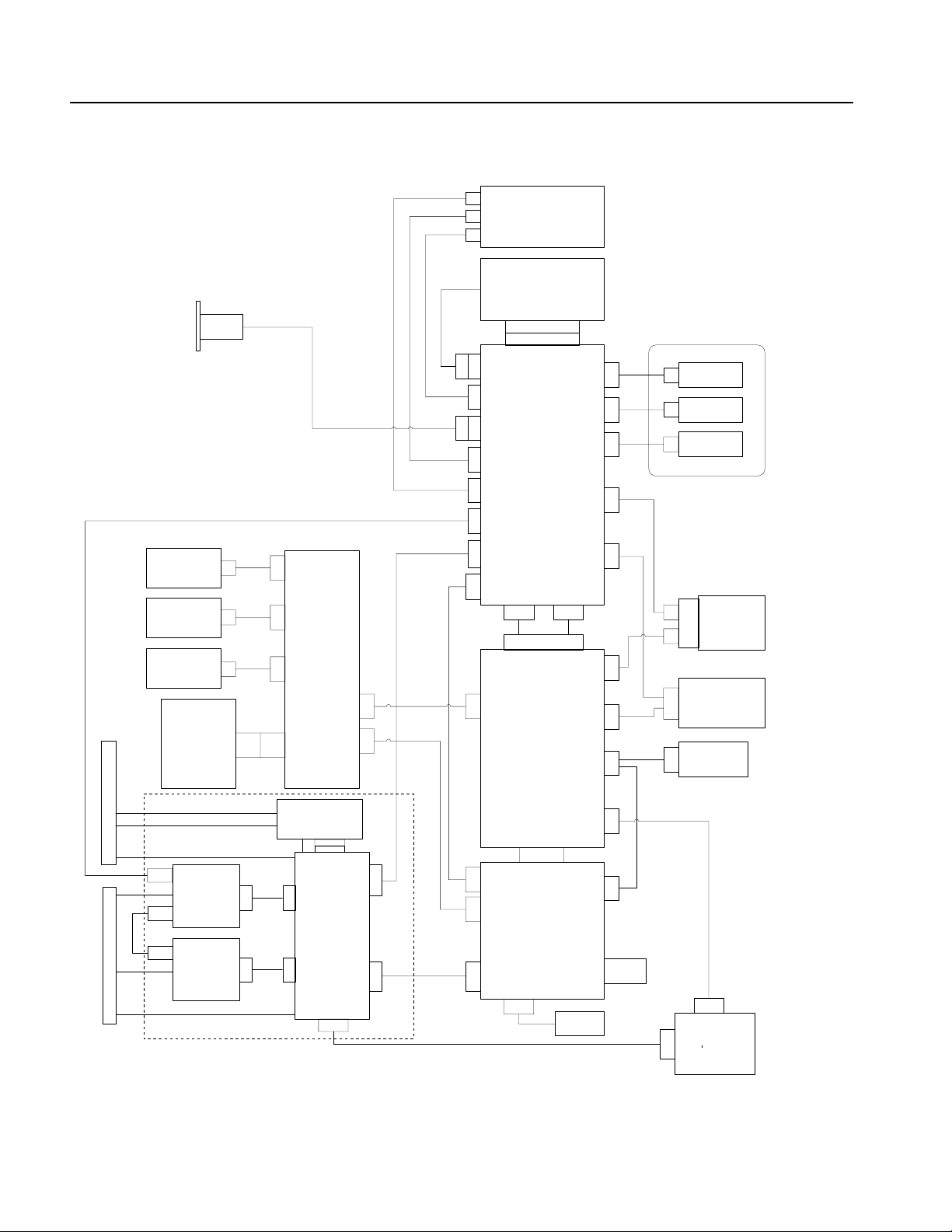
Block Diagram of the
System
The AWG5000 Series Arbitrary Waveform Generators are based on the Tektronix
DPO7000 series platform which consists of the μATX CPU board and modern
components for a PC. The instrument operates with the microsoft Window XP
operating system. Figure 2-1 on page 2-2 shows the system level block diagram of
the AWG5000 Series.
AWG5000 Series Service Manual 2-1
Page 26
Theory of Operation
5GEQPFCT[2QYGT5WRRN[
2QYGT5WRRN[
4GCT2CPGN
6QWEJ2CPGN
+PXGTVGT
$QCTF
.%&
(TQPV2CPGN
$QCTF
4(+
(KNVGT
1WVRWV
,
,
,
, ,
,
,
,
,
(CP
(CP
(CP
2QYGT$QCTF
,
,
,
,
,
,,,
.%&#FCRVQT
$QCTF
, ,
,
,
,*
2TQEGUUQTv#6:
$QCTF
,
,#,#
,
,,
,,
,,
*CTF&KUM&TKXG
,
(TQPV5YKVEJ
$QCTF
&8&41/
&TKXG
)2+$
,)
,
6GM.KPM
,
,
(TQPV%QPPGEVQT
$QCTF
,
176)$QCTF
%*%*
,
(TQPV2CPGN
,
176)$QCTF
%*%*
&GRGPFUQPVJGKPUVTWOGPVV[RG
,
,
%.-)$QCTF
, ,
#9))$QCTF
,
, ,
,
/WNVK+PRWV1WVRWV
$QCTF
,,
2%+
,
Figure 2-1: AWG5000 Series block diagram
2-2 AWG5000 Series Service Manual
Page 27

Module Overviews
Theory of Operation
A Microsoft Windows processor system is the primary controller of the instrument.
The instrument features an XGA resolution flat-panel display, a transparent touch
screen, and a front panel with direct access to commonly used instrument
functions. You can also make complete use of the instrument with a mouse and a
keyboard.
Front Panel (FP) Board
LCD Adapter (LCDA) Board
Push-button switches on the Front Panel (FP) board are read by an embedded micro
controller, which sends the button and knob change information to the μATX bo ar d
via a USB path. The FP board consists of the following blocks:
USB controller (Cypress EZ-USB FX1)
FPGA (Altera Cyclone)
Key switch matrix
LED indicators (Tri-Color and Mono-Color)
The LCDA board supports interconnection between the μATX board and FP
board. Two internal USB ports come from the μATX board. One USB connects to
a touch panel controller. The other connect to a micro controller on the FP board.
Connectors related to the LCD are also included. The LCDA board consists of the
following blocks:
Touch-panel controller
Rotary encoder (signal goes to the FP board)
LCD back light controller
Connector to LCD
Multi-Input/Output (MIO)
Board
The MIO board coordinates the flow of data through the Windows PCI port from
various devices that communicate with the μATX system. The devices include the
display system, GPIB, TekLink, and data flow (PCIF) path to the waveform
generator system. An EEROM on this board is used to store the instrument setting
and calibration data. The MIO board consists of the following blocks:
PCI controller
GPIB controller
LCD display controller (ATI Mobility-MI)
PCI target adapter
PLD140 (Xilinx FPGA)
EEPROM for calibration data storage
TekLink interface
AWG5000 Series Service Manual 2-3
Page 28

Theory of Operation
Front Switch (FSW) Board
Front Connector (FCON)
Board
Display Panel
Touch Panel
Processor (μATX ) B o ard
The FSW board provides interconnection between the Standby switch and μAT X
board. It includes an LED driver.
The FCON board provides front-panel connections of the USB ports and the DC
output. It includes common mode filters that suppress EMI radiation on the USB
signal.
The active-matrix LCD display is fully controlled by Windows drivers. It is
controlled by the ATI Mobility-M1 micro circuit on the MIO board. The display
has a 1024 x 768 resolution. Brightness is controlled by the intensity of the
backlight.
The touch information from the touch screen is processed by Windows drivers,
actively placing the pointer at the touched location. Actions from the mouse and
the touch panel are interchangeable, and treated alike by the user interface
software. The AccuTouch five-wire resistive touch screen uses a glass panel with
a uniform resistive coating. A thick polyester coversheet is tightly suspended over
the top of a glass substrate, separated by small, transparent insulating dots. The
coversheet has a hard, durable coating on the outer side and a conductive coating
on the inner side. The controller is located on the LCDA board.
The μATX board provides standard Windows functionality and I/O port interfaces
on the rear panel. This includes RS-232, Parallel, and Ethernet ports, as well as four
USB ports, including two USB2.0 ports located in the lower right front corner of
the instrument. The μATX board receives input from the front panel and touch
panel, and implements the appropriate changes. Video display data is transferred
to the MIO board through the PCI bus interface. The hard drive is connected to the
μATX board through the SATA interface, and the CD/DVD is connected to the
Windows system through the IDE parallel interface.
Power Supply
Secondary Power Supply
Fans
2-4 AWG5000 Series Service Manual
The power supply CVR460 is a switching AC to DC converter. It automatically
detects the line voltage over the range of 90 to 264 VAC. It supplies power to all
the circuitry in the instrument. No switch completely disconnects the line power
from the instrument. The ON/STBY switch controls the power to the instrument
through the μATX board circuitry. When in the “power off” condition, there is still
a low power standby current to allow the system to monitor the ON/STBY switch.
The secondary power supply ZWQ130 is a switching AC to DC converter. It
automatically detects the line voltage over the range of 85 VAC to 265 VAC.
Three fans on the side of the instrument provide forced air cooling. The fans are
controlled by the fan speed control circuit on the PWR board and are regulated by
monitoring the temperature at the circuitry.
Page 29

Theory of Operation
Power (PWR2) Board
CLK1G Board
AWG1 G B o a rd
The PWR2 board provides DC power to the fans, HDD, CD Drive, μATX b o a rd ,
MIO board, OUT1G board, and AWG1G board. All the power comes from the
CVR460 module and the ZWQ130 module. The fan control circuit has a thermal
sensor on this board. DC voltage to the fans is controlled relative to the sensed
temperature. DC-DC converters are included for generating different DC voltages.
The CLK1G board provides a 600 MHz to 1200 MHz clock to the AWG1G board.
The clock input accepts 600 MHz to 1200 MHz clock signals from an external
signal source. The reference clock input accepts 5 MHz to 800 MHz reference
clock signals from an external signal source. The 10 MHz reference output can be
used for synchronizing frequency between two or more instruments. The CLK10G
board consists of the following blocks:
VCO (600 MHz to 1200 MHz)
Fractional-N PLL
10.0 MHz TCXO (reference oscillator)
External reference input
The AWG1G board generates arbitrary waveforms based on the waveform
memory and the sequence memory. There are two types of PLDs (Xilinx FPGA)
on the board. One is an AWG controller called PLD121 which interfaces to/from
the MIO board. The other is a memory controller called PLD120 which generates
waveform patterns. Waveform data is stored in ZBT type SRAMs. The sequence
memory is included in the memory controller PLD. The AWG1G board consists of
the following blocks:
1.2 GS/s DAC (AD9736)
8 channels 8:1 MUX (TEK0015 ASIC)
PLD120 (Xilinx Virtex-4 FPGA) as a memory controller
PLD121 (Xilinx Virtex-4 FPGA) as an AWG controller
ZBT type SRAM for the waveform memory
28 bits digital output driver
Marker output driver
Trigger and event inputs
DC output
DC-DC converter
AWG5000 Series Service Manual 2-5
Page 30

Theory of Operation
OUT1G Board
The OUT1G board provides analog outputs to the front-panel connector.
Amplitude, filter, offset, add input, and On/Off controls are added to the analog
outputs. The OUT1G board consists of the following blocks:
Analog differential output amplifier
Selectable low-pass filter
Selectable attenuator
Add input from external
Control D/A for offset setting
Level monitor A/D
Relay driver
Controller PLD
2-6 AWG5000 Series Service Manual
Page 31

Adjustment Procedures
Page 32

Page 33

Adjustment Procedures
This section contains information about instrument adjustment. Only qualified
personnel should perform adjustment procedures. Read the Service Safety
Summary and the General Safety Summary before performing any service
procedures.
NOTE. Before performing adjustment procedures, you must warm up the arbitrary
waveform generator at least 20 minutes in an ambient temperature between 20 °C
and 30 °C. Adjustments performed before warm-up or outside this temperature
range may result in poor performance.
Adjustment Interval
If the instrument fails performance tests (refer to the AWG5000 Series Arbitrary
Waveform Generators Technical Reference Manual), then adjustment may be
required.
If periodic calibration is one of your requirements, a general rule is to verify
performance and make adjustments (only if needed) every 2000 hours of operation
or once a year if the instrument is used infrequently.
Adjustment After Repair
After removal and replacement of a module, you must perform the Performance
Verification procedure, found in the AWG5000 Series Arbitrary Waveform
Generators Technical Reference Manual. The Technical Reference PDF manual is
included in the Product Documentation CD. This manual is also available on the
Tektronix Web site (www.tektronix.com/manuals).
AWG5000 Series Service Manual 3-1
Page 34

Adjustment Procedures
Required Equipment
The following equipment is required to complete the procedures.
Table 3-1: Test equipment
Description Minimum requirements Recommended equipment Quantity
Frequency counter Accuracy: within ± 0.01 ppm Agilent 53181A 1 ea
50 Ω BNC cable Tektronix 012-0057-01 1 ea
Adjustment Overview
The adjustment procedure contains three adjustment items. Before performing
adjustment procedures, you must warm up the arbitrary waveform generator at
least 20 minutes in an ambient temperature between 20 °C and 30 °C.
Enable the Service Menu
You must enable the Service menu to perform the adjustment procedure. To do
this:
1. Power on the instrument.
2. Select the System menu from the menu bar, and then select Service Mode...
3. The following dialog box is displayed. Enter the password “1185”.
3-2 AWG5000 Series Service Manual
Page 35

4. The following service UI menu is displayed:
Adjustment Procedures
Figure 3-1: Service UI menu
The left half of the window with the title Calibration is the calibration part of the
window. You can perform the calibrations either all in one step or individually.
However, since the calibration sequence is predefined, follow the sequence from
the top. You must finish a calibration item listed on the upper part of the screen
before performing the lower part of the items. Some items may be grayed out,
depending on your instrument option configurations.
AWG5000 Series Service Manual 3-3
Page 36

Adjustment Procedures
Individual Calibrations
Execute All Calibrations
Saving the Calibration
Results to EEPROM
To perform individual calibrations, click the calibration buttons, starting with
10MHz Reference..., and the corresponding calibrations are executed.
To perform all calibrations in one step, click Execute All Calibrations and all
calibrations are executed in order starting from the top.
When the calibration has been performed and the results are saved to the EEPROM
(regardless of the item, all results are saved to the EEPROM on the MIO board),
the flag under Is Calibrated will be set to TRUE. If the calibration was successful,
the Status field will display PASS. If the calibration failed, FAIL will be displayed.
There are two types of calibration: Self calibration and Manual calibration.
Self calibration – The instrument performs the calibration item and ends
automatically.
Manual calibration – This calibration item requires external devices listed on
Table 3-1 and manual data input.
A warning message is displayed if you click a calibration button without waiting
for 20 minutes after the instrument powered on. Click the Cancel button and allow
at least 20 minutes for the instrument to warm up.
3-4 AWG5000 Series Service Manual
Page 37

Calibration Procedure
Adjustment Procedures
10 MHz Reference Clock
Calibration
This procedure adjusts the built-in TCXO oscillator frequency for the 10 MHz
Reference Output.
Equipment required One frequency counter
One 50 Ω BNC cable
1. Install the test hookup and preset the instrument controls:
a. Use the 50
Ω BNC cable to connect the 10 MHz Reference Output
connector on the AWG5000 rear panel to the CHANNEL 1 connector on
the frequency counter. See Figure 3-2.
AWG5000 rear panel
Frequency counter
Ω BNC cable
50
Figure 3-2: 10 MHz Reference clock calibration test hookup
2. Set the frequency counter settings as indicated below:
Input impedance . . . . . . AC, 50
Ω
Gate time . . . . . . . . . . . 0.1 s
AWG5000 Series Service Manual 3-5
Page 38

Adjustment Procedures
3. Click the 10 MHz Reference... button in the Service UI menu to display the
following dialog box:
Up/down button
Figure 3-3: 10 MHz Reference Calibration dialog box
4. Change the 10MHz Reference DAC value using the up/down button or the
front-panel rotary knob so that the frequency counter reading is within the
range of 10 MHz ±1 Hz.
Analog Output Level
Calibration
Inter-Channel Skew
Calibration
5. Click Save to EEPROM to save the data to the EEPROM.
6. Click Close to close the dialog box.
This is a self calibration. This calibration is required to ensure that the analog
output levels are within the specified range.
This is a self calibration. This calibration is required to ensure that the inter-channel
skews are within the specified range.
This completes the adjustment procedures. Disconnect the equipment from the
instrument.
3-6 AWG5000 Series Service Manual
Page 39

Maintenance
Page 40

Page 41

Maintenance
This section contains information needed to do periodic and corrective
maintenance on the instrument. The following subsections are included:
Preparation — Tells you how to get ready to do arbitrary waveform generator
maintenance.
Preparation Preventing ESD — Provides general information on preventing
damage to internal modules when doing maintenance.
Inspection and Cleaning — Information and procedures for inspecting the
instrument and cleaning its external and internal modules.
Removal and Installation Procedures — Procedures for the removal of
defective modules and replacement of new or repaired modules.
Toubleshooting — Information for isolating failed modules. Included are
instructions for operating the instrument diagnostic routines and
troubleshooting trees. Most of the trees make use of the internal diagnostic
routines to speed fault isolation to a module.
Preparation
Preventing ESD
Only qualified persons should perform service procedures. Before performing any
service procedures, read the Service Safety Summary and General Safety Summary
at the front of this manual and the ESD information below. Also refer to the
Operating Information section and your arbitrary waveform generator quick start
user manual for information about using the arbitrary waveform generator.
When performing any service that requires internal access to this instrument,
adhere to the following precautions to avoid damaging internal modules and their
components due to electrostatic discharge (ESD).
CAUTION. Static discharge can damage any semiconductor component in this
instrument.
Minimize handling of static-sensitive modules.
Transport and store static-sensitive modules in their static protected containers
or on a metal rail. Label any package that contains static-sensitive modules.
AWG5000 Series Service Manual 4-1
Page 42

Maintenance
Inspection and Cleaning
Discharge the static voltage from your body by wearing a grounded antistatic
wrist strap while handling these modules. Do service of static-sensitive
modules only at a static-free work station.
Do not allow anything capable of generating or holding a static charge on the
work station surface.
Handle circuit boards by the edges when possible.
Do not slide the modules over any surface.
Avoid handling modules in areas that have a floor or work-surface covering
capable of generating a static charge.
Inspection and Cleaning describes how to inspect for dirt and damage, and how to
clean the exterior and interior of the instrument. Inspection and cleaning are done
as preventive maintenance. Preventive maintenance, when done regularly, may
prevent instrument malfunction and enhance its reliability.
General Care
Preventive maintenance consists of visually inspecting and cleaning the instrument
and using general care when operating it.
How often to do maintenance depends on the severity of the environment in which
the instrument is used. A proper time to perform preventive maintenance is just
before instrument adjustment.
For optimum performance, follow these recommendations:
Protect the instrument from adverse weather conditions. The instrument is not
waterproof.
Do not store or leave the instrument where the liquid crystal display (LCD) will
be exposed to direct sunlight or high humidity for long periods of time.
The cabinet helps keep dust out of the instrument and must be in place during
normal operation.
To avoid damage to the instrument, do not expose it to any sprays, liquids, or
solvents.
4-2 AWG5000 Series Service Manual
Page 43

Maintenance
Inspection and Cleaning
procedures
The collection of dirt on internal components can cause them to overheat and fail.
Dirt also provides an electrical conduction path
that could cause an instrument
failure, especially under high-humidity conditions. Inspect the instrument as often
as operating conditions require.
WAR N I NG. Before performing any of the following procedures, power down the
instrument and disconnect it from line voltage.
CAUTION. Avoid the use of chemical cleaning agents, which might damage the
plastics used in this AWG5000 Series Arbitrary Waveform Generator. Use only
deionized water when cleaning the front-panel buttons. Use an ethyl alcohol
solution as a cleaner and rinse with deionized water.
Inspection — Exterior. Inspect the outside of the instrument for damage, wear, and
missing parts, using Table 4-1 as a guide. An instrument that appears to have been
dropped or otherwise abused should be checked thoroughly to verify correct
operation and performance. Immediately repair defects that could cause personal
injury or further damage to the instrument.
Table 4-1: External inspection checklist
Item Inspect for Repair action
Cabinet, front-panel,
and cover
Front-panel knob Missing, damaged, or loose knob. Repair or replace missing or
Connectors Broken shells, cracked insulation,
Carrying handle
and cabinet feet
Accessories Missing items or parts of items,
Cracks, scratches, deformations,
damaged hardware or gaskets.
and deformed contacts. Dirt in
connectors.
Correct operation. Repair or replace defective
bent pins, broken or frayed
cables, and damaged connectors.
Repair or replace defective
module.
defective knob.
Repair or replace defective
modules. Clear or wash out dirt.
module.
Repair or replace damaged or
missing items, frayed cables, and
defective modules.
Cleaning Procedure — Exterior. Do the following steps to clean the instrument
exterior:
1. Remove loose dust on the outside of the instrument with a lint-free cloth. Use
care to avoid scratching the clear glass display shield.
AWG5000 Series Service Manual 4-3
Page 44

Maintenance
2. Remove remaining dirt with a lint-free cloth dampened in a general purpose
detergent-and-water solution. Do not use abrasive cleaners.
CAUTION. To prevent getting moisture inside the instrument during external
cleaning, use only enough liquid to dampen the cloth or applicator.
To avoid damage to the surface of the instrument, do not use any abrasive or
chemical cleaning agents.
Flat Panel Display Cleaning. The display is a soft plastic display and must be treated
with care during cleaning.
CAUTION. Imported cleaning agents or methods can damage the flat panel display.
Avoid using abrasive cleaners or commercial cleaners to clean the display surface.
Avoid spraying liquids on the display surface.
Avoid scrubbing the display with excessive force.
1. Clean the flat panel display surface by gently rubbing the display with a
clean-room wipe (such as Wypall Medium Duty Wipes, #05701, available
from Kimberly-Clark Corporation).
2. If the display is very dirty, moisten the wipe with distilled water or a 75%
isopropyl alcohol solution and gently rub the display surface. Avoid using
excess force or you may damage the plastic display surface.
CAUTION. To prevent getting moisture inside the instrument during external
cleaning, use only enough liquid to dampen the cloth or applicator.
Inspection — Interior. Inspect and clean the interior if it appears that the instrument
may have been damaged or exposed to an unusually dirty environment.
To access the inside of the instrument for inspection and cleaning, refer to the
Removal and Installation Procedures in this section.
Inspect the internal portions of the instrument for damage and wear, using
Table 4-2 as a guide. Defects should be repaired immediately.
CAUTION. To prevent damage from electrical arcing, ensure that circuit boards
and components are dry before applying power to the instrument.
4-4 AWG5000 Series Service Manual
Page 45

Maintenance
Table 4-2: Internal inspection checklist
Item Inspect for Repair action
Front and rear case Cracks or deformations. Scratched lettering
or display filter. Loose connectors or labels.
Circuit boards Loose, broken, or corroded solder
connections. Burned circuit boards. Burned,
broken, or cracked circuit-run plating.
Solder connections Cold solder or rosin joints. Resolder joint and clean
Wiring and cables Loose plugs or connectors. Burned, broken,
or frayed wiring.
Chassis Dents, deformations, and damaged
hardware.
Repair or replace defective
hardware.
Remove failed module and
replace with a new module.
with ethyl alcohol.
Firmly seat connectors.
Repair or replace modules
with defective wires or
cables.
Straighten, repair, or
replace defective hardware.
Cleaning Procedure — Interior. Do the following steps to clean the instrument
interior:
1. Blow off dust with dry, low-pressure, deionized air (approximately 9 psi).
2. Remove any remaining dust with a lint-free cloth dampened in isopropyl
alcohol (75% solution) and rinse with warm deionized water. (A cotton-tipped
applicator is useful for cleaning in narrow spaces and on circuit boards.)
NOTE. If steps 1 and 2 do not remove all the dust or dirt, please contact Tektronix.
(See Contacting Tektronix at the front of this manual.)
Lubrication. There is no periodic lubrication required for the AWG5000 Series
Arbitrary Waveform Generator.
AWG5000 Series Service Manual 4-5
Page 46

Maintenance
4-6 AWG5000 Series Service Manual
Page 47

Removal and Installation Procedures
This section contains procedures for removal and installation of all mechanical and
electrical modules.
Preparation
WAR N I NG. Only qualified personnel should perform service procedures.
Before performing this or any other procedure in this manual, read the General
Safety Summary and Service Safety Summary found at the beginning of this
manual.
To prevent damage to the instrument components, read Preventing ESD in this
section.
Before doing any procedure in this section, disconnect the power cord from the line
voltage source.
This section contains the following items:
This preparatory information that you need to properly do the following
procedures.
Adjustment after repair
List of Modules
List of tools required to remove and disassemble all modules.
Procedures for removal and reinstallation of the modules.
NOTE. Read Equipment Required for a list of the tools needed to remove and install
modules in this instrument. See Table 4-3, on page 4-9. Read the cleaning
procedure before disassembling the instrument for cleaning.
After the removal and replacement of a module due to electrical failure, perform
the adjustment procedures. Refer to the Adjustment Procedures section.
The Replaceable Parts section provides a list of all replaceable modules. Any
electrical or mechanical module, assembly, or part listed in the parts list is referred
to as a module.
AWG5000 Series Service Manual 4-7
Page 48

Removal and Installation Procedures
Summary of Procedures
Disassembly for replacement is best achieved by removing and replacing the
modules in a specific order. Complete disassembly is best achieved by the
following procedures in the order given in Figure 4-1 and Figure 4-2.
Front-panel assembly Fan tray unit Hard disk assembly
Front switch board LCDA board Touchscreen assembly Drive-bay module DVD-ROM board
Handle unit
Snaps
Cosmetic covers
Front trim unit
EMI Cover (top)
Inverter Front-panel board LCD display Drive-bay bracket DVD-ROM drive
MIO board
Processor module* * To remove the Prosessor
Secondary power supply
Power supply
RFI filter
Power board
Figure 4-1: Disassembly procedures for external modules and internal modules (top)
module, you need to
remove the AWG1G board.
4-8 AWG5000 Series Service Manual
Page 49

Removal and Installation Procedures
Handle unit
Cosmetic covers
Front trim unit
EMI cover (bottom)
Front connector board CLK1G module CLK1G board
AWG5012/AWG5002 AWG1G 2 ch board AWG1G 4 ch board AWG5014/AWG5004
Required Equipment
CH1 & CH2 OUT1G
board
CH1 & CH2 OUT1G
board
CH3 & CH4 OUT 1G
board
Figure 4-2: Disassembly procedures for internal modules (bottom)
Most modules in the instrument can be removed with a screwdriver handle
mounted with a size T-15, Torx screwdriver tip. All equipment required to remove
and reinstall the modules is listed in Table 4-3.
Table 4-3: Tools required for module removal and reinstall
Item # Name Description General tool #
1. Screwdriver handle Accepts Torx-driver bits 620-440
2. T-15 Torx tip Torx-driver bit for T-15 size screw
heads
3. T-10 Torx tip Torx-driver bit for T-10 size screw
heads
4. T-20 Torx tip Torx-driver bit for T-20 size screw
heads
5. #1 Phillips screwdriver Screwdriver for removing #1 size
Phillips screws
6. #2 Phillips screwdriver Screwdriver for removing # 2 size
Phillips screws
7. 3/16 inch open-end wrench Used to remove nut posts Standard tool
8. Angle-Tip Tweezers Used to remove the front-panel knob Standard tool
9. Wire cutter Used to remove cable ties Standard tool
640-247
Standard tool
Standard tool
AWG5000 Series Service Manual 4-9
Page 50

Removal and Installation Procedures
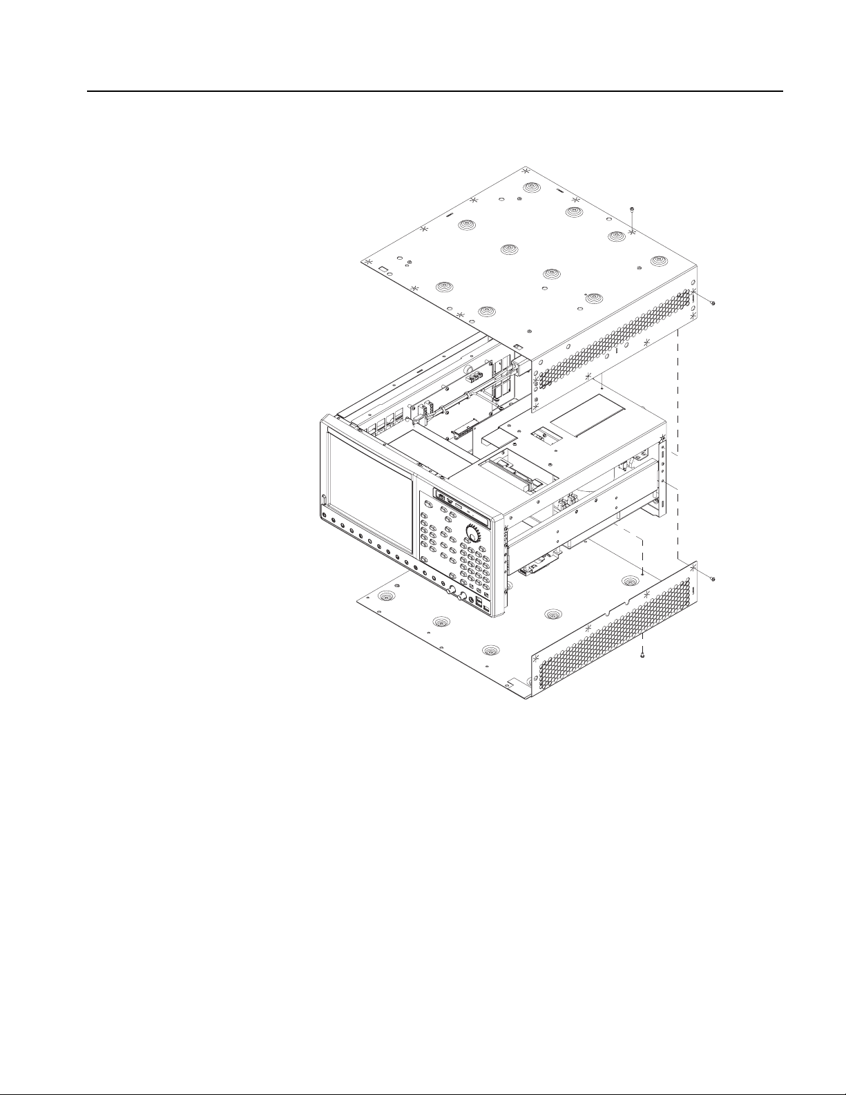
Procedures for External Modules
Handle Unit
Snaps
Cosmetic Cover (Top)
You need a screwdriver with a T-20 Torx tip (items 1 and 4).
Removal. To remove the handle unit, refer to Figure 4-3 and follow these steps:
1. Remove the two screws securing the handle base bracket to the cosmetic cover.
2. Grasp the bracket and handle away from the cosmetic cover.
Installation. To install, reverse this procedure.
You need a screwdriver with a T-15 Torx tip (items 1 and 2).
Removal. To remove the snaps, refer to Figure 4-3 and follow these steps:
1. Remove the four screws securing the snaps to the cosmetic cover.
2. Lift the snaps away from the cosmetic cover.
Installation. To install, reverse this procedure.
You need a screwdriver with a T-15 Torx tip (items 1 and 2).
Removal. To remove the top cosmetic cover, refer to Figure 4-3 and follow these
steps:
Cosmetic Cover (Bottom)
1. Remove the snaps.
2. Remove the two screws securing the cosmetic cover to the chassis.
3. Loosen the cover with a detaching tool, such as a flat-blade screwdriver.
4. Tilt the rear side of the cover up, and then pull it off the chassis.
Installation. To install, reverse this procedure.
You need a screwdriver with a T-15 Torx tip (items 1 and 2).
Removal. To remove the top cosmetic cover, refer to Figure 4-3 and follow these
steps:
1. Remove the handle unit.
2. Orient the instrument so its top is down on the work surface and its rear is
facing you.
3. Remove the two screws securing the cosmetic cover to the chassis.
4. Loosen the cover with a detaching tool, such as a flat-blade screwdriver.
4-10 AWG5000 Series Service Manual
Page 51

Removal and Installation Procedures
5. Tilt the rear side of the cover up, and then pull it off the chassis.
Installation. To install, reverse this procedure.
Cosmetic cover (top)
Snap
Front-trim unit
Cosmetic cover (bottom)
Figure 4-3: Handle, snaps, cosmetic covers, and front-trim unit removal
Handle base bracket
AWG5000 Series Service Manual 4-11
Page 52

Removal and Installation Procedures
Front-Trim Unit
You need a screwdriver with a T-15 Torx tip and angle-tip tweezers
(items 1, 2, and 8).
Removal. To remove the front-trim unit, refer to Figure 4-3 follow these steps:
1. Remove the handle unit, snaps, and cosmetic covers.
2. Orient the instrument so that the rear is on the work surface.
3. Paste a tape to the power switch button so that it will not come off the front
trim.
4. Remove the knob by pulling it straight out from the front panel with the
angle-tip tweezers.
5. Remove the three screws at the bottom of the front trim.
6. Grasp the bottom side of the front trim, and pull off the bottom side of it by
loosening the DVD drive part.
7. The upper part of the chassis has three projections. The front trim fits in these
projections. When removing the front trim, grasp its back edge and flex it
upward before pulling it forward.
Installation. To install, reverse this procedure.
EMI Covers
You need a screwdriver with a T-15 Torx tip (items 1 and 2).
Removal. To remove the EMI covers, refer to Figure 4-4 on page 4-13 and follow
these steps:
1. Remove the handle unit, snaps, cosmetic covers, and front-trim unit.
2. Remove the top cover:
a. Orient the instrument so that the bottom is on the work surface.
b. Remove the 14 screws securing the top EMI cover to the chassis.
c. Lift the cover off the chassis.
3. Remove the bottom cover:
a. Orient the instrument so that the top is on the work surface.
b. Remove the 12 screws securing the bottom EMI cover to the chassis.
c. Lift the cover off the chassis.
Installation. To install, reverse this procedure.
4-12 AWG5000 Series Service Manual
Page 53
Removal and Installation Procedures
Figure 4-4: EMI covers removal
Hard Disk Assembly
AWG5000 Series Service Manual 4-13
Removal. To remove the removable hard disk assembly, follow these steps:
1. Orient the instrument so that its bottom is down on the work surface and its rear
is facing you.
2. Loosen the two thumb screws securing the hard disk assembly to the
instrument.
3. Holding the screw heads, pull out the removable hard disk assembly carefully.
Installation. To install, reverse this procedure.
Page 54

Removal and Installation Procedures
CAUTION. The hard disk drive is extremely susceptible to static-discharge damage,
shock, dust and so on. When you store a removable hard disk assembly, put it into
an anti-static plastic bag to protect it.
Fan Tray Unit
You need a screwdriver with a T-15 Torx tip and a #2 Phillips screwdriver (items 1,
2, and 6).
Removal. To remove the fan tray unit, refer to Figure 4-5 on page 4-14 and follow
these steps:
1. Remove the handle unit, snaps, cosmetic covers, front-trim unit, and EMI
covers.
2. Disconnect the fan cables from J300, J302, and J304 on the Power board.
3. Remove the four screws securing the fan tray unit to the chassis.
4. Lift the fan tray unit away from the chassis.
5. Use a #2 Phillips screwdriver to remove the 12 screws securing the fans to the
fan bracket.
Install. To install, reverse this procedure.
Fan bracket
Figure 4-5: Fan tray unit removal
4-14 AWG5000 Series Service Manual
Page 55

Removal and Installation Procedures
Front-Panel Unit
Front-Panel Assembly
You need a screwdriver with a T-15 Torx tip (items 1 and 2).
Removal. To remove the front-panel unit, refer to Figure 4-6 on page 4-16 and
follow these steps:
1. Remove the handle unit, snaps, cosmetic covers, front-trim unit, and EMI
covers.
2. Orient the instrument so that the rear is on the work surface.
3. Remove the seven screws securing the front-panel bracket to the chassis.
4. Grasp the front-panel assembly and pull it forward.
5. Disconnect the cable from J100 on the LCDA board.
6. Disconnect the cable from J300 on the LCDA board.
7. Disconnect the cable from J100 on the Front Switch board.
Installation. To install, reverse this procedure.
You need a a screwdriver with a T-15 Torx tip (items 1 and 2).
Removal. To remove the front-panel assembly, refer to Figure 4-6 on page 4-16 and
follow these steps:
1. Remove the handle unit, snaps, cosmetic covers, front-trim unit, and EMI
covers.
2. Remove the LCDA board and Front Panel board:
a. Remove the four screws securing the LCDA board and Front Panel board
to the front-panel bracket.
b. Remove the cables from J110, J160, and J200.
c. Lift the boards away from the front-panel bracket.
3. Remove the touch screen module:
a. Remove the two screws securing the touch screen module to the
front-panel bracket.
b. Disconnect the cable from J200 on the LCDA board.
c. Lift the touch screen module away from the front-panel bracket.
AWG5000 Series Service Manual 4-15
Page 56

Removal and Installation Procedures
4. Remove the LCD module:
5. Disassemble the front-panel assembly components, using Figure 4-6 as a
Installation. To install, reverse this procedure.
a. Remove the four screws securing the LCD module to the front-panel
bracket.
b. Disconnect the cable from J110 on the LCDA board.
c. Disconnect the cable from CN2 on the Inverter board.
d. Lift the LCD module away from the front-panel bracket.
guide.
FSW board
Front-panel bracket
Inverter board
LCD module
Touch screen module
Figure 4-6: Disassembly of front-panel assembly
LCDA board
Front Panel board
4-16 AWG5000 Series Service Manual
Page 57

Procedures for Internal Modules (Upper)
Removal and Installation Procedures
Drive-Bay Module
You need a screwdriver with a T-15 Torx tip and a wire cutter (items 1, 2, and 9).
Removal. To remove the drive-bay module, refer to Figure 4-8 on page 4-18 and
follow these steps:
1. Remove the handle unit, snaps, cosmetic covers, front-trim unit, EMI covers,
and hard disk assembly.
2. Orient the instrument so that the bottom is on the work surface.
3. Remove the eight screws securing the drive-bay module to the chassis.
4. Use a wire cutter to remove the two cable ties. See Figure 4-7.
DVD-ROM Drive
Cable ties
Figure 4-7: Location of the cable ties
5. Disconnect the cables from J101 and J104 on the Power board.
6. Disconnect the cables from J5J1 and J7J1 on the Processor board.
7. Lift the drive-bay module away from the chassis.
Installation. To install, reverse this procedure.
You need a screwdriver with a T-15 Torx tip and a #1 Phillips screwdriver (items 1,
2, and 5).
Removal. To remove the DVD-ROM drive, refer to Figure 4-8 on page 4-18 and
follow these steps:
1. Remove the handle unit, snaps, cosmetic covers, front-trim unit, EMI covers,
hard disk assembly, and drive-bay module.
AWG5000 Series Service Manual 4-17
Page 58

Removal and Installation Procedures
2. Remove the two screws securing the DVD-ROM bracket to the drive-bay
3. Slide the DVD-ROM drive with bracket out from the drive-bay chassis.
4. Remove the four screws securing the DVD-ROM drive to the bracket.
Installation. To install, reverse this procedure.
DVD-ROM board
DVD-ROM drive
DVD-ROM drive
chassis.
Drive-bay chassis
DVD-ROM bracket
Figure 4-8: Drive module removal
4-18 AWG5000 Series Service Manual
Page 59

Removal and Installation Procedures
DVD-ROM Board
Multi-Input/Output Board
You need a #1 Phillips screwdriver (item 5).
Removal. To remove the DVD-ROM board, refer to Figure 4-8 and follow these
steps:
1. Remove the handle unit, snaps, cosmetic cover, front-trim unit, EMI covers,
hard disk assembly, and drive-bay module.
2. Remove the two screws securing the DVD-ROM board to the DVD-ROM
drive.
3. Disconnect the cable from J1 on the DVD-ROM board.
4. Disconnect the interface cable on the DVD-ROM board.
5. Lift the board away from the DVD-ROM drive.
Installation. To install, reverse this procedure.
You need a screwdriver with a T-15 Torx tip (items 1 and 2).
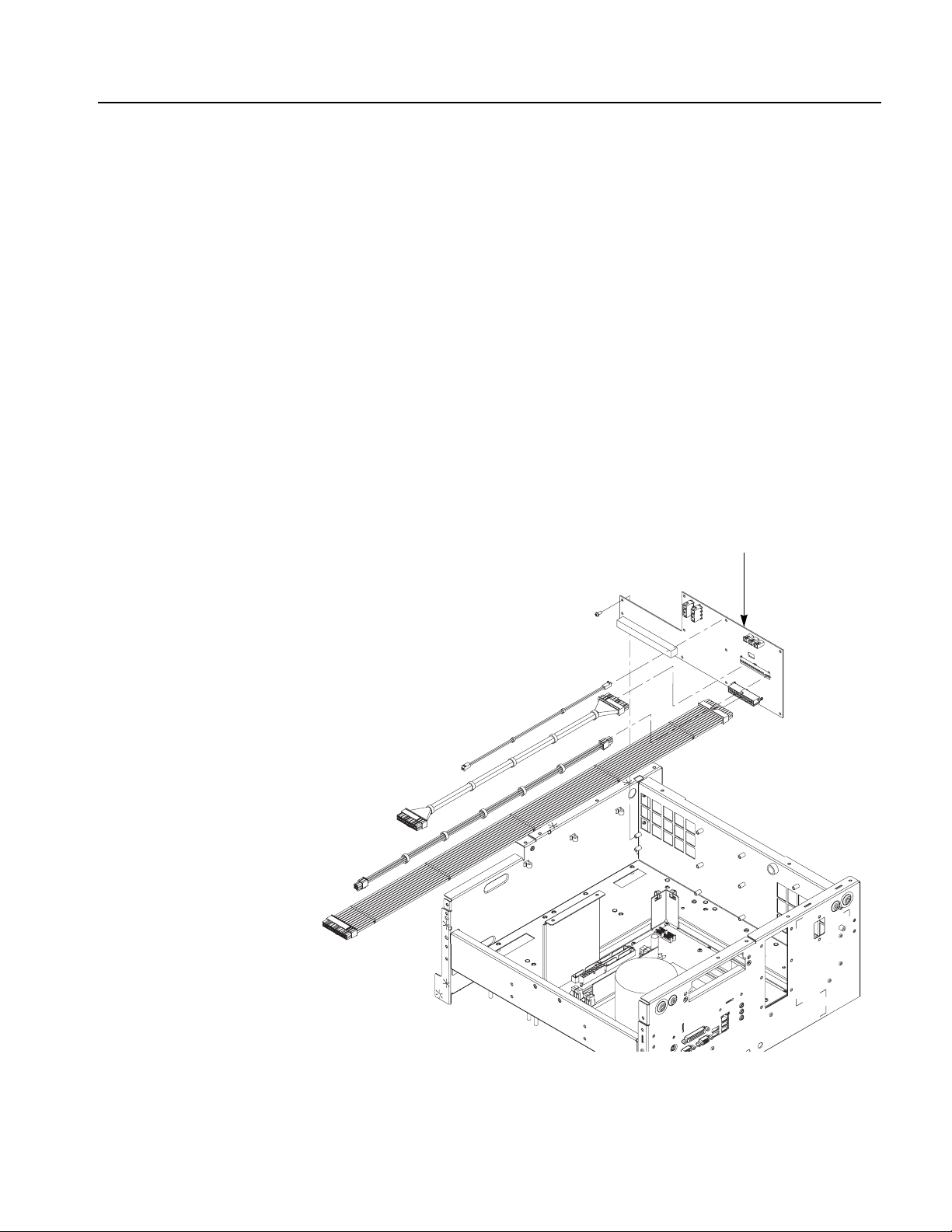
Removal. To remove the Multi-Input/Output board, refer to Figure 4-10 and follow
these steps:
1. Remove the handle unit, snaps, cosmetic covers, front-trim unit, and EMI
covers.
2. Orient the instrument so that the bottom is on the work surface and the rear is
facing you.
3. Remove the clamp cover from the cable clamp to release the ribbon cable.
See Figure 4-9.
Multi-Input/Output board
clamp cover
Figure 4-9: Removing the clamp cover
AWG5000 Series Service Manual 4-19
Page 60

Removal and Installation Procedures
4. Disconnect the cables from J360, J670, J680, and J681 on the
5. Remove the six screws securing the Multi-Input/Output board to the chassis.
6. Carefully pull up on the board to loosen it from the Processor board.
7. Lift the board away from the chassis.
Installation. To install, reverse this procedure.
Multi-Input/Output board.
Processor Module
Multi-Input/Output board
Figure 4-10: Multi-Input/Output board removal
You need a screwdriver with a T-15 Torx tip, and a 3/16 inch open-end wrench
(items 1, 2, and 7).
NOTE. Before you remove the processor module, you need to disconnect the ribbon
cable at J1000 from the AWG1G board. Refer to AWG 1G 2 CH B oa rd on
page 4-30 or AWG1G 4 CH Board on page 4-31.
Removal. To remove the processor module, refer to Figure 4-11 on page 4-22 and
follow these steps:
1. Remove the handle unit, snaps, cosmetic covers, front-trim unit, EMI covers,
drive-bay module, and Multi-Input/Output board.
2. Orient the instrument so that the bottom is on the work surface.
3. Remove the two screws securing the drive-bay bracket to the processor tray.
4-20 AWG5000 Series Service Manual
Page 61

Removal and Installation Procedures
4. Lift the drive-bay bracket away from the processor tray. (If necessary, remove
the ribbon cable through the hole on the drive-bay bracket.)
5. Remove the three screws securing the connector bracket to the rear panel.
6. Lift the connector bracket away from the rear panel.
7. Remove the six mounting posts securing the VIDEO connector, COM 1
connector, and PARALELL PORT connector to the rear panel.
8. Remove the eight screws securing the Processor tray to the chassis.
9. Disconnect these cables:
The cable from the Power board at J2A1, J2A2, and J2J1.
The cable from the LCDA board at J8H1.
The cable from the Front Connector board at J8G2.
The cable from the Front Switch board and Multi-Input/Output board at
J8J3.
10. Carefully lift up and slide the processor module away from the chassis.
Installation. To install, reverse this procedure.
AWG5000 Series Service Manual 4-21
Page 62

Removal and Installation Procedures
Connector bracket
Processor board
Drive-bay bracket
Heat sink
(includes a fan)
Processor tray
Figure 4-11: Processor board removal
4-22 AWG5000 Series Service Manual
Page 63

Removal and Installation Procedures
Secondary Power Supply
Power Supply
You need a screwdriver with a T-15 Torx tip (items 1 and 2).
Removal. To remove the secondary power supply, refer to Figure 4-12 on
page 4-24 and follow these steps:
1. Remove the handle unit, snaps, cosmetic covers, front-trim unit, EMI covers,
drive-bay module, and Multi-Input/Output board.
2. Orient the instrument so that the bottom is on the work surface.
3. Disconnect the cables from J610, J630, and J632 on the Power board.
4. Remove the four screws securing the secondary power supply to the power
supply bracket.
5. Lift the secondary power supply with the insulator away from the chassis.
6. Remove the insulator from the power supply.
7. Remove the three cable from CN1, CN53, and CN51/CN61 on the power
supply.
Installation. To install, reverse this procedure.
You need a screwdriver with a T-15 Torx tip (items 1 and 2).
RFI Filter
Removal. To remove the power supply, refer to Figure 4-12 and follow these steps:
1. Remove the handle unit, snaps, cosmetic covers, front-trim unit, EMI covers,
drive-bay module, and Multi-Input/Output board.
2. Orient the instrument so that the bottom is on the work surface.
3. Remove the six screws securing the power supply bracket to the chassis.
4. Disconnect the cable from J611 on the Power board.
5. Remove the three screws securing the bracket to the power supply.
6. Carefully slide the module to loosen it from the Power board.
7. Lift the power supply up out of the chassis.
8. Lift the bracket up out of the chassis.
Installation. To install, reverse this procedure.
You need a screwdriver with a T-15 Torx tip (items 1 and 2).
Removal. To remove the power supply, refer to Figure 4-12 and follow these steps:
1. Remove the handle unit, snaps, cosmetic covers, and EMI covers.
AWG5000 Series Service Manual 4-23
Page 64

Removal and Installation Procedures
2. Orient the instrument so that the bottom is on the work surface.
3. Disconnect the cable from J600 on the Power board.
4. Remove the two screws securing the ground leads to the chassis.
5. Remove the two screws securing the RFI filter to the chassis.
6. Pull the RFI filter away from the chassis.
Installation. To install, reverse this procedure.
Power supply
Secondary power supply
Insulator
Power supply bracket
RFI filter
Figure 4-12: Secondary power supply, power supply, and RFI filter removal
4-24 AWG5000 Series Service Manual
Page 65
Removal and Installation Procedures
Power Board
You need a screwdriver with a T-15 Torx tip (items 1 and 2).
Removal. To remove the Power board, refer to Figure 4-13 and follow these steps:
1. Remove the handle unit, snaps, cosmetic covers, front-trim unit, EMI covers,
drive- bay module, power supply, Multi-Input/Output board, and Processor
board.
2. Orient the instrument so that the bottom is on the work surface.
3. Disconnect the cables from J102, J103, J120, J300, J302, J304, J600, J610,
J611, J630, and J632 on the Power board.
4. Remove the 10 screws securing the Power board to the chassis.
5. Lift the board away from the chassis.
Installation. To install, reverse this procedure.
Power board
Figure 4-13: Power board removal
AWG5000 Series Service Manual 4-25
Page 66

Removal and Installation Procedures
Procedures for Internal Modules (Lower)
Front Connector Board
You need a screwdriver with a T-15 Torx tip (items 1 and 2).
Removal. To remove the Front Connector board, refer to Figure 4-14 and follow
these steps:
1. Remove the handle unit, snaps, cosmetic covers, front-trim unit, and EMI
covers.
2. Orient the instrument so that the top is on the work surface.
3. Disconnect the cables from J100 and J200 on the Front Connector board.
4. Remove the screw securing the Front Connector board to the chassis.
5. Grasp the board and pull it gently away from the chassis.
Installation. To install, reverse this procedure.
4-26 AWG5000 Series Service Manual
Page 67

CH3 & CH4 OUT1G board
Removal and Installation Procedures
CLK1G module
AWG1G board
BNC bracket
Front Connector board
Cable bracket
CH1 & CH2 OUT1G board
Figure 4-14: Front Connector board, CLK1G module, AWG1G board, and OUT1G boards removal (4-channel model)
AWG5000 Series Service Manual 4-27
Page 68

Removal and Installation Procedures
CLK1G Module
You need a screwdriver with a T-15 Torx tip (items 1 and 2).
Removal. To remove the CLK1G module, refer to Figure 4-15 and follow these
steps:
1. Remove the handle unit, snaps, cosmetic covers, front-trim unit, and EMI
covers.
2. Orient the instrument so that the top is on the work surface.
3. Disconnect these cables:
The cable at J3110 from the CLK1G board to the 10 MHz Reference
Output connector.
The cable at J3120 from the CLK1G board to the Reference Clock Input
connector.
The cable at J3230 from the CLK1G board to the AWG1G board (J3010).
4. Remove the four screws securing the bottom shield case to the chassis.
5. Carefully pull up on the CLK1G module to loosen it from the AWG1G board.
6. Remove the two screws securing the top shield case and CLK1G board to the
chassis.
7. Lift the top shield case away from the CLK1G board.
8. Lift the CLK1G board away from the bottom shield case.
Installation. To install, reverse this procedure.
4-28 AWG5000 Series Service Manual
Page 69

Removal and Installation Procedures
Top shield case
CLK1G board
Bottom shield case
Figure 4-15: Disassembly of the CLK1G module
AWG5000 Series Service Manual 4-29
Page 70

Removal and Installation Procedures
AWG1G 2 CH Board
You need a screwdriver with a T-15 Torx tip (items 1 and 2).
Removal. To remove the AWG1G 2 channel board, refer to Figure 4-14 on
page 4-27 and follow these steps:
1. Remove the handle unit, snaps, cosmetic covers, front-trim unit, EMI covers,
and CLK1G module.
2. Orient the instrument so that the top is on the work surface.
3. Remove the two screws securing the cable clamps to the AWG1G board.
See Figure 4-16.
Cable clamps
Figure 4-16: Location of the cable clamps on the AWG1G board
4. Disconnect the cables at J1050, J2000, and J5000 from the AWG1G board.
5. Disconnect these Peltola cables:
The cable at J6020A from the AWG1G board to the CH1 & CH2 OUT1G
board (J1000).
The cable at J6030A from the AWG1G board to the CH1 & CH2 OUT1G
board (J2000).
The cable at J6020B from the AWG1G board to the CH1 & CH2 OUT1G
board (J3000).
The cable at J6030B from the AWG1G board to the CH1 & CH2 OUT1G
board (J4000).
The cable at J7800I from the AWG1G board to the Channel 1 Mkr 1
connector.
The cable at J7810I from the AWG1G board to the Channel 1 Mkr 2
connector.
4-30 AWG5000 Series Service Manual
Page 71

Removal and Installation Procedures
The cable at J7820I from the AWG1G board to the Channel 2 Mkr 1
connector.
The cable at J7830I from the AWG1G board to the Channel 2 Mkr 2
connector.
The cable at J1430 from the AWG1G board to the Trigger Input connector.
The cable at J1440 from the AWG1G board to the Event Input connector.
The cable at J3011 from the AWG1G board to the External Clock Input
connector.
The cable at J3020 from the AWG1G board to the Oscillator Output
connector.
The cable at J3010 from the AWG1G board to the CLK1G board.
6. Remove the 10 screws securing the AWG1G board to the chassis.
7. Lift the board away from the chassis.
AWG1G 4 CH Board
8. Disconnect the ribbon cable at J1000 on the AWG1G board.
Installation. To install, reverse this procedure.
You need a screwdriver with a T-15 Torx tip (items 1 and 2).
Removal. To remove the AWG1G 4 channel board, refer to Figure 4-14 on
page 4-27 and follow these steps:
1. Remove the handle unit, snaps, cosmetic covers, front-trim unit, EMI covers,
and CLK1G module.
2. Orient the instrument so that the top is on the work surface.
3. Remove the screw securing the cable clamp to the AWG1G board.
See Figure 4-17.
AWG5000 Series Service Manual 4-31
Page 72

Removal and Installation Procedures
Figure 4-17: Location of the cable clamp on the AWG1G board
4. Disconnect the cables at J1050, J1060, J2000, and J5000 from the AWG1G
5. Disconnect these Peltola cables:
Cable clamp
board.
The cable at J6020A from the AWG1G board to the CH1 & CH2 OUT1G
board (J1000).
The cable at J6030A from the AWG1G board to the CH1 & CH2 OUT1G
board (J2000).
The cable at J6020B from the AWG1G board to the CH1 & CH2 OUT1G
board (J3000).
The cable at J6030B from the AWG1G board to the CH1 & CH2 OUT1G
board (J4000).
The cable at J6020C from the AWG1G board to the CH3 & CH4 OUT1G
board (J1000).
The cable at J6030C from the AWG1G board to the CH3 & CH4 OUT1G
board (J2000).
The cable at J6020D from the AWG1G board to the CH3 & CH4 OUT1G
board (J3000).
The cable at J6030D from the AWG1G board to the CH3 & CH4 OUT1G
board (J4000).
The cable at J7800I from the AWG1G board to the Channel 1 Mkr 1
connector.
The cable at J7810I from the AWG1G board to the Channel 1 Mkr 2
connector.
4-32 AWG5000 Series Service Manual
Page 73

Removal and Installation Procedures
The cable at J7820I from the AWG1G board to the Channel 2 Mkr 1
connector.
The cable at J7830I from the AWG1G board to the Channel 2 Mkr 2
connector.
The cable at J7800J from the AWG1G board to the Channel 3 Mkr 1
connector.
The cable at J7810J from the AWG1G board to the Channel 3 Mkr 2
connector.
The cable at J7820J from the AWG1G board to the Channel 4 Mkr 1
connector.
The cable at J7830J from the AWG1G board to the Channel 4 Mkr 2
connector.
The cable at J1430 from the AWG1G board to the Trigger Input connector.
The cable at J1440 from the AWG1G board to the Event Input connector.
CH1 & CH2 OUT1G Board
The cable at J3011 from the AWG1G board to External Clock Input
connector.
The cable at J3020 from the AWG1G board to Oscillator Output connector.
The cable at J3010 from the AWG1G board to the CLK1G board.
6. Remove the 11 screws securing the AWG1G board to the chassis.
7. Lift the board away from the chassis.
8. Disconnect the ribbon cable at J1000 on the AWG1G board.
Installation. To install, reverse this procedure.
You need a screwdriver with a T-15 Torx tip and a wire cutter (items 1, 2, and 9).
Removal. To remove the CH1 & CH2 OUT1G board, refer to Figure 4-14 on
page 4-27 and follow these steps:
1. Remove the handle unit, snaps, cosmetic covers, front-trim unit, EMI covers,
and AWG1G board.
2. Orient the instrument so that the top is on the work surface.
3. Use a wire cutter to remove the four cable ties. See Figure 4-18.
AWG5000 Series Service Manual 4-33
Page 74

Removal and Installation Procedures
Figure 4-18: Location of the cable ties
4. Disconnect these cables:
Cable ties
The cable at J5000 from the CH1 & CH2 OUT1G board to the AWG1G
board (J1050).
The cable at J6000 from the CH1 & CH2 OUT1G board to the Power board
(J631).
5. Disconnect these Peltola cables:
The cable at J1000 from the CH1 & CH2 OUT1G board to the AWG1G
board (J6020A).
The cable at J2000 from the CH1 & CH2 OUT1G board to the AWG1G
board (J6030A).
The cable at J3000 from the CH1 & CH2 OUT1G board to the AWG1G
board (J6020B).
The cable at J4000 from the CH1 & CH2 OUT1G board to the AWG1G
board (J6030B).
The cable at J1180 from the CH1 & CH2 OUT1G board to the Channel 1
Analog connector.
The cable at J2180 from the CH1 & CH2 OUT1G board to the Channel 1
Analog
The cable at J3180 from the CH1 & CH2 OUT1G board to the Channel 2
connector.
Analog connector.
The cable at J4180 from the CH1 & CH2 OUT1G board to the Channel 2
Analog
connector.
4-34 AWG5000 Series Service Manual
Page 75

Removal and Installation Procedures
The cable at J1410 from the CH1 & CH2 OUT1G board to the Ch 1 Add
Input connector.
The cable at J3410 from the CH1 & CH2 OUT1G board to the Ch 2 Add
Input connector.
6. Remove the nine screws securing the CH1 & CH2 OUT1G board to the
chassis.
7. Lift the board away from the chassis.
Installation. To install, reverse this procedure.
CH3 & CH4 OUT1G Board
You need a screwdriver with a T-15 Torx tip and a wire cutter (items 1, 2, and 9).
Removal. To remove the CH3 & CH4 OUT1G board, refer to Figure 4-14 on
page 4-27 and follow these steps:
1. Remove the handle unit, snaps, cosmetic covers, front-trim unit, EMI covers,
and AWG1G board.
2. Orient the instrument so that the top is on the work surface.
3. Use a wire cutter to remove the three cable ties. See Figure 4-19.
Cable ties
Figure 4-19: Location of the cable ties
4. Disconnect these cables:
The cable at J5000 from the CH3 & CH4 OUT1G board to the AWG1G
board (J1060).
The cable at J7000 from the CH3 & CH4 OUT1G board to the CH1 & CH2
OUT1G board (J7000).
AWG5000 Series Service Manual 4-35
Page 76

Removal and Installation Procedures
5. Disconnect these Peltola cables:
The cable at J1000 from the CH3 & CH4 OUT1G board to the AWG1G
board (J6020C).
The cable at J2000 from the CH3 & CH4 OUT1G board to the AWG1G
board (J6030C).
The cable at J3000 from the CH3 & CH4 OUT1G board to the AWG1G
board (J6020D).
The cable at J4000 from the CH3 & CH4 OUT1G board to the AWG1G
board (J6030D).
The cable at J1180 from the CH3 & CH4 OUT1G board to the Channel 3
Analog connector.
The cable at J2180 from the CH3 & CH4 OUT1G board to the Channel 3
Analog
The cable at J3180 from the CH3 & CH4 OUT1G board to the Channel 4
connector.
Analog connector.
The cable at J4180 from the CH3 & CH4 OUT1G board to the Channel 4
Analog
The cable at J1410 from the CH3 & CH4 OUT1G board to the Ch 3 Add
connector.
Input connector.
The cable at J3410 from the CH3 & CH4 OUT1G board to the Ch 4 Add
Input connector.
6. Remove the nine screws securing the CH3 & CH4 OUT1G board to the
chassis.
7. Lift the board away from the chassis.
Installation. To install, reverse this procedure.
4-36 AWG5000 Series Service Manual
Page 77

Troubleshooting
Equipment Required
WARNING. Before performing this or any other procedure in this manual, read the
General Safety Summary and Service Safety Summary found at the beginning of
this manual.
To prevent possible injury to service personnel or damage to electrical components,
please read Preventing ESD on page 4-1.
This section contains information and procedures designed to help you isolate
faults to a module.
This section requires that service personnel have the appropriate skills to work on
this instrument, including PC troubleshooting and Microsoft Windows operating
system skills. Details of PC and Windows operation and service are not in this
manual.
For assistance, contact your local Tektronix Service Center.
You will need a digital multimeter to check voltages of the power supply, secondary
power supply, and PWR board, as described on page 4-40 through page 4-43.
Fault Isolation Procedure
Follow the primary troubleshooting tree in Figure 4-20 and Figure 4-21 for fault
isolation.
AWG5000 Series Service Manual 4-37
Page 78

Troubleshooting
Start
Apply AC power, look at the
monitor LED light inside
(CVR460 power supply)
Does the green LED
blink?
Ye s
Remove the cover, push
the power switch.
Power indicator
(green) lights up?
Ye s
Ye s
Fan working?
Ye s
Tektronix logo
appears?
Ye s
Windows XP
running?
Ye s
No
Replace the power supply.
No
No
Replace the fan.
Replace μ-ATX, MIO, or
No
LCDA board. LCD or
back-light unit.
No
Replace μ-ATX or HDD
unit.
FSW board OK?
Ye s
Output voltages
at J104* OK?
Ye s
PWR board OK?
Ye s
No
Replace the FSW board.
No
Replace the power supply.
* See Figure 4-22 on page 4-40.
No
Replace the PWR board.
Is AWG software
running?
Ye s
Front panel keys
and LEDs OK?
Ye s
Touch scre en
working?
Ye s
1
No
Replace HDD unit.
No
Replace the front-panel
board.
No
Replace the LCDA board or
touch screen.
Replace the μ-ATX board.
Figure 4-20: Primary troubleshooting tree (1)
4-38 AWG5000 Series Service Manual
Page 79

1
Generator troubleshoot
Execute System menu >
Diagnostics...
Diagnostics
passed?
Ye s
Execute System menu >
Calibration...
Check the diagnostics error
No
code on page 4-45.
Replace the related boards.
Troubleshooting
Calibration
passed?
Ye s
Execute functional test
described in Performance
Verification manual.
Amplitude OK?
Ye s
Frequency OK?
Ye s
Output
waveform OK?
Ye s
Completed.
Check the calibration error
No
code on page 4-51.
Replace the related boards.
No
Replace the AWG1G or
OUT1G board.
No
Replace the CLK1G board.
No
Replace the AWG1G board.
Figure 4-21: Primary troubleshooting tree (2)
AWG5000 Series Service Manual 4-39
Page 80

Troubleshooting
Checking the Power
Supply Voltages
To check the power supply voltages, power on the instrument and connect the (–)
lead of a multi-meter to chassis ground.
To measure the output voltages of the power supply, check the voltages at J104 on
the PWR board with the digital multimeter and compare each reading to the values
listed in Table 4-4. If the voltages are within the allowance, your power supply is
functional.
Pin 5
+ 12 V
Pin 3
+ 5 V
Pin 1
+ 3.3 V
Figure 4-22: PWR board test points (J104)
Table 4-4: Test points voltage (J104)
Test point Voltage Allowance
Pin1 +3.3 V +3.1 V to +3.5 V
Pin 3 +5 V +4.7 V to +5.3 V
Pin 5 +12 V +11.4 V to +12.6 V
4-40 AWG5000 Series Service Manual
Page 81

Troubleshooting
Checking the Secondary
Power Supply Voltages
To measure the output voltages of the secondary power supply, check the voltages
at CN51 and CN61 on the power supply with the digital multimeter and compare
each reading to the values listed in Table 4-5. If the voltages are within the
allowance, your power supply is functional.
Pin 3
-15 V
CN61
Pin 1
+15 V
CN51
Pin 1
+5 V
Figure 4-23: Secondary power supply test points (CN51 and CN61)
Table 4-5: Test points voltage (CN51 and CN61)
Test point Voltage Allowance
CN51: Pin 1 +5 V +4.7 V to +5.3 V
CN61: Pin 1 +15 V +14.2 V to +15.8 V
CN61: Pin 3 -15 V -14.2 V to -15.8 V
AWG5000 Series Service Manual 4-41
Page 82
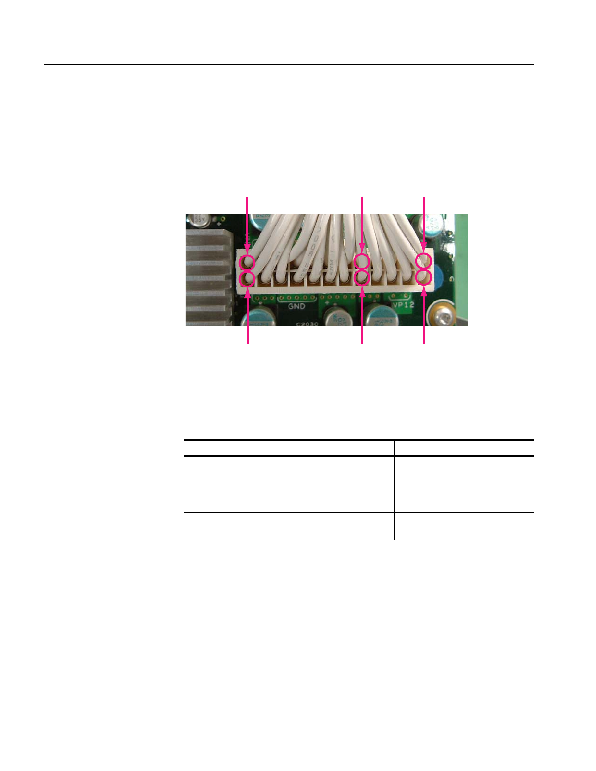
Troubleshooting
Checking the Voltages on
the AWG1G Board
To measure the output voltages of the PWR board, check the voltages at J2000 on
the AWG1G board with the digital multimeter and compare each reading to the
values listed in Table 4-6. If the voltages are within the allowance, your PWR
board is functional.
Pin 24
–12 V
Pin 12
–5.5 V
Pin 17
+5 V
Pin 5
+3.3 V
Pin 13
+15 V
Pin 1
+12 V
Figure 4-24: AWG1G board test points (J2000)
Table 4-6: Test points voltage (J2000)
Test point Voltage Allowance
Pin 1 +12 V +11.4 V to +12.6 V
Pin 5 +3.3 V +3.1 V to +3.5 V
Pin 12 –5.5 V –5.2 to –5.8 V
Pin 13 +15 V +14.2 V to +15.8 V
Pin 17 +5 V +4.7 V to +5.3 V
Pin 24 –12 V –11.4 to –12.6 V
4-42 AWG5000 Series Service Manual
Page 83
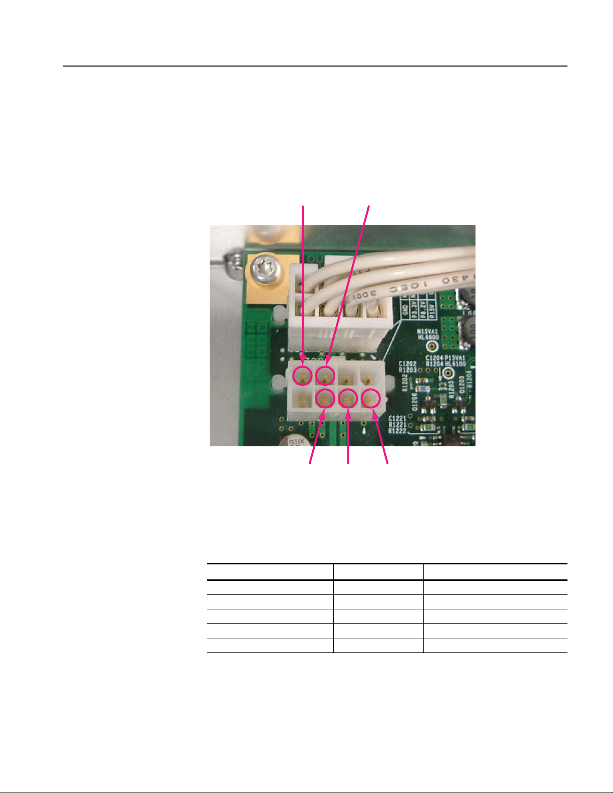
Troubleshooting
Checking the Voltages on
the OUT1G Board
To measure the output voltages of the PWR board, check the voltages at J7000 (or
J6000) on the OUT1G board with the digital multimeter and compare each reading
to the values listed in Table 4-7. If the voltages are within the allowance, your PWR
board is functional.
Pin 8
–15 V
Pin 7
-8.2 V
Pin 3
+3.3 V
Pin 2
+8.2 V
Pin 1
+15 V
Figure 4-25: OUT1G board test points (J7000)
Table 4-7: Test points voltage (J7000 or J6000)
Test point Voltage Allowance
Pin 1 +15 V +14.2 V to +15.8 V
Pin 2 +8.2 V +7.8 V to +8.6 V
Pin 3 +3.3 V +3.1 to +3.5 V
Pin 7 -8.2 V -7.8 V to -8.6 V
Pin 8 -15 V +14.2 V to +15.8 V
AWG5000 Series Service Manual 4-43
Page 84

Troubleshooting
Instrument Diagnostics
The primary diagnostics for the instrument are accessible through the AWG
application software. The instrument diagnostics check the basic functionality of
analog outputs at every power on. The instrument diagnostics run after Windows
has booted up and run its own set of system checks. If any failures occur at power
on, a pop-up message indicates that a failure has occurred and provides an error
code. Table 4-8 lists diagnostics error codes, Table 4-9 lists calibration error codes,
and Table 4-10 lists hardware error codes.
The power-on tests ensure that the hardware is installed and can be accessed by the
software. The tests provide limited diagnostic information, and provide no
performance information.
To run the instrument Diagnostics manually, do these steps:
1. Turn off all other applications.
2. From the menu bar, select System and then select Diagnostics...; the
Diagnostics dialog box appears (see Figure 4-26).
Figure 4-26: Diagnostics dialog box
4-44 AWG5000 Series Service Manual
Page 85

Table 4-8: Diagnostics error
Troubleshooting
3. In the dialog box, confirm that all the check boxes are selected. If they are not
all selected, click Select All.
4. Click Execute to execute the diagnostics.
Error code Error log message Possible defect on
board
AWG register readback
120000000 HwDiagAwgRegister AwgController address_0x21 register
diag. Fail expected data=xxxx actual data=xxxx
120000001 HwDiagAwgRegister AwgController address_0x23 register
diag. Fail expected data=xxxx actual data=xxxx
120000002 HwDiagAwgRegister AwgController address_0x30 register
diag. Fail expected data=xxxx actual data=xxxx
120000003 HwDiagAwgRegister AwgController address_0x40 register
diag. Fail expected data=xxxx actual data=xxxx
120000004 HwDiagAwgRegister AwgController address_0x41 register
diag. Fail expected data=xxxx actual data=xxxx
120000005 HwDiagAwgRegister AwgController address_0x42 register
diag. Fail expected data=xxxx actual data=xxxx
120000006 HwDiagAwgRegister AwgController address_0x50 register
diag. Fail expected data=xxxx actual data=xxxx
120000007 HwDiagAwgRegister Ch1 MemoryController-N
Communication Fail expected data=xxxx actual data=xxxx
120000008 HwDiagAwgRegister Ch2 MemoryController-N
Communication Fail expected data=xxxx actual data=xxxx
120000009 HwDiagAwgRegister Ch1 TEK0015-TNO address_REG
register diag. Fail expected data=xxxx actual data=xxxx
TNO: TEK0015 number
REG: Register number
120000010 HwDiagAwgRegister Ch2 TEK0015-TNO address_REG
register diag. Fail expected data=xxxx actual data=xxxx
TNO: TEK0015 number
REG: Register number
120000013 HwDiagAwgRegister Ch1 TEK0015-TNO address_REG
register diag. Fail expected data=xxxx actual data=xxxx
TNO: TEK0015 number
REG: Register number
120000014 HwDiagAwgRegister Ch2 TEK0015-TNO address_REG
register diag. Fail expected data=xxxx actual data=xxxx
TNO: TEK0015 number
REG: Register number
120000023 HwDiagAwgRegister AD9736 failed channel=1 address=xx
expected data=0xXX actual data=0xXX
120000024 HwDiagAwgRegister AD9736 failed channel=2 address=xx
expected data=0xXX actual data=0xXX
AWG1G AWG1G: U1000
AWG1G AWG1G: U1000
AWG1G AWG1G: U1000
AWG1G AWG1G: U1000
AWG1G AWG1G: U1000
AWG1G AWG1G: U1000
AWG1G AWG1G: U1000
AWG1G AWG1G: U1000, U4000A
AWG1G AWG1G: U1000, U4000B
AWG1G AWG1G: U1000, U4310A, U4420A
AWG1G AWG1G: U1000, U4310B, U4420B
AWG1G AWG1G: U1000, U4310C, U4420C
AWG1G AWG1G: U1000, U4310D, U4420D
AWG1G AWG1G: U1000, U6000A
AWG1G AWG1G: U1000, U6000B
Note
AWG5000 Series Service Manual 4-45
Page 86

Troubleshooting
Table 4-8: Diagnostics error (cont.)
Error code Error log message Possible defect on
board
120000025 HwDiagAwgRegister AD9736 failed channel=3 address=xx
expected data=0xXX actual data=0xXX
120000026 HwDiagAwgRegister AD9736 failed channel=4 address=xx
expected data=0xXX actual data=0xXX
120000027 HwDiagAwgRegister Ch3 MemoryController
Communication Fail expected data=xxxx actual data=xxxx
120000028 HwDiagAwgRegister Ch4 MemoryController
Communication Fail expected data=xxxx actual data=xxxx
CH 1 waveform memory
121000000 HwDiagWaveformMemory channel1, testNo Data bus
[IC-Pin] Error expected data=xxxxxxxx
actual data=xxxxxxxx
testNo: 1'st 2'nd
IC: IC number
Pin: Pin number
121000001 HwDiagWaveformMemory channel1, Address
Bus=xxxxxxxx [IC-Pin] Error expected data=xxxxxxxx
actual data=xxxxxxxx
IC: IC number
Pin: Pin number
121000002 HwDiagWaveformMemory channe1, Memory Cell testNo
BIT[CNT] Error
testNo: 1'st or 2'nd
BIT: Data bus bit
CNT: data bit
CH 2 waveform memory
122000000 HwDiagWaveformMemory channel2, testNo Data bus
[IC-Pin] Error expected data=xxxxxxxx
actual data=xxxxxxxx
testNo: 1'st 2'nd
IC: IC number
Pin: Pin number
122000001 HwDiagWaveformMemory channel2, Address
Bus=xxxxxxxx [IC-Pin] Error expected data=xxxxxxxx
actual data=xxxxxxxx
IC: IC number
Pin: Pin number
122000002 HwDiagWaveformMemory channe2, Memory Cell testNo
BIT[CNT] Error
testNo: 1'st or 2'nd
BIT: Data bus bit
CNT: data bit
AWG1G AWG1G: U1000, U6000C
AWG1G AWG1G: U1000, U6000D
AWG1G AWG1G: U1000, U4000C
AWG1G AWG1G: U1000, U4000D
AWG1G AWG1G: U4000A, U4500A, U4510A,
AWG1G AWG1G: U4000A, U4500A, U4510A,
AWG1G AWG1G: U4000A, U4500A, U4510A,
AWG1G AWG1G: U4000B, U4500B, U4510B,
AWG1G AWG1G: U4000B, U4500B, U4510B,
AWG1G AWG1G: U4000B, U4500B, U4510B,
Note
U4520A, U4530A, U4600A, U4610A,
U4620A, U4630A.
U4520A, U4530A, U4600A, U4610A,
U4620A, U4630A.
U4520A, U4530A, U4600A, U4610A,
U4620A, U4630A.
U4520B, U4530B, U4600B, U4610B,
U4620B, U4630B.
U4520B, U4530B, U4600B, U4610B,
U4620B, U4630B.
U4520B, U4530B, U4600B, U4610B,
U4620B, U4630B.
4-46 AWG5000 Series Service Manual
Page 87
Table 4-8: Diagnostics error (cont.)
Troubleshooting
Error code Error log message Possible defect on
board
CH 3 waveform memory
123000000 HwDiagWaveformMemory channel3, testNo Data bus
[IC-Pin] Error expected data=xxxxxxxx
actual data=xxxxxxxx
testNo: 1'st 2'nd
IC: IC number
Pin: Pin number
123000001 HwDiagWaveformMemory channel3, Address
Bus=xxxxxxxx [IC-Pin] Error expected data=xxxxxxxx
actual data=xxxxxxxx
IC: IC number
Pin: Pin number
123000002 HwDiagWaveformMemory channe3, Memory Cell testNo
BIT[CNT] Error
testNo: 1'st or 2'nd
BIT: Data bus bit
CNT: data bit
CH 4 waveform memory
124000000 HwDiagWaveformMemory channel4, testNo Data bus
[IC-Pin] Error expected data=xxxxxxxx
actual data=xxxxxxxx
testNo: 1'st 2'nd
IC: IC number
Pin: Pin number
124000001 HwDiagWaveformMemory channel4, Address
Bus=xxxxxxxx [IC-Pin] Error expected data=xxxxxxxx
actual data=xxxxxxxx
IC: IC number
Pin: Pin number
124000002 HwDiagWaveformMemory channe4, Memory Cell testNo
BIT[CNT] Error
testNo: 1'st or 2'nd
BIT: Data bus bit
CNT: data bit
Data timing margin
125000000 HwDiagDataTiming channel=1, Value is out of a range
max=xx min=xx
125000001 HwDiagDataTiming channel=2, Value is out of a range
max=xx min=xx
125000002 HwDiagDataTiming channel=3, Value is out of a range
max=xx min=xx
125000003 HwDiagDataTiming channel=4, Value is out of a range
max=xx min=xx
AWG1G AWG1G: U4000C, U4500C, U4510C,
AWG1G AWG1G: U4000C, U4500C, U4510C,
AWG1G AWG1G: U4000C, U4500C, U4510C,
AWG1G AWG1G: U4000D, U4500D, U4510D,
AWG1G AWG1G: U4000D, U4500D, U4510D,
AWG1G AWG1G: U4000D, U4500D, U4510D,
AWG1G, CLK1G AWG1G: U1000
AWG1G, CLK1G AWG1G: U1000
AWG1G, CLK1G AWG1G: U1000
AWG1G, CLK1G AWG1G: U1000
Note
U4520C, U4530C, U4600C, U4610C,
U4620C, U4630C.
U4520C, U4530C, U4600C, U4610C,
U4620C, U4630C.
U4520C, U4530C, U4600C, U4610C,
U4620C, U4630C.
U4520D, U4530D, U4600D, U4610D,
U4620D, U4630D.
U4520D, U4530D, U4600D, U4610D,
U4620D, U4630D.
U4520D, U4530D, U4600D, U4610D,
U4620D, U4630D.
CLK1G: U3200
CLK1G: U3200
CLK1G: U3200
CLK1G: U3200
AWG5000 Series Service Manual 4-47
Page 88

Troubleshooting
Table 4-8: Diagnostics error (cont.)
Error code Error log message Possible defect on
board
Clock register read back
130000000 HwDiagClockRegister PLL_MUX_HIGH=0 AWG1G, CLK1G AWG1G: U1000
130000001 HwDiagClockRegister PLL_MUX_LOW=1 AWG1G, CLK1G AWG1G: U1000
Clock PLL lock
131000008 HwDiagClockPll 100MHz PLL Locked AWG1G, CLK1G AWG1G: U1000
131000009 HwDiagClockPll 900MHz PLL Unlocked AWG1G, CLK1G AWG1G: U1000
131000010 HwDiagClockPll 590MHz PLL Unlocked AWG1G, CLK1G AWG1G: U1000
131000011 HwDiagClockPll 1210MHz PLL Unlocked AWG1G, CLK1G AWG1G: U1000
Output 1 register read back
140000000 The error occurred in the EEPROM read. 1'St=FST
2'Nd=SND
FST: the data that is received from EEPROM at the first read
check
SND: the data that is received from EEPROM at the second
read check, which is implemented after writing 0x55 to
EEPROM
140000001 Error message is changed according to the situation. OUT1G OUT1G-CH1/CH2: U5010, U5020
Output 2 register read back
150000000 The error occurred in the EEPROM read. 1'St=FST
2'Nd=SND
FST: the data that is received from EEPROM at the first read
check
SND: the data that is received from EEPROM at the second
read check, which is implemented after writing 0x55 to
EEPROM
150000001 Error message is changed according to the situation. OUT1G OUT1G-CH3/CH4: U5010, U5020
Te k L i n k
190000000 TekLink receive error Send=TR Recv=RV
TR:Transmition data
RV:Receive data
Output 1 analog level
141XP0031 Analog Level Diag CHX positive (negative) 6db attenuator
failed. Expected 0.5005, actual xxxxx
141XP0032 Analog Level Diag CHX positive (negative) 12db attenuator
failed. Expected 0.2530, actual xxxxx
141XP0033 Analog Level Diag CHX positive (negative) 24db attenuator
failed. Expected 0.0631, actual xxxxx
OUT1G OUT1G-CH1/CH2: U5010, U5020
OUT1G OUT1G-CH3/CH4: U5010, U5020
MIO MIO: U300
OUT1G OUT1G: K1100, K2100, K3100, K4100
OUT1G OUT1G: K1105, K2105, K3105, K4105
OUT1G OUT1G: K1110, K2110, K3110, K4110
Note
CLK1G: U3200
CLK1G: U3200
CLK1G: U3200, U3220, Y3100, Y3230
CLK1G: U3200, U3220, Y3100, Y3230
CLK1G: U3200, U3220, Y3100, Y3230
CLK1G: U3200, U3220, Y3100, Y3230
4-48 AWG5000 Series Service Manual
Page 89

Table 4-8: Diagnostics error (cont.)
Troubleshooting
Error code Error log message Possible defect on
board
141XP0034 Analog Level Diag CHX positive (negative) 20mhz filter
failed. Expected 0.975, actual xxxxx
141XP0035 Analog Level Diag CHX positive (negative) 100mhz filter
failed. Expected 0.995, actual xxxxx
141XP0036 Analog Level Diag CHX positive (negative) amp failed.
Expected 8.95, actual xxxxx
141XP0037 Analog Level Diag CHX positive (negative) output offset
failed. Expected 2.0V, actual xxxxxV
141XP0038 Analog Level Diag CHX positive (negative) output offset
failed. Expected 0.0V, actual xxxxxV
141XP0040 Analog Level Diag CHX positive (negative) D/A internal
offset1 failed. Expected 0.0mV, actual xxxxxmV
141XP0041 Analog Level Diag CHX positive (negative) D/A internal
offset2 failed. Expected 0.0mV, actual xxxxxmV
141XP0042 Analog Level Diag CHX positive (negative) read D/A gain11
failed. Expected 0.300V, actual xxxxxV
141XP0043 Analog Level Diag CHX positive (negative) read D/A gain21
failed. Expected 0.150V, actual xxxxxV
141XP0052 Analog Level Diag CHX 6db att gain balance failed. OUT1G OUT1G: K1100, K2100, K3100, K4100
141XP0053 Analog Level Diag CHX 12db att gain balance failed. OUT1G OUT1G: K1105, K2105, K3105, K4105
141XP0054 Analog Level Diag CHX 24db att gain balance failed. OUT1G OUT1G: K1110, K2110, K3110, K4110
141XP0055 Analog Level Diag CHX 20mhz filter gain balance failed. OUT1G OUT1G: K1120, K1125, K2120,
141XP0056 Analog Level Diag CHX 100mhz filter gain balance failed. OUT1G OUT1G: K1120, K1125, K2120,
141XP0057 Analog Level Diag CHX amp gain balance failed. OUT1G OUT1G: U1140, U1145, U1160A/B,
141XP0058 Analog Level Diag CHX A/D converter read failed. OUT1G OUT1G: U5010, U5100, U5112,
Output 2 analog level
151XP0031 Analog Level Diag CHX positive (negative) 6db attenuator
failed. Expected 0.5005, actual xxxxx
151XP0032 Analog Level Diag CHX positive (negative) 12db attenuator
failed. Expected 0.2530, actual xxxxx
OUT1G OUT1G: K1120, K1125, K2120,
OUT1G OUT1G: K1120, K1125, K2120,
OUT1G OUT1G: U1140, U1145, U1160A/B,
OUT1G OUT1G: U1200, U1220, Q1218,
OUT1G OUT1G: U1200, U1220, Q1218,
AWG1G AWG1G: U6000, U6025, U6035 [A-B]
AWG1G AWG1G: U6000, U6025, U6035 [A-B]
AWG1G, OUT1G AWG1G: U6000, U6015 [A-B],
AWG1G AWG1G: U6000, U6015 [A-B]
OUT1G OUT1G: K1100, K2100, K3100, K4100
OUT1G OUT1G: K1105, K2105, K3105, K4105
Note
K2125, K3120, K3125, K4120, K4125
K2125, K3120, K3125, K4120, K4125
U2140, U2145, U2160A/B, U3140,
U3145, U3160A/B, U4140, U4145,
U4160A/B
Q1228, U2200, U2220, Q2218,
Q2228, U3200, U3220, Q3218,
Q3228, U4200, U4220, Q4218, Q4228
Q1228, U2200, U2220, Q2218,
Q2228, U3200, U3220, Q3218,
Q3228, U4200, U4220, Q4218, Q4228
J6020 [A-B], J6030 [A-B]
OUT1G: J1000, J2000, J3000, J4000
K2125, K3120, K3125, K4120, K4125
K2125, K3120, K3125, K4120, K4125
U2140, U2145, U2160A/B, U3140,
U3145, U3160A/B, U4140, U4145,
U4160A/B
U5114
AWG5000 Series Service Manual 4-49
Page 90

Troubleshooting
Table 4-8: Diagnostics error (cont.)
Error code Error log message Possible defect on
board
151XP0033 Analog Level Diag CHX positive (negative) 24db attenuator
failed. Expected 0.0631, actual xxxxx
151XP0034 Analog Level Diag CHX positive (negative) 20mhz filter
failed. Expected 0.975, actual xxxxx
151XP0035 Analog Level Diag CHX positive (negative) 100mhz filter
failed. Expected 0.995, actual xxxxx
151XP0036 Analog Level Diag CHX positive (negative) amp failed.
Expected 8.95, actual xxxxx
151XP0037 Analog Level Diag CHX positive (negative) output offset
failed. Expected 2.0V, actual xxxxxV
151XP0038 Analog Level Diag CHX positive (negative) output offset
failed. Expected 0.0V, actual xxxxxV
151XP0040 Analog Level Diag CHX positive (negative) D/A internal
offset1 failed. Expected 0.0mV, actual xxxxxmV
151XP0041 Analog Level Diag CHX positive (negative) D/A internal
offset2 failed. Expected 0.0mV, actual xxxxxmV
151XP0042 Analog Level Diag CHX positive (negative) read D/A gain11
failed. Expected 0.300V, actual xxxxxV
151XP0043 Analog Level Diag CHX positive (negative) read D/A gain21
failed. Expected 0.150V, actual xxxxxV
151XP0052 Analog Level Diag CHX 6db att gain balance failed. OUT1G OUT1G: K1100, K2100, K3100, K4100
151XP0053 Analog Level Diag CHX 12db att gain balance failed. OUT1G OUT1G: K1105, K2105, K3105, K4105
151XP0054 Analog Level Diag CHX 24db att gain balance failed. OUT1G OUT1G: K1110, K2110, K3110, K4110
151XP0055 Analog Level Diag CHX 20mhz filter gain balance failed. OUT1G OUT1G: K1120, K1125, K2120,
151XP0056 Analog Level Diag CHX 100mhz filter gain balance failed. OUT1G OUT1G: K1120, K1125, K2120,
151XP0057 Analog Level Diag CHX amp gain balance failed. OUT1G OUT1G: U1140, U1145, U1160A/B,
151XP0058 Analog Level Diag CHX A/D converter read failed. OUT1G OUT1G: U5010, U5100, U5112,
OUT1G OUT1G: K1110, K2110, K3110, K4110
OUT1G OUT1G: K1120, K1125, K2120,
OUT1G OUT1G: K1120, K1125, K2120,
OUT1G OUT1G: U1140, U1145, U1160A/B,
OUT1G OUT1G: U1200, U1220, Q1218,
OUT1G OUT1G: U1200, U1220, Q1218,
AWG1G AWG1G: U6000, U6025, U6035 [C-D]
AWG1G AWG1G: U6000, U6025, U6035 [C-D]
AWG1G, OUT1G AWG1G: U6000, U6015 [C-D],
AWG1G AWG1G: U6000, U6015 [C-D]
Note
K2125, K3120, K3125, K4120, K4125
K2125, K3120, K3125, K4120, K4125
U2140, U2145, U2160A/B, U3140,
U3145, U3160A/B, U4140, U4145,
U4160A/B
Q1228, U2200, U2220, Q2218,
Q2228, U3200, U3220, Q3218,
Q3228, U4200, U4220, Q4218, Q4228
Q1228, U2200, U2220, Q2218,
Q2228, U3200, U3220, Q3218,
Q3228, U4200, U4220, Q4218, Q4228
J6020 [C-D], J6030 [C-D]
OUT1G: J1000, J2000, J3000, J4000
K2125, K3120, K3125, K4120, K4125
K2125, K3120, K3125, K4120, K4125
U2140, U2145, U2160A/B, U3140,
U3145, U3160A/B, U4140, U4145,
U4160A/B
U5114
4-50 AWG5000 Series Service Manual
Page 91

Calibration Error
Troubleshooting
To run the instrument calibration, do these steps:
1. Turn off all other applications.
2. From the menu bar, select System and then select Calibration...; the
Calibration dialog box appears (see Figure 4-27).
Figure 4-27: Calibration dialog box
3. Click Execute to execute the calibration.
Table 4-9: Calibration error
Error code Error log message Possible defect
on board
200XP0031 Analog Level Calibration CHX positive (negative) 6db
attenuator failed. Expected:0.5005, actual:xxxx
200XP0032 Analog Level Calibration CHX positive (negative) 12db
attenuator failed. Expected:0.2530, actual:xxxx
200XP0033 Analog Level Calibration CHX positive (negative) 24db
attenuator failed. Expected:0.0631, actual:xxxxx
200XP0034 Analog Level Calibration CHX positive (negative) 20mhz filter
failed. Expected:0.975, actual:xxxx
200XP0035 Analog Level Calibration CHX positive (negative) 100mhz filter
failed. Expected:0.995, actual:xxxx
200XP0036 Analog Level Calibration CHX positive (negative) amplitude
amp failed. Expected:8.95, actual:x
200XP0037 Analog Level Calibration CHX positive (negative) output offset
0V failed. Expected:0.0V, actual:xxxV
OUT1G OUT1G: K1100, K2100, K3100,
OUT1G OUT1G: K1105, K2105, K3105,
OUT1G OUT1G: K1110, K2110, K3110,
OUT1G OUT1G: K1120, K1125, K2120,
OUT1G OUT1G: K1120,, K1125, K2120,
OUT1G OUT1G: U1140, U1145, U1160A/B,
OUT1G OUT1G: U1200, U1220, Q1218,
Note
K4100
K4105
K4110
K2125, K3120, K3125, K4120, K4125
K2125, K3120, K3125, K4120, K4125
U2140, U2145, U2160A/B, U3140,
U3145, U3160A/B, U4140, U4145,
U4160A/B
Q1228, U2200, U2220, Q2218,
Q2228, U3200, U3220, Q3218,
Q3228, U4200, U4220, Q4218,
Q4228
AWG5000 Series Service Manual 4-51
Page 92

Troubleshooting
Table 4-9: Calibration error (cont.)
Error code Error log message Possible defect
on board
200XP0038 Analog Level Calibration CHX positive (negative) output offset
2.0V failed. Expected:2.0V, actual:xxxV
200XP0039 Analog Level Calibration CHX positive (negative) D/A internal
offset0 failed. FSC=900(FSC=260) expected:0.0mV,
actual:xxxmV
200XP0040 Analog Level Calibration CHX positive (negative) D/A internal
offset1 failed. FSC=900(FSC=260) expected:0.0mV,
actual:xxxmV
200XP0041 Analog Level Calibration CHX positive (negative) D/A internal
offset2 failed. FSC=900(FSC=260) expected:0.0mV,
actual:xxxmV
200XP0042 Analog Level Calibration CHX positive (negative) read D/A
gain1 failed. Expected:0.300V, actual:xxxV
200XP0043 Analog Level Calibration CHX positive (negative) read D/A
gain2 failed. Expected:0.150V, actual:xxxV
200X00044 Analog Level Calibration CHX D/A gain balance1 failed. AWG1G AWG1G: U6000
200X00045 Analog Level Calibration CHX D/A gain balance2 failed. AWG1G AWG1G: U6000
200X00046 Analog Level Calibration CHX D/A gain balance3 failed. AWG1G AWG1G: U6000
200X00047 Analog Level Calibration CHX D/A gain balance4 failed. AWG1G AWG1G: U6000
200X00048 Analog Level Calibration CHX D/A gain balance5 failed. AWG1G AWG1G: U6000, U6025, U6035
200X00049 Analog Level Calibration CHX D/A gain balance6 failed. AWG1G AWG1G: U6000, U6025, U6035
200X00050 Analog Level Calibration CHX D/A gain balance7 failed. AWG1G AWG1G: U6000
200X00051 Analog Level Calibration CHX D/A gain balance8 failed. AWG1G AWG1G: U6000
200X00052 Analog Level Calibration CHX 6db attenuator gain balance
failed.
200X00053 Analog Level Calibration CHX 12db attenuator gain balance
failed.
200X00054 Analog Level Calibration CHX 24db attenuator gain balance
failed.
OUT1G OUT1G: U1200, U1220, Q1218,
AWG1G, OUT1G AWG1G: U6000, U6025, U6035,
AWG1G AWG1G: U6000, U6025, U6035
AWG1G AWG1G: U6000, U6025, U6035
AWG1G, OUT1G AWG1G: U6000, U6015, J6020 [A-D],
AWG1G AWG1G: U6000, U6015
OUT1G OUT1G: K1100, K2100, K3100,
OUT1G OUT1G: K1105, K2105, K3105,
OUT1G OUT1G: K1100, K2100, K3100,
Note
Q1228, U2200, U2220, Q2218,
Q2228, U3200, U3220, Q3218,
Q3228, U4200, U4220, Q4218,
Q4228
J6020 [A-D], J6030 [A-D]
OUT1G: J1000, J2000, J3000, J4000
J6030 [A-D]
OUT1G: J1000, J2000, J3000, J4000
K4100
K4105
K4100
200X00055 Analog Level Calibration CHX filter 20mhz gain balance failed. OUT1G OUT1G: K1120, K1125, K2120,
K2125, K3120, K3125, K4120, K4125
200X00056 Analog Level Calibration CHX filter 100mhz gain balance failed. OUT1G OUT1G: K1120, K1125, K2120,
K2125, K3120, K3125, K4120, K4125
200X00057 Analog Level Calibration CHX amp gain balance failed. OUT1G OUT1G: U1140, U1145, U1160A/B,
U2140, U2145, U2160A/B, U3140,
U3145, U3160A/B, U4140, U4145,
U4160A/B
4-52 AWG5000 Series Service Manual
Page 93

Hardware Error
Table 4-10: Hardware error
Troubleshooting
Table 4-10 lists the instrument hardware related errors.
Error code Error log message Possible defect
on board
300000000 The system cannot find the device specified. MIO MIO: U100, U200, U220,Y230
300000001 The device is not ready. N/A Software
300000002 The AWG register access timeout period has expired. MIO: U200, U300
300000003 The time-out was generated while measuring data. AWG1G AWG1G: U1000
300000004 The timer for the trigger has stopped. AWG1G AWG1G: U1000
300000005 PLL doesn't lock. AWG1G, CLK1G AWG1G: U1000
300000006 AwgController DLL doesn't lock. AWG1G, CLK1G AWG1G: U1000, J3010
300000007 Output board access error Board=No
No: Board number (Start with 0)
300000008 Not enough storage is available to process. N/A Software
300000009 Calibration checksum data has an error. MIO MIO: U300,U390
300000010 Calibration version unmatched. MIO MIO: U300,U390
300000012 The Ipc busy timeout period has expired. AWG1G AWG1G: U1000
300000013 MemoryController DLL doesn't lock. AWG1G AWG1G: U1000, U4000x
300000050 Failed in the phase adjustment of TEK0015 and AD9736.
channel=1
300000051 Failed in the phase adjustment of TEK0015 and AD9736.
channel=2
300000052 Failed in the phase adjustment of TEK0015 and AD9736.
channel=3
300000053 Failed in the phase adjustment of TEK0015 and AD9736.
channel=4
300000054 Failed in the adjustment of AD9736 FIFO. Channel=1 AWG1G AWG1G: U1000, U6000A
300000055 Failed in the adjustment of AD9736 FIFO. Channel=2 AWG1G AWG1G: U1000, U6000B
300000056 Failed in the adjustment of AD9736 FIFO. Channel=3 AWG1G AWG1G: U1000, U6000C
300000057 Failed in the adjustment of AD9736 FIFO. Channel=4 AWG1G AWG1G: U1000, U6000D
300000058 Failed in the phase adjustment of two Tek0015. channel=1 AWG1G AWG1G: U1000, U4310A,
300000059 Failed in the phase adjustment of two Tek0015. channel=2 AWG1G AWG1G: U1000, U4310B,
300000060 Failed in the phase adjustment of two Tek0015. channel=3 AWG1G AWG1G: U1000, U4310C,
300000061 Failed in the phase adjustment of two Tek0015. channel=4 AWG1G AWG1G: U1000, U4310D,
OUT1G OUT1G: U5010
AWG1G, CLK1G AWG1G: U1000, U6000A, J3010
AWG1G AWG1G: U1000, U6000B
AWG1G AWG1G: U1000, U6000C
AWG1G AWG1G: U1000, U6000D
Note
AWG1G: U10 00
MIO-AWG1G Cable
CLK1G: U3200, U3220,Y3230
CLK1G: J3230
CLK1G: J3230
U4420A
U4420B
U4420C
U4420D
AWG5000 Series Service Manual 4-53
Page 94

Troubleshooting
Table 4-10: Hardware error (cont.)
Error code Error log message Possible defect
on board
300000062 Failed in the phase adjustment between channel=2. AWG1G AWG1G: U4720, U4740, U4750,
300000063 Failed in the phase adjustment between channel=3. AWG1G AWG1G: U4720, U4740, U4750,
300000064 Failed in the phase adjustment between channel=4. AWG1G AWG1G: U4720, U4740, U4750,
300000100 The access of MIO board EEPROM, it failed. MIO MIO: U300, U390
300000101 The access of OUTPUT board EEPROM, it failed. OUT1G OUT1G: U5010, U5100
300000102 The relay count is invalid. Board-1 OUT1G OUT1G: U5010, U5100
300000103 The relay count is invalid. Board-2 OUT1G OUT1G: U5010, U5100
300000200 The download (INIT) timeout period has expired. MIO MIO: U200, U300
300000201 The download (INIT) timeout period has expired. MIO MIO: U200, U300
300000202 The download (DONE) timeout period has expired. MIO MIO: U200, U300
300000203 The download timeout period has expired. MIO MIO: U200, U300
300000204 The system cannot find the file specified. (PLD140b.Bit) N/A Software
300000205 An attempt was made to load a program with an incorrect format.
(PLD131.Bit)
300000206 The download (AwgController-INIT) timeout period has expired. MIO, AWG1G MIO: U300, AWG1G: U1000,
300000207 The download (AwgController-INIT) timeout period has expired. MIO, AWG1G MIO: U300, AWG1G: U1000
300000208 The download (DONE) timeout period has expired. MIO, AWG1G MIO: U300, AWG1G: U1000,
300000209 The download timeout period has expired. MIO, AWG1G MIO: U300, AWG1G: U1000,
300000210 The system cannot find the file specified. (PLD131.Bit) N/A Software/disk drive
300000211 An attempt was made to load a program with an incorrect format.
(PLD131.Bit)
300000212 The download (AwgController-INIT) timeout period has expired. MIO, AWG1G MIO: U300, AWG1G: U1000,
300000213 The download (AwgController-INIT) timeout period has expired. MIO, AWG1G MIO: U300, AWG1G: U1000,
300000214 The download (AwgController-DONE) timeout period has expired. MIO,AWG1G MIO: U300, AWG1G: U1000,
N/A Software
N/A Software/disk drive
Note
U4440, U7504, U7500, U7510,
U7600, U7602, U1040
U4440, U7504, U7500, U7510,
U7600, U7602, U1040
U4440, U7504, U7500, U7510,
U7600, U7602, U1040
MIO-AWG1G cable
MIO-AWG1G cable
MIO-AWG1G cable
U4000x
Product configuration (number of
channels) is wrong.
U4000x
Product configuration (number of
channels) is wrong.
U4000x
Product configuration (number of
channels) is wrong.
4-54 AWG5000 Series Service Manual
Page 95

Table 4-10: Hardware error (cont.)
Troubleshooting
Error code Error log message Possible defect
on board
300000215 The download (AwgController) timeout period has expired. MIO/AWG1G MIO: U300, AWG1G: U1000,
300000216 The system cannot find the file specified. (PLD130b.Bit) N/A Software/disk drive
300000217 An attempt was made to load a program with an incorrect format.
(PLD130b.Bit)
300000218 The DCM timeout period has expired. MIO MIO: U300
300000219 The LOCKED timeout period has expired. MIO MIO: U300
310000000 The parameter is incorrect. N/A Software/disk drive
390000001 The calibration data is invalid. The default value is used. N/A This is not a defect.
390000002 *** Warning *** It started with Manufacturing mode. N/A This is not a defect.
390000003 The calibration data is invalid. The default value is used. N/A This is not a defect.
N/A Software/disk drive
Note
U4000x
Product configuration (number of
channels) is wrong.
After Repair
After removal and replacement of a module, you must perform the Adjustment and
Performance Verification procedures. You can find the information about these
procedures in the following manuals:
AWG5000 Series Arbitrary Waveform Generators Service Manual (Tektronix
part number 071-2083-XX)
AWG5000 Series Arbitrary Waveform Generators Specifications and
Performance Verification (Tektronix part number 071-2082-XX)
AWG5000 Series Service Manual 4-55
Page 96

Troubleshooting
Returning the Instrument for Service
When repacking the instrument for shipment, use the original packaging. If the
packaging is unavailable or unfit for use, contact your local Tektronix representative to obtain new packaging.
Seal the shipping carton with an industrial stapler or strapping tape.
Before returning the instrument for service, contact the Service Center to get an
RMA (return material authorization) number, and any return or shipping
information you may need.
If the instrument is being shipped to a Tektronix Service Center, enclose the
following information:
The RMA number.
The owner’s address.
Name and phone number of a contact person.
Type and serial number of the instrument.
Reason for returning.
A complete description of the required service.
Mark the address of the Tektronix Service Center and the return address on the
shipping carton in two prominent locations. See www.tektronix.com\service to find
a Tektronix Service Center near you.
4-56 AWG5000 Series Service Manual
Page 97

Replaceable Parts
Page 98

Page 99

Replaceable Parts
This section contains a list of the replaceable modules for the AWG5000 Series
Arbitrary Waveform Generators. Use this list to identify and order replacement
parts.
Parts Ordering Information
Replacement parts are available through your local Tektronix field office or
representative.
Changes to Tektronix instruments are sometimes made to accommodate improved
components as they become available and to give you the benefit of the latest
circuit improvements. Therefore, when ordering parts, it is important to include the
following information in your order.
Part number
Instrument type or model number
Instrument serial number
Instrument modification number, if applicable
If you order a part that has been replaced with a different or improved part, your
local Tektronix field office or representative will contact you concerning any
change in part number.
AWG5000 Series Service Manual 5-1
Page 100

Replaceable Parts
Part Number Revision
Level
Module Servicing
Tektronix part numbers contain two digits that show the revision level of the part.
For most parts in this manual, you will find the letters XX in place of the revision
level number.
Part Number Revision Level Revision Level may show as XX
}
}
670-7918-03 670-7918-XX
When you order parts, Tektronix will provide you with the most current part for
your product type, serial number, and modification (if applicable). At the time of
your order, Tektronix will determine the part number revision level needed for
your product, based on the information you provide.
Modules can be serviced by selecting one of the following three options. Contact
your local Tektronix service center or representative for repair assistance.
Module Exchange. In some cases you may exchange your module for a
remanufactured module. These modules cost significantly less than new modules
and meet the same factory specifications. For more information about the module
exchange program, call 1-800-833-9200. Outside North America, contact a
Tektronix sales office or distributor; see the Tektronix Web site (www.tektronix.
com) for a list of offices.
Module Repair and Return.You may ship your module to us for repair, after which
we will return it to you.
New Modules.You may purchase replacement modules in the same way as other
replacement parts.
5-2 AWG5000 Series Service Manual
 Loading...