

Page 1
TM 11-6625-2749-14&P
OPERATOR’S, ORGANIZATIONAL, DIRECT SUPPORT, AND GENERAL SUPPORT
MAINTENANCE MANUAL
(INCLUDING REPAIR PARTS AND SPECIAL TOOLS LISTS)
FOR
DIFFERENTIAL AMPLIFIER AM-6786/U
(TEKTRONIX TYPE 7A22, VERTICAL PLUG-IN UNIT)
(NSN 6625-00-478-0597)
HEADQUARTERS,
DEPARTMENT OF THE ARMY
OCTOBER 1979
Page 2

CLEANING THE INTERIOR
Use an eye-shield when cleaning with pressurized air. Hardened dirt can be
removed with a paint brush, cotton tipped swab or cloth dampened with a
water and mild detergent solution. Avoid the use of chemical cleaning agents
that might damage the plastic parts.
SPECIFIC COMPONENT REPLACEMENT INFORMATION
Disconnect the instrument from the power source before removing or replacing components.
The pushbutton switches are not repairable and should be replaced if defective. Components which are mounted on the circuit board associated with the
pushbutton switch can be replaced using the normal replacement procedure.
See the information under Light-Bulb Replacement for bulb replacement.
Page 3

TM 11-6625-2749-14&P
This manual contains copyright material reproduced by permission of Tektronix, Incorporated.
TECHNICAL Manual
HEADQUARTERS
DEPARTMENT OF THE ARMY
No. 11-6625-2749-14&P
OPERATOR’S, ORGANIZATIONAL, DIRECT
MAINTENANCE
SUPPORT,
MANUAL
Washington, DC,
AND GENERAL SUPPORT
10 October
1979
(INCLUDING REPAIR PARTS AND SPECIAL TOOLS LISTS)
FOR
DIFFERENTIAL AMPLIFIER AM-6786/U
(TEKTRONIX TYPE 7A22, VERTICAL PLUG-IN UNIT)
NSN 6625-00-478-0597)
Current as of 20 March 1979
REPORTING OF ERRORS
You can improve this manual by recommending improvements using DA Form 2028-2 located in
the back of the manual. Simply tear out the self-addressed form, fill it out as shown on the sample, fold
it where shown, and drop it in the mail.
If there are no blank DA Forms 2028-2 in the back of your manual, use the standard DA Form
2028 (Recommended Changes to Publications and Blank Forms) and forward to the Commander, US
Army Communications and Electronics Materiel Readiness Command, ATTN: DRSEL-ME -MQ, Fort
Monmouth, NJ 07703.
In either case, a reply will be furnished direct to you.
This manual is an authentication of the manufacturer’s commercial literature which, through usage,
has been found to cover the data required to operate and maintain this equipment. Since the manual
was not prepared in accordance with military specifications, the format has not been structured to
consider levels of maintenance.
i-0.1
Page 4

Page 5

TM 11-6625-2749-14&P
TABLE OF
SECTION O
Introduction . . . . . . . . . . . . . . . . . . .
SECTION 1 SPECIFICATION
Introduction . . . . . . . . . . . . . . . . . . . .
Electrical Characteristics . . . . . . . . . . .
Deflection Factor . . . . . . . . . . . . . . .
Gain . . . . . . . . . . . . . . . . . . . . . . . .
Differential Dynamic Range . . . . . .
DC Offset . . . . . . . . . . . . . . . . . . . .
Frequency Response . . . . . . . . . . . .
Bandwidth limit . . . . . . . . . . . . . . .
Recovery Time . . . . . . . . . . . . . . . .
Common-Mode Signal Range . . . .
Common-mode Rejection Ratio . . . .
Maximum input Voltage . . . . . . . .
Input Rand C . . . . . . . . . . . . . . . . .
Maximum Input Gate Current . . . .
Variable Balance . . . . . . . . . . . . . .
Step Attenuator DC Balance . . . . . .
Displayed Noise
(Tangentially Measured) . . . . . . .
DC Drift . . . . . . . . . . . . . . . . . . . . .
Isolation between + and — Inputs
Environmental Characteristics . . . . . . .
Altitude . . . . . . . . . . . . . . . . . . . . .
Transportation . . . . . . . . . . . . . . . .
Physical Characteristics . . . . . . . . . . . .
Finish . . . . . . . . . . . . . . . . . . . . . . .
Dimensions . . . . . . . . . . . . . . . . . . .
Weight . . . . . . . . . . . . . . . . . . . . . .
SECTION 2 OPERATING INSTRUC-
TIONS
Introduction . . . . . . . . . . . . . . . . . . . . 2-1
Front Panel Controls and Connectors . 2-1
Operating Instructions . . . . . . . . . . . . . 2-2
First Time Operation . . . . . . . . . . . 2-2
General Operating Information . . . . . 2-4
Trace Drift . . . . . . . . . . . . . . . . . . . .
Page
0-1
1-1
1-1
1-1
1-1
1-1
1-1
1-1
1-1
1-1
1-1
1-1
1-3
1-3
1-3
1-3
1-3
1-3
1-3
1-3
1-3
1-3
1-3
1-3
1-3
1-3
1-3
2-4
CONTENTS
Input Gate Current . . . . . . . . . . . . .
Voltage Measurement . . . . . . . . . . .
Signal Input Connectors . . . . . . . . .
High Input Impedance . . . . . . . . . . .
Display Polarity . . . . . . . . . . . . . . .
Deflection Factor . . . . . . . . . . . . . .
Bandwidth Selection . . . . . . . . . . . .
Voltage Comparison Measurements 2-10
Differential Operation . . . . . . . . . . 2-10
DC Offset Operation . . . . . . . . . . . . 2-11
Input Overdrive Indicator . . . . . . . . 2-12
Readout . . . . . . . . . . . . . . . . . . ...2-12
Trace Identify . . . . . . . . . . . . . . . 2-13
SECTION 3 CIRCUIT DESCRIPTION
Introduction . . . . . . . . . . . . . . . . . . . . 3-1
Block Diagram Description . . . . . . . . . 3-1
Input Coupling . .
Input Attenuators
Preamp . . . . . . . .
L F -3 dB Point .
Output Amplifier
H F -3 dB Point
General Information
Feedback Amplifiers . . . . . . . . . . . . 3-2
Differential Configuration . . . . . . . 3-3
Detailed Circuit Description . . . . . . . . 3-3
Input Coupling . . . . . . . . . . . . . . . . 3-3
Input Attenuators . . . . . . . . . . . . . . 3-4
Gate Current Compensation . . . . . . 3-4
Input Amplifier . . . . . . . . . . . . . . . . 3-4
X15 Preamp . . . . . . . . . . . . . . . . . 3-4
DC Balance . . . . . . . . . . . . . . . .
Floating Power Supply . . . . . . . . 3-5
Common-Mode Rejection . . . . . . 3-5
Cross Neutralization . . . . . . . . . . 3-6
. . . . . . . . . . . . . .
. . . . . . . . . . . . . .
. . . . . . . . . . . . . .
. . . . . . . . . . . . . .
. . . . . . . . . . . . . .
. . . . . . . . . . . . . . 3-2
. . . . . . . . . . . . . .
‘age
2-4
2-4
2-4
2-5
2-5
2-5
2-5
3-1
3-1
3-1
3-1
3-2
3-2
3-4
i
Page 6

TM 11-6625-2749-14&P
TABLE OF
Input Overdrive Protection . . . . . 3-7
DC Off set . . . . . . . . . . . .
Offset Generator . . . . . .
Input Overdrive Indicator
LF
-3 dB Point Selector
Output Amplifier . . . . . . . .
Gain Switching Amplifier
Variable Output Stage . . .
Signal Output Amplifier .
Trigger Output Amplifier .
Indicator Oscilloscope Readout . . . . 3-11
Probe Sensing . . . . . . . . . . . . . . . 3-11
Trace Identify . . . . . . . . . . . . . .
SECTION 4 MAINTENANCE
Introduction . . . . . . . . . . . . . . . . . . . .
Preventive Maintenance . . . . . . . . . . .
General . . . . . . . . . . . . . . . . . . . . .
Cleaning Front Panel . . . . . . . . . . . .
Cleaning Interior . . . . . . . . . . . . . . .
Visual Inspection . . . . . . . . . . . . . .
Transistor Checks . . . . . . . . . . . . . .
Calibration . . . . . . . . . . . . . . . . . . .
Corrective Maintenance . . . . . . . . . . . .
General . . . . . . . . . . . . . . . . . . . . .
Obtaining Replacement Parts . . . . .
Special Parts . . . . . . . . . . . . . . . . . .
Soldering Techniques . . . . . . . . . . .
Component Replacement Information
Troubleshooting . . . . . . . . . . . . . . . . .
Introduction . . . . . . . . . . . . . . . . . .
Indicator Oscilloscope . . . . . . . . . . .
Operating Procedure and
Control Settings . . . . . . . . . . . . .
Trouble Symptoms
Visual Inspection .
Calibration Check
. . . . . . . . . . . . . . 4-4
. . . . . . . . . . . . . . 4-4
. . . . . . . . . . . . . .
. . . . . . 3-7
. . . . . . 3-7
. . . . . . 3-8
. . . . . . 3-9
. . . . . .
. . . . . . 3-9
. . . . . .
. . . . . .
. . . . . . 3-11
Page
3-9
3-11
3-11
3-11
4-1
4-1
4-1
4-1
4-1
4-1
4-1
4-1
4-1
4-1
4-2
4-2
4-2
4-3
4-3
4-3
4-4
4-4
4-4
CONTENTS
Detailed Troubleshooting . . . . . . . . . . 4-4
General . . . . . . . . . . . . . . . . . 4-4
Test Equipment Recommended . . . . 4-4
DC Balance Check . . . . . . . . . . . . .
Troubleshooting by Direct
Replacement . . . . . . . . . . . . . . . . 4-5
Component Checks . . . . . . . . . . . . . 4-6
Transistors . . . . . . . . . . . . . . . . .
Diodes . . . . . . . . . . . . . . . . . . . . 4-6
Resistors . . . . . . . . . . . . . . . . . . . 4-6
Capacitors . . . . . . . . . . . . . . . . . 4-7
SECTION 5 PERFORMANCE CHECK/
CALIBRATION PROCEDURE
Introduction . . . . . . . . . . . . . . . . .
Test Equipment Required . . . . . . . .
General . . . . . . . . . . . . . . . . . .
Short Form Procedure . . . . . . . . . .
Performance Check/Calibration
Procedure . . . . . . . . . . . . . . . . .
General . . . . . . . . . . . . . . . . . .
Preliminary . . . . . . . . . . . . . . . .
Check or Adjust . . . . . . . . . . . .
AC Atten Balance . . . . . . . . .
Variable Balance . . . . . . . . .
Coarse DC Balance. . . . . . .
+ Gate Current Zero . . . . .
- Gate Current Zero . . . .
GAIN . . . . . . . . . . . . . . . . . .
VARIABLE Control Ratio . .
VOLTS/DIV Gain Switching .
Isolation between + and -
Inputs . . . . . . . . . . . . . . . .
Total DC Offset Range . . . . .
C241 + Cross Neutralization
C141 - Cross Neutralization
Cl 15 Xl +Input Atten Time
Constant . . . . . . . . . . . . . .
. . . 5-1
. . . 5-1
. . .
. . . 5-2
,..
. . . 5-3
. . . 5-3
. . . 5-4
. . . 5-4
. . . 5-4
. . . 5-4
. . .
. . . 5-5
. . . 5-5
. . . 5-5
. . . 5-5
. . . 5-7
. . . 5-7
. . . 5-7
. . . 5-8
. . . 5-8
Page
4-4
4-6
5-1
5-3
5-5
ii
Page 7

TABLE OF CONTENTS
TM 11-6625-2749-14&P
Page
C215 x1
Constant . . . . . . . . . . . . . . . . . 5-8
Input Atten Accuracy . . . . . . . . . 5-9
Input Atten Differential Balance . 5-9
+ Input Atten
- Input Atten Time
Series
Compensation . . . . . . . . . . . . . 5-10
- Input
-input
Atten Compensation . . . 5-10
Atten Shunt
Compensation . . . . . . . . . . . . . 5-11
HF -3dB Point . . . . . . . . . . . . 5-12
LF
-3dB Point . . . . . . . . . . . . . . . . . . . . . . .5- 12
CMRR . . . . . . . . . . . . . . . . . . . . . . . . . . . . . . .. . .5-13
Input Overdrive Indicator . . . . . . 5-13
Differential Dynamic Range . . . . 5-14
Overall Noise Level
(Measured Tangentially) . . . . . 5-15
Overdrive Recovery Time . . . . . . 5-15
SECTION 10 CALIBRATION TEST
EQUIPMENT REPLACEMENT
APPENDIX A. REFERENCES
SECTION 6 ELECTRICAL PARTS LIST
Abbreviations and Symbols
Parts Ordering Information
Index of Electrical Parts List
Electrical Parts List
SECTION 7 DIAGRAMS AND ME-
CHANICAL PARTS ILLUSTRATIONS
Diagrams
Mechanical Parts Illustrations
SECTION 8 MECHANICAL PARTS
LIST
Mechanical Parts list Information
Index of Mechanical Parts Illustrations
Mechanical Parts List
SECTION 9 PART NUMBER-NATIONAL STOCK
NUMBER CROSS REFERENCE
INDEX.
A - 1
COMPONENTS
B.
C. ADDITIONAL AUTHORIZATION LIST (Not Applicable)
D. MAINTENANCE ALLOCATION
Section I. General
Maintenance Allocation Chart for Differential Amplifier
II.
AM-6786/U
III.
Tool and Test Equipment Requirements for Differential
Amplifier AM-6786/U
APPENDIX E.
EXPENDABLE SUPPLIES AND MATERIALS LIST (Not Applicable)
OF END ITEM LIST (Not Applicable)
. . . . . . . . . . . . . . . . . . . . . . . . . . . . . . . . . . . . . . . . . . . . .
. . . . . . . . . . . . . . . . . . . . . . . . . . . . . . . . . . .
D-1
D-4
D-5
iii
Page 8

TM 11-6625-2749-14&P
LIST OF ILLUSTRATIONS
Figure
1-1
1-2
2-1
2-2
2-3
2-4A
2-4B
2-5
Page
Type 7A22 Differential Amplifier. . . . . . . . . . . . . . . . .
A
CMRR vs Frequency for signal not exceeding Common Mode
Signal Range . . .
. . . . . . . . . . . . . . . . . . . . . . . . . . . . . . . . . . . . .
1-2
Signals applied to the + INPUT Connector Produce an
Upright Display, while signals applied to the - INPUT
are inverted . . . . . . . . . . . . . . . . . . . . . . . . . .
Location of AC ATTEN BAL Control . . . . . . . . . . . . . . . .
2-1
2-3
Location of wire strap between input line and internal
gate . . . . . . . . . . . . . .
. . . . . . . . . . . . . . . . . . . . . . . . . . . . .
2-5
7A22 CMRR at 10 uV/Div to 10 mV/Div. Inputs DC Coupled.
Worst-case degradation due to source resistance . . . . . . . .
2-6
7A22 Bandwidth and VOLTS/DIV Error as functions of Source
Resistance . . . . . . . . . . . . . . . . . . . . . . . . . .
2-7
7A22 FREQUENCY RESPONSE as a function of LF -3 dB POINT
SETTING (HF-3 dB POINT at l MHz) . . . . . . . . . . . . .
2-8
2-6
2-7
2-8
2-9
3-1
3-2
3-3
3-4
3-5
3-6
3-7
7A22 FREQUENCY RESPONSE as a function of HF -3 dB POINT
settings (LF -3 dB POINT of DC).
. . . . . . . . . . . . . . . . . . . . . . .
Improving signal-to-noise ratio by setting bandwidth . . . . .
2-9
2-10
Waveforms showing differential rejection of a common-mode
signal
. . . . . . . . . . . . . . . . . . . . . . . . . . . . . . . . . . . . . . . . . . . . .
Connecting a differential amplifier across a circuit . . . . .
2-11
2-12
Generalized feedback system showing the relation between
input and output . . . . . . . . . . . . . . . . . . . . . .
Feedback amplifier (Single-ended version).
. . . . . . . . . . . . . . .
Feedback amplifier (Differential configuration). . . . . . . . . .
Gate Current Compensation . . . .
. . . . . . . . . . . . . . . . . . . . . . . . . . . .
Common-mode Rejection using floating power supply . . . . . . . .
Input cross neutralization
. . . . . . . . . . . . . . . . . . . . . . . . . . . . . . .
Effects of high impedance to ground in the - INPUT . . . . . . .
3-2
3-2
3-3
3-4
3-5
3-6
3-7
iv
Page 9

TM 11-6625-2749-14&P
Figure
3-8
3-9
3-10
3-11
4-1
4-2
4-3
4-4
4-5
4-6
Page
(A) Overdrive Protection System showing current paths.
(B, C) Sequence of events leading to excessive
overdrive
Offset system showing (A) Conditions with zero offset, (B)
0.25V DC offset
Functional arrangement of the offset generator
Partial Low Frequency -3 dB Point selector for + Input
amplifier
Removing or replacing component on circuit board
Transistor junction-voltage measurements
Transistor base pin and socket arrangement
Diode polarity and color code
Color code for resistors and ceramic capacitors
Plain circuit board (components)
. . . . . . . . . . . . . . . . . . . . . . . . . . . . . . . . . . . . .
. . . . . . . . . . . . . . . . . . . . . . . . . . . . . . . . . . . .
. . . . . . . . . . . . . . . . . . . . . . . . . . . . . . . . . . . . . . . . . . . . . .
. . . . . . . . . . . . . . . . .
. . . . . . . . . . . . . . .
. . . . . . . . . . . . . . . . . . . . . . . . . . . .
. . . . . . . . . . . . . . . . . . . . . . . . . .
. . . . . . . . .
. . . . . . . . . . .
. . . . . . . . .
. . . . . . . . . .
3-8
3-9
3-10
3-11
4-2
4-6
4-7
4-8
4-8
4-10
4-7
4-8
5-1
5-2
5-3
5-4
5-5
5-6
5-7
5-8
Main circuit board (wire color code)
Bandwidth circuit board (components and wire color code) .
Left side of the 7A22 showing adjustment locations
Equipment required for steps 6 through 19
Typical waveform showing (A) Cross neutralization properly
adjusted, (B) incorrectly adjusted
Typical waveform showing (A) Correct adjustment of Input
Attenuator Time Constant. (B) and (C) incorrect
adjustment
Typical display obtained when Input Attenuators are
adjusted for optimum differential balance
Typical display obtained with - Input attenuator adjusted
for optimum Common-Mode signal rejection. (A) C208C
adjusted properly (B) C209C adjusted properly
Equipment required for steps 20 through 24
Right side of Type 7A22 showing location of adjustments . .
. . . . . . . . . . . . . . . . . . . . . . . . . . . . . . . . . . . . . . . . . . . . .
. . . . . . . . . . . . . . . . . . . . .
. . . . . . .
. . . . . . . . . . . . . . . .
. . . . . . . . . . . . . . . . . . . . .
. . . . . . . . . . . . . .
. . . . . . . . . .
. . . . . . . . . . . . . . .
4-11
4-12
5-4
5-6
5-7
5-8
5-9
5-10
5-11
5-12
v
Page 10

TM 11-6625-2749-14&P
Figure
5-9
5-10
5-11
5-12
Page
Equipment required for step 25
. . . . . . . . . . . . . . . . . . . . . . . . . . .
5-14
Typical display showing (A) two noise bands and (B) merging
noise bands . . . . . .
Equipment required for step 26
. . . . . . . . . . . . . . . . . . . . . . . . . . . . . . . . . .
. . . . . . . . . . . . . . . . . . . . . . . . . . .
Typical waveform showing overdrive recovery time . . . . .
5-15
5-16
5-16
vi
Page 11

Page 12
TM 11-6625-2749-14&P
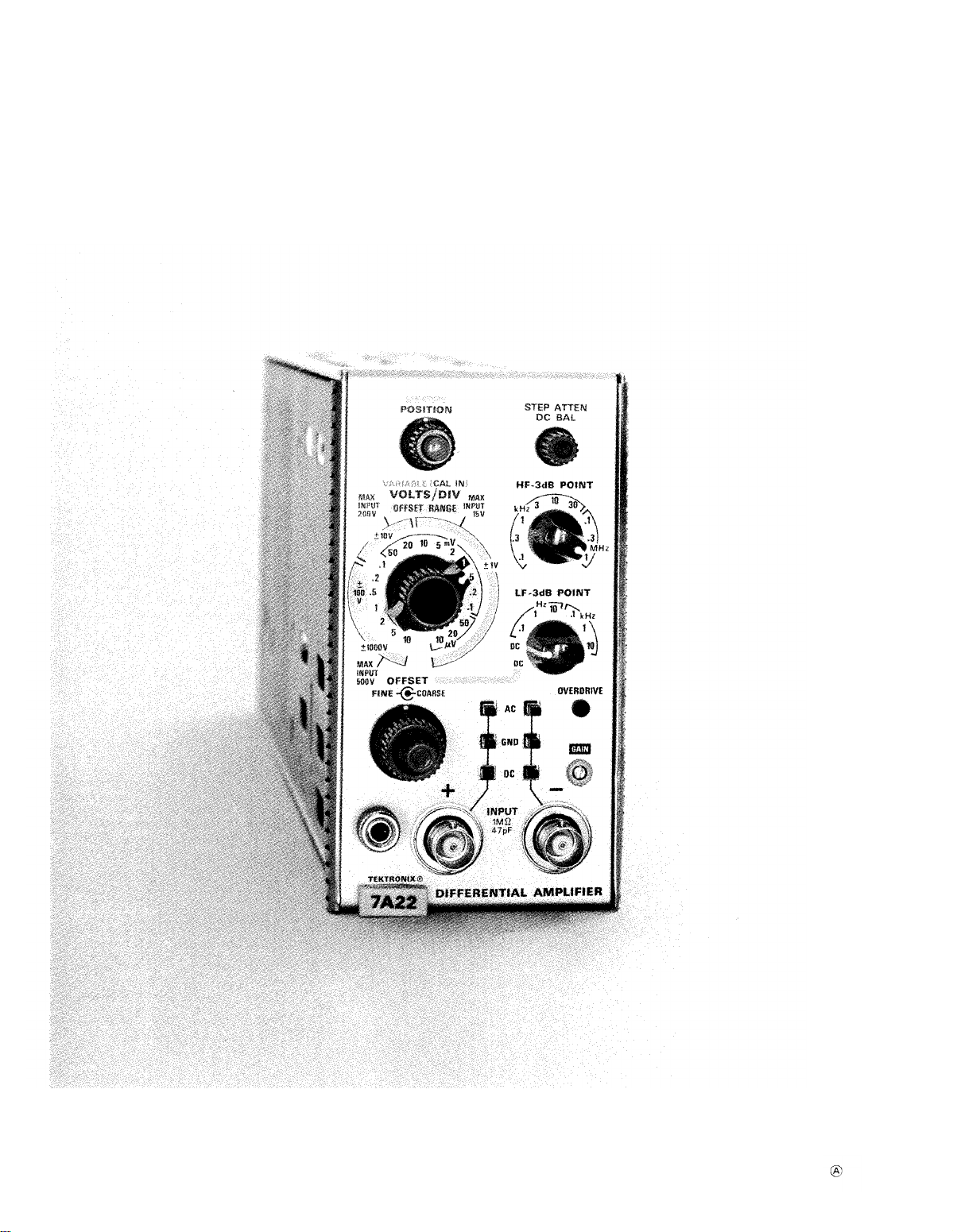
Type 7A22
Fig. 1-1. Type 7A22 Differential Amplifier.
Page 13

SECTION 0
INTRODUCTION
TM 11-6625-2749-14&P
0-1.
6786/U and provides instructions for operation and maintenance. Throughout
this manual, the AM-6786/U is referred to as Tektronix Type 7A22 Differential
Amplifier.
included is a repair parts list.
0-2.
whether there are new editions, changes, or additional publications pertaining
to the equipment.
modification work orders (MWO’S) pertaining to the equipment.
0-3.
forms, records, and reports which are to be used by maintenance personnel
at all maintenance levels are listed in and prescribed by TM 38-750.
DD Form 6 (Packaging Improvement Report) as prescribed in AR 700-58/NAVSUPINST
4030.29/AFR 71-13/MCO P4030.29A and DLAR 4145.8.
SCOPE
This manual describes Vertical Plug-In Unit, Differential Amplifier AM-
The maintenance allocation chart appears in appendix D. Also,
INDEXES OF PUBLICATIONS
DA Pam 310-4.
a.
b.
DA Pam 310-7.
FORMS AND RECORDS
Reports of Maintenance and Unsatisfactory Equipment. Maintenance
b.
Report of Packaging and Handling Deficiencies. Fill out and forward
Refer to the latest issue of DA Pam 310-4 to determine
Refer to DA Pam 310-7 to determine whether there are
Discrepancy in Shipment Report (DISREP) (SF 361). Fill out and for-
ward Discrepancy in Shipment Report (DISREP) (SF 361) as prescribed in AR
55-38/NAVSUPINST 4610.33B/AFR 75-18/MCO P461O.19C and DLAR 4500.15.
0-4.
tions for preparing EIR’s are provided in TM 38-750, The Army Maintenance
Management System. EIR’s should be mailed direct to Commander, US Army
Communications and Electronics Materiel Readiness Command; ATTN: DRSEL-ME-MQ,
Fort Monmouth, NJ 07703.
0-5.
shall be in accordance with TM 750-244-2.
0-6.
in accordance with TM 750-244-2.
REPORTING EQUIPMENT IMPROVEMENT RECOMMENDATIONS (EIR)
EIR’s will be prepared using DA Form 2407, Maintenance Request. Instruc-
A reply will be furnished directly to you.
ADMINISTRATIVE STORAGE
Administrative storage of equipment issued to and used by Army activities
DESTRUCTION OF ARMY ELECTRONICS MATERIEL
Destruction of Army electronics materiel to prevent enemy use shall be
0-1
Page 14

Page 15
TM 11-6625-2749-14&P
SECTION
SPECIFICATION
Introduction
h Type 7A22 Vertical Plug-in is
enticd
amplifier with excellent common-mode reiection char-
acteristics and high gain for low level applications.
The DC Offset capability of the Type 7A22 allows the
display of the very small low-frequency signals containing
a
large DC component, at deflection factors not possible with
AC coupling. The vertical deflection factor range of the
Type 7A22 is from 10 pV to 10 V. The high and low frequency —3 dB points
to set the bandwidth of the instrument. Thus, for low fre-
quency applications the signal-to-noise ratio can be improved
by restricting the bandwidth of the Type 7A22. The bandwidths selection and excellent drift-with-time
provide measurement capabilities in the biomedical, trans-
ducer, and other areas which require stable, low deflection
factor, low noise measurements.
The Type 7A22 is designed for use in Tektronix 7000 Series
oscilloscopes.
The electrical characteristics described in this section are
volid over the stated environmental range for instruments
ccdibrated at an ambient temperature of +20”C to +30”
and after
a 5
can be
minute warmup unless otherwise noted.
ELECTRICAL CHARACTERISTICS
Characteristic
Deflection Factor
~VOLTS/DIV]
Gain Ratio Accuracy
VAR (CAL IN) Range
GAIN
Differential Signal Range
[DC OFFSET not used)
10 pV/Div to
TO
mV/Div
20 mV/Div to
0.1 V/Div
0.2 V/Div to
1 V/Div
2 V/Div to
10 V/Div
Performance
Within 2% with GAIN ad@sted at
1 mV/div
Continuously variable; extends deflection factor to at least 25 V/div
Permits ad@stment of deflection
factor at 1 mV/DIV for all mainframes
At least AI V
At least *1O V
At least A1OO V
At least A1OOO V
a DC
selected at the front panel,
coupled differ-
characteristics
Requirements
C
1
DC OFFSET
COARSE Range from
Electrical Zero
10 pV/Div to
10mV/Div
20 mV to 0.1
V/Div
0.2 V to 1 V/Div
2V to 10 V/Div
Frequency Response (8
div Reference)
Overall Frequency
Response DC (Direct)
Coupled Input
AC (Capacitive) Cou
pled Input Lower
Bandwidth Frequencj
Bandwidth Limit
Accuracy
HF –3dB POINT
100Hz to 1 MHz
Accuracy
LF –3 dB POINT
0.1 Hz to 10 kHz
Accuracy
Recovery Time
Common Mode Signal
10 pV/Div to
10 mV/Div
20 mV/Div to
0.1 V/Div
0.2 V/Div to
10 V/Div
Common-Mode
Reiection Ratio
DC (Direct) Coupled
AC (Capacitive)
Coupled
At least +1 V to –1 V
At least +1OV to –1OV
At least +100 V to –1OOV
At least +1000 V to –1OOOV
DC to within 10~o of 1 MHz at
–3 dB
2 Hz or less
9 steps in
Within 10~o of selected frequency
6 steps in
Within 12% of selected frecluency
10 ps or less to recover to within
0.5% of zero level after the removal of
plied for 1 s. Test signal not to exceed
Specified aberration (0.5%) based
on test signal amplitude
At least +1OV and –1OV
At least +1OOV and –1OOV
At least +500 V and –500 V
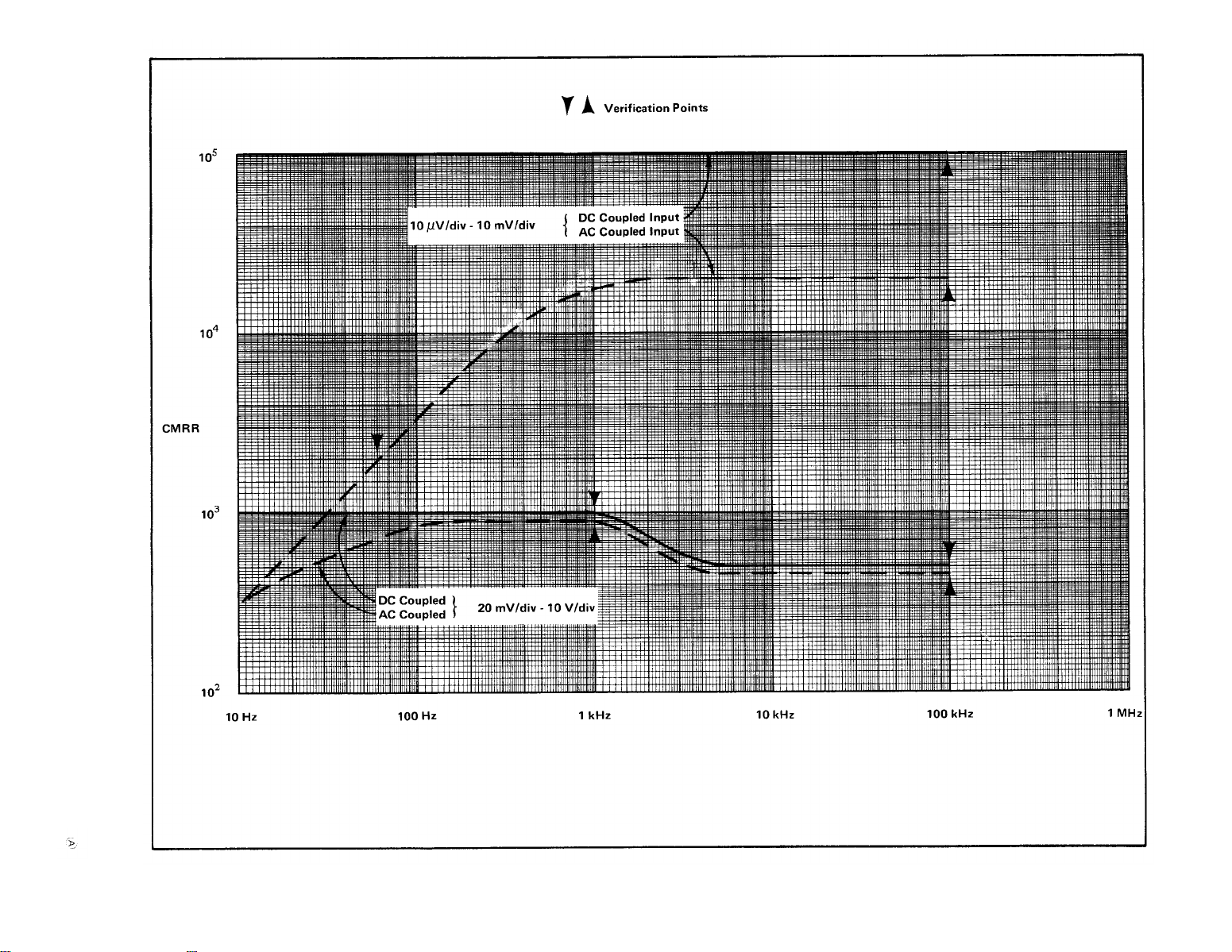
See Verification Points on graph,
Fig. 1-2.
See Verification Points on graph,
Fig. 1-2.
a
1-3 sequence
a
1-10 sequence
a + or —
Differential Signal Range.
test input ap-
1-1
Page 16
1-2
Fig. 1-2. CMRR vs. Frequency for signals not exceeding Common Mode Signal Range.
TM 11-6625-2749-14&P
Page 17
ELECTRICAL CHARACTERISTICS (cont)
Characteristic
Maximum Input Voltage
krch insxst}
Input R and C
Maximum Input Gate
Current
Varicrkde Balance
Displayed Noise (Tangentially Measured)
,-.
,
DC (Direct) Coupled,
EK + Peak AC, AC
Component 1 Mt-lz or
less
10pV/Div
mV/Div
20 mV/Div to 0.1
V/Div
.2 V/Div to 10 V/
Div
AC (Capcrcitive)
Coupled
Input DC Voltage
AC (Capacitive]
Coupled
Input DC Reiection
Resistcmce
Capacitance
F! & C Product
10 ~V/Div to 10 mV/
Div
20 mV/Div to IOV
Div
Display Shift at 10 pV
jDiv (AC Coupled]
tO
Performance
1
10
M least 4 X
lMa & l~o
Approximate
Within 3=1 Y. between all deflection factors
+25°
C
+-20 pA *1OO pA each input
+40 pA *200 pA Differentially
&lOpA
&20pA
A4 div &20 div
).2 div or less shift with VARIABLE
:ontrol turned from fully cw to
UIIY ccw position
6 pV or 0.1 Div (whichever is
~reater), 1 MHz HF –3 dB POINT,
ource resistance
Requirements
05:1
47.0 pF
25 Q or
-4-50°c
less
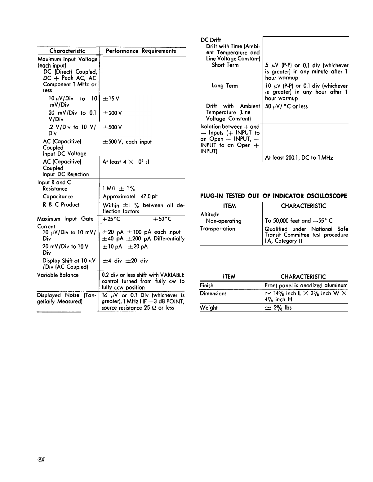
TM 11-6625-2749-14&P
DC Drift
Drift with Time (Ambient Temperature and
Line Voltage Constant)
Short Term
Long Term
Drift with Ambient
Temperature (Line
Voltage Constant)
Isolation between + and
– Inputs (+ INPUT to
an Open — INPUT, —
INPUT to on Open
INPUT)
5 pV (P-P) or 0.1 div (whichever
is greater) in any minute after 1
hour warmup
10 pV (P-P) or 0.1 div (whichever
is greater) in any hour after 1
hour warmup
50 pV/ “C or less
-f-
At least 200:1, DC to 1 MHz
ENVIRONMENTAL
PLUG-IN TESTED OUT OF INDICATOR
ITEM
Altitude
Non-operating
Transportation
CHARACTERISTIC
To 50,000 feet and —55° C
Qualified under National Safe
Tronsit Committee test procedure
1A, Category
PHYSICAL
ITEM CHARACTERISTIC
Finish
Dimensions
Weight
Front panel is anodized aluminum
s
145/8
478 inch H
=
25/8
Ibs
II
inch L X
OSCILLOSCOPE
2S/8
inch W X
1-3
Page 18

Page 19
TM 11-6625-2749-14&P
SECTION 2
OPERATING INSTRUCTIONS
Introduction
This section opens with a brief functional description of
the front-panel controls, input overdrive lamp, and input
connectors. Following the front-panel description is a familiarization procedure and finally a general discussion of the
operation of the Type 7A22.
CONTROLS AND CONNECTORS
INPUT Input overdrive indicator lamp turns on
OVERDRIVE
VOLTS/DIV Volts per displayed division. Nineteen
VARIABLE
(CAL IN]
GAIN
POSITION
IDENTIFY
HIGH
FREQUENCY
-3 dB POINT
to indicate excessive differential drive
to the input amplifier stage. Lights when
the differential dynamic range between
input connectors is exceeded.
position switch used to select the calibrated deflection factors.
Two-position switch activated by the
VARIABLE knob to select calibrated or
uncalibrated deflection factors. At the
IN position, the VARIABLE control is inoperative and the deflection factor is
calibrated. When pressed and released,
the knob moves outward to activate the
VARIABLE control for uncalibrated de-
flection factors. The uncalibrated posi-
tion provides continuously variable uncalibrated attenuation between the calibrated deflection factors and extends
the deflection factor to at Ieost 25
VOLTS/DIV.
Screwdriver adjust control to set the CRT
display scale factor to agree with the
VOLTS/DIV switch indication. Adjusted
for proper deflection with the VOLTS/
DIV switch set to the 1 mV position.
The control that vertically positions the
trace or display.
Momentary contact, push-button switch,
concentric with POSITION. Will cause
the trace, representing the output of the
Type 7A22, to move a small amount
when pressed. Aids in identifying the
Type 7A22 trace when multiple traces
are displayed.
Nine position switch to select the approximate high frequency -3 dB point.
The switch positions are: 100 Hz, 300 Hz,
1 kHz, 3 kHz, 10 kHz, 30 kHz, 100 kHz,
300 kHz, and 1 MHz.
LOW
FREQUENCY
-3 dB POINT
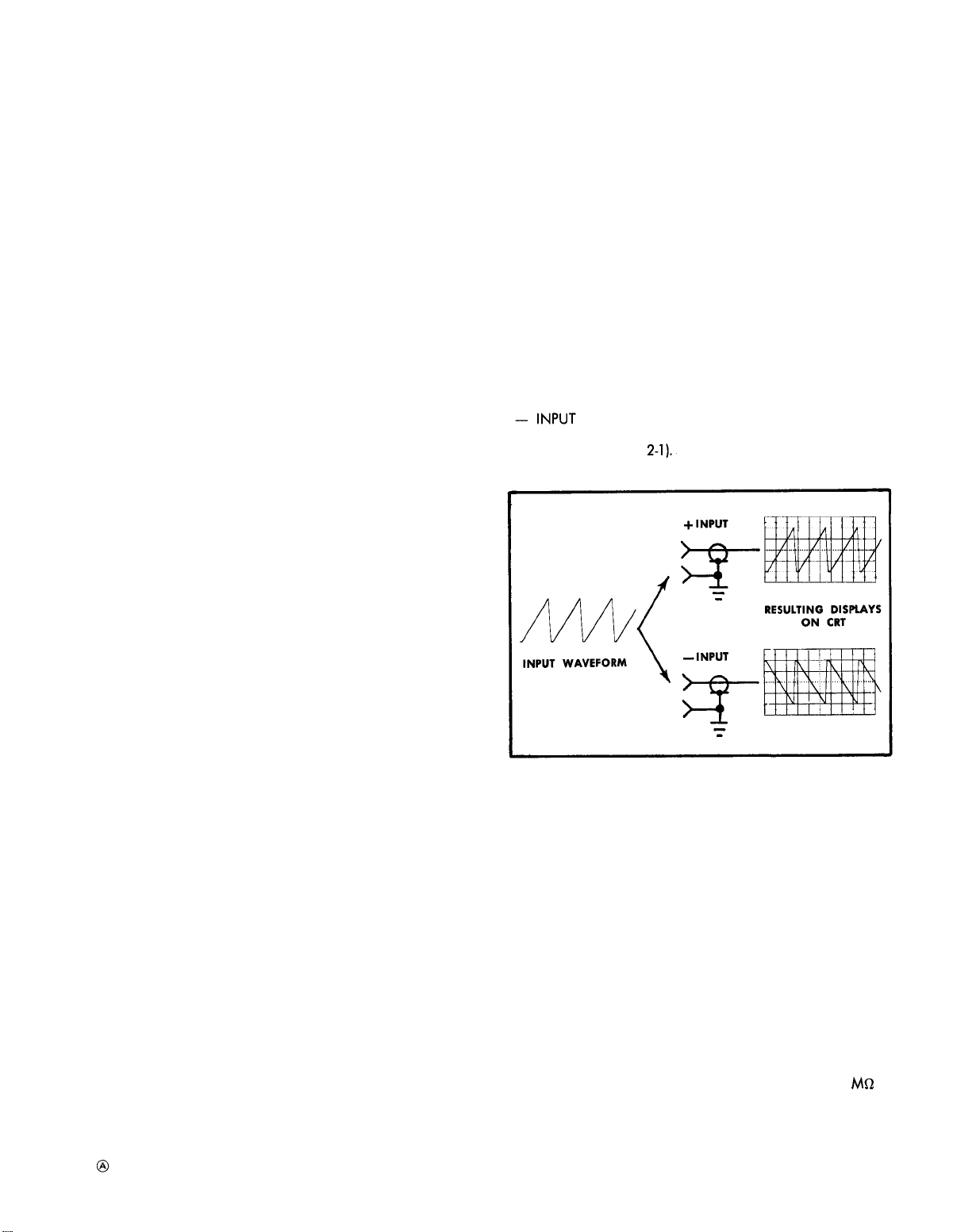
+INPUT
Fig. 2-1. Signals applied to the + INPUT connector produces an
upright display, while signals applied to the — INPUT are inverted.
+ AC-GND-DC
Eight position switch to select DC coupling or the approximate low frequency
-3 dB points. The switch positions are:
DC OFFSET, DC, .1 Hz, 1 Hz, 10 Hz,
100 Hz, 1 kHz, and 10 kHz.
Signal input connector. Positive input
produces deflection upward (see Fig.
2-l).
Signal input connector. Positive input
produces deflection downward (see Fig.
Fig. 2-1
A miniature illuminated push-button type
switch. The buttons are interlocked so
that only one button may be depressed
at one time. When the ‘AC’ button is
depressed the signal is coupled through
0.1 µF to the Input Amplifier and only
the varying component of the input sig-
nal is amplified.
When the ‘DC’ button is depressed the
signal is coupled directly to the Input
Amplifier and the entire input signal,
both AC and DC, is amplified. When
the ‘GND’ button (or none of the buttons) is depressed, the signal is coupled
Mfl
through 0.1 µF and through 1
ground. The Amplifier Input is grounded
in this condition.
to
2-1
Page 20

TM 11-6625-2749-14&P
aEoch push-button is illuminated from
behind when the button is depressed.
– AC-GND-DC
The following
when the LOW
is set to DC
STEP ATTEN
DC BAL (DC MODE the amplifier input stage. With
ONLY)
DC OFFSET
(DC OFFSET
mode only)
RELEASE LATCH Gray rectangular knob near the bottom
Same function as the + AC-GND-DC
switch but applied to the — INPUT.
IMPORTANT
two controls ore operative only
FREQUENCY
or
DC OFFSET.
Front panel cantrol for DC balancing
nals applied ta the input connectors,
the control is adlusted for
shift as the VOLTS/DIV switch is moved
from the 10 mV pasition to the 10
position.
Coarse and fine controls to provide
internal offset bias while maintaining
the differential
range of the offset bias depends upon
the settings of the VOLTS/DIV
and is indicated by shaded gray bands
(OFFSET RANGE) around the VOLTS/
DIV switch.
left of the front panel. Pull out to remove Plug-In fram Plug-In compartment.
—3 dB
POINT switch
capability. Available
no
no
switch,
sig-
trace
~LV
OPERATING INSTRUCTIONS
First-Time Operation
Steps
to help place the trace
the unit for immediate use. Steps 6 through 8 are used to
check
remaining are intended to demonstrate some of the basic
functions of the Type 7A22.
ment.
clockwise and turn the oscilloscope Power ON. Preset the
time-base and triggering controls
and automatic triggering.
oscilloscope to warm up.
1 through 5 in the following procedure are intended
the GAIN adjustment. These steps slang with those
1.
Insert the unit inta the ascilloscape plug-in compart-
2. Set the Type 7A22 front-panel controls as follaws:
VOLTS/DIV
VARIABLE
POSITION
HIGH FREQUENCY
–3dB POINT
LOW FREQ –3 dB
AC-GND-DC
AC-GND-DC
STEP ATTEN DC BAL
3. Turn the oscilloscope Intensity control fully counter-
4. Wait about five minutes for the Type 7A22 and the
(+
(–
INPUT)
INPUT)
on
the screen quickly and prepare
1 mV
IN (CAL)
Midrange
1 MHz
POINT
DC
GND
GND
Midrange
for a .5
ms sweep rate
NOTE
About five minutes is sufficient time for warmup
when using the Type 7A22 for short-term DC measurements. For long-term DC measurements
the lower deflection factors, allow at least one
hour.
5, Adlust the Intensity control for normal viewing of
the trace. The trace shauld appear near the graticule center.
6. Using the POSITION control, position the trace 2 divi-
sions below graticule center.
CAUTION
If the maximum input voltage rating in the 10 /IV
to 10 mV range of the VOLTS/DIV
ceeded, the inputs are diode-clamped
voltages of approximately
—16.5 volts and damage to the signal source is
possible. If the signal source can supply more than
1/1 6 A of current, the input protective fuse (s)
will open. An apen input fuse is indicated by the
lighting of the INPUT OVERDRIVE indicator with the
input coupling switches set to GND.
7. Apply
a
coaxial cable to the + INPUT connector
7A22.
8. For DC coupled, single-ended operation, set the +
INPUT AC-GND-DC
should
bottom of the disploy at the reference established in step 6.
9. For AC coupled, single-ended operation, reposition the
display with the Type 7A22 POSITION control to place the
bottom of the display at the graticule center line.
10. Set the + INPUT AC-GND-DC coupling switch to AC
and note that the display shifts downward about 2 divisions
to its average Ieve!,
11. Disconnect the coaxial cable from
nector. Connect
and — INPUT connectors. Connect the coaxial cable from
the Calibrator
12. For AC coupled differential
—INPUT AC-GND-DC
brator signal is now coupled to both inputs as
mode signal. A straight line display should
since the common-mode is being relected.
Operational Adjustments
Most of the following checks and adjustments may
be made after
to the DC drift of the amplifier during
warmup,
adjusted for each check or adjustment,
warmup of at least one hour should be allowed
before
in conjunction with the Type 7A22 is correctly cali-
brated (refer to the oscilloscope manual) and that
the calibrated output voltage is correct.
a 4 mV
be
square waves 4 divisions in amplitude with the
the
a
BAL is attempted. Insure that the oscilloscope used
peak-to-peak calibrator signal through
coupling switch to DC. The display
a
dual input connector
to
the dual input connector.
a 5
STEP ATTEN DC
final adjustment of the STEP ATTEN DC
+
coupling switch
NOTE
minute warmup; however due
16.5 volts and/or
the +
to
operation, set the
to
BAL shauld be re-
using
switch is ex-
to
fixed
on
the Type
INPUT con-
the + INPUT
AC. The cali-
a
common-
be
observed,
subsequent
and
a
2-2
Page 21
TM 11-6625-2749-14&P
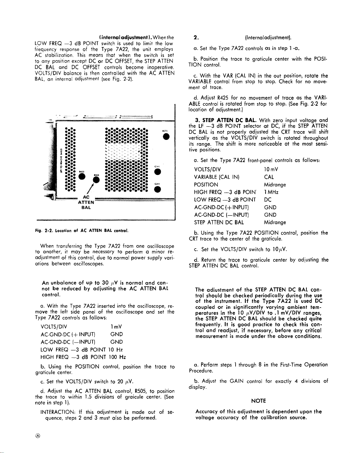
1. AC ATTEN BAL
LOW FREQ —3 dB POINT switch is used to limit the low
frequency response of the Type 7A22, the unit employs
AC stabilization. This means that when the switch is set
to
crny
position except DC or DC OFFSET, the STEP ATTEN
DC BAL and DC OFFSET controls become inoperative.
VOLTS/DIV
BALI ;; inkm-ml cdiushent
Fig.
When trcsnsferring the Type 7A22 from ane oscilloscope
to another, it may
ad~ustment of this control, due to normal power supply varicstions between oscilloscopes.
Ixslance is then controlled with the AC ATTEN
2-2. location
of AC ATTEN BAL
be
(internal adiustmerst) . When the
(see
Fig. 2-2].
control.
necessary to perform
a
minor re-
NOTE
An unbalance of up to 30 pV is normal and cannot be reduced by adiusting the AC ATTEN BAL
control.
a.
With the Type 7A22 inserted into the oscilloscope, re-
move the left side panel of the oscilloscope and set the
Type 7A22 controls as follows:
VOLTS/DIV
AC-GND-DC (+ INPUT)
AC-GND-DC (–INPUT)
LOW FREQ —3 dB POINT 10 Hz
HIGH FREQ –3 dB POINT 100 Hz
b.
Using the POSITION
graticule center.
c. Set the VOLTS/D[V
d.
Adiust the AC ATTEN BAL control, R505, to position
the trace to within 1.5 divisions of graicu[e center. (See
note in step
INTERACTION:
1).
quence, steps 2 and 3 must also
If
this adjustment is made out of se-
1 mV
GND
GND
control, position the trace to
switch to 20 pV.
be
performed.
2.
VAR BAL R425.
a.
Set the Type 7A22 controls as in step 1 -a.
b.
Position the trace to graticule center with the POSl-
TION control.
c.
With the VAR (CAL IN) in the out position, rotate the
VARIABLE control from stop to stop. Check for no move-
ment of trace.
d.
Adiust R425 for no movement of trace as the VARlABLE control is rotated from stop to stop. (See Fig. 2-2 for
location of adjustment.)
3. STEP ATTEN DC BAL. With zero input voltage and
the LF –3 dB POINT selector at DC, if the STEP ATTEN
DC BAL is not properly adiusted the CRT trace will shift
vertically as the VOLTS/DIV
its range.
tive positions.
a.
VOLTS/DIV
VARIABLE [CAL IN)
POSITION
HIGH FREQ –3 dB POIN’
LOW FREQ –3 dB POINT
AC-GND-DC (+ INPUT)
AC-GND-DC (–INPUT)
STEP ATTEN DC BAL
b.
CRT trace to the center of the graticule.
c.
d.
STEP
The shift is more noticeable at the most sensi-
Set the Type 7A22 front-panel centrals as follows:
Using the Type 7A22 POSITION control, position the
Set the VOLTS/DIV
Return the trace to graticule
ATTEN DC BAL cantrol.
(Internal adjustment].
switch is rotated throughout
10mV
CAL
Midrange
1 MHz
DC
GND
GND
Midrange
switch to
I o pv.
center by adiusting the
NOTE
The adjustment of the STEP ATTEN DC BAL con-
trol should be checked periodically
of the instrument. If the Type 7A22 is used DC
coupled or in significantly
peratures in the 10 KV/DIV to
the STEP ATTEN DC BAL should be checked quite
frequently.
trol and readiust, if necessary, before any critical
measurement is made under the above conditions.
It is
good practice to check this con-
during the use
varying ambient tem-
.1
mV/DIV ranges,
4. GAIN
a.
Perform steps 1 through 8 in the First-Time Operation
Procedure.
b.
Adiust the GAIN control for exactly 4 divisions of
display.
NOTE
Accuracy of this adjustment is dependent upon the
voltage accuracy of the calibration source.
2-3
Page 22
TM 11-6625-2749-14&P
GENERAL OPERATING INFORMATION
Trace Drift
The environment in which the Type 7A22 is operated and
the inherent characteristics of the Type 7A22 influence trace
drift. Therefore, to determine trace drift for
vironment refer to the Specification Section. In environment
in which the ambient temperature does not vary
as an air-conditioned building) the trace drift generally will
not exceed 10 ~LV in one hour.
Input Gate Current
When using the .1 mV/DIV to 10 ILV/DIV ranges for measurement with
where the source impedance is high
input gate current should
adlusted to zero. This is particularly desired at high temperatures (abave 40”
Check/Calibration
procedures for setting the gate current to zero.
Voltage Measurement
To obtain accurate DC measurements at maximum sensitivity, it is necessary
the amplifier lust before making the measurement. This is
accomplished by adiusting the STEP ATTEN DC BAL as
described under operational adjustment number 3.
When measuring DC voltages, use the largest deflection
factor (10 V/DIV) when first connecting the Type 7A22 to
an unknown voltage source.
small to make the measurement, switch to
tion factor. If the input stage is overdriven,
of current might flow into the input. See CAUTION after
item 6 of First Time Operation.
Where only the AC component of
AC and DC components is to
GND-DC switches to take advantage of the pre-charging
circuit incorporated in the unit. The pre-charging circuit
permits the coupling capacitor to charge to the DC source
voltage when the AC-GND-DC switch is set to GND. Procedure for using this circuit is as follows:
a.
Before connecting the Type 7A22 to
ing
a DC
switch to GND. Then connect the input to the circuit under
test.
b.
Allow about one second for the coupling capacitor to
charge.
b.
Set the input coupling switch to AC. The display will
remain
ured in the usual manner.
d. On
DC switch to GND and short the input connector to ground.
The above procedure should
other signal with
If the Type 7A22 is connected to
age source
sion,
an AC
companent, set the AC-GND-DC
on
the screen and
completion of the measurement, set the AC-GND-
the peak charging current (into 0.1 ILF
coupled input, for DC measurements
be
C).
Steps 7 and 8 in the Performance
Procedure describe the
to
ground the input and DC balance
the AC
a
different DC level is connected.
CAUTION
without using the pre-charge provi-
(in
checked and allowed for, or
Then, if the deflection is too
a
be
measured, use the AC-
component
be
followed whenever an-
a
specific
much (such
excess of 1 Mo) the
check
signal having both
a
a
large DC volt-
and adiust
a
lower deflec-
a
large amount
signal containinput coupling
can be
en-
meas-
capacitor)
source, and this source may be damaged or de-
stroyed.
When
7A22 with the input AC coupled, the input coupling capacitor acquires
as
a
very slowly decaying output voltage. This
sequent AC coupled measurements at other DC voltages
and drive the trace off-screen. A period of at least 10 min-
utes, with input set to GND, should
reasonable recovery from polarization, and a longer period
may
be
connectors are shorted to ground the depolarization process will require less time.
Signal Input Connectors
When connecting signals to the +INPUT and –INPUT
connectors
pling that will
sometimes
source, particularly when
is monitored at
of these factors are missing, it becomes increasingly important to use shielded signal cables. In all cases, the signaltransparting leads should
When making single-ended input measurements,
to establish
test and the Type 7A22. The shield of
normally used for this purpose.
In some cases differential measurements require
mon ground’,
ference by ground loop currents. Some problems with
stray magnetic coupling into the signal transporting leads
can
also
single-ended measurement.
cussed later in this section under Differential Operation.
It is always important to consider the signal-source loading and resulting change in the source operating characteristics due to the signal-transporting
circuit of the Type 7A22. The circuit at the input connectors
can
normally
ground paralled by 47 pF. A few feet of shielded cable
may increase the parallel capacitance
In many cases, the effects of these resistive and capacitive
loads may
them through the use of
Attenuator probes not only decrease the resistive and
capacitive loading of
measurement range of the Type 7A22 to include substantially higher voltages. Passive attenuator probes having attenuation factors of 10X, 100X, and lOOOX, as well as other
special-purpose types are available through your Tektronix
Field Engineer or Field Office.
Some measurement situations require
put to the Type 7A22 with very littIe source loading or sig-
‘The DC plus
to the chassis
the levels listed in Section 1 under
Voltage
reiection ratio
will be limited only by the signal
a
large DC voltage has been applied
a
low voltage, high impedance voltage source with
characteristics.
charge due
necessary for critical measurements. If the input
on
the Type 7A22, consider the method of
be
be
used to connect the Type 7A22 to
a
a
common ground between the device under
and therefore are less susceptible to inter-
be
minimized by using
be
represented by
be
too great and it may
peak
AC
potential
and
exceed the input
to
dielectric polarization and acts
be
used. Ordinary unshielded test leads
a
high level, low-frequency signal
low impedance point, However when any
be
kept as short as practical.
a
These considerations
an
attenuator probe.
a
signal source, but also extend the
voltages
of the Type
Higher
on the test points with respect
levels will
differential rather than
leads and
a 1
megohm resistance ta
to
be
desirable to minimize
a
7A22
Maximum
degrade
voltage rating
to
the Type
can
offset sub-
allowed to assure
cau
a
be
a
coaxial cable is
no
are dis-
the
100 pF or more.
high-resistance in-
should be limited to
Common-mode Input
the common-mode
of the unit.
a
can
signal
sure
com-
input
-
2-4
Page 23
TM 11-6625-2749-14&P
not attenuation. In such
probe cannot
by using an
vision of the Type 7A22.
High Input Impedance
TIM
coupled signals which permit the use of 10mV through 10
pV”psitions
no input attenuator is used at these switch positions, the
internal gate return resistor olone establishes the 1 megohm
input resistance.
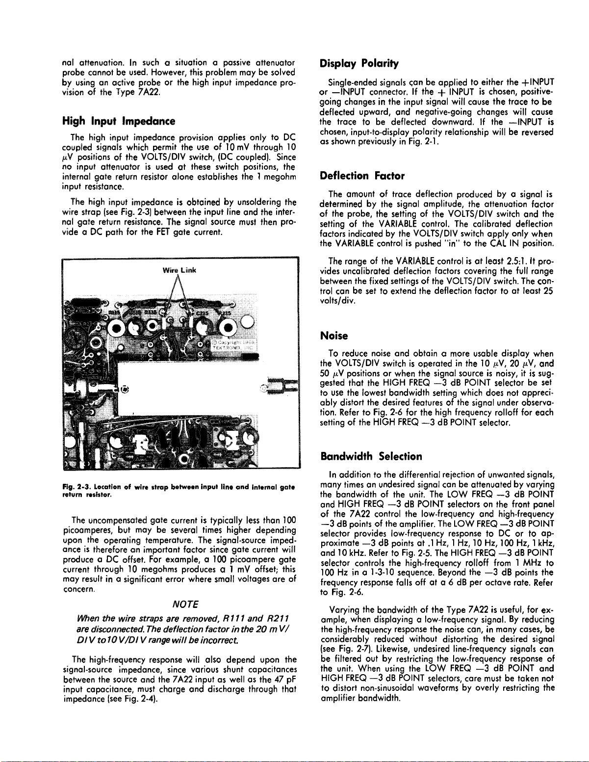
The high input impedance is obtained by unsoldering the
wire strap
nal gate return resistance. The signal source must then provide
a DC
be
csetive
high input impedance provision applies only to DC
of
the VO”LTS/DIV switch, (DC coupled). ‘Since
(see
Fig. 2-3] between the input line and the inter-
path for the FET gate current.
a
situcstion
used. However, this problem may
probe or the high input impedance pro-
a
passive attenuator
be
solved
Display Polarity
Single-ended signals
or —INPUT connector. If the + INPUT is chosen, positivegoing changes in the input signal will cause the trace to be
deflected upward, and negative-going changes will cause
the trace to
chosen, input-to-display polarity relationship will
as shown previously in Fig. 2-1.
Deflection
The amount of trace deflection produced by
determined by the signal amplitude, the attenuation factor
of the probe, the setting of the VOLTS/DIV switch and the
setting of the VARIABLE control. The calibrated deflection
factors indicated by the VOLTS/DIV switch apply only when
the VARIABLE control is pushed “in” to the CAL IN position.
The range of the VARIABLE control is at least 2.5:1. It provides uncalibrated deflection factors covering the full range
between the fixed settings of the VOLTS/DIV switch. The control can be set to extend the deflection factor to at least 25
volts/div.
Noise
be
Factor
Can be
deflected downward. If the —INPUT is
applied to either the +INPUT
be
reversed
a
signal is
Fig.
2-3. location of wire
return resistor.
The uncompensated gate current is typically less than 100
picoamperes,
upon the operating temperature. The signal-source imped-
ance is therefore can important factor since gate current will
produce
current through 10 megohms produces
may resu[t in
concern.
Men the wire straps are removed, R111 and R211
are disconnected. The deflection factor in the 20 m V/
DI V to 10 V/Dl V range will be incorrect.
The high-frequency response will
but may
a DC
a
signcsl-source impedance,
between the source
input capacitance, must charge and discharge through that
impedance [see Fig. 2-4).
strap between input
be
several times higher depending
offset. For example,
significant error where small voltages are of
NOTE
since various shunt capacitances
cmd
the 7A22 input as well as the 47 pF
line and internal gate
a
100 picoampere gate
a 1 mV
also depend upon the
offset; this
To reduce noise and obtain
the VOLTS/DIV switch is operated in the 10 wV, 20 wV, and
50 pV positions or when the signal source is “noisy, it is suggested that the HIGH FREQ —3 dB POINT selector
to use the lowest bandwidth setting which does not appreciably distort the desired features of the signal under observation. Refer to Fig. 2-6 for the high frequency rolloff for each
setting of the HIGH FREQ —3 dB POINT selector.
Bandwidth
In addition to the differential reiection of unwanted signals,
many times an undesired signal
the bandwidth of the unit. The LOW FREQ –3 dB POINT
and HIGH FREQ —3 dB POINT selectors on the front panel
of the 7A22 control the low-frequency and high-frequency
–3 dB points of the amplifier. The LOW FREQ –3 dB POINT
selector provides low-frequency response to DC or to ap-
proximate —3 dB points at .1 Hz, 1 Hz, 10 Hz, 100 Hz, 1 kHz,
and 10 kHz. Refer to Fig. 2-5. The HIGH FREQ —3 dB POINT
selector controls the high-frequency rolloff from 1 MHz to
100 Hz in
frequency response falls off at
to Fig. 2-6.
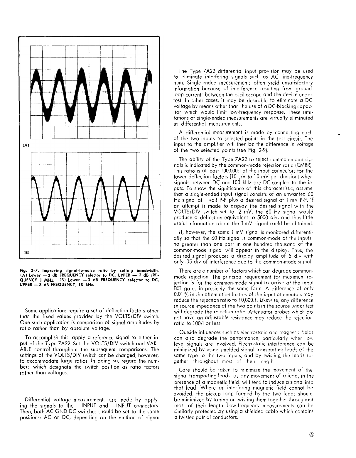
Varying the bandwidth of the Type 7A22 is useful, for example, when displaying
the high-frequency response the noise can, in many cases, be
considerably reduced without distorting the desired signal
(see Fig. 2-7). Likewise, undesired line-frequency signals can
be
filtered out by restricting the low-frequency response of
the unit. When using the LOW FREQ —3 dB POINT and
HIGH FREQ —3 dB POINT selectors, care must be taken not
to distort non-sinusoidal waveforms by overly restricting the
amplifier bandwidth.
Selection
a
1-3-10 sequence. Beyond the –3 dB points the
a
more usable display when
can be
a 6 dB
a
low-frequency signal. By reducing
attenuated by varying
per octave rate. Refer
be
set
REV. B, FEB. 1975
2-5
Page 24

2-6
Fig. 2-4A. 7A22 CMRR at 10 µV/Div to 10 mV/Div. Inputs DC Coupled. Worst-case degradation due to source resistance.
TM 11-6625-2749-14&P
Page 25
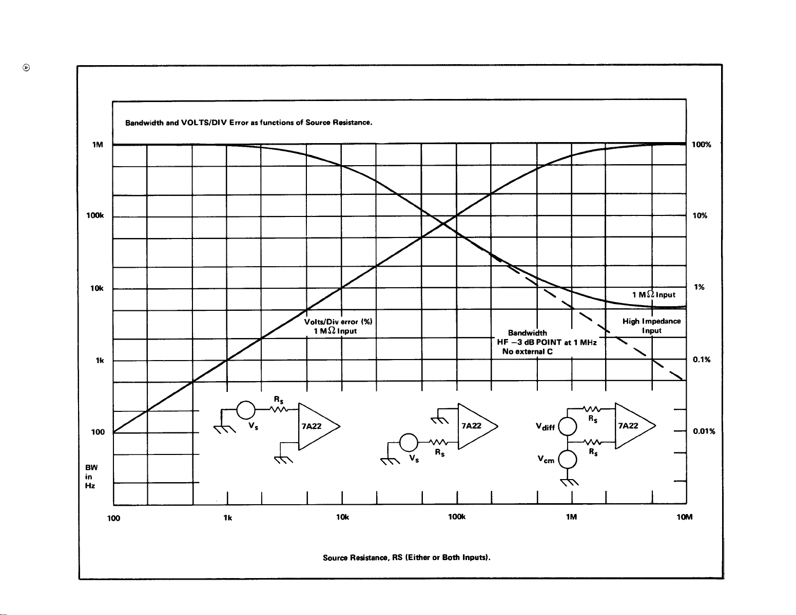
Fig. 2-4B. 7A22 Bandwidth and VOLTS/DIV Error as functions of Source Resistance.
TM 11-6625-2749-14&P
2-7
Page 26

2-8
Fig. 2-5. 7A22 FREQUENCY RESPONSE as a function of LF -3 dB POINT SETTING (HF -3 dB POINT at 1 MHz)
TM 11-6625-2749-14&P
Page 27
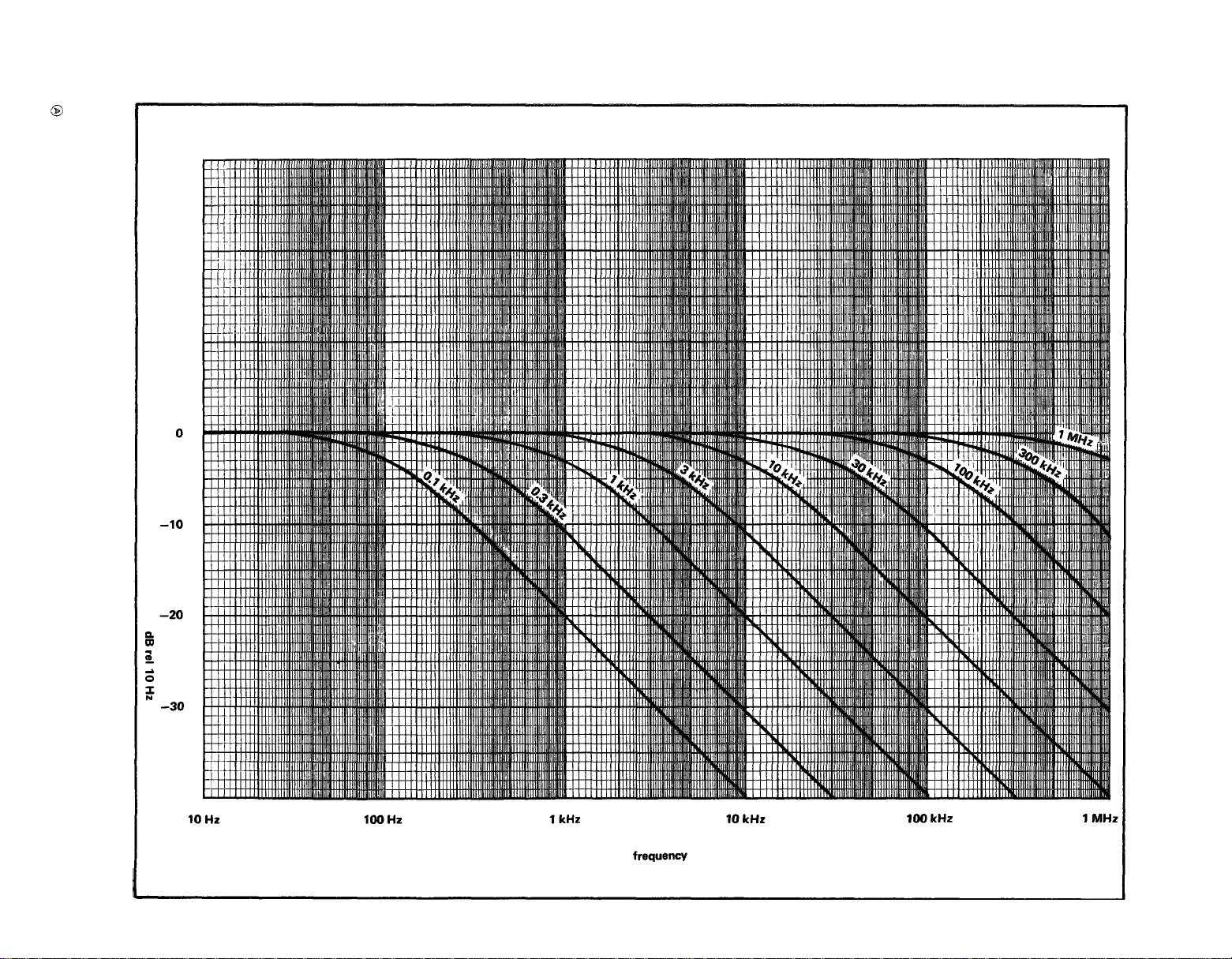
Fig. 2-6. 7A22 FREQUENCY RESPONSE as a function of HF - 3 dB POINT settings ( LF —3 dB POINT of DC).
2-9
TM 11-6625-2749-14&P
Page 28
TM 11-6625-2749-14&P
2-7.
Fig.
QUENCY 1 MHz.
UPPER —3 dB FREQUENCY, 10 kHz.
Improving
(Al
Lower —3 dB FREQUENCY selector to DC, UPPER — 3 dB FRE-
signal-to-noise
[B) Lower —3 dB FREQUENCY selector to DC,
ratio by setfing
bandwidth.
Voltage Comparison Measurements
Some applications require
than the fixed values provided by the VOLTS/DIV
One such application is comparison of signal amplitudes by
ratio rather than by absolute voltage.
To accomplish this, apply
put of
the
ABLE control throughout the subsequent comparisons. The
settings of the VOLTS/DIV switch
to accommodate large ratios. In doing so, regard the num-
bers which designate the switch position as ratio factors
rather than voltages.
Type 7A22. Set the VOLTS/DIV switch and VARl-
a
set of deflection factors other
a
reference signal to either in-
can be
changed, however,
switch.
Differential Operation
Differential voltage measurements are made by applying the signals to the +INPUT
Then, both AC-GND-DC switches should
positions: AC or DC, depending
and —INPUT connectors.
be
set to the same
on
the method of signal
The Type 7A22 differential input provision may
to eliminate interfering signals such as AC line-frequency
hum. Single-ended measurements often yield unsatisfactory
information because of interference resulting from groundIoop currents between the oscilloscope and the device under
test. In other cases, it may
voltage by means other than the use of
itor which would limit low-frequency response. These limitations af single-ended measurements are virtually eliminated
in differential measurements.
A differential measurement is made by connecting
of the two inputs to selected points in the test circuit. The
input to the amplifier will then
of the two selected points
The ability of the Type 7A22 to relect common-mode sig-
nals is indicafed by the common-mode relection ratio (CMRR).
This ratio is at least 100,000:1 at the input connectors for the
lower deflection factors (10
signals between DC and 100 kHz are DC-coupled to the in-
puts. To show the significance of this characteristic, assume
that
a
single-ended input signal consists of
Hz signal at 1 volt P-P plus
an attempt is made to display the desired signal with the
VOLTS/DIV
produce
useful information about the 1 mV signal could
If, however, the same 1 mV signol is monitored differentially so that the 60 Hz signal is ;ommon-mode at the inputs,
no
common-mode signal will appear in the display. Thus, the
desired signal produces
only .05 div of interference due to the common-mode signal.
There are
mode rejection. The principal requirement for maximum reiection is for the common-mode signal to arrive at the input
FET gotes in presicely the same form. A difference of only
0.01 ~o in the attenuation factors of the input attenuators may
reduce the rejection ratio to 10,000:1. Likewise, any difference
in source impedance at the two points in the source under test
will degrade the relecfion ratio. Attenuator probes which do
not have an adjustable resistance may reduce the rejection
ratio to 100:1 or less.
Outside influences such as electrostatic and Imagnefic fields
can
level signals are involved. Electrostatic interference
minimized by using shielded signal transporting leads of the
same ty~e to the two inputs, and by twisting the leads to-
gether ‘throughout most of their length. -
Care should
signal transporting leads, as any movement of
txesence of
that lead. Where
avoided, the pickup loop formed by
be
minir’nized by taping or twisting them together throughout
most of their length. Low-frequency measurements
similarly protected by using
a
twisted pair of conductors.
switch set to .2 mV, the 60 Hz signal would
a
deflection equivalent to 5000 div, and thus little
greater than one part
a
number of factors which
also degrade
the
be
taken to minimize the movement of
a
maanetic field, will tend to induce
an
be
desirable to eliminate
a
DC-blocking copac-
be
the difference in voltage
(see
Fig. 2-9).
/LV to 10 mV
a
desired signal at 1 mV P-P. If
in
one hundred thousand of
a
disploy amplitude af 5 div with
performance, particularly when low
interfering magnetic field cannot
a
shielded cable which contains
per division) when
an
can
degrade common-
the
two leads should
be
a
each
unwanted 60
be
obtained.
can be
a
lead, in the
a
sianal into
can be
used
DC
the
the
be
.
2-10
Page 29
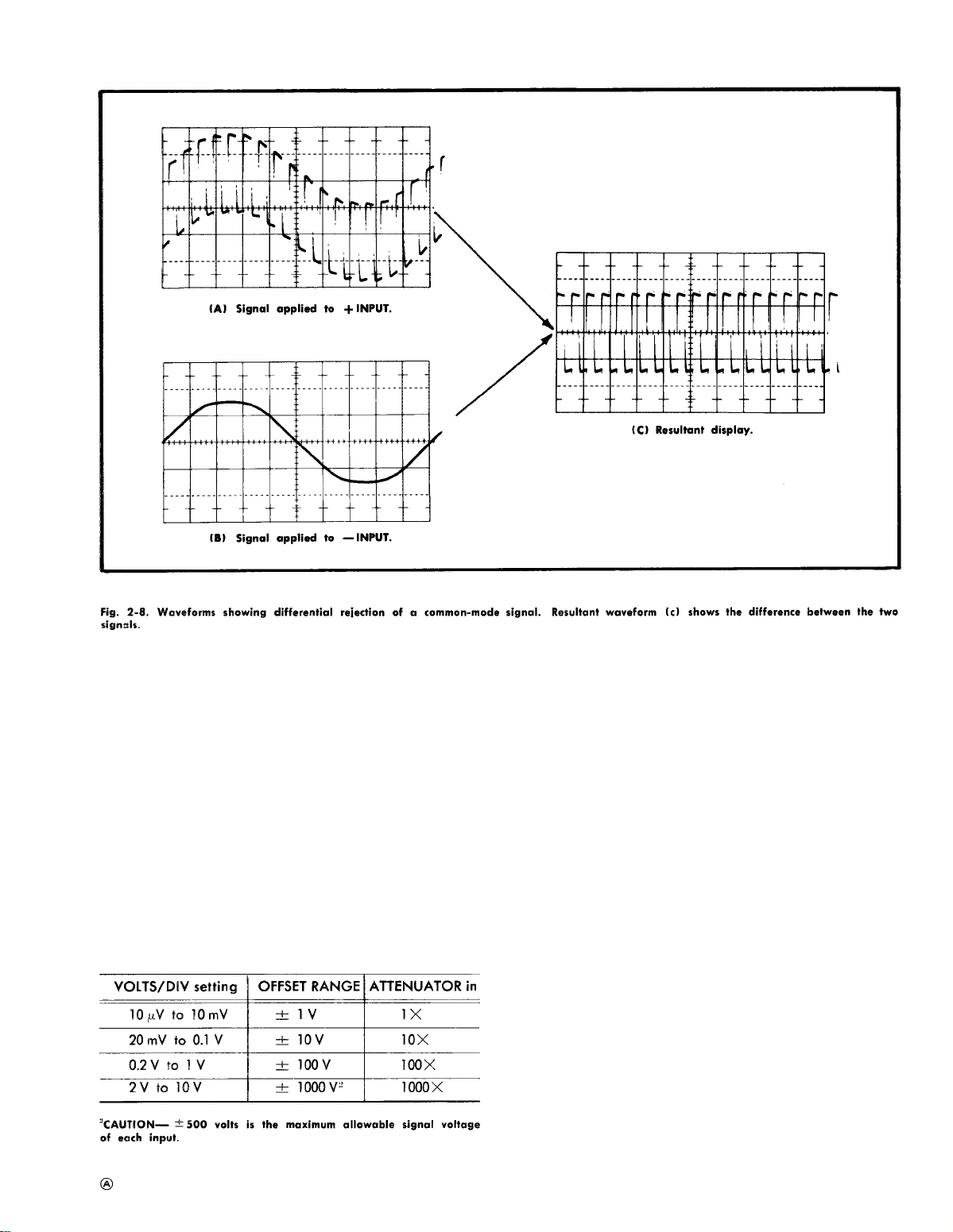
Fig. 2-8
TM 11-6625-2749-14&P
DC Offset Operation
By using the DC OFFSET controls, it is possible to use the
Type 7A22 differentially in a slide-back mode, to observe
small signal whose DC potential difference may be considerable. The offset is continuously adjustable from +1 V to
–1 V when the VOLTS/DIV switch is in the 10µV to 10mV
positions. In the 20mV, 50mV and .1 V positions of the
VOLTS/DIV switch, the 1 V offset is effectively multiplied by
the input attenuator to a range of ±10 V. Table 2-1 sum-
marizes the effective DC offset voltages internally available
for all the VOLTS/DIV switch positions. The table also lists
the input attenuator that is switched into the amplifier circuit
for the various VOLTS/DIV switch positions.
TABLE 2-1
Using the DC OFFSET functions:
Set the Type 7A22 controls as follows:
VOLTS/DIV
VARIABLE (CAL IN) CAL
POSITION Midrange
AC-GND-DC GND
(+ and – INPUT)
HF -3 dB POINT 1 MHz
LF -3 dB POINT DC
STEP ATTEN DC BAL Adjusted for DC balance
1. Position the trace to graticule center (or some other
convenient reference line) using the POSITION control.
2. Connect a coaxial cable from the signal source to the
+INPUT.
3. Set the + INPUT AC-G ND-DC switch to DC and meas-
ure the DC level to be offset.
4. Set the VOLTS/DIV to the largest deflection factor in an
offset range which will encompass the DC level measured in
step 3. See Table 2-1 and front panel color bands.
5. Set the LF -3 dB POINT selector to DC OFFSET,
10V
2-11
Page 30
TM 11-6625-2749-14&P
NOTE
If switching into another offset range, the OFFSET
controls will need to be readjusted. If switching
into
a
smaller offset range, check that the avail-
able range
present (see steps 3 and 4 above) .
is
sufficient to encompass the DC level
Input Overdrive
The INPUT OVERDRIVE indicator turns
to
the input FETs approaches the differential dynamic range
of the amplifier. The 7A22 should not
a
circuit if this light is on, as this may mean that
voltage is present.
The INPUT OVERDRIVE indicator serves another important
function. If the amplifier is direct-coupled at the input, a DC
differential signal could overdrive the input stage ond cause
a
reduction in gain, The small voltages to
not
be
distorted, but will
sult, amplitude measurements made under such conditions will
not
be
accurate. The Type 7A22 INPUT OVERDRIVE indicator provides
lighting before the gain calibration changes by 1
If
the
sible ways to continue:
DC differential sicinals may then
indicated in Table-2-l.
signals up to 1000 V (either input not to exceed 500
be
sarily limits the low frequency response to 1,6 Hz (or
0.16 Hz with
The INPUT OVERDRIVE lamp is insensitive
mode overdrives, and it is possible to overload the Type
7A22 without lighting the input overdrive light.
In summary
following conditions:
a.
of the amplifier
b. An
light will remain on even if
to
GND.
c. There is
an
INPUT OVERDRIVE lamp turns on, there are two pos
1.
Switch the LF —3 dB POINT selector
2. Switch the AC-GND-DC switch to AC. DC differential
removed by using AC coupling at the input. This
The input signal exceeds the differential dynamic range
input protective fuse is blown. In this case,
a
Indicator
be
be
reduced in amplitude. As
indication that such
a
10X probe).
the
overdrive indicator will turn
(see
Section 1 for table of dynamic ranges).
the
circuit malfunction.
a
be
‘
AC-G ND-DC switches are set
on
when the signol
left connected
a
be
measured will
signal is present by
~o.
to DC
balanced out as
to
on
damaging
a
OFFSET.
V)
may
neces-
common-
under the
the
to
re-
Fig,
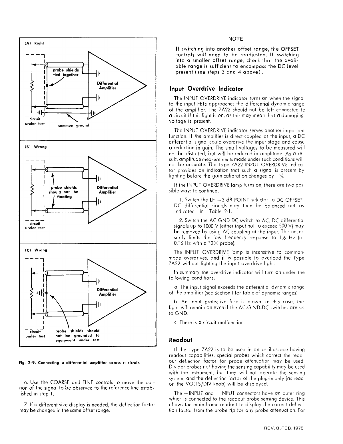
2-9. Connecting
6. Use the COARSE and FINE controls to move
tion of the signal to
lished instep
7. If
a
may
2-12
different size display isneeded, the deflection factor
be
changed in the same offset range.
1.
a
differential amplifier
be
observed to the reference line estab-
across a
circuit.
the
por-
Readout
If
the
Type 7A22 is
readout capabilities, special probes which correct
out deflection factor for probe attenuation may
Divider probes not having
with the instrument, but they will not operate the sensing
system, and the deflection factor of
on the VOLTS/DIV knob) will
The +INPUT and —INPUT connectors have
which is connected
allows
the
tion factor from the probe tip for any probe attenuation, For
main-frame readout
to be
to
used
in an
the
sensing capability may
be
the readout probe sensing device. This
to
oscilloscope having
the
plug-in only (as reed
displayed.
display
the
REV.
an
correct deflec-
B, FE B.
the
read-
be
used.
be
outer ring
1975
used
Page 31

TM 11-6625-2749-14&P
example: if a 10X probe is used it will increase the deflec-
tion factor, in the readout display, by a factor of 10. Then the
actual deflection factor at the probe tip is displayed (see
Table 2-2).
NOTE
If only one divider probe (or two probes with
equal divider ratios) is connected, the deflection
factor at the probe tip will displayed; if probes
with different divider ratios are connected (e.g.,
IOX and 100X), the readout will display the de-
flection factor at the tip of the probe with the
larger division ratio (100X).
TABLE 2-2
TYPE 7A22
Plug In
VOITS/DIV Probe Atten Probe Atten Probe Atten
Setting
.5 mV
50 mV
Trace Identify. With the oscilloscope turned on and a
sweep displayed on the CRT, check for approximately 0.2 div
of vertical movement of the trace when the IDENTIFY
pushbutton is depressed. The vertical scale factor readout
associated with the 7A22 will change to the ward IDENTIFY.
An incorrect CRT readout will occur in the 10V/div
position when using the 100X Readout coded probe
(P6009, Tektronix Part No. 010-0264-01). When used in
10 V/div setting, reading will show IV instead of 1KV.
Main-Frame Displayed Readout
used 1 X used 10X
500
µV
50 mV
NOTE
5 mV
500 mV
used 100X
50 mV
5V
REV. B, AUG. 1974
2-13
Page 32

Page 33
TM 11-6625-2749-14&P
SECTION 3
CIRCUIT DESCRIPTION
introduction
A
Mock diagram description covering the general con-
figuration of
this section. Following the block diagram description is
detailed description of each circuit and the functions of spe-
cific components.
Simplified drawings ore provided where necessary for easier circuit understcsnding. Complete schematic diagrams are
included in the Diagrams section. These should be referred
to throughout the detailed circuit description.
The values of resistors on the schematics are in ohms unless otherwise specified. Capacitor values are indicated in
the following manner unless otherwise specified: whole numbers indicate that the value is. in pF, decimal numbers indiccste that the
pF.
each
circuit in the Type 7A22 is included in
vcdue is in
pF. For example, 33 pF and 0.1
BLOCK DIAGRAM DESCRIPTION
(see Block Diagram Pullout
preceding schematics)
Input coupling
A signal applied to the + or —Input connector passes
through the input coupling selector switch to the input attenuator circuit. The signals
pled or disconnected internally. (See Schematic Diagram
Number
1].
can be AC
coupled, DC cou-
a
Preamp
From the input attenuators, the signal is coupled to the
preamp. The preamp consists of two identical feedback amplifiers connected in
all differential gain is approximately 15.
The supply voltages for the two amplifiers are obtained
from
a
input to improve the common-mode reiection ratio of the
preamp.
cuit consiting of fuses and clamping diades. For deflection
factors from 10 pV/DIV through 10 mV/DIV the fuse will
open if the current exceeds
at the input), preventing damage to the input circuitry.
common power supply which is bootstrapped to the
Each input is equipped with an overdrive protection cir-
a
differential configuration. The over-
‘/IA A
(approximately
CAUTION
16.5 volts
Input Attenuators
The input attenuators for the -f- and —inputs are iden-
ticcsl
and are conventional RC type attenuators. Common
resistive elements are adjustable to facilitate matching the
—
and +- attenuators to obtain optimum DC common-mode
signcrl re~ection.
The attenuators (Schematic Diagram number
quency-compensated
stant attenuation at all frequencies within the passband of
the instrument, while maintaining
voltage dividers which pravide con-
a
constant input time con-
3)
are fre-
Low Frequency
The push-pull output of the preamp is coupled through
LOW FREQ —3 dB POINT selector. The selector switches the
components of the coupling network in each half of the pre-
amp to select the low frequency —3 dB points (.1 Hz, 1 Hz,
10 Hz, 100 Hz, 1 kHz and 10 kHz). The DC position of the
selector bypasses the low frequency selection circuitry and
direct-couples the preamp to the Output Amplifier.
— 3 dB
Point
3-1
a
Page 34

TM 11-6625-2749-14&P
Output Amplifier
The signal from the LF -3dB POINT selector is coupled
to the gain-switching section of the Output Amplifier. This
section of the Output Amplifier is a pair of feedback am-
plifiers similar to ‘that of the prearnp. The VOLTS/DIV
switch changes the amplifier gain.
Fig, 3-1. Generalized feedback system showing the relation between
input and output.
High Frequency -3 dB Point
The HF -3dB POINT selector switches capacitance across
the output of the Gain Switching Amplifier to set the high
frequency -3 dB point at any of 9 frequencies; 100 Hz, 300
Hz,’ 1 kHz, 3 kHz, 10 kHz, 30 kHz, 100 kHz, 300 kHz, and
1 MHz. The capacitance used in the 1 MHz position is adjustable to set the bandwidth to normal value.
Positioning of the trace, and VARIABLE VOLTS/DIV, are
provided in the stage following the HF -3 dB POINT se-
lector.
Overall amplifier gain is adjusted in the signal output
stage of the Output Amplifier by adjusting the common emitter resistance.
GENERAL INFORMATION
Feedback Amplifiers
Since the Type 7A22 utilizes several multi-stage feedback
amplifiers, a brief review of feedback systems in general
is given.
Fig. 3-1 represents a generalized feedback system in which
it is desired to produce an output signal accurately and stably
related to the input. The arrangement of Fig. 3-1 causes the
modified output to be nearly equal to the input. Any difference between these is detected by the comparator, which
produces an error signal equal to the difference, and applies
this error to the amplifier, which amplifies the error and
feeds back a correction to’ reduce the ‘original error
3-2
Fig. 3-2. Feedback amplifier (Single-ended version)
Page 35
TM ll-6625-2749-14&P
The input to the modifier (the system output) is
curately related to the system input, provided the
is constructed of stable components.
Another way of looking at the system is to start at the
output and work backward. Specifically, assume an amplifier gain of 10,000 and
divider. Assume
volt, and the error signal (output-gain)
input is 1.001 valts. In this case, the errar between the desired output [1 OX input) of 10.01 volts and the actual output
of 10.00 volts is only 10 mV, or 1 part in 1,000.
[n
practice the comparator and error amplifier are often
combined in
of the basic configuration used in the Type 7A22 is illustrated in Fig. 3-2, with the basic blocks of Fig. 3-1 identified.
The comparator is FET Q,. Any change in the gate-to-source
bias voltage [dictated by the standing current established
by R, and the supply voltages) will cause
current, the change being applied as an error signal to the
input of the error amplifier.
The error amplifier consists of grounded emitter stage Q,
driving emitter fol[ower Q,. The internal output appears at
the emitter of
modifier [voltage divider) Rz,
tem output, V.,,
a
Qa
can be
a
feedback modifier which isa 10X
a 10
volt output. The modifier output is 1
differential amplifier. A single-ended version
and is fed back ta the comparator input via
R1.
determined by:
is 1
mV, so that the
a
change in drain
For this amplifier, the sys-
also ac-
modifier
Since
Vom is
then
the
R,
1?,
“
The useful output of the amplifier is the Q, collector signal
current
small error current from QJ. VOm = ioRl and since
approximately equal to Vi, and i. is approximately equal to
iO’ then i. is approximately equal to —
cur-rent vs. the input voltage depends primarily on the gainsetiing resistor,
An output voltage
through t-he load resistor,
v.
—,which
vi
cspproximcrtely equal to the input voltage Vi,
system gain, ~,
io’,
which flows through RI (in addition to the relatively
R1.
can
is
approximately equci[ to—
is approximately equal to 1 +
0s
Vi
Thus the output
RI “
also be obtained by passing i.
R~.
The overall voltage gain is then
R,
R,
“
Vo~
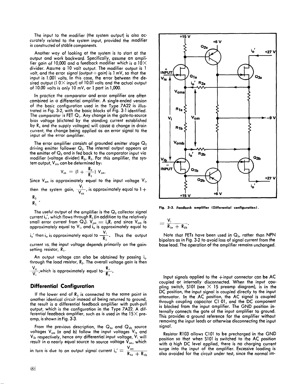
Differential Configuration
If the lower end of R, is connected to the same point in
another identical circuit instead of being returned to ground,
the result is
output, which is the configuration in the Type 7A22. A dif-
ferential feedback amplifier, such as is used in the 15X pre-
amp, is shown in Fig. 3-3.
From the previous description, the Ql, and Qlb source
voltages VO.
Vi~ respectively,
result in
in turn is due to an output signal current
a
differential feedback amplifier with push-pull
(a
and
b)
follow the input voltages Vi. and
hence
any differential input voltage, Vi will
a
nearly equal source to source voltage VO., which
i~’
=
v
R; +
R1~
Fig.
3-3.
Feedback
amplifier (Differential configuration).
is
Note that FETs have been used in Q,, rather than NPN
bipolars as in Fig. 3-2 to avoid loss of signal current from the
base lead. The operation of the amplifier remains unchanged.
DETAILED CIRCUIT DESCRIPTION
Input Coupling (See Schematic 1)
Input signals applied to the +input connector
coupled or internally disconnected. When the input cou-
pling switch, S101
DC position, the input signal is coupled directly to the input
attenuator.
through coupling capacitor Cl 01, and the DC component
is blocked from the input amplifier. The GND position internally connects the gate of the input amplifier to ground.
This provides
removing the input leads or otherwise disconnecting the input
signal.
Resistor R103 allows C101 to
position so that when S101 is switched to the AC position
with
a
surge into the input of the amplifier. Excessive loading is
also avoided for the circuit under test, since the normal im-
high DC level applied, there is no charging current
(see X 15
In the AC position, the AC signal is coupled
a
ground reference for the amplifier without
preamp diagram), is in the
be
precharged in the GND
can be
AC
3-3
Page 36

TM 11-6625-2749-14&P
pedance of 1 MQ-47 pF is still seen by the signal source.
—input switch, S201, functions in the same manner as
+input.
The
the
Input Attenuators
To produce the vertical deflection factor indicated on the
front panel by the VOLTS/DIV switch, the gain of the
feedback amplifier in the gain switched amplifier circuit is
changed by switching the source resistor (R407) of Q404
A and B (See Schematic 2 ) for switch positions 10 µV to
10 mV. For switch positions above 10 mV, input attenuators
are switched by S108 into the input circuit of the Type 7A22,
in conjunction with the gain switching resistors, R407, to
produce the selected deflection factors.
These attenuators are frequency-compensated voltage
dividers. For DC and low frequency signals, they are pri-
marily resistive dividers (e. g., R108C, R108D) and the voltage
attenuation is determined by the resistance ratio in the cir-
The reactance of the capacitors in the circuit is so high
cuit.
at the lower frequencies that their effect is negligible. However, at higher frequencies, the reactance of the capacitors
decreases and the attenuator becomes primarily a capa-
citive voltage divider (e.g., C108C, C108D).
In addition to providing constant attenuation at all frequencies within the bandwidth of the instrument, the input
attenuators are designed to maintain the same input RC
characteristics (1 megohm in parallel with 47 pF) for each
setting of the VOLTS/DIV switch. Each attenuator contains
an adjustable capacitor (e.g. C108C) to provide correct attenuation at high frequencies, and an adjustable shunt ca-
pacitor to provide correct input capacitance.
Gate Current Compensation
The leakage current associated with the gates of the input
FETs may be as high as 100 pA. This 100 pA of leakage
current (through 1 megohm to ground, R111 or R211) will
produce an offset of 100 µV, which at high input sensitivities
is not acceptable. To compensate this effect, the gates of
the input FETs may be adjusted to zero volts by returning
R111, R211 through variable controls R115 and R215 to a
slightly negative supply voltage (see Fig. 3-4).
Leakage current associated with the gates of the input
FETs and the overdrive protection diodes increases rapidly
with temperature, approximately doubling for every 10” C.
To compensate this increase, a temperature sensitive input
current balancing network is included, using thermistors as
the sensing elements.
As the voltage across R111 and R211 increases due to increasing FET gate current at increased temperatures, an equal
voltage change is produced in the thermistor compensating
circuit, maintaining the FET gate level at zero volts.
The gate current compensation becomes inoperative if the
straps are removed for high input impedance operation.
Input Amplifier
The input amplifier circuit in the Type 7A22 is made up
of two identical feedback amplifiers connected in a differ-
Fig. 3-4. Gate Current Compensation.
ential configuration with a push-pull output. The power
supply voltages (except at the output) for each feedback
amplifier are obtained from a power supply that is boot-
strapped to the common-mode input signal. This improves
the CMRR of the amplifier, Input overdrive protection is
provided in the input circuit to prevent damage to the semiconductors if a large overdrive is inadvertently applied to
the input.
Any amplifier of this type, in which the feedback is taken
to the input element, is likely to exhibit a negative resistance
component of impedance at higher frequencies. If the input
signal source impedance is inductive with a sufficiently high
“Q”, the amplifier could oscillate. C115, R116, R117 and
C215, C217 compensate for this negative input resistance.
X 15 Preamp. The feedback amplifiers in the + and —
inputs are identical except for circuit numbers, and operate
in a coupled differential mode as described previously under-
feedback amplifiers.
In the actual circuit (see Schematic 1 ) the + feedback
amplifier consists of the comparator Q133A, error amplifier
Q144A, Q153, feedback modifier R151, R153 and output load
resistor R159. R151 is the gain setting resistor for the ampli-
fier, and the approximate gain of the amplifier can be de-
Diode CR131 is used for temperature compensation of the
base-emitter junctions of Q144A and Q144B. This keeps the
total voltage across the input stage current-setting resistors
R133, R233 constant with temperature, Diode CR144 con-
nected between base-emitter of Q1 44A, protects the transistor
against reverse base-emitter breakdown. Cl 44 and C244
stabilize the circuit at the higher frequencies.
DC Balance. The DC level at the output of Q153, Q253
is balanced by R258, STEP ATTEN DC BAL. The STEP ATTEN
3-4
Page 37

TM 11-6625-2749-14&P
Fig 3-5. Common-mode Rejection using floating power supply.
DC BAL control changes the current through R257, R259, thereby changing the DC ksbance. It is used to adjust the difference in potential across the output of the X15 Preamp
(pins Z and W) to zero with the input coupling switches at
GWD and the LOW FREQ –3 dB POINT switch set to DC.
With high frequency common-mode signals the wiring
stray capacitance of the X 15 preamp
current into the two output lines at high frequencies. C330
is
csd~usted to
frequency range over which useful CMRR
Floating Power Supply. The supply voltages for the
X 15 preamp
regukstors, VR305, VR320 and VR325 connected in series.
Current is supplied by twa current sources, Q304 and Q324.
equcrlize these currents, thus extending the
csre
obtained from
can
iniect undesirable
can be
a
chain of Zener diode shunt
obtained.
C307, C317 and C325 filter out the Zener noise. C315 in-
creases the bootstrap stability at higher frequencies.
Any common-mode changes that occur in the input amplifier, except at the output, are coupled to the power supply
through Q314. Q314 is an emitter follower whose gain is
maintained very close to unity by the minimum loading
presented to its output by the high collector impedance of
Q304 and Q324, thus achieving good bootstrap efficiency.
Common Mode Reiection. One of the primary func-
tions of the X 15 preamp is to reiect any common-mode component in the input signals, and amplify only the difference.
In the extreme case of the inputs tied together and
voltage applied, the output of the amplifier is ideally zero,
and would actually
be
zero provided that the characteristics
a
common
3-5
Page 38

TM 11-6625-2749-14&P
Fig.
3-6.
Input
of all corresponding elements on the two sides of the ampli-
fier (see Fig. 3-5) were exactly matched. In proctice any
mismatch will cause
matching, there is still
a
differential output. Even with perfect
a
common-made output current resulting in an undersiroble common-mode signal applied to
the subsequent stages of the amplifier (common made gain).
The floating power supply eliminates these difficulties and
improve the CMR. Suppose the input to the bootstrap amplifier is connected to the junction of R151 and R251
3-5]. It
can be
amplifier moves
and that
where within the amplifier as
seen that now the entire power supply and
an
amount equal to Vcm [ie: follows
no
changes in voltage or current levels occur any-
a
result of Vcm, except for
(see
Fig.
Vcm]
Q153 and Q253 drain to gate voltage. Thus the only mismatch of importance is that of Q153, Q253 amplification
3-6
cross neutralization.
factors, and being in the third stage of the amplifier at a
point af relativel~ large differentia~ signal Ievel, ”this causes
only
a
small degradation
in
CMR.
At higher frequencies the inevitable stray capacitances
from various points in the X 15 preamp to ground begin to
inject significant current into the amplifier as
a
result of common mode signals. The differential capacitor C330, (Fig.
3-5 or Schematic ~ ) connected from
a
point in the floating
power supply to the two output lines, is used to inject adjustable currents into
the
output. It
can be
adjusted
ize the net output currents resulting from high frequency
common mode signals ond so extend the range of frequencies
over which useful CMRR
Cross Neutralization.
power supply results in
can be
an
obtained,
The use of
a
common bootstrap
undesirable capacitive coupling
to
equal-
Page 39
Ix%-weerst
volt to the +-input while keeping the — input at O volts (see
Fig. 3-6).
The results are
cmd (b) a
age levels by +0.5 V due ta the divider action of R151, R251
operating into the bootstropped power supply system. Specifically, the drain of Q133B also rises +0.5 V and iniects
cs current ilb through the drain to gate capacitance of Q133B
and into the —input. If there is any impedance between the
—input and ground, il~ will develop
which, being applied to the —input subtracts from the original +input and causes an erroneous output (see Fig. 3-7).
Note that the output current flowing through R253 causes
its output end (Q253 source) to go to —0.6 V. A capacitor,
C241, connected from this point to the –input
iust to diver-t i,~ away from the input line (ilb) and so neutralize the effect of Cdg and reduce the —input current to
zero. R141 and Cl 41 perform
+input.
Input Overdrive Protection.
and B, being semiconductors
large overdrive applied directly to them, some input protection is
tection system used in the Type 7A22 are shown in Fig. 3-8A.
There are two different kinds of overdrive associated with
the Type 7A22,
grounded, and
;ately equal inpu~ voltages.
(cm] Assume the –input grounded and
voltage on the + input. The chart in Fig. 3-8B indicates the
seque-nce of
can
present, the +-input remains at +16,5 V, with the overdrive
current flowing to ground as shown in Fig. 3-8.
Now assume the +input grounded and
creasing —voltage on the —in~ut. The seauence of events
is show; in Fig. 3~8C.
Fig.
3-7.
hetwo inputs. Consicfer the effect of applying +1
(a) an
shift of all supply voltages and several other volt-
a
necessity. The important components of the pro-
(a)
(b)
events:”
supply 1 /16 amp of current. If this much current is not
Effects
of high impedance to ground in
output current of 4 mA, as shown,
a
voltage across it
can be
a
similar function for the
Since the input FETs Q1 33A
can be
single-ended overdrive, with one input
common-mode overdrive, with approxi-
F1 19
will open if
destroyed by sufficiently
a
steadily increasing
~he +
signal source
a
steadily in-
the
—
INPUT.
ad-
TM 11-6625-2749-14&P
(b)
For common-mode overdrives the clamping sequence
is essentially similar, except the X 15 amplifier does not
overload, and the current iz does not flow until the input
reaches approximately —13 V. The fuse opening current
paths are shown in Fig. 3-8A.
For differential overdrive the action is
the + and — single-ended sequences, with the —input supplying
i2.
(In effect
inputs when the differential voltage reaches 3 V). The fuses
will not open until one or both inputs reach +16.5 V or
–1 6.5 V.
DC Offset.
allow
a
differential slideback measurement, i.e.: to buck
out small DC components of input signals and allow the
amplifier to amplify only the varying components, while
keeping the differential capability. This means that when
voltage is applied across the inputs, some means must be
found to balance out the resultant output current. Fig. 3-9
illustrates how this is done.
Fig. 3-9A shows the standing currents for zero input. Fig.
3-98 shows the currents with
+input. This would cause an i.’ of 1 mA to flow through
R151, R251. However, if this 1 mA is supplied as shown by
the offset generator, then no net output current results. Both
the Q1 33A and Q133B source currents and the output standing currents, iO’, remain at their zero signal value, 2 mA
and 5 mA respectively.
Offset Generator. The offset generator produces the
adjustable balanced offset current for use in the X 15 preamp.
Due to the wide range of the offset system (200,000 div at
10 NV per div) stable components are used and circuit techniques which minimize drift and noise are employed in the
offset generator.
control is used to obtain adequate resolution at low deflection factors.
The functional arrangement of the offset generator is
shown in Fig. 3-10. In the reference voltage generator the OFFSET control, R270, taps an adjustable portion (Vlb) of the
voltage across the reference Zener VR270, and
age (Vl.) is taken from the voltage divider formed by R271,
R279 (approximately 50% of the reference voltage); thus, the
difference voltage (Vlb–VIJ is adjustable over the range of
at least —4 V to +4 V.
This adustable difference voltage is applied to the inputs of
a
balanced feedback amplifier conceptually similar to that
described previously under differential configuration. In amplifier
“A”, the feedback action forces the —input voltage
(also the output voltage) V,, to follow the +input V,.. In
similar manner, vzb follows Vl~ in amplifier “B”. The differ-
ential input (V~b—V~,) is therefore reproduced across resistors
R287, R289. The resultant current, ——,
, ,.
Ieff,.+”, flows through the FET (Q273, Q283) output stages
of the amplifier and out their drains to the X 15 preamp.
When the offset is not in use V,b is switched to the fixed
divider (R273, R277) by the OFFSET ON/OFF switch (part of
the LF —3 dB POINT switch). V1. is adjustable over
range with respect to Vlb by the COARSE DC BAL control,
whose purpose is to adiust out any initial DC unbalance in
the X 15 preamp, and to bring its output to zero with zero
input.
a 5 k~
The purpose of the DC offset system is to
A 10 turn coarse and 1 turn fine OFFSET
resistor is connected across the
a
0.25 V DC input applied to the
a
vzb—v~,
R287+R289
combination of
a
DC
a
fixed volt-
which is
a
small
a
3-7
Page 40
TM 11-6625-2749-14&P
Fig. 3-8.
In the actual circuit, the reference voltage generator is
modified by the addition of
which changes the effective range of the 10 turn COARSE
potentiometer by means of two voltage dividers, one connected to each
filters out Zener noise from the reference voltage.
The feedback amplifiers A and
Q273 and Q264B, Q283 respectively, with the reference in-
put applied to the emitters of dual transistor Q264 and the
feedback to its bases. Current source Q284 supplies oper-
sting current for the amplifiers.
3-8
(A) Overdrive Protection System showing current paths.
a
FINE OFFSET control (R265),
end of the COARSE control. A capacitor
B
are composed of Q264A,
(B, C) Sequence of events leading to excessive overdrive.
Input Overdrive Indicator.
selector is in
indication of the DC conditions in the X 15 preamp, and it
may
be
ponent, leading to erroneous displays. The input overdrive
indicator detects this condition and indicates by means of
warning light that the X 15 preamp is approaching the limits
of its dynamic range.
The indicator consists of
CR343,
In the
a
position other than DC, there is
driven into non-linearity or overload by
Q344) and
quiescent state, while
a
monostable lamp driver (Q334, Q354).
When the LF –3 dB POINT
no
a
threshold detector (CR341,
no
overdrive exists,
on-screen
a DC
CR341,
com-
a
Page 41
TM 11-6625-2749-14&P
Fig. 3-9.
CR343, Q344, Q334 and Q354 are all cut off. R341 and
R343 form
detector, Q344, at approximately -I-32 V.
+33.4 V;
cm Q334 via R347. Q334 collector current turns on Q354 via
R333, and the resulting negative going step at Q354 collector
turns on the lamp. This causes current in R349 to turn Q334
cm Ivimder. If the overdrive is removed immediately, Q344
turns off. However, the current through C349, R349 keeps
Q334, Q354 and the [amp on until C349 is charged to its
new voltage (approximately
through R337 exceeds that in R349, R337. This keeps Q334
off for approximately
other overdrive signal., Thus far repetitive overdrives, (up
to about 10 Id-lz), the monostable free-runs and the lamp
flashes at approximately
high speed AC effectively charges up the stray capacitance
and makes the circuit act as if it had
however,
discharge does not turn Q334 off since it is kept on by current through R347. Thus, the lamp stays on until the overdrive is removed.
frequency –3 dB point of the amplifier and has
O.1 Hz to 10 Id-lz in decade steps. Selection is done by switching the resistor and capacitor of
in each leg of the amplifier. Fig. 3-11 shows half of the
selector, with the switch split up into its functional elements.
a
voltage divider to set the emitter of the threshold
Now suppose one of the X 15 preamp output lines exceeds
CY!341
a DC
K
– 3 dB POINT Selector. This switch selects the law
[or CR343) and Q344 collector current turns
1
second, even if Q344 receives an-
a 2
overload keeps Q344 on, the end of C349
Offset system showing (A) Conditions with zero offset, (B) 0.25 V DC offset.
1
second) and the current
second rate. (Above 10 kHz the
a DC
a
pair of capacitor couplings
overload.) If,
a
range of
For the 100 Hz to 10 kHz positions, Cl 56 is used and re-
sistors R353C, R353B and R353A are switched to the output in
the following combinations:
—3 dB frequency 1100 Hz I
output resistors I R353C I R353 & R353B I R353C & R353A
Whenever R353A or R353B is not on the output side of
Cl 56, it is placed across the input, to keep the high frequency
load resistance seen by Vin constant.
C353A is switched across Cl 56 for the lower 3 ranges,
(0.1
Hz, 1 Hz and 10 Hz) and C156 is shorted out for DC
coupling. Resistor R157 adds
C156 is used to compensate for the loss of gain through the
capacitive divider farmed by Cl 56 and stray capacitance
c,.
When the 0.1 Hz to 10 Hz positions are in use, C353A may
be rapidly pre-charged by switching to the 10 Hz position
momentarily.
1 kHz
a
small increment in gain when
10 kHz
OUTPUT AMPLIFIER (See Schematic)
Gain Switching Amplifier
The gain switching amplifier [Q404, Q414, Q424, Q524) is
a
balanced differential configuration very similar to the X 15
preamp but with
accomplished by switching R407.
a
fixed power supply. Gain switching is
@J_
3-9
Page 42

TM 11-6625-2749-14&P
Fig. 3-10. Functional
Diodes CR413, CR513 prevent base-emitter reverse breakdown in Q414under overdrive conditions: CR419, CR5191imit
the output current that
CR417 and CR515, CR517 prevent the bases of Q424, Q524
from swirwina too far from the emitter, ~reventina breakdawn
and ensur;ng-a fast, clean overdrive ;ecovery. ~he AC STEP
ATTEN BAL adjustment (R505) in series with the source of
Q404B, develops
any initial unbalance in the gate-to-source voltages of Q404
A &
B.
The AC STEP ATTEN BAL also sets the voltage across
3-10
can
flow through Q424, Q524. CR415,
a
small adjustable voltage which removes
arrangement
of the offset
gain-setting resistor R407 to zero when the differential input
(gate-to-gate) voltage is zero.
VAR BAL (R425) is used to balance the output currents of
Q424 and Q524 with zero input
The gain switched amplifier has excellent overdrive characteristics so that the full dynamic range of the input amplifier
can be
1,000:1 with
characteristics,
generator.
to
the amplifier.
It is gain-switched over
used.
significant change in bandwidth or any other
no
a
range of about
Page 43

Variable Output Stage
The
variable output stage (Q434, Q534) does not contribute
much voltage gain, but
tions.
The
ter amplifier
signal current vs. input voltage) being determined by the total
emitter to emitter resistance.
a 2.5:1 range by the
fine
polates between the steps of the VOLTS/DIV switch.
configuration
with emitter degeneration, the gain (collector
control of gain in the uncalibrated position, and inter-
it
performs a number of other func-
is a
collector loaded, common emit-
This
VAR
resistance
control, R535, which provides a
is
ad@sted over
TM 11-6625-2749-14&P
POSITION control
rents into the emitters of
This
current adds to
veloped in the emitter
out of the collectors into the signal and
plifiers.
is
obtained by feeding adjustable cur-
Q434, Q534,
or
subtracts from the signal current de-
resistors
via
resistors
R432, R535, R532, and
trigger
R431, R531.
output am-
flows
Signal Output Amplifier
R443, R543 equalize the power in
rscsmic conditions, thereby eliminating thermal
C543 are high-frequency by-pass capacitors.
Q444, Q544
distortion.
under dy.-
C44d,
Trigger Output Amplifier
The trigger
to the signal output stage, except the stage gain
justable, sa that the output,
signal output level, can in fact have quite a wide tolerance.
output stage (Q454, Q554)
while
nominally the same as the
is
almost identical
is
not ad-
INDICATOR OSCILLOSCOPE
READOUT
General
Fig. 3-11. Partiol
amplifier.
the symbol V (volts). R618J and R618M select the symbol >
when the
position. Refer to the Schematic Diagram of the VOLTS/DIV
Switch to find the
ting of the VOLTS/DIV switch.
VARIABLE
Low Frequency
VOLTS/DIV knob
resistors
—3 dB Point selector
is in
associated
with a
for + Input
the uncalibrated
particular set-
Probe Sensing
The
probe sensing device (Q614) identifies the attenuation
of the probe connected to the
sensing the amount of current
through the probe coding resistance, and adiusts the readout display so that the actual probe tip deflection factor
displayed.
The
probe connected to the + (or —) INPUT connector
forms a voltage
the
—15 V
lowing current to
Q614. The
by the probe coding resistance of the
When
nector B33,
(detrmined by the base voltage and emitter
is
added to the column current through interface connector
A37.
divider with
supply.
This
flow
through R630, reducing the bias on
bias voltage, applied to the base of
the
—15 V
Q614 is
clock pulse
interrogated and its collector currents
front
panel connector, by
flowing
R61O (R620) through CR615 to
forward biases CR61O (CR620) al-
from the current
divider
is
applied to interface con-
Q614, is
probe.
resistor,
sink
is
set
R614)
3-11
Page 44

TM 11-6625-2749-14&P
With a 1 X probe (or no probe) connected, Q614 is turned
off, and the deflection factor, in the readout display, is determined by the setting of the Readout Switch, S407, (part
of the VOLTS/DIV switch) only.
With a 10X probe connected to the input ( + or –) , the
bias on Q614 will allow 100 µA of collector current to flow.
This increases the deflection factor (in the readout display)
by a factor of 10.
When different-attenuation divider probes are connected
to the + and — INPUT connectors, the displayed readout
will be the probe tip deflection factor of the larger divider.
For example: if a 10X probe is connected to the +INPUT
and a 1OOX probe is connected to the —INPUT the readout
will display the deflection factor at the tip of the 1OOX
probe. The 100X probe will set the bias on Q614 to allow
200 µA of collector current which will increase the deflection
factor (in the readout display) by a factor of 100.
This means that the Indicator Oscilloscope displayed readout will give the correct deflection factor from the probe tip,
for o single probe or two probes having the same attenuation
factor, whereas the VOLTS/DIV knob on the plug-in will dis-
play only the plug-in deflection factor.
Trace Identify
The TRACE IDENTIFY button, when pressed, does two
things:
1. It causes the troce, representing the output of the Type
kfl
7A22, to move a small amount by inserting a 2
R622, from ground through CR630 to the junction of R632 and
R634. This shunts a small amount of the output current
causing the trace to move.
2. Forms a voltage divider from the —15 V supply through
R630 and R622, placing the base of Q614 at approximately
—1.5 V. This low value of bias will cause Q614 to turn on
hard (1 ,000 µA collector current) when interface connector
B33 is interrogated, erasing the readout display and causing
the word “IDENTIFY” to appear.
These two actions aid in identifying the Type 7A22 trace
when multiple traces are displayed. When the IDENTIFY
button is released, the readout is restored to its previous
display.
For more specific information on the operation of the
system, refer to the appropriate Indicator Oscilloscope
manual.
resistor,
3-12
Page 45

SECTION 4
MAINTENANCE
TM 11-6625-2749-14&P
Introduction
Information which will aid in keeping the Type 7A22 operating at
Cleaning, lubricating and visual inspection hints are included
under preventative maintenance. The section on corrective
maintenance includes troubleshooting
cedures. Parts identification and soldering techniques are
included where necessary.
its
peak performance is contained in this section.
and corrective pro-
PREVENTIVE
General
The instrument should be cleaned, inspected and recalibrated at regular intervals.
average operating conditions is every 6 months or every
1000 hours of operation, whichever occurs first.
The recommended interval for
Cleaning the Front Panel
Loose dust may
brush. Water and mild detergents such as Kelite or Spray
White may be use&
Avoid the use of chemical agents which mighf
damage the plastics used in fhis unif. Avoid chemicals such as benzene, toluene, xylene, acetone or
similar solvents.
be
removed with clath and
CAUTION
a
dry painf
Visual Inspection
The unit should
as poor connections, broken or damaged circuit boards, improperly seafed transistors and heaf-damaged parts. The
remedy for most visible defects is obvious. However, damage
from overheating is usually
and unless the cause is determined before parts are replaced
the damage may be repeated.
be
inspecfed occasionally for such defects
a
sympfom of less obvious trouble;
Transistor Checks
Periodic preventive maintenance checks on the fransisfors
used in the unit are not recommended. The circuits within
the unit generally provide the most satisfactory means of
checking transistors usability.
thoroughly checked during recaiibraficm, and substandard
transistors will usually
be
Performance af the circuits is
detected at that time.
Calibration
To insure accurate measurements, the Type 7A22 calibration should
every six months if used intermiftenfly. Complefe calibration
instructions are contained in Section 5.
The calibrated procedure
major froubles in the unit.
apparent during regular operation may
corrected during calibration.
be
checked affer each 1000 hours of operation or
can be
Moreover, minor fraubles not
helpful in isolafing
be
revealed and
Cleaning the Interior
CJxsning of the interior of the unit should precede cali-
bration, since the cleaning process might alter the settings of
the ccslibrafion adiusfments.
To clean the interior, use Iow-velocitv comm-essed air fo
blow off the accumulated dust. High ‘veloci;y air sfreams
shauld be avoided to prevent damage to components.
WARNING
Use an eye-shield when cleaning with pressurized
air. Hardened dirt can be removed with
brush, cotton tipped swab or cloth dampened wifh
a
water and mild detergent solution. Avoid the use
of chemical cleaning agents fhat might damage
the plastic parts.
a
paint
CORRECTIVE MAINTENANCE
General
Replacement of some
by follawing
as soldering-and replacing components on the circuif boards,
are ouflined in this portion of the manual.
Many electrical components are mounted in
way to reduce or control stray capacitance and inductance.
When selecting replacement parts, it is important to remem-
ber thaf the physical size and shape of
affect its performance at high frequencies. When
is mode, calibration and performance of the relevant por-
tions of the circuit should be checked. Refer fo Table 4-1
and fo the Performance Check/Calibration
Section 5 and perform the applicable sfeps.
a
definite
parts in the unit should
procedure. Some procedures, such
a
be
dane
a
particular
component may
a
repair
procedure
4-1
in
Page 46

TM 11-6625-2749-14&P
TABLE 4-1
Areas
of
Repair
Input Coupling
switches and cable:
Input Attenuators
Preamp
LF –3dB POINT
Overdrive Indicator
Gain Switched Amp
Offset Generator
Output Amplifier
Obtaining Replacement Parts
Standard Parts. All electrical and mechanical part re-
placements for the Type 7A22
local Tektronix Field Office or representative.
many of the standard electronic components
tained locally in less time than is required to order them
from Tektronix,
ment parts,
and description.
Inc.
check
Checks and
Adjustments
Affected
Input
R
and C,
Attenuator
pensation,
LF response, Gain
1X iriput”
Neutralization,
BAL, CMRR Comnon-Mode dynamic
range, Differen-
tial dynamic range,
Offset range,
Noise, Input protection system
Gain, 1 MHz freq.
response, Overdrive indicator
Gain, LF freq. response, 1 MHz
freq. response
Dynamic range
Gain,
factar tracking, AC
Atten Bal, HF –3
dB POINT, 1 MHz
freq. response,
Overdrive
ery Variable Balance
Offset Range, DC
Bal, CMRR
HF –3 dB POINTS,
Var balance, Variable ranqe, Gain
8efore purchasing or ordering replace-
the parts lists for value, tolerance, rating
CMRR,
C,
Deflection
recov-
can be
com-
Cross
DC
obtained through your
Section 5
Calibration
Step
6, 13, 14, 15, 16,
17, i8, “19,’
21,
22
3, 6, 10, 11, 12
13, 14,
23,
24
6,
20, 21
23, 24
1,
2:6,
20, 26
3,
10, 22
2, 6, 7, 20
can be
20;
20, 22,
”8
However,
ob-
mechanical parts should
Field Engineer or Field Office. See Parts Ordering information and Special Notes and Symbols
ately preceding Section 6.
Soldering Techniques
Circuit Boards. Use ordinary 60/40 solder and
to 40-watt pencil type soldering iron
The tip of the iron should
for best heat transfer
soldering iron may separate the
base material.
The following technique should
component on the circuit board. Most components
replaced without removing the board from the unit.
1.
Grip the component lead with long-nosed pliers. Touch
the soldering iron to the lead at the solder connection. Do
not touch the soldering iron tip directly
it may damage the board.
2. When the solder begins to melt, pull the lead out
gently. This should leave
the hole
ing
into the hole to clean it out.
in the board. Cut the leads of the new component to the
same length as those of the old component, Insert the leads
into the board until the component is firmly seated against
the board, or as positioned originally, If it does not seat
properly, heat the joint, and gently press the component
nection to make
components, hold the lead between the component body
and the solder joint with
heat sink
flux-remover solvent to maintain good environmental characteristics and appearance.
formation printed
can be
a
sharp oblect, such as
3. Bend the leads of the new component to fit the holes
into place,
4. Apply the iron and
5. Clip the excess lead that protrudes through the board.
6. Clean the area around the soldered connection with
(see
a
Fig. 4-l).
be
ordered through your Tektronix
on
the page immedi-
on
the circuit boards.
be-
clean and properly tinned
to
the solder joint. A higher wattage
etched
be
a
clean hole in the board. If not,
cleaned by reheating the solder and plac-
a
toothpick or pointed tool,
a
firm solder ioint. To protect heat-sensitive
on
small amont of solder
a
pair of long-nose pliers or other
Be
careful not to remove in-
the board.
wiring from the
used
to
on
a
replace
a
can be
the board, as
to the
con-
35-
NOTE
When selecting replacement parts, it is important
to remember that the physical size and shape of
the component may affect its performance
instrument,
replacement
unless it is known that
not adversely affect instrument performance.
Special Parts. Some parts are manufactured or selected
by Tektronix
factured for Tektronix to our specifications. These and most
particularly
parts should be direct replacements
to
satisfy particular requirements, or are manu-
at
high frequencies.
a
different component will
in
the
All
4-2
Fig. 4-1. Removing or replacing component on circuit board.
Page 47

TM 11-6625-2749-14&P
CAUTION
Silk-screen
flux-remover.
Metal Terminals. When soldering metal terminals (inter-
connecting plug pins, switch terminals, potentiometers,
ordinary 60/40 solder can be used. The soldering iron
should have
chisel-shaped tip.
Observe. the following precautions when soldering to
metal terminals:
1. Apply heat only long enough to make the solder flow
freely.
2. Apply only enough solder to form
excess solder may impair the function of the part.
3. If
a
cess close to the ioint.
4. Clean the flux from the solder ioint with a flux-remover
solvent to maintain goad environmental characteristics and
appearance.
lettering dissolves when contacted by
etc.)
a
40- to 75-watt rating with
wire extends beyond the solder ioint, clip the ex-
a
1/8 inch wide
a
solid connection;
Specific Component Replacement Information
WARNING
Disconnect the instrument from the power source
before removing or replacing components.
The pushbutton switches are not repairable and should
be replaced if defective. Components which are mounted
on the circuit board associated with the pushbutton switch
can be
See the information under Light-Bulb Replacement for bulb
replacement. Use the following procedures to replace the
+-INPUT and —INPUT pushbutton switches.
1.
DC OFFSET shafts.
dual DC OFFSET potentiometers out of the front panel and
lift them out of the way.
AC-GND-DC switch.
parsel.
replaced using the normal replacement procedure.
AC-GND-DC ( + INPUT) Switch
a.
Set the front panel controls as follows:
POSITION
STEP ATTEN DC BAL
VOLTS/DP4
HF –3 dB POINT
LF –3 dB POINT
DC OFFSET (FINE)
DC OFFSET (COARSE)
b. Remove all front panel knobs.
c. Remove the GND binding post assembly.
cf. Remove the nut and washer from the POSITION and
e.
Remove the plastic bushing from the VOLTS/DIV
f. Remove the front panel overlay.
g. Without unsoldering any leads, carefully push the
h.
Unsolder and unplug the connecting leads from the
i. Remove four corner screws and remove the front sub-
Midrange
Midrange
10V
1 MHz
DC OFFSET
Midrange
5 turns from either extreme
shaft.
i. Remove the two screws securing the AC-GND-DC
switch to the front sub-panel and remove the switch.
k. Replace by reversing the above procedure.
2.
AC-GND-DC [ -
a. Perform step 1, parts
nent Replacement.
b. Loosen the setscrew on the collar connecting the GAIN
shaft to the pot coupler and pull the shaft out of the front
panel.
c.
Unsolder and unplug the connecting leads from the
AC-GND-DC switch.
d. Remove the four corner screws and remove the front
sub-panel.
e.
Remove the two screws securing the switch to the front
panel.
f. Remove the switch.
g. Replace by reversing the above procedure.
INPUT)
Switch
a
through f, of Specific Compo-
3. Light-Bulb Replacement, + INPUT and - INPUT
Push-Button Switches
Two types of pushbutton switches which have different
light designs are in use. One switch design uses
cover over the light bulb(s) on the back of the switch; the
other type does not. Either or both types of switches may
be used in the 7A22.
To replace light bulbs in the pushbutton switches, use the
following procedure:
a. Remove the applicable INPUT switch as described in
steps 1 and 2.
b. On switches with the metal cover, remove the screw
holding the cover and remove the cover.
c.
Clip off the bulb leads near the bulb body.
d. Remove the leads from the circuit board.
e. Remove the excess solder from the circuit board with
a
vacuum-type resoldering tool.
f. Solder the new bulb to the circuit board (replace
cover).
g. Replace the switch in the instrument.
4.
Bandwidth Circuit Board
a. Set the LF and HF —3 dB POINT Selectors to either
extreme.
b. Loosen the setscrews securing the LF –3 dB POINT
shaft to the collar on the cam switch. Pull the shaft forwrsrd
until it clears the collar.
c.
Loosen the setscrews securing the HF —3 dB POINT
shaft to the collar on the cam switch. Pull the shaft forward
until it clears the bandwidth board.
d, Loosen the setscrew securing the GAIN shaft to the
collar on R540. Pull the shaft forward until it clears the bandwidth circuit board. Loosen the setscrew securing the collar
to R540 and remove the collar.
e.
Loosen the four circuit board retaining screws and lift
out the Bandwidth Circuit Board.
f. Unclip the
AP, AO, and D.
g. Replace by
leads from solderless connectors
reversing the above procedure.
a
metal
A, AN,
4-3
Page 48

TM 11-6625-2749-14&P
CAUTION
Repair of cam-type switches should be undertaken
only by experienced personnel. Switch alignment
and spring tension of the contacts must be carefully maintained for proper operation of the switch.
Far assistance in maintenance of the cam-type
switches, contact your local Tektronix Field Office
or representative.
5. Cam-Type
A cam-type switch repair kit including necessary
teals, instructions and replacement contacts is available from Tektronix, Inc. Order Tektronix Part
No. 040-0541-00.
The cam-type switch consists of a rotating cam, which is
rotated by a front-panel knob, and a set of contacts mounted
on the adjacent circuit board. These switch contacts are actuated by lobes on the cam. The VOLTS/DIV, LF -3 dB
POINT and HF -3 dB POINT cam-type switches can be
disassembled for inspection, cleaning, repair or replacement,
as follows:
A. LF -3 dB POINT and HF –3 dB POINT Switches
1. Remove the Bandwidth board as described in step 4.
2. Remove the two screws which hold the metal covers
in place. (The front switch on the Bandwidth board is the
LF -3 dB POINT Selector and the rear switch is the HF
-3 dB POINT Selector). The switches are now open for
cleaning or inspection.
3. To completely remove either of the two switches from
the board, remove the four screws (from the back side of
the board) which hold the cam assembly to the circuit
board.
4. To remove the cam from the front support block,
remove the retaining ring from the shaft on the front of the
switch and slide the cam out of the support block. Be
careful not to lose the small detent roller (between detent
and detent spring).
5. To replace defective switch contacts, unsolder the
damaged contact and clean solder from the hole in the
circuit board. Position the new contact in the hole in
proper alignment relative to the other switch contacts and
with the mating area on the circuit board (alignment tool
provided in switch repair kit). Solder the new contact into
place; be sure that the spring end of the contact has ade-
quate clearance from the circuit board.
6. To re-install the switch assembly, reverse the above
procedure.
Switches
NOTE
4. Loosen the set screw which secures the VARIABLE
shaft to the VARIABLE control assembly.
5. Pull the VARIABLE shaft through the front of the in-
strument.
6. Remove the 4 screws (from the rear side of the board)
which hold the rear cam assembly to the circuit board.
7. Remove the rear cam assembly.
To remove the front cam switch assembly, perform the pre-
ceding steps and then proceed as follows:
1. Remove the VOLTS/DIV knob.
2. Loosen the ½-inch hex bushing nut which secures the
front support block.
3. Remove the plastic bushing from front of panel.
4. Remove the retaining ring from the shaft at the front
of the switch.
5. Remove the 4 screws which secure the support blocks
to the board.
6. Loosen the 2 set screws in the half of the flexible
coupling and remove coupling.
7. Remove the rear support block by carefully lifting the
block away from the circuit board far enough to clear the
alignment prelection on the bottom of the block. Carefully slide the rear block toward the rear (off the shaft).
8. Slide the cam shaft carefully (keep cam lobes clear
of contacts] out of the front support block and bushing
assembly.
9. To re-assemble, reverse the above procedure.
Interconnecting Pins
6.
Interconnecting pins are used on the Type 7A22 to inter-
connect circuit boards. When interconnection is made at a
circuit board, the pin is soldered into the board. Two types
of mating connectors are used for these interconnecting pins.
If the mating conector is mounted on a plug-on circuit board,
a special socket is soldered into the board. If the mating connector is on the end of a lead, an end-lead pin connector
(which mates with the interconnecting pin) is used. The following information provides the replacement procedures for
the types of interconnecting methods.
A. CIRCUIT-BOARD PINS
NOTE
A pin replacement kit including necessary tools,
instructions and replacement pins is available
from Tektronix, Inc. Order Tektronix Part No.
040-0542-00.
B. VOLTS/DIV Switch
1. Remove the Bandwidth board as described in step 4.
2. Remove the two screws which hold each of the
metal switch covers in place.
3. Push the VARIABLE (CAL IN) to the ‘IN’ position.
4-4
To replace a pin which is mounted on a circuit board,
first disconnect any pin connectors. Then unsolder the damaged pin and pull it out of the circuit board with a pair of
pliers. Be careful not to damage the wiring on the board
with too much heat. Ream out the hole in the circuit board
with a 0,031 -inch drill. Then remove the ferrule from the new
interconnecting pin and press the new pin into the hale in
Page 49

TM 11-6625-2749-14&P
the circuit board. Position the pin in the same manner as the
old pin. Then, solder the pin on both sides of the circuit
board. If the old pin was bent at an angle to mate with a
connector, bend the new pin to match the associated pins.
B. CIRCUIT-BOARD PIN SOCKETS
The pin sockets on the circuit boards are soldered to the
rear of the board. To replace one of these sockets, first
unsolder the pin (use a vacuum-type resoldering tool to remove excess solder]. Then straighten the tabs on the socket
and remove it from the hole in the circuit board. Place the
new socket in the circuit board hole and press the tabs down
against the board. Solder the tabs of the socket to the circuit board; be careful not to get solder into the socket.
NOTE
The spring tension of the pin sockets ensures a
good connection between the circuit board and
the pin. This spring tension can be destroyed by
using the pin sockets as connecting points for
spring-loaded probe tips, alligator clips, etc.
C. END-LEAD PIN CONNECTORS
The pin connectors used to connect the wires to the interconnecting pins are clamped to the ends of the associated
leads. To replace damaged end-lead pin connectors, remove
the old pin connector from the end of the lead and clamp
the replacement connector to the lead.
Some of the pin connectors are grouped together and
mounted in a plastic holder; the overall result is that these
connectors are removed and re-installed as a multi-pin connector when it is replaced. An arrow is stamped on the circuit board and a matching arrow is molded into the plastic
housing of the multi-pin connector. Be sure these arrows are
aligned as the multi-pin connector is replaced. If the individual end-lead
holder, note the
pin connectors are removed from the plastic
color of the individual wires for replacement.
TROUBLESHOOTING
Introduction
The following
shooting of the
sections of this manual should be used along with the fol-
lowing information to aid in locating the defective component. An understanding of the circuit operation is very
helpful in locating troubles. See the Circuit Description
Section for complete information.
information is provided to facilitate trouble-
Type 7A22. Information contained in other
General
2. Inspect the front panels of the Type 7A22 and indicator
oscilloscope to be sure that the trouble is not from an incorrect control setting.
3. Insure that the indicator oscilloscope is not at fault
by inserting a known-good plug-in unit and checking its
operation.
4. Determine all trouble symptoms.
5. Perform a visual inspection of the Type 7A22.
6. Repair or replace obviously defective parts.
7. Troubleshoot the Type 7A22 as necessary.
8. Recalibrate the Type 7A22.
Indicator Oscilloscope
The quickest check of the oscilloscope is to use it with
a good plug-in unit, or check the questionable plug-in with
another oscilloscope. Refer to the oscilloscope manual to
verify proper operation of the oscilloscope.
Operating Procedures and Control Settings
Refer to the Operating Instructions Section of this manual
to verify operating procedures and front panel control settings of the Type 7A22.
Trouble Symptoms
The Type 7A22 response to all front panel controls should
be observed. The first-time operation in Section 2 or the
Performance Check in Section 5 may be used for this purpose. All trouble symptoms should be evaluated and compared against each other. A casualty will often create a
combination of symptoms that, when considered together,
will pinpoint the trouble.
Visual Inspection
In physically examining the Type 7A22, take special note
of the area indicated by evaluation of symptoms. Look for
loose or broken connections, improperly seated transistors
and burned or otherwise damaged parts. Repair or replace
all obviously defective components.
Calibration Check
Troubles can frequently be located and corrected by recalibrating the instrument. Unless the casualty has definitely
been isolated to a specific circuit, it is recommended that
the calibration procedure contained in Section 5 be performed to provide a logical circuit troubleshooting sequence.
If trouble occurs in the Type 7A22, the following pro-
cedure is recommended to accomplish rapid and effective
repairs.
1. Check that the plug-in
nectors are not damaged,
properly inserted.
unit and the oscilloscope con-
and that the plug-in unit is
DETAILED TROUBLESHOOTING
General
If the casualty has not been disclosed and corrected
through the procedure outlined, a detailed troubleshooting
4-5
Page 50
TM 11-6625-2749-14&P
analysis will have ta
Section, the Schematic Diagrams, and the troubleshooting
aids contained in this section are designed to expedite
troubleshooting.
The Circuit Description Section provides
understanding of circuit operation and is referred to the
Schematic Diagrams. The Schematic Diagrams contain voltage and resistance values and signal waveforms. The specified operating conditions should
ing voltage or waveform comparisons.
Voltages and waveforms
tween instruments.
should be checked against each instrument while
it is operating
noted on the schematics for later reference.
be
performed. The Circuit Description
be
duplicated before mak-
NOTE
Those given in the schematics
properly.
may vary slightly be-
Deviations
a
fundamental
should be
Test Equipment Recommended for
Troubleshooting
The test equipment listed here should suffice for most
troubleshooting
bration is listed in the Calibration Section.
High Impedance Voltmeter (20,000 f2/V DC or greater)
Ohmmeter
Test Oscilloscope and Probes
Flexible Plug-in Extension Cable
Dynamic Transistor Tester
iobs. Test equipment required for cali-
(2 mA or
less current on the X 1 k~ scale)
DC Balance Check
A
properly operating oscilloscope will have its trace
tered vertically on the CRT only when the Type 7A22 has
a
balanced output. The Type 7A22 is
connected in
circuit being electrically identical to the —INPUT circuit.
With no signal or comparison voltage applied to the FET
gates, any point in the +INPUT circuit should have
tential equal to an identical point in the —INPUT circuit.
If the CRT trace is deflected as
problem, unbalances will exist between the two circuits. The
unbalance
voltmeter between identical points in the two circuits.
An aid to this process is to short together the inputs of the
stage being checked as shown in this example.
If the output balance is checked first and is in error, work
toward the front until an unbalance
localizes the trouble to the circuitry between the points which
a
differential configuration, with the +INPUT
can be
detected by connecting
a
a
balanced amplifier
result of
no
a
a
high impedance
longer exists. This
cen-
a
Type 7A22
po-
Fig.
4-2.
Transistor
are balanced and the points which are unbalanced. The
individual components must then
iunction-voltage
measurements.
be
checked.
Troubleshooting by Direct Replacement
Semi-conductor
tronic equipment troubles. The
often makes substitution the most practical means of repair.
If this method is used, these guide lines should
Determine that the circuit is safe for the substitute com-
ponent.
Use only substitute components that are known to
Remove
ing components, to protect both you and the equipment.
placed
the
Be
sure components are inserted properly.
Check operation after
Return good components to their original sockets.
Check calibration after
(see
failures account for the maiority
ea :e of
plug-in from the oscilloscope before substitut-
each
component is replaced,
a
Table 4-l).
bad component has been re-
replacing transistors
be
of
followed:
be
elec-
good.
Component Checks
Transistors
The best means of checking
transistor curve display instrument such as the Tektronix
Type 576. If
a
defective transistor
making in-circuit voltage checks, by measuring the transistor
resistances or by the substitution method previously described.
When troubleshooting
emitter-to-base and emitter-to-collector
whether the voltages are consisent with normal circuit voltages. Voltages across
its circuit function. Some of these voltages are predictable.
The base-emitter voltage of
sistor will normally
con
transistor will normally
a
transistor checker is not readily available,
can be
a
be
approximately 0.2 V and that of
a
transistor is by using
located by signal tracing, by
using
a
voltmeter, measure the
voltages
transistor vary with
a
conducting germanium tran-
be
approximately 0.6 V. The
the
to
determine
device and
a
col
a
sili-
-
4-6
Page 51

TM 11-6625-2749-14&P
SECTION 5
PERFORMANCE CHECK/
CALIBRATION PROCEDURE
Introduction
Complete information for performing
or Calibration of the Type 7A22 is contained in this section
of the manual. The Equipment Required list is needed both
for
a
Performance Check
All waveform photographs,
control settings apply whether the instrument is being cali-
brated or checked for pedcmxsnce.
To conduct a Performance Check complete all parts of
each
step in f-he following procedure, except the part subtitled ADJusT. To check the performance of the Type 7A22,
it is not necessary to remove the oscilloscope side panel ar
mcske csny
front panel of the Type 7A22
ing the performance of the instrument. If the instrument does
not meet he performance requirements given in this pro-
cedure,
be
done..
tion correspond to the Specifications given in Section
convenience in calibrating the Type 7A22, steps containing
internal ad~ustments
Calibration of the Type 7A22 requires completion af 011
; mrts of
of every step in this procedure returns the Type 7A22 to
its oriainal nerformonce standards. To assure accurate measurements and correct opercsticm, the calibration of the Type
7A22 should
or every six months if used infrequently. Before performing
a
complete calibration, thoroughly clean and inspect this
instrument as outlined in the Maintenance section.
internal cd~ushwsts. Ad~ustnaents located on the
$he
complete procedure including Crdiustments should
All performance requirements given in this
each
step in the following procedure. Completion
-!
be
checked after
csnd
for calibrating the Type 7A22.
equipment setup pictures, and
can be
csre
marked with the symbol (J.
each
a
Performance Check
performed when check-
sec-
1.
1000 hours of operation;
TEST EQUIPMENT REQUIRED
General
The following test equipment and accessories (or their
equivalent] are required for
or calibration of the Type 7A22. Specifications given are the
minimum necessary for accurate performance of this instrument. All test equipment
brcsted
and operating within the given specifications. If equip-
ment is substituted, it must meet or exceed the specifications
of the recommended equipment.
For the q~ickest
formance check, special Tektronix calibration fixtures are
used where mecessory. These special calibration fixtures are
crnd
a
complete performance check
is
assumed to be correctly cali-
most accurate calibration or per-
For
available thraugh yaur local Tektronix Field Office or rep-
resentative.
1.
7000 Series Oscilloscope, referred ta as “oscilloscope”
in this procedure. For this procedure
7B50 Time Base is used.
2. Constant Amplitude Sine-Wave Generator. Output fre-
quency range af 10 Hz through 1.0 MHz; output amplitude
range from 2 V to 20 V peak to peak. General Radio Type
131OA is recommended.
3. Standard Amplitude Calibrator. Amplitude accuracy,
within 0.25~’; signal amplitude 0.5 mV to 100 V; output sig-
nal 1 kHz square wave and DC. Tektronix Calibration Fixture 067-0502-01 recommended.
4. Reed Pulse Generator. Tektronix Calibration Fixture
067-0608-00 is recommended.
5. Coaxial Cable. Impedance, 50 ohms; length, 42 inches;
connectors,
012-0057-01.
6. Dual input BNC connector. Provides matched signal
paths to both Type 7A22 input connectors. Tektronix Part
Number 067-0525-00.
7. Variable Attenuator. A variable attenuator which has
the end terminals of
input to ground and the potentiometer divider arm connected
to the attenuator output.
0511-00 is recommended.
8. 1000:1 Divider. Tektronix Part Number 067-0529-00
recommended.
9. Input RC Normalizer. RC time constant, 1 megohm X
47 pF; connectors, BNC. Tektronix Part Number 067-0541-00
is recommended.
10. Attenuator. Impedance, 50 !2; Ratio, 10:1; connectors,
BNC. Two each, Tektronix Part Number 011-0059-02.
11. Plug-in extender.
0589-00.
12. Termination. Impedance, 50
011-0049-01.
13. BNC T Connector. Tektronix Part Number 103-0030-00.
14. Adapter, GR to BNC Female. Tektronix Part Number
017-0063-00.
15. Adapter, GR to BNC Male. Tektranix Part Number
017-0064-00.
BNC. Two required. Tektronix Part Number
a
100 ohm patentiometer cannected from
Tektronix Calibration Fixture 067-
Tektronix Calibration Fixture 067-
a
Type 7504 with
(2.
Tektronix Part Number
a
is
REV. B, AUG.
1977
5-1
Page 52
TM 11-6625-2749-14&P
16. Banana plug-jack to banana plug-lack patch card.
Tektranix Part Number 012-0031-00
(black). Three needed.
(red) ar 012-0034-00
SHORT-FORM PERFORMANCE
CHECK/CALIBRATION PROCEDURE
This short-form procedure is provided to aid in checking
the performance orcalibrcstion of the Type 7A22. It may
used as
a
guide by the experienced operator or calibrator, or
it may
be
reproduced and used as
calibration. Since the step numbers and titles used here correspond to those used in the complete procedure, this procedure also serves as an index to locate
plete procedure. Performance requirements listed here cor-
respond to those given in Section
Type 7A22, Serial No.
Calibration
Caiibrated
❑ 1.
❑ 2.
❑ 3.
❑ 4.
❑ 5.
❑ 6.
❑ 7.
❑ 8.
❑ 9.
❑ 10.
Check or Adjust AC Atten Bal (R505)
Trace within 1.5 Div of graticule center as VOLTS/
DIV switch is changed from lof?7vt0’zoJL v.”
Check or Adjust Variable Bal (R425)
Maximum trace shift &O.2 Div as the VARIABLE
(VOLTS/DIV)
Check or Adjust Coarse DC Bal (R275)
Trace within
POINT selector is changed from 10kHz to DC.
Check ar Adjust+ lNPUTZero(Rl
Maximum trace shift *2 Div as the + INPUT AC-
GND-DC switch is switched from GND to AC.
Check or Adjust– lNPUTZero(R215)
Maximum trace shift &2 Div as the – INPUT ACGND-DC switch is switched from GND to AC.
Check or Adiust GAIN (R540)
Correct vertical deflection in the 1 mV position of the
VOLTS/DIV switch (front panel adjustment).
Check VARIABLE (VOLTS/DIV) control
Ratio
Display amplitude decreases by
when the VARIABLE control
rotated fully counterclockwise.
Check VOLTS/DIV Gain Switching
Correct vertical deflection from 10 pV through 10 mV.
Check Isolation Between + and – INPUTS Page 5-7
Trace deflection of 0.5 Div or less.
Check Total DC OFFSET Range
Check for minimum offset range of + and –1 volt.
By-
Date
is
0.1
-----
rotated stop-to-stop.
Div of graticule centeras LF –3dB
a
permanent record of
a
step in the com-
1.
—
.
-
–
(in
---------
__________
15) Page 5-5
a
ratio of 2.5:1
the out position) is
be
Page 5-4
Page 5-4
Page 5-4
Page 5-5
Page 5-5
Page 5-5
Page 5-5
Page 5-7
~ 12.
❑ 13.
❑ 14.
❑ 15,
❑ 16.
❑ 17.
❑ 18.
❑ 19.
❑ 20.
❑ 21.
❑ 22.
❑ 23.
❑ 24.
❑ 25.
INPUT AC-GND-DC from GND to DC; aberration
should not exceed &l
Check or Adjust C141 - Cross Neutralization Page 5-8
With sianal connected to — INPUT. switch
INPUT AC-G ND-DC from GND
should not exceed +1
Check or Adiust C115 Xl + INPUT
Attenuator
Time Constant
Optimum square wave response
Check or Adjust C215 Xl – INPUT
Attenuator
Time Constant
Optimum square wave response.
Check Input Attenuator Accuracy
Correct vertical deflection from 10 mV through 10 V.
Check or Adjust Attenuator Differential
Balance (R108E, R109E, R110E)
Optimum differential balance.
Check or Adjust + Input Attenuator
Compensation
(C108C, C109C, C11OC, C108A, C109A, Cl 10A)
Optimum square wave response.
Check or Adjust – Input Attenuator Series Page 5-10
Compensation to
C21OC)
spike amplitude),
Check or Adjust – Input Attenuator Shunt Page 5-11
Compensation (C208A, C209A,
Optimum flat bottom display.
Check or Adjust HF –3 dB POINT (C425) Page 5-12
HIGH FREQ —3 dB POINT bandwidth limit.
Check LF –3 dB POINT
LOW FREQ —3 dB POINT bandwidth limit.
Check or Adjust CMRR (C330)
CMRR must
requirements at the verification points shown
tion 1, Fig. 1-2 of the manual.
Check OVERDRIVE Indicator
Indicator turns
Check Differential Signal Range
No change in sine-wave amplitude when + or – 1
volt DC is applied.
Check Overall Noise Level Tangentially
Less than 16 /tV of displayed noise, measured tan-
gentially.
Best common-mode siqnal reiection (minimum
be
~o.
the
to
DC; aberration
~c.
Page 5-8
Page 5-8
Page 5-9
Page 5-9
Page 5-10
match +
equal to or better than the specified
on at
approximately 1 volt.
Input (C208C, C209C,
C21 OA)
Page 5-12
Page 5-13
in
Page 5-13
Range 5-14
Page 5-15
Sec-
+
❑ 26.
❑
11
Check or Adjust C241
With signal connected to + INPUT, switch the —
5-2
-
Cross Neutralization Page 5-7
Check Overdrive Recovery
10 ~M or less to recover to within
0,50/0 of
Page 5-15
zero level.
Page 53

TM 11-6625-2749-14&P
lector-emitter voltage will vary with the circuit and circuit
conditions but it should alwcsys exceed 0.5V. The best way of
checking these devices
the junction, using a sensitive voltmeter setting (see Fig. 4-2).
An ohmmeter can beusedto check a transistor if the ohm-
meter’s voltage source and current are kept within safe limits.
1.5V and 2mA are generally acceptable. Selecting the Xl
Ksca[eon
below these values.
Table 4-2
pect when making an ohmmeter check of an otherwise unconnected transistor.
Fig. 4-3
WA
in
this instrument.
most ohmmeters will provide voltage and current
shows the transistor base and socket arrangements
is by
connecting a voltmeter across
contains the normal values of resistance to ex-
Ohmmeter’
Connections
Emitter-Collector
Emitter-Base
Base-Cal lector
‘Test prods
leads
and then
effests of the
meter
to the
TABLE 4-2
Transistor Resistance Checks
Resistance Reading That Can be
Expected Using theRX 1 kRange
Hiah readinas both ways
High reading one way, low read-
ing the other way
High reading one way, law read-
ing the other way
fram the ohmmeter are first
the test
polarity reversal of the voltage applied from the ohm-
transistor
lead
can be
connections
obsewed.
connected to
are
reversed. Thus,
the tmnsistor
the
Fig. 4-3.
Tmnsistor base pin and socket arrangement.
4-7
Page 54

TM 11-6625-2749-14&P
Fig. 4-4. Diode polarity and color code.
Diodes
A diode can rechecked for an open or for a short circuit
by measuring the resistance between terminals with an
ohmmeter set to the R X 1 k scale. The diode resistance
should be very high in one direction and very low when the
meter leads are reversed. Do not check tunnel diodes or
back diodes with an ohmmeter.
Some diodes used in the Type 7A22 are color coded to
identify the diode type. The” cathode end of each glass-
encased diode is indicated by a stripe, a series of stripes
or o dot. For most diodes with a series of stripes, the first
stripe (either pink or blue) indicates a Tektronix part and the
next three stripes indicate the three significant figures of
the Tektronix Part Number. Example: a diode color coded
blue-brown-gray-green indicates a diode with Tektronix Part
No. 152-0185-00. The cathode and anode of a metal-encased .
diode can be identified by the diode symbol marked on the
body. See Fig. 4-4, DIODE POLARITY AND COLOR CODES.
Resistors
The types and accuracies of resistors found in this instru-
ment vary in accordance with the circuit needs, Replacement
resistors should be of the same type and must be at least
as accurate as those originally contained in the circuit, to
maintain the high common-mode rejection ratio. The size,
location and lead length are often critical because of frequency considerations.
4-8
Fig. 4-5. Color code for resistors and ceramic capacitors.
REV. B, FEB. 1975
Page 55
TM 11-6625-2749-14&P
Composition, wire-wound and
in
this unit. The stable metal film resistors may be identified
by their light blue or gray body color. If a metal film resistor hcss cs value indicated by three significant figures and a
multiplier,
ard resistor color code. If it has a value of more than three
significant figures and a multiplier, the value will be printed
it
will be color coded according to the EIA stand-
rnetcsl
film resistors are used
Capacitors
A Ieakyors.horted
resistance with an ohmmeter using the highest scale that does
not exceed the voltage rating of the capocitor. The resistance
reading should be high after the initial charge of the capacitor. An open capacitor can be detected with a capacitance meter or by checking whetlmr the capacitor passes AC
Sigmsk.
The capacitance values of common disc capacitors and
small eiectroiytics are marked
the component body. The white ceramic capacitors used
the Type 7A22 are color coded
fied HA code (see Fig. 4-5].
capacitor can be detected by checking
in
microfarads on the side of
in
picofarads using a modi-
in
Repackaging for Shipment
If the Tektronix instrument
Service Center for service or repair, attach
owner (with address) and the name of an individual at your
firm that can be contacted, complete instrument serial
number and
Save and re-use the package in which your instrument was
shipped. If the original packaging
available, repackage the instrument
Surround the instrument with polyethylene
protect the finish of the instrument. Obtain
corrugated cardboard of the correct carton strength and
having inside dimensions of no
than the instrument dimensions. Cushion the instrument
by tightly packing three inches of dunnage or urethane
foam between carton and instrument, on all sides. Seal
carton with shipping tape or industrial stapler.
The carton test strength far your instrument
a
description of the service required.
is to be
less
shipped to
is
unfit for use or not
as
fallows:
than six inches more
a
a
tag showing:
sheeting to
a
is
200 pounds.
Tektronix
carton of
REV.
B,
AUG. 1977
4-9
Page 56

TM 11-6625-2749-14&P
4-10
Fig. 4-6. Main circuit board (components)
Page 57

TM 11-6625-2749-14&P
Fig. 4-7. Main circuit board [wire color code),
4-11
Page 58
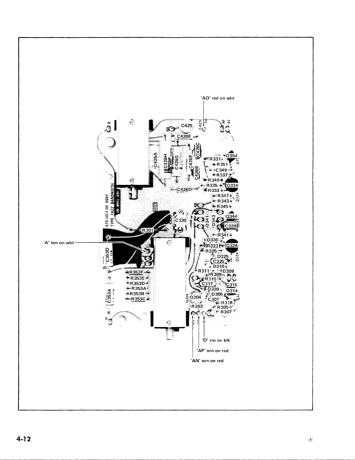
TM 11-6625-2749-14&P
4-12
Fig. 4-8. Bandwidth circuit board (components and wire color code)
Page 59
TM 11-6625-2749-14&P
PERFORMANCE CHECK/CALIBRATION
PROCEDURE
General
The following procedure is arranged in
allows the Type 7A22 to
action of
steps in which
symbol following the title. instrument performance is checked
in he “CHECK’” part of the step before an adjustment is
made. The “ADJUST’” part of the step identifies the point
at which the
“INTERACTION”
csd~ustment
only
csd~ush-nents
ad~w.tmerats
crctual
just performed. This is particularly helpful when
a
partial calibration procedure is performed.
be
ccslibrated with the least inter-
and reconnection of equipment. The
are made are identified by the
ad~ustment is made. Steps listed in the
part of the step may be affected by the
NOTE
To prevent recalibration
strument when performing
readjust only if the tolerances
“CHECK” part of the step are not met. However,
when performing
overall performance
ment is made to the exact setting even if the
“CHECK” is within the allowable tolerance.
In the following procedure,
is shown for each maior group of checks and adjustments.
Each step continues from the equipment setup preceding the
desired portion. External controls or adjustments of the Type
7A22 referred to in this procedure are capitalized (e.g.,
POSITION].
ized only [e.g., Variable Bal).
All waveforms shown in this procedure are actual waveform photographs taken with
era System. The following procedure uses the equipment listed
stituted, control settings or test equipment setup may need
to
be
used. Detailed operating instructions for the test equipment
are not given in this procedure. If an doubt as to the correct operation of any of the test equipment, refer to the instruction manual for that unit.
Internal ad~ustrment names are initial capital-
under Test Equipment Required. If equipment is sub-
altered to meet the requirements of the equipment
of
other parts of the in-
a
a
complete calibration,
is
obtcsined if each adjust-
a
test-equipment setup picture
a
Tektronix Oscilloscope Cam-
a
sequence which
partial calibration,
given
in the
best
NOTE
It is assumed that performance
a temperature range of O“C to +50” C and cali-
bration + 25°C,
this procedure are for this temperature
However, if the procedure is performed at some
other temperature, check the applicable tolerances
for that temperature range.
Preliminary Procedure
1. If the Type 7A22 is to
in extender into the oscilloscope and plug the Type 7A22
into the plug-in extender. If this procedure is
Check only, insert the Type 7A22 into the oscilloscope plugin compartment.
2. Connect the oscilloscope power cord to the design
center operating voltage for which the oscilloscope is wired.
3. Turn on the oscilloscope POWER switch. Allow at
least 20 minutes warmup for checking the instrument to the
given accuracy.
4. Preset the Type 7A22 front panel controls as follows:
VOLTS/DIV
VARIABLE
POSITION
HIGH FREQ –3 dB POINT 100 Hz
LOW FREQ –3 dB POINT
AC-GND-DC (+ INPUT)
AC-GND-DC (–INPUT)
STEP ATTEN DC BAL
DC OFFSET COARSE
DC OFFSET FINE
5. Preset the Time Base front panel controls to these set-
tings:
Time/Div
Variable
Triggering
6. Set the oscilloscope Focus
ing.
*5° C; the tolerances given in
be
is
checked within
range.
calibrated, insert the plug-
a
Performance
10mV
CAL IN
Midrange
10 kHz
GND
GND
Midrange
5 turns from either extreme
Midrange
.5 ms
In (Calibrated)
Auto, AC, Int
and Intensity for
best view-
5-3
Page 60

TM 11-6625-2749-14&P
Fig. 5-1. Left side of the
NOTE
Calibration
with the side covers’;n place. All inter;al adjustments can be made using the access holes provided in the side covers.
of
the Tme 7A22 must be ~erformed
1. Check or Adjust AC Step Atten Bal
a. Center the trace
trol.
b.
Rotate the VOLTS/DIV
\lv pOSifiOrI.
c. CHECK—The
graticule center.
d.
ADJUST—AC
5-1) to position the trace within 1.5 div of graticule center.
on
the CRT with the POSITION con-
switch from 10mV to the 20
trace should remain within 1.5 div of
Step Atten Bal control, R505,
(see
Fig.
2. Check or Adjust VariabIe Bal
a.
Set the Type 7A22 VOLTS/DIV switch to 10mV.
b.
Position the trace to graticule center with the POSl-
TION control.
c. Rotate the VARIABLE VOLTS/DIV
from stop to stop.
d.
CHECK—For maximum trace shift not to exceed *0.2
div while rotating the VARIABLE control throughout its
range.
(in
the out position)
7A22
showing adjustment locations,
e.
ADJUST—Variable
no
trace shift while rotating
Bal control, R425,
the
VARIABLE control.
(see
Fig. 5-1
Fig. 5-1) for
5-4
Page 61

TM 11-6625-2749-14&P
AC-GND-DC (–INPUT]
Time/Div
Variable (Time/Div]
Triggering
GND
.5 ms
Cal
Auto, AC, Int
4. Check or Adiust + Gate Current Zero
b.
Using the POSITION
graticule center.
c. Set the +-INPUT AC-GND-DC switch to AC.
d. CFfECIC----For maximum trace shift within i 2 div.
e.
ADJLJST-The
Fig. 5-1
], to
f.
Cl-f ECK-(only
the +-INPUT AC-GND-DC switch to GND and back to AC.
There should be no movement of the trace.
g. Set the + INPUT AC-GND-DC switch to GND.
position the trace to graticule center.
if
control, position the trace to
+-Gate Current Zero control,
ad~ustment has been made). Switch
R1
15, (see
O
AC-GND-DC
AC-GND-DC (–INPUT)
STEP ATTEN DC BAL
6. Check or Adjust GAIN
a. Test equipment setup is shown in Fig. 5-2.
b.
Connect
from
a
standard amplitude calibrator through
divider and
c.
Set the 1000:1 divider to X 1.
d. Align the display with the graticule lines using the
POSITION control.
e.
CHECK—The
actly 5 div.
f. ADJUST—The
R540) for exactly 5 div of display amplitude.
7. Check VARIABLE Control Ratio
a. With the VARIABLE in the OUT position, rotate the
control fully counterclockwise.
b.
CHECK—The display amplitude shouid be 2 div or less
to meet the 2.5:1 ratio requirement.
(+
INPUT) DC
GND
Ad@st for proper DC bal-
ance.
a 5 mV
a
coaxial cable to the +INPUT connector.
peak-to-peak square wave signal
display for
GAIN control (front panel adjustment
a
vertical amplitude of ex-
a
1000:1
5. Check or Adjust
0. Remove the 50 Q termination from the + INPUT and
connect it to the —INPUT connector.
b. Posi~ion the trace to graticule center with the POSl-
TION control.
c.
Set the —INPUT AC-GND-DC switch to AC.
d. CHECK—For
e.
ADJLJST-The
Fig. 5-1
], to
return the trace to graticule center.
f. CHECK+only
the —INPUT AC-GND-DC
AC. There should
g. Disconnect the 50 Q termination.
h.
Set the –INPUT AC-GND-DC switch to GND.
Type 7A22 controls
VOLTS/DP4
VARIABLE
POSITION
HIGH FREQ –3 dB
POINT
LOW FREQ –3 dB
POINT
be no
- Gate Current Zero
maximum trace shift within & 2 div.
—Gate Current Zero control, R215,
if
adjustment has been made). Return
switch ta GND and back to
trace shift.
1 mV
CAL IN
Midrange
1 MHz
DC
O
(see
8. Check VOLTS/DIV Gain Switching
a. Set the HIGH FREQ —3 dB POINT switch to 3 kHz.
b.
Set the LOW FREQ –3 dB POINT switch to 1 Hz.
c.
Set the standard amplitude calibrator output ta 10 mV.
d. Using the VARIABLE VOLTS/DIV
display amplitude to exactly 5 div.
e.
Set the Time Base Triggering Source to Line.
f. Position the Time/ Div switch to .1 w
g.
Switch the 1000:1 divider to X 1000.
.h.
CHECK—The
through 50 pV. Table 5-1 is provided as
VOLTS/DIV
switch
position
10 pv20 pv
50 lLV
vertical deflection factor from 10 pV
TABLE 5-1
Standard
Amplitude
Calibrator
output
Amplitude
.1 v
.2 v
.5 v
I
Divisions
of
Deflection
5
5
5
control, adiust the
a
guide.
Accuracy
*
* 270
& 270
27!0
REV. B, AUG. 1974
5-5
Page 62

TM 11-6625-2749-14&P
Fig. 5-2. Equipment required for steps 6 through 19..
i. Return the VARIABLE to the CAL IN position.
i. Switch the 1000:1 divider to the Xl position.
k. CHECK—The vertical deflection factor from .1 mV
through 10 mV using Table 5-2 os a guide.
TABLE 5-2
Standard
Amplitude
VOLTS/DIV Calibrator
switch Output of
position
.1 mV .5 mV 5
.2 mV 1 mV
.5 mV 2 mV 4 ± 2 %
1 mV
2 mV
5 mV 20 mV
10mV
1. Remove the 1000:1 divider from the Standard Ampli-
tude Calibrator.
Amplitude Deflection Accuracy
5 mV
10mV
50 mV
Divisions
5
5 ± 2%
5
4
5
± 2%
± 2%
± 2 %
± 2 %
± 2 %
Type 7A22 Controls
VOLTS/DIV
VARIABLE
POSITION
HIGH FREQ –3 dB
POINT
LOW FREQ –3 dB
POINT
AC-GND-DC (+ INPUT)
AC-GND-DC (–INPUT)
STEP ATTEN DC BAL
Time Base Controls
Time/Div
Variable
Slope
Coupling
Source
Mode
1 mV
CAL IN
Midrange
1 MHz
DC OFFSET
DC
GND
Adjusted for DC balance
1
ms
Calibrated
+
AC
Int
Auto
5-6
Page 63

9. Check Isolation Between + and —Inputs
a Set the Standard Amplitude Calibrator to .1 V square
wave.
b, Ad@ the DC OFFSET COARSE and FINE controls to
position the top of the square wave to the graticule center
line.
c.
Switch the —AC-GND-DC
d. CHECK—Trace
e.
Repeat the above procedure for the —INPUT, checking for trace deflection when switching the +AC-GND-DC
switch to DC.
deflection must be 0.5 division or less.
switch to DC.
10. Check Total DC OFFSET Range
a. Set the Type 7A22 controls as follows:
voLTs/Dlv
AC-GND-DC
AC-GND-DC
b. Set the Standard Amditude Calibrator to 1 V and Mode
selector to +-DC.
c. Connect
Calibrator output to the Type
d. Turn the COARSE and
counterclockwise.
e. Ct-f
ter. (1 V minimum DC offset).
i. Set the -I-INPUT AC-GND-DC switch to GND.
~. Rotate the FINE
wise ta return the trace to cjraticule center (approximately
5 turns af the COARSE OFFSET control).
{+-INPUT)
[–INPUT)
a
coaxial cable
ECK-The trace
crnd
can be
TOmV
DC
GND
from the Standard Amplitude
7A22 + INPUT connector.
FINE OFFSET controls fully
returned to graticule cen-
COARSE OFFSET controls clock-
NOTE
The X 10, X 100, and X 1000 input attenuators
will be checked in step 15. Consequently,
remainder of the DC OFFSET ranges stated in Sec-
tion 1 will be verified by that step.
Type 7A22 Controls
VOLTSIDIV
VARIABLE
POSITION
HIGH FREQ –3 dB
POINT
LOW FREQ –3 dB
POINT
Time Base Controls
10mV
CAL [N
Midrange
1 MHz
DC
DC
GND
Acl@sted for proper balance
.5 ms
In
Norm, -+-Slope, AC, Int
the
TM ll-6625-2749-14&P
Fig.
5-3.
properly odiusted, (B)
Typical waveform
11. Check or Adjust C241 + Cross
Neutralization
a. Set the Standard Amplitude Calibrator for
square-wave output.
The Type 7A22 POSITION
Base horizontal positioning control may not always
be mentioned. Use these controls as necessary to
position the display for easy viewing.
b.
CHECK—The
and note any aberration that occurs while switching the
—INPUT AC-GND-DC switch from GND to DC. The wave-
form should appear similar to the one in Fig. 5-3. The aber-
ration should not exceed ~ 1 ~..
c.
Set the —INPUT AC-GND-DC switch to DC.
d. ADJUST—C241
leading corner.
upper leading corner of the waveform,
showhrg
incorrectly
IA) Cross
adiusted.
NOTE
control and the Time
(see
Fig. 5-1) for best square upper
neutralization
a 50
mV
5-7
Page 64
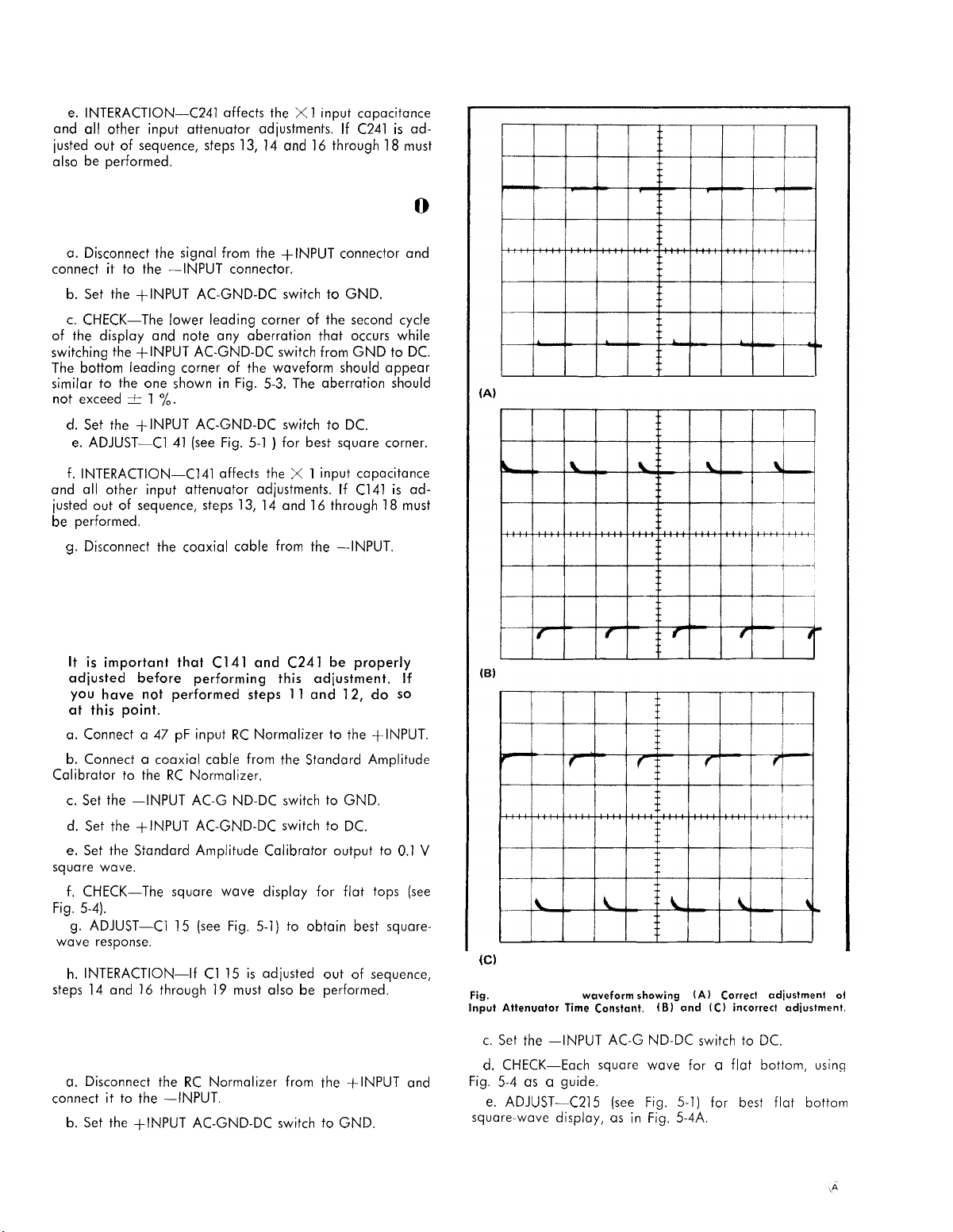
TM 11-6625-2749-14&P
e.
INTERACTION—C241
and all ather input attenuator adjustments. If C241 is adiusted out of sequence, steps 13, 14 and 16 through 18 must
also
be
performed.
affects the Xl input capacitance
12. Check or Adiust Cl 41 + Cross
Neutralization
a. Disconnect the signal from the +INPUT connector and
connect it to the —INPUT connector.
b.
Set the +INPUT AC-GND-DC switch to GND.
c. CHECK—The lower leading corner of the second cycle
of the display and note any aberration that occurs while
switching the +INPUT AC-GND-DC switch from GND to DC.
The bottom leading corner of the waveform should appear
similar to the one shown in Fig. 5-3. The aberration should
not exceed & 1 %.
d.
Set the +INPUT AC-GND-DC switch to DC.
e.
ADJUST—Cl
f.
INTERACTION—C141
and all other input attenuator adjustments. If C141 is ad-
iusted out of sequence, steps 13, 14 and 16 through 18 must
be
performed.
g.
Disconnect the coaxial cable from the –INPUT.
41 (see
Fig. 5-1 ) for best square corner.
affects the X 1 input capacitance
13. Check or Adiust Cl 15—x 1 +INPUT O
Attenuator Time Constant
NOTE
It is important that C141 and C241 be properly
adiusted before performing
you have not performed steps 11 and 12, do so
at this point.
a.
Connect
b.
Calibrator to the
c. Set the —INPUT AC-G ND-DC switch to GND.
d.
e.
Set the Standard Amplitude Calibrator output to
square wave.
f.
CHECK—The
Fig. 5-4).
g.
wave response.
h.
steps 14 and 16 through 19 must also
a 47 pF
Connect
a
Set the +INPUT AC-GND-DC switch to DC.
ADJUST—Cl
iNTERACTION—lf
input
coaxial cable from the Standard Amplitude
RC
Normalizer.
square wave display for flat tops
15 (see
Cl 15 is
14. Check or Adiust C21 5—)(x1
this adjustment.
RC
Normalizer to the +INPUT.
Fig. 5-1) to obtain best square-
adiusted
out of sequence,
be
performed.
0.1
(see
–INPUT O
If
Attenuator Time Constant
a.
Disconnect the
connect it to the —INPUT.
b.
Set the +INPUT AC-GND-DC switch to GND.
RC
Normalizer from
the +INPUT and
V
(c)
(A)
Fig. 5-4. Typical waveform
Input
Attenuator Time Constant.
c. Set the —INPUT AC-G ND-DC switch to DC.
d.
CHECK—Each
Fig. 5-4 as
e.
square-wave display,
a
ADJUST—C215
guide.
showing
(B) and [C) incorrect adjustment.
square wave for
(see
Fig. 5-1) for best flat bottom
as in Fig, 5-4A.
Correct adjustment
a
flat bottom, using
o{
5-8
Page 65

f.
lNTERACTlON—[f
steps 13
crnd 16
g. Disconnect the signal and the RC Normalizer.
C215 is ad~usted out of sequence,
through 19 must
cslso be
performed.
15. Check Input Attenuator Accuracy
cr. Connect
from the Standard Amplitude Calibrator through
cable to the +-INPUT.
b. Se+
c. CHECK—The
guide.
a
50mV peak-to-peak square wave signal
the +-INPUT AC-GND-DC switch to DC.
input attenuators using Table 5-3 as
a
TM 11-6625-2749-14&P
coaxial
a
d.
Disconnect the signal from the Type 7A22.
NOTE
[Applies to calibration only)
If there is
corner of the square wave when checking from
20 mV to 10 V, ignore these, as they will be corrected in step 17.
a
spike or fast rolloff of the leading
16. Check or Adjust Input Attenuator
Differential Balance
a. Connect
Standard Amplitude Calibrator and
the +-INPUT and —INPUT connectors of the Type 7A22.
b.
Connect cr coaxial cable from the T connector to the
dual input connector. Connect
connector to the Ext In connector on the oscilloscope.
c. Set the Type 7A22 controls as follows:
VOLTS/DIV
AC-C%
AC-GND-DC (–INPUT)
d. Set the oscilloscope Triggering Source switch to Ext.
e.
Set the Standard Amplitude Calibrator output to 50 V.
f.
C6-fECK-For
to the information given in Table 5-4. When properly ad-
a T
connector to the Output connector of the
JD-DC (+-INPUT)
optimum differential balance according
a
dual connector to
a
coaxial cable from the T
50 rnv
DC
DC
Fig. 5-5. Typical display
adiusted
iusted, the waveform should appear as shown in Fig. 5-5.
Disregard any spikes on the waveform.
minimum amplitude as shown in Fig. 5-5, using Table 5-4
as
to-peak output.
7A22.
far
optimum
g. ADJUST—R108E,
a
guide.
h.
Set the Standard Amplitude Calibrator
i. Disconnect the dual input connector
Set the Type 7A22 Controls:
VOLTS/DIV
VARIABLE
HIGH FREQ –3 dB
POINT
LOW FREQ –3 dB
POINT
AC-GND-DC (+-INPUT)
AC-GND-DC (–INPUT)
STEP ATTEN DC BAL
abtained when
differential
balance.
R109E and
TABLE 5-4
Input Attenuators
R1
10E
(see
Fig. 5-1) for
for 0.2 V peak-
fram the Type
50 mV
CAL IN
1 MHz
DC
DC
GND
Adiusted for proper DC Bal-
ance
are
5-9
Page 66
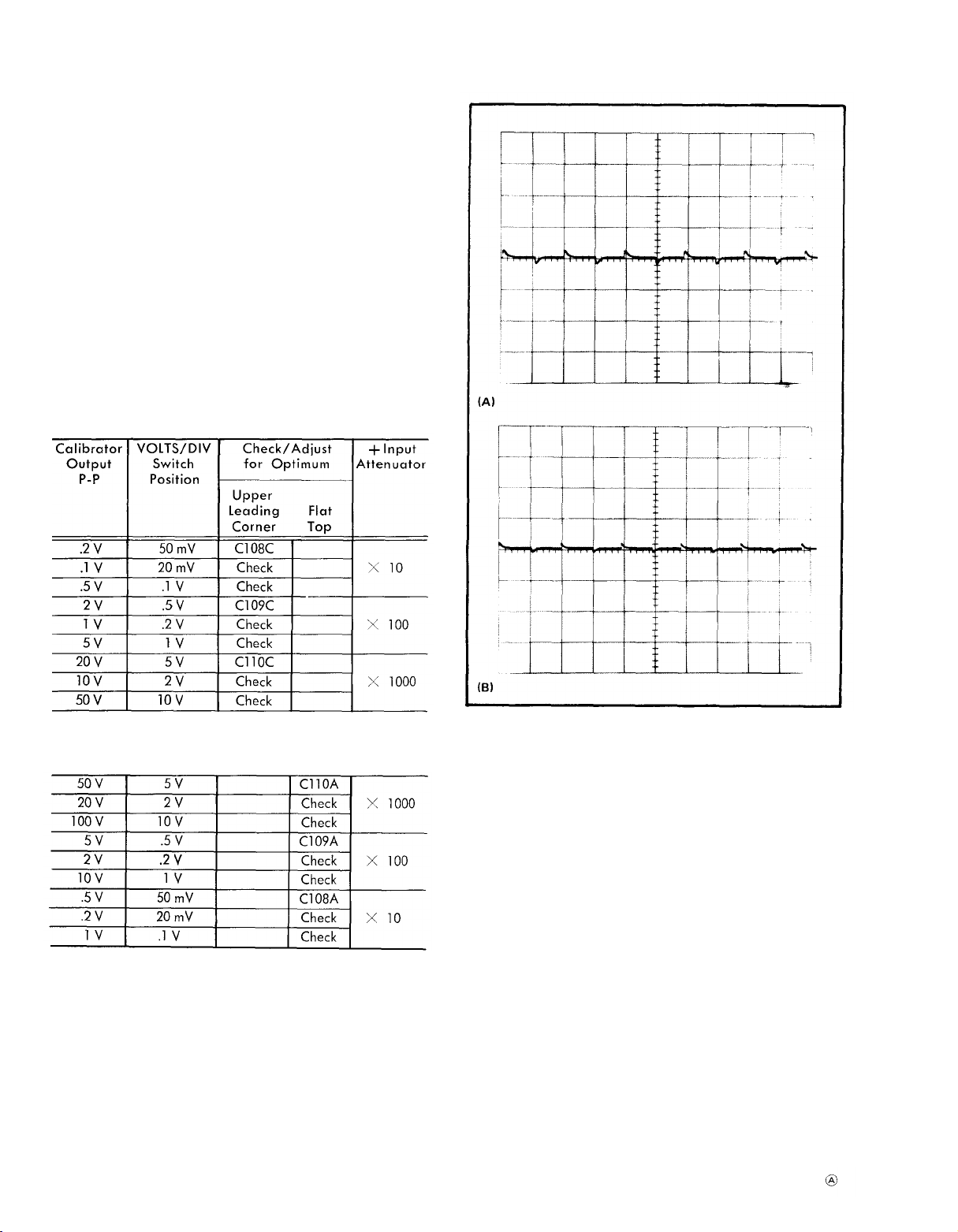
TM 11-6625-2749-14&P
Set the Time Base Controls.
Time/Div
Variable In (Cal)
Triggering
.5 ms
Auto, Ac, Int
17. Check or Adjust + Input Attenuator O
Compensation
a. Connect a 0.2 V peak-to-peak signal from the Standard
Amplitude Calibrator through a coaxial cable to the +lNPUT of the Type 7A22.
b. CHECK—The +INPUT Attenuator compensation for
good square wave response.
c. ADJUST—The +INPUT Attenuator compensation for
best square wave response using Table 5-5 as a guide. Fig.
5-1 shows the locations of the adjustments.
TABLE 5-5
Connect the 47 pF input RC normalizer between the + lN-
PUT and the coaxial cable.
c. INTERACTION--lf this step is performed out of se-
quence, steps 18 and 19 must be performed.
d. Disconnect the RC normalize
Type 7A22 and the Standard Amplitude Calibrator.
and coaxial cable from the
r
18. Check or Adjust - Input Attenuator O
Series Compensation
O. Connect a T connector to the Standard Amplitude Cali-
brator output connector and a dual input connector to the
5-10
Fig. 5-6. Typical display obtained with - Input attenuator ad.
ijusted for optimum Common-Mode signal rejection.
adjusted properly (B) C209C adjusted properly.
Type 7A22 +INPUT and —INPUT connectors. Connect a
coaxial cable from the T connector to the dual input con-
nector. Connect a coaxial cable from the T connector to the
oscilloscope Ext In connector.
b. Set the oscilloscope Triggering Source switch to Ext.
c. Set the Standard Amplitude Calibrator output to 50 V
square wave.
d. Set the Type 7A22 controls os follows:
VOLTS/DIV
AC-GND-DC (–INPUT)
e. CHECK—The displayed waveform
mon-mode signal rejection (minimum spike amplitude).
f. ADJUST—The – Input attenuator series compensation
for best common-mode signal rejection (minimum spike ampli-
tude) using the information given in Table 5-6. Fig. 5-6 illus-
trates the typical displays obtained and Fig. 5-1 shows the
adjustment locations.
50 mV
DC
(Al C208C
for good com-
Page 67
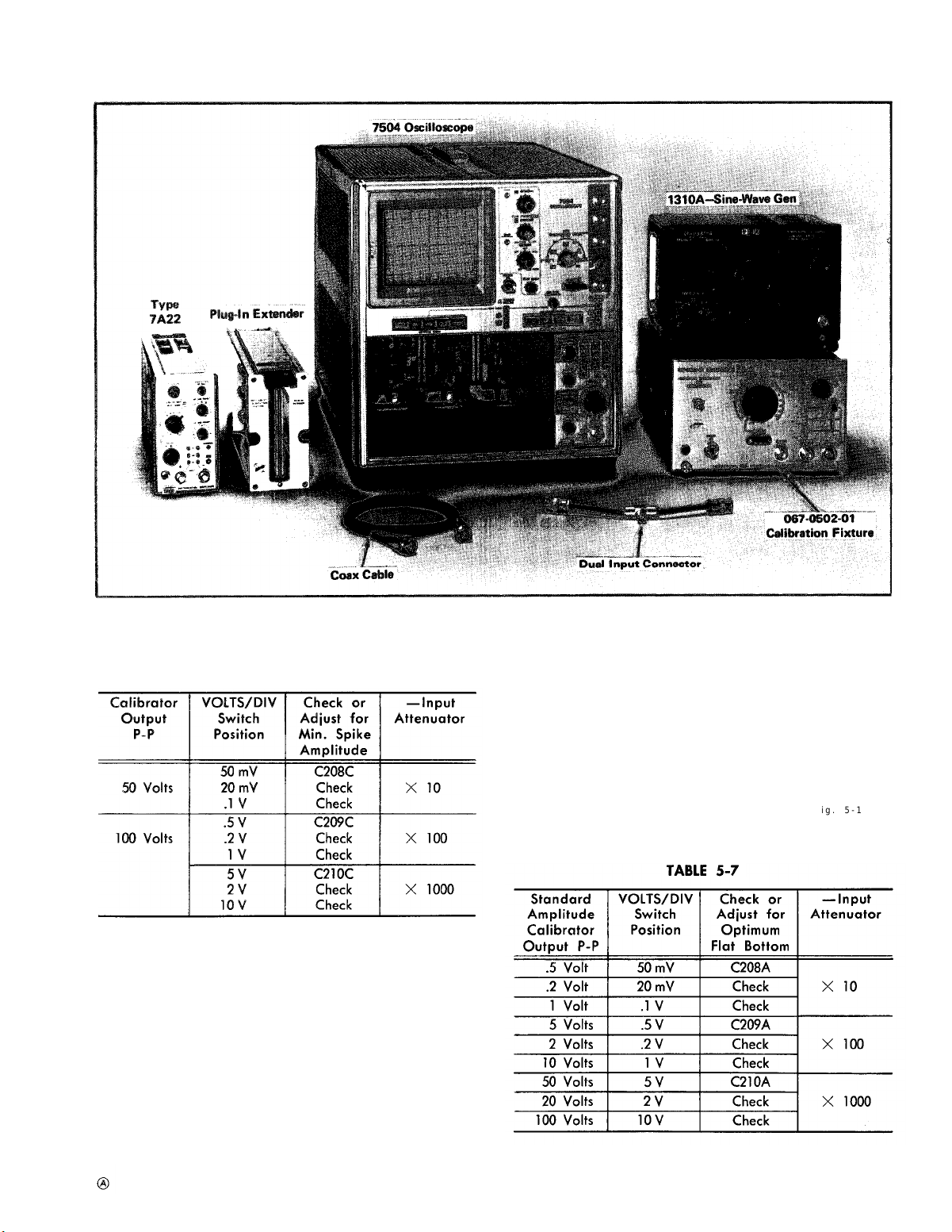
TM 11-6625-2749-14&P
Fig. 5-7. Equipment required for steps 20 through 24.
TABLE 5-6
g. Disconnect all signal leads.
h. Return the oscilloscope Triggering Source switch to Int.
19. Check or Adjust -lnput Attenuator O
Shunt Compensation
a. Connect a 47 pF RC Normalizer to the —INPUT of the
Type 7A22. Connect a coaxial cable from the Standard Amplitude Calibrator output connector to the RC Normalizer.
b. Set the Standard Amplitude Calibrator output to .5 V
square wave.
c. Set the Type 7A22 controls as follows:
VOLTS/DIV
AC-GND-DC (+- INPUT)
d. CHECK—Using Table 5-7 as a guide, check the display
for a square wave response similar to the display illustrated
in Fig. 5-4.
e. ADJUST—C208A, C209A, and C21OA (see Fig. 5-1) for
best flat bottom on the display, according to the information
given in Table 5-7.
50 mV
GND
TABLE 5-7
5-11
Page 68
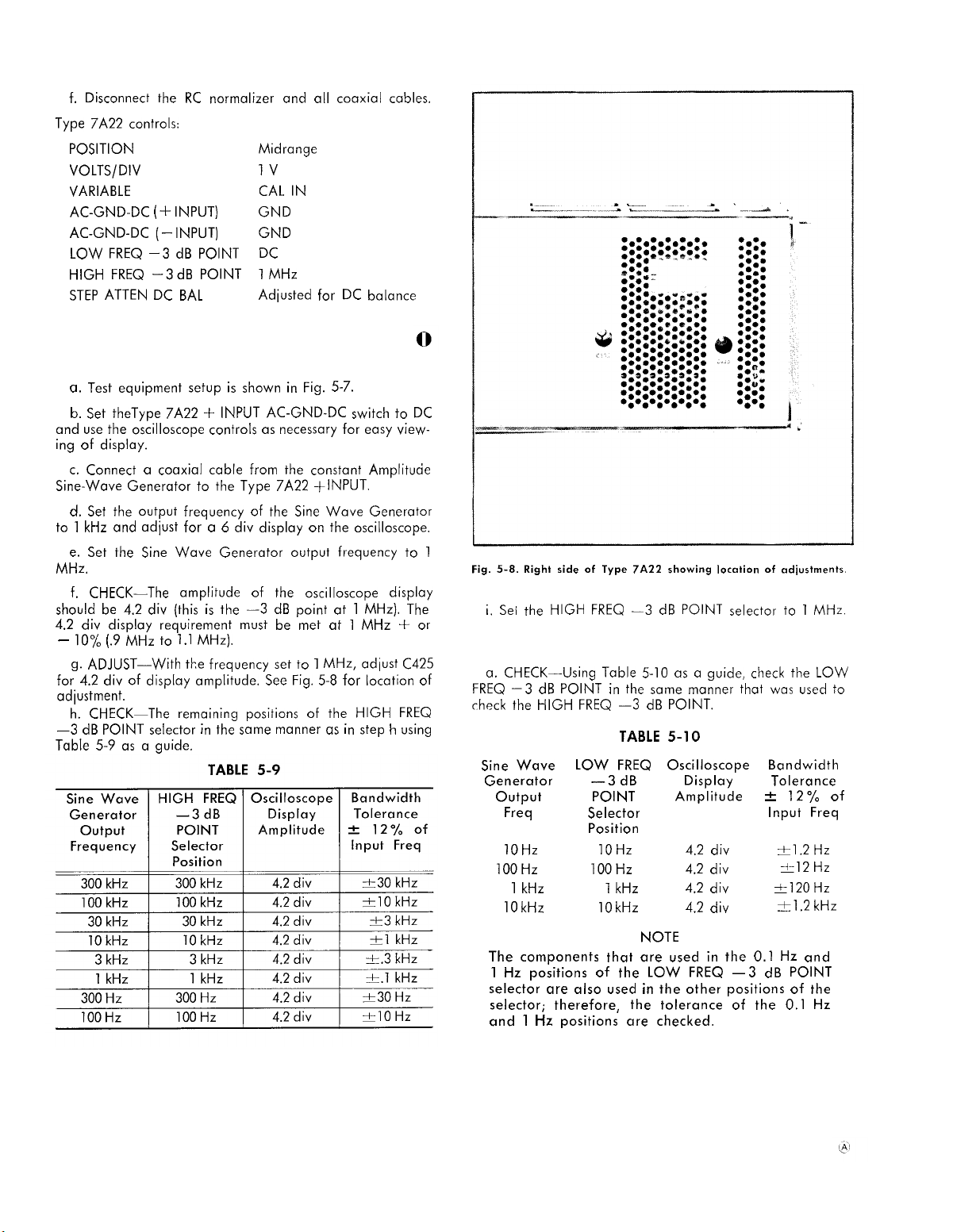
TM 11-6625-2749-14&P
f.
Disconnect the
Type 7A22 controls:
POSITION
VOLTS/DIV
VARIABLE
AC-GND-DC (+ INPUT)
AC-GND-DC (–INPUT)
LOW FREQ –3 dB POINT
HIGH FREQ –3dB POINT
STEP ATTEN DC BAL
RC
normalizer and all coaxial cables.
Midrange
lV
CAL IN
GND
GND
DC
1 MHz
Adiusted for DC balance
20. Check or Adiust HIGH FREQ –3dB
POINT
a. Test equipment setup is shown in Fig. 5-7.
b.
Set theType 7A22 + INPUT AC-GND-DC switch to DC
and use the oscilloscope controls as necessary for easy viewing of display.
c. Connect
Sine-Wove Generator to the Type 7A22 +INPUT.
d.
to 1 kHz and adiust for
e.
MHz.
f.
should
4.2 div display requirement must
–
10~o (.9
g.
for 4.2 div of display amplitude. See Fig. 5-8 for location of
adjustment.
h.
—3 dB POINT selector in the
Table 5-9 as
a
coaxial cable from the constant Amplituae
Set the output frequency of the Sine Wave Generator
a 6
div display on the oscilloscope.
Set the Sine Wave Generator output frequency to 1
CHECK—The
be
ADJUST—With
CHECK—The
amplitude of the oscilloscope display
4.2 div (this is the —3 dB point at 1 MHz). The
MHz to
1.1
MHz).
the frequency set to 1 MHz, adlust C425
remaining positions of the HIGH FREQ
a
guide.
scrme
TABLE 5-9
be
met at 1 MHz + or
manner as in step h using
Fig.
5-8.
Right side of Type
i.
Sei the HIGH FREQ —3 dB POINT selector
7A22
showing location of adjustments.
to 1
MHz.
21. Check LOW FREQ —3 dB POINT
a.
CHECK—Using
FREQ –3 dB POINT in the same manner that wos used to
check
the HIGH FREQ —3 dB POINT.
Sine Wave
Generator
output
Freq
10Hz
100Hz
1 kHz
10 kHz
Table 5-10 as a guide,
TABLE 5-10
LOW FREQ Oscilloscope
—3 dB
POINT
Selector
Position
10Hz
100Hz
1 kHz
10 kHz
Display
Amplitude
4,2 div
4.2 div
4.2 div
4.2 div
check
Bandwidth
Tolerance
& 1270 of
Input Freq
&l.2Hz
~12Hz
&120Hz
&l.2 kHz
the LOW
5-12
NOTE
The components that are used in the 0.1 Hz and
1 Hz positions of the LOW FREQ –3 dB POINT
selector are also used in the other positions of the
selector; therefore,
and 1 Hz positions are checked.
the tolerance of the 0.1 Hz
Page 69
Type 7A22 controls:
VOLTS/13RJ
VARIABLE
HIGH FRECI –3 c9Et
POINT
LOW FREQ –3
POINT
Ac-GND-DC (+ INPUT)
AC-GND-DC (–INPUT]
STEP ATTEN DC
t3AL
Time-Base controls:
Time/Div
Variable
Triggering
CM
5V
CAL IN
1 MHz
DC
DC
GPID
Adjusted for proper DC
balance
As necessary for easy
viewing of display
In (Cal)
Auto, AC, Ext
22. Check or Adjust Attenuator
Common Mode Rejection
a.
Attach
a 13NC T
connector. Connect
Amplitude Sine-Wave
rmn~ector. Connect another coaxial cable from the BNC T
connector to the dual input connector.
b. Connect the Dual-Input connector to the Type 7A22 +
and – INPUTS.
c.
Set the 7650 SOURCE to EXT X1O, and DISPLAY
MODE to AMPLIFIER
Wave Generator Level control for 20 V P-P at 100 kHz. Use
the VARIABLE on the 7B50to adjust fora suitable display of 4
to 6 horizontal divisions.
The Sine-Wave Generator output must be maintained
at
a
constant 20 V p-p for all of the CMRR checks.
d. Switch the Type 7A22 AC-GND-DC (i-INPUT) to GND.
e. Switch the Type 7A22 VOLTS/DIV
f. Simultaneously
GND-DC switches to DC.
g. Cl-f ECK-The vertical deflection should not exceed 2 div.
The 2 divrequirementat
of 100,000:1 (2 div at 1 mV/DIV = .2 mV; 20 V + .2 mV =
1 00,000].
b. Adjust C330 (and C144 SN B080000
minimum vertical deflection. See Fig. 5-8 for C330 location.
C144 is under the ~lasticcover near Q153 on the left side of
the 7A22 (see
Fig. 4-6,
connector to the 7B50 EXT in
a
coaxial cable from the Constant
Generator output to the
Adjust the Constant Amplitude Sine-
13NC
NOTE
to .1
mV.
switch the Type 7A22 + and – AC-
O.1 mV/DIVisequivalent
page
4-10).
toa CMRR
and up) for
TM 11-6625-2749-14&P
NOTE
These adjustments interact, and
of C330 will be necessary after the cover is replaced
over C144.
1, Set the Sine Wave Generator frequency to 100 kHz.
2. Set the Type 7A22 VOLTS/DIV
3. Adjust–Cl
4. ADJUST–RI
i. CHECK–Using
at the remaining attenuator positions.
j. Disconnect all test leads and connectors.
Type 7A22 Controls:
VOLTS/DIV 10mV
VARIABLE
POSITION
HIGH FREQ –3 dB
POINT
LOW FREQ –3 dB
POINT
AC-GND-DC (+ INPUT)
T
AC-GND-DC (–INPUT)
STEP
BAL
Time Base Controls:
Time/Div
Triggering
08C for minimum vertical deflection.
16
for minimum vertical deflection.
Table 5-11 as
ATTEN
‘DC
a
slight readjustment
to 20
mV.
a
guide, check the CMRR
CAL IN
Midrange
1 MHz
DC
GND
GND
Adjusted for DC balance
1 ms
+, Auto, AC, Int
23. Check Input OVERDRIVE Indicator
a. Connect
Generator output and the Type 7A22 +INPUT.
b.
Set the Sine-Wave Generator amplitude to minimum
and frequency to 1 kHz.
c.
Increase the Sine-Wave Generator amplitude until the
Type 7A22 input OVERDRIVE
d. CHECK–The
divide by 2 to find the + or – driving signal amplitude. The
overdrive signal should be approximately
e.
Disconnect coaxial cable from +Input.
Type 7A22 Controls:
VOLTS/DIV
VARIABLE
POSITION
HF –3 dB POINT
LF –3 dB POINT
AC-GND-DC (+ INPUT)
a
coaxial cable between the Sine-Wave
indicator lights.
sine-wave amplitude, peak to peak, and
1
volt.
1 mV
CAL IN
Midrange
1 MHz
10Hz
GND
REV. JAN 1974
5-13
Page 70
TM 11-6625-2749-14&P
AC-GND-DC (–INPUT)
STEP ATTEN DC BAL
Time Base Controls:
Time/Div
Variable
Slope
Coupling
Source
Mode
GND
Adjusted for DC balance
1 ms
Calibrated
+
AC
Int
Auto
b. Set the Standard Amplitude Calibrator amplitude to 1V,
+DC.
c. Connect a coaxial cable between the Sine-Wave Gen-
erator output and the Type 7A22 -INPUT.
d. Switch the -AC-GND-DC switch to DC.
e. Adjust the Sine-Wave Generator amplitude control to
give 5 div of 1 kHz display on the CRT graticule (if the SineWave Generator minimum amplitude is too large, insert an
attenuator between the coaxial cable and the —INPUT).
f. Switch the + AC-GND-DC switch to DC.
24. Check Differential Signal Range g. CHECK—Sine wave amplitude should not change when
a. Connect a coaxial cable between the Standard Ampli-
tude Calibrator output connector and the Type 7A22 + INPUT.
DC level from Standard Amplitude Calibrator is applied.
h. Switch the + AC-GND-DC switch to GND.
5-14
Fig. 5-9. Equipment required for step 25.
Page 71

i. Switch the Standard Amplitude Calibrator mode to
– IX.
~. Switch the + AC-GND-DC switch to DC.
TM 11-6625-2749-14&P
k. CFfECK-Sinewcsve
DC level from Standard Amplitude Calibrator is applied.
l.
Disconnect alltest equipment and test leads.
amplitude should not change when
25. Check Overall Noise Level Tangentially
a.
Equipment setup is shown in Fig. 5-9.
b.
Cannecl
of the Type 7A22. Connect two 10X attenuators to the
50
Q
c.
Connect
C’cdibrator
tenuator to the GR connector. Connect
to the Variable Attenuator. Connect
10X attenuators to the Variable Attenuator.
d.
Set the Oscilloscope Calibrator to 4 mV and 1 kHz.
e.
Set the 7A22 VOLTS/ DIV switch to 10 pV.
f.
Turn the Variable Attenuator fully clockwise.
g. Set the Time
Div to 10 ps.
h.
Turn the Variable Attenuator counterclockwise until the
darker
[see Fig. 5-10].
termination.
-#=-VOkS
bcsnd
a
50Q termination to the -I-INPUT connector
a GR to
Bcsse
between the two noise bands iust disappears
BNC adapter to the Oscilloscope
connector and connect the Varibale At-
Triggering Mode to Auto and Time/
a GR to
a
coaxial cable from the
BNC adapter
i. Set the Type 7A22 VOLTS/DIV switch to 1 rnV and the
Time Base Time/Div switch to 1 rrw.
~. Remove the two 10X attenuators and connect the co-
axiai cable to the 50
k. Measure the square wave amplitude. Calculate the
tangentially measured display noise as follows:
The tangentially measured noise should not exceed 16 pV.
Type 7A22 controls:
VOLTS/DIV
VARIABLE (VOLTS/DlV9
POSITION
I-IF –3 dB POINT
LF –3 dB POINT
AC-GND-DC
AC-GND-DC –INPUT
STEP ATTEN DC BAL
Q
termination.
sauare wave amriitude
100
.2 v
CAL IN
1 division below graticule
center
1 MHz
DC
+-INPUT
DC
GND
Adlusted for
Dc
Balance
Fig. 5-10. Typical display showing [A) two noise bands and (B)
merging noise bands,
Time Base controls:
Time/Div
Variable
Level/Slope
Coupling
Source
Mode
2 ps
Cal In
—
DC
Int
Auto
26. Check Overdrive Recovery Time
a. Test equipment setup is shown in Fig. 5-11.
b.
Connect the Reed Pulse Generator Output to the Type
7A22 + INPUT.
c. Connect the Reed Pulse Generator Power Cable to the
Oscilloscope Probe Power connector (rear panel).
d. Switch the Reed Pulse Generator Polarity switch to +.
5-15
Page 72
TM
11-6625-2749-14&P
Fig.
5-11.
Equipment required
e.
Hold down the
adiust the Level control to position the trace to the top graticule line (1 volt).
f.
Release the Man switch and switch the Time Base Mode
to Norm.
g. Set the Type 7A22 VOLTS/DIV
h.
Increase sweep Intensity to maximum (clockwise).
i. Depress the
second.
i.
CHECK—The
Man switch is released. Readiust the Time Base Level-Slope
as necessary for proper triggering. The trace should return
to within 5 mV of the reference (1 division below the graticule center) within 10
graph of typical recovery waveform.
k. Switch the
1. Set the Time Base Level/Slope to +.
m.
Decrease sweep Intensity for normal viewing.
n.
Reset the Time Base Mode to Auto.
o.
Position the trace (7A22 POSITION control) to 1 divi-
sion above graticule center.
p.
Reset the Time Base Mode to Norm.
Reed
Pulse Generator Man switch and
switch to 1 mV.
Reed
Reed
Pulse Generator Man switch for 1
waveform as the Reed Pulse Generator
/1s (5
divisions). See Fig. 5-12 for photo-
Pulse Generator Polarity switch to —.
for
step
26.
q.
Repeat parts h through I (waveform will
from that in step 1).
r, Connect
—INPUT and repeat obove procedure.
Fig.
5-12.
Reed
Typical waveform
Pulse Generator Output
showing
overdrive recovery time,
be
to the
inverted
7A22
5-16
Page 73

REPLACEABLE
ELECTRICAL PARTS
PARTS ORDERING INFORMATION
Replacement parts are available from or through your local Tektronix, Inc. Field Office
or recmesentative.
TM 11-6625-2749-14&P
Changes to Tektronix instruments are sometimes made to accommodate
components
improvements
ordering parts, to include the following information in your order: Part number, instrument
type ornumber, serial number, and modification
Tektronix, [nc. Field Office orrepresentative
number.
Becawseof space limitations, an Item Name maysometimes
further hem Name identification,
utilized where possible.
as
they become available, and to give you the benefit of the latest circuit
developed in our engineering department, It is therefore important, when
number inapplicable.
Ifapart youhave ordered hasbeen replaced with anew orimproved part, your local
SPECIAL
Xooo
Oox
in the Parts List, an Item Name is separated from the description
Part first added at this serial number
Part rermved after this serial number
will contact you concerning any change in part
NOTES
the U.S. Federal Cataloging Handbook H6-1 can be
ITEM NAME
AND SYMBOLS
appear asincomplete.
by a
improved
colon (:).
ABBREVIATIONS
ACTR
ASSY
CAP
CEF4
CKT
COMP
CONN
ELCTLT
ELEt2
INCAND
LED
NONWIR
ACTUATOR
ASSEMBLY
CAPACITOR
CERAMIC
CIRCUIT
COMPOSITION
CONNECTOR
ELECTROLYTIC
ELECTRICAL
INCANDESCENT
LIGHT IEMITT.ING DIODE
NONWIREWOUND
PLSTC
QTZ
RECP
RES
RF
SEL
SEMICOND
SENS
VAR
Ww
XFMR
XTAL
PLASTIC
QUARTZ
RECEPTACLE
RESISTOR
RADIO FREQUENCY
SELECTED
SEMICONDUCTOR
SENSITIVE
VARIABLE
WIREWOUND
TRANSFORMER
CRYSTAL
For
6-1
Page 74

TM 11-6625-2749-14&P
CROSS INDEX–MFR. CODE NUMBER TO MANUFACTURER
Mfr. Code
00853
01002
01121
02111
03508
04713
08806
11237
12697
15454
15818
24931
27014
32997
56289
71400
71744
72982
73138
74970
75042
80009
80294
80740
81483
87034
91637
Manufacturer Address
SANGAMO ELECTRIC CO. ,
GENERAL ELECTRIC COMPANY, INDUSTRIAL
AwE POWER CAPACITOR PRODUCTS DEPARTMENT
ALLEN-BRADLEY COMPANY
SPECTROL ELECTRONICS CORPORATION
GENERAL ELECTRIC COMPANY, SEMI-CONDUCTOR
PRODUCTS DEPARTMENT
MO!T3ROLA, INC. , SEMICONDUCTOR PROD. DIV.
GENERAL ELECTRIC CO. , MINIATURE
LAMP PRODUCTS DEPARTMENT
CTS XEENE, INC.
CLAROSTAT MFG. CO. , INC.
RODAN INDUSTRIES, INC.
TELEDYNE SEMICONDUCTOR
SPECIALTY CONNECTOR CO., INC.
NATIONAL SEMICONDUCTOR CORP.
BOURNS, INC. ,
SPRAGUE ELECTRIC CO.
BUSSMAN MFG.,
EDISON CO.
CHICAGO MINIATUF03 LAMP WORKS
ERIE TECHNOLOGICAL PRODUCTS, INC.
BECKMAN INSTRUMENTS, INC. , HELIPOT DIV.
JOHNSON,
TRW ELECTRONIC COMPONENTS, IRC FIXED
RESISTORS, PHILADELPHIA DIVISION
TEKTRONIX, INC.
BOURNS, INC.,
BECKMAN INSTRUMENTS, INC.
INTERNATIONAL RECTIFIER CORP.
ILLUMINATED PRODUCTS INC., A SUB OF
OAK INDUSTRIES, INC.
DALE ELECTRONICS, INC.
TRTMPOT PRODUCTS DTV.
DIVISION OF MCGRAW-
E.
F., CO.
INSTRUMENT DIV.
S.
CAROLINA DIV.
P O
BOX 128
JOHN STREET
1201 2ND STREET
17070 EAST GALE
ELECTRONICS PARK
5005 E MCOOWELL RD,PO BOX 20923
NELA PARK
3230 RIVERSIDE AVE.
LOWER WASHINGTON STREET
2905 BLUE STAR ST.
1300 TERRA BELLA AVE.
3560 MADISON AVE.
2900 SEMICONDUCTOR DR.
1200 COLUMBIA AVE.
2536
W.
4433 RAVENSWOOD AVE.
644 W. 12TH ST.
2500 HARBOR BLVD.
299 10TH AVE.
401
P O BOX 500
6135 MAGNOLIA AVE.
2500 HARBOR BLVD.
9220 SUNSET BLVD.
2620 SUSAN ST, PO BOX 11930
P. O.
UNIVERSITY ST.
N.
BROAD ST.
BOX 609
S.
SOUTH
AVENUE
W.
City, State, ZIip
PICKENS, SC 29671
HUDSON FALLS, NY 12839
MILWAUKEE, WI 53204
CITY OF INDUSTRY, CA 91745
SYRACUSE, NY 13201
PHOENIX, AZ 85036
CLEVELAND, OH 44112
PASO ROBLES, CA 93446
DOVER, NH 03820
ANAHEIM, CA 92806
MOUNTAIN VIEW, CA 94043
INDIANAPOLIS, IN 46227
SANTA CLARA, CA 95051
RIVERSIDE, CA 92507
NORTH ADAMS, MA 01247
ST. LOUIS, MO 63107
CHICAGO, IL 60640
ERIE ,PA
FULLERTON, CA 92634
WASECA, MN 56093
PHILADELPHIA, PA 19108
BEAVERTON, OR 97077
RIVERSIDE, CA 92506
FULLERTON, CA 92634
LOS ANGELES, CA 90069
SANTA ANA, CA 92711
COLUMBUS, NE 68601
16512
6-2
REV. D SEPT. 1978
Page 75

TM 11-6625-2749-14&P
Tektronix
Ckt No. Part No.
670-1013-00
670-1014-00
670-1014-01
670-1014-03
670-1014-04
670-1014-05
670-1014-06
670-1050-00
670-1050-01
670-1051-00
670-1051-01
Cu-ul
C?1O.3
CZ08A
C108A
Clew
C108D
CI09A
C109A
C309C
C109D
CIIOA
CHQA
C!lloc
Cnm
cn5
295-0117-00
283-0636-00
28 L-0092-00
281-0131-00
281-0131-00
283-0638-00
281-0092-00
2E11-0131-00
2s1-0081-00
283-0594-00
2$1-0092-00
281-0131-00
281-0079-00
283-0617-00
281-0092-00
Serial/Model
Eff
BO1O1OO B029999
B030000 B059999
B060000 B069999
B070000 B079999
B080000 B115479
B115480
BO1O1OO B059999
B060000
BO1O1OO B059999
BO1O1OO B059999
B060000
BO1O1OO B059999
B060000
BO1O1OO B059999
B060000
BO1O1OO B059999
No.
Dscont
CKT BOARD
CKT BOARD
CRT BOARD
CKT BOARD
CKT BOARD
CKT BOARD
CKT BOARD
CKT BOARD
CKT BOARD
CKT BOARD
CKT BOARD
CAP. ,SET,MTCHD:
CAP.,FXD,MICA
CAP.,VAR,CER
CAP.,VAR,AIR
CAP.,VAR,AIR
CAP. ,FXD,MICA D:13OPF,1%,1OW
CAP. ,VAR,CER DI:9-35PF,20W
CAF.,VAR,AIR
CAP.,VAR,AIR
CAP. ,FXD,MICA D:O.OO1UF,1%,1OW
CAP. ,VAR,CER DI:9-35PF,200V
CAP. ,VAR,AIR DI:2.4-24.5PF,25W
CAF. ,VAR,AIR DI:l.5-9.lPF,BOW
CAP. ,FXD,MICA D:47OOPF,1O%,3OOV
CAP. ,VAR,CER DI:9-35PF,200V
Name & Description
ASSY:BANDWIDTB
ASSY :MAIN
ASSY :MAIN
ASSY :MAIN
ASSY :MAIN
ASSY :MAIN
ASSY :MAIN
ASSY:AC-GND-13C
ASSY :AC-GND-DC
ASSY : +AC-GND-DC
ASSY : +AC-GND-DC
(2)
O.lUF,MATCHED
D:36PF,1.4%,1OOV
DI:9-35PF,200V
DI:2.4-24.5PF,250V
DI:2.4-24.5PF,25W
DI:2.4-24.5PF,250V
DI:l.8-13PF,375VDC
0.1%
fvlfr
Code Mfr Part Number
80009
80009
80009
80009
80009
80009
80009
80009
80009
80009
80009
80009
OOB53
72982
74970
00853
72982
74970
74970
00853
72982
74970
00853
74970
74970
72982
670-1013-00
670-1014-00
670-1014-01
670-1014-03
670-1014-04
670-1014-05
670-1014-06
670-1050-00
670-1050-01
670-1051-00
670-1051-01
295-0117-00
D155F360G0
538-011 D9-35
189-509-5
189-509-5
D151F131F0
538-011 D9-35
189-509-5
189-6-5
D151F102FO
538-011 D9-35
189-509-5
189-4-5
D193F472K0
53B-011 D9-35
cl15
C141
C144
C144
CI.56
C208D
C2!39A
C209A
C209C
C209D
cam
C21OA
C210C
c21cm
c215
C215
C241
C244
c256
C264
C2$%3
281-0131-00
281-0093-00
281-0544-00
281-0122-00
283-0594-00
295-0117-00
283-0636-00
281-0092-00
281-013’1-00
281-0131-00
283-0638-00
281-0092-00
2131-0131-00
281-0081-00
283-0594-00
281-0092-00
281-0131-00
201-0079-00
283-0617-00
281-0092-00
281-0131-00
281-0093-00
281-0544-00
203-0594-00
283-0059-00
290-0284-00
B060000
BO1O1OO B079999
B080000
BO1O1OO B059999
B060000
BO1O1OO B059999
B060000
BOIO1OO B059999
B060000
BO1O1OO B059999
B060000
CAP. ,VAR,AIR DI:2.4-24.5PF,25W
CAP. ,VAR,CER DI:5.5-18PF
CAP. ,FXD,CER DI:5.6PF,1O%,5OOV
CAP. ,VAR,CER DI:2.5-9PF,1OOV
CAP. ,FXD,MICA D: O. OO1UF,1%,1OOV
CAP. ,SET, MTCHD:
CAP. ,FXD,MICA D:36PF,1.4%,1OOV
CAP. ,VAR,CER DI:9-35PF,20W
CAP. ,VAR,AIR DI:2.4-24.5PF,250V
CAP. ,VAR,AIR DI:2.4-24.5PF,25W
CAP.,FXD,MICA
CAP. ,VAR,CER DI:9-35PF,200V
CAP.,VAR,AIR
CAP.,VAR,AIR
CAP.,FXD,MICA
CAP. ,VAR, CER DI:9-35PF,20W
CAP.,VAR,AIR
CAP.,VAR,AIR
CAP. ,FXD,MICA D:47OOPF,1O%,3OW
CAP. ,VAR,CER DI:9-35PF,20W
CAP.,VAR,AIR
CAF.,VAR,CER
CAP. ,FXD,CER DI:5.6PF,1O%,5OW
CAP. ,FXD,MICA D: O. OO1UF,1%,1OOV
CAP. ,FXD, CER DI:lUF, +80-20 %,25V
CAP. ,FXD, ELCTLT:4.7UF,1O%,35V
(2)
O.lUF, MATCHED
D:13OPF,1%,1OOV
DI:2.4-24.5PF,250V
DI:l.8-13PF,375VDC
D:O.OO1UF,1%,1OOV
DI:2.4-24.5PF,250V
DI:l.5-9.lPF,BOOV
DI:2.4-24.5PF,250V
DI:5.5-18PF
0.1%
74970
72982
72982
72982
00853
80009
00853
72982
74970
74970
00853
729B2
74970
74970
00853
72982
74970
74970
00853
72982
74970
72982
72982
00853
72982
56289
189-509-5
538-011A5.5-18
301-000cOH0569D
518-000A2. 5-9
D151F102FO
295-0117-00
D155F360G0
538-011 D9-35
189-509-5
189-509-5
D151F131F0
53B-011 D9-35
189-509-5
189-6-5
D151F102FO
538-011 D9-35
189-509-5
189-4-5
D193F472K0
538-011 D9-35
189-509-5
538-012A5.5-18
301-OOOCOH0569D
D151F102FO
B141NO37Z5UO1O5Z
150D475X9035B2
REV. G SEPT. 1978
6-3
Page 76

TM 11-6625-2749-14&P
Ckt No. Part No,
Tektronix
C307
C315
C317
C325
C329
C330
C349
C353A
C353D
C353G
C413
C425
C426A
C426B
C426C
c426D
C426E
C426F
C426G
C426H
C443
C445
C447
C513
C543
C545
C547
C61O
C62 O
C630
290-0297-00
281-0613-00
290-0297-00
290-0297-00
283-0002-00
281-0114-00
290-0177-00
285-0809-00
285-0809-00
283-0058-00
281-0534-00
281-0093-00
281-0528-00
283-0604-00
283-0594-00
285-0627-00
285-0598-00
285-0702-00
285-0703-00
285-0633-00
283-0000-00
283-0092-00
283-0111-00
281-0534-00
283-0000-00
283-0059-00
283-0134-00
283-0080-00
283-0080-00
283-0080-00
Serial/
Eff
Model
No,
Dscont
Name & Description
CAP. ,FXD, ELCTLT:39UF,1O%,1OV
CAP. ,FXD,CER DI:10PF,+/-1PF,200V
CAP. ,FXD,ELCTLT:39UF,1O%
CAP. ,FXD,ELCTLT:39UF,1O%
CAP. ,FXD,CER DI:0.01uF,+80-20%,500V
CAP. ,VAR, AIR DI:1.3-5.4PF,750V
CAP. ,FXD,ELCTLT:lUF
CAP. ,FXD, PLSTC :1 UF,1O% ,50V
CAP. ,FXD,PLSTC :1UF,1O%,5OV
CAP. ,FXD,CER DI:O.O27UF,1O%,1OOV
CAP. ,FXD,CER DI:3.3PF,+/-0.25PF,500V
CAP. ,VAR,CER DI:5.5-18PF
CAP. ,FXD, CER DI:82PF, +/-8.2 PF,500v
CAP. ,FXD, MICA D:304PF,2%,300V
CAP. ,FXD,MICA D:O.OO1UF,1%,1OOV
CAP. ,FXD, PLSTC :0. 0033 UF,5% , 100v
CAP. ,FXD, PLSTC :0. 01UF,5% ,1OOV
CAP. ,FXD, PLSTC :0.033UF, 5% ,1OOV
CAP. ,FXD, PLSTC:0.1UF,5%,1
CAP. ,FXD, PLSTC:0.22UF,20%,1
CAP. ,FXD, CER DI:O. OOIUF, +1 OO-O%,5OOV
CAP. ,FXD, CER DI:0.03uF, +80-20 %,200V
CAP. ,FXD,CER DI:0.1UF,20%,50V
CAP. ,FXD, CER DI:3.3PF, +/-0.25 PF,500V
CAP. ,FXD,CER DI:O.OO1UF,+1OO-O%,5OOV
CAP. ,FXD, CER DI:lUF, +80–20%,25V
CAP. ,FXD, CER DI:0.47uF, +80-20 %,50v
CAP. ,FXD, CER DI:0.022uF, +80-20 %,25V
CAP. ,FXD, CER DI:0.022uF, +80-20 %,25V
CAP. ,FXD,CER DI:0.022uF,+80-20%,25V
,
20% ,50V
,1OV
,1OV
OOV
OOV
Mfr
Code Mfr Part Number
56289
72982
56289
56289
72982
74970
56289
56289
56289
72982
72982
72982
72982
00853
00853
56289
01002
56289
56289
56289
72982
72982
72982
72982
72982
72982
72982
56289
56289
56289
15 OD396X9O1OB2
374-OO1COGO1OOF
15 OD396X9O1OB2
15OD396X9O1OB2
811-546E103Z
189-0352-075
162 D105xOO5OCD2
LP66A1A105K
LP66A1A105K
8131N147x7R0273K
301-OOOCOJ0339C
538-011A5 .5-18
301-OOOU2M0820K
D153F3040G0
D151F102FO
41OP33251
61 F1OAC1O3
41OP33351
41OP1O451
41 OP22491
831-516 E102P
845-534E303z
8121 -NO88Z5U1O4M
301-OOOCOJ0339C
831-516E102P
8141NO37Z5UO1O5Z
8141 N077z5u0474z
19C611
19C611
19C611
CRIS9
CRI.20
CR131
cR144
CR219
CR22 O
CR244
CR260
CR309
CR341
CR343
CR413
CR415
CR417
CR419
CR513
CR515
CR517
CR519
CR61O
CR615
CR618
CR62 O
152-0323-00
152-0323-00
152-0141-02
152-0141-02
152-0323-00
152-0323-00
152-0141-02
152-0141-02
152-0141-02
152-0141-02
152-0141-02
152-0141-02
152-0141-02
152-0141-02
152-0141-02
152-0141-02
152-0141-02
152-0141-02
152-0141-02
152-0141-02
152-0141-02
152-0141-02
152-0141-02
SEMICOND DEVICE: SILICON,35V,0.1A
SEMICOND DEVICE: SILICON,35V,0.1A
SEMICOND DEVICE:SILICON,30V,150MA
SEMICOND DEVICE:SILICON,30V,150MA
SEMICOND DEVICE:SILICON,35V,0.1A
SEMICOND DEVICE:SILICON,35V,0.1A
SEMICOND DEVICE:SILICON,30V,150MA
SEMICOND DEVICE: SILICON,3DV,150MA
SEMICOND DEVICE :SILICON,30V,150MA
SEMICOND DEVICE:SILICON,30V,150MA
SEMICOND DEVICE:SILICON,30V,150MA
SEMICOND DEVICE: SILICON,30V,150MA
SEMICOND DEVICE:SILICON,30V,150MA
SEMICOND DEVICE:SILICON,30V,150MA
SEMICOND DEVICE:SILICON,30V,150MA
SEMICOND DEVICE: SILICON,30V,150MA
SEMICOND DEVICE:SILICON,30V,150MA
SEMICOND DEVICE:SILICON,30V,150MA
SEMICOND DEVICE:SILICON,30V,150MA
SEMICOND DEVICE:SILICON,30V,150MA
SEMICOND DEVICE:SILICON,30V,150MA
SEMICOND DEVICE,SILICON,30V,150MA
SEMICOND DEVICE:SILICON,30V,150MA
80009
80009
80009
80009
80009
80009
80009
80009
80009
80009
80009
80009
80009
80009
80009
80009
80009
80009
80009
80009
80009
80009
80009
152-0323-00
152-0323-00
152-0141-02
152-0141-02
152-0323-00
152-0323-00
152-0141-02
152-0141-02
152-0141-02
152-0141-02
152-0141-02
152-0141-02
152-0141-02
152-0141-02
152-0141-02
152-0141-02
152-0141-02
152-0141-02
152-0141-02
152-0141-02
152-0141-02
152-0141-02
152-0141-02
6-4
REV. D SEPT. 1978
Page 77

TM 11-6625-2749-14&P
Ckt No.
CR630
Dslol
Dslol
Dslol
DS301
F119
??219
Jlol
J1OI
J201
J201
Q133
Q133
Q144
Q153
Q253
Q264
Q273
Q283
Q284
Q304
Q314
Q324
Q334
Q344
Q354
Tektronix Serial/Model No.
Part No.
152-0141-02
150-0093-00
150-0057-01
150-004s-01
150-0046-00
159-0024-00
159-0024-00
131-0679-00
131-06’?9-02
131-0679-00
131-0679-02
151-1027-00
151-1101-00
151-0261-00
151-1028-00
151-1028-00
151-0261-00
151-0128-00
151-0128-00
151-o195-oo
151-0260-00
151-0220-00
151-0228-00
151-0228-00
151-0195-00
151-0195-00
Eff
BO1O1OO B039999
B040000 B059999
B060000
BO1O1OO Bo93219
B093220
BO1O1OO 5093219
B093220
BO1O1OO B099999
B1OOOOO
Dscont
Name & Description
SEMICOND DEVICE:SILICON,30V,150NA
LAMP, INcAND:5.0v,0.06A
IAMP,INCAND:5V,0.115A,WIRX
LAMP,INCAND:5V,0.06A,SEL
LANP, INCAND:lOV, O.O4A
FUSE,CARTRIDGE:3AG,0.06A,250V,FAST
FUSE,CARTRIDGE:3AG,0.06A,250V,FAST
CONNECTOR,RCPT,
CONNECTOR,RCPT,
CONNECTC)R,RCPT,
CONNECTOR, RCPT, :BNC W/HARDWAF03
TRANSISTOR : SILICON, JPE ,N-CHAN
TRANSISTOR: SILICON, FET,N CHANNEL
TRANSISTOR: SILICON, PNP, DUAL
TRANSISTOR:SILICON,FET,N
TRANSISTOR:SILICON,FET,N
TRANSISTOR : S ILICON , PNP , DUAL
TRANSISTOR:GE
TRANSISTOR : GE , PNP
TRANSISTOR:SILICON
TRANSISTORS
TRANSISTOR:SILICON,PNP
TRANSISTOR:SILICON,PNP,SEL
TRANSISTOR: SILICON, PNP, SEL FR13M 2N4888
TRANSISTOR:SILICON
TRAWSISTOR:SILICON
:BNC W/HARI)WAF03
:BNC W/HARDWARE
:BNC W/HARDWARX
,PNP
ILICON,NPN
,NPN
,NPN
,NPN
LD,SEL
CHANNEL
CRANNEL
FROM 2N4888
lvlfr
Code
Mfr
Part Number
80009
71744
87034
08s06
08806
BLOW
BLOW
71400
71400
24931
24931
24931
24931
80009
27014
80009
15818
15818
80009
04713
04713
80009
80009
80009
80009
80009
80009
80009
152-0141-02
6833AS15
17AS15
683AS15
2107D
AGC 1/16
AGC 1/16
28JR168-1
28JR270-1
28JR168-1
28JR270-1
151-1027-00
2N5565
151-0261-00
u1908
u1908
151-0261-00
2N2140
2N2140
151-0195-00
151-0260-00
151-0220-00
151-0228-00
151-0228-00
151-0195-00
151-0195-00
Q404
Q404
Q414
Q424
Q434
Q444
Q454
Q524
Q534
Q544
Q554
Q614
Q614
FLlo3
Hlo8c
R108D
EIIOSE
FU09C
R109D
R109E
Ruoc
RlloD
RL1OE
Qt3.lo??
Fall
151-1019-00
151-1050-00
151-0261-00
151-0219-00
151-0219-00
151-0219-00
151-0219-00
151-0219-00
151-0219-00
151-0219-00
151-0219-00
151-0254-00
151-0281-00
315-0105-00
323-0611-07
321-0389-01
311-0609-00
323-0614-07
321. -O289-OO
311-0605-00
323-0623-07
321-0197-00
311-0609-00
321-0289-01
321-0481-07
5010100
8070000
BO1O1OO
B11661O
B069999
B116609
TRANSISTOR : S ILICON ,FET ,N-CHANNSL
TIUiNSISTOR:S ILICON,FET,N—CHANNEL
TRANSISTOR:SILICON
TRANSISTOR: SILICON, PNP
TRJJNSISTOR:SILICON
TRANSISTOR:SILICON
TRANSISTOR: SILICON, PNP
TRAWS ISTOR : SILICON , PNP
TRANSISTOR:SILICON
TRANSISTORS
TRANSISTOR:SILICON
TRANSISTY3R:SILICON,
TRANSISTOR : SILICON ,NPN
RSS.,FXD,CMPSN:I.N
RES. ,FXD,FILM:900K
FCSS.
,FXD,FILM:11OK
RES. ,VAR,NONWIR:2K
RES. ,FXD,FILW:990K
RES. ,FXD, FILM:1OK OHM,l%,O.125W
RES. ,VAR,NONWIR:200
RES. ,FXD, FILM:999K OHM, O.1%,0.5W
RES. ,FXD, FILN:l.lK OHM,l%, O.125W
RES. ,VAR, NONWIR:2K OHM,lO%, O.5OW
RES. ,FKD, FILM:1OK 0HM,0.5%,0.125w
RES. ,FXD, FILN:I.N OHN, O.1%,125W
ILICON,PNP
,PNP,DUAL
,PNP
,PNP
,PNP
,PNP
NPN
0HM,5%,0.25w
OHN,O.1%,0.5W
0SM,0.5%,0.125W
ORM,1O%,O.5OW
OHM,O.1%,0.5W
OHM,1O%,O.5OW
,DUAL
80009
80009
80009
80009
80009
80009
80009
80009
80009
SOO09
80009
80009
0350s
01121
91637
91637
73138
91637
91637
80740
91637
91637
73138
91637
91637
151-1019-00
151-1050-00
151-0261-00
151-0219-00
151-0219-00
151-0219-00
151-0219-00
151-0219-00
151-0219-00
151-0219-00
151-0219-00
151-0254-00
X16P4039
CB1055
NFF1226C90002B
NPF1816G11OO2D
82-26-O
NPF1226C99002B
NFF1816G1OOO1F
62-54-3
MFF1226C99902B
NPF1S16G11OOOF
82-26-O
MPF1816G1OOO1D
HNF18SC1OOO3B
REV. G SEPT.
197S
6-5
Page 78

TM 11-6625-2749-14&P
Ckt
R115
Rl15
R116
R117
Rl19
R121
R123
R133
R141
R145
R151
R153
R155
R157
R159
R203
R208C
R208D
R209c
R209D
R2 10C
R2 10D
R21OF
R211
R215
R215
R217
R219
R227
R233
Tektronix Serial/ Model No,
No.
Part No.
311-0827-00
311-1260-00
311-0635-00
321-0210-00
315-0510-00
321-0344-00
315-0151-00
308-0495-00
315-0512-00
321-0289-00
308-0546-00
321-0114-00
315-0101-00
321-0030-00
308-0436-00
315-0105-00
323-0611-07
321-0389-01
323-0614-07
321-0289-00
323-0623-07
321-0197-00
321-0289-01
323-0481-07
311-0827-00
311-1260-00
321-0222-00
315-0510-00
315-0562-00
308-0495-00
Eff
Dscont Name & Description
BO1O1OO B069999
B070000
BO1O1OO B069999
B070000
RES. ,VAR,NONWIR:TRMR,250
RES. ,VAR,NONWIR:250 OHM,1O%,O.5OW
RES. ,VAR, NONWIR:lK OHM,lO%, O.5OW
RES. ,FXD,FILM:l.5K OHM,l%,O.125W
RES. ,FXD, CMPSN:51 0HM,5%,0.25w
RES. ,FXD, FILM:37.4K OHM,l%, O.125W
RES. ,FXD, CMPSN:150 0HM,5%,0.25w
RES. ,FXD,WW:4.5K OHM, O.1%
RES. ,FXD,CMPSN:5.1K 0HM,5’%,0.25w
RES. ,FXD,FILM:1OK OHM,l%,O.125W
RES. ,FXD, WW:125 OHM, O.1%,3W
RBS. ,FXD, FILM:150 OHM,l%, O.125W
RES. ,FXD,CMPSN:1OO 0HM,5%,0.25w
REs.,
FXD, FILM:20 OHM,l%, O.125W
RES. ,FXD,WW:2K OHM,O.1%,3W
RES. ,FXD,CMPSN:lM 0HM,5%,0.25w
RES. ,FXD,FILM:900K OHM,O.1%,0.5W
RES. ,FXD,FILM:11OK 0HM,0.5%,0.125w
RES. ,FXD,FILM:990K OHM,O.1%,0.5W
RES. ,FXD,FILM:1OK OHM,l%,O.125W
RFS. ,FXD, FILM:999K OHM, O.1%,0.5W
RES. ,FXD, FILM:l.lK OHM,l%, O.125W
RES. ,FXD,FILM:1OK 0HM,0.5%,0.125w
RES. ,FXD,FILM:lM OHM,O.1%,0.50W
RRS. ,VAR,NONWIR:TRMR,250
RES. ,VAR,NONWIR:250 OHM,1O%,O.5OW
RES. ,FXD,FILM:2K OHM,l%,O.125W
RES. ,FXD, CMPSN:51 0HM,5%,0.25w
RES. ,FXD, CMPSN:5.6K 0HM,5%,0.25w
RES. ,FXD, WW:4.5K OHM, O.1%
OHM,O.5W
OHM,O.5W
Mfr
Code Mfr Part Number
01121
32997
73138
91637
01121
91637
01121
91637
01121
91637
91637
91637
01121
91637
91637
01121
91637
91637
91637
91637
91637
91637
91637
75042
01121
32997
91637
01121
01121
91637
SV2511
3329 P-L58-251
82-32-O
MFF1816G15000F
CB5105
MFF1816G37401F
CB1515
RS2B11O-45OOOB
CB5125
MFF1816G1OOO1F
RS2B11O-125ROB
MFF1816G150ROF
CB1015
MFF1816G20ROOF
RS2B-A20000B
CB1055
MFF1226C90002B
MFF1816G11OO2D
MFF1226c99002B
MFF1816G1OOO1F
MFF1226c99902B
MFF1816G11OOOF
MFF1816G1OOO1D
CECT9-1OO4B
SV2511
3329P-L58-251
MFF1B16G20000F
CB5105
CB5625
RS2B11O-45OOOB
R241
R245
R251
R253
R255
R256
R257
R258
R259
R261
R263
R264
R265
R267
R269
R270
R271
R273
R275
R277
R279
R281
R283
315-0512-00
321-0289-00
308-0546-00
321-0114-00
315-0101-00
315-0185-00
321-0030-00
311-0467-00
308-0436-00
321-0126-00
321-0385-00
321-0414-00
311-0887-00
321-0385-00
321-0126-00
311-0889-00
308-0436-00
321-0114-00
311-0532-00
321-0114-00
308-0436-00
321-0126-00
323-0220-00
RES. ,FXD, CMPSN:5.lK 0HM,5%,0.25w
RES. ,FXD,FILM:1OK OHM,l%,O.125W
RES. ,FXD,WW:125 OHM,O.1%,3W
RES. ,FXD,FILM:150 OHM,l%,O.125W
RES. ,FXD, CMPSN:1OO 0HM,5%,0.25w
RES. ,FXD,CMPSN:l.8M 0HM,5%,0.25w
RES. ,FXD,FILM:20 OHM,l%,O.125W
RRS. ,VAR,NONWIR:1OOK 0HM,20%,0.50w
RES. ,FXD,WW:2K OHM,O.1%,3W
RES. ,FXD,FILM:200 OHM,l%,O.125W
RES. ,FXD,FILM:1OOK OHM,l%,O.125W
RES. ,FXD,FILM:200K OHM,l%,O.125W
RRS. ,VAR, NONWIR:50K OHM,lO%, O.5OW
RES. ,FXD,FILM:1OOK OHM,l%,O.125W
RES. ,FXD,FILM:200 OHM,l’%,0.125W
RES. ,VAR,WW:PNL,5K OHM,lW
RES. ,FXD, WW:2K OHM, O.1%,3W
RES. ,FXD,FILM:150 OHM,l%,O.125W
RES. ,VAR, WW:TRMR,l.5K OHM,lW
RES. ,FXD, FILM:150 OHM,l%, O.125W
RES. ,FXD,WW:2K OHM,O.1%,3W
RES. ,FXD,FILM:200 OHM,l%,O.125W
RES. ,FXD, FILJ.1:1.91K OHM,l%, O.50W
01121
91637
91637
91637
01121
01121
91637
11237
91637
91637
91637
91637
80009
91637
91637
02111
91637
91637
80294
91637
91637
91637
75042
CB5125
MFF1816G1OOO1F
RS2B11O-125ROB
MFF1816G150ROF
CB1015
CB1855
MFF1816G20ROOF
300sF-41334
RS2B-A20000B
MFF1816G200ROF
MFF1816G1OOO2F
MFF1816G20002F
311-0887-00
MFF1816G1OOO2F
MFF1816G200ROF
162-214
RS2B-A20000B
MFF1816G150ROF
3345P-1-152
MFF1816G150ROF
RS2B-A20000B
MFF1816G200ROF
CECTO-1911F
6-6
RIV. E SEPT. 1978
Page 79

TM 11-6625-2749-14&P
Tektronix
Ckt No. Part No.
R285
R287
R289
F(291
R293
R301
R303
R305
R307
R309
R311
R313
R315
R323
R325
R331
R333
R335
R337
R341
R343
R345
R349
R351
R35 3A
321-0423-00
308-0633-00
308-0633-00
321-0423-00
323-0214-00
323-0256-00
317-0511-00
315-0103-00
315-0130-00
315-0512-00
315-0513-00
315-0101-00
315-0222-00
301-0562-00
321-0160-00
315-0473-00
315-0433-00
321-0184-00
315-0104-00
315-0364-00
315-0363-00
315-0105-00
315-0204-00
315-0151-00
321-0303-00
Serial/Model
Eff Dscont Name & Description
No.
RES. ,FXD,FILM:249K OHM,l%,O.125W
RES. ,FXD,WW:475 OHM,O.1%,3W
RES. ,FXD,WWZ475 OHM,O.1%,3W
RES. ,FXD,FILM:249K OHM,l%, O.
RES. ,FXD,FILM:1.65K OHM,l%,O.50W
RES. ,FXD,FILM:4.53K OHM,lk,O.50W
RES. ,FXD,CMPSN:51O 0HM,5%,0.I.25W
RES. ,FXD,CMPSN:1OK 0HM,5%,0.25w
RES. ,FXD,CMPSN:13 OHM,5%,3.25W
RES. ,FXD,CMPSN:5.1K OHM,5’k,O.25W
RES. ,FXD,CMPSN:51K 0HM,5%,0.25W
RES. ,FXD, CMPSN:1OO 0HM,5%,0.25W
RES. ,FXD,CMPSN:2.2K CSdM,5%,0.25W
RES. ,FXD,CMPSN:5.6K 0HM,5%,0.50w
RES. ,FXD,FILM:453 OHM,l%,O.125W
RES. ,FXD,CMPSN:47K 0HM,5%,0.25w
RES. ,FXD, CMPSN:43K 0HM,5%,,0.25w
RES. ,FXD,FILM:806 OHM,l%,().125W
RES. ,FXD,CMPSN:1OOK 0HM,5%,0.25w
RES. ,FXD,CMPSN:360K 0HM,5%,0.25w
RES. ,FXD,CMPSN:36K 0HM,5%,0.25w
RES. ,FXD,CMPSN:lM 0HM,5%,().25w
RKS. ,FXD,CMPSN:200K 0HM,5%,0.25w
RES. ,FXD,CMPSN:150 0HM,5%,0.25w
RES. ,FXD, FILM:14K OHM,l%, O.125W
I.25W
Mfr
Code Mfr Part Number
91637
91637
91637
91637
75042
75042
01121
01121
01121
01121
01121
01121
01121
01121
91637
01121
01121
91637
01121
01121
01121
01121
01121
01121
91637
MFF1816G24902F
RS2E-B475ROB
RS2E-B475ROB
MFF1816G24902F
CEC’10-1651F
CECTO–4531F
BB5115
CB1035
CB1305
CB5125
CB5135
CB1015
CB2225
EB5625
MFF1816G453ROF
CB4735
CB4335
MFF1B16G806ROF
CB1045
CB3645
CB3635
CB1055
CB2045
CB1515
MFF1316G14001F
R353B
R353C
R353D
R353E
R353F
R401
R403
R405
R407A
R407B
R407C
R407D
R407E
R407F
R407G
R407H
R407J
R407K
R409
R413
R421
R423
R425
R425
R427
R4301
R4301
R431
321-0408-00
301-0165-00
321-0303-00
321-0408-00
301-0165-00
315-0202-00
321-0272-00
321-0039-00
321-0001-01
321-0762-01
321-1068-01
321-0098-01
321-0127-01
321-1166-01
321-0763-07
321-1231-01
321-1289-01
321-0332-00
321-0343-00
321-0361-00
321-0614-00
315-0101-00
311-0704-00
311-1261-00
321-0227-00
311-0888-00
311-0888-01
321-0334-00
BO1O1OO B069999
B070000
BO1O1OO B069999
B070000
RES. ,FXD,FILM:174K OHM,l%, O.125W
RES. ,FXD,CMPSN:1.6M 0HM,5%,0.50W
RES. ,FXD,FILM:14K OHM,l%,O.125W
RES. ,FXD,FILM:174K OHM,l%,O.125W
RES. ,FXD,CMPSN:l.6M 0HM,5%,0.50W
RES. ,FXD,CMPSN:2K 0HM,5%,0.25w
RES. ,FXD, FILM:6.65K OHM,l?, O.125W
RE3. ,FxD,FILM:24.9 OHM,l%,O.125W
RES. ,FXD,FILM:1O OHM,O.5%,0.125W
RES. ,FXD,FILM:20.1 OHM,O.5%,0.125W
RES. ,FXD,FILM:50.5 OHM,O.5%,0.125W
RES. ,FXD,FILM:102 OHM,O.5%,0.125W
RES. ,FXD, FILM:205 OHM, O.5%,0.125W
RES. ,FXD,FILM:530 OHM,O.5%,0.125W
RES. ,FXD,FILM:l.12K OHM,O.1%,3.125W
RES. ,FXD,FILM:2.52K OHM,O.5%,2.125W
RES. ,FXD,FILM:1O.1K OHM,O.5%,().125W
RES. ,FXD,FILM:28K OHM,l%,O.125W
RES. ,FXD,FILM:36.5K OHM,l%,O..125W
RES. ,FXD,FILM:56.2K OHM,l%,O.L25W
RES. ,FXD,FILM:1O.1K OHM,l%,O..L25W
RES. ,FXD,CMPSN:1OO 0HM,5%,0.2!5w
RES.,VAR,NONWIR:TRMR,500
RES. ,VAR,NONWIR:500 OHM,1O%,O,5OW
RES. ,FXD,FILM:2.26K OHM,l%,O.:L25W
RRS. ,VAR,NONWIR:PNL,2X1OK
RES. ,VAR, NONWIR:PNL,2X1OK 3HM,0.5W
RES. ,FXD,FILM:29.4K OHM,l%,O.:L25W
OHM,O.5W
r3HM,o.5w
91637
01121
91637
91637
01121
01121
91637
91637
91637
91637
91637
91637
91637
91637
91637
91637
91637
91637
91637
91637
91637
01121
73138
32997
91637
12697
12697
91637
MFF1316G17402F
EB1655
MFF11316G14001F
MFF11316G17402F
EB1655
CB20.25
MFF11316G66500F
MFF1[316G24R90F
MFF1[316G1OROOD
MFF1I316G2OR1OD
MFF11316G50R50D
MFF1I)16G102ROD
MFF1[116G205ROD
MFF1816G530ROD
MFF1816C11200B
MFF1816G25200D
MFF1W16G101O1D
MFF1016G2EOO1F
MFF1816G36501F
MFF1816G56201F
MFF1816G101O1F
CB1OI.5
91-101-0
3329P-L58-501
MFF1816G22600F
381-CM40098
D381S-CM40098
MFF1016G294O1F
lFurni~h~d as a unit with S622.
F..FJ. H SEPT. 1978
6-7
Page 80

TM 11-6625-2749-14&P
Tektronix Serial/ Model No,
Ckt No. Part No.
R432
R433
R434
R436
R437
R440
R440
R441
R441
R443
R443
R443
R445
R445
R450
R450
R451
R451
R453
R453
R457
R457
R458
R459
R501
R503
R505
R505
R509
R513
321-0164-00
321-0335-00
321-0211-00
321-0197-00
321-0260-00
321-0143-00
321-0149-00
321-0222-00
321-0202-00
317-0561-00
317-0391-00
315-0391-00
321-0251-00
321-0231-00
321-0147-00
321-0149-00
321-0222-00
321-0202-00
321-0251-00
321-0231-00
317-0241-00
315-0241-00
301-0470-00
315-0510-00
315-0202-00
321-0272-00
311-0839-00
311-1258-00
321-0343-00
321-0361-00
Eff
BO1O1OO
B030000
BO1O1OO
B030000
BO1O1OO
B030000
BO1O1OO
B030000
BO1O1OO
B030000
BO1O1OO
B030000
BO1O1OO
B030000
BO1O1OO
BO1O1OO B099999
B1OOOOO
Dscont
B029999
B029999
B029999
B089999
B029999
B029999
B029999
B029999
B089999
Name & Description
RES. ,FXD,FILM:499
RRS. ,FXD,FILM:30.lK
RES. ,FXD,FILM:1.54K
RES. ,FXD, FILM:l.lK OHM,l%, O.125W
RBS. ,FXD,FILM:4.99K
RES. ,FXD,FILM:301
RES. ,FXD, FILM:348 OHM,l%, O.125W
RES. ,FXD,FILM:2K
RES. ,FXD, FILJ!:l.24K OHM,l%, O.125W
RES. ,FXD, CMPSN:560 0HM,5%,0.125W
RES. ,FXD,CMPSN:390
RES. ,FXD,CMPSN:390
RES. ,FXD, FILM:4.02K OHM,l%, O.125W
RES. ,FXD,FILM:2.49K
RES. ,FXD, FILM:332 OHM,l%, O.125W
RES. ,FXD, FILM:348 OHM,l%, O.125W
RES. ,FXD, FILM:2K OHM,l%, O.125W
RES. ,FXD,FILM:1.24K
RES. ,FXD,FILM:4.02K
RFS. ,FXD, FILM:2.49K OHM,l%, O.125W
RES. ,FXD, CMPSN:240 0HM,5%,0.125W
RES. ,FXD,CMPSN:240
RES. ,FXD, CMPSN:47 0HM,5%,0.50W
RES. ,FXD, CMPSN:51 0HM,5%,0.25w
RFS. ,FXD, CMPSN:2K 0HM,5%,0.25w
RES. ,FXD,FILM:6.65K
RES. ,VAR,WW:TRMR,50
RES. ,VAR,NONWIR:50
RES. ,FXD,FILM:36.5K
RES. ,FXD,FILM:56.2K
OHM,l%,O.125W
OHM,l%,O.125W
OHM,l%,O.125W
OHM,l%,O.125W
OHM,l%,O.125W
OHM,l%,O.125W
0HM,5%,0.125W
0HM,5%,0.25w
OHM,l%,O.125W
OHM,l%,O.125W
OHM,l%,O.125W
0HM,5%,0.25w
OHM,l%,O.125W
OHM,O.5W
OHM,1O%,O.5OW
OHM,l%,O.125W
OHM,l%,O.125W
Mfr
Code Mfr Part Number
91637
91637
91637
91637
91637
91637
91637
91637
91637
01121
01121
01121
91637
91637
91637
91637
91637
91637
91637
91637
01121
01121
01121
01121
01121
91637
80294
32997
91637
91637
MFF1816G499ROF
MFF1816G301O1F
MFF1816G15400F
MFF1816G11OOOF
MFF1816G49900F
MFF1816G301ROF
MFF1816G348ROF
MFF1816G20000F
MFF1816G12400F
BB5615
BB3915
CB3915
MFF1816G40200F
MFF1816G24900F
MFF1816G332ROF
MFF1816G348ROF
MFF1816G20000F
MFF1816G12400F
MFF1816G40200F
MFF1816G24900F
BB2415
CB2415
EB4705
CB5105
CB2025
MFF1816G66500F
3305P-1-500
3326 P-T02-500
MFF1816G36501F
MFF1816G56201F
R521
R523
R527
R531
R532
R533
R534
R5351
R540
R541
R541
R543
R543
R543
R545
R545
R551
R551
R553
R553
R557
R557
R559
1
Furnished as a unit with S535
321-0614-00
315-0101-00
321-0227-00
321-0334-00
321-0164-00
321-0335-00
321-0211-00
311-0949-00
311-0702-00
321-0222-00
321-0202-00
317-0561-00
317-0391-00
315-0391-00
321-0251-00
321-0231-00
321-0222-00
321-0202-00
321-0251-00
321-0231-00
317-0241-00
315-0241-00
315-0510-00
BO1O1OO B029999
B030000
BO1O1OO B029999
B030000 B089999
B090000
BO1O1OO B029999
B030000
BO1O1OO B029999
B030000
BO1O1OO B029999
B030000
BO1O1OO B089999
B090000
RES. ,FXD, FILM:1O.1K OHM,l%, O.125W
RES. ,FXD, CMPSN:1OO 0HM,5%,0.25w
RES. ,FXD, FILM:2.26K OHM,l%, O.125W
RES. ,FXD, FILM:29.4K OHM,l%, O.125W
RFS. ,FXD, FILM:499 OHM,l%, O.125W
RES. ,FXD, FILM:30.lK OHM,l%, O.125W
RES. ,FXD, FILM:l.54K OHM,l%, O.125W
RES. ,VAR,NONWIR:2K
RES. ,VAR,NONWIR:250
RES. ,FXD, FILM:2K OHM,l%, O.125W
RES. ,FXD,FILM:1.24K
RES. ,FXD,CMPSN:560
RES. ,FXD,CMPSN:390
RES. ,FXD,CMPSN:390
RES. ,FXD, FILM:4.02K OHM,l%, O.125W
RFS. ,FXD,FILM:2.49K
RES. ,FXD,FILM:2K
RES. ,FXD, FILM:1.24K OHM,l%, O.125W
RES. ,FXD, FILM:4.02K OHM,l%, O.125W
RES. ,FXD, FILJl:2.49K OHM,l%, O.125W
RES. ,FXD,CMPSN:240
RES. ,FXD, CMPSN:240 0HM,5%,0.25w
RES. ,FXD;CMPSN:51
OHM,1O%,O.5OW
OHM,1O%,O.5OW
OHM,l%,O.125W
0HM,5%,0.125w
0HM,5%,0.125w
0HM,5%,0.25w
OHM,l%,O.125W
OHM,l%,O.125W
0HM,5%,0.125w
OHM,i%,O.25W
91637
01121
91637
91637
91637
91637
91637
01121
12697
91637
91637
01121
01121
01121
91637
91637
91637
91637
91637
91637
01121
01121
01121
MFF1816G101O1F
CB1015
MFF1816G22600F
MFF1816G29401F
MFF1816G499ROF
MFF1816G301O1F
MFF1816G15400F
WA1G040S202UA
382-cM39823
MFF1816G20000F
MFF1816G12400F
BB5615
BB3915
CB3915
MFF1816G40200F
MFF1816G24900F
MFF1816G20000F
MFF1816G12400F
MFF1816G40200F
MFF1816G24900F
BB2415
CB2415
CB5105
6-8
REV. I SEPT. 1978
Page 81
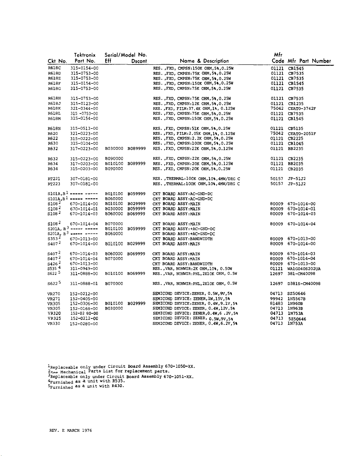
TM 11-6625-2749-14&P
Tektronix
Na.
Part No.
Ckt
315-0154-00
315-0753-00
315-0753-00
315-0154-00
315-0753-00
315-0753-00
315-0123-00
321-0344-00
.315 -0753-00
315-0154-00
R618N
R620
FM522
R630
R632
R632
R634
R634
RT221
RT223
sKm,B~
S1OIA,B1 ----S1CM32
315-0513-00
321-0223-00
315-0222-00
315-0104-00
317-0223-00
315-0223-00
317-0203-00
315-0203-00
307-0181-00
307-0181-00
-----
-----
-----
670-1014-00
S1082 670-1014-01
S1C182
S1082
.s201A, B3 ----S201A, B3 ----$3532
S4072
S4072
S4072
s4262
S535 ~
S622 ~
670-1014-03
670-1014-04
-----
-----
670-1013-00
670-1014-00
670-1014-03
670-1014-04
670-101.3-00
311-0949-00
311-0888-00
311-0888-01
vR27cl
VR271
VR305
VR305
VR320
VR325
VR330
152-0212-00
152-(3405-00
152-0306-00
152-(3168-00
152-02 s0-00
152-0212-00
152-0280-00
Serial/Model No.
Eff
Dscont
5030000 B089999
B090000
Bololoo B089999
B090000
Bololoo FI059999
13060000
33010100 B029999
13030000 B059999
B060000 B069999
B070000
BO1OIOO B059999
B060000
B060000 B069999
B070CU30
5010100 B069999
B070000
BO1OIOO B029999
B030CM30
Name &
Description Code
RZS. ,FXD, CMPSN:150K 0HM,5%,0.25W
S2ZS. ,FXD, CMPSN:75K 0HN,5%,0.25W
RES. ,FXD, CMPSN:75K 0HM,5%,0.25W
RES. ,FXD, CMPSN:150K 0HN,5%,0.25W
RES. ,FXD, CMPSN:75K 0WM,5%,0.25W
RES. ,FXD, CNPSN:75K 0HM,5%,0.25W
RES. ,FXD, CMPSN:12K 0HM,5%,0.25W
F.ES. ,FXD, FIIJ4:37.4K OHM,l%, O.125W
RES. ,FXD, CMPSN:75K 0HM,5%,0.25W
RES. ,FXD, CMPSN:150K 0HM,5%,0.25W
RES. ,FXD, CMPSN:51K 0HM,5%,0.25W
RES. ,FXD, FILN:2.05K OHM,l%, O.125W
RES. ,FXD, CMPSN:2.2K 0HN,5%,0.25W
RES. ,FXD, CMPSN:1OOK 0HM,5%,0.25W
RES. ,FXD, CMPSN:22K 0HN,5%,0.125W
RES. ,FXD, CMPSN:22K OHM,5%,0.25W
RES. ,FXD, CMPSN:20K 0HM,5%,0.125W
FC3S. ,FXD, CMPSN:20K 0HM,5%,0.25W
FX2S. ,THERMAL:1OOK 0HM,10%,4MW/DEG C
RES. ,THERMAL:1OOK 0HN,10%,4NW/DEG C
CKT BOARII ASSY:AC-GND-DC
CKT BOARD ASSY:AC-GNO-DC
CKT BOARD ASSY:MAIN
CKT BOARD ABSY:MAIN
CKT BOARD ASSY:MAIN
CKT BOARD ASSY:NAIN
CKT BOARD ASSY:+AC-GND-DC
CKT BOARD ASSY:+AC-GND-DC
CKT BOARO ASSY:BANDWIDTH
CKT BOARD ASSY:MAIN
CKT BOARD ASSY:NAIN
CKT BOAR13 ASSY:MAIN
CKT
BOARD ASSY:BANDWIDTH
RES. ,VAR, NONWIR:2K OHM,lO%, O.5OW
P.ES. ,VAR, NONWIR:PNL,2X1OK OHM, O.5W
RSS. ,VAR, NONWIR:PNL,2X1OK OHM, O.5W
SENICOND DNICE:ZENER, O.5W,9V,5%
SEMICONO DEVICE: ZENER,1W,15V,5%
SZMICOND DKVICE:ZENER, O.4W,9.1V,5%
SE241COW0 DEvICE: ZENER, O.4W,12V,5%
SEWiICX3ND DEVICE: ZENER,”0.4W,6 .2V,5%
SZMICOND DEVICE: ZENER, O.5W,9V,5$
SEMICOND DEVICE: ZENSR, O.4W,6.2V,5%
Mfr
Mfr Part Number
01121
CB1545
01121
CB7535
01121
CB7535
01121
CB1545
01121
CB7535
01121
CB7535
01121
CB1235
75042
CEATO-3742F
01121
CB7535
01121
CB1545
01121
CB5135
75042
CEATO-2051F
01121
CB2225
01121
CB1045
01121
BB2235
01121
CB2235
01121
BB2035
01121
CB2035
50157
JP-51J2
50157
JP-51J2
80009 670-1014-00
80009 670-1014-01
80009 670-1014-03
80009 670-1014-04
80009 670-1013-00
80009 670-1014-00BOIOIOO B029999
80009 670-1014-03
80009 670-1014-04
80009 670-1013-00
01121 WA1G040S202UA
12697 381-cM40098
12697 D381S-CM40098
04713 SZ50646
99942 1N5567B
81483 1N960B
04713 1N963B
04713 1N753A
04713 5z50646
04713 1N753A
~RepIaCe~Ie only U~der circuit Board Assembly 670-1050-XX.
2See ~ec~a~cal parts
3~eP~ace~le
4FUrni~hed as a unit
OrjIY under ~ircuit Board Aesembly’ 670-1051-xx.
LiSt
with
for
replacement parts.
R535.
5FUrn~~~ed as a unit with R430.
6-9
Page 82

Page 83
SECTION 7
TM 11-6625-2749-14&P
7-1
Page 84

TM
11-6625-2749-14&P
7-3
Page 85

TM 11-6625-2749-14&P
7-5
Page 86
TM 11-6625-2749-14&P
7-7
Page 87

TM 11-6625-2749-14&P
7-9
Page 88

TM 11-6625-2749-14&P
7-11
Page 89

TM 11-6625-2749-14&P
7-13
Page 90

TM 11-6625-2749-14&P
7-15
Page 91
REPLACEABLE
MECHANICAL PARTS
TM 11-6625-2749-14&P
PARTS ORDERING INFORMATION
Replacement
Tektronix, inc. Field Office or representative.
Changes to Tektronix instruments are sometimes made to
accommodate improved components as they become available,
and to give you the benefit of the latest circuit improvements
developed in our engineering department.
impotiant, when ordering parts, to include the following
information in your order: Part number, instrument type or
number, serial number, and modification number if applicable.
If a
part you have ordered has been replaced with
improved part, your local Tektronix, Inc. Field Office or
representative will contact you concerning any change in part
number.
parts
are available from or through your local
It is
therefore
a
new or
SPECIAL NOTES AND SYMBOLS
Xcxxl
Oox
Part first added at ‘this serial number
Part removed after this serial number
FIGURE AND INDEX NUMBERS
Items in this section are referenced by figure and
numbers to the illustrations.
index
INDENTATION SYSTEM
This mechanical parts list is indented to indicate item
relationships. Following is an example of the indentation system
used in the description column.
12345
Assembly andlor Component
Attaching parts for Assembly andlor Component
----- -.
Detai/ Part of Assemb/y andlor Component
Attaching parts for Detai/ Part
------
Parts of Detail Part
Aftaching parts for Parts of Detai/ Part
---.- --
Attaching Parts always appear in the same indentation as
the item it mounts, while the detail parts are indented to the right,
Indented items are part of, and included with, the next higher
indentation. The separation symbol ---’ --- indicates the end of
attaching parts.
Attaching parta must be purchaaed separately, unless otherwise
specified.
Name
&
Description
-
ITEM NAME
In the Parts List, an Item Name is separated from the
description by
Name may sometimes appear as incomplete. For further Item
Name identification, the U.S. Federal Cataloging Handbook H6-1
can be utilized where possible.
a
colon (:). Because of space limitations, an Item
#
ACTF4
ADPTR
ALIGN
M_
ASSEM
ASSV
ATTEN
AWG
BD
EIRKT
Ems
Smz
EK5WG
CAB
CAP
CER
CHAS
cm
CXW”4P
ccmN
CXW
CPLG
CRT
DE(3
mm
w.
INCH
NUMBER SIZE
ACTUATOR
ADAPTER
ALIGNMENT
ALUMINUM
ASSEMBLED
ASSEMBLY
ATTENUATOR
AMERICAN WIRE GAGE
BOARD
EW?ACX.ET
BRASS
BRONZE
BUSHING
CABINET
CAPACITOR
CERAMIC
CHASSIS
CIRCUIT
COMPOSITION
CONNECTOR
COVER
COUPLING
CATHODE
DEGREE
DRAWER
F MARCH
1976
RAY TI.JEIE
ELCTRN
H-EC
ELCTLT
mm
Em
EC2PT
EXT
FIL
FLEX
FLH
FLTR
FR
FSTNR
FT
FXD
GSKT
HDL
HEx
HEX 1-1o
HEX
SC)c
HLCPS
HLEXT
Hv
Ic
ID
IDENT
[MPLR
ABBREVIATIONS
ELECTRON
ELECTRICAL
ELECTROLYTIC
ELEMENT
ELECTRICAL PARTS LIST
EQUIPMENT
EXTERNAL
FILLKSTER t+EAO
FLEXIBLE
FLAT HEAO
FILTER
FRAME or FRONT
FASTENER
FOOT
FIXED
GASKET
HANDLE
HEXAGON
HEXAGONAL HEAO
HEXAGONAL SOCKET
HELlCAL COMPRESSION
HELlCAL EXTENSION
HIGH VOLTAGE
INTEGRATE
INSIDE DIAMETER
IDENTIFICATION
IMPELLER
CIRCUIT
IN
INCAND INCANDESCENT
INSUL
INTL
LPHLOR
MACH
MECt-1
MTCi
NIP
NON WIRE NOT WIRE WOUNO
OBO
OD
Owi
PH
PL
PLSTC
PN
PNH
PWR
RCPT
RES
RGO
RI-F
RTNR
SCH
SCOPE
SCR
INCH
INSULATOR
INTERNAL
LAMPHOLDER
MACHINE
MECHANICAL
MOUNTING
NIPPLE
ORDER BY DESCRIPTION
OUTSIDE DIAMETER
OVAL HEAO
PHOSPHOR BRONZE
BRZ
PLAIN or PLATE
PLASTIC
PART NUMBER
PAN HEAD
POWER
RECEPTACLE
RESISTOR
RIGID
RELIEF
RETAINER
SOCKET HEAD
OSCILLOSCOPE
SCREW
SE
SECT
SEMICOND SEMICONDUCTOR
SHLD
SHLOR
SKT
SL
SLFLKG
SLVG
SPR
SQ
SST
STL
Sw
T
TERM
THO
THK
TNSN
TPG
TRH
v
VAR
Vil
WSHR
XFMR
XSTR
SINGLE ENO
SECTION
DHIELU
SHOULDERED
SOCKET
SLIDE
SELF-LOCKING
SLEEVING
SPRING
SQUARE
STAINLESS STEEL
STEEL
SWITCH
TUBE
TERMINAL
THREAD
THICK
TENSION
TAPPING
TRUSS HEAD
VOLTAGE
VARIABLE
WITH
WASHER
TRANSFORMER
TRANSISTOR
8-1
Page 92

TM 11-6625-2749-14&P
CROSS INDEX–MFR. CODE NUMBER TO MANUFACTURER
Mfr. Code Manufacturer
000BK
00779
13257
22526
24931
55210
70276
71785
73743
74445
76854
78189
79136
79807
80009
83385
86928
87308
89663
93907
95987
99934
STAUFFER SUPPLY
AMP, INC.
AMERACE, LTD.
BERG ELECTRONICS, INC.
SPECIALTY CONNECTOR CO. , INC.
GETTIG ENG. AND MFG. COMPANY
ALLEN MFG. CO.
TRW, CINCH CONNECTORS
FISCHER SPECIAL MFG. CO.
HOLO-KROME CO.
OAK INDUSTRIES, INC. , SWITCH DIV.
ILLINOIS TOOL WORKS, INC.
SHAKEPROOF DIVISION
WALDES, KOHINOOR, INC.
WROUGHT WASHER MFG. CO.
TEKTRONIX, INC.
CENTRAL SCREW CO.
SEASTROM MFG. COMPANY, INC.
N. L.
INDUSTRIES, INC. , SOUTHERN SCREW
DIV.
REESE,
J.
CAMCAR SCREW AND MFG. CO.
WECKESSER CO. , INC.
RENBIV!NDT INC.
RAMSEY, INC.
Address
105 SE TAYLOR
P O
BOX 3608
10 ESNA PARK DRIVE
YOUK EXPRESSWAY
3560 MADISON AVE.
PO BOX
85,
P. O.
1501 MORSE AVENUE
446 MORGAN
31 BROOK ST. WEST
S.
MAIN ST.
ST. CHARLES ROAD
47-16 AUSTEL PLACE
2100
S. O
P O BOX 500
2530 C!ZSSCENT DR.
701 SONORA AVENUE
P. O.
71 MURRAY STREET
600 18TH AVE.
4444 WEST IRVING PARK RD.
6
PARMELEE
OFF ROUTE
DRAWER 570
ST.
BAY
ST.
BOX 1360
STPJ3ET
45
City, State, Zip
PORTLAND, OR 97214
HARRISBURG, PA 17105
MARIWAM, ONTARIO, CANADA
NEW CUMBERLAND, PA 17070
INDIANAPOLIS, IN 46227
SPRING MILLS, PA 16875
HARTFORD, CT 06101
ELK GROVE VILLAGE, IL 60007
CINCINNATI, OH 45206
HARTFORD, CT 06110
CRYSTAL LAKE, IL 60014
ELGIN ,
LONG ISLAND CITY, NY 11101
MILWAUKEE, WI 53207
BEAVERTON, OR 97077
BROADVIEW, IL 60153
GLENDALE, CA 91201
STATESVILLE, NC 28677
NEW YORK, NY 10007
ROCi@ORD, IL 61101
CHICAGO, IL 60641
BOSTON, MA 02118
IL 60120
8-2
REV.
F
SEPT. 1978
Page 93

Fig.
Index
No.
1-1
-2
-3
-4
-5
-6
-7
-$3
-9
-10
-11
-12
-13
-14
-15
-16
-17
-M3
-19
-20
-21
-22
-23
-24
-25
-26
-27
-28
-29
-30
-31
-32
-33
-34
-35
-36
-37
-38
-39
-40
-41
&
Tektronix
Part No.
366-1059-00
366-1077-00
213-0153-00
----- -----
210-0046-00
210-0940-00
210-0583-00
366-0392-02
----- -----
213-0020-00
366-1166-00
213-0153-00
366-1057-00
213-0153-00
366-0379-00
213-0153-00
366-0379-00
213-0153-00
366-1084-00
213-0725-00
366-1101-00
213-0153-00
----- -----
21O-O583+3O
210-0046-00
426-0474-00
211-0111-00
210-0001-00
361-0280-00
----- -----
210-05S.3-00
210-0046-00
210-0940-00
386-1095-00
333-1106-00
306-1447-07
348-0031-00
358-0216-00
358-0378-00
129-0053-00
200-0103-00
355-0507-00
210-0046-00
210-0583-00
131-0679-00
366-1058-07
214-1095-00
105-0076-02
214-12$0-00
Serial/ModelNo.
Eff Dscont
Qty 12345
1
PUSH BUTTON:GRAY
1
KNOB : GRAY
1
SETSCREW:5-40 X 0.125 INCH,HEX SOC STL
.
1
RESIS’N3R,VAR: (SEE R430,S622 EPL)
WASHER,LOCK:INTL,0.26
1
1
WASHER,FLAT:O.25
NUT, PLAIN, HEX. :0.25-32 X 0.312 INCH, BPS
1
1
KNOB : GRAY
1
RILSISTOR,VAR: (SEE R258 EPL)
1
SETSCRXW:6-32 X 0.125 INCH,HEX.SOC STL
1
KNOB : RED
1
SETSCREW:5-40 X 0.125 INCH,HEX SOC STL
.
1
KNOB : GRAY
1
SETSCREW:5-40 X 0.125 INCH,HEX SOC STL
.
1
KNOB:GRAY,MODE
1
.
SETSCREW:5-40 X 0.125 INCH,HEX SOC STL
1
KNOB:GRAY,MODE
1
.
SETSCREW:5-40 X 0.125 INCH,HEX SOC STL
1
KNOB : G~Y
1
.
SETSCREW:3-48 X 0.095 INCH,HEX SOC STL
1
KNOB : GRAY
SETSCREW:5-40 X 0.125 INCH,HEX SOC STL
1
.
1
RBSIS’IQR,VAR:(SEE R270 EPL)
NUT,PLAIN,HEX. :0.25-32 X 0.312 INCH,BRS
1
WASHER, LOCK: INTL,0.26 ID X 0.40” OD, STL
1
MOUNT,RESILIENT:S
1
2
SCREW,MACHINE:2-56
2
WASHER,LCCK:INTL,0.092
2
SPACER, SLEEVE:0.75 INCH LONG
1
RESISTOR,VAR: (SEE R265 EPL)
2
NUT,PLAIN,HEX. :0.25-32 X 0.312 INCH,BPS
1
WASHER,LOCK:INTL,0.26
WABHER,FLAT:0.25
1
PLATE,RES.,MTG:
1
1
PANEL,FRONT:
1
SUBPANEL,FRONT :
2
GROMNET,PmSTIC:O.156
1
BUSHING, PLASTIC:0.257 ID X 0.412 INCH OD
1
BUSHING, SLEEVE: PRESS MOUNT
1
POST,BBG,ELEC :UNINSULATED
1
.
NuT, PLAIN, KNURL: O.25-28 X 0.375” OD,BRASS
STUD,SHOULDERED:BINDING
1
.
1
WASHER, LOCK: INTL,0.26 ID X 0.40” OD, STL
1
NUT, PHiIN, HEX. :0.25-32 X 0.312 INCH,BRS
2
CONNECTOR,RCPT, :BNC W/HARDWARE
1
KNOB : LATCH
PIN, SPG, SPLIT:0.094 OD X 0.187 INCH LONG
1
FC3L BAR,LATCH:PLUG-IN
1
1
SPRING,HLCPS:0.14
Name&Description
(ATTACHING pmTs)
ID X
ID X
0.375 INCH OD,STL
----
(ATTACHING PARTs)
---
(ATTACHING PARTs)
----
SHAPE
(AmAcHING pARTs)
X
1.0 INCH,PNH STL
ID X
----
(ATTACHING PARTS)
ID X
ID X
0.375 INCH OD,STL
---
INCH DIA
POST
(ATTACHING PARTS)
---
(ATTACHING PmTs)
---UNIT
OD X
1.126’’L,O.16’’DIA W
0.40” OD,STL
*
*___
*
0.18’’OD,STL
*
0.40” OD,STL
*---
*___
*
TM 11-6625-2749-14&P
Mfr
Code Mfr Part Number
24931
366-1059-00
366-1077-00
OBD
1214 -05-00 -0541C
OBD
2x20224-402
366-0392-02
OBD
366-1166-00
OBD
366-1057-00
OBD
366-0379-00
OBD
366-0379-00
OBD
366-1084-00
OBD
366-1101-00
OBD
2x20224-402
1214 -05-00 -0541C
426-0474-00
OBD
1202 -00-00 -0541C
3-5152-340
2x20224-402
1214-05-00-0541C
OBD
15528-015
333-1106-00
386-1447-07
348-0031-00
358-0216-00
358-0378-00
129-0053-00
200-0103-00
355-0507-00
1214-05-00-0541C
2x20224-402
28JR168-1
366-1058-07
52-022-094-0187
105-0076-02
214-1280-00
80009
74445
78189
79807
--
--
--
--
73743
80009
70276
80009
74445
80009
74445
80009
74445
74445
80009
74445
80009
74445
73743
78189
80009
83385
78189
76854
73743
78189
79807
76854
80009
80009
80009
80009
80009
80009
80009
78189
73743
80009
13257
80009
80009
FUX.?. F SEPT. 1978
8-3
Page 94

TM 11-6625-2749-14&P
Fig,
&
Index
No.
1-42
Tektronix Serial/Model
Part No.
348-0157-00
348-0235-00
-43
670-1050-00
670-1050-01
-44
131-0589-00
211-0156-00
-45
-46
670-1051-00
670-1051-01
-47
131-0589-00
-48
211-0156-00
-49
352-0068-00
-50
131-0664-00
-51
211-0008-00
-52
210-0586-00
-53
131-0664-00
–54
211-0008-00
-55
210-0586-00
-56
378-0600-00
-57
352-0067-00
211-0018-00
-58
-59
210-0406-00
214-1054-00
-60
-61
105-0075-00
344-0162-00
-62
344-0211-00
-63
344-0161-00
344-0210-00
210-0201-00
-64
211-0101-00
-65
-66
210-0586-00
214-1061-00
-67
337-1243-00
-68
-69
426-0499-03
211-0101-00
-70
210-0586-00
-71
-72
213-0192-00
-73
426-0505-03
211-0101-00
-74
210-0586-00
-75
-76
213-0192-00
-77
386-1402-00
-78
213-0192-00
-79
361-0326-00
-80
337-1145-00
337-1145-01
Eff Dscont
BO1O1OO BO1O18O
BO1O181
BO1O1OO B059999
B060000
BO1O1OO B059999
B060000
BO1O1OO B050549
B050550
BO1O1OO B050549
B050550
BO1O1OO B069999
B070000
No.
Qty 12345
2
SHLD GSKT,ELEC: 80009
2
SHLD GSKT,ELEC;4.734 INCH LONG 80009
1
CKT BOARD ASSY:AC GND DC 80009
1
CKT BOARD ASSY:AC GND DC 80009
2
. TERM,PIN:0.46 L X 0.025 SQ.PH BRZ GL 22526
2
SCREW,MACHINE:l-72
1
CKT BOARD ASSY:+AC GND DC
1
CKT BOARD ASSY:+AC GND DC 80009
2
TERM, PIN: O.46 L X 0.025 SQ. PH BRZ GL 22526
2
SCREW,MACHINE:1-72
2
HOLDER,TEST PRO:PLASTIC
2
CONTACT , ELEC :
1
SCREW,MACHINE :4-40 X 0.25 INCH,PNH STL
1
NUT,PLAIN,EXT W:4-40 X 0.25 INCH,STL
1
CONTACT,ELEC :
1
SCREW,MACHINE :4-40 X 0.25 INCH,PNH STL
1
NUT, PLAIN, EXT W:4-40 X 0.25 INCH, STL
1
LENS, LIGHT: INDICATOR,2.428 INCH LONG
LAMPHOLDER:
1
1
SCPJ?W,MACHINE:4-40 X 0.875 PNH,STL
1
NUT, PLAIN, HEX. :4-40 X 0.188 INCH, BRS
1
SPRING,FLAT:0.825
1
PAWL:0.475 X 0.21 X 0.184 INCH,PLSTC
3
CLIP,SPR TNSN:BOTTOM,PLASTIC
3
CLIP,SPR TNSN:BOTTOM,PLASTIC
2
CLIP, SPR TNSN:TOP, PLASTIC
2
CLIP,SPR TNSN:
2
TERMINAL,LUG:SE #4
1
SCREW,MACHINE:4-40
NUT,PLAIN,EXT W:4-40 X 0.25 INCH,STL
1
1
SPRING,GROUND :FLAT
1
SHIELD,ELEC:4.25
1
FR SECT,PLUG-IN:BOTTOM
2
SCREW,MACHINE:4-40
2
NUT,PLAIN,EXT W:4-40 X 0.25 INCH,STL
2
SCR,TPG,THD FOR:6-32 X 0.50 INCH,PNH STL
1
FR SECT,PLUG-IN:TOP
2
SCREW,MACHINE:4-40
2
NUT,PLAIN,EXT W:4-40 X 0.25 INCH,STL
2
SCR,TPG,THD FOR:6-32 X 0.50 INCH,PNH STL
PANEL,REAR:
1
4
SCR,TPG,THD FOR:6-32 X 0.50 INCH,PNH STL
1
SPACER, SLEEVE:0.18 ID X 0.25 OD X O.1O”L
1
SHIELD,ELEC:LEFT
1
SHIELD,ELEC:LEFT
Name&Description
(ATTACHING pARTs FOR CKT
X 0.25’’,82
---
(ATTACHING PARTS FOR CKT
X 0.25’’,82
---
(ATTAcHING pARTs)
-_*---
(ATTACHING PARTS)
---
(ATTAcHING pARTs)
---
X
O.322,SST
(ATTACHING PARTS FOR EACH)
X
0.25” 100 DEG,FLH STL
---
X
1.5’’,PLSTC,W/ADH
(ATTACHING pARTs)
X
0.25” 100 DEG,FLH STL
---
(ATTACHING PARTs)
X
0.25” 100 DEG,FLH STL
---
(ATTAcHING pARTs)
---
SIDE
SIDE
DEG,FLH STL
*___
DEG,FLH STL
*---
*___
*___
*---
*___
*---
*---
Mfr
Code Mfr Part Number
348-0157-00
348-0235-00
670-1050-00
670-1050-01
93907
47350
OBD
670-1051-00
670-1051-01
47350
OBD
352-0068-00
131-0664-00
OBD
211-041800-00
131-0664-00
OBD
211-041800-00
378-0600-00
352-0067-00
OBD
2x12161-402
214-1054-00
105-0075-00
344-0162-00
344-0211-00
344-0161-00
344-0210-00
A373-157-2
OBD
211-041800-00
214-1061-00
337-1243-00
426-0499-03
OBD
211-041800-00
OBD
426-0505-03
OBD
211-041800-00
OBD
386-1402-00
OBD
361-0326-00
337-1145-00
337-1145-01
BD)
80009
BD)
93907
80009
80009
83385
78189
80009
83385
78189
80009
80009
83385
73743
80009
80009
80009
80009
80009
BOO09
86928
83385
78189
80009
80009
80009
83385
781B9
87308
80009
83385
78189
87308
80009
87308
80009
80009
80009
8-4
RJ3V. C SEPT. 1978
Page 95

Fig, &
index
No.
1-81
-!32
-83
Tektronix Serial/Model
Part No.
337-1146-00 BO1O1OO B069999
337-1146-01 B070000
348-0115-00
337-1045-00
Eff
No.
Dscont
Name
&
Qty 12345
1 SHIELD, ELEC:RIGHT SIDE
1
SHIELU,ELEC:RIGHT
1
GROMMET, PLASTIC: U-SHP,0.548 xO.462 INCH
1 SHIELD, ELEC:INPUT
SIDE
Description
TM 11-6625-2749-14&P
Mfr
Code Mfr Part Number
80009 337-1146-00
80009 337-1146-01
80009 348-0115-00
80009 337-1045-00
REV. J SEPT. 1970
8-5
Page 96

TM
ll-6625-2749-14&P
Fig.
&
Index
No,
2-1
Tektronix Serial/Model
Part
No.
384-0255-00
-2
384-0306-00
-3
384-0444-00
351-0159-00
-4
213-0088-00
-5
-6
131-0792-02
-7
131-0622-00
-8
352-0198-00
-9
131-0740-00
-lo
131-0755-00
-11
352-0169-00
179-1407-00
-12
-13
131-0707-00
-14
131-0512-00
352-0136-00
-15
211-0008-00
-16
210-0586–00
-17
200-0902-00
-18
-19
211-0008-00
-20
200-0687-01
----- -----
-21
-22
407-0554-00
-23
210-0046-00
-24
210-0583-00
-25
376-0029-00
213-0075-00
-26
670-1013-00
-27
211-0155-00
-28
211-1140-00
-29
351-0155-00
-30
131-0608-00
-31
136-0263-01 BO1O1OO BO1O18O
136-0263-03 BO1O181 B094559
136-0263-04 B094560
-32
136-0183-00
-33
136-0220-00
-34
131-0604-00
-35
131-0840-00 XBO1O181
105-0415-00
-36
211-0116-00
200-0996-00
-37
211-0022-00
-38
-39
210-0001-00
-40
407-0714-00
-41
214-1126-021
-42
214-1127-001
-43
401-0058-00
-44
354-0219-00
Eff Dscont
No.
Qty
12345
1
EXTENSION SHAFT:0.08/0.125 DIA X 5.594” L
1
EXTENSION SHAFT:9.5 INCH LONG
1
EXTENSION SHAFT:ll.062 INCH LONG
1
GUIDE,SHAFT:FOR 0.125 OD SHAFT,PLASTIC
1
SCR,TPG,THD CTG:4-24 X 0.25 INCH,PNH STL
2
CONTACT, ELEC:0.577’’L,18 -20 AWG WIRE
2
CONTACT, ELEC:0.577’’L,28 -32 AWG WIRS
2
CONN BODY,PL,EL:2 WIRE BLACK
2
CONTACT,ELEC:O.315
2
CONTACT,ELEC:0.315
2
CONN BODY,PL,EL:2 WIRE BLACK
1
WIRING HARNESS, :MAIN
4
CONNECTOR, TERM. :0.48” L,22-26AwG WIRE
27
CONTACT,ELEC:0.315
1
E’USEHOLDER : TEFLON
2
SCREW,MACHINE:4-40
2
NUT,PLAIN,EXT W:4-40 X 0.25 INCH,STL
1
COVER,CKT CARD:PLASTIC
1
SCREW,MACHINE:4-40
2
COV, TRANSISTOR:0.438 DIA X 0.47 INCH H
1
RESISTOR,VAR: (SEE R540 EPL)
1
BRKT,COMP MTG:
1
WASHER,LOCK:INTL,0.26
1
NUT, PLAIN, HEX. :0.25-32 X 0.312 INCH, BRS
1
CPLG, SHAFT, RGD:0.128 ID X 0.312 OD X 0.5”L
2
SETSCREW:4-40 X 0.094 INCH,HEX SOC STL
. .
1
CKT BOARD ASSY:BANDWIDTH
4
SCREW,EXT,RI,V B:4-40 X 0.375 INCH,SST
4
SPRING,HLCPS :0.251 OD X 0.375” L,SST WIRE
5
INSULATOR,STDF :CONNECTOR,DELRIN
5
TERMINAL,PIN:0.365
18
SOCKET, PIN TERM;
18
SOCKET, PIN TERM: FOR 0.025 INCH SQUARE PIN
18
SOCKET, PIN TERM: FOR 0.025 INCH SQUARE PIN
3
SOCKET,PLUG-IN:3 PIN,ROUND
3
SOCKET,PLUG-IN:3
24
CONTACT, ELEC:CKT BD SW, SPR, CU BE
2
CONTACT,ELEC :GROUNDING
1
DRUM ASSY, CAM S: LOW FREQUENCY
4
SCR,ASSEM WSHR:4-40 X 0.312 INCH,PNH BRS
1
COVER,CAM SW:
2
SCREW,MACHINE :2-56 X 0.188 INCH,PNH STL
2
WASHER,LOCK:INTL,0.092
BRACKET,CAM SW:
1
2
SPRING,FLAT:RED COLORED
1
ROLLER, DETENT:0.125 DIA X 0.125 INCH L
BEARING, CAM SW: FRONT
1
RING,RETAINING:FOR
1
Name &
(ATTACHING pARTs)
INCH LONG,18 TO 20 AWG
INCH LONG,28 TO
“
(ATTAcHING PARTs)
X
(ATTACHING pARTS)
X
(ATTACHING pARTs)
(ATTACHING pARTs)
L X
??OR
PIN,sQuARE
(ATTAcHING pARTS)
(ATTACHING pARTS)
(ATTACHING PARTS)
Description
*___
---
L,22-26 AWG WIRE
0.25 INCH,PNH STL
--- *--
0.25 INCH,PNH STL
---
*___
ID X
0.40” OD,STL
---
*___
*___
---
0.25 PH,BRZ,GOLD PL
0.025 INCH SQUAP3 PIN
*---
---
ID X
*___
---
0.25 INCH SHAFT
-__*
---
32
AWG
-
0.18’’OD,STL
Mfr
Code
Mfr Part Number
80009
80009
80009
80009
83385
22526
22526
80009
00779
00779
80009
80009
22526
00779
80009
83385
7B189
80009
83385 OBD
80009 200-0687-01
80009
78189
73743
80009
000BK
80009
80009
80009
80009
22526
00779
00779
22526
80009
71785
80009
80009
80009
83385 OBD
80009 200-0996-00
83385
78189
80009
BOO09
80009
80009
79136
384-0255-00
384-0306-00
384-0444-00
351-0159-00
OBD
46221
46241
352-0198-00
61508-2
61615-1
352-0169-00
179-1407-00
75691-005
61507-1
352-0136-00
OBD
211-041800-00
200-0902-00
407-0554-00
1214 -05-00 -0541C
2x20224-402
376-0029-00
OBD
670-1013-00
211-0155-00
211-1140-00
351-0155-00
47357
85861-2
86250-2
48059
136-0183-00
133-23-11-034
131-0604-00
131-0840-00
105-0415-00
OBD
1202 -00-00 -0541C
407-0714-00
214-1126-02
214-1127-00
401-0058-00
5103 -25-MD-R
lRePlace only with part bearing the same color as the original part in YOU instr~ent.
8-6
REV. H SEPT. 1978
Page 97

Fig. &
Index
No.
2-45
-46
-47
-48
-49
-50
-51
-52
-53
-54
-55
-56
-57
-5$3
-59
-60
-61
-62
-63
-6.4
-65
-66
-67
-68
-69
-70
-71
-72
-73
-74
-75
-76
-77
-78
-79
-80
-81
-82
-83
-84
Tektronix Serial/fvlodel
Part
No.
105-0112-00
213-0 c375-00
210-0405-00
210-0406-00
401-0061-00
105-0466-00
211-0116-00
200-0995-00
211-0022-00
21O-OOOI-OC?
407-0714-00 XBO1O181
214-1126-011
214-1126-021
214-3.127-00
401-0058-00
354-0219-00
105-0109-00
213-0075-00
210-0405-00
210-0406-00
401-0061-00
----- -----
210-0583-00
210-0046-00
407-0553-00
670-1014-00 BO1O1OO B029999
670-1014-01 B030000 B059999
670-1014-03 B060000 B069999
670-1014-04 B070000 B079999
6’70-1014-05 BO130000 B115479
670-1014-06 B115480
211-0116-00 BO1O1OO B099999
211-0513-00 B1OOOOO
210-05$36-00 BO1O1OO B099999
210-0457-00 B1OOOOO
210-0863-00 XB1OOOOO
343-0002-00 KBJ.00000 B115479
343-0003-00 5115480
23.0-041.%-00
210-0840-00
384-0448-00
376-0091-00
213-0020-00 XS020160
131-0590-00
342-0050-00 xB050000
351-0155-00
136-0235-00
344-0154-00
136-0183-00
131-0566-00
337-1266-02
214-0579-00
136-0235-01
Eff Dscont
No.
Qty
12345
1
. . DRUM,CAN SW:
2
1
2
1
1
4
1
2
2
1
1
1
1
1
1
1
2
1
2
1
1
1
1
1
1
1
1
1
1
1
1
1
1
1
1
1
1
1
1
1
1
4
18
15
22
4
4
4
2
1
4
1
SETSCREW:4-40 X 0.094 INCH,HEX Soil! STL
. .
NWT, PLAIN, HEX. :2-56 X 0.188 INCH, BRS
. .
. .
NUT, PLAIN, HEX. :4-40 X 0.188 INCH, BRS
. . BEARING,CAN SW:REAR
. DRON ASSY,CAN S:LOW FREQENCY
.
SCR,ASSSM WSHR:4-40 X 0.312 INCH,PNH BPS
. .
COVSR,CAN SW:
. .
SCREW,NACHINS:2-56
WASHER,LOCK:INTL,0.092
. .
. .
13RACKET,CAM SW:
SPRING,FLAT:GREEN
. .
SPRING,FLAT:RED COLORED
. .
IVXLER,DETENT:O.125
. .
BEARING,CAN SW:FRONT
. .
. .
RING,RETAINING:FOR
DRUM, CAN SW:
. .
SETSCREW:4-40 X 0.094 INCH, HEX SOC STL
. .
.
. .
NOT,PLAIN,HEX. :2-56 x 0.188..INCH,BRS
NUT,PLAIN,HEX. :4-40 X 0.188 INCH,BRS
. .
BEARING, CAN SW:REAR
. .
RESISTOR,VAR:(SEE
NUT,PLAIN,HEX. :0.25-32 X 0.312 INCH,BRS
WASHER, LOCK: INTL,0.26 ID X 0.40” OD, STL
BRKT,CNPNT MTG:
CKT BOARD ASSY:NAIN
CKT BOARD ASSY:MAIN
CKT BOARD AESY:NAIN
CKT BOARD ASSY:NAIN
CKT BOARD ASSY:NAIN
CKT BOARD ASSY:NAIN
SCR,ASSEM WSHR:4-40 X 0.312 INCH,PNB BRS
SCRJ3W,MACHINE:6-32 X 0.625 INCH,PNH STL
NUT,PLAIN,EXT W:4-40 X 0.25 INCH,STL
NUT,PLAIN,EXT W:6-32 X 0.312 INCB,STL
WSHR,LOOP CLAMP:FOR 0.50” WIDE CLANP,STL
CLAMP,L&3P:0.188
CLAMP,LOQP:0.25 INCH DIA
NUT,PLAIN,HEX. :0.375-32 X 0.50 INCH,STL
WASHER,FLAT:0.39
SHAFT,EXTENSION:ll.125
.
.
CPLG,SHAFT,FLEX :
.
SETSCPEW:6-32 X 0.125 INCH,HEX.SCC STL
.
.
CONTACT,ELEC:0.71
INSULATOR , STDF :
.
INSULATOR, STDF : CONNECTOR , DELRIN
.
.
SOCKET,PLUG-IN:6
.
CLIP, ELECTRKAL:FOR
SOCKET,PLUG-IN:3
.
.
LINK,
TERJ4.
SHIELD,ELEC:
.
TER14.
.
.
,TEST PT:BRS CD PL
SOCKST,PLUG-IN:6
Name &
(ATTACHING PARTs)
(ATTACHING PARTS)
(ATTACHING pARTs)
R535,S535 EPL)
(ATTACHING pARTs)
(ATTACHING PARTS)
INCH DIA
ID X
CONTACT,ROUND
PIN,ROUND
CONNE:O.086 DIA X 2.375 INCH L
CONTACT,ROUND
Description
*
----
X
0.188 INCH,PNH STL
ID X
*___
---
COLORED
DIA X 0.125 INCH L
0.25 INCH SHAFT
*
----
*___
---
0.562 INCH OD,STL
*
----
INCH LONG,PLASTIC
INCH LONG
0.25 INCH DIA FUSE
--
0.18’’OD,STL
--
--
TM 11-6625-2749-14&P
Mfr
Code
Mfr Part Number
000BK
73743
73743
80009
80009
83385
80009
83385
78189
80009
80009
80009
80009
80009
79136
80009
000BK
73743
73743
80009
73743
78189
80009
80009
80009
80009
80009
80009
80009
83385
83385
78189
83385
95987
95987
95987
73743
89663
80009
99934
70276
22526
80009
71785
80009
80009
55210
80009
80009
71785
105-0112-00
OBD
2x12157-402
2x12161-402
401-0061-00
105-0466-00
OBD
200-0995-00
OBD
1202-00-00-0541C
407-0714-00
214-1126-01
214-1126-02
214-1127-00
401-0058-00
5103-25-ND-R
105-0109-00
OBD
2X12157-402
2x12161-402
401-0061-00
2x20224-402
1214 -05-00-0541C
407-0553-00
670-1014-00
670-1014-01
670-1014-03
670-1014-04
670-1014-05
670-1014-06
OBD
OBD
211-041800-00
OBD
C191
3-l6-6B
1-4 6R
3145-402
644R
384-0448-00
A-201-165
OBD
47351
342-0050-00
351-0155-00
133-96-12-062
344-0154-00
136-0183-00
L-2007-1
337-1266-02
214-0579-00
133-96-92-067
1
Replace only with
m.
E
SEPT. 1978
part bearing the same color as the original part in your instrument.
8-7
Page 98

Page 99

SECTION!
9
TM 11-6625-2749-14&P
BB2035
BB2235
BB2435
m3%l15
c.Bm35
cBlmft5
Cmncm
C.BIJ235
mw+5
CBM355
PART
NUMBER
FSCM
olll12L
o111121
ol&211
o1111211
o1111211
0111121
olJ1211
03321
OU21
o111121
olJJ21
on2i
PART NUMBER
CROSS REFERENCE INDEX
N4TIONAL
STOCK
NUMBER
I
5905-00-958-3830
5905-00+03-8837
5905-00-9611-7730
5905-00+07-0085
5905+0-234-4374
5905-00-102-5294
5905-00-909-3885
5905-00-959-1202
5905-00-XI.16-8554
5905-00-989-7%3
5905-00-904-5696
5905-00-800-8068
– NATIONAL STOCK NUMBER
PART
NUMBER
I
I
CEATO-l12411F
CEATO-1272F
CEATO-1500F
CEATO-1501F
CEATO-1541F
CEATO-20ROF
CEATO-2000F
CEATO-2001F
CEATO-20511F
CEATO-2261F
CEATO-2491F
CEATO-2493F
i
FSCM
75042
75042
75042
75042
75042
75042
75042
75042
75042
75042
75042
75042
NATIONAL
STOCK
NUMBER
5905-00-153-4435
5905-00-105-9724
5905-00-937-0576
5905-00-I.109-9848
5905-OIJ-026-5084
5905-00-1177-7172
5905-00-998-L796
5905-00-922-9920
5905-oo-724-5n7
5905-00-102-60011
5905-00-023-64%
5905-00-051r1879
CB2025
CB2W5
CB2225
CB3635
cB3&5
CB3935
CB4335
C134735
cB51!05
CB5%25
CEHJ35
CB%25
CB7535
CEATCI-%O02F
CEATO-MX)31=
CEAT&lOED
CEATO-10112F
olJJ211
0XIJ21
o111211
olJL21.1
milJ211
olll!211
ollL21
Ollxzl.r
0XIJ21
olil12%
Ollla
01J121
OIIKI
75042
75042
75042
75042
5905-00-102-5289
5905-00-136-71103
5905-00-909-3%0
5905-00-L36-8430
5905-ocF141-07411
5905-00-907-QL8
5905-00-122-0004
5905-00-960-01126
5905-00-909-3834
5905-oo-9111.r3754
5905-00-136-3890
5905-0@909-3862
5905-00-9116-7268
5905-00-904-4409
5905-00-484-7475
5905-00-%05-9709
5905-00-893-11242
CEATO-3010F
CEATO-3012F
CEATO-3320F
CEATO-3652F
CEATO-3742F
CEAT040211F
CEATD-4530F
CEATO-4990F
CEATO-4991F
CEATO-5622F
CEATO-8060F
EB5625
SE365
SS22650
SV251JlJ
SZ50646
75042
75042
75042
75042
75042
75042
75042
75042
75042
75042
75042
o1111211
03508
07263
olJ1211
047113
5905-00-078-lJ549
5905-01-017-8307
5905-00-021r6496
5905-00-4119-2676
5905-00-441J-7812
5905-00-922-9923
5905-00+33-7389
5905-00-922-9924
5905-00-922-9925
5905-00-997-9579
5905-00-233-5377
5905-00-L211-9UI0
5961rO0-222-611~0
5961-00-488-9927
5905-00-41A-11101
596%-00-237-2353
CEATO-ldO%F
75042
5905-00-994-8457
WAJJG040S202UA
olA21
5905-00-400-35431
9-1
Page 100
TM 11-6625-2749-14&P
SECTION
9
PART NUMBER NATIONAL STOCK NUMBER
CROSS REFERENCE INDEX
PART
NUMBER
I
IN4152
1N5567B
IN963B
3J214-05-00-0541C
129–0053–00
131-0566–00
131r0589-00
1131-0590-00
131–0604-00
131–0608–00
131–0622–00
131–0679–00
l!31r0707-oo
l131r0792-00
NATIONAL
STOCK
FSCM
I
07910
99942
04713
78189
80009
80009
80009
80009
80009
80009
80009
80009
80009
80009
NUMBER
5961–00–899–8924
5963–00-254–1621
5961–00-998–3666
53110-00-193-6731
5940–00-835–2060
5940–00-242–0676
5999-00-275-0213
5999–00–551–9434
5999–00–IJ73-9923
5999-00-551-9433
5999-01-022–66JJ6
5935-00-236-7554
5999–00-396–6331
5999–01r023–1578
PART
NUMBER
152–0185–00
152–02112-00
152-0280+0
152-0323–00
L52–0405–00
L894–5
189-509-5
189–6–5
2N5308
2R5859
2X12161402
2X20224-402
200–0103–00
210–0046–00
FSCM
80009
80009
80009
80009
80009
74970
74970
74970
03508
04713
73743
73743
80009
80009
NATIONAL
STOCK
NUMBER
5961–00-936-7604
5961-00-237–2353
5961-00436-2890
5961–00-222-6390
5961-00-254-162%
5910–00–958-3153
5910-00-247-8600
5910–00–834–493~
5961–00–146–8295
5961–00+48–671J7
53110-004074600
53>0–00–158-5262
5999-00-914–3308
53L0–00-841r8LlJ7
lJ33-23-111-034
133–96–12-062
li36-0183-00
L36–0220–00
136–0235–00
136–0263–03
150–0046–00
150–0048–01
l150-oo57-oL
150D396X9010B2
150D475X9035B2
151-0219-00
151–0228-00
151-0260–00
151–0261–00
151-1027–00
7L785
7L785
80009
80009
80009
80009
80009
80009
80009
56289
56289
80009
80009
80009
80009
80009
5935-00-067-73111J
5935–00-814–2209
5935-00-938-4734
5935–00–067–73111
5935–00-814–2209
5999-00-394-0381
6240–00-933-5822
6240–00–060-2941
6240-00-183–0669
5910-00–833–5%75
5910–00–177–4300
5961–00-488-9927
5961–00401-6210
5961-00493–1102
5961–00–689–1455
5961-00438-6453
210–0259–00
2L0–0457–00
210-0583-00
210–0586–00
210–0940-00
2104–04-00-252CN
Z1l-ollol-oo
211–0116-00
213-0020–00
213-0153–00
214–0579-00
214-5127-00
214-IA36–00
214-IIJ39-02
2314-lA39-03 80009
214-1190-00
80009
80009
80009
80009
80009
78189
80009
80009
80009
80009
80009
80009
80009
80009
80009
5940–00474-9824
5310-00–841–81106
53L0–00-006–8168
5310-00–836–3520
5310-00–158-5237
5940-00-847-31J38
5305.00492–2145
5305-00-005-8245
5305–00–005-8247
5305-00–283-1909
5940-00-935-8313
3LI0-00+2-8406
5930–01–020-6724
5360-00–480–3639
5360–00447-8721
6625–01–066–3336
9-2
 Loading...