

Page 1

AM
503
CURRENT
AMPLIFIER
PROBE
Page 2

7
e
I
d
ronbc
COMMITTED
TO
EXCELLENCE
Tektronix,
P.O.
Box
Beaverton,
Inc
500
Oregon
PLEASE
AT
THE
CHECK
REAR
FOR
OF
AM
CURRENT
CHANGE
THIS
MANUAL
503
PROBE
INFORMATION
.
AMPLIFIER
INSTRUCTION
.
97077
Serial
Number
MANUAL
070-2052-01
Product
Group
75
First
Printing
Revised
DEC
SEP
1985
1976
Page 3

Copyright
Contents
without
form
Products
byU.S.and
TEKTRONIX,
registered
isaregistered
PrintedinU
are
reserved
1976,
`'
of this
Tektronix,
of
foreign
trademarksofTektronix,
.S .A
.
1979
Tektronix,
publication
the
written
patents
TEK,
SCOPE-MOBILE,
trademarkofTektronixU.K
.
Specification
may
permission
Inc.and
and/or
Inc
not
be
of
subsidiaries are
its
pending patents
Inc.TELEQUIPMENT
price
and
All
rights
.
reproducedinany
Tektronix,
and
.
change
reserved
ilk
Limited
privileges
Inc
.
covered
.
.
.
are
Each
instrument
stamped
or
designates
the
of
unique
United
manufacture
serial
to
States
B000000
100000
200000
300000
700000
INSTRUMENT
has
on
the
countryofmanufacture.The
the
number
instrument.Those
each
have
identifiedasfollows
is
Tektronix,
Tektronix
Tektronix
Sony/Tektronix,
Tektronix
The
SERIAL
a
serial
number
chassis.The
are
assigned
six
unique
Inc.,Beaverton,
Guernsey,
United
Holland,
Netherlands
Japan
NUMBERS
on a
first
sequentially
manufactured
digits
.
:
Ltd.,Channel
Kingdom,
Heerenveen,
NV,
panel
number
last
The
Oregon,
Ltd
insert,
or
five
and
country
Islands
London
.,
tag,
letter
digits
in
USA
are
the
of
Page 4

OPERATOR'S
SERVICE
SECTION
SECTION
The
personneltohazardous
SECTION
SECTION
SECTION
SAFETY
SAFETY
1
2
remaining
3
4
5
TABLE
SUMMARY
SUMMARY
OPERATING
SPECIFICATION
portionofthis
voltages.These
ADJUSTMENT
MAINTENANCE
CIRCUIT
DESCRIPTION
. . . . .
. . .
. . . . . .
INSTRUCTIONS
AND
TableofContents
. . . . . .
. . ...
OF
. . . . . . . . . . . . . . ...
. . . . . . . . . . . . . ... .
PERFORMANCE
WARNING
. . . . . . . . . . . . . . .
. . . . . . . . . . . . . . . .
CONTENTS
. . . . . . . . .
CHECK
lists
instructions
. . . . . . . . . . . . . .
are
for
. . . .
. . . .
. . . . . .
servicing
qualified
. . . . .
. . . . .
. . . . .
. . . . . . . . . . . . . .
. . . . . . . . . . . . . .
. . . . . .
. ... . . . . . . . . . .
instructions
service
. . . . . . . . . . . . . . . .3-1
. . . . . . . . . . . . . . . .
. . . . . . . . . .
. . . .2-1
that
expose
personnel
. . . . . . . . . . . . . . .
only
Page
V
1-1
.
4-1
5-1
SECTION
SECTION
SECTION
CHANGE
6
7
8
INFORMATION
REPLACEABLE
DIAGRAM
REPLACEABLE
AND
ELECTRICAL
CIRCUIT
MECHANICAL
BOARD
PARTS
ILLUSTRATION
PARTS
. . . ...
AND
EXPLODED
. . . .
. . . . . . . . . . . . . . .6-1
.
.
. . . . . . . . . .
VIEW
. . . . . . .8-1
. . . .7-1
Page 5

AM
503
Fig
No
1-1
1-2
2-1
2-2
3-1
3-2
3-3
3-4
4-1
42
43
44
5-1
LIST
.
.
Plug-in
AM
Test
Displayoftangentially
Construction
Power
Gain
Exampleofcorrect
Lubrication
Semiconductor
Installation
Circuit
AM
installation
controls
503
setup
supply
and
board
503and
OF
and
and
connectors.. .
forACDynamic
details
for
test
point
compensation
compensation
procedure
lead
configurations
of
lead-end
pin
and
probe
waveforms
ILLUSTRATIONS
removal
Range
measured
Special
and
adjustment
adjustment
foratypical
connectors
ferrule
assembly
. . . . . . . .
. . .
. . . . . . . . . . . . . .
. . . . . . . . . . . . . .
check..
noise
Adapter
locations
. . . . . . . .
.
cam
. . . . . . . . . . .
. . . . . . . .
. . . . . . . . . . .
. . . .
. . . . . . . . . . . . .
. . . . . .
locations.. .
switch
. . . . . . . . . . . . . .
. . . .
. . . . . . .
.
. . . . . . . . . . . .
. . . . . . . . .
. . . . . . .
. . . . . . . .
. .
. . . . . .
. . . . . . . . . .
. . . . . . . . . . . . . .
. . . . . . . . .
. . . . . .
. .
. . . . . . .
. . . . . . . . . . . . . .
. . . . .
. . . . . . . . . . . . . .
. . . . .
. . . . . . . . . . . . .
. . . . . . . .
.
. . . . . . . . . . . . . ... .
. . . . . . . . . . . . . . . .
. . . . . . . . . . . . . . . .
. . . . . . . . . . . . . .
. . . . . .
. . . . . . . . .
. . . . . . . .2-
. . . . ... . . . .
. . . . . . . . . .
. . . . . . .
. . . . . . ... . . .
. .
. . . . . . . .
. .
. . .
. .
Page
No
1-1
1-3
2-7
3-3
3-3
3-5
3-5
4-2
4-4
47
47
5-1
.
8
Page 6

OPERATOR'S
SAFETY
SUMMARY
The
followingtext
safety
phasesofoperation,
precautions
OPERATORS
SUMMARY
The
general
is
for
warnings
manualwhere
summary
In
This
CAUTION
could
WARNING
that
could
As
Marked
CAUTION
mediately
hazardtoproperty
safety
both
operating
and
cautions
they
.
Manual
statements
resultin
damage
statements
resultinpersonal
on
Equipment
indicatesapersonal
accessible
containsa
that
service,
informationinthis
apply,
and
two-part
must
and
servicing
will
but
be
repair of
be
may
TERMS
identify
to
as
including
conditionsorpractices
the
equipment
identify
conditions
injuryorlossoflife
one
reads
the
summary
this
during
instrument
observed
SAFETY
part of
the
personnel.Specific
found
throughout
not
appear
or
other
or
injury
hazard
the
marking,
equipment
itself
of
general
summary
in
property
practices
.
not im-
.
the
this
that
or
all
.
Power
This
that
supply
and
ground.A
groundingconductor
safe
Grounding
This
torofthe
power
connecting
protective
conductor
tion
.
a
.
Danger
Upon
accessible
trols
electric
Protective
ATTENTION
Source
productisintendedtooperate
will
not
apply
conductors
protective
operation
productisgrounded
that
.
the
power
cord
intoaproperly
the
to
ground
in
the
Arising
loss of the
conductive
may
appear
shock
.
ground
-
more
than
or
between
ground
in
the
Product
through
cord.To
power
From
avoid
product
connection
cordisessential
Loss
protective-ground
parts
to
(earth)
refertomanual
250
power
inputoroutput
by
of
(including
be
insulating)
terminal
fromapower
volts
rms
either
supply
connection
cordisessential
the
grounding
electrical
wired
receptacle
way
of
Ground
knobs
.
.
between
conductor
bywayofthe
conduc-
shock,
connection,
terminals.A
the
grounding
for
safe
and
can
renderan
plug
source
the
for
the
before
opera-
all
con-
DANGER
accessibleasone
In
This
As
REVANOV
A
Marked
indicates
Manual
This
cautionary
found
on
DANGER
1979
personal
a
reads
SYMBOLS
symbol
.
Equipment
the
-
indicates
or
other
High
injury
marking
voltage
hazard
.
where
information
.
immediately
applicable
istobe
Use
the
only
Use
product
Use
only
Refer
personnel
Use
the
To
avoid
voltage
list
for
Refer
fuse
Proper
the
.
a power
cord
.
Proper
fire
rating
your
Power
power
cord
cord
and
connector
Fuse
hazard,
and
current
product
replacement
Cord
and
connector
thatisin
use
.
to qualified
good
changes
only
the
fuseofcorrect
ratingasspecifiedinthe
service
specified
condition
to qualified
personnel
for
.
service
type,
parts
your
.
Page 7

AM
503
Do
Not
To
avoid
explosive
certified
Do
Not
To
avoid
Operate
in
Explosive
explosion,donot operate
atmosphere
for
such
Remove
personal
unlessithas
operation
Covers
.
or
injury,donot
Panels
Atmospheres
this
been
remove
productinan
specifically
product
the
covers
covers
Do
ins
To
or
and
Not
only)
avoid
panels.Do
panels
Operate
personal
without covers
the
plug-in
viaaplug-in
not
properly
Without
injury,donot
or panels
operate
installed
Covers
installed
extender
the
operate
Do
.
.
product
.
(for
TM
not
without
this
apply
500
power
the
plug-
product
to
iv
REVA
NOV
1979
Page 8

AM
503
Do
Not
Do
not
product
aid
and
Use
Care
Dangerous
To
avoid
tions
and
Service
perform
unless
resuscitation
personal
components
another
When
voltages
Alone
internal
Servicing
injury,donot
SERVICING
FOR
is
existatseveral
QUALIFIED
service
person
present
With
while
power
capableofrendering
.
touch
Refer
also to
Summary
or
adjustmentofthis
Power
pointsinthis
is
exposed
on
.
.
On
SAFETY
SERVICE
the
preceding
first
product
connec-
.
SUMMARY
PERSONNEL
Operators
Disconnect
soldering,
Power
This
that
supply
and
grounding conductor
safe
Source
product
will
conductors
ground.A
operation
or
not
Safety
power
replacing
intendedtooperate
is
apply
protective
.
before
components
more
or
between
in
ONLY
removing
than
ground
the
protective
.
fromapower
250
volts
rms
between
either
supply
connectionbywayofthe
power
cordisessential
conductor
panels,
source
the
for
REVA
NOV
197
9
v
Page 9

AM
503
REV
2052-9
A
NOV
197
9
Page 10

Section
1-AM
503
OPERATING
All
references
A6302
probe
referencestothe
All
probe
A6303
Description
The
AM
use
with
Mechanical
attenuator
attenuator
tionofcurrent/division.An
knob-skirt
sitivityofthe
Bandwidth
current
table
amplitude
probeinuse) or5MHz.Input
(acordc);ac provides
to
the
.
.
503
Current
any
of
the
list
Parts
calibratedina
is
knob-skirt
illumination
probe
signalsona high
ac
used
is
selectable
illumination
compatible
NOTE
P6302
probe
P6303
probe
Probe
Amplifierisdesigned
current
for
accessories).The
1, 2,5sequence,
provides
auto-scale
automatically
.
for
either
a
meansofmeasuring
leveldocurrent
also
apply
to the
also
apply
to the
probes
input
and
direct
indica-
switch
changes
match
to
FULL
couplingisselec-
the
(limited
.
INSTRUCTIONS
The
AM
503
operates
and
power
on
the
module
upper
the
only.It
Removal
module
damage
1-1.Check
.
interconnecting
compartment
circuit
and
and
lower
module
interconnecting
AM
the
for
(see
the
the
sen-
by
low
power
modules
a
multiple-compartment
Installation
the
Turn
in;otherwise,
circuitry.Itisalso
modulebeturned
RefertoFig
barriers
power
theAM503
Alignthe
with
the
upper
ment.Push
circuit
boardinthe
To
remove
in
TEKTRONIX
will
operatein
power
module
off
before
may
occur
recommended
before
removing
off
to
match
board
edge
lower
grooveoftheAM503
guidesofthe
in
and
press
503,
pullonthe
any
.
inserting
to the
that
see
that
jackofthe
the
connector
selected
firmlytoseat
jack
.
TM
500-Series
compartment
the
plug-
plug-in
power
the
the
AM
50,'~
the
plastic
selected
cut-outs
.
chassis
compart-
release
latch
of
in
the
REVJUN
198
RELEASE
PULL
Fig.1-1.Plug-in
1
installation
and
removal
.
TO
LATCH
REMOVE
(1431-21)2052-37
Page 11

Operating
Instructions-AM
503
(locatedinthe lower
jack
disengages
and
OPERATING
Introduction
The
remainder
information
mance
and
actionsofthe
tions,
and
procedures
Controls
Allofthe
the
of
brief
is
included
Monitor
The
the
AM
being
be
at
measured
required
from
the instrument
andageneral
for
and
Connectors
major
AM
503
are
functional
bandwidth
503
measured.Oscilloscope
least
descriptionofeach
in
Fig.1-2
Oscilloscope
depends
twice
.
left
the
corner)
AM
503
until
will
interconnecting
the
slide
CONSIDERATIONS
of this
controls
located
section
to
obtain
and
descriptionofthe operating
making
controls
on
.
requiredofthe
upon
the
frequency
contains
the
most
This
includes
.
connectors,
measurements
basic
and
connectors
the
front
control
oscilloscope
the
frequencyofthe
vertical
of
effective
panel
bandwidth
the
out
the
the
input
for
of
and
signal
.
operating
perfor-
function
connec-
modes
.
operation
the
unit.A
connector
with
used
signal
should
being
right
cable
cable
not
termination.The
should not be 50Oif
It
loading
side
cable
Carefully
connector;pressing
interconnecting
INTO
available
upper-rearofthe
side
connects
connected
required
will
cause
of
Changing
snap-in
from
The
coaxial
and
alignment
tion
for
With the output
50
the
the
align
rear
O
.
for
because
an
AM
output
cover
rear of
the
cable
interface
connector
for
monitor
is
jack
instrument,iswhere
rear
interface
rear
interface
of
oscilloscope
rear
the
impedance
503
.
to rear
the
from
the
OUTPUT
coaxial
firmly,
connector
critical
output
(internal)
cable
output,
will
cableatthe
.
output
internal
the
interface
mis-match
interface.Remove
AM
503.Unplug
insert
the
center
when
making
.
the
not
have
With
output,
(factory
input
connection
INTO
50Oconnector
upper-rear
cable
piniseasily
connectedtothe
front-panel
an output
output
the
the
output
atermination
wired)
impedance
is
used
and
possible
the
right
coaxial
the
coaxial
.
bent
the
connec-
OUTPUT
signal
is
.
.
rear
Deflection
tionofthe
positive
Ground-clip
Ground-clip
probes
ground
trostatic
cause
errorsinmeasuring
usedinthe
the
attenuator
of
currents
positions
When
shortest
Output
output
OUTPUT
ting
jackatpin
jackisterminated
Conventional
.
arrow
deflectionofthe
Leads
ground
to
leadisused
voltages
lower
that
.
observing
practical
Connection
connection
INTO
current flowing
the
current-probe
on
oscilloscope
leads
are furnished
the cable
that
(1,
2, 5,
switch
may
ground-clip
50
f2
28A.Pin
in50S2.Connector
shieldatthe
reduce
to
could
.Aground
and
becauseofundesirable
appear
high-frequency
can
be
connectororthe
28Aatthe
display
with
high-frequency
couple
10
accomplished
mA)
in
lead
into
lead
sensitivity
these
available
rear
J480,
in
the
direc-
slider
produces
.
some
current
probe
end
probe
the
normally not
is
positions
chassis
sensitive
more
signals,
rear
interconnecting
use
.
through
interconnec-
located
onthe
The
.
elec-
and
the
the
a
Connecting
Install
module
AM
503
voltagetobe
Connect
necessary,
the
monitor
Set
10
mV/Div
with
tent
Connectacurrent
tor
.
Turn
equipmenttowarm
the
the
AM
.
Ensure
willbeinstalled
applied
a 500cable
a 50
oscilloscope
the
monitor
The
.
the
signal
all
equipment
AM
503
503
into
that
the
.
O
termi
nation for
oscilloscope
horizontal
frequencytobe
probetothe
on
and
up
the
power
is
suitably
with
vertical
sweep
allow 20
and
stabilize
TM
500-Series
module
bnc
impedance
input
speed
AM
into
adapted
connectors
.
vertical
should be
examined
5031NPUTconnec-
minutes
.
power
which
the
to
(and
matching)
sensitivity
consis-
.
for
the
line
if
to
for
the
REVBNOV
197
9
Page 12

Operating
Instructions-AM
503
DC
LEVEL
Control:Adjusts
OUTPUT
do
vi
:rti-l
INPUT
Indicates
current
do
Probe
occur)
CURRENT/DIV
deflection
to
current
scaling
by
BANDWIDTH
a
FULL:Permits
probe
rated
5
to
signal-to-noise
frequency,
measurements
do
leveltooffset
currentsorchange
p-tior
OVERLOAD
that
the
measured
exceeds
current
(signal
the
rating of
distortion
.
Switch
from1mA/Div
factor
50 A/Div
a
depending
probe
changes
factorof10
used.Auto-
the
.
Switch
choiceofbandwidths
amplifier
systemtooperateatfull
bandwidth
MHZ:Reduces
.
the
about5MHztoincrease
ratio
low-level
.
largo
signal
Indicator
maximum
the
Current
will
Selects
:
on
dial
range
:
Provides
.
and
bandwidth
for
low-
the
the
BALANCE
adjustment):Permits
!-Iaiice
tr,p,shiftasCURRENT
- .tt
:
;,w,
(screwdriver
for
probe
are
changed
operritorto
minimum
DIV
.
DEGAUSS
(push-button
switch):Momentary
switch
for
energizing
degauss
PROBE
Indicates
locked
AC-CAL
Selects
mode
circuit
UNLOCKED
or
DC
signal
.
.
probe
closed
LEVEL-DC
input
contact
probe
Indicator
sliderisnot
position
Switch
coupling
:
in
:
AC:TheaccomponentoftI
amplifier
tothe
is
are
coupled
input
.
th
inputtopermit
output
:
bnc
.
to
do
F'.;:,tL
,
Y4'tD1H
signaliscoupled
thedocomponent
and
blocked
.
DC:Both ac
of
the
the
Output
CAL
Output
adjusting
level
OUTPUT
connector
amplifier
anddocomponents
input
signal
Amplifier
DC
LEVEL:Grounds
Amplifier
the
.
INTO50O
for
outputtomonitor
oscilloscope
terminated
into50S2)
amplifier
connecting
(must be
REV
RELEASE
t,:dove
LATCH
plug-in
to
:
.
INPUT
Connector:Provides
c
m),~,
tion
for
current
probe
.
Pull
2052-38
Fig.1-2.AM
C
NOV
197
9
503
controls
and
connectors
.
Page 13

Operating
Using
the
Set
the
and
position
monitor
the
Set
the
CAL
DC
position
center
.
Instructions-AM
AM
503
with
monitor
AM
LEVEL
the
oscilloscope
the
trace
oscilloscope
503
AC-CAL
position.Rotate theDCLEVEL
monitor
503
Probe
vertical
verticallytograticule
vertical
oscilloscope
DC
inputtodo
LEVEL-DC
inputtoground
trace
center.Reset
coupling
switchtothe
to
.
control
graticule
to
Insertion
The
equivalent
when
observing
should
Instruction
relationshipoffrequencytoinsertion
tion
Impedance
insertion
circuit
the
probeisclamped
fast-rise
be
consideredtominimize
.
impedance
thatisplacedinthe
signals
sheet
for
the
of
the
current
aroundaconductor.When
the
insertion
loading.Consult
probe
in
probeisthe
circuit
impedance
use
to find
impedance
under
test
the
the
devia-
With the
connected aroundaconductor)
DEGAUSS
Removalofany
transformer core
probe.This
reconnecting
urementsinexcessofthe instrument
Set
Set
the
driver
cilloscope
The
ed,
and
CURRENT/DIV
10
mV/Div
However,
added
oscilloscope
sensitivityat5
becomes0.5
current
button
the
AM
CURRENT/DIV
BALANCE
tracetograticule
AM
503
readytomeasure
monitor
for
resolution
probe
slideinthe closed
.
NOTE
magnetic
always
is
important
the
503
AC-CAL
controltoposition
and
current
switch
low
amplitude
maybegainedbychanging
sensitivityto5
mV/Div,
mA/Div
.
flux
requires
after
probe,
oscilloscope
or
DC
LEVEL-DC
full
clockwise.Adjust
center
probe
currentina
is
calibrated
currents
mV/Div.With
the
AM
5031mA/Div
position
press
and
presentinthe
degaussing
connecting
making
after
range
switchtoDC
the
monitor
.
are
balanced,
conductor.The
for
use
vertical
(less
than
the
(not
release
.
the screw-
sensitivity
the
the
probe
the
or
meas-
os-
degauss-
at
the
mA),
2
monitor
vertical
sensitivity
High
When
the
clamped
cable
developedinthe
former
.
.
When
probe),
oscilloscope
currents,
sitivityto20
mV/Div,
20
10
A/Div
Maximum
The
amperesvs.
appropriate
Currentisderated
excessive
Currents
measuring
probe
cable
around
disconnected
may
measuring
the
AM
vertical
change
the
.
Currents
maximum
signal
instruction
heatinginthe
high
currents,donot
from
theAM503
the
conductor.With
(unterminated),
secondary
damage
mV/Div.With
the
over
503
output
display.When
the
monitor
AM
5035A/Div
peak-to-peak
frequency
sheet
foracontinuous
probe
winding
current
40
amperes
may
oscilloscope
the
currents
derating
for
the
head
disconnect
while
the
probe
the
thehigh
probe
overdrive
measuring
vertical
sensitivity
curveislistedinthe
current
signal to
.
voltage
of the
.
peak
(with
the
these
vertical
sensitivity
becomes
(approximate)
probeinuse
is
probe
trans-
a 1X
monitor
high
sen-
at
in
.
prevent
The
AM
probe,
amplifier
the
display
used
switch
cilloscope
monitor
amplitude
hasafeature
CURRENT/DIV
the
(e.g.,
becomes
503
internal
gain.When
corresponding
P6303),
oscilloscope
signals
the
10
sensitivity
.
circuitry,inconjunction
for
automatically
the
gainischanged
knob-skirt
lowest
mA/Div.Again,
can
resolution
illumination
switch
range.Ifa10X
rangeonthe
be
changed
the
for
witha10X
changing
fora10X
CURRENT/DIV
to
viewing lower
probe,
changes
probe
monitor
increase
the
to
osthe
is
INPUT
indicator
maximum
monitor
ing)
may
lit
.
OVERLOAD
lights
when
current
do
oscilloscope
be
inaccurate
indicator
the
measured
ratingofthe
display
with
(regardless
the
INPUT
light.The
current
probe
OVERLOAD
of
input
front
exceeds
in
use.The
@
NOV
panel
the
coupl-
lamp
1979
Page 14

Section
2-AM
503
SPECIFICATION
Performance
The
AM
503 has
between
temperature
stated
.
Bandwidth
Full
Amplifier
Conditions
electrical
+20°Cand
(-3
characteristics
been
between
Characteristics
dB)
Only
calibratedatan
and
+30'C
0°C
and
are
valid
onlyifthe
ambienttemperature
is
operatingatan
+50°C,
unless
SPECIFICATION
ELECTRICAL
Performance
DC
to at
AND
CHECK
ambient
otherwise
Table
CHARACTERISTICS
least
100
PERFORMANCE
Items
listedinthe
of
the
Electrical
the
Performance
Items
listedinthe
not
verifiedinthis
planatory
no
limits
are
2-1
Characteristics
MHz
.
Performance
Characteristics
Check
notesorperformance
specified
OUTPUT
function
in
this
Supplemental
manual.The
.
Supplemental
terminated
Characteristics
are
verifiedbycompleting
sectionofthe
Information
items
characteristics
into
column
are
either
for
Information
DC
5012,
column
manual
which
.
are
ex-
with
with
5
MHz
ac
coupled,
Rise time
Noise
Ampl
random
(1
st
twocwpositions
CURRENT/DIV
Amplrandom
switch
two
cw
Random
P6302
P6303
Attenuator
P6303
P6302
lower
limit
(full
bandwidth)
switch)
(CURRENT/DIV
ranges except
positions)
(typical
Accuracy
probes)
of
1st
DC
to at
least15MHz
DC
to at
least50MHz
5
MHz,
±1
MHz
-7
Hz
_3.5ns
_-4
mV
_-0
.8
mV
_-0.3mA
<3
Within3%of
Current/Division
(Tangentially
mA
(Tangentially
indicated
.
.
measured)
measured)
BANDWIDTH
LEVEL;do
BANDWIDTH
CURRENT/DIV
adjusted
for
Full,
functioninCAL
level
adjusted
Full,
functioninDC
fullcw;DCLEVEL
zerodoout
for
zerodoout
DC
;
REV
SEP
1984
Page 15

Specification
and
Performance
Check-AM
503
ELECTRICAL
2-1
Table
CHARACTERISTICS
(cont)
Characteristics
Deflection
(typical
P6302
P6303
Thermal
Amplifier
OUTPUT
Standard
Factor
probes)
Drift
Only
dynamic
Instrument
range
cw
two
at
+350C
Information
positions
(from
cw
positions
OUTPUT
ambient)
setto5
set
2
mV/°C
;
+15°C
(from
mA/Div
for
to
;
.
Performance
1mAto
sequence
mAto50
10
sequence
+80
mV
than
5%
POWER
L
Characteristics
5 A/divina
A/divina
and
compression
mV
-80
CONSUMPTION
2,
5
1,
1, 2,
5
with
less
(into50i2)
Supplemental
In
first
two
or less at
+35°C
In
+15
CURRENT/DIV
Monitor
20
--17
ambient)
all
but
0.4mV/°C
0Cto
oscilloscope
mV/div
W
OUTPUT
first
Characteristics
Temperature
Operating
Non-operating
Humidity
Operating
Non-operating
Altitude
Operating
Non-operating
ENVIRONMENTAL
Testtoprocedures
Procedure
0°Cto
-55°Cto
+50°C
+60°C
TesttoMIL-STD-810C
MIL-T-2880013
TesttoMIL-STD-810C
paragraph
15,000
To
To
50,000
IasspecifiedinMIL-T-2880013
+50°C.
+75°C.
to
95%
relative
95%
4
.5 .5 .2
feet
feet
relative
paragraph
.
.
.
to
2-2
Table
CHARACTERISTICS
Information
of
MIL-STD-810CMethods
humidity
humidity
Method
Method
.
.
507.1Procedure
4.5.5.1.1.2.
500.1Procedure
502.1and
paragraph4.5 .5.1.3
IV,
Iasspecified
501.1using
modified
and4.5
as
specified
MIL-T-2880013
in
.5 .1 .4
.
in
2-2
REVBNOV
1979
Page 16

Table
2-2
(cont)
Specification
and
Performance
Check-AM
503
Characteristics
Vibration
Operating
Non-operating
Shock
Non-operating
Transportation
Maximum
Overall
and
Characteristics
Dimensions
ENVIRONMENTAL
With
the instrument
to10Hz.Vibrate15minutesineachofthe
displacement.Hold10minutesatany
at
55 Hz.Total time,75minutes
30
g's
1/2
sine,11ms
axes,
foratotalof18
Qualified
CategoryII.
under
PHYSICAL
CHARACTERISTICS
Information
operating,
duration,3shocksineach
shocks
National
Table
CHARACTERISTICS
Safe
2-3
the
.
.
Transit
vibration
major
Committee
frequencyisswept
three
major
axesat0
resonance,orif
direction
Test
Procedure
Information
from10to
.015"
none,
along3major
1A,
55
total
Height
Width
Length
Front Panel
Finish
NetWeight
Introduction
This
procedure
theAM503
manual.If
given
procedure
be
used
acceptabilityofperformance
The
if
the
+20'C
of
0°Cto
the
in this
shouldbeperformed.This
by an
electrical
AM
503iscalibratedatan
to
+30°Cand
+50'C
checksthe
that
appearinthe
instrument
performance
incoming
characteristicsinSection 2arevalid
.
inspection
operatedatan
PERFORMANCE
electrical
Specification
failstomeet
check, the
procedurecan
facilitytodetermine
.
ambienttemperature
ambient
characteristics
sectionofthis
the
requirements
adjustment
also
only
temperature
of
of
-5
inches
=2.6inches
-11.7inches
Anodized
-=2
lbs
(12.7cm)
aluminum
.
CHECK
Tolerances
Check
procedure
do
not
include
Test
Equipment
The
following
to
perform
characteristics
the
performanceofthe
equipment
All
test
equipment
tolerances
.
cm)
(6 .7
(29.8cm)
that
are specifiedinthis
applytothe instrument
test
equipment
Required
test
equi
pment,orequivalent,isrequired
the
performance
are
equipment
is
assumed
the
minimum
listed
mustmeetorexceed
error
.
check.Test
requiredtoverify
under
the
stated
to
be operating
Performance
under
test
and
equipment
test.Substitute
requirements
within
.
REVB
NOV
1979
2-
3
Page 17

Specification
Special
facilitate
test
the
Description
1.Test
Oscilloscope
2.Power
TM
Module
500-Series
3.Digital
Voltmeter
Calibration
4
.
Generator
5.Constant
Amplitude
Wave
Generator
Performance
and
devices are used
procedure.Most
Bandwidth
minimum
5
mV/Div;minimum
2ns.
AM
Ranges
0-2
±1
countat1
Amplitude
pulse
and
Calibrator
Amplitude
period,
High
1
/is
50%
toatleast5V
Leading
2%,
Fast
to10ms;duty
50%;amplitude
lesstoat
Rise
1.0ns
aberrations,
first
within0.5%
trigger
50
O),
signal
Frequency
Sine- 50
MHz
reference
rangeto4Vp-p;impedance,
500;
(50
of
indicated
range,
ness,
of
Minimum
vertical
Check-AM
where
these
LIST
Specifications
:doto
503
necessary
are available
OFTEST
150
MHz
deflection
Time/Div,
503
and
test
rms),
(ac
0-200
mV,
V;Accuracy,±0.5%
kHz
.
modes
Fast
Calibrator
:
High
Rise
Amplitude
andtwo
Amplitude
.
5V,p-p
to
into50C2
approx.1ms.
AmplitudeOutput:Period
10ms;
duty
cycle,
to
;
amplitude
range,0.5Vor less
approx
.
aberrations
edge
into50Q
Rise
.
Output.Period1/is
cycle,
range,
1.0V
least
(terminatedin50
time
or less;leading
within
flatness
10 ns
;
after
output
positive
is
(terminated
going
at
least1.0V.
range,toat
50
kHz
with
first10ns
approx
100
into50Q
edge
2%
during
least
within
frequency;Amplitude
amplitude
reference)
kHz
accuracy
within
amplitudeon5
into1%termination;flat-
output
amplitudedoes
;
.
mV
S2),
;
in
3%
V
to
from
Table
EQUIPMENT
All
measurements
Provide
equipment
Dynamic
Noise
Bandwidth
;
.
or
.
Bandwidth
not
Tektronix,
Tektronix
2-4
Usage
amplifier
power
range
Rise
.
Inc.,and
Field
REQUIREMENTS
output
to
Time
Checks
canbeorderedthrough
Officeorrepresentative
Examples
TEKTRONIX
Amplifier
TEKTRONIX
TM
515
or
TEKTRONIX
TEKTRONIX
TEKTRONIX
Wave
Generator
and
7704A
71380
TM
DM
PG
SG
with
Time
503
502'
506'
503'
your
.
7A16A
Base
TM
506
or
Pulse
Generator
Leveled Sine-
local
2-
B
NOV
4
REV
1979
Page 18

and
LIST
OF
2-4
Table
TEST
EQUIPMENTREQUIREMENTS
(cont)
Specification
Performance
Check-AM
503
Description
5.Constant
Amplitude
Wave
(cont)
6.Function
Generator
7.Cable
(3
required)
8.Termination
(2
required)
9.Special
10.Adapter
11.10X
Attenuator connectors,
(3
required)
Sine-
Generator
Adapter Impedance,
Minimum
vary
more
amplitudeof50
to50MHz
Output
5
(into50S2),or5Vp-p
Amplitude
+1.5dB
frequency
Impedance,
length,
connectors,
Impedance,
connectors,
connectors,
bnc
Impedance,
frequency,
Hzto1
throughout
42 inches
`T'
Specifications
than3%from
kHz
reference
.
approx
kHz;amplitude,
;
flatness
range
50
bnc
50
bnc
25
bnc
50
bnc
.
f2
S2,
S2,
O
;
;
;
(sine
required
in-line
in-line
actual
.
wave),
;
;
Usage
Ac
low
frequency
point
-3
dB
Dynamic
Usedinall
Usedinall
Usedinall
AC
Dynamic
Range
Dynamic
Noise
;
check
.
range
test
setups
test
setups Tektronix
setups
test
range
TEKTRONIX
Tektronix
.
012-0057-01
011-0049-01
See
Tektronix
103-0030-00
Tektronix
011-0059-02
Fig.3-1
Examples
FG
502
PartNo.
PartNo.
PartNo.
PartNo.
8
8
RequiresTM500-Series
Preliminary
1.Ensure
2.Ensurethat
into
which
suitably
3.Install
applicable,
into
the
4.Connect
a
suitable
allowatleast20minutes
stabilize
Procedure
that
all
power
all
test
the
AM
503
adaptedtothe
the
AM
install
all
power
module
the
power
line
voltage
.
Power
Module
.
switches
equipment
under
line
voltagetobe
into
503
otherTM500-Series
.
module(s)
source.Turn
for
the
are
and
the
test
willbeinstalled
the
power
and
all
equipment
equipmenttowarmupand
off
power
applied
module,
test
test
.
module
.
and
equipment
equipment
on
are
and
to
if
1.Check
Set the
CURRENT/DIV
Coupling
BANDWIDTH
Amplitude
Mode
Volts/Div
Time/Div
Input
Triggering
Current/Division
following
Coupling
controlsasindicated
Calibration
Monitor
Accuracy
AM
503
5
A
DC
FULL
Generator
lo
std
Oscilloscope
5
mV
50
do
ext
:
v
ampl
/is
REVBDEC
1980
2-5
Page 19

Specification
a.Connect
monitor
the
terminator
b
.
generatortothe
(see
Fig.3-1)
c.Using
oscilloscope
d.Check-that
e.Set
oscilloscopeasindicatedinTable
f.Check-that
divisions±0.15
and
Performance
the
OUTPUT
oscilloscope
.
Connect
the
the
AM
anda500cable
theAM503DCLEVEL
vertical
the
AM
503,
the
division
Ampl
503
position
signal
calibration
signal
.
Check-AM
of
the
using a 500cable
Output
INPUT
using
.
control,
amplitudeistwo
amplitudeineach
AM
503tothe
of
the
the
special
control
generator,
2-2
andthe
center
.
503
input
and
a 50
calibration
adapter
monitor
the
display
divisions
monitor
and
step
isfive
of
Low
FrequencySine-Wave
O
.
.
Frequency
Amplitude
Offset
Volts/Div
Coupling
Time/Div
a.See
b.Set
theAM503
to-peak)
Position
graticule
.
c.Set
trace
Monitor
for
Fig.2-1
the
sine-wavegenerator
(monitor
monitor
.
line
test
oscilloscope
oscilloscope
vertically
Oscilloscope
setup
four
Generator
100
Hz
Minimum
Off
(in)
20
mV
do
5
ms
.
28.3mV,rms
for
indicates80mV,
input
couplingtognd
divisions
below
the
out
of
peak-
center
.
CURRENT/DIVISION
AM
503
2
.0A
1
.0A
0
.5A
0
.2A
0
.1A
50mA 0.5V
20mA
10
mA
mA
5
2
mA
1
mA
g
.Remove
2.Check
AC
Set the
CURRENT/DIV
Coupling
BANDWIDTH
following
CONTROL
test
Dynamic
Table
Calibration
Generator
10
.0V
10
.0V
5
.0V
2
.0V
1
.0V
0
.2V
0.1V
50
mV
20
mV
20
mV
connections
Range
controls
AM
503
2-2
ACCURACY
SETTINGS
.
indicated
as
5
mA
DC
FULL
Monitor
VOLTS/DIV
:
Oscilloscope
5
mV
mV
10
10
mV
10
mV
10
mV
10
mV
mV
10
10
mV
10
mV
10
mV
20
mV
d.Reset
e.Set
f.Adjust
four
g.Reset the
h.Using
nalonthe center
i .
greater
j .
k.Position
center
I.Reset the
m
monitor
AM
AM
divisions
theAM503
Check-DVM
.
Set
monitor
graticule
.
the
Set
503
below
the
monitor
AM
oscilloscope
couplingtoCAL
503
AM
LEVELtoposition
DC
the
center
coupling toDC.
503
LEVEL
DC
line
graticule
should
oscilloscope
trace
line
.
503 couplingtoCAL
.
readatleast26.9mVrms
vertically
oscilloscope
input
DC
graticule
control,
input
couplingtognd
four
divisions
input
coupling todc.
LEVEL
.
trace
vertically
line
.
center the
above
couplingtodc
LEVEL
.
DC
sig-
or
.
the
.
2-6
REV
NOV
1981
Page 20

LOW-FREQUENCY
SINE-WAVE
GENERATOR
.
50
CABLE
10X
ATTENUATOR
SPECIAL
ADAPTER
f2
(50
S2)
Fig.2-1.Test
setup
forACDynamic
AM
503
50
TERMINATION
D
Range
Specification
RMS
READING
DVM
BNC
'T'
ADAPTER
Check
.
Performance
and
OSCILLOSCOPE
MONITOR
Check-AM
503
2052-39
n.Adjust
trace
four
o.Set the
p.Using
nal
on
the center
q.Check-DVM
greater
r.Remove
3.Check
Set the
CURRENT/DIV
BANDWIDTH
Coupling
the
divisions
theAM503
.
Amplifier
following
AM
AM
503
graticule
test
Calibration
LEVEL
center
LEVEL
.
read
at
.
503
1
mA
FULL
CAL
Generator
controltoposition
.
control,
least26.9mVrms
DC
503
DC
above
the
couplingtoDC
DC
line
should
connections
Noise
controlsasindicated
AM
graticule
center
:
LEVEL
line
.
the
the
sig-
or
Monitor
Volts/Div
Time/Div
Input
Coupling
Triggering
a.Using
the
AM
cilloscope
b.Attach
Output
andthespecialadapter,
attenuators
c
.
that
so
d
.
503
of
Setthe
the
Set
the
a 500cable
OUTPUT
.
three
the
the
calibration
.
monitor
traceison
monitor
Oscilloscope
and
a 50Otermination,
to
the
inputofthe
10X
attenuatorstothe
generator.Using
connecttheAM
oscilloscope
the
center
oscilloscope
10
mV
10
us
gnd
ext
vertical
graticule
input
connect
monitor
+Fast
Rise
500cable
a
5031NPUTtothe
Positioncontrol
line
.
couplingtodc
os-
.
REV
Mode
Period
Pulse
(Use
NOV
Amplitude
short
cables
198
1
.)
Fast
Rise
1
ms
midrange
Using
e
.
tracetothe
f.Set the
the
center
AM
AM
503
graticule
503
couplingtoDC
DC
LEVEL
line
.
control,
.
position
the
2-7
Page 21

Specification
g.Decrease
until
the
two
traces,
see
and
the
traces
Fig.2-2)
Performance
calibration
just
merge
.
Check-AM
generator
(no
darkarea
output
503
amplitude
between
the
o.Check-for
p.Repeat
AM
503
At20
Amplitude
Remove
last
1OX
4.Check
Set
CURRENT/DIV
BANDWIDTH
Coupling
Mode
Period
Amplitude
parts n
CURRENT/DIV
mV/Div
the following
with
Output
attenuator
1OX
attenuator
Time/Bandwidth
Rise
maximum
a
and
monitor
on1.0Asetting
controlsasindicated
Calibration
of
for
all
o
control
.
NOTE
oscilloscope,goto
on
Calibration
on0.1Asetting.Remove
AM
503
20
FULL
DC
Generator
Fast Rise
1
Minimum
0.8mV
remaining
.
mA
ps
of
noise
settings of
generator
:
.
the
High
.
Fig.2-2.Display
dark area
of
the
of4mV
showingbetween
h.Remove
i .
Divide
display
displayat10
noise=1.9mV
Check-for
j
.
k.Set
the
I.Check-using
of
noise
tangentially
of
one10X
mV/Div=19mV.
a
AM
503
.
attenuator
amplitude
.
maximum
CURRENT/DIV
procedure
the
traces,
measured
(B)
by10.Example:1.9divisions
of4mV
noise
correct display
.
Divide19mVby10;then
to 2
in
parti,foramaximum
(A) incorrect
.
of
noise
.
mA
.
;
Volts/Div
Bandwidth
Time/Div
Magnifier
Triggering
a.Using
the
cilloscope
b.Using
the
calibration
INPUT
c.Set
calibration
d.Set the
using
trols,
the
AM
503
OUTPUT
.
the
.
the
display
generator
test
the
Triggering
obtainadisplayofthe
Monitor
50S2cable
special
generator
oscilloscopetoInternal
Oscilloscope
10
mV
Full
.02
ps
X10
ext
and
the
to
adapter
Fast
amplitudetofive
Pulse
Level
S2
50
input
anda50S2cable,
Rise
Amplitude
and
horizontal
waveform
termination,
of
the
monitor
Outputtothe
divisions
control
Triggering
Position
leading
using
.
edge
connect
connect
AM
503
and,
con-
.
os-
the
m.Set
n.Repeat
AM
503
parts b
CURRENT/DIV
throughi.
to
5mA.
e.Measure
f.Check-that
the
rise
the
time
(10%-90%
rise
timeis3.5nsorless
point)
REV
.
.
A JUL
1980
Page 22

g.Disconnect
special
special
adapter
h.Connect
adapter
i .
Set
CURRENT/DIV
BANDWIDTH
Coupling
Frequency
Amplitude
Output
Volts/Div
Time/Div
Triggering
.
the
.
the following
Leveled
Range
Multiplier
Amplitude
Monitor
the
calibration
sine-wave
controlsasindicated
Sine-Wave
(MHz)
generator
AM
503
5
FULL
DC
REF
X
3
Oscilloscope
10
50"s
ext
mA
Generator
.01
.0
generator
350kHz
mV
Output
:
from
Specification
the
to
the
p.Check-that
least4MHz
q.Disconnect
wave
generator
generator
r.Set
CURRENT/DIV
BANDWIDTH
Coupling
Frequency
Amplitude
Volts/Div
Time/Div
Triggering
and
.
the following
and
Performance
the
sine-wavegenerator
not
more
than6MHz
the
cable
from
and
connecttothe
controlsasindicated
AM
503
20
5
AC
Function
MonitorOscilloscope
Generator
1
Minimum
50
lops
ext
Check-AM
.
the
Output
Outputofthe
mA
MHz
kHz
mV
frequencyisat
of
:
503
the
sine
function
j
.
generator
k.Increase
until
I .
least
m.Change
BANDWIDTH
Frequency
n.Adjust
forasix-division
o.Increase
until
the
Adjust
forasix-division
the
displayisreduced
Check-that
100
MHz
.
the
Range
Output
the
display
Output
the
frequency
the
following
Sine-Wave
display
the
frequency
amplitude
Amplitude
sine-wave
AM
Amplitude
.
controlofthesine-wave
display
.
of
the
sine-wave
to 4.2divisions
generator
controlsasindicated
503
MHz
5
Generator
Ref
350
of
the
of
the
reduced
is
.
frequencyisat
kHz
sine-wave
sine-wave
to 4.2divisions
generator
:
generator
generator
s.Set the
six-division
t.Decrease
until
the
u.Check-that
more
than7Hz
5.DC
Set the
Current/Div
Bandwidth
Coupling
Volts/Div
.
Time/Div
Triggering
function
display
.
the
frequency
displayisreduced
the
.
and
Balance
controls
Monitor
Level
following
generator
function
AM
Oscilloscope
of
to4.2
generator
as
503
1
Full
Cal
10
10us
ext
Amplitude
the
function
divisions
indicated
mA
DC
mV
control
.
frequencyisnot
:
for
generator
a
REV
NOV
198
1
2-9
Page 23

Specification
and
Performance
Check-AM
503
a.Set
Position
b.Reset
If
an
the
offset
monitor
trace
verticallyatthe
monitor
trace
has
problem
moved
c.Usinga50Ocable
minator,
monitor
connect
the
oscilloscope
oscilloscope
oscilloscope
NOTE
from
with
the
monitor
and
AM
503
OUTPUT
.
input
couplingtognd
centerofthe
input
coupling toDC.
the
gnd
setting,
oscilloscope
a50f2
feed-through
to
CRT
there
the
inputofthe
.
d.Reset
the
AM
503
couplingtoDC
.
.
e.Adjust
shiftonmonitor
Level
position
the
front
oscilloscope
and
the
panel
DC
balance
trace
position
sothereisa
between
the
AM
on
the
503
minimal
Cal
DC
.
is
.
ter-
f.Remove
This
complete
test
set-up
the
performance
.
check
.
2-10
@
JUL
198
0
Page 24

WARNING
THE
ARE FOR
ONLY
PERFORM
CONTAINED
UNLESS
REFER
AND
PERFORMING
FOLLOWING
.
TOAVOID
TO
SERVICE
USE
ANY
YOUARE
SERVICING
IN
OPERATORS
SAFETY
ANY
SERVICING
BY
PERSONAL
QUALIFIED
OPERATING
QUALIFIED
SUMMARY
SERVICE
INJURY,
OTHER
SAFETY
.
INSTRUCTIONS
PERSONNEL
DO
NOT
THAN
INSTRUCTIONS
TO
SUMMARY
PRIOR
THAT
DO SO
.
TO
Page 25

ADJUSTMENT
Section
3-AM
503
Introduction
This
adjustment
AM
503tooriginal
ment
meet
Characteristics
Performance
Completion
ensures
requirements
to
fully
ed
that
adjustment
Adjustment
The
etc.)may
word
follows
1.Check-indicates
a
performance
requirementisderived
as
listed
notbeperformed
need
the
Performance
that
ensure
the
Performance
is
alphabetical
contain
the
of
:
in
Table
procedureistobeusedtorestore
performance
listedinthe
Check
of
all
instrument
the
listedinthe
satisfactory
made
.
Instructions
instructions
Check,
instruction.These
requirement
2-1,
specifications.Adjust-
unlessthe
Requirements
Specification
cannotbecompleted
adjustment
will
Specification
performance,itis
Check
Examine,orAdjust
that
the
instruction
check.Each
from
the
Electrical
instrument
steps
meet
section.However,
be
performed
under
each
terms
instrument
Characteristics
of
the
Electrical
section,
satisfactorily
this
procedure
in
the
performance
recommend-
after
step
as the
are
defined
accomplishes
performance
specification
.
the
failsto
or the
any
(a,
b, c,
first
as
desired
the
madeifa
thatnoadjustmentisnecessary
Adjustment
.
To
manceofthe Current
operation,orevery
Services
Tektronix,
and
adjustmentatlocal Field
Factory Service
Field
Test
The
required
given
for
accurate
mentisassumedtobe
within
result.We
previous
Interval
maintain instrument accuracy,
Available
Inc.provides
Officeorrepresentative
Equipment
test
equipment
for
adjustment
for
the
test
adjustment
specification
recommend
CheckorExamine
Probe
Amplifier
six
monthsifused
complete
Service
Center.Contact
for
Required
listedinTable
of
the
equipment
.
arethe
and
measurement.All
correctly
that
adjustments
instruction
.
check
every
1,000
infrequently
instrument
Centers
your
local
further
AM
calibrated
information
3-1,orequivalent,
503.Specifications
minimum
and
not
indicates
the
perfor-
hours
.
repair
andatthe
Tektronix
.
necessary
test
equip-
operating
be
of
is
Examine-usually
2
.
and
describes
necessary.Measurement
amine
are nottobe
derived
provided
ment
andtoaidinthe
3.Adjust-describes
Description
Oscilloscope
REV
A
NOV
howtodetermine
from
the instrument
as
indicatorsofa
197
9
Bandwidth,to150
sensitivity,10mV/Div
sweep
precedes
whethertheadjustment
limits
following
interpreted
adjustment
which
Performance
rate,2ms
as
specifications.They
properly functioning
adjustmenttousetomake
an
Adjust
the
performance
process
.
LIST
OF
Requirements
MHz;vertical
;
.
instruction
is
Ex-
word
limits
are
instru-
Table
TEST
EQUIPMENTREQUIREMENTS
or
quirementsofthe
0645-02,isuseful
AM
canbeperformed
3-1
Gain,
Degauss
If
other
test
calibration
A
flexible
503;however,
Applications
Compensation,
plug-in
adjustment
equipmentissubstituted,
setup
may
be
alteredtomeet
equipment
extender,
for
the
without
and
.
used
.
Tektronix
troubleshootingoradjusting
complete
Adjustment
useofthe extender
Examples
TEKTRONIX
frame
and7A16A/7B80plug-ins
control
Part
Procedure
.
7704A
settings
the
067-
No
.
the
main-
re-
.
Page 26

Adjustment-AM
503
LIST
OFTEST
Table
3-1 (cont)
EQUIPMENTREQUIREMENTS
Description
Calibration
Generator
Digital
Voltmeter
Probe
Termination
Cable(2required)
Resistor
Special
Adapter
Performance
Pulse
Output:period1us
duty
cycle,
~50%
Requirements
;
amplitude
range,0.5Vor less to
at
least5V
Leading
into500
Rise time
.
edge
aberrations
.
(terminated
<10ns.
Range,
within0.2%
0 to 20V;
.
accuracy
1X
500;
50S2;
connector,
length,
Impedance,
Impedance,
42 inches;connectors,
Fixed
wire-wound,3S2,
3W,5%
.
into
bnc
to
<2%,
50 0)
.
10ms;
bnc
.
Applications
Gain
and
adjustment
Power
supply
check
.
Gain
adjustment
All
measurements
All
measurements
Degauss
Used
for
AM
503
.
Compensation
.
voltage
.
.
.
adjustment
all
inputs
to
Examples
TEKTRONIX
Pulse
Generator
TEKTRONIX
Digital
TEKTRONIX
Tektronix
011-0049-01
Tektronix
012-0057-01
.
Tektronix
308-0441-00
Fig.3-1
See
PG
DM
Multimeter
P6101
PartNo.
.
PartNo.
.
PartNo.
.
.
506'
.
5029
.
.
a
RequiresTM500-Series
Preparation
a.Construct
b.Remove
access
cover
snaps
c.Be
module
the
line
d.Install
power
outward
into
module
the
the
adjustments.Pull
to
from
place)
sure
that
for
the
line
voltage
the
.
Power
Module
Special
AdapterasshowninFig.3-1
left
side
cover
the
the
sideofthe instrument
.
power
the
voltagetobe
source
switchisoff.Set the
applied
.
otherTM500-Series
.
the
of
rear
equipment
AM
503
endofthe
(the
and
connectitto
to
cover
power
into
.
gain
side
the
e.Turnon
warm
up
1.Adjust
a.Connect
and
ground
for
test
point
Examine-each
b
.
within
the
Adjust-each
c
.
adjustment
all
test
stabilization
and
Power
Supply
the
DVM
forthesupplies
and
adjustment
range
given
.
equipment
and
allow 20
minutes
.
Voltages
between
each
voltage
listedinTable3-2.See
locations
.
supply voltagetodetermine
.
supply
voltage
with
the
for
test
point
Fig.3-2
ifitis
indicated
3-
2
REVANOV
1979
Page 27

J(GND)
250
RESISTOR
(321-0039-00)
CONNECTOR
(131-1854-00)
/
f
I
w
Fig.3-1.Construction
details
for
Special
COAXIAL
CABLE
Adapter
Adjustment-AM
BNC,
FEMALE
(131-0955-00)
.
503
2052-40
REVANOV
1979
Fig.3-2.Power
supply
test
point
and
adjustment
locations
.
3-3
Page 28

Adjustment-AM
Supply
-16
+16
+19.3V
-19.3V
2.Adjust
Gain
Set
CURRENT/DIV
Coupling
BANDWIDTH
Period
Mode
Pulse
*Rising
Volts/Div
Time/Div
following
the
Amplitude
edge
503
POWER
V
V
controlsasindicated
AM
503
Calibration
Monitor
Generator
Oscilloscope
SUPPLY
Test
R422
R412
Q450
0460
.1
A
DC
FULL
1
ms
Fast
Rise*
Minimum
-1Vtoo
50
mV
.5
ms
TEST
Point
emitter
emitter
:
V
Table
POINTS,
3-2
AND
LIMITS,
-16.1Vto-15.9V
+15.9V
+18Vto
-21.5Vto-18
h.Set the
(Display
i .
Connectajumper
and
ground
j.Examine-foradisplay
k.Adjust-R346
3.Adjust
Set the
CURRENT/DIV
Coupling
ADJUSTMENTS
Limits
+16.1V
to
+21.5V
will
now
.
Compensation
following
V
current/Div
Adjustment
R405
R415
no
adjustment
I
8
divisions
be
wire
foradisplayof4.5divisions
controlsasindicated
AM
no
the
on
.)
between
of4.4 to
503
5
mA
DC
adjustment
AM
503
P346
(see
4.6divisions
:
to
50MA.
Fig.3-3)
.
.
a.Using
the
calibration
b.Place the
board)
c.Using
control,
the
first
d.Witha50Qcable
the
AM
e.Set the
f.Examine-forafour-division
oscilloscope
g.Adjust-R344
3-3)
.
.
set
10Nsof
503
the
special
generator
1Xprobe
the
the
OUTPUT
monitor
.
adapter
outputtothe
on
calibration
display
amplitude
pulse)
each
and
to
the
oscilloscopeto10mV.
forafour-division
and50Q
J202
(on the
generator
.
a 50Qtermination,
monitor
displayonthe
cable,
AM
back
pulse
for
200
mV,
oscilloscope
display
503
connect
INPUT
.
sideofthe
amplitude
(ignoring
connect
.
monitor
(see
Fig
.
Period
Mode
Pulse
Amplitude
*Rising
Volts/Div
Time/Div
a.Usinga50
attenuator,
output
b.Usinga500cable
the
c.Adjust
six-division
d.Set
AM
to
503
the
edge
connect
the
OUTPUT
the
display
AM
monitor
calibration
Calibration
Monitor
Q
503
Oscilloscope
cable,
the
the
calibration
INPUT
anda50
the
to
generator
.
oscilloscope
Generator
1
Ns
Fast
Rise*
Minimum
-1Vtoo
10
mV
200
ns
special
generator
.
0
termination,
monitor
oscilloscope
pulse
time/divto20 ns
V
adapter,
amplitude
anda10X
fast rise
connect
input
for
.
.
a
3-4
REVBJUL
1980
Page 29

Adjustment-AM
503
e.Examine-front
compensation
f.Adjust-R364,
compensation
g.Refer
(ignore
.
to Fig.3-4
corner
long-term
R345,
for
of
C363,
example
Fig.3-3.Gain
waveform
roll-off
and
.
caused
R363
and compensation
for
correct
by
L202)
.
for
optimum
adjustment
If
necessary
ment.Refertothe
dureinSection2,Performance
h.Remove
4.Adjust
Set
CURRENT/DIV
R136
Coupling
locations
compensation
to
test
Degauss
the
following
.
adjustments
re-check
RISE
connections
Offset/Signal
controlsasindicated
Monitor
NOTE
the
bandwidths
TIME/BANDWIDTH
.
AM
503
Fully
Fully
CALDC
Oscilloscope
are
made,
of
Check
.
Amplitude
:
clockwise
counterclockwise
LEVEL
the
it
instruproce-
is
REV
Fig.3-4.Exampleofcorrect
JAN
1983
compensation
Volts/Div
Time/Div
Triggering
Input
.
Coupling
10
1
ext
gnd
mV
ms
3-
5
Page 30

Adjustment-AM
Connect
a
.
OUTPUT
through
oscilloscope
b
.Position
c.Set
oscilloscope
monitor
monitor
d.Using
the
trace
to
e.Set the
f .
Press
503
a 50
input
.
tracetothe
oscilloscope
AM
the
the
center
AM
503
and
hold the
A
coaxial
cable
a 50S2termination
graticule
center
vertical
503
Position
DC
LEVEL
graticule
input
line
coupling to
control,
.
CouplingtoDC
503
DEGAUSS
AM
from
to
line
control
.
AM
the
the
monitor
using
.
dc
re-position
button
.
.
503
the
Examine-trace
g
.
h.Adjust-11152,
zero
voltsdo(trace
i.Connect
the
AM
503
Set
the
.
j .
clockwise
k.Press
I .
Adjust-11136,
This
t0.4division
completes
divisions
the 3
INPUT
AM
and
positionedatcenter
Degauss
Offset
positionedoncenter
O
.0
connector
503
hold
Degauss
the
resistor
CURRENT/DIV
the
display
AM
.
DEGAUSS
Level
.
503
Adjustment
between
button
(see
graticule
(see
Fig
graticule
pins
fully
Fig.3-3),
Procedure
.
3-2),
.
M
andNof
counter-
for
line
for
line)
a4
.
.
.
.4
3-6
REVAJUL
1980
Page 31

MAINTENANCE
Section
4-AM
503
This
sectionofthe
preventative
troubleshooting
maintenance,
PREVENTIVE
Preventive
will
basis
system.However,
in
the
absenceofa
preventive
checking
tor
ques,
which
tive
maintenanceisjust
Cleaning
The
require.Accumulationofdirtonthe
an
insulating
tion,
which
breakdown
Avoid
damage
particular,
toluene,
Exterior.Loose
canberemoved
ing
dirt
detergent
notbeused
maintenance
enhance
maintenance
information
follows.Aconvenient
AM
503
blanket
can
.
the
useofchemical
the
avoid
xylene,
can
be
and
.
manual
.
contains information
corrective
MAINTENANCE
steps
performedona
the
reliabilityofthe
periodic
malfunction
shouldbecleanedasoperating conditions
cause
plastics
acetone,orsimilar
dust
withasoft
removed
water
checksofthe
are not
measures.See
under
Troubleshooting
timetoperform
before
instrument
prevents
and
overheating
cleaning
in
used
chemicals
solution.Abrasive
that
accumulated
cloth
or
withacloth
maintenance,
instrumentation
semiconductors
recommended
the
semiconduc-
calibration
components
efficient
this
contain benzene,
small
heat
and
component
agents
that
instrument.In
solvents
on
dampened
.
the
front
brush.Remain-
cleaners
about
and
regular
as
Techni-
preven-
.
as
acts
dissipa-
might
panel
inamild
should
conductors,
parts
.
The
obvious;however,
damaged
indicates
important
prevent
Lubrication
Generally,
require
Pushbutton
lubricated
require
electrically
problem
Cam
these switchesisadequate
The
switch
If
the
mentofswitch
necessary
available
Tektronix
silubeO
sothat the
4-1 for
Fig
.
damaged
corrective
components
other
troubleinthe instrument;therefore,itis
that
the
recurrence
there
lubrication
and
priortoleaving
further
.
Switches.In
switch
G-322L
lubrication
cleaning
noisy,
contacts
has
sub-parts,
lubricating
through
PartNo.
silicone
lubricant
lubrication
circuit
procedure
particular
causeofoverheating
the
of
arenocomponents
.
Slide
most
are
been
any
003-0342-01.General
does
instructions
boards,
for
care
are
found.Overheating
damage
Switches.The
the
.
However,
and
cases,
for
designedtooperate
disassembled
a
lubrication
materials
Tektronix
grease
notgetonthe
and
most
visible
mustbetakenifheat-
.
in
factory
lubrication
the
the
maybeapplied
and
if
factory
lifeofthe instrument
for
kit
and
Field
contacts.Referto
.
heat-damaged
defects
usually
be corrected
theAM503that
switches are
should
they
may
lubrication
dry
the
containing
instructions
Office.Order
Electric
to
not
become
solve
the
.
replace-
the
Ver-
sparingly
is
of
.
is
Interior.Dust
removed
under
interioristo
pressure
or
solution.A
in
Visual
defectsasbroken
REVANOV
occasionally
high-humidity
blow
air.Remove
cloth
a
narrow spaces
The
dampened
cotton-tipped
Inspection
AM
503
1979
in
the
interioroftheinstrument should
duetoits
conditions.The
off
the
accumulated
remaining
any
withamild
applicatorisuseful
.
should be inspected
connections,
electrical
best
dirt
detergent
occasionally
improperly
conductivity
wayto
dust with
withasoft
for
seated
clean
dry,
brush,
and
water
cleaning
for
be
the
low-
such
semi-
CORRECTIVE
Corrective
replacement
requiredtoreplace
given here
Obtaining
Most
through
tative.However,
maintenance
and
.
Replacement
electrical
your
local
you
instrument
components
and
mechanical
Tektronix
should
MAINTENANCE
consists
repair.Special
in
this
Parts
parts
canbeobtained
Field
Officeorrepresen-
be ableto
obtain
of
component
techniques
instrument
manyofthe
are
41
Page 32

Maintenance-AM
503
standard
sourceinyour
from
Replaceable
rating,
electronic
source
a
tolerance
When
selecting
remember
component
ment,
particularlyathigh
should
thatadifferent
instrument
beadirect
components
Before
area
.
other than Tektronix
Electrical
and
replacement
the
that
may
affect
component
performance
you
Parts
list
description
NOTE
physical
performanceinthe
its
frequencies.Each
replacement
will
.
fromalocal
purchaseororderapart
Inc.,please
for
.
parts,itis
size
unlessitis
not
commercial
the
proper
important
and
shape
adversely
check
value,
of
instru-
part
known
affect
the
to
a
When
ordering
include the
Instrument type
1
.
2.Instrument
3.A
descriptionofthe
number)
.
4.Tektronix
replacement
following
serial
part
information
.
number
part
number
TROUBLESHOOTING
The
following information
troubleshoot the
sections
following informationtoaidin
nent.An
helpfulinlocating
circuits
Control
does
functionoroperationofany
Instructions
of
understandingofthe
are
Settings
Incorrect
not
exist.If
AM
this
manual
troubles,
used
.
control
thereisany
sectionofthe
Information
503
.
should be
settings
parts
from
Tektronix,
:
.
(if
electrical,
.
is
provided
containedinother
used
along
locatingadefective
circuit
particularly
can
question
control,
manual
operationisvery
where
indicateatrouble
about
see the
.
include
integrated
the
Operating
Inc
circuit
help
to
with
compo-
that
correct
.,
the
'
Apply
O
mating
Apply
O
index
Apply
guide
be
springsifmore
Ensure
O
interface
4-1.Lubrication
Fig
.
Some
Tektronix,
manufactured
Most
manufactured
manufacturerofparts,
Code
the
of
number
lubricanttothe
surfaceinthe
lubricant
wheel
.
lubricanttothe
the
in
applied
electrical
Inc.tosatisfy
mechanical
to
that
between
parts
for
Tektronix,
by
Tektronix,
to
Manufacturer
front bearing.A
some
drum
mounting
the
to
the
inner
than
one
lubricant
bearing
the
procedure
manufacturedorselected
are
particular
Inc.t
parts
usedinthis
refer
to
bearings
wear
surface
index
roller
thin film
faceofthe
springisreplaced
presentatthe
is
and
foratypical
requirements,orare
o our
Inc.To
parts
list
.
journals
retainer
2052-2
specifications
instrument
determine
cross
and
cam
.
of
roller
should
detent
clip
(1481-40)
switch
index,
and
the
.
.
.
are
the
Mfr
by
Testing
multimeter
waveform
The
the
AM
Circuit Isolation
which
appear
circuitsbymakingwaveform
in
correct
accordingtothe
tion
the
.
the instruments
these
.
connected
timetonarrow
Equipment
Generally,awide-band
are
and
Adjustment
features
503
.
Note
the
symptom.It
the
troubleislocated.When
in
more
Incorrect
the
procedures
power
operationofall
power
supplies.Usingamultimeter,
voltagesofthe
modules.Defective
instances,
from
oscilloscope,aprobe,
all
thatisneeded
voltage
necessary
.
canappearaspower
the search
checks
Procedure
than
one
plug-in
Then
apparently
module
check
suspected
lists
to
adequately
often
circuit,
and
circuits
individual
the
bad
.
to
for
diagnostic
specific
identifies
trouble
check
voltage
often
regulated
schematics
unregulated
components
supply
circuits
power
supplies
perform
purposes
equipment
check
measurements
should
out the
the
circuit
symptoms
the
affected
means
trouble
check
first
supplies
and
calibra-
supplies
elsewhere
problems.In
be
oneata
and
basic
and
for
dis-
a
.
in
.
of
in
4-2
REVANOV
1979
Page 33

Maintenance-AM
503
Voltages
Often
waveform
the
waveforms
will
ditions similar
to
the
Semiconductor
Periodic
are
performance
detailsonchecking
under
Component
Ifacomponent
then
considered
soldered-in
ponents
and
defective
and
schematic
and
vary
between
first
diagram
checks
not
recommended
TROUBLESHOOTING
the
effects
when
transistors
canbe
Waveforms
voltage
orinthe
voltage
to
is
actual
Checking
components
indications
labels
instruments.To
those
usedtotake
in
the
Checks
of
the
The
.
operationofthe
semiconductor
cannotbedisconnected
of
the
evaluating
and
liftedatone
can
calibration
are
service
semiconductors
best
checkofsemiconductor
.
associated
the
measurement.Exceptfor
integrated
end
from
be
located
when
they
procedures.Such
typical
indications
obtain operating
these
readings,
sections
.
in
instrument
operation
from
circuitry
circuits,
the
circuit
the
most
by
appear
AM
.
are
its
circuit,
must
board
using
and
con-
refer
503
More
given
com-
not
use
an
Diodes.Do
internal
on
conditionbymeasuring
With
between
highinone
reversed
Resistor
Parts
to
from
detectedbychecking
.
highest
voltage
should be
open
orbychecking
be
current.High
A
diode
may
ohmmeter
an
800
mV
direction
.
Resistors.Check
tolerances
listinevery
be replaced
the
Capacitors.A
scale.Useanohmmeter
rating
capacitor
unless the
specified
of
high
after
can
whetheritpasses
be
scale
and3V,
are
manual.Resistorsdonot
value
leaky
the capacitor.The
bestbedetected
ohmmeter
currents
checked
the
resistance
having
the
and
very
the
resistors with
given
in
measured
.
or
resistance
initial
charge
may
for
resistance
low
the
shorted
withanohmmeter
which
that
damage
an open
between
internal
an
should
when
the
an
Replaceable
normally
value
varies
capacitor
will
not
resistance
of
the capacitor.An
withacapacity
signals
AC
hasahigh
the
diode
or
shorted
terminals
source
be
very
leads
ohmmeter
Electrical
need
widely
can
on
exceedthe
reading
meter,
.
.
.
of
are
.
be
the
Transistors
removing
A
good
mance
effectivelybechecked
forit(or
However,
replacement
stitute
Static-type
not
ditions.A
remove
ment
test
understanding
troubleshooting
logic
are
appropriate
and
not
test
integrated-circuit
extraction
under
transistors are not
check
procedure
Integrated
oscilloscope,
levels,
given
waveforms
shorted
probe
and
or
replacing
checkoftransistor
operating
one
which
be
sure
that
transistor
testers
operation
suction-type
soldered-in
for
circuits
of
circuits
and
other
in
the
circuit
manual
around
together.A
the
to
test clip.This
tool
.
IC's.Turn
circuit
are not
transistors;see
details
or
the
.
Use
14-
the
any
semiconductor
conditions.A
by
substitutinganew
has
been
conditions
might
available,
recommended,
under
desoldering
.
can
be
by
direct
circuit
using
operating
description
care
the
IC's
convenient
and
16-pin
power
switch
off
before
.
operationisactual perfor-
transistor
checked
arenot
also
be
damaged.If
useadynamic
simulatedoperating
tool
component
checked
descriptionisessential to
IC's.Operating
when
so
device
with
substitution.A
information
information
checking
that
adjacent
means
in-line
also
can
component
previously)
such
since
they
must
be
replace-
a voltmeter,
waveforms,
for
the
voltages
leads
of
clipping
IC'siswith
doublesasan
most
that a
tester
used
good
of
sub-
do
con-
IC's
the
are
an
Power
supplyissuspected,
line
Module
each
cilloscope.Voltages
supply
.
points
Check
giveninTable
.
to
a
Ifapower
4-1,
outside
j
ustedoroperating
the
supplies
Supply
. If
selector
supply
the
Adjustment
116
-16
block
Instruction
voltage,
test
points
and
are
showninthe
that
each
power
4-1
.
supplyiswithin
supplycanbeassumed
the
given
tolerance,
incorrectly.Use
section
.
POWER
Power
Supply
V
V
incorrect
first
is in
the
Manual).Useado
and
are
chassis
Calibration
Table
SUPPLY
Output
Voltage
15.9to16.1
operation
check
that
correct position
check
ripple with a
measured
ground.Power
supply
is
the tolerance
tobeworking
the
to
adjust
4-1
TOLERANCES
supply
the
the
of
the
power-module
(see
voltmetertocheck
between
sectionofthe
within the
procedure
the
the
supply
giveninTable
correctly.If
may
be
16-volt
Maximum
Ripple
Peak-to-Peak
2
power
Power
test
os-
power
test
manual
tolerance
misad-
givenin
power
mV
.
Lead
this
instrument
REVANOV
configurations
are
shown
1979
for
the
semiconductors
in
Fig.4-2
in
used
.
119.3V
19.3V
18.3to20.3
150mV
4-
3
Page 34

Maintenance-AM
LEAD
VARY
PLASTIC
503
CONFIGURATIONS
DUE
TO
VENDOR
CASE
METAL
DUAL
S
AND
CASE
CHANGES
TRANSISTORS
13
CASE
FIST
NOTE
OR
STYLES
INSTRUMENT
I
ARE
TYPICAL,
MODIFICATIONS
BUT
L-
MAY
.
METAL
DUAL
FLAT
TRANSISTOR
PACK
O
O
O
O
CASE
DIODE
CATHODE
ANODE
CATHODE
CASE
ANODE
1
2
2
II
The
choiceofsoldering
tobemade
To
avoid
from
the
When
pencil-type
shaped
transfer to
heat
tip.Keep
only
SOLDERING
.
electric
power
source
soldering
soldering
the solder
long
on
the
enough
TECHNIQUES
ironisdetermined
WARNING
shock,
disconnect
before
circuit
boards,
iron
witha1/8-inch
tip
properly
joint.Avoid
to
remove
INDEX
Fig.4-2
the
soldering
use
tinned
excessive
component
the
INTEGRATED
Semiconductor
.
bytherepair
instrument
.
a 15 to
40-watt
wide,
wedge-
for best
heat;apply
heat
or to
INDEX
CIRCUITS
lead
configurations
make
a
good
electronic-grade
make
tiometers,
firm
a
circuit
The
type
board
between
soldering
prevent
conductors;only
sonnel
For
should
metal
etc
.
solder
solder.Apply
solder
joint
board
in this
with
the
top
should
breaking
attempt
terminals,(e.g.,switch
a
higher
.)
Use
joint
.
.
instrument
conductivepaths
and
bottomboard
be
done
the
connections
experienced
repair of
wattage
only
only
with
extreme
maintenance
these
soldering
2052-12A
60/40
rosin-core,
enough
isamulti-layer
to
terminals,
solder
laminated
layers.All
care
the center
boards
.
is
required
iron
per-
to
to
poten-
4-4
REVNOV
1981
Page 35

Maintenance-AM
503
to
accomplish
connected
surface, a
required
The
component
1.Grip
Touch
connection.Do
may
.
2
.Ifunable
out
removing
Some
their
manufacturing
component
process
Ifacomponent
may
the
board
the
soldered
Ifitis
hole
removing
3.Bend
in
the
is
mountedin
protrude
the
in
board
properly,
into
to
75-watt,
.
following
onacircuit
the
the
damage
When
the
the
component
leads
.
be
helpfultostraighten
withasmall
desiredtoremove
for
installation
wick
the
board.If
through
boardsothe
(oraspositioned
heat
place
.
the
work.For
the
chassis
or
techniqueshould
component
soldering
not
lay
the
board
solder
begins
to pull
opposite
leads
were
bentduring
process.The
in
place
leadisextremely
connection
of a
.
leadsofthe
the
component
the
instrument,
board.Insert
the
component
the
solder
example,ifthe
or
other large
larger,
board
iron to
the
.
the
endofthe
NOTE
screwdriverorpliers
.
and
soldering
be
used
:
lead with
iron
directlyonthe
to melt,
lead
may
be
machine
during
the
solder
new
component,
new
component
is
cutthe
is
originally).Ifitdoes
gently
long-nose
the
lead
gently
without
leadsonthe
replaced
firmly
using
component
difficulttoremove
insertioninthe
bent lead held
a
flow-soldering
difficulttoremove,
fromacircuit-board
leads
the
leadsintotheholes
seated
press
component
heat-radiating
iron
may
replace
to
pliers
the solder
at
board,asit
pull
the
force,
.
the
side
back
heating
while
solder-
use
a
fit
the
to
while
sothey
the
holes
the
board
will
against
not
component
be
lead
try
if
just
the
seat
is
a
.
it
of
flux-removing
printedonthe
tion
solvent.Be
COMPONENT
REPLACEMENT
To
avoid
electric
from
the
power
ponents
The
Replaceable
removalordisassembly
assemblies.Component
locations
Circuit
Ifacircuit
entire
Replaceable
boards
Circuit
1.Remove
and
switch
2.Disconnect
board
3.Remove
frame
4.Slide
until
.
exploded-view
Mechanical
are
shown
Boards
boardisdamaged
board
assembly.Part
Electrical
.
Board
pull
the
.
.
tabs
.
the
clearofthe
Removal
the
knob
all
4
screws
circuit
front
board
WARNING
shock,
source
drawing
of
the
in
Parts
knob
from
offofthe
cables
holding
boardtoward
panel
careful
.
nottoremove
REMOVAL
disconnect
before replacing
Parts
list
individual
locations
Diagrams
beyond
numbers
list
the
CURRENT/DIV
AC-CAL
that
terminate
the
and
lift
the
associated
may
be
components
and
section
repair,
are
for
completely
DC
circuit
the
rearofthe
out
.
informa-
AND
instrument
com-
with
helpfulinthe
or
sub-
circuit
on
.
replacethe
given
switch,
LEVEL-DC
the
board
board
in
wired
circuit
to
frame
the
the
the
4.Touch
amount
heat-sensitive
component
nose
board
REVANOV
of
pliersorother
5.Clip
6.Clean
(if
off
not
the
iron to
soldertomakeafirm
components,
body
the
clipped
the
area
1979
the
and
the solder
heatsink
excess
lead
offinstep3).
around
connection
hold
.
that
the
and
solder
joint.To
the
lead
joint
withapairoflong-
protrudes
solder
connection
apply
between
through
small
a
protect
the
the
with a
5.To
replace
removal
Switches
push-button,
switch
following
local
additional repair
.
Three
types
cam,
should
informationisprovided
Tektronix
the
circuit
of
switches
and
be
replacedasaunitifdamaged.The
Field
Officeorrepresentative
information
board,
are
slide.The
.
reverse
usedinthis
push-button
for
the
cam
the
instrument
switch;your
can
order
slide
or
provide
of
:
4-5
Page 36

Maintenance-AM
Cam
Switches.Thecam
consistsofa
circuit
board.These
cam
as
the switchisrotated.A
disassembled
ment
.
503
rotating
for
inspection,
cam
that
contacts
switch
mates
are
activated
cleaning,
usedinthis
with
contactsonthe
by lobes on
cam
switch
repair,orreplace-
instrument
the
can
be
the
circuit
interconnectionismade
lead-end
When
end
pin
interconnecting
board
connector
the
interconnectionismade
connectorisused.This
pin
with
plugs
soldered
other
components.When
withacoaxial
into
a socket on the
with
connector
into
the
cable,aspecial
awire
lead,alead-
mates
with
board
.
the
board
the
.
Repairofa
experienced
A
cam
003-0708-00)
repairingorreplacing
Use
cam
switch
1
.
Remove
Circuit
2.Remove
board
.
3.Remove
4.To
Semiconductors
Semiconductors
ly
defective.Unnecessary
may
affect
from
sockets during
their original
switch
the
following
:
Board
replace
the
cam
switch
maintenance
repair
which
the
circuit
Removal,inthis
eight
cam-switch
cam
should
adjustmentofthe
sockets
should
be
undertaken
personnel
kitisavailable
contains
the
proceduretoremove
screws
switch,
routine
.
special
switch
board
following
section
that
assembly
reverse
be replaced
replacementofsemiconductors
maintenance,
.
(Tektronix
tools
contacts
secure
instrument.If
.
instructions
.
switchtocircuit
from
board
the orderofremoval
only
return
and
when
only
PartNo.
for
replace
.
actual-
removed
them
use
by
to
in
a
in
.
COAXIAL-TYPE
Replacement
requires
maintenance
replace
cable be replacedasa
Replaceable
refer
is
to
your
local
LEAD-END
used
to
clampedtothe
and
replace a
pin
old
ment
connectortothe
If
the lead-end
plastic
holder,
4-3)
:
1.Bend
away
from
2.Re-insert
theholder
its
vertical
of
the
special tools
personnel
these
connectors.Itisrecommended
Mechanical
the
replacementofthe
Tektronix
PIN
connect
connector
the
endsofthe
damaged
they
grooved
cable
terminal
and
bend
position
in
CONNECTORS
wirestothe
from
connectors
canbere-installedasfollows
portionofholder
the
the
so
LEAD-END
coaxial-type
and
techniques;only
should
unit.For cable
Parts
Field
Officeorrepresentative
associated
lead-end
the
lead
lead
.
directionofits
connector
grooved
connector(s)
lead-end connectors
attempttoremove
list.An
become
alternative
defective
.
The
interconnecting
connector,
and
clamp
dislodged
(part
into
part of
fit
CONNECTORS
experienced
part
numbers,
connector
pin
connectors
leads.To
remove
the
nearest
hinged
its
the
into
side
proper
holder
groove
and
that
the
see
solution
.
pins
are
remove
the
replace-
from
the
(see
Fig
cable)
.
hole
backto
.
.
to
.
in
To
avoid
component
off
Replacement
direct
figurationsofthe
When
the socket
of
the
the
other,aspulling
Interconnecting
Two
4-
6
removingorreplacing
before
replacement.Figure
removing
slowly
integrated
methodsofinterconnection
damage,
devices
integrated
circuit
shouldbeof
semiconductors
and
evenly.Trytoavoid having
disengage
unevenly
Pins
powermust
4-2
shows
used
circuits,
from
may
turned
be
semiconductors
the
original
the
lead
inthis
instrument
pull
the device out
the socket
damage
are
pins
usedtoconnect
.
type or a
con-
oneend
before
.
.
of
Some
of
the
mounted
connectors
connector.To
connector
circuit
plastic
sure these
replaced.If
removed
individual
CI
pinsonm
repairstoyour
tative
inaplastic
whenitis
board
housingofthe multi-pin
arrows
from
wires
RCUIT-BOARD
ulti-layer
.
pin
connectors
holder;the
are
removed
provide
andamatching
the
correct
replaced,anarrowisstamped
alignedasthe
are
individual
the
plastic
for
replacement
PINS.Replacementofcircuit-board
boardsisnot
local
Tektronix
are
grouped
resultisthat
and
installedasa
orientationofthismulti-pin
arrowismolded
connector.See
multi-pin
lead-end
holder,
note the
.
recommended;refer
Field
together
multi-pin
into
Fig.4-3.Be
connector
pin
connectors
color
Officeorrepresen-
REVANOV
and
these
on
of
such
1979
the
the
is
are
the
Page 37

Maintenance-AM
503
CRIMPED
OF
CONNECTOR
FACES
HINGED
OF
SIDE
TERMINAL
TOWARD
PORTION
HOLDER
Fig.4-3.Installationoflead-end
TRIANGLE
SYMBOL
KEY
SIGNIFIES
PINNO.
2052-3
connectors
1
(1481-27)
.
Fig.4-4.Circuit-board
pin
and
ferrule
assembly
.
A
circuit-board
sary
tools,
instructions,
from
Tektronix,
00
.
Use
the following
damaged
soldering
lay
damaged
damaged
if
possible.RefertoFig.4-4
spare
pin
1.Grip
the
iron
2.When
3.If
the
ferrule
into
circuit-board
the
irontothe
.
pin
ferrule
the
pin-replacement
Inc.Order
procedure
pin
with
pinatthe solder
directlyonthe
the
solder
from
the
remainsin
from
the
holeinthe
and
replacement
Tektronix
pin
:
long-nose
board,asthe
begins
board.Leave
.
the
replacement
circuit
board
kit
including
pinsisavailable
PartNo.
to
removeand
pliers.Touch
connection.donot
board
to
melt,
gently
the
ferruleinthe
circuit
board,
pin
and
.
040-0542-
replace
may
pull
remove
pressthe
neces-
the
the
hole,
the
new
If
the
ferruleisremoved
clean
out the
scribe.Then
spare
ferrule,
a
4.Position
the
old pin
be
5.Solder
board
.
TROUBLESHOOTING
This
number
followed
that
shouldbechecked.Seethe
the
Diagrams
press
into
the
.
the
procedure
of
possible
byacheck
section
hole
the
replacement
pintothe
lists
with
the
damaged
usingasolder-removing
the
replacement
hole
.
circuit
mostofthe
troubles.The
procedure
for
component
pin,
pininthe
board
PROCEDURE
probable
trouble
that
lists
component
location
oneach
with
same
the
locator
pin,
components
carefully
wick
and
its
attached
manner
sideofthe
causesofa
symptom
grid
.
a
as
is
in
REVA
NOV
1979
4-
7
Page 38

Maintenance-AM
A.TROUBLE
connector.(cont)
CHECK
1.Cable
properly
be
rear
2
3
:
from
installed
connected
interface
.
±16VSupply
±19.3V
.
Supply
4.±3VSupply
5.VoltageatP202
DEGAUSS
pressed
(with
6.Press
DEGAUSS
levelatP202
set
volt
probe
with
button
is11V,
connected).b.Q155,
release
and
button
BALANCE
control.Voltage
40
be
mA,
20
p-p,
should
with
1Xprobe
P6302)
(e.g.,
7.Set
LEVEL,
DC
LEVEL
zero
volt
OUTPUT
and
check
voltages
2
and3.
.
Coupling
adjust
control
out
connector
bias
schematicsg.
on
503
Table
TROUBLESHOOTING
SYMPTOM
J380
is
(may
for
output)
.
witha.
de-
p-p
and
to zero
at
P202
mV,
p-p,
into
to
CALa.
DC
for
of
4-2
(cont)
:NosignalatOUTPUT
If
CHECK
examine
ponents
necessary
F402,
a
.
b.C402,
indicates
the
following
and
replace,
.
F406
C406
c.U410
Q155,
R412,
Q450,
Q166
R422
Q460
VR462
d
.
e
.
a
.
b.VR452,
c.U145
VR100
a
.
b.VR172
Cables
and
P202
stalled
.
from
are
properly
J100toP160
Q165
c.Q115
U145
d
.
e.U135
f.Q130
a.U110
Check
probe
b
.
.
Q230
Q360
b
.
c.Q385
d.Q390
Q395
e
.
f.U370
U350
Q310,
h
.
i .
0315,
Q310
Q325
problem,
a
com-
if
in-
A.TROUBLE
connector
8.Rotate
DIV
throughout
range
thereisno
of
signal
OUTPUT
TROUBLE
B
.
with
CouplinginCAL
CHECK
±16VSupply
1
.
2.Check
on
schematics
3.Wiper
between
volts
;
sudden
TROUBLE
C
.
to
zero with
CHECK
P160
1
.
plugged
correct
2.±19.3V
SYMPTOM
(cont)
CURRENT/
and
note
sudden
at
connector
SYMPTOM
:
bias
R302
of
-
and
with
no
discontinuities
SYMPTOM
BALANCE
:
and
P202
into
the
sockets
Supply
3.±3VSupply
4.VoltageatP202
Table
4-2
TROUBLESHOOTING
:NosignalatOUTPUT
a.R206
full
loss
b.R208
c.R210
d.R212
its
that
e.R214
.
Unabletozero
:
DC
LEVEL
CHECK
If
blem,
componentsand
necessary
a.F402,
b.R403,
c.U410
d.Q155,
voltages
2
and3.b.
a.Q230
c.Q385
d
.
e.0395
f.U370
g.U350
h.Q310,
i .
adjustsa.
+15
b
.
.
:
Unableto
control
CHECK
If
blem,
componentsand
necessary
.
a.Q450,
b.VR452,
a.VR100
b.VR172
witha.
Cables
(cont)
Q360
0390
Q315,
R302
R300,
examine
output
indicatesapro-
examine
the
.
F406
R407
Q166
Q320
Q325
R304
set
signal
indicatesapro-
the
replace,
Q460
VR462
from J100
level
following
replace,
OUTPUT
at
following
P160
to
if
if
4-8
REVANOV
1979
Page 39

Table
TROUBLESHOOTING
C.TROUBLE
to zero
DEGAUSS
is11V
connected
5.With
INPUT
and
shortedtopin
BALANCE
do
voltageatP160
fromatleast-5V
to
greater
CHECK
.
With
6
nected,
lease
and
set
to
zero
control
D.TROUBLE
CHECK
1.±16VSupply
2.±19.3V
VoltageatU135, a.Q130
3
.
pin6,with
button
7Vp-p_±1Vat
Hz
160
4.VoltageatP202
with
DEGAUSS
depressedis11
with
SYMPTOM
with
BALANCE
depressed and
p-p
with
.
removed
probe
pin
E b.U110
F,E c.R120
should vary
than
+5V.
:
probe
recon- a.U110
press
and
DEGAUSS
OUTPUT
BALANCE
with
.
SYMPTOM
:
Supply
DEGAUSS
depressed
.
connected
probe
control
probe
re-
button
level
is
about
button b.Q115
p-pc.
V,
.
4-2
(cont)
Unableto
:
stalled
b.0155
c.Q115
d.U145
e.U135
f.Q130
a.P110
If
CHECK
blem,
componentsand
if
necessary
b.Check
"Probe
ing
shooting
:NoDegauss
If
CHECK
blem,
componentsand
if
necessary
a.F402,
b.U410
c.0155,
d.R403,
a.Q450,
b.VR452,
b.U135
.
c
a.Q155
P202
this
R136
U145
set
(cont)
are
indicatesapro-
examine
probe
Check"
trouble-
table
indicatesapro-
examine
F406
Q166
R407
0460
VR462
signalatOUTPUT
properly
the
.
.
Signal
the
.
in-
following
replace,
using
follow-
following
replace,
.
TROUBLE
E
Response
CHECK
1.ProbeisCLOSED
2.±3VSupply
3.R364
4.VoltageatP202
DEGAUSS
depressed
with
probe
5.Press
DEGAUSS
set
OUTPUT
at
P202tozero
BALANCE
VoltageatP202
should
with40mA,
P6302
F.TROUBLE
Bandwidth
Poor
CHECK
1.±16VSupply
2.Gain
(R344)
3.Aberrations
ments
4.With
CAL
DC
DC
LEVEL
volt at
nector
SYMPTOM
:
Adjustment
button
is
11 V,
connected
and
release
button
voltage
control
be 20
mV,
p-p, into
probe
.
SYMPTOM
:
Adjustment
(R345
and
Coupling
LEVEL,
for
OUTPUT
and
check
Adjust-a.
zero
4-2
Table
TROUBLESHOOTING
:
Excessive
If
CHECK
blem,
components
if
necessary
a.VR100
VR172
b
.
witha.
p-p
and
with
.
p-p,
R363)
settoa.0230
adjustb.
con-
biase.
Cables
and
installed
b.Q155,
c.0115
d.U145
a.U110
b.Check
"Probe
this
:
Excessive Pulse
If
CHECK
blem,
componentsand
if
necessary
a.F402,
b.U410
c.Q155,
d.R403,
a.Set gain per stepBin
Adjustments
Section6.
Adjust per
Adjustments
Section6.
c.0385
d.0390
Maintenance-AM
(cont)
DroopinPulse
indicatesapro-
examine
P202
Check"
troubleshooting
examine
Q360
0395
the
and
.
from J100toP160
are
properly
.
Q165
probeasshown
indicatesapro-
the
.
F406
0166
R407
procedure,
stepC2in
procedure,
following
replace,
following
table
Aberrations
following
replace,
503
in
.
or
REVANOV
1979
4-
9
Page 40

Maintenance-AM
503
Table
4-2
(cont)
TROUBLESHOOTING
Table
4-2
(cont)
TROUBLESHOOTING
F.TROUBLE
Poor
Bandwidth
voltagesonschematics
2
and3in
5.Press
DEGAUSS
set
voltage
to
zero
P202
should
p-p,
with
3%
droop
p-p
into
G.TROUBLE
RippleatAM
CHECK
1.IsAM503
to
display
(monitor
SYMPTOM
(cont)
Section 9
release
and
button
volt.Voltage
less
with
P6302probe
:
device
oscilloscope)?
and
outatJ202
20
be
than
mA,
40
SYMPTOM
503
OUTPUT
grounded
.
mV,
:
Excessive
f
.
U370
g.U350
h.Q310,
i.0315,
a.U110
b.±3VSupply
c.Check
at
"Probe
this
troubleshooting
.
:
Excessive
connector
If
CHECK
blem,
componentsand
if
necessary
a.Be
grounded
Pulse Aberrations
0320
0325
probeasshown
Check"
examine
sure
following
Line-Frequency
indicatesapro-
the
.
AM
503
display
to
table
following
replace,
is
device
or
in
.
.
G.TROUBLE
pleatAM
2.Voltage
C402orC406
be
volts
ripple4.5V,p-p
3.+16VSupply
and
Table
4.119.3V
and
Table
between
with
ripple
4-1
ripple
4-1
503
level
24
maximum
shown
.
Supply
shown
.
ADJUSTMENT
After
any
electrical
adjustment
wellasother
ment
of that particular
closely
sectionofthe
SYMPTOM:Excessive
OUTPUT
across
should
and
.
level
34
in
level
in
connector
a.Circuit-board
nectorisproperly
into
power
b.F402,
a
.
U410
b.R403,
a
.
0450,
b.VR452,
AFTER
component
circuit
related
manual
circuits.Refertothe
.
Line-Frequency
(cont)
edge
plugged
supply
F406
R407
Q460
VR462
module
REPAIR
has
been
replaced,
should
bechecked,
Rip-
con-
.
the
as
Adjust-
4-
REV
A
NOV
1
0
1979
Page 41

Section
5-AM
503
Introduction
the
This
section
circuitry
description
using the
Block
interconnectionsofeach
The
description
the
grey
flow
outputisfed
Amplifier),
Power
transformer
usedintheAM503
begins
block
Diagram
The
block
number
Diagrams
Typical
tint)isshowntogiveageneral
from
byeach
refers to
Current
the
typical
to
Hall
Amplifier
to
manual
of
with
diagram
Description
diagram
titleonthe block
the
section
of
Probe.The
probe
the
Hall
Disconnect,
output
the
input attenuators
CIRCUIT
containsadescription
Current
discussionofthe
a
showninthe
shows
major
corresponding
this
The
.
device
is
fed
Probe
the
states
circuitinthe
manual
.
probe
overviewofthe
current
preamp
and
Power
back
.
Diagrams
diagram
circuit
area
probe
through
of
Amplifier.The
instrument,
section
the
and
(part
Amplifier.The
basic
description
and
circuit
diagram
(depicted
signal
Hall
device
the
of
the
probe
DESCRIPTION
the
.
.
in
in
DC
CURRENT
(A)
TEST
(B)
LOW-FREQUENCY
DEVICE,
ATTENUATOR
HIGH-FREQUENCY
(C)
FORMER
WAVEFORM
.
AMPLIFIED
.
APPLIED
CONDUCTORUNDER
IN
INFORMATION
AND
APPLIED
INFORMATION
TO
INPUT
FROM
TO
FROM
OF
ATTENUATOR
INPUT
TRANS-
HALL
OF
.
Withasquare
and
the
in
Fig.5-1,toproduce
attenuators
.
nector
Amplifier
DC
The
outputtothe
Hall
device
degauss
The
frequencycompensation,
The
signal,
formertoremove
.
core
The
indicator
INPUT,
to
the
indicate
lit
(10X)
(e .g.,P6303)
transformer
probe
(Fig.5-1
Hall
Device
Hall
output outofthe
function
Power
Degauss
through
Amplifier
DC
circuit
the
the proper
behind
.
input,
wave
D)
Preamplifier
Disconnect
.
Amplifier
Oscillator
the
Power
residual
also
.
Witha1X
1Xlampislit
deflection
the
knob-skirt
the
probe
Hall
output are
the
square
andisseenatthe
provides
and
providesadecaying
Amplifier, to
magnetisminthe
containsadeflection
probe
combined
wave
provides
(0115)
sensitivity.Another
which
circuit
overload
input
(e .g.,P6302)
(behind the
usinga10X
when
gain,
output
device
as
shown
thatisfed to the
OUTPUT
single-ended
switches the
when
the
probe
knob-skirt)
con-
using
the
crossover-
indication
sine-wave
trans-
transformer
sensitivity
connected
lamp
probe
to
(D)
A
PROBE
probe
.
Attenuator
The
sitivitiesina
probe,
providesa25Qinput
all
attenuator positions
is
The
and
B) that
Amplifier (on
RESULTANT
OF
THE
AM503
Fig.5-1.AM
UNLOCKED
slideisnot
attenuator
1-2-5
and
from10mA
attenuator
isolates
the
WAVEFORM
.
503
and
lamp
completely
provides
sequence
to50A
termination
.
also
includesasource
the
attenuator
Output
Amplifier
SEEN AT
probe
closedorlocked
current-per-division
from1mA
for
THE
OUTPUT
waveforms
(on)
a
for
theDCAmplifier
output from theX2Gain
block
.
indicates
to5A
10X
probe.It
follower
diagram)
.
2052-11
that
the
sen-
for
a
also
(0230A
.
1X
in
REVANOV
1979
Page 42

Circuit
Description-AM
503
Output
setting
LEVEL
between
for
of
limitedto5
WIDTH
OUTPUT
S200A,
DIV
Power
-16,
Detailed
detailinthis
are
to
description.The
heading
Deflection
DS192,
Amplifier
The
X2
Gain
the output
control)
The
selectable-gain
two
gains:one
the
10X
probe
The
selectable-bandwidth
full
bandwidth
MHz
switch
The
output
INTO50()
5X
attenuationinthe50mA
switch
The
Circuits
locatedinthe
these schematics
This
Supply
power
+16,
circuit
and
positions
-19
Circuit
unique
discussion.Complete
refers
Sensitivity
associated
Amplifier
.
.
(100
The
.
S370
amplifier
supply
.3,
and
Description
Diagrams
number
to the
DC
consistsofQ180, Q185,
provides
amplifier
amplifier
gain
for
MHz
for
bandwidthisselectedbyBAND-
.
provides
connector,
.
provides
+19.3Vtothe
to
this
instrument are
sectionofthis
throughout
inside
schematic
gain
level
do
the
I
IX
amplifier
the
AM
current
J390.It
four
schematic
the
the
diagram
AMPLIFIER
Lamp
Drivers
components
.
andameans
(front-panel
provides
probe
providesachoice
503) or
also
to 50ACURRENT/
regulated
AM
503
following
diamond
for
VR187, DS190,
choice
a
and
another
bandwidth
drive
to
provides, via
voltages,
.
described
diagrams
manual.Refer
circuit
after
that
circuit
DC
the
of
in
a
connector
collector
collector
turned
Hall-Device
amplifier
BALANCE
the
(e .g.,a
conductor
probe
resultantdoor
from
R105,topins2and3of
the
selected
connector
canceldooffset
.
Hall
and
volt
appliedtoQ115
0115
drainof0115when
-0.5V
current
voltage
off,itturns
The
Hall-device
Withaprobe
probe
conductor
transformer)atthe outputofthe
pinsEandFof
To
cancel
Hall
device
resistorinthe
BALANCE
Disconnect
The
Hall
Q115.In
and
0115
n 2ofU145.Diodes
to
pi
.
grounds
U110,
control
coupled
magnetic
and
disconnect
pinLand
illuminates
reverse-biases
off
Preamplifier
preamplifier
its
(R120)
connectedtothe
aroundacurrent-carrying
carryingdoor
low-frequency
any
offset
do
R102,topin2of
control
in
the
normal
is
conducting
drain
the
DS190,
the1Xindicator
consistsofoperational
associated
.
field
induces
the
INPUT
U110
from
bias
probe,
R120
probe
switch
operation,
through
the
signal
components,
output
connector
.
the
Hall
voltageisapplied
via-pinHof
U110
provides
.
consistsofCR115,CR116,
Q115
.
Signals
R116
CR115
levels
anode
the
Q185.When
INPUT
low-frequency
a voltage (through the
and
CR175.Q180
of
10X
indicator;its
Q185
(DS192)
voltageisapplied
device,aportion
.
fine
gateisat
and passed
exceed
connector
Hall
device.The
via
the
adjustment
from
CR116
about+or
.
and
conductor
ac),
R104
through
INPUT
about
U110
through
clampthe
the
and
and
zero
is
the
of
a
to
are
Oneofthetwo
the
CURRENT/DIV
deflection
With
connector,
Q180isbiased
Q185isbiased
R183,
the
at
about
Connectinga10X
5-
2
factor
1X
a
pinLof
and
DS190
lamp).With
-15.5V,
probe
lamps
(DS190
knob-skirt,
selector
off
on
(currentinDS190isnot
Q185
lighting
for
(e .g.,P6302)
theconnector
through
through
biasedon(saturated),
DS192
probe(e.g.,P6303)
DS192),
or
illuminates
eithera1Xor10X
connectedtothe
R176.With
divider
(1X)
remains
Q180
network
sufficient
through
located
the
appropriate
ungrounded
biased
R181, R182,
its
collector
R189
the
to
behind
probe
INPUT
to
INPUT
.
off,
light
is
.
.
Pressing the
through
C124
discharges
When
off
biased
of
C124-R124,
cillator
zero.The
the
the
degauss
and
time
DEGAUSS
probe
K),
DEGAUSS
R122to0115gate
and
Q115
the
DEGAUSS
for
approximately1second
allowing
(as
determined
resultisthat
buttonispressed
transformer core
oscillator.The
through
P160
the
.
switch (S125)
andjunctionof
turns
off
switchisreleased,
the
outputofthe
by
C126-R127)
signal
path
and
to
be
outputisfedtothe
R124andC124
.
bythetime
interrupted
is
released,
degaussed
applies
0115
remains
constant
degauss
decay
to
permitting
J100
REVANOV
-16
os-
when
by the
(pins
1979
V
.
to
N
Page 43

Circuit
Description-AM
503
Degauss
The
U135,
ponents,
In
chargesto--16
and
When
charges
source
13130
of
the
C137)
input
ly
160
The
AGC
The
C133
0130
maintain
as
reaches
Oscillator
Degauss
gain-regulating
including
normal
the
circuittooscillate
and
circuit
oscillator
.
gatetocontrol
the
operation
oscillator
DEGAUSS
C126,
resistance,inseries
and
RT135,
applies
sets
the
Hz
.
oscillator
composed
This
negative
the
oscillator
DEGAUSS
U145
Oscillator
V
through
circuitisnot
which
positive
frequencyofoscillationatapproxi
(U135)
outputisrectifiedbyCR133
via
13140
consistsofsine-wave
FET
0130,
output-amplitude
(DEGAUSS
13127.FET
operating
switch
turns on
increases
TheRCnetwork
.
voltageisapplied
is
S125isdepressed,itdis-
10130.The
with
the
the
feedback
output
of
CR133,
drain-to-source
its
outputata constant
held
.
to
amplitudeislimited
pressed
and
associated
control
switch open),
0130
.
10130
parallel
gainofU135,
(13138,
U135
C133,
13132,
through
resistance
Oscillator
.
oscillator
com-
13136
.
C126
is
biased
drain-to-
combination
causing
C138,
13137,
non-inverting
mate-
by an
and
13133
and
filtered
13132
and
as
level,
long
output
off
by
to
Above
provides
transformer
is
amplifier
The
the core
generated
system
operateatvery
sensititivity
device
from
attenuator
.
(13121,
the
input
coaxial
the crossover
the
signal to
feedback
A
coreto
accomplished
(0155
current
Above
The
crossover
through
opposite
by the
permitsthe
and
the
diminishes.At
the
power
and
remainder
R129,
R123,
impedance
cable
region,
system
operateatvery
by applying the
and
0165)
the
and
current
Hall-device
low
.flux
linearity
crossover
amplifier
J160isterminatedin50
the
of
and
region.L202-13202,
of
the
high
at
frequencies
the
probe
the
input
attenuators
permits the
the
probe
to
transformer
approximately
being
measured
element
densities,
.
region
this
and
resistance-capacitance
C125)
attenuator
time
the cable
provide
the output
L168
in
.
transformer
.
Hall
device
low
densities.This
flux
outputofthe
transformer
coil
causes
equal
This
.
and
ferrite
providing
blocks the ac
between
0
by C168-13168
smooth
series
with
©
terminates
core
and
power
coil
flux
a
the
flux
to
feedback
coreto
excellent
the
of
transition
Hall
signal
input
the
networks
the 25
the
.
in
.
in
Q
When
the
DEGAUSS
biasedonfor
time constant.As
creases
amplitude
Power
VR167,
cluding the
frequency
Degaussing
power
0155
13160,
Thermal
current
CR166
Amplifier
This
CR167,
The
amplifier
Output
and
and
are
approximately0.5
(as
0130
decays,
circuit
160
changes
consistsofU145,
CR168,
degauss
Hz
input
offset
signals
10165,acomplementary
13162
form
resistors
protection
switchisreleased,
0130
drain-to-source
goes
toward
degaussing
offset
degaussing
signalisapplied
(13152)
when
the
from
thedobias
RT156
due
to
diodes
cutoff)
the
and
associated
control,
signal
adjuststhe
DEGAUSS
U145
(pin6)drive
and
RT160
temperature
.
10130
remains
secondby
the
probe
10155,
13152
from
to
offset
buttonispressed
amplifier.13159, 13156,
network
compensate
variation.CR158
13127-C126
resistance
oscillator
core
.
10165,
VR166,
components,
.
U135
pin2of
(at
J160)ofthe
the
bases
10155-0165
for
for
output
U145
in-
in-
low-
bias
and
of
.
.
.
Input
Overload
If
the
output
or
below
zero,
Zeners
approximately
Bridge
negative
Attenuator
0230A
constant
Dual
0230
13204, 13216,
constant
attenuator
rectifier
and
current
diode
gate
25Qinput
VR166
is
voltage
range
from
CR168
10Vdrop
positive
Source
a
CR226
OUTPUT
Indicator
CR167
source
.
13220
and
.
0155-0165
illuminates
VR167
and
from
provides
output
swings
ATTENUATOR
Follower
follower with
limits
current
provides
swingtoabout
current
the
attenuator
termination
AMPLIFIER
swings
(back
the outputof10155-10165
about12V
.
to back) provide
drivetoCR168
.
Q230B
drivetoQ230A
protection
±10V.
sections
throughout
above
both
on
providing
gate
limiting
by
provide a
the
full
.
.
From
provides
REVA
do
allormost
NOV
1979
to
the
crossover
the
signal to
of
region,
the
the
input
Hall
device
attenuators
This
Amplifier
circuit
consistsofQ310A
andB,10315,
0325,
and
5-
3
X2-Gain
.
Page 44

Circuit
Description-AM
503
associated
gainoftwo
DC
amplifieratthe500
Selectable-Gain
The
control
When
J100),
two.This gainisadjustable
R344
compensation
Selectable-Bandwidth
This
ponents,
bandwidth
R372,
components
.
LEVEL
the
R373-R374
control
selectable-gain
R346,
and
P346isat
gainofU350isdecreased
isagain
.
amplifier
including
selecting
(R302)
output
Amplifier
amplifier
associated
ground
adjust
consistsofU370
HF
Comp
switch
.
inacascode
sets
thedolevelofthe
connector
consists
components
potential
by
R346
and R345
Amplifier
(R363);LF
S370;and
by
.
and
amplifier
(J390)
(through
a factor of
is
associated
having
output
.
of
U350,
.
pinBof
high-frequency
Comp
(R364)
networks
gain
about
com-
R370-
a
;
Output
outputofU370
(J390)
attenuation
Power
tor
rectifiers
by
regulator
inthe
0440
-20V
the
the
Amplifier
0390
and
.
Switch
Theacvoltages
C402and
The
The
S200A
Supply
pins
13A,
CR402
regulating
(U410),
power
and
Q470
.
output
Volts
control
+16Vsupply
Q395,
cascaded
from
(CURRENT/DIV)
network
from
13B, 1A,
and
CR406
C406
.
circuit
andtwo
module)
limit
voltageofthe
(R405).The
outputtomatch
the
in
the50mA
the
and
to
provide
the
emitter
OUTPUT
power
1B)
The
rectifier
.
consists
series-pass
regulated
voltage
-16V
Balance
followers,
INTO
50S2connector
connects
to50A
module
are
into
the
positions
(edge
rectified
outputisfiltered
of a
dual-tracking
transistors
-16
and
U410
to
supplyisadjusted
control
(R415)
-16Vsupply
isolate
a 5
connec-
bridge
by
(located
+16
+20
the
times
.
and
sets
.
.
V
by
With
the
U370
outputisfrom
network
With
the
signal
path
passing
established
common-mode
of
VR380
the
0360isa
Q360,
(normally
BANDWIDTH
pins6and8,throughalow-pass
L380-L383,
BANDWIDTH
from
low-pass
current-source
by
thus minimizing
C380-C383,
U370
the
voltage
signalisfed
not
switchinthe5MHz
switchinthe
is
changed
filter
network
for
U370.0360
level
backfrom
common-mode
conducting)
to
0390
.
FULL
to
pins
.
setbyQ385
VR380tothe
is
protection
position,
position,
5 and9,by-
current
circuitry.A
do
bias
for
level
U370
filter
the
is
base
drift
.
.
R403
and
They
set
the
the
power
input
sense
determines
the
voltageatthe
circuit
increases
forward
output
voltage
current
The
20Vdrop
bases
(0450-0460)
outputisat
R407
are
the
biasonthe
module)
(U410,
the
currentinR403andR407
bias
on
increasesto+16V.
through
across
about19.3
series-pass
The
.
pins 4
+16V
output
the
currentinR403,
the
series-pass
VR452
them.This
at20V.With 20
V
load-current-sensing
transistors
output
.
voltageissensed
and
11).This
decreases,
which
transistor.Thus,
and
VR462issettocause
20V
sets
.
the
V on
resistors
(located
at
the
sense
voltage
For
example,
the+sensing
increasesthe
the
pass-transistor
the
base,
the
.
in
if
REVA
NOV
5-
4
1979
Page 45

Replacement
or
representative
Changes
components
improvements
ordering
type
Tektronix,
number
parts,
or number,
Ifapart
.
as they
you
Inc
.
REPLACEABLE
ELECTRICAL
PARTS
parts
.
Tektronix
to
developed
include
to
serial
have
Office or representative
Field
are
become
in
the
number,
ordered
ORDERING
available
instruments
available,
our
engineering
following
and
has been
INFORMATION
fromorthrough
are
sometimes
andtogive
department.Itistherefore
informationinyour
modification
replaced
will
contact
numberifapplicable
withaneworimproved
PARTS
your
local
Tektronix,
madetoaccommodate
you
the
benefitofthe
order:Part
you
concerning
Inc.Field
important,
number,
.
part,
any
changeinpart
Office
improved
circuit
latest
when
instrument
your
local
Section
6-AM
503
Change
information,ifany,islocatedatthe
SPECIAL
X000
00XPart
In
the
Parts
List,
an
Becauseofspace
further
Item
utilized
where
ACTR
ASSY
CAP
CER CERAMIC
CKT
COMP
CONN
ELCTLT ELECTROLYTIC
ELEC
INCAND
LED
NONWIR
limitations,anItem
identification,
Name
possible
.
ACTUATOR
ASSEMBLY
CAPACITOR
CIRCUIT
COMPOSITION
CONNECTOR
ELECTRICAL
INCANDESCENT
LIGHT
EMITT4NG
NON
WIREWOUND
NOTES
Part
first
removed
ITEM
Item
Nameisseparated
theU.S.Federal
ABBREVIATIONS
DIODE
AND
added
after
NAME
Namemay
this
rear
of
SYMBOLS
at this serial
this serial
from
the
sometimes
Cataloging
PLSTC
QTZ
RECP
RES
RF
SEL
SEMICOND
SENS
VAR
WW
XFMR
XTAL
manual
.
number
number
descriptionbya
appearasincomplete.For
Handbook
PLASTIC
QUARTZ
RECEPTACLE
RESISTOR
RADIO
SELECTED
SEMICONDUCTOR
SENSITIVE
VARIABLE
WIREWOUND
TRANSFORMER
CRYSTAL
colon(:)
H6-1
can
FREQUENCY
.
be
Page 46

Replaceable
Electrical
Parts--AM
503
Mfr
.
e
Cod
00853
01121
03508
04272
04713
05347
05397 UNION
07263
07716
12697
12954
14193
14752
14936
15238
19701
24546
32997
34'133
34371
51642
55680 NICHICON
56289
57668
58361
59660
59821
71400
71144
75042
75915
76493
79727
80009
91637
Ma
SANGAMO
SANGAMOCAPACITOR
ALLEN-BRAOLEY
GENERAL
SEMI-CONOUCTORPRODUCTSDEPT
AVX
MOTOROLA
SEMICONDUCTOR
ULTRONIX
DIV
FAIRCHILD
SEMICONDUCTOR
TRM
TRH
TRN IRC
CLAROSTAT
MICROSEMI
CAL-R
ELECTRO
GENERAL
DISCRETE
ITT
A
DIVISION
TELEPHONE
MEPCO/ELECTRA
A
NORTH
CORNING
80URNS
TRIMPOT
SILICON
HARRIS
CORP
CENTRE
SPRAGUE
ROHM CORP
GENERAL
OPTOELECTRONICS
TUSONIX
CENTRALAB
SUB
MCGRAM-EOISON
BUSSMANN
GENERAL
TRN ILK 401NBROAD
TRM
IRC
LITTELFUSE
BELL
C-H
TEKTRONIX
GALE
CROSS
nufact
urer
HESTON
CO
ELECTRICCO
CERAMICS
INC
ELECTRONICS
SEMICONDUCTORS
NORTH
ELECTRONICCOMPONENTS
FIXED
INDUSTRIES
DIVOFAVX
INC
GROUP
INC 461N22NDST
CARBIDE
INC
INDUSTRIES
ELECTRONICS
CORP
CAMERA
DIV
FIXED
RESISTORS/BURLINGTON
MFGCOINC
CORP 8700ETHOMAS
CUBE
INC
INSTRUMENT
CONDUCTOR
SEMI
OF
INTERNATIONAL
AND
TELEGRAPH
INC
AMERICAN
GLASS
HORKS
INC
DIV
GENERAL
SEMICONDUCTOR
ENGINEERING
/AMERICA/
ELECTRIC
INSTRUMENT
INC
INC
AMERICAN
CO
MFGDIV
INSTRUMENT
RESISTORSPHILADELPHIA
INC
INC
INDEX-MFR.CODE
INC
DIV
CORP
MATERIALSSYSTEMS
AND
INSTRUMENTCORP
COMPONENTS
CORP
DIV
CORP
PHILIPS
INC
CO
DIV
INC
INC
CO
DIV
OF HARRIS
INC
CORP
CORP
PHILIPS
CORP
LAMP
MILLERJH
CORP
DIV
DIV
DIV
NUMBER
Address
SANGAMO
P080X
1201
N
19TH
P 0
5005
11901
464
2850MT
LONERHASHINGTON
P0
1601
1710SDEL
600NJOHN
500
P0
P0
550
1200
11651
P0
2820ECOLLEGE
927ESTATE
87
16931
3400
2155NFORBESBLVD
7156
502
P0BOX
4433NRAVENSH000
800ENORTMEST
19070REYES
P0
550
P0BOX96
4900
P0
P0
SOUTH
GENESEE
AVE
BOX
E
ELLIS
80X
OLYMPIC
BROADHAY
BOX168
BOX760
HIGH ST
COLUMBIA
BOX863
MARSHALL
HILLVIEN
MERCHANT
EARTH
BOX
OAVISVILLE
SH
BOX500
BOX609
RD
17
.8
ST
SOUTH
867
MCDONELL
MADISON
ST
PLEASANT
1390
MONARCH
MILLIKEN
CITY
14460
5825
GRIFFITH
2ND
ST
AVE
RD
BLVD
MARAVE
ST
AVE
ST GARDEN
PKY
ST
AVE
AVE
ST
AVE
RO
AVE
ST
AVE
AVE
PLAZA
MY
RD
AVE
OR
MANUFACTURER
TO
City,
PICKENS
MILHAUKEE
AUBURNNY
MYRTLE
PHOENIX
GRAND
CLEVELAND
MOUNTAIN
BURLINGTON
DOVERNH03820
SCOTTSDALE
SANTA
SAN
HICKSVILLENY
LAHRENCE
MINERAL
BRADFORDPA
RIVERSIDE
MELBOURNE
STATE
SCHAUMBURGIL
NORTHADAMSMA01247
IRVINE
PALOALTOCA94304
TUCSON,
EL PASOTX79915
ST
CHICAGO
PHILADELPHIA
DES
COMPTON
NARNINSTER
BEAVERTON
COLUMBUSNE
State,
JUNCTIONCO
MONICACA
GABRIELCA91776
COLLEGE
LOUISNO63178
PLAINES
Zip
SC
29671
HI
53204
13021
BEACHSC29577
AZ
85008
ON
44101
VIENCA
IA
52601
AZ
85252
11802
NA
01841
HELLSTX76067
16701
CA
92507
GROVECA92641
32901
FL
PA
60195
CA
92713
ARIZONA
IL
60640
PA
IL
60016
CA
90224
PA
18974
97077
OR
68601
Code
81501
94042
90404
16801
85705
19108
6-?_
REVDEC
1985
Page 47

Component
AR135
A1
A1
A1
A1
A1
A1
C100
C101
C103
C108
C110
C112
C124
C125
C126
C133
C137
C136
C140
C146
C148
C153
C153
C155
No
Tektronix
.
PartNo.
670-4353-00
670-4353-01
670-4353-02
670-4353-03
670-4353-04
670-4353-06
283-0204-00
283-0204-00
283-0204-00
283-0204-00
283-0204-00
283-0647-00
285-1097-00
283-0693-00
290-0525-00
283-0177-00
285-1050-00
283-0051-00
290-0536-00
283-0204-00
283-0204-00
283-0600-00
283-0676-00
290-0272-00
Serial/Assembly
Effective
8010100
8030000 8047648 CIRCUIT
8047649 8049499 CIRCUIT
8049500 8054926 CIRCUIT
8054927
8063181
8010100 8019999
8020000
Dscont
8029999
8063180
No
.
(SELECTED,NOMINAL
CIRCUIT
CIRCUIT
CIRCUIT
CAP,FXD,CER
CAP,FXD,CER
CAP,FXD,CERD1:0
CAP,FXO,CER
CAP,FXD,CER
CAP,FXO,MICA
CAP,FXD,PLASTIC:0.47UF,10%,50V
CAP,FXD,MICA
CAP,FXD,ELCTLT:4.7UF,20%,50V
CAP,FXD,CERD1:1UF,f80-20%,25V
CAP,FXD,PLASTIC:0.1UF,1%,200V
CAP,FXD,CER
CAP,FXD,ELCTLT
CAP,FXD,CER
CAP,FXO,CER
CAP,FXD,MICA
CAP,FXD,MICA
CAP,FXO,ELCTLT
Name
8
8D ASSY
80 ASSY
BO
ASSY
BO ASSY
BO ASSY
BO ASSY
DI :0
D1 :0
01 :0
01 :0
D1 :0
D1 :0
01 :0
Description
VALUE)
:NAIN
PLUG-IN
:MAIN
PLUG
:MAIN
PLUG
:MAIN
PLUG-1N
:MAIN
PLUG
:NAIN
PLUG
.01UF,20%,50V
.01UF,20%,50V
.010F,20%,50V
.01UF,20%,50V
.01UF,20%,50V
DI
:70PF,I%,100V
01
:1730PF,1%,500V
.0033UF,5%,100V
:10UF,20%,25V
.01UF,20%,50V
.01UF,20%,50V
01
:43PF,5%,500V
D1
:82PF,1X,500V
:47UF,20%,50V
Replaceable
IN
IN
IN
IN
TANTALUM
Electrical
Mtr
.
Code
80009
80009
80009
80009
80009
80009
04222
04222
04222
04222
04222
00853
14752
00853
05397
04222
14752
04222
05397
04222
04222
00853
00853
56289
Parts--AM503
Mfr.PartNo.
6I0-4353-00
670-4353-01
670-4353-02
670-4353-03
670-4353-04
6e0-4353-06
SR155EI03MAO
SR155EI03MAA
SR155EI03MAA
SR155E103MAC
SR155E103MAA
0155EI00FO
230814474K
0195F1731FO
13688475MO50AS
SR302E1051AA
23081CI04F
SR3014332J49
T368B106M025AS
SR155EI03MAA
SR155E103MA9
0105E430JO
0105EB20FO
1090476XO050F2
C156
C160
C165
C166
C172
C176
C187
C218
C218
C220
C232
C234
C242
C244
C306
C308
C313
C323
C328
C345
C345
C351
C360
C363
C363
C364
C364
C364
C365
C365
C366
C366
C367
283-0204-00
283-0204-00
290-0272-00
283-0114-00
283-0204-00
283-0204-00
283-0204-00
283-0212-00
283-0339-00
283-0204-00
283-0204-00
290-0134-00
283-0204-00
290-0134-00
283-0204-00
283-0204-00
283-0077-00
283-0077-00
283-0204-00
283-0600-00
283-0615-00
283-0204-00
283-0204-00
283-0615-00
281-0158-00
283-0210-00
283-0639-00
283-0600-00
---------283-0212-00
283-0238-00
283-0268-00
283-0204-00
8010100 8020286
9010100 8032319
8032320
8010100 8029999
8010100
8010100 8029999
8030000
8010100
8030000
8010100
8030000
8047649
8010100
8030000
8030000 8047648
8047649
8029999
8029999
8029999
8047648
8029999
CAP,FXO,CER
CAP,FXD,CER
CAP,FXD,ELCTLT
CAP,FXD,CERD1:1500PF,5%,200V
CAP,FXD,CER
CAP,FXD,CERD1:0
CAP,FXD,CER
CAP,FXD,CERDI:2UF,20%,50V
CAP,FXO,CER
CAP,FXD,CER
CAP,FXO,CER
CAP,FXD,ELCTLT
CAP,FXD,CER
CAP,FXD,ELCTLT
CAP,FXO,CER
CAP,FXD,CER
CAP,FXD,CER
CAP,FXD,CER01:330PF,5%,500V
CAP,FXD,CER
CAP,FXD,MICA
CAP,FXD,MICA
CAP,FXD,CER
CAP,FXD,CER
CAP,FXD,MICA
CAP,VAR,CER
CAP,FXD,CER
CAP,FXD,MICA
CAP,FXD,MICA
(SELECTED)
CAP,FXD,CERD1:2UF,20%,50V
CAP,FXD,CER
CAP,FXD,CER
CAP,FXD,CER
01 :0
.01UF,20%,50V
D1 :0
.01UF,20%,50V
:47UF,20%,50V
D1 :0
.01UF,20%,50V
.01UF,20%,50V
D1 :0
.01UF,20%,50V
01 :0
.22UF,10%,50V
D1 :0
.01UF,20%,50V
DI :0
.01UF,20%,50V
:22UF,20%,15V
01 :0
.01UF,20%,50V
:22UF,20%,15V
01 :0
.01UF,20%,50V
01 :0
.01UF,20%,50V
DI:330PF,5%,500V
01 :0
.01UF,20%,50V
01
:43PF,5X,500V
01
:33PF,5%,500V
.01UF,20%,50V
01 :0
D1 :0
.01UF,20%,50V
01
:33PF,5%,500V
:7-45PF,25V
01
01 :0
.0056UF,20%,100V
:56PF,1%,100V
01
DI
:43PF,5%,500V
01 :0
.01UF,10%,50V
D1 :0
.015UF,20%,50V
.01UF,20%,50V
DI :0
04222
04222
56289
59660
04222
04222
04222
04222
05397
04222
04222
05397
04222
05397
04222
04222
59660
59660
04222
00853
00853
04222
04222
00853
59660
51642
00853
00853
04222
04222
04222
04222
SR155EI03MOA
SR155EI03MAA
1090476XO050F2
805-534-Y500152J
SR155EI03MAA
SR155E1031444
SR155EI03MAA
SR405E205MAA
C330C224K5R5CA
SR155E103MAA
SR155EI03MAA
111OB226MO15AS
SR155E103MAO
T1108226MO15AS
SR155EI03MAA
SR155E103MAA
831-5008331J
831-500B331J
SR155EI03MOO
0105£430
0155E330JO
SR155EI03NAA
SR155EI03MOA
0155E330JO
518-00667-45
300
0155E560FO
D105E430JO
SR405E2D5MAA
SR155C203KAA
3439-05OC-153K
SR155EI03MOO
.10
100-X7R-562M
REVDEC
1985
6-
3
Page 48

Replaceable
Com-p_o
nentNo
C380
C383
C385
C388
C391
C391
C393
C394
C396
C398
C402
C406
C413
C414
C423
C434
C436
C444
C446
C452
C462
CR103
CR115
CR116
Electrical
.
Parts--AM
lektronix
PartNo.
283--0625-00
283--0600-00
283-0204-00
290-0517-00
283-0615-00
283-0779-00
281-0593-00
281-0626-00 CAP,FXO,CEROI:3
283-0629-00
283-0204-00 CAP,FXO,CER
290-0334-00
290-0334-00
283-0111-00 CAP,FXO,CER01:0
283-0177-00 CAP,FXO,CER01:1UF,+80-20%,25V
283-0111-00 CAP,FXO,CER
283--0204-00
283-0204-00 CAP,FXO,CEROI:0
283-0204-00 CAP,FXD,CER01:0
283-0204-00 CAP,FXO,CER
290-0782-00
290-0782-00
150-1001-00
152-0141-02
152-0141-02
503
Serial/Assembly
Effective
8010100 8047648
8047649
8030000
8030000
Dscont
No
.
Name
CAP,FXD,MICA01:220PF,1%,500V
CAP,FXO,MICAOI
CAP,FXO,CER01:0
CAP,FXD,ELCTLT:6.8UF,20%,35V
CAP,FXO,MICAOI
CAP,FXO,MICA01
CAP,FXO,CEROI:3
CAP,FXO,MICA
CAP,FXO,ELCTLT
CAP,FXO,ELCTLT
CAP,FXO,CER
CAP,FXO,ELCTLT:4.7UF,+75-10%,35VOC
CAP,FXO,ELCTLT:4.?UF,+75-10%,35VOC
LT
EMITTING OID
SEMICONODVC,OI:SN,SI,30V,150MA,30V,00-35
SEMICONOOVC,DI:SN,SI,30V,150MA,30V,00-35
Description
&
:43PF,5%,500V
:33PF,5%,500V
01
01 :0
:1250UF,+75-10%,50V
:1250UF,+75-10%,50V
01 :0
01 :0
01 :0
.01UF,20%,50V
:27
PF,2X,500V
.9PF,+/-0
.3PF,+/-0
:62PF,1%,500V
.01UF,20%,50V
.1UF,20%,50V
.1UF,20%,50V
.01UF,20%,50V
.01UF,20%,50V
.01UF,20%,50V
.01UF,20%,50V
:REO,660NM,100MA
.25PF,500V
.1PF,500V
MAX
Mfr
.
Code
00853
00853 0105E430JO
04222
05397
00853 0155E330JO
00853 0155E27000
59660
59660
00853
04222
56289
56289
05397
04222
05397
04222
04222
04222
04222
55680
55680
58361
03508
03508
Mfr.PartNo.
0105F221FO
SR155E103MAA
T368B685MO35A1
301-080
301-OOOCOJO-3398
0105E620FO
SR155E103MAA
530282
530282
C33000410151
SR302E1051AA
C3300041451
SR155E103MAA
SR155E103YAA
SR155E103MA4
SR155E103MAA
ULAlV4R?TEA
ULA1V4R?TEA
MV5024
DA2527
CA2527
COJO399C
.11CA
.11CA
(1144152)
(1144152)
CR127
CR133
CR158
CR166
CR167
CR168
CR175
CR226
CR320
CR380
CR383
CR386
CR402
CR406
CR452
CR462
OS190
OS192
F402
F402
F406
F406
J100
J160
J202
J390
J480
L168
1202
L202
L380
L383
Q115
Q130
0155
152-0141-02
152-0141-02
152-0141-02
152-0141-02
152-0585-00
150-1001-00
152-0141-02
152-0321-00
152-0141-02
152-0141-02
152-0141-02
152-0141-02
152-0585-00
152-0585-00
152-0141-02
152-0141-02
150-0046-00 LAMP,INCAN0
150-0046-00
159-0064-00
159-0107-00
159-0064-00
159-0107-00
131-1315-01
131-1003-00
131-1003-00
131-1003-00
131-1003-00
108-0245-00
108-0853-00
108-0200-00
108-0345-00
108-0345-00
151-1059-00
151-1059-00
151-0390-00
8020000 8029999
8020000 8029999
8010100
8020000
8010100
8020000 FUSE,CARTRIDGE
8010100 8047648
8047649
8019999
8019999
SEMICONOOVC,01:SM,SI,30V,150MA,30V,00-35
SEMICONO
SEMICONDOVC,DI:SN,SI,30V,150MA,30V,00-35
SEMICOND
SEMICONO
LT
EMITTING
SEMICONO
SEMICONO
SEMICONO
SEMICONO
SEMICONO
SEMICONO
SEMICONO
SEMICONO
SEMICONO
SEMICONO
LAMP,INCAN0
FUSE,CARTRIDGE
FUSE,CARTRI06E
FUSE,CARTRIDGE
CONN,RCPT,ELEC
CONN,RCPT,ELEC
CONN,RCPT,ELEC
CONN,RCPT,ELEC
CONN,RCPT,ELEC
CHOKE,RF:FIXED,3
:FIXE0,48
COIL,RF
:FIXED,52UH
COIL,RF
COIL,RF
:FIXED,1
COIL,RF
:FIXEO,1
TRANSISTOR
TRANSISTOR
TRANSISTOR
DVC,DI
:SH,SI,30V,150MA,30V,00-35
OVC,01
:SN,SI,30V,150MA,30V,00-35
:RECT,SI,200V,1A
OVC,OI
:REO,660NN,100NA
OIO
:SN,SI,30V,150MA,30V,00-35
DVC,OI
OVC,OI
:SM,SI,30V,0
:SN,S1,30V,150MA,30V,00-35
DVC,01
:SN,SI,30V,150MA,30V,00-35
DVC,01
:SN,SI,30V,150MA,30V,00-35
OVC,DI
DVC,DI
:SN,SI,30V,150MA,30V,00-35
OVC,OI
:RECT,SI,200V,1A
OVC,DI
:RECT,SI,200V,1A
DVC,01
:SM,SI,30V,150MA,30V,00-35
OVC,01
:SM,SI,30V,1509A,30V,00-35
:10V,0
.04A,Ik2107D,MIRE
:10V,0
.04A,1121070,NIRE
:DIN,10,250V,10SEC
:DIN,29,250VAC,SLON
:DIN,1A,250V,10SEC
:DIN,2A,250VAC,SLON
:BNC,FEMALE
:CKT
BO NT,3
:CKT
80 MT,3
.9UH
.7UH
.89UH
.89UH
MT,3
BD
BD MT,3
:CKT
:CKT
:FET,N-CHAN,TO-106
:FET,N-CHAN,TO-106
:NPN,SI,X-81
MAX
.1A,00-7S
PRONG
PRONG
PRONG
PRONG
LEAD
LEAD
03508
03508
03508
03508
14936
58361
03508
07263
03508
03508
03508
03508
14936
14936
03508
03508
71744
71744
75915
71400
75915
71400
80009
80009
80009
80009
80009
76493
80009
80009
80009
80009
04713
04713
04713 SPS3414ORMPSU45
092527
(1144152)
OA2527
(1144152)
OA2527
(144152)
OA2527
(1144152)
N02M-30
MV5024
OA2527
(1144152)
FS41480
042527
(1144152)
OA2527
(144152)
OA2527
(1144152)
OA2527
(1144152)
N02M-30
N02M-30
DA2527
(1144152)
DA2527
(1144152)
CM2107
CN2107
212001
6OC-29
212001
GDC-2A
131-1315-01
131-1003-00
131-1003-00
131-1003-00
131-1003-00
86310-1
108-0853-00
108-0200-00
108-0345-00
108-0345-00
ORDERBYOESCR
ORDERBYOESCR
6-4
REV
DEC
1985
Page 49

Component
0165
0180
0180
Q185
0230
0310
Q310
Q315
Q320
Q325
0360
Q385
Q390
0395
Q440
0450
0460
Q470
R100
R102
R103
R104
R105
R106
R108
Tektronix
No
.
PartNo.
151-0391-00
151-0254-00
151-0190-00
151-0190-00
151-1032-00
153-0609-00
151-0461-00
151-0188-00 TRANSISTOR
153-0609-00
151-0188-00
151-0190-00 TRANSISTOR
151-0188-00 TRANSISTOR
151-0190-00 TRANSISTOR
151-0188-00 TRANSISTOR
151-0347-00
151-0190-00
151-0188-00
151-0350-00
308-0243-00
315-0103-00
315-0102-00
321-0162-00
321-0162-00
321-0354-00
315-0100-00
Serial/Ass
Effective
8010100 8047648
8047649
8010100
8030000
8010100 8029999
8020000
8020000
mblyNo.
Dscont
8029999
Name
8
Description
TRANSISTOR
TRANSISTOR
TRW61STOR
TRANSISTOR
TRANSISTOR :FE,DUAL
SEIRCOND
TRANSISTOR
SENICOND
TRANSISTOR
TRANSISTOR
TRANSISTOR
TRANSISTOR
TRANSISTOR
RES,FXD,NN
RES,FXD,FILN
RES,FXD,FILN
RES,FXD,FILli
RES,FXD,FILli
RES,FXD,FILN
RES,FXD,FILli :10
:PNP,SI,X-81
:OARLINOTON,NPN,SI
:NPN,SI,TO-92
:NPN,S1,TO-92
DVCSE:NATCHED PAIR
:NPN,S1,TO-78
:PNP,S1,TO-92
DVC
SE :NATCHED PAIR
:PNP,S1,TC-92
:NPN,S1,TO-92
:PNP,SI,TO-92
:NPN,S1,TO-92
:PNP,S1,70-92
:NPN,S1,TO-92
:NPN,SI,TO-92
:PNP,S1,TO-92
:PNP,S1,TO-92
:240
OHN,5%,3N
:IOK
:IK
OHM,5%,0
:475
:475
:47 .5K
OH11,5%,0
Replaceable
N-CHAN,SI,TO-78A 04713
OHM,5%,0
OHN,1%,0
OIA1,1%,0
.25H
.25H
.125H,TC=TO
.125H,TC=TO
OHN,1%,0
.25H
.125H,TC=TO
Electrical
Parts--AM 503
Mfr
.
Code
04713
03508
80009
80009
80009
04713
80009
80009
80009
80009
80009
80009
80009
04713 SPS7951
80009
80009
04713
14193
19701
57668
19701
19701
19701
19701
Mfr.PartNo.
SPS6867K
X381_3118
151-0190-00
151-0190-00
SF01032
153-0609-00
SRF572
151-0188-00
153-0609-00
151-0188-00
151-0190-00
151-0188-00
151-0190-00
151-0188-00
151-0190-00
151-0188-00
SPS6700
SA31-2400J
5043CX10KDOJ
NTR25JE01KO
5033ED475ROF
5033ED475ROF
5043ED47K50F
5043CXIORROOJ
R110
R112
R113
R114
R116
R118
R120
R121
R122
R123
R124
R126
R127
R128
R129
R130
R130
R132
R133
R134
R135
R135
R135
R136
R136
R137
R138
R140
R142
R145
R145
315-0100-00
315-0102-00
321-0354-00
321-0289-00
315-0471-00
321-0289-00
311-0580-00
321-0200-00
321-0193-00
321-0183-00
315-0225-00
315-0470-00
315-0474-00
315-0105-00
321-0164-00
315-0200-00
315-0300-00
315-0105-00
315-0104-00
315-0104-00
321-0230-00
321-0227-00
311-1267-00
311-1264-00
321-0289-00
321-0431-00
315-0821-00
315-0241-00
321-0135-00
315-0241-00
RES,FXD,FILN
RES,FXD,FIL14 :1K
RES,FXD,FILN
RES,FXD,FILN
RES,FXD,FILN
RES,FXD,FILIi :10 .OK
RES,VAR,NONNN
RES,FXD,FILN:1.18K
RES,FXD,FILN
RES,FXD,FILN
RES,FXD,FILN:2.2N
0030000
8010100 8019999 RES,FXD,FILN
8020000 RES,FXD,FILN
8047649 8063100 RES,FXD,FILN:2.43K
8063101 RES,FXD,FILN:2.26K
11010100
8047649
8010100 0029999 RES,FXD,FILN
8010100 8019999
8020000 RES,FXD,FILN
8047648
RES,FXO,FILN
RES,FXD,FILN
RES,FXD,FILN
RES,FXD,FLLN
RES,FXD,FILN
RES,FXD,FILN
RES,FXD,FILN
(SELECTED,NDNINAL
RES,VAR,NONNN
RES,VAR,NONIN
RES,FXD,FILN
RES,FXD,FILN
RES,FXD,FILN
RES,FXD,FIL11
:10
OHM,5%,0
OHM,5%,0
:47 .5K
:10 .OK
:470
:PNL,50K
:IK
OHN,1%,0
:787
:47
OHM,5%,0
:470K
:IN
OHN,5X,0
:499
:20
OHH,5X,0
:30
OHM,5%,0
:IN
OL91,5X,0
:IOOK
:100K
:TRNR,5K
:TRNR,I
:10 .OK
:301K
:820
:240
:249
:240
.25H
.25H
OHN,1X,0
OHN,1%,0
OHN,5%,0
OHN,1%,0
OHN,0
OHN,1%,0
.125N,TC=TO
OHN,1%,0
OHN,5X,0
.25H
OHN,5X,0
.25H
OIY1,1%,0
.25H
.25H
.25H
OHN,5X,0
OHM,5%,0
VALUE)
OHN,1X,0
OHW,1X,0
OHN,0
.5K
OHN,0
OHN,1%,0
OHN,1X,0
OHN,5%,0
OHM,5%,0
OHN,1X,0
OHM,5%,0
.125N,TC=TO
.125N,TC=TO
.25N
.125H,TC=TO
.5N
.125H,TC=TO
.125H,TC=TO
.25H
.25H
.125H,TC=TO
.25H
.25H
.125N,TC=TO
.125N,TC=TO
.5N
.5N
.125H,TC=TO
.125N,TC=TO
.25N
.25H
.125N,TC=TO
.25H
19701
57668
19701
19701
57668 NTR25J-E470E
19701
01121
19701
19701
07716
01121
57668
19701
19701
19701
19701
19701
19701
57668 NTR25J-EIOOK
57668 NTR25J-E100K
19701
07716
32997
32997
19701
07716
19701
19701
07716
19701
5043CXIORROOJ
NTR25JE01KO
5043ED47K50F
5033ED10KOF
5033ED10KOF
N-8155
5033EDIIKOOF
5033EDIKOOF
CEAD787ROF
C82255
NTR25J-E47EO
5043CX470KOJ92U
5043CX1N000J
5033ED499ROF
5043CX20ROOJ
5043CX30ROOJ
5043CXIN000J
5043ED2K430F
CEAD2260OF
3329P-1_58-502
3329P-1_58-152
5033ED10KOF
CEA030102F
5043CX820RDJ
5043CX240ROJ
CE40249ROF
5043CX240ROJ
R146
R148
R150
REV
DEC
1985
315-0100-00
315-0100-00
315-0243-M
RES,FXD,FILN
RES,FXD,FIL1i :10
8010100 8029999 RES,FXD,FILN
:10
OHM,5%,0
OINi,5X,0
:24K
OHN,5%,0
.25H
.25N
.25N
19701
19701
57668
5043CXIORROOJ
5043CX10RROCJ
NTR25J-E24KO
6-
5
Page 50

Replaceable
Component
11150
11151
11152
11153
11153
11156
11158
11159
11160
11162
11166
8168
11169
11172
11174
11175
11175
11176
11181
11182
11183
11185
11187
11189
11202
11204
11206
11208
11210
11212
11214
11216
11220
11272
11272
11224
11232
11234
11236
11242
11244
11246
11300
11302
11302
11304
11306
11306
11308
11308
11311
11312
11313
11313
11314
11315
11317
11317
11321
Electrical
Tektronix
No
Part
315-0123-00
321-0260-00
311-1271-00
315-0243-00
315-0123-00
321-0181-00
308-0441-00
322-0292-00
321-0181-00
322-0292-00
308-0441-00
321-0068-00
315-0620-00
308-0243-00
315-0822-00
315-0274-00
315-0103-00
315-0274-00
302-0271-00
315-0682-00
315-0153-00
315-0512-00
315-0512-00
302-0271-00
321-0040-00
307-1040-00
307-1020-00
307-1020-00
307-1023-00
307-1024-00
307-1024-00
307-1040-00
315-0102-00
315-0203-00
315-0164-00
315-0101-00
315-0201-00
315-0621-00
321-0030-00
315-0201-00
315-0621-00
321-0030-00
315-0101-00
311-0546-00
311-0429-00
315-0101-00
321-0243-00
321-0279-00
321-0032-00
321-0068-00
322-0172-00
321-0111-00
315-0151-00
321-0068-00
321-0111-00
308-0553-00
Parts--AM
No
321-0010-00
321-0068-00
322-0172-00
503
Serial
Assembly
Effective
8030000
8010100
8030000
80101008020286
8010100
8047649
80101008020286
80101008020286
8010100
6032320
8010100
8050203
8010100
6030000
8010100
8030000
6030000
80101008029999
8030000
8010100
8030000
8030000
Dscont
8029999
6047648
9032319
8050202
8029999
8029999
8029999
Mfr
No
.
Name
8
Description
RES,FXD,FILM
RES,FXO,FILM
RES,VAR,NONM
RES,FXO,FILM
RES,FXO,FILM:12KOHM,SX,0
RES,FXO,FILM
RES,FXD,NN
RES,FXO,FILN
RES,FXD,FILM
RES,FXO,FILM
RES,FXO,NN
RES,FXD,FILM
RES,FXO,FILM
RES,FXO,M1
RES,FXO,FILM
RES,FXO,FILX
RES,FXD,FILl1
RES,FXO,FILM
RES,FXO,CIIPSH
RES,FXD,FILM
RES,FXD,FILM
RES,FXD,FILN:5
RES,FXO,FILM
RES,FXO,CMPSN
RES,FXO,FILM
TEIdI,THK
ATTENUATOR,FXO
ATTENUATOR,FX0
ATTENUATOR,FXO
ATTENUATOR,FX0
ATTENUATOR,FXO
TERM,THK
RES,FXO,FILX
RES,FXO,FILM
RES,FXD,FILM
RES,FXO,FIL11:100
RES,FXO,FILM
RES,FXO,FILM
RES,FXO,FILN
RES,FXO,FILN
RES,FXO,FILM
RES,FXO,FILM
RES,FXO,FILN
RES,VAR,NOMIN
RES,VAR,NONIN
RES,FXO,FILH
RES,FXO,FILM
RES,FXO,FILM
RES,FXO,FILN
RES,FXD,FILM
RES,FXO,FILM
RES,FXO,FILM
RES,FXO,FILM
RES,FXO,FIIX
RES,FXO,FILX
RES,FXO,IW
RES,FXD,FILM
RES,FXO,FILM
RES,FXD,FILX
:12K
:4
.99K
:TRMR,50K
:24K
:750
:3
OHM,5X,3N
:10JK
:750
:10
:3
OHM,5%,3N
:49.9OHM,0
:62
:240
:8
.2K
:270K
:10K
:270K
:270
:6
.8K
:15K
.1K
:5
.1K
:270
:25.5
FILM
:50
:2X,50
:2X,50
:5X,50
:10X,50
:10X,50
FIL14
:50
:IK
:20K
:160K
:200
:620
:20.0OHM,1%,0
:200
:620
:20
:100
:TRMR,IOK
:PNL,100K
:100
:3
.32K
:7
.87K
:21.0OHM,1X,0
:49
:604
:140
:150
:49.9OIW,0
:140
:680
:12
:49
:604
OHM,5%,0
OIW,1X,0
OHN,5%,0
OHN,1%,0
OHN,1%,0
OHM,1X,0
.7K
OHN,1X,0
OIW,5X,0
OHM,5X,3N
OHM,5X,0
OHM,5%,0
OHM,SX,0
OIW,5X,0
OHN,10%,0
OHN,5X,0
OHM,SX,0
OHM,5X,0
OHM,5%,0.25N
OHM,10%,0
OHN,1%,0
OHM
OHM
OHM,SX,0
OHN,5%,0
OHM,5%,0
OHM,SX,0
OHM,SX,0
OHM,5X,0
OHM,SX,0
OHM,SX,0
OHM,1X,0
.0
OHN,5%,0
ON1,5X,0
OHM,0
.9
OHM,1X,0
OIW,1X,0
OHM,SX,0
OHM,1X,0
OHN,1%,3N,TC=20PPN
OIW,1%,0
.4
OHK,O
.9
OHM,1X,0
OHM
OHM
OHM
OHM
OHM
OHM,1X,0
OIW,1X,0
.25H
.125N,TC=TO
OIW,0
.5H
.25H
.25H
.125N,TC=TO
.25N,TC=TO
.125N,TC=TO
.25N,TC=TO
.5%,0J25H,TC=TO
.25H
.25N
.25N
.25H
.25H
.5N
.25H
.25H
.25H
.5N
.125H,TC=TO
.25H
.25N
.25H
.25H
.25H
.25H
.125H,TC=TO
.25H
.25H
.125N,TC=TO
.25H
OHN,0
.5H
X
10K
0141,0
.25H
.125H,TC=T0
.125N,TC=TO
.125N,TC=TO
.5X,0
.125N,TC=TO
.25H,TC=T0
.125N,TC=TO
.25H
.5X,0
.125H,TC=T0
.125N,TC=TO
.125N,TC=TO
.5%,0
.125H,TC=TO
.25N,TC=TO
.5111
.
Code
57668
19701
32997
57668
57668
07716
14193
19701
07716
19701
14193
91637
19701
14193
19701
57668NTR25J-E270K
19701
57668
01121
57668
19701
57668
57668
01121
91637
80009
80009
80009
80009
80009
80009
80009
57668
57668
57668
57668
57668
57668
57668
57668
57668
57668
57668
01121
12697
57668
19701
07716
57668
91637
75042
07716
57668
91637
07716
05347
57668
91637
75042
Mfr.Part
NTR25J-E12KO
5033E04K990F
3329P-1.58-503
NTR25J-E24KO
NTR25J-E12KO
CE40750ROF
S431-3ROOJ
5043ROlOK70F
CEA0750ROF
5043ROlOK70F
SA31-3ROOJ
CMF55116649R90F
5043CX63ROOJ
SA31-240DJ
5043CX8K2OOJ
5043CX10KOOJ
NTR25J-E270K
®
2711
NTR25J-E06K8
5043CX15KOCJ
NTR25J-E05K1
NTR25J-ED5K1
ES
2711
CMF55116625R50F
307-1040-00
307-1020-00
307-1020-00
307-1023-00
307-1024-00
307-1024-00
307-1040-00
NTR25JEOIKO
HTR25J-E
NTR25J-E160K
NTR25J-E
NTR25J-E200E
NTR25J-E62CE
CR814FXE
NTR25J-E2OOE
NTR25J-E620E
CRB14FXE
NTR25J-E
N-81544
CM33098
NTR25J-E
5033ED3K32F
CEA07870OF
R814FXE
CMF55116649R90F
CBTO-6040F
CEAD140ROF
NTR25J-E150E
CMF55116649R90F
CE90140ROF
M53680
R814FXE
CMF55116649R90F
CBTO-6040F
21E0
F
12E4
20K
100E
20
20
100E
100E
No
.
OHM
OHM
6-6
REV
DEC
1985
Page 51

Replaceable
Electrical
Parts--AM
503
Component
11323
11323
11326
8326
11327
11328
11330
8330
11332
R332
11334
11334
11335
11336
11338
11340
8344
11345
11346
8346
11347
11349
11351
11352
11353
11354
11355
8356
11357
R358
11300
11361
11362
8363
11363
11363
11364
11364
11365
11366
11367
R36B
8370
11372
11373
11374
8376
11377
11380
8382
11383
8384
8386
11387
11388
11390
8391
8391
11392
No
.
Tektronix
PartNo.
315-0151-00
321-0068-00
321-0216-00
315-0821-00
321-0242-00
317-0680-00
322-0662-M
321-0140-00
321-0068-00
321-0097-00
321-0068-M
321-0097-00
322-0109-00
321-0111-00
321-0111-00
315-0121-00
311-1260-00
311-1259-00
311-1268-00
311-1267-00
315-0102-00
321-0222-00
315-0103-00
321-0173-00
322-0167-00
321-0068-W
322-0109-00
321-0068-00
321-0068-00
321-0068-00
321-0085-00
321-0085-W
301-0131-00
311-1263-00
311-1260-00
311-1265-00
311-1265-00
311-1260-00
315-0222-00
315-0911-M
315-0103-M
315-0682-00
315-0152-00
321-0176-00
315-0152-00
321-0176-00
321-0130-00
323-0185-00
321-0097-00
301-0001-00
321-0097-00
301-0001-00
321-0068-00
321-0306-00
315-0822-00
322-0212-00
321--0068-00
321-0066-00
315-0122-00
.
No
Serial/Assembly
Eff
ective
.
8010100
8030000
8010100 8029999
8030000
11010100
8030000
11010100
8030000
B010100 8029999
8030000
8010100 8047648
8047649
8010100
8030000
8047649
8010100
8047649
8030000 RES,FXD,FILN
8030000 RES,FXD,FILM
8010100 8020286
8020287 RES,FXD,FILM
Dscont
8029999
8029999
8029999
0029999
8047648
8047648
.
Name
RES,FXD,FIU1
RES,FXD,FILM
RES,FXD,FILM:1.74K
RES,FXD,FILM
RES,FXD,FILM:3.24K
RES,FXO,CMPSN
RES,FXD,FILM
RES,FXD,FILM
RES,FXD,FILM
RES,FXD,FILM
RES,FXD,FILM
RES,FXD,FILM
RES,FXD,FILM
RES,FXD,FILM
RES,FXD,FILM
RES,FXD,FILM
RES,VAR,NONHH
RES,VAR,NONIM
RES,VAR,NOIMN:TRMR,IOK OHM,0
RES,VAR,NOIMMI
RES,FXD,FILM
RES,FXD,FILM:2.OOK
RES,FXD,FILM
RES,FXO,FILM
RES,FXD,FILN
RES,FXD,FILM
RES,FXD,FILM
RES,FXD,FILM
RES,FXD,FILM
RES,FXD,FILM
RES,FXD,FILM
RES,FXD,FILM
RES,FXD,FILM
RE5,VAR,NONH:IK
RES,VAR,N0LiI1
RES,VAR,NDIMIN
RES,VAR,NONVML
RES,VAR,NOIMM
RES,FXD,FILM
RES,FXD,FILM:6.8K
RES,FXD,FILM:1.5K
RES,FXD,FILM :665 OHM,I%,0
RES,FXD,FILM:1.5K
RES,FXD,FILM
RES,FXD,FILM
RES,FXD,FILN
RES,FXD,FILM
RES,FXD,FlLH:MOHM,5X,0
RES,FXD,FILN
RES,FXD,FILM :580
RES,FXD,FILM
RES,FXD,FILA
RES,FXD,FILM:8.2K
RES,FXD,FILM:1.5,K
RES,FXD,FILM
RES,FXD,FILN
&
Description
:150
OHM,5%,0
:49.9OFMi,0
:820
:68
:334
:280
:49.9OH11,0
:100
:49.9OHW,0
:100 OHM,I%,0
:133
:140
:140
:120
:TRMR,250
:TRNR,100
:TRMR,5K
:1K
:10K
:619
:536
:49.9OHW,0
:133
:49.9OHM,0
:49.9OHN,0
:49.9O1M,0
:75
:75
:130
:TRNR,250 OHM,0
:TRMR,2K
:TRNR,2K
:TRMR,250 OHM,0
:2
.2K
:910 OHM,5%,0
:IOK OHM,5X,0 .25N
:665
:221
:825 OHM,1%,0
:100 OHM,I%,0
:100 OHM,I%,0
:49.901M,0 .5X,0
.OK
:IS
:49.9OHW,O
:47.5OHM,0
:1
.2K
.5%,0
OHM,1%,0
O1M,5%,0
OHM,1%,0
OFM1,5%,0
OHM,1X,0
OHW,1%,0
.5%,0
01M1,1%,0
.5%,O
OHW,1%,0
OHN,1X,0
OIM1,1X,0
OHM,5%,0
OHM,0
OHM,0
OIM,0
OLMi,5X,0
OHM,I%,0
OHM,5%,0
OHM,I%,0
OHM,1%,0
.5%,0
OHM,1X,0
.5X,0
.5%,0
.5%,0
OHM,I%,0
OHM,1%,0
OM,5%,0
OHK,10X,0
OHN,0
OHM,0
OHM,5%,0
OHM,5%,0
OIIM,SX,0
OHM,SX,0
OM,1X,0
OHM,1%,0
OIM1,5X,0
OiM1,1X,0A25H,TC=TO 19701
OHN,5X,0
OHM,1%,0
.SX,0
.5X,0
OHM,5X,0
.25H
.125H,TC=TO
.125N,TC=TO
.25H
.125N,TC=TO
.125H
.25H
.125N,TC=TO
.125N,TC=TO
.125H,TC=TO
.125N,7C=TO
.125N,TC=TO
.25N,TC=TO
.125H,TC=TO
.125H,TC=TO
.25H
.5N
.5N
.5H
.5N
.25H
.125N,TC=TO
.25H
.125N,TC=TO
.25N,TC=TO
.125N,TC=TO
.25N,TC=TO
.125H,TC=TO
.125H,TC=TO
.125N,TC=TO
.125N,TC=TO
.125H,TC=TO
.5N
.50N
.5H
.5H
.511
.511
.25N
.25H
.25N
.25H
.125N,TC=TO
.2511
.125N,TC=TO
.125N,TC=TO
.5N,TC=TO
.125N,TC=TO
.5N
.125N,TC=TO
.5N
.125N,TC=TO
.25N
.25N,TC=TO
.125N,TC=TO
.125N,TC=TO
.25H
Mfr,
Code
57668
91637
07716
19701
19701
01121
75042
07716
91637
91637
91637
91637
91637 MFF14216133ROF
07716
07716
19701
32997
32997
32997
32997
57668
19701
19701
07716
07716
91637
91637
91637
91637
91637
57668
57668
19701
32997 3329P-1.58-102
32997
32997
32997
32997
57668 NTR25J-E02K2
57668 NTR25J-E910E
19701
57668 NTR25J-E06KB
57668
07716
57668
07716
91637 MFF1816G221ROF
19701
91637
01121
91637
01121
91637
19701
75042
91637
91537
57668
Mfr.Part
NTR25J-E150E
CMF55116G49R90F
CEA01740OF
5043CX820RDJ
5043ED3K240F
BB6805
CEBTO-334OF
CEAD280ROF
CMF55116649R90F
CMF55116G100ROF
CMF55116649R90F
CMF551166100ROF
CE40140ROF
CEAD140ROF
5043CX120ROJ
3329P-Lab-251
3329P-L58-101
3329P-L58-103
3329P-L58-002
NTR25JEOIKO
5033ED2KOOF
5043CX10KOOJ
CEAD619ROF
CCO0536ROF
CNF55116G49R90F
MFF1421G133ROF
CMF55116G49R90F
CMF55116G49R90F
CMF55116G49R90F
CRB14FXE
CRB14FXE75OHM
5053CX130RDJ
3329P-L58-251
3329P-L58-202
3329P-L58-202
3329P-L58-251
5043CXIOKOGJ
NTR25J-E01K5
CEAD665ROF
NTR25J-E01K5
CEAD665ROF
5033RDS25ROF
CMF551166100ROF
EB6815
CMF551166100RDF
EB6815
CMF55116649R90F
5033ED15JODF
5043CXSK200J
CEBTO-1581F
CMF55116G49R90F
CMF55116G47R50F
NTR25J-E01K2
75
No
00
Page 52

Replaceable
C
omponent
R393
R394
R395
R396
R397
R398
R398
R399
R403
R403
R404
R404
R405
R406
R406
R407
R412
R412
R414
R415
R416
R422
R422
8432
R436
R442
R446
R452
R454
R454
R458
R462
R464
R464
R480
RT135
RT156
RT160
RT342
S125
S200
S200
S370
U110
U135
U135
0145
0145
0350
U350
1
.1370
U370
0410
U410
VR100
YH1113
VR166
Electrical
No
Parts--AM
Tektronix
Part
No
503
Serial/Assembly
Effective
No
Dscont
315-0470-00
321-0135-00
323-0183-00
315-0391-00
315-0151-00
315-0511-00
301-0361-00
8010100 6054926
8054927
321-0078-01
317-0101-00
315-0101-00
321-0380-00
321-0387-00
8010100 8063100
8063101 RES,FXD,FILM
8010100 8047648 RES,FXD,FILN
8047649 RES,FXD,FILM
311-1271-00
321-0377-00
321-0369-00
8010100 8047648 RES,FXD,FILN
8047649 RES,FXO,FILN
317-0101-00
308-0755-00
308-0679-00
8010100 8019999
8020000
321-0356-00
311-1268-00
321-0356-00
308-0755-00
308-0679-00
8010100
8020000
8019999
307-0103-00
315-0100-00
307-0103-00
315-0100-00
315-0102-00
315-0471-00
315-0430-02
308-0240-00
8010100 8019999
8020000
8047649
315-0102-00
315-0471-00
315-0430-02
8010100 8019999
8020000
323-0068-00
307-0122-00
307-0126-00
307-0126-00
307-0126-00 RES,THERMAL
260-1421-00
263-1111-00
105-0243-00
260-0816-00
156-0317-00
156-006?-00
156-006?-01
156-0317-00
156-0317-03
155-0078-11
155-0078-10
155-0078-11
155-0078-10
156-0208-00
156-0208-01
8010100 6056559
8056560
8010100 8049499
8049500
8010100 8033930
8033931
8010100 8033930
8033931
8010100 8049499
8049500
152-0278-DO
W-U278-00
152-0306-00
.
Name
8
RES,FXO,FILM
RES,FXO,FILil
RES,FXO,FILM
RES,FXD,FILN
RES,FXO,FILM
RES,FXD,FILM
RES,FXD,FILM
RES,FXD,FILM
:47
:249
:78T
:390
:150
:510
:360
:63 .4
RES,FXO,CMPSN
:100
:86
:105K
RES,VAR,NONIN
:82.5K
:68.1K
RES,FXD,CMPSN
RES,FXD,NN:0.75
RES,FXO,H1
RES,FXO,FILH
:0.51
:49
RES,VAR,NONNN
RES,FXD,FILM
:49.9K
RES,FXD,NN:0.75
RES,FXD,NN:0.51
RES,FXO,CMPSN:2.7
RES,FXO,FILM
:10
RES,FXD,04PSN:2.7
RES,FXO,FILM
RES,FXD,FILM
:10
:IK
RES,FXD,FILM:470OHI,SX,0
RES,FXD,CMPSN
RES,FXO,NN:2
RES,FXO,FILM
RES,FXO,FIL11
:IK
:470
RES,FXO,CMpSN
RES,FXD,FILM
RES,THERNAL
RES,THERNAL
RES,THERNAL
:49.9OH1,1%,0
:50
:100
:100
:100
SHITCH,PUSH
SH
CAN
:1
ACTRAS:CURRENT/DIY
(S200A)
ACTUATOR,SN1TCH
(52008)
SHITCH,SLIOE
:DPOT,0
MICROCKT,LINEAR
NICROCKT,LINEAR:OPNL
NICROCKT,LINEAR:OPNL
MICROCKT,LINEAR
MICROCKT,LINEAR:OPNL
NICROCKT,LINEWSELECTE4
MICROCKT,LINEAR
MICROCKT,LINEAR
MICROCKT,LIMEAR
MICROCKT,LINEAR
NICROCKT,LINEAR
SENICOND
SENICOND
SENICOND
OVC,OI
OVC,DI
OVC,OI
Description
OH1,5X,0
:100
.7K
OHN,1X,0
OHN,I%,0
OHN,5x,0
OHM,SX,0
OHi,5X,0
OHN,5X,O
OH1,0
OH1,5X,0
OHM,5X,0
OH1,1X,0
.25N
.125N,TC=TO
.5N,TC=TO
.25N
.25N
.25H
.SN
.5X,0
.125H
.25H
OHI,1%,0
:TRNR,50K
OHN,0
OH1,1%,0
OHM,1%,0
OH1,5X,0
:100
OH1,5X,2N
0101,5X,211
.9K
OHN,1%,0
:TRMR,IOK
OH1,0
OHM,IX,0
0111,5X,211
OH1,5X,2N
OH1,5X,0
OHN,SX,0
.25H
OHN,5Z,0.25N
OH1,5X,0
OH1,5X,0
.25H
.25H
.25N
:43
OH1,5X,0
.25H
OH1,SX,3N
OHN,5X,0.25H
:43
OHI,SX,0
OH1,5X,0
.25H
.25N
H1,10X,NTC
OHI,IOX,NTC
OH1,10X,NTC
OHN,IOX,NTC
6TN,2
POLE,INSTRUMENT
:AC,OC
.5A,125V
:OPNL
WL
WL,SEL
WL,CHECKED
:OPNL
AML
AMPL,SCREE?IEDSTESTED
:VERTICALAMPLIFIER
:SELECTED
:VETITICAL
:OUAL
:INIAL
ANPU
TRK6VR6LTR,SEL
TRK6VR6LTR,SCRN 80009
:ZEN,SI,3V,5X,0
:ZEN,SI,3V,5X,0
:ZEN,SI,9AV,SX,0
Mfr
Code
57666
07716 CE40249ROF
19701
57668
57668
19701
19701
.125N,TC=TO
91637
01121
57668 NTR25J-E
.125N,TC=TO
.125N,TC=TO
.5H
.125N,TC=TO
.125N,TC=TO
07716 CEAOB8701F
07716
32997
07716
19701
.125H 01121
75042
75042
.125N,TC=TO
.5N
.125N,TC=TO
19701
32997
19701
75042
75042
.25H
01121
19701
01121
19701
57668
57668
01121
05347
57668
57668
01121
.5N,TC=TO
75042
14193
14193
14193 2021-101-D
14193 2021-101-0
IO
59821 ORDERBYOESCR
80009
80009
?9727
80009
04713
04713
80009
34371
80009
WL
80009
80009
FIER
ML
80009
34333 566195/3501AJ
.4N,DO-7
.4N,00-7
.4N,00-7
04713
04713
12954
.
.
Mfr
NTR25J-E47E0
5053R0787ROF
NTR25J-E390E
HTR25J-E150E
5043CXSIOROJ
5053CX360RCJ
CNF5511666311401)
881015
CEADIO502F
3329P-L58-503
CEA082501F
5043EO68KlOF
881015
BNH-R7500J
811H0.51
5033049K90F
3329p-L58-103
5033ED49KBOF
BNH-R7500J
8!H0.51
C62765
5043CXIORRDCJ
C82765
5043CX10RROOJ
NTR25JEDIKO
NTR25J-E470E
CB4305
MS3-2ROOJ
NTR25JE01KO
NTR25J-E470E
CB4305
CECTO-49R90F
1815-5001(
2021-101-D
263-1111-00
105-0243-00
GF-126-001211
156-031?-00
NC1741Cp1
NC1741CP10S
156-0317-00
H42-2625-7
155-00?8-11
156-0078-10
155-0078-11
155-0078-10
156-0208-01
SZ635009020
SZ6350091C20
1N9608
Part
1OOE
OHM
OM
No
.
5%
5%
8-8
REV
DEC
1985
Page 53
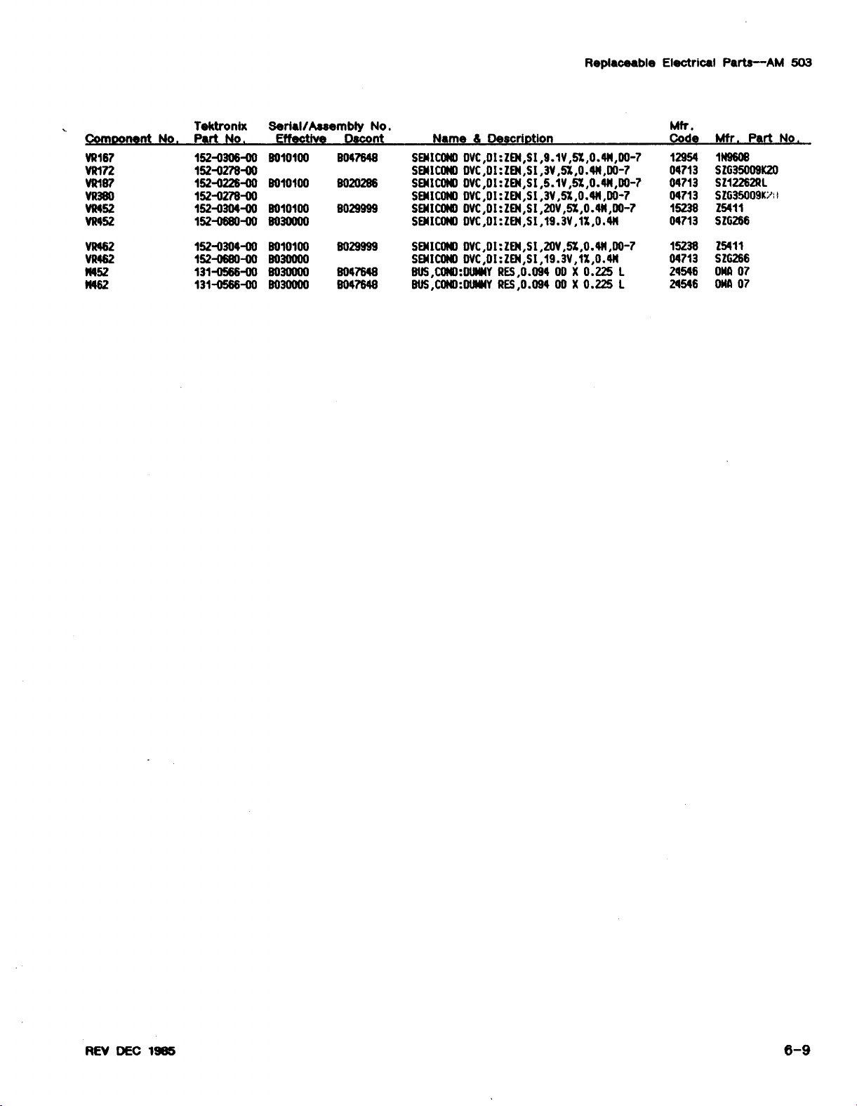
Replaceable
Electrical
Parts-AM
503
Component
VR167
VR172
VR187
VR38D
VR452
VR452
VR462
VR462
N452
N462
Tektronix
No
.
Part
No,-
152-0306-00
152-0278-00
152-0226-00
152-0278-00
152-0304-00
152-0680-00
152-0304-00
152-0680-00
131-0566-00
131-0566-00 8030000 6047648 BUS,COND:DUIWY RES,0
Serial/Assembly
-Effective_
9010100 9047648 SENICOND
8010100 B0202B6 SOIICOND DVC,DI:ZEN,SI,5
11010100
9030000 SDIICOND DVC,DI:ZEN,SI,19
8010100 9029999 SENICOND DVC,DI:ZEN,SI,20V,5X,0.4N,DO-7
8030000 SBIICOND DVC,0I:ZEN,SI,19
90300
No
.
Qtont
9029999 SOIICOND DVC,DI:ZEN,SI,20V,5%,0
8047648 BUS,COND:DIWNY RES,0
.
-
Name
SOIICOND DVC,DI:ZEN,SI,3V,5X,0
SBIICWID DVC,DI:ZEN,SI,3V,5%,0.4N,DO-7
a
Description
DVC,DI:ZEN,SI,9
.094
.094
.1V,5X,0 .4H,DO-7
.4H,DO-7
.1V,5%,0 .4N,D0-7
.4N,D0-7 15238
.3V,1X,0
.3V,1X,0
OD X 0
OD X 0.225 L
.225
.4N
.4N
L
Mfr
.
Code
12954
04713
04713
04713
04713 SZ6266
15238
04713
24546
24546 ONA
Mfr.PartNo.
1N9608
SZ63500SK20
SZ12262RL
SZ635009VO
Z5411
Z5411
SZG266
ONA
07
07
Page 54

Section
7-AM503
DIAGRAMS
Symbols
Electrical
Graphic symbols
Logic
function
The
Abbreviations
Other
The
A
AT
B
BT
C
CB
CR
DL
DS
E
F
FL
The
and
componentsshown
symbology
performed
overlineona
ANSI
standards
Y14
.15,1966
Y14
.2,
1973
.5,1968
Y10
following
Assembly,
(circuit
board,
Attenuator,
Motor
Battery
Capacitor,
Circuit
breaker L
Diode,
signalorrectifier
Delay
line
Indicating
Spark
Gap,
Fuse
Filter
following
Cam
Switch
Closure
(Dot
indicates
switch
Reference
and
is
basedonANSI
and
signal
are
based
Drafting
Line
Letter
Electrical
prefix
letters
separable or
etc)
fixedorvariable
fixedorvariable
device
(lamp)
Ferrite
bead
special
symbols
Chart
closure)
Designators
class
may
name
on
that
are
Conventions
Symbols
repairable
AND
on
the
Capacitors
Resistors
designation
Y32
differ
from
indicates
ANSI
Y1
usedinthe
Practices
Engineering
are
used
may
appearonthe
diagrams
letters
CIRCUIT
areinthe
=
Values
Values
Ohms
=
are
based
following
(SZ)
BOARD
oneorgreater
less
than
.
on ANSI
.14-1973intermsofpositive
the
that
.1-1972
manufacturer's
the
signal
.
data
performs
.
its
preparationofdiagramsbyTektronix,
.
and
for
Quantities
Lettering
.
UsedinElectrical
.
reference
as
designators to
H
Heat
dissipating
heat
HR
HY
J
K
M
P
O
R
FIT
radiator,
Heater
Hybrid
circuit
Connector,
Relay
Inductor,
Meter
Connector,
Transistororsilicon-controlled
rectifier
Resistor,
Thermistor
diagrams
stationary
fixedorvariable
movable
fixedorvariable
:
identify
device
etc)
portion
units unless
noted
areinpicofarads (pF)
one
areinmicrofarads
Standard
Y32
logic.Logic
intended
Science
function
and
components
(heat
sink,
portion
IS
Ill
-
ILLUSTRATIONS
otherwise
.2-1975
symbols
Inc
.
are
or
o~
50
gAL
:
.
(pF)
.
.
depict the
whenitgoes
logic
to the
:
on
assemblies
S Switch or contactor
T
TC
TP
u
V
VR
W
Y
Z
the
Transformer
Thermocouple
Test
point
Assembly,
(integrated
Electron
Voltage
Wirestrap or cable
Crystal
Phase
inseparable or non-repairable
circuit,
tube
regulator
shifter
PlugtoE.C.Board
B
xIdentifies
Controls,
Indit
caors
Modified
~
k
(Depicted
With Grey
See
Parts
Plug Index
low
state
diagrams
etc
.)
(zener
Connectors
Component
Grey,
in
Outline)-
List
.
diode,
Panel
or
.
etc
and
.)
VERTICAL
REV
FEB
1982
AMPLIFIER
RefertoWaveform
RefertoDiagram
Coaxial
Connector
Number
Shielding
Heat
Sink
DecoupledorFiltered
Voltage
Etched
Circuit
Board
OutlinedinBlack
Schematic
and
Name
Number
Page 55

CURlaENT
PROBE
INPUT
CONNECTOR
PROBE
UNLOCKED
DS190
(XIO)
DS
(XI)
192
I
S200A
CURRENT/DIV
INPUT
ATTEN
8206
R210
R214
R208
R212
I
INPUT
IcoUPLING
SWITCH
52008
ATTENUATOR
~
ATTEN
SOURCE
FOLLOWER
Q230A
Q23DB
AM503
BALANCE
HALL
DEVICE
PREAMP
UI10
I
H
ALL
DISCONNECT
Q115
I
SIP-5
DEGAUSS
I
1
l
710-
I
1
-16
V
DEGAUSS
OSCIL-
LATOR
Q
1,30
U135
POWER
AMPL
UI45
0155
0165
DC
2052-32
REV.B
OVERLOAD
CR16B
AMPLIFIER
OCT.1979
,
INPUT
Page 56

5370
BANDWIDTH
-16V
FULL
5
MHZ
S200A
CURRENT/DIV
J390
OUTPUT
INTOSO.n
.
INPUT
,,
FROM
POWER
MODULE
OUTPUT
AMPLIFIER
919
BLOCK
DIAGRAM
POWER
SUPPLY
Page 57

t
Located
*See
serial
Parts
number
on
backofboard
List
for
ranges
Fig.7-1.A1-Amplifier
.
circuit
board
with
component
loca
Page 58

j
board
with
component
locations
components
of
(SN
B030830&above)
.
REVCOCT
1979
Page 59

C100
C108
C710
C712
C124
C125
C133
C137
C138
C140
C146
C148
C153
C155
C156
C160
C165
C168
C172
C176
C218
C220
C232
C234
C242
C244
C306
C308
C328
C345
C351
C360
C363
C364
C365
C366
C367
C380
C383
C385
C388
C391
C393
C394
C396
C398
C402
C406
C413
C414
C423
C434
C436
C444
C446
C452
C462
CR115
CR116
CR127
5D
5E
4E
5E
5E
4G
4A
5A
5B
4B
4F
5F
4G
5H
5H
4H
41
4H
4D
5C
t
3A
3B
2A
2A
2A
2B
28
2C
2C
2C
2D
3E
3D
2D
2D
2D
1D
2D
2E
2E
3E
2F
1D
2F
1F
2E
31
21
2G
2G
2G
3G
3G
1G
1G
4H
3H
5F
5F
5A
CR133
CR167
CR175
CR226
CR320
CR380
CR383
CR386
CR402
CR406
P110
P120
P160
P168
P190 4C
P195
P202 3G
P302
P346
P370
P380t3F
P470
P475
P480
t5J
0115
Q130
Q155
Q165
Q180
0185
0230
Q310
Q315
Q325
Q360 3E
Q385
0390
Q395
Q440
0450
Q460
Q470
R100
R102
R103
R
104
R105
R
106
R108
R110
4D
5D
5G
5D
5D
5D
5E
4E
2E
2H
3G
3G
1H
41
5C
5C
3B
2B
2C
2C
2E
1E
4J
5J
5F
4A
51
4H
5G
5C
18
1C
1E
5D
5F
5G
5D
2A
2B
2E
2E
2F
3J
1J
5B
R112
R113
"
R136
R181
R183
R189
R202
R220
R222
R224
R232
R234
R236
R242
R244
R246
R300
R304
R306
R308
R311 2B
R312
R313
3B
2B
2B
2B
2C
5E
5E
5E
E
4E
4G
5E
4G
5F
5A
4A
4A
5G
4B
4A
4A
4B R345
5A
5B
5B
5B
4B
5F
4F R354
5F
5F
5G
5G
4F
5H
5H
5H
5H
4H
4H
4H
5G
5E
5C
5C
4C
5C
5C
4C
3G
3A
3A
3A
1A
2A
2B
1A
2A
1B R394 2F
1B
R314
R315
R317
R321
R323
R326
R327
R328
R330
R332
R334
R335
R336
R338
R340
R344
R346
R347
R349
R351
R352
R353
R355
R356
R357
R358
R360
R361
R362
R363
R364
R365
R366
R367
R368
R370
R372
R373
R374
R376
R377
R380
R382
R383
R384 2E
R386
R387
R388
R390
R391 2F
R392
R393
R395
R396
R397
R398
R399
R403
2D
2F
1F
2F
2F
3F
2H
2B
A
1R114
B
2R116
C
2R118
C
2R121
C
1R122
C
1R123
C
1R124
C
1R126
C
2R127
C
C
2R128
C
3R129
3R130
C
C
3R132
3R133
C
2R134
C
2R135
C
1
C
1R137
C
1R138
C
D
1R140
D
2R145
D
1R146
2R148
D
D
1R150
2R151
D
2R152
C
2R153
E
E
3R156
F
3R158
2R159
D
D
3R160
D
2R162
D
2R166
D
2R168
E
1R169
E
1R172
1R175
D
1R176
1E
D
1R182
2E
2E
1E
1E
2E
2F
2F
3E
1F
1F
R404
R405
R406
R407
R412
R414
R415
R416
R422
R432
R436
R442
R446
R452
R454
R458
R462
R464
R480
RT135
RT156
RT160
RT342
VR100
VR103
VR166
VR167*
VR172
VR380
VR452
VR462
5D
5G
5G
5G
4D
2F
3H
3H
Page 60

CONDITIONS
DC
VOLTAGES
USED
ON
TOMEASURE
SCHEMATICS
Probe not connectedtoinput
Bandwidth
AC-CAL
Set
settofull
DC
Level-DC
voltageatoutput
.
settoCAL
to zero
.
volts
DC
(into
LEVEL
50
.
ohms)
withDCLevel control
.
Page 61

IM
BALANCE
P020
SOK
P110
CW
HALL
DISCONNECT
CRI15
FEEDBACK
FROM
P202
DIAL
~ti
R
I,
-AC
SIGNAL
FROM
P160
THIS
DIAG
SIGNAL
P202
DIAG
GAIN
SELECT
TO
R346V03
DIAG
_8
AE
\
IVb^b' -
.01
R100
240
GI00
.01
CRI16
+I6V
R124
2
.2M
C124
.47','
0
-I6V
WREMOVEDITH
CIRCUIT
P
.122
IK
LACKED
5125
DEGAUSS
i
I
1
j
1
1
1
j
PRO86
FRO
AND
0-
-I6V
CR127
-
-v6-
1
DEFLECTION
SENSITIVITY
LAMP
M
I6V
R12-7
470K
-I6V
DRIVERS
+~G1
4
26
.7fa
R1M8
DEGAUSS
R132
R133
IOOK
QI30
I
F
~~
R
134
TOOK
G133
1,"F
R130'
CI3Tl
0.1T
OSC
.
CR133
DEGAUS'
AMPLITUI
30
RI3
RI
101
:
UI10
2625
c108
J100
INPUT
P16
CR~1
F
"~
G
IOS
+3VI
I
\T/3V
+3V
R3
K
+I6V
AM503
CIOI
.01
PARTIAL
CR175
AI
C172
.01
R172
240
P176
P-70K
-I6V
AMPLIFIER
-I6V
~G
176
.OI
BOARD
RI81
270
-I6V
Piss
270
R
18P
6
.8K
R183
15K
-I6V
-I6V
RE
Page 62

1I
I
-
PowER
AMPLIFIER,
DC
FEEDBACK
R132
IM
FROM
R202
DIAL
DEGAUSS
OSC
CR133
R121
1
.18K
8123
787
17
1
30
499
R146
10
.01
U145
R152
SOKFTI
+19.3V
2
DEGAUSS
OFFSET
O
2625
.
24
R148
10
-19_3V
S
82
C14S
01
24K
6
C10160
4
C156_
.OI
RI62
RI51
.99K
+16V
_
lf
10.7I;K
-16V
j
8159
107
ORlsa
R156
750
P
T156
R160
750
RT
100
CRISS
160
+16V
-16V
I
CI55
47~rF
+
Q155
~RISB
3
R
3
Q165
CC
i65
47,uF
.0
I66
.0
L168
3
.9,u
Vsv
H
1500
R168
49
.9
6
PI60
PI68
SI
NJ
JT100
THIS
K
DIAG
INPUT
OVERLOAD
NAL
O
R134
100K
$T
3
5
RT1
RI38
301K
C0.1TRIOK
PRL3EIE
SELECT"
+
-16V
7
4
CI38
.0033
7135
I
640
10/aF
135190
(lox)
OS192
IX)
R140
820
'42
40
J
LY
R169
62
1
CRI67
n
2052-33
REV
MAR
1984
DG
AMPLIFIER
Page 63

AM
503
*See
serial
t
Located
CKT
NO
C100
C108 5E
C110
C112 5E
C124
C125
C133
C137
C138
C140
C146
C148 5F
C153*
C155
C156
Parts
List
ranges
on back
for
of
CKT
NO
C160
C165
C168
C172
C176
C187*4D
C218*t
C220
C232
C234
C242
C244
C306
C308
number
GRID
LOC
5D
4E
5E
4G
4A
5A
5B
4B
4F
4G
5H
5H C313*
.
board
GRID
LOC
4H
41
4H
4D
5C
3A
3B
2A
2A
2A
2B
2B C385 2E
2C
2C
CKT
NO
C323*
C328
C345
C351
C360 3E
C363
C364*
C365*
C366
C367
C380
C383 2E
C388
C391 2F
2C
2C
2C
*
*
GRID
LOC
2D
3D
2D
2D
2D
1D
2D
3E
CKT
NO
C393
C394 2F
C396
C398 2E
C402
C406
C413
C414
C423
C434
C436
C444
C446
CR115
CR116
GRID
LOC
1D
1F
31
21
2G
2G
2G
3G
3G
1G
1G
5F
5F
CKT
NO
CR127
CR133
CR167
CR175
CR226
CR320
CR380
CR383
CR386
CR402
CR406
F402*t3.1
F406
GRID
LOC
5A
5B
5G
5D
2A
2B
2E
2E
2F
3J
1J
1J
*t
Fig.7-2.A1-Amplifier
CKT
NO
J110
J120
J160
J168
J190
J195
J202
J346
J380
J470
J475
J480
L168
L202
GRID
LOC
5D
5F
4H
5G
4C P370
5C
3G
1C
3F
4J
5J
5J
4H
3G
CKT
NO
L380 2E
L383 2E
P302
P380
t
Q115
Q130
Q155
Q165
Q180
Q185
Q230
Q310* 2C
Q315
circuit
GRID
C
Lo-
1B
1E
3F
5F
4A
51
41
5C
5C
38
2C
board
witl
Page 64

mplifier
circuit
board
with
component
locationsofcomponents
(SN
B030829&below)
.
CKT
NO
0320*
0325
Q360
0385
Q390
Q395
0440* 2H
0450
0460
0470* 1H
R100
R102
R103
R104
R105
GRID
LOC
2C
2C
3E
2E
1E
2E
3G
3G
4D
5D
5G
5D
5D
CKT
NO
R106
R108
R110
R112
R113
R114
R116
R118
R121 4G
R122
R123
R124
R126
R127
R128
GRID
LOC
5D
5E
4E
5E
5E
5E
5E
4E
5E
4G
5F
5A
4A
4A
CKT
NO
R129
R130
*
R132
R133
R134
R136
R137
R138
R140
R142*
R145*
R146
R148
R150*
R151 5G
GRID
LOC
5G
4B
4A
4A
48
513
5B
5B
4B
4B
5F
4F
5F
5F
CKT
NO
R152
R153*
R156
R158
R159
R160
R162
R166
R168
R169
R172
R174
R175
GRID
LOC
5G
4F R181 4C
5H
5H
5H
5H
4H
4H
4H
5G
5E
*
5D
5C
OCT
@
1979
CKT
NO
R176
R182
R183
R185*
R187
*
R189
R202
R220* 3A
R222
R224
R232
R234
R236
R242 1A
GRID
LOC
5C
5C
5C
4C
5C
4C R311
3G
3A
3A
1A
2A
2B
CKT
NO
R244
R246
R300
R304
R306*
R308
R312 2B R338 3C
R313*
R314
R315
R317*
R321
R323*
R326*
GRID
2A
3B
18
1B
2B
2B R335 3C
*
2B R336 3C
2C R340 3C
2B R344 2C
1A R345 2C
2B
2C
2C
1C
CKT
R327
R328
R330*
R332*
R334*
R346
R347
R349
R351
GRID
1C
1C
1C
2C
2C
1C
1C
1C
1C
Page 65

CKT
N@
R352
R353
R354
R355
R356
R357
R358
R360
R361 3E
R362
R3630
R364
R365
R366
R367
GRID
LOC
2D
1D
2D
1D
2D
2D
2C
3E
2F
3D
2D
2D
2D
10
CKT
NO
R368
R370
R372
R373
R374
R376
R377
R380
R382
R383
R384
R386
R387
R388
R390
GRID
LOC
tE
1E
10
1E
1D
2E
2E
1E
1E
2E
2E
2F
2F
3E
1F
CKT
NO
R391
"
R392
R393
R394
R395
R396
R397
R398 2F
R399
R403
R404
R405
R406
R407
R412
o
GRID
LOC
2F
1F
2D
2F
2F
1F
2F
3F
2H
2G
2G
10
1H
3H
CKT
NO
R414
R415
R416
R422
R432
R436
R442
R446
R452
R454*
R462
R464
R480
RT156
GRID
LOC
2G
2G
1G
1H
"
2G
3G
1G
1G
3H
3H
2H
"
2H
5J
SH
CKT
NO
RT160
RT342
RT135
S125
S200A
U110
U135
U145
U350*
U370
U410
VR100
GRID
LOC
4H
3C
48
5A
4C
SE
4B
5F
2C
"
20
2G
5D
CKT
NO
VR103
VR168
VR167
VR172
VR187"4C
VR380
VR452"3H
VR462"3H
GRID
LOC
5G
50
50
40
2F
Page 66

IIIIIII
IIIIIII
IIIIII1
II1I1II
III
I
~iIIII
I1IIIII
IIII1II
IIIIII
IIIIIII
1IIIII1
1IIIIII
IIIIIII
IIiIIII
1IIiiII
III1I
IIIIIII
IIIIIII
II1IIII
IIIIIII
IIIIII
IIIIv
IIIIII
1I1III
IIIIII
IIIII1
IIIIII
I1III1
1
2X
SP-00A
WITH
CURRENT/DIV
OSCILLOSCOPE
AT
IOmV/DIV
I
+AC
SIGNAL
FROM
,1100
DIAG
P202
®
52,u
R202
25
13013
13
~~UjUNNE§
0
13013
13
0
13
0
3
0,0
-
~
0
=13013
M=Mj13=13j13=13jM13
I'l
IA IA
V
I
l
o-X010-I
0-N,0
-
10
I .
v
I
R212
lox
---01
6
5
I
1
1
1
I
1
I
I
I
I
I
I
I
1
I
I
I
I
I
1
IA
IA
1
'
1
I
I
I
I
I
1
!
0~-O
R214
I
B
I
13
m
2X
13§
19
IA
1-OIOHO
0-m,m
IS
IA
P210
I
X
105
F--0
13M
m-0,a
28
I
I
I
I
I
I
I
I
I
t
1
1
I
I
I
L-O
I
I
IA
I
I
1
I
I
I
I
I
I
P206
BB
i
8204
H
SOJL
TERM
.5
24
I
I
I
IA
1
1
O~--OIO-1
23
IA
1
P208
AM
503
DC
FEEDBACK
TO
go.R121
DIAG
2052-54
REV.C,
OCT.1979
Page 67

NOTES'
1
.
DOTS
INDICATES
'A'
CONTACTS
AND
CW
1
0
2.'4'
3.SWITCH
'B'
CONTACTS
CAM
POSITION
SIDEOFTHE
CONTACTS
SHOWN
.
ARE
CLOSED
OPEN
AREON THE
BOARD
IN
ImA
.
.
0113§MI3
* 13 [3
0
13
GW
INPUT
COUPLING
S200B
ATTEN
SOURCE
FOLLOWE
GAL
DC
LEVEL
R
ATTENUATOR
-IO.T
QQ
Page 68

IOOkX10k
-I6V2
ATTENUATED
AC
SIGNAL
FROM
DIAS
-~Nrt
(12308
R814
680
ca
.eto
GAIN
SELECT
FROM
JI00
DIAS
O
6
6W
94i
R341
Ik
1
R826
8
-16V2-MM-4
+16V2
AL34j'
Mh
"
14
AM503
S/N
AND
8030830
UP
~E
~It
SMHz
P346
BANDWIDTH
PINBGROUNDED
SELECTABLE
GAIN
AMPLIFIER
4
0351
`
.01
8351
IOk
-16V
-
I
2052-35
REVMky
-75
R352
1993
11342
130
-16y,
OL
Page 69

p3lo
spo
BANDWIDTH
(FULL)
IS
mvS
IA
LS74
666
G~w
GED
I
M42)
WITH
A
5200A
CURRENT
OSCILLOSCOPE
AT
10
I
10
j
o,
I
0
.2
0
.4
2
6
DIV
"V/DIV
"WITCH
Stow"
IN
SEE
VALUES
RANGES
OR
PARTS
DEPICTED
LQ
fI
ANDS-Il
OF
SARI
ING,
SEE
DIAL
"
W
so
k
**
ASS2
+16vi
660
M
8392
i
.ll&
8397
ISO
Wo
tp
707
On
OUTPUT
INTO
M]
P380 J390
0395
Page 70

VOLTAGE&WAVEFORM
CONDITIONS
47-11
P403
100
P407
100
C--6-7',S)
INPUT
VOLTS
INPUT
OUTPUT
SENSE
ADJ BAL
U410
3501
SENSE
OUTPUT
STAB
STAB
R412
0
.51-r
6
C414
I,"
F
CW
ov
10
P422
0
.51 J,-
7~
B
LOCATED
MAINFRAME
ON
Page 71

I4
9K
6
9K
BALANCE
O
.Stn
R432
2
R436
R446
10
t
-IGV
REGULATOR
~
10
+16V
0-
+16V
.7
10
C434
~;.01
6436
.01
,1C446
.01
"
-I
i
+16V2
"
-16V2
R442
P422
0
.51.n.
ON
ME
4
.7/,F
-LC444
2
.7
.01
-16V
1
-16V
.J
I,VR46c
2"ISmA
-iy .Bv
REGULATOR
-19
ON-
.3V
Q460
NOTE
;
OPTIONNOT
AT
THIS
DATE
ASSIGNED
.
Page 72

MECHANICAL
PARTS
Replacement
Tektronix, Inc.Field Officeorrepresentative
ChangestoTektronix
accommodate
andtogive
developed
important,
informationinyour
number,
Ifapart
improved
representative
number
.
Change
manual
.
SPECIAL
X000
00X
ORDERING
parts are
improved
you
in
our
when
serial
number,and
you
part,
will
information,ifany,islocatedatthe
the
benefit
engineering
ordering
order:Part
have
your
contact
components
ordered
local
NOTES
Part
first
Part
removed
INFORMATION
available
instruments
modification
you
added
fromor
are
as
they
of the
latest
department
parts,toinclude
number,
numberifapplicable
has
been
replaced
Tektronix,
concerning
AND
SYMBOLS
at this serial
after
this serial
REPLACEABLE
through
your
local
.
sometimes
become
circuit
.
instrument
Inc.Field Office or
any
made
available,
improvements
Itistherefore
the
following
type
with a
new
changeinpart
rearofthis
number
number
Section
8-AM
503
PARTS
INDENTATION
This
mechanical
relationships.Followingisan
usedinthe
to
or
.
or
the
Indented
indentation.The
attaching
Attaching
specified
description
123 4 5
Assembly
Attaching
Detail
PartofAssembly
Attaching
Parts of
Attaching
Attaching
itemitmounts,
items
parts
parts
.
.
parts
column
and/or
Component
parts
for
Assembly
parts
for
Detail
Detail
Part
parts
for
Parts
alwaysappearinthe
while
the
detail
are
part
of,
separation
mustbe
symbol
purchased
list is
example
.
Parts of
and
SYSTEM
indentedtoindicate
the indentation
of
Name
&
and/or
Component
Component
and/or
Part
Detail
Part
same
parts are
included
indented
with,
---'
---
separately,
indicates
Description
indentation
the
to
the
next
the
unless
otherwise
item
system
right
higher
end
as
.
of
FIGURE
Items
numberstothe
"
#
ACTR
ADPTR
ALIGN
AL
ASSEM
ASSY
ATTEN
AWG
BD
BRKT
BRS
BRZ
BSHG
CAB
CAP
CER
CHAS
CKT
COMP
CONN
COV
CPLG
CRT
DEG
OWR
INCH
NUMBER
ACTUATOR
ADAPTER
ALIGNMENT
ALUMINUM
ASSEMBLED
ASSEMBLY
ATTENUATOR
AMERICAN
BOARD
BRACKET
BRASS
BRONZE
BUSHING
CABINET
CAPACITOR
CERAMIC
CHASSIS
CIRCUIT
COMPOSITION
CONNECTOR
COVER
COUPLING
CATHODE
DEGREE
DRAWER
in this
illustrations
SIZE
AND
section
WIRE
RAY
TUBE
GAGE
INDEX
are
referenced
.
ELCTRN
ELEC
ELCTLT
ELEM
EPL
EQPT
EXT
FIL
FLEX FLEXIBLE
FLH
FLTR
FR
FSTNR
FT
FXD
GSKT GASKET
HDL
HEX
HEX
HEX
HLCPS
HLEXT
HV
IC
ID
(DENT
IMPLR
NUMBERS
by
ELECTRON
ELECTRICAL
ELECTROLYTIC
ELEMENT
ELECTRICAL
EQUIPMENT
EXTERNAL
FILLISTER
FLAT
FILTER
FRAMEorFRONT
FASTENER
FOOT
FIXED
HANDLE
HEXAGON
HD
HEXAGONAL
HEXAGONAL
SOC
HELICAL
HELICAL
HIGH
INTEGRATED
INSIDE
IDENTIFICATION
IMPELLER
figure
and
index
ABBREVIATIONS
PARTS
HEAD
HEAD
HEAD
SOCKET
COMPRESSION
EXTENSION
VOLTAGE
CIRCUIT
DIAMETER
LIST
In
the
Parts
descriptionbya
Name
may
sometimes
Name
identification,
canbeutilized
IN
INCAND
INSUL
INTL
LPHLDR
MACH
MECH
MTG
NIP NIPPLE
NON
WIRE
OBD
OD
OVH
PH
BRZ
PL
PLSTC
PN PART
PNH
PWR
RCPT RECEPTACLE
RES
RGD
RLF
RTNR
SCH
SCOPE
SCR
where
INCH
INCANDESCENT
INSULATOR
INTERNAL
LAMPHOLDER
MACHINE SKT
MECHANICAL
MOUNTING
NOT
WIRE
ORDER
BY
OUTSIDE
HEAD
OVAL
PHOSPHOR
PLAIN
or
PLASTIC
NUMBER
PAN
HEAD
POWER
RESISTOR
RIGID
RELIEF
RETAINER
SOCKET
OSCILLOSCOPE
SCREW
ITEM
NAME
List,anItem
colon(:).Becauseofspace
appearasincomplete
theU.S.Federal
possible
WOUND
DESCRIPTION
DIAMETER
BRONZE
PLATE
HEAD
Name
Cataloging
.
SE
SECT
SEMICOND
SHLD
SHLDR
SL SLIDE
SLFLKG
SLVG
SPR
so
SST
STL
SW
T
TERM
THD
THK
TNSN
TPG
TRH
V
VAR
W/
WSHR
XFMR
XSTR
is
separated
limitations,anItem
For
further
.
Handbook
SINGLE
SECTION
SEMICONDUCTOR
SHIELD
SHOULDERED
SOCKET
SELF-LOCKING
SLEEVING
SPRING
SQUARE
STAINLESS
STEEL
SWITCH
TUBE
TERMINAL
THREAD
THICK
TENSION
TAPPING
TRUSS
HEAD
VOLTAGE
VARIABLE
WITH
WASHER
TRANSFORMER
TRANSISTOR
END
from
the
Item
H6-1
STEEL
Page 73

Replaceable
Mfr
.
C
ode
01x''36
02660
06383
09922
12327
18203
22526
24546
272
:38
45722
61957
70278
73743
77900 SHAKEPROOF
78189
79136
79807
80009
83385
83486
854130
86928 SEASTROM
93907
TKD435
TKO507
Mechanical
Manufacturer
TEXTRON
CANCAR
SEWS PRODUCTSUNIT
BUNKER
AMPHEMOLNORTH
PANOUII
BURIAYCORP
FREEWAY
ENGELMAW
PONTEI
OU
PONT
OU
CORNING
BRISTOL
USM
LISM
SUB
ALLIED
SPARTON
FISCHER
DIVOFILLINOIS
ILLINOISTOOL
SHAKEPROOF
NALOES
WROUGHT
TEKTRONIX
MICROOOT
GREEK-CENTRAL
ELCO INDUSTRIES
BRADYNH
TEXTRON
CAMCAR
LENIS
0
HARA
CROSS
INC
DIV
RANG
CORP
CORP
CORP
MICROWAVE
OE-NEMOURS
CONNECTOR
WORKS
GLASS
INDUSTRIES
.,
PARKER-KALANFASTENER
CORP
CORP
EMHART
STEEL
AND
CORP
.
SPECIAL
DIVISION
KOHIMOOR
WASHER
INC
MANUFACTURING
CO
MFG
CO
INC
DIV
CO
METAL
PRODUCTSCO
INDUSTRIES
WORKS
DIV
OF
SCREH
Parts--AM
AMERICA
SYSTEMS
.
CONVEYORS,
MFG
TOOL
INC
MFG.CO
INC
INC
INDEX
DIY
CO
AND
CO
WORKS
INC
.
INC
INC
503
INC
CO
DIV.OF
MFR.CODE
-
Address
1818
2801S25TH
17301
RICHARDS
9301
SKYLINE
30 HUNTER LANE
550
630ELAMBERT
P0
DIV
140
17333HEALY
446
SAINT
CHARLES
ST
47-16
2100S.0SAYST.
4900
P080X500
3221N816
1101
727NGLENDALE
701
600
4114SPEORIA
542
CHRISTINA
RIOGELANO
ALLEN
DRIVE
HIGHST
BOX
630
FEDERAL
MORGAN
CHARLES
AUSTEL
SN
SAMUELSON
SONORA
18TH
BRAWN
AVE
AVE
OR
ST
ST
ROAD
GRIFFITH
BEAVER
AVE
AVE
ST
NUMBER
ST
RD
RD
PLACE
OR
RD
RD
AVE
TO
MANUFACTURER
City
ROCKFORDIL
BROAOVIETi
TINLEIf
NORNALK
CLEVELAND
MONTVILLE
CAMP
BRADFORD
BREA
CAMPBELLSVILLE,
BOSTON
DETROIT,
CINCINNATI
ELGINIL60120
ELGIN
LONG
MILWAUKEE,
BEAVERTON
TROYMI48098
ROCKFORD
MILWAUKEE
GLENDALE
ROCKFORDIL
CHICAGO
SAN
St
ate.Zip
.
61108
60153
IL
PARK
IL
CT
06852
44125
ON
NJ
HILLPA17011
CA
FRANCISCO
07045
PA
16701
92621
NA
02107
MI
48212
OH
IL
60120
ISLANDCITY NY
NI
OR
97077
IL
61101
MI
53209
CA
91201
61101
IL
60609
60477
KY
45206
53207
CA
Code
42718
11101
94107
Page 74

Fig.8
Index
No
1-1
Tektronix
Part No
.
337-1399-04
-2 366-1286-04
-2
.1
366-1690-00
-3 214-1840-008010100 8036697
-4 179-2415-00
-5 211-0012-00
-6 210-0586-00
-7 210-0261-00
-8 131-1855-00
-9 352-0171-00
-10 352-0161-00
-11 352-0164-00
-12 131-0707-00
-13
210-0774-00
-14
210-0775-00 2 .EYELET,METALLIC
-15 366-1669-00
213-0153-00
-16
----
-17
-18
-19
-20
-21
-22 ----------
-23
-24
-25 210-0046-00
-26 358-0029-05
-27 220-0495-00
-28 210-0978-00
-29 210-0012-00
-30 333-2131-00
-31
-32 211-0030-00 2
-33 220-0627-00 2
-34 210-0001-00 2
-35
-36
-37
-38
-39
-40
-41
-42
-43
-43
.1
-43
.2
-44
-45
-46
-----
366-0215-05
366-0494-05
213-0153-00
366-1559-00
358-0301-02
426-1072-00
210-0583-00
210-0940-00
----------
----
-----
358-0409-00
210-0223-00
210-0471-00
210-0046-00
----
----
337-1430-00
378-0703-00
214-1513-01
105-0719-00
105-0718-01
213-0254-00
386-3501-00
213-0229-00
Serial/Assembly
.
Effective
8010100
8036698
8010100 8036697
8036698
8036698
8010100 8036697
No
Dscont
8036697
.
Qty212345
SHIELD,ELEC
1
KNO8:LATCH
1
KNOB,LATCH
(ATTACHING
1
PIN,KNOBSECRG:0.12L
(END
1
MIRINGHARNESS
(ATTACHING
4
SCREN,MACHINE
4
NUT,PL,ASSEM
1
TERMINAL,LUG
(END
HARNESSASSEMBLY
.CONN,RCPT,ELEC
1
1
HLOR,TERMCONN:1MIRE,BLACK
1
HLOR,TERNCONN:3NIRE,BLACK
1
HLOR,TERMCONN:6MIRE,BLACK
.CONTACT,ELEC
10
2 .EYELET,METALLIC
1
KNOB
2
.SETSCREK
1
CONNECTOR,RCPT
1
KNOB:GY,FORLEVER,0
1
KNOB
1
.SETSCREN
1
PUSH
1
BUSHING,SLEEVE
1
FRAME,PUSHBTN
1
RESISTOR,VAR
(ATTACHING
2
NUT,PLAIN,HEX
1
HASHER,FLAT
1
NASHER,LOCK
(ENO
1
9SHG,MACH
(ATTACHING
1
NUT,PLAIN,HEX
1
MASHER,FLAT
1
HASHER,LOCK
(END
1
PANEL,FRONT
1
SMITCH,SLIDE
(ATTACHING
SCREN,MACHINE
NUT,PLAIN,HEX
NASHER,LOCK
(END
1
RESISTOR,VAR:(SEER120
(ATTACHING
1
8SHG,MACH
1
TERNINAL,LUG
1
NUT,SLEEVE
1
MASHER,LOCK
(END
2 LAMP,LED:(SEECR168,CR103
2 SHIELD,ELEC
2 LENS,LIGHT
1
LCH,PL-IN
1
LATCH,RETAINING
1
BAR,LATCHRLSE
(ATTACHING
1
SCR,TPG,TF
(END
1
SUBPANEL,FRONT
(ATTACHING
4
SCREM,TPG,TF
Name
ATTACHING
ATTACHING
:GY,CUR/OIV,0
:5-40
:6Y,0
.12710X 0.500X0
:5-40
BUTTOW
ATTACHING
ATTACHING
ATTACHING
ATTACHING
ATTACHING
&
Description
:SIOE
:SIL
GY,0
PARTS)
PARTS)
PARTS)
:0
:0
TH0:0.375-32
PARTS)
:0
:0
:
PARTS)
:Ik2
PARTS)
THD:0.25-32
:0
:0.261
:
:HOLAER,CLEAR
RTNG
PARTS)
:2-32
PARTS)
.53
X 0
PARTS)
:PR08E
SIGNAL
:4-40
X 0.375,PNH,STL,COPL
MA
:4-40
:0
.22-26
SILGY,0
:(SEE
:0
.25IDX 0
.261
:0
.375I0
.384
:(SEES370
:2-56X0.25,FLH,82
:2-56X0
:0
.25-32
:6-20X0
X 0
.14
10,PLAIN,BRASS
PARTS)
INCLUDES
:165
SERIES,12
ANG,BRS,CU
:OJ52
:0
.126
.189
.125,STL8K OXO,HEX
X 0
J100
:(SEE
.375
X 0.125,STL8K
.18SOX 0
:0
.1610X 0
:SILVER
R302
.25-32
10,INTL,0
PARTS)
.375-32
X 0.024THK,STL,0
10,INTL,0
PARTS)
INTL,0
PARTS)
.26
I0,LOCKING,BRZTINPL
X 0
ID,INTL,0
PARTS)
:PLASTIC
:PLUG-IN
:
X 0
.25,SPCL
PARTS)
:
Replaceable
Mechanical
Mfr
Code
80009
80009 366-1286-04
X 0
.23X1
.059
.94-0
.100,ACETAL
& BIAS
.25,STL
00
00
10 X0.7200X 0
H,M/RTNRSPR 80009
GRAYPLSTC 80009
REPL)
X 0
.375
X 0.5HEX,BRS,0
X 0.438,BRS,COPL
REPL)
.156
.013
REPL)
X 0
.594
.375,TYPE
CO PL
:
FEMALE
CONT
BEGLOPL
X 0
.218
X 0
REPL)
.205
.312,BRS
THK,STL
.159 10
REPL)
L,8RS
.205
L,BRS
.79
SKT
.531
H
OXO,HEX
.43
00
.018
.022THK,STL
HEX,BRSNP 73743
L X0
.018
TYPE,FLH,STL
SKT 27238ORDER
00X0
.125
PL 73743
CO
X 0
.02,STL
THK,STL
.438L
.500
OEG,STL
.247
L 80009 358-0409-00
0
HEX,AL
.312
THK,STL
B,FLH 93907
80009 366-1690-00
80009 214-1840-00
80009 179-2415-00
83385 ORDERBY
78189
80009 210-0261-00
02660
80009 352-0171-00
80009
80009 352-0164-00
22526
80009
80009
H 80009
27238ORDER
80009
80009
L
80009
79807ORDER
77900 1214-05-00-0541C
80009 358-0029-05
73743ORDER
12327ORDER
80009
83385
86928 5441-37
80009 210-0471-00
80009 337-1430-00
80009 378-0703-00
80009 214-1513-01
80009 105-0719-00
80009 105-0718-01
Parts--AM
.
.
Mfr
337-1399-04
211-041800-00
165-12
352-0161-00
47439-000
210-0774-00
210-0775-00
366-1669-00
366-0215-05
366-0494-05
366-1559-00
358-0301-02
426-1072-00
2X-20319-402
77900
1220-02-00-0541C
333-2131-00
ORDER
10002-56-101
1202-00-00-0541C
77900
1214-05-00-0541C
77900
45722ORDERBY
386-3501-00
80009
ORDERBYDESCR
PartNo.
OESCR
BY
OESCR
BY
OESCR
BY
OESCR
BY
OESCR
BY
OESCR
OESCR
BY
OESCR
503
REV
DEC
1985
8-
3
Page 75

Replaceable
Fig.8
Index
N
o
1-
-47 337-2292-00
-48 337-2369-00
-49
-50
-51 105--0243-00
-52
-53
-54
-55 213-0146-00 4
-56 -----
-57
-58
-59
-60
-61
-62 210-0406-00 3
-63 214-1139-03 2
-64 214-1752-00 2
-65 401-0180-00
-66 354-0390-00
-67
-68
-69
-70
-71
-72
-73
-74
-75
-76
-77
-78
-79
-80
-80.1200-2433-00 8047649
Mechanical
Tektronix
Part
No
337-2369-01
211-0101-00
210-0586-00
213-0214-00
343-0081-00
211-0207-00 2
672-0574-00 8010100 8047648
672-0574-01 8047649
672-0574-02
210-0801-01 8010100 8047648 3
210-0801-01 8047649 2
131-0963-00
-----
344-0248-00
263-1111-00
211-0116-00
200-1950-00
211-0244-00
131-0963-00
105-0716-00
384-0878-01
210-0406-00
401-0178-01
210-0406-00
407-1199-00
407-1199-03
105-0651-00
384-1424-01
384-1478-03
210-0406-00
214-1139-03 2
214-1752-00 2
401-0180-00
354-0390-00
----- -----
Parts--AM
Serial/Assembly
Effective
8010100 8061549
8061550
8049500
8010100 8050999
8051000
8010100 8053639
8053640
503
No
Dscont Qty
8049499
.
1
1
1
1
1
1
1
2
1
1
1
1
7
7
1
8 SCR,ASSEM
1
8
1
1
1
1
1
3
1
3
1
1
1
1
1
4
1
1
1
1
Mfr
.
Code
12345
(END
SHIELD,ELEC
SHIELO,ELEC
SHIELO,ELEC
(ATTACHING
SCREN,MACHINE
NUT,PL,ASSEM
(END
ACTUATOR,SHITCH
(ATTACHING
SCREN,CAP
(ENO
STRAP,RETAINING:0.125 OIA,NYLON
(ATTACHING
SCR,ASSEM
(ENO
CIRCUIT 80 ASSY:ATTENUATOR 80009
CIRCUIT 8O ASSY
CIRCUIT8OASSY:ATTENUATOR 80009
(ATTACHING
SCREII,TPG,TF
NASHER,FLAT
NASHER,FLAT:0.14IOX
(ENO
CKT
.CONTACT,ELEC
.ATTEN/TERM,FXO
.R212,R214
.CLIP,ATTENUATOR
SM CAN ACTRAS:CURRENT/CIV
.(ATTACHING
.(END
.ACTR
.
.COVER,CAM
.
.(ATTACHING
.
.SCR,ASSEM
.
.(ENO
.
.CONTACT,ELEC
.
.NUT,PLAIN,HEX
.
.SPRING,FLAT:0.885
.
.ROLLER,DETENT:0.125
.
.BEARING,CAM SM
.
.(ATTACHING
.
.RING,RETAINING
.
.(ENO
.
.ACTUATOR,CAM SN
.
.SHAFT,CAM SM
.
.CENTRIC
.
.NUT,PLAIN,HEX
.
.BEARING,CAN
.
.NUT,PLAIN,HE)I
.
.BRACKET,COVER
.
.BRACKET,COVER:PLASTIC,FINISHID
.
.ACTIkITOR,CAN
.
.SHAFT,CAM SM
.
.SHAFT,CAM SN
.
.ENTRIC
.
.NUT,PLAIN,HEX
.
.SPRING,FLAT:0.885
.
.ROLLER,OETENT:0.125 00 X 0
.
.BEARING,CAN
.
.(ATTACHING
.
.RING,RETAINING:BASIC EXT,U/O O.3750IA
.
.(ENO
CKT
.
.COVER,PROT:CONTACTS,PLASTIC 80009 200-2433-00
Name
ATTACHING
ATTACHING
ATTACHING
ATTACHING PARTS)
ATTACHING
BOARD
ATTACHING
ASSEMBLY
ATTACHING
ATTACHING
ATTACHING PARTS)
BOARD
PARTS)
:FRONT
:CONNECTOR
:CONNECTOR
PARTS)
:4-40X0
NA:4-40X0
PARTS)
:AC,OC
PARTS)
:2-56
X 0
PARTS)
PARTS)
NSHR
:4-40
:ATTETAIATOR
PARTS)
:6-20
.141OX 0
:0
PARTS)
ASSY INCLUDES
:6ROLNOING,PH
:(SEE
AM
216
PARTS)
NSHR
:4-40
PARTS)
INCLUDES
SW
PARTS)
NSHR
:GROUNDING,PH
:4-40
PARTS)
:1
N/DRIVER
:4-40X0
SNXENTER
:4-40X0
:ABS
SM:ATTENUATOR
:7 .4LX0.188
:14.0L
N/DRIVER
:4-40X0
SWR
PARTS)
ASSY
:MAIN
&
Description
PANEL
.25,FLH,100
.25,STL CO PL 78189
.375,SKT
X 0.312,TYPE
REPL)
:0
.866 L,CU
831ELEMENTS
:4-40
PARTS)
:FR8REAR,0
:BASIC
PARTS)
:AC-OC
.166LX 0
HO,STL
X 0.312,PNH,STL
.025
THK,STL NP 86928 ORDERBYDESCR
0
.025
THK,STL NP 86928 ORDER BY OESCR
:
BRZ,N/BRACKET
R204,R206,R208,R210,
BE
X 0
.312,PNH,BRS,POZ
:
X 0
.312,PNH
BRZ,M/BRACKET
X 0
.188,BRSCOPL
X 0
X 0
6 REAR,0.810
CU BE RED CLR 80009 214-1139-03
.156
00
X 0
.16,SST
.880
EXT,U/O 0
.248
.188,BRS
REAR,0
.188,BRS
019 80009
X 0
.188
.188,BRS
.156CUBE
.16,SST
PLUG-IN(SEEAlREPL)
OG,STL
CO PL
B,PNH,STL
STL
.83
CIA 80009 401-0180-00
.3750IA
00 OUTER CON 80009 384-0878-01
CO PL
I0,PLSTC 90009 401-0178-01
.378
PL
CC
OO,1NTMO CONC 80009 384-1478-03
CO PL
RED CLR 80009
.83
CIA 80009 401-0180-00
Mfr.PartNo.
80009
337-2292-00
80009
337-2369-00
80009
337-2369-01
83385
ORDER BY OESCR
211-041800-00
80009
105-0243-00
70278 ORDERBYOESC
CPHY-1728K
85480
83385
ORDER BY
672-0574-00
80009 672-0574-01
672-0574-02
83385 ORDERBYDESCR
TKO507 ORDER BY OESCR
80009
344-0248
80009
263-1111-00
77900
ORDER
80009
200-1950-00
01536
ORDER
TKO507
ORDER
73743 12161-50
80009
214-1752-00
79136
5100-37-ZO
80009 105-0716-00
73743
12161-50
73743
12161-50
80009 407-1199-00
80009 407-1199-03
80009 105-0651-00
384-1424-01
12161-50
73743
214-1139-03
80009 214-1752-00
79136
5100-37-10
OESCR
BY OESCR
BY OESCR
BY OESCR
8-
4
REV
DEC
1905
Page 76

Replaceable
Mechanical
Parts--AM 503
Fig.&
Index
No
1-81
Tektronix
.
PartNo.
----
-82
-83 136-0252-07 108
-84 131-0608-00 39
-85 131-1003-00 4
-86 344-0255-00 4
-87 343-0149-00 2
-88
-89
-90
-91
-92 210-0001-00 2
-93 210-1156-00 2
-94 342-0166-00 2
-95 214-2407-00
-96 211-0097-00
-97 210-0586-00
-98 136-0728-DO8056560
-99
-100 210-3082-00
-101 131-1031-00 13
-102 214-0973-00
-103
-104 214-1061-00
-105
-105.1386-3657-01
-105.2210-1270-008036698
-106
-107
-108
-109
-----
361-0385--00
214-1797-00
-----
----- 2
211-0001-00
220-0627-00 2
210-0801-01
136-0514-00
136-0269-02
131-1030-008010100 8033999 13
131-1030-00
131-1030-01
131-1030-00
131-1030-01
131-1030-06
136-0269-02
131-0566-00
426-0725-05
426-0724-14
198-0001-00
131-0707-00
175-0825-00 AR .CABLE,SP,ELEC
175-0826-00 AR .CABLE,SP,ELEC
352-0169-02
352-0161-00
352-0161-03
352-0161-04
210-0774-00
210-0775-00
Serial/AssemblyNo.
Effe
ctive
8010100
8010100
8034000
8034000
8047649
8049986
8059853
8010100
8030000
8036698
Dscont
8056559
8056559
8047648 10
8049985 13
8059852 13
8029999
Qty112345
.
.SNITCH,PUSH
2
.
.SPACER,PBSH
.
.SOCKET,PIN
.
.TERNINAL,PIN
.
.CONN,RCPT,ELEC
.
.CLIP,ELECTRICAL
.
.STRAP,TIEDONN,E
14
.
.PIN,ATTENCLIP
.
.TRANSISTOR:(SEE
.
.(ATTACHINGPARTS)
2
.
.SCREN,MACHINE
.
.NUT,PLAIN,HEX
1
.
.NASHER,FLAT
.
.NASHER,LACK
.
.NASHER,SHL1)R
.
.(ENO
.
.INSULATOR,PLATE
1
.
.HEAT
.
.(ATTACHINGPARTS)
1
.
.SCREM,MACHINE
1
.
.NUT,PL,ASSEN
.
.(ENO
1
.
.SKT,PL-IN
1
.
.SKT,PL-IN
1 .
.SKT,PL-IN
.
.CONT
3
.
.CONT
.
.CONT
.
.CONT
.
.CONTASSY,ELEC
13
. .
.
.(ATTACHINGPARTS)
13
.
.EYELET,METALLIC
.
.(ENDATTACHING
.
.CONT
1
.
.HEATSINK,XSTR
1
.
.SKT,PL-IN
2
.
.BUS,CONO
1
CONTACT,ELEC
1
FR
SUPPORT,PLUG-IN
2
2
HASHER,FLAT
1
FR
1
HIRE
11
.CONTACT,ELEC:22-26ANG,BRS,CU
1
HLOR,TERNCONN
1
HLOR,TERNCONN
1
HLDR,TERN
1
HLDR,TERW
11.EYELET,METALLIC
.EYELET,METALLIC
Name
CONNWO
ATTACHING
SINK,XSTR
ATTACHING
ELEK
ELEK
ELEK
ASSY,ELEC
ASSY,ELEC
ASSY,ELEC
ASSY,ELEC
ASSY,ELEC
ELEK
:OLMMY
:GROUNDING,CUBE 80009
SECT,PLUG-IN
:0
SECT,PLUG-IN
SET,ELEC
CONN:3NIRE,ORIa1GE
CONN:3HIRE,YELLON 80009 352-0161-04
Description
&
:(SEES125
.164
:0
:0
.365LX 0
:CKT
:
:2-56XO
:2-56
:0
.14IOX 0
:#2
:0
.0910
:2
:4-40
HA
:MICROCIRCUIT,8DIP 09922
:MICROCIRCUIT,14DIP 09922
:MICROCKT,14
:CAN
:CAM
:CAN
:CAM
:CAN
:CAM
:TO-92,CU
:MICROCIRCUIT,14DIP 09922
:TOP
:
.14110X 0.04THK,AL,0
:BOTTON
:
:2,26
:3,26
:2
:3
:O
:0
REPL)
L,GREEN
80
:FUSE,CKT
.75
:6
Q155
X 0
INTL,0
PARTS)
:TRANSISTOR,MICA
EA0.125,0
X O.312,PNH,STL
:4-40
PARTS)
SNITCH,BOTTON
SHITCH,80TTOM
SHITCH,BOTTON
SHITCH,BOTTOM
SHITCH,BOTTOM
:0
.047
PARTS)
SNITCH,TOP
RES,0
ANG,STRO,PVC
AHG,STRO,PVC
NIRE,RED
HIRE,BLACK 80009 352-0161-00
15200X 0.218L,BRS
:126
POLYCARBONATE
DIMPLE
.025
BRIGLOPL 22526 48283-036
NT,3PRONG 80009131-1003-00
NT,CUBE 80009344-0255-00
80
L,PLASTIC 06383 ORDERBYDESCR
AND
0165
REPL)
.25,PNH,STL
.156
HEX,9RS
.025
.013
THK,STL
X 0
.200
.141
X 0
.25,STL
CONTACT
00
X 0
BECOPL 80009
.094
00X 0
00X 0.205L,8RS
NP
THK,STL
XO
.133
NP
.0850,NYL 80009 210-1156-00
OIAHOLES 80009 214-2407-00
PL
CO
L,BRS
NP
.225
L 24546DNA
.21900
BEGLOPL 22526
JKT,RBN 80009 175-0825-00
JKT,RBN
Code
80009 361-0385-00
22526 75060-012
80009 214-1797-00
83385
73743
86928 ORDERBYOESCR
77900
80009 342-0166-00
TK0435ORDERBYOESCR
78189
09922
80009 131-1030-00
80009
80009
80009
80009
80009
61957S6494
80009 131-1031-00
80009
83486
80009
80009
80009 198-0001-00
80009
80009
80009 352-0161-03
80009
80009 210-0775-00
Mfr
.
Mfr.PartNo.
ORDERBYOESCR
10002-56-101
1202-DO-00-0541C
211-041800-00
OIL88P-108
OILB14P-108T
OIL814P-108
131-1030-00
131-1030-01
131-1030-00
131-1030-01
131-1030-06
(MODIFIED)
214-0973-00
DILB14P-108T
07
214-1061-00
426-0725-05
ORDER
BYDESCR
210-1270-00
426-0724-14
47439-000
175-0826-00
352-0169-02
210-0774-00
Page 77

REVOCT
1985
Page 78

m
X
o
r
O
v
m
O
AM503
Page 79

Digitally signed by
http://www.aa4df.com
Fig
.
Index
N
o
2-
-1
-2
8
Tektronix
Part
011-0049-01
012-0057-01
070-2052-01
No
Serial/AssemblyNo.
Effective
Dscont Qty
12345
STANDARD
TERIMI,COAXIAL:50
1
1
CABLE
1
NANUAL,TECH
OPTIONAL
1
PROBE
1
PROSE,CURRENT
Name
ACCESSORIES
ASSY,RF
ACCESSORIES
CURRENT
:50
:INSTR
:A6302
:A6303
Description
8
OHN,2N,BNC
OHN
COAX,43.0L
Replaceable
Mechanical
Mfr
.
Code
18203
80009
80009
Parts--AM
503
Mfr.PartNo.
T132 06
012-0057-01
070-2052-01
REVDEC
1985
8-7
Page 80

REV
APR
1985
AM
503
Page 81

MANUALCHANGE
At
Tektronix,wecontinually
by
are
adding
developed
circuit
and
and
component
tested
.
strivetokeep
improvements
INFORMATION
with
latest
up
to
electronic
our instruments as
developments
soonasthey
Sometimes,
changes
change
are
duplication
manualiscorrectasprinted
informationonfollowing
A
single
carriedinthe
due
immediately
change
may
occur.Ifnosuch
to
may
manual
printing
into
printed
affect
and
manuals.Hence,
pages
several
until
all
change
.
shipping
.
sections.Since
changes
requirements,
are
pages
appear
your
manual
the
change
permanently
following
we
can't
may
contain
information
entered,
this
get these
new
sheets
some
page,
your
Page 82

7bktronix@
Product
Replace
AM503
:
Description
This
manual
52315,
and
portionofTable
the
FYI'F_~
TO
Current
insert
other
Probe
describes
manual
(
Amplifier
changes
2-1
MANUALCHANGE
Date
Tektronix
.
2-21-86
:
DESCRIPTION
mods
51712, 58635,
Specification
thatisshownon
ELECTRICAL
page
Table
2-1
CHARACTERISTICS
INFORMATION
Change
Manual
portionsof35696, 46477, 47304, 52308,
Reference
PartNo. :
:
-
Change
2-1
with
the
following
:
C9/0286
070-2052-01
PG
60
Bandwidth
Full
AM
503
with
with
5
MHz
ac
coupled,
Risetime
Random
Random
Attenuator
(full
AM
503
with
P6302
with
P6303
Noise,AM503
(1st
twocwpositions
CURRENT/DIV
(except
CURRENT/DIV
Noise,
P6302
only
P6303
only
Characteristics
(-3
db)
only
P6302
P6303
lower
limit
bandwidth)
only
only
of
switch)
list
two
positions of
switch)
typical
probes
Accuracy
Performance
DCtoat
DCtoat
DC
5
<7
<3
<7
<23
<4mV
<0.8mV
<0.3mA
<3mA
Within3%of
CURRENT/DIV
least
least50MHz
to at
least
MHz,±1
Hz
.5ns
ns
ns
(tangentially
(tangentially
Requirements
100
MHz
MHz
15
MHz
.
indicated
.
.
.
.
measured)
measured)
Supplemental
OUTPUT
BANDWIDTH
LEVEL;do
BANDWIDTH
CURRENT/DIV
ed
for
terminated
zero do
Information
into
Full,
couplinginCALDC
level
adjusted
Full,
couplinginDC
fullcw;DCLEVEL
out
.
500,DC
for
zero
coupled
out
.
;
adjust-
.
Page1of
6
Page 83

AM503
Product
:
Replace
throughi,beginning
Fig.3-3,
Current
Fig.3-4,
Probe
Amplifier
Adjustment
and
stepsdthrough
on
page
3-4,asfollows
Date
:
DESCRIPTION
Procedure
hofpart3,"Adjust
:
2-21-86
Change
Changes
Compensation",
Reference
with
the
C9/0286
new
steps
d
:
.
. . . . .. .. ....
--
w
Lia
NEENEEMENE
Fig.3-4.Example
correct
of
Fig.3-3.(lain
.. .. ..
-
~
W_
compensation
compensation
and
.
I
.
Page2of
adjustment
d.Examine-the
e.Adjust-R366
f.Set
g
.
correct
h.Adjust-R364,
compensation
If
sarytore-check
Refertothe
Section2,Performance
i .
6
locations
monitor
the
Examine-the
compensation
.
RefertoFig.3-4
compensation
RISE
Remove
all
test
.
long
term
waveform
for
optimum
oscilloscope
front
cornerofthe
.
R345,
C363,
NOTE
adjustments
bandwidths
the
TIMEIBANDWIDTH
Check
connections
.
compensation
TIME/DIVto20ns.
and
R363
for
example
made,itis
are
of the
.
.
.
waveform
for
optimum
.
instrument
procedure
for
neces-
.
in
Page 84

AM503
Product
:
Replaceable
REMOVE
Compon
C234
C244
R232
R234
R242
R244
VR166
:
entNo.
Current
Tektronix
PartNo.
290-0134-00
290-0134-00
315-0201-00
315-0621-00
315-0201-00
315-0621-00
152-0306-00
Probe
Amplifier
Electrical
Serial/ModelNo.
Eff
Date
:
DESCRIPTION
Parts
Dscont
B069999
B069999
B069999
B069999
B069999
B069999
B047648
2-21-86
List
CAP,
CAP,
RES,FXD,CMPSN
RES,FXD,CMPSN
RES,FXD,CMPSN
RES,FXD,CMPSN
SEMICOND
and
Name
FXD,ELCTLT
FXD,ELCTLT
Change
Schematic
Description
&
:22UF,20%,15V
:22UF,20%,15V
:200
OHM,5%,0
:620
OHM,5%,0
:200
OHM,5%,0
:620
OHM,5%,0
DEV
:ZEN,9
Reference
.1V,5%0
.25W
.25W
.25W
.25W
.4W,
:
C9/0286
Changes
Reference
M58635
M58635
M58635
M58635
M58635
M58635
M58635
ADD
:
C311
C395
VR168
VR232
VR242
CHANGE
A1
C232
C242
0230
R135
R136
R220
R328
R366
R407
S370
TO
283-0194-00
283-0194-00
152-0306-00
152-0217-00
152-0217-00
:
670-4353-08
283-0191-00
283-0191-00
151-1090-00
321-0210-00
311-1266-00
315-0474-00
315-0680-00
311-0635-00
315-0101-00
260-1833-00
B063201
B063201
B047649
B070000
B070000
B070000 CIRCUIT
B070000
B070000
B063201
B070000
B070000
B070000
B063181
B070000
B063181
B055859
CAP,FXD,CER
CAP,FXD,CER
SEMICOND
SEMICOND
SEMICOND
CAP,FXD,CER
CAP,FXD,CER
TRANSISTOR
RES,FXD,FILM:1.5K
RES,VAR,NONWW
RES,FXD,CMPSN
RES,FXD,CMPSN
RES,VAR,NONWW
RES,FXD,CMPSN
SWITCH,SLIDE
DI:4.7UF,20%,50V
DI:4.7UF,20%,50V
DEV
:ZEN,9
DEV,DI
:ZEN,SI,8
DEV,DI
:ZEN,SI,8
BDASSY
:MAIN
DI:0.022UF,20%,50V
DI:0.022UF,20%,50V
:
FET,DUAL,N
OHM,1%,0
:TRMR,2
:470K
:68
:IK
:100
:DPDT,0
.1V,5%0
PLUG-IN
CHANNEL,SI
.5K
OHM,5%,0
OHM,5%,0
OHM,0
OHM,5%,0
.5A,125V
.4W,
.2V,5%,0
.2V,5%,0
.125W
OHM,0
.25W
.25W
.5W
.25W
.4W
.4W
.5W
M51712
M51712
M58635
M58635
M58635
M58635
M58635
M58635
M51712
M58635
M58635
M58635
M52308
M58635
M52308
M46477
Page3of
6
Page 85

Product
:
AM503
Current
Probe
Amplifier
Date
:
DESCRIPTION
Diagram
2-21-86
Changes
Change
Reference
:
C9/0286
8ZLZ9Z
BZLZ91
Fig.7-1
NC80
SZ OZ EZ ZZ IZ OZ
SZ OZ CZ ZZIZ0Z
A1-Amplifier
.
6I 81 It 9t 91 01 CI ZlIt01
61 91 LI 91SlVI CI it1101
circuit
board
component
Page4of
6
6 8L9 59C
6 8L9 5 0 C.Z t
Z
locations
I
.
Page 86

Product
:
AM503
Current
Partial,
Probe
Amplifier
Diagram
Diagram
`>
:
OVERLOAD
-
Date
:
DESCRIPTION
Changes
INPUT
2-21-86
Change
(cont
.)
Reference
:
C9/0286
Q310A
Partial,
i~
A
H,
;
8397
0395,
Diagram
+Ih
0311
4
.7-~
I
31
C
395
+I~o
4
.Zc~F
R395
\V
+3.C
OS
F
Q315
C391
H
~-
iF<-
--9
i
Page
5 of 6
Page 87

product
ADD
Fig
Index
No
CHANGE
AM503
:
Current
Probe
Replaceable
:
.
&
TektronixSerial/ModelNo.
.
PartNo.
214-2593-00
TO
Eff
B063181
:
Amplifier
Dscont
Date
:
DESCRIPTION
Mechanical
1
Oty
2345
HEAT
1
SINK,XSTR
2-21-86
Parts
Name&Description
:TO-5,AL
Change
List
Reference
:
Changes
C9/0286
Reference
M51712
1-54
-58
-83
-86
-98
-99
-103
211-0244-00
672-0574-00
672-0574-01
672-0574-02
672-0574-04
672-0574-06
211-0292-00
136-0252-07
136-0252-07
136-0252-07
344-0255-00
344-0326-00
136-0728-00
131-1030-00
131-1030-00
131-1030-01
131-1030-00
131-1030-01
131-1030-00
136-0269-02
131-0566-00
B010100
B047649
B049500B063180
B063181
B070000
B010100B063180
B063181
B070000
B010100
B070000
B056560
8010100
B034000B047648
B034000
B047649 B049985
B049986
B059853
B010100B056559
B030000B047648
B047648
B049499
B069999
B069999
B069999
B063180
B039999
B047648
B059852
2
SCR,ASSEM
1
CIRCUIT
1
CIRCUIT
CIRCUIT
1
CIRCUIT
1
1
CIRCUIT
SCR,ASSEM
8
112
SOCKET,PIN
71
SOCKET,PIN
29
SOCKET,PIN
4
CLIP,ELECTRICAL
4
CLIP,ELECTRICAL
1
SKT,PL-IN
13
CONT
CONT
3
10
CONT
13
CONT
CONT
13
CONT
13
1
SKT,PL-IN
2
BUS
BD
ASSY
BD
ASSY
BD
ASSY
BD
ASSY
BDASSY
ELEK
ASSY,ELEC
ASSY,ELEC
ASSY,ELEC
ASSY,ELEC
ASSY,ELEC
ASSY,ELEC
ELEK
CONDUCTOR
WSHR
:4-40X0
:ATTENUATOR
:ATTENUATOR
:ATTENUATOR
:ATTENUATOR
:ATTENUATOR
WSHR
:4-40X0
CONN
:W/O
CONN
:W/O
:W/O
CONN
:FUSE,KT
:FUSE,BRASS
:14
CONTACT
:CAM
:CAM
:CAM
:CAM
:CAM
:CAM
:MICROCIRCUIT,
:DUMMY
.312,PNH
.29,BRS
DIMPLE
DIMPLE
DIMPLE
BD
MT,CU
SWITCH,BOTTOM
SWITCH,BOTTOM
SWITCH,BOTTOM
SWITCH,BOTTOM
SWITCH,BOTTOM
SWITCH,BOTTOM
14
RESISTOR
STL
NI
PL,POZ
BE
DIP,LOW
CD
(COR
M51712
M58635
(COR
M52308
M58635
M58635
M52308
M52315
M47304
M35696
.)
.)
Page6of6`
 Loading...