

Page 1

COMMITTED
TO
EXCELLENCE
Tektronix, Inc.
P.O. Box
Beaverton, Oregon
070-2958-00
Product Group 75
500
97077
PLEASE CHECK FOR CHANGE INFORMATION
AT THE REAR OF
INSTRUCTICIN
THIS MANUAL.
MANUAL
Serial
Number
First Printing AUG 1980
Revised
NOV
1981
Scans
by
ARTEK
MEDIA
=>
Page 2
Scans
Arfek
1042
Plummer
Rochester,
Media
Cir.
MN
55902
SW
"High
If
your
looking
our
ma~ilals@arlekmedia.com
manuals
If
still
would
reasonably
Typically the
If
ArtekMedia)
"friend"
"share
appreciated
reproduce,
this
mailed
WEB
you
don't
be
able
like
I)
Typed
2)
Photo
3)
Schematic
dpi unless
some
you
purchased
ware".
manual.
to
site
we
have
see
to
scanned
in consideration
scans
text
pages
70's
thank
for
free
in
book,
Donations
us
the
resolution
for
a
quality
at
www.artekmedia.com
available.
the
manual
point
you
please
in
our
pages
diagram
the
vintage
we
By
that
are
are
typically
original
this
manual
you
very
would appreciate
we
recognition
link
etc.),
via
address
to
manuals
pages
TeMronix
of
above.
scans
scanned
and
we
will
you
need
other
sources.
write
for
adding
are
typically
scanned
are
manual
manuals).
from
much.
mean
the
energy
PayPal
a
time
and
of
obsolete
technical
be
happy
on
the
If
for
details,
your manual
done
as
scanned
in
gray
typiwlly
had
colored
us
(typically
If
you
received
your
treating
donation
(a
manual
qualrty
go
rnanuals~~i~l~corn
to:
-.
technical
manual
or
drop
to
email
tist
drop
you
have
This
to
follows;
in
black
scale
scanned
high
through
of
at
least
can
take
of
effort
-
-
manuals"
in
PDF
you
us
a
an
can
often
our
library.
and
white
mode
in
b
tack and
lighting
this
from
this
much
$5-10
as
that
7-
format
us
a
current
tine
existing manual
at
600
(as
our
much
went
-
please visit
an
email
list
of
anyway
be
at
is
Ebay
a
like
per
as
into preserving
we
done
300
dpi.
dpi
white
the
at
case
name
well-meaning
you
would
manual
40
hours
or
can
at
the
may
you
very
600
for
of
is
to
be
T
anks
Dave 8 Lynn
Artek
Media
Henderson
Page 3

Copyright @ 1980
Contents of this publication may not be reproduced in any
form without the written permission of Tektronix, Inc.
Products of Tektronix. Inc. and
by U.S. and foreign patents and/or pending patents.
TEKTRONIX. TEK. SCOPE-MOBILE, and
istered trademarks of Tektronix. Inc.
Printed in U.S.A. Specification and price change privileges
are reserved.
Tektronix. Inc. All rights reserved.
itssubsidiariesarecovered
@
are reg-
O
1980
Copyright
halten. Der lnnalt dieser Publikation darf ohne Genehmlgung
von Tektronix, Inc. nicht weitergegeben werden.
Produkte von Tektronix, Inc. und seinen Tochtergesellschaften
sind durch US- und Auslandspatente
Patente abgedeckt.
TEKTRONIX, TEK. SCOPE-MOBILE und
Warenzeichen von Tektronix, Inc.
Gedruckt in U.S.A. Spezifikations- und
bleiben vorbehalten.
durch Tektronix, Inc. Alle Rechte vorbe-
undloder schwebende
@
sind geschlltzte
PreisBnderungen
Copyright
Le contenu de ce manuel ne peut etre reproduit sous quelque tor-
me
Tous les produits TEKTRONlX sont brevetes
les logotypes TEKTRONI X, TEK SCOPE MOBILE.
dews&.
lmprimb aux USA. TEKTRONIX se reserve le droit de modif~er
caracteristiques et prlx dans le cadre de developpements technologiques.
O
1980
TEKTRONIX INC. Tous droits reserves.
que ce soit sans I'accord de Tektron~x Inc.
US
et Etranger et
'@
01980
R12-79
:
$Kkt8ifi?7-7-
TEKTRONIX, TEK, SCOPE-MOBILE.
t-
~=9i+iaffti%~~f.
%m
11
~p~lj,
eh.8,
'I
3
7-
9
t-
f*+$~
~rdfita,~
q
=
9
x+I,,
T~W,
7~
(
~~76
3%
Scans
by
ARTEK
MEDLA
=>
Page 4
TABLE OF CONTENTS
Page
LlST OF ILLUSTRATIONS
LIST OF TABLES v
OPERATOR'S SAFETY SUMMARY vi
SERVICE SAFETY SUMMARY vii
Section
Section
I
SPECIFICATION
Instrument Description
Performance Conditions 1-1
Electrical Characteristics
Environmental Characteristics 1-7
Physical Characteristics 1-8
English Version
2
OPERATING INSTRUCTIONS
Preparation for Use 2-1
Repackaging Information 2-1
Controls. Connectors. and Indicators 2-2
Instrument Connections
Level Measurements
Distortion Measurements
Distortion Measurement Procedure
IM Distortion Measurements
(Option 01)
IM Distortion Measurement Procedure
(Option 01) 2-1 1
Filters
Displays
Monitoring
..................
..................
......................
....................
...................
..........
.........
.........
..........
..............
............
........
.........
............
........
.
1-1
1-2
2-4
2-5
2-6
2-7
2-9
2-11
2-12
2-13
Page
i
v
CHAPITRE 2 INSTRUCTIONS D'UTILISATION
Kapitel2 BEDIENUNGSANLEITUNG 2.1
French Version
Instructions de reemballage pour
expedition
Cornmandes. connecteurs
lumineux
Connexions de I'appareil
Mesures de distorsion
MBthode de rnesure de distorsion
Mesures de distorsion d'intermodula-
tion (option
MBthode de rnesure de la distorsion
par interrnodulation (option
Filtres
Affichages
ContrBle
German Version
................
et
temoins
................
........
..........
01)
............
01)
....................
..................
..................
2-1
2-2
2-4
2-6
.
.
2-8
2-9
.
.
2-1
2-11
2-13
2-13
...........
lnbetriebnahme 2-1
Verpackung des Gerates
Bedienungselernente. Anschliisse
und Anzeigen
Anschlusse an das Instrument
Pegelmessungen
Verzerrungsmessungen
Durchfuhrung der
Verzerrungsmessung 2-7
......................
.............
........................
.......
.....................
..............
................
2-1
2-2
2-4
2-5
2-6
1
lnterrnodulationsverzerrungs-
Messung (Option 01) 2-9
Messung von Interrnodulations-
verzerrungen (Durchfijhrung) 2-11
.................................
Filter 2-11
Darstellungen 2-12
~berwachung 2-13
........................
........................
................
........
REV
NOV
1981
Scans
by
ARTEK
MEDLQ
=>
Page 5

TABLE
Japanese Version Page
OF
CONTENTS
Section
4
CALIBRATION
(cont)
Page
THE FOLLOWING SERVICING INSTRUCTIONS ARE
.
FOR USE BY QUALIFIED PERSONNEL ONLY
PERSONAL INJURY.
VICING OTHER THAN THAT CONTAINED IN
OPERATING INSTRUCTIONS UNLESS YOU ARE
QUALIFIED TO DO SO
Section 3 THEORY OF OPERATION
Introduction
Input Amplifier
Automatic Gain Control
Notch Filter
Frequency Band Discriminator
Notch Filter Control
Distortion Amplifier
Filters and AC-DC Converters
dB
Converter
dB Offset Generator
dB Ratio Circuitry
6
V
Reference
Dvm
Display Board
Logic Circuitry
Power Supplies
..
15 V Supply
IM
option
@
DO
NOT PERFORM ANY SER-
.
..................
0
a
.............
v
$$
6
@
@
...........
...
@
............
.........
...............
.............
TOAVOID
......
....
:
:
:
...
@
........
......
........
:
3-1
3-1
3-2
3-2
Performance Check Procedure
Introduction
Test Equipment Required
List of Check and Adjustment Steps
Performance Check Summary
Sheet 4-4
Internal Adjustment Procedure
Introduction
Services Available
Test Equipment Required
Adjustment Access
Section 5 MAINTENANCE
General Maintenance Information
Static-Sensitive Components
Cleaning
Obtaining Replacement Parts
Soldering Techniques
Semiconductors
Interconnecting Pins
Coaxial Cables
Square Pin Assemblies
Multipin Connectors
Circuit Board Removal
Front Panel Latch Removal
Magnetic Shield
Jumper Selection for CCIF. AUTO.
or
30 kHz Filter Modification
Rear Interface Information
Functions Available at Rear
Connector
Section 6 OPTIONS
7
Section
REPLACEABLE ELECTRICAL PARTS
....................
..................
SMPTWDIN Measurements
....
................
......
....
................
...........
......
...........
. .
....
...
.........
.............
..........
..............
........
..........
........
.....
.............
...
......
.......
.................
4-1
4-1
4-1
4-3
4-18
4-18
4-18
4-18
4-18
Scam
by
ARTEK
MEm
+
REV
JUL
1981
Page 6

TABLE
OF CONTENTS
(cont)
Section 8 DIAGRAMS AND CIRCUIT BOARD
ILLUSTRATIONS
Adjustment Locations
Component Reference Charts
Schematic Diagrams
Section 9 REPLACEABLE MECHANICAL
PARTS
Fig. 1 Exploded View
Accessories
CHANGE INFORMATION
iii
Page 7

LIST
OF
ILLUSTRATIONS
Fig.
No.
AA
501 Distortion Analyzer
2-1 Installation and removal
2-2
Front panel controls and connectors
2-3 Typical connections for distortion
measurements. See text
2-4 Block diagram of a basic harmonicdistortion
analyzer
2-5 Transfer characteristics of an audio device
THD test of transfer characteristics
2-6
2-7 Block diagram of a basic IM analyzer
IM test of transfer characteristics in time and
2-8
frequency domain.
Response curves for AA 501 filters
2-9
2- 10 Oscilloscope display of deviation from
linearity
Simplified notch filter and control loop
3-1
3-2 Typical frequency discriminator waveforms
at about 800 Hz
3-3 lntermodulation distortion option block
diagram
4-1 Check step 1. Input impedance
4-2 Check step
4-3 Check step
4-4 Check step 4. Bandwidth
4-5 Check step
4-6 Check steps 6,9,10,11 and adjustment steps
9,
CClF distortion and CClF residual
distortion
Check step
4-7
.........................
.................
......................
...................
.........................
2.
Common mode rejection
3.
Level function accuracy
5.
Residual noise
10, and 11. Total harmonic, SMPTE and
........................
7.
Residual THD
...........
.............
....
.............
.....
....
......
.
........
. .
...
.............
..........
IM
tN
........
Page Fig.
N
0.
i
x
2- 1 residual intermodulation distortion
2-3 4-9 Check step
2-5
2-7 4-12 Check step 14. Function output
2- 7 4-13 Check step 15. Auxiliary input
2-8 4-14 Adjustment test setup for steps 1 and 2
2-9 4-15 Adjustment test setup for steps 3, 4.5,6. and
2-10 5-1 Typical square pin assembly
Check step
4-8
Alternate CClF IM distortion accuracy
4-10 Check step 12. Filter accuracy
4-11 Check step 13. lnput monitor.
..............................
7
Orientation and disassembly of multipin
connectors
Side cover removal or replacement
Top and rear panel removal
Screws attaching the board assemblies tothe
plug-in frame
Rear interface connector assignments
Adjustment location illustration for Main,
lnput and Notch dvm boards.
Adjustment location illustration for Control
and IMD Option boards.
lnput board
Main board
Logic board
Dvm board
Display board
IMD option board
8
and adjustment step
8.
SMPTE
......
11A and adjustment step 11A.
.........
.........
........
.........
..........
.......................
.....
...........
.....................
(A14) parts location grid.
(A15) parts location grid.
(A12) parts location grid.
(A1 1) parts location grid.
(A10) parts location grid.
(A13) parts location grid.
...
.
.
...
Page
Scam
by
ARTEK
MEN
=r
Page 8

LIST
OF
TABLES
Table
No.
Electrical Characteristics
Environmental Characteristics
Physical Characteristics
Gains from INPUT terminals to FUNCTION
OUTPUT connector for various settings of
the INPUT LEVEL RANGE control
Truth Table for U1400 Outputs 3-4
Internal Connections in
Logic States of pins 10 and 11
GainandSwitchingthroughU1210
Suggested Test Equipment
Common Mode Rejection Check
Level Function Accuracy
Relative Susceptibility to Static Discharge
Damage..
The following lables are located in the diagrams
foldout section at the rear of this manual.
lnput Board (A14) Component Reference
8-1
Chart.
8-2 lnput Board (A14) Component Reference
Chart.
8-3 Main Board (A15) Component Reference
Chart.
8-4 lnput Board (A14) Component Reference
Chart.
.......................
NOTE
.............
.........
.............
......
........
U1000 Depending on
.........
.....
..........
.......
.............
Page Table
N 0.
1-2
1-6
1-7
2-13
3-4
3-4
4-1
4-6
4-6
5-1
8-5
8-6 Main Board
8-7
8-8 Dvm Board (All) Component Reference
8-9 Display Board
8-10 Logic Board
8-11 Logic Board
8-12 Logic Board
8-13 Main Board (A1 5) Component Reference
8-14 IMD Option Board
lnput Board
Chart.
Chart.
Logic Board
Chart.
Chart.
Chart.
Chart.
lnput Board
Chart.
Main Board
Chart.
Chart.
Chart.
Chart.
Reference Chart.
(A14) Component Reference
(A15) Component Reference
(A12) Component Reference
(A12) Component Reference
(A14) Component Reference
(A15) Component Reference
(A12) Component Reference
(A12) Component Reference
Page
(A10) Component Reference
(A13) Component
Page 9

OPERATORS SAFETY SUMMARY
The general safety information in this part of thesummary
is for both operating and servicing personnel. Specific
warnings
manual where
s~lmmarv.
-
-
.
. . .
. . -.
,
and
cautions
they apply, but may not appear
.
will
be
found
throughout
in
the
this
TERMS
In This Manual
CAUTION Statements identify
could result in damagetotheequipment or other property,
WARNING
that could result in personal injury or loss of life.
As Marked on Equipment
CAUTION indicates a personal injury hazard not immediately
hazard to property including the equipment itself.
DANGER indicates a personal injury hazard immediately
accessible as one reads the marking.
accessible as one reads the marking, or a
conditionsor practicesthat
identify conditions
or
practices
Power Source
This product is intended to operate from a power module
connected to a Power source that will not apply morethan
250
volts rms between the supply conductors or between
either supply conductor and ground. A protective ground
connection by way of the grounding conductor in the
power cord is essential for safe operation.
Grounding the Product
This product is grounded through the grounding conduc-
tor of the power module power cord. To avoid electrical
Shock, plug the Power cord into a properly wired recep-
tacle
before
terminals. A protective ground connection by way of the
grounding conductor in the power module power cord is
essential for safe operation.
'Onnecting
the
product input
Or
Output
Danger Arising From Loss of Ground
Upon loss of the protective-ground ~~nnection, all
accessible conductive parts (including knobs and controls that may appear to be insulating) can render an
electric
SYMBOLS
In This Manual
symbol indicates where applicable
This
cautionary or other information is to be
found.
As Marked on Equipment
9
DANGER - High voltage.
@
Protective ground (earth) terminal.
ATTENTION
-
refer to manual.
Use the Proper Fuse
To avoid fire hazard, use only the fuse of correct type,
voltage rating and current rating as specified in the parts
list for your product.
Refer fuse replacement to qualified service personnel.
DO
NO^
Operate in Explosive Atmospheres
To avoid explosion, do not operate this product in an
explosive atmosphere unless it has been specifically
certified for such operation.
Do Not Operate Without Covers
To avoid personal injury, do not operate this product
without covers or panels installed. Do not apply power to
the plug-in via a
plug-in.extender.
Scans
by
ARTEK
MEDLQ
=>
Page 10

SERVICE SAFETY SUMMARY
FOR QUALIFIED SERVICE PERSONNEL ONLY
Refer also to the preceding Operators Safety Summary.
Do Not Service Alone
Do not perform internal service or adjustment of this
product unless another person capable of rendering first
aid and resuscitation is present.
Use Care When Servicing With Power On
Dangerous voltages may exist at several points in this either supply conductor and ground.
product. To avoid personal injury, do not touch exposed connection by way of the grounding conductor in the
connections and components while power is on. power cord is essential for safe operation.
Disconnect power before removing protective panels,
soldering, or replacing components.
Power Source
This product is intended to operate in a power module
connected to a power source that will not apply more than
250
volts rms between the supply conductors or between
A
protective ground
Scans
by
AR
TEK
MEDL4
vii
=>
Page 11

~lrkvpr
MAX
+
AA501
Distortion
Analyzer
r
-RMs
L
AVC
1
rn
"1
f:~~R
r
viii
Scans
by
ARTEK
MEDIA
=>
Page 12

SPECIFICATION
Instrument Description
The AA 501 is a fully automatic distortion analyzer,
packaged as a two-wide
distortion is measured with the standard instrument. Option
01 instruments also measure
distortion and
tion. Option 02 instruments permit noise measurements in
45405.
Distortion set level, frequency tuning and nulling are
fully automatic, requiring no operator adjustment. Input
level range and distortion measurement range selections
are fully automatic or may be manually selected. Distortion readout is provided in percent or dB.
The
audio frequency voltmeter. Readings may be in volts,
dBm, or dB relative to any arbitrary reference.
Filters are included which allow measurement of noise to
IHF and FCC specifications. Option 02 instruments provide
a quasi-peak detector for noise measurements in accordance with
provided as are provisions for external filters.
All readings are displayed on a
uncalibrated analog readout is also provided to aid in nulling
and peaking applications.
Ac to dc conversion is either average or true rms re-
sponding, allowing conformance with most standards.
CClF two-tone difference frequency distor-
with
CC'R
AA
501 is also a high sensitivity, autoranging,
CClR or DIN standards. A hum rejection filter is
TM
500 plug-in. Total harmonic
SMPTEIDIN intermodulation
468-2
3
112 digit readout. An
Or
Op-
tion 02 instruments provide quasi-peak or true rms
detection. This feature
obtained
the
on
other
Ac input and output connections are available on both
front
respondingtothedisplayed
therearinterface.
with other instruments such as filters, chart recorders,
spectrum analyzers, oscilloscopes, etc.
'permits comparison with readings
instruments.
and
the
rear
interface.
reading,
Thisallowsflexibilityininterconnection
Dc
signals,
areavailablethrough
tor-
Performance Conditions
The electrical characteristics in this specification are
AA
valid only if the
temperature between
must be in a noncondensing environment
described under the
minutes warm-up time for operation to specified ac-
curacy; sixty minutes after exposure to or storagein a high
humidity (condensing) environment. Any conditions that
are unique to
stated as part of that characteristic.
The electrical and environmental performance limits,
together with their related validation procedures, com-
prise a complete statement of the electrical and en-
vironmental performance of a calibrated instrument.
Items listed in the Performance Requirements column
of the Electrical Characteristics are verified by completing
the Performance Check in the Calibration section of this
manual. ltems listed in the Supplemental Information
column are not verified in this manual.
501 has been adjusted at an ambient
+20° C and +30° C. The instrument
whoselimits are
environmental part. Allow twenty
a
particular characteristic are expressly
REV
NOV
1981
SCMS
by
ARTEK
MEDLQ
=>
Page 13

-
--
-
-
--
-
--
-
Characteristics
.-
-
-
- - -- - -
INPUT (all functions)
Impedance
----
-
.
-
-
Maximum Input voltage
-
Common mode rejection
(inputs shorted)
-
-
--
- -
LEVEL FUNCTION
Table
1-1
7-
--
-.
-
-
--
Performance Requirements
.
--
ELECTRICAL CHARACTERISTICS
-
--
-
r
Supplemental Information
-
-
--
--
--
-
-
-
-.
,
100
kR,
+
2%, each side to ground
200
pV to 200 V in 10 steps (2-6 se-
quence from 200
-
--
-
--
250 dB at 50 or 60
mV to 200 V)
~
---
~-
--
Hz
--
for common
mode signals up to one-half of selected
input range or 50
mV, whichever is
greater.
Full differential. Each side ac coupled
through
1
pF
and shunted to ground by
100 pF. Dual banana jack connectors at
0.750 inch spacing with ground connector
additionally provided.
--
-
-.
-
Range selection is manual or automatic.
Auto-ranging time is typically
(1
second.
Separate increase range and decrease
range indicators illuminate whenever input
level does not fall within optimum window
for selected range. For specified instrument performance both indicators must
be extinguished.
-
-
- - --
. . -.
300 V peak, 200 V rms either input to
ground or differentially. Will recover without damage from continuous overloads of
120
V
rms or 200 V rms for 30 minutes on
all ranges. For linear response peak input
voltage must not exceed 3 times INPUT
LEVEL RANGE setting.
~~
~~
~
Typically 240 dB to 300
kHz.
=
Modes
-
--
Accuracy (V,, a 100 pV
with level ranging indicators
extinguished)
20
Hz
-
to 20
kHz
-
---
Volts
Within
+
2%
I
I
1
(
Volts, dBm (600
0).
or dB ratio with push
to set 0 dB reference. lnput range determines display range. Single effective
range in dB modes with 0.1 dB resolution.
Stored
subsequent changes in mode or function.
-
0 dB reference is unaffected by
-.
On the 200 pV range accurcy above
50
kHz
is +4%, -6% (+0.5 dB,
-0.7 dB). Accuracy with quasi-peak re-
sponse (Option 02 only) is valid from
20
Hz
to 50
kHz
only).
REV
NOV
1981
Page 14

1-1
Table
-
(cont)
Performance Requirements
- - -
--
- - -
-
-
At least 300 kHz with no filters
selected.
-
-
-
--
Supplemental Information
--
Residual noise
(Source resistance
-
G
1 kS1)
TOTAL HARMONIC DISTORTION
PLUS NOISE FUNCTION
Fundamental frequency
range
Minimum input level
Distortion ranges
--
Accuracy (THD ~30%
and readings 34% of
selected distortion range)
~3.0 rV
(-
108 dBm) with 80 kHz,
400 Hz filters and rms response
~1.5pV (-114dBm) with A
weighting filter and rms response
(standard and Option 01 instruments
only)
~5.0 wV
(-
104 dBm) with CClR
weighting filter and quasi-peak response (Option 02 only)
-
--
- - -
-.
10 Hz to 100 kHz
Fully automatic tuning and nulling. For
proper tuning
THD+ N <1O0/0. After initial
tunlng THD+ N can degrade to 30% without loss of lock for
nulling
time is less than 5 s above 20 Hz.
-
SINAD testing. Typical
--
-
-
Autorange, 20°/0, 2%, 0.2%, and dB. dB is
internally autoranging with single effective
display range. Autorange allows measurements above 20%.
+
Accuracy is limited by residual THD
N
and filter selection. Not applicable with
quasi-peak response (Option
02 only).
20 Hz to 20 kHz
10 Hz to 100 kHz
-
---
Residual
THD+N (V,,, a250 mV,
source resistance G 1 kS1)
20 Hz to 20 kHz with
80 kHz noise limiting filter
<+40°C
and T
10Hz to50kHz
50 kHz to 100 kHz
Typical fundamental
rejection
REV
NOV
1981
Within
Within
--
for harmonics
- - -
<
100 kHz.
+
10%
(k
1 dB) for harmonics
+lO%, -30%
~300 kHz.
- - -
- - -
(+ 1 dB,
--
-3
dB)
-
-
-.
-
- - -
SG
Measured with
505 oscillator. All dis:ortion, noise, and nulling error sources
:ombined.
~0.0025~/0 (-92 dB) average
response
~0.0032% (-90 dB) rms response
=z0.0071
=zO.OIOO/~
O/O
(-83 dB), rms response
(-
80 dB), rms response
it
least 10 dB below specified residual
rHD
+
N
or the actual signal THD, which-
!ver is greater.
~cMs
by
ARTEK
MEDL4
=,
Page 15

--
.-
Characteristics
- - -
-
-.
-
-
-
INTERMODULATION DISTORTION
FUNCTION
Table
1-1
(cont)
-
Performance Requirements
-
---
-
--
-
-
--
-
--
-
-
Supplemental lnformatlon
-
--
--
--
Operation
SMPTE and DIN tests
Lower frequency range
Upper frequency range
Level ratio range
Residual IMD
(V, 2250 mV,
source resistance 61 kil,
~40°C)
.-
~
CClF difference tone test
(IM components
G
Frequency range
Difference frequency range
Residual IMD
(Vn a250 mV,
source resistance 6 1 kR,
<+40°C)
Minimum input level
-
-~
~~
-
-
~
Accuracy (IMD ~30% and
readings
distortion range)
---.
~.~
>4% of selected
-~
FILTERS
1 kHz)
Fully automatic SMPTE, DIN, or CClF difference tone tests depending upon actual
input signal whenever respective IMD
620%. Distortion ranges are same as
THD
t
N function.
-.
- - -
50 Hz to 250 Hz
3
kHz to 100 kHz
:
1
to 5: 1 (lower : upper)
1
~0.0025% (-92 dB) for 60 Hz-7 kHz
or 250 Hz-8 kHz, 4: 1 signals,
-
response
rms
4 kHz to 100 kHz
80 Hz to 1 kHz
~0.0018% (-95 dB) with 14 kHz and
15 kHz,
Within
rms
k
10%
response
(i
1 dB)
-
-
.
-
Accuracy is limited by residual IMD and
filter selection. Not applicable with quasi-
~
peak response (Option 02 only)
400 Hz high pass
~~~
80 kHz low pass
~
.
30 kHz low pass
(standard and Option 01
only)
~
-
-~
-
22.4 Hz-22.4 kHz
{Option 02 only)
-~
-
~~~-.~ ~ -~.~ - .~
A weighting (standard and
Option 01 only)
~ ~
~
~
CClR WTG (Option 02 only)
-3 dB at 400 Hz,
+
5%; at least
-40 dB rejection at 60 Hz
-3 dB at 80 kHz,
-3
dB at 30 kHz, k 5%
-3
dB at 22.4 Hz, + 5% and
22.4 kHz,
+-
Scans
5%
by
_+
5%
ARTEK
MEDL4
=>
3
pole Butterworth response
-.
- - --
3
pole Butterworth response
3
pole Butterworth response
--
.-
Nithin specifications of CClR Recommenjation 468-2 and DIN 45405 for
~nweighted measurement response.
Nithin specifications for type 1 sound lev?I
meters listed in ANSI S 1.4 1971 (re-
lised 1976) and IEC Recommendation
179.
-
-
Nithin specifications of CClR Recommeniation 468-2 and DIN 45405 for noise
neasurements. Functional only with quaii-peak detector (response).
-
-
-
-
.
- - -
-
--
REV
NOV
1981
Page 16

Table
1-1
(cont)
Performance
--
-
--
Requirements
-
-- . - - -
-
-
-
---
-
Supplemental Information
-
.
--
-
--
- - -
-
-
---
-
Auxiliary
-
--
-
-
-
.-
FRONT PANEL SIGNALS
MONITOR OUTPUT
lmpedance
FUNCTION OUTPUT
Signal
Sensitivity
Maximum
Input Voltage
Selects front panel AUXILIARY INPUT alowing connect~on of external filter be-
-
--
-
-
-
1 V rms, k 10%
ween lt and FUNCTION OUTPUT.
-
-
-
- - -
-
-
Constant amplitude (average response)
version of differential input signal. THD is
typically
20
Hz
~O.OOIOO/~
to 20 kHz.
(-
100 dB) from
Approximately 20 times input signal.
1
V,
+-
3%,
for 1000 count volts or
display.
+-
3%, for 1000 count volts or
1 V,
display.
Selected and filtered ac signal actually be-
O/O
ing measured.
Loop-through accuracy from FUNCTION
O/O
IS
t
OUTPUT
3%.
15 V peak, 6 V peak for linear response.
lmpedance
DETECTORS AND DISPLAYS
Detectors (Response)
RMS
AVG (standard and
Option
Q-PK
01)
-
- - - - -
(Opt~on 02 only)
- - - - -
Ac coupled.
True rms detection.
- - - - -
-
- - -
-
-
Average detection, rms calibrated for
sinewaves. Typically reads 1 to 2 dB lower than true rms detection for noise,
THO+
N,
-.
-.
--
and IMD measurements.
~
~
Quasi-peak detection, rms calibrated for
sinewaves. Within specifications of
CClR
Recommendation 468-2 and DIN 45405.
Due to the peak hold nature of its response readings considerably higher than
rms response will occur with large crest
factor signals such as noise. The input
range indicators should be ignored and
auto-ranging avoided with these types of
signals.
REV
NOV
1981
Scans
by
ARTEK
MEDU
=,
Page 17

--
~
Displays
Digital
~
Characteristics
~
--
~
--
--
I
Table
1-1
--
(cont)
-
.
--
--
3
112 digit, 2000 count
LED.
Overrange in-
--
Performance Requirements Supplemental Information
dication is 1, blank, blank, blank.
--
Analog bar graph
MISCELLANEOUS
Power consumption
Internal poker supplies
+5
-.
-
-
Fuse Data
Recommended adjustment
interval
Warm-up time
10 segment LED intensity modulated bar
graph display of digital readout. Seg-
ments are logarithmically activated with
approximately 2.5
--
-.
-
I
224
-
-
.
watts
Nominally + 15.1
Nominally - 15.1
--
-
Nominally +5.0
3
AG,
1
A,
3
AG,
1
A,
3
AG,
1
A,
-
-
-- --
-.
250
250
250
dBIsegment.
-
-
- - - . - - -
V,
k
3%
V,
k
5%
V,
+
-.
V,
fast blow
V,
fast blow
V,
fast blow
--
5%
- - --
- - -
-
-
-
-.
--
1000 hours or 6 months whichever occurs
first
20 minutes (60 minutes after storage in
high humidity environment)
-
-
-
cons
by
ARTEK
MEDIA
=.>
REV
NOV
1981
Page 18

Table
1-2
ENVIRONMENTAL CHARACTERISTICSa
..~
Characteristics
-
--
-
.
.
--
. .
Temperature Meets MIL-T-28800B, class 5.
.
i
ppppp.-----
Description
Operating
Humidity
--
Altitude
Operating
Non-operating
-
- - - . -
-
Vibration
- --
-
95% RH,
45% RH, to t-50°C
0°C to +40°C
-
4.6 km (1 5,000 feet)
15 km (50,000 feet)
.
Exceeds
----
-
Exceeds MIL-T-28800B, class 5.
p-
- . --
Exceeds MIL-T-28800B, class 5, when
MIL-T-28800B, class 5
~~
installed in qualified power modulesb.
0.38 mm
(0.015") peak-to-peak, 5 Hz
to 55 Hz, 75 minutes.
MIL-T-028800B, class 5, when
Shock
Meets
installed in qualified power modulesb.
30 g's
(112 sine) 11 ms duration, 3
shocks in each direction along 3 major
axes. 18 total shocks.
-
Bench handlingC
-.
~-
~
~~
.. - .
EMC
Electrical discharge
----
-
-
.With power module.
b~efer to
TM
500
power module specifications.
=Without power module.
Meets
MIL-T-28800B, class 5.
12 drops from
45@. 4" or equilibrium,
whichever occurs first.
Qualified under National Safe Transit Association Preshipment Test Procedure
B-1 and 1A-B-2.
Within limits of MIL-461A.
20 kV maximum charge applied to instrument case.
I
.. . . - . . .
.
-
..
-
-
.
.
1A-
REV
NOV
1981
Scans
by
ARTEK
MEDL4
=>
Page 19

Characteristics
.
-~
-~-.
~
-.~~- . --
-
-
~-
Maximum Overall Dimensions
1-3
Table
PHYSICAL CHARACTERISTICS
p--.---p-----.---.-
-..
-
Description
.. - . - -.
~-
-
.
---
---
-~
~
Height
Width
Length
-
Net Weight
-
--
Finish
Front Panel
- - --
--
126.0 mm (4.96 inches)
131.2 mm (5.1 6 inches)
(1
-.
285.5 mm
~1.7
1.24 inches)
kg (3.75 Ibs.)
Plastic-aluminum laminate
Anodized aluminum
Scam
by
ARTEK
MEDL4
-->
@
NOV
1981
Page 20
OPERATING INSTRUCTIONS
Section
2-AA
501
Preparation For Use
The AA is calibrated and
received. It operates in any two compartments of a
TM 500-Series power module. See the power module
instruction manual for line voltage requirements and
power module operation. Figure
installation and removal procedure.
Turn the power module off before inserting the
AA
501.
Otherwise, arcing may occur at the rear
interface connectors, reducing their useful life and
damage may result to the plug-in circuitry.
Check to see that the plastic barriers on the
connecting jack of the selected power module compartment match the cutouts in the AA 501 circuit board edge
2-1
shows the AA 501
use
when
inter-
connector. Align the AA 501 chassis with the upper and
lower guides of the selected compartment. Press the
AA 501 in, to firmly seat the circuit board in the inter-
connecting
To remove the AA 501 pull the release latch (located in
the lower left corner) until the interconnecting jack
disengages and the AA 501 slides out.
Check that the AA 501 is fully inserted in the power
module. Pull the power switch on the power module. One
or more characters in the
visible.
jack.
LED
display should now be
Repackaging Information
If the Tektronix instrument is to be shipped to a
Tektronix Service Center for service or repair, attach atag
Fig.
Scans
2-1.
Installation and removal.
by
AR
TEK
MEDL4
=>
ENGLISH
2-1
Page 21

Operating Instructions-AA 501
showing the owner (with address) and the name of an
individual at your firm that can be contacted. Include the
complete instrument serial number and a description of
the service required.
Save and reuse the package in which your instrument
was shipped. If the original packaging is unfit for use or
not available, repackage the instrument as follows:
Surround the instrument with polyethylene sheeting to
protect the finish of the instrument. Obtain a carton of
corrugated cardboard of the correct carton strength
and having inside dimensions of no Iessthan six inches
more than the instrument dimensions. Cushion the
instrument by tightly packing three inches of dunnage
or urethane foam between carton and instrument on all
sides. Seal the carton with shipping tape or an in-
dustrial stapler.
The carton test strength for this instrument is 200
pounds per square inch.
Controls, Connectors, and Indicators
All controls, connectors and indicators (except for the
rear interface connector) required for operation of the
AA 501 are located on the front panel. Figure2-2 provides
a brief description of all front panel controls, connectors,
and indicators.
@
@
@
@
@
Release Latch
LEVEL
Button in selects input level measuring function.
VOLTS
Button in selects voltage units for level function.
Button in selects
n)
600
dB
Button in selects dB ratio, with respect to preset
level, as units for level function.
PUSH TO SET 0
Push button to set display to 0 with input signal
applied to INPUT terminals in LEVEL function.
dB RATIO and LEVEL pushbuttons must be in for
this feature to operate.
units for level function.
RATIO
dBm (reference is 1 mW into
dB
REF
@
@
@
@
@
INPUT LEVEL RANGE
Selects input voltage range or AUTORANGE.
The three most sensitive ranges operate in the
LEVEL FUNCTION only.
DECREASE RANGE
When this light is illuminated, reduce the INPUT
LEVEL RANGE until the light goes out.
INCREASE RANGE
When this light is illuminated, increasethe INPUT
LEVEL RANGE until the light goes out.
INPUT
Differential input terminal. Positive going input
signal provides positive going output signal at
INPUT MONITOR.
INPUT
Differential input terminal. Negative going input
signal provides positive going output at INPUT
MONITOR.
@
REAR INTFC-INPUT
Button in selects rear interface input; button out
selects front panel input.
@
RESPONSE
Button in gives RMS detection (responds to the
rms value of the input waveform). Button out
gives average detection (rms calibrated for
si newaves).
Button in selects total harmonic distortion
FUNC-I-ION.
@
IMD (Option 01 instruments only)
Button in selects intermodulation distortion func-
tion.
@
AUTO RANGE
Button in selects automatic distortion range
selection (0.2% to 100% full scale).
Scans
by
ARTEK
MEDL4
=>
Page 22

Operating Instructions-AA
501
REV
NOV
1981
Fig. 2-2. Front panel controls and connectors.
Scans
by
AR
TEK
MEDIA
=>
2958-1
ENGLISH
3A
2-3
Page 23

Operating Instructions-AA 501
@
20% AUXILIARY INPUT
Button in selects full scale distortion readout of Provides input to the detector circuit when the
20% with 0.01% resolution.
Button in selects full scale distortion readout of
2% with 0.001% resolution.
Button in selects full scale distortion readout of digital display for nulling and peaking. Each
0.2% with 0.0001% resolution.
@
dB
Selects single equivalent 0 dB to -100 dB distor-
tion display range with 0.1 dB resolution.
@
400 Hz HI PASS
Button in connects filter before detector circuit in
all functions.
EXT FILTER button is pressed.
@
Ground
Provides front panel chassis ground connection.
LED Bar Graph
Provides approximate analog display of the
segment represents about 2.5 dB.
@
Digital Display
3
1/2 digits. Overrange indication is a blanked
display with the numeral 1 in the most significant
digit position.
@
VOLTS
llluminated when display units are volts.
@
@
80 kHz LO PASS
Button in connects filter before detector circuit in
all functions.
@
30 kHz LO PASS
Button in connectsfilter beforedetector circuit in
all functions.
@
'A'
WEIGHTING
Button in connects filter before detector circuit in
all functions.
@
EXT FILTER
Button in allows connection of external filter
between FUNCTION OUTPUT and AUXILIARY
INPUT in all functions.
Instrument Connections
INPUT MONITOR
Provides a sample of the input signal.
@
FUNCTION OUTPUT
Provides a sample of the selected FUNCTION the rear interface signal input press the INPUT pushbut-
signal. ton.
Connections can be made to the rear interface connector.
However, due to possible crosstalk, low level or distortion
measurements made through the rear interface may be
degraded. To measure signals connected to the front
panel make certain the INPUT pushbutton is out.
mVOLTS
llluminated when display units are millivolts.
@
pVOLTS
llluminated when display units are microvolts.
llluminated when display units are percent.
@)
dBm
Illuminated when display units are
@
dB
Illuminated when display units are dB.
To make connections to the AA 501, refer to Fig. 2-3.
dBm.
Toselect
Scans
by
ARlEK
MEDIA
=>
Page 24

SG
505
Oscillator
AA501
Dlstortlon Analyzer Oscilloscope
Operatlng
Shielded twlsted pair
Instructions-AA
501
Fig.
2-3.
Typlcal connectlons for distortlon measurements. See text.
300
V
Maximum front panel input voltage is
200
V
rrns either input to ground or differentially.
42
V
Maximum rear interface input is
rms.
AA
The
cidental overloading. This circuitry will recover without
damage from continuous 120 V rms (30 minutes at 200 V
rms) overloads in any INPUT LEVEL RANGE setting.
In most cases, for maximum hum rejection, follow the
cabling and grounding as shown in the figure. Shielded,
twisted pair offers maximum hum and radio frequency
interference rejection. Cable shielding, if used, should be
grounded only at the AA 501 front panel ground post. Use
shielded cable to connect the output of an oscillator,
external to the device under test, to the input of the device.
Generally, if the device under test has one side of the input
grounded, float the output of the external oscillator to
avoid possible ground loops. If the input to the device
under test is floating (not chassis grounded) then select
the grounded mode for the output of the oscillator.
Terminate the output of the device under test in its
501 input circuitry is protected against ac-
peak and
peak,
30
V
2958-02
recommended load impedance, or the load impedance
specified in the appropriate standard.
The illustration shows an optional oscilloscope for
visual monitoring. If connected as shown in the illustration. channel 1 displays a sample of the input signal and
channel 2 displays the distortion components when in the
IM or THD+N function.
Level Measurements
In the LEVEL function the AA 501 operates as a wide
band ac voltmeter. The Specification section of this
manual contains operating parameters for this meter. The
meter is rms calibrated and either rrns or average responding, depending on the position of the RESPONSE
pushbutton.
Press the FUNCTION LEVEL pushbutton. The top
three buttons to the left of the FUNCTION pushbuttons
dBm
600
n,
select readout units as VOLTS,
An LED to the right of the display indicates the display
units. To measurevoltage press the VOLTS pushbutton. If
the INCREASE RANGE LED is illuminated, adjust the
INPUT LEVEL RANGE control to higher ranges until the
or dB RATIO.
ENGLISH
2-5
Page 25

Operatlng Instructions-AA
501
LED goes out. If the DECREASE RANGE LED is illuminated, turn the INPUT LEVEL RANGE control
counterclockwise to a lower range until the DECREASE
RANGE LED goes out. For specified instrument accuracy
adjust the INPUT LEVEL RANGE as just described.
However, readings are usable as long as the display is not
overranged. Overrange is indicated by a blank display with
the numeral 1 in the most significant digit slot. If the
INPUT LEVEL RANGE switch is placed in the AUTO
RANGE position, the input level adjustment is ac-
complished automatically. The
or pVOLTS) automatically illuminate showing the proper
display units. Notice that the three most sensitive ranges
on the INPUT LEVEL RANGE control operate in the
LEVEL FUNCTION only.
When the
opposite
The reference level for this measurement,
dissipated in 600
developed across a 600
RANGEswitch operates in thesamemanner as previously
described.
The dB RATIO mode permits direct ratio meas-
urements of two input signal amplitudes. When the dB
RATIO pushbutton is pressed, the LED opposite the dB
nomenclature on the display is illuminated. To use this
feature, press the dB RATIO pushbutton. To establish the
input signal as
0 dB REF pushbutton and notice that the display reads all
zeros. As the amplitude of the input signal is changed, the
display will read the dB ratio of the input signal to the
reference signal amplitudes.
There are many useful applications for the dB RATIO
mode in measurements of gain-loss, frequency response,
S/N ratio, etc. For example, the corner frequency of a filter
may be quickly checked. Set the test frequency to some
midband value and set the zero dB reference. Adjust the
test frequency until the display reads -3.0 dB; this is the
corner frequency of the
Gain measurements may be similarly simplified by
using this feature. Set the device to be tested as desired
and connect the AA 501 input to the input of the device
under test. Press the PUSH TO SET
Connect the input of the AA
read the gain or loss directly from thedisplay. When using
the SG 505 oscillator and the TM 500 rear interface
feature, changing of external connections to establish the
0 dB input level reference is not necessary. Interconnect
the Buffered Main Output of the SG 505 and the rear
interface input of the AA 501. Pressing the REAR
pushbutton will conveniently allow direct measurement of
the signal level going to the input of the device under test.
dBm 600
dBm on the display indicates the display units.
0 dB reference, push the PUSH TO SET
f2
f2.
This is equivalent to 0.7746 V rms
fllter.
LED'S (VOLTS, mVOLTS
pushbutton is pressed, the LED
0 dBm, is 1 mW
C2
resistor. The INPUT LEVEL
0 dB REF pushbutton.
501
to the device output and
INTFC
When measuring signal to noise ratio or making noise
level measurements, it is often desired to employ a
frequency dependent weighting network. The AA 501
provides several internal filters as well as facilities for
connecting external filters. For information on their
operation and use, see the text under Filtersin thissection
of the manual.
Dlstortlon Measurements
Distortion is a measure of signal impurity. It is usually
expressed as a percentage or dB ratio of the undesired
components to the desired components of a signal.
Harmonic distortion
ly related or integral multiples of
the fundamental, and can be expressed for each particular
harmonic. Total harmonic distortion, or THD, expresses
the ratio of the total power in all significant harmonics to
that in the fundamental.
A distortion analyzer removes the fundamental of the
signal to be investigated and measures the remainder. See
Fig.
2-4. Because of the notch filter response, any signal
other than the fundamental will influence the measure-
A
ment.
inevitably include effects from noise or hum. The term
THD+N has been recommended' todistinguish distortion
measurements made with a distortion analyzer from those
made with a spectrum analyzer. A spectrum analyzer
allows direct measurement of each harmonic. However, it
is relatively complex, time consuming, and requires
interpretation of a graphic display.
All distortion analyzers are limited ultimately by their
internal distortion and noise. Traditionally, distortion
analyzer residual noise and distortion have been specified
separately. However, because an actual measurement
always includes both effects, both residuals must be
combined to determine the minimum valid reading. For
example, an analyzer rated at 0.002% residual distortion
and 0.002% noise may exhibit a
0.0028% and still be within specification. Also, average
responding analyzers may read up to
rms responding analyzers. The AA 501 specifies the
combined residual effect with rms response and offers
selection of rms or average response.
Distortion analyzers can quantify the nonlinearity of a
device or system. The transfer (input vs output)
characteristic of a typical device is shown in Fig. 2-5.
Ideally this is a straight line. A change in the input
produces a proportional change in the output. Since the
actual transfer characteristic is nonlinear, a distorted
'
IHF-A-202 1978. Standard Methods of Measurement for Audio
Ampllflers. The Institute of High Fidelity, Inc., 489 Fifth Avenue.
New York, N.Y. 10017
total harmonic distortion measurement will
issimply the presence of harmonical-
a
single pure tone called
THD+N reading of
25% lower than true
ENGLISH
2-6
Page 26

-
Fig.
2-4.
Block dlagram of a baslc harmonlc dlstortlon analyzer.
version of the input waveshape appears at the output. The
output waveform is the projection of the input sine wave
on the device transfer characteristic as shown in Fig.
2-6.
The output waveform is no longer sinusoidal, due to the
nonlinearity of the transfer characteristic. Using Fourier
series it can be shown that the output waveform consists
of the original input sine wave, plus sine waves at integer
multiples of the input frequency. These harmonics represent nonlinearity in the device under test. Their
amplitudes are related to the degree of nonlinearity.
Distortion Measurement Procedure
All of the controls found on a traditional distortion
analyzer areautomated on the
to set the INPUT LEVEL RANGE and distortion range
switches to AUTO RANGE, press
for a reading. Minimum input signal amplitude for distortion measurements is 60
the instrument may be manually operated as described in
the following paragraphs.
AA
mV. To
501.
It isonly necessary
THD+N and wait briefly
providegreaterflexibility
-
-
A
Output
Fig. 2-5. Transfer characterlstlcs of an audio device.
4
0
2958-04
REV
NOV
1981
Scum
by
ARTEK
MEDU
ENGLISH
2-7
Page 27

Operating
Instructions-AA
501
A
Actual
transfer
characterlstlc
/
Actual Ideal
Output output output
/
/
1
/
/
/
/
Fig.
2-6.
Input
THD
test of transfer characterlstlcs.
lnput
'.be/
/
2958-05
-
Adjustment of the input level range control is the same
as for level measurements. Manually setting the INPUT
LEVEL RANGE control to the correct scale ensures that
10
to
12
the input is within the
derangeof theinternalauto
set-level circuitry. The range lights must be extinguished
200
to make readings to specified accuracy. The
and
20
mV ranges do not operate in the distortion
pV, 2 mV
function.
To manually select a distortion range, press the
THD
tN button and the desired range button. Selection of
AUTO RANGE causes the instrument to autorange the
distortion readout. The remaining range pushbuttons
cause the instrument to stay in these ranges without
autoranging. This can reduce the measurement time
slightly if the approximate reading is already known. This
is useful in production line testing or in the testing of low
distortion equipment.
ENGLISH
2-8
ThedB display iseffectively asingle
range; however, internal instrument operation is identical
to AUTO RANGE.
When making distortion measurements, the
RESPONSE button should normally be in the RMS
position. Current distortion measurement standards re-
quire the use of rms reading instruments by specifying
power summation of each of the components. The AVG
mode may be used when making comparisons with
readings taken with traditional distortion analyzers.
However, it may read up to
25% (2
dB) lower than rms
response.
For frequencies below
measurement may be improved by activating the
LO PASS filter.
If
'20
kHz the residual noisein the
80
kHz
hum (line related components) are
interfering with the measurement, they may be removed
Page 28

Operating Instructions-AA
501
with the 400 Hz HI PASS filter. This filter should not be
employed at frequencies below 1 kHz as erroneous
readings will result. For more information see text under
Filters in this section of this manual.
A distortion analyzer must tune out the fundamental
frequency. In the AA 501 all tuning of frequency is done
automatically. For input signals with greater than about
20% noise and distortion, care must be taken to ensure
proper locking of thiscircuitry. Inmost applications which
require higher distortion measurements (for example,
SINAD' testing) the circuitry remains locked after it is
initially given a clean signal. To perform a
receiver under test is first given a high level input. The
AA 501 will lock onto the audio signal at theoutput. Therf
level feeding the receiver is then reduced until a 712 dB
distortion reading is obtained on the AA 501.
'
Defined in Electronic Industries Association Standard No.
RS
204A, July 1972, Electronic Industries Association,
Engineering Department, 2001 Eye St. N.W., Washington, D.C.
20006.
SlNAD test, the
IM Distortion Measurements (Option
Another measurement of distortion is the interaction of
two or more signals. Many tests have been devised to
measure this interaction. Three standards are
DIN4, and CCIF'. The Option 01 AA 501 is capable of
automatically selecting and performing all three tests.
To measure intermodulation distortion (IM), according
to SMPTE and DIN standards, the device under test is
excited with a low frequency and high frequency signal
simultaneously (Fig. 2-7). The output signal is high-pass
filtered to remove the low frequency component. The high
frequency tone is then demodulated, as an AM radio
signal. The demodulator output is low-pass filtered to
Society of Motion Picture and Television Engineers, Standard
No. TH 22.51, 862 Scarsdale Avenue, Scarsdale, N.Y. 10583.
Deutsches lnstitut fur Normung e V, No. 45403 Blatt 3 and 4,
January 1975, Beuth Verlag GmbH, Berlin 30 and Koln 1.
'
International Telephone Consultative Committee.
01)
SMPTE~,
High Frequency
Oscillator
-
Fig. 2-7. Block diagram of basic IM analyzer.
Scans
by
ARTEK
MEDU
=>
Meter
2958-06
ENGLISH
2-9
Page 29

Operating Instructions-AA
remove the residual carrier (high frequency) components.
The amplitude of the low frequency modulation is displayed as a percentage of the high frequency level.
As shown in Fig. 2-8, when this composite signal is
applied to the device, the output waveform isdistorted. As
the high frequency tone is moved along the transfer
characteristic, by the low frequency tone, its amplitude
changes. This results in low frequency
tion of the high frequency tone. This modulation is
apparent in the frequency domain as sidebands around
the high frequency tone. The power in these sidebands
represents nonlinearity in the device under test.
The amplitude ratio of low to high frequencies should
be between
ly adjusts calibration to compensate for the selected test
signal ratio. Some additional range is provided in this
circuitry to enable measurement of devices with nonflat
frequency response.
4.1 and 1.1. The AA 501 circuitry automatical-
501
amplitudemodula-
7
SMPTE standard test frequencies are 60 Hz and
The DIN standard is virtually identical to the SMPTE
standard except for the two frequencies used. They may
be any pair of octave band center frequencies, with the
upper at least eight times as high as
8 kHz are common). The AA 501 can accept a wide range
of test frequencies as shown in the Specification section.
CCIF difference frequency distortion is measured with
two high frequency sine waves driving the device under
test. Both are of equal level and closely spaced in
frequency. Nonlinearities in the device under test cause
the sine wavesto cross modulate. This creates new signals
at various sum
For example, the commonly used 14 kHz and 15
frequencies produce 1 kHz, 13 kHz, 14 kHz, 15 kHz,
16 kHz, 28 kHz, etc. Ideally, one would measureeach new
component with a tunable filter such as a spectrum
analyzer. However, this is usually limited to an 80 dB
dynamic range and is very tedious, Agood measureof this
anddifferencefrequenciesfrom
thelower (250 Hzand
kHz.
theinputs.
kHztest
-
Transfer (input-output)
characteristics of
test device
I
ENGLISH
2-10
Fig.
2-8.
IM
test of transfer characteristics in time and frequency domain.
Scam
by
ARTEK
MEDLd
=>
2958-07
Page 30
Operating Instructions-AA
501
distortion may be obtained by measuring only the
difference frequency (in this example 1 kHz). If only the
low frequency component is measured, it is called a CClF
second order difference frequency distortion test.
To measure two tone difference frequency distortion
the device is excited with two input signals as described
above. The output of the device is low-pass filtered to
extract the difference frequency. The level of this compo-
nent is expressed as a percentage of the high frequency
signals and is another measure of nonlinearity.
The AA 501 CCIF difference frequency mode will
accept any pair of input frequencies which are within
limitsas listed in
of the two signals should be equal.
IM
Distortion Measurement Procedure (Option
Intermodulation and THD testing aresimilar, using the
AA 501 (Option
signal source to the device under test, set the INPUT
LEVEL RANGE as described in the THD section. Press the
IMD FUNCTION button and select a distortion range.
Selecting AUTO RANGE or dB provides automatic ranging. The AA 501 accepts either a SMPTE,
difference frequency test signal. Selection between the
necessary analyzing circuits is accomplished
automatically.
There is a moveable jumper inside the AA 501 to allow
selection of SMPTE-DIN, CClF or automatic selection
between the two modes. Defeating the automatic test
selection circuitry is recommended if making
modulation distortion measurements greater than 20%.
Refer any jumper changes to qualified service personnel.
The
LO
will have little effect. The 400 Hz HI PASS and the 'A'
WEIGHTING filters will cause erroneous readings
because the
tests fall between 50 Hz and
activated in the
components being measured.
thespecification section. Theamplitudes
01)
01 only). After
PASS filters may beselected inthe IM mode but
IM components of interest generated by the
IM mode attenuate someof the frequency
connectingtheappropriate
DIN, or a CCIF
inter-
1
kHz. These filters, when
Filters
The five buttons along the right edge of the instrument
allow selection of four built-in frequency weighting filters
plus an external filter, as desired. See Fig.
curves of the various filters. The 400 Hz, 30 kHz and
80 kHz filters are all 3-pole (18 dB per octave
Butterworth alignment. They are placed in the measuring
circuitry immediately before the average or rms detectors.
These filters are functional in all modes of operation and
affect the signal at the FUNCTION OUTPUT connector.
2-9for response
rolloff)
Check the position of all filter pushbuttons before
making measurements to prevent inaccurate results.
Filtering takes place after all gain circuits. It is possible to
overload part of the instrument, when operating in the
manual distortion ranges with a filter selected, even
though the display is not overranged. This may be
checked by releasing the filter pushbuttons and checking
the display for overrange or by pressing the AUTO
RANGE pushbutton.
The 400 Hz HI PASS filter is used to reduce the effects
of hum on the measurement. Although the differential
input and common mode rejection of the AA 501 reduce
the effects of ground loops, extremely bad measurement
conditions may require use of this filter. The device under
test may also generate an undesirable amount of hum.
limiting the noise and distortion residuals obtainable. This
filter may be used when measuring level or harmonic
distortion of signals at about 1 kHz or greater. This filter
should not be used when measuring signals less than
1
kHz nor when measuring intermodulation distortion.
Use of the 80 kHz LO PASS filter reduces the effects of
wideband noise and permits measurement of lower
+N for input signals up to 20 kHz. For 20 kHz inputs, it
allows measurement of harmonics up to the fourth order.
Do not use this filter if harmonic components above
80 kHz are of interest. When checking noise the 80 kHz
filter may be used to reduce the measurement bandwidth.
However, for most noise measurements, the 30 kHz LO
PASS or 'A' WEIGHTING filters are recommended as they
correlate better with the perceived noise level.
The 30 kHz LO PASS filter provides bandwidth limiting
for broadcast proof of performancetesting. It is also useful
for unweighted noise measurements on audioequipment.
providing an equivalent noise bandwidth of 31.5 kHz.
When the 30 kHz filter is used, the 80
It may be desirable to modify the 30 kHz filter so that it
conforms to the 22.4 kHz IEC standard for audio noise
measurements. This may be performed by qualified
service personnel as described in the Service section of
this manual.
The 'A' weighting filter is used when measuring the
subjective noisiness of audio equipment. It conforms to
the noise measurement standards of the Institute of High
Fidelity (IHF). The filter shape is within ANSI, DIN, and
IECQtandards for class 1 sound level meters.
International Electrotechnlcal Commlssion. Publlcatlon
second edition, Precision Sound Level Meters,
Office of IEC (sales
Geneva
20
Switzerland.
department),
kHzfilter is disabled.
1,
rue de Varembe',
1973,
THD
179,
Central
1211
ENGLISH
2-11
Page 31

Operstlng
Instructions-AA
501
10
Hz
20 30 50 100
Hz
200 300 500
Flg. 2-9. Response curves for AA
Connections for an external filter are also provided.
Press the EXT FILTER pushbutton. Connect the external
filter between the FUNCTION OUTPUT and the AUXILIARY INPUT. One application for the external filter is
selective measurement of individual harmonics or components of an input signal. This may be accomplished
using a TEKTRONIX AF 501
filter. Adjust the AF 501 to the desired
cy; set the mode switch to NARROW and the gain to
bandpass filter as an external
harmonicfrequen-
1.
Another application, using the external filter, is the
measurement of noise according to the
CCIR/ARM~
method. A C~1R"ilter is inserted as an external filter with
the response button in the AVG position.
Dolby et al, CCIR/ARM: A Practical Nolse-Measurement
Method, Journal of the
March 1979, p. 149.
lnternatlonal Radio
Audio Englneerlng Soclety,
Consultative
Committee.
Vol.
27,
No.
3,
1
kHz 2
501
filters.
5
10 kHz 20 30 50 100 kHz
2958-08A
When the AA 501 is used as a sound level meter, an
octave or one-third octave filter set may be used to
measure sound spectra.
Therear interface outputs may be
used to drive a storage oscilloscope or chart recorder for
plots, as desired.
Displays
The AA 501 provides two forms of display for
measurements. The digital readout displays the selected
function with units. Overrange indication blanks all digits
and displays a 1 in the most significant digit slot.
For rapid nulling or peaking applications, the digital
display is supplemented by an uncalibrated LED bar graph
for an analog meter-like display. The bar graph responds
logarithmically, with each segment representing ap-
2.5
proximately a
Additionally, the intensity of the segments is modulated
between steps permitting resolution of changes as small
as 0.5 dB. The range of the bar graph is determined
dB change in the selected function.
by
the
ENGLISH
2-12
Scans
by
ARTEK
MEDL4
=>
REV
NOV
1981
Page 32
Operating Instructions-AA
501
measurement range in use. When using this featureit may
be desirable to select a manual range to prevent confusing
displays caused by autoranging.
Monitoring
The interface capabilities of the AA 501 may aid
considerably in the interpretation of measurements.
The INPUT MONITOR connector provides a fixed
(-1
amplitude version
signals of 50
input signal on an oscilloscope, without constantly read-
justing the oscilloscope sensitivity. At input levels below
about 50
ly 26 dB (A =20) above the input signal level.
The FUNCTION OUTPUT is taken after the distortion
measurement and high gain amplifier circuitry. It can be
used for monitoring the signal read on the display. The
signal at the FUNCTION OUTPUT connector is
full scale reading on the display. In the level function this
connector becomes an amplified version of the input
signal. The gain from the input to this output is dependent
on the LEVEL RANGE switch, and is given in Table
When the AA 501 is used as a constant gain differential
amplifier the INPUT LEVEL RANGE switch must be set to
a fixed range. In the distortion function this output can be
displayed
components. This output may also be used to drive a
spectrum analyzer or selective voltmeter for examining
the individual harmonics or modulation products. When
an oscilloscope is used, the triggering signal is best taken
from the sync
possible (for example in tape recorder or Telco link
testing) it should be obtained from the INPUT MONITOR
connector on the AA 501.
mV or greater. This allows display of the
mVthe INPUT MONITOR signal isapproximate-
in an oscilloscope to view the distortion
V rms) of the input signal for input
2
V for a
2-1.
output on the oscillator. If this is not
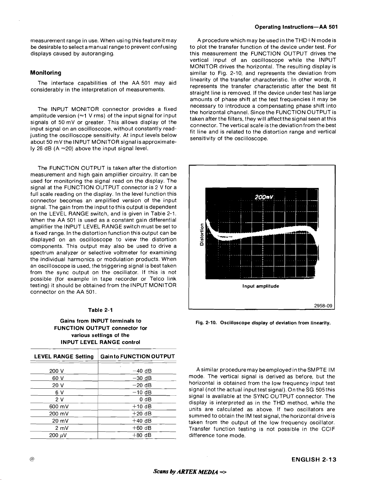
A procedure which may be used in
to plot the transfer function of the device under test. For
this measurement the FUNCTION OUTPUT drives the
vertical input of an oscilloscope while the INPUT
MONITOR drives the horizontal. The resulting display is
similar to Fig. 2-10, and represents the deviation from
linearity of the transfer characteristic. In other words, it
represents the transfer characteristic after the best fit
straight line is removed. If the device under test has large
amounts of phase shift at the test frequencies it may be
necessary to introduce a compensating phase shift into
the horizontal channel. Since the FUNCTION OUTPUT is
taken after the filters, they
connector. The vertical scale is the deviation from the best
fit line and is related to the distortion range and vertical
sensitivity of the oscilloscope.
C
0
.-
.-
z
.-
UI
will affectthesignal seen at this
theTHD+N modeis
ii
Input amplitude
Gains from INPUT terminals to
FUNCTION OUTPUT connector for
various settings of the
INPUT LEVEL RANGE control
LEVEL RANGE Setting
@
Table
2-1
I
Gain to FUNCTION OUTPUT
Scans
by
Fig.
2-10.
Oscilloscope display of deviation from linearity.
Asimilar proceduremay beemployedintheSMPTE IM
mode. The vertical signal is derived as before, but the
horizontal is obtained from the low frequency input test
signal (not the actual input test signal).
signal is available at the SYNC OUTPUT connector. The
display is interpreted as in the THD method, while the
units are calculated as above. If two oscillators are
summed to obtain the
taken from the output of the low frequency oscillator.
Transfer function testing is not possible in the
difference tone mode.
IM test signal, the horizontal drive is
OntheSG 505this
ENGLISH
AR
TEK
MEN
=>
2958-09
CClF
2-13
Page 33
THEORY OF OPERATION
l
ntroduction
Refer to the block diagram
of this manual for a brief description and overall
AA 501 operation. A detailed circuit description follows.
Input Amplifier
The input amplifier is designed for low noise and
distortion. 'The input is differential with single-ended
output. This circuit provides good common mode rejection for suppression of ground loop currents and other
unwanted signals which may be present on both input
leads.
'The input stage is protected to withstand at least
200 V rms on any input range.
-The input amplifier gain is set by the logic circuitry at
0 dB (unity), + 10 dB or + 20 dB. The logic circuitry controls
the gain so that the signal voltage at the output of the input
amplifier remains between 0.75 V and 3.0 V rms. An
uator, prior to the amplifier, additionally provides gain
settings from
gain or attenuation selected depends on the input voltage
level (or the setting of the INPUT LEVEL RANGE switch if
not in AUTO RANGE). A full scale reading of 200 V corresponds to 40 dB of attenuation and 2 V full scale for unity
gain.
-The input signal, from the front panel connections or
the rear interface input (selected by SOURCE switch
S1531) enters the input amplifier through P1620/J1620.
Each input is ac coupled through C1630 or C1631. The
signal then passes to the differential input attenuator
hybrid,
ratioed to maintain gain accuracy and good common
mode rejection. Relays
K1610 select attenuation from 0 dB (unity gain) to40 dB,
respectively in 10 dB steps. Frequency compensation of
the attenuator is provided by
-
10 dB to -40 dB in 10 dB steps. The actual
R1510. These resistors are laser trimmed and
located in the foldout Pages
viewof the
atten-
K1412, K1510, K1511, K1512, and
C1433 and C1520.
Section
CR1520 through CR1626. When the post attenuator
voltage on any scale exceeds about
clampdiodes turns on to limit thevoltage at U1420Aand B.
~h~
effect
of
the
nonlinear capacitance
CR1620, CR1621,
maintaining a constant voltage across the diodes via a
bootstrap arrangement.
The input signal is buffered by low noise amplifiers
U1520Aand U1420B. On the 0 dBthrough 40 dBattenua-
tion ranges, these buffers provide unity gain. Relays
K1410 and K1411 change the gain to +20 dB or $10 dB,
respectively, by adding resistors
Capacitors
sation.
The buffer outputs are combined into a single-ended output signal by
is ac coupled by C1421 to remove any dc offsets caused by
U1420A, B and U1432. This signal is then routed to the
automatic gain control circuitry
el detector.
The gains of the combining stage and the buffers are
controlled by hybrid resistor
laser trimmed and ratioed to insure gain accuracy and
good common mode rejection.
The signal level at the output of the input amplifier is
detected by active rectifier
CR1330 and CR1331. This full wave rectified signal is
filtered by
circuitry through
provided by
that,with2VintotheAA501 inputonthe2Vscale(3Vat
pin 6 of U1432) the output at pin 1 of U1330A is 6 Vdc.
C1423 and C1520 provide frequency compen-
U1330A with C1420 and routed to the logic
CR1624
U1432 (gain=1.5). The output of U1432 pin
J1500, pin 1. Recovery from overload is
VR1320. Resistor R1322 sets t he filter gain so
and
(agc) and input amplifier lev-
R1420. These resistors are
U1320 in conjunction with
i10 V, one set of
CR1625
R1420D or R1420E.
3-AA
of
clamp diodes
is eliminated by
501
6
When there is no attenuation (0 dB), DS1520 and
DS1521 limit the input current. The current passing
through the
resistance from a fairly low value.
Vac indefinitely and 200 Vac for at least 30 minutes. If
120
the AA 501 is subjected to greater overloads in the
attenuator position, the lamps act as fuses to prevent
damage to the input circuitry. When any attenuation other
than
0 dB is selected, the resistance in the hybrid network
provides current limiting. The inputs are clamped by
Zener diodes
REV
JUN
lamps warms their filaments, increasing their
Theselamps can handle
VR1620 and VR1621 through eight diodes,
1981
Scans
0 dB
by
The gain
by transistors Q1400 through Ql600. Control signalsfrom
the logic circuitry enter the input board through
J1500, pins 2through
1-12 V). This logic high at the base of atransistorturnsthe
transistor on and closes the relay. When either
$10 dB or +20 dB (pins 6, 7 or
also activated closing
circuitry selects the proper input attenuation or gain to
maintain 0.75 V to 3.0 V at
than about 50
AR
TEK
MEDLA
settjng relays K1410through K161Oaredriven
9,
with one line at atime high (about
8)
is activated, Q1402, is
K1412. l n AUTORANGE, the logic
U1432 pin 6 for inputs greater
mV. Below 50 mVthe rangeis0.3 Vto 3.0 V.
=>
P1500-
0 dB,
Page 34
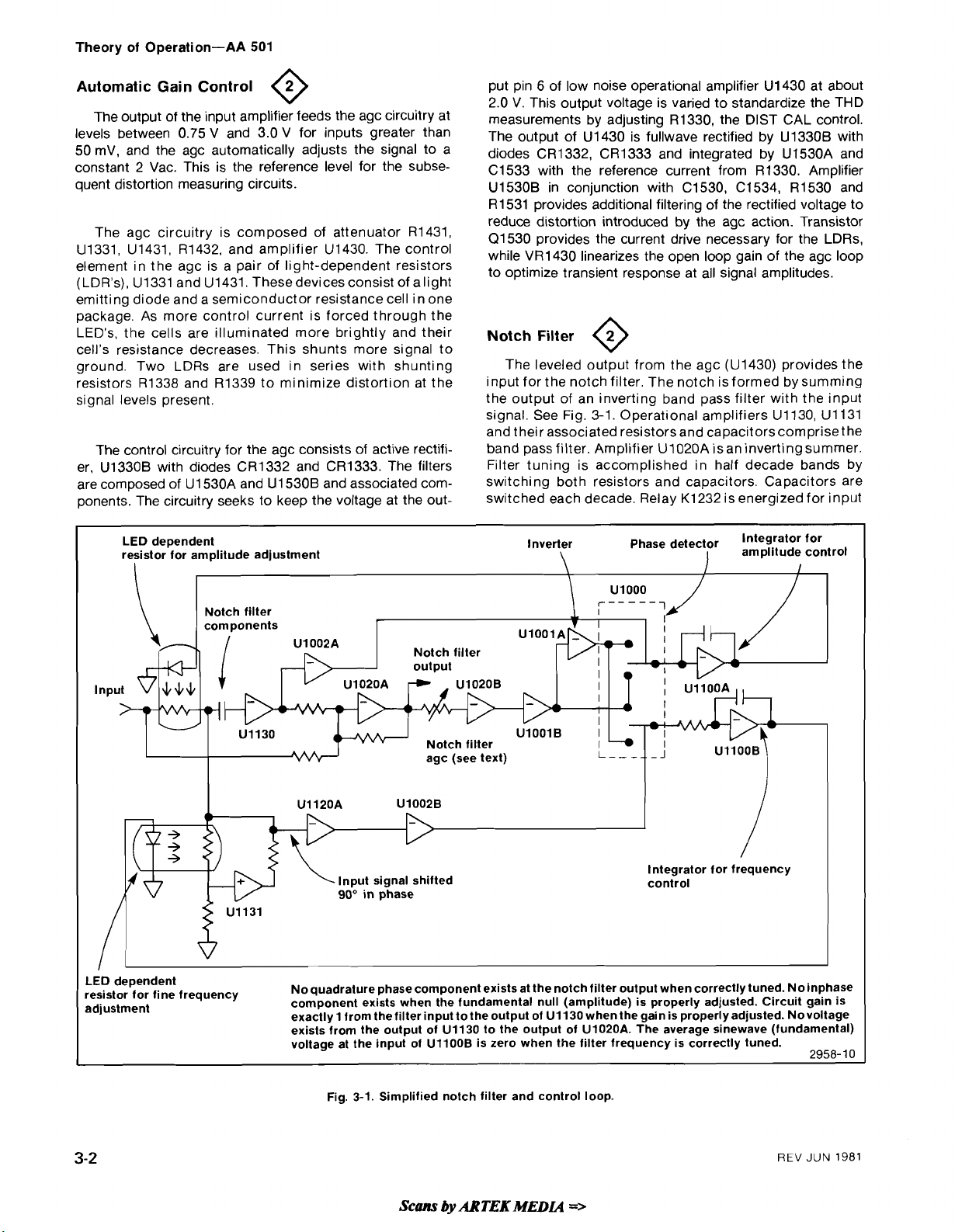
Theory of Operation-AA
501
Automatic Gain Control
0
The output of the input amplifier feeds the agc circuitry at
levels between 0.75 V and 3.0 V for inputs greater than
mV, and the agc automatically adjusts the signal to a
50
constant 2
quent distortion measuring circuits.
The
U1331, U1431, R1432, and amplifier U1430. The control
element in the
(LDR's), U1331 and U1431. Thesedevicesconsist of alight
emitting diode and a semiconductor resistance cell in one
package. As more control current is forced through the
LED'S, the cells are illuminated more brightly and their
cell's resistance decreases. This shunts more signal to
ground. Two LDRs are used in series with shunting
resistors
signal levels present.
The control circuitry for the
U1330B with diodes CR1332 and CR1333. The filters
er,
are composed of
ponents. The circuitry seeks to keep the voltage at the out-
Vac. This is the reference level for the subse-
agc circuitry is composed of attenuator R1431,
agc is a pair of light-dependent resistors
R1338 and R1339 to minimize distortion at the
agc consists of active rectifi-
U1530A and U1530B and associated com-
6
put pin
2.0 V. This output voltage is varied to standardize the THD
measurements by adjusting
'The output of U1430 is fullwave rectified by U1330B with
diodes
C1533 with the reference current from R1330. Amplifier
U1530B in conjunction with C1530, C1534, R1530 and
R1531 provides additional filtering of the rectified voltage to
reduce distortion introduced by the
Q1530 provides the current drive necessary for the LDRs,
while VR1430 linearizes the open loop gain of the agc loop
to optimize transient response at all signal amplitudes.
Notch Filter
input for the notch filter. The notch is formed by summing
the output of an inverting band pass filter with the input
signal. See Fig.
and their associated resistors and capacitors comprise t he
band pass filter. Amplifier
Filter tuning is accomplished in half decade bands by
switching both resistors and capacitors. Capacitors are
switched each decade. Relay
of low noise operational amplifier U1430 at about
R1330, the DlST CAL control.
CR1332, CR1333 and integrated by U1530A and
agc action. Transistor
@
The leveled output from the agc (U1430) provides the
3-1. Operational amplifiers U1130, U1131
U1020A isaninvertingsummer.
K1232 is energized for input
LED dependent Inverter Phase detector Integrator
Notch filter
Notch filter
agc (see text)
I
Integrator for frequency
control
LED
dependent
resistor for fine frequency
adjustment
Input signal shifted
90' in phase
No quadrature phase component exists at the notch filter output when correctly tuned. No
component exists when the fundamental null (amplitude) is properly adjusted. Circuit gain is
exactly 1 from the filter input
exists from the output of
voltage at the input of
tothe output of U1130 when the gain is properly adjusted. Novoltage
U1130 to the output of U1020A. The average sinewave (fundamental)
UllOOB is zero when the filter frequency is correctly tuned.
amplitude control
'Or
inphase
2958-
10
Fig. 3-1. Simplified notch filter and control loop.
Scans
by
ARTEK
MEDLA
=>
REV
JUN
1981
Page 35
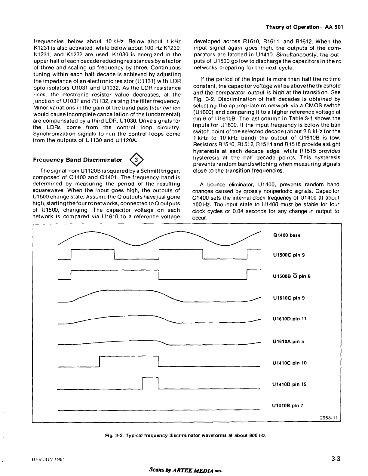
Theory of Operatlon-AA
501
frequencies below about 10 kHz. Below about 1 kHz
K1231 is also activated, while below about 100 Hz K1230,
K1231, and K1232 are used. K1030 is energized in the
upper half of each decade reducing resistances by afactor
of three and scaling up frequency by three. Continuous
tuning within each half decade is achieved by adjusting
the impedance of an electronic resistor
opto isolators
rises, the electronic resistor value decreases, at the
junction of
Minor variations in the gain of the band pass filter (which
would cause incomplete cancellation of the fundamental)
are compensated by a third LDR,
the
LDRs come from the control loop circuitry.
Synchronization signals to run the control loops come
from the outputs of
Frequency Band Discriminator
U1031 and U1032. As the LDR resistance
U1031 and R1132, raising the filter frequency.
U1130 and U1120A.
(U1131)
U1030. Drive signalsfor
with LDR
0
The signal from Ul120Bis squared by a Schmitt trigger,
composed of
determined by measuring the period of the resulting
squarewave. When the input goes high, the outputs of
U1500 change state. Assume the O outputs havejust gone
high, startingthefourrc networks, connected
of
U1500, changing. The capacitor voltage on each
network is compared via
Q1400 and Q1401. The frequency band is
to0 outputs
U1610 to a reference voltage
developed across
input signal again goes high, the outputs of the comparators are latched in
puts of
networks preparing for the next cycle.
constant, the capacitorvoltage will be
and the comparator output is high at the transition. See
Fig. 3-2. Discrimination of half decades is obtained by
selecting the appropriate rc network via a
(U1600) and comparing it to a higher referencevoltage at
pin 6 of
inputs for
switch point of the selected decade (about 2.8 kHz for the
1 kHz to 10 kHz band) the output of
Resistors
hysteresis at each decade edge, while
hysteresis at the half decade points. This hysteresis
prevents random band switching when measuring signals
close to the transition frequencies.
changes caused by grossly nonperiodic signals. Capacitor
C1400 sets the internal clock frequency of U1400 at about
100 Hz. The input state to
clock cycles or 0.04 seconds for any change in output to
occur.
U1500 go low to discharge the capacitors in the rc
If the period of the input is more than half the
U1610B. The last column in Table
U1600. If the input frequency is below the ban
R1510, R1512. R1514and R1518 provideaslight
A bounce eliminator,
R1610, R1611, and R1612. When the
U1410. Simultaneously, the out-
rc time
abovethe threshold
CMOS
3-1
U1610B is low.
R1515 provides
U1400, prevents random band
U1400 must be stable for four
switch
shows the
A--1
6
01400 base
71
r
1
/
-
U1500C pin
UlsOOB6pln6
U1610C pin
U1610D pin 11
U1610A pin 5
Ul4lOC pln 10
UlrlOD pin 15
U1410B pin
9
9
7
REV
JUN
1981
Fig.
3-2.
Typical frequency discriminator waveforms at about 800
scm
by
ARTEK
MEDa
=>
Hz.
2958-1
1
Page 36
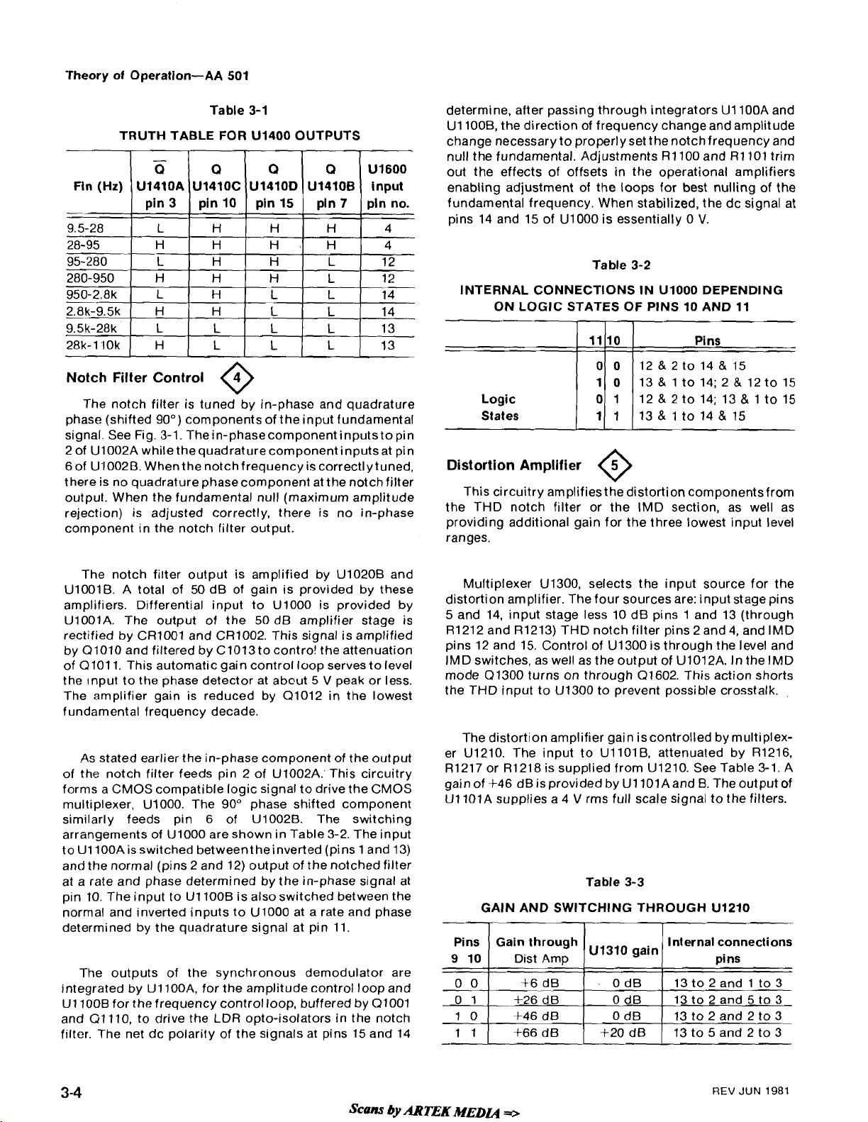
Theory of Operation-AA 501
Table 3-1
TRUTH TABLE FOR
U1400 OUTPUTS
-
H
H
L
L
L
7
U1600
input
pln no.
4
4
12
12
14
Q
Fln (Hz)
-
9.5-28
28-95
95-280
280-950
950-2.8k
Notch Filter Control
U1410A
pin 3
L
H
L
H
L
U1410C
Q
pin 10
H
H
H
H
H
Q
U1410D
pin 15
H
H.
H
H
L
Q
U1410B
pin
@
The notch filter is tuned by in-phase and quadrature
phase (shifted
signal. See Fig.
2 of
U1002A while thequadrature component inputsat pin
6
of UI002B. Whenthe notch frequency is correct1 y tuned,
there is no quadrature phasecomponent at the notch filter
output. When the fundamental null (maximum amplitude
rejection) is adjusted correctly, there is no in-phase
component in the notch filter output.
90") components of the input fundamental
3-1. Thein-phasecomponent inputsto pin
determine, after passing through integrators U1100A and
U1 1008, the direction of frequency change and amplitude
change necessary to properly set the notch frequency and
null the fundamental. Adjustments
out the effects of offsets in the operational amplifiers
enabling adjustment of the loops for best nulling of the
fundamental frequency. When stabilized, the dc signal at
pins 14 and 15 of
INTERNAL CONNECTIONS IN UlOOO DEPENDING
ON LOGIC STATES OF
Logic
States
Distortion Ampllfier
U1000 is essentially 0
Table 3-2
I
I
R1100 and R1101 trim
V.
PINS 10 AND 11
1
Pins
12
& 2 to 14; 13 & 1 to 15
&
1 to 14 & 15
13
0
This circuitry amplifies the distortion components from
the THD notch filter or the IMD section, as well as
providing additional gain for the three lowest input level
ranges.
The notch filter output is amplified by
U1001B. A total of 50 dB of gain is provided by these
amplifiers. Differential input to
U1001A. The output of the 50 dB amplifier stage is
rectified by
by 01010 and filtered by
of 0101 1. This automatic gain control loop serves to level
Input to the phase detector at about 5 V peak or less.
the
The amplifier gain is reduced by 01012 in the lowest
fundamental frequency decade.
As
of the notch filter feeds pin 2 of
forms a CMOS compatible logic signal to drive the CMOS
multiplexer,
similarly feeds pin 6 of
arrangements of
toU1100Aisswitched betweentheinverted (pins 1 and 13)
and the normal (pins 2 and 12) output of the notched filter
at a rate and phase determined by the in-phase signal at
pin 10. The input to
normal and inverted inputs to UlOOO at a rate and phase
determined by the quadrature signal at pin 11.
The outputs of the synchronous demodulator are
integrated by
U1100B for the frequency control loop, buffered by 01001
01 110, to drive the LDR opto-isolators in the notch
and
filter. The net dc polarity of the signals at pins 15 and 14
CR1001 and CR1002. This signal is amplified
C1013to contro! the attenuation
stated earlier the in-phase component of the output
U1000. The 90" phase shifted component
U1000 are shown in Table 3-2. The input
U1100B is also switched between the
UllOOA, for the amplitude control loop and
U1000 is provided by
U1002A:This circuitry
U1002B. The switching
U1020B and
Multiplexer
distortion amplifier. The four sources are: input stage pins
5
and 14, input stage less 10 dB pins 1 and 13 (through
R1212 and R1213) THD notch filter pins 2 and
pins 12 and 15. Control of U1300 is through the level and
IMD switches, as well as the output of
mode 01300 turns on through 01602. This action shorts
the THD input to
The distortion amplifier gain iscontrolled by multiplex-
U1210. The input to UllOlB, attenuated by R1216,
er
R1217 or R1218 is supplied from U1210. See Table 3-1. A
gain of
+46 dB is provided by U1101Aand B. The output of
UllOlA supplies a 4 V rms full scale signal to the filters.
GAIN AND SWITCHING THROUGH U1210
Gain through
Pins
9
10
0 0
0
1
10
11
U1300, selects the input source for the
4,
U1012A. In the IMD
U1300 to prevent possible crosstalk.
3-3
Table
Internal connections
pins
13 to 2 and 1 to 3
13 to 2 and 5 to 3
13 to 2 and 2 to 3
13 to
5
and 2 to 3
Dist Amp
$6
dB
f26 dB
+46 dB
+66
dB
U1310 gain
0 dB
0 dB
0 dB
+20 dB
and IMD
Scans
by
ARTEK
MEDLQ
+
REV
JUN
1981
Page 37
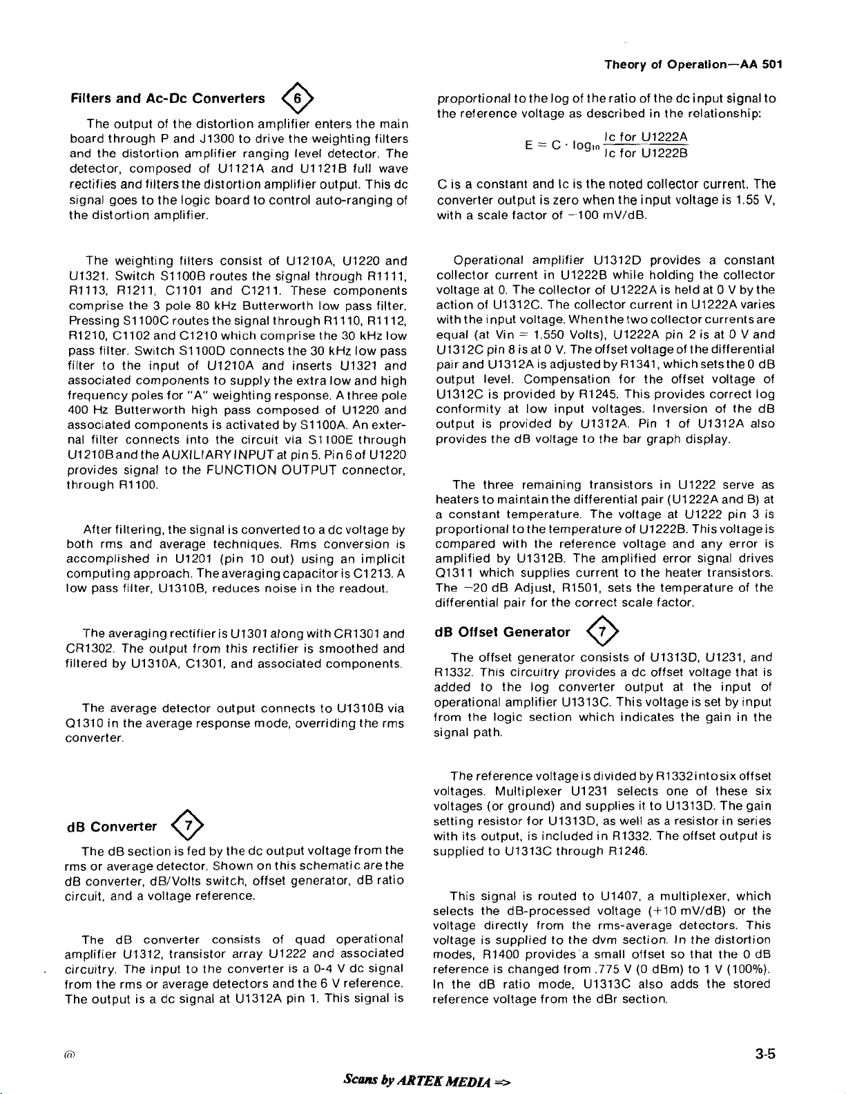
Theory of Operation-AA
501
Filters and
Ac-Dc
Converters
@
The output of the distortion amplifier enters the main
board through P and
and the distortion amplifier ranging level detector. The
detector, composed of
rectifies and filters the distortion amplifier output. This dc
signal goes to the logic board to control auto-ranging of
the distortion amplifier.
The weighting filters consist of
U1321. Switch S1100B routes the signal through R1111,
R1113, R1211, C1101 and C1211, These components
comprise the 3 pole 80 kHz Butterworth low pass filter.
Pressing
R1210, C1102 and C1210 which comprise the 30 kHz low
pass filter. Switch
filter to the input of
associated components to supply the extra low and high
frequency poles for "A" weighting response. A three pole
400 Hz Butterworth high pass composed of
associated components is activated by
nal filter connects into the circuit via
U1210Band the AUXILIARY INPUTat pin 5. Pin 6 of U1220
provides signal to the FUNCTION OUTPUT connector,
through
both rms and average techniques. Rms conversion is
accomplished in
computing approach. The averaging capacitor is
low pass filter,
S1100C routes the signal through R1110, R1112,
R1100.
After filtering, the signal is converted to a dc voltage by
U13106, reduces noise in the readout.
J1300 to drive the weighting filters
U1121A and U1121B full wave
U1210A, U1220 and
S1100D connects the 30 kHz low pass
U1210A and inserts U1321 and
U1220 and
S1100A. An exter-
S1100E through
U1201 (pin 10 out) using an implicit
C1213. A
proportional to the log of the ratio of the dc input signal to
the reference voltage as described in the relationship:
E
=
C . loglo
C is a constant and Ic is the noted collector current. The
converter output is zero when the input voltage is 1.55 V,
with a scale factor of -100
Operational amplifier U1312D provides a constant
collector current in
voltage at
action of
with the input voltage.
equal (at Vin
U1312C pin 8 is at 0 V. Theoffset voltageof thedifferential
pair and
output level. Compensation for the offset voltage of
U1312C is provided by R1245. This provides correct log
conformity at low input voltages. Inversion of the dB
output is provided by
provides the dB voltage to the bar graph display.
The three remaining transistors in
heaters to maintain the differential pair
a constant temperature. The voltage at
proportional to the temperature of
compared with the reference voltage and any error is
amplified by
01311 which supplies current to the heater transistors.
The -20 dB Adjust,
differential pair for the correct scale factor.
0. The collector of U1222A is held at 0 V by the
U1312C. The collector current in U1222A varies
=
U1312A is adjusted by Rl341, whichsetsthe0 dB
U1312B. The amplified error signal drives
U1222B while holding the collector
1.550 Volts), U1222A pin 2 is at 0 V and
R1501, sets the temperature of the
Ic for U1222A
Ic for U1222B
mV/dB.
Whenthe two collector currentsare
U1312A. Pin 1 of U1312A also
U1222 serve as
(U1222A and B) at
U1222 pin 3 is
U1222B. This voltage is
The averaging rectifier is
CR1302. The o~ltput from this rectifier is smoothed and
filtered by
The average detector output connects to
01310 in the average response mode, overriding the rms
converter.
dB
The dB section is fed by the dc output voltage from the
rms or average detector. Shown on this schematic are the
dB converter,
circuit, and a voltage reference.
The dB converter consists of quad operational
amplifier
circuitry. The input to the converter is
from the rms or average detectors and the
The output is a dc signal at
U1310A, C1301, and associated components.
Converter
dB/Volts switch, offset generator, dB ratio
U1312, transistor array U1222 and associated
U1301 along with CR1301 and
U1310B via
a
0-4 V dc signal
6
V reference.
U1312A pin 1. This signal is
dB
Offset Generator
The offset generator consists of U1313D, U1231, and
R1332. This circuitry provides a dc offset voltage that is
added to the log converter output at the input of
operational amplifier
from the logic section which indicates the gain in the
signal path.
The reference voltage is divided by
voltages. Multiplexer
voltages (or ground) and supplies it to
setting resistor for
with its output, is included in
supplied to
This signal is routed to U1407, a multiplexer, which
selects the dB-processed voltage
voltage directly from the rms-average detectors. This
voltage is supplied to the dvm section. In the distortion
modes,
reference is changed from
In the dB ratio mode, U1313C also adds the stored
reference voltage from the
U1313C through R1246.
R1400 provides'a small offset so that the 0 dB
0
U1313C. This voltage is set by input
R1332intosix offset
U1231 selects one of these six
U1313D. The gain
U1313D, as well as a resistor in series
R1332. The offset output is
(+I0 mV/dB) or the
,775 V (0 dBm) to 1 V (lOOO/o).
dBr section.
Scam
by
ARTEK
MEDLQ
Page 38
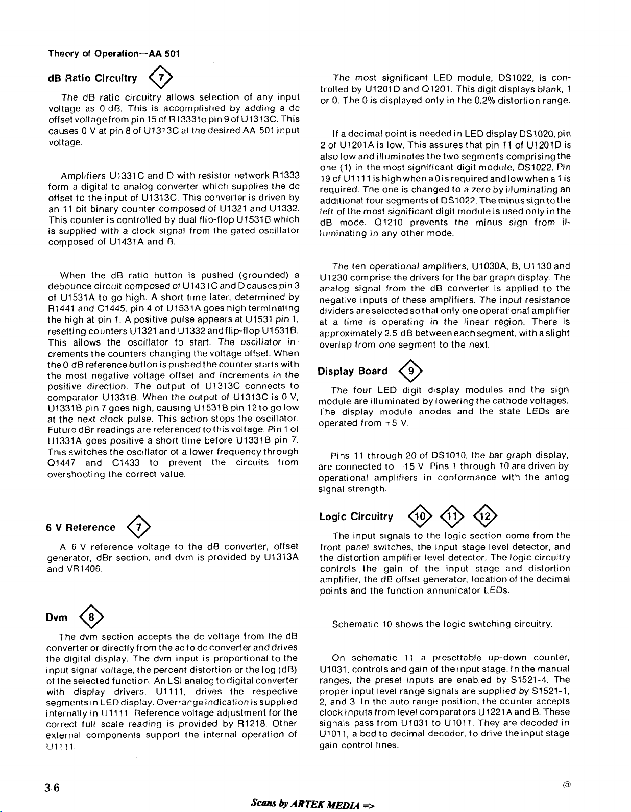
Theory of Operation-AA 501
dB Ratio Circuitry
The dB ratio circuitry allows selection of any input
voltage as
offset voltagefrom pin 150f
causes
voltage.
Amplifiers
form a digital to analog converter which supplies the dc
offset to the input of
an 11 bit binary counter composed of
This counter is controlled by dual flip-flop U1531 B which
is supplied with a clock signal from the gated oscillator
corpposed of U1431A and B.
When the dB ratio button is pushed (grounded) a
debounce circuit composed of U1431 C and D causes pin 3
of
U1531A to go high. A short time later, determined by
R1441 and C1445, pin 4 of U1531A goes high terminating
the high at pin 1. A positive pulse appears at
resetting counters
This allows the oscillator to start. The oscillator increments the counters changing the voltage offset. When
the0 dB reference button is pushed the counter starts with
the most negative voltage offset and increments in the
positive direction. The output of
comparator
U1331B pin 7 goes high, causing U1531B pin 12 to go low
at the next clock pulse. This action stops the oscillator.
Future
U1331A goes positive a short time before U1331B pin
This switches the oscillator ot a lower frequency through
Q1447 and C1433 to prevent the circuits from
overshooting the correct value.
0 dB. This is accomplished by adding a dc
0 Vat pin 8 of U1313C at thedesired AA 501 input
U1331 C and D with resistor network R1333
U1331B. When the output of U1313C is 0 V,
dBr readings are referenced to this voltage. Pin 1 of
0
R1333topin9of U1313C. This
U1313C. This converter is driven by
U1321 and U1332.
U1531 pin 1,
U1321 and U1332 and flip-flop U1531B.
U1313C connects to
7.
The most significant LED module, DS1022, is controlled by
or
0. The 0 is displayed only in the 0.2% distortion range.
If a decimal point is needed in LED display
2 of U1201A is low. This assures that pin 11 of U1201D
also low and illuminates the two segments comprising the
one (1) in the most significant digit module,
19 of
required. The one is changed to a zero by illuminating an
additional four segments of
left of the most significant digit module is used only in the
dB mode.
luminating in any other mode.
The ten operational amplifiers,
U1230 comprise the drivers for the bar graph display. The
analog signal from the dB converter is applied to the
negative inputs of these amplifiers. The input resistance
dividers areselected
at a time is operating in the linear region. There is
approximately 2.5 dB between each segment, with a slight
overlap from one segment to the next.
U1201D and 01201. This digit displays blank. 1
DS1020,
DS1022. Pin
U1111 is high when aoisrequired and lowwhen a 1 is
OS1022. The minus signto the
Q1210 prevents the minus sign from il-
U1030A, B, U1130 and
sothat only one operational amplifier
pin
Display Board
6
The four LED digit display modules and the sign
module are illuminated by lowering the cathode voltages.
The display module anodes and the state
operated from
Pins 11 through 20 of DS1010, the bar graph display.
are connected to -5 V. Pins 1 through 10 are driven by
operational amplifiers in conformance with the
signal strength.
t
5 V.
LEDs are
anlog
is
Logic Circuitry
6
V
Reference
A
6 V reference voltage to the
generator,
VR1406. controls the gain of the input stage and distortion
and
The dvm section accepts the dc voltage from the dB
converter or directly from the ac to dc converter and drives
the digital display. The dvm input is proportional to the
input signal voltage, the percent distortion or the log (dB)
of the selected function. An
with display drivers.
segments in LED display. Overrangeindication issupplied
internally in
correct full scale reading is provided by
external components support the internal
U1111.
0
dB
converter, offset
dBr section, and dvm is provided by U1313A
LSI
analog todigital converter
U1111, drives the respective
U1111. Reference voltage adjustment for the
R1218. Other
operation of
Scans
by
ARTEK
The input sianals to the logic section come from the
front
the distortion amplifier level detector. The logic circuitry
amplifier, the dB offset generator, location of the decimal
points and the function annunicator LEDs.
Schematic 10 shows the logic switching circuitry.
On schematic 11 a presettable up-down counter,
U1031, controls and gain of theinput stage. In the manual
ranges, the preset inputs are enabled by S1521-4. The
proper input level range signals are supplied by
2,
and 3. In the auto range position, the counter accepts
clock inputs from level comparators
signals pass from
U1011, a bcd to decimal decoder, to drive theinput stage
gain control lines.
MEDU
switches, the
-
@
U1031 to U1011. They are decoded in
@
inp$ stage level detector, and
@
U1221A and B. These
51521-1,
Page 39
Theory of Operation-AA
501
A dc signal, proportional to the input signal amplitude
appears at pin 4 of
and 6 of
low when the input signal is higher than the range the
input stage is presently in. This low appears at pin 10 of
U1031 which causes the binary up-down counter tocount
down. If the input attenuator is intheleast sensitive range,
a high exists on pin 1 of
of
illuminated. Pin 1 of
lower than the input attenuator range. Pin 6 of
high in the most sensitive range. The up-down counter
counts only when pin 5 is low. This occurs when the input
signal level is higherthantheattenuator
is not in the least sensitive position, or when the input
signal is lower than the input attenuator
is not in the most sensitive range. The over-range and
underrange LEDs are illuminated through
Q1509 respectively. When the bases of these transistors
are high, through theoutputs of
lights are illuminated. The overrange and underrange
lights are also controlled by thedistortion amplifier gain in
the level mode. Theseinputs, from
bases of transistors
gain and supplies this information to the distortion
amplifier control and to
formatting purposes.
U1221A and Bare such that pin 2 of U1221Agoes
U1032Awhich preventsthe underrange LEDfrom being
U1012A decodes the odd 10 dB steps in theinput stage
U1221A. The bias voltages on pins 5
U1032A. A Iowthen exists on pin3
U1221 B is low when the input signal is
U1032B is
rangeand the unit
rangeand theunit
(21508 and
U1032A and U10328, the
U1407, areshown at the
(21509 and (21508.
U1021 for decimal point and offset
4 and 2 provide distortion amplifier gain information. This
sum is decoded by
CR1025 and CR1028. These diodes drive U1012B and
U1111 to operate the pV, mV, and Volts annunicator LEDs.
The control source for the decimal points is selected by
U1013, a 4 bit and/or selector which operates as a
multiplexer. In the volts mode, the decimal points are
controlled by the decoded decimal information from
U1022 and the diodes. In the distortion modes, the
decimal points are controlled by the distortion amplifier
gain. Gain information from the distortion amplifier
appears at pins
disabled, and
This illuminates the proper decimal point for all dB
displays.
A 4 bit and/or selector
mutliplexer, selects the control source for the dB offset
generator. In the level mode, the offset iscontrolled by the
sum at the output of
is controlled by the distortion amplifier gain.
U1022, and passes through CR1022,
1. 3, 5 and 7. In the dB modes, U1013 is
(21106 is turned on by U1112A or U1112B.
(U1123) operating as a
Ul021. In thedistortion modes U1123
Power Supplies
0
There are three operating voltagesinthe AA 501: t and
-
15 V dc and 4-5 V dc. The k15 V supplies the
operational amplifiers, linear circuitry and CMOS, while
+
V is used for the logic and display circuitry.
Distortion amplifier gain is controlled in a manner
similar to the input circuitry gain.
are the level comparator and U1132A. U1132B, and
U1132D perform the enable gating function.
The gain control input for the distortion amplifier is
selected by
mode pin 9 is high, pin 14 is low, and pins 6, 4, and 2 are
routed to the outputs. This selects the Input Level Range
Switch,
modes, pin 14 is high, 9 is low and pins 7, 5 and 3 are
connected to the output. The distortion range switches
now control the gain.
The signals from and to
U1033. A dc voltage proportional to the output of the
of
distortion amplifier connects to pin 11 of
operation of
for the input stage
up/down counter, U1131, for the distortion amplifier gain.
A three to eight decoder driver,
output for the distortion amplifier gain control circuitry.
A binary adder,
.
the gain of the input stage and the distortion amplifier.
7,
Pins
U1033, a 4 bit and/or selector. In the level
S1521, as the gain control input. In the distortion
U1032C control the switching
U1221 and U1132 are identical as described
up/down counter. 'These gates control
U1021, shown on schematic 12, sums
5 3 and 6 provide input stagegain information. Pins
U1221C, and U1221D
U1221D. The
U1124, supplies decimal
+5 V dc supply is derived from the 4-11.5 V dc
The
supply in the mainframe. A three terminal votlage
regulator,
current limiting. Additional overcurrent protection is
provided by
The +15 V dc supply is regulated from the +33 V dc
mainframe supply. The reference voltage, against which
the regulator output, divided down by
compared, is supplied by
reference voltage and divided output are amplified by
U1420B and Q1510. The mainframe
Q1513 form a Darlington series-pass transitor. Frequency
compensation for stability is provided by
C1510. Current limiting is accomplished by Q1511 which
senses the voltage across
delivered by the
Q1511 turns on. This shunts base drive current from
Q1513 lowering the output voltage. Fuse F1610 provides
additional protection.
-15
The -15 V is supplied from the -33 V dc in the
mainframe. Amplifier
+15 V supply with the -15 V through
Voltage differences are amplified by U1420A and Q1520.
U1523, provides +5 V and includes built-in
F1621.
Rl425 and R1426 is
VR1401. Errors between the
NPN
R1519. When the current
+I5 volt supply exceeds about 500 mA,
V
Supply
U1420A compares the regulated
R1420 and R1421.
transistor and
R1521 and
Scans
by
ARTEK MEDL4
=>
Page 40
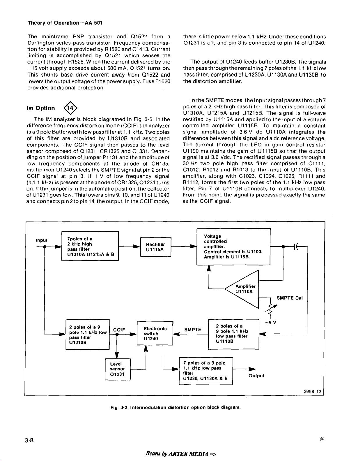
Theory of Operation-AA
501
The mainframe PNP transistor and 01522 form a
Darlington series-pass transistor. Frequency compensa-
tion for stability is provided by
limiting is accomplished by 01521 which senses the
current through
-15 volt supply exceeds about 500
This shunts base drive current away from
lowers the output voltage of the power supply. Fuse
provides additional protection.
Im
option
The IM analyzer is block diagramed in Fig. 3-3. In the
difference frequency distortion mode (CCIF) the analyzer
is a
9
pole Butterworth low pass filter at 1.1 kHz. Two poles
of this filter are provided by
components. The CCIF signal then passes to the level
sensor composed of 01231,
ding on the position of jumper
low frequency components at the anode of
multiplexer U1240 selects the SMPTE signal at pin 2 or the
CCIF signal at pin 3.
(61.1 kHz) is present at theanodeof CR1325, Q1231 turns
If
the jumper is in the automatic position, the collector
on.
of
U1231 goes low. This lowers pins
and connects pin2to pin 14, theoutput. In theCCIFmode,
R1526. When the current delivered by the
@
R1520 and C1413. Current
mA, 01521 turns on.
(21522 and
U1310B and associated
CR1325 and C1331. Depen-
PI 131 and theamplitudeof
If
1 V of low frequency signal
9,
10, and 11 of U1240
F1620
CR135,
there is little power below 1.1 kHz. Under theseconditions
01231 is off, and pin 3 is connected to pin 14 of
The output of U1240 feeds buffer U1230B. The signals
then pass through the remaining
pass filter, comprised of U1230A, U1130A and U1130B, to
the distortion amplifier.
In the SMPTE modes, the input signal passes through
poles of a 2 kHz high pass filter. This filter is composed of
U1310A, U1215A and U1215B. The signal is full-wave
rectified by
controlled amplifier
signal amplitude of 3.6 V dc
difference between this signal and a dc reference voltage.
The current through the LED in gain control resistor
U1100 maintains the gain of U1115B so that the output
signal is at 3.6 Vdc. The rectified signal passes through a
30 Hz two pole high pass filter comprised of
C1012, R1012 and R1013 to the input of U111OB. This
amplifier, along with
R1112, forms the first two poles of the 1.1 kHz low pass
filter. Pin
From this point, the signal is processed exactly the same
as the CCIF signal.
U1115A and applied to the input of a voltage
U1115B. To maintain a constant
C1023, C1024, C1025, R1111 and
7
of U111OB connects to multiplexer U1240.
7
poles of the 1.1 kHz low
U111OA integrates the
U1240.
C1111.
7
Input
Tpoles of a
2
kHz
high
pass fllter
U1310A U1215A & B
1.1
*
pole
pass filter
U1310B
HZ
tow
Level
sensor
01231
Rectifier
U1115A
Electronic
sw~tch SMPTE
U 1240
D
A
filter
U1230, U1130A
Voltage
controlled
amplifier.
Control element is
Amplifier is
U1115B.
2
poles of a
9
pole
1.1
low pass filter
UlllOB
HZ
.
&
B
U1100.
Output
*
+5
v
I
I
-
SMPTE Cal
2958-
12
Fig.
3-3.
Intermodulation distortion option block diagram.
Page 41

CALIBRATION
PERFORMANCE CHECK PROCEDURE
Section
4-AA
501
Introduction
This procedure checks the Electrical Performance
Requirements as listed in the Specification section in this
manual. Perform the internal adjustment procedure if the
instrument fails
not correct the discrepancy, circuit troubleshooting is
indicated. Also, use this procedure to determine
tibility of performance in an incoming inspection facility.
For convenience, many steps in this procedure check the
performance of this instrument at only one value in the
specified performance range. Any value within the
specified range, within appropriate limits, may be sub-
---
Low distortion
sinewave oscillator
with
Description
IM test signal
tomeet thesechecks. If recalibration does
accep-
SUGGESTED TEST EQUIPMENT
Minimum
1
<0.0008°/o THD 20 Hz
to 20 kHz;
10 Hz to 20 kHz and
20 kHz to 50 kHz;
<0.0032% 50 kHz to
100 kHz. 60
rms, 10 Hz to 100 kHz.
Requirements
<0.0018%,
mV to 36 V
stituted. The performance check may be done at any
ambient temperature between 0° C and
Test Equipment Required
The test equipment listed in Table4-1, or equivalent, is
suggested to perform the performance check and the
adjustment procedure.
Exercise caution as dangerous voltages may be
encountered in some of the following steps.
Table
4-1
Performance Adjustment
Check
I
6,
7,
8,
9,
10, 11.
11A, 12, 13, 14
1
+50°
Procedure Recommended
1
Equipment
i
9,
8,
10, 11, 11A
TEKTRONIX SG 505
C.
Sinewave oscillator Sinewave 600 /IV to 4, 6,
v
(2 required for 35
alternate Step
Ac voltage calibrator
Dv m
Counter
Bnc male to dual
binding post adapter
cia
11A) Frequency 20 Hz to
1
I
(
I
rms
>300 kHz.
100 ,uV to 180 V
10 Hz to 100 kHz
lm~to2~ 12, 13, 14
60 Hz to 84 kHz
@
0.9 V
12
1, 2,
I
Scans
by
ARTEK
9,
10, 11,
5,
13, 14, 15
MEDL4
=>
1
I
1
I
9
1 1 A
I
TEKTRONIXSG 502
5200A and
Fluke
1
TEKTRONIX DM 505
TEKTRONIX DC 504
I
4-
1
Page 42

Table
4-1
(cont)
Description
50
fl
coaxial cable
with bnc connectors,
2 ea.
(3 required
for alternate
Step 11
Bnc female to
dual banana
adapter
Bnc T-adapter (2 ea.
required for alternate
Step 11
Banana to alligator
test leads to voltage
calibrator
18" banana test leads
A)
A)
1 1
i
1
I
1
Minimum
Requirements Step
1
I
1
I I
I
I
Performance
Check
I
Adjustment
1
Procedure Recommended
Step
9 1 1 A
1
Tektronix Part
NO. 012-0057-01
Tektronix Part
NO. 103-0090-00
(
Tektronix Part
1
No. 103-0030-00
Tektronix Part
NOS. 01 2-001 4-00
(black) and
012-001 5-00 (red),
30"
Tektronix Part
NOS. 01 2-0039-00
(black) and
012-0031-00 (red)
Equipment
6"
banana to banana
patch cord
1
kn resistor
100
kn resistor
Shorting plug
1, 2
Tektronix Part
NO. 012-0024-00
1
Tektronix Part
1
No. 321-0193-00
Tektronix Part
I
NO. 321-0385-04
Tektronix Part
Scans
by
ARTEK
MEDU
*
Page 43

Cali bration-AA
501
List
of
Check and Adjustment Steps
Performance Check Steps
1. Check Input Impedance
2. Check Common Mode Rejection
3. Check Level Function Accuracy
4. Check Bandwidth
5.
Check Residual Noise
Check Total Harmonic Distortion Accuracy
6.
7.
Check Residual Total Harmonic Distortion
Noise
8.
Check Residual Intermodulation Distortion in the
SMPTE/DIN Mode (Option 01 only)
9.
Check Residual Intermodulation Distortion in the
CClF Difference Tone Test Mode (Option 01
only)
10. Check IM Distortion Accuracy, SMPTE Test
(Option 01 only)
11. Check
Tone Test (Option 01
11A. Check IM Distortion Accuracy, CClF Difference
Tone Test (alternate procedure, omit
performed, Option 01 only)
12.
Check Filter Accuracy
13. Check INPUT MONITOR
IM Distortion Accuracy, CCIF Difference
on1 y)
if
step 11 is
14. Check FUNCTION OUTPUT
15. Check AUXILIARY INPUT
Adjustment Procedure Steps
1. Adjust Dist Amp Offset
2. Adjust Rms and Avg Zero
3. Adjust Volts and Avg Cal
4. Adjust Attn Comp
Adjust 0 dB Adj, -20 dB Adj and Input Zero
+
5.
6.
Adjust Offset Gain
7.
Adjust dBr Zero
8.
Adjust Null, Freq Trim and 3 H Null
9.
Adjust Dist Cal
10. Adjust SMPTE Cal (Option 01 only)
11. Adjust Diff Freq Cal (Option 01 only)
11A. Check IM Distortion Accuracy, CClF Difference
Tone Test (alternate procedure, omit
performed, Option 01 only)
The
AA
501
measurement response. Unless specifically noted
all performance checks may be performed using
either response.
if
step 11 is
NOTE
has selectable average or true rms
Scans
by
ARTEK
MEDLQ
*
Page 44

PERFORMANCE CHECK SUMMARY SHEET
This sheet may be duplicated and used as a short form performance check procedure. Perform the check and record the
reading in the "Measured" column. Compare the reading with the upper and lower limits. After maintenance or adjustment
again perform the procedure and compare the readings.
___
Date
Serial Number Tested by
Description Minimum Measured Maximum
I
Scorn
by
ARTEK
MEDL4
Page 45

1.
Check lnput Impedance
a. Connect the ac voltage calibrator to the input
terminals of the AA 501 as shown in Fig.
4-1. Connect the
black clip lead to the low terminal and the red clip lead to
the high terminal of the voltage calibrator.
b. Make certain the FUNCTION LEVEL and VOLTS
pushbuttons are pressed. All other
c. Set the INPUT LEVEL RANGE switch to the
pushbuttons out.
2
position.
V
h. Reverse the connector at the INPUT terminals of the
AA 501.
i. CHECK-that the reading is between 0.891 and
0.909.
j.
Remove these connections from the front panel
INPUT connector for the next step.
2.
Check Common Mode Rejection
a. Set the acvoltagecalibrator for an output frequency
of 50 Hz.
d. Set the ac voltage calibrator to any frequency from
400 Hz to 1 kHz.
e. Set the ac voltage calibrator amplitude for an
AA 501 display reading of 1.800 V.
f. Move the red clip lead from the red binding post to
the free end of the 100
kn resistor.
g. CHECK-that the display reads between 0.891 and
0.909.
b. Connect the test equipment as shown in Fig.
c. Press the FUNCTION LEVEL and VOLTS
pushbut-
tons. All other pushbuttons out.
d. Refer to Table
4-2.
e. CHECK-that the dvm reads according tothetable
for the listed input conditions.
f. Remove these connections for the next step.
4-2.
-
Patch
cord
Bnc male
dual bindi
post adap
Bnc female to dual banana adapter
-
f
to voltage
calibrator
Fig.
4-1.
Check step
Scans
1.
Input impedance.
by
ARTEKMEDCQ
2958-14
=r
Page 46

Cali bration-AA
501
Shorting
bar
Test leads to dual
voltage calibrator binding
Table
INPUT
4-2
COMMON MODE REJECTION CHECK
INPUT LEVEL
RANGE
200 pV
2 rnV
20 rnV
200 rnV
600 rnV
2
V
6
V
20 V
60 V
200 V
Input Voltage
@
50 Hz
50 mV
50 mV
50 rnV
0.1 V
0.3 V
1
V
3 V
10 V
30 V
100 V
AA
501
FUNCTION
OUTPUT
+
-
Bnc male
adapter
Fig. 4-2. Check step 2. Common mode rejection.
SG 502
OUTPUT
post
SG 505
OUTPUT
•
INPUT
)a
LEVEL FUNCTION ACCURACY
1
Maximum
dvm Reading
1.580 V
158
mV
15.8 rnV
3.2 rnV
1
rnV
3.2 rnV
1.0 rnV
3.2 mV
1.0 rnV
3.2 rnV
Calibrator I RANGE
INPUT
LEVEL Limits of Reading
DVM
Table
4-3
1
20 Hz-20 kHz,
1
f
2%
1
10 Hz-100 kHz,
I
f4%
3.
Check Level Function Accuracy
a. Connect the test equipment as shown in Fig.
b. Set the voltage output of the ac calibrator and the
INPUT
tons.
LEVEL RANGE
c. Press the FUNCTION
All
other pushbuttons out.
switch as listed in Table
LEVEL
and
VOLTS
pushbut-
4-6
4-3.
4-3.
Scans
by
ARTEK
I
The specified accuracy of commercially available ac
calibrators is not adequate to directly check
performance at 100
signal, connect a
of the
AA
501 and a 100
MEDLQ
=>
1
p
V.
1
KSZ
94.0 to 104.0 above 50
NOTE
To obtain an accurate 100
0.1 % resistor across the input
Kf2
0.1% resistor in series
AA
REV
501
p
JUN
kHz.
V
1981
Page 47

AA
501
SG 502
SG 505
DVM
INPUT
Patch
cord
-
To voltage calibrator
+
Fig.
4-3.
Check
step
with the ac calibrator. These connections are similar
to the test setups shown in Fig.
lead from the calibrator is connected to the free end of
Kf2
the 100
age divider (including AA 501 input impedance effects)
setting the ac calibrator for 10.20 mV will cause the
required 100 p V at the AA 50 1 input terminals.
resistor. As this comprises a 102 to 1 volt-
4-
1 except that the
+
OUTPUT
3.
OUTPUT
.
Level function accuracy.
.
I. CHECK-that the display reads within
the calculated result.
m. Repeat parts e through k with the output frequency
of the generator set to any frequency between
100
kHz.
n. CHECK-that the dBm readings arewithin
INPUT
0.
f0.3
10
Hz and
k0.5
dB of
dB
d. CHECK-that the display reads within the limits as
shown
any frequency from
position.
600
--0.3
3100
RANGE position.
using the formula
REV
in
Table
4-2.
20
0.7746
+0.3
kHz.
e. Set the output of the voltage calibrator to
20
Hz to
20
kHz.
f.
Set the INPUT LEVEL RANGE switch to the 2 V
g. Make certain the
R
pushbuttons are pressed.
h. CHECK-that the display reads within
dBm.
i. Set the input voltage amplitude to any voltage
pV at any frequency from
j.
Set the INPUT LEVEL RANGE switch to the AUTO
k. Calculate the dBm equivalent of the input voltage
dBm
=
20
x
logrn
JUN
1981
FUNC'TION LEVEL and dBm
20
Hz to
Input
V
-
0.7746
Vat
dBm to
o. Remove all connections from the front panel for the
next
step.
4-
Check
a. Set the INPUT LEVEL RANGE switch to the AUTO
RANGE position.
b. Press the FUNCTION LEVEL and VOLTS pushbut-
tons,
c. Connect the SG
d. Set the SG
convenient amplitude within
Such
e. Press the dB RATIO pushbutton and push and
release the PUSH TO SET
All
other
V.
Bandwidth
pushbuttons
502
output frequency to 1 kHz at any
out,
502
as shown in Fig.
theinput range of the AA
0
dB
REF
pushbutton.
4-4.
501
4-7
Scans
by
ARTEK
MEDL4
=>
Page 48
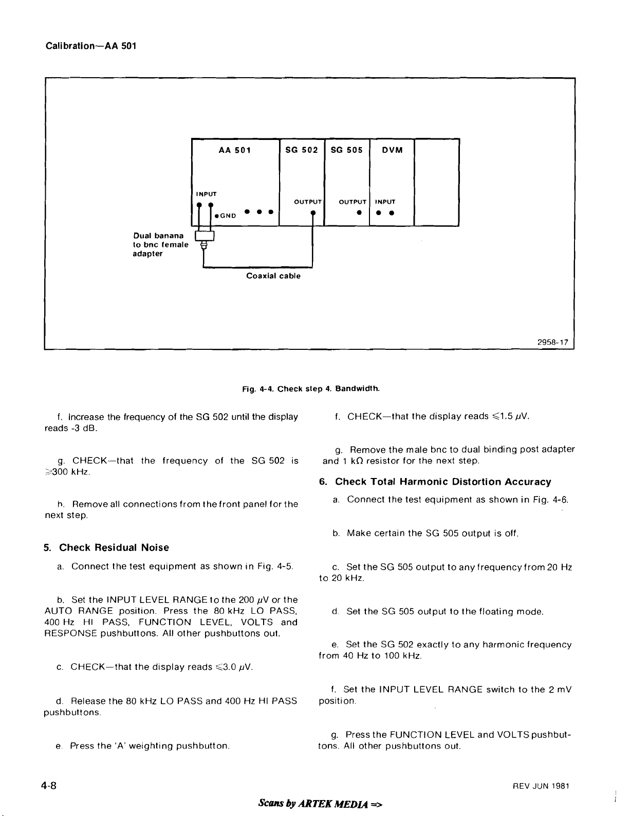
AA
501 SG 502 SG 505
DVM
INPUT
Dual banana
to bnc female
adapter
f. Increase the frequency of the
reads
-3
dB.
g. CHECK-that the frequency of the SG 502 is
2300 kHz.
1
I
Coaxial cable
Fig.
SG
502 until the display
4-4.
OUTPUT
T
I
Check step
OUTPUT
4.
Bandwidth.
f. CHECK-that the display reads
g. Remove the male bnc to dual binding post adapter
1
and
6.
Check Total Harmonic Distortion Accuracy
INPUT
.
..
kfl resistor for the next step.
G1.5 pV.
h.
Remove all connections from the front panel for the
next step.
5.
Check Residual Noise
a. Connect the test equipment as shown in Fig. 4-5.
b. Set the INPUT LEVEL RANGE to the 200 pV or the
AUTO RANGE position. Press the 80 kHz LO PASS,
400 Hz HI PASS, FUNCTION LEVEL, VOLTS and
RESPONSE pushbuttons. All other pushbuttons out.
c. CHECK-that the display reads G3.0 pV
d. Release the 80 kHz LO PASS and 400 Hz HI PASS
pushbuttons.
e. Press the 'A' weighting pushbutton.
4-8
a. Connect the test equipment as shown in Fig. 4-6.
b. Make certain the SG 505 output is off
c. Set the SG 505 output to any frequency from 20 Hz
to 20 kHz.
d. Set the SG 505 output to the floating mode.
e. Set the SG 502 exactly to any harmonic frequency
from 40 Hz to 100 kHz.
f. Set the INPUT LEVEL RANGE switch to the 2
position.
g. Press the FUNCTION LEVEL and VOLTS
tons. All other pushbuttons out.
REV
pushbut-
JUN
mV
1981
Scans
by
ARTEK
MEN
=>
Page 49
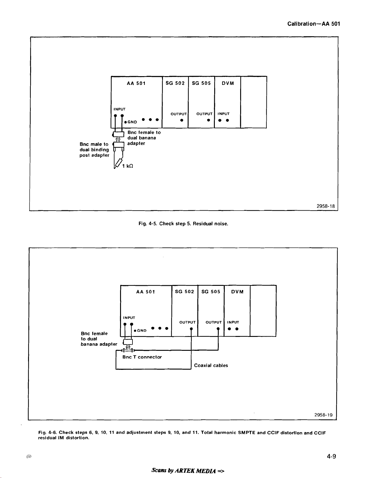
AA
501
SG
502
SG
505
DVM
Cali bration-AA
501
INPUT
.GND
Bnc female to
dual banana
Bnc male to adapter
dual binding
post adapter
f
kn
Fig. 4-5. Check step 5. Residual noise.
OUTPUT
OUTPUT
INPUT
0.
Fig. 4-6. Check steps 6,
residual IM distortion.
(73
Bnc female
to dual
banana adapter
9,
10,
11
l
NPUT
(
Bnc T connector
I
and adjustment steps
Scans
I
I
I
1
Coaxial cables
9,
10, and 11. Total harmonic SMPTE and CClF distortlon and CClF
by
ARTEK
MEDLQ
=>
Page 50
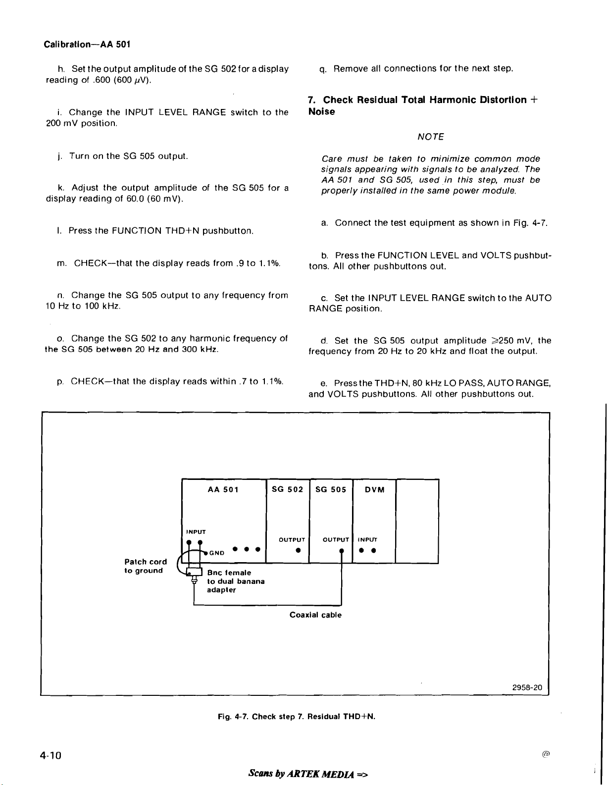
h. Set the output amplitude of the SG
reading of
i. Change the INPUT LEVEL RANGE switch to the
200
j.
k. Adjust the output amplitude of the SG
display reading of
,600 (600
mV position.
Turn on the SG
pV).
505
output.
60.0 (60
mV).
502
for a display
505
for a
q. Remove all connections for the next step.
7.
Check Residual Total Harmonic Distortion
Noise
NOTE
Care must be taken to minimize common mode
signals appearing with signals to be analyzed. The
AA
501
and
SG
505,
used in this step, must be
properly installed in the same power module.
+
I. Press the FUNCTION THD+N pushbutton.
m. CHECK-that the display reads from
n. Change the SG
10
Hz to
100
kHz.
o. Change the SG
SG
505
the
p. CHECK-that the display reads within
between
505
output to any frequency from
502
to any harmonic frequency of
20
Hz and
300
kHz.
.9
.7
to
l.lO/o.
to
l.lO/o.
a. Connect the test equipment as shown in Fig.
b. Press the FUNCTION LEVEL and VOLTS pushbut-
tons,
~11
other pushbuttons
c. Set the INPUT LEVEL RANGE switch to the AUTO
RANGE position.
d. Set the SG
frequency from
e. Press the THD+N,
and VOLTS pushbuttons. All other pushbuttons out.
2
1
SG
505
(
20
DVM
505
Hz to
out.
output amplitude
20
kHz and float the output.
80
kHz LO PASS, AUTO RANGE,
2250
4-7.
mV, the
Patch cord
to ground
to dual banana
adapter
Fig.
4-7.
Check step
Scans
Coaxial cable
7.
by
ARTEK
Residual
MEDLQ
THD-kN.
-
Page 51
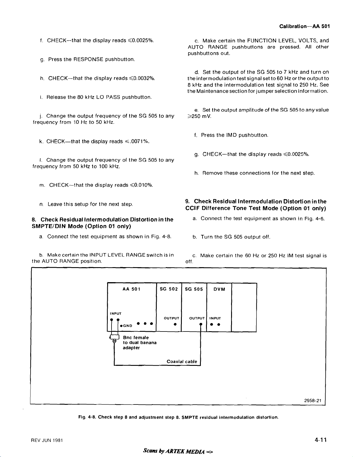
f. CHECK-that the display reads
g.
Press the RESPONSE pushbutton.
h. CHECK-that the display reads
i.
Release the
80
kHz LO PASS pushbutton.
40.0025%.
<0.0032%.
c. Make certain the FUNCTION LEVEL, VOLTS, and
AUTO RANGE pushbuttons are pressed. All other
pushbuttons out.
505
d. Set the output of the SG
the intermodulation test signal set to
8
kHz and the intermodulation test signal to
the Maintenance section for jumper selection information.
to 7 kHz and turn on
60
Hz or the output to
250
Hz. See
j.
Change the output frequency of the SG
frequency from
k. CHECK-that the display reads
I.
Change the output frequency of the SG
frequency from
m. CHECK-that the display reads
n.
Leave this setup for the next step.
8.
Check Residual Intermodulation Distortion in the
SMPTE/DIN Mode (Option
a. Connect the test equipment as shown in Fig.
b. Make certain the INPUT
the AUTO RANGE
-
-
10
Hz to
50
kHz.
<.0071°/~.
50
kHz to
100
kHz.
<O.OIOO/o.
01
only)
LEVEL
-
posit~on. off.
-
RANGE switch is in
-
505
505
to any
to any
4-8.
e. Set the output amplitude of the
2250
mV.
f. Press the IMD pushbutton.
g.
CHECK-that the display reads
h. Remove these connections for the next step.
9.
Check Residual lntermodulation Distortion in the
CClF Difference Tone Test Mode (Option
a. Connect the test equipment as shown in Fig.
b. Turn the SG
c. Make certain the
505
output off
60
Hz or
SG
505
to any value
<0.0025°/~.
01
250
Hz IM test signal is
only)
4-6.
REV
JUN
1981
Fig.
AA
501
INPUT
.GND
Bnc female
to dual banana
adapter
4-8.
Check step 8 and adjustment step
.
&lns
SG 502
OUTPUT
Coaxial cable
8.
by
ARTEK
SG 505
OUTPUT
SMPTE
MEDL4
DVM
INPUT
. .
2958-21
resldual intermodulation distortion.
r>
Page 52
d. Set the output frequency of the SG 502 to 14 kHz.
g. Press the 400 Hz HI PASS pushbutton.
e. Set the INPUT LEVEL RANGE to the AUTO RANGE
position.
f. Press the FUNCTION LEVEL, VOLTS, AUTO
RANGE and RESPONSE RMS pushbuttons. All other
pushbuttons out.
Set the output amplitude of the SG 502 to any
g.
voltage above 177
on the AA 501 display.
h. Turn the SG 505 output on. I. Press the IMD pushbutton and
i.
Set the output frequency of the SG 505 to 15 kHz
and the output amplitude so the AA 501 display reads m. CHECK-that the display reading is 9.00% to
1.414 times the amplitude noted in step g.
j.
Press the IMD pushbutton. n. Leave this setup for the next step.
mV. Note the output amplitude as read
h. Note the AA 501 display reading.
I.
Turn off the
j.
Adjust the SG 502 output frequency to 7.2 kHz with
an output amplitude of exactly
step h.
k. Turn on the SG 505 output.
PASS pushbutton.
11.00%.
SG
505 output.
10%of the reading noted in
releasethe400 Hz HI
11. Check IM Distortion Accuracy, CClF Difference
k. CHECK-that the display reads <0.0025%.
Tone Test (Option 01 only)
I. Leave these connections for the next step.
10. Check IM Distortion Accuracy, SMPTE Test
(Option 01 only)
a. Connect the test equipment as shown in Fig. 4-6.
b. Set the Option 01 SG 505 for a 60 Hz IM test signal.
Float the output.
c. Adjust the SG 502 output level for maximum
attenuation.
d. Set the INPUT LEVEL RANGE switch to the AUTO
RANGE position.
e. Press the VOLTS, FUNCTION LEVEL, AUTO
RANGE, and RESPONSE pushbuttons. All other
tons out.
pushbut-
NOTE
CClF distortion is referenced to the level of either
component of two equal amplitude test tones. The
following procedure simplifies test instrumentation
requirements and minimizes sources of potential
error by omitting one of the two test tones. Because
only one test tone is present the averagingresponse
of the internal automatic set-level circuitry will cause
readings to be high by a factor of exactly
(4i7r).
step
two equal amplitude test tones. However, it requires
an additional
extra cabling.
a. Connect the test equipment as shown in Fig.
b. Set the INPUT LEVEL RANGE switch to the AUTO
RANGE position.
c. Make certain the VOLTS, LEVEL, AUTO RANGE,
and RESPONSE pushbuttons are in. All other
tons out.
If desired, the alternate procedure given in
11A
may be followed. This procedure provides
SG
505
or equivalent oscillator and
1.273
pushbut-
4-6.
f. Adjust the SG 505 for an output frequency of
and a 60
on the AA 501
mV or greater composite test signal level as read
d~splay.
7
kHz
Scans
d. Turn off the SG 505 output. Makecertain the
signal is off. Float the output.
by
ARTEK
MEDU
=>
IM test
Page 53
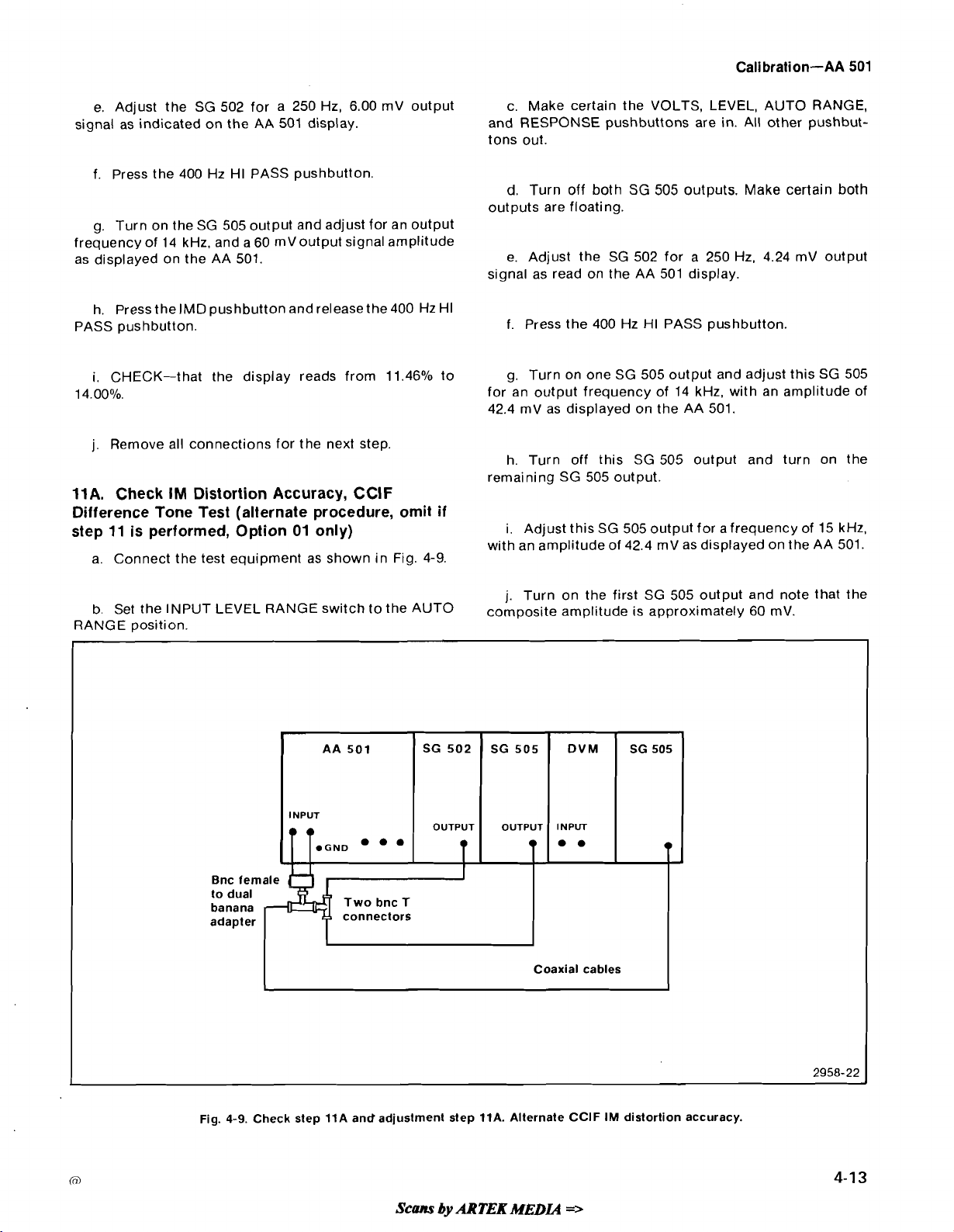
Cali bration-AA 501
e. Adjust the SG 502 for a 250 Hz, 6.00 mV output
signal as indicated on the AA 501 display.
f. Press the 400 Hz HI PASS pushbutton.
g. Turn on the SG 505 output and adjust for an output
frequency of 14 kHz, and a 60
mVoutput signal amplitude
as displayed on the AA 501.
h. Press
theIMD pushbutton and releasethe400 Hz HI
PASS pushbutton.
i.
CHECK-that the display reads from 11.46% to
14.00%.
j.
Remove all connections for the next step.
11A. Check
IM
Distortion Accuracy, CClF
Difference Tone Test (alternate procedure, omit
step 11 is performed, Option 01 only)
a. Connect the test equipment as shown in Fig. 4-9.
if
c. Make certain the VOLTS, LEVEL, AUTO RANGE,
and RESPONSE pushbuttons are in. All other
pushbut-
tons out.
d. Turn off both SG
505
outputs. Make certain both
outputs are floating.
e. Adjust the SG 502 for a 250 Hz, 4.24
mV output
signal as read on the AA 501 display.
f. Press the 400 Hz HI PASS pushbutton.
g. Turn on one SG 505 output and adjust this SG 505
for an output frequency of 14 kHz, with an amplitude of
mV as displayed on the AA 501.
42.4
h. Turn off this SG 505 output and turn on the
remaining SG 505 output.
i. Adjust this SG 505 output for a frequency of 15 kHz,
with an amplitude of 42.4
mV as displayed on the AA 501.
b. Set the INPUT LEVEL RANGE switch to the AUTO
RANGE position.
L
AA
501
INPUT
T
1G.D
Bnc female
banana
adapter
connectors
I
SG 502
OUTPUT
T
j.
Turn on the first SG 505 output and note that the
composite amplitude is approximately 60
SG 505
OUTPUT
DVM
INPUT
**
T
I
Coaxial cables
SG505
9
mV.
4-9. Check step 11A andadjustment step 11A. Alternate CClF IM distortion accuracy.
Fig.
Scans
by
ARTEK
MEDIA
=>
Page 54
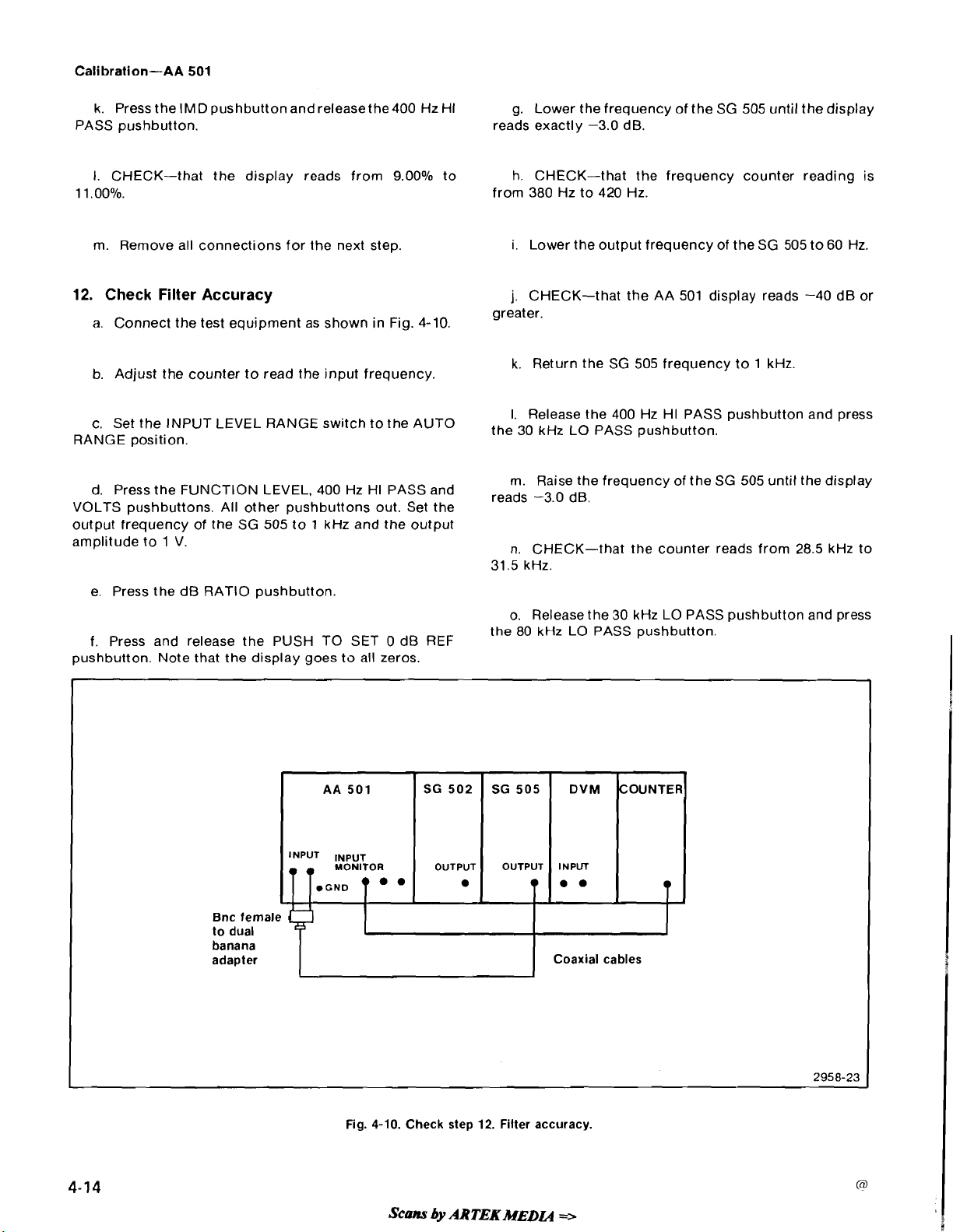
Cali bration-AA
501
k. Press the
IMD
pushbutton and releasethe400 Hz HI
g. Lower the frequency of the SG 505 until the display
PASS pushbutton. reads exactly -3.0 dB.
I.
CHECK-that the display reads from 9.00% to h. CHECK-that the frequency counter reading is
.0O0/o.
1 1
m.
Remove all connections for the next step.
12.
Check Filter Accuracy
a.
Connect the test equipment as shown in Fig. 4-10.
b. Adjust the counter to read the input frequency.
c. Set the INPUT LEVEL RANGE switch to the AUTO
RANGE position.
d. Press the FUNCTION LEVEL, 400 Hz HI PASS and
VOLTS pushbuttons. All other pushbuttons out. Set the
from 380 Hz to 420 Hz.
i.
Lower the output frequency of the SG 505 to 60 Hz.
j.
CHECK-that the AA 501 display reads -40 dB or
greater.
k. Return the SG 505 frequency to 1 kHz.
I.
Release the 400 Hz HI PASS pushbutton and press
the
reads
kHz
LO
PASS
pushbutton.
m.
Raise the frequency of the SG 505 until the display
-3.0
dB,
output frequency of the SG 505 to 1 kHz and the output
amplitude to
1
V.
n. CHECK-that the counter reads from 28.5 kHz to
31.5 kHz.
e. Press the dB RATIO pushbutton.
o. Release the 30 kHz LO PASS pushbutton and press
f. Press and release the PUSH TO SET
0 dB REF
the 80 kHz LO PASS pushbutton.
pushbutton. Note that the display goes to all zeros.
Bnc female
to dual
banana
adapter
AA
501
INPUT INPUT
MONITOR
.GND
Fig. 4-10. Check step 12. Filter accuracy.
'
Scans
SG 502
OUTPUT
by
ARTEK
SG 505
OUTPUT INPUT
Coaxial cables
MEDL~
DVM
3,
COUNTER
T
2958-23
Page 55
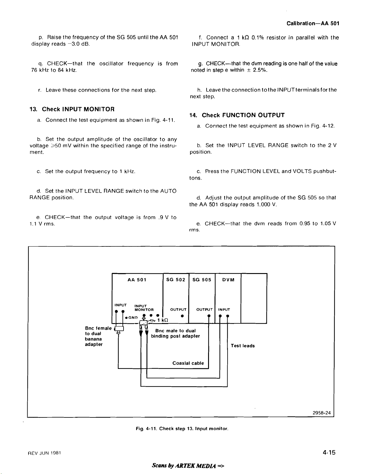
Cali bration-AA
501
p. Raise the frequency of the SG 505 until the AA 501
display reads -3.0 dB.
q.
CHECK-that the oscillator frequency is from
76
kHz to 84 kHz. noted in step e within k 2.5%.
f. Connect a 1
INPUT MONITOR.
g.
CHECK-that the dvm reading is one half of the value
kn
0.1% resistor in parallel with the
r. Leave these connections for the next step. h. Leave the connection tothe INPUTterminalsfor the
next step.
13.
Check INPUT MONITOR
a.
Connect the test equipment as shown in Fig. 4-1 1.
14.
Check FUNCTION OUTPUT
a. Connect the test equipment as shown in Fig. 4-12.
b.
Set the output amplitude of the oscillator to any
b.
voltage
250 mV within the specified range of the instru-
Set the INPUT LEVEL RANGE switch to the 2 V
ment. position.
c. Set the output frequency to 1 kHz.
c. Press the FUNCTION LEVEL and VOLTS
pushbut-
tons.
d. Set the INPUT LEVEL RANGE switch to the AUTO
RANGE position.
d. Adjust the output amplitude of the SG 505 so that
the AA 501 display reads 1.000 V.
e. CHECK-that the output voltage is from
.9 V to
1.1 V rms. e. CHECK-that the dvm reads from 0.95 to 1.05 V
rms.
AA
501
INPUT INPUT
MONITOR
SG 502
OUTPUT
SG 505
OUTPUT
DVM
INPUT
"
T
Bnc
female
to dual
banana
adapter
binding post adapter
Test leads
Coaxial cable
REV
JUN
1981
Fig. 4-11. Check step 13. Input monitor.
Scans
by
ARTEK MEDIA
=>
2958-24
Page 56
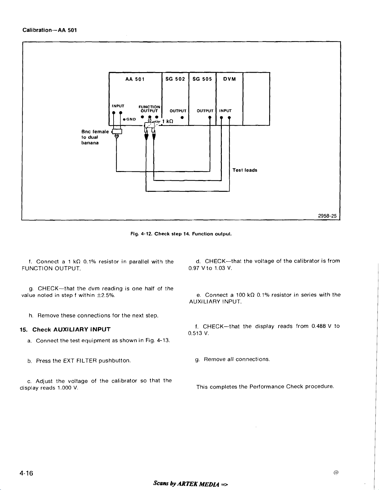
Fig.
4-12.
Check step
14.
Function output.
f. Connect a 1 kQ 0.1% resistor in parallel with the
FUNCTION OUTPUT.
g.
CHECK-that the dvm reading is one half of the
value noted in step f within
h. Remove these connections for the next step.
15.
Check
a. Connect the test equipment as shown in Fig. 4-13.
b.
c. Adjust the voltage of the calibrator so that the
display reads 1.000
AUXILIARY INPUT
Press the EXT FILTER pushbutton.
V.
f
2.5%.
d. CHECK-that the voltage of the calibrator is from
0.97 Vto 1.03 V.
e. Connect a 100
AUXl I-IARY INPUT.
f.
CHECK-that the display reads from 0.488 V to
0.513 V.
g. Remove all connections.
This completes the Performance Check procedure.
kQ
0.1% resistor in series with the
Scans
by
ARTEK
MEDCQ
=>
Page 57
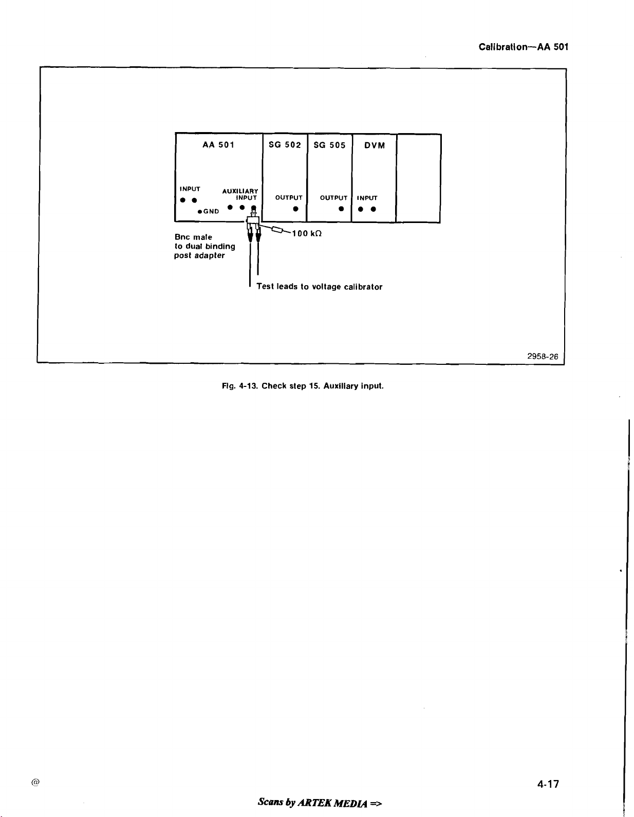
Cali bratlon-AA
501
AA 501
INPUT AUXILIARY
.GND
LLe
Bnc male
lo dual binding
post adapter
INPUT
'
Flg. 4-13. Check step 15. Auxiliary input.
SG 502
OUTPUT
-
1
Test leads to voltage calibrator
100
SG 505
OUTPUT
kn
•
INPUT
em
DVM
Scans
by
ARTEK
MEDM
=>
Page 58

Cali bration-AA
501
INTERNAL ADJUSTMENT PROCEDURE
l
nfroduction
This procedure should be performed if the instrument
fails to meet the performance requirements of the electrical characteristics listed in the Specification section of
this manual. To insurecontinued instrument accuracy it is
recommended that adjustment be performed every 1000
hours of operation or every six to twelve months
infrequently. Adjustment is also recommended following
instrument repair or modification. Adjustments must be
made at an ambient temperature of
+20°C to +30°C.
Services Available
Tektronix, Inc. provides complete instrument repair
and adjustment at
factory service center. Contact your local Tektronix Field
Office or representative for further information.
local field service centers and at the
if
used
If other test equipment is substituted, the calibration
setup may need to be altered to meet the requirements of
the equipment used.
Adjustment Access
Use an extender cable (Tektronix Part No. 067-0645-
02) to operate the plug-in outside the power module.
Remove t he top and both side covers oft he AA 501 to gain
access to the adjustments. All adjustments on the Input
board are accessed from the
Adjustment Location illustration in the pullout pages at
the back of this manual.
1.
Adjust Amp Offset
a. Press the FUNCTION LEVEL and VOLTS
tons.
topof theinstrument. See the
pushbut-
Test
Equipment Required
The test equipment (or equivalent) listed inTable4-1 is
required for adjustment of the AA 501. Specifications
given for the test equipment are the minimum necessary
for accurate adjustment. All test equipment is assumed to
be correctly calibrated and operating within specification. shorting bar. See Fig. 4-14.
Shorting
bar
b. Set the INPUT LEVEL RANGE switch tothe200
position.
c.
Short the INPUT terminals with the dual banana
pV
Fig.
4-14.
Adjustment test setup for steps 1 and
scam
by
ARTEK
MEDL4
2.
=a
Page 59
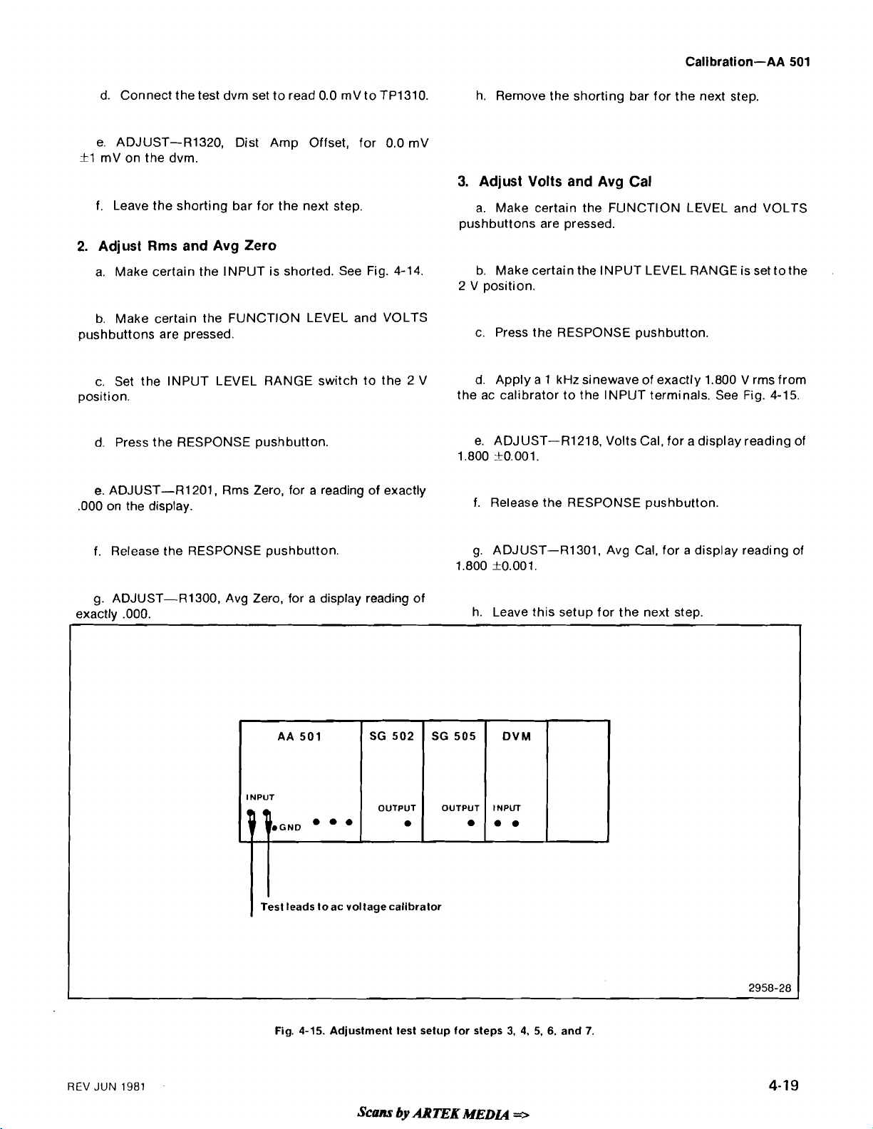
Cali bration-AA
d.
Connect the test dvm set to read 0.0 mV to TP1310.
ADJUST-R1320, Dist Amp Offset, for 0.0 mV
e.
+I
mV on the dvm.
f. Leave the shorting bar for the next step.
h. Remove the shorting bar for the next step.
3.
Adjust Volts and Avg Cal
a. Make certain the FUNCTION LEVEL and VOLTS
pushbuttons are pressed.
2.
Adjust Rms and Avg Zero
a. Make certain the INPUT is shorted. See Fig. 4-14.
b. Make certain the INPUT LEVEL RANGE is set to the
2 V position.
b. Make certain the FUNCTION LEVEL and VOLTS
pushbuttons are pressed. c. Press the RESPONSE pushbutton.
501
c. Set the INPUT LEVEL RANGE switch to the 2 V
position.
d. Press the RESPONSE pushbutton.
d. Apply a 1 kHz
the ac calibrator to the INPUT terminals. See Fig. 4-15.
ADJUST-R1218, Volts Cal, for a display reading of
e.
0.001,
1.800
sinewave of exactly 1.800 V rms from
e. ADJUST-R1201, Rms Zero, for a reading of exactly
.000 on the display. f. Release the RESPONSE pushbutton.
f. Release the RESPONSE pushbutton.
ADJUST-R1301, Avg Cal, for a display reading of
g.
1.800
kO.001.
g. ADJUST-R1300, Avg Zero, for a display reading of
exactlv
.000. h. Leave this setup for the next step.
AA
501 SG 502
SG
505
DVM
REV
JUN
1981
INPUT
1
Test leads toac voltagecalibrator
4-15.
Fig.
Adjustment test setup for steps
OUTPUT OUTPUT
Scam
by
ARTEK
INPUT
a
a.
MEDLA
3,
4,
5,
6,
and
7.
Page 60

Cali
bration-AA
4.
Adjust Attn Cornp
501
i. Reduce the calibrator amplitude to 7.746 mV rms.
a. Make certain the
pushbuttons are pressed. All other pushbuttons out.
b. Make certain the INPUT LEVEL RANGE is set tothe
2 V position.
c. Apply a 1.00 V 50 kHz
calibrator to the INPUT terminals. See Fig. 4-15.
d. Note the display reading.
e. Select the
f.
Set the ac voltage calibrator for a 10.00 V 50 kHz
si newave. 6 V position.
g. ADJUST-C1400, Attn Comp, for a display reading
exactly ten times the reading noted in step d. Use an
insulated low capacitance screwdriver fort his adjustment.
20 V INPUT LEVEL RANGE position.
FLlNCTlON LEVEL and VOLTS
sinewave from the ac voltage
j.
ADJUST-R1245, lnput Zero, for a reading of -40.0
.o.
2.
k. INTERACTION-Repeat steps e through j until
readings are correct.
I. Leave these connections for the next step.
6.
Adjust Offset Gain
a. Use the same control settings as in the previous step
except change the INPUT LEVEL RANGE switch to the
b. Apply a 0.7746
calibrator tothe FRONT PANELINPUTterminals. See Fig.
4-15.
V
rms 1 kHz signal from the ac
h. Leave this setup for the next step.
5.
Adjust 0 dB Adj,
a. Make certain the FUNCTION LEVEL pushbutton is
pressed.
b. Press the
c. Make certain the INPUT LEVEL RANGE switch is in
the 2 V position.
d. Press the RESPONSE pushbutton.
e. Apply a 0.7746 V rms 1 kHz signal from the ac
calibrator to the INPUT terminals. See Fig. 4-15.
f.
ADJUST-R1341, 0 dB Adj, for a reading of exactly
00.0.
-20
dB Adj and lnput Zero
dBm 600 pushbutton.
c.
ADJUST-R1246. Offset Gain, for a display reading
of
exactl y 00.0.
d. Leave this setup for the next step.
7.
Adjust dBr Zero
a. Use the same front panel control settings as in the
previous step except press the dB
b. Make certain the output of the ac calibrator is
0.7746 V rms at 1 kHz. See Fig. 4-15.
c. Press and release the PUSH TO SET 0 dB REF
pushbutton.
d. ADJUST-If the display does not read 00.0 adjust
R1445, dBr Zero, slight1 y clockwise to correct a - error or
counterclockwise for a
+
error.
RATIO pushbutton.
g. Reduce the calibrator amplitude to 77.46
ADJUST-R1501, -20 dB Adj, for a reading of
h.
exact1 y --20.0.
mV rms.
Scans
by
ARTEK
e. INTERACTION-Repeat steps c and d until the
display reads 00.0.
f. Remove all connections for the next step.
MEDIA
=>
Page 61

8.
Adjust Null,
Freq Trim
and
3 H Null
Call bration-AA
c. Connect the test equipment as shown in Fig. 4-6.
501
NOTE
Although not necessary to perform this step, a dual
channel oscilloscope may be of help. Connect the
INPUT MONITOR to channel 1 and the FUNCTION
OUTPUT to channel
signal. Channel 1 shows the fundamental.
and R1100 are adjusted for minimum fundamental at
the FUNCTION OUTPUT while
minimum 3rd harmonic. 900 Hz.
a. Use the same
vious step except change the INPUT LEVEL RANGE switch
to 2 V. Press the 400 Hz HI PASS, THD
30 KHz LO PASS pushbuttons.
b. Connect the test equipment as
c. Set the output frequency of the SG 505 for 500 Hz.
d. Make certain that the output level control on the
SG 505 is at the
0 dBm position (1.55 V rms).
2.
Trigger on the channel 1
RllOl
R1038 is adjusted for
AA501 control settings as for the pre-
+
n, 0.2% and
sho:vn in Fig. 4-8.
on the AA 501. Press the
10.
Float the output.
d. Turn off the SG 505 output.
e. Adjust the SG 502 for an AA 501 display reading of
mV at 7 kHz.
10
f. Turn on the SG 505 output and set the frequency to
g. Adjust the SG 505 output level to 1 V as displayed
THDSN pushbutton.
ADJUST-R1330, Dist Cal, for a reading of 1.000%.
h.
i. Leave these connections for the next step.
Adjust
a. Connect the test equipment as shown in Fig. 4-6.
b. Set the Option 01
SMPTE
Cal
(Option
SG
505 for a 60 Hz IM test signal.
01)
e. ADJUST-R1101, Null Trim, for the lowest display
reading.
f.
ADJUST-R1100, Freq Trim, for the lowest display
reading.
g. Change the SG 505 frequency to 2.5 kHz.
h.
ADJUST-R1038,
reading.
i. INTERACTION-repeat steps
the lowest possible reading.
j.
Disconnect the SG 505 from the AA 501.
9.
Adjust
a. Set the INPUT LEVEL RANGE switch to the AUTO
RANGE position.
Dist
Cal
3
H Null, for the lowest display
c,d,e,f.g and h to obtain
c. Adjust the SG 502 output level for maximum
attenuation.
d. Set the INPUT LEVEL RANGE switch to the AUTO
RANGE position.
e. Press the VOLTS, FUNCTION LEVEL, AUTO
RANGE, and RESPONSE pushbuttons. All other
tons out.
f. Adjust the SG 505 for an output frequency of
and a 60
on the AA 501 display.
mV or greater composite test signal level as read
g. Press the 400 Hz HI PASS pushbutton.
h. Note the AA 501 display reading
i.
Turn off the SG 505 output.
pushbut-
7
kHz
b. Press the FUNCTION LEVEL, VOLTS, and AUTO
RANGE pushbuttons. All other pushbuttons out.
REV
JUN
1981
Scans
j.
Adjust the SG 502 output frequency to 7.2 kHz with
anoutput amplitudeof exactly lO%ofthereadingnotedin
step h.
by
ARTEK
MEDLA
=>
4-2
1
Page 62

k. Turn on the SG 505 output.
i.
ADJUST-R1421. Diff Freq Cal, for a display reading
of 12.73%.
I. Press the
PASS pushbutton.
m. ADJUST-R1001, SMPTECal, for a display reading
lo.OOO/o.
of
n. Leave this setup for the next step.
IMD pushbutton and release the 400 Hz HI
11. Adjust Diff Freq Cal (Option 01)
NOTE
CClF distortion is referenced to the level of either
component of two equal amplitude test tones. The
following procedure simplifies test instrumentation
requirements and minimizes sources of potential
error by omitting one of the two test tones. Because
only one test tone is present the averaging response
of theinternal automaticset-level circuitry will cause
readings to be high by a factor of exactly
(4-rr).
step
two equal amplitude test tones. However, it requires
an additional
extra cabling.
If desired, the alternate procedure given in
11A
may be followed. This procedure provides
SG
505 or equivalent oscillator and
1.273
j.
This completes the AA501 Internal Adjustment
procedure.
11A. Adjust Diff Freq Cal (alternate procedure, omit
if
step 11 is performed, Option 01 only)
a. Connect the test equipment as shown in Fig. 4-9.
b. Set the INPUT LEVEL RANGE switch to the AUTO
RANGE position.
c.
Make certain the VOLTS, LEVEL, 20°/0, and response
pushbuttons are in. All other pushbuttons out.
d. Turn off both SG 505 outputs. Make certain both
outputs are floating.
e. Adjust the SG 502 for a 250 Hz, 4.24
signal as read on the AA 501 display.
mV output
a. Connect the test equipment as shown in Fig.
b. Set the INPUT LEVEL RANGE switch to the AUTO
RANGE position.
c. Make certain the VOLTS, LEVEL,
SPONSE pushbuttons are in. All other pushbuttons out.
d. Turn off the SG 505 output. Make certain the
signal is off. Float the output.
e. Adlust the SG 502 for a 250 Hz, 6.00 mV output
signal as indicated on the AA 501 display.
f.
Press the 400 Hz HI PASS pushbutton.
g. Turn on the SG 505 output and adjust for an output
frequency of 14 kHz, and a 60
as displayed on the AA 501.
mVoutput signal amplitude
20°/0, and RE-
lM test
4-6.
1. Press the 400 Hz HI PASS pushbutton.
g. Turn on one SG 505 output and adjust this SG 505
for an output frequency of 14 kHz, with an amplitude of
42.4
mV as displayed on the AA 501.
h. Turn off this SG 505 output and turn on the
remaining SG 505 output.
i. Adjust this SG 505 output for afrequency of 15 kHz,
with an amplitude of 42.4
j.
Turn on the first SG 505 output and note that the
composite amplitude is approximately 60 mV.
k. Press the IMD pushbutton and
PASS pushbutton.
ADJUST-R1421, Diff Freq Cal, for a display reading
I.
of
10,OOo~o~
mV as displayed on the AA 501.
releasethe400 Hz HI
h.
Press the IMD and release the 400
pushbuttons. procedure.
Hz
HI PASS
m. This completes the AA 501 Internal Adjustment
4-22
Scans
by
ARTEK
MEDL4
=>
REV
JUN
1981
Page 63

Section
MAINTENANCE
GENERAL MAINTENANCE INFORMATION
5-AA 501
Static-Sensitive Components
CAUTION
EX2
Static discharge can damage any semiconductor
component in this instrument.
This instrument contains electrical components that
are susceptible to damage from static discharge. See
Table 5-1 for relative susceptibility of various classes of
semiconductors. Static voltages of 1
common in unprotected environments.
Observe the following precautions to avoid damage:
1. Minimize handling of static-sensitive components.
2.
Transport and store static-sensitive components or
assemblies in their original containers, on a metal rail, or
on conductive foam. Label any package that contains
static-sensitive assemblies or components.
3. Discharge the static voltage from your body by
wearing a wrist strap while handling these components.
Servicina static-sensitive assemblies or comDonents
should be performed only at a static-free work station by
qualified service personnel.
4.
Nothing capable of generating or holding a static
charge should be allowed on the work station surface.
5. Keep the component leads shorted together
whenever possible.
kV to 30 kV are
9.
Use a soldering iron that is connected to earth
ground.
10. Use only special antistatic suction type or wicktype
desoldering tools.
Table
5-1
RELATIVE SUSCEPTIBILITY TO
STATIC DISCHARGE DAMAGE
Relative
Semiconductor Classes
MOS or CMOS microcircuits or discretes.
or linear microcircuits with MOS
inputs. (Most Sensitive)
ECL
Schottky signal diodes
schottky
High-f requency bipolar transistors
JFETS
Linear microcircuits
Low-power Schottky TTL
TTL (Least Sensitive)
a
Voltage equivalent for levels:
=
2
=
3
=
TTL
loo
500
200 to 500 V 5 = 400 to 600 V 8 = 900 V
250 V
=
500
=
600 to 800 V 9 = 1200 V
6
7
Susceptibility
Levels'
2
3
14
5
6
7
8
I
9
=
400 to 1000 V (est.)
(Voltage discharged from a 100 pFcapacitor through a resistance
Of
6.
Pick up components by the body, never by the leads.
7.
Do not slide the components over any surface.
8.
Avoid handling components in areas that have a This instrument should be cleaned as often as
floor or work surface covering capable of generating a
static charge. the outside of the instrument can be removed with a soft
Scans
by
100 ohms.)
Cleaning
operating conditions require. Loose dust accumulated on
ARTEK
MEDLQ
*
Page 64
cloth or small brush. Remove dirt that remains with a soft
cloth dampened in
not use abrasive cleaners.
To clean the front panel use freon, isopropyl alcohol,
or denatured ethyl alcohol. Do not use petroleum
based cleansing
of cleaner, consult your Tektronix Service Center or
representative.
amild detergent and water solution. Do
agents. Before using any.other type
When ordering replacement parts from Tektronix, Inc.,
include the following information:
1.
Instrument type and option number.
2.
I
nstrument serial number.
3.
A description of the part (if electrical, include
complete circuit number).
4. Tektronix part number.
The best way to clean the interior is to blow off the
accumulated dust with dry, low-velocity air (approximate-
5
Ib/in2) or use a soft brush or cloth dampened with a
ly
mild detergent and water solution.
Hold the board so the cleaning residue runs away from
the connectors. Do not scrape or use an eraser to clean the
edge connector contacts. Abrasive cleaning can remove
the gold plating.
CAUTION
a
Circuit boards and components must be dry before
applying power.
Obtaining Replacement
Electrical and mechanical parts can be obtained
through your local Tektronix Field Office or representative. However, it may be possible to obtain many of the
standard electronic components from a local commercial
source. Before purchasing or ordering a part from a
source other than Tektronix, Inc., check the Replaceable
Electrical Parts list for the proper value, rating, tolerance.
and description.
Parts
NOTE
Soldering Techniques
To avoid electric-shock hazard, disconnect the
instrument from the power source before soldering.
The reliability and accuray of this instrument can be
maintained only if proper soldering techniques are used
when repairing or replacing parts. General soldering
techniques which apply to maintenance of any precision
electronic equipment should be used when working on
this instrument. Use only
grade solder. The choice of soldering iron is determined
by the repair to be made.
60/40 rosin-core, electronic
Lx4rA-A
One circuit board
board with a conductive path laminated between the
top and bottom board layers. All soldering on this
board should be done with extreme care to prevent
breaking the connections to this conductive path.
Only experienced maintenance personnel should
attempt to repair the Input board. Do not allow
solder or solder flux to flow under prinled circuit
board switches. The printed circuit board is part
the switch contacts; intermittent switch operation
can occur if the contacts are contaminated.
in
the AA
507
is a multilayer type
Of
When selecting replacement parts, remember that
the physical size and shape of a component may
affect its performance in the instrument.
Some parts are manufactured or selected by Tektronix,
Inc., to satisfy particular requirements or are manufac-
tured for Tektronix, Inc., to our specifications. Most of the
mechanical parts used in this instrument have been
manufactured by Tektronix, Inc. To determine the
manufacturer, refer to the Replaceable Parts list and the
Cross Reference index, Mfr. Code Number to Manufac-
turer.
Scans
by
When soldering on circuit boards or small wiring, use
only a
15
watt, pencil type soldring iron. A higher wattage
soldering iron can cause the etched circuit wiring to
separate from the board base material and melt the
insulation from small wiring. Always keep the soldering
iron tip properly tinned to ensure the best head transferto
the solder joint. Apply only enough heat to remove the
component or to make a good solder joint. To protect heat
sensitive components, hold the component lead with a
pair of long-nose pliers between the component body and
the solder joint. Use a solder removing wick to remove
excess solder from connections or to clean circuit board
pads.
ARmK
MEDL4
=>
Page 65
Semiconductors
To remove in-line integrated circuits use an extracting
;ool. This tool is available from Tektronix, Inc.; order
Tektronix Part Number 003-0619-00. If an extracting tool
is not available, use care to avoid damaging the pins. Pull
slowly and evenly on both ends of the integrated circuit.
Try to avoid disengaging one end before the other end.
Interconnecting Pins
Several methods of interconnection including square
pin and coaxial cable, are used to electrically connect the
circuit boards with other boards and components.
Coaxial Cables
If the coaxial cable to the FUNCTION OUTPUT front
panel connector is damaged replace the entire cable
assembly. Other coaxial cables in the AA 501 can be
replaced or repaired as necessary.
Square Pin Assemblies
If the individual end lead pin connectors are removed
from the plastic holder, note the order of the individual
,ires
for
correct
replacement
replacement in the holder.
see
~i~,
5-2,
END-LEAD
MULTI-PIN
CONNECTOR
F~~
END-LEAD
MULTI-PIN
CONNECTOR
proper
See Fig.
5-1.
These pins areof variouslengths. They are
attached to each other with a plastic strip. To remove
them, simply unsolder from the circuit board.
Fig. 5-1. Typical square pin assembly.
Multi pin Connectors
MULTI-PIN
CONNECTOR
INDEX
Fig. 5-2. Orientation and disassembly of multipin connectors.
1986-68
Circuit Board Removal
Fig. 5-3 shows the removal and replacement of instru-
ment side covers. Next remove the six screws attaching
the top cover and rear panel as shown in Fig.
unsolder the leads from the circuit board to the INPUT
connectors. Remove the INPUT LEVEL RANGE knob.
To remove side
covers turn screw
1/4 turn ccw
screwdrlver or
coln.
wlth
5-4.
Next
The pin connectors used to connect the wires to the
interconnecting pins are clamped to the ends of the wires.
To replace damaged mutlipin connectors, remove the old
pin connector from the holder. Do this by inserting a
scribe between the connector and the holder and prying
the connector from the holder. Clamp the replacement
connector to the wire. Reinstall the connector in the
holder.
Scans
by
ARTEK
Fig. 5-3. Side cover removal or replacement.
MEDL4
=>
Page 66
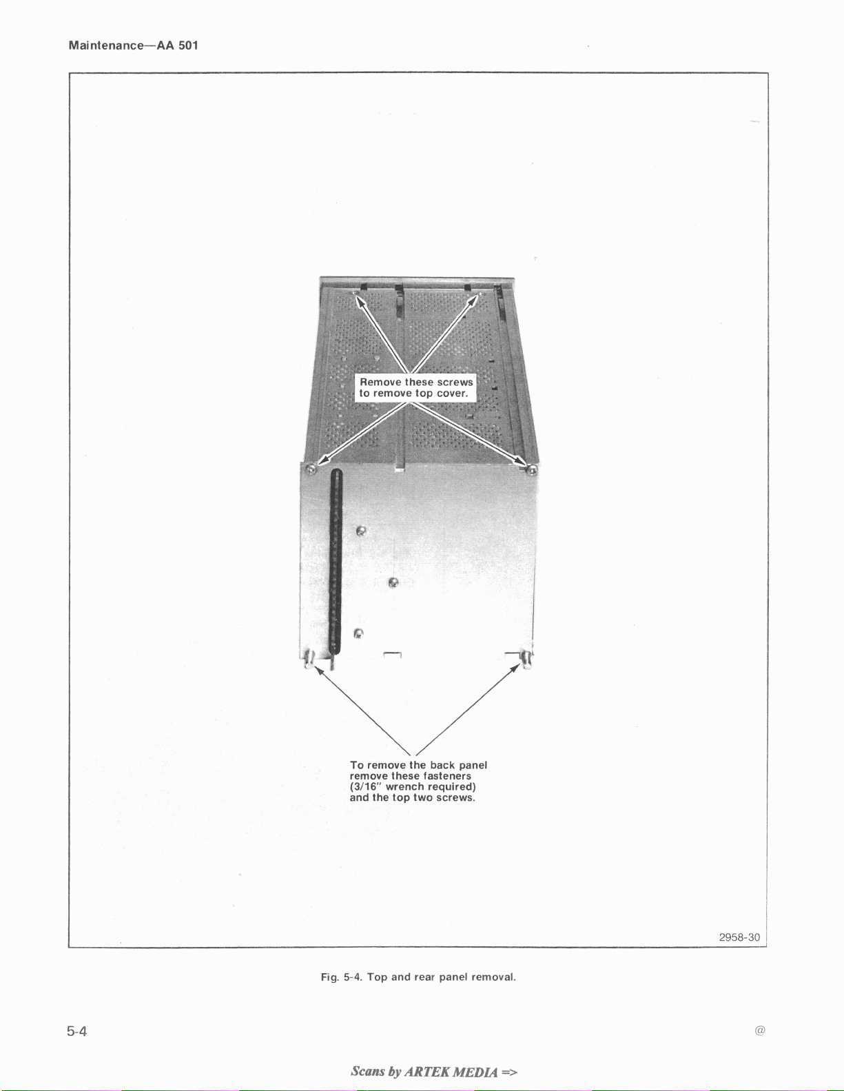
I
/
I
1
f".
I
I
?move these screws
remove top cover.
*
i
\
\
' ' ;
J,
To remove the back panel
remove these fasteners
(3116"
wrench required)
and the top two screws.
Fig.
5-4. Top and rear panel removal.
Scans
by
ARTEK
MEDL.4
2958-30
=>
Page 67
Disconnect all cables attached to the front panel display
board. Finally, remove the two screws attaching the main
board and one screw attaching the logic board tothe plugin frame as shown in Fig. 5-5. Afterthe remaining cablesto
the front panel have been removed, all boards can now be
lifted from the plug-in frame. To further disassemble the
boards, remove the interconnecti ng cables and the screws
holding the boards to each other via spacers.
,
\
To remove
boards remove
these screws.
\
Magnetic Shield
The shield attached to the rear plate of the AA 501 is
heat treated to enhance its magnetic shielding properties.
The benefits of this treatment will be destroyed by
mechanical stresses applied to this part. As such, care
should be taken not to drop or mechanically deform or
bend this shield during service operations.
Jumper Selection for CCIF, AUTO, or SMPTEIDIN
Measurements
To change the jumper position, remove the left side
cover. See Fig. 8-2forjumperIocation. Withthejumper on
the left two pins option 01 instruments are locked in the
CCI F IMD mode. With the jumper on the center two pins,
the unit automatically selects either CCIF or SMPTWDIN
modes as determined bytheinput siqnals. Withtheiumper
on the right two pins thk unit is locked in the SMPTWDIN
mode.
Fig.
5-5.
Screws attaching the board assemblies to the
frame.
~~~~~bl~ is the
that the cables
so that the tracks attached to the instrument top do not
rest on the cables.
over
reverse
the
tops
of
disassembly, ~~k~ certain
of
the boards
are
positioned
plug-in
Front Panel Latch Removal
To disassemble the latch, pry up on the pull tab bar
attached to the latch assembly. Thelatch componentscan
now be removed from the instrument.
30
kHz
Filter Modification
The 3 dB point of the 30 kHz
to 22.4 kHz or 20 kHz by changing three resistor values.
22.4
The
measurements. The 20 kHz modification is useful in high
fidelity audio work. The 30 kHz filter is allowed by the
Federal Communications Commission for proof of perfor-
mance
values of R1110, R1112, and R1210 to 21 kn 1/8
resistors, Tektronix Part Number 321-0320-00. To change
the 3 dB point to 20 kHz, change the values of the same
three resistors to 23.7 kn, 1/8
Part Number 321-0325-00.
kHz modification is useful in certain acoustic
testing
To change the 3 dB point to 22.4 kHz, change the
Of
LO
PASS can be modified
equipment.
W,
1% resistors, Tektronix
W,
l0/o
Scans
by
AR
TEK
MEDL.4
=>
Page 68
REAR INTERFACE INFORMATION
FUNCTIONS AVAILABLE AT REAR
CONNECTOR
Slots exist between pins 17 and 18 and 6 and 7 on the
rear interface connector. The slot between pins 6 and 7
identifies the AA 501 as a member of the TM 500 family.
Insert a barrier in the corresponding position of the power
module jack to prevent noncompatible plug-ins from
being inserted in slots wired for the AA 501. This protects
the plug-in if specialized connections are made to that
compartment. Consult the Building A System section of
the power module manual for further information. Signal
inputs, outputs, or other specialized connections may be
made to the rear interface connectors as shown in the
input output assignmentsillustration (Fig. 5-6).
tion of these connections follows.
+
and - lnput Connectors (28B, 28A)
These terminals are connected to the input of the
AA 501 when the REAR
panel is pressed. The front panel INPUT connectors are
disconnected in this mode. The characteristics of these
terminals are identical with t he front panel INPUT connectors except the maximum input voltage is limited to
peak or 30 V rms. Due
rear interface, noise and distortion performance may be
degraded.
INTFC INPUT button on the front
tothe possibility of crosstalk at the
lnput Common (27B, 27A)
Adescrip-
42
Function Output Ground (24B)
Usethis connector forthereturn circuit forthefunction
out put.
lnput Monitor (24A)
This terminal is in parallel with the front panel INPUT
MONITOR connector.
lnput Monitor Ground (23A)
Use this connector as the return circuit for the INPUT
MONITOR.
SMPTE HF Output (21B)
The high frequency component of a SMPTE test signal
is provided at this jack. This signal can be monitored on a
spectrum analyzer or oscilloscope. The range is typically
from 0.5 V to 3 V. The amplitude varies with the input
signal level and the low to high frequency amplitude ratio.
The output impedance is 2 kn.
V
SMPTE HF Output Ground (22B)
Usethis connector as the ground return forthe SMPTE
HF output.
These are the common (ground) connections for the
rear interface input.
Auxiliary lnput (25B)
This terminal is connected in parallel with the front
panel AUXILIARY INPUT connector. Maximum input
voltage is 15 V peak and limited to 6 V peak for linear
operation.
Auxiliary Input Ground (26B)
Use this connection as a ground return fortheauxiliary
input.
Converter Output (20A)
This connector provides a dc output from the ac to dc
converter. This level corresponds to the average or rms
output as selected on the front panel. The output level is
*5%for a 1000 count display. Thesource resistance is
1 V
500 n k50/0.
dB Converter Output (19B)
This connector provides a dc output from the
logarithmic dB converter. The output voltage is 10 mV
*5% for each 1 dB on the display. Thesource resistance is
kn*5%. Changes in input level rangeor distortion range
1
will cause brief ac transients.
Function Output (23B) dB Converter Output Ground (20B)
This connector is in parallel with the front panel Use this connector as the ground return for the dB
FLlNCTlON OUTPUT connector. converter output.
Scam
by
ARTEK
MEDL4
*
Page 69
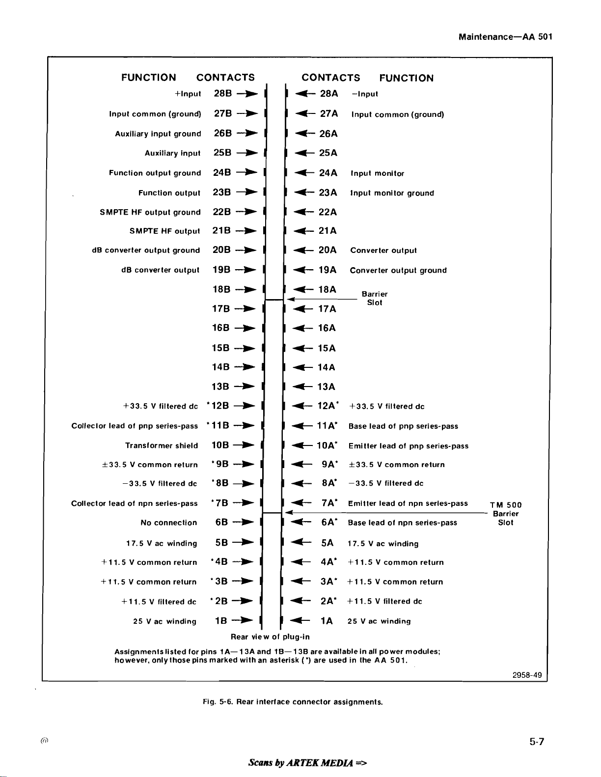
FUNCTION CONTACTS
+Input
288
+
CONTACTS FUNCTION
I
I
+
28A
-Input
Input common (ground)
Auxiliary input ground
Auxiliary input
Function output ground
Function output
SMPTE HF output ground
SMPTE HF output
dB converter output ground
dB converter output
278
268
25B
24B
238
228
218
208
19B
188
178
16B
I5B
148
138
+
--)
1)
?)
1)
--)
--)
+
--)
-W
-W
+
+
-b-
-+
I
I
I
I
I
I
I
1
I
I
+
27A
I
I
+-
26A
I
I
+
25A
I
I
+
24A
I
I
+
23A
I
+
22A
I
+
21A
I
+-
20A
I
+
19A
I
4-
17A
I
+
16A
I
+
15A
I
+
14A
I
+
13A
Input common (ground)
Input monitor
Input monitor ground
Converter output
Converter output ground
Barrier
Slot
+33.5 V filtered dc
Colleclor lead of pnp series-pass
Transformer shield
f33.5 v common return
-33.5 V filtered dc
Collector lead of npn series-pass
No connection
1 7.5 V ac winding
+1
I.
5 V common return
+11.5 V common return
+
11.5 V filtered dc
25 V ac winding
Assignments listed for pins
however, onlythosepins marked with an asterisk (') are used in
'128
1)
I
I
+
12A'
'
11 B
--)
1
1
e
11 A*
10B
1)
1
1
'9B
+
I
I
'88
1)
'
78
--)
6B
-k
58
1)
'48
-b-
'38
-W
'
28
+
18
--)
Rear view
1A-13A and 1B-13B are availablein all power modules;
I
I
I
I
A
-
I
I
I
I
I
1
of
plug-in
1 OA*
+-
+
+
+
+
+
+
f33.5 V filtered dc
Base lead of pnp series-pass
Emitter lead of pnp series-pass
9A'
f33.5 v common return
8A'
-33.5 V filtered dc
7A'
Emitter lead of npn serles-pass
6A'
Base lead of npn series-pass Slot
5A
17.5 V ac winding
4A'
+11.5 V common return
3A'
fll.5 V common return
2A'
+ll.SVfiltereddc
1A
25Vacwinding
the AA 501.
TM
Barrier
500
2958-49
Fig. 5-6. Rear interface connector assignments.
Scans
by
ARTEK
MEDL4
=>
Page 70

OPTIONS
Section
6-AA
501
Option
difference frequency distortion. Information about this option is located in the appropriate sections of
this manual.
01
instruments measure SMPTWDIN intermodulation distortion and CClF two tone
Scans
by
ARTEK
MEDL4
=>
Page 71
REPLACEABLE
ELECTRICAL PARTS
PARTS ORDERING INFORMATION
Section
7-AA
501
Replacement parts are available from or through your local
Tektronix. Inc. Field Office or representative.
Changes to Tektronix instruments are sometimes made to
accommodate improved components as they become available.
and to give you the benefit of the latest circuit improvements
developed in our engineering department. It is therefore important, when ordering parts, to include the following information in
your order: Part number, instrument type or number, serial
number, and modification number if applicable.
If
a part you have ordered has been replaced with a new
improved part, your local Tektronix, Inc. FioldOfficeor representative will contact you concerning any change in part number.
Change information, if any, is located at the rear of this
manual.
or
LIST OF ASSEMBLIES
A
l~st of assemblies can be found at the beginning of the
Electr~cal Parts List. The assemblies arelisted in numerical order.
When the completecomponent number of a part is known, this list ment part from Tektronix.
will identify the assembly in which the part is located.
CROSS INDEX-MFR. CODE NUMBER TO
MANUFACTLIRER
The Mfr. Code Number to Manufacturer index for the
Electrical Parts List is located immediately after this page. The
Cross Index provides codes, names and addresses of manufac-
turers of components listed in the Electrical Parts List.
Only the circuit number will appear on the diagrams and
circuit board illustrations. Each diagram and circuit board
illustration is clearly marked with the assembly number.
Assembly numbers are also marked on the mechanical exploded
views located in the Mechanical Parts List. The component
number is obtained by adding the assembly number prefix to the
circuit number.
The Electrical Parts List is divided and arranged by
assemblies in numerical sequence
subassemblies and parts, precedes assembly
assemblies and parts).
Chassis-mounted parts have no assembly number prefix
and are located at the end of the Electrical Parts List.
TEKTRONIX PART NO. (column two of the
Electrical Parts List)
Indicates
part, number to be used when ordering replace
SERIALIMODEL NO. (columns three and four
of the Electrical Parts List)
Column three (3) indicates the serial number at which the
part was first used. Column four (4) indicates theserial
which the part was removed. No serial number entered indicates
part is good for all serial numbers.
(e.g., assembly A1 with its
A2
with its sub-
numberat
ABBREVIATIONS
Abbreviations conform to American National Standard ~1.1.
COMPONENT NUMBER (column one
of the
Electrical Parts List)
A numbering method has been used toidentify assemblies,
subassemblies and parts. Examples of this numbering method
and typical expansions are illustrated by the following:
Example a. component number
A23R1234
Assembly number Circuit number
Read: Reslslor
Example b. component number
A23A2R1234 R1234
Assembly
number
Read: Reslstor
1234
-
~23 131234
1234
of Assembly
23
-
of Subassembly 2 of Assembly
23
NAME & DESCRlPTlON (column five of the
Electrical Parts List)
In the Parts List, an Item Name is separated from the
description by a colon
Name may sometimes appear as incomplete. For further
Name identification, the U.S. Federal Cataloging Handbook H6-1
can be utilized where possible.
(:).
Because of space limitations, an ltem
ltem
MFR. CODE (column six of the Electrical Parts
List)
Indicates the code number of the actual manufacturer of the
part. (Code to name and address cross reference can be found
immediately after this page.)
MFR. PART NUMBER (column seven of the
Electrical Parts List)
Indicates actual manufacturers part number.
Scam
by
ARTEK
MEDCQ
Page 72
Replaceable Electrlcal Parts-AA
CROSS INDEX-MFR. CODE NUMBER TO MANUFACTLIRER
Mfr.
Code
OOOGS
00853
0
1002
A P PRODUCTS, INC.
SANGAMO ELECTRIC CO., S. CAROLINA DIV.
GENERAL ELECTRIC COMPANY, INDUSTRIAL
AND POWER CAPACITOR PRODUCTS DEPARTMENT
ALLEN-BRADLEY COMPANY
TEXAS INSTRUMENTS, INC., SEMICONDUCTOR
GROUP
SPECTROL ELECTRONICS CORPORATION
RCA CORPORATION, SOLID STATE DIVISION
GENERAL ELECTRIC COMPANY, SEMI-CONDUCTOR
PRODUCTS DEPARTMENT
AVX CERAMICS, DIVISION OF AVX CORP.
MOTOROLA, INC., SEMICONDUCTOR PROD. DIV.
FAIRCHILD SEMICONDUCTOR, A DIV. OF
FAIRCHILD CAMERA AND INSTRUMENT CORP.
GENERAL ELECTRIC CO., MINIATURE
LAMP PRODUCTS DEPARTMENT
UNITRODE CORPORATION
AMPHENOL CARDRE DIV., BUNKER RAM0 CORP.
ITT SEMICONDUCTORS
MICRO SEMICONDUCTOR CORP.
ELECTRO CUBE INC.
SILICONIX, INC.
VACTEC, INC.
SIGNETICS CORP.
ILLINOIS TOOL WORKS, INC. PAKTRON DIV.
ELECTRONIC APPLICATIONS COMPANY
BERG ELECTRONICS, INC.
ANALOG DEVICES INC.
CORNING GLASS WORKS, ELECTRONIC
COMPONENTS DIVISION
SPECIALITY CONNECTOR CO., INC.
NATIONAL SEMICONDUCTOR CORP.
INTERSIL, INC.
BOURNS, INC.,
MIDWEST COMPONENTS INC.
HEWLETT-PACKARD COMPANY
MONSANTO CO., ELECTRONIC SPECIAL
PRODUCTS
ELECTRONIC CONCEPTS, INC.
LITRONIX INC.
MATSUSHITA ELECTRIC, CORP. OF AMERICA
GETTIG ENG. AND MEG. COMPANY
NICHICON/AMERICA/CORP.
SPRAGUE ELECTRIC CO.
BUSSMAN MFG., DIVISION OF MCGRAW-
EDISON CO.
CENTRALAB ELECTRONICS, DIV. OF
GLOBE-UNION, INC.
CHICAGO MINIATURE LAMP WORKS
ERIE TECHNOLOGICAL PRODUCTS, INC.
BECKMAN INSTRUMENTS, INC., HELIPOT DIV.
STACKPOLE CARBON CO.
TEKTRONIX
MALLORY CAPACITOR CO., DIV. OF
P.
DALE ELECTRONICS, INC.
GORDOS COHPORAT ION
Manufacturer
TRIMPOT PRODUCTS DIV.
,
INC
.
R. MALLORY AND CO., INC.
501
Address
BOX 110
P 0 BOX
JOHN STREET
1201
P
EXPRESSWAY
17070 EAST GALE AVENUE
ROUTE 202
ELECTRONICS PARK
P
5005 E MCDOWELL
464 ELLIS STREET
NELA PARK
580 PLEASANT STREET
3301 ELECTRONICS WAY
P
2830 F
1710 S. DEL MAR AVE.
2201 LAURELWOOD DRIVE
2423 NORTHLINE INDUSTRIAL BLVD.
811 E. ARQUES
900 FOLLIN LANE, SE
2213 EDWARDS AVENUE
YOUK EXPRESSWAY
RT
550
2620
2900 SEMICONDUCTOR DR.
10900
1200 COLUMBIA AVE.
P.
1981 PORT CITY BLVD.
640 PAGE MILL ROAD
3400
526 INDUSTRIAL WAY WEST
19000 HOMESTEAD RD.
I
PANASONIC WAY
PO BOX 85,
6435 N PROESEL AVENUE
87 MARSHALL ST.
2536 W. UNIVERSITY ST.
P
0
44 33 RAVENSWOOD AVE
644 W. 12TH ST.
2500 HARBOR BLVD.
P
0
3029 E. WASHINGTON STREET
P.
P.
2 50
128
2ND STREET SOUTH
0
BOX 5012, 13500 N CENTRAL
0
BOX 867, 19TH AVE. SOUTH
0
BOX 3049
FAIRVIEW ST.
1 INDUSTRIAL PK,P 0 BOX 280
UIGH STREET
ENDRESS PLACE
N. TANTAU AVE.
0.
BOX 787
HILLVIEW AVENUE
BOX 858
RD,PO BOX 20923
OFF ROUTE 45
.
BOX 500
0.
BOX 372
0.
BOX 609
GLENWOOD AVENIJE
City-
State,
Zip
PAINESVILLE, OHIO 44077
PICKENS, SC 29671
HUDSON FALLS, NY 12839
MILWAUKEE, WI 53204
DALLAS, TX 75222
CITY OF INDUSTRY, CA 91745
SOMERVILLE, NY 08876
SYRACUSE, NY 13201
MYRTLE BEACH, SC 29577
PHOENIX,
MOUNTAIN VIEW, CA 94042
CLEVELAND, OH 44112
WATERTOWN, MA 02172
LOS GATOS, CA 95030
WEST PALM BEACH,
SANTA ANA, CA 92704
SAN GABRIEL, CA 91776
SANTA CLARA, CA 95054
MARYLAND HEIGHTS, MO 63043
SUNNYVALE, CA 94086
VIENNA, VA 22180
SOUTH EL MONTE, CA 91733
NEW CUMBERLAND, PA 17070
NORWOOD, MA 02062
BRADFORD, PA 16701
GREENWOOD, IN 46142
SANTA CLARA, CA 95051
CUPERTINO, CA 95014
RIVERSIDE, CA 92507
MUSKEGON,
PAL0 ALTO, CA 94304
PAL0 ALTO, CA 94304
EATONTOWN, NJ 07724
CUPERTINO, CA 95014
SECAUCUS, NJ 07094
SPRING MILLS, PA 16875
CHICAGO, IL 60645
NORTH ADAMS, MA 01247
ST. LOUIS, MO 63107
FORT DODGE, IA 50501
CHICAGO, IL 60640
ERIE, PA 16512
FULLERTON, CA 92634
ST.
BEAVERTON, OR 97077
INDIANAPOLIS, IN 46206
COLUMBUS, NE 68601
BLOOMFIELD, NJ 07003
A2 85036
EL 33402
MI 49443
HARYS, PA 15857
Scans
by
ARmK
MEDL4
=>
REV A, MAR
1981
Page 73
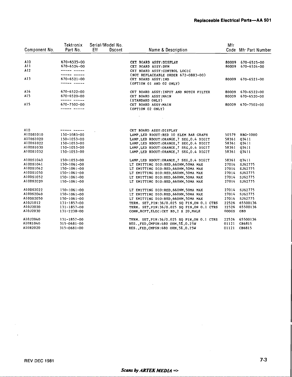
Replaceable Electrical Parts-AA
501
Component
No.
Tektronix
Part
No.
SerialIModel
Ef
f
No.
Dscont
Mfr
Name
&
Description
CKT BOARD ASSY:DISPLAY 80009 670-6525-00
CKT BOARD
CKT BOARD
(NOT REPLACEABLE ORDER 672-0883-00)
CKT BOARD
(OPTION 01 AND 02 ONLY)
CKT BOARD
CKT BOARD
(STANDARD ONLY)
CKT BOARD ASSY:MAIN 80009 670-7502-00
(OPTION
CKT BOARD ASSY:DISPLAY
LAMP,LED RD0UT:RED
LAMP,LED RDOUT:ORANGE,7 SEG,0.4 DIGIT
LAMP,LED RDOUT:ORANGE,7 SEG,0.4 DIGIT
LAMP,LED RDOUT:ORANGE,7 SEG,0.4 DIGIT
LAMP,LED RDOUT:ORANGE,7 SEG,0.4 DIGIT
LAMP,LED RDOUT:ORANGE,7 SEG,0.4 DIGIT
LT EMITTING
LT EMITTING
LT EMITTING
LT EMITTING
LT EMITTING
ASSY:DVM 80009 670-6524-00
ASSY:CONTROL LOGIC
ASSY:IMD 80009 670-6521-00
ASSY:INPUT AND NOTCH FILTER 80009 670-6522-00
ASSY:MAIN 80009 670-6520-00
02
ONLY)
10
ELEM BAR GRAPH
DIO:RED,660NM,bOMA MAX
DIO:RED,660NM,50MA MAX
DIO:RED,660NM,50MA MAX
DIO:RED,660NM,50MA MAX
DIO:RED,660NM,50MA MAX
Code
Mfr
Part
Number
LT EMITTING
LT EMITTING
LT EMITTING
TERM.
TERM.
CONN,RCPT,ELEC:CKT BD.2 X 20,MALE
TERM. SET,PIN:36/0.025 SQ PIN,ON 0.1 CTRS
RES.,FXD,CMPSN:680 OHM,5%,0.25W
RES.,FXD,CMPSN:680 OHM,5%,0.25W
DIO:RED,660NM,50MA MAX
DIO:RED,660NM,50MA MAX
DIO:RED,660NM,50MA MAX
SET,PIN:36/0.025 SQ PIN,ON 0.1 CTRS
SET,~IN:36/0.025 SQ PIN,ON 0.1 CTRS
27014 SJ62775
27014 SJ62775
27014 SJ62775
22526 65500136
22526 65500136
OOOGS OBD
REV
DEC
1981
Scans
by
ARTEK
MEDLQ
*
Page 74

Replaceable Electrical Parts-AA
501
Component
A1
1
A1 LC1020
Al lC1021
AllC1120
A1 lC1220
AllJllll
No.
Tektronix
Part
No.
-----
-----
285-1098-00
281-0813-00
281-0775-00
281-0809-00
131-2238-00
SerialIModel
Ef
f
No.
Dscont
Name
&
Description
CKT BOARD ASSY:DVM
CAP.,FXD,PLSTC:0.22UF,lO%,8OV
CAP. ,FXD CER DI:O.O47UF,20%,50V
CAP.,FXD,CER DI:O.lUF,20%,50V
CAP.,FXD,CER DI:200PF,5%,100V
CONN,RCPT,ELEC:CKT BD,2 X 20,MALE
SET,~IN:36/0.025 SQ PIN,ON
TERM.
TRANSISTOR:SILICON,NPN
TRANSISTOR:SILICON,PNP
RES.,FXD,CMPSN:820 OHM,5%,0.25W
RES.,FXD,CMPSN:820 OHM,5%,0.25W
RES.,FXD,CMPSN:430 OHM,5%,0.25W
RES. ,FXD,CMPSN:51K OHM,5% ,0.25W
RES.,FXD,CMPSN:510K OHM,5%,0.25W
RES.,FXD,CMPSN:3.3M OHM,5%,0.25W
RES.,FXD,CMPSN:3.3M OHM,5%,0.25W
RES.,FXD,CMPSN:82OK OHM,5%,0.25W
RES.,FXD,CMPSN:51K OHM,5%,0.25W
0.
Mfr
Code
56289
04222
72982
72982
OOOGS
Mfr
Part
Number
192P2249R8
GC705-E-473M
8005D9AABZ5U104M
8013T2ADDClG201J
OBD
RES.,FXD,CMPSN:51K OHM,5%,0.25W
RES.,FXD,CMPSN:62OK OHM,5%,0.25W
RES.,FXD,CMPSN:430 OHM,5%,0.25W
RES. ,FXD,CMPSN:430 OHM,5%,0.25W
RES.,FXD,CMPSN:430 OHM,5%,0,25W
RES.,FXD,CMPSN:430 OHM,5%,0.25W
Scans
by
ARTEK
MEDL4
=>
REV
DEC 1981
Page 75

Replaceable Electrical Parts-AA
501
Tektronix SerialIModel No.
Com~onent No. Part No.
Eff
Dscont
Name
&
Descri~tion
RES.,FXD,CMPSN:51K OHM,5%,0.25W
MICROCIRCUIT,LI:OPNL AMPL
MICROCIRLCUIT,LI:A/D CONV.3.5 DICIT
MICROCIRCUIT,LI:OPNL AMPL
MICROCIRCUIT,DI:QUAD 2-INPUT NAND GATE
MICROCIRCUIT,LI:OPNL AMPL
Mfr
Code Mfr Part Number
REV
DEC
1981
Scans
by
ARTEK
MEDLQ
=>
Page 76

Replaceable Electrical Parts-AA
50
1
No.
Tektronix
Part
No.
SerialIModel
Ef
f
No.
Dscont
Mfr
Name
&
Description
CKT BOARD ASSY:CONTROL LOGIC
CAP.,FXD,CER DI:O.lUF,20%,50V 72982 8005D9AABZ5U104M
CAP.,FXD,ELCTLT:IOUF,+50-IO%,2OV
CAP.,FXD,CER DI:O.IUF,20%,50V 72982 8005D9AABZ5U104M
CAP.,FXD,CER DI:O.lUF,20%,50V 72982 8005D9AABZ5U104M
CAP.,FXD,CER DI:O.lUF,20%,50V 72982 8005D9AABZ5U104M
CAP.,FXD,CER DI:O.0047UF,lO%,IOOV 04222 GC701C472K
CAP.,FXD,CER DI:100PF,IO%,IOOV 04222 GC70-1-A101K
CAP.,FXD,CER DI:O.OlUF,I0%,100V 04222 GC70-lC103K
SEMICOND
SEMICOND
SEMICOND
SEMICOND
SEMICOND
SEMICOND
SEMICOND
SEMICOND
SEMICOND
SEMICOND
SEMICOND
SEMICOND
SEMICOND
SEMICOND
CONTACT SET,ELE:R ANCLE,O.Z5OL,STRIP OF 36 22526 65524-136
CONTACT
CONTACT
CONTACT
CONTACT
TERM.
TERM.
DEVICE:SILICON,30V,I50MA
DEVICE:SILICON,30V,l5OMA
DEVICE:SILICON,30V,I50MA
DEVICE:SILICON,30V,I50MA
DEVICE:SILICON,30V,I50MA
DEVICE:SILICON,30V,I50MA
DEVICE:SILICON,3OV,I50MA
DEVTCE:SILICON,SOV,l50MA
DEVICE:SILICON,30V,l5OMA
DEVICE:SILICON,30V,I50MA
DEVICE:SILICON,3OV,I50MA
DEVICE:SILICON,30V,I50MA
DEVICE:SILICON,30V,I50MA
DEVICE:SILICON,30V,l5OMA
SET,ELE:R ANGLE,O.Z5OL,STRIP OF 36 22526 65524-136
SET,ELE:R ANCLE,0.250L,STRIP OF 36 22526 65524-136
SET,ELE:R ANGLE,O.Z5OL,STRIP OF 36 22526 65524-136
SET,ELE:R ANCLE,O.Z5OL,STRIP OF 36 22526 65524-136
SET,PIN:I X 36,O.l CTR,0.9 L 22526 65539-001
SET,PIN:36/0.025 SQ PIN,ON 0.1 CTRS 22526 65500136
Code
Mfr
Part
56289 500D149
01295 lN4152R
01295 1N4152R
01295 lN4152R
01295 1N4152R
01295 1N4152R
01295 lN4152R
01295 1N4152R
01295 IN4152R
01295 1N4152R
01295 1N4152R
01295 1N4152R
01295 1N4152R
01295 1N4152R
01295 1N4152R
Number Component
TERM.
SET,PIN:36/0.025 SQ PIN,ON 0.1
TERM.
SET,PIN:36/0.025 SQ PIN,ON 0.1 CTRS 22526
TRANSISTOR:SILICON,NPN
TRANSISTOR:SILICON,NPN
TRANSISTOR:SILICON.NPN
TRANSISTOR:SILICON,NPN
CTRS 22526 65500136
65500136
07263 SO32677
07263 SO32677
07263 SO32677
07263 SO32677
Scans
by
ARTEK
MEDL4
=>
REV
DEC
1981
Page 77

Replaceable Electrical Parts-AA
501
Com~onent
No.
Tektronix
Part
No.
SerialtModel
Eff
No.
Dscont
Name
&
Descri~tion
M
fr
Code
Mfr
01121
01 121
01121
01121
01121
01121
Part
CB2235
CB2235
CB5135
CB5135
CB5135
CB5135
Number
RES.,FXD,CMPSN:5lK OHM,5%,0.25W
RES.,FXD,CMPSN:510 OHM,5%,0.25W
RES.,FXD,CMPSN:510 OHM,5%,0.25W
RES.,FXD,CMPSN:lOK OHM,5%,0.25W
RES.,FXD,CMPSN:lOK 0HM,5%,0.25W
RES. ,FXD,CMPSN:lOK OHM,5%,0.25W
REV
DEC
1981
Scans
by
ARTEK
MEDL4
=>
Page 78

Replaceable Electrical
Parts-AA
501
Tektronix
Component
A12R1402 315-0104-00
A12R1403 315-0104-00
A12R1404 321-0193-01
A12R1405 321-0193-01
A12R1406 315-0122-00
A12R1407 32 1-0614-00
No.
Part
No.
SeriallModel
Eft
No.
Dscont
Mfr
Name
&
Description
RES.,FXD,CMPSN:lOOK OHM,5%,0.25W
RES.,FXD,CMPSN:lOOK OHM,5X,0.25W
RES.,FXD,FILM:lK OHM,0.5%,0.125W
RES.,FXD,FILM:IK OHM,0.5%,0.125W
RES.,FXD,CMPSN:1.2K OHM,5%,0.25W
RES.,FXD,FILM:lO.IK OHM,1%,0.125W
RES.,FXD,CMPSN:lOOK OHM,5%,0.25W
RES.,FXD,CMPSN:l30 OHM,5%,0.25W 01121
RES.,FXD,CMPSN:lOOK OHM,5%,0.25W 01121
RES.,VAR,NONWIR:5OK OHM,20%,0.50W 73138
RES.
,VAR,NONWIR:5K OHM, 10% ,O .SOW 73138
RES..FXD,FILM:I33K OHM,l%,O.l25W 91637
Code
01
121
Mfr
Part
Number
CB1045
CB1045
MFF 181 6C 10000D
MFF1816G10000D
CB1225
MFF1816C10101F
RES.,FXD,CMPSN:3.9K OHM,5%,0.25W
RES.,FXD,FILM:11.3K OHM,I%',O.l25W
RES. ,FXD,CMPSN:51K OHM,5%,0.25W
RES.,FXD,CMPSN:5lK OHM,5%,0.25W
RES.,FXD,CMPSN:51K OHM,5%,0.25W
RES.,FXD,CMPSN:5IK OHM,5%,0.25W
SWITCH,PUSH:4 RUTTON,2 6 4 POLE,LEVEL M 71590
SWITCH,PUSH:I BUTTON,4 POLE,INPUT 7 1590
TERM.TEST PO1NT:BRS CD PL 80009
TERM,TEST PO1NT:BRS CD PL 80009
TERM,TEST PO1NT:BRS CD PL 80009
MICROCIRCUIT,DI:BCD TO DECIMAL DECODER 80009
MICROCIRCUIT,DI:3 INPUT NOR GATE 80009
MICROCIRCUIT,DI:4 BIT AND/OR SEL 04713
MICROCIRClIIT, DI :4 BIT ADDER ,SELECTED 80009
MICROCIRCUIT,DI:BCD TO DECIMAL DECODER 80009
MICROCIRCUIT,DI:BINARY UP/DOWN COUNTER 04713
MICROCIRCUIT,DI:QUAD 2-INPUT NOR GATE 80009
MICROCIRCUIT,DI :4 BIT AND/OR SEL 04713
MICROCIRCUIT,DI:QUAD 2 INPUT AND GATE 80009
MICROCIRCUIT,DI:QUAD 2-INPUT NAND GATE 80009
MICROCIRCUIT,DI:QUAD ?-INPUT NOR GATE 80009
MICROCIRCIIIT
MICROCIRCUIT,DI:BCD TO DECIMAL DECODER 80009
MICROCIRCUIT,DI:BINARY UP/DOWN COUNTER 04713
MICROCIRCUIT,DI:QUAD 2-INPUT NOR GATE 80009
MICROCIRCUIT,LI:QUAD-COMP,!XL
.DI :4 BIT AND/OR SEL 04713
SUPPLY 27014
Scans
by
ARTEK
MEDU
=>
REV
DEC
1981
Page 79

Replaceable Electrical Parts-AA
501
Component
A12U1222
A12U1231
A12U1312
A12111313
A12U1321
A12U1331
No.
Tektronix
Part
No.
156-0048-00
156-0513-00
156-1200-00
156-1200-00
156-0579-00
156-1200-00
SerialIModel
Ef
f
No.
Dscont
Mfr
Name
&
Description
MICROCIRCUIT,LI:FIVE NPN TRANSISTOR ARRAY
MICROCIRCUIT,DI:8-CHAN MUX
MICROCIRCUIT,LI:OPERATIONAL
MICROCIRCUIT,LI:OPERATIONAL
MICROCIRCUIT,DI:DUAL 4-BIT BIN COUNTER
MICROCIRCUIT,LI:OPERATIONAL
MICROCIRCUIT,DI:DUAL 4-BIT BIN COUNTER 04713 MC14520BCL
MICROCIRCUIT,DI:TRIPLE 3-CHAN MUX 80009 156-0515-00
MICROCIRCUIT,DI:QUAD 2-INPUT NAND GATE 80009 156-0350-01
MICROCIRCUIT,DI:DUAL D-TYPE F-F 80009 156-0366-00
SEMICOND
SEMICOND
DEVICE:ZENER,0.4W,3V,5% 047 13 SZG35009K20
DEVICE:ZENER,0.25W,6.2V,5%
AMPL
AMPL
AMPL
Code
Mfr
Part
Number
02735 CA3046
80009 156-0513-00
01295
01295 TL074CN
04713 MC1452OBCL
01295 TL074CN
80009 152-0486-00
TL074CN
REV
DEC
1981
Scans
by
ARTEK MEDL4
-
Page 80
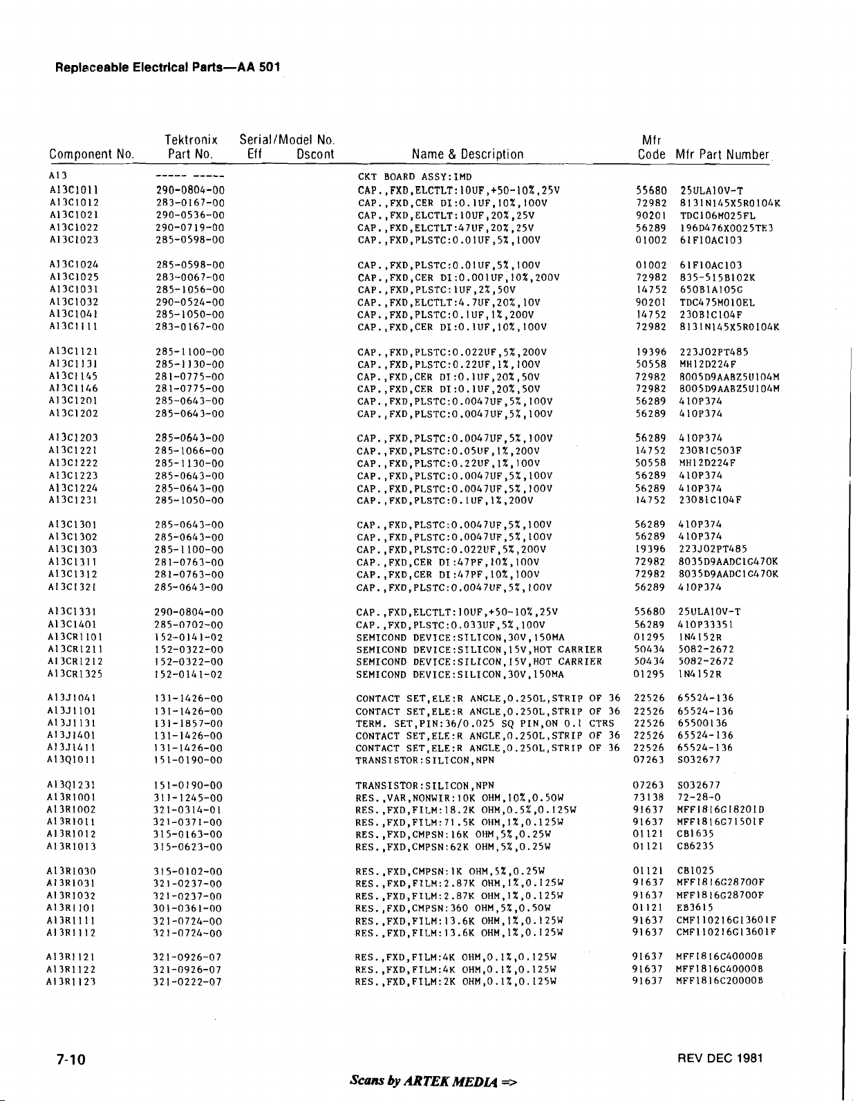
Replaceable Electrical Parts-AA
501
Component
No.
Tektronix
Part
No.
-----
-----
290-0804-00
283-0167-00
290-0536-00
290-0719-00
285-0598-00
SerialIModel
Ef
f
No.
Dscont
Name & Descriotion
CKT BOARD ASSY:IMD
CAP.,FXD,ELCTLT:lOUF,+50-10%,25V
CAP.,FXD,CER DI:O.lUF,IO%,IOOV
CAP.,FXD,ELCTLT:10UF120%,25V
CAP.,FXD,ELCTLT:47UF,20%,25V
CAP.,FXD,PLSTC:O.OIUF,5%,lOOV
CAP.,FXD,PLSTC:O.O22UF,5%,200V
CAP. ,FXD,PI2STC:O.22UF, I%, IOOV
CAP.,FXD,CER DI:O.lUF,20%,50V
CAP.,FXD,CER DI:O.lUF,20%,50V
CAP.,FXD,PLSTC:0.0047UF,5%,lNJV
CAP.,FXD,PLSTC:O.O047UF,5%,10OV
CAP.,FXD,PLSTC:O.O047UF,5%,10OV
CAP.,FXD,PLSTC:0.0047UF,5%,lOOV
CAP.,FXD,PLSTC:O.O22UF,5%,200V
CAP. ,FXD,CER DI :47PF, lo%, 100V
CAP.,FXD,CER DI:47PF,lO%,lOOV
CAP.,FXD,PLSTC:O.O047UF,5X,lOOV
Mfr
Code
Mfr
Part
Number
CAP.,FXD,ELCTLT:IOUF,+50-10%,25V
CAP.,FXD,PLSTC:O.O33UF,5%,10OV
SEMICOND
SEMICOND DEVICE:SILICON,15V,HOT CARRIER
SEMICOND
SEMICOND
CONTACT SET,ELE:R ANGLE,0.250L,STRIP OF 36
CONTACT
TERM.
CONTACT
CONTACT
TRANSISTOR:SILICON.NPN
TRANSISTOR:SILICON,NPN
RES.,VAR,NONWIR:IOK OHM,IO%,0.50W
RES.,FXD,FILM:l8.2K OHM,0.5%,0.125W
RES. ,FXD,FILM:71 .5K OHM,I%,0.125W
RES. ,FXD,CMPSN: 16K OHM,5% ,0.25W
RES.,FXD,CMPSN:62K OHM,5%,0.25W
RES.,FXD,FILM:LK OHM,0.1%,0.125W
RES. ,FXD,FILM:4K OHM,O. I%,0. 125W
RES.,FXD,FILM:ZK OHM,0.1%,0.125W
DEVICE:SILICON,30V,I50MA
DEVICE:SILICON,15V,HOT CARRIER
DEVICE:SILICON,3OV,l5OMA
SET,ELE:R ANGLE,0.250L,STRIP OF 36
SET,PIN:36/0.025 SQ PIN,ON
SET,ELE:R ANGLE,0.250L,STRIP OF 36
SET,ELE:R ANGLE,0.250L,STRIP OF 36
0.1
CTRS
CB1025
MFF 18 16G28700F
MFFI816G28700F
EB36 15
CMF110216G1360lF
CMF110216G13601F
Scans
by
ARTEK
MEDC4
=>
REV
DEC
1981
Page 81
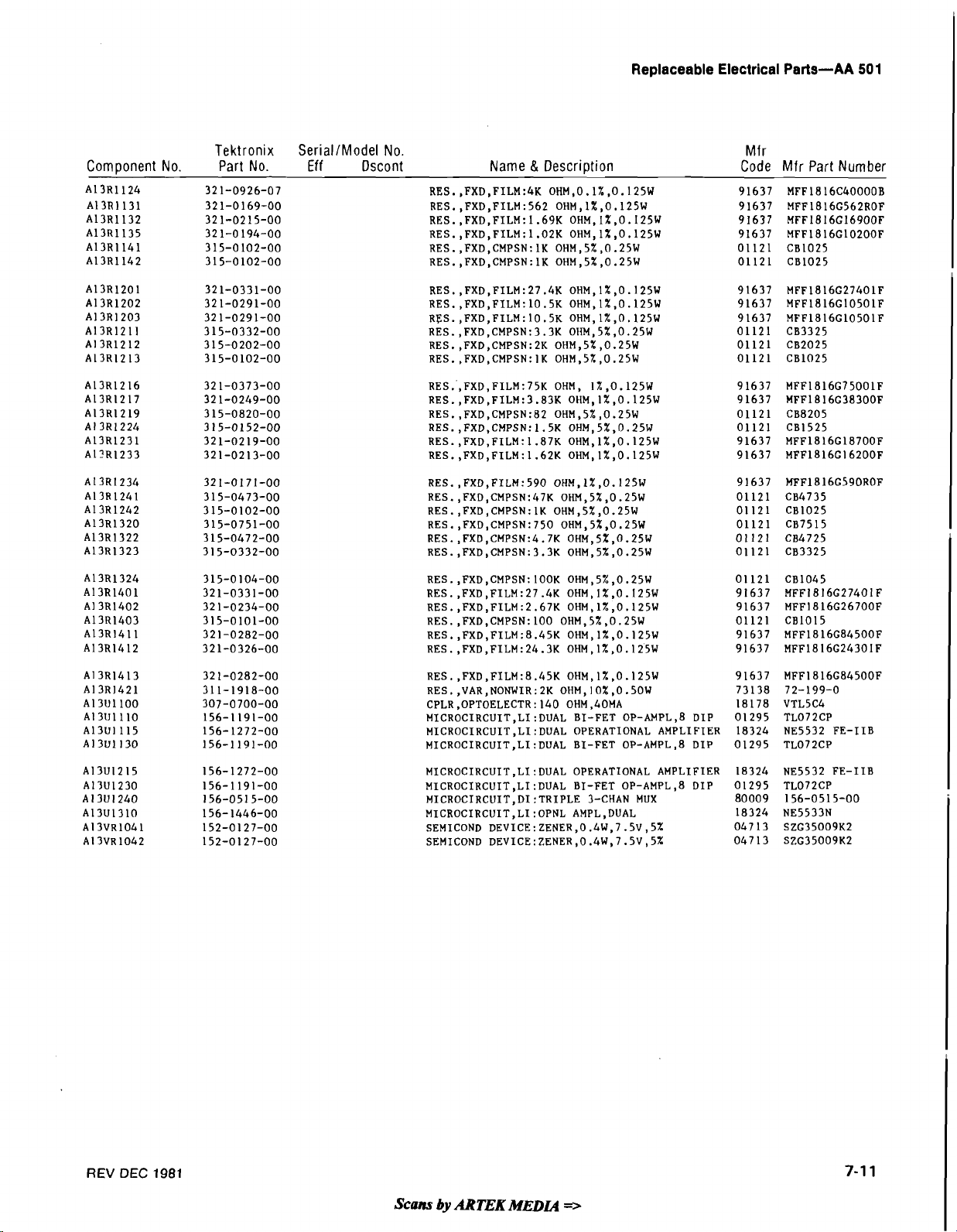
Replaceable Electrical
Parts-AA
501
Component
No.
Tektronix
Part
No.
Serial/Model
Eff
No.
Dscont
Name
&
Description
RES.,FXD,FILM:75K OHM, 1%,0.125W
RES.,FXD,FILM:3.83K Ol~M,l%,0.125W
RES.,FXD,CMPSN:82 OHM,5%,0.25W
RES.,FXD,CMPSN:1.5K OHM,5%,0.25W
RES.,FXD,FILM:1.87K OHM,1%,0.125W
RES.,FXD,FILM:1,62K OHM,l%,0.125W
RES.,FXD,CMPSN:lOOK OHM,5%,0.25W
RES. ,FXD,FILM:27.4K OHM,I%,O. 125W
RES.,FXD,FILM:2.67K OHM,1%,0.125W
RES.,FXD,CMPSN:lOO OHM,5%,0.25W
RES.,FXD,FILM:8.45K OHM,1%,0.125W
RES.,FXD,FILM:24.3K OHM,1%,0.125W
Mfr
Code
Mfr
Part
Number
RES.,FXD,FILM:8.45K OHM,1%,0.125W
RES.,VAR,NONWIR:ZK OHM,I0%,0.50W
CPLR,OPTOELECTR:140 OHM,40MA
MICROCIRCUIT,LI:DUAL BI-FET OP-AMPL,8 DIP
MICROCIRCUIT,LI:DUAL OPERATIONAL AMPLIFIER
MICROCIRCUIT,LI:DUAL BI-FET OP-AMPL.8 DIP
MICROCIRCUIT,LI:DUAL OPERATIONAL AMPLIFIER
MICROCIRCUIT,LI:DUAL BI-FET OP-AMPL,8 DIP
MICROCIRCUIT,DI:TRIPLE 3-CHAN MUX
MICROCIRCUIT,LI:OPNL AMPL,DUAL
SEMICOND
SEMICOND
DEVICE:ZENER,0.4W,7.5V,5%
DEVICE:ZENER,0.4W,7.5V,5%
MFF1816G84500F
72-199-0
VTL5C4
TL072CP
NE5532 FE-IIB
TL072CP
NE5532 FE-IIB
TL072CP
156-0515-00
NE5533N
SZG35009K2
SZG35009K2
REV
DEC
1981
Scans
by
ARTEK
MEDU
=>
Page 82
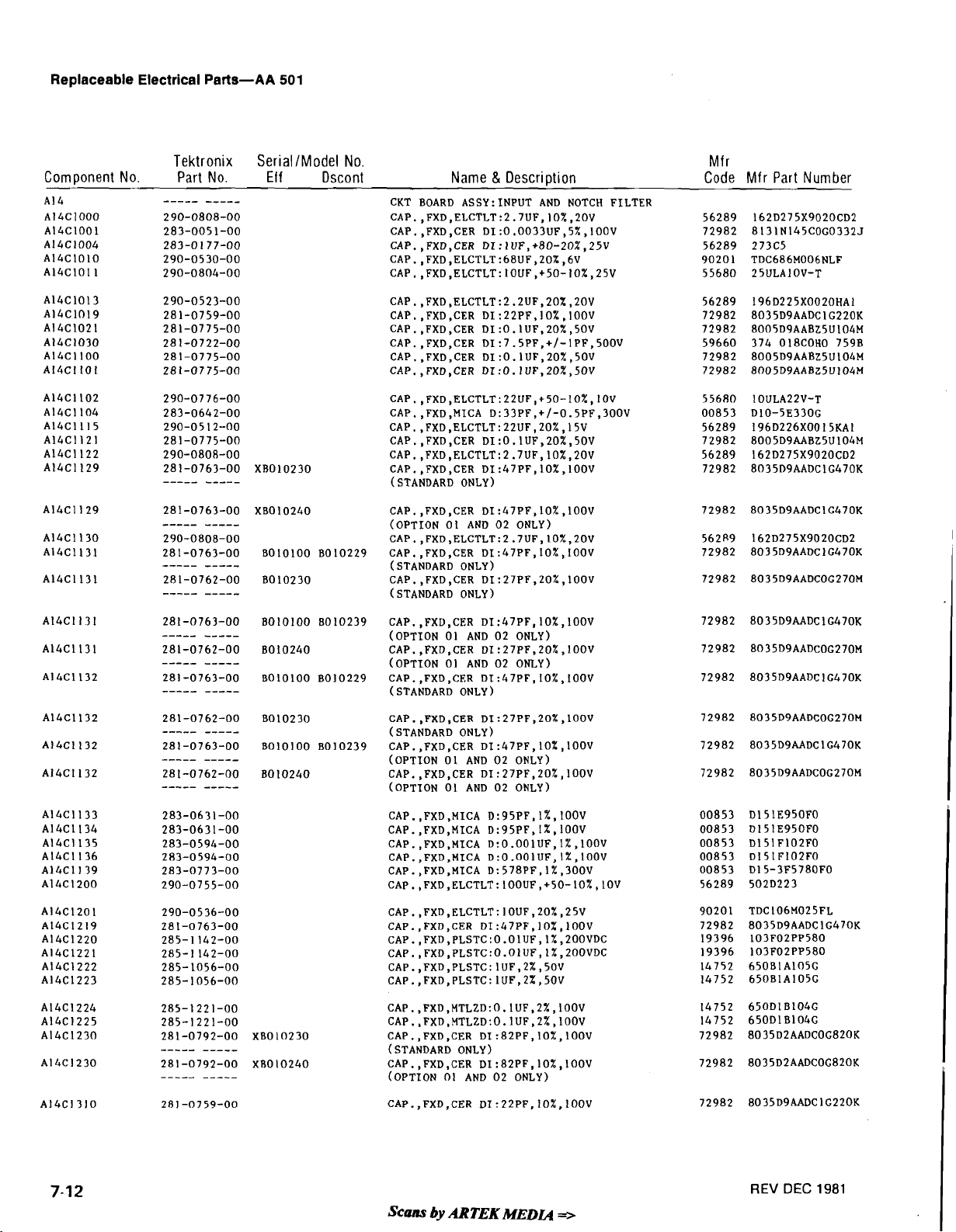
Replaceable Electrical Parts-AA
501
Com~onent
No.
Tektronix
Part
No.
SerialIModel
Eff
BOlOlOO B010229
B010230
No.
Dscont
Name
&
~e~cri~tion
CKT BOARD ASSY:INPUT AND NOTCH FILTER
CAP.,FXD,ELCTLT:2.7UF,l0%,20V
CAP.,FXD,CER DI:0.0033UF,5X,IOOV
CAP.,FXD,CER DI:lUF,+80-20%,25V
CAP.,FXD,ELCTLT:68UF,20XD6V
CAP.,FXD,ELCTLT:lOUF,+50-10%,25V
CAP. ,FXD,CER DI:47PF,10%,100V
(OPTION
CAP.,FXD,ELCTLT:2.7UF,IO%,2OV
CAP.,FXD,CER DI:47PF,lO%,lOOV
(STANDARD
CAP.,FXD,CER DI:27PF,20%,100V
(STANDARD
01
AND 02 ONLY)
ONLY)
ONLY)
Mfr
Code
Mfr
Part
Number
BOLO230
BOlOlOO 8010239
B010240
CAP.,FXD,CER DI:47PF,10%,100V
(OPTION
CAP.,FXD,CER DI:27PF,20%,100V
(OPTION
CAP.,FXD,CER DI:47PF,lOZ,lOOV
(STANDARD
CAP.,FXD,CER DI:27PF,20%,lOOV
(STANDARD
CAP.,FXD,CER DI:47PF,10%,IOOV
(OPTION
CAP.,FXD,CER DI:27PF,20%,100V
(OPTION
01
AND 02 ONLY)
01
AND 02 ONLY)
ONLY)
ONLY)
01
AND 02 ONLY)
01
AND 02 ONLY)
Scans
by
ARTEK
MEDU
=>
REV
DEC
1981
Page 83
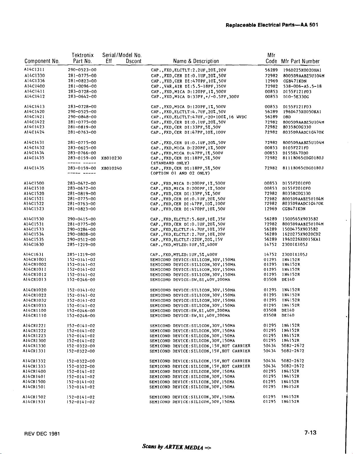
Replaceable Electrical Parts-AA
501
Tektronix
Component
A14C1311 290-0523-00
A14C1330 281-0775-00
A14C1336 281-0823-00
A14C1400 281-0096-00
A14C1411 283-0728-00
A14C1412 283-0642-00
No.
Part
No.
SeriallModel
Eff
No.
Dscont
Narnc
&
Descri~tion
CAP.,FXD,MICA D:200PF,1%,500V
CAP.,FXD.MICA D:200PF,1%,500V
CAP.,FXD,CER DI:33PF,5%,50V
CAP. ,FXD ,CER DI :O. 1 UF,20% ,50V
CAP.,FXD,CER DI:47PF,10%,100V
CAP.,FXD,CER DI:470PF,10%,50V
Mfr
Code
Mfr
Part
Number
56289
72982
12969
72982
00853
00853
00853 D155F121F03
56289 196D475X0050KAl
56289 OBD
72982
72982 8035BCOG330
72982 8035D9AADClG470K
196D225X0020HAl
8005D9AABZ5U104M
CGB47 1 KDN
538-006-A5
D155F121F03
D10-5E330G
8005D9AABZ5U104M
-5-18
CAP.,FXD,MTLZD:lUF,5%,400V
SEMICOND
SEMICOND
SEMICOND
SEMICOND
SEMICOND DEVICE:SW,SI,40V,200MA
SEMICOND
SEMICOND
SEMICOND
SEMICOND
SEMICOND DEVICE:SW,SI,40V,200MA
SEMICOND DEVICE:SW,SI ,40V,200MA
SEMICOND
SEMICOND
SEMICOND
SEMICOND
SEMICOND DEVICE:SILICON,15V,HOT CARRIER
SEMICOND
SEMICOND
SEMICOND
SEMICOND
SEMICOND
SEMICOND
SEMICOND
SEMICOND
SEMICOND
DEVICE:SILICON,30V,l5OMA
DEVICE:SILICON,30V,I50MA
DEVICE:SILICON,30V,l5OMA
DEVICE:SILICON,30V,l5OMA
DEVICE:SILICON.30V,l5OMA
DEVICE:SILICON,30V,I50MA
DEVICE:SILICON,30V,I50MA
DEVICE:SILICON,30V,150MA
DEVICE:SILICON,30V,I50MA
DEVICE:SILICON,30V,l5OMA
DEVICE:SILICON,30V,l5OMA
DEVICE:SILICON,30V,l5OMA
DEVICE:SILICON,15V,HOT CARRIER
DEVICE:SILICON,15V,HOT CARRIER
DEVICE:SILICON,15V,HOT CARRIER
DEVICE:SILICON,30V,l5OMA
DEVICE:SILICON,30V,l5OMA
DEVICE:SILICON.30V,I50MA
DEVICE:SILICON,30V,I50MA
DEVICE:SILICON,30V,I50MA
DEVICE:SILICON,30V,I50MA
REV
DEC 1981
Scans
by
ARTEK
MEDU
=>
Page 84
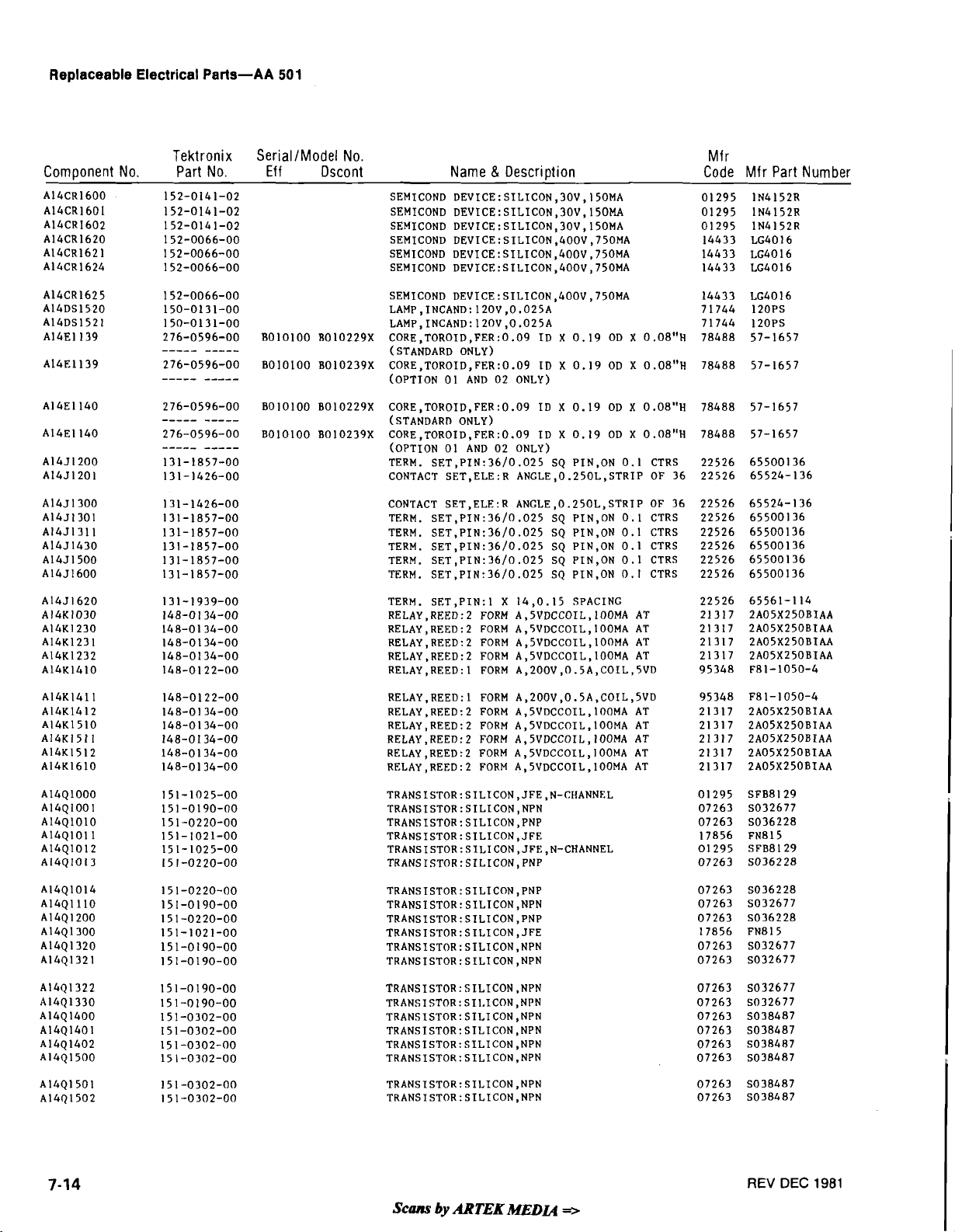
Replaceable Electrical Parts-AA
501
Component
A14CR1600
A14CR160L
A14CR1602
A14CR1620
A14CR162
A14CR1624
No.
1
Tektronix
Part
No.
SerialIModel
Eff
BOlOlOO B010229X CORE,TOROID,FER:O.09 ID X 0.19 OD X 0.08"H
BOlOlOO B010239X CORE.TOROID,FER:0.09 ID X 0.19 OD X 0.08"H
BOlOlOO B010229X CORE,TOROID,FER:O.09 ID X 0.19 OD X 0.08"H
BOlOlOO B010239X CORE,TOROID,FER:0.09 ID X 0.19 OD X 0.08"H
No.
Dscont
Name
&
Description
SEMICOND
SEMICOND
SEMICOND
SEMICOND
SEMICOND
SEMICOND
SEMICOND
LAMP,INCAND:120V,O.O25A
LAMP,INCAND:120V,O.O25A
(STANDARD
(OPTION
(STANDARD
(OPTION 01 AND 02 ONLY)
TERM. SET,PIN:36/0.025 SQ PIN,ON
CONTACT
CONTACT
TERM.
TERM.
TERM.
TERM.
TERM.
TERM.
RELAY,REED:2 FORM A,5VDCCOIL,100MA AT
RELAY,REED:2 FORM A,5VDCCOIL,IOOMA AT
RELAY,REED:2 FORM A,5VDCCOIL,100MA AT
RELAY,REED:2 FORM A,5VDCCOIL,IOOMA AT
RELAY,REED:l FORM A,200V,0.5A,COIL,5VD
DEVICE:SILICON,30V,I50MA
DEVICE:SILICON,30V,l5OMA
DEVICE:SILICON,30V,150MA
DEVICE:SILICON,400V,750MA
DEVICE:SILICON,400V,750MA
DEVICE:SILICON,400V,750MA
DEVICE:SILICON,400V,750MA
ONLY)
01
AND 02 ONLY)
ONLY)
0.1
0.1
0.1
0.1
0.1
0.1
CTRS
CTRS
CTRS
CTRS
CTRS
CTRS
SET,ELE:R ANGLE,O.25OL,STRIP OF 36
SET,ELE:R ANGLE,O.Z5OL,STRIP OF 36
SET,PIN:36/0.025 SQ PIN,ON
SET,PI~:36/0.025 SQ PIN,ON
SET,PIN:36/0.025 SQ PIN,ON
SET,PIN:36/0.025 SQ PIN,ON
SET,P1~:36/0.025 SQ PIN,ON
SET,PIN:l X 14,0.15 SPACING
Mfr
Code
Mfr
Part
Number
RELAY,REED:l FORM A,200V,0.5A,COIL,5VD
RELAY,REED:2 FORM A,5VDCCOIL,100MA AT
RELAY,REED:2 FORM A,5VDCCOIL,IOOMA AT
RELAY,REED:2 FORM A,5VDCCOIL,IOOMA AT
RELAY,REED:2 FORM A,5VDCCOIL,100MA AT
RELAY,REED:2 FORM A,5VDCCOIL,lOOMA AT
TRANSISTOR:SILICON,NPN
TRANSISTOR: SII.ICON,NPN
TRANSISTOR:SILICON,NPN
TRANSISTOR:SILICON,NPN
TRANSISTOR:SILICON,NPN
TRANSISTOR:SILICON.NPN
Scans
by
ARTEK
MEDL4
=>
REV
DEC
1981
Page 85
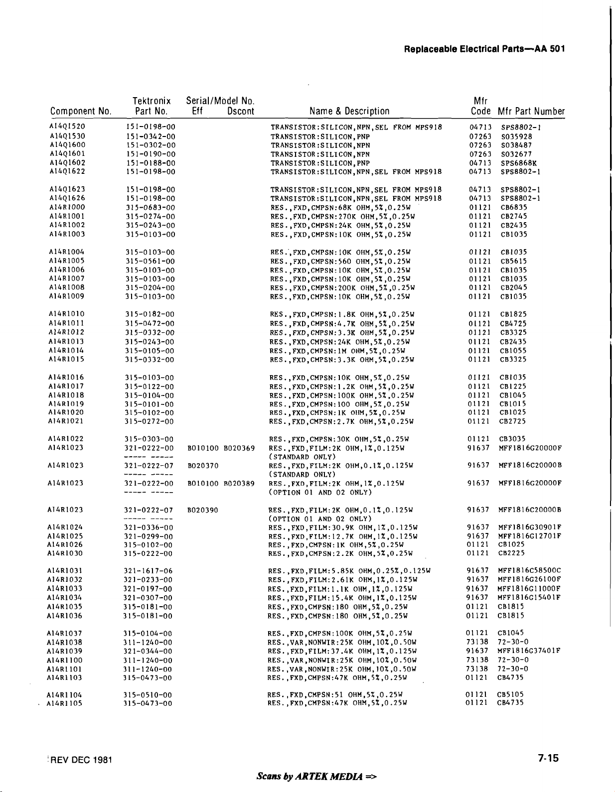
Replaceable Electrical Parts-AA
501
Tektronix
Com~onent No. Part No.
SerialIModel No.
Eff Dscont Name
TRANSISTOR:SILICON,NPN,SEL
TRANSISTOR:SILICON,PNP
TRANSISTOR:SILICON,NPN
TRANSISTOR:SILICON,NPN
TRANSISTOR:SILICON,PNP
TRANSISTOR:SILICON,NPN,SEL
TRANSISTOR:SILICON,NPN,SEL
TRANSISTOR:SILICON,NPN,SEL
RES.,FXD,CMPSN:68K OHM,5%,0.25W
RES.,FXD,CMPSN:27OK OHM,5%,0.25W
RES.,FXD,CMPSN:24K OHM,5%,0.25W
RES.,FXD,CMPSN:lOK OHM,5%,0.25W
RES.',FXD,CMPSN:lOK OHM,5%,0.25W
RES.,FXD,CMPSN:560 OHM,5%,0.25W
RES.,FXD,CMPSN:lOK OHM,5%,0.25W
RES. ,FXD,CMPSN: 1OK OHM,5% ,0.25W
RES.,FXD,CMPSN:ZOOK OHM,5%,0.25W
RES.,FXD,CMPSN:lOK OHM,5%,0.25W
&
Descri~tion
Mf r
Code Mfr Part Number
FROM MPS918
FROM MPS918
FROM MPS918
FROM MPS918
A14R1037
A14R1038
A14R1039
A14R1100
AlORllOl
A14R1103
BOlOlOO 8020369 RES.,FXD,FILM:ZK OHM,1%,0.125W
BOZO370 RES.,FXD,FILM:ZK OHM,0.1%,0.125W
BOlOlOO R020389 RES.,FXD,FILM:ZK OHM,l%,0.125W
8020390 RES.,FXD,FILM:ZK OHM,0.1%,0.125W
RES.,FXD,CMPSN:30K OHM,5%,0.25W
(STANDARD
(STANDARD
(OPTION
(OPTION 01 AND 02 ONLY)
RES.,FXD,FILM:30.9K OHM,1%,0.125W
RES.,FXD,FILM:12.7K OHM,1%,0.125W
RES.,FXD,CMPSN:lK OHM,5%,0.25W
RES.,FXD,CMPSN:Z.ZK OHM,5%,0.25W
RES.,FXD,CMPSN:lOOK OHM,5%,0.25W
RES.,VAR,NONWIR:25K OHM,lO%,O.5OW
RES.,FXD,FILM:37.4K OHM,l%,O.l25W
RES. ,VAR,NONWIR:25K OHM,~O% ,O .SOW
RES.,VAR,NONWIR:25K OHM,10%,0.50W
RES.,FXD,CMPSN:47K OHM,5%,0.25W
ONLY)
ONLY)
01
AND 02
ONLY)
!
REV
DEC
1981
Scans
by
ARTEK
MEDGQ
=>
Page 86
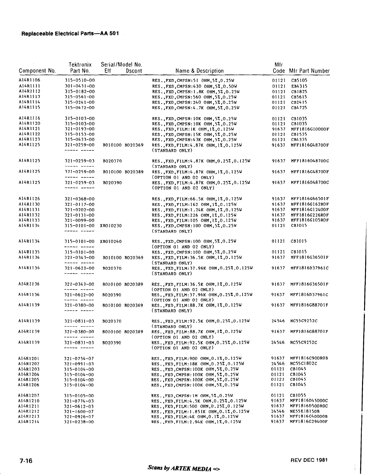
Replaceable Electrical
Parls-AA
501
Component
No.
Tektronix
Part
No.
SeriallModel
XBO 10240
No.
Ef
f
Dscont
BOlOlOO 8020369
8020370
BOlOlOO 8020389
8020390
BOlOlOO
BOZO370
B020369
Name
8
Descri~tion
RES.,FXD,CMPSN:51 OHM,5%,0.25W
RES.,FXD,CMPSN:430 OHM,5%,0.50W
RES.,FXD,CMPSN:l.8K OHM,5%,0.25W
RES. ,FXD,CMPSN:560 OHM,5%,0.25W
RES.,FXD,CMPSN:240 OHM,5%,0.25W
RES.,FXD,CMPSN:4.7K OHM,5%,0.25W
RES.,FXD,FILM:4.87K OHM,0.25%,0.125W
(STANDARD
RES.,FXD,FILM:4.87K OHM,lX,O.l25W
(OPTION
RES.,FXD,FILM:4.87K OHM,0.25%,0.125W
(OPTION 01 AND 02 ONLY)
RES.,FXD,FILM:66.5K OHM,1%,0.125W
RES.,FXD,FILM:162 OHM,1%,0.125W
RES. ,FXD ,FILM: 1.24K OHM, 1% ,O. 125W
RES.,FXD,FILM:226 OHM,1%,0.125W
RES.,FXD,FILM:105 OHH,l%,O.I25W
RES.,FXD,CMPSN:IOO OHM,5%,0.25W
(STANDARD
RES.,FXD,CMPSN:lOO OHM,5%,0.25W
(OPTION 01 AND 02 ONLY)
RES.,FXD,CMPSN:lOO OHM,5%,0.25W
RES. ,FXD,FILM:36.5K OHM, 1% ,O. 125W
(STANDARD
RES.,FXD,FILM:37.96K OHM,0.25%,O.l25W
t
STANDARD
ONLY)
01
AND 02 ONLY)
ONLY)
ONLY)
ONLY)
Mir
Code
Mfr
Part
Number
BOlOlOO BOZO389
8020390
BOlOlOO 8020369
8020370
BOlOlOO
BOZO390
B020389
RES.,FXD,FILM:36.5K OHM,l%,0.125W
(OPTION
RES.
(OPTION
RES.,FXD,FILM:88.7K OHM,1%,0.125W
(
STANDARD
RES.,FXD,FILM:92.5K OHM,0.25%,O.l25W
(STANDARD
RES.,FXD,FILM:88.7K OHM,I%,0.125W
(OPTION
RES.
(OPTION
RES.,FXD,FILM:900 OHM,0.1%,0.125W
RES..FXD,FILM:lBK OHM,0.25%,0.125W
RES.,FXD,CMPSN:lOOK OHM,5%,0.25W
RES.,FXD,CMPSN:lOOK OHM,5%,0.25W
RES. ,FXD,CMPSN: 100K OHM,5%,0.25W
RES.,FXD,CMPSN:lOOK OHM,5%,0.25W
RES. ,FXD,CMPSN: 1M OHM,5% ,0.25W
RES. ,FXD,FILM:4.5K OHM,O. 25% ,O. 125W
RES.,FXD,FILM:500 OHM,0.25%,0.125W
RES..FXD,FILM:1,85lK OHM,O.I%,O.I25W
RES.,FXD,FILM:4K OHM,O.L%,O.I25W
RES..FXD,FILM:2.94K OHM.lX,O.l25W
01
,FXD,FILM:37.96K OHM,0.25%,O.l25W
,FXD ,FILM:92.5K OHM,O .25% ,O. 125W
AND 02 ONLY)
01
AND 02 ONLY)
ONLY)
ONLY)
01
AND 02 ONLY)
01
AND
02
ONLY)
Scam
by
ARTEK
MEM
=>
REV
DEC
1981
Page 87
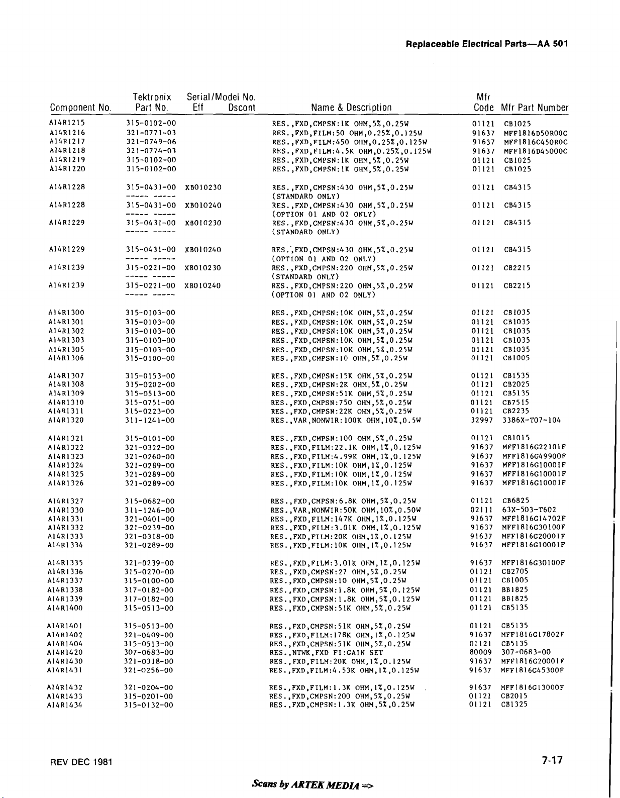
Replaceable Electrical Parts-AA
501
Tektronix
Component
A14R1215 31 5-0102-00
A14R1216 321-0771-03
A14R1217 321-0749-06
A14R1218 321-0774-03
A14R1219 315-0102-00
A14R1220 315-0102-00
No.
Part
No.
SerialIModel
Ef
f
XB010230
XBO 10240
XB010230
No.
Dscont
Mfr
Name
&
Description
RES.,FXD,CMPSN:lK OHM,5%,0.25W
RES. ,FXD,FILM:50 OHM,0.25Z,O.l25W
RES.,FXD,FILM:450 OHM,0.25%,0.125W
RES.,FXD,FILM:4.5K OHM,0.25%,0.125W
RES.,FXD,CMPSN:lK OllM,5%,0.25W
RES.,FXD,CMPSN:lK OHM,5%,0.25W
RES.,FXD,CMPSN:430 OHM,5%,0.25W
(STANDARD
RES.,FXD,CMPSN:430 OHM,5%,0.25W
(OPTION 01 AND 02 ONLY)
RES.,FXD,CMPSN:430 OHM,5%,0.25W
(STANDARD ONLY)
RES.',FXD,CMPSN:430 OHM,5%,0.25W 01121 CB4315
(OPTION 01 AND 02 ONLY)
RES.
(STANDARD
RES.,FXD,CMPSN:220 OHM,5%,0.25W 01121 CB2215
(OPTION 01 AND 02 ONLY)
RES.
RES.,FXD,CMPSN:2K OHM,5%,0.25W
RES.,FXD,CMPSN:51K OHM,5%,0.25W
RES.,FXD,CMPSN:750 OHM,5%,0.25W
RES.,FXD,CMPSN:22K OHM,5%,0.25W
RES.,VAR,NONWIR:lOOK OllM,10%,0.5W
ONLY)
,FXD,CMPSN:220 OHM,5%,0.25W 01121 CB2215
ONLY)
,FXD,CMPSN:15K OIlM.5%,0.25W
Code
Mfr
Part
01121 CB1025
91637 MFF1816D50ROOC
91637 MFFl816C450ROC
91637 MFF1816D45000C
01121 CB1025
01121 CB1025
Number
RES.,FXD,CMPSN:lOO OHM,5%,0.25W
RES.,FXD,FILM:22.1K OHM,l%,O.l25W
RES. ,FXD,FILM:4.99K OHM, 1%,0.125W
RES.,FXD,FILM:IOK OHM,l%,O.I25W
RES.,FXD,FILM:IOK OHM,l%,0.125W
RES.,FXD,FILM:lOK OHM,l%,O.I25W
RES.,FXD,CMPSN:51K OHM,5%,0.25W 01121 CB5135
RES.,FXD,FILM:178K 0~~,1%,0.125W 91637 MFF1816G17802F
RES.,FXD,CMPSN:51K OHM,5%,0.25W 01121 CB5135
RES.,NTWK,FXD F1:GAIN SET
RES.,FXD,FILM:ZOK OHM,1%.0.125W 91637 MFFlRl6G20001F
RES. ,FXD,FILM:4.53K OHM,1%,0.125W 91637 MFF1816G45300F
80009 307-0683-00
REV
DEC
1981
Scam
by
ARTEK
MEDLQ
Page 88
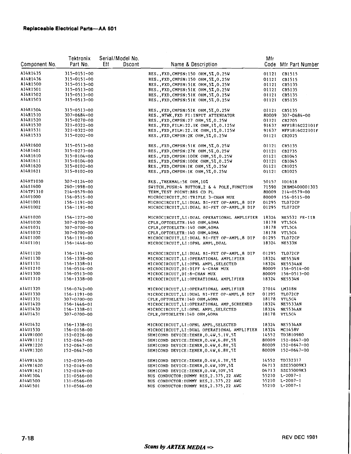
Replaceable Electrlcal Parts-AA
501
Component No.
A14R1435
A14R1436
A14R1500
A14R1501
A14R1502
A14R1503
Tektronix Serial/Model No.
Part No. Eff Dscont
Name 8 Descriotion
RES. ,FXD,CMPSN:.5IK OHM,5%,0.25W
RES.,NTWK,FXD F1:INPUT ATTENUATOR
RES.,FXD,CMPSN:27 OHM,5%,0.25W
RES.,FXD,FILM:22.lK OHM,1%,0.125W
RES.,FXD,FILM:22.1K OHM,1%,0.125W
RES.,FXD,CMPSN:LK OHM,5%,0.25W
RES.,THERMAL:SK OHM,lO%
SWITCH,PUSH:4 BUTTON,2 6 4 POLE,FUNCTION
TERM,TEST P0INT:BRS CD PL
MICROCIRCUIT,DI:TRIPLE 3-CHAN MUX
MICROCIRCUIT,LI:DUAL BI-FET OP-AMPL,8 DIP
MICROCIRCUIT,LI:DUAL BI-FET OP-AMPL,8 DIP
MICROCIRCUIT ,LI
CPLR,OPTOELETR:140 OHM,40MA
CPLR,OPTOELETR:140 OHM.40MA
CPLR,OPTOELETR:140 OHM,40MA
MICROCIRCUIT,LI:DUAL RI-FET OP-AMPL,8 DIP
MICROCIRCUIT,LI:OPNL AMPL,DUAL
:DUAL OPERATIONAL AMPLIFIER
Mfr
Code Mfr Part Number
01121 CB1515
01121 CB1515
01121 CB5135
01121 CB5135
01121 CB5135
01121 CB5135
18324 NE5532 FE-IIB
18178
18178 VTL5C4
18178 VTL5C4
01295 TL072CP
18324 NE533N
VTL5C4
MICROCIRCUIT,LI:DUAL RI-FET OP-AMPL,8 DIP
MICROCIRCUIT,LI:OPERATIONAL
MICROCIRCUIT,LI:OPNL AMPL,SELECTED
MICROCIRCUIT,DI:DIFF 4-CHAN MUX
MICROCIRCUIT,DI:8-CHAN MUX
MICROCIRCUIT,LI:OPERATIONAL
MICROCIRCUIT,LI:OPERATIONAL
MICROCIRCUIT,LI:DUAL RI-FET OP-AMPL,8 DIP
CPLR,OPTOELETR:140 OHM.40MA
MICROCIRCIJIT,LI:OPERATIONAL
MICROCIRCIlIT,LI:OPNL AMPL,SELECTED
CPLR,OPTOELETR:140 OHM,40MA
MICROCIRCUIT,LI:OPNL AMPL,SELECTED
MICROCIRCUIT,LI:DUAL OPERATIONAL AMPLIFIER
SEMICOND
SEMICOND
SEMICOND
SEMICOND
SEMICOND DEVICE :ZENER ,0.4W,4.3V,
SEMICOND
SEMICOND
BUS CONDUCT0R:DUMt-W RES,2.375,22 AWG
BUS
BUS CONDUCT0R:DUMNY RES,2.375,22 AWG
DEVICE:ZENER,0.4W,5.1V,5%
DEVICE:ZENER,0.4W,6.8V,5%
DEVICE:ZENER,0.4W,6.8V,5%
DEVICE:ZENER,0.4W,6.8V,5%
DEVICE:ZENER,0.4W,IOV,5%
DEVICE:ZENER,0.4W,IOV,5%
CONDIICT0R:DUMt-W RES,2.375,22 AWG
AMPLIFIER
AMPLIFIER
AMPLIFIER
AMP,SCREENED
5%
Scans
by
ARTEK
MEDL.4
REV
DEC
1981
Page 89
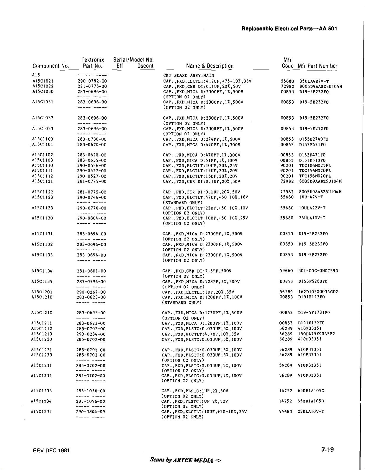
Replaceable Electrical Parts-AA
501
Tektronix
Component No. Part No.
-----
A1 5
-----
SerialIModel No.
Eff Dscont Name
CKT BOARD ASSY:MAIN
CAP.,FXD,ELCTLT:4.7UF,+75-10%,35V
CAP.,FXD,CER DI:O.lUF,20%,50V
CAP.,FXD,MICA D:2300PF,1%,500V
(OPTION
CAP.,FXD,MICA D:2300PF,1%,500V
(OPTION
02
02
ONLY)
ONLY)
&
Description
Mfr
Mfr Part Number
Code
CAP.,FXD,HICA D:2300PF,1%,5OOV
(OPTION
CAP.,FXD,MICA D:2300PF,1%,500V
(OPTION 02 ONLY)
CAP.,FXD,HICA D:2300PF,1%,500V
(OPTION
02
02
ONLY)
ONLY)
REV
DEC
1981
Scans
by
ARTEK
MEDL4
=>
Page 90

Replaceable Electrical Parts-AA
501
Com~onent
No.
Tektronix
Part
No.
SeriallModel
Eff
No.
Dscont
Name & Description
CAP.,FXD,PLSTC:O.O27UF,5%,100V
CAP.,FXD,PLSTC:O.O22UF,5%,100V
CAP.,FXD,PLSTC:O.O~~UF,~%,~~OV
CAP.,FXD,PLSTC:0.01UFF5%,10~V
CAP.,FXD,CER DI:O.IUF,20%,50V
(OPTION 02 ONLY)
CAP.,FXD,CER D1:6.8PF,+/-0.5PF,20OV
(OPTION
CAP. ,FXD,CER DI:O.lUF,20%,50V
(OPTION
CAP.,FXD,CER DI:150PF,IO%,IOOV
(OPTION
02
02
02
ONLY)
ONLY)
ONLY)
Mfr
Code
Mfr
Part
Number
55680 25ULAlOV-T
CAP.,FXD,CER DI:O.lUF,20%.50V
CAP.,FXD,ELCTLT:47UF,-10+75%.35
(STANDARD
CAP.,FXD,ELCTLT:~~UF,+~O-10%,25V
(OPTION
CAP.,FXD CER DI:0,047UF,20%,50V
CAP.,FXD,ELCTLT:47UF,-10+75%,35
(STANDARD
CAP.,FXD,ELCTLT:47UF.+50-10%,25V
(OPTION
CAP.,FXD CER DI:O.O47UF,20%,50V
CAP.,FXD,CER DI:O.~UF,~O%,~OV
CAP.,FXD,ELCTLT:lUF,+75-10%,50V
(OPTION
CAP.
(OPTION
CAP.,FXD,PLSTC:O.IUF,~%,~~~V
CAP.,FXD,CER DI:O.lUF,20%,5OV
CAP.,FXD CER DI:O.O47UF,20%,5OV
CAP.,FXD CER ~I:0.047UF,20%,50V
CAP.,FXD,CER DI:O.IUF,~~%,~OV
CAP.,FXD,MICA D:O.O01UF,1%,~0OV
CAP.,FXD,MICA ~:0.001UF,lX,100V
CAP.,FXD,ELCTLT:~OUF,+~O-IO%,~~V
CAP.,FXD,CER ~1:0.1~F,20%,50V
CAP.,FXD,CER DI:O.lUF,20%,50V
SEMICOND
ONLY)
02
ONLY)
ONLY)
02
ONLY)
02
,FXD,ELCTLT:~.~UF,~O%,~OV
ONLY)
02
ONLY)
DEVICE:SILICON,30V,I50MA
WDC
WDC
Scans
by
ARTEK
MEm
-
REV
DEC
1981
Page 91
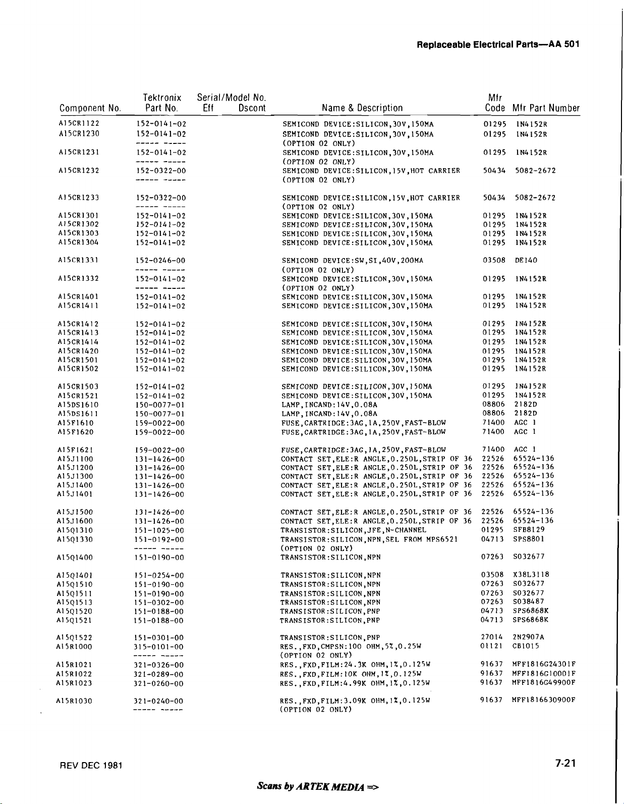
Replaceable Electrical Parts-AA
501
Component
No.
Tektronix
Part
No.
SerialIModel
Ef
f
No.
Dscont
Mfr
Name
&
Description
SEMICOND
SEMICOND
(OPTION
SEMICOND
(OPTION
SEMICOND
(OPTION
SEMICOND
(OPTION
SEMICOND
SEMICOND
SEMICOND
SEMICOND
SEMICOND DEVICE:SW,SI,40V,200MA 03508 DE140
(OPTION
SEMICOND
(OPTION
SEMICOND
SEMICOND
SEMICOND
SEMICOND
SEMICOND
SEMICOND
SEMICOND
SEMICOND
SEMICOND
SEMICOND
LAMP,INCAND:14V,O.O8A
LAMP,INCAND:14V,O.O8A
FUSE,CARTHIDGE:3AG,lA,250V,FAST-BLOW
FUSE,CARTRIDGE:3AG,lA,250V,FAST-BLOW
DEVICE:SILICON,30V,150MA
DEVICE:SILICON,30V,150MA
02
ONLY)
DEVICE:SILICON,30V,150MA
02 ONLY)
DEVICE:SILICON,15V,HOT CARRIER 50434 5082-2672
02 ONLY)
DEVICE:SILICON,15V,HOT CARRIER 50434 5082-2672
02 ONLY)
DEVICE:SILICON,30V,l5OMA
DEVICE:SILICON,30V,l5OMA
DEVICE:SILICON,30V,l5OMA
DEVICE:SILICON,30V,l5OMA
02
ONLY)
DEVICE:SILICON,30V,150MA
02
ONLY)
DEVICE:SILICON,3OV,l5OMA
DEVICE:SILICON,3OV,150MA
DEVICE:SILICON,30V,I50HA
DEVICE:SILICON,3OV,150MA
DEVICE:SILICON,3OV,150MA
DEVICE:SILICON,3OV,150HA
DEVICE:SILICON,3OV,l5OMA
DEVICE:SILICON,30V,150MA
DEVICE:SILICON,30V,I50MA
DEVICE:SILICON,30V,150MA
Code
Mfr
Part
01295 1N4152R
01295 lN4152R
01295 1N4152R
01295 1N4152R
01295 1N4152R
01295 1N4152R
01295 1N4152R
01295 lN4152R
01295 1N4152R
01295 1N4152R
01295 1N4152R
01295 1N4152R
01295 lN4152R
01295 1N4152R
01295 1N4152R
01295 1N4152R
01295 1N4152R
01295 1N4152R
08806 2182D
08806 2182D
71400 AGC
71400 AGC
1
1
Number
FUSE,CARTRIDGE:3AG,IA,250V,FAST-BLOW
CONTACT SET,ELE:R ANGLE,0.250L,STRIP OF 36
CONTACT
CONTACT
CONTACT
CONTACT
CONTACT
CONTACT
TRANSISTOR:SILICON,JFE,N-CHANNEL
TRANSISTOR:SILICON.NPN,SEL
(OPTION
TRANSISTOR:SILICON,NPN 07263 SO32677
TRANSISTOR:SILICON,PNP
RES, ,FXD,CMPSN: 100 OHM,5% ,0.25W 01121 CB1015
(OPTION
RES.,FXD,FILM:24.3K OHM,1%,0.125W 91637 MFF1816G24301F
RES.,FXD,FILM:IOK OHM,IX,O.l25W 91637 MFF1816G10001F
RES.,FXD,FILM:4.99K OHM,lX,O.I25W 91637 MFF1816G49900F
SET,ELE:R ANGLE,O.Z5OL,STRIP OF 36 22526 65524-136
SET,ELE:R ANGLE,0.250L,STRIP OF 36 22526 65524-136
SET,ELE:R ANGLE,O.Z5OL,STRIP OF 36
SET,ELE:R ANGLE,0.250L,STRIP OF 36 22526 65524-136
SET,ELE:R ANGLE,O.25OL,STRIP OF 36 22526 65524-136
SET,ELE:R ANGLE,0.250L,STRIP OF 36 22526 65524-136
02
02
ONLY)
ONLY)
FROM MPS6521 04713 SPS8801
71400 AGC
22526 65524-136
22526 65524-136
01295 SFB8129
27014 2N2907A
1
REV
DEC
1981
Scans
by
ARTEK
MEDU
-
Page 92

Replaceable Electrical Parts-AA
501
Com~onent
No.
Tektronix
Part
No.
SerialIModel
Eff
No.
Dscont
Name
8
Descriotion
RES.,FXD,FILM:lO.2K OHM,1%,0.125W
t
OPTION
RES.,FXD,FILM:ZK OHM,1%,0.125W
(OPTION
RES.,FXD,FILM:lIK OHM,1%,0.125W
(OPTION 02 ONLY)
RES.,FXD,FILM:llK OHM,IX,O.I25W
(OPTION 02 ONLY)
RES.,FXD,FILM:ZK OHM,1%,0.125W
(OPTION 02 ONLY)
RES.,FXD,FILM:I~.IK OHM,l%,O.I25W
(OPTION
RES.,FXD,FILM:19.1K OHM,I%,O.l25W
(OPTION 02 ONLY)
RES.,FXD,FILM:19.1K OHM,1%,0.125W
(OPTION 02 ONLY)
RES.
(OPTION 02 ONLY)
RES.,FXD,FILM:ZK OHM,l%,0.125W
RES.,FXD,FILM:ZK OHM,l%,O.I25W
RES.,FXD,FILM:ZK OHM,l%,0.125U
RES.,FXD.FILM:ZK OHM,1%,0.125W
RES.,FXD,CMPSN:IOOK OHM,5%,0.25W
RES. ,FXD,CMPSN: 1K OHM,5%,0.25W
02
ONLY)
02
ONLY)
02
ONLY)
,FXD,FILM:lO.5K OHM,l%,O.l25W
Mfr
Code
Mfr
Part
Number
RES.,FXD,FILM:IOK OHM,1%,0.125W
RES.,FXD,FILM:IOK OHM.lX.0.125W
RES.,FXD,FILM:15.8K OHM,0.25%.0.125W
(OPTION
RES.,FXD,CMPSN:360K OHM,5%,0.25W
(OPTION 02 ONLY)
RES.,VAR,NONWIR:25K OHM,20%,0.50W
(OPTION
RES.,FXD,FILM:2.87K OHM,1%,0.125W
(OPTION 02 ONLY)
RES.,FXD,FILM:10.2K OHM,I%,0.125W
(OPTION 02 ONLY)
02
02
ONLY)
ONLY)
Scans
by
ARTEK
MEDL4
=>
REV
DEC
1981
Page 93

Replaceable Electrical Parts-AA
501
Component
A15R1220
A15R1221
A15R1222
A15R1223
A15R1224
A15R1230
No.
Tektronix
Part
No.
321-0363-00
321-0244-00
321-0283-00
321-0374-00
321-0405-00
321-0296-00
-----
-----
SerialtModel
Ef
f
No.
Dscont
Name
&
Description
RES.,FXD,FILM:59K OHM,1%,0,125W
RES.,FXD,FILM:3.4K OHM,lX,O.l25W
RES.,FXD,FILM:8.66K OHM,1%,0.125W
RES.,FXD,FILM:76.8K OHM,1%,0.125W
RES.,FXD,FILM:162K OHM,lX,O.l25W
RES.,FXD,FILM:11.8K OHM,l%,O.l25W
(OPTION
02
ONLY)
Mfr
Code
91637
91637
91637
91637
91637
91637
Mfr
Part
Number
MFF1816G59001F
MFF1816G34000F
MFF1816G86600F
MFF1816G76801F
MFF1816G16202F
MFFl816G11801F
RES.,FXD,CMPSN:lOO OHM,5%,0.25W
RES.,FXD,CMPSN:24OK OHM,5%,0.25W
(STANDARD ONLY)
RES.,FXD,CMPSN:680K OHM,5%,0.25W
(OPTION 02 ONLY)
RES.,FXD,CMPSN:24K OHM,5%,0.25W
RES. ,FXD,FILM:I62K OHH,l%,O.l25W
(OPTION
RES.,VAR,NONWIR:25K OHM,20%,0.50W
(OPTION
RES.,FXD,CMPSN:5.1K OHM,5%,0.25W
(OPTION 02 ONLY)
RES.,FXD,FILM:93,1K OHM,l%,0.125W
(OPTION 02 ONLY)
02
02
ONLY)
ONLY)
REV
DEC
1981
Scam
by
AR
TEK
MEDIA
r>
Page 94

Replaceable Electrical Parts-AA
501
Component
No.
Tektronix
Part
No.
SerialIModel
Eff
No.
Dscont
Name
&
Description
RES.,FXD,CMPSN:Z.ZM OHM,5%,0.25W
(OPTION 02 ONLY)
RES.,FXD,FILM:412 OHM,l%,O.l25W
(OPTION 02 ONLY)
RES.,FXD,CMPSN:lOOK OHM,5%,0.25W
(OPTION
RES.,FXD,CMPSN:270 OHM,5%,0.25W
(OPTION
RES.,FXD,CMPSN:IOK OHM,5%,0.25W
RES. ,FXD,CMPSN: 15K OHM,5% ,0.25W
RES.,FXD,CMPSN:15K OHM,5%,0.25W
RES.,FXD,CMPSN:lOOK OHM,5%,0.25W
02
02
ONLY)
ONLY)
Mfr
Code
Mfr
Part
Number
RES.,FXD,CMPSN:lOO OHM,5%,0.25W
RES.,FXD,CMPSN:lOO OHM,5%,0.25W
RES.,FXD,CMPSN:IK OHM,5%.0.25W
RES. ,FXD,CMPSN: IK OIM,5%,0.25W
RES.,FXD,CMPSN:lK OHM,5%,0.25W
RES.,FXD,CMPSN:IK OHM,5%,0.25W
RES. ,FXD,FILM:600 OHM, 1% ,O. 125W
RES.,FXD,FILM:226 o~~,l%,O.l25W
RES.,FXD,CMPSN:4.7K OHM,5%,0.25W
RES.,FXD,CMPSN:4.7K OAM,5%,0.25W
SWITCH,PUSH:5 BUTTON,4,2
SWITCH,PUSH:5 8UTTON,2 6 4 POLE,FILTER
TERM,TEST P0INT:RRS CD PL
MICROCIRCUIT,LI:DUAL BI-FET OP-AMPL,8 DIP
Scans
by
ARTEK
MEDL4
=>
6
0
POILE,DISTOR
ADD
DEC
1981
Page 95

Com~onent
No.
Tektronix
Part
No.
SeriallModel
Eft
No.
Dscont
Replaceable Electrical Parts-AA
Mf
r
Name
&
Description
MICROCIRCUIT,LI:TRUE RMS CONVERTER 24355 AD536AJH
MICROCIRCUIT,LI:DUAL BI-FET OP-AMPL.8 DIP 01295 TL072CP
MICROCIRCUIT,LI:OPERATIONAL
MICROCIRCUIT,LI:OPERATIONAL
(OPTION
MICROCIRCUIT,LI:OPERATIONAL
(OPTION
02
02
ONLY)
ONLY)
AMP,JFET INPUT 27014 LF351N
AMPL
AMPLIFIER 18324 NE5534N
Code
Mfr
Part
01
295 TL074CN
Number
501
MICROCIRCUIT,LI:OPERATIONAL
MICROCIRCUIT,LI:DUAL BI-FET OP-AMPL,8 DIP 01295 TL072CP
(STANDARD
MICROCIRCUIT,LI:OPERATIONAL
(OPTION
MICROCIRCUIT,LI:OPERATIONAL
MICROCIRCUIT,LI:OPERATIONAL
(OPTION 02 ONLY)
MICROCIRCUIT,DI:HEX CONT BOUNCE ELIMINATOR 80009 156-0763-00
MICROCIRCUIT,DI:QUAD D FF 80009 156-0931-00
MICROCIRCUIT,LI:DUAL OPERATIONAL AMPLIFIER 18324 MC1458V
MICROCIRCUIT,DI:QUAD D FF 80009 156-0931-00
MICROCIRCUIT,LI:VOLTAGE REGULATOR 07263 MICROA7805UC
MICROCIRCUIT,DI:8-CHAN MUX
MICROCIRCUIT,LI:QUAD-COMP,SGL
SEMICOND
SEMICOND
SEMICOND DEVICE:ZENER,18V,5% AT 7MA 80009 152-0590-00
SEMICOND
ONLY)
02
ONLY)
DEVICE:ZENER,0.4W,6.8V,5%
DEVICE:ZENER,0.25W,6.2V,5%
DEVICE:ZENER,18V,5% AT 7MA 80009 152-0590-00
AMP,JFET INPUT 27014 LF351N
AMP,JFET INPUT 27014 LF351N
AMP,JFET INPUT 27014 LF351N
AMPL 01295 TL074CN
80009 156-0513-00
SUPPLY 27014 LM339N
80009 152-0647-00
80009 152-0486-00
ADD
DEC 1981
Scans
by
ARTEK
MEDL4
-
Page 96
Tektronix SerialIModel No.
Component No. Part No. Ef f Dscont Name
CHASSIS PARTS
&
Description
Mfr
Code Mfr Part Number
S1521
263-1187-00
SW CAM ACTR AS:LEVEL RANGE
Scans
by
ARTEK
MEDLQ
==-
ADD
DEC
1981
Page 97
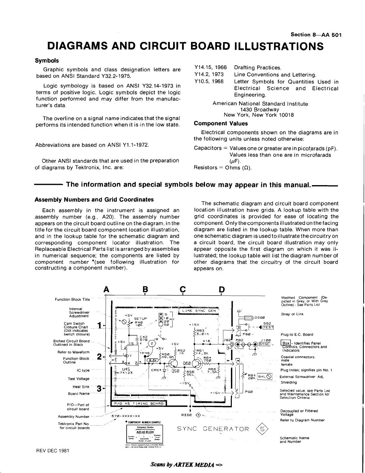
Section
DIAGRAMS AND CIRCUIT BOARD ILLUSTRATIONS
Symbols
Graphic symbols and class designation letters are
based on
ANSI Standard Y32.2-1975.
Logic symbology is based on ANSl Y32.14-1973 in
terms of positive logic. Logic symbols depict the logic
function performed and may differ from the manufacturer's data.
The
overline on a signal name indicates that the signal
performs its intended function when it is in the low state.
Abbreviations are based on ANSl Y1.l-1972.
Other
ANSI standards that are used in the preparation
of diagrams by Tektronix, Inc. are: Resistors = Ohms
The information and special symbols below may appear in this manual.
Y14.15, 1966 Drafting Practices.
Y14.2, 1973
Line Conventions and Lettering.
Y10.5, 1968 Letter Symbols for Quantities Used in
Electrical Science and Electrical
Engineering.
American National Standard Institute
1430 Broadway
New York, New York 10018
Component Values
Electrical components shown on the diagrams are in
the following units unless noted otherwise:
Capacitors
=
Values one or greater are in picof,arads (pF).
Values less than one are in microfarads
(PF).
(n).
8-AA
501
Assembly Numbers and Grid Coordinates
Each assembly in the instrument is assigned an
.assembly number
appears on the circuit board outline on the diagram, in the
title for the circuit board component location illustration,
and in the lookup table for the schematic diagram and
corresponding component locator illustration. The
Replaceable Electrical Parts
in numerical sequence; the components are listed by
component number *(see following illustration for
constructing a component number).
Funct~on Block T~tle
(Dot lndlcates
swltch closure)
Clrcult Board
Etched
Outl~ned In Black
Refer to Waveform
Test Voltage
PIO-Part of
clrcult board
Assembly Number
Tektronix Part No
for
clrcult boards
REV
DEC
1981
(e.g., A20). The assembly number
list isarranged by assemblies
A
Internal
Screwdriver
Adlustrnent
Board Name
670-XXXX-XX R330
#
B
The schematic diagram and circuit board component
location illustration have grids. A lookup table with the
grid coordinates is provided for ease of locating the
component. Only the components illustrated on the facing
diagram are listed in the lookup table. When more than
one schematic diagram is used to
a circuit board, the circuit board
illustratethecircuitry on
~llustration may only
appear opposite the first diagram on which it was il-
lustrated; the lookup table will list the diagram number of
other diagrams that the circuitry of the circuit board
appears on.
C
0-
SYNC
D
GENERATOR
@
Modifled Componenl (De-
~n Grey, or Wlth Grey
picted
Outllne) - See Parts Llst
Strap or Link
Plug to E.C. Board
l
ndicators
Coaxial connectors:
male
female
Plug Index; signifies pin No.
External Screwdriver Adj
Shielding
Selected value, see Parts
and Maintenance Section for
Selection Criteria
Decoupled or Filtered
Voltage
Refer to Diagram Number
Schematic Name
and Number
1
L~st
Scam
by
ARTEK
MEDL4
=>
Page 98
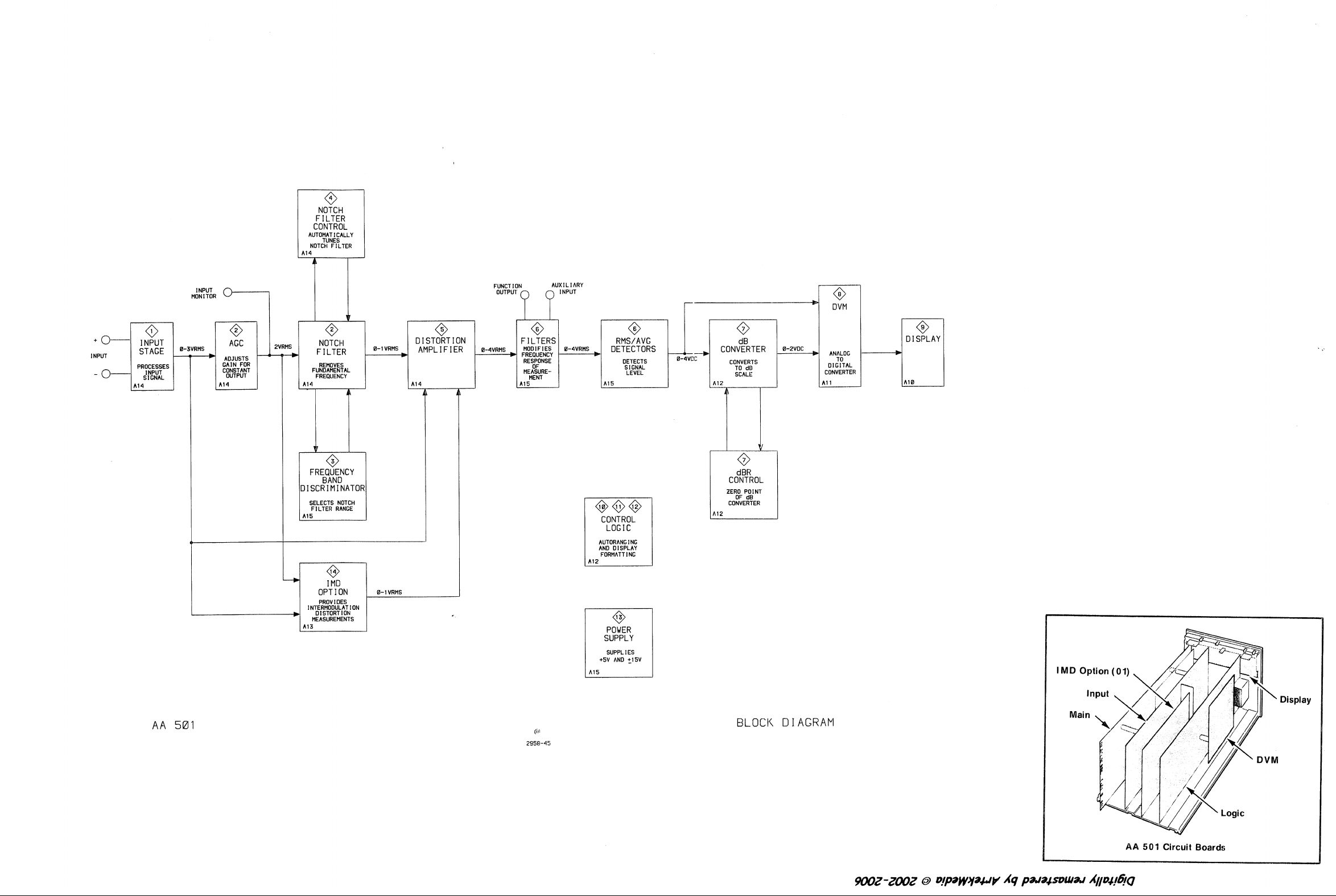
NOTCH
I
LTER
F
CONTROL
AUTOMATICALLY
TUNES
NOTCH FILTER
I
A14
A
I
+
*
INPUT
-
0
INPUT
STAGE
PROCESSES
l
NPUT
SIGNAL
A14
l
NPUT
MONITOR
0-3VRMS
)
GAIN FOR
CONSTANT
A14
O
AGC
ADJUSTS
OUTPUT
-
2v~ns
-
-
FUNDAMENTAL
A14
FREQUENCY
DISCRIMINATOR
SELECTS NOTCH
FILTER
INTERMODULATION
MEASUREMENTS
FUNCTION AUXILIARY
OUTPUl
?
~~>~~k
REMOVES
FREQUENCY
RANGE
DISTORTION
8-lvRns
A
DISTORTION
AMPL 1
F [ ER
A14
A
A
a-4VRMS
F 1 LTERS RMS/AVG
RESPONSE
OF SIGNAL TO
MEASURE- LEVEL
MENT
A15
1
DETECTS CONVERTS TO
A15 A12
CONTROL
I
C
LOG
AUTORANGING
AND DISPLAY
FORMATTING
0
POVER
SUPPLY
1
-*
dB
dD
SCALE CONVERTER
A
v
dBR
CONTROL
ZERO POINT
OF
dB
CONVERTER
A12
D I SPLAY
DIGITAL
A10
BLOCK
D
I
AGRAM
Page 99
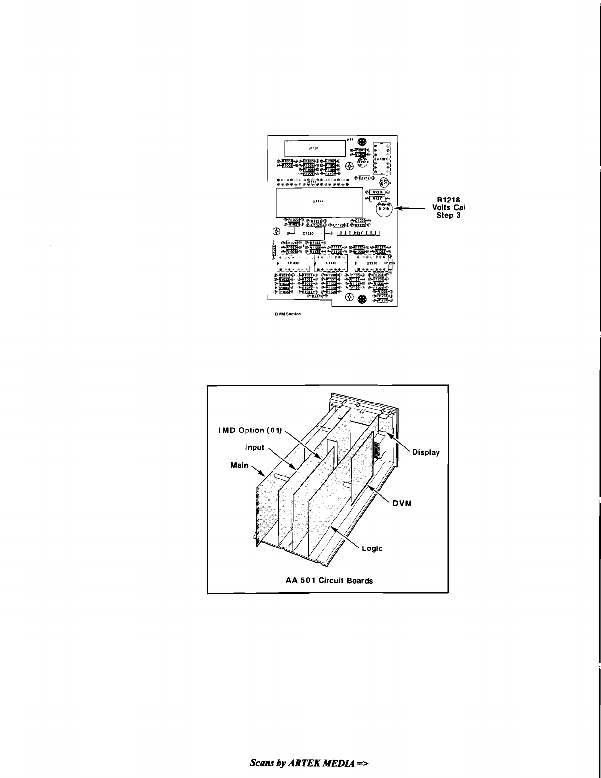
IMD
DVM
Option (01)
Sesllon
R1218
Volts Cal
3
Step
Scans
AA
501 Circuit Boards
by
ARTEK
MEDL4
=-=.
Page 100
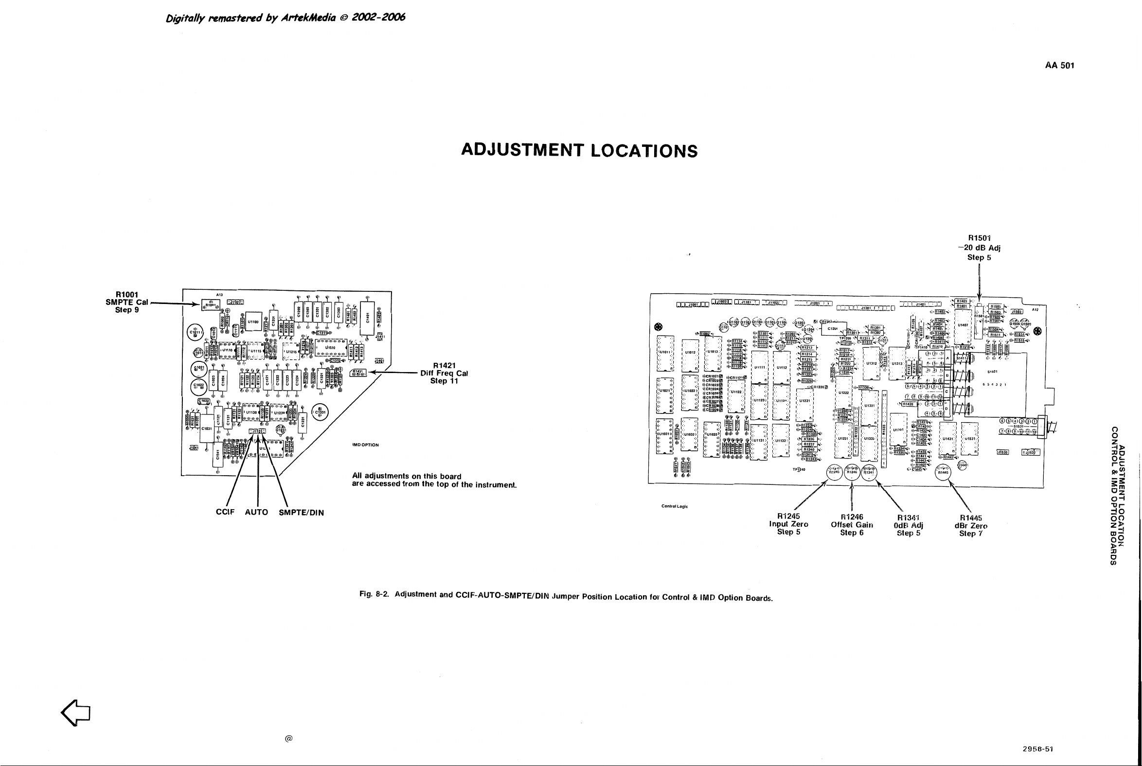
RlOOl
SMPTE Cal
Step
9
D&itally remastered by ArhkMedia
@
2W-2-
ADJUSTMENT LOCATIONS
R1501
-20 dB Adj
Step
5
R1421
Diff Freq Cal
Step 11
All adjustments on this board
are accessed from the top of the instrument.
Fig.
8-2.
Adjustment and CCIF-AUTO-SMPTE/DIN Jumper Position Location for Control & IMD Option Boards.
R1245
Input Zero
Step 5
R4246
Offset
Step
Gait?
6
R1341
OdD Adj dBr Zera
Step
5
R1445
Step
T
 Loading...