

Page 1

Model 82-WIN Simultaneous C-V Measurement
User’s Manual
A GREATER MEASURE OF CONFIDENCE
Page 2

WARRANTY
Keithley Instruments, Inc. warrants this product to be free from defects in material and workmanship for a
period of 1 year from date of shipment.
Keithley Instruments, Inc. warrants the following items for 90 days from the date of shipment: probes, cables,
rechargeable batteries, diskettes, and documentation.
During the warranty period, we will, at our option, either repair or replace any product that proves to be defective.
To exercise this warranty, write or call your local Keithley representative, or contact Keithley headquarters in
Cleveland, Ohio. You will be given prompt assistance and return instructions. Send the product, transportation
prepaid, to the indicated service facility. Repairs will be made and the product returned, transportation prepaid.
Repaired or replaced products are warranted for the balance of the original warranty period, or at least 90 days.
LIMITATION OF WARRANTY
This warranty does not apply to defects resulting from product modification without Keithley’s express written
consent, or misuse of any product or part. This warranty also does not apply to fuses, software, non-rechargeable
batteries, damage from battery leakage, or problems arising from normal wear or failure to follow instructions.
THIS WARRANTY IS IN LIEU OF ALL OTHER WARRANTIES, EXPRESSED OR IMPLIED, INCLUDING ANY IMPLIED WARRANTY OF MERCHANTABILITY OR FITNESS FOR A PARTICULAR USE.
THE REMEDIES PROVIDED HEREIN ARE BUYER’S SOLE AND EXCLUSIVE REMEDIES.
NEITHER KEITHLEY INSTRUMENTS, INC. NOR ANY OF ITS EMPLOYEES SHALL BE LIABLE FOR
ANY DIRECT, INDIRECT, SPECIAL, INCIDENTAL OR CONSEQUENTIAL DAMAGES ARISING OUT OF
THE USE OF ITS INSTRUMENTS AND SOFTWARE EVEN IF KEITHLEY INSTRUMENTS, INC., HAS
BEEN ADVISED IN ADVANCE OF THE POSSIBILITY OF SUCH DAMAGES. SUCH EXCLUDED DAMAGES SHALL INCLUDE, BUT ARE NOT LIMITED TO: COSTS OF REMOVAL AND INSTALLATION,
LOSSES SUSTAINED AS THE RESULT OF INJURY TO ANY PERSON, OR DAMAGE TO PROPERTY.
Keithley Instruments, Inc.
Sales Offices: BELGIUM: Bergensesteenweg 709 • B-1600 Sint-Pieters-Leeuw • 02-363 00 40 • Fax: 02/363 00 64
CHINA: Yuan Chen Xin Building, Room 705 • 12 Yumin Road, Dewai, Madian • Beijing 100029 • 8610-8225-1886 • Fax: 8610-8225-1892
FINLAND: Tietäjäntie 2 • 02130 Espoo • Phone: 09-54 75 08 10 • Fax: 09-25 10 51 00
FRANCE: 3, allée des Garays • 91127 Palaiseau Cédex • 01-64 53 20 20 • Fax: 01-60 11 77 26
GERMANY: Landsberger Strasse 65 • 82110 Germering • 089/84 93 07-40 • Fax: 089/84 93 07-34
GREAT BRITAIN: Unit 2 Commerce Park, Brunel Road • Theale • Berkshire RG7 4AB • 0118 929 7500 • Fax: 0118 929 7519
INDIA: 1/5 Eagles Street • Langford Town • Bangalore 560 025 • 080 212 8027 • Fax: 080 212 8005
ITALY: Viale San Gimignano, 38 • 20146 Milano • 02-48 39 16 01 • Fax: 02-48 30 22 74
JAPAN: New Pier Takeshiba North Tower 13F • 11-1, Kaigan 1-chome • Minato-ku, Tokyo 105-0022 • 81-3-5733-7555 • Fax: 81-3-5733-7556
KOREA: 2FL., URI Building • 2-14 Yangjae-Dong • Seocho-Gu, Seoul 137-888 • 82-2-574-7778 • Fax: 82-2-574-7838
NETHERLANDS: Postbus 559 • 4200 AN Gorinchem • 0183-635333 • Fax: 0183-630821
SWEDEN: c/o Regus Business Centre • Frosundaviks Allé 15, 4tr • 169 70 Solna • 08-509 04 600 • Fax: 08-655 26 10
TAIWAN: 13F-3, No. 6, Lane 99, Pu-Ding Road • Hsinchu, Taiwan, R.O.C. • 886-3-572-9077 • Fax: 886-3-572-9031
28775 Aurora Road • Cleveland, Ohio 44139 • 440-248-0400 • Fax: 440-248-6168
1-888-KEITHLEY (534-8453) • www.keithley.com
2/03
Page 3

Model 82-WIN Simultaneous C-V Measurement
User’s Manual
©1997, Keithley Instruments, Inc.
All rights reserved.
Cleveland, Ohio, U.S.A.
Second Printing, October 1999
Document Number: 82WIN-900-01 Rev. B
Page 4

Manual Print History
The print history shown below lists the printing dates of all Re visions and Addenda created
for this manual. The Revision Le vel letter increases alphabetically as the manual undergoes
subsequent updates. Addenda, which are released between Revisions, contain important
change information that the user should incorporate immediately into the manual. Addenda
are numbered sequentially . When a ne w Revision is created, all Addenda associated with the
previous Revision of the manual are incorporated into the ne w Re vision of the manual. Each
new Revision includes a revised copy of this print history page.
Revision A (Document Number 82WIN-900-01)...............................................................April 1997
Revision B (Document Number 82WIN-900-01).................................................................October 1999
All Keithley product names are trademarks or registered trademarks of Keithley Instruments, Inc.
Other brand names are trademarks or registered trademarks of their respective holders.
Page 5

S
afety Precautions
The following safety precautions should be observed before using this product and any associated instrumentation. Although
some instruments and accessories would normally be used with non-hazardous voltages, there are situations where hazardous
conditions may be present.
This product is intended for use by qualified personnel who recognize shock hazards and are familiar with the safety precautions
required to avoid possible injury. Read and follow all installation, operation, and maintenance information carefully before using the product. Refer to the manual for complete product specifications.
If the product is used in a manner not specified, the protection provided by the product may be impaired.
The types of product users are:
Responsible body
ment is operated within its specifications and operating limits, and for ensuring that operators are adequately trained.
Operators
instrument. They must be protected from electric shock and contact with hazardous live circuits.
Maintenance personnel
voltage or replacing consumable materials. Maintenance procedures are described in the manual. The procedures explicitly state
if the operator may perform them. Otherwise, they should be performed only by service personnel.
Service personnel
trained service personnel may perform installation and service procedures.
Keithley products are designed for use with electrical signals that are rated Installation Category I and Installation Category II,
as described in the International Electrotechnical Commission (IEC) Standard IEC 60664. Most measurement, control, and data
I/O signals are Installation Category I and must not be directly connected to mains voltage or to voltage sources with high transient over-voltages. Installation Category II connections require protection for high transient over-voltages often associated with
local AC mains connections. Assume all measurement, control, and data I/O connections are for connection to Category I sources unless otherwise marked or described in the Manual.
Exercise extreme caution when a shock hazard is present. Lethal voltage may be present on cable connector jacks or test fixtures.
The American National Standards Institute (ANSI) states that a shock hazard exists when voltage levels greater than 30V RMS,
42.4V peak, or 60VDC are present.
circuit before measuring.
Operators of this product must be protected from electric shock at all times. The responsible body must ensure that operators
are prevented access and/or insulated from every connection point. In some cases, connections must be exposed to potential
human contact. Product operators in these circumstances must be trained to protect themselves from the risk of electric shock.
If the circuit is capable of operating at or above 1000 volts,
Do not connect switching cards directly to unlimited power circuits. They are intended to be used with impedance limited sources. NEVER connect switching cards directly to AC mains. When connecting sources to switching cards, install protective devices to limit fault current and voltage to the card.
Before operating an instrument, make sure the line cord is connected to a properly grounded power receptacle. Inspect the connecting cables, test leads, and jumpers for possible wear, cracks, or breaks before each use.
When installing equipment where access to the main power cord is restricted, such as rack mounting, a separate main input power disconnect device must be provided, in close proximity to the equipment and within easy reach of the operator.
For maximum safety, do not touch the product, test cables, or any other instruments while power is applied to the circuit under
test. ALWAYS remove power from the entire test system and discharge any capacitors before: connecting or disconnecting ca-
is the individual or group responsible for the use and maintenance of equipment, for ensuring that the equip-
use the product for its intended function. They must be trained in electrical safety procedures and proper use of the
perform routine procedures on the product to keep it operating properly, for example, setting the line
are trained to work on live circuits, and perform safe installations and repairs of products. Only properly
A good safety practice is to expect that hazardous voltage is present in any unknown
no conductive part of the circuit may be exposed.
5/02
Page 6
bles or jumpers, installing or removing switching cards, or making internal changes, such as installing or removing jumpers.
Do not touch any object that could provide a current path to the common side of the circuit under test or power line (earth) ground. Always make measurements with dry hands while standing on a dry, insulated surface capable of withstanding the voltage being measured.
The instrument and accessories must be used in accordance with its specifications and operating instructions or the safety of the
equipment may be impaired.
Do not exceed the maximum signal levels of the instruments and accessories, as defined in the specifications and operating information, and as shown on the instrument or test fixture panels, or switching card.
When fuses are used in a product, replace with same type and rating for continued protection against fire hazard.
Chassis connections must only be used as shield connections for measuring circuits, NOT as safety earth ground connections.
If you are using a test fixture, keep the lid closed while power is applied to the device under test. Safe operation requires the use
of a lid interlock.
If or is present, connect it to safety earth ground using the wire recommended in the user documentation.
!
The symbol on an instrument indicates that the user should refer to the operating instructions located in the manual.
The symbol on an instrument shows that it can source or measure 1000 volts or more, including the combined effect of
normal and common mode voltages. Use standard safety precautions to avoid personal contact with these voltages.
The
WARNING
information very carefully before performing the indicated procedure.
The
CAUTION
ranty.
Instrumentation and accessories shall not be connected to humans.
Before performing any maintenance, disconnect the line cord and all test cables.
To maintain protection from electric shock and fire, replacement components in mains circuits, including the power transformer,
test leads, and input jacks, must be purchased from Keithley Instruments. Standard fuses, with applicable national safety approvals, may be used if the rating and type are the same. Other components that are not safety related may be purchased from
other suppliers as long as they are equivalent to the original component. (Note that selected parts should be purchased only
through Keithley Instruments to maintain accuracy and functionality of the product.) If you are unsure about the applicability
of a replacement component, call a Keithley Instruments office for information.
To clean an instrument, use a damp cloth or mild, water based cleaner. Clean the exterior of the instrument only. Do not apply
cleaner directly to the instrument or allow liquids to enter or spill on the instrument. Products that consist of a circuit board with
no case or chassis (e.g., data acquisition board for installation into a computer) should never require cleaning if handled according to instructions. If the board becomes contaminated and operation is affected, the board should be returned to the factory for
proper cleaning/servicing.
heading in a manual explains dangers that might result in personal injury or death. Always read the associated
heading in a manual explains hazards that could damage the instrument. Such damage may invalidate the war-
Page 7
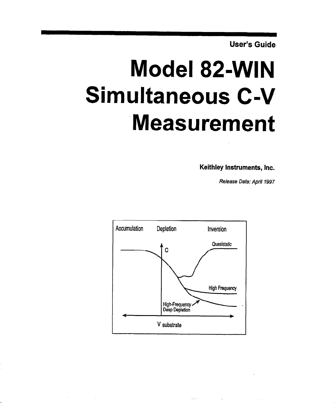
User’s Guide
Model 82~WIN
Simultaneous C-V
Measurement
Keithley instruments, Inc.
Release Date: April 1997
Accumulation
I-
Depletion
if-
\
ligh-Frequenqd .
he0 Deoletion
. .
V substrate
Inversion
Quasistatic
High Frequency
l
Page 8
Contents
C-V Measurement
Introduction
Typical Measurement Sequence
First Time System Testing and
Measurement Procedures
Choose the Right Parameters .................................................................................................. .18
Additional C-V Measurement Features
Measurement Considerations
................................................................................................................................
Leakage Test
Cable Correction
GPIB Configuration
Instrument Selection
Instrument Setup
Making C-V Measurements
Analyzing Data
Optimal C-V Measurement Parameters
Determining the Optimal Delay Tie
Squarewave
Staircase
Capacitance vs. Delay Tie
Time Options
Potential Error Sources
...........................................................................................
1
1
.................................................................................................
Cable Correction
.....................................................................
................................................................................................................
Correcting for Excess Leakage Current
Correcting for Stray Capacitance
......................................................................
..............................................................................
..........................................................................................................
Performing Cable Correction
.....................................................................................
.........................................................................................................
...................................................................................................
.................................................................................................
........................................................................................................
.......................................................................................
..........................................................................................................
.....................................................................
Start, Stop, and Step Voltages..
Sweep Direction
Delay Time
.......................................................................................................
...............................................................................................................
...............................................................................
.......................................................................
Measurement Results
Determining Delay Tie with
Testing Slow Devices..
...............................................................................................
Leaky Devices .........................................................
............................................................................................
....................................................................................
................................................................................................................
.....................................................................................................................
......................................................................................
.............................................................................................................
...................................................................................................
.............................................................................................
Stray Capacitances
Leakage Resistances
High-frequency Effects
....................................................................................................
.................................................................................................
...........................................................................................
3
.5
5
6
-6
7
8
10
10
.l 1
11
13
15
18
.18
19
20
21
.23
24
.25
26
26
26
26
26
28
.28
28
31
.32
User’s Guide Model 82WN Simultaneous C-V
C-V Measurement l i
Page 9

Avoiding
Capacitance
Cabling Considerations ...........................................................................................
Device Connections
Test Fixture
Correcting Residual
Offsets .....................................................................................................................
Errors..
Shielding .............................................................................................
Errors .......................................................................................
Gain and Nonlinearity
Voltage-dependent
Curve Misalignment.. .......................................
Noise .......................................................................................................................
Interpreting C-V Curves
Maintaining
Analyzing
Initial Equilibrium
Dynamic
Range Considerations.. ..............................................................................
Curves for
Equilibrium..
Equilibrium.. ..........................................................................
Series and Parallel Model
Example.. .................................................................................................................
Device Considerations
Series Resistance
Device
Test
Structure .......................................................................................................
Device Integrity..
Equipment Considerations
Light Leaks.. ............................................................................................................
Thermal Errors
...............................................................................................
.........................................................................................................
..................................................................................
..................................................................................................
.34
.34
35
.36
.36
.36
Errors
..................................................................................
Offset..
......................................................................................
.
......................................................
...........................................................................................
........................................................................................
.37
.37
.37
,38
.3 8
38
.40
....................................................................................................
41
.42
Equivalent Circuits.. ........................................................
......................................................................................................
.....................................................................................................
................................................................................
.42
.45
46
46
.46
.47
.47
.47
47
ii 0 C-V Measurement
User’s Guide Model 82-WIN Simultaneous C-V
Page 10
C-V Measurement
Introduction
This chapter provides detailed information on using Metrics ICS
software with Keithley Model 82-WIN to set up C-V
measurements and acquire C-V data. A quicker and easier
approach is to use Keithley libraries, which contain typical
measurement setup parameters and analysis algorithms to
extract many parameters from basic C-V measurements. The
next chapter provides detailed information on how to use
Keithley libraries.
This chapter is organized as the following:
Typical Measurement Sequence: Outlines the basic
measurement sequence that should be followed to ensure
accurate measurements and analysis.
First Time System Testing and Cable Correction: Describes
the procedure to test the complete system for the presence of
unwanted characteristics such as leakage resistance, leakage
current, and stray capacitance. It also details the cable correction
procedure that must be performed in order to ensure accuracy of
high-frequency C-V measurement.
Measurement Procedures: Describes basic procedures for
making C-V measurement. A simultaneous C-V measurement
example is included to illustrate the procedures.
User’s Guide Model 82-WIN Simultaneous C-V
C-V Measurement l 1
Page 11
Choosing the Right Parameters: Briefly discusses the
considerations in choosing right measurement parameters to
achieve accurate
C-V
measurements. It also describes a
procedure to determine the correct delay time to optimize C-V
measurements.
Additional C-V Measurement Features: Includes a
description of squarewave, single staircase, double staircase,
and capacitance vs. delay time measurements.
Measurement Considerations: Outlines numerous factors that
should be taken into account in order to maximize measurement
accuracy and minimize errors.
2 0 C-V Measurement User’s Guide Model 824MN Simultaneous C-V
Page 12
Typical Measurement Sequence
Measurements should be carried out in the proper sequence in
order to ensure that the system is optimized and error terms are
minimized. The basic sequence is outlined below. If your
system is properly set up, tested, and calibrated, you may skip
Steps 1 and 2. Otherwise you must perform the testing and
calibration procedures.
Step 1: Test and
Correct for System Leakage and Strays
Initially, you should test and determine if any problems, such as
excessive leakage or unwanted stray capacitance, are present.
You should correct these problems before making C-V a
measurement. Refer to your system manuals for proper
installation and testing procedures. After initial testing, the
system need be tested only when you have changed some
aspects of its configuration, such as connecting cables or test
futures.
Probe-up suppression should be performed before each
measurement to ensure accuracy. This procedure is discussed in
the measurement section in detail.
Step 2: Correct for Cabling Effects
Cable correction is necessary to compensate for transmission
line effects through the connecting cables and remote input
coupler. Transmission line effects are more significant at higher
frequencies and with longer cables, or with switches in the
system. Failure to perform cable correction will result in
substantially reduced accuracy of high-f?equency C-V
measurement. In order to perform correction, you must connect
the Model 5909 calibration capacitors to the system, and
perform the correction procedure under Metrics ICS. Cable
correction must be performed the first time you use your
User’s Guide Model 82-WIN Simultaneous C-V
C-V Measurement * 3
Page 13
system. After that, it needs to be performed only if the system
configuration
is
changed in
some
manner, or if the ambient
temperature changes by more than 5’C.
Step 3: Configure Your System with Metrics ICS
If you are not using the Keithley library setup to make C-V
measurement, it will be necessary for you to properly configure
your system under Metrics ICS, including GPIB, instrument,
switching matrices, measurement parameters, etc. You should
refer to the Metrics ICS and Keithley C-V Driver manuals for
detailed information regarding configuration of your system.
Step 4: Make a C-V Measurement
Before you can actually make measurements, you must select
measurement parameters such as sweep mode, range, frequency,
and voltage values. As the sweep is performed, measured values
are stored in data arrays for analysis and later retrieval.
Step 5: Analyze C-V Data
4. C-V Measurement
Besides Metrics ICS and Keithley C-V drivers, the Keithley
C-V system includes libraries for setup and data analysis.
Depending on the options you choose, you will be able to
extract a large amount of useful information from your C-V
measurement data. Available analysis features include doping
profile, flatband capacitance and voltage, interface trap density,
and mobile ion density, etc.
User’s Guide Model 82-WIN Simultaneous C-V
Page 14
First Time System Testing and Cable Correction
Leakage Test
Before using the system, it is necessary to check system
leakage. Zero suppress in Metrics ICS is intended to correct for
small system leakage current and stray capacitance. Any
excessive leakage problem must be solved before attempting a
measurement. Procedures are outlined below.
You should run a probe-up test sweep to determine if there is
excessive system or voltage-dependent leakage and stray
capacitance. You may also load the Keithley standard system
leakage check library. Refer to the C-V Libraries and Analysis
chapter for information on using the leakage check library. Note
that setup parameters should be same as those used for your
measurement.
Once leakage check setup is loaded and properly configured,
click on Single on the Meas button. After the sweep, you may
view the capacitance and Q/t vs. voltage plots. There are two
key items to note when performing this procedure. For a typical
system, capacitance and Q/t values should be as small as
possible. Ideally, the stray capacitance should be less than 1%
of the expected capacitance values for optimal accuracy, and
leakage current should be very small as well. Typically, leakage
current should be less than 0.5 pA on the 200pF range, while on
the 2nP range, leakage current should be less than 2pA. In
addition, stray capacitance or leakage current should not display
any voltage-dependent features.
User’s Guide Model 824MN Simultaneous C-V C-V Measurement l 5
Page 15
Make sure proper cables are installed in the correct
1.
places. Be certain you have not interchanged Model
4801 (low noise) cables with the Model 705 1 (50R)
cables or other regular cables.
Make sure all connecting jacks and connectors are f?ee
2.
of contamination. Clean any dirty connectors with
methanol, and allow them to dry thoroughly before
use.
Be certain that you are making a probe-up
3.
measurement.
Check to see that no leakage paths are present in the
4.
test future.
If necessary, tie down cables to avoid noise currents
5.
caused by cable flexing. Also avoid vibration during
testing.
6 l C-V Measurement
Verify that all cables are of the proper type and not of
1.
excessive length.
Verify the integrity of all cable shields, and that the
2.
shield connections are carried through to the
connectors.
Again, make sure the procedure is being performed in
3.
the probe-up configuration.
User’s Guide Model 824VlN Simultaneous C-V
Page 16
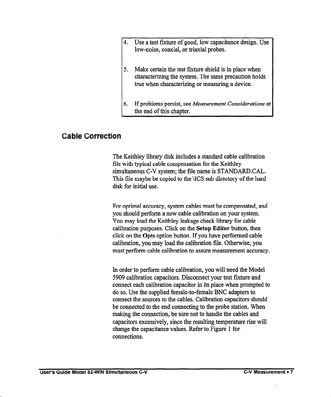
Cable Correction
The Keithley library disk includes a standard cable calibration
file with typical cable compensation for the Keithley
simultaneous C-V system; the tile name is STANDARDCAL.
This file maybe be copied to the UCS sub directory of the hard
disk for initial use.
For optimal accuracy, system cables must be compensated, and
you should perform a new cable calibration on your system.
You may load the Keithley leakage check library for cable
calibration purposes. Click on the Setup Editor button, then
click on the Opts option button. If you have performed cable
calibration, you may load the calibration file. Otherwise, you
must perform cable calibration to assure measurement accuracy.
4. Use a test fixture of good, low capacitance design. Use
low-noise, coaxial, or triaxial probes.
5. Make certain the test fucture shield is in place when
characterizing the system. The same precaution holds
true when characterizing or measuring a device.
6. If problems persist, see Measurement Considerations at
the end of this chapter.
In order to perform cable calibration, you will need the Model
5909 calibration capacitors. Disconnect your test future and
connect each calibration capacitor in its place when prompted to
do so. Use the supplied female-to-female BNC adapters to
connect the sources to the cables. Calibration capacitors should
be connected to the end connecting to the probe station. When
making the connection, be sure not to handle the cables and
capacitors excessively, since the resulting temperature rise will
change the capacitance values. Refer to Figure 1 for
connections.
User’s Guide Model 82WlN Simultaneous C-V
C-V Measurement l 7
Page 17

5951
Remote Input Coupler
to sa%rssmElNFvrauRER
Figure 1
Cable Correction Capacitor Connecfions
Performing Cable Correction
1.
Click on the Calibration button, and the cable
calibration window shown in Figure 2 will be
displayed.
2.
Select the frequency and range you want to calibrate,
then follow the prompts to connect the calibration
capacitors to the cable.
3.
Once calibration is finished, the screen should appear
as shown in Figure 3.
8 l C-V Measurement
User’s Guide Model 82-WIN Simultaneous C-V
Page 18

4. Save this file as CABLE.CAL or the name you prefer.
Note that the file extension must be .CAL.
5. Now load the calibration file, then exit the Opts
window. You should now be in the Setup editor.
6. Click the Done button to exit SetuD.
Current calibration filename
Calibration file
Low CAP @f) :
High CAP
KO, Real
KO,
Kl, Real :
Kl, lmag :
hag
(~9 :
:
:
595 Display
Figure 2
1.
1 kHr -: rjl oakliz
fas1.933 I 1461.97 I 1462.4 1
Options Setup window
”
;,.,, I <..i^ ‘.:
I
,nlMht
Figure 3
User’s Guide Model 82-WIN Simultaneous C-V
System Cable Calibration window
C-V Measurement l 9
Page 19

Measurement Procedures
Detailed information about properly configuring your system
can be found in Metrics ICS and Keithley Instruments C-V
driver manuals. Here, only a brief summary related to Keithley
C-V system is provided. An example of making a simultaneous
C-V measurement is outlined.
GPIB Configuration
Once the GPIE3 board is properly installed and tested, click on
the GPIB button on the menu strip. You should select the GPIB
card installed in your computer (see Figure 4). Note that the
GPIB Timeout option must be set to at least two times the
expected maximum sweep delay time, or a GPIB timeout error
may occur.
WPE
.
:
-“‘I
IO. C-V Measurement
Sub-Type
IKI KMCX38.2
Oj#i 0 ns:
Timeout
30 sect
Delay
No Delay
Figure 4
q
Iail
@!I
ED &ddr
]
I
Cl Show Messages
q
Show bog
Communicafions Setup Window
User’s Guide Model 824VlN Simultaneous C-V
Page 20
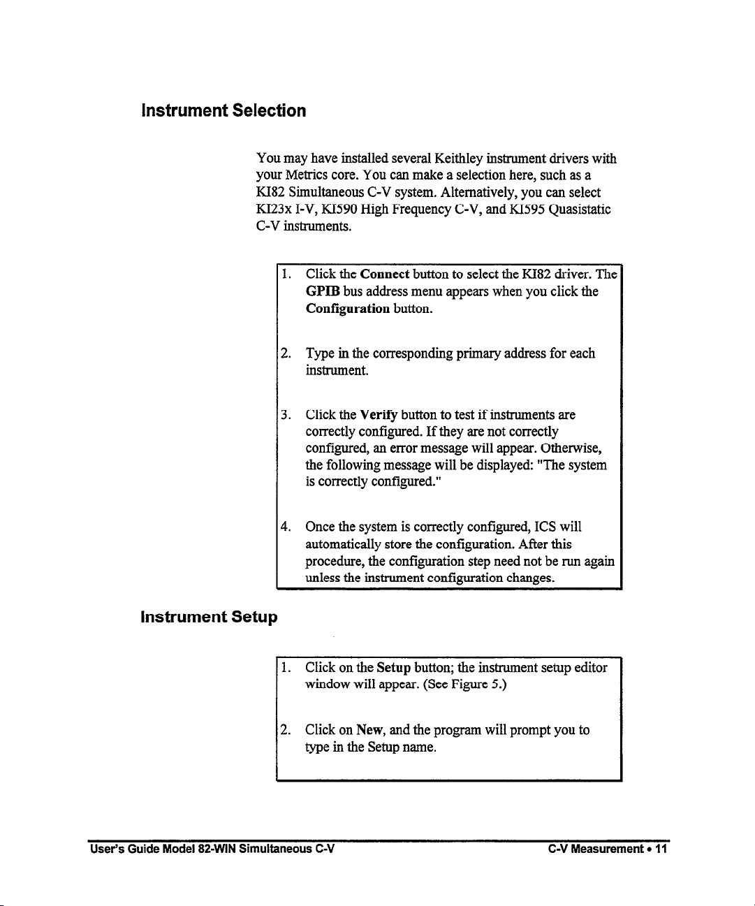
Instrument Selection
You may have installed several Keithley instrument drivers with
your Metrics core. You can make a selection here, such as a
K182 Simultaneous C-V system. Alternatively, you can select
KI23x I-V, KU90 High Frequency C-V, and KI595 Quasistatic
C-V instruments.
Instrument Setup
1.
Click the Connect button to select the K182 driver.
GPIB bus address menu appears when you click the
Configuration button.
2.
Type in the corresponding primary address for each
instrument.
3.
Click the Verify button to test if instruments are
correctly configured. If they are not correctly
configured, an error message will appear. Otherwise,
the following message will be displayed: “The system
is correctly configured.”
4.
Once the system is correctly configured, ICS will
automatically store the configuration. After this
procedure, the configuration step need not be run again
unless the instrument configuration changes.
1. Click on the Setup button; the instrument setup editor
window will appear. (See Figure 5.)
The
2. Click on New, and the program will prompt you to
type in the Setup name.
User’s Guide Model 824MN Simultaneous C-V
C-V Measurement l 11
Page 21
You may
select many different devices. For this
example, select the MOSFET icon.
Click on Source Unit, then click on K182 IN to select
the input.
Click on the G (gate) on the MOSFET symbol to
connect the input to the gate.
Similarly, click on KI82.OUT to select the output,
then click on the B (substrate) symbol of the MOSFET
to connect the output to the substrate.
Click on the W82 OUT icon; the measurement
parameter setup window will appear. (See Figure 6.)
You may now select the proper measurement
parameters. The parameter window should appear like
the one shown in the Figure 6. Refer to the Metrics ICS
and Keithley C-V driver manuals for full details on all
setup parameters.
12 * C-V Measurement
Before you make a measurement, be sure to load the
cable correction and calibration file. To do so, click on
the Opts. button in the Setup Editor, then click on
Load option to select the calibration file for your test
fucture.
Exit from the Opts. window and the Setup Editor
window.
User’s Guide Model 824VlN Simuttandous C-V
Page 22

Figure 5 instrument Setup Editor Window
Stimulus
Bulkhbstrate voltage
Mode: -1
Start (V) :
stop [v] :
Step (VI :
No. Points
Delay (s) :
Time measurement bias
Bias voltage : 14
User’s Guide Model 82-WIN Simultaneous C-V
a
12
10.5 1
Figure 6
Measure
q cs:
q GorR:)G~
•I Vsub :
-
q t?/t:
i?iT:
Range
590: p-i@/
595: 12°F
1
lvsuB
r--l
I
Measurement Setup Parameter Window
Options
Model
@Parallel 0 Series
I
m
C-V Measurement l 13
Page 23

Making C-V Measurements
. The zero cancel procedure described below will correct
system leakage and stray capacitance. Note that large
leakage current or stray capacitance should not be
suppressed. Determine the source of the problems, and
correct them before using your system.
!. Click on the Meas. button, and note there are several
options from which to choose. (See Figure 7.)
;. Before you make measurements, you should do a
probe-up zero suppress by clicking on the Zero Cancel
button and following the instructions.
C. After the zero cancel procedure, the message “Please
lower your probe” will be displayed on the screen.
During this period, the Model 590 C-V meter is in its
active reading mode, and you may lower your probe to
contact the DUT while at same time observing the
Model 590 display reading. Doing so ensures proper
electrical contact between the probe and DUT.
14 0 C-V Measurement
i. You are now ready to make a C-V measurement. For
this example, click on the Single button to make a
single-sweep measurement. You may observe that
when instrument finishes data taking, the data screen
will flicker a few times. This situation is normal while
ICS is updating the data. If the analysis package has
been loaded, it make take some time to perform the
calculations and display the data, depending on the
amount of data and the speed of your computer.
User’s Guide Model 824VlN Simultaneous C-V
Page 24

Analyzing Data
Before you attempt to analyze data, you should plot raw dam
and determine if there are any obvious measurement problems.
Keep in mind that no analysis will compensate for substandard
system-related problems and select better measurement
parameters. If a large amotmt of noise is present, analysis results
will not be dependable and may even be meaningless. Repeat
the measurement procedure to determine the root cause of the
problems, and correct them before proceeding.
Figure 7
Measurement Selection Window
data caused by measurement problems. At this time, you may
find it necessary to make a few adjustments to compensate for
The first step is to transfer the analysis constants to
Metrics. Click on the Transform Editor button, then
the name, value, unit, and comments into the fields.
User’s Guide Model 82WlN Simultaneous C-V
C-V Measurement 0 15
Page 25

2.
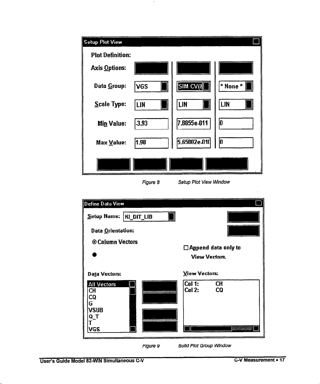
Click on the New Plot button to draw a new graph.
The Setup Plot window will pop up. (See Figure 8.)
3.
Select the data option you wish to plot. For our
example, select Vsm as the X-Axis data parameter. Fo:
a simultaneous C-V measurement, plot both Cn and Cc
on the y-axis.
t.
You may select one data set to plot on the y axis.
Select the data you wish to plot on the Y l-Axis
column. If you wish to plot another data set on a
different scale but on the same graph, select that data
set for the Y2-Axis column.
j.
If you wish to plot two sets of dam on the same scale
you may use the Build Group feature. Click on the
Build Group button, and add both Cu and Co to the
group, for example Sim-CV. (See Figure 9.) After you
close this window, you will notice a Sim-CV group is
available under the y-axis sub-menu selection. Choose
Sim-CV for the y-axis.
18
l C-V
Measurement
i.
Click on Apply and then Done. You should see both
Co and C, curves plotted on the graph. By using the
Build Group feature of Metrics ICS, you can put many
curves on the same graph. Also notice that you can set
up a second y-axis with different scale and different
data set.
User’s Guide Model 82WlN Simultaneous C-V
Page 26
Plot Definition:
Axis Options:
Data Group:
Scale Type:
Min Value:
Max Value: 11.981
Setup Name: -1
Data Orientation:
Q Column Vectors
*
m-o]
-1
piz--l
Figure 8
Setup PIof View Mlindow
q
lAEpend data only to
View Vectors.
Data Vectors:
User’s Guide Model 82-WIN Simultaneous C-V
Figure 9
View Vectors:
Col 1: CH
Co12 CQ
Build Plot Group window
C-V Measurement. 17
Page 27
Choose the Right Parameters
Optimal C-V Measurement Parameters
Simultaneous C-V measurement is a complicated matter.
Besides system considerations, you should carefully choose the
measurement parameters. Refer to the following discussion for
considerations when selecting these parameters.
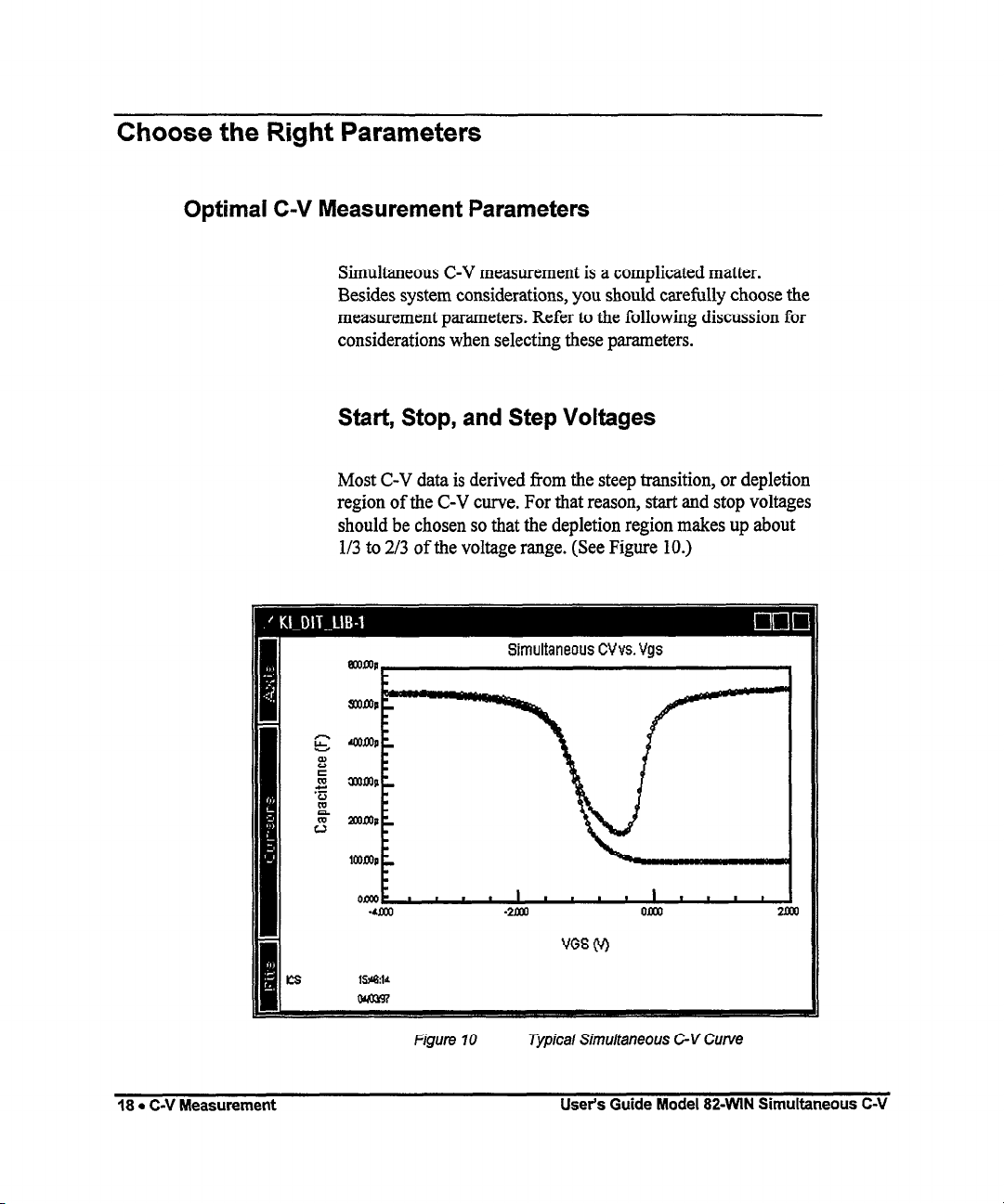
Start, Stop, and Step Voltages
Most C-V data is derived from the steep transition, or depletion
region of the C-V curve. For that reason, start and stop voltages
should be chosen so that the depletion region makes up about
113 to 213 of the voltage range. (See Figure 10.)
Simultaneous CVvs. Vgs
18 l C-V Measurement
VGS (‘4)
Figure 10 Typical Simultaneous C-V Curve
User’s Guide Model 824MN Simultaneous C-V
Page 28

The upper flat, or accumulation region of the high frequency
C-V curve defines the oxide capacitance, Cox. Since most
analysis relies on the ratio C/Cox, it is important that you
choose a start or stop voltage (depending on the sweep
direction) to bias the device into strong accumulation at the start
or the end of the sweep.
You should carefully consider the size of the step voltage. Start,
stop, and step size determine the total number of data points in
the sweep. Some compromise is necessary between having too
few data points in one situation, or too many data points in the
other.
For example, the complete doping profile is derived from data
taken in the depletion region of the curve by using a derivative
calculation. As the data point spacing decreases, the vertical
point scaling is increasingly caused by noise rather than changes
in the desired signal. Consequently, choosing too many points
in the sweep will result in increased noise rather than an
increased resolution in C-V measurement. It also takes more
time to perform a C-V sweep.
Many calculations depend on good measurements in the
depletion region, and too few dam points in this region will give
poor results. A good compromise results from choosing
parameters that will yield a capacitance change of
approximately ten times the percentage error in the signal.
Sweep Direction
For C-V sweeps, you can sweep either from accumulation to
inversion, or from inversion to accumulation. Sweeping from
accumulation to inversion will allow you to achieve deep
depletion-profiling deeper into the semiconductor than you
otherwise would obtain by maintaining equilibrium. When
sweeping from inversion to accumulation, you should use a
light pulse to achieve equilibrium more rapidly before the
sweep begins.
User’s Guide Model 82-WIN Simultaneous C-V
C-V Measurement l 19
Page 29
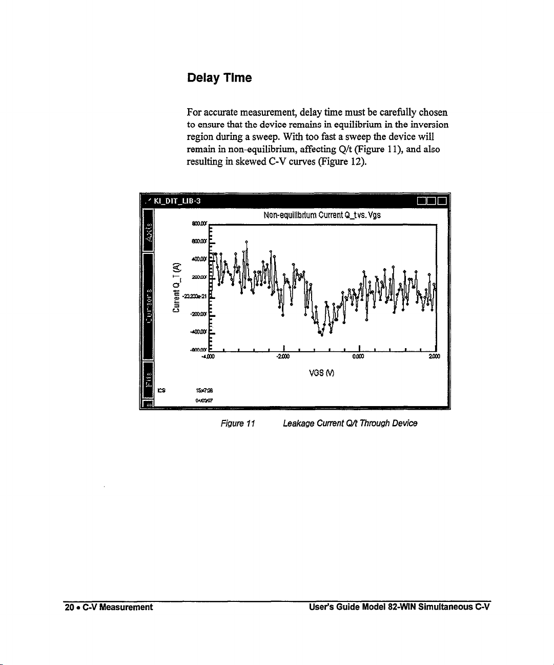
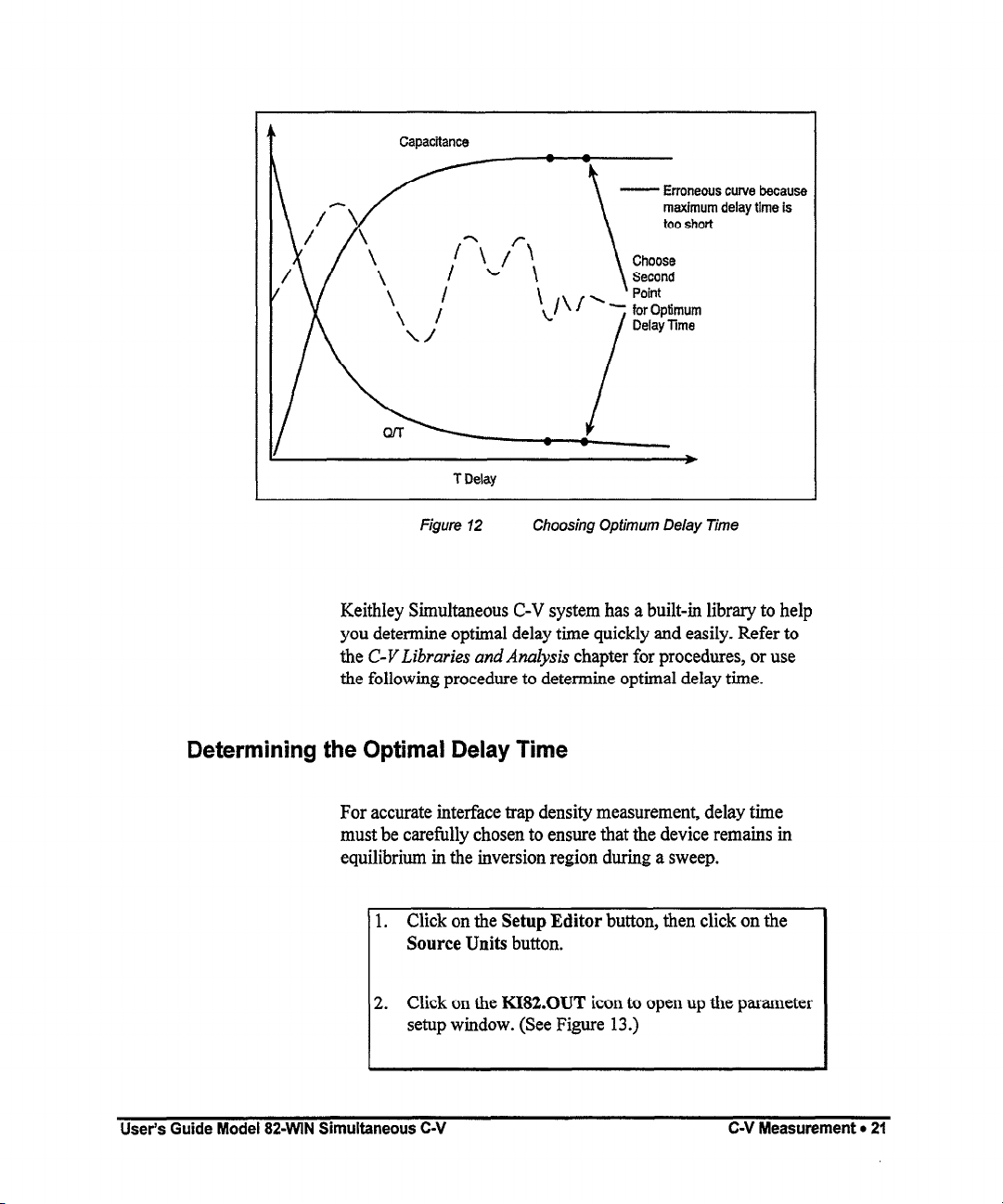
Delay Time
For accurate measurement, delay time must be carefully chosen
to ensure that the device remains in equilibrium in the inversion
region during a sweep. With too fast a sweep the device will
remain in non-equilibrium, affecting Q/t (Figure 1 l), and also
resulting in skewed C-V curves (Figure 12).
Non-equilihrium Current Q-tvs.Vgs
20. C-V Measurement
Figure 11
Leakage Current Q/t 77mugh Device
User’s Guide Model 82WN Simultaneous C-V
Page 30
Capacitance
T Delay T Delay
- Erroneous curve because - Erroneous curve because
maximum maximum delay time is delay time is
Figure 12 Figure 12
Choosing Optimum Delay Time Choosing Optimum Delay Time
Keithley Simultaneous C-V system has a built-in library to help
you determine optimal delay time quickly and easily. Refer to
the C-V Libraries and Analysis chapter for procedures, or use
the following procedure to determine optimal delay time.
Determining the Optimal Delay Time
For accurate interface trap density measurement, delay time
must be carefully chosen to ensure that the device remains in
equilibrium in the inversion region during a sweep.
1. Click on the Setup Editor button, then click on the
Source Units button.
2. Click on the IU82.OUT icon to open up the parameter
setup window. (See Figure 13.)
User’s Guide Model 82JMN Simultaneous C-V
C-V Measurement l 21
Page 31

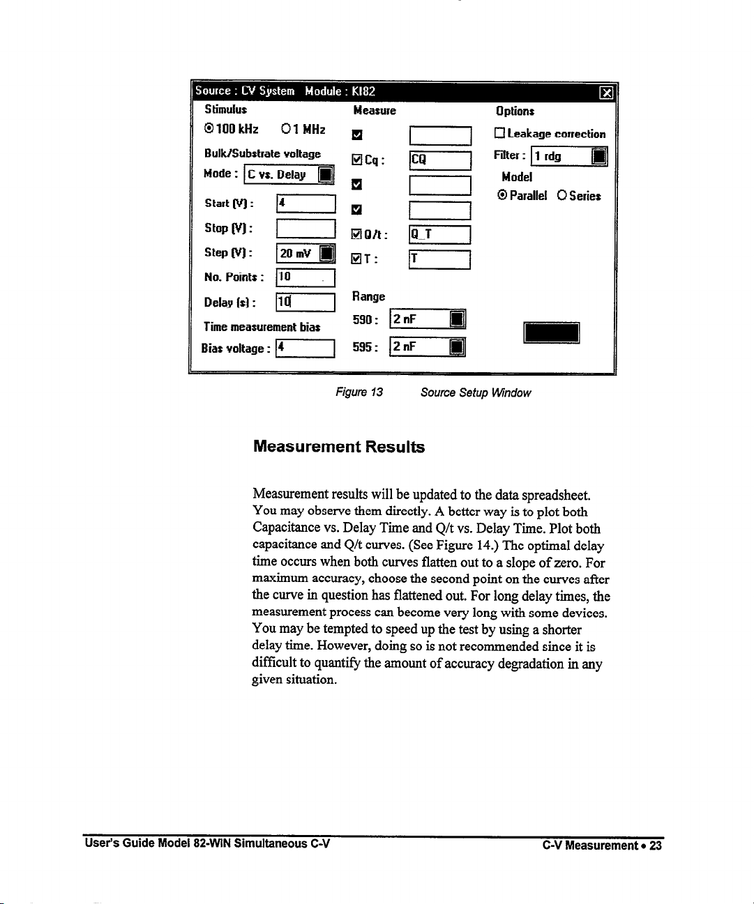
3.
In the Mode section, select the C vs. Delay t
measurement.
4.
Type in the Start voltage to specify the bias voltage on
the DUT during this measurement. Remember that the
DUT should be biased in the inversion region for this
measurement.
Type in the maximum delay times in the Delay (s) box.
5.
Note that the total measurement period will be several
times longer than the maximum delay time you select.
Other parameters should be selected according to your
6.
device under test as in the simultaneous C-V
measurement example.
Click on the OK button to exit from this window, then
7.
Click on the Done button to exit from the Setup
Editor.
Click on the Meas button, then click on the Single
8.
button to start the measurement.
22 0 C-V Measurement
User’s Guide Model 824MN Simultaneous C-V
Page 32
Stimulus
@I 100 kHz
BulklSubstrate voltage
Mode:
Start (V] :
stop (V] :
Step (V] :
No. Points : j-iii-q
Delay (s] :
Time measurement bias
Bias voltage I 14 1
01 MHz
JCvf.Delay
L--l
llol
Measure
R
Hcq:
R
R
q
Q/t: m
MT:
Range
Options
0 Leakage correction
PI
Figurn 13
Source Setup Window
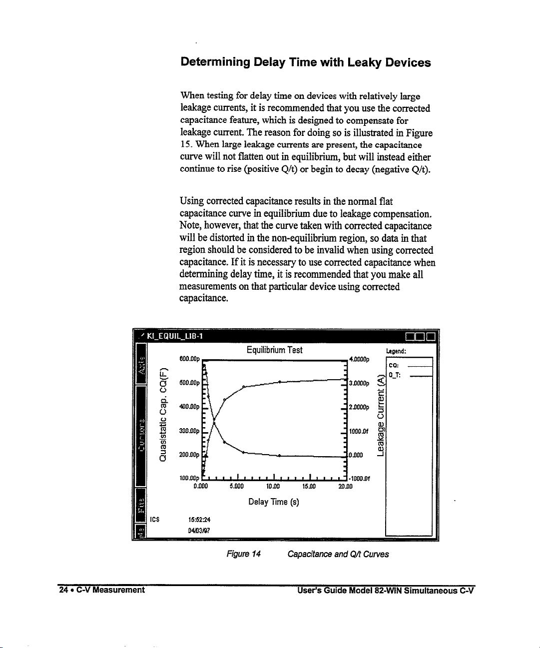
Measurement Results
Measurement results will be updated to the data spreadsheet.
You may observe them directly. A better way is to plot both
Capacitance vs. Delay Time and Q/t vs. Delay Time. Plot both
capacitance and Q/t curves. (See Figure 14.) The optimal delay
time occurs when both curves flatten out to a slope of zero. For
maximum accuracy, choose the second point on the curves after
the curve in question has flattened out. For long delay times, the
measurement process can become very long with some devices.
You may be tempted to speed up the test by using a shorter
delay time. However, doing so is not recommended since it is
difficult to quantify the amount of accuracy degradation in any
given situation.
User’s Guide Model 824MN Simultaneous C-V
C-V Measurement l 23
Page 33
Determining Delay Time with Leaky Devices
When testing for delay time on devices with relatively large
leakage currents, it is recommended that you use the corrected
capacitance feature, which is designed to compensate for
leakage current. The reason for doing so is illustrated in Figure
15. When large leakage currents are present, the capacitance
curve will not flatten out in equilibrium, but will instead either
continue to rise (positive Q/t) or begin to decay (negative Q/t).
Using corrected capacitance results in the normal flat
capacitance curve in equilibrium due to leakage compensation.
Note, however, that the curve taken with corrected capacitance
will be distorted in the non-equilibrium region, so data in that
region should be considered to be invalid when using corrected
capacitance. If it is necessary to use corrected capacitance when
determining delay time, it is recommended that you make all
measurements on that particular device using corrected
capacitance.
24 l C-V Measurement
zj; fi-q-zq[;;
155224
04&3197
Figure 14
Equilibrium Test
5.Mtl ID.00
Delay Time (s)
Capacitance and Q/f Curves
Legend:
15.M 20.00
User’s Guide Model 82WlN Simultaneous C-V
Page 34
A’
A - C-Cap 137, Positive Q/t
.’
- c-capon
Negative Q/t
Figure 15
Capacifance and Leakage Current Curves of Leaky
Device
Testing Slow Devices
A decaying noise curve, such as the dotted line shown in Figure
12, will result if the maximum delay time is too short for the
device being tested. This phenomenon, which is most prevalent
with slow devices, occurs because the signal range is too small.
To eliminate such erroneous curves, choose a longer maximum
delay time. A good starting point for unknown devices is a 30second maximum delay time.
User’s Guide Model 82WlN Simultaneous C-V
C-V Measurement * 25
Page 35
Additional C-V Measurement Features
Besides making basic simultaneous C-V measurements, there
are other features available in the C-V system, including
squarewave, single staircase, double staircase, and Capacitance
vs. delay time.
Squarewave
The squarewave option lets you select a constant output bias
voltage. A squarewave will be output to make the measurement.
This feature may be useful for monitoring device change during
some time period. Under this option, you may select bias
voltage, squarewave step size, and time period.
Staircase
Single Staircase will let you sweep bias voltage in either
direction. The Double Staircase option will let you sweep in one
direction and then return to the original starting voltage. The
sweep step will be the same in both directions. Ideally, if the
DUT is in equilibrium during measurement, C-V curves should
not exhibit any hysteresis. Hence this option provides you with
another means of monitoring the device under test.
Capacitance vs. Delay Time
26 l C-V Measurement
The Capacitance vs. Delay Time option is very useful to help
determine the proper delay time. Detailed procedures are
provided in a previous section.
User’s Guide Model 824MN Simultaneous C-V
Page 36
Time Options
There are many different timing options for you to choose. For
details, refer to the section on Setup Editor and Measurement in
ICS and Keithley C-V driver manuals.
User’s Guide Model 82WlN Simultaneous C-V
C-V Measurement o 27
Page 37
Measurement Considerations
The importance of making careful C-V curve measurements is
often underestimated. However, errors in the C-V data will
propagate through calculations, resulting in errors in device
parameters derived t?om the curves. These errors can be
amplified during calculations by a factor of 10 or more.
With careful attention, the effects of many common error
sources can be miniiized. In the following paragraphs, we will
discuss some common error sources and provide suggested
methods for avoiding them.
Potential Error Sources
Theoretically, a capacitance measurement using one of the
common techniques would require only that two leads be used
to connect the measuring instrument to the device under test
(DUT)-the input and output. In practice, however, various
parasitic or stray components complicate the measuring circuit.
28. C-V Measurement
Stray Capacitances
Regardless of the measurement frequency, stray capacitances
present in the circuit are important to consider. Stray
capacitances can cause offsets when they are in parallel with the
device, can act as a shunt load on the input or output, or can
cause coupling between the device and nearby AC signal
sources.
When stray capacitance is in parallel with the DUT, it causes a
capacitance offset, adding to the capacitance of the device under
test (CD,), as shown in Figure 16. Shunt capacitance, on the
other hand, often increases the noise gain of the instrumentation
amplifiers, increasing capacitance reading noise (Figure 17).
Shunt capacitance also forms a capacitive divider with Cuur,
User’s Guide Model 82-WIN Simultaneous C-V
Page 38
steering current away from the input to ground. This
phenomenon results in capacitance gain error, with the C-V
curve results shown in Figure 18.
-------------_-_---_-- offset
Normal
Figure 16 GV Curve with Capacitance Offset
User’s Guide Model 82-WIN Simultaneous C-V
C-V Measurement l 29
Page 39

Figure 17 C-V Curve wifh Added Noise
30 * C-V Measurement
4
I
V
___---_-----___----_--- With Gain Error
Normal
Figure ‘f8
GV Curve Resulting from Gain Ermr
User’s Guide Model 82-WIN Simultaneous C-V
*
Page 40
Stray capacitance may also couple charge current from nearby
AC signal sources into the input of the measuring instrument.
This noise current adds to the device current and results in noisy
or unrepeatable measurements. For quasistatic measurements,
power line frequency and electrostatic coupling are particularly
troublesome, while digital and RF signals are the primary cause
of noise induced in high-frequency measurements.
Leakage Resistances
Under quasistatic measurement conditions, the impedance of
CDm is almost as large as the insulation resistance in the rest of
the measurement circuit. Consequently, even leakage resistances
of 101X2 or more can contribute significant errors if not taken
into consideration.
Resistance across the DUT will conduct an error current in
addition to the device current. Since this resistive current is
directly proportional to the applied bias voltage, and the
capacitor current is not, the result is a capacitance offset that is
proportional to the applied voltage. The end result shows up as a
“tilt” in the quasistatic C-V curve, as shown in Figure 19.
User’s Guide Model 82-WIN Simultaneous C-V C-V Measurement l 31
Page 41

-------------- Titled Curve Caused by
Leakage
Normal
Figure 19
Curve 77/f Caused by Voltage-Dependent Leakage
Stray resistance to nearby fixed voltage sources results in a
constant (rather than a bias voltage-dependent) leakage current.
Other sources of constant leakage currents include instrument
input bias currents, and electrochemical currents caused by
device or future contamination. Such constant leakage currents
t cause a voltage-independent capacitance offset.
Keep in mind that insulation resistance is reduced, and leakage
current is increased by high humidity as well as by
contaminants. In order to minimize these effects, always keep
devices and test fuctures in clean, dry conditions.
High-frequency Effects
At measurement frequencies of approximately 1OOkHz and
higher, the impedance of Cour may be so small that any series
impedance in the rest of the circuit may cause errors, Whether
such series impedance is caused by inductance (such as from
32 l C-V Measurement
User’s Guide Model 82WlN Simultaneous C-V
Page 42

leads or probes), or from resistance (as with a high-resistivity
substrate), this series impedance causes non-linearity in the
measured capacitance. The resulting C-V curve is, of course,
affected by such non-linearity, as shown in Figure 20.
-------------- With Nonlinearity
Normal
Figure 20 GV Curve Caused by Nonlinearity
Another high-frequency effect is caused by the AC network
formed by the instrumentation, cables, switching circuits, and
the test fuctures. Referred to as transmission line error sources,
the network essentially transforms the impedance of Cum when
it is referred to the input of the instrument, altering the
measured value. Transmission line effects alter the gain and
produce non-linearities.
User’s Guide Model 82JMN Simultaneous C-V
C-V Measurement l 33
Page 43

Avoiding Capacitance Errors
Many possible error sources that can affect C-V measurements
may seem overwhelming at times, but careful attention to a few
key details will reduce errors to an acceptable level. Once most
of the error sources have been minimized, any residual errors
can be further reduced by using the probe-up suppression and
corrected capacitance features.
Key details that require attention include use of proper cabling
and effective shielding. These important aspects are discussed
below.
Cabling Considerations
Cables must be used to connect the instruments to the device
under test. Ideally, these cables should supply the test voltage to
the device unaltered in any way. The test voltage is converted
into a current or charge in the DUT, and should be carried back
to the instruments undisturbed. Along the way, potential error
sources must be minimized.
34 l C-V Measurement
Coaxial cable is usually used in order to eliminate stray
capacitance between the measurement leads. The cable shield is
connected to a low-impedance point (guard) that follows the
meter input. This technique, known as the three-terminal
capacitance measurement, is almost universally used in
commercial instrumentation. The shield shunts current away
f?om the input to the guard.
Coaxial cables also serve as smooth transmission lines to carry
high-frequency signals with minimal attenuation. For this
reason, the cable‘s characteristic impedance should closely
match that of the instrument input and output, which is usually
50R. Standard RG-58 cable is adequate for frequencies in the
range of &Hz to more than 1 OMHz. High-quality BNC
User’s Guide Model 824MN Simultaneous C-V
Page 44

connectors with gold-plated center conductors reduce errors
from high series contact resistance.
Quasistatic C-V measurements are susceptible to shunt
resistance and leakage currents as well as to stray capacitances.
Although coaxial cables are still appropriate for these
measurements, the cables should be checked to ensure that the
insulation resistance is sufficiently high (>lOK2 ). Also, when
such cables are flexed, the shield rubs against the insulation,
generating small currents due to triboelectric effects. These
currents can be minimized by using low-noise cable (such as the
Model 480 1) that is lubricated with graphite to reduce friction
and to dissipate generated charges.
Flex-producing vibration should be eliminated at the source
whenever possible. If vibration cannot be entirely eliminated,
cables should be securely fastened to prevent flexing.
One final point regarding cable precautions is in order: Cables
can only degrade the measurement, not improve it. Thus, cable
lengths should be miniiized where possible, without straining
cables or connections.
Device Connections
Care in properly protecting the signal path should not stop at the
cable ends where the connection is made to the DUT future. In
fact, the device connection is an extremely important aspect of
the measurement. For the same reasons given for coaxial cables,
it is best to continue the coaxial path as close to the DUT as
possible by using coaxial probes. Also, it is important to
minimize stray capacitance and maximum insulation resistance
in the pathway from the end of the coaxial cable to the DUT.
Most devices have one terminal that is well insulated from other
conductors, as in the gate of an MOS test dot. The input should
be connected to the gate because it is more susceptible to stray
signals than is the output. The output can better tolerate being
connected to a terminal with high shunt capacitance, noise, or
User’s Guide Model 82WlN Simultaneous C-V
C-V Measurement l 35
Page 45

poor insulation resistance, although these characteristics should
still be optimized for best results.
Test Fixture Shielding
At the point where the coaxial cable shielding ends, the
sensitive input node is exposed, inviting error sources to
interfere. Proper device shielding need not end with the cables
or probes, however, if a shielded test fixture is used.
A shielded furture, sometimes known as a Faraday cage,
consists of a metal enclosure that completely surrounds the
DUT and leads. In order to be effective, the shield must be
electrically connected to the coaxial shield. Typically, bulkhead
connectors are mounted to the side of the cage to bring in the
signals. Coaxial cables should be continued inside, if possible,
or individual input and output leads should be widely spaced in
order to maintain input/output isolation.
Correcting Residual Errors
36 l C-V Measurement
Controlling errors at the source is the best way to optimize C-V
measurements, but doing so is not always possible. Remaining
residual errors include offset, gain, noise, and voltagedependent errors. Ways to deal with these error sources are
discussed in the following paragraphs.
Offsets
Offset capacitance and conductance caused by the test apparatus
can be eliminated by performing a suppression with the probes
in the up position. These offsets will then be nulled out when
the measurement is made. Whenever the system configuration is
changed, the suppression procedure should be repeated. For
maximum accuracy, it is recommended that you perform a
probes-up suppression or at least verify prior to every
measurement.
User’s Guide Model 82-WIN Simultaneous C-V
Page 46

Gain and Nonlinearity Errors
Gain errors are difficult to quantify. For that reason, gain
correction is applied to every measurement. Gain constants are
determined by measuring accurate calibration sources during
the cable correction process.
Nonlinearity is normally more difficult to correct for than are
gain or offset errors. The cable correction utility, however,
provides nonlinearity compensation for high-frequency
measurements, even for non-ideal configurations such as
switching matrices.
Voltage-dependent Offset
Voltage-dependent offset (curve tilt) is the most difficult to
correct error associated with quasistatic C-V measurements. It
can be eliminated by using the corrected capacitance function of
the software. In this technique, the current flowing in the device
is measured as the capacitance value is measured. The current is
known as Q/t because its value is derived from the slope of the
charge integrator waveform. Q/t is used to correct capacitance
readings for offsets caused by shunt resistance and leakage
currents.
Care must be taken when using the corrected capacitance
feature, however. When the device is in non-equilibrium, device
current adds to any leakage current, with the result that the
curve is distorted in the non-equilibrium region. The solution is
i0 keep ‘the uevice m equumrmm mrougnout me sweep by
carefully choosing the delay time.
>--.I-- :- _ -.-llll...I.-... II. .~~ -1~ --a Ll
Curve Misalignment
User’s Guide Model 824MN Simultaneous C-V
C-V Measurement l 37
Page 47

At times, quasistatic and high frequency curves may be slightly
misaligned due to gain errors or external factors. In such cases,
curve gain and offset factors can be applied to the curves to
properly align them..
Noise
Residual noise on the C-V curve can be minimized by using
filtering when taking your data. However, the filter will reduce
the sharpness of the curvature in the transition region of the
quasistatic curve depending on the number of dam points in the
region. This change in the curve can cause
resulting in erroneous Dn calculations. If this situation occurs,
turn off the filter or add more dam points.
Interpreting C-V Curves
Even when all the precautions outlined here are followed, there
are still some possible obstacles to successfully using C-V
curves to analyze semiconductor devices.
CQ
to dip below Cu
38. C-V Measurement
Semiconductor capacitances are far from ideal, so care must be
taken to understand how the device operates. Also, the curves
must be generated under well-controlled test conditions that
ensure repeatable, analyzable results.
Maintaining Equilibrium
The condition of the device when all internal capacitances are
fully charged is referred to as equilibrium. Most quasistatic and
high-frequency C-V curve analysis is based on the simplified
assumption that the device is measured in equilibrium. Internal
RC time constants limit the rate at which the device bias may be
swept while maintaining equilibrium. They also determine the
hold time required for device settling after setting the bias
voltage to a new value before measuring C&r.
User’s Guide Model 82JMN Simultaneous C-V
Page 48

The two main measurement parameters that affect equilibrium,
then, are the bias sweep rate and the hold time. When these
parameters are set properly, the normal C-V curves shown in
Figure 2 1 result. Once the proper sweep rate and hold time have
been determined, it is important that all curves compared with
one another be measured under the same test conditions;
otherwise, it
may
be the parameters, not the devices themselves,
that cause the compared curves to differ.
Accumulation
Deep Depletion
V substrate
/=igm 21
Inversion
Quasistatic
High Frequency
Normal C-V Curves
User’s Guide Model 82JMN Simultaneous C-V
C-V Measurement l 39
Page 49
Analyzing Curves for Equilibrium
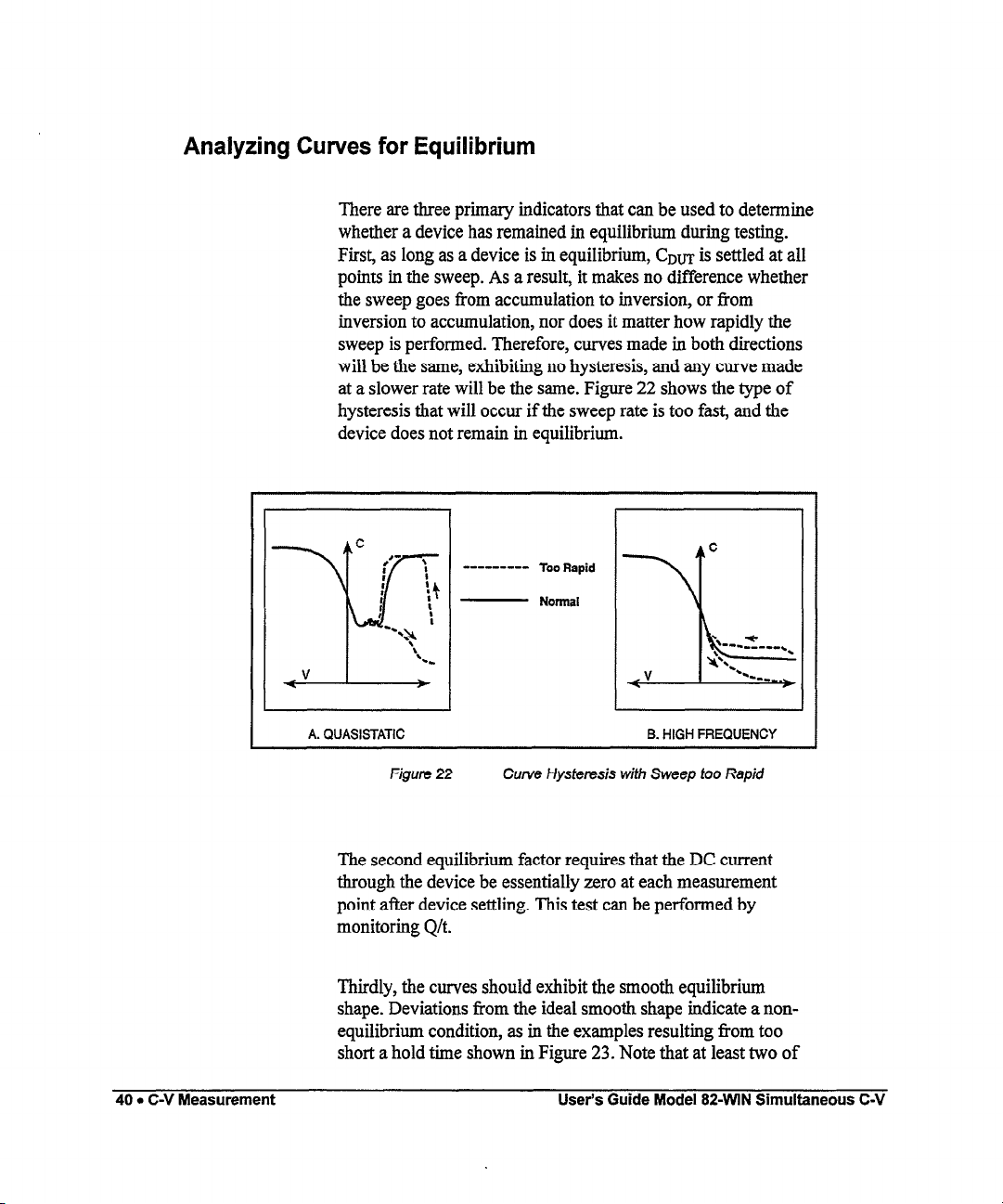
There are three primary indicators that can be used to determine
whether a device has remained in equilibrium during testing.
First, as long as a device is in equilibrium, CD~JT is settled at all
points in the sweep. As a result, it makes no difference whether
the sweep goes tiom accumulation to inversion, or from
inversion to accumulation, nor does it matter how rapidly the
sweep is performed. Therefore, curves made in both directions
will be the same, exhibiting no hysteresis, and any curve made
at a slower rate will be the same. Figure 22 shows the type of
hysteresis that will occur if the sweep rate is too fast, and the
device does not remain in equilibrium.
c
Normal
‘L-2 ---.
+
foo
%.
Rapid
V
L
A. QUASISTATIC B. HIGH FREQUENCY
Figure 22
Curve Hysteresis with Sweep
.
---
The second equilibrium factor requires that the DC current
through the device be essentially zero at each measurement
point after device settling. This test can be performed by
monitoring Q/t.
Thirdly, the curves should exhibit the smooth equilibrium
shape. Deviations from the ideal smooth shape indicate a non-
equilibrium condition, as in the examples resulting from too
short a hold time shown in Figure 23. Note that at least two of
40. C-V Measurement User’s Guide Model 82-WIN Simultaneous C-V
Page 50
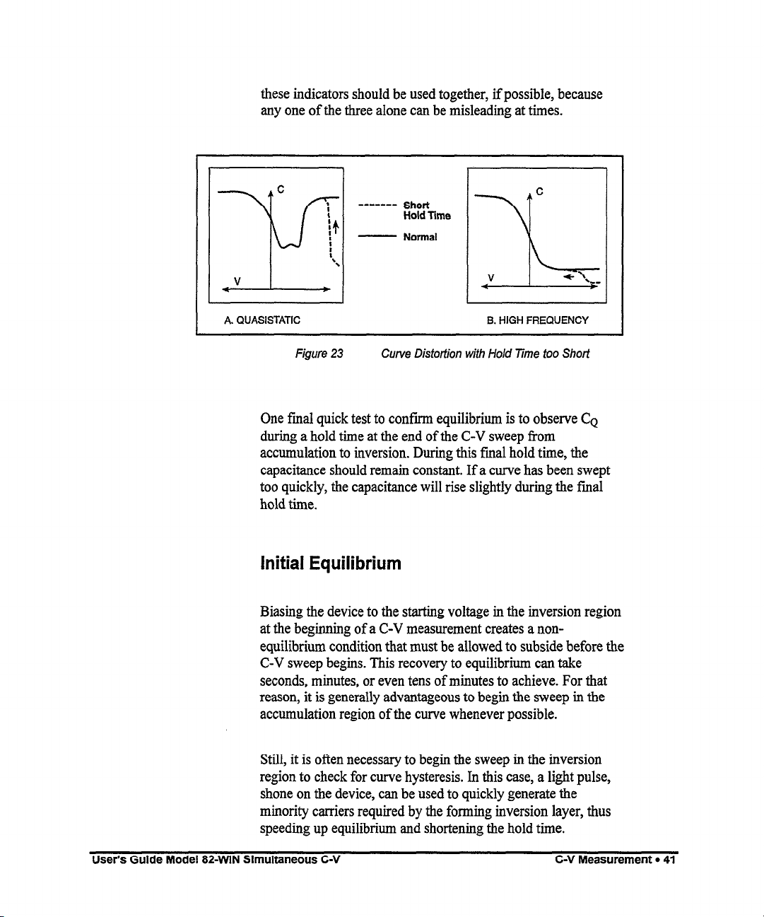
these indicators should be used together, if possible, because
any one of the three alone can be misleading at times.
I 1
C
- Normal
V
I
A. QUASISTATIC
Figure 23
One final quick test to confvm equilibrium is to observe
during a hold time at the end of the C-V sweep from
accumulation to inversion. During this fmal hold time, the
capacitance should remain constant. If a curve has been swept
too quickly, the capacitance will rise slightly during the final
hold time.
Curve Disfortion wifh Hold Time too Short
Initial Equilibrium
Y!z
0. HIGH FREQUENCY
f- ‘8,
CQ
Biasing the device to the starting voltage in the inversion region
at the beginning of a C-V measurement creates a nonequilibrium condition that must be allowed to subside before the
C-V sweep begins. This recovery to equilibrium can take
seconds, minutes, or even tens of minutes to achieve. For that
reason, it
accumulation region of the curve whenever possible.
Still, it is often necessary to begin the sweep in the inversion
region to check for curve hysteresis. In this case, a light pulse,
shone on the device, can be used to quickly generate the
minority carriers required by the forming inversion layer, thus
speeding up equilibrium and shortening the hold time.
User’s Guide Model 82WlN Simultaneous C-V C-V Measurement l 41
is
generally advantageous to begin the sweep in the
Page 51
The best way to ensure equilibrium is initially achieved is to
monitor the DC current in the device and wait for it to decay to
the DC leakage level of the system. A second indication that
equilibrium is reached is that the capacitance level at the initial
bias voltage decays to its equilibrium level.
Dynamic Range Considerations
The dynamic range of a suppressed quasistatic of highfrequency measurement will be reduced by the amount
suppressed. For example, if, on the 200pF range, you were to
suppress a value of lOpF, the dynamic range would be reduced
by that amount. Under these conditions, the maximum value the
instrument could measure without overflowing would be 190pF.
A similar situation exists when using cable correction with the
Model 590. For example, the maximum measurable value on
the 2nF range may be reduced to 1.8nF when using cable
correction. The degree of reduction will depend on the amount
of correction necessary for the particular test setup.
Series and Parallel Model Equivalent Circuits
42. C-V Measurement
The dynamic range of quasistatic capacitance measurements is
reduced with high Q/t. The maximum Q/t value for a given
capacitance value depends on both the delay time and the step
voltage. See the Model 595 Instruction Manual Specifications
for details.
A complex impedance can be represented by a simple series or
parallel equivalent circuit made up of a single resistive element
and a single reactive element, as shown in Figure 24. In the
parallel form of (a), the resistive element is represented as the
conductance, G, while the reactance is represented by the
susceptance, B. The two together mathematically combine to
give the admittance, Y, which is simply the reciprocal of the
circuit impedance.
User’s Guide Model 82WlN Simultaneous C-V
Page 52
Y=G+JB
Z=R+JX
B = mCp (CAPACITIVE)
OR
1 (INDUCTIVE)
B=
OLp
(A) PARALLEL CIRCUIT
Figure 24
In a similar manner, the resistance and reactance of the series
form of(b) are represented by R and X, respectively. The
impedance of the series circuit is Z.
The net impedances of the equivalent series and parallel circuits
at a given frequency are equal. However, the individual
components are not. We can demonstrate this relationship
mathematically as follows:
1
R+jX
=
G+jB
x= L(CAPACITIVE)
OIG
OR
X = wLp (INDUCTIVE)
(B) SERIES CIRCUIT
Series and Parallel Circuits
To eliminate the imaginary form in the denominator of the
right-hand term, we can multiply both the denominator and
numerator by the conjugate of the denominator as follows:
User’s Guide Model 82-WIN Simultaneous C-V
C-V Measurement l 43
Page 53
R+jX=-x-
1
G-jB
G+jB G-jB
Performing the multiplication and combining terms, we have:
G-jB
R+jX= G2 +B2
If we assume the reactance is capacitive, we can use -1 /wCs for
the reactance and oCp for the susceptance (Cs is the equivalent
series capacitance, and Cp is the equivalent parallel
capacitance). The above equation then becomes:
R-jX
QG
In a lossless circuit (R and G both 0), Cp and Cs would be equal.
A practical circuit, however, does have loss be cause of the
finite values of R or G. Thus, Cs and Cp are not equal -the
greater the circuit loss, the larger the disparity between these
two values.
Series and parallel capacitance values can be converted to their
equivalent forms by taking into account a dissipation factor, D,
which is simply the reciprocal of the Q of the circuit. For a
parallel circuit, the dissipation factor is:
---
G- jo.C,
= G2 +co’C;
1 G
D=Q-wC,
For the series circuit, the dissipation factor is defined as:
44 l C-V Measurement
User’s Guide Model 82-WIN Simultaneous C-V
Page 54
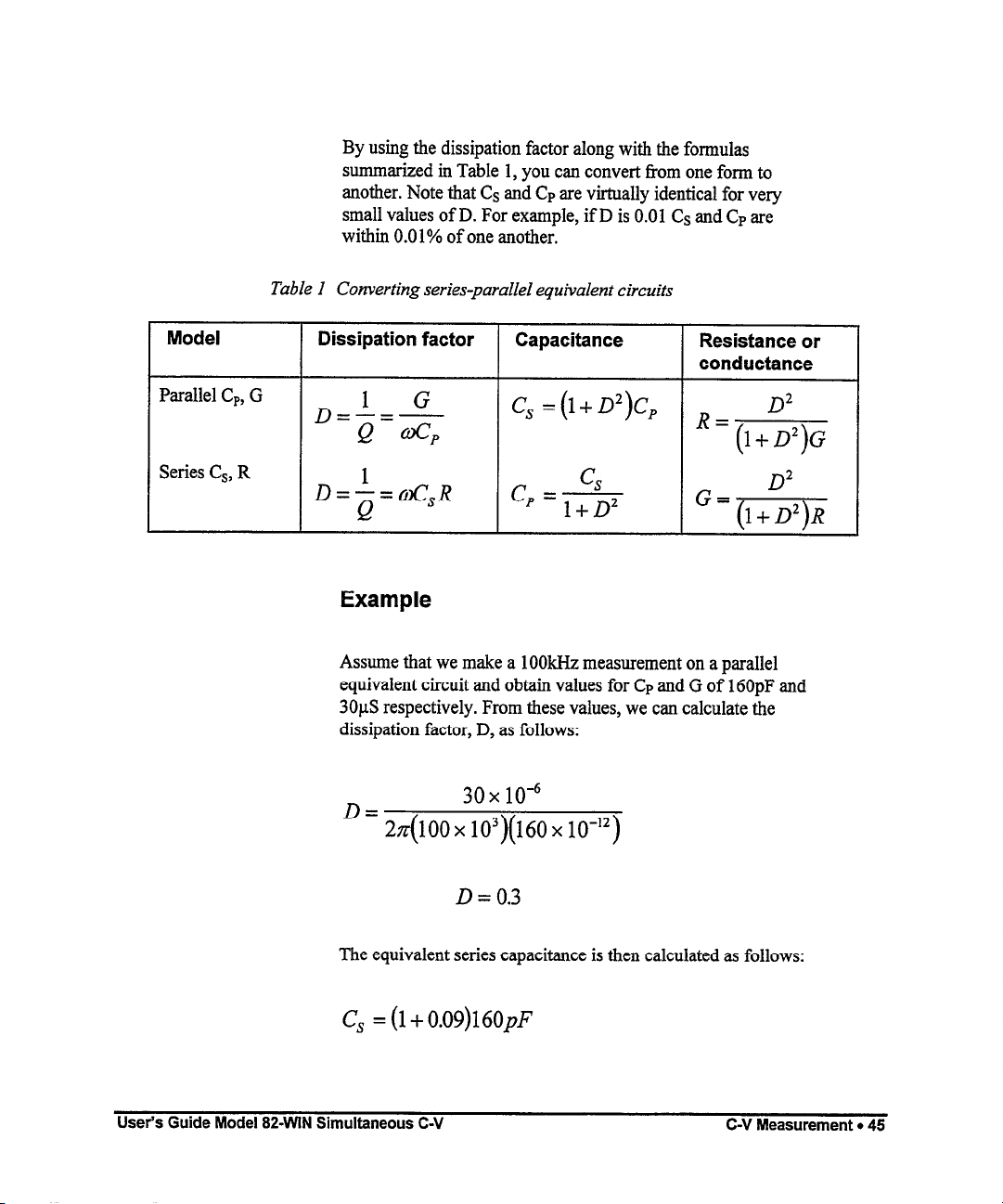
By using the dissipation factor along with the formulas
summarized in Table 1, you can convert from one form to
another. Note that Cs and Cp are virtually identical for very
small values of D. For example, if D is 0.01 Cs and Cp are
within 0.0 1% of one another.
Table I Converting series-parallel equivalent circuits
Model
Parallel Cr, G
Series C,, R
Dissipation factor Capacitance Resistance or
conductance
1 G
D=s=wc,
Cs =(l+
D2)Cp
‘=(l+;‘)G
1
=oC,R Cp=&
D=e
G = (,+;‘)R
Example
Assume that we make a 1 OOkHz measurement on a parallel
equivalent circuit and obtain values for Cp and G of 160pF and
30~s respectively. From these values, we can calculate the
dissipation factor, D, as follows:
30
x lOA
D = 24100 x 103)(160x 10-l’)
The equivalent series capacitance is then calculated as follows:
Cs = (1 + O.O9)16OpF
User’s Guide Model 82-WIN Simultaneous C-V
D = 0.3
C-V Measurement l 45
Page 55
Cs = 174.4pF
Device Considerations
Series Resistance
Devices with high series resistance
analysis errors unless steps are taken to compensate for this
error term. The high dissipation factor caused by series
resistance can cause errors in Cox measurement, resulting in
errors in analysis functions (such as doping concentration) that
use Cox for calculations.
The software uses a three-element model to compensate for
series resistance. The series resistance, Rsm is an analysis
constant that can be determined using the procedure covered
previously.
The software determines the displayed value of Rsa by
converting parallel model data from the Model 590 into series
model data. The resistance value corresponding to the
maximum high-frequency capacitance in accumulation is
defined as h.
Device Structure
The standard analysis assumes a conventional MOS structure
made up of silicon substrate, silicon dioxide insulator, and
aluminum gate material. You can change the program for use
with other types of materials by modifying the material
constants using the Transform editor. For compound materials,
a weighted average of pertinent material constants is often used.
Typical compound materials include silicon nitride and silicon
dioxide in a two- or three-layer sandwich.
can
cause
measurement
and
46 l C-V Measurement
User’s Guide Model 82JMN Simultaneous C-V
Page 56
Device Integrity
In order for analysis to be valid, device integrity should be
checked before measurement. Excessive leakage current
through the oxide can bleed off the inversion layer, causing the
device to remain in non-equilibrium indefinitely. In this
situation, the inversion layer would never form completely, and
CM, measurements would be inaccurate.
Device integrity can be verified by monitoring Q/t levels. If Q/t
levels are excessive, device integrity is suspect.
Test Equipment Considerations
Light Leaks
High-quality MOS capacitors, which are the subject of C-V
analysis, are excellent light detectors. Consequently, care should
be taken to ensure that no light leaks into the test fucture or
probe station. Typical areas to check include door edges and
hinges, tubing entry points, and connectors or connector panels.
Thermal Errors
Accurate temperature control is important for accurate C-V
data. For example, the intrinsic carrier concentration, doubles
for every 8°C increase in ambient temperature. In order to
minimize the effects of thermal errors, keep the device at a
constant temperature during measurement, and repeated
measurements should all be made at the same temperature.
If you change the measurement temperature, change the
material constants for correct values for temperature and
intrinsic concentration using the Transform editor.
User’s Guide Model 82WN Simultaneous C-V
C-V Measurement l 47
Page 57
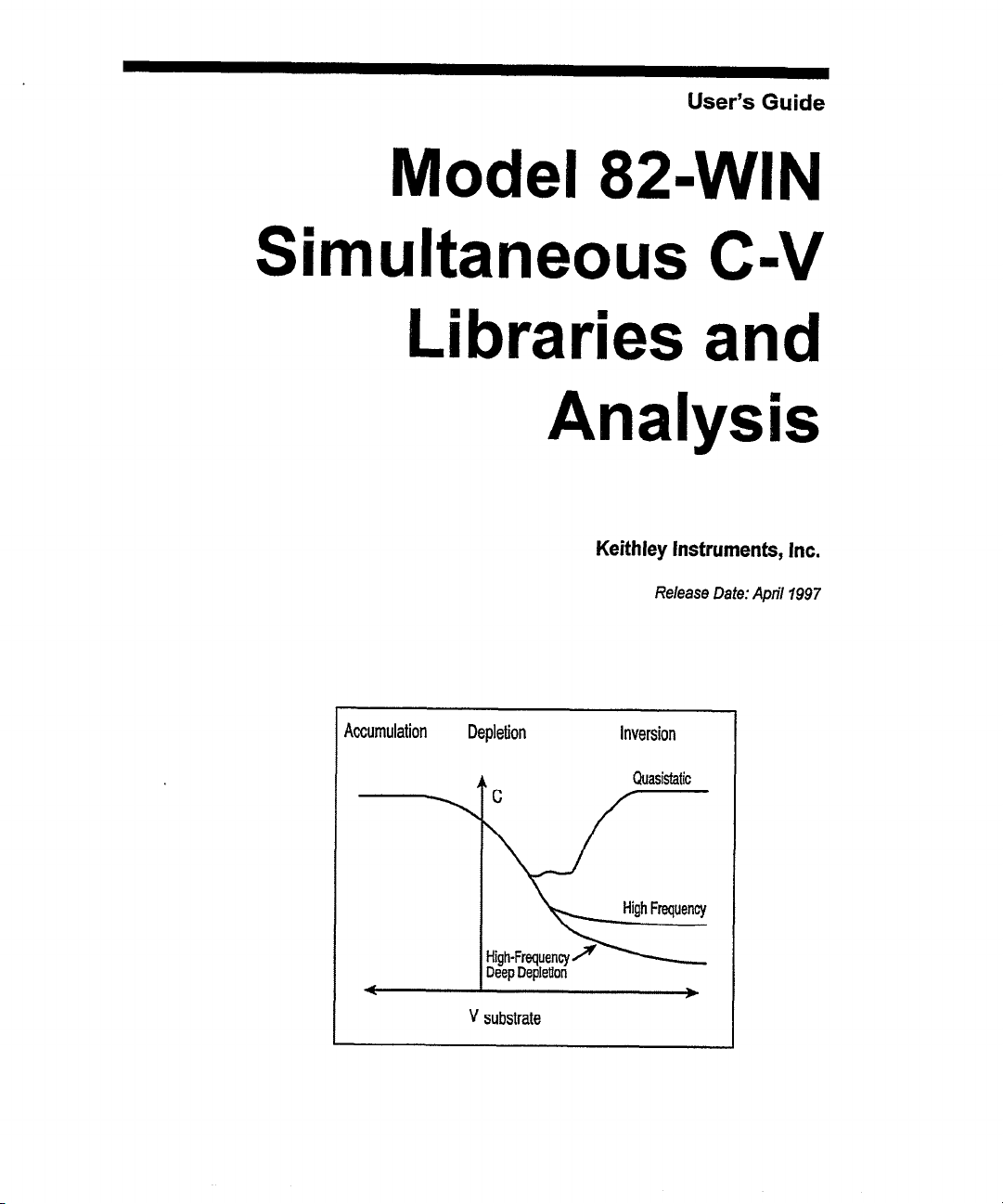
User’s Guide
Model 82-WIN
Simultaneous C-V
Libraries and
Analysis
Keithley Instruments, Inc.
Accumulation
Depletion
C
jeep Depletion
V substrate
Release Date:
Inversion
Guasistatic
April 1997
Page 58

Contents
C-V Libraries and Analysis
Introduction
Using Keitbley
Analysis
................................................................................................................................
Simultaneous
Determining Interface
for Using Interface
Steps
Measurement Results
Typical
Mobile Ion Charge Monitoring with Sirnultaueous Triangular Voltage
Sweep (STVS)
Determining Doping Profile with
Determining Equilibrium
Methods.. ..................................................................................................................
Basic Simultaneous
Basic Device Parameters..
Doping Profile
Interface Trap
Mobile Ion Charge
Technique.. .........................................................................................
for Using Mobile
Steps
Measurement Results
Typical
for Using Doping
Steps
Measurement Results
Typical
for Using Equilibrium
Steps
Measurement Results
Typical
Determining
Capacitance, Thickness,
Oxide
Resistance ......................................................................................................
Series
Gain and
Flatband
Threshold
Semiconductor Work
Metal
Effective
..........................................................................................................
Depletion
1/cH2 vs. Gate Voltage
Concentration
Doping
Density ..............................................................................................
Bending (yrs)
Band
Interface
. . . . . . . . . . . . . . . . . . . . . . . . . . . . . . . . . . . . . . . . . . . . . . . . . . . . . . . . . . . . . . . . . . . . . . . . . . .
C-V Libraries..
Trap Density.. .........................................................................
State
C-V Curves..
..........................................................................................
Device Type ........................................................................................
offset ........................................................................................................
Capacitance and
Voltage ...................................................................................................
Oxide Charge
Depth vs. Gate
vs.
Trap Capacitance
Concentration
...........................................................................
Trap Density
...................................................................................
Ion Charge Library..
...................................................................................
High-ii-equency
Profile Library
..................................................................................
.................................................................................
State Test
..................................................................................
.............................................................................
Flatband Voltage
Function Difference
...........................................................................................
Voltage (v~s).
.............................................................................................
vs. Depth.. ...........................................................................
Gate Voltage
Crr and Density
............................................................................
Library ........................................................
............................................................
C-V ............................................
..................................................................
Library.. ....................................................
and Gate
Area.. .......................................................
...........................................................
...................................................
................................................................
......................................................................
Drr.. ...................................................
I
1
.2
.2
.2
.4
.6
.6
.7
10
.10
11
.12
.13
14
.16
.16
18
18
18
19
.2 1
.2 1
.23
.24
.25
.27
.27
27
.27
.29
.29 .
.30
.3 1
User’s Guide Model 82WN Simultaneous C-V
C-V Libraries and Analysis l i
Page 59

Mobile Ion Monitoring with Triangular Voltage Sweep (STVS) Method
Flatband Voltage Shift Method.. ............................................................................. .32
Triangular Voltage Sweep (TVS) Method
Generation Velocity and Generation Lifetime (Zerbst Plot)
Zerbst Plot ................................................................................................................ 34
Determining Generation Velocity and Generation Lifetime..
Constants, Symbols, and Equations Used for Analysis
Default Material Constants
Modifying Constants..
Data Symbols
.............................................................................................................
Summary of Analysis Equations..
.......................................................................................
...............................................................................................
.............................................................................
References and Bibliography of C-V Measurements..
References
Bibliography of C-V Measurements..
..................................................................................................................
.......................................................................
.........................................................................................................................
Texts
Articles and Papers
...................................................................................................
..............
..............................................................
.3 1
.33
...................................... 34
..................................
.35
............................................................ 37
.37
.37
38
.40
............................................................ .44
44
.44
44
44
User’s Guide Model 82JMN Simultaneous C-V
C-V Libraries and Analysis l ii
Page 60

C-V Libraries and Analysis
Introduction
The Keithley Simultaneous C-V System Model 82-WlN is
equipped with many measurement and analysis libraries that can
help you extract a large amount of information from your
simultaneous C-V measurement data quickly and easily. This
chapter covers using these libraries to suit your measurement
and analysis needs. It is organized as follows:
Using Keithley Simultaneous C-V Libraries: Outlines the
procedures for making measurements and analyzing data
effectively.
Analysis Methods: Discusses methods of extracting parameters
from simultaneous C-V curves. It also includes in-depth
discussion of several methods to determine mobile ion charge
concentration.
Constants, Symbols, and Equations Used for Analysis: Lists
the material constants used in calculations and shows how to
modify the constants. Raw and calculated data symbols used in
the libraries are listed. Equations are also listed.
References and Bibliography of C-V Measurements:
Summarizes references for C-V measurement and analysis,
along with additional texts and papers for suggested reading.
User’s Guide Model 824MN Simultaneous C-V
C-V Libraries and Analysis l 1
Page 61

Using Keithley Simultaneous C-V Libraries
Determining Interface Trap Density
Interface trap charge is important in determining device
integrity. In fabrication environments, trap density must be
carefUlly controlled. Interface trapped charge can be of several
types: (1) structural, oxidation-induced defects; (2) metal
impurities; and (3) other defects caused by radiation or bondbreaking processes. The interface trapped charge is located at
the Si-SiO;! interface. It is in electrical proximity to the
underlying silicon, which can be either charged or discharged.
The Keithley Interface trap density (Dir) library can perform
interface trapped charge density analysis. It has a built-m
correction algorithm to eliminate the problems associated with
leakage current. Many parameters can also be extracted from
this measurement, including doping profile, flatband voltage
and capacitance, threshold voltage, work functions, and oxide
charge.
Step 1: Load the Keithley Interface Trap
Density Library into ICS
Use the Import command under the File menu to import the
Keithley Drr library named KI-DIT.DAT. Your screen should
look like the one shown in Figure 1.
User’s Guide Model 824MN Simultaneous C-V
C-V Libraries and Analysis l 2
Page 62

Step 2: Modify Measurement Parameters
Click on the Setup Editor button.
1.
Click on the KI_82.OUT icon. You should now be in
2.
the parameter setup window.
Type in the appropriate measurement parameters.
3.
Close all windows to return to the main window.
4.
Step 3: Modify Analysis Library Constants
Click on the Transform Editor button.
1.
Click on the Edit Constants button.
2.
Select and type in the constants you wish to change.
3.
Return to the main window by clicking on the OK and
4.
DONE buttons in that order.
Step 4: Make the Measurement
Click on the Zero Cancel button to do a probe-up
1.
suppress.
Click on the Single button on the Measurement menu
2.
to take the measurement.
User’s Guide Model 82-WIN Simultaneous C-V
C-V Libraries and Analysis 0 3
Page 63

3. You may view the results directly on the screen shortly
after data is taken,. Several plots are available on
screen, and you may expand them to examine details,
or you may create your own plot. Available plots are:
capacitance curves, leakage current curve, band
bending, and doping profile. All measured and
calculated data are displayed in the data spreadsheet
window.
Typical Measurement Results
A typical simultaneous C-V measurement is shown in Figure 1.
Figure 2 shows the device leakage current, which can be a
valuable tool to monitor system performance and device
integrity. Interface trap density for this particular device is
shown in Figure 3, and band bending vs. gate voltage and
doping profile vs. gate voltage are also plotted.
Figure 1
User’s Guide Model 82-WlN Simultaneous C-V
Interface Trap Density Library Main Wnciows
C-V Libraries and Analysis l 4
Page 64
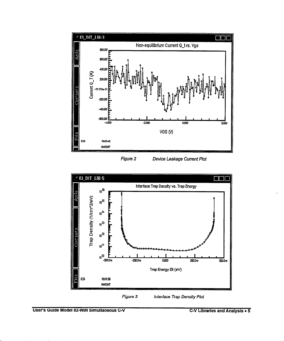
Non-equilibrium Current Q-t vs. Vgs
Figure 2 Device Leakage Current Plot
Interface Trap Density vs. Trap Energy
10'0
User’s Guide Model 82-WIN Simultaneous C-V
I 1 I I I I
-aQnm -2mm
Figure 3 Interface Trap Density Plot
I I I I 1 1
OK0
Trap Energy Eii (eV)
7sln)m smm
C-V Libraries and Analysis. 5
Page 65
Mobile Ion Charge Monitoring with Simultaneous Triangular
Voltage Sweep (STVS) Technique
STVS is a new technique developed by Keithley to monitor
mobile ion charge in MOS structures. Compared with other
mobile ion monitoring techniques, such as the BTS and flatband
shift methods, it offers faster and more accurate measurement.
STVS measures ionic current instead of voltage shift. It has the
ability to identify species, and it eliminates the need for
temperature cycling of the Device Under Test @UT). The
STVS method has proven to be effective in monitoring mobile
ions in dielectrics at levels down to 109cm3.
The STVS library can perform the corresponding mobile ion
charge analysis.
eliminate the problems associated with leakage current. Many
parameters, including mobile ion charge concentration, can be
extracted from this measurement.
It has a built-in correction algorithm to
Step I: Heat the DUT to the Desired
Temperature
Heat the DUT to the desired temperature before testing. 250-
300°C should be sufficient for sodium ions in most cases.
Step 2: Load the Keithley STVS Library
Using the Import command under the File menu, import the
Keithley STVS library named KI-M-ION.DAT. Your screen
should look like the one shown in Figure 4.
User’s Guide Model 82WlN Simultaneous C-V
C-V Libraries and Analysis l 6
Page 66
Step 3: Modify Measurement Parameters
1. Click on the Setup Editor button, and then click on the
KI-82.OUT icon. You should now be in the parameter
setup window.
2. Type in the appropriate measurement parameters, then
close all the windows to return to the main window.
Step 4: Modify Analysis Library Constants
1. Click on the Transform Editor button.
2. Click on the Edit Constants button.
3. Select and type in the constants you wish to change.
4. Return to the main window by clicking on the OK and
DONE buttons in that order.
Step 5: Make the Measurement
1. Click on the Zero Cancel button to do a probe-up
suppress.
2. Click on the Single button on the Measurement menu
to take the measurement.
3. Results will be displayed shortly after dam is taken.
Capacitance curves and the leakage current curve are
displayed, and all measured and calculated data are
displayed in the data spreadsheet window.
User’s Guide Model 82-WIN Simultaneous C-V
C-V Libraries and Analysis l 7
Page 67
Typical Measurement Results
Figure 4 shows a mobile ion plot. A typical Simultaneous C-V
measurement at elevated temperature is shown in Figure 5. Note
that the curve peak is caused by mobile ion charge in the
dielectric. You may also wish to check leakage current for
measurement integrity. For this particular device, the mobile ion
concentration can be obtained from the plot.
User’s Guide Model 82-WIN Simultaneous C-V
Figure 4
Mobile Ion Charge Plot
C-V Libraries and Analysis l 8
Page 68
6 cmE.10
4mx.10
4lmlE.10
L
Simultanqx4s TVS
Figure 5
Simultaneous C-V Curve at Elevated Temperature
User’s Guide Model 82WlN Simultaneous C-V
C-V Libraries and Analysis . 9
Page 69
Determining Doping Profile with High-frequency C-V
Doping profile is one of the important parameters for many
semiconductor devices. It is normally derived from C-V.
measurements, although it is also related to resistivity. It can be
extracted from a high-frequency C-V curve using the Keithley
Model 590 High Frequency Capacitance measurement package.
Step 1: Load the Keithley High-frequency C-V
Library
Using the Import command under the File menu, import the
Keithley high-frequency C-V library named KI-DOPE.DAT.
Your screen should look like the one shown in Figure 6.
Step 2: Modify Measurement Parameters
1. Click on the Setup Editor button.
2. Click on the ICI-82.OUT icon. You should now be in
the parameter setup window.
3. Type in the appropriate measurement parameters.
4. Close all windows to return to the main window.
User’s Guide Model 82WlN Simultaneous C-V
C-V Libraries and Analysis l 10
Page 70
Step 3: Modify Analysis Library Constants
1. Click on the Transform Editor button.
2. Click on the Edit Constants button.
3. Select and type in the constants you wish to change.
4. Return to the main window by clicking on the OK and
DONE buttons in that order.
Step 4: Make the Measurement
1. Click on the Zero Cancel button to do a probe-up
suppress.
2. Click on the Single button on the Measurement menu
to take the measurement.
3. You may view the results shortly after data is taken.
Several plots are available on the screen, and you may
expand them to examine details. Available plots are:
capacitance curves, leakage current curve, band
bending, and doping profile. All data, including
measured and calculated data, are displayed in the dam
spreadsheet window.
Typical Measurement Results
A typical doping profile plot is shown in Figure 6. Figure 7
shows doping profile obtained from high-frequency C-V
measurement. You may also wish to check leakage current to
monitor system performance and device integrity. With this
User’s Guide Model 824VlN Simultaneous C-V C-V Libraries and Analysis. 11
Page 71
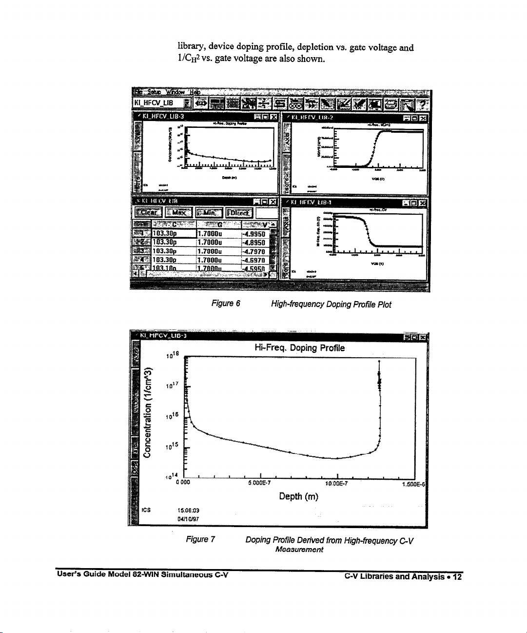
library, device doping profile, depletion vs. gate voltage and
1/cH2
vs. gate voltage are also shown.
Figure 6
10'4
0
t5.06:03
wlcG97
Figure 7
User’s Guide Model 82-WIN Simultaneous C-V
High-frequency Doping Profile Plot
f-ii-Freq. Doping Profile
1O~OOEJ
Depth (m)
Doping Profile Derived from High-frequency C-V
Measurement
C-V Libraries and Analysis. 12
Page 72
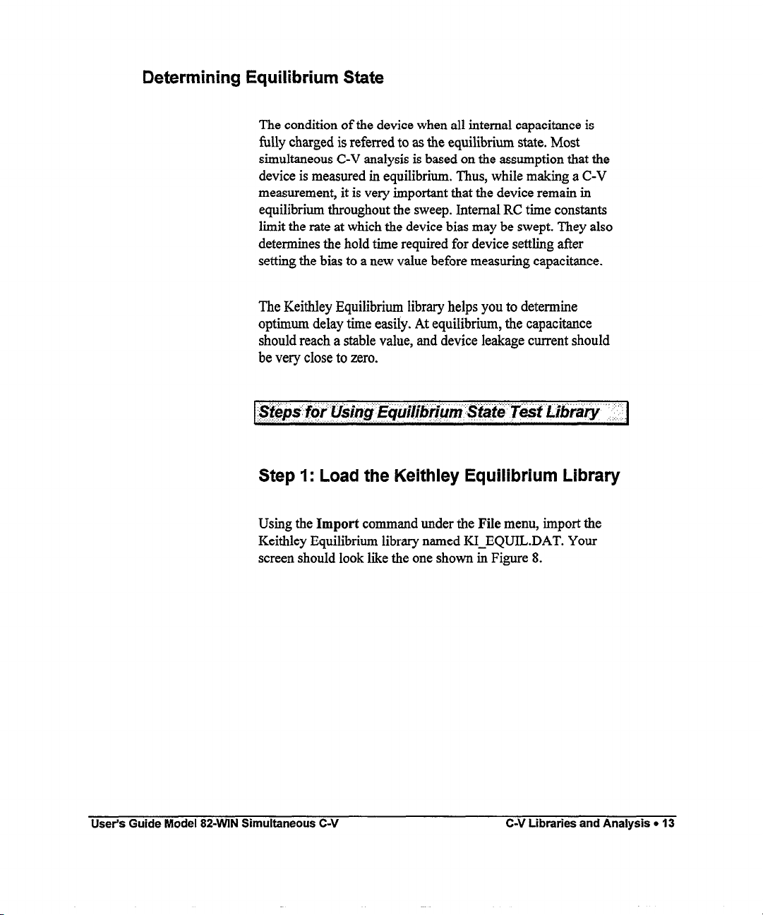
Determining Equilibrium State
The condition of the device when all internal capacitance is
fully charged is referred to as the equilibrium state. Most
simultaneous C-V analysis is based on the assumption that the
device is measured in equilibrium. Thus, while making a C-V
measurement, it is very important that the device remain in
equilibrium throughout the sweep. Internal RC time constants
limit the rate at which the device bias may be swept. They also
determines the hold time required for device settling after
setting the bias to a new value before measuring capacitance.
The Keithley Equilibrium library helps you to determine
optimum delay time easily. At equilibrium, the capacitance
should reach a stable value, and device leakage current should
be very close to zero.
Step 1: Load the Keithley Equilibrium Library
Using the Import command under the File menu, import the
Keithley Equilibrium library named IU-EQULDAT. Your
screen should look like the one shown in Figure 8.
User’s Guide Model 82-WIN Simultaneous C-V C-V Libraries and Analysis 0 13
Page 73
Step 2: Modify Measurement Parameters
1. Click on the Setup Editor button.
2. Click on the KI-82.OUT icon. You should now be in
the parameter setup window.
3. Type in the appropriate measurement parameters.
4. Close all windows to return to the main window.
Step 3: Make the measurement
1. Click on the Zero Cancel button to do a probe-up
suppress.
2. Click on the Single button on the Measurement menu
to take the measurement.
3. You may view the results shortly after data is taken,
and you may expand the plot to examine details. All
data, include measured and calculated data, are
displayed in the data spreadsheet window.
Typical Measurement Results
A typical equilibrium measurement is shown in Figure 8. Also
shown is the device leakage current during measurement, which
can be a valuable tool to monitor system performance and
device integrity.
User’s Guide Model 82-WIN Simultaneous C-V
C-V Libraries and Analysis. 14
Page 74

Figure 8
Equilibtium Sfafe Tesf Plot
User’s Guide Model 82-WIN Simultaneous C-V
C-V Libraries and Analysis l 15
Page 75

Analysis Methods
Basic Simultaneous C-V Curves
This section discusses the theory and techniques used in the
various Keithley Simultaneous C-V libraries. For more detailed
discussions, refer to the references at the end of the chapter. A
text file named EQUATION.TXT lists all the equations used in
Keithley libraries is provided, and another file named
CONSTANT.TXT lists the constants used in Keithley libraries.
Figure 9 and Figure 10 show fundamental C-V curves for p-type
and n-type materials respectively. Both high-frequency and
quasistatic curves are shown in these figures. Note that the highfrequency curves are highly asymmetrical, while the quasistatic
curves are almost symmetrical. Accumulation, depletion, and
inversion regions are also shown on the curves. The gate-
biasing polarity and high-frequency curve shape can be used to
determine device type, as discussed below.
User’s Guide Model 82-WIN Simultaneous C-V
C-V Libraries and Analysis l 16
Page 76

:apacitance
~
@ Onset of Strong Inversion
GATE BlASVOLTAGE,V GR
Cc!
Inversion
hpacitance
Figure 9
Inversh
Onset of Strong
Inversion \ 1
ys = 248
-4
\
CH
'"GS
Figure 70
C-V Characferisfics of p-fype Material
Depletion
j-
v THRESHOLD
VFEi
GATEBlASVOLTAGE,V G.
C-V Characteristics of n-fype Material
Accumulation
+v GS
User’s Guide Model 82WlN Simultaneous C-V
C-V Libraries and Analysis l 17
Page 77

Basic Device Parameters
Determining Device Type
The semiconductor conductivity type (p or n dopant ions) can
be determined from the relative shape of the C-V curves. (See
Figure 9 and Figure 10.) The high-frequency curve gives a
better indication than the quasistatic curve because of its highly
asymmetrical nature. Note that the C-V curve moves from the
accmdation to the inversion region as gate voltage, VGS,
becomes more positive for p-type materials, but the curve
moves from accumulation to inversion as VGS becomes more
negative with n-type materials (Nicollian and Brews 372-374).
1. If Cu is greater when Vos is negative than when Vos is
positive,-the substrate material is p-type.
2.
If, on the other hand, CH is greater with positive VGS
than with negative Vos, the substrate is n-type.
3.
The end of the curve where Cn is greater is the
accumulation region, while the opposite end of the
curve is the inversion region. The transitional area
between these two is the depletion region. These areas
are marked on Figure 7 and Figure 8.
Oxide Capacitance, Thickness, and Gate
Area
The oxide capacitance, Cox, is the high-frequency capacitance
with the device biased in strong accumulation. Oxide thickness
is calculated from Cox and gate area as follows:
User’s Guide Model 82JMN Simultaneous C-V
C-V Libraries and Analysis l 18
Page 78

t
A Eox
OX = (1 x 10-‘9)cox
Where:
LOX = oxide thickness (mrr)
A = gate area (cm2)
lox = permittivity of oxide material (F/cm)
Cox = oxide capacitance (PF)
The above equation can be easily rearranged to calculate gate
area if the oxide thickness is known. Note that lox and other
constants are initialized for use with silicon substrate, silicon
dioxide insulator, and aluminum gate material but may be
changed for other materials. (See
end of this chapter.)
Modtjjkg Constants
near the
Series Resistance
The series resistance, Rsms is an error term that can cause
measurement and analysis errors unless this series resistance
error factor is taken into account. Without series compensation,
capacitance can be lower than normal, and C-V curves can be
distorted. The software compensates for series resistance using
the simplified three-element model shown in Figure 11. In this
model, Cox is, of course, the oxide capacitance while CA is the
capacitance of the accumulation layer. The series resistance is
represented by lQ=.
User’s Guide Model 82-WIN Simultaneous C-V
C-V Libraries and Analysis l 19
Page 79

RSERIES
A. Equivelent Three Element
Model of MOS Capacitor
in Strong Accumulation
Figure 11
Simplified Model to Detemrine Series Resistance
From Nicollian and Brews 224, the correction capacitance, Cc,
and corrected conductance, Gc, are calculated as follows:
(G; +02C;)a
G, =
a2 +w2C2
M
B. Simplified Model of
k;;;;i to determine
(3)
Where:
a =
GM
- (GYM f o%&) hs
CC = series resistance compensated parallel model capacitance
CM = measured parallel model capacitance
GC = series resistance compensated conductance
User’s Guide Model 82WN Simultaneous C-V
C-V Libraries and Analysis l 20
Page 80
GM = measured conductance
RSWES = series resistance
Gain and ofFset
Gain and offset can be applied to
CQ
and Cn data to allow for
curve alignment or to compensate for measurement errors. A
gain factor is a multiplier that is applied to all elements of
CQ
or
Cn array data before plotting or graphics array calculation.
Offset is a constant value added to or subtracted from all
CQ
and
Cn data before plotting or array calculation.
For example, assume that you compare the
reading #3, and you fmd that
then add an offset of +2.3pF to
CQ
is 2.3pF less than Cn. If you
CQ,
the
reading #3 will then be the same, and the
CQ
and Cn values at
CQ
and Cn values at
CQ
and Cn curves will
be aligned at that point.
Gain and offset values do not affect raw
CQ
and Cn values
stored in the data file, but the gain and offset values will be
stored in the data file so that compensated curves can easily be
regenerated at a later date.
Flatband Capacitance and Flatband Voltage
The Model 82-WIN uses the flatband capacitance method of
finding flatband voltage, Vm. The Debye length is used to
calculate the ideal value of flatband capacitance, Cm. Once the
value of Cm is known, the value of Vm is interpolated from the
closest Vos values (Nicollian and Brews 487-488).
The method used is invalid when interface trap density becomes
very large (1012-1013 and greater). However, this algorithm
should give satisfactory results for most users. Those who are
dealing with high values of Drr should consult the appropriate
literature for a more appropriate method.
User’s Guide Model 824ViN Simultaneous C-V
C-V Libraries and Analysis. 21
Page 81
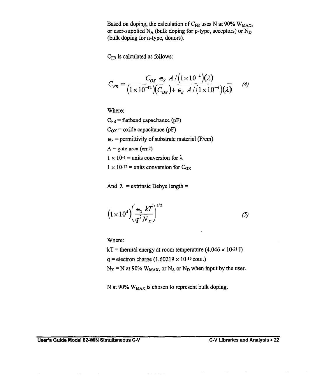
Based on doping, the calculation of Cm uses N at 90% Ww,
or user-supplied NA (bulk doping for p-type, acceptors) or ND
(bulk doping for n-type, donors).
Cm is calculated as follows:
c =
cox ES A/(1x 104)(A)
FB (1 x 10”‘)(c,,) + ES Al(1x10⁻⁴)(A) e.)
Where:
Cm = flatband capacitance (PF)
Cox = oxide capacitance (pF)
ES = permittivity of substrate material (F/cm)
A = gate area (cm2)
1 x 10-r = units conversion for h
1 x lo-12 = units conversion for Cox
And h = extrinsic Debye length =
(1 x 10’,(-g2
.
Where:
kT = thermal energy at room temperature (4.046 x IO-21 J)
q = electron charge (1.60219 x IO-19 coul.)
Nx = N at 90% Wm, or NA or ND when input by the user.
N at 90% W- is chosen to represent bulk doping.
User’s Guide Model 824MN Simultaneous C-V
C-V Libraries and Analysis l 22
Page 82
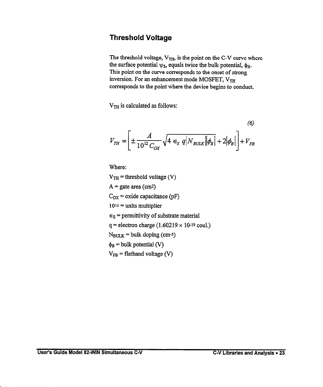
Threshold Voltage
The threshold voltage, Vm, is the point on the C-V curve where
the surface potential ys, equals twice the bulk potential, $a.
This point on the curve corresponds to the onset of strong
inversion. For an enhancement mode MOSFET, Vm
corresponds to the point where the device begins to conduct.
Vm is calculated as follows:
Where:
VW = threshold voltage (V)
A = gate area (cm2)
Cox = oxide capacitance (pF)
1012 = units multiplier
ES = permittivity of substrate material
q = electron charge (1.602 19 x lo-19 coul.)
NB~ = bulk doping (cm-s)
$n = bulk potential (V)
VFB = flatband voltage (V)
User’s Guide Model 82-WIN Simultaneous C-V
C-V Libraries and Analysis l 23
Page 83

Metal Semiconductor Work Function
Difference
The metal semiconductor work function difference, WMS, is
commonly referred to as the work function. It contributes to the
shift in Vm from the ideal zero value, along with the effective
oxide charge (Nicollian and Brews 462-477; Sze 395402). The
work function represents the difference in work necessary to
remove an electron from the gate and from the substrate, and it
is derived as follows:
Where:
WM = metal work fimction (V)
Ws = substrate material work function (electron affinity) (V)
EG = substrate material bandgap (V)
4s = bulk potential (V)
For silicon, silicon dioxide, and aluminum:
=4.1- 4.15+y-
WA5
So that,
W,, =
W,,
User’s Guide Model 82JMN Simultaneous C-V
-0.61+ q&
=-0.61-(~)ln(~)(Lkpel&x)
1.12
[
B
4
0
(9)
(lo)
C-V Libraries and Analysis 0 24
Page 84
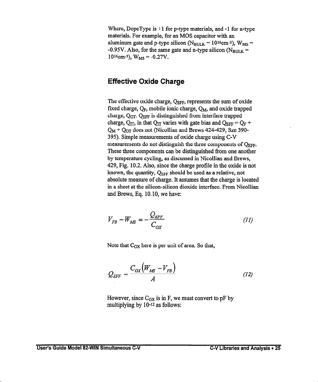
Where, DopeType is +l for p-type materials, and - 1 for n-type
materials. For example, for an MOS capacitor with an
aluminum gate and p-type silicon @Iam = lO%m-s), WMS =
-0.95V. Also, for the same gate and n-type silicon (Nnm~ =
lOt%m-s), WMS = -0.27V.
Effective Oxide Charge
The effective oxide charge, Qm, represents the sum of oxide
futed charge, QF, mobile ionic charge, Qa and oxide trapped
charge, Qor. Qsm is distinguished from interface trapped
charge, Qrr, in that Qrr varies with gate bias and Qm = QF +
QM + QOT does not (Nicollian and Brews 424-429, Sze 390-
395). Simple measurements of oxide charge using C-V
measurements do not distinguish the three components of Qm.
These three components can be distinguished from one another
by temperature cycling, as discussed in Nicollian and Brews,
429, Fig. 10.2. Also, since the charge profile in the oxide is not
known, the quantity, Qm should be used as a relative, not
absolute measure of charge. It assumes that the charge is located
in a sheet at the silicon-silicon dioxide interface. From Nicollian
and Brews, Eq. 10. IO, we have:
FB-Wm=-=
V
Note that Cox here is per unit of area. So that,
Q
EFF
However, since Cox is in F, we must convert to pF by
multiplying by IO-12 as follows:
User’s Guide Model 824MN Simultaneous C-V
Q
c
A
(II)
ox
w
C-V Libraries and Analysis l 25
Page 85
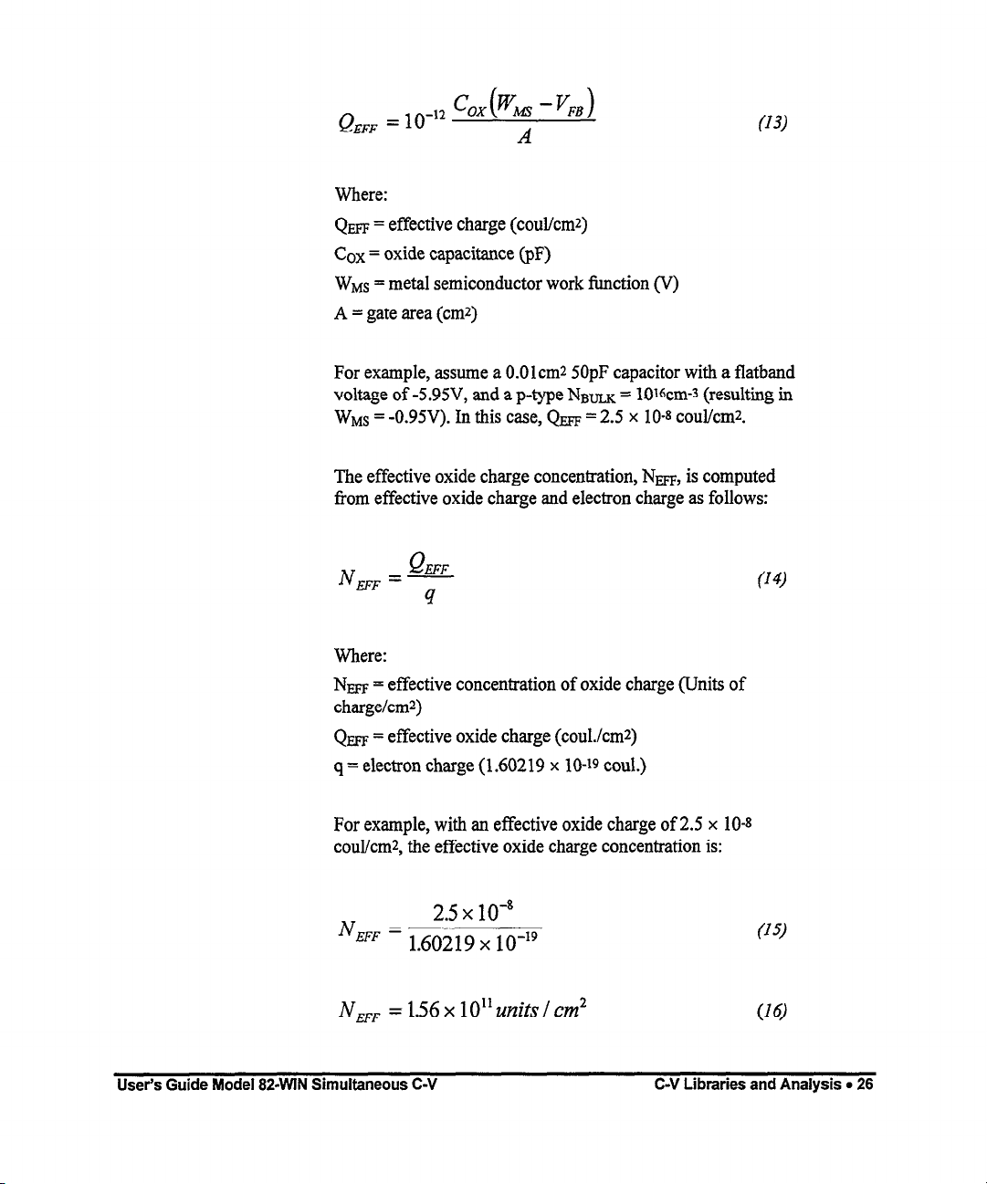
EFF =
Q
Where:
Qm = effective charge (couVcm2)
Cox = oxide capacitance (PF)
WMS = metal semiconductor work fimction (V)
A = gate area (cm2)
For example, assume a 0.0 1 cm2 50pF capacitor with a flatband
voltage of -5.95V, and a p-type Nnm = lOt%m-3 (resulting in
WMS = -0.95V). In this case, QEFF = 2.5 x 10-s coul/cmL
The effective oxide charge concentration, NQTF, is computed
from effective oxide charge and electron charge as follows:
N
EFF =-
cOX(wMT - ‘FB)
lo-l2
Q
JZFF
4
A
(13)
04)
Where:
NW = effective concentration of oxide charge (Units of
chargelcm2)
Qm = effective oxide charge (coulJcm2)
q = electron charge ( 1.602 19 x 1 O-19 coul.)
For example, with an effective oxide charge of 2.5 x 10-s
coul/cmz, the effective oxide charge concentration is:
N
EFF = 1.60219 x 10-l’
N EFF =
User’s Guide Model 82-WIN Simultaneous C-V
1.56
2.5 x 10”
x 1O”units / cm2
(15)
(16)
C-V Libraries and Analysis a26
Page 86
Doping Profile
Depletion Depth vs. Gate Voltage (VGS)
Model S2-WIN computes the depletion depth, w, from the highfrequency capacitance and oxide capacitance at each measured
value of Vcs (Nicollian and Brews 386). In order to graph this
function, the program computes each w element of the
calculated data array as shown below.
Where:
w = depth (pm)
ES = permittivity of substrate material
Cn = high-frequency capacitance (pF)
Cox = oxide capacitance @F)
A = gate area (cm2)
1/cH2
A l/cZ graph can yield important information about doping
profile. N is related to’the reciprocal of the slope of the l/C2 vs.
Vos curve, and the V intercept point is equal to the fiatband
voltage caused by surface charge and metal-semiconductor
work function (Nicollian and Brews 385).
vs. Gate Voltage
Doping Concentration vs. Depth
The doping profile of the device is derived from the C-V curve
based on the definition of the differential capacitance (measured
by the Models 590 and 595) as the differential change in
User’s Guide Model 82-WIN Simultaneous C-V C-V Libraries and Analysis l 27
Page 87

depletion region charge produced by a differential change in
gate voltage (Nicollian and Brews 380-389).
The standard N vs. w analysis discussed here does not
compensate for the onset of accumulation, and it is accurate
only in depletion. This method becomes inaccurate when the
depth is less than two Debye lengths.
In order to correct for errors caused by interface traps, the error
term (l-C&-&/( 1 -C&T&) is included in the calculations as
follows:
Where:
N = doping concentration (cm-s)
CQ
= quasistatic capacitance (PF)
Cox = oxide capacitance @F)
(1 -C~/Cox)/l-C&ox) = voltage stretchout term
CH = high-frequency capacitance @F)
A = gate area (cm2)
q = electron charge (1.60219 x IO-19 coul.)
ES = permittivity of substrate material
1 x lo-24 = units conversion factor
User’s Guide Model 824MN Simultaneous C-V
C-V Libraries
and
Analysis l 28
Page 88
Interface Trap Density
Band Bending (~Js) vs. Gate Voltage
As a preliminary step, surface potential (ws - ~0) vs. Vos is
calculated with the results placed in the ws column of the array.
Surface potential is calculated as follows:
Where:
(ws - w0) = surface potential (V)
CQ
= quasistatic capacitance (pF)
Cox = oxide capacitance @F)
VSTE~ = step voltage (V)
Vos = gate-substrate voltage (V)
Note that the (ys - ~0) value is accumulated as the column is
built, from the first row of the array (Vos #l) to the last array
row (vos last). The number of rows will, of course, depend on
the number of readings in the sweep, which is determined by the
Start, Stop and Step voltages.
Once (ws - ~0) values are stored in the array, the value of (ws ~0) at the flatband voltage is used as a reference point and is set
zero by subtracting that value from each entry in the (ws - ~0)
column, changing each element in the column to vs.
User’s Guide Model 82-WIN Simultaneous C-V
C-V Libraries and Analysis l 29
Page 89
Interface Trap Capacitance CIT and Density
DIT
Interface trap density is calculated from Crr as shown below
(Nicollian and Brews 322).
cl* &$--)--‘ pp)-’
D
= (lx loqcr
IT
Where:
CIT = interface trap capacitance (pF)
Dn = interface trap density (cm-2 eV-1)
CQ
= quasistatic capacitance (pF)
CH = high-frequency capacitance (pF)
Cox = oxide capacitance (pF)
A = gate area (cm2)
q = electron charge ( 1.602 19 x 1 0-l’koul.)
1 x 104 = units conversion for Cm
A
WY
PO
User’s Guide Model 824VlN Simultaneous C-V
C-V Libraries and Analysis .30
Page 90

Mobile Ion Charge Concentration
Mobile Ion Monitoring with Triangular
Voltage Sweep (STVS) Method
STVS is a new technique developed by Keithley to monitor
mobile ion charge in MOS structures. Compared with other
mobile ion monitoring techniques, such as the BTS and flatband
shift methods, it offers faster and more accurate measurement.
STVS measures ionic current instead of voltage shift. It has the
ability to identify species, and it eliminates the need for
temperature cycling of the Device Under Test @UT). The
STVS method has proven to be effective in monitoring mobile
ion charge in dielectrics to levels down to 1 09cm”.
The STVS library can perform the corresponding mobile ion
charge analysis. It has a built-m correction algorithm to
eliminate the problems associated with leakage current. Many
parameters, including mobile ion charge concentration, can be
extracted from this measurement.
The STVS method improves on the conventional TVS method
(discussed below) by measuring both
CQ
and CH and then
computing mobile ion charge concentration as follows:
Where:
NM = mobile ion density (l/cm”)
Vos = gate-substrate voltage (V)
AVos = change in gate-substrate voltage (step voltage) (V)
CQ
= quasistatic capacitance measured by Model 595 Q
Cn = high-frequency capacitance measured by Model 590 (F)
User’s Guide Model 82-WIN Simultaneous C-V C-V Libraries and Analysis l 31
Page 91

q = electron charge (coul.)
Flatband Voltage Shift Method
The primary method for measuring oxide charge density is the
flatband voltage shift or temperature-bias stress method (Snow
et al). In this case, two high-frequency C-V curves are
measured, both at room temperature. Between the two curves,
the device is biased with a voltage at 200-3OOT to drift mobile
ions across the oxide. The flatband voltage differential between
the two curves is then calculated, from which charge density can
be determined.
From Nicollian and Brews (426, Eq. 10.9 and IO. lo), we have:
FB-wm=-=
V
FQO
Eox
Where:
ZQo
= the first moment of the charge distribution
X = charge centroid
WMS = metal semiconductor work function (constant)
lox = oxide dielectric constant
X,, = oxide thickness
Cox = oxide capacitance
So that:
=A-
XQo
A&
FQO
xocox
Eox
(23)
User’s Guide Model 82WlN Simultaneous C-V C-V Libraries and Analysis l 32
Page 92

AV,, = -
Qo
C
For the common case of thermally grown oxide, ‘ii (before) =
XCJ and ‘i7 (after) = 0, so that
5
(26)
OX Ax,
AV,, = -
Where Qo is the effective charge. Divide Qo by the gate area to
obtain mobile ion charge density per unit area.
Triangular Voltage Sweep (TVS) Method
V^L^-^CL ^-_-.^-. A- I^^----- --.:1- _L_--- 3 -..- :-. z-11
I
CL
triangular voltage sweep (TVS) method (Nicollian and Brews
435-440).
Although the method presented here was originally developed
for the ramp technique of quasistatic measurement, the Model
595 is used to make the necessary measurement. The end result
is the same: the area between the measured capacitance curve
and Cox indicates the charge density as follows:
+vG.s
CC
-VGS
-Qo
C
ox
auuu~t;~
way
LO u~ezwue oxme cmrge aensny IS me
GEAS - c,,)WGS = !I%4
[
~(v,,)
-y -
0 X0
(27)
(28)
f(- VA)
1
Where:
Vos = gate-substrate voltage (V)
AVos = change in gate-substrate voltage (step voltage) (V)
C-s = quasistatic capacitance measured by Model 595 (F)
Cox = oxide capacitance (F)
User’s Guide Model 82WlN Simultaneous C-V
C-V Libraries and Analysis l 33
Page 93

q = electron charge (coul.)
NM = mobile ion density (l/cm’)
T( = charge centroid
X0 = oxide thickness (m)
Qo = mobile ion charge (coul.)
or, in the case of thermally grown oxide, the above reduces to:
+vGs
c(
-vGS
Generation Velocity and Generation Lifetime (Zerbst Plot)
- Gx)Av,, = -eo
(29)
Zerbst
Zerbst analysis requires two types of data: C-V and C-t.
Important data taken from the C-V measurement includes COX,
Cm, and doping concentration (N~vo and NnuLK). The results
of the C-V analysis are integrated with data taken during a C-t
measurement to compute generation velocity and generation
lifetime of electron-hole pairs. These two parameters are
computed from the slope and y-axis intercept of the graph of
G/nr vs. w-wr as outlined below.
G/n1 Computation
Gln, =-E, AN,,C,*
Where:
G = generation rate (s-r)
Plot
User’s Guide Model 82-WIN Simultaneous C-V
C-V Libraries and Analysis l 34
Page 94

ES =i permittivity of semiconductor (F/cm)
A = gate area (cm2)
N~vo = average doping concentration (cm-s)
Cox = oxide (maximum) capacitance
Ct(i+t) = (i+l) value of measured C-t capacitance (pF)
Q-1) = (i- 1) value of measured C-t capacitance @F)
nr = intrinsic carrier concentration (cm-s)
trot = time interval between C-t measurements (s)
i = [2, #Rdgs-1]
w - wF comphtion
(PF)
W-WWF =1x10¹² cS
WF =1x10¹² ES A
Where:
w = depletion depth (cm)
wr = equilibrium inversion depth (cm)
ES = permittivity of semiconductor (F/cm)
A = gate area (cm2)
Cti = i(th) value of measured C-t capacitance (pF)
Cm = equilibrium minimum capacitance (pF)
Determining Generation Velocity and
Generation Lifetime
The generation lifetime, TG is equal to the reciprocal of the
slope of the linear portion of the Zerbst plot, while the
A
1 1
---
c 1
cti cm
(30
(32)
User’s Guide Model 82-WIN Simultaneous C-V C-V Libraries and Analysis l 35
Page 95

generation velocity, s, is the y-axis (G/q) intercept of the same
linear section of the Zerbst plot.
User’s Guide Model 824VlN Simultaneous C-V
C-V Libraries and Analysis l 36
Page 96
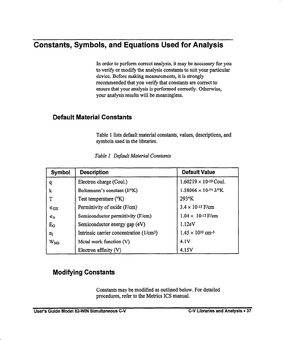
Constants, Symbols, and Equations Used for Analysis
In order to perform correct analysis, it may be necessary for you
to verify or modify the analysis constants to suit your particular
device. Before making measurements, it is strongly
recommended that you verify that constants are correct to
ensure that your analysis is performed correctly. Otherwise,
your analysis results will be meaningless.
Default Material Constants
Table 1 lists default material constants, values, descriptions, and
symbols used in the libraries.
Table I Default Material Constants
Symbol
q
k
T
EOX
ES
EG
3
WMS
Description
Electron charge (Coul.)
Boltzmann’s constant (J/X)
Test temperature (“K)
Permittivity of oxide (F/cm)
Semiconductor permittivity (F/cm)
Semiconductor energy gap (eV)
Intrinsic carrier concentration (l/ems) 1.45 x 1010 cm-s
Metal work function (V)
Electron affinity (V)
Modifying Constants
Constants may be modified as outlined below. For detailed
procedures, refer to the Metrics ICS manual.
User’s Guide Model 824MN Simultaneous C-V
Default Value
1.60219 x lo-19Coul.
1.38066 x
lo-23
J/OK
293°K
3.4 x lo-13 F/cm
1.04 x 1 O-12 F/cm
1.12eV
4.1v
4.15v
C-V Libraries and Analysis l 37
Page 97
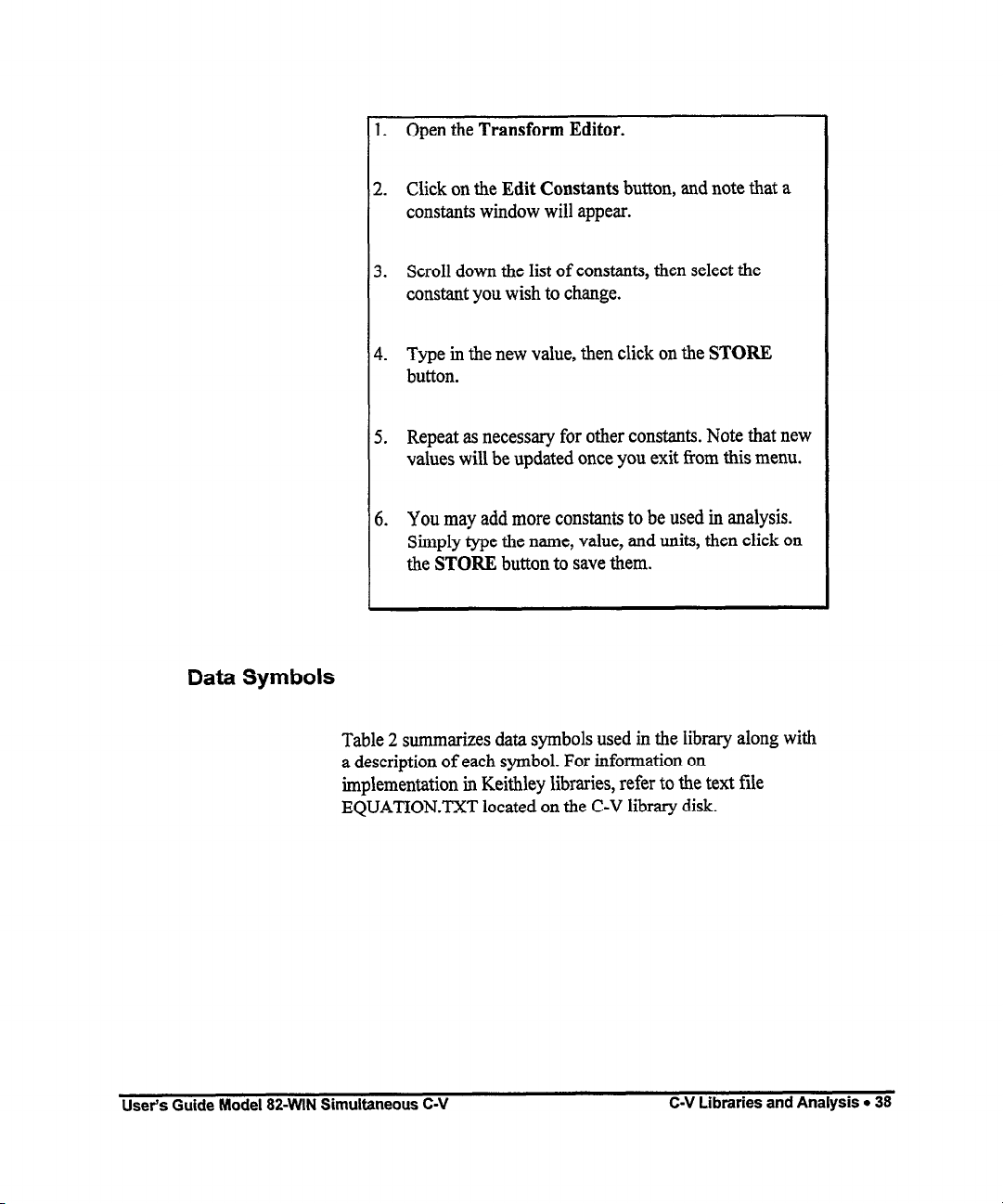
Open the Transform Editor.
2.
Click on the Edit Constants button, and note that a
constants window will appear.
Scroll down the list of constants, then select the
3.
constant you wish to change.
4.
Type in the new value, then click on the STORE
button.
Repeat as necessary for other constants. Note that new
5.
values will be updated once you exit from this menu.
You may add more constants to be used in analysis.
6.
Simply type the name, value, and units, then click on
the STORE button to save them.
Data Symbols
Table 2 summarizes data symbols used in the library along with
a description of each symbol. For information on
implementation in Keithley libraries, refer to the text file
EQUATION.TXT located on the C-V library disk.
User’s Guide Model 824MN Simultaneous C-V C-V Libraries and Analysis l 38
Page 98
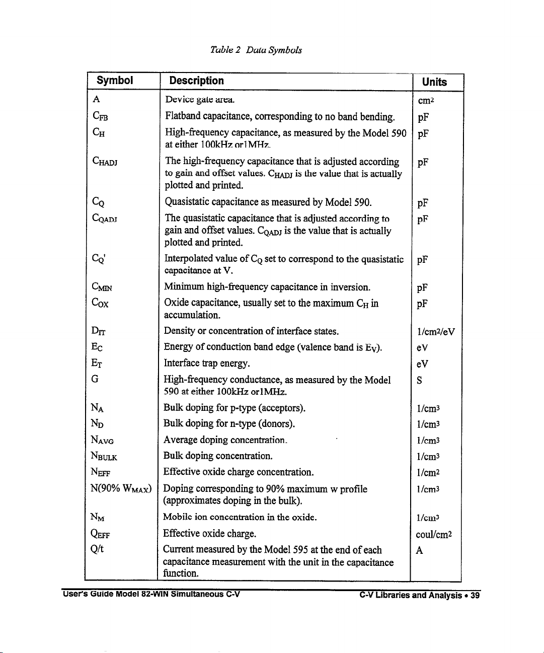
Table 2 Data Symbols
Symbol
A
GB
CH
Description
Device gate area.
Flatband capacitance, corresponding to no band bending.
High-frequency capacitance, as measured by the Model 590 pF
at either 1 OOkHz or1 MHz.
CHADJ
The high-frequency capacitance that is adjusted according
to gain and offset values.
C-J
is the value that is actually
plotted and printed.
CQ
CQADJ
Quasistatic capacitance as measured by Model 590.
The quasistatic capacitance that is adjusted according to
gain and offset values.
CQ~J
is the value that is actually
plotted and printed.
CQ’
Interpolated value of
CQ
set to correspond to the quasistatic
capacitance at V.
GIN
cox
Minimum high-frequency capacitance in inversion.
Oxide capacitance, usually set to the maximum Cn in
accumulation.
DlT
EC
ET
Density or concentration of interface states.
Energy of conduction band edge (valence band is Ev).
Interface trap energy.
G High-frequency conductance, as measured by the Model
590 at either IOOkHz orlMH2.
NA
ND
NAVG
NBIJLK
NEFF
Bulk doping for p-type (acceptors).
Bulk doping for n-type (donors).
Average doping concentration.
Bulk doping concentration.
Effective oxide charge concentration.
N(90% W& Doping corresponding to 90% maximum w profile
(approximates doping in the bulk).
NM
QEFF
Qft
Mobile ion concentration in the oxide.
Effective oxide charge.
Current measured by the Model 595 at the end of each
capacitance measurement with the unit in the capacitance
function.
Unite
cm2
pF
pF
PF
pF
pF
PF
PF
lIcm2feV
eV
eV
S
l/cm3
I/cm3
l/cm3
l/cm3
1 /cm2
l/cm3
l/cm3
coullcm2
A
User’s Guide Model 82-WIN Simultaneous C-V
C-V Libraries and Analysis l 39
Page 99
Table 2 Data Symbols (continued)
Symbol
&ERJES
bX
VGS
VFB
VH
hi
W
WS
WO
@B
h
Description
Series resistance.
Oxide thickness.
Gate voltage. More specifically, the voltage at the gate with
respect to the substrate.
Flatband voltage, or the value of Vos that results in Cm.
Voltage reading sent by Model 590 with matching Cu and
G.
The point where the surface potential, ws, is equal to twice
the bulk potential, $n.
Depletion depth or thickness. Silicon under the gate is
depleted of minority carriers in inversion and depletion.
Silicon surface potential as a function of Vos. More
precisely, this value represents
band
bending and is related
to surface potential via the bulk potential.
Offset in \vs due to calculation method and Vo.
Silicon bulk potential.
Extrinsic Debye length.
Units
n
nm
V
V
V
V
w
V
V
V
m
Summary of Analysis Equations
Table 3 summarizes analysis equations used by the Model 82WIN software. Refer to earlier sections of this chapter for more
details on these equations.
User’s Guide Model 82JMN Simultaneous C-V
C-V Libraries and Analysis l 40
Page 100
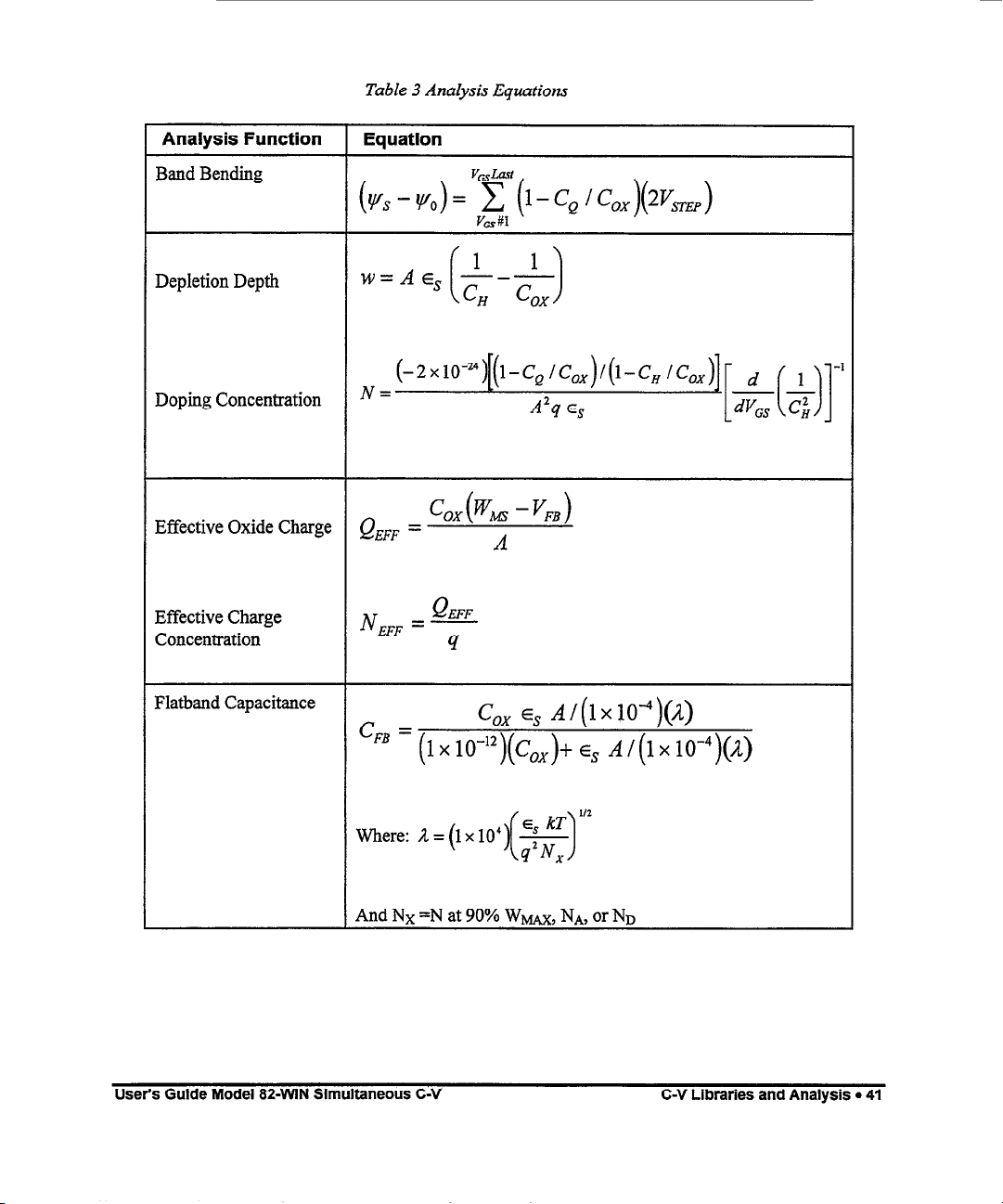
Table 3 Analysis Equations
Analysis Function
Band Bending
Depletion Depth
Doping Concentration
Effective Oxide Charge
Effective Charge
Concentration
Equation
N=
QEFF =
N
EFF = -
l-c,/c,)/(l-c, /c,)
A2q es dVos G
cox @-MS - J?Fi3 )
A
Q
EFF
4
d 1
--
-’
( )I
Flatband Capacitance
User’s
Guide Model
“is = (1 x lo-“)(C&+ Ed
Where: R = (1 x 10’
And Nx =N at 90% Wm, NA, or ND
82-WN Simultaneous C-V
C,, es Al(1x10⁴)(A)
A/(1 x
1O-4)(A)
C-V Libraries and Analysis l 41
 Loading...