

Page 1
PLEASE
7B53A
AT
THE
CHECK
REAR
OF
Fi3R
THlS
CHANGE
MANUAL,
"P853AI7B53AN
fNFOT"IMA"I"ION
Tektranlx,
F'-0.
Box
50Q
Beavertan,
070-1
342-02
Product
Group
tnc.
Oregon
42
970n
DUAL
TIME
INSTRUCTION
BASE
MANUAL
First
Printing
Revised
MAY
SEP
f
988
1980
Page 2
Copyright
7B53A
Contents of this
form without the written permission
"41972,
1980
Tektronix, fne.
publication may not be reproduced
All
rights reserved.
of
Tektronix, Inc.
in
any
Products
by
TEKTRONiX,
registered trademarks
is
a
Printed
are
Each instrument
or
designates the country
of
unique to each instrument.
United States have
manufacture
of
Tektrcmix, tnc.
US,
and foreign patents and/or pending patents.
TEK,
registered trademark of Tektronix
in
t1.5,A.
Spcification
and
its
subsidiaries are cgvered
SCOPE-MOBILE, and
of
Tekrronix. Inc
U.K.
and
price change priviteges
resewed.
INSTRUMENT
has
starnm on the chassis, The
the, serial nurnbr are assigned sequentially
is
identified as follows:
SERIAL
a serial number
of
manufacture.
Those manufaciur& in the
six
unique digits. Tha
NUMBERS
on a panel
first
"i"hs
IELE%MLNI
Limited,
inseft, tag,
numwr or letter
last
five
digits
and
are
country
of
BOOQOOO
100000
ZOOOOQ
300000
7OOQOQ
Tektronix,
Tektronix Guernsey, Ltd,, Channel isrands
"Taktronix Unit& Kingdom, ttd., Landon
Sonynektronix,
Tektranix
The Netherlands
Inc., Beave~on,
Japan
Holland,
NV,
Heerenvwn,
Orwon,
USA
Page 3
TABLE
7B53A
OF CONTENTS
Page Page
LIST OF ILLUSTRATIONS
LIST OF SABLES
OPERATORS SAFETY SUMMARY
SERVICE SAFETY SUMMARY
Section
Section
7Be remaining portion of this Table of Contents lists the
servicing instructions
use by qualified personnel only
do not perform any
operating instructions unless qualified to do so
Section
1
2
3
...........................
SPECIFICATION
OPERATING INSTRUCTIONS
Controls and Connectors
Operating Checkout
General Operating Instructions
Applications 2-1 3
Repackaging for Shipment
sewicing other than that called out in the
THEORY OF OPERATION..
Simplified Block Diagram
Circuit Operation 3-3
Main Trigger Preamp
Main Trigger Generator (SN
&
Up 7B53A Only) 3-4
Main Trigger Generator (SN 8209999
&
Below)
Main Sweep Generator
Delayed
(SN B210000 & Up 7B53A Only)
....................
.............
.................
..................
........
...........
2-1
2-1
...............
.......
......................
..........
.
These servicing instructions are for
.
To avoid electrical shock.
.
...........
............
..................
...............
B210000
.................
.........................
.............
Trigger Generator
.....
2-3
2-6
2-20
3-1
3-1
3-4
3-7
3-9
3-12
iii
iv
vii
Section 3 'THEORY OF OPERATION
Section
Section 5 MAINTENANCE
Section
Section 7 REPLACEABLE ELECTRICAL PARTS
Section
Section
(cont'd)
Delayed Trigger Generator
(SN 8209999 & Below)
Delayed Sweep Generator
Horizontal Preamp
Readout Switching 3-18
4
CALIBRATION
Test Equipment Required
PART 1 PERFORMANCE CHECK
Trigger System Check
Horizontal System Check
PART 2 ADJUSTMENT
Trigger System Adjustment
Horizontal System Adjustment
....................
.............
.........
.................
................
...........
..............
...........
............
..........
.......
..................
Preventive Maintenance
Troubleshooting
Corrective Maintenance
6
OPTIONS
8
DIAGRAMS AND CIRCUIT BOARD
DESCRIPTIONS
9
REPLACEABLE MECHANICAL PARTS
...................
........................
............
............
....
3-17
4-21
4-24
5-1
5-1
5-2
5-4
6-1
REV
DEC
1982
Page 4
Fig.
7B53A
No.
Page
Fig.
No.
Page
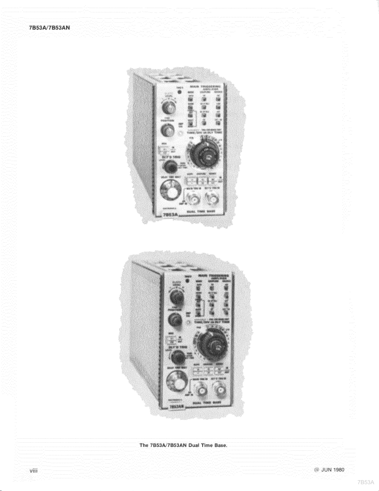
7B53N7B53AN Dual Time Base
Location of release latch.
Front-panel controls and connectors.
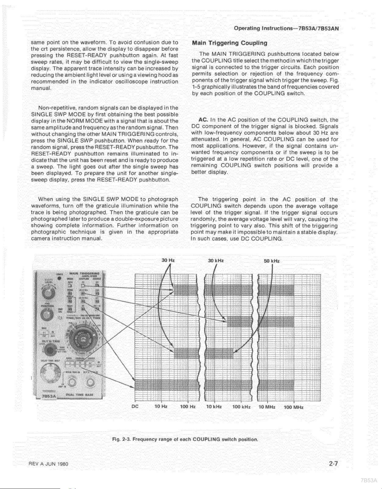
Frequency range of each COUPLING
switch position.
Effect of LEVEL control and SLOPE switch
on CRT display.
Composite
Area of graticule used for accurate time
measurements.
Operation of Sweep Magnifier.
(A) Intensified Sweep display; (B) Delayed
Sweep display.
Typical Mixed Sweepdisplay (DELAY TIME
MULT dial set to 3.55).
DELAY
3.55.
Measuring the time duration between
points on a waveform.
Measuring risetime.
Measuring time difference using delayed
sweep
Using delayed sweep for magnification.
Displaying a complex signal using delayed
sweep
Measuring pulse jitter.
7B53A/7B53AN Simplified Block Diagram. 3-2
Trigger Preamp and Input Switching Block
Diagram.
Main Trigger Generator Block Diagram
(SN
Main Trigger Generator Block Diagram
(SN
Main Sweep Generator Block Diagram.
Delayed Trigger Generator Block Diagram
(SN B210000 and up 7B53A only).
Delayed Trigger Generator Block Diagram
(SN
Delayed Sweep Generator Block Diagram. 3-15
Horizontal Preamp Block Diagram.
Location of Delayed Gate Out and Variable
Selector multi-pin connectors.
"TIME MULT dial. Reading shown
..........................
..........................
..........................
.......................
B210000 and up 7B53A only).
B209999 and below).
B209999and below).
..................
..................
T'ime/Division switch.
...................
...................
.............
..............
...............
.............
.......
...........
......
.......
.....
...........
.....
...........
........
...
.
.
....
.viii
2-1
2-2
2-7
2-9
2-10
2-1 1
2-71
2-12
2-12
2-12
2-15
2-16
2-17
2-18
2-19
2-20
3-5
3-6
3-8
3-10
3-13
3-14
3-17
4-2
4-2 Typical delay time error measurement.
4-3 Typical Delay Time Error Figures.
4-4 Allowable Delay Time Error. 4-17
4-5 Typical CRT display when checking sweep
length..
4-6
5-1 Location of pins on interface connector.
5-2 Cam Switch Removal.
The illustrations in Section 8 are located near their
associated diagrams on the foldout page.
8-1 Electrode configuration for
8-2
8-3 Partial Al--.Interface circuit board
8-4 Partial
8-5 A2-Source Switch circuit board
8-6 A3-.-Coupling Switch circuit board
8-7 Partial
8-8 Partial
8-9 Partial
8-10 Partial
8-1 1 AS-Mode Switch circuit board.
8-12 Partial
8-13
8-14 Partial
Typical
Sweep Start and Dly'd Sweep Stop.
semiconductors in the instrument.
Location of circuit boards in the
7B53A/7B54AN.
component locator (SN
component locator (SN 8089999 and
below).
component locator.
component locator.
component locator
(SN
component locator (SN 8209999 and
below).
component locator (SN
component locator (SN
below).
component locator
(SN
A7--Delayed Trigger Switch circuit board
component locator.
component locator (SN 8209999 and
below).
........................
CRTdisplayfor adjustment of DIy'd
Al--Interface circuit board
A4----Trigger circuit board
7B53A only
B210000 and up).
A4-Trigger circuit board
A6-.-Sweep circuit board
A6---Sweep circuit board
A4.--Trigger circuit board
7B53A only
B210000 and up).
A4---Trigger circuit board
.........
..............
B090000 and up).
B090000 and up).
8089999 and
..
.....
....
.
4-16
4-17
4-25
4-26
5-3
5-7
@?
JUN
1980
Page 5
Fig.
7B53A
No.
Fig.
No.
Partial A6--Sweep circuit board
component locator (SN 8090000 and up).
Partial
component locator (SN 3089999 and
below).
on1 y) component locator.
A8---Readout circuit board
component locator.
A6-Sweep circuit board
Partial
Al--Interface circuit board (7653A
A1 --Interface circuit board
Partial
(7653AN only) component locator.
(7853A only)
Partial
component locator (SN 8090000 and up).
A6--Sweep circuit board
LIST
Table
No.
OF
8-21 Partial A6---Sweep circuit board
component locator (SN 8089999 and
below).
8-22
8-23
8-24
8-25
Partial AG.--Sweep circuit board
component locator
Location of adjustments in the
7653A/7853AN (SN 6209999 and below).
Location of adjustments in the
(SN 8210000 and up).
Location of adjustments in the
7853A/7 B53AN.
(SN
8090000 and up).
TABLES
Page
7853A
Electrical
Environmental
Physical
Deflection Factor of the X Signal
Risetime Measurements
Test Equipment 4-3
Main Sweep Timing
Delayed Sweep Timing
Main Sweep Magnifier Accuracy
Delayed Sweep Magnifier Accuracy
Relative Susceptibility to Static Discharge
Damage
.......................
...................
.......................
......
............
..................
...............
.............
......
....
........................
1-1
1-6
1-6
2-13
2-16
4-13
4-14
4-15
4-15
5-2
@?
JUN
1980
Page 6
OPERATORS
7B53A
The general safety information in this part of the summary is for both operating and servicing personnel. Specific
warnlngs and cautions will be found throughout the manual where they apply, but may not appear in this summary.
IN THlS MANUAL
CAUTION statements identify conditions or practices that could result in damage to the equipment or other property.
WARNING statements identify conditions or practices that could result in personal injury or loss of life
AS MARKED ON EQUIPMENT
CAUTION indicates a personal injury hazard not immediately accessible as one reads the marking, or a hazard to
property including the equipment itself.
DANGER indicates a personal injury hazard immediately accessible as one reads the marking.
SAFETY
SUMMARY
SYMBOLS
IN THlS MANUAL
@
Static-Sensitive Devices.
This symbol indicates where applicable cautionary or other information is to be found
AS MARKED ON EQUIPMENT
DANGER-H~gh voltage.
@
Protective ground (earth) terminal.
A
ATTENTION----refer to manual.
WARNINGS
POWER SOURCE
This product is intended to operate in a mainframe connected to a power source that will not apply more than
rms between the supply conductors or between either supply conductor and ground.
way of the
GROUNDING THE PRODUCT
'This product is grounded throirgh the grounding conductor of the mainframe power cord. To avoid electrical shock, plug
the
mainframe power cord into a properly w~red receptacle before connecting to the product input or output term~nals. A
protective ground connection by way of the grounding conductor in the mainframe power cord is essential for safe
operation.
ground~ng conductor in the mainframe power cord is essential for safe operation.
A
protective ground connection by
250
volts
REV
JAN
1985
Page 7
DANGER ARISING FROM
7B53A
Upon loss of the protectwe-ground connection, all access~bie condijctrve parts (~ncludrng knobs and controls that may
appear to be
rnsulat~ng), can render an electr~c shock
LOSS
OF
GROUND
DO NOT OPERATE IN EXPLOSIVE ATMOSPHERES
To avoid explosion, do not operate this product in an atmosphere of explosive gases unless it has been specifically
certified for such operation.
DO NOT OPERATE PLUG-IN UNIT
To avoid personal injury, do not operate this product without covers or panels installed.
unlt via a plug-in extender.
WITHOUT
COVERS
Do
not apply power to the plug-~n
@
JUN
1980
Page 8
SERVICING
7B53A
SAFETY
SUMMARY
FOR
QUALIFIED
SERVICE
PERSONNEL
ONLY
Refer also to the preceding Operators Safety Summary
DO NOT SERVICE ALONE
Do not perform internal service or adjustment of this product unless another person capable of rendering first aid and
resuscitation is present.
USE CARE WHEN SERVICING WITH POWER ON
Dangerous voltages exist at several points in this product. To avoid personal injury, do not touch exposed connections
and components while power is on.
Disconnect power before
POWER SOURCE
This product is intended to operate in a mainframe connected to a power source that will not apply more than
rms between the supply conductors or between either supply conductor and ground.
way of the grounding conductor in the mainframe power cord is essential for safe operation.
removlng protective panels, soldering, or replacing components.
A
protective ground
250
connection
volts
by
@
JUN
1980
Page 9
7B53A
Page 10
The
7B53A
7B53A
alphanumeric readout system provided for the 7000-series oscilloscopes.
and
7B53AN
are electrically identical except that only the
785314
Section 1-.--7B53A/7B53AN
is compatible with the
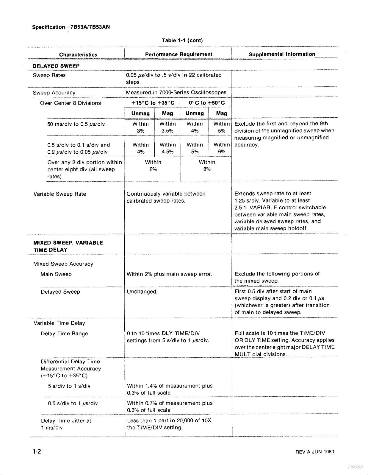
This instrument will meet the electrical characteristics listed under Performance Requirement in Table
The
complete calibration.
except as otherwise indicated. Warmup time for given accuracy is 20 minutes.
-
-.--.
MAIN SWEEP
Sweep Rates 0.05 ys/div to 5 s/div in 25 calibrated
Sweep Accuracy
-
."
Over Center Eight Divisions
-
- - -
Variable Sweep Rates
Characteristics Performance Requirement Supplemental information
-
.
50 ms/div to 0.5 ysldiv
.-~
5 s/div to 0.1 s/div and
0.2
ys/div to 0.05 psldiv
Over any 2 div portion within
center eight div (all sweep
rates)
-
- - -
-
-
--
following electrical characteristics apply over an ambient temperature range of 0°C to +-50°C,
Table 1-1
to
-C35OC
[
:in
". .
1
3.5%
--
5%
---
- - -
ELECTRICAL
".
.
.
--
--
.
O°C to +50°C
------"
1
w;;n
Within
-
4%
T-".-'-."
-
..
.,
..
1..
I
1
w!;i
.
~
I
Within
5%
Within
7%
)variable to at least 2.5:l. VARIABLE
".'."
-
delayed sweep rates, and variable
main sweep
holdoff.
~
-,--
r.-,.-.---.--.-.w-
"
~
-
--
-
-
--
-
J
..4.--"
-A=-"
steps.
Measured in 7000-Series Oscilloscopes.
-115OC
I
Unmag Unmag Mag
--.m----....-..-."
1
w;itn
..
.".
~
Within W~th~n
3%
---
-
With~n
-
.
- - -
-
/
Continuously variable between cali-
/
brated sweep rates. Extends sweep rate /control internally switchable between
I
to at least 12.5 s/div. variable main sweep rates, variable
--
1-1,
^-"
.
following
Sweep Hold-Off Hold-off time may be varied at least
2:l
by front-panel VARIABLE control
when Variable Selector connector
(P140) is connected for variable
holdoff.
REV
D
JUN
1980
Page 11
Table
7B53A
1-1
(cont)
..
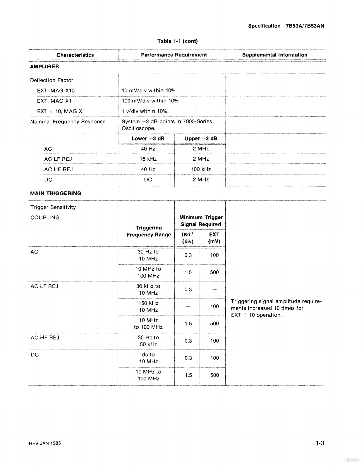
DELAYED
Sweep Rates
Over Center
Variable Sweep Rate
Characteristics Performance Requirement Supplemental l nformation
.
SWEEP
50
ms/div to 0.5 psldiv
0.5 s/div to 0.1 sldiv and
Over any 2 div portion within
center eight div (all sweep
rates)
"
8
Divisions
__
-l.__."
_
-.,---
"^
-l_-....l...lI
.l-ll___.
.05
ps/div to .5 s/div in 22 calibrated
easured in 7000-Series Oscilloscopes.
Continuously variable between
calibrated sweep rates.
_l__-..--------"
"."
---.----,-.
1
-l_l._l_.l
division of the unmagnified sweep when
5%
--
-.
-~
....
"
measuring
Extends sweep rate to at least
1.25
2.51. VARIABLE control switchable
between variable main sweep rates,
variable delayed sweep rates, and
variable main sweep
-.--_
_-_
magnified
sldiv. Variable to at least
or
unmagnified
holdoff.
"--
MIXED
PIME
Mixed Sweep Accuracy
Variable Time Delay
SWEEP, VARIABLE
DELAY
. .- .
- - - - -
Main Sweep
Delayed Sweep
Delay Time Range
Differential Delay Time
Measurement Accuracy
(-+-15OC
Delay Time Jitter at
1
to +35'C)
5 s/div to 1 s/div
msfdiv
- -
-
-
I
Within
0 to 10 times DLY TIME/DIV
I
Within
I
1
the TlMVDlV setting.
2%
plus main sweep error.
settings from 5 s/div to 1 ps/div.
Within 1.4% of measurement plus
0.3% of full scale.
0.7%
0.3% of full scale.
Less than 1 part in 20,000 of 1 OX
...
"
of measurement plus
.....-..l._-.
""
_..__..._-,._l."__
--
I
Exclude the following portions of
the mixed sweep:
First 0.5 div after start of main
sweep display and 0.2 div or 0.1
(whichever is greater) after transition
of main to delayed sweep.
Full scale is 10 times the TlMWDlV
OR DLY TlMEsetting. Accuracy applies
over the center eight major DELAY TIME
MULT dial divisions.
""
I
I
I
.
. . .
.- . -.
-
ps
--
----
-
-
"
-
1-2
REV
A
JUN
1980
Page 12
-"
7B53A
~
,
AMPLIFIER
Deflection Factor
EXT, MAG
EXT, MAG Xl
.
.
EXT
Nominal Frequency Response
Characteristics Performance Requirement Supplemental Information
.. - .
.-
.-i
10, MAG XI
AC
AC
LF REJ
Xi0
"..
......-----A-
""
"
"".
""
"*.."
i
1
10 mV/div within 10%.
100
"~.
mVfdiv within 10%.
1
v/div within 10%.
"
System
Oscilloscope.
.--3
Table
1-1
(cont)
~."
dB
points in 7000-Series
".
.
.
..
...
".
-.
"-
--
"
~
.-..
".
.-
."
-.
.-
.
--
-
.....
"
,.-"
"""
"."
.
-----
""
-
..
--
..
AC HF REJ 100 kHz
DC
MAIN TRIGGERING
Trigger Sensitivity
COUPLING
AC LF REJ 30 kHz to
"
~re~uentq Range
"
Hz
""
DC
Triggering
30
Hz
to
10 MHz
10 MHz
150 kHz
10 MHz
Minimum Trigger
I
.-
"-
/
I
10 MHz
to 100 MHz
AC HF REJ 30 Hz
1
50 kHz
to
1
1
~
""
2
MHz
Signal Required
--
---
0.3
1.5
0.3 100
EXT
1
100
/
500
---
I
1
Triggering signal
~ncreased 10 times for
ments
EXT
+
10 ooeration.
1
1
amplitude
requtre-
DC
-
-"
REV
JAN
---
1385
dc to
10 MHz
-
-
--
-
-
-
--
--
---
10 MHz to
100 MHz
--
0 3
-"-
-
--
1.5
d
-
--
100
,-
--
--
500
--
-
Page 13
Table
7B53A
1-1
(cont)
---------".-
External Trigger Input
lnput
Maximum Safe Input Voltage
Level Range
Internal Trigger Jitter
DELAYED TRIGGERING
Trigger Sensitivity
Coupling
Characteristics Performance Requirement Supplemental Information
-
R and C
EXT
EXT
-,"---.----
-:-
10 At least + and 15 V.
--,.-,"
I
I
least + and - 1.5 V.
1 ns or less at 75 MHz.
Triggering
Frequency Range
--
30 Hz to
-
10 MHz
.
.-
10 MHz to
100 MHz
---
--.
Minimum Trigger
Signal Required
.-
- - -
-
Approximately 1 Mf2 paralleled by
20
pF.
500 V (dc
to-peak ac at 1 kHz or less.
-1
Peak ac). 500 V peak-
."..
-
-.
.
I
---.
-.
.-
----
. .
-
External 'Trigger lnput
Maximum Safe lnput
Voltage
SOURCE set to EXT)
--
Input R and C
Level Ranae
Internal Trigger Jitter
(DLY'D
TRIG
- - - - --
dc to
10 MHz
I
At least + and - 1.5 V.
-
1 ns or less at
1.
--_---p-....."
75
MHz.
500 V (dc
to-peak ac at 1 kHz or less.
11 Mf2 paralleled by 20 pF.
-1-
peak ac). 500 V peak-
I
1
l..lll...lll..-..-.----ll
--
---
..
-
REV A JUN
1980
Page 14
OUTPUT
7B53A
Table
1-1
(cont)
Characteristics Performance Requirement Supplemental Information
SIGNALS
Delayed Sweep Gate
Maximum Safe Input
Voltage
--.".-..-
Amplitude
Output Resistance
Loading
Polarity
Duration
DISPLAY MODE
INTEN, DLY'D SWP
----.-----.---.--
MIXED
..".-,"---".~-
I
--
-....""~~.v",~-~~~-
Rectangular pulse.
23.0
V with baseline at
to
--I
V when loaded by at least
20.475
--0.2
Positive-goi ng.
ll--l~_l_____----.---~-~-.~-"--~--
For the time that the delayed sweep runs.
-----.--.-
--
Composite gate signal with timing de-
termined by the setting of the
DIV OR DLY TIME switch during the
main sweep portion of the display,
and by the setting of the DLY'D
Division switch during the delayed
sweep portion of the display.
with baseline at 0 to
V
when loaded by
--,~-...-----.---"
.
---0.2
50
0.
10
kfl.
----.-----
TIMV
lime/
rtlO
V
(dc i Peak ac).
to-peak ac at
Available at front-panel DLY'D
TRIG IN connector when
operating in the
SWP, or MIXED Display Modes.
The DLY'D
must be set to
be connected for Delayed Sweep
Gate Out.
Approximately
At least
or less.
-,--,."-----.....-....----
1
kHz
or less.
INTEN, DLY'D
TRIG SOURCE switch
IN-i and P613 must
350
---
10
kfl shunted
n.
-
t
I
20
V peak-
by
----
100
--
pF
Sweep Gate
Duration
DISPLAY MODE
MAIN SWEEP, INTEN
DLY'D SWP
MIXED
l_l-~l-..l"
Main Sweep Gate
Duration
@
JUN
1980
----.-.-._lll.-..---
Refer to associated oscilloscope manual.
I
1
Coincident with the main sweep interval.
""-
Coincident with the main sweep interval.
"_
-l.ll_,ll)....
Coincident with the main sweep interval
plus the delayed sweep interval.
.--_____-lll.-.,l_-l
Refer to associated oscilloscope manual.
i
Coincident with the main sweep (all
Display Modes).
""
-
__III^.._,.l
_
I
1
^..
"..
".-
"--.
"
-.-----.l"....X-..-.
X.
-
---
-----
--
.-
---
--
I
Page 15
Table
7B53A
1-1
(cont)
"
Sawtooth
Waveshape
-
.-
Duration
a
For Internal Triggering only, the specified
when the number in the table is greater than the
Characteristics Performance Requirement Supplemental Information
-----
.-.....-~wp-.--"
"--
Refer to associated oscilloscope manual.
"
1
I
DISPLAY MODE
MAIN SWP, INTEN
DLY'D SWP
MIXED
I I
Sawtooth signal with slope determined
by setting of the
TIME switch.
Sawtooth signal with slope determined
by the setting of the DLY'D
Division switch.
Composite sawtooth signal with slope
determined by the setting of the
TlMWDlV OR DLY TIME switch during
the main sweep portion of display, and
by
Division switch during the delayed
sweep portion of display.
Coincident with the time that each
sweep is displayed.
-
I
TlMWDlV
the setting of the DLY'D Time/
--3
dB frequency of the vertical system replaces any frequencies in the above table
--3
dB frequency of the vertical system.
OR
---.-
Time/
DLY
--
--
__.."l-___-_.l_l_._
Characteristics
Size
Weight
Table
1-2
ENVIRONMENTAL
Refer to the Specification for the associated oscilloscope.
Table
1-3
Ibs
(1.5
PHYSICAL
kg).
-.."
Fits all 7000-series plug-in compartments.
3.3
@
JUN
1980
Page 16
Section
7B53A
2-7B53N7B53AN
OPERAT
7B53N7B53AN
The 7B53A and 7B53AN Dual Time Base units provide
Main, Intensified, Delayed, and Mixed sweep operation for
'EKTRRONIX 7000-Series Oscilloscopes. Calibrated
sweep rates from 5
magnification) and triggering to 100 MHz are provided.
7B53A and 7B53AN are electrically identical except
The
that only the
readout system provided for 7000-Series Oscilloscopes.
Other features include
delay,
variable main and delayed sweeprates, and variable
main sweep holdoff. Separate triggering controls are
provided for main and delayed sweep triggering, and
when operating in the AUTO MAIN TRIGGERING MODE,
a bright base line is displayed in the absence of a trigger
signal. The
amplifier for
Features
s/div to 50 ns/div
7B53A is compatible with the alphanumeric
0 to 10 times continuous sweep
7B53N7B53AN can also be used as an
X-Y
operation.
NG
(5
ns with XI0
INSTRUCTIONS
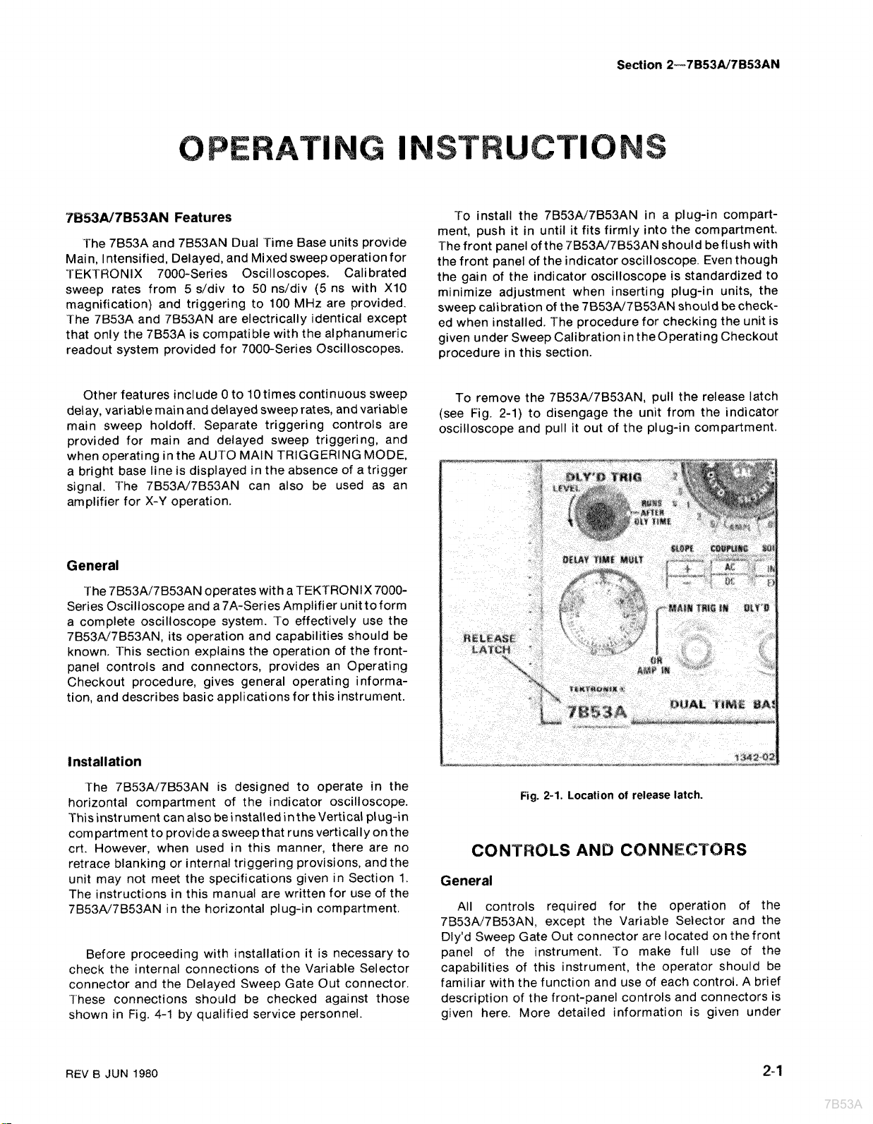
To install the
ment, push it in until it fits firmly into the
The front panel of the 7653N7653AN should beftush with
the front panel of the indicator oscilloscope. Even though
the gain of the indicator oscilloscope is standardized to
minimize adjustment when inserting plug-in units, the
sweep calibration of the
ed when installed. The procedure for checking the unit is
given under Sweep Calibration in
procedure in this section.
To remove the
(see ~i~,
oscilloscope and pull it out of the plug-in compartment.
2-11
7B53N7B53AN in a plug-in compart-
compaitment.
7B53A17B53AN should becheck-
theoperating Checkout
7853N7B53AN, pull the release latch
to disengage the unit
from
the indicator
General
The 7B53A17B53AN operates with a TEKTHONIX 7000Series Oscilloscope and a 7A-Series Amplifier unit to form
a complete oscilloscope system. To
7B53A/7B53AN, its operation and capabilities should be
known. 'This section explains the operation of the
panel controls and connectors, provides an Operating
Checkout procedure, gives general operating information, and describes basic applications for this
effective1 y use the
front-
instrurnent.
Installation
The 7853A17853AN is designed to operate in the
horizontal compartment of the indicator oscilloscope.
Thisinstrument can also beinstalled
compartment to provideasweepthat runsvertically on the
crt. However, when used in this manner, there are no
retrace blanking or internal triggering provisions, and the
unit may not meet the specifications given in Section
The instructions in this manual are written for use of the
7B53N7B53AN in the horizontal plug-in compartment,
Before proceeding with installation it is necessary to
check the internal connections of the Variable Selector
connector and the Delayed Sweep Gate Out connector.
These connections should be checked against those
4-1
shown in Fig.
by qualified service personnel.
inthevertical plug-in
1.
Fig.
2-1.
Location
of
release latch.
CONTROLS AND CONNECTORS
General
All controls required for the operation of the
7B53N?B53AN, except the Variable Selector and the
Dly'd Sweep Gate Out connector are located on the front
panel of the instrument.
capabilities of this instrument, the operator should be
familiar with the function and use of each control. A brief
description of the front-panel controls and connectors is
given here. More detailed information is given under
'To make full use of the
REV 6 JUN
1980
2-
1
Page 17
Operating
7B53A
Instructions.---9853A17B53AN
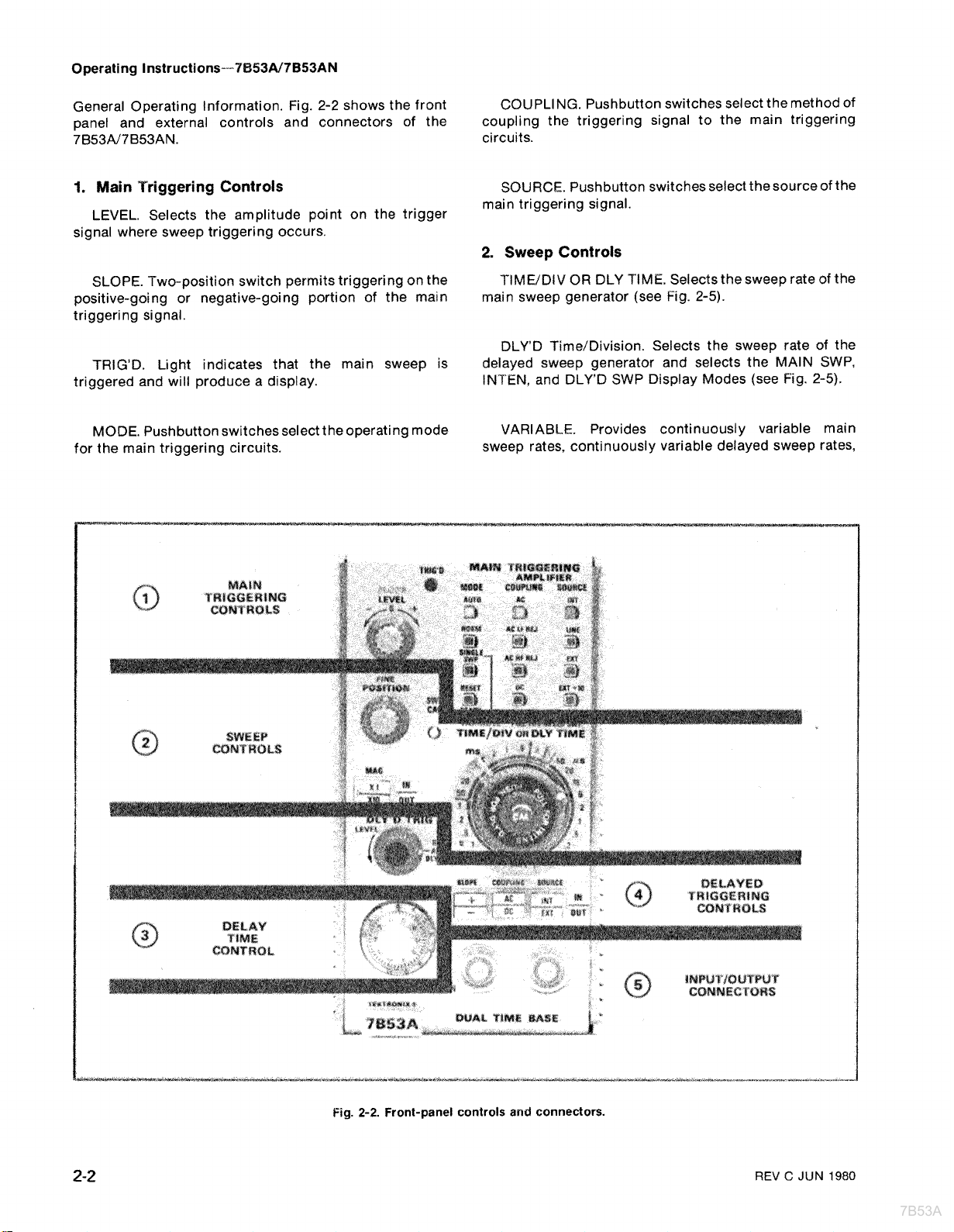
General Operating Information. Fig.
2-2
shows the front
panel and external controls and connectors of the
7
B53A/7 B53AN.
1.
Main Triggering Controls
LEVEL. Selects the amplitude point on the trigger
signal where sweep triggering occurs.
SLOPE. Two-position switch permits triggering on the
positive-going or negative-going portion of the main
triggering signal.
TRIG'D. Light indicates that the main sweep is
triggered and will produce a display.
MODE. Pushbutton switches select the operating mode
for the main triggering circuits.
COUPLING. Pushbutton switches select the method of
coupling the triggering signal to the main triggering
circuits.
SOURCE. Pushbutton switches select thesource of the
main triggering signal.
2. Sweep
Controls
TIMEIDIV OR DLY TIME. Selects the sweep rate of the
main sweep generator (see Fig.
2-5).
DLY'D Time/Division. Selects the sweep rate of the
MAIN
delayed sweep generator and selects the
INT'EN, and
DLY'D
SWP Display Modes (see Fig. 2-5).
SWP,
VARIABLE. Provides continuously variable main
sweep rates, continuously variable delayed sweep rates,
Fig.
2-2.
Front-panel controls
and
connectors.
REV
C
JUN
1980
Page 18
Operating
7B53A
Instructions-7B53A17B53AN
or variable main sweep holdoff; depending on the setting
of the Variable Selector multi-pin connector
VARIABLE control also selects the MIXED Display Mode
(see Fig. 2-5).
SWP CAL. Screwdriver adjustment to match the gain of
7653A/7B53AN to the indicator oscilloscope for
the
calibrated sweep rates.
POSITION. Controls horizontal position of display.
FINE. Provides precise control of horizontal position
adjustment,
MAG. Pushbutton switch selects
magnification.
3.
Delay Time Control
DELAY l IME MULT. Provides variable sweep delay
between 0.00 and 10.0 times the delay time indicated by
TIMUDIV OR DLY rlME switch.
the
4.
Delayed Triggering Controls
XI or XI0 horizontal
(P140). The
OPERATING
CHECKOUT
Introduction
The following procedure checks the basic operation of
the
7B53A/7653AN. It may also be usedfor familiarization
with this instrument or as an incoming inspection. This
procedure is divided into two parts, Sweep Control
Functions, and Main and Delayed Triggering Functions. A
complete operating check of the
functions can be made by performing both parts, or each
part may be performed separately.
NOTE
For optimum performance, the
should
similar frequency and sweep rate capabilities.
be
instalied
in
an oscilfoscope system
7853N7853AN control
7853Ai7B53AN
with
Setup Procedure
1.
Install the 7B53A/7B53AN in the right horizontal
compartment of the indicator oscilloscope.
2.
Install a Vertical Amplifier unit in the left vertical
compartment.
LEVEL. Selects the RUNS AFTER DLY TIME or
Triggerable After Dly Time Modes, and the amplitude
point at which the delayed sweep is triggered.
SLOPE. Two-position switch permits triggering on the
positivegoing or negative-going portion of the delayed
triggering signal.
COUPLING. Two-position switch selects the method of
coupling the triggering signal to the delayed triggering
circuits.
SOURCE. Two-position switch to select the source of
the delayed triggering signal.
5.
InputlOutput Connectors
MAlN TRIG IN OR AMP IN. Front-panel bnc connector
serving as an external trigger input for the maintriggering
circuit or as an external horizontal input, depending upon
the setting of the
MAlN TRIGGERING SOURCE switch.
TRlG IN. Front-panel bnc connector serving as
DLY'D
an external trigger input forthedelayed triggering circuits
or as a delayed sweep gate output; depending upon the
DLY'D TRlG SOURCE switch, the position of
the DISPLAY MODE.
TIMVDIV OR DLY TlMEswitch and the
P613, and
3.
Turn on the indicator oscilioscopeand allow at least
20 minutes
4.
MAlN TRIGGERING
DLY'D TRlG
Sweep Controls
5. Set the indicator oscilloscope to display the plug-in
units and adjust for
warmup.
Set the 7B53N7653AN controls as follows:
SLOPE
MODE AUTO
COUPLING AC
SOURCE INT
I.
EVEL RUNS AFTER DLY
SLOPE
COUPLING AC
SOURCE
POSITION Midrange
MAG
TlMElDlV OR DLY FlME 1 ms
DLY'D TrmefDivision
VARIABLE CAL (fully clockwise)
Variable Selector Main Variable
DELAY[-IMEMULT 1.00
a
well defined display. See indicator
(-f
)
TIME (fully clockwise)
(f)
INT
X1-IN
1
ms
REV
C
JUN
1980
2-3
Page 19
Operating
7B53A
oscilloscope and vertical unit instruction manuals for
detailed operating instructions.
Sweep
'The following procedure checks the operation of the
sweep controls and checks the Display Modes.
Normal Sweep
1.
Instructions~--7B53A/7B53AN
Control
Perform steps 1 through 5 of the Setup Procedure.
Functions
6.
Connect a 1 ms time-mark signal from the TimeMark Generator with a
connectors and 50
associated vertical unit. Adjust the vertical
switch for about four divisions of display and rotate the
MAIN TRIGGERING
Check the crt display for one complete time-mark per
division (position as necessary). If necessary, adjust the
SWP CAL screwdriver adjustment for one complete
mark per division over the center eight divisions of display.
Disconnect the "Time-Mark Generator.
50
Z;1
bnc coaxial cable with bnc
62
bnc termination to the Input of the
VoltdDiv
1-EVEL controt for a stable display.
time
NOTE
The TimeIDivision switch selects main sweep rates,
delayed sweep rates, and Display Modes (MAIN
SWP, INTEN. DL Y'D
Seiectrng Sweep Rates and Display Modes dis-
in
cussions
further information.
2.
To select the MAlN SWP Display Mode, press in the
Time/Division knob, and set the TIMVDIV OR DLY
DLY'D
TIME switch and the DLY'D TimelDivision switch to the
same sweep rate
3.
Connect the 1 kHz calibrator signal from the in-
dicator oscilloscope to the vertical amplifier unit Input.
Adjust the Calibrator and thevertical
for four divisions of display.
4.
Rotatethe MAlN TRIGGERING LEVEL control for a
stable MAIN
DELAY TIME MULT dial and note that it has no effect on
the display.
the General Operating
(1
SWP
SWP,
and MIXEL?). Refer lo
instructions
ms).
Volts/Division switch
display (non-delayed). Rotate the
for
Intensified, Delayed, and Mixed Sweep
7.
Reconnect the osciIloscope Calibrator signal to the
vertical unit and adjust for about four divisions of vertical
display. Pull out the DLY'D
clockwise to
(TIMVDIV OR DLY TlME switch remains at 1 msldiv).
Note that a delaying sweep with an intensified portion
(delayed sweep) is displayed on the crt (the oscilloscope
Intensity may need to be varied to view the intensified
display).
8.
Rotatethe DELAY'T'IMEMULTdial andnotethatthe
amount of delay
display is controlled by the DELAY TlME MULT dial.
9.
Rotate the VARIABLE control counterclockwise out
of switch detent and note that the sweep rate indicated by
TIME/DIV OR DLY TIME switch can be varied to at
the
least the sweep rate
(2
msl'divj. 'The internal Variable Selector connector must
be
set for variable main sweep rates. Return the
VARIABLE control to the GAL position.
.1 msi'div for the INTEN Display Mode
time before the intensified portion of
TimelDivision knob and rotate
of the next adjacent position
5.
Rotate the POSITlON control and note that
horizontally positions the trace, Rotate the FINE control
and note that it provides precise horizontal positioning. position
Disconnect the calibrator signal.
Sweep Calibration
NOTE
For accurate sweep timing, apply a signal of known
frequency or time period (time-mark signal,
60
Hz
calibrator square wave,
associated vertical amplifier unit and adjust the
TIMEIDIV OR DLY nME switch and the
control to calibrate the signal
graticule. Be sure that the sweep timing signa! is
0.5%.
accurate within
tion procedure uses
Generator.
The following sweep caiibra-
a
TEKTRONIX
line etc.) to the
SWP
to
the oscilloscope
Time-Mark
CAF
it
10. Press the DLY'D
magnified display with sweep rate determined by the
DLY'D
may need to be increased to view the delayed sweep
display.
11.
MIXED Display Mode (MIXED Display Mode can be
selected when operating in the DLY'D SWP Display Mode
only). Note that the main sweep is displayed at a rate
determined by the
followed by a delayed sweep display at the rate determined by the DLY'D
DELAY TlME MULT dial
display allocated to each sweep is determined by the
DELAY TlME
2-4
Time/Division switch to the inner
for DLY'D SWP
Time/Division switch. The oscilloscope Intensity
Pull out the VARIABLE "l"ime/Division knob for the
'TIMEIDIV OR DLY TlME switch
Time/Division switch. Rotate the
and note that the amount of
MULT
dial.
REV
C
JUN
the
1980
Page 20
Main and Delayed Sweep Triggering Functions
7B53A
The following procedure checks the operation of the
main and delayed triggering controls:
Partial Procedure. To begin the Operating Checkout
1
with triggering, perform steps
Procedure provided at the beginning of the Operating
Checkout. Connect the
indicator
osciIioscope to the vertical unit Input and adjust
1
for about four divisions of vertical display.
12.
Set the TIME/DIV OR DLY TlME switch and the
DLY'D
DLY'D
Time/Division switch to 1 ms and press in the
TimeiDivision switch and the Variable control.
CHECK---that a stable display can be obtained with the
COUPLING switch for MAlN
HF REJ, and DC for both the positive and negative
positions of the SLOPE switch (MAIN TRIGGERING
LEVEL control may be adjusted as necessary to obtain a
stable main sweep display). Remove all connections from
the oscilloscope system.
13.
Connect a 60
n
cable or voltage probe to the vertical unit Input and
50
adjust the
VoltsIDiv switch for about four divisions of
Hz
signal (iine voltage, etc.) with a
display. Set the MAlN TRIGGERING COUPLING switch
to AC LF REJ and set the
10
ms. Rotate the MAIN TRIGGERING LEVEL control
to
"r^lMVDlV OR DLY TIME switch
throughout its range and check that a stable display
cannot be obtained (TRIG'D light off).
14.
Change the MAlN 'TRIGGERING SOURCEswitch
to LINE and the COUPLING switch to AC. Check that a
stable main sweep display can be obtained with the MAIN
TRIGGERING COUPLING switch set to AC, AC HF REJ,
and DC (MAlN TRIGGERING LEVEL control may be
adjusted as necessary). Remove all connections from the
oscilloscope system.
15.
Connect the indicator oscilloscope Calibrator
signal to the verticai unit Input connector and
TRIG IN connector. Set the Calibrator for a 0.4 V,
signal and adjust the vertical unit
about four divisions of display. Set
TIME switch and the DLY'D
Set the MAlN TRIGGERING SOURCE switch to EXT and
check that a stable display can be obtained with the
COUPLING switch for MAIN TRIGGERING set to AC, AC
HF REJ, and DC, for both the positive and negative
positions of the SLOPE switch (MAIN TRIGGERING
LEVEL control may be adjusted as necessary for a stable
display).
16.
Change the MAlN TRIGGERING SOURCE switch
-:--
to EXT
1
kHz and adjust the vertical unit VoltsiDiv switch for
10. Set the oscilloscope Calibrator for 4 V at
through 5 of the Setup
kHz calibrator signal from the
'T'RIGGERING set to AC, AC
tothe MAIN
1
kHz
Volts/Div switch for
the'TIMWDIV OR DLY
TimelDivision switch to 1 ms.
about
Operating
4
divisions of display. Check that a stable display
Instructions--~7B53A/7B53AN
can be obtained with the COUPLING switch for MAIN
TRIGGERING set to AC, AC HF REJ, and DC, for
boththe
positive and negative positions of the SLOPE switch
(MAIN TRIGGERING LEVEL control may be adjusted as
necessary to obtain a stable delaying sweep display).
Remove the Calibrator signal from the MAlN TRIG IN
connector.
17.
Set the MAlN "TRIGGERING COUPLING switch to
AC and the SOURCE switch to
INT. Adjust the MAlN
TRIGGERING LEVEL control for a stable display. Set the
MODE switch to NORM and check for a stable display.
Change the
MODEswitch to AUTO and adjust the LEVEL
control for a free-running display. Change the MODE
switch to NORM and check for no display.
18.
Adjust the MAlN TRIGGERING LEVEL control for
a stable display. Change the MAlN TRIGGERING MODE
switch to SINGLE SWP. Press the
check for one sweep. Remove the
RESET button and
1
kHz signal from the
vertical unit and press the RESET button. CHECK for no
1
display and that the READY light is on. Connect the
kHz
signal to the vertical unit and check for one sweep as the
signal is applied.
19.
Set the MAIN TRIGGERING MODE switch to
AUTO. With the
pull out the DLY'D
.2
ms (Intensified Display Mode). Rotate the MAlN
TIMWDIV OR DLY TIME switch
Time/Division switch and rotate to
at
1
ms,
TRIGGERING LEVEL control for a stable display
(oscilloscope Intensity may need to be varied to view the
intensified display). Rotate the
Df LAY TlME MULT dial
and note that the intensified portion of display is con-
tinuously variable.
20.
Rotate the DLY'D TRlG LEVEL control counterclockwise out of switch detent for a triggered delayed
sweep. With the DLY'D
SOURCE switches set to
TRIG SLOPE, COUPLING, and
(-f
),
AC, and INT; rotate the
DLY'D TRIG LEVEL control for astable intensified portion
of display. Rotate the DELAY
TIME MULT dial and note
that the intensified portion of display does not start at the
completion
of the
of the delay time (determined by the settings
TIMEIDIV OR DLY TIME switch and the DELAY
TIME MULT dial), but waits for the next trigger pulse.
21.
Press the DLY'D Time/Division switch in for the
DLY'D SWP Display Mode. Rotate the DLY'DTWIG LEVEL
control for a stable delayed sweep display (oscilfoscope
Intensity may need to be varied). Check that a stable
delayed sweep display can be obtained with the DLY'D
TRIG COUPLING switch set to AC and
-
positions of the SLOPE switch (DLY'D TRIG LEVEL
DCfor both
.I-
and
control may be adjusted as necessary for a stable delayed
sweep display).
REV
A
JUN
1980
2-5
Page 21

Operating
7B53A
Instructions-.-7B53Ai1B53AN
22.
Change the DLY'D TRIG SOURCE switch to EXT.
Connect the indicator oscilloscope Calibrator signal to
the DLY'D
Calibrator for
Volts/Division switch for about 4 divisions of display.
Check that a stable delayed sweep display can be
obtained with the DLY'D TRlG COUPLING switch set to
AC and DC for both the
switch (DLY'D TRlG LEVEL control may be adjusted as
necessary for a stable delayed sweep display).
TRlG IN connector. Set the oscilloscope
0.4
V at 1 kHz
-t-
and adjust the vertical
and positions of the SLOPE
GENERAL OPERATING INSTRUCTIONS
Pushbutton Switch Logic
The MODE, COUPLING, and SOURCE pushbuttons of
the MAlN TRIGGERING switches are arranged in
sequence that places the most-often used position at the
top of each series of pushbuttons. With this arrangement,
a stable display can usually be obtained by pressing the
top pushbuttons: AUTO, AC, and INT. When an adequate
trigger signal is applied, the unit is triggered as indicated
by the illuminated
of the LEVEL control and SLOPE switch. If the
light is not on, the LEVEL control isat asetting outsidethe
range of the trigger signal applied to this unit from the
vertical unit, the trigger signal is inadequate, or its
frequency is below the lower frequency limit of the AC
COUPLING switch position. If the desired display is not
obtained with these buttons pushed in, other selections
must be made. Refer to the following discussions or the
intruction manuals for the associated oscilloscope and
vertical unit for more information.
Triggered Light
'IRIG'D light, with the correct settings
TRIG'D
switch are correctly set. The TRIG'D light indicates when
the display is triggered.
When the trigger repetition rate is below about
outside the frequency range selected by the COUPLING
switch, or when thetrigger signal is inadequate,
free-runs at the sweep rate indicated by the -TIMVDlV OR
DLY TIME switch (TRIG'D light off). When an adequate
trigger signal is again applied,
ends and a triggered display is presented. The sweep also
free-runs when the LEVEL control is at a setting outside
the amplitude range of the trigger signal.
running display can be useful when it is desired to
measure only the maximum peak-to-peak amplitude of a
signal without observing the waveshape (such as in
bandwidth measurements). When the display is of amuch
a
greater amplitude than can be displayed on the crt, the
sweep will be triggered in all positions of the LEVEL
control and will not free-run.
NORM.
triggered display is presented with the correct setting of
the LEVEL control and SLOPE switch whenever an
adequate trigger signal is applied.
indicates when the display is triggered.
The NORM trigger mode must be used to produce
triggered displays with trigger repetition rates below
about
outside the amplitude range of thetrigger signal,
trigger repetition rate is outside the frequency range
selected by the COUPLING switch, or when the trigger
signal is inadequate,
When the NORM pushbutton is pressed, a
30
Hz.
When the LEVEL control is at a setting
thereis no trace (TRIG'D light isoff).
the free-running
Thistype of free-
"The TRIG'D light
30
Hz,
thesweep
condition
whenthe
The TRIG'D light conveniently indicates the condition
of the triggering circuits. If the MAlN TRIGGERING
controls are correctly set and an adequate trigger signal is
applied, the TRIG'D light is on. Under certain conditions,
the TRIG'D light may be off, indicating that the sweep is
not triggered. The cause could be a misadjusted LEVEL
control, incorrectly set COUPLING or SOURCE switches,
low trigger signal amplitude, or a triggering signal repetition rate outside the acceptable frequency range. This
light can be used as a general indication of correct
triggering. It is particularly useful when setting up the
trigger circuits when a triggering signal is available
without a display on the crt.
Main Trigger Mode
The pushbuttons located under the MODE title select
the mode in which the main sweep is triggered.
AUTO.
triggered display is presented whenever an adequate
trigger signal is applied and the
When the AU'TO pushbutton is pressed, a
LEVELcontrol and SLOPE
2-6
SINGLE
be displayed is not repetitve or varies in amplitude,
waveshape, or repetition rate, a conventional repetitive
type display may produce an unstable presentation. A
stable display can often be obtained under these circumstances by using the SINGLE
The SINGLE SWP MODE is also useful
non-repetitive or unstable displays.
To obtain a single-sweep display of a repetitive signal,
first obtain the best possible display in the NORM MODE.
Then without changing the other MAlN TRIGGERING
switches, press the SINGLE SWEEP pushbutton. When
ready to view thesingle-sweep display, press the
READY pushbutton. A single trace is presented each time
the RESET-READY pushbutton is pressed
repetitive signal remains connected to the system and
MAlN TRIGGERING switches are correctly set); further
sweeps cannot be presented until the RESET-READY
pushbutton is pressed again. If the display signal is a
complex waveform composed of varying amplitude,
successive single-sweep displays may not start at the
SWEEP,
RESET-READY.
SWPfeature of this unit.
When the signal to
to
photograph
RESET-
(as long as the
REV
B
JUN
1980
Page 22
7B53A
Page 23
Operating
7B53A
Instructions---7B53A/7B53AN
AC
LF
REJ.
In the AC LF REJ position of the
COUPLING switch, dc is rejected and low-frequency
kHz
trigger signals below about 30
Therefore, the sweep is triggered only by the
are attenuated.
higher-
frequency components of the trigger signal. This position
is particularly useful for providing stable triggering if the
trigger signal contains line-frequency components. Also,
the AC LF REJ position provides the best alternate vertical
displays at fast sweep rates when comparing two or more
unrelated signals.
AC
HF
REJ.
The AC
HF
REJ position of theCOUPLlNG
switch passes all low-frequency signals between about
Hz
and 50 kHz. Dc is rejected and signals outside the
30
above rage are attenuated. When triggeringfrom complex
waveforms, this position is useful to provide a stable
display of the low-frequency components.
DC.
The DC position of the COUPLING switch can be
used to provide stable triggering with low-frequency
signals which would be attenuated in the other modes, or
with low-repetition rate signals. It can also be used to
trigger the sweep when the trigger signal reaches a dc
level selected by the setting of the LEVEL control. When
using internal triggering, the setting of the vertical unit
position control affects the dc triggering point.
Main Triggering Source
'TheMAIN TRIGGERING pushbutton located belowthe
SOURCEtitle select the source of the trigger signal which
is connected to the main triggering circuits.
INT.
In the IN% position of the SOURCE switch, the
trigger signal is derived from the associated vertical unit.
Further selection of the internal trigger signal may be
provided by the associated vertical unit or indicator
oscilloscope; see the instruction manuals for these instruments for information. For most applications, the
position of the SOURCE switch can be used. However,
some applications requirespecial triggering which cannot
be obtained in the
such cases the
INT position of the SOURCEswitch. In
LlNE or EXT positions of the SOURCE
switch must be used.
INT
be time-related to the displayed waveform for a stable
display. An external trigger signal can provide a triggered
display when the internal signal is too
low in amplitude for
correct triggering, or contains signal components on
which it is not desired to trigger. It is also useful when
signal tracing in amplifiers, phase shift networks,
waveshaping circuits, etc.
the circuit undertest can beconnected
Thesignal from a single point in
tothe EXTqI"'RIG IN
connector with a probe or cable. The sweep is then
triggered by the same signal at all times and allows
amplitude, time relationship, or waveshape changes of
signals at various points in the circuit to be examined
without resetting the MAIN TRIGGERING controls.
-i-
10.
EXT
Operation in the EXT t 10 position of the
SOURCE switch is the same as described for EXT except
that the external signal is attenuated
lotimes. Attenuation
of high-amplitude external trigger signals is desirable to
broaden the range of the LEVEL control.
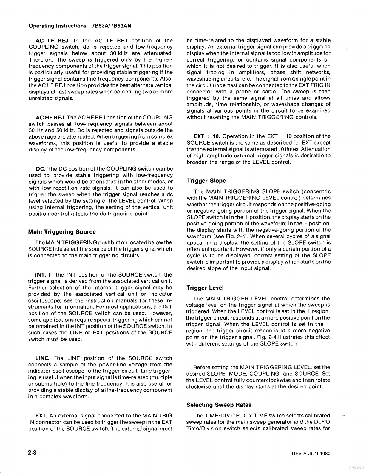
Trigger Slope
The MAIN TRIGGERING SLOPE switch (concentric
with the MAIN TRIGGERING LEVEL control) determines
whether the trigger circuit responds on the positive-going
or negative-going portion of the trigger signal. When the
SLOPE switch is in the
-I-
position, the display startsonthe
positive-going portion of the waveform; in the position,
the display starts with the negative-going portion of the
2-4).
waveform (see Fig.
When several cycles of a signal
appear in a display, the setting of the SLOPE switch is
often unimportant. However, if only a certain portion of a
cycle is to be displayed, correct setting of the SLOPE
switch is important to provideadisplay which starts on the
desired slope of the input signal.
Trigger Level
"The MAlN TRIGGER LEVEL control determines the
voltage level on the trigger signal at which the sweep is
4-
triggered. When the LEVEL control is set in the
the trigger circuit responds at a more positive point on the
trigger signal. When the LEVEL. control is set in the
region, the trigger circuit responds at a more negative
2-4
point on the trigger signal. Fig.
illustrates this effect
with different settings of the SLOPE switch.
region,
-
LINE.
The LlNE ~osition of the SOURCE switch
connects a sample of the power-line voltage from the
indicator oscilloscope to the trigger circuit. Line
trigger-
ing is useful whentheinput signal istime-related (multiple
or submultiple) to the line frequency. It is also useful for
providing a stable display of a line-frequency component
in a complex waveform.
EX$.
An external signal connected to the MAIN TRIG The TIME/DIV OR DLY TIME switch selects calibrated
IN connector can be used to trigger the sweep in the EXT
position of the SOURCE switch.
The external signal must
2-8
Before setting the MAIN TRIGGERING LEVEL, set the
desired
the
clockwise
SLOPE,
LEVEL
MODE, COUPLING,
control
until
the
fully
display
and
counterclockwise
starts
at
the
desired
SOURCE,
and then
point,
Set
rotate
Selecting Sweep Rates
sweep rates for the main sweep generator and the DLY'D
I'imeiDivision switch selects calibrated sweep rates for
REV A JUN
1980
Page 24
(LEVEL)
7B53A
Operating
Instructions--7B53A/7B53AN
CRT DISPLAY
OBTAINED
SLOPE SWITCH
SET
WITH
TO
POSITIVE(+)
REV
A
car
DISPLAY
OBTAINED
SLOPE SWITCH
SET
JUN
W1TH
TO NEGATIVE
1980
(-)
Fig.
2-4.
Effect of LEVEL control and SLOPE
switch
on CRT display.
Page 25
Operating
7B53A
Instructions--7BS3A/7B53AN
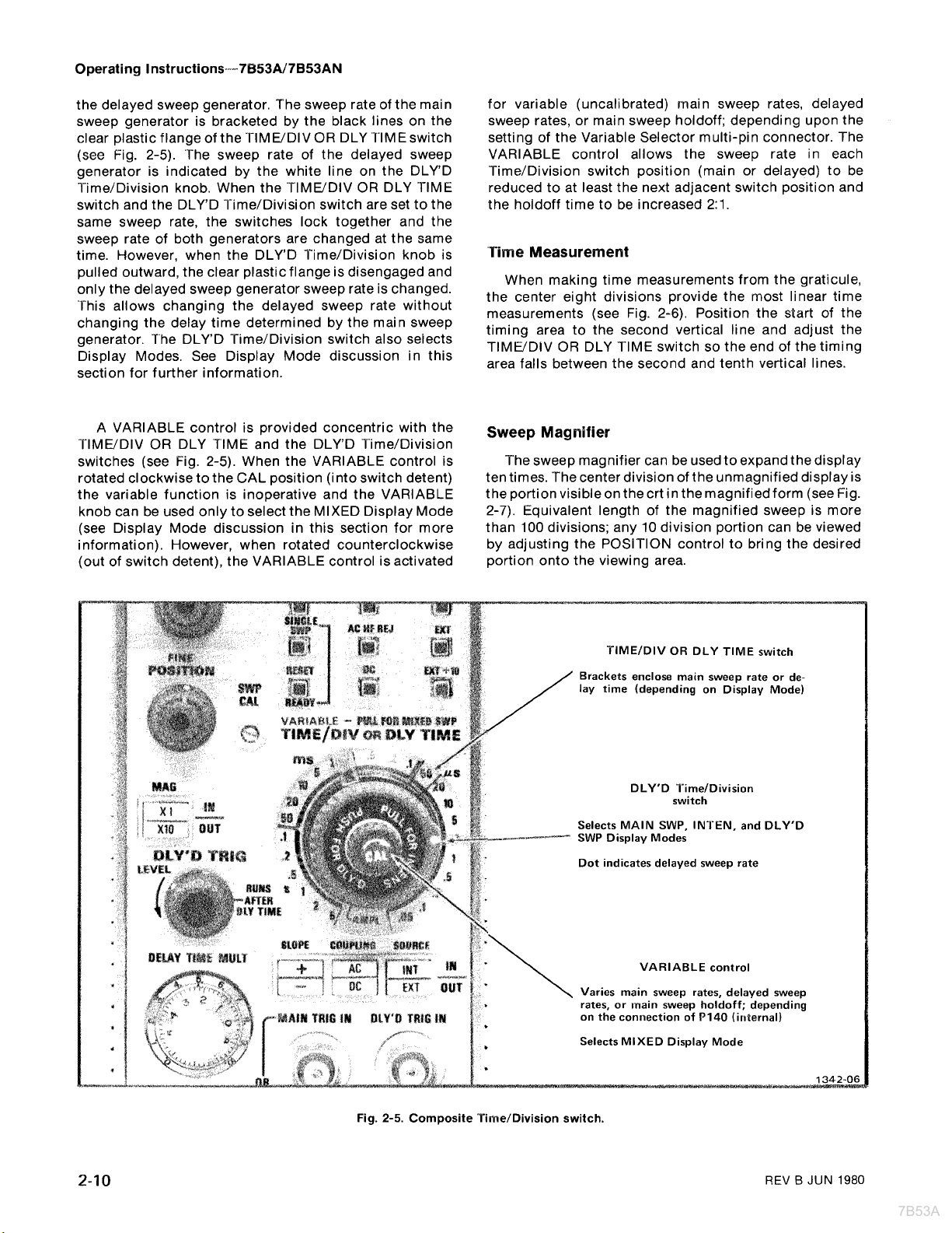
the delayed sweep generator. The sweep rate of the main
sweep generator is bracketed by the black lines on the
clear plastic flange of the TIMVDIV OR DLY TIME switch
(see Fig. 2-5). The sweep rate of the delayed sweep
generator is indicated by the white line on the DLY'D
Time/Division knob. When the T'IMVDIV OR DLY TlME
switch and the DLY'D Time/Division switch are set to the
same sweep rate, the switches lock together and the
sweep rate of both generators are changed at the same
time. However, when the DLY'D
pulled outward, the clear plastic flange is disengaged and
the
all0ws changing
changing
generator. The DLY'D Time/Division switch also seiects
section for further information.
A VARIABLE control is provided concentric with the
T'IMVDIV OR DLY
switches (see Fig. 2-5). When the VARIABLE control is
rotated clockwise to the CAL position (into switch detent)
the variable function is inoperative and the VARIABLE
knob can be used only to select the MIXED Display Mode
(see Display Mode discussion in this section for more
information). However, when rotated counterclockwise
(out of switch detent), the VARIABLE control is activated
the
Modes.
sweep generator sweep
the
time
determined
See
TlME and the DLY'D Time/Division
Time/Division knob is
rate
is
changed'
sweep
Mode
rate
the
main
discussion
without
sweep
in
this
for variable (uncalibrated)
sweep rates, or main sweep
setting of the Variable Selector multi-pin connector. The
VARIABLE control allows the sweep rate in each
Time/Division switch position (main or delayed) to be
reduced to at least the next adjacent switch position and
holdoff time to be increased
the
main sweep rates, delayed
holdoff; depending upon the
2:l.
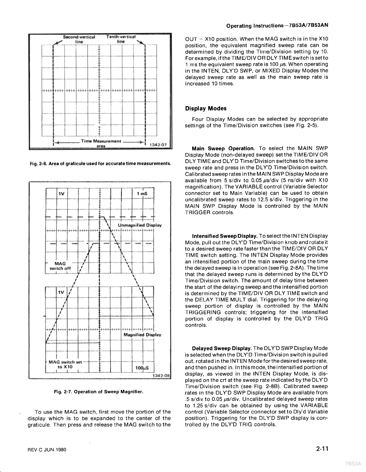
"Time Measurement
When making time measurements from the graticule,
the center eight divisions provide the most linear time
measurements (see Fig, 2-6).
timing
TIMUD,,,
area falls between the second and tenth vertical lines,
area
to the second vertical line and adjust the
OR
DLY
Position the start
switch
so
the
end
of
the
of
the
timing
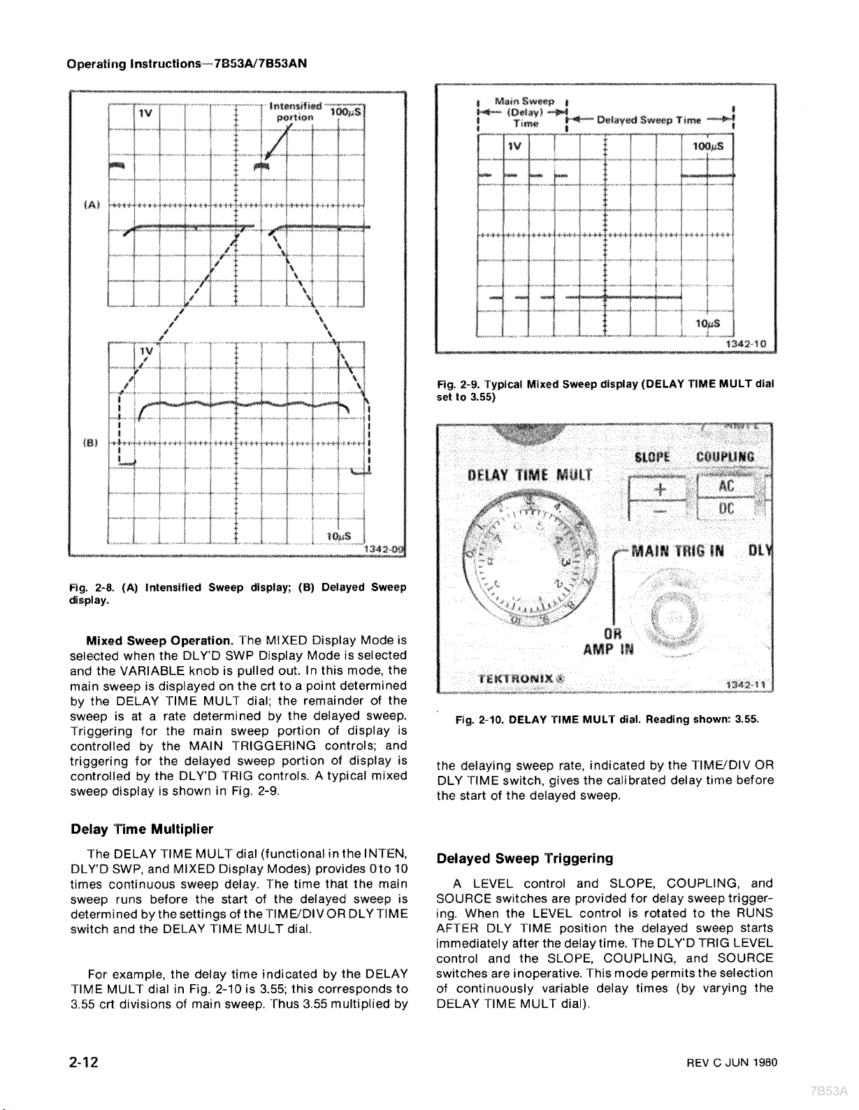
Sweep Magnifier
The sweep magnifier can be used to expand the display
ten times. The center division of the unmagnified display is
the portionvisibleon thecrt in themagnifiedform (see Fig.
2-7).
Equivalent length of the magnified sweep is more
100
than
by adjusting the POSITION control to bring the desired
portion onto the viewing area.
divisions; any
10
division portion can be viewed
Fig.
2-5.
Composite Time/Division switch.
REV 6 JUN
1980
Page 26
Operating
7B53A
Instructions---7B53A/7B53AN
Fig.
2-6.
Area of graticule used for accurate time measurements.
OUT
position, the equivalent magnified sweep rate can be
determined by dividing the
Forexample,
1
in the
delayed sweep rate as well as the main sweep rate is
increased 10 times.
Display
settings of the
DisIJlav Mode (non-delayed sweep) set the TIMVDIV OR
DLY
sweep rate and press in the DLY'D
Calibrated sweep rates in the MAIN SWP Display Mode are
available from 5
magnification). The VARIABLE control (Variable Selector
connector set to Main Variable) can be used to obtain
uncalibrated sweep rates to 12.5
MAlN SWP Display Mode is controlled by the MAlN
TRIGGER controls.
XI0 position. When the MAG switch is in the XI0
Time/Division setting by 10.
iftheTlMVDlVOR DLY TlMEswitch issetto
ms the equivalent sweep rate is 100 ps. When operating
INTEN, DLY'D SWP, or MIXED Display Modes the
Modes
Four Display Modes can be selected by appropriate
Time/Division switches (see Fig. 2-5).
Main Sweep Operation.
TIME
~~~'DLYD
~ime/~ivisibk switches to the same
s/div to 0.05 ps/div (5 ns/div with X10
To select the MAlN SWP
Time/Division switch.
sldiv. Triggering in the
Fig.
2-7.
Operation of Sweep Magnifier.
TO use the MAG switch, first move the portion of the
display which is to be expanded to the center of the
graticule. Then press and release the MAG switch to the
Intensified SweepDisplay.
Mode, pull out the DLY'D
to a desired sweep rate faster than the TIMVDIV OR DLY
TIME switch setting. The INTEN Display Mode provides
an intensified portion of the main sweep during the time
the delayed sweep is in operation (see Fig. 2-8A). The time
that the delayed sweep runs is determined by the DLY'D
Time/Division switch. The amount of delay time between
the start of the delaying sweep and the intensified portion
is determined by the
the DELAY
sweep portion of display is controlled by the MAlN
"TRIGGERING controls; triggering for the intensified
portion of display is controlled by the DLY'D TRIG
controls.
Delayed Sweep Display.
is selected when the DLY'D
out, rotated in the
and then pushed in, In this mode, the intensified portion of
display, as viewed in the
played on the crt at the sweep rate indicated by the DLY'D
Time/Division switch (see Fig. 2-88}. Calibrated sweep
rates in the DLY'D SWP Display Mode are available from
.5 s/div to 0.05 psldiv. Uncalibrated delayed sweep rates
to 1.25
control (Variable Selector connector set to Dly'd Variable
position). Triggering for the DLY'D SWP display is controlled by
TIME MULT dial, Triggering for the delaying
s/div can be obtained by using the VARIABLE
the DLY'D TRIG controls.
TiMEIDIV OR DLY 'TIMEswitch and
INTEN Modeforthedesiredsweeprate,
To select the INTEN Display
Time/Division knob and rotateit
The DLY'D SWP Display Mode
Time/Division switch is pulled
INTEN Display Mode, is dis-
REV
C
JUN
1980
2-1
1
Page 27
Operating
7B53A
Instructions--78fi3Al7B53AN
Fig.
set to
2-9.
Typical Mixed Sweep display (DELAY TIME MULT dial
3.55)
Rg.
2-8.
display.
(A) Intensified Sweep display;
Mixed Sweep Operation.
The MIXED Display Mode is
(B)
Delayed Sweep
selected when the DLY'D SWP Display Mode is selected
and the VARIABLE knob is pulled out. In this mode, the
main sweep is displayed on the crt to a point determined
by the DELAY 'TIME MULT dial; the remainder of the
sweep is at a rate determined by the delayed sweep.
Triggering for the main sweep portion of display is
controlled by the MAIN TRIGGERING controls; and
triggering for the delayed sweep portion of display is
TRlG
controlled by the DLY'D
controls. A typical mixed
sweep display is shown in Fig. 2-9.
Delay Time Multiplier
'The DELAY TIME MULT dial (functional in the INTEN,
DLY'D SWP, and MIXED Display Modes) provides Oto 10
times continuous sweep delay. The time that the main
sweep runs before the start of the delayed sweep is
determined by the settings of the
switch and the DELAY TlME MULT dial.
For example, the delay time indicated by the DELAY
"TIME MULT dial in Fig.
3.55
crt divisions of main sweep. Thus 3.55 multiplied by
2-10
TlMVDlVOR DLY TIME
is 3.55; this corresponds to
Fig.
2-10.
DELAY TlME MULT dial. Reading shown: 3.55.
the delaying sweep rate, indicated by the 'TIMVDIV OR
DLY TlME switch, gives the calibrated delay time before
the start of the delayed sweep.
Delayed Sweep Triggering
A LEVEL control and SLOPE, COUPLING, and
SOURCE switches are provided for delay sweep triggering. When the LEVEL control is rotated to the RUNS
AFTER DLY TIME position the delayed sweep starts
immediately after the delay time. The DLY'D
control and the SLOPE, COUPLING, and SOURCE
switches are inoperative. This mode permits the selection
of continuously variable delay times (by varying the
DELAY TlME MULT dial).
TRlG LEVEL
2-12
REV C JUN
1980
Page 28
Operating
7B53A
Instructions--7B53A/7B53AN
When the DLY'D TRlG LEVEL control is rotated
counterclockwise (out of switch detent), the delayed
sweep is triggerable. The delayed sweep does not start at
completion of the delay time but, waits until a trigger
the
pulse is received by the delayed sweep triggering circuit.
I'he delay time in this mode is dependent not only on the
settings of the delay-time controls, but on the delayed
sweep triggering controls and the occurrence of the
delayed sweep triggering signal. 'The primary purpose of
this mode is to eliminate jitter from the display delayed
sweep waveform. Since the delayed sweep is triggered by
the input waveform, jitter is eliminated from the delayed
sweep display even though it may be inherent in the input
waveform.
When the delayed sweep is triggerable, the LEVEL
control can be rotated to select the amplitude point on the
trigger signal at which the delayed sweep is triggered. The
DLY'D PRIG SLOPE, COUPLING, and SOURCE switches
are activated and their functions are the same for delayed
triggering as functions with the same title are for MAIN
'TRIGGERING (see Main Triggering Level, Slope, Coupling, and Source discussions in this section).
InputIOutput Connectors
Two dual-function bnc connectors are provided on the
instrument front-panel.
MAlN TRIG IN OR AMP IN.
external trigger input for the main triggering circuit when
the MAIN TRIGGERING SOURCE switch is set to EXT or
+
10 and the TIMVDIV OR DLY IIMEswitch is set to
EXT
any position except AMPL. When the
TIME switch is set to AMPL and the MAlN TRIGGERING
SOURCE switch is set to EXTor EXT
serves as an external horizontal input (see X-Y Operation).
'This connector is an
TlMWDlV OR DLY
1.-
10,
this connector
To apply an external signal (X-signal) to the horizontal
system, set the
7B53A/7B53AN TIM WDIV OR DLY TIME
switch to AMPL and the MAlN TRIGGERING SOURCE
EXT.
switch to
The MAlN TRIGGERING COUPLING
selected affects the frequency response of the X-signal.
Apply the external signal to the MAIN TRIG IN OR AMP IN
connector. Deflection factor of the X-signal is provided in
2-1.
multiples of 10 as shown in Table
The Y-signal can be
applied to the plug-in unit installed in the vertical compartment.
Table
2-7
DEFLECTION FACTOR OF
THE
X
SIGNAL
Main Deflection
Triggering
-,.-"--"
.------- "-
EXT 10 mV/div
EX7 700 mV/div
". .-
EXT + 10
.--.-.-.-
,"
----."
.-------.-.
""
--,-
"
1
---.
Vldiv
""
-.----.--
"-----
'To apply the X-signal internally via the triggering
system set the
S'IME/DIV OR DLY TlME switch to AMPL
and the MAlN TRIGGERING SOURCE switch to INT.
Apply the external signal to the Amplifier unit installed in
the vertical compartment. "The attenuator switch of the
Amplifier unit determines the horizontal deflection factor.
For information on X-Y applications see the oscilloscope manual. Also, the reference books listed under
Applications provide information on X-Y measurements
and interpreting the resultant
lissajous displays.
Mainframe Operating Modes
-
DLY'D TRIG IN.
This connector is an external input for
the delayed triggering circuit when the DLY'D TRlG
EXT.
SOURCE switch is set to
When the DLY'D T'RIG
SOUHCE switch is set to INT and P613 is properly
connected,
the DLY'D TRlG IN connector serves as a
Delayed Sweep Gate Out connector (not labeled). The
Delayed Sweep Gatesignal is arectangular positive-going
pulse with approximately 3.0 V amplitude and pulse width
coincident with the delayed sweep.
X-Y
Operation
Some applications required one signal displayed versus another rather than against time (internal sweep). The
amplifier function of the
7B53A/7B53AN allows an external signal to be appliedtothe horizontal deflection system
either externally via the MAIN TRlG IN OR AMP IN
connector or internally by way of the triggering system.
REV
A
JUN
1980
The 7B53A17B53AN can be operated in a 7000-Series
OsciIIsocope which has four plug-in compartments, either
independently, in the Alternate or Chopped Horizontal
Modes, or as a delayed sweep unit. However, when the
7B53N7B53AN is operated as a delayed sweep unit, it
must be triggered for a crt display.
It cannot delay another
time base unit but it can delay its own internal delayed
sweep. Refer to the appropriate oscilloscope manual for
additional mainframe horizontal operating information.
General
The following information describes the procedureand
techniques for making basic measurements with a
7B53N7B53AN installed in a 7000-Series Oscilloscope.
These applications are not described in detail, since each
application must be adapted to the requirements of the
2-13
Page 29
Operating
7B53A
Instructions--7B53A/7B53AN
individual measurement. This instrument can also be used
for many applications not described in this manual.
Contact your local Tektronix
Fieldofficeor representative
for assistance in making specific measurements. The
following books describe oscilloscope measurement
techniques which can be adapted for use with this
instrument. horizontal
4. Divide the period of the reference signal (seconds)
by the product of the horizontal deflection established in
2
(division) and the setting of the TIMWDIV OR DLY
step
TIME switch. This is the horizontal conversion factor:
Horizontal
Conversion
Factor
reference signal period (seconds)
-
deflection
TIM WDlV OR
X
DLY TlME
(divisions) switch setting
J. Czech, "Oscilloscope Measuring Techniques",
Phillips Technical Library, Springer-Verlag, New York,
1965. 5. To measure the period of an unknown signal
disconnect the reference signal and connect the unknown
signal tothevertical unit. Set the TIMWDIVOR
DLY'TIME
switch to a setting that provides sufficient horizontal
John
D.
Lenkl
andbo book
and Applications", Prentice-Hall, Inc. Englewood
of Oscillosco~e
deflection to make an accurate measurement. Do not
the
VARIABLE
control,
Cliffs, N.J., 1968.
6. Measure the horizontal deflection in divisions and
Charles
H.
Roth, Jr., "Use of the Oscilloscope",
Programmed Text, Prentice-Hall, Inc., Englewood
cliffs, N.J., 1970.
J.H. Golding, "Measuring Oscilloscope", Tran-
satlantic, 1971.
calculate the period of the unknown signal using the
following formual:
Period
(Seconds)
-
--
7-IMVDIV OR horizontal horizontal
X
DLY TIME
setting
conversion
factor (divisions)
X
deflection
Comparison Measurement Techniques
Sweep Rates. To establish an arbitrary horizontal
Example. Assume a reference signal frequency of
455 Hz(period2.19
setting of
.2
ms),aTIMVDlVORDLYTIMEswitch
ms, and the VARIABLE control adjusted to
sweep rate based upon a specific reference frequency provide a horizontal deflection of eight divisions.
proceed as follows:
1. Connect the reference signal to the input of the
vertical unit. Set the
Volts/Division switch of the vertical
unit for four or fivedivisions of vertical deflection. Obtain a
Substituting these values in the horizontal conversion
factor formula (step 4):
Horizontal
Conversion
-
Factor
triggered display.
2.
Set the
TIME/DIV OR DL'Y TlME switch and the
VARIABLE control (Variable Selector connector set to
Main Variable) so one cycle of the signal covers an exact
number of horizontal divisions. Do not change the
VARIABLE control after obtaining the desired deflection.
Then, with a
ps, the period of an unknown signal which completes
50
one cycle in seven horizontal divisions can be determined
by using the period formual (step
Period
(Seconds)
TIME/DIV OR DLY TIMEswitch setting of
6):
=5Ops X 1.37 X 7= 48Ops
This display can be used as a reference for frequency
comparison measurements.
Phis answer can be converted to frequency by taking
the reciprocal of the period in seconds (see application on
3. To establish an arbitrary sweep rate so the period
Determining Frequency Measurements).
(time for one complete cycle) of an unknown signal can be
measured accurately at any setting of the
DLY TlME switch, the period of the reference signal must
be known. If it is not known, it can be measured beforethe
VARIABLE switch is set in step 2.
TIM WDlV OR
Time
Duration Measurements
Po measure time between two points on a waveform,
use the following procedure:
2-14
REV
A
JUN
1980
Page 30
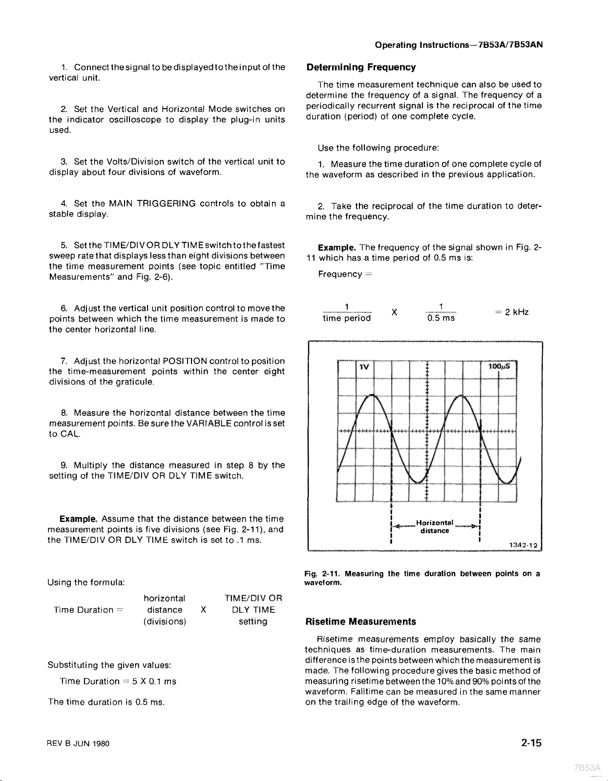
Operating
7B53A
Instructions--7B53A17B53AN
1. Connect thesignal to be displayedtotheinput of the
vertical unit.
Determining Frequency
The time measurement technique can also be used to
determine the frequency of a signal. The frequency of a
2,
set
the
Vertical
and
~~~~~~~~~l ~~d~
on
the indicator oscilloscope to display the plug-in units
periodically recurrent signal is the reciprocal of the time
duration
(period)
Of One
used.
Use the following procedure:
3.
Set the Volts/Division switch of the vertical unit to
display about four divisions of waveform.
4.
Set the MAIN TRIGGERING controls to obtain a
1. Measure the time duration of one complete cycle of
the waveform as described in the previous application.
2.
'Take the reciprocal of the time duration to deter-
stable display. mine the frequency.
Setthe TIMVDIVOR DLY TIMEswitchtothefastest
5.
sweep rate that displays less than eight divisions between
Example. The frequency of the signal shown in Fig. 2-
11 which has a time period of 0.5 ms is:
the time measurement points (see topic entitled "Time
Measurements" and Fig. 2-6).
6.
Adjust the vertical unit position control to move the
points between which the time measurement is made to
Frequency
-.-----"*--
time period 0.5 ms
--=
1
the center horizontal line.
X
cycle-
1
--*-.-
--
2
kHz
7.
Adjust the horizontal POSITION control to position
the time-measurement points within the center eight
divisions of the graticule.
8.
Measure the horizontal distance between the time
measurement points. Be sure the VARIABLE control is set
to CAL.
8
9. Multiply the distance measured in step
setting of the
TIME/DIV OR DLY TlME switch.
by the
Example. Assume that the distance between the time
measurement points is five divisions (see Fig. 2-11), and
"TIMVDIV OR DLY TIME switch is set to
the
.1
ms.
Using the formula:
horizontal TlME/DIV OR
Time Duration
--
distance
X
DLY TIME
(divisions) setting
Substituting the given values:
'Time Duration
The time duration
-
5
is
0.5 ms.
X
0.1 ms
i
Fig.
2-11.
waveform.
[s+~Horizontal
I
I
Measuring the
distance
time
duration between points
I
I
I
on
Risetime Measurements
Fiisetime measurements empfoy basically
techniques as time-duration measurements. The main
difference
made.
measuring
waveform.
isthe points between which the measurement is
The following procedure gives the basic method of
risetime between the 10% and 90% pointsof the
Falltime can be measured in the same manner
on the trailing edge of the waveform.
the
same
a
REV
B
JUN
1980
Page 31

Operating
7B53A
Instructions-7B53Af7B53AN
1. Connect thesignal to bedisplayedtotheinput of the
vertical unit.
2. Set the Vertical and Horizontal Mode switches on
the indicator oscilloscopeto displaythe plug-in unit used.
3.
Set the Volts/Division switch and the Variable
VoltslDivision control of the vertical unit to produce a
signal an exact number of divisions in amplitude.
4.
Center the display about the center horizontal
graticule line with the vertical unit Position control.
5. Set the MAIN TRIGGERING controls to obtain a
stable display.
6. Set the TIMEIDIVOR DLY TlMEswitchtothefastest
sweep rate that displays less than eight divisions between
10°/o and 90% points on the waveform.
the
7.
Determine the 10% and 90% points on the rising
portion of the waveform. Thefiguresgiven in
for the points 10% up from the start
and 10% down from the top of the rising portion (90%
point).
of
Table2-2are
the rising portion
10, Multiply the distance measured in step 9 by the
setting of the
Example.
the
10%and 90% points is four divisions (see Fig. 2-12) and
TIMWDIV OR DLYTlMEswitch issetto 1 ps. Applying
the
the time duration formula to risetime:
Time horizontal
Duration
(Risetime) (divisions) setting
Substitute the given values:
Risetime = 4 X 1 ps.
7"he risetime is 4.0
TIME/DIV OR DLY TIME switch.
Assume that the horizontal distance between
TlMWDlV OR
==
distance
,us.
X
DLY TiME
I
Table
2-2
RlSEf lME MEASUREMENTS
10°/~ and 90%
----
0.4 and 3.6 divisions
0.5 and 4.5 divisions
0.6 and 5.4 divisions
8.
Adjust the horizontal POSITION control to move the
10% point of the waveform tothe second vertical line of the
graticule. For example, with a five-division display as
shown in Fig. 2-12, the
start of the rising portion.
9. Measure the horizontal distance between the 10%
90% points. Be sure the VARIABLE control is set to
and
CAL.
10% point is0.5division upfrom the
-".-".--
10% and
9O0/0
!+*Horizontal
I
distance
Fig.
2-12.
'
-$
I
Measuring risetime.
Delayed Sweep Measurement
The delayed sweep mode can be used to make accurate
time measurements. The following measurement deter-
mines the time difference between two pulses displayed
on the same trace. This application may also be used to
measure time difference from two different sources
trace) or to measure time duration of a single pulse. See
Section 2 for measurement accuracy.
1. Connect thesignal to be displayed
vertical unit.
2. Set the vertical and horizontal Mode switches on the
indicator oscilloscope to display the plug-in units used.
tothe input of the
(dual-
2-16
REV
A
JUN
1980
Page 32

Operating
7B53A
lnstructions--7653A/7BS3AN
3. Set the Volts/Division switch of the vertical unit to
4
produce a display about
4.
Adjust the MAIN TRIGGERING controls for a stable
display.
5.
If possible, set the TlMVDlV OR DLY TlME switch
to a sweep rate which displays about eight divisions
between pulses.
6.
Set the DLY'D Time/Division switch to a setting
1/100 of the TIMVDIV OR DLY TIME switch setting and
pull out the DLY'D
Display Mode. This produces an intensified portion ap-
proximately
Measurement accuracy will
control setting for MAIN TRlGG ERlNG or horizontal
POSITION control setting is changed.
7.
intensified portion of the trace to the first pulse.
0.1 division in length.
Rotate the DELAY TlME MULT dial to move the
Time/Division switch for the INTEN
divisions in amplitude.
NOTE
be
affected if the
LEVEL
I
DELAY-TIME
MULT
1.31
dial:
DELAY-TIME
MULT
dial:
8.81
I
8. Press in the DLY'D 'Time/Division switch for the
DLY'D SWP Display Mode.
9.
Adjust the DELAY TIME MULT dial to move the
pulse (or the rising portion) to the center vertical graticule
line. Note the exact setting of the dials.
Fig.
2-13.
Measuring
10. Turn the DELAY TlME MULT dial clockwise until
thesecond
pulse. (If several pulses are displayed, return
DISPLAY MODE to locate the correct pulse.) Again note
the exact dial setting.
11. Subtract the first dial setting from the second and dial dial
multiply bythedelay timeshown by
TlME switch. This figure is the time interval between
pulses.
Example.
second dial setting 8.81 with the TIMVDIV OR DLY TIME
switch set to
pulseis positionedtothesame point asthefirst
tothe IN'TEN
theTIMVDlVOR DLY setting setting DLY TIME switch setting)
Assume the first dial setting is 1.31 and the
2
ms (see Fig. 2-13).
Time Difference
(Delayed Sweep)
second first
Substituting the given values:
"Time Difference
The time difference is 15
time
difference using delayed sweep.
--
delay time (TIMVDIV OR
-
(8.81 - 1.31) X 2 gs
MS.
@
JUN
1980
Page 33

Operating
7B53A
Instructions--7B53A/7B53AN
Delayed
The delayed sweep feature of the 7B53N7B53AN
provides apparent magnification of the displayed
waveform. The sweep rate of the delayed sweep is not
actually increased; the apparent magnification is the
result of delaying the Delayed Sweep an amount of time
selected by the
DELAY TlME MULT dial before the display is presented at
the sweep rate selected by the DLY'D
switch. The following method uses the RUNSAFTER DLY
TIME DLY'D
the display to be positioned with the DELAY TlME MULT
dial. If thereistoo much jitter in the delayedsweep display,
use the Triggered delay sweep magnification procedure
which follows this procedure.
1.
connector of the vertical unit. Set the Vertical and
Horizontal Mode switches on the indicator oscilloscope to
display the plug-in units used.
2. Set the
produce a display about 4 divisions in amplitude.
Sweep
Connect the signal to be displayed to the input
Magnification
TlMUDlV OR DLY TIME switch and the
Time/Division
TRlG Mode to allow the delayed portion of
Volts/Division switch of the vertical unit to
Pulse
to
magnified
be
I
3,
Adjust the MAIN TRIGGERING controlsfor astable
display.
4. Set the
ratewhich displays thecomplete waveform (see Fig. 2-14).
5.
Pull out the DLY'D Time/Division switch for the
INTEN Display Mode. Rotate the DLY'D TRlG LEVEL
control clockwise to RUNS AFTER DLY TIME.
6.
Position the start of the intensified portion with the
DELAY TIME MULT
magnified.
7.
Set the DLY'D Pime/Division switch to a setting
which intensifies the full portion of the display to be
ma,gnified. 'The start of the intensified trace will remain as
positioned in step
8.
Press in the DLY'D 'TimelDivision switch for the
DLY'D SWP Display Mode.
9.
lime Measurements can be made from the display
in the conventional manner. Sweep rate is determined by
the setting of the DLY'D
TlMElDlV OR DLY TIME switch to a sweep
dial to the part of the display to be
6.
Time/Division switch.
iB)
Delayed sweep display.
Fig.
2-14.
Using
delayed
10. The apparent sweep magnification can be
calculated by dividing the
setting by the DLY'D
Example.
shown in Fig. 2-14 with a
.l
ms and a DLY'D Time/Divisionswitch setting of 10 ,us
of
is:
Apparent
Magnification DLY'D Time/Division setting
Substituting the given values:
~pparent
Magnification
The apparent magnification is 10 times.
The apparent magnification of the display
TIME/DIV OR DLY TlME setting
...
"..
--.
sweep
for
magnification.
TIME/DIV OR DLY 'TIME switch
Tirne/Division switch setting.
IIME/DIV OR DLY TlME setting
--
1
x
3
o-~
1
x
lom5
2-18
@
JUN
1980
Page 34

Operating
7B53A
Instructions-7B53A/7B53AN
Triggered Delayed Sweep Magnification
The delayed sweep magnification method just described may produce too much jitter at high apparent
magnification ranges. The Triggered Delayed Sweep
Mode (DLY'D TRlG LEVEL control rotated out of switch
detent) provides a more stable display, since the delayed
sweep display is triggered at the same point each time.
1.
Set up the display as instructed in steps 1 through
in the Delayed Sweep Magnification procedure.
2.
Rotate the DLY'D TRlG LEVEL control in a
counterclockwise direction but out of switch detent for a
TI
triggerable delayed sweep. Select the desired DLY'D
SLOPE, COUPLING, and SOURCE.
3.
Adjust the DLY'D TRlG LEVEL control to produce
an intensified portion on the display.
4.
Inability to produce an intensified portion of the
display indicates that the DLY'D TRlG controls are
incorrectly set, or that the signal does not meet triggering
requirements. If the condition cannot be remedied with
the DLY'D TRIG controls or by increasing the display
amplitude (lower
the delayed sweep.
Volts/Division setti ng), externally trigger
RG
Use the following procedure:
1. Set up the display as given in steps 1 through
Delayed Sweep Magnification.
2.
Time measurements can be made from the display
in the conventional manner. Sweep rate is determined by
the setting of the DLY'D
7
Example.
displayed on the crt. The circled portion of the waveform
cannot be viewed in any greater detail because the sweep
is triggered by the larger amplitude pulses at the start of
the display and a faster sweep rate moves this area of the
waveform off the viewing area. The second waveform
shows the area of interest magnified 10 times using
Delayed Sweep.
adjusted so the delayed sweep starts just before the area
of interest.
Fig. 2-15 shows a complex waveform as
The DELAY TIME MULT' dial has been
lime/Division switch.
8
of
5. When the correct portion of the display is intensified, press in the DLY'D
DLY'D SWP Display Mode, slight readjustment of the
TRIG LEVEL control may be necessary to produce
DLY'D
a stable delayed sweep display.
6.
Measurement and magnification are as described
above in Delayed Sweep Magnification discussion.
Time/Division switch for the
Displaying Complex Signals Using Delayed Sweep
Complex signals often consist of a number of individual
events of differing amplitudes, Since the trigger circuits
are sensitive to changes in signal amplitude, a stable
display can normally be obtained only when the sweep is
triggered by the
However, this may not produce the desired display of a
lower-amplitude portion which follows the triggering
event. The delayed sweep feature provides a means of
delay~ng the start of the delayed sweep by a selected time
following the event which triggers the main sweep
generator. Then, the part of the waveform which contains
the information of interest can be displayed at thedelayed
sweep rate.
event(s) having the greatest amplitude.
Fig. 2-15. Displaying a complex signal using delayed sweep.
@
JUN
1980
2-19
Page 35

Operating
7B53A
Instructions--.7B53A/7B53AN
Pulse Jitter Measurement
In some applications it is necessary to measure the
amount of jitter on the leading edge of a pulse or jitter
between pulses.
1. Connect the signal to be displayed to the input
connector of the vertical unit. Set the Vertical and
Horizontal Mode switches on the indicator oscilloscope to
display the plug-in units used.
2. Set the
produce a display about four divisions in amplitude.
3.
Adjust the MAIN TRIGGERING controls for astable
display.
4.
Set the 'TIME/DIV OR DLY TIME switch to a sweep
rate which displays the complete waveform (see Fig. 2-14).
5. Pull out the DLY'D
INTEN Display Mode.
Volts/Division switch on the vertical unit to
'Time/Division switch for the
Example.
Assume that the horizontal movement is 0.5
division (see Fig. 2-16) and the DLY'D
switch is .5 ps.
Using the formula:
horizontal DLY'D
Pulse Jitter
-:
jitter
X
Tirne/Division
(divisions) setting
Substituting the given values:
Pulse Jitter
=-
0.5 X 0.5 ps
The pulse jitter is 0.25 ps.
Time/Division
6. Position the start of the intensified portion with
DELAY TIME MULT dial to the part of the display to be
magnified.
7.
Set the DLY'D Time/Division switch to a setting
which intensifies the full portion of the display to be
magnified. 'The start of the intensified trace wili remain as
positioned in step 6.
Repackaging for Shipment
If the
Tektronix Service Center for service or repair, attach atag
showing: owner (with address) and the name of an
individual at your firm that can be contacted, complete
8.
Press in the DLY'D Time/Division switch for the
instrument serial number and a description of the service
DLY'D SWP Display Mode. required.
9.
Slight readjustment of the MAIN TRIGGERING
LEVEL control may be necessary to produce as stable a
display as possible.
Save and re-use the package in which your instrument
was shipped. If the original packaging is unfit for use or
not available, repackage the instrument as follows:
Surround the instrument with polyethlene sheeting to
protect the finish of the instrument. Obtain a carton of
10. Pulse jitter is shown by horizontal movement on
the pules (take into account inherent jitter of delayed
sweep). Measure the amount of horizontal movement. Be
sure that both vertical and horizontal VARIABLE controls
are set to CAL.
corrugated cardboard of the correct carton strength
and having inside dimensions of no less than six inches
more than the instrument dimensions. Cushion the
instrument by tightly packing three inches of dunnage
or urethane foam between carton and instrument, on all
sides. Seal carton with shipping tape or industrial
stapler.
11. Multiply the distance measured in step 10 by the
Time/Divisionswitch settingtoobtain pulsejitter in
DLY'D
The carton test strength for your instrument is 200
time. pounds.
I I
+
L+-
Measuring pulse jitter.
1342-1
7
Fig.
Jitter
2-16.
"Pektronix instrument is to be shipped to a
2-20
@
JUN
1980
Page 36

Section
7B53A
3.-
--7B53Al7B53AN
THEORY
OF
Introduction
'This section of the manual contains adescription of the
circuitry used in the
description begins with a discussion of the major circuit
functions using a simplified block diagram.
SIMPLIFIED
The Simplified Block Diagram, Fig. 3-1, shows interconnection of the basic
7B53A17853AN. In some cases, such as the Main Sweep
Trigger, the block includes a number of separate circuits.
The individual circuits are discussed in detail later in this
section.
7B53A/7B53AN Dual Time Base. The
BLOCK
DIAGRAM
c~rcuit blocks in the
Main Sweep Mode
When the TIME/DIV OR DLY TIME switch is set to
MAIN SWP, operation is as follows:
select
Main Sweep Trigger.
selecting the trigger source, type of coupling, triggering
mode, and point on the trigger signal where triggering
occurs. Also, regardless of the trigger signal shape or
amplitude (within
fast-rise, uniform-amplitude
Comparator. Termination of the pulse (or gate) occurs at
the rise of Main Sweep
'This block includes circuitry for
specification], this circuitry provides a
pulseto the Main Sweep Start
Holdoff.
OPERAT
side is set by the Main Swp Stop adjustment. When the
sawtooth waveform passes through thesetting of the Main
Swp Stop adjustment, the output of the Sweep Stop
Comparator switches to a positive level. Phis positivestep
is applied to the Main Sweep
Main Sweep Hoidoff.
is used to prevent generation of a trigger signal until the
sweep circuits have stabilized after a sweep. The positive
step from the Sweep Stop Comparator initiates the positive
holdoff gate. The duration of the hold off gate is variable,
depending on the setting of the
switch. Holdoff timing capacitors are separate from sweep
timing capacitors.
Output from the Main Sweep
Main Sweep Trigger and the Delayed Sweep
circuit. A trigger signal cannot be generated during the
holdoff interval. The holdoff serves to reset the trigger
circults so that they are ready to receive an input trigger
s~gnal after holdoff.
Horiz Output.
Horiz Amp. Position Amp, Horiz Display Selector, and
Horiz Out Amp circuits.
Holdoff is longer for slower sweep rates.
The Horiz Output block includes the Ext
Holdoff.
This circuit develops a gate which
TIMEIDIV
Holdoff is coupled to the
OR
DLY 'PIME
Holdoff
Main Sweep Start Comparator.
by the positive gate from the Main Sweep Trigger.
output signal coupled tothe Main Sawtooth Generator isa
positive gate with the same duration as the sweep. This
gate is also coupled to the Sweep Gate Out. A
going gate (coincident with the positivegate) iscoupled to
the Delayed Sweep Lockout Multi and the Delayed Sweep
Start Control.
Main Sawtooth Generator.
developed by the Main Sawtooth Generator. When a
positlve gate from the Main Sweep Start Comparator is
applied, a sawtooth waveform is generated. The sawtooth
duration is determined by the positive gate
of change of the sawtooth is set by Ct and Rt, selected by
the
"rIMVDIV switch.
Sweep Stop Comparator.
is driven by the
REV
JAN
1985
maln sweepsawtooth signal, andthe other
This circuit is activated
The
negative-
The main sweep signal is
durat~on. Rate
One side of this comparator
W~th the TIME/DIV OR DLY TIME sw~tch set for maln
sweep, thls circuit selects the signal from the Maln
Sawtooth Generator, amplifies the s~gnal, and converts
the single-ended input to a push-pull output signal. Dc
positioning
level is also applled to th~s block.
Delayed Sweep Mode
To generate the delayed sweep, the Main Sawtooth
Generator must
Delay Pickoff.
whlch starts when the main sawtooth signal passes
through the level selected by the DELAY
control. The gate ends
output signal is coupled to the Delayed Sweep Holdoff
circuitry.
flrst be gated on (see Main Sweep Mode).
This circuit supplles a
w~th the maln sawtooth signal. The
positive
rlME MULT
gate
3-
1
Page 37

Theory of
7B53A
Operation--7FT53A/7B53AN
*,-
-
---
--
--.---
-".------
"------
--
-
Fig.
3-1.
7653A17B53AN
"W
Simplified
-----"--
Block
Diagram.
REV
A
JUN
1980
Page 38

Theory of
7B53A
Operation--'SB53A/7B53AN
Delayed Sweep Trigger.
is set to RUNS AFTER DLY TIME (intoswitch detent), the
output trigger is generated as soon as the delayed gate is
applied. If the DLY'D TRIG LEVEL control is in the
triggerable mode (out of switch detent), the output trigger
is initiated by the next input trigger that occurs after the
Delay Gate is applied.
The Delayed Sweep Trigger output is a positive gate
which is terminated by the
step from the Delayed Sweep Stop circuit. The positive
output gate is coupled to the Delayed Sweep Start Multi.
Sweep
Delayed Sweep Trigger causes the Delayed Sweep Start
~ulti to flip so that a positive gate is coupled to the
Delayed
applied to the
are the same in duration as the positive gate from the
Delayed Sweep 'Trigger.
Sweep Start
~ixed Sweep Comparator. The output gates
Delayed Sweep Start Control.
of operation the Delayed Sweep Start Control serves to
the
positive gate
Mu'ti
to
Gate Out.
and the Delayed Sweep Lockout Multi are not effective in
this mode.
the Sawtooth
lnput signals from the Main Sweep Start Comparator
Delayed Sawtooth Generator.
signal is developed by the Delayed Sawtooth Generator.
The sawtooth is generated during the time that a positive
gate is applied from the Delayed Sweep Start Control.
Rateof change of thesawtooth isset by Ct and Rt, selected
by the
TIME/DIV (Dly'd) switch.
The sawtooth output signal is coupled to the Mixed
Sweep Comparator and the Horiz Output circuits.
Delayed Sweep Stop Circuit.
the output of the Delayed Sweep Stop circuit when the
delayed sawtooth passes through the level selected by the
Dly'd Swp Length adjustment. This step is coupled to the
Delayed Sweep Trigger and the Delayed Sweep Lockout
Multi.
When the DLY'D TRIG LEVEL
Holdoff signal or the positive
Start
Control, and a negative gate is
For delayed sweep mode
from the
A positive step occurs at
signal
and
the
The delayed sweep
the
Start
Mixed Sweep Mode
In this mode of operation, the sweep is first running at
the main sweep rate and then, after the selected delay discussion. Circuits which are commonly used in the
interval, runs at the delayed sweep rate. The main sweep
and delayed sweep are initiated as previously described.
Operation of other circuit blocks follows.
Mixed Sweep Comparator.
whether the delayed sweep generator runs at the main
sweep rate or at the delayed sweep rate. Before the delay
gate is generated (delay gategenerated at delay
determined by the setting of the DELAY
the main sweep sawtooth signal is coupled through the
Mixed Sweep Comparator, causing the delayed sweep
generator to run at the main sweep rate.
sawtooth signal iscoupled
When a positive gate from the Delayed Sweep Trigger is
applied to the Delayed Sweep Start Multi (at Delay Pickoff
as
determined by the DELAY TIME MULT dial setting) a
negative gate is generated and coupled to the Mixed
Sweep Comparator. This opens the Mixed Sweep Comparator, preventing the Delayed Sweep Generator from
running
Delayed Sweep Generator is released to run at the delayed
sweep rate.
at
the main
sweep
Delayed Sweep Lockout Multi.
the Delayed Sweep Stop circuit is inverted by the Delayed
Sweep Lockout Multi and to the Delayed Sweep
Start Control, thus turning off the Delayed Sawtooth
Generator.
Sweep Gate Out.
TIMEIDIV switch, thisstage couplesthe positivegatefrom
either the Main Sweep Start Multi or the Delayed Sweep
Start Control to connector Al. The Sweep Gate signal
serves to unblank the crt in the Oscilloscope during the
sweep.
Depending on the selection of the
This circuit determines
pickoff as
TIME MULT dial)
'The resulting
tothe Horizontal Output stage.
rate.
simultaneously, the
The positive step from
External Horiz lnput
When the TIME/DIV switch is set to AMPL, part of the
Main Sweep Trigger circuitry becomes the Horiz lnput
Amp. An external signal connected to the
or AMPL input is amplified and then coupled to the Horiz
Output stage. The main and delayed sawtooth generators
are disabled to prevent intensity modulation of the crt
trace by the unblanking waveforms.
CIRCUIT
OPERATION
MAIN 7'HIG
IN
General
This section provides a detailed description of the
electrical operation and relationship of the circuits in the
7B53A/7B53AN. The theory of operation for circuits
unique to this instrument is described in detail in this
electronics industry are not described in detail. If more
REV
C
JUN
1980
3-3
Page 39

Theory
7B53A
of
Operation--7653M7653AN
information is desired in these commonly used circuits,
refer to the following text-books.
Phillip Cutler, "Semiconductor Circuit Analysis",
McGraw-Hill, New York. 1964.
P.
Lloyd
Electronics", second edition,
1962
Jacob Millman and Herbert Taub, "Pulse, Digital, and
Switching Waveforms",
'The main headings in this circuit analysis refer to
schematics in the diagrams section with the same name.
The sub-headings indicate the
descri bed
"The Main 7 rigger Preamp coverts t he push-pull internal
trigger signal
trrgger source and coupling for the Main
Generator, Fig. 3-2 shows a detarled block diagram of the
Main
shown on diagram
Trigger Preamp.
Vert~cal Deflection System is converted
output
Q61 drives current gain stage
output
Hunter (Ed.), "Handbook of Semiconductor
McGraw-Hill, New York,
McGraw-Hill, New York, 1965.
indivrdual circuit being
MAIN
Trigger Preamp The schematfc of thrs circuit is
by
is set by internal Trig DC Bal Control, R72
TRlGGER
toasingle-endedsignal and selectsthe main
1
at the rear of this manual
The push-pull trigger signal from the
emitter-coupled stage Q52-Q61. 7 he output of
PREAMP
Q66-Q70. Thedc level of the
@
Trigger
to
a singfe-ended
shows a detailed block diagram of the Main
Generator, the schematic of this circuit
d~agram 2 at the rear of thls manual,
lnput Stage.
a hrgh input rmpedance for the trigger signal
provides
and the rnput source lnput protection diode
protects (2310 from excessive input s~gnals by clamping
the gate of the tnput FET rf the rnput exceeds aoout
7he signal at the source of Q310
em~lter-follower Q315 to the base of Q320 in the Slope
Comparator and to the External Horizontal circuit
Slope Comparator.
difference amplifier to provide selection of the slope and
level
at
voltage for the comparator is provided by LEVEL control
R4
and Main 1 rrg Level Center control R333 R333 sets the
level at the base of
0 V dc level of the incoming trigger when the LEVEL
the
control is centered When MAIN TRIGGERING
control R4
approximately
input of
level of the trrgger signal As the LEVEL control
clockwise, the
more
positive level before comparison takes place The resul-
tant crt display starts at a more
displayed signal When the
~ounterclockwrse from 0, the result is the opposite oi the
above
more negative point along the
Q320, thus switchrng the comparator at the 0 V
posittve Now the trigger signal must rise to a more
reactron and produces a crt dtsplay that starts at a
The input source-follower, Q310, provtdes
fsolation between the Mar n rrigger Generator
is passtng through
Q320 and Q322 are connected as a
which the sweep is triggered The reference
(2322 so that the display is triggered at
IS
set to midrange, the base of (2322 is at
0 V This corresponds tothe 0 Vlevel at the
voltage level on the base of Q327 becomes
posltive point on the
LEVkL control is turned
slopeof thetrigger signal
IS
shown on
LEVkL
IS
turned
l
rigger
It
also
CR307
-
15
V
lnput Switching.
switch,
trlgger sources are
The external signal may also be passed through a
attenuator network.
offers a means of attenuating high or low frequency
components of the trigger signal. In addition to ac and dc
coupling, C23-R23 can be selected to provide
frequency attenuation and R25-C25-C26 for highfrequency attenuation
$70, selects the source of the trigger signal Three
The
MAIN TRiGGERING COUPLING swrtch, 520,
MAIN TRIGGER GENERATOR
(SN B2WO00
The Main Trigger Generator provides selection of the
level and slope where triggering occurs and supplres a
fast-rrse pulse to the marn sweep start comparator. Fig 3-3
Phe MAIN TRIGGERING SOURCE
available;
internal, line, and external
@
&
UP
1PB53A
ONLY)
:
10
low-
3-4
R326 establishes the emitter current for Q320 and Q322,
The transistor with the most posrtrve base controls conduction of the comparator. For example, assume that the
ger signal from the input stage is pos~twe-go~ng and Q320
forward biased. The rncreased current flow through R326
makes the
IS
held constant by the level control voltage, the current
through Q322
Q320 makes the voitage
the decrease
13
of U350 more posrtrve.
em~tter of Q322 more positive and since the base
decreases. The increased current through
at
pin t 4
of U350 less positive, and
m
current through Q322 makes voltage
at
tfrg-
IS
prn
Trigger Generator
An Integrated circuit converts the trrgger signal from
the
tr~gger comparator to a gate waveform used for sweep
1
control With pin
positive-goi ng waveform on the rnput (pin 13) causes pin 3
(output) to rise to about 4.1 V and pin 4 (output)
about 3 2 V Prn 14 is negatrve going under the above
cond~tions The output gate occurs when pins 13 and 14
are within about 40
connected to ground
mV of each other. Opening p~n 1
(
-
SLOPE), a
todropto
REV
JAN 1985
Page 40

Theory of Operation-7B53A/7853AN
7B53A
REV
A
JUN
1980
Fig.
3-2.
Trigger Preamp and Input Switching Block Diagram.
Page 41

Theory
7B53A
of
Operation--7853A/9B53AN
Fig.
3-3.
Main Trigger Generator
Block
Diagram
(SN
8210000
and
up
7853A Only).
REV
MAY
1983
Page 42

Theory of Operation-71353A17B53AN
7B53A
(
---
SLOPE) creates an output gate at pins 3and 4 when pin
13 is negative going and pin 14 positive going. The output
of pin 4 is inverted by
(during
14.2 V). This action inhibits the trigger generator until positive. Notice that thesignal currentsatthecollectorsof
these pins drop to about
time.
holdoff time)
MAlN
TRIGGER
(SM
'The Main Trigger Generator provides selection of the
level and slope where triggering occurs and supplies a
fast-rise pulse to the main sweep start comparator. Fig. 3-4
shows a detailed block diagram of the Main Trigger
Generator; the schematic of this circuit is shown on
diagram 2 at the rear of this manual.
Input Stage.
a high input impedance for the trigger signal. It also
provides isolation between the Main Trigger Generator
and the input source. lnput protection diode
protects (2310 from excessive input signals by clamping
the gate of the input
'The signal at the source of Q310 is passed through
emitter-follower
Comparator and to the External Horizontal circuit.
Slope Comparator.
difference amplifier to provide selection of the slope and
level at which the sweep is triggered. The reference
voltage for the comparator is provided by LEVEL control
R4 and Main Trig Level Center control
level at the base of Q322 so that the display is triggered at
0 Vdc level of the incoming trigger when the LEVEL
the
control is centered. When
control R4 is set to midrange, the base of Q322 is at
approximately
input of
level of the trigger signal. As the LEVEL control is turned
clockwise, the voltage level on the base of Q322 becomes
more positive. Now the trigger signal must rise to a more
positive level before comparison takes place. The
tant crt display starts at a more positive point on the
displayed signal. When the LEVEL control is turned
counterclockwise from 0, the result is the opposite of the
above reaction and produces a crt display that starts at a
more negative point along
0 V. This corresponds to the 0 Vlevel at the
Q320, thus switching the comparator at the 0 V
Q352. After completion of thesweep
pins 6 and 10 are high (about
3.2 V, which occurs after holdoff
GENERATOR
8209999
The input source-follower, Q310, provides
FET
Q315 to the base of Q320 in the Slope
Q320 and Q322 are connected as a
&
BELOW)
iftheinput exceedsabout 15 V.
R333. R333setsthe
MAlN TRIGGERING LEVEL
thei- slopeof thetrigger signal.
@
CR307
resui-
voltage, the current through Q322 decreases. The increased current through
of U350A less positive, and the decrease in current
through Q322 makes voltage at pin 10 of U350C more
Q320 and (3322 are opposite in phase. The sweep can be
triggered from either the positive or negative edge of the
input signal. The selection is made by SLOPE switch
When SLOPEswitch S4 is set to
R347 and
providing a low voltage level at pin 5 of
is also applied to pins 6 and
inverted by
U350C. 'Thus, pin 14 of U350C goes low, as does pin 13 of
U350D. Since pin 11 of U350C is high, pin 1Oof U350C has
no effect. If pin 4 of
12 of
high and the output at pin 3 of inverter
However, if pin 4 of
and the output at pin 3 of
3 of
U355B follows the input at pin 4 of U350A.
When the SLOPE switch 54 is set to
to pin 5 of
Pin 12 is held low, regardless of what happens at pin 4 of
U350A. The I 5 V at pin 5 of U350A
which makes pin 11 of U350C go low. Pin 3 of U355B now
follows the signal at
R341, R339, and CR340, (between pin 3 of U355B and
pin 4 of
R342, and CR343 provide regenerative feedback to pin 10
U350C.
of
In the reset condition, pin 15 of U375B is low, as is pin
U355D. When a negative pulse is applied to pin 4 of
12 of
U350A, pin 3 of U355B goes low as well as pin 13 of U355D.
'Thus, pin 15 of U355D goes high, which sets pin 2 of
U375A to the high state and provides the sweep gate
output (trigger pulse) through Q382 and pin
Sweep Start Comparator. At the end of sweep, the
positive-going
Reset circuit through pin
Q366 turns it on, causing pin 4 and 5 of
coincident with the
inverter
U375A goes low and terminates.
R346 decreases and activates U350A by
U350Bandthishighlevelisappliedtopin
U350D also goes high causing pin 9 of U350D to go
U350A. Pin 2 goes low, asdoes pin 120f U350D.
U350A), prov~de regenerative feedback. R343,
holdoff pulse is coupled to the Sweep Gate
U355A goes high and resets U375A. Pin 2 of
(2320 makes the voltage at pin 4
t,
thevoltage between
U350A. A low level
7
of U350B. The iow level is
11 of
U350A goes low, pin 2 goes high. Pin
U355B to go low.
U350A goes high, the process reverses
U355B also goes high. Thus, pin
-,
-1
15 Vis applied
IS
inverted by U350B,
pin 10 of U350C.
C
to the Main
B.
The high level at the base of
U355A to go low
holdoff pulse. Therefore, pin 2 of
S4.
R326
establishes
1
Q322
conduction
the trigger
and Q320
through R326
and slnce the base is held constant by the level control 13 of U355D
cii!
he transistor with the most positive base controls
of the comparator For example, assume that
s~gnal from the input stage is positive-going
IS
forward-b~ased The increased current flow
JUN
1380
the emitter current for Q320 and
makes
the
emitter
of (2322 more
positive,
The hlgh at pln 2 of U355A sets U375B. causing pin 12
of
U355D to go high and locking out any trigger pulse
durlng the holdoff per~od Wh~le pin 12 of U355D
pin 15 of U355D w~ll stay low regardless of the state of pln
IS
h~gh,
3-7
Page 43

Theory
7B53A
of
Operation-SBS3AITB53AN
Fig.
3-4.
Main Trigger Generator Block Diagram
(SN
8209999
and below).
@
JUN
1980
Page 44

Theory
7B53A
of
Operation---7853Al7B53AN
Trigger Lockout Latch U375B can only be reset when
Trig'd Sweep Gate Latch
2
of U375A low, pin 11 of U355C low, and pin 13 of
(pin
U355D high). Therefore, if pin 13 of U355D islowwhenthe
holdoff pulse terminates, U375B will stay set. When pin 13
of U3555 goes positive, pin
causing a positive level at pin 14 of
level resets trigger lockout latch
U355D to go negative and allowing the next negative
transition at pin 13 of
U375A. This generates a new sweep gate at pin
latch
MAlN
The Main Sweep Generator circuit produces a saw-
tooth voltage which is amplified by the Horizontal
Amplifier circuit to provide horizontal sweepdeflection on
the crt of the indicator oscilloscope. This output signal is
generated on command (trigger pulse) from the Main
Trigger Generator.
produces a Main Sweep Gate pulse coincident with the
time that the Main Sweep runs. 'The Main Gate pulse is
processed by the Sweep Gate Out circuit and the indicator
oscilloscope for crt unblanking and Auxiliary Gate output.
In addition, the Main Sweep Generator produces several
control signals for other circuits within the instrument.
Fig. 3-5 shows a detailed block diagram of the Main Sweep
Generator and theschematic is shown on diagram 3at the
rear of the manual.
The MAlN TRIGGERING MODE switch allows three
modes of operation. When the NORM button is pressed, a
sweep is produced only when a trigger pulse is received
from the Main Trigger Generator circuit. When the
button is pressed, a sweep is produced as in NORM except
that afree-running trace is displayed when a trigger pulse
is not present. SINGLE SWP operation is also similar to
NORM operation except that the sweep is not recurrent.
The RESET button must be pressed to view another trace.
The following circuit description is given with the MAlN
TRIGGERING MODE switch pressed to NORM.
Difference in operation for the other two modes is
discussed later.
SWEEP
U375A is in the reset condition
11
of U355C goes negative,
U355C. This positive
U3758, causing pin 12 of
U355D to set the trigger sweep gate
C.
GENERATOR
The Main Sweep Generator also
@
AU1-0
Main Sweep Start Comparator
Q544, (2547, and Q551 compose the Main Sweep Start
comparator. In the absence of a trigger, Q544 is off and
(2547 is held on by the high level from pin 3 of U520. The
collector of (2547 is low and this low is coupled through
1
emitter-follower Q551 to pin
sweep. When the Main Trigger Generator supplies a
trigger, the positive transition is coupled to the base of
Q544. The base of Q544 rises abovethe level at the base of
Q547 and the current through common emitter resistor
R545 is diverted from Q547 to
rises and the positive step is coupled through emitterfollower
(2551. The positive step appears across divider
of U580, thus preventing a
(2544. The collector of Q547
R555/R556, causing pin 1 of U580 to go positive and start
the sweep.
Sawtooth Generator
The lower half of the U580 diagram symbol constitutes
1
a Miller Integrator. When pin
sawtooth (positive-going) is generated and appears at pin
8. The timing components (Rt and
9,
and
waveform.
being coupled into U580 by way of C579 and pin 9.
determine the rate of change of the sawtooth
(2596 prevents high-speed error currents from
is positive, a linear
Ct),
connected to pins 8
Sweep Stop Comparator
The Sweep Stop Comparator consists of Q564 and
Q568. l n the absence of a sawtooth signal at pin 8 of U580,
(2568 is conducting and Q564 is held off by the positive
level set at its base by
adjustment. When the sawtooth voltage at pin 8 of U580
raises the base of Q568 higher than the base of
turns off and Q564 turns on. The collector of
and the positive step is coupled through emitter-follower
Q538 to pin 16 of U520 and sweep
R564, the Main Sweep Length
Q564, Q568
(2564 rises
holdoff begins.
Hofdoff Circuit
The Holdoff Circuit consists of pins 8, 10, 16, and 17 of
R
U520 plus
TIMEIDIV switch. The holdoff prevents re-triggering the
sweep generator until after the
has discharged and the sweep circuits are again ready to
generate a sweep.
At the end of the sawtooth waveform, a positive step is
coupled to pin 16 of U520 by way of the Sweep Stop
Comparator as previously described. The positive pulse
seen at pin 16 of U520 is coupled internally through U520 to
pin 17 and in turn to (2362 in the Main Trigger Generator.
The Main Trigger Generator is reset and the output at
connector pin
Q547 turns on. The collector of Q547 drops and the
negative step is coupled through emitter-follower
thus ending the sweep.
After a time determined by the timing components at pin
8, internal circuitry within U520 switches pin 17 to its low
state and ends the
is released to generate a trigger signal.
A
negative gate, coincident with the positive holdoff gate,
appears at pin 10 of
(2528 and coupled to the Delayed Sweep Generator for
composite
and C time constants selected by the
sweep timing capacitor(s)
C
goes low. As a result, (2544 turns off and
holdoff gate. 'The Main "Trigger Generator
U520. fhis negative gate is inverted by
holdoff functions.
Q551,
REV
MAY
1983
3-9
Page 45

7B53A
Fig.
3-5.
Main Sweep Generator
Block
Diagram.
@
JUN
1980
Page 46

Trig'd
7B53A
Lamp
Driver
When the main sweep gate is high and the sweep is
7
running, the
RIG'D lamp is on. At all othertimesthe lamp
is off.
Delay Pickoff
The upper half of thediagram symbol for U5801ncludes
the Delay Pickoff circuitry. lnsrde U580, the maln sweep
savvtooth signal is applred to one side of a comparator
ctrcuit. Ptn 6 1s connected to the other side of the
7
comparator
control R9 determines the po~nt on the main sweep
sawtooth at which the comparator switches.
When the comparator switches (delay
a positive gate appears at pin
termlnates at the end of the main sweep sawtooth.
The positive-going gate at pin
through emitter-follower Q584 to the Delayed Sweep
Holdoff Generator via Q671.
Auto
Triggering Mode
Operation of the Main Sweep Generator circuit rn the
AUI O position of the MAIN TRIGGERING MODE switch
is the same as for NORM
trigger pulse
not present, a free-running reference trace is produced in
the AUTO position
7
he Auto Triggering circuit consists of pins
19 of
TRIGGERING MODE sw~tch is pressed, a low at pin 19 of
U520 enables the Auto Circuit. When a repetitive trigger
signal above 30
to the Main Sweep Start Comparator and
internal Auto
volts through
incorn~ng trigger pulse.
In the absence of a trigger pulse, 6535chargestowards
i-5
V,
switching pin 6 to rts hlgh state and pin 3 to its low
Q547 turns off, its collector rises and a high is
state.
coupled through emitter follower
causing the sweep to run.
Single
Sweep
Operation of the Main Sweep Generator In theSINGLE
SWEEP position of the MAIN TRIGGtHING MODEswitch
IS
slmllar to operation in the NORM pos~tion as previously
described
sweeps are inhibited until the RESET button
READY lamp
ready to accept a
he setting of DELAY TIME MUL'TIPLIER
pickoff occurs),
4
of U580.
4
of U580 is coupled
'1
his gate
pos~tion just described when a
is applied. However, when a trigger pulse is
This occurs as follows:
f,3,6,
and
U520. When the AUTQ button of the MAIN
Hz,
and of adquate amplitude, is applied
prn f of U520, the
Mufti at pin 6 of US20 charges towards five
(2535 and R535, but is discharged by each
(2551 to pln 1 of U580,
Operation
However, after one sweep has run, all other
IS
pressed. A
IS
provided to indicate when the sweep is
trlgger
The Single Sweep circuit consists of pins 11, 12, 14, 15,
and 17 of
supply is applied
17
of U52C goes positive, preventing generation of a
sweep. When the
momentarily
U520. For SINGLE SWP operation, the 5
to
pin
12
of U520. The holdoff pulseat pin
RESET button is pressed, pin 35 is
held to ground and pin
17
goes low to allow
the Main Trigger Generator to accept a trigger. The
holdoff line (pin 17 of U520) stays low until a sweep has
been completed. At this time, the
17 and stays in the
holdoff state until the RESET button is
holdoff pulse risesat pin
pressed.
Q524 acts as a switch for the READY lamp. When the
holdoff gate at pin 17 is high, preventing the sweep
generator from accepting a trrgger, pin
11
is high and
Q524 and the READY lamp are off. When the RESET
button is pressed, the
holdoff gate at pin 17 goes low and
allows the Main Sweep Generator to accept a trigger. Pin
11 rises and turns on
Q524, which prov~des the current to
turn on the READY lamp.
Sweep
Lockout
(2513, (2516, Q538, and pins 3, 16, and 18 of U520
compose the Sweep Lockout circuit. The Sweep Lockout
circurt
IS
functional when the 7553A17B53AN is installed
in the B
Horrzontal compartment of an indicator 0scrlloscope that accommodates two horizontal plug-in
units and it
Mode, or to operate the
sweep unit. Lockout is applied to the
IS
desired tooperate ~n the Alternate Horizontal
7553A/7553AN as a delayed
7B53N7B53AN
during the time that the sweep from the assocrated tlme
base is displayed
The indicator oscilloscope controls initlation of a
sweep by
supplyrng current to the base of (2513 when
lockout is required. This current causes a positive step at
pin 18 of
U520. Pin 3of U520 steps positive and Q547lurns
on. The collector of Q547 falls and the low is coupled
through emitter-follower
Q551 to pin I of U580, thus
preventing the sweep. If lockout is initiated while the
IS
sweep
differentiated through
emitter-follower
running, the leading edge of the lockout pulse is
C519 and R519, coupled through
Q538, and appears as a htgh at
pin
16
of
U520. I-his starts the holdoff cycle. (The holdoff cycleisas
described previously.)
Delayed Mode Control
When the TB53A17B53AN is installed in the B Horizon-
tal compartment of an indicator oscilloscope with two
horizontal compartments, the Delayed Mode Control
determ~nes whether the 7553A/7553AN operates as an
independent time base or as a delayed sweep
triggerable after delay time mode. When approximately
to
4.5
V
IS
present at interfaceconnector
13
of U520), the Auto Circuit (previously described) is
pin
B1
(and therefore
d~sabled. A sweep can be enabled only by a trigger pulse
unlt in
(.
V
3
Page 47

Theory
7B53A
of
Operation---711353A/7BS3AN
to the Sweep Start Comparator. During delay time,
determined by the settings of the delaying sweep unit,
sweep lockout (previously described) inhibits the sweep.
After delay time, the
approximate zero
Auto Circuit, causing the
independent time base.
DELAYED TRIGGER
(SN
B210000
The Delayed Trigger Generator circuitry is essentially
the same as the Main Trigger Generator, except for the
Runs After Dly Time and
modes. Therefore, only the circuitry involving these
modes
remaining delayed trigger circuitry, refer to the Main
'I
block diagram of the Delayed Trigger Generator; the
schematic is shown on diagram 4 at the rear of this
manual.
DLY TIME, 55 grounds R457, which turns Q456 off and
allows pin 16 of U450 to go high. This generates a new
sweep gate at pin 4 of
will be described. For detailed description of the
rigger Generator discussion. Fig. 3-6 shows a detailed
When the DLY'U
7B53A17B53AN can be triggered. An
volt level at pin 13 of U520 enables the
7B53A/7B53AN to operate
GENERATOR
&
UP
7B53A
Triggerable After Delay Time
TRlG LEVEL is set to RUNS AFTEH
U450.
ONLY)
as
an
@
low state and pin 2 of U455A goes to the high state. This
sets
U475B. which generates a new sweep gate.
When the DLY'D "TRIG LEVEL control is in the
Triggerable After Dly Time mode, pin 4 of
and pin
the Delayed Trigger Generator operates in
After Dly Time mode in a similar way as the Main Trigger
Generator operates.
voltage that is amplified by the Horizontal Amplifier
circuits to provide a delayed sweep crt display. The
sawtooth output voltage is generated on command of the
Delayed Trigger Generator. The Delayed Sweep
Generator also produces a Delayed Sweep Gate pulse,
coincident with the time that the Delayed Sweep
Generator runs, to be processed by the Sweep Gate Out
circuit and the oscilloscope for crt unblanking. Fig. 3-8
shows a detailed block diagram of the Delayed Sweep
Generator and the schematic is shown on diagram 5at the
rear of the manual.
2
is tow. Therefore, pin 12of U475B is also low and
DELAYED SWEEP
The Delayed Sweep Generator produces a sawtooth
GENERATOR
U455A is high
theiriggerable
When the DLY'D TRIG LEVEL control is in the
'Triqqerable After Dly Time mode, (2456 is turned on,
which allows pin 16 bf U450 to go low and the Delayed
Trigger C3enerator operates in the Triggerable After D~Y
Time in a manner similar to the Main Trigger Generator
operatton.
DELAYED
The Delayed Trigger Generator circuitry is essentially
the same as the Main Trigger Generator, except for the
Runs After Dly Time and Triggerable After Delay Time
modes. Therefore, only the circuitry involving these
modes will be described. For detailed description of the
remaining delayed trigger circuitry, refer to the Main
Trigger Generator discussion. Fig. 3-7 shows a detailed
block diagram of the Delayed Trigger Generator; the
schematic is shown on diagram 4 at the rear of this
manual.
When the DLY'D
DLY TIME, S5 grounds R469 and pin 4 of
to the low state. Thus, pin 2 of U455A wiil follow pln 5, but
reversed in polar~ty When the holdoff pulse is applied to
the base of
wh~ch resets U475B and
the holdoff pulse terminates, pin 4 of U455C goes to the the generation of the delayed sweep sawtooth.
TRIGGER GENERATOR
(SN
B209999
TRlG LEVEL is set to RUNS AFTER
Q466, pin 4 of U455C goes to the high state, the collector of Q608 (Dly'd Swp Start Multi) goes positive,
& BELOW)
terminates
U455A
the sweep gate. When Q610 couples the posltive gate to pin 1 of U650, lnitiatlng
IS
forced
@
D'y'd
Swp
Start
Q603 and Q608 comprise the Dly'd Swp Start Multi.
This clrcult
~608 normally conducting and Q603 off.
When the DLY'D Sweep Gate switches to its high state,
the positive step appears at the base of
the multi
a positive step through
remains in the positive state for the duration of the delay
gate. At the end of the delay gate, the Dly'd Swp Start Multi
reverts to its original state with Q603 off and
Dly'd
The Dly'd Swp Start Control circuit ~ncludes Q656,
Q654, and Q610. rhis clrcuit couples a posltivegateto pin
1 of U650
which a sawtooth is generated
In all Display Modes except MIXED, Q656and Q654are
inactive due to the
(through
IS
connected as a blstable multlvibrator, with
Q603. This causes
toflip, soQ603ison and Q608isoff, thuscausing
(2610 to pin 1 of U650. (2608
Swp Start Control
(Mlller Integrator) to control the period during
t
5 V applied to the base of Q654
CR654 and Q280) from the t5 V supply. When
Q608 on.
3-12
@
JUN
1980
Page 48

Theory of
7B53A
Operation---7853A/7B53AN
REV
JAN
1985
Page 49

Theory of
7B53A
Operation---7B53A/7B53AN
Fig.
3-7.
Delayed Trigger Generator Block Diagram
When operating in the MIXED Display Mode, the anode
circuit of
Multi is negative-going at the base of
current from
gate
CR654
is open. Thegate from the Main Swp Start
(2654
IS
coupled to pin 1 of
forward biases
U650.
Q654.
Q670,
The resulting
and a positive
Mixed Swp Comparator
(2678, (2682, (2684,
Comparator circuit This circuit
IS
running at the
When the
VARIABLE
is forward biased. The main sweep sawtooth at theemitter
(and thus, the collector) of
T'his causes a ramp of increasing current through
During the time that a Delay Gate is not being generated,
and
Q688
comprise the M~xed Swp
determines
main
sweep or delayed sweep rate
control is pulledfor MIXED,
Q682
is a positive-going ramp.
whether
U650
Q682
(2684.
3-14
(SN
6209999
Q603
(Dly'd Swp Start Multi) is biased off and
In
thls condition,
operational amplifier.
collector of
of
U650,
(2684
running at the main sweep rate.
When the Delay Gate is generated, the
Generator forward biases
through
R684
operational amplifier loop.
and below).
Q678
is on.
U650, Q678, (2684,
and
Q688
form an
"The negative-going ramp at the
becomes a positive-going ramp at pin
DelayedTrigger
Q603.
The collector current
reverse biases
U650
(2678,
opening the
is released to run at the
delayed sweep rate. Therefore, the sawtooth at pin
U650
will flrst run at the main sweep rate and then change
to the delayed sweep rate when the Delay Gate
generated.
@
JUN
8
8
of
1s
1980
Page 50

Theory
7B53A
of
Operation--7B53A/7E(53AN
@
JUN
1980
Fig.
3-8.
Delayed Sweep Generator Block Diagram.
Page 51

Theory
7B53A
of
Operation.-,.--PBS3Af7B53AN
Dly'd Swp Stop
Pins 4, 5, and 6 of U650 (plus external circuitry)
constitute the Dly'd Swp Stop circuit.
Dly'd Swp Length adjust
the delayed sweep sawtooth at which pin 4 of U650 goes
positive.
Dly'd Swp Lockout Multi
The operation of the Dly'd Swp Lockout and Holdoff
circuits is dependent on the following signals:
1. The Dly'd Swp Stop signal (positive-going) at pin 4
of
U650.
2. "rhe Main Sweep Holdoff signal (positive-going) by
way of
Q665 through
When the Dly'd Swp Stop circuit causes pin 4 of
positive,
positive-going
main sweep, the positive going Main Sweep Gate pulse
turns on
main
When the main sweep
remains positive due to the negative going Dly Gate pulse
applied to
1"IMVDIV OR DLY TIME switch and the DELAY TlME
MUL'I' dial, the Dly Gate pulse rises, Q671 turns off, and
the
R673.
3.
The Main Sweep Gate (positive-going) at the base of
CR662.
4. The Dly Gate at the base of (2671.
Q659 and Q665 form the Dly'd Swp Lockout Multi.
Q659 turns on and Q665 turns off, coupling a
holdoff pulse to pin G. At the end of the
Q665and itscolIectorfalls. But the positive-going
holdoff pulse through R673 keeps pin G positive.
Q671. After the delay time determined by the
holdoff pulse at pin G goes negative.
(R652) determines the point on
and
holdoff pulsefalls, the level at pin G
The setting of the
Dly'd Swp Holdoff
U650to go
0696 and Q698 or (269.5 and Q698 (depending on
TIME/DIV OR DLY TlME setting) are connected as an
operational amplifier, providing a high degree of gain
stability.
Composite Swp
The Composite Sweep Gate Out circuit includes (2642,
(2639, and (2647. The output at the collector of Q647
connects to interface connector pin
indicator oscilloscope. In the AMPL position of the
'PIMEIDIV OR DLY 'TIME switch, connector A1 is set to
approximately t4.3 V (via
Q647 serves
DLY 'TIME switch set to either
Q642 couples the main sweep gate to the base of Q647.
When either DLY'D or MIXED SWP
The gate signal at the emitter of
Control) is coupled to the base of
Gate
Out
A1 for use in the
CR201) to unblank the crt.
asthe output stage. With the TIMVDIV OR
MAIN SWP or INTENS,
IS
selected, Q639 is on.
(2610 (Dly'd Swp Start
Q647.
Aux Z Axis Control
The Aux Z Axis Control circuit includes (2628 and
(2633. 'This circuit uses the indicator oscilloscope mode
and switching levels to determine when the sweep signal
from the
Information of this type is normally used only when
operating the
oscilloscope.
intensify the
terminal B7.
positive level at its emitter.
7B53N7B53AN is being displayed on the crt.
7B53A/7B53AN in a four plug-in indicator
Typ~cal levels to cause the Aux Z Axis Control to
crt are i 5 V at terminal A16 and -0.6 V at
This forward biases (2633, resulting in a
When operating in the
Delayed Sweep Stop signal (positive-going) at pin 4 of
U650, turns on (2659. The negative step at its collector
turns on Q656 and turns off
level at the collector of Q654 is coupled through emitter
follower
of U650.
Q610, thus removing the positive level from pin
MIXED Display Mode, the
Q654. The resulting negative
Composite Swp Out
(2695, (2696 and Q698 form the Composite Swp Out
circuit. When the
I NTENS, Q696 is forward biased, coupling the main sweep
sawtooth to the base of
stage which couples the signal to output terminals
B3.
If DLY'D or MIXED SWP is selected by the TlMWDlV
OR DLY TIME switch, (2695 is forward biased and couples
the delayed sweep or mixed sweepsawtooth
Q698.
TIME/DIV switch is set for MAIN SWPor
(2698. Q698 is an emitter-follower
A3and
tothe base of
When the
indicator oscilloscope and the
switch is set to INTENS, Q628 is off and Q633 is forward
biased.
1
7853N7B53AN is used in a three plug-in
TIMWDIV OR DLY
Aux Z Axis Out
Q620 is the Aux Z-Axis Out stage. The output at
connector DZ is connected to pin A17 on the interface
connector and then to the Z-axis circuit in the indicator
oscilloscope. A reduction in current through Q620 causes
the crt trace to brighten.
For this description, assumethat the
used in a three plug-in indicator oscilloscope.
Z
As described under Aux
is selected by the TlME/DIV OR DLY TIMEswitch, Q633is
turned on. The positive level at the emitter of Q633
Axis Control, when IN"TENS
7B53Af7853AN is
@
TlME
JUN
1980
Page 52

Theory
7B53A
of Operation--7e353A/7B53AN
reverse-biases CR635, which reduces conduction of
Q620. 'The positive gate appearing at the emitter of (2610
(Dly'd SwP Start Control) during the delayed sweep
further reduces current through Q620, causing the crt
trace to intensify beyond the normal level of unblanking.
In all other selections of the TIME/DIV OR DLY TlME
switch,
off
saturation and the crt trace brightness is now set by the
unblanking signal (Sweep Gate).
signal (main or delayed sweep) and supplies an amplified
sawtooth signal to the horizontal circuits in the indicator
oscilloscope. In addition, this circuit containsthe horizontal magnifier circuit and the horizontal positioning
network. Fig. 3-9 shows a detailed block diagram of the
Horizontal Preamp and the schematic is shown on
diagram 8 at the rear of the manual.
Q628 is forward biased through CR285. This turns
Q633, which diverts current through CR635. Q620 is in
HORIZONTAL PREAMP
The Horizontal Preamp selects thesource ~f the output
@
Ext
Horiz
Amp
The Ext Horiz Amp consists of Q734. When the
TIME/DIV
AMPL,
Q734
external horizontal signal is blocked. When the TlMVDlV
OR DLY TlME
from the base of Q734 and the output signal is coupled
through
Horiz Display
Q724 and U720A,
Display Selector circuitry. Depending upon the setting of
the
mines which signal is coupled to the Horiz Out Amp.
When the
AMPL,
from the
Simultaneously,
Mode Control circuit, ensuring that no internally
OR
DLY
TIME
switch is in any setting except
the
holds
R734.
coupled through cR735
1.5
this
transistor
switchis set to AMPL, the 1-5 V is removed
off.
Therefore, any
to
the base
incoming
Selector
B,
C,
D, and E compose the Horiz
TlMElDlV
U720C is forward biased and couples the signal
OR
DLY TIME switch, this circuit deter-
TlMEiDlV OR DLY TlME switch is set to
Ext
Horiz Amp to the Horiz Out Amp.
1-5 V is disconnected from the Display
of
@
JUN
1980
Fig.
3-9.
Horizontal Preamp Block Diagram.
Page 53

'Theory of Operation--7B53A/7B53AN
7B53A
generated sweep signal is coupled through at this time. In
all other positions of the
1-5
V is connected to the Display Mode Control circu~t
When MAIN SWP or INTENS is selected by the
'TIMWDIV OR DLY TIME switch, -t5 V is applied to the
anode of
couples the main sweep sawtooth to the Horiz Out Amp.
Q724 is also forward biased so that any signal developed
by the Delayed Sweep Generator is by-passed to ground
(via the -15 V supply). Any output from the Ext Horiz Amp
is coupled to ground through
When operating in the DLY'D SWP or MIXED Display
Mode,
CR265. This forward-biases U720B, which couples the
delayed sweep or the mixed sweep signal to the Horiz Out
Amp.
sweep signal to ground.
Position
The POSITION control R8 sets the bias on (2720, thus
setting the dc current coupled to the Horiz Out Amp.
Horiz Out
The Horiz Out Amp includes (2754, Q764, and U744A,
B,
C, and D. U744B and U744C are connected as an
operational amplifier, with
Cal Adjust,
U744C and U744D form a paraphase amplifier. This
stage convertsthesingle-ended input signal to a push-pull
output signal, which is necessary to drive the horizontal
output stage in the indicator oscilloscope.
CR283. Phis forward biases U720A, which
1-5 V is applied to the base of U720B through
U720E is also forward biased, coupling the main
Amp
Amp
R290.
"TIME/DIV OR DLY TIME switch,
U720D.
R, being R768 and R, the Swp
1-hisstagealso
Gain adjustment. When the MAG
and R762 are connected in parallel with R759 and
decreasing the emitter degeneration of the stage. This
increases gain of the stage
is set to provide a calibrated gain when magnified.
Q754 and U744A set the operating bias for the output
stage. Q764 serves as a constant-current source for
U744C and U744D.
READOUT
The Readout Switching circuit consists of switching
resistors that signal the oscilloscope readout system of
the time-base unit sweep rate. The switching resistors are
selected by the
settings.
Refer to schematic diagram 7, Readout Switching, at
the rear of this manual.
by resistors
sweep); and by resistors
Channel 2 (delayed sweep).
selected by
resistors
prefix
R903, and R901 for Channel 1; and by resistors R929,
R915, and R913 for Channel 2. Resistors R927 and R925
select the symbol
R939 and R926 select the symbol
the VARIABLE
calibrated position, R931 selects the symbol > (greater
than) for Channel 1 and R922 selects the symbol
Channel
R943 is switched out of the circuit for Channel 1 and R944
is switched out of the circuit for Channel 2.
R935, R923, and R921 for Channel 2. The time
(milli, micro, nano) is selected by resistors R928,
2.
providestheX10magnification
XI0 button is out, R761
lotimes. The Mag Gain adjust
SWITCHING
lime/Division and XI0 MAG switch
The numbers 1, 2, or 5 areselected
R940, R907, and R905 for Channel 1 (main
R934, R911, and R909 for Channel 1; and by
S
(seconds) for Channel 1 and resistors
Time/Division control is in the Un-
When the MAG switch is in the XI0 position,
@
R941, R919, and R917 for
The number of zeros is
S
for Channel 2. When
and Mag
R766,
>
for
@
JUN
1980
Page 54

Section 4--7B53N7B53AN
7B53A
CALI
Introduction
To ensure instrument accuracy, check the calibration
Of
the
7B53A/7B53AN
every six months if used infrequently. Before complete
calibration, thoroughly clean and inspect this instrument
as outlined in the Maintenance section.
Tektronix Field Service
Tektonix, Inc., provides complete instr~iment repair
and recalibration service at local Field Service Centers
and the Factory Service Center. Contact your local
7
ektronix Field Office or representative for further infor-
matton.
Using
facilitate checking or adjusting the
are:
Adjustment procedure.
making internal adjsutments by performing only Part
ment against the tolerances listed in the Performance
driver adjustments accessible from the outside of the
instrument are adjusted as part of the Performance Check
the step in Part It--Adjustment, which will return the
instrurnent to correct calibration. In most cases, the
adjustment step can be performed without changing
control settings or equipment connections.
This
Procedure
General.
Index.
Check or Adjustment procedure, an index is given
preceding Part
Performance Check.
ment can be checked without removing the covers or
Preformance Check. This prcoedure checks the instruRequirement column of the Specification Section. Screw-
procedure. In addition, a cross-reference is provided to
This section provides several features to
'To aid in locating a step in the Performance
every
looO
hours
Of
operation'
7B53N7B53AN. These
I
--
Performance Check and Part I
The performance
of
this i nstru-
BRAT
Or
I---.
I--
Adjustment Procedure.
correct calibration with the minimum number of steps,
perform
procedure gives the recommended calibration procedure
for all circuits in this instrument. Procedures are not given
for checks that can be made without removing the covers;
see Part I---Performance Check for the procedure for
these checks.
often desirable after replacing components, or to improve
the adjustment of a portion of the instrument between
major recalibrations. To check or adjust
instrument, set the controls as given under Preliminary
Control Settings and start with the nearest Equipment
Required list preceding the desired portion. To prevent
unnecessary recalibration of other parts of the instrument,
readjust only if the tolerance given in the CHECK----part of
the step is not met.
check the calibration of any steps listed in the
INTERACTION--- part of the step.
pletely check and adjust all parts of this instrument,
perform both Part
adjusting the trigger system as given in the adjustment
procedure and follow this with the
the same portion
method ensures that the instrument is both correctly
adjusted and performing within all given specifications.
only
Part - -Adjustment,
Partial Procedure.
Complete Performance Check/Adjustment.
I
and
(e.g., Trigger System Check). This
All waveforms shown in this section were taken with
TEKTRONIX Oscilloscope Camera System, unless
a
noted otherwise,
'To return this instrument to
Adjustment
A partial check or adjustment is
only part of the
If re-adjustment is necessary, also
TO com-
11.
Start the complete procedure by
Performancecheck for
NOTE
Before proceeding with installation it is necessary to
check the settings of the Variable Selector multi-pin
connector
pin connector (P613). The Variable Selector multi-pin
connector
VARIABLE control varies main sweep rates, delayed
sweep rates, or main sweep
Gate Out multi-pin connector
the Delayed Sweep Gate Out signal is connected to the
front-panel DLY'D
to General Operating Instructions in this section for
VARIABLE control and DLY'D
REV A JUN
(P140) and the Delayed Sweep Gate Out rnulti-
(P140) determines whether the front-panel
holdoff; the Delayed Sweep
(P613) determines whether
TRIG IN connector (see Fig. 4-1). Refer
GAI'E
OUT
information.
1980
TEST
General
The following test equipment and accessories, or its
equivalent, is required for complete calibration of the
7B53A/7B53AN. Specifications given for the test equipment are the minimum necessary for accuratecalibration.
Therefore, some of the specifications listed here may be
less precise than the actual performance capabilities of
the test equipment.
correctly calibrated and operating within the listed
specifications.
EQUIPMENT
All
test equipment is assumed to be
REQUIRED
4- 1
Page 55

7B53A
4-
2
ng,
4-1.
R,o~ation
a1
Delayed
Gate
Oul
and
V@rbaWe
SecrXeelor
mull!-plru
ConneClOts.
REV
&AN
1985
Page 56

The Performance Check and Adjustment procedures
7B53A
are based on this recommended equipment. If other
equipment is substituted, control settings or calibration
setup may need to be altered to meet the requirements of
the equipment used. Detailed operating instructions for
the test equipment are not given
the instruction manual for the test equipment if more
information is needed.
Special Calibration Fixtures
Special Tektronix calibration fixtures are used in this
procedure only where they facilitate instrument calibration. These special calibration fixtures are available from
Tektronix, Inc. Order by part number through your local
Tektronix Field Office or representative.
inthis procedure. Referto
Table
TEST EQUIPMENT
Calibration Equipment Alternatives
All of the listed test equipment, or equivalent, is
required to completely check and adjust this instrument.
The procedures are based on the first item of equipment
given as an example of applicable equipment. When other
equipment is substituted, control settings or setup might
need to be altered to meet the requirements. If the exact
item given as an example in the Test Equipment list is not
available, first check the specification columntoseeif any
other equipment might suffice. Then check the Usage
column to see what
or adjustment that is of little or no importance to your
measurement requirements, the item and corresponding
step(s) can be deleted. For example, if only a Performance
Check is to be performed, the square-wave generator can
be omitted.
4-1
thisitem is usedfor. If usedfor acheck
.--A
..
Description
7.
Oscilloscope 7000-series oscilloscope
.
2. Amplifier Unit
-.
--
4. Low-frequency
slne-wave generator
5. Square-wave
generator
---"
"
-
Minimum
-"
mainframe. Bandwidth cap-
ability of 100 MHz re-
quired.
Specifications
1
7A-series amplifier unit.
Combined bandwidth of
amplifier unit and oscilloscope, 100
Frequency range, 50 kHz
10 MHz to 100 MHz; out.
and
put amplitude, variable
from 15 to 500
50
R.
Frequency range, variable
from 30 Hz to
put amplitude, variable
from 30
500 and to30V into
1
Mn.
Amplitude, 500 mV into 50
repetition rate, 1 kHz; risetime, less than 12 ns into
50 n.
MHz.
mV into
2
MHz; out-
mV to 4 V into
I
f
"
Used throughout procedure
to provide display.
I
Used throughout procedure
to provide vertical input to
oscilloscope system.
Internal and external trig-
gering checks. Main and
delayed trigger dc balance adjustments.
"-
Main and delayed triggering
checks. Check trigger
modes. Check external
amplifier gain and
bandwidth.
~
0
Main and delayed external
trigger input compensation
adjustments.
Usage
I
Examples of Applicable
"
a. TEKTRONIX 7603
Oscilloscope.
b. Any TEKTRONIX 7000series oscilloscope with
100 MHz bandwidth (com-
I
bined with amplifier unit)
a.
b.
a. TEKTHONIX Type SG 503
Signal Generator."
b. General Radio Model
Oscillator with General
Rad~o Type 274
to provide bnc output (can
be used for trigger dc balance
*"
a. TEKTRONIX TYPE
FG
a.
PG 506 Generator."
lest Equipment
TEK'FRONIX 7A16A Amplifier.
TEKTRON
ad] ustments only).
504 Generator."
"I
EK TRONI X Type
"-"
IX
7A18A Amplifier.
QBJ
Adapter
----------
-.
13108
REV
JUN
1986
Page 57

Cali bration-7B53Al7B53AN
7B53A
Table
4-1
(cont)
Description
--
6. Time-mark
generator
10X voltage
7.
probe
8.
Cable
. .
--
-
.
...
9. Cable (two
required)
10.
PI ug-i n extender Rigid extender for 7000-series
"--
--
-.
-
- . -
Minimum Specifications
.
-
Marker or sine-wave outputs, from 5 s to 5 ns;
marker accuracy, within
0.1%;
amplitude at least
0.3 V into 50
Compatible with 7A-series
amplifier unit. Combined
risetime of probe, ampli-
fier, and oscilloscope
must be
Impedance, 50
RG-58/U; length, 18 in.
connectors, bnc.
--
Impedance, 50 n; type,
RG-58/U, length 42 in.;
connectors, bnc
plug-in units.
--
n.
less than 3.5 ns.
n;
--
-
-
type,
..
-
.-
Sweep timing checks and
adjustments. Sweep
checks and adjustments.
Check line triggering.
External trigger input
compensation adjustments.
Main and delayed-sweep
offset adjustments.
Used throughout procedure
for
signal interconnection.
-
Used throughout procedure
for
signal interconnection.
Used throughout adj
procedure to provide access
to
internal adjustments
and test points.
- - -
Usage
delay
ustmenl
---
-
a. TEKTRONIX Type
TG 501 'Time-Mark
Generat~r.~
b.
TEK-PRONIX 2901 Time-
Mark Generator.
a. TEKTRONIX
b.
TEKTRONIX P6106A.
a. Tektronix Part No.
01 2-0076-00.
-
a. Tektronix Part No.
01
2-0057-01.
a. Tektronix Part No.
067-0589-00.
Examples
P6053B Probe.
"--
11
r
connector Connectors, bnc External tr~gger checks
*-
--
-
--
-
---
-
-
-
- -
12 Perm~nat~on throughout procedure
t2%,
connectors, bnc
13. Adapter
Input RC
14.
Normalizer
15. Attenuator
16. Screwdriver
17. Low-capacitance
screwdriver
18. VOM
Connectors,
female.
lime constant, one
20 pF; connectors, bnc. pensat ion adjustments.
Impedance, 50
tion; 10X; type, feedthrough;
accuracy,
bnc.
I
Three-inch shaft; 3/32-inch I Used to adjust variable
bit. resistors.
1 1/2-inch shaft.
0-10
volt scale
GR874 to bnc
3~3%; connectors,
--
terminate
to
cable w~th bnc connectors
Internal and external
gering checks. Main and
layed-trigger dc balance
adjustments. External trig-
ger input compensation
adjustments.
Mn times External trigger input com-
n; attenua-
External trigger input compensation adjustments.
Used to adjust variable
capacitors.
Used for sweep offset and
trigger
50 n coax~al
null adjustment.
trig-
de-
--
a. Tektronix Part No.
103-0030-00.
a. Tektronix Part No.
1-0049-01.
01
a. Tektronix Part No.
01 7-0063-00.
.-.
a. Tektronix Calibration
Fixture 067-0538-00.
a. Tektronix Part No.
01 1-0059-02.
I
a. Xcelite R-3323.
"
a. Tektronix Part No.
003-0000-00.
t
TEK'TRONIX Type DM 501A
a.
Digital Multimeter."
. - .-
--
-
.-
"Requires TM 500-Series Power Module.
~~~__I~~~~.~~.~.~__I~
4-4
"-1"
"...
-.
c. Tr~pplet 630NA.
I
i..."..
"
REV
JUN
1986
Page 58

Preliminary Control Settings
7B53A
Set test equipment and 7353Al7B53AN controls as
follows (for both Performance Check and Adjustment
procedure):
Position Midrange
AC-DC-GND AC
Polarity
VoltsiDiv
Variable VoltslDiv (CAL-IN)
+-UP
50
mV
MAlN TRIGGERING
SLOPE
MODE
COUPLING
SOURCE
DLY'D TRIG
LEVEL
SLOPE
COUPLING
SOURCE
Cali bration.--7BS3A/7B53AN
(I-.)
AUTO
AC
INT
RUNS
AFTER
DLY TIME
5
AC
INT
7603 Oscilloscope
Vert Mode Left
Prig
Source Vert Mode
Focus Adjust for well-defined
display
intensity
Graticule
Illurn
Midrange
As desired
POSITION
MAG
TIMVDIV OR
DLY'D
TlME
DLY'D T~mei
Division
VARl ABLE
Variable Selector
DELAY
TlME MUL7
Midrange
X
1
20 fls
20
ps (press in for
MAlN SWP Display Mode)
CAL
MAlN
1.00
REV
A
JUN
1980
Page 59

Cali bration--7B53A/7B53AN
7B53A
Performance
Check
PART
Introduction
The following procedure checks the performance of
the 7B53A/7B53AN without removing the side-covers or
making internal adjustments. All tolerances given in this 13. Check Delay-Time Jitter
procedure are based on the Specification section of the
7B53N7853AN Operators Manual. 14. Check Mixed Sweep Operation
INDEX
TO
PART
I-PERFORMANCE
I--PERFORMANCE
12. Check Delay-Time Multiplier Differential
AccU"cy
15. Check Main and Delayed Sweep Variable
Control Operation
.............................
CHECK
...............
......................
CHECK
16. Check External Amplifier Gain.
Trigger System Check
Page
1. Check Main and Delayed Internal Triggering
Operation
2. Check Main and Delayed External Triggering
Operation
3. Check Main and Delayed Internal Trigger Jitter 4-9
4. Check Main and Delayed Low-Frequency
Triggering Operation
5. Check Main Triggering AC High-Frequency
Reject Operation
............................
............................
....................
.......................
4-7
4-8
4-9
4-10
17. Check External Horizontal Bandwidth
Preliminary Procedure for Performance Check
NOTE
The performance of this instrument can be checked
at
any
temperature within
unfess otherwise stated.
O°C
..........
..........
.....
to
f-50°C
range
4-16
4-17
4-18
4-18
4-19
4-19
6. Check Main "Triggering AC Low-Frequency
Reject Operation
7. Check Main and Delayed Trigger Level and
Slope Operation 4-1 1
8. CheckMainTrigger Modes..
9. Check Line Triggering Operation 4-12
Horizontal System Check
10. Check Main and Delayed Sweep Timing Check.
Accuracy and Linearity 4-13
11. Check Main and Delayed Sweep Magnifier
Accuracy and Linearity
.......................
........................
............
.........
...................
...................
4-10
4-11
4-74
1. Install the
ment of the indicator oscilloscope.
2.
vertical compartment.
3. Turn on the oscilloscope and allow at least 20
minutes warmur, before
4.
under Preliminary Control Settings.
7B53A/7B53AN into the right compart-
lnstall the 7A16A Vertical Amplifier unit into the left
~roceedina with the Performance
Set the equipment controls as given in this section
REV
A
JUN
1980
Page 60

Cali
7B53A
bration--71EL53A/7B53AN
Performance
Check
TRIGGER
Equipment Required
1.
7603 Oscilloscope
7A16A Amplifier Unit
2.
1
3 10X probe
4.
Medium-frequency signal generator
5. Low-frequency sine-wave generator
I
Control Settings
Set the controls as given under Preliminary Control
Settings.
1.
Check Main and Delayed Internal Triggering
Operation
a. Connect the output of the medium-frequency signal
generator to the
adapter, 50
7A16A Input with a GR-to-bnc female
R
coaxial cable, and 50
f2
bnc termination.
SYSTEM
6. GR to bnc female adapter
7.
Bnc T-connector
8.
42-inch
9.
18-inch 50 R coaxial cable with bnc connectors
10.
50
f. Change the following control settings:
MAlN TRIGGERING
TlMVDlV OR
DLY'D Time/
DLY'D TRlG
CHECK
50
il
bnc cable
il
bnc termination
COUPLING
LEVEL
DLY TIME
Division
LEVEL
AC
Set for stable main
sweep display
.2
~.rs
.1
ps (press in for DLY'D
SWP Display Mode)
DLY'D SWP
TRIGGERABLE
1
i
I
b. Change the folfowing control settings:
MAIN TRIGGERING
LEVEL sweep disptay
TlMEiDlV OR
TIME
DLY
DLY'D Time/
Division
c. Set the medium-frequency signal generator for a
0.3-division display at 10 MHz.
d. Change the MAlN TRIGGERING MODE switch to
NORM.
e. CHECK--Stable crt display can be obtained with
the MAlN TRIGGERING COUPLING switch set to AC, AC
LF REJ, and DC for both the positive and negative
positions of the
(MAIN 'TRIGGERING LEVEL control may be adjusted as the COUPLING
necessary to obtain a stable main sweep display,
TRIG'D
light on).
MAIN TRIGGERING SLOPE switch
Set for stable main
.I
ps
.I
ps (press in
for MAIN SWP Display Mode)
i.e., AC LF REJ, and DC (MAIN I'RIGGEHING LEVf L control
g. CHECK-- Stable crt display can be obtained with
DLY'D TRlG COUPLING switch set to AC and
the
1
and - SLOPE (DLY'D TRlG LEVEL control may be
adjusted as necessary to obtain a stable displayed sweep
display).
h. Change the following control settings:
MAlN 'TRIGGERING
MODE AUTO
TIMEIDIV OR
TIME .05 ps
DLY
DLY'D Time/
Division .05 ps
MAG XI
i. Set the medium-frequency generator for a
d~vision display at 100
j.
Set the MAIN TRIGGERING MODEswitch to NORM.
k.
CHECK---Stable crt display can be obtained wtth
may be adjusted as necessary to obtain a stable display).
DCfor both
0
1.5-
MHz.
swttch for MAIN TRIGGERING set to AC,
REV
C
JUN
1980
4-7
Page 61

Cali bration.-.7BS3MB53AN
7B53A
Performance Check
I.
Change the following control settings:
MAIN TRIGGERING
MODE
COUPLING AC
LEVEL
TlMElDlV OR
DLY
TIME
DLY'D Time/
Division DLY'D SWP Display Mode)
m. CHECK-Stable crt display can be obtained
the DLY'D TRIG COUPLING switch set to AC and DCfor
t-
and - SLOPE (DLY'D TRIG LEVEL control may be
the
adjusted as necessary to obtain stable display).
AUTO
Set for a stable
main sweep display
.1
ps
.05
ps (press in for
with
e. Disconnect the 50
MAIN TRIG IN connector and connect them to the DLY'D
IN connector.
TRIG
f. Change the following control settings:
MAlN TRIGGERING
SOURCE
COUPLl NG AC
LEVEL Set for stable main
'I'IME/DIV OR
TIME
DLY
DLY'D Time/
Division DLY'D SWP Display Mode)
DLY'D 'TRIG LEVEL
!2
cable and termination from the
I
NT
sweep display
F
.05 ps (press in for
RUNS AFTER DLY
TIME
n. Disconnect all test equipment.
2.
Check Main and Delayed External Triggering
Operation
a. Change the following control settings:
MAlN TRIGGERING
COUPLING AC
SOURCE EXT
DLY'D TRlG
SOURCE EXT
COUPLING AC
MAG X
TlMWDlV OR
TIME
DLY
DLY'D Time/
Division SWP Display Mode)
b. Connect the medium-frequency signal generator to
7A16A Input with a GR-to-bnc female adapter, 50
the
coaxial cable, and bnc T-connector. Connect the output of
the T-connector to the
connector with a 50
termination.
c. Set the medium-frequency signal generator for a
two-division display (100
7B53N7653AN MAIN TRIG IN
C2
1
@
.1
ps (press in for MAIN
coaxial cable and 50
mV) at 10 MHz.
Sl
bnc
C2
g. Set the medium-frequency signal generator for a
two-division display (100
h. Rotate the DLY'D
SWP TRIGGERABLE position.
i.
CHECK--Stable crt display can beobtained withthe
DLY'D TRIG COUPLING switch set to ACand DCfor both
-I-
and
--
the
adjusted as necessary to obtain a stable delayed sweep
display).
j.
Disconnect the 50
DLY'D 'TRIG IN connector and connect it to the MAlN
TRlG IN connector.
k.
MAIN TRIGGERING
SOURCE
TIMUDIV OR
DLY
DLY'D Time/
Division
DLY'D TRIG
LEVEL
SLOPE (DLY'D TRIG LEVEL control may be
Change the following control settings:
TIME
mV) at 10 MHz.
'WIG LEVEL control tothe DLY'D
!2
cable and termination from the
7BS3A17B53AN
EXT
.l
ps
.1
ps (press in for
MAIN SWP Display Mode)
RUNS AFTER DLY TlME
I.
d. CHECK--Stable crt display can be obtained with
the MAIN
LF REJ, and DC for both the
TRIGGERING LEVEL control may be adjusted as TRIGGERING LEVEL control for a stable main sweep
necessary
'THIGGERING COUPLING switch set to AC, AC
t
and
--
SLOPE (MAIN display (500 mV) at 10 MHz. Rotate the MAlN
to
obtain a stable display).
Set the 7A16A Volts/Division switch to
the medium-frequency signal generator for afive-division
display.
4-8
REV
.l
V and set
A
JUN
1980
Page 62

m. Without changing the output amplitude, increase
7B53A
the output frequency of the generator to 100 MHz.
n. Press and release the MAG switch to
o. CHECK-.-,Stable crt display can be obtained with
the MAlN 'TRIGGERING COUPLING switch set
-1.-
LF REJ, and DC for both the
TRIGGERING LEVEL control may be adjusted as
necessary to obtain a stable display).
R
p. Disconnect the 50
MAlN TRlG IN connector and connect it to the DLY'D
TRlG IN connector.
cabte and termination from the
and
X10.
toAC, AC
--
SLOPE (MAIN
CaIibration--TBS3A/7B53AN
b. Change the following control settings:
MAIN TRIGGERING
LEVEL
DLY'D TRlG
SOURCE
COUPLING AC
LEVEL RUNS AFTER DLY
c. Set the medium-frequency signal generator for a 1.5
division display at 75 MHz.
d. Rotate the DLY'D TRIG LEVEL control to DLY'D
SWP TRIGGERABLE and rotate control for a stable
display.
Performance Check
Set for stable display
(TRIG'D light on)
INT
TIME
q. Change the following control settings:
MAlN TRIGGERING
SOURCE INT
LEVEL Set for stable display
IIME/DIV OR
.I
DLY TIME
DLY'D Time/ .05 ps (press in for the
Division DLY'D SWP Display Mode)
MAG
r. Set the medium-frequency signal generator for five
divisions (500
s. Without changing the amplitude, increase the output frequency to 100 MHz.
t. Change the following control settings:
MAG
DLY'D "rRIG LEVEL DLY'D SWP
u. CHECK--Stable crt display can be obtained with
the DLY'D TRIG COUPLING switch set to AC and
both the
be adjusted as necessary to obtain astabledelayed sweep
display).
v. Disconnect all test equipment.
3.
Check Main and Delayed Internal Trigger Jitter
a. Connect the medium-frequency signal generator to
the
7A16A lnput with a GR-to-bnc female adapter, 50 Q
coaxial cable, and a 50 Q bnc termination.
mV) at 10 MHz.
-6
and --SLOPE (DLY'D TRIG LEVEL control may
,us
X1
X10
TRIGGERABLE
DCfor
CHECK--crt display for no more than
e.
(1
ns) of jitter. Disregard any slow drift.
f. Change the following control settings:
TIME/DIV OR
DLY
TIME .05 ,us
DLY'D 'Time/ .05 ps (press in for
Division
MAlN TRIGGERING
LEVEL Set for stable display
CHECK--crt display for lessthan 0.2 division (1 ns)
g.
of jitter. Disregard any slow drift.
h.
Disconnect all test equipment.
4.
Check Main and Delayed Low-Frequency
MAIN SWP Display Mode)
0.2
division
Triggering Operation
a. Connect the low-frequency sine-wave generator to
the
7A16A lnput with a 50
connector. Connect the output of the bnc T-connector to
the MAIN
a 50
b. Change the following control settings:
TIMVDIV OR
DLY'D
MAG
c. Set the low-frequency sine-wave generator for
division display at 30 Hz.
TRIG IN connector with a 50Q coaxial cable and
R
bnc termination.
DLY TIME 10 ms
Time/
Division
C2
coaxial cable and bnc
10 ms (press in for
MAIN SWP Display Mode)
X
1
T-
a0.3-
REV
A
JUN
1980
Page 63

Cali bration-f
7B53A
B53A17BS3AN
Performance Check
d. CHECK--Stable crt display can be obtained with
the MAlN TRIGGERING COUPLING switch set to AC,
HF REJ, and DC for both the
TRlGGERlNG LEVEL control may be adjusted as
necessary to obtain a stable display).
e. Change the following control settings:
MAIN TRIGGERING
COUPLING AC
LEVEL
TIME/DIV OR
DLY TIME 10 ms
DLY'D Time/
Division SWP Display Mode)
DLY'D TRIG
LEVEL DLY'D SWPTRIGGERABLE
f. CHECK-Stable display can be obtained with the
DLY'D 'TRIG COUPLING switch set to
t
and SLOPE (DLY'D TRIG LEVEL control may be
the
adjusted as necessary to obtain a stable delayed sweep
display).
g.
Change the following control settings:
MAlN TRIGGERING
MODE
SOURCE EX"P
TlMVDlV OR
TIME 10 ms
DLY
Time/
DLY'D
Division SWP Display Mode)
TRlG
DLY'D
SOURCE
-t
and
Set for stable main
sweep display
5
ms (press in for DLY'D
AUTO
10 ms (press in for MAIN
EX7
SLOPE (MAIN
ACand DCfor both
AC
k.
Disconnect the 50 0 cable and termination from the
TRIG IN connector and place it on the DLY'D TRIG
MAlN
IN connector.
I. CHECK--- Stable crt display can be obtained with the
DLY'D
TRIG COUPLING switch set to ACand DCfor both
the
i-
and SLOPE (DLY'D TRIG LEVEL control may be
adjusted as necessary for a stable display).
5.
Check Main Triggering AC High-Frequency
Reject Operation
a. Change the following control settings:
MAlN TRIGGERING
MODE AUTO
COUPLING AC
TIME/DIV OR
TIME
DLY
DLY'D Time/
Division SWP Display Mode)
b. Set the low-frequency sine-wave generator for a
50
0.3-division display at
TRIGGERING MODE switch to NORM.
c. CHECK--Stable crt display can be obtained with
the MAlN TRIGGERING LEVEL control.
d. Without changing theoutput amplitude, set
frequency sine-wave generator to 1 MHz.
e. Press and release MAG switch to
kHz; then return the MAlN
HF REJ
20
,us
20
'us (press in for MAIN
XI0 position.
thelow-
h. Set the low-frequency sine-wave generator for a
one-division display (100
MAIN TRIGGERING MODE switch to NORM.
i.
CHECK-Stable crt display can beobtained withthe
MAlN TRIGGERING COUPLING switch set to AC, AC HF
REJ, and DC for both the + and - SLOPE (MAIN a. Change the following control settings:
TRIGGERING LEVEL control may be adjusted as
necessary to obtain a stable display).
j.
Change the following control settings:
MAIN TRIGGERING
COUPLING AC
SOURCE
LEVEL Set for stable display
TIME/DIV OR
TlME
DLY
DLY'D Time/
Division
4-
10
mV) at 30 Hz; then return the
I
NT
10 ms
5
ms (press in for DLY'D
SWP Display Mode)
f.
CHECK--Stable crt display cannot be obtained at
any setting of the
6,
Check Main Triggering AC Low-Frequency
MAIN TRIGGERING LEVEL control.
Reject Operation
MAlN TRIGGERING
MODE
COUPLING AC LF REJ
MAG X 1
b, Set the low-frequency sine-wave generator for a
0.3-division display at 30
TRIGGERING MODE switch to NORM.
c. CHECK-Stable crt display can be obtained with
the
MAIN TRIGGERING LEVEL control.
AUTO
kHz;
then return the MAlN
REV
A
JUN
1980
Page 64

d. Without changing the output amplitude, set the low-
7B53A
frequency sine-wave generator to 60 Hz.
calibration-7853N7B53AN
Performance Check
waveform (indicates DLY'D TRlG LEVEL control range at
least
1-
and -1.5 Vf. Check that nodisplayexistswhenthe
LEVE L control is rotated to either extreme.
e. Set the
1-IMWDIV OR DLY TIME and DLY'D
Time/Division switches to 2 ms (MAIN SWP Display
Mode).
f. CHECK-Stable crt display cannot be obtained at
any setting of the MAIN TRIGGERING LEVEL control.
7.
Check Main and Delayed Trigger Level and
Slope Operation
a. Change the following control settings:
7A16A
Volts/Div
7B53A/7B53AN
MAlN TRIGGERING
MODE AUTO
COUPLING DC
TlMWDlV OR
TIME
DLY
DLY'D Time/
Division SWP Display Mode)
DLY'D TRIG
LEVEL- RUNS AFTER DLY
1
V
1
ms
.5
ms (press in for DLY'D
TIME
h.
Change the following control settings:
MAlN TRIGGERING
MODE NORM
SOURCE EXT
TlMVDlV OR
TIME
DLY
DLY'D Time/
1
ms
1
ms (press in for MAIN
Division SWP Display Mode)
i.
Disconnect the cable from the DLY'D TRlG IN
connector and connect it
j.
CHECK--.Rotate the MA1 N TRIGGERING LEVEL
tothe MAlN TRlG IN connector.
control and check that all levels can be selected as the
-7-
and
--
main sweep trigger point for both the
(indicates MAIN TRIGGERING
t-
and -1.5 V). Check that no display exists when the
least
LEVEL control range of at
SLOPE
LEVEL control is rotated to either extreme.
k. Change the following control settings:
7A16A
Volts/Div
5
V
b. Remove the 50
C2
termination from the
7B53N7B53AN DLY'D TRlG IN connector; then
reconnect the cable.
c. Set the low-frequency sine-wave generator for the
1
three-divisions of
d. Rotate the DLY'D
kHz signal.
TRIG L EVEL control tothe DLY'B
SWP I'RIGGERABLE position.
e.
CHECK.- ~~t~t~ the
DLYD
TRIG
LEVEL
control
throughout its range and check that display can be
tr~ggered at any point along the positive slope of the
waveform. Check that no display exists when the LEVEL
IS
control
f.
g. CHECK
rotated to either extreme.
Set the DLY'D TRIG SLOPE switch to
-Rotate the DLY'D TRIG LEVEL control
-.
throughout its range and check that display can be
tr~ggered at any point along the negative slope of the
TRIGGERING
MAlN
SOURCE
EXT
:
10
I. Set the low-frequency sine-wave generator for six-
1
divisions of
m. CHECK-Rotate the
kHz signal.
MAIN TRIGGERING L.EVEL.
control and check that all levels can be selected as the
I
main sweep trigger point for both the
and SLOPE
(indicates MAlN TRIGGERING LEVEL control range of at
least I and
LEVEL
15
V). Check that no display exists when the
is
either
extreme.
n. Disconnect all test equipment.
8.
Check Main Trigger Modes
a. Set the following control settings:
7A16A
Volts/div 1 V
REV A
JUN
1980
Page 65

Cali bration--7B53Al7BS3AN
7B53A
Performance Check
7B53N7B53AN
MAlN TRIGGERING
MODE AUTO
COUPLING AC
SOURCE I NT
TlMWDlV OR
DLY TIME 20
DLY'D Time/
Division MAIN SWP Display Mode)
ps
20 ps (press in for
m. Press the MAlN TRIGGERING RESET button.
n. CHECK-Crt for one sweep as RESET button is
pressed (Intensity control on the indicator oscilloscope
may need to be varied in order that a single sweep display
can be observed).
o. Remove the signal from the
the RESET button.
7A16A Input, then press
b. Connect the low-frequency sine-wave generator to
the
7A16A Input with a 50
termination.
c. Set the low-frequency sine-wave generator for a
four-division display at 50 kHz.
d. Rotate the MAlN TRIGGERING LEVEL control fora
free-running display.
e. Set the MAlN TRIGGERING MODE switch to
NORM.
CHECK--Crt for no display.
f.
Set the MODE switch to AUTO. Rotate the MAlN
g.
TRIGGERING LEVEL control so that the display is just
triggered.
h. Set the MAlN TRIGGERING MODE switch
NORM.
fl
coaxial cable and 50
fl
bnc
to
p.
CHECK--Crt for no display and READY light on
q. Reconnect the signal to the
r.
CHECK---That one sweep occurs as the signal is
applied to the
the completion of that sweep.
s. Disconnect all test equipment.
9.
Check Line Triggering Operation
a. Connect the 10X probe to the 7A16A Input.
b. Change the following control settings:
7A16A and that the READY light is out after
7A16A input.
i. CHECK---Crt for triggered display.
j.
Set the low-frequency sine-wave generator for a
four-division display at 500 Hz.
k. Change the following control settings:
TIME/DIV OR
DLY TIME
DLY'D
MAlN TRIGGERING
Time/
Division SWP Display Mode)
LEVEL
MODE SINGLE SWP
I. CHECK-Crt for no display.
2
ms
2
rns (press in for MAIN
Set for a stable display
(IRIG'D light on)
4-12
7B53A/7B53AN
MAlN TRIGGERING
SOURCE
MODE NORM
IIME/DIV OR
DLY
TIME 5 ms
DLY'D Time/
Division MAIN SWP Display Mode)
c. Connect the
source which is connected to the oscilloscope.
d. CHECK-.--For a stable crt display that istriggered on
the correct slope.
e. Disconnect all test equipment
XI0
probe tip to the same line-voltage
LINE
5 ms (press in for
REV
B
JUN
1980
Page 66

r
7B53A
~
Equipment Required
1.
7603 Oscilloscope
1
2.
7A16A Amplifier Unit 5. 42-inch 50 R cable
3.
Time-mark generator 6. 50 Q bnc termination
---..-."-----,.-.---------.-.--..--a"
HORIZONTAL
.,----------
Cali
SYSTEM
"--"
4. Low-frequency sine-wave generator
CHECK
bration-
Perfmmance
9B153A17B53AN
Check
-7
""
I
Control Settings
Set the controls as given under Preliminary Control
Settings.
NOTE
The tolerances given
ambient temperature range of
outside this range, see Specifications in Section
10.
Check Main and Delayed Sweep Timing
in
steps
10
and
+15'C
71
are for an
to
-1-35°C.
Accuracy and Linearity
a. Connect the marker output of the time-mark
generator to the
and 50
Q
b. Change the following control settings:
MAIN TRIGGERING
MODE NORM
LEVEL Set for stable display
7A16A Input with the 50 R coaxial cable
bnc termination.
(TRIG'D tight on)
if
7.
Table
4-2
MAlN
SWEEP
Main sweep timing must be checked when operating
in
the
MAlN
.5 rns
1
rns
SWP or
INTEN
TIMING
NOTE
Display Modes.
c. CHECK-Using the
settings and the time-mark generator settings given in
Table 4-2, that the main sweep timing over the middle
eight graticule divisions is within the tolerances in Table
4-2.
d. CHECK--Using the time-mark generator settings
and the
sion switch settings given in Table
sweep timing over the middle eight graticule divisions is
within the tolerances in Table 4-3.
REV
TIMUDIV OR DLY TIME and DLY'D Time/Divi-
C
JUN
1980
TIMUDIVOR
4-3,
DLY
TIMEswitch
that the delayed
1
s
I
1s
I
1
I
division
Page 67

Calibration.-TB53N7B53AN
7B53A
Performance Check
Table
4-3
i.
Position the third marker to the third vertical line.
DELAYED
Delayed sweep timing must be checked when
operating in
TIME/IDIV / Time/ Display Tolerance
or
DLYTIME (pressin) Markers division) SWP
~--."
-",.--.--.-..---
the
1
Division
SWEEP TIMING
NOTE
DLY'D
SWP
1
Time
-
....
-..-
Display Mode.
/markerdI DLY'D
."
j. CHECK----Fifth marker within 0.12 division of
vertical line.
k. Continue this check for each two-division portion of
the sweep that is within the center eight division
graticule.
I. Set the
Time/Division switches to 1 ms (MAIN SWP Display
Mode).
m. CHECK Repeat sweep linearity check given in
steps g through k. Check for main sweep linearity within
0.1 division
n. Calibration--See step 4 of adjustment procedure.
11.
Check Main and Delayed
Accuracy and Linearity
a. Change the following control settings:
TIMWDIV OR DLY
(5%).
TIME
Sweep
thefifth
of
and DLY'D
Magnifier
the
e. Set the time-mark generator for 1 ms markers.
f.
Change the following control settings:
TIMEIDIV OR
DLY TIME 2 ms
DLY'D Time/
Division DLY'D SWP Display Mode)
g. Position the second marker to the second graticule
line.
h.
CHECK--Fourth marker within 0.12division
the fourth vertical line.
1
ms (press in for
(6%)
of
MAG
POSITION Centered
b.
Check"--Using the TlMVDlV OR DLT TIME switch
and the time-mark generator settings given in "fable
the main sweep magnified timing, excluding the first ten
divisions and the last ten division of the total magnified
display.
c.
Rotate the MAIN TRIGGERING LEVEL control for a
stable display. Using the
settings, DLY'D
generator settings given in Table
sweep magnified timing, excluding the first ten divisions
and the last ten divisions of the total magnified display.
d. Change the following control settings:
.T'IME/DIV
DLY "TIME 2 ms
DLY'D
e. Set the time-mark generator for 0.1 ms markers.
Time/
Division DLY'D SWP Display Mode)
Time/Division settings, and time-mark
OR
XI0
'TIMEIDIV
4-5,
check the delayed
1
ms (press in for
OR
DLY TIME
4-4,
REV
JUN
1986
Page 68

Table
7B53A
4-4
Cali bration--7B53A/7B53AN
Table
4-5
Performance Check
MAlN SWEEP MAGNIFIER ACCURACY
NOTE
Main sweep magnifier accuracy must be checked
MAlN
SWP
when operating in the
Modes.
10 ,s
.5
ms division
or INTEN Display
:t0.2
DELAYED SWEEP MAGNIFIER ACCURACY
NOTE
Delayed sweep magnifier accuracy must be checked
in
when operating
DLY'D
OR
the DLY'D
SWP
Display Mode.
CRT Displa
1
_!..Z
f.
Position the second displayed marker to the second
vertical line of the graticule.
g. CHECK-Fourth displayed marker is within 0.12
division
vertical line.
sion of the fifth vertical line.
REV
(6%)
h. Position the third displayed marker to the third
i.
CHECK--.Fifth displayed marker is within 0.12 divi-
C
JUN
L
of the fourth vertical line.
1980
s 1
A,,-...
1
-
1
division
j.
Continue this check for each two-division portion of
the total displayed sweep within the center eight divisions
of the graticule.
k. Change the following control settings:
TIME/DIV OR
DLY
TIME 1 ms
DLY'D
I.
given in
linearity within 0.1 division
Time/
Division
CtlECK---Repeat magnified sweep linearity check
stepsf through
j.
1
ms (press in for
MAIN
SWP
Display Mode)
Checkfor magnified main sweep
(5%).
Page 69

Cali bration-.-7853A/7853AN
7B53A
Performance Check
12.
Check Delay
Time
Multiplier Differential
Accuracy
a. Set the time-mark generator for 1 ms markers.
b. Change the following control settings:
MAG
TlMWDlV OR
DLY TIME 1 ms
DLY'D Time/ 10
Division DLY'D SWP Display Mode)
MAIN TRIGGERING
LEVEL Set for stable display
DLY'D
TRIG
X
1
ps (press in for
RUNS AFTER DLY TIME
Second time-marker
positioned to graticule
center for reference.
NOTE
The following steps check delay time multiplier
accuracy. Two factors must be determined: the
maximum error allowable to be within the specification, and the actual error of the measurement.
c. Rotate the DELAY TlME MULT dial to 1.00. If
necessary, further rotatethe dial to
placea 1 msmarkeron
the crt. To provide a reference point, position the 1 ms
marker to graticule center with the
7B53N7B53AN
POSITION control (see Fig. 4-2). Note the exact DELAY
TlME MULT dial setting.
d. Rotate the DELAY
points from the dial setting noted in part c
TIMEMULTdial tomajor division
(e.g., if the
DELAY TlME MULT noted in part cis 0.90, major division
points will be 1.90, 2.90, 3.90 through 8.90). Check and
record the position of each time-marker (with respect to
the reference point established at graticule center) at each
major division over the center eight division. See Fig. 4-2
for error measurement and Fig. 4-3 for typical delay time
error figures.
NOTE
With the delayed sweep rate
le.g. VIMEIDIV or DLY
Timeldivision switch at 10
cule division represents 1% error.
11100 of the main sweep rate
TlME
j~s), each major horizontal grati-
T
ime-marker showing
-0.2%
error.
Ti me-marker showing
switch at 1 ms; DLY'D
e. CHECK--Scan the figures recorded in step d for all
difference readings over the center eight divisions (see
Fig. 4-3). Find the maximum error over any one division
measurement. Check that it is within the allowable error
(see Fig.
4-4).
Example. Refer to the curve in Fig. 4-4for the 0.5 s/div
to 1 psldiv delay time range. For any one-division
measurement the allowable error is
3.7%. At the same
delay time range, for any five-division measurement the
allowable error is 1.3%.
f. CHECK---.-Scan the figures recorded in step d for
difference readings over the center eight divisions of
Fig.
4-2.
Typical delay
time
error measurement.
display (see Fig. 4-3). Find the maximum error over any
two division measurement, divide by two, and checkthat it
is within the allowable error given in Fig.
4-4.
REV A JUN
1980
Page 70

Typical
7B53A
DELAY
MULT Dial Setting
Typical Recorded
(divl%)
Error
-.---
--.--
-
Determining Maximum
One-Division Error
TIME
.-.--.
---.-
Measurement
Cali bration--.7B53Al7853AN
Performance
Check
---
Percentage figures apply only when delayed sweep rate
Percentage figures apply only when delayed sweep
Fig.
4-3.
Typical Delay Time
-
NOTE
Error
measurement, divide
allowable error given in Fig.
h. CHECK- Scan the figures recorded in step d for
difference readings over the center eight divisions (see
Fig.
measurement, divide by eight, and check that it
allowable error given in Fig. 4-4.
the
i.
-
0.175%
is
If100
of
the main sweep rate.
rate
is
Ill00
of the main sweep rate.
figures.
by
tour, andcheckthat
4-4.
4-3). Find the maximum error over an eight-division
Set the time-mark generator for
it
iswithinthe
10
ps markers.
is
within
Fig.
4-4.
Allowable Delay Time
g.
CHECK--Scan the figures recorded
difference readinas over the center eiaht divisions (see
4-3). Find thgmaximum error overWany four division
Fig.
REV
A
JUN
1980
Error.
in
step
d
for
1
I
j.
Change the foflowing control settings:
'1'IMWDIV OR
DLY
TIME
DLY'D
MAIN
k.
lime/
Division SWP Display Mode)
TRIGGERING
LEVEL Set for stable display
Repeat steps c through h.
Check
a.
Set the time-mark generator for
Jitter
10 ps
.1
ps (press in for DLY'D
1
ms
markers.
4-17
Page 71

Cali bration--7B53Al7BS3AN
7B53A
Performance Check
b. Change the following control settings:
DELAY TIME
TIME/DIV OR
DLY
DLY'D Time/
Division
VARIABLE CAL
c. Position the pulse near the center of the crt display
area with the DELAY TIME MULT dial.
d. CHECK--.-Jitter in the leading edge of the pulse
should not exceed one graticule division (one part in
20,000).
adjust so the pulse is displayed near the center of the crt
display area.
should not exceed one graticule division.
Disregard any slow drift.
e.
I-urn the DELAY TlME MULT dial to about
f. CHECK---Jitter on the leading edge of the pulse
MULT
I"IME
1
.OO
1
ms
.5
ps (press in for DLY'D
SWP Display Mode)
9.00
and
f. Set the time-mark generator for
g. CHECK-.-Timing over center eight divisions is
0.16
within
15.
division (2%). Position as necessary.
Check Main and Delayed Sweep Variable
0.5
ms markers.
Control Operation
a. Set the time-mark generator for
b. Change the following control settings:
TlMVDlV OR
DLY
TIME
DLY'D Time/
Division SWP Display Mode)
MAlN TRIGGERING
LEVEL Set for stable display
c. Position the markers to the far left and right
graticule lines with the POSITION control.
d.
Turn the VARlABLEcontrol fully counterclockwise.
1
1
10
ms markers.
ms
ms (press in for MAIN
14.
Check Mixed Sweep Operation
a. Change the following control settings:
TIMVDIV
DLY TIME
DLY'D
Division SWP Display Mode)
DELAY
MAlN TRIGGERING
LEVEL Set for stable display
b. CHECK---"Timing over center eight graticule
divisions. Note the error for part d.
c. Change the following settings:
-TIME/DIV OR
DLY
DLY'D Time/
Division SWP Display Mode)
VARIABLE Pull out for MIXED
d. CHECK--.Timing over center eight graticule
divisions is within
error noted in part b.
OR
'rime/
TIME MULT
TIME
0.16
1
ms
1
ms (press in for MAIN
1 0.00
1
ms
.5
ms (press in for DLY'D
Display Mode
division (2%) plus the main sweep
e. CHECK-Crt display for equal to or less than four
division spacing between markers (indicates adequate
range for continuously variable sweep rates between
calibrated steps).
f. Change the following control settings:
TIME/DIV OR
DLY
TIME
DLY'D Time/
Division SWP Display Mode)
Variable Selector
(Internal) Delayed Variable
VARIABLE CAL
g. Position the markers to the far left and right
graticule lines with the POSITION control.
h. Rotate the VARIABLE control fully counter-
clockwise.
CHECK--Crt display for equal to or less than four
i.
division spacing between markers (indicates adequate
range for continuously variable delayed sweep rates
between calibrated steps).
5
ms
1
ms (press in for DLY'D
e. Set the DELAY
TIME
MULT' dial to
0.00.
j. Disconnect all test equipment.
REV F JAN
1981
Page 72

Cali
7B53A
bration.--.9B53A/7553AN
Performance
17.
16.
Check External Amplifier Gain
a. Change the following control settings:
AC-DC-GND
Volts/Div
'TB53AL7B53AN
MAlN TRIGGERING
MODE AUTO
SOURCE EXT c. Without changing the amplitude, increase the
TIMElDIV OR
DLY TIME 10
T~me/
DLY'D
Division
MAG
b.
Connect the low-frequency sine-wave generator to e. Change the MAIN TRIGGERING COUPLING
7A16A Input with a 50 0 coaxial cable and 50 0 bnc
the
termination.
ps
lops (press in for MAIN
SWP Display Mode)
X1
Check External Horizontal Bandwidth
a. Change the following control settings:
MAlN TRIGGERING
COUPLING AC
SOURCE
MAG
b.
Set the sine-wave generator to 1 kHz and adjust the
amplitude for a horizontal trace length of eight divisions.
quency of the sine-wave generator until the horizontal
trace length decreases to 5.6 divisions.
d. CHECK-Sine-wave generator frequency must be
2
MHz or greater (upper ----3 dB point).
switch to
AC LF
REJ.
Repeat parts b, c, and d,
EX7
X
1
Check
fre-
c. Set the generator for a four-division display to
(800 mV) at 100 kHz.
d. Disconnect the sine-wave generator from the
7A16A and connect it to the 7B53Ai7B53AN MAlN TRIG
IN OR AMPL connector.
e. Change the
AMPL. Rotate the POSITION control to center the display
on the graticule.
f.
CHECK--Crt horizontal trace length must be eight
divisions t 0.8 division.
g. Press the EXT
TRIGGERING SOURCE switch.
CHECK.--Crt horizontal trace length must be 0.8
h.
divisions with i 0.08 division.
i
Set the MAG switch
control to center the display on the graticule.
j.
CHECK---Crt horizontal trace length must be eight
divisions t0.8 division.
TIMWDIV OR DLY TIME switch to
:
10 button of the MAIN
to
X10. Rotate the POSITION
f. Change the MAlN TRIGGERING COUPLING switch
DC.
Repeat parts
g. Change the MAlN TRIGGERING COUPLING
switch to AC
h. CHECK--Sine-wave generator frequency must be
100 kHz or less (upper --3 dB point).
"l'his completes the Performance Check procedure for
the
7B53A/7B53AN,
tolerances given in this procedure, it is correctly
calibrated and within the specified tolerances. Disconnect
all test equipment.
This procedure does not check the Delayed Sweep
Gate output signal as applied to the front panel Dly'd
Trig
slde cover and changing an infernal connection.
This step is included in the
srnce the s~de covers are already removed. If it 1s
desired to check this step as part of the Performance
Check refer to step
HF
In
connector, since this requires removal of one
b,
c,
and
d.
REJ. Repeat parts b and c.
If
the
NOPE
Adlustment procedure
77
of the Adjustment procedure.
has
met
all
REV
E
JAN
1981
Page 73

Calibration-~--7BS3A/7B53AN
7B53A
Adjustment
Introduction
'The following procedure returns the 7B53A17B53AN to
correct
procedure are calibration guides, and should not be
interpreted as instrument specifications except as listed in
the Performance Requirement column of the
Specifications. The actual operation of the instrument
may exceed the given limits ortolerances if the instrument
meets the Performance Requirements as checked in
Part I---Performance Check of this section.
calibration. All limits and tolerances given in this
INDEX
TO
PART
II-ADJUSTMENT
Trigger System Adjustment
Page
1.
Adjust Trigger DC Balance and Main Trigger
Level Centering
2. Adjust Delayed Trigger Level Centering
3.
Adjust Main EXTernal : 10 Compensation (C16)
SN
B210000
4. Adjust Main and Delayed External
Compensation
BELOW
..............................
(R72, R333)
&
UP
7B53A Only
(C401, C301, C16)
...............
(R435) 4-22
.............
SN
8209999
&
4-21
4-22
4-22
Horizontal System Adjustment
5.
Adjust Main and Delayed Sweep Offset (R592,
R675)
...............................
4-24
8. Adjust Main and Delayed Sweep Length (R564,
R652) 4-25
9. Adjust Delayed Sweep Start and Delayed Sweep
Stop (R576, R572)
Frequency Timing
,,,
...............................
......................
Adjust
Main
Check
and Delayed
Delayed
(C594, C691)
Sweep
Sweep
High-
.............
Gate
Output
........
Preliminary Procedure for Adjustment
1.
Install the Vertical Amplifier unit directly into
vertical compartment
2.
Install the 067-0589-00 plug-in extender into the
horizontal compartment.
3. Remove the side covers from the
and connect the instrument to the plug-in extender.
4. Turn on the oscilloscope and allow at least 20
minutes
under Preliminary Control Settings.
warmup before proceeding with adjustments.
5. Set the equipment controls as given in this section
of
the oscilloscope.
7B53A/7B53AN
the
4-25
4-26
left
6. Adjust SWP CAL (front-panel)
7.
Adjust Magnified Sweep Gain (R762)
............
.......
4-24
6.
4-24 for appropriate test po~nt
Refer to Figs. 8-23.24, and 25, adjustment Iocat~ons,
(TP)
locat~ons
REV
JUL
1986
Page 74

Cali
7B53A
bration-TB53N7B53AN
Adjustment
TRIGGER
SYSTEM
Equipment Required
1. 7603 Oscilloscope
2.
7A16A Amplifier
3.
10X Probe
4. Medium-frequency signal generator
5. Square-wave generator
6. Plug-in extender
Control Settings
Set the controls as given under Preliminary Control
Settings.
NOTE
ADJUSTMENT
7.
42-inch 50 Q coaxial cable
8.
18-inch 50 R coaxial cable
9.
50 Q bnc termination
10. GR to bnc female adapter
11. 50
R
XlO attenuator
12. Input RC Normalizer; RC 1
13. VOM
e. Set the MAIN TRIGGERING LEVEL control to (0).
f.
CHECK--Crt for sweeptrigger point (start of sweep)
at the electrical center.
MQ X 20 pF
See
Ftgs.
8-23,
24,
and
25
(located on puff-out page
In
rear of
system adjustments and test points.
1.
Adjust Trigger DC Balance and Main Trigger
Level Centering
a. To establish electrical center, set the
coupling switch to GND. Connect aVOM across TP50and
TP59 on the 7B53A17853AN. Rotate the 7A16A position
control for a
Do not move the
of this step has been complefed.
b.
Set the 7A16A input coupling to DC and the
7653N7B53AN MAlN TRIGGERING COUPLING switch
to DC.
c. Connect the medium-frequency signal generator to
the 7A16A Input with a GR-to-bnc female adapter, 50 Q
coaxial cable, and 50 R bnc termination.
diagrams
section] for location of trigger
(R72, R333)
0 V reading on the VOM.
NOTE
7A16A
position control until
7A16A input
part
1
g. ADJUST---R72, Trigger DC Balance, for sweep
trigger point at crt electrical center.
h. Change the MAIN TRIGGERING SLOPE switch to
-
and
I-.
Note the positions of the sweeptrigger point with
respect to crt
I.
Change the MAlN TRIGGERING COUPLING switch
to AC.
j.
CHECK--Sweep trigger points occur at crt electrical
center or at points equally above and below crt electrical
center of the and
k. ADJUST---R333, Main
sweep trigger points equally
trical
center
electrical center.
t
SLOPE.
for
the
-
and
Triqger Level Center, for
above and below crt elec-
+
SLOPE,
d. Set the medium-frequency signal generator for a
one-division display at 50 kHz.
REV E JUN
1980
I. INTERACTION--Ropeat the adjustment of
Trigger DC Balance, and
as necessary.
R333, Main Trigger Level Center,
R72,
4-2
1
Page 75

Cali bration-"753MB53AN
7B53A
Adjustment
2.
Adjust Delayed Trigger Level Centering (R435)
a. Change the following control settings:
TIME/DIV OR
DLY 'TIME 20
DLY'D Time/ 10 ,us (press in for DLY'D
Division SWP Display Mode)
DLY'D
b. Rotate the DLY'D 'TRIG LEVEL control for a stable
display with
c. Change the DLY'D TRlG SLOPE switch to
Note the positions of the sweep trigger point with respect
to crt electrical center.
d. ADJUST-R435 for sweep trigger points to occur at
crt electrical center or at points equally above and below
crt
TRIG LEVEL RUNS AFTER DLY TIME
thesweep trigger point at crt electrical center.
electr~cal center
for
the and I DLY'D TRlG SLOPE.
ps
--
and
-1
f.
Change the following control settings:
VoItsiDiv
COUPLING
g.
ADJUST--EXT
best square corner on leading edge of waveform (ignore
first 2 ps).
h. Disconnect all test equipment.
":-
10 lnput Compensation C16 for
.
4.
Adjust Main and Delayed External Compen-
sation
the
axial cable,
1
(C401, C301, C16)
a. Connect the output of the square-wave generator to
7A16A
lnput with a GR-to-bnc female adapter,
10X
attenuator,
MG
lnput RC Normalizer.
SN
B209999 & Below
50
R
termination and
50
20
R
pF
co-
X
e. Disconnect all test equipment.
3. Adjust Main EXTernal + 10 Compensation (C16)
SN
8210000 & Up 9B53A Only
a. Connect the output of
the7A16A Input with a20 pFX 1 Ma Input RC Normalizer.
b. Change the following control settings:
Volts/Div
COUPLING
7B53A17B53AN
MAlN TRIGGERING
LEVEL Set for stable display
COUPLING
MAG
TIME/DIV
SOURCE
c. Set the square-wave generator for a five-division
display at 1
d. Disconnect the RC Normalizer from the 7A16A
lnput and connect it to the MAlN TRlG IN connector.
e. Connect the
from the
kHz.
10X probe (properly compensated)
7A16A input to TP315.
the square-wave
DC
XI
.2
ms
EXT + 10
generatorto
b. Change the following control settings:
7A16A
VoltsiDiv .1 V
7B53&/7B53AN
MAlN TRIGGERING
LEVEL. Set for stable display
COUPLING DC
X
MAG
TIME/DIV OR
TIME 1 ms
DLY
DLY'D Time/ .5 ms (pull out for
Division
DLY'D
c. Set the square-wave generator for a five-division
display at
d. Disconnect the RC Normalizer from the 7A16A
lnput and connect it to the DLY'D TRIG IN connector.
e. Connect the 10X probe (properly compensated)
from the
TRIG
COUPLING DC
SOURCE EXT
1
kHz.
7A16A lnput to TP415.
f.
Change the following control settings:
7A16A
Volts/Div
1
INTEN Display Mode)
5
mV
REV
JUL
1986
Page 76

MAIN TRIGGERING
7B53A
LEVEL Set for TRIG'D light on
DLY'D
Time/ Press in for DLY'D SWP
Division Display Mode
DLY'D TRIG
LEVEL delayed sweep display
g.
ADJUST -.Dly'd Ext Comp adjustment C401 for best
square corner on leading edge of displayed waveform.
h. Disconnect the 10X probe from TP415 and connect it
TP315. Disconnect the RC Nortnali~er from the DLY'D
to
"TRIG
IN
connector and connect it to the MAIN "TRIG IN
connector.
i. Change the following control settings:
Set for stable display
Calibration
5.
Adjust Main High Frequency Triggering
a. Change the following control settings:
7A16A
VoltslDiv
MAlN "TRIGGERING
MODE Auto
COUPLING AC
SOURCE
MAG XI 0
TlMEfDlV OR
TIME .05 ps
DLY
b. Connect the medium-frequency signal generator to
the 7A16A input,
c. Set the medium-frequency signal generator for 100
MHz and an amplitude for
.I
V
785314
INI
1.5 divisions of display.
-7B53A17B53AN
Adjustment
TIMEIDIV OR
DLY TIME 1 ms
DLY'D
Pimel 1 ms {press in for MAIN
Division SWP Display Mode)
MAlN TRIGGERING
SOURCE EXT
LEVEL Adjust for stable main
sweep display
J.
ADJUST- Main Ext Comp adjustment C301 for best
square corner on leading edge of waveform.
k.
Remove the 10X attenuator and connect the 50
termination directly to the Normal~ter. Change the MAIN
TRIGGERING SOURCE
I.
ADJUST
square corner on leading edge of waveform.
--
Ext
sw~tch to EXT : 10. Division SWP Display Mode)
+-
10 Input Compensation C16 for best
R
d. Set Main Level control to
e. ADJUST
6. Adjust Delayed
a. Change the following control settings:
TlMEiDlV OR
DLY TIME
DLY'D Time1
DLY'D TRIG LEVEL
DLY'D
COUPLING AC
SOURCk INT
b. ADJUST-DLY'D
play.
-C323 for a stable display,
High
TRlG
TRlG LEVEL for a tr~ggered dis-
0.
Frequency Triggering
.I
ps
.05 ps (press in for DLY'D
Approx.
if
necessary.
8
O'clock position
m. Disconnect all test equipment.
REV
JUL
1986
c.
ADJUST--C423 for a stable display, if necessary.
Page 77

Cali bration-71353Ai7853AN
7B53A
Adjustment
Equipment Required
1. 7603 Oscilloscope
/
2
7A16A Amplifier
HORIZONTAL
SYSTEM
50
5.
6.
ADJUSTMENT
0
bnc termination
10X probe
3. Time-mark generator
4. 42-inch
1
50
fi
coaxial cable
Control Settings
Set the controls as given under Preliminary Control
Settings.
NOTE
See Frgs.
in rear of
system adjustments and test
8-23,
24,
and
25
(located on pull-out page a. Connect the marker output of the time-mark
d~agrams section) for locatron of
po/nts.
horizontal
7. Adjust Main and Delayed Sweep Offset (W592,
R675)
a. Change the following control settings:
7A16A
Volts/Div
5
mV
7. Plug-in extender
8.
VOM
9. INTERACTION-Check step
h. Disconnect all test equipment.
8.
Adjust SWP CAL (front-panel)
generator to the 7A16A Input with the 50
and 50
fi
bnc termination.
b. Set the time-mark generator for 1 ms markers.
c. Change the following control settings:
7A16A
VoltslDiv .5 V
7.
Sl
coaxial cable
TIME/DIV OR
DLY "TIME
DLY'D
Time/
Division SWP Display Mode)
Mode Normal
b. Connect a VOM between
c.
ADJUST-R592, Main Sweep Offset, for 0 V.
d. Change the following control settings:
TlMElDlV OR
DLY
TIME
DLY'D Time/
Division SWP Display Mode)
e.
Move the test lead from TP580 to TP690.
f. ADJUST-R675, Delayed Sweep Offset, for 0
1
ms
1
ms (press in for MAIN
TP580 and ground.
2
ms
1 ms (press in for DLY'D
V.
MAIN TRIGGERING Set for stable main
LEVEL sweep display
TIMWDIV
DLY 'TIME
DLY'D Time/
Division SWP Display Mode)
Mode Auto
d.
CHECK--.Crt display for one marker each division
between the second and tenth graticule lines (position the
display as necessary).
e. ADJUST--Front-panel SWP CAL control
one marker per division. The second and tenth markers
must coincide exactly with their respective graticule lines
(reposition the display slightly with the horizontal
POSITION control, if necessary).
9.
Adjust Magnified Sweep Gain (R762)
a.
Set the time-mark generator for 0.1 ms markers.
OR
1
ms
1
ms (press in for MAIN
(R290) for
4-24
REV
JUN
1981
Page 78

b.
7B53A
Press and release the MAG switch to XlO (increase
the oscilloscope intensity as necessary).
CHECK---Crt display for one marker per division
c.
between the second and tenth graticule lines.
d.
ADJUST--Mag Gain control R762 for one marker
per division. The second and tenth markers must coincide
exactly with their respective graticule lines (position the
display as necessary with the horizontal POSITION
control).
10.
Adjust Main and Delayed Sweep Length
(R564,
R652)
a,
Set the time-mark generator for 0.1 and 1 ms
markers. Press MAG switch to
X1.
Cali
bration--7B53N7B53AN
Adjustment
e. Change the following control settings:
TIME/DIV OR
DLY
TIME 1 ms
DLY'D
MAlN TRIGGERING
f. Set the time-mark generator for 0.1 ms and lops
markers.
g. Rotate the DLY'D TRlG LEVEL control for a stable
display. Rotate the horizantal POSITION control to posi-
tion the eleventh
graticule line.
Time/ .1 ms (press in for DLY'D
Division SWP Display Mode)
LEVEL Set for
DLY'D TRlG
LEVEL DLY'D SWP
0.1 ms marker to the center vertical
TRIG'D light on
TRIGGERABLE
b. Rotate the MAlN 'TRIGGERING LEVEL control fora
triggered display. Rotate the POSITION control to position the eleventh 1 ms marker at the center vertical
graticule line (see Fig. 4-5).
Fig.
4-5.
Typical
c.
CHECK--Crt display for sweep length of 10.4
divisions within 0.3 division, as shown by
of display to the right of the center vertical graticule line
(see Fig. 4-5).
CRT
display when checking sweep length.
0.1
to0.7 division
CHECK--Crt display for sweep length of 10.4
h.
divisions within 0.3 division, as shown by 0.1 to 0.7 division
of display to the right of the center vertical graticule line.
i.
ADJUST--,-R652, Dly'd Swp Length, for four 10 ps
markers to the right of the center vertical graticule line.
j.
INTERACTION--Check step 4.
11.
Adjust Delayed Sweep
Sweep Stop
a. Set the time-mark generator for 1
b. Change the following control settings:
TIMUDIV
DLY TIME
DLY'D Time/
Division
MAlN TRIGGERING
LEVEL
DLY'D TRlG
LEVEL
(R576, R572)
TB53A/7B53AN
OR
Start
and Delayed
ms
markers.
1
ms
1 ms
(pufl out for
INTEN Display Mode)
Set for stable display
RUNS AFTER DLY
TlME
d. ADJUST--Main Swp Length, R564 for four 0.1 ms
of
markers to the right
REV
JUN
1981
the center vertical graticule line. DLY'D SWP DISPLAY MODE.
NOTE
Coarse adjustments of the Delayed Start and
in
Delayed Stop controls will be made
DISPLAY MODE followed by fine adjustment in the
the INTEN
4-25
Page 79

Cali
7B53A
bration--7BS3A/7B53AN
Adjustment
c. CHECK-With the DELAY TlME MULT dial set to
1.00, check that the intensified sweep starts on the second
marker (position as necessary).
d. ADJUST-Dly'd Start,
sweep on the second marker.
e. CHECK--Rotatethe DELAY
and check that the intensified sweep starts on the tenth
marker.
f. ADJUST-Dly'd Stop control R572 to start the
intensified sweep on the tenth marker.
g. Change the following control settings:
TIMUDIV OR
DLY
TIME 1 ms
DLY'D
Time/ 10
Division DLY'D SWP Display Mode)
DELAY
h. ADJUST---Observe the timc-marker and adjust
R576 to start the delayed sweep at the bottom of marker
(see Fig. 4-6). Use the POSITION control to position the
display to the center vertical graticule line. If the marker is
not displayed, repeat parts b through d, g, and h.
TIME MULT 1
R576, to start the intensified
TIMEMULTdial to9.00
,us
(press in for
.OO
(B)
Incorrect delayed sweep starting point.
i.
Rotate the DELAY TIME MULT to9.00. Obeservethe
time-marker and adjust R572 to start the delayed sweep at
the bottom of marker (see Fig. 4-6). Use the
control to position the display to the center vertical
graticule line. If the marker is not displayed, repeat parts b,
e, f, g, and
j. INTERACTION-.-Repeat t he adjustment of R572 and
R5'76 as necessary.
12.
Adjust
quency
a. Set the time-mark generator for
b.
TlMElDlV OR TlMWDlV OR
DLY'D Time/ DLY'D Time/
MAIN TRIGGERING Set for stable main DLY'D TRIG
i.
Main and Delayed Sweep
Timing
Change the following control settings: f. Change the following control settings:
DLY
Division
LEVEL sweep display LEVEL RUNS AFTER DLY TIME
.l-lME
(C594,
C691)
.1
.I
,us DLY
.l
ps Division SWP Display Mode)
POSlTiON
High-Fre-
,us markers.
Rg.
4-6.
and Dly'd
.1 ,us marker with the second vertical graticule line and the
tenth
within 0.16 division (2%).
one marker each division.
Typical CRT display for adjustment
c. Rotate the POSITION control to align the second
.1 ,us marker with the tenth vertical graticule line.
CHECK--Ct"t display for .1
d.
e. ADJUST--Main Swp HF Timing control
Sweep
71
ME
--
Stop.
of
Dly'd Sweep Start
,YS
marker per division
.2
,YS
.I
,us
(press in for DLY'D
C594
for
4-26
REV
JUN 1981
Page 80

g. Rotate the POSITION control to align the second
7B53A
.1
ps marker with the second vertical graticulelineandthe
tenth marker with the tenth vertical graticule line.
Cali bration-9BS3N7B53AN
13.
Check Delayed
a. Set the controls as given under Preliminary Control
Settings.
Sweep
Gate Output
Adjustment
h. CHECK-Crt display for
within 0.24 division
i. ADJUST---Dly'd Swp
one marker each division. Use the
necessary to align the display.
j.
Change the following control settings:
TIMWDIV OR
DLY
TIME 1 PS
DLY'D Time/
Division SWP Display Mode)
MAIN TRIGGERING
LEVEL Set for stable display
k. Set the time-mark generator for 1
I. Rotate the DELAY TlME MULT dial to 1.00. Rotate
the dial as necessary to start the delayed sweep in the
second time-marker. Note the exact DELAY TIME
dial setting.
m. Rotate the DELAY
from the dial setting noted in part k.
n. CHECK----Delayed sweep to start on the tenth time
marker.
ADJUST--C594, Main
o.
delayed sweep on the tenth time-marker.
p. Disconnect all test equipment.
(3Oh).
.1 ps marker each division
HF
Timing control C691 for
POSI'I'ION control as
.05 ps (press in for DLY'D
ps markers.
MUL'T
TIME MULT dial exactly 8.00
HF
Timing, to start the
b. Connect the Delayed Gate Out multi-pin connector,
P613, so the signal is connected to the front-panel DLY'D
TRlG IN connector. See Fig. 4-1 for connector location.
c.
Connect a 42-inch 50
TRIG IN connector to the 7A16A input.
DLY'D
d. Set the Delayed
e. Set the
sion with DC input coupling.
f. Change the following control settings:
DLY
TIME/DIV OR
DLY
DLY'D
Division
g. CHECK---The crt display for positive-going rectangular pulse with the baseline level from
peak amplitude of 3.5
the pulse is intensified (verifies that delayed-gate pulse is
same duration as delayed sweep).
h. Disconnect the Delayed Gate Out signal from the
DLY'D TRIG IN connector by reversing
This completes the Adjustment procedure for the
7B53AI7B53AN. Disconnect all test equipment.
7A16Afor adeflectionfactor of onevolt/divi-
TIME MULI 5.00
TIME 1 ms
lime/ .1 ms (pull out for
'Triggering SOURCE switch to INT.
V
S2
INTEN Display Mode)
within 1.4
coaxial cable from the
0
to 1 V and peak-to-
V.
Check that the top of
P613. See Fig. 4-1.
REV JAN
1985
Page 81

NTENANCE
7B53A
Section
5--7B53Al7B53AN
Introduction
This section of the manual contains maintenance
information for use in preventive maintenance, corrective
maintenance, andtroubleshootingof the7B53N7B53AN.
PREVENTIVE
MAINTENANCE
General
Preventive maintenance consists of cleaning, visual
inspeciton, lubrication, etc. Preventive maintenance performed on a regular basis may prevent instrument
breakdown and will improve reliability of this instrument.
The severity of the environment to which the
7B53N7B53AN is subjected determines the frequency of
A
maintenance.
maintenance is preceding recalibration of the instrument.
convenient time to perform preventive
Cleaning
The 7B53A/7B53AN should be cleaned as often as
operating conditions require. Accumulation of dirt in the
instrument can cause overheating and component
breakdown. Dirt on components acts as an insulating
blanket and prevents efficient heat dissipation. It may also
provide an electrical conduction path.
The
dust which reaches the interior of the
'Overs
Operation of the system without the oscilloscope covers in
place necessitates more frequent cleaning. When the
instrument is not in use, it should
location such as a dust-tight cabinet.
Avoid the use of chemical agents which might
damage the plastics used in this instrument. Avoid
chemicals which contain benzene, toluene, zylene,
acetone, or similar solvents.
Of
the
oscilloscope
reduce
bestored in a protected
the
amount
7B53N7B53AN.
Of
Interior.
removed occasionally due to its electrical conductivity
under high-humidity conditions. The best way to clean the
interior is to blow off the accumulated dust with dry
velocity
paint brush or cloth dampened with a mild detergent and
water solution. A cotton-tipped applicatior is useful for
cleaning in narrow spaces.
Dust in the interior oftheinstrument should be
air. Remove
any
dirt
which remains
with a soft
low-
Visual Inspection
The 7853N7B53AN should be inspected occasionaily
for such defects as broken connections, broken or
damaged circuit boards,
relays, and heat-damaged parts.
The corrective procedure for most visible defects is
obvious; however, particular care must be taken if
damaged components are found. Overheating usually
indicates other trouble in the instrument; therefore, it is
important that the cause of overheating be corrected to
prevent a recurrence of the damage.
improper1 y seated transistors or
heat-
Semiconductor Checks
Periodic checks of the transistors, FET's, and IC's used
7653A/7653AN are not recommended. The best
in the
indication of performance is the actual operation of the
device in the circuit. Performance of the circuits is
thoroughly checked during recalibration; substandard
semiconductors
will
usually
be
detected
at
that
time.
Recali bration
To ensure accurate measurements, check the calibra-
1000
tion of this instrument each
every six months if used infrequently. In addition, replace-"
ment of components may necessitate recalibration of the
affected circuits. Calibration instructions are given in
Section
4.
hours of operation or
Static-Sensitive Components
Exterior.
7B53N7B53AN can be removed with a soft cloth or small
paint brush. The paint brush is particularly useful for
dislodging dirt on and around the front-panel controls.
Dirt
which remains can be removed with a soft cloth
dampened in
Abrasive cleaners should not be used.
REV
F
Loose dust accumulated on the outside of the
a
mild detergent and water solution.
JUN
1980
Static discharge can damage any semiconductor
in
component
This instrument contains electrical components that
are susceptible to damage from static discharge. See
this instrument.
5-
1
Page 82

'Table 5-1 for relative susceptibility of various classes of Table
7B53A
semiconductors. Static voltages of 1 kV to 30 kV are
common in unprotected environments.
Observe the following precautions to avoid damage:
1. Minimize handling of static-sensitive components.
2.
'I
ransport and store static-sensitive components or
assem blies in their original containers, on a metal rail,
or on conductive foam. Label any package that contains static-sensitive assemblies or components.
3.
Dischargethestaticvoltagefrom your body by wearing Schottky IPL
a
wrist
strap
while
handling
vicing static-sensitive assemblies
should be performed only at a static-free work station
by qualified service personnel.
these
components,
or components High-frequency 5
Ser-
MOS or CMOS microcircuits or
discretes, or linear microcircuits
with MOS inputs (Most Sensitive) 1
EC
L
Schottky signal diodes
JFETS
Linear microcircuits
RELA'TIVE SUSCEPTIBILITY
STATIC DISCHARGE DAMAGE
Semiconductor Classes Levelsa
".
.
-
5-1
TO
"-
Relative
Susceptibility
I
2
I
3
4
6
7
--
4,
Nothing capable
charge should be allowed on the work station surface.
5 Keep the component leads shorted together whenever
poss~ ble
6.
Pick up components by the body, never by the leads.
7.
Do not slide the components over any surface.
8,
~~~,d handling
or
work-surface
charge.
Use a soldering iron that is connected to earth ground.
9.
10. Use only special antistatic suction type or wick type
desolderi ng tools.
of
generating or holding a static
components
covering
in
capable
areas
that
of generating
have
a
floor
a
static
Low-power Schottky TTL
TTL (Least Sensitive)
aV~ltage equivalent for levels:
1
-
100 to 500 V 4 - 500 V
200
to
3
-
250 V 6 600t0800V
(Voltage dischargedfrom a 100 pFcapacitorthrough a resistance
of 100 ohms.)
500
~
..-.----p-w----..-
t9
"
7
=
--
400
to
600
400 to 1000 V (est)
=
9-
1200V
8
TROUBLESHOOTING
Introduction
The following information is provided to facilitate
troubleshooting of the 7B53N7B53AN. Information contai ned
along with the following information to aid in locating the
defective component. An understanding of the circuit
operation is very helpful in locating troubles. See the
Circuit Operation in Section
Troubleshooting Aids
in Section
of each component in this instrument are shown on the
diagrams.
in other sections of this manual should be used
3.
Diagrams. Circuit diagrams are given on foldout pages
8.
The component num ber and electrical value
Before using any test equipment to make measurements on static-sensitive components or assemblies, be
certain that any voltage or current supplied by the test
equipment does not exceed the limits of the component to
be tested.
5-
2
8-2
Circuit Boards. Fig.
tion) shows the location of the circuit boards within this in-
strument along with the assembly numbers. The assembly
numbers are used on the diagrams to aid in locating the
boards. Pictures of the circuit boards are shown in the
grams section, on the back of the page opposite the circuit
(located in the Diagrams sec-
Dia-
REV
JUL
1986
Page 83

diagram, to aid the cross-referencing between the diagrams
7B53A
and the circuit-board pictures. Each electrical component on
the boards is identified
by
its circuit number as well as the
interconnecting wire or connectors. The circuit boards are
also outlined on the diagrams with a black line to show
which portions of the circuit are located on a circuit board.
Switch Cam Identification. Switch cam numbersshown
on the diagrams indicate the position of the cam in the
complete switch assembly. The switch cams are
numbered from front to rear.
Diode Color Code. The cathode end of each glass
encased diode is identified by a stripe, a
seric?s of stripes,
or a dot. For most silicon or germanium diodes with a
series of stripes, the color code also indicates the type of
diode or identifies the 'Tektronix Part Number using the
resistor color-codesystem
(e.g., a diodecolor coded blue-
or-pink brown-gray-green indicates Tektronix Part No.
152-0185-00).
7'he cathode and anode ends of a metalencased diode can be identified by the diode symbol
marked on the body.
Transistor and Integrated Circuit Basing. Fig. 8-1
(located in the diagrams section)
tllustrates basing con-
figurations for all transistors and integrated circuits used
in the
7B53N7B53AN.
Wiring Color Code. Insulated wire and cable used in the
7B53N7B53AN is color-coded to facilitate circuit tracing.
lnterface Connector Pin Locations. The lnterface cir-
cuit board couples the
7B53A/7B53AN to the associated
oscilloscope. Fig. 5-1 illustrates the locations of pins on
the interface connector as shown on the Voltage distribu-
tion and Output Connectors schematic in the diagrams
section.
the detailed Operating Instructions in the
7B53N7853AN
Operators Manual.
2.
Check Associated Equipment. Before proceeding
with troubleshooting of the
7B53A/7B53AN, check that
the equipment used with this instrument is operating
correctly. Check that the signal is properly connected and
that the probe (if used) is not defective. The indicator
oscilloscope and vertical plug-in unit can be checked for
proper operation by substituting another time-base unit
which is known to be operating properly (preferably
another
7B53A/7B53AN or similar unit). If the trouble
persists after substitution, the oscilloscope or vertical
plug-in unit should be checked.
3.
Visual Check. Visually check the portion of the
instrument in which the trouble is located. Many troubles
can be located by visual indications such as unsoldered
connections, borken wires, damaged components.
4.
Check Instrument Calibration. Check the calibration of this instrument, or the affected circuit if thetrouble
exists in one circuit. The apparent trouble may only be a
result of misadjustment and may be corrected by calibration. Complete calibration instructions are given in the
Calibration section.
5.
Isolate Trouble to a Circuit. 'To isolate a trouble to a
particular circuit, note thetroublesymptom. The symptom
often indicates the circuit in which the trouble is located.
For example, if stable triggering can be obtained in
IN"!'
position of the SOURCE switch and cannot be obtained in
the EXT or LINE positions, the External Trigger Preamp or
Trigger Source Switching circuits are probably at fault.
When trouble symptoms appear, use the front-panel
controls and the crt display to isolate the trouble to one
circuit. Remember, the amplifier unit or the indicator
Troubleshooting Techniques
This troubleshooting procedure is arranged in an order
which checks the simple trouble possiblitiesfirst.
few checks ensure proper connection, operation, and
calibration. If the trouble is not located by these checks,
the remaining steps aid in locating the defective component. When the defectivecomponent islocated,
replaced following the replacement procedures given
under Corrective Maintenance.
1.
Check Control Settings, Incorrect control settings
can indicate a trouble that does not exist. If there is any
question about the correct function or operation of any
control, see the Operating Instructions in this manual or
REV
JUL
1986
Thefirst
it
sould be
Fig. 5-1.
Location of pins on interface connector.
Page 84

oscilloscope may be responsible for the trouble. When
7B53A
trouble appears in more than one circuit, check all
affected circuits by taking voltage and waveform
measurements. Once the defective circuit has been
located, proceed with steps
component(s).
6.
Check
procedures describe methods of checking individual
components in the
soldered in place are best checked by disconnecting one
end. This isolates the measurement from the effects of
surrounding circuitry.
a. TRANSIS'TORS. The best check of transistor
operation is actual performance under operating conditions,
can be checked by substituting a new component or
one which has been checked previously. However, be
sure that circuit conditions are not such that a replacement transistor might also be damaged.
transistors are not available, usea dynamictester (such
as PEKTRONIX Type
b. INTEGRATED CIRCUITS, Integrated circuits
should not be replaced unless they are actually defective. The best
direct substitution with a new component or
is known to be good. Be sure that circuit conditions are
not such that a replacement component might be
damaged.
c.
for a short
term~nals with an ohmmeter set to the R XI k scale. The
diode resistance should be very
and very low when the meter leads are reversed. Do not
check tunnel diodes or back diodes with an ohmmeter.
Individual Components.
7B53A/7B53AN. Components that are
lf a transistor is suspected of being defective, it
metfiod for checking these devices is by
DIODES. A diode can be checked for an open or
c~rcuit by measuring the resistance between
6
and 7 to locate the defective
The following
If substitute
576).
onewhich
hlgh in one direction
checking the waveform response when high-frequency
signals are passed through the circuit. Partial shorting
often reduces high-frequency response.
f. CAPACITORS. A leaky or shorted capacitor can
best be detected by checking the resistance with an
Do
ohmmeter on the highest scale.
voitage rating of the capacitor. The resistance should
be high after initial charge of the capacitor. An open
capacitor can best
meter or by checking whether the capacitor passes ac
signals.
7.
Repair and Readjust
parts are located, follow the replacement procedures given
in this section. Be sure to check the performance of any
circuit that has been repaired, or that has had any electrical
components replaced.
be detected with a capacitance
the
Circuit.
not exceed the
if
any defective
CORRECTIVE MAINTENANCE
General
Corrective maintenance consists of component
replacement and instrument repair. Special techniques
required to replace components in the instrument are
given here.
Obtaining Replacement Parts
Most electrical and mechanical parts can be obtained
through your local
tative. However, you should be able to obtain many of the
standard electronic components from a local commercial
source in your area. Before you purchase or order a part
from a source other than Tektronix,
electrical parts list for the proper value, rating, tolerance
and description.
Tektronix Field Office or represen-
Inc., please check the
Do
not
use
an ohmmeter scale that has a h&h internal
current. High currents may damage the diode.
d. RESISTORS. Resistors can be checked with an
ohmmeter. Check the Electrical Parts List for the
tolerance of the resistors used in this instrument.
Resistors normally do not need to be replaced unless
the measured value varies widely from the specified
value.
e. INDUCTORS. Check for open inductors by
check~ng continuity with an ohmmeter. Shorted or
part~ally shorted ~nductors can usually be found by
NOTE
When selectrng replacement parts, rt is rmportant to
remember that the physical size and shape of
component may affect the performance rn the
instr'urnent, par~icularly at high frequencies. All
replacement parts should be direct replacements
unless
rf is known that a different component will not
adversely affect
When ordering replacement parts from 'Tektronix, Inc.,
include the following information:
1.
instrument Type.
2,
Instrument Serial Number.
~nstrument performance.
REV
JUL
a
1986
Page 85

3.
7B53A
A description of the part (if electrical, includecircuit
number).
4.
rektronix Part Number.
defective connector ro your local Tektronix Field
Office or representative.
b. Circuit-board Pins
Component Replacement
I
WARNING
Disconnect the equipment from the power source
before replacing components.
Semiconductor Replacement.
used in this instrument should not be replaced unless
actually defective. If removed from their sockets during
routine maintenance, returnthem
Unnecessary replacement may affect the calibration of
this instrument. When replaced, check the operation of
that part of the instrument which may be affected.
Replacement devices should be oft he original type or a
direct replacement. Replace in the same manner as the
original. Fig. 8-1 (located in diagram section) shows the
lead configurations of the semiconductor devices used in
this instrument. When
turer's basing diagram for correct basing.
Interconnecting Pin Replacement.
interconnect~on are used in this instrument toconnect the
circuit boards wrth other boards and components. When
the interconnection
end-lead connector plugs into a socket on the board.
Other interconnections are made with a pin soldered onto
the board.
these interconnecting pins. If the mating connector is
mounted on a plug-on circuit board, a special socket is
soldered into the board. If the
end of a lead, an end-lead pin connector is used which
mates with the interconnecting pin. The following
mat~on provides the replacement procedure for the
various interconnecting methods.
Two types of mat~ng connectors are used for
replacing, check the manufac-
IS
made with a coaxlal cable, a special
I
Semiconductor devices
totheir original sockets.
Two methods of
mat~ng connector is on the
infor-
NOTE
A
circu~t-board pin replacemenf kit including
necessary tools, rnstructions, and replacement
IS
ava~lable from Tektronix, Inc. Order lektronrx Part
NO.
040-0542-00.
To replace a pin which is mounted on a circuit
board, first disconnect any pin connectors. Then,
unsolder the damaged pin and pull it out of the
circuit board with a pair of pliers. Be careful not to
damage the wiring on the board with too much heat.
Ream out the hole in the circuit board with a 0.031inch drill. Remove the ferrule from the new interconnecting pin and
the circuit board. Position the pin in the same
manner as the
sides of the circuit board.
an angle to mate with a connector,
to match the associated pins.
c. Circuit Board Pin Sockets
The pin sockets on thecircuit boards aresoldered to
the rear of the board. To replace one of these
sockets, first unsolder the pin (use a vacuum-type
desoldering tool to remove excess solder). Then
straighten the tabs on the socket and
the hole in the board. Place the new socket in the
circuit board hole and press the tabs down against
the board. Solder the tabs of the socket
board, being careful that solder does not flow into
the socket.
pressthe new pin intothe holein
old pin. Then, solder the pin on both
If the old pin was bent at
bendthe new pin
plns
removeit from
tothe circuit
NOTE
The spfiing tension of the
pin
sockets ensures a good
connection between the circuit board and the pin. This
spring tension can be destroyed
sockets as a connecting
pint for spring-loaded probe
by
using the pin
fks, alligator clips, etc.
a. Coaxial-Type End-Lead Connectors
Replacement of the coaxial-type end-lead connectors requires special tools and techniques; only
experienced maintenance personnel should
attempt replacement of these connectors. It is
recommended that the cable or wiring harness be
replaced as a unit. For cable or wiring harness part
numbers, see the Mechanical Parts List. An alter-
nate method is to refer the replacement of the
REV
JUL
1986
d. End-Lead Pin Connectors
"I-he pin connectors used to connect the wires tothe
interconnecting pins are clamped to the ends of the
associated leads. To replace damaged end-lead pin
connectors, remove the old pin connector from the
end of the lead and clamp the replacement connec-
tor to the lead.
Page 86

Some of the pin connectors are grouped together
7B53A
and mounted in a plastic holder; the overall result is
that these connectors are removed and installed as a
multi-pin connector. To provide correct orientation
of this multi-pin connector when it is replaced, an
arrow (or dot) stamped on the circuit board and a
matching arrow is molded
the multi-pin connector. Be sure these arrows are
aligned as the multi-pin connector isreplaced. If the
individual end-lead pin connectors are removed
from the plastic holder, note the color of the
individual wires for replacement.
Switch
7B53N7B53AN are the pushbutton switches and the cam-
type switch. The following special maintenance inf ormation is provided.
a. PUSHBUTT-ON SWITCHES. Use the following
procedure to replace pushbutton switches:
Replacement,
Two type of switches used in the
intothe plastic housing of
6.
Loosen any multi-pin connector(s) associated with
the switch being replaced and unsolder leads or
ponents where necessary.
7. When the switch being replaced is clear from
external connection,
assembly.
8.
To replacethe pushbutton switch, reverse the above
procedure. Observe the following precautions:
a. Make sure that the clear plastic flange and the
DLY'D
switch position from which they were removed (AMPL).
Time/Division knob are replaced at the same
remove
the
com-
b. When replacing the DLY'D
and the clear plastic flange,
NOTE
See Mechanical Parts exploded views fo aid
pushbutton switch removal.
1.
Set the 1IME/DIV OR DLY 'TIME and DLY'D
TimelDivision switch to AMPL to provide easy access to
the setscrew on the clear plastic flange and to facilitate
replacement of the
2.
Loosen the setscrews and remove the LEVEL,
SLOPE, POSITION, FINE, VARIABLE, and DLY'D
LEVEL controls. Loosen two setscrews and remove the
DLY'D
remove the clear plastic flange associated with the
TIMWDIVOR DLY TIMEswitch (setscrew behind thefront
subpanel).
latch.
switch mounting screws.
the chassis and the screws holding the switch to be contact your local
replaced to the front subpanel.
Time/Division knob. Loosen one setscrew and
3. Remove the spring from the
4
Remove front panel to gain access to pushbutton
5.
Loosen four screws holding the front subpanel to asststance on maintenance of the cam switch.
Time/Division switch.
7B53A/7B53AN release
in
TRIG
the shaft but do not tighten. Then install the DLY'D
TimelDivision knob (it takes a little pressure) and
tighten in place. Next, push the clear plastic flange
(from behind the front subpanel) until it seats properly
with the DLY'D
'This
will prevent backlash between theclear plasticand
the DLY'D
b. CAM-TYPE SWITCH. The cam switch used in the
7B53N7B53AN consists of two rotating cams (front
portion for
DLY'D
adjacent Interface circuit board. These contacts are
activated by lobes on the cams as the switch is rotated.
The switch can be disassembled for inspection, cleaning,
repair, or
switch be rernovedfrom the instrument only as a unit. See
Fig.
5-2
Repatr of the cam switch should be undertaken only
by skilled maintenance personnel. Switch alignment
and contact spacing must be carefully maintained
for proper operation of the switch. The cam switch
repalr kit (Tektronix Part No.
special alignment tools for use in repairing or
replacing the switch contacts. For information or
representative.
TIME/DIV OR DLY TIME and rear portion for
Time/Division) which mate with contacts on an
replacement, but it is recommended that the
for special instructions on cam-switch removal.
Time/Division knob and lock in place.
Tinre/Division knob as the cam is rotated.
rektronix Field Office or
*I'ime/Division knob
slidethe plasticflangeonto
040-0541-00)
contains
5-6
REV
G
JUN
1980
Page 87

1.
7B53A
Set the ?'IME/DIV OR DLY TIME AND DLY'S TIME/
Division switches to AMPL to provide easy access to the
srew on the clear plastic flange (rear of front subpanel) and to
facilitate replacement of the switches.
2.
Loosen two setscrews to allow removal of VARIABLE
control shaft (rotate the VARIABLE control
3.
Remove VARIABLE knob and shaft through front of
instrument.
4.
Loosen two setscrews and remove DLY'D TimeIDivision
knob.
5.
Loosen
remove clear plastic flange.
6.
board
cam-switch.
7. Remove MAG switch extension from switch and remove
extension through front panel.
8.
9.
board.
10.
to Interface board
setscrews
Remove two interconnecting cables from rear of readout
(7B53A only) and one cable from interface board (rear of
Remove four interconnecting cables from sweep board.
Remove six screws, from sweep board and remove sweep
Remove eight screws holding cam-switch assembly
(located rear of front subpanel) and
(six
screws
7653AN).
as
set-
necessary).
\-;;;z'J
Do not remove screws holding Readout board to
camswitch (7B53A only
'-11
1.
-I_II__-U______I-
11.
Remove cam switch assembly.
Follow the procedure as given in the switch repair kit to
12.
remove, replace, etc., the contacts on the
TO replace the cam switch, reverse the above procedure.
13.
mve the fdloeng precautions.
a. The innerconcentric shaft of the cam switch must be
properly aligned for correct switch operation. Insert
concentric shaft into rear of cam switch and push all the way
(it may be
fully clockwise (as viewed from rear
outward to
b. When fastening the cam-switch to the lnterface board,
tighten the screws evenly, (recommended torque is three inch
pounds).
c. When replacing the sweep board, do not apply must
pressure until it is certain that all pins from the Interface
board have mated with the
d. Make sure that the clear plastic flange and the DLY'D
YimeIDivision knob replaced at the same switch position
from
e. When replacing the DLY'D
clear plastic flange
tighten.
takes a little pressure) and tighten in place. Next, push the
clear plastic flange {from bhind the front sub-panel) until
scats properly with the DLY'D TimelDivision knob and lock
in place.
TlmelDivision knob and the clear plastic flange as the cam is
rotated.
necessary to rotate shaft slightly). Rotate shaft
lock into place.
conrrectors on the Sweep board.
wh~ch they were removed (AMPL)
slide the flange onto the shaft but do not
Then install the DLY'D
This will assure no backlash between the DLY'D
Interface board.
of
cam switch) and pull
TimeIDivision knob and the
TimeIDivision knob (it
I
inner-
it
1342-34
REV
G
JUN
1980
Fig.
5-2.
Cam
Switch
Removal.
Page 88

Section 6---7B53AlfB53AN
7B53A
Information pertaining to Option 5 can be found in Tektronix manual part number:
070-1471-00,
@
JUN
1980
Page 89

REPLACEABLE
7B53A
Section
7-7853Af7853AN
ELECTRICAL
PARTS
PARTS ORDERING INFORMAPlON
Replacement parts are avatlable from orthrough your local Tektronix, Inc. Field Office
or representative,
Changes to Tektronix instruments are sometimes made to accommodate improved
components as they become available, and to give you the benefit of the latest circuit
improvements developed in our engineering
ordering parts. to include the following information in your order: Part number, instrument
type or number, serial number, and modification number if applicable.
If a part you have ordered has been replaced with a new or improved part, your local
Tektronix, Inc. Field
number
Change information, if any. is located at the rear of this manual.
Officeor representativewillcontact you concerningany change in part
deparlment. It is therefore important, when
SPECIAL NOTES AND SYMBOLS
XOOO
OOX Part removed after this serial number
Part first added at thts serial number
In the Parts Llst. an ltem Name
Because of space Itmttatlons,
Item Name identtficatton
further
uttlized where poss~ble
ACTR
ASSY
CAP
CER
CKT
COMP
CONN
ELCTLT
ELEC
INCAND
LED
NONWIR
ACTUATOR
ASSEMBLY
CAPACITOR
CERAMIC
CIRCUIT
COMPOSITION
CONNECTOR
ELECTROLYTIC
ELECTRICAL
INCANDESCENT
EMI'TT-ING DIODE
LIGHT
WIREWOUND
NON
ITEM
NAME
IS
separated from the descr~pt~on by a colon
an
ltem Name may somettmes appear as tncomplete For
the US Federal Catalogtng Handbook
H6-1
ABBREVIATIONS
PLSTC
QTZ
RECP
RES
RF
SEL
SEMICOND
SENS
VAR
WW
XFMR
XTAL
PLASTIC
QUARTZ
RECEPTACLE
RESISTOR
RADIO FREQUENCY
SELECTED
SEMICONDUCTOR
SENSITIVE
VARIABLE
WIREWOUND
TRANSFORMER
CRYSTAL
( )
can be
REV
DEC
1982
Page 90

Rep1
7B53A
aceabl
e
fl
ectrical
Parts - 7653AI7B53AN
CROSS INDEX - MFR. CODE
b~ufacturrtr
NYTRONICS COMPONENTS GROUP INC
SUBSIDIARY
SANW WESTON INC
COMWNENTS DIV
ALLM-BRADLEY CO
CHERRY ELECTRICAL PROWTS CORP
HAMILTON STANDARD CONTROLS INC
SPECTROL DIV
AMPWM ELECTRONIC CORP
FERROXCUBE DIV
RCA CORP
SOLID STATE DIVISION
GENERAL ELECTRIC
SEMI-CONWTOR PRWTS DEPT
PYlMFILM DIV
DIV OF
AVX CERAMICS DIV
MTTd9OtA INC
S EMICONWCTOR PROWCTS SECTOR
UNION CARBIDE
MATERIALS SYSTEMS DIV
FA1 RCHILD SEMICONWTOR CORP
NORTH
SUB OF
TRW INC
TRW IRC FIXED RESISTORS/BURLINGTON
LICON
DIV OF
CLAROSTAT MFG CO INC
AMPHENOL
I77
IIT SEMImMTORS
A DIVISION OF INTERNATIONAL
TELEPHONE
CADDDCK
RPCO/CENTRALAB
A
NORTH AMERICAN PHILIPS CO
CORNING
UNION CARBIDE CORP
ELECTRONICS DIV
IT1 SCHAWW INC
BOURNS
IRIWT DIV
SPECTRUM CONTROL
HEWLEPT-PACKARD CO
OPIWLECRONICS DIV
PLESSEY WING CORP
PLESSEY OPTOELECTRONICS AND
MICROWAVE
STmNER ELECTKMICS INC
TDK ELECTRONICS CORP
NICHICON
SPRAGUE ELECTRIC CO
WORLD HEAOQUARTERS
R-OM CORP
GENWL INSTRLMENT CORP
OPTOELECTRONICS DIV
GTE PRODUCTS CORP
LIGHTING PROWCTS GROUP
TUSONIX INC
MEPCO/CENTRAIAB
A NORTH AMERICAN MILIPS CO
XIWNSON E F
OF
NYTRONICS INC
CO
KDI ELECTRONICS INC
AMERICAN SALES
SCHL1B'BERGER LTD
lUINOIS TlXll
CADRE
SEMICONDUCTORS DIV
ELECWNICS
GlASS WORKS
OF
GORP
DIV BWJKER
AND
TELEGRAPH CORP
AVX CORP
KRKS
INC
INC
INC
/AMERICA/ CORP
CO
MS
118
INC
RAMO
SAM RD
PO
1201
3600
17070 E GALE AVE
P
5083 KINGS
ROUTE 202
W
19M AVE SOUTH
P
5005 E
11901 WISON AVE
10400 RIDGEVIRJ CT
2850
1714 N
CORP
500
P 0 BOX 168
1717 CHICAGO AVE
P
550
WY
PO
8081
1200
2185
370
1641 KAISER AVE IRVINE CA
6135 AIRWAYS BLVO
PO
12
927 E STATE PKY
92 HAYDEN AM
16931
3400
60 BOSTON ST
7741 N
PO
7158 MERCHANT AVE
299 10M AYE S
NUMBER
BOX
128
SWTH 2ND ST
SWSET AVE
0
BOX 1220
ibM
GENESEE ST
0
BOX 867
MCWWELL RD
MT
PLEASANT AVE BURLINGTON IA 52601
DAMEN AVE
0
BOX
760
HIGH
ST
276 SE
BOX 5928
WALLACE RD
COLUMBIA AVE
WEIGW ST
W
TRIWLE
BOX 21947
HARBOR
PARK
RD
OR
TO MANUFACTURER
PICKENS SC 29671-9716
MILWE WT 53204-2410
WALJKEG4N
CITY OF INDUSTRY
SDMERVILLE
AUBURN NY I3021
WlPPmY
MYRTLE BWH SC 29577
WENIX
CLEVELAND OH 44101
CUPERTINO CA 95014
NH
DOVER
LOS GATOS CA
WEST PALM BEACH FL
MEm
RIVERSIDE
MINERAL WELLS
EDEN PRAIRIE MN 55344-2224
RIVERSIDE CA 92507-2114
WIE PA 16505
SAN
JOSE
WRT
WASHINGTON NY 11550
SCMLIG
LMIMM
MILLIKEN AVE
HILLV1O.i AVE
BllSINESS PARK
BOX
37144
DR
W
CA
IRVINE
PAL0 ALTO
MA
SALEM
TUCSON
AZ
EL
PASO
1X
WECA
MFI
IL 60087-3214
CA
91749
NJ
08876
K3
07981-1001
AZ
81joo8-4229
03820
M4
01841-3002
CA
92507-2302
TX
76067-0760
CA
95131
92714-57@3
I
L 60195-,4526
MA
02173-7929
92713
CA
94304-1319
01970-2147
85740-7144
79915-1207
56093-2539
REV
MAR
1988
Page 91

Replaceable Electrical
7B53A
Parts - 7853M7B53AN
CROSS INDEX
-
MFR.
CODE NUMBER TO MANUFACTURER
Mr.
CoQ?
75042 IRC ELECTRONIC CCMPONENTS 401 N BROAD ST PHILADELPHIA PA 19108-1001
80009 TEKTRONIX INC 14150 SW KARL BRAUN
80031
91637
TK1345
PHILADELPHIA
TRW FIXED RESISTORS
MEPCO/ELECIKA
DALE ELECTRONICS INC 2064 12TH AVE COLWS NE 68601-3632
ZMAN
AN0 ASSOCIATES 7633 S 180TH KENT
OIV
INC
PO
BOX
500 6 53-111
22 COLWBIA RO WRRISTCWN
PO
BOX
609
OR
BEAVERTON OR 97707-0001
NJ
WA
98032
07960
REV MAR
1988
Page 92

Rep1
7B53A
aceabl
e
EP
ecti-ical
Parts
-
7853Af7BSAN
Mr.
CIRCUIT BD ASSY: INTERFACE 80009 670-2257-00
(7853A ONLY)
CIRCUIT
CIRCUIT
CIRCUIT
(7853AN ONLY)
CIRCUIT
(7853AN ONLY)
CIRCUIT
(7853AN ONLY)
BD
(7853A ONLY)
(7B53A ONLY)
ASSY :INTWFACE 80009 670-2257-02
BD ASSY: INTERFACE 8W 670-2257-04
BD ASSY : INTERFACE 80009 670-1863-00
BD
ASSY:INTWKE 800119 670-1863-01
8D ASSY: INTERFACE 80009 670-1863-02
CIflCUif
CIRCUIT
CIRCUIT
CIRCUIT
CIRCUIT
(7853A ONLY
CIRCUIT
CIRCUIT BD ASSY :TRIGGER
CIRCUIT
(7853AN ONLY)
CIRCUIT
CIRCUIT
CIRCUIT
ClRUJIT BD ASSY:SWEEP
CIRCUIT BD ASSY :SWEEP
CIRCUIT
CIRCUIT 80 ASSY:DELAYED CWPLING
CIRCUIT
CIRCUIT
(7853A INCLllDES REAWUT AND ACTUATOR)
CIWIT
(7BSA.RWIOUT ONLY,SUBPARY OF 670-225&01)
CIRCUIT 80 ASSY :REAWUT 80009 670-2258-00
(7853A ONLY)
CIRCUIT
(7853A ONLY)
CIRCUIT
(7853A ONLY)
CIRCUIT
BD
ASSY:TRIG(iER SOigiCE SW
lB
PSSY:TRIGGER COUPLING
BD
ASSY: f'RIGGER
BD
ASSY :TRIGGER
80 ASSY:TRIGGER
SU
1
80
ASSY:TRIWR
BD
ASSY:TRIGGER
BD
ASSY:'IRIm MOOE
BD ASSY:SWEEP
BD ASSY:SWEEP
80
ASSY :SWEEP
BD ASSY:OELAYED CWPLING 80009 670-1866-01
80 ASSY:READOUT 80009 670-2258-01
80
ASSY:READMJT 80009 670-2258-00
BD ASSY :READOUT 80009 670-2258-02
80 ASSY:READ(XIT
BD ASSY:TRIffiER SHIELD
SW
80009 670-1867-00
80009 670-1864-00
80009 670-1864-01
80009 670-1864-02
80009 670-1864-03
80009
80009
80M39
80M39
670-1864-04
670-1866-00
670-2258-03
670-2216-00
7-4
CAP,FXD,MICA D1:36PF,1.4%,100V 00853 D155W60M
CAP, VAR,CER 01 :9-35PF, 200V
CAP,FXD.CER DI
CAP, FX0.CER 01 :68PF,
CAP,FXO,CER DI:7.5PF.+I-O.SPF,SOOV
CAP, FXD, CER DI : 15PF,9.50&! 52763 2RDPLZ007 15W
CAP,FXD.CER DI:O.01UF,+100-0%,500V 59660 871-533E103P
CAP,FXD,CER DI :0.01UF,+100-0"k,500V 59660 871-533E103P
CAP,FXD,MICA Dl :98PF,5%,500V 00853 D105F980JO
CAP,FXD,CER DI :27PF.+/-2.7PF,W 52763 2RDPU007 27W
CAP. FX0,CEIT DI : 2.7PF.+/-0.25PF. 500V 52763 2RDPLZOO7 2P70CC
(7WA ONLY)
CAP,
FXD.CER DI :2.7PF,+/-0.25PF.500V 52763 2RDPU007 2P7CCC
(7853AN ONLY)
CAP, FXD,CER DI:0.022UF,+80-2056,25V 59821 2DDU60E223Z
CAP, FXD.CER 01 : IOOPF,20k,350V 52763 2ROPLZ007 lOOPMU
CAP,FXD.MICA DI:56PF,l%, 100V
CAP,FXD,CER 01 :2.7PF,+/-0.25PF,500V 52763 2RDPLZ007 2P7CCC
:
1.
SPF,+/-0.5PF,500V
10%
500V
33095 53-717-001 D9-35
52763 ZRDPLZ007 1P500S
52763 2RDPUOO7
52763 ZRDPLZ007 7PW
00853
D155E560FO
68W
REV
MAR
1988
Page 93

C63
7B53A
C63
C64
C66
C68
283-0000-00 8010100 8209999
281-0605-00
281-0518-00
283-008060
283-0080-00
8210000
Replaceable
(7B53A ONLY)
CAP.FXD.CER 01 :2.7PF.+/-0.25PF.500V
(7853~~ ONLY)
CAP,FXD,CW Dl
CAP,FXD,CER DI:200PF,10%,500V
CAP,UO,CER DI :47PF,+/-9.4PF,500V
CAP.FXD,CER DI :O.O22W.+80-2%,25V
CAP, FXD.CER 01 :0.022W,+80-20%,25V
:O.
OOlUF.+lOO-0%,500V
Electrical Parts
Mr.
Part
-
7B53M7B53AN
k.
C70
C74
C82
ClOl
C103
C103
C134
283-0080-00
283-0080-00
283-0080-00
290-0523-00
283-0010-00 BOlOlOO
283-0341-00 8050000
295-0156-00
8049999
CAP,FXD,CER 01 :0.022UF,+80-20%,25V
CAP,FXD,CER DI:0.022W,+80-20%,25V
CAP.FXD,CER DI:0.022UF,*20%,25V
CAP, FXD, ELCTLT: 2.2UF.2E4.20V
CAP, FXD.CER DI : O.OSUF.+80-2CPL,5OV
CAP.FXD,CER DI:0,047UF. 10%.1OW
CAP SES,MATW:(Z)
MATCHED 0.75%
(C134,C136,C138,C150 AND C152 WISHED
AS
A UNIT)
(INDIVIDUAL TIMING CAPACITORS IN THIS ASSY
MUST BE ORDERED
LETTER SUFFIX AND TOLERANCE PRINTED ON THE
TIMING CAP TO BE REPLACED. THE TOLERANCE
AND
LETTER SUFFIX SHOULD BE THE SAME
FOR ALL OF THE TIMING CAPS IN THE ASSY.
WLE:
(SEE MOWTE
{SEE FmTmTE ON C134)
CAP. FXD. ELCTLT: 1UF. 20%. 50V
CAP.FXD,CER 01 :0.1UF,20"L,50V
CAP,FXD,CER DI :0.1UF,20%,100V
(SEE FOOTNOYE ON C134)
(SEE FCOTNOTE ON C134)
CAP,FXD,CER DI :0.001UF,+100-0"~,500V
CAP.FXD,CER DI:0.1UF,2%,100V
CAP,FXD.CER DI :0.001UF,+100-a,mv
CAP.FXD.CER OI:O.lUF,2m,100V
CAP. FX0,CER 01 :O.OOIUF,+100-CPk. 500V
285-XXM-XX
lUF,
(2)0.01W, (1)lO.
BY THE 9-DIGIT PART NMER
ON
F-)
C134)
1UF
283-0178-00
283-0000-00
283-0178-00
281-0178-00 BOlOlOO 8209999
283-0081-00 8210000
283-0000-00
281-0523-00 8210000
283-0081-00 BZlW
281-0542-00 BOlOlOO
281-0605-00 8130WO 8209999
283-0079-00 8010100 8209999
283-0002-00 8210000
C319 290-0517-00 8010100 8209999 CAP. FXD. ELCTLT:6.8UF,20%.35V 05397 T368B685M035AZ
C323 281-0511-00 8210000 8229999 CAP. FXD.CER 01 :22PF,+/-2.2PF. 500V 52763 2RDPtZ007 22W
C323 281-0123-00 8230000 CAP,VAR,CER DI : 5-ZSPF, 1OOV 59660 518-O(K1A5-25
C324 283-0633-00 8010100 8209999 CAP.FXD,MICA DI :77PF, 1%. lWV
C330 283-0212-00 8010100 BZ CAP,FXD,CER 01 :21fF,20%,51)V 04222 SR405E20M
C330 283-0203-00 8210000 CAP.FX0,CER 01 :0.47UF, 20%,50'J 04222 SR305SC47W
C340 281-0513-00 BOlOlOO 8147117 CAP,FXD,CER DI :27PF ,+/-5.4PF,SOOV 52763 2RDPLZO07 27POMP
C340 281-0605-00 8147118 8209999 CAP.
C340 281-0513-00 8010100 8144429 CAP. FXD,CER DI : 27PF,+/-5.4PF. 500V 52763 ZRDPLZOO7 27POMP
8129999
CAP.FXD,CER DI:O.lUF,ZCPL, 100V
CAP,FXD.CER 01:0.001W,+100-CPL,500v
CAP.FXD.CER DI:O. lUF,20%,100V
CAP,VAR,PLASTIC:1-3.SPF.500V
CAP,FXD.CER D1:O. lUF,+80-20%.25V
CAP, FXD,CER DI:O.O01UF.+100-0%,SOOV
CAP,FXD,CER DI:lOWF,Zm,350V
CAP,FXD,CER D1:0.1UF,+80-20%,25V
CAP, FXD,CER DI : 18PF, 10%. 500V
CAP.FXD.CER OI:200PF,10%,500V
CAP.FXO,CER OI:O.OlUF.2CPL.250V
CAP,FXD,CER
(7B5aA ONLY)
E(D.
(7B53A ONLY)
DI
:0.01UF,+80-20%,50OV
CER
DI
:
200PF. 10%. 500V 59660 301000Y5MOlK
.
.
00853
0155R70FO
Page 94

Re@
7B53A
aceabl
e
Electrical
C340 281-0605-00 8144430 8209999 CAP.
281-0513-00
281-0513-00 8010100 8144429 CAP, FXD,CER DI : 27PF,:/-5.4W, 500V
C344 281-0605-00 8144430 8209999
C347 283-0000-00
c350 283-0203-00 BZlOM]O CAP,R(D,CER 01:0.47UF,20%,50V
c359 283-0114-00 BOlOl00 8019999 CAP, FXD.CER DI: lWPF,%,200V
C363 283-0047-00 8010100 8209999 CAP, FXD.CER DI :270PF,5%, 500V
C370 290-0782-00 8210000 CAP, FXO,
(372 290-0782-00 8210000 CAP, FXD,
C374 290-0782-00 8210000 CAP,
Parts
-
7135%/78X?AH
(7rnAN ONLY)
FXD,CER DI :200PF,10%. 500V
BOlOlOO 8147117 CAP,FXD,CER
BOlOl00 8209999 CAP, FXD,CER DI : 0. a01W,+lOD-0%, 50OV
(7853AN ONLY)
(7853A ONLY
(7WA
(7853A ONLY
CAP, RD,CER'DI
(7853AN ONLY)
(7rnAN ONLY)
EID.
Dl
:27PF,+/-5.4PF,500V
1
ONLY
f
f
:200~~,10~,,500~
ELCTLT:4.7UF,+75-10%,35VDC
ELCTLT:4.7UF,+75-1PL,35VDC
ELCTLT:4.7UF,+75-10%.35VOC
283-0047-00 BOlOlOO
283-0000-00 B010100
283-OM32-00 8210MXi
281-0523-00 BOlOl00
290-0522-00 8010100
290-0527-00
281-0523-00
290-0522-00
281-0650-00
283-0047-00 8210000
8030000
CAP, FXD,CER DI : 10PF,+/-IPF,
CAP, FXD, ELCTLT: lUF, 2%, 50V
CAP,VAR,CER DI:2-8PF.350V
CAP,FXD,CER DI:O. 1UF,+-80-20;/..25V
CAP,FXD,CER DI :0.001UF,+100-0"L,500V
CAP,FXD,CER DI :O.OOlUF,+lOD-CE4.500V
CAP,FXD,CER DI: 100PF,20%,350V
CAP,FXB,CER DI :O.IUF,+8&20%,25V
CAP,FXU,CER 01 :18PF, 10"L,500V
CAP, FXD.CER DI : 0.01UF.20%,250V
CAP, FXD.CER DI :0.01UF,+80-20%,50OV
W
CAP.FXD.ELCTLT:6.8UF.20%.35V
CAP,FXD,MICA DI:77PF,I%,100V
CAP, FXD,CER DI:0.47UF, 2ffk.5011
CAP,FXD,CER DI:ZUF,203b,SOV
CAP,FXD,CER DI :27PF,+/-5.4PF.%OV
CAP, FXD,CER DI :27PF,+/-5.4PF.500V
CAP,FXD,CW DI :0.001UF,+100-0%,500V
CAP, FXD,CER
CAP. FXD,CER DI : 1500PF. 5%.200V
(7853AN ONLY)
8209999 CAP,
8209999 CAP. FXD.CER DI :0.001UF.+100-0%.5OOV
5209999 CAP,FXD,CER
8209999
FXD. CER DI : 270PF, 5%. 5ODV
CAP,FXU,CER DI :0.01UF,+60-20%,50OV
FXD, ELCTLT: 1UF. 20%, 50V
CAP,
CAP,FXD.ELCTLT: 15UF,20%.20V
CAP, FXD,CER Dl: lWPF,20%,350V
CAP, FXD, ELCTLT: lUF, 20%. 50V
CAP, FXD,CER DI : 18PF. 10%.200V
W,FXD,CER DI:270PF,5%,500V
OI
:
0.47UF,
20%
Dl
:10aPF,20%,350V
50V
283-0087-00
290-0522-00
290-0522-00
281-0504-00
281-0523-00
290-0524-00
290-0522-00
CAP, FXD,CER DI :300PF,
CAP, FXD, ELCTLT: lUF, 2%,5DV
CAP, FXD, ELCTLT: lUF, 203b, 50V
CAP,FXD,CER DI:lOPF,+/-1PF.500V
CAP,FXD,CER 01:100PF,20%,35OV
CAP, FXD, ELCTLT:4.7UF,20%, 10V
CAP,FXD, ELCTLT: 1UF,2%,50V
15%.
1000V
REV
trlAR
1988
Page 95

Tektmix
7B53A
Part
No.
283-0003-00
290-0522-00
281-0593-00
290-0522-00
Replaceable Electrical
CAP,FXD,CER DI :0.01UF,+80-20"L,lW
CAP, FXD, ELCTLT: 1UF. 2%. 5OV
CAP,FXD,CER DI:3.9PF,+/-O.25PF,5OOV
CAP, FXD, ELCTLT: 1UF. 2%,50V
CAP, FXD.CER DI : 100PF,20%,350V
CAP, FXD,CER DI :33PF.
CAP,
FXD.CER DI :47PF,+/-4.7PF, 500V
CAP, FXD,CER DI :82PF. 10%. 500V
CAP,VAR.AIR DI: 1.9-15.7 PF,250V
CAP. FXD,MICA DI :95PF, 1%,500V
CAP, FXD, ELCTLT;2.2UF,20%,20V
CAP,FXD,CER DI : 10PF,+/-lPF, SOW
CAP,FXD,CER OI:O.O033UF,5%,1OW
CAP, FXD,CER 01 :0.001UFV+100-0%, 500V
CAP,FXD,CER DI :lOPF,+/-lPF,SOOV
CAP,E(O,CER DI :lUF,+30-20"L,25V
W,FXD,CER DI:47PF,+/-9.4PF,5W
CAP,FXD,CER DI:47PF,+/-9.4PF,500V
CAP,FXD,CER DI:O.OlUF,+BO-2%,150V
W.FXD,CW DI :0.01UFC+80-20%,15OV
CAP,FXD,CER DI :lOPF.+/-lPF,50I1V
CAP.FXD,ELCXT:2.2UF,20%,2OV
CAP, FXD, ELCTLT: lUF, 2016.50V
CAP, FXD,CER DI :0.01UF,+80-20"L,150V
CAP,FXD,CER DI :10PF,+/-1PF,500V
CAP. FXD.CER DI : 10PF,+/-lPF, 500V
5%.
600V
Parts - 785JM7B53AN
,
w*
Paft
No.
D103Z40Z5WOCM
T368AlOmW
2RDPLZ007 3P90CC
T368A105M050AZ
2rnPU007 lOOFMU
2RDPU007 33WJC
2RDPU007 47PW
2RDPU007 82POKS
CAP. FXD.CER DI : 100PF,20%,350V
CAP,FXD,CER DI :47PF,+/-9.4PF,500V
CAP, FXO, ELCTLT: lUF,20%,50V
CAP,FXD,CER DI :0.001UF,+100-G%,500V
CAP.FXD,CER DI:5.6PF,+/0.5PF,500V
CAP,FXD.CER Dl :10PF.+/-1PF,500V
CAP, FXD,MICA Dl :95PF,
CAP.VAR,AIR 01 :1.9-15.7 PF,250V
CAP,FXD,CER 01 :0.001UF,+100-0%,500V
CAP, FXD,CER DI :0.01UF,1-80-20%, 150V
FX0,CE.R DI :0.001UF,+100-0%,5OOV
CAP,
CAP, FXD,CER DI :0.01UF,1-80-20%,150V
CAP,FXD,CER 01 :O.OlUF,+80-20%,15OV
CAP, FXD. ELCTLT: IUF, 2%. 50V
CAP,
FXD,CER DI :O. 00lUF,+100-0%. 500V
CAP. FX0,CER DI : 0.001UF,+100-0%, 500V
CAP,FXD,CER DI:5.6PF,+/-0.5PF,50OV
CAP, FXD, ELCTLT: 1UF. 2%, 50V
FXD. ELCTLT:47UF,20%,20V
CAP,
CAP, FXD,ELCTLT:22UF,2%,15V
CAP, FXD, ELCTLT:22UF,20%,35V
CAP. FXD.CER 01 :O. OlUF,+80-20"L,lSOV
CAP. FXD, ELCTLT:33UF, 20%,10V TANTALLM
CAP, FXD, ELCTLT: lUF, 2016, 50V
CAP. FXD. ELCTLT:
CAP,FXD,ELCTLT:22UF,20%,15V
CAP, FXD, ELCTLT:22UF,20%,35V
CAP,FXD,CER OI:O.OlUF,s80-2%,150V
SaYIICOND OVC,OI :SW,SI,30V,1~,30V,a0-35
SEMICOW
OVC,DI:SW,SI,30V,150MA,30V,W-35
1%.
500V
47UF. 20"L, 20V
REV
M4R
SEMICOFFD OVC,DI :%,GE,23,8W,W-7
(7853A ONLY)
1988
Page 96

Rep1
7B53A
aceabl
e
fl
ectri
czh
Parks
-
7853A17853AN
Wr.
Part
v
SEMICOND
DVCVDI:SW,SI,30V,150MA,30V.W-35
DA2527 (1N4152)
No.
(785% ONLY)
SMICOND
DVC,DI:SW,SI ,30V,150MA,30V,DD-35
(7B53A ONLY)
SEMICOND
DVC,DI :SW, S1,30V.150M4,30V,W-35
(7B53A ONLY)
SEMICOND
(7853A ONLY
SEMICOND
DVC.DI :SW.SI.30V,150NANA30VV DD-35
f
DVC,DI
:SW,SI ,~OV,I~,~OV.DO-~~
(7B53A ONLY
SEMICOND
DVC,DI:SW,SI.~~V.~~~MA,~~V,W-~~
(7B53A ONLY)
CR.340
CR343 152-0141-02
CR361 152-0141-02
CR365
CR401 152-0141-02
152-0141-02 B010100 8209999
BOlOlOO B209999
6010100
152-0141-02 00101M) 8209999
8135836
8209999
0209999
SEMICON]
SEMICOND
SEMICOND
SMICOND
SMICOND
SEMICDND
SEMICOND
SEMICOND
DVC,DI:SW,S1,30V,150MA,3OV,W-35
DVC,DI
:sw,sI,~ov~~~~,~ov,~-~~
DVC.DI:SW,SI,3DV,150MA,30V,W-35
DVC.DI:SW,SI,30V,150MA,30V.D0-35
DVC,DI:SW,SI.30V,150HA,3DV,DD-35
DVC,DT:SW,S1.30V,150MA,30VVW-35
DVC.DI:SW,S1,30V,15W,3DV,DO-35
DVC,DI:SW,SI,30V,150MA,30V,W-35
SMICOND DVC,DI :SW,SI ,30V,15W,30V. W-35
SEMICOND
SEMICOND
SMICOND
SEMICDND
SEMICDND
SmICOND DVC,DI
SEMICOND
DVC,DI:SW,S1,3OV,15~,30V,DD-35
DVC,DI:SW,SI,30V,150MA,30VVW-35
DVC.DI:SW,SI,30V,150MA,30V,W-35
OVC,DI:SW,SI.30V,150MA,30V,DD-35
DVC,DI:SW,SI,30V,15OMA,30VVDO-35
:SW,S1,30VmlMMI\,30V,W-35
DVC,DI:SW,SI,30V,lSOM9,30V,W-35
S€.MICOND DVC,DI :SW,S1.30V.l50MA,30V. W-35
(7B53A ONLY)
SMICOND
DVC.DI:SW,SI.30V,150MA,3W,W-35
(7B53AN ONLY)
SEMICOND DVC,DI :SW,SI,30V.15W,30V,W-35
SMICDND
SMICOND
SEMICOND DVC.DI
DVC,DI:SW,SI.30V,150MA,30V.DO-35
DVC,DI:SW,SI,30V.150MA,30V,W-35
:SW,SI,30V,150MA,30V.W-35
SEMIW DVC,DI:SW,SI ,30V,150MCI130V,W-35
(7BS3A ONLY)
SEMICOND
(7WAN
DVC,DI:SW,S1.30V.150MA,30V,DO-35
ONLY)
CR4M 152-0141-02 B210000
CR407 152-0141-02 8210000
CR409 152-0141-02 BOlOlOO 6209999
CR440 152-0141-02 8010100 8209999
CR443 152-0141-02 BOlOlOO 8209999
CR461 152-0141-02 BOlOlOO 6209999
CR516 152-0141-02
CR519 152-0141-02
CR528 152-0141-02 B210000
CR556 152-0141-02 BlM)(]00
CR566 152-0141-02
CR582 152-0075-00 BOlOlOO 8241889
CR582 152-0322-00 6241890
SMICOND
SEMICONO
SEMICOND
SMICOND
DVC,DI:SW,S1,30V,15OMAI3OV,W-35
DVC,DI:SW,SI.30V,15OMA,3W.DO-35
0VC,DI:SW,SI.30V,15W,3OVVDO-35
DVC,DI:SW,SI,30V,15W,30V,DO-35
SEMICOND DVC,DI :SW.SI ,30V.150MA.30V.W-35
SEMICON
SEMICW
SEMICOND OVC, DI :SW,
SEMICOND
SEMICOND DVC,DI
SEMICOND
SWICOND
SEMICOND
SEMICOND DVC,DI
SEMICONO
SMICOND DVC,DI
SEMICOND DVC,DI
OVC.DK:SW,S1,30V,150MA,30V,W-35
OVC,DI:SW,SI,30V.150MA,30VVW-35
DVC,DI:SW,SI,30V,15M.V\,30V.DO-35
DVC,DI:SW,S1,3OV,lW,30V,DO-35
SI
,30V, 150MA,30V, W-35
:SW,SI,30V,150MA,30V,W-35
WC,DI:SW,S1,30V,15OMCI,30V,W-35
OVC,DI :SW,SI .30V,150MA,30V,W-35
:SW.SI.30V,150MA,30V.W-35
DVC,DI:SW,S1,30V,15W,3OV,W-35
:SW,SI,30V,150MA,3OV,00-35
:SW,SI,30V,150MA,30VVW-35
SEMICOND DVC,DI :SW,GE.22V,80MW.W-7
SEMICOND DVC,DI :SCtiUTTKY .$I, 15V, 1.2PF, W-35
REV
HAR
1988
Page 97

Replaceable Electrical Parts
7B53A
-
7053M7B53AN
CR617 152-0141-02 SEMICOND
CR624 152-0141-02 SEMICOND DVC,DI :SW,SI ,30V,150MA,30V, W-35
CR629 152-0141 -02 SEMICON[] OVC,DI:SW, S1,30V,150MA,30V,W-35
CR635 152-0141-02 SMICOFID DVC,DI :SW,SI ,30V,15OMA,30V,W-35
CR641 152-0141-02
CR648 152-0141-02 SEMICOND DVC.DI :SW,SI ,30V, 15W,30V, 00-35
CR654 152-0075-00 8010100 8241889 SEMICOND DVC,DI :SW,GE,22V,80MW, DO-7
CR655 152-0141-02 5080ODD SEMICOND
CR661 152-0141-02 SEMICOND
CR662 152-0141-02 SEMICOND
CR677 152-0141-02 SEMICOND
CR678 152-0075-00 8010100 8241889 SEMICOND DVC,DI :SW,GEC22V,8W, W-7
CR678 152-0141-02 8241890 SEMICONO
8241889 SEMICOND OVC,DI:SW,GE,22V,8W,W-7
8241889 SEMICOND DVC.DI :SW,GE.22V.8WMjlWDO-7
0241889
SEMICOND
SEMICOND DVC,DI:SW,SI.lOOV,O. 13A,DO-92
SEMICOND
SEMICOND DVC.01
SEMICOND
SEMICOND
SEMICOND DVC,DI :SW,SI,30V,lM,30V, W-35
SEMICOND
SEMICON0
SEMICON0
SEMICON0
SEMICOND
SEMICOND
(7853A ONLY)
SEMICOND
(7853A MULY)
(7853A DNLY)
SEMICOND
[
7853A ONLY
SEMICOND
(7853A ONLY)
SEMICOND
(7B53A ONLY)
DVC,DI:SW,SI,30V,lm,3W,W-35
DVC,DI:SW,SI,3OV,lSONA,30V,W-35
DVC.DI:SW,SI,30V,15MrlA,30V,DO-35
DVC,DI:SW,SI,30V,150M4,30V,DO-35
DVC.DI:SW,SI,30V,150M4,30V,W-35
DVC,DI:SW,SI,30V,150M4.30V,W-35
DVC,DI:SW,SI,30V,l50MA,30V,W-35
DVC,DI:SW,SI,30V,15M,30VVDO-35
:SW,SI,30V,l5OMA,30V,W-35
DVC,DI:SW,SI,3OV,150MA,3OV,DO-35
DVC,DI:SW,SI,3OV,15M,3OV,W-35
DVC.DI:SW,S1,30V,150Ed4,30V,00-35
DVC,DI:SW,SI,3OV,15MrlA,3OV,00-35
DVC,DI:SW,SI,30V,15MrlA,3OV,00-35
DVC.DI:SW,SI,30V,150MA,30V,00-35
DVC,DI:SW,SI,30V,15OM4,30V,DO-35
DVC,DI:SW,SI,30V,15MrlA,30V.W-35
DVC,DI:SW,SI,30V,150MA,30V,DO-35
DVC,DI:SW,SI,30V,150MA,30V,DO-35
1
DVC,
DI
:SW,GE,
22~,8W, DO-7
DVC,DI:SW,SI,30V,1%50NR,30V,W-35
REV
MAR
1988
8241889
8241889
8241889 SEMICOND
8241889 SEMICOND
8241889 SEMICOND
5241889
SEMICONO WC,DI :SW,GE,22V,8Wr MI-7
(7B53A ONLY
SEMICONO
(7B53A ONLY)
SMICUND WC, DI : SW,GE, 22V,8W, 00-7
17B53A ONLY)
SEMfCOND
(7853A ONLY)
(7853A ONLY)
SEMICOND
(7B53A DNLY)
(7853A DNLY)
SEMICONO
(7853A ONLY)
DVC,DI:SW,SI,30V,150M4,30V,W-35
DVC.DI:SW,S1,30V,150MA,30V,W-35
DVC,DI:SW,GE,22V,8W, DD-7
DVC,DI :SW,SI ,30V,15W,3OV, DO-35
DVC.DI :SW,GE,22V,8W, W-7
DVC.OI:SW,SI,30V,15OM4,3OVVDO-35
DVC,OI:SW,GE,22V,80MW,W-7
f
7853A ONLY
SEMICOND
(
7853A ONLY)
SEMlCONDOVC,DI:SW,GE,22V,EIW,W-7
(7853A ONLY)
SEMICm
(7853A ONLY
DVC,DI:SW,SI,30V,15W,30V,00-35
DVC,DI:SW,SI,30V,lW,30V,M-35
)
f
)
Page 98

Rep1
7B53A
aceabl e Electrical
CM23 152-0075-00 BOlOlOO 8241889
CR923 152-0141-02 8241890
Parts
-
IB53W7BSAN
SEMICOND WC,DI :SW,GE,22V,8Wr DO-7
(7853A ONLY)
SEMICOFID
(7853A ONLY)
SMIMm
(7853A OIULY)
SEMICOND
(7WA ONLY)
SMIW DVCSD1:SW,GE,22V,8W,W-7
(78538 ONLY)
SEMICONO
(7853A ONLY)
DVC,DI:SW,SI,3OV,15DMA,30V,
OVC,DI.:SW,GE,22\1,8W,W-7
DVC,DI:SW,S1,30V,15Wv30V,DO-35
DVC.D1::SW,SI.30V,15M,3OV,00-35
W-35
Wr,
W
14433
Mr.
PartXo,
6856
131-0955-00
131-0955-00
120-0382-00
1206382-00
120-0382-00
120-0382-00
276-0507-60 8010100
276-0507-00 BOlOlOO 8209999
108-0333-00
108-0333-00
151-0223-00
151-0223-00
151-0190-00
151-0220-00
151-0341-00
151-0341-00
151-0302-00 B05W
151-0341-00
151-0341-00
151-0341-00
151-0302-00 B050000
151-0220dt)
151-1042-00
151-0z21-00 Bola100
151-0220-00 B21m
BOlOlOO
lMlOl00
-----
@m99
W,fWD:%,0.06A,#683,AGED & SEL
LT EMITTING DIO:GREEM,565M.t,35MA
LT EMITTING DIO:GREEN,565FE1,20MA
LAMP,INCPND:5V,0.05A,#683.pAjED
SHLD
B&D,
(WIW
CM.RCPT,
ELEK:FmR14E
INSTALLED, TEST SELECTED)
ELEC:
BNC,
FWLE
&
SEL
CONM,RCPT.ELEC:BNCrF03ALE
COIL,RF:210U(.+~-4%t14 TUR@
COIL,RF:210UH,+i18%-4%. 14 TURNS
COIL, RF: 21WH,+Z%-43%,
COIL.RF:21WH,+28"/S-4%e 14 TURNS
SHLD BEAD, ELEK: FERRITE
SHLO BEAD. ELEK: FERRITE
COIL.RF: FIXED.881NH
COIL,RF:FfXU),881NH
TRANSISTOR: NPN , SI,62W, TO-92
TRANSISTOR:NPN.SI .62W.TO-92
TWSISTOR: PNP, $1, TO-92
14
TURNS
TRGNSISTOR:NPN,SI,TO-106
TWSISTOR:NPN,SI ,TO-106
TRANSISTMI:MPM,SI ,TO-@
TRAMS 'ISTOR : NPN.
TRANSISTOR:NPM,SI ,TO-106
TWSISTW:NPN,SI ,TO-106
TWSISTOR:NPN,SI ,TO018
TRANSISTDR:PNP,SI ,TO-92
SEMICOND DVC SE:FET,SI ,TO-92
(PART
OF
TWISTOR: PNP,SI ,TO%?
TWSISTOR: PNP,SI ,TO-92
9310)
SI
,
TO-106
W4 683AS15
58361 QWOJW5274C
50434 HLMP 1503
W
04713 SPS6919
04713 ST899
04713
80W 151-0221-00
80W 151-0220-00
683AS15
276-0543-
151 -0220-00
SPF627R
151-0367-00 BOlOlOO
151-0223-00 B21OM30
151-0367-00 BO101OO
151-0223-00 8210000
151-0199-04 B2100
151-0199-04 8210000
151-0223-00
151-0223-00 BOlOlOO
151-0188-00 BOlOlOO
151-1542-00
151-0221-00 BOlOlOO
151-0220-00
151-0367-60 B0lOi00
151-0223-00
azlowo
---"-
821m
821W
TRANSISTOR:NPN,SI,X-55
TRANSISTOR:NPN,SI ,62W,TD.92
TRGNSISTW:NPn,SI ,X-55
TRANSISTOR:NPN,SI ,62W,TO-92
TRANSISTOR: PNP , SI , TO-92
TRANSISTOR:PNP,SI ,TO-92
TWSISTOR: NPN,
TRAMS1 STOR: NPN, SI ,62%W,TD-92
TRPNSISTOR: PNP,SI ,TO-92
SmIillCONO DVC SE:FET ,SI ,TO-92
(PART
OF
WSISTOR:PNP,SI ,TO-92
TWSISTOR:PNP,SI ,TO-92
TRAPISISTOR:NPN, SI ,X-55
Q410)
Sf,
62W.TO-92
TWSISTOR:NPN,SI,62W,10-92
04713 SPS
04713 SPS8026
04713 SPS 8811
04713
80009 151-0199-04
80009 151-0199-04
04713
04713 SPS8026
80009 151-0188-00
04713
809 151-0221-00
80009 151-0220-00
04713
04713
8311
SPS8026
SPS8026
SPF627NZ
SPS 8811
SPS8026
REV
MPSl
1988
Page 99

Replaceabf
7B53A
e
Electrical
Parts
-
7853MS853AN
m.
No.
TRANSISTDR:NPN,SI,X-55
TRANSISTOR:NPN,Sf ,62W,TD-92 04713 SPS8026
TRANSISTOR:PNP,SI ,TO-92
TRANSISTOR:PNP,SI ,TO-92
TRANSISTOR:NPN,SI ,TO-92
TRANSISTOR:NPN, SI ,62W,TO-92 04713 SPS8026
TRANSISTOR:NPN,SI ,62M,TO-92 04713 SPS8026
TWSISTOR:PNP,SI ,TO-92
TRANSISTOR:
TRANSISTOR
TRANSISTOR:
TRANSISTOR:
TRANS1STOR:NPN ,SI , TO-92
TRANSISTMI:W,SI ,625iidW.TO-92 04713 SF'S8026
TRANSISTOR: NPN ,SI , 62W. TO-92 04713 SPS8026
TRANSISTOR: NPN, SI , TO-92
TRANSISTOR: NPN, SI
TRANSISTOR:
TWSISTOR:
TRANSISTOR:
TRANSISTOR:PNP,SI ,TO-92
PNP, S1,TO-92
:
NPN , SI , TO-92
PNP,SI .TO-18
PNP,SI ,TO-92
,
TO-92
PNP,SI ,TO-92
PNP,Sf ,TO-92
PNP, $1 ,TO-92
TRANSISTOR:E-ET,N-CHAN,SI,TO-106
TRANSISTOR:RT,N-CHAN,SI,TO-92
TRANSISTOR:NPN,SI ,625t.M.TO-92 04713 SPS8026
TRANSISTOR:NPN,SI ,629riW,TO-92 04713 SPS8026
TWSISTOR: NPN ,SI ,TO-92 8oM19 151-0190-00
TRANSISTOR:
TRANSISTOR:NPN,SI , TO-92 04713 SPS8801
TRANSISTOR: NPN, SI , TO-92 80009 151-0190-00
TRANSISTOR:NPN, SI ,625iidW,TO-92
PNP,SI ,TO-92 80W 151-0221-00
04713 SPS 8811
80009 151-0199-04
80009 151-0199-04
80009 151-0190-00
8MX19
80009 151-0188-00
80009 151-0190-00
04713 ST898
80009 151-0221-00
80009 151-0190-00
80009 151-0190-00
80009 151-0190-00
80009 151-0188-00
80009 151-0220-00
80009 151-0220-00
80009 151-0221-00
04713 SPF3[134
04713 SPF3040
04713 SPS8026
151-0188-00
TRANSISTOR:NPN,SI ,62W,TO-92 04713 SPS8026
TRANSISTOR: PNP,SI ,TO-92
TRANSISTOR:PNP,SI .TO-92
TRANSISTOR: PNP,SI ,TO-92
TRANSISTOR:NPN, SI ,62W, TO-92 04713 SPS8026
TRANSISTOR:NPN,SI,625MW,TO-92
TRANSISTOR:PNP,SI,TO-92
TWSISTOR:PNP,SI ,TO-18
TRANSISTOR: NPN
TRANSISTOR:
TRANSISTOR:
TRANSISTOR:PNP,SI,TO-92
TRANSISTOR: PNP,SI ,TO-92
TWSISTOR:PNP,SI,TO-92
TMSISTOR:NPN,SI ,TO-92
TRANSISTOR:
TRANSISTOR:
TKANSISTOR:NPN,SI .TO-92
TRANSISTOR:NPN,SI ,TO-92
RES,FXD,FILM:499K W.r%.O.W,TC=TO 75042 CECTO-4993F
RES,R(O,FILM:lOO ONM,%,0.2% 57668 NTR25.I-E l00E
RES.VM.NOW:PNL,lOK W,lW,W/SW 12697 381-W695
RES,VAR. NOW: PNL, IOK OM.
RES.VAR, NOW: PNL, 5K
,
Sf, TO-92
NPN,SI ,TO-106
NPN,SI , TO-106
NPN, SI , TO-92
PNP,SI ,R-124
OW,
la,
LINEAR.O.25W 12697 CM45205
1W ,W/SW 12697 381-(Xi9701
RES,VAR.NONWW:PNL,5KOH.1.1O%,LINEAR,0.9W
80009
80009 151-0221-00
80009 151-0220-00
04713 SPS8026
80009 151-0190-00
151-0221-00
12697 CM45204
REV
MsS(
1988
Page 100

Replaceable Electrical Parts
7B53A
-
7B53A/7653AN
RES,VAR,W: (2)lK,i%,O-%
RES.VAR.WW:TRMR,SOK OW.2W
RES,FXD,FILM:47 OHM,5%,0.25W
RES,FXD,FILM:4!3K OW,l%,O.l2.%,TC=TO
RES,fXD,FIW:56.2K H,lX,O.l25W,TC=TO
RES,FXD,FILM:47 OHM,%,0.25W
Mfr.
Part
NoLP'
CM45209
534-0070
NiR25J-E47EO
CEAP45302F
CM56201F
NTRZEJ-E47EO
321-0158-00 BOlOlOO 8019999
RES,FXD,FILM:ZZOK OW,5%,0.25W
RES,FXD,FIM:33K 0Me%,0.25W
RES,FXD,FILM:lOO tKIM,S"k.0.2%
RES,FXD,FILM:lOO OHM,5%,0.25W
RESVFXD,FILM:499K DtfM,l%,O.5W,TC=TO
RES,FXD,FIlM:100 OM,5%,0.25W
RES, FXD,FILM:53.6 OMM.i%,O. 12aJ.TC-TO
RES,FXD,FILM:200 OIIM,1%,0.125W,TC=TO
(7B53A ONLY)
RES,FWf,FILM:430 OIIM,5%.0,2%
(7853AN ONLY)
RES,FXD,FILM:200 0~.1%.0.125W.TC=TO
(78UAN ONLY)
RES,FXD,FILM:15.8 GI-1M,l%.O.l2W,TC=TO
RES,FXD,FILM:24.9 W,1%,0.125W,TC=iI)
RES,FXD,FILM:365 GHM.1%,0.5W,TC=TO
RES,FXD,FILM:15.8 W.l%,O.l25W,TC=TO
RES,FXD,FILM:24.9 OIIM,l%,O.lZ%,TC=TO
RES,FXD,FILM:53.6 0~.1%,0.125W.TC=TO
RES,FXD,FILM:120 OW.5"A,0.25W
(7853A ONLY)
RES,R[O,FIM:120 Of(1"1,5%,0,25W
(7853AN ONLY)
RES,FXD,FILM:EOO OM,l%,O.l25W,TC=TO
f7853A ONLY)
RES,FXDVFILM:432 OWM,l%,O.f25W,TC=TO
(7B53AN ONLY)
RES,
FXD, FILM: 200
(7853AN ONLY
RES.E(D,FIU~~~~OO
RES, FXD, FILM:22K ONM.
RES,FXD,FILM:2.87K 0~,1%,0.12%,TC~TO
OM,
1
ONM,5%,0.2%
i%,
0.125W.TC=TO
5%.
0.2%
NTR25J-E220K
NTRZEJ-E33KO
NTR25J-E l00E
NTR25J-E lOOE
CECTO-4993F
NTR25J-E lOOE
NTR25J-E 1OOE
5043CX22KOOJ92U
CEAD 28700F
R64 315-0821-00 8010100 8209999 RES,R(D,FIM:@O OM,5%,0.2% 19701 5043CX820ROJ
R64 315-0101-00 8210MlO RES,FXD,FILM:100 M#,5%,0.2% 57668 NTR2EJ-E lOOE
R66 315-0101-00 RES,FXD,FILM:LOO OM,S"A,O.25W 57668 NfR25J-E 1OOE
R67 315-0510-00 RES,FXD,FILM:51 Ot#,%,0.2% 19701 5043CX51ROOJ
R68 315-0201-00 RES,FXO,FILM:200 01#,5%,0.25W 57668
R70 315-0101-00 RES.FXD,FILM:lOO 0i-W.5%,0.25W 57668 NIR25.l-E l00E
RES,VAR,NOW:TRMR,5K OWM,O.% 32997 3386F-T04-502
RES,FXD,FILM:23.2K 0#4.1%,0.125W,TC=TO 07716 CEAD23201F
RES,FXD,FILM:1.50K W14,1%,0.125W,TC=TO 19701 5033R)11(50F
RES,fXD,FILM:51 OHM,5%,0.2% 19701 5043CX51ROOJ
RES,FXD,FILM:4.7K OM,YA,0.2% 57668 NTR25J-E04K7
RES,FXD,FILM:lOO OM,5%,0.25W 57668 N'TR25.l-E lOOE
R105 315-0103-00 RES,FXD,FILM:lOK W14,5%,0.2% 19701 5043~~10md1
R107 315-0623-00 RES,RD,FILM:62K OHM.5%,0.25W 19701 5043CX62KOOJ
R109 315-0624-00 RES,FXD, FILM:62MC OM,5%,0.25W 19701 5043CX620KOJ
RllO 325-0082-00 8010100 8160099 RES, FXO, FILM:33.51 MEG OM,O.l%,lW,TC=TZ 03888 PME75C335148
RllO
R112 325-0081-00 RES. FXD, FILM: 11.17 MEG
325-0082-03 8160100 RES,FXD,FIU.1:33.51M OI.iM,0.2%,IWrTC=T2 19647 K731 33.51M.25%
RES,MD.FILM:l1.17 MEG OW,O.l%,O.!%,TC=T9 03888 PME7011.17W.l
RES, FXD,FIW:3.351 ME6 ~,0.1%.0.~,TT9 91637 MFFl-C335138
OWM,O.
1%,O. %,TC=T9 03888 PME7011.17MOEN.
Nl
R25J-E200E
REV
1
MAR
1988
 Loading...