

Page 1
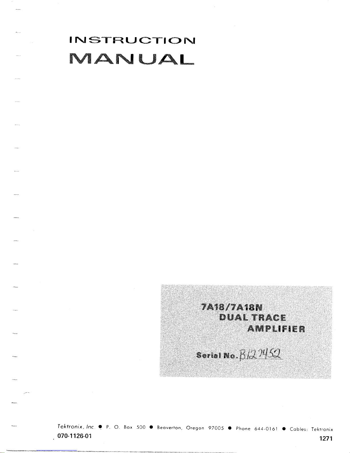
Tektronix,
Inc
P
.
.
0
O.Box
070-1126-01
500
"
Beaverton,
Oregon
97005
"
Phone
644-0161
"
Cables:Tektronix
1271
Page 2
i
1
tv
'Give
~!uestiori
`S
.ai,
Fil)NI'.
t=?
.
°~"Y::IO"=Y:'~'~rYd11W
91i
tiie
warran`"
'or
;ncimo
7
lta
:f
of!
nIns}
All
ferule`.:`
riirectetl
Num
<
.~rVI::'
117 --.,
In
L~~:acid
"eaverion,
America.All
n)ay
riotbereproduced
'9
ektronix,
L1..^
:
:nr
:mo
mreruia
;i)Nlr
ii!n
Y
I''=~:!~
cili0
LalrS
:<`l\!XF;~lc~
SerialNumhciwith
1-,-
wls
priceer
new
Oregon.Printedinthe
rights
reserved.Contents
in
Iric
.
forerurl
;)mL
:ms
. :
;ridiur
:
gis
;ereddemari<
rrpilCernerYt
;
prwile
material
any
form
oareYtts
pifi
:
-..
.
allrequests
1974,
United
of
without
oroducts
irendinrl
.
of
por
:
S
iolll
£n`
it'.:'..
'0
S5
for
parts
by
Tektronix,
States
this
publication
permission
covere."ibyI1 .,
iekironix,
or
of
of
; .
l -
IC,
Page 3
7A18/7A18N
SECTION
SECTION
SECTION
SECTION4
1
SPECIFICATION
Introduction
Electrical
7A18
And
Response
Environmental
Physical
2
OPERATING
Installation
Front
Panel
General
Basic
Applications
3
CIRCUIT
Introduction
Block
Diagram
Detailed
MAINTENANCE
Preventive
Troubleshooting
Replacement
Component
Characteristics
Mainframe Frequency
Characteristics
Characteristics
INSTRUCTIONS
Controls
Operating
and Connectors
Information
DESCRIPTION
Description
Circuit
Description
Maintenance
Parts
Replacement
Page
1-1
1-1
1-3
1-3
1-3
2-1
2-1
2-2
2-4
3-1
3-1
3-1
4-1
4-1
4-3
4-4
OPTION
SECTION
SECTION
SECTION8
CHANGE
INFORMATION
6
ELECTRICAL
Abbreviations
Parts
DIAGRAMS
7
ILLUSTRATIONS
Symbols
Voltage
MECHANICAL
Mechanical
Index
Mechanical
Accessories
INFORMATION
Ordering
and
and
Parts
of
Mechanical
Parts
PARTS
and
Symbols
Information
AND
CIRCUIT
Reference
Waveform
PAR'I'S
List
List
LIST
BOARD
Designators
Conditions
LIST
Information
Parts
Illustrations
SECTION
5
CALIBRATION
Recalibration
Test
Part
PartII--
Equipment
I-.-
Performance
Adjustment
Interval
Required
Check
5-1
5-1
5-3
5-7
REV.JUNE
Abbreviations
or
taken
directly
Symbols
the
for
electronics
locatedatthe
1974
and
symbols
from
Units",
MIL-STD-12B
industry.Change
rearofthis
used
IEEE
manual
in this
manual
Standard
and
260
other
are
standardsof.
information,ifany,
.
based on
"Standard
is
Page 4
7A18/7A18N
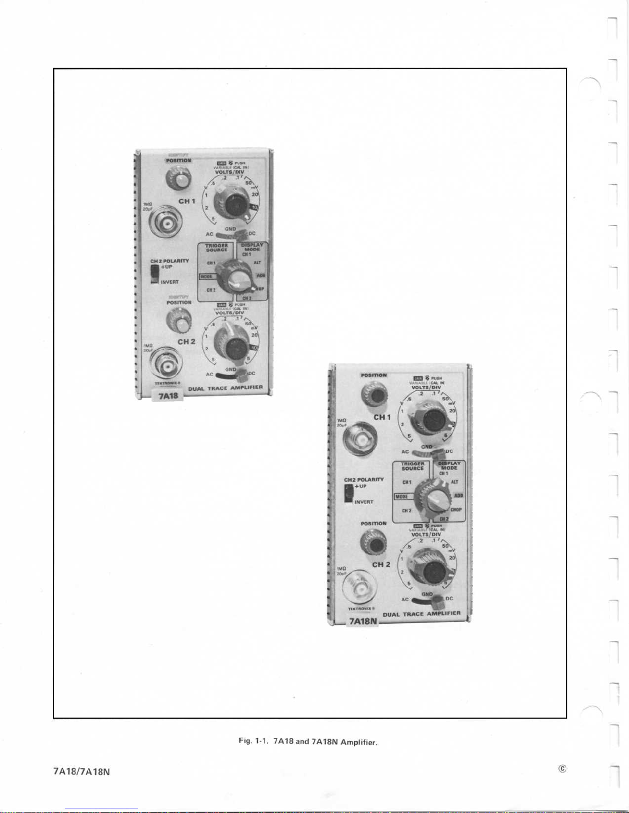
Fig.1-1
.
7A18
and
7A18N
Amplifier
.
Page 5
7A18/7A18N
Introduction
The
7A18
units
are
designed
Oscilloscopes
tical
"IDENTIFY"
references
unless
medium-bandwidth
tion
circuits
Deflection
.
except
made
otherwise noted.The
are
Characteristic
Factor
Change
and
7A18N
for use
The
7A18
that
readout
function
are
to the
7A18
amplifier.Internal
automatically
information,
Dual
with
and
7A18N
encoding
provided onlyinthe
apply
if
Trace
Tektronix
are
equally to the
7A18
switched
any,
Amplifier
capabilities
isadual-channel,
gain
affecting
7000-Series
electrically
7A18.All
and
compensa-
to
correspond
Performance
this
plug-in
iden-
and
7A18N
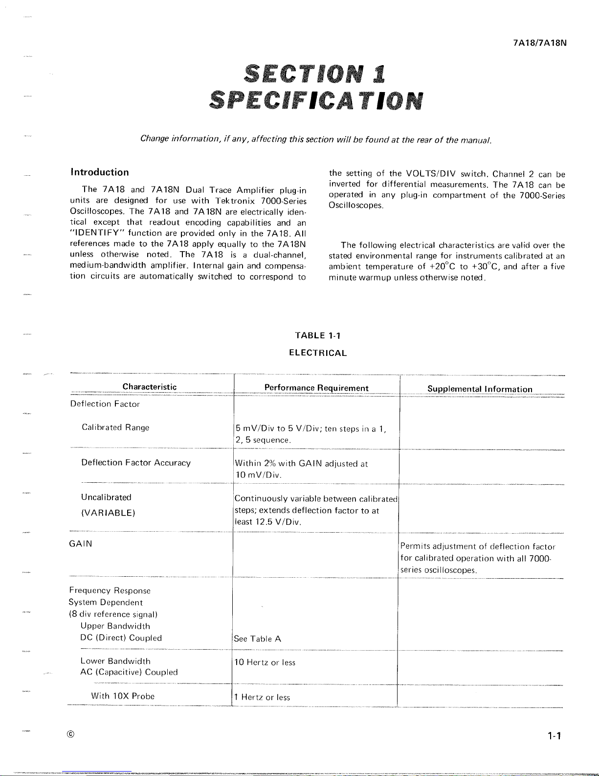
TABLE
ELECTRICAL
section
an
to
willbefound
the
setting
inverted
operated
Oscilloscopes
The
stated
ambient
minute
1-1
Requirement
at the
of the
for differential
in
any
.
following
environmental
temperature
warmup
unless
rearofthe
VOLTS/DIV
plug-in
electrical
range
of
+20°C
otherwise
manual
switch
measurements
compartment
characteristics
for
instruments
+30
to
noted,
.
.
Channel2can
.
The
7A18
of the
7000-Series
are
valid
calibratedatan
°C,and
afterafive
can
over the
be
be
Calibrated
Deflection
Uncalibrated
(VARIABLE)
GAIN
Frequency
System
(8
div
reference
Upper
DC
Lower
AC
With
Range
Factor
Response
Dependent
signal)
Bandwidth
(Direct)
(Capacitive)
Coupled
Bandwidth
10X
Probe
Accuracy
Coupled
5
mV/Div
2,5sequence
Within
2%
0.mV/Div
Continuously
steps
;
extends
least12.5
See
Table
10
Hertzorless
1
Hertz
or
to5V/Div;ten
.
with
GAIN
. .
._
._
. .
.__.._ .
variable
deflection
V/Div
.
A
less
steps
adjusted
between
factortoat
in a
1,
at
calibrated
Permits
for
calibrated
series
adjustment
operation
oscilloscopes
of deflection
with
.
all
factor
7000-
Page 6
Specification-7A18/7A18N
TABLE
1-1
(cont)
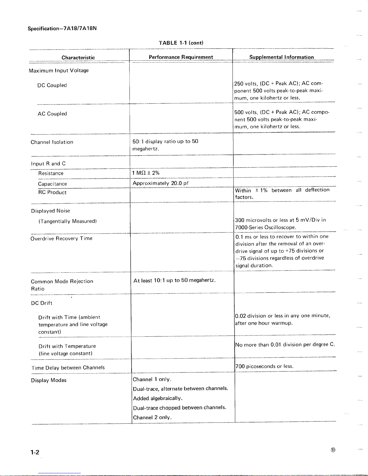
Maximum
Channel
Input
Displayed Noise
Overdrive
InputVoltage
DC
Coupled
AC
Coupled
Isolation
R
and
Resistance
Capacitance
RC
Product
(Tangentially
Recovery
Characteristic
C
m..
Measured)
Time
Performance
50:1display
megahertz
1
MQ±2%~
-
Approximately
ratioupto
.
20.0pf
Requirement
50
Supplemental,
volts,
250
ponent500
mum,
500
nent
mum,
Within
factors
300
7000-Series
0.1msorlesstorecover
division
drive
---75
signal
(DC+Peak
volts
one
kilohertzorless
volts,
(DC+Peak
500
volts
one
kilohertz
:,_
1%
.
microvoltsorlessat5
Oscilloscope
after
signalofup
divisions
duration
Information
peak-to-peak
peak-to-peak
or
between
removal
the
to
regardlessofoverdrive
.
AC);AC
AC);AC
less
+75
com-
maxi-
.
compo-
maxi-
.
all
deflection
mV/Div
.
to
within
of an over-
divisions
-"
in
one
or
Common
Drift
DC
Drift
temperature
constant)
Drift
(line
Time
Display
Mode
Rejection
with
Time
and
with
Temperature
voltage constant)
Delay
between
Modes
(ambient
line
voltage
Channels
At
least10:1
Channel
Dual-trace, alternate
Added
Dual-trace
Channel
1
algebraically
2
up
only
chopped
only
.
.
to50megahertz
between
.
between
.
channels
channels
or
less in
.01
anyone
.
division
.
0.02
division
hour
than
warmup
0
after
one
No
more
picosecondsorless
700
.
.
minute,
per
degreeC.
Page 7
Specification-7A18/7Al8N
Trigger
Cha,~~o,puo
source
With
Selection
7700
75
MHz
SeHes
TABLE
Performance
Channellonly
Follows
ENVIRONMENTAL
DISPLAY
7A18
FREOUENCY
:7-
.
TABLEA
AND
TABLE
1-1
(cont)
Requirement
MODE
MAINFRAME
RESPONSE
60
MHz
1-2
CHARACTERISTIC
selection
.
With
7400S=,ip
50
MHz
Refer
toWeSpecification
Size
Weight
for
the
associated oscilloscope
Fits
all
2
Pounds
.
TABLE
PHYD!CAL
7000-series
10
Ounces
1-3
plug-in
compartments
(1.4kilograms)
.
Page 8
7A18/7A18N
General
To
effectively
ties
of the
cribes
front-panel
signal
input
various
measurement
Installation
The
7A18iscalibrated
can
be
installedinany
Series
oscilloscopes,
vertical
and
fully
oscilloscope
at
against
plug-in
lower
rails
insertit.
the
bottom-left corner
the
front
OPERATING
Change
use
instrument
control functions,
connections,
compartments.To
of the
The
when
panel
information,ifany,
the
7A18,
must
and
applications
and
compartment
butisintended
7A18
with
front
willbeflush
the
7A18isfully
of the
.
the
operation
be
known.This section
general
other
subjects
.
ready
for
install,
the oscilloscope tracks
inserted,
7A18
SECTION
affecting
and
information
that
useasreceived.It
of
Tektronix
for
principal
align
with
the front of the
and
willbein
capabili-
pertain
7000-
use
the
upper
the
place
this
des-
and
latch
2
INSTRUCTIONS
section
on
to
in
willbefound
at the rear of the
manual
.
To
remove
inscribed
and
the
slide
the
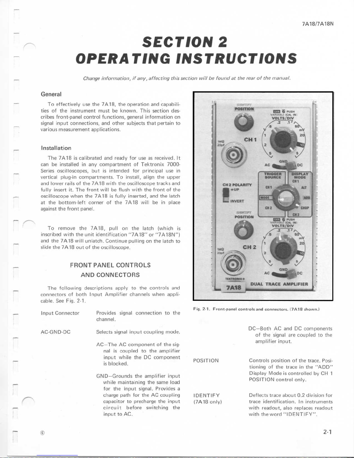
The
connectors
cable.See
Input
Connector
AC-GND-DC
with
will
7A18
7A18
FRONT
following
of
Fig.2-1
the
7A18,
the unit
out
identification
unlatch.Continue
of the oscilloscope
PANEL
AND
CONNECTORS
descriptions
both
Input Amplifier
.
Provides
channel
Selects
AC-The
naliscoupled
input
is
GND-Grounds
while
for the input
charge
capacitortoprecharge
circuit
input toAC.
pull
CONTROLS
apply
signal
.
signal
AC
while
blocked
maintaining
on
the
"7A18"
pullingonthe
.
to
channels
connection
input
component
the
.
the
signal.Provides
path
for
before
latch
(which
or
"7A18N")
latch
the
controls
when
appli-
to
coupling
to the
DC
amplifier
the
theACcoupling
switching
mode
of the
amplifier
component
input
same
the input
and
the
sig-
load
the
is
to
Fig
.
2-1.Front-panel
.
POSITION
a
IDENTIFY
(7A18
only)
controls
DC-Both
Controls
tioningofthe
Display
POSITION
Deflects
trace
with
with
and
connectors.(7A18shown
AC
and
of
the
signal
are
amplifier input
position of the
Modeiscontrolled
trace
identification.In
readout,
the
word
.
trace
control
about0.2
also
"IDENTIFY"
DC
components
coupled
trace.Posi-
in
the
.
only
division
instruments
replaces
.)
to the
"ADD"
by
CH
readout
.
1
for
Page 9
Operating
VOLTS/DIV
VARIABLE
(VOL1-S/DIV)
GAIN
DISPLAY
TRIGGER
Instructions-7A18/7A181\1
Adjustment
MODE
SOURCE
Selects
from
stepsina
Provides
calibrated
brated
factor
or
When
pushed
screw-driver
bration
Selects
of
CH
ALT---A
ADD-Algebraically
CHOP---A
CH
Selects
The
triggering
base
CH1-Internaltriggeringsignal
MODE--Internal
calibrated
5
mV/Div
1-2-5
continuously
steps.Extends
rangeto12.5volts/division
more
.
the
in,itbecomesafront-panel
of deflection factor
one
operation
1-A
single-trace
signal
appliedtoChannel1.
dual-trace
signal
appliedtoboth
- T -hechannels
played,
the
end
sweep
.
appliedtothe
input
algebraic
the
CRT.The
switch allows
CH1+
Positionofthe
play
modeiscontrolledbyCH
POSITION
signals
Thetwo
sweepasdeterminedbythe
dicator
2--A
single-trace
signal
appliedtoCH2.
sourceofthe
trigger signals
for the
units
.
obtained
CH1.
matically
MODE
deflection
to5V/Div;ten
sequence
settings
VARIABLE
adjustment
of
:
and
connectors,
sum
CH2or
dual-trace
appliedtoboth
channels
oscilloscope
from
selection.In
between
the
the
following
displayofthe
displayofthe
are
alternately
switching
of each
adds
CH1and
is
displayed
CH2POLARITY
the
displaytobe
CH1-
traceinthis
control
only
displayofthe
time-share
.
displayofthe
trigger
provide
oscilloscope
signal
trigger
follows
factors
.
variable
deflection
control
for
.
channels
occurs
time-base
the
and
.
channels
internal
applied
signal
DISPLAY
ADD
un
cali-
cali-
modes
dis-
at
signals
CH
the
on
CH2.
dis-
the
in-
signal
time-
to
auto-
or
is
.
2
1
.
.
CH
CH2POLARITY
GENERAL
Provides
+
INVERT--A
OPERATINGINFORMATION
Introduction
For
single-trace
amplifier
DISPLAY
1orCH2and
appropriate
operations
Signal
connectingasignaltothe
uator
circuit
conditions
ring,
series
coding
fier
on the
probe
units
Vertical
switchto10
oscilloscope
nel
four
exactly
is
ing
channels
MODE
input.In
usingCH1
Connections
In
general,
probe
under
.
The
Tektronix
was
designed
amplifier
ringonthe
unit
which
CRT
being
without
Gain
check
To
calibrator
being
checked.The
divisions.If
four
engagedbypressing
the
knob
operation,
canbeused
and
TRIGGER
connecting
the
only
probes
offersahigh
testtoperform
to
used.For
readout,
offer
P6053A
specifically
units
equipped with readout.The
probe
automatically
the
actual
see
Check
the
gain of
mV
and
connect40mV,1kHz
to
vertical
not,
divisions
with a
of deflection
in
narrow-blade
CHOP
display
signalisthe
1
andCH2
2---Internal
obtained
CH2.
meansofinverting
2
display
-UP--A
and
either
positive-going
CH
2
the
CRT
the
CH
flects
the
ward
.
eitherofthe
independentlybysetting
the
signaltobe
discussionstofollow,
apply
the
most
inputofthe
input
impedance
very
probe,
for
connectstoa
corrects
deflection
probes
the
Tektronix,
to be
Adjustment
channel,
the
input
deflection
adjust
the
the
GAIN
modes,
algebraic
trigger
from
signal
.
input
connector
display
positive-going
2
input
CRT
SOURCE
equallytoCH2only
convenient
7A18.A
closetonormal
with
its
use
with
circuitinthe
the
readout
factoratthe
used
Inc.catalog
set
connectorofthe
shouldbeexactly
front-panel
.
The
GAIN
control
screwdriver
the
trigger
sumofCH
.
trigger
upward
connector
display
switchestoCH
observedtothe
and
readout
Tektronix
with
the
signal
knob
signal
applied
the
signal
at
deflects
.
signal at
down-
two
identical
single-trace
.
means
10X
atten-
allows
operating
cod~ng
readout
amplidisplayed
tipofthe
amplifier
.
VOLTS/DIV
from
chan-
GAIN
adjustment
and
turn-
(see
Front
to
CH
the
de-
the
of
the
7A-
the
for
2-2
Page 10
Panel
Controls
and
then counterclockwise,
When
the
GAIN
control
will
changeasthe
knob
with
the
screwdriver
exactly
Input
switches
four
divisions,
Coupling
The
Channel1and Channel
allow
a
choiceofinput
typeofdisplay desired
the
couplingtouse
The
DC
DC
component
AC
signals
probe)
and
these
signals
In
theACcoupling
square
.
coupling
of
the
below
about
waves
are
attenuatedintheACposition
signalisblocked by
coupling
DC
precharge
use
probetothe
coupling
inputofthe
input
inputs
to
VOLTS/DIV
determined by
of
the
tion
switch
calibrated
settings
switch.With
wise
brated
volts/division.By
the
set
position
component
much
feature
this
feature,
first
circuit
capacitortocharge
The
GND
position
amplifier
connectors.However,
are
not grounded,
the
signal
source
and
The
amountofvertical
the
the
probe, the
settingofthe
factors
The
and
input
within the
indicated
apply
(CAL
VARIABLE
between
the
vertical
connector,
only
IN)
the
the
VARIABLE
VOLTS/DIV
deflection factor
rangeofthe
provides
should
.
signal
settingofthe
VARIABLE
when
applyingacalibrated
Connectors).Turn
until
the
GAIN
is
engaged,
knobisturned
until
then
remove
the
.
"Turn
the
the
2
coupling
screwdriver
coupling
and
the
applied
position
signal.It
must
must
30
hertz
with
low-frequency
position,
a
capacitorinthe
the
best
larger
than
be
used with
set
the
couplingtoGND.Connect
and
wait
about
.
Then
provides
without
the
and
the
VARIABLE
deflection
amplitude,
signal will
be
also
(ten
theDCcomponent
input
displayofsignals
theACcomponents.The
largeDCinputs.To
two
set
the
a
ground
externally
signals
same
DC
Controls
produced
the
VOLTS/DIV
control.Calibration
by the
position
control
settingsofthe
the
VARIABLE
.
provides
variable,
calibrated stepsofthe
any
control
set
specific
VARIABLE
fully
to5volts/div
is
extended
deflection factor
control
the
knob
clockwise,
controlisengaged
vertical
the
deflection
GAIN
control
deflectionisset
.
(AC-GND-DC)
methods
.
determine
used
to
display
be
usedtodisplay
hertz
with
a
components
.
of
circuit.The
with
seconds
for
couplingtoAC
referenceatthe
grounding
connectedtothe
loadispresented
by a
signal
attenuation
factor
switch,
deflec-
VOLTS/DIV
controlisin
uncalibrated
VOLTS/DIV
counterclock-
the
uncali-
to at
least12.5
voltage
source
can be
.
The
the
10X
the
AC
the
the
the
and
the
to
as
CH
.
displayed
to
Thisisparticularly
when
POLARITY
the
same
will
positive-going
on
move
DISPLAY
CH1inputortheCH2
switchtothe
signalisalso
desired
the
a
MODE
channel1and
Although
.
CHOP
rates
rates
ceptible
switch
signals,
signal,orfor
channeltooffset
other
is
mode
positionisthe
VOLTS/DIV
VOLTS/DIV
the
CRT
resultant
amplitudeofthe
the
channel1POSITION
Chop Mode.The
MODE
switched
hertz
mode
2
POLARITY
CH2POLARITY
The
waveform
differential
measurements
switch
+UP
position,
polarityasthe
move
the
CRT
waveform
the
CRT
in
inverted
the
trace
down
MODE
For
single-trace
operation,
corresponding
To
displayasignalinone
appliedtothe
channelbysetting
Operating
Switch
of
the
useful
has
two
the displayed
applied
trace
at
form
.
Switch
input
Instructions---7A18/7A18N
switch
may
signal
appliedtotheCH2
in
added
aretobe
positions,
signal
andapositiveDCvoltage
up.In
the
theCH2
and a
apply
and
position:CH1orCH2
channel independently
other
channel,
the
DISPLAY
appropriateCH1orCH2position
Alternate
Mode.The
switch
producesadisplay
ALT
position of
which
channel2with each
the
ALT
mode
can be
usedatall
mode
providesamore
below
about 0.2millisecond/division
alternate
mode
satisfactory
switching
.
Add
Mode.The
can
be
for
common-mode
channel).The
with
resultant
display.In
display
ADD
mode,
switch
between
rate
(controlled
provides
ADD
used to
DC
display
offset
the
DC
overall
both
VOLTS/DIV
deflection
switch
.
However,
switches
are settodifferent
amplitude
this
case,
can be
signal
appliedtoone
positioningofthe
control
CHOP
produces a
channels
by mainframe)
the
best
display
position
the
of the
sum
rejectiontoremoveanundesired
(applyingaDC
component
deflection
switches
factor
if
is
difficulttodetermine
the
voltage
determined
traceiscontrolledbythe
only
.
position of
display
at
approximately a
at
sweep
be
usedtoinvert
the
input
operationofthe
made.The
+UP
and
waveform
will
INVERT
input
willbedisplayed
positiveDCvoltage
the
signal
set
the
DISPLAY
7A18
CH
INVERT.In
have
the
position,
will
eithertothe
MODE
.
when
simply
select
the
MODE
switch to
.
the
DISPLAY
alternates
sweep
sweep
on the
rates,
between
CRT
the
displayatsweep
.
At
slow
sweep
becomes
visually per-
DISPLAY
MODE
or difference of
two
voltagetoone
of a
signalonthe
factorinthe
settothe
indicated
the
CH
deflection
1
by
and
from
ADD
same
either
CH
factors,
the
amplitudeofthe
accurately
onlyifthe
channelisknown.In
the
DISPLAY
whichiselectronically
500
kilo-
.
In
general
rates
the
slower
CHOP
than
.
2
a
a
.
2
REV.APR
1974
2-3
Page 11
Operating
about0.2
repetitive
Instructions--7A18/7A18N
millisecond/divisionorwhenever
phenomena
TRIGGER
CH1.
switch
The
providesatrigger
applied to the
displayofthe
CH
2.The
switch
providesatrigger
applied to the
display
switch,
on
source
as
MODE
the
for
follows
of the
.Inthis
the
setting
each
:
MODE
CH
1
CH
2
ADD
CHOP
ALT
is
to be
SOURCE
Switch
CH1positionofthe
signal
CH1input
signal
CH
connector.This
appliedtothe
2 positionofthe
signal
CH2input
signal
connector.This providesastable
applied to
position of the
trigger
signal
for the
of the
DISPLAY
position
of the
TRIGGER
Channel
Channel
Algebraic
Algebraic
Alternates
l
2
sumofchannel1and
sumofchannel1and
between
displayed
obtained
CH1input
obtained
the
CH2input
time-base
MODE
DISPLAY
SIGNAL
channel1and
dual-trace,
.
TRIGGER
from
providesastable
TRIGGER
from
TRIGGER
unitisdependent
switch.The
MODE
SOURCE
channel
channel
non-
SOURCE
the
signal
connector
SOURCE
signal
the
connector
SOURCE
trigger
switch
2
2
channel
2.Set the
switches
3.Set the
DISPLAY
to display
coupling
the
channel
switchtoAC
MODE
used
and
.
.
TRIGGER
SOURCE
NOTE
For
low-frequency
.
.
is
2
theDCpositiontoprevent
4.Set
divisions
5.Set the
play.Set
several
6.Turn
tionofthe
lines
waveform
Position
peaks
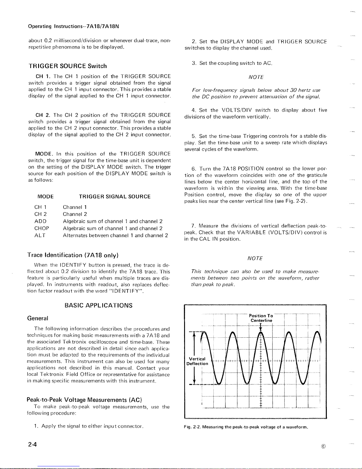
7.Measure
peak
in
the
the
of the
the
cycles of the
the
below
is
control,
lies
near the
.
Check
CAL
IN position
time-base
time-base
waveform
the center horizontal
within
the
that the
signals
VOLTS/DIV
waveform
switch to display
vertically
Triggering
unit toasweep
waveform
7A18
POSITION
coincides
the
viewing
move
the display so
center
vertical
divisionsofvertical
VARIABLE
.
belowabout
30
attenuationofthe
.
controls
forastable
rate
which
.
control so the
with
one
of the
line,
and
the top
area.With
the
one
line (see
Fig.2-2)
deflection
(VOLTS/DIV)
hertz
about
of
use
signal
displays
lower
graticule
of the
time-base
the
upper
.
peak-to-
control
.
five
dis-
por-
is
Trace
Identification
When
the
IDENTIFY
flected
about0.2
divisiontoidentify
featureisparticularly
played.In
tion
factor
instruments
readout
with
BASIC
General
The
following
techniques
the
associated
applications
tion
must
for
be
making
Tektronix
are
not
adapted
information
measurements.This
applications
local
Tektronix
in
making
Peak-to-Peak
To
following
1.Apply
specific
make
procedure
not
described
Field
measurements
Voltage
peak-to-peak
:
the
signal to
(7A18
only)
buttonispressed,
useful
when
multiple
with
readout,
the
word
"IDENTIFY"
APPLICATIONS
describes
basic
measurements
oscilloscope
describedindetail
to
the
requirements
instrument
Office or
can
in
this
manual.Contact
representative
alsobeused
with
Measurements
voltage
either
measurements,
input
the
the
7A18
also
replaces
the
procedures
witha7A18
and
time-base.-
since
of the
this
instrument
(AC)
connector
traceisde-
trace.This
traces
.
each
applica-
individual
for
for
assistance
use the
.
are
dis-
deflec-
and
and
These
many
your
.
This
technique
ments
between
than
peaktopeak
Fig.2-2.Measuring
can
two
.
the
peak-to-peak
NOTE
also
be usedtomake
points
on
voltageofa
the
waveform,
waveform
measure-
rather
.
2-4
Page 12
8.Multiply
VOLTS/DIV
of the
probeifused
EXAMPLE
flectionis4.5divisions
uator
probe,
Volts
PeaktoPeak
Substituting
The
peak-to-peak
Instantaneous
To
measure
proceed
as
1.Connect
the deflection
switch
:
Assume
and
the
-
deflection
(divisions)
the
given
Volts
Voltage
the
follows
the
setting.Include
.
VOLTS/DIV
vertical
values
Peak-to-Peak
voltageis45
DC
:
signal to
measured
that the
(see
Fig.2-2)
VOLTS/D
X
:
= 4.5X1X
volts
Measurements
levelata
given
either
the
peak
switch
setting
.
(DC)
input
in
attenuation
to
peak
using a
is
setto1
IV
point
connector
step7by
factor
vertical
10X
atten-
V
.
probe
X
attenuation
factor
10
onawaveform,
.
the
de-
7.Measure
reference
DC
measurement
8.Establish
POLARITY
the reference
9
VOLTS/DIV
probe,ifused
EXAMPLE
divisions
reference
of
0.5V
Using
Instan-
taneous
Voltage
line
and
levelistobemeasured
is
switchinthe
lineispositive
.
Multiply
setting.Include the
.
:
(see
line
usinga10X
.
the
formula
vertical
=
distanceXpolarity
(divisions)
Operating
the
distance
the
pointonthe
between
the
the distance
Assume
Fig.2-3)
the reference
polarity
the
:
Instructions---7A18/7A18N
in
divisions
waveform
.
For
example,
line
of
the
waveform.With
+UP
position,
.
measured
vertical
and
probe
the
with
in
attenuation
distance
waveform
a
VOLTS/DIV
VOLTS/
XDIVX
setting
between
at
which
in
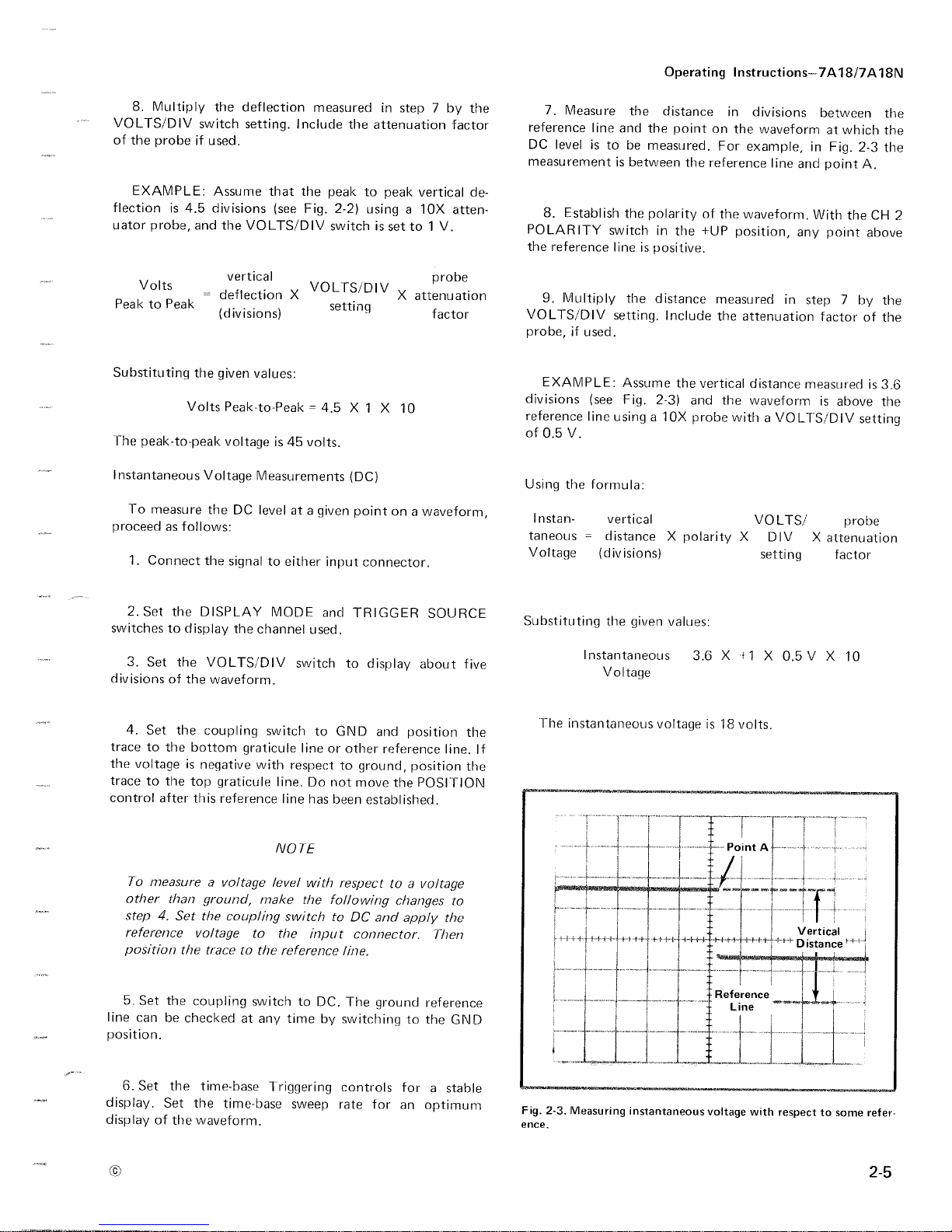
Fig.2-3
and
pointA.
the
any
point
step
7 by the
factor of the
measuredis3
is
above
probe
attenuation
factor
the
the
the
CH
above
the
setting
2
.6
2.Set the
switches
divisions
trace
the
trace to the
control
line
position
to display the
3
.
Set
4.Set the
to the
voltage
after
To
measure
other
step4.
reference
position the
5.Set
the
canbechecked
.
the
of the
is
top
than
Set
DISPLAY
VOLTS/DIV
waveform
coupling
bottom
negative
graticule
this
reference
a voltage
ground,
the
coupling
voltage
tracetothe
coupling
MODE
channel
switch
.
switch to
graticule
to
switch toDC.
at
with
level
make
any
line
respect to
line.Do
line
has
NO
TE
with
the
switch
the
reference
time
and
TRIGGER
used
.
to
display
GND
and
or other reference
ground,
not
move
been
established
respect toavoltage
following
to
DC
and
input
connector.Then
line
.
The
ground
by
switching
position
position
the
POSITION
changes
apply
to the
SOURCE
about
line.If
.
to
the
reference
GND
five
the
the
Substituting
Instantaneous
The
instantaneous
the given
Voltage
values
:
3
.6
voltageis18
X
f
volts
1X0.5V
.
X
10
6.Setthetime-base
display.Set the
displayofthe
waveform
time-base
.
T
riggering
sweep
controls for a
rate
for
an
stable
optimum
Fig.2-3
ence
.
.
Measuring
instantaneous
voltage
with
respect
to
some
refer-
2-5
Page 13
Operating
Comparison
In
arbitrary
by
comparing
use
facilitate
amplitude
of
accurateifarbitrary
so
number
describes
comparison
To
uponaspecific
Set the time-base
of the
2.Set the
control to
vertical
VARIABLE
3.To
the
accuratelyatany
amplitude
not
VOLTS/DIV
Instructions-7A18/7A18N
Measurements
some
applications
units
of
VOL-fS/DIV
the
unknown
for
the
comparison-measurement
calibration
does
not
deflection.The
that
the correct
of
divisions
how
to
measurements
establishanarbitrary
reference
1.Connect
signal
amplitude
known,
the reference
.
VOLTS/DIV
produce
divisions
control
establishanarbitrary
of an
of
the reference
it
can
controlissetinstep2.
it
may
be
desirabletoestablish
measurement
switch.Thisisparticularly
signalstoa
of
produce
adjustment
unitsofmeasurement
adjustment
of deflection.The
establish
unit
sweep
display
a
in
amplitude.Do
after
unknown
settingofthe
be
measured
other
equipment
an
arbitrary
.
vertical
amplitude,
signal
rate
switch
whichisan
obtaining
vertical
signal
than
reference
where
exact
number
will
be
is
indicated
following
unitsofmeasure
deflection
proceedasfollows
to the input
to display
and
the
deflection factor so
signal
VOLTS/DIV
must
before
those
useful
amplitude.One
technique
the
of
easier
and
are
established
by
procedure
factor
connector
several
VARIABLE
the
exact
number
not
change
desired
be
can
be
known.If
the
deflection
measured
switch,
VARIABLE
indicated
when
is
desired
divisions
more
an
exact
for
based
:
cycles
the
the
it is
Signal
Amplitude
to
.
of
.
EXAMPLE
volts,aVOLTS/DIV
control adjusted to
divisions.Substituting these values
conversion
Then
peak-to-peak
produces
determined
Dual-Trace
Phase
comparison
cluency
7A18.This
be
system
cedure
position,
used
1.Set
can
To make
.
:
VOLTS/DIV
settingX
=
:
Assume
factor
formula
Vertical_3_0V
Conversion-4X5
Factor
a
amplitude
vertical
using
VOLTS/DIV
with
a
by
Signal
Amplitude
Phase
between
be
made
method
to
up
the
depending
the
the
CH1and
on
a
reference
setting
provideavertical
(step4):
of an
deflection of
the
signal
-
2
VX1.5X
Difference
using
phase
of
frequency
comparison,
CH2coupling switches
the
type
vertical
conversion
factor
signal
of 5Vand
V=1
setting
unknown
five
amplitude
Measurements
two
signalsofthe
the
dual-trace
difference
limit
use the
coupling
of
deflection of four
in
.5
divisions
formula
5 =15
measurement
of the
X
deflection
(divisions)
amplitude
the
VARIABLE
the
of 2
signal
volts
feature of
oscilloscope
following
to the
desired
vertical
of
vertical
V,
which
can
(step6):
same
pro-
same
.
30
the
be
fre-
the
can
4.Divide
the
product
in
step2and
the
vertical
Vertical
Conversion
5.To
disconnect
signal to
toasetting
make
an
VARIABLE
6.Measure
calculate
following
2-
6
the
amplitude
vertical
of the
the
setting
conversion
Factor
measure
the reference
the
input
that
provides
accurate
control
the
the
amplitude
formula
.
of the reference
deflection
of the
VOLTS/DIV
factor
.
reference
=
the
connector.Set the
.
vertical
amplitude
verticalv~
deflection
(divisions)
amplitude
signal
measurement.Do
of
X
and
sufficient
deflection
the
unknown
(divisions)
signal
(_volts)
VOLTS/DIV
switch
setting
of an
connect
VOLTS/DIV
vertical
not
in
signal
established
switch
__
unknown
the
deflection to
readjust
divisions
signal
(volts)
by
.
This
signal,
unknown
switch
the
and
using the
is
2.Set the
general,
ALT
TRIGGER
the
or
connect
POLARITY
(Signals
difference;if
culation
controls of the
about
CHOP
is
more
SOURCE
3.Connect
comparison
probes
4.If
5.Set the
which
the
the
may
.)
five
divisionsinamplitude
signals
DISPLAY
is
suitable
the
signal to
signals
switch
be of
so,
VOLTS/DIV
two
MODE
more
suitable
for
1
to
CH
reference
theCH2
similar
have
the
input
to
areofopposite
to
invert
opposite
take
this into
channels
for
high
.
signal to
time
connectors
the
polarity
account
switches
so the
.
to
ALT
or
CHOP.In
low
frequencies
frequencies.Set the
the
CH1input
input.Use
delay
polarity,
displays
coaxial
characteristics
.
set
channel
due
to
in
the
and
the
are
the
2 display
180°phase
final
VARIABLE
equal
and
and
cables
to
CH
cal-
and
2
.
Page 14
6.Set the
about
controls
7.Center
POSITION
8.Adjust
one
cycle of the reference
horizontal
lines
of
graticule
45°/division)
degrees
time-base
one
cycle
forastable
the
controls
the
divisions
the
graticule
represents45° of
.
The
as45°
/division
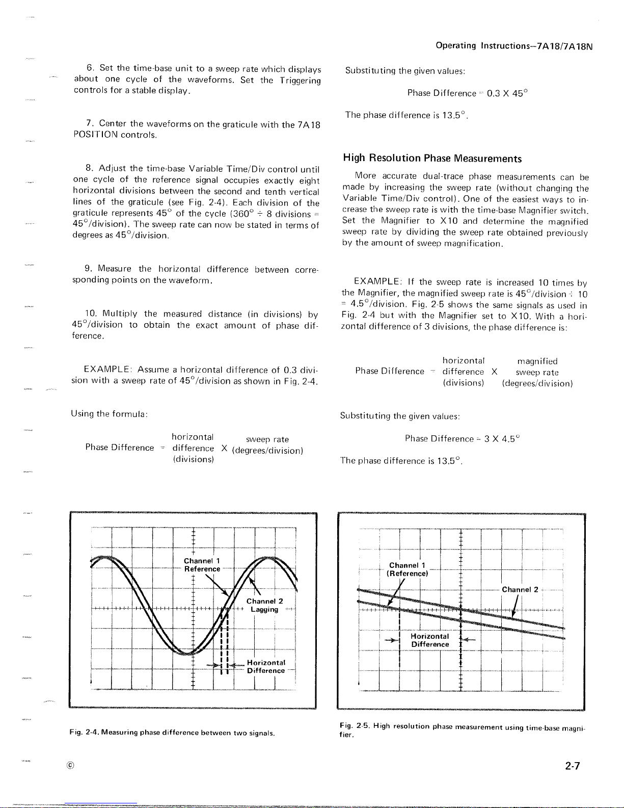
9.Measure
sponding
pointsonthe
10.Multiply
45°/division
ference
to
.
unit toasweep
of the
waveforms
display
waveforms.Set
.
on
.
time-base
Variable
signal
between
(see
the
Fig.2-4)
the
sweep
rate
can
.
the
horizontal difference
waveform
the
measured
obtain
the
exact
the
graticule
Time/Div
occupies
second and
.
cycle
(360°-8
now
.
distance
amount
rate
which
the Triggering
with
control
exactly
tenth
Each
division
be
statedinterms
between
(in
divisions)
of
displays
the
7A18
until
eight
vertical
of the
divisions
corre-
phase
of
by
dif-
Substituting the given values
The
phase
HighResolution
More
made
Variable
crease
=
Set
the
sweep
by
the
EXAMPLE
the
Magnifier,
=4.5
°
Fig.2-4
zontal difference of 3
Operating
Phase
Difference-0.3X 45
differenceis13
Phase
accurate
by
increasing
Time/Div
the
sweep
Magnifier
dual-trace
the
control).One
rateiswith
to
X10
ratebydividing the
amount
of
sweep
:Ifthe
the
magnified
sweep
/division.Fig.2-5
but
with
the
Magnifier
divisions,
Instructions--7A18/7A181\1
:
.5 °
.
Measurements
phase
measurements
sweep
rate
(without
of the
easiest
the
time-base Magnifier
and
determine
sweep
rate
obtained
magnification
.
rateisincreased10times
sweep
rateis45°/division
shows
the
same
signalsasused
settoX10.Withahori-
the
phase
differenceis:
°
the
can
changing
ways
switch
magnified
previously
be
the
to
in-
.
by
-
10
in
EXAMPLE
sion
withasweep
Using
Phase
the
formula
Difference
:
Assume
a horizontal
rateof45°/division
:
horizontal
= difference
(divisions)
difference of 0.3divi-
as
shown
in
Fig.2-4
sweep
X
(degrees/division)
rate
.
Phase
Substituting
The
phase
Difference
the
given
Phase
- difference
values
Difference
differenceis13
horizontal
(divisions)
:
= 3X4
.5 °
.
magnified
X
sweep
rate
(degrees/division)
.5"
Fig.2-4.Measuring
phase
difference
betweentwo
signals
.
Fig.2-5.High
fier
.
resolution
phase
measurement
using
time-base
magni-
2-
7
Page 15
Operating
Instructions--7A18/7A18N
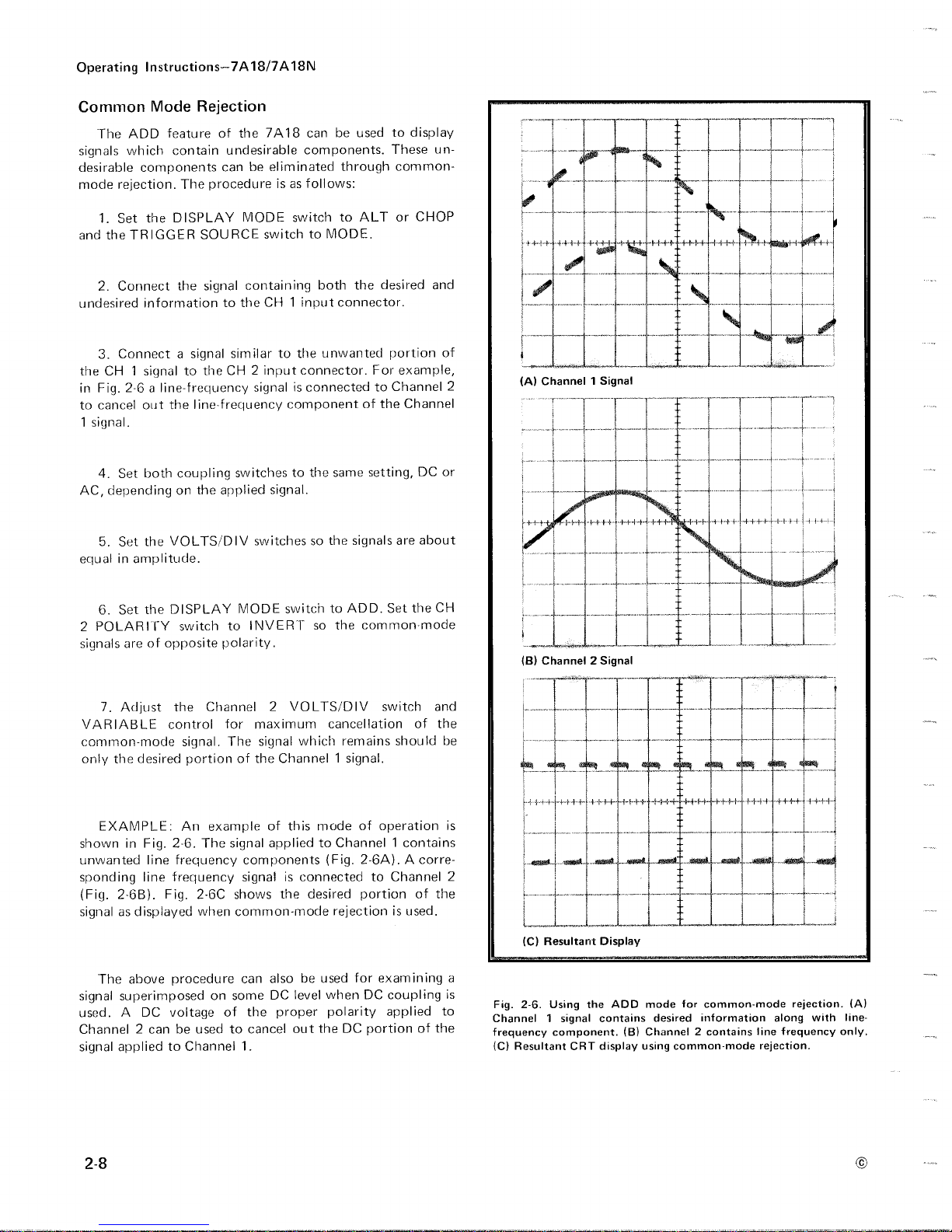
Common
T-he
signals
desirable
mode
1.Set
and
2.Connect
undesired
3
the
in
Fig.2-6aline-frequency
cancel
to
signal
1
4.Set
AC,
5.Set the
Mode
ADD
feature of the
which
contain
components
rejection.The
the
DISPLAY
the
TRIGGER
the
informationtothe
Connectasignal
.
CH1signal
out
to theCH2
the
.
both
coupling switches
depending
on
VOLTS/DIV
line-frequency
equalinamplitude
Rejection
7A18
undesirable
canbeeliminated
procedureisas
MODE
SOURCE
signal
switch
containing
CH
similartothe
input
signalisconnected
the applied
switches
.
be
can
components.These
follows
switch to
MODE
to
both
1
input
connector
unwanted
connector.For
component
to the
same
signal
.
the
so
usedtodisplay
through
common-
:
ALT
or
.
the
desired
.
portion
example,
to
Channel
of the
Channel
setting,DCor
signals
are
un-
CHOP
and
of
2
about
6.Set the
2
POLARI
signals
7
.
Adjust the
VARIABLE
common-mode
only
the
EXAMPLE
shown
unwanted
sponding
Y
I -
opposite
are of
desired
in
Fig.2-6.The
line
line
DISPLAY
switch to
Channel
control for
signal.The
portion
:
An
frequency
frequency
(Fig.2-6B).Fig.2-6C
signal as
signal
used.A
displayed
The
above
superimposed
DC
when
procedure
voltage
Channel2canbeused
signal
appliedtoChannel
MODE
INVERT-so the
polarity
.
2
maximum
signal
of the
example
signal
of
applied to
components
signalisconnected
shows
common-mode
can
alsobeused
on
some
DC
of
the
proper
to cancel
1
.
switchtoADD.Set the
common-mode
VOLTS/DIV
switch
cancellation
which
Channel
this
mode
remains
1
signal
of
operation
should
.
Channel1contains
(Fig.2-6A).A
to
Channel
the
desired
level
out
portion
rejection
when
polarity
for
DC
is
examining
coupling
applied
theDCportion
of the
corre-
of the
used
of the
CH
and
.
Channel2Signal
(B)
be
is
2
(C)
Resultant
Display
a
is
to
Fig.2-6.Using
Channel1signal
frequency
(C)
Resultant
the
ADD
contains
component.(B)
CRT
display
mode
for
desired
Channel2contains
using
common-mode
information
common-mode
along
line
frequency
rejection
rejection.(A)
with
line-
only
.
.
Page 16
7A18/7A18N
Change
Introduction
This sectionofthe
circuitry
tion
block
circuitisdescribed
the
and
vidual stages
Diagrams
following
relationship
usedinthe
begins
with
diagram
interconnections
the
relationship
.
Complete
schematics
section.Refer
circuit
.
7A18
a discussion of the
shown
in
between
of the front-panel
description
BLOCK
The
following
standing
dual
connections
the
represents a
numberon
complete
input
coupling
to the
correct
the
setting,
Channel2Input Amplifier
in
positioning.The
pull
as
the
circuits
block
circuit
The
signal
connector.The
switch,
attenuators.The
amount
input
amplifier
The
Channel
variable gain
additiontogain
to the
Signal
The
Channel
determined
discussionisprovided
overall
conceptofthe
are discussedindetail.Only
between
diagram
each
to be
major
block
is
found
where
of
.
1
outputs
and
Switches
by
(see
circuit
displayed
attenuation
Input
control,
setting,
Trigger
the
information,ifany,
manual
in
detail
contains
dual-trace amplifier.The
the
Diagrams
using
stagesineach
of
each
to these
for
a
instrument
section.Then,
block
controls to the
circuit
schematics
electrical
DIAGRAM
7A18
the
individual
Diagrams
refers to
.
signal
the
appropriate
VOLTS/DIV
Amplifier
provides
variable gain
of these
Channel
select
DISPLAY
within
on
blocks
section).Each
the
the
schematiconwhich
the
CRT
passes
and
the
through
couplingisselected,
and
the
circuit
trace
signal
circuits
Switches
proper
MODE
affecting
descriptionofthe
descrip-
using the
diagrams
are
to
before
instrument.The
is
switch
signalispassed
positioning.The
polarity
control,
are
signal
and
to
major
circuit
giveninthe
throughout
values
aidinunder-
the
indivi-
the
basic
are
shown
block
applied to the
the input
selects
provides
inversion
and
applied push-
.
and
trigger
TRIGGER
show
inter-
trace
this
each
indi-
the
and
on
the
the
to
gain
section
willbefoundatthe
SOURCE
provided
The
readout
suppliedtothe
polarity,
the
plug-in
traceisdeflected
factor
General
The
and
The
To
detail
AC-GND-DC
Input
AC-coupled,
S100A
showing
this
position
switchisin
directly
the
acitor
passingtothe
path
ground.This
to
disconnect
Resistor
allows
trace
if
the
rearofthis
switches.The
to the oscilloscope
Readout
logic
deflection
VARIABLE
mode.When
readoutisreplacedbythe
DETAILED
Encoding
for the oscilloscope
mainframe
factor,
controlisin
the
about0.3
CIRCUIT
ATTENUATOR
the
CH1and
minimize
Attenuator
7A18
throughout
circuit
deflection factor
CH2Attenuator
duplication,
this
Switch
signals
connected
DC-coupled,
isacam-type
the
operationisgivenonDiagram
chart
input
prevents
and
C10
remains
applied
indicate
shown
to the
signal
connects
R102,
when
(open
the
DC
Input
passes
the
amplifier.The
the input
provides
the
applied
connected
to be
precharged
on
screen
signal
has a high
or
position,
Attenuator
DC
a
signal
via
circuit
readout
the
the
IDENTIFY
division
determines
.
TE
NO
only
discussion
to the input
or
switch;a
the
associated
closed).When
the input
through
component
GND
circuit
ground
signal
across the
in
when
switchingtothe
DC
manual
.
and
trigger
the
Interface
(7A18
readout
system
uncalibrated
outward
word
position),
buttonispressed,
and
"IDENTIFY"
DESCRIPTION
the
circuits
CH
1 is
.
connector
internally
contact-closure
contacts
the
signaliscoupled
stage.In
capacitor
of the
position
of
the
reference
from
the
level
without
the input
AC-GND-DC
GND
.
outputs
Connector
only) provides
system.Data
identifying
symbol
the deflection
input
are
described
disconnected
1.The
the
C10
opens
position so the
and
.
coupling
identical
can
dots
areinthe
AC-GND-DC
AC
position,
.
This
signal
the
amplifier
the
connector
switch,
AC
position
(when
in
chart
from
signal
need
are
.
is
the
the
the
.
be
.
on
cap-
to
.
Page 17
Circuit
factor to
attenuators
are
and
vide correct input
signal
ferential
diagram
this
stage.R210
the
or
Description--7A18/7A18N
Input
Attenuator
The
effective
determined
S100B.The
sionofCRT
the
hybrid
capacitors.Each
S100B
closure chart
contacts
5
signalisconnected
uators
produce
These
dividers.For
are
is
reactance
frequencies
higher frequencies, the
and
frequencies
input
RC
of
adjustable
high
General
Input
impedance
Dual-diode
isacam-type
areinthe position
mV/Div
For
switch
are
the deflection factor
attenuators
primarily
determined
the
attenuator
In
addition
attenuators
characteristics
the
VOLTS/DIV
frequencies
The
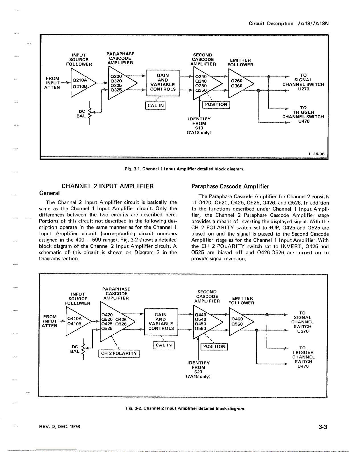
Channel1Input Amplifier
applied to the
(push-pull)
of the
circuitisshown
Source
The
Input
voltage
negative)15volts.Q210B
overall
by
the
basic
deflection
deflection.To
values indicatedonthe front
are
switched
devices
(see
Diagram
position,
directly
positions
switched
and
DC
resistance
by
the
of the capacitorsinthe
that
their
to
within
are
(one
series
capacitortoprovide
andanadjustable
capacitance
INPUT
Channel1Input Amplifier.A
Follower
Source
withalow
limits
the
CR210
swing
at
deflection
setting
factorisfive
into
which
contain
attenuatorisreplaceableasa
switch
1)
shown
input
attenuationisnot
to the input amplifier
above
into
the
are
frequency-compensated
low-frequency
dividers
resistance
effectisnegligible.However,
reactance
becomes
providing
the
output.Fig.3-1
provides
the
primarilyacapacitance
bandwidth
designedtomaintain
megohm
switch.Each
CHANNEL
AMPLIFIER
Channel1input
on
Diagram2in
Follower
impedance
current
circuit
gateof0210A
factor of
of the
increase
the
and
constant
.
VOLTS/DIV
millivolts
the
basic
panel,
circuit.These
the necessary
the
dots
on
indicate
circuit
indicatedonthe front panel
0210A
drivetothe gate of
providesaconstant
when
(openorclosed).In
five
millivolts,
singlyorin
signals,
and
the voltage
ratiointhe
circuitisso
of the capacitors
attenuation
of the
X
20
attenuator
shunt
1
converts
drive
instrument,
pF)
for
correct
capacitor to
the
connector
showsadetailed
the
Diagrams
providesahigh
for the
protection
to
about±(positive
the
7A18
per
deflection
precision
attenuators
resistances
the
contact-
the
associated
used;the
.
the
pairs
the
attenuators
attenuation
circuit.The
highatlow
decreases
divider
the
same
each
contains
attenuation
single-ended
toadif-
schematic
section
following
Q210A
by
limiting
switch,
divi-
unit
the
input
atten-
voltage
at
the
input
setting
pro-
block
input
current
to
at
all
an
at
of
source
the
same
is
circuit
Paraphase
Paraphase
0225-0325,
the single-ended
Diodes
.
0220
±0.6volt.Common-base
isolation
VARIABLE
Amplifierissetinthis
R237A
IN
switchisin
turned
gain
.
Adjustment1R321
the
same
This
position
Second
.
.
.
The
gainofapproximately
TION
circuitry.The
0250-0350
the
Position of
POSITION
drivetoQ250-0350
impedance
change
from
voltage
of the
inserting
junction
the
emitter
This
traces
The
vides
work
stage
Emitter
Emitter
put
Switches,
between
for
0210A.0210A
case so that
.
Cascode
amplifier
formsacascode
CR220-CR221
closetoground
between
controls.The
with
the
fully
counterclockwise
of the
amplifierisreduced
voltage
preventsazero-volt
when
Cascode
Second
control and,inthe
provide
POSITION
the
control,
pointinthe
at
these
the
POSITION
differenceatthe
.
trace
resistor
of
R11-R256.This
current of
in
aids
.
impedance
identifying
are
displayed
network
high
frequency
provide
high-frequency
Follower
Follower
U270-U470.This
the
Second
Amplifier
input
the
CAL
the
outward
varies
levels at
varying
Amplifier
Cascode
emitters of
a
control
traceisdetermined
R11.This
.
points.However,
Trace
R357
.
C246-C345-C245-R246-R345-R245
compensation.R245-C245
stage
to
drive
Cascode
and
Q210B
0210B
low-impedance
Since
temperature-compensates
Q220-0320,
amplifier.022..0-0320
signaltoa
hold
the
voltage
to
limit
connected
paraphase
gain
stagebyfront-panel
IN
switch
(uncalibrated)
to
the base
the
collectorsofQ225
reference
the
GAIN
Amplifier
two.This
7A18
and
IDEN-TIFY
control
the
circuit,
control
collectorstochange
identificationisaccomplished
from
ground
results
Q250
to
the
channel1trace
response
Q260-0360
the
Signal
stage
Amplifier
are
encapsulated
in
conjunction
differential
the
voltage
amplifier
of the
pressedin.
minimum
byafactorofat
levelof0320
trace
or
VARIABLE
stage
stage
only,
common-base
point
by
emitters
thereisnegligible
the
produces
through
in a
cause
and
also
output
levelatthe base of
swingtoabout
0225-0325
and
the
Channel
GAIN
When
position
resistance,
from
providesasignal
includes
trace
IDENTIFY
for
injection
switch
the
setting
changes
the
adjustment
providesalow
and
the current
areavery
change
resultant
a
the position
CR357
slight
tracetomove
when
Trigger
provides
U270-U470
increase
to
and
the
connected
in
in
the
with
convert
signal
provide
GAIN-
1
Input
control
the
CAL
and
the
least2.5
provide
0325
changing
controls
POSI-
of
currents
of the
lowvoltage
current
DC
by
to the
multiple
pro-
this
net-
for
this
out-
Channel
isolation
.
in
.
.
.
.
.
in
.
Page 18
Circuit
Description-7A18/7A181\1
2
PARAPHASE
AMPLIFIER
INPUT
INPUT
SOURCE
FOLLOWER
CHANNEL
General
The
Channel
same
as
the
differences
Portionsofthis
cription
Input
operateinthe
Amplifier
assignedinthe
2 Input
Channel1Input Amplifier
between
circuit
circuit
400--599
block diagram of the Channel 2
schematicofthis
Diagrams
section
.
Amplifier
the
two
not
describedinthe
same
(corresponding
range).Fig.3-2
circuitisshown
CASCODE
Fig
.
3-1.Channel1Input
AMPLIFIER
circuitisbasically
circuit.Only
circuits
mannerasfor the
Input
are
described
following
circuit
showsadetailed
Amplifier
on
Diagram3in
here
Channel
numbers
circuit.A
the
the
des-
1
the
Amplifier
.
detailed
Paraphase
The
Paraphase
of
Q420,
to
the
functions described
fier,
the
block
Cascode
0520,
Channel 2
providesameansofinverting
CH2POLARITY
biasedonand
Amplifier
the
0525
provide
CH
are
stageasfor
2
POLARITY
biased
signal
inversion
EMITTER
FOLLOWER
L,
.~ .
.
CHANNEL
diagram
.
Amplifier
Cascode
Q425,
switch
the
signalispassedtothe
off
Amplifier
0525,
under
Paraphase
for
Q426,
and
Channel1Input
Cascode
Channel2consists
Q526
the displayed
setto+UP,
Q425
the Channel1InputAmplifier.With
switch
and
settoINVERT,
Q426-0526
are turned
.
TO
TRIGGER
SWITCH
U470
1126-08
.Inaddition
Amplifier
signal.With
and
0525
Second
Q425
Ampli-
stage
the
are
Cascode
and
on
to
PARAPHASE
INPUT
SOURCE
FOLLOWER
FROM
INPUT
ATTEN
REV.D,
Q41
0410B
DC
BAL
DEC.1976
OA
CASCODE
AMPLIFIER
0420
0520
Q426
0425
0526
0525
CH2POLARITY
GAIN
AND
VARIABLE
CONTROLS
AL
IN
Fig.3-2.Channel2Input
-I
IDENTIFY
FROM
(7A18
Amplifier
SECOND
CASCODE
AMPLIFIER
0440
0540 0460
0450
0550
w
S23
only)
detailed
block
EMITTER
FOLLOWER
0560
diagram
TO
SIGNAL
CHANNEL
SWITCH
U270
TO
TRIGGER
CHANNEL
SWITCH
U470
.
3-3
Page 19

Circuit
Description-
7A18OA18N
Second
0440,
by
as
PLAY
applied to the
1932.The
emitters of
impedance
change
from
voltage
of the
ADD
tors
to
volts
Since
the
control
Cascode
The
Second
0540,Q450,
the
POSITION
determinedby
MODE
switch position
center
POSITION
Q450-0550.Since
pointinthe
at these
the
POSITION
differenceatthe
trace.When
position,
19455-19555
the
emitters of
(approximately)
+50
voltsisnot applied to the
ADD
position of the
setting
Cascode
points.However,
+50
through
hasnoeffectonthe
CHANNEL
General
The
Channel
outputs
to the
determined by
SOURCE
Diagram4in
Signal
circuit
The
Channel
Signal
U270
one,ormixes
from
the
Switch
stage
vides the
DISPLAY
19376-19377
Switches
oscilloscope
the
switches.A
the
Diagrams
Switch
Channel
and
its
two
DISPLAY
determines
signal
to the oscilloscope
MODE
set
the
C274-19274-C275-19275
vide
high-frequency
and
C375
in
these
sation
adjustments
Fig.3-3
position of
pin 14isLO
at
pin 4.With
LO,
passed
only
this
operating
of
channel1and
determines
the
when
the
signals
to the
the
the
shows
DISPLAY
the
outputofU270isdetermined
the
from
Signal
DISPLAY
mode
channel2signals
mainframe
Amplifier
and
control,
the
DISPLAY
Amplifier
0550.Position of
for
R21orby
MODE
other
arm
of the
POSITION
control
varies
the
the emitters areavery low-
circuit,
control
thereisnegligible
produces
collectorstochange
the
DISPLAY
MODE
voltsisappliedtothe
R32
to
balance
0450-0550.This
difference
between
DISPLAY
circuit
SWITCHES
circuit
provides
via
the
DISPLAY
schematic
Switch
external
input
analog
MODE
which
switch
setting
current
and
compensation
networks
section
MODE
of
.
stage
components.This
signalsinresponse
switch.The
input
.
Resistors
gain
for
each
C374-19374-C375-19375
for
are
high-frequency
.
the
U270
input
combinations
MODE
switch.When
levelatpin14HI
both
channel1and
Output
the
MODE
signal
stage.This
switchissettoADD.In
outputisthe
and
deflection
.
Channel2consists
the
traceisset
network
switch.In
than
current
ADD,
control
19455-8555
any
DIS-
I-50
volts
through
drive
to the
voltage
the
change
a
resultant
the
in
current
position
switchisin
junctionofresis-
the
results
in a
POSITION
MODE
operation
Signal
Interface
and
this
circuitisgiven
current
the
Connector
drive
fixed
collectors
control
switch,
.
and
Trigger
TRIGGER
zero
consistsofintegrated
stage
selects
to inputs
Signal
Channel
(CH1or
as
CH
controlled
2)
pro-
by
19276-19277
channel.Networks
pro-
each
channel.C275
compen-
for
each
the
level
by
the
level
and
the
levelatpin 4
channel2are
condition
the
resultant
algebraic
occurs
sum
signal
DC
the
the
the
and
of
is
SELECTED
CH
1
ALT
---~
CHOP
*Levelisswitched
mate0.5
**Levelisswitched
determinedbythe
Fig.3-3.U270
megahertz
input
between
settingofthe
rate
.
between
combinations
the
HI-level
the
HI-level
time-base
for
and
unit
DISPLAY
LO-levelatan
and
LO-levelata
sweep
rate
MODE
approxi-
.
selection
rate
.
.
in
-
Trigger
Signal
(CH1or
triggering
signaliscontrolledbyinputs
switch.Resistors
rentgain
as
C474-19474-C475-19475
vide
Channel
The
Trigger
Channel
CH
of the
high-frequency
Switching
Channel
Switch
Switch.This
2)
provides
time-base
19476-19477
for
each
and
compensation
U470
is
stage
determines
the
trigger
unit.The
from
and
signal
selection
the
TRIGGERSOURCE
19576-19577
channel
C574-19574-C575-19575
for
each
channel
identical
which
for
of the
set
.
Networks
to the
input
internal
trigger
the
cur-
pro-
.
on
An
input/output
When
the
levelatpin
determinedby
and
the
levelatpin4LO,
triggers
Signal
Output
-
The
are
and
Signal
stage,
added
Trigger
ofapairofcommon-base
vide the
circuits
at
General
mines
the
by
This
mainframe
mation
The
Signal
the
circuit
DC
.
Display
which
DISPLAY
for
level
input
andT-
also
chop
proper
table
the
levelatpin4.
algebraically
Output
Output
0480-0580,
shifting
DISPLAY
TRIGGER
Mode
signal
rigger
MODE
provides
blanking
CRT
for
this
stageisshown
14isLO,
With
the
channel1and
.
stage,
Q280-0380,
are
similar.Each
connected
necessarytodrive
MODE
SWITCHING
and
Trigger
(Channel1or
outputs
and
plug-in
circuit,
display
to the
TRIGGER
mode
and
.
the
output
the
level
at pin14HI
and
the Trigger
stage
transistors
the
AND
Switching
circuit
Channel2)provides
mainframe
SOURCE
information
readout
control
in
Fig.3-4
of
U470
channel
consists
which
mainframe
deter-
as
selected
switches
to
infor-
.
is
2
pro-
.
the
Page 20
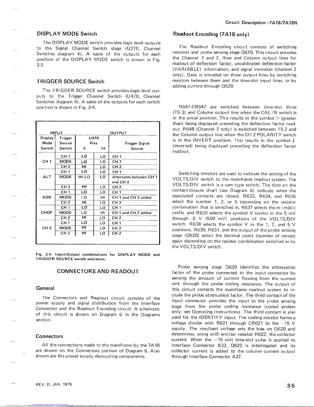
Circuit
Description-7A18/7A18N
DISPLAY
The
to the
Switches
position of the
3-3
.
"
TRIGGER
The
puts
Switches
positionisshown
Fig.3-4.Input/Outpu
TRIGGER
MODE
DISPLAY
Signal
diagram
SOURCE
TRIGGER
to
the Trigger
diagram4).Atable
SOURCE
CONNECTORS
General
The
Connectors
power
Connector
of this
section
supply
.
and
and
the
circuitisshown
Connectors
All
the
connections
are
shown
on
the
shown
are
the
power
Switch
MODE
Channel
4).A
DISPLAY
SOURCE
in
Fig.3-4
t
switch
and
signal
Readout
Connectors
supply
switch provides
Switch
table
MODE
Switch
switch
Channel
of the
.
combinations
selections
AND
Readout
distribution
Encoding
on
Diagram
made
to
decoupling
stage
of
the
switchisshown
provides
Switch (U470,
outputs
for
DISPLAY
.
READOUT
circuit
from
circuit.A
6inthe
the
mainframe
portion
of
components
logic
level
(U270,
outputs
logic
for
each
MODE
consists
the
schematic
by
Diagram6.
outputs
Channel
for
each
in
level
out-
Channel
switch
of the
Interface
Diagrams
the
7A18
Also
.
Fig
and
Readout
1 -heReadout
resistors
the
.
Channel
readout
(VARIABLE)
only).Dataisencoded
resistors
adding
current
R647-CR647
(TS-3)
and
in
the
uncal
than)
being
out.R648
the
Column
is in
the
(inverted)
readout
VOLTS/DIV
VOLTS/DIV
contact-closure chart
associated
select
combination
prefix
through
switch.R638
positions.R630,
stage
again
the
factor
sensing
sink
this
clude
input
stage
only
used
voltage
supply.The
determines,
current.When
Interface
collector
through
.
Switching
the
and
(Q620)
depending
VOLTS/DIV
Probe
of the
through
circuit
the
connector
from
;
see
for
divider
Encoding
Encoding
and
probe
sensing
1
and2,Row
of deflection
information,
between
INVERT
.5
sensing
the
probe
Operating
the
Connector
currentisadded
Interface
them
through
are
Column
position.This
displayed
(Channel
output
position.-
being
displayed
resistors
switch
switchisa
contacts
number
that
is
R639
selects
V
(500
selects
R631,
select
on
switch
stage
probe
amount
the
probe
corrects the
attenuation
provides
the
probe
IDENTIFY
with
resultant
along
with
the
Connector
output
line
1,2,or 5
switchedin.
the
Instructions).The
-15
(7A18
factor,
switched
preceding
2 only)isswitched
are
to the
(see
are
mV)
the
the
connected
of
R621
voltage
B33,
only)
circuit
stage
Q620.This
and
Column
uncalibrated
and
signal
on
these
output
and
the
time-slot
0620
.
between
line
when
resultsinthe
the deflection factor
when
theCH2
This
resultsinthe
preceding
usedtoindicate
mainframe
cam-type
closed.R633,
the
symbol
and
decimal
resistor
.
Q620
current flowing
coding
mainframe
the
coding
input.The coding
through
emitter
volt
switch.The
Diagram
depending
R637
symbol
positions of the
V
the
output
point
combination
identifies
to the
resistance.The
factor
.
The
input
resistance
CR621
sets
the
resistor
time-slot
Q620
is
to
the
column
A37
.
consists
the
the
6)
V
in
readout
to the
third
interrogated
of
circuit
output
deflection factor
inversion
linesbyswitching
between
POLARITY
readout
indicate
selects
(volts)inthe5mV
the1,2,
of the
(number
input
third
biasonQ620
R622,
pulseisapplied
(channel
input
lines,orby
time-slot
CAL
IN switch
symbol>(greater
symbol
deflection
the
setting
system.I-he
dotsonthe
when
R634,
and
on
the
them(milli-)
VOLTS/DIV
probe
of
switchedinby
the
attenuation
connector
from
the
output
system
contact
probe
(coded
contact
resistor
to the
the
current
switching
encodes
lines
for
three
read-
TS-2
and
switch
factor
of the
the
R635
resistor
and5V
sensing
zeroes)
by
current
of
to
in-
of the
sensing
probes
is
also
forms
--15
and
collector
to
and
its
output
2
is
I
a
V
REV.D,
JAN.1975
3-
5
Page 21
Circuit
Description-7A18/7A18N
Witha1X
connector,
outisdeterminedby
a
10X
probe
microamperes
the deflection factor
The
two
things
1.It
channel
discussiononthe
0620
IDENTIFY
when
causes
of the
probe
connected,
of
pressed
7A18
(or
no
is
turned
the
VOLTS/DIV
the
collector
readoutbya
button
the
Channel1or
:
trace
to
move
(S13orS23
probe)
connected
off
.
The
deflection factor
switch
position.With
biasonQ620
currenttoflow.This
factor
representing
about
Channel2Input
will
of 10
.
on
Diagram1)does
the
0.3division
to
the input
read-
allow
increases
appropriate
(see
Amplifier)
100
the
2
sufficient
to
the
readout
These
when
buttonisreleased,
position
For
.
system,
.
Forward
column
with
multiple
are
further
see the
biases
amount
current output,
the
word
two
actions
traces
restored
information
oscilloscope
CR621
of
collector
"IDENTIFY"
aidinidentifying
are displayed.When
the
deflection factor
.
and
current
replaces
on
the
instruction
Q620
which,
the
.
readout
operation
manual
to
result
when
deflection
the
7A18
the
IDENTIFY
and
of the
.
in a
added
factor
trace
trace
readout
Page 22
7A18/7A18N
Change
information,ifany,
Introduction
This
sectionofthe
mation
tenance,
for useinpreventive
and
Further
color
codes
instruction
troubleshootingofthe
maintenance
and
manuals
manual
information
soldering
for
the
techniques
7000-series oscilloscopes
PREVENTIVE
General
Preventive
inspection,
will
improve
maintenance,
lubrication,
the
reliabilityofthis
etc.,performed
checks on the semiconductor
not
recommended
See
semiconductor-checking
Troubleshooting
asapreventive
.
contains
maintenance,
7A18
relatingtocomponent
can be
MAINTENANCE
consisting of
instrument.Periodic
devices
used
maintenance
information
affecting
maintenance
corrective
.
foundinthe
cleaning,
onaregular
in
the
measure
given
.
unit
under
this
infor-
main-
visual
basis,
are
section
will
Lubrication
Useacleaning-type
connecting
switch
containing
tionsisavailable
Tektronix
Recalibration
To
checked
months
check
The
isolating
troubles
revealed
.
befound
at the
rearofthis
lubricant
plug
contacts,
detents
withaheavier
the necessary
lubricating
through any
Part
Number
ensure
accurate
after
each
if
used infrequently.A
003-0342-01
measurements,
1000
hours
procedureisgiveninPart
performance
major
not apparent
and
corrected
check procedure can
troublesinthe
during
.
TROUBLESHOOTING
manual
and
switch
grease.A
Tektronix
of
I
for
regular
.
on
shaft
bushings,
contacts.Lubricate
lubrication
materials
Field
and
Office
.
the
7A18
operationorevery
complete
performance
Section5.
be
helpful
unit.Moreover,
operation
instruc-
.
Order
should
minor
may
inter-
kit
be
six
in
be
Cleaning
Avoid
cloth
used;however,
the
use
might
damage
chemicals containing
tone,orsimilar
Front
Panel.Loose
oradry
abrasive cleaners
Interior.Cleaning
cede
calibration,
settingsofthe
compressed
dirt
can be
swab,
solution
or
.
airtoblow
removed
cloth
of
chemical
the
plastics
benzene,
solvents
dust
brush.Water
the
since
the
calibration
off
with a
dampened
cleaning
in this
instrument.Avoid
toluene,
.
may
be
removed
and
mild
should
interiorofthe
cleaning
process
adjustments.Use
the
accumulated
soft,
dry
brush,
with a
mild
agents
xylene,
detergent
not be
used
unit
could
dust.Hardened
cotton-tipped
detergent
which
ace-
withasoft
may
be
.
should
alter
pre-
the
low-velocity
and
water
General
The
followingisprovided
containedinother
shooting
Description,
advantage
information
.
the
and
'The
on
7A18.The
Circuit
circuit
Troubleshooting
Diagrams.Circuit
Section7.
component
Important
Circuit
The
circuit
in
this
voltages
Board
outlinedonthe
the
board
is
shown
board-mounted
electrical
photographbyits
sections of
Calibration
Description
behavior
Aids
diagrams
number
instrument
are
also
.
The
circuit
schematic
on
the
component
circuit
number
to
this
schematic
sections
and
are
given
and
are
shown
.
board
diagrams,
back
.
augment
manual
information
when
diagrams,
trouble-
Circuit
shouldbeusedtofull
section
output
electrical
shown
gives
requirements
on
foldout
valueofeach
on
the
usedinthe
detailed
pages
diagrams
7A18
andaphotograph
of
Diagram1.
is
identifiedonthe
.
in
.
is
of
Each
Page 23
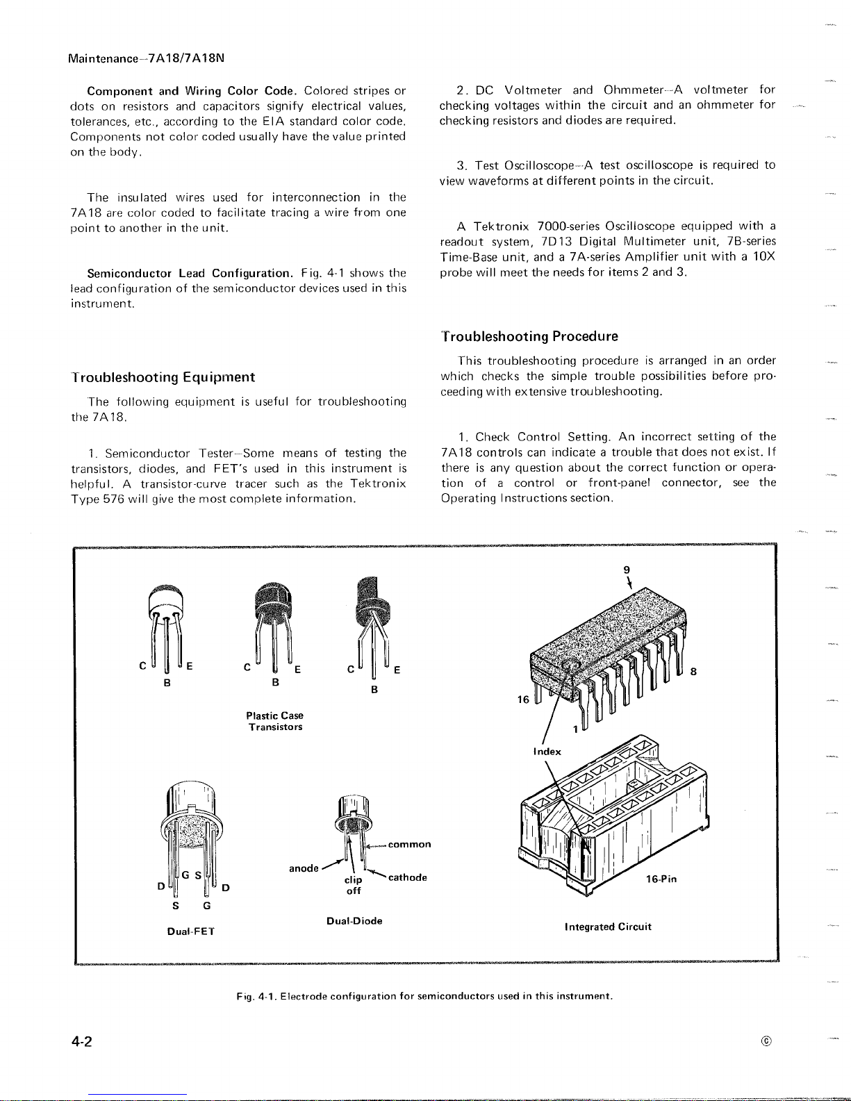
Maintenance---7A18/7A18N
not
and
color
coded
Wiring
and
wires
capacitors
coded
to
Component
dots
on
tolerances,
Components
on
the
body
The
insulated
7A18
are
resistors
etc.,according
.
color
pointtoanotherinthe unit
Lead
Semiconductor
lead
configuration
instrument
.
Troubleshooting
The
following
the
7A18
.
1.Semiconductor
transistors,
diodes,
helpful.A
Type
576
will
transistor-curve tracer
give
Configuration.Fig.4-1
of the
Equipment
equipment
Tester---Some
and
the
most
Color
Code.Colored
signify
to the
EIA
usually
used
for
interconnection
facilitate
tracingawire
.
semiconductor
is
useful for
FET's
used
complete
electrical
standard
have
the value printed
devices
troubleshooting
means
in
this
such
as
information
stripes
color
from
shows
used
of
testing
instrument
the
Tektronix
.
or
values,
code
in
the
one
the
in this
the
and
an
.
circuit
equipped
unit
and
3
.
.
that
does
function
connector,
voltmeter
ohmmeter
required
is
.
unit,
witha10X
before
settingofthe
not
2.DC
checking
.
checking
3.Test
view
A
readout
Time-Base
probe
Troubleshooting
This
which
ceeding
1.Check
7A18
there
is
tion
Operating
Voltmeter
voltages
resistors
Oscilloscope--A
waveforms
Tektronix
system,
unit,
will
meet
troubleshooting
checks
with
extensive
Control
controls
question
is
any
a
control
of
Instructions
and
within
the
and
diodes
at
different
7000-series
7D13
Digital
anda7A-series
the
needs
for items
Procedure
procedureisarrangedinan
simple
the
troubleshooting
Setting.An
indicateatrouble
can
about
or
front-panel
section
Ohmmeter--A
circuit
are required
test
oscilloscope
pointsinthe
Oscilloscope
Multimeter
Amplifier
2
trouble
possibilities
incorrect
the correct
.
for
for
with
7B-series
order
pro-
exist.If
or opera-
see
the
to
a
Fig
.
.
Electrode
4-1
4-2
configuration
for
semiconductors
used
in this
instrument
.
Page 24
Maintenance-7A18/7A181\1
2.Check
Associated
Equipment
with troubleshootingofthe
ment
used with
possible,
substituteanamplifier
correctly
persists.Check
that
the interconnecting
3.Visual
instrumentinwhich
can
be
locatedbyvisual
connections,
damaged
components,
4.Check
brationofthe
PartI-trouble
corrected
are
5
given
.
Check
Performance
may
by
in
component
correct voltage
and waveforms
are
not
absolute
ments.To
to
take
these
section
.
6.Check
methods
are
nentsinthe
are
best
checked
measurement
A.TRANSISTORS
The
best
operationisactual
Ifatransistororintegrated
defective,itcan
ponent
known
conditions
damaged.If
dynamic
testers
under
tester
maybeused,
simulated operating conditions
unnoticed.Fig.4-1
of
semiconductor
this
instrument
into
the
indicator
that
the inputs
cables
Check.Visually
the
troubleissuspected
broken
etc
wires,
.
Instrument
unit,orthe
CheckofSection5.
only
be a
resultofmisadjustment
calibration.Complete
Part
I IofSection5.
Voltages
or
obtain
readings,
and
stage
can be
or
waveforminthe
are
givenonthe
and
may
operating
see
Individual
provided
7A18
from
for
.
Components
by
disconnecting
the
effectsofsurrounding
AND
check
of
transistor
performance
best be
tobegood;however,
are
not
such
thatareplacement
substitute
transistors
(suchasTektronix
but
since
shows
base
devices.Be
indications,
Performance.Check
affected
Waveforms
vary
conditions
the
Components.The
checking
circuit
checked
attemptingtoremoveorreplace
circuit
.
.
Before
7A18,
check
that
is
operating
unit
known
to
unit
and
seeifthe
are
are
not
check
damaged
properly
connected
defective
the
portionofthe
.
Many
such
as
circuit
circuitbyperforming
The
calibration
.
Often the
located
by
checking
circuit.Typical
diagrams;however,
slightly
between
similartothose
instructionsinthe
the
individual
which
are
solderedinplace
one endtoisolate
circuitry
INTEGRATED
and
integrated
under
operating
is
suspectedofbeing
by
substitutingacombe sure
might
are
not
available,
Type
576).Static-type
they
do not
check
some
defects
pin
and
socket
arrangements
sure
the
power
is
any
transistororintegrated
proceeding
the
equip-
correctly.If
be
operating
problem
and
.
troubles
unsoldered
boards,
the
cali-
apparent
and
may
be
instructions
defective
for the
voltages
these
instru-
used
Diagrams
following
compo-
the
.
CIRCUITS
circuit
conditions
that
circuit
also
be
use
.
a
operation
may
go
off before
Integrated
circuits
oscilloscope,orby
standingofthe
shooting
checking
circuits
so that
integrated-circuit
clippingatest
cuits.This
extraction tool
B.DIODES.A
a
short
circuitbymeasuring
nals
withanohmmeter
resistance
when
the
diodes
or
Do
not
current.High
circuit
circuits
using
voltages
adjacent
test clip
probetothe 14-
device
.
should
be very highinone
meter
leads
back
diodes
use
an
ohmmeter
currents
and waveforms
diode
C.RESISTORS.Check
Resistor
Resistors
measured
toleranceisgiven
normallydonot
value
varies
D.CAPACITORS
detectedbychecking
.
highest
voltage
should
capacitor
by
required
Component
manceofany
any
affected
scale.Use
rating
be high
can
checking
7.Repair
to
electrical
circuit
an
of
the capacitor.The
after
initial
bestbedetected
whether
and
Readjust
replace
components
Replacement.Be
circuit
components
may
be
REPLACEMENT
Standard
All
7A18
Officeorrepresentative.However,
electronic
thanisrequired to
purchasingorordering
lists
Parts
electrical
canbeobtained
components
for
value,
tolerance,
and
order
can be
checked
direct
substitution.A
description
integrated
withavoltmeter,
is
essentialtotrouble-
circuits.Use
around
leads
are
not
shorted
provides
also
doublesasan
a
and
convenient
16-pin
canbechecked
the
resistance
the
set
to
RX1kscale.The
direction
are
reversed.Do
withanohmmeter
scale
that
hasahigh
may
widely
damage
resistors
in
need
from
the
to be
the
the
with
Electrical
replaced
specified
.Aleakyorshorted
resistance
ohmmeter
withanohmmeter
which
will
chargeofthe capacitor.An
withacapacitance
the capacitor
passesACsignals
the
Circuit
in this
.
unit
sure to
that
has been
repaired
replaced.Recalibration
necessary
.
PARTS
mechanical
through your
canbeobtained
them from
replacement
rating,
part
many
Tektronix,
parts,
and
description
replacements
local
locallyinless
good
under-
care
when
the
integrated
together.An
means
integrated
integrated-circuit
foranopenorfor
between
termi-
diode
very
and
not
check
tunnel
.
internal
diodes
.
an
ohmmeter
Parts
List
unless
value
.
capacitor
can
on
not
exceed
resistance
reading
open
meter,
.
Special
check
techniques
are
given
the
or
that
Tektronix
of
the
standard
under
perfor-
has had
of
the
for
the
Field
time
Inc.Before
check
the
parts
.
test
of
cir-
low
.
.
the
be
the
the
or
REV.D,
MAY,
1975
4-
3
Page 25
Maintenance-7A1
8/7A18N
When
selecting
remember
component
ment.All
ments
unless
will
not
adversely
Special
to
Tektronix
indicatedinthe
number.Most
ment
special
Officeorrepresentative
Ordering
refertothe
and
trical
circuit
Soldering
boards
excellent
care
rules
Parts
Some
parts
satisfy
particular
to
have
parts
Parts
When
ordering
Symbols
Parts
1.Instrument
2.Instrument
A
description of the
3
.
number)
4.Tektronix
Attenuator
are
electrical
when
cleaning or
shouldbeobserved
1.Useavery
replacement
that the
may
affect
replacement
it is
are
manufactured
our
specifications.These
parts
of the
been
manufactured
directly
replacement
Parts
Ordering
on
the
List
section.Include
type
Serial
Part
Techniques
Circuit
made
from
characteristics.Use
small
requirements,orare
NOTE
physical
its
parts
known
that a
affect the
listbyan
mechanical
from
.
Information
page
immediately
(7A18)
Number
part
Number
Boards.The
polyphenylene
soldering
when
soldering
parts,
it is
important
size
and
shape
performance
shouldbe
different
instrument
or
asterisk
parts
by
your
parts
the
(if
this
removingorreplacing
iron
in
the
direct
component
performance
selectedbyTektronix
manufactured
special
preceding
usedinthis
Tektronix.Order
local
Tektronix
from
Tektronix,
and
Special
preceding
following
electrical,
oxide
material.The
(not
information
Attenuator
becauseofits
more
than
over15watts)
to
of
the
instru-
replace-
.
for
parts are
the
part
instru-
Field
Inc
Notes
the
Elec-
include the
circuit
normal
following
parts
.
all
General
The
ical
assembling
Circuit
In
never
connections
nections.If it is
assembly,
A.READOUT
1.Disconnect
board
.,
:
:
2
mounting
3.Disconnect
board
4.Remove
5.To
ATTENUATOR
B
.
1 .
procedure
2.Disconnect
rear
3.Loosen
control
4.Remove
from
COMPONENT
exploded-view
Parts
List
individual
Board
general,
removed
be
use the
.
.
Remove
surface
.
replace
Remove
.
of the
board
shaft
the control
may
Removal
the
to the
following
CIRCUIT
the
the
.
the wires
the
board
the
the
readout
the
.
the
front
coupling
the red
shaft
REPLACEMENT
drawing
be
helpful
components
circuit
unless
seven
CIRCUIT
boards
they
boards
necessary
wires
board,
.
are
procedures
BOARDREMOVAL
connected
screws
connected
from
the unit
reverse
BOARD
boardasoutlinedinthe previous
resistor/capacitor
set
screwonthe
(usea0
VARIABLE
associated
when
or
must
made
to
holding
.050-inch
with
disassembling
sub-assemblies
usedinthe
replaced.Electrical
be
by
replaceacircuit
.
to
the
the
to the
.
the
orderofremoval
REMOVAL
connected
VARIABLE/GAIN
hex-key
control
the
Mechan-
or
.
7A18
need
soldered con-
board
(7A18
only)
outsideofthe
board
to the
inside
of the
.
to the
wrench)
knob
and
rod
re-
.
2.Do
not
apply
more
heat,orapply
time,
thanisabsolutely
3.Useavacuum-type
excess
solder
from
4.Do
not
apply
or
halogenated
5.To
methyl,
hydrocarbons
clean,
or isopropyl alcohol
use
the
any
necessary
circuit
solvent
only
.
desoldering
board
.
containing
.
water-soluble
.
heat
for
a longer
tooltoremove
ketones,
detergents,
the
esters,
ethyl,
5.Remove
1/16-inch
6.Remove
7.Remove
8.Disconnect
connector
9.Remove
the remaining
hex-key
the front panel
the
the
.
the
wrench
.
attenuator
wires
input
BNC
from
shields
and
resistor
connector
front-panel
the
instrument
.
from
.
knobs
the input
using
.
a
BNC
Page 26
Maintenance--7A18/7A18N
10.Remove
nut
driver
11.Remove
the
instrument
12.To
.
.
replace
the
POSITION
the
attenuator
the board,
C.AMPLIFIERCIRCUIT
1.Remove
viously
.
2.Remove
instrument
3.Disconnect
the
front-panel
4.Loosen
coupling
0
.050-inch
shaft
from
5.Loosen
between
switch
long
sections.Pull
shaft
the
.
controls
the
of
hex-key
the
frontofthe
the
the
DISPLAY
from
the
Readout
plastic
the
front hex-socket
the
wrench
front
the
frontofthe
reverse
BOARD
circuit
plug-in
wires
connectedtothe
.
VARIABLE
.
Pull
instrument
hex-socket
MODE
the-TRIGGER
control usinga5/16-inch
board
with
cam
switch
from
the
order
of removal
REMOVAL
boardsasgiven
guide
from
the
rearofthe
board
screw
in
the
control
the
VARIABLE
shaft
using
knob
.
screwinthe
and
TRIGGER
SOURCE
instrument
.
coupling
SOUCE
knob
.
pre-
from
front
and
and
B.ROTARY
Single
SOURCE
these
SWITCHES
wafers on
switches
switchesisdefective,
shouldbereplaced.A
your
a
Tektronix
When
type
rotary
beyond
solder
Transistor
Transistors
they
are
during
routine
Field
disconnectingorconnecting
switch,donot
the
rivetonthe
can
destroy
and
and
actually
maintenance,
sockets.Special
leads,
because they can
from
sockets.Unnecessary
components
may
Whenatransistorisreplaced,
part of
the
instrument
the
DISPLAY
are
not
new
Office
the spring
Integrated
IC's
should
defective.If
care
must
affect
the
that
MODE
normally
switch
the
replaced.If
entire
switch
can be
ordered
.
leadstoa
let
solder
flow
switch
terminal.Excessive
tensionofthe
Circuit
return
be
Replacement
not
be replaced
removed
them
from
to
giventointegrated
easilybedamaged
replacement
or
calibrationofthe
check
the
operation
may
be affected
.
and
TRIGGER
any
around
contact
their
their
in
switching
instrument
part
assembly
through
wafer-
and
.
unless
sockets
original
circuit
removal
of that
of
of
.
6.Loosen
the
DISPLAY
key
wrench.Pull
from
the
7
.
connected
8.Remove
the
chassisorother
9.Remove
10.To
Switch
Several
following
the cam-type
the
front
MODE
the
frontofthe
Disconnect
to
the
ceramic
the
screws
mounting
the board
replace, reverse
Replacement
typesofswitches
special
maintenance
switches
A.CAM-TYPESWITCHES
Repairofcam-type
onlybyexperienced
alignment
carefully
switch.For
switches,
representative
and
spring
maintained
assistance
contact
.
your
her-socket
switch
DISPLAY
instrument
the
shaft
MODE
.
resistor-capacitor
stripsatthe
and
nuts securing
surface
from
the
the
orderofremoval
are
informationisprovided
and
rotary
switches
switches
should
maintenance
tensionofthe
for
proper
in
maintenanceofthe
local
Tektronix
screwinthe
coupling
usinga5/16-inch
knob
and
combinations
frontofthe board
the board
.
instrument
.
.
usedinthe
.
be undertaken
personnel.Switch
contacts
operationofthe
cam-type
Field
Office
hex-
long
shaft
.
7A18.The
for
must
be
or
to
of
Recalibration
After
any
After
electrical
calibrationofthat
wellasthe
Performance
provide
calibrationofother
Check
a quick
and
instrument operation
of
Section5can
meet
the
Performance
Repackaging
If
the
Tektronix
Service
owner
firm
number
Save
Center
(with address)
that
andadescriptionofthe
and
re-use
shipped.If
available,
repackage
Surround
protect
corrugated
having
than
the
by
tightly
foam
between
carton
The
carton
the
inside
with
thenbeused
for
instrumentisto be
for
can be
the
the
original
the
instrument
finishofthe
cardboardofthe
dimensionsofno
instrument
packing
carton
shipping
test
strength
Repair
component
particular
circuit
closely
instructions
convenient
. -
The
giveninPartIof
means
Calibration
to adjust
Requirements
Shipment
serviceorrepair,
and
the
nameofan
contacted,
complete
service
packageinwhich
packagingisunfit
the
instrumentasfollows
with
polyethylene
instrument.Obtain a
correct
less
dimensions.Cushion
three
inches of
and
instrument,onall
tape or
for
industrial
your
instrumentis200
has
been
replaced,
shouldbechecked,
related
circuits.The
Section
of
checking
Procedure
in
Part
the operation
listedinSection1.
shippedtoa
attachatag
Tektronix
showing
individualatyour
instrument
required
your
.
instrument
for
useornot
:
sheeting to
carton
carton
strength
than
six
inches
the
instrument
dunnageorurethane
sides.Seal
stapler
pounds
the
as
5
the
I
I
to
:
serial
was
of
and
more
.
REV.E
DEC
1976
4-5
Page 27
7A18/7A18N
Change
Recalibration
To
assure
the
7A18
months
thoroughly
the
if
Maintenance
Tektronix
Tektronix,
recalibrationatlocal
Service
or
Center.Contact
representative
Using-This
General.This
tate
checkingoradjusting
Index.To
Check
ceding
ment
or
PartI---
procedure
Interval
instrument
every
used
infrequently.Before
clean
and
section
Field
Inc.provides
for further
Procedure
section
aid
Adjustment
Performance
.
information,ifany,
1000
accuracy,
hours
inspect
.
check
of operation, or every
this
instrumentasoutlined
Service
complete
Field
Service
your
local
information
provides
the
in
locatingastepinthe
procedure,
several
7A18.These
Check
the
complete
instrument
Centers
Yektronix
.
features to
are
an
indexisgiven
and
PartII--
affecting
calibration
calibration,
repair
and
the
Field
:
Performance
this
and
Factory
Office
facili-
pre-
Adjust-
of
six
in
section
willbefound
instrument
within
General
The
equivalent,
7A18.Specifications
minimum
some
of
precise
equipment.All
calibrated
The
based
on
is
substituted,
need
tobealteredtomeet
ment
used.Detailed
equipment
instruction
mationisneeded
at
is
all
Performance
TEST
following
is
necessary
the
specifications
than
the
and
operating
Performance
this
recommended
are
manual
the
rearofthe
both
EQUIPMENT
test
required
given for the
for
actual
test
equipment
Check
control
not
giveninthis
for
.
manual
.
correctly
Requirements
adjusted
as
REQUIRED
equipment
for
accurate
listed
performance
within
and
equipment.If
settingsorcalibration
the
operating
the
and
complete
test
calibration.Therefore,
here
may
capabilities
is
assumed
the
listed
Adjustment
requirements
instructions
procedure.Refer
test
equipment
calibration
equipment
and
performing
given
in
Section1.
accessories,orits
of
the
are
the
be
somewhat
to
be
specifications
procedures
other
setup
of
for the
if
more
of the
test
correctly
.
equipment
may
the equip-
test
to the
infor-
less
are
Performance
ment
canbecheckedwithout
making
Performance
against
column
vided
the
adjustment
settingsorequipment
correct
perform
cedure
circuitsinthis
pletely
form
performing
the
internal
Check
the tolerances
of
Section1.Inaddition,across-referenceispro-
to the stepinPart
instrument
step
Adjustment
calibration
only
Part
gives
the
instrument
Complete
both
Performance
check
PartsIand
the
Performance
and
Adjustment
canbeperformed
Procedure.To
Check.The
adjustments
.
This
listedinthe
I I
to correct
connections
with
II --
Adjustment.The
recommended
.
adjust
II.Start the
Check.Fhis
performance
removing
by
performing
procedure
Performance
--
Adjustment
calibration.In
return
the
minimum
calibration
Check/Adjustment.To
all
parts of
procedure
method
checks the
without
.
this
complete
and
will
the
which
changing
this
number
Adjustment
procedure
of
this
instru-
side
shields
only
PartI--
instrument
Requirement
will
return
most
cases,
control
instrument
of
steps,
pro-
for
com-
instrument,
procedure
follow
this
with
assure that the
the
to
all
per-
by
or
Calibration
All
check
items
used
without
capabilities.For
amplitude
Check
check
operation.Equipment
Check
only
for
note2.
Test
Equipment
1.7000-series
Oscilloscope
mended
2.Time-Base
of the
and
adjust
only
compromising
signal
and
may
the
lower
procedure
the
.
Equipment
test
this
for
example,
generatorisused
be deletedifthe
frequency
is
Adjustment
oscilloscope, referredtoas
in
this
plug-in
Alternatives
equipment
instrument.However,
the
Performance
used
indicated
procedure.Tektronix
unit,
the
the
response
only
procedure
Tektronix
is
instrument's
low-frequency
by
required
Check
onlyinthe
user
does
or
for
the
note1;
are
71350
to
completely
some
of
canbedeleted
measurement
constant-
Performance
not
desire
trigger
items
source
Performance
required
indicated
the
Indicator
7403
recom-
.
the
to
by
Page 28
Calibration-7A1
3.Amplitude
square
wave;output
amplitude
Pulse
Generator
4.Medium-frequency
erator.'Frequency,
reference
able
from
amplitude
kilohertz
at
50
Tektronix
5.Low-frequency
Frequency
tude, variable
peak.For
General
put)
Radio
.
6.Square-wave
put
capabilities
tors):12
witharisetimeof12
into50ohmsat100
8/7A18N
Calibrator.Output
accuracy,
recommended
frequency,
50
millivoltsto200
accuracy,
and
SG
503
Signal
range,
two
from
example,
Type
generator
(may
volts
amplitude
amplitude,20millivoltsto20
within0.25%.Tektronix
.3
constant-amplitude sine-wave
variable
50
from
kilohertz
output amplitude
from50to
75 megahertz.For
Generator
constant-amplitude
hertzto10
10
millivoltsto400
General
274
QBJ
be
Radio
Adaptertoprovide
. 2
Must
obtained
into50ohms
nanosecondsorless;500
kilohertz
witharisetimeofone
secondorless.'TektronixPG506
mended
0589-00
(meets
both
output
requirements
7
.Plug-inextender.2TektronixPart
.
signal,
one
50
to
75
;
output
millivolts
amplitude,
into50ohms
constant
.3
signal
generator
kilohertz;output
millivolts
1310-B
have the
from
Pulse
Oscillator
following
separate
at
one
Generator recom) .
3
Number067-
kilohertz
volts
506
PG
gen-
megahertz
vari-
within
3%
example,
ampli-
peak
(use
BNC
out-
out-
genera-
kilohertz
millivolts
nano-
to
.'
14.In-line
;
wattage
BNC.Tektronix
15.10X
racy,
;
011-0059-02
;
16.InputRCnormalizer.2
X
20
picofarads;attenuation,2X;
tronix
17.Adapter.Adapts
connector.Tektronix
Adjustment
18.Screwdriver.Three-inch
example,
19.Low-capacitance
Tektronix
20.Tuning
tance
003-0307-00,
BNC
termination.'Impedance,
rating,
two
watts;accuracy,
PartNo.
BNC
attenuator
±2%;connectors,
.
calibration
fixture
PartNo.
Tools
Xcelite
and
R-3323
PartNo.
003-0000-00
tool.Handle with
attenuator
003-0334-00,
±2%
;
011-0049-01
. l
.
Impedance,50ohms;accu-
BNC.Tektronix
Time
constant,
one
connectors,
067-0538-00
GR874
.
connectortoBNC
017-0064-00
shaft,
3/32-inch
.
.
screwdriver.1
1/2-inch
.
inserts
for
input
adjustments.'Tektronix
and
003-0497-00
.
50
ohms
connectors,
Part
No
megohm
BNC.Tek-
male
bit.For
shaft
capaci-
PartNo.
;
.
.
Accessories
.18-inch cable.'Impedance,50ohms;type,
8
connectors,
9.42-inch
connectors,
10
RG-213/U
017-0502-00
11.In-lineGRtermination.Impedance,50ohms
tage
input
017-0064-00
12.Dual-input
input.Tektronix
13.1
accuracy,
017-0078-00
'
Required
z
Required
'Requires
BNC.Tektronix
cable.Impedance,
BNC.Tektronix
.
Five-nanosecond
connectors,
;
.
rating,
two
watts;accuracy,
with
BNC
.
OX
G
±2%;connectors,
.
only
for
Performance
only
for
Adjustment
TM
500-Series
PartNo.
50
PartNo.
cable.Impedance,50ohms;type,
GR874.Tektronix
±2%;connectors,
male output.Tektronix
coupler.'Matched
calibration fixture
R
attenuator.2 Impedance,
067-0525-00
GR874.Tektronix
Check
.
procedure
PowerModule
.
.
012-0076-00
ohms;type
012-0057-01
signal
R
G-58/U
.
RG-58/U
.
Part
No
;
wat- Rate
GR874
Part
No
transfertoeach
.
50
ohms
Part
No
;
;
.
.
;
.
Preliminary
Set the
follows
procedure)
(for
I
ntensity
Focus
Graticule Illum
Calibrator
Vert
Mode
Trig
Source
DISPLAY
TRIGGER
CH2POLARITY
POSITION
VOLTS/DIV
AC-GND-DC
Control
Indicator
both
Settings
Oscilloscope
Performance
Indicator Oscilloscope
7A18
MODE
SOURCE
CH1and
Check
Midrange
Adjust
As
40
1
Left
Left
CH
MODE
+UP
CH
Midrange
10
DC
and
display
desired
mV
kHz
Vert
1
2
mV
7A18
controls
and
Adjustment
for
well-defined
as
5-2
REV.E,
MAY,
1976
Page 29
1
Introduction
-
The
following
7A18
without
adjustments.All
basedonSection1of
Index
Factor
(VOLTS/DIV)
IDENTIFY
to PartI---
1 .
Check
2.Check
Accuracy
3.Check
4.CheckChannel
procedure
removing
tolerances
Channel1and2GAIN
Channel
Channel
Range
(7A18
this
manual
Performance
1
and
1
and2VARIABLE
only)
checks
the
the covers or
given
in this
.
Check
2
Deflection
and2Trace
performance
making
procedure
of
internal
Page
Page
Page
Page
5-3
5-3
5-4
5-4
00
the
are
rol
2
.
Connect
which
meets
oscilloscope
3.Turn
least
twenty
given
accuracy
4
.
Set the
Settings
The
both
selectedbythe
the Indicator
the
power
the Indicator
minutes
.
controlsasgiven
.
checks
titled
channels
frequency
supply
warmup
Channel
.
Perform
DISPLA
Performance
Oscilloscopetoa
and
voltage
.
Oscilloscope
for
checking
under
TE
NO
1
and2
the
check
Y
MODE
switch
Check--7A18/7A18N
power
source
requirements
poweron.
Preliminary
apply
on
.
the
the
Allow
7A18
Control
equally
channel
of
the
to the
to
at
5.Check
width
6.Check
quency
Response
7.Check
8.Check
9.Check
10.Check
11.Check
Preliminary
The
performance
at
any
unless stated
1.Install
mentofthe
Channel1and2Upper
Channel
Channel
Common-Mode
Alternate
Chopped
Trigger
Procedure
temperature
otherwise
the
Indicator
1
and2Lower
Isolation
Operation
Operation
Source Operation
for
NO
of
this
within the0°Cto
.
7A18
in
the
Oscilloscope
instrument
Rejection
Performance
TE
left
vertical
.
Band-
Fre-
Ratio
Check
canbechecked
+50
°Crange
plug-in
compart-
Page
Page
Page
Page
Page
Page
Page
5-4
5-4
5-5
5-5
5-5
5-6
5-6
1
.
Check
a.Connect
the
CH
cable
b.Set the
millivolt
c
.
d.If
exactly
in
the
GAIN
e.Set
partscanddof
Channel1and2GAIN
1
and
and
dual-input
square-wave
CHECK--CRT
necessary,
five
GAIN
controlisengaged
the
2.Check
Accuracy
a.Set the
b.CHECK-Using
tude
calibrator
deflection
switch
within
.
the
standard
CH
2 input
coupler
standard
display
adjust the
divisions
knob
with
DISPLAY
this
step
Channel
Channel1AC-GND-DC
settings
2%
amplitude
connectors
.
amplitude
output
.
forafive-division
of
vertical
a
screwdriver
.
MODE
for
Channel2.
1
and
the
VOLTS/DIV
givenin-
in
each
calibrator
with
the
calibrator
front-panel
deflection.To
switchtoCH2and
2
Table
position
GAIN
and
Deflection
switchtoGND
and
standard
5-1,
of the
output
42-inch
fora50-
display
control
adjust,
turn
check
VOLTS/DIV
BNC
.
press
until
repeat
Factor
.
ampli-
vertical
to
for
the
5-3
Page 30
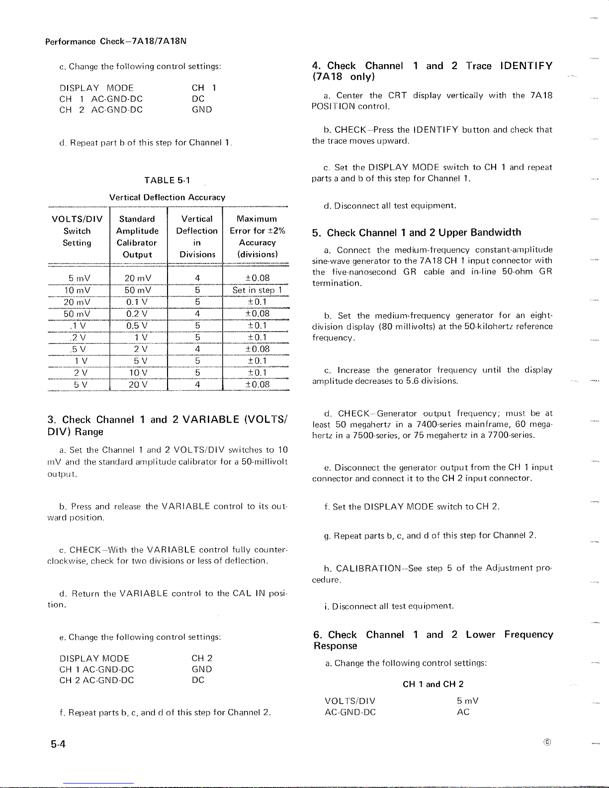
Performance
c.Change
DISPLAY
CH
1
CH
2
d.Repeat
VOLTS/DIV
Switch
Setting
Check--7A18/7A18N
the
following
MODE
AC-GND-DC
AC-GND-DC
part b of
this
Standard
Amplitude
Calibrator
Output
step for
TABLE
control
settings
CH
DC
GND
Channel1.
5-1
:
1
Maximum
Error for
Accuracy
(divisions)
±2%
4.Check
(7A18
POSITION
the
partsaand
5.Check
sine-wave
the
termination
division
frequency
only)
a.Center
b.CHECK----Press
trace
moves
c.Set the
d.Disconnect
Connect
a
.
generatortothe
five-nanosecond
b.Set the
display
.
Channel
the
CRT
control
.
upward
DISPLAY
b of
this
step
all
test
Channel
the
medium-frequency
.
medium-frequency
(80
millivolts)atthe 50-kilohertz
1
and
display
the
IDENTIFY
.
MODE
for
equipment
1
and2Upper
7A18
GR
cable
2 Trace
vertically
button
switchtoCH1and
Channel1.
.
Bandwidth
constant-amplitude
CH1input
and
in-line
generator
IDENTIFY
with
the
and
check
connector
50-ohm
for
7A18
that
repeat
with
GR
an
eight-
reference
3.Check
DIV).Range
a.Set the
mV
and
the
ou tput.
b.Press
ward
position
c.CHECK-With
clockwise,
d.Return
tion
.
e.Change
DISPLAY
CH1AC-GND-DC
CH2AC-GND-DC
.
Repeat
f
Channel
Channel1and2VOLTS/DIV
standard
and
.
check
the
the
MODE
partsb,c,
1
amplitude
release
the
for
two
VARIABLE
following
and
and
2
calibrator
the
VARIABLE
VARIABLE
divisionsorless
control
control
d of
this
VARIABLE
control
to
settings
CH
GND
DC
step
(VOLTS/
switchesto10
fora50-millivolt
controltoits
fully
counter-
deflection
of
the
CAL
:
2
for
Channel2.
c.Increase the
amplitude
d.CHECK----Generator
least50megahertz
hertzina
e.Disconnect
connector
out-
.
IN
posi-
f
g
h.CALIBRATION---See
cedure
i .
6.Check
Response
VOL-T -
AC-GND-DC
.
Set
the
.
Repeat
.
Disconnect
a.Change
decreasesto5.6divisions
7500-series,
and
S/DIV
generator
in
or
the
generator
connectitto theCH2 input
DISPLAY
parts
b, c,
and
all
test
Channel
following
the
CH1and
output
7400-series
a
75
megahertz
MODE
d of
step
equipment
1
and
control
frequency
.
frequency;must
outputfrom
switch toCH2
this step
5 of the
.
2
settings
CH
2
5
AC
until
mainframe,
in a
7700-series
the
connector
for
Channel2.
Adjustment
Lower
:
mV
the
60
CH1input
.
Frequency
display
be
mega-
.
.
pro-
at
4
5-
Page 31

b.Set the
rateoftwo
c.Connect
wave
generator
42-inch
termination
d
.
Set the
display
(30
e.Decrease
amplitude
f
.
CHECK-Generator
less
.
g.Disconnect
2
input
nector
.
h.Set the
i .
Repeat
time-base
milliseconds/division
the
low-frequency
to
the
BNC
cable,
10X
.
low-frequency
millivolts)at10
the
generator
decreasesto4
the
low-frequency
connector
and
DISPLAY
partsdthroughfof
unit
for
a
free-running
.
constant-amplitude
CH
2
input
BNC
attenuator,
generator
kilohertz
.
frequency
.2
divisions
.
frequency;must
generator
connectitto the
MODE
switch to
this
step
connector
and
for
a
until
be 10
CH1input
CH1.
for
Channel1.
sweepata
with
50-ohm
six-division
the
display
hertz
from
the
sine-
the
BNC
or
CH
con-
f
.
Disconnect
connectitto
g.Set
h.Set the
the
theCH2
generator
CH
volts) at50megahertz
i.Change
the
following
CH1VOLT/DIV
DISPLAY
MODE
CH2VOLTS/DIV
j .
CHECK--CRT
flection
8.Check
.
k.Disconnect
Common-Mode
a.Change
CH
1
and
all
the
following
CH2VOLTS/DIV
Performance
the
termination
2
input
VOLTS/DIV
for
.
display
test
equipment
from
connector
switch
a two-division
control
settings
10
mV
CH
1
10
mV
for0.4
.
Rejection
control
settings
20
Check--7A18/7A18N
Channel
.
V
.
to
.1
display
(200
:
division
or
less
Ratio
:
mV
1
and
milli-
de-
j.Disconnect
7.Check
a.Change
CH1and
Channel
the
CH
all
following
2
AC-GND-DC
CH1VOLTS/DIV
CH
2
VOLTS/DIV
b.Connect
input
in-line
c.Set
connector
50-ohm
the
the
with
GR
generator
volts) at50megahertz
d
.
Change
DISPLAY
CH
1
VOLTS/DIV
the
MODE
following
test
equipment
Isolation
control
medium-frequency
the
five-nanosecond
termination
for
.
a
two-division display
.
control
.
settings
DC
.1
V
mV
10
generator
settings
CH
2
10
mV
b
.
and
cable,
coupler
Connect
CH2input
in-line
the
medium-frequency
connectors
50-ohm
GR
with the
termination,
generator
to
five-nanosecond
and
the
theCH1
GR
dual-input
.
:
GR
to the
cable
(200
CH
and
milli-
c.Set the
division
d.Change
1
DISPLAY
CH2POLARITY
e.CHECK-CRT
flection
f
.
Disconnect
constant-amplitude
display
(160
the
following
MODE
(common-mode
all
millivolts)at50
control
display
for0.8
rejection
test
equipment
generator
megahertz
settings
for
an
.
:
ADD
INVERT
division
or
less
ratio10:1orbetter)
.
eight-
de-
.
:
9.Check
a.Set
Alternate
the
DISPLAY
Operation
MODE
switchtoALT
.
e.Check---CRT
(channel
,c)
I
isolation
display
display
for
0.4divisionorless
ratio50:1orbetter)
deflection
.
REV
b.Position
.
APR
1974
the
traces
about
two
divisions
apart
.
5-5
Page 32

Performance
c.Turn
out
its
range
d.CHECK-Trace
at
all
sweep
be
apparent
screen
.
10.Check
a.Set
b.CHECK-CRT
11.Check
Change
a
.
DISPLAY
J
'RIGGER
Check-7A18/7A18N
the
time-base
.
.Atfaster
rates
instead
;
Chopped
the
DISPLAY
Trigger
the
following
MODE
SOURCE
unit
alternation
display
Operation
MODE
display
Source
control
time/division
between
sweep
rates,
appearsastwo
switch to
for
two
traces
Operation
settings
ALT
CH
switch
channel1and
alternation
traces
CHOP
.
.
:
1
through-
will
not
the
on
2
d.Connect
connector
input
e.Set
one-kilohertz
f.CHECK-CRT
square
both
the
wave
g.Set the
h.CHECK-CRT
stable
i .
the
Set
j .
CHECK-CRT
the
low-frequency
with
the
42-inch
generator
signal
onlyisstable
TRIGGER
.
TRIGGERSOURCE
foratwo-division
.
display
SOURCE
display;square
display;sine
generator
BNC
for
square
.
switchtoMODE
wave
switch toCH2
wave
onlyisstable
cable
wave
.
and
to the
(40
and
sine
.
CH
2
millivolts)
sine
wave
.
wave
are
.
;
b.Connect
the
to
c.Set the
sweep
the Indicator
CH1input
rate
of 0.5millisecond/division
connector
time-base
unit for a
Oscilloscope
with
the
triggered
.
Cal
Out
18-inch
connector
BNC
cable
displayata
.
NOTES
k.Disconnect
This
the
7A18.If
this
procedure,
specified
completes
the
limits
.
all
test
equipment
the
Performance
instrument
itiscorrectly calibrated
has
met
.
Check
all
procedure
tolerances given
and
within
for
in
the
Page 33

Introduction
The
following
calibration.All
are
calibration
instrument
mance
operation
tolerances
Requirements
this
section
Index
1.Adjust
2.Adjust
specifications
Requirement
of the
.
to
Part
procedure
limits
and
guides,
instrument
if
the
instrument
as
checkedinPartI--
returns
tolerances giveninthis
and
should
except
column
may
I I-Adjustment
Channel1and2DC
Channel1and2GAIN
the
not
be
as listedinthe
of
Section1.
exceed
the
meets
Balance
the
Performance
7A18
interpreted
The
given
Performance
Page
Page
to correct
procedure
Perfor-
actual
limits
Check
5-7
5-8
Adjustment---7A
5.Set
the
controlsasgiven
Settings
as
obtainawell-defined
or
of
Locationof
5-1
.
6.Adjust
Titles
for
capitalized
Internal
DC
Balance)
The
locationsofthe
.
the
Focus
display
external controls
in this
adjustments
.
Adjustments
7A18
procedure
are
and
.
NO
TE
initial
adjustments
under
Astigmatism
of
this
(e .g
.,
capitalized
Preliminary
instrument
are
18/7A18N
as
necessary
VOLTSIDIV)
only(e.g
showninFig
Control
to
are
.
.,
.
3.Adjust
citance
4.Adjust
Compensation
5
.AdjustChannel1and2High-Page
Frequency
Preliminary
This
temperature
1.Remove
left
side
2.Install
ment
of the Indicator
Channel1and2Input
Channel
Compensation
ProcedureFor
instrument
panel
should
of25°C+5°C
the
left
from
the Indicator
the
7A18
Oscilloscope
side
in
1
and2Attenuator
Adjustment
NO
TE
be
adjusted
for best
shield
from
Oscilloscope
the
left vertical
.
Capa-
overall
the
at
an
7A18,
plug-in
Page
Page
ambient
accuracy
.
compart-
and
5-8
5-9
5-10
.
the
1.Adjust
a.Position the
the
CH1POSITION
b.Push
controltoits
c.CHECK--Turn
counterclockwise
more
d
.
1,
for
is
rotated
e.Set the
position
f.Set
g.Position the
theCH2
Channel1and2DC
and
than0.5
ADJUST-Channel
minimum
from
.
the
DISPLAY
POSITION
release
outward
to
division
trace
fully
CH
trace
to the
control
.
the
CH
position,
the
VARIABLE
fully
clockwise.Trace
vertically
1DCBalance,
shift
as the
counterclockwise
1
VARIABLE
MODE
tracetothe
control
.
Balance
center
horizontal
VARIABLE
1
control
should not
.
adjustment
CH1VARIABLE
to
fully
control
switchtoCH2.
center
to
horizontal
line
(VOLTS/DIV)
from
number
control
clockwise
the
CAL
line
with
fully
move
.
IN
with
3.Connect
whichmeets
oscilloscope
4.Turn
least
twenty
the Indicator
the
frequency
power
supply
the Indicator
minutes
warmup
Oscilloscope
and
voltage
.
Oscilloscope
before
toapower
requirementsofthe
poweron.
proceeding
Allow
.
source
REV.APR
h.Push
outward
Perform
at
ADJUST---DC
trace shift
from-fUPto
1974
and
release
position.(For
the
following
BAL
while
INVERT
the
CH2VARIABLE
instruments
for
instruments
(see
switching
.
number
CH
B070000
B070000
5,
2
POLARITY
controltoits
and
Fig
.
5-1)
below
andup:
for
no
switch
5-7
.)
Page 34

Adjustment-7
A18/7A18N
Fig.5-1.Locationsofadjustments
CH2DCBAL
R521
usedinthis
Channel
Attenuator
Compensations
Channel
Attenuator
Compenstions
procedure.(7A18
2
l
shown
Channel
C100
Channel 2
C100
.)
l
Perform
7A18below
SN
i
.
partsi,j,
8070000
CHECK-Turn
andIfor7A18N
SN
8090000.Perform
andupand7A18SNB090000
the
counterclockwisetofully
more
than0.5
division
vertically
j.ADJUST-Channel
5,
for
minimum
is
rotated
k
.
ADJUST-CH
number
9,
VARIABLE
to
fully
clockwise
I .
Set the
position
.
2.Adjust
a.Connect
2
input
connector
b.Set
square-wave
c.Position
theCH2
d.CHECK-CRT
amplitude
e.ADJUST-CH
exactly
five
trace
shiftastheCH2
from
fully
counterclockwise
2
Fig.5-1)
for
controlisrotated
.
CH2VARIABLE
Channel1and 2
the
standard
with
the
the
standard
output
the
POSITION
.
divisionsofdeflection.To
amplitude
.
displaytothe
control
display
2
GAIN
NOTE
belowSNB070000,
VARIABLE
clockwise.Trace
.
2
DC
Balance,
VARIABLEDC
minimum
from
trace
fully
controltothe
GAIN
amplitude
42-inch
calibrator
centerofthe
.
for
exactly
adjustment
BNC
part k
for7A18N
andup.
control
adjustment
VARIABLE
to
should
fully
BAL
from
not
number
control
clockwise
(R544,
shiftastheCH2
counterclockwise
CAL
calibratortothe
cable
.
for
50-millivolt
graticule
divisions
five
(front
panel)
adjust,
pressinthe
-
fully
move
see
IN
CH
with
for
in
GAIN
controlisengaged
CH2input
connector
theCH1
.
amplitude
exactly
3.Adjust
a.Remove
Place
extender
b.Set
mV
c.Connect
output
knob
withascrewdriver
f.Disconnect
connector
.
the
g.Set
h.Position
DISPLAY
the
POSITION
i .
CHECK-CRT
.
j .
ADJUST-CH
five
divisions
k.Disconnect
Channel1and2Input
the
7A18
into
the
the
CH1and
.
to
the
.
the
standard
displaytothe
control
display
1
GAIN
of deflection
all
test
the
7A18
on
the
left
vertical
the
square-wave
CH
1
and
amplitude
and
connectitto
MODE
switchtoCH1.
centerofthe
.
for
exactly
adjustment
.
equipment
from
plug-in
.
the
extender
Indicator
compartment
CH2VOLTS/DIV
generator
input
connector
turn
until
the
calibrator
the
CH1input
graticule
five
divisions
(front
panel)
Capacitance
Oscilloscope
and
plug
.
switchesto5
high-amplitude
with
the
from
GAIN
the
with
in
for
.
the
five-
5-8
REV.D,
JAN
.
1976
Page 35

nanosecond
GR
termination,
d.Set
play
(30
e.Set
sweep
f.CHECK-CRT
corner
g.ADJUST---Channel
on
the
h.Disconnect
nector
i .
Set
j.CHECK--CRT
corner
GR
the
millivolts)ofa
the
rateof.2
.
displayed
and
connectitto theCH2
the
DISPLAY
.
cable,
10X
GR
and
20 pF
normalizer
square-wave
time-base
millisecond/division
waveform
the
generator
one-kilohertz
unit
display
1C100
(use
normalizer
MODE
display
for
for
attenuator,
.
forasix-division
signal
.
foratriggered
.
square-wave
for
optimum
tuning
tool)
.
from
the
CH1input con-
input
connector
switchtoCH2.
square-wave
in-line
50-ohm
displayata
with
square
.
with
dis-
square
corner
square
top
within0.15
each
switch position to
e.ADJUST-CH
Table
5-2 for
displayed
erator
divisionsofdeflection
signaltothe
switch position
top
each
Table
displayed
switch positiontoprovide
output
f.Disconnect
g.Set the
h.CHECK--CRT
within0.15
switch
i .
ADJUST---CH
5-2
division.Re-adjust
2
attenuator
optimum
waveform
CH1input
DISPLAY
positiontoprovide
for
waveform.Re-adjust the
(use
at
each switch
.
the
normalizer
display
listedinTable
division.Re-adjust the
1
attenuator
optimum
Adjustment
the
provide
square
connector
MODE
square corner
six
divisionsofdeflection
compensations
corner and
tuning
tool).Re-adjust
position
from
.
switchtoCH1.
at
each
5-2 for
six
divisionsofdeflection
compensations
generator
divisionsofdeflection
six
--7A18/7A18N
generator
flat
toponthe
to
provide
CH2and
CH
square corner
and
1
VOLTS/DIV
generator
flat
outputateach
connect
output
as
given
the
gen-
six
the
and
flat
output
as
given
toponthe
.
at
.
in
at
.
in
k.ADJUST--Channel
on
the
displayed
I.Disconnect
m.Remove
Indicator
vertical
compartment
4.Adjust
a.Connect
output
nanosecond
GR
mV
(60
switch position
to the
termination,
b.Set the
.
c
.
the
Set
millivolts)ofone-kilohertz
d.CHECK-CRT
waveform
all
test
the
Oscilloscope.Install
Attenuator
the
CH
GR
cable,
and
CH1and
square-wave
listedinTable
2
C100
.
equipment
7A18
and
.
Compensation
square-wave
2 input
10X
GR
20pF
normalizer
CH2VOLTS/DIV
generator
display
for
optimum
.
plug-in
the
7A18
generator
connector
attenuator,
.
forasix-division
signal
.
at
each
CH
5-2
for
square corner
square corner
extender
onlyinthe
high-amplitude
with
in-line
switches
2
VOLTS/DIV
from
the
50-ohm
display
and
five-
to
the
left
10
flat
j .
Disconnect
VOL-I'S/DIV
Switch
Setting
10
50
0.2V
0.5V
2V
mV
mV
-----------
V
_ .~
Replace
all
test
Attenuator
-
.__
Remove
in-line
with
GR
equipment
TABLE
Compensation
Square
_C106
C110
_C11_4_
Check
10XGR
Check
C118
Check
50-ohm
to
BNC
.
5-2
Adjust
Corner
attenuator
GR
male
for
Optimum
I
_
.
.
termination
adapter
.
Flat
Top
C115
Check
Check
C119
_
Check-
5-
9
Page 36

Adjustment-7A1
8/7A18N
5.Adjust
Compensation
the
a.Set
10mV.
b.Connect
the
CH
1
cable,
10X
tion
.
c.Set the
(60
millivolts)ofa
d.Set the
sweep
rateof2
In
the
magnifier
at
both
sweep
e.CHECK--CRT
response
to-peak
with
.
Channel
CH
1
and
CH
the
square-wave
input
connector
GR
attenuator,
square-wave
time-base
microseconds/division
following
fromX1toX10and
rates
aberrations
100
generator
kilohertz
unit
NOTE
steps,
.
display
nottoexceed
1
and
2
VOLTS/DIV
generator
with
the
and
in-line
forasix-division
signal
foratriggered
change
compare
for
optimum
2
High-Frequency
switches to
fast-rise
five-nanosecond
50-ohm
.
.
the
time-base
the
0.24
division
GR
displayata
response
square-wave
output
termina-
display
unit
peak-
f.ADJUST-Adjustments
optimum
Use
capacitors.Repeat
responseisobtained
to
GR
connector
response
to-peak
optimum
Use the
capacitors.Repeat
responseisobtained
all
and
square-wave
the
low-capacitance
g.Disconnect
and
connectitto
h.Set the
i .
j.ADJUST
This
test
the
DISPLAY
CHECK-CRT
with
aberrations
.
square-wave
low-capacitance
completes
equipment.Replace
left
side
response
these
.
the
termination
display
Adjustments
response with
these
.
Calibration
the
panelonthe Indicator
numbers
with
screwdrivertoadjust
adjustments
the
CH
MODE
switch toCH2
for
nottoexceed
numbers
screwdriver
adjustments
the
left
2, 3,
minimum
from
2 input
optimum
0.24
6, 7,
minimum
to adjust the
of the
side
shieldonthe
Oscilloscope
and
4
aberrations
the
variable
until
optimum
the
CH
1
input
connector
.
division
until
7A18.Disconnect
.
square-wave
peak-
and
8
aberrations
variable
optimum
7A18
.
for
.
for
.
5-10
REV.APR
1974
cw
Page 37

Replacement
or representative
ChangestoTektronix
components
improvements
ordering
typeornumber,
Ifapart
Tektronix, Inc.Field
number
.
.
as
they
developedinour
parts,
to
serial
you
PARTS
parts
become
include
have
Office or
are
the
number,
ordered
available
instruments
ORDERING
fromorthrough
are
available,
engineering
following
representative
informationinyour
and
modification
has
been
sometimes
and
to give
department
replaced
will
INFORMATION
your
local
made
you
the
.
It is
with a
order:Part
if
new
concerning
number
contactyou
Tektronix, Inc.Field
to
accommodate
benefit
of
the
therefore important,
number,
applicable
or
improved
.
part,
any
Section
Office
improved
latest
circuit
when
instrument
your
local
changeinpart
6--7A18/7A18N
Change
In
Becauseofspace
further
utilized
ACTR
ASSY
CAP
CER
CKT
COMP
CONN
ELCTLT
ELEC
INCAND
LED
NONWIR
information,ifany,
the
Parts
Item
Name
where
ACTUATOR
ASSEMBLY
CAPACITOR
CERAMIC
CIRCUIT
COMPOSITION
CONNECTOR
ELECTROLYTIC
ELECTRICAL
INCANDESCENT
LIGHT
NON
SPECIAL
X000
00X
List,
an Item
limitations,anItem
identification,
possible
.
EMI]TJNG
WIREWOUND
is
locatedatthe
NOTES
Part
first
Part
removed
Nameisseparated
theU.S.Federal
ITEM
Name
AND
added
after
NAME
may
ABBREVIATIONS
DIODE
rearofthis
at this
this
from
sometimes
PLSTC
QTZ
RECP
RES
RF
SEL
SEMICOND
SENS
VAR
WW
XFMR
XTAL
SYMBOLS
serial
serial
the
Cataloging
manual
.
number
number
descriptionbya
appearasincomplete.For
Handbook
PLASTIC
QUARTZ
RECEPTACLE
RESISTOR
RADIO
SELECTED
SEMICONDUCTOR
SENSITIVE
VARIABLE
WIREWOUND
TRANSFORMER
CRYSTAL
colon().
H6-1
FREQUENCY
can
be
REV.G
TUN.1975
Page 38

Electrical
Parts
List-7A18/7A18N
MFR
.CODE
01121
03508 GENERAL
04222
07263
07910
12697
17856
24931
36619
56289
71590
72982
74970
75042
76854
78488
79727
80009
80740
IN
MANUFACTURER
ALLEN-BRADLEY
PRODUCTS
CERAMIC
AVX
FAIRCHILD
FAIRCHILD
TELEDYNE
CLAROSTAT
SILICONIX,
SPECIALTYCONNECTOR
MICROWAVE
SPRAGUE
CENTRALAB
GLOBE-UNION,
ERIETECHNOLOGICAL
JOHNSON,E.F.,
TRW
ELECTRONIC
RESISTORS,
OAK
INDUSTRIES,
STACKPOLE
C-W
INDUSTRIES
TEKTRONIX,
BECKMAN
CO
ELECTRIC
DEPT
.
CORP
SEMICONDUCTOR,
CAMERA
SEMICONDUCTOR
MFG.CO.,INC
INC
.
INSTRUMENTS
ELECTRIC
ELECTRONICS,
INC
COMPONENTS,
PHILADELPHIA
CARBONCO
INC
.
INSTRUMENTS,
X
MFR.CODE
.
CO.,SEMI-CONDUCTOR
.
AND
CO
.
CC
INC.,SWITCH
INSTRUMENT
.
CO.,INC
&
COMPONENTS,
.
DIV.OF
PRODUCTS,
DIVISION
.
INC
.
A
DIV.OF
IRC
.
INC
DIV
CORP
.
FIXED
.
NUMBER
1201
ELECTRONICS
P.O.
464
.
12515
LOWER
2201
3560
INC.6600
5757N.
644W.
299
401N.
S.MAINST.
550
P.0.BOX
2500
ADDRESS
2NDST.
867
BOX
ELLISST.
CHADRON
WASHINGTON
LAURELWOOD
MADISON
BOMBARDIERST
GREEN
12THST.
10TH
AVE.S.W
BROADST.
DAVISVILLE
HARBORBlVD
500
SOUTH
PARK
AVE
AVE
BAY
TO
RD
.
ST
.
RD
.
.
.
AVE
.
.
.
MANUFACTU
.
CITY,STATOZIP
MILWAUKEE,
SYRACUSE,
MURTLE
MOUNTAIN
HAWTHORNS,
DOVER,
SANTA
INDIANAPOLIS,
MONTREAL
NORTH
MILWAUKEE,
ERIE,
WASECA,
PHJIADELPHIA,
CRYSTAL
ST.MARYS,
WARMINSTER,
BEAVERTON,
FULLERTON,
BEACH,
VIEW,
NH
CLARA,
ADAMS,
PA
MN
LAKE,
WI
NY
13201
CA
03820
CA
458 QUE
MA
WI
16512
56093
PA
PA
OR
CA
53204
SC
CA
90250
95054
IN
53201
PA
IL
15857
18974
97077
92634
29577
94042
46227
CAN
01,247
19108
60014
6-2
REV.I
JUN.1975
Page 39

Electrical
Parts
List---7A18/7A18N
Tektronix
CktNo.
C91
CIO
C13
1
C19
1
C20
C231 283-0000-00
C1061
C1061
C1062
C106
C1071
C107
C1072
C1072
Cl10
C111
C1141
C1141
C1142
c1142
C1151
C1151
C1152
C1152
C1181
C118
C1.1,82
C1.182
C119
C119
C119
C119
C238
C238
C438
C438
J10
1
J10
2
J20
1
J20
2
L237
L237
L437
L437
RIO
R11
3
R11
3
R11
2
813
1
R20
1
7A18
2
7A18N
3
Fux
-
nished
2
1
1
1
1
2
2
1
2
1
2
1
2
1
2
only
PartNo.
283-0000-00
285-0816-01
283-0000-00
283-0000-00
285-0816-01
307-1010-00
307-1010-01
307-1010-00
307-1010-01
307-1010-00
307-1010-01
307-1010-00
307-1010-01
307-1011-00
307-1011-00
307-1013-00
307-1013-01
307-1013-00
307-1013-01
307-101
307-1013-01
307-1013-00
307-1013-01
307-1014-00
307-1014-01
307-1014-00
307-1014-01
307-1014-00
307-1014-01
307-1014-00
307-1014-01
281-0504-00
281-0504-00
281-0504-00
281-0504-00
131-0679-00
131-0126-00
131-0679-00
131-0126-00
276-0507-00
276-0507-00
276-0507-00
276-0507-00
315-0620-00
311-0880-01
31
.1-1320-00
311-0310-00
317-091
315-0620-00
.
only
.
as a
.3-00
.0-00
unit
Serial/ModelNo.
Eff
CHASSIS
B010100B039999
B040000
B020100
B030000
B0101008039999
B040000
B0201008029999
B030000
B0101008039999
B040000
B020100B029999
B030000
B010100B039999
8040000
B020100
B030000
B010100
8040000
B020100B029999
8030000
B010100
B040000
B0201008029999
B030000
B010100
B020100
B010100
B020100
B010100
B020100
B010100
8020100
B010100
8030000
S13,
with
Dscont
8029999
B029999
B039999
B039999
B079999X
B059999X
B079999X
13059999X
B079999X
B059999X
B079999X
B059999X
B029999
7A18
only
.
Name
CAP
.,FXD,CER
CAP
.,FXD,PLSTC:0.19UF,10%,600V
CAP
.,FXD,CER
CAP
.,FXD,CER
CAP
.,FXD,PLSTC
CAP
.,F'XD,CERDI:O
AT°rENUATOR,FXD
ATrENUATOR,FXD
ATTENUATOR,FXD
ATTENUATOR,FXD
ATTENUATOR,FXD
ATTENUATOR,FXD
ATTENUATOR,FXD
AT",NUATOR,FXD
ATTENUATOR,FXD
ATTENUATOR,FXD
ATTENUATOR,FXD
AT
°
PENUATOR,FXD
ATTENUATOR,FXD
ATTENUATOR,FXD
ATTENUATOR,FXD
ATTENUATOR,FXD
ATTENUATOR,FXD
ATTENUATOR,FXD
ATTENUATOR,FXD
ATTENUATOR,FXD
ATTENUATOR,FXD
ATTENUATOR,FXD
ATTENUATOR,FXD
ATTENUATOR,FXD
ATTENUATOR,FXD
ATTENUATOR,FXD
CAP
.,FXD,CER
CAP
.,F'XD,CERDI:IOPF,+/-1PF,SOOV
CAP
.,FXD,CER
CAP
.,FXD,CER
CONNECTOR,RCPT,
CONNECTOR,RCPT,
CONNECTOR,RCPT,
CONNECTOR,RCPT,
SHIELDING
SHIELDING
SHIELDING
SHIELDING
RES
RES
RES
RES
.,VAR,NONWIR
RES
.,FXD,CMPSN
RES
.,FXD,CMPSN
BEAD,
BEAD,:0.6UH
BEAD,:0.6UH
BEAD,:0.6UH
.,FXD,CMPSN
.,VAR,NONWIR
.,VAR,NONWIR
&
DI:O.OOIUF,+100-0%,500V
DI:O.OOlUF,+100-0%,500V
DI:O.OOlUF,+100-0%,500V
:0
.19UF,10%,600V
.OOIUF,+100-0%,500V
:2X
:2X
:2X
:2X
:2X
:2X
:2X
:2X
:4X
:4X
:1OX
:1OX
:1OX
:1OX
:IOX
:IOX
:IOX
:1OX
:100X
:l00X
:l00X
:100X
:100X
:100X
:l00X
:100X
DI
:1OPF,+/-1PF,500V
DI
:IOPF,+/-1PF,500V
DI
:1OPF,+/-1PF,500V
:BNC
W/HARDWARE
:BNC,FEMALE
:BNC
W/HARDWARE
:BNC,FEMALE
:0
.6UH
:62
OHM,5%,0
:5K
OHM,20%,0
:SK
OHM,10%,1W
:5K
OHM,20%,0
:91
OHM,5%,0
:62
OHM,58,0
Description
.25W
.50W
.50W
.125W
.25W
Mfr
Code
72982
80009
72982
72982
80009
72982
80009
80009
80009
80009
80009
80009
80009
80009
80009
80009
80009
80009
80009
80009
80009
80009
80009
80009
80009
80009
80009
80009
80009
80009
80009
80009
72982
72982
72962
72982
24931
36619
24931
36619
78488
78488
78488
78488
01121
71590
12697
01.121
01121
01121
Part
Mfr
831-5
.16ElO2T'
285-0816-01
831-516E102P
831-516E102P
285-0816-01
831-516EI02P
307-1010-00
307-1010-01
307-1010-00
307-1010-01
307-1010-00
307-1010-01
307-1010-00
307-1010-01
307-101.1.-00
307-1011-00
307-1013-00
307-1013-01
307-1013-00
307-1013-01
307-1013-00
307-1013-01
307-1013-00
307-1013-01
307-1014-00
307-1014-01
307-1014-00
307-1014-01
307-1014-00
307-1014-01
307-1014-00
307-1014-01
301-055000010OF
301-055000010OF
301-055000010OF
301-055000010OF
28JR168-1
9663-1
NT-34
28JR168-1
9663-1
NT-34
57-0180-7D
57-0180-7D
57-0180-7D
57-0180-7D
CB6205
BA202-001
381-CM39700
W-7350A
BB9105
CB6205
Number
REV.I
JUN.1975
6-
3
Page 40

Electrical
Parts
List-7A18/7A18N
Tektronix
CktNo.
821
1
821
1
R21
2
823
3
R35
R36
R38
8236
R237A,B4311-1131-01
8238
8238
8238
8238
8239
8239
8436
R437A,B5311-1131-01
8438
8438
R438
8438
8439
8439
513
6
S22
S237
S30A,B
S30A,B
5237
5237
52372
S237
54373,9262-0928-00
5437
54372,9
54372,9
T11
3
T113
T11
2
T112
T213
PartNo.
311-0880-01
311-1320-00
311-0310-00
317-0910-00
315-0241-00
315-0621-00
315-0392-00
315-0621-00
3
315-0131-00
315-0390-00
3
315-0131-00
2
2
315-0390-00
3
315-0222-00
2
315-0222-00
315-0621-00
3
315-0131-00
3
315-0390-00
2
315-0131-00
2
315-0390-00
315-0222-00
3
2
315-0222-00
260-0816-00
262-0926-00 SWITCH,ROTARY
260-1221-00
3,8
262-0928-00
3,8
262-0928-01
.8
262-0928-00
2,8
262-0928-01
262-0928-01
3,9
262-0928-00
262-0928-01
276-0549-00
276-0525-00
276-0549-00
276-0525-00
276-0549-00
Serial/ModelNo.
Eff
B010100
B030000
B010100
B080000
B020100
B060000
XBO80000
XBO60000
B010100
B080000
B020100
B060000
XBOS0000
XB060000
B010100
B080000
B020100
B060000
B010100
B080000
B020100B059999
B060000
B010100B039999
B040000
B020100
B030000
B010100B039999
Dscont
B029999
B079999
B059999
B079999
B059999
B079999
B059999
B079999
B029999
RES
.,VAR,NONWIR
.,VAR,NONWIR
RES
RES
.,VAR,NONWIR
.,FXD,CMPSN
RES
RES
.,FXD,CMPSN
RE'S
.,FXD,CMPSN
RES
.,FXD,CMPSN:3.9K
RES
.,FXD,CMPSN
RES
.,VAR,NONWIR
RES
.,FXD,CMPSN
RES
.,FXD,CMPSN
RES
.,FXD,CMPSN
RES
.,FXD,CMPSN
RES
.,FXD,CMPSN
.,FXD,CMPSN
RES
RES
.,FXD,CMPSN
RES
.,VAR,NONWIR
RES
.,FXD,CMPSN
RES
.,FXD,CMPSN
RES
.,FXD,CMPSN
RES
.,FXD,CMPSN
RES
.,FXD,CMPSN
RES
.,FXD,CMPSN
SWITCH,SLIDE
SWITCH,ROTARY
SWITCH,ROTARY
SWITCH,ROTARY
SWITCH,ROTARY
SWITCH,ROTARY
SWITCH,ROTARY
SWITCH,ROTARY
SWITCH,ROTARY
SWITCH,ROTARY
CORE,FERRITE
CORE,FERRITE
CORE,FERRITE
CORE,FERRITE
CORE,FERRITE
Name
:5K
:5K
:5K
:91
:240
:620
:620
:5K
:130
:39
:130
:39
.2K
:2
:2
.2K
:620
:5K
:130
:39
:130
:39
:2
.2K
:2
.2K
:DPDT,0
:DISPLAY
:DISPLAY
:CAL IN
:CAL IN
:CAL
:CAL IN
:CAL
:CAL IN
:CAL IN
:CAL IN
:0
.210 IDX0
:0
.196 ID
:0
.210 ID
:0
.196 IDX0
:0
.210 ID
Description
&
OHM,20%,0
OHM,10%,1W
OHM,20%,0
OHM,5%,0
OHM,5%,0
OHM,5%,0
OHM,5%,0
OHM,5%,0
OHM,10%,0
OHM,5%,0
OHM,5%,0
OHM,5%,0
OHM,5%,0
OHM,5%,0
OHM,5%,0
OHM,5%,0
OHM,10%,0
OHM,5%,0
OHM,5%,0
OHM,5%,0
OHM,5%,0
OHM,5%,0
OHM,5%,0
.5A,125VAC
MODE/TRIG
MODE/TRIG
CHl(WIRED)
CH1(WIRED)
IN
CH1(WIRED)
CH1(WIRED)
IN
CH2(WIRED)
CH2(WIRED)
CH2(WIRED)
CH2(WIRED)
X 0
X 0
X 0
Mfr
Code
.50W
.50W
.125W 01121 BB9105
.25W
.25W
.25W
.25W
.25W
.25W
.25W
.25W
.25W
.25W
.25W
.25W
.25W
.25W
.25W
.25W
.25W
.25W
.25W
SCE(WIRED)
SCE
OD
.437"
.437"
OD
.437"
OD
.437"
OD
.437"
OD
71590
12697
01121
01121 CB2415
01121 CB6215
01121 CB3925
01
80009
01121
01121 CB3905
01121 CB1315
01121 CB3905
01121 CB2225
01121 CB2225
01121 CB6215
80009
0.1.121
01121 CB3905
01121 CB1315
01121 CB3905
01121
01121
79727
80009
76854
80009
80009
80009
80009
80009
80009
80009
80009
01121
01121
01121
01.1.21
01121
.121
Mfr
BA202-001
381-CM39700
W-7350A
CB6215
311-1131-01
CB1315
311-1131-01
CB1315
CB2225
CB2225
GF-126-0012A
262-0926-00
5-41981-411
262-0928-00
262-0928-01
262-0928-00
262-0928-01
262-0928-00
262-0928-01
262-0928-00
262-0928-01
T0437C416A
T037C351A
T0437C416A
T037C351A
T0437C416A
Part
Number
T213
T212
T212
A1
3
A13
A1
3
AlA3
AlA3
A1
2
Furnished
1
2
3
Furnished
4
Furnished
5
6
Furnished
7
Furnished
BFurnished
6-
4
276-0525-00
276-0549-00
276-0525-00
672-0020-00
672-0020-01
672-0020-02
670-1706-01XB100000
670-1706-02
670-1386-00
asaunit
7A18N
only
only
.
.
asaunit
asaunit
asaunit
asaunit
asaunit
7A18
B040000
B020100B029999
B030000
B010100B059999
B060000B099999
B100000
B120000
B020100
with
with
with
with
with
with
B119999
B049999
S23, 7A18
5237
.
5437
.
Rll,7A18
R21,7A18
R237A,B
only
only
.
only
CORE,FERRITE
CORE,FERRITE
CORE,FERRITE
CKT
BOARD
CKT
BOARD
CKT
BOARD
CKT
BOARD
BOARD
CKT
CKT
BOARD
.
.
.
:0
:0
:0
ASSY
ASSY
ASSY
ASSY
ASSY
ASSY
9
Furnished
.196 ID
.210 ID
.196 ID
:READOUT
:RF,ADOUT
:READOTJT
:ATTENUATOR
:ATTENUATOR
:ATTENUATOR
asaunitwith
X 0
X 0
X 0
CAM
CAM
CAM
.437"
.437"
.437"
(2)
OD
OD
OD
SWATTENUATOR
SWATTENUATOR
SWATTENUATOR
R437A,B
(2)
(2)
(2)
01121
011
01.121
80009
80009
80009
80009
80009
80009
.
.21
T037C351A
T0437C416A
T037C351A
672-0020-00
672-0020-01
672-0020-02
670-1706-01
670-1706-02
670-1386-00
REV.H
JAN.1976
Page 41

Ckt
No
__
All
All
C100
C101
2
R102
R130
S100A
S100A
S100A
S100A
3,1
S100A
3,1
S100A3,1
S100B13
S100C(
S100B~
3,2
S1000J
810081
S1000I
Sl00B1
3 ,1
51000
.
3,2
3,2
3,2
2
,
3,1
105-0241-00
Tektronix
Part
No
670-1386-03
672-0480-00
281-0064-00
281-0661-00
317-0105-00
322-0481-00
105-0242-00
105-0242-01
105-0242-02
105-0242-00
105-0242-01
105-0242-02
105-0241-00
105-0241-01
105-0241-01
Serial/Model
Eff___
B050000B050000
13085869
B010100B029999X
B010100
13060000
8100000
13020100 13049999
13050000 13085868
13085869
13010100
13060000
13020100 13049999
13050000
D
scont
__
13085868
13059999
13099999
13059999
No
.
CKT
CKT
CAP
CAP
RES
RES
ACTUATOR
ACTUATOR
ACTUATOR
ACTUATOR,CAMSW
ACTUATOR,CAM
ACTUATOR,CAM
ACTUATOR
ACTUATOR
ACTUATOR,CAM
ACTUATOR,CAM
-
BOARDASSY
BOARD
ASSY
.,VAR,PLSTC
.,FXD,CER
.,FXD,CMPSN
.,FXD,FILM
CAMSW:AC/GND/DC
CAMSW:AC/GND/DC
CAM
CAMSW:VOLTS/DIV
CAMSW:VOLTS/DIV
Nam
e&
Description
__
:ATTENUATOR
:CAM
SW
ATTENUA'fOR(2)
:0
.25-1
OHM,58,0
OHM,1%,0
:AC/GND/DC
:AC/GND/DC
:AC/GND/DC
:AC/GND/DC
:VOLTS/DIV
:VOLTS/DIV
.5PF,600V
.25W
DI:0.8PF,+/-O.1PF,500V
:IM
:IM
SW
SW
SW
SW
SW
(2)
.125W
AmW-^^
Electrical
Parts
List--7A18/7A18N
Mfr
Code
01121
75042
80009 105-0242-00
80009
80009
80009
80009
80009
80009
80009
80009
80009
Mfr
-
80009670-1386-03
80009
72982
72982
_~w
672-0480-00
530-002
301-000COK0808B
BB1055
CEBTO-1004F
105-0242-01
105-0242-02
105-0242-00
1
.05-0242-01
105-0242-02
105-0241-00
105-0241-01
105-0241-00
105-0241-01
Part
Number
A22
A2
A2
A2
A2
A2
A2
A24
A2
A2
C210
C212
C216
C225
C225
C225
C225
C237
C241
C241
C241
C241
C245
C246
C256
C264
C270
C274
C275
C278
C313
C318
C325
C325
C325
C325
C341
17A18N
27A18
2
2
2
1
1
1
5
5
2
2
1
1
2
2
1
1
2
2
1
1
2
only
only
670-1384-00
670-1384-02
670-1384-03
670-1384-07
670-1384-00
670-1384-03
670-1384-06
670-1384-01
670-1384-04
670-1384-08
283-0001-00
281-0557-00
290-0512-00
281-0638-00
283-0067-00
281-0638-00
283-0067-00
283-0000-00
281-0580-00
283-0067-00
281-0580-00
283-0067-00
281-0153-00
281-0512-00
283-0000-00
281-0600-00
283-0000-00
281-0592-00
281-0153-00
281-0523-00
283-0000-00
290-0512-00
281-0638-00
283-0067-00
281-0638-00
283-0067-00
281-0580-00
.
.
B010100
8070000
B080000
8120000
13020100
13060000
13085750
X8100000
8120000
B010100
13080000
13020100
8060000
B010100
13080000
B0201008059999
8060000
B010100
13080000
13020100
13060000
B0101008079999
13069999
13079999
13119999
13059999
8085749
13119999
13079999
13059999
13079999
13079999
13059999
CKT
BOARD
ASSY
CKT
BOARD
CKT
BOARD
CKT
BOARD
CKT
BOARD
CKT
BOARD
CK'P
BOARD
CKI'
BOARD
CKT
BOARD
CKT
BOARD
CAP
.,FXD,CER
CAP
.,FXD,CER
CAP
.,FXD,ELCTLT
CAP
.,FXD,CER
CAP
.,FXD,CER
CAP
.,FXD,CER
CAP
.,FXD,CER
CAP
.,FXD,CER
CAP
.,FXD,CER
CAP
.,FXD,CER
CAP
.,FXD,CER
CAP
.,FXD,CER
CAP
.,VAR,AIR
CAP
.,FXD,CER
CAP
.,FXD,CER
CAP
.,FXD,CER
CAP
.,FXD,CER
CAP
.,FXD,CER
CAP
.,VAR,AIR
CAP
.,FXD,CER
CAP
.,FXD,CER
CAP
.,FXD,ELCTLT
CAP
.,FXD,CER
CAP
.,FXD,CER
CAP
.,f'XD,CERDI:240PF,5%,500V
CAP
.,FXD,CER
CAP
.,FXD,CER
3
See
Mechanical
4
7A18
Option1only
:AMPLIFIER
ASSY
:AMPLIFIER
ASSY
:AMPLIFIER
ASSY
:AMPLIFIER
ASSY
:AMPLIFIER
ASSY
:AMPLIFIER
ASSY
:AMPLIFIER
ASSY
:AMPLIFIER
ASSY
:AMPLIFIER
ASSY
:AMPLIFIER
DI
DI
DI
DI:O.OO1UF,108,200V
DI
DI:0.001UF,10%,200V
DI:0.001UF,+100-0%,500V
DI
DI
DI
DI:O.OO1UF,10%,200V
DI:1.7-1OPF,250V
DI
DI:0.001UF,+100-0%,500V
DI
DI:O.OOIUF,+100-0%,500V
DI:4.7PF,+/-0.5PF,500V
DI:1.7-1OPF,250V 74970 187-0106-005
DI
DI:O.OO1UF,+100-0%,500V
DI
DI:O.OO1UF,108,200V
DI:O.OO1UF,10%,200V
DI
Parts
:0
.005UF,+100-0%,500V
:1
.8PF,10%,500V
:22UF,20%,15V
:240PF,5%,500V
:240PF,5%,500V
:470PF,10%,500V
:O
.OO1UF,10%,200V
:470PF,10%,500V
:27PF,+/-2
:35PF,10%,500V
:100PF,+/-20PF,500V
:22UF,20%,15V
:240PF,5%,500V
:470PF,10%,500V
.
List
.7PF,500V
for
replacement
80009
80009
80009
80009 670-1384-07
80009
80009
80009
80009
80009
80009
72982
72982
56289
72982
72982
72982
72982
72982
04222
72982
04222
72982
74970 187-0106-005
72982
72982
72982
72982 831-516E102P
72982
72982
72982
56289
72982
72982
72982
72982
04222
parts.57A18
670-1384-00
670-1384-02
670-1384-03
670-1384-00
670-1384-03
670-1384-06
670-1384-01
670-1384-04
670-1384-08
831-559E502P
301-OOOCOK0189B
196D226X0015KA1
301000Z5D241J
835-515B102K
301000Z5D241J
835-515BI02K
831-516E102P
7001-1374
835-515B102K
7001-1374
835-515B102K
308-OOOCOG0270K
831-516EI02P
308-000COG0350K
301-023COH0479D
301-OOOU2MO1O1M
831-516E102P
196D226XO015KA1
301000Z5D241J
835-515B102K
301000Z5D241J
835-515B102K
7001-1374
Option6only
.
REV.H
JAN
.
1976
6-
5
Page 42

_
Farts
Electrical
List--7A18/7A18N
Tektronix
C_ktNo.PartNo.
~
T
1
2
2
1
1
2
2
1
1
2
2
1
1
2
2
1
1
2
2
1
1
2
2
283-0067-00
281-0580-00
283-0067-00
281-0578-00
283-0067-00
281-0578-00
283-0067-00
283-0000-00
281-0600-00
283-0000-00
281-0592-00
281-0153-00
281-0523-00
283-0002-00
283-0002-00
283-0002-00
283-0002-00
283-0002-00
283-0002-00
283-0002-00
283-0001-00
281-0557-00
290-0512-00
281-0638-00
283-0067-00
281-0638-00
283-0067-00
283-0000-00
283-0000-00
281-0580-00
283-0067-00
281-0580-00
283-0067-00
281-0153-00
281-0578-00
283-0067-00
281-0578-00
283-0067-00
283-0000-00
283-0000-00
281-0600-00
283-0000-00
281-0592-00
281-0503-00
281-0523-00
283-0000-00
290-0512-00
281-0638-00
283-0067-00
281-0638-00
283-0067-00
283-0000-00
C341
C341
C341
C345
C345
C345
C345
C356
C364
0370
C374
C375
C378
C391
C392
C393
C394
C395
C396
C397
C398 283-0002-00
C410
C412
C416
C425
C425
C425
C425
C427
C429
C441
C441
C441
C441
C445
C446
C446
C446
C446
C456
C457
C464
C470
C474
C475
C478
C513
C518
C525
C525
C525
C525
C527
Serial/ModelNo.
E_ff
0080000
B020100B059999
B060000
B010100B079999
B080000
B020100B059999
B060000
B010100
B080000
B020100B059999
B060000
B010100B079999
B080000
B020100
B060000
B010100
B080000
B020100
B060000
B010100
B080000
B020100B059999
B060000
Dscont
B079999
B059999
B079999
B059999
B079999
.,FXD,CER
CAP
CAP
.,FXD,CER
CAP
.,FXD,CER
CAP
.,FXD,CER
.,F'XD,CERDI:O
CAP
CAP
.,FXD,CER
CAP
.,FXD,CER
CAP
.,FXD,CE'R
CAP
.,FXD,CER
CAP
.,FXD,CER
CAP
.,FXD,CER
CAP
.,VAR,AIR
CAP
.,FXD,CER
.,FXD,CER
CAP
CAP
.,FXD,CER
.,FXD,CER
CAP
CAP
.,FXD,CER
.,FXD,CER
CAP
CAP
.,FXD,CER
CAP
.,FXD,CER
CAP
.,FXD,CER
CAP
.,FXD,CER
CAP
.,FXD,CER
CAP
.,FXD,ELCTLT
CAP
.,FXD,CER
CAP
.,FXD,CER
CAP
.,FXD,CER
.,FXD,CER
CAP
CAP
.,FXD,CER
.,FXD,CER
CAP
CAP
.,FXD,CER
CAP
.,FXD,CER
CAP
.,FXD,CER
CAP
.,FXD,CER
CAP
.,VAR,AIR
CAP
.,FXD,CER
CAP
.,FXD,CER
.,FXD,CER
CAP
CAP
.,FXD,CER
.,FXD,CER
CAP
CAP
.,FXD,CER
CAP
.,FXD,CER
CAP
.,FXD,CER
CAP
.,FXD,CER
CAP
.,FXD,CER
CAP
.,FXD,CER
CAP
.,FXD,CER
CAP
.,FXD,ELCTLT
CAP
.,FXD,CER
CAP
.,FXD,CER
CAP
.,FXD,CER
CAP
.,FXD,CER
CAP
.,FXD,CER
Name
._&^
Description
.OO1UF,10%,200V
DI
:O
:470PF,10%,500V
DI
.OO1UF,10%,200V
DI
:0
:18PF,5%,SOOV
DI
.OO1UF,10%,200V
:18PF,5%,500V
D1
DI:O.OO1UF,108,200V
:O
.OO1UF,+100-0%,500V
DI
:35PF,10%,500V
DI
:O
.OO1UF,+100-0%,500V
DI
DI:4.7PF,+/-0
DI:1.7-1OPF,250V
DI
:100PF,+/-20PF,500V
DI:O.O1UF,+80-20%,500V
.O1UF,+80-20%,500V
DI
:0
DI:O.O1UF,+80-20%,500V
DI:O.O1UF,+80-20%,500V
DI:O.O1UF,+80-20%,500V
DI:0.O1UF,+80-20%,500V
.O1UF,+80-20%,500V
DI
:O
DI:O.OlUF,+80-20%,500V
.005UF,+100-O%,SOOV
DI:0
.BPF,l0%,500V
DI
:I
:22UF,20%,l5V
:24OPF,59,500V
DI
:O
.OOIUF,10%,200V
DI
:240PF,5%,500V
DI
DI:O.OO1UF,10%,200V
DI:O.OOIUF,+100-0%,500V
.OO1UF,+100-08,500V
DI
:O
DI
:470PF,10%,500V
DI:O.OO1UF,10%,200V
:470PF,10%,500V
DI
.OO1UF,10%,200V
DI
:O
DI:1.7-10PF,250V
:18PF,5%,SOOV
DI
:O
.OO1UF,10%,200V
DI
DI
:18PF,5%,SOOV
DI:O.OO1UF,10%,200V
.OOIUF,+100-0%,500V
DI:O
.OO1UF,+100-0%,500V
DI:0
DI
:35PF,10%,500V
.OO1UF,+100-0%,500V
DI
:O
DI:4.7PF,+/-0
DI
:8PF,+/-0
:100PF,+/-20PF,500V
DI
.OO1UF,+100-0%,500V
DI
:O
:22UF,20%,15V
:240PF,58,500V
DI
DI:O.OO1UF,10%,200V
DI
:240PF,5%,SOOV
.OO1UF,10%,200V
DI
:O
.001UF,+100-0%,500V
DI
:0
.5PF,SOOV
.5PF,500V
.5PF,500V
Mfr
CodeMfr
72982
04222
72982
72982
72982
72982
72982
72982
72982
72982
72982
74970
72982
72982
72982
72982
72982
72982
72982
72982
72982
72982
72982
56289
72982
72982
72982
72982
72982
72982
04222
72982
04222
72982
74970
72982
72982
72982
72982
72982
72982
72982
72982
72982
72982
72982
72982
56289
72982
72982
72982
72982
72982
835-515B102K
7001-1374
835-515B102K
301-05000G0180J
835-515BI02K
301-OSOCOGO180J
835-515BI02K
831-516BI02P
308-OOOCOG0350K
831-516E102P
301-023COH0479D
187-0106-005
301-OOOU2MO1O1M
811-546E103Z
811-546E103Z
811-546E103Z
811-546E103Z
811-546E103Z
811-546E103Z
811-546E103Z
811-546E103Z
831-559E502P
301-OOOCOKO189B
196D226XO015KA1
301000Z5D241J
835-515BI02K
301000Z5D241J
835-515B102K
831-516E102P
831-516E102P
7001-1374
835-515B102K
7001-1374
835-515BI02K
187-0106-005
301-05000G0180J
835-515B102K
301-050C000ISOJ
835-515B102K
831-516E102P
831-516E102P
308-000COG0350K
831-516E102P
301-023COH0479D
301-OOOCOHOS09D
301-OOOU2MO1O1M
831-516E102P
196D226XO015KA1
301000Z5D241J
835-515B102K
301000ZSD241J
835-515B102K
831-516E102P
Part
Number
1
7A18
only
2
7A18N
only
.
.
6-6
REV.H
JUN.1975
Page 43

Electrical
Parts
List--7Al8/7Al8N
Ck_tNo.
C541~
C541
1
C541
2
C541
2
C545
C556
C564
C570
C574
C575
C578
C584
C591
C592
C593
C594
C595
C596
CR210
CR220
CR221
CR357
CR410
CR420
CR421
CR557
LR391
LR393
LR395
LR396
LR397
Tektronix
rt__No.._
_Part
281-0580-00
283-0067-00
281-0580-00
283-0067-00
281-0512-00
283-0000-00
281-0600-00
283-0000-00
281-0592-00
281-0503-00
281-0523-00
283-0000-00
283-0002-00
283-0002-00
283-0002-00
283-0002-00
283-0002-00
283-0002-00
152-0321-00
152-0185-00
152-0185-00
152-0185-00
152-0321-00
152-0185-00
152-0185-00
152-0185-00
108-0184-00
108-0184-00
108-0184-00
108-0184-00
108-0184-00
Serial/ModelNo.
Ef_f
B010100aB079999
8080000
B020100
B060000
_D_scont
B059999
Nam_e
CAP
.,FXD,CER
CAP
.,FXD,CER
CAP
.,FXD,CER
CAP
.,FXD,CER
CAP
.,FXD,CER
CAP
.,F'XD,CERDI:0
CAP
.,FXD,CER
CAP
.,FXD,CER
CAP
.,FXD,CER
CAP
.,FXD,CER
CAP
.,FXD,CER
CAP
.,FXD,CER
CAP
.,FXD,C°ER
CAP
.,FXD,CER
CAP
.,FXD,CER
CAP
.,FXD,CER
CAP
.,FXD,CER
CAP
.,FXD,CER
SEMICOND
SEMICOND
SEMICOND
SEMICOND
SEMICOND
SEMICOND
SEMICOND
SEMICOND
COIL,RF:3.2UF(WOUND
COIL,RF:3.2UF(WOUND
COIL,RF:3.2UF(WOUND
COIL,RF:3.2UF(WOUND
COIL,RF:3.2UF(WOUND
DI
DI:O.OO1UF,10%,200V
DI
DI:O.OOlUF,lO%,200V
DI
DI
DI:O.OO1UF,+100-0%,500V
DI:4.7PF,+/-0
DI
DI
DI:O
DI:O
DI:O
DI:O
DI:O.O1UF,+80-20%,500V
DI:O.OIUF,+80-20%,500V
DI:O.O1UF,+80-20%,500V
DEVICE
DEVICE
DEVICE
DEVICE
DEVICE
DEVICE
DEVICE
DEVICE
Description
_
&
:470PF,10%,500V~~
:470PF,10%,500V
:27PF,+/-2
.OO1UF,+100-0%,500V
:35PF,10+k,500V
:8PF,+/-O.5PF,SOOV
:l00PF,+/-20PF,500V
.OO1UF,+100-08,500V
.OIUF,+80-20%,500V
.O1UF,+80-20%,500V
.O1UF,+80-208,500V
:SILICON,35V,100MA
:SILICON,40PIV,150MA
:SILICON,40PIV,150MA
:SILICON,40PIV,150MA
:SILICON,35V,100MA
:SILICON,40PIV,150MA
:SILICON,40PIV,150MA
:SILICON,40PIV,150MA
.7PF,500V
.5PF,500V
ONA10OHM,5%,0
ONA10
ONA10
ONA10
ONA10
OHM,5%,0
OHM,5%,0
OHM,5%,0
OHM,5%,0
.5W
.5W
.5W
.5W
.5W
RES)
RES)
RES)
RES)
RES)
Mfr
Code
M
04222m7001-1374
72982
04222
72982
72982
72982
72982
72982
72982
72962
72982
72982
72982
72982
72982
72982
72982
72982
07263
07910 1N4152
07910
07910 1N4152
07263
07910
07910
07910
80009
80009
80009
80009
80009
Mfr
835-515B102K
7001-1374
835-515B102K
308-000COG0270K
831-516E102P
308-000COG0350K
831-516E102P
301-023COH0479D
301-OOOCOHOS09D
301-OOOU2MO1O1M
831-516E102P
811-546EI03Z
811-546E103Z
811-546E103Z
811-546E103Z
811-546EI03Z
811-546E103Z
FSA1480
1N4152
FSA1480
1N4152
1N4152
1N4152
108-0184-00
108-0184-00
108-0184-00
108-0184-00
108-0184-00
Part
Number
LR591
LR592
LR595
LR596
Q210A,B
9220
9220
9220
Q2202,3153-0631-00
9225
9240
9250
9250
9250
9250
9260
9260
9260
9260
9260
9260
1
7A18
2
7A18N
3
9220
4
9240
SQ250
1,3
1,3
2,3
4
1
1,5
2
2,5
1
1
1
2
2
2
only
and
and
108-0184-00
108-0184-00
108-0184-00
108-0184-00
151-1032-00
153-0596-00
153-0631-00
153-0596-00
151-0225-00
153-0597-00
151-0221-00
153-0597-00
151-0221-00
153-0597-00
151-0225-00
151-0367-00
151-0441-00
151-0225-00
151-0367-00
151-0441-00
only
Q320
Q340
and
Q350
.
.
furnished
furnished
furnished
B0101008079999
BO80000
B020100B059999
B060000
B010100B079999
B080000
B0201008059999
B060000
B010100
8040000
B080000
B020100
B030000B059999
B060000
asamatched
as
asamatched
B039999
8079999
B029999
amatched
COIL,RF:3.2UF(WOUND
COILRF:3.2UF(WOUND
COIL,RF:3.2UF(WOUND
COIL,RF:3.2UF(WOUND
TRANSISTOR
SEMICOND
SEMICOND
SEMICOND
SEMICOND
TRANSISTOR
SEMICOND
TRANSISTOR
SEMICOND
TRANSISTOR
SEMICOND
TRANSISTOR
TRANSISTOR
TRANSISTOR
TRANSISTOR
TRANSISTOR
TRANSISTOR
pair
.
pair
.
pair
.
ONA10
ONA10
ONA10
ONA10
:SILICON,F'ET,DUAL
DVCSE:SILICON,NPN,2N3563
DVCSE:SILICON,NPN
DVCSE:SILICON,NPN,2N3563
DVCSE:SILICON,NPN 80009
:SILICON,NPN 07910
DVCSE:SILICON,PNP 80009
:SILICON,PNP
DVCSE:SILICON,PNP
:SILICON,PNP
DVCSE:SILICON,PNP
:SILICON,NPN
:SILICON,NPN,SEL
:SILICON,NPN
:SILICON,NPN
:SILICON,NPN,SEL
:SILICON,NPN
OHM,58,0
OHM,5%,O
OHM,5%,0
OHM,5%,0
FROM
FROM
3571TP
3571TP
.5W
.SW
.5W
.5W
RES)
RES)
RES)
RES)
80009
80009
80009
80009
17856
80009
80009
80009
80009
80009
80009
80009
07910CS23365
80009
80009
07910CS23365
80009
80009
108-0184-00
108-0184-00
108-0184-00
108-0184-00
DN399
153-0596-00
153-0631-00
153-0596-00
153-0631-00
CS23365
153-0597-00
151-0221-00
153-0597-00
151-0221-00
153-0597-00
151-0367-00
151-0441-00
151-0367-00
151-0441-00
REV.J
JUN.197
5
Page 44

Electrical
Parts
List--7Al8/7Al8N
Tektronix
CktNo.
Q280
Q320
Q320
Q320
Q320
Q325
Q340
Q350
Q350
Q350
0,350
0,360
0,360
0,360
0,3603
0,360
0,3603
0,380
Q410A,B
0,420
0,420
0,420
0,420
0,425
0,426
0,440
0,450
0,4501
0,450 3
0,4503'9153-0597-00
PartNo
151-0221-00
1,2
153-0596-00
1,2
153-0631-00
2,3
153-0596-00
2,3
153-0631-00
151-0225-00
4
153-0597-00
151-0221-00
1
5
1
1
153-0597-00
3
151-0221-00
3,5
153-0597-00
1
151-0225-00
1
151-0367-00
1
151-0441-00
151-0225-00
151-0367-00
3
151-0441-00
151-0221-00 TRANSISTOR
151-1032-00 TRANSISTOR
1,6
153-0596-00
1,6
153-0631-00
3,6
153-0596-00
3,6
153-0631-00
7
153-0595-00
7
153-0595-00
8
153-0597-00
1
151-0221-00
9
'
153-0597-00
151-0221-00
Serial/ModelNo.
.
Eff
B0101008079999
B080000
80201008059999
B060000
B010100B079999
B080000
B0201008059999
B060000
B010100B039999
B040000
B080000
B020100B029999
B0300008059999
B060000
B010100B079999
B080000
B020100B059999
B060000
B010100
B080000
B0201008059999
B060000
Dscont
B079999
B079999
TRANSISTOR
SEMICOND
SEMICOND
SEMICOND
SEMICOND
TRANSISTOR
SEMICOND
TRANSISTOR
SEMICOND
TRANSISTOR
SEMICOND
TRANSISTOR
TRANSISTOR
TRANSISTOR
TRANSISTOR
TRANSISTOR
TRANSISTOR
SEMICOND
SEMICOND
SEMICOND
SEMICOND
SEMICOND
SEMICOND
SEMICOND
TRANSISTOR
SEMICOND
TRANSISTOR
SEMICOND
Mfr
Name
:SILICON,PNP 80009
DVCSE:SILICON,NPN,2N3563
DVCSE:SILICON,NPN
DVCSE:SILICON,NPN,2N3563
DVCSE:SILICON,NPN
:SILICON,NPN 07910
DVCSE:SILICON,PNP
:SILICON,PNP
DVCSE:SILICON,PNP
:SILICON,PNP
DVC
:SILICON,NPN
:SILICON,NPN,SEL
:SILICON,NPN
:SILICON,NPN 07910
:SILICON,NPN,SEL
:SILICON,NPN 80009
:SILICON,PNP 80009
:SILICON,FET,DUAL
DVCSE:SILICON,NPN,2N3563
DVCSE:SILICON,NPN
DVCSE:SILICON,NPN,2N3563
DVCSE:SILICON,NPN
DVCSE:SILICON,NPN,2N3563
DVC
DVCSE:SILICON,PNP 80009
:SILICON,PNP 80009
DVCSE:SILICON,PNP
:SILICON,PNP
DVCSE:SILICON,PNP
&
Description
:SILICON,PNP
SE
:SILICON,NPN,2N3563
SE
FROM
3571TP 80009
FROM
3571TP
Code
80009
80009
80009
80009
80009
80009
80009
80009
80009
07910CS23365
80009
80009
17856
80009
80009
80009
80009
80009
80009
80009
80009
80009
Mfr
Part
151-0221-00
153-0596-00
153-0631-00
153-0596-00
153-0631-00
CS23365
153-0597-00
151-0221-00
153-0597-00
151-0221-00
153-0597-00
151-0367-00
151
.-0441-00
CS23365
151-0367-00
151-0441-00
151-0221-00
DN399
153-0596-00
153-0631-00
153-0596-00
153-0631-00
153-0595-00
153-0595-00
153-0597-00
151-0221-00
153-0597-00
151-0221-00
153-0597-00
Number
0,4601
0,460
0,460
0,4603
0,460
0,460
0,480
0,520
0,520
0,520
0,5203'6153-0631-00
0,525 7
0,526
0,540
0,550
0,550
0,550
0,550
0,560
9560
0,560
0,560
0,560
1
7A18
2
0,220
3
7A18N
4
0,240
5
0,250
6
0,420
1
1
3
3
1
1,6
3,6
7
8
1
1,9
3
3,9
1
1
1
3
3
'
only
and
and
and
and
151-0225-00
151-0367-00
151-0441-00
151-0225-00
151-0367-00
151-0441-00
151-0221-00
6
153-0596-00
153-0631-00
153-0596-00
153-0595-00
153-0595-00
153-0597-00
151-0221-00
153-0597-00
151-0221-00
153-0597-00
151-0225-00
151-0367-00
151-0441-00
151-0225-00
151-0367-00
.
0,320
only
0,340
0,350
0,520
furnished
.
furnished
furnished
furnished
B010100B039999
80400008079999
B080000
B020100
8030000B059999
B060000
B010100B079999
8080000
8020100B059999
8060000
B010100
B080000
B020100B059999
B060000
B010100B039999
B040000B079999
8080000
B0201008029999
B030000
asamatched
asamatched
asamatched
asamatched
B029999
8079999
8059999 TRANSISTOR:SILICON,NPN,SEL
TRANSISTOR
TRANSISTOR
TRANSISTOR
TRANSISTOR
TRANSISTOR
TRANSISTOR
'rRANSISTOR
SEMICOND
SEMICOND
SEMICOND
SEMICOND
SEMICOND
SEMICOND
SEMICOND
TRANSISTOR
SEMICOND
TRANSISTOR
SEMICOND
TRANSISTOR
TRANSISTOR:SILICON,NPN,SEL
T'
NSISTOR
TRANSISTOR
pair
.
pair
.
pair
.
pair
.
:SILICON,NPN 07910
:SILICON,NPN,SEL
:SILICON,NPN
:SILICON,NPN 07910
:SILICON,NPN,SEL
:SILICON,NPN 80009
:SILICON,PNP
DVCSE:SILICON,NPN,2N3563
DVCSE:SILICON,NPN
DVCSE:SILICON,NPN,2N3563
DVCSE:SILICON,NPN
DVCSE:SILICON,NPN,2N3563
DVCSE:SILICON,NPN,2N3563
DVCSE:SILICON,PNP
:SILICON,PNP
DVCSE:SILICON,PNP
:SILICON,PNP
DVCSE:SILICON,PNP
:SILICON,NPN
:SILICON,NPN
:SILICON,NPN
7
8
9
0,425, 0,426, 0,525
0,440
and
0,540
0,450
and
0,550
FROM
FROM
FROM
FROM
and
furnished
furnished
3571TP
3571TP
3571TP
3571TP
0,526
furnished
asamatched
asamatched
80009
80009
80009
80009
80009
80009
80009
80009
80009
80009
80009
80009
80009
80009
80009
07910CS23365
80009
80009
07910CS23365
80009
CS23365
151-0367-00
151-0441-00
CS23365
151-0367-00
151-0441-00
151-0221-00
153-0596-00
153-0631-00
153-0596-00
153-0631-00
153-0595-00
153-0595-00
153-0597-00
151-0221-00
153-0597-00
151-0221-00
153-0597-00
151-0367-00
151-0441-00
151-0367-00
asamatched
pair
.
pair
.
set
.
6-
8
REV.G
JUN.1975
Page 45

Ck_t__No._
~~~~
Q560
1
Q580
R32
R210
8211
8212
8215
R222
8223
8224
2
R225
R225
2
R225
1
R225
1
R226
2
R227
8227
2
1
R227
1
R227
2
R241
2
R241
R241
1
R241
1
2
R242
R242
1
R243
8244
8245
8246
2
R246
2
8246
1
R246
1
R250
R251
8256
8257
R259
8260
R263
R264
R274
2
R274
2
R274
1
8274
1
8275
8276
8277
R278
8280
R282
Tektronix
_PartNo.
151-0441-00
151-0221-00
315-0123-00
316-0474-00
315-0470-00
315-0561-00
315-0391-00
321-0153-00
323-0257-00
321-0032-00
315-0471-00
315-0621-00
315-0471-00
315-0621-00
321-0122-00
315-0821-00
315-0561-00
315-0821-00
315-0561-00
315-0241-00
315-0221-00
315-0241-00
315-0221-00
321-0068-00
321-0068-00
323-0255-00
321-0126-00
311-0634-00
315-0103-00
315-0912-00
315-0103-00
315-0912-00
321-0105-00
321-0137-00
315-0471-00
315-0153-00
315-0103-00
315-0101-00
315-0272-00
315-0330-00
315-0182-00
315-0392-00
315-0182-00
315-0392-00
315-0100-00
321-0059°-00
321-0059-00
323-0189-00
315-0330-00
323-0150-00
Serial/ModelNo.
_Eff
3060000
B010100B079999
B080000
B020100B059999
B060000
B010100
B080000
B020100
B060000
B010100
B080000
B020100
3060000
XBO80000
X3060000
B010100B079999
B080000
B020100B059999
B060000
B010100
B080000
3010200
B060000
dh
Dscont
fTTM/
B079999
B059999
3079999
B059999
B079999
B059999
NNMii
_
_
TRANSISTOR
TRANSISTOR
RES
.,FXD,CMPSN
RES
.,FXD,CMPSN
RES
.,FXD,CMPSN
RES
.,FXD,CMPSN
RES
.,FXD,CMPSN
RES
.,FXD,FILM
RES
.,FXD,FILM
RES
.,FXD,FILM
RES
.,FXID,CMPSN:470
RES
.,FXD,CMPSN
RES
.,FXD,CMPSN
RES
.,FXD,CMPSN
RES
.,FXD,FILM
RES
.,FXD,CMPSN
RES
.,FXD,CMPSN
RES
.,FXD,CMPSN
RES
.,FXD,CMPSN
RES
.,FXD,CMPSN
RES
.,FXD,CMPSN
RES
.,FXD,CMPSN
RES
.,FXD,CMPSN
RES
.,FXD,FILM
RES
.,FXD,FILM
RES
.,FXD,FILM
RES
.,FXD,FILM
RES
.,VAR,NONWIR
RES
.,FXD,CMPSN
RES
.,FXD,CMPSN
RES
.,FXD,CMPSN
RES
.,FXD,CMPSN:9.1K
RES
.,FX°D,FILM
RES
.,FXD,FILM
RES
.,FXD,CMPSN
RES
.,FXD,CMPSN
RES
.,FXD,CMPSN
RES
.,FXD,CMPSN
RES
.,FXD,CMPSN:2.7K
RES
.,FXD,CMPSN
RES
.,FXD,CMPSN:1.SK
RES
.,FXD,CMPSN
RES
.,FXD,CMPSN:1.8K
RES
.,FXD,CMPSN
RES
.,FXD,CMPSN
RES
.,FXD,FILM
RES
.,FXD,FILM
RES
.,FXD,FIA,M
RES
.,FXD,CMPSN
RES
.,FXD,FILM
Electrical
Parts
Mfr
Name
&
Description
.
._.._ ._
OHM,5%,0
OHM,5%,0
OHM,5%,0
OHM,5%,0
OHM,1%,0
OHM,I%,0
OHM,5%,0
OHM,5%,0
OHM,5%,0
OHM,5%,0
OHM,1%,0
OHM,5%,0
OHM,5%,0
OHM,S%,0
OHM,5%,0
OHM,5%,0
OHM,5%,0
OHM,5%,0
OHM,5%,0
OHM,1%,0
OHM,5%,0
.1K
OHM,5%,0
OHM,1%,0
OHM,1%,0
OHM,5%,0
OHM,5%,0
OHM,5%,0
OHM,5%,0
OHM,5%,0
.9K
.9K
OHM,5%,0
OHM,1%,0
OHM,5%,0
OHM,1%,0
~m_m
OHM,10%,0
OHM,0
OHM,1%,O
OHM,10%,0
OHM,5%,0
OHM,5%,0
OHM,5%,0
OHM,S%,0
OHM,5%,0
OHM,S%,0
OHM,5%,0
.25W
.25W
.25W
.25W
.25W
.125W
.5%,0
.5W
.125W
.25W
.25W
.25W
.25W
.125W 75042
.25W
.25W
.25W
.25W
.25W
.25W
.25W
.25W
.125W
.125W
.50W
.125W
.50W
.25W
.25W
.25W
.25W
.125W 75042
.125W 75042
.25W
.25W
.25W
.25W
.25W
.25W
.25W
.25W
.25W
.25W
.25W
.125W 75042
.125W 75042
.50W
.25W
.5W
:SILICON,NP
:SILICON,PNP 80009
:12K
:470K
:47
:560
:390
:383
:4
.64K
:21
:620
:470
:620
:182
:820
:560
:820
:560
:240
:220
:240
:220
:49.9OHM,18,0
:49.9OHM,1%,0
:4
.42K
:200
:500
:1OK
:9
:IOK
:121
:261
:470
:15K
:1OK
:100
:33
:3
:3
:10
:40.2OHM,1%,0
:40.2OHM,18,0
:909
:33
:357
Code
80009
01121
01121
01121
01121
01121
75042
75042
75042
01121 CB4715
011
01121 CB4715
01121
01121 CB8215
01121
01121
01121
01121
01
.121
01121
01121
75042
75042
75042
75042
8074062-55-3
01121
01121
01121 CB1035
01121 CB9125
01121 CB4715
01121
01121
01121
01121
01121
01121
01121
01121
01121
011
.21
75042
01121 CB3305
75042
List---7A18/7A18N
Mfr
151-0441-00
151-0221-00
CB1235
CB4741
CB4705
CB5615
CB3915
CEATO-383OF
CECTO-4641F
CEATO-21ROOF
.27.CB6215
CB6215
CEATO-182OF
CB5615
CB8215
CE5615
CB2415
CB2215
CB2415
CB2215
CEATO-49R90F
CEATO-49R90F
CECTO-4421F
CEATO-2000F
CB1035
CB9125
CEATO-121OF
CEATO-261OF
CB1535
CB1035
CB1015
CB2725
CB3305
CB1825
CB3925
CB1825
CB3925
CB1005
CEATO-40R20F
CFATO-40R20F
CECTO-909OF
CECTO-357OF
Part
Number
~
.
A4y
1
7A18N
only
2
7A18
REV.G
.
only
.
JUN.1975
6-9
Page 46

Electrical
Parts
List--7A18/7A18N
Ck_t
_No.PartNo.
1-_
R284
R284
8286
8313
8317
R318
8319
8321
R322
R322
R322
R322
R323
8323
R323
R323
8324
R325
R3251
83252
R325
8326
83271
83271
R3272
R327
R3411
R3411
83412
83412
R3421
83422
8343
R345
8345
8345
R345
R350
8351
R356
R357
8358
R359
8363
8364
8370
8374
8374
R374
8374
8375
8376
8377
2
1
1
2
2
1
1
2
2
1
2
2
1
1
2
2
3
1
1
2
2
316-0121-00
316-0121-00
323-0206-00
315-0105-00
321-0032-00
315-0911-00
315-0391-00
311-0633-00
315-0123-00
315-0273-00
315-0123-00
315-0273-00
315-0131-00
315-0271-00
315-0131-00
315-0271-00
321-0032-00
315-0471-00
315-0621-00
Tektronix
315-0471-00
315-0621-00
321-0
.122-00
315-0361-00
315-0431-00
315-0361-00
315-0431-00
315-0241-00
315-0221-00
315-0241-00
315-0221-00
321-0068-00
321-0068-00
323-0255-00
315-0392-00
315-062,3-00
315-0392-00
315-0623-00
323-0153-00
321-0137-00
315-0471-00
315-0274-00
315-0222-00
315-0122-00
315-0272-00
315-0330-00
321-0217-00
315-0182-00
315-0392-00
315-0182-00
315-0392-00
315-0100-00
321-0059-00
321-0059-00
Serial/ModelNo.
_
Dsc_on_t
__
_Eff
B010100~B039999X
B020100
B010100
B080000
B020100
B060000
B010100
B080000
B020000
B060000
B010100B079999
B080000
B020100B059999
B060000
B010100B079999
B080000
B020100
B060000
B010100B079999
B080000
B020100B059999
B060000
XBO80000
XB060000
B010100
B080000
B020100
B060000
B010100B079999
B080000
B020100
B060000
B029999X
B079999
B059999
B079999
B059999
B059999
B079999
B059999
B059999
RES
.,FXD,CMPSN
.,FXD,CMPSN
RES
RES
.,FXD,FILM
RFS
.,FXD,CMPSN
RES
.,FXD,FILM
RES
.,FXD,CMPSN
RES
.,FXD,CMPSN
RES
.,VAR,NONWIR
RES
.,FXD,CMPSN
.,FXD,CMPSN
RES
RES
.,FXD,CMPSN
RES
.,FXD,CMPSN
RES
.,FXD,CMPSN
RES
.,FXD,CMPSN
RES
.,FXD,CMPSN
RES
.,FXD,CMPSN
RES
.,FXD,FILM
RES
.,FXD,CMPSN
RES
.,FXD,CMPSN
RES
.,FXD,CMPSN
.,FXD,CMPSN
RES
RES
.,FXD,FILM
RES
.,FXD,CMPSN
RES
.,FXD,CMPSN
RES
.,FXD,CMPSN
RES
.,FXD,CMPSN
RES
.,FXD,CMPSN
RES
.,FXD,CMPSN
RES
.,FXD,CMPSN
RES
.,FXD,CMPSN
RES
.,FXD,FILM
RES
.,FXD,FILM
RES
.,FXD,FILM:4.42K
RES
.,FXD,CMPSN:3.9K
RES
.,FXD,CMPSN
RES
.,FXD,CMPSN:3.9K
RES
.,FXD,CMPSN
RES
.,FXD,FILM
RES
.,FXD,F'ILM
RES
.,FXD,CMPSN
RES
.,FXD,CMPSN
RES
.,FXD,CMPSN
RES
.,FXD,CMPSN:1.2K
RES
.,FXD,CMPSN:2.7K
RES
.,FXD,CMPSN
RES
.,FXD,FILM:1.78K
RES
.,FXD,CMPSN:1.8K
RES
.,FXD,CMPSN:3.9K
RES
.,FXD,CMPSN:1.8K
RES
.,FXD,CMPSN:3.9K
RES
.,FXD,CMPSN
RES
.,FXD,FILM
RES
.,FXD,FILM
_&
_
Name
:120
:120
.37K
:1
:IM
OHM,1%,0
:21
:910
:390
:SK
:12K
:27K
:12K
:27K
:130
:270
:130
:270
OHM,I%,0
:21
:470
:620
:470
:620
:182
:360
:430
:360
:430
:240
:220
:240
:220
:49.9OHM,1%,0
:49
.9
:62K
:62K
:383
:261
:470
:270K
:2
.2K
:33
:10
:40.2OHM,18,0
:40.2OHM,I%,0
Description
OHM,10%,0
OHM,108,0
OHM,1%,0
OHM,5%,0
OHM,5%,0
OHM,5%,0
OHM,l0%,0
OHM,5%,0
OHM,58,0
OHM,5%,0
OHM,5%,0
OHM,5%,0
OHM,S%,0
OHM,5%,0
OHM,5%,0
OHM,5%,0
OHM,5%,0
OHM,5%,0
OHM,5%,0
OHM,1%,0
OHM,5%,0
OHM,5%,0
OH4,5%,0
OHM,5%,0
OHM,5%,0
OHM,5%,0
OHM,5%,0
OHM,5%,0
OHM,1%,0
OHM,1%,0
OHM,S%,0
OHM,5%,0
OHM,5%,0
OHM,S%,0
OHM,1%,0
OHM,1%,0
OHM,S%,0
OHM,S%,0
OHM,5%,0
OHM,5%,0
OBM,S%,0
OHM,5%,0
OHM,1%,0
OHM,5%,0
OHM,5%,0
OHM,5%,0
OHM,5%,0
OHM,5%,0
Mfr
Code
.25W
.25W
.50W
.25W
.125W 75042
.25W
.25W
.50W
.25W
.25W
.25W
.25W
.25W
.25W
.25W
.25W
.125W 75042
.25W
.25W
.25W
.25W
.125W 75042
.25W
.25W
.25W
.25W
.25W
.25W
.25W
.25W
.125W
.125W
.50W
.25W
.25W
.25W
.25W
.50W
.125W
.25W
.25W
.25W
.25W
.25W
.25W
.125W
.25W
.25W
.25W
.25W
.25W
.125W
.125W
~_~Vm
01121
01121 CB121
75042
01121 CB1055
01121 CB9115
01121 CB3915
80740
01121 CB1235
01121 CB2735
01121 CB1235
01121 CB2735
01121
01121
01121
01121 CB2715
01121
01121
01121
01121
01121
01121
01121
01121
01121
01121
011
01121
75042
75042
75042
01121
01
01121
01
75042
75042
01121
01121
01121
01121
01121
01121
75042
01121
01121
01121
01121
01121
75042
75042
.121
.1
.21
.21
Mfr
Part
~~
CB1211
.1
CECTO-1371F
CEATO-21ROOF
62-58-3
CB1315
CB2715
CB1315
CEATO-21ROOF
CB4715
CB6215
CB4715
CB6215
CEATO-182OF
CB3615
CB4315
CB3615
CB4315
CB2415
CB2215
CB2415
CB2215
CEATO-49R90F
CEATO-49R90F
CECTO-4421F
CB3925
CB6235
CB3925
CB6235
CECTO-383OF
CRATO-261OF
CB4715
CB2745
CB2225
CB1225
CB2725
CB3305
CEATO-1781F
CB1825
CB3925
CB1825
CB3925
CB1005
CEATO-40R20F
CEATO-40R20F
Number
Yw
1
7A18
only
only
option
.
.
1
only
.
6-
2
7A18N
3
7A18
1
0
REV.G
JUN.1975
Page 47

Tektronix
C_k_tNo._Part
8378
R380
8382
R384
R384
R384
8384
R386
8390
R400
8401
8410
8411
8412
R415
8416
8418
R422
8423
8424
8425
8425
8425
R425
8426
8427
8427
8427
R427
8428
R428
8428
8428
8429
8429
8429
R429
8441
8441
8441
8441
8442
8442
R443
8444
R445
8446
8446
8446
8446
8450
8451
R455
1
1
2
2
1
1
2
2
1
1
2
2
1
1
2
2
1
1
2
2
1
1
2
2
1
2
1
1
2
2
323-0189-00
315-0330-00
323-0150-00
316-0121-00
315-0271-00
316-0121-00
315-0271-00
323-0206-00
315-0470-00
315-0152-00
315-0101-00
316-0474-00
315-0470-00
315-0561-00
315-0391-00
315-0911-00
321-0032-00
321-0153-00
323-0257-00
321-0032-00
315-0471-00
315-0621-00
315-0471-00
315-0621-00
321-0122-00
315-0821-00
315-0561-00
315-0821-00
315-0561-00
315-0241-00
315-0301-00
315-0241-00
315-0301-00
315-0821-00
315-0561-00
315-0821-00
315-0561-00
315-0241-00
315-0221-00
315-0241-00
315-0221-00
321-0068-00
321-0068-00
323-0255-00
321-0126-00
311-0634-00
315-0392-00
315-0623-00
315-0392-00
315-0623-00
321-0110-00
321-0137-00
315-0272-00
_No
Serial/ModelNo.
.__
Eff
B010100
8040000
B020100
B030000
B010100B079999
B080000
B020100B059999
B060000
8010100B079999
8080000
B020100B059999
8060000
B010100B079999
B080000
B020100B059999
B060000
B010100B079999
B080000
B020100B059999
B060000
B010100B079999
B080000
8020100B059999
B060000
X8080000
XB060000
B010100B079999
8080000
B020100
8060000
Dscont
B039999
B029999
8059999
__
.,FXD,FIIM
RES
RES
.,FXD,CMPSN
RES
.,FXD,F'ILM
.,FXD,CMPSN
RES
RES
.,FXD,CMPSN
RES
.,FXD,CMPSN
RES
.,FXD,CMPSN
RES
.,FXD,FIT,,M:1.37K
RES
.,FXD,CMPSN
RES
.,FXD,CMPSN:1.5K
RES
.,FXD,CMPSN
RES
.,FXD,CMPSN
RES
.,FXD,CMPSN
RES
.,FXD,CMPSN
RES
.,FXD,CMPSN
RES
.,FXD,CMPSN
RES
.,FXD,FIt,M
RES
.,FXD,F'ILM
RES
.,FXD,FILM:4.64K
RES
.,FXD,FILM
RES
.,FXD,CMPSN
RES
.,FXD,CMPSN
RES
.,FXD,CMPSN
RES
.,FXD,CMPSN
RES
.,FXD,F'IM:182
RES
.,FXD,CMPSN
RES
.,FXD,CMPSN
RES
.,FXD,CMPSN
RES
.,FXD,CMPSN
RES
.,FXD,CMPSN
RES
.,FXD,CMPSN
RES
.,FXD,CMPSN
RES
.,FXD,CMPSN
RES
.,FXD,CMPSN
RES
.,FXD,CMPSN
RES
.,FXD,CMPSN
RES
.,FXD,CMPSN
RES
.,FXD,CMPSN
RES
.,FXD,CMPSN
RES
.,F'XD,CMPSN:240
RES
.,FXD,CMPSN
RES
.,FXD,FILM
RES
.,FXD,FILM
RES
.,FXD,FILM:4.42K
RES
.,FXD,FILM
RES
.,VAR,NONWIR
RES
.,FXD,CMPSN:3.9K
RES
.,FXD,CMPSN
RES
.,FXD,CMPSN:3.9K
RES
.,FXD,CMPSN
RES
.,FXD,FIIM
RES
.,FXD,FILM
RES
.,FXD,CMPSN:2.7K
Name
&
:909
OHM,1%,0.^
:33
OHM,5%,0
:357
OHM,1%,0
:120
:270
:120
:270
:47
OHM,5%,0
:100
:470K
:47
OHM,5%,0
:560
:390
:910
:21
OHM,1%,0
:383
OEM,1%,0
:21
OHM,1%,0
:470
:620
:470
:620
OHM,1%,0
:820
:560
:820
:560
:240
:300
:240
:300
:820
:560
:820
:560
:240
:220
:220
:49.9OHM,1%,0
:49.9OHM,1%,0
:200
OHM,1%,0
:500
:62K
:62K
:137
OHM,I%,0
:261
OHM,1%,0
Electrical
Description
50W
.25W
OHM,108,0
OHM,5%,0
OHM,10%,0
OHM,5%,0
OHM,5%,0
OHM,5%,0
OHM,5%,0
OHM,5%,0
OHM,5%,0
OHM,5%,0
OHM,5%,0
OHM,5%,0
OHM,5%,0
OHM,5%,0
OHM,58,0
OHM,5%,0
OHM,5%,0
OHM,5%,0
OHM,5%,0
OHM,5%,0
OHM,5%,0
OHM,5%,0
OHM,5%,0
OHM,5%,0
ORM,5%,0
OHM,5%,0
OHM,5%,0
OHM,5%,0
OHM,5%,0
OHM,5%,0
.5W
.25W
.25W
.25W
OHM,1%,0
OHM,5%,0
OAM,10%,0
OHM,1%,0
OHM,1%,0
OHM,10%,O
OHM,58,0
OHM,5%,0
OHM,5%,0
.25W
.50W
.25W
.25W
.25W
.25W
.25W
.25W
.25W
.25W
.125W 75042
.125W 75042
.5W
.125W 75042
.25W
.25W
.25W
.25W
.125W 75042
.25W
.25W
.25W
.25W
.25W
.25W
.25W
.25W
.25W
.25W
.25W
.25W
.25W
.25W
.25W
.25W
.125W 75042
.125W 75042
.50W
.125W
.50W
.25W
.25W
.25W
.25W
.125W
.125W 75042
.25W
Parts
List-7A1WA18N
Mfr
Code
~75042~
01121
75042
01121
01121
01121 CB1211
01121 CB2715
75042
01
01121 CB1525
01121 CB1015
01121 CB4741
01121 CB4705
01121 CB5615
01121 CB3915
01121 CB9115
75042
01121 CB4715
01121
01121
01121
01121
01121
01121
01121
01121
01121
01121
01121
01121
01121
01121
01121
01121
01121
01121
01121
75042
75042
8074062-55-3
01121 CB3925
01121 CB6235
01121 CB3925
01121 CB6235
75042
01121 CB2725
.121
Mfr
CECTO-909OF
CB3305
CECTO-357OF
CB1211
CB2715
CECTO-1371F
CB4705
CEATO-21ROOF
CEATO-383OF
CECTO-4641F
CEATO-21ROOF
CB6215
CB4715
CB6215
CEATO-182OF
CBS215
CB5615
CB8215
CB5615
CB2415
CB3015
CB2415
CB3015
CBS215
CB5615
CB8215
CB5615
CB2415
CB2215
CB2415
CB2215
CEATO-49R90F
CEATO-49R90F
CECTO-4421F
CEATO-2000F
CEATO-137OF
CEATO-261OF
Part
Number
1
7A18
only
JUN
only
.
.
1975
.
2
7A18N
REV.G
1 1
6-
Page 48

Electrical
Parts
List--7A18/7A18N
Tektronix
CktNo.
8456W~m315-0471-00
8459
8460
R463
8464
8474
8475
R476
8477
8478
R480
R482
8484
8486
8513
8517
8518
8519
8521
8522
8522
8522
8522
R523
8523
8523
8523
R524
R525
8525
a
1
1
2
2
1
1
2
2
1
1
PartNo.
315-0103-00
315-0101-00
315-0272-00
315-0330-00
315-0182-00
315-0100-00
321-0059-00
321-0059-00
323-0189-00
315-0330-00
323-0150-00
315-0331-00
323-0206-00
315-0105-00
321-0032-00
315-0911-00
315-0391-00
311-0633-00
315-0123-00
315-0273-00
315-0123-00
315-0273-00
315-0131-00
315-0271-00
315-0131-00
315-0271-00
321-0032-00
315-0471-00
315-0621-00
Serial/ModelNo.
Eff
B010100B079999
B080000
B020100B059999
B060000
B010100B079999
B080000
B020100B059999
B060000
B010100B079999
B080000
Dscont
RES
.,FXD,CMPSN
RES
.,FXD,CMPSN
RES
.,FXD,CMPSN
RES
.,FXD,CMPSN:2.7K
RES
.,FXD,CMPSN
RES
.,FXD,CMPSN:1.8K
RES
.,FXD,CMPSN
RES
.,FXD,FILM
RES
.,FXD,FILM
RES
.,FXD,FILM
RES
.,FXD,CMPSN
RES
.,FXD,FILM
RES
.,FXD,CMPSN
RES
.,FXD,FILM:1.37K
RES
.,FXD,CMPSN
RES
.,FXD,FILM
RES
.,FXD,CMPSN
RES
.,FXD,CMPSN
RES
.,VAR,NONWIR
RES
.,FXD,CMPSN
RES
.,FXD,CMPSN
RES
.,FXD,CMPSN
RES.,FXD,CMPSN
RES
.,FXD,CMPSN
RES
.,FXD,CMPSN
RES
.,FXD,CMPSN
RES
.,FXD,CMPSN
RES
.,FXD,FILM
RES
.,FXD,CMPSN
RES
.,FXD,CMPSN
Name
&
:470
:1OK
:100
:33
OHM,5%,0
:10
OHM,5%,0
:40.2OHM,1%,0
:40.2OHM,1%,0
:909
OHM,1%,0
:33
OHM,5%,0
:375
OHM,1%,O
:330
:IM
OHM,5%,0
:21
OHM,1%,0
:910
:390
:5K
:12K
:27K
:12K
:27K
:130
:270
:130
:270
:21
OHM,1%,0
:470
:620
Description
OHM,5%,0
OHM,5%,0
OHM,5%,0
OHM,5%,0
OHM,5%,0
OHM,5%,0
OHM,1%,0
OHM,5%,0
OHM,5%,0
OHM,108,0
OHM,5%,0
OHM,5%,0
OHM,5%,0
OHMM,5%,0
OHM,5%,0
OHM,5%,0
OHM,5%,0
OHM,5%,0
OHM,5%,0
OHM,5%,0
.25W
.25W
.25W
.25W
.25W
.25W
.25W
.125W
.125W
.50W
.25W
.5W
.25W
.50W
.25W
.125W 75042
.25W
.25W
.50W
.25W
.25W
.25W
.25W
.25W
.25W
.25W
.25w
.125W
.25W
.25W
Mfr
Code
01121
01121
01121
01121
01121
01121
01121
75042
75042
75042
01121
75042
01121
75042
01121
01121
01121
8074062-58-3
01121 CB1235
01121 CB2735
01121
01121 CB2735
01121
01121
01121
01121 CB2715
75042
01121
01121
Mfr
CB4715
CB1035
CB1015
CB2725
CB3305
CB1825
CB1005
CEATO-40R20F
CEATO-40R20F
CECTO-909OF
CB3305
CECTO-3570F
CB3315
CECTO-1371F
CB1055
CEATO-21ROOF
CB9115
CB3915
CB1235
CB1315
CB2715
CB1315
CEATO-21ROOF
CB4715
CB6215
Part
Number
8525
R525
8526
8527
8527
8527
8527
R529
8529
R529
8529
R541
R541
8541
R541
R542
R542
8542
R542
8543
R544
8544
8545
1
2
7A18
7A18N
2
2
1
1
2
2
1
1
2
2
1
1
2
2
1
1
2
2
1
2
1
only
315-0471-00
315-0621-00
321-0122-00
3150621-00
315-0751-00
315-0621-00
315-0751-00
315-0621-00
33
.5-0751-00
315-0621-00
315-0751-00
33
.5-0241-00
315-0221-00
315-0241-00
315-0221-00
321-0068-00
321-0071-00
321-0068-00
321-0071-00
323-0255-00
311-0609-00
311-0609-00
315-0103-00
.
only
.
B020100B059999
B060000
BO10100
B080000
B020100B059999
B060000
B010100B079999
B080000
B020100B059999
B060000
B010100
B060000
B020100B059999
B060000
XBO80000
B090000
XB060000
B070000
XB090000
XB070000
B010100B079999
B079999
B079999
B089999
B069999
RES
.,FXD,CMPSN
RES
.,FXD,CMPSN
RES
.,FXD,FILM
RES
.,FXD,CMPSN
RES
.,FXD,CMPSN
RES
.,FXD,CMPSN
RES
.,FXD,CMPSN
RES
.,FXD,CMPSN
RES
.,FXD,CMPSN
RES
.,FXD,CMPSN
RES
.,FXD,CMPSN
RES
.,FXD,CMPSN
RES
.,FXD,CMPSN
RES
.,FXD,CMPSN
RES
.,FXD,CMPSN
RES
.,FXD,FILM
RES
.,FXD,FILM
RES
.,FXD,FIIX
RES
.,FXD,FILM
RES
.,FXD,FILM:4.42K
RES
.,VAR,NONWIR
RES
.,VAR,NONWIR
RES
.,FXD,CMPSN
:470
OHM,5%,0
:620
OHM,5%,0
:182
OHM,1%,0
:620
OHM,5%,0
:750
OHM,5%,0
:620
OHM,5%,0
:750
OHM,58,0
:620
OHM,5%,0
:750
OHM,58,0
:620
OHM,5%,0
:750
OHM,5%,0
:240
OHM,5%,0
:220
OHM,S%,0
:240
OHM,5%,0
:220
OHM,5%,0
:49.9OHM,1%,0
:53.6OHM,I%,0
:49.9OHM,1%,0
:53.6OHM,1%,0
OHM,18,0
:2K
OHM,1O%,0
:2K
OHM,10%,0
:1OK
OHM,S%,0
.25W
.25W
.125W 75042
.25W
.25W
.25W
.25W
.25W
.25W
.25W
.25W
.25W
.25W
.25W
.25W
.125w
.125w
.125W
.125w
.50w
.50W
.50W
.25W
01121 CB4715
01121 CB6215
01121 CB6215
013
011
01121 CB7515
01121
01121
01121
01121
01121
01121
01121
01121
75042
75042
75042
75042
75042
8074062-57-3
8074062-57-3
01121
.21
.21
CEATO-182OF
CB7515
CB6215
CB6215
CB7515
CB6215
CB7515
CB2415
CB2215
CB2415
CB2215
CEATO-49R90F
CEATO-53R6F
CEATO-49R90F
CHATO-53R6F
CECTO-4421F
CB1035
6-12
REV
F
.
JUN.1975
Page 49

Electrical
Parts
List---7A18/7A18N
Ckt_N_o
R545
R545
8545
8550
8551
8555
8556
8557
R558
8559
R563
R564
R570
R574
8575
8576
8577
R578
R580
R582
R584
8586
R590
U270
U470
1
1
2
2
3
Tektronix
.
Part
315-0912-00
315-0103-00
315-0912-00
323-0153-00
321-0137-00
315-0272-00
315-0471-00
315-0274-00
315-0222-00
315-0122-00
315-0272-00
315-0330-00
321-0217-00
315-0182-00
315-0100-00
321-0059-00
321-0059-00
323-0189-00
315-0330-00
323-0150-00
315-0331-00
323-0206-00
315-0470-00
155-0022-00
155-0022-00
_No
Serial/ModelNo.
Eff
B080000
B020100
B060000
Dscont
B059999
RES
.,FXD,CMPSN
RES
.,FXD,CMPSN
RES
.,FXD,CMPSN:9.1K
RES
.,FXD,FILM
RES
.,FXD,FITA
RES
.,F'XD,CMPSN:2.7K
RES
.,FXD,CMPSN
RES
.,FXD,CMPSN
RES
.,FXD,CMPSN
RES
.,FXD,CMPSN
RES
.,FXD,CMPSN:2.7K
RES
.,FXD,CMPSN
RES
.,FXD,FILM
RES
.,FXD,CMPSN:1.BK
RES
.,FXD,CMPSN
RES
.,FXD,FILM
RES
.,FXD,FILM
RES
.,FXD,FILM
RES
.,FXD,CMPSN
RES
.,FXD,FILM
RES
.,FXD,CMPSN
RES
.,FXD,FILM
RES
.,FXD,CMPSN
MICROCIRCUIT,DI
MICROCIRCUIT,DI
Name
&
:9
.1K
:IOK
OHM,5%,0
:383
OHM,1%,0
:261
OHM,1%,0
:470
OHM,58,0
:270K
:2
.2K
:1
.2K
:33
OHM,5%,0
:1
.78K
:10
OHM,5%,0
:40.2OHM,1%,0
:40.2OHM,1%,0
:909
OHM,1%,0
:33
OHM,58,0
:357
OHM,1%,0
:330
OHM,5%,0
:1
.37K
:47
OHM,5%,0
:A
ANDBLOGIC
:A
AND
Description
OHM,S%,0
OHM,S%,0
OHM,S%,0
OHM,5%,0
OHM,58,0
OHM,S%,0
OHM,5%,0
OHM,1%,0
OHM,5%,0
OHM,1%,0
.25W
.50W
.125W 75042
.25W
.25W
.25W
.125W 75042
.125W 75042
.50W
.25W
.5w
.25W
.50W
.25W
B
LOGIC
.25W
.25W
.25W
.25W
.25W
.25W
.25W
.125W
.25W
ML
ML
CHAN
CHAN
Mfr
Code
01121
01121
01121
75042
01121
01121
01121
01121 CB2225
01121 CB1225
01121 CB2725
01121 CB3305
75042
01121
01121
75042
01121 CB3305
75042
01121 CB3315
75042
01121 CB4705
SW
SW
80009
80009
MfrPartNumber
CB9125
CB1035
CB9125
CECTO-383OF
CFATO-261OF
CB2725
CB4715
CB2745
CEATO-1781F
CB1825
CB1005
CEATO-40R20F
CEATO-40R20F
CECTO-909OF
CECTO-357OF
CECTO-1371F
155-0022-00
155-0022-00
A3
4
4
283-0000-00
283-0000-00
283-0000-00
283-0000-00
283-0003-00
283-0000-00
152-0185-00
152-0185-00
321-0223-00
321-0269-00
321-0299-00
315-0154-00
315-0753-00
only
only
option1only
only,
670-1385-00
670-1385-02
283-0000-00
283-0000-00
283-0000-00
283-0000-00
283-0000-00
.
.
included
A3
C621
C630
C631
C634
C635
C638
C639
C641
C643
C647 283-0000-00
C648
C649
CR621
CR647
Q620 151-0254-00
R621
R622
R622
R630
R631
1
7A18
2
7A18N
3
7A18
4
7A18
B010100B099999
B1000T
B010100
B040000
.
with672-0020-02
B039999
CKT
CKT
CAP
CAP
CAP
CAP
CAP
CAP
CAP
CAP
CAP
CAP
CAP
CAP
SEMICOND
SEMICOND
TRANSISTOR
RES
RES
RES
RES
RES
Attenuator
BOARD
ASSY
BOARD
.,FXD,CER
.,FXD,CER
.,FXD,CER
.,FXD,CER
.,FXD,CER
.,FXD,CER
.,FXD,CER
.,FXD,CER
.,FXD,CER
.,FXD,CER
.,FXD,CER
.,FXD,CER
.,FXD,FILM:2.O5K
.,FXD,FILM:6.19K
.,FXD,FILM
.,FXD,CMPSN
.,FXD,CMPSN
CircuitBoard
:READOUT
ASSY
:READOUT
DI:O.OO1UF,+100-0%,500V
DI
:0
DI
:O
DI:O.OO1UF,+100-0%,500V
DI:O.OOIUF,+100-0%,500V
DI:O.OOIUF,+100-08,500V
DI
:O
DI:O.OOIUF,+100-08,500V
DI
:0
DI
:0
DI:O
DI:O
DEVICE
:SILICON,40PIV,150MA
DEVICE
:SILICON,40PIV,150MA
:SILICON,NPN
:12
:150K
:75K
.001UF,+100-0%,500V
.OOIUF,+100-0%,500V
.OOIUF,+100-0%,500V
.001UF,+100-0%,500V
.001UF,+100-0%,500V
.O1UF,+80-20%,150V
.OO1UF,+100-0%,500V
OHM,18,0
.7K
OHM,I%,0
OHM,1%,0
OHM,58,0
OHM,S%,0
Assembly
.125W 75042
.125W 75042
.25W
.25W
.125W
.
80009
80009
72982
72982
72982
72982
72982
72982
72982
72982
72982
72982
72982
72982
07910 1N4152
07910 1N4152
03508
75042
01121
01121
670-1385-00
670-1385-02
831-516E102P
831-516E102P
831-516EI02P
831-516E102P
831-516E102P
831-516E102P
831-516E102P
831-516E102P
831-516E102P
831-516E102P
855-547E103Z
831-516E102P
2N5308
CEATO-2051F
CEATO-6191F
CEATO-1272F
CB1545
CB7535
REV.C
JUN.1975
6-13
Page 50

Electrical
list----7Al8/7Al8N
Parts
Ckt
R633
R634
R635
R637
R638
R639
R640
R641
R642
R643
R645
R646
R647
R648
_No
Tektronix
.
V
^
Part
315-0753-00
315-0154-00
321-0344-00
315-0154-00
315-0154-00
315-0753-00
315-0753-00
315-0154-00
315-0513-00
321-0344-00
315-0154-00
315-0154-00
315-0133-00
315-0154-00
No
Serial/Model
.
Eff
~
.W
.,^
No
Dscont
.
RES
.,FXD,CMPSN
RES
.,FXD,CMPSN
RES
.,FXD,FYLM
RES
.,FXD,CMPSN
RES
.,FXD,CMPSN
RES
.,FXD,CMPSN
RES
.,F'XD,CMPSN
RES
.,FXD,CMPSN
RES
.,FXD,CMPSN
RES
.,FXD,FYLM
RES
.,FXD,CMPSN
RBS
.,FXD,CMPSN
RES
.,FXD,CMPSN
RES
.,FXD,CMPSN
Name
:75K
:37
:37
&
:150K
.4K
:150K
:150K
:75K
:75K
:150K
:51K
.4K
:150K
:150K
:13K
:150K
Description
OHM,5%,0
OHM,5%fO
OHM,1%,0
OHM,5%,0
OHM,5%,0
OHM,5%,0
OHM,5%,0
OHM,5%,0
OHM,S%,0
OHM,1%,0
OHM,5%,0
OHM,5%,0
OHM,5%,0
OHM,5%,0
.25W
.25W
.125W
.25W
.25W
.25W
.25W
.25W
.25W
.125W
.25W
.25W
.25W
.25W
Mfr
Code
~
.
01121
01121
75042
01121
01121
01121 CB7535
01121 CB7535
01121 CB1545
01121 CB5135
75042
01121
01121
01121
01121
Mfr
Part
CB7535tt~
CB1545
CEATO-3742F
CB1545
CB1545
CEATO-3742F
CB1545
CB1545
CB1335
CB1545
Number
6-14
REV.C
JUN.1975
Page 51

4
Your
directs
Option
instrument
the
readertowhere
6DC
OFFSET:Describedinthis
may
equipped
be
the
option
with
documented
is
oneormore
section
.
options.This
.
section
describes those
options,
Pages
or
O
-i
O
O
D
0
Page 52

OPTION
6-7A18
The
7A18
with
Option
baseline
channel
directlytothe
VOLTS/DIV
panel
formerly
tobeobserved.Amplifier
measurements
to-peak
offset
within the
.
DC
OFFSET.The
inputofeach
settings
CONTROLS
.
Each
The
variable
APPLICATION.The
amplitude
input
used on
.
Separate
coupling
controls
the
of
peakorpeak-to-peak
.
internal
.
unmodified
added
6
is
equipped
input
dynamic
DC
Balance
amplifier,
CH1and
selector
areconcentric
characteristics
CH2(uncalibrated)
switch
unit
Offset
facility
Fig.A.7A18
with
added
range,
circuits
which
hasanadditional
with
the
.
shouldbeused
are not
high-frequencyorpulse
DC
with
gives
position
OPTION6.
offset
uncalibrated
have been
upto±200
Variable
controls,
suitable
circuits
only
for
that
provideupto
front
panel
modifiedtoprovide
divisionsofbaseline
Offset
controls
position
useofthis
waveforms
replacing
for
offsetting
for
±200
divisions
variable
the
DC
the
aDClevelinthe
feature
exceeding15divisions
controls
up
to
offset
are
addedtothe
offset
IDENTIFY
for
"slideback"
for
±1VDC
range
function
pushbuttons
waveform
of
each
offset
for
all
front
.
type
peak-
Page 53

OPTION
6----7A18
AMPLIFIERLINEAR
provide
P200
linear
divisions
OFFSET
amplification
.
CHARACTERISTICS
RANGE.Common-mode
signals
of
within
normal
7A18
DC
range
performance
the
input
of
specificationsatoffsetsofup
amplifiersissufficient
to
to
EFFECTIVE
follows
'Maximum
`Maximum
above.2with
(VARIABLE
VOLTAGE
VOLTS/DIV
5
mV
10
20
50 10
.1
V
.2
.5
1
2 400'
5 1000' 10,000
input
rating
input
ratingofmost
10X
probe
OFFSET.Effective
controlinCal
250Vwhen
probesis500
.
position)
EFFECTIVE
direct
voltage
:
Direct
+.1V
2 20
4
20
40
100
200
coupled.Full
----600V.
offset
OFFSET
offset
Full
offset
values
RANGE
range
range
for
should
should
calibrated
With
not
be used above1V/DIV
notbeusedatVOLTS/DIV
CALIBRATION
VOLTS/DIV
X10
f10V
40
100
200
400
1000
2000
2
4000
2
Probe
2
steps
.
areas
settings
CALIBRATION
a.Reset
horizontal
b.Set
DCOFFSET
c.CHECK---Using
d.Set the standard
e.CHECK--Using
CIRCUIT
couplingtoDC
voltage
current-limiting
inputof0220
CH2)to
The
the Input couplingtoGND
graticule
the
standard
.
DESCRIPTION
from
OFFSET-control
(Q420,
allow a
schematicsofthe
.
Perform
line
amplitude
the
the
OFFSET
resistor
CH2).
larger
the
following
.
calibratof
OFFSET
amplitude
OFFSET
and
R320
voltage
Option6circuits
control,
calibrator
control,
.
DC
levelsofupto+200
using the
R12
(R22,
(R520,CH2)
LED's
are
swingatthe
steps
for
checking
and
the
VOLTS/DIV
for
one-volt
check
foraminus
check
OFFSET
CH
2),isappliedtothe
This
.
insertedinseries with
baseofQ220
shown
are
+DC
that
the
(--)
that
the
divisions
control..IntheDCOFFSET
additional
diagrams1,2
on
Channel1and2OFFSET
to5mV
output
trace
one-volt
trace
bias
(Q420,
and
position
and
set
the
input
canbereturnedtograticule
DC
output
canbereturnedtograticule
can
voltageisusedtobalance
both
offsetbyswitching the
be
mode,
baseof0320
CR220
CH2).
and3.
and
CR221
the
coupling
.
the
(Q520,
Range
tracetothe
switch
center
center
selected
CH2)through
the
differential
(CR420,
:
center
to
.
.
input
offset
CR421,
Page 54

OPTION
6-7A18
Page 55

OPTION
6----7A18
Replacement
Changes
the
to
instrument
parts
Tektronix
type
should
products
numberand
area
be
ordered
from
give
you
serial
number
Tektronix
the
the benefit of
with
each
Field
improved
order
Office or
circuits
for parts or
Representativeinyour
and
components
service
.
.
Please
.
include
Fig
.
&
Index
No.Part
_
-1
_
366-1319-OOw_~____
- -
213-0306-00
-2
333-1939-00
384-1313-00
-3
311-1144-00
-4
-
-5
210-0583-00
-6
376-0039-00
213-0075-00
-7
426-0261-00
- - -
-8
210-0405-00
-9
211-0081-00
-10
-11
-12
- ---
-13
-14
-15
- - - --- -
-16
-17
-18
-19
-20
ABBREVIATIONS
head
BHB
BHS
CRT
csk
DE double
FHB
FHS
Fil
Fil
HB
HS
binding
binding
cathode-ray
countersunk
flat
flat
fillister
fillister
head
head
head
end
head
head
brass
steel
tube
brass
steel
brass
steel
h
hex.hexagonal
HHB
HHS
HSB
HSS
ID
Ig
OD
Q
Tektronix
No
_
.
- - - - -
- - -
- -
Serial/ModelNo.
Eff Dis
.T____~~___
._
- - - - - -.each
- - -
166-0251-00
105-0296-00
311-0889-00
- - -
210-0583-00
210-0046-00
407-1566-00
211-0008-00
129-0299-00
210-0004-00
150-1000-00
315-0332-00
175-0825-00
175-0827-00
t
y
I
2
-
KNOB,gray---IDEN`PIFY(CH1
eachknob includes
1.SETSCREW,2-56
1
PANEL,front
2
SHAFT,extension,stepped
RESISTOR,var--5k
2
-
mountinghardware
1
NUT,hex
2
COUPLING,shaft,0
2.SETSCREW,4-40
2
MOUNT,flexible
-
mounting
2
NUT,hex
2
2
TUBE,spacer,0
2
2
RESISTOR,var--5k
mounting
1
NUT,hex
2
WASHER,lock,interna1,0
1
2
2
2
4
2
ft
ft
heightorhigh
hex
head
brass
head
socket
socket
diameter
steel
brass
steel
long
diameter
5
hex
hex
hex
inside
length or
outside
_z_3 A
X 0
.,0
.25-32X0
.312 OD
couplerincludes
X0
hardware
X 0
X
.562
0
SCREW,2-56
.,2-56
.296
BRAKE,shaft
hardware
.,0
.25-32X0
BRACKET,angle,component
mountinghardware
SCREW,4-50
POST,hex
X0.25
.,4-40X0
WASHER,lock,interna1,0
LAMP,LED:2V,40A
RESISTOR,3
.3k
OHM,114W,5I
WIRE,electrical,2
WIRE,electrical,4
OHB
OHS
PHB pan
PHS pan
RHS
SE single
THB
THS
w
Description
&
CH2)
:
.062
inch,HSS
OHM
for
.312
.094
for
.188
inch,STL
inch,long
OHM,10
for
.312
:(not
inch,PNH,STL
.188X0
(DS220,DS221,DS420
wire
wire
R12)
(R11
&
each
:(not
inch
X 0
.438 inch
:
inch,HSS
each
:(not
inch,STL
turn
each
:(not
inch,STL
.261 IDX0
mtg
included
.335
.12
IDX0
(R320&R520)
ribbon,24
ribbon,10
oval
head
oval
head
head
head
round
head
end
truss
head
truss
head
wideorwidth
~_-
included
long
included
(R12&R22)
included
.400
w/bracket)
long
inch
.26
inch
&
DS421)
inches
.50
inches
brass
steel
brass
steel
steel
brass
steel
w/resistor)
w/mount)
w/resistor)
OD,STL
OD,STL
long
long
Page 56

7A18/7A18N
Symbols
Electrical
Symbols
symbology
Logic
may
and
following
The
Reference
and
components
usedonthe
differ
from
special
diagrams
is
based
the
shown
symbols
Designators
on
the
diagrams
Capacitors
Resistors
are
based
on
MIL-STD-806B
manufacturer's
are
usedonthe
on
data
are
=
=
USA
in
.
diagrams
following
in
the
Values
one
Values
less
Ohms
(S?)
Standard
terms
Y32
of
positive
:
External
External
Screwdriver
control or
Clockwise
Refertodiagram
Refertowaveform
units
unless
greater
or
than
.2-1967
areinpicofarads
one
areinmicrofarads
.
logic.Logic
adjustment
connector
control rotation
number
number
noted otherwise
symbols
depict
.
.
in
directionofarrow
indicated
indicated
in
in
(pF)
.
(pF)
diamond
hexagon
:
.
the
logic
function
performed
.
.
.
P'O
T-he following
Assembly,
A
Attenuator,
AT
Motor
B
Battery
BT
Capacitor,
C
Diode,
CR
DLDelay
signal or
line
DSIndicating
F
Fuse
FL
Filter
HHeat
HR
J
K
L
dissipating
Heater
Connector,
Relay
Inductor,
circuit
hoa{
letters
prefix
or
or
variable
or
separable
fixed
fixed
rectifier
device
(lamp)
device (heat
stationary
fixedorvariable
c
are
used
repairable
variable
portion
as
sink,
reference
(circuit
heat
radiator,
-
Connection
Connection
Blue
designators
board,
etc
etc
tint
encloses
to
.)
.)
soldered
made
identify
LR
M
O
P
R
RT
S
T
TIPTest
U
V
VR
Y
to
circuit
circuit
to
board
components
components
Inductor/resistor
Meter
Transistor
Connector,
Resistor,
Thermiscor
Switch
Transformer
point
Assembly,
circuit,
Electron
Voltage
regulator
Crystal
board
.
interconnecting
with
locatedoncircuit
or
assembliesonthe
combination
or
silicon-controlled
movable
portion
fixedorvariable
inseparable or
etc
.)
tube
(zener
pin
board
.
diagrams
rectifier
non-repairable
diode, etc
.)
.
.
(integrated
Page 57

7A18/7A18N
Typical
following
vidual
voltage
diagrams
Type
Input
impedance
Range
Recommended
(as
used
on
diagrams)
DISPLAY
TRIGGER
CH2POLARITY
VOLTS/DIV
COUPLING
POSITION
VARIABLE
Signal
Applied
using a
P6053
Polarity
Bandwidth
Position
Coupling
Variable
measurements
conditions
:
type
for
voltages
7A18
MODE
SOURCE
7A16
(right vertical
10X
probe
unless
(left
CH1and
probe
used
rioted
Voltmeter
vertical
with
for
waveforms
VOLTAGE
were
obtained
otherwise
Non-loading
multimeter
10
MS2
Oto1000
Tektronix
Digital
compartment)
ALT
MODE
+UP
CH
2
10
mV
DC
Centered
CAL
IN
No
signal
urements,
square
loscope
applied to
connectors
forms
compartment
readout
+UP
Full
Centered
AC
Cal
In
coding
on
AND
digital
volts
7D13
Multimeter
for
voltage
wave
Calibrator
.
ring
diagrams)
under
on
from
both
for
WAVEEORM
the
meas-
40
mV
oscil
input
wave-
.
the
indi-
TEST
CONDrrIONS
71370(AHorizontal
Level/Slope
Triggering
Mode
Coupling
Source
Magnifier
Time/Div
Variable
Ext
TrigInconnector
Vertical
Horizontal
A
B
Calibrator
A
B Trigger
All
voltages
are
photographs
System.Vertical
the
and
absolute
component
settings.Readouts
'The
connection
spring
sockets
tips,
Mode
Mode
Intensity
Intensity
Volts
Rate
Trigger
in
actual
waveforms
Source
Source
givenonthe
milliamps.Waveforms
taken
deflection
and
tolerances,
spring tension
tension
as a
alligator
7704
diagrams
withaTektronix
deflection
factor
on
the
diagrams
may
vary
between
internal
are
simulatedinlarger-than-normal
NOTE
of
the
between
connectingpoint
clips,
may
etc
the
be
.
circuit
damaged
compartment)
Centered
slope
P-P
Auto
AC
Ext
X
1
1
ms
Cal
In
No
connection
measurements
waveforms
oscilloscope
to
Ext
tor
.
Right
A
Optimum
Counterclockwise
40
mV
1
kHz
Right
Left
Vert
areinvolts.All
shown
factor
from
pin
are
Oscilloscope
shown
the
(shown
instruments
calibration
sockets
board
by
for
spring-loaded
on
positive
for
Sig
Trig
In
Vert
actual
on
waveform
probe
tip
in
blue)
because
or front
ensuresagood
and
pin.This
using
the
voltage
.
Out
from
connected
connec-
currents
waveform
Camera
.
Voltages
are
panel
type
pin
probe
For
is
not
of
.
Page 58

GAL
IN
7AI&
7A18/7A18N
AC-GND-DC
ONLY
SIOOA
SIOOB
VOLTS
DIV
INPUT
SOURCE
FOLLOWER
PARAPHASE
CASCODE
AMPLIFIER
Q420
CG42E
C42ko
Q
S20
Q525
Q5--h,
CH2G'0LARITY
GAIN
VARIABLE
CONTROLS
CAL
IN
AND
SECOND
CASCODE
AMPLIFIER
Q440
Q450
QS40
QSSO
\
O
Page 59

SECOND
CASCODE
AMPLIFIER
EMITTER
FOLLOWER
D
E
ID
E
LS
0
Q240
Q250
Q340
Q3SO
SECOND
CASCODE
AMPLIFIER
POSITION
EMITTER
FOLLOWER
CHANNEL
S30AEB
DISPLAY
TRIGGER
TRIGGER
CHANNEL
SIGNAL
SWITCH
U270
SWITCH
U470
MODE
SOURCE
O
SIGNAL
OUTPUT
TRIGGER
OUTPUT
t
SIGNAL
OUTPUT
TRIGGER
OUTPUT
SIOOC
VOLTS~DIv
READOUT
ENCODING
ro20
Q
BLOCK
INTERFACE
CONNECTOR
DIAGRAM
CHANNELIOUT
CHANNEL
TIME-SLOT
PULSES
GRS/h9
1171
2
OUT
Page 60

CHANNEL
1
MIL
pF
20
5100A
X100
POSITION
IN
AC
"
I
I
~
119
~
AC/GND/
GND
DC
OFFSET
CIO
.019
J
1
AC
DC
1
I
DCiDCOFFSET
(SHOWN
" "
ATTEN
Colec
5100B
VOLTS/DI
x10
ATTEN
C114C115
V
"
I I
CHANNEL
1MIL
20
R13
91
C20
.019
u
R20
J20
62
2
pF
1c19
001
R23
91
PROBE
40
.
TO
7AIB
A1
PROBE
-s
TO
CODING
CR357
ONLY
ATTENUATOR
CR557
O
CODING
O
BOARD
ACGND/DG
SIOOA
/DCOFFSET
CIRCUIT
SWITCHING
4
CHANNEL
IDENTICAL
CHANNEL
SIooe
VOLTS/DI
TO
1
V
CH)
2
7A18/7AISN
-
IA18
OPTION
ONLY
6
Page 61

SIOOB
VOLTS~DI
V
(SHOWN
IN
5mv
POSITION
.
I
. .
. . .
.
ATTEN
C114 CI15
CHANNEL
X10
1
.
ATTEN
CI10
X4
C111
.
. .
.
.
X2
ATTEN
C10(.CLOT
5
10
20
1
SO
.1
.z
.5
J
1
z
V
5
J
CHANNEL
INPUT
TO
R210
SIGNAL
1
10
IDENTICAL
CHANNEL
S1006
VOLTS/DIV
TO
2
CHANNEL
1
ABOVE
ARTS
US*FOR
E
,AU1ES
AND
SERIAL
NOESOF PA RRFO
WIT.PLII1
OII1INE
EARLIER
NUMBER
D
m
Z
C
D
O
O
v
INPUT
0
TO
R410
SIGNAL
3
Page 62

Fig.7- 1A.Amplifier
Circuit
Board
Assembly,
Option
6
.
Page 63

ssembly,
Option6.
0
Page 64

I
I
I
I
CHANNEL
1
MI2
20pF
GNO
GND
AC
/
/
DC
(SkIOWN
AC
DC
INACPOSITION
VO,-TS~v
(SIlo~
0
1
I
I
I
I
I
I
I
I
RIO
J
10
roz
~
1
I
CIOO
.2-L5
Al
r,
7
ATTENUATOR
i
-
to
~c
BOARD
I
I
X100
ATTEN
CIIS
c1l9
MID
ATTEN
CI14 CII5
I
I
I
I
S13
IDENTIFY
CHANNEL
1
20
S23
IDENTIFY
M11
PROBECODING
TO
CR
J20
R20
G2
35l
O
7A
18
ONLY
SIOOA
AC-ND/DG
CIRCUIT
~
SWITCHING
CHANNEL
IDENTICAL
SIOOB
vO~DI
1
V
TO
CHANNE
2-
pF
C19
001
IN-
ATTENUATORBOARD
Al
PROBE
TOCR
557
CODING
CHANNEL
2
TAIS
oNL_`(
Page 65

SIOOB
VOLTS/DI
V
SHOWN
IN
5mv
POSITION)
--
XIO
ATTEN
C114
CANNEL
01 01
,
101
S
10
20
s0
.I
.2
.s
"
-
RS
CH5
" "
I
II
" "
ATTEN
Cllo
"
"
X4
Ciil
ATTEN
CIO(
X2
.
C107
I
,
J
"
1
IDENTICAL
-CANNEL
OO6
SI
VOLTS/[)IV
TO
CHANNEL
2
1
ABOVE
D
m
O
1
CHANNEL2
INPUT
TO
SIGNAL
R4I0
SEE
RAOR
E...11OERF
WITH
RIIJE
EARNER
RED
-LINE
c
Page 66

7A18/7A18N
Moved
REV.E
MAY
1976
'See
serial
Fig.7-1
Parts
number
for
List
ranges
.A2Amplifier
.
Circuit
BoardAssembly
(front
view(
Moved
.
Page 67

r
C429
f
c527
Moved
TYPE 7A18
7A18
7A18N
AMPLIIW
SN
SN
13080000
13060000
R423
,
1970
Moved
.TEKTRONIx
All
Rights
7A18
7A18N
Rest
SN
1126-19
13080000
SN
INC
.
8060000
"See
Parts
serial
number
Fig.7-2.A2
List
ranges
for
.
Amplifier
Circuit
Bo,
Page 68

ier
Circuit
Board
Assembly
(back
view)
.
Page 69

-15'v
(DCPLI
CH
1M11
20
)
TO
R215
Q210A
4
TO
VOLTS/DI
GRlo21
5100
A
,
V
I
1
P-218
CR21o
7AI,3
O
SNHHUOOO
SN
HIL1619
-ISv
~_
7==1
C210
,005
R210
4l0K
cR
N\
111,
-
2-10
~R538~-
>
1SV
R113
11
R4
R212
560
C212
CR357
- 5.3
IM
I I
DC
BAL
pv
e
(DCPL
LIS
c
313
.001
(DCPL
R
321
SK
+15v
-1
+15V
(DCPL
(DCPL
R320
3
-WY
I~
RZI5
390
b~
fR2Ile
C2
+~
910
.y
Q?-10A
DS
220
Ej
;R21
B
CR220
21
h
F--1-
-O.OI
CR221
05221
R357
270K
FOR
7AI6-95GA
I
,OPTIONIONLY)
-SOvJvw-
Q210B
-1--3
R311
21
-F-91o
I)
I)
1)
R322
27K
R318
5v
Sv
.3K
C318
22-F
R319
390
RZ25
620
bW
WIN-AQ220
R223
4
.64K
1323
270
R325
620
+ 15v
(DCPL
iW
,r
-r
R222
383
R22G
182
c
+3.S
+
-0
R224
21
R324
21
-0
Q32~"
.
0)+-1
+10
R-626
182
I)
Q225
C22S
.001
O.96
.7c,
.77
C325
.001
+3
0325
+15v
(DCPL
1)
8227
X560
+4
.5
R
a27
430
GAIN
0
.47
.8
.3
(7A16N
ONLY)
5
100A
AC/GNV)
JIO
Rio
1
pF
7A18
1,9
R13
ONLY
DC
+ISV
CIO
OFFSET
DC/DCOFFSET
1S10013
I
I
FOR
DETAILS
SEG
v+
CHANNEL
IDENTIFY
TO
CHANNEL
READOUT
AC
GND
DC
R236
ro20
R237A
5K
R250
121
R3504
3834
(DCPL
i
7AI5/7A18N
P/0
OPTION
AZ
AMPLIFIER
6
I,*
MATCHED
3t
~t
TII,2TURNQUAD
n,a
vomncES
wereobtained
7a
.
and
diagram
gage
BOARD
wnvEFOams
under
PAIR
the
conditionsgiven
.howno
FILAR
,n~,
on
SEE
VALUES
RANGES
OR
PARTS
AND
DEPICTED
LIST
FOR
EARLIER
SERIAL
IN
OUTLINED
BLUE
NUMBER
.
REV
D,JF
OF
PARTS
Page 70

R250
121
R
350
383
(DkPL
-15V
+SV
RZ60
100
R251
261
I)
C264
35
+
CHANNEL
TO
SIGNAL
U210
PIN
1
2
.IST
FOR
1
SERIAL
PARTS
DINBLUE
EARLIER
NUMBER
OUTLINED
.
R351
261
-CHANNEL
SIGNAL
TO
C3G4
35
+3
.R
U270
+
SIGNAL
TO
U470
SIGNAL
TO
U470
PIN
TRIGGER
PIN
TRIG46R
PIN
1
15
2
15
REV
D,JAN.1976
CHANNEL
1
INPUT
AMPLIFIER-
2Q
Page 71

SEMEMMEM
50
mV
500
AS
MENOMONEE
Emosomm
MOSSIMEEM
(D
20
mV:
--
"
MENIMEN
IMMIMMM
MM
®®®ME®EMI
MEMEMISM
500
i,S
-
EMMETT
"
M
OMEN
NEEMEM
MOSIM
(D
O
"
0
5
"
®®
ME
m
"""
®®®
EMMEMEME
Page 72

70R2.1
(7A18N
RIO
CR21o
I
ONLY)
AC
(DCPLI)
5100
GND
-15V
+15v
(DCPL
1)
R222
383
+ISv
(DCPLI)
R27.6
A
0C
182
+10
Q225
2
Q220'
-0
.5
.-75
.3
*h
.5
1
0225
.001
+IS V
(DCPL
R227
560
R327
430
I)
-
IDENTIFY
7AIB
ONLY
CHANNELI
IDENTIFY
C
:621
To
CHANNEL
RErZOUT
P-224
21
-
SOV
R223
4,64
I
2 E
-15V
(DCPL
+IS
(DCPL
v
I)
I)
K
8324
21
8237
A
5K
15
2
18
-0
.74
+2,4
c3zs
L
.001
OGA11J
Q325
+~
s
+10
R326
182
FILAR
.
.3
SEE
VALUES
RANGES
OR
PARTS
AND
OF
DEPICTED
LIST
SERIAL
PARTS
IN
FOR
BLUE
-t,*
* x T
"
vomac
ri,~
EARLIER
NUMBER
OUTLINED
.
MATCHED
II,2TURN
:es
.~od
wnvFFnAnns,i,
PAIR
QUAD
owoo.,n~~
7a
I
8/7a18N
P/O
A2
AMPLIFIER
BOARD
REV.F~
112(0-23
MAY
19~~
Page 73

+ISv
~DCPL
R227
560
R32T
430
I)
R250
121
8350
393
-15V
(DCPL
5I
I)
+5V
R260
100
R201
5
261
+3
.8
R264
33
+CHANNEL
SIGNAL
TO
PIN
U2-70
I
2
R237
5K
OGA11d
-CHANNELI
SIGNAL
TO
PIN
A
8351
261
8364
33
+3
.8
U270
+TRIGGER
SIGNAL
111N
TO
U470I~,
-
TRIGGER
SIGNAL
TO
PIN
U470
13
2
IS
4F,MAY
1974
.
2-23
CHANNEL
5N
8060000
11NPUT
-UP
AMPLIFIER
R
.E .C.474
Page 74

or
MIM
E".
EMIMMMMMMM
.C.a
.mom
....
.m...
MEMEMEN
MEMEMEME
.
Mom
.Cm
m
50
mV
MEMEMOSIME
.".M....
.M
.CECECEC
i
.amaiaifi
MOMMEMOMME
.
.."....
MEMEMEMINE
IN
1
mommmmmmm
m
.C
.mom
mommommmmm
MOMMOMMOMM
.C
.COMECEC
MOMMEMEMEN
MMMENNEEN
m
.CS
.
y-mm
NONE
1
1.
MEN
.'
.
W
M-M
EMOSSIMMON
MOMEMEMENMENOMEMENO
commmums
'
.9ilifis
"..EM
.
..M...
MOMEMEMEN
..
R-MM
MOMMERIONME
MOMMEMEMEN
..
.
.
1
1
..
ON
MOMMMOMON
."O
... "...
MOMMEMOMEN
EMEMOMMEM
ENESIMMEMEN
momosamomm
MENOMEMEME
MOOMMEMENE
M
iiimmiii
MEMEMEMOM
MEMEMENNOM
MEMEMEMEN
MEMEMEMON
11
.
500
uS
.
..
E
M-m
1
1
.
.
EMOMEMEMEM
EMOMMEMENE
mmomommmom
MOMMOOMMON
.r.r.m
MOMMEEMMEN
.
.MM
.r
.r
....
50mV
MEMOMME
EMERIESION
mommoomm
MOMEMOME
".N."
..
.M
..
.m
.M
....
...
n
.
Page 75

CH
1M11
20
S13
IDENTIFY
VOLTAGES
givenonpage
t
15V
(DCPL
S
100A
AC/GND/DC
jSIOOB
VOLTS/DIV
I
JIO
RIO
1
PF
CIO
C9
R13
C13
CR210
C210
R210
410K
005
-I5V
(DCPL
RZIS
?
390
I)
and
WAVEFORMS
7 .2
.
1)
t
ISV
(DCPLI)
R222
383
obtained
under
conditions
5237
CAL
T
(VARIABLE
IN
-7A18
ONLY
CHANNEL
IDCNTIFY
TD
CHANNEL
READOUT
CR(o21
J
`o
V
1
F-F,
7A1~',-9SOA
~OPT~ON
1
y
R313
IM
ON~_Y
BAL
C318
-
22f
j
VA
R321
5K
DC
/
-ISV
DCPLI)
~E
R323
130
MATCHED
TII,2TURN
R32S
470
PAIR
.
QUADFILAR
FERRITE
BEAD
L237
~/
F
-
7
AI8/7AIaN
AZ
AMPLIFIER
P/0
BOARD
Page 76

5237
CAL
T
(VARIABLE)
R259
IOK
8359
1
.2
K
R2G3
2.7K
+5V
R260
100
+3
.3
C2G4
35
R264
33
+CHANNEL
SIGNAL
TO
U2T0
PIN
1
2
R250
121
R350
383
-I5V
~pCP1-
I~
IN
8251
261
`
-
Q2SO
/
IN
R241
240 410
C241
+e.a
Q240
I"
R256
470
C256
.001
Q2G0
+SOV
-
Q
R23G
G20
R037A
5K
GAIN
FERRITE
BEAU
l
1-237
R238
1
I
130
LC238
T
R237B
VARIABLE
-I5V
(UCPL
I)
R3G3
10
R243
4
.42K
R244
+50v
SK
R343
4
R341
240
200
.42K
1521
+50V
POSITION
Q340
0
+F
-
R246
IOK
C246
27
8257
C257
.001
C341
470
.3
Q350
15K
I
R345
3.9K
C345
18
R24S
500
7rC245
1-7-II
*
x
RII
5K
C356
001
R
35G
410
2.7K
RIG4
0364
35
33
-CHANNEL
SIGNAL
TO
U270
+TRIGGER
SIGNAL
TO
U470
SIGNAL
TO
U470
PIN
PIN
TRIGGER
PIN_15
I
15
2
R351
2G1
CHANNEL
BELOW
Q360r-
SNB060000
1
INPUTAMPLIFIEP-
REV
APR
1914
Page 77

5k
+15V
(PGPL
2)
G627
1
.001
CN2
POLARIIV
522
SN
L(7AISN
6110000-UP
ONLY)
?O
8
.418
ft42
182
cl,
Q425
_..
tt,P
.001
G
t
f
coos
Q42
7
F-JLT
Dh
1
.001
#
7AI8
DC
ONLY
OFFSET
GND
4420
0
.77
8424
21
8524
21
8519
390
-
15v
s
1OOA
AC
DC
DG
BAL-~
(DGPL 2)
8521
(OGP
-I5v
_
L 2)
R522
27K
Q520
1ce25
.001
750
\
p526
7-529
750
GAIN
0
I
#
7AIS/7AI8N
P/0
.cc
.'ALUES
;ANGES
DR
DEPICTED
The
VOLTAGES
diagram
<w7-2
OPTION
PARTS
AND
wareobtained
.
A2
LIST
SERIAL
OF
PARTS
IN
and
WAVEFORMS
under
AMPLIFIER
6
FOR
BLUE
the
EARLi
NUMBS
OUTLINE
shownoniP,
conditions
BOARD
;'
8525#
:-
:
.
glue,-
if
*'A
8526
182
MATCHED
4
MATCHED
T2/72
PAIR
TRAM5ISTORS
TURNQUAD
FILAR
REV.F,
111
MAY
6-
19710
26
Page 78

R450
13l
R5150
3E5
(DGPL2
-15v
+5V
;
84
51
241
~
(L4&0
100
(-4b4
35
+
TRIGGER-
914NAL
PIN
70
-
TRIGGER
SIGNAL
To
PIN
+GHANNEL
SIGNAL
TO
PIN
10,U470
7,
U410
10,
U270
2
-GHANNEL
SIGNAL
TO
(-544
35
+50V
3z
R
CHI
ALT
ADD
CHOP
GH
2F
DISPLAY
8551
2&1
AY
197(-
G
CHANNEL
2
INPUT
AMPLIFIER
+3
.8
QQ
3
;4
MODE
S'SOA
PIN
2
2
7,U270
Page 79

50mV
!E!P!S!
500
MENOMONEE
""""""""""
""""""""""
MEMEMMEMEM
"""""""""
MOMMEMMOM
As
""
®
"""m"
III
""""""""
EMMEMEMMM
M
"
o""
"
"
~
E"E"E!E!E!
NNOMMEMEME
EMEMEMEMEM
"
e
<D
"
~
"""""""
MonELEETEns
mMMMMMmmMM
Emommommom
MOMEMEMMEM
"""""""""
MMMMMMMMM
"
l~M~
MMmMmMMMM
SEMEMSEEME
""""""""""
mmommommom
MOMWEEMEME
MMMEEMMEM
EMEMSEEME
"
"
i
!CZ
"
.,
MMEMMEMME
',
"!
""""""""""
mommommoom
®®
"e
"
"'!"!"
M"""®
EMEMEMEME
(D
500
mommommom
""""""""""
moommommom
EMMEMEMMOM
"""""""""
MENOMONEE
uS
""
""
C)
MOMMEMMOMM
"""""""""
MEMEMEMMM
0
"
l~M~
EMEMMEMEM
MMEMMOMMMM
moommommom
MEMMEMMOMM
EMEMEMEME
MEMEMEMEM
""
0
CD
500
t
mommommomm
"o"
mom""om
MOMMEMEMEM
-
"""""""
""""!"""
CD
us
Page 80

+15v
5100A
ACIGND
DC
VOLTS
51008
DIV
St~:~
,~N
6121619
;>OGCO-
-15V
(DC
*15V
PL2)
CH2
+15v
(I)CPL
POLARITY
Szz
2)
R422
383
+uP
(DCPL2)
C427
001
6527
,001
INVERT
C429
00)
R450
137
8
.550
383
-15
(D
CPL
2)
R4
22
7A18
S
23
ONLY
CHANNEL
IDENTIFY
TO
CHANNEL
READOUT
CR621
"
.S
J
Q44(
Q426
C425
.001
R427
560
P428
300
8429
""
2-
R527
750
2
R518
910
C525
001
560
R529
750
R436
620
GAIN
0
R431A
SK
+50V
Re
4,z
_
.
R
2
R,
4
.
~A18/7A18N
SEE
VALUES
RANCE~;OF
OF',
P/0
PARTS
C-Ft:,C
A2
LIST
AND
SERIAL
PARTS
TED
AMPLIFIER
IN
FOR
OUT1_INED
BLUE
BOARD
EARLIEP
NUMBED
.
aC
R526
182
MATCHED
4
ac
T21,2
nu
pageis.
.
MATCHED
.amw.a
c
REV.H,
irJ
obcat~ea
.3
TURN
PAIR
TRANSISTORS
~oas.me
MAY
QUAD
~o~ae,o~ss."~~o~
1970
Q526
FILAR
055
R5
22
c
Page 81

~
?450
137
P550
383
-15
(DCPL
45V
;
R451
261
2)
P460
100
x
.04
C464
35
1-4w-K---~-+
8464
33
+TRIGGER
SIGNAL
TO
PIN(0)
-
TRIGGER
51GNAL
TO
PIN7,U470
+CHANNELZ
SIGNAL
PIN
TO
10,
U470
0270
N
(7
Z
2
N
O
Z
c
D
2551
261
CHANNEL
SNB060000
2
INPUT
UP
-
AMPLIFIER
0
C564
35
R564
3$
2
474
.E.
-CHANNEL
SIGNAL
TO,~114
2
U270
7,
*50V
R32
CH
I
A LT
of
ADD
I
CHOP
CH
MODE
2-
a~
2F
DISPLAY
S30A
C
.
Page 82

MEMMEME
MEMEMSE
M"
MMO"""
MSMEMSMS
o
"""""
"
ONMEMEMEN
EMEMMINNEM
mmmmmMmmmm
MEMOMINOMM
MENEM
EMMOSEEME
NONE
Ims
I
mMmMMMMMMM
amommmossm
MMEEMEMMEN
EMMOMENEME
"
CSCimmmum
MEEMMEEMN
MEMEMEEMN
IN
MOMEMIN
MEMEMEME
MEMEMER
EMOMMEME
Emmommm
MEMEMEMN
MONEMENEM
MEMMMMMMM
Emommmomm
"
ommumems
EMEMMEn
EMEMENME
MEMMENEEM
0
EM
-M""
,
""
"
EV
Rm
"""
MOMEMEMME
so"mmo"m
m
""
ommo
""MO
"" ME
EMOMMEENEM
""""
""""
mmommoomm
No
MOMMEMM
-r"
MEMEMEMEM
MOMMEMEME
OMONM
NETEm
n
0
5
nME
mo"mmo"o
MO
"
MEM""""
EM
"
Miii~°ii
""
E
M"
."""
NO
"M
(0
"
0
MMEMEMEME
m"
mmommmo
MEMMEMEMEM
"
NOM"""
""
EM
M"M
""""
"
"
50
mV
ONMENNEN
MENNOMM
MEMEMME
t
Page 83

+15V
(-H
I
20PF
VOLTAGES
givenonpage
J20
R20
2
Ma
SIOOA
AC/GND/pC
t
DETAILS
5EE
FOR
and
7-2
VOLT
WAVEFORMS
.
SIC06
~/DIV
-
obtained
C410
0o5
~h-
R410
47ok
under
CF-410
conditions
+1SV
(ocPL2)
I
8-411
1
Iz412
560
47
+15v
(D(,PL2)
8418
21
8415
390
Q4/OA
IHVER7
(429
(2422
353
R425
4'70
CR
.420
.001
R450
13l
8550
383
(DCPL2
-15V
;
6412
-w
CR557
P-
s~-,F,
2557
I
1270k
523
7A18ONLY
CHANNEL
IDENTIFY
'T
0
r- [a
CHANNCl_
READOUT
6121
-
sv
FoK
2
2
!,,7PTION
7A18-ssoA
DC
5AL
(21,
I)ONLY
-~
W5v
(oCPL2)
8521
7 k
-15V
,
OCPL2
R519
390
R522
12K
;
F-523
1
30
k'A
iE
MATCHED
4
T2I,2
MATCHED
PAIR
TRAAl5/STORS
TURNQUAD
FILA2
L437
~FER2ITE
5EAD
C435
10
7A15/
7A18N
P/0
AZ
AMPLIFIER
BOARD
Page 84

R450
P550
3b3
(DLP
I31
2)
R45I
2(0l
+SV
P4(o0
100
G4(o4
35
+
TRIG4ER
SICaNAL
TO
PIN
-
TR14C~ER
S14NAL
70
PIN-7,
+CHANNEL
SICaNAL
TO
PIN
IO,U470
04-70
10,
U270
2
8351
2
-CHANNEL
SICaNAL
TOPIN7,U270
L5(o4
35
+50V
CHI
P
LT
ADD
CHOP
CH 2
i
2F
DISPLAY
Io
I
MODE
5'~,OA
2
CHANNEL
BELOW
SN6060000
2
INPUT
AMPLIFIER
.
0
REVAPR,1976
Page 85

EMEMEMMEN
MMEMEMEME
mmomommmom
MMEMEMEMEN
ME
"
MMOM
MEMOMEMEME
MEMEMEMON
50
mV
MOMMEMME
EMMEMMEME
"
NFNEFEERMWN
MEMEMEMMEM
EMMEMMON
MMOMMEMEN
"E
OEM
ku
"
ME
MOMMEMMEMN
momosamomm
MENEM
ME
"
MMO
MEMOMMEN
MEMEMEMME
50
mVr500
MEMO
""""
IMEM
,uS
EMMMEMEMEN
MOMMEMEMEM
mwmwmwmwmw
powspopows
EMEMMEMEME
M
EN
my-mmom
MENEM
"
MEMMEMEME
MEMOMEMEME
mmomommmom
MMMmMMMMMM
MEMM
MOMMOMMEME
MEMEMMEME~
"
ME
""
r
MEMEMEMEM
MOMMMOMMEM
"
wiwmwimim
moompopops
""""""""
""
ME
""""
"
MOOMMEMEM
EMMMEMMOME
~MFmiwiwMwM
"
ommummmum
MEMOMEMMIMMI
""""
""""
50
500
mV
MEMMEMMEME
EMOMMEMEME
mo
"
mmomo
M"MMOMM
mrsomrmm
MOMMEMMEM
EMEMEMME
1
500
50
mV
-
"
AS
P's
cof
"
""
Page 86

+
SIG
U270
SIGNAL
CHANNEL
SWITCH
VOLTAGES
givenonpage
AVO/ALT
and
FROM
FROM
7-2
WAVEFORMS
.
CHANNEL
TRIGGER
R264,R3G4
n
CHANNEL
TRIGGER
R4(~4,R5G4
FROM
FROM
obtained
1
S=OB
S30B
under
conditions
~
t
-SIG
SIG
-15V
(DCPLj)
15
+5V
C
.001
C378
470
U470
+
51G
2
-SIG
~
10
14
C474
R474
4
.71.8K
C475
R475
9 1o
R4
?(.
0
4
.2
C4781
100
R478
909
T
IG
R477
40
.2
TRIGGER
CHANNEL
SWITCH
C570
.001
II
0-
?'
-
(DC1PL
16
R570
51.78K
3)
8
M
C578
100
C57
C57
8
.
P/0
AZ
AMPLIFIER
BOARD
7A18/7A18
-15V
(DCPL3)
N
Page 87

+5V
(4-70
.001
-15V
(f)CPL 3)
2113
A13
-15V
(1)(
PL
3)
CHANNEL
APP.1974
REV,
SWITCHES
m9~%h9
®
Page 88

5
30A
r
-
-----T
2Fr
CHOP-ALT
Aw
COMMON
R
I i
- - -
R
DISPLAY
MORE
-
----r2IF
Rn2
II
12
CH
1
DRIVE
ALT
B&
CHOP
E
AD
DRIVE
t
15V
P400
I
R4
100
O
.5K
01
ALT
ADD
CHOP
CN
2
3R
CH2
MODE
K
J
I
O
-O
O
__
- TSOU2GE
3F
530D
TRIGGCR
18/7A
7A
IS
K
FOR
DETAILS
SEE
(CH
2)
POSITION
D)
SPLAY
MO
Page 89

ZRzF
TO
PIN
U270
U270
4,
TO
PIN
14,
a
ADD
_____
I
7F
I
I
I
I
OLD
'TRIGGC-R
T-
3F
+SV
S30t3
SOURCE
___
O'~
T--I
F
I
I
I
I
T
I~F
O
R35
240
R3((
.20
R38
3 .9
K
T
__
O
O
O
____
--l
PI
MODE
CH
2
COLUMN
CHICOLUMN
)
~
~
ADD/ALT
PIN
B35
A38
A37
14,
TO
U470
7
O
r
I
FROM
CHANNEL
-
T
READOUT
Qfo20
7A16
N
G)
r
D
m
TO
PIN
4,
U410
~I
T
FROM
2
I
ONLY
Q(o20
CHANNEL
READOUT
I
I
®
C)
2
z
c)
O
v
m
fp
DISPLAY
MODE
TRIGGER5WITCHING
~
m19f/k9
Page 90

7Al8/7Al8N
Fig.7-3.A3Readout
Circuit
BoardAssembly
.
Page 91

A
38
E
37
E
<
36
35
<
34
<
33
E-STS-4
32
31
30<-29 <
28<
27
<
(c
2
<
25<
<
23<
22
<
21<
20
19
R390
47
B
4--
CH2COLUMN
F
CHICOLUMN
FROM
G30A
}
n
FROM
READOUT
THIS
PAGE
{
CN2
CHIROW
ROW
38
37
3(o
FROM
530A
PLUG-IN
MODE
35
34
4
TS-2
NORMAL/INVERT
.
FROM
READOUT
TH15
obtained
PAGE
under
condition:given
1,2,ORS
TS-8
4
M,V
t
VOLTAGES
Per
7-2
DECIMAL
CAL/VNCAL
on
T
S-I-"
--
>
33
TS-3
0
32
31
30
V
TS-9
-p
29
-~
FROM
IDENTIFY
CHANNELI
513
B33
E
-15V
~DCPL2~
28
27
26
25
24
23
CR
RG
.
2
.0
0
"
22
R590
47
-~
LR391
3
.2-H
+SOV
-5OV
LR591
3
.
2
.4
H
21
20
19
A32
A30
329
E
E
E
13
<
12 12
11<
10
<
9
<
8E
+TRIGGER
FROM
+
SIGNAL
FROM
Q580
Q380
SIGNAL
-TRIGGER
FROM
SIGNAL
Q480
-SIGNAL
FROMQ280
I
.
0
7
f
7 < 7
6
5
4 <
CHOP-ALT
CHOP
DRIVE
COMMON
ALT-DRIVE
1
j
4
3
2 2
L R
397
3
.2-H
+5V
13
1/
10
9
8
6
5
3
B32
P/O
AMPLIFIER
BOARDS
FROMCHANNEL
IDENTIFY
E
A2
(DCPL2)
2
-ISV
~
"
7Ai8/7A18rt
REV
.
E,JUNE
112(--35
197&
Page 92

SIOoc
VOLTS/DIV
(SHOWNIN5mv
POSITION
s
IO
20
So
.I
.z
.5
2
S
P/O
A2
AMPLIFIER
BOARDS
CHANNEL
YS23
/,\
(bC
-15V
2
PL
~-f-
2)
-0---
CHANNELIREADOUT
NOT
USED
(OPTION
I)
slooc
VOLTS/DIV
"
"
CIRCUIT~SWITCH
CHANNEL
IDENTICAL
1
ABOVE
CHANNEL
(7A10
WITH
TO
2
READOUT
on4LY)
TAIB--5PSOA
READOUT
BOARDS
TO
QG20
TO
A33
(7AIa
TO
OVAL,Y)
B32
R648
Rb47
,64.-T.
UNCAL
TUNE
197&
35
CONNECTORS
4
READOUT
mgr/
C-72
k9
Page 93

PARTS
ORDERING
Replacement
Tektronix, Inc.Field
ChangestoTektronix
accommodate
andtogive
developed
important,
you
in
when
improved
the
our
informationinyour
number,
improved
representative
number
manual
If
a part
.
Change
.
serial
number,
you
have
part,
your
will
information,ifany,islocatedatthe
SPECIAL
X000
00X
parts
are
Office
components
benefitofthe
engineering
ordering
order:Part
and
ordered
local
contact
NOTES
Part
first
Part
removed
INFORMATION
available
or
instruments
modification
you
added
fromorthrough
representative
as
latest
are
they
circuit
.
sometimes
become
department.Itistherefore
parts, to
number,
include
instrument
numberifapplicable
has
been
replaced
Tektronix, Inc.Field
concerning
AND
at this serial
after
any
SYMBOLS
number
this serial
your
local
made
available,
improvements
the following
type
with a
new
Office
changeinpart
rearofthis
number
Section
INDENTATION
This
mechanical
relationships.Following
usedinthe
to
1
description
234
Assembly
Attaching
or
.
or
or
Detail
Part of
Attaching
Parts of
Attaching
Attaching
the
itemitmounts,
Indented
items
indentation.The
attaching
Attaching
specified
parts
parts
.
.
5
and/or
parts
for
Assembly
parts
Detail
parts
Parts
always
while
are part
separation
must
be
parts
isanexample
column
Component
Assembly
for
Detail
Part
for
the
detail
of,
symbol
purchased
SYSTEM
list
is
indentedtoindicate
.
Name&Description
and/or
and/or
Part
PartsofDetail
appearinthe
parts are
and
included
---"---
separately,
of the
8--7A18/7A18N
indentation
Component
Component
Part
same
indentedtothe
with,
the next
indicates
unless
system
indentation
higher
the
end
otherwise
item
right
as
.
of
FIGURE
Itemsinthis
numberstothe
a
ACTR
ADPTR ADAPTER
ALIGN
AL
ASSEM
ASST
ATTEN
AWG
BD
BRKT
BRS
BRZ
BSHG
CAB
CAP
CER CERAMIC
CHAS
CKT
COMP
CONN
COV
CPLG COUPLING
CRT
DEG
DWR
INCH
NUMBER
ACTUATOR
ALIGNMENT
ALUMINUM
ASSEMBLED
ASSEMBLY
ATFENUATOR
AMERICAN
BOARD
BRACKET
BRASS
BRONZE
BUSHING
CABINET
CAPACITOR HDL
CHASSIS
CIRCUIT
COMPOSITION
CONNECTOR
COVER
CATHODE
DEGREE
DRAWER
AND
section are
illustrations
SIZE
WIRE
GAGE
RAY
TUBE
INDEX
NUMBERS
referencedbyfigure
.
ELCTRN
ELEC
ELCTLT ELECTROLYTIC
ELEM ELEMENT
EPL
EQPT EQUIPMENT
EXT
FIL
FLEX FLEXIBLE
FLH
FLT
H
FR
FSTNR
FT
FXD
GSKT
HEX
HEX
HD
HEX
SOCHEXAGONAL
HLCPS
HLEXT
HV
IC
ID
(DENT
IMPLR
and
ELECTRON
ELECTRICAL
ELECTRICALPARTS
EXTERNAL
FILLIST"ER
FLAT
FILTER
FRAMEorFRONT
FASTENER
FOOT
FIXED
GASKET
HANDLE
HEXAGON
HEXAGONAL
HELICAL
HELICAL
HIGH
INTEGRATED
INSIDE
IDENTIFICATION
IMPELLER
HEAD
COMPRESSION
EXTENSION
VOLTAGE
DIAMETER
HEAD
HEAD
SOCKET
CIRCUIT
index
LIST
In
the Parts
descriptionbya
Name
may
sometimes
Name
identification,
canbeutilized
where
IONS
IN
INCAND
INSUL
INTL
LPHLDR
MACH
MECH
MTG
NIP
NON
OBD
OD
OVH
PH
PL
PLSTC
PIN
PNH PAN
PWR
RCPT RECEPTACLE
RES
RGD
RLF
RTNR
SCH
SCOPE
SCR
INCH
INCANDESCENT
INSULATOR
INTERNAL
LAMPHOLDER
MACHINE SKT
MECHANICAL
MOUNTING
NIPPLE
WIRE
NOT
WIRE
ORDERBYDESCRIPTION
OUTSIDE
HEAD
OVAL
BRZ
PHOSPHOR
PLAIN
or
PLASTIC
PART
NUMBER THD
HEAD
POWER
RESISTOR
RIGID
RELIEF
RETAINER
SOCKET
OSCILLOSCOPE
SCREW
ITEM
List,anItem
colon().
PLATE
HEAD
Because
appearasincomplete
theU.S.Federal
possible
WOUND
DIAMETER
BRONZE
NAME
Name
is
of
space
Cataloging
.
SE
SECT
SEMICOND
SHLD
SHLDR
SL
SLFLKG
SLVG
SPR
SO
SST
STL
SW
T TUBE
TERM
THK
TNSN
TPG
IRH TRUSSHEAD
V
VAR
W/
WSHR
XFMR
XSTR
separated
from
limitations,anItem
.
For
further
Handbook
SINGLE
END
SECTION
SEMICONDUCTOR
SHIELD
SHOULDERED
SOCKET
SLIDE
SELF-LOCKING
SLEEVING
SPRING
SQUARE
STAINLESS
STEEL
SWITCH
TERMINAL
THREAD
THICK
TENSION
TAPPING
VOLTAGE
'VARIABLE
WITH
WASHER
TRANSFORMER
TRANSISTOR
STEEL
the
Item
H6-1
REV
.
E
NOV.1974
Page 94

Mechanical
Parts
List-7A18/7A18N
SINDEX
MFR
.CODE
0000C
00779
01295
08261
12327
13257
22526
23499
24931 SPECIALTYCONNECTOR
36619
42838
70276
70278 ALLIED
70318
73743
74445
75543
76854
78189
79136
79727
80009
83385
83501 GAVITT
87308
97464
GETTIG
AMP,
TEXASINSTRUMENTS,
SEMICONDUCTOR
SPECTRA-STRIP
FREEWAY
ESNA
BERG
GAVITTWIRE
RSC
MICROWAVE
NATIONAL
ALLEN
SPARTON
ALLMETAL
FISCHER
HOLD-KROME
LAVELLE
OAK
ILLINOIS
SHAKEPROOF
WALDES,
C-W
TEKTRONIX,
CENTRALSCREWCO.
RSC
N.L.INDUSTRIES,
DIV
INDUSTRIAL
MANUFACTURER
ENGINEERING
INC
.
CORP
LTD
.
ELECTRONICS,
INDUSTRIES,
RIVET
MFG.CO
STEEL
CORP
SCREW
SPECIAL
RUBBER
INDUSTRIES,
TOOL
KOHINOOR,
INDUSTRIES
WIRE
INDUSTRIES,
.
INSTRUMENTS
GROUP
CORP
.
AND
CABLE,
INC
ANDMFG.CO
.
AND
.
PRODUCTS
MFG.CO
CO
.
CO
INC.,SWITCH
WORKS,
DIVISION
INC
.
AND
CABLE,
INC
RETAINING
MFR
AND
MANUFACTURING
INC
.
INC
.
DIVISION
.
CO.,INC
&
COMPONENTS,
.
CONVEYORS,
CO.,INC
.
.
INC
.
INC
.
DIVISION
.
INC.,SOUTHERN
RINGCO
.
OF
.
DIV.OF
.
DIV
.
OF
.
CO
INC.6600
SCREW
NUMBER
ADDRESS
.
P.O.BOX
P.O.BOX
7100
9301
10
ESNA
YOUK
455N.
3560
1-21EAST
P.0.DRAWER
17333
821
446
31
BROOKST.
424N.
S.MAINST
ST.CHARLES
47-16
550
P.0.BOX
2530
CENTRAL
P.0.BOX
57
CORDIER
LAMPSON
ALLEN
PARKDR
EXPRESSWAY
QUINCE
MADISON
BOMBARDIER
HEALY
STEWART
MORGAN
WOOD
AUSTEL
DAVISVILLE
CRESCENT
ST
3608
5012
AVE
DR
.
.
ST
AVE
JEFFERSON
570
AVE
.
ST
.
WEST
.
ROAD
PLACE
RD
500
DR
.
1360
ST
.
TO
.
.
.
ST
.
.
ST
.
MANUFACTU
.
CITY,STATE,ZIP
SPRINGMILL,
HARRISBURG,
DALLAS,
GARDEN
CLEVELAND,
MARKHAM,
NEW
ESCONDIDO,
INDIANAPOLIS,
MONTREAL
WAUPUN,
HARTFORD,
DETROIT,
GARDENCITY,
CINCINNATI,
HARTFORD,
CHICAGO,
CRYSTAL
ELGIN,
LONG
WARMINSTER,
BEAVERTON,
BROADVIEW,
BROOKFIEII),
STATESVILLE,
IRVINGTON,
TX
GROG:,CA
ONTARIO,
CUMBERLAND,
458QUECAN
WI
MI
IL
LAKE,
IL
ISLAND
PA
PA
75222
OH
CA
53963
CT
48212
OH
CT
60622
60120
CITY,
PA
OR
IL
MA
NJ
44125
92025
IN
06101
NY
06110
IL
97077
60153
NC
07111
16875
17105
92642
PA
46227
11530
45206
60014
18974
01506
28677
CANADA
17070
NY
11101
REV.F
JUN197
5
Page 95

Fig
Index
No
1-1
-2
-3
-4
-5
-6
-7
-8
-9
-10
-11
-12
-13
-14
-15
-16
-17
-18
-19
-20
-21
-22
-23
-24
-25
-26
-27
&
.
Tektronix
_
.
Part
No
_-m
366-1163-00
213-0153-00
366-1165-00
213-0153-00
366-1059-00
366-1077-00
213-0153-00
366-0494-00
213-0153-00
366-1308-00
213-0153-00
366-1299-00
213-0153-00
366-0215-02
366-1058-24
366-1058-46
214-1095-00
105-0076-00
214-1280-00
214-1054-00
105-0075-00
348-0235-00
33-1411-00
333-1596-00
337-1064-00
337-1064-04
131-0679-001B010100
131-0126-00
220-0569-00
358-0216-00
210-0583-00
210-0011-00
Serial/Model
.
Eff
1
1
2 2
1
2 1
1
2 1
B010100B029999
B030000
B010100
2
2 1
No
Dscont
B020099X
B020099X
234
1
Qt
y
1
KNOB
1.SETSCREW
1
2.SETSCREW
2
2
1.SETSCREW
1.SETSCREW
2
1.SETSCREW
2
2.SETSCREW
2
1
1
1
1
1
1
2
1
2
2
2
2
1
1
2
2
1
:LIGHT
KNOB
:GRAY
PUSH
KNOB
:GRAY
KNOB
:GRAY
KNOB
:RED
KNOB
:GRAY
KNOB
:LEVER
KNOB
:LATCH
KNOB
:LATCH
PIN,SPG,SPLIT
REL
BAR,LATCH
SPRING,HLCPS
SPRING,DEff
PAWL:0.475
SHLD
PANEL,FRONT
PANEL,FRONT
SHLD,SIDE,ELEC
SHIELD,ELEC
CONNECroR,RCPT,
CONNECTOR,RCPT,
NUT,PLAIN,KNURL
BUSHING,PLASTIC
RESISTOR,VARIABLE
RESISTOR,VARIABLE
NUT,PLAIN,HEX.:0
WASHER,LOCK
Mechanical
5
BUTTON
GSKT,E1,EC:4.734
Name
&
Description
GRAY
:5-40X0
:5-40X0
:GRAY
:5-40
:5-40X0
:5-40X0.1.
:5-40
SWITCH 80009 366-0215-02
:0
:NT
X 0
:
:
:RIGHT
:INTL,0
.125
INCH,HEX
.125
INCH,HEX
X
0
.125
INCH,HEX
.125
INCH,HEX
.25
INCH,HEX
X 0
.125
INCH,HEX
(ATTACHING
:0
.094
:PLUG-IN
.14ODX1.126"L,0
:LATCH
.21
X 0
:PLUG-IN
SIDE
:BNC
:BNC,FEMALE
(ATTACHING
.50-28
:0
:0
.257 ID
:W/HARDWARE
(ATTACHING
.25-32
.062
PARTS)
ODX0
UNIT
.184
INCHLONG
W/HARDWARE
PARTS)
X
X 0
PARTS)
X 0
IDX0.253
.187
INCH,PLSTC
0
.312
.235
.412
SOC
SOC
SOCSTL
SOCSTL
SOCSTL
SOCSTL
INCH
.16"DIA
INCH
INCH
INCH,BRS
OD,STL
STL
STL
LONG
BRS
Parts
Mfr
_
Code
80009
74445
80009
74445
80009
80009
74445
80009
74445
80009
74445
80009
74445
80009 366-1058-24
80009 366-1058-46
13257
W
OD
80009
80009
80009
80009
80009
80009
80009
80009
80009
24931
36619 9663-1NT-34
80009
80009
73743
78189
List
--7A1
Mfr
366-1163-00
OBD
366-1165-00
OBD
366-1059-00
366-1077-00
OBD
366-0494-00
OBD
366-1308-00
OBD
366-1299-00
OBD
52-022-094-0187
105-0076-00
214-1280-00
214-1054-00
105-0075-00
348-0235-00
333-1411-00
333-1596-00
337-1064-00
337-1064-00
28JR168-1
220-0569-00
358-0216-00
2X20224-402
1214-00-00-0541C
8/7A1
Part
8N
Number
-28
-29
-30
-31
-32
-33
-34
-35
-36
-37
-38
-39
-40
-41
-42
-43
-44
1
7A18only
2
7A18N
3
Refer
REV.J
260-0816-00
211-0030-00
210-0405-00
386-1+447-54
213-0192-00
---
---°"136-0252-04
136-0252-04
136-0350-00
131-0566-00
200-0945-00
200-0945-01
211-0001-00
136-0260-02
124-0162-00
355-0046-00
262-0928-00
210-0583-00
210-0046-00
.
only
.
to
Electrical
197
JUNE
3
B010100B054199
B054200
B054200
6
Parts
List
88
10.CONTACT,ELEC
26
4.COVER,HALF
for
part
1
SWITCH,SLIDE
2
SCREW,MACHINE
2
NUT,PLAIN,HEX.:2-56
1
SUBPANEL,FRON'T
4
SCR,TPG,THD
1
CKT
BOARD
.
CONTACT,ELEC
.
SOCKET,PLUG-IN
4.LINK,TERM
4.COVER,HALF
4.SCREW,MACHINE
2
.
SOCKET,PLUG-IN
2.TERMINAL
MOUNT,TERM.BD:0.577
1
. .
2.SWITCH,PUSH
1.NUT,PLAIN,HEX.:0
1.WASHER,LOCK
number
.
:DPDT,0
(ATTACHING
:2-56
:
(ATTACHING
FOR
:6-32X0
ASSY
:AMPLIFIER
:0
:0
.CONNE:0.086
XSTR
XSTR
:2-56X0
BOARD:4NOTCH
:GAIN(CH1,CH2,WIRED)
(ATTACHING
:INTL,0.26IDX 0
.5A,125VAC
PARTS)
X 0
.25"82
X 0
.188
PARTS)
.50
.188INCHLONG
.188
:3
:FOR
:FOR
:16
(SEE
INCH
PIN,LOW
.25-32X0
LANG
DIA
DUAL
DUAL
.25
CONTACT,LOW
INCH
PARTS)
PROFILE 80009
TO-18
TO-18
DEG,FLH
INCH,BRS
INCH,PNH
A2
X 2
.375
INCH,PNH
CLEARANCE
H
.312
.40"
EPL)
INCH
CASE
CS,2-56
INCH,BRS
OD,STL
STL
STL
STL
L
THD
79727
83385
73743
80009
87308
22526
22526
OOOOC
80009
80009
83385
01295
80009
80009
80009
73743
78189
GF-126-0012A
OBD
2X12157-402
386-1447-54
OBD
75060
75060
136-0350-00
L-2007-1
200-0945-00
200-0945-01
OBD
C931602
124-0162-00
355-0046-00
262-0928-00
2X20224-402
1214-05-00-0541C
8-3
Page 96

Mechanical
List---7A18/7A18N
Parts
Fig.&
index
No
1-45,~_2462-0926-00
-46
-47
-48
-49
-50
-51
-52
-53
-54
-55
-56
-57
-58
-59
-60
-61
-62
-63
-64
-65
-66
-67
-68
-69
-70
-71
-72
-73
-74
-75
-76
Tektronix
.
PartNo.
260-1221-00
175-0825-00
175-0828-00
175-0830-00
210-0590-00
210-0012-00
407-0553-00
407-0912-00
376-0039-00
376-0152-001B030000
213-0075-00
376-0125-00
213-0048-00
213-0022-00
354-0251-00
376-0124-00
213-0048-00
354-0251-00
211-0116-00
211-0105-00
220-0547-01
200-1199-00
211-0007-00
210-0994-00
210-1093-002XB053390
131-1075-00
210-0288-00
210-0586-00
211-0101-00
407-0906-00
211-0116-00
210-0586-00
337-1423-00
213-0055-00
672-0020-003B010100B049999
672-0020-013B050000B099999
672-0020-023B100000
672-0480-00
200-1277-00
211-0116-00
____
-----136-0252-04
136-0252-01
210-0799-00
210-0779-00
131-1031-003B0101008099999
Serial/Model
Eff
B0101008029999
B010100B065219
B065220
4
3
3
:{B100000
B010100
B100000
B099999
No
Dscont
.
QtY
1
2 3 4 5
1.SWITCH,ROTARY
1..
FT
FT
FT
1.NUT,PLAIN,HEX.:0
1.WASHER,LOCK
2.BRKT,CMPNT
1.BRKT,CMPNT
2.ADPT,SHAFT,CPLG
2.COUPLING
2..
2.COUPIFR,SWITCH
2.SETSCREW
2.SETSCREW
1.RING,COUPLING
2.COUPLER,SWITCH
2.SETSCREW
1.RING,COUPLING
4
4
4
2
4
4
2
2
1
2
2
2
SWITCH,ROT'ARY
. .
WIRE,ELFCTRICAL0
. .
WIRE,ELECTRICAL2
. .
WIRE,ELECTRICAL
SETSCREW
SCR,ASSEM
SCREW,MACHINE
NUT,BLOCK:0.38
COVER,AT'I°EN
SCREW,MACHINE
WASHER,FLAT
WASHER,PLASTIC
1
CONTACT,ELEC
TERMINAL,LUG
1
NUT,PLAIN,EXT
SCREW,MACHINE
1
BRACKET
SCR,ASSEM
NUT,PLAIN,EXT
2
SHIELD,ELFC
1
SCR,TPG,THD
CKT
2
2
2
1
6.SCR,ASSEM
1.CKT
3..
8..
7..
8
7
BOARD
CKT
BOARD
CKT
BOARD
CKT
BOARD
COVER
.
BOARD
CONTACT,ELEC
CONTACT,ELEC
EYELET,METALLIC
. .
RIVET,TUBULAR
CONTACTASSY,EL
. .
(ATTACHING
:INTL,0
MTG
MTG
SHAFT
:4-40
(ATTACHING
:4-40X0
:4-40
(ATTACHING
:4-40
(ATTACHING
WSHR
:4-40
:4-40X0
:
.
:4-40X0
:0
.125 ID
:0
:GROUNDING
:0
.125 IDX1
(ATTACHING
W
:4-40X0
:CIRCUIT
:CAM
(ATTACHING
WSHR
:4-40
W
:ATTENUATOR,FRONT
(ATTACHING
FOR
ASSY
:ATTENUATOR/READOUT
ASSY
:AT"IENUATOR/READOUT
ASSY
:ATTENUATOR/READOUT
ASSY
:ATTENUATOR(2)
SWITCH
(ATTACHING
WSHR
ASSY:READOUT
&
Name
:TRIG
:
:
:
:0
:
:
X 0
:0
.251 ID
:
X 0
:0
.251
X 0
.187 ID
:4-40X0
BOARD
:4-40
:2-32
:4-40X0
:0
:0
:0
Description
SOURCE/DISPMODE(WIRED)
.833
FT2WIRE
.833
FT5WIRE
:7
WIRE
RIBBON 08261
.375
X 0
PARTS)
X 0
.375 IDX0
.128
AND0.082"DIA
.094
PARTS)
.125
INCH,HEX
.188
INCH,HEX
X 0
PARTS)
.125
INCH,HEX
ID
X 0
PARTS
X 0
.312
.188"100
.25
X 0
.188
0
.25"
X
X 0
PARTS
.25
.25"
PARTS)
.312
X 0
X 0
.25
X 0
.188
(SEE A3
INCH
.188
.178
INCH
.295
:0
.051
OD
:CAM
SWITCH,TOP
.438
INCH,HEX
.282"OA
INCH,PNH
.312
.125
100
PARTS
PARTS)
.312
OD
X 0
INCH,STL
.50"
.375
.375
FORCKT
INCH,PNH
DEG,FLH
OD,STL
INCH
INCH
FOR
INCH,STL
DEG,FLH
INCH,PNH
INCH,STL
FOR
INCH,PNH
INCH,PNH
LONG
LONG
X 0
.115
RIBBON
RIBBON 23499
OD
STL
SHAFT 80009
SOCSTL
SOCSTL
SOCSTL
INCH
OD,AL 80009
SOCSTL
INCH
OD,AL 80009
ASSY)
BD
BRS
STL
STL
OD
LONG
EACH)
STL
BRS
EACH)
STL
BRS
EPL)
.362
INCH
INCHLONG
L
Mfr
Co
80009
76854
23499
73743
78189].220-02-00-0541C
80009
80009
80009
70276
80009
74445
74445
80009
74445
83385
83385
80009
80009
83385
83385
75543
80009
80009
78189
83385
80009
83385
78189
80009
83385
80009
80009
80009
80009
80009
83385
22526 75060
00779
80009
42838
80009
MfrPart
de
262-0926-00
5-41981-411
TEK-175-0825-00
TEK-175-0828-00
TEK-175-0830-00
2X28269-402
407-0553-00
407-0912-00
376-0039-00
376-0152-00
OBD
376-0125-00
OBD
OBD
354-0251-00
376-0124-00
OBD
354-0251-00
OBD
OBD
220-0547-01
200-1199-00
OBD
OBD
OBD
131-1075-00
210-0288-00
OBD
OBD
407-0906-00
OBD
OBD
337-1423-00
OBD
672-0020-00
672-0020-01
672-0020-02
670-0480-00
200-1277-00
OBD
1-332095-2
210-0799-00
RA-29952715
131-1031-00
Number
is
for
7A18N
.Serial
7A18N.Serial
8-
1Serial
2Serial
37A18
4
7A18N
4
only
only
number
number
.
break
break
is
for
.
number
number
break
break
for
for
7A18
7A18
B440000.XB066940
is
X8066940
is
.
REV.I
JUNE
1976
Page 97

Fig.&
index
No
1-
-77
-78
-79
-80
-81
-82
-83
-84
-85
-86
-87
-88
-89
Tektronix
.P
artNo.Eff
131-1031-00
211-0116-00
337-1418-01
213-0277-001B010100
211-0001-0018110475
263-1105-00
105-0243-00
213-0214-00
354-0391-00
354-0390-002B050000
354-0443-0028050000
401-0081-02
401-0180-002B050000
210-0406-00
214-1139-00
214-1139-02
214-1139-03
105-0242-00
105-0242-012B050000
105-0241-00
105-0241-0128050000
384-0878-01
384-0880-01
401-0115-00
401-0178-002B050000
441-0992-00
441-0992-042B020000
210-0405-00
211-0097-00
210-0004-00
Serial/Model
B100000
1
1
XB100000
B010100 B049999
B010100
3 3
3
B010100 B049999
B010100 B049999
2
XBO50000
2
XBO50000
B010100
B010100 B010100
XB020000
Dscont
~
B110474
8049999
B049999
No.Qty
._
.,v
1
2 3 4
._
._8
. .
6
.
SCR,ASSEM
2.SHIELD,ELEC
3.SCR,TPG,THD
3.SCREW,MACHINE
1.ACTUATOR
1..
1
. .
2
1
1
2
2
10
1
. .
1..
1..
1..
1..
1..
1
. .
1
. .
1.CHASSIS
1.CHASSIS
3.NUT,PLAIN,HEX.:2-56 X0.188
3.SCREW,MACHINE
2.WASHER,LOCK
5
CONTACTPASSY,EL
WSHRA-40
:CAM
ASSY
ACTUATOR,SWITCH
SCREW,CAP SCH
RING,RETAINING:0.395"FREE
RING,RETAINING:0.338
RING,RETAINING
BEARING,CAM
BEARING,CAM
NUT,PLAIN,HEX.:4-40
SPRING,FLAT
SPRING,FLAT
SPRING,FLAT
DRUM
CAM SWITCH
DRUM
CAM SWITCH
DRUM(..AM
DRUM
SHAFT,CAMSW:FRONT
SHAFT
BEARING,CAM
BEARING,CAM
SWITCH
CAM
SWITCH
:INTERMEDIATE
:
:
:INTL,0
Name
&
Description
:CAM_SWITCH,TOP
(ATTACHING
SWITCH
(ATTACHING
FOR
:2-56
:2-56 X 0.25
:ATTENUATOR
(ATTACHING
:2-56X0
SW
SW
:FRONT
:GOLD
:GREEN
:RED
SW
:CENTER
SW
:CENTER/REAR
(ATTACHING
:4-40
PARTS
X
0.312
PARTS
X
0.312
PARTS)
:
ID X 0.025"
:0
.328
FREE
:FRONT
X 0.188
COLORED
COLORED
COLORED
:AC
GND
:AC
GND
:VOLTS/DIV
:VOLTS/DIV
PARTS)
X 0.312
.12IDX0.26"OD,STL
Mechanical
FOR CKTBDASSY)
INCH,PNH
FOR
EACH)
INCH,PNH
INCH,PNH
SWITCH
.375"HEX
RED
DC
DC
HD
ID X 0 .025" STL
IDX
0.448
INCH,BRS
GREEN
COLORED
INCH,BRS
INCH,PNH
Parts
rtT
~80009
BRS
STL
STL
STL
THK,STL 79136
OD
COLORED
STL
83385
80009
83385
83385
80009
80009
70278
97464
97464
80009
80009
73743
80009
80009
80009
80009
80009
80009
80009
80009
80009
80009
80009
80009
80009
73743
83385
78189
List--7A18/7A18N
Mfr
Code
Mfr
Part
131-1031-00
OBD
337-1418-01
OBD
OBD
263-1105-00
105-0243-00
OBD
3100-43-CD
5100-37MD
200-37
401-0081-02
401-0180-00
2X12161-402
214-1139-00
214-1139-02
214-1139-03
105-0242-00
105-0242-01
105-0241-00
105-0241-01
384-0878-01
384-0880-01
401-0115-00
401-0178-00
441-0992-00
441-0992-04
2X12157-402
OBD
1204-00-00-0541C
Number
-90
129-0299-00
-91
210-0004-00
-92
214-1127-00
214-1752-002B050000
-93
210-0591-00
-94
337-1406-00
-95
136-0252-01
--96
210-0779-00
-97
131-1031-00
-98
131-1030-00
----- -----
-99
-100
213-0120-00
-101
210-0053-00
-102
210-1134-00
210-0405-00
-103
211-0008-00
-104
129-0080-01
-105
386-1402-00
-106
213-0192-00
-107
361-0326-00
17AIS
only
2
Serial
3
Replace
4
7A18N
.
number
with part
only
B010100B049999
4
1
1 1
break
is
for
bearing
.
7A18N
the
4.POST,ELEC-MECH
1.WASHER,LOCK
4.ROLLER,DETENT:0.125
4
.
ROLLER,DETENT
10.NUT,HEX
1.SHLD,ELECTRICAL
8.CONTACT,ELEC:0.178
10.RIVET,TUBULAR:0.051ODX0.115
10.CONTACT"
10.CONTACT'
1.CKT
3.SCR,TPG,THD
3.WASHER,LOCK
3.WASHER,FLAT:0.09IDX0.25
3.NUT,PLAIN,HEX.:2-56X0.188
2
SCREW,MACHINEA-40
POST
1
PANEL,REAR
4
SCR,TPG,THD
1
SPACER,SLEEVE:0.18IDX0.25
only.Serial
same
color
codeasthe
:4-40 X 0.188
BOARD
:4-40 X 0 .875
number
:HEX,0
(ATTACHING
:INTL,0 .12IDX 0
:
:CAM
ASSY,EL
ASSY,EL
:
:CAM
:CAM
ASSY
:ATTENUATOR
(ATTACHING
FOR
:2-32 X0.250
:INTL,0
(ATTACHING
INCH
(ATTACHING
FOR
:6-32 X 0.50
for
original
7A18isB060000
.333
PARTS
DIA
X 0.125
INCH
CONTACTS
INCH LONG
SWITCH,TOP
SWITCH,BOTTOM
PARTS)
.092 ID X 0
PARTS
.25
X
0
INCH,PNH
LONG
PARTS)
in
your
INCH LONG
FOR
EACH)
.26"OD,STL
INCH
INCH
(SEEAlEPL)
INCH,PNH
.175"OD,STL
INCH
OD,BRS
INCH,BRS
FOR
CKT
STL
INCH,PNH
OD X0.10"L
.
instrument
STL
L
LONG
BDS)
STL
.
80009
78189 1204-00-00-0541C
80009
80009
70318
80009
00779
42836
80009
80009
83385
83385
12327
73743
83385
80009
80009
87308
80009
129-0299-00
214-1127-00
214-1752-00
OBD
337-1406-00
1-332095-2
RA-29952715
131-1031-00
131-1030-00
OBD
OBD
OBD
2X12157-402
OBD
129-0080-01
386-1402-00
OBD
361-0326-00
H
JUNE
REV
.
1976
8-
5
Page 98

Mechanical
Parts
List-
.
---
7A1
8/7A1
8N
Fig.&
Index
No
1-108
-109
-110
-111
-112
-1,13
-114
-115
-116 175-0829-00
-117
Tektronix
.
PartNo.
426-0737-00
426-0736-00
214-1061-00
384-1078-00
175-0825-00 FT
175-0826-00
175-0826-00
175-0827-00
175-0828-00
175-0832-00
Serial/Model
Eff
1
2
No
Dscont
.
1
Qt
2 3 4 5
y
1
FR
SECT,PLUG-IN
1
FRSECT,PLUG-IN
1
SPRING,GROUND
2
EXTENSIONSHAFT
WIRE,ELECTRICAL0
FT
WIRE,ELECTRICAL
FT
WIRE,ELECTRICAL
FT WIRE,ELECTRICAL
FT
WIRE,ELECTRICAL2
FT
WIRE,ELECTRICALO
FT
WIRE,ELECTRICALO
Name
:BOTTOM
:TOP
:FIAT
:0
.833
:3
:3
:4
.833
.585
.542
&
.124 OD
FT2WIRE
WIRERIBBON
WIRE
RIBBON
WIRE
RIBBON
FT5WIRE
FT6WIRE
FT
9
Description
X 6
.843
INCHLONG
RIBBON
RIBBON
RIBBON
WIRE
RIBBON
Mfr
Code
80009
80009
80009
80009
23499
08261
08261
08261
23499
83501
23499
Mfr
Part
Number
426-0737-00
426-0736-00
214-1061-00
384-1078-00
TEK-175-0825-00
TEK-175-0826-00
TEK-175-0826-00
TEK-175-0827-00
TEK-175-0828-00
TEK-175-0829-00
TEK-175-0832-00
1
7A18N
only
only
.
.
2
7A18
Page 99

Page 100

s
Black
are
reference
not
common
numbers
denote
to
both instruments
parts
which
.
0
08
7A18/7A18N
DUAL
TRACE
AMPLIFIERS
 Loading...