

Page 1

MR
Page 2

I
N
STFR
U
CTI
O
N
MAN
UAL
Serial
Number
7A16
AMPLIFIER
Tektronix,
Inc
.
S.W.
Millikan
Way
"P.O.
Box 500
"
Beaverton,
Oregon
97005
"
Phone
644-0161
"
Cables:Tektronix
070-0980-00
1069
Page 3

WARRANTY
All
Tektronix
against
ship
manufactured
for
ranty
up
service
therefore
placement
Tektronix
in
you
include
Model
or
leges
Beaverton,
States
Contents
reproduced
sionofthe
defective
for
one
the
lifeofthe
Any
questions
mentioned
with
your
Tektronix
geared
is
all
parts
Field
your area.This
the
fastest
the
Number
service,
Specifications
reserved
Copyright
Oregon
of
America
of
copyright
instruments
materials
year.Tektronix
in
our
plant,
instrument
with
respecttothe
above
Tektronix
repair
requests
should
Office
possible
instrument
with
and
.
"'
1969
this
in
any
Field
and
directly
for
be
or
procedure
Type
all
requests
price
by
Printedinthe
.
All
.
publication
form
owner
are
warranted
and
workman-
transformers,
warranted
are
.
war-
should
Engineer
replacement-part
to
repairs
directed
representative
service.Please
and
change
Tektronix,
rights
may
without
.
be
the
and
will
Serial
for
reserved
permis-
taken
.
field,
to
assure
parts
privi-
Inc
United
not
re-
the
or
.,
.
be
Page 4

SECTION
1
SPECIFICATION
Introduction
Electrical
Characteristics
Deflection
Factor
Gain
FrequencyResponse
Maximum
Input
Voltage
Input
Resistance
Input
Capacitance
Maximum
Input
Gate
Current
Noise
(Tangentially
Measured)
DC
Drift
Environmental
Characteristics
Altitude
Transportation
Physical Characteristics
Finish
Dimensions
Weight
SECTION
2
OPERATING
INSTRUCTIONS
General
Front
Panel
Controls
and
Connector
First
Time
Operation
Control
Setup Chart
General
Operating
Information
Basic
Applications
SECTION
3
CIRCUIT
DESCRIPTION
Introduction
Block
Diagram
Description
Detailed
Circuit
Description
Input
Coupling
Input
Attenuator
Input
Stage
First
Cascade
Stage
Second
CascadeStage
Output
Stage
Readout
Block
SECTION
4
MAINTENANCE
Preventive
Maintenance
Cleaning
Lubrication
Visual
Inspection
Transistor
Checks
Recalibration
Troubleshooting
Troubleshooting
Aids
Troubleshooting
Equipment
Troubleshooting
Techniques
Corrective
Maintenance
Obtaining
Replacement
Parts
Soldering
Techniques
Component
Replacement
TABLE
-OF
CONTENTS
Page
1-1
1-1
1-1
1-1
1-1
1-1
1-1
1-1
1-1
1-1
2-1
2-1
2-1
2-3
2-3
2-5
3-1
3-1
4-1
4-1
4-1
4-1
4-1
4-2
4-4
4-4
4-6
4-6
4-6
SECTION
6
ELECTRICAL
PARTS
LIST
Abbreviations
and
Symbols
Parts
Ordering
Information
Index
of
Electrical
Parts
List
3-2
3-2
3-2
3-2
3-3
SECTION
7
DIAGRAMS
AND
MECHANICAL
3-3
PARTS
ILLUSTRATIONS
3-3
Diagrams
Mechanical
Parts
Illustrations
SECTION
8
MECHANICAL
PARTS
LIST
Mechanical
Parts
List
Information
IndexofMechanical
Parts
Illustrations
Mechanical
Parts
List
Accessories
Change
Information
Type
7A16
Abbreviations
and
symbols
used
in this
manual
are
based
onortaken
directly
from
IEEE
Standard
260
"Standard
Symbols
for
Units",
MIL
STD-12B
and
other standards
of
the
electronics
industry
.
Change
informationifany,islocatedatthe
rear
of
this
manual
.
SECTION
5
PERFORMANCE
CHECK/
CALIBRATION
Introduction
5-1
Test
Equipment
Required
5-1
Short
Form
Procedure
5-2
Performance
Check/Calibration Procedure
Preliminary
Procedure
5-3
Preliminary
Control
Settings
5-4
Check
or
Adjust
DC
Balance
5-4
Variable
Balance
5-4
STEP
ATTENUATOR
Range
5-4
STEP
ATTENUATOR
Balance
5-4
Position
Centering 5-5
POSITIONRange
5-5
+UP
to
INVERT
Shift
5-5
GAIN
5-5
VARIABLERange
5-6
TriggerDCLevel
5-6
Trigger
Gain
5-6
VOLTS/DIV
Deflection
Accuracy
5-6
Input
Compensation
5-7
Series
and
Shunt
Compensation 5-7
High
Frequency
Compensation
(5
mV)
5-8
High
Frequency
Compensation (10
mV)
5-8
High Frequency
Compensation (20
mV)
5-8
Step
Response
5-9
Upper
-3
dB
Point
5-9
Trigger
Step
Response
5-10
20
Megahertz
Bandwidth
Limiting
5-11
Noise
(Tangentially
Measured)
5-11
Page 5

Fig.1-1.Type
7A16
Amplifier_
Page 6

INTRODUCTION
The Type
7A16
vertical
amplifier
plug-in
unitispartofthe
7000-series
oscilloscope
system.It is
a wide bandDCcoupled
amplifier
with
calibrated
deflection
factors
from5mV/Div
to
5
V/Div.Internal
gain
and
compensation
circuits
are
auto-
matically
switchedtocorrespond
with
the
settingofthe
VOLTS/DIV
switch
.Apolarity
switch
providesaninversion
of
the
signal
within
the
amplifier.A
bandwidth
limit
switch
allows
low-frequency,
low-level
signalstobe viewed
with
reduced
interference
from
signals
above
20 megahertz
.
The
upper bandwidth
limitofthe
Type
7A16ismainly
determinedbythe
oscilloscope
in
which
itisused.For ex-
ample,
the
Type
7A16
used
with
the
Type
7504
oscilloscope
will
have
an upper
bandwidth
limitofapproximately
90
MHz,
and
when
plugged
intoaType
7704
oscilloscope
the
upper
bandwidth
limit will
be
approximately
150
MHz.Re-
fertothe
approperiate
oscilloscope
manual
for
complete
information
.
This
instrument
will
meet
the
electrical
characteristics
listed
in
Table
1-1
following
complete
calibrationasgiveninSec-
tion5.
The
performance
check procedure
given
in
Section
5
providesaconvenient
method
to
check
instrument
per-
formance
without
making
internal
adjustments
.
The
folowing
electrical
characteristics
are
valid
over
the
stated
environmental
range
for
instruments
calibrated
at
an ambient
temperatureof+20°C
to
+30°C,
and
after
a
five
minute
warmup
unless
otherwise
stated
.
The Type
7A16
should be
calibrated
every
1000
hours
or
every
6 monthsifused
infrequently
.
SECTION
1
SPECIFICATIONS
Change
information,
if
any,
affecting
rear
of
the
manual
.
TABLE
1-1
ELECTRICAL
this
section
will
be
found
at
the
TABLE
1-2
ENVIRONMENTAL
Type
7A16
20
Megahertz
Band-
DC
to
20 megahertz
within
3
width
metahertz
.
Risetime
15
nanosecondsto21
nanoseconds
.
Maximum
Input
Voltage
DC
(Direct)
Coupled
100
mV/Div
to
500
VDC.500V,DC+P-PACat
5
V/Div
1
kHzorless
.
5
mV/Div
to
100
VDC.100V,DC+P-PACat
50
mV/
Div
1
kHzorless
.
AC
(Capacitance
Cou- 500V.
pled
Input
DC
Volt-
age
Input
Resistance
1
me
ohm
within2%.
Input
Capacitance
15 picofarads
within0.5
picofarad
.
R
andCProduct
Within1%
over
all
deflection
factor
settings
.
Maximum
Input
Gate
0.5nanoampere
or
lessat0°C
Current
to
+35°C,3nanoamperesorless
at
+35°Cto+50°C
.
Displayed
Noise
(Tan-0.1
divisionorlessat5mVmeas-
gentially
Measured)
uredina
7700-Series
Oscilloscope
.
DC
Drift
Drift
With Time
(Ambi-
ent
Temperature
and
Line
Voltage
Constant)
Short
Term
250,u,V/minute
(P-P)or0
.05
divi-
,
sion
(whicheverisgreater)
after
1
hour
warmup
.
Long
Term
250
~V/hour
(P-P)of0
.05
division
(whicheverisgreater)
after1hour
warmu
w
.
Drift
With
Ambient
100ttV/°Corless.-
Temperature
(Line
Voltage
Constant)
Characteristic
Performance
Deflection
Factor
5
mV/Div
to5V/Div,10steps
in
Calibrated
Range
a
1-2-5sei"uence
.
Gain
Ratio
Accuracy
Within
2%
of
gain
adjusted
at
10mVDiv
.
Uncalibrated
Continuously
variable
between
cal-
(Variable)
ibrated
deflection
factor
settings
.
Extends
uncalibrated
deflection
factor
to at
least12.5
V/Div
.
Gain
Permits
adjustmentofdeflection
factor
for
all
7000
series
oscillo-
scopes
.
Frequency
Response
;
System
Dependent
(8
With
Type
7704
WithType
7504
division
reference)
Oscilloscope
Oscilloscope
Upper
Bandwidth
DC
150
MHz
90
MHz
Coupled
Lower
Bandwidth
AC
10
Hertzorless
.
Coupled
With
P6053
Probe
1
Hertzorless
.
Characteristic
Performance
Temperature
O
.~ar"~
0°C
to
50°
C
Altitude
Non-operatin,
To
50,000
feet
and
-55°C
Transportation Qualified
under
National
Safe
Transit
Committee
test
procedure
1A,
Category[I.
TABLE
1-3
PHYSICAL
Item
Information
Finish
Front
Panelisanodized aluminum
.
Wei-
-?-:i
--_rA
m~w
W
pounds
.
Dimensions
Fits
plug-in
compartmentof7000-
Series
Oscilloscopes
.
Page 7
General
Installation
O?
SECTION
2
OPERATING
INSTRUCTIONS
Change
information,ifany,
affecting
this
section
will
be
found
at
the
rear
of
the
manual
.
The
Type7A16
vertical
plug-in
unit
operates with a
Tek-
tronix
7000-series oscilloscope
and
a
7B-series
time
base
unittoformacomplete
oscilloscope
system.To
effectively
use
the
Type
7A16,
the
operation
and
capabilitiesofthe
instrument
should be
known.This
section
describes
the
op-
erationofthe
front-panel
controls
and
connector,
gives
first
time operation
and
general
operating
information,
and
lists
some
measurement
techniques
using
the
amplifier
.
The
Type
7A16isdesignedtooperateina
vertical
plug-
in
compartment
of
Tektronix
7000-series
oscilloscopes.For
X-Y
operation,
the
plug-in
unit
may
also
be
installed
in
a
horizontal
plug-in
compartment.(Refer to
the
indicator
oscilloscope
instruction
manual
for
information
concerning
X-Y
operation
.)
To
install
the
Type
7A16
intoaplug-in
compartment,
push
it
in until
it is
seated
into
the
front
panelofthe indicator
unit.Pull
the
release
latchtodisengage
the
plug-in
unit,
then continue
pullingonthe
release
latch
to
remove
the
plug-in
from
the indicator
.
FRONT
PANEL
CONTROLS
AND
CONNECTOR
All
controls
required
for
operationofthe
Type
7A16
are
located
on
the
front
panelofthe
unit.A
brief
description
of
the
functionoroperationofthe
front-panel controls
fol-
lows.More
detailed
informationisgiven
under
General
Operating
Information
.
VOLTS/DIV
Selects
vertical
deflection
factor
from
5
mV/DIVto5
V/DIVin1-2-5sequence
(VAR
control
must
be
in
the
calibrated
position
for
indicated
deflection
factor)
.
VARIABLE
Provides
variable
uncalibrated
deflection
(CAL
IN)
factors
to at
least
2.5times
the
setting
of
the
VOLTS/DIV
switch.Push
knobinand
release
to
activate;the
knob
moves
out-
ward
from
the
VOLTS/DIV
control
when
activated
.
POSITION
Controls
vertical
positionoftrace
.
IDENTIFY
Moves
trace
upward
about0.25
division
for
identification.(Also
replaces
readout
information
with
the
word
IDENTIFY
.)
Type
7A16
POLARITY
Provides
means
of
inverting the
display
.
-SUP:A
positive-going
voltageatthe
INPUT
produces
a
positive
de-
flectiononthe
CRT
.
BANDWIDTH
Provides
limitingofupper
bandwidth
.
FULL:Normal
operation with
full
band-
width
capabilities
.
20
MHz:Amplifierbandwidthlimitedto
20
MHz
to
provide a
reduction
in
displayed high-frequency
noise
or
interference
.
AC-GND-DC
Selects
method
of
coupling
input
signal
to
Input
Amplifier
.
GAIN
Screwdriver adjustmenttoset
gainofthe
amplifier
.Gain
standardized
at10mV/
Div
.
STEP
ATTEN
Screwdriver adjustmenttominimize
trace
BAL
shift
when
switching
VOLTS/DIV
control
.
INPUT
Signal
input
connector.Input
impedance
of1megohm
paralleled
by
15 picofarads
.
Similartostandard
BNC
connector,
but
with
additional
conductor
to
indicate
to
the
readout
circuit
the
attenuation
factor
of
the
probe
being used
.
General
Setup
Information
INVERT:A
positive-going
voltageatthe
INPUT
produces
a negative de-
flectiononthe
CRT
.
FIRST-TIME
OPERATION
When
shipped
from
the
factory,
the
Type7A16
has
been
calibrated
to
meet
the
specifications
listedinSection1and
is
ready
tobeused withanindicator
oscilloscope
.
The
following
steps
demonstrate
the
basic
operation of
the
controlsofthe
Type
7A16.Itisrecommended
that
this
procedure
be
followed
completely
for familiarization
with
the
instrument.Operation
of the
indicator
oscilloscope
and
time
base
unitisdescribedinthe
instruction
manuals
for
these
units
.
l.Insert
the
Type
7A16
intoavertical
plug-in
compart-
ment
of a
7000-series
indicator
oscilloscope
.
2.Inserta7B-series
time-base
unit
intoahorizontal
plug-
in
compartment
.
3.Set
the
controlsasfollows
:
Page 8

Operating
Instructions-Type
7A16
Type
7A16
VOLTS/DIV
10
mV
VARIABLE
(CAL
IN)
Calibrated
POSITION
Midrange
POLARITY
-FUP
BANDWIDTH
FULL
AC-GND-DC
GND
Time Base
Time/Div
0.5ms
Variable
Time/Div
Calibrated
Slope
0/+
MODE
P-P
Auto
Coupling
AC
Source
Int
Position
Midrange
Indicator
Oscilloscope
Calibrator
40
mV
Square
Wave
Intensity
Counterclockwise
Focus
Midrange
Astigmatism
Midrange
Scale
Illum
As
desired
4.Connect
the
oscilloscopetoa
power
source
which
meets
the
voltage
and
frequency
requirementsofthe
oscilloscope
power
supply
.
5.Turn
the
oscilloscope
power
on
and
allow
about
five
minutes
warmup
time
.
6.Advance
the
Intensity
and
set
the time
base
unit
trig-
gering
controlstoobtain
a
free-running
traceonthe
CRT
.
Adjust
the
POSITION
controlstocenter
the
trace
vertically
.
7.Connect
the
Calibrator
outputtothe
INPUT
connector,
usinga50-ohm
BNC
cable.Push
the
Type
7A16
DC
input
coupling
button.(Adjust
horizontal
and
vertical
POSITION
controls
as necessary
.)
8
.
Set the
triggering
controls
for
a
stable
display.(Ad-
just
Focus
and
Astigmatism
controls
as
necessary
.)
9
.
Check
the
display
for
four
divisions
of
vertical
deflec-
tion
(see
Fig.2-1)
. If
necessary, adjust
the
front
panel
GAIN
control
for
four
divisionsofdeflection
.
10.Press
the
IDENTIFY
buttontoerase the
readout
infor-
mation.When
the
IDENTIFY
buttonispressed
and
released,
the
display
moves
up
and
down
about0.25
division.This
movement
identifies
the
waveformwhen
more
than
one
dis-
playison
the
CRT
.
11.Press
the
INVERT
buttontodisplay
the
opposite
po-
larityofthe
square
wave
.
(When
observing
a symmetrical
waveform
such as the Calibrator
square
wave,
inverting
the
signal
makes
no
apparent
change
in
the display.This
is
because
the
time-base
unit
triggers
on
the
indicated
slope
of
the
displayed
waveform
.)
12.Switch
the
VOLTS/DIV
control
through
the
remaining
positionsofthe
switch,
setting
the
Calibrator
to
appropriate
output
amplitudes.The
STEP
ATTEN
BAL
control
may
be
adjusted
to
minimize
trace
shift
when
switching
the
VOLTS/
DIV
control
from 5
mV/DIV
to20mV/DIV
.
2-2
MEN
MEMMIMMEME
MOMMIMI
ONE
EMEMMINEEME
MEMO
=_M1ME_
Fig.2-1.40
mV
Calibrator
square
wave
.
This
completes
the
basic
operating
procedure
for the
Type
7A16.Instrument
operations not
explained
here,oropera-
tions
which
need
further
explanation,
are
discussed
under
General
Operating
Information
.
CONTROL
SETUP
CHART
Figure
2-2
shows
the
front
panelofthe
Type
7A16
.
This
chart
can
be
reproduced
and
used as a
front-panel
record
for
special
measurements,
applications
or
procedures,
or
it
may
be
used
as
a
training
aid for familiarization
with
this
instrument
.
GENERAL
OPERATING
INFORMATION
Signal
Connection
In
general,
probes
offer
the
most
convenient
means
of
connecting
signalstothe
inputofthe
Type
7A16.The
Tek-
tronix
probes
are
shieldedtoprevent
pickupofelectrostatic
interference.A
IOX
attenuator
probe
offers
a high
input
impedance
and
allows
the
circuit
under
test
to
perform
very
close
to
normal
operating
conditions.However,
a
1OX
probe
also
attentuates
the
input
signal
ten
times
.
To
obtain
maximum
bandwidth
when
using
probes,
observe
the
ground-
ing
considerations
giveninthe
probe manuals.The
probe-
to-connector
adapters
and
the
bayonet-ground
tip
provide
the
best
frequency
response
.
Remember
thataground
strap
only a
few
inchesinlength
can
produce
several percent
of
ringing
when
operating at
the
higher
frequency
limitofthis
system
(see
Fig.2-3)
.
In
high-frequency
applications
requiring
maximum
over-
all
bandwidth,
useacoaxial
cable
terminatedatboth ends
in
the
characteristic
impedance
of
the
cable.To
maintain
the
high-frequency
characteristicsofthe
applied
signal,
use
high-quality,
low-loss
cable.Resistive
coaxial
attenuators
can
be
used
to
minimize
reflectionsifthe
applied
signal
has
suitable
amplitude
.
Page 9

DATA
TYPE
7A16
AMPLIFIER
SETUP
CHART
POSITION
INPUT
,MR
15pF
TEKTRONIX
O
7A16
AMPLIFIER
POLARITY
+UP
0
INVERT
a
BANDWIDTH
FU
LL
20MHz
VARIABLE
(CAL
IN)
VOLTS/DIV
STEP
ATTEN
BAL
Fig.2-2.Control setup
chart
.
Operating
Instructions
Type
7A16
2-
3
Page 10

Operating
Instructions-Type
7A16
MEEM
ME
M
wo
OEM-M-0-mm
IM111011MMEM
ME
MEMOMM
ME
'ZZ'
Moro=
ENIMEMENEEN
MEMEMMEM
NERIMMENEME
EMEMEN
MEN
MMMM
MENEM
MMMEMMMMMM
MoMawd
""
ri
i
No
MENEEMME
Fig
.
2-3.Waveform
distortion
produced
with
incorrect
probe
ground
.
(A)
Eighteen-inch
ground
strap
between
generator
and
oscilloscope
.
(B)
Five-inch
ground
strap
.
High-level,
low-frequency
signals
can be
connected
di-
rectly
to
the
Type
7A16
INPUT
connector
with
short
unshielded
leads.This
coupling
method
works
best
for
signals
below
about
one
kilohertz
and
deflection
factors
above
one
volt/division.When
this
methodisused,
establishacommon
ground
between
the
Type
7A16
and
the
equipment
under
test
(common
ground
provided
by
line
cordsisusually
in-
adequate).Attempt
to
position
the
leads
away
from
any
source of
interferencetoavoid
errors
in
the
display.If
inter-
ferenceisexcessive
with
unshielded
leads,
useacoaxial
cableora
probe
.
Input
Coupling
The
AC-DC-GND
pushbutton
switch
allows
a choice
of
input
coupling.The
typeofdisplay
desired
determines
the
mode
of
input
coupling used.The
DC
position
can
be used
for
most
applications.However,ifthe
DC
component
of
the
signal
is
much
larger
than
the
AC
component,
the
AC
posi-
tion
will
probably
provideabetter
display.DC
coupling
2-4
shouldbeused
to
display
AC
signals
below
about10hertz
as they
will
be
attenuatedinthe
AC
position
.
In
the
AC
position,
the
DC
component
of
the
signal
is
blocked
by
a capacitorinthe
input
circuit.The
low-fre-
quency
responseinthe
AC
positionisabout10hertz
(-3
dB
point).Therefore,
some
low-frequency
distortion
can
be
expected near
this
frequency
limit.Distortion
will
also
ap-
pearinsquare
waves
which
have
low-frequency
components
.
The
GND
position
provides a
ground
referenceatthe
inputofthe
Type
7A16
.
The
signal
appliedtothe
INPUT
connectorisinternally
disconnected
but
not
grounded.The
input
circuitisheldatground
potential,
eliminating
the
need
to
externally
ground
the
inputtoestablishaDC
ground
reference
.
The
GND
positionisalso
used
to
pre-charge
the
coupling
capacitortothe
average
voltage
level
of
the signal
applied
to
the
INPUT
connector.The
pre-charging
network
allows
the
input-coupling
capacitortocharge
to
the
DC
source
voltage
level
when
the
Input
Coupling
switchissettoGND
.
The
procedure
for
using
this
featureisas
follows
:
1.Before
connecting
the
signal
containingaDC
com-
ponent
to
the
Type7A16
INPUT
connector,
push
the
Input
Coupling
GND
button.Then
connect
the
signaltothe
INPUT
connector
.
2.Allow about
one
second
for the
coupling
capacitor
to
charge
.
3.Push
the
Input
Coupling
AC
button.The
trace
(display)
will
returnonthe
screen
and
the
AC
component
of
the
sig-
nal
canbemeasuredinthe
normal
manner
.
Deflection
Factor
The
amount
of
vertical
deflection
produced
byasignal
is
determined
by
the
signal
amplitude,
the
attenuation
fac-
torofthe
probe
(if
used),
the
settingofthe
VOLTS/DIV
switch
and
the
settingofthe
VARIABLE
VOLTS/DIV
control
.
The
calibrated deflection
factors
indicated
by
the
VOLTS/
DIV
switch
apply
only
when
the
VARIABLE
control
is in
the
calibrated
(pushed
in)
position
.
The
VARIABLE
VOLTS/DIV
control
provides
uncalibrated
vertical
deflection
between
the
calibrated
settings
of
the
VOLTS/DIV
switch
.
The
VARIABLE
control
extends
the
maxi-
mum
vertical
deflection
factorofthe
Type
7A16
to at
least
12.5volts/division
(5V
position)
.
The
GAIN
control,
a
front-panel
screwdriver adjustment,
sets
the
gain
of
the
Type
7A16
Amplifier.The
vertical
de-
flectionofthe
unit
should be
checked
for
accuracy
prior
to
making
critical
measurements,
using
either
the indicator
unit
Calibrator
or a
Standard
Amplitude
Calibrator
(067-
0502-00).If
adjustmentisnecessary,
the
GAIN
control
should
be
adjusted with
the
VOLTS/DIV
switch
in
the10mV
posi-
tion.Applya40
millivolt
Calibrator
signaltothe
INPUT
and
adjust
GAIN
for
four
divisions
of
display
.
Step
Attenuator
Balance
To
check
the
step
attenuator
balance, push
the
Input
Coup-
ling
GND
button
and
set
the
time-base
triggering
controls
to
provide a
free-running
trace.Change
the
VOLTS/DIV
switch
from20mV
to5mV.If
the
trace
moves
vertically,
adjust
the
front-panel
STEP
ATTEN
BAL
adjustmentasfollows
(allow
O
Page 11

(A)
mom
MEE
M
MM
M
Fig.2-4.(A)
CRT
display
showing
high-frequency
interference
when
attemptingtoview
low-level,
low-frequency
signal,
(B) resultant
display
when20MHz
pushbuttonispressed
.
at
least
ten
minutes
warmup
before
performing
this
adjust-
ment)
:
1 .
With
the
Input
Coupling
GND
button
pressed
and
the
VOLTS/DIV
switch
setto20
mV,
move
the
tracetothe center
horizontal
lineofthe graticule
with
the
vertical
POSITION
control
.
2.Set the
VOLTS/DIV
switchto5
mV
and
adjust
the
STEP
ATTEN
BAL
adjustment
to return
the
tracetothe
center
hori-
zontal
line
.
3.Recheck
step
attenuator
balance
and
repeat
adjustment
until
no
trace
shift
occurs
as the
VOLTS/DIV
switch
is
changed
from20mV
to5mV
.
Signal
Polarity
The
POLARITY
switch
providesameans
of
inverting
the
display.With
the
+UP
button
pressed,apositive-going
Operating
Instructions-Type
7A16
voltageatthe
INPUT
producesapositive
deflectiononthe
CRT
.
With
the
INVERT
button
pressed,apositive-going
voltage at
the
INPUT
produces
a negative
deflectiononthe
CRT
.
However,
when
observingasymmetrical
waveform,
such as
the
Calibrator
square
wave,
inverting
the
signal
makes
no
apparent
change
in
the
display.Thisisdue
to
the
time-base
unit
triggeringonthe
indicated
slopeofthe
displayed
waveform
.
Bandwidth
Limiter
The bandwidth
switch
provides a
method
of
reducing
interference
from
unwanted
high-frequency
signals
when
viewing
low-frequency
signals.With
the
FULL
button
pressed,
the
full
bandwidth
capabilitiesofthe amplifier
are
avail-
able.When
the20MHz
button
is
pressed,
the
upper
-3dB
bandwidth
pointofthe
amplifierislimitedtoabout
20
megahertz.The
unwanted
high-frequency
signals
(such
as
television
broadcast
radiation
interference)
are
reduced
in
the
displayed
waveform.Fig.2-4
illustrates
the
useofthis
feature.The
waveform
in
Fig.2-4Aisthe
display
produced
when
a
low-level,
low-frequency
signalisviewed
in
the
presence
ofastrong
50-megahertz
radiation
(FULL
button
pressed).Fig.2-4B
shows
the
resultant
CRT
display
when
the
high-frequency
interferenceisreduced
by
pressing
the
20
MHz
button
.
Display
Identification
When
the
Type
7A16
IDENTIFY
buttonispressed,
the
CRT
displayisdeflected
upward
about0.25
division
for
identification.This
featureisparticularly
useful
when
the
Type
7A16isused
with
an
indicator
unit
designed
for
use
with
more
than
one
vertical
amplifier
.
When
using
an
oscilloscope
system
equipped
with
the
readout
feature,
information
such
as
polarity,
deflection
factor,
etc
. isdisplayed
on
the
CRT.When
the
Type
7A16
IDENTIFY
buttonispressed,
the
readout
information
per-
tainingtothe
Type
7A16
is
replacedbythe
word
IDENTIFY
.
BASIC
APPLICATIONS
The
following
information
describes
the
procedure
and
technique
for
making
basic
measurements
with
a
Type
7A16
Amplifier.These
applications
are
not
described
in
detail,
since
each
application
mustbeadaptedtothe
requirements
of
the
individual
measurements.Familiarity
with
the
Type
7A16
will
permit these basic
techniquestobe
applied
to
a
wide
varietyofuses
.
Peak-to-Peak
Voltage
Measurements-AC
To
make
a
peak-to-peak
voltage
measurement,
use the
following
procedure
:
1.Connect
the signaltothe
INPUT
connector
.
2.Push
the
Input
Coupling
AC
button
.
3.Set
the
VOLTS/DIV
switchtodisplay
about
five
divi-
sionsofthe
waveform.Make
sure
the
VARIABLE
VOLTS/DIV
controlisin
the
calibrated
(pushed
in)
position
.
2-5
Page 12

Operating
Instructions-Type
7A16
For
low-frequency
signals
below
about
10
hertz,
push
the
DC
button
.
4.Set the
triggering
controlstoobtainastable
display
.
Set
the
sweep
rate to
display
several
cyclesofthe
waveform
.
5.Turn
the
vertical
POSITION
controlsothe
lower
portion
of
the
waveform
coincides
with
one
of
the graticule
lines
below
the
center
horizontal
line,
and
the
topofthe
wave-
formiswithin the
viewing
area
.
Move
the
display
with
the
horizontal
position
control,
so
oneofthe
upper peaks
lies
near
the
center
vertical
line
(see
Fig.2-5)
.
6.Measure
the
divisionsofvertical
deflection
from
peak-
to-peak
.
This
technique
may
alsobeusedtomake
measure-
ments
betweentwo
pointsonthe
waveform
rather
than
peak-to-peak
.
7
.
Multiply
the
distance
measuredinstep6by
the
VOLTS/
DIV
switch
setting.Also
include
the
attenuation
factor
of
the
probe,ifany
.
Example.Assume
a
peak-to-peak
vertical
deflection
of
4.6divisions
usinga1OX
attenuator
probe
andaVOLTS/
DIV
switch
settingof.5V.
Using
the
formula
:
Volts
vertical
VOLTS/DIV
probe
peaktopeak
=
deflection
X
setting
X
attenuation
(divisions)
factor
Substituting
the
given values
:
NOTE
NOTE
Volts
peaktopeak
=4.6X0.5X
10
The
peak-to-peak
voltageis23
volts
.
Fig.2-5.Measuring
peak-to-peak
voltageofa
waveform
.
2-
6
Instantaneous
Voltage
Measurements-DC
To
measure
the
DC
levelata
given
pointona
waveform,
use
the
following
procedure
:
1.Connect
the
signal to
the
INPUT
connector
.
2.Set the
VOLTS/DIV
switch
to
display
about
five
divi-
sionsofthe
waveform.Make
sure
the
VARIABLE
VOLTS/DIV
controlisin
the
calibrated
(pushed
in)
position
.
3.Push
the
Input
Coupling
GND
button
.
4.Set the
triggering
controlstoobtain
a
free-running
trace
.
5
.
Position
the
tracetothe
bottom
lineofthe
graticule
or
other
reference
line
. If
the
voltagetobe measuredisneg-
ative
with
respect
to
ground,
position
the
tracetothe
top
lineofthe graticule
.
Do
not
move
the
vertical
POSITION
control
after
this
reference
line
has
been
established
.
NOTE
To
measure
a
voltage
level
with
respect
to
a
voltage other
than
ground,
make
the
following
changes
in
step5:
Push
the Input
Coupling
DC
button
and
apply
the
reference
voltage
to
the
INPUT
connector.Then
position
the trace to
the
reference
line
.
6.Push
the
Input
Coupling
DC
button.The
ground
ref-
erence
line
canbechecked
at
any
timebypushing
the
GND
button
.
7.Set the
triggering
controls
to
obtainastable
display
.
Set the
sweep
ratetodisplay
several
cycles
of
the signal
.
8
.
Measure
the
distanceindivisions
between
the
reference
line
and
the
pointonthe
waveform
at
which
the
DC
level
is
tobemeasured
.
For
example,inFig.2-6 the
measurement
is
made
between
the
reference
line
and
pointA.
9.Establish
the
polarity
of the
signal.If
the
waveform
is
above
the
reference
line,
the
voltageispositive;below
the
line,
negative
.
10.Multiply
the
distance
measured
in
step
8 by the
VOLTS/DIV
switch
setting.Include
the
attenuation
factor
of
the probe,ifany
.
Example.Assume
that
the
vertical
distance
measured
is
4.6divisions,
the
waveform
is
above
the
reference
line,
usinga1OX
attenuator
probe
andaVOLTS/DIV
switch
settingof2V.
Using
the
formula:Instantaneous
Voltage
=
vertical
VOLTS/DIV
probe
distance
X
polarity
X
settingX
attenuation
(divisions)
factor
Substituting
the
given
values
:
Instantaneous
voltage=4.6X
+1
X
2
V
X
10
The
instantaneous
voltageis+92
volts
.
Page 13

EMEMENINEME
Refere~lme
Fig.2-6.Measuring
instantaneous
DC
voltage
with
respect
to
a
reference
voltage
.
Voltage
Comparison
Measurements
In
some
applications,itmay
be necessarytoestablish
a
setofdeflection
factors
other
than
those
indicatedbythe
VOLTS/DIV
switch.Thisisuseful
for
comparing
signals
to
a
reference
voltage
amplitude.To
establish
a new
set
of
deflection factors
based
upon
a
specific
reference
ampli-
tude,
proceed
as
follows
:
l .
Apply
the
reference
signalofknown
amplitudetothe
INPUT
connector.Using
the
VOLTS/DIV
switch
and
the
VARIABLE
control,
adjust
the
display
for
an
exact
number
of
divisions.Do
not
move
the
VARIABLE
VOLTS/DIV
con-
trol
after
obtaining
the
desired deflection
.
2.Divide
the
amplitudeofthe
reference
signal
(volts)
by
the productofthe
deflectionindivisions
(establishedinstep
1)
and
the
VOLTS/DIV
switch
setting.ThisisDeflection
Conversion
Factor
.
Deflection
Conversion
=
Factor
reference
signal
amplitude
(volts)
deflection
(divisions)XVOLTS/DIV
setting
Operating
Instructions
Type
7A16
3.To
determine
the
peak-to-peak
amplitude
ofasignal
compared
toareference,
disconnect
the
reference
and
apply
the
signal to
the
INPUT
connector
.
4.Set the
VOLTS/DIV
switchtoa
setting
that
provides
sufficient
deflectiontomake
the
measurement
.
Do
not
re-
adjust
the
VARIABLE
VOLTS/DIV
control
.
5.To
establish
an
Adjusted
Deflection
Factor
at
any
settingofthe
VOLTS/DIV
switch,
multiply
the
VOLTS/DIV
switch
setting
by
the
Deflection
Conversion
Factor
established
in
step2.
Adjusted
VOLTS/DIV
Deflection
Deflection
=
setting
X
Conversion
Factor
Factor
This
Adjusted
Deflection Factoriscorrect
only
if
the
VAR-
IABLE
VOLT/DIV
controlisnot
moved
from
the
position
setinstepl.
6.Measure
the
vertical
deflection
in
divisions
and
de-
termine
the
amplitude
by
the
following
formula
:
Deflection
Conversion
=
Factor
Signal
Adjusted
deflection
Amplitude
-
Deflection
X
Factor
(divisions)
Example.Assume
a
reference
signal
amplitude
of
30
volts,aVOLTS/DIV
setting
of 5
andadeflectionoffour
divisions.Substituting
these valuesinthe
Deflection
Con-
version
Factor
formula
(step2).
30
V
4X5V
_
1
.5
Then, with a
VOLTS/DIV
switch
setting
of2,the
Adjusted
Deflection Factor
(step5)is
:
Adjusted
Deflection
=2VX1.5=3volts/division
Factor
To
determine
the
peak-to-peak amplitude
of
an applied
signal
which
producesavertical
deflectionoffive
divisions,
use the
Signal
Amplitude
formula
(step6):
Signal
=
3
V
X5=
15
volts
Amplitude
Page 14

Introduction
This
sectionofthe
manual
containsadescriptionofthe
cir-
cuitry
used
in
the
Type
7A16
amplifier.The
description
begins
withadiscussionofthe
instrument
using
the
block
diagrams
shown
in
the
Diagrams
section.Then each
circuit
is
describedindetail
using
the
block
diagram
to
show
in-
terconnections
between
the
circuits
and
the relationship
of
the
frontpanel
controlstothe
individual
stages
.
Complete
schematics of
each
circuit
are given
in
the
Diagrams
section.Refertothese
diagrams
throughout
the
following
circuit
description
for
electrical
values
and
rela-
tionship
.
The
following
discussionisprovidedtoaid
in
understand-
ing the
overall
concept
of
the
Type
7A16
before the
indi-
vidual
circuits
are
discussedindetail.Each
block
on
the
Block
Diagram,
locatedinthe
Diagrams
section,
represents
an
individual
circuit
within the
instrument.The number
on
BLOCK
DIAGRAM
DESCRIPTION
SECTION
3
CIRCUIT
DESCRIPTION
Change
information,ifany,
affecting
this
section
willbefound
at
the
rear
of
this
manual
.
Fig.3-1.
Signal paths
through
input
COUPLING
switch
.
Type
7A16
each
block
referstothe
diagram
on
which
the
complete
circuitisfound
.
The
signaltobe
displayedonthe
CRTisappliedtothe
INPUT
connector,
through
the
input
coupling
circuittothe
VOLTS/DIV
switch.The
VOLTS/DIV
switch
provides
the
appropriate
input
attenuation
and
applies
the
signal to
the
first
stage
of
the
Input
Amplifier.The
signaliscoupled
through
two
emitter followers,
Q40-Q50,
to
the
First
Cas-
code
stage,
which
operates
as a
phase-splitter.The
First
Cascade
stage,
Q60A-Q70-Q60B-Q90,
contains variable
gain
circuits
and
bandwidth
limiting
circuits
.
The
Second
Cascade
Stage,
Q100A-Q120A-Q100B-Q120B,
provides
gain-switching,
signal
polarity
inversion,
and
ver-
tical
positioning.The
gain-switching
relaysinthe
two
cas-
code
stages
are
operated
by
the
VOLTS/DIV
switch
which,
with
the
input
attenuators,
sets
the
overall
gainofthe
am-
plifier.Additional
amplificationisprovided
by
the
Output
Amplifier,
Q125-Q140-Q165-Q180
.
The
Trigger
Pickoff
cir-
cuit,
Q130-Q135-Q170-Q175,
takes
the signal
from
the
emit-
tersofQ125-Q165
and
amplifiesitto
provide
+
and
-
trigger signals
for the
time
base
unit
.
Page 15

Circuit
Description-Type
7A16
In
addition
to
the functionsofthe
amplifier
just
explained,
the
Type
7A16
also
provides
readout
logic
for
the indicator
oscilloscope,
Logic
identifying
the
Polarity
and
the
deflection
factor,
whether
calibratedoruncalibratedissupplied
.
When
the
IDENTIFY
button
is
pressed,
the
readoutisreplaced
with
DETAILED
CIRCUIT
DESCRIPTION
Input
Coupling
Input
signals
applied
to
the
INPUT
connector
canbeAC-
coupled,
DC-coupled,
or internally
disconnected.The
input
coupling
relay,
K5,
a dual pole
alternate
throw
relay,
is
operated
by
S3,
a
three-position
pushbutton
switch.Only
one
side of
the
DPAT
relay
operatesata time
.
When
the
AC
button
is
pressed,
K5A
is
actuated
providingasignal
path
from
the
INPUT
connector through
C3-K5A-K5B-C2-R2
(see
Fig.3-1A).In this
position,C3prevents
the
DC
com-
ponentofthe
signal
from
passingtothe
amplifier
.
When
the
DC
buttonispressed,
K5Bisactuated,
providing a
sig-
nal
path
directly
through
K5B
to
Rl
(see
Fig.3-1C).When
the
GND
buttonispressed,
the
input
signalisAC-coupled
through
C3
and
R3toground.The
input
circuitisgrounded
to
provide a zero
volts
reference
level
(see
Fig.3-113).Re-
sistor
R3
allows
C3tobe
precharged
in
the
GND
position
so
the
trace
remainsonscreen
when
the
AC
buttonispressed
with
a
high
DC
level
applied
.
Input
Attenuator
The
effective
overall deflection
factor
of
the
Type
7A16
is
determined
by
the
VOLTS/DIV
switch attenuators
and
the
gain-switching
relays,
K105-K110-K155-K160.The5mV,
10
mV,
and
20
mV
switch
positions
employ1X
attenuators
.
In all
positions
of
the
VOLTS/DIV
switch
above20mV,
the
basic
deflection
factor
of
the
vertical
deflection
system
is
20
millivolts
per
division of
deflection.To
increase
this
basic
deflection
factor to
the
values
indicatedonthe
front
panel,
precision
attenuators
are switched
into
the
input
circuit.The
positions
of
the
VOLTS/DIV
switch
and
the
corresponding
attenuators
are as
follows
:
The
Input
Attenuators,
with
R14-C14-Rl7-R18-Cl8
form
frequency-compensated
voltage
dividers.For
DC
and
low-
frequency
signals,
they
are
primarily
resistance
dividers
and
the
voltage
attenuation
is
determined
by
the
resistance
ratio
in
the
circuit.The
reactanceofthe
capacitorsinthe
circuit
is
so high
at
low
frequencies
that
their
effectisnegligible
.
However,
at
higher
frequencies,
the
reactance
of
the
capac-
itors
decreases
and
the
attenuator
becomes
primarily
a
capacitance
voltage
divider
.
In
addition
to
providing
constant
attenuation
at
all
fre-
quencies
within
the
bandwidth
of
the
system,
the
Input
Attenuators are
designed
to
maintain
the
same
input
RC
3-
2
characteristics
(one
megohmX15
pF)
for
each
setling
of
the
VOLTS/DIV
switch.The
attenuators
contain
adjustable
shunt
capacitorstoprovide
input
capacitance
.
Input
Stage
The
signal
from
the
Input
Attenuator
is
connectedtothe
Input
Stage
through
the
network
Rl4-Cl4-Rl7-Rl8-Cl8
.
These
resistors
are
part
of
the
attenuation
networkatall
VOLTS/
DIV
switch
positions.Variable
capacitor
C18
adjusts
the
basic input
time
constant
foranominal
valueofone
meg-
ohm
X
15
picofarads
.
R14-C14
isolate
the
input
from
the
gate
of
the
input
field-effect
transistor,
Q20
.
Resistor
R14
also
limits
the
gate
current
of
Q20
.
FET
Q20Bisa
constant
current
source
for
the
source
fol-
lower,
Q20A.The
DC
Bal
adjustment,
R34,
varies the
gate
levelofQ20B
to
provide a zero
volt
levelatthe
base
of
Q60A
with
no
signal
applied.Low-frequency
by-pass
ca-
pacitors
C34
and
C36,
with
L34,
filter
noise
from
the
gate
of
Q20B.L20-C20
and
L30-C30
are
decoupling
networks
.
Damping
for
Q20AisprovidedbyR23.The
sourceofQ20A
is
isolated
from
the
baseofQ40
by
R28-C28
.
Resistor
R28
sets
the
bias
of
Q20A,
preventing
the
gate
from
going
more
positive
than
the
source
.
Damping
for
Q20B
is
provided
by
R38.The
bias
for
Q20B
is
set
by R30.Diode
CR29
clamps
the
gateofQ20A
at
about
-12
volts,
protecting
the
FET
from
large
negative voltage
swings
.
Two
emitter followers,
Q40
and
Q50
couple
the
input
sig-
nal
through
R52-C52
to
the
First
Cascade
Stage
.
Capacitors
C45
and
C52
are
adjustable
for
high
frequency
peaking
.
In
the
collectorofeachofthe
emitter
followersisa
damping
adjustment.Maximum
damping
for
Q40isachieved
when
R40isadjusted
away
from
the
collector
of
Q40.Maximum
damping
for
Q50
is
achieved
when
R55
is
adjusted
away
from
the
collectorofQ50.These
two
damping
adjustments
are
set
foracompromise
between
maximum
risetime
and
minimum
ringing
.
Capacitors
C23 and C56
assure
that
no
feedback
signals
are
seenbythe
input
FETs
.
First
Cascode
Stage
The
first
cascade
stageisa
paraphase
amplifier.With
R34
adjusted
for
zero
voltsatthe
baseofQ60A,
the
quies-
cent
current
through
both
sidesofthe
paraphase
amplifier
is
approximately
10
milliamperes.The
input
signal drives
the
baseofQ60A,
and
the
baseofQ60Bisgrounded
through
R82.A
positive signal at
the
baseofQ60A
increases
the
current
through
R60-Q60A-R68-R71-Q70-R100
and
reduces
the
current
through
R80-Q60B-R88-R90-Q90-Rl50,
producing
push-pull
signalsatthe
basesofQ100A
and
Q100B.Resistor
R68,
paralleledbyC68-1_68,
and
R88,
paralleledbyC88-1_88,
provide
thermal
balance
for
the
stage.Resistors
R70,
R71
and R90
provide
damping.The
divider
R73-R74
sets
the
base
voltageofQ70
and
Q90
at
approximately6.7
V.The
common-emitter
circuit
contains
two
high-frequency
peaking
adjustments,
C61
and
R61
.
The
voltage gain of
this
stage,
from
single-endedtopush-
pull,isapproximately1.6
andissetbythe
ratioofR100
or
R150
to
R60 and R80.With
K65
as
shown
(VARIABLE
pushed
in),
the
exact
gainofthe amplifier
is
setbyR66
(VOLTS/DIV
switch
setto10 mV),
which
adjusts
the
amount
of
shunt
current
through
R64-R66-R84.Relay
K65,
actuated
in
the
uncalibrated
position,
switchesinthe
R65-R85-RB6
O
i
5
mV
1X
.2V
lox
10mv
1X
.5V
25X
20mV
1
X
.1
V
50X
50
mV
2
.5X
2
V
l00X
.1
V
5
X
5
V
250
X
the
word
IDENTIFY
.
At
the
same
time,
the
collector
of
Q120B
is
grounded
through
R200,
shunting
some
of
the
collector
current
which
moves
the
trace
upward
approxi-
mately0.25
division
.
Page 16

network
and
switches
out
the
R64-R66-R84
network
.
The
VARIABLE
control
(R86) affects
the
gainofthe
amplifier
by
a
greater
degree
than R66,
duetothe
comparatively
small
valuesofR65 and
R85.With
R86
settominimum
resistance,
the
gainofthe
amplifierisreduced
by a
factor
of at
least
2.5.
TheVar
Gain
Bal
control,
R89,isadjusted
fornotrace
shift
when
K65isswitched
.
With
the
BANDWIDTH
switch
FULL
button
pressed,
the
outputofthe
first
cascode
stageisconnected
directly
through
K75tothe
second
cascode
stage.With
the20MHz
button
pressed,
the
bandwidth
limiting
circuit,
C77-C97-L76-L96-L97,
is
switchedinby
K75.This
sets
the
upper
frequency
limit
of
the
amplifiertoapproximately
20
MHz
.
Second
Cascode
Stage
The second
cascade
stage,
formed
by
QIOOA-Q120A-
Q100B-Q120B,
contains
gain
switching,
signal inversion,
and
vertical
positioning
circuits.The
gain of
this
stageinthe
5
mV
position of
the
VOLTS/DIV
switchissetbythe
ratio
of
8123orR163toR102orR151.With
the
POSITION
con-
trol
and
R117
settomidrange,
the
quiescent
current
through
Q100A
and
Q100B
is
approximately
15
milliamperes,
set
by
R104-R106-R156.The
quiescent
current
through
Q120A
and
Q120B
is
approximately
10
milliamperes,
setbyR118-
R166.In
the10mV
position,Kl10
and
K160
switch
in
shunt
resistor
R161,
reducing
the
gain by a
factor
of
two.In
the
20
mV
position,
K105
and
K155
switchinshunt
resistor
R159
and
series
resistors
R108
and
R158,
reducing
the
gain
by
an
additional
factoroftwo.The
deflection
factoratthe
out-
putofthis
stageis15
mV/Div
per
side
.
The
emitter
circuitofQ100A-Q100B
contains
high-fre-
quency
peaking
adjustments
C102-R103-C103.Compensation
in
the10mV
positionisprovided
by
C111-R111
.
Additional
compensation
in
the20mV
positionisprovided
by
C109-
R109.Thermal
compensation
networks
for
Q100A
and
Q100B
are
formed by
R105-C105
and
R155-C155.Resistors
R106
and
R156
set
the
voltage
drop
across
the
gain-setting
di-
viderstozero
volts.The
Step
Atten
Bal
control,
R153,
is
adjusted
fornotrace
shift
when
switching
K105
and
K155
or
K110
and
K160.Thermal
compensation
networks
for
Ql20A
and
Q1
20B
are
formedbyC124-R124
and
C164-R164
.
The
polarity
inversion
circuit
consistsofa
DPDT
relay,
K115,
andafront
panel
push-button
POLARITY
switch.With
the
+UP
button
pressed,
the
relayisas
showninthe
schemat-
ic.With
the
INVERT
button
pressed,
Kl15isactuated,
in-
verting
the signal
outputs
and
the
trigger
outputs
.
The
vertical
POSITION
control,
R115,
appliesDCvoltages
of
opposite
polaritytothe
two
sidesofthe
amplifier
through
R114
and
R160.This offset
voltage
is
DC-coupled
to
the
output
moving
the
trace
upward
or
downward
on
the
CRT
.
With
the
vertical
POSITION
control
set
to
midrange,
the
position
centering
network, R117-R118-R168,
appliesaposi-
tive
voltagetoone
side of
the
amplifier,
centering
the
trace
verticallyonthe
CRT
.
Output
Stage
The
output stage
consists of
the
emitter-feedback
and
shunt-feedback
amplifiers,
Q125-Q165
and
Q140-Q180,
and
the
trigger
pick-off
amplifier
Q130-Q135-Q170-Ql75
.
The
gainofthe
output
amplifierisapproximately
five,
set
by
Readout
Block
Circuit
Description-Type
7A16
the
ratioofR142-R182toR128-R168.Thermistor
(RT128)
and
Varactors
(CR128-CR168)
provide
proper
compensation
for
transient
response
variations
with
temperature.Thermal
compensation
for
Q125
and
Q165isprovided
by
R125-C125
and
R165-C165.Resistor
R129
provides
theDCcurrent
source
for
Q125
and
Q165.Decoupling
for
the
output
amplifier
is
provided
by L140
and
C140.The
-15
volt
supplyisdecou-
pledinthe
common-emitter
circuitofQ140-Q180
by
L143
and
C143.R141-R181-R143
provide
approximately
18
milli-
amperes
DC
current
for
each
output
transistor.The
output
signals
are
reverse
terminatedbyC145-R145
and
C185-R185
.
These
networks,
with
the
50-ohm
terminationsinthe
indicator
oscilloscope,
produce
an
output
deflection
factor
of 25
milli-
volts/division
per
side
.
The
trigger
pickoff
amplifier
takes
the
output
signal
from
the
emittersofQ125
and
Q165
and
amplifiesittoalevel
near
thatofthe
output
amplifier.Resistor
R131
sets
the
DC
current
for
Q130
and
Q170
through
R130
and
R170
respec-
tively.Capacitor
C130
provides high-frequency
peaking
.
Thermal
compensation
for
Q130
and
Q170
is
provided
by
C133-R133
and
C173-R173.Divider
R172-R174-R137-R177
provides
approximately15milliamperes
each
for
Q135-Q175
.
The
output
signal
from
the
trigger pickoff
amplifierisreverse
terminated by
C138-R138
and
C178-R178
.
The
readout
block
consists of
switching
resistors
and
a
probe
sensing
device.The
switching
resistors,
selected
by
the
settingofthe
Readout
Switch
(partofthe
VOLTS/DIV
switch),
are
used
to signal
the Indicator
Oscilloscope
the
settingofthe
VOLTS/DIV
switch
.
RefertoSchematic
Diagram4(Section
7),
Switching
and
I :
;terconnecting
Plug,
to find
the
resistors
associated
with
a
particular
setting
of
the
VOLTS/DIV
switch.The
number
1,2,or 5isselectedbyR207-R208-R209.R207
selects
the
numeral
1,
R207-R208
selects
the
numeral2,and
R207-R209
.
selects
the
numeral5.
R226-R228-R234
and
the
output
of
the
probe
sensing
device (Q200)
selects
the
decimal
point
(number
of
zeroes)
.
R224-R225,
when
switched
in,
gives
the
Volts sub-unitm(milli).R205-R206
selects
the
symbolV(volts)
.
R218-R220
selects
the
symbol>when
the
VARIABLE
VOLTS/
DIV
knobisin
the
uncalibrated
position.R219-R222
selects
the
symbol
+
when
the
INVERT
pushbuttonispressedin.
The
probe
connected
to
the
INPUT
connector
forms a
voltage
divider
with
R202
to
the
-15
volt
supply.The
amount
of
probe
resistance
will
determine
the
bias
applied
to
the
baseofQ200
.
Witha1Xprobe
connected,
Q200isbiased
offbythe
-15
volt
supply,
and
the
deflection
factor
(in
the
readout
display)isdetermined
by
the
settingofthe
Readout
Switch
(partofthe
VOLTS/DIV
switch)
.
WithaIOX
probe
connected
to
the
INPUT
connector,
the
bias
appliedtothe
baseofQ200
will
allow
1001(A
of
collector
currenttoflow.When
the
clock
pulse
interrogates
interface
connector
B33,
this
currentisadded
to
the
current
corresponding
to
the
settingofthe
Readout
Switchtoin-
crease
the
deflection
factor
(in
the
displayed
readout)
by 10
.
The
Indicator
Oscilloscope displayed readout
will
give
the
correct
deflection
factor
from
the
probe
tip (using
the
3-3
Page 17

Circuit
Description-Type
7A16
recommended
attenuator
probes)
whereas
the
VOLTS/DIV
knob on
the
Plug-In
will
display
only
the
Plug-In
deflection
factor
.
The
trace
IDENTIFY
button,
when
pressed,
does
two
things
:
l
.
It
causes the
trace,
representing
the
outputofthe
Type
7A16,
to
move
upward
a
small
amount
by
inserting
R200
from
the
collectorofQ120B
to
ground.This
shuntsasmall
amount
of
the
collector
current
causing
the
tracetomove
.
2
.
It
also
grounds
the
base
of
Q200
.
This
causes
Q200
to turn
on hard
erasing
the
displayed
readout
and
causing
the
word
IDENTIFY
to
appear
.
These
two
actions
aidinidentifying
the
Type
7A16
trace
when
multiple
traces
are
displayed
.
When
the
IDENTIFY
buttonisreleased,
the
readoutisrestored
to
its
previous
display
.
For
more
specific
informationonthe
operation
of
the
Indi-
cator
Oscilloscope
refer
to
the
appropriate
Indicator
Oscillo-
scope
Manual
.
Page 18

Introduction
This
sectionofthe
manual
contains
maintenance
infor-
mation
for
useinpreventive
maintenance,
corrective
main-
tenance
and
troubleshootingofthe
Type
7A16
.
General
Preventive
maintenance
consists
of
cleaning,
visual
inspec-
tion,
lubrication,
etc.Preventive
maintenance
performed
onaregular
basis
may
prevent
instrument
breakdown
and
will
improve
the
reliabilityofthis
instrument.The
severity
of
the
endironment
to
which
the
Type 7A16
is
subjected
determines
the
frequencyofmaintenance.A
convenient
time
to
perform
preventive
maintenanceispreceding
recalibration
of
the
instrument
.
Cleaning
O
i
PREVENTIVE
MAINTENANCE
The
Type7A16
should be
cleaned
as
often
as operating
conditions
require.Accumulation
of
dirtinthe
instrument
can
cause
overheating
and componentbreakdown.Dirt
on
components
actsasan
insulating
blanket
and
prevents
ef-
ficient
heat
dissipation.It
may
also
provide
an
electrical
conduction
path
.
The
coversofthe indicator
oscilloscope
minimize
the
a-
mount
of
dust
which
reaches the
interiorofthe
Type7A16
.
Operation
of
the
system
without
the indicator
oscilloscope
coversinplace
necessitates
more
frequent cleaning.When
the
Type7A16isnotinuse,itshouldbestoredina
pro-
tected
location
such as a
dust-tight
cabinet
.
CAUTION
Avoid
the use
of
chemical cleaning
agents
which
might
damage
the
plastics
usedinthis
instrument
.
Avoid
chemicals
which
contain
benzene,
toluene,
xylene,
acetone
or
similar
solvents
.
Exterior.Loose
dust
accumulated
on
the
outsideofthe
Type
7A16
can
be
removed
withasoft
clothorsmall
paint
brush.The
paint
brush
is
particularly
useful
for
dislodging
dirt
on
and around
the
front-panel
controls.Dirt
which
re-
mains
can
be
removed
with a
soft
cloth
dampened
in
a
mild
detergent
and
water
solution.Abrasive
cleaners
should
notbeused
.
Interior.Dustinthe
interiorofthe
instrument
should
be
removed
occasionally
duetoits
electrical
conductivity
under
high-humidity
conditions.The
best
way
to
clean
the
interior
istoblow
off
the
accumulated
dust with
dry, low-velocity
air.Remove
any
dirt
which
remains
withasoft
paint
brush
or a
cloth
dampened
withamild
detergent
and
water
solu-
tion.A
cotton-tipped
applicatorisuseful
for
cleaning
in
narrow
spaces
.
SECTION
4
MAINTENANCE
Change
information,ifany,
affecting
this
section
will
be
found
at
the
rear
of
the
manual
.
Lubrication
Visual
Inspection
Transistor
Checks
Recalibration
Introduction
TROUBLESHOOTING
Type
7A16
General.The
reliability
of
potentiometers
and
other
moving
parts
can
be
maintainedifthey are kept
properly
lubricated.Potentiometer
shaft
bushings should be
lubricated
with a
light-weight lubricant(e.g.,Tektronix
PartNo.
006-
0172-00).Do
not
over
lubricate.A
lubrication
kit
containing
the
necessary
lubricants
and
instructionsisavailable
from
Tektronix,
Inc.Order
Tektronix
PartNo.
003-0342-01
.
The
Type
7A16
shouldbeinspected
occasionally
for
such
defectsasbroken
connections,
broken
or
damaged
circuit
boards,
improperly
seated
transistorsorrelays,
and
heat-
damaged
parts
.
The
corrective
procedure
for
most
visible
defectsisobvi-
ous;however,
particular
care
mustbetaken
if
heat-damaged
components
are
found.Overheating
usually
indicates
other
troubleinthe
instrument;therefore,itis
important
that
the
cause
of overheating
be
corrected
to prevent a
recurrence
of
the
damage
.
Periodic
checksofthe
transistorsinthe
Type7A16
are
not
recommended.The
best
checkoftransistor
performance
is
actual
operationinthe
instrument.More
details
on check-
ing
transistor
operationisgiven
under
Troubleshooting
.
To
ensure accurate
measurements,
check
the
calibration
of
this
instrument
after
each
1000 hours of operation or every
six
monthsifused
infrequently.In
addition,
replacement
of
components
may
necessitate
recalibrationofthe
affected
circuits.Complete
calibration
instructions
are giveninSection
5
.
The
Performance
Check/Calibration
Procedure
can
also
be
helpfulinlocalizing
certain
troublesinthe
instrument.In
some
cases,
minor
troubles
may
be revealed
and/or
cor-
rectedbycalibration
.
The
following
informationisprovided
to
facilitate
trou-
bleshootingofthe
Type
7A16.Information
containedinother
sectionsofthis
manual
shouldbeused
along
with the
follow-
ing
informationtoaidinlocating
the
defective
component
.
Page 19

Maintenance-Type
7AII6
An
understanding
of
the
circuit
operationisvery
helpful
in
locating troubles
.
See
the
Circuit
Description
section
for
complete
information
.
Troubleshooting
Aids
Diagrams.Circuit
diagrams
are given on
foldout
pages
in
section7.
The
componentnumber
and
electrical
value
of
each
component
in
this
instrument
are
shown
on
the
dia-
grams
.
Switch
Wafer
Identification
.
Switch
wafers
shown
on
the
diagrams
are
coded
to
indicate
the
position
of
the
wafer
in
the
complete
switch
assembly
.
The
numbered
portion
of
the
code
referstothe
wafer
number
counting
from
the
front,
or
mounting
endofthe
switch,
toward
the
rear.The
letters
F
andRindicates
whether
the
frontorrearofthe
wafer
per-
forms
the
particular
switching
function.For
example,
a
wafer
designated
2R
indicates
that
the
rearofthe
second
waferisused
for
this
particular
switching
function
.
Wiring
Color-Code
.
All
insulated
wire
and
cable
used
in
the
Type
7A16iscolor-coded
to
facilitate
circuit
tracing
.
Signal
carrying
leads
are
identified
with
oneortwo
colored
stripes
on
white
insulation.Voltage
supply
leads
have
col-
ored
insulation
indicating
the
polarity
of
the
supply;red
for
positive
supplies,
violet
for
negative
supplies
.
The
stripe
on
a voltage
lead
indicates the
numberofthe
supply,
using
the
Composition
Resistors
:
Metal-Film
Resistors
:
Ceramic
Capacitors
:
Resistor
and
Capacitor
Color
Code
Signifi-
Multiplier
I
Tolerance
cant
Resis-
Capaci-
Resis-
Capaci-
Figures
tors
-
toys
1
tors
tors
10
10
i-1
%
±l%or
0.1pF*
%
or
pF*
or
or
1
pF*
(D@
and
O
-1
st,
2ndand
3rd
significant
figures
;
-multiplier
;
O
-tolerance
;
@
-temperature
coefficient
.
NOTE:OT and/or
©C
color
code
for
capacitors
depends
upon
manufacturer
and
capacitor
type.May
not
be
presentinsome
cases
.
*For
capacitanceof10
pF
or
less
.
4-2
Fig.4-1.Color-code
for
resistors
and
ceramic
capacitors
.
EIA
color
code,
counting
in
sequence
from
ground
all
supplies
in
the
oscilloscope
system
.
The
+15-volt
supply
lead
is
identified
byabrown
stripe
on
red
insulation,
indicating
the
second
positive
supply
from
ground.(The
-f-5-volt
supply
is
the
first
positive
supply
.)
The
-15-volt
supply
lead
is
identified
by
a black
stripeonviolet
insulation
.
Resistor
Color-Code
.
Brown
composition
resistors
and
metal-film
resistors
are usedinthe
Type
7A16.The
resistance
values
of
composition
resistors
and
metal-film
resistors
are
color
coded
on
the
components
(some
metal-film
resistors
may
have
the value
printedonthe
body)
with EIA
color-
code.The
color
codeisread
starting
with
stripe
nearest
the
end
of
the
resistor.Composition
resistors
have
four
stripes
which
consistoftwo
significant
figures,amultiplier
and
a
tolerance
value
(see
Fig.4-1)
.
Metal-film
resistors
have
five
stripes
consitingofthree
significant
figures,
a
multiplier
and
a
tolerance
value
.
Capacitor
Marking
.
The
capacitance
valuesofcommon
disc
capacitors
and
small
electrolytics
are
marked
in
micro-
faradsonthe
side
of
the
component
body
.
The
white ceramic
capacitors
used
in
the
Type7A16
are
color
coded
in
pico-
farads
using
a
modified EIA
code
(see
Fig.4-1)
.
Diode
Color
Code
.
The
cathode
end
of
each
glass-
encased
diodeinindicated
byastripe,aseries
of
stripes
or
a dot.For
most
silicon
or
germanium
diodes
with
a
series
of
stripes,
the
color
code
also
indicates the
type
of
diode
Red
2
10
2
10
2
±2%
±2%
Orang
e
3
~_
103
1031
_L3%
-L30/
.
Yellow
4 10
4
10
4
±4%
+100
-0
Green
5 10
5
10
5
±0
.5%
±5%
0.5pF*
Blue
6 10
6
10E
___ ---
Violet
7 --- --- ---
---
Gray
8
---
10-2
---
+80%
-20%
or 0
.25
White
9
---
lp-1
---
±10%
1
pF*
(none)
---
±20%±10%
Page 20

Insert
the
Type
7A16
and
a
calibrated
time
base unit into
a
calibrated
oscilloscope.Turn
the
poweronand
allow
several
minutes
warmup
.
POLARITY,
BANDWIDTH
and
COUPLING
buttons
light
when
pressed
Set
horizontal
and
vertical
POSITION
controls
to
mid-
range
VOLTS/DIV
to10mV,
POLARITY
to
+UP,
BAND-
WIDTH
to
FULL
and
Time/
Div
to0.5ms.
Free
run
the
sweep
and
advance
the
inten-
sity
.
Press
IDENTIFY
button
.
Check
that
the
readout
is
replacedbythe
word
IDEN-
TIFY
and
that
the
trace
moves
upward
about
0
.25
divisions
.
Yes
Connect
the
oscilloscope
cali-
brator
40
mV
square
wave
output
throughaBNC
cable
to
the
Type
7A16
INPUT
.
Check
for
four
divisions of
square
wave
amplitude
.
Yes
Trigger
the
sweep
using
inter-
nal
triggering.Check
for
stable
display
.
Remove
the
Type
7A16
from
the
oscilloscope
and
check
for
a
free
running
trace
.
If
part of
the
readoutismiss-
ing
or
incorrect,
check
the
Type
7A16
readout
circuit
using
the
Circuit
Description
(Section3)and
the
diagram
in
Section
8.Refertooscillo-
scope
manual
for
oscilloscope
readout
circuitry
.
Check
output
amplifier.Check
positioning
circuit
.
Stillnotrace
Check
time
base
unit
control
set-
tings.Check
sweep
output
.
Fig.4-2.Troubleshooting
chart
for
Type
7A16
.
Maintenance-Type
7A16
4-
3
Readout
stays
Check
IDENTIFY
Switch,
on
CRT
Q200
and
associated
circuitry
.
Trace
does
not
shift
Check
IDENTIFY
switch,
0120B
and
output
amplifier
.
Check
waveforms
and
voltages
No
Deflection
using
Schematic
Diagrams
.
Near
four
divi-
Check
input
attenuator
.
sions of
deflec-
tion
Adjust
front panel
GAIN
for
four
divisions
of
deflection
.
Near
eight
divi-
Check
relays
K110
and
K160
.
Check
for
+15Vat
the
relay
sionsofdeflec-
coil
.
tion
Stable
display
cannot
be
ob-
tained
Check
trigger
pickoff
circuit
for
same
output
signalasout-
put
amplifier
.
Page 21

Maintenance-Type
7A16
or
identifies
the
Tektronix
Part
Number
using
the
resistor
color-code system
(e .g.,a
diode
color
coded
blue-orpink-
brown-gray-green
indicates
Tektronix
Part
Number
152-0185-
00)
.
The
cathode
and
anode
end
of
metal-encased
diodes
can
be
identifiedbythe
diode
symbol
marked
on
the
body
.
Troubleshooting
Equipment
The
following
equipment
is
useful
for
troubleshooting
the
Type
7A16
.
1.Transistor
Tester
Description
:
Tektronix
Type
576
Transistor-Curve
Tracer or
equivalent
.
Purpose:To
test
the
semiconductors
usedinthis
instrument
.
2.Volt-ohmmeter
Description:20,000
ohm/volt.0-500
voltsDC.
Accurate
within3%.
Test
probes
mustbewell
insulated
.
Purpose:To
measure
voltages
and
resistances
.
3.Test
Oscilloscope
Description
:DC
to50MHz
frequency
response,
5
milli-
voltsto5
volts/division
deflection
factor.Usea10X
probe
.
Purpose:To
check
waveforms
in
the
instrument
.
4.Plug-In
Extension
Description:Rigid
plug-in
extender,
Tektronix
Part
Number
067-0589-00
.
Purpose:Permits
operationofthe
unit
outside
the
plug-in
compartment
for better
accessibility
during
troubleshooting
.
Troubleshooting
Techniques
This
troubleshooting
procedureisarranged
in
an order
which
checks
the
simple
trouble
possibilities
before
proceed-
ing
with
extensive
troubleshooting.The
first
few
checks
ensure
proper
connection,
operation
and
calibration.If
the
trouble
is
not
locatedbythese
checks,
the
remaining
steps
aidinlocat-
ing
the
defective
component.When
the
defective
component
is
located,itshouldbereplaced
following
the
replacement
procedures
given
under
Corrective
Maintenance
.
1.Check
Control
Settings.Incorrect
control
settings
can
indicateatrouble
that
does
not
exist.If
thereisany
question
about
the
correct
function
or operationofany
control,
see
the
Operating
Instructions
section
.
2
.
Check
Associated
Equipment.Before
proceeding
with
troubleshooting
of
the
Type
7A16,
check
that
the
equipment
used
with
this
instrumentisoperating
correctly.Check
that
the signalisproperly
connected
and
that
the
interconnecting
cables
are not
defective.The
indicator
oscilloscope
and
time-base
plug-in
unit
can
be
checked
for
proper
operation
by
substituting
another
vertical
unit
whichisknown
to
be
operating
properly
(preferably
another
Type
7A16orsimilar
unit)
. If
the
trouble
persists
after
substitution,
the
indicator
oscilloscope
and/or
time-base
plug-in
unit
is
defective
.
3.Check
Instrument
Calibration
.
Check
the
calibration
of
this
instrument,orthe
affected
circuitifthe
trouble
exists
in
one
circuit.The
apparent
trouble
may
only
be a
result
of
misadjustmentormay
be
corrected
by
calibration.Com-
4-4
plete calibration
instructions
are giveninthe
Calibration
section
.
4.Visual
Check.Visually
check
the
portionofthe
instru-
mentinwhich
the
troubleislocated
.
Many
troubles
can
be
locatedbyvisual
indications
such as
unsoldered
connections,
broken
wires,
damaged
components,
etc
.
5.Isolate
Trouble
to a
Circuit.To
isolate
a
troubletoa
circuit,
note
the
trouble
symptom.The
symptom
often
indi-
cates
the
circuitinwhich
the
troubleislocated.When
trouble
symptoms
appearinmore
than
one
circuit,
check
all
affected
circuitsbytaking
voltage
and
waveform
readings
.
If
the
sig-
naliscorrect,
the
circuitisworking
correctlyupto
that
point
.
Fig.4-2
provides
a
guidetoaidinlocatingadefective
circuit.This
chart
does
not
include
checks
for
all
possible
de-
fects;use
steps6and7for
further
troubleshooting.Start
from
the
topofthe
chart
and
perform
the
given checks on
the
left
side of
the
page
untilastepisfound
whichisnot
correct
.
Further
checks
and/or
the
circuitinwhich
the
troubleisprob-
ably
located
are
listedtothe
right
of
the
step
.
After
the
defective
circuit
has
been
located,
proceed
with
steps6and7to
locate the
defective
component(s)
.
6.Check
Voltages
and
Waveforms
.
Often
the
defec-
tive
component
can
be
locatedbychecking
for
the
correct
voltage or
waveform
in
the
circuit.Typical
voltages
and
waveforms
are
given on
the
diagram
.
NOTE
Voltages
and
waveforms
givenonthe
diagrams
are
not
absolute
and
may
vary
slightly
between
instru-
ments.To
obtain
operating
conditions
similar
to
those
used
to
take
these
readings,
see the
first
diagram
page
.
7.Check
Individual
Components
.
The
following
pro-
cedure
describes
methodsofchecking
individual
components
in
the
Type
7A16.Components
which
are
solderedinplace
are
best
checkedbyfirst
disconnecting
one
end.This
isolates
the
measurement
from
the
surrounding
circuitry
.
A.RELAYS.There
are
three
typesofrelays
in
the
Type
7A16.They
are
the
five-pin
SPDT
relay,
Tektronix
PartNo.
148-0035-00,
the eight-pin
DPDT
relay,
Tektronix
PartNo.
148-
0034-00,
and
the eight-pin
DPAT
relay,
Tektronix
PartNo.
148-0063-00.These
relays,
which
are
plugged
into
the
cir-
cuit
board,
may
be
removed
and
checked.Fig.4-3
shows
the
internal
configurations
of
the
three
relays.Using an
ohmmeter,
check
for
the
indicatedDCresistances.Each
relay
canbeactuated by
applying15volts
to
the
coil,asshown
in
Fig.4-3.With
the
relay
actuated,
check
the
normally
open
contacts
for
continuity.When
checking
the
DPAT
relay,
the
polarity of
the15volt
determines
which
side of
the
relay
is
actuated.When
returning the
relays to
the
circuit
board,
place
the
five-pin
SPDT
relaysinthe
five-pin
sockets
.
The
eight-pin
DPDT
relays
are
symmetrical,
hence
may
be
placed
in
their
sockets
facing
either
direction.The
eight-pin
DPAT
relay,
whichisnot
symmetrical,
mustbeplacedinthe
socket
with
the
Tektronix
Part
Number
facing
toward
the
topofthe
instrument
.
B.TRANSISTORS.The
best
checkoftransistor
operation
is
actual
performance
under
operating
conditions.Ifatrans-
sistorissuspected
of
being
defective,itcan
bestbechecked
by
substituting
a
new
component
or
one
which
has
been
checked
previously.However,
be
sure
that
circuit
conditions
are
not
such that
a
replacement
transistor
might
also
be
Page 22
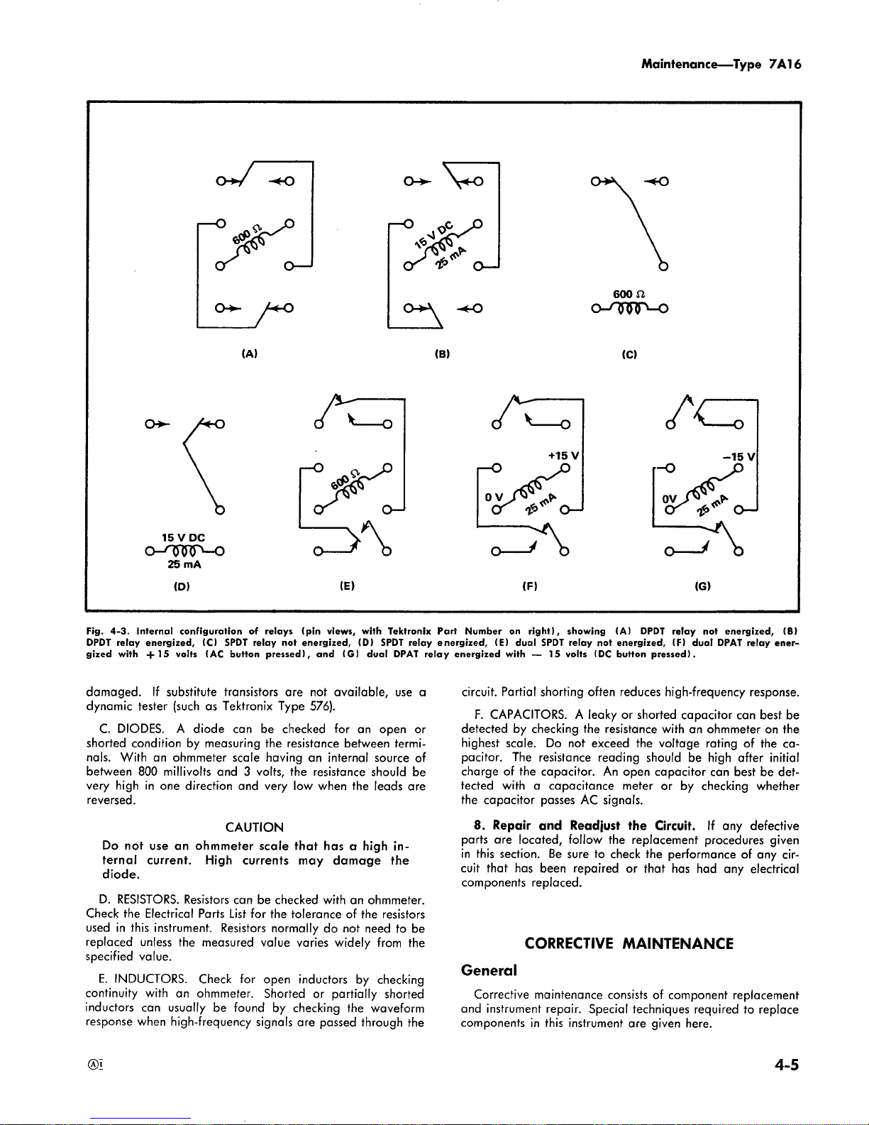
Fig.4-3.Internal
configurationofrelays
(pin
views,
with
Tektronix
Part
Number
on
right),
showing
(A)
DPDT
relay
not
energized,
(B)
DPDT
relay
energized,
(C)
SPDT
relay
not energized, (D)
SPDT
relay
energized,
(E)
dual
SPDT
relay
not
energized,
(F)
dual
DPAT
relay ener-
gized
with
+15
volts
(AC
button
pressed),
and
(G)
dual
DPAT
relay
energized
with-15
volts
(DC
button
pressed)
.
damaged.If
substitute
transistors
are not
available,
use a
dynamic
tester
(suchasTektronix
Type
576)
.
C.DIODES.A
diode
can
be
checked
for
an
open
or
shorted
conditionbymeasuring
the
resistance
between
termi-
nals.With
an
ohmmeter
scale
having
an
internal
source of
between
800
millivolts
and
3 volts,
the
resistance
should
be
very
highinone
direction
and
very
low
when
the
leads
are
reversed
.
D.RESISTORS.Resistors
canbechecked
with an
ohmmeter
.
Check
the
Electrical
Parts
List
for the
toleranceofthe
resistors
usedinthis
instrument.Resistors
normallydonot
needtobe
replaced
unless
the
measured
value
varies
widely
from
the
specified
value
.
E.INDUCTORS
.
Check
for
open
inductors
by checking
continuity
with
an
ohmmeter.Shorted or
partially
shorted
inductors
can
usuallybefound
by
checking
the
waveform
response
when
high-frequency
signals
are
passed
through
the
CAUTION
0-
Do
not
use
an
ohmmeter
scale
that
hasahigh
in-
ternal
current.High
currents
may
damage
the
diode
.
O~
'~Z
600
E2
~-O
0-TO
N-0
0
15VDC
Z
VM
25
mA
(D)
(E)
(F)
(G)
General
Maintenance
Type
7A16
circuit.Partial
shorting
often
reduces high-frequency response
.
F.CAPACITORS
.Aleakyorshorted
capacitor
can
best
be
detectedbychecking
the
resistance
withanohmmeter
on
the
highest
scale.Do
not
exceed
the
voltage
ratingofthe ca-
pacitor.The
resistance
reading
should
be
high
after
initial
chargeofthe
capacitor.An
open
capacitor
can
bestbedet-
tected
withacapacitance
meter
or
by
checking
whether
the
capacitor
passes
AC
signals
.
8.Repair
and
Readjust
the
Circuit.If
any
defective
parts
are
located,
follow
the
replacement
procedures
given
in
this
section.Be
suretocheck
the
performanceofany
cir-
cuit
that
has
been
repairedorthat
has
had any
electrical
components
replaced
.
CORRECTIVE
MAINTENANCE
Corrective
maintenance
consists of
component
replacement
and
instrument
repair.Special
techniques
requiredtoreplace
componentsinthis
instrument
are given
here
.
4-5
Page 23
Maintenance-Type
7A16
Obtaining
Replacement
Parts
Standard
Parts.All
electrical
and
mechanical
part
re-
placements
for
the
Type
7A16
canbeobtained through
your
local
Tektronix
Field
Office
or
representative.However,
many
of
the
standard
electronic
components
can
be
obtained
locallyinless
time thanisrequired
to
order
them
from
Tek-
tronix,
Inc.Before
purchasing
or ordering
replacement
parts,
check
the
parts
list
for
value,
tolerance,
rating
and
descrip-
tion
.
NOTE
When
selecting
replacement
parts,
it is
important
to
remember
that
the
physical
size
and
shape
of
a
component
may
affect
its
performance
in
the
instru-
ment,
particularlyathigh frequencies.All
replace-
ment
parts
should
be
direct
replacements
unless
it
is
known
that a
different
component
will
not
ad-
versely
affect
instrument
performance
.
Special
Parts.In
additiontothe
standard
electronic
com-
ponents,
some
special
parts
are usedinthe
Type
7A16.These
parts
are
manufacturedorselectedbyTektronix,
Inc.,to
meet
specific
performance
requirements,
or are
manufactured
for
Tektronix,
Inc.,in
accordance
with
our
specifications.These
special
parts
are
indicatedinthe
electrical
parts
listbyan
asterisk
preceding
the
part
number.Mostofthe
mechanical
parts
used
in
this
instrument
have been
manufactured
by
Tektronix,
Inc.Order
all
special
parts
directly
from your
local
Tektronix
Field
Officeorrepresentative
.
Ordering
Parts.When
ordering
replacement
parts
from
Tektronix,
Inc.,include
the
following
information
:
l.Instrument
Type
.
2
.
Instrument
Serial
Number
.
3.A
descriptionofthe
part
(if
electrical,
include
circuit
number)
.
4.Tektronix
Part
Number
.
Soldering
Techniques
WARNING
Disconnect
the
instrument
from
the
power
source
before
soldering
.
Circuit
Boards
.
The
components
mounted
on
the
circuit
boards
in
the
amplifier
can
be
replaced
using
normal
circuit
board
soldering
techniques.Keep
the
following
points
in
mind
when
solderingonthe
circuit
boards
:
1
.
Use
a
pencil-type
soldering
iron
with a
power
rating
from
15to50 watts
.
2.Apply
heat
from
the
soldering
iron to
the
junction
be-
tween
the
componentand
the
circuit
board
.
3
.
Heat-shunt
the
leadofthe
component
by
means
of
a
pair of
long-nosed
pliers
.
4
.
Avoid
excessive
heatingofthe
junction
with
the
circuit
board,asthis
could separate
the
circuit
board
wiring
from
the
laminate
.
4-6
5.Use
electronic
grade
60-40
tin-lead
solder
.
6.Clip
off
any
excess
lead
length
extending
beyond
the
circuit
board
and
clean
off
any
residual
flux
withaflux-
removing
solvent.Be
careful
that
the
solvent
does
not
re-
move
any
printing
from
the
circuit
board
.
Metal
Terminals.When
soldering
metal
terminals
(e .g
.,
switch
terminals,
potentiometers,
etc),
use
60-40
tin
lead
solder
anda15 to50watt
soldering
iron.Observe
the
following
precautions
when
soldering
metal
terminals
:
1 .
Apply
only,enough
heattomake
the
solder
flow
freely
.
2.Apply
only
enough
soldertoform a
solid
connection
.
Excess solder
may
impair
the
functionofthe
part
.
3.If
a wire
extends
beyond
the solder
joint,
clip
off
the
excess
.
4.Clean
the
flux
from
the
solder
joint
with
a flux-removing
solvent
.
Component
Replacement
WARNING
Disconnect
the
test
equipment
from
the
power
source before
replacing
components
.
Relay
Replacement
.
The
relaysinthe
Type
7A16
are
manufactured
by
Tektronix,
Inc.Ifarelay
fails,areplace-
ment
may
be
ordered
from your
local
Tektronix
Field
Office
or
representative.The
five-pin
relay
socketsonthe
circuit
board
will
accept
only
the
five-pin
SPDT
relay.Itispossible,
however,
to
place a
five-pin
SPDT
relayinan
eight-pin
socket
intended
for
use
with
oneofthe
eight-pin relays.This
would
not
damage
the
instrument
or
the
relay,
but
would
cause
a malfunctionofthe
instrument
.
The
eight-pin
DPDT
relays
may
be
placedintheir
sockets
facing
either
direction,
as
these
relays
are symmetrical.The
eight-pin
DPAT
relay
is
not
symmetrical
and
must
be
placedinthe
socket
with
the
Tektronix
Part
Number
facing
toward
the
topofthe
instru-
ment
.
Transistor
Replacement
.
Transistors
should
not
be
re-
placed
unless
actually
defective.If
removed
from
their
sockets
during
routine
maintenance,
return
them
to
their
original
sockets.Unnecessary replacement
of
transistors
may
affect
the
calibrationofthis
instrument
.
When
transistors
are
re-
placed,
check
the
operation
of that
partofthe
instrument
which
may
be
affected
.
Replacement
transistors
should
be
of
the
original
type or
a
direct
replacement.Remount
the
transistors
in
the
same
manner
as the
original.Fig.4-4
shows
the
lead
configura-
tionsofthe
transistors
used
in this
instrument.This
view
is
as seen from
the
bottom
of
the
transistor.When
replacing
transistors,
check
the
manufacturer's basing
diagram
for
correct
basing
.
Light-Bulb
Replacement
.
The
POLARITY,
BANDWIDTH,
and
Input
Coupling
switches
each
contain
one
incandescent
light
bulb
common
to
the
twoorthree
push-buttonsofthe
switch.This
light
bulb
may
be
replaced without
removal
of
the switchasfollows
:
1.Remove
the
screw
and
cover
from
the
backofthe
switch,
exposing
the
light
bulb
.
Page 24

2.While
holding
one
leadofthe
bulb
withapairoflong-
nosed
pliers,
touch a
15-watt
pencil-type
soldering
iron
to
the
connection on
the
other
side of
the
circuit
board.Remove
the
lead
from
the
circuit
board.Unsolder
the
remaining
lead
and
remove
the
bulb
.
3.Cut
the
leadsofthe
replacement
bulbtothe
same
length
as
thoseofthe old
bulb
.
4.Grasp
one
lead of
the
replacement
bulb with
the
long-
nosed
plier
and
positioninoneofthe
appropriate
holes
in
the
circuit
board.Touch
the
soldering
iron to
the
connection
on
the
other
sideofthe
circuit
board
and
push
the
lead
into
place.Repeat
with
the
remaining
lead
.
5.Position
the
bulb so
thatitdoes
not
fallinline
with
the
bottom
pushbutton.Replace
the
cover
.
POLARITY
BANDWIDTH,
or
Input
Coupling
Switch
Re-
placement.Should
oneofthe
pushbutton
switches
fail,
the
front
panel
must
be
removed
to
gain accesstothe switch
mounting
screws.Proceedasfollows
:
l .
Remove
the
four
control
knobs
from
their
shafts.The
IDENTIFY
button
pulls
off;use
a
'/16
-
inch
hex-head
wrench
to
remove
the
POSITION,
VOLTS/DIV,
and
VAR
control
knobs
.
2.Remove
the
front
paneltogain
accesstothe switch
mounting
screws
.
3.Remove
the
screw
holding
the faulty switch
assembly
.
Fig.4-4
.
Electrode
configuration
for
transistors in
this
instrument
.
l.Remove
the
attenuator
cover
.
CAUTION
Maintenance-Type
7A16
0200
BASE
I
COLLECTOR
EMITTER
Q40,
Q50
Q70,090
0125,
0135
Q140,
Q165
Q175,
Q180
EMITTER
UNUSED
(CLIP
OFF)
BASE
COLLECTOR
0170
EMITTER
BASE
_COLLECTOR
4
.
Remove
the
connectionsonthe
circuit
board
.
5.Install
the
replacement
switchbyreversing the
above
procedure
.
VOLTS/DIV
Switch
Strip
Replacement.The
VOLTS/DIV
switch
contains
ten
strips
which
are
individually
adjusted
for
optimum
input
responseineach
positionofthe switch.These
strips
should
not
be
removed
unless
they are
known
to
be
defective,inwhich
case
replacements
canbeobtained
from
your
local
Tektronix
Field
Office
or
representative.To
replace
a
defective
strip,
proceed
as
follows
:
2.Rotate
the
VOLTS/DIV
control
to
position
the
defective
striptothe
right
sideofthe
instrument
.
3.Move
the
strip
about
one-quarter
inch
toward
the
rear
of
the
switch.Lift
the
strip
outofthe
switch
assembly
.
4
.
Replace
the
defective
strip
with
the
new
part.(Refer to
the
Electrical
Parts
List
for
replacement
information
.)
When
replacingaVOLTS/DIV
switch
strip,
care-
fully
align the
guidesonthe
edges
of the
strip
with
the
grooves
in
the switch
assembly,
then
slide
the
strip
into
place
.
4-7
Page 25

Maintenance-Type
7A16
5.Adjust
the
new
strip(s)
for
optimum
response
as
de-
scribedinSection5.
Main
Circuit
Board
Replacement
.
If
the
main
amplifier
circuit
board
requires
replacement,acomplete
wired
board
is
available
from
Tektronix,
Inc.To
replace
the
circuit
board,
proceedasfollows
:
1.The
GAIN
potentiometer
is
driven
from
the
front
panel
byacontrol
shaft.Using
a
.05-inch
hex-head
wrench,
loosen
the
two
set
screws
on
the
front
portionofthe
coupling
and
remove
the
shaft
.
2.Disconnect
the
VARIABLE
control
shaft
from
the
push
switch
and
potentiometer
.
3.Remove
the
two
screws
which
secure
the
circuit
board
to
the
VOLT$/DIV
switch
housing
.
4.Unsolder
R14-C14
(connected
from
the
VOLTS/DIV
switchtothe
tie
pointatthe
front
of
the
circuit
board)
from
the
VOLTS/DIV
switch
.
5
.
Remove
all
the pin
connections
on the
left
side
of
the
main
circuit
board
.
6.Unsolder
the
four
leads
from
the
VARIABLE
switch
(cal/
uncal
switch)
circuit
board
.
7
.
Remove
the
four
screws
which
secure
the
rear
casting
to
the
top
and
bottom
frames
.
8.Remove
the
screws
on
the
six
mounting
clamps
along
the top
and
bottom
edgesofthe
circuit
board
.
9.Remove
the
circuit
board
assembly
from
the
instrument
.
10.Lift
the top
and
bottom
tabs
which
hold
the
rear
cast-
ingtothe
circuit
board
and
remove
.
11.Unsolder
the
VARIABLE
and
GAIN
potentiometer con-
nections
and
remove
the
mounting
brackets
from
the
circuit
board
.
12.Install
the
replacement
circuit
board
by
reversing the
above
procedure
.
The
wiring
color-codes
for
the
pin
con-
nections
are
showninFig.4-5
.
Recalibration
After
Repair
After
any
electrical
component
has
been
replaced,
the
calibrationofthat
particular
circuit
should
be
checked,
as
wellasthe
calibration
of
other
closely
related
circuits.The
Performance
Check
procedureinSection
5
provides a quick
and
convenient
means
of
checking
instrument
operation
.
Circuit
Board
Square
Pin
Replacement
.Ifthe
circuit
board
pins
are
damaged
or
brokenafield
replacement
kit
(Tektronix
Part
Number
040-0542-00),
containing
the
necessary
parts
andareplacement
instruction
sheet,
can
be
obtained
from
Tektronix,
Inc.To
replaceapin
proceedasfollows
:
l.Remove
the
broken
pin
by
applying
heat to
the pin
while
maintaining a
steady
pullonthe
pin.Do
not use
ex-
cessive
heat
as
this
may
separate
the
pin
ferrule
from
the
circuit
board
laminate
.
2.Remove
and
discard
the
ferrule
from
the
new
pin
.
3.Position
the
new
pininplace
and
carefully
solder
the
pintoboth
sides
of
the
circuit
board.Do
not
use
excessive
heat
.
4.For those
pins
that
have
been
formed, use
plierstobend
to
appropriate
configuration
after installation
.
End
Lead
Pin
Connector
Replacement.The
pin
connec-
tors
usedtoconnect
the
wirestothe
circuit
board
pins
are
clamped
to
the
ends
of the
associated
leads
.
To
replace the
pin
connectors
proceed
as
follows
:
1.Clip
off
the
damaged
pin
connector
and
dress
the lead
for the
new
connector
.
2.Clamp
the
new
pin
connectortothe lead
.
Some
of
the
pin
connectors
are
grouped
together
and
mounted
inaplastic
holder.To remove
the
pin
connector
from
the
plastic
holder,
lift
up on
the
back
end
and
pull
out
.
To
provide
correct
orientationofthis
multi
connector
when
it is
replaced,
an
arrowisstamped
on
the
circuit
board
and
a
matching
arrow
is
molded
into
the
plastic
housingofthe
multi
pin
connector
.
Instrument
Repackaging
If
the
Type
7A16
is
tobeshipped
for
long
distances
by
commercial
means
of
transportation,
it is
recommended
that
the
instrument
be
repackaged
in
the
original
manner
for
maximum
protection.The
original
shipping
carton
can
be
saved
and
used
for
this
purpose
.
Repackaging
information
and/or
new
shipping cartons
can
be
obtained
from
Tektronix,
Inc.Contact
your
local
Tektronix
Field
Officeorrepresenta-
tive
.
NOTE
The
plug-ins
should
notbeshipped
installedinan
oscilloscope.The
oscilloscope
packaging
material
is
not
designed
to
protect the
plug-ins
.
Page 26

.
-
oo
Braid
Braid
Braid
BIk_:r-----"
BIk
Blk'~
Red
Wht-grn
W
ht-orn
Wht-brn
Wht-hIIc-ye1
VVht-ggry
Wht-vio
Wilt vel
-
_-
w~
~--
._
o
Wtit-hlk-red
iv`"ivN
CLNC
N
U
NCcNrriv
--_
R207'
R
206
.--
~"
-\~,Nht
Vio
hlk---Red-brn
VV
ht red
- ~
L
U
^-
R204
~
r~
Btaid
INht
Blk
Red
U
Red
---,;~
;
U
-__L"
----
~-
\\
ro
.N
~
J
,ct-
C104,
,8156
Ii
R~
CJE
ON
_
._
CR200
M
4,
8130
'-f-8170-:
rr
R31
.C56
-VR30
-
.C30''L30
R
R151;~~
8100-\,,
.R10n~
.--R150
04
.
R
154
'
VR723'
R200
`
R 101
-,
8
,
"
.
`R61~C~'
R80
82ccH
R£rB
-
q'7
,
Lii161
R1E0-
121
C16
"
R16
(]1
I?16/
CR29
Q20
~,
R3
'C
:45
vQ40:R40,L20
ct
,
I
R60
~~
C5
060
168
.
R68
I?
n0'
OSIO
ti7c1
C57_R74
L__-R102
I?
109'
H1159
lilll
C~
11:a-"~
R
k1"
'u
.
1
~
._
.
0125_
._
.
;
-~
Rf,1
2b
' .
-
5
~'"
_
166
C124
8123
L
8120
R18
,
"
R73
1"
159
R118'
.a
:
C18
VR20
. (
.,To
R
106
8117
C20'"
Maintenance-Type
, .
-W716,Vs8123,
R1r'
1
r~li
F1 c
,~a
"
~-~.".
L
8
4
0169
('125
-
124-
"°
8128
7A16
a°
.
-
,
33
R1
C133
?
:
J
LR140
?ER182
8181
8,141
CR168
ccsU
CH
128
017
8172-
R
8177
137
cc"
5
d
Cc
--Brn
cn c~
w
M
~/
NN
11N
UU
UU',
A
x
Fig.4-5
__
Red
bll<
cc
.
Main
amplifier
circuit
board
(front)
.
4-9
Page 27

Maintenance-Type
7A16
4-6.Main
amplifier
circuit
board
(rear)
4-10
Fig
.
.
Page 28

INTRODUCTION
SECTION
5
PERFORMANCE
CHECK
/
CALIBRATION
Change
information,ifany,
affecting
this
section
willbefound
at
the
rear
of
the
manual
.
To
assure instrument
accuracy,
check
the
calibration
of
the
7A16
every
1000
hoursofoperation,
or every
six
months
if
used
infrequently.Before
complete
calibration,
thoroughly
clean
and
inspect
this
instrumentasoutlinedinthe
Main-
tenance
section
.
As an
aidtothe
calibrationofthe
instrument,aShort-
Form
Procedureisgiven
priortothe
complete
procedure
.
To
facilitate
instrument
calibration
for
the
experienced
cali-
brator,
the
Short-Form
Procedure
lists
the
calibration
adjust-
ments necessary
for
each
step
and
the
applicable
tolerances
.
This
procedure
also
includes
the
step
number
and
title
as
listedinthe
complete
Performance
Check/Calibration
Pro-
cedure
and
the
page
number
on
which
each
step
begins
.
Therefore,
the
Short-Form Procedure
canbeusedasan
index
to
locate
a stepinthe
complete
procedure
.
Another
feature
of
the Short-Form
Procedureisthe
spaces
providedtorecord
performance
data
or to
check
off
steps
as they are
com-
pleted.This
procedure
can be
reproduced
and
usedasa
permanent
recordofinstrument
calibration
.
The
complete Performance
Check/Calibration
Procedure
can
be
used
to
check
instrument
performance
without
re-
moving
the
covers or
making
internal
adjustments
by
per-
forming
all
portions
except
the
ADJUST
partofa
step
.
Screwdriver
adjustments
accessible
without
removing
the
covers are
adjustedaspart
of
the
performance
check
pro-
cedure.A
note
titled
PERFORMANCE
CHECK
ONLY
gives
instuctions
which
are applicable onlytothe
performance
check procedure
andifnecessary,
lists
the
next
applicable
step
for
the
performance
check
procedure
.
Completion
of
each
stepinthe
complete
Performance
Check/Calibration
Procedure
insures
that
this
instrument
meets
the
electrical
specifications
giveninSection1.
Where
possible,
instrument
performance
is
checked
before
an
adjustment
is
made.For
best
overall
instrument
performance
when
performingacomplete
calibration
procedure,
make
each
adjustmenttothe
exact
setting
even
if
the
CHECK
is
within the
allowable
tolerance
.
NOTE
Limits,
tolerances
and
waveforms
in
this
procedure
are
given
as calibration
guides
and
should
not
be
interpreted
as
instrument
specifications
except
as
specifiedinSection
1 .
All
waveforms
shown
in
this
procedure
were
taken
with
a
Tektronix
Oscillo-
scope
Camera
System
.
Type
7A16
A
partial
calibrationisoften
desirable
after
replacing
components,
ortotouch
up
the
adjustmentofa
portion
of
the
instrument
between
major
recalibrations.To
check
or
adjust
only
part
of the
instrument,
set
the
controls
as given
under
Preliminary
Control
Settings
and
start
with
the
nearest
test
equipment
picture
preceding
the
desired
portion.If
any
controls
need
tobechanged
from
the
preliminary
settings
for
this
portion
of
the
calibration
procedure, they are
listed
under
the
heading
Partial
Procedure
following
the
equipment
required
picture
.
To
prevent
unnecessary
recalibration
of
other
parts
of
the
instrument,
readjust
onlyifthe
tolerance
giveninthe
CHECK
partofthe
stepisnot
met.If
readjust-
ment
is
necessary,
also
check
the
calibrationofany
steps
listedinthe
INTERACTION
part of
the
step
.
General
TEST
EQUIPMENT
REQUIRED
The
following
test
equipment
and
accessories,
or
its
equiv-
alent,
are
required
for
complete
calibrationofthe
Type
7A16.Specifications
given are
the
minimum
necessary
for
accurate
calibration.Some
of
the
recommended
equipment
may
have
specifications
which
exceed
those
given.All
test
equipmentisassumed
to
be
correctly
calibrated
and
oper-
ating
within
the given
specifications
.
If
equipment
is
sub-
stituted,itmust
meet
or
exceed
the
specifications
of the
recommended
equipment
.
Test
Equipment
1 .
7000
series
Indicator
Oscilloscope.Type
7704
used
in
these
checks
.
2.7B-series Time-Base.Type
71371
usedinthese
checks
.
3.Test
Oscilloscope
.
Storage
and
Sampling
capabilities
;
bandwidth,
at
least
1000
megahertz;minimum
deflection
factor,50millivolts/div
.
Tektronix
Type
56413
with
3Sl
/3T2
plug-in
units
recommended
.
4.Pulse
Generator.Risetime,0.25
nanosecond;amplitude,
0to50
volts
into
50
ohms.Tektronix
Type
109
recommended
.
5.Delay
Line.Characteristic
impedance,
50
ohms;60
nanoseconds
delay.Tektronix
Type
113
Delay
Cable
rec-
ommended
.
Page 29

Performance
Check/Calibration-Type
7A16
6.Constant
Amplitude
Sine-Wave
Generator.Reference
frequency,
50
kHz;frequency
range,
below
15
megahertz
to
above
60 megahertz;output
amplitude, variable
from0.5
to5volts
peaktopeak;amplitude
accuracy,
within3%of
50
kHz
reference
as output
frequency
changes.Tektronix
Type
191
Constant
Amplitude
Signal
Generator
recom-
mended
.
7.Type 106
Square
Wave
Generator
.
Risetime,1nano-
second
into50ohms
;
amplitude,50mVto500mV;
frequency,
1
kHz
.
8.Constant
Amplitude
Signal
Generator
.
Repetition
rate,
about1kHz
;
voltage
range,25millivoltsto25
volts;ac-
curacy,±0.25%
.
Tektronix
Standard
Amplitude
Calibrator
067-0502-00
recommended
.
9.DC
Voltmeter.20,000
ohms/volt
minimum
sensitivity
;
range,0to50volts;accuracy,
checkedtowithin10/.atthe
voltagestobe measured
.
For
example,
Triplett
Model
630-NA
.
10.Calibration
Fixture,
Constant
Amplitude
Signal
Gener-
ator.Reference
frequency,
3
megahertz;frequency
range,
65
megahertztoabove
175
megahertz
;
output
amplitude,0.5
to5volts
peaktopeak
into50ohms
;
amplitude
accuracy,
output
amplitude
constant
within1%of3
megahertz
refer-
ence
as output
frequency
changes.Tektronix
Part
Number
067-0532-00
.
11
.
Calibration
Fixture,
Plug-In
Extender
.
Tektronix
Part
Number
067-0589-00
.
12.Pulse
Generator.Risetime,70picoseconds
;
amplitude,
200mVinto50ohms
;
pulse
width,1microsecond
.
Tektronix
Type
284
recommended
.
Accessories
13.Cable
(two)
.
Impedance,
50
ohms;electrical
length,
2
nanoseconds;connectors,
GR.Tektronix
Part
Number
017-
0505-00
.
14.Adapter
(two).GRtoBNC
female.Tektronix
Part
Num-
ber
017-0063-00
.
15.Adapter.GR
to
BNC
male.Tektronix
Part
Number
017-0064-00
.
16.Adapter
(two).GR
elbow
.
Tektronix
Part
Number
017-
0070-00
.
17
.
Termination.Impedance,50ohms
;
endline;connector,
GR
.
Tektronix
Part
Number
017-0081-00
.
18.50
ohm
Feedthrough
Termination
.
Tektronix
Part
Num-
ber
011-0049-01(2each)
.
19
.
1OX
Attenuator,
BNC
connectors
.
Tektronix
Part
Num-
ber
011-0059-01,(2
each)
.
20.15
pF
RC
Normalizer,
BNC
connectors
.Tektronix
Part
Number
067-0537-00
.
21.Coaxial
Cable;electrical
length,
5
nanoseconds;GR
connectors
.
Tektronix
Part
Number
017-0512-00
.
5-2
22.CT-3
Signal
Pickoff.Tektronix
Part
Number
017-0061-00
.
23
.
Coaxial
Cable.Impedance,
50
ohms;length,42inches
;
connectors,
BNC.Tektronix
Part
Number
012-0057-01
.
SHORT
FORM
PROCEDURE
Type
7A16
Calibration
Date
Calibrated
By
j]
3
.
Adjust
DC
Balance
(R34)
Page
5-4
Requirement
:
Adjusted
for
zero
volts
from
TP60
to
ground
.
Performance:Correct
;
Incorrect
Check/Adjust
Variable
Balance
(R89)
Page
5-4
Requirement:0
.5
divorlessoftrace
shift
as
VARI-
ABLEisrotated
.
Performance:Correct
;
Incorrect
Check
Step
Attenuator
Range
Page
5-4
Requirement:At
least
10
divisionsat5
mV/div
.
Performance:Correct
;
Incorrect
4
.
Check/Adjust
Step
Attenuator
BalancePage
5-4
(Rl53)
Requirement:Trace
shift
of
0.5divisionorless
as
VOLTS/DIV
is
changed
from
one
settingtothe
next
.
Performance
:
Correct
;
Incorrect
Adjust
Position
Centering
(R117)
Page
5-5
Requirement:No
potential
difference
between
the
output
lines
(All
and
Bll)
when
the
traceisposi-
tioned
to
graticule
center
.
Performance
:
Correct
;
Incorrect
6.Check
Position
Range
Page
5-5
Requirement
:
±10
divisions
from
graticule
center
.
Performance
:
Correct
;
Incorrect
7.Check -SUP
to Invert Shift
Page
5-5
Requirement
:
One
divisionorless
trace
shift
when
switching
from
+UP
to
INVERT
.
Performance:Correct
;
Incorrect
Check/Adjust
Front
Panel
Gain
(R66)
Page
5-5
Requirement:With
the
VOLTS/DIV
at 10
mV
and
a50mV
signal
applied,
the
display
can be
adjusted
to
five
divisions
.
Performance:Correct
;
Incorrect
0
9
.
Check
Variable
Control
Range
Page
5-6
Requirement:Continuously
variable
between
cali-
brated
VOLTS/DIV
settings
(2
.5 :1
ratio)
.
Performance:Correct
;
Incorrect
Page 30

F110.
Check
Trigger
DC
Level
Page
5-6
Requirement:Within
one
divisionofsignalDClevel
.
Performance:Correct
;
Incorrect
0
11.Check
Trigger
Gain
Page
5-6
Requirement:Within
10%
of
signal
gain
.
Performance:Correct
;
Incorrect
12.Check
Volts/Div
Deflection
Accuracy
Page
5-6
Requirement:Vertical
deflection
factor
within
2%
of
VOLTS/DIV
switch
indication
with gain
adjusted
at 10
mV/Div
.
Performance
:
Correct-
;
Incorrect
13.Adjust
Input
Compensation
(C18)
Page
5-7
Requirement:Optimum
square
wave
response
.
Performance
:
Correct
;
Incorrect
14
.
Adjust
Volts/Div
Compensation
(C6A,
Page
5-7
C6B,
C7A,
C7B,
C8A,
C8B,
C9A,
C9B,
C10A,
C10B,
C11A,C11B,C12A,
C12B)
Requirement:Optimum
square
corner
and
flat
top
.
Performance:Correct
;
Incorrect
0
15.Adjust
High
Frequency
Compensation,
Page
5-8
5
mV
(R40,
R55,
C61,
C102,
C52, C45,
C103,
R103,
R61)
Requirement:Best
square
corner
and
level
with
aber-
rations
nottoexceed
6%
P-P
.
Performance:Correct
;
Incorrect
16.Adjust
High
Frequency
Compensation,
Page
5-8
10
mV
(R111,
C111)
Requirement:Best
square
corner
and
level
with
aber-
rations
nottoexceed
6%
P-P
.
Performance:Correct
;
Incorrect
17.Adjust
High
Frequency
Compensation,
Page
5-8
20
mV
(R109,
C109)
Require)ent:Best
square
corner
and
level
with
aber-
rations
nottoexceed
6%
P-P
.
Performance:Correct
;
Incorrect
Check
Step
Response
Page
5-9
Requirement:Risetime
nottoexceed1.4
nanoseconds
and
aberrations
nottoexceed
6%
P-P
at 5
mV/div
to.5V/divor8%
P-Pat1
V/divto5
V/div
.
Performance:Correct
;
Incorrect
F
- 119.
CheckUpper
Bandwidth
-3
dB
Point
Page
5-9
Requirement:Not
more
than
-3
dB
at
250
mega-
hertz
.
Performance:Correct
;
Incorrect
Performance
Check/Calibration-Type
7A16
0
20.Check
Trigger Step
Response
Page
5-10
Requirement:Risetime
nottoexceed2.1
nanoseconds
and
aberrations
nottoexceed
15%
P-P
.
Performance:Correct
;
Incorrect
F]21.
Check20Megahertz
Bandwidth
LimitingPage
5-11
Requirement
:
-3
dBat20
megahertz
within3mega-
hertz
.
Performance:Correct
;
Incorrect
E]22.
Check
Overall
Noise
Level
Tangentially
Page
5-11
General
Requirement:0.1division or
lessat5
mV/division
.
Performance:Correct
;
Incorrect
PERFORMANCE
CHECK/CALIBRATION
PROCEDURE
The
following
procedureisarranged
so
the
Type
7A16
can
be
calibrated
with
the
least
interaction
of adjustments
and
reconnection of
equipment.A
pictureofthe
test
equip-
ment
required
for
each
group
of
stepsisgiventoaid
in
identification of
the
necessary
equipment.The
control
set-
tings
and
test
equipment
setup
throughout
this
procedure
continue
from
the
preceding
step(s)
unless
noted otherwise
.
The
control
settings
can
be
checkedatany
"test
equipment
required"
picturebysetting
the
controls
as
givenatthe
startofthe
procedure under
the
heading
Preliminary
Con-
trol
Settings.Then
make
any
changes
listed
following
the
test
equipment
required
picture,
under
the
heading
Partial
Procedure
(also
applies
to
partial
calibration
procedure)
.
The
following
procedure
uses
the
equipment
listed
under
Test
Equipment
Required
.Ifother
equipmentissubstituted,
control
settings or
calibration
setup
may
needtobe
altered
to
meet
the
requirements of
the
equipment
used.Detailed
operating
instructions
for
the
test
equipment
are
not
given
in
this
procedure.Refer
to
the
instruction
manual
for
the
test
equipmentifmore
information
is
required
.
zontal
compartment
.
NOTE
This
instrument
shouldbe
calibratedatan
ambient
temperature
of
+20°Ctox-30°C
for
best
overall
accuracy.The
performance
of
this
instrument
can
be
checked
at
any
temperature
within the 0°C
to
x-50°C
range.If
the
temperature
is
outside
the
given
range, see
Section1for
the
applicable
tol-
erances
.
Preliminary
Procedure
for
Complete
Calibration
1.Connect
the
Type
7A16tothe
plug-in
extender
.
2.Insert
the
plug-in
extender
in
the
oscilloscope
right
vertical
compartment
.
3.Insert
the
time
base
in
the
oscilloscope
left
(A)
hori-
Page 31

Preliminary Control
Settings
Type
7A16
POSITION
Midrange
POLARITY
+UP
BANDWIDTH
FULL
COUPLING
GND
VOLTS/DIV
5
mV
VARIABLE
CAL
IN
(Fine
and
Coarse)
Fully
cw
Horiz
Position
Midrange
5-
4
Position
(A
and
B)
Midrange
Dual
Trace
A
--I--
B
mVOLTS/Div
(both)
50
CH
1
Invert/Norm
Norm
CH2Invert/Norm
Invert
Internal
Trigger
A
1.Adjust
DC
Balance
(R34)
a.Set the
COUPLING
switchtoGND
and
center the
trace
on
the
CRT
with
the
POSITION
control
.
Type
711371
a.Set the
controls
as given under
Preliminary
Control
Settings
.
Level/Slope
0/-}
b.Connect
the
voltmeter
between
TP 60
and
ground
.
Triggering
c.ADJUST-R34
for
zero
volts
from
TP 60
to
ground
.
Mode
P-P
Auto
Coupling
AC
Source
Int
2.Check/Adjust
Variable
Balance
(R89)
Magnifier
X
1
a.Press
and
release
the
VARIABLE
controltoits
outward
Time/Div
0.5ms
position
.
Variable
Cal
In
b
.
CHECK-For
0.5divorless
of
trace
shiftasthe
VARI-
B
Delay
Mode
Independent
ABLE
controlisrotated
throughout
its
range
.
Type
7704
c.ADJUST-R89
for
minimum
movement
of
traceasVARI-
ABLE
controlisrotated
.
Intensity
cow
Calibrator
3.Check
Step
Attenuator
Range
Rate
1
kHz
Volts
40
mV
a.Turn
STEP
ATTEN
BAL
adjustment
fully
clockwise
and
Vertical
Mode
Right
position
the
tracetograticule
center
with
the
POSITION
control
.
Horizontal
Mode
A
A
Trigger
Source
Right Vertical
b
.
Connecta50mVsquare
wave
from
the
standard
ampli-
tude
calibrator
to
the
Type
7A16
INPUT
.
Performance
Check/Calibration-Type
7A16
4.Connect
the
oscilloscopetoa
suitable
power
source
.
Range
100
ns
Start
Point
With
Trigger
5.Set the
controls
as given
under
Preliminary
Control
Time
Magnifier
X
1
Settings
.
Display
Mode
Normal
6.Turn
the
oscilloscope
power
switchtoon
and
allow
Polarity
-I-
20
minutes
warmup
before
proceeding
with
calibration
of
Source
Int
the
instrument
.
Type
3S1
c.CHECK-Set
the
COUPLING
switch
to
DC
and
turn
Type
564B
the
STEP
ATTEN
BAL
adjustment
fully
counterclockwise
.
Check
that
the top
of
the
square
waveisat
or
below
grati-
Intensity
Optimum
cule
center
.
Upper
Screen
Store
Lower
Screen
Store
d.Set the
STEP
ATTEN
BAL
adjustment
to
midrange
.
Type3T2
4.Check/Adjust
STEP
ATTENUATOR
BAL
(R153)
Time
Position
Page 32

PERFORMANCE
CHECK
This
adjustment
may
be
performed
as
part
of the
Performance
Check
.
b.ADJUST-STEP
ATTEN
BAL
(a
front-panel
adjustment)
for
minimum
trace
shiftasthe
VOLTS/DIV
is
changed
from
5
mV
to20mV
.
c.CHECK-The
remaining
positionsofthe
VOLTS/DIV
switch fornotrace
shift
between
steps
.
5.Adjust
Position
Centering
(8117)
a.Center
the
traceonthe
CRT
with
the
POSITION
control
.
b.Connect
the
voltmeter
betweenAll
and
B11
(the
rear-
ward
endofR185
and
R145)
.
c.ADJUST-R117
foranull
(zero)
reading
on
the
volt-
meter
.
6.Check
Position
Range
a.Set the
input
COUPLING
to
AC,
VOLTS/DIV
to20mV
and
center
the
trace
with
the
POSITION
control
.
Fig.5-1.Test
equipment
required
for
steps8through12.
Performance
Check/Calibration-Type
7A16
b.Set the
oscilloscope
calibratorto40
mV
and
connect a
BNC
cable from
the
calibrator
outputtothe
Type
7A16
INPUT
.
c.Center
the
display
on
the
CRT
with
the
POSITION
control
.
d.Reset
the
oscilloscope
calibratorto0.4V
and
turn
the
POSITION
control
fully
clockwise
.
e.CHECK-The
bottom
of
the
waveform
must
position
to
graticule
centerorabove.Turn
the
POSITION
control
fully
counterclockwise
and
check
that
the topofthe
wave
form
can
be
positionedtograticule
centerorbelow
.
f
.
Disconnect
the
signal
from
the
Type
7A16
INPUT
.
7.Check
-f-
UP
to
INVERT
shift
a.Set the
VOLTS/DIV
to
5mV.
b.CHECK-Press
the
INVERT
button
and
check
for
1
divisionorlessoftrace
movement
.
8.Check/Adjust
Front
Panel
GAIN
(R66)
a
.
Test
Equipmentisshown
in
Fig.5-1
.
Page 33

Performance
Check/Calibration-Type
7A16
b.Set the
VOLTS/DIV
to10mV,
POLARITY
to+UP
and
COUPLING
toDC.
c
.Connecta50mVsquare
wave
signal
from
the
standard
amplitude
calibrator
throughacoaxial
cabletothe
Type
7A16
INPUT
connector
.
d.CHECK-The
vertical
amplitude
for
exactly5divisions
.
PERFORMANCE
CHECK
This
adjustment
may
be
performed
as part of
the
performance
check
.
e.ADJUST-GAIN
(a
front
panel
adjustment)
for
exactly
5
divisionsofvertical
amplitude
.
9.Check
VARIABLE
Control
Range
a.With
the
standard
amplitude
calibrator
connected
as
above,
press
and
release
the
VARIABLE
controltoits
outward
position
.
b
.
CHECK-Rotate
the
VARIABLE
control
fully
counter-
clockwise
and
check
for2divisionsorless
off
vertical
ampli-
tude(2.5 :1
ratio
requirement)
.
c.Return
the
VARIABLE
controltothe
CAL
IN
position
.
10.Check
Trigger
DC
Level
a.Set the
Type
7A16
COUPLING
switchtoGND
and
position
the
tracetograticule
center
with
the
POSITION
control
.
b.Connect
the
extender
trigger
cablestothe signal
jacks
and
terminate
the signal
cables
into50ohms
.
c.CHECK-The
trace
must
be
within
one
divisionofgrati-
cule
center
.
11.Check
Trigger
Gain
a.Reset
the
COUPLING
switchtoAC
and
VOLTS/DIV
to
10
mV
.
b.Connect
a 50mVsquare
wave
from
the
standard
ampli-
tude
calibratortothe
Type
7A16
INPUT
.
c.CHECK-For
a
display
amplitudeoffive
divisions
-!-0
.5
division
.
d.Return
the
extender
trigger
and
signal
cablestotheir
correct
jacks
.
12.Check
VOLTS/DIV
Deflection
accuracy
a.CHECK-Using
Table
5-1
as
a
guide,
check
the
vertical
deflection
factor
from 5
voltsto5
millivolts
.
b.Disconnect
the
standard
amplitude
calibrator
.
5-6
TABLE
5-1
Deflection
Factor
Accuracy
Check
E
5
-------------
NEEMENNEMM
ENEEMENEW
""NOWNEEN
OEM
a~;si~~ra
~aosa~
a~re~~&
tdfir~euz
;
~*iii~ma~
No
NEENEEM
mmadmoommm
MEMEMMMMM
Fig
.
5-2.(A)
Compensation
incorrectly
set
.
(B)
Input
properly
compensated
.
VOLTS/DIV
Switch
Setting
Standard
Amplitude
Calibrator
Output
Amplitude
Divisions
of
Deflection
Accuracy
5V
20V
4
+2°/
2V
lov
5
±2%
1
V
5
V
5
-1-2%
.5V
2V
4
±2%
.2
V
l
V
5
±2%
.l
V
.5
V
5
+-2%
50
mV
.2
V
4
±2%
20
mV
.1
V
5
±2%
10
mV
50
mV
5
±2%
5
mV
20
mV
4
±2%
Page 34

13.Adjust
Input
Compensation
(C18)
a.Reset
the
Type
7A16
VOLTS/DIV
to5mV
and
the
time-
base
Time/Div
to.1ms
.
b.Connect
a 3
kHz
square
wave
from
the
Type
106
high-
amplitude
output through a
GR
to
BNC
adapter,
coaxial
cable,
10X
attenuator,
50
ohm
feedthrough
termination
and
15pFinput
RC
normalizer
to
the
Type
7A16
INPUT
connector.Adjust
the
Type
106
amplitude
for
about
four
divisionsofdisplay
.
c.ADJUST-C18
for
best
square
leading
corner
(no
over-
shoot or
rolloff,
see
Fig.5-2A
andB).
d.Switch
the
COUPLING
to
AC
and
check
that
the
dis-
play
shiftsupabout
two
divisions.Return
the
COUPLING
switch
to
DC
.
14.Adjust
Volts/Division
Series
and
Shunt
Compensation
a
.
Using
Table
5-2
as a
guide,
check
the
CRT
display
at
each
VOLT/DIV
setting
and
adjust
for
best
square
leading
corner
and
flat
top on
the
display.Adjust
the
Type
106
amplitude
as necessarytomaintain a
four
division
display
for
each
VOLTS/DIV
setting
.
Partial
Procedure
Performance
Check/Calibration-Type
7A16
TABLE
5-2
Series
and
Shunt
Compensations
b
.
Disconnect
the
Type
106
square
wave
generator
.
If
beginningapartial
procedure
with
this
step,
set
the
controls
as
given
under
Preliminary
Control
Settings,
except
set
the
Type
7A16
Input
CouplingtoDC
.
VOLTS/DIV
Switch
Setting
Adjust
For Best
Flat
Top
Adjust
For Best
SquareCorner
50
mV
C6A
C6B
-
.1
V-
-
.
C7A
C7B
.2
V
C8A
C8B
.5
V C9A
C9B
1
V
C1
OA
C1
0B
2
V
C11A
C11B
5V
C1
2A
C1
2B
Page 35
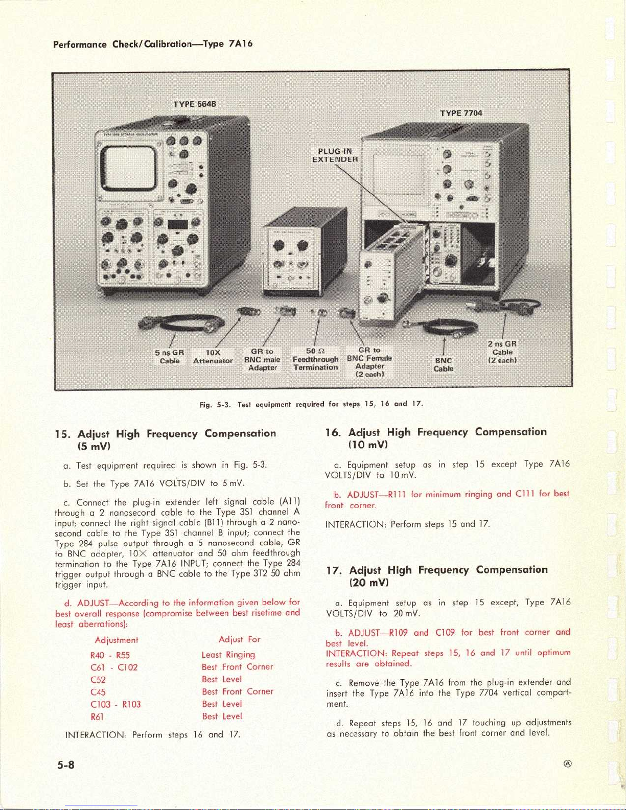
Performance
Check/Calibration-Type
7A16
15.Adjust
(5
a.Test
b.Set the
c.Connect
through
input;connect
second
Type
284
to
BNC
terminationtothe
trigger
output
trigger
d.ADJUST-According
best
overall
least
aberrations)
INTERACTION
High
mV)
equipment
Type
the
a 2
nanosecond
the
cabletothe
pulse
adapter,
throughaBNC
input
.
response
Adjustment
R40-R55
C61-Cl 02
C52
C45
C103-R103
R61
Frequency
requiredisshown
7A16
VOL
plug-in
cabletothe
right
signal
Type
output
through
1OX
attenuator
Type
7A16
to
(compromise
:
Perform
:
Fig.5-3.Test
Compensation
in
TS/DIV
extender
3S1
the
steps16and17.
to5mV
left
signal
Type
(1311)
nanosecond
and
between
Least
Best
Best
Best
Best
Best
through
input;connect
50
Adjust For
Ringing
Front
Level
Front
Level
Level
cable
channel B
a 5
INPUT;connect
cabletothe
information given
Fig.5-3
.
3S1
ohm
the
Type
best
Corner
Corner
equipment
.
(All)
cable
channel
a 2
nano-
cable,
feedthrough
Type
284
3T250ohm
below
risetime
and
A
the
GR
for
required
for
steps
16.Adjust
(10
a.Equipment
VOLTS/DIV
b.ADJUST-8111
front
INTERACTION
17.Adjust
a.Equipment
VOLTS/DIV
b.ADJUST--8109
best
level
INTERACTION
results
c.Remove
insert
ment
.
d.Repeat
as necessarytoobtain
15,
corner
(20
are
the
16 and 17
mV)
tol0mV
.
mV)
to20mV
.
obtained
Type
steps
High
setup
:
Perform
High
setup
Repeat
:
the
7A16
Type
15,
.
Frequency
in
step
as
.
for
minimum
steps15and17.
Frequency
as
in
step
.
and
C109
steps
15,16and
.
7A16
from
into
the
and
16
the
best
Compensation
15
ringing
Compensation
15
for
best
the
plug-in
Type 7704
17
touching
front
corner
except
and
C111
except,
front
17
until
extender
vertical
up adjustments
and
Type
Type
corner
optimum
compart-
level
for
7A16
best
7A16
and
and
.
5-8
Page 36
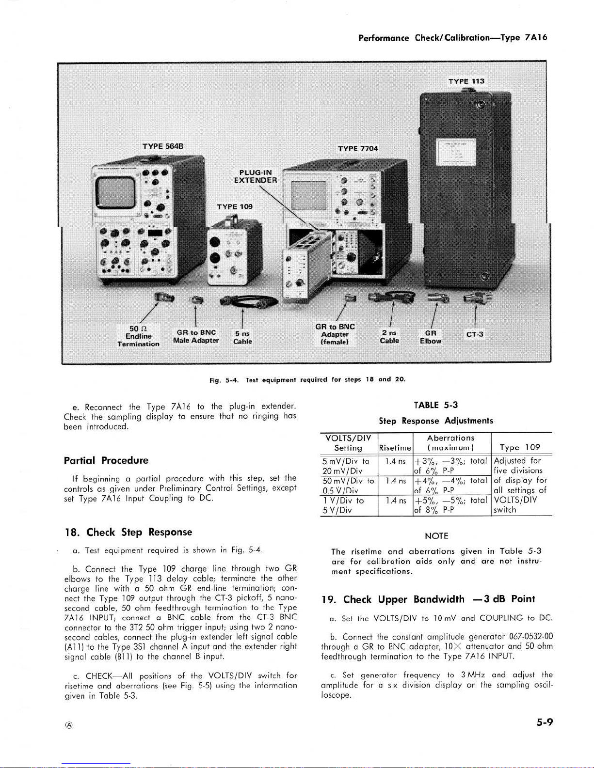
Performance
Check/Calibration-Type
7A16
e.Reconnect
Check
the
sampling
introduced
been
Partial
controls
set
Procedure
beginningapartial
If
Type
as
given
7A16
18.Check
a.Test
b
elbows
charge
nect
second
7A16
connectortothe
second
(All)tothe
signal
equipment
Connect
.
the
to
line
with
the
Type
cable,50ohm
INPUT;connectaBNC
cables,
Type
cable
(1311)tothe
the
Type
displaytoensure
.
under
Input
Coupling
Step
Response
requiredisshown
the
Type
Type
113
a 50
output through
109
3T250ohm
connect
3S1
channel
GRtoBNC
Male
7A16
procedure
Preliminary
toDC.
109
charge
delay
ohm
GR
feedthrough
trigger
the
plug-in
A
channel
Adapter
to
cable;terminate
end-line
the
terminationtothe
cable
input;using
extender
input
B
input
5
Cable
Fig.5-4.Test
the
plug-in
thatnoringing
with
this
Control
Settings,
in
Fig
line
through
termination;con-
CT-3
pickoff,5nano-
from
the
left
and
the
.
ns
equipment
extender
step,
.
.
5-4
two
the
CT-3
two2nanosignal
extender
set
except
other
Type
BNC
cable
right
has
the
GR
required
.
for
steps18and20.
VOLTS/DIV
Setting
mV/Div
5
mV/Div
20
mV/Div
50
0 .5
V/Div
1
V/Div
5
V/Div
The
risetime
are for
ment
19.Check
a.Set the
b.Connect
through a
feedthrough
Response
Step
Risetime'
to-1.4ns
to1.4ns+4%,
to
specifications
1.4ns
and
calibration aids
Upper
VOLTS/DIV
the
constant
GRtoBNC
termination
TABLE
Aberrations
(maximum)
+3%,
-3%;total
of
6%
P-P
-4%;totalofdisplay
of6%
+5%,
-5%
of
8%
NOTE
aberrations
only
.
Bandwidth
tol0mV
amplitude
adapter,
the
to
5-3
Adjustments
P-P
total
;
P-P
given
in
and
are not
-3
and
COUPLING
generator 067-0532-00
IOX
attenuator
Type
7A16
INPUT
Type
Adjusted
five
divisions
all
settings of
VOLTS/DIV
switch
Table
instru-
dB
Point
and50ohm
.
109
for
for
5-3
toDC.
c.CHECK---All
risetime
giveninTable
and
positionsofthe
aberrations
5-3
.
('see
Fig.5-5)
VOLTS/DIV
using
information
the
switch
for
c
.Setgeneratorfrequencyto3
amplitude
loscope
forasix
.
division
MHzandadjust
displayonthe
sampling
the
oscil-
9
5-
Page 37

Performance
Check/Calibration-Type
7A16
Fig.5-5.CRT
display
showing
(A)
typical
aberrations
and
(B)
typical
risetime
of the
Type
7A16
.
d
.
CHECK-Increase
the
generator frequency
until
the
dis-
play
decreasesto4.2divisions
and
check
that
the
frequency
of
the
signal
generatoris250
MHz
or
greater
.
This
bandwidth
limitisgiven
as
an
aid
to
calibra-
tion
andisnotaninstrument
specification
.
e.Return
the
extender
signal
cables
to
their
correct
jacks
and
reset
the
generatorto3
MHz
.
f.Adjust
the
generator
amplitude
forasix
division
dis-
playonthe
Type
7704
oscilloscope
.
g.CHECK-Increase
the
generator frequency
until
the
display
decreases
to
4.2divisions
and
check
that
the
fre-
quency
of
the
generator
is
150
MHz
or greater
(ifaType
7504
oscilloscopeisused,
check
that
the
frequencyis90
MHz
or
greater)
.
5-10
NOTE
Fig.5-6.Noise
(Tangentially
Measured)
.
(A)
CRT
display
show-
ing
noise
and
free
running
square
wave
.
(B)
CRT
display
showing
the
two
noise
bands
merged
.
20.Check
Trigger
Step
Response
a.Equipment
setup asinStep18except
:
Replace
the ex-
tender
signal
cablestotheir
correct
jacks
;
connect
the
left
trigger
cable
through
the2ns
cabletothe
Type
3S1
chan-
nelAinput
;
connect
the
right
trigger
cable through
the2ns
cabletothe
channel
B
input,
b.CHECK-With
the
VOLTS/DIV
switchsetto5
mV,
check
forarisetime of2.1
nanoseconds
or
less
and
aberra-
tions
nottoexceed
x--10%,
-10%
totalof15%
P-P
(use
the
Type
109
amplitude
control
to
obtain a
five
division
dis-
play)
.
NOTE
Risetime
and
aberrations
are
given
as
an
aid to
calibration
and
are not
instrument
specifications
.
c.Reconnect
the
extender
trigger
cablestotheir
proper
jacks
.
Page 38

21.Check
20
Megahertz
Bandwidth
Limiting
a
.
Set
the
Type
7A16
VOLTS/DIV
to10mV
.
b.Connect a 20 megahertz
signal
from
the
Type
191
sig-
nal
generator
through
a 5 nanosecond
cable
and a 50
ohm
feed-through
terminationtothe
Type
7A16
INPUT
.
c.Adjust
the
Type
191
amplitude
control
forasix
divi-
sion
displayonthe
CRT
.
d.Press
the
BANDWIDTH
20
MHz
pushbutton
and
ad-
just
the
Type
191
frequency
controltoobtain
exactly4.2
divisionsofdisplayed
amplitude
.
e.CHECK-The
frequency,asread
from
the
Type
191
frequency
dial,
mustbe20
MHz
within3MHz
.
f
.
Disconnect
the
20 megahertz
signal
from
the
Type
7A16
.
22.Check
Overall
Noise
Level
Tangentially
a
.
Set
the
VOLTS/DIVto5'mV
and
free
run the
time
base
.
EXAMPLE
:
Performance
Check/Calibration-Type
7A16
b.Connect
the
Type
106
fast
rise
output
throughaGR
to
BNC
adapter,
BNC
cable
twoIOX
attenuators
and
a50ohm
terminationtothe
Type
7A16
INPUT.Set the
Type
106
fre-
quencyto1
kHz
.
c.Increase
the
Type
106
amplitude
until
two
noise
bands
are
observed
(noise
and
free
running
square
wave).Decrease
the
amplitude
until
the
two
noise
bands
merge
(dark
line
between
the
noise
bands
just
disappears).See
Fig.5-6.The
final
adjustment
should be
made
slowly
.
d.Set the
VOLTS/DIVto50mVand
remove
the
two10X
attenuators
.
e
.
CHECK-Adjust
the
time
base
forastable
display
and
check
for
a
square
wave
amplitudeofone
divisionorless
.
Tangentially
Measure
Noise
Square
Wave
Amplitude
100
100
0.5mV
50
mV
Page 39

PARTS
LIST
ABBREVIATIONS
BHB
binding
head
brass
int
internal
BHS
binding
head
steel
Ig
length
or long
cap
.
capacitor
met
.
metal
cer
ceramic
mtg
hdw
mounting
hardware
comp
composition
OD
outside
diameter
OHB
oval
head
brass
conn
connector
OHS
oval
head
steel
CRT
cathode-ray
tube
P/O
part
of
csk
countersunk
PHB
pan
head
brass
DE
double end
PHS
pan
head
steel
dia
diameter
plstc
plastic
div
division
PMC
paper, metal cased
elect
.
electrolytic
poly
polystyrene
EMC
electrolytic,
metal cased
prec
precision
EMT
electrolytic,
metal
tubular
PT
paper,
tubular
ext
external
PTM
paper
or
plastic,
tubular,
molded
F&I
focus
and
intensity
RHB
round
head
brass
FHB
flat
head
brass
RHS
round
head
steel
FHS
flat
head
steel
SE
single
end
Fil
HB
fillister
head
brass
SN
or
S/N
serial
number
Fil
HS
fillister
head
steel
SorSW
switch
h
height
or
high
TC
temperature
compensated
hex
.
hexagonal
THB
truss
head
brass
HHB
hex
head
brass
thk
thick
HHS
hex
head
steel
THS
truss
head
steel
HSB
hex
socket
brass
tub
.
tubular
HSS
hex
socket
steel
var variable
ID
inside
diameter
w
wide
or width
inc
incandescent
WW
wire-wound
Page 40

PARTS
ORDERING
INFORMATION
Replacement
parts
are
available
from
or
through your
local
Tektronix,
Inc.Field
Officeorrepresentative
.
Changes
to
Tektronix
instruments
are
sometimes
made
to
accommodate
improved
components
as they
become
available,
and
to
give
you
the
benefitofthe
latest
circuit
improvements
developed
in
our engineering
department
.Itis
therefore
important,
when
ordering
parts,toinclude
the
following
informationinyour
order:Part
number,
instrument
type
or
number,
serial
or
model
number,
and
modification
number
if
applicable
.
If
a part
you
have
ordered
has
been
replaced
withanew
or
improved
part,
your
local
Tektronix,
Inc.Field
Office or
representative
will
contact
you
concerning
any
change
in
part
number
.
SPECIAL
NOTES
AND
SYMBOLS
X000
Part
first
added
at
this
serial
number
00X
Part
removed
after
this
serial
number
*000-0000-00
Asterisk
preceding
Tektronix
Part
Number
indicates
manufactured
by
or
for
Tektronix,
Inc.,or
reworked
or
checked
components
.
Use
000-0000-00
Part
number
indicated
is
direct
replacement
.
Page 41
INDEX
OF
ELECTRICAL
PARTS
LIST
Title
Page
No
.
CHASSIS
.
. . . . . . . . . . . . . ... . . . ... . . ...
.
. . ... . . . . . . . . . . ..... . . . .
6-1
ATTENUATOR
STRIP
Assembly1X
. . . . . .
. ....... . . . . ... . ..... . .
. . . .
6-2
ATTENUATOR
STRIP
Assembly21/ZX. ..... . . . ... . . ... . . . ....... ...
.
6-2
ATTENUATOR
STRIP
Assembly
5X
. ..... . . . . . . . . . . ... . . . ...
. .
. . .
.
. .
6-2
ATTENUATOR
STRIP
Assembly
1OX
. . ....... . ... ....... . ..... .
. ... .6-3
ATTENUATOR
STRIP
Assembly
25X
.
. . . . . ... . . . . . ... ... . ..... . . . . . .
6-3
ATTENUATOR
STRIP
Assembly
50X
. . . . ... . .
. ... ....... . ..... . . ... .6-3
ATTENUATOR
STRIP
Assembly
10OX
. . . ..... . .
.
. . . . . . . . . ....... . . . .6-4
ATTENUATOR
STRIP
Assembly
250X
. ... . . . . . .
.
. . . ... . ......... ... .6-4
AC-DC-GND
RELAY
Circuit
Board
Assembly..
. . .
.
. . . ..... . ... . . . . ... .6-5
VERTICAL
AMPLIFIER
Circuit
Board
Assembly
. .
. . . . . . . . ....... . . . . ...
.6-5
AC-DC-GND
Switch
Circuit
Board
Assembly
. . . ... . ..... . . . . . . ... .
... .
6-12
POLARITY
Switch
Circuit
Board
Assembly.... .
....... ... . . . . . ....... .
6-12
BANDWIDTH
Switch
Circuit
Board
Assembly
. . . . .....
. .
. . . . ..... . . . . .
6-12
Type
7A16
Page 42

Values are
fixed
unless
marked
Variable
.
Tolerance
±20%
unless
otherwise
indicated
.
SECTION
6
ELECTRICAL
PARTS
LIST
Tektronix
Serial/Model
No
.
Ckt.No
.
PartNo.Eff
Disc
Description
CHASSIS
Capacitors
Resistors
Resistors
are
fixed,
composition,
±10%
unless
otherwise
indicated
.
Type
7A16
C3
1
C4
281-0697-00
5000pF
Cer
100V
+100%-0%
C14
283-0674-00
85
pF Mica 100
V
1
%
C200
281-0697-00
5000
pF Cer 100
V
+100%-0%
Connector
Jl
131-0725-01
BNC,
receptacle,
electrical
Semiconductor
Device,
Diode
CR210
*152-0185-00
Silicon
Replaceableby1N4152
Inductors
L4
*120-0382-00
Toroid,14turns,
single
L200
*120-0382-00
Toroid,14turns,
single
R14
321-0756-03
50
ka
1/8
W
Prec
'/4%
R115
2
311-0652-00
2 x 5
kf2,
Var
R153
311-0443-00
2.5kQ,
Var
Switches
Wired
or
Unwired
S10
Wired
*263-0009-00
Rotary
VOLTS/DIV
S10
263-0510-00
S115
3
IDENTIFY
'Furnishedasa
unit
withJ1.
'Furnishedasa
unit
with
5115
.
'Furnished
as a
unit
with
R115
.
6-1
Page 43

Electrical
Parts
List-Type
7A16
ATTENUATOR
STRIP
Assembly
1
X
'Furnished
as
a
unit
with
*307-1001-00
.
'Furnished
as
a
unit
with
*307-1002-00
.
'Furnished
asaunit
with
*307-1003-00
.
6-2
Ckt.No
.
Tektronix
PartNo.
Serial/Model
No
.
Eff
Disc
Description
*307-1001-00
Complete
Attenuator
Strip
Capacitor
C5
4
Resistor
R5
4
ATTENUATOR
STRIP
Assembly
2
1/sX
*307-1002-00
Complete
Attenuator
Strip
Capacitors
C6A
5
C6B
5
C6C
5
Resistors
R6A
5
R6B
5
R6C
5
ATTENUATOR
STRIP
Assembly
5
X
*307-1003-00
Complete
Attenuator
Strip
Capacitors
C76
6
C7B
6
Resistors
R7A
6
R7B
6
R7C
6
Page 44

Cl
OA
9
C10B"
CIOC°
7
Furnished
as
a
unit
with
*307-1004-00
.
'Furnished
asaunit
with
*307-1005-00
.
'Furnished
asaunit
with
*307=1006-00
.
ATTENUATOR
STRIP
Assembly
10
X
Capacitors
Electrical
Parts
List-Type
7A16
6-
3
Ckt.No
.
Tektronix
Part
No
.
Serial/Model
No
.
Eff
Disc
D
escription
*307-1004-00
Complete
Attenuator
Strip
Capacitors
C8A
7
C8137
C8C
7
Resistors
R8A
7
R8137
R8C
7
ATTENUATOR
STRIP
Assembly
25
X
*307-1005-00
Complete
Attenuator
Strip
Capacitors
C9A
8
C9B"
C9Cg
Resistors
R9As
R9Bs
R9C
8
ATTENUATOR
STRIP
Assembly
50
X
*307-1006-00
Complete
Attenuator
Strip
Page 45

Electrical
Parts
List-Type
7A16
C12A
12
C12B
12
C12C12
R12A
12
R12B
12
R1
2C12
"Furnished
as
a
unit
with
*307-1006-00
.
"Furnished
as
a
unit
with*
307-1007-00
.
"Furnished
as
a
unit
with
*307-1008-00
.
6-
4
Capacitors
Resistors
Ckt.No
.
Tektronix
PartNo.
ATTENUATOR
STRIP
Assembly
50
X
(cont)
Serial/Model
No
.
Eff
Disc
Description
Resistors
R10A1
°
R10B
1
o
R10C
1
o
ATTENUATOR
STRIP
Assembly
100
X
*307-1007-00
Complete
Attenuator
Strip
Capacitors
Cl
1
All
CllB
11
C11C
11
Resistors
R11
All
R11
B11
RllC'
1
ATTENUATOR
STRIP
Assembly
250
X
*307-1008-00
Complete
Attenuator
Strip
Page 46

Tektronix
Serial/Model
No
.
Ckt.No
.
PartNo.Eff
Disc
Description
*670-1092-00
Complete
Board
AC-DC-GND
RELAY
Circuit
Board
Assembly
Capacitor
Electrical
Parts
List-Type
7A16
Tolerance
±20%
unless
otherwise
indicated
.
C2
283-0160-00
1
.5
pF
Cer
50
V
10%
Relay
K5
*148-0063-00
Polarized,
200
mW,
dpat,5pin
S5A,B~
Resistors
Resistors
are
fixed,
composition,
±10%
unless
otherwise
indicated
.
R1
317-0620-00
62
S2
W
5%
R2
317-0620-00
6212
W
5%
R3
317-0105-00
1
MQ
W
5%
VERTICAL
AMPLIFIER
Circuit
Board
Assembly
*670-1113-00
B010100B019999
Complete
Board
*670-1113-01
B020000
B029999
Complete
Board
*670-1113-02
B030000
B039999
Complete
Board
*670-1113-03
B040000B049999
Complete
Board
*670-1113-04
B050000B059999
Complete
Board
*670-1113-05
B060000
Complete
Board
Capacitors
Tolerance
±20%
unless
otherwise
indicated
.
C18
281-0064-00
0
.25-1.5pF,
Var
Tub
.
C20
283-0080-00
0
.022
/-tF
Cer
25
V
+80%-20%
C23
283-0059-00
1
1,F
Cer
25V
+80%-20%
C24
290-0135-00
XB060000
15
,uF
Elect
.
20
V
C28
281-0651-00
47
pF
Cer
5%
C30
283-0080-00
0
.022
j
.F
Cer
25V
+80%-20'/
.
C34
283-0080-00
0
.022
,uF
Cer
25V
+80%-20%
C35
283-0178-00
0.1,uF
Cer
100v
+80%-20%
C36
283-0080-00
0
.022
F
Cer
25
V
+80%-20
C40
283-0060-00
100
pF
Cer 200
V
5%
Page 47

Electrical
Parts
List-Type
7A16
VERTICAL
AMPLIFIER
Circuit
BoardAssembly
(cont)
Ckt.No
.
Tektronix
PartNo.
Serial/Model
Eff
No
.
Disc
Description
Capacitors
(cont
)
C45
281-0123-00
5-25
pF,
Var Cer
100v
C52
281-0123-00
5-25
pF,
Var Cer
100v
C55
283-0060-00
100
pF
Cer
200
V
5%
C56
283-0059-00
1
~,F Cer
25V
+80%-20
0/.
C57
290-0135-00
XB060000
15t
.F
Elect
.
20
V
C61
281-0122-00
2
.5-9
pF,
Var
Cer
100
V
C65
281-0656-00
22pF
Cer
200
V
5%
C68
283-0065-00
0
.001
f,F
Cer 100
V
5%
C77
281-0577-00
14pF
Cer
500
V
5%
C85
281-0656-00
22
pF
Cer
200
V
5%
C88
283-0065-00
0
.001
jiF
Cer
100v
5%
C89
283-0178-00
0.1,cF
Cer
100v
+80%-20%
C97
283-0629-00
62
pF
Mica
500
V
1
C102
281-0122-00
2
.5-9
pF,
Var
Cer
100
V
C103
281-0122-00
2
.5-9pF,
Var
Cer
100V
C104
283-0178-00
0
.1
ttF
Cer
100v
+80%-20%
C105
283-0077-00
330
pF
Cer
500
V
5%
C109
281-0122-00
2
.5-9
pF,
Var Cer
100
V
C111
281-0122-00
2
.5-9
pF,
Var
Cer
100v
C112
281-0601-00
7.5pF
Cer
500
V
±0
.5
pF
C124
283-0077-00
330
pF
Cer
500
V
5%
C125
283-0065-00
0
.001
t F
Cer
100
V
5%
C130
283-0185-00
2.5pF
Cer
50V
5%
C131
283-0080-00
0
.022
[F
Cer
25
V
+80
0/
o
-20%
C133
283-0065-00
0
.001~.F
Cer
100v
5%
C138
281-0613-00
10
pF
Cer
200
V
10%
C140
283-0178-00
0.1,u,F
Cer
100v
+80%-20%
C143
283-0080-00
0
.022
,uF
Cer
25
V
+80%-20%
C145
281-0612-00
5.6pF
Cer
200
V
±0.5pF
C155
283-0077-00
330
pF
Cer
500
V
5%
C162
281-0601-00
7.5pF
Cer
500
V
±0.5pF
C164
283-0077-00
330
pF
Cer
500
V
5%
C165
283-0065-00
0
.001
[F
Cer 100
V
5%
C169
281-0617-00
15
pF
Cer
200
V
C173
283-0065-00
0
.001
,uF Cer
100
V
5%
C178
281-0613-00
10pF
Cer
200
V
10%
C185
281-0612-00
5.6pF
Cer
200
V
±0.5pF
C234
290-0135-00
15
t F
Elect
.
20
V
C235
283-0178-00
0.1/AF
Cer
100v
+80%-20%
C236
283-0065-00
0
.001
/,F
Cer
100v
5%
C237
290-0135-00
15
fF
Elect
.
20
V
C238
283-0178-00
0.1I,F
Cer
100v
+80%
-20%
C239
283-0065-00
0
.001
j,F
Cer 100
V
5%
Page 48

VERTICAL
AMPLIFIER
Circuit
Board
Assembly
(cont)
Electrical
Parts
List-Type
7A16
6-7
Ckt.No
.
Tektronix
Serial/Model
No
.
PartNo.
Eff
Disc
Description
Semiconductor
Device,
Diodes
VR20
152-0278-00
13010100
13029999
Zener
1
N4372A
400
mW,3V,
5%
VR20
152-0279-00
13030000
Zener
1
N751A400
mW,5.1
V, 5
0
/
.
CR29
*152-0323-00
Silicon
Tek
Spec
CR30
*152-0153-00
Silicon
Tek
Spec
VR30
152-0278-00
13010100
13029999
Zener
1
N4372A
400
mW,3V,
5%
VR30
152-0279-00
13030000
Zener
1
N751A400
mW,5.1V,5%
VR123
152-0166-00
Zener
1
N753A
400
mW,6.2V,5%
CR128
152-0422-00
Silicon
Voltage
Variable
Capacitance
CR168
152-0422-00
Silicon
Voltage Variable
Capacitance
CR200
*152-0185-00
Silicon
Replaceable
by
1N4152
CR220
*152-0185-00
X13060000
Silicon
Replaceable
by1N4152
CR222
*152-0185-00
X13060000
Silicon
Replaceable
by
1
N4152
CR224
*152-0185-00
Silicon
Replaceable
by
1N4152
CR226
*152-0185-00
Silicon
Replaceable
by
1N4152
CR227
*152-0185-00
Silicon
Replaceable
by
1N4152
CR228
*152-0185-00
Silicon
Replaceable
by
1N4152
Inductors
L20
*108-0440-00
B010100
13059999
8
FM
L20
*120-0382-00
13060000
Toroid,14turns,
single
L30
*108-0440-00
B010100
13059999
8
~H
L30
*120-0382-00
B060000
Toroid,14turns,
single
L34
276-0507-00
Core,
ferramic
suppressor
L68
276-0507-00
Core,
ferramic
suppressor
L76
*108-0170-01
0.5pH
L88
276-0507-00
Core,
ferramic
suppressor
L96 *108-0170-01
0
.5t
H
L97
276-0507-00
Core,
ferramic
suppressor
Ll31
*108-0440-00
8tcH
Ll33
276-0507-00
Core,
ferramic
suppressor
Relays
K65
*148-0034-00 Armature,
dpdt
15VDC
K75
*148-0034-00
Armature,
dpdt
15VDC
K105
*148-0035-00
Armature,
spdt 15VDC
K110
*148-0035-00
Armature,
spdt 15VDC
K115
*148-0034-00
Armature,
spdt 15VDC
K155
*148-0035-00
Armature,
spdt
15VDC
K160
*148-0035-00
Armature,
spdt 15VDC
Page 49

Electrical
Parts
List-Type
7A16
VERTICAL
AMPLIFIER
Circuit
Board
Assembly
(cont)
Resistors
Resistors
are
fixed,
composition,
±10%
unless
otherwise
indicated
.
6-8
LR159
*108-0568-00
75nH (woundona6812,
'/aW,
5%
resistor)
Transistors
Q20
151-1032-00
Silicon
FET,
dual
Q40
*153-0580-00
Silicon
Selected,
Tek
Spec
Q50
Q60
*151-0268-00
Silicon
Tek Spec, dual
Q70
*151-0212-00
Silicon
Tek
Spec
Q90
*151-0212-00
Silicon
Tek
Spec
Q100
*151-0272-00
Silicon
Tek Spec, dual
Q120
*151-0272-00
Silicon
Tek
Spec,
dual
Q125
*151-0212-00
Silicon
Tek
Spec
0130
*151-0259-00
B010100
13039999
Silicon
Selected
from
2N3563
Q130
*151-0269-00
13040000
Silicon
Selected
from
SE3005
Q135
*151-0212-00
Silicon
Tek
Spec
Q140
151-0298-00
Silicon
NPN,
TO-72,
MM1606
Q165
*151-0212-00
Silicon
Tek
Spec
Q170
*151-0259-00
13010100
B039999
Silicon
Selected
from
2N3563
Q170
*151-0269-00
13040000
Silicon
Selected
from
SE3005
Q175
*151-0212-00
Silicon
Tek
Spec
Q180
151-0298-00
Silicon
NPN,
TO-72,
MM1606
Q200
151-0254-00
Silicon
TO-98,
D16P4
R17
323-0612-03
950
kQ
1/2W
Prec
1
/4
%
R18
315-0561-00
56012
1
/4
W
5
%
R23
317-0151-00
15012
%
W
5%
R28
325-0041-00
19
.7512
1/20
W
Prec
1
%
R30
325-0041-00
19
.7512
1/20
W
Prec
1
%
R31
315-0472-00
4
.7 k12
1
/4
W
R34
311-0462-00
1
kn,Va
r
5
%
R35
315-0913-00
91
kQ
1
/
4
W
5%
R38
317-0151-00
150
a
/a
W
5
R40
311-0634-00
50012,Var
5
%
Ckt.No
.
Tektronix
PartNo.
Serial/Model
No
.
Eff
Disc
Description
Inductors
(cont
)
Ll
40
*
108-0440-00
8
N
H
Ll43
*108-0440-00
8
ttH
Ll73
276-0507-00
Core,
ferramic
suppressor
L230
*120-0382-00
Toroid,
14
turns,
single
L236
*120-0382-00
Toroid,14turns,
single
L238
*120-0382-00
Toroid,14turns,
single
Page 50

VERTICAL
AMPLIFIER
Circuit
Board
Assembly
(cont)
Electrical
Parts
List-Type
7A16
6-9
Ckt.No
.
Tektronix
PartNo.
Serial/Model
No
.
Eff
Disc
Description
Resistors
(cont
)
R43
315-0182-00
1.8k52
'/4
W
5%
R45
317-0470-00
47
52
W
5
%
R51
315-0182-00
1.8W
W
5%
R52
317-0560-00
56
52
W
5%
R55
311-0634-00
5000,Var
R60
321-0062-00
43.252
W
Prec
1
R61
311-0605-00
200
S2,
Var
R62
323-0175-00
649
52
W
Prec
1
R64
321-0114-00
13010100
13019999
15052
'/8
W
Prec
1
R64
321-0097-00
13020000
13049999
100
5
W
Prec
1
%
R64
321-0076-00
13050000
60
.4
52
W
Prec
1
R65
321-0033-00
13010100
13049999
21
.552
W
Prec
1
%
R65
321-0024-00
13050000
17
.4 52
W
Prec
1
%
R66
311-0963-00
5 kQ,
Var
R67
315-0153-00
15
k52
'/4
W
5%
R68
317-0241-00
240
0
'/eW
5
%
R70
325-0053-00
5052 1/20
W
Prec
1
%
R71
325-0053-00
5052 1/20
W
Prec
1
%
R73
321-0186-00
845
52
'/8
W
Prec
1
%
R74
321-0177-00
681
52
'/8W
Prec
1
R80
321-0062-00
43
.2 52
'/8
W
Prec
1
%
R82
317-0200-00
20
52
W
5%
R84
321-0114-00
13010100
13019999
150
52
W
Prec
1
%
R84
321-0097-00
13020000
13049999
10052
W
Prec
1
R84
321-0076-00
13050000
60
.452
W
Prec
1
R85
321-0033-00
13010100 13049999
21 .552
W
Prec
1
%
R85
321-0024-00
13050000
17
.452
W
Prec
1
R86
311-0963-00
5
k52,
Var
R87
315-0153-00
15
k52
'/,
W
5%
R88
317-0301-00
300
52
W
5
%
R89
311-0510-00
10
k52,
Var
R90
325-0053-00
50
52
1/20
W
Prec
1
%
Rl00
321-0085-00
7552
'/8
W
Prec
1
R101
323-0135-00
249
52
72
W
Prec
1
R102
321-0039-00
24
.952
'/8W
Prec
1
%
R103
311-0635-00
1
kn,
Var
R104
323-0114-00
150
52
'/2
W
Prec
1
%
RI
05
317-0331-00
35052
'/8
W
5
%
Rl06
322-0193-00
1
kQ
'/,
W
Prec
1
%
R108
325-0047-00
25
52
1/20
W
Prec
72
R109
311-0634-00
500
52,
Var
R111
311-0634-00
500
S2,
Var
R112
325-0045-00
46
.4 52
1/20
W
Prec
'/2
R114
315-0103-00
10
k52
'/,
W
5%
R117
311-0442-00
250
52,Var
R1
18
322-0206-00
1
.37
kn
'/,
W
Prec
1
Page 51

Electrical
Parts
List-Type
7A16
VERTICAL
AMPLIFIER
Circuit
Board
Assembly
(cont)
Ckt.No
.
Tektronix
PartNo.
Serial/Model
No
.
Eff
Disc
Description
Resistors
(cont
)
R120
321-0085-00
75Q
'/e
W
Prec
1
Rl21
322-0207-00
1.4k12
'/4
W
Prec
1
Rl23
321-0114-00 150
i2
'/s
W
Prec
1
R124
317-0391-00
390
St
'/8W
5
R1
25
317-0241-00
240
52
'/s
W
5
%
R126
321-0434-00
324
k12
W
Prec
1
R127
321-0068-00
49
.912
W
Prec
1
R128
321-0068-00
49
.912
W
Prec
1
RT128
307-0181-00
100
k12
Thermal
R129
322-0147-00
33212
'/4
W
Prec
1
R130
321-0062-00
43
.212
'/
8
W
Prec
1
R131
323-0142-00
29412
'/2
W
Prec
1
R133
317-0241-00
24012
W
5%
R135
321-0135-00
24912
W
Prec
1
R137
323-0171-00
590
i2
'/2
W
Prec
1
R138
321-0062-00
43
.212
'/e
W
Prec
1
Rl41
323-0167-00
53612
'/2
W
Prec
1
R142
321-0135-00
24912
'/s
W
Prec
1
R143
323-0146-00
32412
'/2
W
Prec
1
R145
321-0062-00
43
.212
'/s
W
Prec
1
R150
321-0085-00
7512
W
Prec
1
%
R151
321-0039-00
24
.912
W
Prec
1
R154
315-0103-00
10
kQ
'/4
W
5%
R155
317-0331-00
33012
'/s
W
5
%
R156
322-0193-00
1
kit
'
/4
W
Prec
1
R158
325-0047-00
2512
1/20
W
Prec
'
/2
R159
325-0044-00
10012
1/20W
Prec
'
/2%
R160
315-0103-00
10
k12
'/4
W
5%
R161
325-0044-00
100
Q
1/20
W
Prec
'
/2
%
R162
325-0045-00
46
.412
1/20W
Prec
'
/2%
R163
321-0114-00
15012
W
Prec
1
R164
317-0391-00
39012
W
5%
R1
65
317-0241-00
24012
W
5
%
R166
322-0206-00
1
.37
kit
'
/4
W
Prec
1
%
R167
321-0068-00
49.9i2
'/
8
W
Prec
1
R168
321-0068-00
49
.9 S2
W
Prec
1
Rl69
317-0472-00
4
.7 kit
W
5%
R170
321-0062-00
43
.20
W
Prec
1
R172
321-0196-00
1
.07
kO
'/e
W
Prec
1
%
R1
73
317-0241-00
2400
'/e
W
5
%
Page 52

VERTICAL
AMPLIFIER
Circuit
Board
Assembly
(cont)
Electrical
Parts
List-Type
7A16
R239
315-0470-00
4712
'/4
W
Wired
or
Unwired
S65
13
*670-1134-00
Slide
VARIABLE
CAL
IN
"See
Mechanical
Parts
List
for
replacement
parts
.
Switch
6-
1 1
Ckt.No
.
Tektronix
PartNo.
Serial/Model
No
.
Eff
Disc
Description
Resistors
(cont
)
R174
323-0149-00
34812
W
Prec
1
%
R175
321-0135-00
24912
W
Prec
1
%
R177
323-0171-00
59012
1/2
W
Prec
1
%
R178
321-0062-00
43
.212
'/8W
Prec
1
Rl 81
323-0167-00
53612
'/z
W
Prec
1
%
Rl
82
321-0135-00
24912
'/8
W
Prec
1
R185
321-0062-00
43
.212
'/8
W
Prec
1
%
R200
315-0184-00
180
ka
'/4
W
5%
R202
322-0223-00
2
.05
kQ
'/4
W
Prec
1
%
R204
321-0299-00
12.7ka
'/8
W
Prec
1
R205
321-0344-00
37
.4 kit
'/8W
Prec
6%
R206
315-0753-00
75ka
'/4
W
5%
R207
315-0753-00
75
k12
'/4
W
5%
R208
315-0154-00
150
k12
'/4
W
Prec
1
R209
321-0344-00
37.4ko
'/8W
5%
R218
315-0154-00
150
ka
'/4W
5%
R219
315-0154-00
150
k12
'/4
W
5
R220
315-0133-00
13
kit
'/4
W
5%
R222
315-0154-00
150
kit
'/4
W
5%
R224
315-0154-00
150
k12
'/4
W
5%
R225
315-0513-00
51
ko
'/4
W
5%
R226
315-0154-00
150
k12
'/4
W
5%
R228
315-0753-00
75kQ
'/4
W
5%
R232
315-0510-00
51
12
'/4
W
5
R233
315-0753-00
75ko
'/4
W
5%
R234
315-0510-00
51
12
'/4
W
5
R235
307-0103-00
2
.712
'/4
W
5%
R236
315-0101-00
10012
'/4
W
5%
R238
315-0101-00
10012
'/4
W
5
%
Page 53

Electrical
Parts
List-Type
7A16
Tektronix
Serial/Model
No
.
Ckt.No
.
PartNo.
Eff
Disc
D
escription
"See
Mechanical
Parts
List
for
replacement
parts
.
AC-DC-GND
Switch
Circuit
Board
Assembly
POLARITY
Switch
Circuit
Board
Assembly
BANDWIDTH
Switch
Circuit
Board
Assembly
*670-1125-00
*670-1125-01
B010100
B070000
B069999
Complete
Board
Complete
Board
Bulb
DS118
*150-0057-01
13010100
8069999
Incandescent
7153AS15,
selected
DS118
*150-0048-01
8070000
Incandescent
#683,
selected
Switch
Wired
or
Unwired
S118
14
*670-1125-00
13010100
13069999
Pushbutton
INVERT
51181'
*670-1125-01
13070000
Pushbutton
INVERT
*670-1124-00
*670-1124-01
B010100
B070000
B069999
Complete
Board
Complete
Board
Bulb
DS3
*150-0057-01
8010100
13069999
Incandescent
7153AS15,
selected
D53
*150-0048-01
13070000
Incandescent
#683,
selected
Switch
Wired
or
Unwired
S3
14
*670-1124-00
13010100 13069999
Pushbutton
AC-GND-DC
53
11
*670-1124-01
8070000
Pushbutton
AC-GND-DC
*670-1126-00
*670-1126-01
B010100
B070000
B069999
Complete
Board
Complete
Board
Bulb
DS75
*150-0057-01
B010100
8069999
Incandescent
7153AS15,
selected
DS75
*150-0048-01
8070000
Incandescent
#683,
selected
Switch
Wired
or
Unwired
S75
14
*670-1126-00
8010100
8069999
Pushbutton
BANDWIDTH
S75
14
*670-1126-01
8070000
Pushbutton
BANDWIDTH
Page 54

SECTION
7
DIAGRAMS
and
MECHANICAL
PARTS
ILLUSTRATIONS
The
following
special
symbols
are
usedonthe
diagrams
:
0
Screwdriver
adjustment
Frontorrear-panel
control
or
connector
.
Referstothe
indicated
diagram
.
~~Connection
solderedtocircuit
board
.
Blue
line
encloses
components
located
on
circuit
board
.
Test
point
.
Page 55

7AIro
AMPLIFIER
Page 56

W
r
O
W
_v
D
O
D
3
Page 57

Typical
voltage
measurements
and
waveform
photographs
were
obtained
under
the
following conditions
unless
noted
otherwiseonthe
individual
diagrams
:
Type
7704
Oscilloscope
VOLTAGE
AND
WAVEFORM
TEST
CONDITIONS
Vertical
Mode
Right
Horizontal
Mode
A
Type
7A16
Controls
(left
vertical
compartment)
POLARITY
+UP
BANDWIDTH
FULL
AC-GND-DC
DC
VOLTS/DIV
10
mV
INPUT
50
mV
from a
Standard
Amplitude
Calibrator
Type
7A16
Controls
(right
vertical
compartment)
Usea10X
attenuator
probe
Polarity
+Up
Bandwidth
Full
AC-GND-DC
AC
Volts/Div
10
mV
Type
71371
Controls(Ahorizontal
compartment)
Level/Slope
0/+
Triggering
Mode
P-P
Auto
Coupling
AC
Source
Ext
Magnifier
X1
Time/Div
1
ms
Variable
Cal
In
Ext
Trig
In
Positive
trigger signal
(Al
3)
from
the
Type
7A16inthe
left
vertical
compartment
.
All
voltages
givenonthe diagrams
areinvolts.Waveforms
shown
are
actual
waveform
photographs
taken
witliaTektronix
Oscilloscope
Camera
System
.
Voltages
and
waveforms
on
the diagrams
(showninblue)
are
not
absolute
and
may
vary
between
instruments
because
of
differing
component
tolerances,
internal
calibration or
front-panel
control
settings
.
NOTE
Vertical
deflection factor
shown on
waveforms
does
not
include
attenuation
factorofthe
1OX
Probe
.
Page 58

5-
.IY_
C23
I-
F
~-~
R0
+11
.IS
R18
560
C18
0
.2-1
.5
+0
R28
S 9
.75
JC40
.14
100
C28
500
47
OV
Q40
-
-0
.7
R45
47
R43
1
.8K
Q_50
-7
.93
-i5V
C55
100
R55
500
DAM
PIN
G'2
R38
150
-0
.08
Q
.Z0B
C36
.022
C34
.022
cR2U
CR30
R30
19
R31
4.7K
.75
-
+15V
C35
i
7A16
AMPLIFIER
VOLTAGES
only.. ... .
. ... . ... .noai9pel
applied
NQ7ES
1 .
SEE
SEMICONDUCTOR
* 2.HEAT
:
PARTS
SINKED
LIST
FOR
TYPES
MIL
REFERENCE
2O
O4
ATTENUATORS
OUTPUT
SWITCHING
DIAL
AMPLI
I
E
Page 59

40
00
DAMPING-i
8
.4
C45
5-25
R45
47
43
8K
DAMPING
+15V
5
C56
1-F
100
C55
(S65)
VARIABLE
GAL
ONO
R89
SOK
NC
C89
0
~~
i
6 .S
828
T
I
O
I
-15V
+5
Q
S
-
LC-4,5
-
.12
70
.7
I
O,r,V/DI V
L76
0.5-H
W
P6-3I
-15V
C77
MV/DIV
14
0
K75A
I
i
I
~,
f
-:KTS
-
I
6
~P3-2
P3-1
P3-3
P
+SV
41-4
1
-
'o
.,s/D1V
I
I
I
I
I
I
I
I
D 5
75
j~P3-6
P>ANDwIDTN
i-s
L-
NO
62
7
T
---
L97
IT
IJO
1
L96
0
.5-H
10
(S7-5)
BANDWIDTH
+
20MHz
f
T~LIGHTS
P1-C
BOARD
I
TO
O
-
FULL
sw1TC-H
TOQ100
iOOA
SELF
CANCELING
COMMON
B
C85
22
22
K7SB
I
R70
50
68
R
21.5
VAR
7
R86
5K
R85
21
.5
GAIN
BAL
.1
K65
10
mV/DIV
ID
I
I
NO
K65
C68
-001
L68I
c52
5-25
R52
56
-15v
R82
L88
1T
C85
.001
1T
TP60
20
+i5V
R51
1
.8K
O
V
Q50
-7
.93
R55
500
'1
4,49
R80
43_2
RIoB
240
+2
R60
43
-0
+1
ROB
300
Q~OB
Q60A
.96
.7
.z
C(61
2
.5-9
2
8
00
HF
COMP
.76
K45B
R66
5K
NCI
A
~-O
+i5V
OVAR
R87
9,1
SSK
-15V
2
845
R73
+i5V
R74
681
NO
R90
50
+5
.7
Q90
`
,
REFERENCE
2O
O4
ATTENUATORS
OUTPUT
SWITCHING
DIAGRAMS
AMPLIFIER
E`
INTERCONNECTING
PLUG
PARTIAL
INPUT
VERTICAL
AMPLIFIER
AMPLIFIER
0470
BOARD
Page 60

25X
7A16
AMPLIFIER
Page 61

2~2X
50X
2.61
75
1
128
~
980K
Ri08
75
C
7A
t
2
.6-7
.5
Cii
.~l
2
.6-7
.5
Ci1
fi
Page 62

ATTENUATORS
WLB
Laos
Page 63

FROM
K75B
RS50
75
R151
24
.9
R105
330
+9
.93
s
.2
Qi0OB
9
.93
R155
330
r
C103
I
5-25
t
(20-V/DIV)l
I
I
K105
K155
(20
-V/D
IV)
e
STEP
A
BAL
N
R153
2.5
K
+15V
-iSV
R154
10K
7A16
AMPLIFIER
C105
330
C155
390
-i5
v
-iSV
R106
iK
R108
25
O
R158
25
NO
Nv
(iO-V/DI
V)
FROM
S10
SELF
CANCELING
-
1
.--0NC
N
0
I
I
I
(10~V/DIV)
I
INVERT
POLARITY
C112
7
.5
R112
46
.4
C162
7.5
Rftc2
46
.4
NO
Y Y
+5V LIGHTS
COMMON
C124
330
10
FROM
K
75A
O
QIOOA
S
.2
RSOO
R159
Ri61
75
100
C109
100
Cii1
R102
24
.9
R103
SK
.5-9
2.5-9
O
HF
LR159
COMP
57
R109
R101
R104
500
249 150
C102
FROM
510A---1
68
HF
Rili
+15V +15V
2
.5-9
COMP 500
HF
C104
COMP
0
.1
Page 64

.124
I30
2124
?90
:164
190
164
'30
TO
Q200
IO_V/DIV
10~V/DIv
C125
.001
CSGS
.001
PARTIAL
VFRT\CAL
AMPLIF\flR°.,OARD
NOTE
:
REFERENCE
DIAGRAMS
SEE
PARTS
LIST
FOR
SEMICONDUCTOR
TYPES
.
<1>
INPUT
AMPLIFIER
VOLTAGES
and
WAVEFORMS
brained
under
conditions
givenondiagram
O
,
except
as
tollaws
:
VOLTAGES
only...._..
. . ...na
signal
applied
®
SWITCHING
t
INTERCONNECTING
PLUG
+15V
L14O
4T
Ri4i
536
C145
5
.6
Q140
-3
.22
Ci38
10
Ri38
43
.2
Li43
47
Ci43
1
.
022
R178
43
.2
C185
5
.6
IO-V/DIV
OUTPUT
AMPLIFIER
Iorw/DIv
-15V
1
ms/DIV
WLB
1069
Bit
-SIGNAL
Bi3
-TRIGGER
Ai3
+TRIG
GER
Aii
+
SIGNAL
0
C
.
fl
C
D
r
m
23
!V
-15V
20
R143
324
21
4K
Page 65

FROM
-i--~M~
Q120B
R200
180K
FROM
JI
5115
GR
200
510
VOLTS
DIV
REFERENCE
DIAGRAMS
:
INPUT
AMPLIFIER
OUTPUT
AMPLIFIER
5F-E-
PARTS
L157
FOR
SEMIGONOUGTOR
7AIG
AMPLIFIER
SPRING
RETURN
Q
200
-15V R204
12
.7
TO
TO
KI10
K105
t
15V
K160
K155
P6-2~
PS-4~
8~
PT-Z
0---4
O---4
O
O
O
O
O
R
207
75K
R2oe
R2'
160K
b7
.~
T-8-b,
Pa
.
TYPE-
O----j
O
(GAIN)
(READOUT
LOGII
Page 66

cS
6F
O"IN
.F~
R238
.001
Y
100
A57
)7
ADOUT
LOGIC,)
10
mV
20
.2
2
5
P7-S
POLARITY
X
SWITCH
80ARD,
\
0-
0-4
O
O-
0
--4
O
O
O
LIGHTS
COMMON
R235
TP
2
.7
PARTIAL
VERT\CAL
AMPUPIER
bOARo
0
1
SWITCHING
~
INTERCONNECTING,
PLUG
-5Ov
-
)
IB19
h
9
1069
A10
RX239
47
+
SIGNAL
All
-
SIGNAL
611
3
A12
6I2
+
TRIGGER
f
~
A
13
-
TRIGGER
613
TP
~C234
L2E6
565
-L
ISy-F
147
VAR
+15V
F
-
wv
- -
z
A18
(CAL
N)
(DCPL)
7P
C23S
L2
D8
C236
T
P,
'13G
14T
.OOIy
.F
1
_ISV
.
100
_ - _ -
"
g18
(DCPL)
C238
.^^+
C239
Page 67

TYPE
7A16
AMPLIFIER
FIGURE
1
EXPLOC
Po"
90
s
s~
®
0
P 6
Page 68

XPLODED
Page 69
FIGURE
AND
INDEX
NUMBERS
Itemsinthis
section
are
referenced
by
figure
and
index
numberstothe
illustrations
which
appear
eitheronthe
back
of
the
diagramsoron
pullout
pages
immediately
following
the
diagramsofthe
instruction
manual
.
INDENTATION
SYSTEM
This
mechanical
parts
list is
indented to
indicate
item
relationships.Followingisan
exampleofthe
indentation
system used
in
the
Description
column
.
Assembly and/or
Component
Detail
PartofAssembly
and/or
Component
mounting
hardware
for
Detail
Part
PartsofDetail
Part
mounting
hardware
for
PartsofDetail
Part
mounting
hardware
for
Assembly and/or
Component
Mounting hardware
always appearsinthe
same
indentationasthe
itemitmounts,
while
the
detail
parts
are
indentedtothe
right.Indented
items
are
part
of,
and
included
with,
the
next
higher
indentation
.
Mounting
hardware
must
be
purchased
separately,
unless
otherwise
specified
.
PARTS
ORDERING
INFORMATION
Replacement
parts
are
available
fromorthrough
your
local
Tektronix,
Inc.Field
Office
or
representative
.
Changes
to
Tektronix
instruments
are
sometimes
made
to
accommodate
improved
componentsasthey
become
available,
andtogive
you
the
benefit
of
the
latest
circuit
improvements
developedinour
engineering
department.It is
therefore
important,
when
ordering
parts,toinclude
the
following informationinyour
order:Part
number,
instru-
ment
typeornumber,
serialormodel
number,
and
modification
numberifapplicable
.
Ifapart
you
have
ordered
has
been
replaced
withanew
or
improved
part,
your
local
Tektronix,
Inc.Field
Office or
representative
will
contact
you
concerning
any change
in
part
number
.
Change
information,ifany,
is
locatedatthe
rearofthis
manual
.
ABBREVIATIONS
AND
SYMBOLS
Foranexplanationofthe
abbreviations
and
symbols
used
in this
section,
please
refer
to
the
page
immediately
preceding
the
Electrical
Parts
Listinthis
instruction
manual
.
Page 70
Type
7A16
INDEX
OF
MECHANICAL
PARTS
ILLUSTRATION
Title
Location
(reverse
side
of)
Figure1Exploded.. . . . . . . .
... . . ..Switching
&
Interconnecting Plug
Diagram
Page 71

SECTION
s
MECHANICAL
PARTS
LIST
FIGURE
1
EXPLODED
Type
7A16
Fig.&
Index
No
.
Tektronix
PartNo.
Q
Serial/Model
No
.
t
Eff
Disc y
Description
1
2s4
s
1-1
333-1151-00
1
PANEL,
front
-2
366-1059-00
1
KNOB,
gray-IDENTIFY
-3
366-1077-00
1
KNOB,
gray-POSITION
- - --- - -
knob
includes
:
213-0153-00
1
SETSCREW,
5-40 x
1
/
8
inch,
HSS
-4
- --- - - 1
RESISTOR,
variable
- - --- -
-
mounting
hardware:(not
included
w/resistor)
-5
210-0223-01
1
TERMINAL,
lug
-6
210-0583-00
1
NUT,
hex
.,1/4-32x5
/
16
inch
-7
366-1168-00
1
KNOB,
red-black-VARIABLE
(CAL
IN)
-
- --- - -
knob
includes
:
213-0153-00
1
SETSCREW,
5-40
x
1
/
8
inch,
HSS
-8
366-1057-00
1
KNOB,
gray-VOLTS/DIV
- - --- - -
knob
includes
213-0153-00
2
SETSCREW,
5-40x1
/
8
inch,
HSS
263-0009-00
1
SWITCH,
wired-VOLTS/DIV
-
- - - - - -
switch
includes
:
-9
263-0510-00
1
SWITCH,
unwired
-
- - - - - -
mounting
hardware:(not
included
w/switch)
-10
337-1214-02
1
SHIELD
-11
210-0938-00
2
WASHER,
flat,0.109IDx 0
.250 inch
OD
-12
384-0724-00
1
SHAFT-INDEX
ASSEMBLY
--- - - - -
mounting
hardware:(not
included
w/shaft-index assembly)
-13
210-0840-00
1
WASHER,
flat,0.390IDx'/16inch
OD
-14
210-0012-00
1
WASHER,
lock,
internal,
3
/8
ID x
1
/
2
inch
OD
-15
210-041300
1
NUT,
hex
.,3/8-32x1
/
2
inch
-16
131-0725-01
1
CONNECTOR,
receptacle,
w/capacitor
-17
105-0080-01
1
DRUM,
attenuator,
w/insert
--- - -
-
-
drum
includes
:
213-0022-00
1
SETSCREW,
4-40x0
.188
inch,
HSS
-18
124-0230-00
2
ATTENUATOR
STRIP,
dummy
-19 426-0480-01
1
FRAME,
attenuator
131-0927-00
1
CONTACT
PLATE
(not
shown)
- - - - -
-
-
mounting
hardware:(not
included
w/contact
plate)
210-0938-00
7
WASHER,
flat,
#2
211-0169-00
4
SCREW,
2-56x1
/
8
inch,
PHS
-20
670-1092-00
1
ASSEMBLY,
circuit
board-AC-DC-GND
RELAY
- - --- - -
assembly
includes
:
388-1309-00
1
BOARD,
circuit
-21
136-0385-00
8
SOCKET,
relay,8pin
--- ---
-
mounting
hardware:(not
included
w/assembly)
-22
344-0143-00
2 CLIP
-23
211-0179-00
2
SCREW,
4-40 x
1
/
8
inch,
PHS
210-1002-00
2
WASHER,
flat,0.125IDx0.250
inch
OD
131-0886-00
1
ASSEMBLY,
contact
spring,
rear
- -
- ---
-
assembly
includes
:
-24
214-1111-00
1
SPRING,
flat
Page 72

Mechanical
Parts
List-Type
7A16
FIGURE
1
EXPLODED
(cont)
Fig
.
&
Index
No
.
Tektronix
PartNo.
Eff
Serial/Model
No
.
Disc
Q
t
y
Description
1 z 3
4
s
1-25
131-0718-01
1
CONTACT,
pin,
electrical
358-0385-00
1
BUSHING,
feedthru
-26
346-0061-00
1
STRAP,
connector
- --- - -
-
mounting
hardware:(not
included
w/assembly)
210-0938-00
1
WASHER,
flat,
0
.109IDx 0
.250
inch
OD
-27
211-0069-00
1
SCREW,
2-56
x'/8
inch,
PHS
131-0706-00
1
ASSEMBLY,
contact
spring,
front
-
- --- - -
assembly
includes
:
-28
214-1111-00
1
SPRING,
flat
131-0718-01
1
CONTACT,
pin,
electrical
-29
358-0385-00
1
BUSHING,
feedthru
-30
346-0062-00
1
STRAP,
connector
--- -
- - -
mounting
hardware
:
(not
included
w/assembly)
210-0938-00
2
WASHER,
flat,0.109
ID x 0
.250
inch
OD
-31
211-0169-00
1
SCREW,
2-56 x'/8
inch,
PHS
-32
210-0259-00
1
LUG,
solder,
#2
-
- - --- -
mounting
hardware:(not
included
w/lug)
-33
211-0136-00
1
SCREW,
2-56x0
.094
inch,
PHS
131-0901-00
1
ASSEMBLY,
standoff, pin
- -
- ---
-
assembly
included
:
-34
342-0012-00
1
INSULATOR,
standoff
-35
131-0885-00
1
TERMINAL,
pin
-36
131-0675-00
1
CONTACT,
electrical
-
- -
- - - -
mounting
hardware:(not
included
w/assembly)
-37
211-0179-00
2
SCREW,
4-40 x 0
.125
inch,
PHS
210-1002-00
4
WASHER,
flat,0.125
ID x0
.250 inch
OD
-38
401-0051-00
1
BEARING,
sleeve
-39
337-1093-00
1
SHIELD,
input
- - -
- -
- -
mounting
hardware
:
(not
included
w/shield)
-40
211-0136-00
4
SCREW,
2-56x0
.094
inch,
PHS
-41
337-1094-00
1
SHIELD,
output
- - --- -
-
mounting
hardware:(not
included
w/shield)
-42
211-0136-00
2
SCREW,
2-56x0
.094
inch,
PHS
-
- -
- -
-
-
mounting
hardware:(not
included
w/switch)
-43
211-0541-00
2
SCREW,
6-32
x'/4inch,
100°
csk,
FHS
-44
211-0538-00
2
SCREW,
6-32
x
s/16inch,
100°
csk,
FHS
-45
214-1190-01
1
EXTENDER-RETRACTOR,
knob
- --- -
-
-
extender-retractor
includes
:
213-0076-00
1
SETSCREW,
2-56x0
.125
inch,
HSS
213-0239-00
1
SETSCREW,
3-48x0
.062
inch,
HSS
-46
376-0093-00
1
COUPLING,
half
-47
214-0110-00
4 PIN,
roll
-48
384-0463-00
1
EXTENSION
SHAFT,4.29
inches
long
-49
384-0459-00
1
EXTENSION
SHAFT,3.937
inches
long
-50--
- - -
-
1
RESISTOR,
variable
- - --- - -
mounting
hardware:(not
included
w/resistor)
-51
210-0471-00
1
NUT,
hex.,1
/4
-32x1
'/32
inch
-52
210-0046-00
1
WASHER,
lock,
0
.261
ID x 0
.400
inch
OD
-53
3580377-00
B010100
B010197
1
BUSHING,0.275
inch
long
358-0409-00
B010198
1
BUSHING
Page 73

Mechanical
Parts
List-Type
7A16
Fig
.
&
Index
No
.
Tektronix
Part
No
.
Eff
FIGURE
Serial/Model
No
.
Disc
1
EXPLODED
(cont)
Q
t
Description
y
1
z
s
4
s
1-54
348-0157-00
B010100
B010249
2
SHIELDING
GASKET
348-0235-00
B010250
2
SHIELDING
GASKET
-55
358-0378-00
1
BUSHING,
sleeve
-56
358-0301-02
1
BUSHING,
gray
plastic,0.188
inch
ID
-57
386-1447-09
1
SUBPANEL,
front
-58
366-1058-03
1
KNOB,
latch
-
- -
- -
-
-
mounting
hardware
:
(not
included
w/knob)
-59
214-1095-00
1
PIN,
spring
-60
105-0076-00
1
RELEASE
BAR,
latch
-61
214-1280-00
1
SPRING,
helical
-62
337-1054-00
2
SHIELD,
side
-63
426-0505-07
1
FRAME
SECTION,
top
- - --- - -
mounting
hardware:(not
included
w/frame)
-64
213-0192-00
4
SCREW,
thread
forming,,6-32
x 0
.625 inch
Fil
HS
361-0326-00
1
SPACER,
sleeve
-65
426-0499-07
1
FRAME
SECTION,
bottom
- - --- - -
mounting
hardware:(not
included
w/frame)
-66
213-0192-00
4
SCREW,
thread
forming,
6-32
x 0
.625 inch
Fil
HS
-67
214-1061-00
1
SPRING,
flat
sliding
ground
-68
214-1054-00
1
SPRING,
flat,
latch
detent
-69
105-0075-00
1
BOLT,
latch,
plastic
-70
670-1124-00
1
ASSEMBLY,
circuit
board-AC-DC-GND
--- - -
-
-
assembly
includes
:
-71
131-0589-00
7
TERMINAL,
pin
380-0154-00
1
HOUSING
- - - ---
-
mounting
hardware
(not
included
w/housing)
213-0181-00
1
SCREW,
thread
forming,#2x 0
.375
inch,
PHS
-
- - ---
-
mounting
hardware:(not
included
w/assembly)
-72
211-0156-00
2
SCREW,
1-72
x
1
/4
inch,
FHS
-73
670-1125-00
1
ASSEMBLY,
circuit
board-POLARITY
--- - -
-
-
assembly
includes
:
-74
131-0589-00
6
TERMINAL,
pin
380-0153-00
1
HOUSING
--- - -
-
-
mounting
hardware
:
(not
included
w/housing)
213-0181-00
1
SCREW,
thread forming,#2x 0
.375
inch,
PHS
--- - -
- -
mounting
hardware:(not
included
w/assembly)
-75
211-0156-00
1
SCREW,
1-72
x'/4inch,
FHS
-76
670-1126-00
1
ASSEMBLY,
circuit
board-BANDWIDTH
--- - -
- -
assembly
includes
:
-77
131-0589-00
6
TERMINAL,
pin
380-0153-00
1
HOUSING
--- - -
- -
mounting
hardware:(not
included
w/housing)
213-0181-00
1
SCREW,
thread
forming,#2x 0
.375
inch,
PHS
- --- -
-
-
mounting
hardware:(not
included
w/assembly)
-78
211-0156-00
1
SCREW,
1-72
x'/4inch,
FHS
-79
386-1402-00
1
PANEL,
rear
Page 74

Mechanical
Parts
List-Type
7A16
FIGURE
1
EXPLODED
(cont)
Fig
.
&
Index
No
.
Tektronix
PartNo.
Eff
Serial/Model
No
.
Disc
Q
t
y
Description
1
z s
a s
1-80
670-1113-00
B010100
B019999
1
ASSEMBLY,
circuit
board-VERTICAL
AMPLIFIER
670-1113-01
B020000
B029999
1
ASSEMBLY,
circuit
board-VERTICAL
AMPLIFIER
670-1113-02
B030000
B039999
1
ASSEMBLY,
circuit
board-VERTICAL
AMPLIFIER
670-1113-03
B040000
1
ASSEMBLY,
circuit
board-VERTICAL
AMPLIFIER
- ---
- - -
assembly
includes
:
388-1355-00
1
BOARD,
circuit
200-0945-00
XB020000
1
COVER
HALF,
transistor,
temp
stabilizer
200-0945-01
XB020000
1
COVER
HALF,
transistor,
temp
stabilizer,
threaded
211-0001-00
XB020000
1
SCREW,
2-56x0
.25
inch,
PHS
-81
131-0157-00
1
CONNECTOR,
terminal,
standoff
-82
131-0589-00
27
TERMINAL,
pin
-83
136-0252-01
106
SOCKET,
pin
connector
-84
214-0579-00
5 PIN,
test
point
-85
200-0945-03
1
COVER,
half,
transistor
-86
200-0945-02
1
COVER,
half,
transistor,
threaded
-87
211-0001-00
1
SCREW,
2-56
x'/4inch,
RHS
-88
- --- - -
2
RESISTOR,
variable
-
- - -
- -
-
mounting
hardware
for
each:(not
included
w/resistor)
-89
210-0046-00
1
WASHER,
lock,
internal,0.261IDx 0
.400 inch
OD
-90
210-0583-00
1
NUT,
hex
.,1/4-32
x 5/16
inch
-91
407-0644-00
1
BRACKET,
component
mounting
670-1134-00
1
ASSEMBLY,
circuit
board-CAL-UNCAL
-
assembly
includes
:
-92
388-1391-00
1
BOARD,
circuit
-93
407-0663-00
1
BRACKET
210-0656-00
3
EYELET
(not
shown)
-94
131-0604-00
2
CONTACT,
spring
-95
351-0236-00
1
GUIDE,
actuator
-96
214-1136-00
1
ACTUATOR
-
mounting
hardware:(not
included
w/assembly)
-97
211-0105-00
6
SCREW,
4-40 x
3/16
inch,
100°
csk,
FHS
-98
220-0547-01
6
NUT,
5/16
-32
x
8/8
x 0
.130
inch
long
-99
211-0116-00
6
SCREW,
sems,
4-40x5/16
inch,
PHB
-100
131-0825-00
1
LINK,
terminal
connector
-
mounting
hardware:(not
included
w/link)
-101
211-0116-00
2
SCREW,
sems,
4-40 x
5/16
inch,
PHB
-102
210-1002-00
2
WASHER,
flat,0.125
ID x 0
.250 inch
OD
-103
210-0586-00
2
NUT,
keps,
4-40
x
1/4
inch
-104
211-0169-00
2
SCREW,
2-56 x 0
.125
inch,
PHS
-105
210-1008-00
2
WASHER,
flat,0.090IDx 0
.188
inch
OD
-106
376-0051-00
1
COUPLING
-
coupling
includes
:
354-0251-00
2
RING,
coupling
376-0049-00
1
COUPLING
213-0048-00
4
SETSCREW,
4-40 x1/einch,
HSS
Page 75

Mechanical
Parts
List-Type
7A16
Fig.&
Index
No
.
Tektronix
PartNo.
FIGURE
1
EXPLODED
(cont)
Q
Serial/Model
No
. t
Eff
Disc
Description
Y
1 2
3 4 5
1-107
179-1427-00
1
WIRING
HARNESS
--- - -
-
-
wiring
harness
includes
:
-108
131-0621-00
17
CONNECTOR,
terminal,
straight
131-0622-00
10
CONNECTOR,
terminal,
straight
-109
131-0707-00
17
CONNECTOR,
terminal,
straight
131-0708-00
2
CONNECTOR,
terminal,
straight
-110
352-0164-00
2
HOLDER,
terminal
connector,
straight,
6 wire
-111
352-0165-00
1
HOLDER,
terminal
connector,
straight,
7 wire
-112
352-0197-00
4
HOLD'-'R,
terminal
connector,
straight,1wire
-113
352-019800
1
HOLDER,
terminal
connector,
straight,2wire
-114
352-0199-00
1
HOLDER,
terminal
connector,
straight,
3 wire
-115
352-0200-00
1
HOLDER,
terminal
connector,
straight,4lire
-116
352-0203-00
2
HOLDER,
terminal
connector,
straight,
7 wire
STANDARD
ACCESSORIES
070-0980-00
2
INSTRUCTION,
manual
(not
shown)
Page 76

At
Tetdeonix,wecontinually
drivetokeepupwith
kaW
eledraik
dev
wits
by
e*Gng
circuit
and
companera
inVravementstoour
instrontealsassoonw*sy
are
deverl-
and
tested
.
Sometimes,
duetoprinting
and
shWing
nlquiremerfwe
-
'tgothes$
d+onge
immediately
into
printed
mamma
.
Hence,
.
r
manual
may
contain
new
chango
information
at
A
Angle
change
may
Ofd
several
sadiom
Sedgm
of
the
manuot
are
often
printedatMerent
theta,asomlr
of
the
information
on
Ow
dtan4e
p
may
ate
be'
in
your
moual.Since"d+onp
infarmation
or*canned
in
the-
manual
ALL'
untif
t
NY
~
.
duplication
may
a;:;
fIwsuch
chanp
pages
appear
in
th&
section,
yow
nronualbcorrectasprimed
.
Page 77

TYPE
7A16
TENT
SN
B050267
ELECTRICAL
PARTS
LIST
AND
SCHEMATIC
CORRECTION
M16,414/770
VERTICALAMPLIFIER
Circuit
Board
Assembly
CHANGE
TO
:
R64
321-0076-00
60
.4
2
1/8
W
MF
17
R65
321-0024-00
17.42
1/8
W
MF
17
R84
321-0076-00
60.42
1/8
W
MF
R85
321-0024-00
17 .4
~ 1/8
W MF
1%
Page 78

67&1124-01
670-1124-01
rry
576-1125-01
670-1125-01
670-1126-01
670-112b-Ql
Switch
Circuit
BoardAl
ly
CompleteBoard
Pushbutton
SwitchCircuit
BoardAssembly
Complete
Board
Pushbutton
SwitchCircuit
BoardAssembly
CompleteBoard
Pushbutton
.
 Loading...