

Page 1
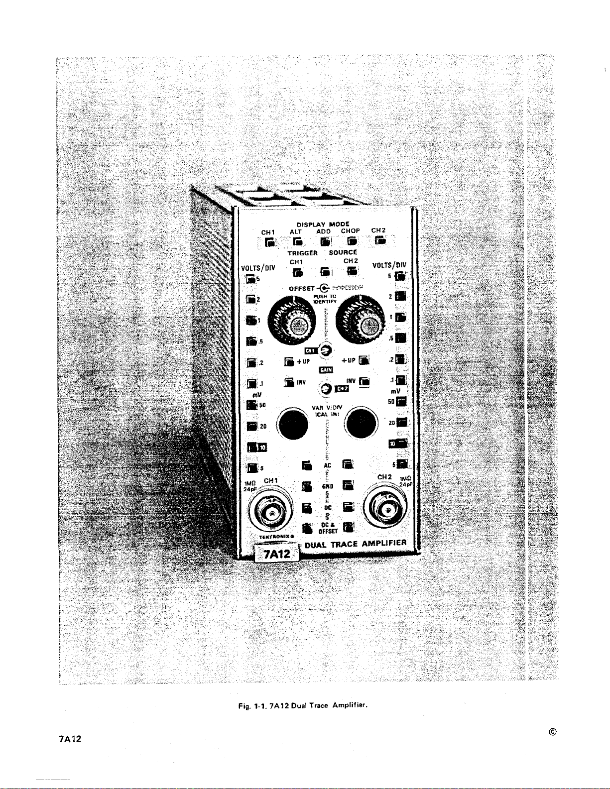
Fig.
1-1.
7A12
Dual
Trace
Amplifier.
Page 2
Introduction
The
7A12
vertical amplifier plug-in
with Tektronix 7000-Series Oscilloscopes. The
dualchannel, wide band amplifier with the upper frequency
limit mainly determined by the oscilloscope mainframe in
which it is used. For example, the 7A12 used with the
oscilloscope will have an upper bandwidth limit of
MHz.
When used with a 7704 oscilloscope, the upper band-
width limit
sation circuits are auotmatically switched to correspond to
the setting of the VOLTSlDlV switch. A +UP/INV switch
for each channel allows either channel to
differential measurements. The
circuit with
is
about 105
a
DC
offset
MHz.
Internal gain and compen-
7,412 features
of
at least
is
designed for use
7A12
about
be
inverted for
a
DC
+500
divisions
is
7504
75
offset
for
viewing low level
DC
component.
AC
signals in the presence
a
This instrument will meet the electrical character stics
listed in Table
in Section
Section 5 provides a convenient method of checking
ment performance without making internal adjustment
The following electrical characteristics are vatid ovep the
stated environmental range for instruments calibrated
ambient temperature of +20°C to
minute warmup unless otherwise stated.
5.
1-1
following complete calibration as kliven
The
performance check procedure givc n
+30"~,
of
a
high level
ir
after a five
in
stru-
;.
~t
an
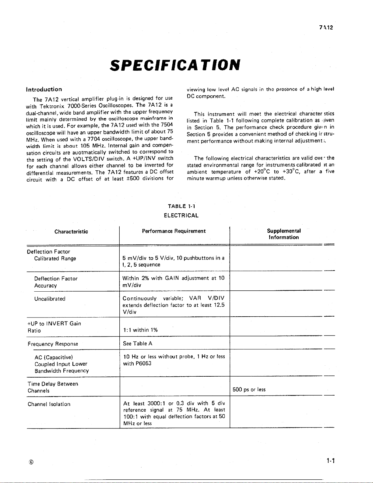
TABLE
ELECTRICAL
Characteristic Performance Requirement
Deflection Factor
Calibrated Range Vfdiv, 10 pushbuttons in
Deflection Factor
Accuracy
Uncalibrated
+UP
to INVERT Gain
Ratio
Frequency Response
AC (Capacitive)
Coupled Input Lower
Bandwidth Frequency
Time Delay Between
Channels
Within
mV/div
Continuously variable: VAR VIDIV
extends deflection factor to
V/div
1:l within
See Table
1
10
with
I
2%
with
GAIN
1%
A
Hz
or less without probe,
P6053
1-1
adjustment
at
least 12.5
1
Hz
at
or
a
10
I
less
500 ps or less
Supplemental
tnformation
-
-
-
-
-
Channel Isolation
At least 3000:l or
reference signal
100:l with equal deflection factors
MHz
or
less
at
0.3
75
div
MHz.
with
At
5
least
at
div
50
Page 3

TABLE
Performance
1-1
(mnt)
Requirement
Maximum
Voltage
DC
Couple
AC
Coupled
Input
Resistance
Capacitance
R
lnput
Direct
5
mV/div
10
mVldiv
(Capacitive)
l
nput
R
and
C
and
C
Product
Recommended
&
Xf
O
Probe
i
1
25
Meaohm
within
within
1
pF
2%
350
V,
l
es5
500
V,
less
350
V,
I
ess
500 V,
Within
DC
DC
DC
DC
1%
or
or
or
or
at
DC
all
DC
-t
Peak
DC
+
Peak
DC
+
Peak
+
Peak
deflection
AC
AC
AC
AC
factor
at
at
at
-
'
kHz
or
-
kHz
or
kHz
or
settings
Maximum
lnput
Current
!DENT
t
FY
Display
(Tangentially
Chopped Mode
installed
compartment.
dependent.)
QC
DC
Common
Noise
in
vsrtica!
Repetition
Channel
Drift
Drift
Temperature
Voltage
OFFSET
Time
With
Constant)
Range
Mode
Ratio
Gate
Measured)
(when
Mainframe
Rate
Segment
Ambient
4
Line
Rejection
I
At
dir
At
div
At
least
at
5
least
from
least
+I000
mV/div
+500
div
10
mV/div
10:l
at
div
40
to
to
MHz
-1
-500
to
5
000
Vtdiv
or
less
Trace
deflects
250
pV
other
def
500
kHz
100
P~f~
greater
.
-
-
-.
-
-
.
-
up
at
5
tectian
within
or
0.2
dlv
mV/div.
factors
20%
0.01
divPC
to
0.1
0.4
div
whic
di
o
I
less
-
lever
at
is
Page 4

Specif ication-7
412
Refer
scope.
With 7900
120
MHz
to
the
Specification
7A12
AND
Serles
TABLE
1-2
ENVIRONMENTAL
for
MAINFRAME
With
7700
105
MHz
the
associated oscillo-
TABLE
FREQUENCY
Series
A
RESPONSE
With
7500
75
Size
Weight
(five
Series
MHz
division
TABLE
PHYSICAL
Fits
all
2.8
Ibs
reference)
With
1-3
7000-Series
(1.3
kg)
7400
55
MHz
Plug-in
Series
Compartm
 Loading...