


Instruction Manual
Model 775A
Programmable Counter / Timer
©1987, Keithley Instruments, Inc.
All rights reserved.
Any unauthorized reproduction, photocopy, or use the information herein, in whole or in part, without the prior written approval
of Keithley Instruments, Inc. is strictly prohibited.
All Keithley Instruments product names are trademarks or registered trademarks of Keithley Instruments, Inc.
Other brand names are trademarks or registered trademarks of their respective holders.
Cleveland, Ohio, U.S.A.
Document Number: 775-901-01 Rev. B / February 1987

WARRANTY
Keithley instruments, Inc. warrants this product to be free from defects
in material and workmenship for a period of 1 year from date of shipment. During the warranty period, we will, at our option, either repair
or replace any product that proves to be defective.
To exercise this warranty, write or call your local Keithley represent-
ative, or contact Keithley headquarters in Cleveland, Ohio. You will be
given prompt assistance and return instructions. Send the instrument,
transportation prepaid, to the indicated service:facility. Repairs will be
made and the instrument returned, transportation prepaid. Repaired
products are warranted for the balance of the original warranty period,
or at least 90 days.
LIMITATION OF WARRANTY
This warranty does not apply to defects resulting from unauthorized
modification or misuse of any product or part. This warranty also does
not apply to fuses, batteries, or damage from battery leakage.
This warranty is in lieu of all other warranties, expressed or implied, in-
cluding any implied warranty of merchantability or fitness for a par-
ticular use. Keithley Instruments, Inc. shall not be liable for any indirect,
special or consequential damages.
STATEMENT OF CALIBRATION
This instrument has been inspected and tested in accordance with
specifications published by Keithley Instruments, Inc.
The accuracy and calibration of this instrument are traceable to the
National Bureau of Standards through equipment which is calibrated at
planned intervals by comparison to certified standards maintained in
the Laboratories of Keithley Instruments, Inc.
KEITHLEY INSTRUMENTS, INC.
INSTRUMENT DIVISION I 29775 Aurora Road / Cleveland. Ohio 44139 / U.S.A. / 1216) 246-0400 / Telex: 99.5469
WEST QERMANY:
aREA BRITAIN: Keithlay Instruments, Ltd. / 1, Boulton Road / Reading, Berkshire RG 2 ONL / 10734) 66-l 2.67/66 / Telex: 94.7047
FRANCE Keithlsy Instruments SARL / 2, Bis Rue L&n Blum / 9.P. 60 / 91121 P$laiseau Cedex / 16101 l-51 -55 /Telex: 600-933
NETHERLAND%
SWITZERLAND:
AUSTRI*:
ITALY:
Keith@ lnatruments Ges.m.b.H. / Doblinger Haupstr. 32 / 1190 Wien / 314 299 / Telex: 13-4500
Kelthley Instruments, SRL / Viale S. Gimignano 4/A / 20100 Milano, Italy / 4120360
Keithley Instruments GmbH / Heiglhofstr. 5 / 6000 Munchen 70 / 10691 710020 / Telex: 52.12160
Kelthley Instruments BV / Arkelsedijk 4 / Postbus 559 / 4200 AN Gorinchem / 101 1930.25577 / Telex: 24-664
Kelthley Instruments SA / Kriesbachstr. 4 / 9600 Oibendorf / 01/821-94-44 / Telex: 57-536

SPECIFICATIONS
INPUT CHARACTERISTICS
Channel A, B; each channel
RANGE:
SENSITIVITY (d):
DYNAMIC RANGE (xl): 50mV to 5V pk-pk, <ZOMHz.
COUPLING: ac or dc, switchable.
IMPEDANCE: lMR nominal, shunted by <60pF.
ATTENUATOR: xl or xl0 nominal, switchable.
LOW PASS FILTER: -1OdB
SIGNAL OPERATING RANGE (xl): -2.55V dc to t2.55V dc.
TRIGGER LEVEL: -2.55V dc to +2.55V dc, xl.
TRIGGER LEVEL RESOLUTION: lGmV, xl.
TRIGGER LEVEL SElTING ACCURACY:
TRIGGER LEVEL SETTING OUTPUT: via rear panel BNC,
SLOPE: + or - slope, switchable.
DAMAGE LEVEL:
0 to l20MHz, dc coupled.
30Hz to IZOMHz, ac coupled.
25mV rms, <lOMHz.
50mV rms, > 1OMHz.
14OmV to 2.5V pk-pk, >20MHz.
at
1OOkHz nominal, switchable.
:25.5V dc to +25.5V dc, x10.
Mo”v, xx?
*(35mV + 2% of setting), xl.
*(35OmV + 2% of setting), x10
not adjusted for attenuators.
xl: dc-2kHz 250V dc + peak ac
2kHz-100kHz 5 x 1OsV rms*Hz/frequency
> 1OOkHz
x10: dcZOkHz 250V dc + peak ac
20kHz.100kHz 5 x 10%’ rms.Hz/frequency
> 1OOkHz
5v rms
5oV rms
PERIOD A
RANGE:
LSD DISPLAYED: 1Ons to O.lms.
ACCURACY:
Mns to 10” seconds.
*l LSD *(Time Base Error x Period) f Trigger Error.
PERIOD AVERAGE A
RANGE: 1Ons to 10sec.
LSD
DISPLAYED: (10ns x l’eriod)/Gate Time.
RESOLUTION:
fl LSD f
ACCURACY:
NUMBER OF PERIODS AVERAGED: Gate Time/Period
(1.4 x Trigger Error + Zns) x Period
Gate Time
f Resolution *(Time Base Error x Period)
TIME INTERVAL A-B
RANGE: 1011s to
LSD DISPLAYED: 1Ons to O.lms.
ACCURACY: fl LSD *(Time Base Error x Time Interval)
f Trigger Error * Trigger Timing Error -t2ns.
lo4 seconds.
PULSE WIDTH A (Positive or Negative)
RANGE: Mns to lo4 seconds.
LSD DISPLAYED: lOns to O.lms.
ACCURACY: fl LSD *(Time Base Error x Pulse Width)
f Trigger Error f Trigger Timing Error f2ns.
mALIZE A
Channel C (with Model 7751 option)
RANGE: 5OMHz to 1.3GHz.
SENSITIVITY: l5mV, 50MHz to l.OCHz;
25mV, l.OGHz to 1.2GHz;
75mV, 1.2GHz to 1.3GHz
DYNAMIC RANGE: 25mV rms to 1V rms.
COUPLING: ac.
IMPEDANCE: 500.
DAMAGE LEVEL:
dc-100kHz
>.lOOkHz
l5V dc + peak ac
5v rms
FREQUENCY A, B
RANGE: O.lHz to l20MHz.
LSD DISPLAYED: (101~s x Frequency)/Cate Time
RESOLUTION:
*l ,.SD -t (1.4 x Trigger Error + 2ns)x Frequency
Gate Time
ACCL RACY:
*Resolution *(Time Base Error x Frequency)
DIGITS DISPLAYED: 8 per second of Gate Time, minimum.
MODES: Cumulative or A gated by B
RANGE: 0 to lo”-1
REPETITION RATE: lZ0MHz “ax.
LSD DISPLAYED: 1 count up to lOLo-1, then 9 most signifi-
cant digits.
ACCURACY: kl LSD
GATE/DELAY
INTERNAL GATE TIME: Variable from loops to IOsec in 45
increments, or one period of the input, whichever is longer.
May be used in Frequency and Period Average
measurements.
EXTERNAL GATE TIME: Continuously variable from loops
to Klsec, or one period of the input, whichever is longer.
EXTERNAL GATE DELW: 10~s + one period of the
input signal, maximum.
INTERNAL DELAY TIME: Variable from lOO@ to 10s~ in 45
increments. May be used in Period, Time Interval and Pulse
Width measurements.
EXTERNAL DELAY TIME: Continuously variable from loops
to >l hour.
EXTERNAL GATE/DELAY INPUT: Positive TTL signal via
rear panel BNC.

TIME BASE
GENERAL
FREQUENCY: 1OMH.z.
AGING RATE: 55 x lo-‘/month.
TEMPERATURE: f5 x lo-! 0’ to 40°C, ref 25’C.
TCXO (with Model 7752 option)
FREQUENOI: l!&II-Iz
AGING RATE: <l x IO-‘/month.
TEMPERATURE: *I x 10-q 0 to 4O’C, ref 25’C.
LINB VOITAGE: < 1 x lO-’ for 10% change.
IEEE-488 INTERFACE
MULTILINE COMMANDS: DCL, LLO, SDC, Gm, GTL,
UNT, UNL, SPE, SPD.
UNILINE COMMANDS: IFC, RBN, EOI, SRQ, NN.
INTERFACE FUNCTIONS: SHl, AHl, T6, TEO, IA, LEO, SRl,
PPO, DCl, DTI, CO, El.
PROGRAMMABLE PARAMETERS: AI1 front panel controls
(except POWER) plus Reading Rate, Data Format, Trigger,
EOI, Terminator, Service Request, Self Test, Display, Stahu.
READING RATES: one shot, normal (3/second), fast
(ZYsecond), or dump (14O/second).
DISPLAY:
BENCH READING RATES: One shot, or normal (3/second).
ARMING nRIGGER): Each channel is armed by it’s own
signal; or RESET button 01 EXT ARMING input when in one
shot (HOLD) mode.
ARMING DELAY: 30~ in Frequency and Period Average;
lOas in Period, Tie Interval and Pulse Width.
EXTERNAL ARMING INPUT: positive edge ‘IX signal via
rear panel BNC.
EXTERNAL TIME BASE INPUT: lOMHz ‘ITL signal via rear
panel BNC
TIME BASE,OUT: 2V minimum @ MMHz, 1OOD output resis-
tance, via rear panel BNC.
GATE: LED ,indicator lights when gate is open.
WARMUP: 2 hours to rated accuracy and stability
OPERATING TEMPERATURE: 0” to 4O”C, 0% to 80% relative
humidity
STORAGE TEMPERATURE: -25” to 65°C.
POWER: lO?-l25V or 2lO-250V (rear panel switch selected),
50-6OHz. 35VA max. 90-1lOV available.
DIMENSIONS, WEIGHT: l27mm high x 2l5mm wide x
359mm deep (5”~ 8’X’x 14r).
Net weight 3.5kg (8 lbs).
Nine
LED digits with decimal point and exponent.
Specifications subject to change without notice.
TABLE OF CONTENTS
SECTION l-GENERAL INFORMATION
1.1
1.2
1.3
1.4
1.5
1.6
1.7
1.8
INTRODUCTION.
MODEL775 FEATURES
WARRANTY INFORMATION
MANUAL ADDENDA
SAFETY SYMBOLS AND TERMS
INSPECTION
USING THE MODEL 775 MANUAL
ACCESSORIES
...........................................................................
......................................................................
................................................................. l-l
.......................................................................
.............................................................
...............................................................................
..........................................................
..............................................................................
SECTION Z-BASIC COUNTER/TIMER OPERATION
2.1
2.2
2.2.1
2.2.2
2.2.3
2.2.4
2.3
2.3.1
2.3.2
2.3.3
2.3.4
2.4
2.5
2.5.1
2.6
2.6.1
2.6.2
2.6.3
2.6.4
2.6.5
2.6.6
2.6.7
2.6.8
2.6.9
2.7
2.7.1
2.7.2
2.7.3
2.7.4
2.8
INTRODUCTION
FRONTI’ANEL FAMILIARIZATICJI’J
Controls
Terminals .................................................................................
Display and Indicators
TiltBail
REAR PANELFAMILIARIZATION
Connectors and Terminals
Line Voltage Selector Switch ................................................................
IEEE-488 Address Switches .................................................................
Line Fuse
POWER-UP PROCEDURE ....................................................................
DISPLAYMESSAGES ........................................................................
No Option Message
CONTROL SELECTION
Function
Selecting GateTime .......................................................................
User Gate Function ........................................................................
Using Delay ...............................................................................
User Delay Function ......................................................................
Selecting Measurement Rate
Selecting the Number of Displayed Digits.
Input Condition Controls Setting.,
Setting Trigger Levels
ARMING..
Continuous Arming....................~ ..................................................
Front Panel Arming
External Arming ..........................................................................
Alarm Conditions
APPLICATIONS
..................................................................................
................................................................................... 2-6
.................................................................................
..................................................................................
...........................................................................
..........................................................
..................................................................... 2-6
............................................................ 2-6
.................................................................. 2-6
......................................................................
.....................................................................
............................................................... 2-10
.................................................. 2-10
......................................................... 2-11
.....................................................................
................................................................................
.......................................................................
.........................................................................
............................................................................
l-l
l-1
l-1
l-1
l-2
l-2
1-2
2-l
2-4
2-4
2-5
2-6
2-6
2-6
2-6
2-7
...2- 7
2-8
2-8
2-8
2-9
2-9
2-10
2-11
2-12
2.12
2-12
2-13
2-13
2-U
SECTION 3-IEEE-488 OPERATION
3.1
3.2
INTRODUCTION . . . . . . . . . . . . . . . . . . . . . . . . . . . . . . . . . . .._..._.................................. 3-l
BUS DESCRIPTION . . . . . . . . . . . . . . . . . . .._...............................................,,... 3-l
TABLE OF CONTENTS
3.3
3.3.1
3.3.2
3.3.3
3.4
3.4.1
3.4.2
3.4.3
3.4.4
3.4.5
3.5
3.6
3.6.1
3.6.2
3.6.3
3.7
3.7.1
3.7.2
3.7.3
3.8
3.8.1
3.8.2
3.8.3
3.0.4
3.9
3.9.1
3.9.2
3.9.3
3.9.4
3.9.5
3.9.6
3.9.7
3.9.8
3.10
3.10.1
3.102
3.10.3
3.10.4
3.10.5
3.10.6
3.10.7
3.108
3.10.9
3.10.10
3.10.11
3.10.12
3.1o.u
3.10.14
3.10.15
3.10.16
3.10.17
3.11
3.11.1
3.11.2
3.11.3
3.u.4
3.: A
IEEE-488 BUS LINES . .
Bus Management Lines.. ..................................................................
HandshakeLines ..........................................................................
Data Lines
................................................................................
BUS COMMANDS ..........................................................................
Uniline Commands
........................................................................
UniversalCommands ......................................................................
Addressed Commands .....................................................................
Unaddressed Commands
..................................................................
Device-Dependent Commands .............................................................. 3-5
COMMAND CODES
COMMAND SEQUENCE. ..............................................
........................................................................
.< ................... 3-6
Addressed Command Sequence ............................................................
Universal Command Sequence .............................................................
Device-Dependent Command Sequence
.....................................................
HARDWARE CONSIDERATIONS ............................................................
Typical Controlled Systems. ................................................................
BusConnections.. ........................................................................
Primary Address Programming ............................................................
:
SOFTWARE CONSIDERATIONS I .............................
...............................
Controlled Interface Routines ..............................................................
HP-8 BASIC Statements ....................................................................
Interface Function Codes . . .
Model 775 Interface Commandr
GENER,
AL BUS COMMAND PROGRAMMING
;
............................................................
..............................................
REN (Remot e Enable) .....................................................................
IFC (Interface Clear)
LLO‘(Local Lockoui)
GTL (Go To Local)
DCL(Device Clear)
SDC (Selective Device Clear)
GET (Group Execute Trigger)
Serial Polling (SPE,
..,,,...,,,,.......................................................... 3-14
...................................... 3-14
..............................
.:
........................................................................
.......................................................................
..............................................................
..............................................................
SPD)
..................................................................
DEVICE-DEPENDENT COMMAND PROGRAMMING ........................................
Execute (X). ..............................................................................
Function(F) ..............................................................................
Channels A, d Coupling (AC, BC) .........................................................
Channels A, B Attenuator (AA, BA) .......................................................
Channels A, B Filter (AF, BF)
Channels A, B Slope (AS, BS).
Channels A, B Trigger Level (AL,
.............................................................
............................................................
BL)
......................................................
Rate(S) .................................................................................
Gate Time(G) ...........................................................................
Delay Time(W) ..........................................................................
Delay(I) .................................................................................
Displayed Digits(N)
Triggering (T)
......................................................................
............................................................................
EOI(K) .................................................................................
SRQ Mode (M) and Serial Poll Status Byte Format
Displayed Modes (D)
Self-Test
(J) ...............................................................................
READING FROM THE MODEL 775
Data Control Commands (B)
Status Word
Terminator (Y)
Prefix(P)
(U)
...........................................................................
................................................................................
Dump Mode (53 Rate Mode)
.....................................................................
.........................................................
..............................................................
..........................................................................
..............................................................
..........................................
3-2
3-2
3-2
3-3
3-3
3-4
3-4
3-5
3-5
3-5
3-6
3-6
3-6
3-6
3-6 1~
3-8
3-10
3-10. ...
3-10
3-11
3-L?
3-13
3-13
3-13
3-14
3-15
,3-15
3-15
3-16
3-16
3-19
3-19
3-19’ ’
3-20
3-20
3-20
3-20
3-21
3-22
3-22
3-23 I
3-23
3-23
3-23
3-24
3-26
3-27
3-27
3-28
3-29
3-30
3-31
3-31
TABLEOFCONTENTS
.
a 4.5.7
. +,4.5.8
3.12
3.x2.1
FRONT PANEL PROGRAhJ.MING
IDDCError .........................................................................................
3.12.2 IDDCO Error
.......................................................................................
...................................................................... 3-34
SECTION G-PERFORMANCE VERIFICATION
...........................................................................
...........................................................
...........................................................
...
......................................................
............................................................
.....................................................
............................................................
..................................................
ii
413
‘~ 4.4
4.5
4.5.1
4.52
‘4.5.3
.,- 4.5.4
4.5.5
4.5.6
4.5.9
INTRODUCTION
ENVIRONMENTAL CONDITIONS
RECOMMENDED TEST EOUIFMENT
INITIAL CONDITIONS VERIFICATION PROCEDURES
Channels A, B and C Inputs Sensitivity.
Period Measurement Accuracy Check ...............................................
Period Averaged Measurement Accuracy Check
Tie Interval A-B Measurement Operation Check.,
Pulse A Measurement Operation Check.. ...........................................
Delay Operation Check
External Gate Operation Check
Arming Operation Check
Model7752TCXO Accuracy Check
SECTION 5-THEORY OF OPERATION
5.1
5.2
5.3
5.3.1
5.3.2
5.3.3
5.3.4
5.3.5
5.3.6
5.3.7
* 5.4
5.4.1
5.4.2
5.4.3
54.4
5.4.5
INTRODUCTION
OVERALL FUNCTIONAL DESCRIPTION
ANALOG CIRCIJITP.Y.
Input Circuits A and B ....................................................................
Input C~cuitC
1OMHz Standard Reference Oscillator
1OMHz ICXO Reference Oscillator
100MHzMultiplier
Measurement Section ......................................................................
Power Supply .............................................................................
DIGITAL CIRCUITRY
Microcomputer Block Diagram
Memory Mapping ........................................................................
Address Decoding
Keyboard/Display Interface
IEEE Interface
...........................................................................
....................................................................... 5-3
............................................................................
..........................................................
........................................................................
.......................................................................
.............................................................
........................................................................ 5-13
................................................................ 5-14
............................................................................
3-34
3-34
4-l
4-l
........................................................ 4-l
.............................................
......................................
.................................
5-l
......................................................
5-l
5-3
5-3
.......................................................
5-3
5-3
5-3
5-4
5-4
5-D
5-13
5-13
5-14
SECTION 6-MAINTENANCE
6.1
6.2
243
6.5
6.6
6.7
6.7.1
6.7.2
6.7.3
6.7.4
6.7.5
INTRODUCTION
LINE VOLIAGE SELECTION
FUSE REPLACEMENT
USING AN EXTERNAL TIME BASE,,
MODEL 7751 CHANNEL C OPTION INSTALLATION
MODEL 7752 TCXO OPTION INSTALLATION
CALIBRATION
Environmental Conditions.
Warm-Up Period
Recommended Test Equipment
Calibration Procedure
Multiplier Adjustment
..................................................................
.......................................................................
.............................................................................
..........................................................................
......................................................................
........................................................
........................................................
.........................................
................................................
.................................................................
.............................................................
.....................................................................
6-l
6-l
6-l
6-2
6-3
6-4
6-5
6-5
6-5
6-5
6-5
6-7
iii
TABLE OF CONTENTS
6.7.6
6.7.7
6.7.8
6.7.9
6.7.10
6.8
6.9
6.10
6.10.1
6.10.2
6.10.3
6.10.4
6.10.5
6.10.6
6.10.7
6.10.8
6.10.9
Trigger Level Adjustment
Channels A and B Sensitivity Adjustment
Inputs A and B Attenuator Compensation
Tune Base Adjustment (Standard 5 PPM Tune Base)
Time Base Adjustment (Optional 1 PPM Tie Base)
SPECIAL HANDLING OF SEATIC SENSITIVE DEVICES
DISASSEMBLY INSTRUCI’IONS. .............................................................
TROUBLESHOOnNG ......................................................................
Recommended Test Equipment. ............................................................
Power-Up Self Diagnostics .................................................................
Power Supply Checks
Reference Oscillator and Clock Checks
Digital Circuitry and Display Checks
Signal Conditioning and Input Circuit Checks.
Multiplier Circuit Checks ..................................................................
Trigger Level Checks ......................................................................
Measurement Section Checks.. ............................................................
...................................................................
.....................................................................
SECTION 7-REPLACEABLE PARTS
Zl
7.2
7.3
7.4
7.5
INTRODUCTION ............................................................................
PARTS LIST..
ORDERING INFORMATION .................................................................
FACTORY SERVICE
SCHEMATIC DIAGRAM AND COMPONENT LOCATION DRAWINGS
...............................................................................
..........................................................................
6-7
...................................................
...................................................
..........................................
..........................................
.......................................
......................................................
....................................................... 6-11
..............................................
..........................
6-7
6-7
6-7
6-7
6-8
6-8
6-10
6-10
6-10
6-10
6-11
6-11
6-11
6-11
6-11
7-1
7-l
7-l
7-1
7-l
A
I
APPENDIX..
INDEX
......................................................................................
...............................................................................
A-l
I-l
iV

LIST OF ILLUSTRATIONS
2-l
2-2
2-3
2-4
2-5
3-l
3-2
3-3
3-4
3-5
3-6
3-7
3-8
3-9
3-10
5-l
5-2
5-3
5-4
5-5
5-6
5-7
5-8
6-l
6-2
6-3
6-4
6-5
Model775
Model775RearPanel ........................................................................
FallTime Measurement
Using Delay to Measure Contact Dwell Time
High Frequency Multiplexed Measurements
IEEE Bus Configuration
IEEE Handshake Sequence
Command Codes
System Types ............................................ 3-8
IEEE-468 Connector ......................................
IEEE-488 Connections., ...................................
Rear Panel of Model 775 Showing IEEE connector
Contact Assignments ..................................... 3-9
Typical IEEE-488 Bus Driver (One of 16)
IEEE-488 Display Error Messages ..........................
Model775 Simplified BlockDiagram
Frequency A Measurement Block Diagram.
Frequency B Measurement Block Diagram
Frequency C Measurement Block Diagram
Period A Measurement Block Diagram
Time Interval A-B Measurement Block Diagram
Pulse Width Measurement Block Diagram.
Microcomputer Block Diagram
Model 775 Standard 5ppm Timebase
Model 7751 Installation
Model 7752 Installation
Model 775 Calibration Adjustments
Model 775 Exploded View ................................
Front Panel
....................................................................... 2-2
2-3
..................................................................... 2-14
.................................................. Z-15
................................................... 2-15
................................... 3-2
................................ 3-3
........................................ 3-7
3-8
................... 3-10
.......................................................... 5-2
.................................................... 5-6
..................................................... 5-7
..................................................... 5-8
........................................................
.................................................... 5-11
............................................................... 5-12
.......................
...................................
...................................
........................
..,...
...........
.............................................. 5-10
.,..,.
.,....
3-9
3-9
3-35
5-9
6-2
b-3
b-4
6-6
6-9
7-l
7-2
7-3
7-4
7-5
7-b
7-7
7-8
7-9
7-10
Mother Board, Component Location Drawing
Mother Board, Schematic Diagram
Display Board, Component Location Drawing
Display Board, Schematic Diagram
Model 7751, Component Location Drawing
Model 7751, Schematic Diagram ....................................................
Model 7752, Component Location Drawing
Model 7752, Schematic Diagram
5 ppm Oscillator, Component Location Drawing.
5 ppm Oscillator, Schematic Location Diagram
.................................................
..................................................
....................................................
.......................................
........................................
..........................................
..........................................
.....................................
.......................................
7-11
7-13
7-26
7-27
7-29
7-30
7-31
7-32
7-33
7-34
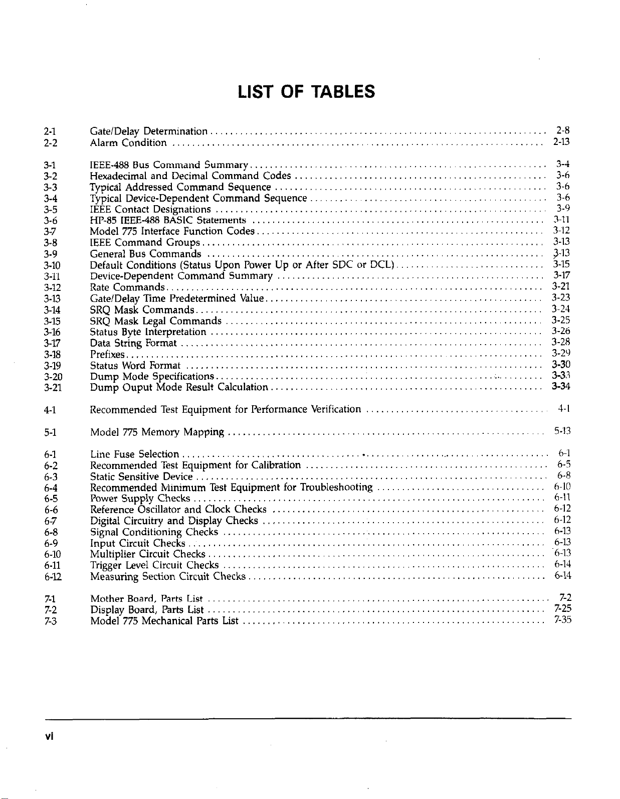
LIST OF TABLES
2-l
2-2
3-l
3-2
3-3
3-4
3-5
3-6
3-7
3-8
3-9
3-10
3-11
3-12
3-D
3-14
3-15
3-16
3-17
3-18
3-19
3-20
3-21
4-l
Gate/Delay Determination.
Alarm Condition
IEEE-488BusCommand Summary
Hexadecimal and Decimal Command Codes
Typical Addressed Command Sequence
Typical Device-Dependent Command Sequence
IEEE Contact Designations
HP-85 IEEE-488 BASIC Statements
Model 775 Interface Function Codes,,
IEEE Command Groups .....................................................................
General Bus Commands
Default Conditions (Status Upon Power Up or After SDC or
Device-Dependent Command Summary
Rate Commands ............................................................................
Gate/Delay Time Predetermined Value.,
SRQ
Mask Commands
SRQ Mask Legal Commands..
Status Byte Interpretation
Data
String Format
Prefixes.
Status Word Format
DumpMode Specifications........................................................:
Dump Ouput Mode Result Calculation
Recommended Test Equipment for Performance Verification
.............................................................................
.........................................................................
...............................................
...................................................................
............................................................
.......................
.......................................................
................................................
...................................................................
...........................................................
........................................................
...........................................................
DCL)
......................................................
...................................................... 3-23
......................................................................
..............................................................
...............................
....................................
... ..............
...................................
,
.
...................................
, ...................................
..................................... 4-l
..............................
.................................
...........................
........ 3-13
3-24
3-25
3-26
3-28
..........
3-34
2-8
Z-13
3-4
3-h
3-b
3-6
3-9
3-11
3-12
3-13
3-15
3-17
3-21
3-2’)
3-30
3-33
5-l
6-l
6-2
6-3
6-4
6-5
6-6
6-7
6-8
6-9
6-10
6.11
6-12
7-l
7-2
7-3
Model775 Memory Mapping ................................................................
Line Fuse Selection
Recommended Test Equipment for Calibration
Static Sensitive Device
Recommended Minimum Test Equipment for Troubleshooting
Power Supply Checks
Reference Oscillator and Clock Checks
Digital Circuitry and Display Checks
Signal Conditioning Checks
Input Circuit Checks
Multiplier Circuit Checks
Trigger Level Circuit Checks..
Measuring Section Circuit Checks
Mother Board, Parts List
Display Board, Parts List
Model 775 Mechanical Parts List
........................................................................... b-l
............
.......................................................................
.......................................................................
..............
.. .............
..............
........................................................................
....................................................................
...............................................................
..........
.....................................................................
....................................................................
......
..................................................
................................................. 6-14
.................................................
.
....................................
.................................. 6-K)
........................................ b-12
........................................
5-13
6-5
6-8
b-11
6-12
b-13
6-U
6-13
b-14
7-2
7-25
7-35
vi
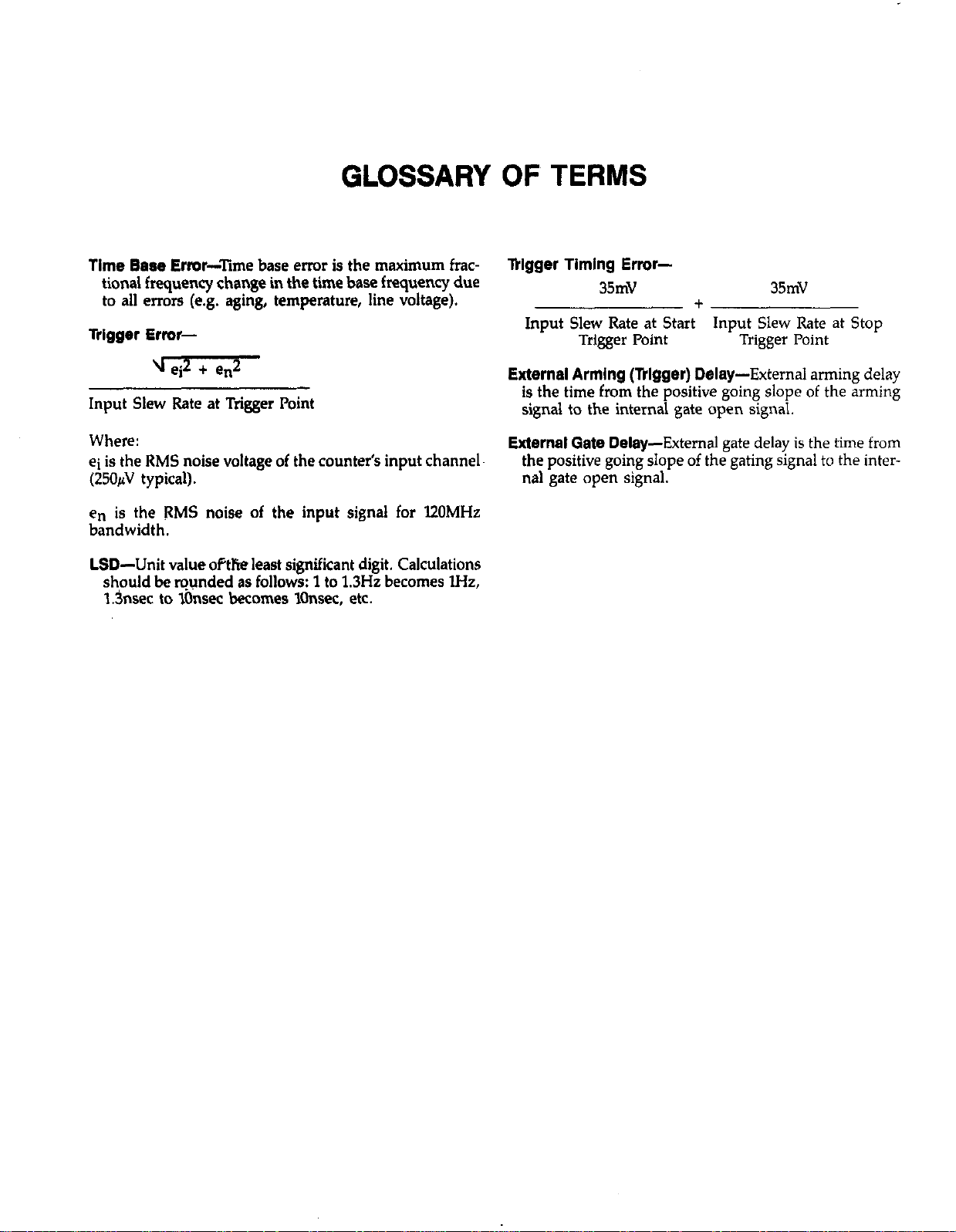
GLOSSARY OF TERMS
Time Base Uror4ime base error is the maximum frac-
tional frequency change in the time base frequency due
to all errors (e.g. aging, temperature, line voltage).
ligger Ermr-
q ei2 + en2
Input Slew Rate at Trigger Point
Where:
ei is the RMS noise voltage of the counter’s input channel
(25OhV typical).
en is the RMS noise of the input signal for lZ0MHz
bandwidth.
LSD-Unit value ot%eleast significant digit. Calculations
should ba rounded as follows: 1 to 1.3Hz becomes IHz,
l.hwec to liinsec becomes IOnsec, etc.
lklgger Timing Error-
35mV 35mV
+
Input Slew Rate at Start Input Slew Rate at Stop
Trigger Point Trigger Point
External Arming (Wgger) Delay-External arming delay
is the time from the positive going slope of the arming
signal to the internal gate open signal.
External Gate Delay-External gate delay is the time from
the positive going slope of the gating signal to the internal gate open signal.

SECTION 1
GENERAL INFORMATION
1.1 INTRODUCTION
The Keithley Model 775 Programmable CouirterlTimer is
a nine digit, microcomputer based, fully programmable,
universal counter/timer. The Model 775 measures with
high resolution the following parameters:
l
Frequency A
l
Frequency B
l
Frequency C
l
Period
. Period Averaged
l
Time Intervals A - B
l
Pulse Width (positive or negative) A
The Model 775 has an 14mm (0.56 in.) LED display. The
display consists of 9 digits with an additional digit for exponent. The built-in interface makes the instrument fully
programmable over the IEEE-488 bus.
The Model 775 contains a programmable trigger level that
allows additional flexibility in measurements over the bus
(e.g. measuring rise and fall time with trigger points other
than 10% and 90%). Gate time is programmed in 46 steps
from 100psec to 1Osec or external from the front panel or
over the bus.
Trigger Delay Channel B-This feature is important for
some channel A - B time measurements.
True DC Coupling-Allows the Model 775 to do channel
A - B time measurements.
Reciprocal Technique-This counting method provides advantages over all traditional counters from DC up to the
clock frequency (100MHz). The constant relative resolution (8 digits/second independent of input frequency)
makes it even more useful for low frequency applications.
1.3 WARRANTY INFORMATION
Warranty information may be found on the inside front
cover of this manual. Should it become necessary to exercise the warranty, contact your Keithley representative cur
the factory to determine the proper course of action.
Keithley Instruments maintains service facilities in the
United States, United Kingdom and throughout Europe.
Information concerning the application, operation or service of your instrument may be directed to the applications
engineer at any of these locations. Check the inside front
cover for addresses.
1.4 MANUAL ADDENDA
1.2 MODEL 775 FEATURES
Dual Channel Capability-Dual channel capability with
two similar channels up to ‘IZOMHz.
Full Programmability-Full programmability of all functions and modes including different SRQ masks and channel selection.
High Frequency Option-H&option adds a third measurement channel for frequencies up to 1GHz.
High Resolution-A 1OOMHz clock rate, along with the
latest technique in frequency counting (reciprocal technique), provides the high resolution of 8 digits/second or VIZ
out of a 1OOMHz input signal.
Information concerning improvements or changes to the
instrument which occur after the printing of this manual
will be found on an addendum sheet included with this
manual. Be sure to review these changes before attempting to operate or service the instrument.
1.5 SAFETY SYMBOLS AND TERMS
The following safety symbols and terms are used in this
manual or found on the Model 775.
Then
should refer to the operating instructions in this manual.
The WARNING used in this manual explains dangers that
could result in personal injury or death.
symbol on the instrument denotes that the user
l-l
The CAUTION used in this manual explains hazards that
could damage the instrument.
1.6 INSPECTION
The Model 775 was inspected both mechanically and electrically before shipment. After unpacking all the items from
the shipping carton, check for any obvious signs of
physical damage that may have occurred during transit.
Report any damage to the shipping agent. Retain and use
the original packing materials in case reshipment is
necessary. The following items are shipped with every
Model 775.
Model 775 Programmable Counter/Timer
Model 775 Instruction Manual
Additional accessories as ordered.
If an additional Instruction Manual is required, order the
manual package (Keithley part number 775-901-00). The
manual package includes an instruction manual and any
applicable addenda.
1.7 USING THE MODEL 775 MANUAL
l
Section 1 contains general information about the
instrument.
l
Section 2 contains detailed operating information on using the front panel controls and rear panel terminals.
l
Section 3 contains information necessary to operate the
Model 775 over the IEEE-488 bus.
l
Section 4 contains performance verification procedures
for the instrument. This information is helpful if you
wish to verify that the instrument is operating in compliance with stated specifications.
l
Section 5 contains a description of operating theory.
l
Section 6 contains information for servicing the instrument. This section includes information on line voltage
selection, fuse replacement, adjustments and
troubleshooting.
l
Section 7 contains replacement parts information.
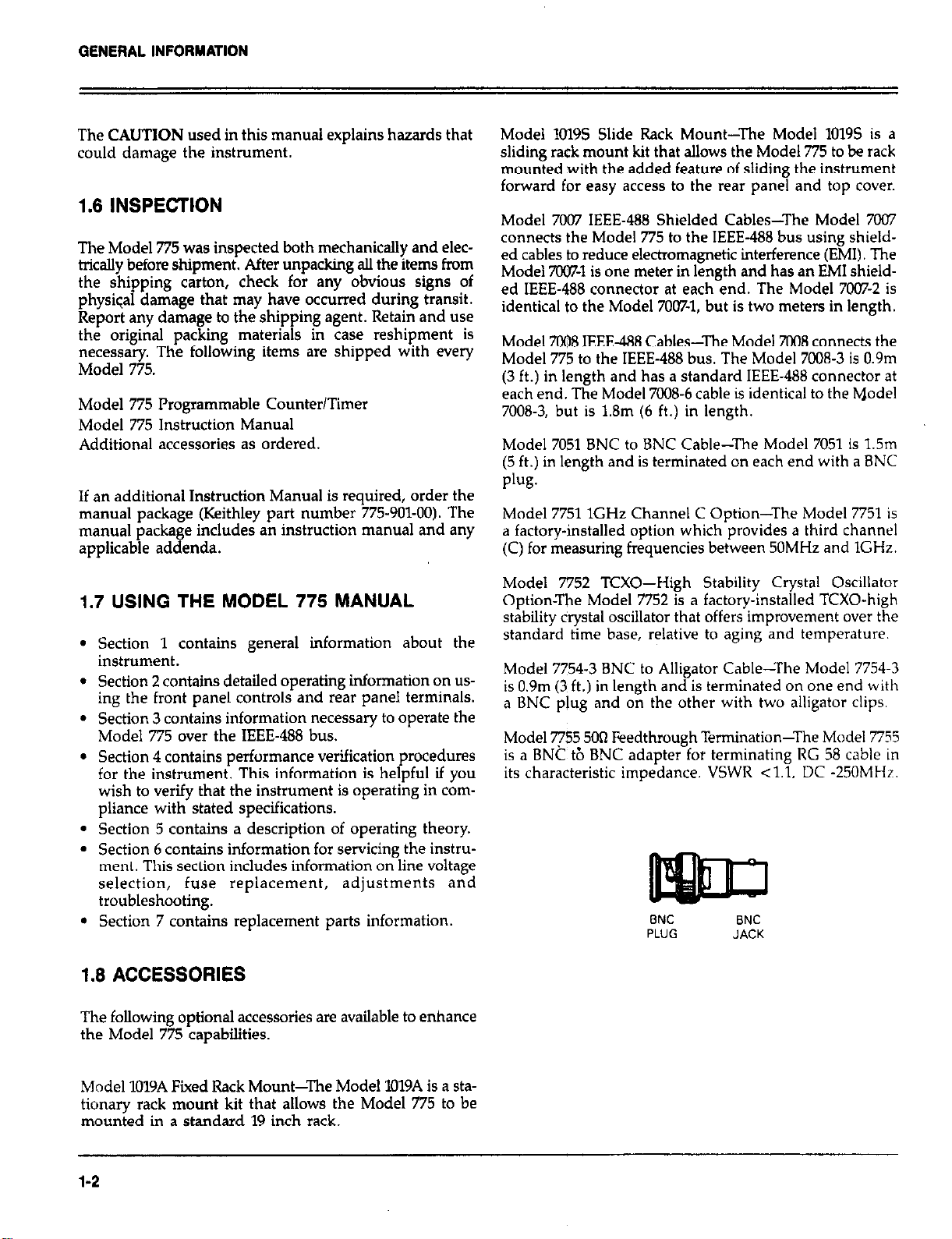
Model 1019s Slide Rack Mount-The Model 10195 is a
sliding rack mount kit that allows the Model 775 to be rack
mounted with the added feature of sliding the instrument
forward for easy access to the rear panel and top cover.
Model 7007 IEEE-488 Shielded Cables-The Model 7007
connects the Model 775 to the IEEE-488 bus using shielded cables to reduce electromagnetic interference (EMI). The
Model 7007-1 is one meter in length and has an EM1 shielded IEEE-488 connector at each end. The Model 7007-2 is
identical to the Model 7007-1, but is two meters in length.
Model 7008 IEEE-486 Cables-The Model 7008 connects the
Model 775 to the IEEE-488 bus. The Model 7008-3 is 0.9m
(3 ft.) in length and has a standard IEEE-488 connector at
each end. The Model 7008-6 cable is identical to the Model
7008-3, but is 1.8m (6 ft.) in length.
Model 7051 BNC to BNC Cable--The Model 7051 is 1.5m
(5 ft.) in length and is terminated on each end with a BNC
Ph%
Model 7751 1GHz Channel C Option-The Model 7751 is
a factory-installed option which provides a third channel
(C) for measuring frequencies between 50MHz and IGHz.
Model 7752 TCXO-High Stability Crystal Oscillator
Option-The Model 7752 is a factory-installed TCXO-high
stability crystal oscillator that offers improvement over the
standard time base, relative to aging and temperature.
Model 7754-3 BNC to Alligator Cable-The Model 7754-3
is 0.9m (3 ft.) in length and is terminated on one end with
a BNC plug and on the other with two alligator clips.
Model 7755 5012 Feedthrough Termination-Ihe Model 7755
is a BNC tb BNC adapter for terminating RG 58 cable in
its characteristic impedance. VSWR <l.l, DC -250MHz.
SNC
PLUG
BNC
JACK
1.8 ACCESSORIES
The following optional accessories are available to enhance
the Model 775 capabilities.
Model 1019A Fixed Rack Mount-The Model 1019A is a stationary rack mount kit that allows the Model 775 to be
mounted in a standard 19 inch rack.
l-2

SECTION 2
BASIC COUNTER/TIMER OPERATION
2.1 INTRODUCTION
Model 775 operation is divided into the two general
categories: basic bench operation, and IEEE-488 operation.
Basic bench operation which is covered in this section, consists of using the Model 775 to perform basic frequency
and time measurements. IEEE-488 programming can also
be used. These aspects are covered in detail in Sections
3 and 4. A layout of the front and rear panels of the Model
775 are shown in Figures 2-l and 2-2 respectively, includ-
ed is a brief description of each control, terminal and
indicator.
NOTE
Any front panel button push or IEEE devicedependent command (see Section 3) will cause the
measurement to restart, which will affect, for example, a measurement of the time from channels
A to B.
2-1
OPERATION
q
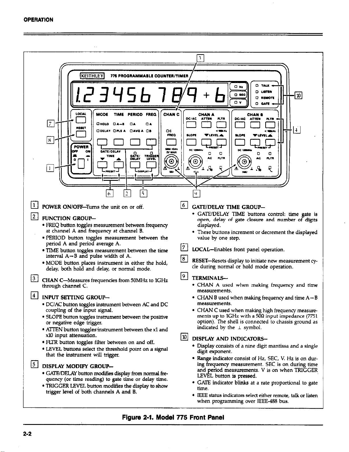
POWER ON/OFF-Turns the unit on or off.
q
FUNCIXON GROUP-
l
FREQ button toggles measurement between frequency
at channel A and frequency at channel 8.
l
PERIOD button toggles measurement b&./em the
period A and period average A.
l
TIME button toggles measurement between the time
interval A-B and pulse width of A.
l
MODE button places instrument in either the hold,
delay, both hold and delay, or normal mode.
El CHAN C-Measures frequencies from 50MHz to 1GHz
through channel C.
El
INPUT SEITING GROUP-
l
DC/AC button toggles instrument between AC and DC
coupling of the input signal.
* SLOPE button toggles instrument between the positive
or negative edge trigger.
l
A’lTEN button tot&sinstmment between the xl and
x10 input attenuZon.
l
FUR button toggles filter between on and off.
* LEVEL buttons select the threshold point on a signal
that the instrument will trigger.
El
DISPLAY MODIFY GROIJP. GATE/DELAY button modifies display horn normal fre-
quency (or time reading) to gate time or delay time.
l
TRIGGER LEVEL button modifies the display to show
trigger level of both channels A and B.
El GATE/DELAY TIME CROUP-
. GATE/DELAY TIME buttons control: time gate is
open, delay of gate closure and number of digits
displayed.
l
These buttons increment or decrement the displayed
value by one step.
El
LOCAL-Enables front panel operation.
q
RESET-Resets display to initiate new measurement cy.
cle during normal or hold mode operation.
El TERMINALS-
l
CHAN A used when making frequency and time
measurements.
* WAN B used when making frequency and time A-B
measurmlents.
. CHAN C used when making high frequency measure-
ments up to 1GHz with a 500 input impedance (7751
option). The shell is connected to chassis ground as
indicated by the I symbol.
El DISPW AND INDICATORS-
l
Display consists of a nine digit mantissa and a single
digit exponent.
l
Ran
e indicator consist of Hz, SEC, V. Hz is on dur-
ing
qwncy measurement. SEC is on during time
te
and ,period measurements. V is on when TRIGGER
LEVEL button is pressed.
l
GATE indicator blinks at a rate proportional to gate
time.
l
IEEE status indicators select either remote. talk or listen
when programming over IEEE-488 bus.
2-2
Figure 2-1. Model 775 Front #Panel

OPERATION
CONNECrORS AND TRRMINALS-
El
l
AC receptacle connects to a three wire line cord
which provides connection to the line voltage.
l
IEEE-483 connector is used to connect the instrument
to the IEEE-488 bus. IEEE interface functions are
marked above the connector.
l
TRIGGER LEVEL OLPTPLJT connections are used to
connect the DC voltage level from the trigger circuits
to an external Dh4M or osciIloscope. DC output range
is marked above the connector.
l
CLOCK connactor is used to output the internal clock
as a reference to another instrument or to use an axternal clock as the Model 775’s time base.
. EXT ARMING & GATE DELAY connector is used to
receive one of three signals: arming pulse, external
gate signal or external delay pulse.
Figure 2-2. Model 775 Rear Panel
LINE VOLTAGE SELEOR switch selects the line
El
voltage that the unit will operate on.
IEEE-488 address switches set the primary address for
El
IEEE-488 bus operation.
LINE FUSE provides protection on the AC power line
El
input.
2-3
OPERATION
2.2 FRONT PANEL FAMIC1ARIZATION
The front panel layout of the Model 775 is shown in Figure
2-1. The front panel is generally divided into three sections:
controls, terminals, and display and indicators. The following paragraphs describe the purpose of each of these items
in detail.
2.2.1~ Controls
All front panel controls except POWER are momentary
contact switches. Many controls include an annunciator
light to indicate the selected configuration. The controls
are color coded into functional groups for easier operation.
Front panel controls may be divided into the following
functional groups: Function, Input Setting, Display Modify
and Gate/Delay Time.
POWER-The POWER switch controls the AC power to the
instrument. Depressing and releasing the switch once
turns the power on. Depressing and releasing the switch
a second time turns the power off.
Function GrouP4he four FUNCTlON buttons control the
type of measurement, Each button is used to select one
of two functions.
MODE-Press the MODE button once to place the lnstrument in the hold mode. Press the RESET button to clear
the display and take a reading. The reading will be held
on the display until the RESET button is pressed again.
Pressing the MODE butt.on a second time, places the
Model 775 in the delay mode of operation; the instrument
holds off closure of the gate for the selected delay time.
Pressing the MODE button a third time places the instrument in both the hold and delay modes. Pressing of the
MODE button a fourth time turns the indicators off: and
places the instrument in the normal mode of operation.
NOTE
The delay ,mode is disabled in the frequency and
period averaging modes.
FREQ C--The: FREQ C button allows the Model 775 to
measure frequencies from 50MHz to lGHz on channel C.
Pressing the FREQ C button turns the C indicator on; lndicating the instrument is set to make high frequency
measurements on channel C. If the Model 7751 Channel
C option is not installed, a ‘no C OPY message will be
displayed for two seconds.
Input Setting Group-The six WAN A pushbuttons control input attenuation, coupling, slope, trigger level and
high frequency noise suppression. The six CHAN B
pushbuttons are functionaly identical to the CHAN A
buttons.
FREQ-The FREQ button places the instrument in frequency measurement mode. Pressing the FREQ button once
turns the A indicator on; indicating the instrument is set
for the frequency A mode. Pressing the button a second
time, turns the B indicator on; indicating the instrument
is set for the frequency B mode. Pressing of the FREQ button toggles the measurement between the frequency at
channel A and frequency at channel B modes.
PERIOD-The PERIOD button places the instrument in
period measurement mode. Pressing the PERIOD button
once turns the A indicator on; indicating the instrument
is in the period A mode. Pressing the PERIOD button a
second time, turns the AVG A indicator on; indicating the
inetrument is in the period average A mode. Pressing of
the PERIOD button toggles the measurement between the
period A and period average A.
TIME-The TIME button sets the Model 775 up to measure
the time interval between channel A and 8. Pressing the
TIME button once turns the A-B indicator on; indicating
the instrument is in the time interval A-B mode. Pressing the button a second time, turns the PLS A indicator
on; indicating the instrument is in the pulse A mode.
l’ressi,ig of the TIME button toggles the measurement between the time interval, A-B and pulse width of A.
DC/AC-The DC/AC button selects either the AC or DC
coupling mode. In default position, the instrument is in
the DC coupling mode. Pressing the DC/AC button turns
the AC indicator on; indicating the instrument is in the
AC coupling mode. Pressing of the DC/AC button toggles
the instrument between AC and DC coupling of the input signal.
SLOPE-The $LQPE button selects the slope that the
Model 775 will trigger on. In default position, the instrument triggers on a positive going edge. Pressing the SLQPE
button turns the ” 1
strument will trigger on a negative going edge. Pressing
of the SLOPE button toggles the instrument between the
positive or negative edge trigger.
ATTEN-The ATTEN button controls the attenuation of the
input signal. In default position, the signal will not be attenuated. Pressing the ATTEN button turns the x10 indicator on; indicating that the instrument will attenuate
the signal by Ill. Pressing of the ATTEN button toggles the
instrument between the xl and xl0 input attenuation. Note
that changing attenuation changes the trigger level. (e.g.
1V trigger on xl goes to lOV on x10).
” indicator on; indicating the in-
OPERATION
FLTR-The FLTR button limits high frequency noise to
about 1OOkHz through a low-pass filter installed at the input terminal. In default position, the low-pass filter is off.
Pressing the FLTR button turns the FLTR indicator on; indicating that the low-pass filter is on. Pressing of the FLTR
button toggles the filter between on and off.
LEVEL-The LEVEL buttons select the signal voltage level
that will trigger the instrument (e.g. start and/or stop the
measurement interval). Pressing the ‘I button decrements
the level by one step. Pressing the A button increments
the level by one step. Each step is 1OmV on the xl attenuator
setting or 1OOmV on the x10 attenuator setting. Holding the
LEVEL A or v button in for more than one second, causes
the trigger level to continuously move up or down respectively. Holding the LEVEL A and v buttons in at the same
time, causes the instrument to jump to the preset position O.OOV (or OO.OV).
Display Modify Group-The two pushbuttons in the
display modify group modify the display from normal frequency (or time reading) to another reading such as trigger level, gate time, delay time or displayed number of
digits.
GATE/DELAY-The GATE/DELAY pushbutton has two
functions: When instrument is in the frequency or period
averaged functions, this button modifies the display to
display the time that the gate remains open to complete
one cycle. When instrument is in the time interval, period
A or pulse A function, this button modifies the display
to show the time that the closure of the gate is delayed
after its opening. Press GATE/DELAY to exit.
TRIGGER LEVEL-The TRIGGER LEVEL button may be
used to modify the display to show the trigger level of both
channels A and B. Pressing !he TRIGGER LEVEL button
turns the indicator above the button on, indicating that
the instrument is in the trigger level display mode. The
display will contain two sets of readings (three digits for
each channel). The three digits to the left on the display
concern channel A, while the three digits to the right on
the display concern channel B. Use CHAN A or CHAN
B Level buttons to modify the values. Press TRIGGER
LEVEL to exit.
Display Function-The display function allows the user to
select the maximum number of most significant digits
which are to be displayed. In the normal operating mode,
the instrument will display a maximum of nine digits. The
minimum number of digits displayed is three. To access
the display function press simultaneously the
GATE/DELAY and TRIGGER LEVEL buttons. Select the
number of digits to be displayed by pressing the
GATE/DELAY TIME A or v button to increment or decre-
ment the display. To resume normal operation, simply
press any other button on the front panel. The instrument
will display its measurements with the preselected number
of digits.
GATE/DELAY TIME-The two GATE/DELAY TIME buttons
control: the time that the gate is open from 100~s~ to 1Osec
in 46 steps; the delay of the gate closure from 100psec to
1Osec in 46 increments; and the number of digits to be
displayed in increments of seven.
GATE/DELAY A, V-Each time the A button is pressed,
the gate or delay increments one step. Each time the v
button is pressed, the gate or delay decrements one step.
If A or v button is held in for more than one second, the
instrument will continuously increment or decrement. If
the A and v buttons are held in at the same time, the
instrument will jump to a preset position of laec delay time
or nine digits displayed numbers.
User Gate/Delay Function-Information on accessing this
function will be given later in this chapter.
LOCAL--Pressing the LOCAL button when the instrument is in remote operation (but not in remote (local)
lockout condition), will place the instrument in local operation. Pressing this button when the instrument is already
in local operation will have no effect on the instrument.
RESET-Pressing the RESET button during normal operation will reset the display and initiate a new measurement
cycle. When the instrument is in the hold mode of operation, pressing the RESET button clears the display and
arms the instrument for the next measurement.
2.2.2 Terminals
The terminals are used to connect the Model 775 to the
signal to be measured.
Channel A-The CHAN A terminal is used when making
frequency and time measurements.
Channel B-The CHAN B terminal is used when making
frequency and time A-B measurements.
Channel C-The CHAN C terminal is used for high fre-
quency measurements up to 1GHz with a 5Ofl input impedance Although this terminal is always installed, the
internal circuitry needed to operate this function is optional
and may not be installed. BNC shell is connected to chassis
ground as indicated by the I symbol.
2-5
OPERATION
2.2.3 Display and indicators
The function of the display and indicators is described
below.
Display-The display consists of a nine digit mantissa and
a single digit exponent. The exponent uses a leading minus
to indicate negative values. The sign on the exponent
changes to + for zero or positive values. The dimension
is determined by the exponent and the Hz, SEC or V
indicdtors.
Units Indicators-The units are shown by three indicators.
The Hz indicator is on during frequency measurements
and the SEC indicator is on during time and period
measurements. When TRIGGER LEVEL button is pressed,
the V (volts) indicator turns on.
GATE Indicator-When the instrument takes a measurement, the GATE indicator blinks at a rate which is proportional to the gate time.
IEEE Status Indicators-The REMOTE, TALK and LISTEN
indicators are used when programming the instrument
over the IEEE-488 bus. Refer to Section 3 for complete IEEE
programming information. These status indicators are not
operational during front panel instrument operation.
2.2.4 Tilt Bail
IEEE-488 Connector--This connector is used to connect the
instrument to the IEEE-488 bus. IEEE interface functions
are marked above the connector.
TRIGGER LEVEL OUTPUT Connector-These two BNC
connectors are used to connect the DC voltage level from
the trigger circuits to an external Dh4M or oscilloscope. DC
output range is marked above the connectors.
CLOCK Connector-This BNC connector is used to output the internal clock as a reference to another instrument.
The same ihput may be connected to an external clock
reference. lb use an external clock reference, the internal
time base must be set for external operation. Refer to Section 6 for this procedure and proper signal levels to apply.
EXT ARMING & GATE/DELAY Connector-A BNdconnectar which may receive one of three signals: arming
pulse, external gate signal or external delay pulse. This input is useful when gate or delay times other than the internal times are required or to take one reading with the
Model 775 in synchronized with other equipment.
2.3.2 LINE VOLTAGE SELECTOR Switch
The LINE VOLTAGE SELECTOR switch selects the line
voltage that, the Model 775 will operate on. For information on voltage selection refer to Section 6.
The tilt bail, which is located on the bottom cover of the
instrument, is useful for elevating the front of the instrument to a convenient viewing height. To extend the bail,
first rotate it 90” away from the bottom cover and push up
on the leg to lock it into pIdie. To retract the bail, pull the
legs away from the bottom cover and then rotate the bail
until it is flush with the bottom cover.
2.3 REAR PANEL FAMILIARIZATION
Figure 2-2 shows the rear panel lavout of the Model 775.
2.3.1 Connectors and Terminals
AC Receptacle-Power is applied through the supplied
power cord to the 3-terminal AC receptacle. Note that the
selected power supply voltage is marked on the rear panel
above the line voltage selector switch.
2.3.3 IEEE-488 Address Switches
The IEEE-488 address switches are used to program the
primary.a@ress for IEEE-488 interface operation. The address may be set from 0 to 30.
2.3.4 Line Fuse
The LINE FUSE provides protection for the AC power line
input. For information on replacing this fuse, refer to Section 6.
2.4 POWER-UP PROCEDURE
The basic procedure of powering up the Model 775 is
described below.
1. Connect the female end of the power cord to the AC
receptacle on the rear panel. Connect the other end of
the pow& cord to a grounded AC outlet.
2-6
CAUTION
Be sure the power line voltage agrees with the
indicated value on the rear panel of the instrument. Failure to heed this warning may result
in instrument damage. If necessary, the power
line voltage may be changed by siidlng the
recessed LINE VOLTAGE SELECTOR switch to
the required voltage positlon. Refer to Section
6 for details
WARNING
The Model 775 is equipped with a 3.wire power
cord desianed to be used with arounded
outlets. When the proper connections are
made, instrument chassis Is connected to
power line ground. Failure to use a properly
grounded outlet may result in personal injury
or death because of electric shock.
Turn on the power by depressing and releasing the
POWER switch on the front panel.
The instrument will then begin operation by performing a display and indicator test for about one second.
All mode and IEEE indicators will turn on and the
display will appear as follows:
8.8.8.8.8.8.8.8.8*8
To verify that all display segments are operating, compare the instrument’s display during the test with the
above figure.
Once the test is completed, the instrument will perform
ROM and RAM tests. If all these tests are passed, the
display will show the software revision level for about
one second similar to the example below:
SoFt A.1
Following the software revision level, the instrument
will display the default IEEE primary address which is
set by the IEEE address switch on the rear panel. For
example, with the rear panel switch set to address 23,
the display will show:
IE Adr 23
Following these display messages, the instrument will
go into the normal operating mode and is ready to take
readings, The instrument will be in the following
configuration:
OPERATION
l
Freq A
l
Gate/Delay Time = 1Sec
l
Trigger Levels = O.OOV
l
Filters: Off
l
Attenuators: Off
. DC/AC: DC
l
Slope: Positive
l
Mode: Normal
l
IEEE Status: Local
l
Displayed digits: 9
7. If any of the power tests fail, the instrument will lock
up and display an error message as follows:
FAtAL Err 1
It is recommended that the power-up procedure be
repeated several times to verify that a consistent error
occurs; if so, a problem exists in the instrument. See Section 6 for troubleshooting information,
2.5 DISPLAY MESSAGES
The Model 775 has two display messages associated with
basic front panel operation. One message indicates that
Model 7751 option is not installed, the other that gate time
or delay time are user selectable. Note that the instrument
has a number of additional display messages associated
with IEEE-488 programming.
2.5.1 No Option Message
The Model 7751 option must be installed in the instrument
before it can measure frequencies through the channel C
input terminal. If the FREQ C button is depressed and the
Model 7751 option is not installed, the following message
will be displayed:
no c oPt
NOTE
There are no additional software modifications required after the Model 7751 option is installed.
After the Model 7751 option is installed, the no
option message will no longer be displayed.
2-7
OPERATION
2.6 CONTROL SELECTION
Selecting the various front panel operating modes is simply
a matter of depressing, once or twice, the appropriate button as described in the following paragraphs.
2.6.1 Function
The Model 775 must be set up for the proper measuring
function with one of the four function buttons.
1. To measure frequency through the channel A input ter-
minal, depress the FREQ button.
2. To measure frequency through the channel B input ter-
minal, depress the FREQ button a second time.
3. To measure the period of a signal through the channel
A input terminal, depress the PERIOD button.
4. To measure the period averaged of a signal through the
channel A input terminal, depress the PERIOD button
a second time.
5. To measure time intervals from events in channel .4 to
events in channel B, depress the TIME button.
6. To measure the pulse width of a pulse at channel A in-
put terminal, depress the TIME button a second time.
Use the slope button(s) to select the desired portion of
the input signal.
7. To measure frequency through the channel C input ter-
minal, depress the FREQ C button.
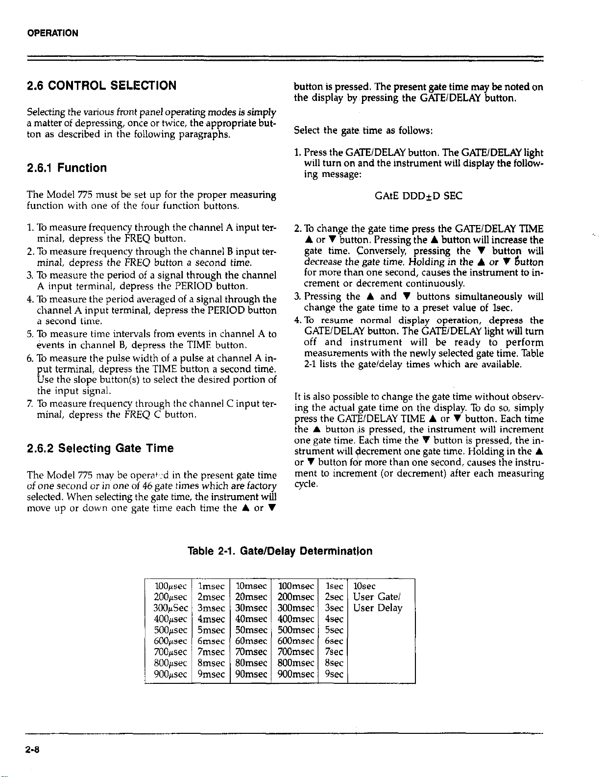
2.6.2 Selecting Gate Time
The Model 775 may be operak:d in the present gate time
of one second or in one of 46 gate times which are factory
selected. When selecting the gate time, the instrument will
move up or down one gate time each time the A or V
button is pressed. The present gate time may be noted on
the display by pressing the GATE/DELAY button.
Select the gate: time as follows:
1. Press the GATE/DELAY button. The GATE/DELAY light
will turn on and the instrument will display the following message:
GAtE DDD*D SEC
2. To change the gate time press the GATE/DELAY TIME
A or V button. Pressing the A button will increase the
gate time. Conversely, pressing the V button will
decrease the gate time. Holding in the A or V button
for more than one second, causes the instrument to increment or decrement continuously.
3. Pressing the A and V buttons simultaneously will
change the gate time to a preset value of lsec.
4. To resume normal display operation, ~depress the
GATE/DELAY button. The GATE/DELAY light will turn
off and instrument will be ready to perform
measurements with the newly selected gate time. Table
2-1 lists the gate/delay times which are available.
It is also possible to change the gate time without observing the actual gate time on the display. To do so, simply
press the GATE/DELAY TIME A or V button. Each time
the A button #is pressed, the instrument will increment
one gate time. Each time the V button is pressed, the in-
strument will decrement one gate time. Holding in the A
or V button for more than one second, causes the instrument to increment (or decrement) after each measuring
cycle.
2.0
Table 2-1. Gate/Delay Determination
OPERATION
NOTE
To prevent operator error, there is an internal
alarm that beeps whenever a limit is reached,
(e.g. 1OOjwsc low limit or 1Osec high limit). With
the GATE/DELAY light on, the alarm will sound
when the users gate is displayed and the A button is pressed. Refer to Table 2-2 alarm conditions.
2.6.3 User Gate Function
The user gate function is useful when a gate time other
than the predetermined gate times listed in Table 2-l is required. The limits which must be observed are the
minimum limit of lO@sec and the maximum limit of 10sec.
The user gate function is accessible in the FREQ A, B and
C and Period Averaged functions. To operate the instrument in the user gate mode proceed as follows:
1. Press the GATE/DELAY button and observe that the light
turns on and the instrument displays the’ following
message:
GAtE DDD+D SEC
2.6.4 Using Delay
The Model 775 has a delay function which disables the
closure of the opened gate for the predetermined periods
listed in Table 2-1. This function is very useful in burst
measurements, relay open/close time measurements where
bounce time should be eliminated or in measurements
done on a train of pulses.
NOTE
The delay mode is accessible only when PERIOD
A, TIME A-B or PLS A functions are on. The
selection of any other function, when the DELAY
light is on, will cause the instrument to exit from
delay mode
The delay time may be selected as follows:
1.
Press
the GATE/DELAY button. The GATE/DELAY light
will turn on and the instrument will display the following message:
dELAY DDDiD SEC
This display shows the actual gate time that the instru-
ment is set to operate. DDDiD SEC may be any time
from lOOE-6 to 10EcO.
2. Press and hold in the GATE/DELAY TIME A button and
observe that the display increments. After the 10s~ gate
time the instrument will enter the user gate mode and
the instrument will display the following:
USEr GATE SEC
Pressing the A button after the gate is displayed will
sound an alarm.
3. Press the GATE/DELAY button. The light will turn off
and the instrument will be ready for measurements with
an external gate time.
4. Apply a ‘ITL pulse to the rear panel EXT ARMING &
GATE/DELAY BNC terminal. The high level of the TTL
pulse width determines the length of the gate time.
NOTE
The user gate function may be accessed only
when the GATE/DELAY light is on. To exit the
user gate function press the GATE/DELAY TIME
V button, or both the A and V buttons to preset
the gate tiine to kc.
2. To change the delay time, press the GATE/DELAY TIME
A or V button. When the A or V button is depressed
for more than one second, the instrument will increment
or decrement continuously.
3. Pressing the A and y buttons simultaneously will
change the delay time to a preset value of lsec.
4.To resume normal display operation, press the
GATE/DELAY button. The GATE/DELAY light will turn
off and instrument will be ready to perform measurement with the newly selected delay time. Table 2-1 lists
the gate/delay times which are available as preselected
values.
It is also possible to change the delay time without obser-
ving the actual delay time on the display. To do so, simpl;,
press the GATE/DELAY TIME A or V button. Exh timk
the A button is pressed, the instrument will increment
one delay time. Each time the V button is pressed, the
instrument will decrement one delay time. When A or V
button is held in for more than one second, the instru-
ment will increment (or decrement) after each measuring
cycle.
2-9
OPERATION
NOTE
To prevent operator error, there is an internal
alarm that beeus whenever a limit is reached.
(e.g. 100ssec 10; limit or 1Osec high limit). When
the GATE/DELAY light is on, the alarm will
sound when the user’s delay is displayed and the
A button is pressed. Refer to Table 2-2.
2.6.5 User Delay Function
The user delay function is useful when a delay time other
than the predetermined delay times listed in Table 2-l is
required. The limits which must be observed are the
minimum limit of 100ssec and the maximum limit of
10,OOOsec. The user delay function is accessible in the
PERIOD A, TIME A-B or PLS A functions. To operate
the instrument in the user delay mode proceed as follows:
1. Press the GATE/DELAY button and observe that the light
turns on and the instrument displays the following
message:
dELAY DDD*D SEC
This display is the actual delay time that the instrument
is set to operate. DDDiD SEC may be any time from
lOOE-6 to lOE+O.
2. Press and hold in the GATE/DELAY TIME UP button
and observe that the display increments. After the 1Osec
delay time the instrument will enter the user delay mode
and the instrument will display the following:
NOTE
The user,delay function may be accessed only
when the GATE/DELAY light is on. To exit the user
delay mode simply depress the GATE/DELAY
TIME v button, or both the A and v buttons to
preset the delay time to lsec.
2.6.6 Selecting Measurement Rate
There are four measurement rates which are available on
the Model 775. Only two measurement rates are accessible from the front panel: normal rate and single cycle
(Hold). The other measurement rates are accessible only
via the rear panel IEEE-488 bus and will be discussed in
further detail in Section 3. To select the measurement rate
proceed as follows:
1. Refer to the front panel MODE indicator: The HOLD
light determines the rate of measurement. When the indicator is off, the instrument is in the normal measurement rate.
2. Press the HOLD button. The HOLD light will turn on
and the instrument will go into the one-shot measurement cycle.
3. Press the RESET button. This action will clear the
display andthe Model 775 will be ready to take and process the next signal from the input terminal (see
paragraph 2.7 for arming).
2.6.7 Selecting the Number of Displayed Digits
USEr dLAY SEC
Pressing the A button after the user delay time is
displayed will sound an alarm.
3. Press the GATE/DELAY button and observe that the light
turns off.
4. Press the MODE button twice. The first time the MODE
button is pressed, the HOLD light will turn on. The second time the button is pressed, the DELAY light will
turn on and the instrument will be ready for
measurements with an external delay.
5. Apply a TTL high level pulse to the rear panel EXT
ARMING & GATE/DELAY terminal. Delay would then
be enabled as long as this input is kept at a TTL high
level. The first negative transition to TTL low at this input will disable the delay. The delay would then be
disabled as long as this input is kept at a TTL low level.
2-10
A major advantage of the Model 775 is its capability to
display a fixed number of digits regardless of the frequency of the sign@ For example, with a one second gate time,
the Model 775lis capable of displaying a minimum of eight
digits. This however, may turn out to a disadvantage when
measuring a frequency of a relatively unstable signal in
which just the most significant digits are stable and the
least significant digits are “jumping around” with no
significant meaning. Model 775 is designed in such a way
that it truncates the unstable least significant digits while
still preserving the full performance of the Model 775. To
select the number of displayed digits proceed as follows:
1. Press the GATE/DELAY and TRIGGER LEVEL buttons
simultaneously. The respective indicators will light and
the following message will appear on the display.
D dIGIt

OPERATION
Where: D is any number from 3 to 9. The factory selected
default number for D is nine. This means that the maximum number of digits that the Model 775 is capable
of displaying 9.
2.To change the number of displayed digits, press the
GATE/DELAY TIME A or v button until D is equal to
the required number of digits.
NOTE
Selecting five digits to be displayed, instead of
nine, will eliminate the four least significant digits
and will move the entire dis lay to the right by
four places. An example o P a normal display
reading, and the same display reading with five
digits of resolution is given as follows.
Display reading with nine digits:
1.13456789Hz
Display reading with selected five digits:
1.1345Hz
To change the input setting proceed as follows:
1. To change the slope that the instrument will trigger on,
press the SLOPE button. If the 1 indicator light is
off, the counter will trigger on the positive edge of the
input signal. If the \ indicator light is on, the counter
will trigger on the negative going edge.
2. To select the required coupling mode, press the AC/DC
button. The instrument is in the DC coupling mode
when the AC indicator light is off. When the AC indiii;zr light is on, the instrument is in the AC coupling
3. When the signal exceeds the specified dynamic range
of the input, attenuation is required. To attenuate the
signal, press the ATTEN button. The input signal will
be attenuated by a factor of 10 when the light is on.
When the light is off, the input signal will not be
attenuated.
4. In low frequency measurements where the frequency
range is below lCOKI-Iz, the use of a filter is recommended to attenuate high frequency signals which may interfere with the measurement. To apply a filter depress
FLIR button, the FLTR light will turn on.
2.6.9 Setting Trigger Levels
3. To return the Model 775 to the normal mode of operation, simply press any button on the front panel, except
the LOCAL button.
NOTE
In certain circumstances, it is possible that the
Model 775 will display less than nine digits. This
may occur when the selected gate time is very
small. In this case, the instrument will override
the function of the selected number of digits and
will display only as many digits as it can. When
gate time is increased, the Model 775 will again
limit the number of displayed digits to the
selected value.
2.6.6 Input Condition Controls Setting
A proper setup of the input controls will ensure proper
operation of the instrument. There are six buttons which
control the input. These buttons are identical in both channels A and 8.
Changing one of the input setting controls is simply a matter of pressing the required button. There are four lights
which :re associated with each of the controls which will
turn on when a button is pressed.
There are two LEVEL buttons associated with both channels A and 8. The LEVEL buttons set the signal voltage
level that will trigger the instrument.
To set the trigger levels proceed as follows:
NOTE
The procedure for setting the trigger level is identical for channels A and B.
1. Press the TRIGGER LEVEL button. The TRIGGER
LEVEL indicator will turn on and the display will rexi
as follows:
-D.DD -D.DD VOLT
The display segment ‘iD.DD” may have any value from
-2.55 to +2.55 if the “ATTEN” indicator is off. When the
ATTEN indicator is on, the value may range from -25.5
to +25.5. Also, note that the left three digits on the
display are associated with channel A and the three
digits on the right side of the display are associated with
channel B.
2-11
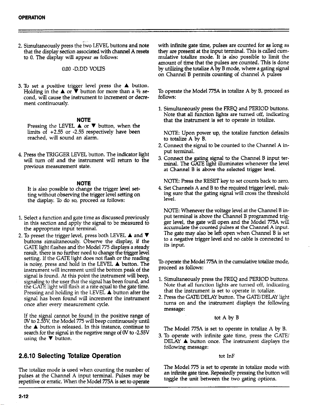
OPERATION
2. Simultaneously press the two LEVEL buttons and note
that the display section associated with channel A resets
to 0. The display wiIl appear as follows:
0.00 -D.DD VOLTS
3. To set a positive tri
Holding in the A or
cond, will cause the instrument to Increment or decrement continuously.
Pressing the LEVEL A or v button, when the
limits of +2.55 or -2.55 respectively have been
reached, will sound an alarm.
4. Press the TRIGGER LEVEL button. The indicator light
will turn off and the instrument will return to the
previous measurement state.
It is also possible to change the trigger level setting without observing the trigger level setting on
the display. To do so, proceed as follows:
er level press the A button.
9 button for more than a % se-
NOTE
NOTE
with infinite gate time, pulses are counted for as long as
they are present at the input terminal. This is called cummulative totalize mode. It is also possible to limit the
amount of time that the pulses are counted. This is done
by utilizing the total&e A by B mode, where a gating signal
on Channel B permits counting of channel A pulses
To operate the Model 77% in totalize A by 8, proceed as
follows:
1. Simultaneously press the FREQ and PERIOD buttons.
Note that, all function lights are turned off, indicating
that the instrument is set to operate in totaliie.
NOTE: Upon power up, the totalize function defaults
to totalire A by B.
2. Connect the signal to be counted to the Channel A input terminal.
3. Connect the gatin
minal. The GATE ight illuminates whenever t
at Channel B is above the selected trigger level.
NOTE: Press the RESET key to set counts back to zero.
4. Set Channels A and B to the required trigger level, making sure that the gating signal will cross the threshold
level.
signal to the Channel B in
F R
ut tere level
1. Select a function and gate time as discussed previously
in this section and apply the signal to be measured to
the appropriate input terminal.
2. To preset the trigger level, press both LEVEL A and v
buttons simultaneously. Observe the display, if the
GATE light flashes and the Model 775 dis
setting. If the GATE light does not flash or the reading
is noisy, press and hold in the LEVEL A button. The
instrument will increment until the bottom peak of the
signal is found. At this point the instrument will beep,
signalin
the GA 7%
Pressing and holding in the LEVEL A button after the
signal has been found will increment the instrument
once after every measurement cycle.
If the si nal cannot be found in the positive range of
OV to 2.
the A button is released. In this instance, continue to
search for the signal in the negative range of OV to -2S5V
using the T button.
to the user that the signal has been found, and
light will flash at a rate equal to the gate time.
V, the Model 775 will beep continuously until
.h
lays a steady
R result, there is no further need to change t
e trigger level
2.6.10 Selecting Totalize Operation
NOTE: Whenever the voltage level at the Channel B input terminal is above the Channel B programmed trigger level, the gate will open and the Model 775A will
accumulate the counted pulses at the Channel A input.
The gate may also be left open when Channel B is set
to a negative trigger level and no cable is connected to
its input.
To operate the Model 775A in the cumulative totalize mode;
proceed as follows:
1. Simultaneously press the FREQ and PERIOD buttons.
Note that, all function lights are turned off, indicating
that the instrument is set to operate in totalize.
2. Press the GATE/DELAY button. The GATE/DELAY light
turns on’ and the instrument displays the following
message:
tot A by B
The Model 775A is set to operate in totalize A by B.
3. To operate with infinite gate time, press the GATE/
DELAY A button once. The instrument displays the
following message:
tot InF
The totalize mode is used when counting the number of
pulses at the Channel A input terminal. Pulses may be
repetitive or erratic. When the Model 77% is set to operate
2-12
The Model 775 is set to operate in totaliie mode with
an in&rite gate time. Repeatedly pressing the button will
toggle the unit between the two gating options,

W’efiAlION
4. Press the GATE/DELAY button. The GAIEIDELAY indicator turns off and the GATE light turns on.
5. Connect the signal to be counted to the Channel A input terminal. The Model 775A will begin accumulating
counts.
2.7 ARMING
Arming allows a measurement to be triggered by the input signal. The Model 775 may be armed to take readings
in four ways:
1. Continuously armed in the normal mode.
2. With the front panel RESET button when the instrument
is in hold mode.
3. Through an arming pulse applied to the rear panel EXT
ARMING & GATE/DELAY input when the instrument
is in the hold mode.
4. With commands given over the IEEE-488 bus as described in Section 3. This section covers front panel and
external arming in detail.
2.7.1 Continuous Arming
When the instrument is not in the hold mode and there
is no signal present at the input terminals, the instrument
will stay in the idle state and the GATE 1iFht will not flash.
An input signal with the correct dynanuc range and correct input control setting will initiate, a measurement cycle and the GATE light will flash wery time the internal
gate opens.
2.7.3 External Arming
External arming operates much like front panel arming except for the arming stimulus itself. In this case the arming stimulus is applied to the rear panel EXT ARMING
& GATE/DELAY terminal (see Figure 2-2). The input arming pulse must conform to TTL levels. To use external arming, proceed as follows:
1. Place the instrument in the hold mode by pressing the
MODE button, (refer to parapaph 2.7.2). Note that the
GATE light will not flash, indlcatmg that the instrument
is in one-shot mode. The instrument will cease processing readings while it is waiting for the arming signal.
2. Connect the external arming source to the rear panel
EXT ARMING & GATE/DELAY connector. The first
positive going pulse at the input terminal will cause the
Model 775 to take and process the next available signal.
Note that after each positive going transition of the ar-
ming signal, the numeric display will be set to read zero
until the next data is processed and displayed.
3. To return the instrument to the continuous mode, press
and release the MODE button until the HOLD light
turns off.
2.7.4 Alarm Conditions
Table 2-2 lists the front panel conditions that will cause
the instrument to sound an audible alarm. Some of these
conditions are errors, while others provide information to
the user.
Table 2-2. Alarm Conditions
2.7.2 Front Panel Arming
Front panel arming is done with the RESET button. This
arming mode is very useful in burst measurements where
a signal is present on1
ming perform the
1. Enter the hold mode by pressing the MODE button. The
HOLD light will turn on and the GATE light will cease
flashing; indicating the instrument is in the one-shot arming mode. The display will zero and no new readings
are processed until an arming stimulus is applied.
2. To trigger a single reading, press and release the RESET
button. The instrument will be ready to take and process the next reading.
3. To arm the instrument for a new measurement, press
the RESET button, the display will zero.
4. To remove the instrument from the one-shot arming
rnc !e, press the MODE button until the HOLD light
turns off.
temporarily. To use front panel ar-
Y
fol owmg steps.
Item
r
Description
1
Pressing two buttons other than those
specified as legal.
2
Pressing the GATE/DELAY TIME A or “V
button when high or low limits are
reached.
3
Pressing the LEVEL A or V button when
upper or lower limits are reached.
4
After selecting the number of digits to be
displayed, pressing the LEVEL A or V button after the limits are reached.
2.8 APPLICATIONS
Applications for the Model 775 are many and varied and
will depend on the user’s needs. Figure 2-3 contains an
application concerning fall time m,easurements; while
Figure 2-4 contains an application usmg delay to measure
contact dwell time. For application information on high fre-
quency multiplexed measurements, refer to Figure 2.5.
2-13
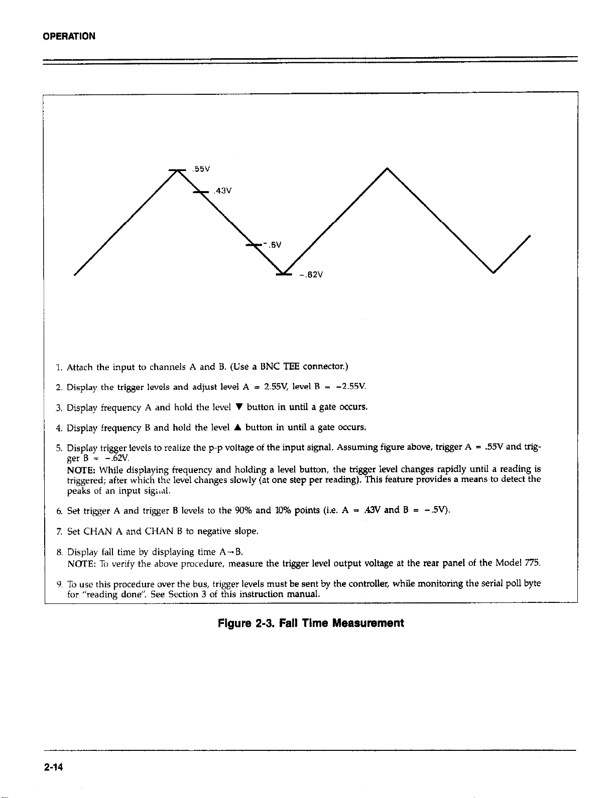
OPERATION
1. Attach the input to channels A and B. (Use a BNC TEE connector.)
2. Display the trigger levels and adjust level A = 2.55V, level B = -2.55V.
3. Display frequency A and hold the level v button in until a gate occurs.
4. Display frequency B and hold the level A button in until a gate occurs,
5. Display trigger levels to realize the p-p voltage of the input signal. Assuming figure above, trigger A = .55V and trig
ger B = -.62V.
NOTE: While displaying frequency and holding a level button, the trigger level changes rapidly until a reading is
triggered; after which the level changes slowly (at one step per reading). This feature provides a means to detect the
peaks of an input sigal.
6. Set trigger A and trigger B levels to the 90% and 10% points (i.e. A = .4W and B = -.5V).
7. Set CHAN A and CHAN B to negative slope.
fi Display fall time by displaying time A-B.
NOTE: To verify the above procedure, measure the trigger level output voltage at the rear panel of the Model 775.
Y. To use this procedure over the bus, trigger levels must be sent by the controller, while monitoring the serial poll byte
for “reading done”. See Section 3 of this instruction manual.
Figure 2-3. Fall Time Measurement
214
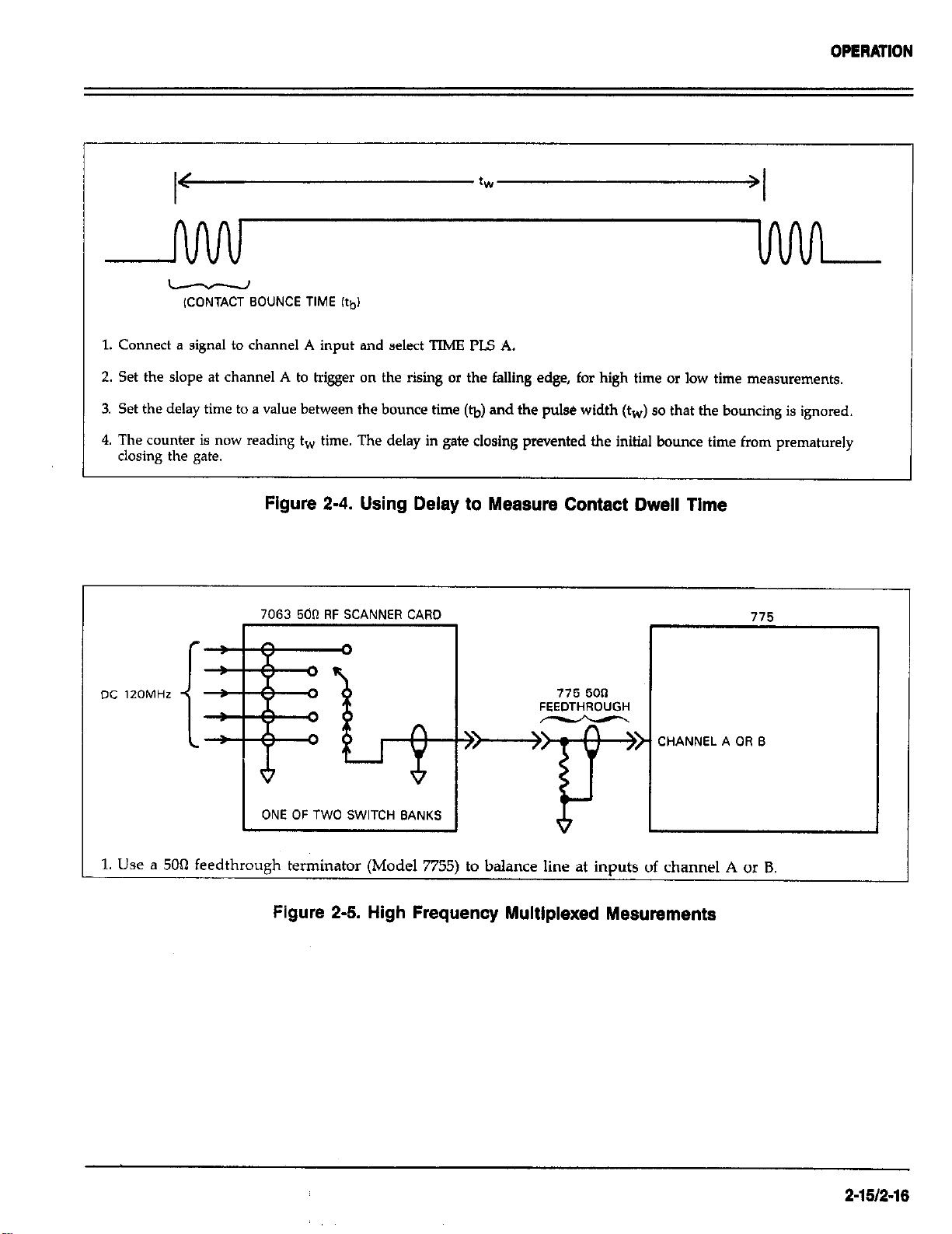
OPERATION
(CONTACT BOUNCE TIME ltb,
1. Connect a signal to channel A input and select TIME PLS A.
2. Set the slope at channel A to trigger on the rising OI the falling edge, for high time or low time measurements.
3. Set the delay time to a value between the bounce time (tb) and the pulse width (tw) so that the bouncing is ignored.
4. The counter is now reading tw time. The delay in gate closing prevented the initial bounce time from prematurely
closing the gate.
Figure 2-4. Using Delay to Measure Contact Dwell Time
7063 500 RF SCANNER CARD
DC 120MHz
CHANNEL A OR 6
1. Use a 5061 feedthrough terminator (Model 7755) to balance line at inputs of channel A or B.
775
Figure 2-5. High Frequency Multlplexed Mesurements
215/z-16


SECTION 3
IEEE-488 OPERATION
3.1 INTRODUCTION
The IEEE-488 bus is an instrumentation data bus with stan-
dards adopted by the IEEE (Institute of Electrical and Electronic Engineers) in 1975 and given the IEEE-488 designation. The most recent revision of bus standards was made
in 1978; hence the complete description for current bus
standards is the IEEE-488-1978 designation. The Model 775
conforms ~CI 1978 standards.
This section contains genera1 bus information as well as
detailed programming information and is divided as
follows:
1.
General introductory information pertaining to the
IEEE-488 bus may be found primarily in paragraphs 3.2
through 3.6.
2.
Information necessary to connect the Model 775 to the
bus is contained in paragraph 3.7 and 3.8.
General bus command programming is covered in
3.
paragraph 3.9.
4.
Device-dependent command programming is described in detail in paragraph 3.10. The commands
outlined in this section can be considered to be the most
important since they control virtually all instrument
functions.
Additional information pertaining to front panel error
5.
messages and controller programs can be found in
paragraphs 3.11 and 3.12.
3.2 BUS DESCRIPTION
bus has only eight data lines that are used for both data
and most commands. Five bus management lines and
three handshake lines round out the complement of signal
lines. Since the bus is of parallel design, all devices connected to the bus have the same information available
simultaneously. Exactly what is done with the information
by each device depends on many factors, including device
capabilities.
A typical bus configuration for controlled operation is
shown in Figure 3-l. The typical system will have one controller and one or more instruments to which commands’
are given and, in most cases, from which data is received.
Generally, there are three categories that describe device
operation. These designations include: controller; talker;
listener.
The controller does what its name implies: it controls other
devices on the bus. A talker sends data, while a listener
receives data. Depending on the instrument, a particular
device may be a talker only, a listener only, or both a talker
and listener.
Any given system can have only one controller (control
may be passed to an appropriate device through a special
command), but any number of talkers or listeners may be
present up to the hardware constraints of the bus. Generally, the bus is limited to 15 devices, but this number may
be reduced if higher than normal data transfer rates are
required or if longer than normal cables are used.
The IEEE-488 bus as designed as a par?llel data transfer
medium to optimize data transfer without using an ex-
cessive number of bus lines. In keeping with this goal, the
Several devices may be commanded to listen ,lt NKP, but
only one device may be a talker at any given time. Otherwise, communications would be scrambled.
3-1

IEEE-488 OPERATION
TO OTHER DEVICES
Once the device is addressed to talk or listen, appropriate
bus transactions are set to take place. For example, if an
instrument is addressed to talk, it will usually place its data
on the bus one byte at a time. The listening device will
then read tqs information, and the appropriate software
can then be used to channel the information to the desired
location.
3.3 IEEE-488 BUS LINES
DEVICE 3
)NLY ABLE
r0 LISTEN
IPRINTER,
, DATA BUS
DATA BYTE
TRANSFER
CONTROL
GENERAL
INTERFACE
MANAGEMENT
} D101...8 DATA 18 LINESI
v
FD HANDSHAKE
I
AC
BUS MANAGEMENT
The signal limes on the IEEE-488 bus are grouped into three
general categories. The data lines handle bus information,
while the handshake and bus management lines ensure
that proper data transfer and bus operation takes place.
Each of the bus lines is active low so that approximately
zero volts is a logic one. The following paragraphs describe
the purpose of these lines, which are shown in Figure 3-l.
3.3.1 Bus ,Management Lines
The bus management group is made, up of five signal lines
that help ensure an orderly transfer of ,data. These lines
are used to, send the unihne commands described in
paragraph 3.4.1.
ATN (Attention)-The ATN line is one of the more important management lines. The state of the ATN line determines whether controller information on the data bus is
to be considered data or a multiline command as des-
cribed in paragraph 3.4.
IFC (Interface Clear)-Setting the IFC line true (low) causes
the bus to go to a known state.
REN (Remote Enable)-Setting the REN line low sends the
REN command. This sets up instruments on the bus for
remote operation.
Figure 3-1. IEEE Bus Configuration
Before a device can talk or listen, it must be appropriately
addressed. Devices are selected on the basis of their
primary address; the addressed device is sent a talk or
listen command derived from its primary address. Normally, each device on the bus has a unique primary address so that each may be addressed individually. The bus
also has another addressing mode called secondary addressing, but not all devices use this addressing mode.
3-2
EOI (End Or Identify)-The EOI line is used to send the
EOI command that usually terminates a multi-byte transfer
sequence.
SRQ (Service Request)-The SRQ line is set low by a device
when it requires service from the controller.
3.3.2 Handshake Lines
The bus uses three handshake lines that operate in an in-
terlocked sequence. This method ensures reliable data
transfer regardless of the transfer rate. Generally, data

IEEE-488 OPERATION
transfer will occur at a rate determined by the slowest active device on the bus.
One of the handshake lines is controlled by the data
source, while the remaining two lines are controlled by ac-
cepting devices. The three bus handshake lines are:
DAV (Data Valid)-The source controls the state of the DAV
line.
NRFD (Not Ready For Data)-The acceptor controls the
state of the NRFD line.
NDAC (Not Data Accepted)-The acceptor also controls the
NDAC line.
The complete handshake sequence for one data byte is
shown in Figure 3-2. Once data is on the bus, the source
checks to see that NRFD is high, indicating that all devices
on the bus are ready for data. At the same time NDAC
should be low from the previous byte transfer. If these conditions are not met, the source must then wait until the
NRFD and NDAC lines have the correct status. If the
source is a controller, NRFD and NDAC must remain stable
for at least 1OOnsec after ATN is set low. Because of the
possibility of bus hang up, some controllers have time-out
routines to display error messages if the handshake sequence stops for any reason.
Once the NRFD and NDAC lines are properly set, the
source sets the DAV line low, indicating that data on the
bus is now valid. The NRFD line then goes low; the NDAC
line goes high once all devices on the bus have accepted
the data. Each device will release the NDAC line at its own
rate, but the NDAC line will not go high until the slowest
device has accepted the data byte.
After the NDAC line goes high, the source then sets the
DAV line high to indicate that the data on the bus is no
longer valid. At this point, the NDAC line returns to its
low state. Finally, the NRFD line is released by each of the
devices at their own rates, until the NRFD line finally goes
high when the slowest device is ready, and the bus is set
to repeat the sequence with the next data byte.
The sequence just described is used to transfer both data
and multiline commands. The state of the ATN line determines whether the data bus contains data or commands
as described in paragraph 3.4.
3.3.3 Data Lines
The IEEE-488 bus uses the eight data lines that allow data
to be transmitted and received in a bit-parallel, byte-serial
manner. These eight lines use the convention DIOl
through DIOS instead of the more common DO through
D7 binary terminology The data lines are bidirectional and,
as with the remaining bus signal lines, low is true.
DA”
NRFD
I
VALID
I
SOURCE
ACCEPTOR
I
I
NDAC
I
I
I
DATA
TRANSFER
BEGINS ENDS
DATA
TRANSFER
I
ACCEPTOR
Fl;ure 3-2. IEEE Handshake Sequence
3.4 BUS COMMANDS
While the hardware aspect of the bus is essential, the in-
terface would be essentially worthless without appropriate
commands to control communications between the various
instruments on the bus. This paragraph briefly describes
the purpose of the bus commands, which are grouped into
the following three general categories:
Uniline commands-Sent by setting the associated bus line
low.
Multiline commands-General bus commands which are
sent over the data lines with the ATN line low (true).
Device-dependent commands-Special commands that
depend on device configuration; sent over the data lines
with ATN high (false).
3-3

IEEE-488 OPERATION
Command Type
Uniline
Multiline
Universal
Addressed
Unaddress
Device-dependent**
Table 3-1. IEEE-488 Bus Command Summary
Command
REN (Remote Enable)
EOI
1FC (Interface Clear)
ATN (Attention)
SRQ (Service Request)
LLO (Local Lockout)
DCL (Device Clear)
SPE (Serial Poll Enable)
SPD (Serial Poll Disable)
SDC (Selective Device Clear)
GTL (Go To Local)
GET (Group Execute Trigger)
UNL (Unlisten)
UNT (Untalk)
state of
A
TN Line” Comments
X
X Sent by setting’EO1 low.
X Clears Interface
Low Defines data bus contents.
X Controlled by external device.
Law
Law
Lmv Enables serial polling.
Low Disables serial polling.
Law
Low
Low
Low
Law
I
High
-I-
Set up for remote operation.
Locks out front panel controls.
Returns device to default conditions.
Returns unit to default conditions.
Returns to local control.
Triggers device for reading.
Removes all listeners from bus.
Removes all talkers from bus.
Programs Model 775 for various modes.
Don’t Care
*x =
**See paragraph 3.10 for complete description
3.4.1 Uniline Commands
Uniline commands are sent by setting the associated bus
line low. The ATN, IFC and REN commands are asserted
only by the system controller. The SRQ command is sent
by an external device. The EOI command may be sent by
either the controller or an external device depending on
the direction of data :.ansfer. The following is a brief
description of each command.
REN (Remote Enable)-When the controller sends the REN
command, the instrument will be set up for remote operation. Generally, the REN command should be sent befom
attempting to program instruments over the bus.
EOI (End Or Identify)-The EOI command is sent to
positively identify the last byte in a multi-byte transfer sequence. This allows variable length data words to be
transmitted easily.
IFC (Interface Clear)-The IFC command is sent to clear
the bus and set device to a known state. Although device
configurations differ, the IFC command usually places instruments in the talk and listen idle states.
ATN (Attention)-The controller sends ATN while
transmitting addresses or multiline commands. Device-
Dependent commands are sent with the ATN line high
(false).
SRQ (Service Request)-The SRQ command is asserted by
an external device when it requires service from the controller. If more than one device is present, a serial polling
sequence, as described in paragraph 3.9.8, must be used
to determine which device has requested service.
3.4.2 Universal Commands
Universal commands are multiline commands that require
no addressing AU instrumentation equipped to implement
the command will do so simultaneously when the command is itransmitted over the bus. As with all multiline
commands, the universal commands are sent over the data
lines with ATN low.
LLO (Local Lockout)-The LLO command is used to lock
out front panel controls on devices so equipped.
DCL (Device Clear)-After a DCL is sent, instrumentation
equipped to implement the command will revert to a
known state. Usually, instruments return to their powerup conditions.
SPE (Serial Poll Enable)-The SPE command is the first step
in the serial polling sequence, which is used to determine
which instrument has requested service with the SRQ
command.
3-4

IEEE-488 OPERATION
SPD (Serial Poll Disable)-The SPD command is sent by
the controller to remove all instrumentation on the bus
from the serial poll mode.
3.4.3 Addressed Commands
Addressed commands are multiline commands that must
be preceded by a listen command derived horn the device’s
primary address before the instrument will respond. On-
ly the addressed device will respond to each of these
commands:
SDC (Selective Device Clear)-The SDC command performs essentially the same function as the DCL command
except that only the addressed device will respond. Instruments usually return to their default conditions when
the SDC command is sent.
GTL (Go To Local)-The GTLcommand is used to remove
instruments from the remote mode of operation. Also,
front panel control operation will usually be restored if the
LLO command was previously sent.
GET (Group Execute Trigger)-The GET command is
used to trigger devices to perform a specific action that
depends on device configuration. Although GET is considered to be an addressed command, many devices res-
pond to GET without being addressed.
quency A mode. The IEEE-488 bus treats device-dependent
commands as data in that ATN is high (false) when the
commands are transmitted.
3.5 COMMAND CODES
Each multiline command is given a unique code that is
transmitted over the data bus as 7-bit ASCII data. This section briefly explains the code groups which are summarized in Figure 3-3. Every command is sent with ATN
low.
Addressed Command Group (ACG)-Addressed commands are listed in column O(B) in Figure 3-3. Column O(A)
lists the corresponding ASCII codes.
Universal Commad Group (UCG)-Columns l(A) and l(B)
list the universal commands and the corresponding ASCII
codes.
Listen Address Group (LAG)-Columns 2(A) and 3(A) list
the ASCII codes corresponding to the primary address
listed in columns 2(B) and 3(B). For example, if the primary
address of the,instrument is set to 16, the LAG byte will
correspond to an ASCII zero.
Talk Address Group (TAG)-TAG primary address values
and the corresponding ASCII characters are listed in col-
umns 4(A) through 5(B).
3.4.4 Unaddressed Commands
The two unaddressed commands are used by the con-
troller to remove all talkers and listeners from the bus
simultaneously. ATN is lov. when these multiline commands are asserted.
UNL (Unlisten)-All listeners are removed from the bus
at once when the UNL command is placed on the bus.
UNT (Untalk)-The controller sends the UNT command
to clear the bus of any talkers.
3.4.5 Device-Dependent Commands
The meaning of the device-dependent commands is deter-
mined by instrument configuration. Generally, these commands are sent as one or more
the device to perform a specific function. For example, FO
is sent to the Model 775 to place the instrument in the fre-
ASCII
characters that tell
The preceding address groups are combined together to
form the Primary Command Group (KG). The bus also
has another group of commands, called the Secondary
Command Group (SCG). These are listed in Figure 3-3 for
informational purposes only; the Model 775 does respond
to these commands, but other devices may have secondary addressing capability.
NOTE
Commands are normally transmitted with the 7.bit
code listed in Figure 3-3. For most devices, the condition of D7 (DI08) is unimportant, as shown b>
the “Don’t Care” indication in the table. Some
devices, however, may require that D7 assumes ‘1
specific logic state before the commands are
recognized.
Hexadecimal and decimal values for each of the commands
or command groups are listed in Table 3-2. Each value in
the table assumes that D7 is set to 0.
3-5

IEEE-488 OPERATION
Table 3-2. Hexadecimal and Decimal Command
Codes
Command 1 Hex Value*
GTL 01
SDC
GET
04
08
LLO 11
DCL
14
SI’E 18
SPD 19
LAG
TAG
UNL
UNT
20-3F
40-5F
3F
5F
*Values shown with D,=O
Decimal Value
1
ii
17
20
24
25
32-63
64-95
63
95
3.6 COMMAND SEQUENCES
The proper command sequence must be sent by the controller before an instrument will respond as intended. The
universal commands, such as LLO and DCL, require only that ATN be set low before the command is sent. Other
commands require that the device be addressed to listen
first, This section briefly describes the bus sequence for
several types of commands.
3.6.1 Addressed Command Sequence
Before a device will respond to one of these commands,
it must receive a LAG cc.nmand derived from its primary
address. Table 3-3 shows a typical sequence for the SDC
command. The LAG command assumes that the instru-
ment is set at a primary address of 23.
3.6.2 Universal Command Sequence
The universal commands are sent by setting ATN low and
then placing the command byte on the bus. For example,
the following gives the LLO command:
ATEI.LLO
Note that both the ATN and LLO commands are on the
bus simultaneously. Also, addressing is not necessary.
3.6.3 Device-Dependent Command Sequence
Device-dependent commands are transmitted with ATN
high. However, the device must be addressed to listen fist
before the commands are transmitted. Table 3-4 shows the
sequence for the following command:
This command, which sets the Model 775 to the frequen-
cy A mode, is described in detail in paragraph 3.10.2.
Table 3~4. vpical Device-Dependent Command
Sequence
Data Bus
Step Command ATN State ASCII Hex Decimal
1
2
3
4
-5
*Assumes primary address=23
UNL Set low ? 3F
LAG* stays low
Data Set high F
Data Stays high 0
Data Stays high X
7 37 55
46 70
30
58
63
ii
Note that an UNL command is transmitted before the
LAG, SDC sequence. This is generally done to remove all
other listeners from the bus first so that only the addressed device responds.
Table 3-3. Qpical Addressed Command Sequence
Data Bus
Step Command ATN State ASCII Hex Decimal
UNL Set low ? 3F 63
:
3
4
*Assumes primary address=23
3-6
LAG* stays low
SDC stays low
Returns high
37 55
ELT 04 4
3.7 HARDWARE CONSIDERATIONS
Before the Model 775 can be used with the IEEE-488 bus,
the instrument must be connected to the bus with a
suitable connector. Also, the primary address must be properly programmed as described in this section.
3.7.1 ‘ly;plcal Controlled Systems
The IEEE-488 bus is a parallel interface system. As a result,
adding more devices is simply a matter of using more
cables to make the desired connections. Because of this
flexibility, system complexity can range from the very simple to extremely complex.

IEEE-488 OPERATION
Figure 3-3. Command Codes
3-7

IEEE-488 OPERATION
Figure 3-4 shows two typical system configurations. Figure
3-4(A) shows the simplest possible controlled system. The
controller is used to send commands to the instrument,
which sends data back to the controller.
The system becomes more complex in Figure 34(B), where
additional instrumentation is added. Depending on programming, all data may be routed through the controller,
or it may be transmitted directly from one instrument to
another,
For very complex applications, a much larger computer can
be used. Tape drives or disks can
then
be used to store
data.
Pigure 3-5. IEEE-488 Connector
MODEL 775
IA1 SIMPLE SYSTEM
CONTROLLER
ISI ADDITIONAL INSTRUMENTATION
CONTROLLER
Figure 3-4. System vpes
3.7.2 Bus Connections
The Model 775 is connected to the bus through an IEEE488
connector which is shown in Figure 3-5. This connector
is designed to be stacked to allow a number of parallel connections on one instrument.
NOTE
To avoid possible mechanical damage, it is
I
recommended that no more than three connectors be stacked on any one instrument. Otherwise, the resulting strain may cause internal
damage.
A typical connecting scheme for the bus is shown in Figure
3-6. Each cable normally has the standard IEEE connector
on each end. The Keithley Model 7007 cable is ideal for
this purpose. Once the connections are made, the screws
should be tightened securely.~For the location of the connector on the rear panel of the Model 775, refer to Figure
3-7.
NOTE
The IEEE-488 bus is limited to a maximum of 15
devices, including the controller. Also, the maximum cable length is 20 meters. Failure to observe
these limits will probably result in erratic bus
operation.
NOTE
For control of possible radio frequency interference, a shielded IEEE488 cable (such as the
Keithley Model 7007-1) must be used.
3-8

IEEE-488 OPERATIOI
r
r
INSTRUMENT
INSTRUMENT
INSTRUMENT
CONTROLLER
Figure 3-8. IEEE-488 Connections
Table 3-5. IEEE Contact Designations
contact
Number
1
2
3
z
6
7
i
10
ii
13
14
15
16
17
18
19
20
21
22
23
24
IEEE-488 Designation
DIOl Data
D102
D103 Data
D104
EOI (24) Management
DAV Handshake
NRFD
NDAC
IFC Management
SRQ
ATN Management
SHIELD
D105 Data
DI06 Data
D107 Data
DIOS
REN (24) Management
Gnd, (6) Ground
Gnd, (7) Ground
Gnd, (8) Ground
Gnd, (9)
Gnd, (10)
Gnd, (11) Ground
Gnd, LOGIC
Type
Data
Data
Handshake
Handshake
Management
Ground
Data
Ground
Ground
Ground
Figure 3-7. Rear Panel of Model 775 Showing IEEE
Connector
Custom cables may be constructed using the information
in Table 3-5 and Figure 3-6. Table 3-5 lists the contact
assignments for the various bus lines, while Figure 3-8
shows contact designations. Contacts 18 through 24 are
return lines for the indicated signal lines, and the cable
shield is connected to contact 12 and the connector shell.
Each ground line is connected to digital common in the
Model 775.
*Numbers in parentheses refer to signal ground return of
referenced contact number. EOI and REN signal lines
return on contact 24.
CONTACT 12 CONTACT 12
/
CONTACT 24
CONTACT 24
CONTACT 1 CONTACT 1
\
CONTACT 12
CONTACT 12
Figure 3-8. Contact Assignments
3-9

IEEE-488 OPERATION
‘CAUTION
The voltage between IEEE common and ground
must not exceed 30V or damage to the instrument may occur.
A typical signal line bus driver is shown in Figure 3-9. With
the configuration shown, the driver has bidirectional
capability. When the 110 control line is high, the line is
configured as an output line. When the control line is low,
the driver is set up for input operation. Note that not all
signal lines have bidirectional capability. Some lines, such
as ATN, will always be configured as an output line in the
controller and as an input line for all other devices on the
bus.
DATA LINE
‘0 CONTROL
To check the present primary address:
1. Turn on the instrument.
2. The Model 775 wiB display the present primary address.
For example, with the factory set value, the display will
show the following:
IE Adr 23
This message will show on the display after a lamp test
is complete and the version of the software has been
displayed.
NOTES:
1. If a new address is set with the address switch on the
rear panel, the instrument should be turned off and
then on to activate the new address.
2. Each device on the bus must have a unique primary address. Failure to observe this precaution may result in
erratic bus operation.
3.8 SOFTWARE CONSIDERATIONS
Figure 3-g. Typical IEEE-488 Bus Driver (One of 16)
3.7.3 Primary Address Programming
The Model 775 must receive a listen command before it
will respond to addressed commands. Similarly, the instrument must receive a talk command before it will
transmit its data string, status word, or status byte. These
listen and talk commands are derived from the instrument’s primary address. The Model 775 is shipped from
the factory with primary address of 23. The primary address may be set to any value between 0 ad 30 as long as
address conflicts with other bus instruments are avoided.
This may be done by setting the address switch on the rear
panel. Note that the primary address of the instrument
must agree with the address specified in the controller’s
programming language.
The most sophisticated computer in the world would be
useless without the necessary software. This basic requirement is also true of the IEEE-488 bus, which requires the
use of handler routines as described in this paragraph.
3.8.1 Controller Interface Routines
Before a controller can be used with the IEEE-488 inter-
face, the user must make certain that appropriate handler
software is present within the controller. With the HP-85
computer,:for example, the HP-85 interface card must be
used with, an additional I/O ROM, which contains the
necessary ,handler software.
Other smd computers that can be used as controllers have
limited IEEE command capability. The I’ETKBM com-
puters, for example, are incapable of sending multiline
commands from BASIC, although these commands can
be sent through machine language routines. The
capabilities of other small computers depends on the par-
ticular interface being used. Often, little software “tricks”
are required to achieve the desired results.
NOTE
The programmed primary address is briefly
displayed as part of the power-up cycle.
3-10
From the preceding discussion, the message is clear: make
sure the proper software is being used with the instru-

IEEE-488 OPERATION
ment. Often, the user may incorrectly suspect that a hardware problem is causing fault, when it was the software
that was causing the problem all along.
3.8.2 HP-85 BASIC Statements
Many of the programming instructions covered in this section use examples written in Hewlett-Packard Model 85
BASIC. The HP85 was chosen for these examples because
it has a large number of BASIC statements that control
IEEE488 operation. This section covers those HI-85 BASIC
statements that are essential to Model 775 operation.
A complete list of HP-85 IEEE-468 BASIC statements is
shown in Table 3-6. All the statements in the table have
one or three digit arguments that must be specified. The
first digit is the HP-85 interface select code, which is set
to 7 at the factory. The last two digits of those statements
that require a three digit argument specify the primary address Generally, only those commands that actually require an address to be sent over the bus require that the
primary address be specified in the BASIC statement.
Those statements in the table with three digit arguments
assume that the primary address of the device is set at 23.
Other primary addresses require that the last two digits
be set to the corresponding value. For example, to send
a GTL command to device 22, the following BASIC statement would be used: LOCAL 722.
Some of the statements in the table have two forms; the
exact configuration used depends on the desired command. For example, CLEAR 7 will cause a DCL to be sent,
while CLEAR 723 causes an SDC to be transmitted to
device 23.
The third column of Table 3-6 lists the mnemonics for the
command sequences. While most of these are covered
elsewhere, a couple of points should be noted. As described earlier, the ATN line is set low by the controller if
the data bus contains a multiline command. This is indicated in the table by ANDing the ATN mnemonic with
the first command on the bus. For example, ATN*GET
means that ATN and GET are sent simultaneously.
F
ABORT10 7
CLEAR 7
CLEAR 723
ENTER 723;A!$
LOCAL 723
LOCAL LOCKOUT 7
OUTPUT 723;A$
REMOTE 7
REMOTE 723
RESET 7
SPOLL(723)
TRIGGER 7
TRIGGER 723
Table 3-6. HP-85 IEEE-488 BASIC Statements
Action
Send IFC.
Send DCL.
Send SDC to device 23.
Device 23 addressed to talk.
Data placed in AS.
Send GTL to device 23.
Send LLO.
Device 23 addressed to listen.
Transmit A$.
Set REN true.
Set REN true. Address device
23 to listen.
Send IFC, cancel REN.
Address device 23 to talk.
Conduct serial poll.
Send GET
Address device 23 to listen.
Send GET.
Bus Command
IFC
ATN*DCL
ATN*UNL;MTA;LAG;E
ATN*UNL;MLA;TAG;ATN;data
ATN*UNL;MTA;LAG;GTL
ATN*LLO
ATN*MTA;UNL;LAG;ATN;data
REN
REN;ATN*IJNL;MTA;LAG
1FC;REN;REN
ATN*IJNL;MLA;TAG;SPE;ATN
status byte;ATN*SPD;UNT
ATN*GET
ATN*IJNL;MTA;LAG;GET
Sequence
3-11

IEEE-448 OPERATION
Two commands not previously covered am MLA (My
Listen Address) and MT4 (My Talk Address). These are
ordinary PCG (Primary Command Group) addresses sent
by the HI-85 to facilitate bus operation.
NOTE
The HE-85 address is set to 21 at the factory. Since
each device on the bus must have a unique
primary address, do not program the Model 775
for the controller’s address to avoid possible
conflicts.
3.8.3 Interface Function Codes
The interface function codes are part of the IEEE-4884978
standards. These codes define an instrument’s ability to
support various interface functions and should not be confused with programming commands found elsewhere in
this manual
Table 3-7 lists the codes for the Model 775. These codes
are also listed for convenience on the rear panel of the instrument immediately above the IEEE connector. The
numeric value following each one or two letter code
defines Model 775 capabilities as follows:
SR (Service~Request Function)-The ability for the Model
775 to request service from the controller is provided by
the SR function.
RL (Ramota&cal Fun&on)-The ability for the Model 775
to be placed in the remote or local modes ls provided by
the RL function.
PI’ (Parallel~Poll Function)-The Model 775 does not have
parallel polling capabilities.
DC (Device Clear Function)-The ability for the Model 775
to be cleared (initialized) is provided by the DC function.
DT (Device Trigger Function)-The ability for the Model
775 to have its readings triggered is provided by the DT
function.
C
(Contrder
troller capabilities.
TE (Extended Talker Capabilities)-The Model 775 does not
have extended talker capabilities.
LE (Extended Listener Capabilities)-The Model 775 does
not have extended listener capabilities.
Function)-The Model 775 does not have con-
Table 3-7. Model 775 Interface Function Codas
SH (Source Handshake Function)-Ihe ability for the
Model 775 to initiate the transfer of message/data on the
data bus is provided by the SH function.
AH (Acceptor Handshake Function)-The ability for the
Model 775 to.guarantee proper reception of message/data
on the data bus is provided by the AH function.
T (Talker Function)-The ability for the Model 775 to send
device-dependent data over the bus (to other devices) is
provided by the T function. Model 775 talker capabilities
exist only after the instrument has been addressed to talk.
L (Listener Function)-The ability for the Model 775 to
receive device-dependent data over the bus (from other
devices) is provided by the L function. Listener function
capabilities of the Model 775 exist only after it has been
addressed to listen.
Coda
SHl
AH1
T6
LA
SRl
RLl
IT0
DC1
ml
co
EO
LEO
Interface Function
Source Handshake Capability
Acceptor Handshake Capability
Talker (Basic Talker, Serial Poll, Unaddressed To Talk On LAG)
Listener (Basic Listener, Unaddressed To
Listen On TAG)
Service Request Capability
Remote/Local Capability
No Parallel Poll Capability
Device Clear Capability
Device Trigger Capability
No Controller Capability
Open Collector Bus Drivers
No Extended Talker Capabilities
No Extended Listener Capabilities
3-12

IEEE-488 OPERATION
3.8.4 Model 775 Interface Commands
Interface commands controlling Model 775 operation are
listed in Table 3-8. Not included in the table are device-
dependent commands, which are covered in detail in
paragraph 3.10.
Table 3-8. IEEE Command Groups
HANDSHAKE COMMAND GROUP
DAC=DATA ACCEPTED
RFD=READY FOR DATA
DAV=DATA VALID
UNIVERSAL COMMAND GROUP
ATN=ATTENTION
DCL=DEVICE CLEAR
IFC=INTERPACE CLEAR
LLO=LOCAL LOCKOUT
REN=REMOTE ENABLE
SI’D=SERIAL POLL DISABLE
SPE=SERIAL POLL ENABLE
ADDRESS COMMAND GROUP
LISTEN: LAG=LISTEN ADDRESS GROUP
MLA=MY LISTEN ADDRESS
UNL=UNLISTEN
TALK: TAG=TALK ADDRESS GROUP
MTA=MY TALK ADDRESS
UNT=UNTALK
OTA=OTHER TALK ADDRESS
ADDRESSED COMMAND GROUP
ACGFADDRESSED COMMAND
GROUP
GET=GROUP EXECUTE TRIGGER
GTL=GO TO LOCAL
SDC=SELECTIVE CLEAR
STATUS COMMAND GROUP
RQS=REQUEST SERVICE
SRQ=SERIAL POLL REQUEST
STB = STATUS BYTE
END=EOI
Unaddressed Commands-No primary address is required
for these commands. All devices equipment to implement
these commands will do so simultaneously when the command is sent.
General bus commands are summarized in Table 3-9,
which also lists the HI-85 BASIC statement that sends each
command. Each addressed command statement assumes
a primary address of 23.
NOTE
The Model 775 rear panel address switches must
be set for a primary address of 23 to work with
addressed command examples.
Table 3-9. General Bus Commands
/ Addressine / HP:85 BASIC
Command 1 Required 7 Statements
REN Yes
IFC
LLO NO
GTL Yes
DCL No
SDC Yes
GET* Yes
GET* NO
*GET may be sent with or without addressing
NO
1 REMOTE 723
ABORT10 7
LOCAL LOCKOUT 7
LOCAL 723
CLEAR 7
CLEAR 723
TRIGGER 723
TRIGGER 7
3.9.1 REN (Remote Enable)
The remote enable command is sent to the Model 775 by
the controller to set the instrument up for remote operation Generally, this should be done before attempting to
program the instrument over the bus. The Model 775 will
indicate that it is in the remote mode by illuminating its
front panel REMOTE indicator.
3.9 GENERAL BUS COMMAND
PROGRAMMING
General bus commands are those commands which have
the same general meaning regardless of instrument configuration. These commands are grouped into two
categories:
Addressed Commands-These commands require that the
primary address of the instrument agrees with the primary
address in the controller’s programming language.
To place the Model 775 in the remote mode, the controller
must perform the following steps:
1. Set the REN line true.
2. Address the Model 775 to listen,
NOTE
Setting REN true without addressing will not
cause the REMOTE indicator to turn on; however,
once REN is true, the REMOTE light will turn on
the next time an addressed command is received.
3-13

IEEE-488 OPERATION
Programming Example-This sequence is automatically
sent by the HP-85 when the following is typed into the
keyboard.
After the END LINE key is pressed, the Model 775
REMOTE indicator light should come on. If not, check to
see that the instrument is set for the proper primary ad-
dress, Also, check to see that all bus connections are tight.
3.9.2 IFC (Interface Clear)
The IFC command is sent by the controller to set the Model
775 to the talk and listen idle states.
To send the IFC command, the controller need only set
the IFC line true.
After the END LINE key is pressed, the Model 775 is in
the talk and listen idle states.
3.9.4 GTL (Go To Local)
The GTL command is used to take the instrument out of
the remote mode. To send the GTL command, the controller must perform the ~following sequence:
1. Set ATN true.
2. Address the Model 775 to listen.
3. Place the GTL command on the bus
NOTE
The GTL command does not remove the local
lockout state. With the local lockout condition
previously set, the GTL command will enable fmnt
panel control operation until the next time 3
listener address command is received. This places
the Model 775 in the local lockout state again.
Programming Example-If the instrument is not in the
remote and lockout modes, enter the following statements
into the HP-85 computer:
3.9.3 LLO (Local Lockout)
The LLO command is sent by the controller to remove the
Model 775 from the local operating mode. Once the unit
receives the LLO command, all its front panel controls (except POWER) will be inoperative.
NOTE
The REN bus line must be true before the instrument will respond to an LLO command.
To lock out the front panel controls of the Model 775, the
controller must perform the following steps:
1. Set ATN true.
2. Send the LLO command to the instrument.
Programming Example-This sequence is automatically
performed by the HP-85 when the following statement se-
quence is typed into the keyboard:
Check to see that the REMOTE indicator is on and that
the front panel controls are locked out. The CTL command
sequence is automatically sent by the HP-85 with the
following statement.
Note that the REMOTE Light on the front panel turns off.
Front panel control operation can be restored by setting
the REN line false with the following HP-85 statement:
After executing this statement, the front panel controls will
again operate.
NOTE
Setting REN false with the LQCAL 7 statement will
also take the instrument out of the remote mode.
314

3.9.5 DCL (Device Clear)
3.9.6 SDC (Selective Device Clear)
The DCL command may be used to clear the Model 775,
setting it to a known state. Note that all
e uipped to res
dll B
en the MO el 775 receives a DCL command, it will
return to the default, conditions listed in Table 34.0.
To send a DCL command, the controller must perform the
following steps:
1. Set ATN true.
2. Place the DCL command on the bus.
ond to a DCL will do so simultaneously
devices on
the bus
Table 3-10. Default Conditions (Status Upon Power
Up or After SDC or DCL)
iraluc
xi-
Frequency on channel A.
AC0
DC coupled on channel A.
AA0 xl attenuator on channel A.
AFO Filter off on channel A.
Slope AS0
Coupling BCO
Attenuator BAO xl attenuator on channel 8.
Filter BFO
90 e
P
De ay IO
Display Mode
Data Format PO Reading with prefix, without
Displayed Digib
EOI
SRQ Mask MOO
Rate Sl Normal 3rdgs per second.
Terminator
Gate Time :i
Delay Time
Trigger Level
Trigger Level
Totalize TOO Totalize A by B
Positive slope on channel A.
DC coupled on channel 8.
Filter off on channel B.
BSO Positive slo P e on channel B.
Delay disab ed.
DO Display the measurement.
reading zero.
N9
Set maximim displayed
di its to 9
Ko
E81 enabled.
SRQ disabled.
CR LF
One second gate time.
wo
One second delay time.
AU) ov
BIJI
ov
-
The SDC command performs the same function as the
DCL command except that only the addressed device
responds. This command is useful for clearing only a
selected instrument instead of all devices simultaneously.
The Model 775 will return to the default conditions listed
in Table 3-10 when responding to an SDC command.
To transmit the SDC command, the controller must perform the following steps:
1. Set ATN true.
2. Address the Model 775 to listen.
3. Place the SDC command on the data bus.
Programming
place the instrument in the frequency B measurement
mode and enable the AC and filter modes. Now enter the
following statement into the HP-85:
Note that the instrument did not respond because the SDC
command was sent with a primary address of 12. Now
enter the following statement into the HP-85 keyboard:
This time the instrument returns to the default conditions
listed in Table 3-10.
Example-Using the front panel controls,
r;LE# ‘1”
I &
3.9.7 GET (Group Execute Trigger)
The GET command is sent to the Model 775 to arm the
instrument. Using the GET command is only one of several
methods that can be used to initiate readings. More detailed information on triggering including GET can be
found in paragraph 3.lO.18.
Programming Example-Place the instrument in the frequency B measurement mode using the front panel controls. Also, enable the AC and filter modes. Now enter the
following statement into the HP-85:
CLEAR 7
When the END LINE key is pressed, the instrument
return? to power-up status.
To send GET command over the bus, the controller must
perform the following sequence:
1. Set ATN true.
2. Address the Model 775 to listen.
3. Place the GET command on the data.
GET can also be sent without addressing by omitting step
2.
3-15

IEEE-488 OPERATION
Programming Example--Type in the following statement
into the HP-85 keyboard:
REMOTE 723
Place the instrument in the one-shot on GET trigger mode
with the following statement:
When the END LINE key is pressed, the GATE LED will
stop flashing and the HOLD LED will light indicating the
instrument is waiting for a trigper.
The instrument may be triggered to take a single reading
with the following statement:
The GATE LED will flash once, indicating that one reading
has been processed.
2. The SPE (Serial Poll Enable) command is placed on the
bus by the controller.
3. The Model 775 is addressed to talk.
4. The controller sets ATN false.
5. The instrument then places its status byte on the bus
to be read: by the controller.
6. The controller then sets the ATN line low and places
SPD (Serial Poll Disable) on the bus to end the serial
polling sequence.
Steps 3 through 5 may be repeated for other instruments
on the bus b using the correct talk address for each instrument. J A N must be true when the talk address is
transmitted and false when the status byte is read.
Programming Example-The HP-85 SPOLL statement
automatically performs the serial polling sequence. To
demonstrate serial polling, momentarily power down the
Model 775 and enter the following statements into the
HP-85 keyboard:
NOTE
The Model 775 will also respond to GET without
addressing. This command is sent with the following HP-85 statement: TA Il;cER 7.
NOTE
The Model 775 will open the gate and complete
a reading, only if a signal is applied to the input
and a proper trigger level has been set.
The preceding examples use device-dependent commands
to place the instrument in the appropriate trigger modes.
These commands are covered in detail in paragraph 3.10.
3.9.6 Serial Polling (SPE, SPD)
The serial polling sequence is used to obtain the Model
775 status byte. Usually, the serial polling sequence is
used to determine which of several devices has requested
service over the SRQ line. However, the serial polling sequence may be used at any time to obtain the status byte
from the Model 775 for more information on status byte
format, refer to paragraph 3.10.15.
The serial polling sequence is~ conducted as follows:
1. The controller sets the ATN line true.
When END LINE is pressed the second time, the computer
performs the serial polling sequence. When END LINE is
pressed the last time, the status byte value is displayed
on the CRT. Paragraph 3.10.15 covers the status byte format in detail.
3.10 DEVICE-DEPENDENT COMMAND
PROGRAMMING
IEEE-488 device-dependent commands are sent to the
Model 775 to control various operating modes such as
function, trigger levels, gate time, filter and data format.
Each command is made up of an ASCII alpha character
followed by one of more numbers designating specific
parameters. For example, a function is programmed by sen-
ding an ASCII “F” followed by numbers representing the
function. The IEEE bus treats device-dependent commands as data in that ATN is high when the commands
are transmitted.
A number of commands may be grouped together in one
string. The Model 775 will ignore all nonprintable ASCII
characters (00 HEX through LF IHEX) and space character
(20 HEX) will be ignored. A command string is terminated
by an ASCII “X” character which tells the instrument to
execute the command string.
3-16

IEEE-488 OPERATION
If an illegal command or command parameter is present
within a command string, the Instrument will:
1. Ignore the entire command string.
2. Display appropriate front panel emor messages.
3. Set certain bits In its status byte.
4. Generate an SRQ if programmed to do so.
These pro
3.10.15 an
I-IF-85 examples are included throughout this section to
clarify programming.
Before performing a programming example, it is
recommended that the instrument be set to its
default values by sending an SDC over the bus.
See paragraph 3.9.6 for information on using the
SDC command.
If the HP-85 should become “hung up” at any point, operation may be restored by holding the SHIFT key down and
then pressing RESET on the keyboard.
In order to send a device-de
troller must perform the fo
amming aspects are covered in paragraphs
cr
3.11.
NOTE
endent command, the con-
lr owing sequence:
1. Set ATN true.
2. Address the Model 775 to listen.
3. Set ATN false.
4. Send the command string over the data bus one byte
at a time.
Pmgrammln
sent by the I-K-85 using the following statement:
A$ in this case contains the ASCII characters that form the
command string.
REN must be true when attempting to program
the Model 775.
Commands that affect the Model 775 are listed in Table
3-11. All the commands listed in the Table 3-11 are covered
in detail in the following paragraphs.
Programming Examples that follow assume that
the Model 775 primary address is at its factory setting 23.
g Example-Daice-dependent commands are
NOTE
NOTE
Mode
Function
Coupling
Attenuator
Filter
Table 3-11. Device-Dependent Command Summary
Command
FO Frequency on Channel A
ii
F3
F4
F5
;;
AC0
AC1
BCO
BCl
AA0
AA1
BAO
BAl
AFO
AFI
BFO
BFI
Description
Frequency on Channel B
Period on Channel A
Period avera
Time interva B
Pulse on Channel A
Frequency on Channel C
Totalize on Channel A
DC coupled on Channel A
AC coupled on Channel A
DC coupled on Channel B
AC coupled on Channel B
Xl attenuator on Channel A
X10 attenuator on Channel A
Xl attenuator on Channel B
X10 attenuator on Channel B
Filter Off on Channel A
Filter On on Channel A
Filter Off on Channel B
Filter On on Channel B
e on Channel A
from A to B
3-17

IEEE.488 OPERATION
Table 3-11. Device-Dependent Command Summary (Cont.)

Table 3-11. Devlce-Dependent Command Summary (Cont.)
IEEE-488 OPERATION
Mode
Self Test
Data Control
Status Word
Execute
Command Description
J
it
82
i:
uo Send operating mode status.
Ul
X Execute other device-dependent commands.
Test ROM, RAM
Send measuring data string.
Send gate time data string.
Send delay time data string.
Send trigger level A data string.
Send trigger level B data string.
Send error status.
3.10.1 Execute (X)
The execute command is implemented by sending an
ASCII “X” over the bus. Its purpose is to tell the Model
775 to execute other device-dependent commands.
Generally, the “X” character is the last byte in the command string.
NOTE
A command string sent without an execute
character will not be executed at that time. but will
be stored in the command buffer. The next time
an execute character command is received, the
stored commands will be executed, assuming all
commands in the previous string were valid.
amming Example-Enter the following statements in-
I+%?
to the HP-85 keyboard:
FO=FREQ A
Fl-FREQ B
F2=l’ERIOD A
F3=PERIOD AVG A
M=TIME A-B
F5=PLS A
F6=FREQ C
F7=Totalize
Upon power-up, or after the instrument receives a DCL
or SDC command, the FO mode will be enabled.
Programming Example-Place the Model 775 in the fre-
uency A function from the front
9
ollowmg statements into the HP-8
me1 and enter the
keyboard:
?
REMOTE 723
rJlJTPlJT 723; 6 1 Xv 3
When END LINE key is pressed the second time, the front
panel LISTEN LED flashes on then off, showing that the
instrument received the command. No other changes will
occur with this example because no other commands were
given.
3.10.2 Function (F)
The function commands select the type of measurement
made by the Model 775A. The eight parameters associated
with the function comman d set the instrument to measure
FREQ A, FREQ B, PERIOD A, PERIOD AVG A, TIME
A-B, PLS A and Totalize, and with Model 7751 option
installed, FREQ C. The function may be programmed by
sending one of the following commands:
After the END LINE KEY is pressed the second time, the
Model 775 will change to the period A function as shown
by the PERIOD A indicator light.
3.10.3 Channels A, B Coupling (AC, BC)
The coupling command gives the user control over the in-
put coupling of the channel A and B inputs for the Model
775. The coupling may be programmed by sending one
of the followmg commands:
ACO=DC coupling CHAN A
ACl=AC coupling CHAN A
BCO=DC coupling CHAN B
BCl=AC coupling CHAN B
3-19

IEEE-488 OPERATION
Upon power-up, or after receiving a DCL or SDC, the in-
strument will be in the AC0 and BCO.
Programming Example-Select AC coupling with the front
panel DC/AC button. Enter the following statements into
HP-85:
When END LINE is pressed the second time, the AC LED
indicator turns off and the instrument switches to DC
coupling.
3.10.4 Channels A, B’Attenuator (AA, BA)
The attenuator command gives the user control over the
input attenuator mode of the channels A and B inputs for
the Model 775. The attenuator may be programmed by sending one of the following cornman&:
AAO=xl attenuator
AAl=xlO attenuator
BAO=xl attenuator
BAl=xlO attenuator
Upon power-up, or after receiving a DCL or SDC, the instrument will be in AA0 and BAO.
Programming Example-Select the X10 attenuator with the
front panel ATTEN button. Enter the following statements
into HP-85:
BFO=Filter off
BFl=Filter on
Upon power-up, or after receiving a DCL or SDC, the in-
strument will be in AFO and BFO.
Programming Example-Select the filter off with the front
panel FLTR button. Enter the following statements into
HP-85:
When END LINE is pressed the second time, the FLTR
LED indicator turns on and the instrument switches the
filter on.
3.10.6 Channels A, B Slope (AS, BS)
The slope selection command gives the user control over
the input slope mode of the channels A and B inputs for
the Model 775. The slope may be programmed by sending
one of the following commands:
ASO=I’ositive slope
ASl=Negative slope
BSO=I’ositive Slope
BSl=Negative Slope
Upon power-up, or after receiving a DCL or SDC, the in-
strument will be in the AS0 and BSO.
Programming Example-Select the positive slope with the
front panel SLOPE button. Enter the following statements
into HP-85:
When END LINE is pressed the second time, the X10 LED
indicator turns off and the instrument switches to Xl
attenuation.
3.10.5 Channels A, B Filter (AF, BF)
The filter onioff~command gives the user control over the
input filter of the channels A and B inputs for the Model
775. Thea filter may be programmed by sending one of the
following commands:
AFO-Filter off
.‘\Fl*Flter on
3.20
When END LINE is pressed the second time, the negative
slope LED indicator turns on and the instrument switches
to negative slope.
3.10.7 Channels A, B Trigger Level (AL, BL)
The trigger level selection command gives the user control over the input threshold point on the signal applied
to the channels A and B inputs of the Model 775. The trigger mode may be programmed by sending a command using the following format:

IEEE-433 OPERATION
ALn
BLn
Where n ls the trigger level in volts ln engineering format
e.g. (<sign>D.DDE<sign>D). The sign and the exponent are optional. The trigger level may range from -2.55
to +2.55V in lOmV steps or from -25.5 to +25.5V in lOOmV
steps. Selecting a trigger level in the range of -2.55V to
+2.55V will automatically set up the xl attenuator. Selec-
ting a trigger level in the range of -25.5V to +25.5V will
change the attenuator setting internally to the x10 at-
tenuator mode.
Upon power-up, or after receiving a DCL or SDC, the instrument will be in ALO and BU) (trigger levels at O.OOV).
Frogramming Example-Select the trigger level O.OoV by
pressing simultaneously the LEVEL A and v buttons.
Select xl attenuator mode. Enter the following statements
into
HP-85:
REMOTE 723
OUTPUT723j“D3X”
OUTPUT723j“AL+l@.OX”
When END LINE is pressed the second time the Model
775 enters the trigger level display mode (More detailed
information on all display modes, including D3 can be
found in paragraph 3.10.16). Observe that the trigger level
on channel A is O.WV.
When END LINE is pressed the third time, the x10 in-
dicator turns on and the trigger level for channel A is set
to +lo.ov.
NOTE
To increase flexibility, the Model 775 was designed in such a way to allow free format in programming the trigger level. In the previous example therefore, the last line may be replaced with
one of the following lines:
3.10.8 Rate (S)
The rate command gives the user control over the measuring rate of the Model 775:Rate command parameters are
summarized in Table 342.
The instrument will be in the Sl mode upon power-up,
or after receiving a DCL or SDC command.
NOTES
1. The rate of transfer of information from the Model 775,
depends to a great extent on the gate time. Table 3-12
lists the measuring rates, with the shortest gate time
selected.
2. The data output format for the 53 mode is different from
the data output format for all the other modes (More
detailed information on data output format for the dump
mode (S3), can be found in paragraph 3.11.5).
3. It may appear that GATE light does not flash when the
fast rate mode (S2) is selected. This is because the
microcomputer is busy performing the fast rate
measurements and therefore cannot update the GATE
light.
Table 3-12. Rate Commands
[ Process Time
Between
Command Mode Measuring Rate
so 1 Hold 1 One-shot on T, GET or]
external arming input.
Normal 3 readings per sec.
Fast*
25 readings per sec. wsmec “w.x
DunuP 140 readines oer sec.
Tan not be selected through front panel programming.
Measurements
W5smec max
5.5msec “lax
3-21

IEEE-488 OPERATION
Programming Example-Observe that the HOLD LED is
off. If the indicator is on, press the MODE button on the
front panel of Model 775 to turn the HOLD LED off. Enter
the following statements into HP-85:
When END LINE is pressed the second time, the front
panel HOLD LED will turn on, indicating that the oneshot mode is enabled.
3.10.9 Gate Time (G)
The gate time command controls the time that the gate remains open. The gate time may be programmed by sending a command using the following format:
G”
Where n is the gate time in seconds in engineering for-
mat e.g. (DE <sign>D). The sign and the exponent are
optional. The allowable values for gate time are listed in
Table 34.3.
NOTE
To increase flexibility, the Model 775 was designed in such a way to allow free format in programming the gate time. In the previous example
therefore, the last line may be replaced with one
of the following lines:
3.10.10 Delay Time (W)
The delay time command controls the amount of delay in
closing the gate after the gate was (pen. The delay time
mode may be programmed using a command with the
following format:
Where n is the delay time is seconds in engineering format e.g (DE < sign > D). The sign and the exponent are op-
tional. The allowed values for delay time are listed in Table
3-n
Upon power-up, or after receiving a DCL or SDC, the instrument will be in the Gl mode, with a gate time of one
second.
The gate time may be programmed to the external user
gate time by sending a command using the following format: GU.
Programming Example-Select the frequency A function,
then select the gate time of one second by pressing
simultaneously the GATE/DELAY TIME A and V buttons
on the front panel. Enter the following statements into
HP-85:
When END LINE is pressed the second time the Model
775 enters the gate time display mode. (More detailed in-
formation on all display modes; including Dl, can be found
in par;;raph 3.10.16.) Observe that the gate time is one se-
cond. When END LINE is pressed the third time, the gate
time
is set to 500msec.
Upon power-up, or after receiving a DCL or SDC, the instrument will be in the Wl mode (delay time of one
second).
The delay time may be programmed to external delay by
sending a command using the following format: WU
Programming Example-Select TIME A-B function, then
select a delay time of one second by pressing
simultaneously the GATE/DELAY TIMP A and V buttons
on the front panel of the Model 775. Enter the following
statements into the HP-85:
When END LINE is pressed the second time the Model
775 enters in delay time display mode. (More detailed information on all display modes; including D2,
can
be
found in paragraph 3.10.16). Observe that the delay time
is one second. When END LINE is pressed the third time,
the delay time is set to 30msec.
3-22

IEEE.488 OPERATION
-
NOTE
To increase flexibility, the Model 775 was designed in such a way to allow free format in programming the delay time. In
the
previous example therfore,
the last line may be replaced with one of the following
lines:
OUTPIJT 723) 6 6 W30E-3x9 ’
CllJTPUT 723; 6 ~11013WMB8, BO@!43E3::<7 ’
UUTPUT723;“W3E-2N?’
Table 3-13. Gate/Delay Time Predetermined
lsec
2sec
3sec
4sec
5sec
6sec
7sec
3.10.11 Delay (I)
Nn
Where n may have any value fom 3 to 9.
Upon power-up, or after receiving a DCL or SDC, the instrument will be set to N9.
Programming Example-Select the frequency A function,
then select the gate time of one second by pressing
simultaneously the GATE/DELAY TIME A and 7 buttons.
Press simultaneously the GATE/DELAY and TRIGGER
LEVEL DISPLAY buttons and then, press simultaneously
the GATE/DELAY TIME A and v buttons. This will set
up the Model 775 to display nine digits. Press any pushbutton on the front panel of the Model 775 to return to the
normal display mode. Apply a signal to the channel A input of Model 775 and observe that the frequency of the
signal will be displayed with at least eight digits. Enter the
following statements into the HP-85:
REMOTE 723
l:llJTPlJT 723; i i ,,,L$><’ 1
The delay command gives the user control over the delay
mode. The delay mode inay be programmed by sending
one of the following commands:
IO=Delay off
Il=Delay on
Upon power-up, or after receiving a DCL or SDC, the in-
strument will be in the IO mode.
Programming Example-Select TIME A-B function, then
select the delay off mode with the front panel MODE but-
Len. Enter the following statemen’s into the HP-85:
REIIOTE 723
ICIJTPIUT 723j 6 1 II:):? 9
When END LINE is pressed the second time, the DELAY
LED indicator turns on and the instrument switches to the
delay on mode.
3.10.12 Displayed Digits (N)
The displaved digits function sets the maximum number
of digits that the Model 775 will display. To program the
number of digits send the folIowing command:
When END LINE is pressed the second time the measured
frequency will be displayed with maximum four digits.
3.10.13 Triggering (T)
The “T” and GET commands are used to trigger the Model
775 over the IEEE bus (see GET 3.9.7). Triggering arms a
measurement cycle. In the continuous mode, the Model
775 is always armed. In the one-shot mode (SO), a separate
trigger stimulus is required to arm each measurement
cycle.
Programming Example-Place the Model 775 into
mode. Using the MODE button on the front panel of the
Model 775, apply a signal to the channel A input of Model
775 and observe that the GATE LED ,indicator is not
flashing, indicating the instrument is waiting for a trigger.
Enter the following statements into the HP-85:
When END LINE is pressed the second time the GATE
indicator flashes once, indicating one reading has been
processed. To continue taking readings in this mode, a bigger is needed for each measurement cycle.
the hold
3.23

IEEE-488 OPERATION
3.10.14 EOI (K)
The EOI line on the bus is usually set low by the device
during the last byte of its data transfer sequence. In this
way, the last byte is properly identified, allowing variable
length data words to be transmitted. The Model 775 will
normally send EOI during the last byte of its data string
or status word. The EOI response of the instrument may
be sent with one of the following commands:
KO=Send EOI during last byte.
Kl=Send no EOI.
Upon power-up, the K!J mode is enabled.
Programming Example-The Model 775 EOI response will
be suppressed with the following HP-85 statement
sequence:
NOTE
HP-85 does not rely on EOI to mark the last byte
of data transfer. Some controllers, however, may
require that EOI be present at the end of
transmitting.
3.10.15 SRQ Mode (M) and Serial Poll Status
Byte Format
The SRQ comntand controls which of a number of conditions within the Model 775 will cause the instrument to
request service from the controller with the SRQ line command. Once a SRQ is generated, the Model 775 status byte
can be checked, via serial polling (see paragraph 3.9.8), to
determine if it was the Model 775 that requested service.
Other bits in the status byte could also be set depending
on certain data or error conditions.
TheModel77Scanbe
one or mans of the following conditions.
1. If a reading has been completed.
2. If an overflow condition ocm.
3.
If en error condition caxrs.
4. lf a self test has
5. If the Model 775 is ready to receive device-dependent
commands.
Upon power-up, or after a DCL or SDC command, SRQ
is disabled.
SRQ Mask-In order to facilitate SRQ programming,
Model 775 uses an internal mask to generate the SRQ.
When a particular mask bit is set, the Model 775 will send
a SRQ when those conditions occur. Bits within the
can
be controlled by sending the ASCII letter “M” followed by a decimal number to set the appropriate bits.
Table 3-14 lists the commands to set the various mask bits,
while Table 3-15 lists all legal SRQ mask commands.
ProgammedtogenemteSRQun~
been
completed.
the
mask
Table 314. SRQ Mask Commands
Condition to
Command
Ml
MT!
M8
Ml6
M32
Sets Bit Number
BO (LSB)
Bl
83
t----l
I
B4
B5
Generate
Overflow
Self-test done
Reading done
Ready
Error
I
--I
SRQ
3-24

IEEE-488 OPERATION
Table 3-15. SRQ Mask Legal Commands
Rit Number I B5 1 84 1 83 I 82 1 Bl 1 BO fLSBI
Command
MO
Ml
M2
zi
Kl
Ml1
Ml6
Ki
Ml9
M24
M25
M26
M27
M32
M33
E
M40
M41
M42
M43
kiti
MS0
M51
M56
M57
M58
M59
Reading
Error Ready
Done
No No NO
No No NO
No No
NO
No No NO
No No
Yes
No No Yes
No No
Yes
No No Yes
NO Yes No
Yes
EE
NO
Yes rJ:
Yes NO
NO Yes Yes
No Yes
NO Yes
Yes
Yes
NO Yes Yes
Yes No
Yes No
Yes No
Yes No
NO
NO
NO
No
Yes No Yes
Yes No Yes
Yes No
Yes No
Yes
Yes
Yes Yes NO
Yes Yes
Yes Yes
No
NO
Yes Yes NO
Yes Yes Yes
Yes Yes Yes
Yes
Yes Yes
Yes Yes Yes
Self-Test
Done
NO
NO
Yes
Yes
NO
NO
Yes
Yes
NO
NO
Yes
Yes
NO
NO
Yes
Yes
NO
NO
Yes
Yes
NO
NO
Yes
Yes
E
Yes
Yes
NO
NO
Yes
Yes
Overflow
NO
Yes
NO
Yes,
NO
Yes
No
Yes
NO
Yes
NO
Yes
NO
Yes
NO
Yes
NO
Yes
NO
Yes
NO
Yes
No
Yes
NO
Yes
NO
Yes
NO
Yes
NO
Yes
NOTE
There are 32 legal SRQ mask commands that are
possible with the Model 775. Table 3-15 lists all
combinations. (e.
request service afi
. selecting MlO, Model 775 will
er one reading is complete or
a self-test occurs.)
Status Byte Format-The status byte conGns information
relating to data and error conditions within the instrument.
Table 3-16 lists the meaning of the various bits. The status
byte is obtained by using the WE, SPD polling sequence
described in paragraph 3.9.8.

IEEE-488 OPERATION
Bit Number 87 (MSB) B6 B5 B4 B3 82 Bl BO (LSB) 1
Interpretation 0
Table 3-16. Status Byte Interpretation
Reading Self-Test
RQS Error Ready Done
0 Done Overflow
1
The various bits in the status byte are described below:
1. Overflow-When measuring a time interval larger than
1OOOOsec in SO, Sl and S2 modes, the overflow bit will
be set. In S3 mode, the overflow bit will be set when
measuring a time interval larger than 9msec or measuring frequency and PERIOD AVG A with a gate time
larger than 9msec. This bit is cleared after the Model
775 is addressed to talk in the BO mode.
2. Self-Test Done-Set after power-up self test completion
or after executing the self test (J) command. This bit is
cleared by reading the error status word (Ul).
3. Reading Done-Set after completion of a measurement
cycle. The reading done bit is cleared after the Model
775 is addressed to talk in the BO mode.
4. Ready-Set after power-up. This bit is cleared when the
Model 775 receives an execute command (X) and is reset
after the instrument completes the command (Mode1 775
is ready for the next command string).
5. Error-Set if an illegal command has been received or
gate error has occurred in the last measurement cle.
This bit is cleared by reading the error status word 7 Ul).
6. RQS-Model775 will set this bit if one or more condi-
tions for service request occur, and the SRQ mask, for
at least one of these service request conditions is enabl-
ed. This bit is cleared by reading the status byte using
the WE, SPD pollin: sequence.
Programming Example-Enter the following program into the HP-85:
PROGRAM
Press the HP-85 RUN key. The computer conducts a serial
poll and displays the status byte bits in order on the CRT.
The SRQ (B6) and the Error (B5) bits are set because line
30 of the program attempts to program the instrument with
an illegal command option (F7). The Model 775 will then
respond with an IddCo Err message which will be diplayed
for about one second.
COMMENTS
eration.
Proeram for SR on
v
error.
Attempt to program
illegal command option.
Perform serial poll.
NOTES
1. Once the Model 775 has generated an SRQ, its status
byte should be read to clear the SRQ line. Otherwise
the instrument will continuously assert the SRQ line.
2. The Model 775 may be programmed to generate an SRQ
for more than one condition simultaneously. For exam-
ple, to set SRQ mask bits for an SRQ if an error occurs
and when an overflow condition occurs, the following
command would be sent: M33X. All possible mask combinations are listed in Table 3-15.
3. If the instrument is programmed to generate an SRQ
when a reading is done, it will generate the SRQ only
once when the reading is complete; the SRQ may be
cleared by reading the status byte. The reading done bit
in the status byte may then be cleared by requesting a
normal reading from the instrument.
3.26
3.10.16 Display Modes (D)
The display command controls what the Model 775A
places on the display. The six parameters associated with
the display command set the instrument to display the
measurement, gate time, delay time, trigger levels, totalize
gate option or an ASCII message. The display mode may
be programmed by sending one of the following
commands:
DO=Measurement
Dl=Gate Tie
D2=Delay Time
D3=Trigger Levels
D4=Totalize gate option
D5=ASCII message

IEEE-488 OPERATION
In the D5 display mode, the ASCII message that can be
placed on the Model 775A display is limited by the
capabilities of the seven segment readout, but; even with
those limitations, considerable versatility is possible.
NOTES
1. The maximum number of characters that can be sent
with the D5 command is 10. Any additional characters
will be ignored.
2. Display position 10 (the second position from the right
on the displa ) is not used in this mode because of its
limited possi&ities.
3. Any undisplayed character will appear as an underline
segment.
4. Decimal points are set on the current display position,
if possible, and do not advance the display to the next
position.
5. Sending a “D5X” command will blank out the display.
6. The “DOX” command restores the display to normal
(measurement) operation.
Pmgramming Example-Enter the following statements into the HP-85 keyboard:
When the END LINE is pressed the second time, the instrument performs the self-test, The result of the self-test
may be checked by reading the Ul error status word. A
detailed description on the Ul error status word and how
to read it is given in paragraph 3.11.2.
3.10.18 Totalize (TO)
The totalize command allows the user to select between
two gating options: Total&e A by B and cumulative totalize.
Totalize A by B allows the user to limit the amount of time
that pulses are counted; where as, the cumulative totalize
command allows an infinite gate time. The totalize gate
option may be programmed by sending one of the following commands.
TOO=Totalize A by B
TOl=Cumulative totalize
NOTE: The TO command only selects the gate option. The
F7 command must also be used to select the totalize
function.
Upon power up, or after receiving a DCL or SDC, the in-
strument defaults to TOO.
REMOTE 723
When END LINE is pressed the second time, the
“HELLO-775” message will be displayed.
3.10.17 Self-Test (J)
The J command causes the instrument to perform ROM
and RAM tests similar to the power-up procedure tests.
When the self-test command is given, the Model 775 performs the following tests:
1. RAM test
2. ROM test
The J command has no parameters. When the test is complete the SELF TEST DONE bit in the status byte is set,
and if the SRQ mask bit for self test done is set, the Model
775 will request service. If the self-test is successful, the
SELF TEST bit in the Ul error status word (see paragraph
3.11.2) will be a 0. Otherwise, this bit will be a 1.
Pro
amming Example-Enter the following statements in-
f?
to t e HP-85:
REtWTE 723
QIJTPIJT 723; 1 1 .JX’ 9
Programming Example-With the Model 775A in the
Totalize A by B mode, enter the following statements into
the HP-85 keyboard.
REIIOTE 723
I:IIJTPI~IT 723.: 6 i FTTljl::” 7
After the END LINE key is pressed a second time, the
Model 775A will change to the cumulative totalize mode.
3.11 READING FROM THE MODEL 775
The reading sequence is used to obtain from Model 775
various information strings such as measurement, gate
time, delay time and tri
is made up of ASCII alp PB
For more details on the information string format refer to
paragraph 3.11.1.
The reading sequence is conducted as follows:
1. The controller sets the ATN line true.
2. The Model 775 is addressed to talk.
3. The controller sets ATN false.
4. The instrument sends the information string over the
bus one byte at a time.
5. The controller recognizes that the string is terminated.
6. The controller sets the ATN line true.
7. The LINT (untalk) command is placed on the bus by the
controller.
er levels. Each information string
a and alphanumeric characters.
3.27

IEEE.488 OPERATION
NOTE
Most controllers use the CR (Carriage Return) or
LF (Line Feed) character to terminate their input
sequences, but other techniques may be used as
well to recognize the end of input sequence (e.g.
EOI line is low on the bus during the transfer of
the last byte).
Programming Example-The command sent by HP-85 to
request the data string from the Model 775 has the following format:
EHTER 723; kb
DISP AB
zi$$his case contains ASCII characters that form the data
Upon power-up, or after the instrument receives a DCL
or SDC command, the Model 775 will respond to a request
for a data string by sending the data string contained in
the measuring buffer. This data string is sent only once
for each measuring cycle. After this string has been sent,
the next re
pletion of t
uest for a data string will be delayed until com-
R
e next measurement cycle. The data format
for the measuring string is described in Table 3-V.
To read other strings of information besides the measur-
in
buffer,
to %
e sent by the controller. This is covered in detail in the
a data control device-dependent command has
following paragraph.
3.11.1 Data Control Commands (6)
The data control commands allow access to information
concerning the present operating conditions of the instru-
ment. When the data control command is given, the Model
775 will transmit the associated data string instead of its
normal data,string the next time it is addressed to talk the
Model 775 data control commands include:
BO=Normal data string (measuring buffer)
Bl=Gate Time string
B2=Delay Time string
B3=Trigger Level A string
B4=Trigger Level B string
Table 3-B’ shows the general data string format for each
of five commands,
NOTES
1. Data strings have fixed length of 14 ASCII characters for
the BO command without the prefix and terminator. For
all other data strings (Bl, 82 83 and B4), the length of
the data string is five ASCII characters without the prefix
and terminator. If the data string is sent with a prefix,
four additional ASCII characters are included (refer to
paragraph 3.11.4). If the data string is sent with one or
two terminators, the length of the data string increases
by one or two characters respectively. If the Model 775
was programmed to the S3 measuring rate (see
paragraph 3.10.13), the 80 data string is no longer ASCII
characters but 12 binary coded digits (BCD), incor-
porated into six bytes. See paragraph 3.11.5 for detailed
information on using the dump mode (S3).
2. All data string information, besides the normal data
string, will be sent only once each time the command
is sent. Once the data string is read, the instrument will
send its normal data string the next time it is addressed
to talk.
3. To ensure that the correct data string is received, the data
string should be read immediately after sending the
command, to avoid having an incorrect data string
transmitted.
3.28
Table 3-17. Data String Format
Data String Format* Description
(orefix)+1.23456789E+OfCR LFI 1 Normal Data Strine**
~ATE;IE+o(CR LF) ~ ’ Data String Formarfor Gate Time
GATE=USER (CR LF)
DLAY+lE+O(CR LF)
DLAY=USER (CR LF)
TRGA+O.OO (CR LF)
TRGB+O.OO (CR LF) Data String Format for Trig Level B
*CR LF is normal terminator. The terminator may be changed (see paragraph 3.11.3):
The prefixes are listed in Table 3-28.
W format is valid for all measuring rates except for the S3 rate mode. S3 mode is covered
in more detail in paragraph 3.11.5.
Data String Format for Delay Time
Data String Format for Trig Level A

Table 3-18. Pdlxes
Data String Prefixes Description
BO
The prefix defines a normal or overflow reading as well as the measuring
function. If a reading is overflow. N- prefix become 0- and the number
is set to: +9.99999999E+9.
NTRA l
NFRB l FREQ B measurements
NPER * PERIOD A measurements
NAVG * PERIOD AVERAGE A measurements
NWB * TIME A - B measurements
NPLS * PULSE A measurements
NFRC * FREQ C measurements
FREQ A measurements
IEEE-488 OPERATION
I
Example-Enter the following program in-
iIziE%?
PROGRAM
10 REMOTE723
2B OUTPUT723i
~‘BiX”
39 ENTER 723; A
40 DISPAS
5B END
Press the HP-g5 RUN key. The computer reads and
dtsplays the gate time string.
COMMENTS
Set up remote operation.
Program Model 77.5 to
send the gate time data
string.
Enter reading into
computer.
Display reading into
computer.
Display on CRT
3.11.2 Status Word (U)
The status word commands allows access to information
concerning present operating modes and the error history
of the instrument. When the status word command is
given, the Model 775 will transmit the appropriate status
information instead of its normal data sting the next time
it is addressed to talk. The Model 775 status word commands include:
UO-Operating mode status word
Ul=Error status word
Table 3-19 shows the general format for each of the status
words.
3.29

IEEE-488 OPERATION
Command 1 Status Word Format
uo
Table 3-19. Status Word Formats
775FACAAAFASBCBABFBSIDl’NKM*SYTO(CRLF)
Ul
CR LF is normal terminator. The terminator may be changed (see paragraph 3.11.3).
“The UO status word sends 2 bytes for the M status and 1 byte for all others.
1 775 IDDC IDDCO GATEERROR SELFI’EST 0 0 0 0 0 (CR LF)
NOTES
1. Status word information will be returned only once each
time the command is sent. Once status is read, the in-
strument will send its normal data string the next time
it is addressed to talk.
2. To ensure that the correct status is received, the status
word should be read immediately after sending the command, to avoid having an incorrect status transmitted.
3. The status word should not be confuged with the status
byte. The status word contains a string of bytes pertaining to the various operating modes of the instrument.
The status byte is a single byte that is,read with the SPE,
SPD command sequence and contains information on
SRQ status.
4.
The retimed Ul value is 1 for an IDDC error, for an IDD-
CO error, for a GATE ERR that occurs after the Ul status
word has been cleared the last time and if the self test
failed.
5. Ul error status word is cleared by reading Ul status
word. Reading this status word also clears the self test
done and the error bits in the SRQ status byte (see
paragraph 3.10.15).
3.11.3 Terminator (Y)
To allow for a wide variety of controllers to be used, the
terminator can be changed by sending an appropriate command over the bus. The default value is the commonly used carriage return, line feed (CR LF) sequence (mode YO).
The terminator sequence will assume this default value
upon power-up, or after receiving a DCL or SDC. The terminator for the Model 775 may be programmed by sen-
ding one of the following commands:
YO=(CR LF)
Yl=(LF CR)
M=(CR)
M=(LF)
Y4=No terminator
NOTE
Most controllers use the CR or LF character to terminate their input sequence. Using the no terminator mode Y4 may cause the controller to hang
up unless special programming is used.
Programming Example-Enter the following program into the HP-85:
PROGRAM
Press the HP-85 RUN key. The computer reads and
&plays the error status word.
3-30
COMMENTS
Set up remote operation.
Program Model 775 to
send the error status
word.
Enter reading into
computer.
Display on CRT.
Programming Example-The terminator can be eliminated
by sending the following HP-85 statements:
When END LINE is pressed the second time, the terminator is suppressed; no terminator will be sent by the
instrument when data is requested. The absence of the
normal terminator may be verified by entering the following statement into the HP-85 keyboard:
At this point, the HP-85 ceases to operate because it is
waiting for the standard CR LF terminator sequence to terminate the ENTER statement. The computer may be reset
by holding down the Sm key and then pressing RESET

IEEE-488 OPERATION
on the keyboard. To return the instrument to normal terminator sequence, enter the following statement into
HIVE:
OUTPUT723;“YBX”
3.11.4 Prefix (P)
The prefix on the data string may be suppressed using this
command. When the prefix is suppressed the output data
string is four bytes shorter. The P command is also used
to replace leading space character (ASCII 20 HEX) in the
data string with character 0 (ASCII 30 HBX). For some controllers an attempt to read a number, instead of a string,
will result ln a reading error because of its inability to read
the spaces before the first significant dlglt. To eliminate thls
problem, the Model 775 should be programmed to send
the data string with leading zeros. P command parameters
incude:
PO-With prefix, without leading zero
PItWithout prefix, without leading zero
P2-With prefix, with leading zero
P3-Without prefix, with leading zero
Pmgrammlng Example-Enter the following program in-
to the HP65:
PROGRAM COMMENTS
10 REMOTE723
20 OUTPUT723i
‘ ‘ P3B0X’ ’
30 ENTER723iA9
40 DISPM
50 END
Press te HP-85 RUN key. The computer reads and displays
the data string without prefix and with leading zeros.
Note that in the previous pmgramming example
two device-dependent commands have been sent
in the same command string.
Set up remote
operation.
Program Model 775 to
send the data string
without urefix and with
leading zeros.
Enter reading into
NOTE
3.11.5 Dump Mode (53 Rate Mode)
The 53
put Model 775 readings to the bus at an extremely fast rate
or to analyze raw measurement data. In this mode the processing and the display cycles are bypassed and a “busy’
message is displayed on the front panel. Table 3-20 lists
the dump mode specifications and considerations. When
Model 775 is addressed to talk, the instrument sends a data
string of 12 binary coded digits (BCD), in six bytes plus
the terminator if the instrument is in the YO, YI, Y2 or Y3
terminator modes. The first six BCD digits are from the
TIh4B register and the other six BCD digits are from the
EVENT register.
Table 3-21 lists the formulas which are used to calculate
the result for the different functions. Examples for some
calculations are also given.
PROGRAM
rate mode may be used when it is desired to out-
COMMENTS
1
2
Program to exercise
binary dump of 775
10
D=723
20
DItlGsC331~k$
ClllrA(8)
30
REMOTE D
40
INPUT GO
50
OUTPUT D i G$
P=SFOLL t::Dl
55
DI:;P 6 6 !;pljLL=” 9 .: F
56
60
ENTER Di A9
FOR I=1 TO E,t?iUI::s
Cl
=NUM IQ$[ I];tlG!
NEXT
I
I=1 @ GO!jllEl 2001E
64
T=R
I =4
bb
‘8
;0
71
75
80
13 GO!:IJB 2MO@
E=R
F=lcJ vE:Tc:E/T)
DI!;;F G ‘FF:E,;!=’ f ,; F
DI::;F d c L::;D ,:,F
F’E!XILIJTII:IN= ! ,i
F...~T
DISF ‘ L E,.,,T
=“jE;“,,,;T
GOTU 40
Configure 775 suggest
“G.OOlS3X”.
80 is OFLO bit.
Binary equivalent of
BCD string.
Decimal time value.
Decimal event count.
Packed BCD to decimal.
200
R=0
FOR N=2 TO 0 STEP
202
-1
2
10
R=R+Ck(I+N)MOD
lb+AcI+N>DIU
16*10)*10 vc2*
(2-N))
NEXT N
225
230
RETURN
3-31

IEEE-488 OPERATION
Device-depedent Command: S3
Display During Dump: bu,SY
Processing Time
Between Measurements:
Data Transfer:
Minimum ReadingslSec:
Maximum ReadingslSec:
Operational Functions
Disabled During Dump:
Data Format:
Output Format:
Table S-20. Dump Mode Specifications
Lass than 5.5msec (measurement processing and display are suppressed).
Controller speed dependent (2.75msec
using PSI 80,. -
40 (with a gate time of 9.99999msec).
140 (with a gate time of 100ssec).
Normal display, external trigger.
BCD except terminator.
T5,T4 T3,TZ Tl,lU E5,E4 E3,E2 El,EO
first byte
I-
last byte -
Interpretation:
Gate Time Limits:
Overflow Indication:
Conditions that cause overflow:
1. Gate-time longer than 9.99999msec.
2. Ir FREQ A or B and PERIOD AVG when maximum frequency x gate
time is greater than 999,999, but under no condition should gate time be
longer than 9.99999msec.
3. In TIME INTERVAL A to 8, PERIOD A and PULSE A + delay time
longer than 9.99999msec.
4. In FREQ C when frequency/256 x gate time is greater than 999,999.
T5-IB=TIME REGISTER
E5-EO=EVENT REGISTER
1OOssec to 9msec with internal gate-time.
1OOFsec to 9.99999msec with external
gate-time.
999999 in either time or event registers.
Overflow bit in the SPOLL byte is set,
RQS in Ml mode.
3-32

IEEE.488 OPERATION
Dump Output Mode Calculation lhamplee:
Frequency
Mode: FOG%3Y4S3X
output:
Time Register: 089852
Event Register: 000005
5 x 10⁸
Frequency: =
5564m6407h
89852
5564.mcm
*LSD: = 0.061931914Hz
89852
This is rounded to O.lHz.
Adjusted Frequency Reading: 5.5647R+3Hz.
Period
Period Averaged
Mode: F3GlE-3Y4S3X
OUtpUt:
lo1 121 64 1001 03109
Tie Register: 101264
Event Register: OOtl309
Ml264 x lo-’
Period Averaged:
= 3277l52104 x 10
309
3277152104 x 1O-1
*LSD:
= 0.003236245 x lo-
101264
This is rounded to .Ol x lO+.
Adjusted Period Averaged Reading: 327.7lE-6s~.
Frequency C
Mode: F2Y4S3X
output:
I73 22 1781 001 001 00 I
Time Register: 732273
Event Register: 0
Period: 732273 x W
Adjusted Period Reading: Z32278E-3sec.
Mode: F6G9E-3Y4S3X
output:
901 171 891 031 73 06
Time Register: 901789
Event Register: 037306
256 x 37306 x lOa
Frequency: = 10.5904565 x lO*H
901787
I
10.5904565 x lOa
*LSD: = 0.00001174 x 10BHz
901787
Thrs IS rounded to 0.00001 x 10⁸Hz
I ”
Adjusted Frequency Reading = l.O59045E+9Hz
*LSD is the least significant usable digit.
3-33

IEEE-488 OPERATION
,,, .Table 3-21. Dump Output Mode Result
3.12 FRONT PANEL ERROR MESSAGES
The process of programming the Model 775 involves the
proper use of syntax. Syntax is defined as the orderly or
systematic arrangement of programming commands or
languages. The Model 775 must receive valid commands
with proper syntax or it will:
CalCuhtlOn
3.12.1 IDDC Error
An IDDC error results when the Model 775 receives an
invalid command such as ClX. This command is invalid
because no such letters exists in the instruments ptogram-
ming language.
1. Ignore the entire command string in which the invalid
command appears.
2. Set appropriate bits in the status byte and error word.
3. Generate an SRQ if programmed to do so.
4. Display an appropriate front panel message.
Device-dependent co
ASCII characters. Some examples of valid command
strings include:
FOX Single command string.
FOD282X Multiple command string.
Bl X Space is ignored.
Examples of invalid command strings are:
COX Invalid command; C is not a command.
F8X Invlaid command option; 8 is not an option of the F
command.
Figure 3-10 shows the front panel error messages employed
by the Model 775. The messages in Figure 3-M(a) results
from an Negal Device-Dependent Command @DC),
while the message in Figure 3-10 (b) results from an Illegal
Device-Dependent Option (IIDCO).
mmands are sent as a string of several
Programming Example-To demonstrate an IDDC
enter the following statements into the HP-85 keyboant:
REMOTE 723
OUTPUT723~“CiX”
When END LINE is pressed the second time, the error
message in Figure 3-u) (a) is displayed for about one
second.
Fr
3.12.2 IDDCO Error
An IDDCO error occurs when the numeric oarameter
associated with a legal command letter is in&d. For example, the command D7X has an invalid option because
the instrument has no display mode associated with that
number.
Programming Example-To demonstrate an IDDCO error
enter the following statements into the HP-85 keyboard;
REMOTE 723
OIJTPUT 723 i ‘ @ D7X’ ’
When END LINE is pressed the second time, the error
message in Figure 3-10(b) is displayed for about one
second.
3-34

A. ILLEGAL-DEVICE DEPENDENT COMMANDS IIDDC)
(--mJml
S. ILLEGAL DEVICE-DEPENDENT COMMAND OPTION IIDDCO)
Figure 3-10. IEEE-488 Display Error Messages
IEEE-488 OPERATION
3.3513.38


SECTION 4
PERFORMANCE VERIFICATION
4.1 INTRODUCTION
This section contains information necessary to verify that
the Model 775 is performing within the specified accuracy.
The Model 775 specifications may be found preceding Section 1 of this manual. Ideally, performance verification
should be performed when the instrument is first received to ensure that no damage or change in calibration has
occurred during shipment. The verification procedure may
also be performed whenever instrument operation is
suspect or following calibration. If performance on any of
the functions is substandard, adjustments can be performed as described in Section 6.
NOTE
If the instrument does not meet specifications and
it is still under warranty (less than 12 months since
date of shipment), contact your Keith@ representative or the factory to determine the action to be
taken,
4.2 ENVIRONMENTAL CONDITIONS
4.3 RECOMMENDED TEST EQUIPMENT
Recommended test equipment for the Model 775 performance verification is listed in Table 4-l. Different equipment may be used as long as the accuracy specifications
are equal or exceed the specifications listed in Table 4-l.
4.4 INITIAL CONDITIONS
Before performing the verification procedures, make sure
the Model 775 meets the following conditions:
1.
If the instrument has been subject to temperatures
below 0°C or above 50°C, allow sufficient time for the
instrument to reach temperatures within the range.
Generally, it takes one hour to stabilize an instrument
that is WC (18°F) outside of this range.
2.
Turn on the power to the Model 775 and allow it to
warm-up for at least two hours before beginning the
verification procedure.
4.5 VERIFICATION PROCEDURES
All measurements should be made at an ambient
temperature between 0 and 40°C with a relative humidity
of less than 80%.
Table
Instrument Model
Oscilloscope
Multimeter
Synthesized Signal Generator Marconi 2019
Function Generator
1OMHz Standard
4-1. Recommended Test Equipment For Performance Verification
Recommended
Tektronics 465
Keithley I75
HP-33I2A
Oscilloauartz 2200 10~Vdav, 5x10-‘” 0-50°C
The following paragraphs give the basic verification procedure for the following functions: Channels A, B and C
input sensitivity, Period A, Period Averaged A, Pulse A,
Time Interval A-B, Delay, Ext. Gate/Delay, and Ext.
Arming.
Specifications
1OOMHz bandwidth
0.1% basic DC accuracy
104OMHz, lo-’ 0-5O’C
WMHz pulse, sine, triangle, triggered
4-i

PERFORMANCE VERIFICATION
NOTE
Channel C input sensitivity verification procedure requires that the Model 7751 option be installed. TCXO accuracy verification requires that
Model 7752 option be installed.
4.5.1 Channels A, B and C Input Sensitivity
The input sensitivity verification procedure is done by ap
plying an accurate sine signal to the channels A, B and
C input terminals and then checking to see if the displayed
value is~ stable within the required range.
NOTE
Unless otherwise specified the initial set up of the
Model 775 throughout the verification procedure
should be the default position upon power-up.
Should this set up change during one of the
following verification procedures, it is imperative
that the default condition is restored before the
next procedure is started.
The output of the synthesized signal generator should
always be terminated, at the input terminals of the Model
775, with 500 feedthrough terminator.
1. Set the synthesized signal generator to 1OMHz and an
amplitude of 25mV RMS. Apply this signal to the channel A input terminal.
2. Observe that the reading on the display is stable within
the limits of lO.OOOOOOOE+6Hz *500 counts.
3. Change the signal generator settings to 1OOMHz and
an amplitude to 5OmV RMS.
4. Observe that the reading on the display is stable within
the limits of 100.000000E+6Hz *500 counts.
5. Change Model 775 setting to frequency B and repeat
steps 1 through 4 while applying the signal to the chan-
nel B input terminal.
6. Change the Model 775 setting to frequency C.
7, Set the signal generator to 1OOMHz and an amplitude
of 25mV RMS, remove the 5OB feedthrough terminator
and apply this signal to the channel C input terminal.
8. Observe that the reading on the display is stable within
the limits of lO0.000000E6Hz i500 counts.
9. Change the signal generator setting to 1040MHz.
10. Observe that the reading on the display is stable within
the range of 1.04000000E+9Hz f500 counts.
4.5.2 Period Measurement Accuracy Check
The period measurement verification procedure is done
by applying an accurate sine signal to the channel A input terminal and then checking to see if the displayed
value is within the required range.
1. Set the synthesized signal generator to lMHz and an
amplitude of 1oOmV RMS. Apply this signal to the channel A input terminal.
2. Change the Model 775 setting to PERIOD A.
3. Observe that the reading on the display is stable within
the limits of LOOE-6 second +l count.
4. Change signal generator setting to 100MHz.
5. Observe that the reading on the display is stable within
the limits of O.OlE-6 second *l count.
4.5.3 Period Averaged Measurement Accuracy
Check
The period averaged measurement verification procedure
is done by applying an accurate sine signal to the channel
A input terminal and then checking to see if the displayed
value is within the required range.
1. Set the synthesized signal generator to lh4Hz and
amplitude of 1OOmV RMS. Apply this signal to the chan-
nel A input terminal.
2. Change the Model 775 setting to PERIOD A.
3. Observe that the reading on the display is stable within
the limits of 1.00000000E-6 second i500 counts.
4. Change signal generator setting to 100MHz.
5. Observe that the reading on the display is stable within
the limits of 10.0000000E-9 second i500 counts.
an
4.5.4 Time, Interval A-B Measurement
Operation Check
The time interval A-B measurement verification procedure is done by applying a square wave signal to the
channels A a,nd B input terminals simultaneously, and
then checking to see if the displayed value is within the
required range.
1. Set the function generator to 500kHz square wave and
an amplitude of 1V RMS. Apply this signal through a
“T” BNC adapter to the channels A and B input
terminals.
4-2

PERFORMANCE VERIFICATION
2. Change the Model 775 setting to TIME A-B, and
SLOPE B setting to negative slope.
Observe that the reading on the display Is appmximate-
3.
ly l.OBE-6 second.
Change the Model 775 setting to positive SLOPE B and
4.
negative SLOPE A.
Observe that the reading on the display is approxlmate-
5.
ly l.OOE-6 second.
4.5.5 Pulse A Measurement Operetlon Check
The pulse A measurement verification procedure is done
by applying a square wave signal to the channel A input
terminal and then checking to see if the displayed value
is within the required
Set the function generator to 5OBkH.z square wave and
1.
an amplitude of 1V RMS. Apply this signal to the channel A input terminal.
2. Change the Model 775 setting to PLS A.
Observe that the reading on the display is approximate-
3.
ly l.OOE-6 second.
range.
4.5.6 Delay Operation Check
The delay function verification procedure is done by applying a square wave signal, to the channels A and B input terminals simultaneously, and then checking to see
of the displayed values, with and without the delay, are
within the required range.
Set the function generator to Wz square wave and an
1.
amplitude of IV RMS. Alply this signal through a “T”
BNC adapter to the channels A and B input terminals.
Change the Model 775 setting to TIME A-B, and
2.
SLOPE B setting to negative slope.
Observe that the reading on the display is approximate-
3.
ly 5OBE-3 second.
Change the Model 775 MODE setting to DELAY.
4.
5.
Observe that the reading on the display is approximately 1.5 second.
4.5.7 External Gate Operation Check
The external gate operation verification is done by apply-
ing a Bating signal through the rear panel Input terminal
and then checking to see lf the ‘reading on the display is
within the requlnad range.
1. Set the synthesized signal generator to 1OMHz and an
amplitude of 50mV RMS. Apply this signal to the channel A input terminal.
2. Change the Model 775 setting to frequency A and user
gate mode.
3. Change function generator setting to .5Hz square wave.
4. Apply this SYNC output (‘ITL) to the rear panel EXT
ARMING & GATE/DELAY input terminal.
5. Observe that the Model 775 displays 1OMHz with a
resolution of nine digits.
6. Change the function generator setting to lkHz.
7. Observe that the Model 775 displays 1OMHz with a
resolution of five digits.
8. Change the function generator frequency setting
throughout the range of .5Hz to lOkHz and observe that
the displayed resolution on the Model 775 increases
when frequency setting on the function generator
decreases and vice-versa.
4.5.8 Arming Operation Check
The arming operation verification is done by applying a
signal to the channel A input terminal when the Model
775 is in the hold mode; then applying an arming signal
to the rear panel EXT ARMING & GATE/DELAY input terminal or depressing the RESET button to activate one
measuring cycle.
1. Set the synthesized signal generator to 1OMHz and an
amplitude of 50mV RMS. Apply this signal to the channel A input terminal.
2. Change the Model 775 setting to the frequency A hold
mode. Note that the GATE LED does not flash, indicating that the Model 775 is in hold mode but has not
received an arming signal yet.
3. Change the function generator setting to IkHz square
wave and manual trigger, and apply the SYNC output
(‘ITL) to the rear panel EXT ARMING & GATE/DELAY
terminal.
4. Depress the MAN button on the function generator and
observe that the GATE light flashed once and the Model
775 displays 10.0000000E+6Hz *500 counts.
5. Reinove the cable from the rear panel EXT ARMING &
GATE/DELAY terminal leaving the above set-up as is.
6. Press once the front panel RESET button and obsenre
that the display reading is cleared (0), the GATE indicator illuminates for about one second and then the
following reading is displayed: 10.0000000E+6Hz +500
counts.
4-3

4.5.9 Model 7752 TCXO Accuracy Check
Model 7752 performance verification is done by using the
same procedures as described above. The difference is in
the resulted display, where instrument equipped with the
Model 7752 option should display a reading with a tighter
tolerance. Therefore, instruments which are equipped with
the Model 7752 option where specified tolerance in the
above checks is 500 counts, tolerance should change to 100
counts.
4-4

SECTION 5
THEORY OF OPERATION
5.1 INTRODUCTION
This section contains an overall functional description of
the Model 775 as well as detailed circuit analysis of the
various sections of the instrument. Information pertalnlng to the standard IEEE interface and the Models 7751
Channel C and 7752 TCXO options are also included.
Information is arranged to provide a description of individual functional circuit blocks. As an aid to understanding, the descriptions are keyed to accompanying block
diagrams and simplified schematics. Detailed schematics
and componet layout drawings am located a: the end of
this instruction manual.
5.2 OVERALL FUNCTIONAL DESCRIPTION
The Model 775 is a nine digit counter with six standard
measurement functions as well as one optional measure-
ment function. Model 775 utilizes a modem reciprocal
measurement technique hence increasing resolution in low
tmquency measurements; as compared to other counters
which utilize the more conventional fixed gate technique.
As an example, a conventional counter measuring WI2
with a gate time of one second will display a resolution
of lHz; where as the Model 775 with the same gate time,
will always display a minimum of eight digits of resolution.
A simplified block diagram of the Model 775 is shown in
Figure 5-l. The heart of the Model 775 is the two counting
registers: one totallzing the number of input events - the
EVENT COUNTER; and one, at the same time, totalizing
the number of pulses from the reference oscillator - the
TIME COUNTRR. The internal microcontroller then computes the result to be displayed, using the following
formula:
EVENT COUNTER
F=
TlME COUNTER x T
where: T=the period of the reference oscillator.
The input signal is applied through the input amplifiers
to switching circuits which in turn routes the signals to
the correct
ed, a signal from the channel C input terminal will pass
through the channel C input amplifier to the internal selectors. The microcontroller, working under software control,
then converts the signal into a form suitable for the display
on the front panel or over the IEEE bus,
counting
circuits. If the Model 7751 is install-
5-1

THEORY OF OPERATION
5-2
Flgure 5-1. Model 775 Slmplltled Block Dlagram

THEORY OF OPERATION
5.3 ANALOG CIRCUITRY
The following paragraphs contain a description of the input circuits, measurement circuits, frequency multiplier
and the power supply. These circuits may be found on
schematic diagrams located at the end of this manual.
5.3.1 Input Circuits A and B
NOTE
Channels A and B are identical in terms of components and operation. Therefore, the following
description, which reviews channel A circuits, applies to channel B as well. Note that letter designations for components in channel A are different
for similar components in channel 8.
The signal which is applied to the channel A input signal
is preconditioned in front of the amplifier circuit by means
of relays and electronic components as follows:
Coupling-Coupling is controlled by a relay Kl and
capacitor Cll. When the instrument is CC coupled, Kl
contacts are closed. When the instrument is AC coupled,
Kl contacts are open and Cl1 blocks the DC components
of the input signal:
5.3.2 Input Circuit C
The signal which is applied to the channel C input terminal is AC coupled through Cl and through the
amplitude limiting network CR1 to CR6 and CRT2 and
CR13 to the input of the first stage amplifier. Further protection is achieved with a fuse FL The amplifier consists
of a two stage amplifier. Ql and Q2 with their associated
components form the first stage, while Q3 and 44 and
their associated components form the second stage. The
output of the second stage amplifier (the collector of Q4)
is AC coupled through C20 to a divide by 256-Ul.
5.3.3 1OMHz Standard Reference Oscillator
The reference oscillator includes a hibrid oscillator Yl, buffers U2a, b and d and a voltage regulator Ul. C2 through
C4 adjust the oscillator frequency to a known reference;
C4 provides a coarse adjustment and C3 provides a fine
adjustment. Sl selects the signal to be applied to the Model
775 internal circuitry either an internal reference or an external standard. CR1 and CR2 protect the external input
against overloads.
5.3.4 1OMHz TCXO Reference Oscillator
(Option 7752)
Attenuation-Attenuation is controlled by relay K2, resistor
‘network R14 and 1215 and capacitor network Cl2 and Cl3.
When K2 is shorting between points 1 and 8 on the relay,
there is no attenuation. When K2 is shorting between
points 8 and 14 on the relay, attenuation is x10.
Filtering-The low-pass filter is controlled by relay K3. Con-
tacts on K3 are normally closed thus, Cl5 is in parallel to
R16. When the relay contact is open, the impedance of R16
shunted by the input capacitance of the impedance converter, act as a low-pass filter.
Input Protection-Front panel conditioning is capable of
handling signals within the specified dynamic range of the
Model 775. Protection <If the input circuit from over-voltage
signals (up to the specified limits) are accomplished by R17,
CR2, 3 and CRZ.1.
Amplifier-The amplifier consists of an impedance converter formed by QZO, an amplifier formed by
and U34a,
and their associated components. The trigger level is controlled by Q22 via L15 and R33. The slope that the input
signal trisers on is controlled by an exclusive OR
circuit-U35.
and
a Schmidt trigger which is formed by U34b
Q21
and Q22
The TCXO reference oscillator circuit consists of a hybrid
oscillator Yl, buffers U2a, band d and a voltage regulator
Ul U2d is an output buffer which connects the internal
1OMHz signal to a rear panel BNC terminal.
5.3.5 100MHz Multiplier
The 1OMH.z reference oscillator is multiplied internally to
generate a stable 1OOMHz signal which is related both in
phase and accuracy to the 1OMHz reference oscillator. The
1OMHz signal from the reference oscillator is coupled to
the multiplier via C49. U50a converts the TTL signal coming from the oscillator to a sine wave which is then fed
to Q37.437 amplifies the 1OMHz signal and produces two
1OMHz signals with a phase difference of 1804 CR16 and
CR17 act as full wave rectifiers, thus creating a 20MHz
signal. The 20MHz signal is fed via C58 to a tuned circuit
where LA and C62 are tuned for 20MHz. The x5 multiplier
consists of U51a and U51b which are tuned by the tank
circuits I.5C67 and L&C70 to the fifth harmonic of the
20MHz signal.
5-3

TIIEONY OF OPERATION
The lOOMFIr signal is finally coupled through 0’2 to the
lOOMHa buffer Q38 and its associated components.
5.3.5 Measurement Section
The measurement section is a block which controls various
switching, routes the internal signals to the correct ports.
It also controls the sequence of the gate and resets and
synchronizes the time and the event counters for the
microcontroller. Figures 5-2 to 5-7 show the routes for the
input s&nal and the reference signal in every measurement
function. The following is a brief explanation of the various
segments in the measurement section.
Control-The control circuit consists of U26, U28 and U30.
Information from the microcontroller is sent in a serial form
to control the ICs which in turn convert the serial information to a parallel format. The parallel outputs of these
ICs are being used to control the D to A converters and
the signal routes as described previously.
Trigger Level--The trigger level circuit comprises U31, U32,
U33, UW, U29 and their associated components. Binary
data which is received from the control circuit is converted
by U31 and UW to a known DC voltage with U32 and U29
respectively. U33 is a +5V voltage reference with very good
stability. R6 adjusts the full scale voltage of the D to A
converters.
Main Gate-The main gate of the Model 775 consists on
U42c. Signals from the synchronizer or the time detector
are applied to one input of this
reference signal is applied to the second input resulting
at the output of the gate.a 1OOMHz burst of pulses.
Clock Divider-The burst of pulses with a frequency of
1OOMHz divided by two by U41b and applied to the ECL
to the TTL
through U43a to the dividers chain.
Signal Divider-The signal coming from the synchronizer
circuit is divided by two using a D flip-flop U4Ob and ap
plied to the ECL to the TTL converter which in turn out-
puts a TTL signal through U49b to the divider chain.
Signal Identifier-The signal identifier comprises U4la, Q28
and 429 and their associated components. A signal when
present at the appropriate input terminal, is applied to the
CLK input of U4la, converted to a Tl’L level signal with
Q28 and Q29 and then fed to one of the microcontroller
ports via U49a. This port will be used to flag the presence
of a signal at the input terminals. This signal is also used
as the arming signal of the counter.
Gate Identifier-The gate identifier informs the micmcontroller of theistate of the main gate. The gate identifier circuit also serves as a time stretcher of gate signals with very
small periods. The gate identifier consists of U43b, 433,
Cl0 and is buffered by U43d and U43c.
converter
which in turn outputs a TIL signal
gate
and the ICOMHz
Signal Selector-The signal selector circuit comprises U3%
U38a and U38b. One of Sig 0 through Sig 3 are selected
to be transmitted to the time detect, signal identifier or the
synchronizer.
Time Detect-The time detect circuit consists of a dual D
flip-flop U39 and a gate L&Id. U39a receives the start signal
and U39b (elk in) receives a stop signal. Following a reset
signal at the reset input of U39, U38d outputs a single
negative going pulse with a duration which is equal to the
time interval between the start and the stop signals,
regardless if the start and the stop signals are repetitive.
Synchronizer-The synchronizer consists of a D flip-flop
LJ40a and a gate U38c and their associated components.
A gate signal is applied from fhe microcontroller to the D
input of U4Oa and the measured signal is coupled to the
CLK input on the same IC. After a reset cycle, and assum-
ing that a signal is present at the appropriate input ter-
,minal, the output of U4Oa will generate a pulse with an
approximate width of the original gate signal from the
microcontroller, but with a new adjusted width which is
equal to an integer number of periods of the signal being
measured. This pulse will be used as the main gating
signal throughout the instrument. Gates U42a. U42b and
U42d control the routing of the synchronized gate and the
trme interval pulses to the main gate of the Model
775442c.
Event Counter-The event counter counts the number of
pulses or events which occur at the input terminal. The
event counter comprises a high speed divider chain which
is formed bythe signal divider circuit in combination with
U44 and U45 and a low speed counter Ul2.
Time Counter-The time counter counts the number of
pulses from the reference oscillator. The time counter corn.
prises a high speed divider chain which is formed by the
clock divider circuit in combination with U46, U47a, U48
.and a low speed counter Ul3.
5.3.7
For the following discussion, refer to the power supply
schematic at the end of the manual. The power supply is
made up of’s line fuse, power on-off switch, line voltage
selection switch, power transformer, two bridge rectifiers,
two regulators and a 5V regulator which is formed by U54,
Q40, 441 and 439 and their associated components.
Fuse Fl is the LINE FUSE which is accessible on the rear
panel. 52 is the LINE VOLTAGE SELECT switch which is
accessible on the rear panel to select ll5V or 230V operation and Sl is the power on-off switch.
Pow&r Supply
5-4

THEORY OF OPEAATIOh
CR18 is used as a full wave rectifier to provide a sufficient
ply. This reference is then buffered by U54 amplifier and
DC voltage for the +l2V and XV regulators U52 and U53 applied through Q41 to the series regulator Q40. Q40 is
respectively. mounted on the rear panel to absorb the heat generated
by the power transistor. Q39 and Rl23 form a protection
circuit against accidental shorts or overload.
LJ54 receives a reference voltage of 5V from the ‘l2V sup-
5-5

THEORY OF OPERATION
5-6
Figure 5-2. Frequency A Measurement Block Diagram

THEORY OF OPERATION
FIgwe 5-3. Frequency B Measurement Block Dlagrem
6-7

THEORY OF OPERATION
6-6
Figure 5-4. Frequency C Measurement Block Diagram

THEORY OF OPERATION
I III” I
Figure 5-5. Period A Measurement Block Diagram
5-9

THEORY OF OPERATION
5-10
Figure 5-6. Time Interval A-B Measurement Block Diagram

THEORY OF OPERATION
t t-
Y-2
Flgure 5-7. Pulse Width Measurement Block Diagram
5-11

THEORY OF OPERATION
,
5.12
Figure 5-6. Microcomputer Block Qiagram

THEORY OF OPERATION
-
5.4 DIGITAL CIRCUITRY
Model 775 operation is supervised by the internal
microcomputer. Through the MCU, the counter measurement process, the front panel switchin , f display, and IEEE
operation are all performed under so tware control. This
section briefly describes the operation of the various sections of the microcomputer and associated digital circuitry.
A simplified block diagram is included for user reference;
for more complete circuit details refer to the digital
schematics at the end of this manual.
5.4.1 Microcomputer Block Diagram
A block diagram of the Model 775 microcomputer is shown
in Figure 5-8. Circuit operation centers around the
microcontroller unit (MCU), U6. The 8031 is an B-bit
microcontroller capable of directly addressing up to 64K
bytes of program memory (ROM) and up to another 64K
bytes of data memory (RAM). The microcontroller works
with a 1OMHz clock which is divided internally to provide
bus operation of about lh4Hz.
5.4.2 Memory Mapping
The 8031 microcontroller is capable of directly addressing
two banks of 64K (65,536) byte memory. One bank of
memory is the program memory and the second memory
bank is the data memory. The selection of the banks is
done internally by the MCU. Although the MCU has this
large addressing capability, only a portion of the possible
memory space is actually needed.
The Model 775 uses a total of 8K of program memory
stored in the 2764 EPROM U9, and a total of lK of data
memory is stored in UlO and Ull. The 8031 MCU uses a
memory-mapped I/O scheme, additional memory locations must be allocated for the various I/O functions. All
the memory-mapped Ii0 functions are in the data memory
space. Table 5-l lists the memory locations for the various
memory elements.
Because of a partial decoding scheme used in this instru-
ment, for some memory elements, a larger memory slot
is allocated than the actual memory needed.
Software for the MCU is contained in an EPROM (Erasable
Programmable Read-Only Memory). U9 is a 2764 EPROM
containing 8K bytes of software. Temporary storage is provided by UlO and Ull RAMS which can store up to 1024
byies of information.
interfacing between the MCU and the IEEE bus is performed by the dedicated IEEE-488 bus interface IC, UZO.
This IC performs many bus functions automatically to
minimize MCU overhead. Buffering between the 8291 IC
and the IEEE bus lines is done with the bus drivers U21
and U22.
interfacing between the MCU to the keyboard and the
display is performed by the Keyboard/Display interface
IC-U5.
Table 5-l. Model 775 Memory Mapping
Selected
Device
RAMS UlO, Ull)
Display interface (U5)
IEEE (U20)
Address Switch (U23)
Counters (VU, Ul3)
Allocated
Memorv
$lOOO-$3FFF
$4OLlO-$4OFF
!§4300-!§4FFF
5.4.3 Address Decoding
The MCU has a total of 16 address lines which are used
to locate a specific memory slot. The LOW address line
(A0 to A7) are multiplexed on the address/data bus, and
the ALE (address latch enable) signal is used to separate
the LOW address from the address/data bus which is done
by U7 address latch. Since no memory or interface element
can fully decode ‘Iddress locations, additional address
decoding must bc used.
U8 is l-of-8 decoder. The dewder is enabled when address
lines Al4 is HIGH and A.12 is LOW. Once the decoder is
selected the decoding is done by addressing line A8, A9
and AlO. When address line A12 is HIGH the RAMS are
selected.
513

THEORY OF OPERATION
_-
5.4.4 Keyboard/Display interface
The Keyboard/Display Interface IC LJ5 is used to control
the front panel display and to determine which one of the
buttons was pushed.
5.4.5 IEEE interface
The Model 775 has a built in IEEE-488 interface that allows
the instrument to be controlled through the system controller. Commands may be given over the bus and data
may be requested from the instrument as well.
The IEEE interface is made up of UZO, a 8291 GPIA
(General Purpose Interface Adapter), and U21 and U22,
which are interface bus drivers. On the MCU side of the
GPIA, data transmission is handled much like any other
bus transaction. The MCU accesses the GPIA through the
usual DO through D7 data lines. Address decoding for the
internal 16 registers (8 read and 8 write) is provided by the
CS, WR, RD and AO, Al A2 terminals.
The output of the 8291 IC is standard IEEE format; the
eight data lines (DIOl through DI08) the three handshake
lines (DAV, NDAC, NRFD), and the five management lines
(ATN, REN, IFC, SRQ, EOI), are all active low with approximately zero volts representing a logic one. The two
IEEE bus drivers, U21 and U22 are necessary to bring the
drive capability of the interface up to the normal IEEE maximum I5 devices.
The GPIA simplifies MCU interfacing to the IEEE bus
because many control sequences take place automatically. For example, when a write is done to the data output
register, the handshake sequence is automatically performed at the proper time. Without the GPIA chip, complictaed MCUiroutines would be required to accomplish
control sequence that are performed automatically.
514

SECTION 6
MAINTENANCE
6.1 INTRODUCTION
This section contains informaton necessary to maintain,
calibrate and troubleshoot the Model 775, Model 7751
Channel C option and Model 7752 TCXO option. Fuse
replacement procedures, line voltage selection and Model
7751 and Model 7752 installation procedures are also
included.
WARNING
The procedures described in this section are for
use only by quellfled service personnel. Do not
prform these procedures unless quslifisd to do
so. Many of the steps covered In this section
may expose the lndlvldusl lo potenttally lethal
voltages that could result in personal Injury or
death If normal safety precautions am not
observed.
0.2 LINE VOLTAGE SELECTION
The Model 775 may be operated from either ll5V or 23OV
nominal 50-6OHz power sources. A special transformer
may be installed for lO0V and 2wV ranges. The instrument
was shipped from the factory set for the operating voltage
marked on the rear panel immediately above the power
line receptacle. To change the line votlage, proceed as
follows:
CAUTION
The correct fuse type must be used to maintain
proper instrument protection.
3. Mark the selected voltage on the rear panel with a water
soluable marking pen for future reference.
6.3 FUSE REPLACEMENT
The Model 775 has a line fuse to protect the instrument
from excessive current. This fuse may be replaced by using the procedure described in the following:
WARNING
Disconnect the Instrument from the power line
and from other equipment before replacing the
fuse.
1. Place the end of a flat-blade screwdriver into the slot in
the LINE FUSE holder on the rear panel. Push in and
rotate the fuse carrier one quarter turn counterclockwise.
Release pressure on the holder and its internal spring
will push the fuse and the carrier out of the holder.
2. Remove the fuse and replace it with the proper type using Table 6-l as a guide.
WARNING
Disconnect the Model 775 from the power cord
and all other WUIESS before changing the line
WItage sattlng.
selection switch in the desired position. The voltage
selection switch is located above the Dower line
receptacle.
2. Install a power line fuse consistent with the operating
voltage (see paragraph 6.3 step 1).
CAUTION
00 not use a fuse with a rating higher than
specified or Instrument damage may occur. If
the instrument persistently blows fuses, a pro-
blem may exist within the instrument. If so, the
problem must be rectified before continuing
ooeration.
. 1. Using a flat-blade -driver, place the line voltage
Table 6-1. Line Fuse Selection
6-1

6.4 USING AN EXTERNAL TIMEBASE
The Model 775A may use an external 1OMHz time base
with the standard 5ppm time base of the 7752 TCXO time
base. The following steps are required to use an external
timebase.
1. Remove the top cover of the instrument as described
in the disassembly instructions in paragraph 6.9
2. For the standard 5ppm time base locate switch Sl on
the timebase board and slide it to the EXT position. See
Figure 6-L4 for the location of Sl. The EXT position is
with the switch towards the front of the Model 775.A
3. For the TCXO time base, locate switch Sl and slide it
to the EXIT position. The EXT position is with the
switch towards the top of the Model 775A.
4. Reinstall the top cover as described in paragraph 6.9.
5. Apply the TTL level (0 to +5V) 1OMHz to the CLOCK
IN/OUT BNC terminal on the rear panel. See Figure 2.2
for the location of this terminal.
CAUTION
Do not exceed the TTL voltage levels or damage
to the Model 775 or the external source may oc-
cur. The EXT CLOCK input impedance of the
Model 776 is nominally 2000, be sum to uss the
appropriate impedance mstching devices to ensure that ringing and cable reflectlons are
minimized. Severe rlnglng and waveform defor-
matlon may cause false or improper clock
operatlon.
*”
6-2
Figure 6-1A. Model 775A Standard 5 ppln Time Base
Figure 6-1B. Model 775A TCXO Time Base

/.
MAINTENANCE
cL, 6.5 MODEL 7751 CHANNEL C OPTION
INSTALLATION
The Model 7751 Channel C option expands the capability
of the Model 775 by allowing it to measure frequencies up
to l.OGHz. If purchased with the Model 775, the Model
7751 will be factory installed; however, removal for service
will require installation as follows:
1. Remove the top cover of the instrument as described
in the disassembly instructions in paragraph 6.9.
WARNING
Disconnect the line cord and test leads from the
instrument before removing the top cover.
2. Plug the Model 7751 into the comb type connector which
is located in the front section of the instrument. The
Model 7751 PC board should slide easily to its
ween the two card guides.
3.
Locate the shielded cable which is connected on one side
to the channel C input terminal. The other side of this
cable is soldered to one card guide to prevent this end
from rattling inside the instrument and causing shorts.
Unsolder the shielded cable from the guide and solder
the prestripped cable as illustrated in Figure 6-2.
Solder both sides of the PC board,to the card guides.
4.
This will secure the Model 7751 to its place and will pre-
t Model 7751 from loosening during transit.
5. Replace the top cover.
6. Turn on the power and wait until the power up procedure is complete. Then depress the FREQ C button
and observe that the FREQ C light turns on. The instrument is now ready to take measurements of frequencies up to l.OGHz.
1 _
place
bet-
Figure 6-2. Model 7751 Installation
6-3

MAINTENANCE
6.6 MODEL 7752 TCXO OPTION
INSTALLATION
The Model 7752 TCXO option increases the accuracy of the
Model 775 by improving the accuracy and the stability of
the reference oscillator. If purchased with the Model 775,
the Model 7752 will be factory installed; however, removal
for service will require installation as follows:
1. Remove the top cover of the instrument as described
in the disassembly instructions in paragraph 6.9.
WARNING
Disconnect the line cord and test leads from the
instrument before removing the top cover.
2. The standard oscillator circuit is built on a separate PC
board and is located in the back of the Model 775 near
the transformer. Locate the oscillator circuit and remove
the solder joint that secures the board to the guide.
3. Remove the oscillator board by pulling the board up un-
til it disconnects from the comb type connector.
4. Disconnect the shielded cable, coming from the oscillator
board, from the rear panel BNC connector.
5. Slide the Model 7752 option along the card guide and
push the card down until it locks into place as shown
in Figure 6d3.
CAUTION
Make sure that Model 7752 is plugged correctly into to the main connector. No pin should be
lefl free.
Solder the loose end of the shielded cable to the rear
6.
panel BNC terminal. The inner wire of the cable should
be soldered to the center conductor on the BNC where
as the shield part of the cable should be soldered to the
shell of the same connector.
7, Solder the side of the PC board to the card guide. This
will secure the Model 7752 to its place and will prevent
the Model 7752 from loosening during transit.
8. Replace the top cover.
9. Mark the correct option installation on the rear panel
with a water soluable marking pen for future reference.
6-4
Figure 6-3. Model 7752 Installation

MAINTENANCE
6.7 CALIBRATION
6.7.1 Environmental Condltlons
Adjustments should be performed under laboratory conditions having an ambient temperature of 24 @‘C and a
relative humidity of less than 70%. If the instrument has
been subjected to conditions outside these ranges, allow
at least one additional hour for the instrument to stabilize
before beginning the adjustment procedure.
6.7.2 Warm-Up Perlod
Most equipment is subject to at least a small amount of
drift when it is first turned on. To ensure long-term calibration accuracy, turn on the power to the Model 775 and
allow it to warm-up for at least two hours before beginrung the adjustment procedure.
6.7.3 Recommended Test Equlpment
Recommended test equipment for calibration is listed in
Table 6-2. Test instruments other than those listed may be
used only lf their specifications equal or exceed the required characteristics.
NOTE
In order to perform the following calibration procedures, the top shield must be removed to gain
access to various components. To do so, remove
the three screws that secure the shield to the
board. Replace the shield after adjustments are
complete.
WARNING
Take gpeclal cara to prevent contact with live circuits or power line area which could cause electrical shock resulting in serious injury or death.
Use an isolated tool when making adjustments.
Use plastic or nylon screwdriver when adjusting
the time base trimmer.
Refer to Figure 6-4 and the component layout in Section
7 when necessary for determining adjustment points.
Follow the procedure in the sequence indicated since some
of the adjustments are interrelated and dependent on the
proceeding steps.
Verify that the Model 775 is functioning according to the
performance checks. Make sure that all results are within
or close to the range of the required specifications, otherwise refer to the troubleshooting information given at the
end of this section.
6.7.4 Callbratlon Procedure
All adjustments are performed with the POWER switch
ON. The top cover should be removed to allow access to
test points and adjustments. Between adjustments, always
leave top cover on the unit to keep maintain temperature.
Table 6-2. Recommended Test Equipment For Calibration
Recommended
Inahument
Oscilloscope Tektronics 465
Multimeter
Function Generator HF33l7A 13MHz ~pulse, sine, triangle, triggered
l0MI-h Standard Oscilloquartz 2200 IxE-lo/day, 5xE-10 0-50°C
Model
Keithley 175 .l% basic DC accuracy
Perform the following adjustment procedure. If an adjustment can not be made to obtain a specific reading, refer
to the troubleshooting information at the end of this
section.
NOTE
If not otherwise specified, perform all adjustments
on the Model 775 in the power up default position.
Specifications
1OOMHz bandwidth
6-5

MAINTENANCE
6-6
I
I
I
I
I I
Figure 6-4. Model 775 Calibration Adjustments

MAINTENANCE
6.7.5 Multiplier Adjustment
1. Connect the probe to the collector of 438. Use a short
ground clip. Refer to Table 6-2 for recommended test
equipment.
2. Set up the oscilloscope and adjust C67 and C70 to get
a maximum amplitude of lOOMI& slnusodial signal.
Note that the signai may appear modulated and
distorted. This has no effect on the normal operation
of the Model 775. Alter adjustments between C67 and
C70 untiI a peak to peak amplitude of about 1.5V is
reached.
6.7.6 Trigger Level Adjustment
1. Set the multimeter to DC voltage measurement. Refer
to Table 6-2 for recommended test equipment.
2. Connect the multimeter probes between pin 15 of U27
and case ground.
3. Adjust R6 to give a voltage reading of 2.55V ilOmV on
the DMM.
6.7.7 Channels A and 6 Sensitivity Adjustment
1. Set the function generator to lkHz sine wave and 40dB
attenuation. Refer to Table 6-2 for recommended test
equipment.
2. Set the multimeter to ACV and 200mV range.
3. Connect the function generator output to the DMM and
adjust function generator amplitude control to give a
reading of l5mV on the DMM.
4. Connect the function generator output to the channel
A input terminal.
5. Connect the oscilloscope probe to pin 3 of U38.
6. Set up the oscilloscope and adjust R23 to display a rectangular waveform of IkHz with a duty cycle of 50%
*lO%.
7. Change the Model 775 setting to FREQ B.
8. Connect the function generator to the channel B input
terminal.
9. Set up the oscilloscope and adjust R50 to display a rectangular waveform of IkHz with a duty cycle of 50%
*lO%.
6.7.6 Inputs A and B Attenuator Compensation
1. Set the function generator to give 1OkHz rectangular
waveform with an amplitude of 1OV peak to peak. Refer
to Table 6-2 for recommended test equipment.
2. Change the Model 775 setting to AC coupling and x10
attenuation on both channels A and B.
3. Connect the function generator output to channel A in-
put terminal
4. Connect the oscilloscope probe to the junction of R20
and R21.
5. Set up the oscilloscope and select Cl3 to give a rising
edge with a minimum overshoot or undershoot. Cl.3
should be in the range of 15pF to 20pF.
6. Change 775 setting to FREQ B and connect function
generator to channel B input terminal.
7. Connect the oscilloscope to the junction of R47 and R48.
8. Set oscilloscope and select C33 to give a rising edge with
a minimum overshoot and undershoot. C33 should be
in the range of l5pF to 20pE
6.7.9 Time Base Adjustment (Standard 5 PPM
Time Base)
1. Allow the Model 775 to warm up for at least two hours
with covers installed at an ambient temperature of 25OC
*2”C. Refer to Table 6-2 for recommended test
equipment.
2. Connect 1OMHz standard output to the channel A input terminal.
3. Set C3 to about mid range (5 turns trimmer capacitor).
4. Adjust C4 to give a reading of 10.0000000 +200 counts
on the display. If proper adjustment cannot be obtained, adjust C2 to bring C4 within range. (C2 should
be in the range of 8pF to I2pF).
5. Adjust C3 to give a reading of lO.O~OOO,OO +50 counts
on the display.
6. Allow an additional warm-up time of approximately 30
minutes. Repeat step 5 if necessary.
6.7.10 Time Base Adjustment (Optional 1 PPM
Time Base)
1. Allow the Model 775 to
covers instaIled at an ambient temperahire of 73 (I ,L’C.
Refer to Table 6-2 for recommended te>t ~~~Iuipment.
2. Connect 1OMHz standard output to the channel A in-
put terminal.
3. Adjust the trimmer on top of the TCXO case using with
a very narrow plastic screwdriver to give a reading of
10.0000000 *lo counts on the display.
4. Allow an additional warm-up time of approximatly 30
minutes, Repeat step 3 if necessary.
warm up at kast tic> 11~au1.i \vith
6-7

MAINTENANCE
6.6 SPECIAL HANDLING OF STATIC
SENSITIVE DEVICES
MOS devices are designed to operate at a very high impedance levels for low power consumption. As a result,
any normal static charge that builds up on,your person
or clothing may be sufficient to destroy these devices if
they are not handled properly. Table 6-3 lists the static sensitive devices in the Model 775. When handling these
devices, use precautions which are described in the following table to avoid damaging them.
Table 6-3. Static Sensitive Device
Schematic
Designation
U6
Ul3
u20
U25
U26
U27
U28
u30
u31
1. The ICs listed in Table 6-3 should be transported and
handled only in containers specially designed to prevent static build-up. Typically, these parts will be received in static-protected containers of plastic or foam.
Keep these devices io their original containers until
ready for installation.
2. Remove the devices from the protective containers only at a properly grounded work station. Also ground
yourself with a suitable wrist strap.
Keithley
Part Number
KO500-2141
LSI-52
KO550-0010
KLI550-VI10
KO500-2130
IC-251
IC-251
K!3560-0070
K-2
X-251
K!3560-0070
7
3. Remove the device only by the body; do not touch the
pins.
4. printed circuit board into which the deivce is to be inserted must also be grounded to the bench or table.
5. Use only an anti-static type solder sucker.
6. Use only ,gmunded soldering irons.
7. Once the device is installed on the PC board, the device
is normally adequately protected, and normal handling
may resume.
6.9 DISASSEMBLY INSTRUCTIONS
If it is necessary to troubleshoot or replace a component,
use the following disassembly procedure to remove the
top cover and refer to Figure 6-5.
1. Remove the two screws that secure the top cover to the
rear panel.
2. Grasp the top cover at the rear and carefully lift if off
the instrument. When the tabs at the front of the cover
clear the front panel, the cover may be pulled completely
clear.
3. When replacing the top cover, reverse the above procedure; be sure to install the tabs at the front panel
before completely installing the cover.
NOTE
The Model 775 covers are coated with shielding
material to suppress RFI and EM1 noises which are
generated by the internal circuits. When replacing
the top ,cover on the Model 775, make sure that
the springs that are mounted on both sides of the
rear panel make contact with the internal shield
of the top cover. If the springs are loose or are not
making contact, push the loose ends toward tne
outside.

TOP COVER
30540
MAINTENANCE
ENC CONNECTOR
K1100~1010 or
DISPLAY BOARD 11)
‘USHEUTTON
TILT SAIL
NOT SHOWNI
30544
BNC CONNECT0
JSHBUTTONS:
ICAL, RESET 228-317-4
IODE. TIME, PERIOD FRE(1: 228-317-5 OVERLAY 775-303
HAN A, CHAN S. CHAN C: 228-317-6
FRONT PANEL
GROUND CLIPS 12
MODEL 7752
TCXO OPTION
Figure 6-5. Model 775 Exploded View
6-9

MAINTENANCE
6.10 TROUBLESHOOTIMG
The troubleshooting instructions contained in this section
are intended for qualified personnel having a basic
understanding of analog and digital circuitry. The individual should also be experienced at using typical test
equipment as well as ordinary troubleshooting procedures.
The information presented here has been written to assist
in isolating a defective circuit or circuit section; isolation
of the specified component is left to the technician.
6.10.1 Recommended Test Equipment
The success or failure in troubleshooting a complex piece
of equipment like the Model 775 depends not only on the
skill of the technician, but also relies heavily on accurate,
reliable test equipment. Table 6-2 lists the recommended
test equipment for a complete troubleshooting and adjustment of the Model 775. However, it is also possible to
troubleshoot the Model 775 with the minimum equipment
which is listed in Table 6-4. Other equipment such as a
logic analyser, an in-circuit emulator etc, could also be
helpful in difficult situation.
6.10.2 Power-Up Self Diagnostics
An advanced feature of the Model 775 is its self diagnosing capabilities. Upon power-up the Model 775 performs
a set of tests which is described in paragraph 2.4. If the
Model 775 locks up due to ROM or RAM fail, there is lit-
tle point in attempting to troubleshoot
micmonhdler
The power-up diagnostic test may be run either upon
power-up or through the’IEEE-466 mterface bus. The procedure to run a self diagnostic program thrnugh the bus
is described ,in detail in Section 3.
6.10.3
It is higmy recommended that the fhst step in
troubleshooting the Mode1 775, as well as any
equipment, would be to check the power supply. If the
various supply voltages within the instrument are not
within the required limits, troubleshooting the remduring
circuits can be very difficult. Table
checks that can be made to the power su
Model 775. In addition to the normal vo tage checks, it is
also a good idea to check the various supplies with an
oscilloscope to make sure no noise or ringing is present.
In case of a “dead short” between one of the supplies to
the common ground, it would be best to disconnect the
entire supply section from the remaining circuitry and then
identify if the problem is in the power supply or in the
remaining circuitry. Model 775 is equipped with points
which are located on the bottom side of the main PC board
To access these points, remove the bottom cover and the
solder from the quick-disconnect points.
Power Supply Check
circuit Is operating pmperly.
elsewhm until the
~imihu
6-5
shows the
plies within the
P
WIOUS
‘6-10
Recommended
Instrument
Oscilloscope
Multimeter Keithley 175
Function Generator HP-33l2A
Model Specifications:
Tektronics 465 1OOMHz bandwidth
.l% basic DC accuracy
l3MHz pulse, sine, triangle, triggered

MAINTENANCE
6.10.4 Reference Oscillator and Clock Checks
The most important section to be verified after the power
supply checks, is the reference oscillator. The reference
oscillator supplies different clock signals to the various sections of the Model 775. Without these clock signals, the
microcomputer would not start to generate the control lines
thus, making it impossible to troubleshoot the remaining
circuitry.
Table 6-6 shows the various checks that can be made to
verify the operation of the clocks and the reference
oscillator.
6.10.5 Digital Circuitry and Display Checks
Problems with the digital and display circuitry could cause
erratic operation or false readings on the display. Check
the various components associated with the digital circuitry, including the IEEE-488 interface, using the information in Table 6-7.
6.10.6 Signal Conditioning and Input Circuit
Checks
Problems in these circuits could generate false results on
the Model 775. Tables 6-8 and 6-9 list checks to be made
on the signal conditioning and the input circuits
respectively.
6.10.7 Multiplier Clrcult Checks
Problems with the multiplier circuit will definitely cause
false results on the Model 775 or may cause no result at
all. Problems in the multiplier circuit may be identified using Table 6-10.
6.10.6 Trigger Level Checks
The trigger level circuits control the threshold point where
the input circuit triggers. The Model 775 may not trigger
at all on a signal that appears to be within the specified
limits. Problems in the trigger circuit may be located us-
ing the checks given in Table 6-11.
6.10.9 Measurement Section Checks
The measurement section circuitry is mainly used as a
digital control to the analog signals within the Model 775.
Due to high speed signals, it was necessary to implement
ECL technology. It is recommended that the checks in
Table 6-12, using an oscilloscope, be made with a special
high frequency probe that has a very short grounding clip.
Table 6-5. Power Supply Checks
Required Condition
Set to 1l5V or 230V
Continuity
Plugged into live receptacle;
power on.
+l2v f5%
+l5V minimum
-lzv *15%
-l5V minimum
+5v *5%
+7V minimum
+5v *5%
Remarks
See paragraph 6.2.
Remove fuse to check.
c12V on U52 output
Positive output of CR18
-12V on IJ53 output
Negative output of CR18
Collector of 440
Positive output of CR19
Input 3 to U54
6-11

MAINTENANCE
‘
Step 1 Item/Component 1 Required Condition
1 1OMHz Reference
2 1OMHz Reference
3 Multiplier Clock
4 Microprocessor Clock
5 Microprocessor Timer
6 Keyboard and Display
7 IEEE Interface Clock
I-----
-
km/Component
SteJ
1
2
?.eset Input
4LE Line
FSEN Line
wlses
iiD WR Lines
Address/Data Bus
3erial Data In
7
8
Serial to Parallel Converters
Clocks
9
Keyboard Interrupt Line
10
LEDs Sink Lines 0 to +4V variable pulses
Table 6-6. Reference Oscillator and Clock Checks
Or
Control Clock
1 Test FoiitlRemarks
Turn on power.
0 to +4V 1OMHz square
0 to +4V 1OMH.z square wave Pin 3 on U2a on TCXO
-0.2V to +O.ZV 1OMHz Pin 2 on U50a. Signal may
square wave
0 to +4V 1OMHz square wave Pin 19
0 to +4V 5kHz square wave Pin 14 on U6
0 to +4V 1.25MHz Pin 3 on U5
square wave
0 to +4V 5MHz square wave
Pin 6 on U2d on standard
oscillator board.
oscillator board.
appear very noisy.
Pin 3 on U20
Table 6-7. Digital Circuitry and Display Checks
Required Condition
Turn on power.
Turn off instrument then back on.
0 to +4V 168nsec pulses Pin 30 on U6
0 to +4V 276nsec negative going
0 to +4V 480nsec negative going
pulses
0 to +4V variable pulse train
Depress and hold the LEVEL A
button during the next two tests.
0 to +4V variable pulse train
0 to +4V burst of pulse train
Depress e&h one of the buttons,
in turn, on the front panel
throughout the next
0 to c4V variable negative going
pulse.
test.
- --
Test Point/Remarks
Some tests here
to digital problems.
Pin 9
about .lsec and then goes
high.
Pin 29
Pins 16 and 17 on U6
Pins 21 thru 28 and Pins 32
thru 39 on U6
This will generate serial data
on the RXD lines.
Pin 2 of U30
Pin 2 of U28
Pin 2 of U26
Pin 2 of U25
Pin 3 of LJ30
Pin 3 of U28
Pin 3 of U26
Pin 3 of U25
This test will check all buttons
on the front panel as well as
the interrupt line.
Pin 4 of US
Pins 10 to 16 on U2 and Collector of Q16
on
U6
on
U6 stays low for
on U6
could fail due
6-12

Table 6-6. Signal Condltloning Checks
MAINTENANCE
Item/Component
Turn .on power. The following tests are per-
Input conditioning
signals:
DC
AC
Xl
x10
Filter On
Filter Off
Negative Slope
Positive Slope
TTL High Level Pin 4 Pin 6
TTL Low Level
TTL Low Level
TTL High Level Pin 14 Pin 12
TTL Low Level Pin 13 Pin 5
TTL High Level Pin 13 Pin 5
TTL Low Level Pin 11 Pin 7
TTL High Level
Table 6-Q. Input Circuit Checks
Item/Component
Channel A Front End
Input Amplifier A Gab
Channel B Front End
Input Amplifier B Gair
Required Condition Test Point/Remarks
formed on U25
Channel A Channel B
Pin 4
Pin 14
Pin 11
Required Condition
Turn on power.
lMHz .lVp-p sine
+3.2 to +4.2V pulses with
50% duty cycle
Depress FREQ button
FREQ B light should be
on.
lMHz .lVp-p sine
+3.2 to +4.2V lMHz
pulses with 50% duty
Test Point/Remarks
Apply lMHz .lVp-p
sine to Channel A input BNC.
Base of 421
Pin 3 of U34b
Apply lIvlHz .lVp-p
sine to Channel B input
BNC.
Base of Q25
Pin 3 of U36
Pin 6
Pin 12
Pin 7
Table 6-10. Multlpller Circuit Checks
Step Item/Component
1
2 TTL to Sine Converter 1OMHz sine wave 2V p-p
3 x2 Multiplier
4 x5 Multiplier
Required Condition
Turn on power.
20MHz sine wave 1V p-p Pin 8 of U50b
1OOMHz sine wave 1V p-p Collector of Q38
Test Point/Remarks
Signal may appear noisy
in the following tests.
Pin 14 of U50a
6-13

MAINTENANCE
Table 6-11. ‘Rigger Level Circuit Checks
I Item/Component
D to A Reference
Channel A Posit
Trigger Level
Channel B Positive
Trigger Level
Channel A Negative -2.55V *ZOmV Pin 10 of U29A
Trigger Level Channel B Negative
Trigger Level
btep Function
1
2 FREQ A
3 FREQ B
4 FREQ C
5 PERIOD A
6 PERIOD AVG A
7 TIME A-B
8 TIME PLS A
9 Signal Selector
10 Time Detect
11 Synchronizer
12 Signal Divider
13 Signal Identifier
14 Gate Identifier
15 Main Gate
16 / Clock Divider
Required Condition
Test PointRemarks
Turn on power.
+2.55V i2OmV
-
Pin 15 of IJZ7 and Pin 15
of u31
Change front panel trigger level
setting for Channels A and B to
+2.55V.
ive +2.55V t2OmV
+2.55V +ZOmV
Pin 10 of U29b
Pin 12 of U32a
Change front panel trigger level
setting for Channels A and B to
-2.55V.
-2.55V +ZOmV
Pin 12 of U32a
Table 6-12. Measuring Section Circuit Checks
Required Condition
Turn on power.
Pin4 Pin5 Pin6 Pin7 Pin11 Pinl2
1 It 0 1
:110 1 1
: E
10
0 111 0 1
110 1 1 0
10 11 0 1
11010 1
Change panel setting to FREQ A and
lsec gate time. Apply lMHz 1V p-p
sine to Channel A BNC.
+3.2V to +42V lMHz pulse. Pin 15 of U37d
Don’t care. Pin 9 of U38d
+3.2V to +4.2V lMHz burst. Pin 14 of U38c
Width of burst is approx. lsec.
TTL 500KHz burst. Width of burst Pin 6 of U49b
about lsec.
TTL low level during measurement
cycle, lTL high for about lmsec after
each cycle.
lTL low level when gate is open,
TTL high for about 300msec after
gate closure.
t3.2V to +4.2V 1OOMHz burst.
Width of burst is about lsec.
TTL 50MHz burst. Width of burst
1 approx lsec.
Test Point/Remarks
The next six tests would be performed
on U28.
Possible with Model 7751
Pin 3 of U49a
Pin 8 of U43c
Pin 14 of U42c
Pin 3 of U43a
614

SECTION 7
REPLACEABLE PARTS
7.1 INTRODUCTION
This section contains replacement parts information, component location drawings and schematic diagrams for the
Model 775.
7.2 PARTS LIST
Parts for each board are listed alphanumerically in order
of their circuit designations. When ordering a part, indicate
the printed circuit board that the part is located on as well
as the part number. Table 7-1 contains parts list informa-
tion for the mother board. Table 7-2 contains a parts list
for the display board. Table 7-3 contains a mechanical parts
list for the Model 775.
7.3 ORDERING INFORMATION
To place an order, or to obtain information concerning
replacement parts, contact your Keithley representative or
the factory. See inside front cover for addresses. When
ordering include the following information:
-_
-
1. Instrument Model Number
2. Instrument Serial Number
3. Parts Description
4. Circuit Designation (if applicable)
5. Keithley Part Number
If anadditional instruction manual is required, order the
manual package (Keithley Part Number 775-901-00). The
manual package contains an instruction manual and any
applicable addenda.
7.4 FACTORY SERVICE
If the instrument is to be returned to the factory for ser-
vice, please complete the service form which follows this
section and return it with the instrument.
7.5 SCHEMATIC DIAGRAMS AND
COMPONENT LOCATION DRAWINGS
Schematic diagrams and component location drawings
follow the appropriate replaceable parts list for that particular board.
7-1

REPLACEABLE PARTS
Table 7-1. Mother Board, Parts Llst
Circuit I I Keithlev
Desig.
::
c3
;:
:;
C8
EO
Cl1
CL?
cl3
Cl4
:iz
Cl7
Cl8
Cl9
c20
c21
c22
C23
C24
C25
C26
t27
I-
C28
C29
c30
c31
C32
c33
c34
c35
C36
c37
C38
c39
c40
c41
C42
c43
c44
c45
C46
c47
Desaiution
Capacitor Ceramic, 0.1~
Capacitor Ceramic, 0.1~
Capacitor Tantalum, 3.3~
Caoacitor Ceramic. 0.1~
Capacitor Ceramic; 0.1;
Capacitor Ceramic, 0.1~
Capacitor Electrolytic, loop, 16V
Capacitor Ceramic, 0.1~
Capacitor Ceramic, 0.1~
Capacitor Ceramic, 0.1~
Capacitor Myler, 33n, 250V
Capacitor Ceramic, 3.3p
Selected value l5p-18p Mica
Capacitor Ceramic, 0.1~
Capacitor Myler, lOn, 250V
Capacitor Ceramic, 33p
Capacitor Ceramic, 0.1~
Capacitor Ceramic, O.lfi
Capacitor Ceramic, 0.1~.
Capacitor Ceramic, 33p
Capacitor Ceramic, 0.1~
Capacitor Ceramic, 0.1~1
Capacitor Ceramic, 33p
Capacitor Ceramic, 0.1~
Capacitor Ceramic, 0.11
Capacitor Ceramic, 0.1~
Ca~cibr Ceramic, 0.1~
Capacitor Ceramic, 0.1~
Capacitor Ceramic, 0.1~
Capacitor Ceramic, 0.1~
Capacitor, Myler, 33~ 250V
Capacitor Ceramic, 3.3p
Selected value l5p-18p, Mica
Capacitor, Myler, lOn, 250V
Capacitor Ceramic, 33p
Capacitor Ceramic, 0.1~
Capacitor Ceramic, 0.1~
Capacitor Ceramic, 0.1~
Capacitor Ceramic, 33p
Capacitor Ceramic, 0.1~
Capacitor Ceramic, 0.1~
Capacitor Ceramic, 33p
Capacitor Ceramic, 0.1~
Capacitor Ceramic, 0.1~
Capacitor Ceramic, 0.1~
Capacitor Ceramic, 0.1~
Capacitor Ceramic, 0.1~
Rut Ntimber
C-237-0.1
C-237-0.1
Kl540-0335
c-237-0.1
c-237-0.1
c-237-0.1
KL532-0107
c-237-0.1
C-237-0.1
c-237-0.1
Kl521-0333
Kl500-03ti
C-237-0.1
Kl521-0103
Kl5W0330
C-237-0.1
c-237-0.1
c-237-0.1
KISOO-0330
C-237-0.1
c-237-0.1
Kl500-0330
C-237-0.1
C-237-0.1
C-237-0.1
C-237-0.1
C-237-0.1
C-237-0.1
C-237-0.1
Kl521-0330
Kl500-03R3
Kl521-0103
KISOO-0330
C-237-0.1
C-237-0.1
C-237-0.1
Kl500-0330
C-237-0.1
C-237-0.1
KL500-0330
C-237-0.1
C-237-0.1
c-237-0.1
C-237-0.1
C-237-0.1
7-2
 Loading...