

Page 1

TECHNICAL MANUAL
OPERATOR’S, ORGANIZATIONAL, DIRECT SUPPORT,
AND GENERAL SUPPORT MAINTENANCE MANUAL
INCLUDING REPAIR PARTS AND SPECIAL TOOLS LISTS
FOR
OSCILLOSCOPE, TEKTRONIX MODEL R7704
(NSN 6625-00-007-8487)
TM 11-6625-2922-14&P
HEADQUARTERS, DEPARTMENT OF THE ARMY
8 SEPTEMBER 1980
Page 2

WARNING
DANGEROUS VOLTAGES EXIST IN
THIS EQUIPMENT
Dangerous potentials exist at several points throughout this equipment. When the equipment is
operated with the covers removed, DO NOT touch exposed connections or components. Some
transistors have voltages present on their cases. Disconnect power before cleaning the
equipment or replacing parts.
DON’T TAKE CHANCES!
Page 3

Copyright 1970 by Tektronix Inc. All rights reserved. Reproduced by permission of the copyright owner, TEKTRO NIX
INC.
TM 11-6625-2922-14&P
TECHNICAL MANUAL HEADQUARTERS
No. 11-6625-2922-14&P WASHINGTON, DC, 8 September 1980
You can help improve this manual. If you find any mistakes or if you know of a way to
improve the procedures, please let us know. Mail your letter, DA Form 2028 (Recommended
Changes to Publications and Blank Forms), or DA Form 2028-2 located in back of this manual
direct to: Commander, US Army Communications and Electronics Materiel Readiness Command,
ATTN: DRSEL-ME-MQ, Fort Monmouth, NJ 07703.
In either case, a reply will be furnished direct to you.
}
OPERATOR’S, ORGANIZATIONAL, DIRECT SUPPORT, AND
GENERAL SUPPORT MAINTENANCE MANUAL
(INCLUDING REPAIR PARTS AND SPECIAL TOOLS LISTS)
FOR
OSCILLOSCOPE, TEKTRONIX MODEL R7704
(NSN 6625-00-007-8487)
REPORTING ERRORS AND RECOMMENDING IMPROVEMENTS
DEPARTMENT OF THE ARMY
Table of Contents
Paragraph Page
SECTION 0. INTRODUCTION
Scope .................................................................................................................... 0-1 0-1
Indexes of Publications.......................................................................................... 0-2 0-1
Maintenance Forms, Records, and Reports.......................................................... 0-3 0-1
Reporting Equipment Improvement Recommendations (EIR).............................. 0-4 0-1
Administrative Storage .......................................................................................... 0-5 0-1
Destruction of Army Electronics Materiel............................................................... 0-6 0-1
This manual is an authentication of the m anufacturer’s commercial literature which, through usage, has been found to
cover the data required to operate and maintain this equipment. Since the manual was not prepar ed in accordance with
military specifications, the format has not been structured to consider levels of maintenance.
0.1
Page 4

R7704
TABLE OF CONTENTS
SECTION 1. R7704 SPECIFICATION Page Page
Introduction 1-1 First-Time Operation
Table 1-1 Electrical General 2-7
Vertical Deflection System 1-1 Setup Information 2-7
Triggering 1-2 Calibration Check 2-8
Horizontal Deflection System 1-2 Vertical and Horizontal Mode 2-8
Calibrator 1-2 Triggering 2-9
External Z-Axis Input 1-2 Control Illumination 2-10
Signal Outputs 1-3 Readout 2-10
Character Generator 1-4 Beam Finder 2-10
Power Supply 1-4 Z-Axis Input 2-10
Display 1-4 Test Set-Up Chart
Table 1-2 Environmental Characteristics 1-4 General 2-10
Table 1-3 Physical Characteristics 1-5 General Operating Information
Standard Accessories 1-5 Simplified Operating Instructions 2-10
Instrument Options Intensity Controls 2-16
General 1-5 Display Focus 2-16
Option 1 1-5 Trace Alignment Adjustment 2-17
Option 2 1-5 Graticule 2-17
Option 3 1-5 Light Filter 2-17
System Specifications Beam Finder 2-17
Control Illumination 2-17
Readout 2-18
Remote Readout 2-19
SECTION 2 OPERATING INSTRUCTIONS Display Photography 2-19
General 2-1 Vertical and Horizontal Mode Switch
Preliminary Information Logic 2-19
Operating Voltage 2-1 Vertical Mode 2-20
Operating Temperature 2-2 Horizontal Mode 2-21
Rackmounting 2-2 Vertical Trace Separation 2-22
Display Definitions 2-2 Trigger Source 2-22
Plug-In Units X-Y Operation 2-22
General 2-3 Intensity Modulation 2-23
Plug-In Installation 2-3 Raster Display 2-24
Controls and Connectors Calibrator 2-24
General 2-3 Signal Outputs 2-24
Display Controls 2-5 Probe Power Connectors 2-25
Mode Selectors 2-5 Remote Connector 2-25
Output Connectors 2-6 Remote Single-Sweep Reset 2-25
Input Connectors 2-7 Applications 2-26
i
Page 5

R7704
CONTENTS (Cont)
SECTION 3 CIRCUIT DESCRIPTION Page Page
Introduction 3-1 Lubrication 4-3
Block Diagram Visual Inspection 4-3
General 3-1 Semiconductor Checks 4-3
Circuit Operation Recalibration 4-3
General 3-3 Troubleshooting
Logic Fundamentals Introduction 4-3
General 3-3 Troubleshooting Aids 4-3
Symbols 3-3 Troubleshooting Equipment 4-4
Logic Polarity 3-3 Troubleshooting Techniques 4-7
Input/Output Tables 3-4 Special Troubleshooting Information 4-9
Non-Digital Devices 3-4 Corrective Maintenance
Main Interface General 4-18
General 3-7 Obtaining Replacement Parts 4-18
Logic Circuit Soldering Techniques 4-18
General 3-7 Component Replacement 4-19
Horizontal Logic 3-7 Recalibration After Repair 4-25
Z-Axis Logic 3-13 Instrument Repackaging 4-25
Horizontal Binary 3-14
Vertical Binary 3-16
SECTION 5 PERFORMANCE CHECK/CALIBRATION
Plug-In Binary 3-18
1 Clock Generator 3-20 Introduction 5-1
Vertical Chopped Blanking 3-21 Test Equipment Required
Chop Counter 3-24 General 5-1
Vertical Mode Logic 3-26 Test Equipment 5-1
Trigger Selector 3-27 Accessories 5-2
Vertical Interface 3-30 Adjustment Tools 5-2
Vertical Amplifier 3-33 Short-Form Procedure and Index 5-3
Horizontal Interface 3-35 Performance Check/Calibration Procedure
Horizontal Amplifier 3-36 General 5-5
Output Signals 3-38 Preliminary Procedure for Performance
CRT Circuit 3-41 Check Only 5-6
Line to DC Converter/Regulator 3-45 Preliminary Procedure for Complete
Low-Voltage Regulator 3-49 Calibration 5-6
Controls and Cabling 3-53 Preliminary Control Settings 5-6
Readout System Calibration Steps 5-7
Introduction to Readout System 3-54
Circuit Analysis of Readout System 3-60
SECTION 6 RACKMOUNTING
SECTION 4 MAINTENANCE Introduction 6-1
Introduction 4-1 Instrument Dimensions 6-1
Cover Removal 4-1 Rack Dimensions 6-1
Power-Unit Removal 4-1 Slide-Out Tracks 6-1
Preventive Maintenance Mounting Procedure 6-1
General 4-1 Removing or Installing the Instrument 6-5
Cleaning 4-2 Slide-Out Track Lubrication 6-5
ii
Page 6

CONTENTS (Cont)
SECTION 7 ELECTRICAL PARTS LIST Page SECTION 9 MECHANICAL PARTS LIST
Abbreviations and Symbols Mechanical Parts List Information
Parts Ordering Information Index of Mechanical Parts List and
Index of Electrical Parts List Illustrations
Electrical Parts List Mechanical Parts List
Part Number-National Stock Number
Cross Reference Index
SECTION 8 DIAGRAMS AND CIRCUIT BOARD CHANGE INFORMATION
ILLUSTRATIONS Abbreviations and symbols used in this manual are
based on or taken directly from IEEE Standard 260
Symbols and Reference Designators 8-1 "Standard Symbols for Units", MIL-STD-12B and
Voltage and Waveform Test Conditions 8-2 other standards of the electronics industry.
Diagrams Change Information, if any, is located at the rear of
Circuit Board Illustrations this manual.
iii
R7704
Page 7

Page
APPENDIX A. REFERENCES......................................................................................................................A-1
APPENDIX B. COMPONENTS OF END ITEM LIST (Not applicable)
APPENDIX C. ADDITIONAL AUTHORIZATION LIST (Not applicable)
APPENDIX D. MAINTENANCE ALLOCATION
Section I. Introduction............................................................................................................................D-1
II. Maintenance Allocation Chart for Oscilloscope, Tektronix Model R7704 .............................D-3
III. Tool and Test Equipment Requirements for Oscilloscope, Tektronix Model R7704 ............D-4
IV. Remarks................................................................................................................................D-5
APPENDIX E. REPAIR PARTS AND SPECIAL TOOLS LIST (See Section 7, Electrical Parts List)
APPENDIX F. EXPENDABLE SUPPLIES AND MATERIALS LIST (Not applicable)
iv
Page 8

SECTION 0
INTRODUCTION
0-1. Scope
This manual contains instructions for the operation and
organizational, direct support, and general support
maintenance of Oscilloscope, Tektronix Model R7704.
Throughout this manual, Oscilloscope, Tektronix Model
R7704 is referred to as the R7704.
0-2. Indexes of Publications
c. Discrepancy in Shipment Report (DISREP) (SF
Fill out and forward Discrepancy in Shipment
361).
Report (DISREP) (SF 361) as prescribed in AR 5538/NAVSUPINST 4610.33B/AFR 75-18/MCO P4610.19C
and DLAR 4500.15.
0-4. Reporting Equipment Improvement
Recommendations (EIR)
a. DA Pam 310-4.
Pam 310-4 to determine whether there are new editions,
changes, or additional publications pertaining to the
equipment.
b. DA Pam 310-7.
determine whether there are modification work orders
(MWO’s) pertaining to the equipment.
0-3. Maintenance Forms, Records, and Reports
a. Reports of Maintenance
Equipment. Department of the Army forms and
procedures used for equipment maintenance will be
those prescribed by TM 38-750, The Arm y Maintenance
Management System.
Refer to the latest issue of DA
Refer to DA Pam 310-7 to
and Unsatisfactory
b. Report of Packaging and Handling Deficiencies
Fill out and forward DD Form 6 (Pac kaging Im pr ovem ent
Report) as prescribed in AR 735-11/NAVINST
4440.127E/AFR 400-54/MCO 4430.3E and DSAR
4140.55.
If your R7704 needs improvement, let us know. Send us
an EIR. You, the user, are the only one who can tell us
what you don’t like about your equipment. Let us know
why you don’t like the design. Tell us why a procedure is
hard to perform. Put it on an SF 368 (Quality Deficiency
Report). Mail it to Commander, US Army
Communications and Electronics Materiel Readiness
Command, ATT ’N: DRSEL-ME-MQ, Fort Monmouth, NJ
07703. We’ll send you a reply.
0-5. Administrative Storage
To prepare the R7704 for administrative storage,
perform the procedures described in Section 4,
Maintenance, and Section 5, Performance
Check/Calibration. Upon removal from administrative
storage, perform the pr ocedures described in Section 5,
.
Performance Check/Calibration, to determine that the
equipment is fully operational.
0-6. Destruction of Army Electronics Materiel
Destruction of Army electronics materiel to prevent
enemy use shall be in accordance with TM 750-244-2.
0-1
Page 9

Fig. 1-1. The R7704 Oscilloscope.
Fig. 1-1. The R7704 Oscilloscope
R7704 (A)
Page 10
SECTION 1
R7704 SPECIFICATION
Change information, if any, affecting this section will be found at the rear of the manual.
R7704
Introduction
The Tektronix R7704 Oscilloscope is a solidstate, high performance instrument designed for
mounting in a 19-inch rack (complete rackmounting
information is given in Section 6). This instrument
accepts Tektronix 7-series plug-in units to form a
complete measurement system. The flexibility of this
plug-in feature and the variety of plug-in units available
allow the system to be used for many measurement
applications.
The R7704 has four plug-in com partments . The
left pair of plug-ins is c onnected to the vertical deflec tion
system. The right pair is connected to the horizontal
deflection system. Electronic switching between the
plug-in units connected to each deflection system allows
a dual-trace vertical display and/or a dual-sweep
horizontal display. This instrument features regulated
DC power supplies to assure that performance is not
affected by variations in line voltage and frequency, or by
changes in load due to the varying power requirements
of the plug-in units. Maximum power consumption of this
instrument is about 225 watts (60 hertz, 115-volt line).
The R7704 features a CRT with sm all spot size
and high writing speed. Graticule area is 8 X 10
centimeters. In addition, the instrument contains a
readout system to provide CRT display of alpha-numeric
information from the plug-in units; data such as
deflection factor, sweep rate, etc. can be encoded.
This instrument will meet the electrical
characteristics listed in Table 1-1 following complete
calibration as given in Section 5. The performance
check procedure included in Section 5 provides a
convenient method of check ing instrument performance
without making internal checks or adjustments. The
following electrical characteristics apply over a calibration
interval of 1000 hours and an ambient temperature range
of 0°C to +50° C, except as otherwise indicated.
Warmup time for given accuracy is 20 minutes.
NOTE
Many of the measurement capabilities of this
instrument are determined by the choice of
plug-in units. The following characteristics
apply to the R7704 Oscilloscope only. See
the system specification later in this section
for characteristics of the complete system.
TABLE 1-1.
ELECTRICAL
Characteristic Performance
VERTICAL DEFLECTION SYSTEM
Deflection Factor Compatible with all 7-series plug-
in units.
Deflection Accuracy Less than 1% difference
between vertical compartments.
Low-Frequency
Linearity
Bandwidth Varies with vertical plug-in
Risetime
(A) 1-1
0.1 division or less compression
or expansion of a center
-screen two- division
signal when positioned any-
where vertically within the
graticule area.
selected.
See System Specifications.
Characteristic Performance Requirement
Isolation Between At least 100:1 from DC to 150
Vertical Compartments
Chopped Mode
Repetition rate
Time segment 0.4 to 0.6 microsecond.
from each
compartment
Delay Line Permits viewing of leading edge
Difference in Delay 0.2 nanosecond or less.
Between Compartments
megahertz.
One megahertz ±20%.
of triggering signal
Page 11
Specification-R7704
TABLE 1-1. (cont)
Characteristic Performance
Vertical Display LEFT: Left vertical unit only.
Modes (selected by
front-panel
VERTICAL MODE ADD: Added algebraically.
switch) CHOP: Dual-trace, chopped be-
Trace Separation
Range for
Dual-Sweep A trace.
Modes
Trigger Source
(selected by frontpanel A TRIGGER
SOURCE and B LEFT VERT: From left vertical
unit only.
TRIGGER SOURCE RIGHT VERT: From right vertical
switches) unit only.
HORIZONTAL DEFLECTION SYSTEM
Deflection Factor Compatible with all 7-series plug-
Deflection Accuracy Less than 1% difference
Fastest Calibrated Two nanoseconds/division.
Sweep Rate
Bandwidth at 10%
Down
Without phase DC to at least three megahertz
correction (10-division reference).
With phase DC to at least three megahertz
correction (10-division reference).
Phase Shift Between
Vertical and Horizontal Deflection
Systems
Without phase 2° or less from DC to at least 35
correction kilohertz.
With phase
correction
ALT: Dual-trace, alternate
between vertical units.
tween vertical units.
RIGHT: Right vertical unit only.
B trace can be positioned +4 to
+6 or -4 to -6 divisions from the
TRIGGERING
VERT MODE: Determined by
vertical mode.
in units.
between compartments.
DC to at least six megahertz
(five-division reference).
Adjustable to less than 2° from
DC to two megahertz.
TABLE 1-1. (cont)
Characteristic Performance Requirement
Chopped Mode
Repetition rate
Time segment. 2.0 to 3.0 microseconds
from each com-
partment
Horizontal Display A: A horizontal unit only.
Modes (selected by
front-panel HORIZONTAL MODE
switch) CHOP: Dual-sweep, chopped
Wave Shape Square wave.
Polarity Positive going with baseline at
Output Voltage
Open circuit 40 mV, 0.4 V, 4 V at front-panel
Into 50 ohms 20 mV, 0.2 V, 0.4 V at front-panel
Output Current 40 milliamperes with current-loop
Repetition Rate One kilohertz.
Accuracy +15 ° C to
Voltage and
current
Repetition rate Within 0.25%. Within 0.5%.
Risetime and Falltime
Duty Cycle 50% ± 0.1%.
EXTERNAL Z-AXIS INPUTS
High Sensitivity Input
Sensitivity Two volts peak to peak provides
200 kilohertz ±20%.
ALT: Dual-sweep, alternate be-
tween horizontal units.
ADD: Added alphabetically
between horizontal units
B: B horizontal unit only.
CALIBRATOR
zero volts.
pin jacks.
4 mV and 40 V available at inter-
nal circuit board connections.
pin jacks.
accessory (012-0259-00)
connected between 4 V pin jack
and
ground.
0°C to +50°C
+35°C
Within 1%. Within 2%.
0.25 microsecond or less.
trace modulation over full intensity
range.
(A) 1-2
Page 12
Specification-R7704
TABLE 1-1. (cont)
Characteristic Performance Requirement
Useful input volt- Two volts peak to peak, DC to two
ages versus
repetition frequency
Polarity of
operation
megahertz; reducing to 0.4 volt
peak to peak at 20 meqahertz.
Positive-going signal decreases
trace intensity; negative- going
signal increases trace intensity.
Minimum pulse 30 nanoseconds at two volts.
width that provides intensity
modulation
Input resistance 500 ohms ± 10%.
at DC
Maximum input 15 volts (DC + peak AC).
voltage
High Speed Input
Sensitivity 60 volts peak to peak provides
trace modulation over full
intensity range.
Useful input volt- 60 volts peak to peak, DC to 100
age versus repeti- megahertz.
tion frequency
Polarity of
operation
Positive-going signal decreases
trace intensity; negative-going
signal increases trace intensity.
Minimum pulse 3.5 nanoseconds at 60 volts.
width that provides intensity
modulation
Input resistance 18 kilohms ± 20%.
at DC
Maximum input 60 volts (DC + peak AC); 60 volts
voltage peak to peak AC.
SIGNAL OUTPUTS
+Sawtooth
Source (selected A HORIZ time-base unit or B
by SWEEP HORIZ time-base unit.
switch)
Polarity Positive-going with baseline at
zero volts ± 1 volt (into one
megohm).
TABLE 1-1. (cont)
Characteristic Performance Requirement
Output voltage
Rate of rise
Into 50 ohms 50 millivolts/unit of time ± 15%.
Into one One volt/unit of time ±10%.
1
megohm
Peak voltage
Into 50 ohms Greater than 500 millivolts.
Into one Greater than 10 volts.
megohm
Output resistance 950 ohms ± 2%.
+Gate
Source (selected A HORIZ time-base unit.
by GATE B HORIZ time-base unit.
switch)
Delaying time-base unit (in A
HORIZ compartment).
Output voltage
Into 50 ohms 0.5 volt ± 10%.
Into one 10 volts ± 10%.
megohm
Risetime into 50 20 nanoseconds or less.
ohms
Output resistance 950 ohms ± 2%.
Vertical Signal
Output
Bandwidth Varies with vertical plug-in selec-
ted. See System Specification.
Risetime
Source Determined by B TRIGGER'
SOURCE switch.
Output voltage
Into 50 ohms 25 millivolts/division of vertical
deflection ± 25%.
Into one 0.5 volt/division of vertical deflecmegohm tion ± 25%.
Output resistance 950 ohms ± 2%.
1
Unit of time selected by time-base time/division switch.
1
(A) 1-3
Page 13
Specification-R7704
TABLE 1-1. (cont)
Characteristic Performance Requirement
CHARACTER GENERATOR
Word Location See Fig. 2-5
POWER SUPPLY
Line Voltage Range
AC, RMS (Selected
by Line Selector
assembly on rear
panel).
115-volts nominal 90 to 136 volts.
230-volts nominal 180 to 272 volts.
Line Frequency 48 to 66 hertz (48 to 66 and 360
to 440 hertz with special MOD
101K).
Maximum Power
Consumption 225 watts, 2.8 amperes at 60
hertz, 115-volt line.
DISPLAY
Graticule
Type Internal with variable edge
lighting.
Area Eight divisions vertical by 10 divi-
sions horizontal. Each division
equals one centimeter.
Phosphor P31 standard. Others available
on special order.
Resolution
Horizontal At least 12 lines/division.
Vertical At least 12 lines/division.
Geometry 0.1 division or less total bowing
or tilt of a display horizontal or
vertical line.
Beam Finder Limits display within graticule
area when actuated.
Photographic Writing
Speed (without film
fogging techniques)
Tektronix C-51 At least 3300 centimeters/microCamera with f1.2 second with Polaroid2 Type 410
lens and 1:0.5 film (10,000 ASA) and P31 CRT
object-to-image phosphor.
ratio At least 7000 centimeters/micro-
second with Polaroid Type 410
film (10,000 ASA) and P11 CRT
phosphor.
2
Registered trademark of the Polaroid Corporation.
TABLE 1-1. (cont)
Tektronix C-27 At least 2200 centimeters/microCamera with f1.3
lens and 1:0.5
object-to-image phosphor.
ratio At least 5500 centimeters/micro-
second with Polaroid Type 410
film(10,000 ASA) and P31 CRT
second with Polaroid Type 410
film (10,000 ASA) and P11 CRT
phosphor.
TABLE 1-2.
ENVIRONMENTAL CHARACTERISTICS
Characteristic Performance
NOTE
This instrument will meet the electrical
characteristics given in Table 1-1 over the
following environmental limits. Complete
details on environmental test procedures,
including failure criteria, etc., can be
obtained from Tektronix, Inc. Contact your
local Tektronix Field Office or representative
Temperature Range
Operating 0°C to +50°C.
Non-operating -55°C to +75°C.
Altitude
Operating 15,000 feet.
Non-operating Test limit 50,000 feet.
Electro-magnetic
Interference (EMI)
as tested in MIL-I6181D (when equipped with Option 3
only)
Radiated inter- Interference radiated from the
ference instrument under test within the
given limits from 150 kilohertz to
1000 megahertz.
Conducted Interference conducted out of the
interference instrument under test through the
power cord within the given limits
from 150 kilohertz to 25 mega-
hertz.
Transportation(pack
aged instrument,
without plug-ins) 1A, Category II.
Qualifies under National Safe
Transit Committee test procedure
1-4 (A)
Page 14

Specification-R7704
TABLE 1-3.
PHYSICAL CHARACTERISTICS
Characteristic Performance
Ventilation Safe operating temperature is
maintained by forced-air
cooling.
Automatic resetting thermal
cutout
protects instrument from over-
heating.
Warm-up Time 20 minutes for rated accuracy.
Finish Anodized front panel and
cabinet.
Overall Dimensions
(measured at maximum points)
Height 7.0 inches (17.7 centimeters).
Width 19.0 inches (48.3 centimeters).
Length 22.4 inches (56.9 centimeters)
behind front panel.
24.2 inches (61.7 centimeters)
over-all.
Net Weight (instru- 44 pounds (19.7 kilograms).
ment only)
STANDARD ACCESSORIES
Standard accessories supplied with the R7704
are given in the Mechanical Parts List illustrations. For
optional accessories available for use with this
instrument, see the Tektronix, Inc. catalog.
INSTRUMENT OPTIONS
General
The following options are available for the R7704
and can be installed as part of the instrument when
ordered, or they can be installed at a later time.
Complete information on all options for this instr ument is
given in this manual. For further information on
instrument options, see your Tektronix , Inc. catalog, or
contact your local Tektronix Field Office or
representative.
Option 1
This option deletes the Readout System. Operation
of the instrument is unchanged except that there is no
alphanumeric display on the CRT and the READOUT
control is non-functional. The Readout System can be
added at any time by ordering the readout conversion kit.
Option 2
The X-Y Delay Compensation Network can be added
to the instrument to equalize the signal delay between
the vertical and horizontal deflection systems. When this
network is installed and activated, the phase shift
between the vertical and horizontal channels is
adjustable to less than 20 from DC to two megahertz.
Option 3
With option 3 inst alled, the instrument will meet the
EMI interference specifications given in Table 1-2.
(A) 1-5
Page 15
SYSTEM SPECIFICATIONS
Your Tektronix 7700-series oscilloscope system
provides exceptional flexibility in operation with a wide
choice of general and special purpose plug- in units . T he
type number of a particular plug-in unit identifies its
usage as follows: The first digit (7) denotes the
oscilloscope system for which the plug-in unit is designed
17000-series).
The second letter describes the purpose of the
plug-in unit:
A - Amplifier unit.
Specification-R7704
L - Spectrum analyzer, double width.
M - Miscellaneous.
S - Sampling unit.
T - Sampling time-base unit.
The third and fourth digits of the plug- in type number are
sequence numbers and do not carry any special
connotation.
B - "Real time" time-base unit.
An "N" suffix letter added to the normal four digit type
number identifies a unit not equipped with the circuitry
D - Digital unit.
necessary to encode data for the 7000-series readout
system.
J - Spectrum analyzer, single width.
K - Spectrum analyzer, single width.
7700-SERIES OSCILLOSCOPE SYSTEM VERTICAL SPECIFICATIONS
This table lists the vertical s pecif ications which are system dependent. For m ore com plete spec ific ations on plug-
in units for the 7000-Series Oscilloscope System, refer to the Tektronix Catalog.
Amplifier Vertical System Deflection Factor Accuracy* SIG OUT
Plug-In EXT CAL INT CAL INT CAL
Unit Probe BW Tr 0 to 50 ° C 15 to 35°C 0 to 50°C BW Tr
7A11 Integral 150 MHz 2.4 ns 2% 3% 4% 60 MHz 5.9 ns
None 105 MHz 3.4 ns 2% 3% 4% 55 MHz 6.4 ns
P6053 105 MHz 3.4 ns 3% 4% 5% 55 MHz 6.4 ns
None 100 MHz 3.5 ns 1.5% 2.5% 3.5% 55 MHz 6.4 ns
7A13 P6053 100 MHz 3.5 ns 1.5% 2.5% 3.5% 55 MHz 6.4 ns
P6055 65 MHz 5.4 ns 1.5% 2.5% 3.5% 45 MHz 7.8 ns
7A14 P6021 50 MHz 7.0 ns 2% 3% 4% 40 MHz 8.8 ns
P6022 105 MHz 3.4 ns 2% 3% 4% 50 MHz 7.0 ns
7A15 None 75 MHz 4.7 ns 2% 3% 4% 50 MHz 7.0 ns
P6053 75 MHz 4.7 ns 3% 4% 5% 50 MHz 7.0 ns
7A16 None 150 MHz 2.4 ns 2% 3% 4% 60 MHz 5.9 ns
P6053 150 MHz 2.4 ns 3% 4% 5% 60 MHz 5.9 ns
7A18 None 75 MHz 4.7 ns 2% 3% 4% 50 MHz 7.0 ns
P6053 75 MHz 4.7 ns 3% 4% 5% 50 MHz 7.0 ns
7A22 None or
any
1.0 MHz
± 10%
350 ns
± 9%
2% 3% 4% 1.0 MHz
± 10%
350 ns
±9%
*Deflection Factor accuracy is checked as follows:
EXT CAL 0° C to 50°C-Plug-in gain set at a temperature within 10°C of operating temperature, using an external calibrator whose
accuracy is within 0.25%.
INT CAL 15°C to 35°C-Plug-in gain set while operating within a temperature range of +15°C to +35°C, using the oscilloscope
calibrator.
INT CAL 0°C to 50°C-Plug-in gain set using the oscilloscope calibrator (within 10°C of the operating temperature} in a temperature
range between 0°C and +50°C.
1-6
Page 16

SECTION 2
OPERATING INSTRUCTIONS
Change information, if any, affecting this section will be found at the rear of this manual.
R7704
General
To effectively use the R7704, the operation and
capabilities of the instrument must be known. This
section describes the operation of the front-, side-, and
rear-panel controls and connectors and gives first time
and general operating information.
PRELIMINARY INFORMATION
Operating Voltage
WARNING
This instrument is designed for operation from
a power source with its neutral at or near earth
(ground) potential with a separate safety-earth
conductor. It is not intended for operation
from two phases of a multi-phase system, or
across the legs of a single-phase, three-wire
system.
The R7704 can be operated from either a 115volt or a 230-volt nominal line voltage source. T he Line
Selector assembly on the rear panel converts this
instrument from one operating voltage to the other. This
assembly also includes fuses to provide protection for
the line-input portion of this instrument. Use the
following procedure to obtain correct instrument
operation from the line voltage available.
Power Cord Conductor Identification
Conductor Color Alternate
Color
Ungrounded (Line) Brown Black
Grounded (Neutral) Blue White
Grounding (Earthing) Green-Yellow Green-Yellow
4. Re-install the cover and tighten the captive
screws.
5. Before applying power to the instrument, check
that the indicator tab on the switch bar is protruding
through the correct hole for the desired nominal line
voltage.
CAUTION
This instrument may be damaged if operated
with the Line Selector assembly set to
incorrect positions for the line voltage applied.
1. Disconnect the instrument from the power
source.
2. Loosen the two captive screws which hold the
cover onto the selector assembly; then pull to remove
the cover.
3. To convert from 115-volts to 230-volts nominal
line voltage, or vice versa, pull out the Selector switch
bar (see Fig. 2-1) and plug it back into the remaining
holes. Change the line-cord power plug to match the
power-source receptacle or use a 115 to 230-volt
adapter.
REV. C, NOV. 1976 2-1
Fig. 2-1. Line Selector assembly on rear panel (shown with
Fig. 2-1. Line Selector assembly on rear panel (shown
cover removed).
with cover removed).
Page 17

Operating Instructions-R7704
TABLE 2-1.
Regulating Ranges
Line Selector Regulating
Switch Position Range
115 V 90 to 136 volts
230 V 180 to 272 volts
The R7704 is designed to be used with a threewire AC power system. If a three- to two-wire adapter is
used to connect this instrum ent to a two-wire AC power
system, be sure to connect the ground lead of the
adapter to earth (ground). Failure to complete the
ground system may allow the chassis of this instrum ent
to be elevated above ground potential and pose a shock
hazard.
Operating Temperature
The R7704 can be operated where the ambient
air temperature is between 0°C and +50° C. This
instrument can be stored in ambient temperatures
between -55°C and +75°C. After storage at
temperatures beyond the operating limits, allow the
chassis temperature to c ome within the operating limits
before power is applied.
The R7704 is cooled by air drawn in through the
air filter on the rear panel and blown out through the
holes on the right side. Adequate clearance must be
provided at these locations (see Dim ensional Drawing in
Section 7). Allow at least one and one-half inches
clearance behind the air filter and at least one inch on
the right side.
A thermal cutout in this instrument provides
thermal protection and disconnects the power to the
instrument if the internal temperature exceeds a safe
operating level. Power is automatically restored when
the temperature returns to a safe level. O peration of this
instrument for extended periods without the covers may
cause it to overheat and the thermal cutout to open.
Also, check the air filter occasionally; a dirty filter will
prevent adequate air flow into the instrument.
which are defined in the instruction manuals for these
special units. The following terminology will be used
throughout this manual (see Simplified Operating
Instructions in this section for set-up information to obtain
each of these displays).
Single Trace
A display of a single plot produced by one
vertical signal and one sweep.
Dual Trace
A display of two plots produced by two vertical
signals and one sweep.
Dual Sweep
A display of two plots produced by one vertical
signal and two sweeps. Both sweeps operate
independently.
Dual Trace-Dual Sweep
A display of four plots produced by combining
two vertical signals and two sweeps. Each vertical signal
is displayed against each sweep. Both sweeps oper ate
independently.
Independent Pairs
A display of two plots produced by two vertical
signals, each displayed against its own sweep (LEFT
versus B; RIGHT versus A). Both sweeps operate
independently. This simulates a dual-beam display for
most repetitive combinations.
Delayed Sweep-Single Trace
A display of a single plot produced by one
vertical signal and a delayed sweep. Two sweeps are
used to produce this display; the sweeps are operating
with a delaying/delayed relationship where one sweep
(identified as the delaying sweep) delays the start of the
second sweep (identified as the delayed sweep). This
display can be expanded to present two plots, produced
by one vertical signal displayed against both the delaying
and the delayed sweep.
Rackmounting
Complete instructions for rackmounting the
R7704 are given in Section 6.
DISPLAY DEFINITIONS
General
The following definitions describe the types of
displays which can be obtained with an R7704
Oscilloscope system with real-t ime amplifiers, tim e-base
units, or combinations of these. Use of special pur pose
plug-in units may result in different types of displays,
Delayed Sweep-Dual Trace
A display of two plots produced by combining
two vertical signals and a delayed sweep. Two sweeps
are used to produce this display; the sweeps are
operating with a delaying/delayed relationship. Each
vertical signal is displayed against the delayed sweep.
This display can be expanded to present four plots,
produced by displaying
2-2 (A)1
Page 18

Operating Instructions-R7704
both vertical signals against both the delaying and the
delayed sweep.
X-Y
A plot of two variables, neither of which
represents time.
PLUG-IN UNITS
General
The R7704 is designed to accept up to four
Tektronix 7-series plug-in units. This plug-in feature
allows a variety of display combinations and also
allows selection of bandwidth, sensitivity, display mode,
etc. to meet the measurement requirements. In
addition, it allows the oscilloscope system to be
expanded to meet future measurement requirements.
The overall capabilities of the resultant system is in
large part determined by the characteristics of the plugin unit selected. A list of the curr ently available plug-in
units for this instrument along with their major
specifications, is given in Section 1. For mo re complete
information, see the current Tektronix, Inc. catalog.
Plug-In Installation
To install a plug-in unit into one of the plug-in
compartments, align the slots in the top and bottom of
the plug-in with the associated guide rails in the plug-in
compartment. Push the plug-in unit firmly into the plug-in
compartm ent until it locks into place. T o remove a plugin, pull the release latch on the plug-in unit to disengage
it and pull the unit out of the plug-in compartment. Plugin units can be removed or installed without turning off
the instrument power.
The plug-in versatility of the R7704 allows a
variety of display modes with many different plug-ins.
Specific inform ation for obtaining these displays is given
under Display Combinations later in this section.
However, the following information is provided here to
aid in plug-in installation.
To produce a single-trace display, install a
single-channel vertical unit (or dual-channel unit set for
single-channel operation) in either of the vertical
compartments. For dual-trace displays, either install a
dual-channel vertical unit in one of the vertical
compartm ents or install a single channel vertical unit in
each vertical compartment. A combination of a singlechannel and dual-channel vertical unit allows a threetrace display; likewise, a combination of two dualchannel vertical units allows a four-trace display.
For single time-base displays, the tim e-base unit
can be placed in either horizontal compartment.
However, for dual time-base displays, other
considerations must be taken into account. In the ALT
position of the VERTICAL MODE switch and ALT or
CHOP position of the HORIZONTAL MODE switch, the
plug-ins in the LEFT VERT and B HORIZ com partments
are displayed together and the RIGHT VERT and A
HORIZ plug-ins are displayed together (independent
pairs operation). Therefore, the vertical and horizontal
units must be correctly mated if a special display is
desired. If delayed sweep operation is desired, a
delaying time-base unit must be installed in the A HO RIZ
(DELAYING TIME BASE) compartm ent. Any compatible
7B-series unit can be used as a delayed timebase in the
B HOR IZ compartment.
It is not necessary that all of the plug-in
compartments be filled to operate the instrument; the
only plug-ins needed are those required for the
measurement to be made. However, at environmental
extremes, exces s interference may be radiated into this
instrument through the open plug-in compartments.
Blank plug-in panels are available from Tektronix , Inc . to
cover the unused compartments; order Tektronix Part
No. 016-0155-00.
When the R7704 is calibrated in accordance with
the calibration procedure given in this ins tr uct ion manual,
the vertical and horizontal gain are normalized. This
allows calibrated plug-in units to be changed from one
plug-in compartment to another without recalibration.
However, the basic calibration of the individual plug-in
units should be checked when they are installed in this
system to verify their measurement accuracy. See the
operating instructions section of the plug-in unit
instruction manual for verification procedure.
(A) 2-3
X-Y displays can be obtained in two ways with
the R7704 system. If a 7B-series time-base unit is
available which has an amplifier f eature, the X s ignal c an
either be routed through one of the vertic al units via the
internal trigger pickoff circuitry to the horizontal system,
or connected to the external horizontal input connector of
the time-base unit. Then, the vertical signal (Y) is
connected to the remaining vertical unit. Also, a 7Aseries amplifier unit can be installed in one of the
horizontal compartments for X-Y operation.
Special purpose plug-in units ma y have specific
restrictions regarding the plug-in com partments in which
they can be installed. This information will be given in
the instruction manuals for these plug-in units.
CONTROLS AND CONNECTORS
General
The major controls and connectors for operation
of the R7704 are located on the front panel of the
instrument. Some aux iliary functions are pr ovided on the
side, top, and rear panels. Fig. 2-2 shows the front and
rear panels of
Page 19

Operating Instructions-R7704
Fig. 2-2. External controls and connectors
Fig. 2-2. External controls and connectors.
2-4
2-4
(A)
Page 20

R7704. To make full use of the capabilities of this
instrument, the operator should be familiar with the
function and use of each of these controls and
connectors. A brief description of each control and
connector is given here. More detailed operating
information is given under General Operating
Information.
Display Controls
A INTENSITY Controls brightness of the trace
produced by the plug-in unit in the
A HORIZ (DELAYING TIME
BASE) compartment. Light
behind the ’A’ of A INTENSITY
indicates when this control is
operative. Control is inoperative
(light off) when the A plug-in is not
selected for display by the
HORIZONTAL MODE switch or
when the A HORIZ compartment
is vacant.
BEAM FINDER Compresses display within
(PULL LOCK) graticule area independent of
display position or applied
signals. Momentary actuation
provided when button is pressed;
display remains compressed when
knob is pulled outward to lock it in
the "find" position.
TRACE ROTATION Screwdriver adjustment to align
trace with horizontal graticule
lines.
B INTENSITY Controls brightness of the trace
produced by the plug-in unit in the
B HORIZ compartment. Light
behind the ’B’ of B INTENSITY
indicates when this control is
operative. Control is inoperative
(light off) when the B plug-in is not
selected for display by the
HORIZONTAL MODE switch or
when the B HORIZ compartment
is vacant.
FOCUS Screwdriver adjustm ent to provide
optimum display definition.
READOUT Controls brightness of the readout
portion of the CRT. In the display
fully counter-clockwise position,
the Readout System is
inoperative.
GRAT ILLUM Controls graticule illumination.
Operating Instructions-R7704
ASTIG (side panel) Screwdriver adjustment used in
conjunction with the FOCUS control
to obtain a well-defined display.
Does not require readjustment in
normal use.
CONTROL ILLUM Controls illumination level of push(side panel) button switches on the R7704 and
the associated plug-in units.
OFF: All pushbutton lights off. A
and B INTENSITY lights remain
at low intensity to provide a
power-on indication.
LOW: All pushbuttons illuminated
at low intensity.
HIGH: Pushbuttons illuminated at
maximum intensity.
Power
POWER Controls power to instrument.
Line Selector (rear Switching
assembly to select the panel)
nominal operating voltage (115 or
230 volts). The assembly also
includes the input power fuses.
Mode Selectors
VERTICAL MODE Selects vertical mode of operation.
LEFT: Signal from plug-in unit in
LEFT VERT compartment is
displayed.
CHOP: Signals from plug-in units in
both LEFT VERT and RIGHT
VERT compartments are
displayed. Display switched
between vertical plug-ins at a
one megahertz repetition rate.
ADD: Signals from plug-in units in
both LEFT VERT and RIGHT
VERT compartments are
algebraically added and the
algebraic sum displayed on the
CRT.
ALT: Signals from plug-in units in
both LEFT VERT and RIGHT
VERT compartments are
displayed. Display switched
between vertical plug-ins after
each sweep except for delayed
sweep operation. Then, the
display is switched between
vertical
(A) 2-5
Page 21

Operating Instructions-R7704
plug-ins after every second
sweep. When the
HORIZONTAL MODE switch
is set to ALT or CHOP,
independent-pairs operation
is provided.
RIGHT: Signal from plug-in unit
in RIGHT VERT compartment is displayed.
A TRIGGER Selects source of internal trigger
SOURCE signal for the time-base in
the A HORIZ compartment.
VERT MODE: Trigger signal
automatically follows the
vertical display except in
CHOP (vertical); then the
trigger signal is the same as
for ADD.
LEFT VERT: Trigger signal is
obtained from plug-in unit in
LEFT VERT compartment.
RIGHT VERT: T rigger signal is
obtained from plug-in unit in
RIGHT VERT compartment.
HORIZONTAL Selects horizontal mode of
MODE operation.
A: Signal from plug-in unit in the
A HORIZ compartment is
displayed.
ALT: Signals from plug-in units
in both A HORIZ and B
HORIZ compartments are
displayed. Display switched
between horizontal plug-ins
at end of each sweep.
CHOP: Signals from plug-in
units in both A HORIZ and B
HORIZ compartments are
displayed. Display switched
between horizontal plug-ins
at a 0.2-megahertz repetition
rate.
B: Signal from plug-in unit in the
B HORIZ compartment is
displayed.
B TRIGGER Selects source of internal trigger
SOURCE signal for the time-base in
the B HORIZ compartment.
VERT MODE: Trigger signal
automatically follows the vertical
display except in CHOP
(vertical); then trigger signal is
the same as for ADD.
LEFT VERT: Trigger signal is
obtained from plug-in unit in
LEFT VERT compartment.
RIGHT VERT: Trigger signal is
obtained from plug-in unit in the
RIGHT VERT compartment.
VERT TRACE Vertically positions the trace proSEPARATION (B) duced by the plug-in unit in the B
HORIZ compartment up to four
divisions with respect to the trace
produced by the plug-in unit in the
A HORIZ compartment (dualsweep modes only).
Output Connectors
CALIBRATOR (4 V, Calibrator output connectors.
0.4 V, 40 mV, GND)
PROBE POWER Power source for active probe
systems. Two output
connectors provided; one on
front panel and one on rear
panel.
+ SAWTOOTH (rear Provides positive-going sample of
panel) sawtooth signal. SAWTOOTH
switch allows selection of sawtooth
from tim e-base unit in the A HORIZ
compartment or the B HORIZ
compartment.
+GATE (rear panel) Provides positive-going gate signal
coincident with the respective
sweep. GATE switch allows
selection of one of three gate
signals; the A gate from time-base
unit in A HORIZ compartment, the
B gate from time-base unit in B
HORIZ compartment, or the
delayed gate from delaying timebase unit in the A HORIZ
compartment.
SIG OUT (rear panel) Provides output signal from the
vertical plug-in units. Source of
the output signal at the SIG OUT
connector is selected by the B
TRIGGER SOURCE switch (see
B TRIGGER SOURCE for
description of sources
available).
2-6 (A)
Page 22

Input Connectors
Z-AXIS INPUTS Input connectors for intensity
(rear panel) modulation of the CRT display.
HIGH SPEED: Input connector for
high-amplitude, high-frequency
Z-axis signals; usable from DC
to 100 megahertz.
HIGH SENSITIVITY: Input
connector for low-amplitude Zaxis signals; usable for signals
with repetition rates between DC
and 10 megahertz; input voltage
derating necessary between 2
and 10 megahertz.
J1075 REMOTE Nine-pin connector which
CONTROL (rear panel) provides remote single-sweep
reset and ready indication for
the time-base units in the A
HORIZ and B HORIZ
compartments (with compatible
timebase units only) and remote
read-out mode and single-shot
readout operation.
Miscellaneous
Operating Instructions-R7704
READOUT MODE Determines operating mode of the
Readout System.
FREE RUN-REMOTE: Readout
System free runs to present
characters as encoded by plugin
units. Free-running condition
can be interrupted for remote
single-shot operation through
J1075.
GATE TRIG’D: Readout System
is locked out so no characters
are displayed during the sweep
time. At the end of the sweep
gate selected by the GATE
switch, a single frame of all
applicable readout characters is
presented.
Ground (not labeled) Binding post to establish common
ground between the R7704 and any
associated equipment. One gr ound
post provided on the front panel
and one on the rear panel.
FIRST-TIME OPERATION
General
SAWTOOTH (top Selects source of signal for +
panel) SAW-TOOTH connector.
A: Sawtooth output signal
derived from time-base unit
in A HORIZ compartment.
B: Sawtooth output signal
derived from time-base unit
in B HORIZ compartment.
GATE (top panel) Selects source of signal for +
GATE connector.
A: Gate output signal derived
from time-base unit in A
HORIZ compartment.
B: Gate output signal derived
from time-base unit in B
HORIZ compartment.
DLY’D: Gate output signal
derived from delaying timebase unit in A HORIZ
compartment.
The following steps demonstrate the use of the
controls and connectors of the R7704. It is recomm ended
that this procedure be followed com pletely for fam iliarization
with this instrument.
Set-up Information
1. Set the controls as follows:
Front panel
A INTENSITY Counterclockwise
B INTENSITY Counterclockwise
BEAM FINDER Released
READOUT OFF
GRAT ILLUM Counterclockwise
POWER Off
VERTICAL MODE LEFT
A TRIGGER SOURCE VERT MODE
HORIZONTAL MODE A
VERT TRACE Midrange
SEPARATION (B)
B TRIGGER SOURCE VERT MODE
Side panel
CONTROL ILLUM OFF
(A) 2-7
Page 23

Operating Instructions-R7704
2. Connect the R7704 to a power source that
meets the voltage and frequency requirements of this
instrument. If the available line voltage is outside the
limits of the Line Selector switch (on rear panel), see
Operating Voltage in this section.
3. Insert Tektronix 7A-series amplifier units into
both the LEFT VERT and RIGHT VERT compartments.
Insert Tektronix 7B-s er ies time-base units into both the A
HORIZ and B HORIZ compartments.
4. Set the POWER switch to ON. Allow several
minutes warmup so the instrument reaches a normal
operating temperature before proceeding.
5. Set both vertical units for a vertical deflection
factor of two volts/division and center the ver tic al pos ition
controls.
6. Set both time-base units for a sweep rate of 0.5
milliseconds/division in the auto, internal trigger mode.
7. Advance the A INTENSITY control until the trace
is at the desired viewing level (near midrange).
8. Connect the 4 V calibrator pin-jack to the input of
the left vertical unit with a BNC to pin-jack cable
(supplied accessory).
9. Check for a sharp, well-defined display over the
entire trace length (if focused display cannot be obtained,
see Display Focus in this section).
10. Disconnect the input signal and position the
trace with the left vertical unit position control so it
coincides with the center horizontal line of the graticule.
11. If the trace is not parallel with the center
horizontal line, see Trace Alignment Adjustment in this
section.
12. Rotate the GRAT ILLUM control throughout its
range and notice that the graticule lines are illuminated
as the control is turned clockwise (most obvious with
tinted filter installed). Set control so graticule lines are
illuminated as desired.
Calibration Check
13. Connect the 4 V calibrator pin-jack to the input
connector of either vertical unit with the BNC to pin-jac k
2-8 cable (supplied accessory) and a BNC T connector.
Connect the output of the BNC T connector to the input
of the other vertical unit with the 42-inch BNC cable
(supplied accessory).
14. The display should be two divisions in amplitude
with five complete cycles shown horizontally. An
incorrect display indicates that the plug-ins need to be
recalibrated. See the instruction manual of the
applicable plug-in unit for complete information.
Vertical and Horizontal Mode
15. Notice that the position controls of only the left
vertical unit and the A time-base unit have any effec t on
the displayed trace. Position the start of the trace to the
left line of the graticule with the A tim e-base unit position
control and move the trace to the upper half of the
graticule with the left vertical unit position control.
16. Press the RIGHT button of the VERTICAL
MODE switch. Also press the B button of the
HORIZONTAL MODE switch. Advance the B
INTENSITY control until the trace is at the desired
viewing level (about midrange).
17. Notice that the position controls of only the right
vertical unit and the B time-base unit have any effec t on
the displayed trace. Position the start of the trace to the
left graticule line with the B time-base position control
and move the display to the bottom half of the graticule
with the right vertical unit position control.
18. Press the ALT button of the VERTICAL MODE
switch. Notice that two traces are displayed on the CRT.
The top trace is produced by the left ver tical unit and the
bottom trace is produced by the right vertical unit; the
sweep for both traces is produced by the B time-base
unit. Reduce the sweep rate of the B time-base unit to
50 milliseconds/division. Notice that the display
alternates between the left and right vertical plug-ins
after each sweep. Turn the B time-base sweep rate
switch throughout its range. Notice that the display
alternates between vertical units at all sweep rates.
19. Press the CHOP button of the VERTICAL MODE
switch. Turn the B time-base unit sweep rate switch
throughout its range. Notice that a dual-tr ace display is
presented at all sweep rates, but unlike ALT, both
vertical units are displayed on each sweep on a timesharing basis. Return the B time-base unit sweep rate
switch to 0.5 millisecond/division.
20. Press the ADD button of the VERTICAL MODE
switch. The display should be four divisions in
amplitude.
2-8 (A)
Page 24

Operating Instructions-R7704
Notice that the position control of either vertical unit
moves the display. Return the VERTICAL MODE s witch
to the LEFT position.
21. Press the ALT button of the HORIZONTAL
MODE switch. Two traces should be presented on the
CRT. If the display overlaps, adjust the VERT TRACE
SEPARATION (B) control to position one trace to the
bottom of the graticule area. Turn the sweep rate
switches of both timebase units throughout their range.
Notice that each timebase unit controls one of the trac es
independent of the other time-base unit. Also notice that
when one of the time-base units is set to a slow sweep
rate (below about 50 milliseconds/division) sweep
alternation is evident. Only one of the traces is
presented on the CRT at a time. Return the s weep r ates
of both time-base units to 0.5 millisecond/ division.
Adjust the A INTENSITY control. Notic e that it changes
the intensity of the trace produced by the A Timebase
unit only. Likewise, the B INTENSITY control changes
the intensity of the trace produced by the B timebase unit
only. Return both intensity controls to the desired level.
22. Press the CHOP button of the HORIZONTAL
MODE switch. Notice that two traces are s hown on the
CRT in a manner similar to the ALT display. Turn the
sweep rate switches of both time-bas e units throughout
their range. Notice that two traces are displayed on the
CRT at all sweep rates. Also notice that even when both
time-base units are set to a slow sweep rate (50
milliseconds/division or slower), both traces are visible
on the CRT at the same time. Return the sweep rate
switches of both time-base units to 0.5
millisecond/division.
23. Connect the BNC to pin-jack cable to the 0.4 V
calibrator output. Press the CHOP button of the
VERTICAL MODE switch. Four traces should be
displayed on the CRT. If not, adjust the position controls
of the vertical units and the VERT TRACE SEPARATION
(B) control to position the four traces onto the viewing
area. Adjust the position controls of the plug-in units to
identify which traces are produced from each of the plugin units (if vertical units have the identif y feature, it can
be used to identify the traces). Also, set one of the tim ebase units to a sweep rate of one millisecond/division.
Notice that the vertical deflection produced by the LEFT
VERT unit is displayed at the sweep rate of both the A
HORIZ and B HORIZ time-base units and that the
vertical deflection produced by the RIGHT VERT plug-in
unit is also displayed at the sweep rate of both the A
HORIZ and B HORIZ time-base units.
24. Press the ALT button of the HORIZONTAL
MODE switch. Notice that the display is very similar to
the display obtained in the previous step. The main
difference in this display is that the sweeps are pr oduced
alternately by the time-base units (noticeable only at slow
sweep rates).
25. Press the ALT button of the VERTICAL MODE
switch. Notice that only two traces are displayed on the
CRT. Also notice that one of the traces is produced by
the left vertical unit at the sweep rate of the B time-bas e
unit and the other trace is produced by the right vertical
unit at the sweep rate of the A time-base unit. This
feature is called independent-pairs operation, and is
obtained only when the VERTICAL MODE switch is in
the ALT position and the HORIZONTAL MODE switch is
in either the ALT or the CHOP position.
Triggering
26. Press the LEFT button of the VERTICAL MODE
switch and the A button of the HORIZONTAL MODE
switch. Center the display on the CRT with the left
vertical unit position control. Disconnect the input signal
from the right vertical unit input connector . Sequentially
press all of the VERTICAL MODE switch buttons. Notice
that a stable display is obtained in all positions of the
VERTICAL MODE switch (straight line in RIGHT
position).
27. Press the LEFT VERT button of the A T RIG G ER
SOURCE switch. Again, sequentially press all of the
VERTICAL MODE switch buttons. Notice that the
display is again stable in all positions, as in the previous
step.
28. Press the RIGHT VERT button of the A
TRIGGER SOURCE switch. Sequentially press all the
VERTICAL MODE switch buttons and notice that a
stable display cannot be obtained in any position. The
reason for this is that there is no input signal connected
to the right vertical unit. Return the A TRIGGER
SOURCE switch to VERT MODE.
29. The B TRIGGER SOURCE switch operates in a
similar manner to the A TRIGGER SOURCE switch
when the B time-base unit is selected for display.
Control Illumination
30. Notice that only the light associated with the A
INTENSITY control is illum inated. Sequentially press all
the HORIZONTAL MODE switch buttons and notice the
A or B INTENSITY lights; these lights indicate which
intensity control is active. The lights also provide an
indication that the POWER switch is on. Set the
CONTROL ILLUM switch (on left s ide panel) to the LOW
position. Notice that the selected pushbuttons of the
R7704 and the plug-in units are illuminated.
31. Change the CONTROL ILLUM switch to the
HIGH position. Notice that the selected pushbuttons of
the R7704 and the plug-in units are illuminated at
maximum
(A) 2-9
Page 25

Readout
32. Note: This step applies only to instruments
equipped with the Readout System. Turn the READOUT
intensity control clockwise until an alpha-num eric display
is visible within the top or bottom division of the CRT
(reset the FOCUS adjustment if necessary for best
definition of the readout). Change the deflection factor of
the vertical unit that is selected for display. Notice that
the readout portion of the display changes as the
deflection factor is changed. Likewise, change the
sweep rate of the time-base unit which is selected for
display. Notice that the readout display for the time-bas e
unit changes also as the sweep rate is changed.
33. Set the time-base unit for magnified operation.
Notice that the readout display changes to indicate the
correct magnified sweep rate. If a readout-coded 10X
probe is available for use with the vertical unit, install it
on the input connector of the vertical plug-in. Notice that
the deflection factor indicated by the readout is increased
by 10 times when the probe is added. Return the timebase unit to normal sweep operation and disconnect the
probe.
34. Sequentially press all of the VERTICAL MODE
switch buttons and the HORIZONTAL MODE switch
buttons. Notice that the readout from a particular plug- in
occupies a specific location on the display area. If either
of the vertical plug-in units is a dual-tr ac e unit, notic e that
the readout for channel 2 appears within the lower
division of the CRT.
Beam Finder
35. Set the deflection factor of the vertical plug-in
which is displayed to 0.1 volt/division. Notice that a
square wave display is not visible since the deflection
exceeds the scan area of the CRT.
Operating Instructions-R7704
and release. Notice that the display remains within the
viewing area.
Z-Axis Input
38. If an external signal is available (five volts peak to peak minimum), the function of the Z-AXIS INPUTS
can be demonstrated. Remove the BNC cap from the
HIGH SENSITIVITY connector (on r ear panel). Connect
the external signal to both the input connector of the
displayed vertical unit and the HIGH SENSITIVITY
connector. Set the sweep rate of the displayed time
base to display about five cycles of the waveform. Adjust
the amplitude of the signal generator until intensity
modulation is visible on the display (change the ver tical
deflection factor as neces sary to produce an on-scr een
display). The positive peaks of the waveform should be
blanked out and the negative peaks intens ified. Notice
that the setting of the intensity controls determines the
amount of intensity modulation that is visible.
39. Remove the BNC cap from the HIGH SPEED
connector. Disconnect the external signal from the
HIGH SENSITIVITY connector and reconnect it to the
HIGH SPEED connector. Again increase the am plitude
of the signal generator until trace modulation is appar ent
on the displayed waveform. Notice that a higher
amplitude signal is necessary to produce trace
modulation. Again, the positive peaks of the waveform
should be blanked out and the negative peaks
intensified. Also, notice that the setting of the intensity
controls affects the amount of trace modulation. The
major difference between these two methods of
obtaining trace modulation is that the HIGH
SENSITIVITY input is more s ensitive, but that the HIGH
SPEED input has a higher usable frequency range.
Replace the BNC caps on both Z-AXIS INPUTS.
36. Press the BEAM FINDER switch. Notice that the
display is returned to the viewing area in compressed
form. Release the BEAM FINDER switch and notic e that
the display again disappears from the viewing area. Pull
the beam finder outward so it locks in the "find" position.
Notice that the display is again returned to the viewing
area in compressed form, but that in this position it
remains on the viewing area as long as the BEAM
FINDER switch is locked in the outward position.
37. With the BEAM FINDER switch locked in the
outward position, increase the vertical and horizontal
deflection factor until the display is reduced to about two
divisions vertically and horizontally (when the time-base
unit is in the time-base mode, change only the deflection
factor of the vertical unit). Adjus t the position controls of
the displayed vertical unit and the time-base unit to
center 2-10 the compressed display about the center
lines of the graticule. Press the BEAM FINDER switch in
(A) 2-10
40. This completes the basic operating procedure
for the R7704. Instrument operations not explained
here, or operations which need further explanation are
discussed under General Operating Information.
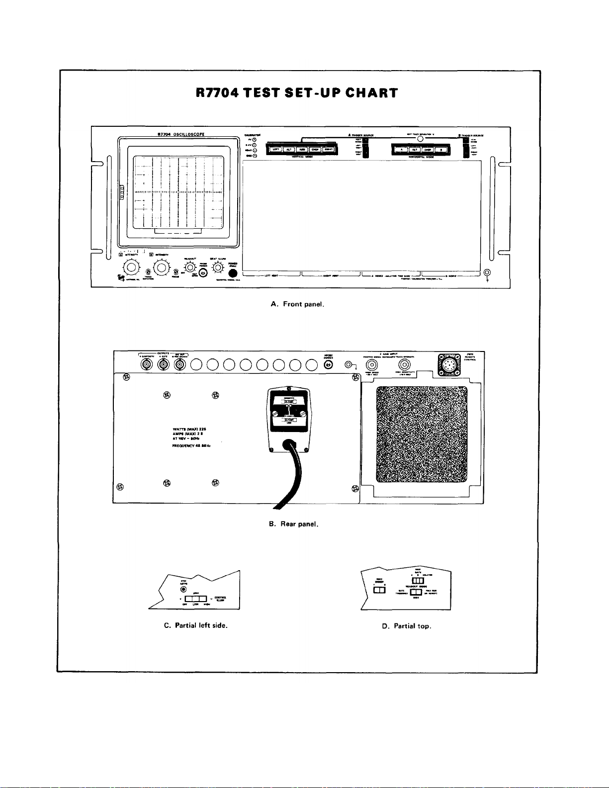
TEST SET-UP CHART
General
Fig. 2-3 shows the front, side, top, and rear panels of
the R7704. This chart may be reproduced and used as a
test setup record for spec ial m easurem ents, applic ations
or procedures, or it may be used as a training aid for
familiarization with this instrument.
GENERAL OPERATING INFORMATION
Simplified Operating Instructions
General. The following information is provided to aid
in quickly obtaining the correct setting for the R7704
controls
Page 26
Operating Instructions-R7704
(A)
Fig. 2-3.
Fig. 2-3.
2-11
Page 27

to present a display. The operator should be familiar with
the complete function and operation of this instrument as
described in this section before using this proc edure. For
detailed operating information for the plug-in units, see the
instruction manuals for the applicable units.
Single-Trace Display. The following procedur e will
provide a display of a single-trace vertical unit against one
time-base unit. For simplicity of explanation, the vertical
unit is installed in the LEFT VERT compartment and the
time-base unit is installed in the A HORIZ compartment.
Other compartments can be used if the following
procedure is changed accordingly.
1. Install 7A-series vertical units in both vertical plug-
in compartments.
2. Press the LEFT button of the VERTICAL MODE
switch.
3. Install a 7B-series time-bas e unit in the A HORIZ
compartment.
4. Press the A button of the HORIZONTAL MODE
switch.
5. Press the VERT MODE button of the A TRIGGER
SOURCE switch.
6. Set the POWER switch to ON. Allow several
minutes warmup.
7. Connect the signals to the input connectors of the
vertical units.
8. Set the vertical units for AC input coupling and
calibrated deflection factors.
9. Set the time-base unit for peak-to-peak auto,
internal triggering at a sweep rate of one
millisecond/division.
10. Advance the A INTENSITY control until a display
is visible (if display is not visible with A INTENSITY at
about midrange, press BEAM FINDER switch and adjust
the vertical deflection fac tor until the display is reduced in
size vertically; then center compressed display with vertical
and horizontal position controls; release BEAM FINDER).
Operating Instructions-R7704
11. Set the vertical deflection factor and vertical
position control for a display which remains within the
graticule area vertical.
12. If necessary, set the time-base triggering controls
for a stable display
13. Adjust the time-base position control so the
display begins at the left line of the graticule. Set the timebase sweep rate to display the desired number of cycles.
Dual-Trace Display. The following procedure will
provide a display of two single-trace vertical units agains t
one-time-base unit.
1. Install 7A-series vertical units in both vertical plug-
in compartments.
2. Press the LEFT button of the VERTICAL MODE
switch.
3. Install a 7B-series time-bas e unit in the A HORIZ
compartment.
4. Press the A button of the HORIZONTAL MODE
switch.
5. Press the VERT MODE button of the A TRIGGER
SOURCE switch.
6. Set the POWER switch to ON. Allow several
minutes warmup.
7. Connect the signals to the input connectors of the
vertical units.
8. Set the vertical units for AC input coupling and
calibrated deflection factors.
9. Set the time-base unit for peak-to-peak auto,
internal triggering at a sweep rate of one
millisecond/division.
10. Advance the A INTENSITY control until a display
is visible (if display is not visible with A INTENSITY at
about midrange, press BEAM FINDER switch and adjust
the vertical deflection fac tor until the display is reduced in
size vertically;
2-12 (A)
Page 28

Operating Instructions-R7704
then center compressed display with vertical and
horizontal position controls; release BEAM FINDER).
11. Set the left vertical unit deflection factor for a
display about four divisions in amplitude. Adjust the
vertical position control to move this display to the top of
the graticule area.
12. Press the RIGHT button of the VERTICAL
MODE switch.
13. Set the right vertical unit deflection factor for a
display which is about four divisions in amplitude (if
display cannot be located, use BEAM FINDER switch).
Position this display to the bottom of the graticule area
with the RIGHT VERT position control.
14. Press the ALT or CHOP button of the VERTICAL
MODE switch. A dual-trace display of the signal from the
LEFT VERT and RIGHT VERT plug-ins should be
presented on the CRT (for more inform ation on c hoice of
dual-trace mode, see Dual-Trace Displays in this
section).
15. If necessary, adjust the time-base triggering
controls for a stable display.
7. Connect the signal to the input connector of the
vertical unit.
8. Set the vertical unit for AC input coupling and
calibrated deflection factors.
9. Set both time-base units for peak-to-peak auto,
internal triggering at a sweep rate of one millisecond/
division.
10. Advance the A INTENSITY control until a display
is visible (if display is not visible with A INTENSITY at
midrange, press BEAM FINDER switch and adjust
vertical deflection factor until display is reduced in size
vertically; then center compressed display with vertical
position control; release BEAM FINDER).
11. Set the vertical unit for a display about four
divisions in amplitude and move the display to the top of
the graticule area with the vertical position controls.
12. If necessary, set the A time-base unit for s table
triggering.
13. Set the A time-base sweep rate for the desired
display.
16. Adjust the time-base position control so the
display begins at the left graticule line. Set the time-base
sweep rate for the desired horizontal display.
Dual-Sweep Display. The following procedure will
provide a dual-sweep display of a single-trace vertical
unit against two time-base units.
1. Install a 7A-series vertical unit in the LEFT VERT
compartment.
2. Press the LEFT button of the VERTICAL MODE
switch.
3. Install 7B-series time-base units in both the A
and B HORIZ compartments.
4. Press the A button of the HORIZONTAL MODE
switch.
5. Press the VERT MODE buttons of the A and B
TRIGGER SOURCE switches.
6. Set the POWER switch to ON. Allow several
minutes warmup.
14. Press the B button of the HORIZONTAL MODE
switch.
15. Advance the B INTENSITY control until a display
is visible (if display is not visible with B INTENSITY at
midrange, press BEAM FINDER switch and adjust the
vertical deflection factor until display is reduced in size
vertically; then center compressed display with vertical
position control; release BEAM FINDER).
16. If necessary, set the B time-base unit for s table
triggering.
17. Set the B time-base unit sweep rate for the
desired display.
18. Press the ALT or CHOP button of the
HORIZONTAL MODE switch (see Dual-Sweep Displays
in this section for further information on selecting sweep
mode).
(A) 2-13
Page 29

Operating Instructions-R7704
19. Adjust the VERT TRACE SEPARATION (B)
control to position the trace produced by the B time-base
unit with respect to the trace produced by the A timebase unit.
Dual Trace-Dual Sweep Displays. The following
procedure will provide a dual-trace, dual-sweep display
of two single-trace vertical units against two time-base
units (four traces displayed on CRT).
1. Install 7A-series vertical units in both vertical
compartments.
2. Press the LEFT button of the VERTICAL MODE
switch.
3. Install 7B-series time-base units in both
horizontal compartments.
4. Press the B button of the HORIZONTAL
DISPLAY switch.
5. Press the VERT MODE buttons of the A and B
TRIGGER SOURCE switches.
6. Set the POWER switch to ON. Allow several
minutes warmup.
7. Connect the signals to the input connectors of
the vertical units.
8. Set the vertical units for AC input coupling and
calibrated deflection factors.
9. Set both time-base units for peak-to-peak auto,
internal triggering at a sweep rate of one millisecond/
division.
10. Advance the B INTENSITY control until a display
is visible (if display is not visible with B INTENSITY at
midrange, press BEAM FINDER switch and adjust the
LEFT VERT deflection factor until display is reduced in
size vertically; then center compressed display with
LEFT VERT position controls; release BEAM FINDER).
11. Set the LEFT VERT deflection factor for a
display which is about two divisions in amplitude and
position the display to the top of the graticule area.
12. If necessary, adjust the B time-base unit
triggering controls for a stable display.
13. Position the start of the trace to the left gratic ule
line with the B time-base unit position control. Set the B
time-base unit sweep rate for the desired display.
14. Press the RIGHT button of the VERTICAL
MODE switch and the A button of the HORIZONTAL
MODE switch.
15. Advance the A INTENSITY control until a display
is visible (if display is not visible with A INTENSITY at
midrange, press BEAM FINDER switch and adjust the
RIGHT VERT deflec tion factor until display is reduced in
size vertically; then center compressed display with
RIGHT VERT position control; release BEAM FINDER).
16. Set the RIGHT VERT deflection factor for a
display about two divisions in amplitude and position the
display just below the center horizontal line of the
graticule.
17. If necessary, adjust the A time-base unit
triggering controls for a stable display.
18. Position the start of the trace to the left gratic ule
line with the A time-base unit position control. Set the A
time-base sweep rate for the desired display.
19. Press the ALT or CHOP button of the
HORIZONTAL MODE switch.
20. If necessary, adjust the VERT TRACE
SEPARATION (B) control to separate the two traces.
21. Press the CHOP button of the VERTICAL MODE
switch.
22. Adjust the vertical position controls and the
VERT TRACE SEPARATION (B) c ontrol as nec es s ary to
obtain the desired display.
Independent Pairs Display. The following
procedure will provide a dual-trace, dual-sweep display
where the LEFT VERT unit is displayed only at the
sweep rate of the B time-base unit and the RIGH T VERT
unit is displayed only at the sweep rate of the A timebase unit.
(A) 2-14
Page 30

Operating Instructions-R7704
1. Follow steps 1 through 19 of the previous
procedure for Dual Trace-Dual Sweep Displays.
2. Press the ALT button of the VERTICAL MODE
switch.
3. If necessary, adjust the VERT TRACE
SEPARATION (B) control to separate the two traces.
The vertical deflection produced by the unit in the LEFT
VERT compartm ent is displayed at the sweep rate of the
time-base in the B HORIZ compar tment, and the vertical
deflection produced by the unit in the RIGHT VERT
compartment is displayed at the sweep rate of the tim ebase in the A HORIZ compartment.
Delayed Sweep-Single Trace. The following
procedure will provide a delayed-sweep display of a
single-trace vertical unit.
1. Follow the complete procedure given under
Single-Trace Displays.
2. Be sure the time-base unit installed in the A
HORIZ (DELAYING TIME BASE) compartment is a
delaying time-base unit.
1. Follow the complete procedure given under
Dual-Trace Displays.
2. Be sure the time-base unit installed in the A
HORIZ (DELAYING TIME BASE) compartment is a
delaying time-base unit.
3. Install a 7B-series time-base unit in the B HORIZ
compartment.
4. Follow the procedure given in the instruction
manual for the delaying sweep time-base unit to obtain a
delayed sweep display.
5. Press the B button of the HORIZONTAL MODE
switch and advance the B INTENSITY control until a
display is visible. Only the delayed sweep display of both
vertical traces is shown on this display.
6. Press the ALT or CHOP button of the
HORIZONTAL MODE switch.
7. Adjust the vertical position controls and the
VERT TRACE SEPARATION (B) c ontrol as nec es s ary to
obtain the desired display.
3. Install a 7B-series time-base unit in the B HORIZ
compartment.
4. Follow the procedure given in the instruction
manual for the delaying sweep time-base unit to obtain a
delayed sweep display.
5. Press the B button of the HORIZONTAL MODE
switch and advance the B INTENSITY control until a
display is visible. Only the delayed sweep is shown on
this display.
6. Press the ALT or CHOP button of the
HORIZONTAL MODE switch.
7. If necessary, adjust the VERT TRACE
SEPARATION (B) control to separate the two traces.
This display provides a simultaneous presentation of the
delaying (A HORIZ) time-base unit and the delayed (B
HORIZ) time base unit.
Delayed Sweep-Dual Trace. The following
procedure will provide a delayed-sweep display of two
single-trace vertical units (four traces displayed on
screen).
NOTE
When operated in the delayed-sweep
mode, there is no special display
relationship between the vertical and
horizontal plug-in as for independent
pairs operation regardless of the
vertical mode selected.
X-Y Display. The following procedure will provide an
X-Y display (one signal versus another rather than
against time).
NOTE
Some 7B-series time-base units have
provisions for amplifier operation in
the X-Y mode; see X-Y Operation in
this section for details of operation in
this manner.
1. Install 7A-series amplifier units in both the LEFT
VERT and the A HORIZ compartments.
2. Press the LEFT button of the VERTICAL MODE
switch and the A button of the HORIZONTAL MODE
switch.
(A) 2-15
Page 31

Operating Instructions-R7704
3. Set the POWER switch to ON. Allow several
minutes warmup.
4. Connect the X-signal to the amplifier unit in the A
HORIZ compartment.
5. Connect the Y-signal to the amplifier unit in the
LEFT VERT compartment.
6. Set both amplifier units for AC input coupling and
calibrated deflection factors.
7. Advance the A INTENSITY control until a display
is visible (if display is not visible, press BEAM FINDER
switch and adjust the deflection fac tors of both am plifier
units until display is reduced in size both vertically and
horizontally; then center compressed display with the
position controls; release BEAM FINDER).
8. Set the deflection factor of both amplifier units
for the desired display and center the display with the
position controls. The amplifier unit in the A HORIZ
compartment controls the horizontal deflection and the
unit in the LEFT VERT compartm ent controls the ver tical
deflection.
Intensity Controls
The R7704 has three separate intensity controls.
The A INTENSITY control determ ines the brightness of
the display produced by the plug-in unit in the A HORIZ
compartment. Likewise, the B INTENSITY control
determines the brightness of the dis play produced by the
plug-in unit in the B HORIZ compartment. The
READOUT intensity control determines the brightnes s of
only the readout portion of the CRT display.
To protect the CRT phosphor, do not turn the
intensity controls higher than necessary to provide a
satisfactory display. The light filters reduce the obs erved
light output from the CRT. When using these filters,
avoid advancing the intensity controls too high. When
the highest intensity display is desired, remove the filters
and use only the clear faceplate protector (permanently
installed behind bezel). Apparent trace intensity can also
be improved in such cas es by reducing the ambient light
or using a viewing hood. Also, be careful that the
intensity controls are not set too high when changing the
time-base unit sweep rates from a fast to a slow sweep
rate, or when changing to the X-Y mode of operation.
This instrument incorporates protection circuitry which
automatically reduces the display intensity to a lower
level when either of the time-base units are set to a slow
sweep rate. This reduces the danger of damaging the
CRT phosphor at these slower sweep rates.
Display Focus
This instrument contains an automatic-focusing
circuit which maintains optimum focus for all intensity
settings after correct setting of the FOCUS adjustm ent is
established. The easiest way to obtain correct setting of
the FOCUS adjustment is to set the READOUT intensity
control so the readout portion of the display is clearly
visible. Then set the FOCUS adjustment for best
definition of the readout display. If this instrum ent does
not contain the Readout System (Option 1), set the
FOCUS adjustment for best definition of a CRT display
at medium intensity settings.
If a well-defined display cannot be obtained with
the FOCUS adjustment, set the ASTIG adjustment
(located on left side of instrument) as follows:
NOTE
To check for proper setting of the ASTIG
adjustment, slowly turn the FOCUS adjustment
through the optimum setting. If the ASTIG
adjustment is correctly set, the vertical and
horizontal portions of the display will come
into sharpest focus at the same position of the
FOCUS adjustment. This setting of the ASTIG
adjustment should be correct for any display.
1. Connect the 4 V calibrator pin-jack to the input of
the vertical unit with a BNC to pin-jack cable.
2. Adjust the vertical deflection factor to produc e a
two-or three-division display.
3. Set the time-base unit for a sweep rate of 0.2
millisecond/division.
4. Set the A INTENSITY control so the display is at
normal intensity (about midrange).
5. Turn the FOCUS adjustment fully
counterclockwise and set the ASTIG adjustment to
midrange.
6. Set the FOCUS adjustment so the top and
bottom of the displayed square wave are as thin as
possible but not elongated.
7. Set the ASTIG adjustment so the top and bottom
of the displayed square wave are as thin as possible.
8. Repeat parts 6 and 7 for the best overall focus.
2-16 (A)
Page 32

Operating Instructions-R7704
Trace Alignment Adjustment
If a free-running trace is not par allel with the horizontal
graticule lines, set the TRACE ROT ATION adjustment as
follows. Position the trace to the center horizontal line.
Set the TRACE ROTATION adjustment so the trace is
parallel with the horizontal graticule lines.
Graticule
The graticule of the R7704 is internally marked on the
faceplate of the CRT to provide accurate, no-parallax
measurements . The graticule is divided into eight vertic al
and ten horizontal divisions. Each division is one
centimeter square. In addition, each major division is
divided into five minor divisions at the center ver tical and
horizontal lines. The vertical gain and horizontal timing of
the plug-in units are calibrated to the graticule so accurate
measurements can be made from the CRT. The
illumination of the graticule lines can be varied with the
GRAT ILLUM control.
NOTE
Two types of crt graticules have been used in
some Tektronix oscilloscopes. One graticule
has 0% and 100% risetime reference points
that are separated by 6 vertical graticule
divisions. The other graticule has the 0% and
100% risetime reference points separated by 5
vertical divisions. In your manual, illustrations
of the crt face or risetime measurement
instructions may not correspond with the
graticule markings on your oscilloscope.
Fig. 2-4 shows the graticule of the R7704 and def ines
the various measurem ent lines. The terminology defined
here will be used in all discussions involving graticule
measurements.
conditions. This filter should be removed for waveform
photographs or when viewing high writing rate displays.
To remove the filter, pull outward on the bottom of the
plastic CRT mask and remove it from the CRT. Remove
the tinted filter (leave the metal light shield in place) and
snap the plastic CRT mask back into place. A clear plastic
faceplate protector is m ounted between the CRT f aceplate
and the bezel. This faceplate protector should be left in
place at all times to protect the CRT faceplate from
scratches.
An optional mesh filter is available for use with the
R7704 (included with Option 3). This filter provides
shielding against radiated EMI (electro-magnetic
interference) from the face of the CRT. It also serves as a
light filter to make the trace more visible under high
ambient light conditions. The mesh filter fits in place of the
plastic CRT mask and the tinted filter. The filter can be
ordered by Tektronix Part No. 378-0603-00.
Beam Finder
The BEAM FINDER switch provides a means of loc ating a
display which overscans the viewing area either ver tically
or horizontally. When the BEAM FINDER switch is
pressed, the display is compressed within the graticule
area. This switch can also be pulled outward to lock it in
the beam-finder position. The latter feature is convenient
when attempting to locate traces from more than one of
the plug-in units in the R7704. Press the BEAM FINDER
switch in to release it from the loc ked position. To loc ate
and reposition an overscanned display, use the following
procedure:
1. Press the BEAM FINDER switch in (or if desired,
pull it outward to the lock position).
2. While the display is compressed, increase the
vertical and horizontal deflection factors until the vertical
deflection is reduced to about two divisions and the horizontal deflection is reduced to about four divisions (the
horizontal deflection needs to be reduced only when in the
X-Y mode of operation).
3. Adjust the ver tical and horizontal position controls
to center the display about the vertical and horizontal
center lines of the graticule.
4. Release the BEAM FINDER switch; the display
should remain within the viewing area.
Fig. 2-4. Definition of measurement lines on R7704
Fig. 2-4. Definition of measurement lines on R7704
Light Filter
The tinted filter provided with the R7704 minimizes
light reflections from the face of the CRT to improve
contrast when viewing the display under high ambient light
REV. B, FEB. 1976
graticule.
graticule.
Control Illumination
The CONTROL ILLUM switch (loc ated on left side of
instrument) determines the illumination level of the
pushbutton switches on the R7704 and the associated
plug-in units. This switch controls the illumination of only
the pushbutton switches on the plug-in units and does not
affect the intensity of lights which are used as function
indicators (for exam ple, it does not affect the illumination
of the ready light on a time-base unit which has the singleconnected
2-17
2-17
Page 33

Operating Instructions-R7704
sweep feature). In the OFF position all pushbutton lights
on the R7704 and the associated plug-in units are off.
The A and B INTENSITY lights rem ain on at low intensity
to provide a power-on indication. In the LOW position
the selected buttons are illuminated at low intensity. This
is the recomm ended position for the CONTROL ILLUM
switch, since it provides an adequate indication of switch
position and also results in longest bulb lif e. The HIGH
position provides maxim um intensity for the pushbuttons
and can be used so the selected switch is obvious even
under high ambient light conditions.
NOTE
If the Readout System is not installed in this
instrument (Option 1), disregard the
following information. Also, the READOUT
intensity control has no effect upon
instrument operation in this case.
Readout
The Readout System of the R7704 allows alpha-
numeric display of information on the CRT along with the
analog waveform displays. The infor mation dis played by
the Readout System is obtained from the plug-in units
which are installed in the plug-in compartments. The
characters of the readout display are written by the CRT
beam on a timeshared basis with the signal waveforms.
shows the area of the graticule where the readout from
each plug-in unit and/or channel is displayed. Notice that
the readout from channel 1 of each plug-in unit is
displayed t within the top division of the graticule and the
readout from channel 2 is displayed directly below within
the bottom division of the graticule. Only the readout
from plug-ins and/or channels which are selected for
display by the VERTICAL MODE or HORIZONTAL
MODE switches, ; or by the mode switches of dualchannel plug-ins, appear in the readout display (some
special purpose plug-in units may over-ride the mode
switches to display readout even through the waveform
is not selected for display).
The READOUT MODE switch (located on top panel),
determines the operating mode of the Readout System.
When this switch is in the the FREE RUN REMOTE
position, the Readout System operates in a free-running
mode to randomly interrupt the waveform display to
present characters. However, the waveform display is
interrupted for only about 20 microseconds for each
character that is displayed. The Readout System can
also be remotely switched to the single-shot m ode when
in this position (see Remote Readout for further
information). In the GATE TR IG’D position, the Readout
System is locked out so no characters are displayed
during the sweep. At the end of the sweep, the Readout
System is triggered and a complete frame of all
applicable readout words is displayed. The trigger for
the Readout System in the Gate Trig’d mode is produced
from the sweep gate selected by the GATE switch
(located on same board as REMOTE READOUT switch)
and is the same as the gate signal connected to the rearpanel + GATE connector (time-base unit must be
installed in selected horizontal compartment).
The readout inform ation f r om each plug-in is called a
word. Up to eight words of readout inform ation can be
displayed on the R7704 CRT (two channels from each of
the four plug-in compartments). The location at which
each readout word is presented is fixed and is directly
related to the plug-in unit and channel from which it
originated. Fig. 2-5
Fig. 2-5. Location of readout on the CRT identifying the
originating plug-in unit and channel.
An "identify" feature is provided by the Readout
System to link the readout word with the originating plugin unit and channel (amplifier units only). When the
"Identify" button of an amplifier unit is pr essed, the word
IDENTIFY appears in the readout location allocated to
that plug-in unit and channel. Other readout words in the
display remain unchanged. When the "identify" button is
released, the readout display from this plug-in channel is
again displayed. Circuitry may also be provided in the
amplifier unit which produces a noticeable change in the
analog waveform display to also identify the associated
trace when the "Identify" button is pressed; see the plugin instruction manuals for details.
The READOUT intensity control determines the
intensity of only the readout portion of the display
independent of the other traces. The Readout System is
inoperative in the fully counterclockwise OFF position.
This may be, desirable when the top and bottom
divisions of the graticule are to be used for waveform
display, or when the trace
2-18
2-18
(B)
Page 34

Operating Instructions-R7704
interruptions necessary to display characters do not
allow a satisfactory waveform display to be obtained.
NOTE
If this instrument is to be operated with the
Readout System board removed, be sure to
connect a jumper lead between pin ZV and
pin ZW (Readout System chassis). Failure to
make this wiring change will result in timing
error, particularly at fast sweep rates.
Remote Readout
The operating mode of the Readout System can be
remotely controlled through the rear-panel REMOTE
CONTROL connector J1075. Grounding Pin E inhibits
(locks out) the Readout System; gr ounding Pin F trigger s
one complete frame of applic able readout words (singleshot). This mode of operation can be used to display the
readout independently of the waveform, such as for
display photography. Requirements for rem ote readout
operation are:
REMOTE READOUT LOCKOUT
Pin of J 1075 E
Signal required Closure to ground (within 0.1 volt) from a
positive level locks out Readout System
Maximum current Two milliamperes
required
Maximum open +2 volts
circuit voltage
Maximum input +5 volts, -1 volt (DC + peak AC)
voltage
REMOTE SINGLE-SHOT READOUT
Pin of J1075 F
Signal required Closure to ground (within 0.4 volt) from a
positive level with Pin E grounded allows
Readout System o display one complete
frame. Rate of change must be at l east 0.1
volt/microsecond.
Maximum current Three milliamperes
required
Maximum open +10volts
circuit voltage
Maximum input +10 volts, -5 volts (DC + peak AC)
voltage
Display Photography
A permanent record of the CRT display can be
obtained with an oscilloscope camera system. The
instruction manuals for the Tektronix Oscilloscope
Cameras include complete instructions for obtaining
waveform photographs. The following specific
information applies to the R7704.
The CRT bezel of the R7704 provides integral
mounting for a Tektronix Oscilloscope Camera. The
three pins located on the left side of the CRT bezel
connect power to compatible camera systems. It also
receives control signals from Tektronix automatic
cameras to allow camera controlled single-shot
photography (see camera manual for further
information).
If the readout portion of the display is to be included
on waveform photographs, the f ollowing suggestions will
aid in obtaining good photographs:
1. Focus the oscilloscope display and the
camera on the readout portion of the CRT display. T he
auto-focus feature in this instrument will maintain the
traces at optimum focus.
2. Set the READOUT intensity control for a
minimum setting that allows the characters to be written.
This normally occurs at a slightly lower intensity level
than is necessary for complete writing of the waveform
display. Some experimentation may be necessary to
establish the correct level. Too high a setting of the
READOUT intensity control will result in a br oad, poorly
defined photograph of the readout display.
3. If single-shot photography is used, set the
READOUT MODE switch to the GATE TRIG’D position
(see Readout for complete operating information).
Then, the readout is displayed in a single-shot manner
after the trace is complete ( be sure the camera shutter
remains open at least 0.5 second after the sweep is
completed to photograph the entire readout). Also, s et
the GRAT ILLUM control counterclockwise while the
trace is being photographed. Then, the graticule c an be
photographed later to produce a double-exposure picture
showing complete information.
Vertical and Horizontal Mode Switch Logic
There are 20 possible combinations of VERTICAL
MODE and HORIZONTAL MODE switch settings . The
total possible number of dis play combinations is further
multiplied by the variety of plug-in units available for use
with this instrument (suc h as voltage amplifiers, current
amplifiers, sam pling units, etc.), the interchangeability of
plug-ins (i.e., an amplifier or time-base unit can be
installed in either of the vertical or horizontal
compartments ), or by the capabilities of the plug- in units
which are used in this
2-19
Page 35

instrument (e.g., a dual-trace vertical unit can be used in
either of the two single-channel modes, in either dualtrace mode or added algebraically; a delaying time base
can be used either for a normal sweep or for delayed
sweep). Therefore, it is diff icult to list all of the display
combinations which can occur using the R7704 and the
plug-in units which are available since the display
combinations possible are dictated by the specific
combination of plug-in units used. Table 2-2 lists the
combination of VERTICAL MODE and HORIZONTAL
MODE switch positions available and the type of display
provided with each combination. For further inf orm ation
on operation in each position of the VERTICAL MODE
and HORIZONTAL MODE switches see the following
sections on Vertical Mode and Horizontal Mode.
Vertical Mode
Left and Right Mode. When the LEFT or RIGHT
button of the VERTICAL MODE switch is pres sed, only
the signal from the plug-in unit in the selected
compartment is displayed.
Alternate Mode. The ALT position of the
VERTICAL MODE switch produces a display which
alternates between the plug-in units in the LEFT VERT
and RIGHT VERT com partm ents with each sweep of the
CRT. Although the ALT mode can be used at all sweep
rates, the CHOP mode provides a more satisfactory
display at sweep rates below about 20
milliseconds/division. At these slower sweep rates,
alternate-mode switching becomes visually perceptible.
The A and B TRIGGER SOURCE switches allow
selection of the triggering for an alternate display. W hen
these switches are set to the VERT MODE positions,
each sweep is triggered by the signal being displayed on
the CRT. This provides a st able display of two unrelated
signals, but does not indicate the time relationship
between the signals. In either the LEFT VERT or RIG HT
VERT positions, the two signals are displayed showing
true time relationship. However, if the signals are not
time related, the display from the plug-in which is not
providing the trigger signal will be unstable on the CRT.
When the ALT vertical mode is selected and
either the ALT or CHOP buttons of the HORIZONTAL
MODE switch are pressed, the instrument operates in
independent pairs mode. Under this condition, the LEFT
VERT unit is always displayed at the sweep rate of the
time-base unit in the B HORIZ compartment and the
RIGHT VERT unit is displayed at the sweep rate of the
time-base unit in the A HORIZ compartment (nondelayed sweep only). This results in two displays that
have completely independent vertical deflection and
sweep rate. This display is equivalent to the display
obtainable with a dual-beam oscilloscope for most
repetitive display combinations. See Horizontal Mode
Operating Instructions-R7704
TABLE 2-2
Display Combinations
VERTICAL HORIZONTAL
MODE Switch MODE Switch
Position Position Comments
LEFT A One trace. Vertical deflection
B deflection from single unit.
ALT Two traces. Vertical deflecCHOP zontal deflection from both
ALT A Two traces. Vertical deflec-
B zontal deflection from single
ALT Two traces. Vertical deflecCHOP zontal deflection from both
ADD A One trace. Vertical deflection
B both units; horizontal deflec-
ALT Two traces. Vertical deflecCHOP of both units; horizontal
CHOP A Two traces. Vertical deflec-
B zontal deflection from single
ALT Four traces. Vertical deflecCHOP zontal deflection from both
RIGHT A One trace. Vertical deflection
B deflection from single unit.
ALT Two traces. Vertical deflecCHOP zontal deflection from both
1
Combinations given for single-channel vertical and horizontal units
only.
from single unit; horizontal
tion from single unit; horiunits.
tion from both units; horiunit.
tion from both units; horiunits. Provides independent-
pairs operation between the
LEFT VERT and B HORIZ
plug-ins and the RIGHT
VERT and A HORIZ plugins.
is algebraic summation of
tion from single unit.
tion is algebraic summation
deflection from both units.
tion from both units; horiunit.
tion from both units; horiunits.
from single unit; horizontal
tion from single unit; horiunits.
1
(A)
2-20
Page 36

Operating Instructions-R7704
for information on selection of either ALT or CHOP
horizontal mode. See Trigger Source for inform ation on
obtaining correct trigger operation. If delayed-sweep
operation is used under this condition, a different
sequence of display occurs. First, the LEFT VERT unit
is displayed at the sweep rate of the time-base unit in the
A HORIZ compartment (delaying sweep) and then at the
sweep rate of the time-base unit in the B HORIZ
compartment ( delayed sweep). The vertical display then
shifts to the RIGHT VERT unit and it is displayed
consecutively at the delaying and delayed sweep rate.
Chopped Mode. The CHOP position of the
VERTICAL MODE switch produces a display which is
electronically switched between channels at a onemegahertz rate. In general, the CHOP mode provides
the best display at sweep rates slower than about 20
milliseconds/division or whenever dual-trace, single-shot
phenomena are to be displayed. At faster sweep r ates
the chopped switching becomes apparent and may
interfere with the display.
Correct internal triggering for the CHOP mode can
be obtained in any of the three positions of the trigger
source switches. W hen the A or B TRIGGER SOURCE
switches are set to VERT MODE, the internal trigger
signals from the ver tical plug-ins are algebraically added
and the time-base units are triggered f rom the resultant
signal. Use of the LEFT VERT or RIGHT VERT trigger
source positions triggers the time-base units on the
internal trigger signal from the selected vertical unit only.
This allows two time-related signals to be displayed
showing true time relationship. However, if the signals
are not time-related, the display from the c hannel which
is not providing the trigger signal will appear unstable.
The CHOP mode can be used to compare two singleshot, transient, or random signals which occur within the
time interval determined by the time-base unit (ten tim es
selected sweep rate). To provide c orrect triggering, the
display which provides the trigger signal must precede
the second display in time. Since the signals show true
time relationship, time- difference measurements can be
made from the display.
Algebraic Addition. The ADD position of the
VERTICAL MODE switch can be used to display the sum
or difference of two signals, f or common-m ode rejection
to remove an undesired signal, or f or DC off set (applying
a DC voltage to one channel to offset the DC com ponent
of a signal on the other channel). The common-mode
rejection ratio between the vertical plug-in c ompar tments
of the R7704 is greater than 10: 1 at 150 megahertz.
The rejection ratio increases to 100: 1 at 20 megahertz.
The overall deflection on the CRT in the ADD mode
is the resultant of the algebraic addition of the signals
from the two vertical plug-in units. It is difficult to
determine the voltage amplitude of the r esultant display
unless the amplitude of the signal applied to one of the
plug-ins is known. This is particularly true when the
vertical units are set to differ ent deflection factors, sinc e
it is not obvious which portion of the display is a result of
the signal applied to either plug-in unit. Also, the polarity
and repetition rate of the applied signals enters into the
calculation.
The following general precautions should be
observed to provide the best display when using the ADD
mode:
1. Do not exceed the input voltage rating of the
plug-in units.
2. Do not apply large signals to the plug-in inputs .
A good rule to follow is not to apply a signal which
exceeds an equivalent of about eight times the vertical
deflection factors. For example, with a vertical
deflection factor of 0.5 volts/division, the voltage applied
to that plug-in should not exceed four volts. Larger
voltages may result in a distorted display.
3. To ensure the greatest dynamic range in the
ADD mode, set the position controls of the plug-in units
to a setting which would result in a mid-sc reen display if
viewed in the LEFT or RIGHT positions of the VERTICAL
MODE switch.
4. For sim ilar response from each channel, set the
plug-in units for the same input coupling.
Horizontal Mode
A and B. When either the A or B button of the
HORIZONTAL MODE switch is pressed, the display is
presented at the sweep rate of only the selected timebase unit. Set the applicable intensity control and trigger
source switch for the desired display.
Alternate Mode. The ALT position of the
HORIZONTAL MODE switch produces a display which
alternates between time-base units after each sweep on
the CRT. Although the ALT horizontal mode can be
used at all sweep rates, the CHOP horizontal mode
provides a more satisfactory display at sweep rates
below about 20 milliseconds/division. At slower sweep
rates, the switching between the alternate-mode traces
becomes apparent and may interfere with correct
analysis of the display.
NOTE
The instrument will not operate in the ALT
position of the HORIZONTAL MODE switch
if either horizontal plug-in compartment is
left vacant.
(A)
2-21
Page 37

The A and B INTENSITY controls allow individual
adjustment of the trac es pr oduc ed by the time-bas e units
in the A HORIZ and B HORIZ compartments. Correct
triggering of both time-base units is ess ential to obtaining
the correct display in the ALT horizontal mode. If either
of the time-base units does not receive a correct tr igger,
and therefore, does not produce a sweep, the other unit
cannot produce a sweep either. This means that one
time-base unit cannot begin its sweep until the pr evious
unit has completed its entire display. This can be
avoided if the time-base units are set for auto-mode
triggering (sweep free runs if not correctly triggered).
The A and B TRIGGER SOURCE switches allow
individual selection of the trigger source for the A HORIZ
and B HORIZ time base units. See the information on
Trigger Source for complete operation of the A and B
TRIGGER SOURCE switches. Also, see Vertical Trace
Separation for information on positioning the B HORIZ
display when in the ALT dual-sweep mode.
Chopped Mode. When the CHOP button of the
HORIZONTAL MODE switch is pressed, the display is
electronically switched between the two time-base units
at a 200kilohertz rate. In general, the CHOP horizontal
mode provides the best display when either of the timebase units is set to a sweep rate slower than about 20
milliseconds/ division. It also provides the best display
when the two time-base units are set to widely varying
sweep rates. In the CHOP horizontal mode, equal tim e
segments are displayed from each of the time-base
units. This provides a display which does not change
greatly in intensity as the sweep rate of one of the timebase units is reduced (in contrast to ALT horizontal mode
operation where the slowest trace tends to be the
brightest).
The A and B INTENSITY controls allow individual
adjustment of the intensity of the traces produced by the
time-base units in the A HORIZ and B HORIZ
compartments . Triggering is not as critical in the CHOP
horizontal mode as in ALT since only the trace fr om the
un-triggered time-base unit is m issing from the dis play if
one of the units is not triggered properly. The other trace
will be presented in the normal manner. The A and B
TRIGGER SOURCE switches allow individual selection
of the trigger source for the A HORIZ and B HO RIZ timebase units. See the information on Trigger Source.
Also, see Vertical Trace Separation for information on
positioning the trace produced by the B HORIZ unit in
relation to the trace from the A HORIZ unit.
Vertical Trace Separation
The VERT TRACE SEPARATION ( B) control allows
the trace produced by the B HORIZ plug-in to be
positioned about four divisions above or below the trace
produced by the plug-in unit in the A HORIZ
compartment when one of the dual-sweep horizontal
modes is selected. T his control ef f ectively operates as a
vertical position control for dual-sweep operation. To
use the control, first establish the desired pos ition of the
Operating Instructions-R7704
trace produced by the unit in the A HORIZ compartment.
Then adjust the VERT TRACE SEPARAT ION ( B) contr ol
to move the trace produced by the unit in the B HO RIZ
compartment away from the A HORIZ display. If both of
the waveforms are larger than four divisions in
amplitude, the displays can only be positioned so they do
not directly overlap since each waveform cannot be
positioned to a unique area of the CRT.
Trigger Source
The A and B TRIGGER SOURCE switches allow
selection of the internal trigger signals f or the A HORIZ
and B HORIZ time-base units respectively. For most
applications, these switches can be set to the VERT
MODE positions. This position is the most convenient
since the internal trigger signal is autom atically switched
as the VERTICAL MODE switch is changed or as the
display is electronically switched between the LEFT
VERT and RIGHT VERT plug- ins in the ALT position of
the VERTICAL MODE switch. It also provides a usable
trigger signal in the ADD or CHOP positions of the
VERTICAL MODE switch, since the internal trigger signal
in these modes is the algebraic sum of the signals
applied to the vertical plug-in units. T herefore, the VERT
MODE positions ensure that the time-base units receive
a trigger signal regardless of the VERTICAL MODE
switch setting without the need to change the trigger
source selection. However, if correct triggering for the
desired display is not obtained in the VERT MODE
position, the trigger source for either the A HORIZ or B
HORIZ time-base unit can be changed so the trigger
signal can be obtained from either the LEFT VERT or
RIGHT VERT plug-in unit. T he internal trigger signal is
obtained from the selected vert ical c ompartment whether
the plug-in unit in that compartment is selected for
display on the CRT or not. If the internal trigger signal is
obtained from one of the vertical units but the other
vertical unit is selected for display, the internal trigger
signal must be time-related to the displayed signal in
order to obtain a triggered (stable) display.
X-Y Operation
In some applications, it is desirable to display one
signal versus another (X-Y) rather than against time
(internal sweep). The flexibility of the plug-in units
available for use with the R7704 provides a means for
applying an external signal to the horizontal deflection
system for this type of display. Some of the 7B-series
time-base units can be operated as amplif iers in addition
to their normal use as time-base generators. This
feature allows an external signal , to provide the
horizontal deflection on the CRT. For most of the tim ebase units with the amplifier function, the X ( horizontal)
signal can be connected either to an external input
connector on the time-base unit or it can be routed to the
time-base unit through the internal triggering system (see
time-base instruction manual for details). If the latter
method is used, the A and B TRIGGER SOURCE
switches
2-22
Operating Instructions-R7704
Page 38

must be set so that the X (hor izontal) signal is obtained
from one of the vertical units and the Y (vertical) signal is
obtained from the other vertical unit. The advantages of
using the internal trigger system to provide the X signal
are that the attenuator switch of the amplifier unit
providing the horizontal signal determines the horizontal
deflection factor to allow full-range operation and the
plug-in units do not have to be moved between
compartments when X-Y operation is desired.
Another method of obtaining an X-Y display is to
install an amplifier plug-in unit in one of the horizontal
plug-in compartments (check am plifier unit gain as given
in the plug-in instruction manual to obtain calibrated
horizontal deflection factors). This method provides the
best X-Y display, particularly if two identical amplifier
units are used, since both the X and Y input systems will
have the same delay time, gain characteristics, input
coupling, etc. For further information on obtaining X-Y
displays see the plug in unit manuals. Also, the
reference books listed under Applications provide
information on X-Y measurements and interpreting the
resultant lissajous displays.
An optional X-Y delay compensation network is
available for use with the R7704. This network provides
close delay matching between the vertical and horizontal
deflection systems up to two megahertz for use in X-Y
applications which require precise phase m eas urem ents.
The network can be added to the R7704 at any time.
Order Tektronix Part No. 040-0529-00 from your local
Tektronix Field Of f ic e or repr es entative f or a c omplete XY delay compensation network; installation instructions
are included.
While the X -Y delay compensation network provides
minimum phase shift between the X and Y portions of an
X-Y display, it adds negative preshoot distortion and
some corner rounding to fast step functions . An internal
Delay Disable switch (see Fig. 2-6) is provided for both
the A and B delay compensation networks to allow
selection of either minimum phase-shift characteris tics or
optimum step response (remove power unit to reach
these switches). When the Delay Disable switch is set to
In (up), minimum phaseshift operation is provided as
controlled by the plug-in units in the associated horizontal
compartment. W hen set to the Out ( down) position, the
X-Y delay compensation network for the applicable
horizontal compartment is disabled; the horizontal signal
is connected to the horizontal deflection system with
minimum distortion.
Intensity Modulation
Intensity (Z-axis) modulation can be used to relate a
third item of electrical phenomena to the ver tical (Y-axis)
and the horizontal (X-axis) coordinates without affecting
the waveshape of the displayed signal. The Z-axis
modulat(A)
Fig. 2-6. Location of A and B Delay Disable
Fig. 2-6. Location of A and B Delay Disable switches.
ing signal applied to the CRT circuit changes the
intensity of the displayed waveform to provide this type of
display. "Gray scale" intensity modulation can be
obtained by applying signals which do not completely
blank the display. Large amplitude signals of the correct
polarity will completely blank the display; the sharpest
display is provided by signals with a fast rise and fall.
The voltage amplitude required for visible trace
modulation depends upon the setting of the intensity
controls.
Time markers applied to the Z-AXIS INPUTS provide
a direct time referenc e on the display. W ith uncalibrated
horizontal sweep or X-Y mode operation, the time
markers provide a means of reading time directly from
the display. However, if the markers are not time- related
to the displayed waveform, a single-sweep display
should be used (for internal sweep only) to provide a
stable display.
Two modes of intensity modulation are provided in
the R7704. The following discussions list the use and
limitations of each mode.
High Sensitivity Input. The HIGH SENSITIVITY
input (on rear panel) permits intens ity modulation of the
CRT display through the Z-Axis Amplifier circuit. A twovolt peak-to-peak s ignal will completely blank the display
even at maximum intensity levels. Lower amplitude
signals can be used to only change the trace brightness
rather than completely blank the display. Negative-going
modulating signals increase the display intensity and
positive-going modulating signals decrease the display
intensity. Bandwidth for this mode of intensity
modulation is DC to 10 megahertz (input voltage derating
necessary above two megahertz). The maxim um input
voltage in this mode should be limited to 15 volts (DC
plus peak AC). Since this
2-23
Page 39

input is the most sensitive, it can be used for all
applications requiring bandwidth of 10 megahertz or less.
When the HIGH SENSITIVITY input is not in use,
replace the BNC cap.
High Speed Input. Intensity modulation signals
con-nected to the HIGH SPEED connector (on rear
panel) are connected primarily to the cathode circuit of
the CRT. A 60-volt peak-to-peak signal will provide
complete blanking of the display even at maximum
intensity settings. Negative-going modulating signals
increase the display intensity and positive-going
modulating signals decrease the display intensity.
Bandwidth for this mode is DC to 100 megahertz.
Maximum input voltage for signals connected to the
HIGH SPEED input is 60 volts (DC plus peak AC).
Replace the BNC cap when the HIGH SPEED input is
not in use.
Raster Display
A raster-type display can be used to effectively
increase the apparent sweep length. For this type of
display, the trace is deflected both vertically and
horizontally by saw-tooth signals. This is accom plished
in the R7704 by installing a 7B-series time-base unit in
one of the vertical plug-in compartm ents. Normally, the
time-base unit in the vertical com partment should be set
to a slower sweep rate than the time-base unit in the
horizontal compartment; the num ber of horizontal traces
in the raster depends upon the ratio between the two
sweep rates. Information can be dis played on the r aster
using several different methods. In the ADD position of
the VERTICAL MODE switch, the signal from an
amplifier unit can be algebraically added to the vertical
deflection. With this method, the vertical signal
amplitude on the CRT should not exceed the distance
between the horizontal lines of the raster. Another
method of displaying information on the raster is to use
the Z-AXIS INPUTS to provide intensity modulation for
the display. This type of raster display could be used to
provide a television-type display. Complete information
on operation using the Z-axis feature is given under
Intensity Modulation.
To provide a stable raster display, both time-base
units must be correctly triggered. Internal triggering is
not provided for the time-base units when they are in the
vertical compartm ents; external triggering m ust be used.
Also, blanking is not provided from the time-base units
when they are installed in a vertical compartment. To
blank out the retrace portion from the tim e-base unit in
the vertical compartment, special connections must be
made from this time- base unit to the blanking network of
the R7704.
Calibrator
General. The internal calibrator of the R7704
provides a convenient signal source for checking basic
vertical gain and
Operating Instructions-R7704
sweep timing. The calibrator output signal is also very
useful for adjusting probe compensation as described in
the probe instruction manual. In addition, the calibrator
can be used as a convenient signal source for
application to external equipment.
Voltage. The calibrator provides accurate output
voltage of 40 millivolts, 0.4 volt, and 4 volts at the three
front-panel pin-jack connectors into high-impedance
loads. In addition, outputs of 20 m illivolts, 0.2 volt, and
0.4 volt are available from the 40 m V, 0.4 V, and 4 V pinjacks respectively into 50 ohms. Additional calibrator
voltages of 4 millivolts and 40 volts are available
internally at the Output Signal board and can be
connected to the front-panel pin-jacks by changing
internal circuit-board connections (see Output Signals
schematic for correct pins). If the calibrator output
connections are changed, the front-panel calibrator
nomenclature will no longer be correct.
Current. A 40-milliampere, one-kilohertz output
current is provided when the current-loop accessory is
connected between the 4 V pin-jack and gr ound. This
output can be used to check and calibrate currentmeasuring probe systems. The current signal is
obtained by clipping the probe around the current-loop
accessory. The arrow on the current-loop accessory
indicates conventional current flow; i.e., from plus to
minus.
Repetition Rate. The calibrator circuit uses
frequency stable components to maintain accurate
frequency and constant duty cycle. Thus, the calibrator
can be used for check ing the basic s weep tim ing of timebase units.
Wave Shape. The square-wave output signal of the
calibrator can be used as a refer ence wave shape when
checking or adjusting the com pensation of pass ive, highresistance probes. Since the square-wave output from
the calibrator has a flat top, any distortion in the
displayed waveform is due to the probe compensation.
Signal Outputs
+ Sawtooth. The + SAWTOOTH connector (on
rear-panel) provides a positive-going sample of the
sawtooth signal from the tim e- base units in the hor izontal
plug-in compartm ents. The SW EEP switch (located on
top panel; see Fig. 2-2) allows the output sawtooth to
be selected from the time-base unit in either the A
HORIZ or B HORIZ compartments. Rate of rise of the
sawtooth output signal is about 50 millivolts/unit of time
into a 50-ohm load or about one volt/unit of time into a
one-megohm load. Unit of time is determined by the
time-base time/division switch (e.g., if time/division
switch is set to one millisecond/ division, a unit of tim e is
one millisecond; at five milliseconds/division, a unit of
time is five milliseconds). The
(A)
2-24
Page 40

peak output voltage is greater than 500 m illivolts into a
50-ohm load or greater than 10 volts into a one-megohm
load.
+ Gate. The + GATE output connector (on rear
panel) provides a positive-going rectangular output pulse
from the time-base units in the horizontal plug-in
compartments . The GATE switch (located on top panel;
see Fig. 2-2) allows the output signal to be selected
from the time-base unit in the A HORIZ com partment, B
HORIZ compartment, or the delayed gate from a
delaying time-base unit in the A HORIZ compartment.
Duration of the gate output signal is the same as the
duration of the respective sweep or, in the case of the
delayed gate, it starts at the end of the delay period and
lasts until the end of the sweep from the delaying timebase unit. Amplitude of the output signal at the +GATE
connector is about 0.5 volts into 50 ohms or about 10
volts into one megohm.
Vertical Signal. The SIG OUT connector (on rear
panel) provides a sample of the vertic al deflect ion signal.
The source of the output signal at this connector is
determined by the B TRIGGER SOURCE switch. In the
VERT MODE position of the B TRIGGER SOURCE
switch, the output signal is determined by the setting of
the VERTICAL MODE switch. The output signal in the
LEFT and RIGHT positions of the VERTICAL MODE
switch is obtained only from the selected ver tical unit. In
the ALT position of the VERTICAL MODE switch, the
output signal at the SIG OUT connector switches
between vertical units along with the CRT display.
However, the vertical output signal in the CHOP position
is a composite signal and is the sa me as obtained in the
ADD position due to the requirements of the triggering
system. The LEFT VERT and RIGHT VERT positions
of the B TRIGGER SOURCE switch provide the vertical
output signal only from the selected vertical unit even
when it is not selected for display. The output voltage
into a 50-ohm load is about 25 millivolts /division of CRT
display and about 0.5 volts/division of display into a onemegohm load. The bandwidth of the output signal is
determined by the vertical plug-in unit which is us ed ( see
Systems Specification given in Section 1).
Probe Power Connectors
The two PROBE POW ER connectors provide operating
power for active probe systems. O ne PROBE POWER
connector is located on the front panel and a second
connector is provided on the rear panel. It is not
recommended that these connectors be used as a power
source for applications other than the com patible probes
or other accessories whic h are specifically designed for
use with this system.
Operating Instructions-R7704
remote operation of the instrument and the associated
plug-in units. Table 2-3 lists the function of each terminal
of J1075. The mating connector for J1075 is Tektronix
Part No. 134-0049-00 (one mating connector supplied
as standard accessory). The methods of obtaining
remote Single-Sweep reset and ready indication are
given under Remote Single-Sweep Reset. Remote
operation of the Readout System is discussed under
Remote Readout.
TABLE 2-3
Remote Connections
J1075 Terminal Function
A Remote single-sweep reset
(A and B HORIZ)
B Chassis ground
C Remote ready indicator
(A HORIZ)
D Remote ready indicator
(B HORIZ)
E Remote readout lockout
F Remote single-shot readout
H No connection
J No connection
K No connection
Remote Single-Sweep Reset
Remote single-sweep reset operation can be
provided to 7B-series time-base units with compatible
features through rear-panel REMOTE CONTROL
connector J1075. The remote single-sweep reset
actuation can be obtained from either an active system
(pulse generator, logic circuit, etc.) or a passive system
(switch or relay). Requirement for remote s ingle-sweep
reset Operation are:
REMOTE SINGLE-SWEEP RESET (A and B HORIZ))
Pin of J1075 A
Signal required Closure to ground (within -5 to
+0.5 volts) from a positive level.
Maximum current 10 milliamperes.
required
Minimum pulse 10 microseconds at 50% amplitude
width points.
Maximum input 15 volts (DC + peak AC).
voltage
Remote Connector
The nine-terminal REMOTE CONTROL connector
J1075 on the rear panel of the R7704 provides input for
(A)
2-25
Page 41

Operating Instructions-R7704
A HORIZ REMOTE READY INDICATOR
Pin of J1075 C
Output signal Open or ground when not ready; +5
volts at 47-ohm source impedance
when ready - output sufficient to
light a No. 49 bulb.
B HORIZ REMOTE READY INDICATOR
Pin of J1075 D
Output signal Open or ground when not ready; +5
volts at 47-ohm source impedance
when ready - output sufficient to
light a No. 49 bulb.
Fig. 2-7 shows a typical passive system to provide
remote single-sweep reset operation. The r emote ready
lights are optional and can be used with an active or
passive system whenever it is necessary to provide an
indication at the remote location that reset has occurred.
Applications
The R7704 Oscilloscope and its associated plug-in
units provide a very flexible measurement s ystem. The
capabilities of the overall system, depend mainly upon
the plug-in units that are chosen for use with this
instrument. Specif ic applications for the individual plugin units are described in the plug-in manuals. The
overall system can also be used for many applications
which are not described in detail either in this manual or
in the manuals for the individual plug-in units. Contact
your local Tektronix Field Office or representative for
assistance in making specific measurements
with this instrument.
The following books describe oscilloscope
measurement tec hniques which can be adapted for use
with this instrument.
Harley Carter, "An Introduction to the Cathode Ray
Oscilloscope", Phillips Technical Library, Cleaver-Hume
Press Ltd., London, 1960.
J. Czech, "Oscilloscope Measuring Techniques",
Phillips Technical Library, Springer-Verlag, New York,
1965.
Fig. 2-7. Typical circuit for remote single-sweep reset
Fig. 2-7. Typical circuit for remote single-sweep reset
operation.
operation
2-26
2-26
Robert G. Middleton, "Scope W aveform Analysis",
Howard W Sams & Co. Inc., The Bobbs-Merrill
Company Inc., Indianapolis, 1963.
Robert G. Middleton and L. Donald Payne, "Using
the Oscilloscope in Industrial Electronics", Howard W.
Sams & Co. Inc., The Bobbs-Merrill Company Inc.,
Indianapolis,
1961.
John F. Rider and Seymour D. Uslan,
"Encyclopedia of Cathode-Ray Oscilloscopes and Their
Uses", John F. Rider Publisher Inc., New York, 1959.
John F. Rider, "Obtaining and Interpreting Test
Scope Traces", John F. Rider Publis her Inc., New York,
1959.
Rufus P. Turner, "Practical Oscilloscope
Handbook", Volumes 1 and 2, John F. Rider Publisher
Inc., New York, 1964.
(A)
Page 42

SECTION 3
CIRCUIT DESCRIPTION
Change information, if any, affecting this section will be found at the rear of this manual.
R7704
Introduction
This section of the manual contains a des cription of
the circuitry used in the R7704 Oscilloscope. The
description begins with a discussion of the instrument
using the basic block diagram shown in Fig. 3-1. Then,
each circuit is described in detail using detailed block
diagrams to show the interconnections between the
stages in each major circuit and the relationship of the
front-panel controls to the individual stages.
A complete block diagram is loc ated in the Diagram s
section at the back of this manual. T his block diagram
shows the overall relationship between all of the circuits.
Complete schematics of each circuit are also given in the
Diagrams section. Refer to these diagrams throughout
the following circuit description for electrical values and
relationship.
BLOCK DIAGRAM
General
The following discussion is provided to aid in
understanding the overall concept of the R7704 before
the individual circuits are discussed in detail. A basic
block diagram of the R7704 is shown in Fig. 3-1. Only
the basic interconnections between the individual block s
are shown on this diagram. Each block represents a
major circuit within the instrum ent. T he num ber on each
block refers to the complete circuit diagram which is
located at the rear of this manual.
vertical (Y) signal due to the delay line. The Horizontal
Channel Switch determines whether the signal from the
A and/or B horizontal unit is displayed. The horizontal
signal selected by the Horizontal Channel Switch is
connected to the Horizontal Amplifier circuit which
amplifies it to provide the horizontal deflection for the
CRT. This circuit also accepts the X-signal from the
Readout System to produce the horizontal portion of the
readout display. The Readout System provides alphanumeric display of information encoded by the plug-in
units. This display is presented on the CRT and is
written by the CRT beam on a time-shared basis with the
analog waveform display.
The internal trigger signals from the vertical plug-in
units are connected to the Trigger Selec tor circuit. This
circuit selects the trigger signal which is c onnec ted to the
horizontal plug-in units. It also provides the drive signal
for the Output Signals circuit to provide an output which
is a sample of the vertical signal. The Output Signals
circuit also provides a sawtooth and a gate output s ignal.
The Calibrator portion of this cir cuit produces a squarewave output with accurate amplitude which can be used
to check the calibration of this instrument and the
compensation of probes.
The Logic Circuit develops control s ignals for use in
other circuits within this instrum ent and the plug-in units.
These output signals automatic ally determine the c orrect
instrument operation in relation to the plug-ins installed
and/or selected, plug-in control settings, and R7704
control settings.
Vertical signals to be displayed on the CRT are applied
to the Vertical Interface circ uit from both vertical plug- in
compartments . The Vertical Interface c ircuit determines
whether the signal from the left and/or r ight vertical unit
is displayed. The selected vertical signal is then
amplified by the Vertical Amplif ier circuit to bring it to the
level necessary to drive the vertical deflection plates of
the CRT. This circuit also includes an input to produce
the vertical portion of an alpha-numeric readout display.
Horizontal signals for display on the CRT are
connected to the Horizontal Interface circuit from both
horizontal plug-in compartments. The X-Y Delay
Compensation network (optional feature) provides a
delay for the horizontal (X) portion of an X-Y display to
match the delay of the
(A)
The CRT Circuit contains the Z- Axis Amplifier which
provides the drive signal to control the intensity level of
the display. The CRT Circuit also contains the controls
necessary for operation of the cathode-ray tube.
The Line to DC Converter/Regulator and LowVoltage Regulator circuits provide the power necessary
for operation of this instrument. This voltage is
connected to all circuits within the instrument. The
Controls and Cabling circuit shows the switching logic of
the front-panel controls. It also includes the rear-panel
REMOTE CONTROL connector and the output
connectors to supply power to active probe systems.
3-1
Page 43

Circuit Description-R7704
Fig. 3-1. Basic block diagram of R7704 Oscilloscope
Fig. 3-1. Basic block diagram of R7704 Oscilloscope.
3-2
3-2
Page 44

CIRCUIT OPERATION
General
This section provides a detailed description of the
electrical operation and relationship of the circuits in the
R7704. The theory of operation for circuits unique to this
instrument is described in detail in this discussion. Circuits
which are commonly used in the electronics industry are
not described in detail. If more inform ation is desired on
these commonly used circuits, refer to the following
textbooks (also see books under Logic Fundamentals):
Circuit Description-R7704
operation of the logic circuits are described using logic
symbology and terminology. This portion of the manual is
provided to aid in the understanding of these symbols and
terms. The f ollowing information is a bas ic introduction to
logic concepts, not a comprehensive discussion of the
subject. For further inf ormation on binary number systems
and the associated Boolean Algebra concepts, the
derivation of logic functions, a more detailed analysis of
digital logic, etc., refer to the following textbooks:
Robert C. Baron and Albert T. Piccirilli, "Digital Logic and
Computer Operation", McGraw-Hill, New York, 1967.
Phillip Cutler, "Semiconductor Circuit Analysis",
McGraw-Hill, New York, 1964.
Lloyd P. Hunter (Ed.), "Handbook of Semiconductor
Electronics", second edition, McGraw-Hill, New York,
1962.
Jacob Millman and Herbert Taub, "Pulse, Digital, and
Switching Waveforms", McGraw-Hill, New York, 1965.
The following circuit analysis is written around the
detailed block diagrams which are given for each major
circuit. These detailed block diagrams give the nam es of
the individual stages within the major circuits and show
how they are connected together to form the m ajor circ uit.
The block diagram s also show the inputs and outputs for
each circuit and the relationship of the front-panel contr ols
to the individual stages. The circuit diagr ams from which
the detailed block diagrams ar e derived are shown in the
Diagrams section.
NOTE
A/ll references to direction of current in this
manual are in terms of conventional current,-
i.e., from plus to minus.
Thomas C. Bartee, "Digital Computer Fundamentals",
McGraw-Hill, New York, 1966.
Yaohan Chu, "Digital Computer Design Fundamentals",
McGraw-Hill, New York, 1962.
Joseph Millman and Herbert Taub, "Pulse, Digital, and
Switching Waveform s", McGraw-Hill, New York, Chapters
9-11, 1965.
Symbols
The operation of circuits within the R7704 which use
digital techniques is described using the graphic symbols
set forth in military standard MIL-STD-806B. Table 3-1
provides a basic logic reference f or the logic devices us ed
within this instrument. Any deviations from the standard
symbology, or devices not defined by the standard will be
described in the circuit description for the applicable
device.
NOTE
Logic symbols used on the diagrams depict
the logic function and may differ from the
manufacturer’s data.
LOGIC FUNDAMENTALS
General
Digital logic techniques are used to perform many
functions within this instrument. The function and
REV. B, FEB. 1976
Logic Polarity
All logic functions are described using the positive logic
convention. Positive logic is a system of notation where
the
3-3
3-3
Page 45

Circuit Description-R7704
more positive of two levels (HI) is called the true or 1state; the more negative level (LO) is called the false or
O-state. The HI-LO method of notation is used in this
logic description. The spec ific voltages which constitute
a HI or LO state vary between individual devices.
NOTE
The HI-LO logic notation can be conveniently
converted to 1-0 notation by disregarding the
first letter of each step. Thus:
HI= 1
LO = 0
Wherever possible, the input and output lines are
named to indicate the function that they perf orm when at
the HI (true) state. For example, the line labeled,
"Display B Command" means that the B Tim e-Base unit
will be displayed
when this line is HI or true. Likewise, the line labeled "XCompensation Inhibit" means that the X-Compensation
function is inhibited or disabled when this line is HI.
Input/Output Tables
Input/output (truth) tables are used in conjunction
with the logic diagrams to show the input combinations
which are of importance to a particular function, along
with the resultant output conditions. This table may be
given either for an individual device or for a complete
logic stage. For examples of input/output tables for
individual devices, see Table 3-1.
Non-Digital Devices
It should be noted that not all of the integrated circuit
devices in this instrum ent are digital logic devices. The
function of non-digital devices will be described
individually using operating waveforms or other
techniques to illustrate their function.
TABLE 3-1.
Basic Logic Reference
Device Symbol Description Input/Output Table
AND gate A device with two or more inputs and
one output. The output of the AND
gate is HI if and only if all of the inputs
are at the HI state.
NAND gate A device with two or more inputs and
one output. The output of the NAND
gate is LO if and only if all of the inputs
are at the HI state.
OR gate A device with two or more inputs and
one output. The output of the OR gate
is HI if one or more of the inputs are at
the HI state.
Input Output
ABX
LO LO LO
LO HI LO
HI LO LO
HI HI HI
Input Output
ABX
LO LO HI
LO HI HI
HI LO HI
HI HI LO
Input Output
ABX
LO LO LO
LO HI HI
HI LO HI
HI HI HI
3-4
Page 46

Circuit Description-R7704
TABLE 3-1. (cont.)
Basic Logic Reference
Device Symbol Description Input/Output Table
NOR gate A device with two or more inputs and
one output. The output of the NOR
gate is LO if one or more of the inputs
are at the HI state
Inverter A device with one input and one
output. The output state is always
opposite to the input state.
Input Output
ABX
LO LO HI
LO HI LO
HI LO LO
HI HI LO
Input Output
AX
LO HI
HI LO
LO-state
indicator
Edge symbol Normally superimposed on an input
A small circle at the input or output of
a symbol indicates that the LO state is
the significant state. Absence of the
circle indicates that the HI state is the
significant state. Two examples
follow:
AND gate with LO-state indicator at
the A input.
The output of this gate is HI if and
only if the A input is LO and the B
input is HI.
OR gate with LO-state indicator at the
A input:
The output of this gate is HI if either
the input is LO or the B input is HI.
line to a logic symbol. Indicates that
this input (usually the trigger input of a
flip-flop) responds to the indicated
transition of the applied signal.
Input Output
ABX
LO LO LO
LO HI HI
HI LO HI
HI HI HI
Input Output
ABX
LO LO LO
LO HI HI
HI LO HI
HI HI HI
3-5
3-5
Page 47

Circuit Description-R7704
TABLE 3-1. (cont.)
Basic Logic Reference
Device Symbol Description Input/Output Table
Triggered
(toggle) FlipFlop
A bistable device with one input and
two outputs (either or both outputs
may be used). When triggered, the
outputs change from one stable state
to the other stable state with each
trigger. The outputs are
complementary (i.e., when one output
is HI the other is LO). The edge
symbol on the trigger (T) input may be
of either polarity depending on the
Input Output
Condition
before trigger
pulse
XXXX
LO HI HI LO
HI LO LO HI
device.
Set-Clear
(J-K) FlipFlop
A bistable device with two inputs and
two outputs (either or both outputs
may be used). The outputs change
state in response to the states at the
inputs. The outputs are
complementary (i.e., when one output
is HI the other is LO).
Input Output
ABXX
LO LO No change
LO HI LO HI
HI LO HI LO
HI HI Changes
Condition
before trigger
pulse
state
Triggered SetClear (J-K)
Flip-Flop
Flip-flop with
direct inputs
(may be
applied to all
triggered flipflops)
A bistable device with three or more
inputs and two outputs (either or both
outputs may be used). When
triggered, the outputs change state in
response to the states at the inputs
prior to the trigger. The outputs are
complementary (i.e., when one output
is HI the other is LO). The edge
symbol on the trigger (T) input may be
of either polarity depending on the
device.
For devices with direct-set (SD) or
direct-clear (C
) inputs, the indicated
D
state at either of these inputs overrides all other inputs (including trigger)
to set the outputs to the states shown
in the input/output table.
Input Output
AB X X
LO LO No change
LO HI LO HI
HI LO HI LO
HI HI Changes
state
Input Output
ABC DX X
1 1 LO LO NO
1
ΦΦ
ΦΦ
ΦΦ
change
LO HI LO HI
HI LO HI LO
HI HI Unde-
fined
Φ = Has no effect in this case
1
Output state determined by
conditions at triggered inputs
3-6
Page 48

MAIN INTERFACE
General
Diagram 1 shows the plug-in interface and the
interconnections between the plug-in compartments,
circuit boards, etc. of this instrument. The circuitry
shown on this diagram associated with Q24 and Q28 is
described in connection with the Trigger Selector circuit.
LOGIC CIRCUIT
General
The Logic Circuit develops control s ignals for use in
other circuits within this instrument. These output
signals automatically determine the correct instrument
operation in relation to the plug-ins installed and/or
selected, plug-in control settings, and R7704 control
settings. A block diagram of the Logic Circuit is shown in
Fig. 3-2. This diagram shows the source of the input
control signals, the output signals produced by this
stage, and the basic interconnections between blocks.
The interconnections shown are intended only to indicate
inter-relation between blocks and do not indicate a direct
connection or that only a single connection is made
between the given blocks. Details of the inter-relation
between stages in this circuit are given in the circuit
description which follows. A schem atic of this circuit is
shown on diagram 2 at the rear of this manual.
This circuit desc ription for the Logic Circuit is written
with the approach that each of the integrated circuits and
its associated discrete components comprises an
individual stage as shown by the block diagram (F ig. 3-
2). The operation of each of these stages is discus sed
relating the input signals and/or levels to the output, with
consideration given to the various modes of operation
that may affect the stage. A logic diagram is also
provided for each stage. These diagrams are not
discussed in detail but are provided to aid in relating the
function performed by a given stage to standard logic
techniques. It should be noted that these logic diagrams
are not an exact representation of the internal s tructure
of the integrated circuit but are only a logic diagram of
the function performed by the stage. An input/output
table is given, where applicable, for use along with the
circuit description and logic diagram. These input/ output
tables document the combination of input conditions
which are of importance to perform the prescribed
function of an individual stage.
Horizontal Logic
General. The Horizontal Logic stage perform s three
separate logic functions. T hese functions are: A Sweep
Inhibit, B Sweep Inhibit, and Alternate Pulse Generator.
Fig. 3-3 identifies the three individual stages and the
input and out-
Circuit Description-R7704
put terminals associated with each. Notice that s om e of
the input levels are used in several or all of the individual
stages.
A Sweep Inhibit. The A Sweep Inhibit stage
produces an output level at pin 14 which determines if
the A Time-Base unit can produce a sweep. If this level
is HI, the A Time-Base unit is loc ked out (disabled) so it
cannot produce a sweep. If the level is LO, the A TimeBase unit is enabled and can produce a sweep when
triggered.
Only two combinations of input conditions produce
an A Sweep Inhibit level (HI); if any one of the prescr ibed
conditions is not met, the A Sweep Inhibit level is LO and
the A Time-Base unit is enabled. These conditions are:
1. Pin 1 HI-HORIZONTAL MODE switch set to
ALT.
Pin 4 HI-A Horizontal unit operated in time-base
mode.
Pin 5 HI-B Horizontal unit operated in time-base
mode.
Pin 12 LO-A Time-Base unit in independent
(non-delayed) mode.
Pin 16 HI-B Sweep is being displayed in the
horizontal-alternate mode.
2. Pin 2 LO-A Time-Base unit is not already
producing a sweep.
Pin 12 HI-A Time-Base unit in delayed mode.
Pin 13 HI-B Time-Base unit has j us t c ompleted a
sweep and is in holdoff condition.
The first combination disables the A Sweep while the
B Sweep is being displayed in the horizontal ALT mode
(both units must be in time-base mode) if non-delayed
operation is being used. The second combination
disables the A Sweep during delayed-sweep operation
so the B Sweep can complete its holdoff before the next
A Sweep begins.
A logic diagram for the A Sweep Inhibit stage is
shown in Fig. 3-4A. A table of input/output combinations
for this stage is shown in Fig. 3-4B. This table shows
the level at each input for the two combinations that
produce a HI output level.
(A)
3-7
3-7
Page 49

Circuit Description-R7704
Fig. 3-2. Block diagram of Logic Circuit
Fig. 3-2. Block diagram of Logic Circuit.
3-8
3-8
Page 50

Circuit Description-R7704
Fig. 3-3. Breakdown of separate stages within Horizontal Logic (U160) showing inputs and outputs for each stage
Fig. 3-3. Breakdown of separate stages within Horizontal Logic (U160) showing inputs and outputs for each stage.
B Sweep Inhibit. The B Sweep Inhibit stage
produces an output level at pin 15 of U160B which
determines if the B Time-Base unit can produce a
sweep. A HI level at this pin disables the B Sweep and a
LO level provides an enabling level to the B T ime-Base
unit. The output at pin 15 is HI only under one set of
input conditions. These conditions are:
Pin 1 HI-HORIZONTAL MODE switch set to ALT.
Pin 4 HI-A Horizontal unit operated in time-base
mode.
Pin 5 HI-B Horizontal unit operated in time-base
mode.
Pin 12 LO-A Time-Base unit in independent (non-
delayed) mode.
Pin 16 LO-A Sweep is being displayed in the
horizontal-alternate mode.
These conditions disable the B Sweep while the A
Sweep is being displayed in the horizontal ALT mode
(both units must be in time-base mode) if non-delayed
sweep is used. For any other combination of input
conditions, the B Sweep Inhibit level at pin 15 is LO.
However, the inhibit level to the B Time-Base unit is
determined by both the
(A)
3-9
Delay Gate from the A Time- Base unit and the B Sweep
Inhibit level produced by this stage. The B Sweep is
enabled only when both of these levels are LO.
Fig. 3-5A shows the logic diagram of the B Sweep
Inhibit stage. The gate connected to the output of this
stage is a phantom-OR gate located on the Main
Interface diagram (a phantom-OR gate performs the ORlogic function merely by interconnection of the two
signals). An input/output table for the B Sweep Inhibit
stage is shown in Fig. 3-5B.
Alternate Pulse Generator. The third function
performed by U160 is to produce alternate pulses for use
by the horizontal and vertical alternate systems. The
conditions that exist at the inputs to the Alter nate Pulse
Generator stage determine which tim e base pr ovides the
Alternate Pulse. The Alternate Pulse is a positive-going
pulse (falling edge only used by following-stages) which
is coincident with the leading edge of the holdoff gate
from the tim e-base units. The holdoff gate is produced
at the end of the sweep by the respective time- base unit,
and differentiated by either C165 or C166 to provide a
positive-going pulse to pins 6 or 9. The Alter nate Pulse
is produced at the end of either the A Sweep or the B
Sweep, or both, depending upon the operating
conditions. The following discussions describe the
3-9
Page 51

Circuit Description-R7704
Fig. 3-4. (A) Logic diagram for A Sweep Inhibit stage, (B) Table of input/output combinations for A Sweep Inhibit stage
Fig. 3-4. (A) Logic diagram for A Sweep Inhibit stage, (B) Table of input/output combinations for A Sweep Inhibit stage
operation of the Alternate Pulse Generator stage in
relation to various combinations of input conditions that
can occur.
1. A (ONLY) MODE
The Alternate Pulse is produced only at the end of
the A Sweep when the HORIZONTAL MODE switch
is set to the A position. The input conditions are:
Pin 4 HI-A Horizontal unit operated in time-base
mode.
Pin 6 HI-Holdoff pulse produced at end of A Sweep.
Pin 7 LO-HORIZONTAL MODE switch set to any
position except B.
Pin 10 HI-HORIZONTAL MODE switch set to A.
2. B (ONLY) MODE-NON-DELAYED
In the B position of the HORIZONTAL MO DE s witch,
the Alternate Pulse is produced only at the end of the B
Sweep (A Time-Base must be in independent, nondelayed, mode). The input conditions are:
Pin 5 HI-B Horizontal unit operated in time-base
mode.
3-10
3-10
Pin 7 HI-HORIZONTAL MODE switch set to B.
Pin 9 HI-Holdoff pulse produced at end of B Sweep.
Pin 10 LO-HORIZONTAL MODE switch set to any
position except A.
Pin 12 LO-A Time-Base unit in independent (nondelayed) mode.
3. ALTERNATE OR CHOPPED OPERATION-NONDELAYED
When the HORIZO NTAL MODE switch is set to ALT or
CHOP (A Time-Base unit m ust be in independent, nondelayed, mode), an Alternate Pulse is produced at the
end of each sweep. For example, an Alternate Pulse is
produced first at the end of the A Sweep, then at the end
of the B Sweep, again at the end of the A Sweep, etc.
Although Alternate Pulses are produced in the CHOP
horizontal mode, they are not used in this instrument.
The input conditions for this mode of operation are:
Pin 4 HI-A Horizontal unit operated in time-base
mode.
Pin 5 HI-B Horizontal unit operated in time-base
mode.
.
.
(A)
Page 52

Circuit Description-R7704
Fig. 3-5. (A) Logic diagram for B Sweep Inhibit stage, (B) Table of input/output combinations for B Sweep Inhibit stage.
Fig. 3-5. (A) Logic diagram for B Sweep Inhibit stage, (B) Table of input/output combinations for B Sweep Inhibit stage
Pin 6 HI-Holdoff pulse produced at end of A Sweep’.
Pin 7 LO-HORIZONTAL MODE switch set to any
position except B.
Pin 9 HI-Holdoff pulse produced at end of B Sweep’.
Pin 10 LO-HORIZONTAL MODE switch set to any
position except A.
Pin 12 LO-A Time-Base unit in independent (nondelayed) mode.
4. DELAYED SWEEP
When the A Time-Base unit is set for delayed
operation, the operation of the stage is changed so an
Alternate Pulse is produced only at the end of the A
Sweep even when the HORIZONTAL MODE switch is
set to B. This is necessary since the A Time-Base
establishes the amount of delay time for the B TimeBase whenever it is displayed. The input conditions for
this mode of operation are:
Pin 4 HI-A Horizontal unit operated in time-base
mode.
1
Simultaneous HI at pins 6 and 9 are not required; a HI
at either input produces an Alternate Pulse if other
conditions are met.
(A)
3-11
3-11
Pin 5 HI-B Horizontal unit operated in time-base
mode.
Pin 6 HI-Holdoff pulse produced at end of A Sweep.
Pin 12 HI-A Time-Base unit in delayed mode.
5. VERTICAL UNIT IN HORIZONTAL COMPARTMENT
When a vertical unit is installed in either of the
horizontal plug-in compartments, the Alternate Puls e can
be produced only from the remaining time-bas e unit. If
vertical units are installed in both horizontal plug-in
compartments , an Alternate Pulse is not produced under
normal operating conditions since there are no time-base
units to produce a holdoff pulse.
NOTE
The conditions of the Alternate Pulse
Generator with vertical units in both
horizontal plug-in compartments are such
that an Alternate Pulse could be produced if
positive-going pulses are applied to pins 6
and 9. Although not used for normal
operation, this mode may be used in special
purpose plug-ins.
Page 53

Circuit Description-R7704
Fig. 3-6. (A) Logic diagram for Alternate Pulse Generator stage, (B) Table of input/output combinations for the Alternate
Fig. 3-6. (A) Logic diagram for Alternate Pulse Generator stage, (B) Table of input/output combinations for the Alternate
Pulse Generator stage.
Pulse Generator stage.
3-12
3-12
(A)
Page 54

6. ONE TIME-BASE REMOVED
If either time-base unit is removed from its
compartment and the compartment is left vacant, an
Alternate Pulse can not be produced. Although the input
levels to the Alternate Pulse Generator stage will allow
an output pulse to be produced by the remaining timebase unit, further operation is prevented by the A or B
Sweep Inhibit stages.
A logic diagram for the Alternate Pulse Generator
stage is shown in Fig. 3-6A. Note the resistors shown
connected to pins 6 and 9 of U160C. These resistors,
which are internal to the device, hold the level at pins 6
and 9 LO unless a HI level is applied to the
corresponding input. Since the holdoff gate is
capacitively coupled to pins 6 and 9, these inputs are at
the LO level except when a differentiated A or B Holdoff
Gate is received from the respective time bas e. Fig. 36B shows an input/output table for the Alternate Pulse
Generator stage.
Circuit Description-R7704
Z-Axis Logic
The Z-Axis Logic stage produces an output current
which sets the intensity of the display on the CRT. T he
level of this output current is determ ined by the setting of
the A or B INTENSITY controls, by a current added
during B Sweep time to provide an intensified zone on
the A Sweep for delayed-sweep operation, or by an
external signal. The input current from the A and B
INTENSITY controls is switched so the output current
matches the horizontal display. The Vertical Chopped
Blanking, Horizontal Chopped Blanking, and Readout
Blanking are applied to this stage to block the output
current and blank the CRT display for vertical chopping,
horizontal chopping, or during a readout display.
Fig. 3-7 identifies the inputs to the Z-Axis Logic
circuit. This circuit is current-driven at all inputs except
pins 5 and 15. The current at pins 1, 2, 9, and 16 is
variable from O to 4 milliam peres and is determined by
the applicable current source to control the output
current at pin 8.
The Vertical Chopped Blanking connected to pin 6,
and the Horizontal Chopped Blanking connected to both
pins 6 and 7 through CR145-CR146, enables or disables
this stage to control all output current. Quiescently, the
level at pins 6 and 7 is HI so that the intensity current
from pins 1, 2, 9, and 16 can pass to the output.
However, pin 6 goes LO during Vertical Chopped
Blanking and both pins 6 and 7 go LO for Horizontal
Chopped Blanking or during a readout display. This
blocks the output current and the CRT is blanked. T he
Vertical Chopped Blanking signal is connec ted to pin 6 of
U170 directly from pin 4 of U120. The Horizontal
Chopped Blanking signal is connected to U170 from
pin 4 of U130 through LR134, 0146, and CR145-CR146
(see diagram 2). Notice that this s ignal is connected to
the
(A)
3-13
3-13
Fig. 3-7. Input and output pins for Z-Axis Logic stage
Fig. 3-7. Input and output pins for Z-Axis Logic stage.
collector of Q146. This trans is tor is nor mally operating in
the saturated condition and the HI Horizontal Chopped
Blanking level from U130 is the c ollector source voltage.
When the Horizontal Chopped Blanking level goes LO,
the current through 0146 drops to produce a
corresponding LO level at its emitter. This level is
connected to both pins 6 and 7 of U170 through CR145
and CR 146.
Q146 also controls the levels at pins 6 and 7 for
readout displays. The Z-Axis Logic OFF Comm and f rom
the Readout Circuit is connected to the base of Q146
through VR148 and R147. This level is normally HI so
Q146 operates as controlled by the Horizontal Chopped
Blanking level at its collector. W hen a readout display is
to be presented, the Z-Axis Logic OFF Command dr ops
LO and this level is coupled to the base of Q146 through
VR148 with very little voltage attenuation. Q146 is
reverse-biased to produce a LO level at its em itter. This
level is coupled to pins 6 and 7 of U170 through CR145
and CR146 to block the Z-Axis Logic output current
during the readout display (intensity of readout display
determined by a separate Readout Intensity level
connected directly to the Z-Axis Amplifier; see CRT
Circuit description). Diode CR147 clam ps the emitter of
0146 at about -0.6 volts when this transistor is off.
The Intensity Limit input at pins 7 and 9 provides
protection for the CRT phosphor at s low sweep rates or
when the BEAM FINDER is actuated. For conditions that
do not require limiting, R140-R141-R142-R143R144R145-R175 establish the operating current at pins 7 and
9. When either of the time-base units is set to a sweep
rate which requires intensity limiting the junction of
Page 55

Circuit Description-R7704
R143-R144-R145 is connected to ground in the timebase unit. This drops the current level at pins 7 and 9 to
limit the output current from this stage. Limiting the
output current of this stage in turn limits the maximum
trace intensity for all CRT displays whenever either of the
time-base units is set to a sweep rate that requires
intensity limiting. The Max Intensity adjustment R140 is
set to provide optimum writing rate on the CRT when the
INTENSITY controls are set fully clockwise.
The A INTENSITY control sets the output current
level when the A Gate at pin 14 is HI and the Display B
Command at pin 15 is LO. W henever the A Gate level
goes LO indicating that the A Sweep is com plete or the
Display B Command goes HI indicating that the B Sweep
is being displayed, the A INTENSITY current is blocked.
The current from the A INT ENSITY contr ol (see diagram
12) is .connected to pin 16 through R176.
In the delayed mode, current is added to the A
INTENSITY current during the A Sweep time to intensify
a portion of the trace. This intensified portion is
coincident with he B Sweep time to provide an indication
of the portion of he A sweep which will be displayed in
the delayed mode. The A Intensified current is supplied
to pin 2 of U170 from .he A INTENSITY control through
R178. With this configuration, the intensified current
increases as the A INTENSITY control setting is
advanced to provide a proportional intensity increase in
the intensified zone as the overall A Sweep intensity
increases. Therefore, the intensified zone is more
readily visible at high intensity levels. The intensified
current is added to the A INTENSITY current to produce
an intensified zone on the A SW EEP under the following
conditions: HI A Gate level at pin 14, LO Display B
Command at pin 15, HI B Gate level at pin 4, and HI
Delayed Mode Control Out level at pin 5.
The B INTENSITY control determines the output
current when the B Gate level at pin 4 and the Display B
Command at pin 15 are both HI. T he current f rom the B
INTENSITY control (see diagram 12) is connected to the
Z-Axis Logic stage through R179.
The current level established by the intensity controls
can be altered by the External and Auxiliary Z-Axis
current level at pin 9. The curr ent at this pin can come
from the Z AXIS INPUT connectors on the rear panel
through R112 or from any of the plug-in compartments
through R110, R 11 1, R 113, or R 114. This current
either increases or decreases (depending on polarity) the
output current to modulate the intensity of the display.
Input from the Z AXIS INPUT connectors allows the
trace to be modulated by external signals. The auxiliary
Z-Axis inputs from the plug-in compartments allow
special purpose plug-in units to modulate the display
intensity. Diodes CR175 and CR176 limit the m aximum
voltage change at pin 9 to about + and
3-14
3-14
-0.6 volt to protect the Z-Axis Logic Stage if an excessive
voltage is applied to the Z AXIS INPUT connectors.
Fig. 3-8A shows a logic diagram of the Z-Axis Logic
stage. Notice the current-driven inputs as indicated by
the current-generator symbols at the associated inputs.
An input/output table for the Z-Axis Logic stage is given
in Fig. 3-8B.
Horizontal Binary
The Horizontal Binary stage produces the Display B
Command to determine which horizontal unit is to be
displayed on the CRT. When this level is HI, the B
Horizontal unit is displayed and when it is LO, the A
Horizontal unit is displayed. The Display B Command is
used in the following stages within the Logic Circuit:
Horizontal Logic (A and B Lockout), Z-Axis Logic, and
Vertical Binary. In addition, it is connected to the
following circuits elsewhere in the instrument to indicate
which horizontal unit is to be displayed: Main Interface
circuit (A and B Horizontal plug-in compartments),
Vertical Interface circuit (for trace separation), and
Horizontal Interface circuit (for horizontal channel
selection). Fig. 3-9 identifies the function of the input
pins for this stage. The following discussions describe
the operation of the Horizontal Binary stage in each
position of the HORIZONTAL MODE switch. Notice that
the levels at pins 3, 4, 7, and 10 are determined by the
HORIZONTAL MODE switch (see diagram 12). This
switch indicates which horizontal mode has been
selected by providing a HI output level on only one of
four output lines; the remaining lines ar e LO. Ther efore,
for U150 either pin 3, pins 4 and 7 (notice that pins 4 and
7 are tied together at U150), or pin 10 can be HI and the
two unselected lines from the HORIZONTAL MODE
switch remain LO.
1. A MODE
When the HORIZONTAL MODE switch is set to A,
the Display B Command is LO to indicate to all
circuits that the A Horizontal unit is to be displayed.
The input conditions are:
Pin 3 HI-HORIZONTAL MODE switch set to A.
Pin 4 and 7 LO-HORIZONTAL MODE s witch set to
any position except B.
Pin 10 LO-HORIZONTAL MODE switch set to any
position except CHOP.
2. B MODE
Selecting the B horizontal mode provides a HI
Display B
Command to all circuits. The input conditions are:
Pin 3 LO-HORIZONTAL MODE switch set to any
position except A.
(A)
Page 56

Circuit Description-R7704
Fig. 3-8. (A) Logic diagram for Z-Axis Logic circuit, (B) Table of input/output combinations for Z-Axis Logic circuit
Fig. 3-8. (A) Logic diagram for Z-Axis Logic circuit, (B) Table of input/output combinations for Z-Axis Logic circuit.
3-15
3-15
Page 57

Circuit Description-R7704
Pin 3 LO-HORIZONTAL MODE switch set to any
position except A.
Pin 4 and 7 LO-HORIZONTAL MODE s witch set to
any position except B.
Pin 8 LO-Alternate Pulse generated by Horizontal
Logic stage goes negative.
Pin 10 LO-HORIZONTAL MODE switch set to any
position except CHOP.
Fig. 3-10A shows a logic diagram of the Horizontal
Binary stage. An input/output table showing the
conditions for each position of the HORIZONTAL MO DE
switch is shown in Fig. 3-10B.
Fig. 3-9. Input and output pins for Horizontal Binary
Fig. 3-9. Input and output pins for Horizontal Binary
stage
Pin 4 and 7 HI-HORIZONTAL MODE switch set to B.
Pin 10 LO-HORIZONTAL MODE switch set to any
position except CHOP.
3. CHOP MODE
In the CHOP position of the HORIZONTAL MODE
switch, the Display B Command switches between the HI
and LO levels to produce a display which switches
between the A and B Horizontal units at a 0.2 megahertz
rate. The repetition rate of the Display B Command in
this mode is determined by the Horizontal Chopped
Blanking pulse (see Chop Counter stage for further
information on this pulse). Each time the Horizontal
Chopped Blanking Pulse at pin 1 drops LO, the output at
pin 6 switches to the opposite state. The input
conditions which cause the output to change states are:
Pin 1 LO-Horizontal Chopped Blanking pulse
generated by Chop Counter stage goes negative.
Pin 3 LO-HORIZONTAL MODE switch set to any
position except A.
Pin 4 and 7 LO-HORIZONTAL MODE s witch set to
any position except B.
Pin 10 HI-HORIZONTAL MODE switch set to CHOP.
4. ALT MODE
For ALT horizontal operation, the Display B
Command switches to the oppos ite state each time the
negative portion of the Alternate Pulse is received from
the Horizontal Logic stage. Repetition rate of the Display
B Command in this m ode is one-half the repetition rate
of the Alternate Pulse. The input conditions which c ause
the output to change states are:
stage.
Vertical Binary
The Vertical Binary stage produces the Display Right
Command to determine which vertical unit is to be
displayed on the CRT. When this output level is HI, the
Right Vertical unit is displayed and when it is LO, the Lef t
Vertical unit is displayed. In the ALT or CHO P positions
of the HORIZONTAL MODE switch, (non-delayed
operation only}, the output of this stage is slaved to the
output of the Horizontal Binary stage so that the Display
Right Command is always HI when the Display B
Command is LO, and vice versa. This action allows
independent pairs operation in the ALT position of the
VERTICAL MODE switch and the ALT or CHOP
positions of the HORIZONTAL MODE switch whereby
the Left Vertical unit is always displayed at the sweep
rate of the B Time-Base unit and the Right Vertical unit at
the sweep rate of the A Time-Bas e unit to s imulate dualbeam operation for repetitive sweeps.
When the A Time-Base unit is set to the delayed
mode, the repetition rate of the Display Right Command
is one-half the repetition rate of the Display B Comm and
input. This results in each ver tical unit being displayed
first against the A Time-Base unit (delaying) and the B
Time-Base unit (delayed) before the display is switched
to the other vertical unit. The Display Right Command is
used in the following stages within the Logic Circuit:
Plug-In Binary, Vertical Chopped Blanking, and Vertical
Mode Control. It is also connected to the following
circuits elsewhere in the instrument (through Vertical
Mode Control stage, ALT vertical mode only) to indicate
which vertical unit is to be displayed: Main Interface
circuit (Left and Right Vertical plug-in compartm ents and
trigger selection circuitry) and Vertical Interface circuit.
Fig. 3-11 identifies the function of the input pins f or
the Vertical Binary stage. This stage uses the same type
of integrated circuit as the Horizontal Binary stage.
Notice the Display A level at pin 7. This input is the
inverse of the Display B level at pin 8. Therefore the
Display A level is always HI when the Display B level is
LO, and vice versa. The following discuss ions describe
the operation of the Vertical
3-16
3-16
(A)
Page 58

Circuit Description-R7704
Fig. 3-10. (A) Logic diagram for Horizontal Binary stage, (B) Table of input/output combinations for the Horizontal Binary
Fig. 3-10. (A) Logic diagram for Horizontal Binary stage, (B) Table of input/output combinations for the Horizontal Binary
stage.
stage.
tical Binary stage in relation to the modes of operation
that can occur.
NOTE
Although the output at pin 6 of U180
is always controlled by the
HORIZONTAL MODE switch as
described here, this level determines
the Vertical Mode control level at the
collector of 0196 only in
(A)
1. A ORB MODE
either A or B, the Display Right Command switches to
the
3-17
3-17
the A L T position of the VER TICA L
MODE switch due to AND gate CR
183-CR 184. See the discussion on
the Vertical Mode Logic stage in this
section for further information.
When the HORIZONTAL MO DE switch is set to
Page 59

Fig. 3-11. Input and output pins for Vertical Binary stage
Fig. 3-11. Input and output pins for Vertical Binary stage.
opposite state each time an Alternate Puls e is received
from the Horizontal Logic stage. Repetition rate of the
Display Right Command in this mode is one-half the
repetition rate of the Alternate Pulse. The input
conditions for these modes are:
Pin 1 LO-Alternate Pulse generated by Horizontal
Logic stage goes negative.
Pin 4 LO-HORIZONTAL MODE switch in any
position except ALT or CHOP, or the A Time-Base
unit is set for delayed sweep.
Pin 10 HI-HORIZONTAL MODE switch set to A or B.
2. ALT OR CHOP MODE (HORIZ)-NON-DELAYED
In the ALT or CHOP positions of the HORIZONTAL
MODE switch, the output level at Pin 6 is the same as
the Display A level at pin 7. The Display A level is
produced by inverting the Display B Command from the
Horizontal Binary stage. Therefore, the repetition rate of
the output signal is the same as the Display B
Command. The result with the VERTICAL MO DE switch
set to ALT and the A Time- Base unit set for non-delayed
operation is that the Right Vertical unit is always
displayed at the sweep rate of the A Time-Base unit and
the Left Vertical unit at the sweep rate of the B TimeBase unit (independent-pairs operation). The input
conditions to provide a HI output level so that the Right
Vertical unit can be displayed at the A Sweep rate are:
Pin 4 HI-HORIZONTAL MODE switch s et to ALT or
CHOP with non-delayed sweep.
Pin 7 HI-A Sweep is to be displayed (Display B
Command LO).
Pin 10 LO-HORIZONTAL MODE switch set to any
position except A or B.
3-18
3-18
Circuit Description-R7704
The input conditions to provide a LO output level
so the Left Vertical unit can be displayed at the B Sweep
rate are:
Pin 4 HI-HORIZONTAL MODE switch s et to ALT or
CHOP with non-delayed sweep.
Pin 7 LO-B Sweep is to be displayed (Display B
Command HI).
Pin 10 LO-HORIZONTAL MODE switch set to any
position except A or B.
The Display Right Command switches f rom HI to LO
along with the Display A level at pin 7 (inverse of Display
B Command). However, notice that the Display Right
Command changes from HI to LO as the Display B
Command changes from LO to HI, and vice versa.
3. ALT OR CHOP MODE (HORIZ)-DELAYED
If the A Time-Base unit is set to the delayed mode
when the HORIZONTAL MODE switch is set to either
ALT or CHOP, the operation of the stage is changed
from that discus sed above. Now, the Display Right
Command switches between the HI and LO states at a
rate which is one-half the repetition rate of the Display B
Command. The resultant CRT display in the ALT
position of the VERTICAL MODE switch allows the Right
Vertical unit to be displayed first against the A Sweep
(delaying) and then against the B Sweep (delayed).
Then the display switches to the Left Vertical unit and it
is displayed consecutively against the A and B Sweeps in
the same manner. T he input conditions for this mode of
operation are:
Pin 4 LO-A Time-Base unit set for delayed operation.
Pin 8 LO-Display B Command generated by
Horizontal Binary stage goes negative.
Pin 10 LO-HORIZONTAL MODE switch set to any
position except A or B.
A logic diagram of the Vertic al Binar y stage is shown
in Fig. 3-12A. Several Logic functions in this stage are
performed by logic devices made up of discrete
components. The c omponents that m ake up these logic
devices are identified on the logic diagram. An
input/output table for the Vertical Binary stage is given in
Fig. 3-12B.
Plug-In Binary
The Plug-In Binary stage produces the Display
Channel 2 Command to provide a Plug-In Alternate
Command to dual-trace vertical units. Fig. 3-13
identifies the function of the input pins for the Plug-In
binary stage. This stage uses the same type of
integrated circuit as the Horizontal Binary and Vertical
Binary stages.
(A)
Page 60

Circuit Description-R7704
Fig. 3-12. (A) Logic diagram for Vertical Binary stage, (B) Table of input/output combinations for the Vertical Binary stage
Fig. 3-12. (A) Logic diagram for Vertical Binary stage, (B) Table of input/output combinations for the Vertical Binary stage.
When the Display Channel 2 Command level is HI
and the vertical plug-ins are set for alternate operation,
Channel 2 of the dual-trace unit is displayed. W hen it is
LO, Channel 1 is displayed. The repetition rate of the
Display Channel 2 Command is determined by the
setting of the VERTICAL MODE switch. For all pos itions
of the VERTICAL MODE switch except ALT , the Display
Channel 2 Command is the sam e as the Display Right
Command from the Vertical Binary stage. Since the
Display Right Command was
(A)
3-19
derived directly from the Display B Command, this allows
the two channels of a dual-trace vertic al unit to be s laved
to the time-base units (non-delayed, dual-sweep
horizontal modes only) in the same manner as previous ly
described for independent-pairs operation between the
vertical and time-base units. The resultant CRT
presentation when the dual-trace unit is set for alternate
operation displays the Channel1 trace at the sweep rate
of the B Time-Base unit and the Channel 2 trace at the
sweep rate of the A Time Base unit.
3-19
Page 61
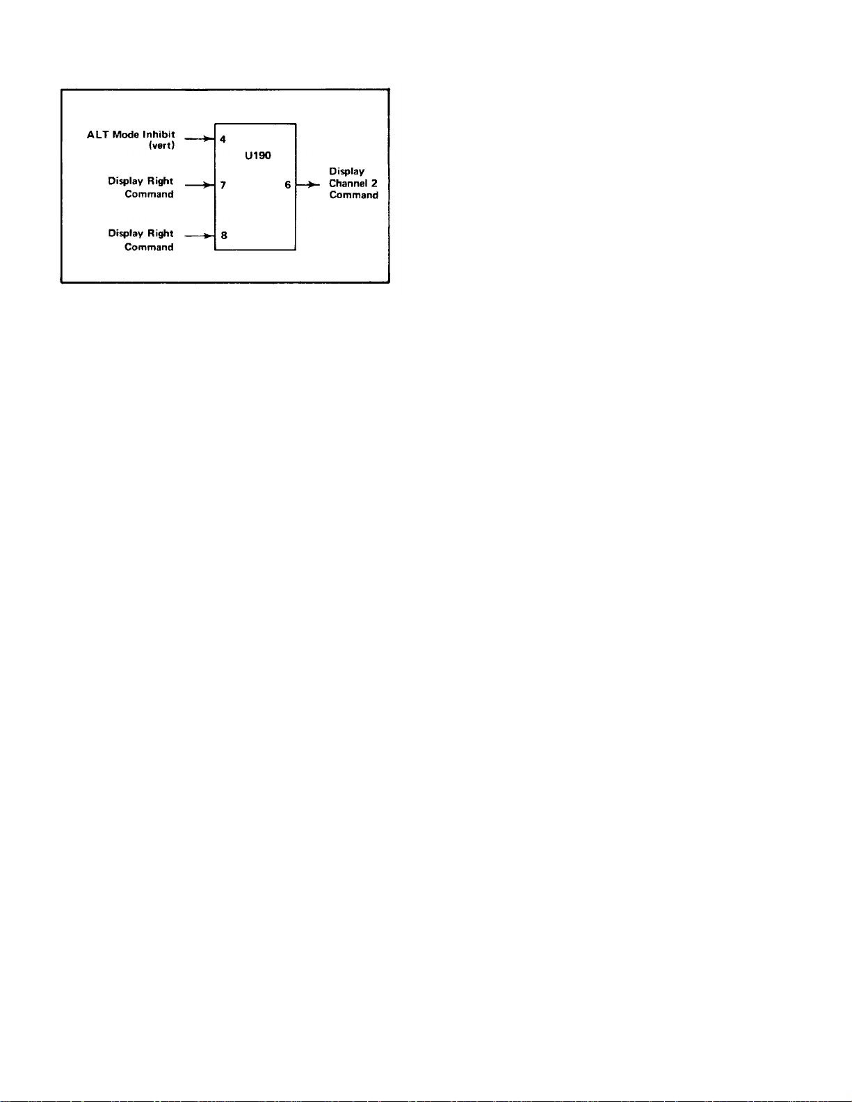
Fig. 3-13. Input and output pins for Plug-In Binary stage
Fig. 3-13. Input and output pins for Plug-In Binary stage.
Circuit Description-R7704
of A Time-Base unit. Notice that under these conditions,
both channels of the Left Vertical unit are displayed at
the B Sweep rate and that both channels of the Right
Vertical unit are displayed at the A Sweep rate. The
repetition rate at the output of this stage is one-half the
Display Right Command rate. Input conditions when the
VERTICAL MODE switch is set to ALT are:
Pin 4 LO-VERTICAL MODE switch set to ALT.
Pin 8 LO-Display Right Command generated by
Vertical Binary stage goes negative.
Fig. 3-14A shows a logic diagram of the Plug-In
Binary stage. An input/output table for this stage is
given in Fig. 3-14B.
Input conditions for a LO output level so that Channel 1
of the vertical plug-in can be displayed at the B Sweep
rate are:
Pin 4 HI-VERTICAL MODE switch set to any position
except ALT.
Pin 7 LO-B Sweep to be displayed (Display Right
Command and Display B Command HI).
The input conditions to provide a HI output level so
that Channel 2 of the plug-in can be displayed at the A
Sweep rate are:
Pin 4 HI-VERTICAL MODE switch set to any position
except ALT.
Pin 7 HI-A Sweep to be displayed (Display Right
Command and Display B Command LO).
The Display Channel 2 Command switches from HI
to LO as the Display B Command from the Horizontal
Binary stage switches from LO to HI, and vice versa.
When the VERTICAL MODE switch is set to ALT,
the Display Right Command from the Vertical Binary
stage switches the vertical display between the two
vertical units. However, if either or both of the vertical
plug-in units are dual-trace units, they can be operated in
the alternate mode also. To provide a switching
command to these units, the Plug-In Binary stage
produces an output signal with a repetition rate one-half
the repetition rate of the Display Right Command. The
sequence of operation when two dual-trace vertical units
are installed in the vertical plug-in compartments and
they are both set for alternate operation, is as follows
(VERTICAL MODE and HORIZONTAL MODE switches
set to ALT): 1) Channel 1 of Left Ver tical unit at sweep
rate of B Time-Bas e units, 2) Channel 1 of Right Ver tical
unit at sweep rate of A Time-Bas e unit, 3) Channel 2 of
Left Vertical unit at sweep rate of B Tim e-Base unit, 4)
Channel 2 of Right Vertical unit at sweep rate
3-20
3-20
Clock Generator
One half of integrated circuit U120 along with the
external components shown in Fig. 3-15A mak e up the
Clock Generator stage. R1, Q1, Q2, and Q3 represent
an equivalent circuit which is contained within U120A.
This circuit along with discrete com ponents C117-R116R117-R118 comprise a two-megahertz free-running
oscillator to provide a timing signal (clock) for vertical,
horizontal, and plug-in chopping.
The stage operates as follows: Assume that Q2 is
conducting and Q1 is off. The collector current of Q2
produces a voltage drop across R1 which holds Q1 off.
This negative level at the collector of Q2 is also
connected to pin 14 through Q3 (see waveforms in Fig.
3-15B at time T ). Since ther e is no current through Q1,
C117 begins to charge towards -15 volts through R116R117. The emitter of Q1 goes negative as C117
charges until it reaches a level about 0.6 volt more
negative than the level at its base. Then, Q1 is forward
biased and its emitter rapidly rises positive ( see time T,
on waveforms). Since C117 cannot change its charge
instantaneously, the sudden change in voltage at the
emitter of Q1 pulls the emitter of Q2 positive also, to
reverse-bias it. With Q2 reverse biased, its collector
rises positive to produce a positive output level at pin 14.
Now, conditions are reversed. Since Q2 is reverse
biased, there is no current through it. Theref ore, C117
can begin to discharge through R118. T he emitter level
of Q2 follows the discharge of C117 until it reaches a
level about 0.6 volt more negative than its base. Then,
Q2 is forward biased and its co llector drops negative to
reverse-bias Q1. The level at pin 14 drops negative
also, to complete the cycle. Once again, C117 begins to
charge through R116-R117 to start the second cycle.
Two outputs are provided from this oscillator. The
Delay Ramp signal from the junction of R1 16-R1 17 is
con-
(A)
Page 62

Circuit Description-R7704
Fig. 3-14. (A) Logic diagram for Plug-In Binary stage, (B) Table of input/output combinations for the Plug-In Binary stage
Fig. 3-14. (A) Logic diagram for Plug-In Binary stage, (B) Table of input/output combinations for the Plug-In Binary stage.
to the Vertical Chopped Blanking stage. T his signal has
the same waveshape as shown by the waveform at pin
13, with its slope determined by the divider ratio between
R116-R117. A square-wave output is provided at pin 14.
The frequency of this square wave is determ ined by the
overall RC relationship between C117-R116-R117-R118,
and its duty cycle is determined by the ratio of R 116-R
117 to R118.
The square wave at pin 14 is connected to pin 16
through C1 19. C119, along with the internal resistance
of U120A, differentiates the square wave at pin 14 to
produce a negative-going pulse coincident with the falling
edge of the square wave (positive-going pulse coinc ident
with rising edge has no effect on circuit operation). This
negative-going pulse is connected to pin 15 through an
inverter-shaper which is also part of U120A. The output
at pin 15 is a positive-going Clock pulse at a repetition
rate of about two megahertz.
(A)
Vertical Chopped Blanking
The Vertical Chopped Blanking s tage is made up of
the remaining half of integrated circuit U120. This stage
determines if Vertical Chopped Blanking pulses are
required based upon the operating mode of the vertical
system or the plug-in units (dual-trace units only).
Vertical Chopped Blanking pulses are produced if: 1)
VERTICAL MODE switch is set to CHOP; 2) Dual-trac e
vertical unit is operating in the chopped mode and that
unit is being displayed; 3) Dual-trace vertical unit is
operating in the chopped mode with the VERTICAL
MODE switch set to ADD. The repetition rate of the
negative-going Vertical Chopped Blanking pulse output
at pin 4 is two megahertz for all of the above conditions
as determined by the Clock Generator stage.
The Delay Ramp signal from the Clock Generator
stage determines the repetition rate and pulse width of
the Vertical Chopped Blanking pulses. T he Delay Ramp
applied to
3-21
3-21
Page 63

Circuit Description-R7704
Fig. 3-15. (A) Diagram of Clock Generator stage, (B) Idealized waveforms for Clock Generator stage.
Fig. 3-15. (A) Diagram of Clock Generator stage, (B) Idealized waveforms for Clock Generator stage.
Fig. 3-16. (A) Input and output pins for Vertical Chopped Blanking stage, (B) Idealized waveforms for Vertical Chopped
Fig. 3-16. (A) Input and output pins for Vertical Chopped Blanking stage, (B) Idealized waveforms for Vertical Chopped
Blanking stage.
Blanking stage.
pin 10 starts to go negative from a level of about +1.1
volts coincident with the leading edge of the Clock pulse
(see waveforms in Fig. 3-16B). This results in a HI
quiescent condition for the Vertical Chopped Blanking
pulse. The slope of the negative-going Delay Ramp is
determined by the Clock Generator stage. As it reaches
a level slightly negative from ground, the Vertical
Chopped Blanking pulse
output level changes to the LO state. This signal
remains LO until the Delay Ramp goes HI again. Notic e
the delay between the leading edge of the Clock pulse
generated by U120A and the leading edge of the Vertical
Chopped Blanking pulses (see Fig. 3-16B). The amount
of delay between the leading edges of these pulses is
determined by the slope of the Delay Ramp applied to
pin 10. This delay is
3-22
3-22
(A)
Page 64

necessary due to the delay line in the vertical deflection
system. Otherwise, the trace blank ing resulting from the
Vertical Chopped Blanking pulse would not c oincide with
the switching between the displayed traces. The duty
cycle of the square wave produced in the Clock
Generator stage determines the pulse width of the
Vertical Chopped Blanking pulses (see Clock Generator
discussion for more information).
Whenever this instrument is turned on, Vertical
Chopped Blanking pulses are being produced at a twomegahertz rate. However, these pulses are available as
an output at pin 4 only when the remaining inputs to U
120B are at the correct levels. The following discuss ions
give the operating conditions which produce Vertical
Chopped Blanking pulses to blank the CRT during
vertical chopping. Fig. 3-16A identifies the function of
the pins of U120B.
1. CHOP VERTICAL MODE
When the VERT ICAL MODE switch is set to CHOP,
Vertical Chopped Blanking pulses are available at pin 4
at all times. The input conditions necessary are:
Pin 3 HI-VERTICAL MODE switch set to CHOP.
Pin 7 LO-VERTICAL MODE switch set to any
position except ADD.
Pin 10 LO-Delay Ramp more negative than about
zero volts.
Circuit Description-R7704
Notice that the Display Right Command at pin 6 must
be LO for output pulses to be available at pin 4. This
means that when the VERTICAL MODE s witch is set to
ALT, Vertical Chopped Blanking puls es will be produced
only during the time that the Left Vertical unit is to be
displayed (unless Right Vertical unit is also set for
chopped operation).
3. RIGHT VERTICAL UNIT SET FOR CHOPPED
OPERATION
If the Right Vertical unit is set for the chopped m ode,
operation is the same as described above for the Left
Vertical unit except that Vertical Chopped Blanking
pulses are produced when the VERTICAL MODE s witch
is set to RIGHT or when the Display Right Command is
HI in the ALT mode. The input conditions are: Pin 3 LOVERTICAL MODE switch set to any position except
CHOP.
Pin 6 HI-Right Vertical unit to be displayed (Dis play
Right Command HI).
Pin 7 LO-VERTICAL MODE switch set to any
position except ADD.
Pin 8 LO-Right Vertical unit set to chopped mode.
Pin 10 LO-Delay Ramp more negative than about
zero volts.
4. ADD VERTICAL MODE
2. LEFT VERTICAL UNIT SET FOR CHOPPED MODE
If the Left Vertical unit is set for chopped operation,
the setting of the VERTICAL MODE switch determines
whether Vertical Chopped Blanking pulses are available.
If the VERTICAL MODE switch is set to the CHOP
position, conditions are as described in No. 1 above.
Operation in the ADD position of the VERTICAL MO DE
switch is given later. For the LEFT position of the
VERTICAL MODE switch or when the Left Vertical unit is
to be displayed in the ALT mode, Vertical Chopped
Blanking pulses are available at all times (two-megahertz
rate). The input conditions are:
Pin 3 LO-VERTICAL MODE switch set to any
position except CHOP.
Pin 5 LO-Left Vertical unit set to chopped mode.
Pin 6 LO-Left Vertical unit to be displayed (Display
Right Command LO).
Pin 7 LO-VERTICAL MODE switch set to any
position except ADD.
Pin 10 LO-Delay Ramp more negative than about
zero volts.
When the VERTICAL MODE switch is in the ADD
position and either or both of the vertical units are
operating in the chopped mode, Vertical Chopped
Blanking pulses must be available to block out the
transition between the traces of the vertical units. The
input conditions are: Pin 3 LO-VERTICAL MODE s witch
set to any position except CHOP.
Pin 5 LO-Left Vertical unit set to chopped m ode (c an
be HI if pin 8 is LO).
Pin 7 HI-VERTICAL MODE switch set to ADD.
Pin 8 LO-Right Vertical unit set to chopped mode
(can be HI if pin 5 is LO).
Pin 10 LO-Delay Ramp more negative than about
zero volts.
Fig. 3-17A shows a logic diagram of the Vertical
Chopped Blanking stage. Notice the comparator block
on this diagram (one input connected to pin 10). The
output of this comparator is determined by the
relationship between the levels at its inputs. If pin 10 is
more positive (HI)
(A) 3-23
3-23
Page 65

Circuit Description-R7704
Fig. 3-17. (A) Logic diagram for Vertical Chopped Blanking stage, (8) Table of input/loutput combinations for Vertical
Fig. 3-17. (A) Logic diagram for Vertical Chopped Blanking stage, (8) Table of input/loutput combinations for Vertical
Chopped Blanking stage
Chopped Blanking stage.
than the grounded input, the output is HI also; if it is
more negative (LO), the output is LO. An input/output
table for this stage is given in Fig. 3-17B.
Chop Counter
The Chop Counter stage produces the Vertical
Chopping Signal, the Plug-In Chop Command, and the
Horizontal Chopped Blanking signal. The Clock pulse
produced by the Clock Generator stage provides the
timing signal for this stage. The functions of the input
and output pins for the
Chop Counter stage are identified in Fig. 3-18A.
Idealized waveforms showing the timing relationship
between the input and output signals for this stage are
shown in Fig.3-18B.
The repetition rate of the output signals from this
stage is determined by the setting of the HORIZONTAL
MODE switch. When the HORIZONTAL MODE switch is
set to any position except CHOP, the repetition rate of
the Vertical Chopping Signal output at pin 1 is one
megahertz (onehalf Clock rate). This determines the
switching between the
3-24
3-24
(A)
Page 66

Circuit Description-R7704
Fig. 3-18. (A) Input and output pins for Chop Counter stage, (B) Idealized waveforms for Chop Counter stage.
Fig. 3-18. (A) Input and output pins for Chop Counter stage, (B) Idealized waveforms for Chop Counter stage.
Left and Right Vertical units when the VERT ICAL MODE
switch is set to CHOP. At the same time, the repetition
rate of the Plug-In Chop Command at pin 8 is 0.5
megahertz (one-fourth Clock rate). This provides a
chopping signal to dual-trace vertical units to provide
switching between the two channels. The relationship
between these output signals and the Clock input is
shown by the waveforms in Fig. 3-18B in the area
between To and T, . During this time, the level at pin 4
remains HI.
When the HORIZONTAL MODE switch is set to
CHOP, the basic repetition rate of the Vertical Chopping
Signal and the Plug-In Chop Command is altered. For
example, if the HORIZONT AL MODE switch is changed
to the CHOP position at time T, (s ee Fig. 3-18B), a HI
level is applied to pin 6. This stage continues to produce
outputs at pins 1 and 8 in the normal manner until both
outputs are at their HI level (see tim e T2; this condition
only occurs once every fifth Clock pulse when the
HORIZONTAL MODE switch is set to CHOP). When
both of these outputs are at their HI level, the next Clock
pulse switches both outputs LO and at the same time
switches the Horizontal Chopped Blanking to the LO
level. However, this change does not appear at pin 4
immediately due to a delay network in the circuit. The
delay is necessary so the Horizontal Chopped Blanking
coincides with the Vertical Chopped Blanking produced
by
(A)
3-25
U120A and the switching between the displayed signals
(compare bottom two waveform s of Fig. 3-18B; also see
Vertical Chopped Blanking for f urther inf ormation). After
the delay time, the output level at pin 4 goes LO where it
remains for about 0.5 m icrosecond which is equal to the
period of the Clock pulse (two megahertz repetition rate).
The Horizontal Chopped Blanking time must be longer
than the Vertical Chopped Blanking time since it takes
more time for the display to switch between horizontal
units than between vertical units. During the time that
the level at pin 4 is LO, the CRT is blanked and the
Vertical Chopping Signal and the Plug-in Chop
Command cannot change levels. The Cloc k pulse at T 3
changes only the Horizontal Chopped Blanking output at
pin 4. The level on this pin goes HI after the delay tim e
to unblank the CRT.
For the next three trigger pulses, the Vertical
Chopping Signal output and Plug-In Chop Command
operate in the normal manner. However, j ust prior to the
fourth clock pulse (time T4 ) both outputs are again at
their HI level. The fourth Clock pulse at T4 switches the
output at pin 1, pin 8, and pin 4 (after delay) to the LO
level to start the next cycle. Notice that a Horizontal
Chopped Blanking pulse is produced at pin 4 with every
fifth Clock pulse. Als o notice that with the HO RIZO NT AL
MODE switch set to CHOP, two complete cycles of the
Vertical Chopping Signal are produced with each five
Clock pulses (repetition rate two
3-25
Page 67

Circuit Description-R7704
fifths Clock rate) and one com plete cycle of the Plug-In
Chop Command for every five Clock pulses (one fifth
Clock rate). Notice that the large shaded area produced
by the Horizontal Chopped Blanking pulse (see Fig. 318B) is not part of the display time (CRT display
blanked). However, about the same time segment is
displayed from the vertical signal s ource with or without
Horizontal Chopped Blanking due to the change in
repetition rate when in the CHOP horizontal mode.
The Vertical Chopping Signal at pin 1 of U130 is
connected to the Vertical Mode Logic stage (see
following description) through L138-R138. This signal is
HI when the Right Vertical unit is to be displayed and it is
LO when the Left Vertical unit is to be displayed. The
Plug-In Chop Command at pin 8 is connected to the
plug-in units in the vertical com partments through L136R136 via the Main Interface board. When this signal is
HI, Channel 2 of the plug-in units can be displayed and
when this level is LO, Channel 1 can be displayed. The
Horizontal Chopped Blanking signal at pin 4 is connected
through LR134 to the Horizontal Binary stage U150, and
to the Z-Axis Logic stage U170 by way of Q146. W hen
this signal is HI, the CRT is unblanked to display the
selected signal. W hen it is LO, the CRT is blanked to
allow switching between the time-base units.
A logic diagram of the Chop Counter stage is shown
in Fig. 3-19. Details of operation for the flip-flops (FF)
are shown in Table 3-1 at the front of this section. Use
the waveforms given in Fig. 3-18B along with this
diagram.
Vertical Mode Logic
The Vertical Mode Logic stage is made up of
discrete components CR128-CR139, CR183-CR184,
and Q194-0196. These components develop the
Vertical Mode Command which is connected to the Main
Interface circuit (vertical plug-in compartments and
trigger selection circuitry) and the Vertical Interface
circuit to indicate which vertical unit is to be displayed.
When this output level is HI, the Right Vertical unit is
displayed and when it is LO, the Left Vertical unit is
displayed.
The VERTICAL MODE switch located on diagram 12
provides control levels to this stage. This switch
provides a HI level on only one of five output lines to
indicate the selected vertical mode; the remaining lines
are LO (notice that only four of the lines from the
VERTICAL MODE switch are used on this schematic).
Operation of this stage is as follows:
When the VERTICAL MODE s witch is set to RIGHT ,
a HI level is connected to the base of Q194 through
R127. This forward biases Q194 and the positive-going
level at its emitter is connected to the emitter of Q196.
The collector of Q196 goes HI to indicate that the Right
Vertical unit is to be displayed. For the CHOP position of
the VERTICAL MODE switch, a HI level is applied to the
anodes of CR128-CR139 through R128. Both diodes
are forward biased so that the Vertical Chopping Signal
from pin 1 of U130 can pas s to the base of Q194. T his
signal switches between the HI and LO levels at a onemegahertz rate and it produces a corres ponding Vertical
Mode Command output
Fig. 3-19. Logic diagram of Chop Counter stage.
Fig. 3-19. Logic diagram of Chop Counter stage
3-26
3-26
(A)
Page 68

Circuit Description-R7704
at the collector of Q196. When the output is HI, the
Right Vertical unit is displayed and when it switches to
LO, the Left Vertical unit is displayed.
In the ALT position of the VERT ICAL MODE switch,
a HI level is applied to the anodes of CR183-CR184
through R 183. These diodes are forward biased so the
Display Right Command from pin 6 of the Vertical Binar y
stage can pass to the base of Q194 to determine the
Vertical Mode Command level. The Display Right
Command switches between its HI and LO levels at a
rate determined by the Vertical Binary stage.
The control levels in the LEFT and ADD positions of
the VERTICAL MODE switch are not connected to this
stage. However, since only the line corresponding to the
selected vertical mode can be HI, the RIGHT, CHOP,
and ALT lines must rem ain at their LO level when either
LEFT or ADD are selected. Ther ef or e, the base of Q194
remains LO to produce a LO Vertical Mode Control
output level at the collector of Q196.
A logic diagram of the Vertical Mode Logic stage is
shown in Fig. 3-20. The discrete components which
make up each logic function are identified.
TRIGGER SELECTOR
General
The Trigger Selector circuit determines the trigger
signal which is connected to the A and B time-base units
as controlled by the A TRIGGER SOURCE and B
TRIGGER
SOURCE switches. This circuit also provides the drive
signal for the Vertical Signal Am plif ier s tage as c ontrolled
by the B TRIGGER SOURCE switch. Fig. 3-21 shows a
detailed block diagram of the Trigger Selector circuit
along with a simplified diagram of all the circuitry
involved in selection of the trigger s ource. A schem atic
of the Trigger Selector cir cuit is shown on diagram 3 at
the rear of this manual. Also see diagram s 1 and 12 for
the trigger selection circuitry not shown on diagram 3.
Trigger Mode and ADD Signals
General. The circuitry shown on the left side of the
simplified diagram in Fig. 3-21 determines the operation
of the A and B Trigger Channel Switch stages. The A
TRIGGER SOURCE switch S1011 controls the A Trigger
Channel Switch U304 through Q24; the B TRIGGER
SOURCE switch S1001 controls the B Trigger Channel
Switch U324 through Q28. W hen the front-panel A or B
TRIGGER SOURCE switches are set to the VERT
MODE positions, the setting of the VERTICAL MODE
switch determines the trigger selection. In the LEFT
VERT or RIGHT VERT positions, the trigger signal is
obtained from the indicated vertical unit. The following
discussions give detailed operation in each position of
the A and B TRIGGER SOURCE switches. It is written
assuming that both of these switches are set to the same
position. However, the A and B TRIGGER SOURCE
switches can be operated independently to control the
operation of the A and B Trigger Channel Switch stages,
respectively, and select the trigger output signal for the
associated time-base unit.
VERT MODE. In the VERT MODE position of either
the A or B TRIGGER SOURCE switch, the setting of the
VERTICAL MODE switch determines the operation of
the
(A)
Fig. 3-20. Logic diagram of Vertical Mode Logic stage.
Fig. 3-20. Logic diagram of Vertical Mode Logic stage.
3-27
3-27
Page 69

Circuit Description-R7704
Fig. 3-21. Simplified schematic of trigger selector circuitry.
Fig. 3-21. Simplified schematic of trigger selector circuitry.
3-28
3-28
(A)
Page 70

Circuit Description-R7704
A and B Trigger Channel Switch stages (A TRIGGER
SOURCE, B TRIGGER SOURCE, and VERTICAL
MODE switches shown on diagram 12). In the LEFT
position of the VERTICAL MODE switch, the base of
Q24 or Q28 (see Main Interface schematic) is connected
to ground through the ALT and RIGHT sections of
S1021, CR1022 and CR1027, and S1001 or S1011.
This holds Q24 or Q28 reverse biased to provide a LO
level to pin 4 of U304 or U324 (see Fig. 3-22).
When the VERT ICAL MO DE s witch is s et to ALT, +5
volts is applied to the base of Q24 or Q28 through CR
1022 and S1001 or S1011. Q24 and Q28 are forward
biased and their emitter level is determined by the
Vertical Mode Command from the Logic Circuit applied
to their collectors. This signal switches between the HI
level (Right Vertical unit to be displayed) and the LO level
(Left Vertical unit to be displayed) at the end of each
sweep. When the Vertical Mode Command is HI, it
provides a positive collector voltage to Q24 and Q28.
Q24 and Q28 are saturated due to CR 1022, and their
emitter levels are very near the collector level. This
provides a HI output level to the Trigger Channel Switch
stages. As the Vertical Mode Signal goes LO, the
collector supply for Q24 and Q28 also goes negative.
Q24 and Q28 remain saturated and the output again
follows the collector level to supply a LO output level to
U304 and U324.
1
Pin 14 LO for all other conditions.
Fig. 3-22. Input levels at pin 4 of U304 and U324
Fig. 3-22. Input levels at pin 4 of U304 and U324
(source of triggering signal is shown in parenthesis).
(source of triggering signal is shown in parenthesis).
For ADD and CHOP vertical mode operation, +5
volts is connected to pin 14 of U304 or U324 through
CR1021 or CR1023 and S1001 or S1011. At the same
time, the base of Q24 or Q28 is held LO by the ground
connection through the ALT and RIGHT sections of
S1021 so the level at pin 4 of the Trigger Channel Switch
stages is LO also (produces an ADD mode in Trigger
Channel Switches; see description of these circuits
which follows). In the RIGHT position of the VERTICAL
MODE switch, +5 volts is connected to the bases of Q24
or Q28 through CR1027 and S1001 or S1011 to forward
bias these transistors. The Vertical Mode Command
connected to the collectors of Q24 and Q28 is also HI in
this mode and a HI output level is produced at the
emitters of Q24 or Q28.
LEFT VERT. When the LEFT VERT trigger source
is selected, the VERTICAL MODE switch is
disconnected from the trigger selec tor cir cuitr y. Now, the
ground connection through the RIGHT VERT s ection of
S1001 or S1011 establishes a LO output level at the
emitters of Q24 and Q28.
RIGHT VERT. In the RIGHT VERT position of the A
or B TRIGGER SOURCE switches, +5 volts is connected
to the emitters of Q24 or Q28 through S1011-R23 or
S1001-R27. This produces a Hl output level to the A and
B Trigger Channel Switch stages.
A and B Trigger Channel Switch
The A and B Trigger Channel Switch stages
determine which input signal provides the trigger signal
to the time base units as controlled by the trigger mode
and ADD signals from the trigger selection circuitry.
Resistors R301R321 and R302-R322 (refer to diagram
3) establish the input resistance of this s tage and provide
a load for the trigger output of the Left and Right Vertic al
plug-in units. Resistors R303-R304-R305 and R307R308-R309 establish the operating levels for the A
Trigger Channel Switch; R303-R305 and R307-R309 set
the current gain for each channel. Resistors R323R324-R325 and R327-R328-R329 establish the
operating levels for the B Tr igger Channel Switch; R323R325 and R327-R329 set the current gain for each
channel. These stages are made up primarily of
integrated circuits U304 and U324. An input/output table
for U304 and U324 is shown in Fig. 3-23. U304-U324
provide a high impedance diff erential input for the trigger
signal from the Left Vertical unit at pins 2 and 15 and for
the trigger signal from the Right Vertical unit at pins 7
and 10. The output signal at pins 12 and 13 is a
differential signal. The sum of the DC cur rent at pins 12
and 13 is always equal to the sum of the DC c urrents at
pins 1, 8, 9, and 16 in all modes. This provides a
constant DC bias to the stages which follow as the A or B
TRIGGER SOURCE switches or the VERTICAL MODE
switch are changed.
When the level at pin 4 is LO (s ee T rigger Mode and
ADD Signals discussion and Fig. 3-23), the trigger signal
3-29
3-29
(A)
Page 71

Fig. 3-23. Input/output table for A and B Trigger
Channel Switch stages.
from the Left Vertical unit passes to the output while the
trigger signal from the Right Vertical unit is blocked. A HI
level at pin 4 connects the trigger signal from the Right
Vertical unit to the output and the trigger signal from the
Left Vertical unit is blocked. For VERT MO DE operation
in the ALT position of the VERTICAL MODE switch, the
level at pin 4 switches between the LO and HI level at a
rate determined by the Vertical Binary stage (see Logic
Circuit description). This action obtains the tr igger s ignal
from the Left Vertical unit when the Left Vertical unit is
being displayed and from the Right Vertical unit when it
is being displayed.
When the level at pin 4 is LO and the level at pin 14
is HI, the trigger signal from both the Left and Right
Vertical units passes to the output pins. T his condition
occurs only when the A or B TRIGGER SOURCE
switches are set to VERT MODE and the VERTICAL
MODE switch is set to either ADD or CHOP. Under this
operating mode, the trigger output signal is the algebraic
sum of the trigger input signals from the Left and Right
Vertical units to prevent triggering on the vertical
chopping transition or only on one signal of an added
display.
A Trigger Output Amplifier
The trigger output signal at pins 12 and 13 of the A
Trigger Channel Switch is connected to the emitters of
common-base amplifier Q314-Q316 through R311-R312.
These transistors provide a low-resistance load f or the A
Trigger Channel Switch while providing a high output
impedance to the circuits which f ollow. The signal at the
collectors of Q314 and Q316 is connected to the A
Horizontal unit via the Main Interface circuit. The A
Horizontal unit
provides a 50-ohm differ ential load for this stage. If it is
removed from its compartment, the voltage-swing at the
collectors of Q314-Q316will increase substantially.
Vertical Signal Buffer Amplifier
The trigger output signal at pins 12 and 13 of the B
Trigger Channel Switch is connected to the emitters of
common-base amplifier Q334-Q336. The output signal
at the collectors of Q334 and 0336 is connected to the
Vertical Signal Amplifier (see Output Signals description)
through R337 and R338. R339 provides a differential
output resistance of about 100 ohms.
B Trigger Output Amplifier
The signal at pins 12 and 13 of the B Trigger
Channel Switch is also connected to the bases of Q 344Q346 to provide the internal trigger signal for the B
Horizontal unit (via the Main Interface circuit). This stage
provides isolation between the B Horizontal unit and the
Vertical Signal Buffer Am plifier stage. The B Horizontal
unit provides a 50-ohm differential load for this stage. If
it is removed from its com partm ent, the collector load for
0344-Q346 changes and the voltage swing at their
collectors increases. The action of this stage prevents
this change from affecting the Vertical Signal Buffer
Amplifier stage. CR342-CR346 clam p the collectors of
Q344 and Q346 at about +0.6 volts to prevent these
transistors from saturating under this no load condition.
VERTICAL INTERFACE
General
The Vertical Interface circuit selects the vertical
deflection signal from the output of the Left Vertical
and/or the Right Vertical plug-in unit. This stage also
accepts an input from the Readout System to block the
vertical signal while readout information is displayed on
the CRT. In addition, this stage contains the Trace
Separation Circuit to shift the vertical position of the BSweep portion of a dual-sweep display. Fig. 3-24 shows
a detailed block diagram of the Vertical Interface c ircuit.
A schematic of this circuit is shown on diagram 4 at the
rear of this manual.
Vertical Switching
Transistors Q202-0206 and Q212-Q216 form
differential amplifier s which determine if the signal from
the left vertical plug-in or the right vertical plug-in, or
both, provides the vertical deflection s ignal to the Ver tic al
Amplifier. T ransistor Q218 provides a constant voltage
source of about -8.7 volts for the collector circuits of
Q202-Q206 and Q212-Q216. The operation of this
stage is controlled by the Vertical Mode Command, the
ADD Mode signal, and the Vertical Channel Switch OFF
Command. Fig. 3-25 shows an input/output table for the
overall Vertical Interface circ uit to show the output signal
for the applicable input conditions.
3-30 (A)
Page 72

Circuit Description-R7704
Fig. 3-24. Vertical Interface detailed block diagram.
Fig. 3-25. Input/output table for Vertical Interface circuit.
When the VERTICAL MODE s witch is set to LEFT,
the Vertical Mode Comm and is LO. T his level allows the
bases of Q202 and Q212 to go negative so that these
transistors are forward biased. The resulting positivegoing change at the collectors of Q202 and 0212
produce different results for the Left and Right Vertical
Preamplifier stages. The positive-going signal at the
collector of Q212 is connec ted to the bases of the series
transistors Q278-0288 in the Left Vertical Preamplifier
stage through R212. At the same time, the other
transistor in this differential amplifier, Q216, is reverse
biased. The negative level at its collector reduces the
conduction of Q279 to reverse bias s hunt diodes CR279CR289. As a result, the signal from the Left Vertical
plug-in can pass to the Delay-Line Driver stage. The
positive-going change at the collector of Q202 forward
biases transistor Q249 and shunt diodes CR249-CR259
in the Right Vertical Preamplifier s tage. Q206 is reverse
biased and the negative level at its collector holds series
transistors Q248-Q258 reverse biased to bloc k the s ignal
from the Right Vertical plug-in. Instead, the signal is
shunted through CR249-CR259 and Q249 to the junction
of R262-R292. This arrangement provides a constant
DC current to the Delay-Line Driver stage as the
VERTICAL MODE switch is changed by providing a
signal current
(A) 3-31
Page 73

either through the applicable series transistors or an
equivalent DC current through the shunt diodes via
R262-R292.
In the RIGHT position of the VERTICAL MODE
switch, the Vertical Mode Comm and is HI. Now, diodes
CR200 and CR209 are forward biased and the positive
signal at the base of Q202-0212 reverse biases these
transistors. The previous conditions are now reversed.
The collector of Q212 is negative so that series
transistors 0278-Q288 are reverse bias ed. At the same
time Q216 is forward biased to hold Q279 and the shunt
diodes CR279-CR289 forward biased also. This ac tion
blocks the signal from the Lef t Vertical plug-in unit. On
the Right Vertical side of the circuit, the negative level at
the collector of Q202 reduces the conduction of Q249 to
reverse bias shunt diodes CR249-CR259. T he positive
level at the collector of Q206 forward biases series
transistors Q248-Q258 to allow the signal fr om the Right
Vertical plug-in unit to pass to the Delay-Line Driver
stage.
For either the ALT or CHOP position of the
VERTICAL MODE switch, the Vertical Mode Command
switches between the LO and HI levels at a rate
determined by either the Chop Counter or the Vertical
Binary stages (see Logic Circuit description). This action
allows the signal from the Left Vertical unit to be
displayed when the Vertical Mode Command is LO and
the signal from the Right Vertic al unit is displayed when
the Vertical Mode Command is HI.
When ADD vertic al mode operation is s elected, a HI
Vertical Mode Command level is applied to the base of
Q202 through R200. The level at the collector of Q202
goes negative to reverse bias the Right Vertical shunt
diodes and the positive level at the collector of Q206
forward biases the series transistors to allow the Right
Vertical signal to pass to the Delay-Line Driver stage. At
the same time, the Ver tical Mode Com mand level is LO
as determined by the Vertical Mode Control stage in the
Logic Circuit. This allows Q212 to conduct to forward
bias the Left Vertical series trans istors; the shunt diodes
are reverse biased by the negative level at the collector
of Q216. Therefore, the signal from the Left Vertical
plug-in unit can pass to the Delay-Line Driver stage.
Now, the signal from both vertical units is algebraically
added by the Delay-Line Driver stage and the resultant
signal determines the vertical deflection.
The Vertical Channel Switch OFF Command from
the Readout System has final control over the output
signal from this s tage. Quies cently, this signal is LO and
the signal from the selected vertical unit can pass to the
Delay-Line Driver stage. However, when the Readout
System is ready to display readout information, the
Vertical Channel Switch OFF Command goes HI.
Transistor Q212 is reverse biased through CR210 and
Q206 is reverse biased through R208. This reverse
biases the series transistors Q248-Q258
Circuit Description-R7704
and Q278-Q288 to block the signal from both vertical
units. At the same time the r emaining transistor in eac h
differential amplifier is forward biased to shunt the
vertical signal. Therefore, the signal from neither plug-in
unit is displayed on the CRT so the CRT deflection can
be determined by the Readout System.
Left Vertical Preamplifier
The vertical signal from the Left Vertical plug-in unit is
connected to the Left Vertical Pream plifier stage by way
of the strip lines on the Vertical Interconnect board.
These strip lines provide an impedance of 50 ohms. The
applied signal is amplified by transistors Q274-Q284.
C274-C282-R274-R284 in the emitter circuit of Q274Q284 provide high-frequency compens ation; C274-R274
are variable to provide high-frequency response
adjustment for this stage. The Left Vertical Centering
adjustment R277 balances the quiescent DC levels at
the output of the Left Vertical Preamplif ier stage so the
trace from the Lef t Vertical unit is dis played at the center
of the CRT when the inputs to this stage are at the sam e
potential. Transistors Q278-Q288 oper ate along with the
Vertical Switching stage to determine if the Left Vertical
signal is displayed on the CRT.
Right Vertical Preamplifier
The components in the Right Vertical Pream plifier stage
serve the same function as the corresponding
components in the Left Vertical Pream plifier stage. The
only difference between the two circuits is the presence
of the Right Vertical Gain adjustment, R242, in this
circuit. The overall gain of the Vertical Amplifier circuit is
set when the Left Vertical signal is displayed. The Right
Vertical Gain adjustment compensates for any
differences in gain between the Right Vertical
Preamplifier stage and the Left Vertical Preamplifier
stage. Gain is controlled by changing the emitter
degeneration between transistors Q244-Q254.
Trace Separation Circuit
The Trace Separation Circuit provides a variable
positioning voltage to offset the B Sweep display when
operated in either the ALT or CHOP dual-sweep modes
(horizontal). The display B Command from the Logic
Circuit controls the operation of this s tage through 0234.
When the B Sweep is being displayed (for ALT or CHOP
horizontal operation), the Display B Command is HI to
forward bias Q234. The collector of Q 234 goes negative
to reverse bias shunt diodes CR233-CR234. Under this
condition, the VERT TRACE SEPARATION (B) control
determines the bias at the base of transistors Q236Q238 through R230-R232 and the series diodes CR230CR232. The output current at the collectors of Q2360238 is connected to the Delay-Line Driver stage through
R261-R291 to offset the B Sweep display up to about
four divisions above or below the A Sweep display. This
prevents a confusing
3-32 (A)
Page 74

display when using dual-sweep operation, as the A and B
Sweeps would be displayed on top of each other without
this feature.
When the Display B Command is LO (A Sweep
displayed), Q234 is reverse biased and the shunt diodes
CR233-CR234 are forward biased through R233. This
applies a DC bias of about +5.1 volts to the bases of
transistors Q236-Q238 to provide a quies cent DC output
current from this stage to the Delay-Line Driver stage.
Since the series diodes CR230-CR232 are reverse
biased, the VERT TRACE SEPARATION (B) control is
disconnected while the A Sweep is being displayed.
Two other signals also control the current through
this stage. When the HORIZONT AL MODE switch is set
to B (only), a HI level is connected to the base of Q224
through CR224 and R224. This forward biases Q224
and, since Q224-Q234 share emitter resistor R227,
transistor Q234 is reverse biased even though the
Display B Command at its base is HI for this mode.
Therefore, the VERT T RACE SEPARATION (B) control
has no effect. The Vertical Channel Switch OFF
Command from the Readout System is connected to the
base of Q222 through R221. This s ignal is quiescently
LO so that Q222 is conducting through R222 to hold
Q224 reverse biased by way of R223 (except when
HORIZONTAL MODE switch is in B position described
above). When the Readout System is ready to display
readout information, the Vertical Channel Switch OFF
Command goes HI to rever se bias Q222. The base of
Q224 goes positive through R222-R223 and it is forward
biased. Now, Q224 controls conduction and Q234 is off
to disconnect the VERT TRACE SEPARATION (B)
control. The output of this stage goes to its quiescent
DC level so that the
Circuit Description-R7704
Readout System has full control of the trace position
(see Readout System description for more information).
Delay-Line Driver
Output of the Left Vertical Pream plifier and the Right
Vertical Preamplifier stages, along with any positioning
current from the Trace Separation Circuit is c onnec ted to
the bases of Q264-Q294. This stage provides
amplification for the selected signal as well as providing
a reverse termination for the delay line. Diodes CR264CR295 decrease the feedback resistance for Q264Q294 as the signal is deflected towards the edges of the
display area. This action reduces the gain of the stage to
compensate for the inherent expansion char acteristic of
the CRT. The output signal from the Delay-Line Driver
stage is connected to the Vertical Amplifier circuit
through C266-R266 and C296-R296.
VERTICAL AMPLIFIER
General
The Vertical Amplifier circuit provides the final
amplification for the vertical signal befor e it is applied to
the vertical deflection plates of the CRT. This circuit
includes the delay line and an input to produce the
vertical portion of a readout display. The BEAM FINDER
switch limits the dynamic range of this circuit to
compress an over-scanned display within the viewing
area of the CRT. Fig. 3-26 shows a detailed block
diagram of the Vertical Am plifier circuit. A schematic of
this circuit is shown on diagram 5 at the rear of this
manual.
Delay Line
Delay Line DL400 provides approximately 120
nanoseconds delay for the vertical signal to allow the
horizontal
Fig. 3-26. Vertical Amplifier detailed block diagram.
(A) 3-33
Page 75

circuits time to initiate a sweep before the vertical signal
reaches the vertical deflection plates of the CRT. This
allows the instrument to display the leading edge of the
signal originating the trigger pulse when using internal
triggering. The delay line used in this instrument has a
characteristic impedance of about 50 ohms per side, or
about 100 ohms differentially. It is of the coaxial type
which does not produce preshoot or phase distortion in the
CRT display.
Buffer Amplifier
The Buffer Amplif ier stage Q412-Q416 provides a low
input impedance for the Vertic al Amplifier circ uit to permit
accurate delay-line termination. C401-R401 and C408R408 provide the forward termination for the delay line.
The output signal from the Buffer Amplifier stage is
connected to the First Push-Pull Amplifier stage through
C411-R411-VR411 and C417-R417-VR417. Zener diodes
VR411 and VR417 limit the voltage swing across R411
and R417 to keep Q412 and Q416 out of saturation. R405
and the operating bias of Q412-Q416 provide
compensation for thermal distortion produced in Q470Q476.
For readout displays, the Y-signal from the Readout
System is connected to the emitter of Q412 through R402.
Since the signal from the vertical units is blocked in the
Vertical Interface circuit, the readout signal provides the
only vertical deflection. Although this signal is connec ted
to the emitter of Q412 as a single-ended signal, it is
converted to a push-pull signal in the following stages.
First Push-Pull Amplifier
Q434-Q442 and Q436-Q444 are connected as a
pushpull cascode amplifier stage. The network C426L421L422-L423-R420-R421-R422-R423-R424-R425R426 provides compensation for the delay line. R421R422-R423 in this network are adjustable to provide midfrequency compensation. C430-R430, connected
between the emitters of Q434-Q436, provide highfrequency compensation adjustment for this stage. The
network CR431-CR432-RT433 provides thermal
compensation for this stage. As the temperature
increases, the resistance of RT433 decreases and the
capacitance of varactors CR431-CR432 increases. The
output signals at the collectors of Q434-Q436 are
connected to the common-base transistors Q442-Q444
through C435-R435-R436 and C438-R437-R438. The low
input resistance of the Q442-Q444 common-base
transistors allows this stage to provide maximum highfrequency performance. The Vertical Centering
adjustment R443 balances the quiesc ent DC levels in the
Vertical Amplifier circuit so the trace is displayed at the
center of the CRT when the inputs to this circuit are at the
same potential. The output signal from the First Pus h-Pull
Amplifier stage is connected to the next stage through
C447-L447 and C448-L448. Zener diode VR449
establishes a collector source voltage of about -6.2 volts
for Q442-Q444.
Circuit Description-R7704
Second Push-Pull Amplifier
The Second Push-Pull Amplifier, Q454-Q466 and
Q456-Q468, operates in the same manner as the previous
stage. The main difference between the stages is the
compensation networks and the BEAM FINDER switch
located in this circuit. C458-R458 in the emitter circuit of
Q454-Q456 provide adjustable high-frequency
compensation for this stage.
BEAM FINDER switch S455A switches the emitter
current source for Q454-Q 456 to provide the beam finder
function. Normally, the emitter c urrent for Q454-Q456 is
supplied through S455A-L452. However, when S455A is
pressed in, the current source thr ough L452 is interrupted
and the only emitter-current source for Q454-Q456 is
through R451. This limits the dynamic range of this stage
by limiting its current, so the display is compressed
vertically within the graticule area. The BEAM FINDER
switch can also be pulled out to lock it in the "find" position
to aid in locating the traces of several plug-in units.
The signal at the collectors of Q454-Q456 is
connected to common-base transistors Q466-Q468
through C460-R460-R461-R462 and C465-R463-R464R465. Transformer T466 reduces the common-mode
signal components in the push-pull signal applied to the
following stages. The output signal from this stage at the
collectors of Q466-Q468 is connected to the Output PushPull Amplifier through VR467-VR469 and LC networks
C470-L470 and C471-L471. VR467-VR469 provide DC
voltage matching without appreciable current loss. Vertical
Gain adjustment R468 sets the resistance between the
bases of 0470-Q476 in the following stage to control the
current gain of this stage. T his adj us tment sets the overall
gain of the Vertical Amplifier stage.
Output Push-Pull Amplifier
Q470-Q480 and Q476-Q482 operate in the same
manner as the previous st ages to provide amplif ication for
the vertical deflection signal. T he output signal from this
stage provides the vertical deflection on the CRT. C472
and thermistor RT472 provide f requency compensation to
maintain high-frequency response with temperature
changes. Thermistor RT480 and R480 provide gain
compensation with changes in temperature. The output
signal is connected to the vertical deflection plates of the
CRT through buffer transistors Q480-Q482. A distributed
deflection plate system is used in this instrument for
maximum frequency response and sensitivity. T he output
signal at the collectors of Q480-Q482 is c onnected to the
integral inductors in the CRT and then to the deflectionplate termination network C483-L481-L483-R483-R485
and C484-L482-L484-R484R487. As the signal passes
through the integral inductors in the CRT, its velocity is
essentially the same as the velocity of the electron beam
passing between the vertical deflection plates. The
synchronism of the deflection signal and the
3-34 (A)
Page 76

Circuit Description-R7704
electron beam reduces the loss in high-frequency
sensitivity due to electron transit time through the
deflection plates. Inductors L483-L484 and capacitors
C483-C484 are adjusted to minimize signal reflections by
providing the correct termination for the vertical
deflection plate structure.
HORIZONTAL INTERFACE
General
The Horizontal Interface circuit is made up of the X-Y
Delay Compensation Network and the Horizontal
Channel Switch stage. The X-Y Delay Compensation
Network (optional) provides a delay for the horizontal (X)
portion of an X-Y display to match the delay of the
vertical (Y) signal due to the Delay Line. The Horizontal
Channel Switch portion of the circuit selects the
horizontal deflection signal from the output of the A
Horizontal and/or the B Horizontal plug-in unit. Fig. 3-27
shows a detailed block diagram of this circuit. A
schematic of this circuit is shown on diagram 6 at the
rear of this manual.
X-Y Delay Compensation
Time-Base Operation. When the plug-in unit
installed in the A or B horizontal compartment is
operated as a standard time-base unit to produce a
horizontal sweep for deflection of the CRT beam, the A
or B Delay Compensation Networks are effectively
disabled. The X Compensation Inhibit command is HI
and relays K50-K60 or K70-K80 are not actuated.
Therefore, the relay contacts remain in the normally
closed position so the horizontal signal passes directly
through this network to the Horizontal Channel Switch
without delay.
X-Y Operation. If the tim e-base unit installed in the
A or B horizontal compartment is operated as an
amplifier or if a vertical unit is installed in a horizontal
compartment, the X-Compensation Inhibit command to
the applicable Delay Compensation Network drops to the
LO level (zero volts). This provides an actuating level to
relays K50-K60 or K70-K80 to connect the Delay
Compensation Network into the circ uit. For example, if
the X-Compensation Inhibit command from the A
Horizontal Unit goes LO, K50 and K60 close to route the
A Horizontal Signal through the A Delay Compensation
Network. Diodes CR50 and CR70 shunt the voltage
produced across the relays when the actuating level is
removed. LR networks L51-R51 and L61- R61 along with
capacitors C53 and C55 provide a constant input
impedance. The LC network made up of C56-C58C66-C68-L55-L56-L65-L66 provides a fixed delay from
DC to about two megahertz to provide minimum phase
shift between the X and Y portions of the CRT
Fig. 3-27. Horizontal Interface detailed block diagram.
(A) 3-35
Page 77

display. C55 is adjusted to match the horizontal and
vertical signal delay up to at least two megahertz.
The Delay Compensation Network normally
produces negative preshoot distortion along with some
corner rounding of fast step functions. The A Delay
Disable switch S50 allows selection of a display with
either minimum phase-shift characteristics or optimum
step response. When this switch is set to Out (down),
the X Compensation Inhibit command from the A
Horizontal Unit is disconnected from relays K50-K60.
Now, the signal from the A Horizontal Unit passes
directly to the Horizontal Channel Switch without delay to
provide a horizontal display with optimum step response.
The B Delay Compensation Network operates in the
same manner as described above. The X-Y Delay
Compensation Network is an optional feature. For
instruments which are not equipped with this feature, the
horizontal signals from the plug-in units are connected
directly to the Horizontal Channel Switch stage by the
Horizontal Interconnect board.
Horizontal Channel Switch
The Horizontal Channel Switch determines which
input signal provides the horizontal signal to the
Horizontal Amplifier circuit as controlled by the Display B
Command fr om the Logic Circuit. Resistors R352-R354
and R356-R358 establish the input resistance of this
stage and provide a load for the A and B Horizontal units.
Resistors R363-R365-R367 and R373-R375-R377
establish the operating levels for this stage. R363-R365
and R373-R375 set the current gain for each channel.
C361-R361 and C371-R371 provide frequency
compensation.
This stage is made up prim arily of integrated circuit
U364 which is the same type as used for the Trigger
Channel Switch stage. An input/output table for U364 is
shown in Fig. 3-28. U364 provides a high-impedance
differential input for the signal from the A Hor izontal unit
at pins 2 and 15 and the signal from the B Horizontal unit
at pins 7 and 10. The output signal at pins 12 and 13 is
a differential signal which is connected to the Horizontal
Amplifier circuit. T he sum of the DC current at pins 12
and 13 is always equal to the sum of the DC c urrents at
pins 1, 8, 9, and 16 in all modes. This provides a
constant DC output current level to the following stage as
the HORIZONTAL MODE switch is changed.
When the HORIZONTAL MODE switch is set to A,
the level at pin 4 is LO. This level allows the signal f rom
the A Horizontal unit to pass to the output while the
signal from the B Horizontal unit is blocked. In the B
position of the HORIZONTAL MODE switch, the level at
pin 4 is HI. Now, the signal from the B Horizontal unit is
connected to the output while the signal from the A
Horizontal unit is blocked.
Circuit Description-R7704
Fig. 3-28. Input/output table for Horizontal Channel
Switch.
For ALT or CHOP positions of the HORIZONTAL
MODE switch, the Display B Command at pin 4 switches
between the LO and HI levels at a rate determined by the
Horizontal Binary stage in the Logic Circuit. This action
allows the signals from the A Horizontal unit to be
displayed when the Display B Command is LO and the
signal from the B Horizontal Unit is displayed when the
Display B Command is Hi.
The Horizontal Channel Switch OFF Command from
the Readout System which is applied to pin 6 has final
control over the output signal from this stage.
Quiescently, this signal is LO and the signal from the
selected horizontal unit can pass to output pins 12 and
13. However, when the Readout System is ready to
display readout information, the level at pin 6 goes HI.
This level blocks the signal from both horizontal units so
there is no signal output from this stage under this
condition.
The output signal at pins 12 and 13 is connected to
the Horizontal Amplifier circuit through Q384-Q394.
Resistors R381-R383 and R391-R393 establish the
correct operating DC levels for U364. Buffer amplifier
Q384-Q394 provides a low load impedance for U364 as
well as providing DC voltage matching between the
Horizontal Interface and Horizontal Amplifier circuits.
HORIZONTAL AMPLIFIER
General The Horizontal Amplifier circuit amplifies the
push-pull horizontal deflection signal from the Horizontal
Interface circuit and connects it to the horizontal
deflection plates of
3-36 (A)
Page 78

the CRT. This circuit also accepts the X -signal from the
Readout System to produce the horizontal portion of a
readout display. Fig. 3-29 shows a detailed block
diagram of the Horizontal Amplif ier circuit. A schematic
of this circuit is shown on diagram 7 at the rear of this
manual.
Input Amplifier
The horizontal signal from the Horizontal Interface
circuit is connected to the bases of Q526 and Q536. The
Input Amplifier is driven from an equivalent 100-ohm
source. The resistive network R521-R522-R524-R531R532R533-RT534 between the emitters of 0526-Q536
controls the emitter degeneration of this s tage to perform
several functions. Horizontal Gain adjustment R522 is
variable to determine the amount of emitter degeneration
between Q526-Q536 to set the overall gain of the
Horizontal Amplifier circuit. Therm istor RT534 provides
thermal gain compensation for this circuit. As the
temperature increases, the resistance of RT534
decreases resulting in less emitter degeneration between
Q526-Q536. Therefore, the overall gain of this stage
increases to compens ate for the opposite characteristic
of the transistors in the Horizontal Amplifier circuit.
Transistor Q514 is normally supplying current to the
emitters of Q526-Q536 through R521-R531. However,
Circuit Description-R7704
when the BEAM FINDER switch is actuated, Q514 is no
longer forward biased so the current supplied to R521R531 is determined only by R515. This results in less
current to Q526-Q536 so their dynamic range is lim ited.
When the BEAM FINDER switch S455B is actuated, a
ground level is also connected to the Logic Circuit to
provide an intensity limit. This action prevents damage
to the CRT phosphor when the display is compressed.
The Horizontal Centering adjustment R529 provides
adjustment for differential unbalance in the Horizontal
Amplifier circuit and the CRT . The network CR528CR538-CR544-CR554 limits the input to the next stages
so they always operate within their dynamic range and
are not overdriven by excessive current from the Input
Amplifier stage. Since the output signal from the Input
Amplifier stage is a current signal, very little voltage
change occurs across the limiting network. With
horizontal deflection signals which produce an on- screen
display, CR544 and CR554 remain forward biased and
CR528-CR538 are reverse biased. However, if highamplitude horizontal deflection signals are applied to this
circuit as a result of sweep magnification or highamplitude external horizontal signals, either CR544 or
CR554 is reverse biased, depending on the polarity of
the overdrive signal. This res ults in a sufficient voltage
change at the anode of either CR528 or CR538 to
forward bias it. The shunt diodes provide a curr ent path
for
Fig. 3-29. Horizontal Amplifier detailed block diagram.
(A) 3-37
Page 79

the signal current to limit the curr ent change at the bases
of Q544-Q554 during the overdrive condition.
For readout displays, the X readout signal from the
Readout System is connected to the base of Q526
through R525. The signal from the A HORIZ and B
HORIZ plug-in units is blocked in the Horizontal Interface
circuit so the only horizontal deflection is provided by the
Readout System. Q526 and Q536 operate as a
paraphase amplifier to conver t the single-ended readout
signal at the base of Q526 to a push-pull signal at the
collectors of both 0526 and Q536. For instruments
which are not equipped with a Readout System, R525 is
connected to ground at the Readout System chassis.
Left Output Amplifier
Transistors Q544, 0548, Q 564, Q584, and Q582 are
connected as a current-driven feedback amplifier. The
input current is converted to a voltage output signal to
drive the left horizontal deflection plate of the CRT. Input
transistor Q544, an NPN transistor, responds best to
positive-going input signals. The signal at the collector of
Q544 is connected to the emitters of output transistors
Q582-Q584 through two parallel paths. High-frequency
signals are connected through capacitor C544. Lowfrequency signals are connected to the output
transistors through R544-Q548-R549. The output
transistors Q582 and Q584 are connected in the
complementary configuration to provide less resistive
loading at the output. The output signal at the collector
of Q582-Q584 is connected to the lef t deflection plate of
the CRT through L589-R589.
Negative feedback is provided f rom the collectors of
Q582-Q584 to the base of 0544 through feedback
network C569-R569-Q564-C563-R563. Em itter follower
Q564 in the feedback network provides cur rent gain for
the feedback signal. With this configuration, the input
impedance of the Left Output Am plifier is low since the
feedback network beyond the emitter followers is
effectively reduced in impedance as far as the input
signal is concerned. Variable capacitor C569 adj us ts the
transient response of the feedback network to provide
good linearity at fast sweep rates. C568-R568 provide
adjustment for correct high-frequency gain versus
frequency response in the amplifier.
Right Output Amplifier
Basic operation of the Right Output Amplifier stage is
the same as just described f or the Left Output Amplifier
stage. Notice that the input transistor in this stage is
complementary to the corresponding transistor in the Left
Output Amplifier stage. Therefore, this stage provides
the best response to negative-going input signals. C579
provides linearity adjustment for the Right Output
Amplifier at fast sweep rates. The output signal at the
collectors of Q592-Q594 is connected to the right
deflection plate of the CRT through L599-R599.
Circuit Description-R7704
Thermal Balance Network
Q562 provides thermal balance for the Horizontal
Amplifier circuit. The T herm al Balance adjustm ent R571
sets the bias on Q562 and thereby determines the
operating voltage for Q544-Q554. This adjustment
provides DC shift in the CRT display and reduces lowfrequency signal cross talk. Diode CR562 provides
reverse-voltage breakdown protection f or Q 562 when the
instrument is firs t turned on. Diodes CR560 and CR570
establish the operating bias for Q544-Q554.
OUTPUT SIGNALS
General
The Output Signals circuit provides output voltages
to the front-panel Calibrator jack s and output signals to
the connectors located on the rear panel. These output
signals are either generated within this instrum ent or are
samples of signals from the associated plug-in units.
Fig. 3-30 shows a detailed block diagram of the Output
Signals circuit. A schematic of this circuit is shown on
diagram 8 at the rear of this manual.
Vertical Signal Amplifier
The vertical signal selected by the B Trigger Channel
Switch (see Trigger Selector description for more
information) is connected to the bases of differential
amplifier Q684-Q694. Resistors R681-R692 establish an
input resistance of about 50 ohms for this stage. The
amplified signal at the collectors of Q684 and Q694 is
connected to buffer amplifier Q686-Q696 through RC
networks C686-R686 and C695-R695. These networks
provide thermal balance for this st age. T he s ingle-ended
signal at the collector of Q686 is connected to the rearpanel SIG OUT connector J699. The signal at the
collector of Q696 is connected to ground. CR696 and
CR699 protect this stage if high-level voltages are
accidentally applied to the SIG OUT connector. CR696
provides protection from positive voltages and CR699
provides protection from negative voltages.
Sawtooth Amplifier
The sawtooth signals from the A T im e-Bas e unit and
the B Time-Base unit are connected to the Sawtooth
Amplifier stage through series resistors R4 and R5
respectively (on Main Interface board). The SWEEP
switch S666 (on top panel) determines which sawtooth
signal provides the output signal. The other sawtooth
signal is terminated by R667 to provide a similar load to
the signal source. Transistors Q670, Q672, and Q675
comprise an inverting feedback amplifier. Gain of this
stage is about two as determined by the ratio of
feedback resistor R678 to the input res istance made up
of R669 and either R4 or R5, depending on which
sawtooth source is selected. The signal at the collector
of Q675 is connected to the rear-panel +SAWTOOTH
connector J679 through R679. RC network C675-R675
provides
3-38 (A)
Page 80

Circuit Description-R7704
Fig. 3-30. Output Signals detailed block diagram.
(A) 3-39
Page 81

frequency response stabilization for this stage. Diode
CR674 provides protection from high-level positive
voltages inadvertently connected to the output connector
by providing a current path to the +15-volt supply through
the collector-base junction of Q675. When CR674 is
forward biased it clamps the base of Q675 at this level.
CR676 provides protection from high-level negative
voltages at the +SAWTOOT H connector by clamping the
output if it attempts to go more negative than about -15.6
volts.
Gate Amplifier
The output signal at the rear-panel +GATE connector
J618 is selected from three input gate signals by GATE
switch S607 (on top panel). In the A position, the A Gate
signal from the A Tim e-Base unit is connected to the bas e
of emitter-follower Q607 thr ough R607. The base of Q608
is connected to ground by S607 in this position so it
operates as a comm on-bas e stage. Q607 pr ovides a high
input impedance for the stage while the emitter coupling
between Q607-Q608 provides temperature com pensation.
Operation is the same in the B position of S607 except
that the B Gate signal from the B Time-Bas e unit provides
the input signal. In the DLY’D position, S607 connects the
base of Q607 to ground through R607 and disconnects
both the A and B Gate signals. Now, the Delayed Gate
signal from the delaying time base (in A HORIZ
compartment) can pass to the base of Q608 through
R602. Q608 inverts this negative going input signal so the
gate output signals at the +GATE connector are all
positive going.
The input gate signal selected by S607 is connected to
the emitter of Q615 through C612-R612. Diode CR614
provides temperature com pensation for Q615. T he signal
at the collector of Q615 is connected to the +GATE
connector through CR615 and R617. CR615 protects
Q615 if a high-level positive voltage is applied to the
+GATE connector and CR616 clamps the output at about -
0.6 volt if a negative signal is applied to this connector.
Readout Control
Q660 and Q664 along with S664 control the operating
mode of the Readout System. When READOUT MODE
switch S664 is in the FREE RUN-REMOTE position, the
Readout System runs continuously in a free-running
manner. The emitter of Q664 has no ground return, so
Q664 can not conduct and its collector rises positive
(through circuitry in the Readout System) to enable the
Readout System. However, in this position, the readout
mode can be controlled remotely through rear-panel
REMOTE CONTROL connector J1075. If a remote
readout lockout comm and (ground level) is connected to
pin E of J1075, a ground return is provided for the emitter
circuit of Q664 through the shield of the interconnecting
cable. The positive voltage connected to the base of Q664
through R663-R664 results in a LO level at the collector of
Circuit Description-R7704
Q664. This LO level disables the Readout System (see
Readout System for complete details). Now, the operation
of the Readout System can be controlled r em otely through
pin F of J1075. If pin F is connected to ground, a
negative-going pulse is connected to the base of Q664
through C661. The collector of Q664 momentarily rises
positive to enable the Readout System so it can present
one complete frame (eight words).
In the GATE TRIG’D position, the emitter of Q664 is
connected to ground through R666 and S664. The base
of Q664 is pulled positive through R663-R664 to produce a
LO lockout level to the Readout System. The gate signal
selected by GATE switch S607 is connected to the
Readout Control stage from the emitter of Q615. At the
end of the selected gate, a negative level is applied to the
base of emitter-follower Q660. This negative level is
differentiated by C660-R660, and the resultant negativegoing pulse reverse biases Q664 to allow its collector to go
HI momentarily. This enables the Readout System so it
can produce one complete f rame (eight words) each tim e
the selected gate goes negative.
Calibrator
General. The Calibrator circuit provides accurate
voltage output at the front-panel calibrator pin-jacks.
Repetition rate of the output signal is one kilohertz. 2-kHz
Oscillator. Q624 and Q626 are connected as a twokilohertz square-wave oscillator to provide the drive signal
for the Calibrator Countdown stage. Os cillation occurs as
follows: Assume that Q624 is conducting and Q626 is off.
The collector current of Q624 through R624-R625
produces a voltage level which holds the base of Q626
low. This keeps Q626 turned off, and since there is no
current through it, its collector goes pos itive to pr oduc e the
positive portion of the square wave. At the same time,
C621 begins to charge toward -50 volts through R627.
The emitter of Q626 goes negative also as C621 charges,
until it reaches a level about 0.6 volt mor e negative than
the level at its base. Then, Q626 is for ward biased and its
emitter rapidly rises positive. Since C621 cannot change
its charge instantaneously, the sudden change in voltage
at the emitter of Q626 pulls the emitter of Q624 positive
also, to reverse bias it. The current through Q626
produces a voltage drop at its collector to produce the
negative portion of the square wave.
Now, conditions are reversed. Since Q624 is revers e
biased, there is no current through it. Therefore, C621 can
begin to discharge through R621. The emitter level of
Q624 follows the discharge of C621 until it reaches about -
0.6 volt. Then, Q624 is forward biased and its collector
drops negative to reverse bias Q626. T his interrupts the
current through Q626 and its collector goes positive again
to complete the square wave. Once again, C621 begins to
charge through R627 to start the second cycle. The signal
3-40 (A)
Page 82

produced at the collector of Q626 is a two-kilohertz
square wave. C628 differentiates this s ignal to produce
positive and negative-going output pulses, coincident
with the rise and fall of the square wave, which provides
negative-going trigger pulses for the Calibrator
Countdown stage (positive going pulses have no effect
on circuit operation). The 1 kHz adjustment, R625, sets
this stage so an accurate one kilohertz square-wave is
produced at the output of the Calibrator circuit.
Calibrator Countdown. Integrated circuit U632 is a
triggered set-clear (J-K) flip-flop. An input/output table
for this device is shown in Fig. 3-31. U632 is connec ted
so it only operates in one mode; the output changes
state with each trigger. The two-kilohertz signal fr om the
2-kHz Oscillator stage is connected to the trigger input of
U632. This results in a one-kilohertz square-wave output
signal at pin 7.
Output Amplifier. Transistors Q642 and Q644 are
connected as a comparator with the reference level at
the base of Q644 determined by the network R638R646R647-R648-R649-Q646. The 0.4 V adjustment
R649 is set to provide accurate output voltage at the 0.4
V Calibrator pin-jack J651.
The output of the Calibrator Countdown stage is
connected to the base of Q634 through R634. Q634
acts as a switch to control the current through Q636, and
the output of Q636 controls the conduction of
comparator Q642-Q644. T he level at the base of Q634
is switched between the LO and HI levels at the twokilohertz rate. When the base of Q 634 is LO , Q 642 is of f
and Q644 is conducting. This produc es a pos itive output
voltage at the Calibrator pin-jacks. When the level at the
base of Q634 is switched to HI, Q644 conducts and
Q646 is reverse biased. Now, the voltage level at the
Calibrator pin-jacks drops to zero.
Input Output
3 1 Condition at pin 7 after trigger pulse
LO LO Output changes state with each
trigger pulse
LO HI HI
HI LO LO
HI HI No change
Fig. 3-31. Input/output table for U632.
Output Voltage Divider. The collector current of
Q644 in the Output Amplifier s tage is applied acros s the
voltage divider made up of resistors R652 through R659.
This divider is designed to provide a low output
Circuit Description-R7704
resistance in all positions except 40 V, while providing
accurate output voltages between 4 mV and 40 V (4 m V
and 40 V levels available at internal board connections
and can be connected to the front-panel by changing
board connections). The output resistance in the 40 V
position is about 15 kilohms as determ ined by R651 and
the equivalent resistance of divider network R652-R659.
This means that a 1.5 m egohm load will produce about
1% error in output voltage for this position; error
increases as the load resistance decreases. The
remaining four output voltages are ac curate with a onemegohm load or, at reduced output, a 50-ohm load.
Output voltages into a 50-ohm load are: 4 V pin-j ack , 0.4
V; 0.4 V pin-jack, 0.2 V; 40 mV pin-jack , 20 mV; 4 mV
(internal), 2 mV.
CRT CIRCUIT
General
The CRT Circuit produces the high-voltage potentials
and provides the control circuits necessary for the
operation of the cathode-ray tube (CRT). This circuit
also includes the Z-Axis Amplifier stage to set the
intensity of the CRT display and the Auto-Focus Amplifier
to maintain optimum focus of the CRT display. Fig. 3-32
shows a detailed block diagram of the CRT Circuit. A
schematic of this circuit is shown on diagram 9 at the
rear of this manual.
Z-Axis Amplifier
General. The Z-Axis Amplifier stage is a current
driven, shunt-feedback amplifier with voltage output.
The output voltage provides the drive signal to control
the CRT intensity level through the Control-Grid Supply.
Details of operation for the individual stages within this
circuit follow.
Turn-On Delay. Transistors Q706, Q708, and Q 712
provide a delay for the CRT Circuit to prevent it from
coming into operation until the other circuits within the
instrument have reached operating levels. When the
instrument is turned on, C711 begins to charge
through R709R71 1-R712. However, since C71 1 is
completely discharged when the instrument is turned on,
the base of Q712 is at -15 volts. As C711 charges, it
pulls the base of Q712 positive and its em itter follows.
C711 continues to charge until the emitter level of Q712
reaches about +50 volts (Q712 satur ated). The emitter
voltage of Q712 supplies the positive voltage for the
feedback divider in the High-Voltage Regulator stage.
The delay provided by the charging of C711 prevents
CRT beam current for about four s econds. T his protects
the CRT phosphor from damage due to a high-intensity
display as the instrument is first turned on.
(A) 3-41
Page 83

Circuit Description R7704
Fig. 3-32. CRT Circuit detailed block diagram.
3-42 (A)
Page 84

The current flow through R709 as C711 charges als o
forward biases transistor Q 708. This holds 0706 reverse
biased so it does not supply current to Input Amplifier
Q704. The result of this reduction in current to Q704 is
that the Z-Axis Amplifier output remains at its low level
regardless of the input from either the Z-Axis Logic stage
or the Readout System. W hen C711 reaches full charge,
the current flow through R709 ceases and Q708 is rever se
biased. Q706 is now forward biased and it supplies about
four milliam peres of bias current to Q704. Diode CR708
protects Q708 as C711 discharges when the ins trument is
turned off.
Input Amplifier. Transistor Q704 is a comm on-base
amplifier to establish a low input im pedance for the Z-Axis
Amplifier. The operating bias for 0704 is established by
Q706 as described in the previous paragraph. T he output
level of this stage is determined by the input current from
either of two circuits. For normal operation, the Z-Axis
Signal from the Logic Circuit sets the input current as
determined by the front-panel A and B INTENSITY
controls, the chopped blanking logic, or an external signal
connected to either of the rear-panel Z-Axis Inputs (see
Logic Circuit description for details ). For readout displays,
the Z-Axis Signal is blocked in the Logic Circuit. Now, the
input current is provided from the Readout System as
determined by the READOUT intensity control on the front
panel.
Output Amplifier. The output stage is a shuntfeedback operational amplifier with feedback connected
from the output to the input through C732-R732. The
output voltage is determined by the input current multiplied
by the feedback resistor and is expres sed by the formula:
Eout = lin X Rfb where R732 is Rfb. The signal current
change at the base of 0704 for max imum intensity is about
four milliamperes. The maximum output voltage change is
set for 64 volts (about 4 mA X 15.4 kQ). AC feedback is
provided from the output to the base of Q718 by C732.
This capacitor is adjusted for optimum step response to
provide a fast rise unblanking gate output signal with
minimum overshoot or ringing. Otherwise, the CRT
display would vary in intensity level following sudden
changes in blanking.
The signal from the Input Am plifier stage is amplified
by Q718-Q724. Variable resistor R719 in the collector
circuit of Q718 provides trans ient response adjus tment f or
this stage. The signal at the collector of Q724 is
connected to the base of transistor Q732 through C730
and to the base of Q734 through R722-C723-R723.
These transistors are connected as a collector-coupled
complementary amplifier to provide a linear, fast output
signal while consuming minimum quiescent power. The
signal at the collector of Q724 is connec ted to the bas e of
Q734 through R722. This transistor maintains the lowfrequency response of the input signal and provides a fas t
falling edge on the output signal.
(A) 3-43
Circuit Description-R7704
Only the fast-changing portions of the input signal are
coupled to the base of Q732 through C730. Since Q732 is
a PNP-type transistor, it responds faster to negative-going
changes at its base than to positive-going changes. T his
action provides a fast rising edge on the output signal (fast
falling edge provided by Q734, an NPN-type transistor).
The signal at the collectors of Q732-Q734 is c onnected to
the Control Grid Supply stage through R735-R736.
Diodes CR718, CR734, and CR735 provide protection
for the Z-Axis Amplif ier circuit. CR735 protects this s tage
from damage due to high-voltage s urges connected back
into this circuit from the high-voltage supply. CR734
protects Q734 by clamping its base at -0.6 volt if Q724
fails or is removed f rom its socket while the instr ument is
on. CR718 protects Q718 against ex cess reverse baseemitter voltage.
Auto Focus
General. The Auto Focus stage develops control
voltages to maintain optimum focus of the CRT display.
When the FOCUS c ontrol is set for best definition of the
CRT display at low to medium settings of the INT ENSITY
controls, this stage will maintain optimum focus for all
portions of the display as it switches between readout, A
sweep, B sweep, and high or low intensity displays.
Level Clipper. The voltage requirements at the
Focus Grid of the CRT to m aintain a focused display are
fairly constant for low and medium intensity level settings.
However, for displays which require intensity control
settings beyond midrange, the voltage requirement at the
Focus Grid increases linearly with the increase in intensity
drive at the output of the Z-Axis Amplifier s tage. CR730
and zener diode VR749 clip the output level of the Z-Axis
Amplifier stage so the Auto Focus stage is not activated
for low or medium intensity displays. Quiescently, the
anode of VR749 rests near zero volts. The positive
voltage applied to VR749 through R730 sets the cathode
of VR749 at about +30 volts. Therefore, CR730 is held
reverse biased until its anode rises above about +30.5
volts. Then, the portion of the Z-axis drive signal which
exceeds the 30-volt level is coupled to the Auto-Focus
amplifier stages.
Fast-Rise Amplifier. The portion of the Z-axis drive
signal which exceeds the clipping level is coupled to the
base of Q774 through C767-R767-R768-R769. Focus
Gain adjustment R769 determines the amount of signal
connected to the base of Q774 to set the overall gain of
the Fast-Rise Amplifier . C767 adjusts the high-frequency
attenuation of the input signal to determine the step
response of the stage. Q774, Q777, and Q794 are
connected as a feedback amplifier to provide fast
response to the high-frequency components of the autofocus control signal. The output signal at the emitter of
Q794 is connected to the Focus Grid of
Page 85

the CRT through R798 and C798. This capacitor blocks
the DC component so only the fast changing portions of
the signal at the emitter of Q794 are coupled to the Focus
Grid.
Focus Level Amplifier. Q761 and Q765 make up a
DC-coupled amplifier to determine the amplitude of the
low-frequency components of the auto-focus control
signal. The portion of the Z-axis drive signal which
exceeds the clipping level is also coupled to the base of
Q761 through R760 and R761. Focus Level adjustment
R761 determines the gain of this stage to pr ovide optimum
focus at all intensity levels. Typical gain of this stage is
about 10.
The output at the collector of Q765 is coupled to the
Focus Grid through R740E, R785, and R784. Therefore,
this stage determines the source voltage for the FOCUS
adjustment. The FOCUS adjustment is adjusted for best
focus for low to medium intensity displays (if the
instrument is equipped with readout, the FOCUS
adjustment should be set f or best definition of the r eadout
display). Then, the auto-focus stages automatically control
the voltage at the Focus Grid to maintain optimum focus of
the remaining portions of the display.
High-Voltage Oscillator
Unregulated voltage for operation of the high-voltage
supply is provided from the semi-r egulated +15 volts in the
Low-Voltage Regulator circuit. The starting bias current
for the High-Voltage Oscillator is s upplied f rom the positive
side of the +15 volt input through R759. As the High
Voltage Oscillator begins to operate, the em itter of Q758
goes negative and further bias c urrent is available through
CR759 from the negative side of the sem i-regulated +15
volts. This configuration provides a controlled starting
current for the High-Voltage Oscillator at turn-on and at the
same time allows the High-Voltage Regulator stage to
control the current of the High-Voltage Oscillator to
regulate the output level after the stage reaches operating
potential.
Q764-Q766 and the associated circuitry comprise an
oscillator to drive high-voltage transformer T764. When
the instrument is turned on, assum e that Q764 com es into
conduction first. The collec tor cur rent of Q764 produc es a
corresponding current increase in the base-feedback
winding of T764 to further increas e the bias on Q764. At
the same time, the voltage developed across the base
feedback winding connected to Q766 reverse biases it.
As long as the collector current of Q764 continues to
increase, a voltage is induced into the base-feedback
windings of T764 which holds Q764 forward biased.
However, when the collector current of Q764 stabilizes,
the magnetic field built up in T764 begins to collapse. This
induces an opposite current into the base windings
3-44 (A)1
Circuit Description-R7704
which reverse biases Q764, but forward biases Q766.
When the induced voltage at the base of 0766 exceeds
the bias set by Q758, Q766 is forward biased and the
amplified current at its c ollector adds to the c urrent flowing
through T764 due to the collapsing field. Then, as the
current through T764 stabilizes again, the magnetic field
around it once more begins to collapse. This reverses the
conditions to start another cycle.
The signal produced across the primary of T764 is a
sine wave at a frequency of 35 to 45 kilohertz. C764-L764
shape the signal in the primary of T764 to improve
regulation of the high-voltage supply. The amplitude of the
oscillations in the primary of T 764 is contr olled by the High
Voltage Regulator stage to set the total accelerating
potential for the CRT. Filter network C762-L762
decouples high peak operating currents from the +15- Volt
Supply.
High-Voltage Regulator
A sample of the secondary voltage from T764 is
connected to the High-Voltage Regulator stage through
divider R740A-R740B-R740C. Q752 and Q756 are
connected as an error amplifier to sense any change in the
voltage level at the base of Q752. The -15-Volt Supply,
connected to the emitter of Q752 through R753-R755, and
the +50 volts connected to R740A from the emitter of
Q712 provide the reference level for this stage. High
Voltage adjustment R743 sets the quiescent level at the
base of Q752 to a level which establishes a -2.96 k ilovolt
operating potential at the CRT cathode. CR747 protects
Q752 from excessive reverse emitter-base voltage.
Regulation occurs as follows: If the output voltage at
the -2960 V test point starts to go positive (less negative),
a sample of this pos itive-going change is connected to the
base of Q752. Both Q752 and Q756 are forward biased
by this positive change which in turn increases the
conduction of Q758. This results in a greater bias cur rent
delivered to the bases of Q764-Q766 through Q 758. Now,
the bases of both Q764 and Q766 are biased closer to
their conduction level so that the feedback voltage induc ed
into their base feedback windings produces a larger
collector current. T his results in a larger induced voltage
in the secondary of T764 to produce a m ore negative level
at the -2960 V test point to correct the original error . In a
similar manner, the circuit compensates for output
changes in a negative direction. Since the amplitude of
the voltage induced into the secondary of T764 also
determines the output level of the positive High-Voltage
Supply and the Control-Grid Supply, the total high-voltage
output is regulated by sampling the output of the negative
High-Voltage Supply.
High-Voltage Supplies
High-voltage transformer T764 has three output
windings. One winding provides filament voltage for the
Page 86

cathode-ray tube. Two high-voltage windings provide the
negative and positive accelerating potential for the CRT
and provide the bias voltage for the control grid. All of
these outputs are regulated by the High-Voltage
Regulator stage to maintain a constant output voltage as
previously described.
Positive accelerating potential for the CRT anode is
supplied by voltage quintupler C782-C783-C784-C785C786CR782-CR783-CR784-CR785-CR786. This
rectified voltage is filtered by C787-R786-R787 to
provide an output of about +21 kilovolts. All of these
components are included in encapsulated assembly
U786. The negative accelerating potential for the CRT
cathode is also obtained from the same secondary
winding. Half-wave rectifier CR781 provides an output
voltage of about -2.96 kilovolts which is c onnected to the
CRT cathode through L781 and L788. The cathode and
filament are connected together thr ough L788 to prevent
cathode-to-filament break down due to a large difference
in potential between these CRT elements. Neon bulbs
DS781 and DS785 protect L781 and L788 if the CRT
cathode is shorted to chassis ground. Diode CR780 and
neon bulb DS780 protect the +50-Volt Supply from
damage under this condition. A s ample of the negative
accelerating voltage is connected to the High-Voltage
Regulator stage to maintain a regulated high-voltage
output.
Half-wave rectifier CR772 provides a negative
voltage for the control grid of the CRT . Output level of
this supply is set by the CRT Grid Bias adjus tment R739.
Rectifier CR771 provides rectified low-potential voltage
to R739 so that it can perform its function without being
enclosed in the high-voltage compartment. Neon bulbs
DS786-DS787-DS788 protect the CRT by limiting the
voltage difference between the cathode and control grid
to a maximum of about 165 volts. T he unblanking gate
from the Z-Axis Amplifier circuit is connected to the
positive side of the Control-Grid Supply. As the
unblanking gate level changes, it shifts the overall supply
level to change the bias on the CRT which controls the
intensity of the display.
High speed intensity modulating signals from the
rear panel HIGH SPEED connector J1055 are applied to
the CRT cathode through C790-C791-R788. This signal
changes the CRT bias, and thereby the intensity of the
display, by changing the level of the cathode. RC divider
C 1056-C 1057-R 1056-R 1057 provides a cross-over
network between the HIGH SPEED and HIGH
SENSITIVITY inputs. The HIGH SENSITIVITY
connector provides an input for low-frequency, lowamplitude intensity modulating signals. This signal is
connected to the Z-Axis Logic stage through R 1060 (see
Logic Circuit description for further information).
CRT Control Circuits
The ASTIG adjustment R793, which is used in
conjunction with the FOCUS adjustment to obtain a well
Circuit Description-R7704
defined display, varies the positive level on the
astigmatism grid. Geom adjustment R792 varies the
positive level on the horizontal deflection plate shield to
control the overall geometry of the display.
Two adjustments control the trace alignment by
varying the magnetic field around the CRT. Y Axis Align
adjustment R795 controls the current through L795
which affects the CRT beam after vertical deflection but
before horizontal deflection. Theref ore, it af fects only the
vertical (Y) components of the display. TRACE
ROTATION adjustment R790 controls the current
through L790 and affects both the vertical and horizontal
rotation of the beam.
LINE TO DC CONVERTER/REGULATOR
General
The Line to DC Converter/Regulator circuit provides
the operating power for this instrument from an AC line
voltage source. This circuit also includes the Line
Selector assembly to allow selection of the nominal
operating voltage for the instrument. Fig. 3-33 shows a
detailed block diagram of the Line to DC
Converter/Regulator circuit. A schematic of this c ircuit is
shown on diagram 10 at the rear of this manual.
Line Input
Power is applied to this circuit through Line fuse
F800, EMI (electro-magnetic interference) filter FL801,
POWER switch S800, and thermal cutout S801. The
EMI filter is made up of C800-C801-C803-L800-L801T800. This filter is designed prim arily to filter out the 25
kilohertz interference originating within this circuit. L800L801 provide differential and com mon-mode inductance;
T800 provides additional common-mode inductance.
C803 along with the differential inductance of L800-L801
provides differential EMI filtering. R803 provides
differential resonance damping for C803-L800-L801.
R804 provides a discharge path for C803 when the
POWER switch is turned off. Common-mode EMI
filtering is provided by C800-C801 along with the
common-mode inductance of T800. R801 provides
common-m ode resonance damping for C800-C801 T800.
Thermal cutout S801 provides thermal pr otection for
this instrument. If the internal temperature of the
instrument exceeds a s afe operating level, S801 opens
to interrupt the applied power. When the temperature
returns to a safe level, S801 automatically closes to reapply the power. Cooling is provided by fan B801. Line
power is connected directly to B801 in the 115 V position
of the Line Selector switch. In the 230 V position, power
is connected to B801 through step-down autotransformer T801 to provide the required 115-volts
operating potential for B801.
(A) 3-45
Page 87

Circuit Description-R7704
Fig. 3-33. Detailed block diagram of Line to DC Converter/Regulator circuit.
Line Selector switch S810 allows this instrument to
operate from either a 115- volt nominal line or a 230-volt
nominal line. In the 115 V position, rectifier CR810
operates as a full-wave doubler along with capacitor s
C813-C814. For 230 V operation, S810 connects
rectifier CR810 in the bridge configuration and C813C814 operate as series energy-storage capacitors. W ith
this configuration, the output voltage applied to the
Inverter stage from the Line Input stage is about the
same for either 115-volt or 230-volt operation.
C810-L810 and C81 1-L811 form a 25 kiloher tz filter
to provide further EMI filtering. Thermistors RT810
and RT811 limit the surge current demanded by the
power supply when it is first turned on. After the
instrument is in operation, the resistance of the
thermistors drops s o they have very little power loss and
have little effect on the operation of this stage. The
stored charge on C813 and C814 limits the s urge c ur rent
if the POWER switch is quickly turned off and back to
ON after the resistance of these thermistors has dropped
to their low value. The discharge of capacitors C813C814 is controlled by R813, and it is so designed that the
discharge time constant of C813-C814-R813 is about
equal but opposite to the thermal time constant of
RT810-RT811. This arrangement provides surgecurrent limiting for the Line Input stage at all
times. Since C813-C814 discharge slowly, dangerous
potentials can exist within this supply for several m inutes
after the POWER switch is turned off. C812-DS812R812 form a relaxation oscillator to indicate the pr esenc e
of voltage across C813-C814. Neon bulb DS812 will
blink until the potential across these capacitors dr ops to
about 80 volts.
The rectified output voltage from this stage is
connected to the Start Network through Inverter fuse
F810. This fuse protects the Inverter s tage if it dem ands
too much current due to a malfunction.
DS805 and DS806 are surge voltage protectors.
When the Line Selec tor switch is in the 115 V position,
only DS805 is connected across the line input. If a peak
voltage surge in excess of about 230 volts is present on
the line, DS805 will break down and demand high
current. This exces s current will quickly open Line fuse
F800 to interrupt the input power before the circuit can
be damaged. In the 230 V position, DS805 and DS806
are connected in series across the line input to provide
surge voltage protection for peak voltage surges in
excess of about 460 volts.
Transformer T805 provides a sample of the line
voltage to the plug-in connectors in the Main Interface
circuit for
3-46 (A)
Page 88

internal triggering at line frequencies or for other
applications. In the 115 V position of S810, the line input
voltage i$ connected across the primary of T805 and
R805. For the 230 V position, the line voltage is
connected across the prim ar y of T805 and R805- R806 in
series. This arrangem ent provides an output line trigger
signal of about one volt RMS for both nominal line
voltages. This trigger signal is also connected to the
Stop Circuit to indicate when line voltage is connec ted to
the Line Input stage and the POWER switch is ON.
Start Network
Rectified DC power for the Inverter stage is supplied
through EM I filter C820-C821-C822-T820. C820C822-T820 provide common-mode filtering and C821
provides differential filtering. Res istors R820 and R821
provide common-mode and differential resonance
damping respectively. The positive input voltage is
connected directly to power transformer T870. The
negative input voltage provides the negative reference
for the Inverter stage; the negative voltage to the power
transformer is determined by the Inverter stage.
The input line voltage to this instrum ent is connected
to divider R823-R824. This voltage charges C824 on
each half cycle. When the charge on C824 reaches
about 32 volts, trigger diode CR830 conducts to provide
a turn-on trigger current to transistor Q835 through
C835. This current allows the Inverter stage to start
operating. After the Inverter stage is operating, the
recurrent waveform at the c ollector of Q 835 keeps C824
discharged through CR831.
Circuit Description-R7704
Inverter
A simplified schematic of the Inverter stage is shown
in Fig. 3-34. After the circuit has been placed into
operation by the Start Network, LC circuit C1-L1
oscillates at its resonant frequency. The resulting
current through the one turn winding of T1 induces a bias
current into the base circuit of either Q1 or Q2,
depending upon the polarity. The 1:4 turns ratio of T1
results in a current in the tr ansistor bas e c ircuits which is
one-fourth the current in the one turn feedback winding,
Since the current in the feedback winding must flow
through the conducting transistor, the tr ansistors operate
at a forced beta of four. A sine-wave curr ent is produc ed
across the primary of power transform er T2; the voltage
is a square-wave with a peak-to-peak am plitude equal to
the input DC voltage. The voltage induced into the
secondary of T2 is rectified by diodes CR 1 and CR2,
filtered by capacitor C2 and applied across load R2.
Now, refer to the complete Line to DC
Converter/Regulator diagram. T he LC circuit is m ade up
of C870 and L870. After the circuit has been started by
the Start Network as discussed previously, C870-L870
resonate at a frequency of 25 kilohertz. T he feedback to
the base circuits of Q825-Q 835 through T 825 alternately
turns Q825 and 0835 on. These transis tors operate at a
forced beta of four due to the turns ratio of T825, and
their output current sustains resonance in C870-L870.
The 60-turn center tapped winding of T825 is used to
delay the turn-on of Q825 or Q835 to provide preregulation of the voltages produced in the secondary of
T870. This operation will be discussed in more detail
under Pre-Regulator.
Fig. 3-34. Simplified schematic of Inverter stage.
(A) 3-47
Page 89

Diodes CR828 and CR838 provide reverse
conduction paths across Q825 and Q835 respectively
when these transistors are held off for pre-regulation
purposes. Inductors L826-L836 m inimize turn-on loss es
in the transistors by reducing the voltage on Q825- Q835
during their turn-on interval. CR826-R826 and CR836R836 protect Q825 and Q835 from excessive voltage
due to stored energy in the associated inductors when
the transistors are turned off . Diodes CR825 and CR835
aid in the turn off of the associated transistors by
connecting the collector potential back to the base of
each transistor. This feedback does not turn the
transistor off but eliminates excess base current to
reduce the turn-off time when the current fr om feedback
transformer T825 reverses. The networks C825-R825
and C835-R835 develop voltage biases in response to
the average base currents of Q825 and Q835 which help
to hold Q825 and Q835 in cutoff during their respective
off intervals.
Trigger Amplifier
The primary current of power transformer T870 also
flows through the one-turn primary winding of T839. The
voltage induced into the secondary of T839 is
differentiated by C855-R855 and C856-R856 and
connected to the bases of Q855 and Q856. Notic e that
the differentiated signals at the bases of these transistors
is opposite in polarity and this polarity changes on each
half-cycle of the induced voltage. Therefore, on each
half-cycle the transistor which receives a positive-going
pulse at its base is momentarily forward biased. This
results in a negative-going pulse at the collector of either
Q855 or Q856 which is connected to the Pre-Regulator
multivibrator.
CR857 and CR858 rectify the voltage in the
secondary of T839. Under normal conditions, the
rectified voltage developed across C858-R858 is not
sufficient to forward bias CR859. However, if excess
current is demanded from the Inverter stage, the current
through the primary of T839 increases to result in a
larger current in its secondary. This results in a larger
voltage drop across R858 and, when it is sufficient to
forward bias CR859, Q860 in the Regulator Amplifier
circuit is turned on to limit the output current of the
Inverter stage.
Feedback Rectifier
Diodes CR840 and CR841 form a center-tapped
fullwave rectifier. T he rectified output of these diodes is
filtered by C840-R840 to provide a feedback voltage of
about +16 volts to the Pre-Regulator stage. The exact
output level depends upon the voltage applied to the
primary of transform er T870. This feedback is used to
provide preregulation of the output voltage from T870.
Pre-Regulator
Q853 and Q863 form a monostable multivibrator.
The circuit conditions are s uch that Q863 is conducting
in the stable state. W hen a negative-going trigger pulse
is received
Circuit Description-R7704
from the Trigger Amplifier stage, Q863 turns off and
Q853 turns on. The amount of tim e that Q853 remains
in conduction is determined by the recharge time of
C852. This time is, in turn, determined by Q843-Q846
and the feedback voltage from the Feedback Rectifier.
Q843 and 0846 are connected as a comparator. Zener
diode VR848 sets a level of about +9 volts at the base of
Q846. The output voltage of the Feedback Rectifier
stage is connected across divider R842-R843-R844.
The +75 Volts adjustment R843 in this divider is
adjustable to set the output voltages produced by this
circuit. If the feedback voltage from the Feedback
Rectifier stage should increase after R843 has been
adjusted properly, the collector current of Q843 will
decrease. Therefore, C852 will recharge more slowly
and Q863 will remain off for a longer period of time
(further explanation of regulation will be given under
Regulator Amplifier, which follows). Likewise, if the
feedback voltage decreases, the collector current of
Q843 increases and C852 recharges more rapidly so
Q863 is off for a shorter period of time.
Regulator Amplifier
The actual pre-regulation of the voltages produced
by this circuit is controlled by transistor Q860. This
transistor is connected s o it is always on when Q863 is
off (note exceptions for curr ent limiting and Stop Circuit
operation). Therefore, when multivibrator 0853-Q863
has been triggered so Q863 is off, Q860 is on. The
collector of Q860 drops negative and it conducts cur rent
away from the secondary of T825 through CR823 and
CR824. Due to the turns ratio of T 825, this action does
not allow any current from the feedback winding of T 825
to reach the bases of either Q825 or Q 835. As a result,
the inverter transistors remain off as long as Q860 is on,
and they do not conduct current through the prim ary of
T870. When the Pre Regulator multivibrator resets so
Q863 is again conducting, Q860 turns off . Now, Q860
no longer conducts current away from T 825 so feedback
current can reach the base windings of this transformer .
As a result, the Inverter transistors operate as des cribed
previously for the remainder of this half cycle. By
controlling the amount of time that Q860 is in conduc tion,
the voltage that is delivered to power transform er T870
can be controlled. The amount of time that Q860
conducts is controlled by comparator Q843-Q846 and
the feedback voltage as described under Pre-Regulator.
The network C860-CR860-R860-R861 in the
collector circuit of Q860 pr otects this transistor from the
positive voltage which is developed across the 60-turn
winding of T825 when Q860 is turned off . C858-CR857CR858CR859-R858 in the Trigger Amplifier stage,
provide a current limiting network to protect the supply
when excess current is demanded from the inverter
stage. When this condition occurs, the bas e of Q860 is
pulled positive so that it conducts to limit the output
current from this circuit as long as excess current is
flowing through the primary of T839.
3-48 (A)
Page 90

Stop Circuit
Transistors Q864 and Q 868 provide a circuit to stop
the operation of the Inverter stage when the POWER
switch is turned off or the line voltage is disconnected
from this instrument. When the POWER switch is turned
on and line voltage is available, line-trigger puls es from
transformer T 805 in the Line Input stage are connected
to the base of Q868 through R868. Each tim e a trigger
pulse is received, Q868 conducts and its collector goes
negative to discharge C867. However, when there are
no line triggers at the base of Q868, C867 begins to
charge towards the feedback voltage through R867. As
C867 charges, the base of Q864 is pulled positive to a
level where it conducts. Then, the emitter of Q864 pulls
the base of Q860 positive also to bring it into conduction.
The conduction of Q860 tak es all of the f eedbac k current
away from T825 so the Inverter stage ceases operation.
Low-Voltage Rectifiers
The rectifiers and associated f ilter c omponents in the
secondaries of T870 provide rectified, pre-regulated
voltages for re-regulation by the Low Voltage Regulator
circuit for operation of this instrument or for connection to
the plug-in compartments. Zener diode VR876 and
silicon controlled rectifier Q876, connected from the
+150 Volt output to ground, provide over-voltage
protection for this circuit. If the output voltage across this
secondary of T870 increases to about 180 volts, VR876
conducts to turn on Q876. This effectively provides a
direct short across this winding of T870 and demands
high current from the circuit. A high current dem and in
the secondary of T870 results in Inverter fuse F810
opening to interrupt the power to the Inverter stage.
LOW-VOLTAGE REGULATOR
General
The Low-Voltage Regulator circuit contains five
regulated supplies. Electronic regulation converts the
semiregulated input voltages from the Line to DC
Converter/ Regulator circuit to stable, low-ripple output
voltages. Each supply contains a short-protection circuit
to prevent instrument damage if a s upply is inadvertently
shorted to ground or to another supply. Fig. 3-35 shows
a detailed block diagram of the Low-Voltage Regulator
circuit. A schematic of this circuit is shown on diagram
11 at the rear of this manual.
-50-Volt Supply
The following discussion includes the description of
the -50 V Series Regulator, -50 V Feedback Amplif ier, 50 V Reference, and -50 V Current Limiting stages.
Since these stages are closely regulated in the
production of the -50-volt regulated output voltage, their
operation is most easily understood when discussed as a
unit.
Circuit Description-R7704
Semi-regulated -50 volts from the Line to DC
Converter/Regulator circuit provides the unregulated
voltage source for this supply. Tr ansistors Q984, Q992,
Q994, and Q998 operate as a feedback-stabilized
regulator circuit to maintain a constant -50-volt output
level. Q984 is connected as a differential amplifier to
compare the feedback voltage at the base of Q984B
against the reference voltage at the base of Q 984A. T he
error output at the collector of Q984A reflects the
difference, if any, between these two inputs. The change
in error-output level at the collector of Q984A is always in
the same direction as the change in the feedback input
at the base of Q984B (in phase).
Zener diode VR982 sets a reference level of about -9
volts at the base of Q984A. A sample of the output
voltage from this supply is connected to the base of
Q984B through divider R985-R986-R987. R986 in this
divider is adjustable to set the output level of this supply.
Notice that the feedback voltage to this divider is
obtained from a line labeled -50 V Sense. Fig. 3-36
illustrates the reason for this configuration. T he inherent
resistance of the interconnecting wire between the output
of the -50-Volt Supply and the load produces a voltage
drop which is equal to the output current multiplied by the
resistance of the interconnecting wire. Even though the
resistance of the wire is sm all, it results in a substantial
voltage drop due to the high output current of this s upply.
Therefore, if the f eedback voltage were obtained ahead
of this drop, the voltage at the load might not maintain
close regulation. However, the -50 V Sense
configuration overcomes this problem since it obtains the
feedback voltage from a point as clos e as prac tic al to the
load. Since the current in the -50 V Sense line is small
and constant, the feedback voltage is an accurate
sample of the voltage applied to the load.
Regulation occurs as follows: If the output level of
this supply decreases (less negative) due to an increase
in load, or a decrease in input voltage (as a result of line
voltage changes or ripple), the voltage across divider
R985-R986-R987 decreases also. This results in a more
positive feedback level at the base of Q984B than
established by the -50 V Reference stage at the base of
Q984A. Since the transistor with the more pos itive base
controls the conduction of the differential amplifier, the
output current at the collector of Q984A dec reases . This
decrease in output from Q 984A allows more current to
flow through Q992 and Q994 to result in increased
conduction of the -50 V Series Regulator Q998. The
load current increases and the output voltage of this
supply also increases (more negative). As a result, the
feedback voltage from the --50 V Sense line increases
and the base of Q984B returns to the sam e level as the
base of Q984A. Similarly, if the output level of this
supply increases (more negative), the output current of
Q984A increases. The feedback through Q992 and
Q994 reduces the conduction of the -50 V Series
Regulator to decrease the output voltage of this supply.
(A) 3-49
Page 91

Circuit Description-R7704
Fig. 3-35. Detailed block diagram of Low-Voltage Regulator circuit.
3-50 (A)
Page 92

Circuit Description-R7704
Fig. 3-35. (cont).
(A) 3-51
Page 93

Fig. 3-36. Schematic illustrating voltage drop between power
supply output and load due to resistance of interconnecting
wire.
C990-R990 and C992-R992 provide stabilization for the
feedback network by reducing the response time of the
feedback network so it can not oscillate.
The -50 Volts adjustment R986 determines the
divider ratio to the base of Q984B and thereby determines the
feedback voltage. This adjustment sets the output level of the
supply in the following manner: If R986 is adjusted so the
voltage at its variable arm goes less negative (closer to
ground), this appears as an error signal at the base of Q984B.
In the same manner as described previously, this positivegoing change at the feedback input of the differential amplifier
increases the conduction of the -50 V Series Regulator to
produce more current through the load and thereby increase
the output voltage of this supply. This places more voltage
across divider R985-R986-R987 and the divider action returns
the base of Q984B to about -9 volts. Notice that the feedback
action of this supply forces a change in the output level which
always returns the base of Q984B to the same level as the
base of Q984A. In this manner, the output level of the -50Volt Supply can be set to exactly -50 volts by correct
adjustment of R986.
The -50 V Current Limiting stage Q988 protects the 50-Volt Supply if excess current is demanded from this
supply. Since the ground return for the -50 Volt Supply is
through R997-R998, all current from the -50-Volt Supply must
flow through these resistors. Transistor Q988 senses the
voltage drop across R997-R998. Under normal operation,
there is about 0.3-volt drop across R997-R998 which is not
sufficient to forward bias Q988. However, when excess
current is demanded from the -50 V Series Regulator due to a
short circuit or similar malfunction at the 3-52
output of this supply, the voltage drop across R997R998 increases until it is sufficient to forward bias Q988. The
Circuit Description-R7704
collector current of Q988 results in a reduction of current
through Q992 and Q994 to limit the conduction of Q 998. As
the output voltage of this supply decreases due to current
limiting, the level of the positive semi-regulated voltage
increases. More current flows through R988-R989 to
increase the voltage drop across R989. As a result, the bias ’
on Q998 increases so the Series Regulator supplies less
current. This current limiting protects Q998 from damage due
to excess power dissipation.
Several protection diodes are also included in this
circuit. CR981 prevents the output of this supply from going
more positive than about +0.6 volt if it is s horted to a positive
supply. CR984 protects Q984A from reverse voltage
breakdown. CR991 protects transistor 0994 by disconnecting
the +50-Volt Supply if it is more negative than the base of
Q994, such as when the instrument is turned on, or if the +50Volt Supply is shorted to a less positive supply. CR994
protects Q994 from reverse-voltage breakdown.
-15-Volt Supply
Basic operation of all stages in the -15-Volt Supply is
the same as for the -50-Volt Supply. Reference level for this
supply is established by divider R962-R963 between ground
and the -50 V Sense voltage. The divider ratio of R962-R963
sets a level of -15 volts at the base of Q964A. The level on
the -50 V Sense line is held stable by the -50 Volt Supply. Any
change at the output of the -15-Volt Supply appears at the
base of Q964B as an error signal. The output voltage is
regulated in the same manner as described for the - 50-Volt
Supply. Diode CR972 insures a conduction path between the
collector of -15 V Current Limiting transistor Q966 and the -15
V Series Regulator Q974 when current limiting is required.
CR961 limits the output of this supply from going more
positive than about +0.6 volts when it is shorted to one of the
positive supplies. Diode CR964 and CR965 provide reversevoltage protection for transistors Q964A and Q964B
respectively.
+5-Volt Supply
Basic operation of the +5 V Series Regulator and +5
V Current Limiting stages are the sam e as descr ibed for the
previous supplies. The +5 V Feedback Am plifier operates in
the same manner as described previous ly except that Q948
provides inversion in the feedback path. The ref erence level
for this supply is established by the ground connection at the
base of Q944. Feedback voltage to the base of Q946 is
provided by divider R946-R947 between the +5 V Sense line
and the -50 V Sense line. The divider ratio of R946-R947 is
10:1 so that the base of Q946 is at zero volts when the supply
is operating properly. The level on the -50 V Sens e line is
held stable by the -50-Volt Supply. Therefore, any change at
the output of the +5-Volt Supply ®
3-52 (B)
Page 94

Circuit Description-R7704
appears at the base of 0946 as an error signal. T he output
voltage is regulated in the manner described previously for the
-50-Volt Supply. Diode CR941 limits the output of this supply
to about -0.6 volt if it is shorted to one of the negative supplies.
Diode CR942 provides a current path to limit the output of the
+5-Volt Supply to about +7.6 volts if this supply is shorted to
the +50-Volt Supply. Diode CR948 establishes a level of
about +0.6 volt at the emitter of Q948. CR949 along with the
forward drop across the base-emitter junction of Q948
establishes sufficient voltage drop f or corr ect operation of the
+5 V Current Limiting stage 0954.
The output of this supply is also connec ted across
the GRAT ILLUM control R957 through fuse F957. R957
controls the current through the graticule illumination lights
DS957, DS958, DS959 to change the illumination of the
graticule lines. Fuse F957 protects the +5-Volt Supply if a
short-circuit condition occurs in the graticule light network.
Elapsed-time meter M941 is connected to the +5-volt
output. This meter records the amount of time that this
instrument has been operating. R941 establis hes the current
through M941 which determines the rate at which the meter
records time.
+15-Volt Supply
The semi-regulated voltage applied to the +15-Volt
Supply is also connected to the High-Voltage Osc illator s tage
in the CRT Circuit through F921. This f use protec ts the +15Volt Supply from damage due to failur es in the High-Voltage
Oscillator stage. The +15 V Series Regulator and +15 V
Current Limiting stages operate in the same manner as
described for the previous supplies. The +15 V Feedback
Amplifier stage is connected in the inverting configuration.
The ground connection at the base of Q922A provides the
reference for this s upply. Feedbac k voltage to the base of
Q922B is provided through divider R925-R926 between the
+15 V Sense line and the -50 V Sense line. The divider ratio
of R925-R926 sets the base of Q922B to zero volts. Any
change in the output level of the +15-Volt Supply appears at
the base of Q922B as an error signal. This results in an
opposite change at the collector of Q922B which is connected
to the base of Q936 through zener diode VR927. T his diode
provides voltage-level shifting between Q922B and Q936.
The change at the base of Q936 is connected to the +15 V
Series Regulator stage through Q938 to correc t the error in
the output voltage.
Diodes CR922 and CR924 provide reverse-voltage
breakdown protection for transistors Q922A and Q922B
respectively. Diode CR923 protects Q922B against negative
voltages when the +15-Volt Supply is shorted to ground.
CR938 provides a connection between the +15 V Current
Circuit Description-R7704
Limiting stage and the +15 V Series Regulator stage when
current limiting is required. Diode CR935 disconnects the
emitter circuit of Q936 from the - 50-Volt Supply if the -50-Volt
Supply is shorted to a positive supply.
The +5 V Voltage Limiting stage Q930 provides
protection for the integrated circuits which are powered from
the +5-Volt Supply if the +5-Volt and +15-Volt supplies are
shorted together. The output of the +5-Volt Supply is
connected across zener diode VR930 through R929 and
R930. Under normal conditions, Q930 does not conduct.
However, if the output of the +5-Volt Supply rises positive
because it is shorted to the +15-Volt Supply, the base of Q930
is clamped at about +5.1 volts by zener diode VR930. As the
output voltage of the +5-Volt Supply increases to about +5.7
volts, Q930 is forward biased and its collector current turns on
the +15 V Current Limiting stage through R931. This limits
the output level of the +15-Volt Supply so it drops to about
+5.7 volts. Since the output level of the +15-Volt Supply is
now limited, it can not pull the +5-Volt Supply more positive
than about +5.7 volts.
+50-Volt Supply
Operation of the +50 V Series Regulator and the +50
V Current Limiting stages are the same as described
previously for the other supplies. The +50 V Feedback
Amplifier operates in the same manner as described
previously except that Q910 provides inversion in the
feedback path. Reference voltage for this supply is
established by the ground connection at the base of Q906A.
Feedback voltage to the base of Q906B is provided by divider
R907-R908 between the +50 V Sense line and -50 V Sense
line. The divider ratio of R907-R908 sets the base level of
Q906B to zero volts when the output of this s upply is cor rect.
The protection diodes in this circuit operate similarly to the
other supplies.
+75and +150-Volt Supply
The +75-Volt and +150-Volt levels produced by the
Line to DC Converter/Regulator circuit are connected to fuses
F901 and F902, respectively, in this circuit. These fuses
protect the Line to DC Converter/Regulator circuit if the output
of these supplies is shorted.
CONTROLS AND CABLING
General
Diagram 12 shows the front-panel switches and
controls of the R7704 and the interconnections between these
controls and the circuits within this instrum ent. To use the
cabling diagram, note the number on the wire at the point
where an individual wire joins the cable. Then follow the cable
around until a break-out is found with the same number. This
is the source/location of the desired wire.
(A) 3-53
Page 95

Switch Logic
The VERTICAL MODE and HORIZONTAL MODE s witches
determine the operating mode of the Vertical Interface and
Horizontal Interface circuits respectively. Each of these
switches is designed so that it is self-c anceling (i.e., only one
button can be pressed at a time). Spec if ic operation of these
switches is described in connection with the circuits that they
control.
The A TRIGGER SOURCE and B TRIGGER
SOURCE switches control the operation of the Trigger
Selector circuit. These switches are also self-canceling so
that only one of the buttons can be pressed at a time.
Operation of these switches is disc ussed in connection with
the Trigger Selector circuit.
Indicator Lights
The indicator lights shown in connection with the
VERTICAL MODE and HORIZONTAL MODE switches
indicate which mode has been selected. When one of the
buttons of these switches is press ed, it completes the circuit
between the associated bulb and the lamp-common line.
Notice that a separate bulb is used for each mode switch
position. Bulbs DS1035 and DS1037, located beside the B
INTENSITY and A INTENSITY controls respectively, are
actuated by the HORIZONTAL MODE switch to indicate
which of the intensity controls is active for the selected
horizontal mode. The selected button of the A TRIGGER
SOURCE and B TRIGGER SOURCE switches is also
illuminated to indicate the trigger source. Notice that only one
bulb is associated with each of the trigger source switches.
The source switches are m echanically designed so that the
button which is pressed receives light fr om the bulb, but the
remaining buttons remain un-illuminated.
Circuit Description-R7704
READOUT SYSTEM
Introduction to Readout System
General. The Readout System in the R7704
provides alpha-numeric display of information encoded by the
plug-in units. This display is presented on the CRT and is
written by the CRT beam on a time-shared basis with the
analog waveform display. Schematic s for the total Readout
System are shown on diagram 13, 14, and 15 at the rear of
this manual.
The definitions of several terms must be clearly
understood to follow this description of the Readout System.
These are:
Character-A character is a single number, letter, or symbol
which is displayed on the CRT, either alone or in
combination with other characters.
Word- A word is made up of a r elated group of characters. In
the R7704 Readout System, a word can consist of
up to ten characters.
Frame-A fram e is a dis play of all words for a given oper ating
mode and plug-in combination. Up to eight words
can be displayed in one frame. Fig. 3-37 shows one
complete fram e (simulated readout) and the position
at which each of the eight words is displayed.
Column-One of the vertical lines in the Character Selection
Matrix (see Fig. 3-38). Columns C-0 (colum n zero)
to C-10 (column 10) can be addres s ed in the R7704
system .
The CONTROL ILLUM switch S1040B determines
the illumination level of the pushbutton switches on the R7704
and the associated plug-in units. In the HIGH position of this
switch, lamp power from the Line to DC Converter/Regulator
circuit is connected directly to the light bulbs. In the LOW
position, lamp power is connected to the bulbs through diodes
CR1040 and CR1041. The forward drop across these diodes
reduces the current available to the bulbs so they operate at a
lower intensity level. In the OFF position, lamp power to all of
the pushbutton switches is disconnected. However, lamp
power is still connected to the bulbs associated with the A and
B INTENSITY controls through CR1040 and CR1041 to
provide an indication that the POW ER switch is ON. Fuse
F1040 protects the +5-Volt Lamp Supply if the lam p power
circuit is shorted to ground.
This diagram also s hows the wiring for the Camera
Power Connector on the CRT bezel, the PROBE POWER
connectors J1080-J1085, and the REMOTE CONTROL
connector J1075.
Fig. 3-37. Location of readout words on the CRT identifying
the originating plug-in and channel (one complete frame
shown, simulated readout).
3-54 (A)
Page 96

Circuit Description-R7704
Unused locations. Available for future expansion of Readout System
Operational address.
Fig. 3-38. Character Selection Matrix for R7704 Readout System.
(A) 3-55
Page 97

Row-One of the horizontal lines in the Character Selection
Matrix (Fig. 3-38). Rows R-1 (row 1) to R-10 (row
10) can be addressed in the R7704 system.
Time-Slot-A location in a pulse tr ain. In the R7704 Readout
System, the pulse train consists of 10 negative-going
pulses. Each of these time-slots is assigned a
number between one and ten. For example, the first
time-slot is TS-1.
Time-multiplexing-Transmission of data from two or more
sources over a com m on path by using differ ent tim e
intervals for different signals.
Display Format. Up to eight words of readout
information can be displayed on the R7704 CRT. The
position of each word is fixed and is directly related to the
plug-in unit from which it originated. Fig. 3-37 shows the area
of the graticule where the readout from each plug-in unit is
displayed. Notice that channel 1 of each plug-in unit is
displayed within the top division of the CRT and channel 2 is
displayed directly below within the bottom division. Fig. 3-39
shows a typical display where only channel 1 of the Right
Vertical and B Horizontal units is selected for display.
Each word in the readout display can contain up to
10 characters, although the typical display will contain
between two and seven characters per word. The characters
are selected from the Character Selection Matrix shown in
Fig. 3-38. Any one of the 50 separate characters can be
addressed and displayed on the CRT. In addition, 12
operational addresses are provided f or special instru ctions to
the
Circuit Description-R7704
3- 56 Readout System. The unused locations in the Matrix
(shaded area) are available for future expansion of the
Readout System. The method of addressing the locations in
the Character Selection Matrix is described in the following
discussion.
Developing the Display. The following basic
description of the Readout System uses the block diagram
shown in Fig. 3-40. This description is intended to relate the
basic function of each stage to the operation of the overall
Readout System. Detailed information on circ uit operation is
given later.
The key block in the Readout System is the Timer
stage. This stage produces the basic signals which establis h
the timing sequences within the Readout System. Period of
the timing signal is about 250 m icroseconds (drops to about
210 microseconds when Display-Skip is received; see
detailed description of Timing stage for further information).
This stage also produces control signals for other stages
within this circuit and interrupt signals to the Vertical Interface,
Horizontal Interface, CRT Circuit, and Z-Axis Logic stage
which allow a readout display to be presented.
The Time-Slot Counter stage r eceives a trapezoidal voltage
signal from the Timer stage and directs it to one of ten output
lines. These output lines are labeled TS-1 through TS-10
(time-slots one through ten) and ar e connected to the ver tical
and horizontal plug-in compartments as well as to various
stages within the Readout System. The output lines are
energized sequentially so there is a pulse on only one of the
10 lines during any 250 microsecond timing period. When the
Time-Slot Counter stage has completed time-slot 10, it
produces an End-of-W ord puls e which advances the system
to the next channel.
Fig. 3-39. Typical readout display where only channel 1 of
the Right Vertical and B Horizontal units is displayed.
Two output lines, row and column, are connected
from each channel of the plug-in unit back to the Readout
System. Data is typically encoded on these output lines by
connecting resistors between them and the time-slot input
lines. The resultant output is a sequence of ten analog
current levels which range from zero to one m illiam pere (100
microamperes/step) on the row and column output lines. This
row and column correspond to the row and column of the
Character Selection Matrix in Fig. 3-38. The standard format
in which information is encoded onto the output lines is given
in Table 3-2 (special purpose plug-in units may have their own
format for readout; these special formats will be defined in the
manuals for these units).
The encoded column and row data f rom the plug-in
units is selected by the Column Data Switch and Row Data
Switch stages respectively. These stages take the analog
currents from the eight data lines (two channels fr om each of
the four plug-in compartments) and produce a single time
multiplexed analog voltage output which contains all of the
3-56 (A)
Page 98

TABL E 3 -2
Standard Readout Format
Time-Slot Number Description
TS-1 Determines decimal magnitude
(number of zeros displayed or prefix change information) or the
IDENTIFY function (no display
during this time-slot).
TS-2 Indicates normal or inverted input
(no display for normal).
TS-3 Indicates calibrated or uncalibrated
condition of plug-in variable control (no display for calibrated con-
dition).
TS-4 1-2-5 scaling.
TS-5 Not encoded by plug-in unit. Left
TS-6 blank to allow addition of zeros by
TS-7 Readout System.
TS-8 Defines the prefix which modifies
the units of measurement.
TS-9 Define the units of measurement of
TS-10 the plug-in unit. May be standard
units of measurement (V, A, S,
etc.) or special units selected from
the Character Selection Matrix.
column or row information from the plug-ins. The Column
Data Switch and Row Data Switch are sequenced by the
binary Channel Address No. 1 code from the Channel
Counter.
The time multiplexed output of the Column Data
Switch is monitored by the Display-Skip Generator to
determine if it represents valid information which should be
displayed. Whenever information is not encoded in a timeslot,
the Display-Skip Generator produces an output level to
prevent the Timer stage from producing the control signals
which normally interrupt the CRT display and present a
character.
The analog outputs of the Colum n Data Switch and
Row Data Switch are connected to the Column Decoder and
Row Decoder stages respectively. These stages sens e the
magnitude of the analog voltage input and produce an output
current on one of ten lines. The outputs of the Column
Decoder stage are identified as C-1 to C-10 ( colum n 1 to 10)
which correspond to the column information enc oded by the
plug-in unit. Likewise, the outputs of the Row De®
coder stage are identified as R-1 to R-10 (row 1 to 10) which
correspond to the row information encoded by the plug-in unit.
The primary function of the row and column outputs is to
select a character from the Character Selection Matrix to be
produced by the Character Generator stage. However, these
outputs are also used at other points within the system to
indicate when certain information has been encoded. One
such stage is the Zeros Logic and Memory. During time-slot 1
(TS-1), this stage checks if zero-adding or prefix-shifting
information has been encoded by the plug-in unit and stores it
in memory until time-slots 5, 6, or 8. After storing this
information, it triggers the Display Skip Generator stage so
there is no display during this time-slot (as defined by
Standard Readout Format; see Table 3- 2). W hen time-slots
5, 6, and 8 occur, the memory is addressed and any
information stored there during time-s lot 1 is transferred out
and connected to the input of the Column Decoder stage to
modify the analog data during the applicable time-slot.
Another operation of the Zeros Logic and Memory
stage is to produce the IDENTIFY function. When time-slot 1
is encoded for IDENTIFY (column 10, row 3), this stage
produces an output level which connects the Column Data
Switch and Row Data Switch to a coding network within the
Readout System. Then, during time-slots 2 through 9, an
analog current output is produced from the Column Data
Switch and Row Data Switch which addresses the correct
points in the Character Selection Matrix to display the word
"IDENTIFY" on the CRT. The Zeros Logic and Memory stage
is reset after each word by the Word Trigger pulse.
The Character Generator stage produces the
characters which are displayed on the CRT. Any of the 50
characters shown on the Character Selection Matrix of Fig. 337 can be addressed by proper selection of the colum n and
row current. Only one character is addressable in any one
timeslot; a space can be added into the displayed word by the
Decimal Point Logic and Character Position Counter stage
when encoded by the plug-in. The latter stage counts how
many characters have been generated and produces an
output current to step the display one character position to the
right for each character. In addition, the character pos ition is
advanced once during each of tim e-slots 1, 2, and 3 whether
a character is generated during these tim e-slots or not. T his
action fixes the starting point of the s tandard format display
such that the first digit of the scaling factor always starts at the
same point within each word regardless of the information
encoded in time-slot 2 (normal/invert) or time-slot 3 (cal/uncal)
which precedes this digit. Also, by encoding row 10 and
column 0 during any time-slot, a blank-space can be added to
the display. Decimal points can be added to the display at any
time by addressing row 7 and columns 3 through 7 (see
Character Selection Matrix for location of these decimal
points). The Decimal Point Logic and Character Position
Counter stage is reset after each word by the W ord Trigger
pulse.
(A) 3-57
Page 99

Circuit Description-R7704
Fig. 3-40. Detailed block diagram of Readout System.
3-58 (B)
Page 100

Circuit Description-R7704
Fig. 3-40. (cont).
(B) 3-59
 Loading...