

Page 1

Instruction Manual
Model 7072
Semiconductor Matrix Card
Contains Operating and Servicing Information
Page 2

WARRANTY
Keithley Instruments, Inc. warrants this product to he free from defects in material and workmanship for a period of I year from
date of shipment.
Keithley Instruments, Inc. warrants the following items for 90 days from the date of shipment: prohcs, cahlcs, rcchargcahlc hattcrits, diskcttcs, and documentation
During tbc warranty period, we will, at our option, either repair or replace any product that proves to he defective.
To exercise this warranty, write or call your local Keithley representative, or contact Keithley headquarters in Clcvcland, Ohio. You
will he given prompt assistance and return instructions. Send the product, transportation prepaid, to the indicated service facility.
Repairs will he made and the product returned, transportation prepaid. Repaired or replaced products arc warranted for the halancc
of the original warranty period, or at last 90 days.
LIMITATION OF WARRANTY
This warranty does not apply to defects resulting from product modification without Keithley’s express written consent, or misuse
of any product or part. This warranty also does not apply to fuses, software, non-rechargeahlc battcrics, damage from battery leakage, or prohlcms arising from normal wear or failure to follow instructions.
THIS WARRANTY IS IN LIEU OF ALL OTHER WARRANTIES, EXPRESSED OR IMPLIED, INCLUDING ANY IMPLIED
WARRANTY OF MERCHANTABILITY OR FITNESS FOR A PARTICULAR USE. THE REMEDIES PROVIDED HEREIN
ARE BUYER’S SOLE AND EXCLUSIVE REMEDIES.
NEITHER KEITHLEY INSTRUMENTS, INC. NOR ANY OF ITS EMPLOYEES SHALL BE LIABLE FOR ANY DIRECT,
INDIRECT, SPECIAL, INCIDENTAL OR CONSEQUENTIAL DAMAGES ARISING OUT OF THE USE OF: ITS INSTRU-
MENTS AND SOFTWARE EVEN IF KEITHLEY INSTRUMENTS, INC., HAS BEEN ADVISED IN ADVANCE OF THE POSSIBILITY OF SUCH DAMAGES. SUCH EXCLUDED DAMAGES SHALL INCLUDE, BUT ARE NOT LIMITED TO: COSTS
OF REMOVAL AND INSTALLATION, LOSSES SUSTAINED AS THE RESULT OF INJURY TO ANY PERSON, OR DAM-
AGE TO PROPERTY.
STATEMENT OF CALIBRATION
This instrument has hecn inspcctcd and tested in accordance with specifications puhlishcd by Kcithlcy Instruments, Inc.
The accuracy and calibration of this instrument al-c traceahlc to the National Bureau of Standards through cquipmcnt which is cali-
brated at planned intervals by comparison to certified standards maintained in the Laboratories of Kcithlcy Instruments, Inc.
Page 3

Model 7072 Semiconductor Matrix Card
Instruction Manual
01988, Keithley Instruments, Inc.
All rights reserved.
Cleveland, Ohio, U.S.A.
Third Printing, April 2000
Document Number: 7072-901-01 Rev. C
Page 4

Manual Print History
The print history shown below lists the printing dates of all Revisions and Addenda created for this manual. The
Revision Level letter increases ,II ‘ phabetically as the manual undergoes subsequent updates. Addenda, which arc
released between Revisions, contain important change information that the user should incorporate immcdiatcly into
the manual. Addenda arc numbcrcd sequentially. When a new Revision is created, all Addenda associated with the
previous Revision of the manual are incorporated into the new Revision of the manual. Each new Revision includes
a revised copy of this print history page.
Revision A (Document Numbcr 7072-901-01) ... .................... ................... February lY88
Revision B (Document Number 7072-901-01) ......................................... ......... April I988
Addendum B (Document Number 7072-901-02). ............................................... April I988
Addendum B (Document Numbcr 7072-901-03). ......................................... February I996
Revision C (Document Number 7072-901-01) ,...............................,.......,.....,.., April 2000
Page 5

Safety Precautions
The following safety precautions should be observed before using
this product and any associated instrumentation. Although some in~tmmcnt~ and accessories would normally be used with non-hazardous voltages, there are sitilafions when hazardous conditions
may be prcscnt.
This product is intended for use by qualified personnel who recognize shock hazards and are familiar with the safety precautions rcquired to avoid possible injury Read the operating information
carefully before using the product.
The types of product users are:
Responsible body is the individual or group responsible for the use
and maintenance of equipment, for ensuring that the equipment is
operated within its specifications and operating limits, and for ensuring that operators are adequately trained.
Operators use the product for its intended function. They must be
trained in electrical safety procedures and proper use of the instrument. They must be protected from electric shock and contact with
hazardous live circuits.
Maintenance personnel perform routine procedures on the product
to keep it operating, for example, setting the line voltage or replacing consumable materials. Maintenance procedures are described in
the manual. The procedures explicitly state ifthe operator may perform them, Otherwise, they should be performed only by service
personnel.
Service personnel are trained to work on live circuits, and perform
safe installations and repairs ofproducts. Only properly trained service personnel may perform installation and service procedures.
Users of this product must bc protected from electric shock at all
times. The responsible body must ensure that users are prevented
access and/or insulated from every connection point. In some cases,
connections must be exposed to potential human contact. Product
users in these circumstances must bc trained to protect themsclvcs
from the risk of electric shock. If the circuit is capable of operating
at or above 1000 volts, no conductive part of the circuit may be
exposed.
As described in the International Electrotechnical Commission
(IEC) Standard IEC 664, digital multimctcr measuring circuits
(e.g., Keithley Models 175.A. 199,2000,2001,2002, and 2010) are
Installation Category II. All other instruments’signal terminals are
Installation Category I and must not be connected to mains.
Do not connect switching cards directly to unlimited power circuits.
They are intended to be used with impedance limited sources.
NEVER connect switching cards directly to AC mains. When con-
necting sources to switching cards, install protective devices to limit fault current and voltage to the card.
Bcforc operating an instrument, make sure the line cord is connected to a properly grounded power receptacle. Inspect the connecting
cables, test leads, and jumpers for possible wear, cracks, or breaks
before each use.
For maximum safety, do not touch the product, test cables, or any
other instruments while power is applied to the circuit under test.
ALWAYS remove power from the cntire test system and discharge
any capacitors before: connecting or disconnecting cables or jumpers, installing or removing switching cards, or making internal
changes, such as installing or removing jumpers.
Exercise extreme caution when a shock hazard is present. Lethal
voltage may be present on cable connector jacks or test fixtures. The
American National Standards Institute (ANSI) states that a shock
hazard exists when voltage levels greater than 30V RMS, 42.4V
peak, or 60VDC are present. A good safety practice is to expect
that hazardous voltage is present in any unknown circuit before
measuring.
Do not touch any object that could provide a current path to the
common side of the circuit under test or power line (earth) ground.
Always make measurements with dly hands while standing on a
dry, insulated surface capable of withstanding the voltage being
measured.
Page 6

The instrument and accessories must be used in accordance with its
specifications and operating instructions or the safety oftbe equipment may be impaired.
The WARNING heading in a manual explains dangers that might
result in personal injury or death. Always read the associated information very carefully before performing the indicated procedure.
Do not exceed the maximum signal levels ofthe instruments and accessories, as defined in the specifications and operating information, and us shown on the instrument or test fixture panels, or
switching card.
When fuses are used in a product, replace with same type and rating
for continued protection against fire hazard.
Chassis connections must only be used as shield connections for
measuring circuits, NOT as safety earth ground connections.
If you are using a test fixture, keep the lid closed while power is up-
plied to the device under test. Safe operation requires the use of a
lid interlock.
Ifa @
screw is present, connect it to safety earth ground using the
wire recommended in the user documentation.
Then symbol on a” instrument indicates that the user should re-
fer to the operating instructions located in the manual.
Them
symbol on an instrument shows that it can source or mcasure 1000 volts or mom, including the combined effect of normal
and c”,,,,,,~” mode voltages. Use standard safety precautions to
avoid personal contact with these voltages.
The CAUTION heading in a manual explains hazards that could
damage the instmmcnt. Such damage may invalidate the warranty.
Instrumentation and accessories shall not be connected to humans.
Before performing any maintenance, disconnect the line cord and
all test cables.
To maintain protection from electric shock and fire, replaccmcnt
components in mains circuits, including the power transformer, test
leads, and input jacks, must be purchased from Kcithlcy Instm-
men& Standard fuses, with applicable national safety approvals,
may be used if the rating and type are the same. Other components
that are not safety related may be purchased from other suppliers as
long as they are equivalent to the original component. (Note that selected pans should be purchased only through Keithlcy Instruments
to maintain accuracy and functionality of the product.) If you are
unsure about the applicability of a replacement component, call a
Keithley Instruments office for information.
To clean an instrument, use a damp cloth or mild, water based
cleaner. Clean the exterior of the instrument only. Do not apply
cleaner directly to the instrument or allow liquids to enter or spill
on the instrument. Products that consist of a circuit board with no
case or chassis (C&L data acquisition board for installation into a
computer) should “ever require cleaning if handled according to instructions. If the board bccames contaminated and operation is affected, the board should be returned to the factory for proper
clca”i”glservici”g.
Rev. IO199
Page 7

SAFETY PRECAUTIONS
The following safety precautions should be observed before using the Model 7072 and the associated
instruments.
This matrix card is intended for use by qualified personnel who recognize shock hazards and are familiar
with the safety precautions required to avoid possible injury. Read over this manual carefully before
using the matrix card.
Exercise extreme caution when a shock hazard is present at the test circuit. User-supplied lethal voltages
may be present on the card connector jacks. The American National Standards Institute (ANSI) states
that a shock hazard exists when voltage levels greater than 30V RMS or 42.4V peak are present. A good
safety practice is to expect that hazardous voltage is present in any unknown circuit before measuring.
Do not exceed 200V between any two pins or between any pin and earth ground
Inspect the connecting cables and test leads for possible wear, cracks, or breaks before each use.
For maximum safety, do not touch the test cables or any instruments while power is applied to the
circuit under test. Turn off the power and discharge any capacitors before connecting or disconnecting
cables from the matrix card.
Do not touch any object which could provide a current path to the common side of the circuit under
test or power line (earth) ground. Always make measurements with dry hands while standing on a
dry, insulated surface capable of withstanding the voltage being measured.
Do not exceed the maximum allowable input of the matrix card, as defined in the specifications and
operation section of this manual.
Page 8

7072 8×12 Semiconductor Matrix Card
MATRIX CONFIGURATION: 8 rows by 12
columns.
CONNECTOR TYPE: 3-lug triaxial (Signal,
Guard, Chassis).
MAXIMUM SIGNAL LEVEL: 200V, 1A
carry/0.5A switched, 10VA peak (resistive
load).
COMMON MODE VOLTAGE: 200V maxi-
mum between any 2 pins or chassis.
CONTACT LIFE: Cold Switching: 10
sures. At Maximum Signal Level: 10
sures.
PATH RESISTANCE (per conductor):<1Ω
initial, <3.5Ω at end of contact life.
CONTACT POTENTIAL: <40µV per cross-
point (Signal to Guard).
7
clo-
5
clo-
RELAY SETTLING TIME: <15ms.
INSERTION LOSS (1MHz, 50Ωsource, 50Ω
load): 0.1dB typical.
EMC: Conforms to European Union Directive
89/336/EEC.
SAFETY: Conforms to European Union Directive
73/23/EEC (meets EN61010-1/IEC 1010).
ENVIRONMENT:
OFFSET CURRENT and PATH ISOLA-
TION Specifications: 23°C, <60% R.H.
Operating: 0° to 50°C, up to 35°C at 70%
R.H.
Storage: –25° to +65°C.
ACCESSORIES SUPPLIED: Instruction
manual and four SMB expansion cables
(C54-1).
ACCESSORIES AVAILABLE:
7078-TRX-BNC: 3-Lug Triax to BNC
7078-TRX-T: 3-Lug Triax Tee Adapter
7078-TRX-3: 3-Lug Triax Cable,
7078-TRX-10: 3-Lug Triax Cable,
7078-TBC: 3-Lug Female Triax Bulk
7078-CSHP: Cable Set to connect
Adapter
0.9m (3 ft)
3m (10 ft)
head Connector with
Cap
7072 to HP 4145
LOW-CURRENT GENERAL-PURPOSE C-V
(ROWS A - B) (ROWS C - F) (ROWS G - H)
CROSSPOINT 2-pole Form A 2-pole Form A 1-pole Form A,
CONFIGURATION: Common Guard
OFFSET CURRENT: a<1 pA <20 pA <20 pA
PATH ISOLATION:
Resistance: >10
Capacitance (nominal): 0.4 pF 1 pF 0.6 pF
CROSSTALK
1 MHz, 50Ωload (typical): <–50 dB <–40 dB <–50 dB
3dB BANDWIDTH (typical),
50Ω Load: 15 MHz 8 MHz 5 MHz
RELAY DRIVE CURRENT
(per crosspoint): 40 mA 60 mA 80 mA
HGCHGCHGCHGCHGCHGCHGCHGCHGCHGCHGCHGC
2
2
2
2
2
2
2
2
2
2
2
2
2
2
2
2
2
2
1
1
1
1
2
2
2
2
2
2
2
2
2
2
2
2
2
2
2
2
2
2
2
1
1
1
1
1
1
1
1
2
2
2
2
2
2
2
2
2
2
2
2
2
2
2
2
2
2
2
2
2
2
2
1
1
1
1
1
1
1
1
13
Ω >1012Ω >1012Ω
User
connections
and backplane
expansion
2
2
2
2
2
2
2
2
2
2
2
2
2
2
2
2
2
2
2
2
2
2
2
2
2
2
2
1
1
1
1
2
2
2
2
2
2
2
2
2
2
2
2
2
2
2
1
1
1
1
1
1
1
1
2
2
2
2
2
2
2
2
2
2
2
2
2
2
2
2
2
2
2
1
1
1
1
1
1
1
1
2
2
2
2
2
2
2
2
2
2
2
2
2
2
2
2
2
2
2
2
2
2
2
1
1
1
1
1
1
1
1
H
G
C
H
G
C
H
G
C
H
G
C
H
G
C
H
G
C
H
G
C
H
G
C
Low I
Paths
General
Purpose
Paths
C-V
Paths
Page 9

Contains information on Model 7U72 features, specifications, and accessories.
SECTION 1
General Information
Details installation of the Model 7072 Semiconductor
Matrix Card within the Model 707 Switching Matrix,
covers card connections, and also discusses measurement considerations.
Gives four typical applications for the Model 7072, including combined quasistatic and high-frequency CV
measurements, semiconductor switching matrix, van
der Pauw resistivity measurements, and semiconductor parameter analysis.
-
Contains performance verification procedures, troubleshooting information and principles of operation for
the matrix card.
Lists replacement parts, and also includes component
layout and schematic drawings for the Model 7072.
Service Information
SECTION 2
Operation
SECTION 3
Applications
SECTION
4
SECTION 5
Replaceable Parts
I
Page 10

Table of Contents
1
General Information
INTRODUCTION.. .............................................................................................................................................
FEATURES ........................................................................................................................................................
WARRANTY INFORMATION
MANUAL ADDENDA
SAFETY SYMBOLS AND TERMS..
SPECIFICATIONS .............................................................................................................................................
UNPACKING AND INSPECTION
Inspection for Damage..
Shipment Contents.. ....................................................................................................................................
Instruction Manual
REPACKING FOR SHIPMENT..
OPTIONAL ACCESSORIES
COAXIAL JUMPER ACCESS ..........................................................................................................................
2 Operation
INTRODUCTION ...............................................................................................................................................
HANDLING PRECAUTIONS
ENVIRONMENTAL CONSIDERATIONS
CARD INSTALLATION AND REMOVAL..
CONNECTIONS
Card Connectors.. ........................................................................................................................................
Recommended Cables and Adapters
Triaxial to Banana Plug Adapter Preparation
General Instrument Connections
Keithley Instrument Connections
Typical Test Fixture Connections..
MATRIX CONFIGURATION
Switching Matrix
Row and Column Isolators ........................................................................................................................
Pathway Considerations..
Internal Matrix Expansion .........................................................................................................................
External Matrix Expansion
l-1
l-1
......................................................................................................................... l-1
...................................................................................................................................... l-l
................................................................................................................
................................................................................................................... l-2
.............................................................................................................................. l-2
......................................................................................................................................
...................................................................................................................... l-2
............................................................................................................................. 1-2
...........................................................................................................................
......................................................................................................
...................................................................................................
................................................................................................................................................ 2-3
...........................................................................................................
.............................................................................................
.................................................................................................................
.............................................................................................................. 2-11
...........................................................................................................
......................................................................................................................... 2- 18
....................................................................................................................................... 2- 18
.......................................................................................................................... 2-20
.......................................................................................................................
I- I
I-I
1-2
1-2
l-2
2-l
2-I
2-I
2-l
2-3
2-4
2-4
2-5
2- 17
2-20
2-20
2-23
Page 11

MEASUREMENT CONSIDERATIONS .........................................................................................................
Magnetic Fields .........................................................................................................................................
Electromagnetic Intcrfcrencc (EMI). .........................................................................................................
Ground Loops.. ..........................................................................................................................................
Keeping Connectors Clean ........................................................................................................................
Noise Currents Caused by Cable Flexing..
Shielding.. ..................................................................................................................................................
Guarding.. ..................................................................................................................................................
Matrix Expansion Effects on Card Spccilications..
3 Applications
2.24
2-24
2-25
2-25
2-26
................................................................................................ 2-26
2.26
2-28
................................................................................... 2-29
4
....
3. I
3-l
3-l
3-l
3-4
3-4
3-4
3-6
3-6
3-9
3-9
3-9
3-12
3- I3
3- I.5
3.15
INTRODUCTION.. .............................................................................................................................................
CV MEASUREMENTS.. ....................................................................................................................................
Stand AIonc System Configuration.. ...........................................................................................................
Computerized System Configuration ..........................................................................................................
Optimizing CV Measurement Accuracy
Basic CV Test Procedure.. ...........................................................................................................................
Typical CV Curves ......................................................................................................................................
SEMICONDUCTOR TEST MATRIX ...............................................................................................................
System Configuration.. ................................................................................................................................
Testing Common-Source Characteristic
RESlSTIVITY MEASUREMENTS ...................................................................................................................
Test Configuration ............................................................................................
Test Procedure.. ...........................................................................................................................................
Resistivity Calculations.. ........................
SEMICONDUCTOR PARAMETER ANALYSIS ,.,..,..................................................................,...,
System Configuration.. ..............................................................................................................................
Cable Connections.. ...................................................................................................................................
SPA Mcasuremcnt Considerations.. ..........................................................................................................
Typical Test Proccdurc.. ............................................................................................................................
.......................................................... ...........................
of FETs.. ...................................................................................... 3-8
.......................................... 3-9
................. .......................................................... ...
.........
..................
.............. 3.12
Service Information
INTRODUCTION
HANDLING AND CLEANING PRECAUTIONS
PERFORMANCE VERIFICATION.. .................................................................................................................
Environmental Conditions.. .........................................................................................................................
Recommended Test Equipment..
Relay Testing.. .............................................................................................................................................
Offset Current Verification.. ........................................................................................................................
Path Isolation Verification.. .........................................................................................................................
Path Resistance Verification.. ......................................................................................................................
SPECIAL HANDLING OF STATIC-SENSITIVE
TROUBLESHOOTING
Recommended Equipment
Using the Extcndcr Card
Troubleshooting Prwxdure
PRINCIPLES OF OPERATION..
Block Diagram..
ID Data Circuits.. .......................................................................................................................................
Relay Control..
Powcr-on Safeguard
Isolator Relays ...........................................................................................................................................
REAR SHIELD..
............................................................................................................................................... 4-I
............................................................................................ 4-I
4 -1
4-l
................................................................................................................. 4-l
4-2
4-3
4-S
4-7
DEVICES
.................................................................................................................................... 4-10
......................................................................................................................... 4-10
........................................................................................................................... 4-10
.......................................................................................................................
..................................................................................................................... 4 I2
......................................................................................................................................... 4-12
...........................................................................................................................................
.................................................................................................................................. 4-l 3
................................................................................................................................................
........................................................................
4 -IO
4-10
4 I3
4 I3
4 I3
4-13
ii
Page 12

5 Replaceable Parts
INTRODUCTION.. .............................................................................................................................................
PARTS LISTS .....................................................................................................................................................
ORDERING INFORMATION ...........................................................................................................................
FACTORY SERVICE
COMPONENT LAYOUT AND
........................................................................................................................................
SCHEMATIC DIAGRAM.. ........................................................................... 5-1
5-I
5-I
5-I
5-I
111
Page 13

List of Illustrations
2
Figure 2. I
Figure 2-2
Figure 2-3
Figure 2-4
Figure 2-5
Figure 2-6
Figure 2-7
Figure 2-8
Figure 2-9
Figure 2-10
Figure 2-l 1
Figure 2-12
Figure 2- 13
Figure 2-14
Figure 2.15
Figure 2- I6
Figure 2- I7
Figure 2-18
Figure 2- I9
Figure 2-20
Figure 2-21
Figure 2-22
Figure 2-23
Figure 2-24
Operation
Model 7072 Installation
Card Connectors..
Connector Configuration..
Triax
Triaxial
General
Model
Model
Model
Model 590 CV Analyzer Connections
Model
Typical
Equivalent Circuit
Model
Connecting Three
Jumper Connector Locations
Three Cards in Daisy Chain Configuration
I6 x 36 Matrix Constructed by External Jumpering.
Using Triax
Power Line
Eliminating Ground Loops
Shielding Example
Dual Shield Test Fixture
Guarded Circuit
Typical Guarded Signal Connections
Cable Preparation ..........................................................................................................................
Instrument Connections..
617 Electrometer Connections..
196 DMM Connections
230 Voltage Source
220 Current Source Connections..
Test Fixture Connections..
7072 Matrix Organization
Tee Adapters to
Ground Loops..
.........................................................................................................................................
..............................................................................................................................
........................................................................................................................................
.................................................................................................................
...............................................................................................................
.....................................................................................................
.................................................................................................................
Connections ..................................................................................................
......................................................................................................
.................................................................................................
...........................................................................................................
of Test Fixture
Cards for 8
....................................................................................................................................
...........................................................................................................................
Connections .......................................................................................
.............................................................................................................
x 36 Matrix.. .............................................................................................
....................................................................................................................
...............................................................................................
Daisy Chain Cards..
......................................................................................................................
........................................................................................................................
.......................................................................................................
....................................................................................
2-2
2-3
2-4
2-5
2-6
2-1 1
2-13
2-14
2-l 5
2-16
2-17
2-18
2-19
2-21
2-21
2-22
................................................................................
2-23
2-24
2-25
2-25
2-27
2-27
2-28
2-29
3 Applications
Figure 3- 1
Figure 3-2
Figure 3-3
Figure 3-4
Figure 3-S
Figure 3-6
Figure 3-7
Figure 3-8
Figure 3-9
Figure 3-10
Figure 3-l I
Figure 3-12
Figure 3- 13
Stand Alone
Computerized CV
Typical Quasistatic CV Curve Generated by Model 595
Typical
Semiconductor Test Matrix
System Configuration
Typical Common-Source
Resistivity Test Configuration
Resistivity Measurement Conventions
Semiconductor Parameter Analysis
SPA Connections
System Configuration for JFET Test
Typical JFET Plot
CV System Configuration..
System Configuration
High-frequency CV
......................................................................................................................................
.....................................................................................................................................
....................................................................................................
...................................................................................................
............................................................................
Curve Generated by Model 590..
.........................................................................................................................
for Measuring Common-Emitter Characteristics..
IV Characteristics..
FET
..................................................................................................................
......................................................................................................
Switching System
........................................................................................................
....................................................................................
.................................................................. 3-6
..................................................
............................................................................ 3-13
3-2
3-3
3-5
3-7
3-8
3-9
3-10
3-l 1
3-14
3-l 6
3-17
Y
Page 14

4
Service Information
Figure 4-l
Figure 4-2
Figure 4-3
Figure 4-4
Figure 4-5
Figure 4-6
Figure 4-7
Figure 4-X
Figure 4-9
Figure 4.10
5
Figure 5-l
Figure 5-2
Figure 5-2
Figure 5-2
Figure 5-2
Test Cable Preparation ................................................................................................................................
Connecting the Test Cable to the Model 7072
Offset Verification Test Connections..
Connections for Path Isolation Verification
Triaxial Cable Preparation ...........................................................................................................................
Connections for Path Resistance Verification..
Shorting Measurement Paths Using Triax Tee Adapter..
ID Data Timing.. ........................................................................................................................................
Model 7072 Block Diagram ......................................................................................................................
Model 7072 Rear Shield ............................................................................................................................
........................................................................................................
............................................................................................
................................................................................................
...........................................................................................
............................................................................
4-2
4-3
4-4
4-h
4-7
4-X
4-9
4-I I
4.12
4.14
Replaceable Parts
Model 7072 Component Location Drawing, Dwg. No. 7072- 100
Model 7072 Schematic Diagram, Dwg.
Model 7072 Schematic Diagram, Dwg.
Model 7072 Schematic Diagram, Dwg.
Model 7072 Schematic Diagram, Dwg. No. 7072-l 06 4 of 4..
No. 7072-106 1 of 4.. ....................................................................
No. 7072.106 2 014.. ....................................................................
No. 7072-106 3 of 4.. ................... ........................................
..................................................................
...............................................................
5-5
S-7
S-9
.... .5-l 1
S- I3
vi
Page 15

List of Tables
2
Table 2-l
Table 2-2
Table 2-3
3
Table 3. I
Table 3-2
Table 3.3
4
Table 4. I
Tahlc 4-2
Tahlc 4-3
5
Table 5-l
Table 5-2
Operation
Recommended Cables and Adapters..
Parts for Special Triaxial Cable
Column Numhcring by Slot and Unit
...................................................................................................................
.........................................................................................................
........................................................................................................
.2-4
2-S
2-l 8
Applications
CV Test Crosspoint Summary
Crosspoint Summary Ibr Resistivity Measurements..
Crosspoint Summary for JFET Test
.....................................................................................................................
...........................................................................................................
................................................................................
3-4
3- I2
3 I5
Service Information
Recommended Vcritication Equipment..
Recommended Troubleshooting Equipment
Troubleshooting Procedure
........................................................................................................................
.....................................................................................................
..............................................................................................
4-2
4-10
4 -I I
Replaceable Parts
Model 7072 Electrical Parts List .,,,,,.,,,,,,,.._.__,.........................,................................................................... 5-3
Model 7072, Mechanical Parts List .,......_._._................................................................................................ 5-4
vii
Page 16

SECTION 1
General Information
1.1 INTRODUCTION
This section contains general information about the Model
7072 Semiconductor Matrix Card. The Model 7072 is
designed for flexibility in switching semiconductor test
setups. Two low-current pathways, and two C-V pathways
in addition to four general-purpose pathways allow complete system versatility.
Section 1 is arranged in the following manner:
1.2 Features
1.3 Warranty Information
1.4 Manual Addenda
1.5
Safety Symbols and Terms
1.6 Specifications
-
1.7 Unpacking and Inspection
1.8 Repacking for Shipment
1.9 Optional Accessories
1.10 Coaxial Jumper Access
tion. When returning the matrix card for repair, be sure
to fill out and include the service form at the back of this
manual in order to provide the repair facility with the
necessary information.
1.4 MANUAL ADDENDA
Any improvements or changes concerning the matrix card
or manual will be explained in an addendum included
with the the unit. Be sure to note these changes and incorporate them into the manual before using or servicing
the unit.
1.5 SAFETY SYMBOLS AND TERMS
The following symbols and terms may be found on an instrument or used in this manual.
The A symbol on an instrument indicates that the user
should refer to the operating instructions located in the
instruction manual.
1.2 FEATURES
symbol on an instrument shows that high
WARNING
CAUTION
heading used in this manual explains
heading used in this manual explains
Key features of the Model 7072 Semiconductor Matrix Card
include:
l 8 x 12 (eight row by 12 column) switching matrix.
l Two rows (A and B) with low-current offset for low-
current measurements.
l Two dedicated rows (G and H) for CV measurements.
l Three-lug triax connectors for all row and columns allow
guarding of each signal pathway to minimize the effects
of stray capacitance, leakage current, and leakage
resistance.
l Model 7072 cards can be connected together to expand
the number of columns in the matrix.
The&
voltage may be present on the terminal(s). Use standard
safety precautions to avoid personal contact with these
voltages.
The
dangers that might result in personal injury or death.
Always read the associated information very carefully
before performing the indicated procedure.
The
hazards that could damage the matrix card. Such damage
may invalidate the warranty.
1.3 WARRANTY INFORMATION
Warranty information is located on the inside front cover
of this instruction manual. Should your Model 71372 require
warranty service, contact the Keithley representative or
authorized repair facility in your area for further informa-
1.6 SPECIFICATIONS
Model 7072 specifications may be found at the front of this
manual. These specifications are exclusive of the matrix
mainframe specifications, which are located in the Model
707 Instruction Manual.
l-l
I
Page 17

GENERAL INFORMATION
1.7 UNPACKING AND INSPECTION
l Write ATTENTION REPAIR DEPARTMENT on the ship-
ping label.
l Fill out and include the service form located at the back
1.7.1 Inspection for Damage
Upon receiving the Model 7072, carefully unpack it from
its shipping carton and inspect the card for any obvious
signs of physical damage. Report any such damage to the
shipping agent immediately. Save the original packing carton for possible future reshipment.
of this manual.
1.9 OPTIONAL ACCESSORIES
The following accessories are available to make connections to the Model 7072.
Model 61713~slot Male to 2-lug Female Triaxial Adapters-
1.7.2 Shipment Contents
The following items are included with every Model 7072
order:
The Model 6l7I allows male 2.lug triaxial cables to be connected to the Model 7072.
Model 7078-TRX-T 3-Lug Trim Tee Adapter-The Model
7078-TRX-T allows multiple trim connections to the Model
7072 column or row jacks.
l Model 7072 Semiconductor Matrix Card.
l Model 7072 Instruction Manual.
l Coaxial jumper cables (4) for matrix expansion.
l Additional Accessories as ordered.
Model 707%TRX-BNC 3-Lug Triax to BNC Adapter-The
Model 7078~TRX-BNC allows BNC cables to be connected
to the Model 7072.
Model 7078-m Triaxial Cables-The Model 7078-TRX
1.7.3 Instruction Manual
cables are terminated with 3-slot male triaxial connectors.
The Model 7078-TRX-3 is 0.9m (3 ft.) in length, and the
Model 7078-TRx-10 is 3m (10 ft.) long.
-
The Model 7072 Instruction Manual is three-hole drilled
so that it can be added to the three-ring binder of the
Model 707 Switching Matrix Instruction Manual. After
removing the plastic wrapping, place the manual in the
Model 7078-TBC 3-Lug Female Trim Bulkhead Connector
with Cap-The Model 7U78-TBC can be used for applica-
tions such as test fixtures.
binder after the mainframe instruction manual. Note that
a manual identification tab is included and should precede
the matrix card instruction manual.
Model 7U78-CSHP Cable Set--The Model 707%CSHP Cable
Set includes the necessary cables and adapters to connect
the Model 7072 to the Hewlett-Packard Model 4145
Semiconductor Parameter Analyzer. The Model
If an additional instruction manual is required, order the
manual package, Keithley part number 7072-901-00. The
manual package includes an instruction manual and any
707%CSHP includes four Model 7078.TRX-10 loft. 3-lug
triaxial cables, four Model 7051-10 loft. BNC cables, and
four Model 7078-TRX-BNC 3-lug triax to BNC adapters.
pertinent addenda.
1.8 REPACKING FOR SHIPMENT
Should it become necesary to return the Model 7072 for
repair, carefully pack the card in its original packing car-
ton or the equivalent, and include the following
information:
l Advise as to the warranty status of the matrix card.
l-2
1.10 COAXIAL JUMPER ACCESS
Coaxial jumpers can be installed to expand rows A, B, G
and H of the matrix using two or more Model 7072 Cards.
An access door on the mainframe allows access to these
jumpers. To allow access when the Model 7W is mounted
in a rack, it is recommended that the Model 7079 Slide Rack
Mount Kit be used.
I
Page 18

SECTION 2
Operation
2.1 INTRODUCTION
This section contains information on matrix card connections, installation and matrix programming, and is arranged as follows:
Handling Precautions: Discusses precautions that
2.2
should be taken when handling the card to avoid contamination that could degrade performance.
Dirt build-up over a period of time is another possible
source of contamination. To avoid this problem, operate
the mainframe and matrix card only in a clean environment. If contamination is suspected,clean the card as
discussed in Section 4. Also, the performance verification
procedures in Section 4 can be used to test the card for
low leakage resistances that could signal contamination.
2.3 ENVIRONMENTAL CONSIDERATIONS
2.3
Environmental Considerations: Outlines environmental aspects of using the Model 7072.
2.4
Card Installation and Removal: Details installation
in and removal from the Model 707 Switching Matrix
mainframe.
Connections: Discusses card connectors, cables and
-
2.5
adapters, and typical connections to other instrumentation.
Matrix Configuration: Discusses the switching
2.6
matrix, as well as matrix expansion by connecting two
or more cards together.
2.7
Measurement Considerations: Reviews a number of
considerations when making low-level current and
capacitance measurements.
HANDLING PRECAUTIONS
2.2
To maintain high impedance isolation, care should be
taken when handling the matrix card to avoid contamination from such foreign materials as body oils. Such contamination can substantially lower leakage resistances,
degrading performance. The areas of the card that are most
sensitive to contamination are those associated with the
Teflon@ insulators. To avoid any possible contamination,
always grasp the card by the handle or the card edges. Do
not touch board surfaces, components, or card edge
connectors.
For rated performance, the card should be operated within
the temperature and humidity limits given in the specifica-
tions at the front of this manual. Note that current offset
and path isolation values are specified within a lower range
of limits than the general operating environment.
2.4 CARD INSTALLATION AND REMOVAL
Before making connections, the Model 7072 should be in-
stalled within the Model 707 Switching Matrix, as sum-
marized below. Figure 2-l shows the installation procedure.
WARNING
Turn off the mainframe power and disconnect
the line cord before installlng or removing
matrix cards.
NOTE
The SMB coaxial jumpers used to expand the
matrix with two or more Model 7072 cards need
not be installed before card insertion; an access
door on top of the mainframe allows access to the
SMB connectors after the card is installed.
-
2-l
I
Page 19

OPERATION
MOUNTING SCREWS
-
CARD HANDLE
Figure 2-1. Model 7072 InstallatiOt’I
2-2
I
Page 20

I
OPERATION
1. Before installing the card, make sure the access door on
top of the Model 707 is fully closed and secured. The
access door contains tracks for the card slots and must
be in place to properly install the card.
the inner shield is GUARD, and the outer shield, or shell
is chassis ground. Note that 3-lug connectors are used to
avoid possible damage from inadvertently attempting to
connect BNC cables.
2. With one hand grasping the handle, and the other
holding the bottom of the card, line up the card with
the tracks in the desired slot. Make certain that the component side of the card is facing the fan on the
mainframe.
CAUTION CAUTION
Do not touch the card surfaces or any com- Do not touch the card surfaces or any components to avoid contamination that could ponents to avoid contamination that could
degrade card performance. degrade card performance.
3. Slide the card into the mainframe until it is properly
seated in the edge connectors at the back of the slot.
Once the card is properly seated, secure it to the main-
A-H
LOW - current
Rows
3
Mounilng
screw
-Columns
i-12
@j,
@)2
B@
@3
frame by finger tightening the spring-loaded screws.
@4
WARNING
The mounting screws must be secured to ensure a proper chassis ground connection be-
@5
tween the card and the mainframe. Failure to
-
properly secure this ground connection may
result in personal injury or death due to elec-
tric shock.
carrying
Handle
@6
4. To remove a card, first turn off the power and disconnect the line cord from the mainframe. Disconnect all
external and internal cables (internal cables can be
reached through the access door). Loosen the mounting
screws, then pull the card out of the mainframe by the
handle. When the back edge of the card clears the main-
frame, support it by grasping the bottom edge near the
back edge.
2.5 CONNECTIONS
Card connectors, recommended cables and adapters, and
typical connections to test instruments are discussed in the
following paragraphs.
2.5.1 Card Connectors
The card connectors are shown in Figure 2-2. Each row and
column is equipped with a 3-lug female triax connector.
As shown in Figure 2-3, the center conductor is SIGNAL,
Mountlng
SCPW
Figure 2-2. Card Connectors
2-3
I
Page 21

I
OPERATION
Table 2-1. Recommended Cables and Adapters
Chassis
Ground
Warning : Do not Exceed Maximum
Voltage Levels Shown
Figure 2-3. Triax Connector Configuration
Description
6171
3-slot male to 2-lug
female triax.
6011 2-slot triax to alliga-
tor cable*
7078-TRX-3, 7078TRX-10
triax cables
7078.TRX-T triax tee
adapter
7078TRX-BNC triax to
BNC adapter
7025 unterminated triax
(2
slot)
Guarded
*Model 6171 adapter required to connect these cables to
Model 7072
**6167 requires modification by disconnecting input LO
internally.
adapter (6167**)
Applications
Connect 2.slot triax cable
to 7072
7072 input/output
connections
7072 input/output
connections
Daisy chain 7072 columns
or rows
Connect BNC cables to
7072
For custom 7072
connections
Guarded current source
WARNING
Do
-
not exceed 200V
GUARD, or between SIGNAL and chassis
ground, or GUARD and chassis ground.
between SIGNAL and
2.5.3 Triaxial to Banana Plug Adapter
Preparation
The Model 7072 has 12 columns that are labelled 1 through
12, as well as eight rows, A through H. Rows A and B are
labelled LOW I and are intended for low-current measurements. Rows G and H are labelled CV and are designed
for capacitance-voltage measurements. Rows C through F
are general purpose rows that can be used for ordinary
voltage, current, or resistance measurements.
2.5.2 Recommended Cables and Adapters
Table 2-l summarizes the cables and adapters recommended for use with the Model 7072. Equivalent user-supplied
items may be substituted as long as they are of sufficient
quality (low offset current, high leakage resistance). Using
substandard cables and adapters may degrade the integrity
of the measurements made using the matrix card. See
paragraph 2.7 for a discussion of measurement considerations.
For instruments that use banana jacks, a special 3-slot hiaxto-single banana plug must be prepared, as discussed
below. This special cable can be prepared as outlined below
using the parts listed in Table 2-2. Note that you can use
either an unterminated triax cable, or cut a dual-connector
cable (7L?78-TRX-10) in half to construct two cables. The steps
for the procedure below are shown in Figure 2-4.
1. Using a knife, cut and strip back the outer insulation
about 1% inches.
2. Remove the outer insulation, then cut away the outer
shield back as far as the insulation is stripped.
3. Carefully strip away the insulation over the inner shield
one inch, then cut the inner shield off even with the
stripped insulation.
4. Strip the inner conductor % inch, then twist the strands
together.
5. Unscrew the cover from a banana plug, then slide the
cover over the center conductor of the t&xx cable.
6. Insert the stripped center conductor through the hole
in the body of the banana plug, then wrap the wire
around the plug body.
7. Screw on the plastic cover, and make certain the wire
is secure by gently pulling on the plug.
2-4
I
Page 22

OPERATION
Table 2-2. Parts for Special Triaxial Cable
Keithley Part or
Model Number
7078-TRX-3 triax
CIA
r
le- l”4
(A) Cut off insulation with knife.
Cut off outer shield.
Insulation Over
Inner Shield
/-
I
cot
2.5.4 General Instrument Connections
The following paragraphs discuss connecting the
Model 7072 to various general classes of instrumentation
such as DMMs, electrometers, sources, and source/measure
units. Because these configurations arc generic in nature,
some modification of the connecting schemes may be necessary for your particular instrumentation. Also, special
cables or adapters may be necessary. In all cases, 3-lug triax
cables must be used to make the connections.
WARNING
Do not use coaxial cables and adapters
because hazardous voltage from guard
sources may be present on the cable shields.
Figure 2-5 shows the general instrument connections for the
discussions below. Note that DUT guarding or shielding are
not indicated here; see Figures 2-21 and 2-24 for shielding
and guarding information. Also, 2-pole switching for rows
A-F is shown in the figures; GUARD is not switched on
rows G and H. As shown, all figures assume instruments are
connected to rows, and the DUT is connected to columns.
(B) Strip insulation off Inner shield.
(C) Twist inner shield then strip Inner conductor.
Twist inner shield and center conductor together,
slip on plastic cover.
(D) Insert wires into hole and wrap around body.
(E) Screw on plastic cover.
Figure 2-4. Triaxial Cable Preparation
DMM Connections
General DMM connections are shown in Figure 2-5(A),
(B), and (C). Floating connections are shown in (A), with
LO and HI routed to two separate jacks on the Model 7072.
The common LO connections in (B) should be used only for
non-critical applications because the performance of the
GUARD pathway is not specified.
WARNING
Hazardous voltage from other guard sources
may be present on LO or the DUT if other
crosspoints are closed.
4-wire DMM connections are shown in Figure 2-5(C). In
this case, a total of fourjacks are required; HI, LO, SENSE
HI, and SENSE LO.
Electrometer Connections
Typical electrometer connections are shown in Figure
2-5(D) through (G). The unguarded volts connections in(D)
show the HI signal path routed through one jack, and the LO
path goes through the other connector. Both GUARD pathways are connected to electrometer LO. For guarded voltage (E), Model 7072 GUARD is connected to electrometer
GUARD.
2-5
Page 23

OPERATION
I
The connections for electrometer fast amps and resistance
measurements are shown in Figures 2-5(F) and (G). These
configurations are essentially the same as those discussed
GUARD is again connected to source LO, with source HI
and Ix) routed through two pathways. In the case of the
guarded current source in (J), card GUARD of the HI signal
above. For the case of fast amps, both GUARD paths are path is connected to source GUARD, and the other
connected to electrometer Lo, while in the case of guarded
GUARD path is connected to source Lo.
resistance, one GUARD path is connected to electrometer
GUARD, and the other GUARD path is connected to elec-
trometer LO.
Source/Measure Unit Connections
Figure 2-5(J) shows typical connections for a
Source Connections
source/measure unit (SMLJ). In this instance, a remote-
sensing type of a SMU is shown, requiring a total of four
Voltage and current source connections are shown in
Figures 2-5(H) through (J). The HI and LO paths of the
voltage source (H) are routed through two jacks, with both
card GUARD pathways connected to voltage source Lo.
signal pathways to the DUT. For critial measurements, both
source and sense HI pathways would be guarded as
shown, with two of the four card GUARD pathways con-
netted to SMU GUARD terminals. As with other instru-
For the unzuarded current source connections (I), card ment connections, the LO card GUARD pathways are con-
netted to SMU LO terminals.
2-6
A.) DMM Floating
ROW
Warning : Hazardous voltage from guard
source6 may be present on LO.
B.) DMM Common LO
Figure 2-5. General Instrument Connections (A-B)
L----J
L-----f
7072
7072
COLUMN
L-l
Note : Use this configuration only fol
non-crltlcaf measurements.
Page 24

OPERATION
C.) DMM 4-Wire
ROWS
ROWS
COLUMNS
DUT
L-----l
7072
COLUMNS
r----i
HI
LO
I
Electrometer
D.) Electrometer, Unguarded Volts
Figure 2-5. General Instrument Connections (C-D)
DUT
7072
2-7
I
Page 25

OPERATION
ROWS COLUMNS
l
E.) Electrometer. Guarded Volts
i-
7072
i r----~ c
ROWS
IIY I
DUT
-0LUMNS
-
2-8
L----A
F.) Electrometer. Fast Current
7072
ROWS
Electrometer
G.) Electrometer. Resistance (Guarded)
Figure 2-5. General Instrument Connections (E-G)
7072
DUT
I
Page 26

H.) Voltage Source
OPERATION
L-----l
7072
ROWS
I.) Current Source, Unguarded
COLUMNS
L----J
7072
ROWS COLUMNS
DUT
7072
Figure 2-5. General instrument Connections (HJ)
I
2-9
Page 27

OPERATION
I
K.) Sourca/Measure Unit
ROWS
COLUMNS
-“; /J-F-
L----A
7072
Notes : 1.) DUT shielding/guarding not shown. See figures 2-21 and2-24.
2.) 2-P& switching for rows A-F shown. GUARD is not switched
on rows G and Ii.
Figure 2-5. General Instrument Connections (K)
Z-10
1
Page 28

OPERATION
2.5.5 Keithley Instrument Connections
The following paragraphs outline connecting typical
Keithlev instruments to the Model 7072 Semiconductor
MatrixCard. Other similar instruments can be connected
using the same cabling as long as their input/output confieurations are the same. Instrument connections covered
include:
l Model 617 Electrometer/Source
l Model 196 DMM
ir \ II
. Model 230 Programmable Voltage Source
l Model 220 Programmable Current Source
l Model 590 CV Analyzer
Model 617
Electrometer
Connections
Connections for the Model 617 Electrometer are shown in
Figure 2-6. The electrometer INPUT should be connected
only to row A and B for currents less than 2nA; otherwise,
current offset will affect measurement accuracy.
IlTriax/Banana
I -
a 3 I
“&age So”,c~bles
Connection
(See Figure 2 _ 4)
Figure 2-6. Model 617 Electrometer Connections
7072 Matrix Card
2-11
Page 29

OPERATION
Connect one end of a Model 7G78-TRX-3 or -10 3-lug
triaxial cable to row A of the Model 7072.
Connect the other end of the triax cable to the Model
617 INPUT connector.
Connect the triax end of a prepared triaxibanana cable
to row B of the Model 7072.
Connect the banana plug end of the triaxibanana cable
to the COM terminal of the Model 617. The shorting link
between COM and chassis ground should be removed
for this application.
Place the GUARD switch in the OFF position.
5.
6.
To connect the voltage source to the Model 7072, connect the V-SOURCE HI and LO connectors of the Model
617 to the desired row connectors on the matrix card.
Figure 2-6 shows connections to rows C and D.
Model 196 DMM Connections
Connect the Model 196 or other similar DMM to the matrix
card using the general configuration shown in Figure Z-i!
The VOLTS OHMS HI and LO terminals should be connected to the desired rows using the prepared t&w/banana
cables discussed above. For 4wire ohms measurements,
the OHMS SENSE HI and LO terminals should be connected to two addtional rows using the same type of cables.
Model 230 Voltage Source Connections
Connect the Model 230 OUTPUT and COMMON ter-
minals to the desired rows using the prepared triaxibanana
plug cables, as shown in Figure 2-8. For remote sensing
applications, the SENSE OUTl’UT and SENSE COMMON
connectors can be routed through two additional rows
using similar cables.
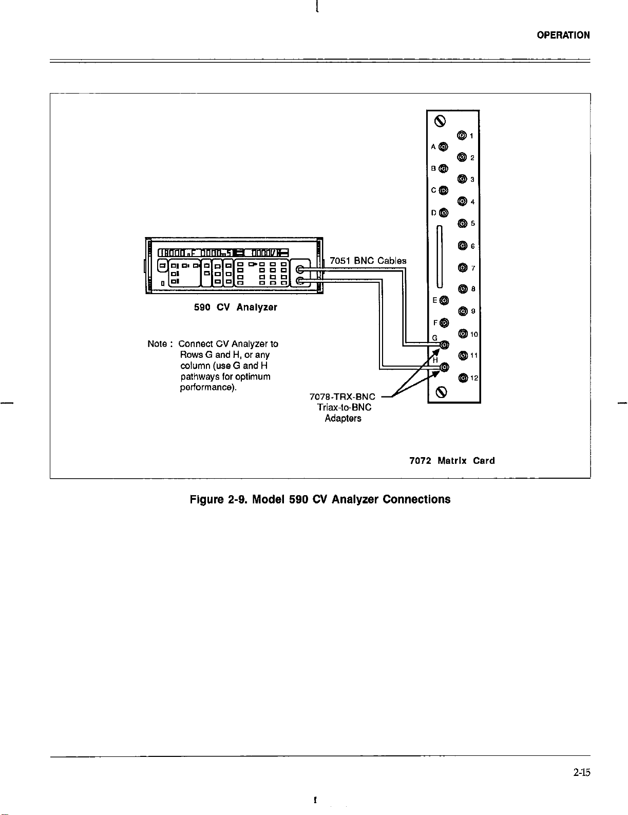
Model 590 CV Analyzer Connections
The Model 590 CV Analyzer should be connected to rows
G and H (CV rows), or any column as shown in Figure
2-9. The BNC cables that are supplied with the Model 590
can be used; however, Model 7078~TRX-BNC triax-to-BNC
adapters must be used at the Model 7072 end.
Model 220 Current Source Connections
The Model 220 Current Source can be connected to the
matrix card using the Model 6167 Guarded Adapter, as
shown in Figure Z-10. This configuration guards the out-
put signal to minimize the effects of distributed capacitance
and leakage current.
-
NOTE
For low-level voltage measurements, connect the
inner shield of the HI cable to VOLT OHMS Lo
to minimize noise.
The Model 6167 Adapter must be modified by in-
ternally disconnecting the inner shield connection
of the input jack from the GUARDED/
UNGUARDED selection switch. Otherwise, instrument IO will be connected to chassis ground
through the adapter.
NOTE
z-12
I
Page 30

OPERATION
196 DMM
Inner Shield (Connect to LO
for Low-Level Measurements)
Figure 2-7. Model 196 DMM Connectlons
--I
LL,
7072
Matrix Card
z-13
I
Page 31

I
OPERATION
Triax/Banana Cables (See Figure 2-4)
Common
230 Voltage Source
7072 Matrix Card
-
Figure 2-6. Model 230 Voltage Source Connections
2-14
I
Page 32
OPERATION
Note : Connect CV Analyzer to
Rows G and H, or any
column (use G and H
pathways for optimum
performance).
Figure 2-9. Model 590 CV Analyzer Connections
Adapters
7072 Matrix Card
z-15
I
Page 33

OPERATION
Use Row A or Bfor Source High when
Sourcing < 2nA
Guarded Adapter
Connect GUARD
-A
7078-TRX Trim
220 Current Source
P
L
E
c
c
I
7072 M&lx Card
2-16
Figure 2-10. Model 220 Current Source Connections
Page 34

OPERATION
1. Connect the Model 6167 adapter to the Model 220 OUT-
2.5.6 Typical Test Fixture Connections
PUT jack.
2. Connect a Model 707%TRX-3 or -10 trim cable between
the guarded adapter and the desired row of the Model
7072.
Typically, one or more test fixtures will be connected to
desired columns of the Model 7072. Typically, the test fixtures will be equipped with card-edge connectors with
3. Connect the Model 220 GUARD output to GUARD IN- wires soldered to them. In some cases, the test fixture will
PUT terminal of the adapter.
4. Connect the triax end of a triaxlbanana cable to the
desired row on the Model 7072.
be equipped with triax connectors; for those types,
Keithley Model 7078-TRX-3 or -10 cables can be used, as
shown in Figure Z-11.
5. Connect the banana olue end of the triaxibanana cable
to the OUTPUT CO?vfGON jack of the Model 220.
(or run cables through strain
reliefs and conned internally)
7072 Matrix Card
Note : Teflon@ - insulated connectors
recommended for specified
performance.
Warning : Do not use BNC connectors
to avoid possible shock
hazard.
Figure 2-11. Typical Test Fixture Connections
2-37
I
Page 35

OPERATION
WARNING
Do not use BNC cables and adapters in cases
where hazardous voltages from guard sources
could be present on the BNC cable shields.
Internally, the test fixture should be wired as shown in the
equivalent circuit of Figure Z-12. SIGNAL should be connected to the probe or other device contact points, while
GUARD should be carried through as close to the device
as possible. If coaxial probes are to be used, connect
GUARD to the probe shield if the probe shield is insulated
from the fixture shield.
Triax Cable
km
7072
Zard
Ground L
_-----_-_-
Test Fixture Chassis
2.6.1 Switching Matrix
As shown in Figure Z-13, the Model 7072 is organized as
an 8 X 12 (eight row by 12 column) matrix. The rows are
labelled A through H, while the columns on the card are
numbered 1 through 12. The actual column number to use
when programming depends on the slot and unit number,
as summarized in Table 2-3. For example, card column
number 2 on a card in slot 5 of unit 1 is accessed as matrix
column 62.
Table 2-3. Column Numbering by Slot and Unit
Slot
3 97-108
4 109-120
5 121-132
6 x33-144
CoIumns (l-12)
I
,
l-12
13-24
25-36
37-48
49-60
61-72
73-84
85-96
Figure 2-12. Equivalent Circuit of Test Fixture
Connections
Usually, the chassis ground terminal of the trim connector will automatically make contact with the fixture shield
by virtue of the mounting method. However, ground integrity should be checked to ensure continued protection
against hazardous guard voltages.
2.6 MATRIX CONFIGURATION
The following paragraphs discuss the switching matrix of
the Model 7072 as well as how to expand the matrix by
connecting two or more cards together.
L
3
4
/
5
/ I
1 145-156
2 W-168
3 169.180
4
5 193-204
6 205-216
1
2 229-240
3 241-252
6
1
2
3
4
5
6
/ 217-228
181-192
253-264
265-276
277-288
289-300
301-312
313.324
325-336
337-348
349-360
2-18
Page 36

Columns
OPERATION
Crosspolnt Switching
for Rows A - F.
Columns 1 - 12
Figure 2-13. Model 7072 Matrix Organization
Columns 1 - 12
2-19
Page 37

OPERATION
Each intersecting point in the matrix is called a crosspoint
that can be individually closed or opened by programming
the Model 707 mainframe. The crosspoints for rows A
through F are configured for 2-pole switching, as shown
in Figure 2-13. For these rows, SIGNAL and GUARD are
switched separately to any of the 12 columns on the card.
Many of the specifications for the card differ among row
types. For example, the offset current for the low-current
rows is <lpA, but the general purpose and CV rows have
a higher offset current of 2OpA. Thus, A and B would be
the rows of choice for low-current measurements. Also, the
path isolation for rows A and B is an order of magnitude
higher than that the other rows (lo’% vs. lO’*Q Again,
these two rows would be preferable for very high-
The crosspoints for rows G and H use l-pole switching,
impedance measurements.
with only SIGNAL being switched. The equivalent circuit
for this arrangement is also shown in Figure 2-13.
In summary, the following general rules apply when
choosing which rows to use for specific measurements:
2.6.2 Row and Column Isolators
l
Use rows A and B for low-current measurements.
l
In order to maintain the integrity of the low-current and
CV pathways, isolator relays are incorporated into each column. These isolators are indicated as small circles on the
matrix diagram of Figure 2-13. Each relay remains open until a crosspoint located in rows C through H is to be closed.
In this manner, the general-purpose pathways are isolated
from the more critical low-current and CV pathways.
In a similar manner, row isolator relays isolate the crosspoint relays from a given row to minimize leakage current
and capacitance, and maximize path resistance. The row
-
isolator relay closes when any crosspoint relay associated
with that row is closed.
Use rows A, B, G, and H for low-capacitance
measurements.
l
Rows A and B should be used where high path isolation resistance is of primary concern.
l
Rows A and B have the largest bandwidth, while rows
G and H have the smallest bandwidth.
For more detailed information on these factors, refer to the
Model 7072 Specifications located at the front of this
manual.
2.6.4 Internal Matrix Expansion
2.6.3 Pathway Considerations
As discussed previously, the eight rows on the matrix card
are designed for different purposes. Rows A and B are
designated low-current mws, rows C through F are general
purpose rows, and rows G and H are CV rows.
Two to six Model 7072 cards can be connected together
within the mainframe to yield an 8 X N matrix, where N
depends on the number of cards. Figure 2-14 shows an internally expanded matrix with three cards, resulting in an
8 x 36 (eight row by 36 column) matrix. As summarized
in Table 2-3, the actual column number used when programming the unit is determined by the slot.
Z-20
I
Page 38

I
OPERATION
Note : Rows C - F jumpered through backplane.
Rows A. 8, G. and H require installation of coaxial jumpers (shown heavily shaded).
Figure 2-14. Connecting Three Cards for 6 x 36 Matrix
Rows
C through
through the backplane of the mainframe. The mainframe
can be configured for two sets of three cards each by
-
removing jumpers from the backplane of the mainframe;
see Section 3 of the Model 707 Instruction Manual for
details on removing the jumpers. With the row jumpers
removed, rows C through F of Model 7072 cards in slots
1 through 3 are connected, and rows C through F of Model
7072 cards in slots 4 through 6 are connected together.
Because of more critical signal paths, rows A, B, G, and
H are not jumpered through the backplane. Instead, you
must install the supplied coaxial jumpers between appropriate connectors on Model 7072 cards (for critical signal
paths, rows can be isolated from other cards by not installing these cables). Each card has two SMB coaxial connectors for each row, allowing daisy chaining of card rows.
These connectors can be reached by lifting the access door
on the top of the mainframe; it is not necessary to remove
cards to install the jumpers. Figure 2-15 shows an edge-on
view of the jumper connectors with row numbers marked for convenience. Figure 2-16 demonstrates how three
cards can be daisy chained together using the coaxial
jumpers.
F are automatically connected together
WARNING
The SMB coaxial shields are at guard potential.
To avoid a posslble shock hazard, always
disconnect all cables from the row and column
jacks before removing or installing jumpers.
Figure 2-16. Jumper Connector Locations
2-21
I
Page 39

OPERATION
I
2-22
Figure 2-16. Three Cards in Daisy Chain Configuration
Page 40

OPERATION
2.6.5 External Matrix Expansion
External jumper cables must be used to expand the
number of rows in the matrix, or to connect between columns of cards installed in different mainframes. An example of such an expanded matrix is shown in Figure 2-17.
Here, six cards are configured as a 16 x 36 matrix. Since
the rows are internally jumpered, only columns must be
jumpered externally in this configuration. Note that the
backplane jumpers must be removed to separate the cards
into two groups.
Trim tee adapters (Model 7078-TRX-T) can be used to provide daisy chain capability between the trim input connectars. Figure 2-18 shows a typical arrangement between
two Model 7072 cards. Ideally, custom-length triax cables
should be used to avoid the cable “jungle” that would oc-
cur with longer, standard-length cables.
Figure 2-17. 16 x 36 Matrix Constructed by External Jumpering
I
2-23
Page 41

OPERATION
Trim Tee
Adapters
Figure 2-16. Using Triax Tee Adapters to Daisy Chain Cards
2.7 MEASUREMENT CONSIDERATIONS
Many measurements made with the Model 7072 concern
low-level signals. Such measurements are subject to
various types of noise that can seriously affect low-level
measurement accuracy. The following paragraphs discuss
possible noise sources that might affect these
measurements.
2.7.1 Magnetic Fields
When a conductor cuts through magnetic lines of force,
a very small current is generated. This phenomenon will
frequently cause unwanted signals to occur in the test leads
of a switching matrix system. If the conductor has sufficient length, even weak magnetic fields lie those of the
2-24
earth can create sufficient signals to affect low-level
measurements.
Two ways to reduce these effects are: (1) reduce the lengths
of the test leads, and (2) minimize the exposed circuit area.
In extreme cases, magnetic shielding may be required.
Special metal with high permeability at low flux densities
(such as mu metal) are effective at reducing these effects.
Even when the conductor is stationary, magneticallyinduced signals may still be a problem. Fields can be pro-
duced by various signals such as the AC power line
voltage. Large inductors such as power transformers can
generate substantial magnetic fields, so care must be taken
to keep the switching and measuring circuits a good
distance away from these potential noise sources.
I
Page 42

OPERATION
2.7.2 Electromagnetic Interference (EMI)
The electromagnetic interference characteristics of the
Model 7072 Semiconductor Matrix Card comply with the
electromagnetic compatibility (EMC) requirements of the
European Union as denoted by the CE mark. However, it is
still possible for sensitive measurements to be affected by
external sources. In these instances, special precautions may
be required in the measurement setup.
Sources of EMI include:
l radio and television broadcast transmitters
l communication transmitters, including cellular phones
and handheld radios
l devices incorporating microprocessors and high speed
digital circuits
l impulse sources as in the case of arcing in high-voltage
environments
The effect on instrument performance can be considerable if
enough of the unwanted signal is present. A common
problem is the rectification by semiconductor junctions of
RF picked up by the leads.
The equipment and signal leads should be kept as far away
as possible from any EMI sources. Additional shielding of
the measuring instrument, signal leads, and sources will
oRen reduce EM1 to an acceptable level. In extreme cases, a
specially constructed screen room may be required to
sufficiently attenuate the troublesome signal.
Many instruments incorporate internal filtering that may
help to reduce RF1 effects in some situations. In some cases,
external filtering may also be required. Such filtering,
however, may have detrimental effects on the desired signal.
rent develops a small but undesirable voltage between the
LO terminals of the two instruments. This voltage will be
added to the source voltage, affecting the accuracy of the
Figure 2-19. Power Line Ground Loops
Figure 2-20 shows how to connect several instruments
together to eliminate this type of ground loop problem.
Here, only one instrument is connected to power line
INSTRVMENT 1 INSTRUMEM 2 lNS,R”MEM 3
o----a
I
7
T
T
2.7.3 Ground Loops
When two or more instruments are connected together, care
must be taken to avoid unwanted signals caused by ground
loops. Ground loops usually occur when sensitive
instrumentation is connected to other instrumentation with
more than one signal return path such as power line ground.
As shown in Figure 2-19, the resulting ground loop causes
current to flow through the instrument LO signal leads and
then back through power line ground. This circulating CUT-
Figure 2-20. Eliminating Ground Loops
Ground loops are not nomu.lly a problem with instruments
having isolated LO terminals. However, all instruments in
the test setup may not be designed in this manner. When in
doubt, consult the manual for all instrumentation in the test
setup.
2-25
Page 43

OPERATION
2.7.4 Keeping Connectors Clean
As is the case with any high-resistance device, the integrity
of biaxial and other connectors can be damaged if they
are not handled properly. If the connector insulation
becomes contaminated, the insulation resistance will be
substantially reduced, affecting high-impedance measurement paths.
Oils and salts from the skin can contaminate connector insulators, reducing their resistance. Also, contaminants present in the air can be deposited on the insulator surface.
To avoid these problems, never touch the connector insulating material. In addition, the matrix card should be
used only in clean, dry environments to avoid
contamination.
If the connector insulators should become contaminated,
either by inadvertent touching, or from ah-borne deposits,
they can be cleaned with a cotton swab dipped in clean
methanol. After thorough cleaning, they should be allowed to dry for several hours in a low-humidity environment
before use, or they can be dried more quickly using dry
nitrogen.
or contraction. Tie down offending cables securely to avoid
movement, and isolate or remove vibration sources such
as motors or pumps.
2.7.6 Shielding
Proper shielding of all unguarded signal paths and devices
under test is important to minimize noise pickup in virtually any switching matrix system. Otherwise, interference from such noise sources as line frequency and RF
fields can seriously corrupt a measurement.
In order for shielding to be effective, the shield surrounding the HI signal path should be connected to signal LO
(or chassis ground for instruments without isolated Ix) terminals). Since most Model 7072 matrix applications call
for separately switching LO, a separate connection from
LO to the cable shield at the source or measurement end
must be provided, as in the example of Figure 2-21. Here,
we are using the GUARD path of the Model 7072 to carry
the shield out to the device under test. Needless to say,
this arrangement should not be used with guarding, as
GUARD and LO should not be connected together.
-
2.7.5 Noise Currents Caused by Cable Flexing
Hazardous voltage may be present if LO on any
WARNING
instrument is floated above ground potential.
Noise currents can be generated by bending or flexing
coaxial or triaxial cables. Such currents, which are known
as triboelectric currents, are generated by charges created
between a conductor and insulator caused by friction.
Low-noise cable can be used to minimize these effects.
Such cable has a special graphite coating under the shield
to provide lubrication and to provide a conduction path
to equalize charges.
Even low-noise cable generates some noise currents when
flexed or subjected to vibration. To minimize these effects,
keep the cables as short as possible, and do not subject
them to temperature variations that could cause expansion
If the device under test is to be shielded, the shield should
be should be connected to the Lo terminal. If you are using the GUARD connection as shield, care should be taken
to insulate the outer ring of the triaxial connector mounted
on the test fixture from the test fixture itself. Otherwise,
Lo will be connected to chassis ground, possibly resulting
in a ground loop. An alternative is to use two shields, one
mounted within (and insulated from) the other. In this
case, the GUARD path would be connected to the inner
shield, while the outer shield would be chassis grounded. This arrangement is shown in Figure 2-22. Incidental-
ly, this configuration is also recommended for guarded ap-
plications, with the inner shield as guard, and the outer
shield acting as a safety shield.
2-26
I
Page 44

OPERATION
Inner Shield of HI Trim
Connected to LO
Inner Shield
Connected to
r
1
COLUMNS
Trim
-I
r-----
-----
7072 Card
Flgure 2-21. Shielding Example
r----------i
L
- - - - - _ _ _ - - AC- Outer Shield
Flgure 2-22. Dual Shield Test Fixture
(Chassis Ground)
2-27
I
Page 45

OPERATION
I
2.7.7 Guarding
Guarding is important in high-impedance circuits where
leakage resistance and capacitance could have degrading
effects on the measurement. Guarding consists of using
a shield surrounding a conductor that is carrying the highimpedance signal. This shield is driven by a lowimpedance amplifier to maintain the shield at signal potential. For triaxial cables, the inner shield is used as guard.
Guarding minimizes leakage resistance effects by driving
the cable shield with a unity gain amplifier, as shown in
Figure 2-23. Since the amplifier has a high input impedance, it minimizes loading on the high-impedance
signal lead. Also, the low output impedance ensures that
the shield remains at signal potential, so that virtually no
leakage current flows through the leakage resistance, R,.
Leakage between inner and outer shields may be considerable, but that leakage is of little consequence because
that current is supplied by the buffer amplifier rather than
the signal itself.
In a similar manner, guarding also reduces the effective
cable capacitance, resulting in much faster measurements
on high-impedance circuits. Because any distributed
capacitance is charged through the low impedance of the
buffer amplifier rather than by the source, settling times
are shortened considerably by guarding.
In order to use guarding effectively with the Model 7072,
the GUARD path of the matrix card should be connected
to the guard ‘output of the sourcing or measuring instrument. Figure 2-24 shows typical connections. Guard
should be properly carried through the inner shield to the
device under test to be completely effective. The shield-
ed, guarded test fixture arrangement shown in Figure 2-22
is recommended for safety purposes (guard voltage may
be hazardous with some instruments). With most instruments, special adapters or cables may be required to
connect guard to the inner shield, and at the same time
route signal Lo through a separate cable.
Inner Shield
Signal
. - ,. Buffer ,...-. I
J
----
I
I
I I
EM I
Figure 2-23. Guarded Circuit
1
I
I
Measuring
I
Instrument
I
I
I
Page 46

Current Source
OPERATION
COLUMNS
------
7072
Figure 2-24. Typlcal Guarded Signal Connections
2.7.8 Matrix Expansion Effects on Card
Specifications
Specifications such as those given for path isolation and
offset current are with a single Model 7072 Card installed
in the mainframe. Expanding the matrix by internally or
externally connecting two or more Model 7072 Cards
together will degrade system performance specifications
(other types of cards do not affect the specifications
because they use different pathways in the mainframe
backplane). The extent depends on how many cards are
Card
used, as well as the amount of cabling used to connect
them together.
With internal row expansion, isolation among rows is
decreased, and offset current is increased, although the
isolator relays on the card do help to minimize these effects. With external row or column expansion, isolation and
offset current specifications are degraded because of the
additional parallel paths and relays present on each signal
line.
Warning : Outer fixture must be -
used to avoid possible
shock hazard from guard.
2-29/2-30
I
Page 47

SECTION 3
Applications
3.1 INTRODUCTION
This section covers typical applications for the Model 7072
Semiconductor Matrix card and is organized as follows:
CV Measurements: Outlines the test configuration
3.2
and procedure for making quasistatic and highfrequency CV measurements.
Semiconductor Test Matrix: Details a semiconductor
3.3
test matrix that can be used to perform a variety of
different tests on semiconductors such as FETs.
3d
Resistivity Measurements: Covers methods to
measure the resistivity of semiconductor samples using the van der Pauw method.
Semiconductor Parameter Analysis: Discusses using
-
3.5
the Model 7072 in conjunction with an HP 41458
Semiconductor Parameter Analyzer.
3.2 CV MEASUREMENTS
The Model 7072 can be used in conjunction the Keithley
Model 590 CV Analyzer, and the Keithley Model 595
Quasistatic CV Meter to perform quasistatic and highfrequency CV (capacitance vs. voltage) tests on semiconductors. The resulting CV curves can be used to calculate
important semiconductor parameters such as doping profile, band bending, and mobile ion concentration.
3.2.1 Stand Alone System Configuration
The stand alone system shown in Figure 3-l can be used
to make CV measurements without the aid of a computer.
System components perform the following functions.
Model 590 CV Analyzer: Measures CV data at lOOkHz and
lMHz and sends the resulting data to the plotter for
graphing.
Model 595 Quasistatic CV Meter: Measures quasistatic CV
data and sends the data to the plotter for graphing in real
time.
Model 707 Switching Matrix: Controls the semiconductor matrix card to close and open the desired crosspoints
at the proper time.
Model 7072 Semiconductor Matrix Card: Switches the
signal pathways to the six wafers under test.
HP-GL Plotter: Plots CV and other curves directly from
the Models 590 and 595.
3.2.2 Computerized System Configuration
Figure 3-2 shows a computerized version of the CV matrix
test system. The addition of a computer allows greater
system versatility and easier instrument control. Also,
analysis functions such as doping profile and ion concentration can be added to the software to expand CV analysis
capabilities.
3-3
I
Page 48

APPLICATIONS
Wafers Under
Test
Note : Rows C-F can be used
for this signal path.
L--------J
7072 Matrix Card
Model 590
CV Analyzer
707 Switching Matrix
Note : Connect plotter to only one
instument at a time.
Figure 3-1. Stand Alone CV System Configuration
3-2
I
Page 49

Wafers Under
Test
APPLICATIONS
Note : Rows C-F can be used for
this signal path.
7072 Matrix Card
707 Switching Matrix
Figure 3-2. Computerized CV System Configuration
IEEE-499 Bus
Note : Remove jumpers to other 7072 cards (if installed)
to optimize Model 595 measurement accuracy.
3-3
I
Page 50

APPLICATIONS
3.2.3 Optimizing CV Measurement Accuracy
For accurate CV measurements, each Model 590 CV
measurement pathway must be cable corrected using the
procedure outlined in the Model 590 Instruction Manual.
The pathways to each DUT must be cable corrected
separately.
Also, for best quasistatic CV results, the corrected
capacitance feature of the Model 595 should be used. Corrected capacitance compensates for any leakage currents
present in the cables, switching matrix, or test fixture.
However, care must be taken when using corrected
capacitance to ensure that the device remains in
equilibrium throughout the test sweep to avoid distorting
the CV curves.
In order to minimize the effects of the switching network
on quasistatic CV measurements, cables to the Model 595
and DUT should be kept as short as possible. Also, the
low-current pathways (rows A and B) should be used with
the Model 595.
3.2.4 Basic CV Test Procedure
The fundamental CV test procedure is outlined below.
Keep in mind that this procedure does not address many
considerations and aspects of CV testing, which is fairly
complex. The procedure given is for the stand alone system
in Figure 3-l. Detailed instrument operating information
may be found in the pertinent instruction manuals.
1. Connect the HP-GL plotter to the IEEE-488 bus connector of the Model 595 only.
2. Set up the Model 595 for the expected CV sweep.
3. Close the crosspoints necessary to connect the Model
595 to the device under test, as summarized in Table
3-l. For example, to test device #l, close Al and 82.
4. Place the probes down on the wafer test dots.
5. Run a quasistatic sweep on the selected device and
generate a CV curve.
6. Open the crosspoints that are presently closed.
7, Set up the Model 590 for the expected CV sweep.
8. Close the crosspoints necessary to connect the Model
590 to the device under test. For example, to test device
#l, close Gl and H2.
9. Run a high-frequency test sweep on the device to store
the CV data in the Model 590 buffer.
10. Disconnect the plotter from the Model 595 and connect it to the Model 590.
11. Generate a plot from the data in the Model 590 buffer.
12. Repeat steps 2 through 11 for the remaining devices,
as required.
Table 3-1. CV Test Crosspoint Summary
!d
Wafer #
Quasistatic (595)
Al, 82
A3, B4
A5, B6
A7, B8
A9, 810
All, 812
t
Close
Crosspoints
High Frequency (590)
Gl, H2
G3, H4
G5, H6
t
3.2.5 Typical CV Curves
Figures 3-3 and 3-4 show typical CV curves as generated
by the Models 595 and 590 respectively. The quasistatic
curve shows a fair amount of symmetry, while the the
high-frequency curve is highly asymmetrical. The asym-
metrical nature of the high-frequency curve results from
the inability of the minority carriers to follow the highfrequency test signal.
3-4
I
Page 51

+0.6E-10
APPLICATIONS
\
+0.4E-10
-005.00
Figure 3-3. Typical Quasistatic CV Curve Generated by Model 595
+005.00
KEITHLEY 595
3-5
I
Page 52

APPLICATIONS
Figure 3-4. Typical High-frequency CV Curve Generated by Model 590
3.3 SEMICONDUCTOR TEST MATRIX 3.3.1 System Configuration
Two important advantages of a matrix switching system Figure 3-5 shows the configuration for a typical multiare the ability to connect a variety instruments to the device purpose semiconductor test matrix. Instruments in the
or devices under test, as well as the ability to connect any system perform the following functions.
instrument terminal to any device test node. The following paragraphs discuss a typical semiconductor matrix test
system and how to use that system to perform a typical
test: common-source characteristic testing of a typical JFET.
3-6
I
Page 53

I
Device Under Test
APPLICATIONS
SGSG SGSG
--_-___ --_-___
------ ------
2 3 4 5 6 7
1
7072 Matrix 7072 Matrix Card Card
707 Switching 707 Switching Matrix
SGSG ___ SGSG ___
SGSGSGSGSG SGSGSGSGSG
---- ----
6 9 10 11 12
Matrix
Figure 3-5. Semiconductor Test Matrix
3-7
I
Page 54

APPLICATIONS
Model 617 Electrometer/Source: Measures current, and
also could be used to measure voltages up to GIOOVDC.
The DC voltage source can supply a maximum of +lOOV
at currents up to 21~4.
Model 230 Voltage Source: Sources DC voltages up to
*lOlV at a maximum current of lOOmA.
Model 590 CV Analyzer: Adds CV sweep measurement
capability to the system.
Model 220 Current Source: Used to source currents up to
a maxinwm of 1OlmA with a maximum compliance voltage
of 105V.
Model 196 DMM: Measure DC voltages in the range of
1OOnV to 300V. The Model 196 could also be used to
measure resistance in certain applications.
Device Under Test: A three-terminal fiitwe for testing such
devices as bipolar transistors and FETs. Additional connec-
tions could easily be added to test more complex devices,
as required.
3.3.2 Testing Common-Source Characteristic
of FETs
The system shown in Figure 3-5 could be used to test a
variety of characteristics including
and Vos,,,,. To demonstrate a practical use for the system,
we will show how it can be used to generate common
source characteristic curves of a particular JFET.
In order to generate these curves, the instruments must
be connected to the JFET under test, as shown in Figure
3-6. The advantage of using the matrix is, of course, that
it is a simple matter of closing specific crosspoints. The
crosspoints that must be closed are also indicated on the
diagram.
To run the test, V,, is set to specific specific values, for
example in increments of 0.25V. At each V,, value, the
drain-source voltage (V,,) is stepped across the desired
range, and the drain current, I,, is measured at each value
of V, Once all data are compiled, it is a simple matter
to generate the common-source IV curves, an example of
which is shown in Figure 3-7. If the system is connected
to a computer, the test and graphing could all be done
I
ass, Lqm,, L,m,, Ls,
@=
617
Electrometer/Source
Closed Crosspoints on 7072 Card (Figure 3-5).
3-8
Figure 3-6. System Configuration for Measurlng Common-Emitter Characteristics
I
Page 55

3.4.2 Test Procedure
APPLICATIONS
100
80 80 - VGS = ov
(I
0 1 2 3 4 5 6 7 s fl 1c
VW (Volts)
In order to make van der Pauw resistivity measurements,
four terminals of a sample of arbitrary shape are measured.
A current (from the Model 220) is applied to two terminals,
while the voltage is measured (by the Model 196) across
the two opposite terminals, as shown in Figure 3-9. A total
of eight such measurements on each sample are required,
with each possible terminal and current convention. The
resulting voltages are designated VI through Vs
In order to source current into and measure the voltage
across the sample, specific crosspoints must be closed.
Table 3-2 summarizes the crosspoints to close for each
voltage measurement on all three samples from the test
configuration shown in Figure 3-8.
3.4.3 Resistivity Calculations
Figure 3-7. Typlcal Common-Source FET IV
Characteristics
3.4 RESISTIVITY MEASUREMENTS
-
The Model 7072 Semiconductor Matrix card can be usec
in conjunction with a Model 220 Current Source and a
Model 196 DMM to perform resistivity measurements on
semiconductors. Such measurements can yield such important information as doping concentration.
Once the eight voltage measurements are known, the
resistivity can be calculated. Two values of resistivity, p*
and pB are initially computed as follows:
1.1331 fA t, (V, + v, - v, -V,)
pa =
1
1.1331 fB ts (V, + v, - v, - V,)
pB =
I
I
3.4.1 Test Configuration
Figure 3-8 shows the basic test configuration to make
resistivity measurements on van der l’auw samples. The
Model 220 sources current through the samples, while the
Model 196 measures the voltage developed across the
samples. The matrix card, of course, switches the signal
paths as necessary. In order to minimize sample loading,
which will reduce accuracy, the Model 196 DMM should
be used only on the 3OOmV or 3V ranges. Also, this configuration is not recommended for resistance
measurements above lMn due to the accuracy-degrading
effects of DMM loading.
Where: pA and pB are the resitivities in O-cm
ts is the sample thickness in cm
V, through v, are the voltages measured by the
Model 196
I is the current through the sample in amperes
fA and fB are geometrical factors based on sample
symmetry (f, = f, = 1 for perfect symmetry).
Once pA and pB are known, the average resistivity, pAvO,
can be determined as follows:
PA + Pa
pm0 =
2
3-9
I
Page 56

APPLICATIONS
SGSGSGSGSGSGSGS
SGSGSGSGSGSGSGSGSGSGSGSG
--------
220 Current Source
(Sources Current through Sample)
196 DMM
(Measures Voltage Across Sample)
-
7072 Matrix Card
707 Switching Matrix
Figure 3-8. Resistivity Test Configuration
3-10
I
Page 57

APPLICATIONS
6)
VI3
1
2
4 3
IT
(0
Figure 3-8. Resistivlty Measurement Conventions
t
‘~
3-11
I
Page 58

APPLICATIONS
Table 3.2 Crosspoint Summary for Resistivity Measurements
Voltage
“I
v2
“3
v4
“5
“6
v7
“!?
T
Sample #l
Al B4 E3 F2
A4 Bl E3 F2
A4 83 E2 Fl
A3 B4 E2 Fl
A3 B2 El F4
A2 03 El F4
A2 Bl E4 F3
Al 82 E4 F3
Crosspoints Closed
i
Sample #2
A5 B9 El
A8 85 El
A8 81 Eb
Al B8 Eb
Al Bb E5
Ab B7 E5
A6 BS E8
A5 Bb E8
3.5 SEMICONDUCTOR PARAMETER ANALYSIS
One or more Model 7072 Semiconductor Matrix Cards can
be used in conjunction with an HP 41458 Semiconductor
Parameter Analyzer (SPA) to provide a versatile switching
system capable of complete DC characterization of
semiconductors. The following paragraphs discuss system
configuration, connections using the 7078~CSHP Cable Set,
and SPA measurement considerations.
3.51 System Configuration
Figure 3-10 shows the general configuration of the SPA
switching system. The components of the system perform
the following functions:
HP 4145B: Has four SMUs (Source/Measure Units), two
voltage sources, and two voltage measurement ports. The
unit can automatically run a variety of tests on
semiconductors and plot data on a built-in CRT.
T
Current Voltage
r
Fb
Fb
F5
F5
F8
F8
F7
F7
-
Model 707 Switching Matrix: Controls the matrix card to
open and close signal paths as required.
Model 7072 Semiconductor Matrix Card: Switches the test
pathways to the device under test. In this particular applica-
tion, three Model 7072 cards provide 3b-pin test capability.
A total of six cards can be installed in a single mainframe,
providing up to 72-pin capability in one mainframe.
System Controller: Controls the SPA and switching matrix
with user-written software. Typical controllers for this
application are HP 9000 Series 200 or 300 (with HP-IB
interface), and IBM PC, AT or compatible computers
(equipped with an IEEE-488 interface).
Test Fixture: Provides the interface between the device
under test and the matrix card. Typically, the test fixture will
be equipped with triax connectors for ease of connections.
Sample #3
A9
B12 El1 FlO
Al2 B9 El1 FlO
Al2 Bll El0 F9
All B12 El0 F9
All BlO E9 F12
Al0 Bll E9
A10 B9 El2 Fll
A9 BlO El2 Fll
F12
Between
l-2
2-1
2-3
3-2 4-1
3-4 1-2
4-3 1-2
4-1
l-4
Between
3-4
3-4
4-l
2-3
2-3
3-12
Page 59

l-izcJ
APPLICATIONS
Test Fixture
HP 41458
Semiconductor
Parameter
Aflalyzer
A
L I
1...12
SMU 1
SMU 2
SMU 3
SW 4 .
Vsl -
vs
2
.A
B I
C
0
E
.F
V,l
vm2 w J--&)-T-,,_--
Rows
IEEE-488 Bus
,
13...24 25...36
I
I
I
7072 1 7072 7072
Card 1 Card 1 Card
I
I
I
I
A
I
C0lllllln5
>
System Controller
HP9000 or IBM PC/AT
Note: Row connecting cables included in 7078.CSHP cable set.
Figure 3-10. Semiconductor Parameter Analysis Switching System
3.5.2 Cable Connections
Figure 3-11 shows how to connect the HP 4145B to the
Model 7072 using the optional Keithley Model 7078~CSHP
Cable Set. The four SMU ports are to be connected with the
triax cables (707%TRX-IO), while the two voltage source
and voltage measurement ports (Vs and Vm) are to be connetted using BNC cables (705 l-10) and triax-BNC adapters
(7078-TRX-BNC). Typically, the SPA will be connected to
the rows, as shown in Figure 3-I I.
3-13
Page 60

APPLICATIONS
IT= ‘LIUI
HP 4145 Semiconductor Parameter
Analvzer
Triax
Cables
Coax Cables
7072 Matrix Card
Triax-BNC
Adapiers
i
Figure 3-11. SPA Connections
3-14
I
Page 61

APPLICATIONS
Connections to a user-supplied test fixture should be made
using triax cables in order to maintain path integrity and
safety. BNC cables and adapters should not be used in case
hazardous potential appears on guard terminals.
points to close to test a specific FET are summarized in
Table 3-3.
Table 3-3. Crosspoint Summary for JFET Test
3.5.3 SPA Measurement Considerations
JFET Crosspoints Closed*
A complete discussion of SPA measurements is well
beyond the scope of this manual. However, there are a few
points that should be kept in mind when using this arrangement. Additional measurement considerations may
be found in Section 2, paragraph 2.7 of this instruction
manual.
* Crosspoints from Figure 3-12
Any switching system can degrade low-level signals, and
the same hold true for the system shown in Figure 3-10.
Since rows A and B on the Model 7072 are dedicated low
current pathways, the SMUs that will source or sense lowlevel signals should be connected only to these rows. The
remaining rows can be used for less-critical signals.
Safety considerations are also a concern when connecting
instruments to a switching matrix. Therefore, it is strongly recommended that you carefully read the HP 41458
-
manual before using the system.
Procedure
1. Connect the system and devices together, as shown in
2. Turn on the HP 41458 and allow it to go through its
3. Turn on the Model 707 Switching Matrix.
4. From the HP 41458 main menu, select the channel
5. Press the PAGE NEXT key, and program the source
WARNING
Hazardous voltage may be present on the outer
6. Press the PAGE NEXT key, and program the required
conductors of the connecting cables when the
HP 41458 is set up for floatlng measurements.
7. Press the PAGE NEXT key to display the graph format.
8. From the front panel of the Model 707, close the cross-
3.5.4 Typical Test Procedure
9. Press the MEASUREMENT SINGLE key to initiate the
The following paragraphs outline the procedure for using
the SPA/matrix system to perform a typical test: V,&,
(common-source) curves of a typical JFET. The procedure
uses one of the four standard setups that are part of the
applications package supplied with the HP 41458.
10. Open the crosspoints presently closed.
11. Repeat steps 8 and 9 for the remaining devices, as
Tested (Source, Gate, Drain)
I
1 A2, Cl, B3
2 A5, C4, B6
3
4
Figure 3-12.
boot-up routine.
definition page, then choose the FET VDsIo
application.
parameters, as required.
graphing parameters.
points necessary to connect the FET being tested to the
SMUs (see Table 3-3).
sweep. The SPA will generate the ID vs. V, curves at
specified V, values.
required.
As, 0, 89
All. ClO. 812
System Configuration
Figure 3-12 shows the configuration and connections for
this example. Only three of the four SMLJs are required
for the test, as indicated in the figure. A total of four FETs
can be connected to a single card, as shown on the diagram. In all cases, triax cabling should be used. The cross-
l)-pica1 Plot
Figure 3-13 shows a typical plot made using the procedure
above. The device tested was a 2N4392 N-channel JFET.
For the graphs, V,, was swept from OV to 1OV in O.lV increments, and V, was stepped from 0 to -025V.
3-15
I
Page 62
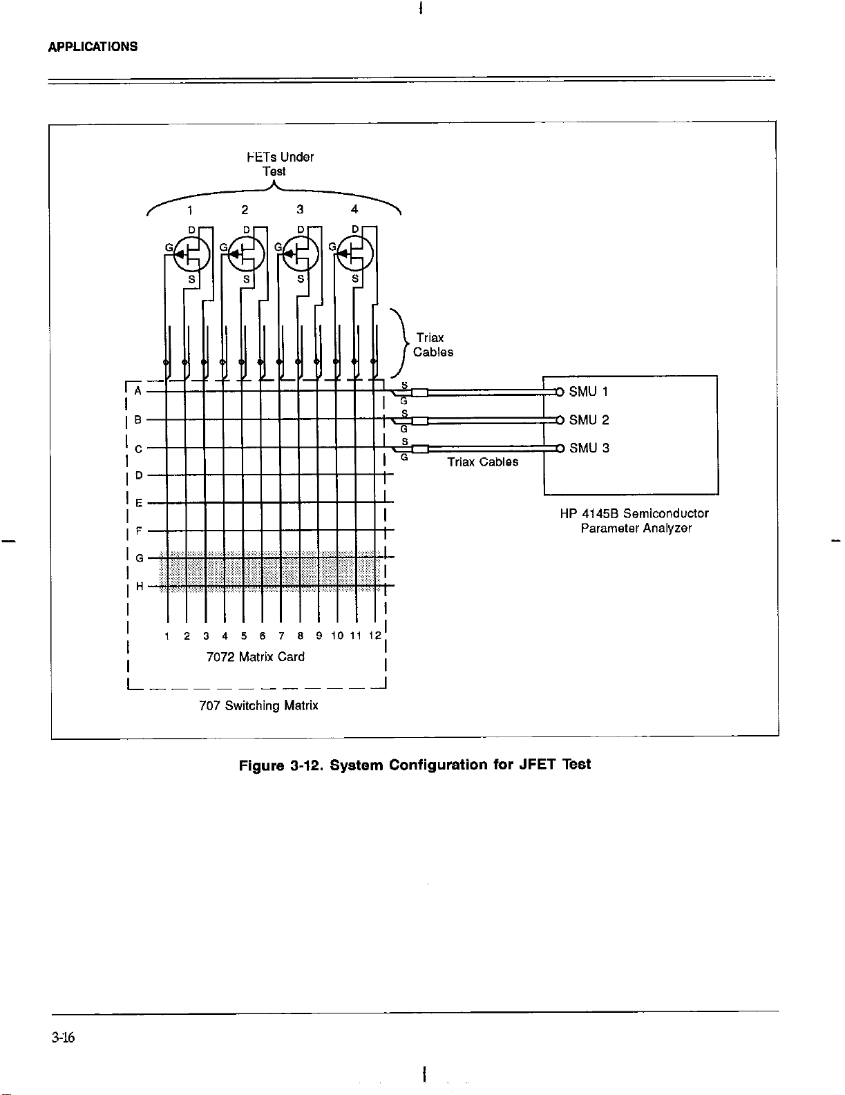
APPLICATIONS
FETs Under
Test
IF
IG
IH
I
I I I I I I I I I I I II
I 1 2 3 4 5 8 7 8 9 to
I
I
7072 Matrix Card
L----------J
707 Switching Matrix
Figure 3-12. System Configuration for JFET Test
1, 12’
I
3-16
I
Page 63

APPLICATIONS
ID
35.00
3.500
W)
/div
VDS l.OOO/div (V)
Variable 1 :
VDS -ChZ
Linear sweep
Stan
SQ to.000”
S@P
Variable 2 :
“G -Ch3
Start .oooov
stop -t.ooca”
SbP
constant :
VS -Chl .OOOOV
.oooov
.IWO”
-.2500”
Figure 3-13. Typical JFET Plot
3-w
I
Page 64

APPLICATIONS
REFERENCES
ASTM, F76-84. “Standard Method of Measuring Hall Mobility and Hall Coefficient in Extrinsic Semiconductor Single
Crystals:’ Annual Bk. AST-, 1986: 10.05 155.
Coyle, G. et al Switching Handbook.. Keithley Instruments Inc., Cleveland, (1987).
Nicollian, E.H. and Brews, J.R. MOS Physics and Technology. Wiley,
Sze, S.M. msics of Semiconductor Devices, 2nd. edition. Wiley, New York (1985)
Van der Pauw, L.J. “A Method of Measuring Specific Resistivity and Hall Effects of Discs of Arbitrary Shape.” F_hm
Rec. Rep&., 1958: 13 1.
Operation and Service Manual, Model 4145A Semiconductor Parameter Anaiys Yokogawa-Hewlett-Packard Ltd, Tokyo,
Japan (1982).
-
New
York (1982).
3-18
I
Page 65

SECTION 4
Service Information
4.1 INTRODUCTION
This section contains information necessary to service the
Model 7072 Semiconductor Matrix Card and is arranged
as follows:
Handling
4.2
handling precautions and methods to clean the card
should it become contaminated.
Performance Verification: Covers the procedures
4.3
necessary to determine if the card is operating
properly.
and
Cleaning Precautions: Discusses
3. Should it become necessary to use solder on the circuit
board, remove the flux from the work areas when the
repair has been completed. Use Freon8 TMS or TE or
the equivalent along with clean cotton swabs or a clean,
soft brush to remove the flux. Take care not to spread
the flux to other areas of the circuit board. Once the flux
has been removed, swab only the repaired area with
methanol, then blow dry the board with dry nitrogen
gas.
4. After cleaning, the card should be placed in a 50°C lowhumidity environment for several hours before use.
4.3 PERFORMANCE VERIFICATION
Special Handling of Static-Sensitive Devices:
4.4
Reviews precautions necessary when handling staticsensitive devices.
-
Troubleshooting: Presents some troubleshooting
4.5
tips for the Model 7072.
Principles of Operation: Briefly discusses circuit
4.6
operation.
4.2 HANDLING AND CLEANING PRECAUTIONS
Because of the high-impedance circuits on the Model 7072,
care should be taken when handling or servicing the card
to prevent possible contamination. The following precautions should be taken when servicing the card.
The following paragraphs discuss performance verification
procedures for the Model 7072, including relay testing, contact resistance, contact potential, path isolation, and
leakage current.
4.3.1 Environmental Conditions
All verification measurements except for path isolation and
offset current should be made at an ambient temperature
between 0°C and 35°C and at a relative humidity of less
than 70%. Path isolation and offset current verification
must be performed at an ambient temperature of 23°C and
at a relative humidity of less than 60% If the matrix card
has be subjected to temperature or humidity extremes,
allow the card to environmentally stabilize for at least one
hour before performing any tests.
1. Handle the card only by the edges and handle (do not
touch the edge connectors). Do not touch any board SWfaces or components not associated with the repair.
2. Do not store or operate the card in an environment
where dust could settle on the circuit board. Use dry
nitrogen gas to clean dust off the board if necessary.
4.3.2 Recommended Test Equipment
Table 4-l summarizes the equipment necessary to make
the performance verification tests, along with the application for each item.
4-l
I
Page 66

SERVICE INFORMATION
Table 4-1. Recommended Verification Equipment
2!Y
Description
1
Model 617 Electrometer
1
Model 196 6% Digit DMM
1
Model 707 Switching Matrix
1
IBM PC or HP 200 or 300 computer
Model 707WKX-10 trim cables*
4
2
Model 7CVWRX-3 triax cables
Model 6172 2-slot male to 3-lug female
1
triaxial adapter
Model 7078-TRX-T trim tee adapter
3
5
Banana plugs (part #B6-10-2)
1
Relay test terminal block*
*These items are used to construct special cables; see text.
4.3.3 Relay Testing
The relays on Model 7072 can be tested using the test software supplied with the Model 7G7 Switching Matrix. The
- following paragraphs discuss the test equipment and connections. For detailed information on using the test software, consult Section 6 of the Model 707 Instruction
Manual.
Application
Offset current; path isolation
Path resistance
All tests
Relay test
Offset current; path resistance
Path isolation, offset current
Offset current
Path resistance
Path isolation and resistance
Relay test
Terniinal Block
Recommended Equipment
l Model 707 Switchim Matrix
l Unterminated 3-slot &ax cables (2), made by cutting one
TRX-7078-10 cable in half
l Relay test software (supplied with Model 707)
l IBM PC compatible or Hewlett Packard Series 200 or 300
computer
l Relay test connector (supplied with Model 707)
Connections
The test cable should be prepared using the information
shown in Figure 4-l. The center conductor of the unterminated end of one trim cable should be connected to pin
1 of the relay test connector, while the inner shield should
be connected to pin 2. The outer shield should be cut off
and be left floating at the test connector end.
Cables
“‘-..
To Row A
Figure 4-1. Test Cable Preparation
The remaining triax cable should be connected as follows:
connect the center conductor to pin 6, and connect the in-
ner shield to pin 5. Again, the outer shield should be left
floating. Also, jumper pins 5 and 6 of the relay test con-
nector together.
Figure 4-2 shows how to connect the prepared test cable
to the Model 7072. Connect the first triax cable to row A
of the card, and connect the second triax cable to row B.
Also be sure to connect the test connector to the RELAY
TEST jack on the rear panel of the Model 707.
4-2
I
Page 67

SERVICE INFORMATION
Trim Cables
-A
707 Switching Matrix
Figure 4-2. Connecting the Test Cable to the Model 7072
Running the Test
Follow the instructions given in the Model 707 Instruction
Manual to perform the relay test. The computer will advise you as to which relay or group of relays (if any) fail
to p&s the test
4.3.4 Offset Current Verification
Recommended Equipment
l Model 707 Switching Matrix
l Model 617 Electrometer
l Model 7078-TRX-3 Trim Cable
* Model 6172 2-&t male to 3-lug female triaxial adapter
Test Connections
Figure 4-3 shows the test connections for offset current
verification. The Model 7072 row being tested is to be connected to the Model 617 Electrome& input through the
triaxial cable and the triaxial adapter. Note that the electrometer ground strap is to be removed, and the electrometer should be operated in the unguarded mode.
4-3
I
Page 68

SERVICE INFORMATION
6172 Z-Slot10 -
Connect Cable
Figure 4-3. Offset Verification Test Connections
Procedure
NOTE
The following procedure should be performed at
an ambient temperature of 23°C and at a relative
humidity of less than 60%.
1. Turn on the Model 617 power and allow it to warm up
for two hours before beginning the verification
procedure.
2. With the power off, install the Model 7D7+2 in the desired
slot of the Model 707 Switching Matrix. Remove all
other cards from the instrument, and install the slot
covers.
3. After the prescribed warm up period, select the amps
function and the 2pA range on the Model 637. Zero correct the instrument, and then select autoranging.
7072 Matrix Card
4. Connect the Model 617 to row A of the Model 7072,
as shown in Figure 4-3.
5. Close crosspoint Al by using the Model 707 front panel
controls.
6. Disable zero check on the Model 617, and allow the
reading to settle.
7, Verify that the offset current reading is <lpA.
8. Enable zero check on the Model 617, and open cross-
point Al.
9. Repeat steps 5 through 8 for crosspoints A2 through
Al2. Only one crosspoint at a time should be closed.
10. Disconnect the triax-cable from row A, and connect
it instead to row B.
11. Repeat steps 5 through 8 for crosspoints Bl through
812. Only one crosspoint at a time should be closed.
12. With zero check enabled, disconnect the electrometer
from row B, and connect it to row C.
4-4
I
Page 69

SERVICE INFORMATION
13. Close crosspoint Cl by using the front panel controls
of the Model 707.
14. Disable zero check, and allow the reading to settle.
15. Verify that the offset current reading is i 2OpA.
16. Enable zero check, then open the crosspoint presently
COM and the LO terminal of the electrometer voltage
source must be connected together as shown. Also, the
ground link between COM and chassis must be removed,
and the Model 617 guard must be turned off for current
measurements.
closed.
17. Repeat steps 12 through 16 for rows D through H. The
electrometer should be connected to the row being
Procedure
tested, and only one crosspoint must be closed at a
time. The offset current for each crosspoint should be
<ZOpA.
Hazardous voltage from the electrometer
WARNING
voltage source will be used in the following
steps. Take care not to contact live circuits,
43.5 Path Isolation Verification
The procedure for verifying path isolation is discussed
below. Should the card fail any of the tests, clean it using
the procedures outlined in paragraph 4.2. If rows C
through F still fail, the problem may lie in contamination
of the mainframe backplane.
NOTE
If the path isolation for specific rows is below stan-
dards, test the associated rows or columns with
the card removed from the mainframe. (Of course,
-
it will not be possible to close crosspoints with the
card removed.) If rows C-F pass with the card
removed but fail with the card installed, the
backplane in the mainframe may require cleaning.
See the Model 707 Instruction Manual.
Recommended Equipment
l Model 707 Switching Matrix
l Model 617 Electrometer
l Model 7078-TRX-3 triaxial cable
l Unterminated 3-slot triaxial cable (cut connector off
7078-TRX-3)
l Banana pl;g (Keithley part #BG-10-2)
l #16-l8AWG insulated stranded wire (6 in. length)
Test Connections
Figure 4-4 shows the test connections for the path isola-
tion tests. One row being tested is to be connected to the
Model 617 Electrometer input through a Model 6172 2-slot
female to 3-lug male triaxial adapter. The other row is to
be connected to the voltage source HI terminal using a
specially prepared 3-slot triax-to-banana plug cable, the
construction of which is shown in Figure 4-5. Note that
both the inner shield and the center conductor are to be
connected to the banana plug as shown.
which could cause personal injury or death.
NOTE
The following procedure must be performed at an
ambient temperature of 23OC and at a relative
humidity of less than 60%.
1. Turn on the Model 617 and allow it to warm up for two
hours for rated accuracy.
2. With the mainframe power turned off, plug the Model
7U72 into slot 1 of the mainframe. Remove all other cards
from the mainframe, and install the slot covers.
3. After the prescribed warm up period, select the Model
617 amps function, and enable zero check. Select the
2pA range, and zero correct the instrument.
4. Connect the Model 617 to rows A and B of the matrix
card, as shown in Figure 4-4.
5. Program the Model 617 voltage source for a value of
+lOOV, but do not yet turn on the voltage source
output.
6. Close crosspoints Al and B2 by using the switching
matrix front panel controls.
Z With the Model 617 in amps, enable suppress after the
reading has settled.
8. Turn on the Model 617 voltage source output, and
enable the VII ohms function on the electrometer.
9. After the reading has settled, verify that the resistance
is >loTQ (lO’%).
10. Turn off the voltage source, and enable zero check.
Disable suppress, and select the amps function on the
electrometer.
11. Open crosspoints Al and 82, and close crosspoints A3
and B4.
12. Repeat steps 7 through 11 for A3 and 84.
X3. Repeat steps 7 through 12 for crosspoint pairs A5 and
86, A7 and 88, A9 and BlO, and All and 812.
14. Disconnect the electrometer from rows A and B, and
connect it instead to rows C and D.
4-5
I
Page 70

SERVICE INFORMATION
1
15. Repeat steps 7 through 13 for rows C and D. The path
isolation for these rows should be >lTO (lO’%).
16. Repeat steps 7 through 14 for row pairs E and F, and
G and H. For each row pair, step through the cross-
point pairs 1 and 2, 3 and 4, 5 and 6, 7 and 8, 9 and
7078.TRX-3 Triax Cable ,, $ 3:
Guard off
User-Prepared Triax Cable
(See Figure 4-5)
617 Electrometer
lo, and 11 and 12. The complete procedure outlined
in steps 7 through 11 should be repeated for each crosspoint pair. Each resistance measurement for rows E
through H should be >lTR (lo’%).
7-l
Warning : Hazardous voltage from
the electrometer source
may be present on terminals. QQ
a”
H@
Is
7072 Matrix Card
Figure 4-4. Connections for Path Isolation Verification
4-6
Page 71

I
A
Cut
I+--- I”-4
SERVICE INFORMATION
4.3.6 Path Resistance Verification
The following paragraphs discuss the equipment, connec-
tions, and procedure to check path resistance. Should a
particular pathway fail the resistance test, the relay (or
relays) for that particular crosspoint is probably defective.
See the schematic diagram at the end of Section 5 to determine which relay is defective.
(A) Cut off insulation with knife
Cut off outershield.
Insulation over
inner shield
(B) Strip insulation oft inner shield.
(C) Twist inner shield then strip inner conductor.
Twist inner shield and center conductor together,
slip on plastic cover.
(D) Insert wire into hole and rap around body.
Recommended Equipment
l
Model 196 DMM
l
7078-TRX-T triax tee adapters (3)
l
Unterminated 3-slot triax cables (4), made from two
7078.TRX-10 triax cables.
l
Banana plugs (4), Keithley part number BG-10-Z
Connections
Figure 4-6 shows the connections for the path resistance
tests. The Model 196 is to be connected to the row and column jacks using prepared triaxlbanana cables (Figure 4-5,
but with inner shield and center conductor disconnected.)
and 7078-TRX-T triax tee adapters. The special cables can
be made from two 7G7ETRY-10 cables each cut in half, or
four 7G78-TRX-3 cables by cutting one triax connector off
each cable.
(E) Screw on plastic cover.
Figure 4-5. Triaxial Cable Preparation
4-7
I
Page 72

SERVICE INFORMATION
Figure 4-6. Connections for Path Resistance Verification
Procedure
1. Turn on the Model 196 DMM and allow it to warm up
for at least one hour before beginning the test.
2. With the power off, install the Model 7072 card in slot
1 of the mainframe.
3. Connect the four triaxial cables to the Model 196 and
the two triax tee adapters (Figure 4-6), but do not yet
connect the adapters to the Model 7072.
4. Temporarily connect the two triax tee connectors
together using a third triax tee adapter, as shown in
Figure 4-7.
5. Select the ohms function, 3000 range, and 6%digit
resolution on the Model 196.
7072 Matrlr Card
6. After the reading settles, enable zero on the Model 196
DMM. Leave zero enabled for the remainder of the
tests.
7. Disconnect the two triax tee adapters from the shorting adapter, and connect the two adapters with the
cable to the row A and column 1 connectors on the
Model 7072 (see Figure 4-6).
8. Close crosspoint Al, and allow the reading to settle.
9. Verify that the resistance reading is < 3.50.
10. Open the crosspoint, and disconnect the triax adapter
from column 1. Connect the adapter to column 2.
11. Repeat steps 8 through 10 for columns 2 through 12.
In each case, the column adapter must be connected
to the column under test, and the crosspoint must be
closed.
4-8
I
Page 73

SERVICE INFORMATION
12. Disconnect the row adapter from row A, and connect 14. Repeat steps 8 through 13 for rows C through H. In
it instead to row 8. each case, the crosspoint to close is the one correspon-
X3. Repeat steps 8 through 10 for row B. The crosspoints
of interest here are Bl through 812. Also, the row
ding to the row and column connections at that time.
In all cases, the measured resistance should be <3.5n.
adapter must be connected to the row being tested.
To
196
Figure 4-7. Shorting Measurement Paths Using Triax Tee Adapter
4-9
I
Page 74

SERVICE INFORMATION
I
4.4 SPECIAL HANDLING OF STATICSENSITIVE DEVICES
CMOS and other high-impedance devices are subject to
possible static discharge damage because of the highimpedance levels involved. When handling such devices,
use the precautions listed below.
NOTE
In order to prevent damage, assume that all parts
are static sensitive.
Table 4-2. Recommended Troubleshooting
Equipment
Manufacturer
Description
5%Digit DMM Keithley 199
Oscilloscope
Extender card Keithley 7070 Allow circuit access
and Model Application
Measure DC voltages
TEK 2243 View logic waveforms
4.5.2 Using the Extender Card
1. Such devices should be transported and handled only
in containers specially designed to prevent or dissipate
static build-up. Typically, these devices will be received
in anti-static containers made of plastic or foam. Keep
these parts in their original containers until ready for
installation or use.
2. Remove the devices from their protective containers only
at a properly-grounded work station. Also ground
yourself with an appropriate wrist strap while working
with these devices.
3. Handle the devices only by the body; do not touch the
pins or terminals.
-
4. Any printed circuit board into which the device is to be
inserted must fist be grounded to the bench or table.
5. Use only anti-static type de-soldering tools and
grounded-tip soldering irons.
In order to gain access to the test points and other circuitry
on the Model 7072, the card must be plugged into the
Model 7070 Extender Card, which, in turn, must be plugged into the desired slot of the mainframe. The Model 7wO
must be configured as an extender card by placing the configuration jumper in the EXTEND position. See the
documentation supplied with the Model 7070 for complete
details on using the card.
NOTE
The Model 7070 cannot be used for performing the
verification tests because its presence will affect the
results.
4.5.3 Troubleshooting Procedure
4.6 TROUBLESHOOTING
4.5.1 Recommended Equipment
Table 4-2 summarizes the recommended equipment for
general troubleshooting.
Table 4-3 summarizes the troubleshooting procedure for
the Model 7072 Semiconductor Matrix Card. Some of the
troubleshooting steps refer to the ID data timing diagram
shown in Figure 4-8. In addition to the procedure shown,
the relay tests outlined in paragraph 4.3.3 can be used to
aid in troubleshooting. Also, refer to paragraph 4.6 for an
overview of operating principles.
4-10
I
Page 75

Table 4-3. Troubleshootlng Procedure
SERVICE INFORMATION
CT-.. II_-. Jn^----^-l
arep
~rrm,~““qJ”‘,rIlr
1 TP2
2 TPl
3 TP3
4
TP4
5 TP5
6
TP6 ID data pulses
7 TP7
TP8 Relay data (128 bits)
8
Tl=‘9 CLK pulses
9
10 TPlO
11
U30-U45, pins lo-18
CARDSELl
“^-..:..^-I r-^-A:&:-..
NqUlLSU LUIIUIIIUII
rn.“...,..dc
L”fiI,ULS&,LD
All voltages referenced to TP2 (digital
COllUTlO*)
+6VDC Relay voltage
+5VDC
Logic voltage
NEXT ADDR pulses Power up only (Fig. 4-8)
CLR ADDR pulse
Power up only (Fig. 4-8)
Power up only (Fig. 4-8)
STROBE pulse
End of relay data sequence.
Present when updating relays.
Present during relay data or ID data.
High on power up until first
Power on safe guard.
STROBE sets low.
Low with relay energized, high Relay driver outputs
with relay de-energized.
CLRADDR (TP5)
NEXTADDR (TP4)
CLK (TP9)
IDDATA (TP6)
Note : ID data sequence wc”rs on power-up only.
l-l
CLRADDR pulse occurs only once.
Figure 4-8. ID Data Timing
4-11
I
Page 76

SERVICE INFORMATION
4.6 PRINCIPLES OF OPERATION
The following paragraphs discuss the basic operating principles for the Model 7072. A schematic diagram of the
matrix card may be found in drawing number 7072-106
(four sheets), located at the end of Section 5.
4.6.1 Block Diagram
Figure 4-9 shows a simplified block diagram of the Model
7072. Key elements include the buffer (U46), ID data circuits (U14, U27, and U47), relay drivers (U30-U45) and
relays (Kl-KIB), and power-on safe guard (U29). The major elements are discussed below.
Address
Counter
u14
TO
-
Mainframe
AO-All
Suffer (
ROM
DO-D7
u27
IDDATA
CLK _ >
RELAYDATA
P%&3l
to Serial
CCXWWter
u47
Relay
Drivers
Relays
>
Kl -K128
4-12
Figure
Power-On
Safeguard
Output
u29
Enable
4-9. Model 7072 Block Diagram
I
Page 77

SERVICE INFORMATION
4.6.2 ID Data Circuits
Upon power up, the card identification data information
from each card is read by the mainframe. This ID data
includes such information as card ID, hardware settling time
for the card, and a relay configuration table, which tells the
mainframe which relays to close for a specific crosspoint.
This configuration table is necessary bccausc sornc cards
(such as the Model 7072) require the closing of more than
one relay to close a specific crosspoint.
ID data is contained within a” on-card ROM, U27. I” order
to read this information, the sequence below is performed
upon power up, Figure 4-X shows the general tinning of this
scqucnce.
The CARDSEL line is brought low, enabling the ROM
I.
outputs. This line remains low throughout the ID data
transmission sequcncc.
2.
The CLRADDR line is pulsed high to clear the address
counter and set it to zero. At this point, a ROM address
of zero is selected. This pulse occurs only once.
The NEXTADDR line is set low. NEXTADDR going
3.
low increments the counter and enables parallel loading
of the parallcl-to-s&d convcrtcr. NEXTADDR is kept
low long enough for the counter to incrcmcnt and the
ROM outputs to stabilize. This scqucncc functions
because the load input of the parallel-to-serial converter
is level sensitive rather than cdgc scnsitivc. The first
ROM address is location I, not 0.
4.
The CLK line clocks the parallel-to-serial converter to
shift all eight data bits from the converter to the mainframe via the IDDATA line.
Once all I6 bytes have been shifted into each card in the
mainframe, the STROBE line is set high to latch the relay
information into the Q outputs of the relay drivers, and the
appropriate relays are energized (assuming the driver otltputs arc enabled, as discussed below). Logic convention is
such that the corresponding relay driver output must be low
to cncrgirc the associated relay, while the output is high
when the relay is de-energized. For example, if the Ql output of U35 is low, relay Kl will be energized.
4.6.4 Power-on Safeguard
A power-o” safeguard circuit, made up ofU29 and associate
components, cnsut-es that relays do not randomly energize
upon power-up. The two AND gates, U29, make up a” R-S
flip-flop. Initially, the Q output of the flip-flop (pin 3 of
U29) is set high upon power up. Since the OEN terminals of
the relay drivers U30-U45 are held high, their outputs are
disabled, and all relays remain de-energized regardless of
the r&y data information present at that time.
The first STROBE pulse that comes along (in order to load
relay data) clears the R-S flip-flop, setting the OEN lines of
U30-U45 low to cnablc their outputs. This action allows the
relays to be controlled by the transmitted relay data
information.
A hold-off period of approximately 470mscc is included in
the safeguard circuit to guard against premature enabling 01”
the relays. The time constant of the hold-off period is deter-
mined by the relative values of Rl and C20.
4.6.5 Isolator Relays
The process in steps 3 and 4 repeats until all the necessary
ROM locations have been read. A total of 49X bytes of
information are read by the mainfratne during the card ID
sequcncc.
4.6.3 Relay Control
The relays arc controlled by serial data transmitted via the
RELAYDATA line. A total of 16 bytes for each card arc
shifted in serial fashion into latches located in the I6 relay
drivers, U30-U45. The serial data is fed in through the
DATA lines under control of the CLK signal. As data over-
flows one register, it is fed out the Q’S line of that register to
the next IC down the chain.
Row and column isolator relays are “ccessary in addition to
the crosspoint relays in order to enswe the integrity of lowlevel signal pathways (rows A, B, G, and H). Row isolator
relays include K12l through K128, while column isolators
are K25 through K36, and K85 through K96. The “ccessary
isolator relay(s) arc closed in addition to the selected crosspoint to complete the entire pathway. For example, if crosspoint Cl0 is closed, relays K34, K46, and Kl23 would be
energized.
4.7 REAR SHIELD
Copper cladding has been added to the rear shield of the
matrix card in order to provide increased protection from
static discharge. The copper shield is electrically connected
to chassis ground of the matrix card by a jumper wire.
4-13
Page 78

SERVICE INFORMATION
In order to service the matrix card, it may be necessary to
remove the rear shield. Referring to Figure 4-10, perform
the following procedure to remove and reinstall the rear
shield:
I. Disconnect the jumper wire from the matrix
sis. The wire is secured to the matrix card chassis with a
screw.
2. The rear shield is secured to the matrix card by eight
standoffs. Carefully slide the rear shield upward until
the eight standoffs align with the large clearance holes
in the shield and remove the shield.
3. To reinstall the shield, reverse the above procedure.
Make sure the metal side of the shield is facing
outward.
card
chas-
CAUTION
Failure to observe the following precautions
could result in damage not covered by the
warranty:
1. The shield must be installed such that
the metal side is facing away from the
matrix card. Backward installation will
cause PC board connections to short out
against the metal shield.
2. The jumper wire must be connected as
shown in order to provide circuit protec-
tion from static discharge.
4-14
Figure 4-10. Model 7072 Rear Shield
Page 79

SECTION 5
Replaceable Parts
5.1 INTRODUCTION
This section contains a list of replaceable electrical and
mechanical parts for the Model 7072, as well as a component layout drawing and schematic diagram of the matrix
card.
4. Circuit designation, if applicable
5. Keithley part number
5.4 FACTORY SERVICE
If the matrix card is to be returned to Keithley Instruments
for repair, perform the following:
5.2 PARTS LISTS
1. Complete the service form located at the back of this
Electrical parts are listed in order of circuit designation in
Table 5-1. Table 5-2 summarizes mechanical parts.
5.3 ORDERING INFORMATION
-
To place an order, or to obtain information about replacement parts, contact your Keithley representative or the factory (see the inside front cover of this manual for addresses). When ordering parts, be sure to include the
following information:
1. Matrix card model number (7072)
2. Card serial number
3. Part description
manual, and include it with the unit.
2. Carefully pack the card in the original packing carton
or the equivalent.
3. Write ATTENTION REPAIR DEPARTMENT on the shipping label. Note that it is not necessary to return the
matrix mainframe with the card.
5.5 COMPONENT LAYOUT AND SCHEMATIC
DIAGRAM
Figure 5-l is the component layout for the Model 7072.
Figure 5-2 shows a schematic diagram of the card on four
separate sheets.
5-115-2
I
Page 80

TABLE 5-1. MODEL 7072 ELECTRICAL PARTS LIST
CIRCUIT
DESIG.
C18..C20
c21,c22
C23..C38
c39,c40
c41
C&.C8,C16,C17,
CR1
CR2
.Jl...J20
J21-J28
Kl..K36,K121,
K122
K127,K128
K37..K96,
K97..K120,
Rl
R2
R3
R4
R5
R6
DESCRIPTION
CAP,lOuF,-20+100%,25V,ALUM ELEC
CAP,.OluF,20%,50V,CERAMIC
CAP,270pF,20%,100V,CERAMIC/FERRITE
CAP,.O1uF,10%,1000V,CERAMIC
CAP,.luF,20%,50V,CERAMIC
DIODE,SILICON,lN4148 (DO-35)
DIODE,SCHOTTKY,lN5711
CONN,TRIAX
CONN,SMB,MALE
RELAYREED
RELAY,REED,(DPST)
RELAY,(4PST)
RES,47K,5%,1/4W,COMPOSITION OR FILM
RES,IOK,5%,1/4W,COMPOSITION OR FILM
RES,120K,5%,1/4W,COMPOSITION OR FILM
RES,680,5%,1/4W,COMPOSlTION OR FILM
RES,llK,5%,1/4W,COMPOSITION OR FILM
RES,200,5%,1/4W,COMPOSITION OR FILM
KEITHLEY
PART NO.
c-314-10
C-237-.01
C-386.270P
C-64-.01
C-365-.1
RF-28
RF-69
CS-630
CS-580
RL-106
RL-105
RL-104
R-76-47K
R-76-10K
R-76.120K
R-76-680
R-76-1lK
R-76-200
TEl..TE17,
TE19..TE51
TPl..TPlO
u14
U27
U29
u3o..u45
U46
u47
Wl
TERMINAL (TEFLON)
CONN,TEST POINT
IC.12 STAGE BINARY COUNTER,74HCT4040
IC, 64K EPROM, 2764, PROGRAMMED
IC,QUAD 2 INPUT NAND,74HCTOO
IC,8-BIT SERIAL-IN/LTCH DRIVE,UCN-5841A
IC,OCTAL BUFFER/LINE DRIVER,74HCT244
IC.8 BIT PARALLEL TO SERIAL,74HCT165
STIFFENER,BOARD
TE-97-1
cs-553
IC-545
7072-800
IC-399
IC-536
IC-483
IC-548
J-16
5-3
Page 81

TABLE 5-2 MODEL 7072, MECHANICAL PARTS LIST
KEITHLEY
DESCRIPTION
PART NO.
CABLE CLAMP
STANDOFFS
ASSEMBLYREAR PANEL
CABLE ASSEMBLY
CAP,PROTECTIVE
FASTENER
HANDLE
SHIELD,REAR
SHlELD,ROW A
SHIELQROW B
STANDOFF
SOCKET FOR U27
CC-38-4
ST-137-l
7072-302
CA-54-l
CAP-30-l
FA-154-l
HH-33-l
7071-311
7072-305
7072.306
7071-310
SO-69
5-4
Page 82

M1
Page 83

Page 84

Page 85

Page 86

Page 87

Service Form
Model No. Serial No. Date
Name and Telephone No.
Company
List all control settings, describe problem and check boxes that apply to problem.
❏
Intermittent
❏
IEEE failure
❏
Front panel operational
Display or output (check one)
❏
Drifts
Unstable
❏
❏
Overload
❏
Calibration only
Data required
❏
(attach any additional sheets as necessary)
Show a block diagram of your measurement system including all instruments connected (whether power is turned on or not).
Also, describe signal source.
❏
Analog output follows display
❏
Obvious problem on power-up
❏
All ranges or functions are bad
❏
Unable to zero
Will not read applied input
❏
❏
CertiÞcate of calibration required
❏
Particular range or function bad; specify
❏
Batteries and fuses are OK
❏
Checked all cables
Where is the measurement being performed? (factory, controlled laboratory, out-of-doors, etc.)
What power line voltage is used? Ambient temperature? °F
Relative humidity? Other?
Any additional information. (If special modiÞcations have been made by the user, please describe.)
Be sure to include your name and phone number on this service form
.
Page 88

Specifications are subject to change without notice.
All Keithley trademarks and trade names are the property of Keithley Instruments, Inc. All other
trademarks and trade names are the property of their respective companies.
Keithley Instruments, Inc. 28775 Aurora Road • Cleveland, Ohio 44139 • 440-248-0400 • Fax: 440-248-6168
1-888-KEITHLEY (534-8453) www .keithley.com
BELGIUM: Keithley Instruments B.V. Bergensesteenweg 709 • B-1600 Sint-Pieters-Leeuw • 02/363 00 40 • Fax: 02/363 00 64
CHINA: Keithley Instruments China Yuan Chen Xin Building, Room 705 • 12 Yumin Road, Dewai, Madian • Beijing 100029 • 8610-6202-2886 • Fax: 8610-6202-2892
FRANCE: Keithley Instruments Sarl 3, allée des Garays • 91127 Palaiseau Cédex • 01 64 53 20 20 • Fax: 01 60 11 77 26
GERMANY : Keithley Instruments GmbH Landsberger Strasse 65 • D-82110 Germering • 089/84 93 07-40 • Fax: 089/84 93 07-34
GREAT BRITAIN: Keithley Instruments Ltd. The Minster • 58 Portman Road • Reading, Berkshire RG30 1EA • 0118-9 57 56 66 • Fax: 0118-9 59 64 69
INDIA: Keithley Instruments GmbH Flat 2B, WILLOCRISSA • 14, Rest House Crescent • Bangalore 560 001 • 91-80-509-1320/21 • Fax: 91-80-509-1322
ITALY : Keithley Instruments s.r.l. Viale San Gimignano, 38 • 20146 Milano • 02-48 39 16 01 • Fax: 02-48 30 22 74
KOREA: Keithley Instruments Korea 2FL., URI Building • 2-14 Yangjae-Dong • Seocho-Gu, Seoul 137-130 • 82-2-574-7778 • Fax: 82-2-574-7838
NETHERLANDS: Keithley Instruments B.V. Postbus 559 • NL-4200 AN Gorinchem • 0183-635333 • Fax: 0183-630821
SWITZERLAND: Keithley Instruments SA Kriesbachstrasse 4 • 8600 Dübendorf • 01-821 94 44 • Fax: 01-820 30 81
TAIWAN: Keithley Instruments Taiwan 1FL., 85 Po Ai Street • Hsinchu, Taiwan, R.O.C. • 886-3-572-9077• Fax: 886-3-572-9031
© Copyright 2000 Keithley Instruments, Inc. No. 2193
Printed in the U.S.A. 2/2000
 Loading...