

Page 1

Model 7070Universal Adapter Card
Instruction Manual
A GREATER MEASURE OF CONFIDENCE
Page 2

W ARRANTY
Keithley Instruments, Inc. warrants this product to be free from defects in material and workmanship for a period of 1 year
from date of shipment.
Keithley Instruments, Inc. warrants the following items for 90 days from the date of shipment: probes, cables, rechargeable
batteries, diskettes, and documentation.
During the warranty period, we will, at our option, either repair or replace any product that proves to be defective.
To exercise this warranty, write or call your local Keithley representative, or contact Keithley headquarters in Cle veland, Ohio.
You will be given prompt assistance and return instructions. Send the product, transportation prepaid, to the indicated service
facility . Repairs will be made and the product returned, transportation prepaid. Repaired or replaced products are warranted for
the balance of the original warranty period, or at least 90 days.
LIMIT A TION OF W ARRANTY
This warranty does not apply to defects resulting from product modification without Keithley’s express written consent, or
misuse of any product or part. This warranty also does not apply to fuses, software, non-rechargeable batteries, damage from
battery leakage, or problems arising from normal wear or failure to follow instructions.
THIS WARRANTY IS IN LIEU OF ALL OTHER WARRANTIES, EXPRESSED OR IMPLIED, INCLUDING ANY
IMPLIED WARRANTY OF MERCHANTABILITY OR FITNESS FOR A PARTICULAR USE. THE REMEDIES PROVIDED HEREIN ARE BUYER’S SOLE AND EXCLUSIVE REMEDIES.
NEITHER KEITHLEY INSTRUMENTS, INC. NOR ANY OF ITS EMPLOYEES SHALL BE LIABLE FOR ANY DIRECT,
INDIRECT, SPECIAL, INCIDENTAL OR CONSEQUENTIAL DAMAGES ARISING OUT OF THE USE OF ITS
INSTRUMENTS AND SOFTWARE EVEN IF KEITHLEY INSTRUMENTS, INC., HAS BEEN ADVISED IN ADVANCE
OF THE POSSIBILITY OF SUCH DAMAGES. SUCH EXCLUDED DAMAGES SHALL INCLUDE, BUT ARE NOT LIMITED TO: COSTS OF REMOVAL AND INSTALLATION, LOSSES SUSTAINED AS THE RESULT OF INJURY TO ANY
PERSON, OR DAMAGE TO PROPERTY.
Keithley Instruments, Inc. • 28775 Aurora Road • Cleveland, OH 44139 • 440-248-0400 • Fax: 440-248-6168 • http://www.keithley.com
BELGIUM: Keithley Instruments B.V.
CHINA: Keithley Instruments China Y uan Chen Xin Building, Room 705 • 12 Yumin Road, Dewai, Madian • Beijing 100029 • 8610-62022886 • F ax: 8610-62022892
FRANCE: Keithley Instruments Sarl 3, allée des Garays • 91127 Palaiseau Cedex • 01-64 53 20 20 • Fax: 01-60 11 77 26
GERMANY: Keithley Instruments GmbH Landsberger Strasse 65 • 82110 Germering • 089/84 93 07-40 • Fax: 089/84 93 07-34
GREAT BRITAIN: Keithley Instruments Ltd
INDIA: Keithley Instruments GmbH Flat 2B, WILOCRISSA • 14, Rest House Crescent • Bangalore 560 001 • 91-80-509-1320/21 • Fax: 91-80-509-1322
ITALY: Keithley Instruments s.r.l. Viale S. Gimignano, 38 • 20146 Milano • 02-48 39 16 01 • Fax: 02-48 30 22 74
NETHERLANDS: Keithley Instruments B.V. Postbus 559 • 4200 AN Gorinchem • 0183-635333 • Fax: 0183-630821
SWITZERLAND: Keithley Instruments SA Kriesbachstrasse 4 • 8600 Dübendorf • 01-821 94 44 • Fax: 01-820 30 81
TAIWAN: Keithley Instruments Taiwan 1 Fl. 85 Po Ai Street • Hsinchu, Taiwan, R.O.C. • 886-3572-9077 • Fax: 886-3572-903
Bergensesteenweg 709 • B-1600 Sint-Pieters-Leeuw • 02/363 00 40 • Fax: 02/363 00 64
The Minster • 58 Portman Road • Reading, Berkshire RG30 1EA • 0118-9 57 56 66 • Fax: 0118-9 59 64 69
9/00
Page 3

Model 7070
Universal Adapter Card
Instruction Manual
©1988, Keithley Instruments, Inc.
All rights reserved.
Cleveland, Ohio, U.S.A.
Second Printing, October 2000
Document Number: 7070-901-01 Rev. B
Page 4

Manual Print History
The print history shown below lists the printing dates of all Revisions and Addenda created for this manual. The
Revision Level letter increases alphabetically as the manual undergoes subsequent updates. Addenda, which are
released between Revisions, contain important change information that the user should incorporate immediately
into the manual. Addenda are numbered sequentially. When a new Revision is created, all Addenda associated
with the previous Revision of the manual are incorporated into the new Revision of the manual. Each new Revision includes a revised copy of this print history page.
Revision A (Document Number 7070-901-01) ............................................................ 1988
Addendum A (Document Number 7070-901-02)................................................ April 1988
Addendum A (Document Number 7070-901-03)........................................ December 1988
Revision B (Document Number 7070-901-01) ..............................................October 2000
All Keithley product names are trademarks or registered trademarks of Keithley Instruments, Inc.
Other brand and product names are trademarks or registered trademarks of their respective holders.
Page 5

Safety Precautions
The following safety precautions should be observed before using
this product and any associated instrumentation. Although some instruments and accessories would normally be used with non-hazardous voltages, there are situations where hazardous conditions
may be present.
This product is intended for use by qualified personnel who recognize shock hazards and are familiar with the safety precautions required to avoid possible injury. Read the operating information
carefully before using the product.
The types of product users are:
Responsible body is the individual or group responsible for the use
and maintenance of equipment, for ensuring that the equipment is
operated within its specifications and operating limits, and for ensuring that operators are adequately trained.
Operators use the product for its intended function. They must be
trained in electrical safety procedures and proper use of the instrument. They must be protected from electric shock and contact with
hazardous live circuits.
Maintenance personnel perform routine procedures on the product
to keep it operating, for example, setting the line voltage or replacing consumable materials. Maintenance procedures are described in
the manual. The procedures explicitly state if the operator may perform them. Otherwise, they should be performed only by service
personnel.
Service personnel are trained to work on live circuits, and perform
safe installations and repairs of products. Only properly trained service personnel may perform installation and service procedures.
Keithley products are designed for use with electrical signals that
are rated Installation Category I and Installation Category II, as described in the International Electrotechnical Commission (IEC)
Standard IEC 60664. Most measurement, control, and data I/O signals are Installation Category I and must not be directly connected
to mains voltage or to voltage sources with high transient over -voltages. Installation Category II connections require protection for
high transient over-voltages often associated with local AC mains
connections. The user should assume all measurement, control, and
data I/O connections are for connection to Category I sources unless otherwise marked or described in the Manual.
Exercise extreme caution when a shock hazard is present. Lethal
voltage may be present on cable connector jacks or test fixtures. The
American National Standards Institute (ANSI) states that a shock
hazard exists when voltage levels greater than 30V RMS, 42.4V
peak, or 60VDC are present.
that hazardous voltage is present in any unknown circuit before
measuring.
Users of this product must be protected from electric shock at all
times. The responsible body must ensure that users are prevented
access and/or insulated from every connection point. In some cases,
connections must be exposed to potential human contact. Product
users in these circumstances must be trained to protect themselves
from the risk of electric shock. If the circuit is capable of operating
at or above 1000 volts,
exposed.
Do not connect switching cards directly to unlimited power circuits.
They are intended to be used with impedance limited sources.
NEVER connect switching cards directly to AC mains. When connecting sources to switching cards, install protective devices to limit fault current and voltage to the card.
Before operating an instrument, make sure the line cord is connected to a properly grounded power receptacle. Inspect the connecting
cables, test leads, and jumpers for possible wear, cracks, or breaks
before each use.
When installing equipment where access to the main power cord is
restricted, such as rack mounting, a separate main input power disconnect device must be provided, in close proximity to the equipment and within easy reach of the operator.
For maximum safety, do not touch the product, test cables, or any
other instruments while power is applied to the circuit under test.
ALWAYS remove power from the entire test system and discharge
any capacitors before: connecting or disconnecting cables or jumpers, installing or removing switching cards, or making internal
changes, such as installing or removing jumpers.
Do not touch any object that could provide a current path to the common side of the circuit under test or power line (earth) ground. Always
make measurements with dry hands while standing on a dry , insulated
surface capable of withstanding the voltage being measured.
A good safety practice is to expect
no conductive part of the circuit may be
Page 6

The instrument and accessories must be used in accordance with its
specifications and operating instructions or the safety of the equipment may be impaired.
Do not exceed the maximum signal levels of the instruments and accessories, as defined in the specifications and operating information, and as shown on the instrument or test fixture panels, or
switching card.
When fuses are used in a product, replace with same type and rating
for continued protection against fire hazard.
Chassis connections must only be used as shield connections for
measuring circuits, NOT as safety earth ground connections.
If you are using a test fixture, keep the lid closed while power is applied to the device under test. Safe operation requires the use of a
lid interlock.
If a screw is present, connect it to safety earth ground using the
wire recommended in the user documentation.
!
The symbol on an instrument indicates that the user should refer to the operating instructions located in the manual.
The symbol on an instrument shows that it can source or measure 1000 volts or more, including the combined effect of normal
and common mode voltages. Use standard safety precautions to
avoid personal contact with these voltages.
The
WARNING heading in a manual explains dangers that might
result in personal injury or death. Alw ays read the associated infor mation very carefully before performing the indicated procedure.
The
CAUTION heading in a manual explains hazards that could
damage the instrument. Such damage may invalidate the warranty.
Instrumentation and accessories shall not be connected to humans.
Before performing any maintenance, disconnect the line cord and
all test cables.
To maintain protection from electric shock and fire, replacement
components in mains circuits, including the power transformer, test
leads, and input jacks, must be purchased from Keithley Instruments. Standard fuses, with applicable national safety approvals,
may be used if the rating and type are the same. Other components
that are not safety related may be purchased from other suppliers as
long as they are equivalent to the original component. (Note that selected parts should be purchased only through Keithley Instruments
to maintain accuracy and functionality of the product.) If you are
unsure about the applicability of a replacement component, call a
Keithley Instruments office for information.
To clean an instrument, use a damp cloth or mild, water based
cleaner. Clean the exterior of the instrument only. Do not apply
cleaner directly to the instrument or allow liquids to enter or spill
on the instrument. Products that consist of a circuit board with no
case or chassis (e.g., data acquisition board for installation into a
computer) should never require cleaning if handled according to instructions. If the board becomes contaminated and operation is affected, the board should be returned to the factory for proper
cleaning/servicing.
2/01
Page 7

SAFETY PRECAUTIONS
The following safety precautions should be observed before using the Model 7070 and the associated
instruments.
This card is intended for USC by qualified personnel who recognize shock hazards and are familiar
with the safety precautions required to avoid possible injury. Read over this manual carefully before
using the adapter card.
Exercise extreme caution when a shock hazard is present at the test circuit. User-supplied lethal voltages
may be present on the card or the card connector jacks. The American National Standards Institute
(ANSI) states that a shock hazard exists when voltage levels greater than 30V RMS or 42.4V peak are
present. A good safety practice is to expect that hazardous voltage is present in any unknown circuit
before measuring.
Do not exceed ZOOV between any two pins or any pin and earth ground
Inspect the connecting cables and test leads for possible wear, cracks, or breaks before each use.
For maximum safety, do not touch the card, test cables or any instruments while power is applied
to the circuit under test. Turn off the power and discharge any capacitors before connecting or discon-
necting cables from the adapter card.
Do not touch any object which could provide a current path to the common side of the circuit under
test or power line (earth) ground. Always make measurements with dry hands while standing on a
dry, insulated surface capable of withstanding the voltage being measured.
Do not exceed the maximum input signal levels of the adapter card, as defined in the specifications
and operation section of this manual.
Observe IEC-348 recommended voltage spacing with high-voltage circuits (>2OOV) mounted on the
unplated prototyping area (see paragraph 2.5.10).
Page 8

SPECIFICATIONS
DESCRIPTION: Backplane atender card for
707 matrix cards or breadboard card, jumper
selectable. Access to analog and digital backplanes, relay drivers, and power supplies.
MAXIM”M SIGNAL LEVEL m4CKPLANEh
2oov, IA.
SUPPLY SPECIFIC.KrIONS: 6”. 2.9A^ max-
imum; SV, 500mA maximum, digital supply.
*Assuming no other cards are installed. See
individual card specifications for their relay
drive requirements.
RELAY DRIVE LINES: 96 open collector sink
drivers, 140mA each. Coded in 8 row x 12
column format for front panel display. User
may provide external coil voltage supply up
to WI or use mainframe h” supply
BREADBOARD SPACE: Approximate,y
330mm x 228mm (13 in. x 9 in.).
RIBBON CABLE: Extends analog and digital
backplanes 10 feet for benchtop servicing
of cards.
CONNECWR TYPE: 20 quick disconnect with
3 screw termina,s. 2 strain relief clamps.
*CCESSORY SUPPLIED: instruction man”a,.
Page 9

Contains information on Model 7070 features, specifications, and accessories.
SECTION 1
General Information
Details installation of the Model 7070 Universal Adapter
Card within the Model 707 Switching Matrix, covers
card signal paths, describes use as an extender card,
and presents information for mounting relays and other
components on the breadboard portion of the Model
7070.
Gives typical applications for the Model 7070.
Contains performance verification procedures, troubleshooting information and principles of operation for
the adapter card.
Lists replacement parts, and also includes component
layout and schematic drawings for the Model 7070.
SECTION 2
Operation
SECTION 3
Applications
SECTION 4
Service Information
SECTION 5
Replaceable Parts
Page 10

Table of Contents
SECTION 1 —
1.1 INTRODUCTION. . . . . . . . . . . . . . . . . . . . . . . . . . . . . . . . . . . . . . . . . . . . . . . . . . . . . . . . . . . . . . . . . . . . . . . . . . 1-1
1.2 FEATURES. . . . . . . . . . . . . . . . . . . . . . . . . . . . . . . . . . . . . . . . . . . . . . . . . . . . . . . . . . . . . . . . . . . . . . . . . . . . . . . . 1-1
1.3 WARRANTY INFORMATION. . . . . . . . . . . . . . . . . . . . . . . . . . . . . . . . . . . . . . . . . . . . . . . . . . . . . . . . . . . . . . . 1-1
1.4 MANUAL ADDENDA . . . . . . . . . . . . . . . . . . . . . . . . . . . . . . . . . . . . . . . . . . . . . . . . . . . . . . . . . . . . . . . . . . . . . 1-1
1.5 SAFETY SYMBOLS AND TERMS . . . . . . . . . . . . . . . . . . . . . . . . . . . . . . . . . . . . . . . . . . . . . . . . . . . . . . . . . . . . 1-1
1.6 SPECIFICATIONS . . . . . . . . . . . . . . . . . . . . . . . . . . . . . . . . . . . . . . . . . . . . . . . . . . . . . . . . . . . . . . . . . . . . . . . . . 1-2
1.7 UNPACKING AND INSPECTION . . . . . . . . . . . . . . . . . . . . . . . . . . . . . . . . . . . . . . . . . . . . . . . . . . . . . . . . . . . 1-2
1.7.1 Inspect for Damage . . . . . . . . . . . . . . . . . . . . . . . . . . . . . . . . . . . . . . . . . . . . . . . . . . . . . . . . . . . . . . . . . . . . . . 1-2
1.7.2 Shipment Contents. . . . . . . . . . . . . . . . . . . . . . . . . . . . . . . . . . . . . . . . . . . . . . . . . . . . . . . . . . . . . . . . . . . . . . . 1-2
1.7.3 Instruction Manual. . . . . . . . . . . . . . . . . . . . . . . . . . . . . . . . . . . . . . . . . . . . . . . . . . . . . . . . . . . . . . . . . . . . . . . 1-2
1.8 REPACKING FOR SHIPMENT . . . . . . . . . . . . . . . . . . . . . . . . . . . . . . . . . . . . . . . . . . . . . . . . . . . . . . . . . . . . . . 1-2
SECTION 2 —
2.1 INTRODUCTION. . . . . . . . . . . . . . . . . . . . . . . . . . . . . . . . . . . . . . . . . . . . . . . . . . . . . . . . . . . . . . . . . . . . . . . . . . 2-1
2.2 HANDLING PRECAUTIONS . . . . . . . . . . . . . . . . . . . . . . . . . . . . . . . . . . . . . . . . . . . . . . . . . . . . . . . . . . . . . . . 2-1
2.3 CARD CONFIGURATION . . . . . . . . . . . . . . . . . . . . . . . . . . . . . . . . . . . . . . . . . . . . . . . . . . . . . . . . . . . . . . . . . 2-1
2.3.1 Row/Column Connectors . . . . . . . . . . . . . . . . . . . . . . . . . . . . . . . . . . . . . . . . . . . . . . . . . . . . . . . . . . . . . . . . 2-5
2.3.2 SMB Connectors . . . . . . . . . . . . . . . . . . . . . . . . . . . . . . . . . . . . . . . . . . . . . . . . . . . . . . . . . . . . . . . . . . . . . . . . . 2-5
2.3.3 Prototyping Areas. . . . . . . . . . . . . . . . . . . . . . . . . . . . . . . . . . . . . . . . . . . . . . . . . . . . . . . . . . . . . . . . . . . . . . . . 2-5
2.3.4 Analog Pathway Connections . . . . . . . . . . . . . . . . . . . . . . . . . . . . . . . . . . . . . . . . . . . . . . . . . . . . . . . . . . . . . 2-5
2.3.5 Ribbon Cable Connections . . . . . . . . . . . . . . . . . . . . . . . . . . . . . . . . . . . . . . . . . . . . . . . . . . . . . . . . . . . . . . . . 2-5
2.3.6 CARD FUNCTION Jumper . . . . . . . . . . . . . . . . . . . . . . . . . . . . . . . . . . . . . . . . . . . . . . . . . . . . . . . . . . . . . . . 2-5
2.3.7 Relay Drivers . . . . . . . . . . . . . . . . . . . . . . . . . . . . . . . . . . . . . . . . . . . . . . . . . . . . . . . . . . . . . . . . . . . . . . . . . . . 2-5
2.3.8 +V Relay and Digital Common Buses . . . . . . . . . . . . . . . . . . . . . . . . . . . . . . . . . . . . . . . . . . . . . . . . . . . . . . 2-5
2.3.9 +5V and +6V Supplies . . . . . . . . . . . . . . . . . . . . . . . . . . . . . . . . . . . . . . . . . . . . . . . . . . . . . . . . . . . . . . . . . . . . 2-6
2.3.10 Chassis and GND Connections . . . . . . . . . . . . . . . . . . . . . . . . . . . . . . . . . . . . . . . . . . . . . . . . . . . . . . . . . . . . 2-6
2.4 EXTENDER CARD OPERATION . . . . . . . . . . . . . . . . . . . . . . . . . . . . . . . . . . . . . . . . . . . . . . . . . . . . . . . . . . . . 2-6
2.4.1 Selecting the Extend Function . . . . . . . . . . . . . . . . . . . . . . . . . . . . . . . . . . . . . . . . . . . . . . . . . . . . . . . . . . . . . 2-6
2.4.2 Ribbon Cable Connections . . . . . . . . . . . . . . . . . . . . . . . . . . . . . . . . . . . . . . . . . . . . . . . . . . . . . . . . . . . . . . . . 2-6
2.4.3 Connecting Cards to the Extender Card . . . . . . . . . . . . . . . . . . . . . . . . . . . . . . . . . . . . . . . . . . . . . . . . . . . . 2-7
2.4.4 Card Installation and Removal. . . . . . . . . . . . . . . . . . . . . . . . . . . . . . . . . . . . . . . . . . . . . . . . . . . . . . . . . . . . . 2-7
2.4.5 Extender Card Considerations . . . . . . . . . . . . . . . . . . . . . . . . . . . . . . . . . . . . . . . . . . . . . . . . . . . . . . . . . . . . 2-10
2.5 PROTOTYPING CARD OPERATION . . . . . . . . . . . . . . . . . . . . . . . . . . . . . . . . . . . . . . . . . . . . . . . . . . . . . . . . 2-10
2.5.1 Local Function Selection . . . . . . . . . . . . . . . . . . . . . . . . . . . . . . . . . . . . . . . . . . . . . . . . . . . . . . . . . . . . . . . . . . 2-10
2.5.2 Breadboarding Considerations . . . . . . . . . . . . . . . . . . . . . . . . . . . . . . . . . . . . . . . . . . . . . . . . . . . . . . . . . . . . 2-10
2.5.3 Board Cleaning . . . . . . . . . . . . . . . . . . . . . . . . . . . . . . . . . . . . . . . . . . . . . . . . . . . . . . . . . . . . . . . . . . . . . . . . . . 2-11
2.5.4 Power Supply Considerations . . . . . . . . . . . . . . . . . . . . . . . . . . . . . . . . . . . . . . . . . . . . . . . . . . . . . . . . . . . . . 2-11
2.5.5 Internal/External Relay Powering. . . . . . . . . . . . . . . . . . . . . . . . . . . . . . . . . . . . . . . . . . . . . . . . . . . . . . . . . . 2-11
2.5.6 Digital Common Connections . . . . . . . . . . . . . . . . . . . . . . . . . . . . . . . . . . . . . . . . . . . . . . . . . . . . . . . . . . . . . 2-13
2.5.7 Relay Coil Connections . . . . . . . . . . . . . . . . . . . . . . . . . . . . . . . . . . . . . . . . . . . . . . . . . . . . . . . . . . . . . . . . . . . 2-13
2.5.8 Relay Matrix Wiring. . . . . . . . . . . . . . . . . . . . . . . . . . . . . . . . . . . . . . . . . . . . . . . . . . . . . . . . . . . . . . . . . . . . . . 2-15
2.5.9 Relay Settling Time. . . . . . . . . . . . . . . . . . . . . . . . . . . . . . . . . . . . . . . . . . . . . . . . . . . . . . . . . . . . . . . . . . . . . . . 2-16
2.5.10 High-Voltage Switching Considerations. . . . . . . . . . . . . . . . . . . . . . . . . . . . . . . . . . . . . . . . . . . . . . . . . . . . . 2-16
2.5.11 Prototype Card Installation. . . . . . . . . . . . . . . . . . . . . . . . . . . . . . . . . . . . . . . . . . . . . . . . . . . . . . . . . . . . . . . . 2-17
2.5.12 Switching Matrix . . . . . . . . . . . . . . . . . . . . . . . . . . . . . . . . . . . . . . . . . . . . . . . . . . . . . . . . . . . . . . . . . . . . . . . . 2-17
2.5.13 Internal Matrix Expansion. . . . . . . . . . . . . . . . . . . . . . . . . . . . . . . . . . . . . . . . . . . . . . . . . . . . . . . . . . . . . . . . . 2-19
2.5.14 External Matrix Expansion . . . . . . . . . . . . . . . . . . . . . . . . . . . . . . . . . . . . . . . . . . . . . . . . . . . . . . . . . . . . . . . . 2-19
2.6 MEASUREMENT CONSIDERATIONS . . . . . . . . . . . . . . . . . . . . . . . . . . . . . . . . . . . . . . . . . . . . . . . . . . . . . . . 2-21
2.6.1 Magnetic Fields. . . . . . . . . . . . . . . . . . . . . . . . . . . . . . . . . . . . . . . . . . . . . . . . . . . . . . . . . . . . . . . . . . . . . . . . . . 2-21
General Information
Operation
Page 11

2.6.2 Radio Frequency Interference. . . . . . . . . . . . . . . . . . . . . . . . . . . . . . . . . . . . . . . . . . . . . . . . . . . . . . . . . . . . . . 2-21
2.6.3 Ground Loops. . . . . . . . . . . . . . . . . . . . . . . . . . . . . . . . . . . . . . . . . . . . . . . . . . . . . . . . . . . . . . . . . . . . . . . . . . . 2-21
2.6.4 Keeping Connectors Clean . . . . . . . . . . . . . . . . . . . . . . . . . . . . . . . . . . . . . . . . . . . . . . . . . . . . . . . . . . . . . . . . 2-22
2.6.5 Shielding . . . . . . . . . . . . . . . . . . . . . . . . . . . . . . . . . . . . . . . . . . . . . . . . . . . . . . . . . . . . . . . . . . . . . . . . . . . . . . . 2-22
2.6.6 Guarding . . . . . . . . . . . . . . . . . . . . . . . . . . . . . . . . . . . . . . . . . . . . . . . . . . . . . . . . . . . . . . . . . . . . . . . . . . . . . . . 2-23
SECTION 3 —
3.1 INTRODUCTION . . . . . . . . . . . . . . . . . . . . . . . . . . . . . . . . . . . . . . . . . . . . . . . . . . . . . . . . . . . . . . . . . . . . . . . . . 3-1
3.2 SCANNER SWITCHING . . . . . . . . . . . . . . . . . . . . . . . . . . . . . . . . . . . . . . . . . . . . . . . . . . . . . . . . . . . . . . . . . . . 3-1
3.2.1 Scanner ConÞguration. . . . . . . . . . . . . . . . . . . . . . . . . . . . . . . . . . . . . . . . . . . . . . . . . . . . . . . . . . . . . . . . . . . . 3-1
3.2.2 Relay Wiring . . . . . . . . . . . . . . . . . . . . . . . . . . . . . . . . . . . . . . . . . . . . . . . . . . . . . . . . . . . . . . . . . . . . . . . . . . . . 3-1
3.2.3 Programming the Scanner. . . . . . . . . . . . . . . . . . . . . . . . . . . . . . . . . . . . . . . . . . . . . . . . . . . . . . . . . . . . . . . . . 3-3
3.2.4 A Practical Scanner Application . . . . . . . . . . . . . . . . . . . . . . . . . . . . . . . . . . . . . . . . . . . . . . . . . . . . . . . . . . . . 3-4
3.3 ON-CARD BUFFERING . . . . . . . . . . . . . . . . . . . . . . . . . . . . . . . . . . . . . . . . . . . . . . . . . . . . . . . . . . . . . . . . . . . . 3-6
3.3.1 Buffer ConÞguration . . . . . . . . . . . . . . . . . . . . . . . . . . . . . . . . . . . . . . . . . . . . . . . . . . . . . . . . . . . . . . . . . . . . . 3-6
3.3.2 Buffer Considerations . . . . . . . . . . . . . . . . . . . . . . . . . . . . . . . . . . . . . . . . . . . . . . . . . . . . . . . . . . . . . . . . . . . . 3-7
3.3.3 Powering the Buffer ICs . . . . . . . . . . . . . . . . . . . . . . . . . . . . . . . . . . . . . . . . . . . . . . . . . . . . . . . . . . . . . . . . . . 3-7
3.3.4 A Typical Buffer Application . . . . . . . . . . . . . . . . . . . . . . . . . . . . . . . . . . . . . . . . . . . . . . . . . . . . . . . . . . . . . . 3-8
3.4 SOLID-STATE RELAYS . . . . . . . . . . . . . . . . . . . . . . . . . . . . . . . . . . . . . . . . . . . . . . . . . . . . . . . . . . . . . . . . . . . . . 3-11
3.4.1 Solid-state Relay Advantages. . . . . . . . . . . . . . . . . . . . . . . . . . . . . . . . . . . . . . . . . . . . . . . . . . . . . . . . . . . . . . 3-11
3.4.2 Typical Application . . . . . . . . . . . . . . . . . . . . . . . . . . . . . . . . . . . . . . . . . . . . . . . . . . . . . . . . . . . . . . . . . . . . . . 3-13
3.4.3 Solid-state Relay Considerations . . . . . . . . . . . . . . . . . . . . . . . . . . . . . . . . . . . . . . . . . . . . . . . . . . . . . . . . . . . 3-14
3.4.4 Programming Solid-state Relays . . . . . . . . . . . . . . . . . . . . . . . . . . . . . . . . . . . . . . . . . . . . . . . . . . . . . . . . . . . 3-14
3.5 HIGH-SPEED ANALOG SWITCHING . . . . . . . . . . . . . . . . . . . . . . . . . . . . . . . . . . . . . . . . . . . . . . . . . . . . . . . 3-14
3.5.1 Analog Multiplexer ICs. . . . . . . . . . . . . . . . . . . . . . . . . . . . . . . . . . . . . . . . . . . . . . . . . . . . . . . . . . . . . . . . . . . 3-14
3.5.2 Typical Analog Switching Circuit . . . . . . . . . . . . . . . . . . . . . . . . . . . . . . . . . . . . . . . . . . . . . . . . . . . . . . . . . . 3-15
3.5.3 Control Program. . . . . . . . . . . . . . . . . . . . . . . . . . . . . . . . . . . . . . . . . . . . . . . . . . . . . . . . . . . . . . . . . . . . . . . . . 3-17
3.6 USING THE ADAPTER CARD WITH OTHER MATRIX CARDS. . . . . . . . . . . . . . . . . . . . . . . . . . . . . . . . . 3-18
3.6.1 Scanner-Matrix Combination . . . . . . . . . . . . . . . . . . . . . . . . . . . . . . . . . . . . . . . . . . . . . . . . . . . . . . . . . . . . . . 3-18
3.6.2 Signal Conditioning . . . . . . . . . . . . . . . . . . . . . . . . . . . . . . . . . . . . . . . . . . . . . . . . . . . . . . . . . . . . . . . . . . . . . . 3-18
Applications
SECTION 4 —
4.1 INTRODUCTION . . . . . . . . . . . . . . . . . . . . . . . . . . . . . . . . . . . . . . . . . . . . . . . . . . . . . . . . . . . . . . . . . . . . . . . . . 4-1
4.2 HANDLING AND CLEANING PRECAUTIONS . . . . . . . . . . . . . . . . . . . . . . . . . . . . . . . . . . . . . . . . . . . . . . 4-1
4.3 SPECIAL HANDLING OF STATIC-SENSITIVE DEVICES. . . . . . . . . . . . . . . . . . . . . . . . . . . . . . . . . . . . . . . 4-1
4.3.1 Rear Shield . . . . . . . . . . . . . . . . . . . . . . . . . . . . . . . . . . . . . . . . . . . . . . . . . . . . . . . . . . . . . . . . . . . . . . . . . . . . . 4-1
4.4 TROUBLESHOOTING . . . . . . . . . . . . . . . . . . . . . . . . . . . . . . . . . . . . . . . . . . . . . . . . . . . . . . . . . . . . . . . . . . . . . 4-2
4.4.1 Recommended Equipment . . . . . . . . . . . . . . . . . . . . . . . . . . . . . . . . . . . . . . . . . . . . . . . . . . . . . . . . . . . . . . . . 4-2
4.4.2 Troubleshooting Procedure. . . . . . . . . . . . . . . . . . . . . . . . . . . . . . . . . . . . . . . . . . . . . . . . . . . . . . . . . . . . . . . . 4-2
4.5 PRINCIPLES OF OPERATION . . . . . . . . . . . . . . . . . . . . . . . . . . . . . . . . . . . . . . . . . . . . . . . . . . . . . . . . . . . . . . 4-3
4.5.1 Block Diagram . . . . . . . . . . . . . . . . . . . . . . . . . . . . . . . . . . . . . . . . . . . . . . . . . . . . . . . . . . . . . . . . . . . . . . . . . . 4-3
4.5.2 ID Data Circuits . . . . . . . . . . . . . . . . . . . . . . . . . . . . . . . . . . . . . . . . . . . . . . . . . . . . . . . . . . . . . . . . . . . . . . . . . 4-4
4.5.3 Relay Control . . . . . . . . . . . . . . . . . . . . . . . . . . . . . . . . . . . . . . . . . . . . . . . . . . . . . . . . . . . . . . . . . . . . . . . . . . . 4-5
4.5.4 Power-on Safeguard. . . . . . . . . . . . . . . . . . . . . . . . . . . . . . . . . . . . . . . . . . . . . . . . . . . . . . . . . . . . . . . . . . . . . . 4-5
SECTION 5 —
5.1 INTRODUCTION . . . . . . . . . . . . . . . . . . . . . . . . . . . . . . . . . . . . . . . . . . . . . . . . . . . . . . . . . . . . . . . . . . . . . . . . . 5-1
5.2 PARTS LISTS. . . . . . . . . . . . . . . . . . . . . . . . . . . . . . . . . . . . . . . . . . . . . . . . . . . . . . . . . . . . . . . . . . . . . . . . . . . . . . 5-1
5.3 ORDERING INFORMATION . . . . . . . . . . . . . . . . . . . . . . . . . . . . . . . . . . . . . . . . . . . . . . . . . . . . . . . . . . . . . . . 5-1
5.4 FACTORY SERVICE. . . . . . . . . . . . . . . . . . . . . . . . . . . . . . . . . . . . . . . . . . . . . . . . . . . . . . . . . . . . . . . . . . . . . . . . 5-1
5.5 COMPONENT LAYOUT AND SCHEMATIC DIAGRAM . . . . . . . . . . . . . . . . . . . . . . . . . . . . . . . . . . . . . . . 5-1
Service Information
Replaceable Parts
Page 12

List of Illustrations
SECTION 2 —
Figure 2-1 Card ConÞguration . . . . . . . . . . . . . . . . . . . . . . . . . . . . . . . . . . . . . . . . . . . . . . . . . . . . . . . . . . . . . . . . . . . . 2-3
Figure 2-2 Extend Function Jumper Selection . . . . . . . . . . . . . . . . . . . . . . . . . . . . . . . . . . . . . . . . . . . . . . . . . . . . . . . 2-6
Figure 2-3 Ribbon Cable Connections . . . . . . . . . . . . . . . . . . . . . . . . . . . . . . . . . . . . . . . . . . . . . . . . . . . . . . . . . . . . . . 2-7
Figure 2-4 Extender Board Connections . . . . . . . . . . . . . . . . . . . . . . . . . . . . . . . . . . . . . . . . . . . . . . . . . . . . . . . . . . . . 2-8
Figure 2-5 Model 7070 Installation. . . . . . . . . . . . . . . . . . . . . . . . . . . . . . . . . . . . . . . . . . . . . . . . . . . . . . . . . . . . . . . . . 2-9
Figure 2-6 LOCAL Function Jumper Position . . . . . . . . . . . . . . . . . . . . . . . . . . . . . . . . . . . . . . . . . . . . . . . . . . . . . . . 2-10
Figure 2-7 Jumper Installation for Internal Relay Supply. . . . . . . . . . . . . . . . . . . . . . . . . . . . . . . . . . . . . . . . . . . . . . 2-12
Figure 2-8 External Supply Connections. . . . . . . . . . . . . . . . . . . . . . . . . . . . . . . . . . . . . . . . . . . . . . . . . . . . . . . . . . . . 2-13
Figure 2-9 Typical Relay Driver Output . . . . . . . . . . . . . . . . . . . . . . . . . . . . . . . . . . . . . . . . . . . . . . . . . . . . . . . . . . . . 2-14
Figure 2-10 Typical Relay Coil Connections (Row A Shown) . . . . . . . . . . . . . . . . . . . . . . . . . . . . . . . . . . . . . . . . . . . 2-14
Figure 2-11 Relay Matrix Wiring . . . . . . . . . . . . . . . . . . . . . . . . . . . . . . . . . . . . . . . . . . . . . . . . . . . . . . . . . . . . . . . . . . . 2-15
Figure 2-12 Matrix Organization . . . . . . . . . . . . . . . . . . . . . . . . . . . . . . . . . . . . . . . . . . . . . . . . . . . . . . . . . . . . . . . . . . . 2-18
Figure 2-13 Connecting Three Cards for 8
Figure 2-14 16
Figure 2-15 Power Line Ground Loops . . . . . . . . . . . . . . . . . . . . . . . . . . . . . . . . . . . . . . . . . . . . . . . . . . . . . . . . . . . . . . 2-21
Figure 2-16 Eliminating Ground Loops. . . . . . . . . . . . . . . . . . . . . . . . . . . . . . . . . . . . . . . . . . . . . . . . . . . . . . . . . . . . . . 2-22
Figure 2-17 Shielding Example . . . . . . . . . . . . . . . . . . . . . . . . . . . . . . . . . . . . . . . . . . . . . . . . . . . . . . . . . . . . . . . . . . . . . 2-23
Figure 2-18 Guarded Circuit . . . . . . . . . . . . . . . . . . . . . . . . . . . . . . . . . . . . . . . . . . . . . . . . . . . . . . . . . . . . . . . . . . . . . . . 2-24
Figure 2-19 Typical Guarded Connections . . . . . . . . . . . . . . . . . . . . . . . . . . . . . . . . . . . . . . . . . . . . . . . . . . . . . . . . . . . 2-24
SECTION 3 —
Figure 3-1 A Scanner as a Rotary Switch. . . . . . . . . . . . . . . . . . . . . . . . . . . . . . . . . . . . . . . . . . . . . . . . . . . . . . . . . . . . 3-2
Figure 3-2 8-Input, 2-Pole Relay Scanner . . . . . . . . . . . . . . . . . . . . . . . . . . . . . . . . . . . . . . . . . . . . . . . . . . . . . . . . . . . 3-3
Figure 3-3 Scanner Relay Coil Wiring . . . . . . . . . . . . . . . . . . . . . . . . . . . . . . . . . . . . . . . . . . . . . . . . . . . . . . . . . . . . . . 3-3
Figure 3-4 Program 1 Flowchart. . . . . . . . . . . . . . . . . . . . . . . . . . . . . . . . . . . . . . . . . . . . . . . . . . . . . . . . . . . . . . . . . . . 3-4
Figure 3-5 Testing Thick Film Resistor with a Scanner . . . . . . . . . . . . . . . . . . . . . . . . . . . . . . . . . . . . . . . . . . . . . . . . 3-5
Figure 3-6 Program 2 Flowchart. . . . . . . . . . . . . . . . . . . . . . . . . . . . . . . . . . . . . . . . . . . . . . . . . . . . . . . . . . . . . . . . . . . 3-6
Figure 3-7 Buffer ConÞguration . . . . . . . . . . . . . . . . . . . . . . . . . . . . . . . . . . . . . . . . . . . . . . . . . . . . . . . . . . . . . . . . . . . 3-7
Figure 3-8 DC Converter Used to Power Buffer ICs . . . . . . . . . . . . . . . . . . . . . . . . . . . . . . . . . . . . . . . . . . . . . . . . . . 3-8
Figure 3-9 Typical High-Resistivity Test System . . . . . . . . . . . . . . . . . . . . . . . . . . . . . . . . . . . . . . . . . . . . . . . . . . . . . 3-9
Figure 3-10 Voltages Necessary to Determine Resistivity. . . . . . . . . . . . . . . . . . . . . . . . . . . . . . . . . . . . . . . . . . . . . . . 3-10
Figure 3-11 Zero-crossing Switching . . . . . . . . . . . . . . . . . . . . . . . . . . . . . . . . . . . . . . . . . . . . . . . . . . . . . . . . . . . . . . . . 3-11
Figure 3-12 Typical DC Solid-state Relay . . . . . . . . . . . . . . . . . . . . . . . . . . . . . . . . . . . . . . . . . . . . . . . . . . . . . . . . . . . . 3-12
Figure 3-13 Typical AC Solid-state Relay . . . . . . . . . . . . . . . . . . . . . . . . . . . . . . . . . . . . . . . . . . . . . . . . . . . . . . . . . . . . 3-12
Figure 3-14 Typical Solid-state Relay Application . . . . . . . . . . . . . . . . . . . . . . . . . . . . . . . . . . . . . . . . . . . . . . . . . . . . . 3-13
Figure 3-15 Typical Multiplexer IC. . . . . . . . . . . . . . . . . . . . . . . . . . . . . . . . . . . . . . . . . . . . . . . . . . . . . . . . . . . . . . . . . . 3-14
Figure 3-16 High-Speed Analog Multiplexer with Control Circuit. . . . . . . . . . . . . . . . . . . . . . . . . . . . . . . . . . . . . . . 3-16
Figure 3-17 Program 3 Flowchart . . . . . . . . . . . . . . . . . . . . . . . . . . . . . . . . . . . . . . . . . . . . . . . . . . . . . . . . . . . . . . . . . . . 3-I7
Figure 3-18 Adding a Scanner to a Switching Matrix . . . . . . . . . . . . . . . . . . . . . . . . . . . . . . . . . . . . . . . . . . . . . . . . . . 3-18
Figure 3-19 Signal Conditioning Example . . . . . . . . . . . . . . . . . . . . . . . . . . . . . . . . . . . . . . . . . . . . . . . . . . . . . . . . . . . 3-19
Operation
×
36 Matrix . . . . . . . . . . . . . . . . . . . . . . . . . . . . . . . . . . . . . . . . . . . . . . . . . 2-19
×
36 Matrix Constructed by External Jumpering . . . . . . . . . . . . . . . . . . . . . . . . . . . . . . . . . . . . . . . . . 2-20
Applications
SECTION 4 —
Figure 4-1 Removing the Rear Shield . . . . . . . . . . . . . . . . . . . . . . . . . . . . . . . . . . . . . . . . . . . . . . . . . . . . . . . . . . . . . . 4-2
Figure 4-2 ID Data Timing. . . . . . . . . . . . . . . . . . . . . . . . . . . . . . . . . . . . . . . . . . . . . . . . . . . . . . . . . . . . . . . . . . . . . . . . 4-3
Figure 4-3 Model 7070 Block Diagram. . . . . . . . . . . . . . . . . . . . . . . . . . . . . . . . . . . . . . . . . . . . . . . . . . . . . . . . . . . . . . 4-4
Service Information
Page 13

List of Tables
SECTION 2 —
Table 2-1 Analog Pathway Summary . . . . . . . . . . . . . . . . . . . . . . . . . . . . . . . . . . . . . . . . . . . . . . . . . . . . . . . . . . . . . 2-5
Table 2-2 Drive Current per Crosspoint . . . . . . . . . . . . . . . . . . . . . . . . . . . . . . . . . . . . . . . . . . . . . . . . . . . . . . . . . . . 2-11
Table 2-3 Partial List of Recommended Spacing for High-Voltage Circuits . . . . . . . . . . . . . . . . . . . . . . . . . . . . . 2-16
Table 2-4 Column Numbering by Slot and Unit . . . . . . . . . . . . . . . . . . . . . . . . . . . . . . . . . . . . . . . . . . . . . . . . . . . . 2-17
SECTION 3 —
Table 3-1 Multiplexer IC Truth Table . . . . . . . . . . . . . . . . . . . . . . . . . . . . . . . . . . . . . . . . . . . . . . . . . . . . . . . . . . . . . . 3-15
SECTION 4 —
Table 4-1 Recommended Troubleshooting Equipment . . . . . . . . . . . . . . . . . . . . . . . . . . . . . . . . . . . . . . . . . . . . . . . 4-2
Table 4-2 Troubleshooting Procedure . . . . . . . . . . . . . . . . . . . . . . . . . . . . . . . . . . . . . . . . . . . . . . . . . . . . . . . . . . . . . 4-2
Operation
Applications
Service Information
Page 14

SECTION 1
General Information
•
1.1 INTRODUCTION
This section contains general information about the
Model 7070.
Section 1 is arranged in the following manner:
1.2 Features
1.3 Warranty Information
1.4 Manual Addenda
1.5 Safety Symbols and Terms
1.6 SpeciÞcations
1.7 Unpacking and Inspection
1.8 Repacking for Shipment
1.2 FEA TURES
The Model 7070 Universal Adapter Card provides two functions. As an extender card, the unit is designed for backplane extension using a 10-foot ribbon cable assembly. The
second function is as prototyping or breadboarding card,
allowing for user-installed relays or other circuits for custom matrix designs.
There are now two versions of the Model 7070. The standard
Model 7070 Universal Adapter Card includes ribbon cables
for extender card operation. All sections of this manual
apply to this version of the card. The Model 7070-PCA
Prototype Circuit Assembly is intended for use only as a
prototyping card and does not include extender cables.
Those with a Model 7070-PCA should disregard all
references in this manual to extender card operation. Major
sections that do not apply to the Model 7070-PCA include:
paragraph 2.4, Table 5-2, and the extender board component
layout and schematic located at the end of Section 5.
Other key features of the Model 7070 Universal Adapter
Card include:
•
Detachable 10-foot ribbon cable assembly for extender
card operation.
•
Prototyping area consisting of a grid of holes on 0.1 in.
centers for relay and component mounting.
•
96 relay drivers, each with 140mA current sink capability.
•
On-card decoding circuity to allow mainframe front
panel and IEEE-488 control of user-installed relays and
circuits.
Plated-through holes and pads for easy access to backplane pathways and relay drivers.
•
Screw-terminal connections using quick-disconnect connectors for row and column connections.
•
8
×
12 (eight row by 12 column) matrix implementation
with user-supplied relays or circuity.
•
Guarding pathways are maintained on the card.
1.3 W ARRANTY INFORMA TION
Warranty information is located on the inside front cover of
this instruction manual. Should your Model 7070 require
warranty service, contact the Keithley representative or
authorized repair facility in your area for further
information. When returning the card for repair, be sure to
Þll out and include the service form at the back of this
manual in order to provide the repair facility with the
necessary information.
1.4 MANUAL ADDEND A
Any improvements or changes concerning the adapter card
or manual will be explained in an addendum included with
the unit. Be sure to note these changes and incorporate them
into the manual before using or servicing the unit.
1.5 SAFETY SYMBOLS AND TERMS
The following symbols and terms may be found on an
instrument or used in this manual.
!
The symbol on an instrument indicates that the user
should refer to the operating instructions located in the
instruction manual.
The symbol on an instrument shows that high voltage
may be present on the terminal(s). Use standard safety precautions to avoid personal contact with these voltages.
The
WARNING
gers that might result in personal injury or death. Always
read the associated information very carefully before performing the indicated procedure.
heading used in this manual explains dan-
1-1
Page 15

GENERAL INFORMATION
The
CAUTION
ards that could damage the adapter card. Such damage may
invalidate the warranty.
heading used in this manual explains haz-
•
Ribbon cable clips (5).
•
Model 7070 Instruction Manual.
•
Additional Accessories as ordered.
1.6 SPECIFICA TIONS
Model 7070 speciÞcations may be found at the front of this
manual. These speciÞcations are exclusive of the matrix
mainframe speciÞcations, which are located in the
Model 707 Instruction Manual.
1.7 UNP A CKING AND INSPECTION
1.7.1 Inspection for Damage
Upon receiving the Model 7070, carefully unpack it from its
shipping carton and inspect the card for any obvious signs
of physical damage. Report any such damage to the shipping agent immediately. Save the original packing carton for
possible future reshipment.
1.7.2 Shipment Contents
The following items are included with every Model 7070
order:
•
Model 7070 Universal Adapter Card.
•
Ribbon cable/extender board assembly.
1.7.3 Instruction Manual
The Model 7070 Instruction Manual is three-hole drilled so
that it can be added to the three-ring binder of the
Model 707 Switching Matrix Instruction Manual. After
removing the plastic wrapping, place the manual in the
binder after the mainframe instruction manual. Note that a
manual identiÞcation tab is included and should precede
the adapter card instruction manual.
If an additional instruction manual is required, order the
manual package, Keithley part number 7070-901-00. The
manual package includes an instruction manual and any
pertinent addenda.
1.8 REP A CKING FOR SHIPMENT
Should it become necessary to return the Model 7070 for
repair, carefully pack the unit in its original packing carton
or the equivalent, and include the following information:
•
Advise as to the warranty status of the adapter card.
•
Write ATTENTION REPAIR DEPARTMENT on the shipping label.
•
Fill out and include the service form located at the back of
this manual.
1-2
Page 16

SECTION 2
Operation
2.1 INTRODUCTION
This section contains information on card and matrix configuration, extender and prototyping functions, as well as
measurement considerations, and is arranged as follows:
2.2 Handling Precautions:
should be taken into account when handling the card
to avoid contamination that could degrade
performance.
2.3 Card Configuration: Covers the various
and pads on the card.
2.4 Extender Card Operation:
7070 as an extender card for such applications as
troubleshooting other matrix cards.
2.5 Prototype Card Operation:
relays and other circuits to construct a custom matrix
card.
2.6 Measurement Considerations: Covers some important
aspects to keep in mind when using the Model 7070.
Discusses precautions that
connectors
Details using the Model
Discusses
breadboarding
foreign materials as body oils. Such contamination can
substantially lower leakage resistances, degrading performance. To avoid any possible contamination, always grasp
the card by the handle or the card edges. Do not touch
board surfaces, edge connectors, or components after
prototyping and cleaning.
Dirt build-up over a period of time is another possible
source of contamination. To avoid this problem, operate
the mainframe and adapter card only in a clean environment.
Contamination from solder flux can also degrade performance. After soldering wires to the card, carefully clean
it using the procedure discussed in paragraph 2.6.3.
2.3 CARD CONFIGURATION
The overall configuration of the Model 7070 is shown in
Figure 2-l. The following paragraphs discuss the main
aspects of the card.
2.2 HANDLING PRECAUTIONS
To maintain isolation, care should be taken when handling the adapter card to avoid contamination from such
WARNING
User-supplied lethal voltages may be present on
the PC board or connectors.
2-112-Z
Page 17

m
m
m
m
m
m
m
m
m
m
m
m
m
m
m
m
m
m
m
m
m
m
m
m
m
m
m
m
01
m
m
m
m
m
Page 18

OPERATION
2.3.1 Row/Column Connectors
A 3-terminal removable connector block is available for
each row and column connection of the switching matrix.
These blocks are labelled rows A through H, and columns
1 through 12. The three terminals available are H (HI), L
(Lo), and G (guard). The connectors are equipped with
screw terminals, and they accept wires as large as #16AWG.
Plated through holes with pads adjacent to the connectors allow input/output connections to circuits and relays
mounted on the protoptyping areas.
2.3.2 SMB Connectors
The four SMB connectors are intended for expanding the
matrix of rows A, B, G, and H to a Model 7072 Semicon-
ductor Matrix Card. These jumpers are supplied with the
Model 7072, and they can be installed as discussed in the
Model 7072 Instruction Manual.
2.3.3 Prototyping Areas
There are two prototyping areas located on the card. The
larger of the two is approximately 9in. x 9in. and has
plated-through hole pairs (0.04in. in diameter) on O.lin.
centers. The unplated area is about 4.5in x 8in. and is intended for such applications as switching higher voltages
than ZOOV using suitable relays and wiring. Again, the
holes are 0.04in. in diameter and are located on O.lin.
centers.
rows A through H of the Model 7073 expansion pathways.
Note that Model 7072 expansion of rows A, B, G, and H
is available through the SMB connectors.
Table 2-1. Analog Pathway Summary
2.3.5 Ribbon Cable Connections
The three ribbon cable connectors mate with the ribbon
cable headers when the Model 7070 is being used as an
extender card. In addition to the three analog pathways,
the digital circuits are extended through the ribbon cable
so that any card connected to the extender can function
normally.
2.3.6 CARD FUNCTION Jumper
The CARD FUNCTION jumper selects the operating mode
of the adapter card. In the EXTEND position, the Model
7070 is set up for extender card operation. In the LOCAL
position, relays or circuits on the card can be controlled
by the relay drivers.
WARNING
The maximum voltage between any two
backplane connections or between any
backplane connector and chassis ground is
200V. The maximum voltage between any two
pads in the plated area is 200V. IEC-346 recommended spacing must be maintained for highvoltage circuits mounted on the unplated prototyping area. See paragraph 2.6.10 for highvoltage conslderatlons.
2.3.4 Analog Pathway Connections
Three groups of pads are intended for matrix expansion
to other cards available for the matrix system: the Model
7071 General Purpose Matrix Card, the Model 7072
Semiconductor Matrix Card, and the Model 7073 Coaxial
Matrix Card. As summarized in Table 1, ANALOG #l accesses rows C through F of the Model 7072 expansion
pathways, ANALOG #2 accesses rows A through H of the
Model 707I expansion pathways, and ANALOG #3 access
2.3.7 Relay Drivers
There are 96 relay drivers located in 12 ICs on the circuit
boards. The connecting pads for the drivers are labelled
in row-column format. The output of each driver is active
IQ with a 14OmA sink capability. Note, however, that the
maximum number of relays that can be energized is liited
by the power available; see paragraph 2.5.4 for more information.
2.3.6 +V Relay and Digital Common Buses
The +V RELAY BUS is intended for connection of the
supply voltage to the on-card relays. If using the +6V
mainframe supply, a jumper must be connected between
the +V RELAY BUS and the +6V supply pad on the card.
If an external supply is used, it should be connected to
the +V RELAY BUS, and the +6V supply must be disconnected from +V RELAY BUS.
2-5
Page 19

OPERATION
The DIGITAL COMMON BUS provides a common connection for on-card active circuits using the mainframe’s +5V
supply.
2.3.9 +5V and +6V Supplies
The +5V supply can be used to power user-installed digital
circuits mounted on the Model 7070 breadboard. Note that
the maximum +5V supply current for the card is 500mA.
The +6V supply can be used to power user-installed relays.
The maximum current available from the +6V supply 2.9A;
this value assumes that no other cards are installed in the
mainframe. See paragraph 2.5.4 for a detailed discussion of
power supply limitations.
2.3.10 Chassis and GND Connections
The two screw terminals adjacent to the input/output connectors are at chassis ground potential and can be used to
connect cable shields to chassis ground. An additional chassis ground pad is located on the lower rear corner of the
card. The GND pad located at the lower rear terminal is connected to digital common.
2.4 EXTENDER CARD OPERA TION
NOTE
If relays are mounted on the card, disconnect the
+V relay bus from the relay supply voltage before
using the Model 7070 as an extender card. Otherwise, any on-card relays will be energized when
accessing the card slot.
Card Function
Extend
Local
NOTE
This section does not apply to the Model 7070-PCA.
One of the two functions of the Model 7070 is used as an
extender card for troubleshooting or bench-top testing of
other matrix cards. The following paragraphs discuss setting up the unit as an extender card, connecting the ribbon
cables, and connecting other cards to the extender board.
2.4.1 Selecting the Extend Function
In order to use the Model 7070 as an extender card, the
CARD FUNCTION switch must be in the EXTEND position, as shown in Figure 2-2.
Figure 2-2. Extend Function Jumper Selection
2.4.2 Ribbon Cable Connections
Three 10-foot ribbon cables attached to an extender board
are supplied with the Model 7070. In order to use the
Model 7070 as an extender card, these cables must be connected to the on-card connectors, as shown in Figure 2-3.
The widest cable should be routed through the upper cable
clamp, while the two narrower cables should be routed
through the lower cable clamp (remove upper half of clamp
Þrst). After making connections, secure the ribbon cables
with the clamps. Also dress the cables with the supplied
cable clips where convenient.
2-6
Page 20

OPERATION
Connect Ribbon
Cables to Cable
Connectors
Extender
Board
Route Two -/
Narrow Cables
Through Lower
Clamp
Model 7070
Figure 2-3. Ribbon Cable Connections
2.4.3 Connecting Cards to the Extender Card
To connect other cards to the Model 7070, simply plug in
the card in question to the extender board, as shown in
Figure 2-4. Make certain the card is properly seated in the
edge connectors.
WARNING
User-supplied lethal voltages may be present on
the extender board. Place the matrix card that
has been set outslde the mainframe on a nonconductive surface. Do not place the matrix
card on a conductive surface such as a rack.
Voltages present on the card could short, caus-
ing a shock hazard or posslble damage to the
matrlx card or mainframe.
CAUTION
Do not touch any card edge connectors to avoid
contamlnatlng them; such contamination may
degrade
card performance.
2.4.4 Card Installation and Removal
After prototyping or extender card selection, the Model
7070 should be installed within the Model 707 Switching
Matrix, as summarized below. Figure 2-5 shows the installation procedure.
WARNING
Turn off the mainframe power and disconnect
the line cord before installing or removing
matrix cards.
1. Before installing the card, make sure the access door on
top of the Model 707 is fully closed and secured. The
access door contains tracks for the card slots and must
be in place to properly install the card.
2. With one hand grasping the handle, and the other
holding the back of the card, line up the card with the
tracks in the desired slot. Make certain that the component side of the card is facing the fan on the mainframe.
2-7
Page 21

OPERATION
707X Card
Extender
3
L-
gl
Seat Card
Properly in connectors
Board
To 7070
Main Board
Figure 2-4. Extender Board Connections
CAUTION
Do not touch the card surfaces or any components to avoid contamination that could
degrade card performance.
3. Slide the card into the mainframe until it is properly
seated in the edge connectors at the back of the slot.
Once the card is properly seated, secure it to the mainframe by finger tightening the spring-loaded screws.
WARNING
The mounting screws must be secured to ensure a proper chassis ground connectlon be-
tween the card and the mainframe. Failure to
properly secure this ground connection may
result in personal injury or death due to electric shock.
4. To remove a card, first turn off the power and disconnect the line cord from the mainframe. Disconnect all
external and internal cables (internal cables can be reached through the access door). Loosen the mounting
screws, then pull the card out of the mai&ame by the
handle. When the back of the card clears the mainframe,
support it by grasping the bottom edge near the rear
of the card.
2-8
Page 22

OPERATION
CARD HANDLE
Figure 2-5. Model 7070 Installation
MOUNTING SCREWS
2-9
Page 23

OPERATION
2.4.5 Extender Card Considerations
The following points should be kept in mind when using
the extender card.
1. Using the extender card may degrade the specifications
of other cards. Card specifications are not applicable
when they are used with the extender card.
2. When a matrix card is being operated outside the mainframe, it is no longer shielded from RFIEMI interference
or static discharge by the mainframe. If the card is to
be operated in such an enviroment, shield the card as
necessary.
3. Because of the long ribbon cables, the digital circuits on
the card or in the mainframe may radiate signals that
interfere with other equipment. In order to minimize
these effects, keep the ribbon cables and external card
as far away as possible from sensitive instrumentation.
l-----l
1
2.5 PROTOTYPING CARD OPERATION
A primary function of the Model 7070 is as a prototyping
card. Two large prototyping areas on the card allow the
installation of user-supplied relays or active circuits for
custom matrix applications. The following paragraphs
describe the major aspects of using the Model 7070 as a
prototyping card.
2.5.1 Local Function Selection
In order to use the Model 7070 as a prototyping card, the
CARD FUNCTION jumper must be placed in the LOCAL
position. Figure 2-6 shows the LOCAL jumper position.
Also, the ribbon cables used for the extension function
should be disconnected and removed from the card.
Figure 2-6. LOCAL Function Jumper Position
2.5.2 Breadboarding Considerations
The adapter card has two prototyping areas available for
user-installed components. The larger 9ii. x 9in. area has
plated-through hole pairs on O.lin. centers with a hole
diameter of 0.04in. The secondary (4%in. x 8in.) prototyp
ing area has unplated holes for such uses as switching
higher voltages than ZOOV. These holes are also on Olin.
centers and have a diameter of 0.04in.
The holes will accept conventional IC packages, transistors,
relays, resistors, and other similar components. In addi-
z-10
Page 24

OPERATION
tion, the holes will accept vector pins and micro klip pins
to simplify circuit connections. The plated hole pairs can
be cut with a sharp knife or razor blade, if necessary. Note
that components must be mounted on the same side of
the card as the digital components that are already
mounted on the card; soldering should be done on the
opposite side. After installing components or connecting
pins, make sure that pins or leads do not extend more than
0.25in. above the surface of the solder side. After soldering, the board should be cleaned, as discussed in
paragraph 2.5.3.
WARNING
The maximum voltage between any two plated
pad pairs, or between any plated pad and
chassis ground is ZOOV. The maximum voltage
between any two backplane connectors between any backplane connector and chassis
gmund is 2OOV. The maximum card signal level
is 2OOV, IA. IEC-346 recommended spacing
must be maintained for high-voltage clrcults
mounted on the unplated prototyping area. See
paragraph 2.5.10 for details.
CAUTION
Make certain the +5V or +6V supplies are not
shorted to chassis or common before installing
the card. Failure to
ObSeNe
this precaution may
result in card or mainframe damage.
2.5.4 Power Supply Considerations
The prototyping section has access to the mainframe’s +5V
and +6V supplies via the supply pads located on the card.
The +5V supply can be used to power digital circuits on
the card, and it has a maximum current available of
5oom.k
The +6V supply is intended for powering on-card relays,
and it has a maximum available current of 2.9A. Note,
however, that this value excludes any other cards installed in the mainframe. The available current with a given
configuration depends on how many other cards are installed in the mainframe, as well as how many crosspoints
on each card are closed at any given time.
As summarized in Table 2-2, the amount of drive current
required per crosspoint depends on the card type. To determine how much current is available for use by the Model
7070, simply multiply the maximum number of like crosspoints to be closed at any given time by the current per
crosspoint, Sum the card totals and subtract that value
from 2.9A. The result is the amount of current available
to drive prototyping relays. The total number of prototype
relays that can be closed at once can then be found by
dividing the available current by the drive current per prototyping relay. See the specifications for your relays for the
required drive current per relay.
2.5.3 Board Cleaning
Flux left on the circuit board after soldering can degrade
measurements, especially those of the high-impedance
variety. After soldering to the circuit board, the board
should be carefully cleaned as follows:
1. Carefully clean the soldered areas using Freon@ TMS or
TE, or the equivalent. Clean cotton swabs or a clean,
soft brush can be used to help remove the flux. Be
careful not to spread the flux around to other areas of
the board.
2. After cleaning with FreorP , swab the treated area with
clean methanol, then blow dry the board with dry
nitrogen gas.
3.
After cleaning the board, allow it to dry for several hours
in a 5O”C, low-humidity environment before use.
Table 2-2. Drive Current per Crosspoint
Card
7071
7072
7073
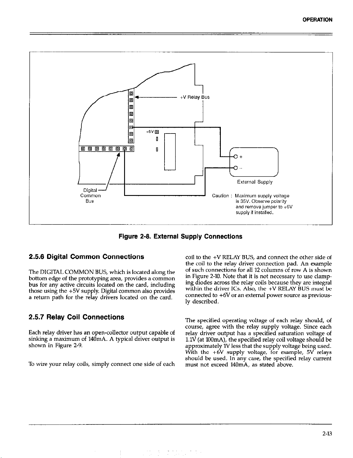
2.5.5 Internal/External Relay Powering
Card relays can be powered either from the +6V mainframe supply, or from an external supply of up to 35V, as
described below.
z-11
Page 25

OPERATION
Internal Relay Supply
To power all relays from the +6V supply, you must install
a jumper between the +6V pad and the +V RELAY BUS,
as shown in Figure 2-7. Be sure to remove this jumper if
using an external supply.
available from the +6V supply is required, an external
supply of up to +35V can be connected to the card, as
shown in Figure 2-8. Connect the positive terminal to the
+V RELAY BUS, and connect the negative terminal to the
DIGITAL COMMON BUS.
CAUTION
Do not exceed 35V for the external supply. Also,
make sure to disconnect the internal +6V supply when using an external supply, or damage
to the card or mainframe may occur.
Splitting the Relay Supply
In some cases, you may wish to split up the power supply
allotment among the relays because of different relay
voltages or other factors such as current constraints. To do
so, simply cut the +V RELAY BUS at a convenient location, and connect the two sections to the internal and external supplies, as required. Be careful to avoid a short between the two sections, or instrument damage may occur.
Power Supply Decoupling
Figure 2-7. Jumper Installation for Internal Relay
SUPPlY
External Relay Supply
In cases where more current or a higher voltage than is
Active circuits wired on the prototyping board should be
properly decoupled to ensure proper operation and
minimum EM1 radiation. For example, digital circuits
typically use a O&F capacitor between +5V and digital
common, with one capacitor per IC for MS1 and LSI
packages, and one capacitor for every three or four
packages for small scale integration ICs. Each capacitor
should be mounted as close to the IC as possible, and only low equivalent series resistance capacitors such as
ceramic film types should be used.
242
Page 26
+
External Supply
OPERATION
1
Common
Bus
Figure 2-6. External Supply Connections
2.5.6 Digital Common Connections
The DIGITAL COMMON BUS, which is located along the
bottom edge of the prototyping area, provides a common
bus for any active circuits located on the card, including
those using the +5V supply. Digital common also provides
a return path for the relay drivers located on the card.
2.5.7 Relay Coil Connections
Each relay driver has an open-collector output capable of
sinking a maximum of 140mA. A typical driver output is
shown in Figure 2-9.
To wire your relay coils, simply connect one side of each
Caution : Maximum supply voltage
is 35’ Observe polarity
and remow jumper to +W
supply ii installed.
coil to the +V RELAY BUS, and connect the other side of
the coil to the relay driver connection pad. An example
of such connections for all 12 columns of row A is shown
in Figure 2-10. Note that it is not necessary to use clamping diodes across the relay coils because they are integral
within the driver KS. Also, the +V RELAY BUS must be
connected to +6V or an external power source as prwiously described.
The specified operating voltage of each relay should, of
course, agree with the relay supply voltage. Since each
relay driver output has a specified saturation voltage of
l.lV (at lOOmA), the specified relay coil voltage should be
approximately 1V less that the supply voltage being used.
With the +6V supply voltage, for example, 5V relays
should be used. In any case, the specified relay current
must not exceed 140mA, as stated above.
2-13
Page 27

OPERATION
r----------i
I
I
I
I
I
I
I >
I
I
I
L----------A
Driver IC
I
I
+v
+35V Maximum External Supp,,,
User-installed Relay
I
I$
Figure 2-9. Typical Relay Driver Output
Digital
Common
Relay Bus (+6V or
.A,\
User-Installed
Relays
Relay Drivel
Outputs
+v Relay Bus
(+6V or +35V Maximum External Supply)
P
ii!!‘l:‘El)i’
’ { Al A2 A3 A4 A5 A6 A7 A6 A9 A10 Al 1 A12
Notes : 1.) Maximum current per relay is 140mA.
2.) Nominal driver saturation voltage is TX 1V.
Figure 2-10. Typical Relay Coil Connections (Row A Shown)
2-14
Page 28

OPERATION
2.5.6 Relay Matrix Wiring
The exact way you wire your relay contacts will, of course,
depend on your particular requirements. Typically, such
relays will be wired in a row-column matrix configuration,
as shown in Figure 2-11 (for the sake of clarity, we have
shown only a few relays on the diagram), Note that 3-pole
switching is shown, with HI, ID, and guard all switched.
If the relays are equipped with shields, guard would be
connected to the relay shields.
HI
A
B LO
LO
Guard
HI
In order to complete the matrix, the like contacts of the
relays must be connected together to complete the rowcolumn format. One end of each row and column group
would typically be connected to the input/output connectors, while the other end of each row and column group
would be connected to the pathway extension pads, if
matrix expansion to other cards in the mainframe is
required.
Guard
HI
H
LO
Guard
Figure 2-H. Relay Matrix Wiring
2-15
Page 29
2.5.9 Relay Settling Time
Any mechanical relay takes a finite length of time to make
contact and settle completely. The other cards in the Model
707 system have a hardware settling time that is dependent
on the type of relays programmed into their ROMs.
However, since there is no way to anticipate the type of
relays you will use, the Model 7070 has a hardware settling time of lmsec programmed into its ROM. For that
reason, it will be necessary for you to program a suitable
settling time into the Model 707. The required settling time
will, of courx’depend on your particular relays; see the
relay specifications for information. Settling time can be
programmed using the front panel SETTLING TIME key
(or over the bus with the S command). The allowable range
for the settling time is lmsec to 65.535~~ in lmsec
increments.
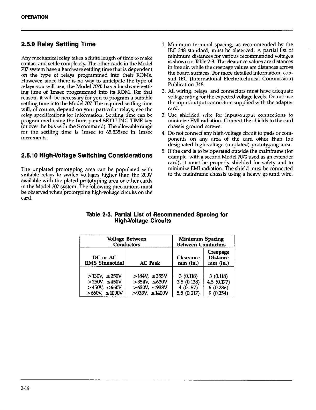
2.5.10 High-Voltage Switching Considerations
The unplated prototyping area can be populated with
suitable relays to switch voltages higher than the ZOOV
available with the plated prototyping area or other cards
in the Model 707 system. The following precautions must
be observed when prototyping high-voltage circuits on the
card.
1. Minimum terminal spacing, as recommended by the
IEC-348 standard, must be observed. A partial list of
minimum distances for various recommended voltages
is shown in Table 2-3. The clearance values are distances
in free air, whiie the creepage values are distances across
the board surfaces. For more detailed information, consult IEC (International Electrotechnical Commission)
Publication 348.
2. All wiring, relays, and connectors must have adequate
voltage rating for the expected voltage levels. Do not use
the input/output connectors supplied with the adapter
card.
3. Use shielded wire for input/output connections to
minimize EM1 radiation. Connect the shields to the card
chassis ground screws.
4. Do not connect any high-voltage circuit to pads or components on any area of the card other &an the
designated high-voltage (unplated) prototyping area.
5. If the card is to be operated outside the mainframe (for
example, with a second Model 7070 used as an extender
card), it must be properly shielded for safety and to
minimize EMI radiation. The shield must be connected
to the mainframe chassis using a heavy ground wire.
Table 2-3. Partial List of Recommended Spacing for
High-Voltage Circuits
r
DC or AC
RMS Sinusoidal
>mv, zs25w
>25w, <45Ov
>45w, <66Ov
>66Ov, ~1Ooov
etween
ctors
AC Peak
>l84v, 5355v
>354v, dl3w
>63ov, 5933v
>933v. s14oov
Minimum Spacing
T
Between C hductors
Clearance
mm (in.)
3 (0.118)
3.5 (0.138)
4 (0.157)
5.5 (0.217)
Creepage
Distance
mm (in.)
3 (O.lls)
4.5 (O.l77)
6 (0.236)
9 (0.354)
1
2-16
Page 30
OPERATION
2.5.11 Prototype Card Installation
After prototyping your circuits, install the card in the
desired slot of the mainframe. The detailed installation procedure is covered in paragraph 2.4.4.
WARNING
The card mounting ecrewe must be secured to
ensure a good connection to chassis ground.
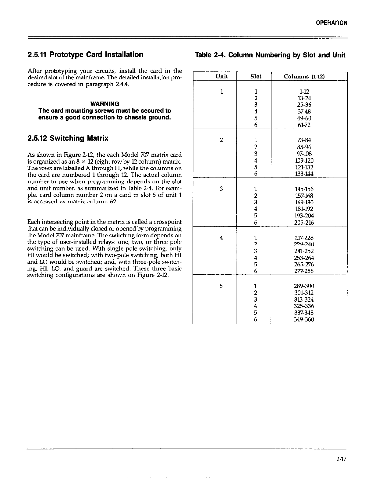
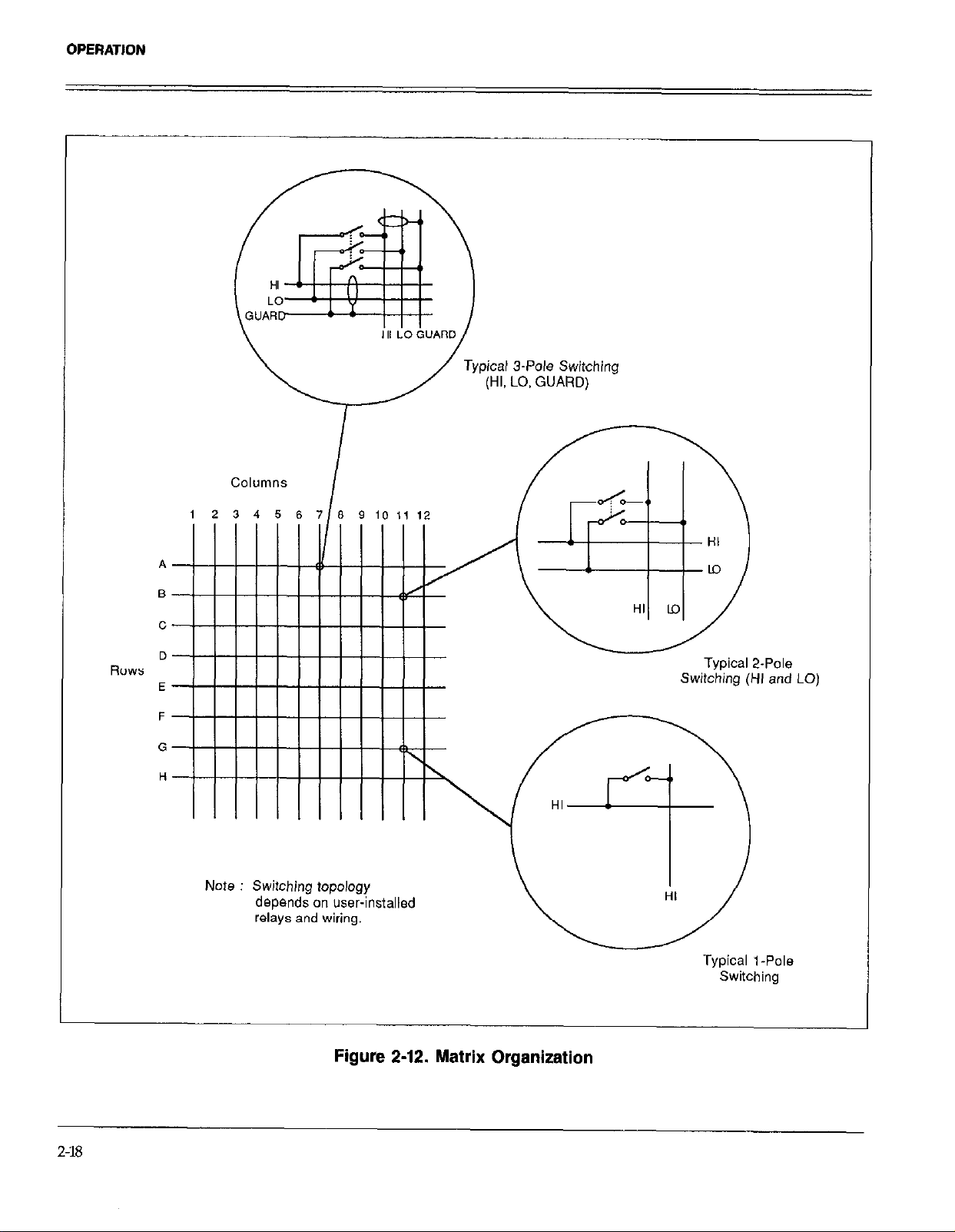
2.5.12 Switching Matrix
As shown in Figure 2-12, the each Model 707 matrix card
is organized as an 8 x 12 (eight row by 12 column) matrix.
The rows are labelled A through H, while the columns on
the card are numbered 1 through 12. The actual column
number to use when programming depends on the slot
and unit number, as summarized in Table 2-4. For example, card column number 2 on a card in slot 5 of unit 1
is accessed as matrix column 62.
Each intersecting point in the matrix is called a crosspoint
that can be individually closed or opened by programming
the Model 7G7 mainframe. The switching form depends on
the type of user-installed relays: one, two, or three pole
switching can be used. With single-pole switching, only
HI would be switched; with two-pole switching, both HI
and LO would be switched; and, with three-pole switching, HI, LO, and guard are switched. These three basic
switching configurations are shown on Figure 2-12.
Table 2-4. Column Numbering by Slot
Unit
1
Slot Cohnns (142)
1
2
3 25-36
4
5
6
1
2
3 97108
4 109-120
5 121-132
6 133-144
l-12
13-24
37-48
49-60
61-72
73-84
85-96
145-156
157-168
169-180
X31-192
193-204
205.216
217-228
229.240
241-252
253-264
265-276
277288
and Unit
-
289.300
301-312
313.324
325-336
337348
349-360
2-17
Page 31
OPERATION
Columns
I.0 GIJARD
HI
Typical 3-P& Switching
(HI, LO, GUARD)
i
2-18
Note : Switching topology
depends on user-installed
relays and wiring.
Typical l-Pole
Switching
Figure 2-12. Matrix Organization
Page 32

2.5.13 internal Matrix Expansion
Two to six matrix cards can be connected together within
the mainframe to yield an 8 x N matrix, where N depends
on the number of cards. Figure Z-13 shows an internally
expanded matrix with three cards, resulting in an 8 x 36
(eight row by 36 column) matrix. As summarized in Table
2-2, the actual column number used when programming
the unit is determined by the slot.
For ANALOG #2 and ANALOG #3 pathways, all rows (A
through H) are automatically connected together through
the backplane of the mainframe (you must of course make
the necessary on-card connections from your relay buses
to the appropriate pathway pads). For ANALOG #l, pathways C through F are connected through the backplane,
while rows A, 8, G, and H use the SMB connectors. As
discussed previously, ANALOG #l connects to Model 7072
cards, ANALOG #2 connects to Model 7071 cards, and
ANALOG #3 connects to Model 7U73 cards.
The mainframe can be configured for two sets of three
cards each by removing jumpers from the backplane of the
mainframe; see Section 3 of the Model 707 Instruction
Manual for details on removing the jumpers. With the row
jumpers removed, cards in slots 1 through 3 are connected,
and cards in slots 4 through 6 are connected together.
Because of more critical signal paths, rows A, B, G, and
H of ANALOG #l are not jumpered through the
backplane. Instead, you must install the coaxial jumpers
(supplied with the Model 7072) between appropriate connectors on Model 7070 and 7072 cards. Each card has one
OI two SMB coaxial connectors for each row, allowing daisy
chaining of card rows. These connectors can be reached
by lifting the access door on the top of the mainframe; it
is not necessary to remove cards to install the jumpers.
2.5.14 External Matrix Expansion
External jumper wires must be used to expand the number
of rows in the matrix, or to connect between columns of
cards installed in different mainframes. An example of
such an expanded matrix is shown in Figure 2-14. Here,
six cards are configured as a 16 x 36 matrix. Since the rows
are internally jumpered, only columns must be jumpered
externally in this configuration. Note that the backplane
jumpers must be removed to separate the cards into two
groups.
Note : Rows A-H of ANALOG #Z and ANALOG #3, and KW C-F of ANALOG #I jumpered through backplane.
Rows A, B, G, and H of ANALOG #1 require installation of coaxial jumpers.
Figure 2-13. Connecting Three Cards for 6 x 36 Matrix
2-19
Page 33

OPERATION
2-20
Figure 2-14. 16 x 36 Matrix Constructed by External Jumping
Page 34

OPERATION
2.6 MEASUREMENT CONSIDERATIONS
Many measurements made using the Model 7070 concern
low-level signals. Such measurements are subject to
various types of noise that can seriously affect low-level
measurement accuracy. The following paragraphs discuss
possible noise sources that might affect these measurements.
2.6.1 Magnetic Fields
When a conductor cuts through magnetic lines of force,
a very small current is generated. This phenomenon will
frequently cause unwanted signals to occur in the test leads
of a switching matrix system. If the conductor has sufficient strength, even weak magnetic fields like those of the
earth can create sufficient signals to affect low-level
measurements.
Two ways to reduce these effects are: (1) reduce the lengths
of the test leads, and (2) minimize the exposed circuit area.
In extreme cases, magnetic shielding may be required.
Special metal with high permeability at low flux densities
(such as mu metal) are effective at reducing these effects.
Even when the conductor is stationary, magneticallyinduced signals may still be a problem. Fields can be produced by various signals such as the AC power line
voltage. Large inductors such as power transformers can
generate substantial magnetic fields, so care must be taken
to keep the switching and measuring circuits a good
distance away from these potential noise sources.
result from impulse sources, as in the case of arcing in
high-voltage environments. In either case, the effect on the
measurement can be considerable if enough of the unwanted signal is present.
RF1 can be minimized in several ways. The most obvious
method is to keep the equipment and signal leads as far
away from the RFI source as possible. Shielding the matrix
switching card, signal leads, sources, and measuring instruments will often reduce RF1 to an acceptable level. In
extreme cases, a specially-constructed screen room may be
required to sufficiently attenuate the troublesome signal.
Many instruments incorporate internal filtering that may
help to reduce RF1 effects in some situations. In some
cases, additional external filtering may also be required.
Keep in mind, however, that filtering may have detrimental effects on the desired signal.
2.6.3 Ground Loops
When two or more instruments are connected together,
care must be taken to avoid unwanted signals caused by
ground loops. Ground loops usually occur when sensitive
instrumention is connected to other instrumentation with
more than one signal return path such as power line
ground. As shown in Figure 2-U, the resulting ground loop
causes current to flow through the instrument LO signal
leads and then back through power line ground. This circulating current develops a small but undesirable voltage
between the Lo terminals of the two instruments. This
voltage will be added to the source voltage, affecting the
accuracy of the measurement.
At high current levels, even a single conductor can generate
significant fields. These effects can be minimized by using twisted pairs, which will cancel out most of the
resulting fields.
2.6.2 Radio Frequency Interference
RF1 (Radio Frequency Interference) is a general term used
to describe electromagnetic interference over a wide range
of frequencies across the spectrum. Such RF1 can be particularly troublesome at low signal levels, but is can also
affect measurements at high levels if the problem is of suf-
ficient severity.
RF1 can be caused by steady-state sources such as radio
or TV signals, or some types of electronic equipment
(microprocessors, high speed digital circuits, etc.), or it can
Figure 2-15. Power Line Ground Loops
2-21
Page 35

Figure 2-16 shows how to connect several instruments
together to eliminate this type of ground loop problem.
Here, only one instrument is connected to power line
ground.
instrument 1 Instrument 2 Instrument 3
0 0 o---o
T T 1
Powet Line Ground
=F
Figure 2-16. Eliminating Ground Loops
of connectors can be compromised if they are not handled properly. If the connector insulation becomes contaminated, the insulation resistance will be substantially
reduced, affecting high-impedance measurement paths.
If the connector insulators should become contaminated,
either by inadvertent touching, or from air-borne deposits,
they can be cleaned with a cotton swab dipped in clean
methanol. After thorough cleaning, they should be allowed to dry for several hours in a low-humidity environment
before use, or they can be dried more quickly using dry
nitrogen.
2.6.5 Shielding
Proper shielding of all signal paths and devices under test
is important to
ching matrix system. Otherwise, interference from such
noise sources as line frequency and RF fields can seriously corrupt a measurement.
minimize noise pickup in virtually any swit-
Ground loops are not normally a problem with instruments having isolated Lo terminals. However, all instruments in the test setup may not be designed in this
manner. When in doubt, consult the manual for all instrumentation in the test setup.
2.6.4 Keeping Connectors Clean
As is the case with any high-resistance device, the integrity
In order for shielding to be effective, the shield should be
connected to signal M (or chassis ground for instruments
without isolated LO terminals). If the device under test
is to be shielded, the shield should also be connected to
the LO terminal. Figure 247 shows typical shielding configuration for a matrix card using 2-pole switching.
2-22
Page 36

r--------i
OPERATION
Figure 2-17. Shielding Example
2.6.6 Guarding
Guarding is important in high-impedance circuits where
leakage resistance and capacitance could have degrading
effects on the measurement. Guarding consists of using
a shield surrounding a conductor that is carrying the highimpedance signal. This shield is driven by a lowimpedance amplifier to maintain the shield at signal
potential.
Guarding minimizes leakage resistance effects by driving
the cable shield with a unity gain amplifier, as shown in
Figure 2-K Since the amplifier has a high input impedance, it minimizes loading on the high-impedance
signal lead. Also, the low output impedance ensures that
the shield remains at signal potential, so that virtually no
leakage current flows through the leakage resistance, RL.
Leakage between inner and outer shields may be considerable, but that leakage is of little consequence because
Relay Shield
(if available)
that current is supplied by the buffer amplifier rather than
the signal itself.
In a similar manner, guarding also reduces the effective
cable capacitance, resulting in much faster measurements
on high-impedance circuits. Because any distributed
capacitance is charged through the low impedance of the
buffer amplifier rather than by the source, settling times
are shortened considerably by guarding.
In order to use guarding effectively with the Model 7070,
the GUARD path of the matrix card should be connected
to the guard output of the sourcing or measuring instrument. Each guard path should be switched by the crosspoint relay; thus 3-pole switching should be used with
guarding (assuming that both HI and LO are also switched). Figure 2-19 shows a typical matrix card guarded
configuration.
2-23
Page 37

OPERATION
DUT
r------ ---,
Guarded
Switch
Figure 2-16. Guarded Circuit
r---i
0
Instrument
2-24
Chassis
Measuring or Sourcing
Instrument
Warning : Lethal voltage may be present on guard. Surround guard
Connect Guard
to Relay Shield
if available.
with safety shield. Connect safety shield to card chassis ground.
L-------J
Crosspoint Relay
Matrix Card
Figure 2-19. Typical Guarded Connections
Page 38

SECTION 3
Applications
3.1 INTRODUCTION
Applications for the Model 7070 Universal Adapter Card
will depend, of course, on your particular needs. This section presents some typical applications for the Model 7070
used as a prototyping card, and it is arranged as follows.
3.2
Scanner Switching:
as a scanner instead of as a switching matrix.
3.3
On-Card Buffering:
minimize the effects of leakage resistance.
3.4
Solid-state Relays:
for such purposes as power control.
3.5
High-Speed Analog Switching:
solid-state switching KS to provide high-speed switching not possible with relays.
3.6
Using the Adapter Card with Other Matrix Cards:
Gives two typical applications for using the Model
7070 with other matrix cards.
Outlines methods to use the card
Details using on-card buffers to
Covers solid-state relay switching
Describes the use of
3.2 SCANNER SWITCHING
switch, as shown in Figure 3-l. Each switch position is actually a set of relay contacts, giving the switch 1, 2, 3, or
even 4-pole switching capability.
A scanner operates by stepping through its inputs or channels in sequence. Thus, with the example in Figure 3-1,
the switch would begin at channel 1, advance to channel
2, and so on until all channels have been sequenced. After
the last channel in the sequence, the unit will start over
again with channel 1. Note that only one channel is connected to the output at any given time.
3.2.2 Relay Wiring
Figure 3-2 shows how to connect eight 2-pole relays
together to construct an &input, 2.pole scanner. Note that
one side of each set of relay contacts serves as a channel
input, while the other side of each set of relay contacts are
paralleled together as the scanner output. Other relay
types could be used for 1, 3, or even 4-pole switching, as
required. Additional relays could be added to increase the
number of scanner inputs, as required, up to a maximum
of 96 relays per card.
Although the primary configuration of a Model 707 is as
a switching matrix, there are situations where a scanner
switching system can do the job better. The following
paragraphs discuss various aspects of building a scanner
switching system on the Model 7070.
3.2.1 Scanner Configuration
Functionally, a scanner can be thought of as a rotary
For control, the relay coils must be wired to the relay driver
outputs and the +V RELAY BUS (which must itself be connected to the desired relay voltage). Figure 3-3 shows the
relays wired to columns 1 through 8 of row A. Of course,
you can connect the relays to any unused driver outputs;
simply keep in mind which “crosspoints” to close when
programming the unit, as discussed in the paragraph
below.
Page 39

APPLICATIONS
DUT 1
DUT 2
DUT 3
DUT 4
DUT 5
DUT 6
DUT 7
DUT 8
r----------i
I
I
I
I
I
I
I
I 0
I
I o
I
I I
I
I
I
I I
L-----------l
0
0
0 I
0
0
Multiplexer
I
I
I
I
I
I
I
I
!
I
I
I
I
I
Measuring
Instrument
Figure 3-1. A Scanner as a Rotary Switch
3-2
Page 40

APPLICATIONS
r
,
Channel 2
Channel 3
Channel 4
Channel 5
Channel 6
Channel 7
Channel 8
Figure 3-2. B-Input, 2-Pole Relay Scanner
.
scanner
output
3.2.3 Programming
the Scanner
Since the Model 707 is designed as a switching matrix, the
intelligence necessary to control a scanner must be design-
ed into a controlling program (or appropriate front panel
setups can be used to sequence through the relays). Program 1 below, which is written in Hewlett-Packard BASIC,
demonstrates the basic principles of controlling the scanner with programming. Figure 3-4 is a flowchart of the program. One feature included in the program is a programmable channel settling time. As written, the program
assumes that the Model 7070 is located in slot 1 of the
Model 707. Note that user-defined code must be added
to line 80 to control any measurement instrument.
Program 1 Simple Scanner Program Control
Comments
6 i :.::! ?
70 I.liiIT
SE1 ! IUSER S ~1EA!XIREtIEt~T CODE.
Settle
Put 707
remote.
Return 707 to
default.
Input settling
time.
Settle time in
msec.
Loop for all
eight channels.
Close A, I.
Settling time.
Add code for
measurement
instrument.
Open channel.
in
Al AZ A3
A4 A5 A6
A7 A8
Figure 3-3. Scanner Relay Coil Wiring
Loop back for
next channel.
Relay Drive’
outputs
3-3
Page 41

3.2.4 A Practical Scanner Application
A scanner performs well at switching a number of devices
to one instrument. One possible application for a scanner
is shown in Figure 3-5. Here, we are using the scanner to
select among the eight resistances located in a thick-film
resistor package. A Model 196 DMM is used to make the
resistance measurement. For lower-value resistors, the
4.wire measurement method shown should be used for
maximum accuracy. Note that only 2.pole switching is required because of the common device terminal. For other
4wire measurements, 4.pole switching may be required.
Program 1 above can be modified to make the resistance
measurements. Program 2 below provides the basic test
capability for the system, including the basic scanner sequencing, and obtaining and displaying a reading from the
DMM. Figure 3-6 is a flowchart of the program. Keep in
mind that this program may require modification for your
particular requirements.
Program 2 Resistor Test Program
Measurement
Program
10 REMOTE 718
30 CluTFtuT
40 OUTPlJT
1241 OUTFUT 718 .i 6 i NA ’ .: I; i *Xl 7
130 NEXT I
14W EHD
71:s .i 6 6 RBX 7
787 ,: I i F2R@XI
:tlE
I.iLLX3’
s 196 ohms func-
Comments
Put 707
remote.
Put 196
remote.
in
in
Return 707 to
default.
tion,
autorange.
Input settling
time.
Settle time in
msec.
Loop for all
eight channels.
CloseA,I.
Settling time.
Get 196
reading.
Display 196
rea;ling.
Open channel.
Loop back for
next channel.
34
Figure 3-4. Program 1 Flowchart
Page 42

r-------i
APPLICATIONS
OHMS SENSE HI
"cLT,OHMS LO
OHMS SENSE LO
on 7070 Card
Figure 3-5. Testing Thick Film Resistor with a Scanner
3-5
Page 43

APPLICATIONS
l”P”,
Settling
Time
cl
3.3 ON-CARD BUFFERING
Buffers can be incorporated into a switching matrix constructed on a Model 7070 card in order to minimize the
effects of loading on the circuit under test. Such buffering
can extend the measurement range of the card to higherimpedances than would otherwise be possible by minimizing the effects of leakage resistance and capacitance, as well
as providing drivers for guarding. The following
paragraphs discuss buffer configuration, powering the buffers, as well as a typical application for on-card buffers.
3.3.1 Buffer Configuration
The chief advantage of buffers is that they provide isolation between a device under test and the switching and
measurement pathways. Typically, buffers would be placed
between the row or column inputs and any switching
relays, as shown in the simple matrix of Figure 3-7 In this
instance, a simple 2 x 2 matrix is shown, but the same
general configuration would be used for larger matrices.
Since a buffer is a unity-gain operational amplifier, its output voltage is the same as the input. Because the buffer
typically has much lower output impedance than the
device being buffered, loading effects of pathways and test
instrumentation are minimized.
A buffer output can also be used to provide a driven guard
signal, which is also shown in Figure 3-7, The guard should
be connected to the shield surrounding the signal pathway
of the high-impedance input circuitry. Either coaxial or
triaxial cables can be used (triaxial cable should be used
for safety considerations for guard voltages above 3OV, with
the outer shield connected to chassis ground). If the
associated switching relays are shielded, guard can be connected to the relay shields.
3-6
Figure 3-6. Program 2 Flowchart
Page 44

APPLICATIONS
Signal >
Row A
Guard >
Signal
Row B
Guard
3.3.2 Buffer Considerations
Column 1
n
Row A Buffer
Figure 3-7. Buffer Configuration
3.3.3 Powering the Buffer ICs
Column 2
For best performance, only high-quality op amps should
be used for buffers. Specified offset current and offset
voltage should be <lpA and <lmV respectively. Typical
of available high-quality ICs is the OPA104 (Keithley Part
Number IC-519), which is one op amp recommended for
this application.
Care in component selection should not stop at the buffer
ICs. All components on the buffer input side should be
carefully selected to ensure that high isolation resistance
is maintained. BNC and triax connectors used on the input should be Teflona msulated. Also, do not connect any
high-impedance nodes to the circuit board itself; instead,
mount Teflon@ insulators on the board, and make all connections at the insulator terminals.
Typical ICs used as buffers require both positive and
negative power supplies in the neighborhood of f15V dc.
This situation presents a small problem with the Model
7070 because only +5V and +6V supplies are available.
Forhmately, there is a fairly simply solution: a dc converter,
which can convert the available supply voltage to positive
and negative voltages usable by the on-card buffers, can
be mounted on one of the prototyping areas.
Figure 3-8 shows a typical power supply arrangement using a dc converter module (Keithley part #MO-E+ The converter is powered by the +5V supply available on the card,
and it supplies *l8V at a maximum current of k17OmA.
In order to reduce and regulate the supply voltages, +15V
and -15V regulator ICs are used along with the usual filter
capacitors.
3-7
Page 45

APPLICATIONS
+15v Regulator
/
1
+i8V
1 O&F
corn
*
1 O&F
DC Converter
I
-18V
Figure 3-8. DC Converter Used to Power Buffer ICs
3.3.4 A Typical Buffer Application
On-card buffering can be used whenever high-impedance
circuits are involved. One possible application for such oncard buffering is for high-resistivity measurements on
semiconductors. Such measurements can help in yielding
important information about semiconductors such as doping concentration.
‘7
I+ ’
Signal
+
0 IN
-15v Regulator
OUT 0
I
1
OUT
S”ffW
the current is sourced by a Model 220 current source, and
the voltage is measured by a Model 196 DMM. The switching matrix provides the flexibility necessary to make the
various connections for the measurements, and the oncard buffers isolate the sample under test from the DMM
to minimize the effects of loading, which would otherwise
degrade accuracy for measurements above lM&
Figure 3-9 shows a typical test system that can be used to
perform such tests. Basically, resistivity is determined by
forcing a current through the sample under test, and then
measuring the voltage across the sample. In this example,
3-8
In order to compensate for such factors as thermal EMFs,
a total of eight voltage measurements are generally made
on a typical sample, as shown in Figure 3-10. The resulting
voltages are then used to compute the resistivity of the
sample.
Page 46

APPLICATIONS
1
A
220 Current source
(Sources Current through Sample)
2
Columns
196 DMM
(Measures Voltage Across sample)
Figure 3-9. Typical High-Resistivity Test System
3-9
Page 47

APPLICATIONS
A4
(G)
03 Cl
Al
I
02 c‘l
’ (H)
3-10
Note : @ Denotes closed crosspoints from figure 3-9
Figure 3-10. Voltages Necessary to Determine Resistivity
Page 48

3.4 SOLID-STATE RELAYS
The Model 7070 can be populated with solid-state relays
to provide switching capabilities not available with other
Model 707 cards. The following paragraphs discuss the advantages of using solid-state relays, give a typical example
of how to wire them, and also summarize several considerations to observe when using solid-state relays.
3.4.1 Solid-state Relay Advantages
There are several advantages to using solid-state relays, including long life, zero-crossing turn off, and high isolation, as discussed below.
APPLICATIONS
High Reliability
Because the switching component of a solid-state relay is,
by definition, solid state, such relays generally last indefinitely, in contrast to their mechanical counterparts,
which have a limited contact life. The actual switching component used depends on the application. Relays designed to switch dc use a simple power transistor, while relays
designed for ac use a triac.
Zero-crossing Switching
Virtually all relays designed for ac switching have zerocrossing turn off, and many incorporate zero-crossing turn
on. Zero-crossing action simply means that the switching
action of the relay occurs at the point when the ac signal
crosses the zero axis, as indicated in Figure 3.11. Zerocrossing switching minimizes EMI radiation when controlling inductive loads such as motors, solenoids, or
transformers. Such switching can be beneficial when sensitive digital and analog circuits must be operated in the
same electrical environment as power circuits.
Figure
High Isolation
3-11. Zero-crossing Switching
Many solid-state relay modules have a high degree of electrical isolation (typically 2.5-4kV) between the control input and the switching output. This type of relay should
always be used with the Model 7070 to ensure proper isolation between the card and high-voltage circuits.
WARNING
Do not use non-isolated solid-state relays with
the Model 7070.
Isolated relays use optical coupling between control circuits and the output stages. Figure 3-12 shows a simplified
schematic diagram of an ac solid-state relay, and Figure
3-13 shows a simplified diagram of a typical dc solid-state
relay. The main difference between the two relays is the
type of device used in the switching circuit: the dc relay
uses a transistor, while the ac relay uses a triac.
3-11
Page 49

APPLICATIONS
+V Relay Bus
Control I Control I
R&V
D&r
+v
way BUS
1‘
1‘
I I
+’ +’
Input , Input ,
T T
+--+
\L
r----
+’
r----- r-----
L----
-------------
__-----------
DC Solid-State Relay
Figure 3-12. Typical DC Solid-state Relay
-------------
1
I
I
J
1
I
DC Supply
AC Supply
Load
3-n
Control I
Input ,
+----I
L----
------------AC Solid-State Relay
Relay
Driver
Flgure 3-13. Typical AC Solid-state Relay
I
J
Page 50

APPLICATIONS
3.4.2 Typical Application
Figure 3-14 shows a typical configuration using solid-state
relays. Note that the + terminal of the relay control circuit
is connected to the +V RELAY BUS, while the - terminal
of the control circuit is connected to the desired driver
output.
The relay output is connected in series with the ac supply
and the load, which could be any appropriate ac device
such as a motor or solenoid. In this application we have
added an MOV (Metal Oxide Varistor) across the output
’ +
RL-78
2
Al
I
Relay Driver
terminals to protect the device from transients. A series
fuse is included to protect the relay from over-current situations. Fusing is recommended for all solid-state relays as
they are much less tolerant of abuse than mechanical
relays.
This particular application uses a Teledyne 675-6 relay
(Keithley part number RL78). The control voltage for this
device is in the range of 3VDC to 32VDC, and the unit can
switch a maximum of 14OV, 3A RMS. The minimum turnon current for this relay is lOOmA.
1 140V AC Max
3 _ ,
I
MO”
’ (“R-1)
4
I
I
I
Fast El<
,“‘YLY1,
Solenoid,
Etc)
I
I
L------l-.-------l
7070 Card
Note : 1.) Relay is Teledyne 675-6 (Keithley RL-78)
2.) Fuse and MOV should be used where shown to protect
relay from over current and transients.
Figure 3-14. Typical Solid-state Relay Application
’ 140V AC Max
3-13
Page 51

APPLICATIONS
3.4.3 Solid-state Relay Considerations
While solid-state relays do have their advantages, there are
a number of considerations to keep in mind when using
them, including:
1. Solid-state relays are usually specified for either dc or ac
voltages only. You cannot use a dc switching relay for
control ac or vice versa.
2. In addition to a maximum current, such relays often
have a specified minimum turn-on current below which
the relay will not operate. You can determine the appmximate relay current from Ohm’s law by dividing the
supply voltage by the load resistance.
3. The control voltages for both dc and ac relays are dc,
so you must carefully observe polarity. Connect the +
control terminal to the +6V (or external) supply, and
connect the - terminal to the relay driver output. Proper polarity must also be observed on the output ter-
minals of a dc relay.
4. When switching voltages above ZOOV, mount the relays
on and make connections to only the unplated prototyping area of the card. Be sure to observe pmper voltage
spacing, as discussed in paragraph 2.5.10.
5. Use only isolated solid-state relays, and make sure the
outputs are fused according to the current rating of the
device. Fast blow fuses should be used to ensure proper protection. Also, a transient-suppression device,
such as an MOV, should be connected across the output terminals.
3.5.1 Analog Multiplexer ICs
Functionally, a multiplexer IC can be thought of as a series
of solid-state switches, as shown in Figure 3-25. In this instance, an 8-input multiplexer is shown, although 4-input
and 16-input multiplexer ICs are also available. Note that
only one switch can be closed at any given time, as determined by IC control circuitry.
r-----i
Multiplexer
output
L-----J
I
MUX IC
3.4.4 Programming Solid-state Relays
To control solid-state relays, simple close or open the appropriate crosspoint as you would with any mechanical
relay. The relay will hum on when the crosspoint is closed,
and it will turn off when the crosspoint is open (assuming proper wiring). For example, for a &y connected to
relay driver terminal Al, close crosspoint Al from the front
panel, or send the “CAD” command over the bus.
3.5 HIGH-SPEED ANALOG SWITCHING
The following paragraphs discuss solid-state analog switching with higher speed than is usually possible with
electm-mechanical relays. Typical circuits and a control pmgram are also presented.
Figure 3-15. Typical Multiplexer IC
Solid-state multiplexer ICs have several advantages over
mechanical relay-based units, including:
l
Solid-state switching gives higher reliability.
l
Much faster switching than is possible with relays
(typically in the psec range).
l
Smaller size than relays, allowing much higher circuit
density.
l
Lower power requirements
l
Lower cost per switch.
3-14
Page 52

APPLICATIONS
Although such ICs are better suited to many applications,
they do have some disadvantages, such as:
l
Limited voltage capability (typically +lOV).
l
Relatively high on resistance (typically hundreds of
ohms).
l
Susceptability to damage from electrical discharge.
l
Require positive and negative supply voltages.
3.5.2 Typical Analog Switching Circuit
Figure 3-16 shows a typical circuit using an analog
multiplexing IC. Additional control circuitry includes a programmable timer to allow specific intervals between channels to be programmed. The same type of operation could
be performed by programming the Model 707, but at the
expense of speed. This circuit will allow you to scan channels at rates as high as 100kHz. Note that the timer is configured for astable operation. For monostable operation,
disconnect timer RESET from main RESET, and connect
timer RESET to COUNT instead.
The various sections of the circuit are discussed below.
Relay Driver Interfacing
The circuit is interfaced to the Model 7070 relay drivers Al
through AlO. Al-Al3 provide timer programming information, while A9 is the RESET signal for the timer and the
counter. A10 is the TRIGGER signal which starts the programmable timer.
basic unit interval is determined by the values of R, and
c, as follows:
t = R,r C,
For example, typical values for a lmsec minimum interval
are lOOk and O.Ol$. Two or more timer ICs can be cascaded to increase the programmable interval range. For ex-
ample, one additional timer IC will increase the range to
65,535 interval counts. Note that the maximum timer frequency is lOOkHz, for a minimum interval between chan-
nels of lo~sec.
Counter
The output pulses of the programmable timer are used to
sequence a 4-bit binary counter, IC5. As pulses occur, the
counter counts from 0000 to 1111 in sequential order,
module 16. The counter outputs are used to select
multiplexer inputs, as described below.
Multiplexer IC
IC5 is the analog multiplexer IC (6116), which has 16 analog
inputs. The input that is routed to the output is determined
by the logic level on the AO-A3 inputs, as outlined in the
truth table shown in Table 3-l. Note that the multiplexer
requires +15V supply voltages, and the maximum input
is limited to
paragraph 3.3 could be used to supply the mux IC.
*llV.
The DC converter discussed in
Table 3-1. Multiplexer IC Truth Table
Since the relay driver outputs are open collector, they must
be pulled up to +5V through the lkQ resistors, Rl-RlO.
Note that closing a specific “crosspoint” will result in a low
logic level, while opening the “crosspoint” sets the logic
level high.
Quad Switches
Two quad switches, ICl and ICZ, provide the interface between the timer programming information and the timer
itself. The logic levels on Al-A8 control whether or not a
specific timer output is connected to the COUNT output
of the timer, and thus the timer interval.
Programmable Timer
IC3, a 7240 programmable timer, provides the fundamental time base for the scanning sequence. The unit is capable
of intervals in the range of l-255 timer units, where the
A, 1 A, / A,
0
0 I
0 0 0
0
0
0
0
0
0 1 1
1 0
0 I
1
1 0
1 0 1
1 1
1 1
1 1 1
1 1 1
1
0
I
1 0
1
I
1
0 0
A0
0
I
1
1
I
0
I
1
0
I
1
i
1
0
Selected Input
13
14
15
16
3-15
Page 53
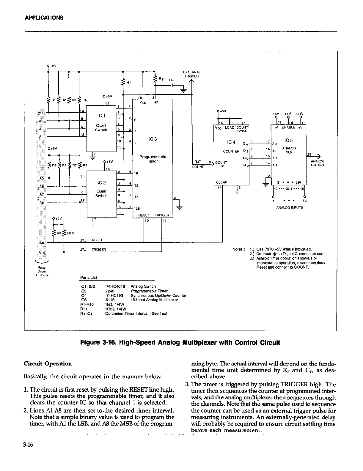
APPLICATIONS
Flgure 3-16. High-Speed Analog Multiplexer with Control Clrcult
Circuit Operation
Basically, the circuit operates in the manner below.
1. The circuit is first reset by pulsing the RESET line high.
This pulse resets the programmable tier, and it also
clears the counter IC so that channel 1 is selected.
2. Lines Al-A8 are then set to.the desired timer interval.
Note that a simple binary value is used to program the
timer, with Al the LSB, and A8 the MSB of the program-
3-16
ming byte. The actual interval will depend on the fundamental time unit determined by R, and CT, as des-
cribed above.
3. The timer is triggered by pulsing TRIGGER high. The
timer then sequences the counter at programmed intervals, and the analog multiplexer then sequences through
the channels. Note that the same pulse used to sequence
the counter can be used as an external trigger pulse for
measuring instruments. An externally-generated delay
will probably be required to ensure circuit settling time
before each measurement.
Page 54

3.53 Control Program
Program 3 below is simple program that demonstrates
basic techniques for controlling the circuit shown in Figure
3-16. The program, which is written in HP BASIC 4.0, will
prompt you to input the timer interval and then program
the interval accordingly. As discussed previously, the timer
interval depends on the values of R, and C,. Figure 3-17
is a flowchart of the program.
APPLICATIONS
Put 707
in Remote
Program 3 Multiplexer Control Program
Program Comments
16 REBOTE 718
20 IlII1 CtlD1C5UI
4M OCITPIUT 718 .: i * k:Wg ’
50 OLITFIJT 718 ,: 6 6 l::Ql,
A2,A3?A4rA5,A6?A7,
AS, 09, (ii@‘x’” ?
60 INPUT i LTIMEF:
I HTER!IAL <: 1 -255::a 9 s , value.
Timer
Put 707 in remote.
Dimension command
string.
Define
letter.
Reset 707.
Set control lines low.
Input timer control
Convert time to
crosspoints.
open command
Reset
707
52
Set Control
Lines Low
ti
Trigger timer, start scan.
Wait 100msec.
Reset trigger pulse.
Figure 3-17. Program 3 Flowchart
3-17
Page 55

APPLICATIONS
3.6 USING THE ADAPTER CARD WITH OTHER MATRIX CARDS
Special circuits mounted on the Model 7070 can be used
with other matrix cards to enhance system capabilities.
Two possible applications are using a scanner-mati combination, and on-card signal conditioning, as discussed in
the following paragraphs.
3.6.1 Scanner-Matrix Combination
A scanner similar to the one discussed in paragraph 3.2
could be used with a matrix card to add additional switching capabilities to that matrix. As shown in Figure 3-18,
the scanner could be used as preselector to add additional
input/output capabilities to a particular row. In this instance, the scanner is being used in conjunction with a
Model 7071 General Purpose Matrix Card, which utilizes
3-p& switching (HI, LO, and guard). To take full advantage of the switching capabilities of the Model 7071,3-p&
switching should be used with the scanner constructed
on the breadboard. External wiring between the two cards
is not necessary; simply connect the scanner output to the
row terminals of the ANALOG #2 pathway on the Model
7070.
3.6.2 Signal Conditioning
limit. To switch higher voltages, signal conditioning circuits, in the form of voltage dividers, can be mounted on
the adapter card. Figure 3-19 shows voltage dividers with
1O:l ratios, which would, for example, attenuate a 1OOOV
signal to 1OOW well within the range of the Model 7071.
WARNING
Mount high-voltage clrcults only on the
unplated prototyping area of the Model 7070,
and maintain proper voltage spacing, es
discussed in paragraph 2.5.10.
In order for the division ratio to be accurate, the input
resistance of any measuring instrument used with the
divider should be much higher than the values of the
divider resistor. An instrument with an input resistance
of 1OMn will result in a loading error of about 1% with the
resistance values shown in Figure 3-19.
As with the scanner example above, external connections
between the two cards are not necessary because connections are automatically made through the backplane. To
take advantage of the backplane pathways, simply connect
the divider outputs to the row pads of the ANALOG #2
pathways located on the Model 7070. The attenuated
signals will be routed through the mainframe backplane
to the corresponding rows of the Model 707l card.
All matrix cards in the Model 707 system have a 200V signal
r-----
-4-L:
Figure 3-18. Adding a Scanner to a Switching Matrix
348
Page 56

r------------------’ 1 2 3 4 5 6 7
L------------------J
7071 General
Matrix car.3
8 9 10 (1 12 ’
Purpose
APPLICATIONS
I
1
/
I
I
I
I
I
I
I
I
I
Figure 3-19. Signal Conditioning Example
3-1913-20
Page 57

SECTION 4
Service Information
4.1 INTRODUCTION
This section contains information necessary to service the
Model 7070 Universal Adapter Card and is arranged as
follows:
4.2 Handling and Cleaning Precautions: Discusses han-
dling precautions and methods to clean the card
should it become contaminated.
4.3 Special Handling of Static-Sensitive Devices:
Reviews precautions necessary when handling staticsensitive devices.
4.4 Troubleshooting: Presents some troubleshooting tips
of the Model 7070.
4.5 Principles of Operation: Brießy discusses circuit
operation.
4.2 HANDLING AND CLEANING PRECAUTIONS
Care should be taken when handling or servicing the card to
prevent possible contamination. The following precautions
should be taken when servicing the card.
1. Handle the card only by the edges and handle. Do not
touch any board surfaces or components not associated
with the repair.
2. Do not store or operate the card in an environment
where dust could settle on the circuit board. Use dry
nitrogen gas to clean dust off the board if necessary.
3. After soldering on the circuit board, remove the ßux
from the work areas when the repair has been completed. Use Freon TMS or TE or the equivalent along
with clean cotton swabs or a clean, soft brush to remove
the ßux. Take care not to spread the ßux to other areas
of the circuit board. Once the ßux has been removed,
swab only the repaired area with methanol, then blow
dry the board with dry nitrogen gas.
4. After cleaning, the card should be placed in a 50°C lowhumidity environment for several hours before use.
4.3 SPECIAL HANDLING OF ST ATIC-SENSITIVE DEVICES
CMOS and other high-impedance devices are subject to
possible static discharge damage because of the high-
impedance levels involved. When handling such devices,
use the precautions listed below.
NOTE
In order to prevent damage, assume that all parts
are static-sensitive.
1. Such devices should be transported and handled only
in containers specially designed to prevent or dissipate
static build-up. Typically, these devices will be received
in anti-static containers made of plastic or foam. Keep
these parts in their original containers until ready for
installation or use.
2. Remove the devices from their protective containers
only at a properly-grounded work station. Also ground
yourself with an appropriate wrist strap while working
with these devices.
3. Handle the devices only by the body; do not touch the
pins or terminals.
4. Any printed circuit board into which the device is to be
inserted must Þrst be grounded to the bench or table.
5. Use only static-sensitive type de-soldering tools and
grounded-tip soldering irons.
4.3.1 Rear Shield
Copper cladding has been added to the rear shield of the
matrix card in order to provide increased protection from
static discharge. The copper shield is electrically connected
to chassis ground of the matrix card by a jumper wire.
In order to service the matrix card, it may be necessary to
remove the rear shield. Referring to Figure 4-1, perform the
following procedure to remove and reinstall the rear shield:
1. Disconnect the jumper wire from the matrix card chassis. The wire is secured to the matrix card chassis with a
screw.
2. The rear shield is secured to the matrix card by eight
standoffs. Carefully slide the rear shield upward until
the eight standoffs align with the large clearance holes
in the shield and remove the shield.
3. To reinstall the shield, reverse the above procedure.
Make sure the metal side of the shield is facing
outward.
4-1
Page 58
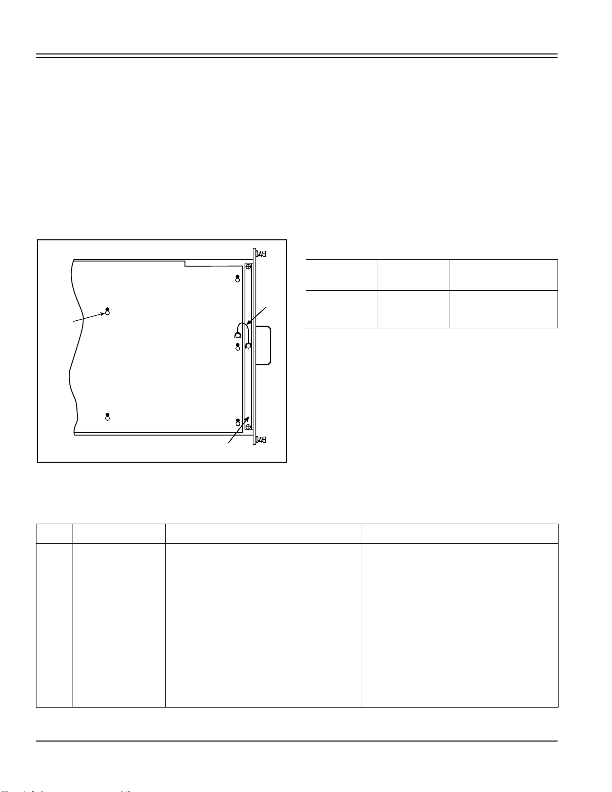
SERVICE INFORMATION
CAUTION
Failure to obser ve the f ollo wing precautions
could result in dama ge not co vered b y the
warranty:
1. The shield m ust be installed suc h that the
metal side is facing away fr om the matrix
car d. Bac kwar d installation will cause PC
boar d connections to shor t out a gainst the
metal shield.
2. The jumper wire m ust be connected as
sho wn in or der to pr ovide cir cuit pr otection
from static disc har ge.
Rear Shield
Mounting
Hole and
Standoff
(1 of 8)
Ground
Wire
4.4 TROUBLESHOO TING
4.4.1 Recommended Equipment
Table 4-1 summarizes the recommended equipment for general troubleshooting. Note that a second Model 7070, used
as an extender card, will be necessary to gain access to the
board components for troubleshooting.
WARNING
Disconnect all e xternal equipment fr om the car d
bef ore tr oub leshooting.
Table 4-1. Recommended Troub leshooting Equipment
Manufacturer
Description
5 ½ -Digit DMM
Oscilloscope
Extender Card
*A second Model 7070 will be necessary to access the card.
and Model Application
Keithley 199
TEK 2243
Keithley 7070*
Measure DC voltages
View logic waveforms
Allow circuit access
4.4.2 Troubleshooting Procedure
Table 4-2 summarizes the troubleshooting procedure for the
Universal Card. Some of the troubleshooting steps refer to
the ID data timing diagram shown in Figure 4-2. Also, refer
to paragraph 4.5 for an overview of operating principles.
Matrix Card
Chassis
Figure 4-1. Removing the Rear Shield
The Model 7070 should be in the LOCAL mode
when troubleshooting.
Table 4-2. Troubleshooting Procedure
Step Item/Component Required Condition Comments
TP2
1
TP1
2
TP3
3
TP4
4
TP5
5
TP6
6
TP7
7
TP8
8
TP9
9
TP10
10
U30-U41, pins 10-18
11
+6VDC
+5VDC
NEXT ADDR pulses
CLR ADDR pulse
ID data pulses
STROBE pulse
Relay data (128 bits)
CLK pulses
High on power up until Þrst STROBE sets
low.
Low with relay energized, high with relay
de-energized.
All voltages referenced to TP2 (digital
common)
Relay voltage
Logic voltage
Power up only (Fig. 4-2)
Power up only (Fig. 4-2)
Power up only (Fig. 4-2)
End of relay data sequence
Present when updating relays
Present during relay data or ID data
Power on safe ground
Relay driver outputs must be pulled up
through relay coil to operate.
NOTE
4-2
Page 59
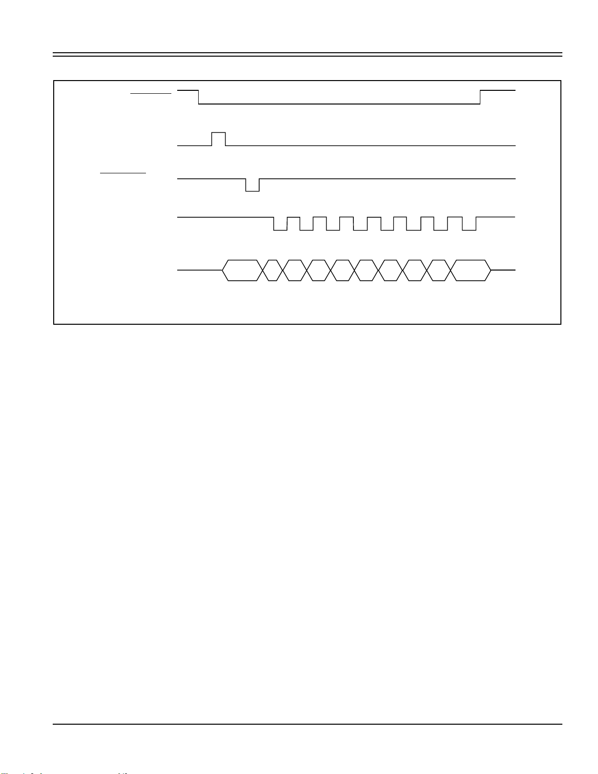
CARDSEL
CLRADDR (TP5)
NEXTADDR (TP4)
CLK (TP9)
SERVICE INFORMATION
IDDATA (TP6)
Note: ID data sequence occurs on power-up only.
CLRADDR pulse occurs only once.
HI-Z
D7 D6 D5 D4 D3 D2 D1 D0
Figure 4-2. ID Data Timing
4.5 PRINCIPLES OF OPERA TION
The following paragraphs discuss the basic operating principles for the Model 7070. A schematic diagram of the
adapter card may be found in drawing number 7070-106,
located at the end of Section 5.
HI-Z
4.5.1 Block Diagram
Figure 4-3 shows a simpliÞed block diagram of the
Model 7070. Key elements include the buffer (U44), ID data
circuits (U45, U46, and U47), relay drivers (U35-U41), and
power-on safeguard (U42). The major elements are discussed below.
4-3
Page 60

SERVICE INFORMATION
CLRADDR
To
Mainframe
Address
Counter
U45
A0-A11
NEXTADDR
Buffer
U44
ROM
U47
CARDSEL
IDDATA
RELAYDATA
STROBE
Power-On
Safeguard
D0-D7
NEXTADDR
CLK
Parallel
to Serial
Converter
U46
Relay
Drivers
U30-U41
User
Installed
Relays
Columns
1-12
Rows
A-H
U42
Figure 4-3. Model 7070 Block Diagram
4.5.2 ID Data Circuits
Upon power-up, the card identiÞcation data information
from each card is read by the mainframe. This ID data
includes such information as card ID, hardware settling
time for the card, and a relay conÞguration table, which tells
the mainframe which relays to close for a speciÞc crosspoint.
This conÞguration table is necessary because some cards
require the closing of more than one relay to close a speciÞc
crosspoint.
ID data is contained within an on-card ROM, U47. In order
to read this information, the sequence below is performed
upon power-up. Figure 4-2 shows the general timing of this
sequence.
Output
Enable
1. The CARDSEL line is brought low, enabling the ROM
outputs. This line remains low throughout the ID data
transmission sequence.
2. The CLRADDR line is pulsed high to clear the address
counter and set it to zero. At this point, a ROM address
of zero is selected. This pulse occurs only once.
3. The NEXTADDR line is set low. NEXTADDRS going
low increments the counter and enables parallel loading
of the parallel-to-serial converter. NEXTADDR is kept
low long enough for the counter to increment and for
the ROM outputs to stabilize. This sequence functions
because the load input of the parallel-to-serial converter
is level sensitive rather than edge sensitive. The Þrst
ROM address is location 1, not 0.
4. The CLK line clocks the parallel-to-serial converter to
shift all eight data bits from the converter to the mainframe via the IDDATA line.
4-4
Page 61

The process in steps 3 and 4 repeats until all the necessary
ROM locations have been read. A total of 498 bytes of information are read by the mainframe during the card ID
sequence.
4.5.3 Relay Control
User-installed relays are controlled by serial data transmitted via the RELAYDATA line. A total of 16 bytes for each
card are shifted in in serial fashion (only 12 are used in
the Model 7070, however) into latches located in the 12 relay
drivers, U30-U41. The serial data is fed in through the
DATA lines under control of the CLK signal. As data
overflows one register, it is fed out the Q’S line of that
register to the next IC down the chain.
Once all the bytes have been shifted into the card, the
STROBE line is set high to latch the relay information into
the Q outputs of the relay drivers, and the appropriate user
relays are energized (assuming the driver outputs are
enabled, as discussed below). Logic convention is such that
the corresponding relay driver output must be low to
energize the associated relay, while the output is high
when the relay is de-energized.
4.5.4 Power-on Safeguard
A power-on safeguard circuit, made up of U42 and
associate components, ensures that relays do not randomly
energize upon power-up. The two NAND gates, U42,
make up an R-S flip-flop. Initially, the Q output of the flipflop (pin 3 of U42) is set high after the RC combination
at pin 1 times out. Since the OEN terminals of the relay
drivers U30-U41 are held high, their outputs are disabled, and all relays remain de-energized regardless of the
relay data information present at that time.
The first STROBE pulse that comes along (in order to load
relay data) clears the R-S flip-flop, setting the OEN lines
of U30-U41 low to enable their outputs. This action allows
the relays to be controlled by the transmitted relay data
information.
A hold-off period of approximately 2.209sec is included
in the safeguard circuit to guard against premature enabling of the relays. The time constant of the hold-off period
is determined by the relative values of Rl and C20.
4-514-6
Page 62

SECTION 5
Replaceable Parts
5.1 INTRODUCTION
This section contains a list of replaceable electrical and
mechanical parts for the Model 7070, as well as a component
layout drawing and schematic diagram of the adapter card.
5.2 P AR TS LISTS
Electrical parts for the main board are listed in order of circuit designation in Table 5-1. Table 5-2 lists parts for the
extender board. Table 5-3 summarizes mechanical parts.
5.3 ORDERING INFORMA TION
To place an order or to obtain information about
replacement parts, contact your Keithley representative or
the factory (see the inside front cover of this manual for
addresses). When ordering parts, be sure to include the
following information:
1. Card model number (7070)
2. Card serial number
3. Part description
4. Circuit designation, if applicable
5. Keithley part number
5.4 F A CT OR Y SER VICE
If the matrix card is to be returned to Keithley Instruments
for repair, perform the following:
1. Complete the service form located at the back of this
manual, and include it with the unit.
2. Carefully pack the card in the original packing carton or
the equivalent.
3. Write ATTENTION REPAIR DEPARTMENT on the
shipping label.
Note that it is not necessary to return the matrix mainframe
with the card.
5.5 COMPONENT LAYOUT AND SCHEMATIC DIAGRAM
Figure 5-1 is the component layout for the main circuit
board. Figure 5-2 shows a schematic diagram of the main
board. Figures 5-3 and 5-4 show the component layout and
schematic for the extender board.
NOTE
Figure 5-3 and Figure 5-4 do not apply to the Model
7070-PCA.
5-1/5-2
Page 63
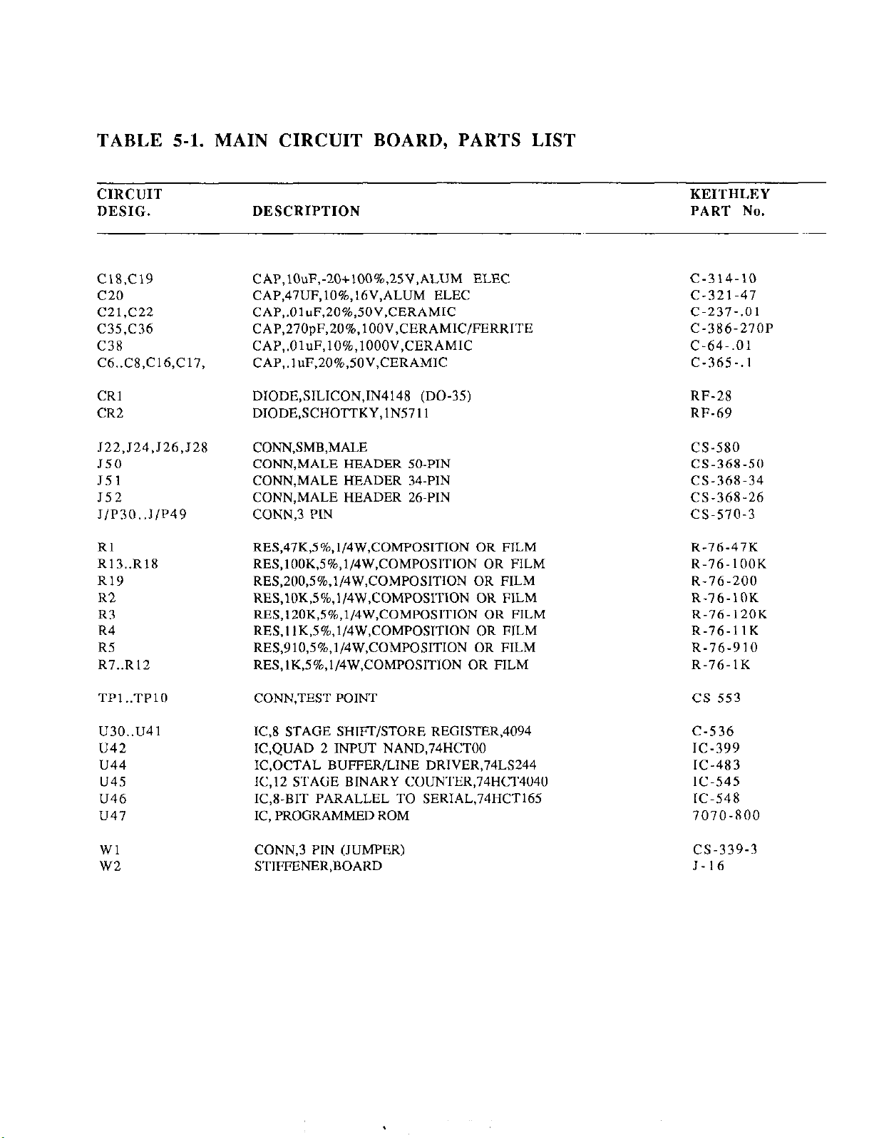
TABLE 5-1. MAIN CIRCUIT BOARD, PARTS LIST
CIRCUIT
DESIG. DESCRIPTION
C18,C19 CAP,lOuF;20+100%,25V,ALUM ELEC
c20 CAP,47UF,10%,16V,ALUM ELEC
c21,c22
C35,C36 CAP,270pF,20%,100V,CERAMIC/FERRITE
C38 CAP,.OluF,10%,1000V,CERAMIC
C6..C8,C16,C17, CAP,.luF,20%,50V,CERAMIC
CR1
CR2
122,J24,J26,J28
5.50
J51
J52
I/P3O..I/P49
Rl
R13..R18
R19
R2
R3
R4
R5
R7..R12
CAP,.OluF,20%,50V,CERAMIC
DIODE,SILICON,IN4148 (DO-35)
DIODE,SCHOTTKY,lN5711
CONN,SMB,MALE
CONN,MALE HEADER 50.PIN
CONN,MALE HEADER 34.PIN
CONN,MALE HEADER 26.PIN
CONN,3 PIN
RES,47K,5%,1/4W,COMPOSITION OR FILM
RES,100K,5%,1/4W,COMPOSITION OR FILM
RES,200,5%,1/4W,COMPOSITION OR FILM
RES,1OK,5%,1/4W,COMPOSITION OR FlLM
RES,120K,5%,l/4W,COMPGSITION OR FILM
RES.1 lK,5%,1/4W,COMPOSITION OR FILM
RES,910,5%,1/4W,COMPOSITION OR FILM
RES,lK,5%,1/4W,COMPOSITION OR FILM
KEITHLEY
PART No.
c-314-10
C-321-47
C-237-.01
C-386.270P
C-64-.01
C-365-.1
RF-2R
RF-69
CS-580
CS-368-50
CS-36X-34
CS-368-26
cs-510-3
R-76-47K
R-76.100K
R-76-200
R-76.10K
R-76.l20K
R-76.1lK
R-76-910
R-76.1K
TPl..TPlO CONN,TEST POINT
u3o..u41
U42
u44
u45
U46
u47
Wl
W2
IC.8 STAGE SHIFT/STORE REGISTER,4094
JC,QUAD 2 INPUT NAND,74HCTOO
IC,OCTAL BUFFER/LINE DRIVER,74LS244
IC.12 STAGE BINARY COUNTER,74HCT4040
IC&BIT PARALLEL TO SERIAL,74HCT165
IC, PROGRAMMED ROM
CONN,3 PIN (JUMPER)
STIFFENER,BOARD
cs-553
C-536
IC-399
IC-483
IC-545
IC-548
7070-800
cs-339-3
J-16
Page 64

Page 65

Page 66

Page 67

TABLE 5-2. EXTENDER BOARD, PARTS LIST
NOTE
This table does not apply to the Model 7070-PCA.
CIRCUIT
DESIG. DESCRIPTION
C1 CAP, 150pF, 10%, 1000V, CERAMIC C-64-150P
J101
J107
J113
P50
P51
P52
R1
R2
CONN, 86 PIN CARD EDGE
CONN, 34 PIN CARD EDGE
CONN, 30 PIN CARD EDGE
CABLE ASSY, 50 PIN
CABLE ASSY, 34 PIN
CABLE ASSY, 26 PIN
RES, 2K, 1%, 1/8W
RES, 130, 1%, 1/8W
KEITHLEY
PART No.
CS-579-1
CS-591-2
CS-591-1
CA-62-3
CA-62-2
CA-62-1
R-88-2K
R-88-130
Page 68

Page 69

Page 70

TABLE 5-3. MISCELLANEOUS MECHANICAL PARTS LIST
QTY. DESCRIPTION
KEITHLEY
PART No.
5
1
1
1
I
8
2
12
1
1
1
1
CLAMP, RIBBON CABLE
CLAhtP,LOWER
CLAMP, UPPER
SHIELD
SHlELD,REAR
STANDOFFS FOR REAR SHIELD
SOCKET.16 PIN DIP
SOCKET,18 PIN DIP
SOCKET,20 PIN DIP
SOCKET.28 PIN DIP
REAR PANEL
SOCKET,14 PIN DIP
cc-59
7071.306
7071-305
7070.305
7071.311
7071-310
SO-65
SO-82
SO-84-20
SO-69
7070-303
so-70
Page 71

SERVICE FORM
Model No.
Serial No.
Name and Telephone No.
Company
List all control settings, describe problem and check boxes that apply to problem.
q Intermittent
q IEEE failure
aFront panel operational aAll ranges or functions are bad
Display orautput (circle one)
ODrifts
q Unstable
aAnalog output follows display q Ptiicular range or function had; specify
OObvious problem on power-up q Batteries and fuses are OK
q Checked all cables
q Unable to zero
q Will not read applied input
q Overload
q Calibration only
aData required
(attach any additional sheets as necessary.)
DC of C required
Date
Show a block diagram of your measurement system including all instruments connected (whether power is turned on or not).
Also, describe signal source.
Where is the measurement being performed? (factory, controlled laboratory, out-of-doors, etc.)
What power line voltage is used?
Relative humidity?
Any additional information. (If special modifications have been made by the user, please describe.)
Other?
Ambient Temperahxe?
“F
Page 72

Specifications are subject to change without notice.
All Keithley trademarks and trade names are the property of Keithley Instruments, Inc. All other
trademarks and trade names are the property of their respective companies.
Keithley Instruments, Inc. 28775 Aurora Road • Cleveland, Ohio 44139 • 440-248-0400 • Fax: 440-248-6168
1-888-KEITHLEY (534-8453) www .keithley.com
BELGIUM: Keithley Instruments B.V. Bergensesteenweg 709 • B-1600 Sint-Pieters-Leeuw • 02/363 00 40 • Fax: 02/363 00 64
CHINA: Keithley Instruments China Yuan Chen Xin Building, Room 705 • 12 Y umin Road, Dewai, Madian • Beijing 100029 • 8610-6202-2886 • Fax: 8610-6202-2892
FRANCE: Keithley Instruments Sarl 3, allée des Garays • 91127 Palaiseau Cédex • 01 64 53 20 20 • Fax: 01 60 11 77 26
GERMANY : Keithley Instruments GmbH Landsberger Strasse 65 • D-82110 Germering • 089/84 93 07-40 • Fax: 089/84 93 07-34
GREAT BRITAIN: Keithley Instruments Ltd. The Minster • 58 Portman Road • Reading, Berkshire RG30 1EA • 0118-9 57 56 66 • Fax: 0118-9 59 64 69
INDIA: Keithley Instruments GmbH Flat 2B, WILLOCRISSA• 14, Rest House Crescent • Bangalore 560 001 • 91-80-509-1320/21 • Fax: 91-80-509-1322
ITALY: Keithley Instruments s.r.l. V iale San Gimignano, 38 • 20146 Milano • 02-48 39 16 01 • Fax: 02-48 30 22 74
KOREA: Keithley Instruments Korea 2FL., URI Building • 2-14 Yangjae-Dong • Seocho-Gu, Seoul 137-130 • 82-2-574-7778 • Fax: 82-2-574-7838
NETHERLANDS: Keithley Instruments B.V. Postbus 559 • NL-4200 AN Gorinchem • 0183-635333 • Fax: 0183-630821
SWITZERLAND: Keithley Instruments SA Kriesbachstrasse 4 • 8600 Dübendorf • 01-821 94 44 • Fax: 01-820 30 81
TAIWAN: Keithley Instruments Taiwan 1FL., 85 Po Ai Street • Hsinchu, Taiwan, R.O.C. • 886-3-572-9077• Fax: 886-3-572-9031
© Copyright 2000 Keithley Instruments, Inc. No. 2193
Printed in the U.S.A. 2/2000
 Loading...