

Page 1

Model 7053 High Current Scanner Card
instruction Manual
Contains Operating and Servicing Information
Page 2

WARRANTY
LIMITATION OF WARRANTY
Page 3
Model 7053 High Current Card
Instruction Manual
0 1987, Keithley Instruments, Inc.
Test Instrumentation Group
All rights reserved.
Cleveland, Ohio, U.S.A.
May 1996, Third Printing
Document Number: 7053-901-01 C
Page 4
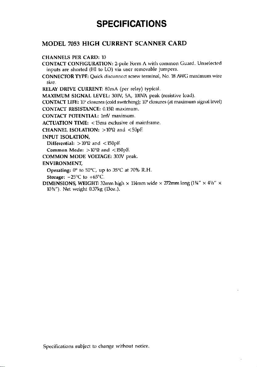
SPECIFICATIONS
MODEL 7053 HIGH CURRENT SCANNER CARD
CHANNELS PER CARD: 10
CONTACT CONFIGURATION: 2-p& ltirm A with common Guard. Unselected
inputs are shorted (HI to LO) via user removable jumpers.
CONNECTOR TYPE: Quick disconnect screw terminal, No. 18 AWG maximum wire
size.
RELAY DRIVE CURRENT: ROrnA (PC’ day) typicat.
MAXIMUM SIGNAL LEVEL: 3OOV. 5A, lOOVA peak (resistive load).
CONTACT LIFE: IO’ closures (cold switching); 10’ closures (at maximum signal level)
CONTACT RESISTANCB: 0.15fl maximum.
CONTACT POTENTIAL: ImV maximum.
ACTUATION TIME <15ms exclusive of mainframe.
CHANNEL ISOLATION: >lO*O and <50pF.
lNP”T ISOLATION,
Differential: >lO’R and <150pF.
Comman Made: >10’11 and <150pF.
COMMON MODE VOLTAGE: 30W peak.
ENVIRONMENT,
Operating: 0” to 5O”C, up to 35°C at 70% R.H.
Storage: -25°C to +65”C.
DIMENSIONS, WEIGHT: 32mm high x 114mm wide x 272mm long (l’%” x 4%” x
10%“). Net weight 0.37kg (l3oz.).
Specifications subject 1~ change without notice.
Page 5
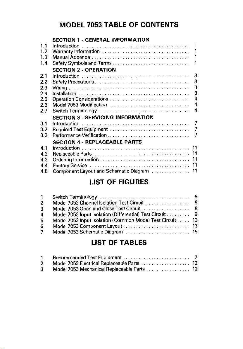
MODEL 7053 TABLE OF CONTENTS
SECTION 1 GENERAL INFORMATION
1.1
Introduction.. ............. .......................
Warranty Information
1.2
ManualAddenda.. ....................................
1.3
Safety Symbols and Terms. .............................
1.4
SECTION 2 OPERATION
Introduction..
2.1
Safety Precautions
2.2
2.3
2.4
2.5
2.6
2.7
3.1
3.2
3.3
4.1
4.2
4.3
4.4
4.5
...............................................
Wiring
Installation
Operation Considerations ...............................
Model 7053 Modification ...............................
Switch Terminology ...................................
SECTION 3 SERVICING INFORMATION
Introduction.. ........................................
Required Test Equipment
Performance Verification. ...............................
SECTION 4 REPLACEABLE PARTS
Introduction ..........................................
ReplaceableParts ......................................
Ordering Information
FactoryService
Component Layout and Schematic Diagram ...............
..........................................
..................................
................... .................... 3
.....................................
............................... 7
...................................
.......................................
LIST OF FIGURES
1
1
1
1
3
3
3
4
4
4
7
7
11
11
11
11
11
SwitchTerminology ...................................
1
Model 7053 Channel Isolation Test Circuit
Model 70530pen and Close Test Circuit. ..................
Model 7053 Input Isolation (DifferentialI Test Circuit
Model 7053 Input Isolation ICommon Mode) Test Circuit
Model7053ComponentLayout
Model 7053 Schematic Diagram .........................
.......................... 13
LIST OF TABLES
1
Recommended Test Equipment ..........................
Model 7053 Electrical Replaceable Paris
2
Model 7053 Mechanical Replaceable Parts
3
................... 12
5
................. 8
9
......... 9
10
15
7
................. 12
Page 6
SECTION 1
GENERAL INFORMATION
1.1 INTRODUCTION
The Model 7053 is a high current scanner card with the maximum capabilities
of 3OOV. 5A or lOOV*A switching Iresistive load onlyl. Signal levels of this
magnitude may be found in applications such as power semiconductor
testing. The Model 7053 can also be used in monitoring currents from DC
power supplies in general purpose ATE bench or laboraton, applications. For
easy input and output wiring the Model 7053 is designed with quick disconnect screw terminals. Each channel has a HI and LO connection with a common guard. Each of the 10 channels consist of a single Z-pole Form C relay.
The card is field installable in an appropriate Keithley .scanner mainframe (e.g.
Model 7051 via the mainframe’s rear panel. Channel switching is accomplished
in less than 15msec (exclusive of mainframe) and the specified relay life is
greater than IO’closures (greater than IO5 closures at maximum signal levels).
With the Model 7053’s high channel isolation (>lO%l), it is well insulated from
cross channel noise and interference. The Model 7053’s high input isolation
l>lO%l reduces loading to a minimum.
1.2 WARRANTY INFORMATION
Warranty information is stated on the inside front cwer of this manual. If there
is a need for service, contact the Keithley representative or authorized repair
facility in your area. Check the back cover of this manual for addresses. The
service form supplied at the end of the manual should be used to provide the
repair facility with adequate information concerning any difficulty.
1.3 MANUAL ADDENDA
Improvements or changes to this manual will be explained on an addendum included with this manual.
1.4 SAFETY SYMBOLS AND TERMS
The symbol
tions.
The symbol
terminal(s).
The WARNING used in this manual explains dangers that could result in per-
sonal injun, or death.
The CAUTION used in this manual explains hazards that could damage the
denotes that the user should refer to the operating instruc-
A
denotes that a high voltage may be present on the
If
instrument.
1
Page 7

SECTION 2
OPERATION
2.1 INTRODUCTION This section provides the necessary information to use the Model 7053 with an
appropriate Keithley scanner mainframe fsuch as the Model 705). Once the
card is installed in the scanner mainframe, refer to the scanner mainframe’s instruction manual for complete operating instructions.
2.2 SAFETY PRECAUTIONS
1. DO not exceed the Model 7053’s maximum allowable signal level as defined
in the specifications.
2. Do not exceed the maximum common mode voltage of 300V as defined in
the specifications. Exercise extreme caution when a shock hazard is present
at the terminals. The American National Standard lnstituto (ANSI) states
that a shock hazard exists when voltage levels greater than 30V rms or
42.4V peak are present.
3. Make sure the scanner mainframe is grounded through a properly earth
grounded receptacle before operation.
4. Turn off all power supplies and discharge any residual power before install-
ing or removing the Model 7053 from the scanner mainframe or wires from
the terminals of the Model 7053.
5. Use appropriately rated wire when switching high current.
6. Read this manual carefully and ahere to all the safety precautions listed
before operating the instrument.
7. lnspsct all test connections for wear or defects such as cracks, exposed
wires, etc. Correct any defect found before operating the instrument.
2.3 WIRING
Each channel on the Model 7053 high current card consists of a single Z-pole
Form C relay. The Model 7053 will switch any one of the 10 signals linputsl tq
one output. or switch one signal to any one of 10 outputs.
1. Wiring is accomplised by means of quick disconnect screw terminals as
shown on the component layout (Figure 61.
2. Resistance of the relay contacts fterminalsl is less than 150mR
3. Use wires or cables that are rated for maximum signal levels. The maximum
allowable wire size is No. 18 AWG. When operating at high current levels
(e.g. Amps) consider the voltage burden (IoR drop1 of the wire or cable being used. For example: The approximate resistance of 18 gusge copper wire
is 6,3mQ/ft. The voltage burden is approximately 6.3mVlhlAmp. At the
maximum signal current of 5 Amps the voltage burden would be 31 .SmV/ft.
If the wire being used is 3ft long the voltage burden of the wire is approximately O.lV.
4. Route the wires or cables through the rubber clamps at the rear of the card.
2.4 INSTALLATION Refer to the scanner mainframe’s instruction manual for installation instwc-
tions.
Page 8

2.5 OPERATION CONSIDERATIONS Signal Level-The maximum signal levels that the Model 7053 high current
card operates at are 300V maximum, 6A or lOOVA peak iresistive load only).
The contact life of the relays at maximum signal levels is greeter than lo5
operations.
NOTE
Maximum signal specifications apply to scanner output as well
as inputs. For example, multiple channel closures cannot put
more than 5A onto the output.
WARNING
When switching signals greater than 30V rms or 42.4V
rms peak take care to prevent contact with live circuits
which could cause electrical shock resulting in injury or
death.
Cables-Sheilded cables should be used with the Model 7053 high current
card and when switching above 5OV or high current. The shield should be
connected to circuit guard. This helps prevent excessive radiation from the
cables from interfering with any equipment. The cable rating must exceed the
maximum allowable signal levels as defined in the specifications.
External Considerations-The Model 7053 is specified for a resistive load,
however, external circuit capacitances and inductances can cause excessive
currents and voltages across the relay contacts. The currents and voltages
must be limited to within the maximum allowable signal levels.
1. Capacitance-Charged capacitances in the circuit can cause excessive
currents (surge currents) to flow through the relay contacts if the source i8
shorted out or the output is switched to capacitive loads. This excessive
current can weld the relay contacts together. Therefore, use series resistors,
where needed, to limit the maximum current that can flow to within contact
ratings. The maximum signal levels are stated in the specifications.
2. Inductance-The inductance of cables can produce high voltage and arcing across relay contacts when switching. The peak transients must be
limited to within the maximum signal levels as defined in the specifications.
2.6 MODEL 7053 MODIFICATION
Unselected inputs on the Model 7053 high current scanner card, are shorted
(HI to LO) via installed jumpers (WlOl-WllO). If isolation is required between
channel LO and channel HI. the Model 7053 can be modified to disconnect
channel LO from channel HI when a relay is off lopenl. The modification involves removing a jumper wire for the channel that is to be modified. For example, remove jumper WlOl to disconnect channel l’s HI terminal from channel l’s LO terminal. Refer to the component layout (Figure 6) for jumper lxxtion.
It is recommended to remove the jumpers by cutting them with a pair of wire
CUttOE.
2.7 SWITCH TERMINOLOGY
Throughout this manual the terminology Form C is used. The term Form C is
used in switch terminology and is described 88 follows:
St
Page 9

1. Form A is simply a slngle pole normally open /SPNOl switch (refer to Figure
11.. A 2-p&1 switch normally open 18 classified 8~ 8 2 Form A.
2. Form FJ is similar to Form A except that its contacts are normally closed
(refer to Figure 1 I. A 2-pole switch normally closed is classified as a 2 Form
6.
3. Form C is shown in Figure 1 as a single pole double throw switch. It could
also be B multiple switch such as a Z-pole which would be,classified 88 a 2
Form C.
Figure 1. Switch Terminologv
6
Page 10
SECTION 3
SERVICING INFORMATION
3.1 INTRODUCTION
This section contains B performance verification procedure. Since there are no
calibration adjustments. no recalibration is necessary. Recommended maintenance would include inspection of the scanner plug-in board and card edge
connector to ensure good el8ctric.4 contact. The verification procedure should
be performed upon receiving the Model 7053 or at the time maintenance is
performed on the mainframe.
3.2 REDUIRED TEST EQUIPMENT
Recommended test equipment for performance verification is given in Table 1.
Test equipment other than the recommended equipment in Table 1 may be
substituted if specifications equal or exceed the stated characteristics.
Table 1. Recommended Test Equipment
~~~~~~~~~~~~1
Sensitivity to IO-‘A Keithley
3.3 PERFORMANCE VERIFICATION This section contains procedures needed to verify that the operation of the
Model 7053 is within specifications.
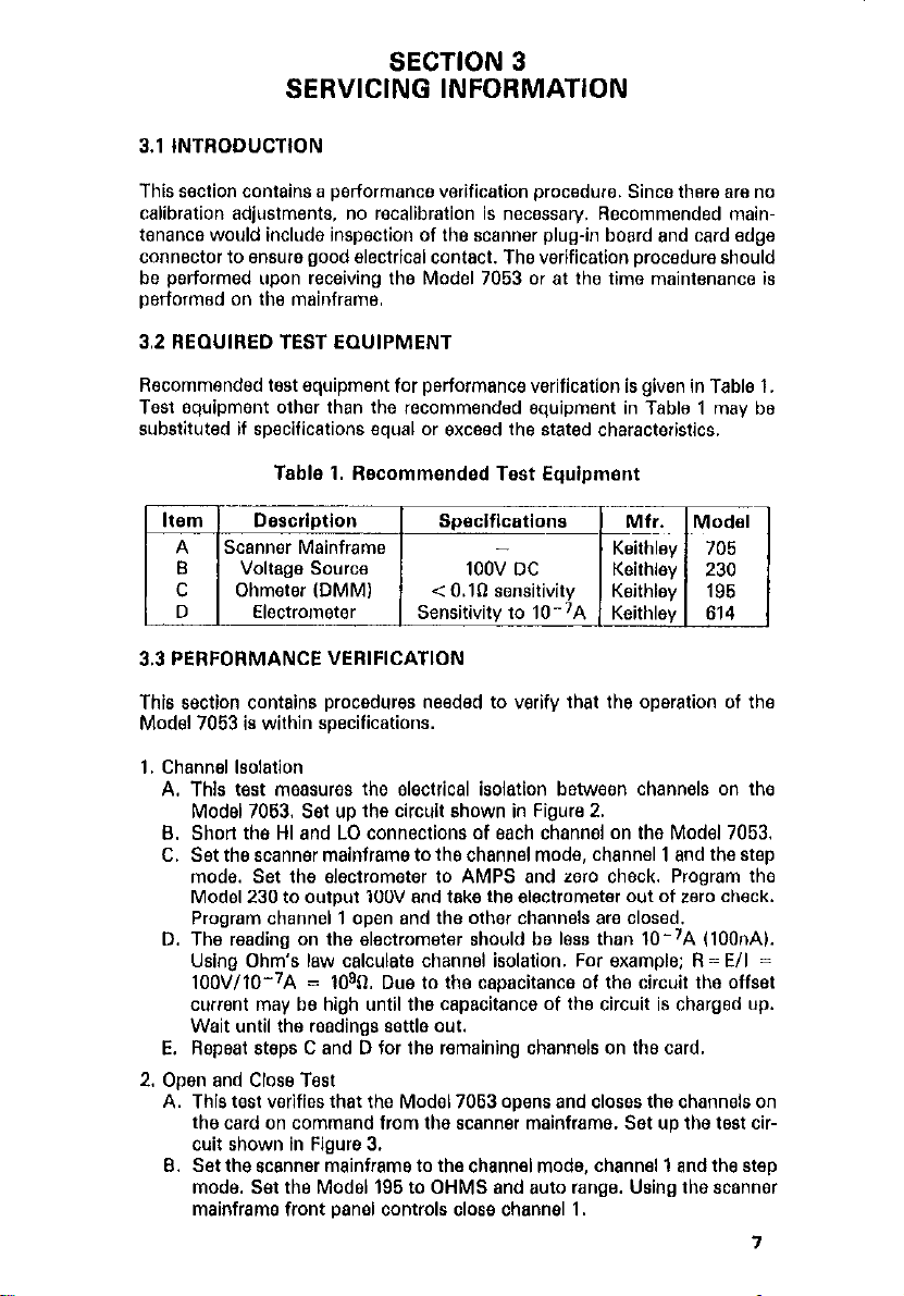
1. Channel Isolation
A. This test measures the electrical isolation between channels on the
Model 7063. Set up the circuit shown in Figure 2.
8. Short the HI and LO connections of each channel on the Model 7053.
C. Set the scanner mainframe to the channel mode, channel 1 and the step
mode. Set the electrometer to AMPS and zero check. Program the
Model 230 to output IOOV and take the electrometer out of zero check.
Program channel 1 open and the other channels are closed.
D. The reading on the electrometer should be less than lo-‘A (lOOnA).
Using Ohm’s law calculate channel isolation. For example; R = E/I =
100V110-7A = 10%). Due to the capacitance of the circuit the offset
current may be high until the capacitance of the circuit is charged up.
Wait until the readings settle out.
E. Repeat steps C and D for the remaining channels on the card.
2. Open and Close Test
A. This test verifies that the Model 7063 opens and closes the channels on
the card an command from the scanner mainframe. Set up the test circuit shown in Figure 3.
6. Set the scanner mainframe to the channel mode, channel 1 and the step
mode. Set the Model 196 to OHMS and auto range. Using the scanner
mainframe front panel contmls close channel 1.
7
Page 11
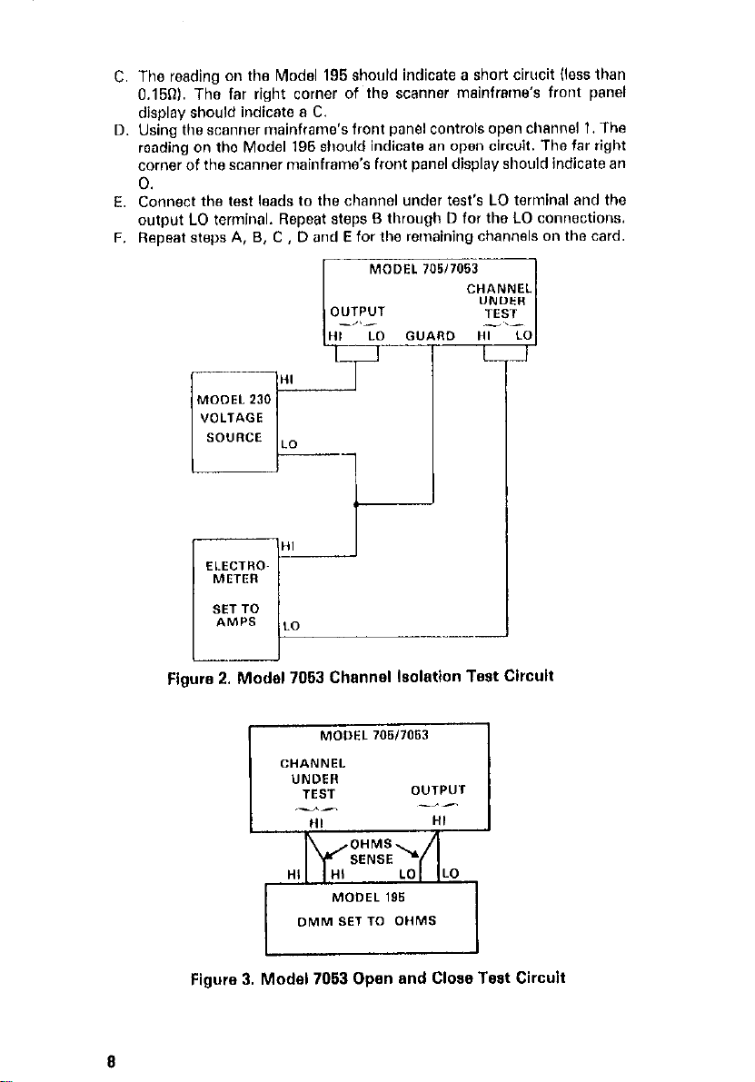
C. The reading on the Model 195 should indicate a short cirucit Iless than
0.15Rl. The far right corner of the scanner mainframe’s front psnel
display should indicate 8 C.
D. Using the scanner mainframe’s front panel controls open channel 1. The
reading on the Model 195 should indicate an open circuit. The far right
corner of the scttnner mainframe’s front panel display should indicate an
0.
E. Connect the test leads to the chrmnel under test’s LO terminal and the
output LO terminal. Repeat steps B through D for the LO connsctions.
I;. Repeat steps A, B, C , D and E for the remaining channels on the card.
Figure 2. Model 7063 Channel lsolat1on Test Circuit
Figure 3. Model 7053 Open and Close Test Circuit
Page 12
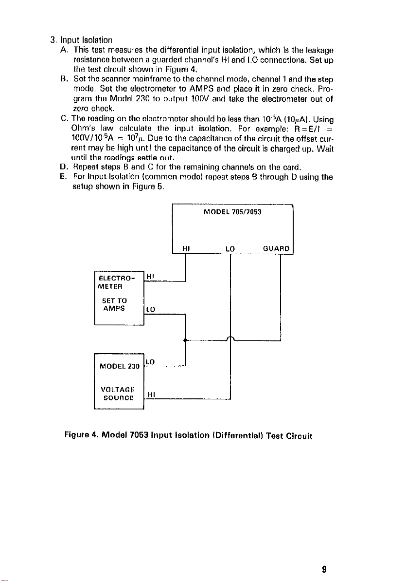
3. Input isolation
A. This test measures the differential inout isolation. which is the leakaoe
resistence between a guarded chanr& HI and Lb connections. Set ;p
the tee1 circuit shown in Figure 4.
8. Set the scanner mainframe to the channel mode, channel 1 and the step
mode. Set the electrometer to AMPS end place it in zero check. Program the Model 230 to output 1OOV and take the electrometer out of
zero check.
C. The reading on the electrometer should be loss then 105A
Ohm’s law calculate the input isolation, For example: R =Ell =
lOOVllC6’A = lo’,,. Due to the capacitance of the circuit the offset current may be high until the capacitance of the circuit is charged up. Wait
until the readings settle out.
D. Repeat steps B and C for the remaining channels on the card.
E. For Input Isolation (common model repeat steps B through D using the
setup shown in Figure 5.
(IO,~A~. Using
Figure 4. Model 7063 Input Isolation Dlfferentfsll Test Circuit
9
Page 13
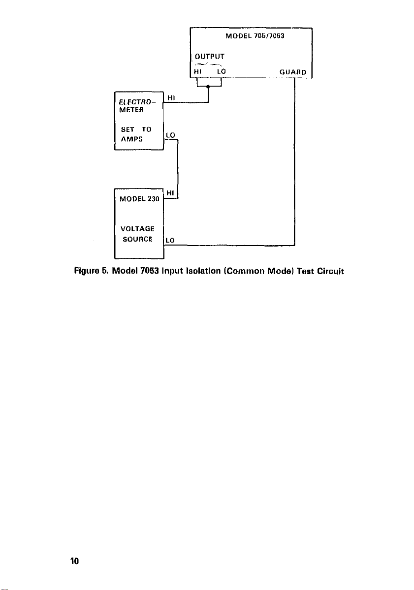
Figure 6. Model 7063 Input Isolation Kommon Model Test Circuit
10
Page 14

SECTION 4
REPLACEABLE PARTS
4.1 INTRODUCTION
This section contains replacement parts information, a schematic diagram and
B companont layout for the Model 7053.
4.7. REPLACEABLE PARTS
Parts are listed alpha-numerically in order of their circuit designation. Table 2
contains the electrical replaceable parts. Table 3 contains the mechanical
p%k.
4.3 ORDERING INFORMATION
To place an order, or to obtain information concerning replacement parts.
contact your Keithley representative or the factory. See the back cover for addresses. When ordering include the following information:
1. Instrument Model Number
2. Instrument Serial Number
3. Part Description
4. Circuit Description lif applicable)
5. Keithley Part Number
4.4 FACTORY SERVICE
If the instrument is to be returned to the factory for service, please photo copy
the setvice form which follows this section, fill it out and return with the instrument.
4.6 COMPONENT LAYOUT AND SCHEMATIC DIAGRAM
Figure 6 contains a component layout for the Model 7053. Figure 7 contains
the schematic diagram of the Modal 7053.
11
Page 15

Table 2. Model 7063 Electrical Replaceable Parts
Circuit
Desig.
Cl01
JlOOl
J1002
MOO3
J1004
J1005
J1006
J1007
KIOI
K102
K103
K104 Relay, 2 Form C
K105
K106 Relay, 2 Form C
K107
KlOa
Kl09
KllQ Relay, 2 Form C
WI01
WI02
w103 Jumper
WI04 Jumper
W106
W106 Jumper
w1o-l Jumper
WI06 Jumper
w109
WI10
Description
Capacitor, lO,iF, 26V, Aluminum Electrolytic3 pin terminal strip
3 pin terminal strip
3 pin terminal strip
3 pin terminal strip
3 pin terminal strip
10 pin terminal strip
10 pin terminal strip
Relay. 2 Form C
Relay, 2 Form C
Relay, 2 Form C
Relay, 2 form C
Relay, 2 Form C
Relay, 2 Form C
Relay, 2 Form C
Jumper
Jumper
Jumper
Jumper
Jumper
--
Keithley
Pert No.
--c-31410
cs-457-l
cs-457-1
cs-457-1
cs-467-l
cs-457-l
CS-467-2
CS-457-2
RL-60
RL-60
RL-a0
RL-60
RL-90
RL-90
RL-a0
RL-a0
RL-60
RL-a0
J-3
J-3
J-3
J-3
J-3
J-3
J-3
J-3
J-3
J-3
Table 3. Model 7063 Mechanical Replaceable Parts
Description
Handle 12 required1
Rivet I2 required)
Clamp, assembly, upper
8. Clamp, upper
b. Strip, rubber
Clamp, assembly, lower
a. Clamo. cable. lower
b. Strip; kubber’
No. 6-32 x 5/16 Phillias Pan Head Screw
No. 6-32 x 1 inch Phiilips Pan Head Screw
12
.__
Kelthley
Part No.
FA-119
FA-121
70%303.07
706%306.
26621
26740
26620
26621
Page 16

Figure 6. Model 7053 Component Layout
13
Page 17

Figure 7. Model 7053 Schematic Diagram
14
Page 18

Service Form
Model No. ~ Serial No. __~~~~~~~ Date
Name and Telephone No.
Company
List
ail control
settings, describe
problem and check boxes that apply to prnblcm,
u 1ntemlittent
U IEEE failure
u Front panel operational
Ll Analog output follows display
U Obvious problem on power-up
(attach any additional she& as ncccssary)
Show a block diagram of your mea.sur~m~nt system including all instruments connected
(whether power is turned on or not). Also, describe signal SOUICC.
0 All ranges or functions arc bad
0 Particular rang2 or function bad; specify
U Batteries and fuses arc OK
0 Checked all cables
0 Ccrtiiicate of calibration required
Page 19

Keithley Instruments, Inc.
Test Instrumentation Croup
20775
Cleveland, Ohio 44139
Aurora
Printed in the U.S.A.
Road
 Loading...