

Page 1

Model 7022Matrix-Digital I/O Card
Instruction Manual
A GREATER MEASURE OF CONFIDENCE
Page 2

WARRANTY
Keithley Instruments, Inc. warrants this product to be free from defects in material and workmanship for a period of 1 year
from date of shipment.
Keithley Instruments, Inc. warrants the following items for 90 days from the date of shipment: probes, cables, rechargeable
batteries, diskettes, and documentation.
During the warranty period, we will, at our option, either repair or replace any product that proves to be defective.
To exercise this warranty, write or call your local Keithley representative, or contact Keithley headquarters in Cleveland, Ohio.
You will be given prompt assistance and return instructions. Send the product, transportation prepaid, to the indicated service
facility. Repairs will be made and the product returned, transportation prepaid. Repaired or replaced products are warranted for
the balance of the original warranty period, or at least 90 days.
LIMITATION OF WARRANTY
This warranty does not apply to defects resulting from product modification without Keithley’s express written consent, or
misuse of any product or part. This warranty also does not apply to fuses, software, non-rechargeable batteries, damage from
battery leakage, or problems arising from normal wear or failure to follow instructions.
THIS WARRANTY IS IN LIEU OF ALL OTHER WARRANTIES, EXPRESSED OR IMPLIED, INCLUDING ANY
IMPLIED WARRANTY OF MERCHANTABILITY OR FITNESS FOR A PARTICULAR USE. THE REMEDIES PROVIDED HEREIN ARE BUYER’S SOLE AND EXCLUSIVE REMEDIES.
NEITHER KEITHLEY INSTRUMENTS, INC. NOR ANY OF ITS EMPLOYEES SHALL BE LIABLE FOR ANY DIRECT,
INDIRECT, SPECIAL, INCIDENTAL OR CONSEQUENTIAL DAMAGES ARISING OUT OF THE USE OF ITS
INSTRUMENTS AND SOFTWARE EVEN IF KEITHLEY INSTRUMENTS, INC., HAS BEEN ADVISED IN ADVANCE
OF THE POSSIBILITY OF SUCH DAMAGES. SUCH EXCLUDED DAMAGES SHALL INCLUDE, BUT ARE NOT LIMITED TO: COSTS OF REMOVAL AND INSTALLATION, LOSSES SUSTAINED AS THE RESULT OF INJURY TO ANY
PERSON, OR DAMAGE TO PROPERTY.
Keithley Instruments, Inc.
BELGIUM: Keithley Instruments B.V.
CHINA: Keithley Instruments China
FRANCE: Keithley Instruments Sarl
GERMANY: Keithley Instruments GmbH
GREAT BRITAIN: Keithley Instruments Ltd
INDIA: Keithley Instruments GmbH
ITALY: Keithley Instruments s.r.l.
NETHERLANDS: Keithley Instruments B.V.
SWITZERLAND: Keithley Instruments SA
TAIWAN: Keithley Instruments Taiwan
• 28775 Aurora Road • Cleveland, OH 44139 • 440-248-0400 • Fax: 440-248-6168 • http://www.keithley.com
Bergensesteenweg 709 • B-1600 Sint-Pieters-Leeuw • 02/363 00 40 • Fax: 02/363 00 64
Yuan Chen Xin Building, Room 705 • 12 Yumin Road, Dewai, Madian • Beijing 100029 • 8610-62022886 • Fax: 8610-62022892
3, allée des Garays • 91127 Palaiseau Cedex • 01-64 53 20 20 • Fax: 01-60 11 77 26
Landsberger Strasse 65 • 82110 Germering • 089/84 93 07-40 • Fax: 089/84 93 07-34
The Minster • 58 Portman Road • Reading, Berkshire RG30 1EA • 0118-9 57 56 66 • Fax: 0118-9 59 64 69
Flat 2B, WILOCRISSA • 14, Rest House Crescent • Bangalore 560 001 • 91-80-509-1320/21 • Fax: 91-80-509-1322
Viale S. Gimignano, 38 • 20146 Milano • 02-48 39 16 01 • Fax: 02-48 30 22 74
Postbus 559 • 4200 AN Gorinchem • 0183-635333 • Fax: 0183-630821
Kriesbachstrasse 4 • 8600 Dübendorf • 01-821 94 44 • Fax: 01-820 30 81
1 Fl. 85 Po Ai Street • Hsinchu, Taiwan, R.O.C. • 886-3572-9077 • Fax: 886-3572-903
9/00
Page 3

Model 7022 Matrix-Digital I/O Card
Instruction Manual
©1997, Keithley Instruments, Inc.
All rights reserved.
Cleveland, Ohio, U.S.A.
Second Printing, March 2001
Document Number: 7022-901-01 Rev. B
Page 4

Manual Print History
The print history shown below lists the printing dates of all Revisions and Addenda created for this manual. The Revision
Level letter increases alphabetically as the manual undergoes subsequent updates. Addenda, which are released between Revisions, contain important change information that the user should incorporate immediately into the manual. Addenda are numbered sequentially. When a new Revision is created, all Addenda associated with the previous Revision of the manual are
incorporated into the new Revision of the manual. Each new Revision includes a revised copy of this print history page.
Revision A (Document Number 7022-901-01)....................................................................................... April 1997
Addendum A (Document Number 7022-901-02) ................................................................................ August 1998
Revision B (Document Number 7022-901-01)..................................................................................... March 2001
All Keithley product names are trademarks or registered trademarks of Keithley Instruments, Inc.
Other brand and product names are trademarks or registered trademarks of their respective holders.
Page 5

Safety Precautions
The following safety precautions should be observed before using
this product and any associated instrumentation. Although some instruments and accessories would normally be used with non-hazardous voltages, there are situations where hazardous conditions
may be present.
This product is intended for use by qualified personnel who recognize shock hazards and are familiar with the safety precautions required to avoid possible injury. Read the operating information
carefully before using the product.
The types of product users are:
Responsible body
and maintenance of equipment, for ensuring that the equipment is
operated within its specifications and operating limits, and for ensuring that operators are adequately trained.
Operators
trained in electrical safety procedures and proper use of the instrument. They must be protected from electric shock and contact with
hazardous live circuits.
Maintenance personnel
to keep it operating, for example, setting the line voltage or replacing consumable materials. Maintenance procedures are described in
the manual. The procedures explicitly state if the operator may perform them. Otherwise, they should be performed only by service
personnel.
Service personnel
safe installations and repairs of products. Only properly trained service personnel may perform installation and service procedures.
Keithley products are designed for use with electrical signals that
are rated Installation Category I and Installation Category II, as described in the International Electrotechnical Commission (IEC)
Standard IEC 60664. Most measurement, control, and data I/O signals are Installation Category I and must not be directly connected
to mains voltage or to voltage sources with high transient over-voltages. Installation Category II connections require protection for
high transient over-voltages often associated with local AC mains
connections. The user should assume all measurement, control, and
data I/O connections are for connection to Category I sources unless otherwise marked or described in the Manual.
is the individual or group responsible for the use
use the product for its intended function. They must be
perform routine procedures on the product
are trained to work on live circuits, and perform
Exercise extreme caution when a shock hazard is present. Lethal
voltage may be present on cable connector jacks or test fixtures. The
American National Standards Institute (ANSI) states that a shock
hazard exists when voltage levels greater than 30V RMS, 42.4V
peak, or 60VDC are present.
that hazardous voltage is present in any unknown circuit before
measuring.
Users of this product must be protected from electric shock at all
times. The responsible body must ensure that users are prevented
access and/or insulated from every connection point. In some cases,
connections must be exposed to potential human contact. Product
users in these circumstances must be trained to protect themselves
from the risk of electric shock. If the circuit is capable of operating
at or above 1000 volts,
exposed.
Do not connect switching cards directly to unlimited power circuits.
They are intended to be used with impedance limited sources.
NEVER connect switching cards directly to AC mains. When connecting sources to switching cards, install protective devices to limit fault current and voltage to the card.
Before operating an instrument, make sure the line cord is connected to a properly grounded power receptacle. Inspect the connecting
cables, test leads, and jumpers for possible wear, cracks, or breaks
before each use.
When installing equipment where access to the main power cord is
restricted, such as rack mounting, a separate main input power disconnect device must be provided, in close proximity to the equipment and within easy reach of the operator.
For maximum safety, do not touch the product, test cables, or any
other instruments while power is applied to the circuit under test.
ALWAYS remove power from the entire test system and discharge
any capacitors before: connecting or disconnecting cables or jumpers, installing or removing switching cards, or making internal
changes, such as installing or removing jumpers.
Do not touch any object that could provide a current path to the common side of the circuit under test or power line (earth) ground. Always
make measurements with dry hands while standing on a dry, insulated
surface capable of withstanding the voltage being measured.
A good safety practice is to expect
no conductive part of the circuit may be
Page 6

The instrument and accessories must be used in accordance with its
specifications and operating instructions or the safety of the equipment may be impaired.
Do not exceed the maximum signal levels of the instruments and accessories, as defined in the specifications and operating information, and as shown on the instrument or test fixture panels, or
switching card.
When fuses are used in a product, replace with same type and rating
for continued protection against fire hazard.
Chassis connections must only be used as shield connections for
measuring circuits, NOT as safety earth ground connections.
If you are using a test fixture, keep the lid closed while power is applied to the device under test. Safe operation requires the use of a
lid interlock.
If a screw is present, connect it to safety earth ground using the
wire recommended in the user documentation.
!
The symbol on an instrument indicates that the user should refer to the operating instructions located in the manual.
The symbol on an instrument shows that it can source or measure 1000 volts or more, including the combined effect of normal
and common mode voltages. Use standard safety precautions to
avoid personal contact with these voltages.
The
WARNING
result in personal injury or death. Always read the associated information very carefully before performing the indicated procedure.
The
CAUTION
damage the instrument. Such damage may invalidate the warranty.
Instrumentation and accessories shall not be connected to humans.
Before performing any maintenance, disconnect the line cord and
all test cables.
To maintain protection from electric shock and fire, replacement
components in mains circuits, including the power transformer, test
leads, and input jacks, must be purchased from Keithley Instruments. Standard fuses, with applicable national safety approvals,
may be used if the rating and type are the same. Other components
that are not safety related may be purchased from other suppliers as
long as they are equivalent to the original component. (Note that selected parts should be purchased only through Keithley Instruments
to maintain accuracy and functionality of the product.) If you are
unsure about the applicability of a replacement component, call a
Keithley Instruments office for information.
To clean an instrument, use a damp cloth or mild, water based
cleaner. Clean the exterior of the instrument only. Do not apply
cleaner directly to the instrument or allow liquids to enter or spill
on the instrument. Products that consist of a circuit board with no
case or chassis (e.g., data acquisition board for installation into a
computer) should never require cleaning if handled according to instructions. If the board becomes contaminated and operation is affected, the board should be returned to the factory for proper
cleaning/servicing.
heading in a manual explains dangers that might
heading in a manual explains hazards that could
2/01
Page 7

ANALOG MATRIX SPECIFICATIONS
MATRIX CONFIGURATION: 5 rows×6 columns. Jumpers can be removed
to isolate any row from the backplane. Rows A–D are connected to the
backplane.
CONTACT CONFIGURATION: 2-pole Form A (HI, LO).
MAXIMUM SIGNAL: 110V DC, 110V rms, 155V peak between any two
inputs or chassis, 1A switched, 30VA (resistive loads).
CONTACT LIFE:
Cold Switching: 10
8
closures.
Maximum Signal Levels: 105closures.
CHANNEL RESISTANCE (per conductor): <1.25Ω.
CONTACT POTENTIAL:
<3µV per channel contact pair
<9µV per single contact
OFFSET CURRENT: <100pA.
ACTUATION TIME: <3ms.
ISOLATION
1
: Path: >109Ω, <50pF.
Differential: >10
9
Ω, <70pF.
Common Mode: >109Ω, <200pF.
CROSSTALK
1
(1MHz, 50Ω Load): <–40dB.
INSERTION LOSS
1
(50Ω Source, 50Ω Load): <0.25dB below 1MHz, <3dB
below 10MHz.
RELAY DRIVE CURRENT (per relay): 16mA.
1
Specifications apply with no more than one crosspoint closed.
DIGITAL I/O SPECIFICATIONS
DIGITAL I/O CAPABILITY: 10 independent inputs. 10 independent
outputs.
OUTPUT:
Configuration: 10 open-collector drivers with factory installed
10kΩ pull-up resistors. Each driver has an internal flyback
diode.
Pull-Up Voltage: 5V internally supplied, external connection pro-
vided for user supplied voltage up to 42V max. Outputs short
circuit protected up to 25V.
Maximum Sink Current: Per Channel: 250mA. Per Card: 1A.
Logic: Hardware user configurable for negative or positive true
logic levels.
INPUT:
Configuration: 10 inputs with internal 10kΩ pull-up resistors pro-
vided. Input resistors can be set for pull-up or pull-down configuration.
MAXIMUM VOLTAGE LEVEL: 42V peak.
LOGIC: Positive true.
1 2 3 4 5 6
J
A
J
B
J
C
J
D
E
Backplane
5V
Output
V
EXT
GND
Output Channel 1 of 10
5V
Input
GND
Input Channel 1 of 10
10K
10K
10K
Matrix Configuration Digital I/O Configuration
GENERAL
CONNECTOR TYPE: 96-pin male DIN connector (7011-KIT-R mating
connector included).
ENVIRONMENT:
Operating: 0° to 50°C, up to 35°C <80% RH.
Storage: –25° to 65°C.
EMC: Conforms to European Union Directive 89/336/EEC.
SAFETY: Conforms to European Union Directive 73/23/EEC (meets
EN61010-1/IEC 1010).
7022 Matrix-Digital I/O Card
HW 8/24/01
Rev. A
Page 8

Table of Contents
1 General Information
Introduction......................................................................................................................................................... 1-1
Features ............................................................................................................................................................... 1-1
Warranty information.......................................................................................................................................... 1-2
Manual addenda .................................................................................................................................................. 1-2
Safety symbols and terms ................................................................................................................................... 1-2
Specifications ...................................................................................................................................................... 1-2
Unpacking and inspection................................................................................................................................... 1-2
Inspection for damage................................................................................................................................. 1-2
Shipping contents........................................................................................................................................ 1-2
Instruction manual....................................................................................................................................... 1-2
Repacking for shipment ...................................................................................................................................... 1-3
Optional accessories............................................................................................................................................ 1-3
2 Matrix Configuration
Introduction......................................................................................................................................................... 2-1
Basic matrix configuration (5 × 6) ...................................................................................................................... 2-1
Typical matrix switching schemes...................................................................................................................... 2-2
Single-ended switching ............................................................................................................................... 2-3
Differential switching ................................................................................................................................. 2-3
Sensing ........................................................................................................................................................ 2-4
SMU connections........................................................................................................................................ 2-4
Matrix expansion................................................................................................................................................. 2-5
Two-card switching systems....................................................................................................................... 2-5
Mainframe matrix expansion ...................................................................................................................... 2-8
3 Digital I/O Configuration
Introduction......................................................................................................................................................... 3-1
Digital outputs..................................................................................................................................................... 3-1
Controlling pull-up devices................................................................................................................................. 3-1
Controlling devices using pull-up resistors......................................................................................................... 3-2
Digital inputs....................................................................................................................................................... 3-2
i
Page 9

4 Card Connections and Installation
Introduction ......................................................................................................................................................... 4-1
Handling precautions........................................................................................................................................... 4-1
Matrix connections .............................................................................................................................................. 4-2
Backplane row jumpers ............................................................................................................................... 4-2
Jumper removal ........................................................................................................................................... 4-2
Jumper installation....................................................................................................................................... 4-2
Digital I/O connections........................................................................................................................................ 4-2
Voltage source jumper................................................................................................................................. 4-2
Pull-up resistors ........................................................................................................................................... 4-3
Configuring digital I/O output logic............................................................................................................ 4-4
Configuring digital I/O input pull-up resistance ......................................................................................... 4-4
Multi-pin (mass termination) connector card ...................................................................................................... 4-5
Typical matrix connection schemes .................................................................................................................. 4-11
Single-card system..................................................................................................................................... 4-11
Two-card system ....................................................................................................................................... 4-12
Two-mainframe system ............................................................................................................................. 4-14
Typical digital I/O connection schemes ............................................................................................................ 4-16
Output connection schemes....................................................................................................................... 4-16
Input connection scheme ........................................................................................................................... 4-17
Model 7022 installation and removal ................................................................................................................ 4-18
Card installation......................................................................................................................................... 4-18
Card removal ............................................................................................................................................. 4-18
Models 7022-D and 7022-DT ........................................................................................................................... 4-19
Internal connections................................................................................................................................... 4-19
Input/output connections ........................................................................................................................... 4-19
5 Operation
Introduction ......................................................................................................................................................... 5-1
Power limits......................................................................................................................................................... 5-1
Analog matrix maximum signal levels........................................................................................................ 5-1
Digital I/O maximum signal levels.............................................................................................................. 5-1
Mainframe control of the card............................................................................................................................. 5-1
Channel assignments ................................................................................................................................... 5-2
Closing and opening channels ..................................................................................................................... 5-4
Scanning channels ....................................................................................................................................... 5-4
Reading input channels................................................................................................................................ 5-5
IEEE-488 bus operation .............................................................................................................................. 5-5
Matrix switching examples.................................................................................................................................. 5-7
Thick film resistor network testing.............................................................................................................. 5-7
Transistor testing ....................................................................................................................................... 5-10
Measurement considerations ............................................................................................................................. 5-12
Path isolation ............................................................................................................................................. 5-12
Magnetic fields .......................................................................................................................................... 5-13
Radio frequency interference .................................................................................................................... 5-13
Ground loops ............................................................................................................................................. 5-14
Keeping connectors clean.......................................................................................................................... 5-14
AC frequency response.............................................................................................................................. 5-14
ii
Page 10

6 Service Information
Introduction......................................................................................................................................................... 6-1
Handling and cleaning precautions ..................................................................................................................... 6-1
Performance verification..................................................................................................................................... 6-2
Environmental conditions ........................................................................................................................... 6-2
Recommended equipment........................................................................................................................... 6-2
Matrix connections...................................................................................................................................... 6-2
Channel resistance tests .............................................................................................................................. 6-3
Offset current tests ...................................................................................................................................... 6-4
Contact potential tests ................................................................................................................................. 6-6
Path isolation tests....................................................................................................................................... 6-7
Differential and common-mode isolation tests ........................................................................................... 6-8
Channel functionality test ................................................................................................................................. 6-10
Special handling of static-sensitive devices...................................................................................................... 6-11
Principles of operation ...................................................................................................................................... 6-11
Block diagram ........................................................................................................................................... 6-11
ID data circuits .......................................................................................................................................... 6-12
Matrix relay control .................................................................................................................................. 6-13
Matrix relay power control ....................................................................................................................... 6-13
Digital I/O output channel control ............................................................................................................ 6-13
Digital I/O input channel control .............................................................................................................. 6-13
Power-on safeguard................................................................................................................................... 6-13
Troubleshooting ................................................................................................................................................ 6-14
Troubleshooting equipment ...................................................................................................................... 6-14
Troubleshooting access ............................................................................................................................. 6-14
Troubleshooting procedure ....................................................................................................................... 6-14
7 Replaceable Parts
Introduction......................................................................................................................................................... 7-1
Parts lists ............................................................................................................................................................. 7-1
Ordering information .......................................................................................................................................... 7-1
Factory service .................................................................................................................................................... 7-1
Component layouts and schematic diagrams ...................................................................................................... 7-2
Index
iii
Page 11

iv
Page 12

List of Illustrations
2 Matrix Configuration
Figure 2-1 Model 7022 simplified schematic ............................................................................................................... 2-1
Figure 2-2 Model 7001/7002 analog backplane ........................................................................................................... 2-2
Figure 2-3 Matrix row connections to backplane ......................................................................................................... 2-2
Figure 2-4 Single-ended switching example ................................................................................................................ 2-3
Figure 2-5 Differential switching example................................................................................................................... 2-3
Figure 2-6 Sensing example ......................................................................................................................................... 2-4
Figure 2-7 SMU connections........................................................................................................................................ 2-4
Figure 2-8 Two separate 5 × 6 matrices........................................................................................................................ 2-5
Figure 2-9 Narrow matrix example (4 × 12)................................................................................................................. 2-6
Figure 2-10 Wide matrix example (10 × 6) .................................................................................................................... 2-7
Figure 2-11 Mixed card type example............................................................................................................................ 2-8
Figure 2-12 Partial matrix expansion (10 × 12).............................................................................................................. 2-9
3 Digital I/O Configuration
Figure 3-1 Output configuration for pull-up devices.................................................................................................... 3-1
Figure 3-2 Output configuration using pull-up resistance ............................................................................................ 3-2
Figure 3-3 Input configuration...................................................................................................................................... 3-2
4 Card Connections and Installation
Figure 4-1 Backplane row jumpers............................................................................................................................... 4-2
Figure 4-2 Voltage source jumper for output channels ................................................................................................ 4-3
Figure 4-3 Component locations - connector board ..................................................................................................... 4-3
Figure 4-4 Voltage source jumper installation ............................................................................................................. 4-3
Figure 4-5 Digital I/O output logic location ................................................................................................................. 4-4
Figure 4-6 Digital I/O output logic selection................................................................................................................ 4-4
Figure 4-7 Digital I/O input pull-up resistance selection.............................................................................................. 4-5
Figure 4-8 Multi-pin connector card terminal identification ........................................................................................ 4-6
Figure 4-9 Typical round cable connection techniques ................................................................................................ 4-9
Figure 4-10 Model 7011-MTR connector pinout ......................................................................................................... 4-10
Figure 4-11 Model 7011-KIT-R (with cable) assembly ............................................................................................... 4-10
Figure 4-12 Single-card system example...................................................................................................................... 4-11
Figure 4-13 Two-card system example ........................................................................................................................ 4-13
Figure 4-14 Two-mainframe system example.............................................................................................................. 4-15
Figure 4-15 Digital output, solenoid control ................................................................................................................ 4-16
Figure 4-16 Digital output, motor control .................................................................................................................... 4-16
Figure 4-17 Digital output, logic device control........................................................................................................... 4-17
v
Page 13

Figure 4-18 Digital input, monitoring micro-switches.................................................................................................. 4-17
Figure 4-19 Model 7022 card installation in Model 7001 ............................................................................................ 4-18
Figure 4-20 Mating the PC-boards................................................................................................................................ 4-19
Figure 4-21 Mating connector (solder-side view)......................................................................................................... 4-20
5 Operation
Figure 5-1 Model 7001 channel status display.............................................................................................................. 5-2
Figure 5-2 Model 7002 channel status display (slot 1) ................................................................................................. 5-2
Figure 5-3 Channel display organization ...................................................................................................................... 5-3
Figure 5-4 Model 7022 programming channel assignments......................................................................................... 5-3
Figure 5-5 Thick film resistor network testing.............................................................................................................. 5-7
Figure 5-6 Four-terminal ohms measurements ............................................................................................................. 5-8
Figure 5-7 Voltage divider checks ................................................................................................................................ 5-9
Figure 5-8 Transistor testing ....................................................................................................................................... 5-10
Figure 5-9 DC parameter checks................................................................................................................................. 5-11
Figure 5-10 Common-emitter characteristics of an NPN silicon transistor.................................................................. 5-12
Figure 5-11 Path isolation resistance ............................................................................................................................ 5-12
Figure 5-12 Voltage attenuation by path isolation resistance ....................................................................................... 5-13
Figure 5-13 Power line ground loops............................................................................................................................ 5-14
Figure 5-14 Eliminating ground loops .......................................................................................................................... 5-14
6 Service Information
Figure 6-1 Path resistance testing.................................................................................................................................. 6-3
Figure 6-2 Common-mode offset current testing.......................................................................................................... 6-4
Figure 6-3 Differential offset current testing ................................................................................................................ 6-5
Figure 6-4 Contact potential testing .............................................................................................................................. 6-6
Figure 6-5 Path isolation testing (guarded) ................................................................................................................... 6-7
Figure 6-6 Differential isolation testing ........................................................................................................................ 6-8
Figure 6-7 Common-mode isolation testing................................................................................................................ 6-10
Figure 6-8 Testing an input or output channel ............................................................................................................ 6-10
Figure 6-9 Model 7022 block diagram........................................................................................................................ 6-11
Figure 6-10 Start and stop sequences............................................................................................................................ 6-12
Figure 6-11 Transmit and acknowledge sequence ........................................................................................................ 6-12
vi
Page 14

List of Tables
4 Card Connections and Installation
Table 4-1 Mass termination accessories...................................................................................................................... 4-5
Table 4-2 Pin designation identification...................................................................................................................... 4-7
Table 4-3 Terminal identification.............................................................................................................................. 4-20
6 Service Information
Table 6-1 Verification equipment ............................................................................................................................... 6-2
Table 6-2 Path isolation tests....................................................................................................................................... 6-8
Table 6-3 Differential and common-mode isolation testing........................................................................................ 6-9
Table 6-4 Recommended troubleshooting equipment............................................................................................... 6-14
Table 6-5 Troubleshooting procedure ....................................................................................................................... 6-15
7 Replaceable Parts
Table 7-1 Relay card for Model 7022, parts list.......................................................................................................... 7-3
Table 7-2 Mass terminated connector card for Model 7022, parts list........................................................................ 7-5
Table 7-3 Model 7011-KIT-R 96-pin female DIN connector kit, parts list ................................................................ 7-7
vii
Page 15

viii
Page 16

•
•
•
General Information
1
Introduction
This section contains general information about the Model
7022 matrix-digital I/O card.
The Model 7022 consists of a multi-pin (mass termination)
connector card and a relay card. External test circuit connections are made via the 96-pin male DIN connector on the
connector card. Keithley offers a variety of optional accessories that can be used to make connections to the connector
card. (See the available accessories at the end of this section.)
The rest of Section 1 is arranged in the following manner:
• Features
• Warranty information
Manual addenda
• Safety symbols and terms
Specifications
• Unpacking and inspection
• Repacking for shipment
Optional accessories
Features
The Model 7022 has a two-pole, 5 × 6 (five rows by six columns) matrix. It also has ten independent inputs and outputs
for digital I/O capabilities. Some of the key features include:
• Low contact potential and offset current for minimal effects on low-level signals.
• Backplane row jumpers. Cutting jumpers disconnects
matrix rows from the Model 7001/7002 analog backplane.
• High density switching and control.
• High capacity digital output sink of 250mA.
• 1A pathway current carrying capacity.
• Model 7011-KIT-R connector kit that includes a 96-pin
female DIN connector that will mate directly to the connector on the Model 7022 or to a standard 96-pin male
DIN bulkhead connector (see Model 7011-MTR). This
connector uses solder cups for connections to external
circuitry and includes an adapter for a round cable and
the housing.
1-1
Page 17

General Information
Warranty information
Warranty information is located on the inside front cover of
this instruction manual. Should your Model 7022 require
warranty service, contact the Keithley representative or
authorized repair facility in your area for further information. When returning the card for repair, be sure to fill out and
include the service form at the back of this manual in order
to provide the repair facility with the necessary information.
Manual addenda
Any improvements or changes concerning the card or manual will be explained in an addendum included with the card.
Addenda are provided in a page replacement format. Replace
the obsolete pages with the new pages.
Safety symbols and terms
The following symbols and terms may be found on an instrument or used in this manual.
!
The symbol on an instrument indicates that the user
should refer to the operating instructions located in the
instruction manual.
Unpacking and inspection
Inspection for damage
The Model 7022 is packaged in a resealable, anti-static bag
to protect it from damage due to static discharge and from
contamination that could degrade its performance. Before
removing the card from the bag, observe the following precautions on handling.
Handling precautions
1. Always grasp the card by the side edges and shields. Do
not touch the board surfaces or components.
2. When not installed in a Model 7001/7002 mainframe,
keep the card in the anti-static bag and store it in the
original packing carton.
After removing the card from its anti-static bag, inspect it for
any obvious signs of physical damage. Report any such damage to the shipping agent immediately.
Shipping contents
The following items are included with every Model 7022
order:
The symbol on an instrument shows that high voltage
may be present on the terminal(s). Use standard safety precautions to avoid personal contact with these voltages.
The WARNING heading used in this manual explains dangers that might result in personal injury or death. Always
read the associated information very carefully before performing the indicated procedure.
The CAUTION heading used in this manual explains hazards that could damage the card. Such damage may invalidate the warranty.
Specifications
Model 7022 specifications are found at the front of this manual. These specifications are exclusive of the mainframe
specifications.
• Model 7022 Matrix-Digital I/O Card
• Model 7011-KIT-R 96-pin Female DIN Connector Kit
• Model 7022 Instruction Manual
• Additional accessories as ordered
Instruction manual
The Model 7022 Instruction Manual is three-hole drilled so
it can be added to the three-ring binder of the Model 7001 or
7002 Instruction Manual. After removing the plastic wrapping, place the manual in the binder following the mainframe
instruction manual. Note that a manual identification tab is
included and should precede the Model 7022 Instruction
Manual.
If an additional instruction manual is required, order the
manual package, Keithley part number 7022-901-00. The
manual package includes an instruction manual and any pertinent addenda.
1-2
Page 18

General Information
Repacking for shipment
Should it become necessary to return the Model 7022 for
repair, carefully pack the unit in its original packing carton,
or the equivalent, and include the following information:
• Advise as to the warranty status of the card.
• Write ATTENTION REPAIR DEPARTMENT on the
shipping label.
• Fill out and include the service form located at the back
of this manual.
Optional accessories
The following accessories are available for use with the
Model 7022:
Model 7011-MTC-2 This two-meter round cable assem-
bly is terminated with a 96-pin female DIN connector on
each end. It will mate directly to the connector on the Model
7022 and to a standard 96-pin male DIN bulkhead connector
(see Model 7011-MTR).
Model 7011-MTR This 96-pin male DIN bulkhead con-
nector uses solder cups for connections to external circuitry.
It will mate to the Model 7011-KIT-R connector and Model
7011-MTC-2 cable assembly.
1-3
Page 19

General Information
1-4
Page 20

Rows
Columns
To 7001/7002
Analog
Backplane
Backplane
Jumpers
(4 pairs)
1
A
B
C
D
23456
E
HI
LO
Crosspoint (1 of 30)
2
Matrix Configuration
Introduction
This section covers the basics for matrix switching and is
arranged as follows:
• Basic matrix configuration (5 × 6) — Covers the basic
5 × 6 matrix configuration. The significance of the
backplane jumpers is also covered here.
• Typical matrix switching schemes — Explains some
of the basic ways a matrix can be used to source or measure. Covers single-ended switching, differential (floating) switching, and sensing.
• Matrix expansion — Discusses the various matrix
configurations possible using multiple cards.
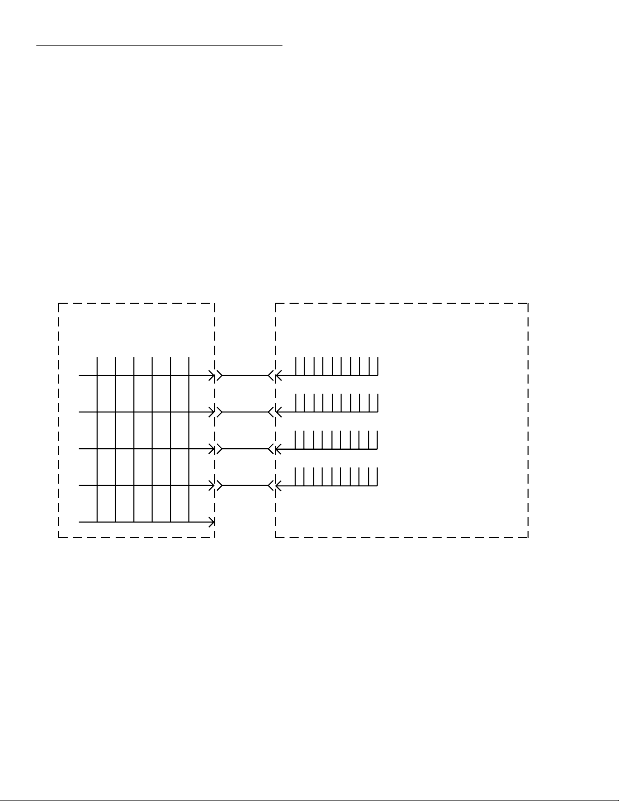
Basic matrix configuration (5
A simplified schematic of the Model 7022 matrix is shown
in Figure 2-1. The card is configured as a 5 × 6 matrix. Each
of the 30 crosspoints is made up of a two-pole switch. By
closing the appropriate crosspoint switch, any matrix row
can be connected to any column in the matrix.
×
6)
Figure 2-1
Model 7022 simplified schematic
Backplane jumpers
In Figure 2-1, the four pairs of backplane jumpers shown are
located on the relay card. With the jumpers installed, the
matrix is connected to the analog backplane of the Model
7001/7002 to allow matrix expansion with a second card
installed in the mainframe. With the jumpers removed (cut),
the matrix is isolated from an adjacent card installed in the
mainframe. Note that row E does not connect to the analog
backplane.
2-1
Page 21

Matrix Configuration
F
M
Card 1
Model 7001/7002
Analog
Backplane
Row A
H
L
G
Row B
H
L
G
L
L
Row C
Row D
H = High
L = Low
G = Guard
H
G
H
G
Card 2
H
L
G
H
L
G
H
L
G
H
L
G
Row = Matrix (7022)
Note: Row E does not
connect to the
analog backplane.
igure 2-2
odel 7001/7002 analog backplane
The three-pole analog backplane of the mainframe is shown
in Figure 2-2. It is through this analog backplane where the
rows of a Model 7022 card installed in one slot can be connected to the rows (or banks) of a compatible card installed
in the adjacent slot of the mainframe.
Figure 2-3 shows how each row of the Model 7022 is connected to the backplane. Since the Model 7022 is a two-pole
card, it does not provide a connection to the Guard terminal
of the backplane. The Model 7022 is shipped from the factory with the backplane row jumpers installed.
7001/7002
Analog
Backplane
H
L
G
H
L
H = High
L = Low
7022
Matrix Row
(1 of 4)
Backplane
Jumpers
Figure 2-3
Matrix row connections to backplane
Removing (cutting) the backplane jumpers isolates the card
from the backplane, and subsequently, any card installed in
the adjacent slot. For information on removing the jumpers,
refer to Section 4.
NOTE
The Model 7001/7002 does not provide an
analog backplane for the non-701X/702X/
703X series cards. As a result, any of these
cards installed in one slot in the mainframe is electrically isolated from any card
installed in the adjacent slot. The only way
to connect a Model 7022 to one of these
cards is to wire them together.
Typical matrix switching schemes
The following paragraphs describe some basic switching
schemes that are possible with a two-pole switching matrix.
These switching schemes include some various shielding
configurations to help minimize noise pickup in sensitive
measurement applications. These shields are shown connected to chassis ground. For some test configurations,
shielding may prove to be more effective connected to circuit
common. Chassis ground is accessible at the rear panel of the
Model 7001/7002.
2-2
Page 22

Matrix Configuration
Single-ended switching
In the single-ended switching configuration, the source or
measure instrument is connected to the DUT through a single pathway as shown in Figure 2-4.
Row Columns
HI
LO
Source or
Measure
Figure 2-4
Single-ended switching example
Differential switching
The differential or floating switching configuration is shown
in Figure 2-5. The advantage of using this configuration is
that the terminals of the source or measure instrument are not
confined to the same matrix crosspoint. Each terminal of the
instrument can be connected to any matrix crosspoint.
H
DUT
L
7022
Optional
Shield
Source or
Measure
Figure 2-5
Differential switching example
HI
LO
Rows Columns
H
L
DUT
H
L
7022
2-3
Page 23

Matrix Configuration
Sensing
Figure 2-6 shows how the matrix can be configured to use
instruments that have sensing capability. The main advantage of using sensing is to cancel the effects of matrix path
resistance (<1.25Ω) and the resistance of external cabling.
Whenever path resistance is a consideration, sensing should
be used.
Rows
Source HI
Sense HI
Sense LO
Source LO
Source or
Measure
Figure 2-6
Sensing example
SMU connections
Figure 2-7 shows how a Keithley Model 236, 237, or 238
Source Measure Unit could be connected to the matrix. By
using triax cables that are unterminated at one end, the driven
guard and chassis ground are physically extended all the way
to the card.
Columns
H
L
DUT
H
L
7022
Rows
Output HI
Guard
Sense HI
Guard
Sense LO
Output LO
Output LO
Triax
Cables (3)
236/237/238
WARNING: Hazardous voltages may be present on
GUARD. Make sure all cable shields are
properly insulated before applying power.
Columns
H
L
DUT
H
L
7022
Figure 2-7
SMU connections
2-4
Page 24

Matrix Configuration
Matrix expansion
With the use of additional cards and mainframes, larger
matrices can be configured. Each Model 7001 Switch System mainframe can accommodate up to two cards, and up to
six mainframes can be connected together to configure up to
12 cards. Each Model 7002 Switch System mainframe can
accommodate up to ten cards. And, by connecting up to six
Model 7002 mainframes, 60 cards can be configured. The
limits on the number of cards in the Model 7001/7002 are
due to triggering.
Card 1
7022
Columns
16
A
7001/7002
Analog
Backplane
Two-card switching systems
The Model 7001 and 7002 Switch System mainframes can
accommodate two and ten cards, respectively. The following
paragraphs use a two-card system to illustrate multiple-card
switching configurations.
Separate switching systems
Two single-card systems can be configured by removing the
backplane jumpers from one of the cards. The two cards will
be controlled by the same mainframe, but they will be electrically isolated from each other. Figure 2-8 shows an example using two Model 7022 cards.
Card 2
7022
Columns
16
A
B
Rows
C
D
E
Note: Row E does not connect
to the analog backplane.
Figure 2-8
Two separate 5 × 6 matrices
5 × 6 Matrix
B
Rows
C
D
E
5 × 6 Matrix
Jumpers
Removed
2-5
Page 25

Matrix Configuration
Narrow matrix expansion (4 × 12 matrix)
A narrow 4-row by 12-column matrix can be configured by
installing two “as shipped” Model 7022s in the Model 7001/
7002 mainframe. By leaving the backplane jumpers
installed, matrix rows A through D of the card installed in
Card 1
7022
Columns
16
A
B
Rows
C
D
E
slot 1 (CARD 1) are automatically connected to matrix rows
A through D of the card installed in slot 2 (CARD 2) through
the analog backplane. Note that row E does not connect to
the analog backplane. The 4 × 12 matrix is shown in Figure
2-9.
Card 2
7022
7001/7002
Analog
Backplane
712
Columns
Notes: 1. Backplane jumpers on both cards must be installed.
Figure 2-9
Narrow matrix example (4 × 12)
4 × 12 Matrix
2. Row E does not connect to the analog backplane.
2-6
Page 26

Matrix Configuration
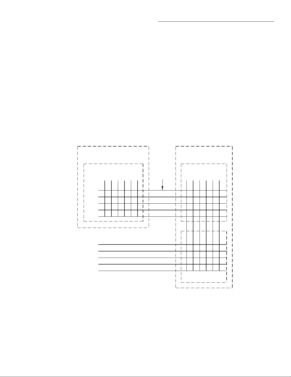
Wide matrix expansion (10 × 6 matrix)
A wide ten-row by six-column matrix is shown in
Figure 2-10. For this configuration, the six columns of the
two matrices must be physically hard-wired together. Also
Card 1
7022
16
A
B
Rows
C
D
E
Columns
note that the backplane jumpers on one of the cards must be
removed in order to isolate the rows of the two cards from
each other.
Jumpers
Removed
External
Column
Jumpers
7001/7002
Analog Backplane
A
B
Rows
C
D
E
7022
Card 2
10 × 6 Matrix
Figure 2-10
Wide matrix example (10 × 6)
2-7
Page 27
Matrix Configuration
Mixing card types
Different types of cards can be used together to create some
unique switching systems. For example, you could have a
Model 7022 matrix-digital I/O card installed in one slot and
a Model 7011 card installed in the adjacent slot.
Figure 2-11 shows a possible switching system using a
Model 7011 and a Model 7022. The backplane jumpers for
both cards must be installed. This allows matrix rows to be
connected to multiplexer banks. On the Model 7011, the
bank-to-bank jumpers must be removed to maintain isolation
between matrix rows. See the instruction manual for the
Model 7011 for complete multiplexer information.
Card 1
7022
16
A
Columns
7001/7002
Backplane
Mainframe matrix expansion
A 12-card matrix is possible by using six Model 7001 mainframes together, which provides 360 crosspoints. Also, a 60card matrix is possible by using six Model 7002 mainframes
together, which provides 1800 crosspoints. The limits on the
number of cards in the Model 7001/7002 switch system are
due to triggering.
In general, connecting the rows of a card in one mainframe
to the rows of a card in a second mainframe increases the column numbers of the matrix. For example, if the rows of a
4 × 12 matrix in one mainframe are connected to the rows of
a 4 × 12 matrix in a second mainframe, the resulting matrix
would be 4 × 24. Section 4 explains how to connect a test
system using two mainframes.
Card 2
7011
Inputs
1
1
10
Bank A
10
B
Rows
C
D
E
5 × 6 Matrix
Notes: 1. Models 7011 and 7022 backplane jumpers must be installed.
2. Model 7011 bank-to-bank jumpers must be removed.
Figure 2-11
Mixed card type example
Bank B
10
Bank C
10
Bank D
Quad 1 × 10 Mux
2-8
Page 28
Matrix Configuration
Partial matrix implementation
A fully implemented matrix provides a relay at each potential crosspoint. For example, a fully implemented 10 × 12
matrix utilizing four 5 × 6 cards contains 120 crosspoints. A
partially implemented 10 × 12 matrix would contain fewer
crosspoints.
An example of a partially implemented 10 × 12 matrix is
shown in Figure 2-12. The partial matrix is still considered
10 × 12 but contains only 90 crosspoints using three Model
7022 cards installed in two Model 7001/7002 mainframes.
Matrix card #1 (7022 #1) installed in one of the slots of the
first mainframe (7001/7002 #1) provides a 5 × 6 matrix. The
other slot of the first mainframe should be left empty. If
another switching card is left in that slot, it must be isolated from the analog backplane (i.e., backplane jumpers
7001/7002 #1
7022 #1
Columns
1
6
removed). The two cards (7022 #2 and #3) installed in
the second mainframe (7001/7002 #2) are configured as a
10 × 6 matrix as explained in the wide matrix expansion
(10 × 6) paragraph. Remember that the rows of card #2 must
be isolated from the rows of card #3. This is accomplished by
removing the jumpers on one of the two cards. Finally, the
partially implemented 10 × 12 matrix is realized by externally hard-wiring the rows of card #1 to the rows of card #2.
An obvious advantage of a partial matrix is that fewer cards
are needed. Another reason to use a partial matrix is to keep
specific devices from being connected directly to other
devices. For example, a source connected to rows F, G, H, I,
or J (Figure 2-12) cannot be connected to a column of Model
7022 #1 with one “accidental” crosspoint closure. Three specific crosspoints must be closed in order to route the source
signal to a column of card #1.
7001/7002 #2
External
Row
Jumpers
7
7022 #2
Columns
12
A
B
Rows
C
D
E
F
G
Rows
H
I
J
Figure 2-12
Partial matrix expansion (10 × 12)
7022 #3
2-9
Page 29

Matrix Configuration
2-10
Page 30

3
F
Digital I/O Configuration
Introduction
This section covers the basic digital input and output configurations for the Model 7022. Connection information for
these configurations is provided in Section 4 of this manual,
while operation (front panel and IEEE-488 bus) is explained
in Section 5.
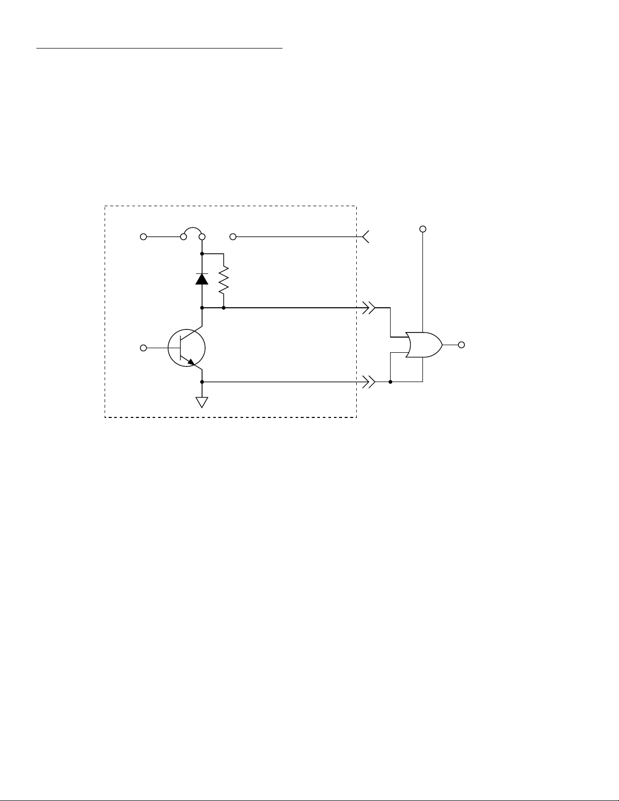
Digital outputs
Output channels are user configurable for negative (low) or
positive (high) true logic. That is, the output can be high or
low when the channel is turned on (closed) depending upon
user configuration. Conversely, the output can be high or low
when the channel is turned off (open). Refer to Section 4 to
configure the logic to your requirement.
7022
Jumper
5V
10kΩ
Controlling pull-up devices
Typically, the digital outputs are used to provide drive for relatively high current devices such as solenoids, relays, and
small motors. The configurations for these applications are
shown in Figure 3-1. Figure 3-1 allows you to use an external
voltage source (V) for devices that require a higher voltage
(42V maximum). An internal jumper is used to select the
internal pull-up voltage. At the factory, the internal 5V
source is selected.
Each output channel uses a fly-back diode for protection
when switching an inductive device, such as a solenoid coil.
This diode diverts the potentially damaging fly-back voltage
away from the driver.
V
V
EXT
Solenoid or
relay coil
NOTE: Setup uses an
external voltage
source (42V maximum).
Driver
igure 3-1
Output configuration for pull-up devices
3-1
Page 31
Digital I/O Configuration
Controlling devices using pull-up resistors
CAUTION
Failure to set J201 to the Vext position,
when using external pull-up voltages,
may result in damage to the output
drivers.
7022
Jumper
5V
R
P
10kΩ
Driver
When interfacing outputs to high-impedance devices (i.e.,
logic devices), internal pull-up resistors are used to achieve
the appropriate logic level. Figure 3-2 shows the output configuration using the 10kΩ pull-up resistor (Rp).
The configuration in Figure 3-2 uses the internal 5V source
as the high logic level. If you need a higher logic level, you
can place the jumper in the alternate position and apply an
external voltage (via V
V
EXT
GND
EXT
A
B
).
+V
Or
gate
Y
Logic
device
Figure 3-2
Output configuration using pull-up resistance
3-2
Page 32

Digital I/O Configuration
Digital inputs
Input channels use positive true logic but can be pulled up or
pulled down based on the configuration of the pull-up resistor. Each channel uses a 10kΩ pull-up resistor (R1). The pullup resistors can be pulled up to 5V or pulled down to ground
depending on the positioning of the jumper on the input
logic bank. Refer to Section 4 for more information. Figure
3-3 shows the resistor being pulled up to 5V.
When the resistor is connected to 5V, the channel is pulled
high. Thus, with nothing connected to the channel, the input
is pulled high to 5V which displays the channel as on.
7022
R
2
10kΩ
When the resistor is connected to ground, the channel is
pulled low. Thus, with nothing connected to the channel, the
input is pulled low to ground which displays the channel as
off.
The digital input is compatible with external TTL logic.
Each built-in pull-up resistor provides level shifting so
devices such as micro-switches can be monitored. Each input
has a protection network that clamps the input at 5.7V. This
allows logic levels up to 42V peak to be monitored.
5V
R
1
10kΩ
INPUT
GND
R1 = Pull-up resistor
R
= Input protection resistor
2
Figure 3-3
Input configuration
3-3
Page 33

Digital I/O Configuration
3-4
Page 34

4
Card Connections and
Installation
Introduction
WARNING
The procedures in this section are
intended only for qualified service personnel. Do not perform these procedures unless qualified to do so. Failure
to recognize and observe normal safety
precautions could result in personal
injury or death.
The information in this section is arranged as follows:
• Handling precaution — Explains precautions that
must be followed to prevent contamination to the card.
Contamination could degrade the performance of the
card.
• Matrix connections — Covers the basics for connecting external circuitry to the connector card.
• Digital I/O connections — Explains the voltage source
jumpers, pull-up resistors, output logic, and input resistance and how to configure them.
• Multi-pin (mass termination) connector card —
Covers the basic connections to the 96-pin DIN male
connector and identifies each terminal.
• Typical matrix connection schemes — Provides some
typical connection schemes for single-card, two-card,
and two-mainframe system configurations.
• Typical digital I/O connection schemes — Provides
some typical connection schemes for output solenoid,
relay, motor, and logic device control and for input micro-switch monitoring.
• Model 7022 installation and removal — Provides a
procedure to install and remove the Model 7022 card
from the Model 7001/7002 mainframe.
Handling precautions
To maintain high impedance isolation, care should be taken
when handling the relay and connector cards to avoid contamination from such foreign materials as body oils. Such
contamination can substantially lower leakage resistances,
thus degrading performance.
To avoid possible contamination, always grasp the relay and
connector cards by the side edges or shields. Do not touch
the board surfaces or components. On connectors, do not
touch areas adjacent to the electrical contacts. Dirt build-up
over a period of time is another possible source of contamination. To avoid this problem, operate the mainframe and
card in a clean environment.
If a card becomes contaminated, it should be thoroughly
cleaned as explained in Section 6.
4-1
Page 35

Card Connections and Installation
Matrix connections
The following paragraphs provide the basic information
needed to connect your external test circuitry to the matrix.
The removal/installation of the backplane row jumpers on
the relay card and detailed information on the connector card
is included.
WARNING
The following connection information is
intended to be used by qualified service
personnel. Failure to recognize and
observe standard safety precautions
could result in personal injury or death.
Backplane row jumpers
The Model 7001/7002 mainframe has an analog backplane
that allows the matrix rows of a Model 7022 to be internally
connected to a compatible switching card installed in the
adjacent slot. (See Section 2 for details.)
The backplane row jumpers for the card are located on the
relay card as shown in Figure 4-1. The card is shipped from
the factory with the jumpers installed.
7022 Relay Card
Jumper removal
Perform the following steps to remove the backplane row
jumpers:
1. If mated together, separate the relay card from the connector card by removing the mounting screw and then
pulling the two cards away from each other. Remember
to only handle the cards by the edges and shields to
avoid contamination.
2. Use Figure 4-1 to locate the jumper(s) to be removed.
3. It is not necessary to physically remove the jumpers
from the PC board. Using a pair of wire cutters, cut one
lead of each jumper.
Jumper installation
Referring to Figure 4-1 for jumper locations, perform the following steps to install the backplane row jumpers:
1. If mated together, separate the relay card from the connector card by removing the mounting screw and then
pulling the two cards away from each other. Remember
to only handle the cards by the edges and shields to
avoid contamination.
2. Physically remove a cut jumper by unsoldering it from
the PC board.
3. Install a new #22 AWG jumper wire (Keithley P/N J-15)
and solder it to the PC board.
4. Remove the solder flux from the PC board. The cleaning
procedure is explained in Section 6.
Figure 4-1
Backplane row jumpers
4-2
W100
W101
W102
W103
W104
W105
W106
W107
Jumpers
Digital I/O connections
Voltage source jumper
Digital output high uses the internal +5V source as the high
logic level. If higher voltages are required, a user-supplied
voltage can be used (42V maximum). At the factory, the
internal jumper is set to use the internal +5V source.
Page 36

Card Connections and Installation
CAUTION
Failure to set J201 to the Vext position, when using external pull-up
voltages, may result in damage to the
output drivers.
A plug-in jumper for the bank allows you to select the internal +5V source or an external source. In Figure 4-2, the
banks are using the external voltage source.
The voltage source jumper is located on the connector board
as shown in Figure 4-3. Figure 4-4 shows how the plug-in
jumper is installed on J201.
Pull-up resistors
When interfacing outputs to high-impedance devices (i.e.,
logic devices), pull-up resistors are used to achieve the
appropriate logic level. These resistors are installed at the
factory.
5V
J201
U203
31
32
33
34
U201 U202
35
36
37
38
Figure 4-2
Voltage source jumper for output channels
WARNING: USER SUPPLIED LETHAL
VOLTAGE MAY BE PRESENT ON
CONNECTORS OR P.C. BOARD
REFER TO MANUAL FOR MAXIMUM
VOLTAGE RATING OF CONNECTORS
V
ext
39
40
U203
Figure 4-3
Component locations - connector board
Jumper
EXT
A. External Source Selected
Figure 4-4
Voltage source jumper installation
U201 U202
+5VV
J201
5V
Vext
EXT
B. 5V Source Selected
Jumper
+5VV
4-3
Page 37

Card Connections and Installation
Configuring digital I/O output logic
Referring to Figure 4-5 for the digital I/O output logic location, perform the following steps to configure J101:
1. If mated together, separate the relay card from the connector card by removing the mounting screw and then
pulling the two cards away from each other. Remember
to only handle the cards by the edges and shields to
avoid contamination.
2. Locate J101 on the relay board. Refer to Figure 4-5.
3. Determine if you require positive (high) or negative
(low) logic.
4. Install the plug-in jumper in the appropriate position as
shown in Figure 4-6.
WARNING: USER SUPPLIED LETHAL VOLTAGES MAY BE
PRESENT ON CONNECTORS OR P.C. BOARD.
Jumper
High Low
A. High Selected
Jumper
High Low
HIGH
DOWN
LOGIC
OUTPUT
INPUT LOGIC
LOW
UP
J101
J100
Figure 4-5
Digital I/O output logic location
B. Low Selected
Figure 4-6
Digital I/O output logic selection
Configuring digital I/O input pull-up
resistance
Referring to Figure 4-5 for digital I/O input pull-up resistance location, perform the following steps to configure
J100:
1. If mated together, separate the relay card from the connector card by removing the mounting screw and then
pulling the two cards away from each other. Remember
to only handle the cards by the edges and shields to
avoid contamination.
2. Locate J100 on the relay board. Refer to Figure 4-5.
3. Determine if you require pull-up (5V) or pull-down
(ground) input logic.
4. Install the plug-in jumper in the appropriate position as
shown in Figure 4-7.
4-4
Page 38

Card Connections and Installation
Jumper
Down Up
A. Pull-down Resistance
Jumper
Down Up
B. Pull-up Resistance Selected
Keithley has a variety of cable and connector accessories
available to accommodate connections from the connector
card to test instrumentation and DUT (devices under test). In
general, these accessories, which are summarized in
Table 4-1, utilize a round cable assembly for connections.
Table 4-1
Mass termination accessories
Model Description
7011-KIT-R 96-pin female DIN connector and hous-
ing for round cable (provided with the
Model 7022 card).
7011-MTC-2 Two-meter round cable assembly termi-
nated with a 96-pin female DIN connector on each end.
7011-MTR 96-pin male DIN bulkhead connector.
Terminal identification for the DIN connector of the multipin connector card is provided by Figure 4-8 and Table 4-2.
This connector will mate to a 96-pin female DIN connector.
Figure 4-7
Digital I/O input pull-up resistance selection
Multi-pin (mass termination) connector card
Since connections to external circuitry are made at the 96-pin
male DIN bulkhead connector, there is no need to separate
the connector card from the relay card. If the connector card
is separated from the relay card, carefully mate them
together. Make sure to handle the cards by the edges and
shields to avoid contamination.
4-5
Page 39
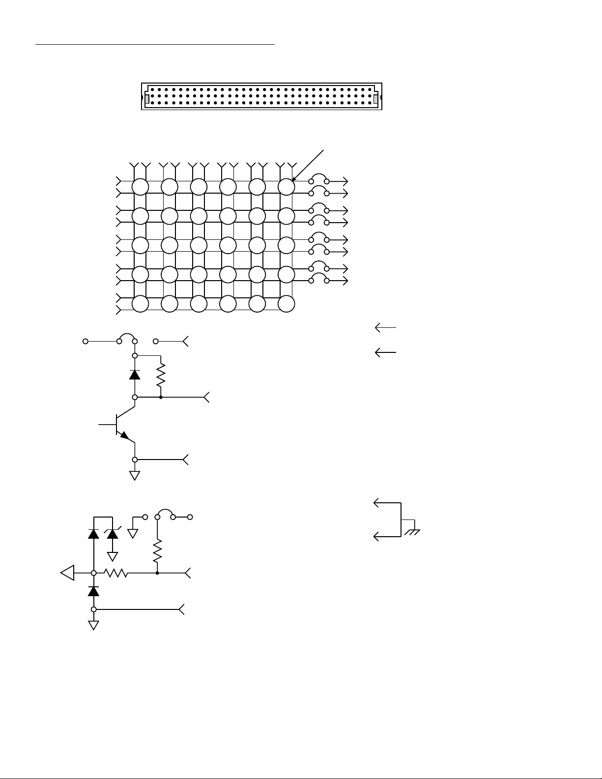
Card Connections and Installation
323130292827262524232221201918171615141312111098765432 1
c
b
a
123456
HL
Schematic Designator
Connector Designator
54
H
22b
A
86
L
22c
55
H
23b
B
87
L
23c
56
H
24b
C
88
L
24c
57
H
25b
D
89
L
25c
58
H
26b
E
90
L
26c
5V
91
27c5927b9228c6028b9329c6129b9430c6230b9531c6331b9632c6432b
HL HL HL HL HL
1 6 11 16 21 26
2
3
4
5
10
View from pin side
of connector
Channel
Pins of the Model 7022 mass
termination connector can be identified
12
17
7
27
22
in one of three ways:
• Matrix row (A-E) or column (1-6).
13
18
• Connector designation, consisting
8
28
23
of rows a-c and columns 1-32.
14
15
EXT
19
20
5375a
30
25
5b
9
V
29
24
• Schematic and component layout
designation (1-96).
1
Short pins
1a
1 (1a) and 33 (1b)
to close output
33
relays
1b
10K
10K
10K
Output Schematic Connector
Channel Designator Designator
31 42 10b
32 43 11b
33 44 12b
34 45 13b
35 46 14b
36 47 15b
GND
34
35
GND
2
3
34
35
2
3
Input
37 48 16b
38 49 17b
39 50 18b
2a
40 51 19b
3a
2b
3b
5V
Channel Schematic Connector
1 74 10c
27511c
3 76 12c
4 77 13c
2a
5 78 14c
3a
6 79 15c
2b
7 80 16c
3b
8 81 17c
9 82 18c
10 83 19c
Designator Designator
41
9b
9
9a
Shield
Connection
Figure 4-8
Multi-pin connector card terminal identification
4-6
Page 40

Table 4-2
Pin designation identification
Card Connections and Installation
Connector
Matrix
terminal
row A, HI 22b 54 IN 1 10c 74 nc 12a 12
row A, LO 22c 86 IN 2 11c 75 nc 13a 13
row B, HI 23b 55 IN 3 12c 76 nc 14a 14
row B, LO 23c 87 IN 4 13c 77 nc 15a 15
row C, HI 24b 56 IN 5 14c 78 nc 16a 16
row C, LO 24c 88 IN 6 15c 79 nc 17a 17
row D, HI 25b 57 IN 7 16c 80 nc 18a 18
row D, LO 25c 89 IN 8 17c 81 nc 19a 19
row E, HI 26b 58 IN 9 18c 82 nc 20a 20
row E, LO 26c 90 IN 10 19c 83 nc 21a 21
col 1, HI 27c 91 vext 5a 5 nc 22a 22
col 1, LO 27b 59 vext 5b 37 nc 23a 23
col 2, HI 28c 92 shield 9a 9 nc 24a 24
col 2, LO 28b 60 shield 9b 41 nc 25a 25
col 3, HI 29c 93 gnd 2a 2 nc 26a 26
col 3, LO 29b 61 gnd 3a 3 nc 27a 27
col 4, HI 30c 94 gnd 2b 34 nc 28a 28
col 4, LO 30b 62 gnd 3b 35 nc 29a 29
col 5, HI 31c 95 inter 1b 33 nc 30a 30
col 5, LO 31b 63 inter 1a 1 nc 31a 31
col 6, HI 32c 96 nc 4b 36 nc 32a 32
col 6, LO 32b 64 nc 6b 38 nc 1c 65
OUT 31 10b 42 nc 7b 39 nc 2c 66
OUT 32 11b 43 nc 8b 40 nc 3c 67
OUT 33 12b 44 nc 20b 52 nc 4c 68
OUT 34 13b 45 nc 21b 53 nc 5c 69
OUT 35 14b 46 nc 4a 4 nc 6c 70
OUT 36 15b 47 nc 6a 6 nc 7c 71
OUT 37 16b 48 nc 7a 7 nc 8c 72
OUT 38 17b 49 nc 8a 8 nc 9c 73
OUT 39 18b 50 nc 10a 10 nc 20c 84
OUT 40 19b 51 nc 11a 11 nc 21c 85
designator
1a-32c
Schematic
designator
1-96
Matrix
terminal
Connector
designator
1a-32c
Schematic
designator
1-96
Matrix
terminal
Connector
designator
1a-32c
designator
Schematic
1-96
4-7
Page 41

Card Connections and Installation
Typical connection techniques
All external circuitry, such as instrumentation and DUTs,
that you want to connect to the card must be terminated with
a single 96-pin female DIN connector. The following connection techniques provide some guidelines and suggestions
for wiring your circuitry.
WARNING
Before beginning any wiring procedures, make sure all power is off and
any stored energy in external circuitry
is discharged.
WARNING
When wiring a connector, do not leave
any exposed wires. No conductive part
of the circuit may be exposed. Properly
cover the conductive parts, or death by
electric shock may occur.
NOTE
It is recommended that external circuitry
be connected (plugged in) after the Model
7022 is installed in the Model 7001/7002
mainframe and with the mainframe power
off. Installation is covered at the end of
this section.
Output relays The multi-pin connector card uses a relay
for each of the four output banks. These output relays are
normally open to prevent any hazardous voltages (via the
mainframe backplane) from appearing on the pins of the
male DIN connector. The output relays will only close when
the Model 7011-MTC-2 cable assembly is connected to card.
If building your own cable assembly, make sure it shorts pins
1a to 1b of the card connector (Figure 4-10) when it is mated
to the card. Shorting pins 1a to 1b allows the output relays to
close.
Round cable assemblies Figure 4-9 shows typical round
cable connection techniques using accessories available
from Keithley.
4-8
Page 42

Card Connections and Installation
.
Wire instrumentation
A)
Multi-Pin
Connector
Card
7011-MTC-2
cable assembly
7011-MTR
bulkhead connector
and DUT to bulkhead
connector (See Table 4-2
and Figures 4-8 and 4-10
for terminal identification)
B)
Connector
Card
Multi-Pin
Multi-Pin
C)
Connector
Card
Figure 4-9
Typical round cable connection techniques
Wire directly to
instrumentation
and DUT
7011-MTC-2
(Cut in Half)
Wire directly to
instrumentation
and DUT
Cable
7011-Kit-R
Connector Kit
Notes: Figure 4-11 provides an exploded view showing
how the connector (with cable) is assembled.
Cable Hitachi p/n N2807-P/D-50TAB is a
50-conductor cable. Two of these cables
can be used to supply 100 conductors.
4-9
Page 43
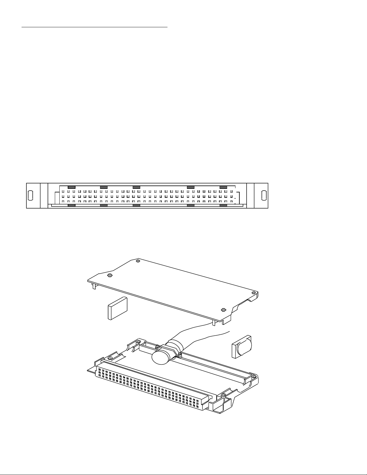
Card Connections and Installation
F
M
In Figure 4-9A, connections are accomplished using a Model
7011-MTC-2 cable and a Model 7011-MTR bulkhead connector. The two-meter round cable is terminated with a 96pin female DIN connector at each end. This cable mates
directly to the multi-pin connector card and to the bulkhead
connector. The bulkhead connector has solder cups to allow
direct connection to instrumentation and DUT. Figure 4-10
provides pinout for the bulkhead connector. The view shown
is from the solder cup end of the connector.
In Figure 4-9B, connections are accomplished using a Model
7011-MTC-2 cable assembly that is cut in half. The 96-pin
female DIN connector on one end of the cable mates directly
to the multi-pin connector card. The unterminated end of the
cable is wired directly to instrumentation and DUT. The
other half of the cable assembly could be used for a second
switching card.
Note: See Figure 4-8 for terminal identification.
In Figure 4-9C, connections are accomplished using a
custom-built cable assembly that consists of a Model 7011KIT-R connector and a suitable round cable. Hitachi cable
part number N2807-P/D-50TAB is a 50-conductor round
cable. Two of these cables can be used to provide 100
conductors. The connector has solder cups to accommodate
the individual wires of the unterminated cable. Figure 4-11
provides an exploded view of the connector assembly and
shows how the cable is connected. For further Model
7011-KIT-R assembly information, refer to the packing list
provided with the kit. The connector end of the resultant
cable assembly mates directly to the multi-pin connector
card. The unterminated end of the cable assembly is wired
directly to instrumentation and DUT.
3231302928272625242322212019181716151413121110987654321
c
b
a
View from solder
cup side of
connector
igure 4-10
odel 7011-MTR connector pinout
Figure 4-11
Model 7011-KIT-R (with cable) assembly
4-10
Page 44

Card Connections and Installation
Typical matrix connection schemes
The following information provides some typical connection
schemes for single-card, two-card, and two-mainframe system configurations. Connection schemes for the multi-pin
connector card use some of the techniques presented in this
section. Keep in mind that these are only examples to demonstrate various ways to wire a test system.
Single-card system
Figure 4-12 shows how external connections can be made to
a single-card system that uses the multi-pin connector card.
Instrumentation and DUT are hard-wired to the Model
7011-MTR male bulkhead connector. This connector has
solder cups that will accept wire size up to #24 AWG. The
test system is connected to the matrix using the Model
7011-MTC-2 round cable assembly. This cable mates
Instrument
Instrument
Instrument
Row A
Row B
Row C
22 Individual Conductors
directly to both the external bulkhead connector and the
Model 7022. Notice that the bulkhead connector is shown
mounted to a fixture to help keep the cabling stable during
the test.
When using a single-card system, make sure that the card
remains electrically isolated from any other switching cards.
There are several ways to ensure isolation for a single card in
the Model 7001/7002 mainframe:
1. Vacate the adjacent slot in the mainframe. If there is a
Model 70XX card installed in the other slot, remove it.
2. Remove the backplane jumpers on the card. This will
disconnect the card from the analog backplane of the
mainframe.
3. Remove the backplane jumpers from the switching card
installed in the adjacent slot.
7022
Fixture for
Bulkhead
Connector
Instrument
Instrument
Figure 4-12
Single-card system example
Row D
Row E
123456
DUT T est Fixture
Instruments
DUT
12 3456
12 3456
A
B
C
D
E
Columns
Equivalent Circuit
7011-MTR
Bulkhead
Connector
Rows
7011-MTC-2
Cable Assembly
4-11
Page 45

Card Connections and Installation
Two-card system
Figure 4-13 shows a system using two Model 7022 cards
installed in one Model 7001/7002 mainframe to configure a
4 × 12 test matrix. In this connection scheme, row connections of the two cards are accomplished internally through
the backplane of the mainframe. To connect rows internally,
the backplane row jumpers of both cards must be installed.
Figure 4-13 shows how external connections can be made for
the multi-pin connector cards. In this example, a single
Model 7011-MTC-2 round cable assembly is cut in half to
provide two cables, each of which is unterminated at one
end. The unterminated ends of the two cables are hard-wired
to instrumentation and DUT as shown in the drawing. The
other ends of these cables mate directly to the Model 7022
cards.
4-12
Page 46

Card Connections and Installation
Instrument
Instrument
Instrument
Instrument
123456
Row A
Row B
Row C
Row D
DUT Test Fixture
7011-MTC-2
Cable Assembly
(Cut in half to
provide two cables)
Note: Backplane row jumpers for
both cards must be installed.
7001/7002 #2
C
7022
7022
A
R
D
1
C
A
R
D
2
123456
DUT Test Fixture
Figure 4-13
Two-card system example
Instruments
DUT
123456
A
B
C
D
E
Column Column
CARD 1 CARD 2
7001/7002
Backplane
123456
123456123456
Backplane Row
Jumpers installed
Equivalent Circuit
DUT
Row
4-13
Page 47

Card Connections and Installation
Two-mainframe system
Figure 4-14 shows a system using three cards in two Model
7001/7002 mainframes to configure a 4 × 18 test matrix. This
system is similar to the two-card system (see previous paragraph), except that a third card (installed in a second mainframe) is added.
Figure 4-14 shows the connection scheme for the multi-pin
connector cards. External circuit connections to the Model
7001/7002 #1 mainframe are identical to the ones used for
the two-card system. The third card (installed in Model
7001/7002 #2 mainframe) shows how a custom-built cable
can be used to make connections to external circuitry. A suitable round cable can be terminated with a 96-pin female DIN
connector (Model 7011-KIT-R) that will mate to the Model
7022. The unterminated end of the cable is connected
directly to instrumentation and DUT. Notice that the row
connections for the third card are made at the instruments.
4-14
Page 48

Card Connections and Installation
DUT T est Fixture
123456
Instrument
Instrument
Instrument
Instrument
123456
DUT T est Fixture
7011-MTC-2
Cable Assembly
(Cut in half to
provide two cables)
7011-Kit-R
Connector Kit
Cable
7001/7002 #2
7022
7022
7001/7002 #2
7022
7022
C
A
R
D
1
C
A
R
D
2
C
A
R
D
1
C
A
R
D
2
123456
DUT T est Fixture
Trigger Link
I
N
O
U
T
Trigger Link
I
N
O
U
T
Trigger
Link
Cable
Note: Backplane
row jumpers for
both cards in 7001/
7002 #1 must be
installed.
A
Instruments
B
C
D
E
Figure 4-14
Two-mainframe system example
7001/7002 #1 7001/7002 #2
7001/7002
Backplane
DUT
12 3456
12 3456
12 345612 3456
Column Column
CARD 1 CARD 2
Backplane Row
Jumpers installed
Equivalent Circuit
DUT
DUT
1234 56
1234 56
Column
CARD 3
External Row Jumpers
Row
4-15
Page 49

Card Connections and Installation
Typical digital I/O connection schemes
Output connection schemes
The following examples show output connections from the
card to external circuitry and summarizes the required internal connections on the card. Each example assumes negative
true logic is used. To configure for positive true logic, refer
to the Configuring digital I/O output logic paragraph.
Solenoid control — Figure 4-15 shows a digital output connection scheme to control solenoids. This example assumes
that an external 24V source is being used. A solenoid is energized when the corresponding output channel is turned on
(closed).
7022
V
EXT
OUT 31
OUT 32
SOLENOIDS
+
24V
–
Motor control — Figure 4-16 shows a digital output connection scheme to control small 12V dc motors. An external
12V source is used to provide the necessary voltage level. A
motor is turned on when the corresponding output channel is
turned on (closed).
7022
V
EXT
OUT 39
OUT 40
GND
INTERNAL CONNECTIONS:
EXTERNAL VOLTAGE SOURCE (V
MOTORS
M M
) SELECTED.
EXT
+
12V
–
OUT 33
GND
INTERNAL CONNECTIONS:
EXTERNAL VOLTAGE SOURCE (V
Figure 4-15
Digital output, solenoid control
) SELECTED.
EXT
Figure 4-16
Digital output, motor control
4-16
Page 50

Card Connections and Installation
Logic device control — Figure 4-17 shows a digital output
connection scheme to control a logic device. This example
assumes that an internal +5V voltage source is being used.
+5V
G2A
A
B
C
LOGIC DEVICE
74LS138
DMUX
V
CC
GND
Y0
Y1
Y2
Y3
Y4
Y5
Y6
Y7
7022
OUT 31
OUT 32
OUT 33
GND
INTERNAL CONNECTIONS:
INTERNAL VOLTAGE SOURCE (+5V) USED.
Figure 4-17
Digital output, logic device control
7022
IN 1
IN 2
IN 3
GND
A. INPUT RESISTOR IS SET TO PULL UP.
7022
IN 1
IN 2
IN 3
MICRO-
SWITCHES
MICRO-
SWITCHES
The logic device is a demultiplexer (DMUX). The binary
pattern (value) seen at the input of the DMUX (lines A, B,
and C) determines which DMUX output line (Y0 through
Y7) is selected (pulled low). For example, with channels 1,
2, and 3 off (open), lines A, B and C are high. The binary 7
at the DMUX input (A = 1, B = 1 and C = 1) selects (pulls
low) output Y7. If channel 2 is turned on (closed), line B goes
low. The binary 5 seen at the DMUX input (1, 0, 1) selects
(pulls low) Y5.
Input connection scheme
Figure 4-18 shows a digital input connection scheme to monitor the state of micro-switches. With a switch open and the
input resistor configured for pull up as shown in Figure 418a, the corresponding input channel is pulled high by the
internal input resistor. As a result, the input channel is high
(appears as a bar on the Model 7001 display or a lit LED on
the Model 7002). When a switch is closed, the corresponding
input channel is pulled low to ground. As a result, the input
channel is low (appears as a single dot on the Model 7001
display or an unlit LED on the Model 7002).
+V
B. INPUT RESISTOR IS SET TO PULL DOWN.
Figure 4-18
Digital input, monitoring micro-switches
With a switch open and the input resistance configuration set
to pull down as shown in Figure 4-18b, the corresponding
input channel is pulled low by the internal input resistor. As
a result, the input channel is low. When a switch is closed, the
corresponding input channel is pulled high. As a result, the
input channel is high.
For more information on configuring pull-up resistance,
refer to the Configuring digital I/O input pull-up resistance
paragraph.
4-17
Page 51

Card Connections and Installation
Model 7022 installation and removal
The following paragraphs explain how to install and remove
the Model 7022 card from the Model 7001/7002 mainframe.
WARNING
Installation or removal of the Model
7022 is to be performed by qualified service personnel. Failure to recognize and
observe standard safety precautions
could result in personal injury or death.
CAUTION
To prevent contamination to the
Model 7022 card that could degrade
performance, only handle the card by
the edges and shields.
Card installation
Perform the following steps to install the Model 7022 card in
the Model 7001/7002 mainframe:
1. Mate the connector card to the relay card if they are separated. Install the supplied 4-40 screw at the end of the
card to secure the assembly. Make sure to handle the
cards by the edges and shields to prevent contamination.
2. Facing the rear panel of the mainframe, select the slot
(CARD 1 or CARD 2) that you want to install the Model
7022 card in.
3. Referring to Figure 4-19, feed the Model 7022 card into
the desired slot so the edges of the relay card ride in the
rails.
4. With the ejector arms in the unlocked position, push the
Model 7022 card all the way into the mainframe until
the arms engage into the ejector cups. Then push both
arms inward to lock the card into the mainframe.
WARNING
To avoid electric shock that could result
in injury or death, make sure to properly install and tighten the safety
ground screw shown in Figure 4-19.
5. Install the screw shown in Figure 4-19.
WARNING
Turn off power from all instrumentation (including the Model 7001/7002
mainframe) and disconnect their line
cords. Make sure all power is removed
and stored energy in external circuitry
is discharged.
Screw
Unlock card
Card removal
To remove the Model 7022 card, first unloosen the safety
ground screw, unlock the card by pulling the latches outward, and then pull the card out of the mainframe. Remember to handle the card by the edges and shields to avoid
contamination that could degrade performance.
Ejector
Arms (2)
Screw
Lock card
Figure 4-19
Model 7022 card installation in Model 7001
4-18
Page 52

Card Connections and Installation
Models 7022-D and 7022-DT
The Models 7022-D and 7022-DT are alternate configurations of the Model 7022 Matrix-Digital I/O Card. The
Model 7022 consists of a relay card and a connector card in
a sandwich. The configurations are as follows:
• Model 7022 — Relay card and mass-terminated card
with 96-pin male DIN connector.
• Model 7022-D — Relay card and mass-terminated card/
cable with 50-pin male and female D-Sub connectors.
• Model 7022-DT — Spare mass-terminated card/cable
with 50-pin male and female D-Sub connectors.
The following is additional information that applies to the
Models 7022-D and 7022-DT.
Internal connections
The two PC-boards that plug together are secured by a 4-40
screw (see Figure 4-20).
Input/output connections
WARNING
Connections and installation procedures are to be performed by qualified
service personnel. Failure to recognize
and observe standard safety precautions could result in personal injury or
death.
Connections to external circuitry are made at the 50-pin
D-Sub connectors. Connector pinouts are shown in
Table 4-3. Figure 4-21 shows the solder-side view of a
mating connector.
4-40x¼PPHSEM
(5 IN LBS)
7022-019, MASS TERM BOARD ASSEMBLY
Figure 4-20
Mating the PC-boards
7021-010, RELAY BOARD ASSEMBLY
4-19
Page 53

Card Connections and Installation
Table 4-3
Terminal identification
Male D-Sub (Dig I/O) Female D-Sub (Matrix)
Signal Pin Signal Pin Signal Pin Signal Pin
Ve xt
Gnd
Inter
Out 31
Out 34
Out 37
Out 40
In 8
In 5
In 2
N/C
N/C
N/C
N/C
N/C
N/C
Inter
Ve xt
Gnd
Out 32
Out 35
Out 38
In 10
In 7
In 4
10
11
12
13
14
15
16
17
18
19
20
21
22
23
24
25
1
In 1
2
N/C
3
N/C
4
N/C
5
N/C
6
N/C
7
N/C
8
N/C
9
Gnd
Gnd
Out 33
Out 36
Out 39
In 9
In 6
In 3
N/C
N/C
N/C
N/C
N/C
N/C
N/C
N/C
N/C
26
27
28
29
30
31
32
33
34
35
36
37
38
39
40
41
42
43
44
45
46
47
48
49
50
Col 3 LO
Row E LO
Row C HI
Row B LO
Col 4 LO
Col 6 HI
Col 2 LO
Col 1 HI
N/C
N/C
N/C
N/C
N/C
N/C
N/C
N/C
N/C
Col 3 HI
Row D HI
Row C LO
Row A HI
Col 4 HI
Col 5 LO
Col 2 HI
Shield
10
11
12
13
14
15
16
17
18
19
20
21
22
23
24
25
1
2
3
4
5
6
7
8
9
N/C
N/C
N/C
N/C
N/C
N/C
N/C
N/C
Row E HI
Row D LO
Row B HI
Row A LO
Col 6 LO
Col 5 HI
Col 1 LO
Shield
N/C
N/C
N/C
N/C
N/C
N/C
N/C
N/C
N/C
26
27
28
29
30
31
32
33
34
35
36
37
38
39
40
41
42
43
44
45
46
47
48
49
50
17
33
50
Figure 4-21
Mating connector (solder-side view)
4-20
1
18
34
Page 54

5
Operation
Introduction
The information in this section is arranged as follows:
• Power limits — Summarizes the maximum power lim-
its of the Model 7022.
• Mainframe control of the card — Summarizes pro-
gramming steps to control the card from the Model
7001/7002 Switch System mainframe.
• Matrix switching examples — Provides some typical
applications for using the Model 7022.
• Measurement considerations — Reviews a number of
considerations when using the Model 7022 to make
measurements.
Power limits
CAUTION
To prevent damage to the card, do not
exceed the maximum signal level specifications of the card.
Digital I/O maximum signal levels
Output channels
Maximum user-supplied pull-up voltage: 42V
Maximum sink current:
Per channel: 250mA
Per card: 1A
Input channels
Maximum voltage level: 42V peak
Mainframe control of the card
The following information pertains to the Model 7022 card.
It assumes you are familiar with the operation of the Model
7001/7002 mainframe.
If you are not familiar with the operation of the mainframe,
it is recommended that you proceed to Getting Started (Section 3) in the Model 7001 or Model 7002 Instruction Manual
after reading the following information.
Analog matrix maximum signal levels
To prevent overheating or damage to the relays, never exceed
the following maximum signal levels:
DC signals: 110V DC or 155 VAC peak between
any two inputs or chassis, 1A switched,
30VA (resistive load).
5-1
Page 55

Operation
F
M
1 234567891012345678910
= Open Channel
= Closed Channel
igure 5-1
odel 7001 channel status display
7001 Display
CARD 1 CARD 2
Channel assignments
The Model 7001 has a channel status display (Figure 5-1)
that provides the real-time state of each available channel.
The left portion of the display is for slot 1 (card 1), and the
right portion is for slot 2 (card 2). For the Model 7002, channel status LED grids are used for the ten slots. The LED grid
for slot 1 is shown in Figure 5-2.
7002 LED DISPLAY
SLOT 1
1234 6785910
1
2
ROW
3
4
Figure 5-2
Model 7002 channel status display (slot 1)
Organization of the channel status display for each slot is
shown in Figure 5-3. The card contains 40 channels and
is made up of a 5 × 6 matrix using 30 channels, with each
channel designated as a row/column crosspoint, and ten digital output channels.
The matrix rows can be jumpered to the backplane of the
mainframe to expand matrix inputs.
COLUMN
= OPEN CHANNEL
= CLOSED CHANNEL
The hardware for the digital output channels is user configurable for negative or positive true logic. That is, depending
on the user configuration, the output can go high or be pulled
low when the channel is turned on (closed) or off (open). To
configure output logic, refer to Section 4.
Input channels use positive true logic but can be configured
to pull up or pull down. Thus, a channel can be pulled high
or pulled low when the input is open depending on the
jumper configuration. Input channels will be displayed as
high (on) when the input has a high logic level applied. Conversely, an input channel will be displayed as low (off) when
a low logic level is applied.
To control the card from the mainframe, each matrix crosspoint and digital output must have a unique channel assignment. The channel assignments for the card are provided in
Figure 5-4. Each channel assignment is made up of the slot
designator (1 or 2) and the matrix crosspoint or digital output
channel. For the Model 7002, the slot designator can be from
1 to 10 since there are ten slots. To be consistent with Model
7001/7002 operation, the slot designator and channel are
separated by exclamation points (!). Some examples of channel assignments:
CHANNEL 1!1 = Slot 1, Channel 1 (Row A, Column 1)
CHANNEL 1!40 = Slot 1, Channel 40 (Output 40 of
Digital I/O)
CHANNEL 2!2 = Slot 2, Channel 2 (Row B, Column 1)
CHANNEL 2!34 = Slot 2, Channel 34 (Output 34 of
Digital I/O)
All digital input and output channels are isolated from the
backplane of the mainframe. With the mainframe in the normal display state, the status (on or off) of the output and
matrix crosspoint channels is displayed. When the mainframe is in the read input channels mode, the status (on or
off) of the input channels is displayed.
5-2
These channels are displayed and controlled from the normal
display state of the mainframe. If currently in the menu
structure, return to the normal display state by pressing
EXIT.
Page 56

Crosspoint
Operation
Channel
Digital
Output
Channels
Figure 5-3
Channel display organization
12345678910
1!1 1!2 1!3 1!4 1!5 1!6 1!7 1!8 1!9 1!10
1!11 1!12 1!13 1!14 1!15 1!16 1!17 1!18 1!19 1!20
1!21 1!22 1!23 1!24 1!25 1!26 1!27 1!28 1!29 1!30
A. Slot 1
(Card 1)
1!31 1!32 1!33 1!34 1!35 1!36 1!37 1!38 1!39 1!40
RA,C1 RC,C1 RD,C1 RE,C1 RA,C2 RB,C2 RC,C2 RD,C2 RE,C2
RA,C3 RB,C3 RC,C3 RD,C3 RE,C3 RA,C4 RB,C4 RC,C4 RD,C4 RE,C4
RA,C5 RB,C5 RC,C5 RD,C5 RE,C5 RA,C6 RB,C6 RC,C6 RD,C6 RE,C6
OUT
RB,C1
12345678910
11 12 13 14 15 16 17 18 19 20
21 22 23 24 25 26 27 28 29 30
OUT OUT OUT OUT OUT OUT OUT OUT OUT
31 32 33 34 35 36 37 38 39 40
12345678910
2!1 2!2 2!3 2!4 2!5 2!6 2!7 2!8 2!9 2!10
2!11 2!12 2!13 2!14 2!15 2!16 2!17 2!18 2!19 2!20
2!21 2!22 2!23 2!24 2!25 2!26 2!27 2!28 2!29 2!30
B. Slot 2
(Card 2)
2!31 2!32 2!33 2!34 2!35 2!36 2!37 2!38 2!39 2!40
Examples: 1!18 = Slot 1, Channel 18 (Row C, Column 4)
2!36 = Slot 2, Channel 36 (Output 36, Digital I/O)
Figure 5-4
Model 7022 programming channel assignments
5-3
Page 57

Operation
Closing and opening channels
NOTE
This procedure applies to matrix channels
(channels 1!1 through 1!30) and digital
I/O output channels (1!31 through 1!40).
Digital input channels are read only.
A channel is turned on (closed) from the front panel by simply keying in the channel assignment and pressing CLOSE.
For example, to close row C, column 4 crosspoint of a card
installed in slot 2, key in the following channel list and press
CLOSE:
SELECT CHANNELS 2!18
The above closed channel can be turned off (opened) by
pressing OPEN or OPEN ALL. The OPEN key opens only
the channels specified in the channel list, and OPEN ALL
opens all channels.
NOTE
For the Model 7002, you can use the light
pen to turn channels on and off.
Pressing CLOSE will turn on channel 2!1 and the channels
that make up channel pattern M1. Refer to the instruction
manual for the mainframe and for information on defining
channel patterns.
Scanning channels
Channels are scanned by creating a scan list and configuring
the Model 7001/7002 to perform a scan. The scan list is created in the same manner as a channel list. (See the Closing
and opening channels paragraph.) However, the scan list is
specified from the SCAN CHANNELS display mode. (The
SCAN LIST key toggles between the channel list and scan
list.) The following shows an example of a scan list:
SCAN CHANNELS 2!1, 2!3, 2!1-2!5
When a scan is performed, the channels specified in the scan
list will be scanned in the order that they are presented in the
scan list.
Channel patterns can also be used in a scan list. This allows
you to control specific bit patterns for logic circuits.
Example:
SCAN CHANNELS M1, M2, M3, M4
The following display is an example of a channel list that
consists of several channels:
SELECT CHANNELS 2!1, 2!3, 2!222!25
Notice that channel entries are separated by commas (,). A
comma is inserted by pressing ENTER or the right cursor
key (). The channel range is specified by using the hyphen
(-) key to separate the range limits. Pressing CLOSE will
close all the channels specified in the channel list. Pressing
OPEN (or OPEN ALL) will open the channels.
Channel patterns can also be used in a channel list. This
allows you to control specific bit patterns for logic circuits.
Example:
SELECT CHANNELS 2!1, M1
When M1 is scanned, the channels that make up channel pattern M1 will turn on. When M2 is scanned, the M1 channels
will turn off and the channels that make up M2 will turn on.
M3 and M4 are scanned in a similar manner. Refer to the
instruction manual for the mainframe for information on
defining channel patterns.
A manual scan can be performed by using the RESET
default conditions of the Model 7001/7002. RESET is
selected from the SAVESETUP menu of the main MENU.
When RESET is performed, the mainframe is configured for
an infinite number of manual scans. The first press of STEP
takes the mainframe out of the idle state. The next press of
STEP will close the first channel specified in the scan list.
Each subsequent press of STEP will select the next channel
in the scan list.
5-4
Page 58

Operation
Reading input channels
Input channels are read from the READ-I/O-CARD option
of the CARD CONFIG MENU of the mainframe. This menu
is accessed by pressing the CARD key. In this “read input
channels” display mode, the mainframe displays the realtime state of each input channel.
Input channels use positive true logic but can be configured
to pull up or pull down. Open inputs will read high (on) if
inputs are configured for pull up. Conversely, open inputs
will read low (off) when configured for pull down. To configure pull-up resistance, refer to Section 4.
Perform the following steps to configure the mainframe to
display the digital input channels.
1. Press the CARD CONFIGURATION key to display the
CARD CONFIG MENU.
2. Use the and keys to place the cursor on READ-I/
O-CARD and press ENTER.
Model 7001 mainframe — The real-time state (on or
off) of each input channel is provided on the first row of
the display. Only digital I/O input channels are displayed.
Model 7002 mainframe — The real-time state (on or
off) of each input channel is provided on the first row of
the appropriate LED display grid. Use the TYPE option
of the CARD CONFIG MENU if you do not know
which slot the card is installed in.
3. Use the EXIT key to exit from the “read input channels”
display mode.
NOTE
With input channels displayed, you can
turn off (open) all other channels by pressing OPEN ALL.
Turning channels on and off
The following SCPI commands are used to turn matrix and
digital I/O output channels on and off:
:CLOSe <list> Turn on specified channels.
:OPEN <list>|ALL Turn off specified (or all) channels.
The following program statement turns on channels 1!1, 1!4
through 1!6, and the channels that make up channel pattern
M1.
PRINT #1, "output 07; clos (@ 1!1, 1!4:1!6, M1)"
Notice that the colon (:) is used to separate the range limits.
Either of the following statements turns off channels 1!1, 1!4
through 1!6, and the channels of M1:
PRINT #1, "output 07; open (@ 1!1, 1!4:1!6, M1)"
PRINT #1, "output 07; open all"
Scanning output channels
There are many commands associated with scanning. However, it is possible to configure a scan using as little as four
commands. These commands are listed as follows:
*RST
:TRIGger:COUNt:AUTo ON
:ROUTe:SCAN <list>
:INIT
The first command resets the mainframe to a default scan
configuration. The second command automatically sets the
channel count to the number of channels in the scan list, the
third command defines the scan list, and the fourth command
takes the Model 7001/7002 out of the idle state.
IEEE-488 bus operation
Bus operation is demonstrated using Microsoft QuickBASIC
4.5, the Keithley KPC-488.2 (or Capital Equipment Corporation) IEEE interface and the HP-style Universal Language
Driver (CECHP). Refer to “QuickBASIC 4.5 Programming”
in the mainframe manual for details on installing the Universal Language Driver, opening driver files, and setting the
input terminal. Program statements assume that the primary
address of the mainframe is 07.
The following program fragment will perform a single scan
of channels 1 through 4 of slot 1 and the channels that make
up channel pattern M1:
PRINT #1, "output 07; *rst"
PRINT #1, "output 07; trig:coun:auto on"
PRINT #1, "output 07; scan (@ 1!1:1!4, M1)"
PRINT #1, "output 07; init"
5-5
Page 59

Operation
The first statement selects the *RST default configuration for
the scan. The second statement sets channel count to the
scan-list-length (5). The third statement defines the scan list,
and the last statement takes the mainframe out of the idle
state. The scan is configured to start as soon as the :INIT
command is executed.
When the above program fragment is run, the scan will be
completed in approximately 240msec (3msec delay for
channel closures and 3msec delay for each open), which is
too fast to view from the front panel. An additional relay
delay can be added to the program to slow down the scan for
viewing. The program is modified by adding a statement to
slow down the scan. Also, a statement is added to the beginning of the program to ensure that all channels are open
before the scan is started. The two additional statements are
indicated in bold typeface.
PRINT #1, "output 07; open all"
PRINT #1, "output 07; *rst"
PRINT #1, "output 07; trig:coun:auto on"
PRINT #1, "output 07; trig:del 0.5"
PRINT #1, "output 07; scan (@ 1!1:1!4, M1)"
PRINT #1, "output 07; init"
The first statement opens all channels, and the fourth statement sets a 1/2 second delay after each channel closes.
Reading digital I/O input channels
:SENSe10:DATA? <list> Read input channels; slot 9
:SENSe11:DATA? <list> Read input channels; slot 10
The conventional form for the <list> parameter includes the
slot and input channel number. However, for these commands you do not need to include the slot number. For example, you can send either of the following two commands to
read input channel 2 in slot 6:
:SENSe7:DATA? (@6!2) or :SENSe7:DATA? (@2)
After the mainframe is addressed to talk, the response message will indicate the state of each listed input channel. A
returned “0” indicates that the channel is off (open), and a
returned “1” indicates that the channel is on (closed).
The following program fragment reads channel 3 of a digital
I/O card installed in slot 1:
PRINT #1, "output 07; sens2:data? (@3)"
PRINT #1, "enter 07"
LINE INPUT #2, A$
PRINT A$
The first statement reads input channel 3 (slot 1). The second
statement addresses the mainframe to talk (sends response
message to computer). The third statement reads the
response message, and the last statement displays the message (0 or 1) on the computer CRT.
The following SCPI commands are used to read the status of
digital I/O input channels:
:SENSe2:DATA? <list> Read input channels; slot 1
:SENSe3:DATA? <list> Read input channels; slot 2
:SENSe4:DATA? <list> Read input channels; slot 3
:SENSe5:DATA? <list> Read input channels; slot 4
:SENSe6:DATA? <list> Read input channels; slot 5
:SENSe7:DATA? <list> Read input channels; slot 6
:SENSe8:DATA? <list> Read input channels; slot 7
:SENSe9:DATA? <list> Read input channels; slot 8
The above program fragment is modified to read all 10 digital I/O input channels in slot 1 as follows. The modified statement is shown in bold typeface.
PRINT #1, "output 07; sens2:data? (@1:10)"
PRINT #1, "enter 07"
LINE INPUT #2, A$
PRINT A$
The response message will include a “0” (off) or “1” (on) for
each of the ten input channels (i.e. “0, 0, 0, 1, 0..... 0, 1”).
5-6
Page 60

Ω
Sense 4 Wire
Input
TF-1
R1R2R3R
Operation
4
Input HI
Sense 4 Wire HI
Input LO
Sense 4 Wire LO
Output
Sense Output
Common
Ω
Ω
Measure V or
4-terminal Ω
HI
LO
POWER
Model 2000
Sense Common
Source V
Model 230
Figure 5-5
Thick film resistor network testing
Matrix switching examples
Some applications to test thick film resistor networks and
transistors are provided in the following paragraphs. These
applications are intended to demonstrate the versatility of
using the matrix in test systems.
Thick film resistor network testing
134562
A
B
Rows
C
D
E
HL HL HL HL HL HL
Cols
H
L
H
L
H
L
H
L
H
L
7022
The system shown in Figure 5-5 tests one four-element thick
film, but it can be expanded to test more by simply using
additional Model 7022 cards. The Model 7001 accommodates two cards. Daisy-chaining six Model 7001s expands
the system to 12 cards allowing 12 four-element thick films
to be tested. Using a Model 7002 accommodates ten cards.
Daisy-chaining six Model 7002s expands the system to 60
cards allowing 60 four-element thick films to be tested.
A dedicated matrix system for testing thick film resistor networks is shown in Figure 5-5. This particular system provides two different methods to check thick films: four-wire
resistance measurements and voltage measurements using an
applied voltage.
5-7
Page 61

Operation
Four-terminal ohms measurements
For general purpose testing, the Keithley Model 2000 can be
used to make four-terminal resistance measurements of each
thick film. As shown in Figure 5-6, INPUT HI and SENSE Ω
4 WIRE HI are connected to one matrix row, and INPUT LO
and SENSE Ω 4 WIRE LO are connected to another matrix
row. With this configuration, the resistance of each resistor
element and/or combined elements can be measured by closing the appropriate crosspoints. In Figure 5-6, crosspoints 1
(row A, column 1) and 12 (row B, column 3) are closed to
measure the combined resistance of R1 and R2.
The effects of thermal EMFs generated by relay contacts and
connections can be cancelled by using the offset compensated ohms feature of the Model 2000. (The Model 7022
Input HI
Sense 4 Wire HI
Ω
HI
LO
POWER
Model 2000
X = Closed Crosspoints
Input LO
Sense 4 Wire LO
Ω
has been designed to keep relay EMF at a minimal level.) To
compensate for thermal EMFs, close two crosspoints (such
as 1 and 2). This will short the input of the Model 2000,
enable zero to cancel internal offset, and then enable offset
compensated ohms.
Voltage divider checks
For thick film resistor networks that are to be used as voltage
dividers, it may be desirable to test them using voltages that
simulate actual operating conditions. This is a particularly
useful test for resistor networks that have a voltage coefficient specification. The test system in Figure 5-5 uses a Keithley Model 230 to source voltage and the Model 2000 to
measure voltage.
Thick Film
R
HL1HL2HL3HL
H
A
X
L
Rows
H
B
L
R
1
R
2
X
R
3
4
4
HL
5
Cols
Figure 5-6
Four-terminal ohms measurements
5-8
R
HL LH HLHL
R
1
R
2
R
3
4
HL
Ω
2000
Equivalent Circuit
Page 62
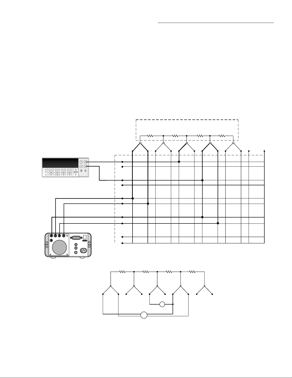
Operation
A consideration in these checks is the effect of the Model
2000 input impedance on voltage measurements. The input
impedance is shunted across the resistor being measured.
The resultant divider resistance is the parallel combination of
the resistor under test and the input impedance. As long as
the input impedance is much larger than the resistor being
tested, the error introduced into the measurement will be
minimal. Minimum input impedance requirements are determined by the accuracy needed in the measurement. The input
impedances of the Model 2000 are as follows: 10mV, 1V, and
10V ranges, 10GΩ; 100V and 1,000V ranges, 10MΩ. For
better input impedance requirements, the Keithley Model
6517A Electrometer can be incorporated into the test system
to measure voltage.
HLHLHLHL
1234
HI
LO
POWER
Model 2000
Measure V
Input HI
Input LO
Output
Sense Output
H
L
H
L
Rows
H
L
A
B
C
X
Another factor to be considered when checking low voltage
dividers is thermal EMFs generated by the card. (The Model
7022 has been designed to keep relay EMF at a minimal
level.) A matrix crosspoint can generate up to 3µV of thermal
EMF. Thus, when making low voltage measurements, be
sure to account for this additional error.
Even though four-terminal connections are made at the
Model 2000 and the resistor networks, the sense leads are
internally disconnected from the input of the DMM when the
volts function is selected. The simplified test system is
shown in Figure 5-7.
Thick Film
R
1
R
2
R
3
Cols
X
R
4
HL
5
X
6
Model 230
Source V
Figure 5-7
Voltage divider checks
Common
Sense Common
H H H H
H
D
L
H
E
L
X = Closed Crosspoints
R
1
R
2
V
2000
+/-
230
Equivalent Circuit
Model 7022
R
3
X
R
4
H
5-9
Page 63
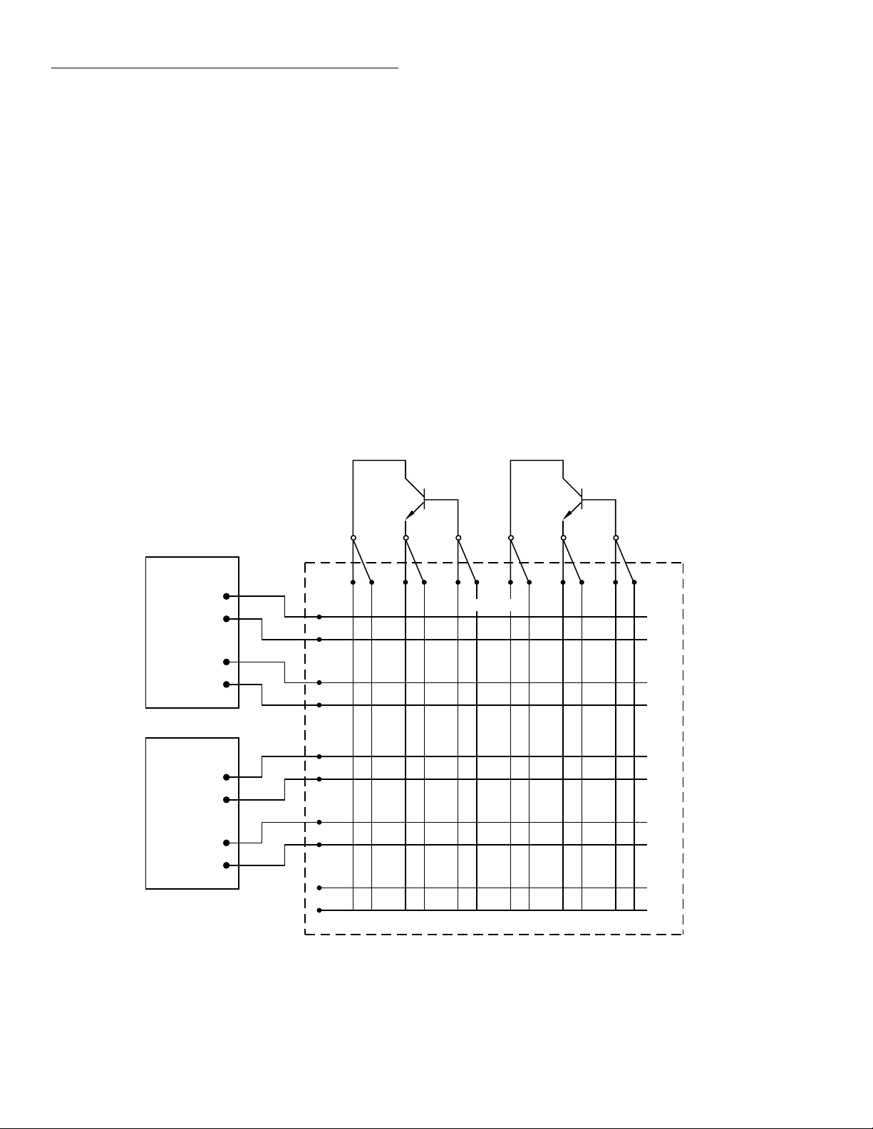
Operation
The thick film is tested by applying a voltage across the resistor network and measuring the voltage across each resistor
element and/or across combined elements. In Figure 5-7,
crosspoints 3 and 19 are closed to apply voltage across the
network, and crosspoints 11 and 17 are closed to measure the
voltage drop across R3.
Transistor testing
A matrix system for testing DC parameters of transistors is
shown in Figure 5-8. This system uses two Source Measure
Units (SMU). There are three SMUs available from Keithley; the Model 236 Source Measure Unit, Model 237 High
Voltage Source Measure Unit and Model 238 High Current
Source Measure Unit. Keep in mind that if using the Models
237 (high voltage capability) or 238 (high current capability), do not exceed the maximum signal levels of the card.
Maximum allowable DC signals are 110V and 1A, 30W with
resistive load.
This system tests two transistors but can be expanded to test
more by simply using additional Model 7022 cards. The
Model 7001 will accommodate two cards. Daisy-chaining
six Model 7001s expands the system to 12 cards allowing 24
or more transistors to be tested. Daisy-chaining six Model
7002s expands the system to 60 cards allowing 120 or more
transistors to be tested. The limits on the number of cards in
the Model 7001/7002 switch system are due to triggering.
NOTE
The Model 7022 is a general purpose card
and cannot be used to check FETs or transistors that have high gain or low power.
To test these devices, a card with low offset current and high isolation characteristics must be used.
SMU #1
Output HI
Sense HI
Sense LO
Output LO
SMU #2
Output HI
Sense HI
Sense LO
Output LO
A
B
Rows
C
D
E
123
L HL HL
H
Columns
7022
456
HL HL HL
H
L
H
L
H
L
H
L
H
L
Figure 5-8
Transistor testing
5-10
Page 64

Operation
Gain
I
C
I
B
-----=
IEICIB+=
DC parameter checks
With a transistor configured as a common-emitter amplifier,
the test system shown in Figure 5-9 can be used to determine
the following DC parameters: collector current (IC), base
current (IB), current gain, emitter current (IE) and base-toemitter voltage (VBE).
Figure 5-9 shows which crosspoints to close to configure the
amplifier circuit. SMU #1 is configured to source voltage and
measure current. It is used to power the collector circuit
(VCE) and measure the collector current (IC). SMU #2 is
configured to source current and measure voltage. It is used
to provide the base current (IB) for the transistor, and will
SMU #1
A
±
I
C
I
B
V
BE
I
E
SMU #2
V
also measure the base-to-emitter voltage (VBE). With collector current (IC) and base current (IB) known, the current gain
can be calculated as follows:
The emitter current (IE) can be determined by using Kirchoff’s Current Law as follows:
A = Measure I
± = Source V
V = Measure V
↑ = Source I
Source V
Measure I
Source I
Measure V
Equivalent Circuit
SMU #1
Output HI
Sense HI
Sense LO
Output LO
SMU #2
Output HI
Sense HI
Sense LO
Output LO
A
B
Rows
C
D
HL HL HL
X = Closed Crosspoint
X
X
X
X
7022
Figure 5-9
DC parameter checks
5-11
Page 65

Operation
Common-emitter characteristic curves
A profile of the transistor operating characteristics can be
obtained by measuring the collector current over a specified
voltage range (VCE) for different base bias currents (IB). For
example, Figure 5-10 shows the characteristics of a typical
NPN silicon transistor at base bias currents (I
) of 20µA,
B
40µA, 60µA, and 80µA.
Extensive trigger capabilities facilitate synchronization of
the Keithley Source Measure Unit operations. By performing a subordinate sweep, SMU #1 will perform a staircase
sweep at every base bias current level set by SMU #2. On
every step of each staircase sweep, SMU #1 will source a
voltage level (V
) and measure the subsequent collector
CE
current (IC). For the characteristics shown in Figure 5-10,
four staircase sweeps were performed; one staircase sweep at
each base bias level.
10
+80 µa
+60 µa
+40 µa
+20 µa
I = 0
B
, ma
c
I
8
6
4
2
Measurement considerations
Many measurements made with the Model 7022 are subject
to various effects that can seriously affect low-level measurement accuracy. The following paragraphs discuss these
effects and ways to minimize them.
Path isolation
The path isolation is simply the equivalent impedance
between any two test paths in a measurement system. Ideally,
the path isolation should be infinite, but the actual resistance
and distributed capacitance of cables and connectors results
in less than infinite path isolation values for these devices.
Path isolation resistance forms a signal path that is in parallel
with the equivalent resistance of the DUT, as shown in
Figure 5-11. For low-to-medium device resistance values,
path isolation resistance is seldom a consideration; however,
it can seriously degrade measurement accuracy when testing
high-impedance devices. The voltage measured across such
a device, for example, can be substantially attenuated by the
voltage divider action of the device source resistance and
path isolation resistance, as shown in Figure 5-12. Also,
leakage currents can be generated through these resistances
by voltage sources in the system.
R
DUT
RPAT H
DUT
E
RIN
V
012345
V , volts
CE
Figure 5-10
Common-emitter characteristics of an NPN silicon
transistor
Refer to a Keithley Source Measure Unit instruction manual
for details on performing sweeps.
5-12
DUT
= Source Resistance of DUT
DUT
R
E
DUT
= Source EMF of DUT
R
PATH
= Path Isolation Resistance
RIN
= Input Resistance of Measuring Instrument
Figure 5-11
Path isolation resistance
Matrix
Card
Measure
Instrument
Page 66

Operation
R
DUT
DUT
RPATH
+
RPATH
R
PATH
DUT
E
E
=
E
OUT
R
DUT
Figure 5-12
Voltage attenuation by path isolation resistance
Any differential isolation capacitance affects DC measurement settling time as well as AC measurement accuracy.
Thus, it is often important that such capacitance be kept as
low as possible. Although the distributed capacitance of the
card is generally fixed by design, there is one area where you
do have control over the capacitance in your system: the connecting cables. To minimize capacitance, keep all cables as
short as possible.
Magnetic fields
When a conductor cuts through magnetic lines of force, a
very small current is generated. This phenomenon will frequently cause unwanted signals to occur in the test leads of a
switching matrix system. If the conductor has sufficient
length, even weak magnetic fields like those of the earth can
create sufficient signals to affect low-level measurements.
Even when the conductor is stationary, magnetically induced
signals may still be a problem. Fields can be produced by
various signals such as the AC power line voltage. Large
inductors such as power transformers can generate substantial magnetic fields, so care must be taken to keep the switching and measuring circuits a good distance away from these
potential noise sources.
At high current levels, even a single conductor can generate
significant fields. These effects can be minimized by using
twisted pairs, which will cancel out most of the resulting
fields.
Radio frequency interference
Radio Frequency Interference (RFI) is a general term used to
describe electromagnetic interference over a wide range of
frequencies across the spectrum. Such RFI can be particularly troublesome at low signal levels, but it can also affect
measurements at high levels if the problem is of sufficient
severity.
RFI can be caused by steady-state sources such as radio or
TV signals or some types of electronic equipment (microprocessors, high speed digital circuits, etc.), or it can result from
impulse sources, as in the case of arcing in high-voltage environments. In either case, the effect on the measurement can
be considerable if enough of the unwanted signal is present.
RFI can be minimized in several ways. The most obvious
method is to keep the equipment and signal leads as far away
from the RFI source as possible. Shielding the switching
card, signal leads, sources, and measuring instruments will
often reduce RFI to an acceptable level. In extreme cases, a
specially constructed screen room may be required to sufficiently attenuate the troublesome signal.
Two ways to reduce these effects are: (1) reduce the lengths
of the test leads, and (2) minimize the exposed circuit area.
In extreme cases, magnetic shielding may be required. Special metal with high permeability at low flux densities (such
as mu metal) is effective at reducing these effects.
Many instruments incorporate internal filtering that may
help to reduce RFI effects in some situations. In some cases,
additional external filtering may also be required. Keep in
mind, however, that filtering may have detrimental effects on
the desired signal.
5-13
Page 67

Operation
Ground loops
When two or more instruments are connected together, care
must be taken to avoid unwanted signals caused by ground
loops. Ground loops usually occur when sensitive instrumentation is connected to other instrumentation with more
than one signal return path such as power line ground. As
shown in Figure 5-13, the resulting ground loop causes current to flow through the instrument LO signal leads and then
back through power line ground. This circulating current
develops a small but undesirable voltage between the LO terminals of the two instruments. This voltage will be added to
the source voltage, affecting the accuracy of the measurement.
Figure 5-14 shows how to connect several instruments together to eliminate this type of ground loop problem. Here,
only one instrument is connected to power line ground.
Ground loops are not normally a problem with instruments
having isolated LO terminals. However, all instruments in
the test setup may not be designed in this manner. When in
doubt, consult the manual for all instrumentation in the test
setup.
Signal Leads
Instrument 1 Instrument 2 Instrument 3
Instrument 1 Instrument 2 Instrument 3
Power Line Ground
Figure 5-14
Eliminating ground loops
Keeping connectors clean
As is the case with any high-resistance device, the integrity
of connectors can be damaged if they are not handled properly. If connector insulation becomes contaminated, the insulation resistance will be substantially reduced, affecting
high-impedance measurement paths.
Oils and salts from the skin can contaminate connector insulators, reducing their resistance. Also, contaminants present
in the air can be deposited on the insulator surface. To avoid
these problems, never touch the connector insulating material. In addition, the card should be used only in clean, dry
environments to avoid contamination.
Ground Loop
Current
Figure 5-13
Power line ground loops
Power Line Ground
If the connector insulators should become contaminated,
either by inadvertent touching or from airborne deposits,
they can be cleaned with a cotton swab dipped in clean methanol. After thoroughly cleaning, they should be allowed to
dry for several hours in a low-humidity environment before
use, or they can be dried more quickly using dry nitrogen.
AC frequency response
The AC frequency response of the Model 7022 is important
in test systems that switch AC signals. Refer to the specifications at the front of this manual.
5-14
Page 68

6
Service Information
WARNING
The information in this section is
intended only for qualified service personnel. Some of the procedures may
expose you to hazardous voltages that
could result in personal injury or death.
Do not attempt to perform these procedures unless you are qualified to do so.
Introduction
This section contains information necessary to service the
Model 7022 matrix-digital I/O card and is arranged as
follows:
• Handling and cleaning precautions — Discusses
handling procedures and cleaning methods for the card.
• Performance verification — Covers the procedures
necessary to determine if the card is operating properly.
• Functionality test — Provides a test procedure to de-
termine if a digital I/O input or output channel is functioning properly.
• Special handling of static-sensitive devices — Re-
views precautions necessary when handling static-sensitive devices.
• Principles of operation — Briefly discusses circuit
operation.
• Troubleshooting — Presents some troubleshooting tips
for the card.
Handling and cleaning precautions
Because of the high impedance circuits on the Model 7022,
care should be taken when handling or servicing the card to
prevent possible contamination, which could degrade performance. The following precautions should be taken when
handling the card.
Do not store or operate the card in an environment where
dust could settle on the circuit board. Use dry nitrogen gas to
clean dust off the card if necessary.
Handle the card only by the side edges. Do not touch any
board surfaces, components, or connectors. Do not touch
areas adjacent to electrical contacts. When servicing the
card, wear clean cotton gloves.
If making solder repairs on the circuit board, use an OAbased (organic activated) flux. Remove the flux from these
areas when the repair is complete. Use pure water along with
plenty of clean cotton swabs or a soft brush to remove the
flux. Take care not to spread the flux to other areas of the circuit board. Once the flux has been removed, swab only the
repaired area with methanol, then blowdry the board with
dry nitrogen gas.
After cleaning, the card should be placed in a 50°C low
humidity environment for several hours.
6-1
Page 69

Service Information
Performance verification
The following paragraphs discuss performance verification
procedures for the Model 7022, including path resistance,
offset current, contact potential, and isolation.
With the Model 7022’s backplane jumpers installed, the performance verification procedures must be performed with
only one card (the one being checked) installed in the Model
7001/7002 mainframe. These conditions do not apply if the
backplane jumpers are removed.
CAUTION
Contamination will degrade the
performance of the card. To avoid
contamination, always grasp the card
by the side edges. Do not touch the
connectors and do not touch the board
surfaces or components. On plugs and
receptacles, do not touch areas adjacent
to the electrical contacts.
NOTE
Failure of any performance verification
test may indicate that the card is contaminated. See the Handling and cleaning precautions paragraph to clean the card.
Environmental conditions
Matrix connections
The following information summarizes methods that can be
used to connect test instrumentation to the connector card.
Detailed connection information is provided in Section 4.
One method to make instrument connections to the card is by
hard-wiring a 96-pin female DIN connector and then mating
it to the connector on the Model 7022. Row and column
shorting connections can also be done at the connector. The
connector in the Model 7011-KIT-R connection kit (see
Table 4-1) can be used for this purpose. Pin identification for
the multi-pin connector for the card is provided by
Figure 4-8 and Table 4-2.
WARNING
When wiring a connector, do not leave
any exposed wires. No conductive part
of the circuit may be exposed. Properly
cover the conductive parts, or death by
electric shock may occur.
CAUTION
After making solder connections to a
connector, remove solder flux as
explained in the Handling and cleaning
precautions paragraph. Failure to clean
the solder connections could result in
degraded performance preventing the
card from passing verification tests.
All verification measurements should be made at an ambient
temperature between 18° and 28°C and at a relative humidity
of less than 70%.
Before pre-wiring any connectors plugs, study the following
test procedures to fully understand the connection
requirements.
Recommended equipment
Table 6-1 summarizes the equipment necessary for performance verification, along with an application for each unit.
Table 6-1
Verification equipment
Description Model Specifications Applications
DMM Keithley Model 2000 100Ω; 0.01% Path resistance
Electrometer w/voltage source Keithley Model 6517A 20pA, 200pA; 1%
100V source; 0.15%
Sensitive DVM Keithley Model 182 3mV; 60 ppm Contact potential
Triax cable (unterminated) Keithley Model 7025 Offset current
Low thermal cable
(unterminated)
Keithley Model 1484 Contact potential
Offset current, path isolation
6-2
Page 70

Service Information
Channel resistance tests
Referring to Figure 6-1, perform the following steps to verify
that each contact of every relay is closing properly and that
the resistance is within specification.
1. Turn off the Model 7001/7002 if it is on.
2. As shown in Figure 6-1, connect all terminals of matrix
columns 1-6 together to form one common terminal.
3. Set the Model 2000 to the 100Ω range and connect four
test leads to the INPUT and SENSE Ω 4 WIRE input.
4. Short the four test leads together and zero the Model
2000. Leave zero enabled for the entire test.
5. Connect INPUT HI and SENSE Ω 4 WIRE HI of the
Model 2000 to the common terminal. It is recommended
that the physical connections be made at columns 1 and
6 as shown in the illustration.
6. Connect INPUT LO and SENSE Ω 4 WIRE LO to the
high (H) terminal of row A.
7. Install the Model 7022 in slot 1 (CARD 1) of the Model
7001/7002.
Sense Ω 4 Wire HI
HI
LO
POWER
Input HI
Input LO
8. Turn on the Model 7001/7002 and program it to close
channel 1!1 (row A, column 1). Verify that the resistance
of this channel is <1.25Ω.
9. Open channel 1!1 and close 1!6. Verify that the resistance of this channel is <1.25Ω.
10. Open channel 1!6 and close 1!11. Verify that the resis-
tance of this channel is <1.25Ω.
11. Repeat the basic procedure of opening and closing channels to check the resistance of row A high (H) terminal
paths for columns 4 through 6 (channels 1!16, 1!21, and
1!26).
12. Turn off the Model 7001/7002 and connect the INPUT
LO and SENSE Ω 4 WIRE LO test leads of the Model
2000 DMM to the low (L) terminal of row A.
13. Repeat steps 8 through 11 to check the low (L) channel
paths of row A.
14. Turn off the Model 7001/7002 and repeat the basic procedure in steps 7 through 13 for rows B, C, D, and E.
Jumpers
(Measure 4-Wire Ohms)
Note:
Figure 6-1
Path resistance testing
Model 2000
Sense
Ω 4
Wire LO
Setup shown is configured
to test the high (H) terminal
of row A through crosspoints
1!1, 1!6, 1!11, 1!16,
1!21, and 1!26.
Rows
1 34562
A
B
C
D
E
Columns
H
L
H
L
H
L
H
L
H
L
Model 7022
6-3
Page 71

Service Information
WARNING:NO INTERNAL OPERATOR SERVICABLE PARTS,SERVICE BY QUALIFIED PERSONNEL ONLY.
WARNING:NO INTERNAL OPERATOR SERVICABLE PARTS,SERVICE BY QUALIFIED PERSONNEL ONLY.
CAUTION:FOR CONTINUED PROTECTION AGAINST FIRE HAZARD,REPLACE FUSE WITH SAME TYPE AND RATING.
CAUTION:FOR CONTINUED PROTECTION AGAINST FIRE HAZARD,REPLACE FUSE WITH SAME TYPE AND RATING.
Offset current tests
These tests check leakage current from high (H) to low (L)
(differential), and from high (H) and low (L) to chassis
(common mode) for each pathway. In general, these tests are
performed by simply measuring the leakage current with an
electrometer. In the following procedure, the Model 6517A
is used to measure leakage current.
Referring to Figure 6-2, perform the following procedure to
check offset current:
1. Turn off the Model 7001/7002 if it is on.
2. Connect the Model 6517A electrometer to row A of the
matrix as shown in Figure 6-2. Note that electrometer HI
is connected to both high (H) and low (L) of row A.
Electrometer LO is connected to chassis ground, which
is accessible at the rear panel of the mainframe.
3. Install the card in slot 1 (CARD 1) of the Model 7001/
7002.
4. On the Model 6517A, select the 200pA range, and
enable zero check and zero correct the instrument.
Leave zero correct enabled for the entire procedure.
5. Turn on the Model 7001/7002.
6. Program the Model 7001/7002 to close channel 1!1.
7. On the Model 6517A , disable zero check and verify that
it is <100pA. This measurement is the leakage current of
the pathway.
8. On the Model 6517A, enable zero check and on the
Model 7001/7002, open channel 1!1.
9. Repeat the basic procedure in steps 6 through 8 to check
the rest of the pathways (channels 1!6, 1!11, 1!16, 1!21,
and 1!26) of the row.
10. Turn off the Model 7001/7002 and connect the Model
6517A to row B. Repeat the basic procedure in steps 6
through 9 to check channels 1!2, 1!7, 1!12, 1!17, 1!22,
and 1!27.
11. Repeat the basic procedure in step 10 to check rows C,
D, and E.
12. Turn off the Model 7001/7002.
13. To check differential offset current, connect the Model
6517A to row A as shown in Figure 6-3, and repeat steps
4 through 12.
Model 7025
Unterminated
Triax Cable
!
90-110V
105-125V
!
MODEL 6517A
(Measure Current)
Setup shown is configured
Note:
to test row A pathways for
offset current.
Figure 6-2
Common-mode offset current testing
Columns
180-220V
210-250V
115V
HI
LO
Rows
134562
A
B
C
D
E
HL HL HL HL HL HL
H
L
H
L
H
L
H
L
H
L
Model 7022
Chassis ground is
accessible at rear
panel of the 7001/7002.
6-4
Page 72

WARNING:NO INTERNAL OPERATOR SERVICABLE PARTS,SERVICE BY QUALIFIED PERSONNEL ONLY.
WARNING:NO INTERNAL OPERATOR SERVICABLE PARTS,SERVICE BY QUALIFIED PERSONNEL ONLY.
CAUTION:FOR CONTINUED PROTECTION AGAINST FIRE HAZARD,REPLACE FUSE WITH SAME TYPE AND RATING.
CAUTION:FOR CONTINUED PROTECTION AGAINST FIRE HAZARD,REPLACE FUSE WITH SAME TYPE AND RATING.
Model 7025
Unterminated
Triax Cable
!
MODEL 6517A
(Measure Current)
Service Information
Columns
A
B
C
134562
H
L
H
L
H
L
90-110V
180-220V
105-125V
210-250V
115V
!
HI
LO
Rows
Note:
Setup shown is configured
to test row A pathways for
offset current.
Figure 6-3
Differential offset current testing
D
E
HL HL HL HL HL HL
Model 7022
H
L
H
L
6-5
Page 73
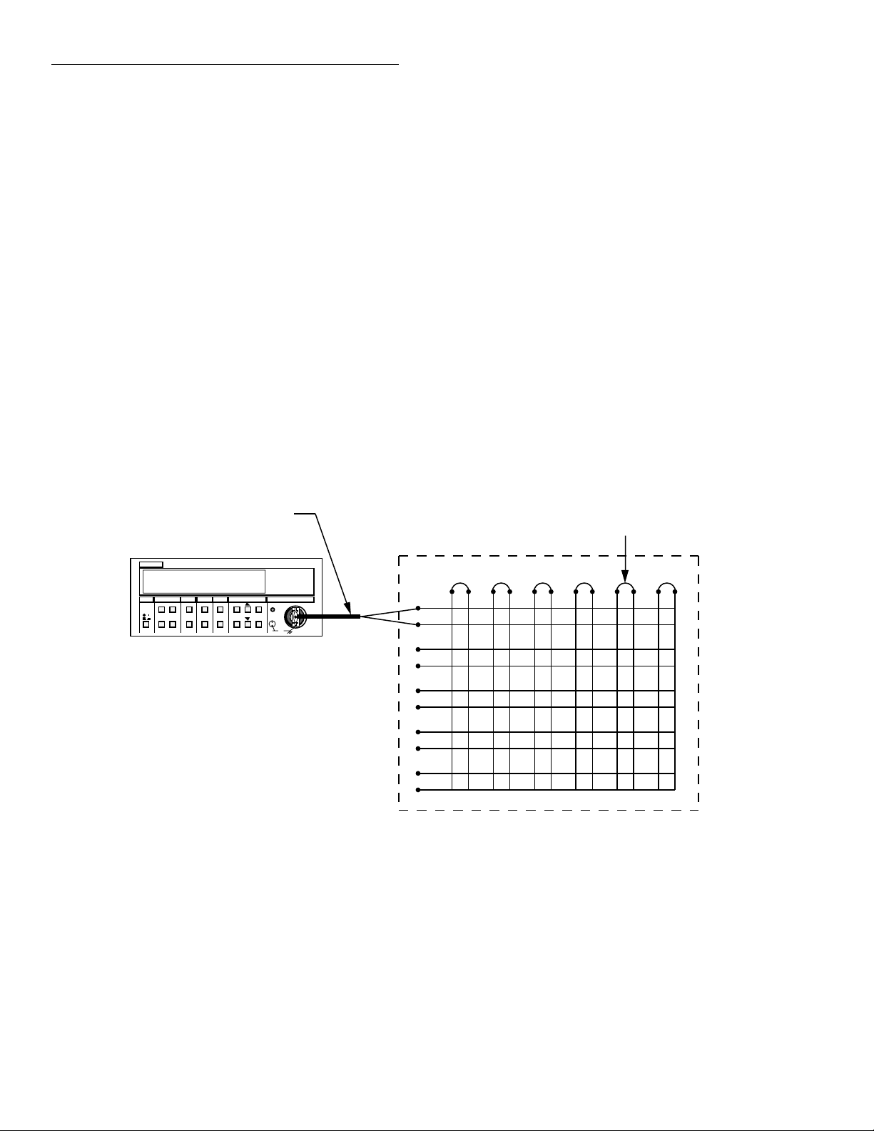
Service Information
Contact potential tests
These tests check the EMF generated by each relay contact
pair (H and L) for each pathway. The tests simply consist of
using a sensitive digital voltmeter (Model 182) to measure
the contact potential (Figure 6-4).
Perform the following procedure to check contact potential
of each path:
1. Turn off the Model 7001/7002 if it is on.
2. Place a short between HI to LO on each input column
1-6.
3. Connect all row HI terminals together on the common
bus.
4. Connect all row LO terminals together on the common
bus.
5. Place a short between HI to LO on the rows.
6. Connect the Model 182 input leads to HI and LO of the
rows.
Model 1484
Low Thermal Cable
(Unterminated)
7. Install the Model 7022 in the Model 7001/7002 slot 1
and turn on the mainframe.
8. Allow the Models 7022, 7001/7002, and 182 to warm up
for two hours.
9. Select the 3mV range on the Model 182.
10. Press REL READING on the Model 182 to null out
internal offsets. Leave REL READING enabled for the
entire procedure.
11. Turn off the mainframe. Remove the Model 7022 front
slot 1. Cut the short from HI to LO on the rows.
12. Install the Model 7022 in the Model 7001/7002 slot 1
and turn on power.
13. Wait 15 minutes.
14. Program the Model 7001/7002 to close channel 1!1.
15. After settling, verify that the reading on the Model 182
is <3µV. This measurement represents the contact
potential of the pathway.
16. From the Model 7001/7002, open channel 1!1.
17. Repeat steps 14 through 16 for all 30 crosspoints.
Low Thermal, short,
clean, high purity
copper (1 of 6)
KEITHLEY
182 SENSITIVE DIGITAL VOLTMETER
Note:
Figure 6-4
Contact potential testing
TRG
SRQ
REM
TALK
LSTN
Model 182
Setup shown is configured
to test row A crosspoints
for contact potential.
HI
LO
Columns
134562
A
B
Rows
C
D
E
HL HL HL HL HL HL
Model 7022
H
L
H
L
H
L
H
L
H
L
6-6
Page 74
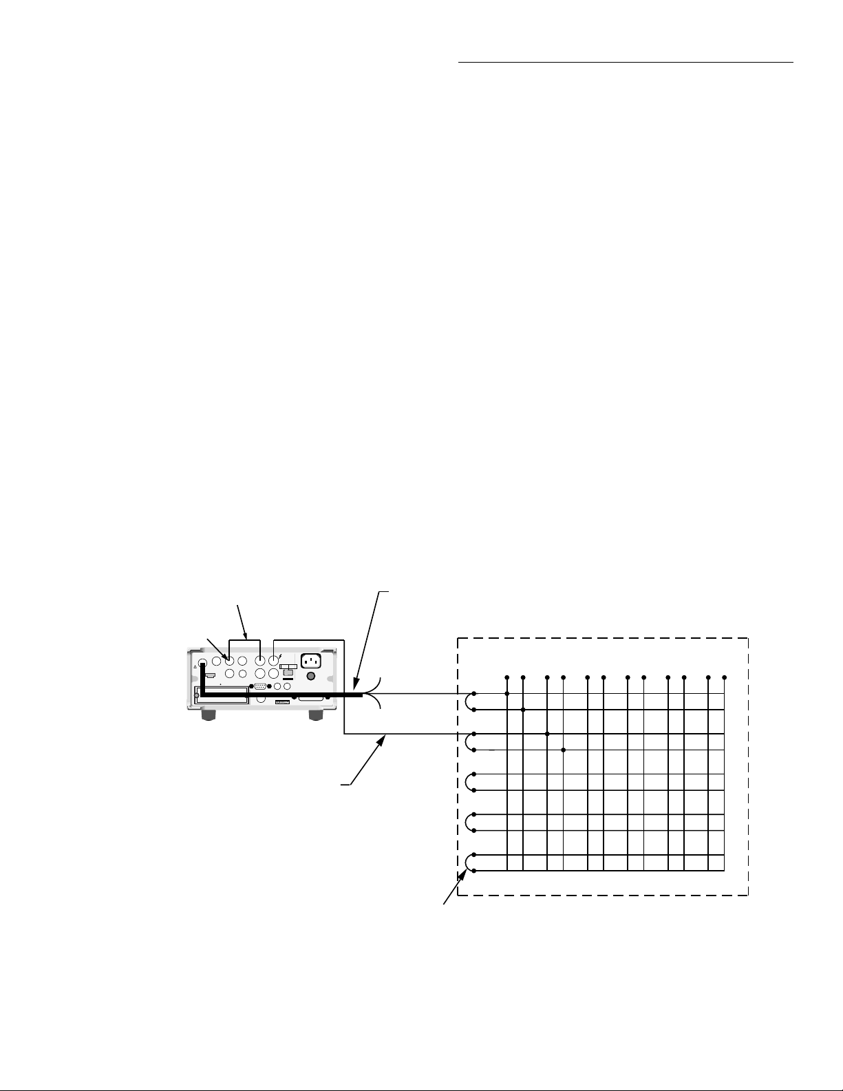
Service Information
WARNING:NO INTERNAL OPERATOR SERVICABLE PARTS,SERVICE BY QUALIFIED PERSONNEL ONLY.
WARNING:NO INTERNAL OPERATOR SERVICABLE PARTS,SERVICE BY QUALIFIED PERSONNEL ONLY.
CAUTION:FOR CONTINUED PROTECTION AGAINST FIRE HAZARD,REPLACE FUSE WITH SAME TYPE AND RATING.
CAUTION:FOR CONTINUED PROTECTION AGAINST FIRE HAZARD,REPLACE FUSE WITH SAME TYPE AND RATING.
Path isolation tests
These tests check the leakage resistance (isolation) between
adjacent paths. A path is defined as the high (H) and low (L)
circuit from a row to a column that results by closing a particular crosspoint. In general, the test is performed by applying a voltage (+100V) across two adjacent paths and then
measuring the leakage current across the paths. The isolation
resistance is then calculated as R = V/I. In the following procedure, the Model 6517A functions as both a voltage source
and an ammeter. In the R function, the Model 6517A internally calculates the resistance from the known voltage and
current levels and displays the resistance value.
1. Turn off the Model 7001/7002 if it is on.
2. Jumper the high (H) terminal to the low (L) terminal for
each row (Figure 6-5).
3. Connect the Model 6517A to rows A and B as shown in
Figure 6-5. Make sure the voltage source is off. Also,
make sure there are no other connections to the card.
4. Install the Model 7022 in slot 1 of the Model 7001/7002.
WARNING
The following steps use high voltage
(100V). Be sure to remove power from
the circuit before making connection
changes.
5. Place the Model 6517A in the R measurement function.
6. Turn on the Model 7001/7002 and program it to close
channels 1!1 (row A, column 1) and 1!7 (row B,
column 2).
7. On the Model 6517A, source +100V.
8. After allowing the reading on the Model 6517A to settle,
verify that it is >1GΩ. This measurement is the leakage
resistance (isolation) between row A, column 1 and row
B, column 2.
9. Turn off the Model 6517A voltage source.
10. Turn off the Model 7001/7002.
11. Disconnect the Model 6517A from rows A and B, and in
a similar manner, reconnect it to rows B and C (picoammeter high to row B and voltage source high to row C).
12. Turn on the Model 7001/7002 and program it to close
channels 1!7 and 1!13.
13. On the Model 6517A, source +100V.
14. After allowing the reading on the Model 6517A to settle,
verify that it is >1GΩ.
15. Using Table 6-2 as a guide, repeat the basic procedure in
steps 9 through 14 for the rest of the path pairs (starting
with test 3).
Banana to Banana Cable
Ground Link
Removed
!
Source V and
Measure V/I
Model 6517A
Unterminated
Banana Cables
Note: Setup shown is configured
to test isolation between
row A column 1 and row B
column 2.
Figure 6-5
Path isolation testing (guarded)
Model 7025
Unterminated
Triax Cable
90-110V
180-220V
105-125V
210-250V
115V
!
HI
(Red)
HI
1 34562
A
B
Rows
C
D
E
HL HL HL HL HL HL
Jumpers
Columns
H
L
H
L
H
L
H
L
H
L
Model 7022
(1 of 5)
6-7
Page 75
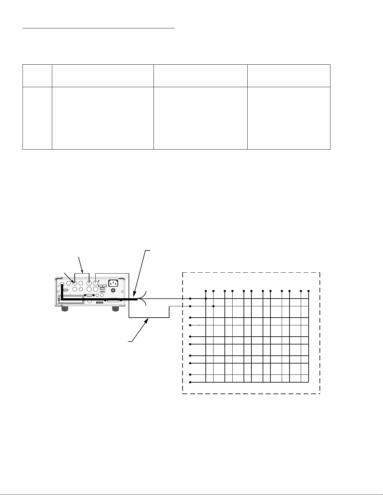
Service Information
WARNING:NO INTERNAL OPERATOR SERVICABLE PARTS,SERVICE BY QUALIFIED PERSONNEL ONLY.
WARNING:NO INTERNAL OPERATOR SERVICABLE PARTS,SERVICE BY QUALIFIED PERSONNEL ONLY.
CAUTION:FOR CONTINUED PROTECTION AGAINST FIRE HAZARD,REPLACE FUSE WITH SAME TYPE AND RATING.
CAUTION:FOR CONTINUED PROTECTION AGAINST FIRE HAZARD,REPLACE FUSE WITH SAME TYPE AND RATING.
Table 6-2
Path isolation tests
Test
no. Path isolation Test equipment locations Channels closed
1 Row A, Col 1 to Row B, Col 2 Row A and Row B 1!1 and 1!7
2 Row B, Col 2 to Row C, Col 3 Row B and Row C 1!7 and 1!13
3 Row C, Col 3 to Row D, Col 4 Row C and Row D 1!13 and 1!19
4 Row D, Col 4 to Row E, Col 5 Row D and Row E 1!19 and 1!25
5 Row D, Col 5 to Row E, Col 6 Row D and Row E 1!24 and 1!30
Differential and common-mode isolation tests
These tests check the leakage resistance (isolation) between
high (H) and low (L) (differential), and from high and low to
chassis (common-mode) of every row and column. In general, the test is performed by applying a voltage (100V)
across the terminals and then measuring the leakage current.
The isolation resistance is then calculated as R = V/I. In the
following procedure, the Model 6517A functions as a volt-
Banana to Banana Cable
Ground Link
Removed
!
Source V and
Measure V/I
90-110V
105-125V
!
Model 6517
Unterminated
Banana Cables
180-220V
210-250V
115V
Model 7025
Unterminated
Triax Cable
HI
(Red)
HI
age source and an ammeter. In the R function, the Model
6517A internally calculates the resistance from the known
voltage and current levels, and displays the resistance value.
1. Turn the Model 7001/7002 off if it is on.
2. Connect the Model 6517A to row A as shown in
Figure 6-6. Make sure the voltage source is off. Also,
make sure there are no other connections to the card.
3. Install the Model 7022 in slot 1 of the Model 7001/7002.
Columns
1 34562
A
B
H
L
H
L
Rows
C
D
H
L
H
L
igure 6-6
ifferential isolation testing
6-8
E
HL HL HL HL HL HL
Model 7022
H
L
Page 76

Service Information
WARNING
The following steps use high voltage
(100V). Be sure to remove power from
the circuit before making connection
changes.
4. On the Model 6517A, set the voltage source for +100V.
Make sure the voltage source is off.
5. Place the Model 6517A in the R measurement function.
6. Turn on the Model 7001/7002, but do not program any
channels to close. All channel crosspoints must be open.
7. On the Model 6517A, source 100V.
8. After allowing the reading on the Model 6517A to settle,
verify that it is >1GΩ. This measurement is the leakage
resistance (isolation) of row A.
9. Turn off the Model 6517A voltage source.
10. Program the Model 7001/7002 to close channel 1!1.
11. On the Model 6517A, source +100V.
12. After allowing the reading on the Model 6517A to settle,
verify that it is also >1GΩ. This measurement checks
the isolation of column 1.
13. Using Table 6-3 as a guide, repeat the basic procedure in
steps 9 through 12 for the rest of the columns and rows
(test numbers 3 through 11 of the table).
14. Turn off the Model 6517A voltage source and the Model
7001/7002.
15. For each matrix row, jumper the high (H) terminal to the
low (L) terminal as shown in Figure 6-7.
16. Connect the Model 6517A to row A as shown in
Figure 6-7, and repeat steps 6 through 14 to check
common-mode isolation.
Table 6-3
Differential and common-mode isolation testing
Differential or
Test
no.
1 Row A None
2 Column 1 1!1
3 Column 2 1!6
4 Column 3 1!11
5 Column 4 1!16
6 Column 5 1!21
7 Column 6 1!26
8 Row B 1!1 and 1!2
9 Row C 1!1 and 1!3
10 Row D 1!1 and 1!4
11 Row E 1!1 and 1!5
common-mode
test Channels closed
6-9
Page 77
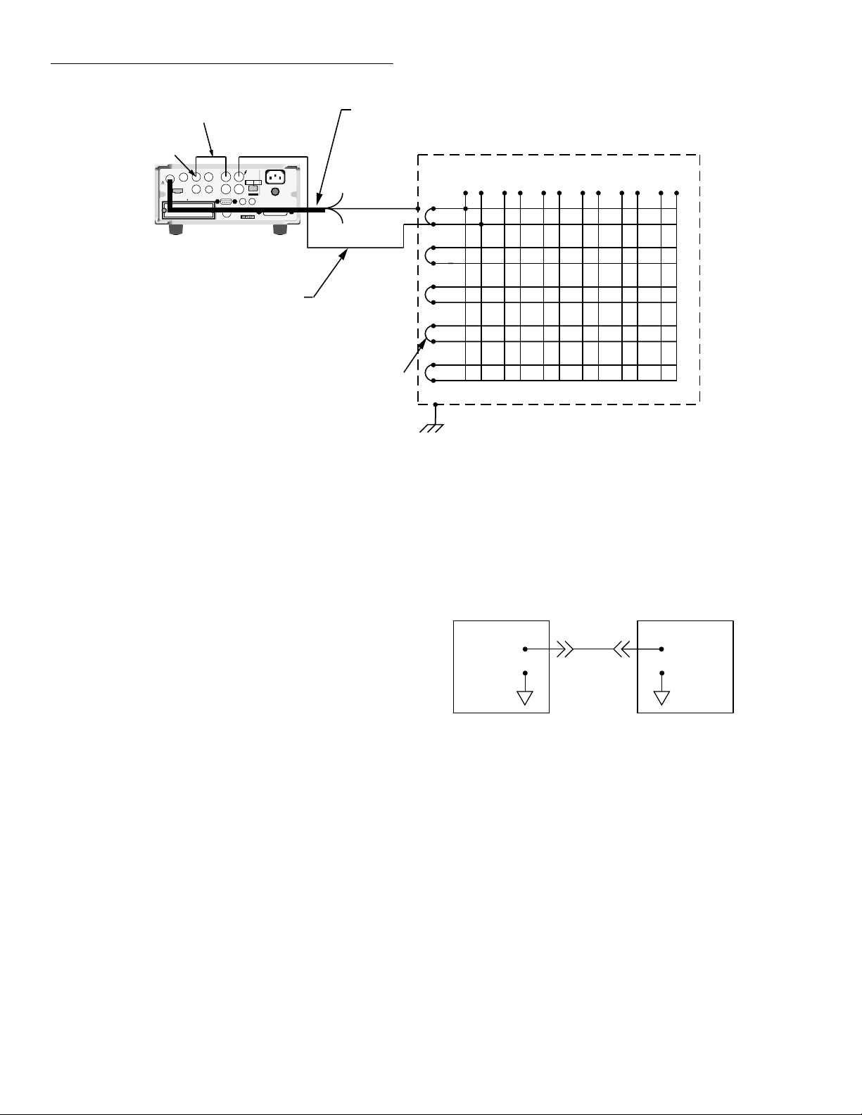
Service Information
WARNING:NO INTERNAL OPERATOR SERVICABLE PARTS,SERVICE BY QUALIFIED PERSONNEL ONLY.
WARNING:NO INTERNAL OPERATOR SERVICABLE PARTS,SERVICE BY QUALIFIED PERSONNEL ONLY.
CAUTION:FOR CONTINUED PROTECTION AGAINST FIRE HAZARD,REPLACE FUSE WITH SAME TYPE AND RATING.
CAUTION:FOR CONTINUED PROTECTION AGAINST FIRE HAZARD,REPLACE FUSE WITH SAME TYPE AND RATING.
Banana to Banana Cable
Ground Link
Removed
!
Source V and
Measure V/I
90-110V
180-220V
105-125V
210-250V
115V
!
Model 6517A
Unterminated
Banana Cables
Model 7025
Unterminated
Triax Cable
H
(Red)
H
Jumpers
(1 of 5)
1 34562
A
B
Rows
C
D
E
HL HL HL HL HL HL
Chassis Ground
is accessible
at 7001/7002 rear
panel
Columns
H
L
H
L
H
L
H
L
H
L
Model 7022
igure 6-7
ommon-mode isolation testing
Channel functionality test
1. As shown in Figure 6-8, connect the suspect input or
output channel to an output or input channel that is
known to be functioning properly. The internal 5V
supply must be used.
2. From the front panel of the mainframe, turn on (close)
the output channel. Verify that the display indicates that
the output channel is on (closed). Keep in mind that the
output can be high (positive) or low (negative) when the
channel is turned on, depending on the logic
configuration.
3. Place the mainframe in the “read input channels” display mode. Verify on the display that the input channel
is off (open).
4. On the mainframe, turn off (open) the output channel
and verify on the display that the input channel turns on
(closes).
5. On the mainframe, return the instrument to the normal
display mode and verify on the display that the output
channel is off (open).
Output Channel
OUT
GND
Internal connections:
Internal voltage source (+5V) selected.
Pull-up resistor installed.
Figure 6-8
Testing an input or output channel
Input Channel
IN
GND
6-10
Page 78
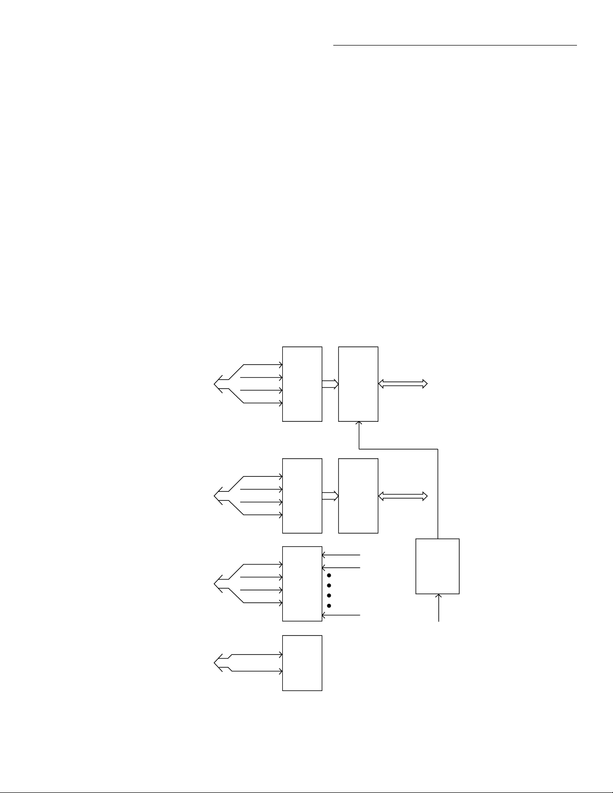
Service Information
F
M
Special handling of static-sensitive devices
CMOS and other high-impedance devices are subject to possible static discharge damage because of the high-impedance
levels involved. The following precautions pertain specifi-
cally to static-sensitive devices. However, since many
devices in the Model 7022 are static-sensitive, it is recommended that they all be treated as static-sensitive.
1. Such devices should be transported and handled only in
containers specially designed to prevent or dissipate
static buildup. Typically, these devices will be received
in anti-static containers made of plastic or foam. Keep
these parts in their original containers until ready for
installation.
2. Remove the devices from their protective containers
only at a properly grounded work station. Also, ground
yourself with a suitable wrist strap while working with
these devices.
3. Handle the devices only by the body; do not touch the
pins or terminals.
To Mainframe
OUTCLOCK
OUTDATA
STROBE
ENABLE
Relay
Drivers
U106U109
4. Any printed circuit board into which the device is to be
inserted must first be grounded to the bench or table.
5. Use only anti-static type de-soldering tools and
grounded-tip soldering irons.
Principles of operation
The following paragraphs discuss the basic operating principles for the Model 7022 and can be used as an aid in troubleshooting the card. The schematic drawings of the card are
shown on drawing numbers 7021-106 and 7022-176 located
in Section 7.
Block diagram
Figure 6-9 shows a simplified block diagram of the Model
7022. Key elements include the ROM, which contains card
ID and configuration information, matrix relay drivers and
relays, digital I/O output channel drivers, and digital I/O
input channel registers. These various elements are discussed
in the following paragraphs.
User
Relay
Channels
1-30
connections
igure 6-9
odel 7022 block diagram
To Mainframe
From
Mainframe
To/From
Mainframe
OUTCLOCK
OUTDATA
STROBE
ENABLE
IN DATA
INCLOCK
STROBE
ENABLE
IDCLK
ID DATA
Output
Channel
Drivers
U105
and
U106
Input
Channel
Registers
U101
and
U102
ROM
U110
Output
Channels
31-40
In 1
In 2
In 10
+3.5V (Steady State)
+5.7 (ª 100 msec during
relay actuation)
User
connections
Relay
Power
Control
Q100, Q101
U114, U115
+6V, +15V
6-11
Page 79
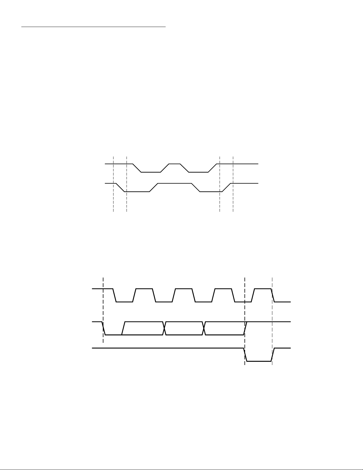
Service Information
ID data circuits
Upon power-up, card identification information from each
card is read by the mainframe. This ID data includes such
information as card ID, hardware settling time, and relay and
channel configuration information.
ID data is contained within an on-card EEPROM (U110). In
order to read this information, the sequence described below
is performed on power-up.
1. The IDDATA line (pin 5 of U110) is set from high to low
while the IDCLK line (pin 6 of U110) is held high. This
action initiates a start command to the ROM to transmit
data serially to the mainframe (Figure 6-10).
IDCLK
IDDATA
Start Bit Stop Bit
2. The mainframe sends the ROM address location to be
read over the IDDATA line. The ROM then transmits an
acknowledge signal back to the mainframe, and it then
transmits data at that location back to the mainframe
(Figure 6-11).
3. The mainframe then transmits an acknowledge signal,
indicating that it requires more data. The ROM will then
sequentially transmit data after each acknowledge signal it receives.
4. Once all data is received, the mainframe sends a stop
command, which is a low-to-high transition of the
IDDATA line with the IDCLK line held high (Figure
6-10).
Figure 6-10
Start and stop sequences
IDCLK
IDDATA
(Data output
from mainframe
or ROM)
IDDATA
(Data output
from mainframe
or ROM)
Start
Figure 6-11
Transmit and acknowledge sequence
189
Acknowledge
6-12
Page 80

Service Information
Matrix relay control
Card relays are controlled by serial data transmitted via the
relay OUTDATA line. A total of five bytes for each card are
shifted in serial fashion into latches located in the card relay
driver ICs. The serial data is clocked in by the OUTCLOCK
line. As data overflows one register, it is fed out the Q’s line
of the register down the chain.
Once all five bytes have shifted into the card, the STROBE
line is set high to latch the relay information into the Q outputs of the relay drivers, and the appropriate relays are energized (assuming the driver outputs are enabled, as discussed
below). Note that a relay driver output goes low to energize
the corresponding relay.
Matrix relay power control
A relay power control circuit, made up of U114, U115,
Q100, Q101, and associated components, keeps power dissipated in relay coils at a minimum, thus reducing possible
problems caused by thermal EMFs.
During steady-state operation, the relay supply voltage, +V,
is regulated to +3.5V to minimize coil power dissipation.
When a relay is first closed, the STROBE pulse applied to
U114 changes the parameters of the relay supply voltage regulator, Q100, allowing the relay supply voltage, +V, to rise to
+5.7V for about 100msec. This brief voltage rise ensures that
relays close as quickly as possible. After the 100msec period
has elapsed, the relay supply voltage (+V) drops back down
to its nominal steady-state value of +3.5V.
Digital I/O output channel control
Digital output channels are controlled by serial data transmitted from the mainframe to the card via the OUTDATA
line. A total of two bytes (10 bits) are shifted in a serial fashion into latches located in the output channel driver ICs. The
serial data is clocked in by the OUTCLK line. As data overflows one register, it is fed out the Q’s line of the register
down the chain.
Once all bytes have shifted into the card, the STROBE line
is set high to latch the output channel information into the Q
outputs of the output channel drivers. Note that a channel
driver output can go low or high when it is turned on (closed)
depending on its logic configuration.
Digital I/O input channel control
The mainframe reads digital input channels of the I/O card
from a serial, two-byte data stream (via INDATA line).
Digital inputs are applied in a parallel fashion to the two
input channel registers (U102 contains eight channels and
U101 contains two channels). When the digital inputs are
read, the STROBE line goes high to latch the input channel
information. The INCLOCK line then clocks out the information as a serial, two-byte data stream (via INDATA line)
to the mainframe. As data empties from the lead register
(U101), it is replaced by data via the Q7 line of the registers
down the chain.
Power-on safeguard
NOTE
The power-on safeguard circuit discussed
below is actually located on the digital
board in the mainframe.
A power-on safeguard circuit, made up of a D-type flip-flop
and associated components, ensures that relays and digital
I/O output channels do not randomly energize on power-up
and power-down. This circuit disables all relays and output
channels (all relays and output channels are open) during
power-up and power-down periods.
The PRESET line on the D-type flip-flop is controlled by the
68302 microprocessor, while the CLK line of the D-type
flip-flop is controlled by a VIA port line on the 68302 processor. The Q output of the flip-flop drives each switch card
relay/output channel driver IC enable pin (U105-U109,
pin 8).
When the 68302 microprocessor is in the reset mode, the
flip-flop PRESET line is held low, and Q out immediately
goes high, disabling all relays and output channels (driver IC
enable pins are high). After the reset condition elapses
(≈200msec), PRESET goes high while Q out stays high.
When the first valid STROBE pulse occurs, a low logic level
is clocked into the D-type flip-flop, setting Q out low and
enabling all relay drivers and output channel drivers simultaneously. Note that Q out stays low, (enabling relay drivers
and output channels) until the 68302 processor goes into a
reset condition.
6-13
Page 81
Service Information
Troubleshooting
Lethal voltages are present within the
Model 7001/7002 mainframe. Some of
the procedures may expose you to hazardous voltages. Observe standard
safety precautions for dealing with live
circuits. Failure to do so could result in
personal injury or death.
Observe the following precautions when
troubleshooting or repairing the card:
To avoid contamination, which could
degrade card performance, always handle the card only by the handle and side
edges. Do not touch edge connectors,
board surfaces, or components on the
card. Also, do not touch areas adjacent
to electrical contacts on connectors.
Use care when removing relays from the
PC board to avoid pulling traces away
from the circuit board. Before attempting to remove a relay, use an appropriate de-soldering tool, such as a solder
sucker, to clear each mounting hole
completely free of solder. Each relay pin
must be free to move in its mounting
hole before removal. Also, make certain
that no burrs are present on the ends of
the relay pins.
WARNING
CAUTION
Troubleshooting equipment
Table 6-4 summarizes recommended equipment for troubleshooting the Model 7022.
Table 6-4
Recommended troubleshooting equipment
Manufacturer
Description
Multimeter Keithley 2000 Measure DC voltages
Oscilloscope TEK 2243 View logic waveforms
and model Application
Troubleshooting access
In order to gain access to the relay card top surface to measure voltages under actual operation conditions, perform the
following steps:
1. Disconnect the connector card from the relay card.
2. Remove the Model 7001/7002 cover.
3. Install the relay card in the CARD 1 slot location.
4. Turn on Model 7001/7002 power to measure voltages
(see following paragraph).
Troubleshooting procedure
Table 6-5 summarizes matrix-digital I/O card troubleshooting.
6-14
Page 82

Service Information
Table 6-5
Troubleshooting procedure
Step Item/Component Required condition Comments
1 GND pad All voltages referenced to digital ground
(GND pad).
2 Q100, pin 2 +6VDC Relay voltage.
3 U101, pin 16 +5VDC Logic voltage.
4 R135 +15VDC Relay bias voltage.
5 Q100, pin 3 +3.5VDC* Regulated relay voltage.
6 U110, pin 6 IDCLK pulses During power-up only.
7 U110, pin 5 IDDATA pulses During power-up only.
8 U106, pin 7 STROBE pulse End of relay update sequence.
9 U106, pin 2 CLK pulses During relay update sequence only.
10 U106, pin 3 DATA pulses During relay update sequence only.
11 U105-U109, pins 10-18 Low with relay energized; high
Relay driver outputs.
with relay de-energized.
*+3.5VDC present at +V pad under steady-state conditions. This voltage rises to +5.7VDC for about 100msec when relay configuration is changed.
6-15
Page 83

Service Information
6-16
Page 84

7
Replaceable Parts
Introduction
This section contains replacement parts information, schematic diagrams, and component layout drawings for the
Model 7022.
Parts lists
Parts lists for the various circuit boards are included in tables
integrated with schematic diagrams and component layout
drawings for the boards. Parts are listed alphabetically in
order of circuit designation.
Ordering information
To place an order, or to obtain information concerning
replacement parts, contact your Keithley representative or
the factory (see inside front cover for addresses). When
ordering parts, be sure to include the following information:
1. Card model number 7022
2. Card serial number
3. Part description
4. Circuit description, if applicable
5. Keithley part number
Factory service
If the card is to be returned to Keithley Instruments for repair,
perform the following:
1. Complete the service form at the back of this manual
and include it with the card.
2. Carefully pack the card in the original packing carton or
the equivalent.
3. Write ATTENTION REPAIR DEPT on the shipping
label.
NOTE
It is not necessary to return the mainframe
with the card.
7-1
Page 85

Replaceable Parts
Component layouts and schematic diagrams
Component layout drawings and schematic diagrams are
included on the following pages integrated with the parts
lists:
Table 7-1 — Parts List, Relay Card for 7022.
7021-100 — Component Layout, Relay Card 7022.
7021-106 — Schematic, Relay Card 7022.
NOTE
The Model 7021 and 7022 use the same
relay card; only the connector cards are
different.
Table 7-2 — Parts List, Mass Terminated Connector Card
for 7022.
7022-170 — Component Layout, Mass Terminated
Connector Card for 7022.
7022-176 — Schematic, Mass Terminated Connector Card
for 7022.
Table 7-3 — Parts List, Model 7011-KIT-R 96-pin Female
DIN Connector Kit.
7-2
Page 86

Table 7-1
Relay card for Model 7022, parts list
Replaceable Parts
Circuit
designation Description
2-56X3/16 PHILLIPS PAN HEAD SCREW 3-56X3/16PPH
2-56X5/8 PHILLIPS PAN HEAD FASTENER (FOR P2001 TO
STANDOFF AND SHIELD)
2-56X7/16 PHILLIPS PAN HEAD SCREW 2-56X7/16PPH
4-40X3/16 PHILLIPS PAN HEAD SEMS SCREW (FOR Q100) 4-40X3/16PPHSEM
4-40 PEM NUT FA-131
EJECTOR ARM 7011-301B
ROLL PIN (FOR EJECTOR ARMS) DP-6-1
SHIELD 7011-305C
STANDOFF, 2 CLEARANCE ST-204-1
C100112,114,115,118,
121,122,125
C116,117,126 CAP, 150PF, 10%, 1000V, CERAMIC C-64-150P
C119,127 CAP, 1µF, 20%, 50V, CERAMIC C-237-1
C120 CAP, 0.001µF, 20%, 500V, CERAMIC C-22-.001
C123,124 CAP, 10µF, -20+100%, 25V, ALUM ELEC C-314-10
CR100-119 DIODE, SILICON, IN4148 (D0-35) RF-28
J100,101 CONN, BERG CS-339
J1002,1003 CONN, 48-PIN, 3-ROW CS-736-2
K100-129 RELAY, ULTRA-SMALL POLARIZED TF2E-5V RL-149
P2001 CONN, 32-PIN, 2-ROW CS-775-1
Q100 TRANS, NPN PWR, TIP31 (T0-220AB) TG-253
Q101 TRANS, N CHAN MOSPOW FET, 2N7000 (T0-92) TG-195
R100-130,132 RES, 10K, 5%, 1/4W, COMPOSITION OR FILM R-76-10K
R131 RES, 1K, 5%, 1/4W, COMPOSITION OR FILM R-76-1K
R133 RES, 220K, 5%, 1/4W, COMPOSITION OR FILM R-76-220K
R134,135 RES, 560, 10%, 1/2W, COMPOSITION R-1-560
R136 RES, 2.49K, 1%, 1/8W, METAL FILM R-88-2.49K
R137 RES, 1.15K, 1%, 1/8W, METAL FILM R-88-1.15K
R138 RES, 1K, 1%, 1/8W, METAL FILM R-88-1K
S110 SOCKET S0-72
ST1 STANDOFF, 4-40X0.812LG ST-137-20
U100,103,104 IC, QUAD 2-INPUT EXCLUSIVE OR 74HCT86 IC-707
U101,102 IC, 8-BIT PARALLEL TO SERIAL, 74HCT165 IC-548
U105-109 IC, 8-BIT, SERIAL-IN LATCH DRIVER, 5841A IC-536
U110 EPROM PROGRAM 7022-800A01
U111 IC, HEX INVERTER, 74HCT04 IC-444
U112 IC, QUAD 2 INPUT OR 74HCT32 IC-443
U113 IC, HIGH SPEED BUFFER, 74HC125 IC-451
U114 IC, RETRIG MONO MULTIVIB, 74HC123 IC-492
U115 IC, AJD SHUNT REGULATOR, TL431CLP IC-677
VR100 DIODE, ZENER, 5.1V, IN751 (D0-7) DZ-59
W100-107 JUMPER J-15
CAP, 0.1µF, 20%, 50V, CERAMIC C-365-.1
Keithley
part no.
FA-245-1
7-3
Page 87

Replaceable Parts
7-4
Page 88

Page 89

Page 90
Page 91
Page 92

Page 93

Table 7-2
Mass terminated connector card for Model 7022, parts list
Replaceable Parts
Circuit
designation Description
2-56X3/16 PHILLIPS PAN HEAD SCREW (FOR SHIELD) 2-56X3/16PPH
2-56X3/8 PHILLIPS PAN HEAD SCREW (FOR BRACKET) 2-56X3/8PPH
2-56X7/16 PHILLIPS PAN HEAD SCREW 2-56X7/16PPH
4-40X1/4 PHILLIPS PAN HEAD SEMS SCREW (CONNECTS
RELAY BOARD TO CONNECTOR BOARD)
CONN, JUMPER (FOR J201) CS-476
SHIELD 7011-311A
STANDOFF ST-203-1
C201-204 CAP, 0.1µF, 20%, 50V, CERAMIC C-365-.1
CR201-204 DIODE, SILICON, IN4148 (D0-35) RF-28
J201 CONN, BERG CS-339
J202,203 CONNECTOR SHIM 7011-309A
J1004 CONN, 96-PIN, 3-ROW CS-514
K201-204 RELAY, ULTRA-SMALL POLARIZED TF2E-4.5V RL-162
P1002,1003 CONNECTOR, 48-PIN, 3-ROW CS-748-3
Q201 TRANS, NPN SILICON, 2N3904 (T0-92) TG-47
R201-205, 207210, 212
R206 RES, 100K, 5%, 1/4W, COMPOSITION OR FILM R-76-100K
R211, 213 RES, 220, 10%, 1/2W, COMPOSITION R-1-220
U201-203 IC, 4-CHANNEL PWR DRIVER, 2549B IC-1044
RES, 10K, 5%, 1/4W, COMPOSITION OR FILM R-76-10K
Keithley
part no.
4-40X1/4PPHSEM
7-5
Page 94

Replaceable Parts
7-6
Page 95
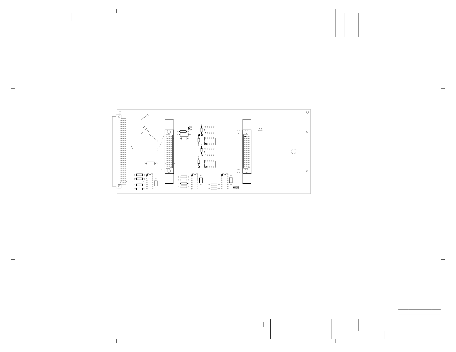
43 2
7022-170
NO.
A
B
PRELIMINARY
RELEASED
1
DATEENG.REVISIONECA NO.LTR.
D
D
J1004
Q201
CR202
R207
R204
R205
C204
R208
R206
R213
CR203
CR201
CR204
U201
C
R211
R202 U203
R212
R210
R209
J202
C203
P1003
C202
R203
R201
K203
K201
K202
K204
U202
C201
P1002
J201
+5V
VEXT
WARNING: USER SUPPLIED
LETHAL VOLTAGE MAY BE
PRESENT ON CONNECTORS
OR P.C. BOARD.
!
REFER TO MANUAL FOR
MAXIMUM VOLTAGE
RATING OF CONNECTORS.
J203
C
B
B
NOTE: FOR COMPONENT INFORMATION, PLEASE REFER TO PRODUCT STRUCTURE.
A
A
QTY.NEXT ASSEMBLYMODEL
1 OF 1
SCALEDATE
KEITHLEY
KEITHLEY INSTRUMENTS INC.
CLEVELAND, OHIO 44139
DIM ARE IN IN. UNLESS OTHERWISE NOTED
DIM. TOL. UNLESS OTHERWISE SPECIFIED
XX=+.01
XXX=+.005
ANG.=+1
FRAC.=+1/64
12/23/96
CAB
DO NOT SCALE THIS DRAWING
1:1
APPR.DRN
TITLE
C
NO.
43 2
USED ON
COMPONENT LAYOUT
CONNECTOR BOARD
7022-170
1
PG
Page 96

Page 97

Page 98

Table 7-3
Model 7011-KIT-R 96-pin female DIN connector kit, parts list
Replaceable Parts
Circuit
designation Description
96-PIN FEMALE DIN CONNECTOR CS-787-1
BUSHING, STRAIN RELIEF BU-27
CABLE ADAPTER, REAR EXIT (INCLUDES TWO CABLE
CLAMPS)
CONNECTOR HOUSING CS-788
Keithley
part no.
CC-64
7-7
Page 99

Replaceable Parts
7-8
Page 100

Index
A
AC frequency response, 5-14
Analog matrix maximum signal
levels, 5-1
B
Backplane jumpers, 2-1
Backplane row jumpers, 4-2
Basic matrix configuration (5 × 6), 2-1
Block diagram, 6-11
C
Card connections and installation, 4-1
Card installation, 4-18
Card removal, 4-18
Channel assignments, 5-2
Channel functionality test, 6-10
Channel resistance tests, 6-3
Closing and opening channels, 5-4
Common-emitter characteristics
curves, 5-12
Component layouts and schematic
diagrams, 7-1
Configuring digital I/O input pull-up
resistance, 4-4
Configuring digital I/O output
logic, 4-4
Contact potential tests, 6-6
Controlling devices using pull-up
resistors, 3-2
Controlling pull-up devices, 3-1
D
DC parameter checks, 5-11
Differential and common-mode
isolation test, 6-8
Differential switching, 2-3
Digital I/O configuration, 3-1
Digital I/O connections, 4-2
Digital I/O input channel control, 6-13
Digital I/O maximum signal
levels, 5-1
Digital I/O output channel
control, 6-13
Digital inputs, 3-3
Digital outputs, 3-1
E
Environmental conditions, 6-2
F
Factory service, 7-1
Features, 1-1
Four-terminal ohms
measurements, 5-8
G
General information, 1-1
Ground loops, 5-14
H
Handling and cleaning
precautions, 6-1
Handling precautions, 1-2, 4-1
I
ID data circuits, 6-12
IEEE-488 bus operation, 5-5
Input channels, 5-1
Input connection scheme, 4-17
Input/output connections, 4-19
Inspection for damage, 1-2
Instruction manual, 1-2
Internal connections, 4-19
J
Jumper installation, 4-2
Jumper removal, 4-2
K
Keeping connectors clean, 5-14
M
Magnetic fields, 5-13
Mainframe control of the card, 5-1
Mainframe matrix expansion, 2-8
Manual addenda, 1-2
Matrix configuration, 2-1
Matrix connections, 4-2, 6-2
Matrix expansion, 2-5
Matrix relay control, 6-13
Matrix relay power control, 6-13
Matrix switching examples, 5-7
Measurement considerations, 5-12
Mixing card types, 2-8
Model 7022 installation and
removal, 4-18
Models 7022-D and 7022-DT, 4-19
Multi-pin (mass termination)
connector card, 4-5
i-1
 Loading...