

Page 1

Models 7018-S and 7018-C
28-Channel3-Pole Multiplexer Cards
Instruction Manual
Contains Operating and Servicing Information
Page 2

WARRANTY
Kcithley Instruments, Inc. warrants this product to be free from defects in material and workmanship for a period of I year
from date of shipment.
Keithley Instruments, Inc. warrants the following items for 90 days from the date of shipment: probes, cables, rechargeable
baitcries, diskettes, and documentation.
During the warranty period, we will, at our option, either repair or replace any product that proves to be defective.
To exercise this warranty, write or call your local Keithley representative, or contact Keithlcy headquarters in Cleveland, Ohio.
You will be given prompt assistance and return instructions. Send the product, transportation prepaid, to the indicated sewice
facility. Repairs will be made and the product returned, transportation prepaid. Repaired or replaced products arc warranted for
the balance of the original warranty period, or at least 90 days.
LlMlTATlON OF WARRANTY
This warranly does not apply to defects resulting from product modification without Keithley’s express written consent, or
misuse of any product or part. This warranty also does not apply to fuses, software, non-rechargeable batteries, damage from
battery leakage, or problems arising from normal wear or failure to follow instructions.
THIS WARRANTY IS IN LIEU OF ALL OTIIER WARRANTIES, EXPRESSED OR IMPLIED, INCLUDING ANY
IMPLIED WARRANTY OF MERCHANTABILITY OR FITNESS FOR A PARTICULAR USE. THI? REMEDIES I’ROVIDED HEREIN ARE BUYER’S SOLE AND EXCLUSIVE REMEDIES.
NEITHER KEITHLEY INSTRUMENTS, INC. NOR ANY OF ITS EMPLOYEES SHALL BE LIABLE FOR ANY DIRECT,
INDIRECT, SPECIAL, INCIDENTAL OR CONSEQUHNTIAL DAMAGES ARISING OUT OF THE USE OF ITS
INSTRUMENTS AND SOFI-WARE EVEN IF KEITHLEY INSTRUMENTS, INC., HAS BEEN ADVISED IN ADVANCE
OF THE POSSIBILITY OF SUCH DAMAGES. SUCH EXCLUDED DAMAGES SHALL INCLUDE, BUT ARE NOT LIMITED TO: COSTS OF REMOVAL AND INSTALLATION, LOSSES SUSTAINED AS THE RESULT OF INJURY TO ANY
PERSON, OR DAMAGE TO PROPERTY.
Kcithley Instruments, Inc. * 28775 Aurora Road - Cleveland, OH 44139 - 440-24X-0400 - Fax: 440-248-6168 9 http://www.kcithley.com
Page 3

Models 7018-S and 7018-C
Instruction Manual
01993, Keithley Instruments, Inc.
All Rights Reserved
Cleveland, Ohio, U. 5. A.
First Printing, October 1993
Document Number: 7018-901-01 Rev. A
Page 4

Manual Print History
The print history shown below lists the printing dates of all Revisions and Addenda created for this manual. The
Revision Level letter increases alphabetically as the manual undergoes subsequent updates. Addenda, which are
released between Revisions, contain important change information that the user should incorporate immediately
into the manual. Addenda are numbered sequentially. When a new Revision is created, all Addenda associated
with the previous Revision of the manual are incorporated into the new Revision of the manual. Each new Revision includes a revised copy of this print history page.
Revision A (Document Number 7018~901.01) October 19%
Page 5

Safety Precautions
l‘hc following safciy prccaulions should hc ohscrvcd heforc using
this producl and any associated instrumcnlation. Although some in~mmxmis and accessories would normally hc used with non-hazardous voltages, thcrc are siluations whcrc hazardous conditions
may hc prcscnl.
This product is imended for USC by queiilicd pcrsonncl whn rcwg~
nix shock hazards and arc familiar with :hc safety prccaulions rc~
quired Lo avoid possihlc injury. Kcad tbc “peraiing informalion
carclully hefore using the pruducl.
The types “C product users arc:
Responsible body is lhc individual or group rcsponsihlc lor the USC
and mainlenancc or equipmcnl. r”r ensuring that the equipment is
operated within its specilicauons and “pcrating limits. and for cn~
swing lhal “pcratnrs arc adcquatcly waincd.
Operators us” the product for ils imendcd runclion. They must he
trained in clcctrical salety procedures and proper US” of lhc instrumcnt. They must hc protcctcd from electric shock and con&i wilb
hazardous live circuits.
Maintenance personnel perform routine proccdurcs on the producl
to keep it “pcrating, for example. setting the line vollagc or replacing consumahic materials. Maintenance proccdurcs arcdcscrihcd in
the manual. The proccdurcs cxplicidy stat” if ~hc opcralor may pcrSourm Ihem. Otherwise, they should bc pcrrormcd only by service
personnel.
Service personnel arc lraincd 1” work on live circuits. and pcrlurm
safe installations and repairs or
vice personnel may perform installation and service proccdurcs.
lixcrcise extreme caution when a shock hazard is prcscnt. Lcihal
vol~agc may be present on cable connector jacks or test Axturcs. The
American National Slandards lnstitule (ANSI) BIZBES thdl B shock
hazard exists when voltage levels grcatcr than 30V RMS. 42.4V
peak. or 60VDC arc prcsen~. A goud safety practice is to fx-
pect that hazardous vnltage is present in any un-
known circuit before measuring.
products.
Only properly trained scr-
Page 6
The insmmcnt and accessories mu bc used in accordance with its
spccilicalions and operating inslrucLinns OT the safely of Ihc cquipmcnt may be impeircd.
Do ml exceed the maximum signal lcvcls ofthc inswmcnls and acccssorics, as defined in the specificaliuns and operating information, and as shown on Ihc insliumcnt OT test fixlurc panels, or
switching card.
The
WARNING
rcsul~ in persrmal injury or death. Always read the asocialed i&rmaCon very carefully bclore performing ~hc indicated procedure.
The
CAUTION
damage the inslrumcnl. Such damage may invatidaw the wananty.
Inavumenlalian and acccssorics shall nol hc connected 10 humans.
hcading in a manual explains dangcrs that might
hcading in a manual cxplains haxds Lhat could
When fuses BTC used in B produa, replace with same type and Ming
I’m continued prolcclion againsl fire harard.
Chassis conncclions must only be used as shield ConnecLions for
measuring circuits, NOT as safely carlh ground conneclions.
II you arc using a test fixurc, keep the lid closed while power is applied IO the device under test. Sale operalion rcquircs the use of a
lid intcriock.
Ira 0..
wire recommended in lhc user documentalion.
Then
rccr to the operating inslruclions located in lhc manual.
Then.
suc 1000 volls or more, including Lhc combined elfal of normal
and common mode voltages. Use standard safculy precautions 10
avoid pcrsonai contact with these vol~agcs.
ww is present mnm it LO sareely earth ground using the
symbol on an instrument indicates Hal the USCT should TC-
~ymhol on an instrumcnl shows Lhal il can swrcc OT mca-
Bcrorc pcribrming any maimcnancc, discoonccl the lint cord and
all test cahlcs.
To maintnin protcclion from elcc~ric shock and fire, rcplaccmcm
components in mains circuils, including lhc power Iransrormcr, test
leads, and input jacks, musL bc purchased from Kcithlcy Instrumcnts. Slandard rusts, wilh applicable national sarcly approvals,
may be used if the rating and type ari: Lhc same. Other components
that are not safety related may hc purchased from oLhcr suppliers as
long as Lhcy arc cquivalenl LO Ihc original componcnl. (Note thal set
lcclcd patts should bcpurchased only through Kcithlcy lnstrumenls
LO maintain accuracy and functiunalily of the producl.) If you arc
unsure about the applicabilily (11 a rcptaccmem componcm, call a
Kcithlcy Insmunents
To clean an insvumenl. USC B damp clolh or mild, water based
cleaner. Clean the exlerior of the instwmcnl only. Do not apply
ctcancr dircclly Lu Lhc instrument or aliow liquids LO enLcr or spilt
on the instrumenl. Products that consisL of a circuit board wilh no
case or chassis (c.g., dala acquisition board for installation into a
computer) should ncvcr rcquirc cleaning if handled according LO in-
sLruclions. I( Ihc board bccomcs cantaminaled and apcratian is a[-
f&cd, the board should be retuned Lo lhc factory for proper
clcaninglservicing.
dficc
for infonna~ion.
Page 7

MODEL 7018-C, 7018-S
2%CHANNEL 3-POLE MULTIPLEXER
MULTIPLEX CONFIG”RATION: TWO indepcndcnt 1x14 3.pole
multiplex banks or 0°C 1x14 h-poic muitiplcxer. Jumpers can be
rcmovcd to isolate any bank from the backplane.
CONTACT CONFIG”RATION: 3~poIe Form A.
CONNECTOR TYPE:
AC Signals: 125” RMS or 175” AC peak, between any two pins,
IA switched, 60VA (rcsistivc land).
COMMON MODE VOLTAGE: 175” peak, any pin to chassis.
CONTACT LIFE:
Cold Switching: IOx closures.
At Maximum Signal Levels: 10’ CIOSureS.
CHANNEL RESlSTANCE ,per eonductor~: < 1.50.
CONTACT POTENTIAL: < SpV per single contact.
OFFSET CLlRRENT: < 100pA.
Page 8

Page 9
Table of Contents
1
1.1
1.2
1.3
I .4
1.5
1.6
1.7
1.7.1
1.7.2
1.7.3
1.7.4
1.8
General Information
Introduction
Features
WalTanty
Manual
Safety
Specifications..
Unpacking
Inspection for damage .................................................................................................................................
Shipping contents ........................................................................................................................................
Instruction manual
Repacking for shipment
Optional accessories
.........................................................................................................................................................
...............................................................................................................................................................
lnformatlo”.
addenda.. ................................................................................................................................................
symbols and terms ...................................................................................................................................
and inspcctio”.
.........................................................................................................................................
....................................................................................................................................................
.......................................................................................................................................
............................................................................................................................................
2 Multiplexing Basics
2.1
2.2
2.2.1
2.2.2
2.3.2
2.3.3
2.3
2.3. I
2.3.4
2.3.5
2.4.2
2.4
2.4. I
Introduction
Basic multtplexer configurations
Multiplexer bank-to-bank jumpers..
Backplane jumpers. .....................................................................................................................................
Differential switching .................................................................................................................................
Sensing ........................................................................................................................................................
Typical
Single-cndcd switching.. .............................................................................................................................
3.pole connections
h-pole connections ......................................................................................................................................
Mainframe multiplexer expansion
Multiplexer expansion..
Multiple-card swttchlng systems
.........................................................................................................................................................
multiplexer swtchlng schemes..
.......................................................................................................................................
..................................................................................................................................
..............................................................................................................................
?-I
........................................................................................................................
............................................................................................................
............................................................................................................
......................................................................................................................................
..............................................................................................................
................................................................................................................
2~ I
2-Z
2~3
2-J
2-J
2-4
2~4
2~5
2-S
2~1
2-7
Z-7
3
3.1
3.2
3.3
3.3.1
3.3.2
3.3.3
3.3.4
3.4
3.4.1
3.4.2
Card Connections & Installation
Introduction
Handling precautions
Connections
Bank-to-bank jumpers .................................................................................................................................
Backplane jumpers.. ....................................................................................................................................
Screw terminal connector card
Multi-pin (mass termination)
Typical connection schemes
Single-card system ......................................................................................................................................
Two-card system..
.........................................................................................................................................................
..........................................................................................................................................
.........................................................................................................................................................
....................................................................................................................
connector card..
...............................................................................................................................
.....................................................................................................................................
............................................................................................
3~ I
3 I
3~ I
3-X
3-3
3-3
3-5
3-9
3-5
3-I I
Page 10
3.4.3
35.1
3.5
3.5.2
3.5.3
Two-mainframe system .............................................................................................................................
Ground screw .............................................................................................................................................
Model 7018 installation and removal
Multiplexer card installation. .....................................................................................................................
Multiplexer card removal
................................................................................................................ 3-14
.......................................................................................................................... 3-15
3- 12
3 I4
3- 15
4
4.1
4.2
4.2. I
4.2.2
4.3
4.3.1
4.3.2
4.3.3
4.3.4
4.4
4.4.1
4.4.2
4.4.3
4.5
4.5. I
4.5.2
4.5.3
4.5.4
4.5.5
4.5.6
4.5.1
5
5.1
5.2
5.3
5.3.1
5.3.2
5.3.3
5.3.4
5.3.5
5.3.6
5.3.1
5.3.8
5.4
5.5
5.5.1
5.5.2
5.5.3
5.5.4
5.6
5.6.1
56.2
5.6.3
Operation
Introduction
Operational constraints..
Maximum signal levels ................................................................................................................................
Channel hmdatlons .........................................................................................................................................
Mainframe control of multiplexer card
Channel assignments
Front panel control ......................................................................................................................................
IEEE-488 bus operation ..............................................................................................................................
Selecting 3-pale/6-pole operation ................................................................................................................
Multiplexer applications ......................................................................................................................................
Resistor testing ............................................................................................................................................
Transistor current gain testing .....................................................................................................................
Testing with matrix cards ............................................................................................................................
Measurement considerations ...............................................................................................................................
Path isolation ...............................................................................................................................................
Magnetic tields ..........................................................................................................................................
Radio frequency interference ....................................................................................................................
Ground loops .............................................................................................................................................
Keeping connectors clean.. ........................................................................................................................
AC frequency response.. ............................................................................................................................
Thermoelectric potentials ..........................................................................................................................
......................................................................................................................................................... 4-l
......................................................................................................................................
...............................................................................................................
...................................................................................................................................
4-l
4-l
4-l
4-l
4 -I
4-3
4-4
4-4
4-5
4-S
4-6
4-7
4-9
4-9
4 -10
4-10
4 -10
4-l 1
4-l 1
4-l I
Service Information
Introductio” .........................................................................................................................................................
Handling and cleaning precautions .....................................................................................................................
Performance verification .....................................................................................................................................
Environmental conditions.. ..........................................................................................................................
Recommended equipment ...........................................................................................................................
Multiplexer card connections ......................................................................................................................
Channel resistance tests.. .............................................................................................................................
Offset current tests.. ..................................................................................................................................... 5-3
Contact potential tests.. ................................................................................................................................
Bank and channel-to-channel isolation tests
Differential and common-mode ..................................................................................................................
Special handling of static-sensitive devices
Principles of operation .......................................................................................................................................
Block diagram ...........................................................................................................................................
ID data circuits ..........................................................................................................................................
Relay control .............................................................................................................................................
Relay power control ..................................................................................................................................
Troubleshooting.. ...............................................................................................................................................
Troubleshooting equipment.. .....................................................................................................................
Troubleshooting access .............................................................................................................................
Troubleshooting procedure.. ......................................................................................................................
...............................................................................................
......................................................................................................
5-l
5-l
5-l
5-2
5-2
5-2
5-3
5-5
5-6
5-8
5 -IO
5-l I
S-1 I
5 -I I
5-l I
5-12
5-12
5-l 2
5.12
S-12
ii
Page 11
6.1
6.2
6.3
6.4
6.5
Replaceable Parts
Introduction
Parts lists
Ordering information ..........................................................................................................................................
Factory service
Component layouts and schemetic ......................................................................................................................
.........................................................................................................................................................
.............................................................................................................................................................
h- I
6-I
b- I
....................................................................................................................................................
h-l
6 -I
iii
Page 12

Page 13
2 Multiplexing Basics
Figure 2. I
Figure 2-2
Figure 2-3
Figure 2-4
Figure 2-5
Figure 2-6
Figure 2-7
Figure 2-X
Figure 2-9
Figure 2-l 0
Figure 2. I I
Figure 2. I2
Figure 2. I3
Model 7018 simplified schematic..
Dual 1 x 14 multiplexer configuration (jumpers not installed)
Single I x 28 multiplexer configuration (jumpers installed)
Model 7001/7002 analog backplane ...........................................................................................................
Bank connections to backplane ,.,..................................., ............................................................................
Single-ended switching example
Differential switching example..
Sensing example
3.pole connections
6.~01~ connections
Two separate multiplexer systems..
Multiplexer input cxpension example
Mixed card type cxamplc ...... ..................................
........................................................................................................................................ 7-5
............ . .....
............
List
.............................................................................................................
.._
............
......... .... .... .............. .......... .. .... ... ....
................................................................................................................. 2-h
.._
................................................................................................................ 1-h
. .
.._
.....
.....................................................................................
...............................................................................................
.........
of
.............................................................................................. 2~8
..............................................................................
Illustrations
................................................................... 2-2
...................................................................... 2-3
.. ........
............................
2-2
2~3
2-J
........... 2-J
1-5
............
2-7
2~8
3
Figure 3-I
Figure 3-2
Figure 3-3
Figure 3-4
Figure 3-5
Figure 3-6
Figure 3-7
Figure 3-X
Figure 3-9
Figure 3-10
Figure 3-l I
Figure 3-12
Figure 3-13
Figure 3-14
Figure 3-15
Figurc 3-16
Figure 3-17
Figure 3-18
Figure 3-19
4
Figure 4-l
Figure 4-2
Figure 4-3
Card Connections & Installation
Bank-to-bank jumper locations ..,.......,.._ .....................................................................................................
Bank-to-bank jumpcr terminal identtficatton ,......................................., .....................................................
Bank-to-bank jumper installation
Backplane jumpers ._...............,,..,., ..............................................................................................................
Model 7018 screw terminal connector card..
Typical screw terminal connections..
Cable clamp for screw terminal connector card..
Multi-pin card terminal identif~catlon.. ... .. .... .. ... ......... ... .......
Typical round cable connection techniques ,.....,.,...,.,...._ ............................................................................
Model 701 1 -MTR connector pinout
Model 701 I-KIT-R (with/cable) assembly
Single-card system example (multi-pin connector card) _...,
Single-card system example (screw terminal connector card).
Two-cud system example (multi-pin connector card) .._.._
Two-card system example (screw terminal connector card)
Two-mainframe system example (multi-pin connector card)
Two-mainframe system example (screw terminal connector card)
Model 7018 card installation in Model 7001
7018 card installation in Model 7002 ..... ...................................
..
........ ....
.._............................................. ................................................... 3-i
........................................................................ 3-J
.._.......,
...........
.......................................................................................................... 3-J
.. ..... ........... ......... .....
......................................................................................................
....
......................................
.....................................................................
................................................................. 3-l I
....................................................................... 3-l I
..................................................................... 3- I2
..........................................................
.._
......
..........................................................
..... .. .. ......... ........
.........................................................
..............................................
......................................................
.......................................................... 3-9
...................................................
3-1
3-Z
3-3
3~5
3~7
3-X
i-X
3 -IO
3~ I3
3- IJ
3-15
3 16
Operation
Channel status display .._..............,.,,...........................,.,....., .......................................................................
Display organization for Model 7018 multiplexer inputs..
Model 7018 programming channel assignments
.._..,,, ..........................................................................
....
..............................................................
... ....
J-2
J-2
J-3
Page 14

Figure 4-4
Figure 4-5
Figure 4-6
Figure 4-7
Figure 4-8
Figure 4-9
Figure 4-10
Figure 4-l I
Figure 4. I2
Four-wire resistance
testing.. .......................................................................................................................
Low resistance testing .................................................................................................................................
Configuration for current gain test ..............................................................................................................
cards together .....................................................................................
Connecting multiplexer and
Path isolation resistance
Voltage attenuation
by path isolation resistance
Power line ground loops
matrix
..............................................................................................................................
.......................................................................................
............................................................................................................................
Eliminating ground loops ..........................................................................................................................
Thermoelectric
generation.. .......................................................................................................................
4-6
4.7
4.8
4-9
4-9
4.10
4-I 0
4-l I
4-l
I
5
Figure 5-l
Figure 5-2
Figure 5-3
Figure 5-4
Figure 5-5
Figure 5-6
Figure 5-7
Figure 5-X
Figure 5-9
Figure 5-10
Service Information
Path resistance
Offset current
test connections.. .................................................................................................................
test connections ....................................................................................................................
Contact potential test connections.. .............................................................................................................
Bank isolation
Channel-to-channel
Differential isolation test connections..
Common-mode
Model 7018 block diagram..
Start and stop sequences
Transmit and acknowledge sequence..
test connections ...................................................................................................................
isolation test connections
..
lsolatmn test connections..
............................................................................................
.....................................................................................................
...............................................................................................
......................................................................................................................
............................................................................................................................
......................................................................................................
5-3
5-4
5.5
5-7
5-7
5.10
IO
5
5 -I
5 -1 I
5 -I I
I
vi
Page 15
List
of Tables
3
Table 3. I
Table 3-2
Table 3-3
4
Table 4-l
5
Table 5-l
Table 5-2
Table 5-3
Table 5-4
Table 5-5
Table 5-6
Card Connections & Installation
Bank-to-bank jumpers (on connector cuds) ~..~ 3~2
Backplane jumpcrs (on r&y cards) ~.~ 3~3
Mass termmatton accessories . 3-5
Operation
Paired Channels in 4.pole Operation .,.........................,,,,....,.,..,,....,,.......................................................... 4-S
Service Information
Verification equipment .... ~.,
Bank isolation test summary ..,..,.....,............................,...................................................................~.......... S-7
Channel-to-channel isolation test summary 5-X
Differential and common-mode isolation testing ~.~...~~.~
Recommended troubleshooting equipment 5. I2
Troubleshooting procedure 5- I3
6 Replaceable Parts
Table 6-I Verification equipment
Table 6-2
Table 6-3
Bank isolation test summary
Channel-to-channel isolation test summa~
5~2
SL)
Page 16

General Information
1.1
This section contains general information about the Model
7018 28.Channel 3.Pole Multiplexer Card.
There are two basic versions of this multiplcxcr card; the
Model 7018-S and the Model 7018-C. The Model 701X-S asscmbly consists of a screw terminal connector card and a relay card. External test circuits arc wired directly to the screw
terminals of the connector card. Also available from Keithley is the Model 7018.ST. This accessory is an extra screw
terminal connector card. With an extra connector card, you
can wire a second test system without disturbing the wiring
configuration of the first test system.
The Model 7018-C assembly consists of a multi-pin (mass
termination) connector card and the relay card. External test
circuit connections to the multiplexer are made via the 96.
pin male DIN connector on the connector card. Keithley offers a variety of optional accessories that can be used to make
connections to the connector card (see paragraph I .a).
The rat of Section I is arranged in the following manner:
1.2 Features
1.3 Warranty information
1.4 Manual addenda
1.5 Safety symbols and terms
1.6 Specifications
introduction
I.8 Optional accessories
1.2 Features
The Model 7018 is a three-pole.
card. Some of the key features include:
* Low contxt potential and offset current for Iminimal cf-
fats on low-Icvcl signals.
. The connector board detaches fronl the rulq board
allowing easy access to the screw terminals (.Modcl
7018-S) and jumpers.
* Easy jumper configuration of one or two multiplcxcr
banks(I x28or2x 14).
* Backplane jumpers. Cutting jumpers disconnects muIt&
plcxcr hank outputs from the Model 700117002 imalog
backplane.
.
l-pole or 6-p& operation.
2X-cbanncl multiplc*cr
1.3 Warranty information
Warranty information is located on the inside front cover ot
this instruction manual. Should your Model 7018 rcquirc
warranty scrvicc. contiict the Keithlcy rcpresentatiw or
authorized repair facility in your area for further informotion. When returning the multiplexer card for repair. be
sure to till out and include the service form at the back of this
manual in order to provide the repair facility with the
necessary information.
1.7 Unpacking and inspection
l-1
Page 17
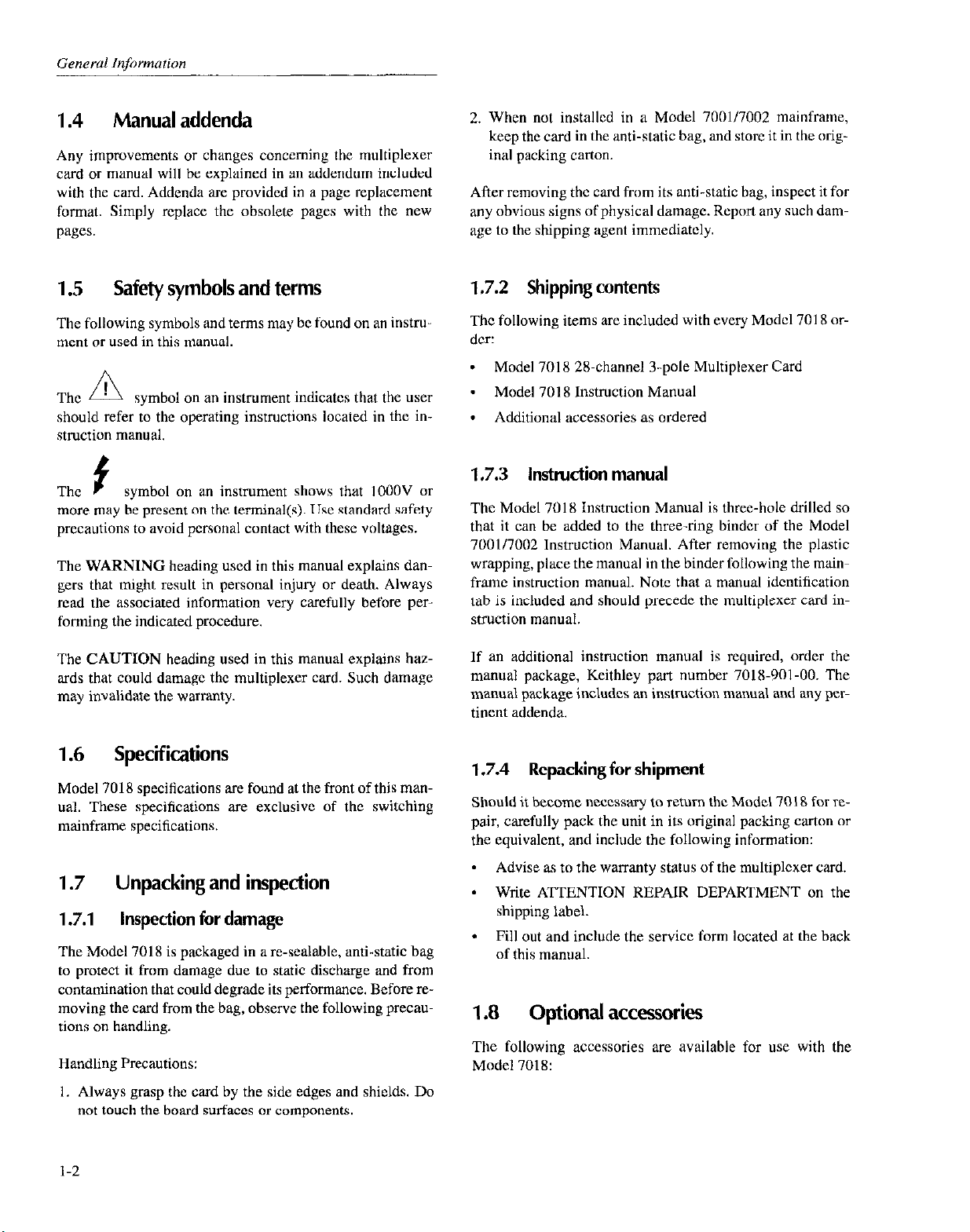
1.4 Manual addenda
Any improvements or changes concerning the multiplexer
card or manual will be explained in an addendum included
with the card. Addenda are provided in a page replacement
format. Simply replace the obsolete pages with the new
pa&X.
2. When not installed in a Model 7001/7002 mainframe,
keep the card in the anti-static bag, and store it in the original packing carton.
After removing the card from its anti-static bag, inspect it for
any obvious signs of physical damage. Report any such damage to the shipping agent immediately.
1.5
The following symbols and terms may be found on an instro-
ment or used in this manual.
The L!?!, symbol on an instrument indicates that the user
should refer to the operating instructions located in the instruction manual.
The
more may be present on the terminal(s). USC standard safety
precautions to avoid personal contact with these voltages.
The WARNING heading used in this manual explains dangers that might result in personal injury or death. Always
read the associated information very carcfully before performing the indicated procedure.
The CAUTION heading used in this manual explains hazards that could damage the multiplexer card. Such damage
may invalidate the warranty.
Safety symbols and terms
f
symbol on an instrument shows that IOOOV or
1.7.2 Shipping contents
The following items are included with every Model 7018 ordcr:
- Model 7018 2%channel 3-pole Multiplexer Card
- Model 7018 Instruction Manual
- Additional accessories as ordered
1.7.3 instruction manual
The Model 7018 Instruction Manual is three-hole drilled so
that it can be added to the three-ring bindcr of the Model
700117002 instruction Manual. After removing the plastic
wrapping, place the manual in the binder following the mainframe instruction manual. Note that a manual identification
tab is included and should precede the multiplexer card in-
stnrction manual.
If an additional instruction manual is required, order the
manual package, Keithlcy part number 701X-901-00. The
manual package includes an instruction manual and any per-
tinent addenda.
1.6 Specifications
Model 7018 specifications are found at the front of this man-
ual. These specifications are exclusive of the switching
mainframe specifications.
1.7 Unpacking and inspection
1.7.1 inspection for damage
The Model 7018 is packaged in are-sealable, anti-static bag
to protect it from damage due to static discharge and from
contamination that could degrade its performance. Before rcmoving the card from the bag, observe the following precautions on handling.
Handling Precautions:
I. Always grasp the card by the side edges and shields. Do
not touch the board surfaces or components.
1-2
1.7.4 Repacking for shipment
Should it become necessary to return the Model 7018 for repair, carefully pack the unit in its original packing carton or
the equivalent, and include the following information:
- Advise as to the warranty status of the multiplexer card.
. Write ATTENTION REPAIR DEPARTMENT on the
shipping label.
* Fill out and include the service form located at the back
of this manual.
1.8 Optional accessories
The following accessories are available for use with the
Model 7018:
Page 18
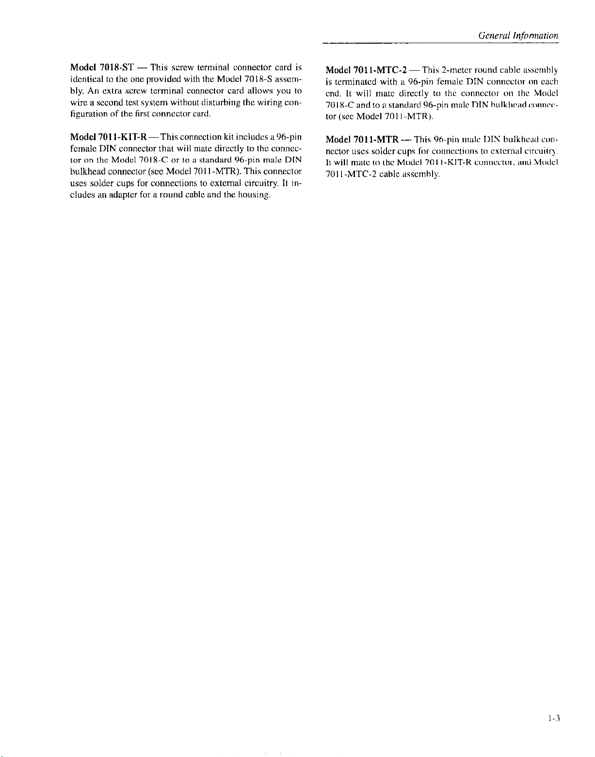
Model 701%ST - This screw terminal connector card is
identical to the one provided with the Model 7018-S assembly. An extra screw terminal connector card allows you to
wire a second test system without disturbing the wiring conliguration of the first connector card.
Model 701 l-MTC-Z-This 2.mctcr round cable assembly
is terminated with a 96.pin female DIN connector on each
end. It will mate directly to lbc connector on the Model
701X-C and to a standard Y6-pin male DIN bulklaid com~cctar (see Model 701 I-MTR).
Model 7011-KIT-R-This connection kit includes a 96.pin
fcmalc DIN connector that will mate directly to the conncctar on the Model 7018-C or to a standard Yh-pin male DIN
bulkhead connector (see Model 701 I -MTR). This connector
uses solder cups for connections to external circuitry. It includes an adaptcr for a round cable and the housing.
Model 701 I-MTR - This Y&pin malt DIN bulkhead con
ncctor uses solder cups for connections 10 e.xtemal circuitr).
It wilt mate to the Model 701 I -KIT-K connector. and !vI~niel
701 t -MTC-2 cable assembly.
Page 19
2
Multiplexing Basics
2.1 Introduction
This section covers the basics for multiplex switching and is
arranged as follows:
2.2 Basic multiplex configurations: Covers the basic
multiplex configurations: dual I x 14 configuration
and single I x 28 configuration. The backplane jumpers are also covered here.
2.3 Typical multiplexer switching schemes: Explains
some of the basic ways a multiplexer can be used for
switching. Covers sin&cndcd switching, diffcrcntiat
(floating) switching, sensing, and 3-pale/6-pole operation.
2.4 System expansion: Discusser the various configor;tlions that arc possible by using multiple cwds.
2.2 Basic multiplexer configutations
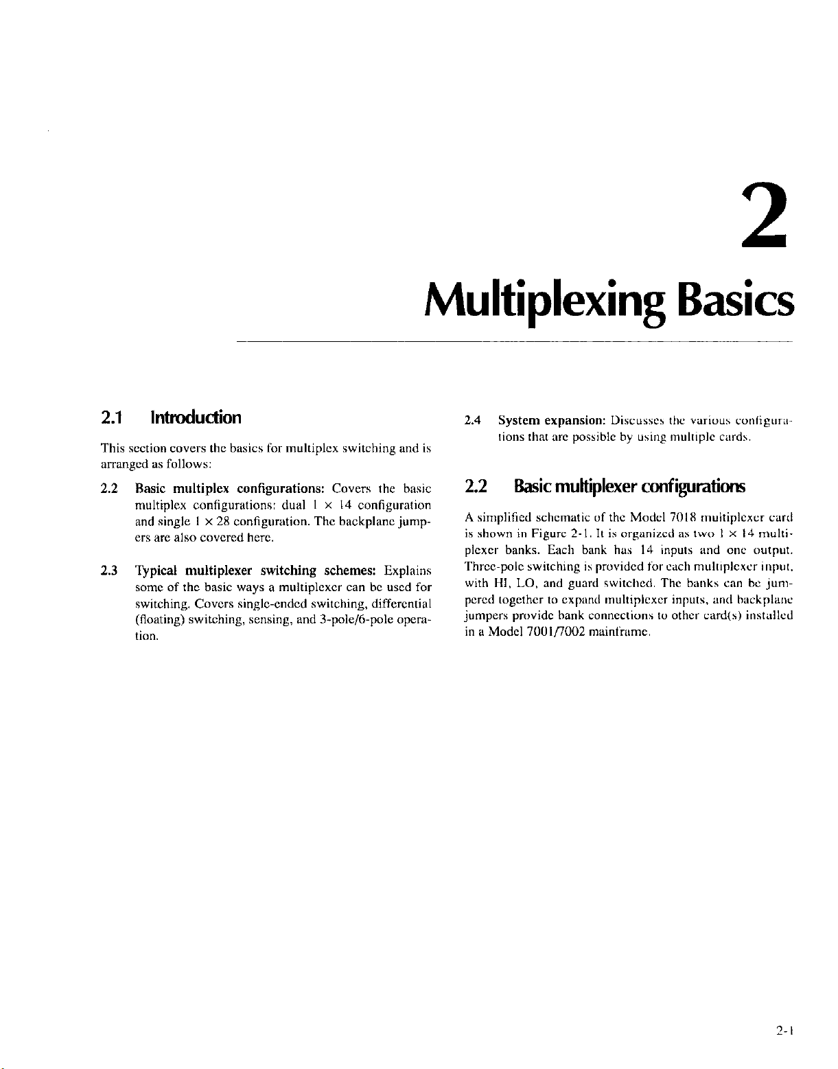
A simplified schematic of the Model 70 t 8 multiplexer card
is shown in Figure 2. I. It is organized ns two I x t 4 multiplexer banks. Each bank has 14 inputs and one output.
Three-potc switching is provided for each mult~plcxcr input.
with HI. LO, and guard switcbcd The banks can bc junlpercd together to expand muttiplcxcr inputs, and beckplanc
jumpers provide bank connections to other card(s) installed
in a Model 7001/7002 mainframe.
2-t
Page 20
r-----
-----_-______-------------
7018
1
Note : Factory Config”ration shown
Figure 2- 1
Model 7018 simplified schematic
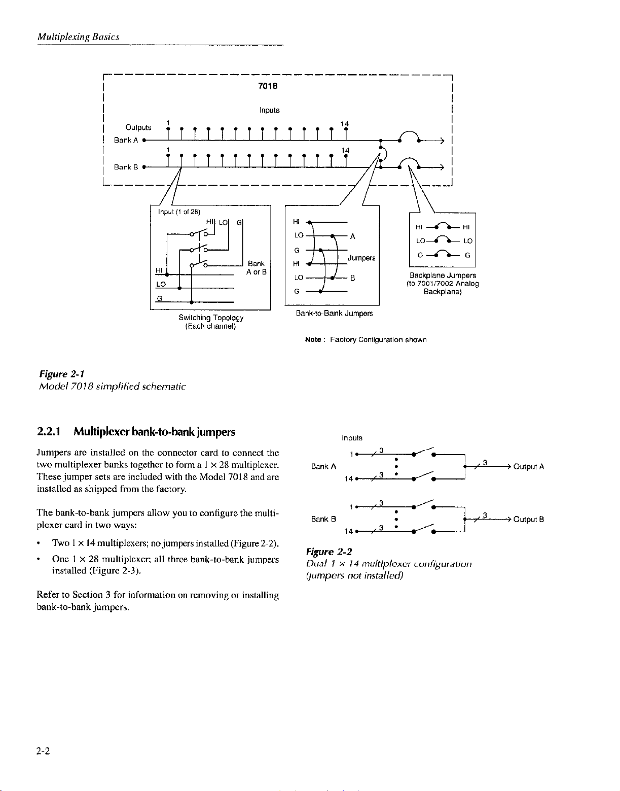
2.2.1 Multiplexer bank-to-bank jumpers
Jumpers arc installed on the connector card to connect the
two multiplexer banks together to form a I x 28 multiplexer.
These jumper sets are included with the Model 7018 and are
installed as shipped from the factory.
The bank-to-bank jumpers allow you to configure the multi-
plexer card in two ways:
* Two 1 x I4 multiplexers; no jumpers installed (Figure 2-2).
* One 1 x 2X multiplexer; all three bank-to-bank jumpers
installed (Figure 2-3).
Refer to Section 3 for information on removing or installing
bank-to-bank jumpers.
Figure 2-2
Dual 1 X 14 multiplexer configuration
(jumpers not installed)
2-2
Page 21

Figure 2-3
Single1 x28 multiplexer configuration (jumpers installed)
2.2.2 Backplane jumpers
NOTE
When the backplane jumpers nrc installed.
connecting the banks together on one card
will automatically connect the banks of
cards in other slots to~cther.
Figure 2-5 shows how each bank of the Model 701X i> cons
ncctcd to the backpbmc. The Model 70 IX is shipped fro111 the
factory with the backplxx jumpers installed.
&moving (cutting) the beckphuw .jumpws isrrlatcs the card
from the beckplanc. and subsequently. any card installed in
the other slot. For information on rcmoviny the jumpcr~. rcfcr to Section 3.
There arc six backplane jumpers located on the relay card
(three for each bank). With the jumpers instelled, the banks
of the multiplexer card are connected to the analog backplane of the Model 7OOl/7002, allowing expansion with other 7001/7002 card(s) installed in the mainframe. With the
jumpers removed (cut), the multiplexer card is isolated from
other card(s) installed in the mainframe.
The three-pole analog backplane of the Model 700117002
mainframe is shown in Figure 2-4. Through this analog
backplane, the banks of a Model 7018 multiplexer card, in-
stalled in one slot, can be connected to the banks (or rows) of
n compatible card installed in another slot of the mainframe.
Model 7001/7002
Analog
Backplane
Row 2 or Bank B
r----
l
Card 1
l r----
I I
&------!‘L
G\!-?G
I
I I
H)I
NOTE
The Model 7(101I7002 dots not provide itn
analog backplane for the non-701X scrics
cards. As a result, any of these c;irds installed in one slot in the nwinfrwnc is clectrically isoletcd from any card instidlcd io
another slot. The only way to connect il
Model 701X to one of thcsc cards is to wire
them togcthcr cxtemelly,
Card 2
I
KH
I
I
I
L------------.
Figure 2-4
Model 7001/7002 analog backplane
L\/t,
Gi-10
H = High
L= LOW
G = Guard
L----- -------
ROW = Matrix Card (7012,
Bank = MUX Card 17018,
Page 22
7018
Bank
(1 Of 2)
700117002
Analog
Backplane
I
, BankAorS I
Input l-14 r---)
,- I
H‘A., H
L‘A L
G>
H = High
i= LOW
G = Guard
Figure 2-5
Bank connections to backplane
2.3
The following paragraphs describe some basic switching
schemes that are possible with a three-pole switching multiplexer. These switching schemes include some various
shielding configurations to help minimize noise pickup in
sensitive measurement applications. These shields are
shown connected to chassis ground. For some test configurations, shielding may prow! to be more effective connected to
circuit low or common. Chassis ground is accessible at the
rear panel of the Model 7001/7002.
Typical multiplexer switching schemes
Jumpers
9::
Backplane
G
<
<
<
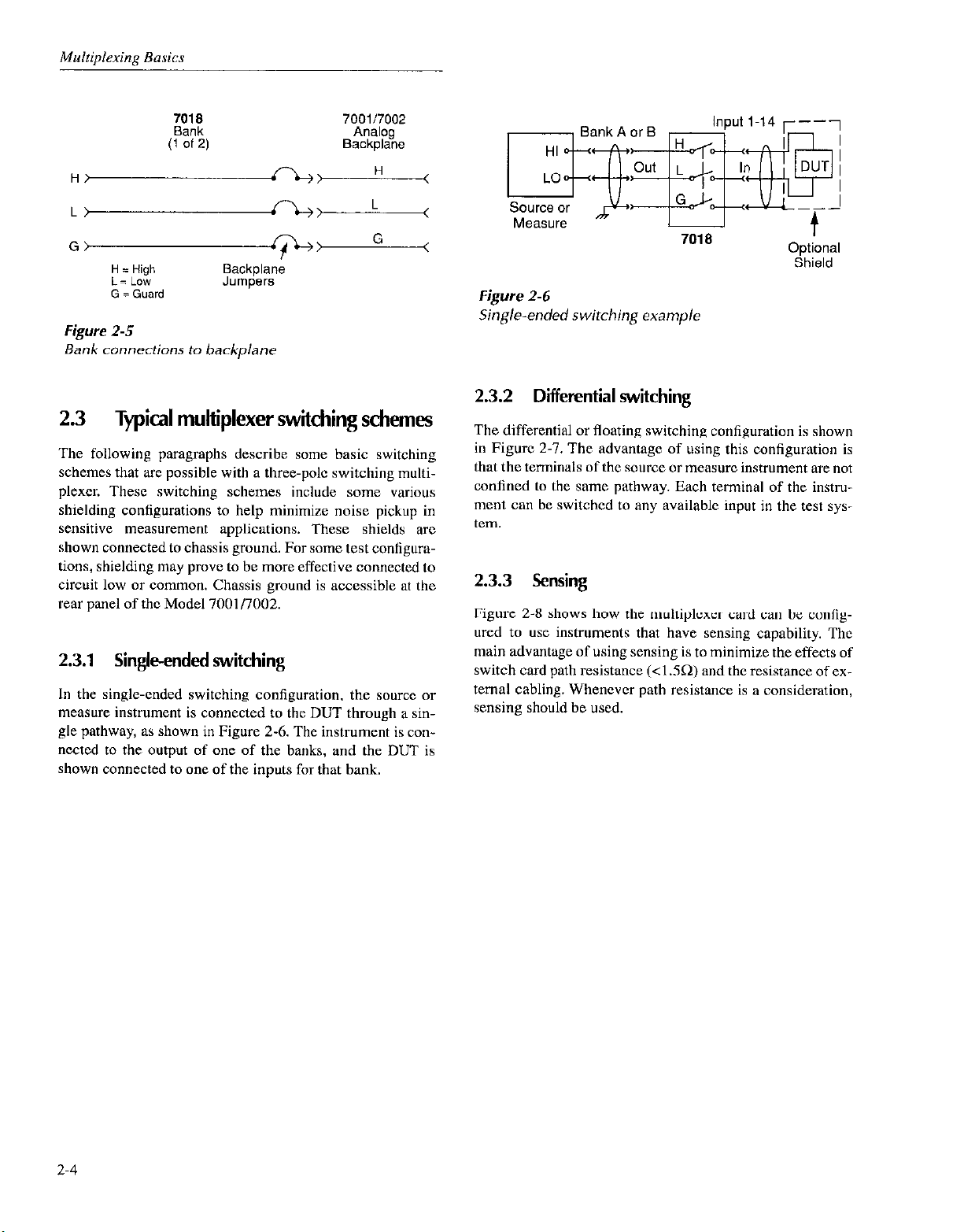
2.3.1 Single-ended switching
In the single-ended switching configuration, the source or
measure instrument is connected to the DUT through a single pathway, as shown in Figure 2-6. The instrument is connected to the output of one of the banks, and the DUT is
shown connected to one of the inputs for that bank.
Measure or
Figure2-6
Sing/e-ended switching example
t
Optional
Shield
2.3.2 Differential switching
The differential or floating switching configuration is shown
in Figure 2-l. The advantage of using this configuration is
that the terminals of the source or measure instrument are not
confined to the same pathway. Each terminal of the instrument can be switched to any available input in the test system.
2.3.3 Sensing
Figure 2-8 shows how the multiplexer card can be configured to use instruments that have sensing capability. The
main advantage of using sensing is to minimize the effects of
switch card path resistance (<I .SQ) and the resistance of ex-
ternal cabling. Whenever path resistance is a consideration,
sensing should be used.
2-4
Page 23

Figure 2-7
Differential switching example
3”“ICtl “I -
Sense HI
Figure 2-8
Sensing example
I-
701
Input I-14
a
7018
2.3.4 3-pole connections
Figure 2-9 shows typical 3-p& connections using a single
channel to switch both source and measure instruments to
the DUT. In this example, source HI and measure HI arc
routed separately to the DUT, while the LO terminals xc
connected together externally.
2.3.5
6-pole connections
The Model 7018 can also be used for h-pole switching for
testing more complex DUTs. Figure 2. IO shows typical Opole connections. In order to use h-pole switching. Ihc tikc-
numbcrcd channels of Banks A and I3 must bc paired togcther (Bank A, Input I with Bank B. Input I, etc.,. See ,>a~graph 4.3.4 f& informalion on sclting up the switching
mainframe for h-potc operation.
Page 24
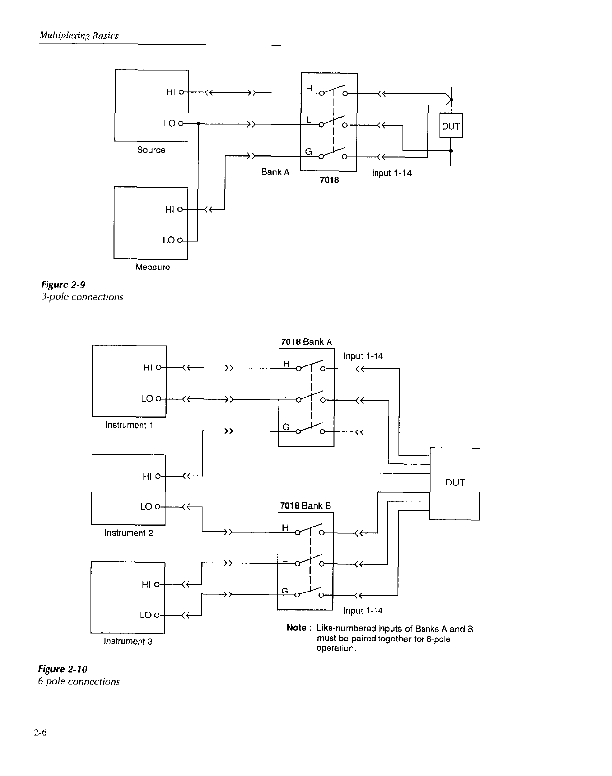
Figure 2-9
3-p& connections
HI 0
LO
ci
HI
LO
--
t---j-
Lit )
Instrument 1
r
Instrument 3
1 DUT
Note : Like-numbered inputs of Banks A and Et
must be paired together for &pole
operation.
Figure 2- 10
6.pole
2-6
connections
Page 25
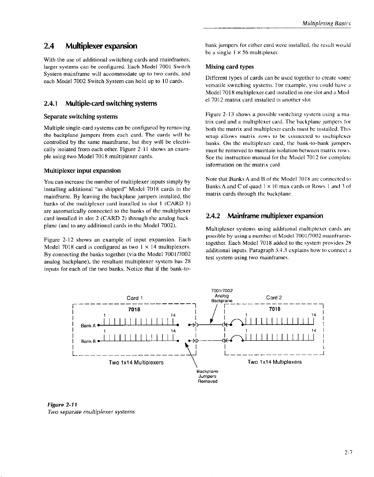
2.4 Multiplexer expansion
With the USC of additional switching cards and mainframes.
larger systems can be configured. Each Model 7001 Switch
System mainframe will accommodate up to two cards. and
each Model 7002 Switch System can hold up to IO cards.
2.4.1 Multiple-card switching systems
hank jumpcrs for either card were installed. the rewh would
be a single I x 5h muhiplexcr.
Mixing card types
Different types of cards cw bc used togcthcr to create some
vcrsatilc switching systems. For cxemplc. you could have it
Model 7018 multiplexer card instellcd in one slot and ii Modcl 7012 matrix card installed ill imothcr slot.
Separate switching systems
Multiple single-card systems can be configured by removing
the backplane jumpers from each card. The cards will be
controlled by the sane mainframe, but they will be clcctrially isolated from each other. Figure 2-l I shows an exemplc using two Model 7018 multiplexer cards.
Multiplexer input expansion
You can incrcasc the number of multiplexer inputs simply by
installing additional “as shipped” Model 7018 cards in the
mainframe. By leaving the backplane jumpers installed, the
banks of the multiplexer card installed in slot I (CARD I)
arc automaticttlly conncctcd to the banks of the multiplexer
card installed in slot 2 (CARD 2) through the analog backplane (and to any additional cards in the Model 7002).
Figure 2-12 shows an example of input expansion. Each
Model 7018 card is configured as two I x I4 multiplcxers.
By connecting the banks together (via the Model 7OOlflOO2
analog backplane), the resultant multiplexer system has 28
inputs for each of the two banks. Notice that if the bank-to-
Card 1
7018
r----
______---------
Figure 2-13 shows a possible switching system using a nw
trix card and a muhiplcxcr card. The bxkphmc jumpus for
both the matrix and multiplcxcr cards must bc installcd. Thih
setup allows mntrix rows to be conncctcd to multiplexer
banks. On the muhiplcxcr card. the bank-to-bank jumpers
must be removed to maintain isolation hctwccn matrix IOU\.
See the instruction Manuel fur the Model 7012 ior complctc
information on the matrix card.
Note that Banks A and B of the Model 70 IX arc connected tiz
Banks A and C of quad 1 x IO mux cards or Rows I and 3 of
matrix cards through the backplane.
2.4.2
Muhiplcxcr systems using udditional muhiplexcr cards arc
possible by using a number of Model Xi) l/7002 n~~inframc~
together. Each Model 701X added to the system provides 2X
additional inputs. Paragraph 3.4.3 cxphlins hwv tu connc~t a
wst system using two mainframes.
1
I
Mainframe multiplexer
700117002
A”CliOg
Backpiane
r----
I I
_----------
Card 2
7018
expansion
1
I
Figure 2-11
Two
separate multiplexer systems
Two 1x14 Multiplexers Two 1 x14 Multiplexers
Page 26

r-----
----------____
Card 1
700117002
Dual 1 xl 4 Multiplexers
Figure 2- 12
Multiplexer input expansion example
Card 1
r---I
7012
Dual 1 x 28 Multiplexer
1
I I
r----
Dual 1x14 Multiplexers
Card 2
-------__
7018
---
Bank A ’
Bank B I
----
1
I
I
Figure 2- 13
Mixed card type example
2-x
Page 27

3
Card Connections & Installation
3.1 Introduction
WARNING
The procedures in this section are intended only for qualified service personnel. Do not perform these procedures
unless qualified to do so. Failure to recognize and observe normal safety pre-
cautions could result in personal injury
or death.
The information in this section is arranged as follows:
3.2 Handling precautions: Explains precautions that
must be followed to prevent contaminetion to the multiplexer card assembly. Contamination could degrade
the performance of the multiplexer card.
3.3 Connections: Covers the basics for connecting external circuitry to the two available connector cards for
the multiplexer; the screw terminal connector card and
the multi-pin connector card.
3.4 Typical connection schemes: Provides some typical
connection schemes for single card, two-card, and
two-mainframe system configurations.
3.5 Model 7018 installation: Provides a procedure to install the multiplexcrcardassembly in the Model 70011
7002 mainframe.
3.2 Handling precautions
To maintain high impedance isolation. care should be taken
when handling the curd to avoid contamination from such
foreign materials as body oils. Such contamination can suhrtantially lower leakage rcsist;mccs. thus dcgwding pwformance.
To avoid possible contaminailfion. always grasp the r&y and
connector cuds by the side edges or shields. Do not touch
the board surfaces or components. On cwux-cto~\. do not
touch areas adjacent to tbc clcctricul COIIIBCIS. Din build-up
over a period of time is anotbcr possihlc source of contam~
station To avoid this problem. opcratc the mainframe and
multiplexer card in a clean en\‘ironment.
If a card becomes contaminated, it should he tborougbl)
cleaned as explained in paragraph 5.2.
3.3 connections
This paragraph provides the basic information needed to
connect your cxtemnl test circuitry to the multiplcxcr card. It
includes the instnlletion of the bank-to-bank jumpers 011 the
connector card, installation/remov;lI of backplane jumper)
on the relay card. and detailed information on making extcr-
nal connections to the two available connector cards.
WARNING
The following connection information is
intended to be used by qualified service
personnel. Failure to recognize and ob-
serve standard safety precautions could
result in personal injury or death.
3-l
Page 28

3.3.1 Bank-to-bank jumpers
As explained in paragraph 2.2.1, the two banks of the multi-
plexer card can he connected together (using plug-in jump-
ers) to form a larger multiplexer. The locations of the bankto-bank jumper terminals for both connector cards are shown
in Figure 3-1. The Model 7018 is shipped from the factory
with the bank-to-bank jumpers installed.
Terminal identification is provided by Figure 3-2. On the
drawing, the three terminal pairs arc labeled WlOl through
w103.
Figure 3-2
Bank-to-bank jumper terminal identification
Referring to Figure 3-l for jumper locations. perform the following steps to remove or install bank-to-bank jumpers:
Table 3-1
Bank-to-bank jumpers (on connector cardsi
~.~-~ ~~.
Installed
jumper*
WI01
WI02
WI03
Connection
Connect Bank A G to Bank B G
: Connect Bank A HI to Bank B HI
/ Connect Bank A LO to Bank B LO
I, If mated together, separate the relay card from the con-
nector card by removing the mounting screw and pulling the two cards away from each other. Remember to
handle the cards only by the edges and shields to avoid
contamination.
2. Refer to Figure 3-2 to determineJumper location.
3. Using Figure 3-3 as a guide, install or remove the jumpers on all three terminal pairs.
A. Screw Terminal Connector
Card (Model 7018-S)
Figure 3- 1
Bank-to-bank jumper locations
3-2
0
-1
P
I_~~~~~~~~.~~ . .._..........,....,....,..,..,..,...,.,,.,.,..,.. ~.,~.,.~A
_I,_l.w.“l-i
6. Multi-pin Connector Card
(Model 7018-C)
Page 29

-Jumper
Figure 3-3
Bank-to-bank jumper
installation
3.3.2 Backplane jumpers
The Model 7001/7002 mainframe has an analog backplane
that allows the banks of a Model 7018 multiplexer to be internally connected to B compatible switching card installed
in another slot (see paragraph 2.4.1 for details).
The backplane jumpers for the multiplexer card assembly are
located on the relay card as shown in Figure 3-4. The card is
shipped from the factory with the jumpers installed.
Card Connections &
lnstallalion
2. Use Figure 3-4 and Table 3-2 to locntc the jumper(s) thut
arc to be removed.
3. It is not necessary to unsolder the jumpers from the PC
board. Using a pair of wire cutters, cut both cuds of each
jumper, then remove the cut jumper scgmcnt complctcly.
Table 3-2
Backplane jumpers (on relay cards)
ran
~ Jumper* ~ Connection
I
WI01 ~ Bank AMI
: WI112
WI03
WI04
WI05
WI06
Bank AL0
Bunk A G
Bank B HI
Bank B 1.0
Bank B G
*see I:igurc 3-4 fur kwilm
Jumper
installation
Referring to Figure 3-4 forjumper locations. perform the following steps to install backplane row jumpers:
I. If mated together. scparatc the relay card from rhc cow
ncctor card by removing the mounting screw und pulling the two curds sway from each other. Rcn~emhcr to
handle the cards only by the edges and shields to avoid
contamination.
2. Physically remove cut jumper ends by unsoldering them
from the PC board.
3. Install a new #22 AWG jumper wire (Keithlcy P/N J-
15), and solder it to the PC board.
4.
Remove the solder flux from the PC boerd The cleaning
procedure is explained in paragraph 5.2.
Figure 3-4
Backplane jumpers
Jumper removal
Perform the following steps to remove backplane jumpers:
1. If mated together, separate the relay card from the connector card by removing the mounting screw and pull-
ing the two cards away from each other. Remember to
handle the cards only by the edges and shields to avoid
contamination.
3.3.3
Screw terminal connector card
The screw terminal connector curd is shown in Figure 3-5.
Connections are made directly to the screw tcrminuls of the
twelve terminal blocks. Each screw tenninnl will uccommodate #16-22 AWG wire. Note that the inputs for channels I
14ofhothBankAand BankB urc Inbelled INI through IN14
respectively.
Each input and output has three tcrminuls labelled II. Land
G for HI, LO and guard respectively.
NOTE
Although the G tcnninitl is called guard. it
is not a guard terminal uud should not bc
considcrcd a guard in the usual sense. All
3-3
Page 30

three pathways for each input have the
same electrical characteristics. Chassis
ground is available at the rear panel of the
mainframe.
Wiring procedure
Perform the following procedure to wire circuitry to the
screw terminal connector card:
WARNING
Make sure all power is off and any
stored energy in external circuitry is discharged. All DUT connections must be
insulated to prevent electric shock. The
recommended minimum wire insulation
rating is 175V RMS.
1. If mated together, separate the connector card from the
relay card by removing the mounting screw and pulling
the two cards away from each other. Remember to only
handle the cards only by the edges and shields to avoid
contamination.
2. Using an insulated screwdriver, connect the circuitry to
the appropriate terminals. Figure 3-6 shows how the
output of Bank A would be connected to a DMM.
Figure 3-5
Model 7018 screw terminal connector card
Warnlng:All DUTconnections mwt
be insulated. Recommended
minimum insulation rating is 175V
RMS.
Figure 3-6
Typical
3. Referring to Figure 3-1, remove the top half of the cable
4. Route wires under the wire guide/connector shim.
5. Route the wires through the bottom half of the cable
screw terminal connection.5
clamp as f0ll0ws:
A. Loosen the cable clamp screw enough to disengage
it from the bottom half of the cable clamp.
B. Using your thumb and forefinger, press the retaining
clips inward, and, with your other hand, remove the
top half of the clamp.
&tIlp.
3-4
Page 31

electrical characteristics. and they ciul bc
used intcrch;mgeably.
Keithlcy has B variety of cable and connccmr accessories
available to accommodi~tc con~~cctio~~s from the conncc~or
card to test instrumentation and DUT (devices under wst,. In
gcncral, these ucccssories, which arc summwizcd in Tahlc J3, utilize a round cable assembly for connections.
Cautkm: External strain relief should be used
with large wire bundles
Figure 3-7
Cable clamp for screw
terminal
connector card
6. Replace the top half of the clamp. It simply snaps onto
the bottom half of the clamp. Tighten the cable clamp
SCTCW. The clamp serves as a strain relief for terminal
block wires.
CAUTION
An external strain relief should be used
with large wire bundles to prevent damage to the card.
7. Mate the connector card to the relay card. The Model
7018 is now ready to be installed in the Model 70011
7002 meinframe. See paragraph 3.5 for details.
3.3.4 Multi-pin (masstermination) connector card
WARNING
All DUT connections must be insulated
to prevent electric shock. The recommended minimum wire insulation rat-
ing is 17SV RMS.
CAUTION
An external strain relief should be used
with large wire bundles to prevent damage to the card.
Since connections to external circuitry we made at the 96.
pin male DIN bulkhead connector. there is no wed to scparate the connector card from the relay card. If the connector
card is separated from the relay card, carefully mate them together, and install the supplied 4-40 mounting screw. Make
sure to handle the cards by the edges and shields to avoid
contamination.
Terminal identification for the DIN connector of the multipin connector card is provided by Figure 3-8. This connector
will mate to a 96-pin female DIN coonc~to~. Each input Rod
output has three terminals, HI, LO and G (guard).
NOTE
Although the G terminal is called guard, it
is not a guard in the usual sense. All three
pathways of each input have the same
Qpical connection techniques
All external circuitry, such as instrumenmtion sod DUTs.
that you wish to connect to tbe multiplexer card murt be tcrminated with u single 96.pin fcmalc DlZ cwncctor. The Ibl~
lowing connection techniques provide some guidehoer and
suggestions for wiring your circuitry.
WARNING
Before beginning any wiring procedures, make sure all power is off and
any stored energy in external circuitry is
discharged.
3-s
Page 32

Card Connections & Installation
NOTE
External circuitry should be connected
(plugged in) only with the mainframe
power off, after the Model 7018 assembly
is installed in the Model 7001/7002 mainfranc. Installation is covered in paragraph
3.5.
Output relay+The multi-pin connector card uses a relay
for each of the two output banks. These output relays arc normally open to prevent any hazardous voltages (via the mainframe backplane) from appearing on the pins of the male
DIN connector. The output relays will only close when the
Model 701 I -MTC-2 cable assembly is connected to card. If
building you own cable assembly, you must make sure that it
shorts pins la to lb of the card connector (Figure 3-8) when
it is mated to the card. Shorting pins la to I b allows the output relays to close.
Round cable assemblies-Figure 3-Y shows typical round
cable connection techniques using accessories available
from Keithley.
In Figure 3.YA, connections are accomplished using a Model
701 I-MTC-2 cable and a Model 701 I-MTR bulkhead con-
ncctor. The two-meter round cable is terminated with a 96.
pin female DIN connector at each end. This cable mates directly to the multi-pin connector card and to the bulkhead
connector. The bulkhead connector has solder cups to allow
direct connection to instrumentation and DUT. Figure 3-10
provides the pinout for the bulkhead connector.
In Figure 3.9B, connections are accomplished using a Model
7011.MTC-2 cable assembly that is cut in half. The 96.pin
female DIN connector on one end of the cable mates directly
to the multi-pin connector card. The unterminated end of the
cable is wired directly to instrumentation and DUT. The other half of the cable assembly could bc used for a second
switching card,
In Figure 3.YC, connections are accomplished using a custom-built cable assembly that consists of a Model 7011.KITR connector and a suitable round cable. Hitachi cable part
number N2807-P/D-SOTAB is a 50.conductor cable. Two of
these cables can be used to supply 100 conductors.The connector has solder cups to accommodate the individual wires
of the unterminated cable. Figure 3-l I provides an exploded
view of the connector assembly and shows how the cable is
connected. The connector end of the resultant cable assembly mates directly to the multi-pin connector card. The unterminated end of the cable assembly is wired directly to
instrumentation and DUT.
3-6
Page 33

Pins of the Model 701 B~C mass termination connector can be identified in one of three ways:
1. MUX terminal, consisting of banks A-B and inputs i-14.
2. Connector description, consisting of rows a-c and columns l-32.
3. Schematic and component layout designation (l-96).
The following pinout diagrams show the correspondence between these arrangements:
Carrl Connections & Insrallation
.................................
.
................................
.................................
MUX
Terminal
Bank A Bank A
Input 1 HI
Input * HI
Input3 HI 4a
Input4 HI
Input 5 HI
Input 6 HI 78
Input7 HI
Notes:
1. Pins 9a and 9b (pins 9 and 41 on schematic) are shield.
2. Short pins la to 1 b an the mating connector (pins 1 and 33 an schematic) to allow the output relays on the connector card 10 close
Desig.
la-32~
*a
LO
G
LO
G
LO
G
LO
G 5b
LO 6C
G
LO 7c
G
LO
G 8b
2c
2b
38
3c
3b
4c
4b
5a
5c
6a
6b
7b
*a
BC
onnect
:cllem.
or S
I
hslg. MUX
1-96 Terminal
2l LC
66
34 I
3 Input9 HI
67 LC
36 G
4 Input lOti
68 LC
36 G
5 Input 11 HI
69 LC
37 G
6
70 LC
3s
7 Input 13HI
71 LC
39 G
8 Input 14HI
72 LC
40 G
Input8 HI
G
lnpu, 12HI
G
output HI
LC
G
~Onnectol
Desig.
18-32s
Bank B
Ill Input 1 HI
74 LO
42 G
11
75
43
12 Input 3 HI
76 LO
44 G
13 Input4 Hi
77 LO
45 G
Input 6 HI
LO
G
Input 7 HI
LO
G
COnneCtOl
DC&g.
ts-32~
178
17c
17b
19a
19c
19b
20a
2oc
20b
22a
22c
22b
2%
2%
23b
View from pin side
of connector
:hem. i
esig. / MUX
l-96 ~ Terminal i 18-32~ ~ t-96
/Bank B
I
85
53 28b
InoUt 13HI /
22
~ connector 1 Schem.
~ Desig. Deaig.
-~-
24a 24
24c 66
24b 56
25s 25
2%
25b 57
2&l 26
26C 90
26b
27a 27
27c 91
27b 59
ma
LOI
G 1
Lo: 29c
G
26C
29a
29b
ma
97 1
55
G 30b
ou,put HI
G
3oc
LOI
32a
LO 32c
32b
69
58
28
All DUT connections must be insulated. Recommended minimum insulation rating is 175V RMS.
External strain relief should be used for large wire bundles
Figure 3-8
Multi-pin card terminal identifkation
WARNING
CAUTION
Page 34

Card Connections & Installation
Figure 3-9
Typical round cable connection techniques
Note
: See Figure 3-8 for terminal
identification.
Figure 3- 10
Model 70 11 -MTR connector pinout
3-8
View from solder
cup side of
connector
Page 35

Figure 3-
Model 701 I-KIT-R (with/cab/e) assembly
3.4
The following information provides some typical conacction
schemes for single-card, two-card and two-mainframe system configurations. Connection schemes for the multi-pin
connector card use some of the techniques presented in paragraph 3.3.2. Keep in mind that these arc only cxamplcs to
demonstrate various ways to wire a test system. Connection
details for both connector cards (multi-pin and screw termi-
nal connector cards) are provided in paragraph 3.3.
11
Typical connection schemes
3.4.1 Single-card system
Card Connections & Installation
(Model 7018-C). This single-card system is conligurcd as
two I x 14 multiplcxcrs. To accomplish this. the bank-tom
bank jumpers must bc rcmovcd.
Instrumentation and DUTs arc bard-wired to the Model
701 1 -MTR male bulkhead cormcctor. This connector has
solder cups thtat will accept wire size up to #24 AWG. The
test system is conncctcd to the multiplexer using the Mudci
701
I -MTC-2 round c;iblc wembly. This cahlc ~natc\ dircct~
ly to both the externill hulkhead connector and the Llodcl
701X-C multiplcxcr card assctnbly. Uoticc that the bulkhcxd
connector is shown mounted to it lixturc to help keep tbc oil-
bling stable during the test.
The single-card system in Figure 3-l 3 is identical to the sys-
tem in the previous illustration. cxccpl for the connection
scheme. The system in Figure 3-l 3 uses the screw tcrmirtal
connector card (Model 7018-S). With this curd. single-cow
ductor connections are made directly from the terminal
blocks of the connector card to instrumentntion and I)l:Ts.
When using a single-card system. mskc sure th;lt the card rcmains clcctrically isolated from any other switching cwd.
There arc several ways to ensure isolation for a sinflc card
in the Model 7001/7Gil2 mainfmmc:
I, Vacate other mainframe slot(s). If thcrc is a Model 70 IX
card installed in another slot, rermwc it.
2. Remove the backplane jumpcrs on the multiplcxr card.
Doing so will disconnect the card from the mulog hackplane of the mainfrnme.
3. Remove the bnckplanc jumpers from switching card(s)
installed in other slot(s).
4. Remove backplune jumpers from the Model 7002 hacks
pltNlC.
Figurc 3.12 shows how external connections can be made to
a single-card system that uses the multi-pin connector card
Page 36

. . .
L
r----
Simplified Equivalent Circuit
Figure 3- 12
Sing/e-card system example (multi-pin connector card)
3-10
Page 37

Figure 3- 13
Sing/e-card system example hcrew
terminal connector
Card Connecrionr & Inutallarion
cardi
Figure 3- 14
Two-card system example
3.4.2
Two-card system
(multi-pin connector card)
Both Figure 3-14 and Figure 3-15 show a system using two
multiplexer cards installed in one Model 7001 mainframe to
configure a single 1 x 56 multiplexer system. Each card is
configured as a single I x 28 multiplexer. To accomplish this,
bank-to-hank jumpers are installed to connect Banks A and
B together. By leaving the backplane jumpers of both cards
installed, the banks of Card 1 are connected to the banks of
Card 2 through the analog backplane of the Model 7001
mainframe resulting in the I x 56 configuration.
Figure 3. I4
shows how extcmnl connections can he made
for the multi-pin connector cards. In this exnmplc. a single
Model 7011.MTC-2 round cable asscmhly is cut in halt. to
provide two cables. each of which is untem~inated at ore
end. The unterminated ends of the two cahlcs iwc herd-wired
to the instrument and DUT as shown in the drawing. The other ends of these cables mate directly to the Modct 701X-C
multiplexer card assemblies.
Figure 3-15 shows how cxtcmal connections can be made
for the screw tcnninal connector card. Single conductor cow
ncctions are made directly from the screw tcmlinals 01’ the
connector card to tbc instrument sod DUT.
7-l I
Page 38

Card Connections & Installation
.
Simplified Equivalent Circuit
Figure 3- 15
Two-card system example (screw
. . .
/ Ill
DUT Test Fixture
terminal connector
I Ill
28 29
card)
. . . . . . . . .
56
3.4.3 Two-mainframe system
Both Figure 3- 16 and Figure 3-17 show a system using three
multiplexer cards installed in two Model 7001 mainframes to
configure a single I x 84 multiplexer system. Each card is
configured as a single 1 x 28 multiplexer. To accomplish this,
bank-to-bank jumpcrs of all at least one card must be installed to connect Banks A and B together.
By leaving the backplane jumpers of the cards in mainframe
#l installed, the hanks of Card 1 are connected to the hanks
of Card 2 through the analog backplane of the Model 7001
3.12
mainframe resulting in a 1 x 56 configuration. External bank
connections from the instrument to the card in the second
mainframe connect the banks of all three cards together to
form the 1 x 84 multiplexer system. This system is similar to
the Two-card System (see previous paragraph) except that a
third multiplexer card (installed in a second mainframe) is
added.
Figure 3-16 shows the connection scheme for the multi-pin
connector cards. External circuit connections to the Model
7001 #I mainframe are identical to the ones used for the
Page 39

Card Connections & installation
Two-card System. The third multiplexer card (installed in
Model 7001 #2 mainframe) shows how a custom-built cable
can be used to make connections to cxtcrnal circuitry. A suit-
able round cable can be constructed using il 96-pin female
DIN connector (Model 701 I-KIT-R) with two lengths of Hitachi cable P/N N2807-P/D-50TAB. This cable contains SO
conductors; two lengths provide 100 conductors. This cable
will mate to the Model 701 I-C multiplcxcr card assembly.
DUT Test Fixture
I
The unterminated end of the cable is conncctcd directly to
the instrument and DUT. Notice that the bank connections
for the third multiplexer cud arc made at the instruments.
Figure 3-17 shows connections for the screw terminal cow
ncctor card. Single conductor connections arc made directly
from the screw tcrminnls of the connector card to the instrument and DLJT.
Figure 3- 16
Two-mainframe system example (multi-pin connector card)
Page 40

Figure 3- 17
Two-mainframe system example Ocrew terminal connector card)
c
Simplified Equivalsnt Circuit
3.5 Model 7018 installation and removal
This paragraph explains how to install and remove the Modcl 7018 multiplexer card assembly from the Model 7001 or
7002 mainframe.
WARNING
Installation or removal of the Model
7018 is to be performed by qualified service personnel. Failure to recognize and
observe standard safety precautions
could result in personal injury or death.
NOTE
If using the screw terminal connector card,
make sure your external circuitry is wired
to the card (as explained in paragraph
3.3.1) before installing the card assembly
in the Model 7001 or Model 7002 mainframe.
3-14
CAUTION
To prevent contamination to the multiplexer card that could degrade performance, handle the card assembly only
by the edges and shields.
3.5.1 Ground screw
The Model 701X-C is equipped with a ground screw, which
is identified with this symbol: I (The Model 7018-S does
not require a ground screw because there arc no exposed
metal parts.)
The Model 70 I X-C ground screw must be securely tightened
after installation and remain secure during use of the multiplexcr card. This ground screw provides a proper safety
ground for the Model 701X-C when in use.
0
Page 41

WARNING
Securely tighten the ground screw after
installing the Model 7018-C. Failure to
do so may result in personal injury or
death.
3.5.2
Multiplexer card installation
Perform the following steps to install the multiplexer card
assembly in the Model 7001 or Model 7002 moinframc:
2. Facing the rear panel of the mainframe. wlcct the slut in
which you wish 10 inst;dl the card.
3. Rcfcrring to Figure 1-17 or Figure 3-18. fad the multiplcxer card assembly into the dcsircd slot such that Ihc
cdgcs of the rclny card ride in the wils.
4. With the ejector arms irl the unlocked position. push Ihc
card assembly 811 the way into the m;~iofmmc until Lhc
anns engegc into the ejector cups. I~CIJ push both imos ia
ward to lock the card into the mainfremc.
5. For the Model 7018-C only. tighten the grouod \crc’\
shown in Figure 3.17 and Figure 3-18.
WARNING
Turn off all instrumentation power (including the Model 7001 or Model 7002
mainframe), and disconnect their line
cords. Make sure all power is removed
and that any stored energy in external
circuitry is discharged.
I, Mate the connector card to the relay card if they are sep-
aratcd. Install the supplied 4.40 screw at the end of the
card to secore the assembly. Make sure to handle the cards
by the edges and shields to prcvcnr contamination.
Warning: Tighten Ground Screw
after installation (Model 7018-C)
Ejector Arms
fOpen Position)
WARNING
Securely tighten the ground screw. Failure to tighten the ground screw may result in a shock hazard.
3.5.3
Multiplexer card removal
To nxnove the multiplcxcr card xwnbly. first Iuosco the
ground screw (Model 7018-C ooly), unlock the cord by pulls
ing the latches outward. then pull
c card wcmhly <TUT of
th
the mainframe. Rememher to handle the card xwmbly b)
the edges and shields to avoid cootamioatio~l 1ha1 could dcgrade performance.
Figure 3- 18
Model 7018 card installation in Model 7001
”
Ejector Arms
(Locked Position)
Page 42

Figure 3- 19
7078
card installation in Model 7002
3-16
Page 43

Operation
4.1
The information in this section is formatted as follows:
4.2
4.3
4.4
4.5
4.2 Operatiod
Introduction
Operational constraints: Summarizes the maximum
signal limits of the Model 701X multiplexer card assembly, and the maximum number of relays that can
be turned on simultaneously.
Mainframe control of multiplexer card: Summarizes
programming steps to control the multiplexer card
from the Model 7001/7002 Switch System mainframe.
Multiplexer applications: Provides some typical ap-
plications for using the Model 7018.
Measurement considerations: Reviews a number of
considerations when using the Model 7018 to make
mcas”rements.
constraints
4.2.1 Maximum signal levels
CAUTION
4.2.2 Channel limitations
A maximum of I I chunncls can bc turned on simuh;mcousl~
hecausc of relay power control circuit limiwions.
4.3
The following information pertains to the ~Modcl 7018 multiplcxer card. It assumes that you xc f;mGliar with the opw
ation of the Model 7001/77002 maiofremes.
If you are not fxniliar with the operation of the mainfrerncs.
it is recommended that you proceed 10 Getting Stencd (Seetion 3) of the Model 7001/7002 Instruction Manuals after
reading the following information.
Mainframe contd
of
muttiplexer card
To prevent damage to the card, do not
exceed the maximum signal level specifications of the card.
To prevent overheating or damage to the relays, never exceed the following maximum signal lcvcls:
4.3.1 Channel assignments
The Model 7001 hns a channel status display (Figure J-I)
that provides the rc&timc state of each availahlc channel.
The left portion of the display is for slot I (Gird I). and the
right portion is for slot 2 (Card 2).
The Model 7002 has a similar display organized into il4-row
hy IO-column matrix for each of the IO cards in the syrtcm.
Page 44

Multiplexer organization of the channel status display for
each slot is shown in Figure 4-2. The card contains 28 channels and is made up of two banks (Banks A and B), of I4
multiplexer inputs as shown in the illustration.
multiplexer channel. To be consistent with Model 7001/7002
operation, the slot designator and mux input arc separated by
exclamation points (!). Some examples of CHANNEL assignments are as follows:
To control the multiplexer card from the mainframe, each
multiplexer input must have a unique CHANNEL assignment which includes the slot number in which the card is in-
stalled. The CHANNEL assignments for the multiplexer
card in slots I and 2 are provided in Figure 4-3. Each CHANNEL assignment is made up of the slot designator and the
7001 Display
CARD 1 CARD 2
n = Open Channel
. . . . . = Closed Channel
Figure 4-
Channel status display
1
CHANNEL I ! I = Slot I, Channel I (Input I of Bank A)
CHANNEL 1!28 = Slot 1, Channel 28 (Input 14 of Bank B)
CHANNEL 2!3 = Slot 2, Channel 3 (Input 3 of Bank A)
CHANNEL 4! I6 = Slot 4, Channel 16 (Input 2 of Bank B),
Model 7002 only
ROWS
4
Numbers
Figure 4-2
Display organization for Model 7018 multiplexer inputs
within
circles identify inputs
4-2
Page 45

4.3.2 Front panel control
Closing and opening channels
A multiplexer channel is closed from the front panel by simply keying in the CHANNEL assignment and pressing
CLOSE. For example, to close channel 2!6 (Input 6 of Hank
A) of a multiplexer card installed in slot 2, key in the follow-
ing channel list and press CLOSE:
close all the channels spccilicd in the chimncl list. l’rcssing
OPEN (or OPEN ALL) will open the channels.
CAUTION
Use care when closing more than one
channel at a time, or the card may be
damaged.
SELECT CHANNELS 2!6
The above closed channel can be opened by pressing OPEN
or OPEN ALL. The OPEN key opens only the channels specified in the channel list, and OPEN ALL opens all channels.
The following display is an example of a channel list that
consists of several channels:
SELECT CHANNELS 2! I, 2!3, 2!22-2!25
Notice that channel entries are separated by commas (J. A
comma is inserted by pressing ENTER or the right cursor
key . ), The channel range is specified by using the hyphen
(-) key to separate the range limits. Pressing CLOSE will
Scanning channels
Multiplexer channels arc scanned by creating a scan list und
configuring the Model 7001/7002 to perform a scan. The
scan list is created in the same manner as a channel list tscc
Closing and Opening Channels). However. the scan list is
specified from the “SCAN CIIANNEL” display mode. The
SCAN LIST key toggles between the clranncl list and the
scan list.) The following shows an cxample of a scan list:
SCAN CHANNELS 2! I. 2!3. 2!21-2!25
When a scan is performed, the channels specified in the scan
list will be scanned in the order that they arc presented in the
scan list.
J-3
Page 46

A manual scan can be paformed by using the RESET dcfault conditions of the Model 7001/7002. RESET is selected
from the SAVESETUP menu of the main MENU. When RESET is performed, the mainframc is configured for an infinite
number of manual scaos. The first press of STEP takes the
mainframe out of the idle state. The next press of STEP will
close the first channel specified in the scan list. Each subsequent press of STEP will select the next channel in the scan
list.
4.3.3 IEEE-488 bus operation
Bus operation is demonstrated below using HP BASIC 4.0.
The programming statements assume that the primary ad-
dress of the mainframe is 7.
The following program will perform a single scan through
all 2X channels of a Model 7018 multiplexer card installed in
slot I:
10 0”TP”T 707; “*PST”
20 OUTPUT 707; 3’: trig:seq:coun:auto on”
30 OUTPUT 707;
40 OUTPUT 707; “:init”
50 EN3
Line 10 Selects a default configuration for the scan.
Line 20
Line 30 Defines the scan list.
Lint 40 Takes the Model 7001/7002 out of the idle state.
Sets channel count to the scan-list-length.
The scan is configured to start as soon as this
command is executed.
“:scan (@1!1:1!28)”
Closing and opening channels
The following SCPI commands are used to close and open
channels:
The following statement closes channels l!l, and 1!3
through I ! 1 I :
0uTPuT707: “:clos (@l!l, 1!3:1!11)”
Notice that the colon (:) is used to separate the range limits.
Either of the following statements will open channels I ! 1,
and I!3 through l!ll:
ouTPuT707; “:open(@l!l, 1!3:1!11)”
0uTPoT707; “:openall”
Scanning
There are many commands associated with scanning. How-
ever, it is possible to configure a scan using as littlc as four
commands. These commands are listed as follows:
*RST
:TRIGger:SEQuence:COUNt:AUTo ON
:ROUTe:SCAN <lisU
: INIT
The first command resets the mainframe to a default scan
configuration. The second command automatically sets the
channel count to the number of channels in the Scan List, the
third command defines the Scan List and the fourth command takes the Model 7OOlflOO2 out ofthe idle state.
channels
When the above program is TUII, the scan will be completed
in approximately 240 milliseconds (3mscc delay for each relay close and a 3msec delay for each open), which is too fast
to view from the front panel. An additional relay delay can
be added to the program to slow down the scan for viewing.
The program is modified by adding line 25 to slow down the
scan. Also, Line 5 is added to the beginning of the program
to ensure that all channels are open before the scan is started.
5 OUTPUT 707; “:open all”
10 0”TP”T 707: “*PST”
20 OUTPWI 707: “:trig:seq:coun:auto on”
25 OUTPOT 707; “:trig:del 0.25”
30 ouTPuT 707;
40 OUTPUT 707; “:INIT”
50 END
Line 5 Opens all channels.
Line 25 Sets a l/4 second delay after each channel closes.
“:scan (@1!1:1!28)”
4.3.4 Selecting 3-pale/6-pole operation
The Model 701 R may be used in either the 3-p& mode or
the 6-pole mode. In the 6.pole mode, the inputs of Bank A
are paired with the corresponding inputs of Bank B (Input I,
Bank A with Input 1, Bank B, etc.).
To select 3.pole or 6-pole operation, press the CARD CON-
FIGURATION key, then choose the #-OF-POLES selection
in the card configuration menu. USC the 2.POLE selection to
operate the card in the 3-pole mode, or select 4.POLE to use
the multiplexer card in the 6-pole mode.
4-4
Page 47

4.4 Multiplexer applications
The following paragraphs discuss some typical applications
for the Model 7018. These applications include various
forms of resistor testing, transistor testing. as well as a discussion of how to combine the Model 7018 with a matrix
card to increase switching versatility.
4.4.1 Resistor testing
The Model 7018 can be used to test a number of resistors using only one test instrument or group of instruments. Such
tests include four-wire resistance measurements using a
DMM, and low-resistance measurcmcnts using a separate
current source and sensitive digital voltmeter.
Four-wire resistance tests
Although many resistance tests are made using the two-wire
method, more precise measurements over a wider rnngc of
system and DUT conditions am be obtairlcd by using the
four-wire measurement scheme shown in Figure 4-4. Hcrc.
separate sense leads from the Model 2001 Multimctcr are
routed through the multiplexer card to the resistor under test.
The extra set of sense leads minimizes the effects of voltage
drops across the card contacts that supply the test current to
the DUT. (The current through the sense leads is negligible,
resulting in virtually no voltage drop across the sense lcad rem
lay contacts.) Note, however, that four poles of switching per
device are required for four-wire resistance measurements.
(Although the Model 701X cm switch up to six poles. only
four poles are needed in this application.) For this rceson.
only I4 resistors per card can be tested using this configuration.
The Model 7018 can he configured for I4 channels of /L-pole
or 6.pole operation by isolating Bank A from B. and by programming the Model 7001/7002 mainframe for 4.pole mode.
(See paragraph 4.3.4.) Bank jumper removal is described in
paragraph 3.3.1. To configure the connector card for 4-p&
or h-pole operation, remove the jumpers between Banks A
and B. The resulting paired channels arc shown in Table 4-l.
Table 4-1
Paired Channels in 4-p& Operation
7001 Channel
CHANNEL pair in
assignment
I land15 ~-
2
:3 3 ;md 17
;4
5 5 and I9 fhnk A, In 5 and
6 6 and 20 Hank A. In 6 ilml
7 7 arld 2 I nzmk A. In 7 and
!R
Y Y ;uld 23
IO IO and 24
II II and 25
12 12 and 26 Hank A. In I2 and
I3 I3 and 27
I4
4.pole*
2 and I6
4 and IX
8 imd 22
14and28
Connection
designations
Ikmk A. In I imd
ISank H, 111 I
Rank A. 111 2 ;md
ISalk B, III 2
Balk A. In 3 and
Bank Ii. In 3
I%ank A. In 4 illld
Bel,k Il. In 4
Ihmk n, 111 5
Har1k R. In 6
B;mk U. III 7
Bank A. III X and
Ihmk n. In x
Aenk A. In ‘1 and
Hank 1% 111 9
Bank A. In IO and
H;mk 13. In IO
Ihmk A. 1,) I I il,ld
Rank I% In I I
Bank B, In 12
Bank A, In I3 ;md
Bank II. In I3
Bank A. In 14 and
Bank B. In I4
4-5
Page 48

Figure 4-4
Four-wire
resistance testing
Low-level resistance measurements
Many times, it is necessary to make resistance measurements
with either lower voltage sensitivity or higher currents than
arc available with ordinary DMMs. Examples of cases where
low-level resistance measurements may be necessary include the testing of PC board traces, contacts, bus bars, and
low resistance shunts.
Figure 4-5 shows a typical test configuration for a switching
system capable of testing a number of low-resistance dcvices. Again, the Model 7018 is operated in the 6-pole mode (although only four poles arc used). The Model 220 Current
Source forces current through the device under test, while
the Model 182 Sensitive Digital Voltmeter measures the rc-
suiting voltage across the device.
Since low voltage levels arc being measured, thermal EMF
offsets generated by relay and connector contacts will have a
detrimental effect on measurement accuracy unless steps arc
taken to avoid them (the Model 7018 has been designed to
keep relay EMF at a minimal level). Thermal EMF effects
can be virtually eliminated by taking two voltage measurements, El and E2, the first with the current, I, flowing in one
direction, and the second with a current, I, of the same mag-
nitude flowing in the opposite direction. The resistance can
then be calculated as follows:
E,-E,
R = ‘F
4.42 Transistor current gain testing
The DC or static common-emitter current gain of a transistor
can be determined by biasing the transistor for a specific value of base current, IB, and then measuring the collector current, I,. The DC common-emitter current gain, p, of the
transistor is then dctermincd as follows:
4-6
Page 49

Figure 4-5
Low
resistance testing
Figure 4-h shows the test configuration and equivalent circuit for the current gain test. The Model 224 Current Source
is used to source the base current, 1~. The Model 230 Voltage
Source supplies the collector-emitter voltage, VCE, and the
collector current, Ic, is measured by the Model 2001 Mutlimeter. Switching among the transistors being tested is. of
course, performed by the Model 7018 multiplexer card. The
Model 7018 is especially suited to this application because
of its 3.pole switching configuration.
In order to perform the current gain test, the voltage source
is first set to the desired value of VcE The current source is
then set to tt base current value that will result in the desired
value of Ic as measured by the DMM. The current gain can
then he calculated as outlined above.
4.4.3 Testing with matrix cards
The Model 7018 can he added to a matrix switching system
to enhance the test capabilities of that system. The following
paragraphs discuss an overall multiplcxcrlmatrix switching
system.
Multiplexer and matrix card connections
Figure 4-7 shows a typical zyrtcn~ using Model 7012 and
7018 cards together. In this instance, the multiplcxcr card is
configured as two I x 14 multiplcxcrs. Now that rww of the
matrix card are connected to the banks of the multiplexer
card through the analog hackplanc of the mainframe; no cxtcrnal wiring is neccssay to connect the two cards togcthcr.
Note, however, that the Model 7012 switches only Ill ;md
LO as it is il 2.pole card.
In this application. the DUTs arc com~ected to the bank inputs on the multiplexer card, allowing a Iargc number 01
DUTs to he switched through the matrix card. Also. the instrumeots arc connected to the columns on the matrix card.
This pnrticular configuration is best suited for applications
requiring a large number of DUTs to he con~tected to several
instruments. In other CLLSCS,
for a large number of instruments and few DUTs. In those situations, the instruments would hc conncctcd to the multiplexer inputs, and the DUTs would he connected to the
columns.
the test configuration mey call
4.7
Page 50

Operation
output
I
Figure 4-6
Configuration for current gain tesl
I
A. Test Configuration
8. Simplified Equivalent Circuit
4-R
Page 51

Backplane
Jumpers
Figure 4-7
Connecting multiplexer and matrix cards together
4.5 Measurement considerations
Many measurements made with the Model 7018 are subject
to various effects that can seriously affect low-lcvcl rnczlsurcment accuracy. The following paragraphs discuss these
effects and ways to minimize them.
4.5.1 Path isolation
The path isolation is simply the equivalent impedance hctween any two test paths in a measurement system. Ideally,
the path isolation should be infinite, but the actual resistance
and distributed capacitance of the card, cables, and connectors results in less than infinite path isolation values for these
devices.
Path isolation resistance forms a signal path that is in parallel
with the equivalent resistance of the DUT, as shown in FigWC 4-8. For low-to-medium device resistance values, path
isolation resistance is seldom a consideration: however, it
can seriously degrade measurement accuracy when testing
high-impedance devices. The voltage measured across such
a device, for example, can be substantially attenuated by the
voltage divider action of the device source resistance and
path isolation resistance, as shown in Figure 4-9. Also, leek-
age currents cat be generated through these resistances by
voltage SOUTCCS in the system.
7 r-----i r-:--y
DUT
Rwr = Source Resistance of DUT
Eour = Source EMF of DUT
RpnrH = Path l?.olation Resistance
RIN = Input Resistance of Measuring Instrument
Figure 4-8
Path isolation resistance
Any differential isolation capacitance affects DC mcasurc-
mcnt settling time as well ils AC rncasurcrncnt accuracy.
Thus, it is often imponent that such capacitance bc kept ifs
low as possible. Although the distributed capacitance of the
card is generally Rxed by design, there is one arca where you
do have control over the capacitance in your system - the
connecting cables. To minimize capacitance. keep all wblcs
as shon as possible.
J-5
Page 52

Operation
Eour RPATH
Flour + b&W
isolation resistance
Figure 4-9
Voltage attenuation
E
OUT =
bypath
4.5.2 Magnetic fields
When a conductor cuts through magnetic lines of force, a
very small current is generatcd. This phenomenon will frequently cause unwanted signals to occur in the test lends of
a switching matrix system. If the conductor has sufficient
length, even weak magnetic tields like those of the earth can
create sufficient signals to affect low-level measurements.
Two ways to reduce these effects are: (1) rcducc the lengths
of the test leads, and (2) minimize the exposed circuit area.
In extreme cases, magnetic shielding may be required. Special metal with high permeability at low flux densities (such
as mu metal) is effective at reducing these effects.
Even when the conductor is stationary, magnetically-induced signals may still be a problem. Fields can be produced
by various signals such as the AC power line voltage. Large
inductors such as power transformers can generate substantial magnetic fields, so care must be taken to keep the switching and measuring circuits a good distance away from these
potential noise sources.
RFI can be caused by steady-state sources such as radio or
TV signals, or some types of electronic equipment (microprocessors, high-speed digital circuits, etc.), or it can result
from impulse sources, as in the case of arcing in high-voltage
environments. In either case, the effect on the measurement
can be considerable if enough of the unwanted signal is
present.
RF1 can be minimized in several ways. The most obvious
method is to keep the equipmcnt and signal leads as far away
from the RF1 source as possible. Shielding the switching
card, signal leads, sources, and measuring instruments will
often reduce RF1 to an acceptable level. In extreme cases, a
specially-constructed screen room may be required to sufficiently attenuate the troublesome signal.
Many instruments incorporate internal filtering that may
help to reduce RF1 effects in some situations. In some cases,
additional external filtering may also be required. Keep in
mind, however, that filtering may have detrimental effects on
the desired signal.
4.5.4 Ground loops
When two or more instruments are connected together, care
must be taken to avoid unwanted signals caused by ground
loops. Ground loops usually occur when sensitive instrumentation is connected to other instrumentation with more
than one signal return path such as power line ground. As
shown in Figure 4-10, the resulting ground loop causes current to flow through the instrument LO signal leads and then
back through power line ground. This circulating current devclops a small but undesirable voltage between the LO terminals of the two instruments. This voltage will bc added to
the source voltage, affecting the accuracy of the measurement.
At high current levels, even a single conductor can generate
significant fields. These effects can be minimized by using
twisted pairs, which will cancel out most of the resulting
fields.
4.5.3
Radio frequency interference
RF1 (Radio Frequency Interference) is a general term used to
describe electromagnetic interference over a wide range of
frequencies across the spectrum. Such RFI can be particularly troublesome at low signal levels, but it can also affect
measurements at high levels if the problem is of sufficient severity.
Figure 4- 10
Power line ground loops
Page 53

Figure 4-l I shows how to connect several instruments togethcr to eliminate this type of ground loop problem. Hcrc,
only one instrument is connected to power line ground.
Figure 4- 11
Eliminating
ground loops
Ground loops are not normnlly R problem with instruments
having isolated LO terminals. However. all instruments in
the test setup may not be designed in this manner. When in
doubt, consult the manual for all instrumentation in the test
setup.
4.5.5 Keeping connectors clean
As is the case with any high-resistance device, the integrity
of connectors can be damaged if they arc not handled properly. ISconnector insulation becomes contaminated, the insulation resistance will bc substantially reduced. affecting
high-impedance measurement paths.
4.5.6
AC frequency response
The AC frcqucncy response of the Model 701 X is important
in test systems that switch AC signals. Refer to the spccilic;,~
tions at the front of this manual.
4.5.7 lhermoekctric potentials
Thcrmoelcctric potentials (thermal EMFsl arc small clcctric
potentials gcneratcd by differences in tempcraturc iit circuit
connecting points such iis multiplexer relay cootacts, card
termin;ds, and connectors.
Thermoelectric generation
Figure 4-12 shows a reprcsent;aion of how thcnnal l3lFs
xc gcncrated. The test Icads arc made ot. the A material.
wbilc the source under test is the I< matcri~l. The temper;+
turcs between the junctions are Tl sod T2. To detcmline the
thermal EMF gencratcd, the rcliitionship shown may he
used.
In the unlikely event that the two junctio~l tcmpcrxturc~ xc
identical. the thcmmul IiMFs will exactly CUICCI because the
generated potentials oppose one imother. Marc often. the two
junction temperatures will differ. and considcrahle thcnnal
EMFs will hc gcncretcd.
Oils and salts from the skin can contaminate connector insulators, reducing their resistance. Also, contaminants present
in the air can be deposited on the insulator surface. To avoid
these problems, never touch the connector insulating material. In addition, the multiplexer card should be used only in
clean, dry environments to avoid contamination.
If the connector insulators should become contaminated, ei-
ther by inadvertent touching, or from air-borne deposits, they
can be cleaned with a cotton swab dipped in clean methanol.
After thorough cleaning, they should be allowed to dry for
several hours in a low-humidity environment before use, or
they can be dried more quickly using dry nitrogen.
Figure 4- 12
Thermoelectric generation
J-II
Page 54

Nulling residual thermal offsets
Even if all reasonable precautions are taken, some residual
thermal offsets may still be present. These offsets can be
minimized by using the measuring instrument’s offsct-compensated ohms feature if available. Also, the zero or rclativc
feature can be used to null them out. To do so, place the instrument on the range to he used for the measurement, close
the multiplexer card channel to he used for the measurement,
and short the end of the connecting cable nearest the mea-
sured source (first disconnect the cable from the source to
avoid shorting out the source). After allowing the reading to
settle, press the zero or rcl button to null the offset, then
make your measurement as usual. Note that it may bc neces-
sary to ~-zero often to counteract thermal drifts, and the rel
process should bc rcpcated whenever the range is changed 01
when a different channel is used for best accuracy.
4-12
Page 55

5
Service Information
WARNING
The information in this section is intended only for qualified service personnel. Some of the procedures may expose
you to hazardous voltages that could result in personal injury or death. Do not
attempt to perform these procedures
unless you are qualified to do so.
5.1 Introduction
This section contains information necessary to service the
Model 7018 multiplexer card and is arranged as follows:
5.2 Handling and cleaning precautions: Discusses handling precautions and methods to clean the card should
it become contaminated.
5.3 Performance verification: Covers the procedures
necessary to determine if the card meets stated specifications.
5.4 Special handling of static-sensitive devices: Rc-
views precautions necessary when handling staticsensitive devices.
5.5 Principles of operation: Briefly discusses circuit operation.
5.2 Handling and cleaning precah
Handle the card only by the cdgcs and sbiclds.
Do not touch any board surfxcs or components not a\~
sociated with the repair.
Do not touch areas adjacent to electrical comxt~.
.
.
Do not store or operate the card in an en\wronmcnt
whcrc dust could settle on the circuit hoard. Lx dry ntrogen gas to clenn dust off tbc board if ncccssery
Should it become necessary to use solder on the circuit
hoard, use an OA-based (organic itctivated) llux. Kc
move the flux from the work areas when the repair has
been comptetcd. USC pure water along with ctciul cotton
swabs or a clean. soft brush to remove the flux. Take
care not to spread the flux to other areas of the circuit
board. Once the flux has hcen removed. swab only the
repaired area with methanol, then blow dry the board
with dry nitrogen gas.
Aftcrcteaning, the card should he ptaccd in ii 50°C low
humidity environment for scvcral hours before USC.
5.6 Troubleshooting: Presents some troubleshooting tips
for the Model 7018 including r&y replacement precautions.
5.3
The following paragraphs discuss pctiomnwc verification
procedures for the Model 7018, including path resistance.
offset current, contact potential, and isotntion
Performance verification
s-1
Page 56

With the Model 701 X’s backplane jumpers installed, the performance verification procedures must be performed with
only one multiplexer card (the one being checked) installed
in the Model 7001/7002 mainframe. These conditions do not
apply if the backplane jumpers are removed.
CAUTION
Contamination will degrade the performance of the card. To avoid contamination, always grasp the card by the side
edges. Do not touch the connectors, and
do not touch the board surfaces or components. On plugs and receptacles, do
not touch areas adjacent to the electrical
contacts.
NOTE
Failure of any performance verification
test may indicate that the multiplexer card
is contaminated. See paragraph 5.2 for
procedures to clean the card.
5.3.1 Environmental conditions
All verification measurements should be made at an ambient
temperature between 18’ and 28°C and at a relative humid-
ity of less than 70%.
5.3.2 Recommended equipment
5.3.3 Multiplexer card connections
The following information summarircs methods that can be
used to connect test instrumentation to the two connector
cards. Detailed connection information is provided in Section 3.
Model 7018-S- Instrumentation can simply bc hard-wired
directly to the screw terminals of the connector card. Jumper
wires should be kept as short as possible.
Model 7018-C-One method to make instrument connections to the multiplexer card is by hard-wiring a 96.pin female DIN connector then mating it to the connector on the
Model 7018-C. Input and output shorting connections can
also be done at the connector. The connector in the Model
701 I-KIT-R connection kit (see Table 3.2) can be used for
this purpose. Pin identification for the connector is provided
by Figure 3-X.
CAUTION
After making solder connections to a
connector, remove solder flux as explained in paragraph 5.2. Failure to
clean the solder connections could result
in degraded performance preventing
the card from passing verification tests.
Before pre-wiring any connectors or plugs, study the following test procedures to fully understand the connection requirements
Table S-1 summarizes the equipment necessary for performance verification, along with the application for each unit.
rabble S- 1
Verification equipment
Description
DMM
Electrometer w/voltage source
Sensitive Digital Voltmeter
Triax cable (unterminated)
Low thermal cable
Model or part
Keithley Model 2001
Keithlcy Model 617
Keithley Model I82
Keithley Model 7025
Keithley Model 1484
(unterminated)
s-2
Specifications
20R; 72ppm
IOpA, lOOpA; 1.6%
IOOV source; 0.2%
/ 3mV; 6Oppm
I-
Applications
Path resistance
Offset current, path isolation
Contact potential
Offset current
Contact potential
Page 57

5.3.4 Channel resistance tests
Perform the following steps to verify that each contact of every relay is closing properly and that the r~~i~tan~~ is within
spccitication.
1.
Turn off the Model 700 l/7002 if it is on.
2.
Turn on the Model 2001, and allow it to warm up for o”c
hour before making measurements.
3.
Connect all input terminals of Bank A together t” form
one comm”” terminal, as shown in Figure 5-l.
4.
Set the Model 2001 to the 200 range, and c”ntxct the
four test leads t” the INPUT and SENSE jacks.
5.
Short the four test lcads together, and press REL on the
Model 2001. Leave REL enabled for the entire test.
Connect INPUT HI and SENSE HI of the Model 2001
6.
to the common terminnl (jumper on Bank A inputs). It is
recommended that the physical connections be made at
inputs I and 14 of Bat& A. as shown in Figure 5-l.
Connect INPUT LO tutd SENSE LO to the HI (H) tcr-
7.
minal of Bank A output.
Install the Model 7018 in slot I (CARD I) of the Model
R.
7001/7002.
9.
Turn on the Model 7001/7002. and program it to close
Channel l! I (BankA. Input I). Verify that the resistance
of this path is <lSR.
Open Channel I! I. and close Channel I!2 (Bank A, In-
IO.
put 2). Verify that the resistance of this peth is <I .50.
I I, Using the basic proccdurc in steps 9 and IO. cheek tbc
rcsisttmcc of Bank A HI (1~1) terminal paths for Inputs 3
through I4 (Chatmcls I !3 through I ! 14).
12. Turn off the Model 7OOli7002, and move tbc INPUT
LO and SENSE LO test lcads to the 1.0 (L.) tcrmimll 01~
Bank A output.
13. Repeat steps 9 through I I to cbcck the I.0 (L) tcrmini!l
paths of Bank A (Ch;urncl~ I ! I tbr”ugl~ I ! IJi.
14. Turn off the Model 7003/71l02. und III”YC tbc IVPL:T I.0
and SENSE LO test Icads to tbc G termitul of t&ml. h
output.
t 5. Repeat steps 9 through I I to cheek the G termimd p;ithb
of Bank A (channels I ! I tu I ! 14).
16. Rcpcat the basic procedure in steps I tbrrngtl I5 for
Bank B (Channels I ! I5 through I !28 1. >Mxkc pure tbc rc~
sisttmcc of each path is <I XL.
5.3.5
Offset current tests
Tbcsc tests check leekage current bctwecn III itli. 1.0 11.1.
and G (differential offset currc”t) and front tll (HI. 1.0 IL].
and G to chassis (common-m”dc offset currcW “1 each path
way. lu gcnerel. tbesc tests arc pcrt’“nncd by simply mcit\uring the leakage current with an clectromctcr. In the Sollowing
procedure. the Model 6 t 7 is used t” mciwurc tbc Icxkagc cure
rem. Test connections arc shown in I;igurc 5-2.
Fi@m 5- 1
Path
resistance test connections
s-3
Page 58

Figure 5-2
offset current test
Model7018
B) Common Mode
connections
Perform the following procedure t” check offset current:
I. Turn off the Model 700 l/7002 if it is on, and remwe any
jumpers or wires connected t” the multiplexer card.
2. Connect the triax cable t” the Model 617, but do not
connect it to the multiplexer card at this time.
3.
Turn on the Model 617, and allow the unit to warm up
for tw” hours before testing. After warmup, select the
ZOOpA range, and enable zer” check and zer” correct in
that order. Leave zer” cwrect enabled for the entire procedure. Also, be certain that V-Q, GUARD is OFF and
that the ground strap is connected to LO,
4. Connect the triax cable t” Bank A output HI and LO, as
shown in Figure 5-2A.
5. Install the Model 7018 in slot 1 (CARD I) of the Model
700117002.
6. Turn on the Model 7001/7002, and program the “nit to
close Channel 1 ! 1 (Bank A, Input I).
5-4
7. On
the Model 617, disable zem check, and allow the
reading t” settle. Verify that the reading is <l OOpA. This
specification is the offset (leakage) current of the pathWkly.
8. Enable zero check on the Model 617, and opt” Channel
l! 1 from the front panel of the Model 7001/7002.
9. Repeat steps 6 through 8 with the electrometer connect-
ed to the HI and G output terminals.
10. Repeat steps 6 through 8 with the electrometer connccted to the LO and G output terminals.
11. Repeat the basic procedure in steps 6 through 10 to
check the rest of the pathways (Inputs 2 through 14) of
Bank A (Channels I!2 through 1!14).
12. Turn off the Model 7001/7002 and change the electromcter connections to Bank B.
13. Repeat the basic procedure in steps 6 through 11 to
check Bank B, Inputs I through 14 (Channels I!15
through 1!2R).
Page 59

14. Turn off the Model 7001/7002, and change the clcctr”mcter connections, as shown in Figure 5.2B. Note
that electrometer HI is connected t” HI, LO, and G of
the Bank A output, which arc jumpered together. Elcctromcter LO is connected to chassis.
15. Repeat steps 6 through I I, and check that the Bank A
common-mode offset current is <lOOpA.
16. Repeat step 15 for Bank B to check that the commonmode offset current is <lOOpA.
5.3.6 Contact potential tests
These tests check the thermal EMF generated by the relay
contact for each pathway (HI, LO, and G). The tests USC a
sensitive digital vohmcter (Model 182) to measure the contact potential.
Perform the following procedure t” check contact potential
of each contact:
I, Turn off the Model 7OOlflOO2 if it is on.
2. Turn on the Model 182, and allow the unit to wtrm up
for tw” hours to achieve rated accuracy.
3. Connect the Model 182 input leads to Bank A output HI
and input I HI (see Figure 5-3).
4. Temporarily connect a clam. higbpurily copper shon
between Bank A output HI and Bank A input I HI.
5. Install the Model 7018 in the Model 7001/7002 slot I,
and turn on the Model ~OOl,lOO2.
6. Allow Models 7001/7002.7018. and I X2 to wilrm up
ior
two hours.
7. Select the 3mV range “11 the ~Modcl I X2.
H. Press REL READING (on the Model I X2) to null out iw
tcrnal offsets. Lcevc REI. Rl%‘,DING cnahlcd for the
cmirc proccdurc.
9. Turn off the Model 7001/700~. 7 and rc,,,0vc the Model
7018 from slot I. Remove the shon bctwccn Input Ill
and Bank A output HI.
10. Install the Model 7018 in Model 7OOl~OO2 slot I, and
urn on the power.
I I. Wait I5 minuws.
12. Program the Model 7001~0112 tu close Chtmncl I ! I.
13. After settling, verify that reading on the M”dcl IX2 is
<.spV, This mexurcmcnt rcprescnts the contact p”tcn~
tial of the pathway.
14. From the Model 7001,‘7002. opal Ch;mncl I ! I.
IS. Rcpcat steps 7 through 14 for the 1.0 sod G leml~nals.
(Be sure t” connect the voltmeter HI and LO terminals
to the path heing tested.1
16. Repeat steps 7 through IS l~orthc rcm;~ining channels 01
Bank A (I!2 to l!l4) sod idl channels of Bxnk B (I!15
to I !28).
Figure 5-3
Contact potential test
connections
5-s
Page 60

5.3.7 Bank and channel-to-channel isolation tests
Bank isolation tests check the leakage resistance between ad-
jacent banks. Channel-to-channel isolation tests check the
leakage resistance between a Bank Output connection and a
Bank Input connection with an adjacent Bank Input relay
closed. In general, the tests arc performed by applying a voltage (IOOV) across the leakage resistance and then measuring
the current. The isolation resistance is then calculated as R =
V/I. In the following procedure, the Model 617 functions as
both a voltage source and an ammeter. In the V/I function,
the Model 611 internally calculates the resistance from the
known voltage and current levels and displays the resistance
WlUEZ.
Perform the following steps to check bank and channel-tochannel isolation:
I.
Turn off the Model 7OOlflOO2 if it is on, and remove any
jumpers or test lcads connected to the multiplexer card.
2.
Turn on the Model 617, and allow the unit to warm up
for two hours before testing.
On the Model 617, select the ZpArange, and enable zero
3.
check and zero correct in that order. Leave zero correct
enabled for the entire procedure.
4.
Connect the electrometer to the Model 7018, as shown
in Figure 5-4.
5.
Install the Model 7018 in slot 1 (CARD I) of the Model
7001/7002, and turn on the mainframe.
On the Model 617, select the 20pA range, and release
6.
zero check.
7.
On the Model 617, press SUPPRESS to cancel offset
current, then enable zero check.
WARNING
The following steps use high voltage
(1OOV). Be sure to remove power from
the circuit before making connection
changes.
8.
On the Model 617, set the voltage source for +I OOV, and
select the 20nA current range. Make sure the voltage
source is in standby.
9.
Place the Model 6 I7 in the V/I measurement function by
pressing SHIFT OHMS.
Program the Model 7OOlflOO2 to close Channels I ! I
IO.
and I! I6 (Bank A, Input 1 and Bunk B, Input 2).
On the Model 617, disable zero check and press OPER-
Il.
ATE to source + I OOV.
After allowing the reading on the Model 617 to settle,
12.
verify that it is >lGbl (109a). This measurement is the
leakage resistance (bank isolation) between Bank A, Input I and Bank B, Input 2.
Using Table 5-2 as a guide, repeat the basic procedure of
13.
steps IO through 12 for the rest of the path pairs (test
numbers 2 through 7 in the table).
Place the Model 617 voltage source in standby, and en-
14.
able zero check.
Repeat the entire test with the electrometer connected to
15.
the Bank A and B G terminals instead of the HI termiIXllS.
16.
Turn off the Model 7001/7002, and connect the Model
617 to the card as shown in Figure 5-5
Install the Model 701 R in slot 1 of the Model 7001/7002,
17.
and turn on the mainframe.
IX.
Program the Model 7001/7002 to close Channel I !2
(Bank A, Input 2). Make sure all other channels are
open.
19.
On the Model 617, disable zero check, and press OPERATE to source IOOV.
20.
After allowing the readin
verify that it is >IGR (10
21.
Place the Model 617 voltage source in standby, and en-
on the Model 617 to settle,
$
Q).
able zero check.
22.
Using Table 5-3 as a guide, perform tests 2 through 13
for the remaining Bank A Inputs. Remember to move
Bank Input connections as indicated in the table.
23.
USC Table 5-3 (test numbers I4 through 26) and the
above procedure to test Bank B.
24.
Repeat steps 16 through 22 with the electrometer con-
nected to the G terminals instead of the HI terminels.
5-6
Page 61

Table 5-2
Hank isolation test summary
--~Test~ 1 ~~~~~~~~~~~~~~~~~~
number Bank isolation
Channels closed’
~ I
2
3
4
5
6
7
Bank A, Input I to Bank B. Input 2 I ! I and I ! I6
Bank A, Input 3 to Bank IS, Input 4
~ Bank A, Input 5 to Bank B. Input 6
1!3;md I!18
I!5 and I!20
Hank A, Input 7 to Bank B, Input X I!7 and I!22
Bank A. Input 9 to Bank B, Input IO
~
! Bdnk A, Input 1 I 10 Bank B, Input I2 I!11 and I!26
I!9 and I!24
Bank A, Input 13 to Bank B. Input I4 ~ 1!13nnd I!28
*A\sumcr M”dd 7018 ins!d,ed in S,‘l, I ot mainframe. I’rogmmmcd as slot c I) and Cllil”“Bl~
Page 62

Service information
Table 5-3
Channel-to-channel isolation test summary
----~‘~~-
number : Channel-to-channel isolation
I Bank A, Input I to Bank A, Input 2
2
Bank A, Input 2 to Bank A, Input 3 Bank A and Input 2
3 Bank A, Input 3 to Bank A, Input 4
4 Bank A, Input 4 to Bunk A, Input 5
5
Bank A, Input 5 to Bank A, Input 6 Bank A and Input 5
6 Bank A, Input 6 to Bank A, Input 7
7 Bank A, Input 7 to Bank A, Input 8
; Test equipment location
i Bank A and Input I
Bank A and Input 3 I!4
Bank A and Input 4 I!5
Bank A and Input 6
Bank A and Input 7
8 Bank A, Input 8 to Bank A, Input 9 Bank A and Input 8
9
IO Bank A, Input 10 to Bank A, Input I I
II Bank A, Input 11 to Bank A, Input 12
I2 Bank A, Input 12 to Bank A, Input 13
Bank A, Input 9 to Bank A, Input 10
Bank A and Input 9
Bank A and Input 10
Bank A and Input 11
Bank A and Input 12
I3 ( Bank A, Input 13 to Bank A, Input 14 Bank A and Input 13
I4 ’ Bank B, Input 1 to Bank B, Input 2
IS Bank B, Input 2 to Bank B, Input 3
I6 Bank B, Input 3 to Bank B, Input 4
17 Bank B, Input 4 to Bank B, Input 5
18 Bank B, Input 5 to Bank B, Input 6
Bank B and Input I
Bank B and Input 2
Bank B and Input 3
Bank B and Input 4
Bank B and Input S
I9 Bank B, Input 6 to Bank B, Input 7 Bank B and Input 6
20
21 Bank B, Input 8 to Bank B, Input 9
22 Bank B, Input 9 to Bank B, Input IO
23 Bank B, Input IO to Bank B, Input 11
24 Bank B, Input I1 to Bank B, Input 12
25 Bank B, Input I2 to Bank B, Input 13
26 Bank B, Input I3 to Bank B, Input 14
Bank B, Input 7 to Bank B, Input 8
Bank B and Input 7
Bank B and Input 8 I!23
Bank B and Input 9
, Bank B and Input 10
~ Bank B and Input 11
~ Bank B and Input I2
/ Bank B and Input 13
II .._.. .“.l., *,~,‘, :-...,,., :~~ .,~~_ 1 ~/~~~~~~~~~~~~~~~ ..~~~~~~~~~~~~-1 ~.~. I.\ ~1 ~.~
-Channel
closed*
I!2
I!3
I!6
1!7
I!8
I!9
I!10
I!11
I!12
I!13
I!14
I!16
I!17
1!18
I!19
1!20
1!21
I!22
1!24
1!25
I!26
1!27
1!28
~,
5.3.8 Differential and common-mode
isolation tests
These tests check the leakage resistance (isolation) between
Hl @I), LO (L) and G (differential), and from HI (H), LO (L),
and G to chassis (common-mode) of every bank and channel.
In general, the test is performed by applying a voltage (IOOV)
across the taminals and then measuring the leakage current.
The isolation resistance is then calculated as R = V/I. In the
following procedure, the Model 617 functions as a voltage
source and a” ammeter. In the V/I function, the Model 617 internally calculates the resistance from the known voltage and
current levels, and displays the resistance value.
Perform the following steps to check differential and common mode isolation:
S-8
I. Turn off the Model 7001/7002 if it is on, and remove any
jumpers and test leads connected to the multiplexer
card.
2. Turn on the Model 617, and allow the unit to warm up
for two hours for rated accuracy.
3. On the Model 617, select the 2pA range, and enable zero
check and zero correct in that order. Leave zero correct
enabled for the entire procedure.
WARNING
The following steps use high voltage
(1OOV). Be sure to remove power from
the circuit before making connection
changes.
Page 63

4. On the Model 617, set the voltage source for +IOOV, and
select the 200nA current range. Make sure the voltage
source is still in standby.
S. Place the Model 617 in the V/l measurement function by
pressing SHIFT OHMS.
6. With the Model 617 in standby, connect the clcctrometer
to Bank A of the multiplexer card, as shown in Figure 5.
6.
7. install the Model 7018 in slot I (CARD I) of the mninframe, and turn on the Model 7001/7002 on.
8. Make sure all the relays are open. (Press OPEN ALL on
the Model 7001/7002.)
9. On the Model 617, disable zero check, and press OPERATE to source IOOV.
IO. After allowing the reading on the Model 617 to settlc,
verify that it is >IGR (109Q). This measurement is the
differential leakage resistance (isolation) of Bank A.
1 I, Place the Model 617 in standby and enable zero check.
12. Program the Model 700117002 to close Channel I! I
(Bank A, Input I).
13. On the Model 617, disable zero check, and press OPER-
ATE to source +IOOV.
14. After allowing the reading on the Model 617 to scttlc,
verify that it is also >IGQ (IO’Q). This measurement
checks the diffcrcntial isolation of Input 1.
15. Using Table 5-4 ils a guide, repeat the basic procedure in
steps 12 through 14 to test Inputs 2 through 14 of Bank
A (tat numbers 3 through 15 of the table).
16. Use Table 5-4 (test numbers 16 through 32) and the
above procedure to test Bank B.
17. Repeat steps 12 through 14 for the H and G, and the L
and G terminals. (The electrometer should be connected
between H and G, and Land G respectively.)
18. Place the Model 61 I voltage source in standby, and cnable zero check.
NOTE
Refer to Figure 5-7 for the following procedurc to cheek cornmoo mode isolation.
Differential or
Test
number
common mode
isolation
I Bank A
2 Bank A. Input I
3
4
5
6
Bunk A. Input 2
Bank A. 1npu1 3 Ii3
Bank A, Input 4 I !J
Bank A. Input 5 I!5
Channel
ClOSCd*
Sow
III
I!?
7 Bank A. Input 6 I !h
x Bank A. Input 7
Y HZl”k A, Input x
I 0
II
12
I.7
Bank A. Input Y I !‘I
Bunk A. loput IO 1110
Bank A, Input I I IIll
Bank A. Input I? Ill?
14 Bank A. Input I3
15
Bank A, Input 14
117
I!X
1113
I!14
I6 Bunk B
IX Bank B. Input I
19 Bank B. Input 2
20 Bank B, Input 3
21
22
24
25
Bank B. Input .I
Bank B, Input 5 l!lY
Bank A. Input h
Bank B. Input 7
26 Bank B. Input X
27
2x
21)
30
31
32
Bunk B. Input Y
Bank B, Input IO Ii24
Bank B, Input I I
Bank B, Input I?
Bank B. Input I3
Bank B. Input 14 1128
I!15
l!lh
Ii17
l!lX
I I20
I!21
I !22
I!23
I!?5
I!26
I!27
“Assumer M”&, 70,” i”P,ilkl 111 Sk>, , of rllill”l~mrt,c. ,‘W
gramme* as 910, (I, .m* chnnncl.
19. Turn off the Model 7001/7002, and connect the electrometer to the Model 7018 as shown in Figure 5-7.
20. Repeat steps 4 through 16 to check common-mode isolation. Verify that each reading is >ICR (IO’Q).
5-Y
Page 64

Figure 5-7
Common-mode isolation test connections
5.4
Special handling of static-sensitive devices
CMOS and other high-impedance devices arc subject to possible static discharge damage because of the high-impedance
levels involved.
CAUTION
Follow the precautions below when ban.
dling static-sensitive parts.
I. Static-sensitive devices should be
transported and handled only in
containers specially designed to
prevent or dissipate static build-up.
Qpically, these devices will be received in anti-static containers
5.10
made of plastic or foam. Keep these
parts in their original containers
until ready for installation or use.
2. Remove the devices from their protective containers only at a properly-grounded
ground yourself with an appropriate wrist strap while working with
these devices.
3. Handle the devices only by the
body; do not touch the pins or terminals.
4. Any printed circuit board into
which the device is to be inserted
must first be grounded to the bench
or table.
5. Use only anti-static type de-soldering tools and grounded-tip soldering irons.
workstation. Also,
Page 65

5.5 Principles of operation
The following paragraphs discuss the basic operating priwples for the Model 7018, and can be used as an aid in troub&hooting the card. The schematic drawing of the relay
card is shown on drawing number 701 X-106, located at the
cod of Section 6.
5.5.1
Figure 5-8 shows a simplified block diagram of the Model
701X.
well as the ROM, which contains cerd ID and configuration
information. These various elements are discussed in the following paragraphs.
Figure 5-8
Model 7018 block diagram
5.5.2
Block diagram
Key elements include the relay drivers and relays. as
ID data circuits
Figure 5 10
Transmit and acknowledge seyuenw
Upon power-up, card identification information from cxb
card is read by the mainframe. This ID data includes such illformation as card ID, hardware settling time, and relay configuration information.
ID data is contained within an on-card EEPROM (UIOS). In
order to read this information, the sequence described below
is performed on power-up.
I. The IDDATA line (pin 6 of UlO5) is set from high to
low while the IDCLK lint (pin 5 of UlO5) is held high.
This action initiates a start command to the ROM to
transmit data serially to the mainframe (Figure 5-9).
2. The mainframe sends the ROM address location to be
read over the IDDATA line. The ROM then transmits an
acknowledge signal back to the mainframe, and it then
transmits data at that location back to the mainframe
(Figure 5-10).
5.5.3 Relay control
Card relays arc controlled by serial data transmitted viz! the
relay DATA line. A total of four bytes for each card arc shifted in serial fashion into latches located in the card relay driv
er ICs. The serial data is clocked in hy the CLK line. As diltil
overtlows one register. it is fed out the Q’S lint of the rcgis~
ter down the chain.
Once all four bytes have shifted into tbc card. the STROBE
line is set high to latch the relay information into the Q outputs of the relay drivers. and the appropriate relays are criergizcd. Note that a relay driver output goes low to encrgire
the corresponding relay.
5.11
Page 66

5.5.4
A relay power control circuit, made up of U106, UlO7,
QlOO, QlOl, and associated components, keeps powerdissi-
pated in relay coils at a minimum, thus reducing possible
problems caused by thermal EMFs.
Relay power control
2.
Remove the Model 7001 cover.
3. Install the relay card in the CARD I slot location.
4. Turn on Model 700 I power to measure voltages (see fol
lowing paragraph).
During steady-state operation, the relay supply voltage, +V,
is regulated to +3SV to minimize coil power dissipation.
When a r&y is first closed, the STROBE pulse applied to
UlO6 changes the parameters of the relay supply voltage
regulator, QlOO, allowing the relay supply voltage, +V, to
rise to +5.7V for about IOOmsec. This brief voltage rise CD-
sures that relays close as quickly as possible. After the
IOOmsec period has clapsed, the relay supply voltage (+V)
drops back down to its nominal steady-state value of +3.X
5.6 Troubleshooting
5.6.1 Troubleshooting equipment
Table 5-S summarizes recommended equipment for troublc-
shooting the Model 7018.
Table 5-5
Recommended troubleshooting equipment
Manufacturer
Description land model
Application
5.6.3 Troubleshooting procedure
Table 5.6 summarizes switch card troubleshooting.
WARNING
Be careful not to touch AC mains or other high-voltage circuits while working
on low-voltage circuits. Failure to observe these precautions may result in
personal injury or death because of electric shock.
CAUTION
Observe the following precautions when
troubleshooting or repairing the switch
card:
To avoid contamination, which could
degrade card performance, always handle the card only by the handle and side
I
edges. Do not touch edge connectors,
board surfaces, or components on the
card. Also, do not touch areas adjacent
to electrical contacts on connectors.
5.6.2 Troubleshooting access
The Model 7018 can be tested while installed in the Model
7001 only. The circuit board cannot be accessed while in-
stalled in a Model 7002.
In order to gain access to the relay card top surface to measure voltages under actual operation conditions, perform the
following steps:
I Disconnect the connector card from the relay card.
s-12
Use care when removing relays from the
PC board to avoid pulling traces away
from the circuit board. Before attempting to remove a relay, use an appropriate de-soldering tool, such as a solder
sucker, to clear each mounting hole
completely free of solder. Each relay pin
must be free to move in its mounting
hole before removal. Also, make certain
that no burrs are present on the ends of
the relay pins.
Page 67

Table 5-6
Troubleshooting procedure
StCp
Service Information
I
UIOS, pin 4 GND
2
QIOO collector
3
UlO5, pin 8
4
Junction “f RI02 and
Cl09
5
QIOO emitter
6
UlO5, pin 5
7
UlO5, pin 6
8
UIOI. pin 7
9
UIIII. pin 2
IO
UIOI. pin 3
II
UlOl-U104,pins IO-18
+hVDC
+SVDC
+I4.6VDC
+3.SVDC*
ID CLK pulses
ID DATA pulses
STROBE pulse
CLK pulses
DATA pulses
Low with relay cncrgizcd. high
~
with rekey de-energized.
All voltngcs rcfcrenccd to digital ground
(UIOS, pin 4).
Relay voltage.
Logic voltngc.
R&y bias voltage.
Rcgulatcd rclny voltage.
During powwup only.
During power-up only.
End of relay updutc SC‘lUC”CC
During relay update sequcncc only.
During relay update scqucncc only.
Relay driver wtputs.
S-13
Page 68

Page 69

6
Replaceable Parts
6.1 Introduction
This section contains replacement pans information, sche-
matic diagrams. and component layout drawings for the
Model 7018.
6.2 Parts lists
Parts lists for the various circuit boards arc included in tables
integrated with schematic diagrams and component layout
drawings for the boards. Pats arc listed alphabetically in order of circuit designation.
6.3 Ordering information
To place an order, or to obtain information concerning re-
placement parts, contact your Kcithley rcprcsentativc or the
factory (see inside front cover for addresses). When ordering
parts, be sure to include the following information:
I. Card model number (7018)
2. Card serial number
3. Part description
4. Circuit description, if applicable
5. Keithley part number
I. CornpIe& the scwicc form al the hack of this nw~ual.
and include it with the card.
2. Carefully pack the card in !hc original packing cimon
3. Wtitc A’ITENTION KEPAIK IEPT oo 111~ shipping l;~kl.
Note: It is not ncccss;~y 10 return the switching mainframe
with the card.
6.5
Component layouts and schematic diagrams
Component layout drawings and schematic diagrams are irrcluded on the following pages imcgriwd with the panh lists:
Table
b-l,
Parts Lisl. 3.pole Scanner Card fur 701 X~S ;mtl
7018-C.
7018-100, Component Layout. 3-pole Scrmoer Cud for
701X-S and 7018-C.
7018-106. Schematic, 3.pole Scanocr Card for 701X-S and
70 I x-c.
Table 6-2. Puts List. Screw Tcmlinal Conncc~or Boxd for
7018-S.
701X-160, Component Layout. Screu, Terminal Connector
Board for 7018-S.
7018-166, Schematic. Screw Terminal Connecror Board for
7018-S.
6.4 Factory service
If the card is to he returned to Keithlcy Instruments for repair, perform the following:
Table 6-3, Parts List, Mass TerroinaGon Card for 701X~C.
701% 170. Component Layout. Mass Termination Card for
701x-c.
701X- 176. Schematic. Mass Tcrrnination Card for 701 X~C.
6-I
Page 70

Table 6-1
Parts List, 3.pole Scanner Cavdfov 7018-S and 7018-C
Circuit
Designation
Description
Keithley Part No.
ClOl-109
c110,111
Cl12
c113,114
c115-119
J1002,1003
KlOl-156
P2001
QlOO
QlOl
RlOO
RlOl
R102,103
R104
R105
R106,107
UlOl-104
u105
U106
u107
SHIELD
EJECTOR ARM
CAF,.lUF,20%,50V,CERAMIC
CAP,lUF,20%,50V, CERAMIC
CAP, O.OOluF, 20%, SOOV, CERAMI
CAP, lOUF,-20+100%,25V,ALUM ELEC
CAP,l5OPF,lO%,lOOOV,CERAMIC
CONN, 48-PIN, 3-ROWS
RELAY, MINI SIGNAL REL
CONNECTOR, 32.PIN, Z-ROWS
TRANS, NI’N PWR, TIP31, (TO-220AB)
TRANS,N CHAN MOSPOW FET,ZN7000 (TO-92)
RES, 2.49K, 1% 1/8W, METAL FILM
RES, l.l5K, 1% 1/8W, METAL FILM
RES, 560,10%, 1/2W, COMPOSITION
RES,lK,l%,l/XW,METAL FILM
RES,220K,5%,1/4W,COMPOSITION OR FILM
RES,lOK,5”‘o,l/4W,COMI’OSITION OR FILM
IC, H-BIT SERIAL-IN LATCH DRIVER,5841A
EPROM PROGRAM
IC,RETRIG MONO MULTIVIB,74HC123
IC,AJD SHUNT REGULATOQTL431CLP
7011.305c
7011.3018
C-365-.1
C-237-l
c-22-.001
c-314-10
C-64.15OP
CS-736-2
RL-163
cs-775-1
TG-253
TG-195
R-88-2.49K
R-X8-1.15K
R-l-560
R-X8-1K
R-76.220K
R-76.10K
IC-536
701X800AOl
IC-492
IC-677
WlOl-106
JUMPER
J-15
Page 71

MC- i -612 (SIDE-01
-MC-285
- 7018- -102
Page 72

8
I
7
I
6
I
5
I
4
I
3
I
2
I
1
D
~
C
CWA
CH7R 0-J
CH7FI
G
CH14R
CH6R
G
CH13FI
C’ISR
CHSQ
G
CH12F(
CH4FI
G
CHllQ
CH3R
G
CHlOR
CH2F(
G G
CH9R
CHiFl
CHEF)
8
I
7
I
6
I
5
I
4
I
3
I
2
I
1
SYEEI 1 DF 2
Page 73

I
8 I 7
I
6 I 5 I 4 I 3 I 2 I 1
I
CH7.B
CH14B
CH6B
CH138
CHSB
CH12B CHllB CHlOB CHQB
CH4B
CH3B CH2B
CHlB
ID
t-
CHBB
Page 74

BOTTOM CLAMP, RAW
SHIELD
TOP CLAMP
TERMINAL BLOCK
CONN, h PIN
CONN,BERG
7011-3038
7011.305c
7011.302B
T&11.5-9
T&115-6
cs-339
P1002,1003
CONNECTOR, 48.PIN, 3 ROWS
CONN,BERG,Z PIN
cs-748-3
cs-339-2
Page 75

BRNK U
0
ERNK R
H
3
H
Page 76

I
8
1 7 I
6
I
5
I 4 ,
3
I
2
/
1
i
Page 77

Table 6-3
F’arts List, Mass Termination Cardfor 7018-C
Circuit
Designation Description
Keithley fart No.
BRACKET
SHIELD
c101,102 CAP,lUF,20%,5OV, CERAMIC
Cl03
CRlOl-105 DIODE,SILICON,IN4148 (DO-35)
ElOl,lOZ FERRITE BEAD
J1004 CONN, 96-PIN, 3 ROWS
KlOl-104 RELAY, ULTM-SMALL POLARIZED TFZE-4.5V
P1002,1003
QlOl-103
X103,104
X105
R106
R107
R108,llO
R109
Rlll RES,lOK,l”/o,l/SW,METAL FILM
UlOl ~ IC,QUAD 2 INPUT NOR,74HC02
u102
: CAI’.lUF,2O”/o,50V,CERAMIC
JUMPER FOR WlOl-103 CONNECTOR, JUMPER
CONNECTOR, 4%PIN, 3 ROWS
! TRANS,N CHAN MOSI’OW FET,2N7000 (TO-92)
~ RES, lM, lo%, 1/2W, COMPOSITION
RES, 39,5%,1/4W, COMPOSITION OR FILM
RES,lO,5%,l/4W,COMI’OSITTON OR FILM
RES,4.99K,l%,l/SW,METALFILM
RES,1OK,5%,1/4W,COMPOSITION OR FILM
RES,100K,5%,1/4W,COMI’OSITION OR FILM
IC, DUAL, VOLTAGE COMPARATOR, LM393
7011.307
7011.311A
C-237-l
C-365-.1
RF28
CT-8
cs-514
CS-476
RL-162
cs-748-3
TG-195
II-1.1M
R-76-39
R76-10
R-8%4.YYK
R-76.10K
R-76. IOOK
R-8%IOK
IC-412
IC-343
WlOl-103 ~ CONN,BERG,2 PIN
S-339-2
Page 78

0
0
Page 79

8
I
7
I
6
I
5
I
4
I
3
I
2
I
1
8
I
7
I
6
I
5
I
4
I
3
I
2
I
1
Page 80

Index
i-iii-2
Page 81

Service Form
Model No.
Serial No.
Date
Name and Telephone No.
Company
List all control settings, describe problem and check boxes that apply to problem. _
U Intermittent
u IEEE failure
0 Front panel operational
Display or output (check one)
0 Drifts
0 Unstable
0 Overload
u Calibration only
3 Data required
(attach any additional sheets as necessary)
Show a block diagram of your measurement system including all instruments connected (whether power is turned on w not)~
Also, describe signal source.
0 Analog output follows display
a Obvious problem on power-up
3 All ranges or functions are bad
3 Unable to zero
3 Will not read applied input
3 Certificate of calibration required
Where is the measurement being performed? (factory, controlled laboratory, out-of-doors, etc.)
What power line voltage is used?
Relative humidity?
Any additional information. (If special modifications have been made by the user, please describr.)
Other?
Ambient temperaturr? ~~__
i ,:
Page 82

Keithley Instruments, Inc.
28775 Aurora Koad
Cleveland, Ohio 44139
Printed in the U.S.A.
 Loading...