


Instruction Manual
Model 7016
5062 GHz Multiplexer Card
Contains Operating and Servicing Information

WARRANTY
Keithley Instruments, Inc. warrants this product to be free from defects in material and workmanship Sor a period of I year Cram date of
shipment.
Keithley Instruments, Inc. warrants the following items for 90 days from the date of shipment: probes, cables, rechargcahle batteries,
diskettes, and documentation.
During the warranty period, we will, at our option, either repair or replace any product that proves to be defective.
To exercise this warranty, write or call your local Keithley representative, or contact Keithley headquarters in Cleveland, Ohio. You will
be given prompt assistance
will be made and the product returned, transportation prepaid. Repaired or replaced products are warranted for the balance of the original warranty period, or at least 90 days.
This warranty does not apply to defects resulting from product modification without Keithley’s express written consent, or misuse of
any product or part. This warranty also does not apply to fuses, software, non-rechageable batteries, damage from battery leakage, or
problems arising from normal wear or failure to follow instructions.
and
return instmctions. Send the product, transportation prepaid, to the indicated service facility. Repairs
LIMITATION OF WARRANTY
THIS WARRANTY IS IN LIEU OF ALL OTHER WARRANTIES, EXPRESSED OR IMPLIED, INCLUDING ANY IMPLIED
WARRANTY OF MERCHANTABILITY OR FITNESS FOR A PARTICULAR USE. THE REMEDIES PROVIDED HEREIN ARE
BUYER’S SOLE AND EXCLUSIVE REMEDIES.
NEITHER KEITHLEY INSTRUMENTS, INC. NOR ANY OF ITS EMPLOYEES SHALL BE LIABLE FOR ANY DIRECT, INDI-
RECT, SPECIAL, INCIDENTAL OR CONSEQUENTIAL DAMAGES ARISING OUT OF THE USE OF ITS INSTRUMENTS AND
SOFTWARE EVEN IF KEITHLEY INSTRUMENTS, INC., HAS BEEN ADVISED IN ADVANCE OF THE POSSIBILITY OF
SUCH DAMAGES. SUCH EXCLUDED DAMAGES SHALL INCLUDE, BUT ARE NOT LIMITED TO: COSTS OF REMOVAL
AND INSTALLATION, LOSSES SUSTAINED AS THE RESULT OF INJURY TO ANY PERSON, OR DAMAGE TO PROPERTY.

Model 7016 5OQ GHz Multiplexer Card
instruction Manual
01995, Kcithley Instruments, Inc.
Test Instrumentation Croup
All rights reserved.
Clcvcland, Ohio, U.S.A.
First Printing March 1995
IDocument Number: 7016.901~01 Rev. A

Manual Print History
The print history shown below lists the printing dates of all Revisions and Addenda created for this manual. The Revision
Level letter increases alphabetically as the manual undergoes subsequent updates. Addenda, which are released between Revisions, contain important change information that the user should incorporate immediately into the manual. Addenda are numbered sequentially. When a new Revision is crcatcd, all Addenda associated with the previous Revision of the manual are
incorporated into the new Revision of the manual. Each new Revision includes a revised copy of this print history page.
Re”lslon A (oocumenr Number (7016-W-01) ,..,,...,.,,........................................................................ March ,995

The following safety precautions should be observed before using
this product and any associated instrumentation. Although some ins
strumcnts and acccssuries would normally hc used with non-hazardous voltages, there are situations where hazardous conditions
may bc prcscnt.
This product is intended for use by qualified personnel who recognix shack hazards and arc familiar with the safety precautions required to avoid possible injury. Read the operating information
czcfully before using the product.
Safety Precautions
Do not connect switching c,uds directly IO unlimited power circuits.
They arc intended 10 he used with impcdancc limired wurcer.
NEVER connecL switching cards directly tu AC nuin. When cons
netting sources to switching cards, instill1 protcc~ivc dcviccs LO lime
it fault currem and voltage IU the card.
Exercise ex~cme caution when a shack hazard is present. Lethal
voltage may be present on cable connector jacks or test fixtures.
The American National Standards Institute (ANSI) states that a
shock hazard exists when voltage levels grcatcr than 30V RMS.
42.4V peak, or 60VDC arc present. A good safety practice is to ex-
pect that hazardous voltage is
present
in any unknown circuit
before measuring.
Before operating an instrument, make sure the lint cord is connected to a properly grounded power receptacle. Inspect the connecting
cab&. test leads, and jumpers for possible wear, cracks, or breaks
before each use.
For maximum safety, du not touch the product, test cables, or any
other instruments while power is applied to the circuit under test.
ALWAYS remove power from the entire test system and dischrzge
any capacitors before: connecting or disconnecting cables or jumpers, installing or removing switching cards, or making internal
changes, such as installing or removing jumpers.
Do not touch any object that could provide a current path to the
common side of the circuit under test or power line (earth) ground.
Always make mcasurcmcnts with dry hands while standing on a
dry, insulated surface capable of withstanding the voltage being
measured.
When fuses are used in a prodw. replace wilh ~ilmc type and rating
for conlinued protection againsl fire hazard.
Chassis connections must only he used as shield conncc~ions for
measuring circuits, NOT BS safety cwth ground connections.
If you are using a Tess lixturc. keep the lid closed while power is apt
plied to the device under test. Safe operation requires the use of B
lid interlock.
1fa @ screw is present, connect it 10 safety eanh ground using
#I 8 AWG or larger wire.
The f \ymhol on an instrument or accessory indicates that IOWV
or mom may be present on the terminals. Refer to the product mu
ual for detailed operating information.
Instrumentation and acccs~ories should not he conncctcd to hu-
IllB”E.
Maintenance should bc pcrformcd by qualified service personnel.
Before pctiorming any maintcnilnce. disconnect the line cord and
all ,CSI cables.

SPECIFICATIONS
d.3
GHZ
<3.”
<-55
<-60
<2.6

Table of Contents
1
1.1
1.2
1.3
1.4
1.5
1.6
1.7
1.7.1
1.7.2
1.7.3
1.X
1.9
1.10
1.10.1
1.10.2
General Information
introduction..
Features I ...............................................................................................................................................................
Warranty information ..........................................................................................................................................
Manual addenda ..................................................................................................................................................
Safety symbols and terms ...................................................................................................................................
Specifications ......................................................................................................................................................
Unpacking and inspection ...................................................................................................................................
Inspection for damage ................................................................................................................................
Handling precautions .................................................................................................................................
Shipment contents..
Instruction manual ................................................................................................................................................
Repacking for shipment .......................................................................................................................................
Recommended accessories.. .................................................................................................................................
Connecting cables
Terminating resistors.. ................................................................................................................................
........................................................................................................................................................
....................................................................................................................................
......................................................................................................................................
2 Connections and Installation
2. I
2.2
2.3
2.3.1
2.3.2
2.3.3
2.3.4
2.3.5
2.4
2.4. I
2.4.2
Introduction .........................................................................................................................................................
Handling precautions ...........................................................................................................................................
Conncclions ..........................................................................................................................................................
Simplified schematic
Card configuration
Input/outpul connecting cables
Typical connecting schcmc
Input termination
Card installation and removal ..............................................................................................................................
Card installation
Card removal..
.................................................................................................................................. 2 -I
..................................................................................................................................... 2 -I
..................................................................................................................
........................................................................................................................
........................................................................................................................................ 2-4
......................................................................................................................................... 2-5
............................................................................................................................................ 2-5
I I
I
I I
I I
I-I
I-I
I-2
I-2
I-2
l-2
l-2
l-2
I-?
I-?
I-2
2-I
2 -I
2- I
2-3
2-3
2-4
3
3.1
3.2
3.3
3.3.1
3.3.2
3.4
3.4.1
3.4.2
Operation
Introduction .........................................................................................................................................................
Signal limitations
Front panel control
Closing and opening channels.
Scanning channels
IEEE-488 bus control
Closing and opening channels.
Scanning channels ......................................................................................................................................
.................................................................................................................................................
...............................................................................................................................................
................................................................................................................... 3 -I
......................................................................................................................................
...........................................................................................................................................
................................................................................................................... 3-2
3 -I
3 I
3 -I
3-2
3-2
3-2

3.5
3.5.1
3.5.2
3.6
3.6. I
3.6.2
3.6.3
Switching considerations.. ...................................................................................................................................
Card characteristics ....................................................................................................................................
Cable characteristics ..................................................................................................................................
Applications.. .......................................................................................................................................................
Multiplexer expansion ...............................................................................................................................
Filter testing
Impedance testing ......................................................................................................................................
...............................................................................................................................................
3-2
3-2
3-3
3-3
3-3
3.4
3-6
4
4.1
4.2
4.2.1
4.2.2
4.3
4.3. I
4.3.2
4.3.3
4.3.4
4.3.5
4.4
4.4.1
4.4.2
4.4.3
4.4.4
4.5
4.5. I
4.5.2
Service Information
Introduction .........................................................................................................................................................
Handling and cleaning precautions.. ....................................................................................................................
Handling precautions .................................................................................................................................
Soldering considerations
Performance verification
Environmental conditions ..........................................................................................................................
Recommended verification equipment.
Insertion loss tesls..
Isolation tests .............................................................................................................................................
Special handling of static-scnsitivc devices ..............................................................................................
Principles of operation .........................................................................................................................................
Block diagram.. ..........................................................................................................................................
Relay control
Switching circuits
Card configuration memory
Troubleshooting
Troubleshooting equipment.. .....................................................................................................................
Troubleshooting procedure.. ......................................................................................................................
..............................................................................................................................................
...................................................................................................................................................
5 Replaceable Parts
5.1
5.2
5.3
5.4
5.5
Introduction
Parts list..
Ordering information.. .........................................................................................................................................
Factory service..
Component layout and schematic diagram ..........................................................................................................
.........................................................................................................................................................
.............................................................................................................................................................
...................................................................................................................................................
4-l
4-l
4 -I
............................................................................................................................
.....................................................................................................................................
.....................................................................................................
....................................................................................................................................
......................................................................................................................................
.......................................................................................................................
4-l
4 -I
4.2
4-2
4.2
4.3
4.7
4.7
4-7
4-X
4-X
4-X
4-X
4-X
4-X
5-1
5-l
5-l
5-l
5-l

list of Illustrations
2
Figure 2. I
Figure 2-2
Figure 2-3
Figure 2-4
Figure 2-5
Figure 2-6
3
Figure 3. I
Figure 3-2
Figure 3-3
Figure 3-4
4
Figure 4-l
Figure 4-2
Figure 4-3
Figure 4-4
Figure 4-5
Connections and Instillation
7016 simphficd schematic..
Model
7016 configuration..
Model
Typical
5OQ
Card
Card
connection scheme..
terminator installation
installation in Model 7001.. ................................................................................................................
installation in Model 7002..
..........................................................................................................................
..........................................................................................................................
..............................................................................................................
........................................................................................................................
................................................................................................................
Operation
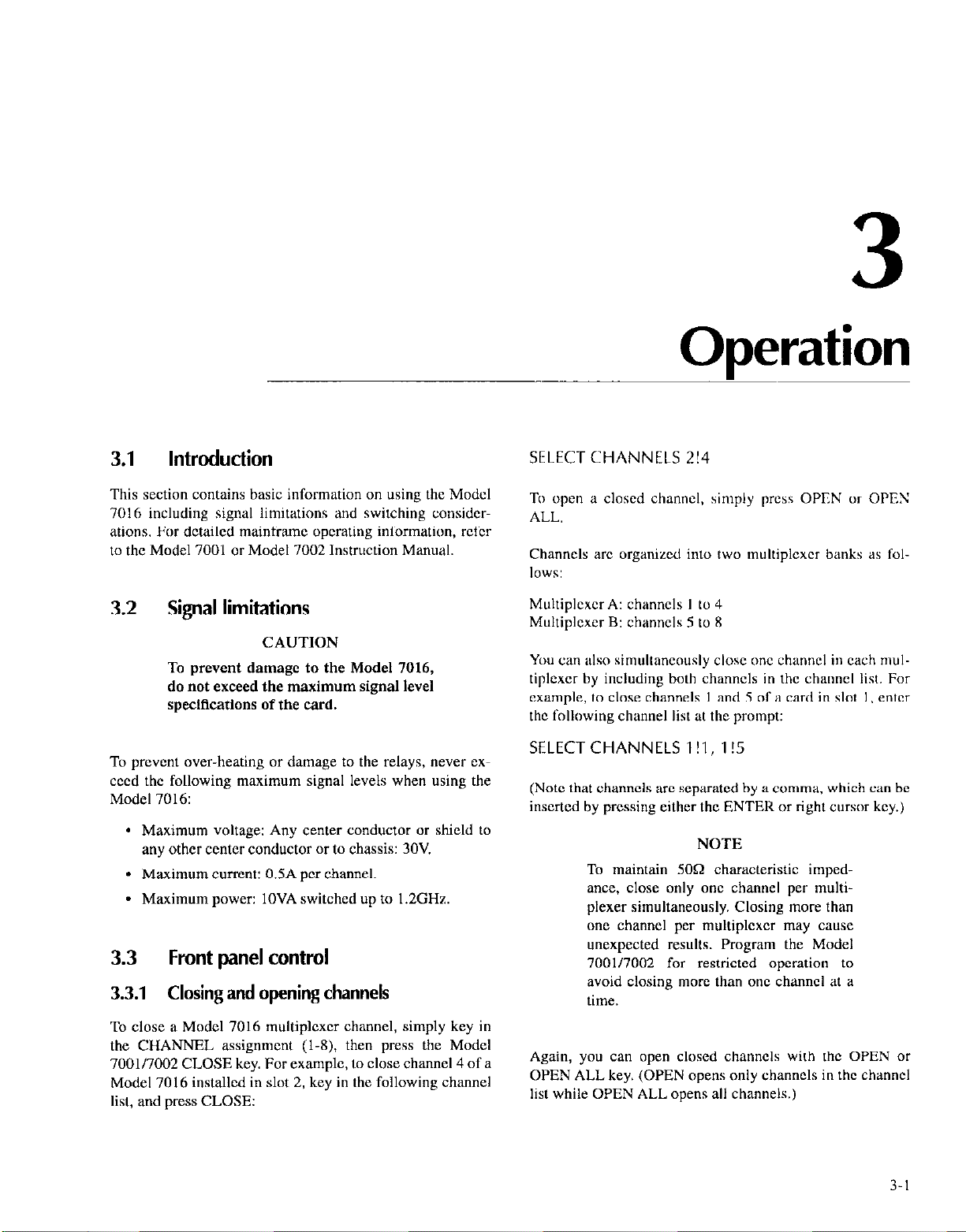
“T” connector multiplexer expansion
4 x 4 matrix connections
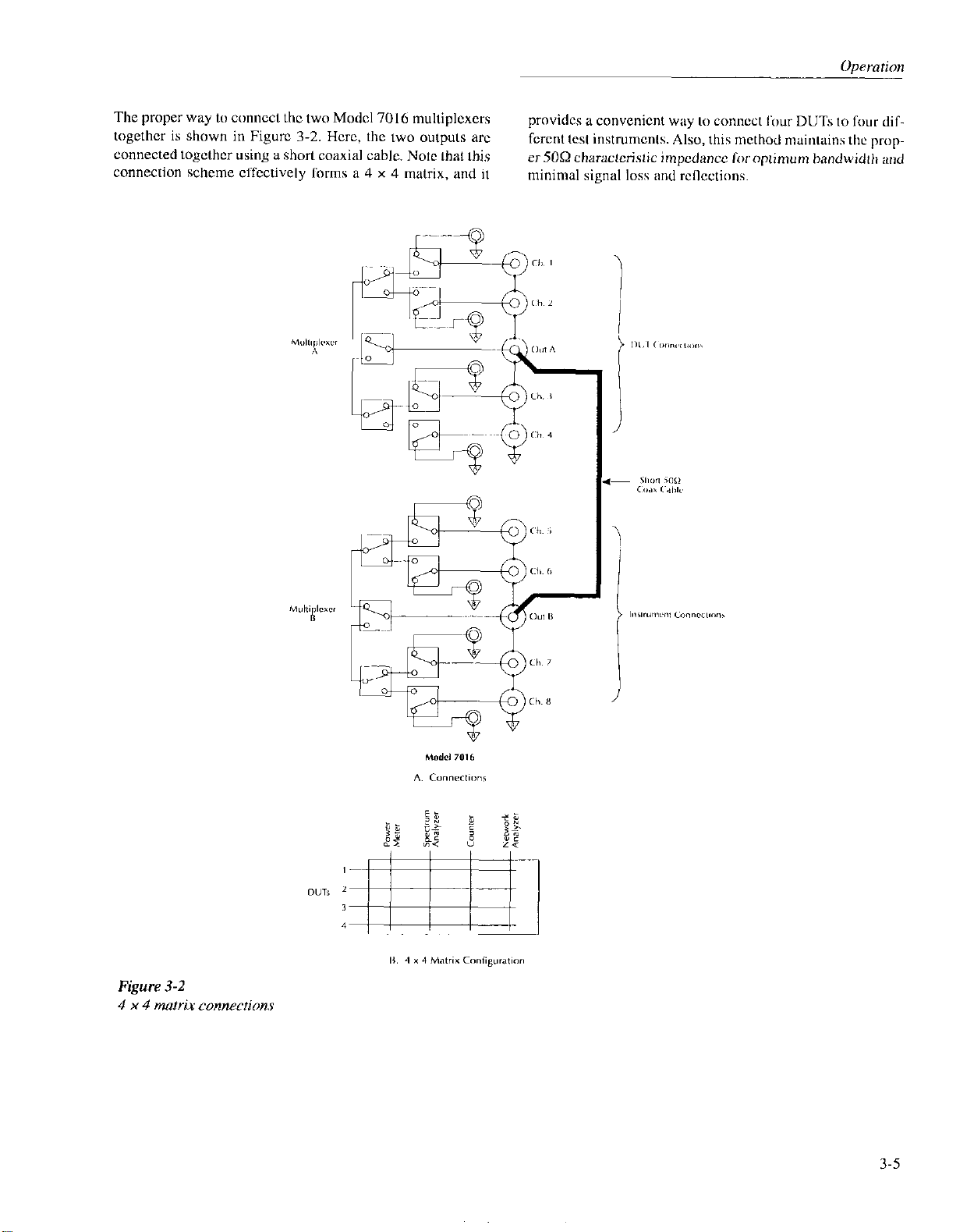
Filter testing
Impedance
...............................................................................................................................................
testing ........................................................................................................................................
..............................................................................................................................
.........................................................................................................
Service Information
Connections for insertion loss tests..
Connections for channel isolation tests
Connections for center-to-shield isolation tests
Connections for multiplexer-to-multiplexer isolation tests
diagram ..............................................................................................................................................
Block
............................................................................................................
........................................................................................................
...........................................................................................
..........................................................................
2-2
2-Z
2-3
2-J
.2-S
.2-h
.3-J
3~5
..l-6
3-7
4-3
4.4
4-S
4.6
4-7
iii

List
of Tables
4
Table 4. I
Table 4-2
Table 4-3
Table 4-4
Service Information
Rccommcndcd
lnsenion loss values
Recommended troubleshooting cquipmcnl
Troubleshooting procedure
verification
cquipmcnt ........................................................................................................
.....................................................................................................................................
..........................................................................................................................
J-2
4.2
..................................................................................................
4-X
4-X

General Information
1.1 Introduction
This section contains general information about the Model
7016 5051 GHz Multiplexer Card. The Model 7016 is
equipped with two four-channel multiplcxers and is dcsigned for SO8 operation. Provisions for user-supplied 5051
terminators are provided on the card.
1.2 Features
Key Model 7016 features include:
* Two independent multiplexers each with four channels.
- SO!2 characteristic impedance.
l Provisions for user-supplied SMB terminators to main-
tain nominal 5Os2 characteristic impedance for off
channels.
* 1.3GHz bandwidth.
* Low insertion loss (<3dB @ I .3GHz.).
- Low VSWR assures good high-frequency performance.
1.3 Warranty information
1.4 Manual addenda
Any improvements or changes conccming the card or manual will bc explained i” a” addendum included with the card.
1.5 Safety symbols and terms
The following symbols and tcrnu may be found 011 an instrumcnt or used in this manual.
The A:
fer to the operating instructions located in the instruction
“Xl”U~l.
The WARNING heading used in this numual explains dugcrs that might result in personal illjury or death. Always
read the associated information very carefully bcforc pcrCorming the indicated procedure.
The CAUTION heading used in this manual explains hazards that could damage the multiplexer card. Such damage
may invalidate the warranty.
symbol on equipment indicates that you should re-
Warranty information is located on the inside front cover of
this instruction manual. Should your Model 7016 require
warranty service, contact the Keithley representative OT authorized repair facility in your area for further information.
When returning the card for repair, be sure to fill o”t and include the service form at the back of this manual in order to
provide the repair facility with the necessary information.
1.6 Specifications
Model 7016 specilications are located at the front of this
manual.

1.7 Unpacking and inspection
1.9 Repacking for shipment
1.7.1 Inspection for damage
The Model 7016 is packaged in are-sealable, anti-static bag
to protect it from damage due to static discharge and from
contamination that could degrade its performance. Before removing the card from the bag, observe the precautions on
handling discussed below.
1.7.2 Handling precautions
* Always grasp the card by the side cdgcs and covci-s. Do
not touch the board surfaces or components.
- After removing the card from its anti-static bag, inspecl
it for any obvious signs of physical damage. Repon any
such damage to the shipping agent immediately.
- When the card is not installed in a switching mainfranc, keep the card in its anti-static bag, and store it in
the original packing carton.
1.7.3 Shipment contents
The following items are included with every Model 7016 order:
* Model 7016 5OQ GHz Multiplexer Card
. Model 7016 Instruction Manual
- Additional accessories as ordered
Should it become necessary to return the Model 7016 for repair, carefully pack the unit in its original packing carton or
the cquivalcnt, and include the following information:
- Advise as to the warranty stztus of the card.
* Write ATTENTION REPAIR DEPARTMENT on the
shipping label.
* Fill out and include the service form located at the back
of this manual.
1 .I 0 Recommended accessories
Recommended cables and lcrminating resistors are covered
below. Thcsc itcms arc not stocked by Keithley and must be
obtained from other sources.
1 .I 0.1 Connecting cables
The following cable type is recommended for making input/
output connections to the Model 7016: RG223N.
Other 50R cables may be used, bul keep in mind key pawneters as such as maximum outside diameter, attenuation over
the desired frequency range, flexibility, and shield type. See
paragraph 3.5 in Section 3 for mom information on cable paramctcrs.
1.8 Instruction manual
If an additional Model 7016 Instruction Manual is required,
order the manual package, Keithlcy pact number 7016.901.
00. The manual package includes an instruction manual and
any pertinent addenda.
l-2
1 .I 0.2 Terminating resistors
The following terminating resistor is recommended for use
with the Model 7016:
Type: Female SMB terminator
Manufacturer: Sealecmo Corp.
Part number: 61-001-0101
Nominal resistance: 51 Q2, +I %.
Power dissipation: 2W

2
Connections
2.1
This section includes information on making connections to
the Model 7016 and installing the card in the Model 7001/
7002 Switch System.
2.2
To maintain high-impedance isolation between channels,
care should be taken when handling the card to avoid contamination from such foreign materials as body oils. Such
contamination can reduce isolation rcsistancc. To avoid pos-
sible. contamination, always grasp the card by the side edges
or covers. Do not touch board surfaces, components, or connector insulators.
Dirt build-up over a period of time is another possible source
of contamination. To avoid this problem. operate the card in
a clean environment. If the cad becomes contaminated, it
should be thoroughly cleaned as explained in paragraph 4.2.
Introduction
WARNING
The procedures in this section are intended only for qualified service personnel. Do not perform these procedures
unless you are qualified to do so. Failure
to recognize and observe normal safety
precautions could result in personal in-
jury or death.
Handling precautions
and Installation
2.3 Connections
This paragraph provides the information ncccssary 10 cow
necl your cxlernal test circuitry to the Model 7016.
2.3.1 Simplified schematic
Figure 2-l shows a simpliticd schematic diagram or the
Model 7016. The card is arranged into two separate multiplexers. each with four channels.
2.3.2
Figure 2-2 shows the general conliguration of the Model
7016. Connectors include:
IN l-8 (channels l-8): Each input is equipped with an SMA
coaxial connector. The center conductor is the signal path,
while the outer shell connected to signal common.
OUT A and OUT B: Each multiplexer is equipped with an
SMA coaxial conocctor. The center conductor is the signal
path, and the shell is conncctcd to signal common.
Termination jacks: Each channel has an SMB coaxial tcr-
minator jack. User-supplied 5OG terminators can bc conncctcd to these jacks when a 5OQ nominal input impedance
must bc maintained for off channels.
Card configuration
2-l

Figure 2-l
Model 7016 simplified schematic
Figure 2-2
Model 7016
configuration
2-2

Connections and lnstallatior~
2.3.3 Input/output connecting cables
All connections to the scanner card input and output jacks
should be made using SW coaxial cable equipped with
SMA connectors. The rccommcndcd cable type is RG223lU.
WARNING
Make sure that
energy sources are discharged before
connecting or disconnecting cables.
500 cables most bc used to assure good
high-frcqucncy performance. RG22YU
should be used for best performence. See
power
is off and external
NOTE
paragraph 3.S in Section 3 for more inSormation.
2.3.4
Figure 2-3 shows a typical connecting scbemc Sor tbc Model
7016. In this arrangcmcnt. so~~rccs WC connccwd to lbc illputs while the mcesuring insrument is connected IU the ow
puts.
Typical connecting scheme
CAUTION
Maximum voltage from any terminal
(center conductor or shield) to any other
terminal or chassis is 30V RMS. Exceed-
ing this value may result in card dam-
age.
Figure 2-3
Typical connection scheme
2-3

2.3.5 Input termination
2.4
Card installation and removal
User-supplied SOQ female SMB terminators may bc in-
stalled lor applications requiring propcr 5OQ termination 01
off channels. Figure 2-4 shows typical installation of a 5OQ
terminator. Set paragraph I. IO in Section I for recommendcd terminators. Switching considerations in Section 1 discusses terminator aspects in more detail.
NOTE
Be sure to observe the maximum power
handling capability of installed tcrmina-
tars. The terminators recommcndcd in
Section 1 are limited to 2W even through
the Model 7016 can switch up to IOW.
This paragraph explains how to install and remove the Modcl 7016 card assembly from the Model 700117002 main-
cramc.
WARNING
Installation or removal of the Model
7016 should be performed only by qualified service personnel. Failure to recognize and observe standard safety
precautions could result in personal in-
jury or death.
NOTE
To prevent performance degradation
caused by contamination, handle the card
only by the edges and co~crs.
Figure 2-4 Figure 2-4
2-4

2.4.1 Card installation
2.4.2 Card removal
Perform the following steps, and refer to I:igure 2-s or Figure 2-6 to inslall the card assembly in the Model 7OOl/7002
mainframe.
WAKNINC
Turn off power to all instrumentation
(including the Model 7001/7002), and
disconnect all line cords. Make sure all
power is removed and any stored energy
in external circuitry is discharged.
I. Open the cjcctor arms at the back cdgc of the card.
2. Slide the card cdgcs into the guide rails inside the mainframe.
3. Carefully push the card all the way forward until the
ejector arms engage the mounting cups.
4. Push in on the card edge and ejector arms until the card
is properly seated.
5. Make sure the ejector arms are properly latched.
Follow the steps below to ~CIIWYC the multiplcxor cud Sro,,,
the mainframe:
WARNING
Turn off power to all instrumentation
(including the Model 7001/7002), and
disconnect all line cords. Make sure all
power is removed and any stored energy
in external circuitry is discharged.
I. Pull out on the cjcctor arms until the card pulls fret from
the intcrnal connccto~.
2. Carefully slide the card out or the switching mainirw~e.
2-s

Figure 2-6
Card installation in Model 7002
2-6
3
Operation
3.1
This section contains basic information on using the Model
7016 including signal limitations and switching considcrations. For detailed mainframe operating inlbrmation, refer
to the Model 7001 or Model 7002 Instruction Manual.
Introduction
3.2 Signal limitations
CAUTION
To prevent damage to the Model 7016,
do not exceed the maximum signal level
specifications of the card.
To prevent over-heating or damage to the relays, never ex-
cccd the following maximum signal levels when using the
Model 7016:
* Maximum voltage: Any center conductor or shield to
any other center conductor or to chassis: 3OV.
* Maximum current: 0.5A per channel.
- Maximum power: IOVA switched up to l.ZGHz.
3.3
3.3.1
Front panel control
Closing and opening channels
SELECT CHANNELS 2!4
To open a closed channel. simply press OPEN or OPES
ALL.
Channels arc organized into two multiplcxcr banks as folIOWS:
Multiplcxcr A: channels I to 4
Multiplexer B: channels 5 to 8
You can also simultaneously close one chenncl in each multiplexcr by including both channels in the channel list. For
example, to close channels I and 5 of a card in slot I, enter
the following channel list at the prompt:
SELECTCHANNELS l!l, 1!5
(Note that channels arc separated by a cwnma, which can be
inserted by pressing either the ENTEK or right cursor key.)
NOTE
To maintain 50R characteristic impedance, close only one channel per multiplexer simultaneously. Closing more than
one channel per multiplexer may cause
unexpected results. Program the Model
700117002 for restricted operation to
avoid closing more than one channel at a
time.
To close a Model 7016 multiplcxcr channel, simply key in
the CHANNEL assignment (l-g), then press the Model
7001/7002 CLOSE key. For example, to close channel 4 of a
Model 7016 installed in slot 2. key in the following channel
list, and press CLOSE:
Again, you can open closed channels with the OPEN or
OPEN ALL key. (OPEN opens only channels in the channel
list while OPEN ALL opens all channels.)
3-l

Oprration
3.3.2 Scanning channels
To scan through channels, first configure a scan list, then program the Model 700 I I7002 to perform a scan sequence. You
can creak a scan list in the same manner as you would a
channel list. First, however, press the SCAN LIST key to select the “SCAN CHANNEL” mode, then enter the dcsircd
channels to be included in the scan list. For example, the iollowing list scans channels I, 3. and 5 through 8 of a Model
7016 installed in slot 2:
SCAN CHANNELS 2!1, 2!3, 2!5-2!8
Note that channels are scanned in the order they appear in the
scan list.
To perform a manual scan, first select the RESET default
conditions in the SAVESETUP men” oi the main MENU.
Press STEP to take the mainframe o”t of the idle state, the”
manually scan through channels by pressing the STEP key.
For infornxition on more complex scan sequences, refer to
the Model 7001 or 7002 Instruction Manual.
3.4 IEEE-488 bus control
3.4.1 Closing and opening channels
Use the following SCPI commands to close and open channels:
:CLOS <list>
:OPEN 4isu I ALL
For example, the following command will close channels 2
and 6 of a Model 7016 installed in slot I:
The *RST command selects the default scan contiguratio”,
while the second colnmand automatically sets the channel
co”“t to the number of channels in the scan list. The
:ROUT:SCAN command programs the scan list, and the
:INIT command takes the mainframe out of the idle state.
For example, send the following commands to scan through
all eight channels of a Model 7016 installed in slot I:
*RST
:TRIG:SEQ:COUN:AUT ON
:ROUT:SCAN (@ I !I :I !8)
:INIT
3.5 Switching considerations
Signals passing through the Model 7016 5O!J GHz Multiplexer Card are subject to various effects that can inlluence
their characteristics. The following paragraphs discuss some
of these effects and ways to minimize them.
3.5.1 Card characteristics
Insertion loss: Insertion loss indicates signal power lost
while passing through the card. This loss occurs in the var.
ous signal path components through the card (connectors,
PC board traces, and relays). The amount of power lost will,
of course, depend on the particular insertion loss specification as well as the applied power. For example, with a” insertion loss of ldB, and a 1OW source signal applied to the card,
about 2W will be dissipated in the card, and approximately
8W will appear at the load. Note that, as with most transmission lines, Model 7016 insertion loss values increase with increasing frequency.
:CLOS (@ 1!2, 1!6)
Conversely, either of the commands below will open previously closed channels 2 and 6:
:OPEN (@ 1!2, 1!6)
:OPEN ALL
3.4.2 Scanning channels
There are a number of commands associated with scanning.
However, you can perform a simple scan “sing only the following four commands:
*RST
:TRIG:SEQ:COlJN:AUT ON
:ROUT:SCAN <list>
:INIT
3-2
Capacitance: Model 7016 capacitance values arc sufficient-
ly small to be of little concern in most applications. In some
applications (primarily with pulse signals where capacitance
can affect rise limes), capacitance may be a factor. Typical
Model 7016 center-to-shield capacitance is 60pF.
Crosstalk: Crosstalk figures indicate the amount of signal
leakage between channels or switches on the card. With similar power levels applied to the various channels, crosstalk
will be of little consequence. With widely different power
levels, however, crosstalk may produced undesired results.
For example, assume that IOW is applied to channel 1, and
ImW is applied to channel 2. Assuming a -55dB crosstalk
figure, the unwanted signal coupled from channel 1 to than“el2 will be only 15dB below the desired channel 2 signal.

VSWR: The term VSWR (Voltage Standing Wave Ratio) is
ddincd as the ratio of the maximum and minimum voltages
along a transmission path, and it indicates the degree of impcdancc mismatch. In a pericctly match system, the VSWR
is 1, while open and shorted paths have infinite VSWR values. Since VSWR is related to both the return loss and rcllcction coefficient, VSWR figures indicate the dcgrec of signal
loss and rcllcction; the Iowa the VSWR ligure, the less signal atlcnuation that occurs along the transmission path.
Path isolation resistance: The path isolation rcsistancc is
simply the equivalent resistance between two given connecting points on the card and is of importance primarily for DC
and low-frcqucncy AC signals switched by the card. The effects of this characteristic depend on the paxticular isolation
specilication. Center-to-shield isolation resistance, for cxample, may cause loading problems with signals having high
source rcsistancc. Channel-to-channel isolation resistance
may result in leakage currents gcncratcd in one channel
caused by a voltage source connected to another channel.
3.5.2 Cable characteristics
Characteristic impedance (Z,): Characteristic impedance
is the value of cable impcdancc obtained by an RF meesurement at either end. For cxamplc. B cable with a 5OQ characteristic impedance is equivalent to a 5051 resistor with
sufficient length to connect two components. (The characteristic impedance of a cable depends on the relative diameters
of the inner and outer conductors, as well as on the dielectric
constant of the insulating material.) Since the Model 7016 is
designed to work with 50R cables, you must use 5On cables
to assure proper impcdancc matching. (RG223N cable is
recommended.) Mismatching anywhere along the transmission path will increase VSWR and signal reflections, decrease return loss, and consequently result in signal
attenuation.
power transfer. For cxamplc, if a 50R cable is terminated
with 1008, the reflection coefficient is 0.33, the VSWR increases to 2, and the return loss is rcduccd to less then IOdR.
Proper termination of off channels may also bc important in
many casts. For cxamplc. a 75MHz source signal will xc a
Im open cable as an RF short, B situation that could damage
some equipment. To alleviate such problems. the Model
7016 has provisions for on-card instidlation ol’5OQ SMR tcrminators. (See paragraph 2.3.5 in Section 2 for details oo itIstalling terminators.) Bc sure to observe tbe power-tundling
capabilities of such terminators as most are limited to substantially less power than tbc IOW capability of the :Modcl
7016.
Distributed capacitance: The distributed capacitencc of tbc
cable may be a factor. but generally only for pulse type signals where rise times are a consideration. The recommended
RG223N cable. for cxamplc. bas a nominal distributed capacitance of30.8pFlli
Cable connectors: Cable connectors UC an obvious ncccssity to conveniently make signal connections to various points
in a switching system. While cooncctor designs arc optimized for best pcrformence, some small impcdancc Miss
match at connecting points is virtually inevitable. For that
nxson, it is considered good practice to minimize the nun
ber of connectors used in a transmission path, cspccially at
higher frequencies.
3.6 Applications
The Model 7016 is designed primarily lor RF switching applications at frequencies up to I .3GHz. The following par+
graphs discuss typical RF applications for tbc Model 7016.
including multiplexer expansion. liltcr testing. and d&cc
impcdancc testing.
Cable
attenuation:
tion loss of the card itself in that it delincs the dcgrec of attcnuation of the signal as it passes through the cable. Cable
attenuation factors are generally given in dB per 100 ft. and
increase with rising frequency. The recommended RG223N
cable has attenuation factors of 8.8dB/lOO ft. @ 400MHz
and 16.5dB/lOO ft. @ IGHz. Thus, with a IOW. IGHz signal
applied to IO ft. of RG223N, 3.16W will be dissipated in the
cable, and 6.84W will be passed on to the card or load.
Cable termination: Proper cable termination is imperative
to ensure maximum signal transfer and to minimize VSWR
and signal rellcctions. In the case of Model 7016 operation,
both source and load impedances should he as close to SOR
as possible to assure optimum matching and thus maximum
Cable attenuation is analogous to inser-
3.6.1 Multiplexer expansion
The simplest way to connect the two Model 7016 multiplcxers together for expansion is to USC the classic “T” conliguralion shown in Figure 3. I. Note that this conliguration results
in a I -of-K multiplexer. Although this conliguration is useful
in many applications. the ideal 5OQ characteristic impedance
will not be maintained. Consequently, VSWR will increase.
affecting card insertion loss, particularly at higher frcqucnties. Also, considerable transmission path rellcctions will
occur, an important consideration when switching pulse sigllals.
3-3
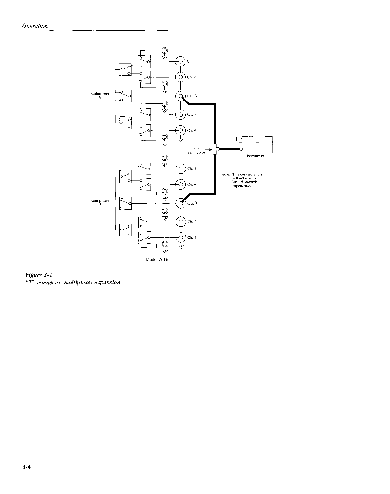
Figure 3-l
“T” connecf*r multiplexer expansion
3-4
The proper way to connect the two Model 7016 multiplcxers
together is shown in Figurc 3-2. Hcrc, the two outputs arc
connected togclhcr using a short coaxial cable. Note that this
connection scheme cSfcctively lorms a 4 x 4 matrix, and it
provides a convenient way to connect Sour DUTs to fwr diffcrenl test instruments. Also, this method maintains the proper 509 charactetistic impcdancc liroptimum bandwidth and
minimal signal loss and rcllections.
3-5
3.6.2 Filter testing
Filter frequency rcsponsc and phase characteristics are key
circuit parameters that often require testing. The Model 7016
may be used in conjunction with a network analyzer to test
multiple filters on an automated basis.
Figure 3-3 shows a typical circuil configuration for testing
four filters. Note that the network analyzer input is connected
to the output of one Model 7016 multiplexers. One tcrminal
of each DUT is connected to a corresponding Model 7016
channel, while the remaining DUT terminals ax connected
in common to the network analyzer output port.
The basic configuration shown in Figure 3-3 may also be
used for a variety ofolhcr tests. For example, the same gencral scheme may be used to test amplifier S-parameters.
3.6.3 Impedance testing
Figure 3.4 shows the general circuit conliguration for device
impedance testing using the Model 7016 along with an impedancc or LCZ meter, such as a Kcithley Model 3321,
3322, or 3330. Since /I-wire connections are required for
such measurements, two Model 7016 cards are necessary for
this application. Each multiplexer switchcs one of the four
required signal paths to the DUTs.
Since the characteristics of the Model 7016 may affect mea-
sured DUT impedance, steps should be taken to null out the
residual affects of stray capacitance and inductance. Most
LCZ meters have provisions for both open and short zeroing
procedures to minimize these effects. For optimum accuracy,
the zeroing procedure should be carried out independently
for each channel.
Figure 3-3
Filter testing
3-6
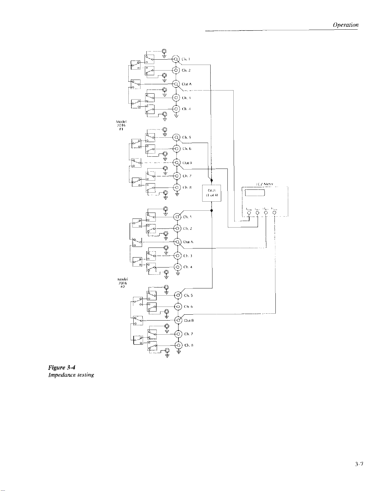
Figure 3-4
Impedance testing
3-7

Service Information
4.1
This section contains information necessary to service the
Model 7016 and includes information on handling and clcaning, performance verilication, as well as principles of opcration and troubleshooting.
Introduction
WARNING
The information in this section is intended only for qualified service personnel. Some of the procedures may expose
you to hazardous voltages that could result in personal injury or death. Do not
perform these procedures unless you are
qualified to do so.
4.2 Handling and cleaning precautions
Because of the high-impedance areas on the Model 7016,
care should be taken when handling or servicing the card to
prevent possible contamination. The following precautions
should be observed when servicing the card.
* Do not touch areas adjacent to clccric;d cootacts.
- When servicing the card, wear clean cotton glows.
- Do not store or operate the card in an cnvironmcnt
whcrc dust could settlc on the circuit board.
* Use dry nitrogen gas to clean dust off the board if ncc-
essuy.
4.2.2 Soldering considerations
Should it become necessary to USC solder on the circuit
board, observe the following precautions:
- Use an OA-based (organic activated) flux. and take care
not to spread the flux to other areas of the circuit board.
* Remove the flux Srom the work ilrcas when the repair
has been completed. Use pure water along with clean
cotton swabs or a clean soft brush to remove the Ilux.
* Once the flux has been removed, swab only the repaired
arca with methanol. then blow dry the hoard with dry
nitrogen gas.
* After cleaning, allow the card to dry in a 50°C low-hu-
midity environment for several hours before use.
4.2.1 Handling precautions
Observe the following precautions when handling the multiplexer card:
- Handle the card only by the edges and shields.
* Do not touch connector insulators.
. Do not touch any board surfaces or components not as-
sociated with the repair.
4.3
The following paragraphs provide performance vcrilication
procedures for the Model 7016. These tests include insertion
loss and isolation tests.
Performance verification
4-l

4.3.1 Environmental conditions
All performance verification measurements should bc made
at an ambient temperature of 18°C t” 28°C and ~70% rclativc humidity.
4.3.2 Recommended veriiication equipment
Table 4. I summarizes the test equipment recommended for
performance verification. Alternate equipment may bc used
as long as the corresponding specifications arc at least as
good as those listed.
4.3.3 Insertion loss tests
Insertion loss tcsls are perf”rmed by applying a IOMHz-
I.3GHz signal from a network analyzer to the Model 7016
channel inputs and then measuring the amount of attenuation
as the signal passes through the card.
Proceed as follows:
I. Set the network analyzer t” sweep the IOOMHz to
I .3GHr frequency range.
2. Normalize the analyzer reference channel to OdB on the
display.
3. Connect the network analyzer to the Model 7016 as
shown in Figure 4-l. Bc sure to use 5061 cables and sctup for all insertion loss tests.
4. Install the Model 7016 in the Model 7001 or 7002 mainframe.
5. Close channel I on the Model 7016 card.
6. Verify that the insertion loss values arc within the limits
shown in Table 4-2.
7. Open the closed channel.
8. Repeat steps 3 through 7 for channels 2 through 8. For
eech channel:
* Connect the analyzer signal to the input jack of the
channel being tested.
* Bc sure lhc signal output cable is conncctcd to the
correct output jack.
* Close the channel being tested.
- Verify that the insertion loss values at the various frc-
quencics arc within the limits stated in Table 4-2.
Table 4-2
Insertion loss values
4-2
Table 4-1
Recommended verification equipment
Description
Network Analyzer Hewlett-Packard 8754A IOMHz-I .3GHz Insertion loss
Test set
Cable set
Electrometer
Manufacturer and Model
Hewlett-Packard 8753C
Hewlett-Packard 1185 1
Kcithlcy 6517 IOOMB, eO.l51% Isolation
Specifications Test
IGP, +0.226%

Service I&mation
4.3.4 Isolation tests
These tests check the leakage resistance (isolation) bctwcen
various Model 7016 terminals using the ohms function of a
Model 65 17 Electrometer.
CAUTION
The following tests use the Model 6517
voltage source to measure resistance. Do
not apply more than 30V to the Model
7016 to avoid card damage.
Channel isolation tests
Perform the following steps to check channel isolation:
I. Connect the Model 65 17 Electromctcr to the ccntcr con-
ductors of channels I and 2, as shown in Figure 4-2.
2. With the power off, install the Model 7016 card in the
mainframe.
3. Turn on the mainframe and the Model 65 I7 power. and
allow the electrometer to warm up for at least one hour
before making measurements. Make sure the voltage
source is turned off.
4. Select the Model 6517 ohms function. choose the
200MS2 range, and make certain zero check is disabled.
5. Close channel 1 on the Model 7016.
4-3

6. Program the Model 6517 voltage source for 3OV. and
make sure the internal voltage source connection mode
is selected.
7. Turn on the Model 6517 voltage source, and allow the
reading to settle.
8. Verify that the Model 65 I7 resistance reading is
>lOOMQ.
9. Turn off the voltage source, and open channel I.
IO. Repcat the proccdurc for channels 2 through 4, measur-
ing the resistance between the center conductor of each
channel and the center conductors of all other channels
of multiplexer A. For each test:
. Connect the elcctromcter to the center conductors of
the two channels being tested.
- Close only one of the channels being tested.
I I Repeat the entire procedure to test channel isolation be-
tween all multiplexer B channels (channels 5-X).
Figure 4-2
Connections for
4-4
L
channel isolation felts

Center-to-shield isolation
Perform the following steps to check center-to-shield isola-
tion:
I. Connect the Model 65 I7 Electrometer to the ccntcr con-
ductor and shield of channel I, as shown in Figure 4-3.
2. With the power off, install the Model 7016 card in the
mainlrame.
3. Turn on the mainframe and the Model 65 17 power, and
allow the electrometer to warm ul, for at least one hour
before making measurements. Make sure the voltage
source is turned off.
4. Select the Model 6517 ohms function, choose the 2GQ
range, and m&c certain zero check is disabled.
5. Close channel I on the Model 7016.
6. Pro&yam tbc Model 65 17 voltage source for 3OV. and
make sure the internal voltage source connection mode
is selected.
7. Turn on the Model 6517 voltage source. and allow the
reading to scttlc.
8. Verify that the Model 6517 rcsistancc reading is >lGQ
0. Turn off the voltage source. and open ch1umc1 I.
IO. Rcpcat the proccdurc for chimncls 2 through 8. mcirsur-
ing the rcsistancc bctwccn the ccntcr conductor and
shield ofcach chenncl. For each test:
. Connect the electromctcr to the center conductor and
shield of the chenncl being tested.
- Close only the chenncl being tcstcd
Figure 4-3
Connections
for
center-to-shield is&rim fesfs
4-s

Multiplexer-to-multiplexer isolation
Perform the following steps to cheek multiplcxcr-to-multi-
plcxcr isolation:
I. Connect the Model 65 17 Electrometer to the center con-
ductors of channels I and 5, as shown in Figure 4-4.
2. With the power off, install the Model 7016 card in the
mainirame.
3. Turn on the mainframe and the Model 65 17 power, and
allow the electrometer to warm up for at least one hour
before making measurements. Make sure the voltage
source is turned off.
4. Select the Model 6517 ohms function, choose the 2GQ
range, and make certain zero check is disabled.
5. Close channels I and 5 on the Model 7016.
6. Program the Model 6517 voltage source for 3OV, and
make sure the internal voltage source connection mode
is sclccted.
7. Torn on the Model 65 I7 voltage source, and allow the
reading to settle.
8. Verify that the Model 65 I7 resistance reading is >lGQ.
9. Turn off the voltage source, and open channels I and 5.
Figure 4-4
4-6

4.3.5 Special handling of static-sensitive devices
CMOS and other high-impedencc devices are subject to possible static discharge damage because of the high-impedance
lcvcls involved. When handling such dcviccs, obscrvc the
precautions listed below.
4. Any printed circuit hoard into which the dcvicc is tu bc
inscrtcd must lirst bc grounded to the bench or table.
5. llse only anti-static type dc-soldcting tools and groundcd-tip soldering irons.
NOTE
To prcvcnt damage, assume that all pans
are static-sensitive.
I. Such dcviccs should bc transponcd and handled only in
containers specially designed to prcvcnt or dissipate
static build-up. Typically, these devices will bc received
in anti-static containers made of plastic or foam. Keep
thcsc parts in their original containers until ready for installation or use.
2. Remove the devices from their protective containers
only at a properly grounded workstation. Also, ground
yourself with an appropriate wrist strap while working
with these dcviccs.
3. Handle the dcviccs only by the body; do not touch the
pins or terminals.
4.4 Principles
The following paragraphs discuss the basic Model 7016 operating principles that can be used as an aid in m~ublcshooing the card. The schematic diagram of the card is Iocatcd at
the end of Section 5.
4.4.1
Figure 4-S shows a simplilied block diagram of the Model
7016. Key sections include the relay date control circuits, the
relay driver IC, the relays, and the card conliguralion mcmory. These various elcmcnts arc discussed in the following
paragraphs.
Block diagram
of
operation
Figure 4-5
Block diagram
4-7
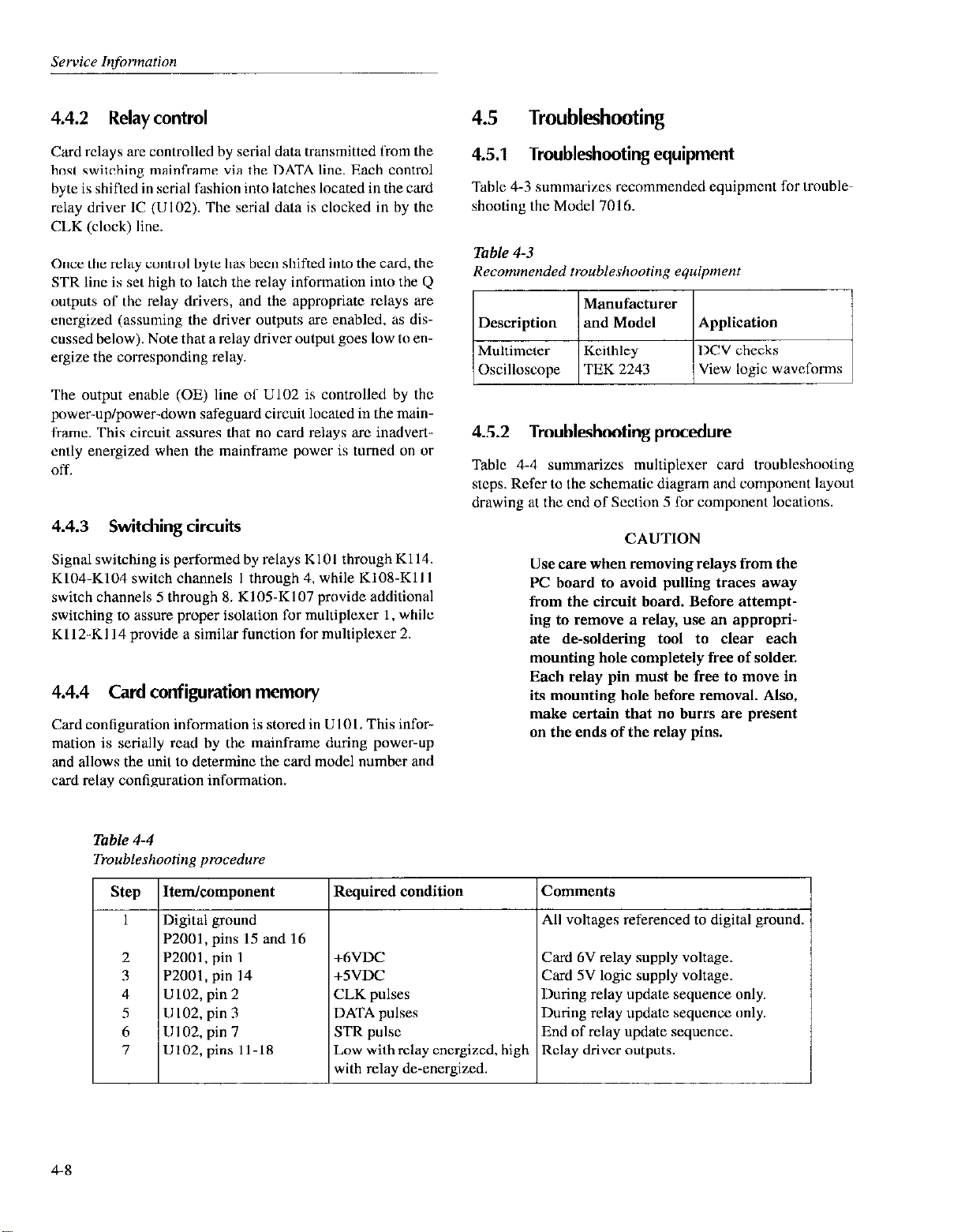
4.4.2 Relay control
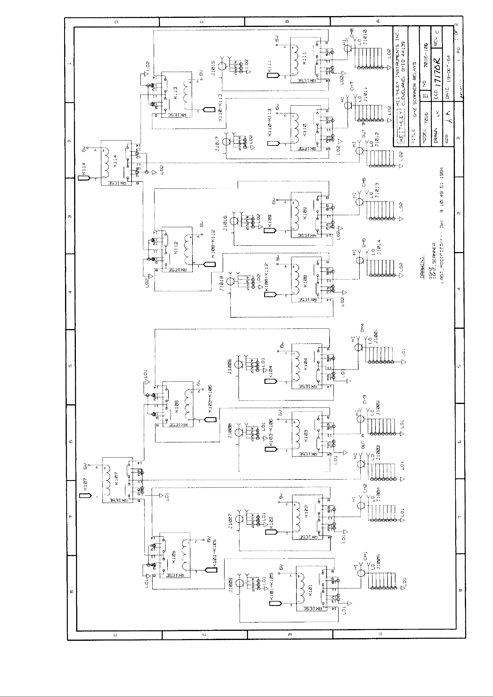
4.5 Troubleshooting
Card relays are controlled by serial data trensmitted from the
host switching mainframe via the DATA lint. Each control
byte is shifted in serial fashion into latches located in the card
relay driver IC (UIOZ). The serial data is clocked in by the
CLK (clock) line.
Once the relay control byte has been shifted into the card, the
STR lint is set high to latch the relay information into the Q
outputs of the relay drivers, and the appropriate relays are
cncrgixd (assuming the driver outputs are enabled, as discussed below). Note that a relay driver output goes low to energize the corresponding relay.
The output enable (OE) line “1 U102 is controlled by the
power-up/power-down safeguard circuit located in the mainframe. This circuit assures that no card relays arc inadvertcntly energized when the mainframe power is turned on or
off.
4.4.3 Switching circuits
Signal switching is performed by relays KIOI through K114.
Kl04-K104 switch channels I through 4, while Kl08-Kll I
switch channels 5 through 8. K105-K107 provide additional
switching to assure proper isolation for multiplexer 1, while
Kl l2-Kl I4 provide a similar function for multiplexer 2.
4.4.4 Card configuration memory
Card configuration information is stored in UIOI. This information is serially read by the mainframe during power-up
and allows the unit to determine the card model number and
card relay configuration information.
4.5.1 Troubleshooting equipment
Table 4-3 summarixs recommended equipment for troubleshooting the Model 7016.
4.5.2 Troubleshooting procedure
Table 4-4 summarizes multiplexer card troubleshooting
sups. Refer to the schematic diagram and component layout
drawing at the end of Section 5 for component locations.
CAUTION
Use care when removing relays from the
PC board to avoid pulling traces away
from the circuit board. Before attempt-
ing to remove a relay, use an appropriate de-soldering tool to clear each
mounting hole completely free of solder.
Each relay pin must be free to move in
its mounting hole before removal. Also,
make certain that no burrs are present
on the ends of the relay pins.
Table 4-4
Troubleshooting procedure
step
Item/component 1 Required condition
I
Digital ground
P2001, pins I5 and 16
2
P2001, pin I
3
P2001, pin I4
4
Ul02,pin2
5
UlO2, pin 3
6
U102, pin I
7
U102, pins II-18
r
4-8
+6VDC
+SVDC
CLK pulses
DATA pulses
STR pulse
Low with relay energized, high
with relay de-energized.
1 Comments
I
All voltages referenced to digital ground.
Card 6V relay supply voltage.
Card 5V logic supply voltage.
During relay update sequence only.
During relay update sequence only.
End of relay update sequence.
Relay driver outputs.

5
Replaceable Parts
5.1 Introduction
This section contains replaccmcnt parts information, schcmatic diagrams, and component layout drawings for the
Model 7016.
5.2 Parts list
The parts list for the multiplexer card is included in tables integrated with the schematic diagram and component layout
drawing. Parts UC listed alphabetically in order of circuit
designation.
5.3 Ordering information
To place an order, or to obtain information conccming rcplacement parts, contact your Keithlcy representative or the
Sactory (see the inside front cover for addresses). When ordering parts, be sure to include the following information:
. Card model numbcr (7016)
. Card serial numbcr
* Part description
* Circuit description, if applicable
* Keithley pat number
5.4 Factory service
II’ the card is to bc rctumcd to Kcithley Instruments for rcpair, perform the following:
. Call the Repair Department at I-800-552-I I I5 for a Rc-
turn Mstcrial Authorization (RMA) numhel-.
- Complete the scrvicc form at the back of this manual
and include it with the card.
- Carefully pack the card in the miginel packing camm
- Write ATTENTION REPAIR DEFT and the RMA
number on the shipping label.
It is not necessary to return the switching
mainframe with the card.
5.5
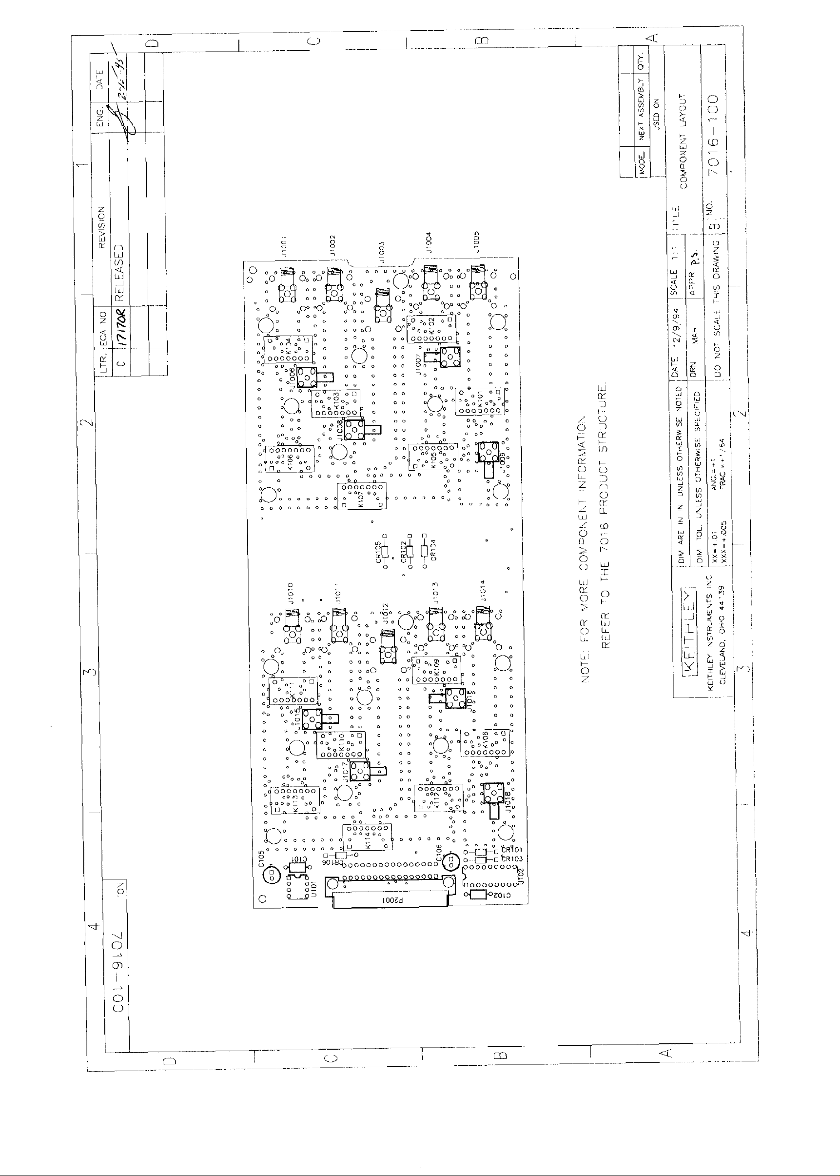
Component layout and schematic diagram
A component layout drawing and schematic diagram me includcd on the following pages integrated with the parts list.
5-l
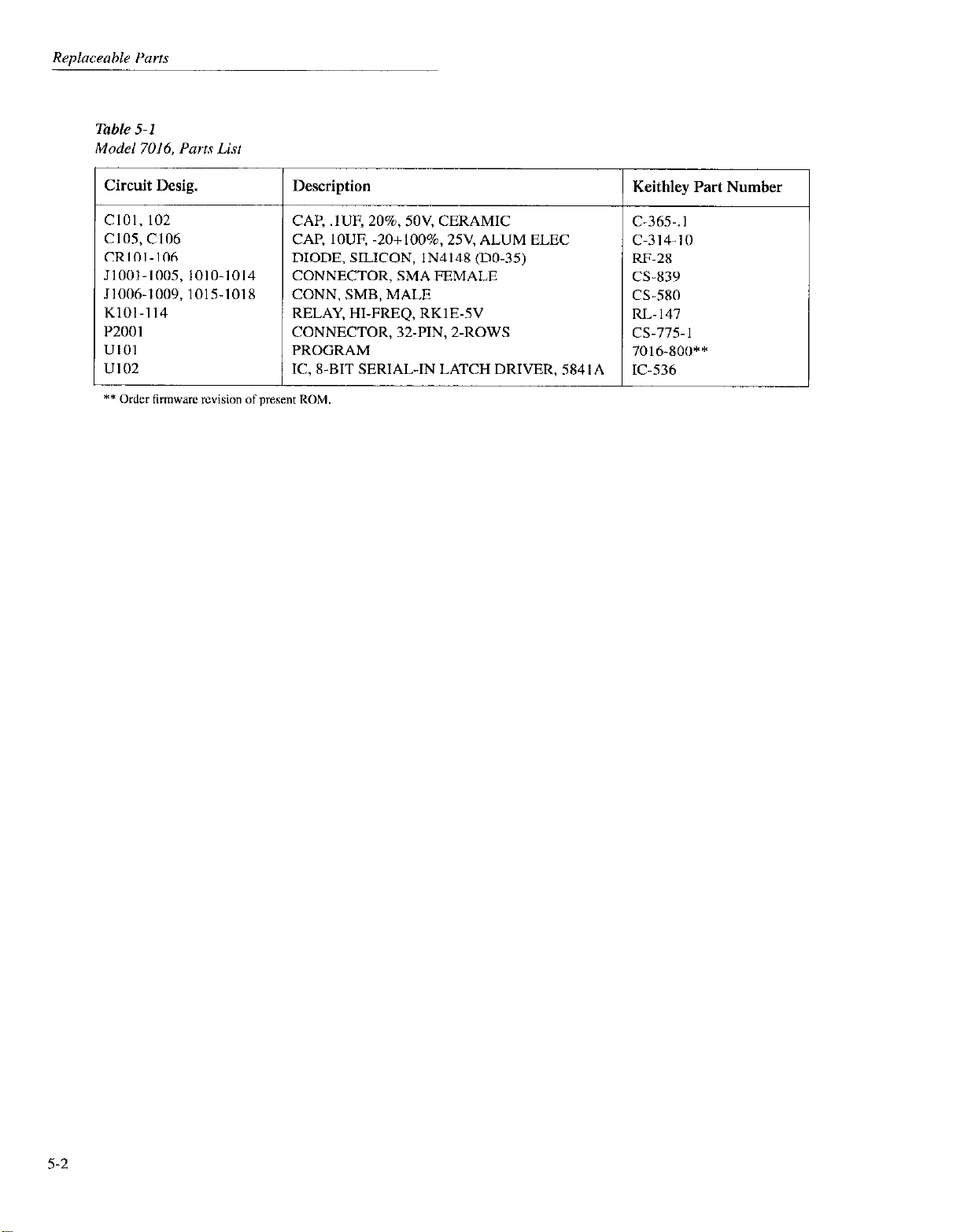
Table 5-l
Model 7016. Parts List
Circuit Desig. Description
CIOI, 102 CAP, .lUF, 20%. 5OV. CERAMIC
C105, Cl06 CAP, IOUF, -2O+lOO%, 25V. ALUM ELEC
CRlOl-106
DIODE, SILICON, IN414R (DO-35)
JlOOl-1005,1010-1014 CONNECTOR, SMA FEMALE
J1006-1009,1015-1018 CONN, SMB, MALE
KIOI-II4 RELAY, HI-FREQ, RKlE-5V
PZOOI CONNECTOR, 32.PIN, 2.ROWS
UIOI PROGRAM
UlO2 IC, X-BIT SERIAL-IN LATCH DRIVER, 584lA
** Order firmware mvision of~resent ROM.
Keithley Part Number
C-365-.1
c-314-10
RF-28
cs-839
CS-5x0
RI>- 147
cs-775-l
7016.X00**
IC-536
5-2
i
:
0
0
I
r-
”
I
.-.-. -~~
3
m
I
Is


in
-
n
?
P
r
;m
r ---
a
A
Applications 3-3
B
Block diagram 4-l
C
Cautiun 1-I
Connecting cab& l-2
Connections and installation 2. I
Connections 2-l
Card configuration 2-l
Card installation and removal 2-4
Cad installation 2-5
Card removal 2-5
Closing and opening channels 3-l,3-2
Card characteristics 3-2
Capacitance 3-2
Crosstalk 3-2
Cable characteristics 3-3
Cable attenuation 3-3
Cable termination 3-3
Cable connectors 3-3
Channel isolation tests 4-3
Characteristic impedance 3-3
Center-to-shield isolation 4-5
Card configuration memory 4-8
Component layout and schematic diagram
5-l
D
Distributed capacitance 3-3
E
Environmental conditions 4-2
G
General Information I -I
H
Handling precautions I-2. 2-l
Handling and cleaning precautions 4-l
Handling precautions 4~ I
I
Inspection for damage l-2
lnsmction manual 1-2
lnpuVoutput connecting cables 2-3
Input termination 2-4
IEEE-488 bun control 3-2
Insertion loss 3-2
Impedance testing 3-6
insertion loss tests 4-2
Isolation tests 4-3
M
Manual addenda 1-I
Multiplexer expansion 3-3
Multiplexer-tu-multiplexer isolation 4-6
0
Operation 3-l
Ordering information 5-l
Index
T
Terminating
Typic;d connecting scheme 2-3
Troubleshooting equipment 4-X
Traublcshooting procedure 4-X
U
Unpacking and inspection 1~2
V
VSWR 3-3
rcsisLon I-2
P
Path isolation resistance 3-3
Performance verification 4-l
Principles of operation 4-7
Parts list 5-I
i-l

Service Form
Model No.
~ Serial No.
Date
Name and Telephone No.
Company
List all control settings, describe problem and check boxes that apply to problem.
U Intermittent
Cl IEEE failure
0 Front panel operational
Display or output (check one)
3 Drifts
0 Unstable
u Chwload
a Calibration only
a Data required
(attach any additional sheets as necessary)
Show a block diagram of your measurement system including all instruments connected (whether power is turned on or not).
Also, describe signal source.
3 Analog output follows display
3 Obvious problem on power-up
0 All ranges or functions are bad
0 Unable to zero
a Will not read applied input
0 Certificate of calibration required
Lj Particular range or function bad; spcciiy
0 Batteries and fuses arc OK
0 Checked all cables
Where is the measurement being performed? (factory, controlled laboratory, out-of-doors, etc.)
What power line voltage is used?
1.111 L.._ ..-....-..,
Any additional information. (If special modifications have been made by the user, please describe.)
Be sure to include your name and phone nurdcr “” thiS .z.x”iCe form.
-..._..
Ambient tempcraturc?
“F

Test Instrumentation Croup
Keithley Instruments, inc.
28775 Aurora Road
Cleveland, Ohio 44139
Printed in the U.S.A
 Loading...