

Page 1
TBktronix
®
COMMfTTED TO EXCELLENCE
Tektronix, Inc.
P.O. Box 500
Beaverton,
Oregon 97077 Serial Number
PLEASE CHECK FOR CHANGE INFORMATION
AT THE REAR OF THIS MANUAL.
5A14N
FOUR CHANNEL
AMPLIFIER
INSTRUCTION MANUAL
070-1229-00 First Printing OCT 1972
Product Group
52
Revised OCT 1987
Page 2
Copyright © 1971 Tektronix, Inc. All rights reserved. Contents of this
publication may not be reproduced in any form without the written
permission of Tektronix, Inc.
Products of Tektronix, Inc. and its subsidiaries are covered by U.S. and
foreign patents and/or pending patents.
TEKTRONIX, TEK, SCOPE-MOBILE, and ® are registered trade-
marks of Tektronix, Inc. TELEQUIPMENT is a registered trademark of
Tektronix U.K. Limited.
Printed in
U.S.A.
Specification and price change privileges are
reserved.
INSTRUMENT SERIAL NUMBERS
Each instrument has a serial number on a panel insert, tag, or stamped
on the chassis. The first number or letter designates the country of
manufacture. The last five digits of the serial number are assigned
sequentially and are unique to each instrument. Those manufactured in
the United States have six unique digits. The country of manufacture is
identified as follows:
BOOOOOO Tektronix, Inc., Beaverton, Oregon, USA
1000000 Tektrnoix Guemsey, Ltd., Channel Islands
2000000 Tektronix United Kingdom, Ltd., London
3000000 Sony/Tektronix, Japan
7000000 Tektronix Holland, NV, Heerenveen, The Netherlands
Page 3

5A14N Instruction
TABLE OF CONTENTS
Operators Safety Summary ii
Servicing Safety Summary. Jii
Frontispiece iv
SECTION
1—OPERATING
Instrument Description 1-1
Controls and Connectors. 1-1
Basic Operation 1-1
General Information 1-2
Electrical Characteristics 1-4
Repackaging for Shipment 1-4
THE FOLLOWING SERVICING INSTRUCTIONS ARE FOR USE BY QUALIFIED PERSONNEL
ONLY. TO AVOID PERSONAL INJURY, DO NOT PERFORM ANY SERVICING OTHER THAN
THAT CONTAINED IN OPERATING INSTRUCTIONS UNLESS YOU ARE QUALIFIED TO DO SO,
INSTRUCTIONS
Preparation 1-1
C3aln Check (All Channels) 1-2
Applying Signals 1-2
Channel Sequence Logic 1-3
Input Coupling 1-3
Deflection Factor 1-3
Display Modes 1-3
Trigger Source 1-3
Oscllloscxjpe Applications 1-3
Performance Conditions 1-4
Display Modes 1-4
Bandwidth (-3 dB) 1-4
Deflection Factor 1-4
Maximum Safe Input Voltaga 1-4
Channel Isolation 1-4
Input RC 1-4
WARNING
SECTION
SECTION
SECTION 4—DIAGRAMS AND PARTS LISTS
2—THEORY
Introduction 2-1
Plug-In Logic 2-1
Input Coupling 2-1
Input Attenuator 2-1
Amplifier 2-1
Cfiannel Switching 2 2
Probe Sensing 2-2
3—CALIBRATION
Test Equipment Requried 3-1
Procedure 3-1
OF OPERATION
Inti-oduction. 3-1
Instrument Maintenance 3 1
Service Available 3-1
General 3 1
Calibration Equipment Alternatives 3 1
Special Calibration Fixtures. 3-1
Test Instruments 3-1
Accessories 3 1
Preparation 3-3
Initial Control Settings 3-3
1.
Step Attenuator Balance 3-3
2.
Input and Attenuator Compensation .3-3
3. Amplifier Gain and VOLTS/DIV Accuracy 3-3
4.
Amplifier Bandwidth 3-4
REV MAR 1987
Page 4
5A14N Instruction
OPERATORS SAFETY SUMMARY
The general safety information in this part of the summary is for tx)th operating and servicing personnel. Specific warnings and
cautions will be found throughout the manual where they apply, but may not appear
in
this summary.
TERMS
In This Manual
CAUTION statements identify conditions or practices that
could result in damage to the equipment or other property.
WARNING statements identify conditions or practices that
<x)uld result
in
personal injury or
loss
of life.
As Marked On Equipment
CAUTION indicates a personal injury hazard not immediately
accessible as one reacJs the marking, or a hazard to property
including the equipment
DANGER indicates a personal injury hazard immediately
accessible as one reads the marking.
itself.
SYMBOLS
In This Manual
^p Static-Sensitive Devices.
|\ This symtxjl indicates where applic:able cautionary
A
or other information
is
to
be
fourid.
As Marked On Equipment
Use the Proper Power Cord
Use only the power cord and connector specified for your
product. Use only a power
Refer cord and connector changes to qualified personnel.
cord
that is in gcxjd condition.
Grounding the Product
This product is grounded through the grounding conductor
of the mainframe power
the power cord into a properly wired receptacle before
connecting to the product input or output terminals. A
protective-ground connection, by way of the grounding
conductor
in
the power
cord.
To avoid electric shock, plug
cord,
is essential for safe operation.
Danger Arising From Loss of Ground
Upon loss of the protective-ground connection, all
accessible conductive parts (including knobs and controls
that may appear to be insulating), can render an electric
shock.
Do Not Operate In Explosive
Atmospheres
To avoid explosion, do not operate this product in an
atmosphere of explosive gasses unless it has been
specifically certified for
such
operation.
^ DANGER—High voltage.
^Q Protective ground (earth) terminal.
/!\ ATTENTION—refer to manual.
WARNINGS
Power Source
This prcxjuct is intended to operate in a mainframe
connected to a power source that will not apply more than
250 volts rms between the supply conductors or between
either supply conductor and ground. A protective ground
connection, by way of the grounding conductor in the power
cord,
is essential for safe operation.
Do Not Remove Covers or Panels
To avoid personal injury, do not rennove the protective
covers or panels. Do not operate the product without
the
covers
and
panels properiy installed.
Do Not Operate Without Covers
(For TM 500 Plug-Ins Only)
To avoid personal injury, do not operate this product without
covers or panels installed. Do not apply power to the plug-in
via a plug-in extender.
REV MAR 1987
Page 5
5A14N Instruction
SERVICING SAFETY SUMMARY
FOR QUALIFIED SERVICE PERSONNEL ONLY
Refer also to
the preceding
Operators Safety Summary
Use Care When Servicing Do Not Service Alone
With Power On
Do not perform internal servrce or adjustment of this prcxiuct
Dangerous voltages exist at several points in this product. To unless another
avoid personal injury, do not touch exposed connections resuscitation
and
components while power
Disconnect power before removing protective panels,
soldering,
or replacing components.
is
on.
person
is
present,
capable of rendering first aid and
REV MAR 1987
jjj
Page 6
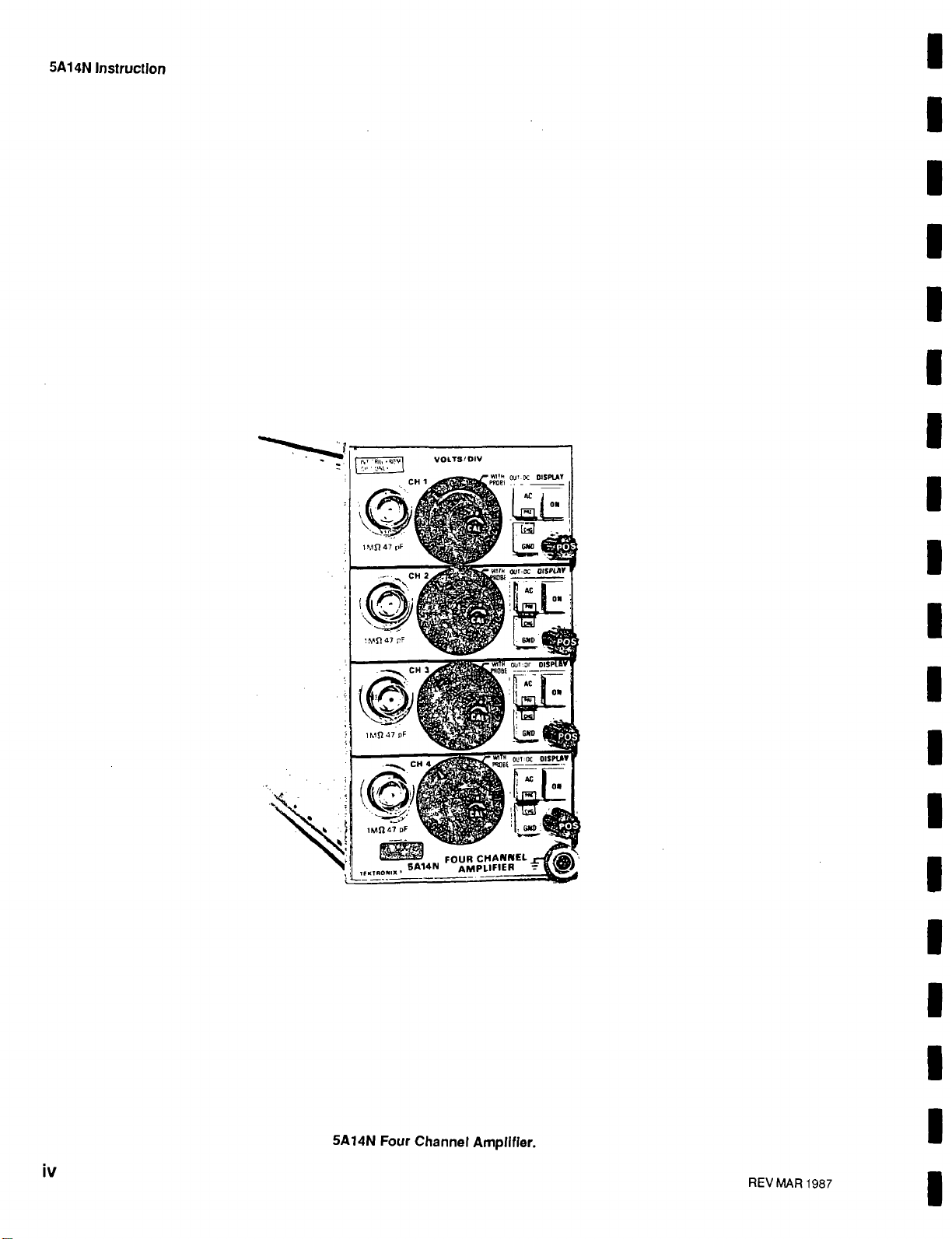
5A14N Instruction
VOLTS'DIV
«"'« OU!.K OlSPUY
IV
„«,.o.,..
FOURCHANIKEL^
8*^*" AMPLIFIER rr
5A14N Four Channel Amplifier.
REV MAR
1987
Page 7
SECTION 1
OPERATING INSTRUCTIONS
5A14N
INSTRUMENT DESCRIPTION
The 5A14N Four Channel Amplifier is a general-purpose
plug-in unit (refer to current Tektronix Products Catalog for
compatible mainframe information). The unit contains
independent amplifier channels with identical characteristics,
and features solid-state circuitry and simplicity of
operation.
provide a direc^t readout of calibrated deflection factor either
with or without a probe. Any channel may be used to
produce a single-channel display. All channels may be displayed alternately, or channel 4 and 3 may be alternated
with 2 and 1 to produce four displayed channels. While
designed primarily for use as a vertical amplifier, the unit can
be operated in conjunction with the horizontal deflection
system of the oscilloscope for X-Y displays.
The VOLTS/DIV knob skirts are lighted to
CONTROLS AND CONNECTORS
This is a brief description of the function or operation of the
controls and connectors. Additional operating information
is given under General Information.
DISPLAY
POSITION
Applies kigic levels to the oscilloscope system to enable
plug-in operation. The switch
functions only when the
in is operated in one of the
vertical plug-in compartments.
Positions display.
plug-
Input Coupling
Pushbuttons
Single or Dual Beam
Selector (Internal)
Input Connectors
AC-DC: Button pushed in
selects capacitive coupling of
input signal; button out
ects direct coupling of input
signal.
GND:
Disconnects the input
signal and provides ground
reference to the ampliiier input stage.
PRECHG: Both AC and GND
buttons pushed in allows
precharging of the coupling
capacitor. Release GND for
measurement.
Slide switch at the rear of the
plug-in that selects the chan-
nel logic sequence. When
the switch is in the forward
position (toward the front
panel), the plug-in is in the
single-beam mode, which
provides a 4-3, 4-3, 2-1, 2-1
logic sequence. In the opposite position, the plug-in is
in the dual-beam mode,
which provides a 4-3-2-1 logic
sequence.
BNC connectors for application of external voltage
nals.
Includes a coded-probe
input ring for activation of 10X
readout.
sel-
sig-
VOLTS/DIV
Variable (CAL) Volts/Div
REV MAR 1987
Volts per major graticule
division.
deflection factors from 1
mV/div to 5 V/div; 12 steps in
a 1-2-5 sequence. Knob skirt
is illuminated to indicate
deflection factor. Readout is
automati-cally scaled when
readout-coded 10X probe is
installed.
Provides uncalibrated,
tinuously variable deflection
factor between calibrated
steps;
V/ div.
Selects calibrated
con-
extends range to 12.5
BASIC OPERATION
Preparation
The 5A14N is calibrated and ready for use when received.
It can be installed in any compartment of any 5000-series
oscilloscx}pe, but it is intended for use primarily in vertical
cxjmpartments (the center and left compartments). For X-Y
operation,
(right) compartment (refer to the 5000 Oscilloscope System Instruction Manual for information on X-Y operation).
the 5A14N may also be installed in the horizontal
1-1
Page 8
Operating Instructions—5A14N
NOTE
// the oscilloscope system receives no DISPLAY ON logic levels from the vertical plug-ins,
ii is designed to display the unit in the left
compartment
To install, align the upper and lower rails ofthe 5A14N with
the plug-in compartment tracks and fully insert it (the
in panel must be flush with the oscilbscope panel). To remove,
pull the release latch to disengage the 5A14N from
the oscilloscope.
The first few steps of the following procedure are intended
to quickly obtain a trace on the screen and prepare the instrument for immediate use. The remainder of the steps
demonstrate some of the basic functions of the 5A14N.
Operation of the other instruments in the system is described in the instruction manuals for those units.
1.
Insert the unit all the way into the oscilloscope system
plug-in compartment.
2.
Turn the oscilloscope Intensity control fully counter-
clockwise and turn the oscilloscope power on. Preset the time-base and triggering controls for a 2-ms/
division sweep rate and automatic triggerng.
3. Set the 5A14N front-panel controls as follows:
CH 1 through CH 4
DISPLAY
POSITION
VOLTS/DIV
Input Coupling
Adjust the Intensity control for normal viewing of the
four traces.
Position the traces two divisions apart with the
TION controls.
Apply a 400-miHivolt peak-to-peak signal (available at
the oscilloscope Calibrator loop) through a test lead
or IX probe to the CH 1 input connector.
Release the CH 1 GND pushbutton. The display
should be square waves approximately two divisions
in amplitude, with the bottom of the display at the
reference established in step 5. Adjust trigger Level,
if necessary, to obtain a stable display. Rotate the
CAL control throughout its range, observing a
reduction of the display amplitude. Return the CAL
control to the detent (calibrated Volts/Div) position).
The preceding procedure applies for each
channel.
for the time-base plug-in is obtained from CH 1
only.
However, the internal trigger signal
ON (deflection factor
illuminated)
Midrange
0.2 V (Calibrated)
DC,
GND
NOTE
plug-
POSI-
To demonstrate AC-coupled operation, position
(with the POSITION control) the bottom of the display
to the graticule centeriine.
Push in the AC button and note that the display
shifts downward to its average level.
Gain Check (All Channels)
The vertical and horizontal deflec:tion system of the 5000series oscilloscopes are gain-standardized to permit a
in to be moved from one oscilloscope to another (or from
one compartment to another within the oscilloscope)
out the need to recheck the calibration each time.
This completes the basic operating procedure for the
5A14N.
that need further explanation are discussed under General
Instrument operations not explained here or those
Information.
plug-
with-
GENERAL INFORMATION
Applying Signals
When measuring DC voltage, use the largest deflection
factor (5 V/Div) when first connecting the 5A14N to an un-
known voHage source. H Ihe deflection is loo small to make
the measurement, switch to a smaller deflection factor.
In general probes offer the most convenient method of
connecting a signal lo the input of the 5A14N. Tektronix
probes are shielded to prevent pickup of electrostatic
interference. A 10X attenuator probe oilers a high input
impedance and allows the circuit under test to perform very
close to normal operating conditions. The 5A14N is de-
signed for compatibility with coded probes,. The input
connector has an outer ring to which the coding ring on the
probe connector makes contact. This type of probe allows
the vertical deflection factor indicated by the readout to
correspond with the actual deflection factor at the probe tip,
eliminating the need to consider the attenuation factor of
the probe when measuring the signal amplitude on the
graticule scale. See your Tektronix, Inc., catalog lor
characteristics and compatibility of probes for use with this
system.
Sometimes unshielded test leads can be used to connect
the 5A14N to a signal source, particularly when a high-level,
low-frequency signal is monitored at a low-impedance
point. However, when any of these factors is missing, it
becomes increasingly important to use shielded signal
cables. In all cases, the signal transporting leads should be
kept as short as practical. Be sure to establish a common
ground connec:tion between the device under test and the
5A14N.
signal probe provides an adequate common ground
nection.
The shield of a coaxial cable or ground strap of a
con-
1-2
REV MAR
1987
Page 9
Operating Instructions—5A14N
Channel Sequence Logic
The 5A14N has two channel-sequence modes selected by
the internal Single Beam/Dual Beam selector. In the forward or Single Beam position (toward the front panel), the
channels are displayed in a 4-3, 4-3,
the rear or Dual Beam position, the channels are displayed
in a
4-3-2-1,
quence is necessary in order to display all channels when
operating with a single-beam oscilloscope where each vertical compartment is given two time slots in sequence
before the other compartment receives its two time slots.
Since a possible four channels per compartment may be
desired,
sary. The Dual Beam sequence is useful when only one
vertical compartment of a single-beam oscilloscope is being
used,
any YT mcxie.
4-3-2-1 sequence. The Single Beam se-
a double count of each 4-3 and 2-1 pair is neces-
or when a dual-beam oscilloscope is being used in
2-1,
2-1 sequence. In
Input Coupling
The AC-DC pushbutton switch allows a choice of input
coupling.
coupling used.
DC coupling (button out) can be used for most applica-
tions.
larger than the AC component, AC coupling (button in) will
probably provide a better display. DC coupling should be
used to display AC signals below atout 2 hertz as they will
be attenuated in the AC position.
In the AC position, the DC component is blocked by a capacitor in the input circuit. The low-frequency response in
the AC position is about 2 hertz (-3 dB point). Therefore,
some low-frequency attenuation can be expected near this
frequency limit. Distortion will also appear in square waves
which have low-frequency components.
The type of display desired will determine the
However, if the DC component of the signal is much
b. Wait about one second for the coupling capacitor to
charge.
c. Remove the ground from the coupling capacitor
(GND button out). The display will remain on-screen
and the AC component can be measured in the
usual manner.
Deflection Factor
The amount of trace deflectbn produced by a signal is determined by the signal amplitude, the attenuation factor (if
any) of the probe, the setting of the VOLTS/DIV switch,
and the setting of the Variable control. The deflection factors indicated by the VOLTS/DIV switch are calibrated only
when the CAL control is rotated fully clockwise to the detent position.
The range of the CAL control is at least
uncalibrated deflection factors covering the full range between the fixed settings of the VOLTS/DIV switch. The
control can be set to extend the deflection factor to at least
12.5 volts/division.
2.5:1.
It provides
Display Modes
SINGLE TRACE. To display a single channel, apply the
signal to the desired input and press the DISPLAY button
to display the corresponding channel.
FOUR TRACE. To display all four channels, press all the
DISPLAY buttons.
The GND pushbutton provides a ground reference at the
amplifier input. The signal applied to the input connector is
presented with a one-megohm
put is grounded. This eliminates the need to externally
ground the input to establish a DC ground reference.
Pre-charging. To minimize surge currents in the circuit under test when using deflection factors of 50 mV/div
through 1 mV/div and a test lead or IX probe, use the ACDC and GND pushbuttons to take advantage of the precharging circuit permits charging the coupling capacitor to
the DC source voltage when the AC and GND buttons are
pressed in, and also limits surge current to the coupling capacitor from the signal source. The procedure for using
this circuit is as follows:
a. Before connecting the 5A14N to a signal containing
a DC component, push in the AC and GND buttons.
Then connect the input to the circuit under test.
REV MAR 1987
load,
while the amplifier in-
Trigger Source
The internal trigger signal lor the time-base plug-in unit is
obtained from the Channel 1 display only. Select the
ger source by pushing the CH 1 DISPLAY button.
trig-
Oscilloscope Applications
Refer to the Operating Instructions of a 5000-series
Oscilloscope System manual for basic oscilloscope
applications, including peak-to-peak AC voltage meas-
urements, instantaneous DC voltage measurements,
comparison measurements, time-duration measurements,
determining frequency, rise time measurements, X-Y
measurements, etc.
1-3
Page 10
Operating Instructions—5A14N
ELECTRICAL CHARACTERISTICS
In this manual the word Volts/Div or division refers to major
graticule division.
Performance Conditions
The following charac^teristics apply when the 5A14N is operating within the environment described in the 5000series Oscilloscope System manual. In addition, the
5A14N must have been calibrated at an ambient temperature between -i-220° C and •i-30° C.
Display Modes
Selectable by switch on rear panel. All four channels displayed alternately, i.e.,
alternated with 2 and 1, i.e.,
vides a lull display of left ancl right vertical channels when
the 5A14N is usecd in a 3 plug-in single-beam system.
4-3-2-1
-4-3-2-1,
4-3-4-3-2-1-2-1,
or channel 4 and 3
which pro-
Bandwidth (-3 dB)
REPACKAGING FOR SHIPMENT
If the Tektronix instrument is to be shipped to a Tektronix
Servk^ Center for service or repair, attach a tag showing:
owner (wKh address) and the name of an individual at your
firm that can be contacted. Include complete instrument
serial number and a description of the service required.
Save and re-use the package in whk:h your instrument was
shipped.
available, repackage the instrument as foltows:
Surround the instrument with polyethylene sheeting to
protect the finish of the instrument. Obtain a carton of
corrugated cardboard of the corre<:t carton strength and
having inside dimensions of no less than six inches more
than the instrument dimensions. Cushton the instrument
by tightly packing three inches of dunnage of urethane
foam t>etween carton and instrument, on all sides. Seal
carton with shipping tape or industrial stapler.
The carton test strength for your instrument is 200 pounds.
If the original packaging is unfit for use or not
DC (DIRECT) COUPLED: DC to at least 1 MHz.
AC (CAPACITIVE) COUPLED: 2 Hz or less to at least
1 MHz.
Deflection Factor
1 mV/Divto 5 V/div within 2% in a 12 step, 1-2-5 sequence.
Uncalibrated, continuously variable between steps and to
12.5 V/div.
Maximum Safe Input Voltage
DC (DIRECT) COUPLED: 350 V (DC + peak AC).
AC (CAPACITIVE) COUPLED: 350 VDC.
Channel Isolation
At least 50 dB with any displayed combination.
input RC
1 Mn paralleled by =47 pF.
1-4
REV MAR
1987
Page 11

WARNING
THE FOLLOWING SERVICING INSTRUCTIONS
ARE FOR USE BY QUALIFIED PERSONNEL
ONLY. TO AVOID PERSONAL INJURY, DO NOT
PERFORM ANY SERVICING OTHER THAN THAT
CONTAINED IN OPERATING INSTRUCTIONS
UNLESS YOU ARE QUALIFIED TO DO SO.
REFER TO OPERATORS SAFETY SUMMARY
AND SERVICE SAFETY SUMMARY PRIOR TO
PERFORMING ANY SERVICE.
Page 12
SECTION 2
THEORY OF OPERATION
5A14N
INTRODUCTION
This section contains an electrical description of the circuits
in the 5A14N Four Channel Amplifier unit. A complete
block and schematic diagram is given on a pullout page at
the back of the manual.
The four channels are nearly identical except for Trigger
Pickoff, which occurs in Channel 1 only. Thus, this discussion concerns only Channel 1 except for the Channel
Switching portion, which necessarily involves all the chan-
nels.
PLUG-IN LOGIC
When the DISPLAY button, S510, is pressed, a logic level
is applied to the electronic switching circuit in the oscilloscope to enable plug-in operation (this button has no effect
when the plug-in is inserted in a horizontal plug-in
compartment). Power is applied to illuminate the frontpanel knob-skirt readout lamps, indicating the ON mcxJe.
INPUT COUPLING
Signals applied to the front-panel input connectors may be
capacitive coupled (AC), direct coupled (DC), or internally
disconnected (GND). Provision is made to precharge (or
discharge) the input capacitor to protect delicate circuitry
under test. When both the AC and GND buttons are
pressed,
input capacitor is pre-charged through a one-megohm
resistor to the level of the applied input signal.
the input to the amplifier is grounded and the
AMPLIFIER
The Input amplifier consists of two identical feedback
amplifiers, connected in a paraphrase configuration.
Quiescently, the two sides of the amplifier are balanced by
the internal Step Atten Bal adjustment Rl 15 so there is no
current through the gain-setting resistor (R123 through
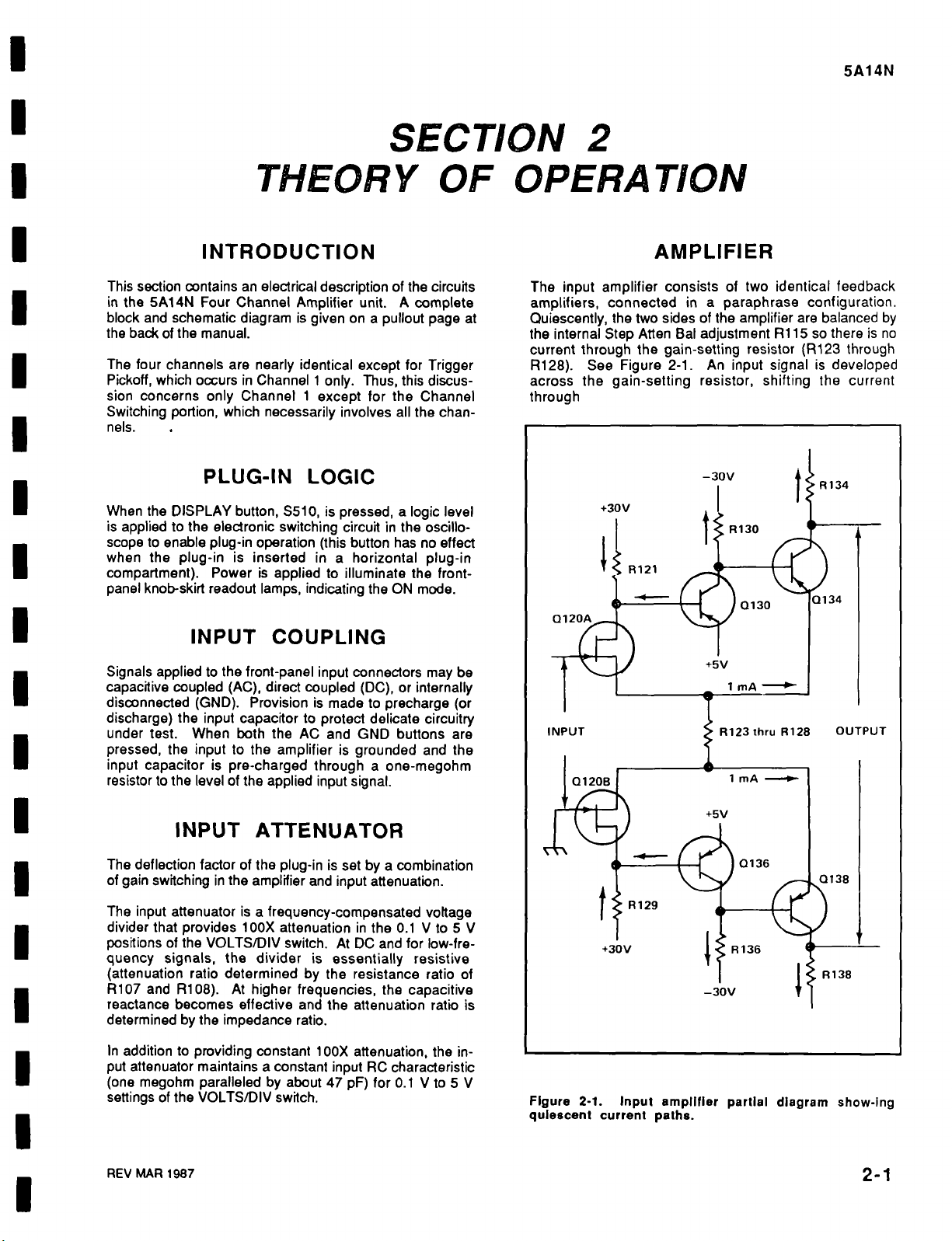
R128). See Figure 2-1. An input signal is developed
across the gain-setting resistor, shifting the current
through
-sov
130
Q120A,
INPUT R123thru R128 OUTPUT
Q120B
O130
1 mA
1 mA
(134
Q134
INPUT ATTENUATOR
The deflection factor of the plug-in is set by a combination
of gain switching in the amplifier and input attenuatbn.
The input attenuator is a frequency-compensated voltage
divider that provides 100X attenuation in the 0.1 V to 5 V
positions of the VOLTS/DIV switch. At DC and for tow-frequency signals, the divider is essentially resistive
(attenuation ratio determined by the resistance ratio of
R107 and R108). At higher frequencies, the capacitive
reactance becomes effective and the attenuation ratio is
determined by the impedance ratio.
In addition to providing constant 10OX attenuation, the input attenuator maintains a constant input RC characteristic
(one megohm paralleled by about 47 pF) for 0.1 V to 5 V
settings of the VOLTS/DIV switch.
REV MAR 1987
+5V
VT\
j > R129 ^^
+30V 1136
Figure 2-1. Input amplifier partial diagram show-ing
quiescent current paths.
0136
0138
-30V
2-1
Page 13
Theory of Operation—5A14N
Q134 and Q138 by the amount established through R123R128,
and developing a push-pull output signal across
R134 and R138. The gain of this amplifier ranges from
about one to fifty, and is primarily determined by the ratio of
the gain-setting resistor to the sum of R134 and R138.
The push-pull signal voltage from 0134 and 0138 collectors then passes through emitter followers 0142 and Q146
and is transformed to a signal current by 0160 and 0162.
The Variable VOLTS/DIV (CAL) potentiometer R168, and
the Gain-setting potentiometer R166, reduce the gain in
the Q160-Q162 stage by developing an adjustable amount
of signal voltage between their emitters.
Q150,
0156 and 0158 in Channel 1 only receive the pushpull signal and provide a single-ended trigger signal out.
0177 and Q178 provide positioning current.
CHANNEL SWITCHING
When only the CH 1 DISPLAY button S510 is pressed,
0510 is biased off, turning on Channel 1 switches 0180
and 0182 and albwing a signal to pass.
When only the CH 2 DISPLAY button S520 is pressed,
Q510 is biased on, switching Q516 off. This action turns
Channel 2 switches Q280 and 0282 on.
When both CH 1 and CH 2 buttons are pressed (dual-trace
mode), the state of O510 and 0516 is determined by the
channel-switching signal generated in the oscilloscope
mainframe. The form of this signal is selected on the sweep
plug-in by the Alternate-Chop Mode button.
Channels 3 and 4 operate as a switched pair just as Channels 1 and 2. Thus, the Channel 3 switches Q380 and
0382 are controlled by Q520, and the Channel 4 switches
Q480 and 0482 are controlled by Q526. When both
Channels 3 and 4 are ON, they are either alternated or
chopped as a pair through Q520 and 0526 by the channelswitching signal.
Channels 1 and 2 are displayed as a composite pair when
their composite switches Q530 and 0534 are turned on.
This occurs when Q550 is biased off. Channels 3 and 4
composite switches Q540 and 0544 are similariy turned on
when 0556 is biased off. When one or two channels from
each composite pair are ON, U550 switches between the
two pairs at either 1/2 or 1/4 the Alternate or Chop rate of
the channel-switching signal. U550 divides the channel-
switching signal by 2 in the Dual Beam position or by 4 in
the Single Beam position of S550. The divided channel-
switching signal from S550 determines the state of Q550
and Q556 when 1 or 2 channels from each composite pair
are
ON.
PROBE SENSING
Either of two lamps located behind the VOLTS/ DIV knob
skirt illuminates the selected deflection factor to provide a
direct readout. Normally, DS190 is lit; connection of a
readout-coded 10X probe extinguishes DS190 and lights
DS196. This changes the knob skirt readout by a factor of
10 to reflect the probe attenuation, eliminating possible
operator error.
2-2
REV MAR
1987
Page 14
SECTION 3
CALIBRATION
5A14N
Introduction
This section of the manual contains a procedure to return
the circuits of the 5A14N within their designed operating
capabilities. Calibration is generally required alter a repair
has been made, or after long time intervals in which normal
aging of components may affect instrument accuracy. For
initial inspection, verify instrument operation by performing
the procedures described under Basic Operation in Section 1.
Instrument Maintenance
Before complete calibration, thoroughly clean and inspect
this instrument as outlined in the Maintenance section of
the Oscilloscope System manual. Also, the System manual
contains information for general maintenance of this instrument, including preventive maintenance, component
identification and replacement, etc.
Service Available
Tektronix, Inc. provides complete instrument repair and
calibration at local Field Service Centers and at the Factory
Sen/ice Center. Contact your local Tektronix Field Office or
representative for further information.
test equipment are not given in this procedure. Refer to
the instruction manual for the test equipment if more infor-
mation is needed.
Special Calibration Fixtures
Special Tektronix calibration fixtures are used in this procedure only where they facilitate instrument calibration.
These special fixtures are available from Tektronix, Inc. Order by part number through your local Tektronix Field
Office or representative.
Test Instruments
1.
5000-series oscilloscope system. For this proce-
dure,
a 5110 Oscilloscope with a 5B10N Time-Base
plug-in is used.
2.
Constant amplitude sine-wave generator. Fre-
quency, 2 Hz to 1 MHz; output amplitude, about 0.5
V to at least 4 V P-P. Tektronix FG 501 Function
Generator recommended (requires a TM 500-series
power module).
3. Standard amplitude calibrator. Output signal, 1 kHz
square wave; output amplitude, 5 mV to at least 20 V;
accuracy, within 0.25%. Tektronix PG 506 Calibration
Generator recommended (requires a TM 500-series
power module).
TEST EQUIPMENT REQUIRED
General
The following test equipment and accessories, or the
equivalent are required for complete calibration of the
5A14N.
the minimum necessary for accurate calibration. Therefore,
some of the specifications listed may be less rigorous than
the actual performance capabilities of the test equipment.
All test equipment is assumed to be correctly calibrated and
operating within the listed specifications.
Specifications given for the test equipment are
Calibration Equipment Alternatives
If other test equipment is substituted, control settings or
set-up may need altering to meet the requirements of the
equipment used. Detailed operating instructions for the
REV MAR 1987
Accessories
1.
Coaxial cable, Impedance,
connectors, BNC. Tektronix Part No.
2.
Input RC normalizer. RC time constant, 47 ms
x 47 pF); connectors, BNC. Tektronix Calibration
Fixture 0067-0541-00 recommended.
3. In-line termination. Impedance, 50 il, accuracy,
within 2%; connectors, BNC. Tektrnoix Part No.
0049-01 recommended.
4.
Plug-in extension for the 5000-series oscilloscope
system.
(not mandatory for this procedure).
Tektrnoix Calibration Fixture 0067-0645-03
50fi;
length, 42 inches;
012-0057-01.
(1
Mi2
011
3-1
-
Page 15
Calibration—5A14N
3-2
^OUOOOO
:C3-
.an
'•CID
Q'^O'OOQQO
is.^
^
>^-l.y>
OO
OOOOQ
-T^_T
c—n
e a
^i^^
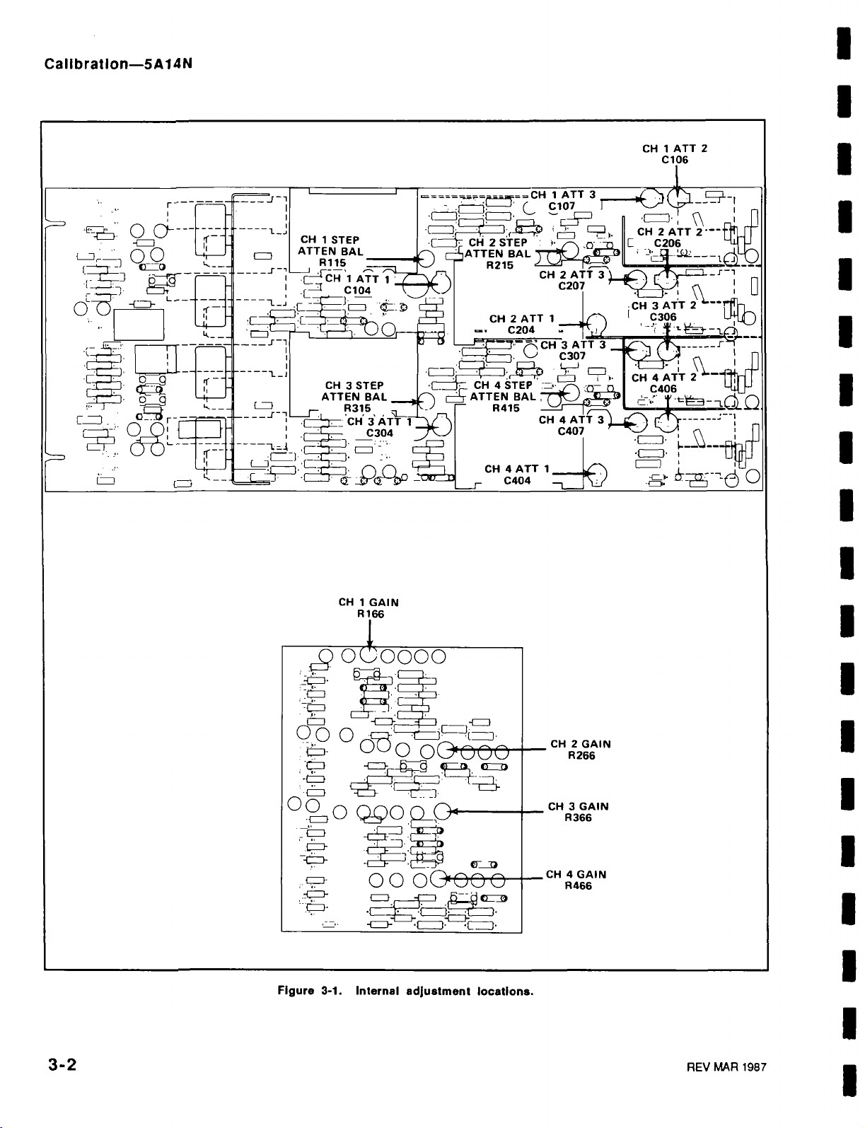
Figure 3-1. Internal adjustment locations.
CH 2 GAIN
R266
CH 3 GAIN
R366
.CH 4 GAIN
R466
REV MAR 1987
Page 16

PROCEDURE
Calibration—5A14N
1.
Step Attenuator Balance
Preparation
1.
Remove the protective cover from the left side of the
5A14N and also the left side panel from the 5000series oscilloscope. (The plug-in extender can be
used to gain access to the internal adjustments rather
than by removing the oscilloscope side panel.) Insert
the 5A14N into the left plug-in compartment, and the
5B10N into the right compartment.
2.
Connect the oscilloscope to the power source for
which it is wired. Set the controls as described under
Initial Control Settings. Refer to Figure 3-1 for location of internal adjustments and test points.
NOTE
This instrument should be calibrated at an ambient temperature between +20° C and
(+68° F and -^86° F) for best accuracy.
-1-30°
C
Initial Control Settings
NOTE
Do not preset internal controls unless they are
known to be significantly out of adjustment, or
unless repairs have been made in the circuit. In
these instances, the internal control scan be
set to midrange.
5A14N (All Channels)
a. Position the CH 1 trace to graticule center and adjust
R115 (CH 1 STEP ATTEN BAL) for no trace shift
when the VOLTS/DIV switch is turned throughout its
range.
b. Turn the CH 1 CAL control throughout its range and
check for less than 1 division of trace shift. Return
the CAL control to the fully cw (detent) position.
c. Repeat the preceding procedure for CH 2 through
CH 4. Adjust R215, R315, and R415 respectively.
2.
Input and Attenuator Compensation
a. Set all VOLTS/DIV switches to 0.1. Apply a 1 volt
signal from the Standard Amplitude Calibrator, using
the HIGH AMPL mode, through the Input RC
Normalizer to the 5A14N CH 1 input. Adjust the time
base triggering Level control for a stable display.
b. Adjust Cl
for a square leading corner on the square-wave display.
c. Set CH 1 VOLTS/DIV to 50 m and the Standard Am-
plitude Calibrator for a 0.5 volt output. Adjust C106
(ATT 2) for a square leading corner on the display.
d.
Set CH 1 VOLTS/DIV to 0.1 and the Standard Am-
plitude Calibrator for a 1 volt output. Adjust C107
(ATT 3) for a square leading corner on the display.
e. Repeat the preceding procedure for the remaining
channels. Adjust the attenuator capacitors that correspond to those adjusted in channel 1.
04,
Cl
06,
and Cl 07 (CH 1 ATT 1,2, and 3)
POSITKDN
DISPLAY
VOLTS/DIV
INPUT COUPLING
All other pushbuttons
CAL
Seconds/Div
Position
Level
Triggering Source
Trigger Mode
All other pushbuttons
REV MAR 1987
Centered
On
50 m
GND
Out
In detent (fully cw)
Time Base (5B10N)
0.5 m
Centered
Fully
CW
Left/Right
(Composite)
Auto Trig
Out
3. Amplifier Gain and VOLTS/DIV
Accuracy
a. Set all VOLTS/DIV switches to 1 and connect the
Standard Amplitude Calibrator, using the STD AMPL
mode,
through the Coaxial Cable to the CH 1 input.
b. Set Standard Amplitude Calibrator for a 5 volt square-
wave output and adjust the time-base triggering
Level control for a stable display.
c. Adjust R166 (CH 1 GAIN) for exacfly 5 divisions of
display.
d.
Repeat the preceding procedure for CH 2 through
CH 4. Adjust R266, R366, and R466 respectively.
e. Set all VOLTS/DIV switches to 5 and connect the
Standard Amplitude Calibrator the CH 1 input.
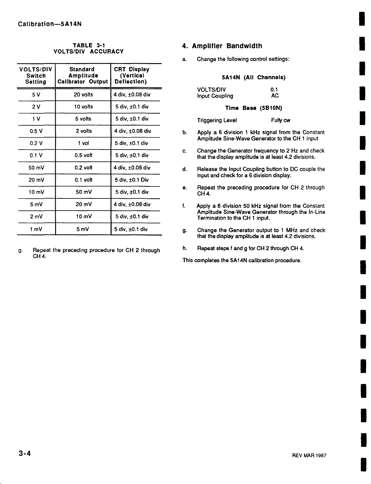
f. Check the VOLTS/DIV accuracy as outlined in Table
3-1.
3-3
Page 17
Calibration—5A14N
VOLTS/DIV
Switch
Setting
5V
2V
1 V
O.SV
0.2 V
0.1 V
50 mV
20 mV
10 mV
5mV
2mV
TABLE 3-1
VOLTS/DIV ACCURACY
Standard
Amplitude
Calibrator Output
20 volts
10 volts
5 volts
2 volts
1 vol
0.5 volt
0.2 volt
0.1 volt
50 mV
20 mV
10 mV
CRT Display
(Vertical
Deflection)
4 div, ±0.08 div
5
div,
5
div,
4 div, ±0.08 div
5 div,
5
div,
4 div, ±0.08 div
5 div,
5
div,
4 div, ±0.08 div
5
div,
±0.1
±0.1
±0.1
±0.1
±0.1
±0.1
±0.1
div
div
div
div
Div
div
div
4.
Amplifier Bandwidth
Change the following control settings:
a.
5A14N (All Channels)
VOLTS/DIV
Input Coupling
Time Base (5B10N)
Triggering Level Fully cw
b. Apply a 6 division 1 kHz signal from the Constant
Amplitude Sine-Wave Generator to the CH 1 input
c. Change the Generator frequency to 2 Hz and check
that the display amplitude is at least 4.2 divisions.
d.
Release the Input Coupling button to DC couple the
input and check for a 6 division display.
e. Repeat the preceding procedure for CH 2 through
CH4.
f. Apply a 6 division 50 kHz signal from the Constant
Amplitude Sine-Wave Generator through the In-Line
Termination to the CH 1 input.
0.1
AC
ImV
Repeat the preceding prcx:edure for CH 2 through
CH4.
5mV
5 div,
±0.1
div
g.
Change the Generator output to 1 MHz and check
that the display amplitude is at least 4.2 divisions.
h. Repeat steps f and g for CH 2 through CH 4.
This completes the 5A14N calibratbn procedure.
3-4
REV MAR 1987
Page 18

DIAGRAMS AND PARTS LISTS
Symbols and Reference Designators
Electrical components shown on the diagrams are in the following units unless noted otherwise:
Capacitors = Values one or greater are in picofarads (pF).
Values less than one are in microfarads
Resistors = Ohms (£2).
Graphic symbols and class designation letters are based on ANSI Standard Y32.2-1975.
Logic symbology is based on ANSI Y32.14-1973 in terms of positive logic. Logic symbols depict the logic
function performed and may differ from the manufacturer's data.
The overline on a signal name indicates that the signal performs its intended function when it goes to the low state.
Abbreviations are based on ANSI Y1.1-1972.
Other ANSI standards that are used in the preparation of diagrams by Tektronix, Inc. are:
Y14.15, 1966 Drafting Practices.
Y14.2,
1973 Line Conventions and Lettering.
Y10.5,
1968 Letter Symbols for Quantities Used in Electrical Science and
Electrical Engineering.
The following prefix letters are used as reference designators to identify components or assemblies on the diagrams.
Assembly,
A
AT
B
BT
C
CB
CR
DL
DS
E
F
FL
separable or repairable
(circuit
board,
Attenuator,
Motor
Battery
Capacitor,
Circuit
Diode,
Delay
Indicating
Spark
Fuse
Filter
tixed or variable
tixed or variable
breaker
signal or rectitier
line
device (lamp)
Gap. Ferrite bead
etc)
H
HR
HY
J
K
L
M
P
O
R
RT
Heat
dissipating device (heat sink,
heat
radiator, etc)
Heater
Hybrid
Circuit
Connector,
Relay
Inductor,
Meter
Connector,
Transistor
rectitier
Resistor,
Thermistor
stationary portion
tixed or variable
movable portion
or silicon-controlled
tixed or variable
The following special symbols may appear on the diagrams:
Strap or Link
Cam Switch
I ^'^ [BALf^ Indicators
- V I
Closure Chart
(Dot indicates
switch closure
SEL Value Selected
at Factory
(/JF).
S
T
TC
TP
U
V
VR
W
Y
Z
Switch
or contactor
Transtormer
Thermocouple
Test
point
Assembly,
inseparable or non-repairable
(integrated
Electron
Voltage
Wirestrap
Crystal
Phase
circuit, etc )
tut>e
regulator (zener
or cable
shitter
diode,
Plug to EC. Board
Identifies Panel
Controls, Connectors and
Modified Component—See
Parts List (Depicted in grey,
or with grey outline)
Plug Index
Refer to Waveform
5A14N
etc 1
Test Voltage
Internal
Screwdriver
Adjustment
Assembly Number
Board Name
REV. A JUL 1977
Refer to Diagram Number
Coaxial Connector
Shielding
Heat Sink
Decoupled or Filtered
Voltage
Etched Circuit Board
Outlined in Black
VERTIC^L AMPL1F1ER<|>-^ fnSSbe'
Schematic Name
r
4-1
Page 19

REPLACEABLE
ELECTRICAL PARTS
PARTS ORDERING INFORMATION
Replacement parts are available from or through your local Tektronix, Inc. Field Office
or representative.
Changes to Tektronix instruments are sometimes made to accommodate improved
components as they become available, and to give you the benefit of the latest circuit
improvements developed in our engineering department. It is therefore important, when
ordering parts, to include the following Information in your
type or number, serial number, and modification number if applicable.
If a part you have ordered has been replaced with a new or improved part, your local
Tektronix, Inc. Field Office or representative
will
contact you concerning any change in pari
number.
order;
Part number, instrument
Section 4—5A14N
Change information, if any, is located at the rear of this manual.
SPECIAL NOTES AND SYMBOLS
XOOO Part first added at this serial number
OCX Part removed after this serial number
rTEM NAME
In the Parts List, an Item Name is separated from the description by a colon (:).
Because of space limitations, an Item Name may sometimes appear as incomplete. For
further Item Name identification, the U.S. Federal Cataloging Handbook H6-1 can be
utilized where possible.
ABBREVIATIONS
ACTR
ASSY
CAP
CER
CKT
COMP
CONN
ELCTLT
ELEC
INCAND
LED
NONWIR
ACTUATOR
ASSEMBLY
CAPACITOR
CERAMIC
CIRCUIT
COMPOSITION
CONNECTOR
ELECTROLYTIC
ELECTRICAL
INCANDESCENT
LIGHT EMITTING DIODE
NON WIREWOUND
PLSTC
QTZ
RECP
RES
RF
SEL
SEMICOND
SENS
VAR
WW
XFMR
XTAL
PLASTIC
QUARTZ
RECEPTACLE
RESISTOR
RADIO FREQUENCY
SELECTED
SEMICONDUCTOR
SENSITIVE
VARIABLE
WIREWOUND
TRANSFORMER
CRYSTAL
REV B. MAY 1979
4-3
Page 20

Replaceable Electrical Parts - SA14N
CROSS INDEX - MFR. CODE NUMBER TO MANUFACTURER
Mfr.
Code
00853
01121
01295
03508
04222
04713
05397
07263
07716
11236
12697
14433
15238
15513
19701
24546
24931
31918
32997
52763
53944
55680
57668
59660
71590
73138
74970
79727
80009
91637
^famifBctur^
SANGAMO WESTON INC
SANGAMO CAP/CITOR DIV
ALLEN-BRADLEY CO
TEXAS INSTRIWENTS INC
SEMIC0NDl£T0R GROUP
GENERAL ELECTRIC CO
SEMI-CONDUCTOR PRODUCTS OEPT
AVX CERAMICS DIV OF AVX COKP
MOTOROLA INC
SEMICONDUCTOR GROUP
W<ION CARBIDE CORP MATERIALS SYSTEMS
DIV
FAIRCHILD CAMERA AND INSTRIHENT CORP
SEMICONDUCTOR DIV
TRW INC
TRW ELECTRONICS COMPONENTS
TRW IRC FIXED RESISTORS/BURLINGTON
CTS OF BERNE INC
CLAROSTAT MFG CO INC
ITT SEMICONDUCTORS DIV
in SEMICONDUCTORS
A DIVISION OF INTERNATIONAL
TELEPHONE ANO TELEGRAPH CORP
DATA DISPUY PRODUCTS
MEPCO/ELECTRA INC
A NORTH AMERICAN PHILIPS CO
CORNING GLASS WORKS
SPECIALTY COWIEaOR CO INC
in SCHADOW INC
BOURNS INC
TRIfPOT DIV
STLIINER ELECTRONICS INC
GLOW LITE CORP
NICHICON mmCA/ CORP
mmcQKP
TUSONIX INC
GLOBE-UNION INC
CEN7RALAB ELECTRONICS DIV
BECKMAN INSTRUMENTS INC HELIPOT DIV
JOHNSON E FCO
C-W INDUSTRIES
TEKTRONIX INC
DALE ELECTRONICS INC
Address
SANGAMO RD
P 0 BOX 128
1201 SOUTH 2ND ST
13500 N CENTRAL EXPRESSWAY
P 0 BOX 225012 K/S
W GENESEE
19TH AVE SOUTH
P 0 80X867
5005 EMCOOWaLRD
11901 MADISON AVE
464 ELLIS
2850 MT PLEASANT AVE
406 PARR ROAD
LOWER WASHINGTON
500 BROADWAY
P 0 BOX 168
303 N OAK ST
P 0 BOX 760
550 HIGH
2620 ENDRESS PUCE
P 0 BOX
8081 WALLACE RD
1200 coLureiA AVE
6135 AIRWAYS BLVD
PO BOX 21947
BOX 698
927 E STATE PKY
16931 MILLIKEN AVE
2155 N FORBES BLVD
HWY 20
P0B0X858
2500 HARBOR BLVD
299 lOm AVE S
550 DAVISVILLE RD
P 0 BOX 96
4900
P 0 BOX 500
POBQX 609
ST
ST
ST
D
W
S W
GRIFFITH OR
49
ST
W
City. State. Zip Code
PICKENS SC 29671
MILWAUKEE WI 53204
DALLAS TX 75265
AUBURN NY 13021
MYRTLE BEACH SC 29577
PHOENIX AZ 85008
aEVELAND OH 44101
MOUNTAIN VIEW CA 94042
BURLINGTOI IA 52601
BERNE IN 46711
DOVER NH 03820
WEST PALM BEACH
LAWRENCE MA 01841
LOS ANGELES CA 90302
MINERAL WaLS TX 76067
BRADRKD PA 16701
GREENWOOD IN 46142
EDEN PRAIRIE MN 55343
RIVERSIDE CA 92507
CHAHANOOW TN 37421
PAULS VALLEY OK 73075
SCHAUMBURG IL 80195
IRVINE CA 92713
TUCSON, ARIZONA 85705
FORT DODGE IA 50501
FULLERTON CA 92634
WASECA MN 56093
WARMINSTER PA 18974
BEAVERTON OR 97077
COLUMBUS NE 68601
R.
4-4
REV XT 1987
Page 21

Replaceable Electrical Parts - 5A14N
Al
Al
Al
A2
ClOl
C104
C106
C107
C108
Clio
Clio
C113
C130
C135
C136
C139
C167
C177
C178
C190
C201
C204
C206
C207
C208
C210
C210
C213
C218
Tektronix
f^rt No.
670-1891-00
670-1891-01
670-1891-02
670-1892-00
285-0603-00
281-0166-00
281-0166-00
281-0166-<K)
283-0605-00
283-0068-00
281-0614-00
283-0177-00
281-0700-00
290-0247-00
281-0700-00
283-0204-00
281-0628-00
283-0023-00
283-0023-00
283-0068-00
285-0603-00
281-0166-00
281-0166-00
281-0166-00
283-0605-00
283-0068-00
281-0614-00
283-0177-00
283-0204-00
Serial/Assently
Ef=fiBctive
BOlOlOO
B070000
B080000
BOlOlOO
B063739
BOlOlOO
BOlOlOO
B063739
~
B069999
B079999
B063738
B069999
B063738
No.
uscont
Hane & Descriptiai
CIRCUIT
BD
CIRCUIT
CIRCUIT
CIRCUIT
CAP,FXD,PLASTIC:0.1UF,3.5%,600V
CAP.VAR.AIR 01:1.9-15.7 PF,250V
CAP.VAR.AIR 01:1.9-15.7 PF,250V
CAP,VAR,AIR 01:1.9-15.7 PF,250V
CAP.FXD.MICA DI:678PF,1%,300V
CAP.FXD.CER DI:0.01UF,+100-0%,500V
CAP.FXD.CER DI:6800PF,-t80-20%,500V
CAP,FX0,CER DI:lUF,-i«)-20%,25V
CAP.FXD.CER DI:3.3PF.-i-/-0.33PF.500V
CAP.FXD.ELCTLT:5.6UF,10%,6V
CAP.FXD.CER DI:3.3PF.•^/-0.33PF.500V
CAP.FXD.CER DI:0.01UF,20%.50V
CAP.FXD.CER OI:15PF.5%.500V
CAP.FXD.CER DI:0.1UF,-t80-20%,12V
CAP.FXD.CER DI:0.1UF,-t80-20%,12V
CAP.FXD.CER DI:0.01UF,-H00-0%.5OOV
CAP,FXD,PLASTIC.O.1UF,3.5%,600V
CAP.VAR.AIR 01:1.9-15.7 PF.250V
CAP.VAR.AIR 01:1.9-15.7 PF,250V
CAP.VAR.AIR 01:1.9-15.7 PF.250V
CAP.FXD.MICA DI:678PF,1%.300V
CAP.FXD.CER DI:0.01UF.+100-0%.500V
CAP.FXD.CER DI:6800PF,+80-20%,500V
CAP,FXD.CER DI:1UF.+60-20%.25V
CAP.FXD.CER DI:0.01UF.20%,50V
(CHANNEL 2 ONLY)
ASSY:MAIN
BD
ASSY:MAIN
BD
ASSY:MAIN
BD
ASSY:SECONDARY
Mfr.
Code
80009 670-1891-00
80009 670-1891-01
80009 670-1891-02
80009 670-1892-00
80009
74970
74970
74970
00853
59660
52763
04222
52763
05397
52763
04222
52763
71590
71590
59660
80009
74970
74970
74970
0flR53
59660
52763
04222
04222
Hfr.
Part
No.
285-C603-00
187-0109-055
187-0109-055
187-0109-055
D153PB78OF0
871-533E103P
2RDPLZ007 6N80Z6
SR302E105ZAATR
2RDPLZ007 3P30KS
T322B565K006AS
2RDPLZ007 3P30KS
SR155E103MAA
2RDPLZ007 15P0JC
2DDU668104Z
2DDU668104Z
871-533E103P
285-0603-00
187-0109-055
187-0109-055
187-0109-055
0153F678OF0
871-533E103P
2RDPLZ007 6N80Z6
SR302E105ZAATR
SR155E103MAA
C230
C235
C236
C239
C267
C277
C278
C290
C301
C304
C306
C307
C308
GIO
GIO
C313
G30
C335
C336
cm
C367
C377
G78
C390
C401
C404
C406
281-0700-00
290-0247-00
281-0700-00
283-0204-00
281-0628-00
283-0023-00
283-0023-00
283-0068-00
285-0603-00
281-0166-00
281-0166-00
281-0166-00
283-0605-00
283-0088-00
281-0614-00
283-0177-00
281-0700-00
290-0247-00
281-0700-00
283-0204-00
281-0628-00
283-0023-00
283-0023-00
283-0068-00
285-0603-00
281-0166-00
281-0166-00
BOlOlOO
BOlOlOO
B063739
BOlOlOO
B069999
B063738
B069999
CAP.FXD.CER DI:3.3PF,+/-0.33PF.500V
CAP,FXD,ELCTLT:5.6UF.10%.6V
CAP.FXD.CER DI:3.3PF.+/-0.33PF.500V
CAP.FXD.CER DI:0.01UF,20%.50V
CAP.FXD.CER DI:15PF.5%.500V
CAP.FXD.CER DI:0.1UF,+60-20%.12V
CAP.FXD.CER 01:0.1UF,+80-20%.12V
CAP.FXD.CER OI:0.01UF.+100-0%.500V
CAP,FXO.PLASTIC:0.lUF.3.5%.600V
CAP.VAR.AIR 01:1.9-15.7 PF,250V
CAP.VAR.AIR 01:1.9-15.7 PF.250V
CAP.VAR.AIR 01:1.9-15.7 PF.250V
CAP.FXD.MICA DI:678PF,1%,300V
CAP.FXD.CER DI:0.01UF.+100-0%.500V
CAP.FXD.CER DI:6800PF.+80-20%.500V
CAP.FXD.CER DI:1UF.+80-20%.25V
CAP.FXD.CER DI:3.3PF.+/-0.33PF.500V
CAP.FXO.ELCTLT:5.6UF.10%.6V
CAP.FXD.CER DI:3.3PF.+/-0.33PF.500V
CAP.FXD.CER DI:0.01UF.20%.50V
CAP.FXD.CER DI:15PF,5%.5O0V
CAP.FXD.CER DI:0.1UF.+8O-2O%.12V
CAP.FXD.CER 0I:0.1UF.+8O-20%.12V
CAP.FXD.CER DI:0.01UF.+100-0%,500V
CAP.FXD.PLASTIC:0.1UF,3.5%.600V
CAP.VAR.AIR 01:1.9-15.7 PF.250V
CAP.VAR.AIR 01:1.9-15.7 PF.250V
52763
05397
52763
04222
52763
71590
71590
59660
80009
74970
74970
74970
onas3
59660
52763
04222
52763
05397
52763
04222
52763
71590
71590
59660
80009
74970
74970
2RDPLZ007 3P30KS
T322B565K006AS
2RDPLZ007 3P30KS
SR155E103MAA
2R0PLZ007 ISPOJC
2D0U66B104Z
2DDU668104Z
871-533E103P
285-0603-00
187-0109-055
187-0109-055
187-0109-055
D153F6780F0
871-533E103P
2RDPLZ007 6N80Z6
SR302E105ZAATR
2RDPLZ007 3P30KS
T322B565KD06AS
2RDPLZ007 3P30KS
SR155E103MAA
2RDPLZ007 15P0X
2DDU66B104Z
200U668104Z
871-533E103P
285-0603-00
187-0109-055
187-0109-055
REV OCT 1987
4-5
Page 22

Replaceable Electrical Parts - 5A14N
C407
C408
C410
C410
C413
C430
C435
C436
C439
C467
C477
C478
C490
C512
C517
C517
C522
C527
C527
C550
C551
C557
C557
C590
CR113
CR130
CR136
CR180
CR181
CR182
CR183
Tektronix
Part No.
281-0166-00
283-0605-00
283-n0fi8-00
281-0614-00
283-0177-00
281-0700-00
290-0247-00
281-0700-00
283-0204-00
281-0628-00
283-0023-00
283-0023-00
283-0068-00
283-0000-00
281-0628-00
281-0579-00
283-0000-00
281-0628-00
281-0579-00
283-0212-00
283-0000-00
281-0628-00
281-0579-00
290-0480-00
152-0246-00
152-0141-02
152-0141-02
152-0141-02
152-0141-02
152-0141-02
152-0141-02
Serial/Assed)ly No.
Effective "^ "
6010100
B063739
BOlOlOO
BOlOlOO
B051983
BOlOlOO
B051983
B080000
BOlOlOO
B051983
BOlOlOO
B063738
8069999
B051982
B051982
B051982
6069999
u A n 1 1.J
Mane & Description
CAP.VAR.AIR 01:1.9-15.7 PF.250V
CAP.FXD.MICA DI:678PF,1%.300V
CAP.FXD.CER DI;0.01UF,+100-0%,500V
CAP.FXD.CER DI:6800PF,+eO-20%,500V
CAP.FXD.CER DI:lUF.+60-20%.25V
CAP.FXD.CER DI:3.3PF,+/-0.33PF.500V
CAP.FXO.ELCTLT:5.6UF.10%.6V
CAP.FXD.CER DI:3.3PF,+/-0.33PF,500V
CAP.FXD.CER DI:0.01UF.20%.5OV
CAP.FXD.CER DI:15PF.5%.500V
CAP.FXD.CER DI:0.1UF,+80-20%.12V
CAP.FXD.CER 0I:0.1UF,+«)-20%,12V
CAP.FXD.CER DI:0.01UF.+100-0%.500V
CAP.FXD.CER DI:0.001UF.+100-0%,500V
CAP.FXD.CER DI:15PF.5%.500V
CAP.FXD.CER OI:21PF.5%.500V
CAP.FXD.CER DI:0.001UF.+100-0%.500V
CAP.FXD.CER 0I:15PF.5%.5O0V
CAP.FXD.CER 01:21PF.5%.500V
CAP.FXD.CER DI:2UF.2(K.50V
CAP.FXD.CER OI:0.0011F.+100-0%.500V
CAP.FXD.CER 01:15PF.5%.500V
CAP.FXD.CER DI:21PF,5K,5O0V
CAP.FXD,ELCTLT:0.5UF.+50-10%.200V
SEMICOND DVC.DI:SW,SI.40V.200m.DO-7
SEMICOW) DVC.0I:SW.SI.30V.150m.30V.DO-35
SEMICOND DVC.DI:SW,SI,30V.150m,30V.0O-35
SEMICOND DVC.DI:SW.SI.30V.15flMA.30V.0O-35
SEMICOND DVC.DI:SW.SI.30V.150MA.30V.DO-35
SEMICOND DVC.0I:SW.SI,30V.150m,30V,DO-35
SEMICOND DVC.DI:SW.SI.30V.150m,30V,DO-35
Mfp.
Code
74970
onfW3
59660
52763
04222
52763
05397
52763
04222
52763
71590
71590
59660
59660
52763
52763
59660
52763
52763
04222
59660
52763
52763
55680
14433
03508
03508
03508
03508
03508
03508
Mfr. Part No.
187-0109-055
D153F6780F0
871-533E103P
2RDPLZ007 6N80Z6
SR302E105ZAATR
2RDPLZ007 3P3(KS
T322B565K00fiAS
2RDPLZ007 3P3a(S
SR155E103MAA
2R0PLZ007 15P0X
2D01lfifiR104Z
2DDU66B104Z
871-533E103P
831-610-Y5U0102P
2RDPLZ007 ISPOJC
2RDPLZ007 21PQJC
831-610-Y5U0102P
2RDPLZ007 ISPOJC
2RDPLZ007 21P0X
SR405E205MAA
831-610-Y5U0102P
2RDPLZ007 ISPOX
2RDPLZ007 21P0JC
THU20R4rTAA
WGISSTTK
DA2527 (1N4152)
DA2527 (1N4152)
DA2527 (1N4152)
DA2527 (1N4152)
0A2527 (1N4152)
DA2527 (1N4152)
CR190
CR195
CR213
CR230
CR236
CR280
CR281
CR282
CR283
CR290
CR295
CR313
CR330
CR336
CR380
CR381
CR382
CR383
CR390
CR395
CR413
CR430
CR436
CR480
CR481
CR482
CR483
152-0141-02
152-0141-02
152-0246-00
152-0141-02
152-0141-02
152-0141-02
152-0141-02
152-0141-02
152-0141-02
152-0141-02
152-0141-02
152-0246-00
152-0141-02
152-0141-02
152-0141-02
152-0141-02
152-0141-02
152-0141-02
152-0141-02
152-0141-02
152-0246-00
152-0141-02
152-0141-02
152-0141-02
152-0141-02
152-0141-02
152-0141-02
BOlOlOO
BOlOlOO
BOlOlOO
BOlOlOO
BOlOlOO
BOlOlOO
B068999
B069999
8069999
B069999
B069999
8069999
SEMICOND DVC.DI:SW.SI.30V.150MA.30V.DO-35
SEMICOND DVC.DI:SW.SI.30V.150m.30V.DO-35
SEMICOND DVC.0I:SW.SI.40V.200m.DC-7
SEMICOfO 0VC.DI:SW.SI.30V.150MA.30V.DO-35
SEMICOMD 0VC.OI:SW.SI.3OV,150MA.30V.DO-35
SEMICOND DVC,DI:SW.SI.30V.150W.30V.DO-35
SEMICOND DVC.DI:SW.SI.30V.150W.30V.DO-35
SEMICOND DVC.DI:SW.SI.30V.150W.30V.DO-35
SEMICOND DVC.DI:SW.SI,30V,150m,30V.DO-35
SEMICOND 0VC.DI:SW.SI.3OV.15flW,30V,0O-35
SEMICOND DVC.DI:SW.SI,30V.15CHA,30V.DO-35
SEMICOND DVC.DI:SW.SI.40V.20(WA.DO-7
SEMia»ID OVC.DI:SW.SI.30V.15flMA,30V.DO-35
SEMICOND 0VC.DI:SW.SI,30V.150MA,30V.00-35
SEMICOND DVC.DI:SW,SI.30V.150MA,30V.DO-35
SEMICOND DVC.DI:SW,SI,30V,150MA,30V.DO-35
SEMICOND DVC.DI:SW.SI.30V.150MA,30V.DO-35
SEMICOND DVC.DI:SW.SI.30V.150MA.30V.0O-35
SEMICOfO 0VC.DI:SW,SI.3OV.150m.30V.DO-35
SEMICOW) 0VC,DI:SW.SI.30V.15(»1A.30V,DO-35
SEMICOND 0VC,DI:SW.SI.40V.20(»W.D0-7
SEMICOND DVC.DI:SW.SI.30V.15(WA,30V.D0-35
SEMICOND DVC.DI:SW.SI.30V.15flMA,30V.D0-35
SEMICOND DVC.DI:SW.SI.30V.150MA.30V,DO-35
SEMICOND DVC.OI:SW.SI,30V.150m,30V,DO-35
SEMICOND DVC.DI:SW.SI.30V.150MA.30V.DO-35
SEMICOND DVC.DI:SW,SI.30V.15flMA.30V.DO-35
03508
03508
14433
03508
03508
03508
03508
03508
03508
03508
03508
14433
03508
03508
03508
03508
03508
03508
03508
03508
14433
03508
03508
03508
03508
03508
03508
DA2527 (1N4152)
DA2527 (1N4152)
W61537TK
DA2527 (1N4152)
DA2527 1N4152)
DA2527 1N4152)
OA2527 (1N4152)
DA2527 (1N4152)
DA2527 (1N4152)
DA2527 (IN4152)
DA2527 (1N4152)
W61537TK
DA2527 (1N4152)
DA2527 (1N4152)
DA2527 (1N4152)
DA2527 (1N4152)
DA2527 (1N4152)
0A2527 (1N4152)
DA2527 (1N4152)
DA2527 (1N4152)
WG1537TK
DA2527 (1N4152
0A2527 (1N4152
DA2527 (1N4152
DA2527 (1N4152)
DA2527 (1N4152)
DA2527 (1N4152)
4-6
REV OCT 1987
Page 23

Replaceable Electrical Parts - 5A14N
Cuiixxuit
CR490
CR495
CR510
CR516
CR520
CR526
CR530
CR531
CR534
CR535
CR540
CR541
CR544
CR545
CR550
CR556
DS190
DS190
OS 196
0S196
0S290
DS290
0S296
0S296
DS390
0S390
DS396
0S396
0S490
DS490
No.
Tektronix
Part
No.
152-0141-02
152-0141-02
152-0141-02
152-0141-02
152-0141-02
152-0141-02
152-0141-02
152-0141-02
152-0141-02
152-0141-02
152-0141-02
152-0141-02
152-0141-02
152-0141-02
152-0141-02
152-0141-02
150-0111-00
150-1064-00
150-0111-00
150-1064-00
150-0111-00
150-1064-00
150-0111-00
150-1064-00
150-0111-00
150-1064-00
150-0111-00
150-1064-00
150-0111-00
150-1064-00
Soial/Assartily
Effective
BOlOlOO
BOlOlOO
BOlOlOO
6069999
8069999
B069999
B070000
BOlOlOO
8069999
8070000
8010100
8069999
8070000
BOlOlOO
8069999
8070000
BOlOlOO
B069999
8070000
BOlOlOO
8069999
8070000
8010100
B069999
B070000
No.
Dscont
Nane & Description
SEMICOND DVC.DI:SW.SI.30V.15OMA.30V.0O-35
SEMICOND DVC.DI:SW.SI.30V.150MA.30V.D0-35
SEMICOfC DVC.DI:SW.SI.30V.150MA.30V.DO-35
SEMICOND OVC.DI:SW.SI.30V.150MA.30V.DO-35
SEMICOND DVC.DI:SW,SI.30V,150MA.30V,DO-35
SEMICOND DVC.DI:SW.SI.30V.150m.30V.DO-35
SEMICOND OVC.DI
SEMICOND DVC.OI
SEMICOND DVC.OI
SEMICOND DVC.OI
SEMICOND DVC.OI
SEMICOND DVC.OI
:SW.SI.30V.150MA.30V,DO-35
:SW.SI.SOV.150m.30V.00-35
:SW.SI.30V.150MA.30V.DO-35
:SW.SI.30V.150MA.30V.0O-35
:SW.SI.30V.150W\.30V.DO-35
:SW.SI,30V.150^W.30V.DO-35
SEMICOND 0VC.DI:SW.SI,30V.150m.30V.DO-35
SEMICOND DVC,DI:SW.SI,30V.150MA.30V.0O-35
SEMICOND DVC,DI:SW.SI,30V.150MA.30V.DO-35
SEMICOND OVC.DI:SW.SI,30V.150MA.30V.D0-35
LAMP.GLOW:125V MAX.1.5MA.2AC-AT.WIRE
LT
EMITTING 0I0:YELLCW,585NM.40
MA MAX
LAMP.GLDW:125V MAX.1.5MA.2AC-AT.WIRE
LT
EMITTING DIO:YELL0W.585NM.4O
MA MAX
LAMP.GLOW:125V MAX.1.5MA.2AC-AT.WIRE
LT
EMiniNG DIO:YELL0W.585NM.4O
MA MAX
LAMP.GLOW:125V MAX,1.5MA.2AC-AT.WIRE
LT
EMITTING DI0:YELL0W,585NM,40
LAMP.aOW:125V
LT
EMITTING 0IO:YELL0W.585NM,4O
MAX.
1.5MA.2AC-AT.WIRE
MA MAX
MA MAX
LAMP,GL0W:125V MAX.1.5MA.2AC-AT.WIRE
LT
EMiniNG DI0:YELL0W.585NM.4O
MA MAX
LAMP.GLOW:125V MAX.1.5MA.2AC-AT.WIRE
LT
EMiniNG DI0:YELL0W.585»1.40
MA MAX
Mfr.
Code
03508
03508
03508
03508
03508
03508
03508
03508
03508
03508
03508
03508
03508
03508
03508
03508
53944
15513
53944
15513
53944
15513
53944
15513
53944
15513
53944
15513
53944
15513
Mfr.
Part
No.
DA2527 (1N4152)
DA2527 (1N4152)
DA2527 (1N4152)
DA2527 (1N4152I
DA2527 (1N4152)
0A2527 (1N4152)
DA2527 (1N4152)
DA2527 (1N4152)
DA2527 (1N4152)
DA2527 (1N4152)
DA2527 (1N4152)
DA2527 (1N4152)
DA2527 (1N4152)
DA2527 (1N4152)
DA2527 (1N4152)
DA2527 (1N4152)
AlB-9
SP840113
AlB-9
SP840113
AlB-9
SP840113
AlB-9
SP840113
AlB-9
SP840113
AlB-9
SP840113
AlB-9
SP840113
DS496
0S496
JlOl
JlOl
J201
J201
J301
J301
J401
J401
Q120
Q130
Q134
Q136
Q138
Q142
Q146
Q150
Q156
0158
Q160
0162
Q177
Q178
Q180
Q182
Q190
150-0111-00
150-1064-00
131-0679-00
131-0679-02
131-0679-00
131-0679-02
131-0679-00
131-0679-02
131-0679-00
131-0679-02
151-1049-00
151-0342-00
151-0342-00
151-0342-00
151-0342-00
151-0341-00
151-0341-00
151-0341-00
151-0341-00
151-0341-00
151-0341-00
151-0341-00
151-0342-00
151-0342-00
151-1005-00
151-1005-00
151-0347-00
BOlOlOO
8070000
8010100
8031129
8010100
B031129
BOlOlOO
B031129
BOlOlOO
B031129
BOlOlOO
B069999
B031128
B031128
8031128
8031128
8069999
LAMP.GL0W:125V MAX.1.5MA.2AC-AT.WIRE
LT
EMiniNG 0I0:YELL0W.585W1.40
MA MAX
CONN.RCPT.ELEC:BNC,MALE.3 CONTACT
CONN.RCPT.ELEC:BNC.MALE.3 CONTACT
CONN.RCPT.ELEC:BNC.MALE.3 CONTACT
CONN.RCPT.ELEC:BNC.MALE.3 CONTACT
C0im.RCPT.EL£C:8NC.MALE.3 CONTACT
CONN.RCPT.ELEC:BNC.MALE.3 CONTACT
COW.RCPT.ELEC:BNC.MALE.3 CONTAa
COW.RCPT,ELEC:BNC.MALE.3 CONTACT
TRANSISTOR:FET.N-CHAN.SI.TO-71
TRANSIST0R:PNP.SI.T0-92
TRANSISTOR:PNP,
TRANSISTOR:PNP,
TRANSISTOR:PNP,
TRANSISTOR:NPN,
TRANSISTOR:NPN,
TRANSISTOR:NPN,
TRANSISTOR:
TRANSISTOR:
TRANSISTOR:
TRANSISTOR:
TRANSISTOR:
TRANSISTOR:
TRANSIST0R:FET.N-CHAN.SI.T0-106
TRANSISTOR:FET.N-CHAN,SI.T0-106
TRANSISTOR:NPN.SI.TO-92
SI.TO-92
SI.TO-92
SI.TO-92
SI.T0-106
SI.TO-106
SI,TO-106
NPN,SI,TO-106
NPN.SI.TO-106
NPN.SI.TO-106
NPN.SI.TO-106
PNP.SI.TO-92
PNP.SI.TO-92
53944
15513
24931
24931
24931
24931
24931
24931
24931
24931
04713
07263
07263
07263
07263
04713
04713
04713
04713
04713
04713
04713
07263
07263
04713
04713
04713
AlB-9
SP840113
28JR168-1
28JR270-1
28JR168-1
28JR270-1
28JR168-1
28JR270-1
28JR168-1
28JR270-1
Sn31049
S035928
S035928
S035928
S035928
SPS6919
SPS6919
SPS6919
SPS6919
SPS6919
SPS6919
SPS6919
S035928
S035928
SPF685
SPF685
SPS7951
REV XT 1987
4-7
Page 24

Replaceable Electrical Parts - 5A14N
CunxjiKaiL
Q190
Q196
Q196
0220
Q230
Q234
Q236
Q238
Q260
Q262
0277
Q278
Q280
Q282
Q290
Q290
Q296
Q296
Q320
Q330
0334
Q336
Q338
Q360
0362
0377
0378
Q380
0382
0390
Q390
No.
Tektronix
Part
No.
151-0254-00 8070000
151-0347-00 8010100
151-0254-00 8070000
151-1049-00
151-0342-00
151-0342-00
151-0342-00
151-0342-00
151-0341-00
151-0341-00
151-0342-00
151-0342-00
151-1005-00
151-1005-00
151-0347-00
151-0254-00
151-0347-00
151-0254-00
151-1049-00
151-0342-00
151-0342-00
151-0342-00
151-0342-00
151-0341-00
151-0341-00
151-0342-00
151-0342-00
151-1005-00
151-1M5-00
151-0347-00
151-0254-00
Serial/Assentily
Effective Osoont
BOIOIX
X700X
XIOIOO
B070X0
XIOIOO
8070X0
No.
8069999
8069999
8069999
8069999
Name & Description
TRANSIST0R:[»RLINGT0N.NPN,SI.625MW.TO-92
TRflNSISTOR:NPN.SI.TO-92
TRANSIST0R:DARLINGT0N.NPN,SI.625MW.T0-92
TRANSISTOR:FET.N-CHAN.SI.TO-71
TRANSISTOR:PNP,SI,TO-92
TRANSISTOR:PNP.SI,TO-92
ISTOR:
PNP.SI.TO-92
PNP.SI.TO-92
NPN.SI.TO-IX
NPN.SI.TO-IX
PNP.SI.TO-92
PNP.SI.TO-92
FET.
N-CHAN.
NPN. SI.
TO-IX
FCT.
N-CHAN.
SI,
SI.
TO-IX
TO-IX
TRANSISTOR:
TRANSISTOR:
TRANSISTOR;
TRANSISTOR;
TRANSISTOR;
TRANSISTOR;
TRANSISTOR:
TRANSISTOR:FET,N-CHAN,SI .TO-IX
TRANSISTOR:NPN,SI,TO-92
TRANSIST0R:QARLINGT0N,NPN,SI,625MW,T0-92
TRANSISTOR:NPN.SI.TO-92
TRANSIST0R:QARLINGT0N.NPN.SI.K5MW.T0-92
TRANSISTOR:FET.N-CHAN.SI.TO-71
TRANSISTOR:PNP.SI.TO-92
TRANSISTOR:FNP.SI.TO-92
TRANSISTOR:PNP.SI.TO-92
TRANSISTOR:PNP,SI.TO-92
TRANSISTOR:
TRANSIST(»:NPN.SI.T0-1X
TRANSISTOR:PNP,SI,TO-92
TRANSISTOR:PNP,SI,TO-92
TRANS
TRANSISTOR:FET,N-CHAN.SI.TO-IX
TRANSISTOR:NPN,SI,TO-92
TRANSISTOR:DARLINGTON,NPN,SI.625MW.T0-92
Mfr.
Code
03508
04713
03508
04713
07263
07263
07263
07263
04713
04713
07263
07263
04713
04713
04713
03508
04713
03508
04713
07263
07263
07263
07263
04713
04713
07263
07263
04713
04713
04713
03508
Mfr.
Part
X38L3118
SPS7951
X38L3118
SFD1049
S035928
S035928
S035928
S035928
SPS6919
SPS6919
S035928
S035928
SPF685
SPF685
SPS7951
X38L3118
SPS7951
X38L3118
SFD1049
S035928
S035928
S035928
S035928
SPS6919
SPS6919
S035928
S035928
SPF685
SPF685
SPS7951
X.'Hfll
3118
No
0396
Q396
Q420
Q430
0434
0436
Q438
046O
Q462
Q477
Q478
Q480
Q482
0490
Q490
0496
Q496
Q510
Q516
0520
0526
Q530
Q534
Q540
Q544
Q550
Q556
151-0347-00
151-0254-00
151-1049-00
151-0342-00
151-0342-00
151-0342-00
151-0342-00
151-0341-00
151-0341-00
151-0342-00
151-0342-00
151-1X5-00
151-1X5-X
151-0347-00
151-0254-X
151-0347-X
151-0254-M
151-034HX)
151-0341-X
151-0341-X
151-0341-X
151-1X5-00
151-1X5-X
151-1X5-X
151-1X5-X
151-0341-X
151-0341-X
XIOIOO
M700X
XIOIX
B0700X
XIOIX
M700X
8069999
8069999
8069999
TRANSISTORrNPN.SI.TO-92
TRANSIST0R:DARLINGT0N.NPN.SI.625MW.T0-92
TRANSISTOR:PFT.N-CHAN.SI.TO-71
TRANSISTOR:PNP.SI.TO-92
TRANSISTOR:PNP.SI.TG-92
TRANSISTOR:PNP.SI.TO-92
TRANSISTOR:PNP.SI.TO-92
TRANSISTOR:NPN,SI,TO-106
TRANSISTOR
TRANSISTOR:PNP,SI.TO-92
TRANSISTOR:PNP.SI.TO-92
TRANSISTOR:FET.N-CHAN.SI .TO-IX
TRANSISTOR:
TRANSISTOR:NPN.SI.TO-92
TRANSIST0R:aARLINGT0N.NPN.SI,625MW.TO-92
TRANSISTOR:NPN,SI.TO-92
TRANSISTOR:QARLINGTON,NPN,SI.625MW.TO-92
TRANSISTOR:NPN.SI.TO-106
TRANSISTOR:NPN.SI.TO-IX
TRANSISTOR:NPN,SI,TO-IX
TRANSISTOR:NPN.SI.TO-IX
TRANSISTOR:FET.N-CHAN.SI.TO-IX
TRANSISTOR:FET.N-CHAN.SI.TO-IX
TRANSISTOR:FET.N-CHAN,SI.TO-IX
TRANSISTOR:
TRANSISTOR:NPN,SI,TO-IX
TRANSISTOR:NPN,SI,TO-IX
:l«^,
SI,
T0-106
FET.
N-CHAN.
FET.N-CHAN.SI,TO-IX
SI
.TO-IX
04713
03508
04713
07263
07263
07263
07263
04713
04713
07263
07263
04713
04713
04713
03508
04713
03508
04713
04713
04713
04713
04713
04713
04713
04713
04713
04713
SPS7951
X38L3118
SFD1049
S035928
S035928
S035928
S035928
SPS6919
SPS6919
S035928
S035928
SPF685
SPF685
SPS7951
X38L3118
SPS7951
X38L3118
SPS6919
SPS6919
SPS6919
SPS6919
SPF685
SPF685
SPF685
SPF685
SPS6919
SPS6919
4-8
REV XT 1987
Page 25

Replaceable Electrical Parts - 5A14N
RlOl
R102
R102
R107
RIX
RllO
RllO
Rill
Rill
R113
R113
R114
R114
R115
R117
R118
R121
R123
R124
R125
R126
R127
R128
R129
R130
R130
Tektronix
Part No.
315-0681-00
316-0105-X
315-0105-X
322-X24-03
321-0289-03
316-0224-X
315-0224-X
316-0102-X
315-0102-X
316-0223-X
315-0223-X
316-0154-X
315-0154-X
311-0613-X
321-0435-X
321-0193-X
321-X28-X
321-0X7-03
321-0126-X
321-X12-03
321-0193-03
321-0222-X
321-X16-03
321-0328-X
316-0333-X
315-a\^3-X
Seria1/Ass8rt)ly No.
Effective ~
BOlOlX
uscont
6069999
B0700X
BOlOlOO
8069999
M70X0
MIOIOO
8069999
M70X0
BOIOIX
8069999
M7OX0
BOlOlOO
B069999
M700X
BOlOlOO
B069999
M70X0
NatB & Description
RES,FXD.FILM:680 0HM.5%.0.25W
RES.FXD.CMPSN:1M 0I*1.10%.0.25W
RES.FXD.FILM:lMOIt1.5%,0.25W
RES,FXD,FILM:990K Om.0.25%.0.25W.TC=T2
RES.FXD.FILM:10.0KOIt1.0.25%.0.125W.TC=T2
RES,FXD,CMPSN:220K Olt1.10%.0.25W
RES,FXD.FILM:220K 0IW.5%.0.25W
RES.FXD.CMPSN:1K Ot*1.10%.0.25W
RES.FXD.FILM:lK0tf1.5%.0.25W
RES.FXD.CMPSN:22K Off1.10%.0.25W
RES.FXD.FILM:22K 0HM.5%,0.25W
RES,FXD.CMPSN:150K 0t«.10%.0.25W
RES.FXD.FILM:150K 0HM.5%,0.25W
RES,VAR,N0NWW:TRM?,100K Olti.O.SW
RES,FXD,FILM:332K OHM.l%,0.125W.TC=TO
RES.FXD.FILM:IK 0I»1.1%.0.125W.TC=T0
RES.FXD.FILM:25.5KOfW.l%.0.125W,TC=T0
RES.FXD.FILM:IX OHM.0.25%.0.125W,TC=TO
RES.FXD.FILM:2X 0IW.0.25%.0.125W
RES.FXD,FILM:500 OHM.0.25%.0.125W.TC=T2
RES.FXD.FILM:IK Om.0.25%,0.125W.TC=T2
RES.FXD.FILM:2.OK OHM.0.25%.0.125W.TC=T2
RES,FXD.FIU1:5K 01*1.0.25%.0.125W.TC=T2
RES,FXD,FILM:25.5K 0W,1%,0.12W,TC=T0
RES,FXD.CMPSN:33K 0>«.10%.0.25W
RES.FXD.FILM:33K 0I*I.5%.0.25W
nil .
Code
57668
01121
19701
91637
07716
01121
57668
01121
57668
01121
19701
01121
57668
32997
07716
19701
19701
91637
19701
19701
07716
19701
19701
19701
01121
57668
Mfr.
Part
No.
NTR25J-E680E
CB1051
5043aiM000J
MFF1421D99X2C
CEACIOXIC
CB2241
NTR25J-E220K
CB1021
NTR25JE01K0
CB2231
5043CX22K00J92U
CB1541
NTR25J-E150K
3329H-648-104
CEAD33202F
5033ED1KXF
5043ED25K50F
CMF55116D100RX
5033RC200RX
5a33RC500RX
CEACIOOOX
5033RC2K00X
5033RC5K00X
5043ED25K50F
CB3331
NTR25J-E33K0
R134
R135
R135
R136
R136
R138
R139
R141
R141
R142
R142
R146
R146
R150
R152
R154
R156
R158
R158
R159
R159
R161
R163
RIX
R167
R168
RIM
R170
R171
R172
R172
321-0232-X
316-0220-X
315-0220-X
316-0333-X
315-a3-T.3-X
321-0232-00
321-0289-00
316-0471-X
315-0471-00
316-a^13-X
315-m,\3-00
316-0333-X
315-0333-00
321-0255-00
321-0320-00
321-0185-X
321-0320-X
316-0153-X
315-0153-00
316-0181-X
315-0181-X
321-0323-X
321-0323-00
311-0978-M
321-0214-X
311-1327-X
311-1400-X
311-1088-X
321-0323-X
316-0272-X
315-0272-00
BOIOIX
M700X
BOIOIX
B0700X
XIOIX
8063869
BOIOIX
X63869
BOIOIX
8063869
XIOIX
X63869
BOlOlOO
B063869
BOIOIX
BX0564
XIOIX
B063869
8069999
8069999
8063868
B063868
B063868
B063868
8063868
B030563
B0638X
RES.FXD.FILM:2.55K 0t*(.l%.0.125W.TC=T0
RES.FXD.CMPSN:22 Off<.10%.0.25W
RES.FXD.FILM:22 01*1.5%.0.25W
RES.FX0.CMPSN:33K 0H1.10%.0.2SW
RES.FX0.FILM:33K Otf).5%.0.25W
RES.FXD.FILM:2.55K 0lt1.1%.0.125W.TC=T0
RES.FXD.FILM:10.0KOm.l%.0.12W.TC=TO
RES.FXD,CMPSN:470 Ott1.10%,0.25W
RES.FXO,FILM:470 0W.5%.0.25W
fiES.FXD.CMPSN:33K 0»1.10«.0.25W
RES.FX0,FILM:33K OHM.5%.0.25W
RES.FX0.CMPSN:33K 0HM.10%.0.2a;
RES.FXD,FIU1:33K OHM.5%.0.25W
RES.FXD,FILM:4.42K 0ltt.l%.0.125W.TC=T0
RES,FXD,FILM:21.0K 0m.l%,0.125W.TC=T0
RES.FX0.FILM:825 0t*1.1%.0.125W.TC=T0
RES.FXO.FIU1:21.0K 0tW.l%.0.125W.TC=T0
RES.FXD.CMPSN:15K OtW.10%.0.25W
RES.FXO,FILM:15K 0rt1.5%.0.25W
RES.FXD.CMPSN:1X OHM.10%.0.25W
RES.FXD.FILM:IM Otti.5%,0.25W
RES,FXD.FILM:22.6K Ot«,l%,0.125W,TC=TO
RES.FX0,FIW:22.6K 01«.1%.0.125W.TC=T0
RES.VAR.NONWW:TRM?.250 OfW.O.SW
RES.FX0.FILM:1.65K 0m.l%.0.125W.TC=T0
R£S.VAR.N0NWW:PNL.5K 0W,2W
RES.VAR.N0NWW:PNL.5K OW.IW
RES.VAR.N0NWW:PNL.5K Olfl.O.SW
RES.FXD.FILM:22.6K 0H1,1%.0.125W,TC=T0
RES.FXD.CMPSN:2.7K Of«.10%.0.25W
RES.FXO.FILM:2.7K 0ff(.5%.0.25W
19701
01121
19701
01121
57668
19701
19701
01121
57668
01121
57668
01121
57668
19701
19701
07716
19701
01121
19701
01121
57668
07716
07716
73138
19701
11236
12697
01121
07716
01121
57668
5043ED2K550F
CB2201
5043CX22R00J
CKTOl
NTR25J-F,\TK0
5043ED2K550F
5033ED10KOF
C84711
NTR25J-E470E
CB3331
NTR25J-E33K0
CB3331
NTR25J-E33K0
5033ED4K420F
5033ED21KXF
CEAn«25R0F
5O33ED21K00F
CB1531
5O43CX15K00J
X1811
NTR25J-E180E
CEAn?2XlF
CEAD22X1F
82PR250-37C
5033ED1K65F
551-8830659
CM43516
W-7682
CEAD22601F
CB2721
NTR25J-E02K7
REV
R173
XT
1987
316-0272-X
BOIOIX
B063868
RES.FXD.CMPSN:2.7K 0m.l0%.0.25W
01121 CB2721
4-9
Page 26

R^laceable
Electrical Parts - 5A14N
R173
R174
R177
R178
R179
R179
RIX
R180
R181
R181
R182
R182
R183
R183
R184
R184
R190
R191
R191
R192
R192
R193
R193
R194
R194
R195
R195
R196
R196
R197
R198
Tektronix
Part
No.
315-0272-X
321-0260-X
321-0326-X
321-0326-X
316-0392-X
315-0392-X
316-0470-X
315-0470-X
316-oira-x
315-oira-x
316-0470-X
315-0470-X
316-oira-x
315-OlX-X
316-0153-X
315-0153-X
316-0154-X
316-0334-X
315-0104-X
316-0474-00
315-0105-X
315-0753-X
315-0105-X
316-aV13-X
315-0104-X
316-0155-X
315-0105-X
316-0224-X
315-0334-X
315-0334-X
315-0750-X
S«ial/AssGri>ly
ErruL'tivB
R0a38fi9
XIOIX
B063869
MIOIX
8063869
BOIOIX
RORiafig
MIOIM
8083869
BOIOIX
B083869
XIOIX
8083869
XIOIX
BOIOIX
8070X0
XIOIX
B0700X
XIOIX
X700X
MIOIX
B0700X
BOIOIX
B0700X
BOIOIX
B0700X
B0700X
B0700X
8063868
8063868
8063868
8063868
806,3868
8069999
B069999
8069999
8069999
8069999
B069999
8069^
No.
usccnc
B063868
NdMB & Descrlution
RES,FXD,FILM:2.7K 0HM.5%,0.25W
RES.FXD,FIL>1:4.99K 0tt1.1%.0.125W,TC=T0
RES,FXD,FILM:24.3K 0lt1.1%.0.125W.TC=T0
RES,FXD.FIU1:24.3K 0H1,1%,0.12W,TC=T0
R£S,FXD,CMPSN:3.9K 0tW.10%,025W
RES,FXD,FILM:3.9K 0HM,5%,0.25W
R£S.FXD.CMPSN:47 0I«,10%.0.25W
RES.FXD.FILM:47 0HM.5%.0.2W
RES.FXD.CMPSN:10K 0HM.10%,0.25W
RES,FXD.FIU1:10K 0W1.5%,0.2a(
R£S.FXD.CMPSN:47 0m.l0%,0.25W
R£S,FXD.FIU1:47 0I#1.5%.0.25W
RES.FXD.CMPSN:10K 0HM.10%,0.25W
RES,FXD,FILM:lOK 0HM,5%,0.25W
RES,FXD,CMPSN:15K 0HM,10%,0.25W
RES.FXD.FIU1:15K 0I#1.5%.0.25W
RES.FXD.CMPSN:150K 0m.l0%.0.25W
RES.FXD.CMPSN:330K 0tW.10%.0.25W
RES.FXD.FILX:100K 0W.5%.0.25W
RES,FXD.CMPSN:470K 0W,10%,0.25W
RES,FXD,Fim:lM 0t#i,5X.0.25W
RES.FXD,FILM:75K 0t»1.5%,0.25W
RES.FXD.FILM:IM Ort1.5%.0.2W
RES,FXD.CMPSN:33K 0t«.10%.0.25W
RES.FXD.FILM:lOOK 0J#«.S%.0.25W
RES.FXD,CMPSN:1.5M (»t).10%,0.25W
RES,FXD.FILM:1M 0rt1.51%.0.25W
RES.FXO.C>a>9l:220K 0H4.10%,0.25W
RES.FXD.FILM:330K 0»i,5X,0.2»
RES,FXD,nU1:330K 0rt1.5%.0.25W
RES.FXD,FILM:75 OHM.5K,0.25W
Mfr.
Code
57668
19701
19701
19701
01121
57668
01121
57668
01121
19701
01121
57668
01121
19701
01121
19701
01121
01121
57668
01121
19701
57668
19701
01121
57668
01121
19701
01121
57668
57668
57668
Mfr.
Part
No.
NTR25J-E02K7
5033ED4K990F
5043ED24K30F
5043ED24K30F
rR,3921
NTR25J-E03K9
C84701
NTR25J-E47E0
CBIXI
5O43ai0K0OJ
CB4701
NTR25J-E47E0
CBIXI
5043ai0K00J
CB1531
5043CX15K00J
CB1541
CB3341
NTR25J-E100K
CB4741
5043aiMXW
NTR25J-E75K0
5043aiM000J
ril,^^31
NTR25J-E100K
CB1551
5043aiMOOOJ
CB2241
NTR25J-E 330K
NTR25J-E 330K
NTR25J-E75E0
R199
R201
R202
R202
R207
R2X
R210
R210
R211
R211
R213
R213
R214
R214
R215
R217
R218
R221
R223
R224
R225
R226
R227
R228
R229
R230
R230
315-0750-X
315-OXl-X
316-0105-X
315-0105-X
322-0624-X
321-0289-03
316-0224-X
315-0224-X
316-0102-X
315-0102-X
316-0223-X
315-0??3-X
316-0154-X
315-0154-X
311-X13-X
321-0435-X
321-0193-X
321-0328-X
321-0X7-X
321-0126-X
321-X12-03
321-0193-03
321-0222-03
321-X16-03
321-ra28-X
316-a^\3-X
315-0333-00
X700X
BOIOIX
B0700X
BOIOIX
B0700X
BOIOIX
X700X
BOIOIX
X700X
XIOIX
B0700X
MIOIX
8070X0
B069999
8069999
B069999
8069999
8069999
B069999
RES.FXD,FILM:75 0HM.5%.0.25W
RES.FXD.FILM:680 0W.5%,0.25W
RES,FXD.CMPSN:1M 0ffi.l0%.0.25W
RES.FXD.FILM:IM OHM.5X,0.25W
RES.FXD.FILM:990K 0«i.0.2S%.0.2aJ.TC=T2
RES.FXO.FILM:10.0K0H1.0.25%.0.125W.TC=T2
RES.FX0.CMPSN:220K Olt1.10%.0.25W
RES,FXD.FIU1:220K 0H4,5%,0.25W
RES.FX0,CMPSN:1K 0rt1,10%.0.25W
RES,FX0.FIL>1:1K Om,5%,0.2W
RES,FXD,CMPSN:22K 0tfl,10%,0.25U
RES.FXD,FILM:22K Off1,5%,0.25W
RES,FXD,CMPSN:150K OH4.10%.0.25W
RES,FXD.FILM:150K 0HM.5%.0.25W
RES.VAR.N0NWW:TRMR.100K 0W.0.5W
RES,FX0.FILM:332K Ot*1,l%.0.125W,TC=TO
RES.FXD.FILM:IK 0I*1,1%,0.125W.TC=T0
RES.FXD.FILM:25.5K 0«1.1%,0.12W.TC=T0
RES.FXD.FILM:IX OHM.0.25%,0.125W.K>TO
RES.FXD.FILM:2X 0HM.0.25%,0.125W
R£S.FXD,FIU*(:5OT 0Hi«,0.25%.0.12a^,TC=T2
RES.FXD.FILM:1K Ott(.0.25%.0.125W.TOT2
RES.FXD.FILM:2.aK OI#1.0.25X.0.125W.TC=T2
RES,FXD.FILM:5K 0tt1,0.25%.0.125W,TC=T2
RES.FXD.FILM:25.5K 01W.1%.0.125W,TC=T0
RES.FXD,CMPSN:33K Of#1.10%,0.25W
RES.FX0,FILM:33K 0I»1.5%,0.25W
57668
57668
01121
19701
91637
07716
01121
57668
01121
57668
01121
19701
01121
57668
32997
07716
19701
19701
91637
19701
19701
07716
19701
19701
19701
01121
57668
NTR25J-E75E0
NTR25J-E680E
CBIXI
5O43CX1M00OJ
MFF1421D99002C
CEACIOXIC
CB2241
NTR25J-E220K
CB1021
NTR25JE01K0
CB2231
5O4.3rX22K0OJ92U
CB1541
Nn?25J-E150K
3329H-G48-104
CEAD33202F
5033ED1KXF
5043ED25K50F
CMF5511W100RX
5033RC200RX
5033RC500RX
CEACIOOOX
5m3RC2K00X
5O,^3RC5K00X
5043ED25K50F
CR,1331
NTR25J-E33K0
4-10
REV
XT
1987
Page 27
Replaceable Electrical Parts - 5A14N
R234
R235
R235
R236
R236
R238
R239
R261
R263
R2X
R267
R2X
R2X
R270
R271
R272
R272
R273
R273
R274
R277
R278
R279
R279
R2M
R280
Tektronix
Part
No.
321-0232-X
316-0220-X
315-0220-X
316-0,3,^3-00
315-a3,33-00
321-0232-X
321-0289-00
321-M25-X
321-0325-X
311-0978-X
321-0214-X
311-1327-X
311-1400-X
311-1068-X
321-0323-X
316-0272-X
315-0272-00
316-0272-X
315-0272-00
321-0260-X
321-0326-00
321-0326-00
316-0392-00
315-0392-X
316-0470-X
315-0470-00
Senal/Assailily
Effective
XIOIX
B069999
X700X
XIOIX
5069999
X700X
XIOIOO
8030563
8030564
XIOIX
B063868
8063869
BOIOIX
B063868
M63869
XIOIX
B063868
8063869
XIOIX
8063868
8063869
No.
Dsccnt
Nane
8l
Description
RES.FXO.FILM:2.55K 0tt1.1%.0.125W,TC=T0
RES.FX0.CMPSN:22 0W.10%.0.25W
RES.FXD.FIU1:22 0t*1.5%.0.25W
RES.FXD.CMPSN:33K Ort1.10%.0.25W
RES.FXD.FILM:33K Offl.5%.0.25W
RES.FX0.FILM:2.55K 0H1,1%.0.125W.TC=T0
RES.FXD.FIU1:10.0K 0>W,1%.0.125W,TC=T0
RES.FXD.FILM:23.7K 0tf1.1%.0.125W,TC=T0
RES,FX0.FILM:23.7K 0tff.l%,0.125W.TC=T0
RES.VAR.N0NWW:TRM?.250 01*1.0.5W
RES.
FXD.FILM:
1.65K
0ff1.1%.0.125W.TC=T0
RES.VAR.N0NWW:PNL.5K 0t*1.2W
RES.VAR.N0NWW:PNL.5K OHM.IW
RES.VAR.N0NWW:PNL,5K 0HM.0.5W
RES.FX0.FILM:22.6K 0lt1.1%.0.125W.TC=T0
RES.FXD,CMPSN:2.7K 0tt1.10%.0.25W
RES.FX0.FILM:2.7K 0IW,5%.0.25W
RES.FXD.CMPSN:2.7K Om.lO%.0.25W
RES.FXO.FILM:2.7K 0HM.5%.0.25W
RES.FXO.FILM:4.99K 0m.l%.0.125W.TC=T0
RES.FX0.FILM:24.3K 0IW.1%.0.125W.TC=T0
RES.FXD.FILM:24.3K Off1.1%.0.125W.TC=TO
fiES.FXD.CMPSN:3.9K OfW.10%.025W
RES.FXD.FILM:3.9K 0lf1,5%.0.25W
RES.FXD.CMPSN:47 Ot*1.10%.0.25W
RES.FX0.FILM:47 0m,5%.0.25W
Hfr.
Code
19701
01121
19701
01121
57668
19701
19701
07716
07716
73138
19701
11236
12697
01121
07716
01121
57668
01121
57668
19701
19701
19701
01121
57668
01121
57668
Mfr.
Part
No.
5043ED2K550F
CB2201
5O43CX22R0W
CB3331
NTR25J-E33K0
5043ED2K550F
5033ED10KOF
CEAD23701F
CEAD23701F
82PR250-37C
5033ED1K65F
551-ffl30659
CM43516
W-7682
CEAD22X1F
CB2721
NTR25J-E02K7
CB2721
NTR25J-E02K7
5033ED4K990F
5043ED24K30F
5043ED24K30F
063921
NTR25J-E03K9
CB4701
NTR25J-E47E0
R281
R281
R282
R282
R283
R283
R284
R284
R290
R291
R291
R292
R292
R293
R293
R294
R294
R295
R295
R296
R296
R297
R298
R299
R301
R302
R302
R307
R3X
R310
R310
316-OlX-X
315-OlX-X
316-0470-X
315-0470-X
316-OlX-X
315-oira-x
316-0153-00
315-0153-00
316-0154-X
316-0334-X
315-0104-X
316-0474-X
315-0105-X
315-0753-X
315-0105-X
316-a3,3,3-X
315-0104-X
316-0155-X
315-0105-X
316-0224-X
315-0334-X
315-0334-X
315-0750-00
315-0750-X
315-OXl-X
316-0105-X
315-0105-X
322-0624-03
321-0289-03
316-0224-X
315-0224-X
MIOIX
8063869
XIOIX
8063869
BOIOIX
X63869
MIOIX
B063869
XIOIX
XIOIX
B0700X
XIOIX
B070X0
MIOIOO
B070X0
BOlOlOO
X700X
XIOIOO
80700X
XIOIX
X700X
B0700X
X700X
X700X
BOlOlOO
B070X0
XIOIOO
X700X
B063868
R0fv!fi68
8063868
8063868
8069999
6069999
B069999
8069999
8069999
8069999
B069999
B069999
B069999
RES.FXO,CMPSN:10K 0HM,10%.0.25W
RES.FXO.FILM:10K 0tt1,5%.0.25W
RES.FXD.CMPSN:47 0HM.10%.0.25W
RES.FXD.FILM:47 Ot«,S%.0.25W
RES.FXO.CMPSN:10K 0HM.10%.0.25W
RES,FXD,FILM:10K Ott1,5%,0.25W
RES.FXD.CMPSN:15K 0HM.10%.0.25W
RES.FXO.FILM:15K 0HM.5%,0.2a<
RES.FXD.CMPSN:150K 0tt1.10%.0.25W
RES.FXD.CMPSN:330K 0m.l0%.0.25W
RES,FXD,FIL>1:100K 0W,5%,0.25W
RES.FX0.CMPSN:470K Om.lO%.0.25W
RES.FXD,FILM:IM OW.5%.0.25W
RES,FXD,FILM:75K 0HM.5%.0.25W
RES.FXD.FILM:IM 0t»1.5%.0.25W
RES,FXD,CMPSN:33K 0HM,10%.0.25W
RES.FXD.FILM:lOOK Olt1.5%.0.25W
RES,FXD.CMPSN:1.5M Olf1.10%.0.2a^
RES.FXD.FILM:IM Ot*1.5%.0.25W
RES.FXD.CMPSN:220K 0fW.10%.0.25W
RES.FXD.FILM:330K OHM.5%.0.25W
RES.FXD.FIU1:330K 0lt1.5%.0.25W
RES.FXD.FILM:75 0*.a.0.25W
RES.FXD.FILM:75 0HM.5%.0.25W
RES.FXD.FILM:680 Om.5%.0.2ai/
RES.FX0.CMPSN:1M 0m.l0%.0.25W
RES.FXD.FILM:IM 0t*1.5%.0.25W
RES.FXD.FILM:990K Olf1,0.25%.0.25W.TC=T2
RES.FXD.FILM:10.0K0lt1.0.25%.0.125W.TC=T2
RES.FXD,CMPSN:220K Off(.10%.0.25W
RES,FXD,FILM:22(K 01»1,5%,0.25W
01121
19701
01121
57668
01121
19701
01121
19701
01121
01121
57668
01121
19701
57668
19701
01121
57668
01121
19701
01121
57668
57668
57668
57668
57668
01121
19701
91637
07716
01121
57668
CBIXI
5O43ai0KDOJ
CB4701
NTR25J-E47E0
C81X1
5043aiOKDW
C81531
5O43ai5K0OJ
X1541
CR.3,341
NTR25J-E100K
C84741
5043CX1M000J
NTR25J-E75K0
5043aiM000J
CB3331
Nlk25J-E100K
CB1551
5O43CX1M000J
CB2241
NTR25J-E 330K
NTR25J-E 330K
NTR25J-E75E0
NTR25J-E75E0
NTR25J-E680E
CB1051
5043CX1M000J
MFF1421D99X2C
CEACIOXIC
CB2241
NTR25J-E220K
R311
REV
XT 1X7
316-0102-X
XIOIX
6069999
RES,FXD.CMPSN:1K 0HM.10%,0.25W
01121
CB1021
4-11
Page 28

Replaceable Electrical Parts - 5A14N
Conoonent
R311
R313
R313
R314
R314
R315
R317
R318
R321
R323
R324
R325
R326
R327
R328
R329
R330
R330
R334
R335
R335
R336
R336
R.3,3«
R339
R361
R363
R3X
R367
R3X
R368
No.
Tektronix
Part
No.
315-0102-X
316-0223-X
315-0223-X
316-0154-X
315-0154-X
311-0613-X
321-0435-X
321-0193-X
321-0328-X
321-0X7-03
321-0126-X
321-X12-03
321-0193-03
321-0222-03
321-X16-X
321-0328-X
316-0333-00
315-a3,33-X
321-0232-X
316-X20-X
315-0220-X
316-0333-X
315-0333-X
321-0232-X
321-0289-X
321-X25-X
321-0325-X
311-X78-X
321-0214-X
311-1327-X
311-1400-X
Serial/Assaibly
Effiactive
X700X
MIOIX
B0700X
XIOIX
B0700X
BOIOIX
M700X
MIOIX
X700X
XIOIX
X700X
BOIOIX
8X0564
8030563
No.
Dscont
B069999
8069999
B069999
8069999
8069999
Nane & Descrintioi
RES,FXD.FILM:1K0W.5%.0.25W
RES,FXD.CMPSN:22K 0H1.10%.0.25W
RES.FXD.FILM:22K0rt1.5%.0.25W
RES.FXD.CMPSN:150K 0m,10%.0.25W
RES.FXO.FILM:150K 0HM.5%.0.25W
RES.VAR.N0NWW:TRW?.100K OtW.O.SW
RES.FXD,FILM:332K Om.l%,0.125W.TC»TO
RES.FXD.FILWrIK 0t*l.l%,0.125W.TC=T0
RES.FXD.FILM:25.5K 0W<.1%.0.125W.TC=T0
RES.FXO,FILM:IX 0I*1.0.25%,0.125W.TC=T0
RES.FXD.FIl>1:2X Off1.0.25%.0.125W
RES.FXD.FILM:5X 01*1.0.25%.0.125W.TC=T2
RES.FXD.FILM:IK 0HM.0.25%.0.125W,TO=T2
RES,FXD.FILM:2.0K Oft1.0.25%.0.125W.TC=T2
RES.FXD.FILM:ac 0HM.1%.0.125W,TC=T0
RES,FXD.FILM:25.5K 0m.l%.0.125W.TC=T0
RES.FXD.CMPSN:33K OHM.10%.0.25W
RES.FXD.FILM:33K 0I*1.5%.0.25W
RES.FXD.FILM:2.5SK0m.l%.0.125W.TC=T0
RES.FXD,CMPSN:22 Ot#1.10%.0.25W
RES,FXD,FIU1:22 0tt1,5X,0.2a<
R£S,FXD,CMPSN:33K 0I*1.10%,0.25W
RES,FXD,FIU1:33K0H1,5%.0.25W
RES.FX0,FILM:2.55K 01*1,1%.0.12W,TC=T0
RES.FXD.FILM:10.0K 0lt(.l%.0.12W.TC=T0
RES.FXO,FILM:23.7K Olt1,l%.0.12W.TC=TO
RES.FXO,FILM:23.7K 0t«.l%.0.125W.TC«T0
RES.VAR.NONUW:TRMR,250 Otti.O.SW
RES.FX0,FIU1:1.65K Om.l%.0.125W,TC=T0
RES,VAR,N0NWW:PNL.5K (»t1.2W
RES,VAR,N0NWW:PNL.5K OW.IW
Mfr.
Code
57668
01121
19701
01121
57668
32997
07716
19701
19701
91637
19701
19701
07716
19701
24546
19701
01121
57668
19701
01121
19701
01121
57668
19701
19701
07716
07716
73138
19701
11236
12697
Mfr. Part
NTR25JE01K0
CB2231
5O43CX22K00J92U
CB1541
NTR25J-E150K
3329H-G48-104
CEAD33202F
5a3.3EDlKXF
5O43ED25K50F
CMF5511X10XX
5033RC200RX
5033RC50(»X
CEACIOOOX
5033RC2KXX
NASSnSXlF
5043ED25K50F
C83331
NTR25J-E33K0
5043ED2K550F
CB2201
5043CX22R00J
CB3331
NTR25J-E33K0
5043ED2K550F
5033ED10KDF
CEAD23701F
CEAD23701F
82PR250-37C
5033ED1K65F
551-8830659
CM43516
No.
R370
R371
R372
R372
R373
R373
R374
R377
R378
R379
R379
R380
R3X
R381
R381
R382
R382
R383
R383
R384
R384
R390
R391
R391
R392
R392
R393
311-1068-X
321-X23-00
316-0272-X
315-0272-X
316-0272-X
315-0272-00
321-02X-X
321-0326-X
321-0326-X
316-0392-X
315-0392-X
316-0470-X
315-0470-X
316-Oira-X
315-OlX-X
316-0470-X
315-0470-X
316-OlX-X
315-OlX-X
316-0153-X
315-0153-X
316-0154-X
316-0334-X
315-0104-X
316-0474-X
315-0105-X
315-0753-X
BOIOIX
8063869
XIOIX
8063869
XIOIX
8063869
XIOIX
8063869
BOIOIX
B083869
XIOIX
MB.3fiR9
XIOIX
X63869
XIOIOO
8063869
BOIOIX
BOIOIX
B0700X
XIOIX
M700X
XIOIX
8063868
8063868
B063868
BOftlfWfi
8063868
B063868
8063868
8063868
8069999
8069999
B069999
B069999
RES,VAR,N0NWW:PNL.5K 0HM,0.5W
RES.FX0.FILM:22.6K 0m.l%.0.125W.TC=T0
RES.FXO.CMPSN:2.7K 01*1.10%.0.25W
RES.FXD,FILM:2.7K Ot*1.5%.0.25W
RES,FXD,CMPSN:2.7K Ot*1,10%.0.25W
RES.FXD.FIL>1:2.7K0HM.5%.0.25W
RES.FXD.FIU1:4.99K 0lfl.l%.0.125W.TC=T0
RES.FXD.FILM:24.3K0H1.1%.0.125W.TC=T0
RES.FXD.Fim:24.3K 0H1,1%.0.125W,TC=T0
R£S,FX0.CMPSN:3.9K 0fW,l(»,025W
RES,FX0,FILM:3.9K 0H1,S%,0.2a<
RES,FXD,CMPSN:47 0t*(,10%,0.2a
R£S,FXD.FILM:47 01t(.5%.0.25W
RES,FXD,CMPSN:1QK OHM.10%.0.25W
RES.FXD.FILH:10K Ot*1.5%.0.25W
RES.FXD.CHPSN:47 OHM.10%,0.25W
RES.FXD.FILM:47 0I*1,5%.0.25W
RES.FXD,CMPSN:10K OH1.10%.0.25W
RES.FXD.FILM:10K 0tt1.5%.0.25W
RES.FX0.CMPSN:15K 0H<.10%,0.25W
RES,FXD,FILM: 15K 0W.5%,0.25W
RES,FX0,CMPSN:150K 0m,10%.0.25W
RES,FXD.CMPSN:330K 0H1,10%.0.25W
RES.FXD.FILM:lOCK 0HM.5%.0.25W
RES,FXD,CMPSN:470K 0tt).10%.0.25W
RES,FXD,FIL>1:lM0W.5%.0.2a(
RES.FXD.FILM:75K 0t«.5%.0.2»
01121
07716
01121
57668
01121
57668
19701
19701
19701
01121
57668
01121
57668
01121
19701
01121
57668
01121
19701
01121
19701
01121
01121
57668
01121
19701
57668
W-7682
CEAD22M1F
CB2721
NTR25J-E02K7
CB2721
NTR25J-E02K7
5033ED4K990F
5043ED24iaOF
5043ED24K30F
CB3921
NTR25J-E03K9
C84701
NTR25J-E47E0
XlXl
5O43ai0K0OJ
CB4701
NTR25J-E47E0
CBIXI
5043CX10K00J
CB1531
5043ai5K00J
CB1541
CR3341
NTR25J-E1XK
CS4741
5O43aiM000J
NTR25J-E75K0
4-12
REV
XT 1987
Page 29
Replaceable Electrical Parts - 5A14N
R.3q,3
R394
R394
R395
R395
R396
R396
R397
R398
R399
R401
R402
R402
R407
R4X
R410
R410
R411
R411
R413
R413
R414
R414
R415
R417
R418
R421
R423
R424
R425
R426
Tektronix
Part
No.
315-0105-X
316-0333-00
315-0104-X
316-0155-X
315-0105-X
316-0224-X
315-0334-X
315-0334-X
315-0750-X
315-0750-X
315-OXl-X
316-0105-X
315-0105-X
322-0624-X
321-0289-X
316-0224-X
315-0224-00
316-0102-00
315-0102-00
316-0223-00
315-0223-00
316-0154-00
315-0154-X
311-X13-00
321-0435-00
321-0193-X
321-X28-00
321-0X7-03
321-0126-X
321-X12-X
321-0193-X
Serial/Assaibly
Effective
8O70OX
BOIOIX
B0700X
MIOIOO
X70X0
BOIOIX
M700X
8070X0
M70X0
M700X
XIOIX
B0700X
BOIOIX
M700X
BOIOIX
8070X0
XIOIX
B0700X
BOlOlOO
B0700X
8069999
8069999
B069999
8069999
B069999
B069999
8069999
8069999
No.
Dscont
None & Oescripticxi
RES.FXD,FILM:IM OfW,5%.0.25W
RES.FXD.CMPSN:33K 0I*1.10%,0.25W
RES.FXD.FILM:lOOK Of*1.5%.0.25W
RES.FXD.CMPSN:1.5M Off1.10%.0.25W
RES.FXD.FILM:1M 0lt1.5%.0.25W
RES,FXD.CMPSN:220K OI*1.10%,0.2arf
RES.FXD.FILM:330K 0HM.5%.0.25W
RES.FXD.FILM:330K 0W.5%.0.25W
RES,FXD.FIU1:75 OHM,5K.0.25W
RES,FXD.FILM:75 0HM.5%.0.25W
RES.FXD.FILM:680 0HM.5%.0.25W
RES.FXD.CMPSN:1M 0(*1.10%.0.25W
RES.FXD.FILM:1M 0W.5%,0.25W
RES.FXD.FILM:99aC 0HM.0.25%.0.25W.TC=T2
RES.FXD.FILM:10.0K0m.0.25%,0.125W.TC=T2
RES.FXD.CMPSN:220K 0m.l0%.0.25W
RES.FXD,FILM:220K OHM.5%.0.25W
RES.FXD.CMPSN:1K 0HM.10%.0.25W
RES,FXD.FII»:1K
RES.FXD.CMPSN:22K 0IW.10%.0.25W
RES.FX0,FILM:22K 0HM.5%.0.25W
RES,FXD.CMPSN:150K 0m.l0%.0.25W
RES.FX0.FILM:15(X 0m.5%.0.25W
RES.VAR.NONWW:Tra«.lXK OfW.O.SW
RES.FXD.FILM:332K 0I*1.1%.0.125W.TC=T0
RES.FXD.FILM:1K Off<.l%,0.125W.TC=TO
RES.FXD.FILM:25.5K 0W,1%.0.125W.TC=T0
RES.FXD.FILM:IX 0f«.0.25%,0.125W.TC=T0
RES.FXD.FILM:2X 0HM.0.25%.0.125W
RES.FXD.FILM:5X Om.0.25%.0.125W.TC»T2
RES.FXD.FIL>1:1K Ot*(.0.25%.0.125W.TC=T2
0^W.5%.0.25W
Mfr.
Code
19701
01121
57668
01121
19701
01121
57668
57668
57668
57668
57668
01121
19701
91637
07716
01121
57668
01121
57668
01121
19701
01121
57668
32997
07716
19701
19701
91637
19701
19701
07716
Mfr. Part
5043aiMXW
CB3331
NTR25J-E1XK
CB1551
5O43aiM0OOJ
CB2241
NTR25J-E 330K
NTR25J-E 330K
NTR25J-E75E0
NTR2SJ-E75E0
NTR25J-E680E
CB1051
5043aiMXX
MFF1421D99X2C
CEACIOXIC
CB2241
NTR25J-E220K
CB1021
NTR25JE01K0
CB2231
5043CX22K00J92U
C61541
NTR25J-E150K
3329H-G48-104
CEAD33202F
5033ED1KXF
5043a)25K50F
CMF5511X100RX
5X3RC200RX
5033RC50(»X
CEACIOOOX
No.
R427
R428
R429
R430
R430
R434
R435
R435
R436
R436
R438
R439
R461
R463
R4X
R467
R468
R4X
R470
R471
R472
R472
R473
R473
R474
R477
R478
321-0222-X
321-X16-03
321-X28-X
316-0333-X
315-X33-X
321-0232-X
316-0220-X
315-0220-X
316-0333-X
315-a3a3-X
321-0232-X
321-0289-X
321-X25-X
321-X25-00
311-X78-00
321-0214-00
311-1327-X
311-1400-X
311-lOX-X
321-X23-X
316-0272-X
315-X72-X
316-0272-X
315-0272-X
321-0260-00
321-X26-00
321-X26-X
MIOIOO
B0700X
BOlOlOO
M700X
BOlOlOO
B0700X
BOIOIX
8X0564
MIOIX
B063869
BOlOlOO
8063869
8069999
8069999
B069999
8X0563
8063868
8063868
RES.FXD.FILM:2.(K 01*1.0.25S.0.125W.TC=T2
RES.FX0.FILM:5K 01W.0.25%.0.125W.TO=T2
RES.FXD.FILM:25.5K Olt1,l%.0.125W.TC=TO
RES,FXD.CMPSN:33K 0t*1.10%.0.25tf
RES.FXD.FILM:33K0HM.5%.0.25W
RES.FXD.FILM:2.55K OfW.l%.0.125W.TC=TO
RES,FXD.CMPSN:22 OHM.10%.0.25W
R£S.FXD.FILM:22 0HM.5%.0.25W
RES.FXD,CMPSN:33K 0HM.10%,0.25W
RES,FXD.FILM:33K 0HM.5%.0.25W
RES.FXD.FILM:2.55K 0W1.1%,0.125W,TC=T0
RES.FXD.FILM:10.0K 0I*1.1%,0.125W.TC=T0
RES.FXD.FILM:23.7K 0f«.l%.0.125W.TC»T0
RES.FXD.FILM:23.7K0W.1%.0.125W,TC=T0
RES.VAR.N0NWW:TRMR.250 0HM.0.5W
RES.FXD.FILM: 1.65K Ot*1.1%.0.125W.TC=TO
RES.VAR.N0NVM:PNL.5K0W.2W
RES.VAR.N0NWW:PNL.5K OhW.lW
RES.VAR.N0NWW:PNL.5K 0IW.0.5W
RES.FX0,FILM:22.6K 0IW,1%,0.125W,TC=T0
RES.FX0,CMPSN:2.7K 0W,10%.0.25W
RES.FXD.FIL>1:2.7K 0t*1.5%.0.25W
RES.FXD.CMPSN:2.7K Om,10%,0.25W
RES.FXD,FILM:2.7K0h*1,5%.0.25W
RES,FXD.FILM:4.99K Ot*1,l%.0.125W,TC=TO
RES,FXD.FILM:24.3K Om.l%.0.125W.TC=TO
RES.FXD.FILM:24.3K 0I*).1%,0.125W.TC=T0
19701
19701
19701
01121
57668
19701
01121
19701
01121
57668
19701
19701
07716
07716
73138
19701
11236
12697
01121
07716
01121
57668
01121
57668
19701
19701
19701
5033RC2KOOX
5033RC5KXX
5O43ED25K50F
rK3,331
NTR25J-E33K0
5043ED2K550F
C82201
5043CX22R00J
CR^331
NTR25J-E33K0
5043ED2K550F
5033ED10KOF
CEAD23701F
CEAD23701F
82PR250-37C
5033ED1K65F
551-BB30659
CM43516
W-7682
CEAD22X1F
C82721
NTR25J-EXK7
Ce2721
NTR25J-EXK7
5X3ED4K990F
5043ED24K30F
5O43ED24IG0F
REV
XT 1X7
4-13
Page 30

Replaceable Electrical Parts - 5A14N
CuiixiHil
R479
R479
R480
R480
R481
R481
R482
R482
R483
R483
R484
R484
R490
R491
R491
R492
R492
R493
R493
R494
R494
R495
R495
R496
R496
R497
R498
R499
R510
R511
R511
No.
Tektronix
Part
Mo.
316-0392-X
315-0392-X
316-0470-X
315-0470-X
316-OlX-X
315-OlX-X
316-0470-X
315-0470-00
316-OlX-X
315-OlM-OO
316-0153-X
315-0153-X
316-0154-X
316-0334-X
315-0104-X
316-0474-X
315-0105-X
315-0753-X
315-0105-X
316-ft3.33-X
315-0104-X
316-0155-X
315-0105-X
316-0224-X
315-0334-X
315-0334-00
315-0750-X
315-0750-X
321-X56-X
316-0472-X
315-0472-X
Serial/Asseobly
Effiactive
"
BOIOIX
8063869
BOIOIX
X63869
BOIOIX
8063869
XIOIX
8063869
XIOIX
B063868
8063869
BOIOIX
8063868
X63889
XIOIX
XIOIX
806^99
B069999
B0700X
BOIOIX
8069999
80700X
XIOIX
8069999
B0700X
MIOIX
8069999
M700X
MIOIX
8069999
B0700X
BOIOIX
B069999
B0700X
B0700X
B0700X
X700X
MIOIX
8069999
X70X0
No.
uGconc
8063868
8063868
8063868
8063868
Name
ft
Description
RES,FXD.CMPSN:3.9K 0I*1.10%.X5W
RES.FXD.FILM:3.9K 01*<,5%.0.25W
RES.FXD,CMPSN:47 0f*1.10%.0.2a<
RES.FXD.FILM:47 OfW.5%.0.25W
RES.FXD,CMPSN:10K Ot*1,10%.0.25W
RES.FXD.FILM:10K (»*1.5%.0.25W
RES.FX0.CMPSN:47 0t«.10%.0.25W
RES.FX0.FILM:47 OI*1.5%.0.25W
RES.FXO.CMPSN:10K OW.10X.0.25W
RES,FX0,FILM:10K 01*i,5%,0.2a/
RES,FXD.CMPSN:15K 0HM.10%.0.25W
RES.FXO.FILM:15K 0HM,5%,0.25W
RES,FXD,CMPSN:150K 0W,10%,0.25W
RES.FXD.CMPSN:330K 0I*1.10%,0.25W
RES.FXD.FILM:lOOK 0I*1.5%.0.25W
R£S.FXD.CMPSN:47C»C (»M.10%.0.25W
RES,FXD.FILM:1M 0I*1.5%.0.25W
RES.FXD.FILM:75K 0HM.5%.0.25W
R£S.FXD.FIIX:1M 0f#1.5%.0.25W
RES.FX0.CMPSN:33K 0HM.10%.0.25W
RES.FXD.FIl>1:100K 01*i,5%.0.25W
RES.FXD,CMPSN:1.5M 0Hi.l0%.0.25W
RES.FXO.FILM:IM Of*1.S«.0.25W
RES.FXD.CMPSN:220K 0t*1.10%.0.25W
RES.FXD.FIU1:33(K 0HM.5%.0.25W
RES,FXD,FILM:330K 0f*1,5%,0.25W
RES,FXD,FILM:75 0rt<,5X,0.2SW
RES,FXD,Fim:75 01*(,5K,0.25W
RES,FX0,FILM:49.9K Ot*l,l%.0.125W.TC=TO
RES.FX0,CMPSN:4.7K 0I*1,10%.0.25W
RES.FXD.FILM:4.7K 0HM.5%.0.2»
Mfr.
Cbde
01121
57668
01121
57668
01121
19701
01121
57668
01121
19701
01121
19701
01121
01121
57668
01121
19701
57668
19701
01121
57668
01121
19701
01121
57668
57668
57668
57668
19701
01121
57668
Mfr. Part
Mo.
CB3921
NTR25J-EXK9
CB4701
NTR25J-E47E0
CBIXI
5043ai0K0X
CB4701
NTR25J-E47E0
CBIXI
5043ai0K00J
CB1531
5043ai5K00J
CB1541
CB3341
Nn?25J-E100K
CB4741
5043aiM00X
NTR25J-E75K0
5O43aiM0OOJ
rR,^3,31
NTR25J-E100K
C81551
5043aiMXW
CB2241
NTR25J-E 330K
NTR25J-E 330K
NTR25J-E75E0
NTR25J-E75E0
5033ED49R90F
C84721
NTR25J-E04K7
R512
R513
R513
R516
R517
R517
R520
R521
R521
R522
R523
R523
R526
R527
R527
R530
R530
R531
R531
R532
R534
R534
R536
R540
R540
R541
R541
321-X56-X
316-0154-X
315-0104-X
321-X56-X
321-X62-X
321-XX-X
321-X56-X
316-0472-X
315-0472-X
321-X56-X
316-0154-X
315-0104-X
321-X56-X
321-X62-X
321-X60-X
316-OlX-X
315-OlX-X
316-0153-X
315-0153-X
321-0188-X
316-OlX-X
315-OlX-X
321-0188-X
316-OlX-X
315-OlX-X
316-0153-X
315-0153-X
MIOIOO
8063289
BOIOIX
M74798
MIOIX
B0700X
BOIOIX
B063289
XIOIOO
8074798
MIOIX
80700X
BOIOIX
B0700X
BOIOIX
80700X
BOIOIX
60700X
MIOIX
M700X
8063288
B074797
B069999
B063288
X74797
B069999
B069999
8069999
B069999
B069999
RES.FXD,FILM:49.9K 0I*I,1%.0.125W.TC=T0
RES.FXD.CMPSN:150K 0m,10%.0.25W
RES.FXO.FILM:lOOK 01*I.5%,0.25W
RES,FXD.FILM:49.9K 01«,1%.0.125W.TC=T0
RES.FXD.Fim:57.6K 01*(.1%.0.125W.TC=T0
RES.FXD.FILM:54.9K 0I«.1%.0.12W.TC=T0
RES.FXD.FILM:49.9K 0I*1.1%.0.125W.TC=T0
RES,FXD.CMPSN:4.7K 0t*i.l0%,0.25W
RES,FXD.FILM:4.7K (»*1.5%.0.25W
RES.FXD.FILM:49.9K 0f«.l%.0.125W.TC=T0
RES,FX0.CMPSN:150K 0W,10%,0.25W
RES.FXO.FILM:lOOK 0HM.5%.0.25W
RES.FX0.FILM:49.9K 0I*<.1%,0.125W.TC»T0
RES.FX0.FILM:57.6K 0»*1,1%.0.125W.TC=T0
RES,FXD,FILM:54.9K 01«,1%,0.125W.TC=T0
RES,FXD.CMPSN:10K 01*1.10%,0.2SW
RES,FXD.FIL>1:10K 01*(,5%.0.25W
RES,FXD,CMPSN:15K 0HM.10%.0.25W
RES,FXD.FILM: 15K 0W.5%.0.25W
RES,FXD.FILM:887 0I*<.1%.0.125W.TC=T0
RES,FXD.CMPSN:1»: 0t*1.10%.0.25W
RES.FXD.FIU1:10K C»*1.5%.0.25W
RES.FXD.FILM:887 0t*1.1%.0.125W.TC=T0
RES.FXD.CMPSN:!* Of*1.10%,0.25W
RES.FXD.FILM:lOK (»*i.5%.0.25W
RES,FXD.CMPSN:15K 0HM.10%.0.25W
RES.FXD.Fim:15K 0l*1.S%,0.2aJ
19701
01121
57668
19701
19701
19701
19701
01121
57668
19701
01121
57668
19701
19701
19701
01121
19701
01121
19701
07716
01121
19701
07716
01121
19701
01121
19701
5033ED49K90F
CB1541
NTR25J-E1XK
5033ED49raOF
5043ED57K60F
5033ED54K90F
5033ED49IO0F
C84721
NTR25J-E04K7
5033ED49K90F
CB1541
NTR25J-E100K
5033ED49K90F
5043ED57K60F
5033ED54K90F
XlMl
5O43ai0K0W
X1531
5043ai5KOW
CEAD887R0F
CBIXI
5043CX10ROOJ
CEAD887R0F
XlXl
5043ai0KD0J
CB1531
5043CX15K00J
4-14
REV
XT 1987
Page 31

Replaceable ElectHcal Parts - 5A14N
Coovonent
R542
R544
R544
R546
R550
R551
R553
R553
R555
R555
R556
R557
R557
R590
SlOl
SllO
S201
S210
S301
S310
S401
S410
S510
S520
S530
S540
S550
U550
VR510
VR520
VR550
No.
Tektronix
Part
No.
321-0188-X
316-OlX-X
315-OlX-X
321-0188-00
321-0356-00
321-X56-X
316-0154-00
315-0104-00
316-0472-00
315-0472-X
321-0356-X
321-X62-00
321-X60-X
316-OlX-X
260-1227-X
105-X15-X
260-1227-X
105-X14-00
260-1227-X
105-X15-00
260-1227-X
105-X14-X
260-1361-00
260-1361-00
2M-1361-00
2X-1361-00
2X-0723-X
156-0X9-02
152-0149-X
152-0149-X
152-0149-X
Serial/Assarfaly
Effiactive
BOIOIX
X700X
BOIOIX
8063289
BOIOIX
B0700X
BOIOIX
B074798
BOlOlOO
B063288
6069999
8074797
8069999
No.
Oscont
B069999
Nane & Description
RES,FXD.FILM:887 OHM,l%.0.12a<.TC=TO 07716 CEAD887R0F
RES.FXO.CMPSN:10KOHM,10%.0.25W
RES.FXD.FILM:lOK Ot*1.5%.0.25W
RES.FXD.Fim:887 0HM.1%.0.125W.TC=T0 07716 CEAD887R0F
RES.FXD.FILM:49.9K0f«.l%,0.125W.TC=T0
RES.FXD.Fim:49.9K0fW.l%.0.125W.TC=T0
RES.FXD.CMPSN:150K 0W1.10%.0.25W
RES.FXD.FILM:100K0t*<.5%.0.25W 57668 NTR25J-E100K
RES.FXO.CMPSN:4.7KOW.10%.0.25W
RES.FX0.FIL>1:4.7K0HM.5%,0.25W 57668 NTR25J-E04K7
RES.FXD.FILM:49.9K0W,1%.0.125W,TC=T0
RES.FX0.FIU1:57.6K0IW.l%.0.125W.TO=T0
RES.FXD.FIL>1:54.9K OI*1.1%.0.125W,TC=TO
RES.FXO.CMPSN:10KOHM.10%.0.25W
SWITCH.PUSH:OPDT.PUSI+-PUSH
ACTR ASSY.CAM
SWITCH.PUSH:DPOT.PUSH-PUSH
ACTR ASSY.CAM
SWITCH.PUSH:DPOT,PUSH-PUSH
ACTR ASSY.CAM
SWITCH.PUSH:DPDT.PUSH-PUSH
ACTR ASSY.CAM
SWITCH.PUSH:1 BUTTON.6 POLE.OF-ON
SWITCH.PUSH:1 BUTTON.6 POLE.OFF-ON
SWITCH.PUSH:1 BUTTON.6 POLE.OF-ON
SWITCH.PUSH:1 BUTTON.6 POLE.OF-ON
SWITCH,SLIDE:DPDT.0.5A.125VAC 79727 GF126-X28
MICROCKT.XTL:DUAL
SEMICOND DVC,DI:ZEN.SI.10V.5%.0.4W.M-7 15238 Z5406
SEMIXND
SEMICOND
S:VOLTS/DIV
S:VOLTS/DIV
S:VOLTS/0IV
S:VOLTS/DIV
J-K
OVC.DI:ZEN.SI,
OVC.DI:ZEN.SI.
MA-SUVE
10V,5%.0.4W.X-7 15238 Z5406
10V.5%.0.4W.M-7 15238 Z5406
01121
19701
01121 X1541
01121
01121
31918
800X
31918
800M 105-X14-00
31918
80009
31918
800X 105-X14-00
31918
31918
31918
31918
F.SCRN
Mfr.
Code
19701
19701
19701
19701
19701
01295 SN7473NP3
Hfr.
Part
CBIXI
5O43ai0K0X
5033ED49IC90F
5033ED49K90F
CB472I
5033ED49raOF
5043ED57K60F
5033ED54K90F
CBIXI
ORDER
BY
105-X15-X
ORDER
ORDER
105-X15-X
ORDER
ORDER
ORDER
ORDER
XDER
BY
BY
BY
BY
BY
BY
BY
DESCR
DESCR
DESCR
DESCR
DESCR
DESCR
DESCR
DESCR
No.
REV
XT 1X7
4-15
Page 32

5A14N
•S«»
tmria\
tluicated
Part*
nufnber
on
Ust tor
ranges.
bach
of
5A14N Main Board
|SN
B070000
& Up)
CKT
NO
C101
C104
C106
C107
C108
C1101
C113
C130
C135
C136
C139
C201
CJ(»
C206
C207
C208
C2101
C213
C218
C230
GRID
LOC
J2
F2
Jl
If
12
F3
F3
F3
F3
E3
D3
J3
13
12
12
13
12
12
G1
H2
CKT
NO
C235
C236
C239
C30t
C304
C306
C307
C30S
C310t
C3t3
C330
C33S
C336
C339
CM1
CAM
CAM
CM7
ctos
C4t0t
GRID
Lcx:
Hf
HI
Fl
J4
F4
J3
13
14
F5
F5
E5
F5
E5
05
J5
15
14
14
15
H4
CKT
NO
C413
C430
C435
C436
C439
C512
C5t7
C522
C527
C550-1
0551
C557
CH113
CR130
CR136
CR213
CR230
CR236
GRID
LOC
14
H4
H3
H3
03
B2
B2
B4
B4
B3
B4
B4
E2
F2
E2
12
H2
H2
CKT
NO
CR313
CR330
CR335
CR413
Cn430
CR436
CRSitI
CRS16
CH520
CRsze
CH530
CR531
CB534
CH535
CH54(I
CR541
CR544
CR545
CR550
CR5S6
GRID
LOC
E4
F4
ES
14
H3
H4
B2
B2
B4
B4
B5
AS
B5
B5
Al
Bf
Bt
At
A3
B3
CKT
NO
0Sf90
DSf9«
DS29a
OS296
DS390
OS396
DS490
DS496
O120
O130
Qt34
Q136
0133
Q190
O220
O230
0234
0236
0238
GRID
LOC
K1
K1
K2
K2
K3
K3
K4
K4
F2
F3
F2
E3
E2
J2
K2
H2
HI
H2
H1
CKT
NO
0290
0296
O320
O330
0334
0336
0338
Q390
0396
042C
O430
0434
0436
0438
Q490
0496
QS10
0516
0520
0526
GRID
LOC
J3
K3
F4
F5
F4
E5
E4
J4
K4
14
H4
H3
H4
H3
J5
K5
B2
B2
B4
B4
CKT
NO
0530
0534
0540
0544
O550
0556
R101
H102
R107
R10S
RflO
Bill
R113
H114
R115
R117
R118
R121
R123
GRID
LOC
B5
BS
B2
B2
B3
A3
K2
J2
11
11
F3
F2
E3
E3
E3
03
CKT
NO
H124
R125
H126
R127
R128
R129
R130
R134
R135
R136
R13e
R139
R168
R170t
H191
R192
R193
ni94
R195
R196
GRID
LOC
E2
E2
E2
E2
E2
03
E3
D3
D3
E2
D3
D3
01
02
02
Jl
Jl
12
12
Jl
CKT
NO
R197
R198
R199
R201
R202
R207
R208
R210
R211
R213
R214
R215
H217
R218
R221
R223
R224
R225
R22e
R22r
GRID
LOC
Kf
J1
Jl
K3
J3
13
12
H2
HI
HI
HI
H2
G2
G1
Fl
G2
G2
G2
Cl
G2
1
CKT
, NO
R228
1
R229
1
H230
1
R234
1
R235
1
fl236
1
R23e
!
R239
1
R268
1
R270t
1
R291
1
R292
:
R293
1
R294
R295
1
R296
i
H297
1
R298
•
R299
1
R301
GRID
LOC
G2
Fl
G1
G1
F2
G2
G1
F2
C2
C3
02
J2
J2
13
13
K2
K2
J2
J2
K4
1
CKT
NO
R302
R307
R308
R310
R311
R313
R314
R315
R317
R318
R321
R323
R324
R325
R326
R327
R328
R329
R330
R334
GRID
LOC
J4
14
13
F5
F4
F5
F5
F4
E5
E5
ES
ES
E4
E4
E4
E4
E4
ES
ES
05
CKT
NO
R335
R336
H338
R339
R36a
R370t
R391
R392
R393
R394
R395
H396
R397
R398
R399
R401
R402
R407
R408
R410
GRID
LOC
E4
•5
05
03
04
04
J4
J4
14
14
K3
K3
J3
J4
KS
J5
IS
11
CKT
GRID
CKT
LOC
NO
R411
05
R413
R414
R415
R417
R418
R421
R423
fl424
R425
R426
R427
R428
R429
R430
R434
R435
R438
R43e
H4
R439
H3
H3
H3
H4
G4
G3
G4
G3
Q4
G4
G3
G4
G4
F4
C3
G3
F4
04
G3
F3
NO
R468
R470i
R491
R492
R493
R494
R49S
R496
R497
R498
R499
R510
RS11
R512
R513
R522
GRID
LOC
04
05
04
J5
J5
15
15
K5
K5
J4
J4
B2
B2
B2
D2
CS
B4
CKT
NO
R523
R526
RS27
RS30
R531
R532
RS34
R536
HS40
R54t
RS42
RS44
R546
R550
R5S1
RS53
R55S
R5S6
R567
GRID
LOC
04
B4
B4
B4
B4
B4
B4
B4
B2
B3
B2
B2
B2
B3
B3
B4
B2
B3
B3
CKT
GRID
NO
SIOIAt
SIOIBt
S110
S201At
S201Bt
S210
S301At
S301Bt
S310
S401At
S401B1
S410
S510
SS20
SS30
S540
S550
U550
LOC
J2
J2
El
J3
J3
G3
J4
J4
E4
J4
JS
GS
01
02
03
04
B3
B3
CKT
NO ••
VR5
VRS:
VRS'
j
1
!
Page 33

i^vasvia
>ioo'Ta
ISbl AON A.3y
SO-oZSI
Nf IVS
ti-a <-
rig<-
Eiv ^
LB<-
iv<-
la-a <-
I 1
Ot'SO
HOil/V\'S
atvd
i 1
•^asft o^s&
39*0 oet^o
3Qeb OBCD
HDilAA"S
~13NNVH-D
I I
ossn
"13NNVH-3
1_JL_1
9tSb 0)5Cl
ZQZ^ oazb
H-^llMS
H
OKSS OESS 02SS OISS
w3Aiwa
BLIO LL\a
»3Ai»a
LN3aano
-A
iNOlllSGd]
jhtOIXtSOd]
-V.> ><3,g
NOlXlSOd
±r.ciJ.no
I I (3TBVI
33N3n63S
OIOOI -l3r.*NVHO
AJ
UiaviavA)
±±
3916
o^ito
if\dxno
VliiVA)
[253
Q9lb
JdO><Oid
51 ai
N3J.1.V Aia/A
N31±V
H
N3J-±>/
d3J.S
h
N34.-L>*
'o WV3Q "ivna
dl^V3yd QtNlv
NSJ-IV Ata/A
N3XiV
d3J.S
H
N3±±V
d3J.S
8Cit> *%s:\t)
frElb OSiO
Q/VOSit>
dlAtVBHd ONV
N3J.1V Aia/A
AIQ/A
j.ndNi
xndNi
3—<
^SNBS 3BOUd
3—<
3SN35
a-aobd
3SN3S aaOdd
r<
L/ xndNi
J-^
3SN3<:
BQO^d
-—r<
\y
J.ndNl
1^ 1 HD
3-k
frV ^
Page 34

5A14N Upper Board
t»
H
R173K
H
R146
N
H
1 R152 I
-^
R141
M
178)
(H166|
foi6tf|
tal6^ P142) ^146]
7C167(2^___^fj~R163
"^^fSl167
t^'" -IRITJT-
TC177
3 n] B161 ^
^
, -1179
-I R142 1^ .| R177 ^J
!^^ ^ ^(H266) Q(^jQ
H
R280
h
0278ra
TElz3-
e.C378
R374
(.j»
fejC478C3
IQ46O)
J -1 ""^ t'
R378 ^ E>C37.'''j)
.
B367
H
R379
|Q482
l'~^Ic367
I- -.J
(Q48d ta47a {ntssj ,0462)
h-
C277Q
(0477)
r,
510
520
550
GRID
LOC
Al
84
83
CKT
NO
C167
C177
C178
C267
C277
C278
C367
C377
C378
C467
C477
C478
CR180
CR181
CR182
CR183
CR280
CR281
CR282
CR283
CR380
CR381
CR382
CR383
GRID
LOC
Ml
M1
M2
N3
03
N3
N4
N4
N4
N5
05
04
L2
LI
L2
LI
L2
L2
L3
L3
L4
L4
L4
L4
CKT
NO
CR480
CR481
CR482
CR483
Q142
Q146
Q150 Q156
Q158
Q160
Q162
Q177
0178
Q180
0182
Q260
Q262
Q277
Q278
Q280
0282
Q360
Q362
Q377
|CR4a3.
H R4a3}-
|CR480
GRID
LOC
L5
L4
L5
L5
NI
NI
M2
N2
M2
M1
N1
L1
M1
L2
L2
02
N2
02
N2
M2
L3
N3
M3
N3
i-
|CR482
CKT
NO
0378
Q380
0382
Q460
0462
0477
Q478
Q480
0482
R141
R142
R146
RISC
R152
R154
R156
R158
R159
R161
R163
R166
R167
R171
R172
-H
R482
t- H
•^
R463
f- <1 R471 pe •^' B461 [>
-H
R473
I— =^
GRID
LOC
M3
M3
L3
04
N4
04
N4
M4
M4
02
M2
N2
N2
N2
N2
02
M2
M2
N1
NI
Ml
M1
M2
NI
<1
R467
-JR47TV
CKT
NO
R173
R174
R177
R178
R179
R180
R181
R182
R183
R184
R261
R263
R266
R267
R271
R272
R273
R274
R277
R278
R279
R280
R281
R282
R283
B480
h-
pC467
t^ 'i
H
R474
^
GRID
LOC
N2
M2
N2
N2
N2
LI
L2
LI
L2
L2
N3
M3
N2
M3
N3
M3
M3
N3
03
N3
03
M3
L3
L2
L3
B47B
R479
CKT
NO
R284
R361
R363
R366
R367
R371
R372
R373
R374
R377
R378
R379
R380
R381
R382
R383
R384
R461
R463
R466
R467
R471
R472
R473
R474
I-
Q gJcfTT^
1^
GRID
LOC
L3
N3
M4
N3
M4
N4
M4
M4
N4
N4
M4
M4
M3
L4
L3
L4
L4
05
M5
CKT
NO
R477
R478
R479
R480
R481
R482
R483
R484
N4
N5
N5
N5
M5
N5
GRID
LOC
05
N5
N5
N5
L5
M5
L5
L4
Page 35

5A14N
5A14N Main Board (SN B069999 & below)
*SM
Pans Lin for MtU numlMf
f Localcd on back of board.
REV BNOV 1979
Page 36

»«oia
\ i.
SK.VM4
/ ^
«ioiA
*«m
H5
3 >
C O
•n =0
m
"
a *
M
<s>
>l >-9--~-
JlPI
^TSfS,
>-
SAI4N
PARTlAl.
Al
MAIN B<:>A(»D
/
ST ~~; (sf.i-.Vi I
_
* _ 1.
_
A _ _
r-:
liz
il
1 =
SEE PARTS LIST
VALUES
AND
RANGES
OF
PARTS OUTLINED
OR DtP'CTEO
i'":f
STtPArrCH
-J
I
/Va.7
•oon, W ^,^,—,
® 1 «^e
•
z
=
g
*
•»
1
I VOLTS/DIV
(
Rev C NOV
FOP
EARLIER
SERIAL NUMBER
IN
GREV.
-
-
'*
•
n^'^-o4
rill
^
ft
-^
NO
res;
I.see
ftkRTS LIST
FOR
t IS
EQOIVU.EMT
3 t *
NOT
CH 3 NUMBERS,
BOARDI
SCMtCONOOCTOR TYfCS
TO
CHANMCl_<>
SHCWN ; ADO 100 TD
ADD
^00
cOftCH^ MJMBCItS
Z.CMAMUCi.
NOTED-
« CH^HNEL Z 0HU1.
CMAM«LS
F=OS,HtUiV.
PMtTUKLA2
ATTENUATORS i INPUT AMPLIFIEBS \V>
UPPER.
3^4
CXCCPT
CH Z CKT. NOS.
<J>
AS
.
Page 37

JlOl
PR.O&E
tiEr;e>!N&-
Jlol
PR-O&t
K'i'=)A
TOS5ZO'
VTV
Page 38

CKT
GRID
NO
C104
C106
C107
C108
ciiot
C113
C130
C135
C136
C139
C190
C204
C206
C207
C208
C210t
C213
C218
C230
C235
C236
C239
C290
C304
C306
C307
C308
C310t
C313
C330
C335
C336
C339
C390
C404
C406
C407
C408
C410t
C413
C430
C435
C436
C439
C490
C512
C517«
C522
C527*
C551
C557*
C590
CR113
CR130
CR136
CR190
CR195
CR213
CR230
CR236
CR290
CR295
CR313
CR330
CR336
CR390
CR395
CR413
CR430
LOC
G2
Jl
Jl
J2
F3
F3
F3
F3
E3
03
J2
13
J2
J2
J3
12
12
G1
12
11
H1
G1
J3
G4
J3
J3
J4
FS
GS
F5
FS
ES
DS
J4
IS
J4
J4
JS
14
14
14
13
H4
G3
J5
82
82
84
84
84
84
84
F2
F3
F3
J2
J2
12
H2
H2
J3
J3
F4
FS
FS
J4
J4
14
H4
CKT
NO
CR436
CR490
CR49S
CR510
CRS16
CR520
CR526
CR530
CR531
CRS34
CRS35
CR540
CRS41
CRS44
CRS45
CRS50
CRSS6
0120
O130
0134
Q136
Q138
Q190
Q196
Q220
O230
0234
0236
0238
Q290
0296
0320
Q330
0334
Q336
0338
Q390
0396
Q420
Q430
Q434
Q436
0438
0490
0496
QS10
0516
QS20
QS26
QS30
0534
Q540
0544
Q550
0556
R102
R107
RIGS
R110
R111
R113
R114
R115
R117
R118
R121
R123
R124
SRID
LOC
H4
JS
JS
B2
A2
84
84
85
AS
85
AS
A1
81
81
Al
A3
A3
F2
F3
F2
E3
E2
K2
K2
12
H2
H1
H2
HI
K3
K3
F4
FS
F4
ES
E4
K4
K4
14
H4
H3
H4
H3
KS
KS
82
82
84
84
85
85
82
82
83
A3
J1
J2
Jl
F3
F3
F3
F3
F2
E3
E3
E3
E3
E3
CKT
NO
R12S
R126
R127
R128
R129
R130
R134
R135
R136
R138
R139
R168
R170
R190
R191
R192
R193
R195
R196
R202
R207
R208
R210
R211
R213
R214
R215
R217
R218
R221
R223
R224
R225
R226
R227
R228
R229
R230
R234
R235
R236
R238
R239
R268
R270
R290
R291
R292
R293
R295
R296
R302
R307
R308
R310
R311
R313
R314
R315
R317
R318
R321
R323
R324
R32S
R326
R327
R328
R329
R330
GRID
LOC
E2
E2
E2
E2
E3
E3
03
03
E2
03
03
Cl
C2
K1
K1
K2
K1
K2
K2
J2
J3
J2
H2
12
11
HI
H2
H2
G1
G2
G2
G2
G2
G1
G2
G2
G1
HI
G1
G2
H2
G1
G2
C2
C3
J2
K3
K3
K2
K3
J3
J4
J4
J4
FS
FS
FS
FS
F4
ES
E5
ES
ES
ES
E4
E4
ES
. E4
ES
E5
CKT
NO
R334
R335
R336
R338
R339
R368
R370
R390
R391
R392
R393
R39S
R396
R402
R407
R408
R410
R411
R413
R414
R415
R417
R418
R421
R423
R424
R42S
R426
R427
R428
R429
R430
R434
R435
R436
R438
R439
R468
R470
R490
R491
R492
R493
R495
R496
R510
RS11
RS12
R513
R516
R517
R520
R521
R522
R523
R526
RS27
R530
RS31
R532
R534
R536
R540
R541
R542
R544
R546
R550
R551
R553
GRID
-
LOC
05
05
E5
05
DS
C3
C4
J4
K4
K4
K3
K4
K4
- KS
JS
J5
H4
14
13
H4
H4
H4
G3
G4
G4
G4
G4
G4
G4
G4
G4
H4
G3
G4
H4
G3
G4
CS
CS
JS
KS
KS
K5
KS
KS
A3
82
A2
02
82
82
84
85
84
04
A4
A4
85
AS
AS
85
A4
82
83
82
82
A2
A4
B4
84
CKT
GRID
NO
RS5S
R556
R557
R590
S101A
S101B
8110
S201A
82018
8210
8301A
83018
8310
8401A
8401B
8410
8510
8520
8530
8540
8550
USSO
VR510
VR520
VRSSO
LOC
A2
A3
83
CS
K1
K2
E2
K2
K3
H3
K3
K4
E4
KS
K5
H5
01
02
03
04
83
83
Al
A4
83
Page 39
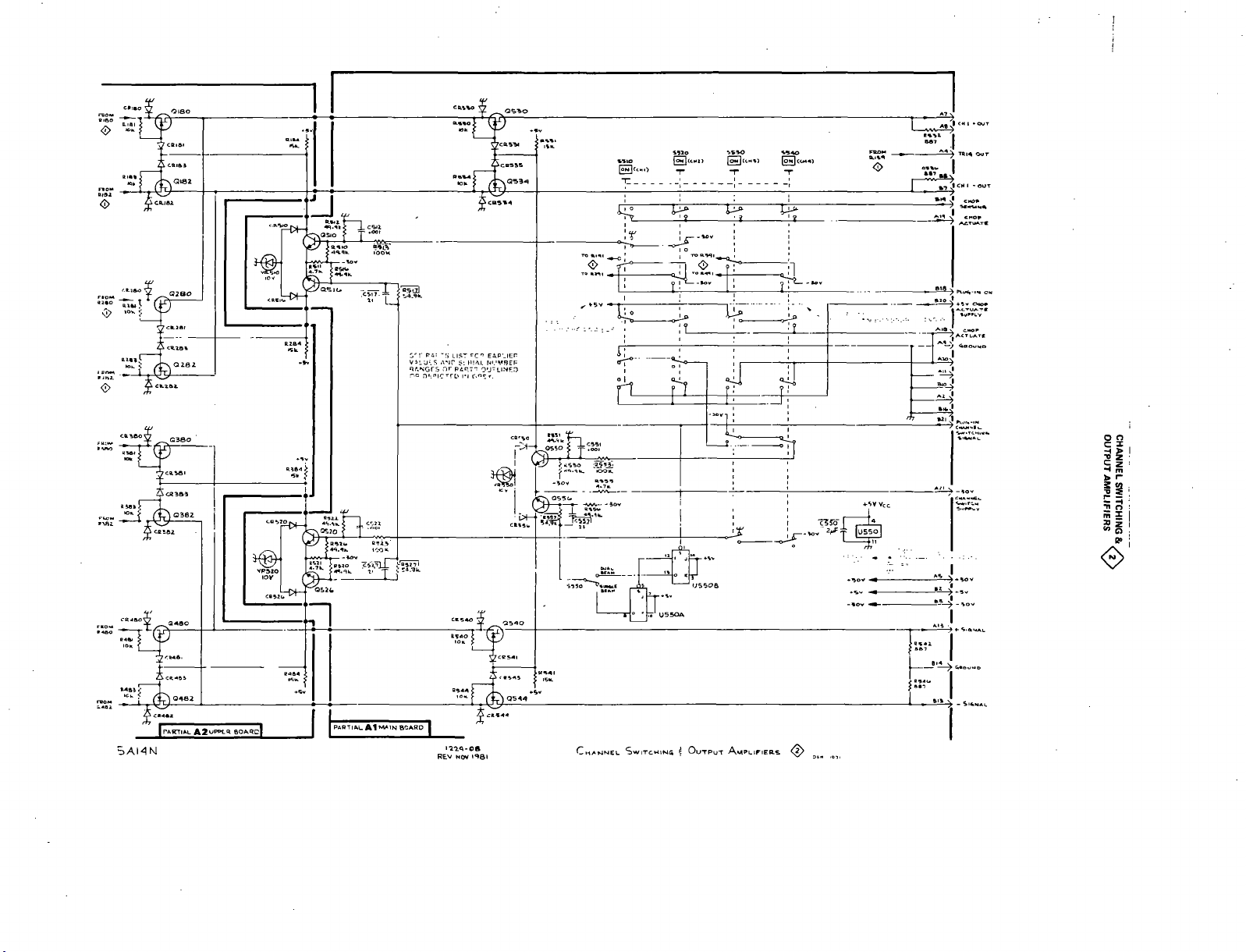
si;
H m
> I-
-n
n :
m
X
a
z
«
o
<^
SAMN
I'^l'^-OS
REV
NOV i*»SI
CMAMNEL
SwiTcwiN(i ^
OUTPUT
AwPLiriERs ^
Page 40

REPLACEABLE
MECHANICAL PARTS
5A14N
PARTS ORDERING INFORMATION
Replacement parls are available from or through your local
Tektronix, Inc. Field Office or representative.
Changes to Tektronix instruments are sometimes made to
accommodate improved components as they become available,
and to give you the benefit of the latest circuit improvements
developed in our engineering department. It is therefore
important, when ordering parts, to include the following
information in your
order;
Part number, instrument type or
number, serial number, and modification number if applicable.
If a part you have ordered has been replaced with a new or
improved part, your local Tektronix, Inc. Field Office or
representative will contact you concerning any change in part
nurriber
Change information, if any, is located at the rear of this
manual.
SPECIAL NOTES AND SYMBOLS
XOOO Part first added at this serial number
OCX Part removed after this serial number
FIGURE AND INDEX NUMBERS
Items in this section are referenced by figure and index
numbers to the illustrations.
INDENTATION SYSTEM
This mechanical parts list is indented to indicate item
relationships. Following is an example of the indentation system
used in the description column.
12 3 4 5
Name & Description
Assembly and/or Component
Attaching parts tor Assembly and lor Component
Detail Part ol Assembly and/or Component
Attactiing parts for Detail Part
Parts of Detail Part
Attactiing parts for Parts of Detail Part
Attaching Parts always appear in the same indentation as
the item if mounts, while the detail parts are indented to the right.
Indented items are part of, and included
with,
the next higher
indentation. The separation symbol — * — indicates the end of
attaching parts.
Attaching parts must be purchased separately, unless otherwise
specified.
ITEM NAME
In the Parts List, an Item Name is separated from the
description by a colon (;). Because of space limitations, an Item
Name may sometimes appear as incomplete. For further Item
Name identification, the U.S. Federal Cataloging Handbook H6-1
can be utilized where possible.
INCH
«
ACTR
ADPTR
ALIGN
AL
ASSEM
ASSV
ATTEN
AWG
BO
BRKT
BRS
BRZ
BSHG
CAB
CAP
CER
CHAS
CKT
COMP
CONig
COV
CPLG
CRT
OEG
DWR
NUMBER SIZE
ACTUATOR
ADAPTER
ALIGNMENT
ALUMINUM
ASSEMBLED
ASSEMBLY
ATTENUATOR
AMERICAN WIRE GAGE
BOARD
BRACKET
BRASS
BRONZE
BUSHING
CABINET
CAPACITOR
CERAMIC
CHASSIS
CIRCUIT
COMPOSITION
CONNECTOR
COVER
COUPLING
CATHODE RAY TUBE
DEGREE
DRAWER
REV I, NOV 1980
ELCTRN
ELEC
ELCTLT
ELEM
EPL
EOPT
EXT
FIL
FLEX
FLH
FLTR
FR
FSTNR
FT
FXD
GSKT
HDL
HEX
HEX HD
HEX SOC
HLCPS
HLEXT
HV
IC
ID
IDENT
IMPLR
ABBREVIATIONS
ELECTRON
ELECTRICAL
ELECTROLYTIC
ELEMENT
ELECTRICAL PARTS LIST
EQUIPMENT
EXTERNAL
FILLISTER HEAD
FLEXIBLE
FLAT HEAD
FILTER
FRAME or FRONT
FASTENER
FOOT
FIXED
GASKET
HANDLE
HEXAGON
HEXAGONAL HEAD
HEXAGONAL SOCKET
HELICAL COMPRESSION
HELICAL EXTENSION
HIGH VOLTAGE
INTEGRATED CIRCUIT
INSIDE DIAMETER
IDENTIFICATION
IMPELLER
IN
INCAND
INSUL
INTL
LPHLDR
MACH
MECH
MTG
NIP
NON VKIRE
OBD
OD
OVH
PHBRZ
PL
PLSTC
PN
PNH
PWR
RCPT
RES
RGD
RLF
RTNR
SCH
SCOPE
SCR
INCH
INCANDESCENT
INSULATOR
INTERNAL
LAMPHOLDER
MACHINE
MECHANICAL
MOUNTING
NIPPLE
NOT WIRE Vl/OUND
ORDER BY DESCRIPTION
OUTSIDE DIAMETER
OVAL HEAD
PHOSPHOR BRONZE
PLAIN or PLATE
PLASTIC
PART NUMBER
PAN HEAD
POVrtR
RECEPTACLE
RESISTOR
RIGID
RELIEF
RETAINER
SOCKET HEAD
OSCILLOSCOPE
SCREW
SE
SECT
SEMICOND SEMICONDUCTOR
SHLD
SHLDR
SKT
SL
SLFLKG
SLVG
SPR
SO
SST
STL
SW
T
TERM
THD
THK
TNSN
TPG
TRH
V
VAR
W/
WSHR
XFMR
XSTR
SINGLE END
SECTION
SHIELD
SHOULDERED
SOCKET
SLIDE
SELF-LOCKING
SLEEVING
SPRING
SQUARE
STAINLESS STEEL
STEEL
SWITCH
TUBE
TERMINAL
THREAD
THICK
TENSION
TAPPING
TRUSS HEAD
VOLTAGE
VARIABLE
WITH
WASHER
TRANSFORMER
TRANSISTOR
4-17
Page 41
Replaceable Mechanical Parts - 5A14N
CROSS INDEX - MFR. CODE NUMBER TO MANUFACTURER
Mfr.
Code
06915 RICHCO PLASTIC
07416 NELSON NWE PUTE
08261 SPECTRA-STRIP AN ELTRA
09922 BURNDY CORP
12327 FREEWAY CORP
127X JUOD WIRE DIV ELECTRONIZED
22526 DU PONT E I DE NEMOURS AND X INC
24931 SPECIALTY CONNECTOR X INC
28520 HEYX MOLDED PROOXTS
45722 USM CORP.. PARKER-KALON FASTENER DIV
Manufacturer Address City. State. Zip Code
X
X
X
CHEMICALS CORP
DU PONT CONNECTOR SYSTEMS
DIV MILITARY PRODUCTS GROUP
5825 N TRIPP AVE
3191 CASITAS
71X LAMPSON AVE
RICHARDS AVE
9301 ALLEN OR
250 TIKNPIKE RD
P 0 BOX 390
515 FISHING CREEK RD
2620 ENDRESS PLACE
P 0 BOX
D
147 MICHIGAN AVE
P 0 BOX
IX
CHICAGO IL 60646
LX ANGELES CA 90039
GARDEN GROVE CA 92642
NORWALKCT 06852
CLEVELAND OH 44125
TURNERS FALLS MA 01376
NEW CUffiERLANO PA 17070-3X7
GREENWDX IN 46142
KENILWORTH NJ 07033
CAMPBELLSVILLE. KY 42718
71785 TRW INC
Tia/
73743 FISCHER SPECIAL MFG
779X SHAKEPRXF
78189 ILLINOIS TXL WORKS INC
79136 WALDES KOHINOOR INC
800X TEKTRONIX INC
83385 MICROXT MANUFACTURING INC
93907 TEXTRtW INC
TK0392 NORTHWEST FASTENER SALES INC
TK0435 LEWIS SCREW
TK1319 MORELLIS
TK1665 PORTLAND DIE AND STAMPING INC
CINCH COWIECTORS
DIV OF ILLINOIS TXL WORKS
SHAKEPRXF DIVISION
GREER-CENTRAL DIV
CAMCAR DIV
X
Q & D
X
PLASTIX
1501 MORSE AVE
446 MORGAN
SAINT CHARLES
ST CHARLES ROAD
47-16 AUSTEL PLACE
49X
P 0 BOX
3221 W BIG BEAVER RO
6X 18TH AVE
7923 SW CIRRUS DRIVE
4114 S PEORIA
1812 16-TH AVE
48X SE 26TH
ST
S W
GRIFITH OR
5X
RO
ELK GRDVE VILLAGE IL 60X7
CINCINNATI OH 452X
aGIN IL X120
ELGIN IL X120
LONG ISLAND CITY NY 11101
BEAVERTON OR 97077
TROY MI 48098
ROCKFORD IL 61101
BEAVERTON OR 97X5
CHICAGO IL 60609
FOREST GROVE X 97116
PORTLAND OR 97202
4-18
REV XT 1987
Page 42

Fig.
Index
No.
1-1
-2
-3
-4
-5
-6
-7
-8
-9
-10
-11
-12
-13
-14
-15
-16
-17
-18
-19
-20
-21
-22
-23
-24
-25
-26
-27
-28
-29
-30
-31
-32
-33
-34
-35
-36
-37
&
Tektronix
Part
3X-1X1-03
213-0153-X
366-1367-X
366-1367-01
213-0153-X
366-1286-X
366-1286-03
366-1690-X
214-1840-X
3X-1257-74
3X-1257-12
3X-1257-11
426-0836-X
426-0681-X
337-1399-X
131-X79-X
131-X79-02
220-0497-X
210-1X9-X
358-X29-X
210-0590-X
210-X78-X
384-1114-X
384-1059-01
358-X78-X
358-0599-X
220-0633-X
355-0170-X
333-1507-X
333-1X7-01
214-1513-X
214-1513-01
105-0718-01
105-0719-X
213-X54-X
386-2117-X
213-X29-X
378-0702-X
378-OlX-X
337-1530-X
337-1530-01
131-06X-X
131-0604-X
136-0235-X
136-02X-02
I36-0728-X
200-1298-X
342-X27-X
361-0RR5-X
361-03fl5-X
337-1555-X
337-1552-X
337-1552-01
376-X51-X
376-X51-01
376-X29-X
384-0162-X
No.
—--«
Serial/Assently
Effective Dscont
XIOIX
BX62X
XIOIX
BXOOX
B063429
BXOOX
XIOIX
8X1129
X31129
X31129
XIOIX
X53219
XIOIX
B0862X
XIOIX
BXOOX
8063429
X63429
MIOIX
X700X
XIOIX
X700X
X700X
XIOIX
BX5859
XIOIX
8X5520
8085520
XIOIX
X73889
XIOIX
8085844
B0882X
B0299X
B063428
X63428
8X1128
8053218
80fl62X
M29999
8063428
8069999
X69999
8085858
8069999
X73888
8085843
No.
Otv
12345 Nane & Description
KNOB:RED.CAL.0.127
.SETSCREW:5-40 X 0.125.STL
KNX:GY.V/DIV.0.252
KNX:CLEAR.V/DIV.0.252
.SETSCREW:5-40 X 0.125,STL
KNX:SIL GY.0.5X
ICNX:GY.0.5
l<J(08.WTCH:SIL GY.0.53
PIN.KNOB SECRG:0.12
PUSH BUTT0N:SIL GY.ON
PUSH 8UnON:SIL GY.CHG
PUSH 8UnON:SIL GY.AC
FRAME.PUSH
FRAME.PIBH
SHIELD.ELEC:SIDE
CONN.RCPT,ELEC:Bf«:.MALE.3 CONTACT
XNN.RCFT.ELEC:BNC.MALE.3 CONTACT
(AHACHING PARTS)
NUT.PLAIN.HEX:0.5-28 X 0.562
WASHER.LOCK:0.521 ID.INT.0.025 Tl+C.SST
(END AHACHING PARTS)
8SHG.MACH TH0:0.375-32
lftJT.PLAIN.HEX:0.375-32 X 0.438
V«SHER.FUT:0.375
EXTENSION SHAFT:7.6
EXTENSION SHAFT:
BUSHING.SLEEVE:0.131
BUSHING.SLEEVE:0.125
NUT.PLAIN,KNURL:0.25-28 X 0.375
STID.SHLDR8STEP:8INDING
PANEL.FRONT:
PANEL,FRONT:
LCH.PL-IN RTNG:PLASTIC
LCH.PL-IN RTNG:PLASTIC
BAR.LATCH RLSE:
LATCH.RETAINING:PLX-IN
SCREW.TPG.TF:2-32 X 0.25,TYPE
SUBPANEL.FRONT:
(AHACHING PARTS)
3
SCREW.TPG.TF:6-20 X 0.375.TYPE
DEG,STL
(END AHACHING PARTS)
8
L£NS,LIGHT:CLEAR
8
LENS.LIGHT:CLEAR
1
SHIELD.ELE;:REAR SXPANEL
1
SHIELD,ELEC:REAR SXPANEL
CKT BOARD ASSY:MAIN(SEE
1
8
.TERMINAL.PIN:0.365
36
.CONTACT.ELEC:CKT X SW.SPR.X
4
.SKT.PL-IN ELEK:TRANSIST0R,6 CONTACT
.SKT,PL-IN ELEK:MICRXIRCUIT.14
1
1
.SKT.PL-IN ELEK:MICR0CKT.14 CONTACT
4
.COVER.LAMP:
1
.SWITCH.SLIDE:(SEE A1S550 REPL)
4
.SWITCH.PIBH:(SEE A1S101,S201.S301,
.S401 REPL)
4
.SWITCH.PUSH:(SEE A1S510,S520.S530.
.S540 REPL)
.INSULAT0R.FIU1:REF MODU.E COVER.POLYEST
1
16
.SPACER.PUSH SW:0.04
8
.SPACER.PB SW:0.164
4
.SHIELO.ELEC:SIGNAL
3
.SHIELD.ELEC:INPUT SWITCH
.SHIELD.ELEC:INPUT SWITCH
3
4
.CPLG.SHAFT.FLEX:0.127
4
.CPLG.SHAFT.FLEX:0.127
4
.CPL6.SHAFT.RX:0.128
4
.EXTENSION SHAFT:8.564
BTN:
BTN:
0.2 X
X 0.2 X
ID X 0.5 X X
ID X
0.392
ID X 1.0
ID X 1.0 X X 0.6 H
0.375
0.375
X 0.23 X 1.059
L X
0.X4-0.1
GND
PRE
X 0.5
L X 0.123
ID X 0.18 X X 0.125 L
ID X 0.25 X X
PXT
Al
L X
0.025
L.TURQUOISE
L.GREEN
ID X
ID X
ID X 0.312
L X 0.125 X.AL
OD X 0.466
OD
X 0.6 H
X.ACETAL
HEX.BRS
HEX.BRS
REPL)
POLYCARBONATE
0.375
0.375
CD PL
NP
BRS
X PL
0.024.STL
X.PLASTIC
0.234
X.BRS
B.FLH.IX
B.FLH.IX
BRZ GLD
PL
BE
DIP
BLUE
X.XLRIN
X.XLRIN
OD.AL
Replaceable Mechanical Parts - SAMN
Mfp.
Code
NP
DEG
H
Mfr. Part
800X
3X-1X1-X
TK0392 ORDER
3X-1367-X
80009
366-1367-01
8XX
TKX92 ORDER
3X-1286-X
800X
8XX
3X-1286-X
3X-1X0-X
8XX
800X
214-1840-X
366-1257-74
800X
366-1257-12
800X
3X-1257-11
800X
426-0836-00
8XX
426-0681-X
800X
337-13X-00
800X
24931
28JR1X-1
24931
28JR270-1
800X
220-0497-00
ORDER
24931
358-X29-00
8XX
73743
282X-402
12327
ORDER
384-1114-X
800X
8XX
384-1059-01
358-X78-X
800X
28520
B-187-125
800X
220-0633-X
355-0170-X
800X
8XX
333-1507-X
800X
333-1507-01
214-1513-X
800X
800X
214-1513-01
105-0718-01
800X
800X
1X-0719-X
ORDER
45722
386-2117-00
800X
93907
ORDER
800X
378-07X-00
800X
378-OlX-OO
800X
337-1530-00
337-1530-01
800X
22526
482X-X6
131-0604-00
800X
71785
133-X-12-062
DILB14P-1XT
09922
DILB14P-1X
09922
800X
2X-1298-X
800X
342-X27-X
TK1319 ORDER
800X
361-n385-X
337-1555-X
800X
337-1552-X
800X
800X
337-1552-01
376-X51-X
800X
BOOM
376-X51-01
800X
376-X29-X
800X
384-0162-X
BY
BY
BY
BY
BY
BY
BY
No.
DESCR
DESCR
DESCR
DESCR
DESCR
DESCR
DESCR
REV XT 1X7
4-19
Page 43
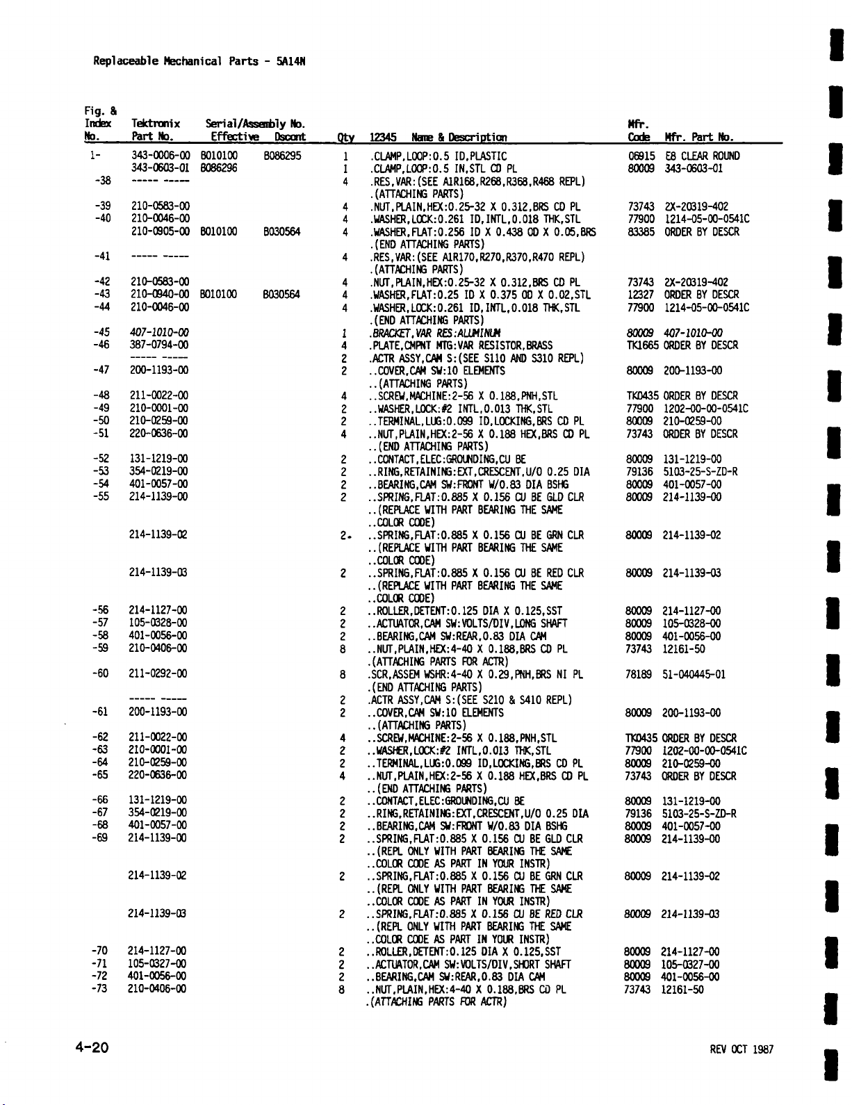
Replaceable Mechanical Parts - 5A14N
Fig.
&
Index Tektronix
No.
Part Ho.
343-0X6-X
1-
343-06X-01
-M
**~~~~ ————
-39
210-nfift3-X
-40
210-0046-X
210-X05-X MlOlX
-41
-42
210-05a3-X
-43
210-0940-X XlOlX
-44
210-0046-X
•45
407-1010-X
-46
387-0794-X
•47
200-1193-X
-48
211-X22-X
•49
210-OXl-X
50
210-X59-X
51
220-0636-X
•52
131-1219-X
•53
354-X19-X
54
401-X57-X
55
214-1139-X
214-1139-X
214-1139-X
56
214-1127-X
57
105-X28-X
58
401-X56-X
59
210-0406-X
60
211-X92-X
-61 2X-1193-X
-62
211-X22-X
-X
210-OXl-X
-64
210-X59-X
-X
220-0636-X
-X
131-1219-X
-67
354-X19-X
-X
401-X57-X
-X
214-1139-X
214-1139-X
214-1139-X
-70
214-1127-X
-71
105-X27-X
-72
401-0056-X
-73
210-04X-X
Serial/Asseibly No.
EffartivB Dscont
XlOlX
6086296
B086295
8030564
8030564
Qtv 12345 Nane & Description
.CLAMP.LOOP:0.5 ID.PLASTIC
.CLAMP.LOOP:0.5 IN.STL
-RES.VAR:(SEE AlRlX,R2ffl.R3X.R4X REPL)
.(ATTACHING PARTS)
.NUT.PLAIN.HEX:0.25-32 X 0.312.BRS
.WASHER,L0CK:0.261 ID.INTL.0.018 THK.STL
.WASHER.FLAT:0.256
.(END AHACHIte PARTS)
.RES.VAR:(SEE A1R170,R270.R370.R470 REPL)
.(AHACHING PARTS)
.NUT.PLAIN.HEX:0.25-32 X 0.312.BRS
4
.WASHER,FLAT:0.25
4
.WASHER.L0CK:0.261 ID.INTL.0.018 THC.STL
4
.(END AH/CHING PARTS)
.BRACKET.VAR RES:ALLWINt>«
1
.PUTE.CMPNT MTS:VAR RESISTOR.BRASS
4
2
.ACTR ASSY.CAM
2
..COVER.CAM SW:10 ELEMENTS
..(AHACHING PARTS)
4
..SCREW.MACHINE:2-56 X O.IX.PNH.STL
2
..WASHER.LXK:#2 INTL.0.013 THK.STL
2
..TERMINAL.LX:0.099 ID.L0CKIN6.BRS
4
..NUT,PLAIN.HEX:2-56 X O.IX HEX.BRS
.. (END AHACHING PARTS)
2
..CONTACT,ELEC:GROUNDING,CU BE
2
..RING,RETAINING:EXT,CRESCENT.U/0 0.25 DIA
2
..BEARING.CAM SW:FRONT W/O.X OIA BSHG
2
..SPRING,FLAT;0.885 X 0.156 X BE GLD CLfi
..(REPLACE WITH PART BEARING THE SAME
..XLX CXE)
..SPRING,FLAT:0.885 X 0.156 X BE 6RN CLR
..(REPLACE WITH PART BEARING THE SAME
..XLORCXE)
..SPRING,FIAT:0.885 X 0.156 X BE RED CLR
..(REPLACE WITH PART BEARIIffi THE SAME
..XLORCXE)
..ROLLER,DETENT:0.125 DIA X 0.125,SST
..ACTUATX,CAM SW:VOLTS/OIV,LONG SHAFT
..BEARING.CAM SW:REAR.O.X DIA CAM
..NUT,PLAIN.HEX:4-40 X 0.IX.BRS
.(AHACHING PARTS R5R ACTR)
.SCR.ASSEM WSHR:4-40 X 0.29.PNH.8RS
.(END AHACHING PARTS)
.ACTR ASSY.CAM
..XVER.CAM SW:10 ELEMENTS
..(AHACHING PARTS)
..SCREW.MttHINE:2-X X O.IX.PNH.STL
..WASHER.L0CK:#2 INTL.0.013 THK.STL
..TEIWINAL.LX:0.099 ID.LOCKING.BRS
..NUT.PLAIN.HEX:2-X X O.IX HEX.BRS
..(END AHACHING PARTS)
..CONTACT,ELEC:GROUNDING.CU BE
..RING.RETAINING:EXT.CRESCENT.U/0 0.25 OIA
..BEARING.CAM SW:FRONT W/O.X DIA XHG
..SPRING.FUT:0.X5 X 0.156 X BE GLD CLR
..(REPL WILY WITH PART BEARING THE SAME
..XLOR CXE AS PART IN YOUR INSTR)
..SPRING.FLAT:0.885 X O.IX X BE GRN CLR
..(REPL ONLY WITH PART BEARING THE SAf€
..XLW CXE AS PART IN YOUR INSTR)
..SPRING.FLAT:0.X5 X 0.156 X BE RED CLR
..(REPL ONLY WITH PART BEARING THE SAME
.
.XLOR CXE AS PART IN YOUR INSTR)
..R0LL£R,DETENT:0.125 DIA X 0.125,SST
..ACTUATOR.CAM SW:VOLTS/DIV.SHORT SHAFT
..BEARING.CAM SW:REAR.0.83 DIA CM
..NUT.PLAIN,HEX:4-40 X 0.1X,BRS
.{AHACHING PARTS FDR ACTR)
S:(SEE
S:(SEE
X PL
ID X
0.438 X X
ID X
0.375
X X
SllO AND S310 REPL)
S210 & S410 REPL)
X PL
O.X.BRS
X PL
O.X.STL
X PL
X PL
X PL
NI PL
X PL
X PL
X PL
Mfr.
Code
Hfr. Part No.
06915
E8 CLEAR ROUND
343-06X-01
800X
73743 2X-2rai9-4X
77900 1214-05-X-0541C
83385 ORDER BY DESCR
73743 2X-2X19-402
12327 ORDER BY DESCR
779X 1214-05-00-0541C
800X 407-1010-X
TK1665 ORDER BY DESCR
800X 200-llX-X
TK0435 ORDER BY DESCR
779X 1202-X-X-0541C
800X 210-X59-00
73743 ORDER BY DESCR
800X 131-1219-X
79136 51X-25-S-Z0-R
800X 401-X57-X
800X 214-1139-X
800X 214-1139-02
800X 214-1139-X
800X 214-1127-X
800X 105-X28-X
800X 401-X56-X
73743 12161-M
781X 51-040445-01
800X 200-llX-X
TX0435 ORDER BY DESCR
779X 12X-X-00-0541C
800X 210-X59-X
73743 ORDER BY DESCR
800X 131-1219-X
79136 51X-25-S-ZD-R
800X 401-X57-X
800X 214-1139-X
800X 214-1139-02
80009 214-1139-X
800X 214-1127-X
800X 105-X27-X
800X 401-X56-X
73743 12161-X
4-20
REV
XT 1X7
Page 44

Fig.
&
Index Telctronix
No,
Part
1-74
211-0116-X
-75
-76
-77
-78
-79
-80
-81
-82
213-0146-X
-X
-84
-85
-86
-87
-88
-89
-90
-91
No.
343-OOX-X
211-0565-X
210-0457-X
210-08X-X
129-0089-X
385-X79-X
337-1533-X
337-1532-X
337-1547-X
334-3448-X 8063639
426-0724-01
426-0725-X
198-2819-X
198-2819-01
198-2819-X
175-0828-X
175-0827-X
175-0832-X
175-0825-X
177-X77-X
131-0707-X
352-OlX-X
Serial/Assenbly
Effective Dscort Qtv 12345 Nane & Description
XlOlX
BX0725
XlOlX
X700X
80800X
XlOlX
X7XX
X700X
M700X
No.
8030724
B069999
8079999
8069999
8 .SCR.ASSEM WSH?:4-40 X 0.312.PNH.BRS.POZ
.(END AH/CHING PARTS)
3 .CLAMP.L00P:0.5 ID.PLASTIC
4 .SCREW.MACHINE:6-32 X 0.250.TRH.STL
2 .NUT.PL.ASSEM WA:6-32 X 0.312.STL
.HASHER.FLAT:0.15
.SPACER.PXT:0.x L.6-32.AL,0.25 HEX
.SPACER.POST:0.375 L W/5-32 THD TTOJ.AL
.SHIELD.ELEC:CHANNEL
.SHIELD.ELEC:CHANNEL
.SHIELD.ELEC:CHANNEL
(ATTACHING PARTS FOR
SCREW.TPG.TF:6-20 X 0.312.TYPE B.PNH.STL
(END AHACHING PARTS)
^WRKER.IDENT:MARKED NOTICE
OCT BOARD ASSY:SECONDARY(SEE
FR SECT.PLUG-IN:XnOM
FR SECT.PLUG-IN:TOP
WIRE SET.ELEC:
WIRE SET.ELEC:
WIRE
SET
AR .CABLE,SP,ELEC:5,26 AWG,STWD,PVC JKT,RBN
AR .CABLE,SP,ELEC:4.26 AW6.STRD.PVC JKT.IfflN
AR .CABL£.SP,ELEC:9,26 AWG,STRO.PVC JKT.RBN
AR .CABLE.SP.ELEC:2.26 AWG.STRD.PVC JKT.RBN
AR .CABLE.RF:M
4 . XNTACT.
2 .HLOR.TERM C0NN:2 WIRE.REO
ELEC:
ELEC:
OW
22-26
ID X
CQAX.9-0
AWG. BRS. X BE
0.375 X X
1-2
2-3
3-4
CKT
80)
A2
REPL)
Replaceable Mechanical Parts - 5A14N
Hfr.
Code
X PL
0.032.STL
GLD
PL
Mfr. Part
779X ORDER
06915
E8 CLEAR ROUND
TK0435
ORDER
781X
511-X1800-X
12327
ORDER
800X
129-0089-X
BOOM
385-X79-X
BOOM
337-1533-00
800M
337-1532-00
800X
337-1547-X
83385 XDER
07416 ORDER
800M
426-0724-01
8XM
426-0725-X
8MM
198-2819-X
BOOM
198-2819-01
800M
198-2819-02
08261
111-2699-955
08261
111-2699-954
08261
111-2699-956
8XX
175-0825-X
127X
ORDER
22526
47439-XO
BOOM
352-01X-02
BY
BY
BY
BY
BY
BY
No.
DESCR
DESCR
DESCR
DESCR
DESCR
DESCR
070-1229-X
STANDARD ACCESSORIES
1 MANUAL.TECH:INSTRXTION
800X 070-1229-X
REV
XT 1X7
4-21
Page 45

Page 46

FIG.
1 EXPLODED
Page 47

MANUAL CHANGE INFORMATION
At Tektronix, we continually strive to keep up with latest electronic developments
by adding circuit and component improvements to our instruments as soon as they
are developed and tested.
Sometimes, due to printing and shipping requirements, we can't get these
changes immediately into printed manuals. Hence, your manual may contain new
change Information on following pages.
A single change may affect several sections. Since the change information sheets
are carried in the manual until all changes are permanently entered, some
duplication may occur. If no such change pages appear following this page, your
manual is correct as printed.
o
z
>
z
a
o
9
>
Page 48

 Loading...