


INSTRUCTION MANUAL
Digital Multimeter
Model 5900

WARRANTY
We warrant each of our products to be free from defects in material
and workmanship. Our obligation under this warranty is to repair
or replace any instrument or part thereof which, within a year after
shipment, proves defective upon examination. We will pay local
domestic surface freight costs.
To exercise this warranty, write or call your local Keithley repre-
sentative, or contact Keithley headquarters in Cleveland, Ohio.
You will be given prompt assistance and shipping instructions,
REPAIRS AND
CALIBRATION
Keithley Instruments maintains a complete repair and calibration
service as well as a standards laboratory in Cleveland, Ohio. A
service facility is also located in Los Angeles for our west coast
customers.
A Keithley service facility at our Munich, Germany office is
available for our customers throughout Europe. Service in the
United Kingdom’can be handled at our office in Reading. Addition-
ally, Keithley representatives in most countries maintain service
and calibration facilities.
To insure prompt repair or recalibration service, please contact
your local field representative or Keithley headquarters directly
before returning the instrument. Estimates for repairs, normal
recalibrations and calibrations traceable to the National Bureau of
Standards are available upon request.
KEITHLEY
The measurement engineers.
Keithley Instruments, inc., 28775 Aurora Road, Cleveland, Ohio 44139. (216) 248-0400
European Headquarters: Heiglhofstrasse 5, D-8000 Munchen 70 West Germany, (0811) 7144065
Unlted Kingdom: 1 Boulton Road, Reading, Berkshire, (0734) 861287
France: 44 Rue Anatole France. F-91121 Palaiseau (01) 928-00-48

FOR YOUR SAFETY
Before undertaking any maintenance procedure, whether it
be a specific troubleshooting or maintenance procedure
described herein or an exploratory procedure aimed at
determining whether there has been a malfunction, read the
applicable section of this manual and note carefully the
WARNING and CADTlON notices contained therein.
The equipment described in this manual contains voltages
hazardous to human life and safety and which is capable of
inflicting personal injury. The cautionary and warning
notes arc included in this manual to alert operator and
maintenance personnel to the electrical hazards and thus
prevent personal injury and damage to equipment.
If this instrument is to be powered from the AC Mains
through an autotransformer (such as a Vartac or equivalent)
ensure that the instrument common connector is connected to the ground (earth) connection of the power
mains.
Before operating the unit ensure that the protective conductor (green wire) is connected to the ground (earth)
protective conductor of the power outlet. Do not defeat
the protective feature of the third protective conductor in
the power cord by using a two conductor extension cord or
a three-prong/two-prong adapter.
Maintenance and calibration procedures contained in this
manual sometimes call for operation of the unit with power
appliedandprotective covers removed. Read the procedures
carefully and heed Warnings to avoid “live” circuit points
to ensure your personal safety.
Before operating this instrument,
1. Ensure that the instrument is configured to
operate on the voltage available at the power
source See Installation section.
Ensure that the proper fuse is in place in the
2.
instrument for the power source on which the
instrument is to be operated.
3. Ensure that all other devices connected to or in
proximity to this instrument are properly grounded
or connected to the protective third-wire earth
ground.

COPYRIGHT
0
Copyright
States of America.
not be reproduced in any form without written permission of the
publishers.
1976 by Keithley Instruments, Inc. Printed in the United
All rights reserved. This book or parts thereof may
PROPRIETARY NOTICE
This document and the technical data herein disclosed, are proprietary
to Keithley Instruments, Inc., and shall not, without express written
permission of Keithley Instruments, Inc., be used, in whole or in part
to solicit quotations from a competitive source or used for manufacture
by anyone other than Keithley Instruments, Inc. The information
herein has been developed at private expense, and may only be used for
operation and maintenance reference purposes or for purposes of
engineering evaluation and incorporation into technical specifications
and other documents which specify procurement of products from
Keithley Instruments, Inc.

TABLE OF CONTENTS
Section
1
1.1
1.7
1.9
1.11
1.13
1.15
1.17
1.19
I .26
I .32
2
2.1
2.4
2.6
2.8
2.12
2.13
2.16
2.18
2.19
2.21
2.23
2.24
2.28
2.42
2.44
2.46
2.48
2.50
2.54
2.56
2.59
2.60
2.62
2.64
2.66
2.68
2.70
2.72
2.75
2.77
GENERALDESCRIPTION
Introduction
Options .’
Model 42 Remote Programming
Rear Input Options(-I, -1s)
Rack-Mounting Flanges (403402)
High-Voltage Probe
Current Shunt Set (651)
Electrical Description
MechonicalDescription
Specifications
mSTALLATION& OPERATION
Unpacking and Inspection
Bench Operation
Rack Mounting
Power Connections
Input/Output Cabling
Binding Posts
Rear Input Connector
Manual Operation
Controls
Display ...............
Measurement Connections.
Basic Voltage Measurement
Ohms Measurement
Ratio Measurements
System Capabilities
Printer Output
Program Input.
Logic Levelsand Electronic Interface
Driving the Inputs
TTL Loading Conditions
Exceptions to Input Loading Conditions
‘ITL Output Capabilities
Thning Sequence
Other Read CommandOptions
Reading Rates.
Superfast
Printer Output
Numerical Data
Function Data.
Range Data.
............
............
............
.............
. JZOI .........
.............
............
............
.........
............
..........
.........
...........
........
.......
..........
..........
...........
...........
..........
........
........
...........
......
...........
...........
...........
Title Page
. .
.....
...
I-1
1-l
I-I
I-1
I-1
1.2
1-2
l-2
1-2
I.3
l-3
2-1
2-l
2-l
2-1
2-l
2-2
2-2
2-2
2-2
2-2
2-2
2.4
24
24
2-7
2-7
2-8
2-8
2-8
2-B
2-8
2.10
2-10
2.10
2.11
2-12
2.12
2-13
2-13
‘2.14
2.14
111

980453
Section
TABLE OF CONTENTS (continued)
2.79
2.81
2.83
2.84
2.86
2.88
2.90
2.93
2.95
2.97
“NO” Indication
Status Output Lines
Input Control Lines
System Direct Command
Remote Programming
SystemControl
Function Programming
Range Programming
+ Five Volts
Hold
2.99 Read Commands
2.101
2.103
2.105
2.107
2.109
Timeouts
Data Inhibit
Program Storage
Superfast
Adding/Removing Accessories
3 SPECIFICATIONTESTS .....
3.1
3.4
3.6
4
4.1
4.3
4.5
4.7
General ...........
Required Equipment ......
Procedure ..........
THEORY OF OPERATION
General
Mechanical Description
Electrical Description
Signal Conditioning Section
4.10 Switching Board
4.14
4.18
4.2 1
4.24
4.28
4.30
4.33
4.35
4.37
4.52
4.54
4.56
4.70
4.12
4.74
OhmsConverter
Scaling Atnplifier
Averaging AC Converter
RMSACConverter
Attenuator
Isolator
Switching Bypass.
Integration
Digitizer,
Ratio, Standard
Ratio,Option
Display Board
Main Logic and Control Circuitry
Control Logic
Program Cycle
. .
2.14
2.15
2-15
2.16
2.16
2.16
2.16
2.17
2.17
2-17
2.17
2.17
2-17
2-17
2.18
2.18
3.1
3-l
3-l
3-1
4.1
4-l
4-l
4-l
4-1
4-l
4-1
4.3
4.9
4-9
4.9
4.9
4-9
4-9
4.12
4-14
4.15
4.15
4.17
4-17
4.19
iv

TABLE OF CONTENTS (continued)
980453
Section
4.76 Display Logic
4.78 Superfast
4.80
4.82
5
5.1
5.3
Power Supplies
Program.
CALIBRATION
scope
General
5.5
5.7
5.10
5.19
5.23
Preliminary Procedure
5.24
5.26
5.28
5.30
5.32
Recalibration Procedure .
5.34
5.35
5.36
5.38
DC Range Calibration
Ohms Calibration.
5.39
5.40
5.41
Ohms Range
AC Calibration (Model 33).
5.42
5.43
5.44
5.45
5.46
RMS AC Calibration (Model 32)
4-Wire Ratio Calibration
Troubleshooting
5.48
5.50
5.52
5.54
5.55
5.86
Board Revision
..................
...................
.................
...................
.................
....................
Required Equipment
..............
Fabricated Calibration Equipment
DC Voltage Sources
AC Voltage Sources
...............
...............
...............
Warmup.
Familiarization
Calibration Points
Environmental Considerations
Isolator Zero
..................
................
...............
...........
.................
DC Voltage Zero and Gain.
................
ohms Zero
..................
..................
AC Converter Zero
Frequency Response
...............
..............
..............
.................
Troubleshooting Equipment
Power Supply Check
Operational Check
...............
Preliminary Instrument Setup
Circuit Descriptions
...............
............
...............
...........
.................
Title
..........
4-19
4.19
4.19
4.20
5-1
5-l
5-l
5-l
5-l
5-l
5-4
5-4
s-4
54
54
5-4
54
5-6
5-6
5-6
5-6
5.6
5-7
5.7
5.7
s-7
5-9
s-10
s-10
s-10
S-10
5-l 1
5-1 1
5.11
s-14
1
DRAWINGS . . . . .
PARTS LIST . . . . . . . . . . .
6-1
7-1
v/vi blank

LIST OF ILLUSTRATIONS
Figure
2.1
2.2
2.3
2.4
2.5
2.6
2.7
2.8
2.9
2.10
2.11
2.12
2.13
2.14
2.15
2.16
2.17
4.1
4.2
4.3
4.4
4.5
4.6
4.7
4.8
4.9
4.10
4.11
4.12
4.13
4.14
4.15
4.16
4.17
5.1
5.2
5.3
5.4
5.5
5.6
5.7
5.8
5.9
1.1
1.2
Block Diagram -Model 5900
Dimensions,
Rack Mount Installation’
Cabling Diagram, Binding Posts
Cabling Diagram, Rear Input
Readout
Front Panel
Basic Voltage Measurement Connections
Maximum RMSlnput Voltage
Two Wire Ohms Measurements
Four Wire Ohms Measurement
Rear Panel
Measurement Sequence.
Command Timing
Minimum Read Rate vs. Input
Superfast Read Rate (Worst Case)
Pin Assignments 5201 PRINTER OUT
Pin Assignments 5202 PROGRAM INPUl
Jumper Location
Mechanical Assembly
Signal Flow, Loaded DVM.
Switching Board
Signal Flow of Switching Board
Ohms Converter
OhmsMeasurement Systems
Scaling Amplifier
Averaging AC Converter
RMS AC Converter
Attenuator/Isolator DC.
Signal Flow, Switching Bypass
Digitizer.
Integration Timing Diagram
4.Wire Ratio Option
Display Board
Main Logic&Control Block Diagram
Program Block Diagram.
10 Volt Source
Generating Accurate DC Levels
AC Source
Adjustment Locations
Ohms Input Connection
Connections for Ohms Range Adjustment
4.Wire Connections
AC Adjustment Locations
4.Wire Ratio Adjustment Locations
Title Page
l-2
l-3
2-l
2-2
2-2
2-2
2-3
2.4
2-4
2-s
2-6
2-8
2-9
2-11
2.12
2.13
2-14
2-16
Z-IX
4-2
4.3
4-4
4.5
4-6
4-7
4-R
4-8
4.10
4.11
4.12
4-13
4.14
4-1s
4.15
4-18
4-20
5-2
s-2
s-3
s-s
S-6
5.7
s-7
S-8
S-IO
vii

980453
LIST OF ILLUSTRATIONS (continued)
Figure
6.1
Layout, Logic and Interconnection
6.2 Layout, Readout
6.3
6.4
6.5
6.6
6.7
6.8
Schematic, Logic and Interconnection ..........
Schematic, Power Supply
Layout, Attenuator
Schematic, Attenuator
Layout, Switching
Schematic, Switching
6.9 Layout, Isolator
6.10
6.11
6.12
Schematic, Isolator
Layout, IOV Reference Amplifier
Layout, Digitizer
.................
..............
................
...............
................
...............
.................
................
.................
...........
...........
6.13 Schematic, Digitizer and 1OV Reference Amplifier ......
6.14
Layout, Program
6.15 Schematic, Program
6.16
layout, Display
6.17 Schematic, Display
6.18
6.19
6.20
Layout, AC Converter
Schematic, AC Converter
Layout, RMS Converter
6.21 Schematic, RMS Converter
6.22
6.23
Layout, Scaling Amplifier
Schematic, Scaling Amplifier
6.24 Layout, Ohms Converter
6.25 Schematic, Ohms Converter
6.26
Layout, 4.Wire Ratio
6.27 Schematic, 4.Wir-s Ratio
6.28 Layout,RearPanel
.................
................
.................
................
...............
..............
..............
.............
..............
.............
..............
.............
...............
..............
................
6.29 Layout, Parallel Front-Rear Input (-1) ..........
6.30 Layout, Switchable Front.Rear Input (-IS) ........
Title
Page
6-3
6.3
6-S
6-7
6.8
6.9
6-10
6-11
6.12
6-13
6.14
6.14
6-15
6.16
6.17
6.18
6.19
6.20
6-21
6.22
6.23
6.24
6.25
6-26
6-27
6.28
6.29
6.30
6.3 1
6-32
viii

LIST OF TABLES
Table
1.1
1.2
2.1
2.2
2.3
2.4
2.5
2.6
2.7
2.8
3.1
3.2
3.3
3.4
3.5
3.6
3.7
3.8
3.9
3.10
3.11
3.12
4.1
4.2
4.3
4.4
4.5
4.6
4.7
5.1
5.2
5.3
5.4
5.5
5.6
5.7
5.8
5.9
5.10
7.1
7.2
Measurement Capability
Specifications
Operating Controls
Maximum Input Voltage
Positive True Logic Relationships
Range Codes(Printer Output)
Function Programming
Range Codes(Programmet)
Timeouts
Maximum Input Voltage
Required Equipment
DC Range Check(Low Ranges)
DC Range Check (High Ranges)
3.Wire Ratio Check
4.Wire Ratio Check
DC Input Resistance.
Model 33 AC Converter Range Check
Model 32 AC Converter Range Check
Ohms-Megohms Range Check.
Common Mode Rejection (In DC Volts Function)
Normal Mode Noise Rejection (In DC Volts Function)
Common Mode Rejection (In AC Volts Function)
Switching Board Range Decode
Range Switch Code
Autorange Logic
Relay Logic Coding
Annunciator Logic
“NO” Annunciator Logic
Program Logic Conversion
Required Calibration Equipment
Fixed Voltage Dividers
DC Source Accuracies
AC Source Accuracies
Power Supply Check
OperationalCheck
Trollblesllooting Guide
Troubleshooting Chart-Digitizer and 1OV Reference Amplifier
Troubleshooting Chart. Isolator and Attenuator Boards
Troubleshooting Chart
Table7.1
List of Suppliers
................
...............
....................
...............................
.............................
..........................
.............. 1 1 : : 1 1 1 1 1 1 1 1 1 :
..........................
............... : : : : : : : : : : : ,: : : : :
..................
................
.......... : : : : : : : : : : : : : : : :
.....................
........................
...............
...............
...........................
......................
................
..................
....................
...................
............................
............................
..........................
..........................
.......................
...........................
...........................
...........................
.........................
...........................
Optional Accessories
...............
..............
...................
: : : : : : : : : : : : : : :
............. : : :
: : : : : : : : : : : : : : :
................
: : : : : : : : :
: : : : : : : : : : : : :
: : : : : :
: : : :
: : : : : : : : :
.............
Page
1-1
1-4
2.3
2.4
2-a
2.15
2.17
2.17
2-18
2.18
3-1
3.2
3-3
3-4
3-s
3.6
3-7
3-8
3-9
3-10
3-11
3.12
4-1
4.16
4-16
4.16
4.17
4.17
4-2 1
5-a
S-l
s-3
s-4
S-II
s-1 1
s-12
s-13
s-14
s-14
7-1
7-l
980453
ix


SECTION 1
GENERAL DESCRIPTION
1.1 INTRODUCTION.
The Model 5900 Digital Multimeter is a five-decade
1.2
instrument with a sixth digit providing 60% overrange. The
basic instrument is equipped for dc and dc/dc ratio measurements on five ranges. With the addition of the optional
AC Converter, a-c and ac/dc ratio measurements on four
ranges are available. The Ohms Converter, also optional,
adds ohms measurements on eight ranges. Complete measurement capability of a fully equipped instrument is tabulated in table 1 .l.
Table 1 .I - Measurement Capability
r
DC & Dc/Dc
RATIO
Range (Basic 5900)
.lV I x I
1vI x I
I
1ov X
FUNCTION
OhIllS
(Model 52
Ohms
Converter)
I
AC & AC/DC
RATIO
(Model 32
or 33
AC Converter)
1
IOOV I x I
ooov I x I
100.
I
.I KS2 X
I x
until a single reading is commanded by an external command. The new measurement is then held until the next
external command. In Periodic mbde (RATE control CW),
measurements are made automatic+ly at the rate of approximately four per second.
1.5 The basic Model 5900 includes an analog output
voltage that is proportional to the parameter being measured (except ratio). The voltage, at 20 volts maximum, is
available at a rear panel connector.
Also included as standard equipment is a solid-state
1.6
isolated BCD output. TTL-compatible output levels of the
reading, function, range, etc., plus a print command are
provided. An additional line enables a new reading to be
commanded externally. An optional isolated remote pro.
gramming unit (Model 42) allows all operating commands to
be made extcmally.
1.7 OPTIONS.
1.8 All optional accessories having model numbers are
plug-in circuit boards that may be added at any time. A
calibrated accessory board can be installed without affecting the d-c calibration of the basic instrument. An
instrument shipped without PCB accessories will not be
equipped with a Function Switching PCB assembly. This
board must be added when accessory boards are installed.
Analog accessories are identified in table 1 .l.
1Kn
10Kn 1
100 K$-l 1
000 KS2 1
lOMa/
lOOMa 1
1.3 Range can be selected manually or automatically
(autorange).
ular measurement is selected automatically (full scale is defined as “100000” on any range). The instrument “up
ranges” at 16U% of full scale and “downranges” at 15% of
full scale. Polarity selection is also automatic and is displayed on the readout.
1.4
(RATE control on EXT), a measurement is held (displayed)
In AUTO range, the proper range for a partic-
Two operating modes are provided. In Hold mode
X
I x
I x
I x
I x
I x
Model 42 Remote Programming.
1.9
The Model 42 Remote Programming accessory al-
1.10
lows the selection of function, range, filter, read command,
etc., to be made externally. Auto range selection is also
provided and appropriate timeouts are generated internally
when ranging takes place. Remote Programming “overrides”
all manual control settings to prevent erratic selections.
Complete isolation of the programming unit is achieved by
the use of photoauplers and pulse transformers.
1.11 Rear Input Options (-1, -lB, -1s. -1SB).
1.12
5900 DMM. The option designated -1 or -IB consists of
connector 5204 on the back panel with input lines +
INPUT, + CURRENT, and GUARD wired in parallel with
the front panel input terminals; the option designated -1s
or -1SB is the same as the -1 or -lB except that the front or
rear inputs are selectable by a switch on the front panel.
Two rear input options are available for the Model
b
I-I

980453
T T
1.13 Rack-Mounting Flanges (403402).
1.14 Rack.Mounting Flatages are used where 1111’ IIIS~~U-
ment is to be installed in a relay-rack or cabinet.
1.15 High-Voltage Probe (641).
1.16 The High.Voltage Probe extends the voltage range of
the instrument up to 10,000 volts (or 7SOOV rms). It is an
insulated prube containing a 1000: 1 voltage divider.
l-2
1.17 Current Shunt Set (651).
I .I8 The Current Shunt Set consists of six precision
sIllill assemblies witb values selected to produce a voltage
drop that, n~e:tsured in millivolts. Ins a numerical value
cqual to 111~ current Ilow in milliamps or micro;tmps.
1.19 ELECTRICAL DESCRIPTION.
1.70
1be Model 5900 DMM is a dual slope integration
instrument consisting of three main functional areas: signal
9804.53
conditioning, integrating, and control/display. A block diagram of the instrument is shown in figure I, 1.
1.21 The signal conditioning section includes the
Switching p-c board, AC Converter, Ohms Converter,
Attenuator, and Isolator. The function of these circuits is
to convert the incoming signal to 10 MC, full scale into the
integrator.
1.22 The Integrating section consists of the Integrator
amplifier, Null Detector and + reference voltages. The
function of these circuits is to convert the conditioned in.
put signal to an equivalent time period and to transmit this
iime period to the display portion of the DMM.
1.23 Dual slope integration operates as follows in a
sequence of program (PCM) states:
a. Signal Integration (KM-A). The integrator capaci-
tor charges to a voltage proportional to the input
voltage during a 20 msec sampling period.
b. Reference Integrate (KM-C). During this period,
the integrator capacitor discharges at a constant current. The time that the integrator requires to discharge (full discharge detected by the Null Detector)
is measured by the counter. The data in the counter
at the end of PCM.C is proportional to the input
voltage.
1.28 The Function Switching board is used only when
either or both of the options (AC and Ohms) are installed.
With no options installed, the Function Switching board is
replaced with the Switching Bypass board. The Switching
Bypass merely connects the + Input (from input connector)
directly to the Isolator input and the - Input to ground.
1.29 At the rear edge of the Logic and Interconnection
assembly is a PCB connector that extends to the rear panel
and serves as the BCD output connector 1201. If the
optional Remote Program board is installed, it is mounted
on stand-offs above the Logic and Interconnection board
with the PROGRAM INPUT connector (J202) available at
the rear panel above the BCD OUTPUT connector.
1.30 The POWER input connector 1203, the power transformer, and power transistors for the power supply are
mounted on the rear panel of the instrument. Other power
supply components are mounted on the Logic and Inter-
connection assembly. Also mounted on the rear panel, in
addition to .I201 and 1202, is the rear INPUT connector
J204, the ANALOG OUTPUT connector and common, the
EXTernal REFerence connector and common, and the line
fuse F201,
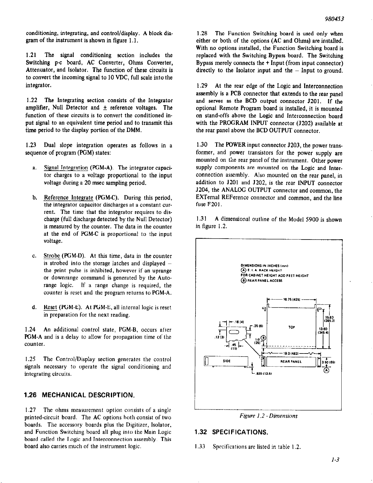
1.31 A dimensional outline of the Model 5900 is shown
in tigure 1.2.
c. Strobe @CM-D). At this time, data in the counter
is strobed into the storage latches and displayed -
the print pulse is inhibited, however if an uprange
or downrange command is generated by the Autorange logic. If a range change is required, the
counter is reset and the program returns to PGM-A.
d. Reset @‘CM-E). At PCM-E, all internal logic is reset
in preparation for the next reading.
1.24 An additional control state, PGM.B, occurs after
PGM-A and is a delay to allow for propagation time of the
counter.
1.25 The Control/Display section generates the control
signals necessary to operate the signal conditioning and
integrating circuits.
1.26 MECHANICAL DESCRIPTION.
1.21 The ohms measurement option consists of a single
printed-circuit board. The AC options both consist of two
boards. The accessory boards plus the Digitizer, Isolator,
and Function Switching board all plug into the Main Logic
board called the Logic and Interconnection assembly. This
board also carries much of the instrument logic.
Figure 1.2 Dimensions
1.32 SPECIFICATIONS.
1.33 Specifications are listed in table 1.2.
1-3

980453
Table 1.2 - Specifications
SPECIFICATIONS, MODEL SSOO
AS A DC VOLTMETER IBASIC INSTRUMENTl
RATIO tdcldc. mVldc. acldc)
SPECIFICATIONS CONTINUED NEXT PAOE

Table 1.2 -Specifications (continued)
980453
l-5


SECTION 2
2.1 UNPACKING AND INSPECTION.
INSTALLATION & OPERATION
2.2
plastic-foam form within a cardboard carton for shipment.
The plastic form holds the DMM securely in the carton and
absorbs any reasonable external shock normally encountered
in transit. Prior to unpacking, examine the exterior of the
shipping carton for any signs of damage. Carefully remove
the DMM from the carton and inspect the exterior of the
instrument for any signs of damage. If damage is found,
notify the carrier immediately.
2.3 Included with the instrument in the packing container are the instruction manual, power cord, and rear input and BCD output mating connectors. With instruments
equipped with remote programming, a mating connector
for that accessory is included.
2.4 BENCH OPERATION.
2.5 Each Model 5900 is equipped with a tilt bail or
“kickstand” to enable the front of the instrument to be
elevated for convenient bench use. The tilt bail is attached
to the two front supporting “feet” at the bottom of the
instrument. For use, the bail is pulled down to its supporting position.
The Model 5900 DMM is packed in a molded
2.6 RACK MOUNTING.
2.1 The instrument can be mounted in a standard 19.
inch rack with the optional rack-mounting flanges (403402,
includes attaching hardware). To install the flanges, proceed as follows:
a. With instrument on its side, remove four Phillips-
head screws holding bottom cover. Remove cover.
Remove screws holding feet (and bail) in place. Replace bottom cover.
b. Place one of the supplied screws through each of
the two holes in the mounting flange (figure 2.1).
Thread a securing nut onto each screw just enough
to attach it to the screw (approximately one turn).
c. Place the mounting flange onto the mounting slot
in the instrument side panel so that the securing
nuts fit entirely into the slot. Be sure the rackmount slots on the flange are toward the front of
the instrument.
d. Tighten screws. The securing nuts will rotate and
hold the flange securely in place.
2.6 POWER CONNECTIONS.
2.9 Standard units operate on either 1 IS volts or 230
volts, SO to 60 Hz (400 Hz available). Power consumption
is less than 40 watts. Operation on either of the two line
voltages is selectable by a slide switch on the rear panel.
Operation on lOO/ZOO volts or 1201240 volts is possible by
simple rewiring of the power transformer secondary wires:
WARNING
Disconnect the instrument from the AC Power source
before attempting to change power connections.
Potentially lethal voltages are exposed when covers
are removed.
a. For operation on 100/200 volts, cut the brown wire
1” from the transformer and splice it to the red
wire on the transformer; cut the blue wire 1” from
the transformer and splice it to the violet wire.
b. For operation on 120/240 volts, cut the brown
wire 1” from the transformer and splice it to the
black wire; cut the blue wire and splice it to the
yellow wire on the transformer.
2-I

980453
2.10 A standard power cable having a three-pin plug is
supplied with the instrument. It connects to POWER con.
nectar 5203. The ground pin (round) is attached to the
instrument case. It is important that this pin be connected
to a good quality earth ground.
2.1 I
Fuse receptacle F20l on the rear panel is equipped
with a .5 amp fuse in domestic units.
2.12 INPUT/OUTPUT CABLING.
2.13 Binding Posts.
2.14 Several connectors on the Model 5900 consist of a
pair of binding posts spaced so as to accept standard
“banana” plugs. The connectors are:
I
Front Panel
I
Rear Panel
+ INPUT f. ANALOG OUTPUT
+ OHMS CURRENT
?1 REFerence INput
2.15 Input cables to fit this type of connector can be
ordered from Keithley (P/N 5900-402190). Figure 2.2 is a
wiring diagram of this cable included for assistance to users
desiring to construct their own cables.
panel binding posts. The rear-panel input lines are wired in
parallel with the front-panel input lines. It is recommended
that the cable for the mating connector be constructed as
shown in figure 2.3 using two two-conductor shielded
cables. Other configurations may be desirable depending
on the ohms measuring method to be used (see paragraph 2.28).
I
2.18 MANUAL OPERATION.
2.19 Controls.
2.16 Rear Input Connector.
2.17 Instruments equipped with the -I or -IS rear input
option are supplied with 5204 7.pin input connector
(Keithley P/N 5900-600673) and a mating connector
(Keithley P/N 5900-600616). The instrument acceptsinputs
applied to this connector or inputs applied to the front-
2.20 All operating controls are located on the front panel
of the instrument. They are shown in figure 2.5 and their
operation described in table 2.1. Description of Systems
operation begins in paragraph 2.44.
2.21 DISPLAY.
2.22 The Pisplay consists of 6 LED decimal readout
devices with moving decimal point. The decimal point
moves in conjunction with the range switchor automatically
in auto range. Maximum usable readout with overrange is
159999. Overload is indicated by a NO and 160000 readout. A non-compatible range and function is indicated by
a NO. However, mechanical interlocks are provided to prevent illegal combinations from the front panel. Figure 2.4
illustrates the readout, NO indicator, polarity sign and the
DC MO
+
r /--- r-7 ,---I ,---I ,--1 AC
- I L-, L-4 L-4 L-,’ L-4 PGM
NO,’ --J. ,’
Fiwe 2.4 . Readout
: : :
KO
n
FIL R
2-2

Figure 2.5 -Front Panel
Table 2.1 . Operating Controls
Control
POW1
(rocker switch)
Function Select
(rotary switch)
Range Select
(rotary switch)
DATA OUTPUT
(pushbutton)
Position
ON (UP)
OFF (down)
ACT
DC
AUTO
Other Positions
Depressed
Function
Applies power to instrument
Removes power from instrument
Selects the measurement of AC voltages on the I, IO, 100, and
1000 volt ranges (max. input, 1OOOV RMS)
Selects the measurement of DC voltages on the .l, 1, IO, 100,
and 1000 volt ranges (max. input, IlOOV)
Selects the measurement of resistance on the 10 ohm range; on
the.1,1,10,100,andlOOOkilohmsranges;oronthe10or100
Megohm ranges
Selects Auto Range in which the optimum range is selected automatically by internal circuits. Uprange occurs at 160% of full
scale; downrange occurs at 15% of full scale
Enables manual selection of fiied ranges. Ranges permissible for
each function are inscribed on the parlel
,Enables the print pulse causing BCD data at P201 to be recorded
by printer, or other output device. (Output data is present at
P201 regardless of the position of this switch.)
PROGRAM CONTROL
(pushbutton)
Depressed
Enables the selection of range, function, and mode to be made
externally through the remote programming connector and dis.
ables all front panel controls (requires programming option)
RATIO
(pushbutton)
Depressed
Selects a ratio measurement in which the readout represents the
ratio of the input to an external d-c reference voltage (applied at
terminals on the rear panel) multiplied by 10: Ein/ERafx 10
FILTER
Depressed
Adds an active four.pole filter across the input circuit
(pushbutton)
RATE EXT (ccw)
(pot)
cw
FRONT/REAR FRONT
Selects the Hold mode. A new reading is initiated through the
remote program input
Increase periodic read rate to a maximum of four readings/second
Connects front panel data input terminals to instrument
(slide switch)
REAR
Connects rear panel data input terminals to instrument
*NOTE: Ohms input terminals are open in AC or DC function.
TNOTE: For inputs greater than lSOV, Filter should be “IN”.

980453
2.23 MEASUREMENT CONNECTIONS.
NOTE
Before taking any measurements, refer, to the list of
maximum input voltages, table 2.2.
Table 2.2 - hlaximum Input Voltage
CAUTION
Do not exceed the following maximum inputs:
DC
AC
1lOOVDCor 1OOOVRMSAC
1OOOV RMS decreasihg to 20V RMS at
1 MHz (see figure 2.7)
n
+SOOV peak between +I and -I(lOOOV
RMS if in DC or AC function.)
RATIO
Input: same as function selected
Reference: +lO.SV, -0.5V
achieved by ‘placing a shorting bar between - INPUT and
GUARD and shorting the single banana plug (shield) to the
-
INPUT side of the double banana plug at the input connector. This arrangement is adequate for measuring all but
low voltage (mV) levels and/or in high-noise environments.
2.27 When making “floating”voltage measurements(both
measurement points above ground potential), do not connect GUARD to measurement ground without making sure
that the voltage between GUARD and - INPUT does not
exceed 250 volts.
Y
‘RMS
GUARD
Voltage between GUARD and - INPUl
must not exceed 250 volts or damage
to the instrument may result
2.24 Basic Voltage Measurement.
2.25 An ac or dc voltage measurement connection recommended to minimize the effects of noise requires a twoconductor shielded cable connected as shown in figure 2.6.
t
Figure 2.6. Basic Voltage Measurement Connections
2.26 For all voltage measurements, the GUARD lead ar
Id
the - INPUT lead are connected to the measurement point
nearest ground potential.
Somewhat less shielding is
2.28 Ohms Measurement.
2.29
Ohms measurement in the Model 5900 consists of
the application of a known current through the unknown
resistance (Rx) and measuring the ratio of the voltage drop
across Rx to the drop across an internal “full-scale” resistor
(Eh/EFS). Current through Rx is applied through leads
from the f. OHMS CURRENT terminals. The voltage drop
is sensed by the + INPUT terminals.
2.30 TWO.WIRE MEASUREMENTS.
2.31
Connections for a simple two-wire shielded ohms
measurement are shown in figure 2.8a. It consists simply of
a single-conductor shielded cable with the conductor serving
as both the t CURRENT and + INPUT leads and the shield
2.4

(4
(b)
Y&v453
lNP”T CVRRENT
Figure 2.8 - Two Wire Ohms Measurements
RX
2-s

980453
2-6
Figure 2.9 - Four Wire Ohms Measurement

980453
carrying - CURRENT and - INPUT. While reasonably
accurate measurements can be made with this method,
shunt leakage problems result from the parallel combinations
of Rx and the cable impedance. This causes loss of accuracy,
especially at high resistance (100 Ma range). Also, lead
resistance becomes a factor in the 10 and 100 ohms ranges;
the four wire measurement system is recommended for
these ranges.
2.32 A more accurate two-wire measurement connection
is shown in figure 2.6b. The + INPUT and + CURRENT,
-
INPUT and - CURRENT terminals are again tied to-
gether. But now, the positive side is a single-conductor,
shielded cable with the shield tied to Ohms Guard. Ohms
Guard is the low ANALOG OUTPUT terminal on the rear
panel of the Model 5900 when ohms is selected. The negative
side is a single wire connected as shown. Guard current is
present in the low side, but the leakage problems of the
first configuration are eliminated.
2.33 In high noise-level environments, the configuration
shown in figure 2.8~ is recommended. This method also
eliminates error due to shunt leakage, but provides more
complete shielding. The positive terminals are tied together
and carried in a single-conductor, double-shielded cable with
the inner shield tied to OhmsGuard (-ANALOG OUTPUT).
The outer shield is tied to GUARD. The negative terminals
are tied together and carried in a single-conductor shielded
cable with the shield tied to GUARD. This configuration
eliminates guard current sensitivity, thereby increasing
guarding characteristics.
2.36 This configuration, although shielded, places the
shield capacitance and cable leakage in parallel with Rx.
This results in loss of accuracy and slow measurements. In
addition, it is very responsive to the triboelectric effect at
high resistance measurements.
2.39 Better guarding is achieved by the use of the configuration shown in figure 2.9b. Here again, RG196U teflon
dielectric cable (either single-conductor shielded or twoconductor shielded) is used on the positive terminals. The
shield(s) are connected to Ohms Guard (low ANALOG
OUTPUT terminal). The negative leads are single wires with
the - INPUT terminal tied to GUARD.
2.40 This eliminates much of the shunt leakage problem
of the previous configuration since guard current now flows
through the low side of the measurement circuit. Measurement is much faster since the shield capacity is driven by
the guard current.
2.41 A high-noise environment calls for the “super”
configuration shown in figure 2.9~. Here, a two-conductor,
double-shielded cable is used as the positive leads. The inner
shield is tied to Ohms Guard. A twoanductor shielded
cable is used as the negative leads. Its shield is tied to
GUARD and to the outer shield of the positive cable. The
shield is also tied to CURRENT at the measurement point.
This configuration maintains high guarding characteristics
while eliminating guard current sensitivity.
2.42 Ratio Measurements.
2.34 FOUR-WIRE MEASUREMENTS
2.35 In most system applications, the device to be measured is located at B remote location requiring interconnection
by cables of lengths from several to possibly hundreds of
feet. When measuring low resistance values over long cables,
most lead resistance problems can be solved by the use of a
four-wire measurement system.
2.36 For high resistance measurements over long cables,
other problems are encountered: noise pick-up, leakage
resistance, and capacitive loading of the system. These
problems can be minimized by proper shielding and the use
of ohms guard.
2.37 Figure 2.9a shows a basic shielded four-wire ohms
measurement configuration. This method uses two singleconductor shielded teflon cables. The conductors carry the
positive sides of the INPUT and CURRENT lines while each
shield carries the low side.
2.43 Ratio measurements are made by applying a positive
d-c voltage to the reference input terminals on the rear panel
and an input signal of any function at the front input
terminals. For DC/DC or AC/DC ratios, the reference
voltage must be within the range of +IV to +lO.SV. Input
signal limitations (numerator) are the same as tbosc given
for conventional measurement of the particular function
(table 2.2). The readout is the ratio multiplied by ten:
Einput/Ereference x 10. In the standard instrument the
INPUT terminal is internally connected to the REF input terminal; in instruments equipped with the option 62
4-wire ratio, both reference inputs arc floating (IO Ma
between - REF and -SIGNAL).
2.44 SYSTEM CAPABILITIES.
2.45 The 5900 has two system interface connectorsdesignated as 3201 (PRINTER OUTPUT) and 5202 (PROGRAM
INPUT) mounted on the rear panel of the instrument (fig
ure 2.10). The following is a brief description of the capabilities of each connector.
2-7

980453
Printer Output - 5201.
2.46
2.47 Through this connector the 5900 supplies BCD
representations of the decimal display; various flags or
indicators of the mode of operation, function and range;
and a print command. Provision has also been made for 60
Hz instruments to accept a fast (20 readings per second
maximum) or a superfast (I 01 readings per second minimum)
read command. In 50 Hz units, the fast command obtains
I7 readings per second, minimum, and the superfast com-
mand 93 readings per second.
2.48 Program Input.
2.49
Through this connector the 5900 receives externally
generated signals that select the function, range, mode of
operation, and initiate the read commands.
2.50 LOGIC LEVELS AND ELECTRONIC IN-
TERFACE.
TTL-compatible positive-true logic levels are used
2.5 1
in the 5900. In some instances, however, complementary
signals are used. These terms are more specifically defined
below:
other words, the complement of X is x. The truth table
shows that the two signals X and x, are by definition, in
opposite logic states (see table 2.3).
Table 2.3 - Positive True Logic Relationships
Voltage Level of
Voltage Level of
Signal Logic State Output Line “x” Output Line “p
“X” True or “1” 2.4 - 5.0
False or “0” 1 0.0-0.4
2.53
As seen above, if gate A has a true or “1” level on
Volts 0.0.0.4
Volts 1
2.4.5.0
output X, its voltage level is the most positive of the two
ranges present, and output x must be in a false or “0”
state with the lowest or most negative voltage range present.
The reverse would be true for a false or “0” level on output
X.
2.54 Driving the Inputs.
2.55 All inputs are TTL compatible and most are the
equivalent of one 7400 series TTL input with a pull-up
resistor for contact closure operation.
Signals and Their Complements -
2.52
If the non-inverting output of gate A is defined as
signal X, then it follows that the inverting output is ???; in
Figure 2. IO - Rear Panel
0
2.56 TTL Loading Conditions,
2.57 To input a “I” level the pull.up resistor will supply
the necessary source current (40 /.tA) to maintain the minimum 2.4 volts. In fact, the pull-up resistor will maintain a
2-8

980453
Figure 2.11 Measurement Sequence
2-9

980453
one level as long as the input source resistance (RI) to
ground is greater than ISK ohms.
2.58 To input a “0” level, at least 2.0 ma of current must
be sinked maintaining the input voltage below 0.4 volts.
This requires a resistance to ground of 200 ohms or less.
Exceptions to Input Loading Conditions.
2.59
a.
Program Storage Input (5202, pin B.15) is the
equivalent of 3 TTL inputs and requires a minimum
5.8 ma sinking current, or 68 ohms or less to common.
b.
Maximum input voltage level, referenced to common,
must not exceed 5.5 volts peak. Otherwise, gate
destruction will occur.
c.
The Direct and Time Out Commands are AC coupled
with pullap resistors to t5 volts. These inputs are
compatible with TTL outputs or contact closures
to ground. The AC coupling does require that rise
and fall times be less than 100 peconds. This input
circuit is illustrated below:
ts” +5V
P 9
2.62 Timing Sequence.
2.63 The standard remote mode of operation of the 5900
is to initiate a reading sequence with each Direct Command
received through the programmer, providing
time has been allowed between commands for the reading
to be completed. This reading sequence is illustrated in
figure 2. I I
TI .To
T2-TI
T3-T2
T4.T3
During this period the input signal must finish settling to within the desired accuracy.
Any control changes involving the 25 msec
relay settling time (a) can he completed;
other logic control inputs (b) can also be
changed.
The Direct Comma signal, which is AC
coupled, must meet the following conditions:
a. Rise and fall times less than 100 /.wc.
b.
Signal must stay in the logical “0”
state for at least 3.4 /&ec. If these
conditions are met, the internal read
command is sustained at T2 and the
signal integrate period is started.
The period of signal integration lasts for
16.2/3 mw (60 Hz line frequency; 20 mw
in 50 Hz units). During this time the integrator charges to a voltage proportional to
the input voltage. This is the input sampling
period.
During this period, the integrator is isolated
from the input signal, and is discharged at a.
precise current. The time the integrator requires to discharge to a level equal to its
voltage at T2 is proportional to the input
voltage. This time is measured by an internal
counter and stored.
that
sufficient
d. Digital output common can be floated as high as
200 VDC above power line ground.
2.60. TTL Output Capabilities.
2.61 The 5900 electrical outputs are specified to drive
two ‘ITL inputs such as described in the TTL loading section.
Summary:
False: 0 to tO.4V
True: t2.4 to +S.OV
Fanout: 2minimum ,
Maximum Capacitance Load: 500 pF
2-10
T5.T4
To-TS
TI -To
This I.7 /J.W period is required to strobe the
new reading from the internal counter into
the readout latches.
This 5 mseconds (&IO%) is required to reset
the internal logic for the next reading.
If the next read command is a Direct
Command, this period must be made long
enough to allow for the condition covered in
the first cycle; however, if the next command
is a Timeout Command, this period can
approach zero since the necessary timeout to
satisfy these conditions are automatically
programmed.

980453
Figure 2.12. Command Timing
2.64 Other Read Command Options.
2.65 In addition to the Direct Command, there are two
other programmable read commands, as illustrated in figure 2.12.
a.
Time Out Command: Again, this is an AC coupled
input which must have rise and fall times of less
than 100 weconds but must remain in a “0” state
for at least 0.1 @second. The timeouts given in
table 2.7 for various combinatioris of ranges and
functions ranging from 30 mseconds to 500 msec.
onds will be automatically inserted before the internal read command is generated. If this command
is wired to the m on J2Ol - pin
All, fully automatic reading with timeouts is
achieved.
The 5 msec internal delay is not adequate for settling
time on the 100 VDC, 1000 Ka 10 MS1, IO0 MS1
ranges, or any AC range. Therefore, the timeout command, providing timeout delays listed in table 2.7,
must be used to initiate accurate readings on these
ranges unless a fixed range and function have been
programmed and the input has been present longer
than the timeout period.
System Direct Command: While the other two read
b.
commands were AC coupled and programmed
through the Program Input Connector (J202), this
command is DC coupled and programmed through
2-11

980453
Figure 2.13. Minimum Read Rate vs. Input
the Printer Output Connector (5201). The $&%
Direct Command must remain in the “0” state for
at least 3.4 /.&seconds to generate the internal read
command. This delay, as in the Direct Command, is and internal reset remain fixed while the reference integrate
to prevent noise from triggering the readings. If this period can vary from 0 to 32 mseconds. Therefore the
command is tied to ground, the 5900 will recycle at maximum read rate could very from 17.4 to 45 reading per
its maximum reading rate with no timeouts. second.
2.66 Reading Rates.
2.67 In figure 2.13, integrator operation with three different input signal levels is illustrated: half scale, full scale,
2-12
and 160% of full scale (full scale is defined as 100000 on any
range). The figure shows that the maximum reading rate is
a function of the input signal. The signal integrate period
2.66 Superfast.
2.69 The Superfast reading mode (programmed through
either the PRINTER OUT or PROGRAM INPUT connector)

980453
Figure 2.14
- Superfast
increases the minimum reading rate from 20.5 to 102
readings per second (50 Hz: 17.4 to 93 r/s). This is done at
the expense of losing the least-significant digit which is reset to zero (blanked out on readout). The signal integration
period is reduced from 16.2/3 msec to I -2/3 msec (SO Hz:
20
msec to 2 msec). This and the resulting reference integrate period reduce the maximum recycle time from 48.8
msec to 9.8 msec (SO Hz: 57.5 msec to 10.7 msec), thereby
yielding the 107 reading per second figure (93 r/s with 50
Hz). Timing changes are shown in figure 2.14.
2.70 PRINTER OUTPUT.
2.71 The printer output connector is a double-edged
PCB connector (extension of Interconnection and Logic
board) with pins Al through A22 on the bottom edge and
pins B I through B22 on the top edge. Pin assignments are
shown in figure 2.15. All outputs are referenced to digital
ground pin B I.
Read Rate (Worst Case)
2.72 Numerical Data
2.73 Numerical data appears as positive true, four-line
BCD code, as shown in figure 2.15. The designator of each
line identifies the digit and weight. For example: Pins Al8,
19, 20, and 21 are designated 12. Ig, 14. and I, consecutively. The 1 indicates these lines correspond to the units
or least significant display; the 2, 8, 4, and I subscripts
indicate the hinary weight of each line.
CAUTION
True output lines arc not short-circuit proof. Accidental grounding may damage the output circuitry.
2.13

980453
Figure 2.15 . Pin Assignments 5201 PRINT.!?R OUT
2.74
Polarity is indicated in positive true format on pin
A9 (positive) and pin A10 (negative). The positive polarity
line is true when the function output is AC or .lK through
IK OHMS ranges. Negative polarity is true with Ohms on
the IOK through lOOMranges. If the instrument overranges,
the polarity bit is not updated since no axis-crossing has
occurred.
2.76 Function Data.
2.76
Function outputs appear on pins Al, 2, 3 and B2 in
their true format. For example: with AC function selected,
2-14
AC is true and is indicated by B true level on the corresponding line.
2.77 Range Data.
2.78
Range data appears in four-line BCD code on pins
Al4 through Al7. Range codes are described in table 2.4.
2.79 “NO” Indication.
2.80 The NO line (pin AI2) is the same as the
NO indicator on the readout. The line is true if a function

Table 2.4 - Range Codes (Printer Output)
980453
or range is selected for which the particular instrument is
not equipped. Overrange is indicated by a true NO line plus
a numerical data output of 160000.
2.81 Status Output Lines.
2.82 The following outputs indicate the status of the
conversion process within the instrument.
DATA READY. This line (pin Al 1) remains true
during the signal and reference integration periods
plus any overrange time, if required. The line drops
to the false level to indicate to the printer that the
measurement is complete and output data can be
printed (PrinterCommand). With front-panel operation, DATA READY ‘is enabled only when the
DATA OUTPUT switch (on front panel) is de-
pressed. Minimum false level time is 4.5 mseconds.
HOLD FLAG. A true level on this line (pin A4)
indicates that the instrument is in the Hold mode.
A reading can be initiated by one of the following
commands:
SYSTEM DIRECT COMMAND (J201.A8)
1.
2. bIRECT COMMAND (3202.A15)
d.
SIGNAL INTEGRATE. This line (pin B 1 I) becomes
true at the end of the signal integration period. After
this time, the input signals may be changed in prepa-
ration for the next reading. The input signal need
remain constant only while the instrument is in
Signal Integrate, indicated by this line in the false
state. For example, the l-2/3 msec sample time in
Superfast could be used in slow sample and hold
applications.
2.83
Input Control Lines.
a.
DATA DISABLE. A contact closure to ground or a
false logic level applied to this line (pin A7) inhibits
the DATA READY output (Print) pulse.
SYSTEM CONTROL. A contact closure to ground
b.
or a false logic level on this line (pin B6) &sables
all front panel operating controls. Operation of the
instrument is then under control of the Remote
Program input. This command duplicates operation
of the PROGRAM CONTROL switch on the front
panel. It is necessary that one of these commands
be initiated during Autorange to inhibit extraDATA
READY pulses.
TIMEOUT COMMAND (JZOZ-B IO)
3.
RATE Control (front panel)
4.
SYSTEM READY. This line (pin AS) drops to a
false level to indicate that the instrument can now
initiate a new reading at the first available read com-
mand.
c.
SUPERFAST. A contact closure to ground or a
false logic level applied to this line (J20l-A6 or
1202.A7) decreases the conversion time of the
instrument while sacrificing the least-significant
digit. This mode is described in paragraph 2.68.
Because of the superfast read rate, do not use this
mode with Autorange.
Z-15

980453
r
Figure 2.16 -Pin Assignments 5202 PROGRAM INPUT
2.84 SYSTEM DIRECT COMMAND.
2.85 To externally initiate a measurement with this command, the instrument must be in the Hold mode. Then, a
contact closure to ground or a false logic level to this line
(pin A8) generates a read command. Minimum false level
time is 3.4 r.oec. Continuous readings at the maximum read
rate are obtained by tying this line to ground. Read com-
mands delayed by 5 msec f 10% (for settling time) are then
generated automatically.
2.86 REMOTE PROGRAMMING.
2.87 The instrument accepts commands made through
PROGRAM INPUT connector J202 on the rear panel. Pin
assignments of 5202 are shown in figure 2.16. Commands
2-16
are made by a switch closure from the appropriate pin to
ground or by standard TTL logic levels as described earlier.
2.88 SYSTEM CONTROL.
2.89
A contact closure to ground or a false logic level
applied to pin 86 disables all front panel operating controls.
Operation of the instrument is then under control of the
remote program input. This line duplicates the PROGRAM
CONTROL switch on the front panel.
2.90 Function Programming.
2.91 The desired function is selected by applying a
ground or false logic level to the appropriate pin (table 2.5).

980453
Table 2.5 -Function Programming
FE
I
2.92
settling time on the 100 VDC, 1000 Kilohm, IO Megohm,
100 Megohm, and all AC ranges. Therefore, the timeout
command, providing timeout delays listed in table 2.7, must
be used to initiate readings on these ranges unless the input
is fixed with range and function predetermined.
2.93 Range Programming.
2.94 Range programming is selected by applying false
logic levels in BCD code to the four range lines described in
table 2.6 below. With no lines programmed, Autorange is
automatically selected.
2.95 + Five Volts.
z
OHMS pin A9
RATIO
FILTER pin B7
The 5 msecond internal delay is not adequate for
I
NC
nin A8
pin 88
2.99 Read Commands.
2.100 Either of two read command lines can be selected
by a contact closure to ground or by a negative logic
level applied to the appropriate pin. Pin AIS, DIRECT
COMMAND, commands a new measurement if applied after
a five millisecond reset delay, and if the command is present for 3.4 peconds. Pin BIO, TIMEOUT COMMAND,
starts a new measurement after five milliseconds plus a
timeout delay to allow for internal settling time of the
measured signal. TIMEOUT COMMAND may be commanded before the previous 5 mw delay since the timeout
generator stores the reading.
2.101 Timeouts.
2.102 Timeout periods for each function are listed in
table 2.7. In Autorange, the indicated delays are taken
following each range change.
2.103 Data Inhibit.
2.104 A contact closure or false logic level on pin B9
inhibits DATA READY OUTPUT (Print pulse) from being
generated.
This voltage, +5 volts + 5%, from the logic power
2.96
supply isavailable at pin Al3 for external use. Current output is .lA, maximum.
2.97 Hold.
2.98
position of the front panel RATE potentiometer and is
selected by a contact closure or a false logic level on pin
commands.
The Hold line parallels the operation of the ccw
Hold is required when using either of the two read
AIO.
Table 2.6 _ Range Codes (Rogrammer)
2.105 Program Storage.
2.106 A false level (equivalent to three TTL inputs) on
pin BIS will stoIe all the programmed inputs except the
Direct and Timeout commands as they existed on the
negative edge of this command (see diagram below).
PROGRAM STORAGE
c’
at this time the program
is stored

980453
2.107 SUPERFAST. 2.109 ADDING/REMOVING ACCESSORIES.
2.108 A contact cloture to ground or a false logic level
applied to pin A7 decreases the signal integrate and the
reference integrate times (see paragraph 2.68). This provides the maximum reading rate in the Direct COMMAND
mode of operation. Because of the high reading rate, Supafast
must
be programmed with a fixed range rather than
AUTORANGE.
Table 2.7 . Timeouts
DC
I Ohm to I Meaohm 130 msec
IO Meg*
100 Megohm
Filter
30 rmec
1
30 msec
300 msec
470 msec (plus function timeout)
ACffixed rawznofilter) 180 msec
AC+Filter(&Autorange) 650 msec
*Use filter for <.Ol%
error
I
Table 2.8 -Maximum Input Voltage
CAUTION
Do not exceed the following maximum inputs.
2.110 The AC and Ohms options may be added or removed at any time in the field without modification to the
basic instrument. Note that the switching board (403625)
is required whenever the plug-in options are used. Access
to the mounting connectors is by removal of the top cover,
held down by captive screw in each of the four corners,
and by removal of the shield, mounted by four flat head
screws.
2.1 I I When an option is added or removed from the
instrument, a jumper corresponding to the option is removed or added to allow proper operation of the NO cir-
cuitry. The two jumpers (WI Ohms and W2 AC) are
located on the display board, shown partially in figure 2.17.
When an option is added, the corresponding jumper is
added; conversely, whw iin wxcssory is removed, the
jumper is rcmovcd
DC
1000 MC or RMS AC
All ranges
AC
1000 RMS to 20 kHz decreasing 20 dB/
decade to 20V RMS at 1 MHz
RATIO Input: same as function selected
Rcfercnce: +10.5V. -0.5V
) OHMS ) +5OOV DC or Peak AC
GIJARD Voltage between GUARD AND - INPUT
mutt not exceed 250 volts or damage
1
1 / to the instrument may result
Figure 2. I7 - Jumper Location
2.18

SECTION 3
3.1 GENERAL.
3.2 This section contains procedures that compare the
operation of the instrument against the published specifications found at the front of this manual. It is intended to
be used for incoming inspection and as a periodic check
determine if recalibration of the instrument is warranted.
3.3
proper operation and that the instrument is within the 90
day accuracy limits. Covers of the instrument are not re-
moved for any of the tests.
temperature of the environment is 23” + 5°C.
3.4 REQUIRED EQUIPMENT.
3.5
checking the instrument. The equipment in this table, with
The procedures provide sufficient checks to verify
The required ambient
In Table 3.1 is a list of equipment necessary for
Table 3.1 - Required Equipment
to
SPECIFICATION TESTS
the exception of those in the OTHER category, is the same
as required for recalibration and is explained in detail in
Section 5.
3.6 PROCEDURE.
3.7
ment end the test equipment as shown in the figure supplied
with each accuracy check. Select the controls and inputs as
called out in the tables and monitor the instrument readout
for the indicated values. If the instrument is equipped
with the rear panel selectable input option, set the FRONT/
REAR switch to the FRONT position for all procedures
presented in this section
Allow one hour for warmup. Convert the instru-
ES1 SRI with corrections
ES1 SRl with corrections
ES1 SRI with corrections
ES1 SRI with corrections
ES1 SRI with corrections
ES1 SRI with corrections

DVM INPUT SIGNAL
FUNCTION
Table 3.2. DC Range Check (Low Ranges)
DC
RANGE VOLTAGE
STANDARD
DIVIDER
SETTING
NOMINAL
READING
TOLERANCE
NOTE
DC
.lV I0.00000
IV 10.00000
STANDARD CELL
.01000 .1ooooo .099992 - .I00008
.10000 I .ooooo
0.99997 - 1.00003
(1” VOLT SOVRCE,
23% + PC
(After zeroing)

Table 3.3 - DC Range’Check (High Ranges)
( “fooooo
980453
+
3-3

980453
Table 3.4 -3.Wire Ratio Check
TOLERANCE

Table 3.5 -4-Wire Ratio Check
980453
DVM
FUNCTION
DC
RATIO
I
INPUT SIGNAL
RANGE “OLYAGE
STANDARD
10
10
+ 2.ooooov
+ 1 o.ooooov
-1o.ooooov
I
NOMINAL
READING
tlO.OOOO
+10.0000
+10.0000
I
TOLERANCE
9.9980
9.9996
9.9996
- 10.0020
-
- 10.0004
I
~O.OOO~
NOTE
23% + 5°C
(After zeroing)
3-5
I

980453
Table 3.6 - DC Input Resistance
TOLERANCE
*Adjust the DC Voltage
Standard to produce the
DVM DISPLAY reading.
l--+T-1-1
O”ARDTERMlNAL
STRAPPED TO LOW
lNP”T TERMINAL
DC “OLTAGE STANDARD
0000000

Table 3.7 - Model 33 AC Converter Range Check
980453
TOLERANCE
formation on use
3-7

980453
Table 3.8 - Model 32 AC Converter Range Check
DVM
FUNCTION
-__AC
INPUT SIGNAL
IT111
0000000
3-8
L
0
0
0 0
c
0
ZACo 0 0
0
u
000
l_;i
I
i

Table 3.9. Ohms-Megohms Range Check
TOLERANCE
TOLERANCE
(Same as Standard)
3-9

Table 3.10 -Common Mode Rejection (In DC Volts Function)
TOLERANCE
DMM’s readout
in the “nominal

Table 3.11 - Normal Mode Noise Rejection (In DC Volts FuKtion)
DVM
FUNCTION RANGE
t
DC
FILT. OUT
FILT. IN
DC
IO osv
IV
0.w 2V*, 60 Hz?
INPUT SIGNAL
AC
iOV*, 60 Hz? 00.5000
*peak
t50 Hz (Option 04)
NOMINAL
READING
0.50000
TOLERANCE
~400 digits
? 2 digits
NOTE
3-1 I

980453
Table 3.12 _ Common Mode Rejection (In AC Volts Function)
TOLERANCE
NOTE
Enter reading with
shorted input in
nominal column
before beginning
3-12

SECTION 4
4.1 GENERAL,
4.2
This section describes the operation of the main
circuitry of the Model 5900 DVM, briefly covering the
mechanical organization and then the electrical operation of
the instrument. The simplified drawings provided in this
section are for the purpose of illustration, and supplement
the complete schematics of Section 6.
4.3 MECHANICAL DESCRIPTION.
4.4
The Model 5900, shown in figure 4.1, consists of a
large, single, printed circuit Logic and Interconnection
board (Main Logic) with as many as 12 separate PC boards
plugging directly or indirectly (by means of cables) into the
Main Logic board. The electronics are housed in a sturdy
die cast and stamped aluminum package with the readout,
input terminals, and allmanual controlslocated on the front
panel. On the back panel is located the power cable input,
all data output, optional remote input, analog output,
external reference, and optional rear inputs.
4.5 ELECTRICAL DESCRIPTION.
4.6
The instrument is divided into three functional
groups. These are the Signal Conditioning section, the
Analog-to-Digital Conversion section, and the Display/
Control Logic section.
by the options. The interconnection of the Switching board
with the options and the other components of the Signal
Conditioning section is shown in block diagram form in
figure 4.2.
4.12 The control of signal flow through the Switching
board, shown in simplified form in figure 4.3, is by means of
two relays Kl ‘and K2. The three possible signal routes
provided by the board are illustrated in figure 4.4. Referring to this figure, with the- dc function selected,
neither of the relays is energized and the signal flow is as
shown in (a); with the ac functiowselected, relay Kl is
energized and the signal flow is as shown in(b); with ohms
function selected, relay K2 is energized and the signal flow
is as shown in (c).
4.13 The range control of the option boards uses analog
supply voltages and require isolation from the digital
supplies and decoding. This is provided on the Switching
board by three Optically Coupled Isolators (OCI) and a
BCD to TEN line driver. The decoding of the range logic is
given in table 4.1.
Table 4.1 -Switching Board Range Decode
4.7 SIGNAL CONDITIONING SECTION.
4.8
The Signal Conditioning section for a fully equipped
instrument consists of: the Switching Board, the Ohms
Converter, the Averaging AC Converter or the RMS AC
Converter, the Attenuator, and the Isolator. The basic
instrument consists of the Switching Bypass Board, the
Attenuator, and the Isolator.
4.9,
The Signal Conditioning section routes, scales, filters
and, when required, converts the input signal into a stable
lOvolt full scale dc level for use by the measurement portion
of the DVM.
4.10 Switching Board.
4.11 The Switching board is a single printed circuit
board and occupies conne&ors J5 and 36 on the Main Logic
board. The Switching board is used with instruments
equipped with either the Ohms Converter or either of the
available ac converters and is necessary for the generation
and isolation of range data and for signal routing required
4.14 Ohms Converter.
4.15 The Ohms Converter circuitry is mounted on a
single printed circuit board and occupies connector JIO on
the Main Logic board. The circuitry, shown simplified in
figure 4.5, consists of a high gain amplifier and a relay
operated positive current source that is capable of producing any one of eight precise current levels depending on
the range selected.
4-l

LOGIC AND
INTERCONNEC
READOUT
DISPLAY
TION
J2
J4
PROGRAM (LOCATION -
J3
BOARD NOT SHOWNI
I
Jl4 II-WIRE RATIO (LOCATION
BOARD NOT SHOWN)
J7 ATFENUATOR
J8 ISOLATOR
J9 DIGITIZER
JlO OHMS CONVERTER
‘INSTRUMENTSHOWN IS EOUIPPED~WITH RMSCONVERTER,
Figure 4.1 -M&mid Assenrbly
Jl, RMS BYPASS’ OR
AC CONVERTER
J12 RMS CONVERTER* OR
SCALtNG AMPLlFlER

980453
4.16 The Ohms Converter, in conjunction with the
Switching board, the Attenuator, and the Isolator, converts
the resistance to be measured into a proportional dc voltage
that can be measured by the DVM. The current produced
for each range, when applied to a resistance equal to the
range selected, generates a voltage et the output of the
resistance measurement network of 10 volts.
4.17 The resistance measurement network assumes two
forms, depending on the range being measured, as shown in
figure 4.6. The basic technique used consists of effectively
connecting the resistance to be measured (Rx) as a negative
feedback path of an operational amplifier, with the amplifier
provided by the Ohms Converter and the input to the
operational amplifier formed by the current generator. In
this hookup, the current through Rx equals the current
generated by the current SOIIIC~. Referring to configuration
(a). used for the ranges 10 kilohm through 100 megobm, the
voltage developed across Rx is monitored through the - IN
front panel connector and buffered by the isolator
in a
gainof-one mode. The full scale output for these ranges, as
shown in the table, is -10 volts. Referring to figure (b),
the isolator is connected in a potentiometric configuration
but with the input at an effective ground potential and the
reference end of the feedback nehvork tied to the voltage
developed across Rx. The low impedance provided by the
isolator feedbacknetwork is offset by the current compensa-
tion circuit (CL). This circuit monitors the output potential
of the isolator and produces a current drain precisely equal
to the current produced by the feedback network. The result is that the feedback network appears to have an
extremely high input impedance. The configuration used
in (b) reduces normal the gain of the isolator by I, thereby
producing gains of 99 and 9 as shown in the table.
4.18 Scaling Amplifier.
4.19 The Scaling Amplifier, shown simplified in fig
ure 4.7, is used in conjunction with the Averaging AC
Converter and occupies position J12. It provides isolation
between the signal being measured end the signal converting
circuitry and it scales the input signal to a level suitable for
the converter (1V RMS output for a full scale input).
4.20 The Scaling Amplifier consists of an AC coupled
operational amplifier with four possible gain settings (XI,
X.1, X.01, and X.001). The gain control network is con-
trolled by three relays and these are operated from decoded
data from the range logic. A change in the roll off of the
amplifier is provided when the 1 volt range is selected.
4.3

980453
4-4
Figure 4.3. Switching Board

la) DC Routing
P6
.1v + 1” ,+ INPUT,
H
, .I + 1” ,- INPUT,
6 0
980453
0
0
K1
lb) AC Routing
c) Ll Routing

980453
*
I
4-6
Figure 4.5 - Ohms Converter

980453

980453
Figure 4.7 - Scaling Amplifier
4-8
Figure 4.8 _ Averaging AC Converter

YKfJ453
4.21 Averaging AC Converter.
4.22 The Averaging AC Converter receives the scaled input from the Scaling Amplifier and generates a positive dc
equivalent for the DVM, measurement section. The circuitry
is mounted on a single printed circuit board and occupies
location 111 on the Main Logic board. The circuitry, shown
simplified in figure 4.8, consists of an active rectifier, a
summing qmplifier, and an active filter circuit.
4.23 Referring to figure 4.8, a full scale input (1.414
volts peak) is shown applied to the input of the active
rectifier. The active rectifier consists of an operational
amplifier having two polarity selective feedback loops (one
positive, one negative), and the closed loop gain of the
circuits is set at 2. The output of the negative going feedback loop is fed through a resistor to the summing node of
the summing amplifier. Also fed to this summing node and
through a resistor is the full wave input signal. The
summing amplifier adds the two inputs, averages them and
multiplies the signal by I .I I to produce the dc equivalent
of the RMS input, or 1 volt dc. The ripple content is
attenuated by the summing amplifier. A full scale input of
100 Hz would result in a ripple at the summing amplifier
output of 350 millivolts. Further ripple attenuation is
provided by the active 3.pole filter. For the same example,
the filter would increase the ripple attenuation to=5 milli-
volts.
4.24 RMS AC Converter.
4.25 The circuitry is shown simplified in figure 4.9. The
Scaling Amplifier consists of an operational amplifier with
a fixed input impedance and four feedback paths. The
feedback path for the one volt range is permanently wired
into the circuit; the 10, 100, and 1000 volt range feedback
paths are connected in parallel to the I volt feedback path
by relays KI, K2, and K3. The scaling amplifier supplies an
accurate 1 volt output on each range selected with full
range inputs applied.
4.26 The active rectifier is an operational amplifier with
two polarity selective feedback paths (one conducting only
with a positive amplilicr output and the other conducting
only with a negative amplifier output).
developed across the positive conducting leg is applied
through a IOK resistor to the summing node of the log
amplifier along with the full wave signal through a 20K
resistor from the output of the scaling amplifier. These two
inputs are combined and, due to the non-linear feedback
loop of the log amplifier (consisting of Q14A and QISA)
produce the log of the combined signal at @ This rig-
nal is fed through an identical path (consisting of transistors
Q1SB and Q14B) to the input of the summing amplifier.
The voltage
4.27 The summing amplifier converts the signal to a dc
level. The ripple content of the dc level is attenuated and
the output reduced to provide a dc equivalent of the RMS
value of the ac input signal.
4.28 Attenuator.
4.29 The Attenuator board is a single printed circuit
board and occupies connector 57 on the Main Logic board.
The Attenuator consists of a relay controlled voltage
divider used on dc function that provides selectable scaling
factors of Xl, X.1, and X.01 ; a relay controlled feedback
network used in conjunction with the isolator that provides
selectable gain factors of Xl, X10, and X100; and current
compensation circuitry used in conjunction with the ohms
converter.
4.30 Isolator.
4.31 The Isolator is a single printed circuit board and
occupies connector JB on the Main Logic board. The Isolator
consists of a high open-loop.gain amplifier, a bootstrap
amplifier, and a 3.pole filter.
potentiometrically and operates in conjunction with the
attenuator board as shown in figure 4.10.
4.32 The bootstrap amplifier generates the + and supply voltages for the input stages of the isolator, causing
them to track the input signal. This results in an effective
input impedance of greater than 10,000 megohms. The
filter is an active 3-p& Bessel type connected by relay Kl
to a point between the gain stage and the post amplifier of
the isolator. The filter increases normal mode noise
rejection from 10 to 48 dB (at 59 Hz) when Kl is energized.
Filter selection is through the front panel switch or the
remote programming option.
4.33 Switching Bypass.
4.34 The Switching Bypass board is a printed circuit
jumper board and occupies connector IS. The Bypass
board replaces the Switching board when the Ohms and AC
converter options are not used in the DVM. The signals are
routed through the Bypass board in exactly the same manner
as in the Switching board when the dc function is selected.
A block diagram of the Signal Conditioning section with
the Bypass board installed is shown in figure 4.11.
4.35 INTEGRATION.
4.36 The Model 5900 uses an improved version of the
standard dual slope integration method of analogto-digital
conversion, called delayed dual slope. As in the standard
technique, the input signal is integrated for a set time
The amplifier is used
4-9

980453
AC ,NP”T
4-10
Figwe 4.9 - RMS AC Converter

980453
Figure 4.10 Attenuator/lsolntor DC
period to produce a voltage that is directly proportional to
the input signal. At the conclusion of this signal integration
period, the input signal is removed from the integrator and
replaced by a fixed reference voltage whose polarity is
opposite that of the input signal. This causes the integrate
output voltage to discharge at a linear and fixed rate for a
time period that is directly proportional to the voltage
developed during the signal integration period.
This
reference integration time period is measured and displayed
in the instrument readout. The transition from signal to
referenceintegration in the A toDsequence, is accompanied
by switch noise in the form of spikes. Due to this and
normal mode noise which may accompany the input signal,
the standard dual slope technique issubject to noise induced
errors with input signals at or near zero. The delayed dual
slope technique used in the Model 5900 DVM minimizes
this source of measurement error by generating a period of
non-measurement or delay between the two integration
4-11

980453
Figure 4.11 - Signal t&w, Switching flypass
periods. The circuitry used to perform this task include
both the Digitizer and portions of. the Display/Logic section.
In the Digitizer, shown in simplified form in figure 4.12,
this is reflected as an adjustment to the basic shape of the
integrator output signal as shown in figure’ 4.13. The
‘delay’ portion of the integration cycle is initiated imme-
diately following the signal integrate period and is the result
of two factors. First, an’ analog level equal to 180 digits
and of a polarity that resists the axis crossing from occurring,
is produced at the integrator output by a network called
the feed forward circuitry. Second, a capacitor in the feedback network of the gain stage that follows the integrator
adds to the total delay period. The total effect is a fixed
delay of the axis crossing signal of 200 digits.
4.37 Digitizer.
4.38 The circuitry that performs the A/D conversion is
mounted on the single, printed circuit Digitizer board and
occupies connector J9 on the Main Logic board. The circuitry includes: an integrator and switching network, a
gain stage, null detector, transformer driver, signal and re.
set logic, switch controls and + and - reference supplies.
4.39 INTEGRATOR.
4.40 The Integrator consists of an operational amplifier
with a capacitive feedback path to convert the dc levels
applied to its input to a corresponding ramp voltage at the
integrator output. The use of a dual FET input stage pro.
vides a correspondingly high input impedance and per-
mitting capacitor input coupling during the integration
period and allowing auto-zeroing during reset. The feed
forward circuitry is a voltage divider network that takes a
portion of the reference voltage and applying it to the noninverting input of the integrator. This results in an equal
amount of voltage appearing at the integrator output.
-.
4.41
The integrator switches consist of junction FET’s,
controlled by circuitry located on the Digitizer. Referring
to figure 4.12, switch Sl conducts during the signal integration period, switch S2 or S3 during reference integration
and S4 and S5 during reset. The output of the integrator is
coupled to the following Gain Stage through two FET’s
connected as current generators. The purpose of these
generators is to prevent loading of the Integrator while
maintaining reasonable coupling to the gain stage input.
4.42 GAIN STAGE.
4.43
The gain stage greatly increases the amplitude of the
integrator output especially in the area near zero to provide
a more clearly defined axis crossing signal for the null
detector to respond to. The gain stage also exhibitslow pass
filter characteristics which, as previously discussed, adds to
the total delay of the integration sequence. This reduces
the total noise response of the system and reduces the wide
band response requirements of the null detector. The circuit consists of a potentiometric amplifier with a programmed gain control, providing gains of 300 for stage inputs
of up to I3 mV and decreasing to 14 for signals above this
level.
4.44 NULL DETECTOR.
4.45
The Null Detector consists of an inverting, openloop amplifier with an output swing of 5 volts. The Null
Detector
converts
the amplified analog signal (ramp) from
the integrator to a digital level (logic 1 =: +5 volts and logic
=: 0 volts). This digital signal, called either the null
0
detector output or axis signal is used on the Digitizer board
for determining the polarity of the reference to be used for
the reference integration and, by way of the transformer
driver and transformer Tl, the circuitry of the Display/
Logic section of the main assembly.
4-12

-1
980453
Figure 4.12 . Digitizer
4-1.3

980453
PGM E
Figure 4.13 -Integration Timing Dkpm
4.46 TRANSFORMER DRIVER.
4.47 This circuit consists of a complementary emitterfollower, capacitor coupled to the isolation transformer Tl.
4.48 SIGNAL AND RESET LOGIC.
4.49 This circuitry operates from pulse data obtained
through isolation transformers T2, T3 and originating from
control circuitry of the Display/Logic section. The data is
converted into control signals for operating the integration
switches.
4-14
ll
4.50 DIGITIZER LOGIC,
4.5 1
The Digitizer Logic receives its timing information
through isolating data transformers T2 and T3. The logic
converts this information into control signals that operate
the FET switches. The timing of the input data and switch
operation is provided in figure 4.13.
4.52 Ratio, Standard.
4.53
The standard ratio consists of relay KI on the inter-
connect board. When nonenergized, this relay routes the

I
Figure 4.14 - 4.Wire Ratio Option
outputs of the internal zener reference bridge to the
reference amplifier (both located on the reference amplifier
assembly) and produces a fixed + and - IO volts; when
energized (Ratio selected) the relay reroutes the signal flow,
replacing the zener input with the EXT REF input and
converting the +I0 output amplifier to a noninverting gain
of one amplifier.
4.54 Ratio Option.
4.55 The four wire ratio circuitry is mounted on a single
printed circuit board and occupies connector 514 on the
Main Logic board. The 4wire ratio option eliminates ground
loop errors in ratio measurements by permitting the
reference input common lead to float in reference to the
signal input common. The circuitry, shown in figure 4.14,
consists of two gainof-one isolation amplifiers driving a
differential potentiometric amplifier. Field installation of
980453
the ratio board requires removal of jumpers WI and W2 on
the Main Logic board.
4.56 Display Board.
4.57 The Display board is a single printed circuit board
and occupies connectors JI and 52 on the Main Logic
board. The display board is located directly behind and
parallel to the front panel of the instrument; the function
and range control knobs on the front panel are connected
by shafts to the rotary switches on the display board. A
mechanical interlock attached between the two shafts prevents the manual selection of incorrect function/range
combinations. The display board contains the function,
the manual and autorange, and the annunciator circuitry.
The circuit is shown in simplified block form in figure 4.15
and described below.
4.58 FUNCTION AND RANGE SWITCHES,
4.59 These generate a negative true output and operate
only in local control (programming not selected). The
function switch has three positions_generating outputs
(from left to right) of AC, DC, and a The range switch
has nine positions and generates the outputs shown in
table 4.2.
4.60 DATA ENCODE
4.61 The output of the range switch is converted to
positive true 1248 BCD logic by this circuitry. The BCD
--
Figure 4.15 . Display Board

980453
Table 4.2 - Range Switch Code
output is the same as produced by the programmer for
remote range selection and is shown in table 4.2. The four
BCD output lines from the data encode are applied to the
up/down counter.
Table 4.3 - Autorange Logic
4.62 UP/DOWN COUNTER.
4.63
The up/down counter is adecade counter capable of
counting up from, 0 to 9 and overflowing to 0, counting
down from 9 to 0 and overflowing to 9, being preset to the
BCD input, and being cleared to zero. In manual range the
up/down counter is held in the preset mode and the output
of the counter always equals the BCD code from the data
encode circuitry. In autorange the BCD input from the
range data encode is inhibited and the output of the counter
is controlled by the autorange logic.
4.64 AUTORANGE LOGIC.
4.65 The autorange logic generates the control pulses,
for advancing
the
counter up or down. Data are received
from the function switch and from the range data decode
circuit, a BCD to IO-line converter. If no range change is
required the circuitry generates no control signals and the
counter is not advanced. An up range signal is generated
during the Program D period if an up range 160% signal is
true and the up range inhibit signal is not false (see
table 4.3). One up range signal is generated per measurement cycle. A down range signal is generated during the
Program D period if the down range 15% signal is true and
the down range inhibit signal is not false (see table 4.3).
One down range signal of this type is generated for each
measurement cycle.
In the event that the counter is in a
,forbidden range (not available for thk function selected),
during the clear period, the counter is made to down range
at the clock rate until the counter is in an available range.
The autorange circuitry then operates normally to select
the most appropriate range. The forbidden ranges are
indicated in table 4.3. If the counter output produces an
‘impossible code’ (as could happen when the instrument is
turned on and autorange is selected), the impossible code
logic resets the counter to zero; the autorange circuitry then
selects the appropriate range.
Table 4.4 -Relay Logic Coding

Table 4.5 - Annuncint
980453
4.66 RELAY LOGIC.
4.61 The relay logic is generated by data from the range
data decode and the function switch and is used via optically
coupled isolators on the Main Logic board to control the
attenuator range relays. The codes as shown in table 4.4
indicate the attenuator relay closure.
4.68 ANNUNCIATOR LOGIC.
4.69 The annunciator logic controls the selection of the
annunciator lamps as shown in tables 4.5 and 4.6.
4.70 MAIN LOGICANDCONTROLCI~ClJITRY.
4.71 This circuitry, shown in the block diagram of fig.
ure 4.16, is located on the Main Logic board and consists of
the control and display logic. In general this circuitry
controls all instrument operation including the integration
cycle, ‘times’ the output of the digitizer, and converts this
information into data compatible with the Display board.
4.72 Control Logic.
4.73 This circuitry controls the operation of the instru-
ment and consists of the program logic, program counter,
Table 4.6 - “NO” Annunciator Logic
4-l 7

980453
program clock, read rate generator, master clock, clear
logic, and counter logic. The instrument operates on a five
step program cycle produced by the program circuitry.
This consists of a five stage shift register (or program
counter), a program clock, and control logic. The five outputs of the program counter correspond to the five program
states (PGM A, PGM B, PGM C, PGM D, and PGM E).
Only one output of the counter is true at any time during
the measurement cycle of the instrument and all of the
4-18
outputs are false when the instrument is in clear. The
program counter is advanced by a gated square wave from
the program clock. The program clock output is driven by
and equal to the master clock frequency divided by IO or
600 kHz and is synchronized with the counter at the start
of each measurement cycle. The correlation between the
master and program clocks causes a IO count lag between
the program counters advancing during the signal integration
period and the counter.

980453
4.74 Program Cycle.
4.75 Preceding the start of the measurement cycle, the
instrument is in a clear state with the counter set to
100000 and the logic in the reset state. Upon receipt of a
read command, whether from the read rate generator or by
an external command, the clear signal is removed and the
counter begins counting. After ten clock counts (100010)
the program counter advances to PGM A. Program A, via
the pulse transformer T3, initiates the signal integrate
period of the integration cycle on the digitizer board. Program A is terminated after the counter is advanced 100,000
counts. The period is a precise 16-213 millisecond and the
counter now reads 000010 (the counter overflows to zero
at 199,999). At the completion of Program A, Program B
is initiated, lasting for 200 clock cycles.
corresponds to and provides the required digital delay for
the analog delay period between the signal and reference
integrate periods of the digitizer as described in paragraph 4.36. At the completion of the 200 count delay
(PGM B), the l’s, lo’s, and 100’s decades of the counter are
reset, causing the counter to read OBOOOO. At the same time
the program counter is advanced to Program C, which in
turn enables the axis crossing detector. The program counter
remains in this state until (1) an axis crossing signal is
received, indicating the reference integration period of the
digitizer is completed or (2) the counter reaches 160,000,
indicating an overload condition. One of these two inputs
causes the axis flip-flop output to go true, inhibiting the
clock gate and stopping the counter. The program counter
is advanced toProgramD and the A(delta) delay is initiated.
The delta delay lasts for about 1 millisecond and prevents
the ready line from going through until after the program
counter has completed its cycle. Program D lasts for one
program clock cycle and strobes all but the 1OOK latches.
The program counter then advances to Program E which
also lasts for one program clock cycle and strobes the IOOK
latch. At the end of Program E, the Program A-E line goes
false, resetting the read rate oscillator, starting the E (epsilon)
delay which lasts for 5 milliseconds and generates the reset
signal for the digitizer, and generates the clear signal which
sets the counter to 100,000 and resets the logic. At the
end of the delta delay, the ready line goes true generating
the DATA READY output signal and enables the program
logic to receive a new read command. At the completion
of the epsilon delay, the SYSTEM READY signal is
generated and indicates that the instrument is able to
accept an externalread command. This returns the circuitry
to the state at the start of the program cycle.
4.76 Display Logic.
4.77 This circuitry consists of the counter, latches, BCDto-7 line converters, display strobe, clear logic, decimal
logic, and the counter control logic. The counter consists
This period
of five series connected decade counters and a J-K flip-flop,
and is capable of counting from 000000 to 199999 and then
overflowing to 000000. The counter is driven by the 6 MHz
master clock by way of the clock gate and the counter
logic. The clock gate permits the counter to advance only
during the measurement cycle. The counter logic circuitry
routes the clock signal for normal or superfast operation.
The clear logic operates in conjunction with the clear flip
flop and the counter logic to clear all or portions of the
counter depending on normal or superfast operation for
different parts of the measurement cycle. The latches store
the information from the counters from the last measurement cycle in the form of BCD data. The units through
10K latches are strobed (the information at the input of the
latch is transferred to the latch output 1 at Program D; the
1OOK latch is strobed at Program E. The data from the
latches are converted to be compatible with the seven
segment LED displays by the BCD-to-7 line converter. The
converters are also used in conjunction with the decimal
logic to provide leading zero blanking. The LEDs on the
readout board are controlled by the BCD-to-7 line converters
and powered by the driver decoder strobing circuit. This
consists of a one-shot driven by a 120 Hz signal. The strobe
permits the LED’s to operate at their greatest efficiency
while maintaining low overall power consumption.
4.78 Superfast.
4.79 This is a high speed operating mode in which the
instrument is effectively converted to a four decade instrument.
considerationsare covered under paragraphs 2.68 and 2.105.
Basically the superfast mode is achieved by bypassing the
least significant decade (l’s) with the counter logic. At the
start of a superfast measurement cycle, the l’s decade is in
the clear mode and the 6 MHz clock is applied directly to
the input of the lo’s decade. The signal integration time of
the digitizer is reduced from 16.2/3 milliseconds to 1.6.2/3
milliseconds. The 200 digit time period nnut remain the
same as in the standard measurement operation so the
instrument is converted back to standard operation during
the 200 count delay. At its completion the operation
reverts back to superfast and the reference integration
period is measured at the same rate the signal integration
period was generated.
4.80 Power Supplies.
4.8 1 There are two separate power supplies used in the
Model 5900; one provides the voltage levels required for
operating the analog portions of the instrument and the
other provides the voltage levels for the digital/display, data
output, and programming. The two supplies use a common
transformer core and primary winding but the supplies
themselves are completely isolated to maintain the common
The actual selection of this mode and timing
4-19

9804S3
Figure 4.17 . Progranr Block Diagram
mode rejection characteristics ofthe instrutient. The
analog
supply provide outputs of +25 volts, +20 volts, and -40
volts, all referenced to analog common (mecca). The digital
supply provides outputs of t5 volts, +5 volts unregulated,
and +I 50 volts, all referenced to digital common.
4-20
4.82 Program.
4.83
The program board is an option provided to allow
external remote operation of the instrument. The circuitry
is mounted on a single printed circuit board. The board is

located above and parallel to the Main Logic board and
mounted to the Main Logic board on standoffs. Electrical
connection between
the
Main Logic board and the Program
board is by way of two cables (13.J3A and J4-J4A). A
portion of one end of the Program board extends through
the rear panel of the instrument, through an opening pro-
vided for that purpose. This portion of the board forms an
edge connector and isdesignated P202 PROGRAM INPUT.
980453
/
4.84
The circuitry, shown simplified in figure 4.17, consists of the program logic, data gate, and the command/
timeout circuitry. The program logic converts the control
line data generated at P202 to correspond to the instrument
control lines. The data gate paws or rejects the converted
data; the gate is enabled when the. program switch is
operated and system control is selected on P202. A series
of inputs with their outputs are shown in table 4.7. The
timeout circuitry generates the necessary timeouts for
delayed remote programming. The timeout periods are
covered under paragraph 2.99.
4-21

980453
Table 5.1 -Required Calibration Equipment
Lx
AC
Qty
(1)
-1
0
0
<I,
0)
0
(1)
~(1)
-5
(1)
-
Item
aturated Standard Cell Bank
5 cells)
IC Voltage Sources
I:
‘oltage Divider Adjustable
\
0: I Voltage Divider, Fixed
I
00: I Voltage Divider, Fixed
I
qull Detectorl~Voltmeters
P
ihermal Transfer Standard
1
fhermal Voltage Converter
1
9C Voltage Source
1
Pulse Generator*
I
Minimum Use
Specifications
I ppm, certified
D.1 ppm resolution
0.1 ppm linearity
1 PPm,
Output Z 210 Kohms
1 aom.
O;ipu; 2 110 Kohms
I WV sensitivity
35 ppm @ 400 Hz,
50 $rn @ 40 kHz
SO ppm @ IO0 kHz
I ppm resolution
IO voltsvariable, 5On outp”t
-
Suggested
Equipment
-
SPPLEY 106
FLUKE 3328
FLUKE 720A
Fabricated*
-
Fabricated*
FLUKE 845AR
HOLT 6A
HOLT I I
HP745A/746A
-
TEKTRONIX 2101
OTHER
*See Text
1
Resistance Standards
(8)
IOR
I oon
IKS?a
10Ka
100 Ki2
I M&-I
lOMa
100 MZ;2
-
tiomentary Switch, SPST
I
(1)
‘hillips head screwdriver #I
I
Gi-
-
;nsulated Adjustment tool
I
(1)
-
IO Kohm l/4 Watt 5%
(1)
I
zarbon Resistor
I Megohm l/4 Watt 5%
(1)
I
-
larbon Resistor
10
w*
low*
10
pp*
10
w*
Iow*
10
w*
50
w*
80
w*
5%
5%
ESI SRI with corrections
ES1 SRI with corrections
ES1 SRI with corrections
ES1 SRI with corrections
ES1 SRI with corrections
Fabricated*
ES1 SRI with corrections
Fabricated*
-
JFD5284

SECTION 5
CALIBRATION
5.1 SCOPE.
5.2
Model 5900 DMM and the following options:
5.3 GENERAL.
5.4
and is precisely calibrated under closely controlled conditions, prior to leaving the plant. The procedure provided in
this section isdesigned to recalibrate the Model 5900 and to
keep the instrument operating within specifications for
indefinite periods of time. If the instrument is equipped
with the rear panel selectable input option, set the FRONT/
REAR switch to the appropriate position for each of the
checks in this section calling for the application of input
signals to the instrument.
This section describes the calibration of thcKeithley
Model 52 Ohnx/DC Converter
Model 32 AC/DC Converter, RMS
Model 33 AC/DC Converter. Averaging
Model 62 4-Wire Ratio
The Keithley Model 5900 undergoes rigorous testing
Table 5.2. Fixed Voltage Dividers
Range outpu1
Ratio Used on lmpcdancc
The absolute accuracy of each
age applied (i.e., the voltage
‘oo”~pdd”,y / /;~cJntmustalsobe 1
Suitable lypes of resistors for the IWO ranges are listed
below.
I Megohm
100 Mcgohm 25 ppm TC metal film of known value
5.10 DC Voltage Sources.
To produce voltage levels of necessary accuracy,
5.11
special techniques are required.
generating these voltages are shown in figures 5.1 and 5.2.
5.12 IOVOLT SOURCE
2 ppm TC wirewound of known value
Suitable methods of
5.5 Required Equipment.
5.6
provided in table 5.1. The specific types of equipment in
the Suggested Equipment column are acceptable for calibration and provided as a guide in selecting suitable equipment; instruments having operating characteristics equal to
or better than those indicated may be substituted.
5.7 Fabricated Calibration Equipment.
5.8
quired for dc range calibration. The dividers provide the
required accuracy and low output impedance not normally
available on commercial equipment. The specifications of
the dividers are indicated in table 5.2.
5.9 Two standard resistors are called out for ohms
calibration, for which no commercially available standard
resistors having the required accuracy are presently available. These can be fabricated by mounting precision
resistors in a standard minibox on 5.way binding posts.
A list of the equipment required for calibration is
Two fixed voltage dividers, 10: 1 and 100: 1, are re-
5.13
not only for calibrating the IO volt range. but also as a
reference for generating highly accurate 1, I, 100, and 1000
volt levels. The 10 volt source used must satisfy the
following requirements.
A source filling these requirements is shown in figure 5.1.
This circuit consists of a null detector, II-decade voltage
divider, a dc voltage supply, and a bank of saturated
standard cells. Two advantages of this particular hookup
are that; (a) there is minimal loading of the standard cells
and (b) stability, not accuracy, is the primary requirement
of the dc voltage supply.
5.14
by setting the voltage divider to the value of the standard
cells. The dc voltage source is then adjusted to produce a
null on the null detector. The accuracy of the IO volt
source is within I. I ppm.
Aprecise and traceable source of IOvoltsis required,
a. It must be traceable to the National Bureau of
Standards;
It must have a total accuracy of 1 .I ppm;
b.
It must have a low output impedance
c.
The output of this circuit is set to a precise 10 volts
S-1

980453
5-2
Figure 5.2 - Generating Accurate DC Levels

Range
10 Volt
Source
Table 5.3 - DC Source Accuracies
Fixed Total
Divider
Accuracy
24 hr.
DMM
Accuracy
Times
Better
10
I
.I
100
1000
I.1 ppm
1.1 ppm
1.1
ppm
1.1 ppm
1.1 ppm
- I.1 ppm
1 pm 2.1 ppm
1
PPm
1 PPm 2.12 ppm
1 PPm 2.12 ppm
5.15 OTHER SOURCES.
5.16 The remainder of the dc sources can be generated by
the circuits shown in figure 5.2. Each of these hookups use
a calibrated 10 volt source having the characteristics of the
one previously described:
5.17 ACCURACY. DC.
5.18 The accuracy of the dc voltage sources is obtained’
by adding the various sources of error in each hookup;
10ppm 9
10ppm 4.8
2.1
ppm
20
pm
4.8
lOPPm 4.7
1OPPm 4.7
errors in this discussion are defined in parts per million
(ppm). For the 10 volt source, the error is the sum of the
standard cell bank (certified at 1 ppm) and the voltage
divider (0.1 ppm), giving a constant 1.1 ppm. In table 5.3
is shown the errors ofeach voltage source, the totalaccuracy
of each hookup, the accuracy of the Model 5900 DMM, and
the degree to which the sources exceed the required
accuracy of the DMM (4 to 10 times better is the suggested
accuracy ratio per MIL-M-38793).
DC. With DMM used to monitor DC output, dc source is
adjusted to desired voltage. Transfer standard is then used
per manufacturer instructions.
ACSOURCE
,
oo-
TRANSFER STANDARD
AC. The ac source is adjusted to produce a null on transfer
standard. The ac source output is now calibrated and can
be used as a precision source for the recalibration of the
5900 AC Converter.
NOTE: Because of the low input impedance of the transfer
standard, the DMM input leads must be connected as close
to the transfer standard input terminals as possible.
rrgure J.3 n c 3ource
s-3

980453
Table 5.4 _ AC Source Accuracies
~
1000 Volts
400 Hz
52
wm
5.19 AC Voltage Sources.
5.20 The generation of accurate ac signals for calibrating
the ac converter ranges, requires the use of a thermal
transfer standard and a precise dc standard as well as a stable
ac source. Sufficient accuracy can be obtained by using a
dc source and the Model 5900 being calibrated (immediately
after the dc calibration has been completed). The circuitry
connections are shown in figure 5.3. Information on the use
of the transfer standard can be obtained from the operators
manual accompanying the standard. The 5900 is used to
set the dc source to the desired voltage; the thermal transfer
standard is then used to calibrate the output of the ac
source. The calibrated ac source is used to calibrate the
5900 ac converter. This procedure is repeated for each
range.
5.2’ ACCURACY, AC.
5.22 The accuracy of the ac source is equal to the sum of
the transfer standard accuracy and the accuracy of the dc
source. The accuracy of the setup for each range and frequency used in the calibration procedures as well as the
specified accuracy of the converters is provided in table 5.4.
42
200ppm
wm
1
600 ppm
miscellaneous hookup cables required for the calibration
procedure are readily available. Verify that all of the equipment used in the calibration is warmed up for the period
prescribed by the manufacturer to reach full accuracy.
5.28 Calibration Points.
5.29 The location of the calibration points (except ac)
used in the calibration procedure are shown in figure 5.4.
The ac calibration points are shown in figure 5.8. Access to
the calibration points is gained by removal of the top
cover; the cover is secured to the DMM by captive screws
located in each of the four corners of the cover. Directly
beneath the cover is located a metal shield with access holes
to calibration points (except ac). The shield is part of the
instrument internal guard system and helps to reduce noise.
For reference, an abbreviated form of the basic calibration
procedure is silkscreened to the top of the shield. The
shield is to be left in place unless specific instructions are
given for removal.
5.30 Environmental Considerations.
5.31
The ambient temperature of the calibration environ-
ment shall be held to 23OC + l°C.
5.23 PRELIMINARY PROCEDURE.
5.24 Warmup.
5.25 Apply power to the instrument and allow two (2)
hours of warmup time before calibrating with instrument
covers in place.
5.26 Familiarization.
5.27 Prior to starting the procedure, read all of the steps
and verify that all of the necessary equipment, tools, and
5-4
NOTE
In instruments equipped with the optional 4.wire
ratio option it is necessary to remove the 4.wire ratio
circuit board and connect jumpers W2 and W3 on the
interconnection board. The shield is removed for
~CCCSS to the circuit board and then replaced prior to
calibration of the instrument.
5.32 RECALIBRATION PROCEDURE.
5.33
The procedure is designed to produce the highest
accuracy in the least number of steps while minimizing
interaction between adjustments. To ensure accuracy, do

980453
Figure 5.4 -Adjustment Locations
J-5

980453
not deviate from the order of adjustments as given in the
procedure.
Removal of covers exposes potentially lethal voltages.
5.34 Isolator Zero.
a.
Select DC function and .l volt range. Short the +
input terminals; connect microvoltmeter
ANALOG OUTPUT terminals. Set DC OFFSET
(front panel) to the center of its mechanical spa”.
b. Adjust RI4 (.lV Zero) on Isolator for a micro-
voltmeter reading of less than 100 microvolts.
c.
Replace the jumper across the t INPUT terminals
with a 1 Megohm resistor. Adjust R3 (1OOV ZERO)
for a reading of less than I millivolt.
d. Replace the resistor with a jumper. Select IOV
range. Adjust R7 (IOV Zero) for a reading on the
microvoltmeter of less than 20 microvolts.
to
c. Repeat the above steps as required until all steps
are calibrated.
d. Verify that the voltage at the ANALOG OUTPUT
terminals (on rear panel) is the same as the voltage
on the input terminalsat various input levels (+lOV,
klV, etc.).
5.36 DC RANGE CALIBRATION.
5.37
DC function and range as listed for each step. Adjust the
indicated control for a readout equal to the input voltage.
Apply inputs listed in the following table. Select
e.
Repeat the above steps until all ranges are zeroed
within the indicated tolerance.
5.35 DC Voltage Zero and Gain.
a.
Select DC function and IOV range. Apply a” input
of +OO.OOlOV. Observe readout and reverse polarity
of input (-OO.OOlOV). Adjust R27 (+lO DIGIT
BAL) for same readout for 9” or “-” inputs. Ad-
just R40 (+lO DIGIT SPAN) for + 10 digits.
b.
Apply inputs listed in following tables to the front
panel input terminals and the rear panel ratio input
terminals. Select mode as listed for each step and
adjust indicated control for a readout of +lO.OOOO.
Ratio Select
F/P Input
r--
Input Mode (on Digitizer)
t1.000OOV Ratio RS (-RATIO LIN)
+l.OOOOOV Ratio R64 (+RATIO LIN)
t10.000OV Ratio R2(-IOV RATIO)
DC
DC
Adjust
R4(-IOV)
R57 (+lOV)
5.38 OHMS CALIBRATION (Figure 5.4).
5.39 Ohms Zero.
a.
Select 0MS2 function and the IO Megohm range.
Short the + INPUT and + CURRENT terminals
together. Adjust R56 (0 ZERO) for zero readout.
b. Remove short from INPUT and CURRENT ter-
minals. Connect a IO Megohm standard resistor
across the + INPUT terminals. Do not connect the
+ CURRENT lead (figure 5.5).
+ INPUT
70 MEGOHMS
- lNP”T
-I
4:1
5-6
Figure 5.5. Ohms Input Connection

5.40 OHMS RANGE.
YXO453
5.41 AC CALIBRATION (Model 33).
5.42 AC Converter Zero (Figure 5.8).
Figure 5.6 . Connectiunsfor Ohms Range Adiustment
I
Connect input with 4.wire configuration (figure 5.7)
b.
I
I I
and complete the adjustments of the low ranges.
a. Remove Scaling Amp, insert Scaling Amp Bypass
card (Keithley P/N 5900-410617) in its place, and
install AC Converter 011 extender. Select AC
function, any range, and leave illput open,
b. Connect the microvoltmeter with a IO kilohm
resistor in series with the positive lead to TP3, with
negative side to TP6 (common). Adjust R35 for a
microvoltmeter reading of less tba” IO cNolts.
c. Cormect the + microvoltmeter lead alternately
between TPS a”d TPI. Adjust R5 so that the
voltages at TPS add TPI are equal (balanced) within
approximately +IO~olts(oppositepolarities). The
voltage at each of the two test points must be less
than +20 /NoIts.
5.43 Frequency Response.
a. Depress FILTER switch. Apply I volt at 400 Hz
and record readout. Apply 1 volt at 100 kHz and
adjust Cl3 for same readout (+I0 digits) as ob-
tained with 400 Hz.
Figure 5.7 - 4. Wire Connections
b. Remove extender fro”1 AC Converter; remove
Scaling Amp Bypass cud. Install AC Co”verter and
Scaling Amp into instrument.
c. Apply the inputs listed in the followiop t;lhlr a”d
adjust the indicated co”trol 01, Scaling Amp for a
readout equal to the illput.
s-7

980453
5-8
I -!
Figure 5.8 - ACAdjustment Locations
t I

980453
Ein
.01000
1 .ooooo
10.0000
100.000
1 1000.00 1 400 Hz (
-
I
1 500.00 1 40 kHz 1 CZO(INFW H.F.)
5.44 RMS AC CALIBRATION (Model 32).
Freq.
400 Hz
400 Hz
400 Hz
400 Hz
-
AC OFFSET (front
RI I (1V L.F.)
R8 (1OV L.F.)
R7 (IOOV L.F.)
R3 (IOOOV L.F.)
Cl (1OOOV H.F.)
set to center of span
Adjust
panel)
e. Connect + microvoltmeter lead to TP3. Adjust R31
for 0 + 30 mV. Remove t microvoltmeter lead
from TP3.
f. Connect + microvoltmeter l&to TP4. Adjilst R41
counterclockwise until the voltage at TP4 reads
0 ?1 5 /.tV. Remove microvoltmeter leads a”d re-
move jumper across DVM input.
g. Apply -1 SIOOOOV DC and “otc DVM display.
h. Reverse polarity of input to +i.OOOOOV DC and
adjust R28 to obtain approximately the same DVM
display as obtained in step g. Repeat steps g and h
until the two readings are within .OI% of each
I
other.
Apply tO.10000 to DVM input and note DVM
i.
display.
Reverse polarity of input to -0.10000 and verify
j.
DVhI display is within +5 digits of the reading
obtained in step i. If not, use R31 to balance the
readings.
Remove DC supply from DVM input.
Use 10 KS2 resistor in series with + lead of micro.
voltmeter.
Set DVM power switch to off. Extract converter.
Set Sl and S2 to DC (away from center of board),
replace converter and set power switch to on. Select AC and 1 volt range on DVM front panel.
Allow 10 minutes for temperature to stabilize.
Connect jumper across DVM input terminals. Con-
nect the microvoltmeter to TPI (t) and TP5 (-).
Adjust RI7 for a microvoltmeter reading of 0 +
30 /.tVuv. Remove t microvoltmeter lead from TPI.
Turn R41 fully clockwise.
Connect microvoltmeter + lead to TP4. Adjust R42
for a microvoltpxaer reading of +20 pV + 10 pV.
Connect t microvoltmeter lead to TP2. Adjust R33
for a microvoltmeter reading of 0 + 30 PV. Re-
move microvoltmeter t lead from TP2.
NOTE
R54 is a” FSV adjustment and is reset only if major
repairs have been perfornud on the converter. In this
event, perform the following adjustment:
Apply a calibrated l.OOOOOV RMS pulse train with a
crest factor of 7 and a period of 1 millisecond (1 kHz
repetition rate). Adjust RS4 for a readout of I .OOOOO.
Remove the pulse generator from the DVM input and
continue with the calibration procedure starting at
step k.
k. Set power switch on DVM to off, extract converter,
set Sl and S2 to AC (toward center of board). Replace converter in DVM. Reapply power and allow
10 minutes for temperature to stabilize. Select
FILTER.
1. Connect the AC source to the DVM input terminals.
Apply the inputs listed in the following table and
adjust the indicated control for the proper readout.
s-9

980453
I l-i??-+ I I
Range
1v 1 .oooo 500 Hz
1v
Repeat steps for R58 and ax. offset until no
Voltage Freq
.I000 SO0 Hz a.c.offset 0.10000
adjustment is required.
Adjust Readout
R58 1 .ooooo
f. Remove jumper from high side of reference input
to comma”. Connect the jumper between low
reference input and common. Adjust R9 for a
readout of -10.0000. Remove jumper and verify
that the readout does not change by more than one
digit.
g. Apply +l.OV to both signal and reference inputs.
Verify a readout of t10.0000.
IOOOV 1 1000.0 t 500 Hz
I ooov
IV 1 1.0000 ( 50 kHz
IOV 1 10.000 1 500 Hz
IOV
I oov
IOOV
*Use an insulated screwdriver when adjusting the
capacitors. High voltage present on Cl I.
I
5.45 4WIRE RATIO CALIBRATION.
DC calibration of the instrument must be completed
before calibrating 4wire ratio. The DC calibration
must be performed with the 4.Wire Ratio boaid removed andjumpers installed across W2 and W3 on the
interconnection board.
a. Install 4.Wire Ratio board; remove jumpers across
b. Connect -1.OV to front panel INPUT terminals;
500.00 1 40 kHz’ ! Cl 1’ ! 500.000 1
I ~~~ ,
10.000
100.00 500Hz R5 100.000
I00.00
W2 and W3. Select RATIO, IOV RANGE, and DC
function.
connect +l.OV to REF INPUT terminals on rear
panel. Connect a jumper from high side of reference
input to ANALOG COMMON (on rear panel).
50kHz C7’
SOkHz C4* I00.000
NOTE
1 R3 I 1000.00
1 C9* 1 1.00000
1 R7 I 10.0000
10.0000
0 ““N!
R10 R12 AB
I
-xi-J-
Figure 5.9.4.Wire Ratio Adjustment Locations
5.46 TROUBLESHOOTING
5.47 This procedure is provided to aid in locating the
cause of an instrument malfunction. The procedure consists
of a systematic basic instrument operation check, a table
of symptoms and probable causes, and a brief description
of major areas of the instrument circuitry from a troubleshooting standpoint. To eliminate as much as possible
redundant material, frequent reference is made to informa.
tion located in other sections of the manual.
6.46 Troubleshooting Equipment
5.49 The equipment listed in table 5.1 can be used for
the procedure with the addition of an oscilloscope such as
the Tektronix type 453. Access to the main circuitry is
gained by removal of the top cover and shield.
-I
c. Adjust R12 on 4.Wire Ratio board for a readout
of -10.0000 (figure 5.9).
d. Increase voltage at INPUT terminals to -10.0 volts;
increase REF INPUT to t10.0 volts. Adjust RlO for
a readout of -10.0000.
e. Repeat steps b through c until both are achieved
without further adjustment.
5.60 Power Supply Check
Removal of covers exposes potentially lethal voltages.
Avoid contact with internal electrical connections
5.51
cuitry, check that all the supply voltages are present. If a
discrepancy is found, proceed to table 5.5.
Before proceeding with the analog and digital cir.

Table 5.5 -Power Supply Check
Low or Zero output of Supply:
Set power switch to OFF.
1.
Remove all plug in boards to eliminate possible
2.
source of shorts.
Apply power and recheck supply output.
3.
a. If normal, check plug in boards
b. If low, check components on main board
for excessive heat dissipation.
No output of any Supply:
Disconnect power cable from line voltage and
1.
back of instrument.
With power switch on, check for continuity
2.
(Low DC resistance) between HI (pin 2) and
Lo (pin 1) of 3203 (typically, 110 volt range is
12a 220 volt range is 3%X). An open indicates
a failure of F201, S201, S202, or Tl.
5.52 Operational Check
5.53
the basic instrument functions in a prescribed sequence and
5.54 Preliminary Instrument Setup
The check consists of narrowing down the problem
to a specific area or circuit. This is done by checking out
referring to the troubleshooting guide when the instrument
fails to perform as indicated.
a. Select DC function, I Range, Filter OUT, Ratio
Out, Data Output Out, Remote Control Out, and
Rate Control fully clockwise.
Verify the line voltage selector on the DMM rear
b.
panel is positioned for the available line voltage
and connect power cable.
Perform the checks indicated in Table 5.6 if the
c.
instrument fails to provide the indicated output,
refer to table 5.7 for assistance.
Table 5.6 - ODerational Check
across + and -
volt (DC sburce)
6.
Select 10 volt on
DMM
7.
Select 100 volt
on DMM
8. Select 1000 volt
on DMM
9. Increase input voltage
to -200
Reduce DC Source and remove source from
input
I
5.57 MEASUREMENT LOGIC. These circuitsare covered
in paragraphs 5.58 through 5.63 and include the control
and display logic. Symptoms of a failure in this area is the
Display does not change with a change of input signal
(see block diagram in figure 4.16 and schematic -figure 6.3)
5.58 CLOCK OSCILLATOR. The clock oscillator runs
continuously at 6 MHz. If there is no signal, repair the clock.
(5. MHz for SO Hz operation). Ql, lJ38C, YI, U13A
*May require adjustment of front panel offset
range
range
range
volts
- 00.1000
- 000.100
- 0000.10
-
0200.00
I
5.55 Circuit ljascriptions
5.56 The remaining paragraphs describe the operation
of the instrument circuitry from the standpoint of specific
operating characteristics. These are to be used in troubleshooting to verify proper operation. The majority of the
circuitry operates in a linear flow; that is, a signal is generated at one point and processed, encoded, decoded, or converted through various other circuits. If the output of one
of the circuits is incorrect. the circuit is bad.
5.59 DECADECOUNTERS. These IC’s(Ul4.UlS,U33A)
are the decade counters and are driven by the 6 MHz clock
and run only during measurement cycle. If they do not run,
replace them.
5.60 LATCHES. These 1C’s (U7.Ul I, U38B) store the
information appearing at the input line (2, 6, 7, 3) upon
receipt of a transfer pulse (PGMD) the stored date
5-l I

Table 5.7 . Troubleshooting Guide
Symptom
Display Blank
Left 3 digits blank
Decimal point wrong position
Display does not change with
a change in input signal
Diagnosis
Range Logic
Instrument locked up
Probable Cause
Power Supply
leading Zero Blanking
Annunciator Logic
Clock
Decade Counters
Measurement Logic
Reference
Pam. 5.50
Para. 5.61
Pam. 5.66
Para. 5.58
Pam 5.59
Para. 5.57
Will not read full scale
appears and remains at output lines (16, 10, 9, 15) until
the next transfer pulse. (PGMD).
5.61
BCD TO ‘I-LINE CONVERTERS. These units Ul
through U6 convert the data from the counters to ‘I-line
for the display and provide the leading zero blanking
function. These units may be checked by swapping if a
malfunction is suspected.
5.62 READ-OUT. The LED’s on the readout board
(LED 1 through LED 6) are controlled by the BCD to
7.line converters and are powered by the driver decades
strobing circuit (U44, Ql9). Failure of strobe circuit is
indicated by blank display or excessive current drain
from +SV regulated supply.
5.63 CONTROL LOGIC. This circuit controls the operation of the instrument and consists of the program logic
(U38B, U38D, Ul3D, U32A, U38A, U36A.E), program
’ Integrating Capacitor C8
Digitizer Logic
Isolator
Table 5.8
Table 5.9
counter (U37), read rate generator (Q43, Q42, Q9, QlO,
U31B. U30A), program clock (U39), clear logic (U28A, I$,
U29B), counter clear logic (Ul9A, Ul3F, U27B, U27A,
U34C, U20A, C, D, Ul3E, U34D), decimal logic (U41),
auto range logic (U4OA, D, U26A, U19B, D), are axis
crossing/polarity logic (Q2, Q3, U32C, U3OB, U26B,
U29A). Failure of any of above circuits would be indicated
by a locked-up display. See figure 4. I3 for timing and wave.
form diagram.
5.64 DIGITIZER LOGIC AND IOV REFERENCE AMPLIFIER. (See block diagram, figure 4.12 and schematic
figure 6.13). This circuitry performs the A/D conversion.
It is mounted on a single PC Board and mates with
connector J9 on main logic board. The circuitry includes:
integrator and switching network, gain stage, null detector,
transformer driver, signal and reset logic, switch controls
and 310 volt reference supplies (see paragraph 4.38
through 4.5 I for theory of operation). For troubleshooting
chart on digitizer and 100 reference amplifier see table 5.8.
5-12

980453
5-13

980453
Table 5.9 - Troubleshooting Chart -
Isolator and Attenuator Boards
Table 5.10 - Troubleshooting Chart -Optional Accessories
Sympton
1, Unstable, Noisy Reading a. Oscillation of AR2,
on all functions
2. Won’t Read Full Scale
3. Display locked on over- a. Ql
load
4. Excessive Input Bias
Current
Probable Cause
or AR4
b. BadQ6
c. Filter circuit AR5
Kl (Isolator)
d. Attenuator relays
Kl,K2,K3,K4
a. Q8 or Q9
b. See table 5.8
b. AR3 (Check AR4
pin 6 if 20 volts
replace AR3)
c. Q6
d. Q2, Q3, Q4, or QS
e. See table 5.8
a. Adjust R3, R7
b. Ql failure if cannot
adjust
REPLACE “l,C
5.65 ISOLATOR. The isolator is a single printed circuit
board and mates with connector 18 on the main logic
board, The isolator operates in conjunction with the
attenuator board as shown in figure 4.10. See table 5.9 for
troubleshooting information.
5.66 ANNUNCIATOR LOGIC. This logic controls the
selection of annunciator, autoranging and polarity as shown
in tables 4.5 and 4.6, and schematic figure 6.17. Failure
of these circuits would cause improper range coding,
improper annunciation, improper decimal placement, or
improper autoranging.
5.67 OPTIONAL ACCESSORIES. Options include AC
converter, RMS AC converter, ohms converter, remote
programming, and four-wire ratio. See troubleshooting
guide table 5.10 for more information.
5.68 BOARD REVISION.
5.69 Every effort is made to keep the manual con-
current with the instrument despite changes to the design,
which are an inevitable adjunct of the manufacturing pro-
cess. The manual is updated and periodically reprinted
throughout the year. In between printings, Addendums
and Errata Sheets are added to the manual if required to
implement the reprinted copy.
5.70 Any design change is accompanied by a” updating
of a board revision. Such change could be as simple as a
revised hole size or as complex as major modifications of
the circuitry. The revision of a board is indicated by the
letter preceding the assembly number stamped on the
board; the revision of the assembly drawing in Section 6 or
on a” Errata Sheet is indicated by the letter following the
assembly number, located below the drawing. Comparing
the revision letters can indicate how closely the drawing
corresponds to the hoard.
5-14

980453
r
Table 5.10 -Troubleshooting Chart-Optional Accessories (continued)


Table 6.1- Sii htammxtion List
980453
6-2

.I
Y

6
I
21 1

sf I^

-

C4
t

>
--.
-I-------
I
P
2
3j
-
----__----_------
-,

980453
r
I
I
I
I
I
I
I
I
I
I
I
I
I
I
I
I
I
I
I
I
I
I
I
I
I
Figure 6.7 -Layout, Switching (403625)
6-10

rC(
“,’
16”
G”IRO--~---------------+
T T I
, , , 0 *w
T
Figure 6.8 Schematic, Switching
6-1 I

980453
Figure 6.9. Layout, Isolator (403624/
6.12

E
Y n

980453
Figure 6.11 -Layout, IOVReference Amplifier (403916)
6-14
Figure 6.12 -Layout, Digitizer (403626)

-..--L- I

0
J
 Loading...