

Page 1

TECHNICAL MANUAL
OPERATOR’S, ORGANIZATIONAL, DIRECT SUPPORT, AND
GENERAL SUPPORT MAINTENANCE MANUAL
(INCLUDING REPAIR PARTS AND SPECIAL TOOLS LIST)
TM 9-6625-963-14-1
GRAPHICAL DISPLAY SYSTEM,
TEKTRONIX TYPE 561 SERIES
This copy is a reprint which includes current
pages from Change 1.
HEADQUARTERS, DEPARTMENT OF THE ARMY
OCTOBER 1972
Page 2

NOTE
This manual is an authentication of the manufacture’s commercial literature which, through
usage, has been found to cover the data required to operate and maintain this equipment.
Since the manual was not prepared in accordance in with military specifications, the format
has not been structured to considered level of maintenance nor to include a formal section
on depot overhaul standards.
This manual contains copyrighted information. Reproduced by permission of Tektronix,
Incorporated. All rights reserved.
Page 3

CHANGE TM 9-6625-963-14-1
Change 2
No. 2 HEADQUARTERS
DEPARTMENT OF THE ARMY
WASHINGTON, DC, 12 August 1986
OPERATOR’S ORGANIZATIONAL, DIRECT SUPPORT AND
GENERAL SUPPORT MAINTENANCE MANUAL,
INCLUDING REPAIR PARTS AND SPECIAL TOOLS LIST:
GRAPHICAL DISPLAY SYSTEM
TEKTRONIX TYPE 561 SERIES (NSN 4931-0(1-910-8164)
Current as of 16 April 1986
TM 9-6625-963-14-1, 11 October 1972, is changed as follows:
1. Remove old pages and insert new pages as indicated below. New or changed material is indicated by a vertical bar in the margin
of the page.
Remove pages Insert pages
0 -1 and 0 -2 0 -1 and 0 -2
12 - 1 through 12 - 11 12 - 1 through 12 - 16
2. File this change sheet in front of the publication for reference purposes.
By Order of the Secretary of the Army:
JOHN A. WICKHAM, JR.
General, United States Army
Chief of Staff
Official:
R. L. DILWORTH
Brigadier General, United States Army
The Adjutant General
Distribution:
To be distributed in accordance with DA Form 12-34C, Block No. 319, requirements for calibration procedures publications.
Page 4

TM 9-6625-963-14-1
CHANGE 1
CHANGE HEADQUARTERS
DEPARTMENT OF THE ARMY
NO. 1 WASHINGTON, D.C. 20 MARCH 1975
TM 9-6625-963-14-1, 11 October 1972, is changed as follows:
1. The title is changed to read as shown above.
2. Remove old pages and insert new pages as indicated below. New or changed material is indicated by a vertical bar in the margin
of the page.
}
OPERATOR’S, ORGANIZATIONAL, DIRECT SUPPORT,
AND SUPPORT MAINTENANCE MANUAL,
INCLUDING REPAIR PARTS AND SPECIAL TOOLS LIST:
GRAPHICAL DISPLAY SYSTEM, TEKTRONIX
TYPE 561 SERIES (NSN 4931-00-910-8164)
Current as of 11 September 1974
Remove pages Insert pages
i and ii i and ii
12-1 through 12-11
3. File this change sheet in front of the publication for reference purposes.
Page 5

TM 9-6625-963-14-1
TECHNICAL MANUAL HEADQUARTERS
DEPARTMENT OF THE ARMY
NO. 9-6625-963-14-1 Washington, D.C.
SECTION 0 INTRODUCTION................................................................................................................................................0-1
1A TYPE R561B SPECIFICATION......................................................................................................................1-1A
2A OPERATING INSTRUCTIONS R561B...........................................................................................................2-1A
3A CIRCUIT DESCRIPTION R561B....................................................................................................................3-1A
4A MAINTENANCE R561B..................................................................................................................................4-1A
5A PERFORMANCE CHECK VIRGULE MAINTENANCE CALIBRATION R561B...............................................5-1A
10 PREVENTIVE MAINTENANCE INSTRUCTIONS............................................................................................10-1
11 RACKMOUNTING............................................................................................................................................11-1
12 REPAIR PARTS LIST......................................................................................................................................12-1
Appendix A REFERENCES..................................................................................................................................................A-1
B BASIC ISSUE ITEMS LIST AND ITEMS TROOP INSTALLED OR AUTHORIZED LIST..................................B-1
C MAINTENANCE ALLOCATION CHART...........................................................................................................C-1
}
OPERATOR’S ORGANIZATIONAL, DIRECT SUPPORT, AND
GENERAL SUPPORT MAINTENANCE MANUAL
INCLUDING REPAIR PARTS SPECIAL TOOL LIST
GRAPHICAL DISPLAY SYSTEM,
TEKTRONIX TYPE 561 SERIES
(NSN 4931-00-910-8164)
1 CHARACTERISTICS RM561A...........................................................................................................................1-1
2 OPERATING INSTRUCTIONS RM561A............................................................................................................2-1
3 CIRCUIT DESCRIPTION RM561A....................................................................................................................3-1
4 MAINTENANCE RM561A..................................................................................................................................4-1
5 PERFORMANCE CHECK RM561A...................................................................................................................5-1
6 MAINTENANCE CALIBRATION RM561A..........................................................................................................6-1
PARTS LIST ABBREVIATIONS......................................................................................................................7-0.1
7 ELECTRICAL, PARTS LIST...............................................................................................................................7-1
8 MECHANICAL, PARTS LIST.............................................................................................................................8-1
9 DIAGRAMS........................................................................................................................................................9-1
11 October 1972
Page
Change 1 i
Page 6
TM 9-6625-963-14-1
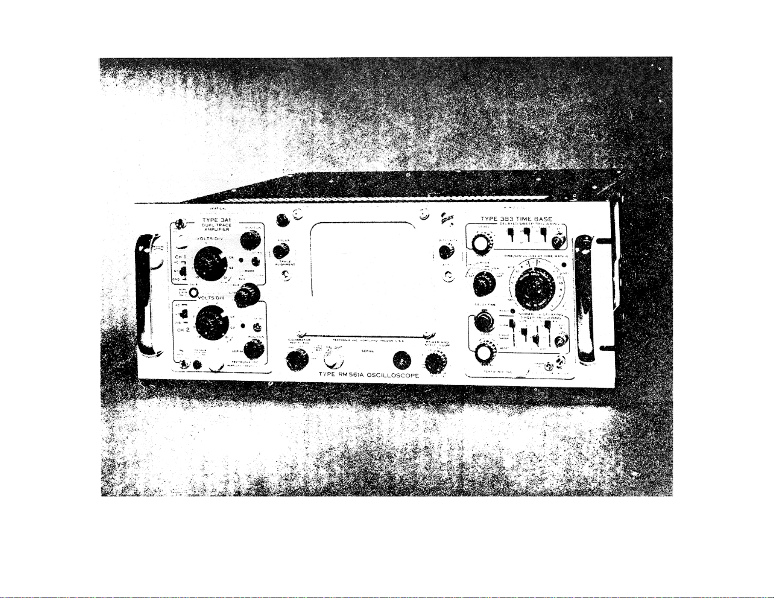
Figure 1-1A. Type RM561A Oscilloscope
ii
Page 7

SECTION 0
INTRODUCTION
TM 9-6625-963-14-1
Scope
The manual includes installation and operation
instructions and covers organizational, direct support (DS),
and general support (GS) maintenance. It describes Graphical
Display System, Tektronix Type 561 Series. The basic issue
items list appears in appendix B. Appendix ’B is current as of
1 September 1972.
Indexes of Publications
DA Pam 310-4.
to determine if there are any new editions, changes, or
additional publications pertaining to the equipment.
DA Pam 310-7.
whether there are Modification Work Orders (MWO) pertaining
to the equipment.
Forms and Records
Refer to the latest issue of DA Pam 310-4
Refer to DA Pam 310-7 to determine
Reports of Maintenance and Unsatisfactory Equipment.
Use equipment forms and records in accordance with
instructions given in TM 38750.
Change 2 0-1
Report of Packaging and Handling Deficiencies
6). Fill out and forward DD Form 6 as prescribed in AR 700-8
(Army), NAVSUP Pub 378 (Navy), AFR 71-41 (Air Force), and
MCO P4030.29 (Marine Corps).
Discrepancy in Shipment Report.
Discrepancy in Shipment Report (SF 361) as prescribed in AR
55-38 (Army), NAV SUPINST 4610.33 (Navy), AFM 7-18 (Air
Force), and MCO P4610.19A (Marine Corps).
Fill out and forward
Reporting of Equipment Publication Improve
reporting of errors, omissions, and recommendations for
improving this publication by the individual user is encouraged.
Reports should be submitted on DA Form 2028
(Recommended Changes to Publications) and forwarded
direct to: Commander, U. S. Army TMDE Support Group,
ATTN: AMXTM-LML, Redstone Arsenal, AL 35898-5400.
(DD Form
ments. The
Page 8
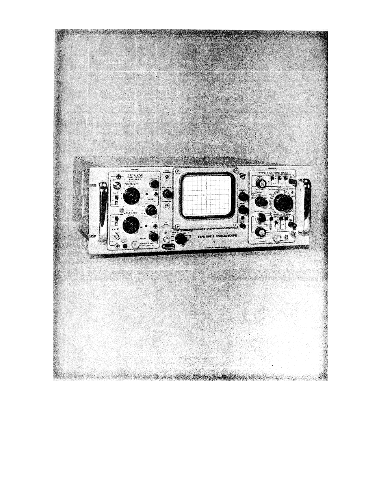
Fig. 1-1. Type R561B Oscilloscope.
0-2
Page 9

SECTION 1
CHARACTERISTICS
General Information
The Tektronix Type RM561A Oscilloscope is essentially
an indicator unit with provision for two plug-in units. The plugin unit in the right-hand opening controls the horizontal (X-axis)
deflection, and the plug-in unit in the left-hand opening
controls the vertical (Y-axis) deflection. The plug-in units con
be selected from any of the Tektronix ’2’ Series or ’3’ Series
groups to provide the desired oscilloscope performance.
Cathode-Ray Tube
Type - T5032-31-1 (rectangular ceramic-envelope).
Phosphor-P31.
Unblanking - Deflection type, dc-coupled, with grid
intensification.
Graticule - Variable edge lighted "no parallax" internal
graticule. Marked in 8 vertical and 10 horizontal divisions with
each major division divided into 5 minor divisions on
centerlines.
Accelerating voltage - 3.5 kv.
Useable viewing area - 8 divisions vertical by 10
divisions horizontal.
Deflection meters - 18.5 to 20.5 volts per centimeter
vertical, and 17.5 to 19.3 volts per centimeter horizontal.
Calibrator
Waveform - Square waves at line frequency.
RM561A
Output voltage - 1 millivolt to 100 volts, peak-to-peak, in 6
steps. The 1 v position provides an output of 0.1 volt into 50
ohms.
Accuracy - Peak-to-peak amplitude within 3% of indicated
voltage.
Rise-time - Typically 5 microseconds.
Power Supplies
Electronically regulated for stable operation with normal line
voltage variations and widely varying loads. The low voltage
supplies hold regulation within ± 1% of value.
Line voltage requirements - 105 to 125 volts, or 210 to 250
volts, rms, 50 to 60 cps, single-phase ac.
Fuse requirements - 3-amp slow-blowing type for 117 volts,
1.25-amp slow-blowing type for 234 volts.
Ventilation
Forced air cooled. Automatic-resetting thermal cutout
interrupts instrument power if internal temperature exceeds about
123° F.
Construction
Aluminum-alloy chassis.
Photo-etched anodized front panel.
Weight - 30-1/2 pounds, indicator unit only.
Dimensions - see Dimension Drawing at rear of manual.
1-1
Page 10
SECTION 1A
TYPE R561B SPECIFICATION
Introduction
The Type R561B Oscilloscope is compatible with
Tektronix 2-Series and 3-Series plug-in units (see following
table and Section 2 for exceptions); thus, it con be used in a
variety of applications including differential, multi-trace, wideband, delayed sweep, sampling and spectrum analysis.
This instrument will perform to the specifications listed in
this section in a laboratory environment with ambient
temperature range between 0°C and +50°C, except as
indicated. Warm-up time for rated accuracy is 5 minutes
(certain plug-ins may require additional warmup time). The
Performance Check instructions outlined in Section 5 provide
a convenient method of checking the performance of this
instrument.
ELECTRICAL CHARACTERISTICS
DISPLAY
Characteristics Performance
Plug-in Compatibility 2- and 3-Series plug-ins, except the
3S6, 3T6, 385 (horizontal only)
CRT Type Electrostatic deflection
Graticule Area 8 x 10 cm
Phosphor P31
Typical CRT
Accelerating Voltage
EXTERNAL INPUTS AND OUTPUTS
CRT Cathode Input
(AC Coupled)
Low - 3 dB
Frequency 1.8 kHz or less
Z Axis Modulation 10 V or less (P-P) gives useful
Maximum Input
Voltage
Calibrator
Output Voltages Into
High Impedance (1
MΩ or greater)
Into 50.0Ω
Current Loop 10mA DC or 10mA (P-P) square
3.5 kV
intensity variation
150 V
+4 mV, +40 mV, +0.4 V, +40 V
(ground to peak) square wave and
40 VDC (within 1-1/2%, +20°C to
+30° ;2 %, 0°C to +50°C
+2mV, +20mV, +0.2V (ground to
panel) square wave (within 1-1/2%,
+20°C to +30° C; 2%, 0° C to
+50°C
wave (within 1-1/2%, +20°C to
+30°C; 2%, 0°C to +50°C
Type R561B
Frequency 1 kHz within 1%
Duty Factor 48% to 52%
Rise-time and Fall-time
Line Voltage 115 VAC
Low 90 V to 110 V 180 V to 220 V
Medium 104 V to 126 V 208 V to 252 V
High 112 V to 136 V 224 V to 272 V
Line Frequency Range 48 Hz to 66 Hz
Maximum Power
Consumption at 115 VAC,
60 Hz
ENVIRONMENTAL CHARACTERISTICS
Characteristics Performance
Temperature
Non-operating
Operating
Altitude
Non-operating To 50,000 feet
Operating To 15,000 feet
Finish Lacquered aluminum panels.
Dimensions
Height
Width
Length
Accessories
Standard accessories supplied with the Type R561B are
listed on the last pullout page of the Mechanical Parts List
illustrations. For optional accessories available for use with this
instrument, see the current Tektronix, Inc. catalog.
1 µs or less at all voltages with
load capacitance of 100pF or
less, except 40 V, 2.5µs or less
at 40 V with load capacitance at
100 pF or less
POWER SUPPLY
230 VAC
186 W, 2.02 A
-40°C to +65°C
0°C to +50°C
PHYSICAL
Anodized aluminum front panel
≅ 7 inches
≅ 19 inches
≅ 20-1/2 inches
(A)
1-1A
Page 11

SECTION 2
OPERATING INSTRUCTIONS
RM561A
Introduction
Before operating the Type RM561A Oscilloscope, be sure
that the instrument will cool properly, the proper line voltage is
used and the crt deflection potentials are correct. Function of
front-panel controls and operating considerations are given in
this section.
Cooling
A fan at the rear of the Type RM561A provides cooling.
The entire fan assembly is in a snap-in mounting that can be
mounted to exhaust air at the rear of the instrument or draw air
in at the rear and blow it throughout the instrument. Direction
of air flow con be changed to meet the operating conditions.
The Type RM561A can operate in ambient temperatures
up to 50°C. If the instrument overheats, the thermal cutout
turns off the power. When the internal temperature drops to a
safe operating level, power is automatically restored. If wired
for 117-volt operation, the fan will continue to operate when
the thermal cutout opens. On 234-volt operation, power for
the fan is turned off when the thermal cutout opens.
Line Voltage
The Type RM561A can be wired for either 117-volt or
234-volt operation. It will operate properly between 105 and
125 volts when wired for 117-volt operation and between 210
and 250 volts when wired for 234-volt operation. Converting
from one operating voltage to the other requires a change in
the power transformer primary connections, fan connections,
fuse and line cord plug. Figs. 2-1 and 2-2 indicate the
transformer primary and fan connections for
117-volt and 234-volt operation. A 3-amp slow-blow type fuse is
required for 117-volt operation and a 1.25-amp slow-blow type
fuse is required for 234-volt operation.
Front Panel Controls
The POWER ON switch and SCALE ILLUM. control permit
turning the instrument power on or off and provide adjustment of
the brightness of the graticule markings.
The FOCUS control adjusts the trace or spot focus.
The ASTIG. control is used in conjunction with the FOCUS
control, to assure proper focus over the entire crt display.
The INTENSITY control adjusts the crt display brightness.
The ALIGNMENT control permits electronic alignment of the
crt trace to match the horizontal graticule markings.
The 7-position CALIBRATOR switch determines the peak-topeak amplitude of the signal at the CAL. OUT connector. It also
turns the Calibrator on or off.
Rear Panel Controls
The CRT CATHODE SELECTOR switch permits the operator
to select either (1) internal DUAL-TRACE CHOPPED BLANKING
to remove dual-trace chopped mode switching transients from the
crt display, or (2) Z-axis intensity modulation by external signals.
Operation
Operation of the Type RM561A Oscilloscope with two plug-in
units in place is much the same as that of a Tektronix oscilloscope
with corresponding vertical and horizontal deflection systems built
into the main frame. The plug-in
Fig. 2-1. Power transformer primary connections for
operation at (a) 117 volts or (b) 234 volts.
(A)(A)
Fig. 2-2. Fan terminal strip located near thermal cutout. (a) 117
volts, (b) 234 volts
.
2-1
Page 12

Operating Instructions--Type RM561A
units are the vertical and horizontal deflection systems; their
outputs connect directly to the deflection plates of the cathoderay tube. The plug-in units can be selected to give the Type
RM561A Oscilloscope the degree and type of performance
required for a particular application.
The controls and switches on the Type RM561A affect the
display; however, the plug-in units determine the major
characteristics of the system.
Calibrator Output
The Calibrator output signal of the Type RM561A provides
a convenient signal source for setting the gain of an amplifier
plug-in unit or the basic timing of a time-base plug-in unit. The
1 V position also provides a 0.1 volt amplitude signal when
connected to a 50-ohm system. This is very useful for
calibrating sampling plug-in units. See the plug-in unit
Instruction Manual for complete adjustment procedure.
In addition to these applications, the Calibrator output
signal can be used as a convenient square-wave signal source
for other applications.
NOTE
When using the Calibrator output
signal as a signal source for a system
sharing a common ground with the
Type RM561A (including plug-ins
used in the instrument) be sure that the
outer conductor of the CAL. OUT
connector is connected to the chassis
(or ground). Otherwise, the current
through the Calibrator ground resistor,
R899, may cause an incorrect
Calibrator output signal.
CRT CATHODE SELECTOR Switch
The CRT CATHODE SELECTOR switch provides two
modes of operation; CHOPPED BLANKING for dual-trace
amplifier plug-ins and EXT CRT CATHODE for intensity
modulation of the display.
The CRT CATHODE SELECTOR switch should be left in
the CHOPPED BLANKING position except when external
intensity modulation is used. For normal operation the
shorting plug should connect the EXT CRT CATHODE jack to
ground. Remove the plug for Z-axis modulation:
Display Combinations
The plug-in unit in the right opening of the Type RM561A
controls the horizontal (X-axis) deflection of the crt beam. The
unit in the left opening controls the vertical (Y-axis) deflection.
Conventional Display. To obtain the conventional display of
a horizontal sweep with vertical deflection by the input signal,
insert a time-base plug-in unit in the right-hand opening and
an amplifier unit in the left. If a vertical sweep is desired with the
input signal displayed horizontally, reverse the plug-ins. However,
in this manner, the sweep retrace will not be blanked. Retrace
blanking is provided only when a time-base unit is inserted in the
right side of the Type RM561A.
X-Y Display. To obtain an X-Y display, insert amplifier plug-in
units in both plug-in openings. Plug-in units with equal
characteristics should be used.
Intensity Modulated Display. The crt beam can be intensity
modulated, (Z-axis modulated) by applying a signal to the EXT
CRT CATHODE jack on the rear panel. Depending on the setting
of the INTENSITY control, the crt beam can be turned on with a
negative pulse, or off with a positive pulse.
To intensity modulate the display remove the shorting strap
from between the EXT CRT CATHODE and GND jacks. Set the
CRT CATHODE SELECTOR switch to the EXT CRT CATHODE
position and apply the modulating signal to the EXT CRT
CATHODE jack.
Changing Plug-in Units
Before inserting a plug-in unit into the Type RM561A
Oscilloscope, make sure the latching bar (bottom front) is not
pointing down., Then, push the plug-in unit all the way into the
opening. Turn the aluminum knob at the bottom center of the unit
clockwise until it is tight. To remove the unit, turn the knob
counterclockwise several turns and pull the unit out of the plug-in
compartment.
CAUTION
Although most plug-in units can be
inserted or removed without damage when
the power is on, best protection is
provided for all units by turning the power
off before changing units.
Different plug-in units apply slightly different dc voltages to
the crt deflection plates. The Type RM561A crt has higher
horizontal deflection sensitivity than vertical deflection sensitivity.
Also, changing one plug-in unit con affect the accuracy of the
other unit installed. Therefore, if one or both of the units are
replaced, check the gain of both units. If a plug-in needs
adjustment, follow the directions in the applicable Instruction
Manual to adjust gain or sweep timing.
When the plug-in units are changed, the FOCUS and ASTIG,
controls on the Type RM561A may need readjustment.
The Type RM561A can be operated with only one plug-in unit
if desired. For example, moving film recording may be used in
place of a sweep plug-in unit. To operate with only one plug-in
unit, it will be necessary to elevate the unconnected crt deflection
plates to about +170 to +210 volts dc vertical or +150 to +180
volts dc horizontal. This will provide proper action of the FOCUS
and ASTIG. controls.
(A)(A)
2-2
Page 13
SECTION 2A
OPERATING INSTRUCTIONS R561B
Type R561B
Introduction
To effectively use the Type R561B, the operation and
capabilities of the instrument must be understood. This
section of the manual describes the operation of the frontand rear-panel controls and connectors, and gives first time
and general operating information.
Rack-mounting
Complete information for rack-mounting installation of the
Type R561B is given on the Rack-mounting fold-out pages at
the back of this manual.
Line Voltage
The Type R561B can be operated from either a 1 5-volt
or a 230-volt nominal line-voltage source. The Line Voltage
Selector assembly on the rear panel converts the instrument
from one operating range to the other. In addition, this
assembly changes the primary connections of the power
transformer to allow selection of one of three regulating
ranges. The assembly also includes two fuses to provide the
correct protection for the instrument; both fuses are connected
for 230-volt nominal operation, and only one fuse is
connected for 115-volt nominal operation. Use the following
procedure to obtain the proper line voltage and regulating
range settings of the Line Voltage Selector.
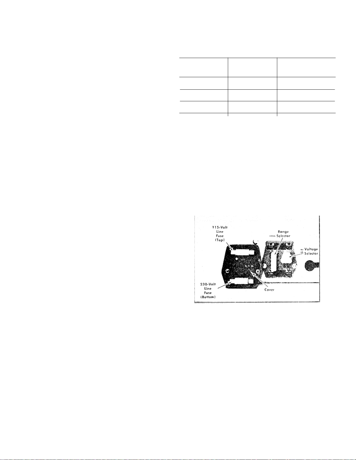
1. Disconnect the instrument from the power source.
2. Loosen the two captive screws which hold the cover
onto the voltage selector assembly; then pull to remove the
cover.
3. To convert from 115 volts nominal to 230 volts
nominal line voltage, pull out the Voltage Selector switch bar
(see Fig. 2-1); turn it around 180- and plug it back into the
remaining holes. Change the line-cord power plug to match
the power-source receptacle or use a 115- to 230-volt
adapter.
4. To change regulating ranges, pull out the Range
Selector switch bar (see Fig. 2-1); slide it to the desired
position and plug it back in. Select a range which is centered
about the average line voltage to which the instrument is to be
connected (see Table 2-1).
5. Re-install the cover and tighten the two captive
screws.
6. Before applying power to the instrument, check that
the indicating tabs on the switch bars are protruding through
the correct holes for the desired nominal line voltage and
regulating range.
TABLE 2-1
Regulating Ranges
Regulating Range,
Range Selector 115-Volts 230-Volt
Switch Position Nominal Nominal
LO (switch bar in 90 to 110 volts 180 to 220 volts
left holes)
M (switch bar in 104 to 126 volts 208 to 252 volts
middle holes)
HI (switch bar in 12 to 13 volts 224 to 272 volts
right holes)
Operating Temperature
The Type R561B can be operated where there ambient air
temperature is between 0°C and +50°C. The instrument can be
stored in ambient temperatures between -40°C and +65°C. After
storage at a temperature beyond the operating limits, allow the
chassis temperature to come within the operating limits before
power is applied.
A fan at the rear of the Type R561B provides forced air
cooling of the instrument. For proper circulation of air the
instrument should normally be operated with the top and bottom
covers in place. Do not block or restrict the air flow through the
instrument.
A thermal cutout provides thermal protection and disconnects
the power to the instrument if the internal temperature exceeds a
safe operating level. This device will automatically reapply power
when the temperature returns to a safe level.
Fig. 2-1. Line Voltage Selector assembly on the rear panel
(shown with cover removed).
CAUTION
Damage to the instrument may result from
incorrect Line Voltage Selector settings.
(A)
2-1A
Page 14

Operating Instructions--Type R561B
SELECTION OF PLUG-IN UNITS
General Information
The Type R561B is designed to use Tektronix 2-series
and 3 series amplifier and time-base plug-in ’units for
amplifying the vertical input signal and producing the timebase sweep. The use of plug-in permits the selection of
display modes, bandwidth, sensitivity and number of inputs so
that the oscilloscope performance can be changed to meet
changing measurement needs.
NOTE
Programmable plug-in Types 3S6 and 3T6
are not compatible with the Type R561B.
However, the capability of these plug-ins
is available (without programmability)
with Types 3S5 and 3T5. Use the Type
3B5 in the right-hand (horizontal)
compartment only. Refer to the
instruction manual of the plug-in unit for
specific information.
To install a plug-in unit in the Type R561B, push it all the
way in to the plug-in compartment, then turn the locking knob
,at the bottom of the front panel) clockwise until it is tight. To
remove the unit, turn the knob counterclockwise until the latch
releases, then pull the unit out.
The accuracy of measurements made with the Type
R561B depends on the calibration of the plug-in units used.
Since the plug-in units drive the deflection plates directly, each
unit must be adjusted to match the deflection sensitivity of the
particular CRT that it drives. Therefore, the gain or sweep
timing adjustment must be checked each time a plug-in unit, is
changed. On most units, gain or timing calibration is made
with a front-panel screwdriver adjustment. (Sampling units
require special adjustment procedures.) Refer to the plug-in
unit instruction manual for the required procedure. Since the
various plug-in units present different output voltage levels to
the deflection plates, the FOCUS and ASTIGMATISM controls
will also require re-adjustment.
Plug-in units can be changed without turning off the
instrument power, but it is recommended that the power be
turned off while the change is made.
Either or both of the plug-in units can be operated on
special extension cables for troubleshooting. For normal
operation, power, the units must be installed in the
oscilloscope. If the instrument is operated with the plug-in
units on extension cables, the high-frequency response and
fast sweep rates will be affected.
Display Combinations
The plug-in unit in the left plug-in compartment controls
the vertical (Y-axis) deflection of the CRT beam, and the unit in
the right plug-in compartment controls the horizontal (X-axis)
deflection. The following paragraphs discuss some of the
display combinations that con be obtained.
Time-Base Displays. To produce a conventional timebase, or Y-T display, an amplifier plug-in unit is used in the
vertical (left) plug-in compartment and a time-base plug-in unit
is used in the horizontal (right) plug-in compartment.
If a vertical sweep is desired with the input signal
displayed horizontally, the time-base unit is inserted in the left
compartment
and the amplifier unit in the right compartment. However, if a
vertical sweep is used, there is no retrace blanking, no
chopped blanking multi-trace displays and the delaying-sweep
intensification does not operate because these circuits are
associated with the horizontal (right) plug-in compartment.
X-Y Displays. Two amplifier units may be used to
produce either a single or a multiple X-Y display (for example,
for phase comparison measurement). Plug-in units with
equal phase shift will produce an accurate X-Y display;
however, for high-frequency X-Y operation, use of two units of
the some type is recommended. Careful factory adjustment of
deflection-circuit capacitance to a standard value in the Type
R561B minimizes the high-frequency phase-shift between two
plug-in units of the same type. For multiple X-Y displays, both
synchronization and automatic pairings are provided for
some amplifier units. Refer to the instruction manual of the
plug-in unit to be used.
Multi-Trace Displays. The use of a dual-trace or multitrace amplifier unit permits almost simultaneous viewing of two
or more signals. For a multi-trace amplifier unit with single
channel trigger capability ("Channel 1 Trigger"), the trigger
signal is applied through the Type R531B to the trigger circuit
in the time-base unit. This permits triggering from a single
input signal and the CRT display shows the time relationship
between the various signals. When using a plug-in without
single-channel triggering, an external trigger is recommended
to establish time relationship in multi-trace displays. In
chopped mode, the multi-trace blanking pulses from the
amplifier unit are applied internally through the Type R561 B to
the CRT cathode to blank the CRT beam while it is switched
from one channel to another (with the amplifier unit in the left
compartment and the time-base unit in the right compartment,
and with the rear panel CRT CATHODE SELECTOR switch in
the CHOPPED BLANKING position).
Delayed Sweep. A delayed-sweep time-base unit is
convenient for detailed viewing of pulse-train segments that
occur a relatively long time after the maximum-amplitude
(triggering) portion of the signal. The portion of the pulse train
to be displayed by the delayed sweep may be intensified on
the delaying-sweep display. A delayed-sweep unit that has a
calibrated time delay can also be used for making very
accurate (within 1%) time measurements
Raster Generation. A roster display can be presented by
using two time-base units, one in each compartment. Intensity
modulation can be achieved through the Z-axis of the CRT by
applying the signal to the EXT INPUT connector on the rear
panel and setting the CRT CATHODE SELECTOR to the EXT
INPUT position.
Sampling. The apparent bandwidth of the oscilloscope
can be increased to as much as one Gigahertz through the
use of sampling plug-in units. A sampling time-base unit must
be used with a sampling amplifier unit in the Type R561 B in
order to produce the sampling display (even for X-Y
operation). Generally, sampling and conventional plug-in units
cannot be used together in the oscilloscope. However, Type
3S1 and 3S2 sampling amplifiers do have limited compatibility
with conventional time-base units and the Type 3T5 sampling
time-base unit con generate a real-time staircase sweep
usable with conventional amplifiers.
Spectrum Analysis. Spectrum analyzer plug-in units
can be used in conjunction with conventional time-base units
2-2A (A)
Page 15

Operating Instruction--Type R561 B
to produce a spectral display ( a graph of the relative
amplitude distribution as a function of frequency).
FUNCTIONS OF CONTROLS AND
CONNECTORS
A brief description of the function or operation of the frontand rear-panel controls and connectors follows. See Fig. 2-2
for locations.
Front Panel
ASTIGMATISM Used in conjunction with FOCUS
(Screwdriver control to obtain a well-defined display.
adjustment)
FOCUS Control Used to optimize focus.
INTENSITY Control Controls display brightness.
TRACE ALIGNMENT Permits alignment of the trace with
(Screwdriver respect to the horizontal graticule lines.
adjustment)
SCALE ILLUM Varies illumination of the graticule grid
Control lines.
POWER Switch Used to apply or remove instrument
input power.
POWER Indicator Lamp bulb which indicates that AC
power is applied to the instrument.
CALIBRATOR Switch Provides selection of one of several
values of square wave voltage or a
calibrated DC voltage. A calibrated DC
or square wave current can also be
selected.
CAL OUT Connector BNC connector at which calibrator
output voltage is available.
10 mA Current Loop Convenient means for calibrating
current probes.
Rear Panel
CRT CATHODE Permits .election of normal CRT
SELECTOR operation, chopped blanking (blanking
Switch of the between-channel switching
transients when using multi-channel
plug-in units in the chopped mode) and
external CRT cathode input (permitting
intensity modulation of the CRT by an
external signal).
EXT INPUT BNC connector by which an external signal
Connector can be applied to the CRT cathode.
Line Voltage Provides quick method of changing
Selector transformer taps to allow instrument to
operate over a wide range of line voltages.
Horizontal and Permit installation of auxiliary inputs
Vertical and outputs through rear panel.
Connector Holes
FIRST TIME OPERATION
The following procedure, using normal single-channel timebase mode, will demonstrate the basic operation of this instrument
and its plug-in units.
1. Install a 2-Series or 3-Series amplifier plug-in unit in the
vertical (left) plug-in compartment and a 2-Series or 3-Series timebase plug-in unit in the horizontal (right) plug-in compartment.
Lock the plug-in units in place with their locking screws.
2. Set the POWER switch to the off position (pushed in).
3. Connect the power cord from the Type R561B to the
proper line voltage.
NOTE
The LINE VOLTAGE SELECTOR assembly on
the rear panel should be checked to be sure
the Voltage Selector and Range Selector
switch bars are in the proper positions for
the line voltage applied.
4. Set the instrument controls as follows:
Type R561B
INTENSITY Counterclockwise
FOCUS Centered
SCALE ILLUM Counter-clockwise
ASTIGMATISM Centered
(Screwdriver adjustment)
CALIBRATOR 4 V
CRT CATHODE SELECTOR NORM
(rear panel)
Amplifier Unit
(For example: Type 3A6)
Position Centered
Mode Normal (Channel 1)
Volts/Div 2
Variable (Volts/Div) Calibrated
Input Coupling DC
Time-Base Unit
(For example: Type 3B3)
Position Centered
Time/Div .5 ms
Variable (Time/Div) Calibrated
Magnifier Off
Sweep Mode Normal
(A)
2-3A
Page 16

Operating Instructions--Type R561 B
Fig. 2-2. Front-and rear-panel controls and connectors.
2-4A
(A)
Page 17

Normal-Single Sweep Normal
Level Free run (clockwise)
Triggering Source Internal
Slope +
Coupling Auto
5. Connect a patch cord from the CAL OUT connector to
the Channel 1 input connector of the amplifier plug-in unit.
6. Set the POWER switch to ON (pulled out) and allow a
few minutes for warm up.
7. Adjust the INTENSITY control to obtain a display of
moderate brightness. The amplifier unit Position control may
have to be adjusted to position the free running trace on the
CRT screen. Do not turn the intensity higher than is
necessary for adequate observation of the display.
8. Trigger the display by adjusting the time-base Level
control.
9. Set the SCALE ILLUM control so the graticule
illumination is approximately equal to the intensity of the
display.
10. Adjust the time-base Position control to position the
start of the trace at the left edge of the graticule.
11. Adjust the FOCUS and ASTIGMATISM controls for a
sharp well-defined display over the entire trace length. (If a
focused display cannot be obtained, see Astigmatism
Adjustment later in this section under General Operating
Information.)
12. Adjust the TRACE ALIGNMENT screwdriver
adjustment to align the display with the graticule lines.
13. Check the gain and DC balance of the amplifier unit
and the timing adjustment (Sweep Cal) of the time-base unit
as given in the instruction manuals for those units before
making any voltage or time measurements. (In this
demonstration, the calibrator waveform should be displayed as
two divisions per cycle and two divisions in amplitude.)
GENERAL OPERATING INFORMATION
General
Refer to the amplifier unit manual for the following:
Compensation of probes, selection and use of input cables,
coupling and attenuation, and measurement of input signal
voltage and phase (X-Y). Refer to the time-are unit manual for
selection of triggering sources and coupling, and for
measurements of time intervals, frequency and phase (linear
measurement).
Scale Illumination
The CRT graticule is edge-lighted by three small lamps at
the bottom. The lighting can be adjusted to suit the ambient
light conditions by means of the SCALE ILLUM control.
Rotating the control clockwise increases the brightness of the
graticule scale markings.
Intensity Control
The setting of the INTENSITY control may affect the
correct focus of the display. Slight adjustment of the FOCUS
control may be necessary when the intensity level is changed.
(A)
Operating Instruction--Type R561B
Do not leave a bright, sharply focused spot on the CRT
screen for a prolonged period. An excessively bright stationary
spot may damage the CRT phosphor.
Astigmatism Adjustments
For most displays, the trace can be adequately focused using
only the front-panel FOCUS control. However, whenever a large
change is made in the beam intensity (to offset large changes in
sweep rates or triggering repetition rates), or when plug-in units
are changed, adjustment of the ASTIGMATISM control may also
be required for a sharp display.
To check for proper setting of the ASTIGMATISM adjustment,
slowly turn the FOCUS control through the optimum setting with a
signal displayed on the CRT screen. If the ASTIGMATISM
adjustment is correctly set, the vertical and horizontal portions of
the trace will come into sharpest focus at the same position of the
FOCUS control.
To set the ASTIGMATISM adjustment, use the following
procedure:
1. Connect a 4 V Calibrator signal to the vertical input and
set the corresponding Volts/Div switch to present 2.5 divisions of
vertical deflection.
2. Set the Time/Div switch .2 ms.
3. Adjust the INTENSITY control so that the rising portion of
the display can be seen.
4. Alternately adjust the FOCUS and ASTIGMATISM
controls so that the horizontal and vertical portions of the display
are equally focused.
Graticule
The graticule of the Type R561B is marked with eight vertical
and 10 horizontal divisions. Each division is one centimeter
square. In addition, each major division is divided into five minor
divisions on the center vertical and horizontal lines. With the
vertical gain and horizontal timing calibrated to the graticule,
accurate measurements can be made from the CRT. The
illumination of the graticule lines can be varied with the SCALE
ILLUM control.
Trace Alignment Adjustment
If a free-running trace is not parallel to the horizontal graticule
lines, set the TRACE ALIGNMENT adjustment as follows: position
the trace to the center horizontal line, and adjust the TRACE
ALIGNMENT adjustment so the trace is parallel with the horizontal
graticule lines.
1 kHz Calibrator
The 1 kHz Calibrator provides a convenient source of square
waves of known amplitude at an accurate frequency of one
kilohertz. The output square-wave voltages available at the CAL
OUT connector are 4 mV, 40 mV 0.4 V, 4 V and 40V. The loading
of a terminated 50Ω system at the CAL OUT connector will
provide output square-wave voltages of 2 mV, 20 mV and 0.2 V.
A constant 40-volt DC level is also provided.
2-5A
Page 18

Operating Instructions--Type R561 B
The current link provides 10 milliamperes, available as
either DC or a square-wave current signal, which can be used
to check and calibrate current probe systems. This current
signal is obtained by clipping the probe around current loop.
The arrow indicates conventional current (i.e., positive to
negative).
Intensity (Z-Axis) Modulation
Intensity modulation can be used to relate other voltage
information to the display signal without changing the shape of
the waveform. The modulating signal is AC-coupled to the
CRT cathode through the rear-panel EXT INPUT connector
and the CRT CATHODE SELECTOR switch. With the
INTENSITY
control set correctly, a positive excursion will dim or blank the
CRT beam, and a negative excursion will brighten the beam
(see Section 1 for amplitudes).
Time markers may be applied for direct time reference of
the display or for establishing the sweep rate when
uncalibrated deflection is used. Fast-rise pulses of short
duration provide best resolution with respect to time. If the
markers are not time-related to the displayed wave-form, a
single sweep display is required. If sine waves are used for
Z-axis modulation, the minimum usable frequency is about
250 hertz, due to AC coupling at the input. Be sure the CRT
CATHODE SELECTOR is in the NORMAL position when the
EXT INPUT connector is not in use, to avoid random intensity
modulation from stray signals.
(A)
2-6A
Page 19

SECTION 3
CIRCUIT DESCRIPTION
Introduction
The Tektronix Type RM561A Oscilloscope has a lowvoltage power supply circuit, a cathode-ray tube circuit, and a
calibrator.
The low-voltage power supply circuit provides the
regulated and unregulated power used by the instrument and
the plug-in units.
The crt circuit has the necessary controls and input
facilities needed to give a sharp trace of useable intensity.
Two negative high-voltage power supply outputs are used
for the cathode, focus element, and control grid of the crt.
The calibrator produces amplitude-calibrated square
waves.
LOW-VOLTAGE POWER SUPPLY
The low-voltage power supply circuits have regulated
outputs of -100, -12.2, +125, and -300 volts, and unregulated
output of +420 volts. These circuits use silicon diode rectifiers
and series-regulators. Each regulator circuit has a vacuum
tube (or transistor, in the case of the -12.2-volt supply) in
series with the load. This tube’s series plate resistance (and
current) is controlled to maintain a constant voltage drop
across the load. For example, if the load increases the series
tube plate resistance decreases to pass more current to the
load. If the load decreases it passes less current. In both
cases, the voltage across the load remains the same.
The -100-, +125-, and +300-volt regulated supplies
require shunt resistors when supplying more current than can
be handled by the series tube. A shunt allows some of the
load current to bypass the supply-series-regulator tube. The
size of the shunt is very important. If the shunt resistance is
too high, the series tube can overheat; if the resistance is too
low, the supply can fail to regulate. If a plug-in draws an
amount of current that calls for a supply shunt, the correct
shunt resistance is located in that plug-in unit. When the unit
is plugged into the Type RM561A, the shunt is connected
around the series regulator tube. The plug-in portion of the
shunt is always in series with a resistor located in each power
supply circuit.
Power for the Type RM561A Oscilloscope and its plug-in
units is supplied through the power transformer T601. The two
primary windings of T601 are connected in parallel for 117-volt
operation, or in series for 234-volt operation, as shown on the
schematic diagram.
RM561A
The series tube plate resistance changes to hold the load voltage
constant. R616, -100 VOLTS adjustment, determines the
percentage of the total divider voltage applied to the grid of V634A
and thus controls the output voltage. When this control is properly
adjusted, the output is exactly -100 volts.
Should the output voltage tend to change because of a
change in input voltage or a change in load current, the potential
at the grid of V634A will change a proportional amount. Any
change at the grid of V634A is amplified by V634A and Q624 and
applied to the grid of V627. The resulting grid change at V627 will
cause its plate resistance to change in the direction needed to
bring the output back to --100 volts. C616 improves the response
of the regulator to sudden changes in output voltage R628 is part
of the series tube shunt. connected by some plug-in units.
+ 125-Volt Supply
The -100-volt supply serves as a reference for the +125 volt
supply. With the R651 end of the divider R650-R651 fixed at -100
volts, any change in the +125-volt output produces a proportional
change at the grid of V654. This change is amplified and supplied
to the grid of the series regulator tube, V667A. The change at the
grid of V667A changes its plate resistance to bring the output
voltage back to 4-125 volts. R656, the +125 VOLTS control,
determines the percentage of total divider voltage applied to the
grid of V654 and permits adjustment of the output voltage. W hen
this control is properly adjusted, the output is exactly +125 volts.
C650 improves the response of the regulator to sudden changes
in output voltage. .R666 is port of the series tube shunt.
+ 300-Volt Supply
The + 300-volt supply works the some as the + 125-volt
supply. To supply the voltage for the + 300-volt regulator, rectified
voltage from the transformer pins 21 and 22 is added to the
voltage supplying the + 125-volt regulator. R676, the -+ 300
VOLTS control, adjusts the output voltage. The + 300-volt supply
has an unregulated output of + 420-volts for the crt circuit.
- 12.2-Volt Supply
Operation of the --12.2-volt regulating circuit is essentially the
same as that of the other regulating circuits, except that
transistors are used instead of vacuum tubes. The base of Q734
is fixed near ---12 volts by the voltage divider R731-R732
between ---100 volts and ground. Any variation of the --12 2-volt
output at the emitter of Q734 is amplified by 0734 and 0744 to
change the collector resistance of 0757 which is in series with the
lead R730, the -12.2 VOLTS control, allows adjustment of the
voltage applied to the base, of Q734 and thus the output voltage.
- 100 Volt Supply
Reference voltage for the -100-volt supply is established
by the gas diode, V609. The constant voltage drop across
V609 establishes a fixed potential of about --85 volts at the
grid of V634B. Voltage at the grid of V634A is established by
the divider R616, R617, and R618. The difference in voltage
between the two grids of V634 determines the plate current cf
V634A. Plate current of V634A determines the base voltage
of transistor Q624 which in turn determines the grid voltage of
the series tube, V627.
(A)(A)
3-1
Page 20

Circuit Description--Type RM561A
When this control is properly adjusted, the output is exactly -
12.2 volts. F720 protects Q757 in case of an overload on the -
-12.2-volt supply.
CRT CIRCUIT
The crt circuit contains the cathode-ray tube and two highvoltage supplies (one for the crt and focus element, the other
for the control grid). The circuit also contains the necessary
controls and signal input facilities.
Cathode-Ray Tube
A Tektronix T5032-31-1 ceramic-envelope cathode-ray
tube is used in the Type RM561A. The accelerating voltage is
approximately 3500 volts, developed by about -3300 volts at
the cathode and an average deflection plate voltage of about
+200 volts. With this accelerating voltage, the nominal vertical
and horizontal deflection factors are 19.5 and 18.4 volts per
centimeter respectively.
Deflection blanking of the crt beam is used in the Type
RM561A. The crt contains a special set of deflection plates,
pins 6 and 7, for this purpose. Both plates are connected to
+125 volts; however pin 6 is also driven by the horizontal plugin unit.
During sweep time, or if no plug-in unit is installed, both
plates rest at +125 volts and permit the electron beam to pass
on to the crt phosphor. During sweep retrace, however, pin 6
is driven considerably away from +125 volts by the right-hand
plug-in unit. This scatters the beam and prevents it from being
displayed.
High-Voltage Supplies
Energy for both high-voltage supplies is furnished by
T801. V800, the primary of T801, and the stray circuit
capacitance form a Hartley oscillator which operates at about
45 kc.
The output of one secondary winding of T801, rectified by
V822, provides voltage for the crt cathode and focus element.
This voltage is about -3300 volts at the crt cathode, and
between about -2200 and -3000 volts at the focusing element,
depending on the setting of the FOCUS control. The 6.3-volt
crt heater is elevated to the cathode potential by R851.
The output of the other secondary winding of T801 is
rectified by V832 for the control grid. The grid voltage ranges
from -3200 to -3450 volts, depending on the setting of the
INTENSITY control. The reference to ground for this supply is
determined by the voltage at the junction of diodes D838 and
D839. The voltage at this junction, plus the setting of the
INTENSITY control, determines the crt bias and therefore the
intensity of the display.
Two neon bulbs, B856 and B857, keep the voltage
between the grid and cathode of the crt within safe limits. If
the voltage exceeds about 140 volts, the neons fire and the
voltage reduces to about 120 volts.
Regulation of the -3300-volt supply is accomplished through
feedback from the arm of R841. The -3450-volt supply is
regulated indirectly by mutual coupling in T801. If, because of
loading or a change in input voltage, the output of the -3300-volt
supply changes, a proportionate change occurs at the arm of
R841. This change is amplified by V814 and is coupled to the
screen of V800. The resulting change in screen voltage of V800
will increase or decrease the amplitude of oscillations in V800,
changing the output voltage of T801 in the direction needed to
return the high voltage to the correct level. The HIGH VOLTAGE
control, R841, permits adjustment of the output voltage by setting
the bias on V814B.
Deflection Signals
Push-pull signals for the deflection plates appear at pins 17
and 21 of the plug-in connector. The effective deflection circuit
capacitance these signals see at the connector affects the bandpass and phase shift of each plug-in unit. C760 and C761
(Interconnecting Socket diagram) are set at the factory.
Intensifying Signals
Two signals may be used to modulate the intensity of the crt
display. First, intensifying signals from a two-sweep (delayingsweep) time-base plug-in unit are applied to the grid supply
through pin 14 of the right-hand Interconnecting Socket. W hen
the overall display intensity is reduced with the INTENSITY
control, positive intensifying pulses from a two-sweep time-base
plug-in unit will brighten any desired portion of the display.
The ground return for the crt grid supply can be either through
D838 in the case where the plug-in unit does not supply
intensifying signals or through D839 to a negative voltage in the
intensifying circuit of the plug-in unit. In the second case D838 is
back-biased and the junction of D838 and D839 is at a low
negative voltage. With the same setting of the INTENSITY
control, the first case will provide a brighter display. The second
case provides a slightly dimmer display due to the plug-in unit
negative voltage. Intensification results when the plug-in unit
positive pulse turns D839 off and the crt grid supply return again
becomes D838. R837 and C837 then couple the leading edge of
the intensifying pulse directly to the crt grid.
Other external intensifying signals can be fed to the crt
cathode through the EXT CRT CATHODE jack. Depending on the
setting of the INTENSITY control, a negative pulse of 5 volts or
more will turn the crt beam on.
Crt Controls
The INTENSITY control, R833, has a range of about 250 volts
to control the crt bias and permit changing the intensity of the
display.
The FOCUS control, R844, adjusts the focus of the crt by
varying the voltage at the focusing anode through a range from
about -2200 to -3000 volts.
The ASTIG. control, R864, has a 300-volt adjustment range.
3-2 (A)(A)
Page 21

Circuit Description--Type RM561A
The GEOMETRY control, R865, adjusts the geometry by
varying the voltage of the crt isolation shield through a range
from +180 to +246 volts.
The TRACE ALIGNMENT control, R860, rotates the
display so it can be aligned with the graticule.
CALIBRATOR
The calibrator for the Type RM561A Oscilloscope
produces line-frequency amplitude-calibrated square waves.
The 6.3-volt (approximately 18 volts peak-to-peak) ac heater
voltage for V884 is supplied through C876 to the cathode of
V884A. The signal at the plate of V884A is coupled to the grid
of V884B to turn that tube on and off.
(A)(A)
Regenerative feedback from the plate of V884B to the grid of
V884A speeds up the switching action, and drives V884A into and
out of cutoff.
The voltage present at the cathode of V884B during the time
that V884B is conducting is adjusted to exactly 100 volts with the
CAL. AMPL. adjustment, R871.
The voltage divider in the cathode circuit of V884B contains
precision resistors to provide an output accuracy of 3% or better
at the various settings of the CALIBRATOR control.
When the CALIBRATOR control is set to the IV position, there
will be a 0.1-volt output when the CAL. OUT connector is
terminated in 50 ohms.
3-3
Page 22

SECTION 3A
CIRCUIT DESCRIPTION
Type R561B
R561B
Introduction
This section of the manual contains a description of the
circuitry used in the Type R561B Oscilloscope. Each circuit is
described in detail using a detailed block diagram to show the
interconnections between the stages in each major circuit and
the relationship of the front-panel controls to the individual
stages. Complete schematic diagrams are located at the rear
of this manual.
LOW-VOLTAGE POWER SUPPLY
General
The Low-Voltage Power Supply circuit provides the
operating power for this instrument from four regulated
supplies. Electronic regulation is used -to provide stable, lowripple output voltages. Each regulated supply contains a short
protection circuit to prevent instrument damage if a supply is
inadvertently shorted to ground or to another supply. The
voltage input stage includes the Voltage Selector Assembly
which allows selection of the nominal operating voltage and
regulating range for the instrument. Fig. 3-1 shows a detailed
block diagram of the Low-Voltage Power Supply.
Power Input
Power is applied to the primary of transformer T1 through
fuse F1, POWER switch SW1, thermal cutout TK1, Voltage
Selector switch SW2 and Range Selector switch SW3. SW2
connects the split primaries of T1 in parallel for 115-volt
nominal operation, or in series for 230-volt nominal operation.
SW3 allows three ranges of regulation by changing the taps
on the primary windings to fit different line requirements. A
second fuse, F2, is connected into the circuit when SW2 is set
to the 230V position to provide the correct protection for 230volt operation.
Thermal cutout TK1 provides thermal protection by
interrupting the power if the instrument overheats. When the
temperature returns to a safe level, TK1 automatically closes
to re-apply the power.
- 100 Volt Supply
The -100-Volt Supply provides the reference voltage for
the remaining supplies. The output from the secondary of T1
is rectified by bridge rectifier D8A-D. This voltage is filtered by
C9, then applied to the -100-Volt Series Regulator stage to
provide a stable output voltage. The Series Regulator can be
compared to a variable resistance which is changed to
stabilize the output voltage. The conductance
of the Series Regulator stage is controlled by the Error Amplifier to
provide the correct regulated output voltage.
The Error Amplifier consists of Q12 and Q14, which are
connected as a comparator. The output at the collector of Q14
indicates any voltage variations which occur at the base of Q14
relative to the fixed voltage at the base of Q12. Zener diode D10
maintains a fixed 9-volt drop, setting the base of Q12 at about -9
volts. The base level of Q14 is determined by the voltage divider
network R18-R19-R20-R21-R23. R23, the -100 Volts adjustment,
allows the operating point of the Error Amplifier to be adjusted to
set the output voltage of the supply at -100 volts. R13 is the
emitter resistor for both comparator transistors and the current
through it divides between Q12 and Q14. The output current of
the Error Amplifier stage controls the conduction of the Series
Regulator stage. This is accomplished as follows: Assume that
the output voltage increases (becomes more negative) because of
a change in load or an increase in line voltage. This negativegoing voltage change at the output is applied to the base of Q14,
reducing the conduction of Q14. As current through Q14 is
reduced, Q24 base current increases. This results in increased
Q24 collector current, increasing the voltage drop across R25 and
R26 and pulling the base of Q28 negative. The emitter of Q28
follows the base; hence, the base of Q32 is also pulled negative.
Reduced current through Series Regulator Q32 decreases current
through the load, causing the output voltage to decrease (become
less negative) to its correct level. These changes occur rapidly,
and the effect is to maintain unchanged output voltage. In a
similar manner, the Series Regulator and Error Amplifier stages
compensate for output changes due to ripple. As will be seen in
subsequent paragraphs, R33 determines the limit current for the
Series Regulator stage, and thus for the load. Transients beyond
the frequency range of the regulator are filtered by C31 to prevent
their appearance on the output voltage.
When the power switch is activated, diode D25 provides a
base current path for Q28, allowing the -100-Volt Supply to turn on
first, since all the other supplies are dependent upon its output.
As the -100-Volt Supply output builds up to its correct level, D25 is
reverse biased and remains off during normal operation of the
instrument.
The Short-Protection Amplifier stage, Q30, protects the -100Volt Supply if the output is shorted, and also serves to limit the
current demanded from the Series Regulator under excessive
load. During normal operation, divider R30-R31 sets the base of
Q30 to a point below the turn-on level of the transistor. When
excess current is demanded from Series Regulator Q32 due to an
overload or short circuit, the additional current through R33 raises
the emitter of Q32 more positive. This produces a
corresponding change at the base of Q32, which is connected
through R30
(A)
3-1A
Page 23

Circuit Description--Type R561B
Fig. 3-1. Power Supply detailed block diagram.
3-2A
(A)
Page 24

Circuit Description--Type R561B
to the base of Q30. This positive-going change biases Q30
into conduction. As a result, less current is available to Q28,
to Q32 and to the load, thus causing the supply to lose
regulation. R31 senses the decrease in load voltage and adds
to increasing base current of Q30. As the collector of Q30
goes negative, conduction of Q28 and Q32 is further
decreased. Thus the output current is decreased and remains
low until the excessive load is removed. D19, together with
divider R18-R19-R20, provides protection to the --12.2-Volt
supply in the event the -100-Volt Supply is shorted to the -
12.2-Volt Supply by causing the -100-Volt Supply to lose
regulation, and therefore lose reference voltage for the -12.2Volt Supply. D31 protects the -100-Volt Supply from
damaging polarity reversal if it is shorted to either the +125Volt Supply or the +300-Volt Supply.
- 12.2-Volt Supply
Rectified voltage for operation of the -12.2-Volt Supply is
provided by D35A-B, filtered by C36 and applied to the -12.2Volt Supply Series Regulator stage. Reference voltage for this
supply is provided by voltage divider R42-R43 between the
regulated -100-Volt Supply and ground. If the -12.2-volt output
changes, a sample of the change appears at the base of Q46
as an error signal. Regulation of the output voltage is
controlled by Error Amplifier Q44-Q46-Q49 and Series
Regulator Q51 in a manner similar to that described for the 100-Volt Supply. Transients beyond the frequency range of
the regulator are filtered by C47.
Short protection is provided by Q38 and R38. For normal
operation, the emitter-base voltage of Q38 is not enough to
bias it into conduction. However, when the output is shorted,
the high current demanded from the -12.2-Volt Supply is
drown through R38, producing a voltage drop sufficient to
forward bias Q38. Q38 collector current then produces an
increased voltage drop across R40, reducing the conduction of
both Q49 and Q51 to limit the output current. R39 protects
Q38 from sudden current surges by limiting the base current.
D47 protects the -12.2-Volt Supply from damage if it is shorted
to either the +;125-Volt Supply or the +300-Volt Supply.
+ 125-Volt Supply
Rectified voltage for operation of the +125-Volt Supply is
provided by D53A-D, filtered by C54 and applied to the +125Volt Supply Series Regulator stage. The +125-volt output is
summed with the -100-volt reference through divider R62-R63,
and the summation is applied through R61 to the base of Q60
and compared to the grounded base of Q58. If the +125-volt
output changes, a sample of the change appears at the base
of Q60 as an error signal. Regulation of the output voltage is
controlled by Error Amplifier Q58-Q60-Q66-Q68 and Series
Regulator Q74 in a manner similar to that described for the 100-Volt Supply. Transients beyond the frequency range of
the regulator are filtered by C97B-C to prevent their
appearance on the output voltage.
Short protection for this supply is provided by the ShortProtection amplifier stage, Q70, which functions in a manner
similar to that described for Q30 in the --10Volt Supply. D62
protects the Error Amplifier from damage if the output of the
+125-Volt Supply collapses or goes negative, causing C62 to
rapidly discharge and reverse bias 060. Diode D75 protects
electrolytic capacitor C97B-C and the transistors in the circuit from
damaging polarity reversals in the event the +300-volt output is
shored to ground or to one of the negative supplies. D76 causes
the +125-Volt Supply to go into current limiting when the +300-Volt
Supply is shorted to ground or to one of the negative supplies.
+ 300-Volt Supply
Rectified voltage for operation of the +300-Volt Supply is
provided by D77A-D, filtered by C78 and applied from the
negative side of the rectifier to the +300-Volt Supply Series
Regulator stage. The +300-volt output is summed with the -100volt reference through divider R80-R81, and the summation is
applied through R83 to base of Q84 and compared to the
grounded base of Q86. If the +300-volt output changes, a
sample of the change appears at the base of Q84 as an error
signal. Regulation of the output voltage is controlled by Error
Amplifier Q84-Q86-Q88-Q90 and Series Regulator Q96 in a
manner similar to that described for the -100-Volt Supply.
Transients beyond the frequency range of the regulator are filtered
by C97A. The load current through Series Regulator Q96 also
posses through the +125-Volt Supply Series Regulator, Q74.
However, this does not affect the limit current of the +125-Volt
Supply.
Shorting protection for this supply is provided by the ShortProtection Amplifier stage, Q91, which functions in a manner
similar to that described for Q30 in the -100-Volt Supply. D80
protects the Error Amplifier from damage if the output of the +300Volt Supply collapses or goes negative, and D95 protects the
transistors in the circuit from damaging polarity reversals in the
event the +125-Volt Supply is shorted to ground or to one of the
negative supplies.
6.5-Volt RMS AC Source
The four 6.5-volt RMS secondary windings of T1 provide
power for the CRT heater, the plug-in heaters via J11 and J21, the
pilot light, B7, and the scale illumination lights, B4, B5, and B6.
Current through the scale illumination lights is controlled by the
SCALE ILLUM control, R4, to change the brightness of the
graticule lines.
DEFLECTION CIRCUITS
horizontal and vertical signals for deflecting the CRT beam are
received through pins 17 and 21 of each plug-in unit and applied
to the respective deflection plates of the CRT. The effective
deflection circuit capacitance encountered by each of these
signals at the plug-in connector affects the bandwidth and phase
shift of the plug-in unit. Compensating capacitors C102 and C109
(shown on the Plug-In Connectors diagram) are factory-adjusted
to set the effective capacitance at a standard value of 14.3
picofarads to ensure plug-in compatibility.
1 kHz CALIBRATOR
General
The 1 kHz Calibrator circuit produces a square-wave output
with accurate amplitude and frequency. This output is available
as a square-wave voltage at the CAL OUT connector or as a
square-wave current through the 10 mA probe current
(A)
3-3A
Page 25
Circuit Description--Type R561B
Fig. 3-2. 1 kHz Calibrator detailed block diagram.
loop. An accurate +40 volts DC level is also available. The
CALIBRATOR switch selects the attenuation of the output
signal to provide square-wave voltage outputs between 40
volts and 4 millivolts (between 0.2 volts and 2 millivolts into 50
ohms) peak to peak. Fig. 3-2 shows a detailed block diagram
of the 1 kHz Calibrator circuit.
Calibrator Multivibrator
The Calibrator Multivibrator is comprised of Q151 and
Q159, and is a free-running emitter-coupled multivibrator. The
circuit operates in a symmetrical manner and the output is an
accurate one-kilohertz square wave. Only an approximate 9volt change is exhibited at the emitters of Q151 and Q159, so
that an essentially constant current of about 0.8 mA is
maintained through resistors R150 and R1 58.
Refer to the wave shapes shown in Fig. 3-3 for this
discussion. With the CALIBRATOR switch, SW150, in all
positions except 1 mA DC and OFF, the emitters of Q151 and
Q159 are returned to the +125-volt supply through D151-R150
and D159-R158. Assume that the multivibrator has just
switched states; Q151 is off and Q159 is on. This is To in Fig.
3-3. The base potential of Q159 is set to about -11.0 volts by
voltage divider R153-R154-R156 to ensure that Q159 will not
saturate. The voltage at the anode of D159 is about -9.8 volts
because of the voltage drop across two forward biased
junctions. Capacitor C157 had about a 2-volt charge as
switching occurred; thus, the voltage at the anode of D151 is
about -7.8 volts, cutting off Q151. C157 begins to charge
toward the +125-volt supply via R150. Total current through
Q159 is about 1.6 mA; 0.8 mA through R158 and 0.8 mA
through C157 and R150.
After about 0.5 milliseconds (corresponding with T, in Fig.
3-3), C157 has charged to the turn-on level of Q151 and D151.
At this point, the capacitor has a charge of about 11 volts and
the potential at the anode of D151 is about +1.2 volts. The
capacitor charging current through Q159 ceases as Q151 and
D151 begin
to conduct. As the collector of Q151 (hence the base of Q159)
rises, Q159 and D159 are switched off and C157 begins to
discharge through R158. The C157-R158 current sums with R150
current through Q151, producing an approximate 9-volt positivegoing step at the base of Q159.
C157 continues to discharge, and after 0.5 milliseconds (T,
in Fig. 3-3), the voltage at the anode of D159 has risen to
forward-bias Q159 and D159. As Q159 begins to conduct, the
anode of D159 is clamped at about 0.8 volts and discharge action
of C157 is halted. The current through Q151 decreases, causing
its collector to introduce a negative-going step, which is connected
through the Q159 base-emitter junction and D159 to C157.
Because C157 cannot obtain an instantaneous charge, the anode
of D151 is pulled negative to reverse bias D151 and Q151. Q151
turns off, and its collector falls rapidly to about -11.0 volts,
resulting in an approximate 9-volt negative-going step applied
through Q159 and D159 to C157. The anode of D151 is pulled
down to about -7.8 volts, completing the cycle.
The Calibrator Multivibrator circuit has been designed to
repeat the preceding sequence at an accurate one-kilohertz
frequency. However, since a tolerance range of the passive
components does exist, the frequency can be adjusted by varying
slightly the amplitude across C157 during the charge-discharge
cycle. This is accomplished by adjustment of R154, Frequency,
which determines the potential on D159 anode at the instant the
diode turns on. For example, with greater amplitude, longer
charge and discharge times are required, thus lowering the
frequency.
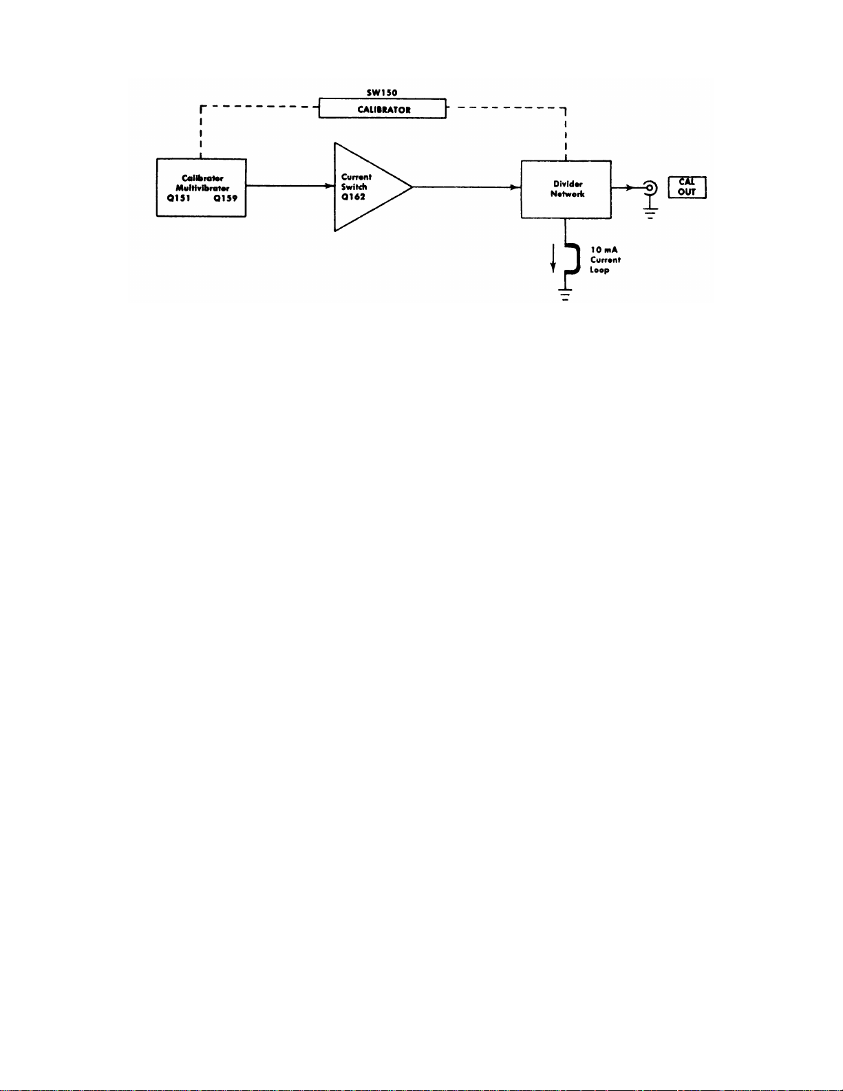
Output Stage
The output stage consists of the Current Switch, Q162, and
the Divider Network. During the half cycle that Q159 is
conducting, current is injected into the base of Q162. Q162
saturates and its collector drops to about -12 volts, reverse
biasing D168. With D18 off, there is no current through R170 and
R171, and the output level at the cathode of D168 drops to zero
volts.
(A)
3-4A
Page 26

When Q159 turns off, Q162 turns off and D161 turns on to
protect the Q162 base-emitter junction from reverse-bias
breakdown. D164 and D168 turn on, and the output of the
circuit (at D168 cathode) is dependent upon voltage divider
R166-R167-R170-R171 between +125 volts and ground. This
output level is set to exactly +40 volts by adjustment of R166,
Amplitude. When this adjustment is made, the current through
the divider is an accurate 10 mA, which is available at the
current probe loop in the 10 mA positions of the CALIBRATOR
switch.
The signal voltage available at the CAL OUT connector is
determined by the divider network (made up of precision
resistors) and the setting of the CALIBRATOR switch. In the
10 mA DC (40 VDC) position, the Calibrator Multivibrator is
inoperative so that a +40-volt DC output level is produced.
R173 is placed in series with the R166-R167-R170-R171
resistance to obtain an effective resistance of 450 ohms with 4
volts applied, as seen by the CAL OUT connector in the 4 V
position of the switch. This effective resistance becomes port
of the output voltage divider in the positions of 0.4 V and below
(these positions have an accurate 50- ohm output resistance,
which when terminated by 50 ohms can further divide the
outputs by two, providing outputs of 0.2V, 20 mV and 2 mV).
In the 10 mA position, the CAL OUT connector is grounded.
R183, which is about ten times the resistance of the braid
of a 42-inch coaxial cable, cancels any ground loop current
that may exist between the CAL OUT connector and some
other instrument chassis.
CRT CIRCUIT
General
The CRT Circuit provides the high voltage and control
circuits necessary for operation of the cathode-ray tube (CRT).
Fig. 3-4 shows a detailed block diagram of the CRT Circuit.
High Voltage Oscillator
Q219 and its associated circuitry comprise a class C
oscillator to provide the drive for the high-voltage transformer,
T220. When the instrument is turned on, conduction of Q214
provides a base current path for Q219. The collector current
of Q219 increases and a voltage is developed across the
collector winding of T220. This produces a corresponding
voltage increase in the feedback winding of T220 which is
connected to the base of Q219, causing it to conduct harder.
While Q219 is conducting, C217 charges negatively to the
peak to peak voltage of the feed-back winding. Eventually the
rate of collector current increase in Q219 becomes less than
that required to maintain the voltage across the collector
winding and the voltage drops.This turns off Q219 by way of
feedback voltage to the base. During the interval that Q219 is
not conducting, the negative charge on C217 is partially
removed through Q214. Q219 remains off until the feedback
voltage on the base is near the peak positive value again. The
cycle repeats at a frequency of 40 to 50 kilohertz. The
amplitude of sustained oscillation depends upon the average
current delivered to the base of Q219, and finally, the average
Q219 collector current.
Circuit Description--Typo R561 B
Fig. 3-3. Calibrator Multivibrator waveforms.
High Voltage Regulator
Feedback from the secondary of T220 and +125 volts is
summed through the voltage divider network consisting of R200,
R201, R206, R208 and R233 through R238, and the difference is
applied to the gate of Field-Effect Transistor Q211.. This sample
of the output voltage is compared to the regulated --12.2-volt level
at the source of Q211. It is then inverted and amplified by Q211
and applied to the base of Q214. Amplitude of the oscillations at
the collector of Q219 is determined by the average collector
current of Q214.
Regulation. is accomplished as follows: If the output voltage
at the -330Q V test point starts to go positive (becomes less
negative), a sample of this positive-going voltage is applied to the
gate of Q211. Conduction of Q211 is increased, and as its drain
goes negative because of the voltage dropped across R211, the
base current of Q214 is increased. An increase in conduction of
Q214 increases the average collector current, which is applied
through the feedback winding of T220 to the base of Q219. Q219
conducts harder, increasing the collector current to produce a
larger induced voltage in the secondary of T220. This increased
voltage appears as more negative voltage at the -3300 V test
point to correct the original positive-going change. By sampling
the output from the cathode supply in this manner, the total output
of the high-voltage supply is held constant.
(A)
3-5A
Page 27
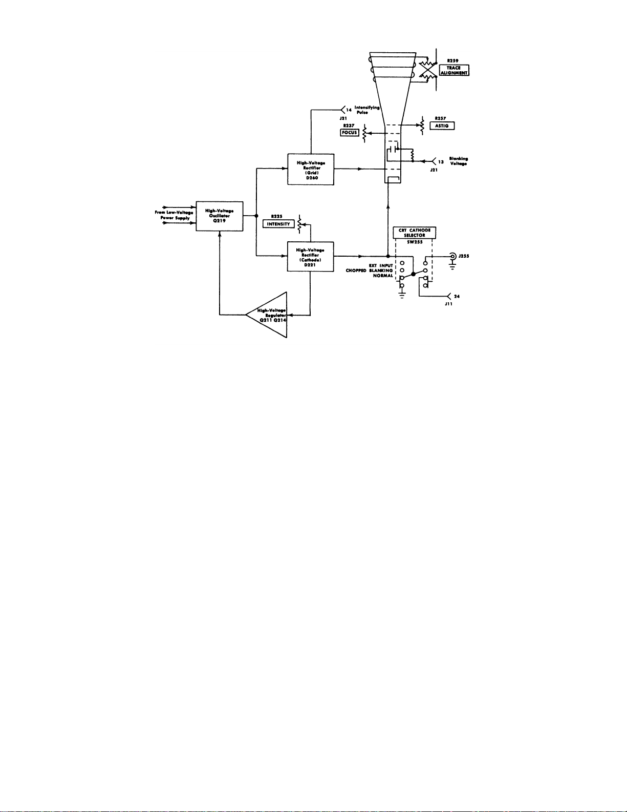
Circuit Description--Type R561B
Fig. 3-4. CRT Circuit detailed block diagram.
Output voltage level of the high-voltage supply is controlled by
the High Voltage adjustment, R206, in the gate circuit of Q211.
This adjustment sets the effective divider ratio, which in turn
determines the voltage necessary to satisfy the quiescent
condition of Q214 and Q219 in the manner described for a
change in output voltage. Neon bulb B209 and diode D212
protect the FET, Q211, from damage due to excessive voltage.
High Voltage Rectifiers and Output
The high-voltage transformer, T220, has two output
windings. These windings provide the negative CRT cathode
potential and the CRT control grid bias.
The accelerating potential for the CRT cathode is supplied
by the half-wave rectifier D221 and held constant by the HighVoltage Regulator stage in the primary of T220. The output
level is adjustable to about -3300 volts on the cathode by the
High Voltage adjustment mentioned previously. (The 6.5-volt
CRT cathode heater is also elevated to the cathode potential
through R246.)
Half-wave rectifier D260 provides a negative voltage for
the control grid. The voltage applied to-the-control-grid is
determined by the setting of the INTENSITY control (to be
(A)
3-6A
Page 28

Circuit Description--Type R561B
discussed in the next paragraph), the CRT Grid Bias control
(R269) and any intensification signals received from the timebase plug-in unit (delayed sweep and sampling units only).
Reference to ground for this supply is set by the conduction of
D272.
Beam current is controlled by R225, INTENSITY. As the
control is rotated clockwise, the wiper arm moves toward -100
volts. This more negative DC reference voltage is applied to
the secondary winding controlling the CRT cathode, reducing
the voltage demanded of the winding to maintain -3300 volts at
the -3300 V test point. This is accomplished by the regulator
circuit. The voltage across the grid winding is also reduced,
which results in a more positive voltage applied to the CRT
control grid, thus increasing beam current. Beam current is
reduced in a like manner by rotating R225 counterclockwise.
Neon bulbs B277, B278 and B279 provide protection to
the CRT if the voltage difference between the control grid and
the cathode exceeds about 135 volts.
CRT Control Circuits
In addition to the INTENSITY control discussed
previously, the FOCUS and ASTIGMATISM controls have
been incorporated for arriving at the optimum CRT display.
FOCUS control R237 provides the correct voltage for the
second anode in the CRT. Proper voltage for the third anode
is obtained by adjusting ASTIGMATISM control R257. In order
to obtain optimum spot size and shape, both the FOCUS and
ASTIGMATISM controls are adjusted to provide the proper
electrostatic lens configuration in the CRT. The TRACE
ALIGNMENT control, R259, permits adjustment of the DC
current through beam-rotation coil L259 to align the display
with the horizontal graticule lines. The Geometry adjustment,
R256, controls the overall geometry of the display.
Blanking
The CRT beam is blanked by a special set of deflection
plates in the CRT. One of the plates (pin 7) is connected
directly to the +-125-volt supply. The second plate (pin 6) is
connected through plug-in connector J21 to the horizontal
plug-in unit. When there is no sweep, a quiescent voltage is
applied from the horizontal unit to create a difference of potential
between the two plates. This voltage can either be positive or
negative with respect to the +125 volts on the other plate. The
potential difference created is sufficient to deflect the CRT beam
so that it is absorbed in the deflection structure and does not
reach the screen.
The CRT beam is unblanked whenever the two deflection
plate voltages become equal. For example, if a sweep occurs or if
the horizontal plug-in unit is removed, the voltages are made
equal and the beam is allowed to pass through to the CRT screen.
Sweep unblanking is produced by either a positive or negative
gate pulse (depending on the quiescent level) applied to pin 6,
equaling the +125 volts normally present at pin 7. In a like
manner, when the horizontal plug-in unit is removed, the two
deflection plates are equalized through R244 at +125 volts.
Intensity Modulation
The intensity of the CRT display may be modulated by
applying signals to either the grid or the cathode of the CRT.
Intensifying signals from a delayed sweep time-base plug-in
unit are applied to the grid supply via pin 14 of the horizontal plugin interconnecting socket, J21. These signals brighten the
delayed-sweep portion of the delaying-sweep display. When the
time-base unit is set to Intensified, the control grid supply is
referred to a negative voltage in the intensifying circuit through
D275, reducing the overall display intensity. At this time, D272 is
reverse biased by the negative voltage at the juncture of the two
diodes. Intensification results when the positive-going pulse from
the time-base unit reverse biases D275 and the grid supply is
referred to ground through D272 (as for normal operation). The
positive-going pulse is then coupled through R275 and C275 to
the CRT control grid. Thus the brightened portion of the display is
the same intensity as a normal display and the background trace
is dimmed.
External modulating signals may also be applied to the CRT
by way of the cathode, through the rear-panel EXT INPUT
connector, J255, and the CRT CATHODE SELECTOR, SW255.
With the INTENSITY control adjusted properly, a positive or
negative pulse between 3 and 50 volts in amplitude will produce
dimming or intensification of the CRT beam.
When a multi-channel vertical plug-in amplifier that provides
dual-trace chopped blanking pulses is used, the blanking pulses
are applied via the interconnecting socket J11 and the CRT
CATHODE SELECTOR to the CRT cathode circuit. These pulses
are about 5 volts in amplitude, and at normal intensity levels are
sufficient to cut off the CRT beam during the time the amplifier
channels in the vertical plug-in unit are being switched.
(A)
3-7A
Page 29

SECTION 4
MAINTENANCE
R561A
PREVENTIVE MAINTENANCE
Cleaning
Occasionally blow the dust out of the instrument with a
low-velocity dry air stream. Remove persistent dirt with a
small paint brush or damp cloth. The screen on the fan con be
snapped out and should be cleaned as needed. Check it
frequently.
Fan Oiling
The fan should be oiled with a few drops of oil about every
six months. An industrial hypodermic syringe and needle is
used to insert oil through a protective rubber cap located under
the fan label. The oil recommended is Anderol L826 from the
Lehigh Company or Rotron distributors, but if not available, a
good light machine oil may be used. If a syringe and needle
cannot be obtained locally, you can order them through the
NICP by specifying Hypodermic Syringe, Tektronix Part No.
003-282 and Hypodermic Needle, Tektronix Part No. 003-285.
Fig. 4-1 shows how to oil the fan. Place the needle at the
point on the label shown in Fig. 4-1. With the needle at about
45’, pierce the label and rubber cap (located under the label);
insert the needle about 1/4" and depress the syringe-plunger
to inject a few drops of oil.
CORRECTIVE MAINTENANCE
Replacing Parts
Most parts in the Type RM561A Oscilloscope can be replaced
without detailed instructions. Some parts, however, should be
replaced by using definite procedures. These procedures are
described in the following paragraphs.
A replaced part may affect instrument calibration. Check and
adjust where needed.
Soldering Precautions and Procedure
In Tektronix instruments, parts are connected to ceramic
terminal strip notches with solder containing about 3% silver.
The bond between the notch and ceramic strip may be broken by
repeated use of ordinary 60 40 tin-lead solder or by excessive
heat. Therefore, when resoldering parts to a ceramic strip use
solder containing 3% silver and do not overheat the work.
Occasional use of ordinary solder, however, will not break the
bond. Usually 3% silver solder is available locally; or one-pound
rolls may be ordered from the NICP.
The following soldering procedure may be used to remove
and replace parts on a ceramic terminal strip.
1. Use 50-to-70-watt soldering iron with a wedge shaped
tip. (With this type tip you can heat the solder slot without
overheating the strip.)
2. Tin the soldering iron tip with silver-bearing solder.
3. Heat the parts soldered to the ceramic strip only
enough to make the solder flow freely. Do this by touching one
corner of the soldering iron tip to the notch. (Be careful: excessive
pressure will break the ceramic strip.)
4. When you remove a part, pull its lead out of the notch
while the solder is hot.
5. When you replace a part use only enough solder to cover
the wires and form a small fillet in the notch.
6. Clip excess leads of parts replaced and be sure to
remove all clippings from the instrument.
Fig. 4-1. Fan motor oiling with hypodermic
(A)(A)
Replacing Ceramic Terminal Strips
Damaged ceramic terminal strips can be replaced by the
following procedure. Fig. 4-2 shows how ceramic strip parts are
assembled.
1. Unsolder all connections to damaged ceramic strip.
2. Cut off one side of each plastic yoke holding the old
ceramic strip.
3. Remove old ceramic strip.
4. Remove remainder of old yokes from spacers.
4-1
Page 30

Maintenance--Type RM561A
Fig. 4-2. Ceramic terminal strip assembly.
5. Replace old spacers with new ones. (If not damaged,
spacers can be reused.)
6. Set new ceramic strip yoke pins into spacers.
7. Drive new yoke pins completely into spacers by
pressing or lightly tapping the ceramic strip directly above the
yokes. Be careful, don’t break strips.
8. Cut off portion of new yoke pins protruding through
spacers on side of chassis opposite the ceramic strip.
9. Resolder connections to new ceramic strip using the
information headed Soldering Precautions and Procedure.
Replacing Calibrator Switch
The entire switch should be replaced and can be ordered
either wired or unwired.
falls directly under the grounding strip. Tighten the base clamp
screw.
After the crt is replaced, it may be necessary to adjust the
TRACE ALIGNMENT and HIGH VOLTAGE controls and the
deflection-circuit capacitance (C760 and C761) according to the
calibration procedure. Also check the calibration of time-base and
amplifier plug-in units.
Cathode-Ray Tube
WARNING
When replacing crt, wear a plastic face
mask and protective gloves for protection
in case tube implodes.
To remove the cathode-ray tube, disconnect the four
leads connected to the neck of the tube, the tube socket, and
loosen the tube clump on tube base. Remove the crt bezel,
light reflector and light shield. Pull the crt straight out
through the front panel, being careful not to bend or break the
crt neck pins. The rubber gasket and implosion shield can be
removed from the crt face after it is out of the instrument.
Install the new crt by the reverse of the preceding
procedure. When replacing the implosion shield be sure that
the notched side is down. Follow the color-code information
on the tube shield when the crt neck pin leads are replaced.
When the crt is properly installed, the back of its faceplate is
flush with the instrument front panel.
Correct position of the shield extension, grounding strip
and Mylar sleeve is important when re-installing the crt.
Replace these components on the positions shown in Fig. 4-
3. Note that the gap between the ends of the shield extension
Fig. 4-3. Correct position of shield extension and Mylar sleeve.
TROUBLESHOOTING
If trouble occurs in the Type RM561A Oscilloscope, a fivestep procedure may be used for repair. First, confirm the trouble.
Next, isolate trouble to a plug-in unit or to the Type RM561A.
Localize a trouble in the Type RM561A to the Power Supply, Crt
Circuit, or Calibrator. Troubleshoot the correct circuit to find the
defective parts. Replace defective parts.
Confirmation of Trouble
Improper control settings may at times give indications of
trouble. Therefore, you should be sure that the apparent trouble is
not caused by improper front panel control settings. For example,
an improper setting of the SOURCE or COUPLING switch on a
time-base unit can cause apparent trigging troubles: an improper
setting of the VARIABLE
(A)(A)
4-2
Page 31

Maintenance—Type RM561A
control on an amplifier unit can cause an apparent decrease in
sensitivity.
When a trouble exists, it must be isolated to one of he
plug-in units or to the Type RM561A indicator.
Isolating Trouble
Isolating trouble to a plug-in unit or to the indicator can be
done in one of two ways, depending on whether or not there
are spare plug-in units available.
If trouble is found to be in the plug-in unit, refer to the
instruction manual for that unit. A plug-in extension (Part
Number 013-034, available through the NICP) allows the units
to be operated while extended out through the front of the
plug-in opening.
Spare Plug-In Units Available
If more than two plug-in units are available, the easiest
way to isolate trouble is to replace the plug-in units one at a
time. The faulty unit can then be isolated by noting when
proper operation is restored. If plug-in replacement
does not correct the trouble, the Type RM561A is probably faulty.
NOTE
A non-sampling plug-in unit cannot be
operated with a sampling plug-in unit.
Spare Plug-In Units Not Available
When spare plug-in units are not available, the crt display will
be of great help. Trouble will normally show up as an erroneous
display, or as no display at all. Since the crt display will help
isolate the trouble, the following procedure is divided according to
the type of display.
No Trace Or Spot. If no trace can be obtained on the crt,
remove both plug-in units and vary the INTENSITY control. A spot
should appear. If no spot appears, the trouble is in the Type
RM561A. If a spot does appear when both plug-in units are
removed reinsert each unit separately. After warm up, vary its
POSITION control. If the spot or trace cannot be returned to the
approximate center of the crt when a single plug-in unit is in the
indicator, the trouble
Fig. 4-4. Power-Supply test points (1) through (17). CRT Circuit test points, (20) through (26). Calibrator test points (4)
through (45).
4-3
Page 32

Maintenance—Type RM561A
is probably In that unit. (if a lime-base unit is installed, be sure
it is set for free-running operation to unblank the crt.)
Insufficient Vertical Deflection or Improper Sweep
Timing. If the plug in unit front-panel gain controls do not
permit adequate vertical deflection or proper sweep timing,
check the low-voltage and high-voltage power supply ,voltages
(see schematics).
If the power-supply voltages are not correct, remove both
plug-in units and check the voltages again. If they still are not
correct, the trouble is in the Type RM561A indicator If the
power-supply voltages are correct with both plug-in until
removed, but incorrect with only one of the two inserted, the
trouble is in that unit. If the power-supply voltages are correct
with both plug-in units removed, but incorrect when either is
inserted, the trouble is probably the power supply of the Type
RM561A.
Improper Triggering. If external triggering and line
triggering are satisfactory, but internal triggering is not, the
trouble is probably in the Trigger Pick-off Circuit of the
amplifier plug-in units. If satisfactory triggering cannot be
obtained from any of the three sources external, internal or
line) the trouble is probably in the time-base plug-in unit.
Waveform Distortion. If there is any waveform distortion,
but no other indications of malfunction (such, as improper
sweep timing) the trouble is probably in the vertical plug-in unit
Localizing Trouble In Type RM561A Indicator
If it has been determined that trouble exists in the Type
RM561A, the location of the trouble can be further localized to
the Power Supply, the Crt Circuit, or the Calibrator.
To localize the trouble to either the Power Supply or the
Crt Circuit, measure the output of each of the regulated power
supplies. If incorrect supplies are measured, the trouble is in
the Power Supply or the power source. If all of the measured
voltages are proper. the trouble is in the Crt Circuit.
Trouble in the Calibrator is indicated by an erroneous
output at the CAL. OUT connector.
When it is known which circuit contains the trouble, that
circuit can be checked to isolate the defective component
Circuit Troubleshooting
In troubleshooting a circuit, broken wires, worn switches,
scorched parts, and improperly seated tubes can be found by
visual inspection. (Before a scorched part is replaced the
cause of the scorching should be eliminated.)
Tube failure is the most prevalent cause of trouble in
Tektronix instruments. Therefore, ii a visual check falls to reveal
the cause of trouble, oil tubes should be checked as the next step.
Tubes should be checked by substitution, one at a time. (Tubetesters cannot adequately check all parameters.) Be sure to return
all good tubes to their original sockets; otherwise the instrument
may have to be recalibrated unnecessarily because rf different
characteristics of the same tube type. If tube substitution does not
correct the trouble, then check the rest of the circuit by voltage
and resistance measurements. Voltages at various test points
throughout the instrument are indicated on the schematics. The
test points can easily be located using Fig. 4-4. The voltages at
the test points are typical and may vary considerably from
instrument to instrument. Resistance measurements in a circuit
will usually be point-to-point checks for which the proper values
can be approximated from the schematic diagrams. Table 4-1
may be used as an aid in relating trouble symptoms to the
probable cause and the procedure to use to locate the defective
component. Voltages listed in the table were obtained with the
Type RM561A operated without plug-in units.
All signal wiring in the Type RM561A is colored to make
Circuit tracing easier. In addition, all regulated power supply
leads are color coded to follow the standard EIA code. The first
color (widest stripe) indicates the first number of the voltage. The
second color indicates the second and the third color (smallest
stripe) indicates the multiplier. The voltage is positive if the main
color of the wire is white and negative if the main color of the wire
is tan. Four colors would be required to indicate all the digits plus
a multiplier for the 4-125-volt leads. To avoid this, the +125-volt
leads are coded as +120; that is, brown, red, brown on a white
base. A -100-volt lead is coded brown, black, brown on a ton
base while +300-volt leads are coded orange, black, brown on
white
The switch wafer shown on the Calibrator diagram is coded.
The letters F and R indicate whether the front or rear of the wafer
is used to perform the particular switching function.
Table 4-1.
RM561A Troubleshooting Table
Symptoms Checks
- 100 Volt Supply
(Any change in this supply may change instrument calibration).
1. Incorrect
output level,
ripple, or
regulation.
2. Output
voltage high (too
negative).
a. Check line voltage.
b. Check Setting of - 100 volts adjustment
(see Calibration Procedure).
c. Check V609, V634, V627 and Q624 by
substitution.
d. If output still incorrect go to whichever
symptoms apply of 2 through 7.
b. Measure V634 bias, between pin 7 of
V609 and pin 8 of V634; about 2 v. Use
meter that can be elevated. (If bias is
excessive check R618 and R616).
c. Check R618, R616, R634, R633, and
R624.
4-4
(A)(A) 1
Page 33

Symptoms Checks
3. Output
voltage low (too
positive).
4. Poor
regulation at
either high, low
or normal line
voltage. (Supply
should hold
regulation within
± 1% throughout
normal line
voltage range).
5. Poor
regulation at low
line voltage.
6. Poor
regulation at high
line voltage.
7. Excessive
ripple.
(Any change in this supply may change instrument
8. Incorrect
output level,
ripple, or
regulation.
9. Output
voltage high.
10. Output
voltage low.
a. Check voltage between pins 17 and
18 of T601. 137 vac ± 10% check T601
primary circuit).
b. Check voltage between C640A
terminals: about 175 vdc ± 10%.
(Incorrect: check C640A, C640B, R640,
and D640).
c. Check test point (14): about -80 vdc.
(Incorrect: check V609).
d. Check R617, R616, C616, C640B.
a. Check for correct output voltage
before checking regulation - also, check
output voltage after regulation trouble is
fixed.
b. Check voltage at test point (17):
about +85 vdc. (Voltage low: check
D660 and do checks 2A, 2B, and 2C).
c. Check for excessive loading by either
plug-in unit or RM561A circuits.
Check R635, R628 and shunt resistors
in plug-in unit.
Substitute another plug-in unit.
(Symptom occurs if load is reduced while
shunt resistor remains the same in plugin unit).
a. Check for correct output voltage and
regulation before checking ripple - also
check output voltage and regulation after
ripple trouble is fixed.
b. Check voltage at test point (17):
about +85 vdc.
c. Check ripple at test point (17): should
be less than 25 v peak-to-peak with load.
(Excessive: check C640A and D640).
d. Check tubes.
e. Check C616, C611, C640A and
C640B.
+125-Volt Supply
calibration).
a. Check line voltage.
b. Check -100 volt supply output test
point (7).
c. Check setting of -12.2 VOLTS
adjustment (see Calibration Procedure).
d. Check V654, V667.
e. If output still incorrect go to whatever
symptoms apply of steps 9 through 14.
a. Check voltage at test point (1): about
+68 vdc. (Incorrect: check R657, R658,
and V654).
b. Check R650.
a. Check voltage between pins 19 and
20 of T601: 160 vac +10%. (Incorrect:
check primary circuit).
Maintenance—Type RM561A
Symptoms Checks
b. Check voltage at test point (2): +215 vdc.
(Incorrect: check C642A, R642, D642).
c. Check test point (1): about +68 vdc.
(Incorrect: check R659, V654).
d. Check C650, R651.
11. Poor
regulation at
either high, low,
or normal line.
(Supply should
hold regulation
within 1%
throughout
normal line
voltage range).
12. Poor
regulation at low
line voltage.
13. Poor
regulation at high
line voltage.
14. Excessive
ripple.
Symptom and Checks similar to those described for the +125
(Any change in this supply may change instrument calibration).
15. Incorrect
output level,
ripple or
regulation
16. Output high
(too negative).
17. Output low
or zero, (too
positive).
a. Check for correct output voltage before
checking regulation - also check output
voltage after regulation trouble is fixed.
b. Check tubes.
c. Check voltage at test point (2): about
+215 vdc. (Incorrect: do checks 10A and
10B).
Check R653, C650, R666, and shunt
resistors on plug-in unit.
a. Check C650.
b. Substitute another plug-in unit.
(Symptom occurs if load is reduced while
shunt resistor remains the same in plug-in
unit).
a. Check for correct output voltage and
regulation before checking ripple-also,
check output voltage and regulation after
ripple trouble is fixed.
b. Check tubes.
c. Check voltage at test point (2): about
+215 vdc. (Incorrect: do checks 10A and
10B).
d. Check voltage at test point (1): about
+68 vdc. (Incorrect: check R657, R659,
R658).
e. Check C642A, and B, C650, D642.
+300 Volt Supply
volt supply.
-12.2 Volt Supply
a. Check line voltage.
b. Check -100 volt supply output test point
(7).
c. Check setting of -12.2 VOLTS
adjustment (see Calibration Procedure).
d. Check Q734, Q744, Q757, and F720.
e. If output still incorrect go to whichever
symptoms apply to steps 16 through 20.
a. Check test point (9): about -12 vdc.
(Incorrect: check C732, R732).
b. Check test point (10): about +7.9 vdc.
(Incorrect: check R734, C737).
c. Check C737, R734, R744.
a. Check voltage between pins 14 and 15
then 125 and 16 of T60: 15 vac ±10% with
117 (234) vac line. (Incorrect: check
transformer primary circuit).
(A)(A) 1
4-5
Page 34

Maintenance—Type RM561A
Symptoms Checks
b. Check voltage between C720A and B
terminals, test points (8) and (12): about
18 vdc. (Incorrect: check C720A, C720B,
D720, D721).
c. Check voltage at fuse F720: about
+8.2 vdc. (Incorrect: check C757 and
F720).
d. Check test point (9): about -12 vdc.
(Incorrect: check R731).
e. Check test point (10): about +7.9 vdc.
(Incorrect: check R735).
f. Check C757.
18. Poor
regulation at
either high, low,
or normal line
voltage. (supply
should hold
regulation within
± 1% throughout
normal line
voltage range.
19. Poor
regulation at low
or high line
voltage.
20. Excessive
Ripple
(Any change in this circuit may change display vertical and
21. Any incorrect
operation of CRT
circuit.
a. Check for correct output voltage before
checking regulation-also, check output
voltage after regulation trouble is fixed.
b. Check for excessive loading by either
plug-in units or RM561A circuits.
Check R734, R735, R744, and C737.
a. Check for current output voltage and
regulation before checking ripple-also,
check output voltage and regulation after
ripple trouble is fixed.
b. Check ripple at test point (12): should
be less than 4v peak-to-peak with load.
(Excessive: do checks 17A and B).
c. Check D720, D721, C720A and B,
C732, C757.
CRT Circuit
horizontal calibration).
a. Check line voltage.
b. Check HIGH VOLTAGE adjustment, (3300 volts at test point (21), see
Calibration Procedure). If minor
adjustment restores operation circuit may
be normal.
c. Check V822 and V832 heaters color.
Dull orange - normal
bight - heavy load on either tube
dim - poor tube (replace)
both dark - oscillator inoperative.
Symptoms Checks
d. If operation still incorrect, go to
whichever symptoms apply of 22 through
29
22. Low
Intensity
23. High
Intensity.
25. Poor
astigmatism
and/or focus
26. Blooming
(size of display
increases with
intensity
increase).
27. No
intensifying
pulse.
28. No Z-axis
modulation or
no chopped
blanking
29. Intensity
varies
(unwanted Zaxis
modulation).
30. Incorrect
outputs.
a. Check intensity control setting.
b. Check V822 and R835.
c. Unblanking pulse doesn’t return pin 6 of
crt fully to +125 v.
d. Check crt.
a. Check intensity control setting.
b. Make sure spot or trace is not deflected
off screen. (Spot should appear near
center with both plug-in units removed).
c. V822 heater open, (B856 and B857
glowing brightly show V822 open). If V822
is open check V814A.
d. Check oscillator tubes and circuit
including T801).
e. Check C822, C842, and crt.
a. Check FOCUS and ASTIG. Control
settings.
b. Check HIGH VOLTAGE at pin 2 of crt,
test point (20): -3300 vdc. (Incorrect:
check R852).
c. Check voltage at pin 9 of crt: 0 to +300
vdc when ASTIG. Control is rotated.
(Incorrect: check R864 and +300 vdc to
R864).
Check V800 and V822 (either may be
weak).
a. D838 shorted, D839 open.
b. C837 or R837 open (leading edge of
long intensifying pulse missing).
C853 or R853 open. If R853 open check
for shorted C853.
D838 and/or D839 open.
CALIBRATOR
a. Check CAL. AMPL. Adjustment (see
Calibration Procedure).
b. Check V884.
c. Check voltages at test points (4)
through 45).
d. Use Calibration Procedure, check
divider in V884B cathode.
4-6
(A)(A) 1
Page 35

SECTION 4A
Type R561B
MAINTENANCE
Introduction
This section of the manual contains information for use in
preventive maintenance, corrective maintenance and
troubleshooting of the Type R561B.
Access to the Interior
The top and bottom dust covers of the Type R561B can
be easily removed for access to the internal circuitry. The
covers should be re-installed on the instrument for normal
operation to keep dust out and provide proper distribution of
the air flow.
PREVENTIVE MAINTENANCE
General
Preventive maintenance consists of periodic inspection
and cleaning at regular intervals. The Type R561B should be
checked approximately every 500 hours of operation, or every
six months, whichever occurs first. If the instrument is
subjected to adverse environmental conditions, such as
excessive dust, high temperatures or high humidity, the
frequency of the checks should be increased. A convenient
time to perform preventive maintenance is preceding recalibration of the instrument.
Cleaning
The Type R561B should be cleaned as often as operating
conditions require. Accumulation of dirt in the instrument can
cause overheating and component breakdown. Dirt on
components acts as an insulating blanket and prevents
efficient heat dissipation. It also provides an electrical
conduction path.
The top and bottom covers provide protection against dust
in the interior of the instrument. Operation without covers in
place necessitates more frequent cleaning.
CAUTION
Avoid the use of chemical cleaning
agents which might damage the plastics
used in this instrument. Avoid chemicals
which contain benzene, toluene, xylene,
acetone or similar solvents.
Exterior. Loose dust accumulated on the outside of the
Type R561B can be removed with a soft cloth or small point
brush. The point brush is particularly useful for dislodging dirt
on and around the front-panel controls. Dirt which remains
can be removed with a soft cloth dampened in a
R561B
mild detergent and water solution. Abrasive cleaners should not
be used.
Clean the graticule and CRT face with a soft, lint-free cloth
dampened with a mild detergent and water solution.
Interior. Dust in the interior of the instrument should be
removed occasionally due to this electrical conductivity under
high-humidity conditions. The best way !o clean the interior is to
blow off the accumulated dust with dry, low-pressure air. Remove
any dirt which remains with a soft paint brush or a cloth dampened
with a mild detergent and water solution. A cotton-tipped
applicator is useful for cleaning in narrow spaces and/or circuit
boards.
The high voltage circuits, particularly parts located in the highvoltage comportment and the area surrounding the CRT socket
receive special attention. Excessive dirt in these areas may cause
high-voltage arcing and result in improper instrument operation.
Lubrication
The reliability of potentiometers, rotary switches and other
moving parts can be maintained if they are kept properly
lubricated. Use a cleaning-type lubricant (e.g., Tektronix Part No.
006-0220-001. The pot lubricant can also be used on shaft
bushings. Do not over lubricate.
Fan Oiling. During periodic servicing, the fan motor should
be lubricated with a few drops of light machine oil (Anderol L826
available from Lehigh Company or Rotan Distributors is
recommended). An industrial hypodermic needle and syringe is
used to insert the oil through the rubber seal, as shown in Fig. 4-
1. Hold the syringe at a 45° angle, pierce the rubber seal, then
insert the needle about 1/4 inch and depress the plunger for
enough to inject 3 or 4 drops of oil into the hearing. If a syringe
and needle cannot be obtained locally, they may be ordered from
NICP (Tektronix Part No. 003-0282-00 for the syringe; 003-028500 for the needle).
Visual Inspection
The Type R561B should be inspected occasionally for such
defects as broken connections, improperly seated transistors,
damaged circuit boards and heat-damaged ports.
The corrective procedure for most visible defects is obvious;
however, particular care must be taken if heat-damaged
components are found. Overheating usually indicates other
(A)
4-1A
Page 36

Maintenance—Type R561B
Fig. 4-1. Oiling the fan with a hypodermic.
trouble in the instrument; therefore, it is important that the
cause of overheating be corrected to prevent a recurrence of
the damage.
Transistor Checks
Periodic checks of the transistors in the Type R561B are
not recommended. The best check of transistor performance
is its actual operation in the instrument. More details on
checking transistor operation are given under Troubleshooting.
Recalibration
To assure accurate measurements, check the calibration
of this instrument after each 500 hours of operation or every
six months if used infrequently. In addition, replacement of
components may necessitate recalibration of the affected
circuits. Complete calibration instructions are given in the
Calibration section.
The calibration procedure can also be helpful in localizing
certain troubles in the instrument. In some cases, minor
troubles may be revealed and/or corrected by recalibration.
TROUBLESHOOTING
Introduction
The following information is provided to facilitate
troubleshooting in the Type R561B. Information contained in
other sections of this manual should be used along with the
following information to aid in locating the defective
components. When replacing a defective semiconductor, be
certain that all associated components are in good condition
before application of power, a precaution which may prevent
further damage. An understanding of the circuit operation is very
helpful in locating troubles. See the Circuit Description section for
complete information.
Troubleshooting Aids
Diagrams. Circuit diagrams are given on fold-out pages in
Section 8. The component number and electrical value of each
component in this instrument are shown on the diagrams. Each
main circuit is assigned a series of component numbers. Table 41 lists the main circuits in the Type R561B and the series of
component numbers assigned to each. Important voltages and
waveforms are also shown on the diagrams at the rear of this
manual. The portion of the circuit mounted on the circuit board is
enclosed with a blue line.
Table 4-1
Component Numbers
Component
Numbers on
Diagrams
1.99 1 Power Supply
100-110 2 Plug-in
150-199 3 1 kHz Calibrator
200-299 4 CRT circuit
Switch Wafer Identification. Switch wafers shown on the
diagrams are coded to indicate the position of the wafer in the
complete switch assembly. The numbered portion of the code
refers to the wafer number counting from the front, or mounting
end of the switch, toward the rear. The letters F and R indicate
whether the front or rear of the wafer performs the particular
switching function. For example, a wafer designated 2R indicates
that the rear of the second wafer J (from the front) is used for this
particular switching function.
Circuit Boards. Fig. 4-5 through 4-7 show the circuit boards
used in the Type R561B. Each electrical component on each
board is identified by its circuit number. The circuit board is also
outlined on its schematic diagram with a blue line. These pictures
used with the diagrams will aid in locating the components
mounted on the circuit boards.
Wiring Color Code. All insulated wire and cable used in the
Type RSS61B is color-coded to facilitate circuit tracing. Signal
carrying leads are identified with three stripes to indicate the
approximate voltage, using the EIA resistor color code. A white
background color indicates a positive voltage and a tan
background indicates a negative voltage. The widest color stripe
identifies the first color of the code. Table 4-2 gives the wiring
color code for the power supply voltages used in the Type R561B.
Diagram
Number Circuit
Connectors
TABLE 4-2
Power Supply Wiring Color Code
Back-
ground
Supply
+300 V White Orange Black Brown
+125 V White Brown Red Brown
-12.2 V Tan Brown Red Black
-100 V Tan Brown Black Brown
Color
First
Stripe
Second
Stripe
Third
Stripe
4-2A
(A)
Page 37

Fig. 4-2. Standard EIA color code
Maintenance—Type R561B
Resistor Color Code. In addition to the brown composition
resistors, some metal-film resistors and some wire-wound
resistors are used in the Type R561B. The resistance values
of wire-wound resistors are printed on the body of the
component. The resistance values of composition resistors
and metal-film resistors are color-coded on the components
with EIA color code (some metal-film resistors may have the
value printed on the body). The color code is read starting
with the stripe nearest the end of the resistor. Composition
resistors have four stripes which consist of two significant
figures, a multiplier and a tolerance value (see Fig. 4-2).
Metal-film resistors hove five stripes consisting of three
significant figures, a multiplier and a tolerance value.
Capacitor Marking. The capacitance values of common
disc capacitors and small electrolytic are marked in microfarads on the side of the component body. The white ceramic
capacitors used in the Type R561B are color coded in
picofarads using a modified EIA color code (see Fig. 4-2).
(A)
Diode Color Code. The cathode end of a glass-enclosed diode is
indicated by a stripe, a series of stripes or a dot. For most silicon
or germanium diodes with a series of stripes, the color code
identifies the three significant digits of the Tektronix Part Number
using the resistor color-code system (e.g., a diode color-coded
blue-brown-gray-green (6, 1, 8, 5) indicates Tektronix Part
Number 152-0185-00). The cathode and anode ends of metal
diodes can be identified by the diode symbol marked on the body.
Troubleshooting Equipment
The following equipment is useful for troubleshooting the
Type R561B:
1. Transistor Tester
Description: Tektronix Type 575 Transistor Curve Tracer
or equivalent.
Purpose: To test the semiconductors used in this
instrument.
2. Multimeter
Description: Electronic Voltmeter, 10 megohms, or greater, input
resistance; 0 to 500 volts; 0 to 50 megohms. Accuracy, within 3%
(1% is necessary to check power supply voltages). Test prods
must be insulated to prevent accidental shorting.
Purpose: To check operating voltages and for general
troubleshooting in this instrument.
NOTE
A 20,000 ohms/volt VOM can be used to
check the voltages in this instrument if
allowances are made for the circuit loading
of the VOM at high impedance points.
4-3A
Page 38

Maintenance—Type R561B
3. Test Oscilloscope (with 1X and 10X probes).
Description: DC to 1 MHz frequency response, 1 milli-
volt to 10 volts/division deflection factor.
Purpose: To check waveforms in the instrument.
Troubleshooting Techniques
This troubleshooting procedure is arranged in an order
which checks the simple trouble possibilities before
proceeding with the extensive troubleshooting. The first few
checks assure proper connection, operation and calibration. If
the trouble is located by these checks, the remaining steps aid
in locating the defective component. When the defective
component is located, it should be replaced following the
replacement procedures given under Corrective Maintenance.
1. Check Control Settings. Incorrect control settings
con indicate a trouble that does not exist. If there is any
question about the correct function or operation of any control,
see the Operating Instructions section of the manual.
2. Check Associated Equipment. Before proceeding
with troubleshooting of the Type R561B, check that the
equipment used with this instrument is operating correctly.
Substitute another vertical or time-base plug-in which is known
to be operating properly. Check that the signal is properly
connected and that interconnecting cables are not defective.
Also, check the power source.
3. Visual Check. Visually check the portion of the
instrument in which the trouble is located or suspected. Many
troubles can be located by visual indications such as
unsoldered connections, broken wire, damaged circuit boards,
damaged components, etc.
4. Check Instrument Calibration. Check the
calibration of this instrument, or the affected circuit if the
trouble exists in one circuit. The apparent trouble may only be
a result of misadjustments or may be corrected by calibration.
Complete calibration instructions are given in the Calibration
section.
5. Isolate Trouble to a Circuit. To isolate trouble to a
circuit, note the trouble symptom. The symptom often
identifies the circuit in which the trouble is located. For
example, poor focus indicates that the CRT circuit (includes
high voltages) is probably at fault. When trouble symptoms
appear in more than one circuit, check affected circuits by
taking voltage and waveform readings.
Incorrect operation of all circuits often indicates trouble in
the power supplies. However, a defective component
elsewhere in the instrument con appear as a power supply
trouble and may also affect the operation of other circuits.
NOTE
Turn the instrument off before attempting to
remove or replace connections to any circuit
board.
Table 4-3 lists the tolerances of the power supplies in his
instrument. If a power supply voltage is within the listed
tolerance, the supply can be assumed to be working correctly.
If outside the tolerance, the supply may be misadjusted or
operating incorrectly. Use the procedure given in the
Calibration section to adjust the power supplies.
TABLE 4-3
Power Supply Tolerances
Power Supply Tolerance
-3300 V Within 3%
-100V Within 0.5%
-12.2V Within 1.2%
+125V Within 1.5%
+300V Within 1.5%
6. Check Circuit Board Interconnections. After the
trouble has been isolated to a particular circuit, check the pin
connectors on the circuit board for correct connection. Figs. 4-5
through 4-7 show the correct connections for each board.
The pin connectors used in this instrument also provide a
convenient means of circuit isolation. For example, a short circuit
in a power supply can be isolated to the power supply itself by
disconnecting the pin connectors for that voltage at the remaining
boards.
7. Check Voltages and Waveforms. Often the defective
component can be located by checking for correct voltage or
waveforms in the circuit. Ideal voltages are given on the
diagrams.
NOTE
Voltages given on the diagrams are
calculated with the assumption that
conditions are ideal (variable components at
design center, etc.), and may vary slightly
from actual measured voltages.
8. Check Individual Components. The following
procedures describe methods of checking the individual
components in the Type R561B. Components which are
soldered in place are best checked by disconnecting one end.
This isolates the measurement from the effects of surrounding
circuitry.
A. TRANSISTORS. The best check of transistor operation
is actual performance under operating conditions. If a transistor is
suspected of being defective, it can best be checked by
substituting a new component or one which has been checked
previously. However, be sure that circuit conditions are not such
that a replacement transistor might also be damaged. If substitute
transistors are not available, use a dynamic tester (such as
Tektronix Type 575). Static type testers may be used, but since
they do not check operation under simulated operating conditions,
some defects may go unnoticed. Fig. 4-3 shows transistor base
pin and socket arrangements. Be sure power is off before
attempting to remove or replace any transistor.
B. DIODES. A diode can be checked for an open or
shorted condition by measuring the resistance between terminals.
With an ohmmeter scale having an internal source of between 800
millivolts and 3 volts, the resistance should be high in one
direction and low when the leads are reversed.
C. RESISTORS. Check the resistors with an ohmmeter.
See the Electrical Parts List for the tolerance of the resistors used
in this instrument. Resistors normally need not be
(A) 1
4-4A
Page 39

Maintenance—Type R561B
Fig. 4-3. Transistor electrode configuration data.
replaced unless the measured value varies widely from the
specified value.
D. CAPACITORS. A leaky or shorted capacitor can be
determined by checking resistance with an ohmmeter on the
highest scale. Use an ohmmeter which will not exceed the
voltage rating of the capacitor. The resistance reading should
be high after initial charge of the capacitor. An open capacitor
can best be detected with a capacitance meter or by checking
whether the capacitor passes AC signals.
9. Troubleshooting in the Low Voltage Power
Supplies. The low voltage supplies incorporate special
circuitry to
(A)
prevent damage due to short circuits on the voltage output lines.
When this circuitry is operating properly, the low voltage supplies
are extremely reliable. If any trouble occurs in the low-voltage
power supply (Diagram 1), be certain that all defective
components are replaced before reapplication of power.
Otherwise uncorrected problems could cause further damage,
including damage to the new component. Although not every
situation can be predicted, such occurrences will be unlikely if the
following precautions are taken:
A. Turn the power off.
4-5A
Page 40

Maintenance—Type R561B
B. If the problem is possibly in the -100-, or +125-, or
+300-volt supplies, visually check current sensing resistors
R33, R75 and R94 for charring or cracking. For location of
components, refer to Fig. 4-5.
C. Check current-sensing transistors Q30, Q38, Q70 and
Q91 on a transistor checker.
D. If a current-sensing resistor or transistor has failed,
check all remaining diodes and transistors in the
corresponding section of circuitry (see Table 4-4). Most of the
diodes mentioned can be checked in the circuit using an
ohmmeter.
TABLE 4-4
Component
Failure Check
Q38 D35A, D35B, D47, Q44, Q46, Q49, Q51
Q30 or R33 D8A, D8B, D8C, D8D, D19, D25, D31,
Q12, Q14, Q24, Q28, Q30, Q32
Q70, Q91, R75
or R94
E. Make a careful visual check of R8, R52, R53, R61,
R69, R77 and R82 for charring or cracks.
F. Re-apply the power. If a line-voltage auto-transformer
is available, gradually increase the line voltage from zero volts
to 115 volts (or to the center of the regulating range to which
the Voltage Selector Assembly is set) while monitoring the
output of the low-voltage supply.
10. Repair and Readjust the Circuit. If any defective
parts are located, follow the corrective maintenance
procedures in this section. Be sure to check the performance
of any circuit that has been repaired or that has had any
electrical components replaced.
General
Corrective maintenance consists of component
replacement and instrument repair. Special techniques
required to replace components in this instrument are given
here.
Obtaining Replacement Parts
D53A, D53B, D53C, D53D, D62, D65,
D75 D76, D77A, D77B, D77C, D77D,
D80, D95, Q58, Q60, Q66, Q68, Q74,
Q84, Q86, Q88, Q90, Q96
CORRECTIVE MAINTENANCE
Fig. 4-4. Removing or replacing component on circuit
board.
component will not adversely affect
instrument performance.
Soldering Techniques
WARNING
Disconnect the instrument from the power
source before soldering.
Circuit Boards. Use ordinary 60/40 solder and a 35- to 40-
watt pencil-type soldering iron on the circuit boards. The tip of the
iron should be clean and properly tinned for best heat transfer to
the solder joint. A higher wattage iron may separate the wiring
from the base material. The following technique should be used
to replace a component without removing the boards from the
instrument:
1. Grip the component lead with long-nose pliers. Touch the
soldering iron tip to the lead at the solder connection. Do not lay
the iron directly on the board, as it may damage the board. See
Fig. 4-4.
When the solder begins to melt, pull the lead out gently. This
should leave a clean hole in the board. If not, the hole can be
cleaned by reheating the solder and placing a sharp object such
as a toothpick into the hole to clean it out.
See page 7-0.
NOTE
When selecting replacement parts, it is
important to remember that the physical
size and shape of the component may
affect its performance in the instrument.
All replacement parts should be direct
replacements unless it is known that a
different
(A)
4-6A
Page 41

Maintenance—Type R561B
(A) 1
Fig. 4-5 Low Voltage Power Supply and 1 kHz Calibrator circuit board.
4-7A
Page 42

Maintenance—Type R561B
3. Bend the leads of the new component to fit the holes in
the board. Insert the leads into the holes in the board so the
component is firmly seated against the board (or as positioned
originally). If it does not seat properly, heat the solder and
gently press the component into place.
4. Touch the iron to the connection and apply a small
amount of solder to make a firm solder joint. To protect heatsensitive components, hold the lead between the component
body and solder joint with a pair of long-nose pliers or other
heat sink.
5. Clip the excess lead that protrudes through the board
(if not clipped in step 3).
6. Clean the area around the solder connection with a
flux-remover solvent. Be careful not to remove information
printed on the board. Metal Terminals. When soldering metal
terminals (e.g., switch terminals, potentiometers, etc.) ordinary
60/40 solder can be used. Use a soldering iron with a 40- to
75-watt rating and a 1/,-inch wide wedge-shaped tip. Observe
the following precautions when soldering metal terminals:
1. Apply heat only long enough to make the solder flow
freely.
2. Apply only enough solder to form a solid connection.
Excess solder may impair the function of the part.
3. If a wire extends beyond the solder joint, clip off the
excess.
4. Clean the flux from the solder joint with a flux-remover
solvent.
Component Replacement
WARNING
Disconnect the instrument from the
power source before replacing
components.
Circuit Board Replacement. If a circuit board is
damaged beyond repair, either the entire assembly including
all soldered-on components, or the board only, can be
replaced. Part numbers are given in the Mechanical Parts List
for either the completely wired or the unwired board. Many of
the components mounted on the circuit boards can be
replaced without removing the boards from the instrument.
Observe the soldering precautions given under Soldering
Techniques in this section. However, if the bottom side of the
board must be reached or if the board must be moved to gain
access to other areas of the instrument, the mounting screws
need to be removed and it may be necessary to disconnect
some of the interconnecting wires from the pin connectors.
Refer to Figs. 4-5 through 4-7 for component locations and
interconnecting wire identifying colors.
GENERAL:
Most of the connections to the circuit boards are made
with pin connectors; however, the connections to the High
Voltage circuit boards are soldered. See the special
instructions to remove these boards as units.
Use the following procedure to remove a circuit board:
1. Disconnect all the pin connectors.
2. Remove all screws that hold the board to the chassis.
3. Lift the board out of the instrument. Do not force or bend
the board.
4. To replace the board, reverse the order of removal.
Replace the pin connectors carefully so they mate correctly with
the pins. If forced into place incorrectly positioned, the pin
connectors may be damaged.
HIGH VOLTAGE BOARD REMOVAL:
1. Remove the metal high voltage shield (secured to the
chassis by two nuts on the opposite side of the chassis).
2. Remove the plastic cover on the high voltage
compartment (held in place with three screws).
3. Unsolder the two diodes connected between the boards
and the high-voltage transformer. Extra care should be used to
avoid damaging the plastic compartment with the soldering iron.
4. Ease the board assembly out of the plastic comportment,
while unsoldering the wires on the side nearest the transformer.
Unsolder other wires as necessary until the entire assembly can
be removed as a unit.
5. To replace the boards, reverse the order of removal.
Fan Assembly Replacement. The fan assembly may be
removed from its snap-in mounting using the following procedure:
1. Pry off the snap-in protective grille.
2. From the interior of the instrument, depress the holding
clip on one side by inserting a small screwdriver or other tool
between the fan assembly and the clip. While the clip is
depressed, pull the fan toward the rear with the other hand until it
is clear of the holding fingers (about 1/2 inch). At this stage, the
fan assembly should be tilted from the centerline, since the fingers
on the opposite clip will still be engaged.
3. Depress the opposite holding clip while pulling the fan
assembly to the rear. When the fan assembly is free of the
holding fingers of both clips, it may be pulled free of the snap-in
mounting to the length of the power leads.
4. To completely disconnect the fan assembly from the
instrument, unsolder the two power leads.
5. To replace the fan, reverse the order of removal. Very
little pressure is required to properly seat the fan assembly in the
holding clips, provided the alignment is correct. To assure proper
alignment, observe that the upper and lower ends of the holding
clips are curved inward to form flanges and that the sides of the
fan assembly are grooved to accept the flanges when alignment is
correct.
Cathode-Ray Tube Replacement. The following procedure
outlines the removal and replacement of the cathode-ray tube:
A. REMOVAL:
1. Remove the bezel (held in place with four knurled nuts)
and the plastic graticule light conductor. Also remove any filters
that may be in front of the graticule.
4-8A
(A)
Page 43

MaintenanceType R561B
(A)1
Fig. 4-6. Upper High Voltage circuit board
4-9A
Page 44

Maintenance—Type R561B
2. Disconnect the deflection-plate leads. Be careful not
to bend the deflection-plate pins.
3. Remove the fan assembly as outlined in the preceding
paragraphs.
4. Remove the CRT base socket.
5. Loosen the three screws on the CRT clamp inside the
CRT shield (base end). Do not remove the screws. (One of
these screws is for the clamp; the other two permit positioning
of the clamp.)
6. Pushing on the CRT base, slide the CRT forward. Pull
the CRT cut of the instrument from the front. Be sure that the
CRT neck-pins clear the shield edge as the CRT is pushed
out.
WARNING
High vacuum cathode-ray tubes are
dangerous to handle. To prevent
personal injury from flying glass in case
of tube breakage, wear face mask or
safety goggles, and gloves.
Handle the CRT with extreme care. Do
not strike or scratch it. Never subject it
to more than moderate force or pressure
when removing or installing.
Always store spare CRT’s in original
protective cartons. Save cartons to
dispose of used CRT’s.
7. Remove the boot (shock mounting gasket) and
graticule from the CRT faceplate.
B. REPLACEMENT:
1. Make sure the faceplate and graticule are clean, then
place the graticule on the faceplate (with the etched graticule
lines against the faceplate). Place the boot around the CRT
faceplate and graticule such that the two tabs on the graticule
extend through the two slots in the boot, and the graticule is
held firmly against the faceplate.
2. Check that the CRT base pins are straight (make a test
installation of the CRT base socket onto the base pins outside
the instrument), then insert the CRT into the shield. Guide the
CRT base into the clamp and slide the CRT toward the rear of
the instrument.
3. Tighten the clamp screw inside the CRT shield, leaving
the two positioning screws loose. Recommended tightening
torque: 4 to 7 inch-pounds.
4. Align the CRT faceplate square with the front of the
instrument by positioning the CRT base. Tighten the two
positioning screws.
5. Replace the light conductor, filter (if used), bezel and
securing nuts.
6. Place the CRT base socket onto the CRT base pins.
7. Replace the deflection-plate pin connectors. Correct
location is indicated on the CRT shield.
8. Replace the fan assembly.
9. Replacing the CRT will require instrument recalibration.
Refer to Calibration, Section 5.
Scale Illumination Lamp Replacement. The procedure is
as follows:
1. Remove the CRT bezel (held in place with four knurled
nuts) and the plastic graticule light conductor. Also remove any
filters that may be in front of the graticule.
2. Remove the Storage board to gain access to the lamp
sockets.
3. Loosen the nut holding the adjustable lamp-socket
bracket and slide the bracket forward through the front panel as
far at possible.
4. Remove the defective lamp by pulling straight out with the
fingers.
5. Insert the new lamp. Be sure it is pushed all the way into
the socket.
6. Adjust the lamp-socket bracket for proper protrusion
through the front panel. It must fit into the cavity in the plastic light
conductor.
7. Replace the Storage board, light conductor, filters (if any)
and bezel.
Transistor Replacement. Transistors should not be
replaced unless they are actually defective If removed from their
sockets during routine maintenance, return them to their original
sockets. Unnecessary replacement or switching of components
may affect the calibration of the instrument When a transistor is
replaced, check the operation of that part of the instrument which
may be affected.
Any replacement component should be of the original type or
a direct replacement. Remount the components in the same
manner as the original. Fig. 4-3 shows the lead configurations of
the transistors used in this instrument.
Transistors which are mounted on the heat sin., on the rear
panel use a special thermal-joint compound to increase heat
transfer. Replace the compound when replacing these
transistors.
WARNING
If silicone grease is used as a thermal-joint
compound, handle the silicone grease with
care. Avoid getting silicone grease in the
eyes. Wash hands thoroughly after use.
Fuse Replacement. Table 4-5 gives the rating, location and
function of the fuses used in this instrument.
TABLE 4-5
Circuit
Number Rating Location Function
F1 3.2A Line Voltage Selector 115-volt line
Slo-blow assembly
F2 2 A Line Voltage Selector 230-volt line
F9 0.15 A Low Voltage Power High Voltage
Fast-blow Supply circuit board
(A)
4-10A
Page 45

Maintenance—Type R561B
Fig. 4-7. Lower High Voltage circuit board.
(A) 4-11A
Page 46

Maintenance—Type R561B
Rotary Switches. Individual wafers or mechanical parts
of rotary switches are normally not replaceable. If a switch is
defective, replace the entire assembly. Replacement
switches can be ordered either wired or unwired; refer to the
Parts List for the applicable part numbers.
When replacing a switch, tag the switch terminals and
leads with corresponding identification tags as a guide for
installing the new switch. An alternate method is to draw a
sketch of the switch layout and record the wire color at each
terminal. When soldering to the new switch, be careful that
the solder does not flow beyond the rivets on the switch
terminal. Spring tension of the switch contact can be
destroyed by excessive solder.
Power Transformer Replacement. The power
transformer in this instrument is warranted for the life of the
instrument. If the power transformer becomes defective,
contact your local Tektronix Field Office or representative for a
warranty replacement (see the Warranty note in the front of
this manual). Be sure to replace only with a direct
replacement Tektronix transformer.
When removing the transformer, tag the leads with the
corresponding terminal numbers to aid in connecting the new
transformer. After the transformer is replaced, check the
performance of the complete instrument using the
Performance Check instructions in Section 5, Calibration.
High-Voltage Compartment. The components located in
the high-voltage compartment can be reached for
maintenance or replacement by using the following procedure:
1. Remove the metal high-voltage shield by removing the
two hexagonal nuts on the opposite side. of the chassis.
2. Remove the plastic cover (held in place with three
screws).
3. To remove the complete wiring assembly from the highvoltage compartment, first unsolder the two diodes connected
between the board assembly and the high-voltage transformer
and then lift the board assembly out far enough to unsolder the
leads connecting to the side of the assembly closest to the
transformer. Unsolder other leads as necessary to allow the
board assembly to be lifted free of the instrument.
4. To remove the high-voltage transformer, unsolder the
leads connecting to the pins on the top of the transformer.
5. To replace the high-voltage compartment, reverse the
order of removal.
NOTE
All solder joints in the high-voltage
compartment should have smooth surfaces.
Any protrusions may cause high-voltage
arcing at high altitudes.
Recalibration After Repair
After any electrical component has been replaced, the
calibration of that particular circuit should be checked, as well as
the calibration of other closely related circuits. Since the lowvoltage supply affects all circuits, calibration of the entire
instrument should be checked if work has been done in the lowvoltage power supply or if the power transformer has been
replaced. The Performance Check instructions outlined in Section
5 provide a quick and convenient means of checking the
instrument operation.
4-12A
(A)
Page 47

SECTION 5
PERFORMANCE CHECK
RM561A
Introduction
This section of the manual provides a means of rapidly
checking the performance of the-Type RM561A. It is intended
to check the calibration of the instrument without the need for
performing the complete Calibration Procedure. The
Performance Check does not provide for the adjustment of any
internal controls. Failure to meet the requirements given in
this procedure indicates the need for internal checks or
adjustments, and the user should refer to the Calibration
Procedure in this manual.
Recommended Equipment
The following equipment is recommended for a complete
performance check. Specifications given are the minimum
necessary to perform this procedure. All equipment is
assumed to be calibrated and operating within the original
specifications. If equipment is substituted, it must meet or
exceed the specifications of the recommended equipment.
For the most accurate and convenient performance
check, special calibration fixtures are used in this procedure.
These calibration fixtures are available the NICP.
1. Tektronix 2- or 3-series amplifier plug-in unit.
2. Tektronix 2- or 3-series time-base plug-in unit.
3. Variable auto-transformer. Must be capable of
supplying at least 350 volt-amperes over a voltage range of
105 to 125 volts (210 to 250 volts for 234-volt nominal line).
For example, General Radio W10MT3 Metered Variac Autotransformer.
4. Test oscilloscope. Frequency response, 10MHz;
minimum deflection factor, 0.005 volts/division. Tektronix Type
561A/RM with Type 3A1 and 2A63 Amplifier Plug-ins and Type
3B4 Time-Base Plug-In recommended.
5. CRT deflection capacitance normalizer. Tektronix
Calibration Fixture, 067-0500-00, recommended.
6. Standard amplitude calibrator. Amplitude accuracy,
0.25%; signal amplitude, 50 millivolts to 100 volts; output
signals, 1-kHz square-wave. Tektronix Calibration Fixture,
067-0502-00, recommended.
7. Time-mark generator. Marker outputs, 1 µs and 100
µs; accuracy 0.001%. Tektronix Type 184 Time-Mark
Generator recommended.
8. Termination. Impedance, 50-ohm; accuracy, -±3%;
connectors, BNC. Tektronix Part No. 011-0049-00.
9. Cable (two). Impedance, 50-ohm; connectors, BNC
Tektronix Part No. 012-0057-00.
10. Patch cord. Length, 18-inch; connectors, BNC-tobanana plug. Tektronix Part No. 012-0091-00.
1
Use maximum performance plug-in units. .For example, use
a high-frequency unit In performance to low-frequency, dualtrace rather than single-trace, etc.
11. Patch cord. Length, 18-inch; connectors, BNC-to-
BNC Tektronix Part No. 012-0087-00.
PERFORMANCE CHECK PROCEDURE
General
In the following procedure, test equipment connection or
control settings should not be changed except as noted. If
only a partial check is desired, refer to the preceding step(s)
for setup information.
The following procedure uses the equipment listed under
Recommended Equipment. If substitute equipment is used,
control settings or setup must be altered to meet the
requirements of the equipment used.
Preliminary Procedure
1. Insert the amplifier plug-in in the left plug-in
compartment.
2. Insert the time-base plug-in unit in the right plug-in
compartment.
3. Connect the auto-transformer to a suitable power
source.
4. Connect the Type RM561A to the auto-transformer
output.
5. Set the auto-transformer to 115 (or 230) volts.
6. Set the Type RM561A POWER switch to ON. Allow at
least 20 minutes warm up for checking the instrument to the
given accuracy. Set the following controls:
Type RM561A
FOCUS Any position
INTENSITY Midrange
CALIBRATOR OFF
SCALE ILLUM Clockwise
CRT CATHODE Normal
SELECTOR
Amplifier Unit
Position Midrange
Ac Dc Gnd Ac
Volts/Division 1
Variable Calibrated
Time-Base Unit
Position Midrange
Magnifier Off
Time/Division 1 millisecond
Variable Calibrated
Triggering controls Adjusted for free running trace
(A)(B)
5-1
Page 48

Performance Check—Type RM561A
1. Check CRT for Double Peaking
a. Requirement—There should be a constant increase in
trace intensity as each INTENSITY control is rotated
clockwise. All signs of double peaking must be gone within 3
minutes.
b. Turn the INTENSITY control counterclockwise and
then slowly clockwise.
c. Check—For a constant increasing brightness of the
trace. If the trace brightens, then decreases intensity and then
constantly brightens again it is double peaking.
d. Turn the INTENSITY control counterclockwise from its
fully clockwise position.
e. Check—For a constantly decreasing brightness. If the
trace brightness decreases, then increases and then
decreases once more, this again is double peaking.
f. Readjust the INTENSITY control for a usable trace
brightness.
2. Checking Calibrator
a. Requirement—The signal amplitude accuracy must be
within 3% of !he indicated peak-to-peak amplitude except at
the .1V INTO 50Ω where it is ±3.5% when terminated with 50
ohms. The symmetry must be within ±20% of being a 50%
duty cycle and the rise-time must not exceed 6 µs.
b. Set the test oscilloscope Volts/Div switch to 10.
c. Connect a 50-ohm coaxial cable from the test
oscilloscope vertical input connector to the Output of the
standard amplitude calibrator.
d. Connect a second 50-ohm coaxial cable from the
Unknown Input of the standard amplitude calibrator to the CAL
OUT connector of the Type RMS61A.
e. Set the Mode switches of the standard amplitude
calibrator to Square-Wave and Mixed.
f. Set the CALIBRATOR to 100 VOLTS.
Fig. 5-1. Measuring rise time.
g. Using Table 5-1, switch the Amplitude control of the
standard amplitude calibrator and the CALIBRATOR control of the
Type RM561A simultaneously to each setting listed in the table.
h. Check—Top of the mixed square-wave presentation noting
the amount of trace separation. The trace separation noted must
not exceed the amount listed in Table 5-1.
TABLE 5-1
Calibrator
Switch
Settings
100 Volts 10 3 mm
50 Volts 5 3 mm
20 Volts 2 3 mm
10 Volts 1 3 mm
5 Volts .5 3 mm
2 Volts .2 3 mm
1 Volt .1 3 mm
.5 Volt .05 3 mm
.2 Volt .02 3 mm
.1 Volt .01 3 mm
50 mVolts .005 3 mm
i. Set the standard amplitude calibrator Amplitude control to
.1 Volt and the Type RM561A CALIBRATOR control to .1 V INTO
50 Ω.
j. Disconnect the 50-ohm coaxial cable from the Type
RM561A CAL OUT connector.
k. Connect a 50-ohm termination to the CAL OUT connector,
then connect the 50-ohm coaxial cable that was removed in part j
to the 50-ohm termination.
I. Set the test oscilloscope Volts/Div switch to .01.
m. Check—For not more than 3.5 mm of trace separation.
n. Remove the coaxial cables and the 50-ohm termination
connections.
o. Connect a 50-ohm coaxial cable from the Type
RM561A CALIBRATOR to the test oscilloscope vertical input
connector.
p. Set the CALIBRATOR for a two-volt output.
q. Adjust the test oscilloscope Volts/Div and Position controls
to obtain a 4-cm high display centered about the center horizontal
graticule line.
r. Set the Time/Div switch to 1 ms and the Triggering Level
control for a stable display.
s. Adjust the test oscilloscope Horizontal Position control and
Time/Div Variable control until one complete cycle of the squarewave presentation occupies the center 8 cm of the graticule.
t. Check—The width, in centimeters, of the positive-going
portion of the square-wave presentation. The width should not be
less than 3.2 cm nor more than 4.8 cm for a square-wave whose
duty cycle is 50% ±20%.
Test Oscilloscope
Volts/Div switch
Settings
Maximum
Trace Separation
5-2
(A)(B)
Page 49

Performance Check — Type RM561A
u. Return the Time/Div Variable control to its Calibrated
position and set the Time/Div switch to 1 µs.
v. Position the rising portion of the display to the center
vertical graticule line with the Horizontal Position control.
w. Check—The rise-time (see Fig. 5-1). The rise-time
should not exceed 6 µs.
x. Remove the coaxial cable and set the Type RM561A
CALIBRATOR to OFF.
3. Graticule Scale Illumination
a. Requirement—There should not be any flickering of
the graticule scale illumination as the SCALE ILLUM control is
rotated throughout its range.. When the SCALE ILLUM control
is fully counterclockwise there should be no illumination, and
with the control fully clockwise there should be maximum
illumination.
b. Set the SCALE ILLUM control fully counterclockwise.
c. Check—For no graticule illumination.
d. Check—That as the control is slowly rotated clock-wise
the graticule illumination does not flicker.
e. Check—For maximum graticule illumination when the
control has been rotated to its fully clockwise position.
f. Set the SCALE ILLUM control for a usable graticule
illumination level.
4. Trace Alignment
The trace should be parallel to the horizontal graticule
lines, but due to the different effects that the earth's magnetic
field will have at various locations, it is impossible to state that
the trace should be aligned within plus or minus a specific
tolerance.
If the trace is not parallel to the horizontal graticule lines it
will be necessary to adjust the ALIGNMENT control until the
trace is parallel to the horizontal graticule lines.
6. High-Voltage Regulation
a. Requirement-High-voltage supply should regulate (no
spot blooming) between the high and low line voltages that the
Type RM561A has been designed to operate from.
b. Set the auto-transformer for the low-line voltage 105 volts
for 115 volts line voltage or 210 volts for 230 volts line voltage.
c. Rotate the FOCUS control fully clockwise.
d. Position the spot onto the graticule area with the
positioning controls.
e. Rotate the INTENSITY control from its normal position to
its fully clockwise position.
f. Check-For blooming (see Fig. 5-1).
g. Return the INTENSITY control to normal position.
h. Set the auto-transformer for the high-line voltage 125 volts
for 115 volts line voltage or 250 volts for 230 volts line voltage.
i. Rotate the INTENSITY control fully clockwise from its
normal position.
j. Check—For blooming (see Fig. 5-2).
5. Horizontal Position Control
a. Requirement--Clockwise rotation of the control should
move the trace smoothly to the right, while counter-clockwise
rotation of the control should move the trace smoothly to the
left.
b. Rotate the horizontal position control clockwise.
c. Check—That the trace moved smoothly to the right.
d. Rotate the horizontal position control counterclockwise.
e. Check—That the trace moved smoothly to the left.
f. Return the horizontal position control to its midrange
position.
(A)(B)
Fig. 5-2. Checking CRT display for spot blooming (high-voltage
not in regulation).
k. Return the INTENSITY control to its normal position and
the auto-transformer to the design center line voltage, 115 volts or
230 volts.
I. Readjust the FOCUS control for the best focus.
7. Vertical Geometry
a. Requirement-The vertical display lines must not deviate
more than 2 mm from being parallel to the vertical graticule
lines.
b. Set the Time/Div switch of the time base plug-in to 1 ms.
5-3
Page 50

Performance Check—Type RM561A
c. Connect a 50-ohm coaxial cable from the Type 184
Marker Out connector to the amplifier plug-in input connector.
d. Apply 1 µs time markers from the Type 184 and adjust
the display amplitude so the time markers extend beyond the
graticule limits.
e. Adjust the vertical positioning control to move the
bottom of the time marker display out of the display area.
f. Adjust the FOCUS control for the best focus.
g. Check—That the vertical time marker lines are within 2
mm of being parallel to the vertical graticule line. The time
markers are 1 mm apart.
h. Remove the coaxial cable.
8. Horizontal Geometry
a. Requirement-The horizontal display lines must not
deviate more than 2 mm from being parallel to the horizontal
graticule lines.
b. Set the Time/Div switch of the time base plug-in to 0.1
ms and cause the trace to free run.
c. Set the amplifier plug-in Volts/Div switch to .5.
d. Connect 100 mVOLTS of CALIBRATOR signal through
50-ohm coaxial cable to the input connector of the amplifier
plug-in.
e. With the vertical position control, place the display of
two parallel lines to the horizontal center graticule line.
f. With the vertical position control place the bottom line
of the two-line display upon the top graticule line.
g. Check—For not more than 2 mm of trace deviation in a
horizontal distance of 10 cm. The lines of the two-line
display are 2 mm apart.
h. With the position control place the top line of the twoline display upon the bottom graticule line.
i. Check—For not more than 2 mm of trace deviation in a
horizontal distance of 10 cm. The lines of the two-line display
are 2 mm apart.
i. Disconnect the coaxial cable.
9. Focus and Astigmatism
a. Requirement—That individual vertical time markers 1
mm apart can be distinguished within the graticule area when
the FOCUS control has been properly adjusted. The FOCUS
control when properly adjusted must not be at either end of
adjustment range.
b. Set the Time/Div switch time base of the plug-in to 1
ms.
c. Apply 100-µs time markers from the Type 184 through
a 50-ohm coaxial cable to the input connector of plug-in
amplifier.
d. Adjust the display amplitude so the time markers go
beyond the graticule area.
e. Adjust the vertical position control so the bottom of the
time markers is positioned out of the viewing area.
f. Adjust the triggering controls of the time base plug-in for a
stable display.
g. Adjust the FOCUS control for the best focus throughout
the graticule area.
h. Check—That the individual vertical time markers 1 mm
apart can be distinguished anywhere within the graticule area.
i. Check—That the FOCUS control when adjusted is not at
either end of its range.
j. Remove the coaxial cable.
10.Vertical and Horizontal CRT Deflection-Plate
Compensation
a. Requirement-Optimum square corner must be obtained
with the CRT Deflection Capacitance Normalizer for both the
vertical and the horizontal plug-in compartments.
b. Remove the amplifier plug-in from the left plug-in
compartment.
c. Insert the CRT Deflection Capacitance Normalizer into the
left plug-in compartment.
d. Connect 100 VOLTS of CALIBRATOR signal through a
50-ohm coaxial cable to the Capacitance Normalizer input
connector.
e. Adjust the time-base plug-in triggering controls so the
leading edge of the waveform is displayed.
NOTE
The INTENSITY control may need to be
advanced slightly to view the leading edge of
the waveform.
f. Check-For optimum square corner (see Fig. 5-3A).
g. Interchange the Capacitance Normalizer and the timebase plug-in. Readjust the FOCUS control and the time-base
plug-in triggering controls for a stable well focused display.
h. Check—For optimum square corner (see Fig. 5-4).
i. Disconnect the coaxial cable.
j. Remove the Capacitance Normalizer. Replace the
amplifier plug-in in the left compartment and the time-base plug-in
in the right compartment.
(A)(B)
5-4
Page 51

Performance Check—Type RM561A
Fig. 5-4. Typical CRT display showing correct adjustment of
horizontal compensation.
11. Alternate Trace and Chopped Blanking
a. Requirement—In the alternate mode two traces must
show for the vertical plug-in at all sweep rates (TIME/CM switch
settings).
In chopped mode the chopping transients (rising and falling
portions of the waveform) must be blanked out.
NOTE
This check can only be made with an
amplifier plug-in which has both alternate
trace and chopped blanking provisions.
Fig. 4. (A) Typical CRT display showing correct vertical
compensation adjustment, (B1 and (C) Incorrect adjustment.
b. Set the amplifier plug-in Mode switch to Alter.
c. Set the amplifier plug-in Ac-Dc Gnd switches to Gnd.
d. Position the traces about three divisions apart.
e. Rotate the Time/Div switch of the time base plug-in
throughout its range.
f. Check—For an alternating two-trace display at all sweep
rates.
g. Set the amplifier plug-in Mode switch to Chop.
h. Position the two traces about three divisions apart.
i. Set the time-base plug-in Time/Div switch to display
several cycles of the waveform and adjust the triggering controls
for a stable display.
j. With the CRT CATHODE SELECTOR switch in the No rmal
position, notice the overshoot on the display (see Fig. 5-5A).
k. Set the CRT CATHODE SELECTOR switch to CHOPPED
BLANKING.
I. Check—That the between-channel switching transients are
removed from the display (see Fig. 5-5B).
m. Set the amplifier plug-in Mode switch to display only one
channel.
n. Set the CRT CATHODE SELECTOR switch in the Normal
position.
(A)(B)
5-5
Page 52

Performance Check—Type RM561A
Fig. 5-5. Alternate waveform showing IA) unblanked chopping transients and 1i5 blanked transients.
12. CRT Intensifier Circuit
a. Requirement—A portion of the trace must appear
brighter (intensified) than the rest of the trace. The intensified
portion of the trace should move along the trace as the delay
time control is rotated.
NOTE
This check can only be made with a timebase plug-in which has delayed sweep
provisions.
b. Set the time-base plug-in Time/Div switch to 1 ms and
the time-base plug-in delayed sweep Time/Div switch to 0.1
ms.
c. Adjust -the time-base plug-in triggering controls to
produce a trace.
d. Adjust the FOCUS control and the tine-base plug-in
triggering controls for a well-focused tree-running (or
automatic triggered) trace.
e. Turn the time-base plug-in Mode switch to Intensified
(not triggered).
f. Check—That an intensified portion appears on the trace
(see Fig. 5-6). If the display appears only as a shortened trace,
increase the INTENSITY control slightly until the complete trace,
showing an intensified portion, appears.
g. Check—That as the delay time control is rotated
throughout its range the intensified portion moves along the trace.
h. Set the time-base plug-in Mode switch for a normal sweep
and the triggering controls for a free running trace.
13. Intensity (Z-Axis) Modulation
a. Requirement—The trace can be modulated when 10
volts or more of signal is applied to the EXT CRT CATHODE
connector.
b. Remove the ground strap between the rear-panel banana
jacks.
c. Set the CALIBRATOR for a 10-volt output signal.
Fig. 5-6. Typical CRT display showing correct Intensifier
circuit operation.
Fig. 5-7. Typical CRT display showing correct intensity
modulation (time/division, 10 milliseconds).
(A)(B)
5-6
Page 53

Performance Check—Type RM561A
d. Connect the CALIBRATOR signal to the EXT CRT
CATHODE banana jack with the BNC-to-BNC and BNC-tobanana jack jumper leads.
e. Check—The display for intensified dots (see Fig. 5-7).
It may be necessary to reduce the INTENSITY setting slightly
to see the dots.
(A)(B)
f. Remove the jumper leads and replace the ground strap.
This completes the Performance Check of the Type RM561A.
Disconnect all test equipment. The plug-in amplifier and timebase plug-in are checked separately.
5-7
Page 54

SECTION 5A
PERFORMANCE CHECK/MAINTENANCE CALIBRATION
R561B
Type R561B
1
Introduction
To assure instrument accuracy, check the calibration of
the Type R561B every 500 hours of operation, or every six
months if used infrequently. Before complete calibration,
thoroughly clean and inspect this instrument as outlined in the
Maintenance section.
This section provides several features to aid in checking
or calibrating this instrument. For example:
Index. The Short-Form Procedure lists the step numbers
and titles of the Complete Calibration Procedure and gives the
page on which each step begins. Therefore, the Short-Form
Procedure can be used to locate a step in the complete
procedure.
Calibration Record. The Short-Form Procedure can be
reproduced and used as a permanent record of instrument
calibration. Spaces are provided to check off each step as it is
completed and to record performance data.
Abridged Calibration Procedure. The Short-Form
Procedure lists the adjustments necessary for each step and
the applicable tolerance for correct calibration. The
experienced technician who is familiar with the calibration of
this instrument can use this procedure to facilitate its checking
or calibration.
Performance Check. The Complete Calibration
Procedure con be used as a front-panel check of the
instrument’s performance by doing all portions except the
ADJUST part of a step. When used as a performance check
procedure, the instrument is checked to the original
performance standards without removing the covers or making
internal adjustments. Screwdriver adjustments which are
accessible without removing the covers can be adjusted.
Some steps are not applicable to a performance checkout
procedure. These steps have a note which gives the next
applicable step.
Complete Calibration. Completion of each step in the
Complete Calibration Procedure checks this instrument to the
original performance standards and gives the procedure to
return each adjustment to its optimum setting. Limits,
tolerances and waveforms in this procedure are given as
calibration guides and are not instrument specifications.
Where possible, instrument performance is checked before an
adjustment is made. For best overall instrument performance
make each adjustment to the exact setting even if the CHECKis within the allowable tolerance.
Partial Calibration. To check or adjust only part of this
instrument, start with the nearest "equipment required" picture
preceding the desired portion. To prevent recalibration of
other parts of the instrument
1
For calibration procedure, see TB 750-236
when performing a partial calibration, re-adjust only if the
tolerance given in the CHECK- part of the step is not met. If an
adjustment is made, any steps listed in the INTERACTION- part of
the step should also be checked for correct tolerance.
TEST EQUIPMENT REQUIRED
General
The following test equipment and accessories, or its
equivalent, is required for complete calibration of the Type R561B.
Specifications given are the minimum necessary for accurate
calibration. Therefore, some of the recommended equipment may
have specifications which exceed those given. All test equipment
is assumed to be correctly calibrated and operating within the
given specifications. If equipment is substituted, it must meet or
exceed the specifications of the recommended equipment.
For the quickest and most accurate calibration, special
Tektronix calibration fixtures are used where necessary. These
special calibration fixtures are available from the NICP.
1. Vertical amplifier. Dual trace; bandwidth, DC to at least 10
MHz; deflection factor, 0.01 volts/division to 5 volts/division;
chopped and alternate modes. Tektronix Type 3A6 Dual-Trace
Amplifier recommended.
2. Time-base unit. Normal and delayed sweeps; sweep
rates, one millisecond/division to one microsecond/division; 5X
magnifier; single-sweep operation. Tektronix Type 383 Time-Base
Unit recommended.
3. CRT deflection capacitance normalizer. (Normally
required only if new cathode-ray tube has been installed or if
deflection-plate compensation has been inadvertently
maladjusted. Alternate method of adjustment is also given).
Tektronix Calibration Fixture, 067-0500-00, recommended. (For
alternate method, Tektronix Type 130 L-C Meter recommended.)
4. Variable auto-transformer. Must be capable of supplying
at least 186 watts over a voltage range of 90 to 136 volts (180 to
272 volts for 230-volt nominal line). If auto-transformer does not
have an AC (RMS) voltmeter to indicate output voltage, monitor
output with an AC (RMS) voltmeter. For example, General Radio
W10MT3W Metered Variac Auto-transformer.
5. DC volt-ohmmeter. Minimum sensitivity, 20,000 ohms/volt.
For example, Triplett 630.
6. Precision DC voltmeter. Accuracy, within ±0.05%; meter
resolution, 50 microvolts; range, zero to 3.5 kilovolts. For
example, Fluke Model 825A Differential DC Voltmeter (with Fluke
Model 80E-5 Voltage Divider to measure the high-voltage supply).
(A)
5-1A
Page 55

Performance Check/Calibration—Type R561B
7. Test oscilloscope, with 1 X probe. (Optional, for
checking power supply ripple.) Bandwidth, DC to 300 kilohertz;
minimum deflection factor, five millivolts/division; accuracy,
within 3%. Tektronix Type 561B with 2A63 and 2B67 plug-in
units, and P6028 Probe recommended.
8. Square-wave generator. Frequency, 100 kilohertz;
output amplitude, three volts to ten volts. Tektronix Type 106
Square-Wave Generator recommended.
9. Time-mark generator. Marker output, one millisecond;
marker accuracy, within 0.1 %. Tektronix Type 184 Time-Mark
Generator recommended.
10. Cable. Impedance, 50 ohms, electrical length, five
nanoseconds; connectors, GR874. Tektronix Part No. 0170502-00.
11. Cable, coaxial. Impedance, 50 ohms; length, 42
inches; connectors, BNC. Tektronix Part No. 012-0057-00.
12. Adapter, GR to BNC male. Tektronix Part No. 0170064-00.
13. Adapter, BNC to banana terminal. For example,
Pomona # 1269 (Tektronix Part No. 103-0090-00).
14. T connector, BNC. Tektronix Part No. 103-0030-00.
15. Termination. Impedance, 50 ohms; accuracy, ±3%;
connectors, BNC. Tektronix Part No. 011-0049-00.
16. Current-measuring probe with passive termination.
Sensitivity, two milliamperes/millivolt; accuracy, within ±3%.
Tektronix P6019 Current Probe with 011-0078-00 passive
termination recommended.
SHORT-FORM PROCEDURE
Type R561B, Serial No.
Calibration Date
Calibrated By
1. Adjust -100-Volt Power Supply Page 5-5
-100 volts, ±0.5 volts
2. Check Low-Voltage Power Supplies Page 5-5
3. Check Low-Voltage Power Supply Page 5-5
Regulation and Ripple (Optional Check)
4. Adjust High Voltage Page 5-6
-3300 volts, ±99 volts
5. Check High Voltage Regulation Page 5-6
6. Adjust CRT Grid Bias Page 5-6
Coarse intensity adjustment.
7. Check Alternate Trace Page 5-7
Trace alternates at all sweep rates.
8. Check Dual-Trace Blanking Page 5-8
Switching transients (vertical lines) blanked between
chopped segments.
9. Check External CRT Cathode Page 5-9
Intensity (Z-Axis) modulation with 3 volts input.
10. Adjust Trace Alignment Page 5-9
Trace parallel to horizontal graticule lines.
11. Adjust CRT Geometry Page 5-10
Best overall geometry
12. Check CRT Vertical Deflection Factor Page 5-10
18.5 to 20.5V/cm
13. Check CRT Vertical Electrical Center Page 5-10
Trace within 0.5 major division of graticule horizontal
centerline.
14. Check CRT Horizontal Deflection Page 5-10
Factor 17.5 to 19.25V/cm
15. Check CRT Horizontal Electrical Page 5-11
Center Trace within 0.8 major division of graticule vertical
centerline.
16. Check Delaying Sweep Intensification Page 5-11
Intensified portion on trace (with delayed sweep timebase unit).
17A. Adjust Vertical and Horizontal Page 5-12
Deflection-Plate Compensation Optimum square corner
(or 14.3 picofarads effective capacitance).
17B. Alternate Method of Adjusting Page 5-14
Deflection-Plate Compensation Optimum square corner
(or 14.3 picofarads effective capacitance).
18. Check and Adjust Calibrator Amplitude Page 5-15
+40 volts, ±0.6 volt.
19. Check and Adjust Calibrator Repetition Page 5-16
Rate
One kilohertz, 10 hertz.
20. Check Calibrator Duty Factor Page 5-16
48% to 52%
21. Check Calibrator Rise-time Page 5-17
<2.5 microseconds at 40 volts; <
other voltages
22. Check Current Through Probe Loop Page 5-18
Ten milliamperes
1 microsecond at all
5-2A
(A)
Page 56

Performance Check/Calibration—Type R561B
COMPLETE CALIBRATION PROCEDURE
General
The following procedure allows the Type R561B to be
calibrated with the least interaction of adjustments and
reconnection of equipment. An equipment required picture is
shown for each group of checks and adjustments to identify
the test equipment used. Following this picture is a complete
list of front-panel control settings for the Type R561B.
Controls which have been changed for the new group of
checks and adjustments are printed in bold type. Each step
following the test equipment picture continues from the
equipment setup and control settings used in the preceding
step(s) unless noted otherwise. External controls or
adjustments of the Type R561B referred to in this procedure
are capitalized (e.g., INTENSITY). Internal adjustment names
are initial capitalized only (e.g., High Voltage).
All waveforms shown in this procedure were token with a
Tektronix Oscilloscope Camera System and Projected
Graticule. The following procedure uses the equipment listed
under Test Equipment Required. If equipment is substituted,
control settings or equipment setup may need to be altered to
meet the requirements of the equipment used. Detailed
operating instructions for the test equipment is not given in this
procedure. If in doubt as to the correct operation of any of the
test equipment, refer to the instruction manual for that unit.
NOTE
This instrument should be calibrated at
an ambient temperature of +25C, ±5C. Its
performance
can be checked at any temperature within
the 0°C to 50°C range. If the ambient
temperature is outside the given range, see
Section 1 for the applicable tolerances.
Preliminary Procedure for Performance Check Only
1. Connect the Type R561B to a power source which meets
the voltage and frequency requirements of this instrument.
2. Set the POWER switch to ON. Allow at least 5 minutes
warm-up before proceeding.
3. Begin the Performance Check with step 7.
Preliminary Procedure for Complete Calibration
1. Remove the top and bottom covers from the Type R561B.
2. Set the Line Selector to 115 V and the Range Selector to
Medium.
3. Connect the auto-transformer to a suitable power source.
4. Connect the Type R561B to the auto-transformer output.
5. Set the auto-transformer output voltage to 115 volts.
6. Set the POWER switch to ON. Allow at least 5 minutes
warm-up before proceeding.
(A)
5-3A
Page 57

Performance Check/Calibration—Type R561B
Fig. 5-1. Test equipment required for steps 1 through 6.
POWER SUPPLIES
Control Settings
Type R561B
INTENSITY Counter-Clockwise
FOCUS Midrange
ASTIGMATISM Midrange
SCALE ILLUM As desired
CALIBRATOR OFF
CRT CATHODE SELECTOR NORM
(rear panel)
Vertical Amplifier Unit
Ch 1 Input Coupling AC
Ch 1 Volts/Div 5
Mode Ch 1
Position Centered
Time-Base Unit
Mode Norm
Time/Div 1 ms
Normal-Single Sweep Single Sweep
Slope +
Coupling Auto
Source Int
Level Clockwise
Test Oscilloscope (Optional — To check ripple)
Intensity Nominal brightness
Focus and Astigmatism Well defined trace
Time Base
Mode Normal
Time/Div 1 ms
Normal-Single Sweep Norm
Level 0
Slope +
Coupling Auto
Source Int
Vertical Amplifier
Mode Ch 1
Volts/Div 0.01
Input Coupling AC
(A) 1
5-4A
Page 58

1. Adjust—100-Volt Power Supply
For performance check only, proceed to step 7.
a. Test equipment required for steps 1 through 6 is
shown in Fig. 5-1. The illustrated equipment is keyed to that
listed under Test Equipment Required.
b. Connect the precision DC voltmeter between the 100-volt test point and ground (see Fig. 5-2).
c. ADJUST—R23, -100 Volts (Fig. 5-2) for exactly –
100 volts.
d. INTERACTION—Operation of all circuits within the
Type R561B is affected by the 100-volt supply.
Performance Check/CalibrationType R561B
Fig. 5-2. Locations of power supply test points and R23, -100
Volts adjustment.
2. Check Low-Voltage Power Supplies
a. Connect the precision DC voltmeter between
each low-voltage test point and chassis ground. See Fig. 5-2
for test point locations.
b. CHECK—Each supply is within the tolerance listed in
Table 5-1.
TABLE 5-1
Maximum Line
Supply Tolerance
+300 V +295.5 to +304.5 V 5 mV
+125 V +123.1 to 126.9 V 3 mV
-12.2 V -12.05 V to -12.35 V 2 mV
-100 V. -99.5 V to -100.5 V 2 mV
(A) 1
Frequency Ripple
Fig. 5-3. Location of (A) -3300-volt test point, and (B) R206,
High Voltage adjustment
3. Check Low-Voltage Power Supply Regulation and Ripple
(Optional Check)
a. To check regulation, connect the precision DC volt-
meter between each low voltage supply test point and chassis
ground. To check ripple, connect the 1X probe from the test
oscilloscope Ch 1 input connector to each test point.
b. Set the auto-transformer output to 104 VAC
c. CHECK—Each supply output and ripple amplitude must
be within the tolerance listed in Table 5-1.
NOTE
Power supply voltage and ripple tolerances
in this step are guides to correct instrument
operation; not instrument performance
requirements. Actual values may exceed
listed tolerances with no loss in
measurement accuracy if the instrument
meets the performance requirements in
Section 1 as tested in this procedure.
d. Set the auto-transformer output to 126 VAC.
.
5-5A
Page 59

Performance Check/Calibration—Type R561B
Fig. 5-4. Location of R269, CRT Grid Bias.
e. CHECK—Each supply output and ripple amplitude
must be within the tolerance listed in Table 5-1.
f. Return the auto-transformer output to 115 VAC and
disconnect the precision DC voltmeter and test oscilloscope.
4. Adjust High Voltage
a. Connect the DC voltmeter between ground and the -
3300-volt test point (Fig. 5-3A).
b. CHECK—Meter reading must be -3300 volts, ±99 V.
c. ADJUST—R206, High Voltage (Fig 5-3B), for a
meter reading of exactly -3300 volt,.
5. Check High Voltage Regulation (Optional Check)
a. With the DC voltmeter connected between ground
and
the -3300-volt test point and the High Voltage within the limits
stated in step 4b, adjust the auto-transformer for an output of 104
VAC and then 126 VAC to check the regulation of the high-voltage
supply.
b. CHECK—Meter reading should not vary more than :-t 15
volts when checking regulation.
c. Remove the DC voltmeter and return the auto-
transformer output to 115 VAC.
6. Adjust CRT Grid Bias
a. Connect the precision DC voltmeter between pin AL of
the power supply board (Fig. 5-2; this is connected to center
terminal of the INTENSITY potentiometer) and ground.
b. Rotate the INTENSITY control clockwise until the meter
reading is -40 volts. The knob index should be aligned with the
control mid-range panel mark.
c. ADJUST—R269, CRT Grid Bias (Fig. 5-4) for a trace of
medium brightness.
d. Rotate the INTENSITY control counterclockwise and
observe that the trace disappears completely.
e. Disconnect the electronic voltmeter.
NOTE
The Type R561B may now be connected
directly to the power source for the
remainder of the procedure, provided the
Line Selector and Range Selector switches
are set to the proper positions for the source
line voltage.
(A) 1
5-6A
Page 60

Performance Check/Calibration-Type R561B
Fig. 5-5. Test equipment required for steps 2 through 16.
CRT AND DEFLECTION CIRCUITS
Control Settings
Type R561B
INTENSITY Counterclockwise
FOCUS. Midrange
ASTIGMATISM Midrange
SCALE ILLUM As desired
CALIBRATOR OFF
CRT CATHODE SELECTOR NORM
(rear panel)
Vertical Amplifier Unit
Input Coupling (Ch 1 & 2) AC
Volts/Div (Ch 1 & 2) 5
Mode Alter
Position (Ch 1 & 2) Centered
Trigger Composite (pushed in)
Time-Base Unit
Mode Norm
Time/Div 1 ms
(A)
CANNOT READ TEXT
5-7A
Page 61

Performance Check/Calibration-Type R561B
Fig. 5-6. Typical CRT displays showing correct
blanking. (A) Chopped transients visible with CRT
CATHODE SELECTOR switch set to NORM Time/Div
µ
); B transients blanked with CRT CATHODE
2
SELECTOR switch set to CHOPPED BLANKING
compartment and pin 3 of the interconnecting socket in the
horizontal plug-in compartment. Also check for infinite
resistance between pins 3 and 4 of the vertical plug-in unit
connector. Since the Type R561B interconnects the two plugin units in the Alternate mode, the continuity check also
checks the alternate-trace function.
c. Perform the substitute procedure for single-trace
units given in step 8 before re-inserting the plug-in units and
applying power to the instrument.
8. Check Dual-Trace Blanking
a. Reset the following controls:
Mode (amplifier) Chop
Time/Div (time-base) 2µs
b. Position the two traces about 2 major divisions apart
on the CRT screen and trigger the chopped waveform (see
Fig. 5-6A) using the Triggering Level control.
.
Fig. 5-7. Typical CRT displays when checking intensity
modulation; (A) 10-volt signal applied to both vertical
amplifier and CRT cathode. (B) 3-volt signal applied only
to CRT cathode
c. Adjust the INTENSITY control so the vertical
segments of the chopped waveform are barely visible. Adjust
FOCUS and ASTIGMATISM as needed.
d. Move the CRT CATHODE SELECTOR switch to
CHOPPED BLANKING.
e. CHECK-The vertical segments should now be
blanked and the horizontal segments should be slightly
intensified. (See Fig. 5-6B.)
f. Return the CRT CATHODE SELECTOR switch to
NORM.
If a single-trace amplifier plug-in unit is used:
a. (With power off and amplifier plug-in unit removed),
connect the ohmmeter between pin 24 of the interconnecting
socket in the vertical plug-in compartment and the wire strap
that diagonally connects the inboard terminals of switch
SW255 (CRT CATHODE SELECTOR)
b. CHECK-Meter reading is infinity (open circuit) with the
CRT CATHODE SELECTOR switch in the NORM and EXT
INPUT positions.
.
5-8A
(A)
Page 62

Performance Check/Calibration-Type R561B
Fig. 5-8. (A) Idealized waveforms showing good geometry with examples of poor geometry; (8) location of R256,
Geometry.
c. Set the CRT CATHODE SELECTOR to CHOPPED
BLANKING.
d. CHECK-Meter reading is zero ohms (closed circuit).
Together with the following external-cathode intensity
modulation check, this continuity check tests the chopped
blanking function of the Type R561B.
e. Disconnect the ohmmeter and set the CRT
CATHODE SELECTOR to NORM.
f. Re-insert the plug-in units into the Type R561B.
g. Set the POWER switch to ON and allow five minutes
for the instrument to warm up.
9. Check External CRT Cathode
a. Change the following control settings:
Mode (Vertical Amplifier) Ch 1
Time/Div (Time-Base) 5 µs
b. Connect the square-wave generator high amplitude
output to the amplifier unit Ch 1 input connector through a 5nanosecond GR cable and BNC T connector (use a GR to
BNC adapter to connect the GR cable to the T connector).
Connect a coaxial cable from the T connector to the EXT
INPUT connector at the rear of the Type R561B.
c. Set the square-wave generator for a two-division CRT
display (10 volts peak to peak) at 100 kilohertz. Adjust the
Triggering Level control for a stable display.
d. Decrease the intensity until the waveform is barely
visible.
e. Set the CRT CATHODE SELECTOR to EXT INPUT.
f. CHECK--The top portions of the waveform should be
blanked completely and the bottom portions should be
intensified (see Fig. 5-7A).
g. Set the CRT CATHODE SELECTOR to NORM and
the amplifier Volts/Div switch to 1.
h. Adjust the square-wove generator amplitude to
produce a three-division CRT display (3 volts peak to peak).
Use an attenuator if necessary.
i. Move the signal lead from the amplifier Ch 1 input to
the time-base Ext Trig input (use a BNC to banana terminal
adapter). Do not remove the signal from the EXT INPUT
connector.
j. Set the time-base Source switch to Ext and the CRT
CATHODE SELECTOR to EXT INPUT. Trigger the display.
k. CHECK-Intensity modulation should be visible with
the 3-volt signal applied (see Fig. 5-7B).
I. Remove the square-wave generator signal.
10. Adjust Trace Alignment
a. Change the following control settings:
INTENSITY Nor m a l d i s p l a y b r i g h t n e s s
CR T CA T H O D E S E L E C TO R NORM
(A)
5-9A
Page 63

Fig. 5-9. Location of vertical and horizontal deflection-
plate neck pins
Time/Div (time-base) 1 ms
Triggering Level (time base) Clockwise
Triggering Source (time-base) Int
b.Position the trace to the horizontal centerline
c.CHECK--Trace should be parallel to the horizontal
graticule lines. If necessary, adjust the TRACE ALIGNMENT
adjustment front panel to align the trace to the horizontal
graticule line.
.
Performance Check/Calibration-Type R561 B
i.Position the trace to the top graticule line.
j.CHECK-Deviation from straight line should not
exceed 0.1 division.
For Performance Check only, proceed to step 16.
12. Check CRT Vertical Deflection Factor
This step is not applicable to Performance Check.
a.Connect the DC voltmeter (set to 300 volt scale
between the two vertical deflection plate neck pins (BLUE and
BROWN leads, see Fig 5-9.) Do not short to the CRT shield.
b.Position the trace to the top graticule line.
c.Note and record the meter reading.
d.Remove the meter leads and position the trace to the
bottom graticule line.
e.Reconnect the DC voltmeter between the two vertical
deflection plate neck pins, opposite in polarity to the
connection in step a.
f.Again note and record the meter reading.
g Determine the voltage swing over the eight major
divisions by adding the meter reading noted in step c to the
meter reading noted in step f.
h.CHECK--Voltage swing over eight major divisions is
between 148 and 164 volts. This indicates a vertical deflection
factor of 18 5 to 20 5 volts per division.
13. Check CRT Vertical Electrical Center
This step is not applicable to Performance Check.
11. Adjust CRT Geometry
a.Connect the time-mark generator marker output to
the amplifier Ch 1 input connector with a coaxial cable.
b.Set the time-mark generator for 1 millisecond
markers.
c.Trigger the display, with the Triggering Level control
and position the display baseline to a point below the bottom
edge of the graticule.
d.Set the Volts/Div switch so that the time markers
over-scan the graticule area.
e.ADJUST R256. Geometry (Fig 58B), for minimum
bowing of markers at the left and right edges of the graticule.
f.CHECK- Deviation from straight line should not
exceed 0.1 division (see Fig. 5 8A).
g.Remove the time mark signal and position the trace
to the bottom graticule line.
h.CHECK-Deviation from straight line should not
exceed 0.1 division.
a.With the DC voltmeter connected between the
vertical deflection-plate neck pins, position the trace towards
graticule center while observing the meter. Continue to
position the trace until the meter reading is zero volts. This is
the CRT vertical electrical center:
b.CHECK- Trace must be within 0.5 major division of
the graticule centerline.
c.Disconnect the DC voltmeter.
14. Check CRT Horizontal Deflection Factor
This step is not applicable to Performance Check.
a.Rotate the INTENSITY control fully counterclockwise.
b.Remove the two plug in units, then insert the timebase plug-in unit into the vertical (left) compartment and the
amplifier unit into the horizontal (right) compartment.
c.Allow about 1/2 minute warmup, then increase the
intensity to normal brightness and note the trace is now
vertical.
d.Connect the DC voltimeter (set to 300-volt scale)
between the two horizontal deflection plate neck pins (GREEN
anti RED leads, see Fig. 5-9).
(A)
5-10A
Page 64

e. Position the trace to the jeft edge of the graticule.
f. Note and record the meter reading.
g. Remove the meter leads and position the trace to the
right edge of the graticule.
h. Reconnect the DC voltmeter between the horizontal
deflection-plate neck pins, opposite in polarity to the
connection in step d.
i. Again note and record the meter reading.
j. Determine the voltage swing over the ten major
divisions by adding the meter reading noted in step f to the
meter reading noted in step i.
k. CHECK-Voltage swing over ten. major divisions is
between 175 and 192.5 volts. This indicates a horizontal
deflection factor of 17.5 to 19.25 volts per division.
15. Check CRT Horizontal Electrical Center
This step is not applicable to Performance Check.
a. With the DC voltmeter connected between the
horizontal deflection-plate neck pins, position the trace
towards graticule center while observing the meter. Continue
to position the trace until the meter reading is zero volts. This
is the CRT horizontal electrical center.
b. CHECK-Trace must be within 0.8 major division of
the graticule vertical centerline.
c. Disconnect the DC voltmeter.
d. Rotate the INTENSITY control fully counterclockwise.
e. Remove the plug-in units, then re-insert the amplifier
unit into the vertical (left) compartment and the time-base unit
into the horizontal (right) compartment. Allow about 1/2
minute warmup.
Performance Check/Calibration-Type R561B
Fig. 5-10. Typical CRT display showing correct
intensifier circuit operation
16. Check Delaying Sweep Intensification
a. Set the time-base Delayed Sweep Time/Div switch to
0.1 ms and the Delay Time dial to 1.00. Position the display
as needed.
b. Switch the time-base Mode switch to Intensified (not
Trig Intensified).
c. CHECK-It should be possible to adjust the
INTENSITY control so that only the intensified portion of the
delaying (normal) sweep is visible on the CRT screen. See
Fig. 5-10.
.
5-11A
For Performance Check only, proceed to step 18.
(A)
Page 65
Performance Check/Calibration-Type R561B
Fig. 5-11. Test equipment required for stop 17.
DEFLECTION-PLATE COMPENSATION
Control Settings
Type R561B
INTENSITY Counterclockwise
FOCUS Well-defined trace
ASTIGMATISM Well-defined trace
SCALE ILLUM As desired
CALIBRATOR OFF
CRT CATHODE SELECTOR NORM
(rear panel)
Vertical Amplifier Unit
Input Coupling (Ch 1 & 2) AC
Volts/Div (Ch 1 & 2) 5
Mode Ch 1
Position Centered
Time-Base Unit
Mode Norm
Time/Div 0.1 ms
Normal-Single Sweep Norm
Slope ---
Coupling Auto
Source Int
Level Clockwise
17A. Adjust Vertical and Horizontal
Deflection-Plate Compensation
Omit this step unless the CRT has been replaced.
a.Test equipment required for step 17 is shown in Fig.
5-11. The illustrated equipment is keyed to that listed under
Test equipment Required.
b.Remove the vertical amplifier plug-in unit and insert
the CRT Deflection Capacitance Normalizer into the left plugin compartment.
c.Connect a coaxial cable from the CAL OUT connector
to the Capacitance Normalizer input connector.
d.Set the CALIBRATOR switch to 40 V.
e.Increase the intensity to normal display brightness
and adjust the Triggering Level control for a stable display.
(A)
5-12A
Page 66

Performance Check/Calibration-Type R561 B
Fig. 5-12 (A) Typical CRT display showing correct vertical compensation adjustment; (B) and (C) incorrect adjustment, (D)
location of C109 (left side).
f.Turn the 51/2 Magnifier on and position the leading
edge of the square wave as shown in Fig. 5.12A.
g.ADJUST - C109 (Fig. 5-12) for optimum square
corner.
h.Rotate the INTENSITY control counterclockwise and
interchange the Capacitance Normalizer and time-base unit.
Readjust the INTENSITY, FOCUS and time-base triggering
controls for a stable well-focused display.
i.ADJUST--C102 (Fig. 5-13B) for optimum square
corner. See Fig. 5-13A.
j.Turn the 5X Magnifier off and rotate the INTENSITY
control counter clockwise.
k.Remove the Capacitance Normalizer. Replace the
amplifier unit in the left compartment and the time-base unit in
the right compartment.
(A)
5-13A
Page 67

Performance Check/Calibration-Type R561B
Fig. 5-13. (A) Typical CRT display showing correct adjustment of horizontal compensation; (B) location of C102 (right side).
17B. Alternate Method of Adjusting
Deflection-Plate Compensation
NOTE
The following method can be used to
adjust the deflection-plate compensation
if a Capacitance Normalizer is not
available.
The effective deflection-plate capacitance of the CRT is the
capacitance seen by the plug-in unit when the deflection plates
ale driven push-pull. Therefore, it cannot be measured directly
with a capacitance meter. However, the individual circuit
capacitances which make up the effective deflection plate
capacitance can be measured. These individual circuit
capacitances are shown schematically in Fig. 5-14. C1 and
C2 represent the capacitance from each deflection plate to
ground. C3 represents the variable capacitance
Fig. 5-14. Schematic representation of the effective
CRT deflection-plate capacitance
.
between the deflection plates. The variable capacitor is made
up of the circuit capacitance, plus the capacitor added for
adjustment.
The effective deflection-plate capacitance, C
can be
eff
expressed in terms of C1, C2 and C3 as follows:
CC12
eff
+
=
2
+2(C3)
Setting C
C
equal to 14.3 picofarads (value set at factory),
eff
the value of the variable capacitor can be calculated.
CC12
C3 = 7.15 pF -
+
4
a. Disconnect the power cord and isolate the Type
R551B from ground.
b. Remove both plug-in units.
c. Connect the capacitance meter guard voltage to pin
21 of the vertical (left) plug-in compartment and measure the
capacitance between pin 17 and the oscilloscope chassis.
This is C1.
d. Connect the capacitance meter guard voltage to pin
17 and measure the capacitance between pin 21 and the
oscilloscope chassis. This is C2.
e. Substitute the measured capacitance values into the
equation and solve for C3.
f. Connect the guard voltage to the oscilloscope
chassis and measure the capacitance between pins 17 and
21.
g. Adjust C109 until the measured capacitance equals
the value calculated for C3 in step e.
h. Repeat steps c through g for the horizontal (right)
plug-in compartment. Adjust C102 for the calculated value of
C3.
i. Remove the capacitance meter.
j. Replace the plug-in units removed in step b and
reapply power to the instrument. Allow about five minutes
warmup before continuing.
5-14A
(A)
Page 68

Performance Check/Calibration-Type R561 B
Fig 5-15. Test equipment required for steps 18 through 22.
1 kHz CALIBRATOR
Control Settings
Type R561B
INTENS!TY Normal brightness
FOCUS Well defined trace
ASTIGMATISM Well defined trace
SCALE ILLUM As desired
CALIBRATOR 10 mA DC (40 V DC)
CRT CATHODE SELECTOR NORMA
(rear panel)
Vertical Amplifier
Input Coupling (Ch 1 & 2) DC
Volts/Div (Ch 1) 2
Volts/Div (Ch 2) .5
Mode Alter
Position (both) Centered
Time-Base
Mode Norm
Time/Div 1 ms
Normal-Single Sweep Norm
Slope +
Coupling Auto
Source Int
Level Clockwise
18. Check and Adjust Calibrator Amplitude
a. Test equipment required for steps 18 through 22 is
shown in Fig. 5-15. The illustrated equipment is keyed to that
listed under Test Equipment Required.
b. Connect the differential voltmeter between ground
and the CAL OUT connector.
For Performance Check only:
CHECK--- Meter reading is -+40 volts, ±0.6V. Proceed to
step 19.
c. ADJUST--R166, Amplitude (Fig. 5-16) for meter
reading of exactly +40 volts.
d. Remove Q159 (Fig. 5-16) and check the remaining
calibrator voltages as listed in Table 5-2. Connect a 50 ohm
termination to the CAL OUT connector when checking the 0.2
V, 20 mV and 2 mV positions of the CALIBRATOR switch.
e. Set the CALIBRATOR witch to OFF.
f. Replace Q159 and remove the Differential Voltmeter
5-15A
(A)
Page 69

Performance Check/Calibration-Type R561B
Fig. 5-16. Location of Calibrator controls
.
TABLE 5-2
Calibrator Meter Reading
40 V
4V
0.4 v
40 mV
40 mV
Into 50 Ω (tolerance within 3% )
0.2 V
20 mV
2 mV
19. Check and Adjust Calibrator Repetition Rate
a.Connect the CAL OUT connector to the Ch 1 input
connector with a coaxial cable.
b.Set the CALIBRATOR to 4 V.
c.Connect the time-mark generator marker output
connector to the Ch 2 input connector with o coaxial cable.
d.Set the time-mark generator for one-millisecond
markers.
e.Position the display so that the square-wave
calibrator signal is superimposed on the time-mark signal.
Adjust the Triggering Level control for a stable display.
f.Adjust the time-base Sweep Cal (front panel) for one
time marker each major division, and adjust the amplifier Calib
control (front panel) for exactly two major divisions of
calibrator signal amplitude.
For Performance Check only:
CHECK--One cycle of calibrator waveform for each marker
(see Fig 5-17). The error in 10 major divisions must be ≤0.5
minor divisions (the positive transition of the square wave at
the right hand edge of the graticule must be no more than 0.5
minor divisions (1 mm) from the positive transitions of the
corresponding time marker. Disconnect the time -mark
generator and proceed to step 20.
+40V, .±0.6V
+4V, ±:0.06 V
+0.4 V, ± 6 mV
+40 mV, ±O.6 mV
-+4 mV, ±0.06 mV
+0.2 mV, -±4.5%
+2 mV, ±4.5%
+2 mV, ±4.5%
Fig. 5-17. Typical CRT display showing correct
calibrator repetition rate.
g.ADJUST--R154, Frequency (Fig. 5-16), for one cycle
of calibrator waveform for each marker. See Fig. 5-17 (Since
the sweep was calibrated in step 4, the display should also be
one cycle of calibrator waveform for each major division.)
h.Position the leading edge of the tenth cycle of
calibrator waveform to the center of the graticule and turn the
5X Magnifier on.
i.Make final adjustment of the Frequency control by
aligning the positive-going transition of the square wave with
the positive-going transition of the tine marker.
j.Turn the 5>X Magnifier off and position the sweep
start to the left edge of the graticule.
k.Disconnect the time-mark generator.
20. Check Calibrator Duty Factor
a.Change the following control settings:
Mode (amplifier unit) Ch 1
Volts/Div (amplifier unit) 1
Time/Div (time-base unit) 0.1 ms
b.Center the display vertically with the Ch 1 Position
control.
c.Set the Triggering Level control so the display starts
on the rising portion of the waveform.
d.Turn the 5X Magnifier on.
e.Position the 50% point on the falling edge of the
calibrator waveform to the center vertical line.
f.Set the Triggering Slope to
(A)
5-16A
Page 70

Fig. 5-18. Typical CRT display when checking calibrator
duty cycle.
Performance Check/Calibration-Type R561B
g.CHECK-50% point on the rising edge is now
displayed not more than two divisions from the center vertical
line (indicates a duty factor of 48% to 52%; see Fig. 5-18).
21. Check Calibrator Risetime
a.Change the following control settings:
Volts/Div 0.5
5 X Mag Off
Time/Div (Normal Sweep) 0.5 ms
Time/Div (Delayed Sweep) 1 µs
Triggering Slope +
b.Adjust the amplifier unit Variable Volts/Div control
(concentric with Volts/Div switch) for exactly 5 divisions of
vertical display.
c.Set the time-base Mode switch to Intensified and
adjust the Delay Time dial to brighten the leading edge of the
second cycle of display (approximately 2.00).
d.Set the time-base Mode switch to Delayed Sweep.
5-17A
(A)
Page 71

Performance Check/Calibration-Type R561B
Fig. 5-19. Idealized waveform showing maximum
allowable calibrator risetime at sweep rate of 1
µ
s/division.
e. Position the 10% point on the leading edge to a
vertical graticule line. It may be necessary to increase the
intensity slightly to see the leading edge.
f. CHECK-CRT display for one division or less between
the 10% and 90% points on the leading edge of the calibrator
waveform (one microsecond, or less, risetime); see Fig. 5-19
g. Set the time-base Mode switch to Norm, amplifier
Volts/Div switch to 5 and the CALIBRATOR switch to 40V.
h. Repeat steps b through e to obtain the leading-edge
display of the 40-volt calibrator waveform.
i. CHECK-CRT display for 2.5 divisions or less between
the 10% and 90% points on the leading edge of the calibrator
waveform (2.5 microseconds, or less, risetime).
j. Disconnect the coaxial cable.
22. Check Current through Probe Loop
a. Change the following control settings:
CALIBRATOR 10 mA
Mode (time-base) Norm
Volts/Div 0.01 (Calibrated)
Fig. 5-20. Typical CRT display when checking calibrator
current
b. Connect the current-measuring probe and passive
termination to the Ch 1 input connector. Set the passive
termination for a sensitivity of 2 mA/mV.
c. Clip the current probe around the probe loop on the
front panel.
d. Position the display vertically so the amplitude of the
square-wave current can be measured.
e. CHECK-CRT display is 0.5 division in amplitude (ten
milliamperes; see Fig. 5-20).
This step checks for the presence of
current in the probe loop. This current
will remain within the stated 1%
accuracy due to the tolerance of the
divider resistors and tolerance of the
calibrator output voltage. If it is
necessary to verify the accuracy of the
calibrator current, use a current
measuring meter with an accuracy of
at least 0.25%.
f. Disconnect all test equipment. This completes the
calibration procedure for the Type R561B Oscilloscope.
.
NOTE
5-18A
(A)
Page 72

SECTION 6
MAINTENANCE CALIBRATION RIV1561A
5
Introduction
Complete calibration information for the Type RM561A is
given in this section. This procedure checks the instrument
against the performance requirements listed in the
Characteristics section. The Type RM561A can be returned to
original performance standards by completion of each step in
this procedure. If it is desired to merely touch up the
calibration, perform only those steps entitled "Adjust ...". A
short-form calibration procedure is also provided in this section
for the convenience of the experienced calibrator. It may also
be used as a calibration record or as an index to the steps in
the complete Calibration Procedure. The Type RM561A
should be checked, and recalibrated if necessary, after 500
hours of operation, or every six months if used infrequently, to
assure correct operation and accuracy.
EQUIPMENT REQUIRED
The following test equipment (shown in Figs. 6-1 and 6-2),
or its equivalent, is required for complete calibration of the
Type RM561A. Specifications given are the minimum
necessary for accurate calibration of this instrument. All test
equipment is assumed to be correctly calibrated and operating
within the given specifications. If equipment is substituted, it
must meet or exceed the specifications of the recommended
equipment.
For the quickest and most accurate calibration, special
calibration fixtures are used where necessary. All calibration
fixtures listed here can be obtained from Tektronix, Inc. Order
by part number through your local Tektronix Field Office or
representative.
5. Test oscilloscope. Frequency response,
10OMHz; minimum deflection factor, 0.005 volts/division.
Tektronix 530-, 540-series Oscilloscope with Type B Plug-In
Unit or Tektronix Type 561A/RM with Type 3A1 and 2A63
Amplifier Plug-Ins and Type 3B4 Time-Base Plug-In
recommended.
6. CRT deflection capacitance normalizer.
Tektronix Calibration Fixture 067-0500-00 recommended.4
7. Standard amplitude calibrator. Amplitude
accuracy, 0.25%; signal amplitude, 0.2 millivolts to 100 volts;
output signals, 1-kHz square-wave and +DC. Tektronix
Calibration Fixture 067-0502-00 recommended.
8. Termination. Impedance, 50-ohm; connectors,
GR; accuracy, ±0.1%. Tektronix Calibration Fixture 0670515-00.
9. 1X probe. BNC Connector. Tektronix P6028
Probe. 10. Cable (three). Impedance, 50-ohm; connectors,
BNC. Tektronix Part No. 012-0057-00.
11. Patch cord. Length, 18 inches; connectors,
BNC-to-banana plug. Tektronix Part No. 012-0091-00.
12. Patch cord. Length, 18 inches; connectors,
BNC-to- BNC. Tektronix Part No. 012-0087-00.
13. Adjustment tool. Insulated screwdriver, non-
metallic. Tektronix Part No. 003-0000-00.
14. Adapter. GR to BNC female. Tektronix Part
No. 017-0063-00.
15. Adapter. GR to BNC male. Tektronix Part No.
017- 0064-00.
16. Jumper lead (not shown). Length, 6 inches;
connectors, insulated alligator clips. Not available from
Tektronix.
CALIBRATION RECORD AND INDEX
1. Tektronix 2- or 3-series amplifier plug-in unit.’
2. Tektronix 2- or 3-scries time base plug-in unit.’
3. DC voltmeter. Minimum sensitivity, 20,000
ohms/volt; accuracy, checked to 1% at -100 volts,-12.2 volts,
+125 volts and +300 volts and ±3% at --3300 volts. For
example, Simpson Model 262.
2
4. Variable autotransformer. Must be capable of
supplying at least 350 volt-amperes over a voltage range of
105 to 125 volts (210 to 250 volts for 230-volt nominal line).
For example, General Radio W10MT3W Metered Variac Autotransformer.
1
Use maximum performance plug-in units. For example, use a
3
high-frequency unit in preference to low-frequency, dual-tracs
rather than single-trace, etc.
2
When used with sampling plug-in units. The Type RM561A
low-voltage power supplies must be adjusted to 0.5%. or
better for correct plug-in operation. Use a DC voltmeter with
accuracy better than 0.05 %.
3
Used only to check power-supply regulation and ripple in
steps 6 and 7. May be deleted from list if these checks are not
performed.
5
For calibration procedure, see TB 750-236
This short-form calibration procedure is provided to aid in
checking the operation of the Type RM561A. It may be used
as a calibration guide by the experienced calibrator, or it may
be used as a record of calibration. Since the step numbers
and titles used here correspond to those used in the complete
Calibration Procedure, this procedure also serves as an index
to locate a step in the complete Calibration Procedure.
Performance requirements correspond to those given in the
Characteristics section.
Type RM561A, Serial No. ___________________________
Calibration Date___________________________________
Calibration Technician______________________________
4
Normally required only If new cathode-ray tube has been
installed or if deflection-plate compensation has been
inadvertently misadjusted. An alternative method of
adjustment is also given in step 16b.
6-1
Page 73

Calibration-Type RM561A
Fig. 6-1. Recommended calibration equipment, items 1 through 7.
6-2
(A)(B)
Page 74

Calibration-Type RM561 A
Fig. 6-2. Recommended calibration equipment, items 8 through 15.
1. Adjust -100-Volt Power Supply (Page 6-5) --100 volts,
±3 volts.
2. Adjust +125-Volt Power Supply (Page 6-5) 4-125
volts, ±3.8 volts.
3. Adjust -.-300-Voit Power Supply (Page 6-6) +300
volts, ±9 volts.
4. Adjust -.1 2.2-Voi Power Supply (Page 6-6) .--12.2
volts, ±0.37 volt.
5. Adjust High-Voltage Power Supply (Page 6-6) -3300
volts, ±100 volts.
6. Check Low-Voltage Power Supply Regulation (Page 6-
6)
--100 volt +1 volt
+125 volt ±1.25 volts
+300 volt ± 3 volts
--12.2 volt ±0.12 volt
Check regulation at low and high line.
7. Check High-Voltage Power-Supply Regulation (Page
6-7)
Within +100 volts at low and high line.
8. Adjust Calibrator Amplitude (Page 6-8)
+100 volts, ±3 volts.
9. Check D838-D839 Junction Voltage (Page 6-8)
Less than +0.6 volt DC.
10. Check Power-Supply Ripple (Page 6-9)
--100 volt 5 millivolts
+125 volt 10 millivolts
+300 volt 80 millivolts
--12.2 volt 3 millivolts
-3300 volt DO NOT MEASURE
11. Adjust Astigmatism (Page 6-10)
Sharp, well-defined display.
12. Adjust Trace .Alignment (Page 6-10)
Trace parallel to horizontal graticule lines
13. Adjust Cathode-Ray Tube Geometry (Page 6-11)
Best overall geometry.
6-3
(A)(B)
Page 75

14. Check Calibrator Accuracy (Page 6-12)
Within ±3% of indicated voltage.
Calibration-Type RM561A
during calibration should be corrected using the techniques
given in the Maintenance section.
15. Check Calibrator Risetime and Symmetry (Page 6-14)
Risetime, less than 6 microseconds; symmetry, 40%
to 60%.
16. Adjust Vertical and Horizontal Deflection-Plate
Compensation (Page 6-15)
Optimum square corner (or 14.3 picofarads effective
capacitance).
17. Check Dual-Trace Chopped Blanking (Page 6-17)
Blanking of between channel switching transients
(with dual-trace amplifier unit).
18. Check CRT Intensifier Circuit (Page 6-18)
Intensified portion on trace (with delayed sweep timebase unit).
19. Check CRT Vertical Sensitivity (Page 6-19) 19.5
volts, ±1 volt.
20. Check CRT Horizontal Sensitivity (Page 6-19) 18.4
volts, ±0.9 volt.
21. Check Intensity (Z-Axis) Modulation (Page 6-19)
Intensity modulation with 10 volts input.
CALIBRATION PROCEDURE
General
The following procedure is arranged in a sequence which
allows the Type RM561A to be calibrated with the least
interaction of adjustments and reconnection of equipment. If
desired, the steps may be performed individually or out of
sequence. However, some adjustments affect the calibration
of other circuits within the instrument. In this case, it will be
necessary to check the operation of other parts of the
instrument. When a step interacts with others, the steps
which need to ’e checked will be noted.
Any needed maintenance should be performed before
proceeding with calibration. Troubles which become apparent.
The Adjust . . . steps in the following procedure provide a
check of instrument performance, whenever possible, before
the adjustment is made. To prevent recalibration of other
circuits when performing a partial calibration, readjust only if
the listed tolerance is not not. However, when performing a
complete recalibration, best overall performance will be
provided if each adjustment is made to the exact setting, even
if the CHECK . . . is within the allowable tolerance. The
symbol
is made.
In the following calibration procedure, a test equipment
setup is shown for each major group of adjustments and
checks. Beneath each setup picture is a complete list of
front-panel control settings for the Type RM561A. To aid in
locating individual controls which have been changed during
complete calibration, these control names are printed in bold
type. If only a partial calibration is performed, start with the
nearest setup preceding the desired portion.
The following procedure uses the equipment listed under
Equipment Required. If substitute equipment is used, control
settings or setup must be altered to meet the requirements of
the equipment used.
Preliminary Procedure
rack, pull it out to the fully extended position.
Type RM561 A.
in compartment.
plug-in compartment.
power source.
autotransformer output.
Allow at least 20 minutes worm it) for chcckin1ig the
instrument the given accuracy.
is used to identify the steps in which an adjustment
1. If the Type RM561A is mounted in a cabinet
2. Remove the top and bottom covers from the
3. Insert the amplifier plug-in unit in the left plug
4. Insert the time-base plug-in unit in the right
5. Connect the autotransformer to a suitable
6. Connect the Type RMA561 A to the
7 Set the autotransformer to 15 (or 230) volts.
8 Set the Type RM561A POWER switch to ON.
6-4
(A)(B)
Page 76

Calibration-Type RM561 A
Fig. 6-3. Test equipment setup for power supply adjustments
Control Settings
Type RM561A
FOCUS Any position
INTENSITY Midrange
CALIBRATOR OFF
SCALE ILLUJM Clockwise
CRT CATHODE SEI ECTOR Normal
Amplifier Unit
Position Midrange
AC DC Gnd AC
Volts/Division 1
Variable Calibrated
Time-Base Unit
Position Midrange
Magnifier Off
Time/Division 1 millisecond
.
Variable Calibrated
Triggering controls Any Position
1. Adjust --100-Volt Power Supply It
a. Test equipment setup is shown in Fig 6-3.
b. Connect the DC voltmeter from the - 100 volt test
point (Fig. 6-4A) to chassis ground.
c. CHECK –Meter reading; -- 100 volts, ±3 volts.
d. ADJUST - - 100V adjustment, R616 (Fig. 6-4B) for -
100 Volts.
e. INTERACTION - May affect operation of all circuits
within the Type RM561A.
2. Adjust + 125-Volt Power Supply
a. Test equipment setup is shown in Fig. 6-3.
b. Connect the DC voltmeter from the +125,-volt test
point (Fig. 6-4A) to chassis, ground.
c. CHECK-Meter reading; +125 volts, ±3.8 volts.
(A)(B)
6-5
Page 77

Calibration-Type RM561 A
4. Adjust -1 2.2-Volt Power Supply
a. Test equipment setup is shown in Fig. 6-3.
b. Connect the DC voltmeter from the --12.2-volt test
point (Fig. 6-6) to chassis ground.
c. CHECK-Meter reading; -12.2 volts, ±0.37 volt.
d. ADJUST-12.2 Volts adjustment, R730 (Fig. 6-5), for -
12.2 volts.
e. INTERACTION-May affect operation of all circuits
within the Type RM561A.
5. Adjust High-Voltage Power Supply
a. Test equipment setup is shown in Fig. 63.
b. Connect the DC voltmeter from the high-voltage test
point (Fig. 6-7A) to chassis ground.
c. CHECK-Meter reading; -3300 volts, ±100 volts.
d. ADJUST-High Voltage adjustment, R841 (Fig. 6-7B),
for -3300 volts.
e. INTERACTION-Check steps 7, 11-13 and 16.
Fig. 6-4. (A) Location of -100-, +125- and +300-volt test
points (bottom view), (B) location of -100-volt adjustment
(top view).
d. ADJUST-+125 Volts adjustment, R656 (Fig. 6-5), for
+125 volts.
e. INTERACTION-May affect operation of all circuits
within the Type RM561A.
3. Adjust +300-Volt Power Supply
a. Test equipment setup is shown in Fig. 6-3.
b. Connect the DC voltmeter from the +300-volt test
point (Fig. 6-4A) to chassis ground.
c. CHECK-Meter reading; +300 volts, ±9 volts.
d. ADJUST-+300 Volts adjustment, R676 (Fig. 6-5), for
+300 volts.
e. INTERACTION-May affect operation of all circuits
within the Type RM561A.
Fig. 6-5. Location of + 125-, +300- and --12.2-volt
adjustment (bottom view).
6. Check Low-Voltage Power-Supply Regulation
a. Test equipment setup is shown in Fig. 6-3.
b. Connect the DC voltmeter from the --100-volt test
point (Fig. 6-4A) to chassis ground.
c. With the autotransformer set to 117 volts (or 234
volts) note the test point voltage
(A)(B)
6-6
Page 78

d.Set the autotransformer to 105 (210) volts and again
check the voltage. Voltage should be within 1 volt of reading
in step c.
e.Set the autotransformer to 125 (250) volts and check
the voltage. Voltage should be within 1 volt of reading in step
c.
f.Remove both plug-ins from the instrument (minimum
load).
g.With the autotransformer set to 125 (250) volts, the
voltage should be within 1 volt of reading in step c.
h.Return the autotransformer to 105 (210) volts and
check the voltage. Voltage should be within 1 volt of reading
in step c.
Calibration-Type RM561A
Fig. 6-6. Location of -1 2.2-volt test point (bottom view).
i.Repeat this procedure for each low-voltage supply.
Table 6-1 shows maximum voltage deviation allowable for
each supply. Test point locations are shown in Figs. 6-4A and
6-6.
NOTE
A 150-milliamp minimum load current is
necessary for proper regulation of the --
12.2-volt supply. Minimum-load
regulation of this supply can be checked
by placing an 82-ohm, 5-watt resistor
between pins 5 and 16 of either
interconnecting plug.
TABLE 6-1.
Power Maximum Voltage
Supply Deviation
-100 volt 1 volt
+125 volt 1.25 volts
+300 volt 3 volts
-12.2 volt 0.12 volt
Fig. 6-7. (A) Location of high-voltage test point (bottom
view), location of high-voltage adjustment (top view).
7. Check High-Voltage Power-Supply Regulation
a.Test equipment setup is shown in Fig. 6-3.
b.Connect the DC voltmeter from the high-voltage test
point (Fig. 6-7A) to chassis ground.
c.Set the autotransformer to 117 (234) volts and note
the voltage at the test point.
d.Set the autotransformer to 105 (210) volts and check
the voltage. It should be within 100 volts of reading in step c.
(A)(B)
6-7
Page 79

Calibration-Type RM561 A
Fig 6-9. Location of D838-D839 test point (bottom
view).
f Return the autotransformer to 117 (234) volts and
disconnect the voltmeter.
8. Adjust Calibrator Amplitude
Fig. 6-8. (A) Location of calibrator test point bottom
view), (B) location of calibrator adjustment (top view)
e.Set the autotransformer to 125 (250) volts and check
the voltage. Voltage should be within 100 volts of reading in
step c.
a.Test equipment setup is shown in Fig. 6-3.
b.Connect the DC voltmeter from the calibrator test
point (Fig. 6-8A) to chassis ground
c.CHECK---Meter reading; 4-100 volts, ±3 volts Be
sure the CALIBRATOR switch is set to OFF.
d.ADJUST--Cal Ampl adjustment, R871 (Fig 6-8B),
for + 100 volts.
9. Check D838-D839 Junction Voltage
a.Connect the voltmeter from the D838-D839 test
point (Fig 6-9) to chassis ground.
b.CHECK--Voltage should be less than +0.6 volt DC.
Higher voltages could damage a time-base unit with an
intensifying circuit.
(A)(B)
6-8
Page 80

Calibration Type RMS61 A
Fig. 6-10. Test equipment setup for power-supply ripple measurements.
Control Settings
Type RM561A
FOCUS Any position
INTENSITY Midrange
CALIBRATOR OFF
SCALE ILLUM Clockwise
CRT CATHODE SELECTOR Normal
Amplifier Unit
Position Midrange
AC DC Gnd AC
Volts/Division 1
Variable Calibrated
Time-Base Unit
Position Midrange
Magnifier Off
Time/Division 1 millisecond
Variable Calibrated
Triggering controls Adjust so sweep is not
triggered
10. Check Power-Supply Ripple
b. Connect the 1X probe to the test oscilloscope input.
c. Set the test oscilloscope volts/division switch to
0.005. Set the input coupling switch to AC.
d. Measure the line-frequency ripple of each regulated
power supply at the power-supply test points. Test points are
shown in Figs. 6-4A and 6-6. Table 6-2 gives maximum ripple
for each supply. Check ripple with autotransformer set at 105
and 125 (210 and 250 if wired for 234-volts nominal). Fig. 611 shows typical test oscilloscope display.
e. Disconnect the test oscilloscope and return the autotransformer to line voltage (instrument may be connected
directly to line).
TABLE 6-2
Maximum
Power Ripple
Supply (millivolts)
-100 volt I 5
+125 volt 10
+300 volt - 80
--12.2 volt 3
-3300 volt DO NOT MEASURE
a. Test equipment setup is shown in Fig. 6-10.
(A)(B)
6-9
Page 81

Fig. 6-1 1. Typical test oscilloscope display showing
power-supply ripple (-100-volt supply). Volts/division,
0.005 volts, AC coupled; time/division, 5 milliseconds
11. Adjust Astigmatism
Calibration--Type RM561A
.
Fig. 6-12. Location of ASTIGMATISM and TRACE
ALIGNMENT controls(front panel).
a. Set the tine-base unit triggering controls to produce a
trace on the CRT.
b. ADJUST--FOCUS control and ASTIGMATISM
adjustment, R864 (Fig. 6-12) for c sharp, well-defined display
over the entire race length.
c. Slight readjustment of these controls may be
necessary during normal operation.
12. Adjust Trace Alignment
a. Adjust the amplifier unit Position control to move the
trace to the horizontal graticule centerline.
b. CHECK-The trace should be parallel with the center-
line.
c. ADJUST-TRACE ALIGNMENT adjustment, R860
(Fig. 6-12), so the trace is parallel with the horizontal graticule
lines.
(A)(B)
6-10
Page 82

Calibration--Type RM561A
Fig. 6-13. Test equipment setup for geometry adjustment and CALIBRATOR check.
Control Settings
Type RM561A
FOCUS Adjust for focused
display
INTENSITY Midrange
CALIBRATOR 100 V
SCALE ILLUM Clockwise
CRT CATHODE SELECTOR Normal
Amplifier Unit
Position Midrange
AC DC Gnd AC
Volts/Division 1
Variable Calibrated
Time-Base Unit
Position Midrange
Magnifier Off
Time/Division 1 millisecond
Variable Calibrated
Triggering Controls Automatic
13. Adjust Cathode-Ray Tube Geometry
a. Test equipment setup is shown in Fig. 6-13.
b. Set the Standard Amplitude Calibrator controls as
follows (if the test oscilloscope has a 1-kHz Calibrator, it may
be used for this step):
Amplitude 10 Volts
Mode Square wave
Function Up
Power On
c. Connect the Standard Amplitude Calibrator Output
connector to the amplifier unit input connector.
d. Adjust the time-base unit Position and Variable Time/
Division controls so a rising portion of the waveform coincides
with the left and right graticule lines. The INTENSITY control
may need to be advanced slightly to view the rising portions of
the waveform (top and bottom of square wave should be
positioned off of the viewing area).
e. CHECK-Good linearity at the left and right edges of
the graticule (Fig. 6-14A shows typical CRT display as well as
examples of poor geometry).
6-11
(A)(B)
Page 83

Calibration-Type RM561 A
Fig. 6-14. (A) Idealized waveforms showing good geometry with examples of poor geometry, (B) location of Geometry
adjustment (top view).
f. ADJUST-Geometry adjustment, R865 (Fig. 6-14B),
for best linearity at left and right edges of the graticule. If a
setting cannot be found that provides best linearity on both
sides of the graticule, a compromise setting will be necessary
to provide best overall linearity.
g. Disconnect the signal from the amplifier unit input and
return the INTENSITY control to normal setting.
14. Check Calibrator Accuracy
a. Test equipment setup is shown in Fig. 6-13.
b. Change the following Standard Amplitude Calibrator
controls:
Amplitude 100 Volts
Mode +DC
Function Mixed
AC DC Gnd DC
c. Connect the CAL OUT connector to the Standard
Amplitude Calibrator Unknown Input with a 50-ohm cable.
d. Connect the standard Amplitude Calibrator Output
connector to the test oscilloscope input (minimum deflection
factor, 0.005 volts/division) with a 50-ohm cable.
e. Connect the six-inch jumper lead from pin 8, V884
(Fig. 6-15A), to chassis ground. This provides a DC calibrator
output voltage.
f. The difference between the Standard Amplitude
Calibrator +DC voltage and the Type RM561A CALIBRATOR
output voltage should be less than 3%. Table 6-3 gives
maximum allowable difference for 3% CALIBRATOR accuracy
at each position of the CALIBRATOR switch. (The Standard
Amplitude Calibrator output can be identified by setting the
Type RM561A CALIBRATOR switch to a higher or lower
position; the signal which remains is the Standard Amplitude
Calibrator output.) Fig. 6-15B shows a typical test
oscilloscope display. Check accuracy of all positions between
100V and 100 mV.
g. Set the CALIBRATOR switch to the 1 V INTO 50Ω
position (1 V position).
h. Connect the 50-ohm termination (067-0515-00)
between the CAL OUT connector and the 50 ohm table
using the GR to BNC adapters.
i. Leave the Standard Amplitude Calibrator Amplitude
switch set to .1 Volts and set the test oscilloscope
volts/division switch to 0.005.
j. The test oscilloscope display should be 0.6 division or
less in amplitude for 3% accuracy.
k. Remove the 50-ohm termination and -connect the
50-ohm cable to the CAL OUT connector.
I. Connect the Standard Amplitude Calibrator Output
connector to the X 100 Amplifier Input connector with a 50ohm cable.
(A)(B)
6-12
Page 84

Calibration-Type RM561A
Fig. 6-15 (A) Location of Pin 8, V884 (bottom view), (B) typical test-oscilloscope display showing about +1.5% error in the
10V position (volts/division, 0.1 volts; time/division, 5 milliseconds), (C) typical test-oscilloscope display showing about
+1.2% error in the 10mV position (volts/division, 20 millivolts; time/division, 0.2 milliseconds; using X100 Amplifier section).
m. Connect the Output ±50 V Max connector to the input
of the test oscilloscope.
n. Set the test oscilloscope time/division switch to 0.2
milliseconds. Adjust the Standard Amplitude Calibrator Output
DC. Level control to center the trace on the screen.
o. Check the accuracy of the 10mV and 1 mV
CALIBRATOR switch positions. Table 6-3 gives maximum
allowable difference and control settings. Fig. 6-15C shows a
typical test oscilloscope display.
p. Disconnect all test equipment and remove the jumper
lead from pin 8 of V884.
Fig 6-16. (A) Typical test oscilloscope display for checking Calibrator risetime (time/division, 1 microsceond), (B)
typical test oscillioscope display for checking Calibrator symmetry.
6-13
Page 85

Calibration-Type RM561A
TABLE 6-3
Type RM561 A
CALIBRATOR
setting and
Standard
Amplitude
Calibrator setting
Test
Oscilloscope
Volts/Division
Switch Setting
100 V 1 Volt 3
Maximum
Display
Amplitude for
3% Accuracy
(divisions)
5
10 V .1 Volt 3
1 V 10 Millivolts 3
100 mV 5 Millivolts 0.6
10 mV 10 Millivolts 3
5
For maximum Calibrator accuracy, reset the Cal Ampl
1 mV 5 Millivolts 0.6
adjustment for minimum difference
15. Check Calibrator Risetime and Symmetry
a. Test equipment setup is shown in Fig. 6-13.
b. Connect the CAL OUT connector to the vertical input
of the test oscilloscope with a 50-ohm cable.
c. Set the CALIBRATOR switch to 1 V.
d Set the test oscilloscope time/division switch to 1 microsecond and the volts/division and variable control for exactly 5
divisions of display (four divisions if using 540A-series test
oscilloscope).
e. Check for risetime of less than 6 microseconds as
shown by less than 5 divisions between the 10% and 90%
points on the test oscilloscope display (see Fig. 6-16A).
f. Set the test oscilloscope Time/Division switch and
Variable control to display one complete cycle of the calibrator
signal in 10 divisions. Adjust the triggering controls, If
necessary, so the display starts on the leading edge of the
waveform.
g. Check for Calibrator symmetry of ±20%. This is
shown by each segment of the square wave having a length of
4 to 6 divisions (see Fig. 6-16B).
h. Disconnect the test oscilloscope.
Fig. 6-17. Test equipment setup for vertical and horizontal compensation.
6-14
(A)(B)
Page 86

Calibration-...-Type RM561A
Fig. 6-18. (A) Typical CRT display showing correct vertical compensation adjustment, (1) and (C) incorrect adjustment,
(D) location of C760 (Ieft side).
Control Settings
Type RM561A
FOCUS Adjust for focused
display
INTENSITY Midrange
CALIBRATOR 100 V
SCALE ILLUM Clockwise
CRT CATHODE Normal
SELECTOR
Amplifier unit
Position Midrange
AC DC Gnd AC
Volts/Division 1
Variable Calibrated
Time-Base Unit
Position Midrange
Magnifier Off
Time/Division .2 millisecond
Variable Calibrated
Triggering Controls Adjust for triggered
sweep
16A. Adjust Vertical and Horizontal Deflection-
Plate Compensation
a. Test equipment is shown in Fig. 6-17.
b. Insert the CRT Deflection Capacitance Normalizer
into the left plug-in compartment
c. Connect the CAL OUT connector to the Capacitance
Normalizer input connector.
d. Adjust the time-base triggering controls so the
leading edge of the waveform is displayed.
NOTE
The INTENSITY control may need to be
advanced slightly to view the leading
edge of the waveform
e. CHECK-For optimum square corner (see: Fig. 6-
18A).
f. ADJUST--C760 (Fig. 6-18D) for optimum square
corner.
g. Interchange the Capacitance Normalizer and the
time-base unit. Readjust the FOCUS control and the time-base
triggering controls for a stable well-focused display.
h. CHECK--For optimum square corner (see Fig. 619A).
6-15
(A)(B)
Page 87

Calibration-Type RM561 A
Fig. 6-19. (A) Typical CRT display showing correct adjustment of horizontal compensation, (B) location of C761 (right
side)
i. ADJUST-C761 (Fig. 6-19B) for optimum square
corner.
j. Remove the Capacitance Normalizer. Replace the
amplifier unit in the left compartment and the time-base unit in
the right compartment.
16B. Alternative Method of Adjusting Deflection Plate
Compensation
NOTE
The following method can be used to
adjust the deflection-plate compensation
if a Capacitance Normalizer is not
available.
The effective deflection-plate capacitance of the CRT is the
capacitance seen by the plug-in unit when the deflection plates
are driven push-pull. Therefore, it cannot be measured
directly with a capacitance meter However, the Individual
circuit capacitances which make up the effective deflectionplate capacitance can be measured. These individual circuit
capacitances are shown schematically in Fig. 6-20. C1 and
C.2 represent the capacitance from each deflection plate to
ground C3 represents the capacitance between the deflection
plates. The variable capacitor is made up of the circuit
capacitance plus the capacitor added for adjustment.
The variable capacitor for the vertical (left) plug-in
compartment may be C3 (Fig. 6-20A) or C2 (Fig. 6-20B)
depending on other circuit capacitance values.
Fig. 6-20. Schematic representation of the effective CRT deflection-plate capacitance; (A) configuration 1, (B)
configuration 2.
(A)(B)
6-16
Page 88

Calibration-Type RM561A
Fig. 6-21. Typical CRT display showing correct chopped blanking. (A) Chopped transients visible with CRT CATHODE
SELECTOR switch up (time/division, 2 microseconds), (8) transients blanked out with CRT CATHODE SELECTOR switch
in the CHOPPED BLANKING position.
Check the instrument to determine the configuration and
formula to use for correct deflection-plate capacitance.
The effective deflection-plate capacitance, C
expressed in terms of C1, C2, and C3 as follows:
C
eff=
21 CC +
2 (C3)
eff
can be
2
Setting C
the value of the variable capacitor con be calculated.
Configuration 1, Fig. 6-20A. C3 = 7.15 pF Configuration 2, Fig. 6-20B. C2 = 28.6 pF - 4 (C3) - C1
a. Disconnect the power cord and isolate the Type
RM561A from ground.
b. Remove both plug-in units.
c. Connect the capacitance meter guard voltage to pin
21 of the vertical plug-in compartment and measure the
capacitance between pin 17 and the oscilloscope chassis this
is C1.
d. Connect the capacitance meter guard voltage to pin
17 and measure the capacitance between pin 21 and the
oscilloscope chassis-- this is C2. (For configuration 2, connect
the guard voltage to the oscilloscope chassis and measure the
capacitance between pin 17 and 21--this is C3.)
e. Substitute the measured capacitance values into the
equation and solve for C3 configuration 2, solve for C2).
f. Connect the guard voltage to the oscilloscope
chassis and measure the capacitance between pins 17 and
21. (For configuration 2, connect the guard voltage to pin 17
and measure the capacitance between pin 21 and the
oscilloscope chassis.)
g. Adjust C760 until the measured capacitance equals
the value calculated for C3 in step e (configuration 2, adjust
C760 for calculated value of C2).
h. Repeat steps c through g for the horizontal (right)
plug-in compartment. Fig. 6-20A shows the individual
capacitances for the horizontal plug-in comportment.
, equal to 14.3 picofarads (value set at factory),
eff
CC12
+
4
17. Check Dual-Trace Chopped Blanking
a. Set the amplifier unit Mode switch to Chopped (this
check can be made only with a dual-trace plug-in unit).
b. Set the amplifier unit AC DC Gnd switches to Gnd.
c. Position the traces about three divisions apart.
d. Set the time-base Time/Division switch to display
several cycles of the waveform and adjust the triggering
controls for a stable display.
e. With the CRT CATHODE SELECTOR switch in the
normal position, notice the overshoot on the display (see Fig
6-21A).
f. Set the CRT CATHODE SELECTOR switch to
CHOPPED BLANKING. The between-channel switching
transients should be removed from the display (see Fig. 621B).
Fig. 6-22. Typical CRT display showing correct
intensifier circuit operation.
6-17
Page 89

Calibration-Type RM561A
18. Check CRT Intensifier Circuit
a. Set the time-base Time/Division switch to 1
millisecond and the delayed sweep Time/Division switch to 0.1
millisecond (this check can be made only with a delayed
sweep plug-in unit).
b. Set the amplifier unlit mode switch to display only one
channel.
c. Adjust the time-base triggering controls to produce a
trace.
d. Adjust the FOCUS control and the time-base
triggering controls for a well-focused free-running (or
automatic triggered) trace.
e. Turn the time-base Mode switch to Intensified (not
triggered).
f. An intensified portion should appear on the trace (see
Fig. 6-22). If the display appears only as a shortened trace,
increase the INTENSITY setting slightly until the complete
trace, showing on intensified portion, appears.
g. Turn the delay time control throughout its range and
check that the intensified portion moves along the trace.
Fig. 6-23. Test equipment setup for checking CRT vertical and horizontal sensitivity.
Control Settings AC DC Gnd AC
Type RM561 A Volts/Division 1
FOCUS Adjust for focused Variable Calibrated
display
INTENSITY Midrange Time-Base Unit
CALIBRATOR 10 V
Position Midrange
SCALE ILLUM Clockwise
CRT CATHODE Normal Magnifier Off
SELECTOR Time/Division 10 milliseconds
Amplifier Unit Variable Calibrated
Position Midranqe Triggering controls Automatic
6-18
(A)(B)
Page 90

CAUTION
In steps 19 and 20 be careful not to short
the CRT deflection pins to chassis ground.
19. Check CRT Vertical Sensitivity
a. Test equipment setup is shown in Fig. 6-23.
b. Connect the DC voltmeter between the vertical
deflection-plate pins. Be careful not to bend the pins.
c. T urn the am plifier unit Position control to m ove
the trace to the top graticule line.
d. Note the meter reading.
e. Turn the amplif ier unit Position control to m ove
the trace to the bottom graticule line.
f. Again note the meter reading.
g. Calculate the difference in voltage between
step d and f. Divide by 8 to determine the deflection
voltage/ division (sensitivity).
h. Sensitivity should be 19.5 volts/division, +1
volt.
20. Check CRT Horizontal Sensitivity
a. Test equipment setup is shown in Fig. 6-23.
b. Interchange the plug-ins so the tim e-base unit
is in the left compor tment and the amplifier unit is in the
right compartment.
c. Connec t the DC voltmeter between the vertical
deflection-plate pins. Be careful not to bend the pins.
d. Adjust the FOCUS control and the time-base
triggering controls for a well-focused free-running (or
automatic triggered trace).
e. Turn the amplif ier unit Position control to m ove
the trace to the left graticule line.
f. Note the meter reading.
g. Turn the amplif ier unit Position control to m ove
the trace to the right graticule line.
h. Again note the meter reading.
i. Calculate the difference in voltage between
step f and h. Divide by 10 to determine the deflection
voltage/ division (sensitivity).
Calibration—Type RM561
Fig. 6-24. Typical CRT display showing correct Intensity
modulation (time/division. 10 milliseconds).
j. Sensitivity should be 18.4 volts/division, ±0.9
volt.
k. Disconnect the voltmeter and return the
amplifier unit to the left com partment and the tim e-base
unit to the right compartment.
21. Check Intensity (Z-Axis) Modulation
a. Remove the ground strap between the rearpanel binding posts.
b. Connect the CALIBRATOR signal to the EXT
CRT CATHODE binding post with the BNC-to-BNC and
BNC-to-banana jack jumper leads.
c. Chec k the display for intensified dots (s ee Fig.
6-24). It may be necessary to reduce the INTENSITY
setting slightly to see the dots.
d. Remove the jumper leads and replace the
ground strap.
This completes the c alibration of the T ype RM561A.
Disconnect all test equipment. Replace the top and
bottom panels. The gain of the amplifier unit and tim ing
of the time-base unit should be c hecked before using the
system.
(A)(B)
6-19
Page 91

PARTS LIST ABBREVIATIONS
BHB binding head brass int internal
BHS binding head steel Ig length or long
cap. capacitor met. metal
cer ceramic mtg hdw mounting hardware
comp composition OD outside diameter
conn connector OHB oval head brass
CRT cathode-ray tube OHS oval head steel
csk countersunk PHB pan head brass
DE double end PHS pan head steel
dia diameter plstc plastic
div division PMC paper, metal cased
elect. electrolytic poly polystyrene
EMC electrolytic, metal cased prec precision
EMT electrolytic, metal tubular PT paper, tubular
ext external PTM paper or plastic, tubular, molded
F & I focus and intensity RHB round head brass
FHB flat head brass RHS round head steel
FHS flat head steel SE single end
Fil HB fillister head brass SN or S/N serial number
Fil HS fillister head steel SW switch
h height or high TC temperature compensated
hex. hexagonal THB truss head brass
HHB hex head brass thk thick
HHS hex head steel THS truss head steel
HSB hex socket brass tub. tubular
HSS hex socket steel var variable
ID inside diameter w wide or width
incd incandescent WW wire-wound
7-0.1
Page 92

PARTS PROVISIONING INFORMATION
REPLACEMENT PARTS
To obtain replacement parts, find the manufacturer’s part number and description in this
manual and then refer to the appropriate Repair Parts and Spec ial Tools List (RPST L) TH. In the
RPSTL, find the assembly or subassembly first and then the desc ription which corresponds with
that in this manual. Under the description in the RPSTL find the manuf actur er’s part num ber , and
then order the part by the listed Federal stock number . If the part is not listed in the RPSTL, it
should be requisitioned from the NICP in accordance with AR 725-50.
SPECIAL NOTES AND SYMBOLS
X000 Part first added at this serial number
00 X Part removed after this serial number
*000-0000-00 Asterisk preceding Tektronix Part Number indicates manufactured by
or for Tektronix, Inc., or reworked or checked components.
Use 000-0000-00 Part number indicated is direct replacement.
Screwdriver adjustment.
Control, adjustment or connector.
7-0
7-0
Page 93

Type RM561A
SECTION 7
ELECTRICAL PARTS LIST
TYPE RM561A
Values are fixed unless marked Variable.
Tektronix S/N Range
Ckt. No. Part No. Description
Bulbs
B601 150-001 Incandescent, G.E. #47, Graticule Light
B602 150-001 Incandescent, G.E. #47, Graticule Light
B603 150-004 Incandescent, G.E. #328, Pilot Light
B856 150-025 Neon, NE-2E 5001-12899
B856 150-0030-00 Neon, NE-2V 12900-up
B857 150-025 Neon, NE-2E 5001-12899
B857 150-0030-00 Neon, NE-2V 12900-up
Capacitors
Tolerance ± 20% unless otherwise indicated.
Tolerance of all electrolytic capacitors are as follows (with exceptions):
3V - 50V = ––10%, +250%
51 V - 350V = ––10%, +100%
351 V - 450V = ––10%, +50%
C611 285-510 .01 µfMT400 v
C616 285-510 .01 µfMT400 v
C640A,B Use 290-224 340 µf x 10 µf EMC 250 v
C644 Use 290-224 340 µf x 10 µf EMC 250 v
C642A,B Use 290-224 340 µf x 10 µf EMC 250 v
C650 285-510 .01µfMT400 v
C667 290-002 8 µf EMT 450 v
C670 285-510 .01 µfMT400 v
C720A Use 290-086 2000 µf EMC 30 v
C720B Use 290-086 2000 µf EMC 30 v
C732 Use 290-201 100 µf EMT 15v
C737 283-026 .2 µf Disc Type 25 v
C757 Use 290-231 100 µf EMT 25 v
C760 281-027 .7-3 µf Tub Var.
C761 281-027 .7-3 µf Tub Var.
C801 283-006 .02 µf Disc Type 600 v
C803 283-000 .001 µf Disc Type 500 v
C807 285-502 .001 µfMT1000 v
C822 283-071 .0068 µf Disc Type 5000 v
C830 Use 283-0071-00 .0068 µf Disc Type 5000 v
C832 Use 283-0071-00 .0068 µf Disc Type 5000 v
C837 Use 283-0034-00 .005 µf Disc Type 4000 v
C841 285-519 .047 µfMT 400 v
C842 283-071 .0068 µf Disc Type 5000 v
C853 Use 283-0034-00 .005 µf Disc Type 4000 v
C876 290-025 6.25 µf EMT 300 v
C878 281-523 100 µf Cer 350 v
C884 281-524 150 µf Cer 500 v
(F)
7-1
Page 94

Electrical Parts List-Type RM561A
Diodes
Tektronix S/N Range
Ckt. No. Part No. Description
D640A,B,C,D *152-047 Silicon Replaceable by 1N2862 5001-10309
D640A,B,C,D 152-0066-00 Silicon 1N3194 10310-up
D642A,B,C,D *152-047 Silicon Replaceable by 1N2862 5001-10309
D642A,B,C,D 152-0066-00 Silicon 1N3194 10310-up
D644A,B,C,D *152-047 Silicon Replaceable by 1N2862 5001-10309
D644A,B,C,D 152-0066-00 Silicon 1N3194 10310-up
D663 152-0066-00 Silicon 1N3194 X12500-up
D664 152-0066-00 Silicon 1N3194 X12500-up
D720 152-035 Silicon 1N1563A
D721 152-035 Silicon 1N1563A
D745 *152-0107-00 Silicon Replaceable by 1N647 X8270-up
D837 152-0066-00 Silicon 1N3194 X11270-up
D838 *152-047 Silicon Replaceable by 1N2862 5001-10309
D838 152-0066-00 Silicon 1N3194 10310-up
D839 *152-047 Silicon Replaceable by 1N2862 5001-10309
D839 152-0066-00 Silicon 1N3194 10310-up
Fuses
F601 159-005 3 Amp 3AG Slo-Blo 117v oper 50 & 60 cycle
F601 159-041 1.25 Amp 3AG Slo-Blo 234v oper50 & 60 cycle
F720 159-023 2 Amp 3AG Slo-Blo 5001-11449
F720 159-0021-00 2 Amp 3AG Fast-Blo 11450-11597
F720 159-0023-00 2 Amp 3AG SIo-Blo 11598-up
Inductors
L860 Use *108-285 Beam Rotator
Resistors
Resistors are fixed, composition, ± 10% unless otherwise indicated.
R601† 311-340 50
R601† 311-0672-00 50
R602 308-142 30
R603 304-330 33
R609 302-106 10 meg 1/2 w
R610 302-104 100 k 1/2w
R611 302-102 1 k 1/2 w
R612 302-272 2.7 k 1/2 w
R616 311-015 10k Var WW -100 VOLTS
R617 308-186 80 k 1/2 w WW 1% 5001-10059
R617 308-0186-0180 k 1 w WW 1% 10060-up
R618 308-226 10 k 1/2 W WW 1%
R619 302-224 220 k 1/2 w
R624 302-473 47 k 1/2 w
R625 302-222 2.2 k 1/2 w
R626 302-184 180 k 1/2 w
R627 302-102 1 k 1/2 w
† Concentric with SW601. Furnished as a unit.
Ω
Ω
Ω
Ω
3 w WW 5%
1 w
Var SCALE ILLUM 5001-12499
Var SCALE ILLUM 12500-up
7-2
(K)
Page 95

Electrical Parts List—Type RM561A
Resistors (Cont'd)
Tektronix S/N Range
Ckt. No. Part No. Description
R628 308-176 4k 20 w WW 5%
R632 302-102 1 k 1/2 w
R633 302-473 47 k 1/2 w
R635 301-302 3 k 1/2 w 5%
R640 304-100 10
Ω
1 w
R642 304-100 10
R644 304-100 10
R650 309-101 330 k 1/2 w Prec 1%
R651 309-162 250 k 1/2 w Prec 1%
R652 302-102 1 k 1/2 w
R653 302-225 2.2 meg 1/2 w
R654 302-474 470 k 1/2 w
R655 302-685 6.8 meg 1/2 w
R656 311-068 500 k 2 w Var. +125 VOLTS
R657 302-684 680k 1/2 w
R658 302-273 27 k 1/2 w
R659 302-333 33k 1/2 w
R663 302-102 1 k 1/2 w
R664 302-102 1 k 1/2 w
R666 308-176 4 k 20 w WW 5%
R667 308-176 4k 20 w WW 5%
R670 309-156 1.024 meg 1/2w Prec 1%
R671 309-053 333 k 1/2 w Prec 1%
R672 302-102 1 k 1/2 w
R673 302-105 1 meg 1/2w
R675 302-825 8.2 meg 1/2 w
R676 311-068 500 k 2 w Var. +300 VOLTS
R677 304-224 220 k 1 w
R678 302-394 390k 1/2 w
R679 302-333 33k 1/2 w
R729 302-823 82 k 1/2 w X5160-up
R730 311-068 500 k 2 w Var. -12.2 VOLTS
R731 309-104 2.05 k 1/2 w Prec 1%
R732 310-115 15k 1 w Prec. 1%
R733 302-564 560 k 1/2 w 5001-5159
R733 301-394 390 k 1/2 w 5% 5160-up
R734 302-334 330k 1/2 w
R735 302-272 2.7k 1/2 W
R737 302-151 1500 1/2w
R744 308-231 220 0 3 w WW 5%
R749 3030563-00 -56 k 1w 5% X8270-up
R754 302-471 470 1/2 w
R759 302-104 100 k 1/2 w
R770 302-564 560k 1/2 w
R781 316-470 47 0 1/4 w 5001-12499X
R782 316470 470 1/4 w 5001-12499X
R783 316470 47 1/4 w 5001-12499X
R784 31670 470 1/4 w 5001-12499X
R801 306-681 680 n 2 w
R802 302-562 5.6 k 1/2 w
R803 306-273 27 k 2 w
Ω
Ω
1 w
1 w
(D)
7-3
Page 96

Electrical Parts List-Type RMS61A
Resistors (Cont’d)
Tektronix S/N Range
Ckt. No. Part No. Description
R806 302-104 100 k 1/2 w
R807 302-472 4.7 k 1/2 w
R813 302-101 100
R815 302-474 470 k 1/2 w
R816 302-102 1 k 1/2 w
R831 302-104 100 k 1/2 w
R832 302-106 10 meg 1/2 w
R833 311-349 2 meg Var. INTENSITY
R834 302-105 1 meg 1/2 w
R835 Use *050-115 Replacement Kit 5001-5609
R835† (3) 306.565 5.6 meg 2w 5610-up
(2) 306485 6.8 meg .2w
R836 302-223 22 k 1/2 w
R837 302-471 470 a 1/2 w
R838 301-242 2.4 k 1/2 w 5%
R839 302-104 100k 1/2 w
R840 301-125 1.2 meg 1/2 w 5%
R841 311-042 2 meg Var. HIGH VOLTAGE
R842 Use *050-147 Replacement Kit 5001-5609
R842†† (3) 306-395 3.9 mer 2w 5610-up
R844 311-254 5 meg .2 w Var. FOCUS
R846 304-225 2.2 meg 1 w
R849 302-223 22k 1/ w
R851 302-104 100 k 1/ w
R852 302-273 27 k 1/ w
R853 302-471 470
R854 302-105 1 meg 1/2 w
R860 311-007 2 x 1 k Var. ALIGNMENT
R861 302-680 68
R862 302-823 82 k 1/2 w
R863 302-823 82k 1/ w
R864 311-206 250 k Var. ASTIGMATISM
R865 311-026 100 k Var. GEOMETRY
R870 301-393 39 k 1/2 w 5%
R871 311-315 20 k Var. CAL AMPL
R872 301-154 150 k 1/2 w 5%
R873 302-103 10 k 1/2 w
R876 301-153 15 k 1/2 w 5% 5001-13129
R876 323-0306-00 15k 1/2 w Prec. 1% 13130-up
R877 301-183 18k 1/2 w 5% 5001-13129
R877 323-0314-00 18.2 k 1/2 w Prec. 1% 13130-up
R878 301-564 560 k 1/2 w 5% 5001-13129
R878 323-0455-00 536 k 1/2 w Prec. 1% 13130-up
R879 Use 301-114 110k 1/2 w 5% 5001-13129
R879 3230389-00 110 k 1/2 w Prec. 1% 13130-up
R883 305-223 22 k 2 w 5%
R885 310-066 18k 1 w Prec. 1%
R886 309-30 1.8 k 1/2 w Prec. 1%
R887 309-072 180Ω 1/2 w Prec 1%
R88 8 3094064 20Ω 1/2 w Prec 1%
Ω
Ω
Ω
1/2 w
1/ w
1/2 w
† S/N 5610-up *050-115 may be used
††S/N 5610-up *050-147 may be used
(D)
7-4
Page 97

Electrical Parts List-Type RM561A
Resistors (Cont)
R890 309-030 1.8 k 1/2 W Prec. 1%
R891 309-072 180
R892 309-064 20
R898 309-178 250
R899 *308-090 1/4
Ω
Ω
Ω
Ω
1/2 w Prec. 1%
1/2 w Prec. 1%
1/2 w Prec. 1%
1 w WW 1%
Switches
Tektronix S/N Range
Ckt. No. Part No. Description
Unwired Wired
SW601† 311-340 POWER ON-OFF 5001-12499
SW601† 311-0672-00 POWER ON-OFF 12500-up
SW854 260449 Slide CRT CATHODE SELECTOR
SW870 260-394 *262-515 Rotary CALIBRATOR
Thermal Cutout
TK601 260-246 Thermal Cutout 123
O
Transformers
T601 *120-280 L.V. Power
T801 *120-297 H.V. Power
Transistors
Q624 151-087 Selected from 2N1131
Q734 151-040 2N1302
Q744 151-042 2N1378
Q757 Use 151-0165-00 2N3614
Electron Tubes
V609 154-291 0G3
V627 154-307 7233
V634 154-187 6DJ8
V654 154-022 6AU6
V667 154-056 6080
V674 154-022 6AU6
V800 154467 6CZ5
V814 154-046 12BH7
V822 154-051 5642
V832 154.051 5642
V859†† Use *154-449 T5032-31-1 CRT Standard Phosphor 5001-6885
V859 *154-449 T5032-31-1 CRT Standard Phosphor 6886-up
V884 154-278 6BL8
† Concentric with R601. Furnished as a unit.
††S/N 5001-6885 add ’050-214 kit.
(D)
7-5
Page 98

Type RS61B
TYPE R561B
Values are fixed unless marked Variable.
Tektronics Serial/Model No.
Ckt. No. Part No. Eff Disc Description
Bulbs
B4 150-0047-00 Incandescent #CN8-398
B5 150-0047-00 Incandescent #CN8-398
86 150-0047-00 Incandescent #CN8-398
B7 150-0045-00 Incandescent #685
B209 150-0030-00 Neon, NE 2V
8277 150-0030-00 Neon, NE 2V
B278 150-0030-00 Neon, NE 2V
B279 150-0030-00 Neon, NE 2V
Capacitors
Tolerance ± 20% unless otherwise indicated.
C9 290-0319-00 1300 µF Elect 150V +75%-10%
C11 293-0245-00 1.5µF Elect 10V 10%
C16 281-0523-00 100 µF Cer 350V
C24 281-0546-00 330 µF Cer 500V 10%
C31 290-0271-00 B010100 B139999 9µF Elect 125V +20%-15%
C31 290-0486-00 B140000 6.8 µF Elect 100V 10%
C36 290-0398-00 10,000µF Elect 25 V +100%-10%
C42 290-0267-00 1 µF Elect 35 V
C47 290-0201-00 100 µF Elect 15 V
C50 281-0525-00 470 µF Cer 500 V
C54 290-0318-00 650 µF Elect 250 V +75%-10%
C62 283-0079-00 B010100 B129999 0.01 µF Cer 250 V
C62 283-0267-00 B130000 0.01 µF Cer 500 V
C65 281-0638-00 B010100 B139999 240 pF Cer 500 V 5%
C65 283-0104-00 B140000 2000 pF Cer 500 V 5%
C75 290-0305-00 XB100000 B139999X 3 µF Elect 150 V
C78 290-0181-00 290 µF Elect 350 V
C82 283-0079-00 B010100 B129999 0.01 µF Cer 250 V
C82 283-0267-00 B130000 0.01 µF Cer 500 V
C88 281-0536-00 1000 pF Cer 500 V 10%
C97 A, B 290-0089-00 3 X 20 µF Elect 350 V
C102 281-0027-00 0.7-3 pF, Var Tub.
C109 281-0027-00 0.7-3 pF, Var Tub.
C157 *285-0758-00 0.05 µF MT 400 V 2%
C203 283-0000-00 0.001 µF Cer 500 V
C209 283-0057-00 0.1 µF Cer 200 V +80%-20%
C215 283-0092-00 B010100 B099999 0.03 µF Cer 200 V +80%-20%
C215 285-0628-00 B100000 0.033 µF PTM 300 V
C217 285-0572-00 0.1 µF PTM 200 V
C221 283-0071-00 0.0068 µF Cer 5000 V
C223 283-0008-00 0.1 µF Cer 500 V
7-6
Page 99

Electrical Parts List-Type R561 B
Capacitors (cont)
Tektronics Serial/Model No.
Ckt. No. Part No. Eff Disc Description
C229 283-0071-00 0.0068 µF Cer 5000 V
C232 283-0071-00 0.0068 µF Cer 5000 V
C250 283-0071-00 0.0068 µF Cer 5000 V
C260 283-0071-00 0.0068 µF Cer 5000 V
C262 283-0071-00 0.0068 µF Cer 5000 V
C275 283-0071-00 0.0068 µF Cer 5000 V
Semi-conductor Device, Diodes
D8A,B,C,D (4) 152-0066-00 Silicon 1N3194
D10 152-0212-00 Zener 1N936 9V, 5%, TC
D19 *152-0185-00 Silicon Replaceable by 1N4152
D25 152-0333-00 Silicon High Speed and
Conductance
D31 152-0066-00 Silicon 1N3194
D35A *152-0198-00 Silicon Replaceable by MR-1032A
D35B *152-0198-00 Silicon Replaceable by MR-1032A
D47 152-0066-00 Silicon 1N3194
D53A,B,C,D (4) 152-0066-00 Silicon 1N3194
D62 *152-0185-00 Silicon Replaceable by 1N4152
D65 *152-0107-00 Silicon Replaceable by 1N647
D68 *152-0107-00 XB040000 Silicon Replaceable by 1N647
D70 *152-0107-00 XB040000 Silicon Replaceable by 1N647
D75 152-0066-00 Silicon 1N3194
D76 152-0066-00 Silicon 1 N3194
D77A,D,C,D (4)152-0066-00 Silicon 1N3194
D80 *152-0185-00 Silicon Replaceable by 1N4152
D88 *152-0107-00 Silicon Replaceable by 1N647
D90 *152-0107-00 XBC40000 Silicon Replaceable by 1N647
D91 *152-0107-00 XB040000 Silicon Replaceable by 1N647
D95 152-0066-00 Silicon 1N3194
D151 *152-0185-00 Silicon Replaceable by 1N4152
D159 *152-0185-00 Silicon Replaceable by 1N4152
D161 *152-0185-00 Silicon Replaceable by 1N4152
D164 *152-0185-00 B010100 B019999 Silicon Replaceable by 1N4152
D164 *152-0107-00 B020000 Silicon Replaceable by 1N647
D168 152-0333-00 Silicon High Speed and
Conductance
D204 *152-0107-00 Silicon Replaceable by 1N647
D212 *152-0185-00 Silicon Replaceable by 1 N4152
D214 *152-0107-00 XB100000 Silicon Replaceable by 1N647
D217 152-0333-00 Silicon High Speed and Conductance
D221 152-0218-00 B010100 B029999 Silicon 10,000 V 20 mA
D221 152-0408-00 B030000 Silicon 10,000 V 5 mA
D260 152-0218-00 B010100 B029999 Silicon 10,000 V 20 mA
D260 152-0408-00 B030000 Silicon 10,000 V 5 mA
D271 152-0066-00 Silicon 1N3194
D272 152-0066-00 Silicon 1N3194
D275 152-0066-00 Silicon 1N3194
Fuses
F1 159-0026-00 3.2 A 3AG Slo-Blo
F2 159-0023-00 2A 3AG Slo-Blo
F9 159-0083-00 150 mA 3AG Fast-Blo
7-7
(E)
Page 100

Electrical Parts List––Type R561
Connectors
Tektronics Serial/Model No.
Ckt. No. Part No. Eff Disc Description
J11 131-0148-00 24 Contact, Female
J21 131-0148-00 24 Contact, Female
J183 131-0274-00 BNC
J255 131-0126-00 BNC
Inductor
L259 *108-0495-00 CRT Trace Rotator
Transistors
Q12 151-0190-00 Silicon 2N3904
Q14 151-0190-00 Silicon 2N3904
Q24 151-0190-00 Silicon 2N3904
Q28 *151-0136-00 Silicon Replaceable by 2N3053
Q30 151-0190-00 Silicon 2N3904
Q32 151-0149-00 Silicon 2N3441
Q38 151-0190-00 Silicon 2N3904
Q44 *151-0192-00 Silicon Replaceable by MPS-6521
Q46 *151-0192-00 Silicon Replaceable by MPS-6521
Q49 *151-0136-00 Silicon Replaceable by 2N3053
Q51 151-0165-00 Germanium 2N3614
Q58 151-0190-00 Silicon 2N3904
Q60 151-0190-00 Silicon 2N3904
Q66 *151-0253-00 B010100 B139999 Silicon Replaceable by 2N3439
066 *151-0150-00 B140000 Silicon Selected from 2N3440
Q68 *15140253-00 B010100 B139999 Silicon Replaceable by 2N3439
Q68 *151-0150-00 B140000 Silicon Selected from 2N3440
Q70 151-0190-00 Silicon 2N3904
Q74 *151-0256-00 Silicon Tek Spec
Q84 151-0190-00 Silicon 2N3904
Q86 151-0190-00 Silicon 2N3904
Q88 *151-0253-00 B010100 B139999 Silicon Replaceable by 2N3439
Q88 *151-0150-00 B140000 Silicon Selected from 2N3440
Q90 *151-0253-00 B010100 B139999 Silicon Replaceable by 2N3439
Q90 ’151-0150-00 B140000 Silicon Selected from 2N3440
Q91 151-0190-00 Silicon 2N3904
Q96 *151-0256-00 Silicon Tek Spec
Q151 *151-0216-00 Silicon Replaceable by MPS-6523
Q159 *151-0216-00 Silicon Replaceable by MPS-6523
Q162 151-0250-00 Silicon 2N5184
Q211 151-1005-00 Silicon FET
Q214 *151-0228-00 Silicon Tek Spec
Q219 151-0201-00 Silicon 2N3739
Resistors
Resistors are fixed, composition, ± 10% unless otherwise indicated.
R4 311-0377-00 25Ω, Var
R7 302-0330-00 33Ω 1/2 W
R8 307-0093-00 1.2Ω 1/2 W 5%
R9 304-0333-00 33 Ω 1 W
7-8
 Loading...