

INSTRUCTION MANUAL
Tektronix, Inc. S.W. Millikan Way P. O. Box 500 Beaverton, Oregon Phone MI 4-0161 Cables: Tektronix Tektronix International A.G. Terrassenweg 1A Zug, Switzerland PH. 042-49192 Cable: Tekintag, Zug Switzerland Telex 53.574 070-163
WARRANTY
All Tektronix instruments are warranted against defective materials and workmanship for one year. Tektronix transformers, manufactured in our own plant, are warranted for the life of the instrument.
Any questions with respect to the warranty mentioned above should be taken up with your Tektronix Field Engineer.
Tektronix repair and replacement-part service is geared directly to the field, therefore all requests for repairs and replacement parts should be directed to the Tektronix Field Office or Representative in your area. This procedure will assure you the fastest possible service. Please include the instrument Type and Serial number with all requests for parts or service.
Specifications and price change privileges reserved.
Copyright © 1960 by Tektronix, Inc., Beaverton, Oregon. Printed in the United States of America. All rights reserved. Contents of this publication may not be reproduced in any form without permission of the copyright owner.
| 20 | B.I' | r E | R. I | 76 |
|---|---|---|---|---|
| N | ||||
| Section 1CharacteristicsSection 2Operating InformationSection 3ApplicationsSection 4Circuit DescriptionSection 5MaintenanceSection 6Calibration ProcedureSection 7AccessoriesSection 8Parts List and Circuit Diagrams | Section 1CharacteristicsSection 2Operating InformationSection 3ApplicationsSection 4Circuit DescriptionSection 5MaintenanceSection 6Calibration ProcedureSection 7AccessoriesSection 8Parts List and Circuit Diagrams | Warranty | ||
|---|---|---|---|---|
| Section 2Operating InformationSection 3ApplicationsSection 4Circuit DescriptionSection 5MaintenanceSection 6Calibration ProcedureSection 7AccessoriesSection 8Parts List and Circuit Diagrams | Section 2Operating InformationSection 3ApplicationsSection 4Circuit DescriptionSection 5MaintenanceSection 6Calibration ProcedureSection 7AccessoriesSection 8Parts List and Circuit Diagrams | Section 1 | Characteristics | |
| Section 3ApplicationsSection 4Circuit DescriptionSection 5MaintenanceSection 6Calibration ProcedureSection 7AccessoriesSection 8Parts List and Circuit Diagrams | Section 3ApplicationsSection 4Circuit DescriptionSection 5MaintenanceSection 6Calibration ProcedureSection 7AccessoriesSection 8Parts List and Circuit Diagrams | Section 2 | Operating Information | |
| Section 4Circuit DescriptionSection 5MaintenanceSection 6Calibration ProcedureSection 7AccessoriesSection 8Parts List and Circuit Diagrams | Section 4Circuit DescriptionSection 5MaintenanceSection 6Calibration ProcedureSection 7AccessoriesSection 8Parts List and Circuit Diagrams | Section 3 | Applications | |
| Section 5MaintenanceSection 6Calibration ProcedureSection 7AccessoriesSection 8Parts List and Circuit Diagrams | Section 5MaintenanceSection 6Calibration ProcedureSection 7AccessoriesSection 8Parts List and Circuit Diagrams | Section 4 | Circuit Description | |
| Section 6 Calibration Procedure Section 7 Accessories Section 8 Parts List and Circuit Diagrams | Section 6Calibration ProcedureSection 7AccessoriesSection 8Parts List and Circuit Diagrams | Section 5 | Maintenance | |
| Section 7AccessoriesSection 8Parts List and Circuit Diagrams | Section 7 Accessories Section 8 Parts List and Circuit Diagrams | Section 6 | Calibration Procedure | |
| Section 8 Parts List and Circuit Diagrams | Section 8 Parts List and Circuit Diagrams | Section 7 | Accessories | |
| Section 8 | Parts List and Circuit Diagrams |
SECTION 1
CHARACTERISTICS
General Information
The Tektronix Type 545A Oscilloscopes are wide-range general-purpose laboratory instruments. The Type 545A provides accurate measurements in the dc to 30 mc range. The instrument can be operated with any Tektronix letterseries plug-in unit to satisfy the requirements for virtually any application.
Special circuits incorporated in the Type 545A Oscilloscope permit an accurate, continuously variable delay in the presentation of the sweep from 1 microsecond to 10 seconds after receipt of a triggering impulse. This feature permits observation of a small portion of the normal sweep, accurate measurement of waveform jitter, precise time measurements, as well as many other uses.
Vertical-Deflection System
All specifications for the Vertical-Deflection System of the Type 545A Oscilloscope depend upon the plug-in unit used with the instrument. The following specifications are given assuming that a Type K Plug-In Unit is used.
Type 545A:
| Bandpass | DC to 30 mc (3 db down at 30 mc |
|---|---|
| ± ¼ db. | |
| Risetime | 0.012 microseconds |
Triggering Modes
TimeBase A—Automatic, AC, DC, AC Low Frequency Reject, and High Frequency Sync.
Time Base B—Automatic, AC, and DC.
Triggering Signal Requirements
Internal triggering—a signal producing 2 millimeters of vertical deflection.
External triggering-a signal of 0.2 volts to 10 volts.
Sweep will trigger on larger signals, but TRIGGERING LEVEL control operates over a ±10 volt range.
High Frequency Sync.—Assures a stable display of sine wave signals to approximately 30 mc. Requires a signal producing 2 centimeters of vertical deflection or an external signal of more than 2 volts.
Sweep Rates
Time Base A-0.1 microseconds to 5 seconds per centimeter in 24 accurately calibrated steps. An uncalibrated control permits sweep rates to be varied continuously between 0.1 microseconds and approximately 12 seconds per centimter.
Calibrated sweep rates are typically within 1%, and in all cases within 3%, of the indicated sweep rate.
Time Base B—2 microseconds to 1 second per centimeter in 18 accurately calibrated steps. Sweep rates are typically within 1%, and in all cases within 3%, of the indicated sweep rate.
Magnifier
Provides a 5-times magnification of the center 2-centimeter portion of the oscilloscope display. Extends the fastest Time Base A sweep rate to 0.02 microseconds per centimeter and the fastest Time Base B sweep rate to 0.4 microseconds per centimeter.
External Horizontal Input
Deflection factor-approximately 0.2 to 15 volts per centimeter, continuously variable.
Frequency response—from dc to 240 kc. Response down 3 db at 240 kc. When variable control is full right and multiplier is on X1.
Horizontal input connector characteristics—1 megohm paralleled by approximately 47 µµf.
Delayed Sweep
Sweep delay continuously variable from 1 microsecond to 10 seconds. Actual delay steps (between 1.00 and 10.00) are within 1% of the indicated delay from 2 µsec/cm to 0.1 sec/cm; within 3% from 0.2 sec/cm to 1 sec/cm. Incremental delay accuracy is within 0.2%.
Time jitter—1 part in 20,000.
Cathode-Ray Tube
Type 545A Oscilloscope—Type T543P2.
Phosphors—Type P2 phosphor normally supplied; P1, P7, and P11 phosphors optional. Other phosphors available on special order.
Unblanking—dc coupled.
Characteristics — Type 545A
Accelerating potential-10,000 volts.
Usable viewing area:
Type 545A Oscilloscope-4 by 10 centimeters.
Graticule
Illumination—variable edge lighting.
Type 545A graticule markings—marked in 4 vertical and 10 horizontal 1-centimeter divisions with 2-millimeter markings on the centerlines.
Amplitude Calibrator
Waveform-square-waves at approximately 1,000 cycles.
Output voltage—0.2 millivolts peak-to-peak to 100 volts peak-to-peak in 18 steps.
Accuracy—peak-to-peak amplitudes of square-waves within 3% of indicated voltage.
Power Supplies
Electronically regulated for stable operation with widely varying line voltages and loads.
Line voltage requirements—105 to 125 volts, or 210 to 250 volts.
Power—approximately 500 watts with a Type CA Plug-In Unit installed.
Line frequency—50 to 60 cycles.
Output Waveforms Available
Delayed trigger pulse—approximately 5 volts in amplitude, occurring at the end of the delay period.
Positive Gate B—approximately 20 volts peak-to-peak with same duration as sweep B.
Positive Gate A—approximately 20 volts peak-to-peak with same duration as sweep A.
Sawtooth A—sweep A sawtooth waveform, approximately 150 volts peak.
Vertical signal output—output from vertical deflection system. Approximately 1.5 volts peak-to-peak per centimeter of vertical deflection.
Ventilation
Forced filtered air. Thermal relay interrupts instrument power in the event of overheating.
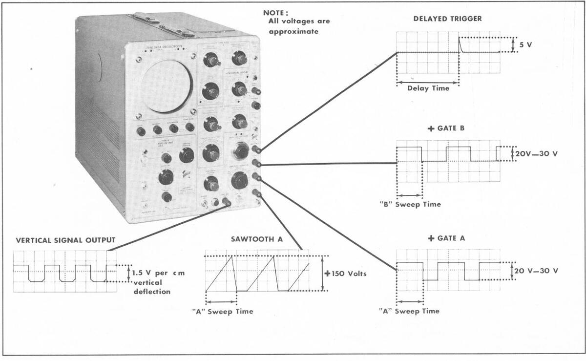
Fig. 1-1. Output waveforms available at the Oscilloscope front panel.
Construction
Aluminum-alloy chassis and three-piece cabinet. Photo etched anodized panel, blue wrinkle-finished cabinet.
Dimensions—see Figure 1-2.
Weight—65 pounds.
Accessories
- 1—3 to 2-wire Adapter, 103-013
- 2—Type P6006 Probes, 010-127
- 2-Binding Post Adapter, BNC, 103-033
- 1—Test Lead (012-031).
- 1—Type F510-5 Green Filter (3/8-514)
- 2—Operator's Manuals.
- 1—Operator's Handbook.
- 1—3-conductor power cord, 161-010

Fig. 1-2. Type 545A Oscilloscope Dimensions.
Type N
The Type N Sampling Unit is designed for use with Tektronix plug-in type Oscilloscopes. The sampling system thus formed permits the display of repetitive signals with fractional nanosecond (10-9 second or nsec) risetime. By taking successive samples at a slightly later time at each recurrence of the pulse under observation, the Type N reconstructs the pulse on a relatively long time-base. Specifications of the Type N include a risetime of 0.6 nsec, corresponding to a maximum bandpass of approximately 600 mc; a sensitivity of 10 mv/cm with 2 mv or less noise; and a dynamic range of ±120 mv minimum linear range before overloading results.
Accidental overload of ±4 volts dc is permissible.
Type P
The Type P Plug-In Unit generates a fast-rise stepfunction test signal of known waveform, simulating the output of an ideally compensated Type K Unit driven with a Tektronix Type 107 Square-Wave Generator. The Type P permits the standardization of the main-unit vertical amplifier transient response of a Tektronix convertible oscilloscope. Risetime of the Type P is approximately 4 nanoseconds when it is used to standardize a Type 540-Series Oscilloscope. Pulse repetition rate is 240 step functions per second, with either positive or negative polarity. Step function amplitude is continuously adjustable between 0 and 3 major graticule divisions.
Type Q
The Type Q Plug-In Unit permits any Tektronix convertible oscilloscope such as the Type 545A to be operated with strain gages and other transducers. Excitation voltages for the strain gages and transducers are provided by the plug-in unit. The unit provides high gain, low noise, and extremely low drift. Frequency response of the Type Q Plug-In Unit is DC to 6 kc; risetime is approximately 60 microseconds. Strain sensitivity is calibrated in 10 steps from 10 microstrain per major graticule division to 10,000 microstrain per division, and is continuously variable between steps.
Type R
The Type R Plug-In Unit is a combined power supply and pulse generator which is used to measure the high-frequency characteristics of junction transistors by the pulse-response method. When the Type R is used in an oscilloscope having a delay line; delay time, risetime, storage time, and falltime may be displayed simultaneously. A pushbutton switch connects a front-panel terminal directly to the input of the oscilloscope for observing externally derived waveforms.
Pulse risetime of the Type R unit is less than 5 nanoseconds, so measurements depend on the risetime of the oscilloscope used. Pulse amplitudes are in 8 fixed, calibrated steps from .05 to 10 volts, adjustable between steps. Pulse recurrence frequency is 120 pulses per second.
Type S
The Type S Plug-In Unit is designed for use with Tektronix Wide-Band convertible oscilloscopes. The slower risetime of the Tektronix 530-Series Oscilloscopes will affect the ability of the S Unit to analyze fast semiconductor diodes. Using the Type S, voltage across a test diode is displayed as a function of time.
Certain diode parameters, such as junction resistance, junction capacitance, and the stored charge at the junction, can be measured readily and reliably from the display. Performance of a diode in a particular circuit can be predicted by analyzing the recovery and "turn-on" characteristics. Since it is essentially a means for plotting voltage across an element while passing constant current through it, the unit can be used for other applications as well. For
Characteristics — Type 545A
| PLUG-IN TYPE |
CALIBRATED
DEFLECTION FACTOR |
PASSBAND | RISETIME |
INPUT
CAPACITANCE |
|---|---|---|---|---|
|
Type A
Wide-Band DC Coupled |
0.05 v/cm to 20 v/cm |
dc to 14 mc
dc to 20 mc |
18 nsec | 47 pf |
|
TYPE B
Wide-Band |
5 mv/cm to 0.05 v/cm | 2 c to 12 mc | 30 nsec | 47 pf |
|
High Gain
DC Coupled |
0.05 v/cm to 20 v/cm | dc to 20 mc | 18 nsec | |
|
TYPE CA
Dual-Trace DC Coupled |
0.05 v/cm to 20 v/cm | dc to 24 mc | 15 nsec | 20 pf |
|
TYPE D
High-Gain DC Coupled Differential |
1 mv/cm to 50 v/cm | dc to 2 mc | 0.18 µsec | 47 pf |
|
Type E
Low-Level AC Coupled Differential |
50 µv/cm to 10 mv/cm | 0.06 cycles to 60 kc | 6 μsec | 50 pf |
|
TYPE G
DC Coupled Differential Wide-Band |
0.05 v/cm to 20 v/cm | dc to 20 mc | 18 nsec | 47 pf |
|
TYPE H
DC Coupled High-Gain Wide-Band |
5 mv/cm to 20 v/cm | dc to 15 mc | 23 nsec | 47 pf |
|
TYPE K
Fast-Rise DC Coupled |
0.05 v/cm to 20 v/cm | dc to 30 mc | 12 nsec | 20 pf |
|
TYPE L
Fast-Rise |
5 mv/cm to 2 v/cm | 3 c to 24 mc | 15 nsec | 20 pf |
|
High-Gain
DC Coupled |
0.05 v/cm to 20 v/cm | dc to 30 mc | 12 nsec | |
|
TYPE N*
Pulse Sampling |
10 mv/cm | 600 mc | 0.6 nsec |
Input Impedance
50 ohms |
| TYPE P* is a fast-rise | e step-function test signal unit. | |||
|
TYPE Q*
Strain Gage |
10 μstrain/div to
10,000 μstrain/div |
dc to 6 kc | 60 µsec | Adjustable |
|
TYPE R*
Transistor Risetime |
0.5 ma/cm to 100 ma/cm | 12 nsec | ||
|
TYPE S*
Semiconductor Diode Recovery |
0.05 v/cm and 0.05 v/cm | |||
|
TYPE T*
Time-Base Generator |
||||
|
TYPE Z*
DC Coupled Differential Comparator |
0.05 v/cm to 25 v/cm | dc to 13 mc | 27 nsec | 27 pf |
PLUG-IN PREAMPLIFIER CHARACTERISTICS FOR TYPE 545A OSCILLOSCOPES
*More data available on the special purpose plug-in units in the following paragraphs.
example: observing the junction characteristics of transistors, or measuring the resistance, capacitance or inductance of circuit components.
The Type S offers calibrated forward currents in five fixed steps from 1 to 20 milliamps, and reverse currents calibrated in six steps from 0 to 2 milliamps. Diode shunt capacitance is 9 picofarads, and deflection factors are 0.05 v/cm and 0.5 v/cm, calibrated.
Туре Т
The Type T Time-Base Generator provides sawtooth sweep voltages from 0.2 µsec/div to 2 sec/div. The trigger source may be line frequency, external, ac or dc coupled, automatic or high-frequency sync. The triggering point can be on either rising or falling slope of the waveform, and triggering level is adjustable. A signal of 0.2 to 50 volts is required for triggering.
Туре Z
The Type Z Plug-In Unit extends the accuracy of oscilloscope voltage measurements. It can be used in three modes of operation: (1) as a conventional preamplifier, (2) as a differential input preamplifier, or (3) as a calibrated differential comparator. With sensitivity of 50 mv/cm and insertion voltage range of ±100 volts, the effective scale range is ±2000 cm. Maximum resolution of the Type Z Unit is .005%.
As a conventional preamplifier, the Type Z Unit offers a passband of dc to 13 mc for the 545A for signals that do not overscan the screen. The deflection factors are 0.05 volts/cm to 25 v/cm in 9 fixed, calibrated steps.
As a differential input preamplifier, the Type Z accepts a common-mode signal level ±100 volts with input attenuation X1, and offers a common-mode rejection ratio of 40,000 to 1. Maximum input signal is 1 volt/7 nsec, or -1 volt/5 nsec.
As a calibrated differential comparator, the Type Z makes available three comparison voltage ranges; from zero to ±1 volt, zero to ±10 volts, zero to ±100 volts.
NOTES
SECTION 2
The Type 545A Oscilloscope is an extremely versatile instrument which is adaptable to a great number of applications. However, to make use of the full potentialities of the instrument, it is necessary that you understand completely the operation of each control. This portion of the Instruction Manual is intended to provide you with the basic information that you require. If you are familar with other Tektronix Oscilloscopes, you should have very little difficulty in understanding the operation of the Type 545A since the function of many controls is the same as the function of corresponding controls on other Tektronix instruments.
Plug-In Units
The Type 545A Oscilloscope is designed to operate with any one of the Tektronix letter-series plug-in units. The particular plug-in unit used must be selected by you to satisfy the requirements of your application. In selecting the plug-in unit for any particular application, you must consider the bandpass, sensitivity, and the type of input required for that application. The plug-in units available will satisfy the requirements for most applications.
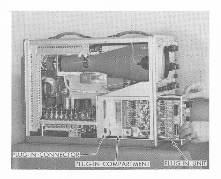
Fig. 2-1. Inserting the selected plug-in unit into the oscilloscope plug-in unit compartment.
OPERATING INSTRUCTIONS
Preparation for use
When the plug-in unit has been selected, insert it into the plug-in compartment of the oscilloscope and press firmly to insure that the connectors make proper contact (see Figure 2-1). Tighten the plug-in unit locking control to hold the unit securely in place and turn the oscilloscope INTENSITY control fully counterclockwise. Connect the power cord to the rear of the instrument and to the power line and place the POWER switch in the ON position.
Time Delay
Time delay relays used in Type 545A Oscilloscopes delay operation of the instrument for approximately 25 seconds after the POWER switch is turned on to allow a brief tubewarmup period. The delay allows the tubes sufficient time to heat before the dc operating voltages are applied.
If the ac power is off for only an instant, the normal 25second delay will occur before the instrument returns to full operation. This delay will occur regardless of whether the ac power is off because of a momentary power failure or is turned off with the POWER switch.
Focus and Astigmatism Contols
The FOCUS and ASTIGMATISM controls operate in conjunction with each other to allow you to obtain a sharp, clearly defined spot or trace. The proper setting of the ASTIGMATISM control is obtained by rotating the FOCUS control fully clockwise, setting the HORIZONTAL DISPLAY switch to EXT. X10, and adjusting the INTENSITY control to obtain a spot on the screen. After positioning the spot to the center of the screen, the ASTIGMATISM control is adjusted for the most nearly circular spot possible. The FOCUS control is then adjusted to reduce the spot diameter as much as possible. (You must be certain that all input signals to the oscilloscope are disconnected when you adjust the FOCUS and ASTIGMATISM controls.)
Intensity Control
The INTENSITY control is used to adjust the brightness of the oscilloscope display. This permits you to compensate for changes in brightness resulting from changes in the sweep or triggering rate. The INTENSITY control is rotated clockwise to increase brightness and counterclockwise to decrease brightness. Care must be taken when using the INTENSITY control that the brightness is not turned up to
Operating Instructions — Type 545A
the point where the face of the cathode-ray tube is permanently damaged. If the intensity of the beam is turned up too far, the phosphor on the face of the crt may be burned. The intensity of the beam should never be turned up to the point where a halo forms around the spot.
Graticule Illumination Control
The graticule used with the Type 545A Oscilloscope is accurately marked with 10 horizontal and 4 vertical 1centimeter divisions with 2-millimeter markings on the centerlines. These graticule markings allow you to make time and voltage measurements from the oscilloscope screen.
The graticule is illuminated by two lamps located at the top edge of the graticule. This illumination can be controlled so that the graticule markings appear either red or white, as desired. The graticule markings are changed from red to white or from white to red by removing the graticule cover and rotating the graticule through 180° about an axis through the center of the graticule (see Figure 2-2). As a general rule, white graticule markings are superior to red for photographic purposes.
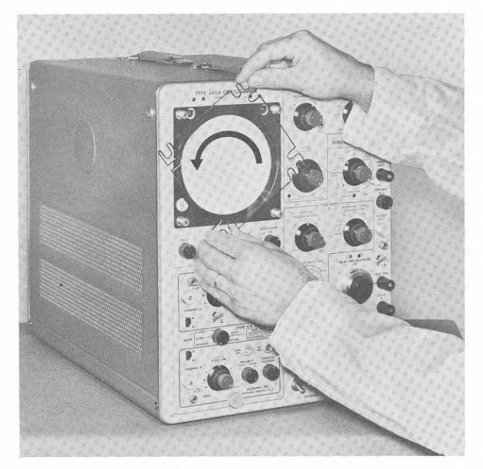
Fig. 2-2. Rotating the graticule to change the color of the graticule markings from red to white or from white to red.
Graticule illumination is adjusted by the SCALE ILLUM control located just under the oscilloscope screen. Rotating the control clockwise increases the brightness of the graticule markings and rotating the control counterclockwise decreases the brightness. For convenience in photographic work, the SCALE ILLUM control is marked in approximate f-stops. These f-stops can be used with a shutter speed of 1 second when TRI X film is used or with a shutter speed of 10 seconds when Type 44 Polaroid film is used. Regardless of the type of film used, white graticule markings should be used. To obtain satisfactory waveform photographs, the intensity of the trace must approximately match the brightness of the graticule markings.
2-2
Positioning Controls
Three controls are used with the Type 545A Oscilloscope to allow you to position the trace to the desired point on the oscilloscope screen. Two of these controls are used to set the horizontal position of the trace and are located on the front panel of the instrument. The third control is used to set the vertical position of the trace and is located on the front panel of the plug-in unit used with the oscilloscope. (The Type 53/54C and Type CA Dual-Trace Plug-In Units have two Vertical Positioning controls.)
The two HORIZONTAL POSITION controls cause the trace to move to the right when they are rotated in the clockwise direction and to the left when they are rotated counterclockwise. The combination of the two controls has a total positioning range of approximately 12 centimeters with the sweep magnifier off or approximately 60 centimeters with the sweep magnifier on. The black HORIZONTAL POSITION control has approximately three times the range of the red VERNIER control. The fine range of adjustment of the VERNIER control makes this control particularly useful whenever fine horizontal positioning is required, as for example, when the sweep magnifier is used.
The vertical positioning control has sufficient range to allow the trace to be positioned completely off the top or bottom of the screen or to any intermediate point. The trace moves up when the control is rotated clockwise and down when the control is rotated counterclockwise.
Beam Position Indicators
Four small indicator lights located just above the oscilloscope screen indicate the position of the spot or trace. When one of these lamps is lit, it indicates that the trace is off-centered in the direction of the arrow. These four lights allow you to position the spot to the center of the screen even though the intensity is so low that the trace is not visible. When the sweep is running, the spot moves from the left side of the screen to the right and may cause both horizontal lamps to light each time the sweep runs.
Input Signal Connections
The electrical waveform to be observed is applied to one of the plug-in unit input connectors. The waveform is then connected through the vertical-deflection system of the plug-in unit and the oscilloscope to cause the spot to be deflected vertically and to trace out the waveform on the screen of the crt. The vertical size of the displayed waveform is adjusted with the plug-in unit VOLTS/CM switch. The VOLTS/CM switch is an accurately calibrated control which, when used with the graticule, allows you to make precise voltage measurements from the displayed waveforms. The operation of other plug-in unit controls varies between plug-in units. For information regarding the operation of these controls, refer to the instruction manual for the plug-in unit you are using.
Certain precautions must be taken when you are connecting the oscilloscope to the input signal source to insure that accurate information is obtained from the oscilloscope display. This is particularly true when you are observing low-level signals or waveforms containing high- or extremely
low-frequency components. For applications where you are observing low-level signals, unshielded input leads are entirely unsatisfactory due to their tendency to pick up stray signals which produce erroneous oscilloscope displays. Shielded cables should be used whenever possible, with the shield connected to the chassis of both the oscilloscope and the signal source. Regardless of the type of input lead used, leads should be kept as short as possible.
Distortion of the input waveform may result if very lowfrequency input signals are ac coupled into the oscilloscope, if high-frequency waveforms are not properly terminated, or if the input waveform contains high-frequency components which exceed the pass band of the oscilloscope and plug-in unit combination. You must be aware of the limitations of the instrument.
In analyzing the displayed waveform, you must consider the loading effect that the oscilloscope has on the inputsignal source. In most cases this loading effect is negligible; however in some applications, loading caused by the oscilloscope may materially alter the results obtained. In such cases you may wish to reduce the amount of loading to a negligible amount through the use of a probe.
Use of Probes
Occasionally connecting the input of an oscilloscope to a signal source loads the source sufficiently to adversely affect both the operation of the source and the waveform displayed on the oscilloscope. In such cases an attenuator probe may be used to decrease both the capacitive and resistive loading caused by the oscilloscope to a negligible value.
In addition to providing isolation of the oscilloscope from the signal source, an attenuator probe also decreases the amplitude of the displayed waveform by the attenuation factor of the probe. Use of a probe allows you to increase the vertical-deflection factors of the oscilloscope to observe large-amplitude signals which are beyond the normal limits of the oscilloscope and plug-in combination. Signal amplitudes, however, must be limited to the maximum allowable value of the probe used.
Before using a probe you must check (and adjust if necessary) the compensation of the probe to prevent distortion of the applied waveform. To adjust the probe compensation control, place the HORIZONTAL DISPLAY switch to A, the
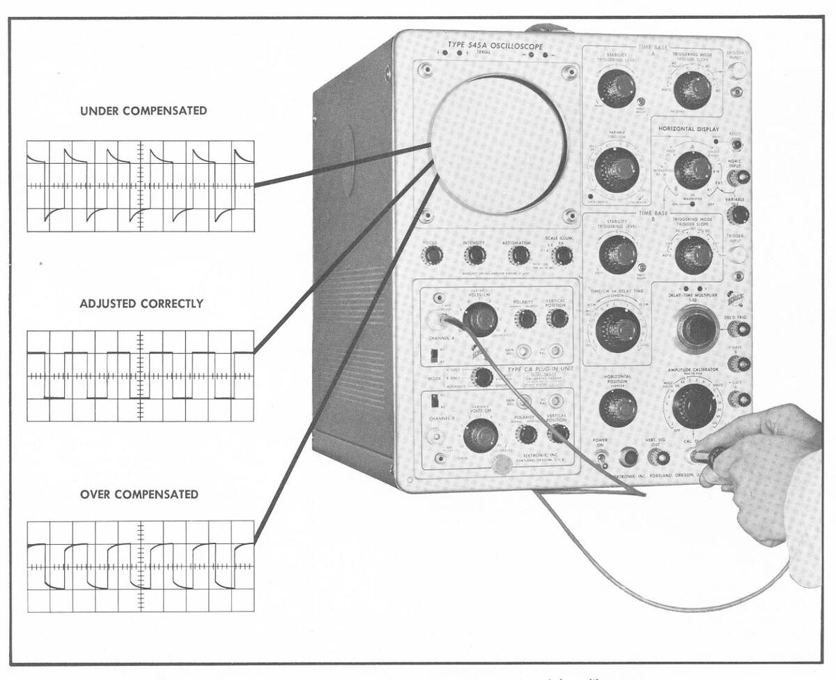
Fig. 2-3. When compensating the probe it is adjusted to obtain an undistorted presentation of the calibrator square-waves.
Operating Instructions --- Type 545A
TIME BASE A TRIGGERING MODE switch to AUTO, and the TIME BASE A TRIGGER SLOPE switch to +INT. Turn up the intensity until the trace is visible and connect the probe tip to the CAL OUT connector. Set the AMPLITUDE CALI-BRATOR switch for 2 centimeters of displayed signal. Set the TIME BASE A TIME/CM switch to display approximately 3 or 4 cycles of the Calibrator waveform and adjust the probe compensation control to obtain flat tops on the displayed Calibrator square-waves (see Figure 2-3).
First unlock the Locking Sleeve by turning it counterclockwise. The probe is then compensated by rotating the probe body while watching the oscilloscope display for the desired waveform. When compensation is completed, carefully turn the Locking Sleeve clockwise to lock it without disturbing the adjustment of the probe.
Horizontal Sweep
The usual oscilloscope display is a graphical presentation of instantaneous voltage versus time. Voltage information is presented by vertical deflection of the trace and time information is presented by horizontal deflection. To obtain a useful display, it is necessary for the spot formed by the electron beam to be deflected horizontally at a known rate so that any horizontal distance on the screen represents a definite known period of time. The trace formed by the deflection of the spot across the screen is known as the horizontal sweep. Since the horizontal deflection of the spot bears a definite relationship to time and provides the means for making time measurements from the screen, the horizontal sweep is also known as the time base.
The Type 545A Oscilloscope features two independent time-base units: Time Base A and Time Base B. Either of the two time bases may be displayed on the oscilloscope screen at any time. Controls affecting Time Base A and Time Base B operation are in the correspondingly labeled blocks on the oscilloscope front panel. The HORIZONTAL DISPLAY switch determines which time base is used and the type of display to be presented. Time Base A is selected when the HORIZONTAL DISPLAY switch is in position A and Time Base B is selected when the switch is in position B.
Fig. 2-4. The oscilloscope plots instantaneous voltage versus time, thereby serving both as a voltmeter and a timer.
The rate at which the spot is deflected across the screen is accurately controlled by the setting of the appropriate TIME/CM controls. The settings of the TIME/CM controls determine the sweep speed and the horizontal size of the displayed waveform. The controls are set to display the portion of the waveform you wish to observe.
Time Base A has 24 accurately calibrated sweep rates ranging from .1 microsecond to 5 seconds per centimeter. These calibrated sweep rates are obtained only when the VARIABLE TIME/CM control is in the fully clockwise position. The VARIABLE TIME/CM control permits you to vary the sweep rate continuously between .1 microsecond and approximately 12 seconds per centimeter. All sweep rates obtained with the VARIABLE TIME/CM control in any position but fully clockwise are uncalibrated. Uncalibrated sweep rates are indicated when the UNCALIBRATED lamp is lit.
Time Base B has sweep rates ranging from 2 microseconds to 1 second per centimeter in 18 steps. There is no VARI-ABLE TIME/CM control for Time Base B. The red LENGTH control adjusts the sweep length between approximately 4 and 10 centimeters.
Sweep Triggering
The oscilloscope display is formed by the repetitive sweep of the spot across the oscilloscope screen. If the sweeps are allowed to occur at random or at a rate unrelated to the rate of occurrence of the input waveform, the displayed waveform will be traced out at a different point on the screen each time the sweep runs. This will either cause the waveform to drift across the screen or to be indistinguishable.
In most cases it is desirable for a repetitive waveform to appear stationary on the oscilloscope screen so that the characteristics of the waveform can be examined in detail. As a necessary condition for this type of display, the start of the sweep must bear a definite, fixed-time relationship to the appearance of the input waveform. This means that the sweep must be synchronized with the input waveform. In the Type 545A Oscilloscope this is accomplished by starting (triggering) the sweep with the displayed waveform or with another waveform bearing a definite time relationship to the displayed waveform.
The following paragraphs outline the means for selecting the triggering source, triggering slope, and triggering level with specific information regarding the operation of the controls affecting triggering. Triggering controls for Time Base A and Time Base B are virtually identical so that the following information is applicable to both time-base units. Triggering of the sweep is adjusted by the respective STABILITY, TRIGGERING LEVEL, TRIGGERING MODE, and TRIGGER SLOPE controls.
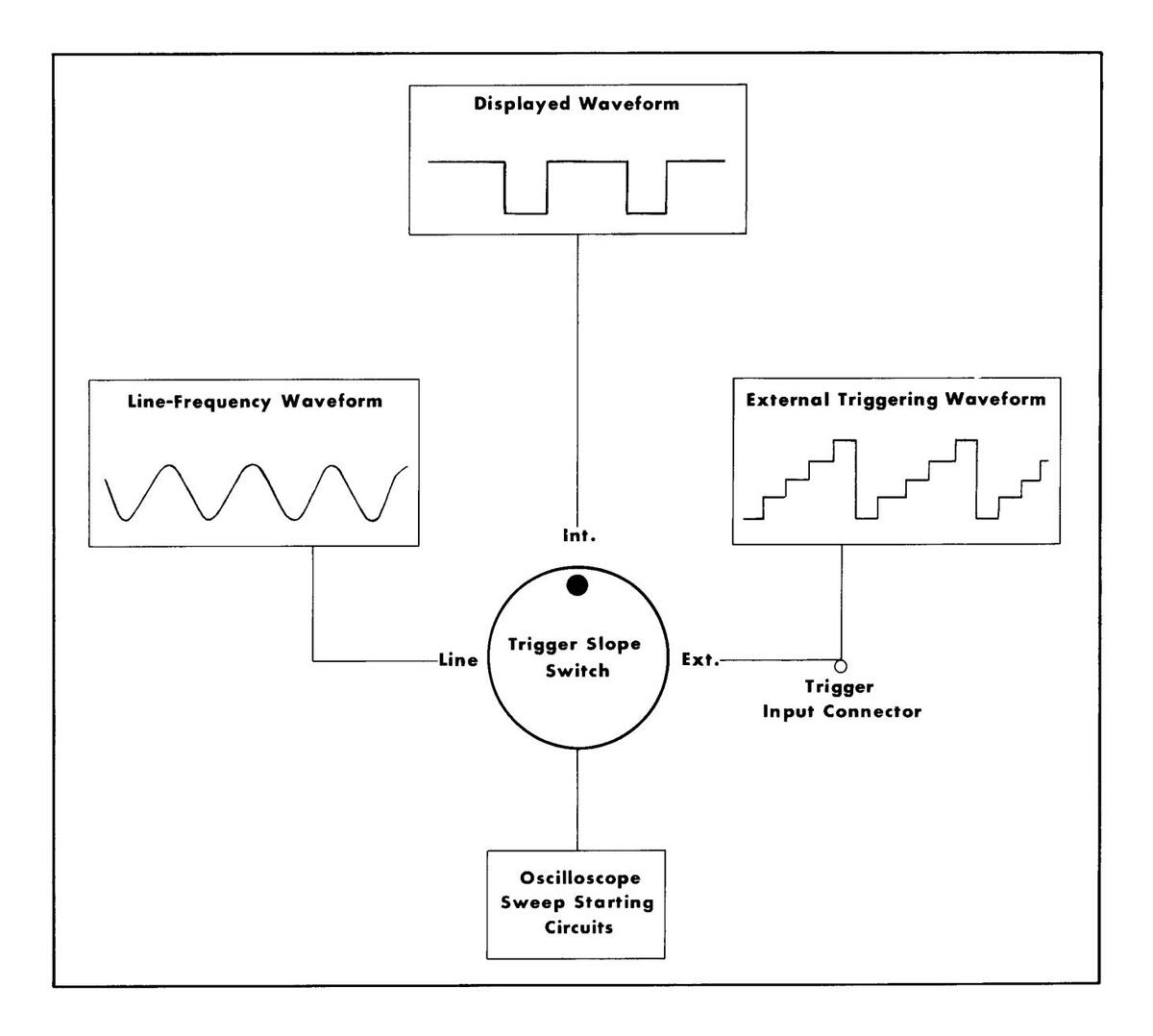
Selecting the Triggering Source
In preparing the Type 545A Oscilloscope for triggered operation of the sweep, it is first necessary to select the triggering signal source which will provide the best display for the particular application. The sweep can be triggered by the displayed waveform, a line-frequency waveform,

or by an externally derived waveform. This selection is made by the setting of the TRIGGER SLOPE control. Each type of triggering has certain advantages for some applications.
Triggering from the displayed waveform is the method most commonly used. The displayed waveform is selected when the TRIGGER SLOPE control is in either the +INT. or -INT. position. Internal triggering is convenient since no external triggering connections are required. Satisfactory results are obtained in most applications.
When you are observing a waveform which is related to the line frequency, you may wish to trigger the sweep from a line-frequency waveform. This can be done by placing the TRIGGER SLOPE switch in either the +LINE or the -LINE position. This type of triggering is particularly useful in observing waveforms which bear a definite relationship to the line frequency. The shape and the amplitude of the triggering waveform remains constant to provide extremely stable triggering.
To trigger the sweep from some external waveform connect the triggering waveform to the appropriate TRIG-GER INPUT connector and place the TRIGGER SLOPE switch in either the +EXT, or -EXT, position, External triagering provides definite advantages over other methods of triggering in certain cases. With external triggering, the triggering signal usually remains constant in amplitude and shape. It is thereby possible to observe the shaping and amplification of a signal in an external circuit without resetting the oscilloscope triggering controls for each observation. Also, time and phase relationships between the waveforms at different points in the circuit can be seen. If for example the external triggering signal is derived from the waveform at the input to a circuit, the time relationship and phase of the waveforms at each point in the circuit are compared to the input signal by the display presented on the oscilloscope screen.
When you are using external triggering and a stable triggering signal, it is possible to observe and accurately measure jitter of the displayed waveform. This is not possible when the sweep is triggered internally.
Selecting the Triggering Slope
The horizontal sweep can be triggered on either the rising (+slope) or falling (-slope) portion of the triggering waveform as determined by the position of the TRIGGER SLOPE switch. When the switch is in one of the + positions, the sweep is triggered on the rising portion of the triggering waveform; when the TRIGGER SLOPE switch is in one of the - positions, the sweep is triggered on the falling portion of the waveform (see Figure 2-7).
In many applications the triggering slope is not important since triggering on either slope will provide a display which is suitable to the application. However, in many other cases, such as pulse measurements, the triggering slope is very important. If, while using a fast sweep, you may wish to observe the rise of a pulse, it will be necessary for you to trigger the sweep on the rising portion of the waveform by placing the TRIGGER SLOPE switch in one of the + positions. To observe the fall of a pulse at a fast sweep rate, it will be necessary to trigger the sweep on the falling portion of the waveform by placing the TRIGGER SLOPE switch in one of the — positions. In either case, selection of the wrong triggering slope will make it impossible for you to observe the portion of the waveform you wish to check.
Selecting the Triggering Mode
After selecting the triggering source and triggering slope, it is next necessary to select the triggering mode which will allow you to obtain the desired display. Time Base A has five triggering modes while Time Base B has three. Not available for Time Base B are the HF SYNC and AC LF REJECT triggering modes.
Each of the triggering modes is designed to provide stable triggering from a certain type of waveform. For most applications, however, several of the triggering modes will work equally well. For applications of this type, the triggering mode used is purely a matter of choice. The primary thing to consider in choosing the triggering mode is whether or not it allows you to obtain the display you want.
To determine the best mode of operation for a particular application, it is usually best to try each triggering mode in the application. The AUTOMATIC mode should be tried first since this triggering mode provides stable triggering in most applications without the necessity of setting the STABILITY or TRIGGERING LEVEL controls. If the AUTO-MATIC mode does not provide the desired display, it will then be necessary for you to try one or more of the other triggering modes.
Automatic Triggering Mode
The AUTOMATIC mode is most frequently used because of its ease of operation. This mode is useful in obtaining stable triggering from waveforms with frequencies of from approximately 60 cycles to 2 megacycles. The principal advantage of this type of operation is that it is not necessary to adjust either the STABILITY or TRIGGERING LEVEL controls to obtain a stable display. This permits you to observe a large number of waveforms with different shapes

and amplitudes without adjusting any of the triggering controls. In the absence of a triggering signal, the sweep continues to run to provide a convenient reference trace on the oscilloscope screen.
The AUTOMATIC triggering mode is selected by placing the TRIGGERING MODE switch in the AUTO. position. The triggering source and slope is then selected and the input signal is applied to the oscilloscope. No other control adjustments are required. Since the TRIGGERING LEVEL control has no effect on the display when AUTOMATIC trig-
gering is used, it is impossible to select the point on the triggering waveform where the sweep is triggered. Each sweep is instead triggered at the average voltage point of the waveform.
DC Triggering Mode
The DC triggering mode is selected by placing the TRIG-GERING MODE switch in the DC position. This mode permits excellent triggering on all types of waveforms in the
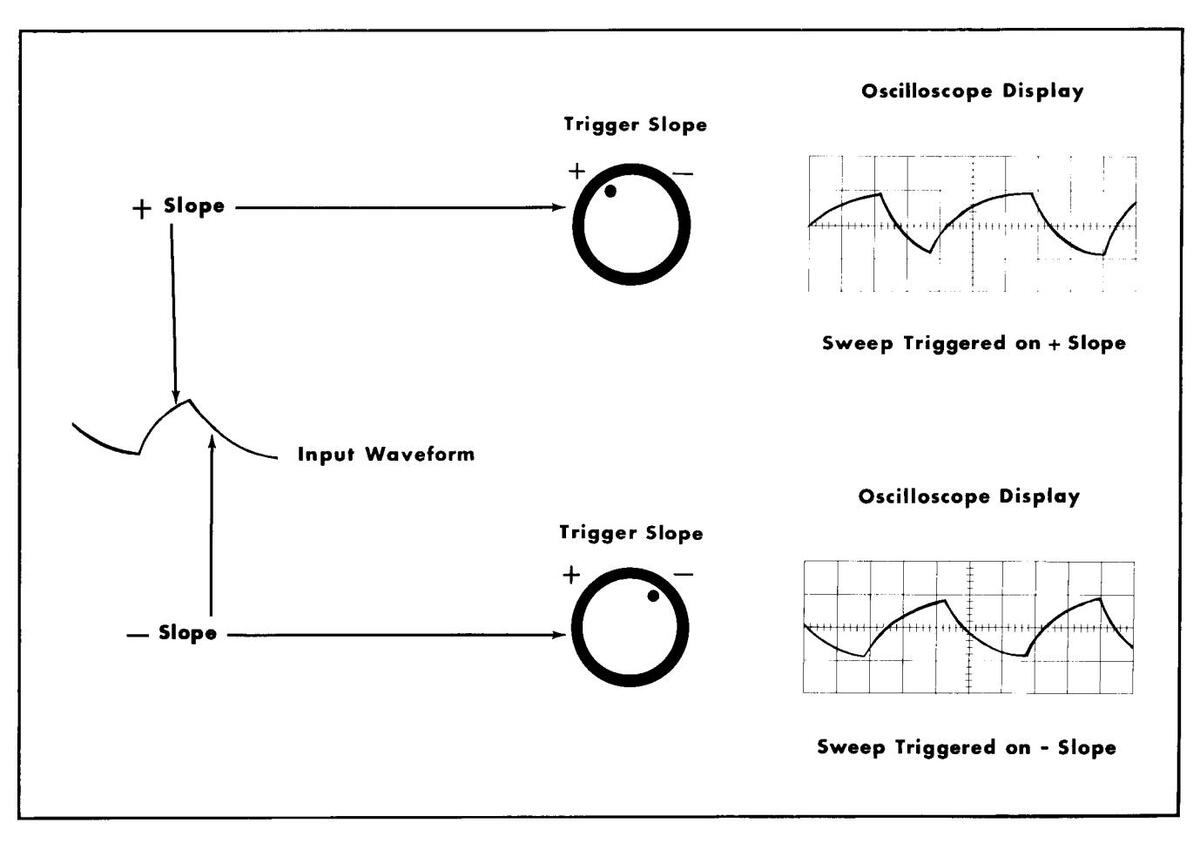
Fig. 2-7. Effects on the oscilloscope display produced by + and — settings if the TRIGGER SLOPE control.
frequency range from dc to approximately 5 mc. The DC mode also permits the selection of the point on the triggering waveform where the sweep is triggered through the use of the TRIGGERING LEVEL control.
To use the DC triggering mode you must set the STA-BILITY and TRIGGERING LEVEL controls after first selecting the triggering signal source and slope. The method used to set the STABILITY and TRIGGERING LEVEL controls is the same for the DC mode, AC mode, and AC Low Frequency Reject mode. The STABILITY control must be set properly before the TRIGGERING LEVEL control can be adjusted.
The STABILITY control has a PRESET position at the fully counterclockwise setting of the control. This position permits proper triggering in most applications without necessitating additional adjustment of the STABILITY control. If it becomes impossible or difficult for you to obtain proper triggering with the STABILITY control at PRESET, you must then adjust the control. This is done with the TRIGGERING LEVEL control fully counterclockwise. The STABILITY control is rotated clockwise from the PRESET position until a trace appears on the screen. The proper setting for the control is then obtained by rotating the knob slowly counterclockwise until the trace just disappears.
The TRIGGERING LEVEL control determines the point on the triggering waveform where triggering of the sweep occurs. This control is set to provide the display you want
while at the same time causing stable triggering. Rotating the control clockwise causes the sweep to trigger at more positive points on the waveform while rotating the control counterclockwise causes the sweep to trigger at more negative points. If the displayed waveform is vertically centered under the graticule, setting the TRIGGERING LEVEL control at 0 will cause the sweep to start at approximately the midvoltage point of the waveform. In the DC mode, rotating the vertical position control will change the point on the triggering waveform where the sweep is started.
The + and — markings for the TRIGGERING LEVEL control should not be confused with similar markings for the TRIGGER SLOPE control. The markings on the TRIGGER SLOPE control indicate only whether triggering occurs on the rising or falling portion of the triggering waveform. The markings for the TRIGGERING LEVEL control indicate whether triggering occurs on the upper portion or lower portion of the waveform.
AC Triggering Mode
Selection of the AC triggering mode is made by placing the TRIGGERING MODE switch in the AC position. This mode provides useful triggering in the frequency range of approximately 15 cycles to 5 mc. These frequency limits vary slightly depending upon the shape and amplitude of
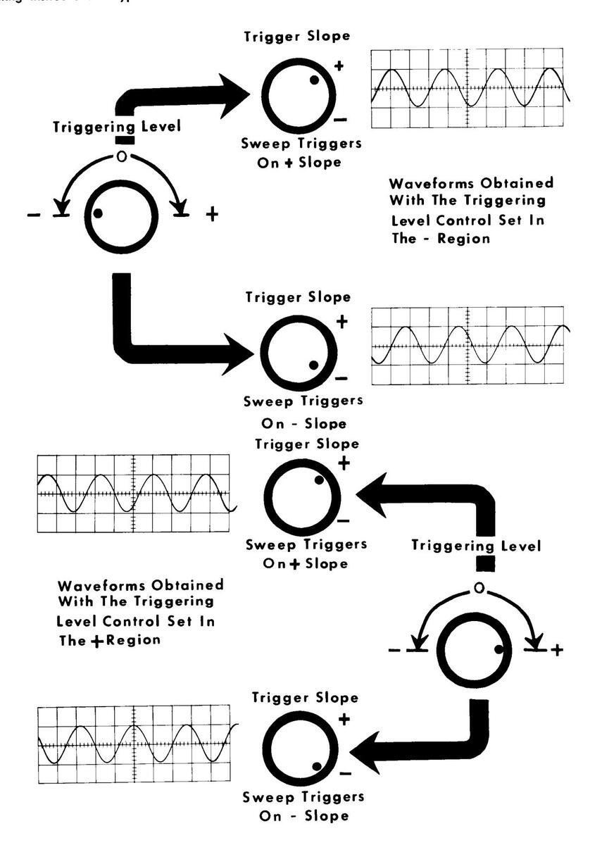
Fig. 2-8. Effects on the oscilloscope display produced by + and — settings of the TRIGGERING LEVEL control. When the TRIGGERING LEVEL control is set in the + region, the sweep is triggered on the upper portion of the input waveform; when it is set in the - region, the sweep is triggered on the TRIGGER SLOPE control determines whether the sweep is triggered on the rising portion or the falling portion of the input waveform.
the triggering waveform. In the AC mode, triggering is unaffected by the dc components of the triggering signal or by the vertical positioning of the trace. The triggering level can be selected to provide the desired display using the STABILITY and TRIGGERING LEVEL controls. These two controls are set as described for the DC triggering mode.
AC Low Frequency Reject Triggering Mode
The AC Low Frequency Reject triggering mode is used when the TRIGGERING MODE switch is in the AC LF REJECT position. This mode is similar to the AC mode except that low-frequency waveforms are rejected by the triggering circuit. This triggering mode works well with highfrequency waveforms, but it may be difficult to obtain stable triggering with frequencies below approximately 1000 cycles.
Occasionally you may be required to obtain stable triggering from a fairly high-frequency waveform that is mixed with a great deal of low-frequency noise or line-frequency pickup. In such cases the additional noise and pickup can make it very difficult to obtain a stable display. If this occurs, you can select the AC Low Frequency Reject triggering mode, thereby eliminating the effects of the low frequency noise and pickup. The low frequencies are blocked from the triggering circuit while the high-frequency triggering waveform is passed to produce the stable triggering that you require. In all other respects the AC Low Frequency Reject triggering mode is identical to the AC mode.
High Frequency Synchronization Mode
The High Frequency Synchronization Mode permits stable displays of waveforms with frequencies higher than approximately 5 mc. Stability of the display is adjusted with the STABILITY control. The TRIGGERING LEVEL control is not used. To use the High Frequency Synchronization Mode, place the TRIGGERING MODE switch in the HF SYNC position. Rotate the STABILITY control clockwise until a trace appears. Continue to adjust the STABILITY control until a stable display is obtained.
Although the synchronization signal source is selected with the TRIGGER SLOPE control, the slope cannot be selected. Also you cannot use the PRESET position of the STABILITY control in this mode.
Free-Running Sweep Operation
In the usual oscilloscope application, the sweep is triggered or synchronized by the input waveform. However, in some applications it may be more desirable to reverse the process and initiate the input waveform through use of a periodically recurrent waveform from the oscilloscope. In this type of application the sweep is caused to free-run and an output from either the +GATE or SAWTOOTH connectors is used to trigger or synchronize the input waveform (see Figure 2-9).
The sweep can be made to free run with any setting of the TRIGGERING mode switch by rotating the STABILITY
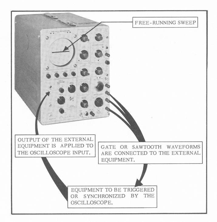
Fig. 2-9. Using the + Gate or Sawtooth output waveforms to synchronize or trigger external equipment.
control fully clockwise. In all positions of the TRIGGERING MODE switch except AUTO, the number of sweeps per second is determined by the setting of the TIME/CM controls. In the AUTO, position, the sweep repetition rate remains at approximately 50 sweeps per second regardless of the setting of the TIME/CM control.
In addition to providing the means for controlling an applied waveform, a free-running sweep also provides a convenient reference trace on the oscilloscope screen without requiring an input signal. This trace can then be used to position the sweep or to establish a voltage reference line.
Delayed Sweep
With the Type 545A Oscilloscope the start of the horizontal sweep can be delayed for a period of from 1 microsecond to 10 seconds after application of the triggering
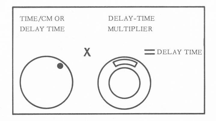
Fig. 2-10. Calculating delay time.
Operating Instructions — Type 545A
waveform. This is done through simultaneous use of Time Base A and Time Base B. In this application Time Base B is used to provide the accurate time delay while Time Base A presents a normal horizontal sweep at the end of the delay period. The duration of the sweep delay is controlled by the Time Base B TIME/CM OR DELAY TIME switch and the DELAY_TIME MULTIPLIER control
The delayed sweep feature of the Type 545A Oscilloscope can be used in a number of special applications to increase the versatility of the instrument. Such applications include high magnification of a selected portion of an undelayed sweep, accurate time measurements, and accurate measurements of waveform jitter. Also, it is possible to pick off and display any desired line of a television scan or to check pulse-time modulation. In addition, the delayed sweep feature is readily adaptable to a great number of other applications.
The delayed sweep is selected when the HORIZONTAL DISPLAY switch is in the 'A' DEL'D BY 'B' position. The amount of delay occurring from the application of the triggering waveform until the sweep runs is indicated directly by the settings of the TIME/CM OR DELAY TIME switch and the DELAY TIME MULTIPLIER control. The settings
of the two controls are multiplied together to obtain the actual delay time. For example, if the TIME/CM OR DELAY TIME switch is set at 1 MILLISEC and the vernier dial of the DELAY TIME MULTIPLIER control indicates 6.75, the delay time is 6.75 milliseconds. When the Time Base A STABILITY control is in the fully clockwise position, the horizontal sweep starts immediately at the completion of the delay period at a rate determined by the settings of the Time Base A TIME/CM controls.
There are actually two modes of delayed sweep operation available in the Type 545A Oscilloscope (see Figure 2-11). In one mode the delayed sweep is started immediately after the completion of the delay time. This is the mode described previously and is obtained with the Time Base A STABILITY control fully clockwise. This mode permits you to select continuously variable delay times and is the mode of operation used to make accurate time and waveform jitter measurements as well as most other measurements.
The second delayed-sweep mode is different from the first in that the sweep does not start at the completion of the delay time until a triggering waveform is applied to Time Base A. The delay time in this mode is not continuously variable and is dependent not only on the settings of
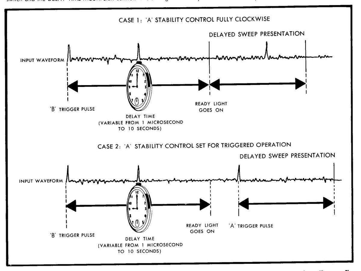
Fig. 2-11. Comparison of the two delayed-sweep modes. In each case the waveform shown represents the input to the oscilloscope. The waveform shown in the delayed-sweep presentation boxes represents the portion of the input waveform that is actually displayed on the oscilloscope screen. Note that in Case 2 an additional triggering pulse is required before the delayed sweep will occur.
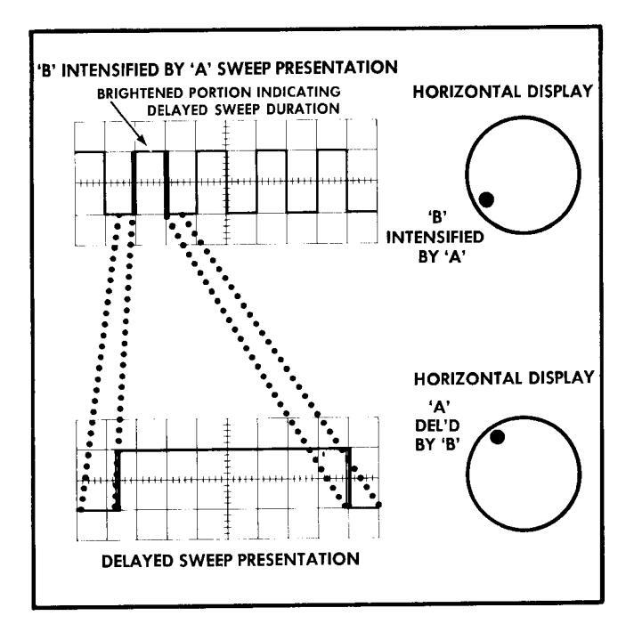
Fig. 2–12. Correlation of the 'B' INTENSIFIED BY 'A' and 'A' DEL'D BY 'B' positions of the HORIZONTAL DISPLAY switch.
the delay-time controls, but on the occurrence of the Time Base A triggering waveform as well. The primary purpose of this mode is to eliminate jitter from the displayed waveform. Since the sweep is triggered by the input waveform, jitter is eliminated from the display even though it is inherent in the input waveform.
The second delayed-sweep mode is also obtained with the HORIZONTAL DISPLAY switch in the 'A' DEL'D BY 'B' position. In this mode, however, the Time Base A triggering controls are set to provide normal triggering. The STABIL-ITY control is not placed in the fully clockwise position.
When the HORIZONTAL DISPLAY switch is placed in the 'B' INTENSIFIED BY 'A' position, you can obtain a normal sweep presentation using Time Base B. If all other controls are set for delayed sweep operation and the Time Base A TIME/CM switch is set for a faster sweep rate than the Time Base B control, a portion of the displayed waveform will be brightened. The start of this brightened portion indicates the start of the delayed sweep and the length of the brightened portion indicates the delayed sweep duration. The start of the brightened portion can be positioned left or right with the DELAY-TIME MULTIPLIER control. The length of the brightened portion can be adjusted with the Time Base A TIME/CM control. Using these two controls, it is possible to include any portion of the displayed waveform in the brightened area.
To expand a portion of the display obtained with the HORIZONTAL DISPLAY switch in the 'B' INTENSIFIED BY 'A' position, adjust the DELAY-TIME MULTIPLIER and Time Base A TIME/CM controls to include the portion you wish to expand in the brightened area (see Figure 2-12). Then place the HORIZONTAL DISPLAY switch in the 'A' DEL'D BY 'B' position. This expands the brightened portion to the full width of the screen. The amount of magnification is the ratio of the Time Base B TIME/CM OR DELAY TIME control
setting to the Time Base A TIME/CM control setting. For example, if the Time Base B TIME/CM OR DELAY TIME switch is set at 1 MILLISEC and the Time Base A TIME/CM switch is set at 1 µSEC, the brightened portion of the sweep is magnified horizontally 1,000 times. Using this method, practical sweep magnifications up to approximately 10,000 times are attainable.
At times when you are using the delayed sweep with high magnification, the intensity of the trace will be so low that it is difficult to see. In many of these cases the intensity cannot be improved significantly with the INTENS-ITY control. However, the intensity can often be increased by using the Time Base B SWEEP LENGTH control to increase the duty cycle. To set the SWEEP LENGTH control, place the HORIZONTAL DISPLAY switch in the 'B' INTENSI-FIED BY 'A' position. Adjust the SWEEP LENGTH control until the sweep runs to a point just past the brightened portion of the trace. Then return the HORIZONTAL DISPLAY switch to the 'A' DEL'D BY 'B' position.
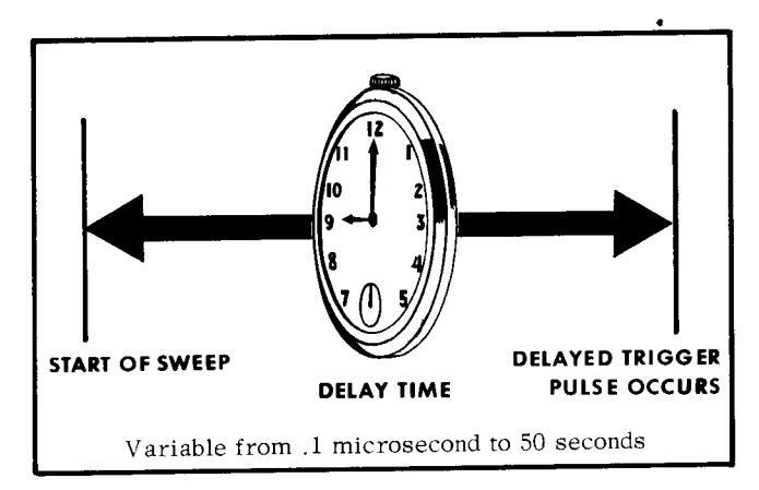
Fig. 2-13. Occurrence of the delayed triggering pulse. The delay time is adjusted with the DELAY-TIME MULTIPLIER control. The delayed triggering pulse occurs at the end of the delay time.
Delayed Trigger
A delayed triggering pulse can be obtained from the DEL'D TRIG. connector of the oscilloscope any time from .1 microsecond to 50 seconds after the start of a sweep. When the oscilloscope is set for delayed sweep operation, the delayed trigger occurs at the start of the delayed sweep. This delayed triggering pulse can be used to initiate some action after a known time interval, and when used with the delayed sweep, permits you to observe the resulting action.
In the B, 'B' INTENSIFIED BY 'A', 'A' DEL'D BY 'B', EXT. X1, and EXT. X10 positions of the HORIZONTAL DISPLAY switch, the delayed trigger is controlled by Time Base B. In the other two positions of the HORIZONTAL DISPLAY switch, the delayed trigger is controlled by Time Base A.
To obtain a delayed trigger you must first adjust the appropriate time-base unit for triggered operation or for free-running operation, depending upon the application. The delay is then set with the appropriate TIME/CM control and the DELAY-TIME MULTIPLIER. The lights above the DELAY-TIME MULTIPLIER control indicate which time-base unit is used to produce the delayed trigger with each setting of the HORIZONTAL DISPLAY switch.
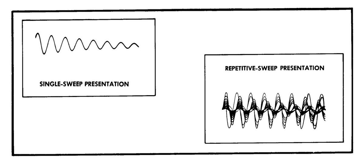
Fig. 2-14. Comparison of single sweep and repetitive sweep presentation of a damped sine wave. In the repetitive sweep presentation, it is difficult to determine what is being presented. However, in the single sweep presentation the damped sine wave can be clearly seen.
Single Sweep
The usual oscilloscope display formed by a repetitive sweep is entirely satisfactory for most applications. However, in applications where the displayed waveform is not repetitive or varies in amplitude, shape, or time interval, a repetitive sweep produces a jumbled display. When observing a waveform of this type, it is usually advantageous to use a single-sweep presentation.
The Type 545A Oscilloscope permits you to obtain a single-sweep presentation and to eliminate all subsequent sweeps so that information is clearly recorded without the confusion resulting from multiple traces. The single-sweep feature is selected by placing the HORIZONTAL DISPLAY switch in the 'A' SINGLE SWEEP position. In this position, only Time Base A is used. The RESET button controls the start of the single sweep.
When the STABILITY control is set fully clockwise or the TRIGGERING MODE switch is in the AUTO. position, a single sweep runs immediately each time the RESET button is depressed. However, if Time Base A is set for triggered operation with the TRIGGERING MODE switch in other than AUTO. or HF SYNC positions, the single sweep does not occur when the RESET button is depressed unless a triggering signal is applied to Time Base A. Instead the READY lamp lights to indicate that the sweep is ready to be triggered. When a triggering signal occurs, the single sweep runs and the READY light goes out. Each time the RESET button is depressed the procedure is repeated.
External Horizontal Input
For special applications you can deflect the trace horizontally with some externally derived waveform. This allows you to use the oscilloscope to plot one function versus another.
To use an external horizontal input, connect the externally derived waveform to the HORIZ. INPUT connector and place
the HORIZONTAL DISPLAY switch in either EXT. position. The horizontal deflection factor is continuously variable from approximately .2 to approximately 15 volts per centimeter with the VARIABLE 10-1 control and the HORIZONTAL DISPLAY switch.
Sweep Magnifier
The sweep magnifier allows you to expand any twocentimeter portion of the displayed waveform to the full ten-centimeter width of the graticule. This is done by first using the HORIZONTAL POSITION control to move the
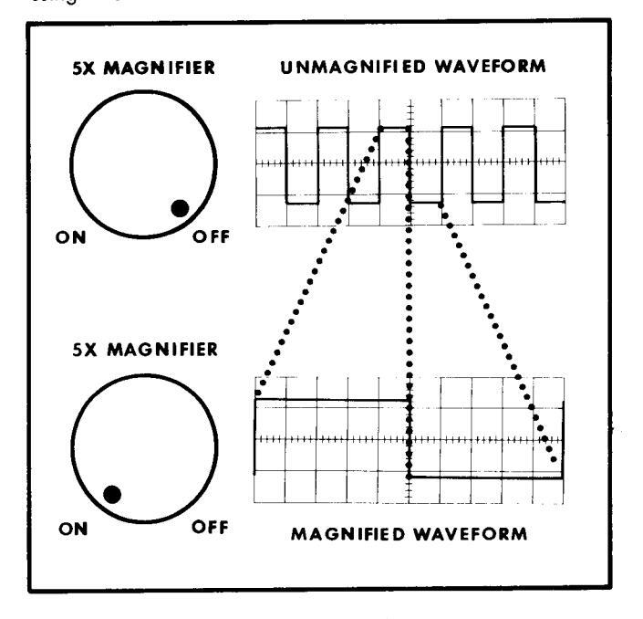
Fig. 2-15. Operation of the sweep magnifier.
portion of the display you wish to expand to the center of the graticule, then placing the 5X MAGNIFIER switch in the ON position. When the 5X MAGNIFIER switch is at ON, the 5X MAGNIFIER lamp lights to indicate the magnifier is on. Any portion of the original unmagnified display can then be observed by rotating the HORIZONTAL POSI-TION controls. The sweep magnifier can be used with either time base unit
In magnified sweep operation, the sweep speed indicated by the position of the TIME/CM control is divided by 5 to obtain the actual time required for the spot to move one centimeter. For example, if the TIME/CM control is set at 5 MILLISEC, the actual time per centimeter is 5 milliseconds divided by 5, or 1 millisecond per centimeter. The actual time per centimeter must be used for all measurements of time.
Amplitude Calibrator
The amplitude calibrator provides a convenient source of square waves of known amplitude at a frequency of approximately 1 kc. The square waves are used primarily to adjust probes and to verify the calibration of the vertical-deflection system of the oscilloscope and plug-in unit
Calibrator square-waves are adjustable from .2 millivolts, peak-to-peak, to 100 volts, peak-to-peak, in 18 steps. The amplitude is controlled by the setting of the AMPLITUDE CALIBRATOR switch and is accurate within 3% of the AMPLITUDE CALIBRATOR switch setting when the output is connected to a high impedance load.
Dual-Trace Displays
The Type CA Plug-In Unit allows you to obtain two separate traces on the face of the crt. This permits you to display two functions simultaneously. Detailed instructions for operating the Type CA Unit in conjunction with the Type 545A Oscilloscope are contained in the Instruction Manual for the Type CA Unit.
When you are using the Type CA Unit in the chopped mode to obtain a dual-trace presentation, switching transients will be displayed on the screen. You can eliminate these switching transients by placing the CRT CATHODE SELECTOR switch on the rear of the instrument in the DUAL-TRACE CHOPPED BLANKING position.
Intensity Modulation
The crt display of the Type 545A Oscilloscope can be intensity modulated by an external signal to display additional information. This is done by disconnecting the grounding bar from the EXTERNAL CRT CATHODE con nector at the rear of the instrument and connecting the external signal to this terminal. The CRT CATHODE SELEC-TOR switch must be in the EXTERNAL CRT CATHODE position
When you wish to make very accurate time measurements from the crt display, you can intensity modulate the beam with time markers and make your measurements directly from the time markers presented on the screen. A positive signal of approximately 25 volts is required to cut off the beam from normal intensity.
Operating Instructions — Type 545A
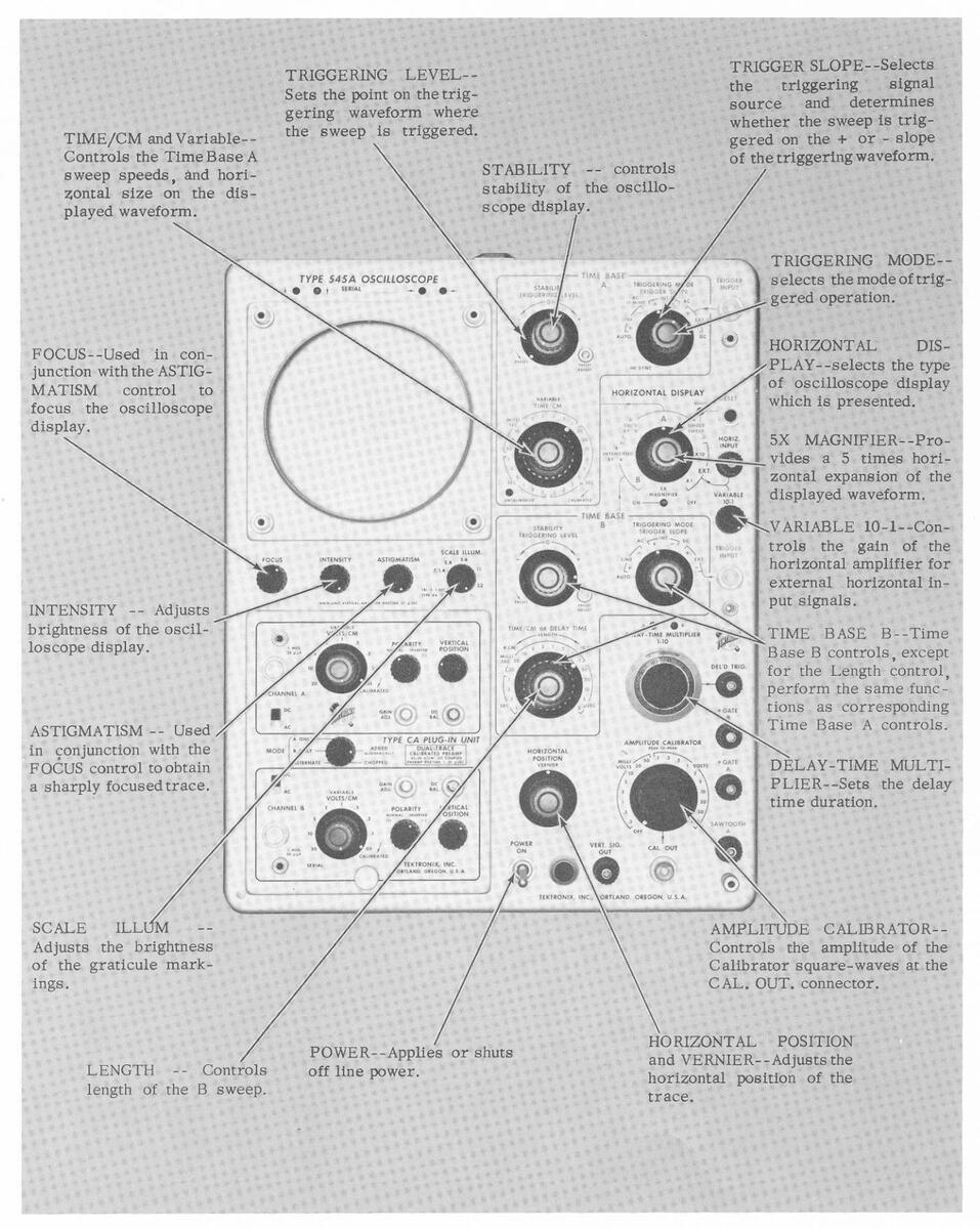
Fig. 2-16. Functions of the Type 545A Oscilloscope front panel controls.
SECTION 3
APPI ICATIONS
38-7m32
Voltage Measurements
The Type 545A Oscilloscope can be used to measure the voltage of the input waveform by using the calibrated vertical-deflection factors of the instrument and associated plug-in unit. The method used for all voltage measurements is basically the same although the actual techniques vary somewhat depending on the type of voltage measurements required. Essentially there are two types of voltage measurements: ac-component voltage measurements and instantaneous voltage measurements with respect to some reference potential. Many waveforms contain both ac and dc voltage components. It is often necessary to measure one or both of these components.
When making voltage measurements, you should display the waveform over as large a vertical portion of the screen as possible for maximum accuracy. Also, it is important that you do not include the width of the trace in your measurements. You should consistently make all measurements from one side of the trace. If the bottom side of the trace is used for one reading, it should be used for all succeeding readings. The VARIABLE VOLTS/CM control must be in the CALIBRATED position.
AC Component Voltage Measurements
To measure the ac component of a waveform, the plug-in unit input selector switch should usually be set to one of the AC positions. In these positions only the ac components of the input waveform are displayed on the oscilloscope screen. However, when the ac component of the input waveform is of very low frequency it is necessary for you to make voltage measurements with the input selector switch in one of the DC positions to prevent errors.
To make a peak-to-peak voltage measurement on the ac component of a waveform, perform the following steps (see Figure 3-1):
1. With the aid of the graticule, measure the vertical distance in centimeters from the positive peak to the negative peak.
2. Multiply the vertical distance measured by the setting of the plug-in unit VOLTS/CM control to obtain the indicated voltage.
3. Multiply the indicated voltage by the attenuation factor of the probe used to obtain the actual peak-to-peak voltage.
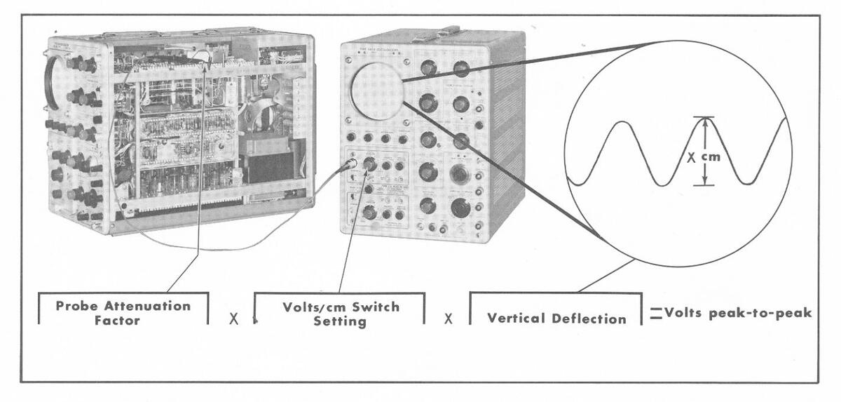
Fig. 3-1. Measuring the peak-to-peak ac component voltage of an applied waveform.
Applications — Type 545A
As an example of the method, assume that using a 10X probe and a deflection factor of 1 volt per centimeter, you measure a vertical distance between peaks of 4 centimeters. In this case then, 4 centimeters multiplied by 1 volt per centimeter gives you an indicated voltage of 4 volts peak-to-peak. The indicated voltage multiplied by the probe's attenuation factor of 10 then gives you the true peak-to-peak amplitude of 40 volts.
When sinusoidal waveforms are measured, the peak-topeak voltage obtained can be converted to peak, rms, or average voltage through use of standard conversion factors.
Instantaneous Voltage Measurements
The method used to measure instantaneous voltages is virtually identical to the method described previously for the measurement of the ac components of a waveform. However for instantaneous voltage measurements the plug-in unit input selector switch must be placed in one of the DC positions. Also since instantaneous voltages are measured with respect to some potential (usually ground) a reference line must be established on the oscilloscope screen which corresponds to that potential. If, for example, voltage measurements are to be made with respect to +100 volts, the reference line would correspond to +100 volts. In the following procedure the method is given for establishing this reference line as ground since measurements with respect to ground are by far the most common type. The same general method may be used to measure voltage with respect to any other potential, however, so long as that potential is used to establish the reference line.
To obtain an instantaneous voltage measurement with respect to ground, perform the following steps (see Figure 3-2):
1. To establish the voltage reference line, touch the probe tip to an oscilloscope ground terminal (or if the reference line is to represent a voltage other than ground, to a source of that voltage) and adjust the oscilloscope controls to obtain a free-running sweep. Vertically position the trace to a convenient point on the oscilloscope screen. This point will depend on the polarity and amplitude of the input signal, but should always be chosen so that the trace lies along one of the major divisions of the graticule. The graticule divisions corresponding to the position of the trace is the voltage reference line and all voltage measurements must be made with respect to this line. (Do not adjust the vertical positioning control after the reference line has been established.)
2. Remove the probe tip from ground and connect it to the signal source. Adjust the triggering controls for a stable display.
3. Using the graticule, measure the vertical distance in centimeters from the desired point on the waveform to the voltage reference line.
4. Multiply the setting of the VOLTS/CM control by the distance measured to obtain the indicated volage.
5. Multiply the indicated voltage by the attenuation factor of the probe you are using to obtain the actual voltage with respect to ground (or other reference voltage).
As an example of this method, assume that you are using a 10X probe and deflection factor of .2 volts per centimeter. After setting the voltage reference line at the second from the bottom division of the graticule, you measure a distance of 3 centimeters to the point you wish to check. In this case then, 3 centimeters multiplied by .2 volts per centimeter gives you an indicated .6 volts. Since the voltage point is above the voltage reference line the polarity is
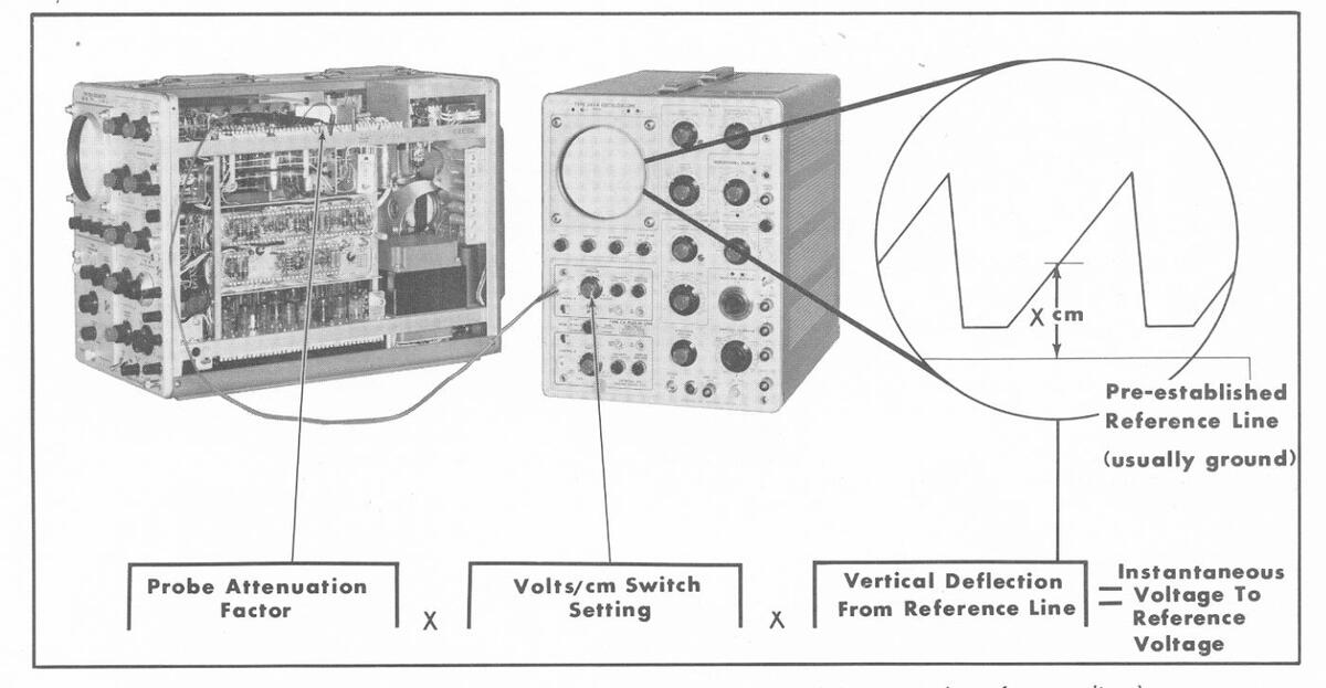
** Fig. 3-2. Measuring the instantaneous voltage with respect to ground (or some other reference voltage).
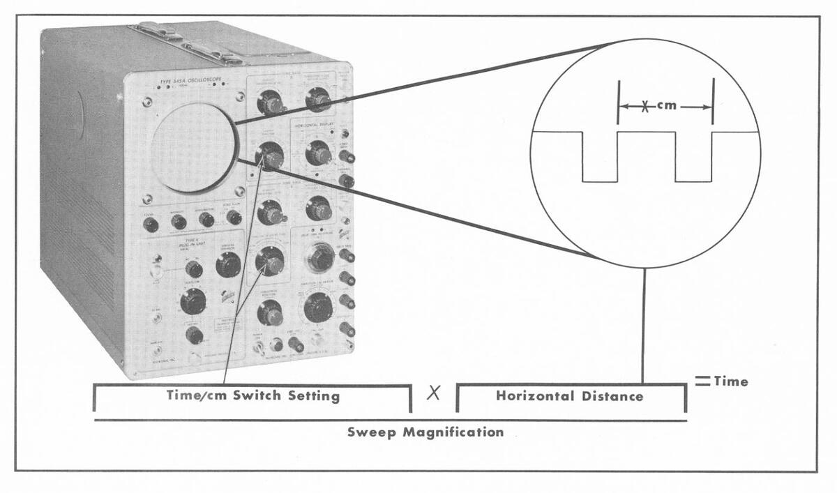
Fig. 3-3. Measuring time interval between events displayed on the oscilloscope screen.
indicated to be positive. The indicated voltage multiplied by the probe's attenuation factor of 10 then gives you the actual voltage of positive 6 volts.
Timé Measurements
The calibrated sweeps of the Type 545A Oscilloscope cause any horizontal distance on the screen to represent a definite known interval of time. Using this feature you can accurately measure the time lapse between two events displayed on the oscilloscope screen. One method which produces sufficient accuracy for most applications is as follows (see Figure 3-3):
1. Using the graticule, measure the horizontal distance between the two displayed events whose time interval you wish to find.
2. Multiply the distance measured by the setting of the appropriate TIME/CM control to obtain the apparent time interval. (The VARIABLE TIME/CM control must be in the CALIBRATED position).
3. Divide the apparent time interval by 5 if the magnifier is on, and 1 if the magnifier is off, to obtain the actual time interval.
For example, assume that the TIME/CM switch setting is 1 MILLISEC, the MAGNIFIER is ON, and that you measure a horizontal distance of 5 centimeters between events. In this example then, 5 centimeters multiplied by 1 millisecond per centimeter gives you an apparent time interval of 5
milliseconds. The apparent time divided by 5 then gives you the actual time interval of 1 millisecond.
Another method for measuring time intervals involves the use of the delayed sweep feature of the Type 545A Oscilloscope. In this method the HORIZONTAL DISPLAY switch is placed in the 'B' INTENSIFIED BY 'A' position to brighten a portion of the trace. The brightened portion of the trace and the DELAY-TIME MULTIPLIER control are then used to make the time measurements. This method provides a very high degree of accuracy when care is taken in making the measurements. The method is summarized as follows:
1. Place the HORIZONTAL DISPLAY switch in the 'B' INTENSIFIED BY 'A' position and adjust the Time Base B triggering controls for a stable display of the input waveform. Adjust Time Base A for free-running operation.
2. Turn the intensity down until the brightened portion of the trace is easily distinguishable. Adjust the Time Base A TIME/CM controls to reduce the brightened area to a small spot or to cover as small a portion of the trace as possible.
3. Using the DELAY-TIME MULTIPLIER control, position the start of the brightened portion of the beginning of the interval you wish to measure. Record the setting of the DELAY-TIME MULTIPLIER control.
4. Using the DELAY-TIME MULTIPLIER control, position the start of the brightened portion of the trace to the end of the interval you wish to measure. Again record the setting of the DELAY-TIME MULTIPLIER control.
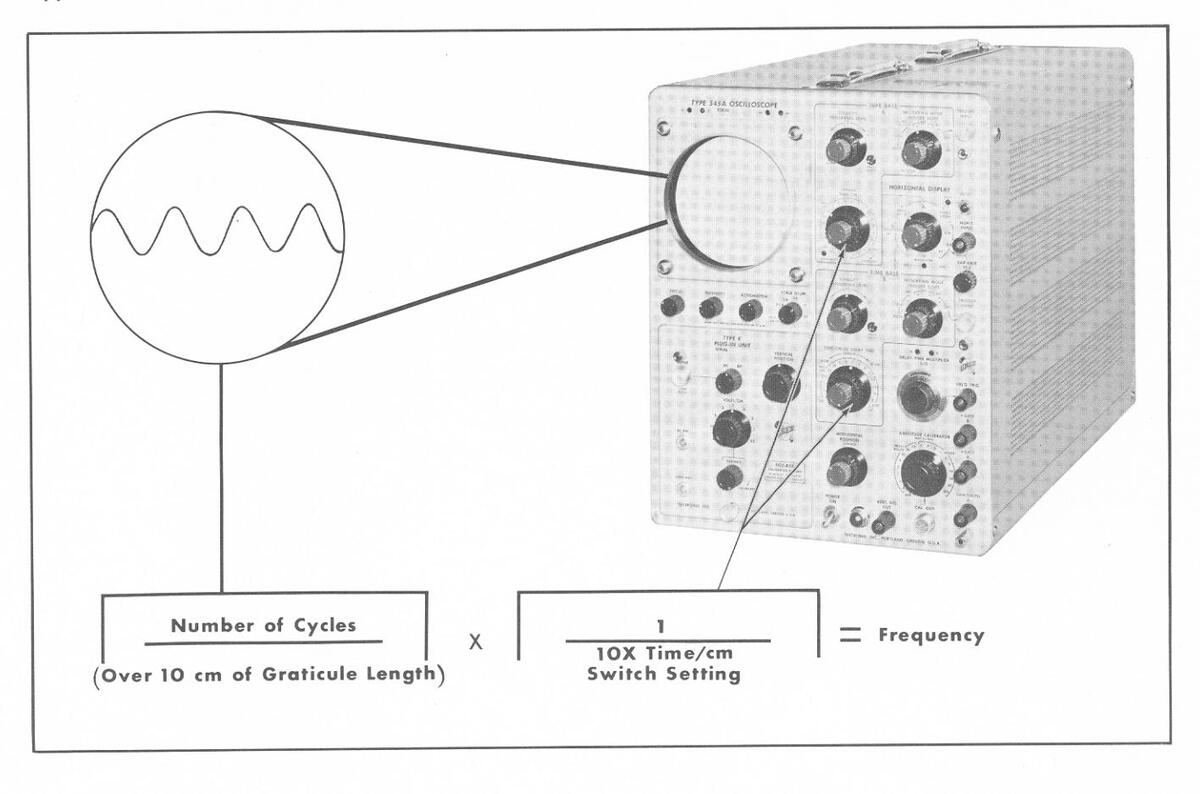
Fig. 3-4. Measuring the frequency of a repetitive input signal.
5. Subtract the first DELAY-TIME MULTIPLIER control setting from the second and multiply the result by the setting of the Time Base B TIME/CM control. The figure obtained is the time interval between the two events. The figure obtained is correct regardless of whether the magnifier is on or off.
Frequency Measurements
Using the methods described in the previous section, you can measure the period (time required for one cycle) of a recurrent waveform. The frequency of the waveform can then easily be calculated since frequency is the reciprocal of the period. For example, if the period of a recurrent waveform is accurately measured and found to be 0.2 microseconds, the frequency is the reciprocal of 0.2 microseconds, or 5 mc.
At any given oscilloscope sweep rate, the number of cycles of the input waveform that is displayed on 10 centimeters of the screen is dependent on the frequency of the input waveform. Frequencies can usually be measured faster by the following method than by the one given in the last paragraph.
If you divide the cycles per unit of length by the time required for the input waveform to sweep this unit of length, you get the frequency. The total number of cycles are found for 10 cm for greater accuracy. Since the TIME/CM switch gives time for 1 cm, multiply this setting by 10 to have the time required for 10 cm. (See Fig. 3-4).
To obtain the frequency of a repetitive input signal, perform the following steps:
1. Adjust the TIME/CM control to display several cycles of the input waveform. Insure that the VARIABLE TIME/CM control is in the CALIBRATED position.
2. Count the number of cycles of the waveform shown on the 10 centimeters of the graticule.
3. Divide this number by 10 times the TIME/CM switch setting. This gives you the frequency of the input waveform.
For example, assume that when you are using a sweep rate of 50 milliseconds per centimeter, you count 7.2 cycles in 10 centimeters. The frequency is 7.2 cycles divided by 50 milliseconds times 10, or 500 milliseconds. 500 milliseconds are 500 x .001 seconds, or .5 seconds. 7.2 cycles per 1/2 second gives you 14.4 cycles per second.
SECTION 4
CIRCUIT
VERTICAL DEFLECTION SYSTEM
General
The dc-coupled, push-pull, main Vertical Amplifier provides the necessary gain to drive the Delay Line and the vertical deflection plates of the crt. The main units of the Vertical Amplifier are the Input Amplifier stage V1014 and V1024, the cathode follower stages V1033 and V1043, and the 6-section Distributed Amplifier output stage. Other circuits of importance are the Trigger Pickoff Amplifier V1054 and V1064, the Trigger Pickoff C.F. V1223B, the Vert. Sig. Out. C.F. V1223A, and the Indicator Amplifiers and lamps, V1084A and B1083, and V1084B and B1087, respectively.
Input Circuit
The signal input from the plug-in unit is coupled through terminals 1 and 3 of the interconnecting plug to the grids of the Input Amplifier stage. GAIN ADJ., R1027 varies the cathode degeneration, and thus sets the gain of the stage to agree with the Preamplifier's front-panel calibration when the VARIABLE knob is in the CALIBRATED position.
The Input Amplifier is coupled to the Distributed Amplifier by the cathode followers V1033 and V1043. The cathode followers isolate the Distributed Amplifier from the Input Amplifier, and provide the necessary low-impedance drive for the Distributed Amplifier's grid line.
High-frequency compensation for the Input Amplifier is provided by the variable peaking coils L1014 and L1024. Variable inductors L1036 and L1046 provide additional peaking at the very high frequencies.
Output Stage
The output stage is a 6-section Distributed Amplifier. The tapped inductors in the transmission line, between each grid and between each plate, isolate each section from the capacitance of the adjacent sections.
The input signal for each tube is obtained from the grid line, which is driven by the cathode followers V1033 and V1043. The amplified signal at each plate, fed to the plate line, becomes an integral part of the wave traveling down the line toward the deflection plates.
The vertical signal is delayed 0.2 microsecond between the input to the grid line and the vertical deflection plates.
This delay insures that the very "front" of fast vertical signals can be observed. About 0.015 microsecond of the total delay time occurs in the Distributed Amplifier; the remaining 0.185 microsecond occurs in the Delay Line.
The tapped inductors between each section of the Distributed Amplifier provide about 0.003 microsecond of delay. By making the delay time in the grid and plate lines equal, the signal arriving at each plate, through the electron stream of the tube, will be synchronous with the signal moving down the plate line from the preceding sections.
DC Shift Compensation
DC shift in the amplifiers — a condition whereby the dc and very low-frequency transconductance is less than at mid-frequencies — is compensated for in two ways. R1090 and C1093B in plate line L1104, and R1095 and C1093D in plate line L1114, form a low-frequency boost network; the time constant of this network is such that the termination resistance of the line is increased in the range from very low-frequencies to dc. A longer time constant, for extremely low-frequency and dc compensation is provided by R1092, R1094 and C1093A in one plate line, and by R1097, R1099 and C1093C in the other, which provide a small amount of positive feedback from the plate lines to the plate circuits of the Input Amplifier. A variable resistor R1091, the DC SHIFT ADJ. control, is connected between the two networks to adjust for the proper amount of compensation.
Beam-Position Indicators
The beam-position indicators B1083 and B1087 located on the front panel above the crt, indicate the relative vertical position of the trace with respect to the center of the graticule. When the beam is centered vertically, the potential across either neon is insufficient to light it. As the beam is positioned up or down the screen, however, the current through the Indicator Amplifiers, and hence the voltage across the neons will change. The voltage across one will increase, causing it to light, and the voltage across the other will decrease, causing it to remain extinguished. The neon that lights will indicate the direction in which the beam has been moved.
Trigger Pickoff
When internal triggering of the Time Base Generator is desired (black TRIGGER SLOPE knob on either the + or
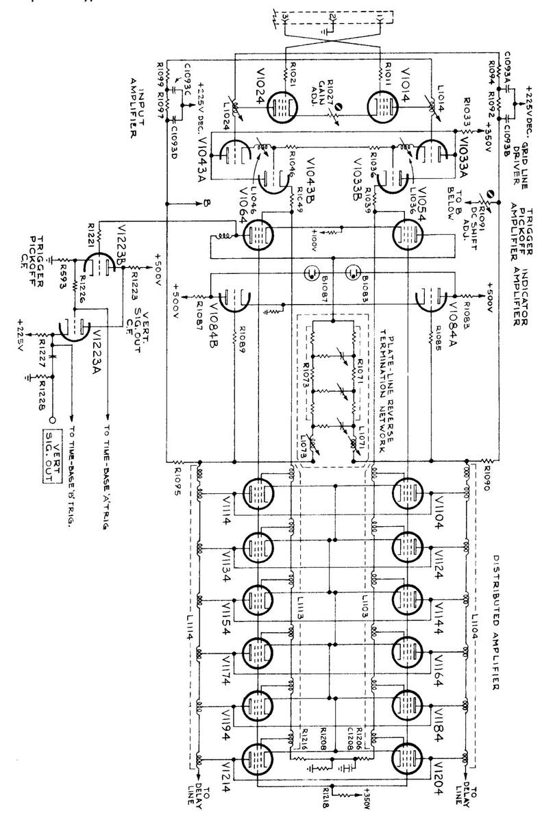
Fig. 4-1. Simplified Vertical Amplifier.
-INT. position), a "sample" of the vertical signal is used to develop the triggering pulse. This "sample" is obtained from the trigger pickoff circuit consisting of the Trigger Pickoff Amplifier V1054 and V1064, and Trigger Pickoff C.F. V1223B.
This "sample" of the vertical signal is also ac-coupled through V1223A and C1228, to a front-panel binding post labeled VERT, SIG, OUT.
Delay Line
The output signal from the Vertical Amplifier is coupled through the Balanced Delay Line to the vertical deflection plates of the crt. The function of the Delay Line is to retard the arrival of the waveform at the deflection plates until the crt has been unblanked and the horizontal sweep started. This delay, as mentioned previously, insures that the very "front" of fast vertical signals can be observed. The line is adjusted, by means of the variable capacitors connected across the line, for optimum transient response.
The entire Delay Line, which includes the plate line in the Distributed Amplifier, is reverse-terminated in its characteristic impedance. The Termination Network, shown on the Vertical Amplifier diagram, is designed to dissipate both the dc and signal energy in the line by presenting a constant resistance over the frequency range of the amplifier. The terminating resistors R1071 and R1073 are specially made, wirewound, noninductive, distributed resistors. The 600 ohms total resistance in each is "tapered", or distributed in steps. The largest segment of the terminating resistance appears nearest the line; the smallest segment appears at the opposite end. Each step of the resistance is then tuned, by means of the variable capacitors, so the network will present an optimum load to the line.
HORIZONTAL DEFLECTION SYSTEM
Time-Base Trigger
General
The Time-Base Trigger developes a pulse which will initiate a cycle of action in the Time Base Generator. To display signals below five megacycles, a TRIGGERING MODE switch allows the operator to select the type of triggered operation most suitable for the waveform to be displayed. A second switch, the TRIGGER SLOPE switch, allows the operator to select the "slope", either positive or negative, which will cause triggered operation of the sweep. To display signals above five megacycles, the Time Base Trigger is bypassed, and the signal is applied to the Sweep-Gating Multivibrator in the Time-Base Generator. (HIGH FREQUENCY SYNC. mode.) No choice of triggering slope is available in this mode.
Trigger-Input Amplifier
Triggering signals may be developed from several sources. The most common source of triggering signals utilizes the internal circuitry of the oscilloscope to sample the signal present in the vertical amplifier. Using an internal source
of triggering signal, either triggered operation in the various triggering modes, or synchronized operation, is available
Triggered or synchronized operation of the time-base circuitry may also be effected from external sources. Operation in any of the available modes is possible with external signals.
In +Line or —Line positions of the TRIGGER SLOPE switch a voltage at the power line frequency is used to develop the triagering signal.
The Trigger-Input Amplifier is a polarity-inverting, cathode-coupled amplifier. It serves two basic functions in the Time-Base Trigger. First, it provides a source of negative-going signal to drive the following stage. Secondly, by means of the TRIGGERING LEVEL control, it enables the operator to select the signal at which triggered operation of the Time-Base will occur.
To trigger from a negative-going signal, the grid of the V24A section is connected to the input signal source. The grid of the V24B section is connected to a dc bias source, which is adjustable with the TRIGGERING LEVEL control. This bias voltage establishes the voltage present at the plate under no-signal conditions.
The voltage at the grid of V24A and the voltage at the plate of V24B are in phase with each other; that is, they both go through ac zero in the same direction at the same time. Thus, the V24A section acts as a cathode-follower, and the signal voltage developed across the cathode resistor becomes the input signal to the V24B section.
To trigger from a positive-going signal, the grid of the V24A section is connected to the TRIGGERING LEVEL control, and the grid of V24B is connected to the input signal. With this configuration, the voltage at the plate of the V24B section will be 180 degrees out of phase with the input-signal voltage.
In each of the cases outlined above, a negative-going signal is produced at the plate of the V24B section of the Trigger-Input Amplifier irrespective of the polarity of the input signal.
Also, the amplitude of the triggering signal necessary to cause operation of the following stage is determined by the setting of the TRIGGERING LEVEL control.
Trigger Multivibrator
The Trigger Multivibrator is a dc-coupled multivibrator. In the quiescent state, ready to receive a signal, the V45A section is conducting and the plate voltage is down. Since the plate is dc-coupled to the grid of the V45B section, that grid is held below cutoff. With the V45B section cut off its plate voltage is up and no output is developed.
The negative-going portion of the signal from the Trigger-Input Amplifier is required to drive the grid of the V45A section down. As the V45A section grid is driven negative the current flow through the tube is restricted, and the voltage at the plate starts to rise.
The rise in voltage at the plate of the V45A section carries the grid of the V45B section in the positive direction.
Fig. 4-2. Simplified Time-Base Trigger Circuit.
The cathodes of both sections are coupled together, and follow the action of the grids. With the V45B section grid going in a positive direction, and the cathode in a negative direction, the V45B section starts to conduct. As the V45B section starts to conduct the cathodes of both sections follow the action of the V45B section grid; hence the cathode voltage starts to rise.
As the V45A section grid goes down and its cathode goes up it stops conducting. As the V45B section conducts, its plate voltage drops, creating a negative step at the output. This transition occurs rapidly, regardless of how slowly the grid falls.
When the signal applied to the grid of the V45A section goes in a positive direction the action described in the previous paragraphs reverses itself. That is, the V45A section will start to conduct once more, while the V45B section will be cut off.
In the AUTO. position of the TRIGGERING MODE switch the Trigger Multivibrator is converted from a bistable configuration to a recurrent configuration. This is accomplished by coupling the grid circuit of the V45A section to the grid circuit of the V45A section. In addition, the dc coupling between the grid of the V45A section of the Trigger Multivibrator and the plate of the V24B section of the Trigger Input amplifier is replaced by ac coupling.
In the AUTO. triggering mode the Trigger Multivibrator will free run in the absence of a triggering signal. For example, assume that the grid of the V45A section is just being driven into cutoff. The voltage at the plate of the V45A section starts to rise, carrying with it the grid of the V45B section. As the voltage at the grid of the V45B section starts to rise, the V45B section starts to conduct.
The rising voltage at the grid of the V45B section is coupled to the grid of the V45A section through R40. The grid of V45A is prevented from rising immediately by the action of C31, which must be charged sufficiently to raise the voltage at the grid of the V45A section above cutoff.
As the V45A section starts to conduct, its plate voltage drops, which in turn lowers the voltage at the grid of the V45B section. The voltage at the grid of V45A starts dropping exponentially towards cutoff. When the V45A section reaches cutoff, the circuit has completed one cycle of an approximately 50-cycle repetition rate.
The Trigger Multivibrator produces a square-wave which is coupled to the Time-Base Generator. This square wave is differentiated in the Time-Base Generator to produce a sharp, negative-going pulse which is used to trigger the Time-Base Generator in the proper time sequence when triggered operation is desired. For synchronized operation of the Time-Base Generator, the TRIGGERING MODE switch is placed in the HF SYNC position. This couples the signal present at the input of the Time-Base Trigger directly into the Time-Base Generator, and the Time-Base Trigger circuitry is not used in the HF Sync mode.
Time-Base Generator
General
The Time-Base Generator consists of three main circuits: the Sweep-Gating Multivibrator, the Miller Runup Circuit,
and the Holdoff Circuit. The simplified schematic diagram of Fig. 4-3 shows the basic parts of each circuit, and the interconnections between circuits.
The Time-Base Trigger circuit furnishes the waveform which initiates a cycle of action in the Time-Base Generator. Square waves from the output of the Trigger Multivibrator are fed to the Time-Base Generator where they are differentiated and used as trigger pulses. In analyzing the action of the Time-Base Generator we will assume it to be in the quiescent state, just before the arrival of a suitable trigger pulse.
In the quiescent state of the Time-Base Generator V135A is conducting.
Square waves, generated by the Time-Base Trigger circuitry, are differentiated by the C131, R131 network.
If the STABILITY control, R110 is now advanced, the grid of V135A becomes more negative. As the grid of V135A becomes more negative, a point is reached at which a negative-going triggering pulse from the C131, R131 network will drive V135A into cutoff.
As V135A is driven to cutoff the plate voltage rises, carrying with it the grid of the cathode-follower stage, V135B. V135B, used as a cathode follower between the two halves of the multivibrator, isolates the positive-going plate of V135A from the capacitance of the loads requiring a positive-going pulse. This results in a faster rise of the positive-going pulse at the plate of V135A.
The cathode of V135B follows the action of the grid closely. This cathode is long-tailed through the resistors R141, R143. Since the grid of V145 has a certain shunt capacitance to ground, C141 is connected in parallel with R141 to compensate for this capacitance.
The voltage rise at the cathode of V135B drives the grid of V145 above cutoff. As V145 begins to conduct its plate voltage drops rapidly. Any spiking which may occur is attenuated by the C141, R141 network.
When V145 is conducting at the maximum determined by circuit parameters, the Sweep-Gating Multivibrator has reached its other stable state and the action of the Miller Runup circuit has been initiated.
Miller Run-up Circuit
The Miller Run-Up circuit is essentially a Class A amplifier employing negative feedback. The positive-going voltage at the plate of the Miller Tube is fed back to the grid through the Run-Up Cathode Follower, V173, in such a manner as to oppose the attempt of the grid to go negative. Because the gain of the Miller Tube is high, (approximately 200) it is possible to maintain an essentially linear rate of charge on the Timing Capacitor.
In the quiescent state of the Time-Base Generator the voltage at the plate of the Miller tube is determined by the voltage drop across a dc network formed by the neon lamp, B167, the Runup C.F., and the On-Off Diodes. The purpose of this dc network is to establish a voltage at the plate of the Miller Tube of such value that the tube will operate above the knee, and hence over the linear region of its characteristic curve.
Fig. 4-3. Simplified Time-Base Generator.
The grid of the Miller Tube, V161, is returned to the -150-volt supply through the Timing Resistor, R160. In the quiescent state of the Time-Base Generator the grid of the Miller Tube is held slightly negative, but well above cutoff, by the flow of the current through the A section of the On-Off Diode. When the On-Off Diodes stop conducting the grid of the Miller Tube tends to become more negative
As the grid of the Miller Tube starts negative the plate becomes more positive. This positive-going excursion of the plate carries the grids of V173, the Run-Up Cathode Follower, with it. The voltage at the grids of V173 is maintained at a constant difference with respect to the Miller Tube plate voltage by the voltage drop across the neon bulb, B167. C167 and R168 form a network connected around B167 to improve the risetime. A bootstrap capacitor, C165, is connected between a tap on the Miller Tube plate load and the cathode of V173. This bootstrap capacitor increases the charging rate of the stray capacitances in the Miller Tube plate circuit. Its action is most important in the generation of fast time-bases.
The cathode of V173 follows the action of the grids closely. This results in a linear rise in the voltage at the upper end of the Timing Capacitor, C160. Since the charge on the capacitor cannot change instantaneously this voltage is coupled to the grid of the Miller Tube in a direction to correct for the attempt of the Miller Tube grid to go negative.
Current to charge the Timing Capacitor is supplied through the Timing Resistor, R160. Since the voltage across the Timing Resistor is virtually constant a constant current source is thus provided for charging the Timing Capacitor.
The linear voltage rise at the cathode of V173 is used as the Time-Base sawtooth. This voltage rise continues until a positive step from the Sweep-Gating Multivibrator raises the plate voltage of the On-Off Diodes to the point at which they begin to conduct.
The positive-going voltage at the cathode of V173 is coupled back to the input of the Sweep-Gating Multivibrator and causes that circuit to revert to its other state. It is kept from acting on further trigger pulses by the action of the Holdoff Circuit.
The waveform coupled to the Time-Base Generator from the Time-Base Trigger circuit contains both positive- and negative-going pulses. To prevent a negative-going pulse from triggering the Sweep-Gating Multivibrator before the action of the Time-Base Generator is completed the grid of V135A must be held above cutoff.
Holdoff Circuit
The Holdoff Circuit keeps the grid of V135A above cutoff until the capacitances in the Time-Base Generator have had time to reach their quiescent state. The point at which the Holdoff Circuit will allow the Sweep-Gating Multivibrator to return to its quiescent state is determined by the adjustment of R176.
The sawtooth present at the cathode of the Run-up Cathode-Follower is coupled to the grid of V183A through R176. During calibration R176 is adjusted so that the time-base terminates after it has passed the right-hand limit of the
graticule. R176 adjusts the voltage at the grid of V183A and consequently at the cathode of V183A and on the capacitor C180.
The positive-going pulse from the cathode of V183A is coupled to the bus connecting the cathode of V183A and the grid of V133B. The action of the capacitor C180 retards the voltage at the grid of V133B. The value of C180 is chosen so that its capacitance will prevent the voltage at the grid of V133B from falling until all capacitances in the Time-Base Generator have returned to their aviescent level.
Output Waveforms
Various waveforms available during the cycle of action in the Time-Base Generator are made available through cathode followers for other functions. Shown in Fig. 4-3 are the unblanking pulse, the +Gate, and the Sawtooth from the Time-Base. The same signal used to provide the +Gate is used to provide the unblanking signal for the crt circuit.
Unblanking
In the quiescent state of the Time-Base Generator the crt beam is cut off. To allow the crt beam to be seen the potential at the control grid of the crt must be raised. The voltage rise appearing at the cathode of V135B in the Time-Base Generator is used to drive a cathode-follower in the crt circuit. This "unblanks" the beam during the time a sawtooth is generated, permitting the left-to-right motion on the beam to be seen.
The end of the unblanking pulse coincides with the end of the time-base, and the crt is "blanked" during the retrace portion of the sweep, and during quiescent periods of the Time-Base Generator.
Sweep "B" Circuits
In the Type 545A, the operator is offered a selection of two sweep circuits of very similar configuration and operating principles. The Time-Base Trigger B and Time-Base Generator B circuits are practically identical to those found in Time-Base A. There are, however, some noticeable differences between the Time Base A and Time Base B Timing switches, due to the difference in sweep rate selections between the two circuits.
Delay Pickoff Circuit
Delayed triggers can be applied to Sweep Generator A from the Delayed Trigger Amplifier, V114, through V133A which acts as a coupling C.F. to apply delayed triggers to the Sweep-Gating Multivibrator. Delayed Trigger Pulses are applied to the grid of V114 from the cathode of V428B.
These pulses are shaped and amplified in the Delay Pickoff Circuit, comprised of V414, V424, V445 and V428. The first stage of this circuit, V414 and V424 combine to form a difference amplifier which picks off a sample of the sawtooth output from Sweep Generator A or B and converts it into a positive pulse of step form. Before the pickoff
Fig. 4-4. Simplified Delay Pickoff Circuit.
time, V414 is cut off. Its cathode is tied to the cathode of V424 which is conducting, and therefore determining the common-cathode voltage.
The common-cathode voltage is adjustable by means of R433, a 10-turn helical resistor, labeled DELAY-TIME MULTI-PLIER 1-10 on the front panel. V428A is a constant-current triode supplying cathode current to the difference amplifiers from the -----------------------------------
Plate current through R424 and L424 therefore also remains very nearly constant while V424 is conducting, no matter at what voltage the grid is set by the DELAY-TIME MULTIPLIER control, R433. This is important because the plate voltage of V424 is required to hold the grid voltage of the shaper stage, V445A, near the triggering point.
The positive-going delaying-sweep sawtooth raises the grid of non-conducting V414 toward its cathode voltage. When the grid rises past the cathode voltage set by the DELAY-TIME MULTIPLIER control, V414 conducts and V424 cuts off
Delaver Trigger Multivibrator
When V424 cuts off because of conduction in V414, its plate rises, carrying the grid of trigger shaper V445A positive past its transition point. The trigger-shaper stage is regenerative so as to produce a fast transition, and the resulting positive step at the plate of V445B is differentiated through C454 and used to arm or to trigger the main-sweep circuits. The sharp differentiated pulse is transmitted to the succeeding circuits through cathode follower V428B.
Two internal screwdriver controls located on the "B" sweep gate at the right side of your oscilloscope and labeled, respectively, Delay Start Adj. and Delay Stop Adj., precisely adjust the upper and lower V424 grid voltage limits set by the DELAY-TIME MULTIPLIER so that centimeters of delay can be read within a fraction of one percent directly from the micrometer dial of the DELAY-TIME MULTI-PLIER.
Single Sweep Operation
When the HORIZONTAL DISPLAY switch is in the A SINGLE SWEEP position, plate voltage is applied to V133A and this tube operates in conjunction with V125 as a bistable multivibrator.
In the first stable state that exists after the completion of a sweep, V125 is cut off and V133A is conducting. In this state the divider between the plate of V125 and the grid of V133A sets the cathode voltage of the Lockout Multivibrator and consequently the grid voltage of V135A. The Lockout Level Adj. R125 is adjusted to set the grid of V135A high enough so that the Sweep-Gating Multivibrator cannot be triggered; this "locks out" the sweep.
Depressing the RESET switch grounds C102 and R102. The resulting positive pulse at the grid of V114 forces the Lockout Multivibrator into its other stable state with V125 conducting and V133A cut off. With V133A cut off, its plate
voltage rises and ignites the READY light. With V125 conducting, the STABILITY control regains control over the arid level of V135A.
Depending on the adjustment of the STABILITY control, a sweep can now be produced in one of two ways. If the STABILITY control is turned full right (cw) the grid of V135A will be pulled down and cause the Sweep-Gating Multivibrator to switch to its other state and initiate a sweep. If the STABILITY control is adjusted for triggered operation, the sweep will be initiated by the first negative trigger pulse to arrive at the grid of V135A.
As the sweep begins, the rising sawtooth voltage pulls up the cathode of V133B by the holdoff action previously described. As the cathodes of the Lockout Multivibrator follow the cathode of V133B up, V125 cuts off and V133A conducts. As the cathodes continue to rise, following the rise in the sawtooth sweep voltage, V133A cuts off again. Both tubes are then held cutoff for the remainder of the sweep and the READY light stays on. When the grid of V135A rises to the point at which the Sweep-Gating Multivibrator is reverted, the sweep is terminated.
As the Hold-off Capacitor C180 discharges, the cathodes of the Lockout Multivibrator start to fall. The grid level of V133A is such that this tube comes out of cutoff first; thus: V133A conducts and V125 remains in cutoff. As V133A conducts its plate drops, extinguishing the READY light. A new sweep cannot be initiated until the RESET switch is depressed again.
Unblanking
The positive rectangular pulse at the cathode of V135B, in the Sweep-Gating Multivibrator circuit, is coupled through a cathode follower V183B (shown on the CRT circuit diagram, Fig. 4-10) to the grid supply for the crt. This pulse, whose start and duration are coincident with the rising portion of the sawtooth sweep waveform, pulls up the grid of the crt. This unblanks the crt during the trace portion of the sweep and permits the trace to be observed.
Output Waveforms
The positive pulse coupled to the crt circuit for unblanking is also coupled through a cathode follower V193A to a front-panel binding post labeled +GATE A. This positive gate waveform starts at ground and rises to +20 volts.
The sweep sawtooth voltage at the cathode of V173 is coupled through a cathode follower V193B to a front-panel binding post labeled SAWTOOTH A. This waveform, which starts at about ground, provides a 150-volt linear rise in voltage.
Dual Trace Sync and Blanking
Synchronizing pulses for dual-trace plug-in preamplifiers are supplied by V154A. When multi tube V145 cuts off a sharply differentiated positive pulse is developed at its screen. This pulse, coupled to the grid of V154A, produces a negative trigger at the plate of V154A. This trigger then

Fig. 4-5. Simplified Single-Sweep Circuit.
Fig. 4-6. Simplified Alternate-Trace Operation Circuitry.
Circuit Description — Type 545A
switches the multivibrator in the dual-trace unit employed for alternate sweeps.
When the dual-trace multi is connected for free-running operation to produce chopped sweeps, a negative pulse is coupled from the multi to the grid of V154B. The resultant positive pulse at the plate of V154B is coupled to the cathode of the crt to blank out the beam during switching. Refer to the manual for the dual-trace unit for a detailed description of the switching operation.
Alternate-Trace Operation
Alternate-trace operation is available with Tektronix convertible oscilloscopes by employing the 53C, 53/54C or Type CA plug-in preamplifiers. Additional circuitry in the Time-Base Generator circuit provides a pulse to "flip" a bistable multivibrator in the plug-in. This multivibrator provides a change in dc level at the outputs of the amplifiers in the plug-in. This change in dc level is used as a positioning voltage which separates the two traces a distance selected by the operator.
The Time-Base Generator circuitry necessary for alternatetrace operation utilizes an amplifier which amplifies the signal present at the grid of V154A. The signal at the plate of the amplifier, V154A, is connected to pin 16 of the interconnecting socket, while the signal at the cathode is connected to pin 8 of the interconnecting socket. Fig. 4-3 shows the Time-Base Generator circuitry involved. Fig. 4-6 shows the plug-in circuitry which affects the positioning.
Negative-going pulses, generated at the end of each time-base by the Sweep-Gating Multivibrator in the Time-Base Generator, are amplified by the amplifier, V154A. The pulses are coupled through the interconnecting socket to the Trigger Coupling Diode in the plug-in. Each trigger causes the multivibrator to "flip" from one stable state to another at a rate determined by the repetition rate of the Time-Base Generator.
The square-waves present at the cathodes of the multivibrator tubes are used to drive the amplifiers, V3384A and V3384B. The signals from these amplifiers are used to drive V3393B and V3393A; cathode followers which isolate the multivibrator circuitry from the signal amplifiers. The output of the cathode followers raises or lowers the plate voltage of the Input Amplifiers as the multivibrator passes from one stable state to the other.
In later Tektronix instruments an additional stage has been added in the Time-Base Generator to provide blanking when the plug-in is operated in the CHOPPED MODE. This is shown as V154B in Fig. 4-3. In the CHOPPED MODE of operation the multivibrator in the plug-in free runs at a rate determined by circuit constants. Transients generated during free-running operation are blanked from appearing on the crt screen by the action of V154B.
Horizontal Amplifier
The Horizontal Amplifier converts the single-ended sawtooth output of the Time-Base Generator into push-pull signal suitable for driving the horizontal plates of the crt.
The sawtooth waveform from the Time-Base Generator is coupled to the Input Cathode Follower through the R330, C330 network. This network attenuates the input signal and provides a means of compensating the input circuitry for optimum frequency response. During calibration C330 is adjusted for best response to a square wave.
The HORIZONTAL POSITION and VERNIER controls adjust the dc level at the grid of V343A. This change in dc level changes the dc level on the signal path through the amplifier, thus changing the dc voltage applied to the crt horizontal deflection plates and affecting horizontal positioning.
Coupling between the Input CF and the Driver CF is made by the 5X MAGNIFIER switch. When this switch is in the OFF position the signal from the Input CF must pass through the network formed by C348 in parallel with the series combination R348, and R349. R348, a variable resistor, allows the operator to adjust the length of the time base by varying the attenuation applied to the signal. C348, a variable capacitor, is adjusted to provide optimum linearity of the time base on the fastest time bases.
This network attenuates the signal by a factor of five. To provide magnification of the time base, the network is removed when the 5X MAGNIFIER switch is turned to the ON position.
The gain of the Horizontal Amplifier is controlled by a negative-feedback circuit. The signal appearing at the lefthand deflection plate is fed back to the input of the Driver CF. R358 is an adjustable resistor which allows the operator to vary the dc voltage applied to the feedback loop.
By changing the dc voltage at this point the operator can adjust the position of the unmagnified sweep so that it will correspond with the position of the magnified sweep.
The output waveform from the Horizontal Amplifier is taken from V364A and V384A. The cathodes of these tubes are connected through a network which includes the Mag. Gain control. This control enables the operator to adjust the gain of the Horizontal Amplifier so that the ratio between the magnified and unmagnified sweeps is correct. C375, in parallel with the Mag. Gain control, has considerable effect on the linearity at the beginning of the time base, and is adjusted while displaying a signal with a high repetition rate.
Part of the signal appearing at the plates of the output amplifiers is used to drive the Output CFs. Note that the cathode of V364B is connected to the plate of V398, a pentode. The function of the Output CFs is to drive the capacitance of the horizontal deflection plates and the associated wiring. To assure a sufficient flow of current at fast time bases, the pentode, V398 is used to supply current to the Output CF which drives the negative-going, or lefthand deflection plate. A pentode is chosen as a current booster, since its plate characteristic provides a flat-topped pulse of current. The pulse to drive the grid of the pentode is derived from the waveform at the right-hand deflection plate. This waveform is differentiated by the C390, R390 network before being applied to the grid. Its amplitude is
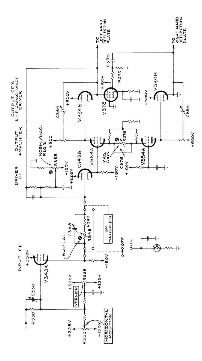
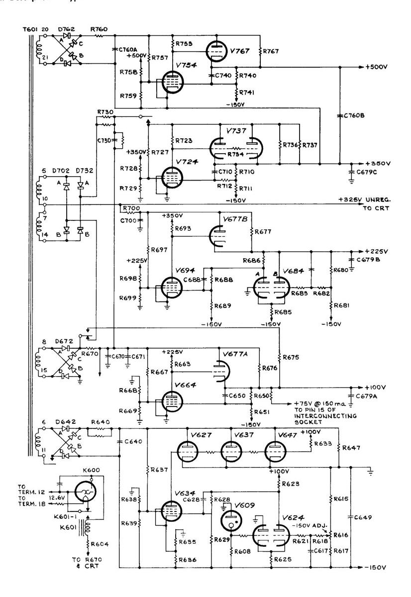
Fig. 4-8. Simplified Low-Voltage Power Supply.
thus proportional to the time base. For the fastest time bases, the tube current is several times normal, but at the reduced duty cycle of the time base, well within the dissipation rating of the tubes.
Bootstrap capacitors C364 and C384 are used to help supply the necessary charging current for fast time bases. During calibration these two capacitors are adjusted on the fastest time base for optimum linearity.
LOW-VOLTAGE POWER SUPPLY
Plate and filament power for the tubes in the Type 545A is furnished by a single power transformer T601. The primary has two equal windings which may be connected in parallel for 117-volt operation, or in series for 234-volt operation. The power supply will remain in regulation over line voltage ranges of 105 to 125 volts, or 210 to 250 volts, rms, 50-60 cycles. Bridge rectifiers are employed for the five separate, full-wave, power supplies. The five supplies furnish regulated output voltages of -150, +100, +225, +350 and +500 volts.
-150-Volt Supply
Reference voltage for the -150-volt supply is furnished by a gas diode voltage-reference tube V609. This tube, which has a constant voltage drop, establishes a fixed potential of about -87 volts at the grid of V624A, one-half of a difference amplifier. The grid voltage for the other half of the difference amplifier, V624B, is obtained from a divider consisting of R615, R616 and R617. The -150 Adj. control R616 determines the percentage of total voltage that appears at the grid of V624B and thus determines the total voltage across the divider. This control is adjusted so that the output voltage is exactly -150 volts.
If line-voltage or load fluctuations tend to change the output voltage, an error signal exists between the two grids of the difference amplifier. The error signal is amplified in V624 and V634 and applied to the grids of the series tubes, V627, V637 and V647. The resulting change in voltage at the plates of the series tubes, which will be in a direction to compensate for any change in output voltage, is coupled through the rectifiers to the output to keep this voltage constant. Capacitors C617 and C628 improve the ac gain of the feedback loop to increase the response of the regulator circuit to sudden changes in output voltage.
A small amount of unregulated bus ripple is coupled to the screen of V634 through R637. The phase of the amplified ripple voltage at the plate of V634 is such as to cancel most of the ripple on the --150-volt bus.
+ 100-Volt Supply
The +100-volt supply is regulated by comparing to ground (the cathode of V664) the voltage of a point near ground potential obtained from the divider R650-R651 connected between the +100-volt bus and the regulated -150-volt supply. Any error voltage that exists is amplified and inverted in polarity by V664 and coupled through the cath-
ode follower V677A to the output to prevent the output voltage from changing. Capacitor C650 improves the ac gain of this circuit.
A small sample of the unregulated bus ripple appears at the screen on V664 through R667. This produces a ripple component at the grid of the cathode follower V677A that is opposite in polarity to the ripple at the plate; this tends to cancel the ripple at the cathode and hence on the +100volt bus. This same circuit also improves the regulation in the presence of line-voltage variations.
+ 225-Volt Supply
Rectified voltage from terminals 7 and 10 of the power transformer is added to the voltage supplying the +100volt regulator to furnish power for the +225-volt regulator. This supply is regulated by comparing to around (the grid of V684A) the voltage of a point near around obtained from the divider R680-R681, connected between the +225volt bus and the regulated —150-volt supply. Any error voltage that exists between the grids of the difference amplifier (V684) is amplified in both V684 and V694, and coupled through the cathode follower V677B to the +225volt hus. The change in voltage at the cathode of V677B. due to the regulator action, will be opposite in polarity to the original error sianal and will thus tend to keep the output constant. This supply also furnishes an unregulated output of about +325 volts for the oscillator in the crit high-voltage supply. It is unnecessary to regulate this voltage as the crt supply has its own regulator circuits.
+ 350-Volt Supply
Rectified voltage from terminals 5 and 14 of T601 is added to voltage supplying the +100-volt regulator to furnish power for the +350-volt regulator. This supply is regulated by comparing to ground the voltage of a point near ground obtained from the divider R710-R711 connected between the +350-volt bus and the regulated -150-volt supply. The operation of the regulator circuit is the same as that described for the +100-volt supply.
+ 500-Volt Supply
Rectified voltage from terminals 20 and 21 of T601 is added to the regulated side of the +350-volt supply to furnish power for the +500-volt regulator. This supply is regulated by comparing to the regulated +350-volts the voltage of a point near +350 obtained from the divider R740-R741 connected between the +500-volt bus and the regulated —150-volt supply. The regulator action of this circuit is the same as that described for the +100-volt supply.
Time-Delay
A Time-Delay relay K600 delays the application of dc voltages to the amplifier tubes in the instrument for about 25 seconds. This delay is to allow the tube heaters time to bring the cathodes up to emission temperatures before operating potentials are applied.
CALIBRATOR
The Calibrator is a square-wave generator whose approximately 1-kc output is available at a front-panel connector labeled CAL. OUT. It consists of a multivibrator V875 and V885A connected so as to switch the cathode follower V885B between two operating states . cutoff and conduction
During the negative portion of the Multivibrator waveform the grid of V885B is driven well below cutoff and its cathode rests at ground potential. During the positive portion of the waveform V875 is cut off and its plate rests slightly below +100 volts. The voltage at the plate of V875 when this tube is cut off, is determined by the setting of the Cal. Adj. control R879, part of the divider connected between +100 volts and ground.
Cathode-follower V885B has a precision, tapped divider for its cathode resistor. When the Cal. Adj. control is properly adjusted, the cathode of V885B is at +100 volts when V875 is cut off. By means of the tapped divider R885 through R893 and a second 1000/1 divider R896-R897, output voltages from .2 millivolts to 100 volts, in steps, are available. C885, connected between the cathode of V885B and ground, corrects the output waveform for a slight overshoot.
CRT CIRCUITS
Cathode-Ray Tube Control Circuits
The INTENSITY control R826 varies the voltage at the grid of the crt to control the beam current. The FOCUS control R856 varies the voltage at the focusing ring to focus the trace. The ASTIGMATISM control R864 varies the voltage at the astigmatism anode to focus the spot in both dimensions simultaneously. The Geom Adj. R861 varies the field the beam encounters as it emerges from the deflection system to control the linearity at the extremes of deflection
The CRT CATHODE SELECTOR switch SW848 connects the cathode of the crt through C848 to either a rear-panel binding post labeled EXTERNAL CRT CATHODE or to the plate of V154B in the Time-Base Generator circuit. When in the DUAL-TRACE CHOPPED BLANKING position, the cathode of the crt is connected to receive positive pulses from the Time-Base Generator circuit to blank the crt during switching while operating a dual-trace plug-in unit in the chopped mode.
When SW848 is in the EXTERNAL CRT CATHODE position, the cathode circuit of the crt is connected to the binding post mentioned previously. A bare bus bar normally connects the binding post to ground. When intensity modulation of the beam is desired, the bus bar can be removed so that the modulating signal can be coupled to the crt cathode.
High-Voltage Supply
A single 60-kc Hartley oscillator furnishes power for the three power supplies that provide accelerating potentials for the crt. The main components in the Oscillator circuit are the pentode V800 and the primary of T801 tuned by C808. A half-wave rectifier V862 provides —1350 volts for the crt cathode. A half-wave voltage-tripler circuit, V832, V842, and V852, provides +8650 volts for the postanode accelerator. This provides a total accelerating voltage of 10,000 volts. Both supplies are tied to the +100volt regulated supply through the decoupling filter R801-C801
A floating half-wave rectifier V822 furnishes bias voltage (about —1450 volts) for the crt grid. This floating grid supply, independent of the cathode supply, is required in order to provide dc-coupled unblanking to the crt grid. All three supplies employ capacitor-input filters.
The -1350-volt cathode supply is regulated by comparing to the -150-volt regulated supply (the cathode of V814B) a voltage near -150 volts obtained from a tap on the divider connected between the decoupled +100-volt bus and the -1350-volt bus. The total resistance of the divider, and hence the voltage across the divider, is determined by the setting of R840 labeled H.V. Adj. When this control is properly adjusted, the voltage of the H.V. Adj. Test Pt. will be exactly -1350 volts.
If variations in loading should tend to change the voltage on the —1350-volt bus, an error signal will exist between the grid and cathode of V814B. The error signal will be amplified by V814B and V814A; the output of V814A varies the screen voltage of the oscillator tube V800, thereby controlling its output.
The +8650-volt supply and the negative bias supply are regulated indirectly, as the output voltage of all three supplies is proportional to the output of the Oscillator circuit.
Unblanking
As mentioned previously, dc-coupled unblanking is accomplished by employing separate power supplies for the grid and cathode of the crt. The unblanking pulses from the Time-Base Generator are transmitted to the crt grid through the cathode follower, V183B and the floating grid supply.
At the faster sweep rates the stray capacitance in the circuit makes it difficult to pull up the floating supply fast enough to unblank the crt in the required time. To overcome this, an isolation network composed of C827, R827, and R828 is employed. By this arrangement the fast leading edge of the unblanking pulse is coupled through C827 to the grid of crt. For short-duration unblanking pulses, at the faster sweep rates, the power supply itself is not appreciably moved.
The longer unblanking pulses, at the slower sweep rates, charge the stray capacitance in the circuit through R827. This pulls up the floating supply and holds the grid at the unblanked potential for the duration of the unblanking pulse.
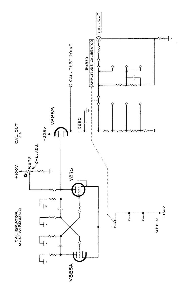
Fig. 4-9. Simplified Calibrator Circuit.
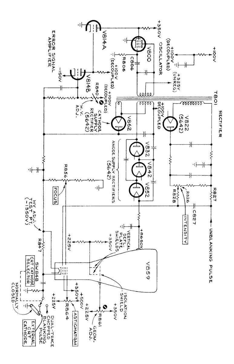
Fig. 4-10. Simplified Cathode-Ray Tube Circuit.
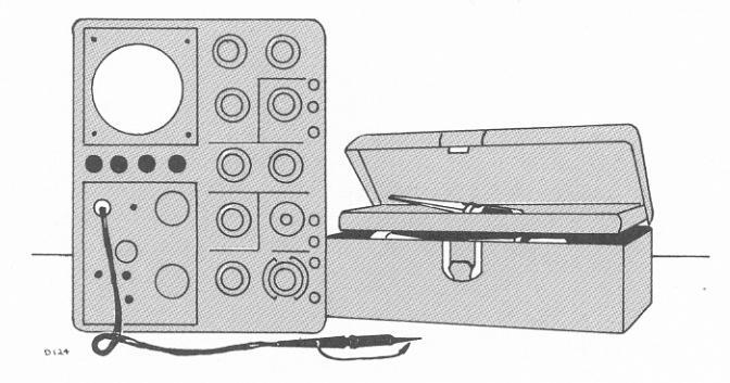
SECTION 5
MAINTENANCE
PREVENTIVE MAINTENANCE
Air Filter
Care must be taken to assure free ventilation of the Type 545A inasmuch as some of the components are operated at dissipation levels such that excessive interior temperatures will result without adequate air circulation. To assure free passage of air the instrument must be placed so that the air intake is not blocked and the filter must be kept clean. Moreover, the side panels and bottom cover must be in place for proper air circulation. Do not remove covers except during maintenance.
A washable EZ KLEEN filter is used at the air intake port of the instrument. Under normal operating conditions the filter should be inspected and cleaned if necessary every three to four months. More frequent inspection is required when the operating conditions are more severe.
The following cleaning instructions are issued by the filter manufacturer:
(1) If grease or dirt load is light, remove filter from installation and rap gently on hard surface to remove
loose dirt. Flush remaining dirt or grease out of filter with a stream of hot water or steam.
- (2) If load is too heavy for treatment described in (1), prepare mild soap or detergent solution in pan or sink deep enough to cover filter when laid flat. Agitate filter up and down in solution until grease or dirt is loosened and floated off.
- (3) Rinse filter and let dry.
- (4) Dip or spray filter with fresh Filter Coat or Handi-Coater. These products are available from the local representative of the Research Products Corporation and from most air conditioner suppliers.
Fan Motor
The fan motor bearings should be lubricated every three or four months with a few drops of light machine oil (see Fig. 5-1). Failure to lubricate the bearings periodically will cause the fan to slow down or stop thereby causing the instrument to overheat. If your oscilloscope is equipped with a dc fan motor — modification number 101 — and if
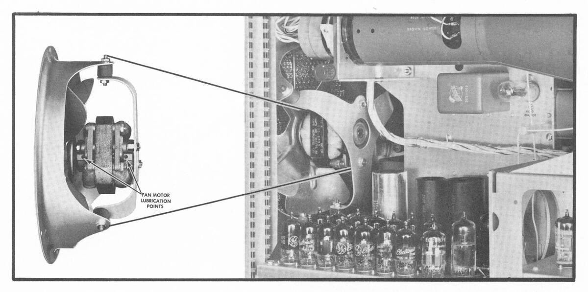
Fig. 5-1. Location of the fan motor lubrication points.
it operates throughout the working day, we suggest that you all the begrings lightly once a month
You should check the condition of the brushes of dc fans every other month since their life expectancy is approximately 6 months under conditions of daily use.
Fan Connections
The cooling fan is powered by a 117-volt ac motor. When the instrument is operating from a 117-volt line source, the fan is connected as illustrated in Fig. 5-2. The ceramic strip shown in the illustration is located adjacent to one corner of the power transformer
If the instrument is converted to operate from a 234volt line source, one of the fan connections must be changed so that the fan can operate from a 117-volt source. To make the change, unsolder the fan lead in the fifth slot at the ceramic strip, lift it free, and move it to the third slot as illustrated by the dotted line in Fig. 5-2. Use silverbearing solder to solder the lead into the slot. The other fan lead connected at the second slot is not changed during the conversion from one line voltage to the other.
Visual Inspection
You should visually inspect the entire oscilloscope every few months for possible circuit defects. These defects may include such things as loose or broken connections, damaged binding posts, improperly seated tubes, scorched wires or resistors, missing tube shields, or broken terminal strips.
Fig. 5-2. Fan connections for 117 V ac operation. The dotted line indicates the fan lead change required for operation on 234 V ac.
For most visual troubles the remedy is apparent; however, particular care must be taken when heat-damaged components are detected. Overheating of parts is often the result of other, less apparent, defects in the circuit. It is essential that you determine the cause of overheating before replacing heat-damaged parts in order to prevent further damage
Soldering and Ceramic Strips
Many of the components in your Tektronix instrument are mounted on ceramic terminal strips. The notches in these strips are lined with a silver alloy. Repeated use of excessive heat, or use of ordinary tin-lead solder will break down the silver-to-ceramic bond. Occasional use of tin-lead solder will not break the bond if excessive heat is not applied.
If you are responsible for the maintenance of a large number of Tektronix instruments, or if you contemplate frequent parts changes, we recommend that you keep on hand a stock of solder containing about 3% silver. This type of solder is used frequently in printed circuitry and should be readily available from radio-supply houses. If you prefer, you can order the solder directly from Tektronix in one-pound rolls. Order by Tektronix part number 251-514.
Because of the shape of the terminals on the ceramic strips it is advisable to use a wedge-shaped tip on your soldering iron when you are installing or removing parts from the strips. Fig. 5-3 will show you the correct shape for the tip of the soldering iron. Be sure to file smooth all surfaces of the iron which will be tinned. This prevents solder from building up on rough spots where it will quickly oxidize.
When removing or replacing components mounted on the ceramic strips you will find that satisfactory results are obtained if you proceed in the manner outlined below.
- 1. Use a soldering iron of about 75-watt rating.
- 2. Prepare the tip of the iron as shown in Fig. 5-3.
Fig. 5-3. Soldering iron tip properly shaped and tinned.
- 3. Tin only the first 1/16 to 1/8 inch of the tip. For soldering to ceramic terminal strips tin the iron with solder containing about 3% silver.
- 4. Apply one corner of the tip to the notch where you wish to solder (see Fig. 5-4).
- 5. Apply only enough heat to make the solder flow freely.
- 6. Do not attempt to fill the notch on the strip with solder; instead, apply only enough solder to cover the wires adequately, and to form a slight fillet on the wire as shown in Fig. 5-5.
In soldering to metal terminals (for example, pins on a tube socket) a slightly different technique should be employed. Prepare the iron as outlined above, but tin with ordinary tin-lead solder. Apply the iron to the part to be soldered as shown in Fig. 5-6. Use only enough heat to allow the solder to flow freely along the wire so that a slight fillet will be formed as shown in Fig. 5-5.
General Soldering Considerations
When replacing wires in terminal slots clip the ends neatly as close to the solder joint as possible. In clipping the ends of wires take care the end removed does not fly across the room as it is clipped.
Occasionally you will wish to hold a bare wire in place as it is being soldered. A handy device for this purpose is a short length of wooden dowel, with one end shaped as
Fig. 5-4. Correct method of applying heat in soldering to a ceramic strip.
shown in Fig. 5-7. In soldering to terminal pins mounted in plastic rods it is necessary to use some form of "heat sink" to avoid melting the plastic. A pair of long-nosed pliers (see Fig. 5-8) makes a convenient tool for this purpose.
Ceramic Strips
Two distinct types of ceramic strips have been used in Tektronix instruments. The earlier type mounted on the chassis by means of #2-56 bolts and nuts. The later type
Fig. 5-5. A slight fillet of solder is formed around the wire when heat is applied correctly.
Fig. 5-6. Soldering to a terminal. Note the slight fillet of solder------------------------------------
is mounted with snap-in, plastic fittings. Both styles are shown in Fig. 5-9.
To replace ceramic strips which bolt to the chassis, screw a #2-56 nut onto each mounting bolt, positioning the bolt so that the distance between the bottom of the bolt and the bottom of the ceramic strip equals the height at which you wish to mount the strip above the chassis. Secure the nuts to the bolts with a drop of red glyptal. Insert the bolts through the holes in the chassis where the original strip was mounted, placing a #2 starwasher between each nut and the chassis. Place a second set of #2 flatwashers on the protruding ends of the bolts, and fasten them firmly with another set #2-56 nuts. Place a drop of red glyptal over each of the second set of nuts after fastening.
Mounting Later Ceramic Strips
To replace strips which mount with snap-in plastic fittings, first remove the original fittings from the chassis.
Fig. 5-7. A soldering aid constructed from a 1/4 inch wooden dowel.
Fig. 5-8. Soldering to a terminal mounted in plastic. Note the use of the long-nosed pliers between the iron and the coil form to absorb the heat.
Assemble the mounting post on the ceramic strip. Insert the nylon collar into the mounting holes in the chassis. Carefully force the mounting post into the nylon collars. Snip off the portion of the mounting post which protrudes below the nylon collar on the reverse side of the chassis.
NOTE
Considerable force may be necessary to push the mounting rods into the nylon collars. Be sure that you apply this force to that area of the ceramic strip directly above the mounting rods.
L.V. Power Transformer Connections
Unless tagged otherwise your instrument is connected at the factory for operation at 105 to 125 volts, 50 to 60 cycles ac, (117 volts nominal). However, provisions are made for easy conversion to operation at 210 to 250 volts, 50 to 60 cycles (234 volts nominal). The power transformer
Fig. 5-9. Two types of ceramic strip mountings.
T601 is provided with split input windings which are normally connected in parallel for 117-volt operation but which can be connected in series for 234-volt operation. Each of these split windings terminates in a group of four terminal lugs arranged in a square on the underside of the transformer, and numbered 1, 2, 3, and 4 in a clockwise direction.
Terminals 1 and 3 are connected to one winding and terminals 2 and 4 are connected to the second winding. The ac input leads are connected to terminals 1 and 4 for both 117-volt and 234-volt operation, so these connections do not have to be changed when converting from one line voltage to the other.
When wired for 117-volt operation terminals 1 and 2 are joined by a bare bus wire and terminals 3 and 4 are similarly joined, as shown in Fig. 5-10 (a). To convert to 234-volt operation remove the bare bus wires between these terminals and substitute a single connecting wire between terminals 2 and 3, as shown in Fig. 5-10 (b).
TROUBLESHOOTING PROCEDURE
This section of the manual contains information for troubleshooting your oscilloscope. Before attempting to troubleshoot the instrument, however, make sure that any apparent trouble is actually due to a malfunction within the instrument and not to improper control settings or to a faulty plug-in unit. Instructions for the operation of the oscilloscope and general information concerning plug-in operation, are contained in the Operating Instructions section of this manual. Operating instructions for a specific plug-in unit will be found in the manual for that unit.
To determine that the oscilloscope is at fault, the plug-in unit may be replaced with another known to be in good
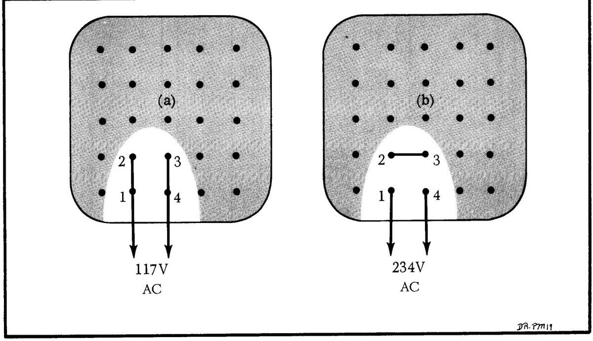
Fig. 5-10. Converting the power transformer from 105-125 volt operation to 210-250 volt operation.
operating condition. If the trouble is still apparent, it is almost a certainty that the oscilloscope is at fault. However, should the trouble appear to have been corrected by replacing the plug-in unit, the trouble most likely lies within the original plug-in unit and not with the oscilloscope.
Tube failure is the most prevalent cause of circuit failure. For this reason, the first step in troubleshooting any circuit in the instrument is to check for defective tubes, preferably by direct substitution. Do not depend on tube testers to adequately indicate the suitability of a tube for certain positions within the instrument. The criterion for usability of a tube is whether or not it works satisfactorily in the instrument. Be sure to return all good tubes to their sockets; if this procedure is followed less recalibration of the instrument will be required upon completion of the servicing.
When replacing any tube in the instrument, check first to see that components through which the tube draws current have not been damaged. Shorted tubes will sometimes overload and damage plate-load and cathode resistors. These damaged components can generally be located by a visual inspection of the wiring. If no damaged components are apparent, and if tube replacement does not restore operation, it will be necessary to make measurements or other checks within the circuit to locate the trouble.
The component number of each resistor, inductor, capacitor, vacuum tube, control and switch is shown on the circuit diagrams. The following chart lists the component numbers associated with each circuit:
All numbers less than 100 ..... Time-Base Trigger 100 series ..... Time-Base Generator
| 200 series Tir | me-Base Generator B |
|---|---|
| 300 series Ho | orizontal Amplifier |
| 400 series De | elay Pickoff |
|
600 series and
700 series Lo |
w-Voltage Power Supply |
|
800 series CF
Vo Co |
RT Circuits and High-
oltage and Square-Wave alibrator |
| 1000, 1100, 1200 series . Ve | ertical Amplifier |
| 1300 series De | elay Line |
Switch wafers shown on the schematic diagrams are coded to indicate the position of the wafer on the actual switches. The number portion of the code refers to the wafer number on the switch assembly. Wafers are numbered from the front of the switch to the rear. The letters F and R indicate whether the front or the rear of the wafer is used to perform the particular switching function. Photographic details of these switches are shown on the same fold-out page as the corresponding schematic diagram. These photographs are provided as parts location guides.
CIRCUIT TROUBLESHOOTING
Although the Type 545A is a complex instrument, it can be thought of as consisting of eight main circuits, in addition to the Calibrator circuit. These are the:
- 1. Low-Voltage Power Supply.
- 2. CRT Circuit and High-Voltage Power Supply.

Fig. 5-11. Physical location of the circuits which compose the Type 545A Oscilloscope.
- 3. Vertical Amplifier and Delay Line
- 4. Time-Base "A" Trigger Circuit.
- 5. Time-Base "B" Trigger Circuit.
- 6. Time-Base "A" Generator.
- 7. Time-Base "B" Generator.
- 8. Horizontal Amplifier.
The first circuit to check, for practically any type of trouble, is the Low-Voltage Power Supply. Because of the circuit configuration employed, it is possible for an improper power supply voltage to affect one circuit more than the others. For example, if the gain of the Vertical Amplifier should decrease slightly, while the other circuits appear to be functioning normally, this could be due to an improper supply voltage and not to any condition originating in the Vertical Amplifier. In cases of this type, valuable time can be saved by checking the power supply first
On the other hand, the crt display can often be used to isolate trouble to one particular circuit when trouble obviously exists in that circuit. If there is no vertical deflection, for example, when the intensity and horizontal deflection appear to be normal, it is apparent that an open condition exists in the Vertical Amplifier and this circuit should be investigated first.
Front-Panel Checks
The following front-panel checks will help you to isolate the trouble in an instrument to a given circuit. The interrelation between circuits is such that these checks are not always completely accurate in isolating a trouble to a given circuit. If you are unfamiliar with the instrument these front-panel checks may prove helpful in starting to look for the trouble.
Before attempting any of the following front-panel checks make sure that the plug-in installed in the instrument is operating correctly. If the pilot lamp fails to light when the POWER switch is turned on to the ON position, and if the fan fails to operate, turn to the section on troubleshooting the Low-Voltage Power Supply. If the pilot light and fan both operate but the Time-Delay Relay fails to operate with an audible "click" after one minute you should also consult the section on Troubleshooting the Low-Voltage Power Supply.
With an operating plug-in installed, and the pilot light and fan both operating, allow the oscilloscope to run for several minutes.
Set the front-panel controls as follows:
| full | right | (clockwise) |
|---|---|---|
| 0 | ||
| AC | ||
| +INT. | ||
| full right | ||
| 5 MILLISEC | ||
| А | ||
| mid-scale | ||
| full | full right |
| INTENSITY | full-left (d | counterclockwise) |
|---|---|---|
| ASTIGMATISM | mid-scale | |
| scale illumination | mid-scale | |
| HORIZONTAL POSITION | mid-scale | |
| VERNIER | mid-scale |
The settings of other controls are not critical at this time
If you are using a Type TU1 or TU2 Test-Load Plug-in Unit set the toggle switch to the 1:1 position and the AMPLI-TUDE CALIBRATOR switch to the .2 VOLTS position. If using another type of plug-in set the VOLTS/CM switch to 1 volt and the AMPLITUDE CALIBRATOR switch to 2 VOLTS.
Using a patch cord which introduces no attenuation connect the CAL. OUT connector to the INPUT connector of the plug-in preamplifier. Advance the INTENSITY control to the mid-scale position.
Now examine the face of the crt. If no display is evident examine the Beam-Position Indicator lamps. If the display is positioned off the screen vertically turn the VERTI-CAL POSITION control from one extreme position to the other, watching the face of the crt as you do so. If no display appears, and operation of the VERTICAL POSITION control has no effect on the Beam-Position Indicator lamps turn to the section on Troubleshooting the Vertical Amplifier.
If the display which appears consists of a horizontal line, you may check the operation of the calibrator by removing the end of the patch cord which is inserted into the CAL. OUT connector and holding it in your hand. A series of sloping vertical lines appearing on the crt indicate that the Vertical Amplifier is operating, and that the Amplitube Calibrator is probably inoperative. See the section on Troubleshooting the Amplitude Calibrator for the remedy.
If the operation of the VERTICAL POSITION control causes the vertical Beam-Position Indicator lamps to indicate the display as centered, rotate the HORIZONTAL POSITION control from one extreme position to the other. If the horizontal Beam-Position Indicator lamps still indicate the display is off the screen refer to the section on Troubleshooting the Horizontal Amplifier.
If both sets of Beam Position lamps indicate that the display is centered, but no display is observed, CAUTIOUSLY advance the INTENSITY control. Watch for a display to appear on the screen. If no display is seen or if the display is of low intensity but otherwise normal, refer to the section on Troubleshooting the CRT Circuit.
TROUBLESHOOTING THE VERTICAL AMPLIFIER
No Spot or Trace Visible on CRT
If all power supply voltages are normal, and the crt is known to be good, failure to obtain a spot or trace on the screen will be due to improper positioning voltages. This condition is caused by a dc unbalance in either or both of the deflection amplifier circuits.
To determine which circuit is at fault, adjust the Time-Base controls for a free-running sweep at 1 millisec/cm (STABILITY control full right). Set the INTENSITY control to midscale. Using a screwdriver with an insulated handle, short the deflection plates together at the neck pins on the crt. These are the pins marked BLUE (UPPER) and BROWN (LOWER). Be extremely careful not to short either pin to the metal shield around the crt, or to the pin marked ORANGE (GEOM). If the dc unbalance is being produced in the vertical deflection circuit the trace will appear at or near the center of the crt when the vertical deflection plates are shorted together. If the trace does not appear, however, the trouble does not lie in the vertical circuit and the dc balance of the horizontal circuit can be checked in a like manner.
If it is determined that the vertical deflection circuit is unbalanced, the next step is to check the Delay Line. For this check, and for others to follow, it is convenient to have a short lead (about 6 to 10 inches) with a rubber-covered alligator clip on each end (see Fig. 5-12). Connect this lead across the input to the Delay Line (at the output from the Distributed Amplifier). If the trace appears on the crt the Delay Line is not at fault. If the trace does not appear, check for an open line. This can be done by turning off the instrument and checking the continuity of both sides of the line with an ohmeter.
If the Delay Line is not at fault, connect the shorting strap across the input of the Distributed Amplifier. If the trace does not appear when these grids are connected together, the trouble lies in the Distributed Amplifier. Check for an open grid or plate line. Check R1206 and R1216 at the grid line termination, and check R1071 and R1073 and the associated circuitry at the plate line termination. Refer to the simplified diagram of a distributed amplifier shown in Fig. 4-1 for the location of these components: then
refer to the schematic diagram for your instrument for the exact value. Fig. 4-1 shows the normal location of these components in a vertical amplifier.
If the trouble is being caused by tubes, it may help to connect the shorting strap between the grids of that pair of distributed amplifier tubes closest to the input of the delay line. Then move the shorting strap back stage-by-stage toward the input of the distributed amplifier until a point is reached at which the trace no longer appears as the opposite arids are shorted together.
The trouble will then lie in that part of the circuit between the shorting strap and the Delay Line. It is unlikely that just one tube in the Distributed Amplifier could be responsible for the trouble because the current from each tube is only a small portion of the total current flowing in the plate circuit.
If the trace appears when the input grids to the Distributed Amplifier are connected together, the trouble is occurring ahead of the Distributed Amplifier in one of the input stages. If the tube replacement does not correct the trouble, then look for open peaking coils, defective resistors, and shorted or leaky capacitors.
After replacing tubes in the distributed amplifier or other sections of the Type 545A vertical amplifier, it is necessary to check the various stages for balance between paired tubes on opposite sides of the amplifier. To check the balance of the 6DK6 stages, insert a Type TU-2 Test Load Unit in your oscilloscope. Short together the vertical deflection plates of the CRT to determine the Electrical Center and adjust VERTICAL POSITIONING so that the trace is at the electrical center. Jumper the grid lines of the 6DK6 stages together. Then attach a meter lead or suitable connector between the +225 volt output of the TU-2 and the cathodes of each pair of 6DK6 tubes in order. Unbalance of the
Fig. 5-12. Shorting strap useful in locating an unbalanced stage in vertical or horizontal amplifier. Insulating tape covers the 100-ohm resistor.
stage is indicated by a sudden shift in vertical location of the crt trace. Balancing should begin with the last pair of tubes toward the rear of the oscilloscope and continue successively toward the front. By interchanging tubes from side to side and between pairs, unbalance should be reduced to a minimum in the 6DK6 stage. Then proceed forward to the 6DJ8 tubes following the same procedure to obtain a minimum of unbalance. Matching of the 12BY7 stage is most critical of all. This can be accomplished by simply placing a jumper between the 12BY7 grids and pushing the ZERO REFERENCE button on the front of the TU-2.
Insufficient or No Vertical Deflection
Insufficient deflection indicates a change in the gain characteristics of the Vertical Amplifier. If only a slight change in deflection is apparent, the circuit can normally be recalibrated for gain. In this event, refer to the Calibration Procedure section of this manual.
If the change in deflection is more pronounced, or if there is no deflection at all, the tubes should first be checked. Then check for components which can affect the gain of the circuit but not the dc balance. Such components would be the common cathode resistors and the GAIN ADJ. control; common screen resistors and common plate load resistors
Waveform Distortion
Any waveform distortion produced by the distributed amplifier will generally be of high-frequency nature. There will be no low-frequency distortion since the deflection circuit is dc-coupled from input to output (unless one or more of the tubes enter into heavy grid current, a condition that will produce other types of distortion as well).
A distortion-free positive step function, having a risetime of 10 nanoseconds or less, may be used to observe the high-frequency characteristics of the oscilloscope-plug-in combination. This is illustrated in the waveform photoaraphs of Figs. 5-13, 5-14, 5-15. Fig. 5-13 (a) shows a display of the 3-nanosecond risetime square-wave output of the Tektronix Type 107 Saugre-Wave Generator: this photoaraph was taken on a standard Type 545A Oscilloscope with a Type K Plug-In Unit. The straight leading edge, square corner and flat top are indicative of the frequency response of a properly adjusted Type 545A/K-Unit combination. Fig. 5-13 (b) shows the same waveform except for a small aberration in the top about 2 centimeters to the right of the leading corner. This aberration is known as the termination "bump", and was obtained by detuning the Delay Line termination network slightly. The oscilloscope was adjusted for a sweep rate of 2 usec/cm for these photographs: the termination hump therefore occurs .4 microsecond after the leading corner. Since the Delav Line is reverse terminated, this corresponds to twice the .2microsecond delay time of the circuit.
Any waveform distortion that may be produced by the vertical deflection circuit will occur between the leading corner and the termination bump. The vertical deflection circuit in the Type 545A may be divided into three parts, and each part will affect the waveform in a different man-
Fig. 5-13. (a). A 450-kc, 3 nanosecond risetime square wave displayed on properly adjusted Type 545A/K-unit combination. (b). The small aberration in the top of the waveform is a termination bump produced by an improperly terminated Delay Line.
ner. An analysis of the distortion is therefore helpful in determining which part of the circuit is at fault. The three parts are:
- (1) The plug-in unit and input stage of the main Vertical Amplifier.
- (2) The Distributed Amplifier.
- (3) The Delay Line.
The plug-in unit and the input stage of the main Vertical Amplifier will affect only the leading corner of the step
Fig. 5-14. (a). Rolloff at leading corner caused by an undercompensated Input Amplifier Stage. (b). Ringing produced by an overcompensated Input Amplifier Stage.
function. Assuming the trouble is not being caused by the plug-in unit, the Input Amplifier stage and the cathode follower circuit can be investigated for the type of distortion shown in Fig. 5-14. Fig. 5-14 (a) shows rolloff, or undershoot, at the leading corner of the step function. Rolloff is the result of insufficient high-frequency compensation. A small amount of rolloff is normally due to a change, with age, in the characteristics of the circuit components, and can usually be compensated by adjusting the variable peaking coils. If the rolloff is more pronounced the tubes should be checked. If a tube cannot deliver current, instantaneously on demand, the transients in the signal will not be produced.
Shorted or partially shorted peaking coils will result in a rolloff. Be especially careful when soldering around the peaking circuits as hot solder dropping on a coil may burn through the insulation and short the turns.
Ringing at the leading corner, shown in Fig. 5-14 (b), is produced by an overcompensated amplifier. This is generally caused by misadjusting the peaking coils. An overshoot at the leading edge, without ringing, can also be produced by an over-compensated amplifier; in this case the degree of compensation is not sufficient to produce ringing. In both of these cases the distortion can generally be eliminated by readjusting the variable peaking coils.
Fig. 5-15. (a). Rolloff and aberrations in top of pulse are due to a low Gm tube in the Distributed Amplifier. (b). Small aberrations in top of pulse are caused by a slightly misadjusted portion of the Delay Line.
An overshoot at the leading edge of a fast-rise pulse may also be the result of cathode interface in one of the amplifier tubes. Since the constant of the interface layer is normally in the range from .1 to 3 µsec, this effect is most noticeable on waveforms whose period is long compared to the interface time constant. This condition is produced by the tubes themselves, so it is important to first check the tubes when such distortion is evident.
The Distributed Amplifier will affect the step function both at the leading corner and in the vicinity of the termination bump. A typical example is that shown in Fig. 5-15 (a).
The rounded corner, and the aberrations about .4 µsec following the corner, were produced by replacing V1204 with a tube whose Gm was quite low. This points up the importance of the tubes in maintaining the proper frequency response in pulse amplifiers. Other factors causing similar effects would be shorted coils in the plate and grid lines, off-value resistors, leaky or open capacitors, or improper adjustment of the capacitors across the plate lines.
The Delay Line will affect the pulse from the corner to the termination bump. If the line is badly defuned the ton of the pulse will be uneven, instead of smooth and flat as shown in Fig. 5-15 (a) and the leading corner may either overshoot or rolloff. If just one or two sections of the line are defuned either due to a shorted coil or a defective capacitor an aberration will appear in the waveform in the region affected by the defective component. Since the Delay Line is reverse-terminated, the end of the line nearest the cathode ray tube will affect the start of the pulse and the beginning of the line lat the output of the Distributed Amplifier) will affect the waveform in the region of the termination hump. Sections of the line between the two and will affect the waveform in the region between the corner and the termination bump. The location of an aberration in the top of the pulse, with respect to the leading corner and the termination hump will indicate the relative soction of the line in which the trouble is occurring. For example the small aberrations shown in Fig. 5-15 (b) were produced by slightly detuning two sections of the line about midway between the Distributed Amplifier and the cathoderav tube.
Unstable Triggering
If the sweep generator is not being properly triggered a stable display of a waveform will not be possible. If the sweep can be turned off and on with the STABILITY control (for any setting of the TRIGGERING MODE switch except AUTOMATIC) the sweep generator is capable of being triggered; this indicates the trigger circuitry is not functioning properly. The first step is to replace the Trigger Pickoff tube V1223 in the Vertical Amplifier. The operation of this stage can also be checked by observing the signal available at the VERT. SIG. OUT binding post with another oscilloscope. If no signal is available at this connector the Trigger Pickoff stage is defective; a proper signal at this connector indicates the stage is functioning correctly.
If the Trigger Pickoff stage is operating correctly, trouble exists in the Time-Base Trigger circuit. To check the quiescent stage of the circuit, set the TRIGGERING MODE switch to AC, the TRIGGER SLOPE switch to —INT. and the TRIG-GERING LEVEL control to 0. Next, connect a jumper wire from the junction of R19, R20, and C20 (on the Trigger Switch; Fig. 6-7) to ground. This fixes the voltage at the grid of V24B at ground potential. Then measure the voltage at the plate of V24B; this should be about +85 volts. If this voltage does not measure very close to +85 volts, replace the Trigger Input tube V24. If necessary, check for off-value resistors, broken leads and poor switch contacts.
The next step is to connect the voltmeter between the plate of V24B and the arid of V45B (the junction of R41) PIGTE OF V24B and the grid of V43B (the junction of K41, V45B) The voltage between the plate of V24B and the arid of V45A (or the divider side of R41) should not exceed about 2.75 volts. It is the function of the Tria Level Centering control R39 to set the voltage at the grid of V45B approximately equal to the voltage at the grid of V45A. With the grids of V/5 at about the same voltage the center of the hysteresis of the Triager Multivibrator circuit will be at the proper level. It is difficult to measure the voltage directly between the two grids of V45 due to the logding of the voltmeter, for this reason we suggest the voltage be measured between the plate of V24B and the arid circuit of V45B A voltage of 2.5 to 2.75 volts between these points will indicate proper quiescent operation.
If the voltage at the grid of V45B cannot be adjusted to within 2.5 to 2.75 volts of the voltage at the plate of V24B, trouble in the Trigger Multivibrator is indicated. Replace the tube; then, if necessary, check for off-value resistors, broken leads and poor switch connections.
Conversely, if the voltages are found to be correct, the adjustment of the Trig. Sens. control R47 can be checked. Refer to Step (7) in the Calibration Procedure for the proper method of checking the adjustment of this control.
When triggering in the DC mode from the signal being observed (TRIGGER SLOPE at + or -INT.), the Int. Trig. DC Level Adj., R3 and its associated components are connected to the input grid of V24. This control is adjusted so that the input grid (pin 7 at -INT; pin 2 at +INT.) is at ground potential when the trace is centered vertically on the crt. If the voltage at the input grid cannot be adjusted to zero when the triggering-switch controls are in the indicated positions, this control and its associated components should be checked.
TROUBLESHOOTING THE TIME-BASE GENERATOR
No Horizontal Sweep
If the Time-Base Generator is not producing a sawtooth sweep voltage when the STABILITY control is adjusted for a free-running sweep some defect in the generator is hanging up the Miller circuit. Depending on the on-off characteristics of the diodes V152, the Miller circuit may be hung up at either the high end or the low end of the sawtooth. The manner in which it is hung up may be determined by measuring the voltage at the SAWTOOTH A binding post. If the Miller circuit is hung up at the high end of the sawtooth the voltage at the front-panel binding post will measure about +200 volts; if hung up at the low end, the voltage at this point will measure anywhere between ground and -20 to -30 volts, depending on the cause.
If the Miller circuit is hung up at the high end of the sawtooth a check of the voltage at the grid of the Miller tube will offer a clue to the cause of the trouble. The static voltage at the Miller grid is determined by conduction through the Timing Resistor, R160 (from -150-volt bus), the lower diode V152B, and the divider R147-R148. It will be
impossible to measure the exact voltage at the Miller grid because of the loading of the meter. However, if a 20,000-Ω/v meter, or a vacuum-tube voltmeter is used, the voltage reading obtained will be sufficient to indicate the source of the trouble. For example, if a voltage reading more negative than about —15 volts is obtained, there is probably no conduction through the Timing Resistor. This would indicate an open divider, R147-148, assuming the diode V152 to be good.
If the Miller circuit is hung up at the low end of the sawtooth, as indicated by a voltage reading of zero or a few volts negative, a check of the voltage at the plate of the Miller tube will offer a clue to the cause. If this voltage is quite high (about +300 volts), check the neon lamp B167 and the Runup CF tube V173. If the voltage at the plate of the Miller tube is zero or slightly negative, check for an open plate-load resistor R164, R165 or R166.
However, if the voltage at the plate of the Miller tube is near the quiescent level (about +45 volts) the trouble will generally lie ahead of the Miller tube. The result of the trouble is that the On-Off Diodes V152 cannot be gated off; they are conducting heavily and clamping the grid of the Miller tube near ground. If all of the tubes have been checked, then check for open plate and cathode resistors in the Sweep-Gating Multivibrator circuit, the Hold-Off circuit and the Runup CF circuit. Also check that the STABILITY control can vary the voltage at the grid of V125.
Improper Triggering
If the sweep cannot be triggered properly, the gating pulse from the Multivibrator is not turning the diodes V152 off and on properly. The start of the gating pulse, which turns the diodes off and starts the sweep, is initiated by the triggering pulse at the grid of V135A. The end of the gating pulse, which turns the diodes on and initiates the retrace, is controlled by the hold-off waveform at the grid of V135A. The Sweep-Gating Multivibrator can be eliminated as the cause of the trouble if the sweep can be turned off and on with the STABILITY control. The main component to check, in addition to the tubes, is the differentiating capacitor C131.
Nonlinear Sweep
A nonlinear sweep voltage will be generated if the current charging the Timing Capacitor C160 does not remain constant. If the nonlinearity occurs at all sweep rates a defective Miller tube will be the probable cause. If the nonlinearity occurs only at certain sweep rates a leaky timing Capacitor will be the probable cause but the Miller tube should not be overlooked. A defective bootstrap capacitor C165 can cause the sweep to be nonlinear at the faster sweep rates.
Insufficient Horizontal Deflection
If the horizontal trace starts at the left side of the graticule, but does not extend to the right side, the Hold-Off circuit is causing V135A to conduct too soon after the triggering pulse had forced it into cutoff. If the trace cannot
be expanded the full length of the graticule with the Swp. Length control R176, check the resistance values in the cathode circuit of V173.
No Spot or Trace Visible on CRT
To determine that the Horizontal Amplifier is in a state of dc unbalance, short the horizontal deflection plates together at the neck pins of the crt in the manner explained for troubleshooting the Vertical Amplifier. The horizontal deflection plates are marked RED (LEFT) and GREEN (RIGHT). The INTENSITY control should be set to mid-scale. If a spot appears when the horizontal deflection plates are shorted together (it may be necessary to adjust the Vertical POSITIONING control), the trouble lies in the Horizontal Amplifier.
CAUTION
Do not permit the spot to remain on the crt at this setting of the INTENSITY control. Either reduce intensity until the spot is just visible, or remove the short from the horizontal deflection plates.
The procedure for troubleshooting the Horizontal Amplifier to locate the defective stage, is similar to that explained for troubleshooting the Vertical Amplifier for unbalance. The shorting strap can be moved from the deflection plates back toward the Input Amplifier stage, until a point is reached where the trace does not appear. When the stage at fault is determined, check for defective tubes and components associated with the stage.
Insufficient or No Horizontal Deflection
If the gain of the Horizontal Amplifier decreases, the trace will not extend from the left to the right side of the graticule. In addition, the timing will no longer correspond to the calibrated value indicated by the TIME/CM switch. (This is to distinguish the condition of insufficient sweep produced by a malfunction in the Horizontal Amplifier from one produced in the Time-Base Generator, e.g., an improper adjustment of the Swp. Length control. In the latter case the trace will start at the left side of the graticule, for the normal setting of the HORIZONTAL POSI-TION conrol, and the timing will not be affected.)
If the change in gain is slight, as indicated by improper timing and a slightly decreased sweep, the amplifier can usually be recalibrated. Since the gain of the Horizontal Amplifier regulates the timing of the sweep, care must be taken to insure that the gain adjustments are accurately made. Be sure to refer to the Calibration Procedure if it is necessary to adjust the gain of the Horizontal Amplifier.
If the decrease in gain of the Horizontal Amplifier is more pronounced, or if there is no sweep at all (in which case only a spot will be visible on the horizontal axis), check for defective components which can affect the gain but not the dc balance. In addition to the tubes, such components would be the common cathode resistors and controls.
Proper operation of every circuit in your instrument depends on proper operation of the Power Supply. The regulated dc voltages must remain within their specified tolerances for the instrument to retain its calibration.
CAUTION
Exercise care in checking the power supply. Because of their high current capabilities and low impedance, the Low-Voltage supplies can produce more harmful shocks than the high-voltage supply in the CRT circuit.
Open Power Circuit (Dead Circuit)
If the pilot lamp and the fan do not come on when the power is turned on, check the source of power and the power cord connections. Check the fuse. If the fuse is blown replace it with one of the proper value and turn the instrument on again. If the new fuse blows immediately, check the power transformer for shorted primary or secondary windings. Also check for shorted rectifiers. If the new fuse does not blow until the time-delay relay has activated (a "click" can be heard), check for a shorted condition in the regulator circuits and the loading on the supply.
If the fuse is good, check for an open primary winding in the power transformer. If your instrument is wired for 234-volt operation, check for an open Thermal Cutout Switch; the resistance of this switch is about .1 Ω. (If your instrument is wired for 117-volt operation, the fan will come on even though the Thermal Cutout Switch may be open).
If both the fan and pilot light come on, the primary circuit of the power transformer is operating normally.
Incorrect Output Voltage
The voltage for each test point is silk-screened on the lip of the chassis adjacent to the ceramic strip on which the test points are located. Refer to Fig. 5-16 for a lowvoltage check point location.
Each regulated bus is identified by a color-coded wire. The -150-volt bus is coded brown, green and brown on a black wire; the +100-volt bus is coded brown, black and brown on a white wire; the +225-volt bus is coded red, red and brown on a white wire; the +350-volt bus is coded orange, green and brown on a white wire; and the +500-volt bus is coded green, black and brown on a white wire.
If any of the supplies fail to regulate the first thing to check is the line voltage. The supplies are designed to regulate between 105 and 125 volts with the design center at 117 volts, or between 210 and 250 volts with the design center at 234 volts, rms, 50-60 cycle single phase ac.
When possible, check the resistance values between the outputs of the Low-Voltage Power supplies and ground.

- e. Open or leaky filter capacitors.
- f. Defective rectifiers.
If the output is low with normal ripple, check:
- a. The resistance values in the dividers.
- b. The capacitors across the dividers.
NOTE
If any components in the -150-volt supply are changed, or if the setting of the -150 Adj. control is changed, it will be necessary to recalibrate the instrument.
TROUBLESHOOTING THE CALIBRATOR
Asymmetrical Output
If the output square wave is not symmetrical (the positive portion has a duration different from that of the negative portion) the two tubes in the Multivibrator circuit are not being held cutoff for equal periods. This will normally be caused by a defective tube. If tube replacement does not correct the waveform the circuit components must be checked. The triode in the Multivibrator is held cutoff for an interval determined by the discharge of C871 and the pentode is held cutoff for an interval determined by the discharge of C874. A change in the value of either capacitor, or in the value of the resistor through which they discharge, could produce an asymmetrical waveform.
In addition, the time needed for these capacitors to discharge a given amount is affected by the potential toward which they discharge; this would be the voltage at the plate of the triode in the case of C874, and the voltage at the screen of the pentode in the case of C871. Since these voltages are affected by the value of R870 and R875, these resistors should be checked. The resistors in the plate circuit of the pentode should also be checked, since they will affect the plate-to-screen ratio of the pentode.
Incorrect Output Voltage
The amplitude of the output square wave is determined almost entirely by the resistance value in the divider in the cathode-follower stage. A quick check of the resistance values can be made by turning off the Calibrator and measuring the voltage at the Cal. Test Pt.; if this point does not measure exactly +100 volts the output voltages when the Calibrator is turned on will not be correct.
The Cal. Adj. control R879 will vary the voltage at the test point over about a 10-volt range. If this voltage cannot be set to exactly +100 volts, and if the tubes have been replaced, then one or more of the precision resistors in the divider have changed in value.
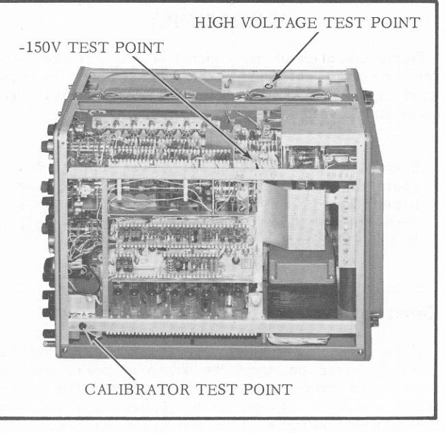
Fig. 5-16. Location of Power Supply and Calibrator test points.
If the resistance values between the regulated buses and ground check out, check the tubes (if this has not already been done). Then make sure that the line voltage is set near the design center for your instrument (117 or 234 v) and check the rms voltage across the secondary winding for each supply; the nominal value of each secondary voltage, when the line is set to the design center, is indicated on the circuit diagram. If the secondary voltages are all correct, check the operation of the bridge rectifiers. This can be done by measuring the rectified voltage at the input to each regulator. These values are also indicated on the circuit diagram. Then check for off-value resistors, especially in the dividers, and for open or leaky capacitors.
The material that follows may be used as a quick index for troubleshooting the regulator circuits.
-
If the output voltage is high with excessive ripple, check:
- a. For high line voltage.
- b. For open voltage-regulator tube.
- c. The amplifier tubes in the regulator circuit.
- d. For insufficient loading.
-
If the output voltage is high with normal ripple, check:
- a. For proper resistance value in the dividers refer to the schematic for your instrument to determine the location of the resistors involved. Since these are generally precision resistors (±1% tolerance) the use of a good bridge is recommended in checking the value.
If the output is low with excessive ripple, check:
- a. For low line voltage.
- b. For shorted voltage-regulator tube.
- c. The series tubes in the regulator circuit.
- d. For excessive loading.
TROUBLESHOOTING THE CRT CIRCUIT
The intensity, focus, geometry and calibration of the crt display depend on proper operation of the high-voltage supplies in the CRT Circuit.
No Intensity
If the low-voltage power supply is operating normally, but no spot or trace is visible on the crt, the trouble could be a defective crt, a defect in the crt cathode circuit including the supply, or an unbalanced dc condition in either or both of the deflection amplifiers. In the latter case the dc unbalance is producing improper positioning voltages and the beam is being deflected off the screen.
To determine which circuit is at fault, turn the INTENSITY control full right (cw). If a flare is observed on the crt screen (it may be necessary to darken the room) one of the deflection amplifiers is probably at fault: the procedure for troubleshooting these circuits follows a bit later in this section. If no flare is observed with the INTENSITY control turned full right, the trouble will either be due to a defective crt or to an inoperative cathode supply circuit. The cathode supply can be checked by measuring the voltage at the HV Adi Test Pt. In the majority of instruments the test point is located at the top left rear of the instrument. Fig. 5-16 shows the location of typical high-voltage test points. Refer to the schematic diagrams for your instrument to determine the correct voltage. If the voltage reading you obtain is in the vicinity of the correct voltage noted on the schematic turn the instrument off, and measure the value of the 27 K resistor attached to the test point (see Fig. 5-16) If this resistor is not open a defective crt is indicated
If the voltage at the H.V. Adj. Test Pt. is zero or abnormally low replace the Oscillator tube and the Error-Signal Amplifier tube. If this does not restore operation the Oscillator circuit should be checked.
A quick check on the operation of the Oscillator circuit can be made by observing the heater glow in the 5642 rectifier tubes, located under the shield at the upper right rear of the instrument. These tubes are visible through the opening in the side of the shield. If no heater glow is visible the Oscillator circuit is inoperative. This could be due to an open high-voltage transformer, or to a defective component in the oscillator or error-signal amplifier circuits.
If heater glow is visible in the rectifier tubes, the Oscillator circuit is operating. If the heater glow appears to be dim, however, the output of the Oscillator may be insuf-
ficient for proper operation. A more accurate check on the Oscillator may be made by removing the shield covering the high-voltage transformer and measuring the bias at the grid of the oscillator tube. This can be measured at the junction of the 100 k resistor and the .01-µfd capaacitor. See the simplified schematic, Fig. 4-10 for normal circuit configuration in the high-voltage oscillator. The voltage at this point should measure about -6.5 volts.
CAUTION
Do not let your hand or body touch the chassis when making the following check. Secondary reactions to an otherwise harmless shock might result in a painful injury.
If the Oscillator circuit is operating properly, but the voltage at the H.V. Adj. Test Pt. does not measure in the vicinity of that indicated on the schematic diagram for the instrument, the 5642 rectifier tube, V822, shown in the simnlified schematic of Fig. 4-10, is most likely defective.
Abnormal Intensity
If a trace is visible on the crt, the relative intensity of the trace may be used to identify trouble in either the negative bias supply or the positive anode supply.
If the trace is excessively brilliant, and if the brilliancy does not change as the INTENSITY control is adjusted, check the negative bias supply including the lead to the first grid of the crt. Check for a defective rectifier tube V822, (shown in the simplified schematic diagram of Fig. 4-10), an open supply winding or filament winding, an open resistor including the INTENSITY control, or a shorted or leaky capacitor. If trouble is not found in any of these components, a defective crt is indicated.
If the intensity of the trace is extremely low, check for an inoperative positive supply. Also check the anode connection to the crt, including R836 and C836.
If the accelerating potentials appear to be too high, as evidenced by decreased deflection sensitivity, check the Error-Signal Amplifier circuit.
If a badly distorted trace or spot is visible on the crt, check the Geom. Adj. control and its connection to the neck pin on the crt, and the ASTIGMATISM control and its connection to the crt base socket. If the FOCUS control has no effect on the trace, check this control and its connection to the crt base socket.
NOTE
If any components in the Oscillator, Error-Signal Amplifier or cathode supply circuit are changed, or if the setting of the H.V. Adj. Control is changed it will be necessary to recalibrate the instrument.
SECTION 6
CALIBRATION PROCEDURE
The Type 545A Oscilloscope is a stable instrument and should not require frequent calibration. However, it will be necessary to calibrate certain parts of the instrument when tubes or components are changed, and periodic calibration is desirable from the standpoint of preventive maintenance.
In the instructions that follow, the steps are arranged in the proper sequence for full calibration. Each numbered step contains the information necessary to make one adjustment. If a complete calibration is not necessary, you may perform individual steps, PROVIDING that the steps performed do not affect other adjustments. It is most important that you are fully aware of the interaction of adjustments. Generally speaking, the interaction of controls will be apparent in the schematic diagrams. If you are in doubt, check the calibration of the entire section on which you are working.
If you make any adjustments on the power supplies, you will have to check the calibration of the entire instrument. In particular the sweep rates and vertical deflection factors must be checked.
EQUIPMENT REQUIRED
The following equipment is necessary for a complete calibration of the Type 545A Oscilloscope.
(1.) A DC voltmeter having a sensitivity of at least 5000 Ω/v and calibrated for an accuracy of at least 1% at 100, 150, 225, 350 and 500 volts, and for an accuracy of at least 3% at 1350 volts. Portable multimeters should be regularly checked against an accurate standard and corrected readings noted, where necessary, at the above listed voltages.
BE SURE YOUR METER IS ACCURATE
(2.) An accurate rms-reading ac voltmeter, having a range of 0-150 volts. (0-250 or 0-300 for 234 v. operation).
(3.) Variable auto-transformer (e.g. Powerstat or Variac) having a rating of at least 6.25 amperes.
(4.) Time-Mark Generator, Tektronix Type 180, 180A or equivalent, having markers at 1 µsec, 10 µsec, 50 µsec, 100 µsec, 1 msec, 5 msec, 10 msec, 100 msec, 1 sec, and 5 sec and sine-wave outputs of 10 mc and 50 mc, all having an accuracy of at least 1%.
(5.) Square-Wave Generator, Tektronix Type 107 or equivalent, having a risetime of no more than 7 nanoseconds, and a frequency of approximately 500 kc. The top of the square-wave must be free of overshoot and wrinkles. A Tektronix Type P Unit may be used in place of the Type 107. A Type P52 Coaxial Cable and a Type B52R Terminating Resistor is required with the Type 107.
6.) Tektronix Type K or Type L Plug-In Unit. (If delay-line adjustment is not required, other Tektronix Plug-In Units may be substituted.)
7.) Low-Capacitance Recalibration Tools: Tektronix part numbers 003-000, 003-007 and 003-301. (See Recalibration Tools in Accessories Section of Operator's Manual and Fig. 6-1).
(8.) Tektronix Type P6000 or P410A Probe.
[9.) Test Oscilloscope, Tektronix Type 316 or equivalent, providing triggered sweeps and a bandpass of at least dc to 10 mc.
(10.) Gain Set Adapter, Tektronix Type EP53A.
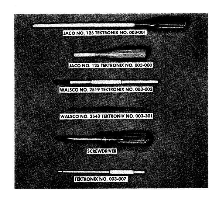
Fig. 6-1. Suggested Calibration Tools.
Calibration Procedure — Type 545A
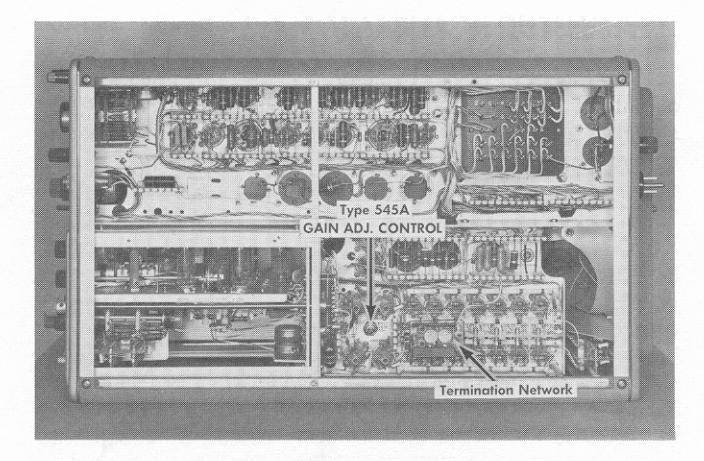
Fig. 6-2. Bottom view of the Type 545A Oscilloscope showing the location of the GAIN ADJ. control.
PRELIMINARY
Remove the side covers and bottom plate from the instrument to be calibrated and install the Type K or Type L Unit.
| Set the front-pai | nel controls as follows | : |
|---|---|---|
| INTENSITY | full left | |
| HORIZONTAL | DISPLAY | А |
| TRIGGERING MODE (A | and B) AC |
|---|---|
| TRIGGER SLOPE (A and | I B) + INT. |
| STABILITY (A and B) | full left, but not PRESET |
| TIME/CM (A and B) | .5 MILLISEC |
| VARIABLE | CALIBRATED (full irght) |
| CALIBRATOR | OFF |
Plug-In Unit
| AC/DC | DC |
|---|---|
| VOLTS/CM | .05 |
| VARIABLE | CALIBRATED (full right) |
NOTE
Settings for all controls not listed above are not pertinent to this part of the procedure and the controls may be left in any position.
Check the rear panel of the instrument to be sure the metal strap between EXTERNAL CRT CATHODE and GROUND binding posts is in place, and that the CRT SE-LECTOR switch is away from the DUAL-TRACE CHOPPED BLANKING position. Connect the instrument and the ac meter to the autotransformer output and turn on all equipment. Adjust the autotransformer to the design-center voltage for which your instrument is wired (117 or 234 v.) and allow at least 5 minutes warmup before making any adjustments.
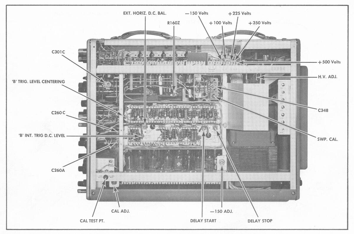
Fig. 6-3. Right-Side View of the Oscilloscope showing the internal controls locations.
PROCEDURE
1. Low-Voltage Power Supplies
Measure the output voltage of the -150 v, +100 v, +225 v, +350 v and +500 v supplies at the points indicated on the right side view, Fig. 6-3. Be sure your meter is accurate (see Equipment Required, Fig. 6-1). The output voltage of the -150 v supply must be between -147 v and -153 v, and the other regulated supplies must be within 2% of their rated values. You should be able to set the -150 V Adj. control (see Right Side View, Fig. 6-3) so that all of these voltages are within the specified tolerance. Bear in mind that the calibration of the entire instrument is affected by changes in the power supply voltages. Don't adjust the -150 v unless one or more of the supplies is actually out of tolerance.
To check the above supplies for proper regulation, vary the autotransformer voltage between 105 v and 125 v (or from 210 v to 250 v if the power transformer is connected for 234 v operation). All of the regulated voltages should remain essentially constant.
The ripple present on any of the regulated supplies, as measured with a test scope at the voltage check points, will nominally be under 20 mv., with AMPLITUDE CALIBRATOR-OFF, and neither sweep operating.
2. AMPLITUDE-CALIBRATOR Adjustment
The Cal. Adj. control should be set to provide a dc output of 100 volts when the AMPLITUDE CALIBRATOR switch is in the OFF position. Under these conditions, the calibrator output will be within 3% of the front-panel readings.
To make this adjustment connect the voltmeter between the Cal. Test Pt. jack and ground (see Right Side View, Fig. 6-3), turn the AMPLITUDE CALIBRATOR switch to the OFF position, and adjust the Cal. Adj. control for a reading of exactly 100 volts. To assure suitable symmetry of the calibrator waveform, the reading at this point should not be less than 45 v nor more than 55 volts when the calibrator is turned on (to any of the output voltage settings). Readings outside this range are generally caused by unbalanced multivibrator tubes (V875 or V885A).
3. High-Voltage Power Supply Adjustment
This adjustment determines the total accelerating potential on the crt, and thus affects the deflection sensitivity.
Connect the voltmeter between ground and the highvoltage check point (see Top-View, Fig. 6-4), and set the H.V. Adj. (see Right Side View, Fig. 6-3) for a meter reading of exactly —1350 volts. If your meter has a full scale reading of 1200 v, you can connect the positive meter lead to the —150 v supply, at any convenient point, and set the H.V. Adj. for a meter reading of —1200 v.
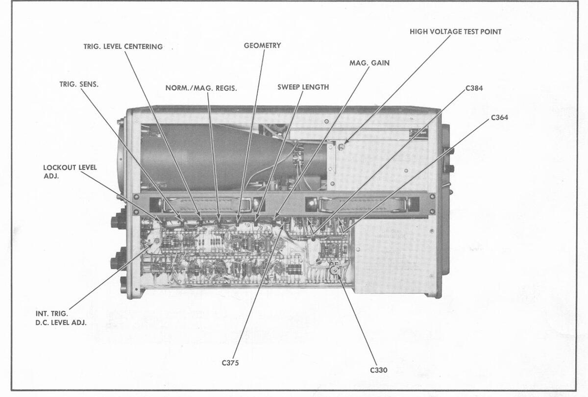
Fig. 6-4. Top View of the Oscilloscope showing locations of internal controls.
Calibration Procedure — Type 545A
4. CRT Alignment
If the crt has been replaced, or if, due to considerable handling, the trace does not align with the graticule, you should make this adjustment before proceeding with the calibration.
With the crt base clamp loose (see Left Side View, Fig. 6-5), and no vertical signal applied, free run TIME BASE A, by turning the STABILITY control full right. Position the
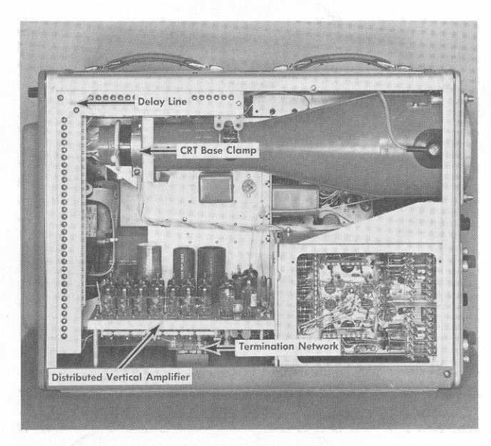
Fig. 6-5. Left-Side View of the Type 545A Oscilloscope showing locations of major components.
trace directly behind the center graticule line. If the trace and the graticule line do not coincide over the width of the graticule, rotate the crt by turning red knob on crt base clamp until they are properly aligned.
After aligning, push the crt forward until it rests snugly against the graticule, and tighten the crt base clamp. Recheck the alignment of the trace after tightening the clamp to be sure the crt didn't rotate while the clamp was being tightened.
5. CRT Geometry
The geometry of the crt display is adjusted by means of the GEOMETRY control. To achieve optimum linearity,
vertical lines are displayed on the crt and the GEOMETRY control is adjusted for minimum curvature of the lines. Nonlinearity is most noticeable at the edges of the graticule.
Set front panel controls as follows (use TIME BASE A):
| HORIZONTAL DISPLAY | A |
|---|---|
| TRIGGERING MODE | AC |
| TRIGGER SLOPE | +INT |
| TIME/CM | .5 MILLISEC |
| VARIABLE | CALIBRATED (full right) |
| VOLTS/CM (plug-in) | .2 |
Connect 500 µsec markers from the Type 180 or 180A to the INPUT connector and position the base line of the timing comb below the bottom of the crt face so it is not visible. Adjust the GEOMETRY control (see Top View, Fig. 6-4) for straight vertical lines running parallel to the left and right edges of the graticule (see Fig. 6-6).
NOTE
The amplitude calibrator may be used for this step, but due to the low intensity of the vertical lines, the adjustment is somewhat more difficult.
6. 'A' Trigger Level Centering and Trigger Sensitivity
Reset front-panel controls as follows.
| STABILITY | full right (cw) |
| TRIGGERING LEVEL | 0 |
| TRIGGERING MODE | AC SLOW (AC)- |
| TRIGGER SLOPE | +INT. |
| TIME/CM | .5 mSEC |
| VARIABLE | CALIBRATED |
| HORIZONTAL DISPLAY | А |
| CALIBRATOR | 10 MILLIVOLTS |
| LUG-IN UNIT | |
| AC/DC | DC |
| VOLTS/CM | .05 |
| VARIABLE | CALIBRATED |
Connect a test lead from the CAL. OUT connector to the INPUT connector on the plug-in unit; this should result in a free-running trace having an amplitude of about 2 millimeters (1 minor division). Center the trace vertically on the
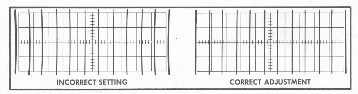
Fig. 6-6. Waveforms obtained while adjusting the geometry of a Type 545A Oscilloscope.
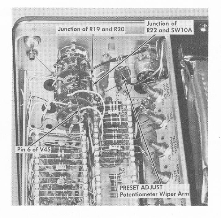
Fig. 6-7. Time Base A Triggering Circuit test points.
screen and adjust the INTENSITY, FOCUS and ASTIG-MATISM controls for best definition. Then ground the junction of R19 and R20 with a short clip lead. This junction is located on top of the Trigger switch (see Fig. 6-7).
Preset the Trigger Sensitivity control full left (ccw) and the Trigger Level Centering control full right (cw). Turn the STABILITY control left until the trace just disappears from the crt screen, then two or three degrees further left.
Turn the Trigger Level Centering control to the left until the display reappears on the screen. If the display does not appear, turn the Trigger Sensitivity control to the right a few degrees, and repeat the adjustment of the Trigger Level Centering control until the display reappears. Reduce the amplitude of the signal by turning the VARIABLE gain control on the plug-in unit slowly toward the full left position, at the same time continuing the adjustment of the Trigger Level Centering and Trigger Sensitivity controls to keep the trace on the screen. Then switch the TRIGGER SLOPE control to —INT. and +INT.; it may be necessary to turn the Trigger Level Centering control back to the right a bit to obtain a stable display. Then while swiching back and forth between +INT. and —INT., slightly readjust both the Trigger Level Centering and Trigger Sensitivity controls for stable triggering in both positions.
7. Internal Triggering DC Level
Increase the setting of the CALIBRATOR to 20 millivolts. Return the VARIABLE gain to the CALIBRATED position, center the display vertically, and turn the TRIGGERING MODE switch to the DC position. Then, while switching the TRIGGER SLOPE control back and forth between +INT. and -INT., adjust the Int. Trig. DC Level Adj. control for stable triggering in both positions. It may be necessary to slightly adjust the VERTICAL POSITION control to obtain stable triggering.

Fig. 6-8. Time Base B Triggering Circuit Test points.
8. 'A' Trigger Level
Remove the jumper and turn the TRIGGERING LEVEL control until the wave-form is triggered at the same point as that observed when the shorting lead was connected. The white dot on the TRIGGERING LEVEL knob should now point at 0. If it doesn't, loosen the knob and move it to this position.
9. 'A' Preset Adjust
Place the 'A' TRIGGERING MODE switch at AUTO. and the TRIGGER SLOPE switch at +LINE. Connect the dc voltmeter between the PRESET ADJUST potentiometer wiper arm (see Fig. 6-7) and ground and rotate the potentiometer full left. Now, rotate the control slowly to the right until a trace first appears and note the meter reading at this point. Next, continue to rotate this control until the trace brightens and again note the meter reading. Finally, set the PRESET ADJUST control to obtain a meter reading midway between the two previously noted meter readings.
10. 'B' Trigger Level Centering
It will be the controls for TIME BASE 'B' that you will set up now.
Set up the oscilloscope as indicated in Step 6, except for the HORIZONTAL DISPLAY switch. It will be set to 'B' position. Then ground the junction of R69 and R70 with a short clip lead. This junction is located on top of the Trigger switch (see Fig. 6-8).
Preset the Trigger Level Centering control full right (cw). Turn the STABILITY control left until the trace just disappears from the crt screen, then two or three degrees further left.
Turn the Trigger Level Centering control to the left until the display reappears on the screen. Reduce the amplitude of the signal by turning the VARIABLE gain control on the plug-in unit slowly toward the full left position, at the same time continuing the adjustment of the Trigger Level
Calibration Procedure --- Type 545A
Centering. Then while switching back and forth between +INT. and —INT., slightly readjust the Trigger Level Centering control for stable triggering in both positions.
11. 'B' Internal Triggering DC Level
Increase the setting of CALIBRATOR to 20 millivolts. Return the VARIABLE gain control to the CALIBRATED POSI-TION, center the display vertically, and turn the TRIGGER-ING MODE switch to the DC position. Then, while switching the TRIGGER SLOPE control back and forth between +INT. and -INT., adjust the Int. Trig. DC Level Adj. control for stable triggering in both positions. It may be necessary to slightly adjust the VERTICAL POSITION control to obtain stable triggering.
12. 'B' Triggering Level
Remove jumper and turn the TRIGGERING LEVEL control until the waveform is triggered at the same point as that observed when the shorting lead was connected. The white dot on the TRIGGERING LEVEL knob should now point at 0. If it doesn't, loosen the knob and move it to this position.
13. 'B' Preset Adjust
Place the 'B' TRIGGERING MODE switch at AUTO and the 'B' TRIGGER SLOPE switch at +LINE. Connect the dc voltmeter between ground and the junction of R214 and SW60B (see Fig. 6-8), and rotate the 'B' PRESET ADJUST control full left. Now, rotate the control slowly to the right until a trace first appears, and note the meter reading at this point. Next continue to rotate this control until the trace brightens, and again note the meter reading. Finally, set the PRESET ADJUST control to obtain a meter reading midway between the two previously noted readings.
14. Adjust 5X Magnifier Gain
| Set controls as follows: | |
|---|---|
| HORIZONTAL DISPLAY | 'B' |
| TRIGGERING MODE (B) | AC |
| TRIGGER SLOPE (B) | +INT |
| TIME/CM (B) | 1 MILLISEC |
| 5X MAGNIFIER | ON |
| VOLTS/CM (Plug-In) | 2 |
Connect 1 millisecond and 100 microsecond markers from the Type 180A to the vertical input and adjust the 'B' triggering for a stable display. If necessary adjust Mag. Gain (see Top View Fig. 6-4) to display 1 large marker every 5 cm, and 2 small markers every cm. Position the display horizontally to observe linearity on both ends. Check that the neon lamp lights when MAGNIFIER is switched on.
15. Adjust Sweep Magnifier Registration
With the MAGNIFIER ON, position the display so that the first time marker is directly behind the center graticule line. Turn the MAGNIFIER OFF and adjust Norm./Mag. Regis. (see Top View Fig. 6-4) so that the first time marker again falls directly behind the center graticule line.
16. Adjust External Horizontal DC Balance
Connect a jumper from the 'A' SAWTOOTH to the vertical INPUT, switch the HORIZONTAL DISPLAY to EXT. X1 and turn 'A' STABILITY full right. Turn the HORIZONTAL POSITION control to the left to position a vertical trace to the left vertical graticule line. Now, adjust the Ext. Horiz. DC Bal. (see Right Side View, Fig. 6-3) control for no horizontal shift of the trace while turning the horizontal VARI-ABLE 10-1 front-panel control.
17. Check EXT. HORIZ. INPUT Deflection Factor
With conditions as in Step 16 above, connect a jumper from CAL. OUT to HORIZ. INPUT, set CALIBRATOR for .2 volt and turn VARIABLE 10-1 control full right. At least one centimeter of horizontal deflection must be observed between the two vertical lines. Increase the CALIBRATOR to 2 VOLTS and adjust VARIABLE 10-1 for exactly 10 cm of horizontal deflection between the vertical lines. Now switch HORIZONTAL DISPLAY to EXT. X10. Horizontal deflection should now be 1 centimeter. (Attenuator accuracy ±2%).
18. Adjust External Horizontal Input Compensation
Connect a jumper from 'A' SAWTOOTH to the vertical INPUT. Feed .5 VOLT from CAL. OUT. to both HORIZ. INPUT and 'A' TRIGGER INPUT. Set the controls as follows:
| HORIZONTAL DISPLAY | EXT. X1 |
|---|---|
| TRIGGER SLOPE (A) | EXT. |
| TIME/CM | 1 MILLISEC |
| VOLTS/CM (Plug-In) | 10 |
Adjust 'A' STABILITY and TRIGGERING LEVEL controls for a stable square-wave, displayed vertically. Adjust C330 (see Top View, Fig. 6-4) for optimum square wave response. Now switch the HORIZONTAL DISPLAY to EXT. X10, increase CALIBRATOR signal to 5 VOLTS, and adjust C301C (see Right Side View, Fig. 6-3) for optimum flattop.
19. Adjust Sweep Calibration
Set controls as follows:
| HORIZONTAL DISPLAY | В |
|---|---|
| TIME/CM (B) | 1 MILLISEC |
| TRIGGERING MODE | AC |
| TRIGGER SLOPE | +INT |
| 5X MAGNIFIER | OFF |
| VOLTS/CM (Plug-In) | 2 |
Connect 1 millisecond markers from the Type 180A to the Vertical INPUT and adjust 'B' triggering for a stable display. Adjust Sweep Cal (see Right Side View, Fig. 6-3) for 1 time-marker per centimeter.
NOTE
Any non-linearity present in the sweep will always be in the first and last centimeter. Consequently all timing adjustments should be made from the 1 cm line to the 9 cm line on the graticule.
20. Adjust Time Base A to Time Base B
Switch HORIZONTAL DISPLAY to A, set TIME/CM to 1 MILLISEC, VARIABLE to CALIBRATED, and adjust 'A' triggering for a stable display. Adjust R160Z (see Right Side View, Fig. 6-3) for the same timing as that obtained for the 'B' sweep in Step 19 above, ±.5%.
21. Adjust Time Base A Sweep Length
With controls as in Step 20 above, adjust the Sweep Length control (see Top View, Fig. 6-4) for a sweep length of 10.5 centimeters.
22. Check Time Base B Sweep Rates
Starting with conditions as in Step 19 above, Check TIME BASE B sweep rates according to the following table:
| TIME BASE B | TYPE 180A |
Markers
displayed |
|---|---|---|
| 1 MILLISEC | 1 MILLISECOND | 1/cm |
| 2 MILLISEC | 1 MILLISECOND | 2/cm |
| 5 MILLISEC | 5 MILLISECOND | 1/cm |
| 10 MILLISEC | 10 MILLISECOND | 1/cm |
| 20 MILLISEC | 10 MILLISECOND | 2/cm |
| 50 MILLISEC | 50 MILLISECOND | 1/cm |
| .1 SEC | 100 MILLISECOND | 1/cm |
| .2 SEC | 100 MILLISECOND | 2/cm |
| .5 SEC | 500 MILLISECOND | 1/cm |
| 1 SEC | 1 SECOND | 1/cm |
23. Check Time Base A Sweep Rates
Starting with conditions as in Step 20 above, check TIME BASE A sweep rates according to the following table:
| TIME BASE A | TYPE 180A |
Markers
displayed |
|---|---|---|
| 1 MILLISEC | 1 MILLISECOND | 1/cm |
| 2 MILLISEC | 1 MILLISECOND | 2/cm |
| 5 MILLISEC | 5 MILLISECOND | 1/cm |
| 10 MILLISEC | 10 MILLISECOND | 1/cm |
| 20 MILLISEC | 10 MILLISECOND | 2/cm |
| 50 MILLISEC | 50 MILLISECOND | 1/cm |
| .1 SECOND | 100 MILLISECOND | 1/cm |
| .2 SECOND | 100 MILLISECOND | 2/cm |
| .5 SECOND | 500 MILLISECOND | 1/cm |
| 1 SECOND | 1 SECOND | 1/cm |
| 2 SECOND | 1 SECOND | 2/cm |
| 5 SECOND | 5 SECOND | 1/cm |
24. Check Time-Base A—Variable Time/CM Control and Uncalibrated Neon.
The VARIABLE control provides for a complete range of control between the calibrated TIME/CM steps. To check
operation of this control, set TIME/CM to 1 MILLISEC— CALIBRATED, connect 5 MILLISECOND markers from the Type 180A to the VERTICAL INPUT and trigger the oscilloscope for a stable display consisting of 1 marker for each 5 cm. Next, turn the VARIABLE control full left. The display should now consist of markers every 2 cm or less. Check to see that the UNCALIBRATED neon indicator lamp is lit in all positions of the VARIABLE control except when switched to the CALIBRATED position.
25. Adjust Time Base A Sweep rates, 50 µsec/ cm to .02 µsec/cm.
Set TIME BASE A TIME/CM to .1 MILLISEC, apply 10 MICROSECOND markers from the Type 180A to the Vertical INPUT, and adjust the triggering for a stable display. Turn the 5X MAGNIFIER to ON and horizontally position the trace so that the first time marker is aligned with the center graticule line. Then switch the TIME/CM switch to 50 µSEC and check for horizontal shift of the first marker. If shift occurs, adjust C330 (see Top View, Fig. 6-4) until the first marker of both the .1 MILLISEC and 50 MICROSEC positions occur at the same point.
Turn the 5X MAGNIFIER to OFF, TIME BASE A TIME/CM to 10 uSEC and proceed with the following adjustments:
| TIME | Adjust | | | |
|---|---|---|---|
| Aujusi- | |||
| CM | TYPE 180A | ments | Observe |
| 10 µSEC | 10 MICROSECOND | C160E | 1 marker/cm. |
| 1 μSEC | 1 MICROSECOND | C160C | 1 marker/cm. |
| .5 μSEC | 1 MICROSECOND | C160A |
1 marker/2 cm.
Position 2nd marker to 2nd line on gra- ticule |
| .1 μSEC | 10 MC |
†C375 for
linearity and C348 for time |
1 cycle/cm |
| 2 μSEC | 1 MICROSECOND |
Check
timing range |
2 markers/cm. |
| 5 μSEC | 5 MICROSECOND |
Check
timing range |
1 marker/cm. |
|
.1 μSEC
X5 |
50 MC* |
C364 and
C384 (See Fig. 6-4) |
1 cycle/cm. |
† C375 only affects the first part of the display. There is considerable reaction between C348 and both C160A and C160C. The adjustments of C348 and C160A should be repeated back and forth several times to obtain optimum linearity with correct timing, after which C160C should be readjusted if necessary. Timing adjustments should be made, as usual, between the first and ninth centimeter lines of the graticule.
* Couple 50 MC from Type 180A through a small capacitor (100 µµf) directly to one of the vertical plates of the crt. C364 and C384 should be set as nearly at the same capacity as possible. It may be necessary to slightly readjust C375 to obtain best possible linearity.
(A)ž
26. Check 'B' Sweep Length
Place the HORIZONTAL DISPLAY switch at B, the 'B' TIME/CM switch at .5 MILLISEC, and adjust for a free running sweep. Rotate the LENGTH control and check that the sweep length changes between approximately 3.5 and 10.5 centimeters. If the sweep length range is incorrect, substitute resistance values for R277 and R278 which will allow the proper range. R277 is normally between 12 k and 18 k. R278 is usually between 47 k and 68 k.
27. Set Delay Start and Delay Stop Adjustments
Set the HORIZONITAL DISPLAY switch at 'B' INTENSIFIED BY 'A' Apply 500 usecond markers from the time-mark generator to the oscilloscope vertical input. Set the 'A' TIME/CM switch at '50 µSEC and the 'B' TIME/CM switch at 5 MILLISEC. Adjust the 'B' triagering controls for a stable display Rotate the 'A' STABILITY control fully clockwise. A partian of the display will be brightened. Set the DELAY-TIME MULTIPLIER control at 1.00. Adjust the Delay Start (see Right Side View, Fig. 6-3) control until the brightened portion starts at the first time mark long centi meter from the start of the tracel. Set the DFLAY-TIME MULTIPLIER control at 9.00 and adjust the DELAY STOP (see Right Side View, Fig. 6-3) control until the brightened portion starts at the ninth time mark (nine centimeters from the start of the trace). Repeat the Delay Start and Delay Stop adjustments until a satisfactory setting is obtained for both controls. Set the DELAY-TIME MULTIPLIER control at 1.00 and place the HORIZONTAL DISPLAY switch at 'A' DEL'D BY 'B'. Adjust the Delay Start control so that the leading edge of the time mark is at the start of the trace. Set the DELAY-TIME MULTIPLIER control at 900 and adjust the Delay Stop control until the leading edge of the time mark is at the start of the trace
28. Adjust Time Base B Sweep Rates
Place the HORIZONTAL DISPLAY switch at 'B' INTENSI-FIFD BY 'A'. Set the 'A' TIME/CM switch at 5 µSEC and the 'B' TIME/CM switch at 50 uSEC. Connect 50 usecond time markers to the oscilloscope vertical input and adjust the 'B' triggering controls for a stable display. Rotate the 'A' STABILITY control fully clockwise. Adjust the DFLAY-TIME MULTIPLIER control to place the start of the brightened portion of the trace at the first marker lone centimeter from the start of the trace). Place the HORIZONTAL DIS-PLAY switch at 'A' DEL'D BY 'B' and adjust the DELAY-TIME MULTIPLIER control so that the leading edge of the time marker is at the start of the trace. Record the DELAY-TIME MULTIPLIER control setting. Adjust the DELAY-TIME MULTIPLIER control for a setting 8.00 higher than the setting recorded. Adjust C260C (see Right Side View, Fig. 6-3) until the leading edge of the ninth time marker is at the start of the trace
Repeat the procedure outlined in the previous paragraph with the 'A' TIME/CM switch at .5 µSEC, the 'B' TIME/CM switch at 5 µSEC, and 5 µsecond markers connected to the oscilloscope. The adjustment should be made with C260A (see Right Side View, Fig. 6-3).
29. Set Lockout Level Adjust
Set the HORIZONTAL DISPLAY switch at 'A' DEL'D BY 'B' the 'B' STABILITY control fully clockwise, and the 'A' TIME/ CM switch at .1 MILLISEC. Slowly adjust the 'A' STABILITY control until the sweep first appears. Connect the test oscilloscope through a 10X probe to pin 3 of V133 using dc coupling. Adjust the test oscilloscope so that the displayed waveform has a vertical amplitude of four divisions. Adjust the Lockout Level Adj. control (see Top View, Fig. 6-4) until the square-wave portion of the displayed waveform is 2.4 divisions in amplitude. During adjustments, the 'A' STABILITY control should be checked frequently to be sure that it is set where the sweep just runs. At the completion of the adjustment, the square wave portion should be 2.4 centimeters in amplitude, the sawtooth portion should be 1.6 centimeters in amplitude.
30. Set Vertical Gain
Connect the EP53A Gain Set Adapter between the oscilloscope and plug-in unit. Connect a jumper from the CAL. OUT connector to the connector on the gain set adapter. Place the AMPLITUDE CALIBRATOR switch in the .2 VOLTS position and adjust the oscilloscope for a stable display. Set the Gain Adj. (see Figure 6-2) control for exactly 2 centimeters of vertical deflection.
31. Adjust Delay Line and High Frequency Compensations
Delay Line adjustments are probably the most difficult adjustments to make. This is due to interaction between the large number of controls. The adjustments can be made properly with a minimum of difficulty if the proper procedure is followed and if care is used in making the adjustments. In general, it is not necessary to completely readjust the delay line. Rather it is a case of occasionally touching up the line for best results. Before attempting to adjust the line, briefly run through this procedure to establish the basic concepts in your mind. This will make the actual adjustments considerably easier. Be sure that the line requires adjustment before attempting to adjust it.
In general the procedure for adjusting the delay line and high frequency controls involves application of a fast rising pulse or square wave to the vertical amplifier. The delay line is then adjusted for minimum distortion of the pulse or square wave displayed on the screen. In particular, the delay line and amplifier high frequency controls are adjusted for three characteristics of the displayed waveform: fastest possible risetime without overshoot, minimum irregularities on the top of the pulse, and minimum slope of the top of the waveform.
Displaying the Test Signal
To determine the extent of misadjustment of the delay line in your instrument, you will need to closely examine a displayed fast rising pulse or square wave. The waveform used to make this examination should have a risetime of no more than 7 nanoseconds. A Tektronix Type 107 Square-Wave Generator or a Tektronix Type P Plug-In Unit is recommended.
If a Type 107 Square-Wave Generator is used, the frequency control should be set to obtain approximately 400 kc square waves. The output of the generator should be connected through a 52 ohm coaxial cable and termination resistor to the input of either a Type K or a Type L Plug-In Unit. The termination resistor should be connected at the input to the plug-in unit.
When a Type P Plug-In Unit is used, it is only necessary to insert the unit into the plug-in compartment of the oscilloscope. The pulse frequency of the P Unit is fixed.
If it is necessary to use a signal generator other than a Type 107 or Type P, you must check the output waveform from the generator for suitability. Obviously a waveform which is distorted in any manner is not suitable for adjusting the delay line of an oscilloscope. A good check on the suitability of your test equipment is to display the output waveform on another Tektronix oscilloscope with a delay line known to be correctly adjusted.
When the input signal has been connected, adjust the oscilloscope triggering controls for a stable display using Time Base A. Rotate the TIME/CM control to .1 µSEC and adjust the oscilloscope and signal source for approximately 3 centimeters of vertical deflection.
With the oscilloscope display, it is possible to check the delay line and amplifier adjustments for proper setting. There are three general characteristics which you will have to appraise, and to do this, you will need to use three different sweep rates. The first characteristic to look for is the level of the display; the second is the amount of bumpiness contained in the flat top of the displayed waveform; and the third is the risetime of the displayed waveform.
Determining the Level of the Display
The level of the display refers to the top of the displayed waveform. The waveform should show neither an upward nor downward slope anywhere along the top of the waveform. Any slope of the waveform can most easily be seen with a sweep rate of approximately 1-2 µsecond per centimeter.
Checking the Bumpiness of the Display
The next characteristic to look for in the displayed waveform is the bumpiness in the top portion of the waveform immediately following the rise. This is the portion of the waveform affected by the delay line adjustments. To make this observation, use a sweep rate of approximately .2 useconds per centimeter.
There are two general types of bumps to be found in a poorly adjusted delay line. The first type is the irregularity caused by the misadjustment of a group of capacitors. This type is indicated by a fairly long duration bump. If the bumps occur at random intervals along the delay line, they are probably due to misadjustment of the delay line and can usually be corrected by a few slight adjustments. However, if there is a certain rhythmic waviness or symmetry to their appearance, the trouble may be due to a faulty adjustment in the terminating network. The trouble could
also be an improper adjustment of the amplifier high frequency compensation. In either case a complete adjustment may be necessary.
The second kind of bump is caused by misadjustment of a single delay line capacitor. This is indicated by a very short duration bump. This type can be easily corrected by readjustment of the misadjusted capacitor. The proper capacitor can be determined by observing the location of the bump on the displayed waveform.
Checking the Rise of the Displayed Waveform
The third characteristic to be investigated in the displayed waveform is the extreme leading edge and corner. This part of the waveform is affected by the vertical amplifier high frequency peaking coils and the delay line adjustments closest to the cathode-ray tube neck connections. These adjustments collectively determine the high frequency response of the vertical deflection system and for that reason are of the utmost importance.
The leading edge of the displayed waveform is best observed with a sweep speed of approximately .1 µsecond per centimeter. The corner should be sharp as possible with no overshoot. While it is necessary that the corner be as sharp as possible for optimum frequency response, it is also necessary that there be no wrinkles or bumpiness in this portion of the display.
There is a good deal of similarity in the effect of the amplifier peaking coils and the delay line adjustments. For this reason, it is sometimes difficult to ascertain which adjustments are faulty. The adjustment at fault can usually be determined by the location and occurrence of the waveform irregularities.
NOTE
In the procedure that follows, the trimmer capacitors in the Type 545A Oscilloscope vertical amplifier are considered to be a part of the delay line. They are adjusted in the same manner as other delay line capacitors.
Physical Presetting
Perhaps the most important single bit of information for a line tuner is knowledge of the approximate positions of the various adjustments in a properly adjusted instrument. This knowledge will give him a good starting off point. And later, during the adjustment procedure, he can use the information as a check on his progress.
The variable inductors in the vertical amplifier and at the neck connections to the crt are normally preset so that the slugs are just out of the coils. They can be set by shining a light through the coil forms and adjusting the slugs. By presetting the slugs in this manner you will reduce the effects of the inductors during the delay line adjustment procedure. Then, during the last step of the adjustment procedure, you will move the slugs into the coils (usually about two or three turns).
If in your preliminary investigation, you detected a cyclic waviness in the display, or if there was extreme over-
Calibration Procedure — Type 545A
shoot at the leading edge, you will probably save yourself considerable time by presetting the variable inductors. Usually, turning the slugs too far out of the coil will only result in a rounding off of the leading edge. However, turning the slugs too far into the coil windings will result in severe wrinkles in the displayed waveform — wrinkles which can frequently be reduced by misadjusting the delay line. This might give you the impression that the delay line was at fault instead of the high frequency peaking coils.
The variable capacitors in the delay line will not, as a rule, require presetting. If the performance of the instrument has deteriorated as a result of normal use and handling, the delay line should require only touching up. The original physical positions of the capacitors should be very nearly correct. On the other hand, if the instrument has been tampered with, or if it has been subject to severe vibration or rough handling, it may be desirable to preset the delay line capacitors as described in the following paragraph.
In a properly adjusted delay line, the adjusting screw extends above the capacitor body about 3/8 inch. The important characteristic is that the tops of all the delay line adjusting screws be about the same height. It is very important to keep this characteristic in mind as you adjust the delay line. Normally, trimmers located at points where fixed capacitors are connected across the delay line are somewhat higher than other trimmer capacitors.
If you can observe a waviness in the height of the adjusting screws (while at the same time, the display is level), the trouble is probably due to misadjustment of the inductors in the vertical amplifier. In this event, you should recheck the physical positions of the slugs as described in the previous paragraphs.
If, in the preliminary inspection, you noticed a bump following the termination bump, (that is, on the portion of the delay line not normally affected by delay line adjustments), be sure to check the termination inductors for balance. The slugs in both inductors should be equidistant from the coil windings. When you adjust the slugs, be sure to adjust each slug the same amount.
As a final step in the physical presetting procedure, dress the leads to the crt vertical-deflection plates. They are to be uniformly spaced both with respect to each other and with respect to the crt shield.
Establishing a Level Display
The level of the flat top of the displayed waveform is determined by the collective effect of all the delay line capacitors. When the delay line is properly adjusted, the top of the displayed waveform should be almost perfectly flat.
To make the display level, adjust each delay line capacitor a small amount in a direction that will result in a level display. Start at the termination network by adjusting the inductors and capacitors for a termination bump of minimum amplitude. Then, advance from capacitor to capacitor on the delay line, working toward the crt end. During your first attempt, you will probably find it most convenient to use a sweep rate of approximately 1-2 µseconds per centimeter. After you have adjusted all of the capacitors to
Removing the Bumps and Wrinkles
After you have established a level display with the amplitude of the bumps and wrinkles reduced to within a trace width of the level line, you can start to remove the wrinkles and bumps over smaller sections of the display. It is usually best to start at the terminated end of the delay line and work toward the crt end.
Set TIME/CM switch at .5 µSEC and proceed to remove the bumps caused by the termination network. Do not try to arrive at a perfectly straight line during your first attempt. Just reduce the bumps by one-half. Then advance to the first group of 4 or 5 capacitors in the delay line and adjust them for a smooth line over the portion of the display that they affect. Keep in mind that each capacitor will only require a slight adjustment — a mere "touch" — and that it is the combined effect of the group of capacitors that you should be concerned with.
While you are adjusting a group of capacitors to remove a bump or wrinkle, be sure to frequently turn to a sweep rate of 2 or 5 microseconds/centimeter and check the level of the display.
Advance along the delay line from each group of capacitors to the next until you have traversed the entire length. Then, turn the TIME/CM switch to .2 µSEC and repeat the process. This time, however, you must be extra careful. The capacitors that require adjustment will only need a slight touch — to do otherwise might nullify all of your efforts up to this point. Be sure to check the level of the display frequently. It is very easy to concentrate on removing a particularly stubborn bump and, in so doing, introduce an upward or downward slope in the display.
At this point in the adjustment procedure, it will not be necessary to adjust every capacitor. Touching up here and there will probably produce the desired results.
Adjusting the High Frequency Compensation
If you have successfully completed the adjustment procedure up to this point, the display should be level and free of bumps and wrinkles with a pronounced rolloff on the leading edge. During this final part of the adjustment procedure, you will strive for a square corner on the leading edge, while at the same time maintaining the proper level without introducing wrinkles or bumps.
Set the TIME/CM switch at .1 /SEC and position the display to afford a good view of the leading edge and corner. The inductors in the vertical amplifier and near the crt affect this portion of the waveform. The delay line capacitors nearest the crt also affect the leading edge of the
waveform. It is important that you adjust each pair of inductors in conjunction with each other. Each inductor should be set at the same position as its correspondingopposite inductor.
Adjust the inductors, in pairs for the squarest possible corner. It may be necessary to readjust the first two or three capacitors closest to the crt in order to achieve a wrinkle-free corner.
At this time the displayed waveform should be level on top, there should be virtually no bumps or wrinkles, and the risetime of the displayed waveform should be within specifications for the instrument. A risetime check on the displayed waveform gives a very good check on the completeness of the adjustments.
BANDPASS CHECKS
Install a properly calibrated Type K Unit in the oscilloscope and connect the output cable from the Constant-Amplitude Signal Generator to the INPUT Connector of the Type K Unit. Set the front-panel controls as follows:
| STABILITY | full right |
|---|---|
| any position |
| TRIGGER SLOPE | INT. (+ or —) |
|---|---|
| TRIGGERING MODE | AC LF REJECT, AC |
| or DC | |
| TIME/CM | 1 MILLISEC |
| VARIABLE | CALIBRATED |
| HORIZONTAL DISPLAY | Α |
Tve K Unit
| AC/DC | DC |
|---|---|
| VOLTS/CM | .05 |
| VARIABLE | CALIBRATED |
Set the frequency controls on the Signal GENERATOR for an output frequency of 500 kc, and adjust the amplitude controls for a vertical deflection of exactly 4 centimeters. Position the display on the crt (with the VERTICAL POSI-TION control) so that the deflection extends exactly from the top araticule mark to the bottom graticule mark.
Then increase the output frequency of the Signal Generator to 30 mc (make sure the VOLTS/CM and VARIABLE controls are set to .05 and CALIBRATED, respectively); the deflection should be at least 2.8 centimeters at 30 mc. If not, the Vertical Amplifier and the Delay Line (and possibly the Type K Unit) are in need of futher adjustment.
PARTS LIST and
DIAGRAMS

MANUFACTURERS OF CATHODE-RAY OSCILLOSCOPES
HOW TO ORDER PARTS
Replacement parts are available from or through your local Tektronix Field Office.
Changes to Tektronix instruments are sometimes made to accommodate improved components as they become available, and to give you the benefit of the latest circuit improvements developed in our engineering department. It is therefore important, when ordering parts, to include the following information in your order: Part number including any suffix, instrument type, serial number, and modification number if applicable.
If a part you have ordered has been replaced with a new or improved part, your local Field Office will contact you concerning any change in part number.
PARTS LIST
ABBREVIATIONS
| Cer. | Ceramic | m | milli or 10⁻³ |
|---|---|---|---|
| Comp. | Composition | Ω | ohm |
| EMC | Electrolytic, metal cased | РТВ | Paper, "Bathtub" |
| f | Farad | PMC | Paper, metal cased |
| GMV | Guaranteed Minimum value | Poly. | Polystyrene |
| h | Henry | Prec. | Precision |
| k | Kilohm or 10 3 ohms | PT | Paper Tubular |
| M/Cer. | Mica or Ceramic | v | Working volts DC |
| mea | Megohm or 10 6 ohms | Var. | Variable |
| ш. | Micro. or 10 -6 | w | Watt |
|
г-
цц |
Micromicro or 10 -12 | WW | Wire-wound |
Special Notes and Symbols
+ and up
† Approximate serial number.
X000 Part first added at this serial number.
000X Part removed after this serial number.
(Mod. w/) Simple replacement not recommended. Modify to value for later instruments and change other parts to match.
Bulbs
| Part Number | ||
|---|---|---|
| B129 | NE-2 | 150-002 |
| B160W | NE-2 | 150-002 |
| B167 | NE-2 | 150-002 |
| B171 | NE-2 | 150-002 |
| B267 | NE-2 | 150-002 |
| B271 | NE-2 | 150-002 |
| B347 | NE-2 | 150-002 |
| B386 | NE-2 | 150-002 |
| B397 | NE-2 | 150-002 |
| B398 | NE-2 | 150-002 |
| B434A | NE-2 | 150-002 |
| B434B | NE-2 | 150-002 |
| B601 | Incandescent, #47 | 150-001 |
| B602 | Incandescent, #47 | 150-001 |
| B603 | Incandescent, #47 | 150-001 |
| B1083 | NE-2 | 150-002 |
| B1087 | NE-2 | 150-002 |
Capacitors
|
C1
C2 C10 C11 C15 |
X38830-up |
4.7 μμf
.02 μf .0022 μf .00 μμf .001 μf |
Cer.
Cer. PTM Cer. Cer. |
Fixed
Fixed Fixed Fixed Fixed |
500 v
600 v 400 v 350 v 500 v |
±1 μμf
±20 μμf |
281-501
283-006 Use 285-543 281-523 283-000 283-000 |
|---|---|---|---|---|---|---|---|
| C20 | .001 µf | Cer. | Fixed | 500 v | 283-000 |
Taluaniu
|
C24
C31 C37 C47 C51 C52 |
Х38830-ир |
47 μμf
.01 μf 22 μμf .005 μf 6.8 μμf .01 μf |
Cer.
PTM Cer. Cer. Cer. Cer. |
Fixed
Fixed Fixed Fixed Fixed Fixed |
500 ∨
400 ∨ 500 ∨ 500 ∨ 500 ∨ 500 ∨ |
±9.4 μμf
±4.4 μμf |
281-518
285-510 281-510 283-001 281-541 283-002 |
|---|---|---|---|---|---|---|---|
|
C60
C65 C70 C74 C76 |
20420-ир
20420-ир |
.001 μf
.001 μf .001 μf .005 μf .005 μf |
PTM
Cer. Cer. Cer. Cer. |
Fixed
Fixed Fixed Fixed Fixed |
600 v
500 v 500 v 500 v 500 v |
285-501
283-000 283-000 283-001 283-001 |
|
|
C78
C81 C87 C102 C103 |
.001 μf
.005 μf 22 μμf 22 μμf .001 μf |
Cer.
Cer. Cer. Cer. Cer. |
Fixed
Fixed Fixed Fixed Fixed |
500 v
500 v 500 v 500 v 500 v |
±2.2 μμf
±2.2 μμf |
283-000
283-001 281-511 281-511 283-000 |
|
|
C105
C109 C116 C123 C129 |
.001 μf
.005 μf .001 μf 10 μμf .005 μf |
Cer.
Cer. Cer. Cer. Cer. |
Fixed
Fixed Fixed Fixed Fixed |
500 v
500 v 500 v 500 v 500 v |
±1 μμf |
283-000
283-001 283-000 281-504 283-001 |
|
|
C131
C134 C138 C141 C150 |
27 μμf
8 μμf .005 μf 8 μμf 82 μμf |
Cer.
Cer. Cer. Cer. Cer. |
Fixed
Fixed Fixed Fixed Fixed |
500 v
500 v 500 v 500 v 500 v |
±5.4 μμf
±0.5 μμf ±0.5 μμf ±8.2 μμf |
281-513
281-503 283-001 281-503 281-528 |
|
|
C151
C157 C160A C160B C160C C160D |
.005 μf
12 μμf 3-12 μμf 82 μμf 4.5-25 μμf 82 μμf |
Cer.
Cer. Cer. Mica Cer. Mica |
Fixed
Fixed Var. Fixed Var. Fixed |
500 v
500 v |
±\ 2 μμf
5% 5% |
283-001
281-506 281-007 283-534 281-010 283-534 |
|
|
C160E
C160F C160G C160H C160J C160K |
X31660-up |
4.5-25 μμf
.001 μf .1 μf 1 μf 270 μμf |
Cer.
Mylar timing series |
Var.
Fixed |
500 v |
±½%
±½% |
281-010
*291-008 *291-007 281-543 |
|
C165
C165 C167 C180A C180B |
20001-20002
20003-up |
82 μμf
470 μμf .001 μf 220 μμf .0022 μf |
Cer.
Cer. Cer. Mica PTM |
Fixed
Fixed Fixed Fixed Fixed |
500 v
500 v 500 v 400 v |
5%
±94 μμf 10% |
281-528
281-525 283-000 283-536 285-543 |
|
C180C
C180D C180E C181 C181 |
20001-201
2
9
20130-ир |
.022 μf
.1 μf .1 μf 39 μμf 27 μμf |
PTM
PTM Cer. Cer. |
Fixed
Fixed Fixed Fixed Fixed |
400 v
400 v 400 v 500 v 500 v |
±3.9 μμf
±1.35 μμf |
285-515
285-526 285-526 281-517 281-515 |
|
C187
C190 C190 C193 C196 |
20001-20988
20989-up |
.005 μf
18 μμf 15 μμf .005 μf .001 μf |
Cer.
Cer. Cer. Cer. Cer. |
Fixed
Fixed Fixed Fixed Fixed |
500 v
500 v 500 v 500 v 500 v |
土10%
土10% |
283-001
Use 281-509 281-509 283-001 283-000 |
| • |
Tektronix
Part Number |
||||||
|---|---|---|---|---|---|---|---|
| C221 | 47 µµf | Cer. | Fixed | 500 v | ±9.4 μμf | 281-518 | |
| C234 | 10 µµf | Cer. | Fixed | 500 v | ±1 μμf | 281-504 | |
| C241 | 3.3 µµf | Cer. | Fixed | ±.25 μμf | 281-534 | ||
| C250 | 39 µµf | Cer. | Fixed | 500 v | ±3.9 μμf | 281-516 | |
| C260A | 3-12 μμf | Cer. | Var. | • • | 281-007 | ||
| C260B | 39 µµf | Mica | Fixed | 500 v | 5% | 283-533 | |
| C260C | 7-45 μμf | Cer. | Var. | 281-012 | |||
|
C260D
C260D C260E C260F C260G |
20001-24951
24952-ир |
.00046 μf
480 μμf .005 μf .05 μf .5 μf |
Manufactured by | Tektronix | *291-026 | ||
| C267 | .001 µ f | Cer. | Fixed | 500 v | 283-000 | ||
| C280A | 22 uuf | Cer. | Fixed | 500 v | + 4.4 μμf | 281-510 | |
| C280B | 470 µµf | Cer. | Fixed | ±94 μμf | 281-252 | ||
| C280C | .0047 µf | PTM | Fixed | 400 v | 285-506 | ||
| C280D | .047 µf | PTM | Fixed | 400 v | 285-519 | ||
| C280E | .047 μf | ΡΤΜ | Fixed | 400 v | 285-519 | ||
| C295 | 15 µµf | Cer. | Fixed | 500 v | ±1.5 μμf | 281-509 | |
| C301C | 7-45 μμf | Cer. | Var. | ••• | 281-012 | ||
| C301E | 330 µµf | Cer. | Fixed | 500 v | ±10% | 281-546 | |
| C301H | 20001-20002 | 22 µµf | Cer. | Fixed | 500 v | 281-511 | |
| C301H | 20003-up | 12 μμf | Cer. | Fixed | 500 v | ±1.2 μμf | 281-506 |
| C320 | .005 μf | Cer. | Fixed | 500 v | 283-001 | ||
| C330 | 4.5-25 μμf | Cer. | Var. | 500 v | 281-010 | ||
| C336 | .005 µf | Cer. | Fixed | 500 v | 283-001 | ||
| C340 | 4.7 μμf | Cer. | Fixed | 500 v | ±1 μμf | 281-501 | |
| C347 | .001 μf | Cer. | Fixed | 500 v | 283-000 | ||
| C348 | 3 -12 μμf | Cer. | Var. | 500 v | 281-007 | ||
| C355 | 1.5 μμf | Cer. | Fixed | 500 v | ±0.5 μμf | 281-526 | |
| C356 | .005 µf | Cer. | Fixed | 500 v | 283-001 | ||
| C364 | 3-12 μμf | Cer. | Var. | 500 v | 281-036 | ||
| C375 | 9-180 µµf | Mica | Var. | 500 v | 281-023 | ||
| C380 | 6.2 5 μf | EMT | Fixed | 300 v | 290-000 | ||
| C384 | 3-12 μμf | Cer. | Var. | 500 v | 281-036 | ||
| C390 | 4.7 μμf | Cer. | Fixed | 500 v | ±1 μμf | 281-501 | |
| C393 | .047 μf | РТМ | Fixed | 400 v | 285-519 | ||
| C396 | 23190-up | .005 µf | Cer. | Fixed | 500 \ | 283-001 | |
| C421 | .01 µf | Cer. | Fixed | 500 v | 283-002 | ||
| C426 | .005 μf | Cer. | Fixed | 500 v | 283-001 | ||
| C444 | 22 µµf | Cer. | Fixed | 500 v | ±2.2 μμf | 281-511 | |
| C454 | 47 μμf | Cer. | Fixed | 500 v | ±9.4 μμf | 281-518 | |
| C457 | .005 μf | Cer. | Fixed | 500 v | 283-001 | ||
| C601 | 20,001-27729 | .02 μf | Cer. | Fixed | 150 v | 283-004 | |
| C601 | 27730-ир | .1 µf | Cer. | Fixed | 500 v | 283-008 | |
| C610 | .01 µf | PTM | Fixed | 400 v | 285-510 | ||
| C617 | .01 µf | РТМ | Fixed | 400 v | 285-510 | ||
| C628 | .01 u f | РТМ | Fixed | 400 v | 285-510 | ||
| C640 | 125 uf | EMC | Fixed | 350 v | 290-044 | ||
| C648 | .01 µf | Cer. | Fixed | 500 v | 283-002 | ||
| C649 | 2 x 40 µf | EMC | Fixed | 250 v | 290-040 | ||
| C650 | .01 μf ΄ | РТМ | Fixed | 400 v | 285-510 | ||
| c ( 7 0 | 150 ( | ELLC. | r: | 250 | 200 049 | ||
| C6/0 | 150 µf | EMC | Fixed | 250 V | 270-040 | ||
| C6/1 | 150 μt | EMC | Fixed | 250 V | 270-040 | ||
| C6/9A,B,C | 3 x 10 µt | EMC | Fixed | 450 V | 270-033 | ||
| C680 | .01 µt | PIM | Fixed | 400 v | 265-510 | ||
| C688 | .01 μt | PIM | Fixed | 400 v | 285-510 | ||
| C700 | 125 f | FMC | Fixed | 450 v | 290-045 | ||
| C710 | 20001 21640 |
01
|
PTAA | Fixed | 400 v | Use 285-511 | |
| C710 | 21450 up | .01 µf | PTAA | Fixed | 400 V | 285-511 | |
| C720 | 21030 00 |
.01 μ1
125 μ |
FAAC | Fixed | 350 v | 290-044 | |
| C730 | 125 µ1 | PTAA | Fixed | 400 v | 285-510 | ||
| C/ 40 | .01 µ1 | 1 1/01 | lixed | 400 V | 200 010 | ||
| C760A, B | 2 x40 μf | EMC | Fixed | 450 v | 290-042 | ||
| C775 | .005 µf | Cer. | Fixed | 500 v | 283-001 | ||
| C777 | .005 µf | Cer. | Fixed | 500 v | 283-001 | ||
| C780 | .005 µf | Cer. | Fixed | 500 v | 283-001 | ||
| C783 | .01 µf | Cer. | Fixed | 500 v | 283-002 | ||
| C785 |
01
|
Cer | Fixed | 500 v | 283-002 | ||
| C801 | 047f | PTM | Fixed | 400 v | 285-519 | ||
| C802 | 2 γ20 μf | FMC | Fixed | 450 v | 290-037 | ||
| C803 |
2 x20 μ1
001 μf |
PTM | Fixed | 400 v | 285-501 | ||
| C804 | .001 µ1 | PTAA | Fixed | 400 v | 285-510 | ||
| 000 | .01 µ1 | 1 1/41 | lixed | 400 1 | |||
| C808 | 001 . .f | PTA | Fixed | 600 v | 285-501 | ||
| C819 | X28860-up | 1f | Cer | Fixed | 200 v | Use 283-057 | |
| C820 | 20001-24920 | 0068f | PTM | Fixed | 3000 v | 285-508 | |
| C820 | 2/921.00 | .00000 µ.i | Cer | Fixed | 2000 v | 283-011 | |
| C821 | 20001-23289 | .015 μf | PTM | Fixed | 3000 v | 28 5-51 3 | |
| C821 | 23290-up | .01 µf | Cer. | Fixed | 2000 v | 283-011 | |
| C822 | 20130-up | 470 μμf | Cer. | Fixed | ±94 μμf | 281-525 | |
| C827 | 20001-23289 | .015 µf | PTM | Fixed | 3000 v | 285-513 | |
| C827 | 23290-up | .01 µf | Cer. | Fixed | 2000 v | 283-011 | |
| C828 | 23290-up | .01 µf | Cer. | Fixed | 2000 v | 283-011 | |
| C 000 | 2000.00 | 001 ( | c | F ' 1 | COD | 202.000 | |
| C829 | X28860-up | .001 µt | Cer. | Fixed | 500 v | 203-000 | |
| C831 | 2000124920 | .0068 µt | PIM | Fixed | 3000 v | 285-506 | |
| C831 | 24921-up | .01 µt | Cer. | Fixed | 2000 V | 203-011 | |
| C832 | 20001-23839 | .0068 µt | PIM | Fixed | 5000 v | Use 283-034 | |
| C832 | 23840-up | .005 µt | Cer. | Fixed | 4000 v | 283-034 | |
| C833 | 20001-23106 | .00047 µf | РТМ | Fixed | 10,000 v | Use 281-556 | |
| C833 | 23107-up | 500 µµf | Cer. | Fixed | 10,000 v | 281-556 | |
| C834 | 20001-23106 | .00047 μf | PTM | Fixed | 10,000 v | Use 281-556 | |
| C834 | 23107-up | 500 μμİ | Cer. | Fixed | 10,000 v | 281-556 | |
| C836 | 20001-23106 | .00047 μf | PTM | Fixed | 10,000 v | Use 281-556 | |
| C836 | 23107-up | 500 uuf | Cer | Fixed | 10.000 v | 281-556 | |
| C841 | 2010/ OP | .02 u f | Cer. | Fixed | 600 v | Use 283-006 | |
| C842 | 20001-24920 | .0068 uf | PTM | Fixed | 3000 v | 285-508 | |
| C842 | 24921-un | .01f | Cer | Fixed | 2000 v | 283-011 | |
| C845 | 20001-23289 | .015 µf | PTM | Fixed | 3000 v | 285-513 | |
| C0 / 5 | 00000 | ~ | 0000 | 102 011 | |||
| C845 | 23290-up | .01 µt | Cer. | Fixed | 2000 V | 203-011 | |
| C848 | 20001-23289 | .015 µt | PIM | Fixed | 3000 v | 200-013 | |
| C848 | 23290-up | .01 μt | Cer. | rixed | 2000 V | 10% | 203-011 |
| C8/1 | 330 µµt | Mica | Fixed | 500 V | 10% | 203-218 | |
| C8/4 | 330 µµt | Mica | Fixed | 200 v | 10% | ∠03-218 |
|
C885
C897 C1003 C1005A C1005B C1005C |
27 μμf
.001 μf 2 × 20 μf 40 μf 20 μf 10 μf |
Cer.
Cer. EMC EMC EMC EMC |
Fixed
Fixed Fixed Fixed Fixed Fixed |
500 v
500 v 450 v 475 v 475 v 475 v |
±5.4 μμf |
281-513
283-000 290-036 290-063 |
|---|---|---|---|---|---|---|
| C1007 | .1 μf | PTM | Fixed | 400 v | 285-526 | |
| C1013 | .005 μf | Cer. | Fixed | 500 v | 283-001 | |
| C1029 | .001 μf | Cer. | Fixed | 500 v | 283-000 | |
| C1031 | .005 μf | Cer. | Fixed | 500 v | 283-001 | |
| C1033 | .005 μf | Cer. | Fixed | 500 v | 283-001 | |
|
C1039
C1049 C1052 C1054 C1056 |
.001 μf
.001 μf .001 μf .005 μf 150 μμf |
Cer.
Cer. Cer. Cer. Cer. |
Fixed
Fixed Fixed Fixed Fixed |
500 v
500 v 500 v 500 v 500 v |
10%
10% ±30 μμf |
281-536
281-536 283-000 283-001 281-524 |
| C1062 | .001 μf | Cer. | Fixed | 500 v | 283-000 | |
| C1075 | 8-50 μμf | Cer. | Var. | 500 v | 281-022 | |
| C1077 | 8-50 μμf | Cer. | Var. | 500 v | 281-022 | |
| C1078 | .7-3 μμf | Tub. | Var. | 500 v | 281-027 | |
| C1085 | .005 μf | Cer. | Fixed | 500 v | 283-001 | |
| C1089 | .005 μf | Cer. | Fixed | 500 v | ±30 μμf | 283-001 |
| C1093A,B,C,D | 4 × 75 μf | EMC | Fixed | 150 v | 290-071 | |
| C1102 | .001 μf | Cer. | Fixed | 500 v | 283-000 | |
| C1104 | .7-3 μμf | Tub. | Var. | 500 v | 281-027 | |
| C1105 | 150 μμf | Cer. | Fixed | 500 v | 281-524 | |
|
C1106
C1112 C1122 C1124 C1126 |
150 μμf
.001 μf .001 μf .7-3 μμf 150 μμf |
Cer.
Cer. Cer. Tub. Cer. |
Fixed
Fixed Fixed Var. Fixed |
500 v
500 v 500 v 500 v 500 v |
±30 μμf
±30 μμf |
281-524
283-000 283-000 281-027 281-524 |
| C1132 | .001 μf | Cer. | Fixed | 500 v | ±30 μμf | 283-000 |
| C1142 | .001 μf | Cer. | Fixed | 500 v | 283-000 | |
| C1144 | .7-3 μμf | Tub. | Var. | 500 v | 281-027 | |
| C1146 | 150 μμf | Cer. | Fixed | 500 v | 281-524 | |
| C1152 | .001 μf | Cer. | Fixed | 500 v | 283-000 | |
| C1162 | .001 μf | Cer. | Fixed | 500 v | ±30 μμf | 283-000 |
| C1164 | .7-3 μμf | Tub. | Var. | 500 v | 281-027 | |
| C1166 | 150 μμf | Cer. | Fixed | 500 v | 281-524 | |
| C1172 | .001 μf | Cer. | Fixed | 500 v | 283-000 | |
| C1182 | .001 μf | Cer. | Fixed | 500 v | 283-000 | |
|
C1184
C1186 C1192 C1202 C1204 |
.7-3 μμf
150 μμf .001 μf .001 μf .7-3 μμf |
Tub.
Cer. Cer. Cer. Tub. |
Var.
Fixed Fixed Fixed Var. |
500 v
500 v 500 v 500 v 500 v |
±30 μμf
GMV GMV |
281-027
281-524 283-000 283-000 281-027 |
| C1205 | 150 μμf | Cer. | Fixed | 500 v | 20% | 281-524 |
| C1208 | .005 μf | Cer. | Fixed | 500 v | GMV | 283-001 |
| C1212 | .001 μf | Cer. | Fixed | 500 v | GMV | 283-000 |
| C1223 | .001 μf | Cer. | Fixed | 500 v | GMV | 283-000 |
| C1228 | .022 μf | PTM | Fixed | 600 v | 20% | 285-517 |
| 001 007 | |||||
| C1301 | .7-3 μμt | lub. | Var. | 500 v | 281-03/ |
| C1302 | .7-3 µuf | Tub. | Var. | 500 v | 281-037 |
| C1303 | 73 | Tub | Var | 500 v | 281-037 |
| C1003 | ./-0 µµi | Tub. | Var. | 500 + | 201 027 |
| C1304 | .7-3 µµt | IUD. | var. | 500 V | 281-03/ |
| C1305 | .7-3 μμf | Tub. | Var. | 500 v | 281-03/ |
| C1306 | 7-3 uuf | Tub | Var. | 500 v | 281-037 |
| C1207 | 7 0 µµi | TL | Var. | 500 | 281 037 |
| .7-3 μμτ | var. | 300 • | 201-037 | ||
| C1308 | .7-3 μμt | Tub. | Var. | 500 v | 281-03/ |
| C1309 | .7-3 µµf | Tub. | Var. | 500 v | 281-037 |
| C1310 | 7-3f | Tub | Var | 500 v | 281-037 |
| ., -0 µµ1 | 105. | var. | 500 1 | 201 007 | |
| C1011 | 70 ( | T 1 | V | 500 | 001.027 |
| CI3II | .7-3 µµt | TUD. | var. | 500 V | 201-03/ |
| C1312 | .7-3 μμf | Tub. | Var. | 500 v | 281-037 |
| C1313 | 7-3 uuf | Tub. | Var. | 500 v | 281-037 |
| C1214 | 7 2f | Tub | Var | 500 v | 281-037 |
| ./-3 μμι | TUD. | 500 4 | 201 007 | ||
| C1315 | .7-3 μμt | Iub. | var. | 500 V | 281-03/ |
| / | 500 | 001 007 | |||
| C1316 | ./-3 μμt | iub. | Var. | 500 v | 281-037 |
| C1317 | .7-3 µµf | Tub. | Var. | 500 v | 281-037 |
| C1318 | 7-3f | Tub | Var | 500 v | 281-037 |
| C1010 | 7 2 m f | T.L | Var. | 500 1 | 281 037 |
| C1317 | .7-3 μμτ | var. | 500 v | 201-037 | |
| C1320 | .7-3 μμf | Tub. | Var. | 500 v | 281-037 |
| C1321 | .7-3 μμf | Tub. | Var. | 500 v | 281-03/ |
| C1322 | .7-3 µµf | Tub. | Var. | 500 v | 281-037 |
| C1323 | 7.3f | Tub | Var | 500 v | 281-037 |
| C1323 | .7-5 µµ1 | 500 V | 201 007 | ||
| C1324 | .7-3 µµt | lub. | Var. | 500 v | 281-037 |
| C1325 | .7-3 μμf | Tub. | Var. | 500 v | 281-037 |
| C1326 | .7-3 μμf | Tub. | Var. | 500 v | 281-037 |
| C1327 | 7-3 uuf | Tub | Var | 500 v | 281-037 |
| C1220 | 7 2 f | Tub | Var | 500 | 281.037 |
| C1320 | .7-3 μμι | vui. | 200 • | 201-037 | |
| C1329 | .7-3 μμt | lub. | Var. | 500 v | 281-03/ |
| C1330 | .7-3 μμf | Tub. | Var. | 500 v | 281-037 |
| C1331 | .7-3 uuf | Tub. | Var. | 500 v | 281-037 |
| C1222 | 7.2 | Tub | Var | 500 v | 281,037 |
| C1332 | .7-3 μμι | vui. | 500 v | 201-037 | |
| C1333 | .7-3 μμt | lub. | var. | 500 v | 281-037 |
| C1334 | .7-3 μμf | Tub. | Var. | 500 v | 281-037 |
| C1335 | .7-3 μμf | Tub. | Var. | 500 v | 281-037 |
| C1336 | 7-3f | Tub | Var | 500 v | 281-037 |
| C1227 | TL | V | 500 4 | 201 027 | |
| .7-3 µµt | var. | 500 v | 201-03/ | ||
| C1338 | .7-3 μμt | lub. | Var. | 500 v | 281-037 |
| C1339 | .7-3 µuf | Tub. | Var. | 500 v | 281-037 |
| C1340 | .7-3 μμf | Tub. | Var. | 500 v | 281-037 |
| C1341 | .7-3 μμf | Tub. | Var. | 500 v | 281-037 |
| C1342 | .7-3 uuf | Tub. | Var. | 500 v | 281-037 |
| C1343 | 7.3f | Tuh | Var | 500 v | 281-037 |
| C1040 |
γuι.
|
500 $ | 201-007 | ||
| C1344 | . /-3 μμt | lub. | Var. | 500 v | 281-037 |
| C1345 | .7-3 μμf | Tub. | Var. | 500 v | 281-037 |
| C1346 | . 7-3 μμf | Tub. | Var. | 500 v | 281-037 |
| C1347 | .7-3 unf | Tub | Var. | 500 v | 281-037 |
| C1348 | 7_3f | Tub | Var | 500 v | 281-037 |
| C1040 |
vur.
V |
500 4 | 001 007 | ||
| C1349 | ./-3 μμt | lub. | Var. | 500 V | 281-037 |
| C1350 | .7-3 μμf | Tub. | Var. | 500 v | 281-037 |
| • • |
~ •• •
| Co | ipacitors ( | continued) |
Tektronix
Part Number |
||||
| C10/0 | Car | Ciad | 500 ·· | 0 25f | 281 529 | ||
| C1360 | Cer. | Fixed | 500 v | ±0.25 μμ1 | 201-527 | ||
| C1361 |
1.5 μμτ
1.5 f |
Cer. | Fixed | 500 v | 0.25 μμι | 201-527 | |
| C1362 | 1.5 µµī |
Cer.
Cor |
Fixed | 500 v | + 0.25 μμ1 | 281-529 | |
| C1363 |
1.5 μμf
1.5 μμf |
Cer. | Fixed | 500 v | ±0.25 μμf | 281-529 | |
| C1245 | 15f | Cor | Fixed | 500 v | +0.25f | 281-529 | |
| C1365 |
1.5 μμι
1.5 μ. f |
Cer. | Fixed | 500 v |
0.25 μμι
0.25 μμι |
201-527 | |
| C1247 |
1.5 μμι
1.5 μμί |
Cer. | Fixed | 500 v |
0.25 μμι
0.25 μμι |
201-527 | |
| C1368 |
1.5 μμι
1.5 μμf |
Cer. | Fixed | 500 v | +- 0.25 μμf | 281-529 | |
| C1369 | 1.5 μμf | Cer. | Fixed | 500 v | ±0.25 μμf | 281-529 | |
| C1370 | 1.5f | Cer | Fixed | 500 v | -+-0.25 uuf | 281-529 | |
| C1371 | 1.5 µµf | Cer | Fixed | 500 v | +0.25 µµf | 281-529 | |
| C1372 | 1.5 µµf | Cer. | Fixed | 500 v | ±0.25 µµf | 281-529 | |
| C1373 | 1.5 µµf | Cer | Fixed | 500 v | +0.25 µµf | 281-529 | |
| C1374 | 1.5 μμf | Cer. | Fixed | 500 v | ±0.25 μμf | 281-529 | |
| C1375 | 1.5 uu f | Cer. | Fixed | 500 v | ±0.25 µµf | 281-529 | |
| C1380 | .68 uuf | Cer. | Fixed | 500 v | ±0.136 µµf | 281-537 | |
| C1381 | .68 µµf | Cer. | Fixed | 500 v | ±0.136 μμf | 281-537 | |
| C1382 | 1 µµf | Cer. | Fixed | 500 v | ±0.2 μμf | 281-538 | |
| C1384 | .68 µµf | Cer. | Fixed | 500 v | ±0.136 μμf | 281-537 | |
| C1385 | .68 µµf | Cer. | Fixed | 500 v | ±0.136 μμf | 281-537 | |
| Diod | es | ||||||
| D122 | T12G or HD2607 | 152-008 | |||||
| D131 | 21109-up | T12G | 152-008 | ||||
| D642A,B,C,D | •••• | Silicon Diode | 152-047 | ||||
| D672A,B,C,D | Silicon Diode | 152-047 | |||||
| D679 | Х29230-ир | Silicon Diode | 152-047 | ||||
| D702A,B, | Silicon Diode | 152-047 | |||||
|
D732A,B
D762A,B,C,D |
Silicon Diode
Silicon Diode |
152-047
152-047 |
|||||
| Fuse | s | ||||||
| F601 | 6.25 amp. Slo-Blo 34 | G for 117 | v operation | 50 cycle | 159-011 | ||
| F601 | 6 amp. Fast-Blo 3AC | 6 for 117 v | operation | 60 cycle | 159-013 | ||
| F601 | 3 amp, Fast-Blo 3AC | 6 for 234 v | operation | 60 cycle | 15 9 -015 | ||
| F601 | 3 amp, Slo-Blo 3AG | for 234 v o | peration | 50 cycle | 159-005 | ||
| F1054 | Х29960-ир | 150 MA, Fast-Blo | • | · | 159-049 | ||
| Induct | ors | ||||||
| LR149 | 1.2 mh | Fixed | 108-164 | ||||
| L249 | 4.7 mb | Fixed | 108-165 | ||||
| L424 | 280 µh | Fixed | 108-015 | ||||
| L1014 | 1.8-3.9 μh | Var. | core 276-506 | 114-112 | |||
| L1015 | .45 μh | Fixed | 108-062 | ||||
| L1024 | 1.8-3.9 u h | Var. | core 276-506 | 114-112 | |||
| L1025 | .45 µh | Fixed | 108-062 | ||||
| L1036 | .355 µh | Var. | core 276-506 | 114-111 | |||
| L1046 | . 3 55 μh | Var. | core 276-506 | 114-111 | |||
| LR1064 | 8.4 μh | Fixed | 10 8- 15 7 | ||||
| L1071 | . 3 5 μh | Var. | core 276-506 | 114-092 | |||
| L1073 | . 3 5 μh | Var. | core 276-506 | 114-092 | |||
| L1103 | Grid Line | 108-145 | |||||
| L1104 | Plate line | 108-139 | |||||
| L1113 | Grid Line | 108-145 | |||||
| L1114 | Plate line | 108-139 | |||||
| L1304 | Delay Line 30 sectio | n Coil | Fixed | Use 108-177 | |||
| L1305 | Delay Line 30 sectio | n Coil | Fixed | Use 108-177 | |||
| L1334 | Delay Line 20 sectio | n Coil | Fixed | Use 108-176 |
Inductors
|
L1335
L1354 L1355 |
Delay Line 20 sec
.9-1.6 μh .9-1.6 μh |
tion Coil |
Fixed
Var. Var. |
Tektronix
Part Number Use 108-176 114-038 114-038 |
|||
|---|---|---|---|---|---|---|---|
| , | Resist | ors | |||||
|
R1
R2 R3 R4 R5 R12 |
Х38830-ир |
1 meg
390 k 50 k 100 k 10 meg 1 meg |
1/2 w
1/2 w 2 w 1/2 w 1/2 w 1/2 w |
Fixed
Fixed Var. Fixed Fixed Fixed |
Comp.
Comp. Comp. Comp. Comp. Comp. |
5%
5% 20% 10% 10% 10% |
301-105
301-394 311-023 302-104 302-106 302-105 |
|
R13
R15 R17* R18 R19 |
100 k
470 k 100 k 22 k 470 k |
1/2 w
1/2 w 2 w 1/2 w 1/2 w |
Fixed
Fixed Var. Fixed Fixed |
Comp.
Comp. Comp. Comp. Comp. |
10%
10% 20% 10% 10% |
302-104
302-474 311-096 302-223 302-474 |
|
|
R20
R22 R23 R24 R25 |
56 k
47 Ω 47 Ω 4.7 k 4.7 k |
1/2 w
1/2 w 1/2 w 1 w 1 w |
Fixed
Fixed Fixed Fixed Fixed |
Comp.
Comp. Comp. Comp. Comp. |
10%
10% 10% 10% 10% |
302-563
302-470 302-470 304-472 304-472 |
|
|
R28
R29 R31 R32 R33 |
33 k
39 k 47 k 47 k 47 k |
2 w
2 w 1/2 w 1/2 w 1/2 w |
Fixed
Fixed Fixed Fixed Fixed |
Comp.
Comp. Comp. Comp. Comp. |
10%
10% 10% 10% 10% |
306-333
306-393 302-473 302-473 302-473 |
|
|
R34
R35 R37 R38 R39 |
680 Ω
1.5 k 100 k 120 k 100 k |
1/2 w
1/2 w 1/2 w 1/2 w 2 w |
Fixed
Fixed Fixed Fixed Var. |
Comp.
Comp. Comp. Comp. Comp. |
10%
10% 10% 20% |
302-681
302-152 302-104 302-124 311-026 |
|
|
R40
R41 R43 R43 R44 R44 |
20001-21108
21109-up |
2.7 meg
47 Ω 820 Ω 1.5 k 1 meg 18 k |
Y₂ w
Y₂ w Y₂ w Y₂ w Y₂ w Y₂ w I w |
Fixed
Fixed Fixed Fixed Fixed Fixed |
Comp.
Comp. Comp. Comp. Comp. Comp. |
10%
10% 10% 10% 10% 10% |
302-275
302-470 Use 302-152 302-152 302-105 304-183 |
|
R47
R48 R51 R51 R52 R52 |
20001-22409
22410-up 20001-22409 22410-up |
500 Ω
18 k 1 meg 1 meg 390 k 390 k |
2 w
1 w 1/2 w 1/2 w 1/2 w 1/2 w 1/2 w |
Var.
Fixed Fixed Fixed Fixed Fixed |
Comp.
Comp. Comp. Comp. Comp. Comp. |
10%
10% 10% 5% 10% 5% |
311-005
304-183 Use 301-105 301-105 Use 301-394 301-394 |
|
R53
R54 R55 R62 R65 R67** |
Х38830-ир |
50 k
100 k 10 meg 1 meg 470 k 100 k |
.2 w
V/2 w V/2 w V/2 w V/2 w V/2 w 2 w |
Var.
Fixed Fixed Fixed Fixed Var. |
Comp.
Comp. Comp. Comp. Comp. Comp. |
20%
10% 10% 10% 10% 20% |
311-125
302-104 302-105 302-105 302-474 311-096 |
|
R68
R69 R70 R72 R73 |
22 k
470 k 56 k 100 Ω 100 Ω |
1/2 w
1/2 w 1/2 w 1/2 w 1/2 w 1/2 w |
Fixed
Fixed Fixed Fixed Fixed |
Comp.
Comp. Comp. Comp. Comp. |
10%
10% 10% 10% 10% |
302-223
302-474 302-563 302-101 302-101 |
|
|
R74
R75 R76 |
20420-up
20420-up |
47 Ω
33 k 47 Ω |
½ w
2 w ⅓ w |
Fixed
Fixed Fixed |
Comp.
Comp. Comp. |
10%
10% 10% |
302-470
306-333 302-470 |
*Concentric with R110 and SW110. Furnished as a unit. **Concentric with R210 and SW210. Furnished as a unit.
| • | |||||||
|---|---|---|---|---|---|---|---|
|
Tektronix
Part Number |
|||||||
| R78 | 500 Ω | .2 w | Var. | Comp. | 20% | 311-066 | |
| R79 | 33 k | 2 w | Fixed | Comp. | 10% | 306-333 | |
| R81 | 220 k | ½ ₩ | Fixed | Comp. | 10% | 302-224 | |
| R82 | 220 k | 1/2 W | Fixed | Comp. | 10% | 302-224 | |
| R83 | 100 Ω | 1∕₂ w | Fixed | Comp. | 10% | 302-101 | |
| R84 | 1.5 k | 1∕₂ w | Fixed | Comp. | 10% | 302-152 | |
| R85 | 20001-21295 | 1.8 k | 1∕₂ w | Fixed | Comp. | 5% | Use 301-152 |
| R85 | 21296 up | 1.5 k | 1∕₂ w | Fixed | Comp. | 5% | 301-152 |
| R87 | 10 0 k | ½ w | Fixed | Comp. | 10% | 302-104 | |
| R88 | 270 k | ¹∕₂ w | Fixed | Comp. | 10% | 302-2/4 | |
| R90 | 101-33014 | 1.2 meg | 1∕₂ w | Fixed | Comp. | 10% | Use 302-225 |
| R90 | 33015-up | 2.2 meg | 1∕₂ w | Fixed | Comp. | 10% | 302-225 |
| R91 | 100 Ω | ½ ₩ | Fixed | Comp. | 10% | 302-101 | |
| R93 | 1.2 k | י∕₂ w | Fixed | Comp. | 10% | 302-122 | |
| R96 | 33 k | 2 w | Fixed | Comp. | 10% | 300-333 | |
| R101 | 1 k | י∕₂ ₩ | Fixed | Comp. | 10% | 202-102 | |
| R102 | 22 k | 1/2 W | Fixed | Comp. | 10% | 202-223 | |
| R103 | 22 meg | י∕₂ w | Fixed | Comp. | 10% | 302-220 | |
| R105 | 3 90 k | ½ w | Fixed | Comp. | 10% | 302-394 | |
| R106 | 1 meg | ½ w | Fixed | Comp. | 10% | 302-105 | |
| R107 | 47 Ω | 1∕₂ w | Fixed | Comp. | 10% | 302-470 | |
| R109 | 220 k | ½ w | Fixed | Comp. | 10% | 302-224 | |
| R110* | 100 k | 2 w | Var. | Comp. | 20% | 311-096 | |
| R111 | 20001-25639 | 100 k | .2 w | Var. | Comp. | 20% | Use 311-219 |
| R111 | 25640-up | 200 k | .2 w | Var. | Comp. | 20% | 311-219 |
| R114 | 470 k | 1∕₂ w | Fixed | Comp. | 5% | 301-474 | |
| R115 | 100 k | ¹∕₂ w | Fixed | Comp. | 5% | 301-104 | |
| R116 | 180 k | 1∕₂ w | Fixed | Comp. | 5% | 301-184 | |
| R121 | 47 Ω | ½ ₩ | Fixed | Comp. | 10% | 302-470 | |
| R122 | 68 k | 1 w | Fixed | Comp. | 10% | 304-683 | |
| R123 | 270 k | 1∕2 w | Fixed | Comp. | 10% | 302-2/4 | |
| R124 | 470 k | 1∕2 w | Fixed | Comp. | 10% | 302-4/4 | |
| R125 | 50 k | 2 w | Var. | Comp. | 20% | 311-023 | |
| R126 | 100 k | ½ ₩ | Fixed | Comp. | 10% | 302-104 | |
| R127 | 47 Ω | 1∕₂ w | Fixed | Comp. | 10% | 302-4/0 | |
| R128 | 12 k | 1∕₂ w | Fixed | Comp. | 10% | 302-123 | |
| R129 | 10 k | 1/2 W | Fixed | Comp. | 10% | 302-103 | |
| R130 | 22 k | 2 w | Fixed | Comp. | 10 % | 500-225 | |
| R131 | 1 k | ½ w | Fixed | Comp. | 10% | 302-102 | |
| R132 | 47 Ω | 1/2 W | Fixed | Comp. | 10% | 302-4/0 | |
| R134** | 6 k Manutac | tured by lektror | 11X | ~ | 100/ | 310-333 | |
| R137 | 47 Ω | 1∕2 w | Fixed | Comp. | 10% | 302-4/0 | |
| R1 3 8 | 47 Ω | י∕₂ w | Fixed | Comp. | 10% | 302-4/0 | |
| R141 | 33 k | 1 w | Fixed | Prec. | 1% | 310-070 | |
| K143 | 30 k | I w | rixed | rrec. |
1 %
50/ |
310-0/2 | |
| K|44 | 8 k | 5 W | rixed | 10% | 202-000 | ||
| KI46 | 4/ \2 | 1/2 W | Fixed | Comp. | 10% | 302-4/0 | |
| K14/ | ΙK | '∕₂ ₩ | rixea | Comp. | 10 /0 | 502-102 | |
| R148 | 47 k | 1∕₂ w | Fixed | Comp. | 10% | 302-473 | |
| R150 | 270 Ω | % w | Fixed | Comp. | 10% | 302-271 | |
| R151 | 68 k | /₂ ₩ | Fixed | Comp. |
5%
5% |
301-083 | |
| R152 | l meg | % ₩ | Fixed | Comp. |
5%
10% |
301-105 | |
| R153 | 10 k | '∕₂ ₩ | Fixed | Comp. | 10% | 302-103 |
* Concentric with R17 and Ganged with SW110. Furnished as a unit.
** Center tap.
Tektronix
Part Number
|
R155
R156 R157 R158 R159 |
1.8 meg
1 meg 470 k 1 k 3.3 k |
1/2 w
1/2 w 1/2 w 1/2 w 1/2 w 2 w |
Fixed
Fixed Fixed Fixed Fixed |
Comp.
Comp. Comp. Comp. Comp. |
10%
10% 10% 10% |
302-185
302-105 302-474 302-102 306-332 |
|
|---|---|---|---|---|---|---|---|
|
R160A
R160B R160C R160D R160E |
100 k
200 k 500 k 1 meg 2 meg |
1/2 w
1/2 w 1/2 w 1/2 w 1/2 w 1/2 w |
Fixed
Fixed Fixed Fixed Fixed |
Prec.
Prec. Prec. Prec. Prec. |
1%
1% 1% 1% 1% |
309-045
309-051 309-003 309-014 309-023 |
|
| R160F | 24140-up | 5 meg | 1/2 w | Fixed | Prec. | 1% | 309-087 |
| R160G | 10 meg | 1 w | Fixed | Prec. | 1% | 310-107 | |
| R160H | 10 meg | 1 w | Fixed | Prec. | 1% | 310-107 | |
| R160J | 30 meg | 2 w | Fixed | Prec. | 1% | 310-505 | |
| R160J | 56 k | 1 w | Fixed | Comp. | 10% | 304-563 | |
| R160V | 24140-ир | 1 meg | 1/2 w | Fixed | Comp. | 10% | 302-105 |
| R160W | 100 k | 1/2 w | Fixed | Comp. | 10% | 302-104 | |
| R160X | 10 k | 1/2 w | Fixed | Comp. | 10% | 302-103 | |
| R160Y † | 20 k | 2 w | Var. | WW | 10% | 311-108 | |
| R160Z | 500 Ω | .2 w | Var. | Comp. | 20% | 311-066 | |
| R164 | 22 k | 2 w | Fixed | Comp. | 10% | 306-223 | |
| R165 | 22 k | 2 w | Fixed | Comp. | 10% | 306-223 | |
| R166 | 22 k | 2 w | Fixed | Comp. | 10% | 306-223 | |
| R167 | 1.5 meg | 1/2 w | Fixed | Comp. | 10% | 302-155 | |
| R168 | 47 k | 1/2 w | Fixed | Comp. | 10% | 302-473 | |
|
R171
R172 R173 R174 R176 |
47 Ω
47 Ω 470 Ω 8 k 2 k |
½ w
½ w ½ w 5 w 2 w |
Fixed
Fixed Fixed Fixed Var. |
Comp.
Comp. Comp. WW Comp. |
10%
10% 10% 5% |
302-470
302-470 302-471 308-053 311-008 |
|
| R178 | 4 k | 5 w | Fixed | WW | 5% | 308-051 | |
| R180A | 470 k | 1/2 w | Fixed | Comp. | 10% | 302-474 | |
| R180B | 4.7 meg | 1/2 w | Fixed | Comp. | 10% | 302-475 | |
| R181 | 4.7 meg | 1/2 w | Fixed | Comp. | 10% | 302-475 | |
| R183 | 47 Ω | 1/2 w | Fixed | Comp. | 10% | 302-475 | |
| R186 | 20001-24139 | 47 Ω | 1/2 w | Fixed | Comp. | 10% | 302-470 |
| R187 | 47 Ω | 1/2 w | Fixed | Comp. | 10% | 302-470 | |
| R189 | 56 k | 2 w | Fixed | Comp. | 10% | 306-563 | |
| R190 | 47 k | 1/2 w | Fixed | Comp. | 10% | 302-473 | |
| R191 | 120 k | 1/2 w | Fixed | Comp. | 10% | Use 301-114 | |
| R191 | 24140-up | 110 k | 1/2 w | Fixed | Comp. | 5% | 301-114 |
| R192 | 47 Ω | 1/2 w | Fixed | Comp. | 10% | 302-470 | |
| R193 | 47 Ω | 1/2 w | Fixed | Comp. | 10% | 302-470 | |
| R194 | 4.7 k | 1 w | Fixed | Comp. | 10% | 304-472 | |
| R196 | 100 k | 1/2 w | Fixed | Comp. | 10% | 302-104 | |
|
R199
R210* R211 R214 |
100 k
100 k 100 k 100 k 100 k |
1 w
2 w .5 w ½ w |
Fixed
Var. Var. Fixed |
Comp.
Comp. Comp. Comp. |
10%
20% 20% 10% |
304-104
311-096 Use 311-110 302-104 |
* Concentric with R67 and SW210. Furnished as a unit.
† Concentric with SW160 and SW160Y.
| DO1 6 | 07 ł. | 1/ | Fixed | Comp | 5% | 301-273 | |
| K215 | 27 K | 1/2 W | Fixed | Comp. |
J /0
E 0/ |
201-270 | |
| K216 | 39 K | 7₂ W | Fixed | Comp. | 5% | 202 101 | |
| R221 | 100 Ω | י∕₂ ₩ | Fixed | Comp. | 10% | 302-101 | |
| R230 | 22 k | l w | Fixed | Comp. | 10% | 304-223 | |
| R232 | 10 0 Ω | 1∕₂ w | Fixed | Comp. | 10% | 302-101 | |
| R233 | 5.6 k | ¹⁄₂ ₩ | Fixed | Prec. | 1% | 309-132 | |
| R234 | 5 k | 1/2 W | Fixed | Prec. | 1% | 309-159 | |
| R235 | 270 k | 1/2 w | Fixed | Comp. | 10% | 302-274 | |
| R237 | 100.0 | 1/2 W | Fixed | Comp | 10% | 302-101 | |
| P241 | 23 1 | 1 w | Fixed | Prec | 1% | 310-070 | |
| KZ41 | 55 K | 1 ** | Tixea | 1100 | 1 78 | ||
| R243 | 30 k | 1 w | Fixed | Prec. | 1% | 310-072 | |
| R2-10 | 15 k | 5 w | Fixed | WW | 5% | 308-108 | |
| D244 | 100.0 | 1/2 w | Fixed | Comp | 10% | 302-101 | |
| K240 | 100 77 | 72 W | Fixed | Comp. | 10% | 302-222 | |
| KZ4/ | 2.2 K | '∕2 W | Fixed | Comp. | 10 /0 | 202-222 | |
| R248 | 4/ k | '∕₂ ₩ | Fixed | Comp. | 10% | 302-4/3 | |
| DD 40 | 0 O L | 1/ | Fixed | Comp | 10% | 302-822 | |
| KZ49 | 0.2 K | 1/2 W | Fixed | Comp. | 10% | 202-022 | |
| R250 | 2./ K | '∕2 W | Fixed | Comp. | 10 /0 | 212 547 | |
| R260A | 404 k | י∕₂ ₩ | Fixed | Prec. | 1/4 70 | 312-30/ | |
| R260B | 606 k | 1∕₂ w | Fixed | Prec. | 1/4 % | 312-568 | |
| R260C | 1.01 meg | ¹⁄₂ w | Fixed | Prec. | 1/4 % | 312-571 | |
| • / | - . , | 14.04 | 210 576 | ||||
| R260D | 4.04 meg | '/₂ ₩ | Fixed | Prec. | 1/4 % | 312-5/5 | |
| R260E | 6.06 meg | י∕₂ w | Fixed | Prec. | 1/4 % | 312-5/6 | |
| R260F | 10.1 meg | 1∕₂ w | Fixed | Prec. | 1/4 % | 312-577 | |
| R264 | 220 k | 2 w | Fixed | Comp. | 10% | 306-224 | |
| R267 | 1.5 meg | ¹⁄₂ w | Fixed | Comp. | 10% | 302-155 | |
| - | 1001 | 000 10/ | |||||
| R268 | 100 k | % v/2 | Fixed | Comp. | 10% | 302-104 | |
| R271 | 100 Ω | % √2 W | Fixed | Comp. | 10% | 302-101 | |
| R274 | 15 k | 2 w | Fixed | Comp. | 10% | 306-153 | |
| R276 | 20001-20319 | 10 k | 2 w | Var. | Comp. | 10% | Use 311-016 |
| - | 20320-up | 10 k | 2 w | Var. | Comp. | 311-016 | |
| R277 | Selected | ||||||
| R278 | Selected | ||||||
| R279 | 12 k | 2 w | Fixed | Comp. | 10% | 306-123 | |
| R280 | 1.2 mea | 1/2 w | Fixed | Comp. | 10% | 302-125 | |
| P281 | 4.7 meg | V/a w | Fixed | Comp | 10% | 302-475 | |
| K201 | 4./ meg | /2 ** | , inter | eep. | ,0 | ||
| P282 | 16 | 1/2 W | Fixed | Comp | 10% | 302-102 | |
| D202 | 00001 01070 | 1/ 1/ | Fixed | Comp. | 10% | Lise 302-102 | |
| N203 | 20001-210/7 | 100 32 | /2 ** | Finad | Comp. | 10% | 302,102 |
| K283 | 21880-up | '∕₂ ₩ | Fixed | Comp. | 10 /0 | 202-102 | |
| R291 | ΤΟΟΩ | י∕₂ w | Fixed | Comp. | 10% | 302-101 | |
| R293 | 82 k | 2 w | Fixed | Comp. | 10% | 306-823 | |
| D 205 | 20 1/ | 1/ | Fixed | Comp | 10% | 302-393 | |
| K273 | 37 K | '∕2 ₩ | Fixed | Comp. | 10 % | 202-373 | |
| K296 | '∕2 ₩ | Fixed | Comp. | 10 % | 302-104 | ||
| R297 | 100 Ω | י∕₂ ₩ | Fixed | Comp. | 10% | 302-101 | |
| R299 | 10 k | % v/2 | Fixed | Comp. | 10% | 302-103 | |
| R300 | 47 Ω | ¹⁄₂ w | Fixed | Comp. | 10% | 302-470 | |
| D201C | 200 1 | 1/ | Fixed | Proc | /ە ر | 200-111 | |
| ROUIC | 700 K | /2 W | rixea | Frec. |
'/o
1 o/ |
200 044 | |
| KJUIE | 111 K | 7₂ ₩ | rixea | rrec. | 1% | 307-040 | |
| K303 | Imeg | √2 W | Fixed | Comp. | 10% | 302-105 | |
| R311 | 1 k | י∕₂ w | Fixed | Comp. | 10% | 302-102 | |
| R313 | 33 k | 2 w | Fixed | Comp. | 10% | 306-333 | |
| Resistors (c | onfi nue d) | ||||||
|---|---|---|---|---|---|---|---|
| Tektronix | |||||||
| Part Number | |||||||
| R314 | 20001-21879 | 10 k | 2 w | Var. | Comp. | 10% | Use 311-112 |
| R314 | 21880-up | 15 k | 2 w | Var. | Comp. | 20% | 311-112 |
| R315 | • | 33 k | 2 w | Fixed | Comp. | 10% | 306-333 |
| R317 | 100 k | 2 w | Var. | Comp. | 20% | 311-026 | |
| R319 | 220 k | 1/2 W | Fixed | Comp. | 10% | 302-224 | |
| 220 K | /2 ** | , incod | eep. | ,. | |||
| R320 | 3.3 k | 1∕₂ w | Fixed | Comp. | 10% | 302-332 | |
| R321 | 100 Ω | 1∕₂ w | Fixed | Comp. | 10% | 302-101 | |
| R324 | 20001-21879 | 22 k | 2 w | Fixed | Comp. | 10% | Use 306-273 |
| R324 | 21880-up | 27 k | 2 w | Fixed | Comp. | 10% | 306-273 |
| R330 | 1.5 meg | 1/2 W | Fixed | Prec. | 1% | 309-017 | |
| R332 | 3.5 mea | 1/2 W | Fixed | Prec. | 1% | 309-086 | |
| R333* | 100 k | 2 w | Var. | Comp. | 20% | 311-149 | |
| R336 | 12 1 meg | 1/2 W | Fixed | Prec. | 1% | 309-268 | |
| 5228* | 200 k | 2 w | Var | Comp | 20% | 311-149 | |
| R340 | 2.00 k | ½ w | Fixed | Comp. | 10% | 302-222 | |
| _ | |||||||
| R341 | 100 Ω | 1∕₂ w | Fixed | Comp. | 10% | 302-101 | |
| R345 | 100 k | 1 w [ | Fixed | Comp. | 10% | 304-104 | |
| R347 | 100 k | 1∕₂ w | Fixed | Comp. | 10% | 302-104 | |
| R348 | 50 k | .2 w | Var. | Comp. | 20% | 311-125 | |
| R349 | 20001-23839 | 111 k | 1∕₂ w | Fixed | Prec. | 1% | Use 309-091 |
| R3/9 | 23840-00 | 120 k | 1/2 W | Fixed | Prec. | 1% | 309-091 |
| P251 | 20040 00 | 100 0 | 1/2 W | Fixed | Comp | 10% | 302-101 |
| R357 | 100 1 | /2 w | Fixed | Comp. | 10% | 304-104 | |
| P355 | 100 k | 1.w | Fixed | Prec | 1% | 310-094 | |
| R356 | 400 k | l w | Fixed | Prec. | 1% | 310-094 | |
| •• | 100/ | ||||||
| R357 | 20001-28589 | 22 k | % √2 W | Fixed | Comp. | 10% | Use 304-223 |
| R357 | 28590-up | 22 k | 1 w | Fixed | Comp. | 10% | 304-223 |
| R358 | 20001-24139 | 10 k | 2 w | Var. | Comp. | Use 311-018 | |
| R358 | 24140-ир | 20 k | 2 w | Var. | Comp. | 311-018 | |
| R361 | 47 Ω | . 1∕₂ w | Fixed | Comp. | 10% | 302-4/0 | |
| R364 | 6—25 k Manul | factured by Tek | tronix | 310-506 | |||
| R366 | 47 0 | 1/2 W | Fixed | Comp. | 10% | 302-470 | |
| R372 | 224 | 1 w | Fixed | Comp | 10% | 304-222 | |
| R375 | 2.2 0 | 2 w | Var | Comp | ,0 | 311-008 | |
| P276 | ว้าเ | 1 w | Fixed | Comp. | 10% | 304-222 | |
| R377 | 6 k | 5 w | Fixed | WW | 5% | 308-052 | |
| - | 100/ | 000 101 | |||||
| R380 | 100 Ω | י∕₂ ₩ | Fixed | Comp. | 10% | 302-101 | |
| R381 | 47 Ω | י_∕₂ ₩ | Fixed | Comp. | 10% | 302-4/0 | |
| R384 | 6—30 k Manut | actured by lek | fronix | ~ | 100/ | 310-30/ | |
| R386 | 100 Ω | % w | Fixed | Comp. | 10% | 302-101 | |
| R38/ | 39 k | 2 w | Fixed | Comp. | 10% | 306-393 | |
| R388 | 39 k | 2 w | Fixed | Comp. | 10% | 306-393 | |
| R390 | 2.2 k | ½ w | Fixed | Comp. | 10% | 302-222 | |
| R391 | 47 Ω | 1/2 w | Fixed | Comp. | 10% | 302-470 | |
| R393 | 390 Ω | 1/2 W | Fixed | Comp. | 10% | 302-391 | |
| R396 | 470 k | i∕₂ w | Fixed | Comp. | 10% | 302-474 | |
| P207 | 920 k | 1/ | Fixed | Comp | 10% | 302-834 | |
|
R37/
D200 |
020 K
020 L |
'∕₂ ₩
1/ |
Fixed | Comp. | 10% | 202-024 | |
|
NJ70
D200 |
020 K | /2 W | Fixed | Comp. | 10% |
302-024
302-171 |
|
|
R377
D410 |
4/UK |
72 ₩
1/ |
Fixed | Comp. | 10% | 202-4/4 | |
|
⊼41U
₽/11 |
100 o |
'∕2 ₩
1/ |
Fixed | Comp. | 10% | 302-103 | |
| 11411 | 100.75 | 72 W | i ikeu | comp. | 10 /0 | 002-101 |
*R333 and R338 are concentric. Furnished as a unit.
| Resistors (c | ontinued) | ||||||
|---|---|---|---|---|---|---|---|
| Tektronix | |||||||
| Part Number | |||||||
| R415 | 47 k | ½ w | Fixed | Cornp. | 10% | 302-473 | |
| R416 | 12 k | 1⁄2 w | Fixed | Comp. | 10% | 302-123 | |
| R421 | 100 Ω |
₩
₩ |
Fixed | Comp. | 10% | 302-101 | |
| R424 | 10 k | 1/2 W | Fixed | Comp. | 10% | 302-103 | |
| R425 | 100 k | 1/2 W | Fixed | Comp. | 10% | 302-104 | |
| K42J | TOOK | /2 ** | , inco | Comp | |||
| R426 | 47 k | ½ w | Fixed | Comp. | 10% | 302-473 | |
| R427 | 100 Ω | 1/2 w | Fixed | Comp. | 10% | 302-101 | |
| R428 | 10 k | 1/2 w | Fixed | Comp. | 10% | 302-103 | |
| R431 | 10 k | Ĵ. Św | Fixed | ww | 5% | 308-054 | |
| R432 | 10 k | 2 w | Var. | WW | 311-015 | ||
| R433 | 30 k | 3 w | Var. | helipot | .1% | 311-022 | |
| R434 | 100 k | ½ w | Fixed | Comp. | 10% | 302-104 | |
| R436 | 2 k | 2 w | Var. | WW | 5% | 311-141 | |
| R437 | 15 k | 5 w | Fixed | WW | 5% | 308-108 | |
| R441 | 100 Ω | ⅓ w | Fixed | Comp. | 10% | 302-101 | |
| 0.71 | 1/ | Et and | Com | 10% | 202 272 | ||
| R443 | 2./ k | "∕₂ ₩ | Fixed | Comp. | 10% | 200 044 | |
| R444 | 95 k | √2 W | Fixed | Prec. | 1% | 307-044 | |
| R446 | 150 k | % 1 /2 ₩ | Fixed | Prec. | 1% | 307-047 | |
| R447 | 39 k | 2 w | Fixed | Comp. | 10% | 306-393 | |
| R451 | 100 Ω | 1∕₂ ₩ | Fixed | Comp. | 10% | 302-101 | |
| D.450 | 2.2.1 | 17 | Fixed | Comp | 10% | 302-332 | |
| K453 | 3.3 K | /2 W | Fixed | Comp. | 10% | 302,103 | |
| K454 | /2 ₩ | Fixed | Comp. | 10% | 302-274 | ||
| R455 | 270 K | '/₂ ₩ | Fixed | Comp. | 10% | 302-101 | |
| R456 | 100 \ | י∕₂ ₩ | Fixed | Comp. | 10% | 302-101 | |
| R45/ | 4/ Ω | '∕₂ ₩ | Fixed | Comp. | 10 /0 | 502-470 | |
| P/158 | 16 | 1/2 w | Fixed | Comp. | 10% | 302-102 | |
|
N4J0
D502* |
201 |
72 W
10 w |
Fixed | ww | 5% | 308-027 | |
| R373 · | 12 O | 10 w | Fixed | Comp | 10% | 304-120 | |
|
ROUU
RZOI |
20.0 | 2 | Fixed | 5% | 308-142 | ||
| KOUT | 50 02 | 3 w | Var | 5% | 311-055 | ||
| R602 | V07700 | 50 12 | 2 W | Vur. | 5% | 308-052 | |
| K6U4 | X2//30-up | οĸ | 5 W | rixed | ** ** | 5 /6 | 000-032 |
| R408 | 33 k | 1/2 W | Fixed | Comp. | 10% | 302-333 | |
| PAIO | 100 k | 1/2 W | Fixed | Comp. | 10% | 302-104 | |
| DZ15 | 40 L | /2 W | Fixed | Prec | 1% | 310-054 | |
|
KOID
D/1/ |
2 | Var | ww | 20% | 311-015 | ||
| KO10 | 10 K | 2 w | Fixed | Prec | 1% | 310-086 | |
| KOI7 | JUK | 1 11 | TIXEG | 1100. | • 70 | •••••• | |
| R618 | 100 k | 1/2 W | Fixed | Comp. | 10% | 302-104 | |
| R621 | 1 k |
₩
₩ |
Fixed | Comp. | 10% | 302-102 | |
| R623 | 470 k | 1/2 W | Fixed | Comp. | 10% | 302-474 | |
| R625 | 100 k | 1/2 W | Fixed | Comp. | 10% | 302-104 | |
| R628 | 2.7 meg | 1/2 w | Fixed | Comp. | 10% | 302-275 | |
| , , | |||||||
| R629 | 2.7 meg | 1∕₂ w | Fixed | Comp. | 10% | 302-275 | |
| R633 | 1 meg | ½ w | Fixed | Comp. | 10% | 302-105 | |
| R635 | 15 k | 1 w | Fixed | Comp. | 10% | 304-15 3 | |
| R636 | 15 k | 1 w | Fixed | Comp. | 10% | 304-153 | |
| R637 | 150 k | 1∕₂ w | Fixed | Comp. | 10% | 302-154 | |
| • / | F . 1 | C | 100/ | 202 072 | |||
| K638 | 2/ k | "∕₂ ₩ | Fixed | Comp. | 10% | 302-2/3 | |
| R639 | 68 k | '/₂ ₩ | Fixed | Comp. | 10% | 302-083 | |
| R640 | 10 Ω | lw | Fixed | Comp. | 10% | 304-100 | |
| R641 | 10 Ω | lw | Fixed | Comp. | 10% | 304-100 | |
| R64 3 | 1 k | % w | Fixed | Comp. | 10% | 302-102 |
* Cathode resistor for V1223.
Tektronix Part Number
| DZAA | 1 L | 1/ | Fixed | Comp | 10% | 302-102 | |
|
K044
D217 |
⊺ κ
750 Ω |
72 W
25 W |
Fixed | WW | 5% | 308-147 | |
| N04/ | 100 | 25 W | Fixed | Comp | 10% | 302-100 | |
|
K040
D450 |
233 F | 72 W | Fixed | Prec | 10% | 310-056 | |
|
R0JU
P451 |
100 L | 1 w | Fixed | Prec | 1% | 310-057 | |
| KOJI | 470 K | 1 ** | Tixed | Tree. | 1 /0 | 010 00, | |
| P443 | 1.5 meg | 1/2 | Fixed | Comp | 10% | 302-155 | |
| R665 | 680 k | 1/2 W | Fixed | Comp. | 10% | 302-684 | |
| R600/ | 47 k | 1/2 W | Fixed | Comp. | 10% | 302-473 | |
| R669 | 39 k | 1/2 W | Fixed | Comp. | 10% | 302-393 | |
| R670 | 10 Ω | 2 w | Fixed | Comp. | 5% | 306-100 | |
| R675 | 20001-20319 | 750 Ω | 10 w | Fixed | WW | 10% | 308-016 |
| R675 | 20320-up | 750 Ω | 25 w | Fixed | WW | 5% | 308-147 |
| R676 | 1.5 k | 10 w | Fixed | WW | 5% | 308-055 | |
| R677 | 20001-20139 | 1. 2 5 k | 25 w | Fixed | WW | 5% | 308-102 |
| R677 | 20140-ир | 1.5 k | 25 w | Fixed | ww | 5% | 308-040 |
| D/00 | 222 |. | 1 | Fixed | Proc | 19/ | 310-056 | |
|
K00U
0201 |
333 K
220 L |
1 W | Fixed | Prec. | 1% | 310-055 | |
| R001 | 120 k | 1/. w | Fixed | Comp. | 10% | 302-124 | |
|
R002
P493 |
120 K | 72 W | Fixed | Comp. | 10% | 302-102 | |
| R685 | 821 | 72 W | Fixed | Comp. | 10% | 304-823 | |
| KOOS | UZ K | The d | comp. | ,0 | |||
| R686 | 180 k | 1/2 W | Fixed | Comp. | 10% | 302-184 | |
| R688 | 1.5 meg | 1/2 W | Fixed | Comp. | 10% | 302-155 | |
| R689 | 2.2 meg | 1/2 W | Fixed | Comp. | 10% | 302-225 | |
| R693 | 1.5 mea | 1/2 W | Fixed | Comp. | 10% | 302-155 | |
| R697 | 1 meg | 1∕₂ w | Fixed | Comp. | 10% | 302-105 | |
| 100/ | 000.074 | ||||||
| R698 | 270 k | י∕₂ ₩ | Fixed | Comp. | 10% | 302-2/4 | |
| R699 | 56 k | י∕₂ w | Fixed | Comp. | 10% | 302-303 | |
| R/00 | 00001 07040 | 2 w | Fixed | 10% | 308 083 | ||
| K/10 | 20001-27049 | 236 K | I W | Fixed |
1 /o
1 º/ |
310-124 | |
| R/10 | 27050-up | 237 k | I W | Fixed | Prec. | I /o | 510-124 |
| R711 | 100 k | 1/2 W | Fixed | Prec. | 1% | Use 309-334 | |
| R712 | 150 k | 1/2 W | Fixed | Comp. | 10% | 302-154 | |
| R723 | 1.5 meg | 1/2 W | Fixed | Comp. | 10% | 302-155 | |
| R727 | 1 mea | 1/2 W | Fixed | Comp. | 10% | 302-105 | |
| R728 | 560 k | 1/2 w | Fixed | Comp. | 10% | 302-564 | |
| _ | 000 (70 | ||||||
| R729 | 47 k | %₂ w | Fixed | Comp. | 10% | 302-4/3 | |
| R730 | 10 Ω | lw | Fixed | Comp. | 10% | 304-100 | |
| R/31 | 10 Ω | I w | Fixed | Comp. | 10% | 204-100 | |
| R/32 | 82 k | 2 w | Fixed | Comp. | 10% | 202-023 | |
| K/34 | IK | י∕₂ ₩ | Fixed | Comp. | IU /o | 302-102 | |
| R736 | 1.5 k | 25 w | Fixed | ww | 5% | 308-040 | |
| R737 | 2 k | 25 w | Fixed | WW | 5% | 308-065 | |
| R740 | 220 k | 1 w | Fixed | Prec. | 1% | 310-055 | |
| R741 | 720 k | 1 w | Fixed | Prec. | 1% | 310-059 | |
| R753 | l meg | ½ w | Fixed | Comp. | 10% | 302-105 | |
| 0767 | 1501 | 17 | E:I | C a | 10% | 202 154 | |
|
K/ 3/
D760 |
100 K |
'∕2 ₩
1/ ··· |
Fixed | Comp. | 10% |
302-134
203 134 |
|
|
K7 30
0750 |
120 K
97 L |
72 W
1/ |
Fived | Comp. | 10% | 302-124 | |
|
N/ J7
17/10 |
27 K
10 O |
72 W | Fixed | Comp. | 10% | 302-273 | |
| K/ OU | 10.75 | 72 W | rixea | comp. | V /o | 302-100 |
Fixed
8 w
3 k 150 k 100 k
| Tektro | nix. |
| Part Number | ||
|---|---|---|
| WW | 5% | 308-113 |
| Comp. | 10% | 302-154 |
| Comp. | 10% | 302-104 |
| Comp. | 10% | 302-102 |
| Comp. | 10% | 306 -3 91 |
| Comp. | 10% | 306-563 |
| Comp. | 10% | 302-104 |
| Comp. | 10% | 302-102 |
| Comp. | 10% | 302-474 |
| Comp. | 10% | 302-185 |
|
R767
R780 R785 R801 |
3 k
150 k 100 k 1 k |
8 w
1/2 w 1/2 w 1/2 w |
Fixed
Fixed Fixed Fixed |
Comp.
Comp. Comp. |
5%
10% 10% 10% |
308-113
302-154 302-104 302-102 |
|
|---|---|---|---|---|---|---|---|
|
R802
R803 |
56 k |
2 w
2 w |
Fixed | Comp. | 10% | 306-563 | |
|
R806
R807 |
100 k
1 k |
1/2 W
1/2 W |
Fixed
Fixed |
Comp.
Comp. |
10%
10% |
302-104
302-102 |
|
| R814 | 470 k | 1/2 W | Fixed | Comp. | 10% | 302-474 | |
| R818 | X28860-up | 1.8 meg | 1/2 W | Fixed | Comp. | 10% | 302-185 |
| R819 | X28860-up | 1.8 meg | 1/2 w | Fixed | Comp. | 10% | 302-185 |
| R820 | X20120 | 47 k | 1∕₂ ₩ | Fixed | Comp. | 10% | 302-473 |
| K822 | X20130-0p | 33 K | '∕₂ ₩ | Fixed | Comp. | 10% | 302-333 |
|
R024
R825 |
4.7 meg |
2 w
2 w |
Fixed | Comp. | 10% | 306-475 | |
| R826 | l mea | 2 w | Var. | Comp. | . 0 /0 | 311-041 | |
| R827 | X20001-23289 | 100 k | 1/2 W | Fixed | Comp. | 10% | 302-104 |
| R827 | 23290-ир | 33 k | 1/2 w | Fixed | Comp. | 10% | 302-333 |
| R828 | 2000.00 | 1 meg | ½ ₩ | Fixed | Comp. | 10% | 302-105 |
| R829 | X28860-up | 22 k | '/₂ ₩ | Fixed | Comp. | 10% | 302-223 |
| R840 | 2 meg |
7
2
w
2 w |
Var. | Comp. | 10 /6 | 311-042 | |
| R841 | 2.2 meg | ¹∕₂ w | Fixed | Comp. | 10% | 302-225 | |
| R842 | 4.7 meg | 1∕₂ w | Fixed | Comp. | 10% | 302-475 | |
| R843 | 4.7 meg | ½ w | Fixed | Comp. | 10% | 302-475 | |
|
R844
R845 |
4./ meg
10 k |
י∕₂ w
י∕₂ w |
Fixed |
Comp.
Comp. |
10% |
302-475
30 2 -103 |
|
| R847 | 27 k | 1/2 w | Fixed | Comp. | 10% | 302-273 | |
| R848 | l meg | % w | Fixed | Comp. | 10% | 302-105 | |
| R853 | 2.2 meg |
2 w
2 w |
Fixed | Comp. | 10% | 306-223 | |
| R856 | 2.2 meg |
2 w
2 w |
Var. | Comp. | 10 /8 | 311-043 | |
| R857 | l meg | 2 w | Fixed | Comp. | 10% | 306-105 | |
| R861 | 100 k | 2 w | Var. | Comp. | 20% | 311-026 | |
| R862 | 100 k | ½ w | Fixed | Comp. | 10% | 302-104 | |
|
R863
R864 |
150 k
50 k |
י∕₂ w
2 w |
Fixed
Var. |
Comp.
Comp. |
10% |
302-154
311-023 |
|
| R870 | 150 k | 1/2 W | Fixed | Comp. | 10% | 302-154 | |
| K8/1 | 2./ meg |
י∕₂ ₩
1/ |
Fixed | Comp. | 10% | 302-2/3 | |
|
R0/2
R871 |
1 K
3 9 meg |
1/2 W | Fixed | Comp. | 10% | 302-395 | |
| R875 | 68 k | 1/2 w | Fixed | Comp. | 10% | 302-683 | |
| R876 | 1 k | ½ w | Fixed | Comp. | 10% | 302-102 | |
| R8/8 | 33 k | I w | Fixed | Comp. | 10% | 304-333 | |
|
KO/7
2020 |
10 K
100 L |
2 W
1/ |
var.
Fizad |
Comp. | 10% | 302-104 | |
| R883 | 100 Ω |
/₂ ₩
/₂ ₩ |
Fixed | Comp. | 10% | 302-101 | |
| R885 | 9.5 k | ¹∕₂ w | Fixed | Prec. | 1% | 309-121 | |
| R886 | 6.375 k | 1∕₂ w | Fixed | Prec. | 1% | 309-119 | |
| R887 | 2.1 k | 1∕2 ₩ | Fixed | Prec. |
|%
1% |
309-117 | |
|
rood
R889 |
1.025 K
610 Ω |
י∕₂ ₩
1∕₂ ₩ |
Fixed | Prec. | 1% | 309-113 | |
| 14 | . + | ,0 |
R767
|
R890
R891 R892 R893 R896 |
200 Ω
100 Ω 60 Ω 40 Ω 100 k |
1/2 w
1/2 w 1/2 w 1/2 w 1/2 w 1/2 w |
Fixed
Fixed Fixed Fixed Fixed |
Prec.
Prec. Prec. Prec. Prec. |
1%
1% 1% 1% 1% |
309-073
309-112 309-067 309-066 309-045 |
|
|---|---|---|---|---|---|---|---|
|
R897
R898 R899 R1003 R1005 |
100 Ω
100 Ω .25 Ω 100 Ω 100 Ω |
1/2 w
1/2 w 1 w 1 w 1 w |
Fixed
Fixed Fixed Fixed Fixed |
Prec.
Comp. WW Comp. Comp. |
1%
10% 10% 10% 10% |
309-112
302-101 308-090 304-101 304-101 |
|
|
R1007
R1008 R1009 R1011 R1013 |
47 Ω
47 Ω 100 Ω 27 Ω 910 Ω |
1/2 w
1/2 w 1 w 1/2 w 2 w |
Fixed
Fixed Fixed Fixed Fixed |
Comp.
Comp. Comp. Comp. Comp. |
10%
10% 10% 10% 5% |
302-470
302-470 304-101 302-270 305-911 |
|
|
R1014
R1016 R1017 R1018 R1019 |
500 Ω
3 k 10 k 330 Ω 470 k |
1/2 w
5 w 8 w 1/2 w 1/2 w |
Fixed
Fixed Fixed Fixed Fixed |
Prec.
WW WW Comp. Comp. |
1%
5% 5% 10% 10% |
309-179
308-062 308-126 302-331 302-474 |
|
|
R1021
R1024 R1026 R1027 R1029 |
27 Ω
500 Ω 330 Ω 200 Ω 470 k |
1/2 ₩
1/2 ₩ 1/2 ₩ 2 ₩ 1/2 ₩ |
Fixed
Fixed Fixed Var. Fixed |
Comp.
Prec. Comp. Comp. Comp. |
10%
1% 10% 10% |
302-270
309-179 302-331 Use 311-333 302-474 |
|
|
R1031
R1033 R1036 R1039 R1046 |
2.2 k
2.5 k 27 k 33 Ω 27 k |
1 w
5 w 2 w ½ w 2 w |
Fixed
Fixed Fixed Fixed Fixed |
Comp.
WW Comp. Comp. Comp. |
10%
5% 10% 10% 10% |
304-222
308-127 306-273 302-330 306-273 |
|
|
R1049
R1052 R1054 R1055 R1062 |
33 Ω
470 k 167 Ω 4.5 k 470 k |
1/2 w
1/2 w 5 w 5 w 1/2 w |
Fixed
Fixed Fixed Fixed Fixed |
Comp.
Comp. WW WW Comp. |
10%
10% 5% 5% 10% |
302-330
302-474 308-104 308-066 302-474 |
|
|
R1071
R1073 R1075 R1077 R1078 |
600 Ω
600 Ω 220 Ω 47 Ω 150 Ω |
5 w |
5 w | 1/4 w 1/4 w 1/4 w |
Pair matc
Fixed Fixed Fixed |
hed within ½%
Comp. Comp. Comp. |
10%
10% 10% |
312-587
316-22J 316-470 316-151 |
|
|
R1080
R1080 R1081 R1083 R1083 |
20001-28859
28860-ир 20001-28859 28860-ир |
150 k
100 k 330 k 390 k 330 k |
1/2 w
1/2 w 1/2 w 1/2 w 1/2 w 1/2 w |
Fixed
Fixed Fixed Fixed Fixed |
Comp.
Comp. Comp. Comp. Comp. |
10%
10% 10% 10% 10% |
302-154
302-104 302-334 302-394 302-334 |
|
R1084
R1085 R1087 R1087 R1089 |
20001-28859
28860-up |
680 k
1 meg 390 k 330 k 1 meg |
1/2 W
1/4 W 1/2 W 1/2 W 1/2 W 1/4 W |
Fixed
Fixed Fixed Fixed Fixed |
Comp.
Comp. Comp. Comp. Comp. |
10%
10% 10% 10% 10% |
302-684
316-105 302-394 302-334 316-105 |
|
R1090
R1090 R1091 R1092 |
20001-29259
29260-up |
8.2 k
6.8 k 250 k 47 k |
Selected
Selected 2 w 1/2 w |
Var.
Fixed |
Comp.
Comp. |
10% |
316-822
316-682 311-061 302-4 73 |
Tektronix
Part Number
| P1093 | ¥29960-up | 56 k | lw | Fixed | Comp. | 10% | 304-563 |
| P1094 | 40 L | 1/10. | Fixed | Comp | 10% | 307-006 | |
| D1005 | 00.001.00050 | Selected | Tixed | Comp. | 10% | 316-822 | |
| R1095 | 20,001-29259 | 0.2 K | Selected | 10% | 214 492 | ||
| R1095 | 29260-up | 6.8 k | Selected | 10% | 200.472 | ||
| R 1097 | 47 k | 1/2 W | Fixed | Comp. | 10% | 302-4/3 | |
| R1099 | 6 8 k | 1/10 w | Fixed | Comp. | 10% | 30/-006 | |
| R1102 | 470 k | 1/2 W | Fixed | Comp. | 10% | 302-474 | |
| R1105 | 45k | .5 w | Fixed | ww | 5% | 308-066 | |
| R1112 | 470 k | 1/2 W | Fixed | Comp. | 10% | 302-474 | |
| R1122 | 470 k | 1/2 W | Fixed | Comp. | 10% | 302-474 | |
| D1105 | 4/01 | 72 W | Fixed | ww | 5% | 308-066 | |
| KHZO | 4.J K | 5 w | TIXEU | ** ** | 5 /8 | ||
| R1132 | 470 k | ¹⁄₂ w | Fixed | Comp. | 10% | 302-474 | |
| R1142 | 470 k | % 1 ∕2 √ | Fixed | Comp. | 10% | 302-474 | |
| R1145 | 4.5 k | 5 w | Fixed | WW | 5% | 308-066 | |
| R1152 | 470 k | 1∕₂ w | Fixed | Comp. | 10% | 302-474 | |
| R1162 | 470 k | 1/2 W | Fixed | Comp. | 10% | 302-474 | |
| D11/6 | 5 | Fixed | 5 ٥/ | 308-066 | |||
| K1100 | 4.5 K | 5 W | Fixed | Comp | 10% | 302-474 | |
|
K11/2
D1100 |
4/UK | 7/2 W | Fixed | Comp. | 10% | 302-474 | |
| K1182 | 4/U K | י∕₂ w | Fixed | Comp. | 200 044 | ||
| K1185 | 4.5 k | 5 W | Fixed | ~~ | 5% | 300-000 | |
| R1192 | 470 k | 1/2 W | Fixed | Comp. | 10% | 302-474 | |
| R1202 | 470 k | ½ w | Fixed | Comp. | 10% | 302-474 | |
| R1205 | 4.5 k | 5 w | Fixed | WŴ | 5% | 308-066 | |
| R1206 | 360 0 | 1/2 W | Fixed | Comp. | 5% | 301-361 | |
| R1208 | 12 k | 8w | Fixed | ww | 5% | 308-069 | |
| R1212 | 470 k | 1/2 w | Fixed | Comp. | 10% | 302-474 | |
| • / | - · · | C | E 0/ | 201 241 | |||
| K1216 | 360 Ω | 1/2 W | Fixed | Comp. | 5 % | 200 104 | |
| R1218 | 1 k | 5 w | Fixed | ww | 5% | 308-100 | |
| R1221 | 10 0 Ω | י∕₂ w | Fixed | Comp. | 10% | 302-101 | |
| R1223 | 4.7 k | 2 w | Fixed | Comp. | 10% | 306-4/2 | |
| R1226 | 10 0 Ω | γ₂ w | Fixed | Comp. | 10% | 302-101 | |
| R1227 | 15 k | 2 w | Fixed | Comp. | 10% | 306-153 | |
| R1228 | lmen | 1/2 W | Fixed | Comp. | 10% | 302-105 | |
| P1220 | 16 | 1/2 W | Fixed | Comp | 10% | 302-102 | |
| D1201 | 16 | /2 ** | Fixed | Comp. | 10% | 302-102 | |
| D1202 |
1 K
1 L |
72 W | Fixed | Comp. | 10% | 302-102 | |
| KT302 | I K | 72 ₩ | Tixed | comp. | 10 /6 | 002 102 | |
| R1303 | 1 k | 1/2 w | Fixed | Comp. | 10% | 302-102 | |
| R1304 | 1 k | ½ w | Fixed | Comp. | 10% | 302-102 | |
| R1305 | 1 k | 1∕₂ w | Fixed | Comp. | 10% | 302-102 | |
| R1 3 06 | 1 k | ½ w | Fixed | Comp. | 10% | 302-102 | |
| R1307 | 1 k | 1/2 W | Fixed | Comp. | 10% | 302-102 | |
| R1308 | 1 k | 1⁄2 w | Fixed | Comp. | 10% | 302-102 | |
| ** | • |
Switches
| WIRED UNWIRED | |||
|---|---|---|---|
| SW10A | TRIGGER SLOPE | TIME BASE A | use *262-561 260-099 |
| SW10B | triggering mode 🧃 | HME BASE A | 038 202-501 200-077 |
| SW60A* | TRIGGER SLOPE | TIME BASE B | use *262-562 260-261 |
| SW60B* | TRIGGERING MODE ( | TIME BASE B | 030 202-502 | 200-201 |
| SW103 | RESET, push button, SPST | 260-017 |
*SW60A and SW60B are concentric controls.
Switches (continued)
Tektronix Part Number
|
SW110
SW160 SW160†† SW160Y SW210 |
20001-20129
20130-ир |
PRESET, (TIME BASE A)
TIME/CM (TIME BASE A) TIME/CM (TIME BASE A) PRESET (TIME BASE B) |
Wired Unwired
† 311-096 *262-206 | 260-230 *262-245 | 260-230 311-108 ‡ 311-096 |
|
|---|---|---|---|---|
| SW260 | TIME/CM OR DELAY TIME (TIM | AE BASE B) | *262-208 | 260-260 | |
|
SW301**
SW347A** SW347B*** SW347A** SW347B*** SW601 SW848 SW870 |
20001-39009
39010-up |
HORIZONTAL DISPLAY (FRON
HORIZONTAL DISPLAY ) 5X MAGNIFIER ) HORIZONTAL DISPLAY ( 5X MAGNIFIER ) POWER ON, SPST CRT CATHODE SELECTOR, SPI AMPLITUDE CALIBRATOR |
JT)
REAR REAR DT |
Use *262-531 | Use 260-502
Use *050-079 | Use *050-078 *262-534 | 260-503 260-134 260-209 *262-207 | 260-253 |
| Thermal | Cutout | |||
| TK601 | 133° Thermo Cutout | 260-208 | ||
| Transfo | rmers | |||
|
T601
T801 |
L.V. Power
High Voltag |
Domestic and Export voltage |
range Use 120-140
120-036 |
Relays
| K600 | 6N045T 45 sec. thermal time delay 6.3 v | 148-002 | |
|---|---|---|---|
| K601 | 20001-27729 | 4PDT, 6.3 v | 148-004 |
| K601 | 27730-ир | DC Relay Coil, 2000 Ω | 148-016 |
Vacuum Tubes
| V24 | 6DJ8 | 154-187 |
|---|---|---|
| V45 | 6DJ8 | 154-187 |
| V74 | 6DJ8 | 154-187 |
| V95 | 6DJ8 | 154-187 |
| V114 | 6AU6 | 154-022 |
| V125 | 6AU6 | 154-022 |
| V133 | 6DJ8 | 154-187 |
| V135 | 6DJ8 | 154-187 |
| V145 | 12BY7 | 154-047 |
| V152 | 6AL5 | 154-016 |
| V154 | 6DJ8 | 154-187 |
| V161 | 6CL6 | 154-031 |
| V173 | 6DJ8 | 154-187 |
**SW301 and SW347A are ganged.
***SW347B is concentric with SW301 and SW347A.
†Ganged with R110, concentric with R17. Furnished as a unit.
†† Concentric with R160Y and SW160Y.
‡ Concentric with R67 ganged with R210. Furnished as a unit.
Vacuum Tubes (continued)
| Tektronix | |
|---|---|
| Part Number |
| 154 197 | |||
| V183 | 6DJ8- | 154-107 | |
| V193 | 6DJ8 | 104-107 | |
| V233 | 6DJ8 | 154-18/ | |
| V235 | 6DJ8 | 154-18/ | |
| V245 | 6AU6 | 154-022 | |
| V050 | 12415 Checked | ( | Jse *157-075 |
| V252 | 154-040 | ||
| V261 | 12AU6 | 154-187 | |
| V283 | 6D18 | 154-187 | |
| V293 | 6DJ8 | 154-107 | |
| V314 | 6DJ8 | 104-107 | |
| V343 | 6DJ8 | 154-187 | |
| V364 | 6DJ8 | 154-18/ | |
| V384 | 6DJ8 | 154-18/ | |
| V398 | 6CL6 | 154-031 | |
| V414 | 6AU6 - | 154-022 | |
| ••••• | |||
| V424 | 64116 | 15 4-022 | |
| ¥424 | 154-187 | ||
| V420 | 0010 | 154-187 | |
| V445 | 6018 | 154-052 | |
| V609 | 5651 | 154.043 | |
| V624 | 12AX7 | 104-040 | |
| 154.044 | |||
| V627 | 12 B4 | 154-044 | |
| V634 | 6AU6 | 154-022 | |
| V637 | 12B4 | 154-044 | |
| V647 | 12B4 | 154-044 | |
| V664 | 6AU6 | 154-022 | |
| V677 | 6080 | 154-056 | |
| V684 | 12AX7 | 154-043 | |
| V694 | 6AU6 | 154-0 22 | |
| V72A | 64116 | 154-022 | |
| V737 | 6080 | 154-056 | |
| */ 5/ | 0000 | ||
| 1775 4 | 154-022 | ||
| V/54 | 6AU6 | 154.044 | |
| V/67 | 1284 | 154.001 | |
| V800 | 6AU5 | 154-021 | |
| V814 | 12AU7 | 154-041 | |
| V822 | 5642 | 154-051 | |
| V832 | 5642 | 154-051 | |
| V842 | 5642 | 154-051 | |
| V852 | 5642 | 154-051 | |
| V052 | T5420 2 CPT Stand | lard Phosphor | *154-175 |
| 10400-2 CKT 51010 | 154-051 | ||
| ¥662 | 5042 | ||
| 1/075 | 2 4 1 12 | 154-022 | |
| V0/J | 154-041 | ||
| *157_052 | |||
| VIUI4T | 12BT/ Selected | *1 57 053 | |
| V1024T | 12BY/ Selected | 107-003 | |
| V1033 | 6DJ8 | 154-18/ | |
| 1/10/2 | 2010 | 154-187 | |
| V1043 | 0102 | Use 154-367 | |
| V 1004 | 0130 | 154-267 | |
| V 1004 | 0130 | 154 041 | |
| V1084 | IZAU/ | 154-041 | |
| V1104 | 8136 | Use 104-30/ |
| Vacuum Tubes (continued) | ||
|---|---|---|
| Tektronix | ||
| Part Number | ||
| V1114 | 8136 | Use 154-367 |
| V1124 | 8136 | Use 154-367 |
| V1134 | 8136 | Use 154-367 |
| V1144 | 8136 | Use 154-367 |
| V1154 | 8136 | Use 154-367 |
| V1164 | 8136 | Use 154-367 |
| V1174 | 8136 | Use 154-367 |
| V1184 | 8136 | Use 154-367 |
| V1194 | 8136 | Use 154-367 |
| V1204 | 8136 | Use 154-367 |
| V1214 | 8136 | Use 154-367 |
| V1223 | 6DJ8 | 154-187 |
Mechanical Parts List Type 545A
Taktroniv Part Number 102-013 ADAPTER POWER CORD 3-wire to 2-wire ANICLE ERANAE ALLINA EXT TOP LEET 207/... 100 010 ANGLE, FRAME, ALUM., EXT. RT. BOTTOM SN 20001-24602 122-050 ANGLE FRAME ALUM. FXT. LEFT BOTTOM SN 20001-24602 122-051 ANGLE FRAME ALUM. FXT. LEFT BOTTOM 207/14 SN 24603-36459 122-070 ANGLE FRAME ALLIM EXT LEFT BOTTOM 20%, SN 36460-up 122 105 122-071 ANGLE FRAME ALUM EXT RT BOTTOM 201/1/ SN 24603-36459 ANGLE FRAME ALLIM FXT RT BOTTOM 207/ SN 36460-10 122-104 BAR, ALUM., 3/8 x 107/32 Swivel Support w/4 6-32 tapped holes 381-063 BAR, ALUM., 3/4 x 913/14, Swivel Support 381-064 381-073 BAR, ALUM., 3/4 x 1/2 x 13/4, Retaining w/2 8-32 tapped holes BAR. AILIM. 1/4 x 1/4 x 1117/200 Support, tapped 6-32 SN 20001-36459 381-107 BAR ALLIM Transformer Support SN 36460-up 381.212 BAR ALLIM EXT CHANNEL TOP SUPPORT 207/1 1100 201 204 BASE ALLINA CRT ROTATOR BLACK SN 22060.00 122 022 214-008 BOLT, CAPTIVE Alum. 3/4 OD x 113/32 214-012 BOLT, SPADE, STEEL, 6-32 x 3/ BOLT. SPADE. STEEL. 6-32 x 7/2 214-013 BRACKET, ALUM ... 080 x 1 x 11/2 x 1/2 406-022 BRACKET ALLIM -----------------------------------406-108 BRACKET PLASTIC 13/1 x 11/2 Molded Coil Mtg 106 175 BRACKET, SP. PHOS. BRONZE, .013 × 3/4 × 21/4 × 5/8 104 220 106 211 BRACKET, NYLON MOLDED, .160 x 3/4 406-245 BRACKET, PHOS, BRONZE, 3/4 x 1/2 x 1 5/14, Ground Clip 406-251 BRACKET, ALUM., 080 x 43/2 x 31/2 x 15/2, CRT Support BRACKET ALLIM 080 x 2 x 51/2 x 5/2. WW Res. Mtg. 106-135 BRACKET ALLIM 063 x 25/2 x 1 x 11/2 Time/CM Switch 406-449 BRACKET, ALUM., Vertical Amp SN 36460-up 106 827 406-450 BRACKET, ALUM., .063 x 27/32 x 15/16 x 7/8, Mag. Switch BRACKET, ALUM., .080 x 21/8 x 17/8 x 9/32, Horiz. Disp. Sw. 406-451 104 151 BRACKET, ALUM., POT (7) 104 107 BRACKET, ALUM., .063 x 321/32 x 1, Time/CM SN 20960-up 259 010 BUSHING, ALUM., 3/2-32 x 9/14 x .412 250 024 BUSHING, NYLON, for 5-way binding post BUSHING, BANANA JACK, BRASS 1/4-32 x 13/32 x .159 ID x .375 OD 358-054 179-061 CABLE, HARNESS, F & I 179-179 CABLE, HARNESS, VA
| CABLE, HARNESS, POWER | 179-296 |
| CABLE, HARNESS, RECTIFIER | 179-298 |
| CABLE, HARNESS, SWEEP SN 20001-23505 | 179-300 |
| CABLE, HARNESS, DELAY SWEEP #1 SN 20001-20420 | 179-301 |
| CABLE, HARNESS, DELAY SWEEP #1 SN 20421-up | 179-371 |
| CABLE, HARNESS, DELAY SWEEP #2 SN 20001-26779 | 179-302 |
| CABLE, HARNESS, DELAY SWEEP #2 SN 26780-up | 179-506 |
| CABLE, HARNESS, 110 VOLTS POWER | 179-306 |
| CABLE, HARNESS, 110 VOLT RECTIFIER | 179-305 |
| CABLE, HARNESS, POWER #2 | 179-324 |
| CABLE, HARNESS, SWEEP SN 23506-up | 179-405 |
| CAM, NYLON 3/8" OD .150 hi. | 401-004 |
| CAN, 202-013, 500A Rect. Bracket | 202-015 |
| CAP, FUSE, 3 AG | Use 200-582 |
| CHASSIS, DELAY LINE, Horiz. 10" | 441-100 |
| CHASSIS, DELAY LINE, Horiz. 81/8" | 441-114 |
| CHASSIS, DELAY LINE, Vert. 121/4" | 441-115 |
| CHASSIS, DELAY LINE, Vert. | 441-137 |
| CHASSIS, VA | 441-219 |
| CHASSIS, F & I | 441-223 |
| CHASSIS, POWER | 441-238 |
| CHASSIS, SWEEP, Silk Screened | 441-240 |
| CHASSIS, DELAY SWEEP | 441-242 |
| CLAMP, CABLE, 1/8" Plastic | 343-001 |
| CLAMP, CABLE, 3 / 16 " Plastic | 343-002 |
| CLAMP, CABLE, 1/2" Plastic | 343-003 |
| CLAMP, CABLE, 5/14" Plastic | 343-004 |
| CLAMP, CABLE, 7/16" Plastic | 343-005 |
| CLAMP, CABLE, 1/2" Plastic | 343-006 |
| CLAMP, CABLE, 3/8" Plastic | 343-013 |
| CLAMP, STAINLESS STEEL, 2 7 / 32 ID w/2 mtg. feet SN 101-22059 | 343-034 |
| CLAMP, CABLE, 5/16" (half) Plastic | 343-042 |
| CLAMP, #20 Wire for Neon Bulbs | 343-043 |
| CONNECTOR, CHASSIS MT., 16-contact female | 131-018 |
| CONNECTOR, CABLE, CRT PIN | 131-049 |
| CONNECTOR, CHASSIS MT., (CALOUT) COAX SN 20001-38829 | 131-064 |
| CONNECTOR, CHASSIS MT., COAX, BNC SN 38830-up | 131-279 |
Mechanical Parts List (continued)
| - | Tektronix |
|---|---|
| Part | Number |
| CONNECTOR, CHASSIS MT., COAX SN 20001-38829 | 131-081 |
| CONNECTOR, CHASSIS MT., COAX, BNC SN 38830-up | 131-126 |
| CONNECTOR, CABLE, 31" ANODE ASS'Y | 131-086 |
| CONNECTOR, CHASSIS MT., 3-wire Tekmotor Base, male | 131-102 |
| CONNECTOR, BINDING POST ADAPTER SN 20001-38829 | 013-004 |
| CONNECTOR, BINDING POST ADAPTER, BNC SN 38830-up | 131-033 |
| CORD, PATCH BANANA PLUG, both ends 18" Red | 012-031 |
| CORD, POWER, 16 ga., 8 ft., 3-wire w/male & female, round ground | 161-010 |
| COUPLING, 1 long, w/2 tapped holes | 376-007 |
| COUPLING, POT WIRE STEEL | 376-014 |
| COVER, GRATICULE | Use 200-382 |
| COVER, CRT ANODE & PLATE ASS'Y | 200-112 |
| DIAL, DUODIAL w/o brakes | 331-022 |
| EYELET, .190183 OD tapped barrel | 210-601 |
| FAN, ALUM., 7" blade | 369-007 |
| FILTER, AIR | 378-011 |
| GRATICULE, 5" | 331-034 |
| GROMMET, RUBBER 1/4" | 348-002 |
| GROMMET, RUBBER 5/14" | 348-003 |
| GROMMET, RUBBER 3/8" | 348-004 |
| GROMMET, RUBBER 1/2" | 348-005 |
| GROMMET, RUBBER 3/4" | 348-006 |
| GROMMET. RUBBER 5/." | 348-012 |
| HOLDER, NYLON, NEON, Double molded 7/8 x 1.088 | 352-006 |
| HOLDER, NYLON, NEON, Bulb, single, black molded 11 / 16 x .90 dia. | 352-008 |
| HOLDER, FUSE, 3 AG | 352-010 |
| HOLDER, NYLON, for Coil Form 3/16 dia.x 9/16 lg. molded w/o pin | 352-016 |
| HOLDER, NYLON, for Coil Form 3/16 dia.x 9/16 lg. molded w/pin | 352-017 |
| HOUSING, AIR FILTER SN 101-24602 | 380-008 |
| HOUSING, AIR FILTER SN 24603-up | 380-018 |
| JEWEL, PILOT LIGHT, RED | 378-518 |
| KNOB, SMALL RED .694 dia. x 13 / 32 hi, 3 / 16 insert hole SN 22060-up | 366-032 |
| KNOB, SMALL BLACK .694 dia. x 1/2 hi, 1/4 insert hole | 300-033 |
| KNOB SMALL RED 780 OD x 451 hi 3/2 hole part way | 366-039 |
| KNOB, LARGE BLACK, 1.375 OD x.650 hi. 1/4 hole thru | 366-040 |
| KNOB, LARGE BLACK, 1.375 OD x .650 hi, 17 / 64 hole thru | 366-046 |
| KNOB, LARGE BLACK, 1.625 OD x .655 hi, .250 ID thru | 366-058 |
|
Tektronix
Part Number |
|
|---|---|
| KNOB, LARGE BLACK, 1.625 OD x .655 hi, 1/4 hole part way | 366-060 |
| LOCKWASHER, STEEL INT #4 | 210-004 |
| LOCKWASHER, STEEL INT #6 | 210-006 |
| 210-007 | |
| LOCKWASHER, STEEL INT #8 | 210-008 |
| LOCKWASHER, STEEL INT #10 | 210-010 |
| 210-011 | |
| LOCKWASHER, STEEL POT INT 3/8 × 1/2 | 210-012 |
| LOCKWASHER, STEEL INT 3/8 × 11/16 | 210-013 |
| LOCKWASHER, STEEL #5 | 210-017 |
| LOCKWASHER, STEEL INT. 1/4 | 210-046 |
| LUG, SOLDER SE4 | 210-201 |
| LUG, SOLDER SE6 w/2 wire holes | 210-202 |
| LUG, SOLDER DE6 | 210-204 |
| LUG, SOLDER SE8 | 210-205 |
| LUG, SOLDER SE10, long | 210-206 |
| LUG, SOLDER POT Plain 3/8 | 210-207 |
| LUG, SOLDER 1/4" hole lock round perimeter (.018 thick) | 210-223 |
| LUG, SOLDER #10 Non-locking 7/8" long | 210-224 |
| LUG, SOLDER SE8, long | 210-228 |
| MOTOR, FAN | 147-001 |
| MOUNT, FAN MOTOR 7" | 426-047 |
| NUT, CAP HEX 8-32 × ⁵/1₀ | 210-402 |
| NUT, HEX 4-40 × 3 /16 | 210-406 |
| NUT, HEX 6-32 x ¼ | 210-407 |
| NUT, HEX 8-32 × ⁵/16 | 210-409 |
| NUT, HEX 10-32 × 5 / 16 | 210-410 |
| NUT, HEX 3/8-32 × 1/2 | 210-413 |
| NUT, HEX 15/32-32 x 9/16 | 210-414 |
| NUT, KNURLED, GRATICULE 3 /8-24 × 9 /16 × 3 /16 | 210-424 |
| NUT, HEX 1/2" × 5/8" lg, 3/8-32 Int. thread (Pot) | 210-444 |
| NUT, HEX 10-32 x 3/8 x 1/8 thick | 210-445 |
| NUT, HEX 5-40 x ¼ | 210-449 |
| NUT, HEX ¼-28 × ¾ × ¾ | 210-455 |
| NUT, KEPS 6-32 x 5 /16 | 210-457 |
| NUT, KEPS 8-32 x 11 / 32 | 210-458 |
Mechanical Parts List (continued)
| NUT, HEX 8-32 x 1 / 2 x 23 / 64 thick body, 25w res. mtg. | 210-462 |
| NUT, POT MINIATURE HEX 1/4-32 x 5/16 dia. x 19/32 lg. | 210-471 |
| NUT, SWITCH 15 / 32 -32 x 5 / 64 , 12-sided | 210-473 |
| NUT, HEX 6-32 x 5 /16 x .194 body, 5-10w res. mtg. | 210-478 |
| NUT. HEX 3 / 0 -32 x 1 / 1 x 1 / 14 | 210-494 |
| NULT 3/4 x 10-32 Cad Plated | 210-501 |
| 210-502 | |
| 210-502 | |
| NUT, 1/32 x 21/2 tapped 6-32 both ends, CKT KOTATOK SECUKING | 210-503 |
| NO1, HEX 10-32 X % X % | 210-304 |
| NUT, KEPS, steel 10-32 x 3/8 | 220-410 |
| PANEL, FRONT | 333-481 |
| PLATE, ALUM., .125 x 5 11 / 16 x 6 11 / 16 , Plug-In Housing | 386-355 |
| PLATE, BAKELITE 3 / 32 × 2 3 / 4 × 5 1 / 4 | 386-358 |
| PLATE, BRASS .040 x 9/16 x 117/32, Connecting | 386-374 |
| PLATE, ALUM040 x 41/4 x 415/16, Air Deflector | Use 386-921 |
| PLATE, ALUM., .063 x 91/8 x 67/16, Plug-In Housing Side | Use 386-680 |
| PLATE, ALUM., .050 x 20 3 / 8 x 10 43 / 64 , Cab. Bottom SN 20001-24602 | 386-597 |
| PLATE, ALUM., Cab. Bottom SN 24603-36459 | 387-061 |
| PLATE, ALUM., Cab. Bottom SN 36460-up | 387-478 |
| PLATE, CAB. SIDE, LEFT SN 101-24602 | 386-736 |
| PLATE, CAB., SIDE LEFT SN 24603-up | 387-077 |
| PLATE, SUBPANEL, REAR | 386-766 |
| PLATE, REAR OVERLAY SN 20001-24602 | 387-767 |
| PLATE, REAR OVERLAY SN 24603-up | 386-0/8 |
| PLATE, CAB. SIDE w/box SN 20001-24602 | 387-076 |
| PLATE ALLM 080 x 115/ x 111/2 Silicon Rect Mtg | 386-886 |
| PLATE, SUBPANEL, FRONT | 386-888 |
| PLATE, Delay Line Mtg. | Use 387-712 |
| PLATE, Delay Line Mtg. | Use 387-713 |
| PLATE, TEXTOLITE, 3/32 x 1 1/8 x 2 w/8 eyelets, termination | Use 386-963 |
| PLATE, TEXTOLITE, 3/32 x 1 x 511/16, Plate Line | Use 386-964 |
| PLUG, CRT CONTACT, nickel plated | 134-031 |
| POST, BINDING, 5-way Stem & Cap Ass'y only fluted cap | 129-036 |
| POST, BINDING, BPN13, metal, long | 129-051 |
| POST, BINDING, BPN13, metal, short | 129-053 |
| RING, SECURING STEEL .335 OD x .145 ID x .025 thick | 354-048 |
| Mechanical Parts List (continued) | Tektronix |
|---|---|
| Part Number | |
| RING, FAN ALUM. /3/8 ID w/mtg. ears | 354-053 |
| RING, LOCKING SWITCH 23 / 32 OD x 15 / 32 ID | 354-055 |
| RING, NYLON MOLDED, ROTATING, 2.215 ID w/handle SN 20001-22059 | 354-066 |
| RING, SECURING 2.4 OD x 2 11 / 16 ID x 13 / 16 CRT Rotator, SN 22060-34039 | 050-063 |
| RING, SECURING 2.4 OD x 2 11 / 16 ID x 13 / 16 CRT Rotator, SN 34040-up | 354-178 |
| RING, CLAMPING ASS'Y | 354-103 |
| ROD, SPACING ALUM. 1/4 x 31/8, tapped 6-32 both ends | 384-135 |
| ROD, EXT., STEEL, 1/8 × 87/16 | 384-162 |
| ROD, EXT., STEEL, 1/8 x 55/8 | 384-180 |
| ROD, SPACING ALUM. ROUND 3 / 8 x 3, tapped 8-32 both ends | 384-527 |
| ROD, NYLON, 5 /16 dia.xl tapped 6-32 one end w/#44 hole | 385-135 |
| ROD, NYLON, 1/16 dia.x11/8 tapped 6-32 one end w/#44 hole | 385-138 |
| ROD, ALUM. HEX 1/4 × 1/16 | 385-080 |
| ROD, NYLON, 5 / 16 dia.x2 1 / 4 tapped 6-32 one end w/2 #44 holes | 385-137 |
| ROD, NYLON, 5/16 OD x 19/16 tapped 6-32 both ends | 385-090 |
| ROD, NYLON, ¼ x 1¼ tapped 6-32 one end w/3 #44 holes | 385-136 |
| ROD, ALUM., 1/4 x 3 5 /16 tapped 6-32 both ends SN 20001-36459 | 385-106 |
| ROD, ALUM., hex transformer support SN 36460-up | 384-599 |
| ROD, NYLON, 5/16 x 15/8 tapped 6-32 one end w/3 #50 holes, 1 #11/16 | 385-129 |
| ROD, ALUM., HEX 3/8 x 5/8 tapped 6-32, 1/4-28 | 385-142 |
| SCREW 4-40 x 3 / 16 BHS | 211-007 |
| SCREW 4-40 x 1/4 BHS | 211-008 |
| SCREW 4-40 x 5 / 16 BHS | 211-011 |
| SCREW 4-40 x 3 / 8 RHS | 211-013 |
| SCREW 4-40 x 5 / 8 RHS | 211-016 |
| SCREW 4-40 × ¼ FHS | 211-023 |
| SCREW 4-40 x 3/8 FHS | 211-025 |
| SCREW 4-40 x 1 FHS | 211-031 |
| SCREW 4-40 x 5 / 16 Pan HS w/lockwasher | 211-033 |
| SCREW 4-40 x 1 / 2 BH Nylon | 211-036 |
| SCREW 6-32 x 3 / 16 BHS | 211-503 |
| SCREW 6-32 x 1/4 BHS | 211-504 |
| SCREW 6-32 x 5 /16 BHS | 211-507 |
| SCREW 6-32 x 3/8 BHS | 211-510 |
| SCREW 6-32 x 1/2 BHS | 211-511 |
| SCREW 6-32 x 1/2 FHS | 211-512 |
Mechanical Parts List (continued)
| Mechanical Parts List (continued) | |
|---|---|
|
Tektronix
Part Number |
|
| SCREW 6-32 x 7/8 BHS | 211-516 |
| SCREW 6-32 × 5/8 FHS 100° | 211-522 |
| SCREW 6-32 × 11/4 BHS | 211-529 |
| SCREW 6-32 × 13/4 BHS | 211-530 |
| SCREW 6-32 x ⁵/16 Pan HS w/lockwasher | 211-534 |
| SCREW 6-32 x 3/8 Truss HS Phillips | 211-537 |
| SCREW 6-32 x 1/2 Fil HS | 211-539 |
| SCREW 6-32 x ⁵/16 RHS | 211-543 |
| SCREW 6-32 x 3 / 4 Truss HS | 211-544 |
| SCREW 6-32 x 11/2 RHS Phillips | 211-553 |
| SCREW 6-32 x 1 RHS | 211-560 |
| SCREW 6-32 x 3/8 Hex Soc FH Cap | 211-561 |
| SCREW 6-32 x 1/4 Truss HS Phillips | 211-565 |
| SCREW 8-32 x 5 /16 BHS | 212-004 |
| SCREW 8-32 x 1/2 BHS | 212-008 |
| SCREW 8-32 × 3/8 BHS | 212-023 |
| SCREW 8-32 x 11/4 RHS | 212-031 |
| SCREW 8-32 x 1 3 / 4 Fil HS | 212-037 |
| SCREW 8-32 x 3 / 8 Truss HS Phillips | 212-039 |
| SCREW 8-32 x 3/8 FHS 100° Phillips | 212-040 |
| SCREW 10-32 × 3¼ HHS | 212-524 |
| SCREW 10-32 × 3 HHS | 212-511 |
| SCREW 10-32 × 7/8 RHS | 212-548 |
| SCREW, THREAD CUTTING, 4-40 x 3/8 FHS | 213-012 |
| SCREW, THREAD CUTTING, 6-32 x 3/8 Truss HS Phillips | 213-041 |
| SCREW, THREAD CUTTING, 5-32 x 3/16 Pan H Steel Phillips | 213-044 |
| SCREW, SELF TAPPING, 4-40 x 5 /16 Pan Head Phillips | 213-045 |
| SCREW, THREAD FORMING #4 x 1/4 Type B | 213-088 |
| SCREW, THREAD FORMING 6-32 x 3/8 THS | 213-104 |
| SHIELD, SOCKET, 29 / 32 ID | 337-005 |
| SHIELD, SOCKET, .770 ± .005 SN 20001-35019X | 337-004 |
| SHIELD, TUBE, 7/8 ID w/spring 13/8 hi. | 337-006 |
| SHIELD, TUBE, 11/32 ID w/spring 115/16 hi. | 337-008 |
| SHIELD, TUBE, 1 1 / 32 ID w/spring 2 13 / 32 hi. | 337-009 |
| SHIELD, PLUG-IN HOUSING TOP, ALUM. 515/16 × 83/4 × 21/8 | 337-066 |
| SHIELD, CRT | 337-088 |
| SHIELD, ALUM., 7% × 613/32, Plug-In Housing | 337-091 |
| SHIELD, ALUM., 6 3 / 4 x 3 3 / 8 x 1 1 / 2 , F & I | 337-148 |
| SHIELD, 5" GRATICULE LIGHT | 337-187 |
| SHIELD, ALUM., 1 5 / 8 x 1 7 / 8 x 1 7 / 8 | 337-279 |
| SHIELD, 500A SERIES HV | 337-287 |


 Loading...