

Page 1
Section
5
Adjustment
Procedure
Adjustment
f ntroductio
n
Procedure
lf
instrument
the
pafiicular
appropriate
performance
repeating
Allow
temperature
illustrations in
construed as
Adjustment
circuit or steps.
STATIC
COMPANENTS USED
Many
static
immediately
characteristics. Devices
JFETS,
damaged
reliability will
reduced
characteristic,
that
instrument
the
DISCHARGE
semiconductor components,
discharge.
and
by
performance
adjustment
specification.
part
of +20o C
the
being representative
steps thal
apparent. lt
high impedance
parts
have
obseruing
the Performance
of
warm
to
to +30" C before
adjustment
interact
CAN
IN THIS INSTRUMENT.
Damage may
may
operate
been severely
the
is nol within
determine
procedure
After
DAMAGE
usually appears as a degradation
that are
following
the cause, repair
to return
any adjustrnent, verify
for
up
at least
procedure
of
flagged
are
especially
nat
be catastrophic and,
particularly
operational amplifiers
within
accepted
impaired.
specified
the instrument
Check.
one hour,
making
may
specilication
MANY
precautions.
any adjustrnents. Waveform
be
and references
SEMICONDUCTOR
MOS
susceptible
limits
Damage
requirements for
if necessary,
performance
in
an ambient
idealized
tolerances.
types,
therefore, not
are: MOS,
(FET
input
over a
can
a
then use
operation
and should
made
can
be
of
the
stages). The
short
be significantly
to
by
not
to the affected
damaged
semiconductor
CMOS,
period,
but
the
be
by
their
492AlP
& 4gzBlP Service,
1 .
Handle
free
work
wrist
2. All
to eafih
Minimize
3.
until
from
4. Hold
Use containers
5.
material for
containers.
returned
one
Vol. 1 5-1
static-sensitive
surface.
plane
strap.
test equipment,
ready
their circuil
the
with
Work
such
as
The
work
ground.
handling
lor
lC
devices
storage
Tektronix,
to
anti-static
by
use.
boards.
made
Any
static sensitive
packaging
station
conductive
accessories,
Minimize
by
and transportation. Avoid
cornponents
areas should contain a
plane
should be connected
keeping
their body
of conductive
Inc.,
the
the
should be
material.
circuit
or
polyethylene
and soldering
components in
removal
rather
material
part
or assembly
packaged
assemblies
sheeting
tools
installation
and
than the
f
illed with
or
using ordinary
in its
at or
static-free
and
to
their
terminals.
(circuit
ground.
earth
should
original
of
conductive
board) that
original
on a static-
bench cover or
grounding
a
be connected'
containers
semiconductors
plastic
is
to be
container
or
Page 2
Adjustment
Equipment
Procedu re
Required
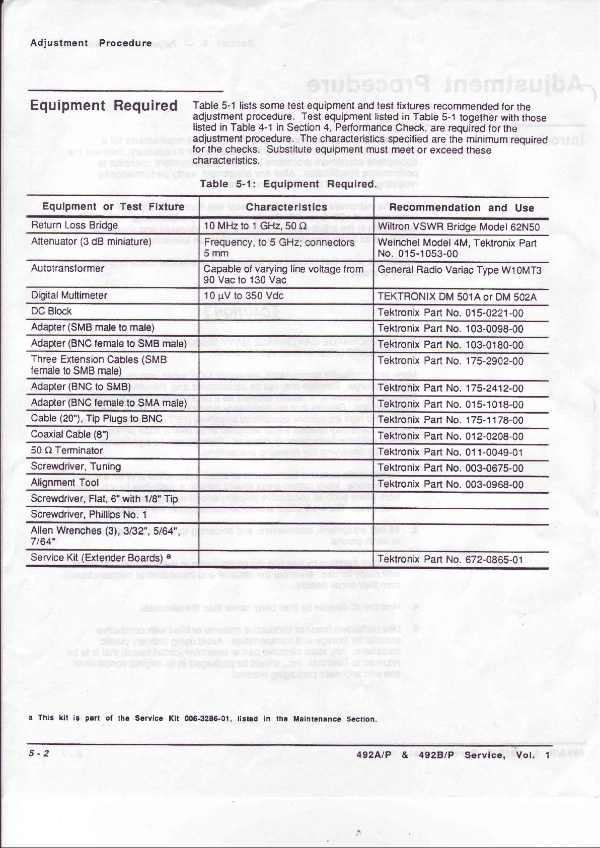
Table
5-1 lists
adjustment
listed in
adiustment
for
the
checks. Substitute
some test equipment and test fixtures
procedure.
Table 4-1 in
procedure.
characteristics.
Test
Section
4, Performance
The
characteristics
equipment
equipment
listed
must
in
Table
Check,
specified
meet
are
are
or exceed
recommended
5-1
together
required
minimum
the
for
for
with
the
these
the
those
required
Equipment
Return
Loss Bridge
Attenuator
(3
dB
or
miniature)
Autotransformer
Digital
DC
Adapter
Adapter
Three
female
Adapter
Adapter
Cable
Coaxial
Multimeter
Block
(SMB
(BNC
Extension
to
SMB male)
(BNC
(BNC
(20"),
Tip
Cable
male
female
Cables
to SMB)
female
Plugs
(8")
50 O Tenninator
Screwdriver,
Alignment
Screwdriver, Flat,
Screwdriver,
Alfen
Wrenches
Tuning
Tool
6"
Phillips
(3),
7164"
Service
(Extender
Kit
Test Flxture
male)
to
to SMB
mate)
(SMB
to SMA
to
male)
BNC
with 1/8" Tip
No.
1
3132",5164"
Boards)
"
Table
10 MHz
Capable
Vac
90
pV
10
to
Equlpment Required.
5-1:
Characterlstlcs
to 1 GHz. 50
varying line voltage
of
130 Vac
to
Vdc
350
C)
from
Flecommendation
Wiltron VSWR
Weinchel
No.
015-1053-00
General Radio
TEKTRONIX
Tektronix
Tektronix
Tektronix
Tektronix
Tektronix
Tektronix
Tektronix
Tektronix
Tektronix Part
Tektronix
Tektronix
Tektronix
Bridge
Model
4M,
Variac
DM
5O1A
Part
No.
Part
No.
Part
No. 103.0180-00
Part
No. 175-2902-00
Part
No.
Part
No.
Part
No.
Part
No.
No.
Part
No.
Part
No.
Part
No.
and
Use
Model
OZN50
Tektronix Part
Type
W10MTo
DM
or
5O2A
015-0221-00
103-0098-00
175-2412-00
015-1018-00
175-1178-00
012-0208-00
011-0049-01
003-0675-00
003-0908-00
672-0865-01
a
This
5-2
kit is
psrt
of
the
Servlce
Klt 006-3286-01, llsted in tha
f,tatntenance Seolon.
492AlP
&
492BlP
Service, Vol. 1
Page 3
P reparatio
n
plepare
To
the
Options
rackmount model for
the
section of this
manual
adjustment,
(Section
8).
Adjustment
refer
to
the
Procedure
Rackrnount
part
of
Remove
1
.
Set the
2.
Loosen
Pull
3.
4. Place
Some circuit boards
gain
to
power
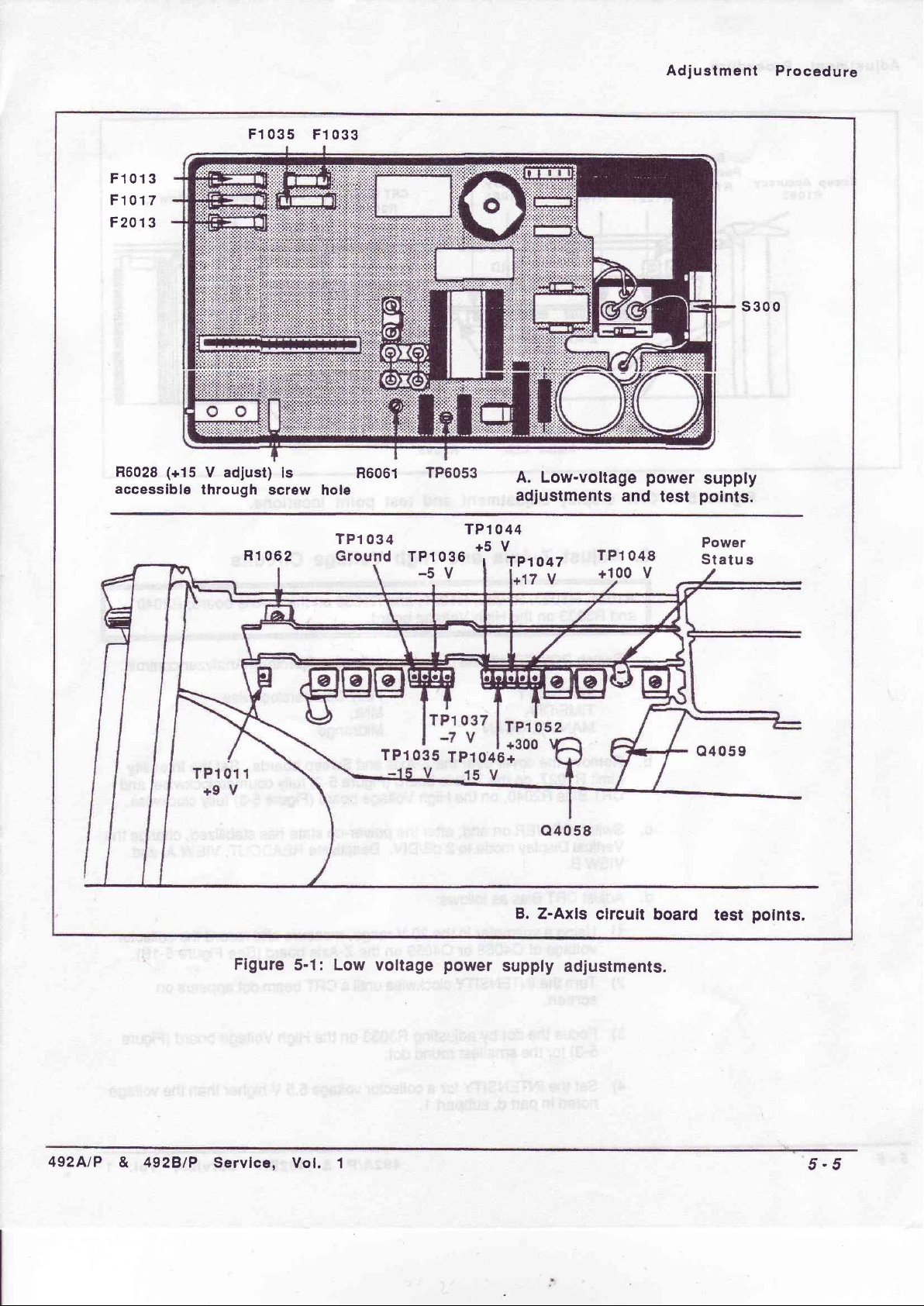
1. Adjust
R6028
This
high-efficiency
kHz. The frequency
66
oscillator components;
procedure.
assembly.
the cabinet
instrument
lour
the
the cover up
instrument
the
access
olf
to some test
before
removing
Low Voltage
and R6061
Parl2
on
screws through
and
or assemblies must
on the
power
adjustment is normally required
therefore, Part
of this step should
follows:
as
face
its
otf.
on the bench
points
the assembly.
front
or
the
or adjustments.
Power
Power
supply
Supply
uses an
1 is
only
panel.
back
reconnect
and
removed
be
Supply
board.
internal
the
required
be
rubber
and
When
oscillator
normal
feet.
power
the
placed
this
only after
adjustment
after repair
cord.
on extenders
is
done, turn
with
a
and
the
frequency
replacing
check
of the
of
Since
the Spectrum
primary
transformer, with
used between
receptacle.
The
ground
suitable transformer.
ground
the
lf
bench,
power
and C6111.
potential
Pan
a.
ground patential
transformer must
through
side
to chassis
input
filter
power
the
Connect
power
the Z-Axis
supply
hazardous
is
disconnected.
A relaxation
exceeds
-
1
Check and
a
input
Analyzer
a turns
power
the
input
the
FL301) .
is
potentials
80
voltage-variable
and set
and
Sweep
WARNING
uses
different
ratio
of
source
have
a three-wire input
and output. Stancor
jumper
A
ground
separated
exisf within
This
is
oscillator
V.
Adiust
the transformerfor 117 Yac. Remove
boards.
high
a
from
1:1
and
should
(emitter
from
due to the
ligltts D55112
Low
transformer
efficiency
cfiassrs or
and a 500
the
Spectrum
also be
of Q2061 and
instrument
the
the supply for
slow
voltages.
in line with
power
ground,
earth
minimum
VA
Analyzer
and output
G1521000
connected
the
and operated
several secands
discharge
(nextto
the
connector
is
between
ground
of capacitars C6101
Spectrum
supply,
rating,
an exampte
C6111)
with
isolation
an
should
power
input
with
the
terminal of
on the
when
Analyzer
the coverover
the
be
a
of
primary
after
the
492AlP
& 492BlP Service,
Vol. 1
5-3
Page 4
Adjustment
Procedure
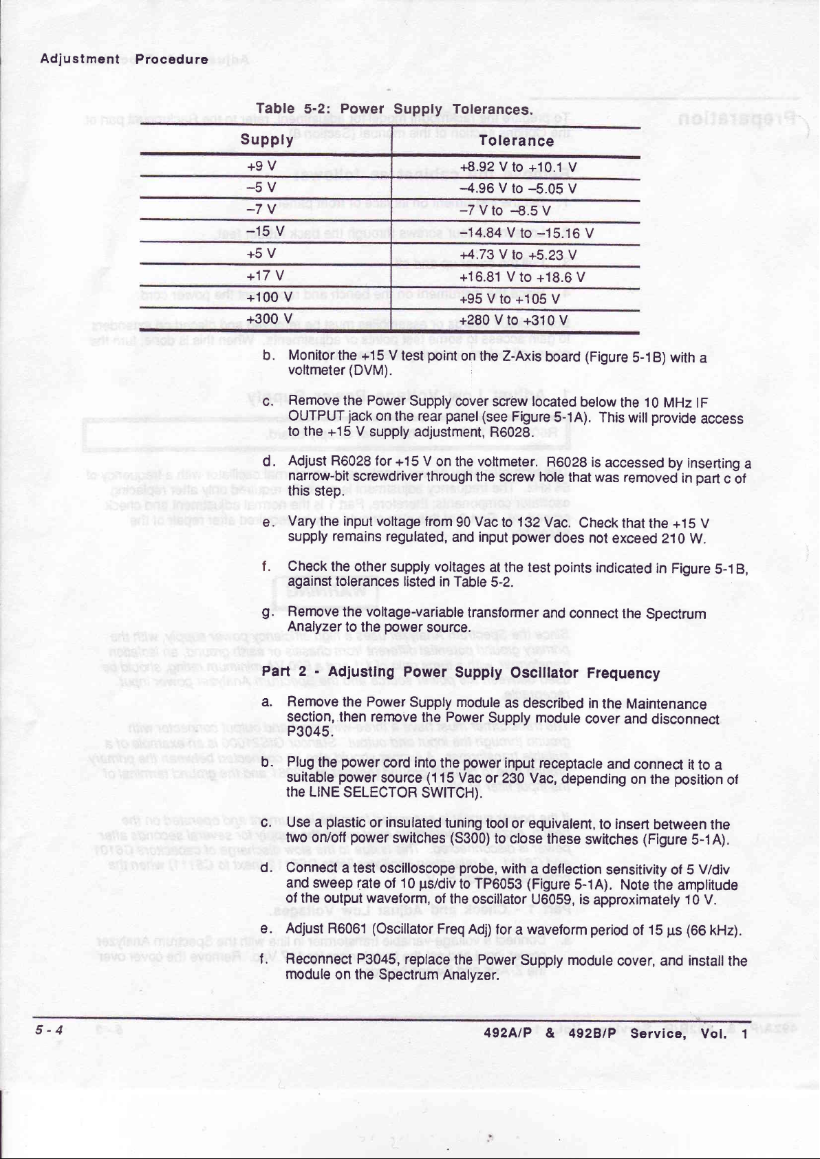
Table
Supply
+9V
-5V
-7V
-15
V
+5V
+17 V
+100
V
+300 V
Monitorthe
b.
voltmeter (DVM).
Remove
c.
OUTPUT
to the
Adjust
d.
narrow-bit
this step.
5-2:
+15
R6028 for
Power
the
jack
Supply
point
v
+15
test
Power
V
screwdriver
Supply
the
rear
on
supply adjustment,
V
+15
on the voltmeter.
through
Tolerances.
Tolerance
+8.92
V
lo
-4.96
V
to
-7
-14.84
+4'.73 V
+16.81
+95
+280
on
-€.5
V
to
V
V
V
to +105 V
V
to +310 V
Z-Axis
the
to
to +5.23
to
;
cover
screw
panel
(see
Figure
R6028.
the
screw
+10.1
V
-5.05
V
V
-1
5. 1 6 V
V
+18.6
board
located
5-1A).
R6028
hole
that
V
(Figure
berow
This
is
accessed
was
with
5-18)
the 1
0
provide
will
MHz lF
by
removed
a
access
inserting
part
in
c bt
a
vary
e.
t.
the input voltage
supply
Check
remains
the other
against tolerances listed
g.
Remove
Analyzer
Part 2
a. Remove
section,
the voltage-variable
to the
-
Adiustlng
Power
the
remove
then
P3045.
Plug
b.
suitable_p_oryel
the
c. Use
two on/off
d.
Connect
power
the
LINE
SELECTOR
plastic
a
power
test
a
gource
or
oscilloscope
and sweep rate
of the
output
wavelorm,
from
regulated,
supply
and input
voltages
in Table
power
source.
Power
Supply
Power
the
into
cord
the
(1
15 Vac
SwlTCFl).
insulated
switches
of 10
tuning
(S300)
ps/divto
of the oscillator
vac
90
to 1
82
power
at the test
5-2.
transformer
Supply
module
and
Osclllator
as described
Supply module
power
input
receptacle
or 230
Vac,
tool or equivalent,
to close
probe,
with
TP6053
a deflection
(Figure
U6059,
vac.
check
does not
points
indicated
connect
Frequency
in
cover
depending
to
these
switches
5-1A).
is
approximately
that
the +'t 5 V
exceed 210
the
Spectrum
in
Figure
w.
the Maintenance
and
disconnect
and
connect
on the
insert
(Figure
sensitivity of 5
Note
it
to
position
between the
5-1A).
V/div
the amptitude
10
V.
5-18,
a
of
5-4
Adjust
e.
Reconnect
t.
module
R6061
(Oscillator
P3045,
replace
on the Spectrum
Freq Adj)
Power
the
Analyzer.
492AlP &
waveform
for
a
Supply module
period
492BlP
ps
15
of
cover, and
Service,
(66
kHz).
install
Vol.
the
1
Page 5
F1013
F1017
F201
3
F1
035
Adjustment Procedure
F1 033
s300
R6028
accessible
(+15
V adJust)
through
R1062
is
screw
hole
TP1
Ground
H6061
03 4
TP1035
TP6053
TP1 044
TP1036
-5V
TP1046+
A. Low-voltage
adjustments
*,u Ur,
1047
17V
Q4058
B.
Z-Axls
and
TP1
048
+100
circuit
power
test
V
board
supply
points.
Power
Statu s
Q4059
test
polnts,
492AlP
& 4928/P
Figure
Servlce,
5-1: Low
Vo
l. 1
voltage
power
supply
adiustments.
5-5
Page 6
Adjustment
Procedure
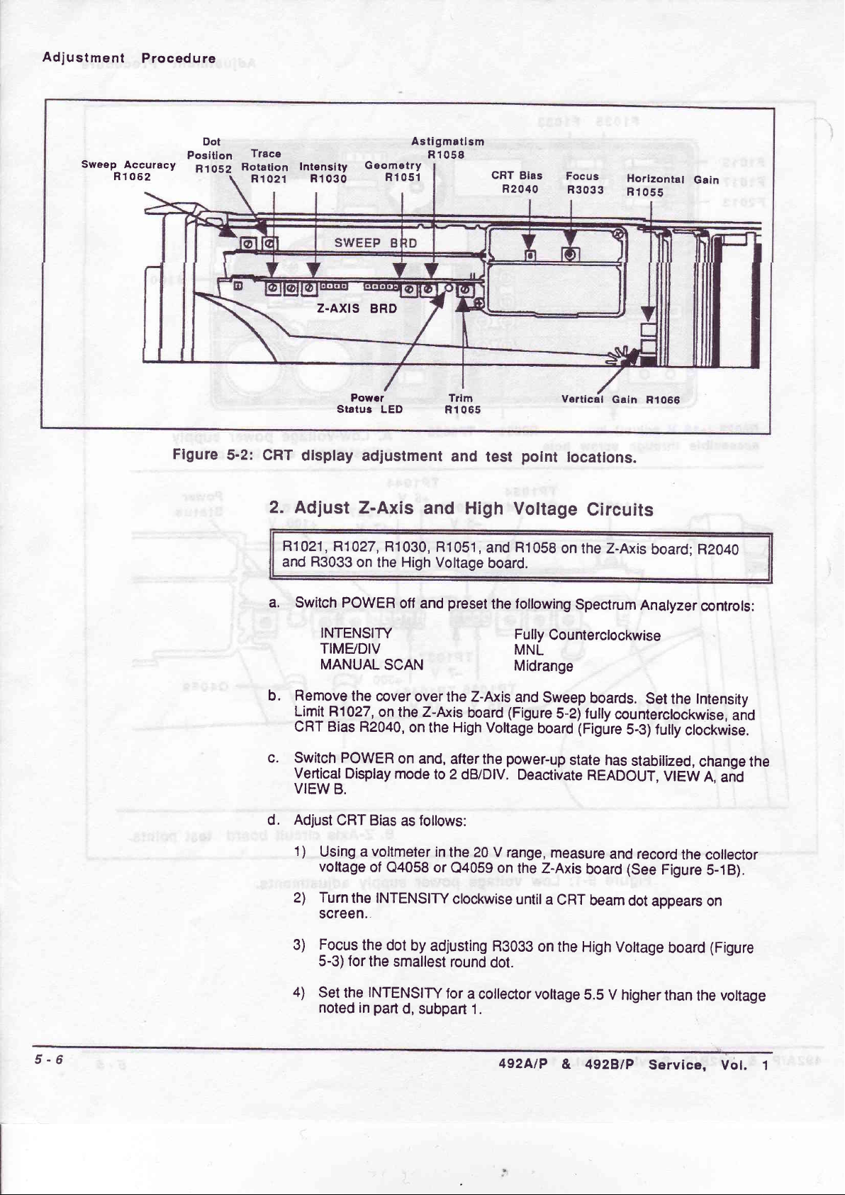
Sweep
R1
Accuracy
062
Dot
Positlon
R1052
Flgure
Trace
Rotation
Rl
5-2:
Intensity
R1
021
Z.AXIS
cRT
dlsplay adjustment
2.
Adjust
R1021
R3033
and
Geometry
030
Power
Status
Z-Axis
R1027,
,
on the
Rl 051
BRD
LED
R1030,
High
Astigmatlsm
R1058
Trim
R106s
and
and
High
R1051
Voltage
CRT
R2040
test
Voltage
and
,
board.
Bias
Focus
Vertical
potnt
R1OsB
on the Z-Axis
R3033
Horlzontal
R1055
Gain
locations.
Circuits
Gain
R1066
board; R2040
a.
Switch
POWER
INTENSITY
TIME/DIV
MANUAL
b. Remove
the
Limit R1027,
Bias
CRT
c.
d.
Switch
Velical
VIEW
Adjust
1)
POWER
Display mode
B.
CRT Bias
Using a
voltage
2l rurn
the INTENSITY
screen.
Focus
3)
for
5-3)
4l
set
the
noted in
off and
SCAN
epver
over
on
R2040,
Z-Axis
the
on the
on
and,
follows:
as
voltmeter
of
Q4058
the dot
by
adjusting
the smallest
INTENSITY
part
d,
subpart 1.
preset
following
the
Fully
MNL
Midrange
the Z-Axis
board
High
after
to 2
dB/DlV.
in
the 20 V range,
or
Q4059 on
clockwise
and Sweep
(Figure
Voltage
po_wer-up
lhe
Deactivate
the Z-Axis
untir
R3033
round
dot.
for
a collector
Spectrum
Analyzer
Counterctockwise
5-2)
board
state
boards.
fully
(Figure
Set the
counterclockwise,
5-B)
has
stabilized,
READour,
measure
a
cRT
on
the High
voltage
5.5
board
beam dot
record
and
(see
Voltage
v
higher
controls:
Intensity
lully
clockwise.
change the
vlEW
A,
the collector
Figure
s-18).
appears on
(Figure
board
than
the
and
ari'd
voltage
5-6
492AlP
& 492BlP
ServicE,
Vol.
1
Page 7

Adlustment Procedure
Flgure
5)
6)
7)
Adjust
e.
Adjustment
5-3:
m odu le.
use
counterclockwise
beam
with
Turn
dot
(Figure
and sharpest
Turn
non-metallic
the
until
just
dot
the
extinguishes
adjustment
the INTENSITY
with
the Focus
for
5-2)
adjustment,
round
a
dot.
the INTENSITY
and again measure
should
less,
repeat
the
CRT
egualor
lhe
cathode
exceed
procedure
and
screwdriver
the
fully
counterclockwise,
clockwise
point
test
to
adjust
CRT beam is
(with
screen
until
a dot is
R3033.
dot; then
refocus
counterclockwise
the
collector voltage
part
set
for
setting
as
in
CRT
follows:
that
current
tocations
cRT Bias,
visible,
then
shaded). lf
will
this
visible:
Adjust
Astigmatism
with R3033
until
the
dot
at
Q4058 or
d, subpan
bias.
Hlgh
on
R2040,
clockwise
no
dot
appears,
be
the
bias setting.
then defocus
Fl105B
for
the
smallest
just
disappears,
Q4059.'Voltage
A.
lf
voltage
the
vottage
until the
the
is-
492AlP
&
492glP
Sarvice,
Vot.
2)
Connect
lug
on the CRT
3)
Switch
2
dB/DlV
4l
Adlglt
TP4028.
at
5)
Switch
board. Turn
1
voltmeter
the
shield.
POWER
and
switch
Intensity
Limit
POWER
POWER
back
Digital
off
and
between
After
on.
Storage
R1027
(Figure
reinstall
on
and
TP4028 (Figure
the instrument
off.
5-2) for a voltage
jumper
the
adjust
INTENSIW
the
5-3)
initializes,
P4036
on the High Vottage
lor normal
and the
activate
reading
ground
V
of 0.9
viewing.
5-7
Page 8

Adjustment
Procedure
f .
Appfy
controls as
the CAL
follows:
OUT
signal
to the
RF INPUT
and set
Spectrum
lhe
Analyzer
'\
FREQUENCY
FREQUENCY
AUTO
REF LEVEL
MIN RF ATTEN O dB
VERTICAL
NARROW VIDEO
VIEW
TIMSDIV
TRIGGERING FREE RUN
g.
Activate ZERO
approximately
5-2) so
Activate VIEW
h.
positioned
adjust
bottom of the screen.
i.
Change the
Vertical
the
just
visible.
j.
Adjust Delta
characters
visible
iust
setting
INPUT.
RESOLN
A/B
the
trace
at the top then bottom of the screen,
Geometry
REF LEVEL
Display mode
is
after the
photograph purposes.
for
1OO MHZ
SPAN/DIV
DISPLAY
FILTER
SPAN and
mid-screen; then adjust
is
aligned
A
and
R1051
Intensity R1030
slightly
trace
adjust
with
VIEW
(Figure
position
to
of 2 dBlDlV.
higher than the trace. Fleadout
has disappeared. This ratio
10
ON
-20
2
ON
Off
AUTO
REFERENCE
graticule
the
B,
then
5-2) for the
(Figure
Disconnect
MHz
dBm
dB/DIV
LEVEL
Trace Rotation
the
lines.
PEAK/AVERAGE
the
use
as
straightest
the trace within
Adjust
5-2)
INTENSITY
the
so
brightness
CAL
until the trace
R1021
reference
a
lrace
at top and
graticule
the
so the
of
characters
provides
OUT
signal
(Figure
cursor,
line
to
area
trace
readout
the
should be
the
best
from
the
is
with
is
RF
-
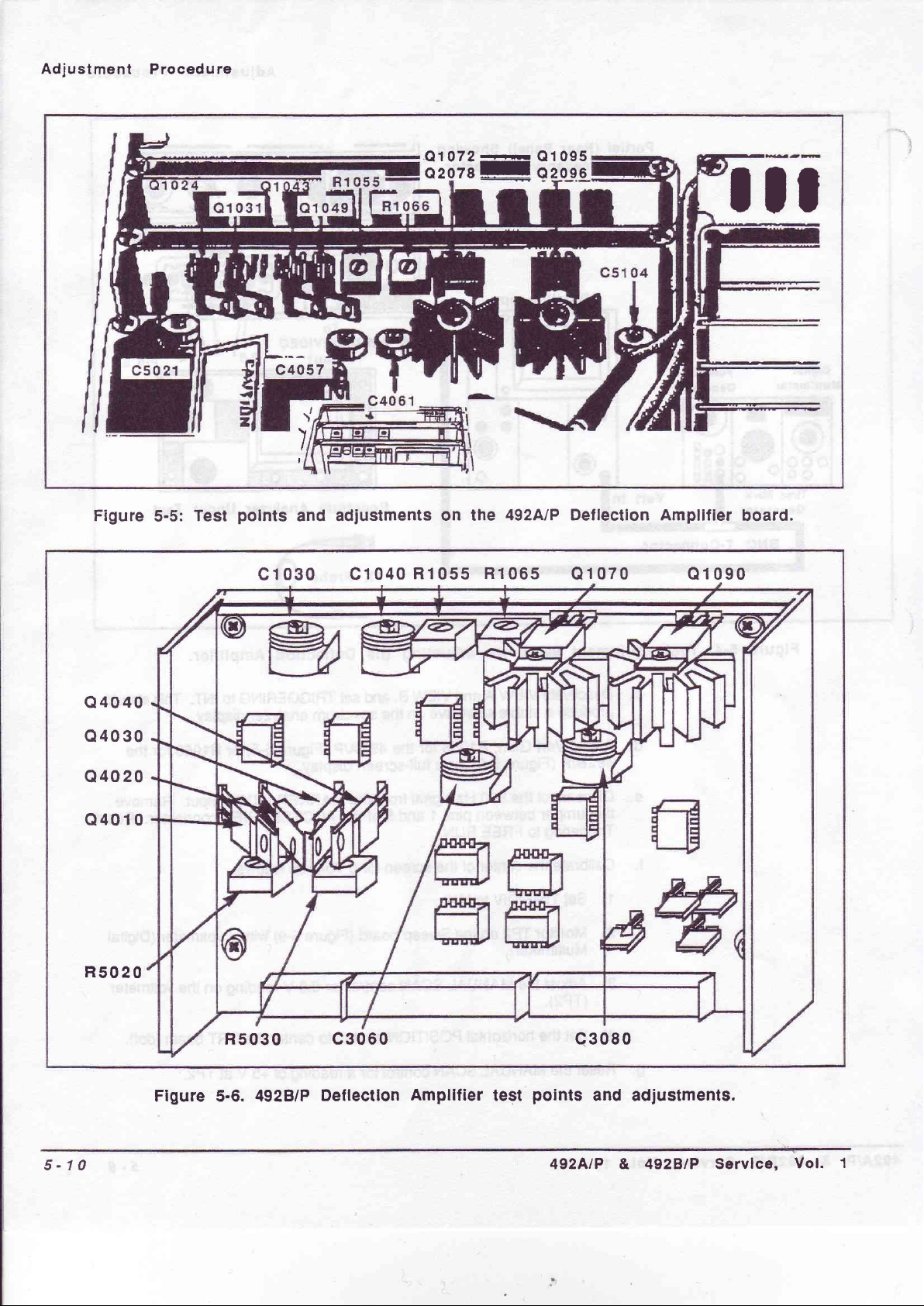
Adjust Deflection
3
Respo
C4057, C4061 , C5021,
lection Amplif
Def
C1040, C1030,
492BlP Deflection
When
must be connected
rather than as
ACCESSORIES
manner.
connect
a.
1 ms. Position the
Set the
b.
amplitude
Select
nse
adjusting
shown
the
Function
of
and Ground
ier
C3080, C3060,
Option
to the
in Figura 5-4.
connector
eguipment as shown
test
generator
0 to
+4
Amplifier
C5104,
board.
Amplifier
R1055,
R1055, R1066, R5020,
board.
NOTE
42 instruments,
PEN LIFT
Be sure to
when
using the
trace on
V. Connect a
respectively)
the
bottom
controls for
Gain
and
the output of the
connector
PEN
in Figure
graticule
a 500 Hz
jumper
the ACCESSORIES connector.
on
and Frequency
R1066
at
ground pin
between
on the 492AlP
Function
rear
the
LIFT
connector
5-4. set the
line.
sinewave
pins
and
of
the
t
of the
1
R5030
instrument,
in this
TlMHDlv to
signal,
and 5
the
on
Generator
with
an
(Ext
Video
5-8
4gzLtP &
gzBtP
Servlce,'Vol.
1
Page 9

justment
Ad
Procedure
c
ooo
oo
Time illark
Ganarator
BNC
Partial
J104
T-Connector
(Rear
Accessory
Panel)
Oscllloscope
Showing
Gonnector
c
MARKER/vIDEo
Input
Spectrum
1 3'\
Analyzer
2 5
i
14
Under
1
Test
I
Jumper
Pln
1 to
Pin
5
Figure
5-4: Test
equipment
Deactivate
c.
produce
d.
fliu9t
492BlP
Disconnect
e.
t.
g.
jurnper
the
Triggering
calibrate
1)
Set
2) Monitor
Multimeter).
3)
{Ojugt
(rP2).
4l
Set the
Reset
the
setup
vert
(Figure
TIMHDIV
for
VIEW
a
stable
Gain,
the 500
between
FREE
to
the cenler
TP2
MANUAL
the
horizontal
MANUAL
adjusting
A
and VIEW
sinewave
R1060
5-6) for
Io MNL.
on
for
a
Hz
signalfrom
pins
1
RUN.
of the
the Sweep
SCAN
POSITION
scAN
the
Deflectlon
B,
and sel TRIGGERING
on
the
spectrum
492Np (Figure
the
full-screen
the MARKER/VIDEO
and
5 of the ACCESSORIES
screen for
control for
0 Vorts
(Figure
board
control
controlto
a
analyzer
display.
as
5-9) with
for
0.0
center the
reading
follows:
V
of +5
Amplifier.
lNT. This
to
display.
5-5) or R1066
input.
c6nnector. Reset
voltmeter
a
reading
on the
CRT beam
v
Tp2.
at
should
for
the
Remove
(Digital
voltmeter
(dot).
492AlP
& 4928/P
Servlce,
Vol.
1
5-9
Page 10
justment
Ad
Procedu
re
c4057
,
Y
)
I
ltiii'-3133:
ill
Figure
Q4040
Q40 30
Q4020
Q4010
5-5:
Test
polnts
c1030
adjustments
and
c1040
on t'he
R1055 R1065
492AlP
Deflection
Q1070
Ampllfier
Q1090
board.
R5020
5-10
Figure
R5030 c3060
5.6.
4928/P
Deflecilon
Ampllfier
test
Q3080
points
492AlP &
and adiustments.
492BlP
Servlce,
Vol.
1
Page 11

Adjustment
Procedure
h.
fliu_st_Holz
492BlP
(10th
i.
Set
the
graticule
j
Disconnect
Press
k.
t.
Adjust
C3080
shape
Adjust
c1040 for
character
n.
Check
readout,
and readjust
Only
complete
R1055 for
Gain,
(Figure
graticule
MANUAL
line
<Blue-SHIFT>
c5021
for
(no
c4061
5-6), to
line).
SCAN
and check that
voltmeter
the
RESET
and c4057 tor
4928/P
the
overshoot
or
and C5104
the 492BlP
shape.
the appearance
and
the
letter
as needed
part
when
o
rhe 4g2vp
position
the
control to
voltage
the
and set
(Figure
TIME/D|V
restore
to
492AiP (Figure
the
5-6)
roll-off).
for
the 492AlP
(Figure
of lhe
"X"
for
letter
in
MAX
best
5-o)
vertical
NOTE
adjusting the
(Figure
CRT
beam
position
at Tp2
the
for
the
(Figure
for
the best
"7"
in
GHZ
Frequency
of the
and
4928/P
5-5)
on the right
the
CRT
is now
AUTO.
to
power-up
R1055
or
(dot)
beam
-s.0
settings.
graticute
v
5-5) or c3060
best
vertical
horizontal
readout
5-5)
or C1080
readout
of the FREQUENCY
SPAN/DIV
horizontal
Deflection
readout
Amptifier.
for
the
on
the left
t0,z
v.
and
character
and
readout,
shape,
edge
o. Adjust
R5020, R/O
the readout
1)
For
standard instruments,
below
above
2)
For
Option 43
slightly
slightly
4.
Adjust
R1040,
R1033,
a.
R1050,
R1034,
ltanthe
PULSE
STRETCHER,
the instructions
1)
Adjust
Digital
vefiical
the
2l Adjust
Digital
the horizontal
Gain,
and
characters.
the top
the
graticule
baseline.
line,
(reduced graticule),
above
the top
below the
Digital
R1055,
R1045
Digital
Storage Calibration routine
that are
Output
Storage
Output
Storale
Offset
board
graticule
Offset
board
graticule
graticule
baseline.
Storage
R1060
and
and R1046
and
select
displayed on
R1040
place
to
lines.
R1045
place
to
lines.
R5030, R/O
place
and
Offset, for
the
top two rows
place
the
set
the top two rows
line,and
Calibration
on
on the Vertical
itern
and Output
the risers
and
the
2
the
Output
the
steps of
(DIGITAL
Horizontar
by
CRT.
bottom
place
the
storage
pressing
STORAGE
R1050
Gain
of the
adjustment
R1033
Gain
the
adjustment
the best
placement
of readout
readouts
bottom
storage
slightly
readout
of
readouts
board.
6oard.
<Blue-SHIFT>
CAL).
on the
pattern
the
on
pattern
of
slightly
Fonow
Horizontal
on
Vertical
on
492AlP
&
492BlP
Servlce,
Vol.
1
5-11
Page 12
Adjustment
Procedure
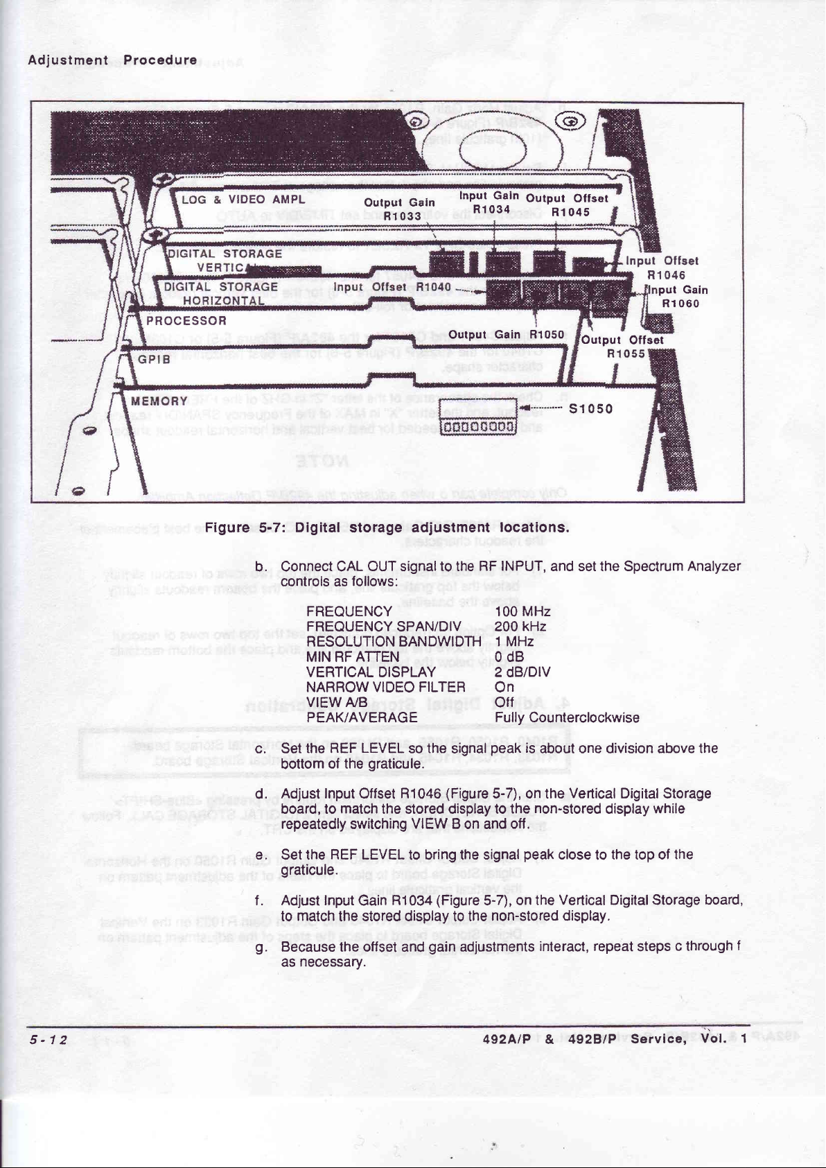
G)
VIDEO AMPL
PROCESSOR
Figure
Digital
5-7:
storage adjustment
b. Connect CAL
controls as
follows:
Oulpul Galn
B1 033
OUT
signalto
Input
Galn
Rl034
Output Gain
locations.
RF INPUT,
the
gugpgl
R1050
Offset
R1 04S
Output
.-'
s1050
Input Offset
Offset
R1055
and setthe Spectrum
R1046
put
Rl 060
Gain
Analyzer
FREQUENCY 100 MHz
FREQUENCY
RESOLUTION
MIN
ATTEN
RF
VERTICAL DISPLAY
NARROW VIDEO
VIEW A/B
PEAK/AVERAGE
c, Set
d.
e. Set the
the REF
the
bottom
Adjust
board, to
repeatedly
of
Input Offset R1046
match
switching
REF LEVEL
graticule.
f . Adjust Input
match
to
g.
Because the offset
as
the
necessary.
SPAN/DIV
BANDWIDTH
FILTER
LEVEL
so the
signal
graticule.
(Figure
the stored display to
VIEW
B on and
to bring the signal
and
(Figure
to
gain
H1034
Gain
stored display
kHz
2A0
1 MHz
O dB
2
dB/DIV
On
Off
Fully
Counterclockwise
peak
is
about
5-7), on the
non-stored
the
off .
peak
on the
5-7),
non-stored display.
the
adjustments
interact, repeat
one division above the
Vertical
close
Digital
display
the top of
to
Storage
while
the
Vertical Digital Storage board,
steps
c through
f
5-12
4g2AlP
&
4gz}lP
Service,
Vol. 1
Page 13

h.
Select
these
settings:
Adjustment
Procedure
FREOUENCY
FREQUENCY
RESOLUTION
REF
LEVEL
MIN
RF ATTEN
VERTICAL
NARROW
VIEW
A/B
PEAK/AVERAGE
Adjust
match
signal
k.
f{ust
5-7),
stored
5. Adjust
R1062
When
must
rather
ACCESSORIES
Input
oflset,
the horizontal
at center
Input
Gain, R1060
match
to
signal
Sweep
on the Sweep
adjusting
be connected
than as
Option 42 instruments,
shown in
connector when
manner.
SPAN/DIV
BANDWIDTH
DISPLAY
VIDEO FILTER
R1055
on the
position
screen.
on
horizontal
the
near
the
right
edge of
Timing
board.
to
PEN
the
Figure
LIFT
5-4. Be
600 MHz
100
MHz
Auto
-20
dBm
O dB
1O
dB/DIV
Off
Off
Fully
Countercfockwise
Horizontal
of
the
stored
Horizontal
the
position
ol lhe
the screen.
NOTE
the
output of
connector
sure to
using the PEN
Digitar
signal
to that
Digital
stored
the
rear
at the
ground
L\FT
Storage board,
of the non,stored
Storage
signal
pin
connectar
board
to
that of
Functian
instrument,
of
the
I
of the
in
Generator
this
to
(Figure
non-
thb
a.
Connect
the test
Spectrum Analyzer
FREQ
TIMSDIV
TRIGGERING
b.
Connect
jumper
a
respectively)
c. set
e_ditpt_Sryeep
d.
492BlPr,
the
Time
for
align markers
e.
Check
the
accuracy
center eight
f .
Reset
AUTO
mark
pins
moved in
TlMgDlV
the
RESOLN.
generator
1
and 5 of the ACCESSORIES
part
equipment
controls :
SPAN/DIV
between
on
Mark
1 marker
with
ACCESSORIES
the
Generator
Timing,
R1062
per
graticule
of
the
divisions must
AUTO
to
Return Triggering
from
the Spestrum
d.
as shown in
10 MHz
10
EXT
pins
1
and 5
controls for 10
(see
Figure
division.
lines.)
remaining
not
(Use
exceed x5
FREQ
and
to
Analyzer.
conneclor.
Figure
less
or
ms
(Ext
Video
connector.
ms
for 492NP
5-9
Horizontal
TlMgDlV
%.
SPAN/D|V
FREE
RUN.
Remove
5-8.
Set
the
Select
and Ground
time marks.
and
Position
selections.
Error
to MAX,
Disconnect
jumper
the
Reposition
the trace
following
Figure
5-5
adjustment to
over
the
and activate
the time-
between
if
for
492AlP
& 492glP
Service,
Vo
l.
1
5-13
Page 14
Adjustment
Procedure
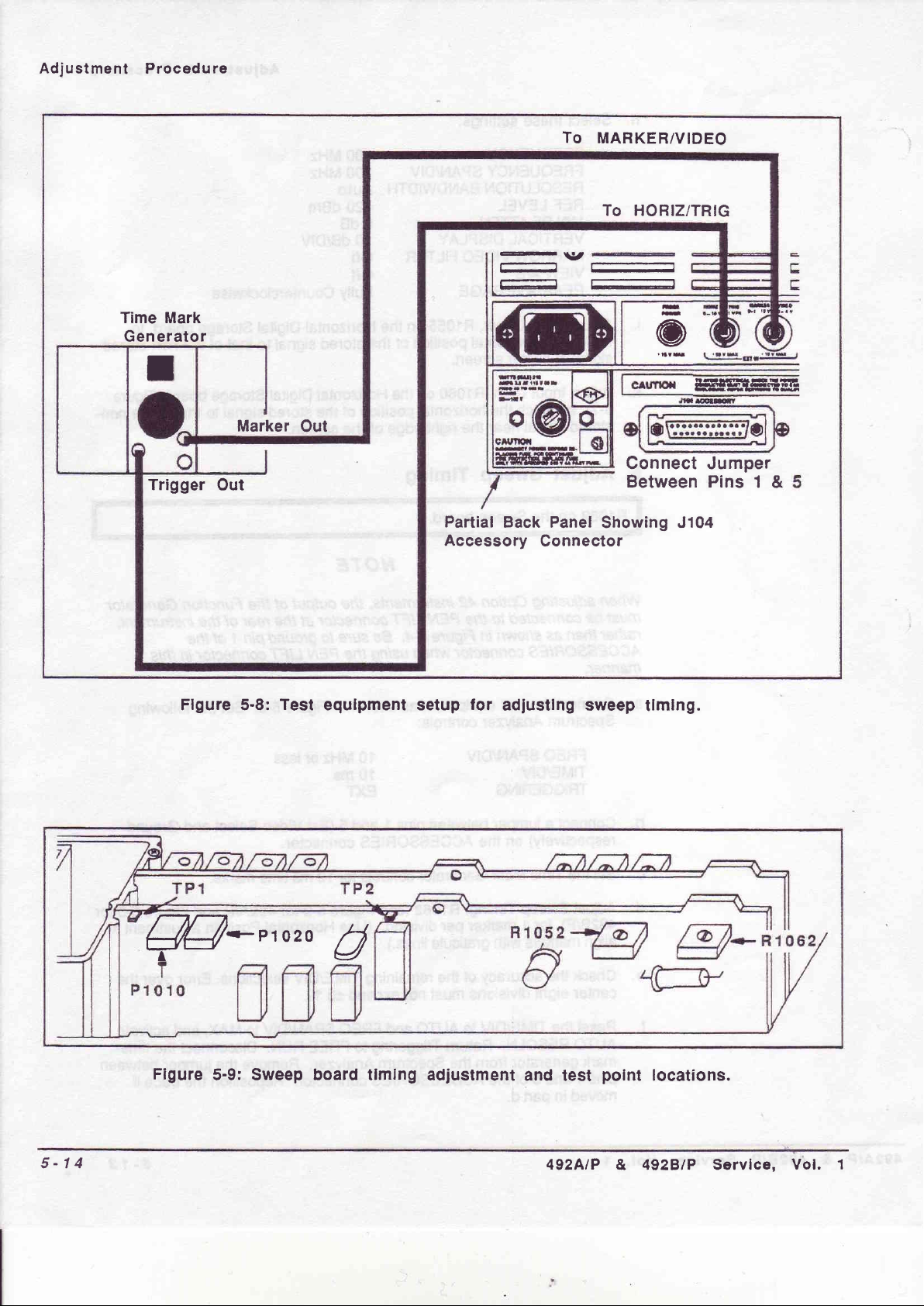
To
MARKER/VIDEO
Time Mark
Generator
I
Trigger
Marker
Out
Out
-\l/
: ::
Partial
Accessory
Back Panel
To HORIZ/TRf
Showing J104
Connector
g
Connect
Between
G
rtttlG?rt
cltrtlrrtilFrEt-
-n-EtILg
u
J
Pins
t3
mper
1
rarlt
&
Flgure 5-8:
Test
W*P1o2o
Figure
5-9: Sweep
equlpment setup
U
board tlming
adjustment
for
adlustlng sweep
and
test
polnt
tlmlng.
locations.
5-14
492AlP
&
492BlP
$ervice,
Vol,
1
Page 15

Adjustment Procedure
R3040:
Figure
rP1o3s
{l
e
R4040-
H1031 R1 034
5-10: Frequency
6,
R1063,
R1031, R1032,
R1028, R1
board.
C1013
R1062
Sweep
R1028
R1 032
control system
Adjust
R1065,
032, R3040,
C201 1 on the
on
the Sweep board.
Offset
R1 063
Frequency
R1067,
and
1st LO
Swee
2nd LO
test
Tune
R1065
Sweep
point
Control
R1071
and
R1034
on
F14040
and
Controlled
1st
Sweep
R1067
LO FM
H1071
T F;E,BOArd
Coll
IT
032
Rl
and
on
the 1st LO Driver
on the
oscillator
JJ\
TP1 0s8
I
lfl-'
adjustment
System
the Span
board.
Center
board.
Cotl
I
Sp"n Attenuator
lc"n,",,
Control
I
1st
LO Driver
Board
I
I
I
r-i
locatlons.
Attenuator
Frequency
board.
Frequency
Board
Controf
The
Spectrum Analyzer
frequency
not
error message. lf
routine.
Test
and
a. Select
h.
c.
d. Remove
control
be adjusted
equipment required
Frequency
FREQUENCY
FREQUENCY
TRIGGERING
Connect a shorting
chassis
Adjust
STRETCHER
(OVERALL
directed
BOARD
properly,
Counter.
following
the
ground
Sweep
the
SYSTEM) from
("coNNEcT
AND
procedure
has
a
system.
this
(Figure.S-tO).
Offset
shorting
and select
GROUND"),
However,
which
may cause
occurs,
SPAN/DIV 5 MHz
bypass the
forthis
Spectrum Analyzer
strap
step arc a
from TP1035,
R1063
straplrom
item 1
the
A
DVM
etc.
in firmware
possible
it is
the microcomputer
step
and
Voltmeter,
settings:
MHz
O.O
FREE
RUN
on the
Monitor
(Figure
(FREOUENCY
menus. Perform
TO
TP1073 with
for
5-10)
TP1035.
Tp1
Press
058 ON THE 1ST
for
calibrating the
that some
return
Time Mark
Span
0.00
<Blue-SHIFT>
LOOPS
the
adjustments
to display
to the
calibration
Attenuator
the
Digital
V.
CAL), then
calibration steps as
LO DBTVER
may
an
Generator,
board, to
Vottmeter.
PULSE
item
0
4gzAlP
&
gzBlP
Service,
Vol,
1
5-15
Page 16
justment
Ad
Procedu
re
e.
1) tf
Adjust
1)
2)
3)
4\
5)
6)
"cALlBRATtoN
a
displayed, bypass
to
the adjustment and try
problem persists,
System, in
the SPANIDIV accuracy as
Apply
the cAL
MHZ, FREQ
600
display the
fdiust
5-10)
graticule.
rnarkers.
Remove
Mark
Set
FREQUENCY to
Adjustthe
markerldivision
Set the
Time
Tune
for
one
Reset
the
Generator to
FREQ
the
1st
FREQ
Mark
Generator.
srEP cANNoT
the
refer
Maintenance
the
OUT signal ro rhe RF INPUT,
SPAN/DIV
markers.
Swp R1065,
Coil
marker
CAL
LO
per
the
CENTER FREQUENCY
OUT signal
the
SPAN/DIV
about
FM
over
the
SPAN/DIV
perform
step,
tg bring
Troubleshooting
to
section.
tO
division over
and
RF
INPUT.
to 5
10
MHz.
Coil Swp
center eight divisions
to 20
BE
the other
the
follows:
1OO
MHZ,
on the
apply 0.2
MHz,
REF LEVEL
R1071
kHz
and
OOMPLETED"
adjustments
adjustment
ANd
Span
the
center
(Figure
apply 50
in
range.
Frequency
the
set
the
SEt thE
Attenuator
eight divisions
necessary
as
ps
time mafts
to +10
5-10)
of
the display.
ps
message
Control
FREQUENCy
REF
LEVEL
board
to
from
dBm, and
for
1
markers from
is
then return
lf
the
to
tO
(Figure
ot tne
align
the
Time
the
the
7)
Adjust
center
f . Adjust
1)
Disconnect
2l Press <Blue-SHIFT>
Adiust
3)
the
Adjust
7.
R4020,
board.
R1012,
board.
only
Use
003-0675-00,
the 2nd LO
eight
divisions.
Dot Marker
Dot Position R1062
marker
dot
position
the CAL OUT
over
Log Amplifier
R4052,
R1025,
an
R4471,
R1030,
insulated
to
screwdriver
make
Sweep, R1067, for
follows:
as
signal
RESET.
on the
the start spur.
R4081,
R1037,
and
and
NOTE
or tuning
these
adjustments.
from
the
Sweep
R1085
R1060
tool,
markerldivision
one
RF INPUT.
(Figure
board
on the
on the
49?NP
492BlP
such as
Tektronix
over
5-9) to
Amplifier
Log
Arnplifier
Log
Part Number
the
position
5-16
Preliminary
a.
setup:
4gZAlP
& AgzBtP
Service, Vol. 1
Page 17

Adjustment Procedure
1)
lpttle
SHIFT>
selecting
(sET
2)
Remove
(Figure
3)
Switch POWER
4)
Remove
instrument;
5) Replace
connect
b.
removed in
5-13.)
c.
Set the
FREQUENCY
FREQUENCY
AUTO
REF
MIN RF
VERTICAL
VIEW A/B
TIMSDIV
r_qg-
4ryp,1,lgr_qollegtion
PULSE
item
STRETCHER
(INTERNAL
5
RESULTS TO
Leveler Disable
5-11).
off.
the Log Amplifier
then
the
assembly
the test
equipment
order to access
Spectrum
Analyzer
SPAN/DIV ZMHz
RESOLN
LEVEL
ATTEN
DISPLAY
"UNCALED").
plug
and
remove
in
the
the
as shown
J621 on
controls
factors
(DIAGNOSTIC
MEASUREMENT
P3035
Detector
shield so
instrument
in
zero
ro
by
FUNCTIONSJ
RESULTS),
on the Video Processor
board
assembry from
adjustments
and switch
Figure
5-12.
the Log Amplilier
lollows:
as
2MHz
On
-60
dBm
0dB
10
dB/Dtv
off
10
ms
pressing
<Btueand
then
item
board
the
are accessible.
POWER
(P621
board,
back
must
See
be
Figure
2
on.
d.
Center
signal
attenuators
Position
e.
control;
the two
generator
the display
then switch
for
front
50
steps.
f.
Adiust
g.
set
the REF LEVEL
attenuation.
h.
Increase
ro 70
4oiqst
5-13)
of change
the f ront
dB.
the Log
so each
panel
Reset
attenuation
the
Gain,
10
on
the
Reset vgrlic_alnosition
vertical
Return
k.
4djgsl
5-13) for
settings
10
POSITION
the step
Input
minimum
while
dB/DlV
and 2
attenuator
Ref
alternately
panel
LOG
controls for
and Alri'PL
a 10 MHz/+6
dB of attenuation.
graticule
at a
REF
the
LOG
-20
to
vertical
through
R4020
increment
dB
reference
LEVEL from
CAL so each
dBm and
position
to a
the
tar 492AlP
of attenuation results
display.
by temporarily removing
control to
align
the
to 0 dB.
Lvl,
n4a71 for 492AtP
amplitude change
switching
the
dB/DlV.
CAL
adjustments.
dBm output.
line with
-60
dBm to
10
dB
step
the
step attenuators
graticule
step
attenuators
line
or R102s
the
baseline to
the bottom
or R1097
betweenthe
10
vERTICAL
Set
the
vertical
the
-110
dBm in
equals
one
for
if
necessary.
in
10
dB increments
tor
49zB/p
in
one major
signal
and
graticule
for 4928/p
dB/DtV
DlSpLAy
anO a OA/OIV
between
Set the
step
PO$|T|ON
decade
division.
0 dB
(Figure
division
setting the
line.
(Figure
492AlP
& 492glP
Servlce,
Vot.
1
5-17
Page 18

Adjustment
Procedure
Figure
10
MHz
Leveled
Generator,
0 to
5-11 : P3035
Slgnal
-10
dBrn
@"@"@,@"@
0n
the video
BNC
processor
to smb
board.
Adapter
Spectrum Analyzer
To
J621
Vldeo
on Log
Ampl
Board
Under Test
&
5-18
Flgure
10
5'12:
dB
Test
Step
Attenuator
equlpment
setup for
dB
Step Attenuator
adjusting
492AlP
the Log
& 492BlP
Amplifler.
Servlce.
Vol.
1
Page 19
l.
Fine-tune
1) Activate
the
2
Gain
iog
dBlDlV
as
and
follows:
10
add
of
dB
attenualion.
Adjustment
Procedure
lf
Zt
the
R4020
remove the
gZAlP
10
the
Repeat this
3)
division.
Activate
4)
m. Activate
Amplifier;
signal to
Adjust output
n.
lor a full-screen
5-13)
o.
Switch
to
attenuation.
R1060
p.
lf a large change
parts
q.
Check
for 4928/P
m
through
the
step
10
dB
492AlP
for
10 dB
R1 A37
or
dB/DlV
check
10
dB/DlV
2
dB/DlV
the baseline
align
Log
the
Rel
10 dB/DlV
the
Adjust
accuracy
(five
divisions)
R1025
or
of external
492BlP
br
2 dB/DlV settings.
and
until the
repeat
and
momentarily
and
to
AmPlifier.
R4081
Lvl,
(eight
divisions)
mode
Log Linearity,
(Figure
in
the adjustment
because
o
of
5-13)
10
dB/DlV
of
is
short, adjust
for
4928/P in
the same
attenuation and adiust
for
equal
display
10
dB step
part
remove the
bottom
the
492AlP or
for
five
is
ito
check
graticule
divisions
10
input
R1030
display.
and set
the step attenuators
492AlP
R1085
so the
setting
for
display
was
required
is mid-screen.
interaction.
2 dB/DlV display
and
gain
the
slightly
direction;
R4071
amplitude
t1
logging.
dB
to
signal
line;
then
for
4928/P
Log
or
part
in
modes as
for
when
minor
the Log
return the
(Figure
for 40
dB of
Fidelity
repeat
o,
follows:
with
then
in
Add
1)
the
Z) Check that
divisions
+0.5
output
Reset
A)
full-screen
for
Add
4,t
'
measure
to
exceed
range.
lf
the
5).
with R4020
Ref
r.
s.
Set
Set
the
the
full-screen
attenuation
2
dB/DlV
rnode.
each
(10
dB
minor
division
to establish
the step
attenuator
disPlaY.
of step
80 dB
the
worst
*1.5 dB
10 dB
step
for
R4071
Lvl,
attenuators
step
Ref
Levelto
display
in the
10
in
10
steps),
steps
dB
dB/DlV
and
(1
steps).
dB
new
a
reference
attenuation
case
2
the
492A
10
to
dBm
2
dB/DlV
first 80
dB/Dlv
or
over the
in
492AlP
for
-15
10
lor
display
each
step is
2 dB/DlV
You may
level
and adjust the
0 dB
to
for 10
dB/DlV,
over the dynamic
error
of
dB
mode
R1037
activate
and
for
the signal
R1025
lP or
dB
and adjust
mode.
1
dB/DlV
mode
1 majordivision,
display step
the signal
adjust
after each
generator
16
and
and
step.
dB
steps
dB
t0.25 minor
is
0.5
generator
output
tor 2
dB/DlV,
range. Error
range,or
+1.0
dB over the
is out of tolerance, adiust
4928/P
4928/P.
for
2
dB/DlV.
readjust the
and
generator
output
for
division,
level
not
must
16 dB
gain
Input
for a
492AlP
&
492BlP
Serviee,
Vol.
1
".5-19
Page 20

Adjustmenl
Procedu
re
Log Galn
R4020
I-t
l-r
A. 492AlP
Un. Bel.
F4052 Level R4071
Log & Video
lnput Ref.
Amptifier
Board.
Log
Unearity
R1085
P1105
(J620)
P2105
(J621)
Output
Level
Ref.
R4081
Lln.
81012
T
T
Bal.
Log
Gain
R1025
B.492BlP
Output
Ref.
Level Rl030
Log
& Video
Input
Ret
Level
R1037
Amplifler
Board.
Log Fidelity
R1
060
5-20
Figure
5-13: Log
and Video
Amplifler
test
point
and adjustment
492AtP
&
492BlP
locailons.
Service,
'Vol.
1
Page 21

Adiustment Procedure
From
3rd
Converter
(A)
10
MHz
@-25
(B)
Figure
dBm
5-14:
Test
equlpment setup
t.
U.
V.
J683
Press
LIN and
492BlP
and
Check
and
+4.4
(Figure
10
dB/DlV display
LIN display linearity
note
divisions.
Remove
jack
and
order to
install
VR 2nd
Filter
for
adjustlng
adjust
Lin
for a full-screen
5-13)
should now be
the display
the signal
step
generator
replace P621,
lhe circuit
Select
Varlable
the
Mode
Balance,
display.
the same.
by adding
down
6 dB,
from full
screen
signal connection to the
and
repeat
part
a
board.
Resolutlon module.
R4052
12
tlg2AlP
for
Amplitude
dB, and
to,
18
410.4,
or
of LlN, 2
dB of attenuation
+0.4,
6
Log Amplifier
subparts 2 through 5
R1012tor
dBlDlV,
andT
input
reverse
in
Adjust
8.
492AlP
R3015, R3029,
C1026, C1033, C2037,
VR 1st
492BlP
R3029, R3033,
Resolution
adjustments
R3033,
Filter
Select.
adiustments
R4025
and
-
C1022,
and
C3023, C3035, C3050,
-
C5055,
on the
C1034, C1044, C1046, C2030,
1st
VR
The
wider
Before
correction
selecting
The 1A0 kHz
applied through
filter
to compensate
each
Filter
Select.
3 dB down bandwidth of each
the 6 dB down
than
calibrating the
factors
item
5; then item 2.
filters
both
shape and
bandwidth.
for
filter in
small
to
in
another
increments.
point
Variable Resolution Bandwidth
zero
each
the
pressing
by
section are
first
and
Because of
filter
Bandwidth and
C2026,
R4025
on the
C5048,
VR 2nd
C3030,
filter
of the combined two
<Blue-SHIFT>
C5055, C5048,
VR
Znd
R2025,
C3041 , R1065,
Filter
Select board.
C3039,
section
C3045,
should
NOTE
second
is
that
aligned
out
separately;
sections.
interaction, it
of
adjustment;
Shape
Factor
C3041,
Filter
Select board
R3035
and
R3015,
R1027
and
wide
be as
filter
sections.
or slightly
and Gain, set the
PULSE
The final
is
STRETCHER
a signal
then
adjustments
to
easy
offset
therefore, only adiust
R1065,
on the
the
on
and
is
trim
filter
one
492AtP
492BlP Service,
&
Vol.
1
5-2I
Page 22

Adjustment
Procedu re
a.
Equipment
1)
setup
Remove
the
is
shown
Variable
Resolution
in Figure
5-144.
module
and
install
it
on
an
extender.
2) Remove
section of the rnodule).
3)
Using smb
(output
4)
Using SMB male-to-male
(10
of
MHz
to second
5) Apply
the
Analyzer
FREQUENCY
FREQUENCY
RESOLUTION
REF LEVEL
MIN
RF ATTEN
VERTICAL
b. Reset
c.
d. Disconnect
the REF
Adjust
(Figure
down,
Third
LEVEL
C5055,
5-15) for
that is
Converter
as
the 10 MHz
needed
the cable
plug
male-to-male
module)
the
output
controls
from
section
cAL
our
the Third
module).
of
signat to
follows:
as
SPAN/DIV
BANDWIDTH
DISPLAY
LEVEL for
C5048, and
the
centered
100
best
around mid-screen).
Third
output
to J693
to maintain
connected
adapters
to
J621, the
adapters
to
and
and
Converter, with red
RF |NPUT,
the
100
MHz
kHz
50
100 kHz
-20
dBm
O dB
2
dB/DIV
a
seven division
C3041
on the
kHz
filter response
Converter
(Figure
5-148).
a 7-division
(input
J683
coaxial
input
cables,
to the
coaxial
and
(100
kHz
(300
kHz
excursion.
VR
2nd Filter
(100
Refer
to
signal from
Set the
display.
to the
connect
Log Amptif
cables,
connecl
band)
set
the spectrum
tor
Oprion
for
Oprion
Select
kHz
bandwidth,
Figure
J683
S-16.
and connect
REFERENCE
second
JOB2
ier.
P6gg
to
J683
07)
07)
board
(input
dB
O
the
Adjust
e.
C3030
screen
f
Sfeps
proceed
t.
through i
to
Change
BANDWIDTH
amplitude
g.
{djust
h.
Change
the
(FL36)
is
centered
BANDWIDTFI
amplitude
i.
Adjust
5-18)
C1034,
for
mid-screen).
c3023,
for
(Figure
part
the
c3035,
4928lP)
5-17).
anly
apply to
j.
FREQ
SPAN/DIV
tor
to 3 MHz. Reset
lo about 7
four
tuning
for
the
best
3
about mid-screen.
FREQ
the
SPAN/DIV
to 1 MHz.
to
about 7
C1044,
the
best
1 MHz
c3050
the
on
best
NOTE
4928/P.
the
to 1 MHz
the
divisions.
screws
MHz
divisions.
(capacitors)
filler
response
to
Reset
the
and C1046
filter response
4gzAtp
the
100
kHz response
your
lf
and
REF
LEVEL
on the
(3
MHz
200 kHz
on the
REF
and
LEVEL
VB 1st
(1
MHz 6 dB
(C3045,
instrument
RESOLUTTON
the
to bring
110
1600 kHz,
C3039,
centered
around
is a 4g2Np,
the signal
MHz
Bandpass Filter
6 dB
the RESOLUTTON
to
the
bring
Filter Select
down,
signal
board
centered
and
mid-
down) that
(Figure
about
5-22
4gZAtP & 4gZBtP Servlce, Vol.
1
Page 23

Y
r
J683
R3o2e
O
R4025
R106s
s6'Jj",
S
Adjustment Procedure
JoB2----->
Figure
5-15:
Adjustments
iSFENEilCE
IARKEi LEI'EL
-1gDBM
tw
s
?3,,,t I tl lt rl ,l ,,rr a a
aa t r
I I tt tr tt
zDBI
VEFT
olsplAY
on the front
15'81
TT'NE
*
t::\
t:
I I
I
I
t
I
20DB
FF
ltttN
of the
CEilfER FNEOUETICY
IAAKEN FBEOUE}ICY
100.000MH2
492BlP Varlable
4 \
I
\
, ,\, ll It tt I i arrf
i. tt,
0-1.8
FREO
nalroE
INT
itt
osc
aP^'{/Dn
sOKHZ
\ -tl
.I
tt tl tt I f I rt I
100KHZ
vtoEo
NL?gF
BE$OLUNOH
SAlilgwtO?H
Hesolutlon
BE'
-14
module.
492AlP
& 492BlP
Service,
Flgure
Vol. 1
5-16: 100 kHz
fllter
centered.
5-23
Page 24

Adjustment
Procedure
NOTE
Parts
i
?nd
part
to
j.
l.
change rhe
BANDWIDTH
amplitude
k.
{djust
(FL36)
is
centered
l.
change
BANDWIDTH
amplitude
m. Adjust
response
N.
SEt
thE
200 Hz.
Adjust
o.
p.
Check
the
100 kHz
be
adjusted
k
only
apply
to the
FREQ
spAN/DtV
to 1 MHz.
to about 7
the thre.e
forthe
best
about
FREQ
the
to 10
to
about
C2a37
for
centered
divisions.
tunlng
MHz filter
3
mid-screen.
SPAN/D|V
kHz.
7
divisions,
492A/P (c2090
about
RESOLUTION
Reset
the REF
R4025
the
(Figure
shape,
5-15)
bandwidth,
f ilter is required,
separately.
492NP.
ro
Reset
screws
your
lf
soo kHz
the REF
(capacitors)
response (1
kHz
2
to
Reser
the
REF
for 492Btp)
the 1 kHz
BANDWIDTH
LEVEL
reference
IO 1OO
for
a 7
for maximum
and centering
1st
the
Figure
5-18
and
shows
instrument
and the
LEVEL
on
and
the
LEVEL
RESoLUTtoN
to
bring
the 110
+200
MHz
RESoLUTtoN
to
for
(Figure
HZ
ANd
division
display.
signat
amptitude.
of
each
Znd Filter
typical respense
is
a 4gZB/p, proceed
the
signal
MHz
Bandpass
kHz,
6
dB
bring
the
signal
the
besr 10
5-17),
FREQ
Select
filter.
SPAN/DIV
lf
adjustment
boarijs
shapes.
down)
kHz
tO
shoufd
Filter
that
of
q.
Level
1)
2)
3)
Table
5.3: Filter
Filter
MHz
MHz
(492BlP
(492BlP
3
1
1 MHz (492AtP
10
kHz
1
kHz
100
Hz
gain
the
Select
of
the
these
FREQUENCY
FREQ
SPAN/DIV
RESOLUTION
REF
LEVEL
VIEW A/B
Activate
reference
4qig{
FREQ
SAVE A
for
all other
allfilters
SPAN/DIV
Gain
Ad
R1027
Onty)
H1065
R3029
R3015
filters
follows:
as
settings:
BANDWIDTH
to store
the
filters.
to the 100
kHz level
as necessary
Leveling
Adfustments.
just
100
MHz
20 kHz
100
kHz
-20
dBm
on
100 kHz
as
maintain
to
Locat ion
Figure
Figure
Figure
Figure
Figure
Figure
(300
kHzlorOption
f ilter
amplitude.
perthe
a suitable
5-15
5-17
5-15
5-15
5-15
5-15
This is
following
tabte.
display.
07)
the
Change
5-24
492AlP
& 492BlP
Service,
Vot.
1
Page 25

Input
I
Y
J693
@
R2045
(4e2BtP
From
3rd Converter
only)
c1034
046
c1
c1044
Adjustment
H2060
@
10 dB Gain
Procedure
Flgure
@
5-17; Adjustments
Preset
9.
Level
R2038
R3035
Rza23
R2031
czoso 10
on
(R1030
on the
and R2060
0n
rear
the
the
g
i n
for 492B/P)
10
the VR
dB
kHz
of
the
Variable
on the
Steps
Gain
(R2045
#2 Mother
for 492BlP)
board.
Variable
Resolutlon
Resolution
Post
VR Amptifier
board.
on
the
Output
On VR#2
Gain
20
dB
To
module.
Band
and
board.
Gain
Steps
J683
board.
492AlP
&
492BlP
Servlee,
The
Log Amplifier
gqiry
gettings.
MHz
10
screen
Resistor
a.
Vol. 1
signal to the
display
R2025 is
Before
correclion factors
and
selecting
must be calibrated
Amplifier
Log
input
with
the
not
used
adjusling the
to
menu item
calibration can
(J621),
nEF
LEVEL
for
the
Variable
zero
pressing
by
"SET
2
NOTE
before
of the Log Amplifier,
at
492NP
Resolution
RESULTS
adjusting
verified
be
-20
dBm.
and 4928/P
gain
and
<Blue-SHIFT>
TO
UNCALED".
any Variabte Resolutian
by applying a +6
and
checking for
Epectrum Analyzers.
band leveling,
PULSE
dBm,
futt
the
set
STRETCHER
5-25
Page 26

Adjustment
Procedu
re
Adjust
Flat Top
<0.5
Ripple
al
For
dB
lB
A. Response
Fl.t
of 1 0
BW
t29o/o
Down
kHz
filter.
{.756
=
10 kHz
6 clB
lmg
ta.itf,
BW
BW
to|
B.
Response
*tl
1 MHz
Fl
lter
rt.ntrt
Fl.l
of
100
Fllter
10
kHz
Fllter
100 ktlz
na
kHz
Inf,
f ilter.
Flgure
d
Response
C,
5-18:10 kHz, 100
Test
b.
equipment setup is
controls
FREQ
follows:
as
SPAN/DIV 1 MHz
RESOLUTION
REF
LEVEL
MIN RF ATTEN
VERTICAL
c. set the
Band
ccw.
gain
The
d.
ra':,
p*.;ormed
pedorm
of the
through
on this
following
the
10 kHz
Fllter
|-l.f
of 1
MHz fllter.
kHz, and 1 MHz
shown
in
BANDWIDTH
DISPLAY
1
the
R2031
Gain
Post VR
Variable
stage,
vR
on
Amplifier
Resolution
or
the
signal
steps.
ll|c
fltter response.
Figure
-20
KHz
1OO
dBm
5-14.
Set
O dB
2 dB/DIV
Mother
should be 20
board
stages.
gain
through
ll
#2
dB
any
the Spectrum Analyzer
(Figure
for
maintenance
the
5-15) lully
best signalto-noise
has
been
module is incorrect,
5-26
4gZAtP & Ag2BlP Servlce,
'Vol.
1
Page 27

rle
vf
signa.l
may
adjustments.
gain
should
be
due
1)
Remove
the
2)
Apply
of
jumper
the
is
che.cked
produce
to improper
a
amplifier.
a
the
cover
connector
10
MHz,-14
b-y
?pptying
full-scre,en
catibration
forthe
VR
to the input
dBm
signal
NOTE
q-gs dBm,
disptay.
of ihe'resoiution
2nd
Filter
of
from
r0
Signat
Select
post
the
a
50 ohm
MHz
Adjustment
signat
loss
thio,ugn
band*idth
board,
VR
signal
to
ne
fiter
and disconnect
Amplitiei
source,
Procedure
J69s.
module
ciit"'ring
.1.11.
lpin
to
This
pin
JJ
3) Adjust
4)
e.
Set
f.
Disconnect
-25
to J693.
amplitude
not
module.)
1)
2)
g.
set the
h.
switch
the
REF
10
dB
Gain R2038
screen
Remove
!!e
Replace
the front
dBm
within
!!lte
R2038
amplitude.
lf.the
step.
display.
the
jymper
front
MIN
LEVEL
Gain
connecrorro
the
panel
P69B
signal,
Set the
should
these limits,
signalamptitude
tor
492Alp
signal
amplitude
panet
NolsE
board
for
signal
from
cover
for
AM,PL
(Figure
from
generator
be
A[4pL
qt:20
(Figure
S-17)
the
between
it
indicates a gi
(R1030
cAL for
off,
decrease
dBrn,
5-17')so
492A/P
the input
plllJjJ
the vR
CAL fr,rlly
signal
is
is
2nd
CCW.
and
a<
gene
freguency
3.5
ani
over
s
divisions,
for
4gzB,tp,)foia
less
than
7
a
the
and
adjust
the
(R1030
to
allfe
Filter
5
division
generator
signal
for
the
Post
inpur
select
adjust
divisions,
signal.
rhe
10
amptirudi
the 4928
VR
Amplilier
p6st
ro
the
board.
the
S-division
proceed
output
dB'cain
to
is
tor
tp)
and replace
VR
Amptirier.
post
vR
Gain
signal
part
to
-85
dBm, leave
R3ffi5;on
ToivGions.
futl
a
g
of this
the
492AlP
& 492Blp
Service,
t.
an{adjust
5-17)
change
t.
q{d
20
k.
set
check
a.nd
signal
necessary.
t.
Remove
Vol.
change
1
the
for
a
the.generatoroutpq!
goiust the 10
dB
Gain
the
REF
tor a 7-divis.ion
dBT input
;Q5
verify
to
the 10
gener?loloytp_ut
the
20
dB
Gain
7-division
dB
step
board
LEVEL
levels.
that
the
MHz
Rz}zg
signal
amplitude.
Gain
R2060_for
(Figure
-90
to
dBm
signal.amptitude.
Note
gain
of
signal
to
-4s
to
to
each
J693
dBm,
on
the
-65
dBm,
s-17)
for
and
that
each
gain
and connect
rhe
REF
ao
dB
Gain
the REF
492!tP (R2045
7-division
a
generator
the
n-epeat
stage
this
detting
maintains
is-10
p698.
Oe.-
LEVEL
step
ooird
LEVEL
toligzB/p)
signat
ampritroe.
output
chrick
ieadiust
to
for-4s,
-40
to
to
ine 7-division
(Figure
-60
-35
dBm,
dBm,
on
dBm.
-5s,
gain
5-27
ine
if
Page 28

Adjustment
Procedure
m. Press
<Blue-SHIFT>
correction factors.
The
band
level
Tracki7g
mean
10.
R1041
The
used
the
a.
@hen
level for
Adjust
on the
CAL
OUT
verify
to
generatar
signal
Apply
g
through
-20
ol
dBm
10_0 MHz
a 3 dB
adjusting
adiustments
preselector
each
band
CAL
100
OUT
MHz
output level
the output
must
signal
attenuator,
on the
the
CAL
Pow_er
OUT
CAL
rerun
to
performed
are
installed
is
sef
to the
Output Level
Osc
and
3rd
NOTE
is
matched
level
of
the
greater
be
from
the signal
and
sellhe
meter.
output
level.
a calibration
NOTE
after catibrating
a)
and checking
level
of Band
Converter
knawn
to a
reference
than
This
signat
40
dB
generatorto
generator
sets
up
routine
freq-uency
I .
board.
reference.
generator.
from
dowi
the
output level
reference
a
and
establish
preselector
the
response.
power
A
Harmonics
fundamental.
the
power
meter
for
signal
The
meter
is
of
a reading
lor
Disconnect
b.
reference
INPUT.
signal.
c.
Set the
test
FREQUENCY
FREQUENCY
RESOLUTION
REF
MIN RF
VIEW
PEAK/AVERAGE
TIME/DIV
TRIGGERING
d. Press
SAVE
e. Remove
OUlqigry!
the
CAL
OUT
f
.
Adjust
cal
displacement
display)
power
the
(from
signal
Be
sure to
use
spectrum
SPAN/DIV
BANDWIDTH
LEVEL
ATTEN
A/B
A
to
store
reference
the
q
place.
its
signat with
Level R1041
between
rneter from
generator)
the
the
same
analyzer
the signal
to
the
cable that was
controls
100
100
follows:
as
MHz
kHz
1 MHz
-18
dBm
O dB
On
Fully
Counterclockwise
AUTO
AUTO
the
display,
signal from
Tune
the CENTEB
the SAVE A
in
the 3rd converter (Figure
,
the
CAL
RF
the
INPUT
FREQUENCY
disptay.
OUT signal
generator
test spectrum
used
and
to
connect
and connect
analyzer
set thb reference
the
conrrot
s-19) for
no
and the reference
the
RF
CAL
to atign
(SAVE
A
a
sea
5-2I
Section
1,
General
Informatlon,
to determlne
when a
preselector
fitter
is installed.
492AlP
&
492BlP
Service.
Vol. 1
Page 29

110
MHz
(
FL36)
Fllter Input
justment
Ad
Procedure
lF
110
Gain
MHz
Figure
R1015
lF
Amplitler
5-19:
Calibrator
Level
110 MHz
(J
110
and
Callbrator
lF Input
321
)
MHz lF
In
3rd
gain
adiustment
Level
Converter
Rl041
Spectrum Analyzer
tocailons.
11.
Adjust lF
1
R
015 on the
a.
Connect
b.
Set the test speclrurn
1 1 0 MHz
the
CAL
FREQUENCY
FREQ
SPAN/DIV
RESOLUTION
REF
LEVEL
MIN RF ATTEN
VIEW
A/B
PEAK/AVERAGE
TIMSDIV
TRIGGERING
panel
c. Set the
Gain)
excessive
If
unable
for
excessive
has
a
front
for
5 divisions
to
adjustthe AMP
signal loss in
gain
of
2A
loss
dB when
Gain
Amplif ier
OUT signal
analyzer
BANDWIDTH
AMPL
of signal.
through the front
board.
to the
controls as follows:
lully
CAL
(lf
NOTE
patforfive
CAL
input
the
the AMP
circuitry.
CAL
RF Input
100
MHz
200 kHz
1 MHz
-20
dBm
O dB
On
Fu
lly
Counterclockwise
AUTO
AUTO
CCW
and adiust R1015
this cannot
end.)
divisions
The 1 10
pot
r.s
sef
. dbl
el
(110
be
achieved, it indicates
of signal
MHz lF
for
6 dB of down
amplitude, check
module
MHz lF
typically
range.
4gzAlP
&
492BlP
Service,
Vol.
1
'"'g-zg
Page 30
Adjustment
Procedure
d. Adiust
should
least
Two
variable
require
measurement
12.
adjustment
Adjust
51015 on
When
where
B-SAVE A
k is
AMPL
the
now
dB above the
6
capacitors, C|054
which is a maintenance
lhe
a constant
about 0.2 minor
graticule
binary
five
To
a. Estimate
line,
switch S1015
divisions;
set
B-SAVE
the
the amount
but
switch
for
CAL
be
able to adjust
full
a
screen
the
signal
Reference
Level.
signal. The
6 dB
NOTE
C2047
and
during calibration.
These
repair
and
on
the
adjustments require
B-SAVE A Reference
Vertical
is selected,
divisions. The
it may
Digital
Storage board.
the expression
the
input
data. Each
set by
reference
positioned
be
(Figure
halt
#7
5-7).
this
amount,
The
A Reference level:
and direction the
level
within
MSB
etc.
reference
implemented
is
the
(switch
AMPL
below
the
1 10
MHz
function.
Level
moves
bit
typically set
graticule
#8)
shifts the display
level
CAL
adjustment
Referenc6
lF
board,
return
(B-SAVE
is
the reference
at lhe center
area by
is
setting
to be shifted.
Level,
do not
loss
A)
+k,
level
8-bit
about
at
b.
Close
or open the
reference
level.
changes, and
13. Adiust
R1031,
R1065,
a. Conned
b. Sel tha
R1045,
and R2066
the test
ottset
adiusting fi
1)
Switch
on
an extender board
2)
Sel rhe
Remove
3)
ground
4)
Starting
5-21) for 0 V
switches on
the most
Use
least
the
significant switches
Preselector
R1049,
R1052, R1054,
on the
S1015 to obtain the
significant settings
Driver"
Preselector
equipment as shown in Figure
for
driver U2054 as
lollows
U2054 is changed):
POWER
FREQUENCY
P3055
(Figure
from
otl and r€move
(Figure
5-21),
RANGE
and connect a DVM
5-21
tully
a
CCW
tho voltmeter range
Set
).
position,
to band 1
at TP4054.
(5
(1
through
R1056, R1061,
driver
board.
5-20.
(otfsel
Preselector
th8
should only require
and switch POWER
(0-1.8
GHz).
between TP4054
to 30
adiust Ddver
desired
through
4) for
R1063,
Driver
board. Insta it
and analog
pV
Ofiset
R2060
B-SAVE
for large
8)
small
changes.
R1064,
on.
or less.
(Figurs
A
a
Sea
5-30
S€ctlon
I, Gln.ral
tntoamltion,
Disconnecl
5)
reinslall
t0 oatatnma who'l !
ths Preselector
the DVM
prcarlactor
replace P3055;
and
Ddver board.
f tcr lr Inrtlth.t.
492AlP
thon switch
Switch POWER
& 492glP Servica, Vot.
POWER
on.
back
otf and
1
Page 31

justment
Ad
Procedure
Maln
r
o
oo
Digltal
Voltmeter
Frame
Comb
Source
Generator
Spectrum
Analyzer
Preselector
Comb
Modu
Under
Generator
Test
Driver
le
Board
E.E...lnput
P2011
Figure
ffi
@@
ffi@
5-20: Preselector
Analog
Ground
Drlver
adjustment
P3055
TP4054
R 4049
setup.
rPl
azz@r)
TP1069
Preselector)
(Ext,
4g2AlP
&
Figure
492BlP
5-21
: Preselector
Service,
Vol.
1
Drlver
test
point
and
adjustment
locattons.
5-31
Page 32

Adjustment
Procedure
c. Adjusl
1)
MANUAL
the
Connect
potentiometer
2) lf
necessary,
mark on the
CAL OUT signal
the
follows:
Apply
d.
controls as
center
FREOUENCY
FREQUENCY SPANiDIV
AUTO RESOLN
REFERENCE LEVEL
Adjust the CENTER
e.
f
. Center the
Input
TP1069 with a
screen before
g.
Adjust
Preselector
the
signal; then
h. Peak
figure
2.1 GHz
the
5-21).
PEAK
DVM
a
between
ground,
and
loosen
the
f ront
RANGE 1.7
FREQUENCY
Offset
jumper
installing
adjustment R1031
strap.
the
Offset
remove
grounding
the
with
signal
control
the center
and
knob
and
panel
to
RF INPUT,
the
20
On
-30
Be sure
shorting
R1064 for
R1049
position
as follows:
tap of the
adjust
the control
position
adjust
peaking
its
range indicator.
and set the
-
5.5 GHz
MHz
dBrn
centerthe
to
2.1
(Figure
that the
2.1
GHz marker is
strap.
maximum response
strap.
-829
(the
MHz lF
MANUAL
for
Volts.
0
PEAK
to align
Spectrum
GHz marker.
then
ground
5-21);
of
Offset
adjustment;
it with
Analyzer
at
center
the
2.1
the
GHz
i.
Remove the CAL
Comb Generator
FREQUENCY
REFERENCE LEVEL
i.
Use the
screen,
FREQUENCY control
peak
and
Sense adjustment;
k. Repeat
frequency
l.
Select
steps
points
these settings:
FREQUENCY
FREQUENCY 6
REFERENCE
RESOLUTION BANDWIDTH
m. Adjust
n. Set
the
Peak
MANUAL PEAK
the
FREQUENCY
the signal amplitude
5-211,
o.
Repeat
parts
OUT signal and
RF INPUT
to
the
connect the output
select
and
5.5 GHz
O dBm
to
center
the 5.5 GHz signal amplitude
figure
5-21).
h through j to ensure
track the
input
RANGE
that
tuning.
5,4- 18.0
GHz
As
LEVEL
needed
As needed
peak
observe the
R1052
(the
m
and n
controlto
to 9
GHz and
with
to ensure tracking over
these
the
5.5
the 2.1
GHz
the
X3
Gain adiustment;
this
of the
settings:
GHz comb
with
R1065
GHz and
5.5 GHz
(Band
6 GHz
signal.
9 GHz
mafier on
range.
Microwave
marker
(the
Preselector
4)
ligure
on
screen.
p.
lrrcrease
amplitude
5-32 492AlP
FREQU ENCY
the
with R1054
to
(the
Shaper #1
12
GHz, then
adjustment;
peak
the
1 2
figure
& 492BlP
marker
GHz
5-21).
Servlce,
Vol. 1
Page 33

q.
Set the FREQUENCY
amplitude with R1056
r.
Recheck
same
repeat
the 6, 9,
position
steps
within
i
through
to the 17
(the
shaper
'12,
and
17
GHz
the MANUAL
q.
GHz
marker,
#2
adjustmenti
points
PEAKING
then
verify
to
control's
Adjustment
peak
figure
that they all
17
the
s-21).
range.
GHz marker
peak
lf
Procedure
near
the
they
do not,
s.
change the
comb marker
MANUAL PEAK
t.
change FREQUENOY
lame
Offset
Repeat
u.
same
Set
V.
MANUAL
MANUAL
W.
Change
to
center
Adjust.€29
X.
FREQUENOY
between
control.
used
ln
signal
adjustment R1031
parts
s
position
and t untilthe
within
PEAK
PEAK
control's
FREQUENOY
the
3.5 GHz
MHz
lF
response.
Select these settings:
Y.
FREQUENCY
FREQUENCY
z.
Observe the 5 GHz marker;
Rl045
(the
+829 MHz lF
RANGE
RANGE
5.4 and 5.5
RANGE
with
step s
(Figure
ro 1.7
GHz;
to
the 5.4 - 18.0
the FREQUENCY
5-21)
signal
MANUAL
the
control
so
PEAKING
index
the
range.
RANGE
to 1 .7
comb marker
Offset R1049
(Figure
5.0 GHz
3.0
peak
then
CIfset adjustment).
-
5.5
peak
then
peak
to
amplitude
peaks
control's range.
mark
-
5.5
GHz
on
the screen.
5-21)
-
7.1
GHz
the
5.0 GHz
(Band
GHz
the
signalwith the
(Band
GHz
control, and
the signal.
(on
both
aligns with
set
and
to
peak
the
the
signal
2).
center
4).
centerthe
Input
adjust
bands)
at the
the center of
FREQUENCY
3.S GHz
amplitude
with
a
the
Select these
FREQUENCY
FREQUENCY
ab.
Obserue
R1064
Tune
(the
lhe
the
t9
amplitude with R1061
Tune
ad.
the
21
with R1063
ae.
Check the 15,
af.
range
change
to
the
of
the
center screen;
adjustment;
ag.
Change
then
ah.
Signals within
index
to the 1.7
peak
the
mafter
settings:
RANGE
15
GHz marker,
Shaper
GHz marker
GHz markerto
(the
MANUAL
FREQUENOY
figure
#2 adjustment; ligure
to
center screen,
(the
shaper
center screen,
Shaper #4
19,
and21
adjustment).
GHz
PEAK
RANGE
peakthe
then
5-21l'.
-5.5
GHz
3.5 GHz
each
nears
signalwith
should now
band
the center
15.0
GHz
-
15
21 GHz
peak
then
the 15
5-21).
then
#3
adjustment; figure
then
points
verify
to
control.
-7.1
to 3.0
signalwith R1045
band. Center
R1049
range.
of its
(the
peak
a 3.5
when
GHz signal
peak
the
peak
the
that
they
all
GHz; tune
(the
+829
marker on screen;
GHz
-829
MHz
the MANUAL
amplitude
19
GHz signal
with
5-21).
signal amplitude
peak
within
the
GHz signal
a 5.0
lF
MHz
f F
adjustment).
knob
PEAK
492AlP
&
492BlP
Service, Vol.
1
5-33
Page 34

Adjustment
To
Input
Procedure
EXT
ALC
Connector
-
Spectrum
Analyzer
Under Test
II
o oo
Sweep Oscillator
N
to SMA aorpt.r
Figure
r
o
RF
OUT
ol
o
To
HF.
Connector
(
)s
Low
5-222 Test
1 4,
EXT
ALC
o
Attenuator
dB
Loss
equipment setup
Adjust
Coax Cable Wlth SMA
Band
for
band leveling
Leveling for
Connectors
adjustment.
Coaxial Bands
(1
5)
R2031 , R3034, R3030, R3019
The
mean value
reference
Pedorm
a.
the
(average
Perform
b.
Baseline Leveling
c.
Connect
d. Set the
100
at
Frequency Response
Performance
level
adjustment step
test equipment as shown
Spectrum
REFERENCE RANGE
REFERENCE
AUTO RESOLN
BEFERENCE
MIN RF ATTEN
VERTICAL DISPLAY
VIEW
A
and
frequency
of
the
MHz.
Check section and
between two
before
Analyzer
SPAN/DIV
LEVEL
VIEW
B
n3A22
and
on the
NOTE
respanse far
Check
extremes)
g
Presetting
proceeding
controls as lollows:
of bands 1
note
for
the Variable
to the
in
Figure
-
1.7
5.5
MHz
10
On
-20
dBm
O dB
2 dB/DIV
On
Vn
each
band
frequency
the
each
band.
next
5-22.
GHz
Mother
#2
rs
sef
to
through
Resolution
part.
5
as described
the
at
board.
a-20 dBm
level
mean
Gain
and
in
5-34
492AlP
&
492BlP
Service, Vol. 1
Page 35

Adjustment
Procedure
Flgure
5-23:
Band
Band levellng
Apply
e.
noted
to center
calibrated
a
lorthe mean level
the
J683
(lnput
#10
adjustment
-20
dBm signal,
in
input
signal
and
pail
and
otr
Band
.#2I
I I
galn
diode locatlons.
whose
to the
a,
reduce
the
frequency
RF
INPUT.
FREQ
SPAN/DIV
is
the same as
Set the
FREQUENCY
to 500
that
k{z.
power
lf
a
sensor
I.
g.
meter is
in
line with
Adjust Band
full
screen
Change
the
calibrated
level
in
Band 3 for
h.
set the
FHEQUENCY
SPAN/DIV to 500
i.
j.
Adjust
Repeat
of each
Band
the above
with
insufficient,
adjustment
required range.
Variable
increases
monitor
signal
R3034
display.
to
the
on
the
2
Gain
(-20
used to
dBm)
FREQUENCY RANGE
-20
dBm signal
part
a of
with
this
to center the
kHzlDiv.
3 Gain
R3030
procedure
the
appropriate adiustment.
add or
remove
potentiometer
Refer
Resolution
Mother Boards,
(Figure
for
a diode between
on
the
to
schematic diagram and component
gain.
NOTE
level,
signal
RF INPUT.
VR
the
the
Mother
to 3.0
the
same
procedure.
input
5-23)
each coaxial
VR
Mother
in Volume
connect
board
-7.1
GHz
frequency
signal,
for
lf
a
band
the
pin
full
range
and set the
screen
(1
DD
board
Adding
2.
power
the
(Figure
#2
(Band
noted for
as
meter
5-23)
3) and apply a
FREQ
display.
-
5)
and set
any adiustment
of
the
and
lf2,lo
appropriate
obtain
diode
the
for
mean'
the
gain
the
the
locator
a
is
for
492AlP
&
492BlP
Service, Vo l.
1
5-35
Page 36

Adjustment
Procedu re
1
5. Adjust
(Bands
Band Leveling
-
11)
6
for
Waveguide
Bands
R3024,
Gain
bands will
a.
b.
R3026, R3028, R3029,
adiustment for
be used.
2073._MHz,
lpe]y
EXT MIXER
Set
the
Spectrum
FREQUENCY
FREQUENCY
AUTO
REFERENCE
The
baseline
applied to the
generatar
c.
frequency
-6_0
With
for
full-screen
a
waveguide
the
-60
input.
Analyzer
RANGE
SPAN/DIV
RESOLN
LEVEL
of_the
spectrum
EXTERNAL
slightly
input level
dBm
display.
dBm
signal
controls
analyzer
MIXER
peak
to
applied,
and R30BZ
NOTE
bands
need
through
as follows:
-
1B
26
200
MHz
On
-30
dBm
NOTE
display will
port
input
the response
connector.
adjust R3024
on
a DC-blocking
the
to be
(Band
GHz
rise when
VR
Mother
adjusted
capacitor
6)
ZA72
Adjust
on
the
spectrum
Band
6
Gain
board
if
only
MHz
the
signat
ahalyzer.
(Figure
#Z
these
to the
signat is
S-Zg)
Table
d.
Change the FREQUENCY
adiustments,
e. Switch POWER
POWER
5-4: External
-
(18
6
7
B
e
1
11
12
(26
(33
(50
(75
0
(110
(170
27
-
4A
-
60 GHz)
-
e0
-
140
-
-
back on.
Mlxer
GHz)
GHz)
GHz)
GHz)
220
GHz)
325 GHz)
RANGE
shown in Table
replace
off;
Band
Variable
Leveling
Gain Adjustment
R3024
R3026
R3029
and
5-4, for
Adjustments
adjust the
full-screen
a
Resolution
appropriate
Band
display.
module;then
switch
Gain
5-36
492AlP
& 492BlP
Servlce,
Vo
l.
1
Page 37

justment
Ad
Procedure
16. Phase
c1016,
C1013
R1061
The
the
to
determine
section in
a. Prepare
lf
desired,
of
the test
appropriate,
oscilloscape
instruments.
c1018,
C201
and
R3082
and
Phase
assernbly has
1)
2l
3)
Lock
if
this manual.
the
Remove
points
test
Plug
the
Use extender
respective
with
black
the direct reading
oscilloscope
throughout
probe
f-ocf
assembly normally requires
calibration is necessary.
module
the Phase
assembly
Calibration
c1032,
1
been
and adjustments
connectors
band to
and
c1034
on the
on the Error
Controiled
repaired
for
calibration
Lock
onto
cables
J502).
Amptifier
or
module
extender
and
adapters
(cable
on the
Oscillator
replaced.
Refer
as
are
accessible.
with
NOTE
counter may
get
to
will
this
serue
a count
procedure.
as
of a display
common
the
strobe
board.
board.
calibration
Phase
to
the
follows:
and
the
two
boards
to
connect
yellow
be
The
band
connected
ground
ground
Driver
Performance
and then
at each
board.
only after
noise
should
plates
cover
into
signals
to J501,
to the
test
side
of
return
for
the
part
some
be
checked
Check
so
all circuit
instrument.
the
to their
and the cable
Vertical
point,
both
Output
when
test
of
b.
Initial
setup:
1)
Press
routine;
SHIFT>
2l
set the
active
c. Check
repair
or
1)
Co^nnect
5'2FA)
2)
Connect
3)
connect
frequency.
and
the
4',
Connect
lor
and
<Blue-SHIFT>
following
retum
to
REF
LEVEL
(button
Offset Mlxer
replacement
and
lit).
th9 Dirgct
set the
+
the counter
the
counter
Frequency
(for
K
example,
counter
a signalwith
an amplitude
probe
test
a
oscilloscope
a
CAL
and complete
adjustment
instrument
the
to
-
This
of
the
Input
counter
to
lo
25.080
from
frequency
of
approximately S V
of the LOG
-30
dBm
part
ot the
Mixer
board.
frequency
of the
controls for
pin
K
and note
the collector
should equal
MHz
the
collector
probe
of approximately
initial
the
CAL
control,
norrnaloperation
to
and
check that
procedure
a
the
of
e1040
the
-
25.000
of
e1040.
to the
peak-to-peak.
is
counter
count. Note
frequency.
and note the
ditference
=
MHz
collector
80
part
of
this calibration
press
<Blue-
the AUTo
only required
to
between
g0
of Q1040 and check
kHz,
RESoLN is
atter
pin
(Figure
N
frequency.
the
pins
Dibconnect
kHz).
a 50o/o duty cycle,
N
492AlP
&
492glP
Servlce,
Vol.
1
5-37
Page 38

Adjustment
Procedure
@
CONTROLLED
OSCILLATOR
0
TP201 1
A. Syntheslzer,
OFFSET
Oflset
MIXER
o1040
Mlxer,
and
Controlled
AMPLIFIER
f
o-
'--l
SYNTHES
rP2o40
E
s
TP1
040
Oscillator
IZE
circuit
R
boards.
Flgure
rp
E
B.
5'24.
1os2
Error
Phase
Amplifier
Lock
assembly
Error
STROBE
FL
1 024
and
Strobe
adiustment
Count
P3057
trt
DHIVER
Driver
circuit
and
Point
TP1O12E
boards.
point
test
Rl061
Gain
TP3081
R3082
locations.
5-3I
4gZAtP
& 4gzBlP
Service,
Vot.
1
Page 39

d.
Check
1)
2)
Synthesizer
Set
the SPAN/DIV
Change
Synthesizer
to 200 kHz. Phase
SPAN/DIV to
board.
Check
500
kHz
for
a
lock
and
connect
reading
Adjustment Procedure
should
of
50.00
the
counter to
MHz.
occur.
J500
on
the
3)
Connect
that
4l
Connect
positive
5)
Change
TP1040
e.
Controlled
replacement
or
Bandpass
they require
the counter
is
near
25.0
the test
pulses
the SPAN/DIV
remains.
Osclllator
of the
filter
adjustments
a special
test
adjustment.
lf
adjustment
board
should be replaced.
of Cl013
1) Press <Blue-SHIFT>
(FREOUENCY
SYNTHESIZER)
2)
Follow
displayed.
C2011,
instructions
the
Due
the
two steps will have
correct. Alternately
the
two voltage readings
TP2040
to
(Figure
MHz.
oscilloscope
with
an amplitude
200
to
-
part
This
TP1040
to
of approxirnately 4 V
kHz
of the check
Controlled Oscillator
NOTE
C|041
fixture.
and C2011 is not
LOOPS
from
to the
press
and C|042
These
adjustments
sufficient
PULSE
STRETCHER
CAL);then
the
displayed menu.
until the message,
interaction
of adjustmenl
to be
AUTO
are
RESOLN
correct,
5-24A) and
(Figure
and
observe
board.
are
item
#5
"VERIFY
repeated
check
5-24A) and
peak-to-peak.
that the signal
only
at the
not
do
setect
required
factory
need further
phase-lock,
item
LOCK
is
set
to achieve
and
(PHASE
LAST
capacitors
until the
and IDENT,
for
reading
a
check
for
on
after
repair
because
the
#1
STEP" is
C1013
voltages
and
are
and adjust until
4gzAlP
& 492BlP
Service,
3)
Connect
(Figure
check
I
Check
SYNTHESIZER"
<BIUE-SHIFT>
routine.
1)
Connect
(Figure
of
about 5 MHz.
2)
Connect
sinusoidalwaveform
lf
3)
the
of
select
amplitude
these
3.3
Vol.
1
the
counter to TP2011
5-24A')
lor
a count
Operatlon
routine
PULSE
Any
step
in
the test
5-248),and
the
test
amplitude
capacitors
and minimum
capacitors,
-
pF
27
pF.
on
either
of
press
and alternately
reading
of Strobe Drlver
is
still
STRETCHER
routine
the
oscilloscope
check for
Amplitude
oscilloscope
of
approximately 5
of the
strobe
forthis
used
to
will
work independently.
to TP101 2
a square wave response
should be
TP1032
to
signal
C1016, C1018, C1032,
noise at TP1032. The range
which
are
located
the Controlled
AUTO
25.0943 MHz
relurn
is low
RESOLN
"PHASE
The
test. lf
to
the SYNTHESIZER
on the
=5
peak-to-peak.
V
and
check
p-p.
V
noisy,
or
or 25.0328 MHz.
aborted,
Strobe
and C1034
on the
Strobe Driver circuit board,
Oscillator
board
and IDENT
LOCK
press
Driver
board
with a frequency
for
change
? = 5
the
MHz,
values
for maximum
values
of
for
5-3I
and
is
Page 40

Adjustment
Procedure
4)
Connec{ the counter
5.018868 or 5.006477
5) Connect
the Strobe
(6)
Press
g.
Error
either the
replaced.
is
1) Disable
I
set
Press
I
FUNCTIONS
r
Select
I
Select
Phase lock
2l
Connect the
test
amplitude that
test oscilloscope to
the
frequency.
<Blue-SHIFT>
Lock
assernbly,
lock
procedure
operation
Ampllfler - This
Phase
phase
the
SPAN/D|V to
<Blue-SHIFT> PULSE
menu is
menu item
1st LO
is
(DIAGNOSTIC
3
PHASE
now
disabled.
test oscilloscope to
oscilloscope
Time/Div
is
approximately 6
TP1032
to
MHz
to
abort
200 kHz.
now
displayed.
LOCK
to
and
for
check
and check
J504
the test.
gain
loop
sets
1st
LO, Phase
follows:
as
STRETCHER.
Detector,
The
AIDS).
(sub-menu
TP2037
20 ms.
V
item
(Figure
for a waveform
Check
peak-to-peak.
a
count
of either
for
5 V logic
which
is required
or
DIAGNOSTIC
and
press
0),
5-248)
levels
at
when
Error Amplifier
HELP.
and set lhe
with
an
HELP
Press
3)
LOCK
5-2481and
to enable
ENABLED.
vary
oscilloscope display
<Blue-SHIFT>
4)
Set the
TIMEIDIV
2), and SPAN/DIV to 50
Remove
5)
Gate. Set
pins
Monitor TP3081 with
6)
Trigger
(U2048-6)
I
Set
Note
I
by
the
Vary R3082
7)
beat
P3057
Loop
2
and 3.
the test oscilloscope externally
shown
the
the
phase
oscilloscope
test
beat
notes
the
frequency
lock
clockwise,
just
notes
later comparison. The
phase
Gonnect
R3082
(beat
return
to
AUTO,
to
(Figure
R3082
Gain
the
Figure
in
on
difference
(one
every
before
phase
beat
lock
the
from
stop
note
signal)
normaloperation.
to
FREOUENCY
note
and
that
the message
test oscilloscope to
to
stop and
varies
note
in
amplitude.
RANGE
kHz.
5-248l'.
test
This
turns on
fully
counterclockwise.
oscilloscope:
with
the signal
the
5-248.
Time/Div
to 5
ms
Volts/Div
and
the oscilloscope display.
between harmonics
MHz)
5
slowly, and
lock
occurs.
noles
and the
rnake a note
disappear
frequency
of
value will
This
when lock
TP3081
that
(Figure
the
Press
-
1.7
lo
strobe
5.5
to the Phase
Move P2035
TP2037
al
to
0.5
are
strobes
of the
produced
1st
They
of the
the amplitude
used
be
is
achieved.
indicates
(Band
to
V.
from
LO.
of the
for
5-40
8)
Set
R3082
tully
clockwise.
4g2AtP
& 4g2BlP
Servlce,
''Vol.
1
Page 41

9)
Select
these
settings:
Adjustment
Procedure
FREQUENCY
RESOLUTION
TIMSDIV
VIEW A/B
10)
As
the
sweep
screen
position
oscilloscope.
1 1)
Tune
the
location
sPAN/Dlv
12)
Adjust
R3082
amplitude
13)
Calibrate
I Reset
r
t
I
t
I
the
Set SPAN/DIV
Center
the CRT
Carefully
on the
test oscilloscope.
Position
f rom
center
Monitor TP1031
Externally
t
I Yary
$et
R1061
Rl061
up.
r
Use the MANUAL
opposite
the display
occurs
as
controlfor
I
Adjust R1061
14)
center
Move
lest
screen.
P2035
oscilloscope lrom
SPANIDIV
BANDWIDTH
MAX
100
AUTO
Off
crosses the spectrum
produces
FREQUENGY
noted
in
the
100
to
MHz,
to set the
noted
Error
part
in
Count
TIMEiDIV
to 50
the
position
to
previous
TIME/DIV
set
amptitude
g (Enor
Break
Point
MNL,
to
kHz,
and
then
smallest
step
beam with MANUAL
set the FREQUENCY
the
CRT
screen
on the
trigger
with
beam
(400
kHz
Error
the test
the MANUAL
from
Amplilier
oscilloscope with
to mid-range.
clockwise
side
of
on the
the
beam
null
a
such
back
until the oscilloscope
SCAN
@ntrolto
center screen. As
test oscilloscope
reaches
ol the
that
pins
to
center
display on the test
points
break
1
and 2. Fleplace
the Error Amplifier
Hz
analyzer
beat
the
{subpart
to 1
of the
Amplifier),
display,
note
frequency
10),
s,
and
note
beat
subpart
adjustment R1031
lor
VIEW
100
to
control.
null
a
deactivate
increase it
SCAN
control
SCAN
center
screen).
board with
the signal
display
position
the beam
should
the
crosses
go
through a null.
screen, reset
oscilloscope.
400
are
kHz
P3057
board.
note
which
display
on the
dot at the
reduce
then
to
7,
ot this
as
vlEW
1.5x
the
foltows:
activate
A.
kHz.
of the
beat note
control
beam 4
4
divisions
the
test oscilloscope.
TP1031.
at
just
starts to
divisions
center
FREQUENCY
the
on
either side
and disconnect
screen
the
A.
.
step
display
break
on the
screen,
lf no null
of
the
492AlP
&
492BlP Servlce,
15)
Vol. 1
Fleduce
the
the assembly
phase
SPAN/DIV
absence
of an
lock noise
and
section.
to 200 kHz
message
error
reinstall
and ensure
and
rnodule
the
a
in
check as described in
phase
that
sweep.
the
the
Replace
instrument.
Perlormance
lock
occurs,
the covers
Perform
check
''5-41
by
on
the
Page 42
Adjustment
Procedure
Option
lnstruments
17.
Adjust
R3024
a.
Set the
FREQUENCY
FREQUENCY
REFERENCE
MIN
AUTO
TIMHDIV
VERTICAL
VIEW
b. Place
the 50 O RF INPUT
lf needed,
c.
center screen.
d.
Set
the
DISPLAY
Option 07 VR
on the
front-panel
RF ATTEN
RESOLN
tuB@On
VR
the
set the FREQUENCY
RESOLUTION
to 2 dBIDIV.
VR
Mother
SPAN/DIV
LEVEL
DISPLAY
module
board
#2.
conlrols
on an
via
a 50 O
BANDWIDTH
follows:
as
extender,
cable.
Band
100
MHz
200
kHz
-20
dBm
0dB
On
AUTO
10
dB/Dtv
and
control
to 3OO
Leveting
connect
keep
to
KHz
the
and
the
CAL
OUT signal to
100
MHz
signal
the VEHTIOAL
at
e. Set the front
signal.
t. Remove
to
button.
g.
Reset
h.
fdiusl
for a 7-division
i. Disconnect
module
the
the 50
75 o RF
REFERENCE
the
R3024
the
into
the
panel
AMPL
O
cable
INPUT via
on the VR
excursion
75
O
cable, disable
spectrum
CAL for a 7-division
from
a75 dtcable,
LEVEL
Mother
of the 100 MHz
analyzer.
instrument,
the
and
to +20 dBmV.
board
#2
75
the
push
(Band
signal.
Ct input,
excursion
connect
the
the 7s
6 Gain,
and install
of
100 MHz
the
CAL OUT
o RF tNpur
see Figure
VR
the
signal
S-23)
5-42
492AlP
&
492BlP Service,
Vol.
1
Page 43

Adiustment Proeedure
DC503A
il
o
TR502
Outl
LO
1st
o
LO
OPTION
P1024
(rFouT)
42 MODULE
P101
(our)
2 P1010
(tN)
rrn
I
e
I
O
lst LO
O
Figure
TR502
OUTPUTLEVEL
VAR
dB
-25dBm
O FREO
5-25:
Option 42
18.
Adjust
C1016,
This
adiustmsfi
module
the
a.
Connect the test
b. Set
CENTERFREQUENCY
RESOLUTION
MHZ
the
SPAN/DIV
adiustment
Option
C1020
and C1024
generally
has
bgen replaced.
front-panel
7L14
BANDW|DTH
XEF JE0I'''"*"
DISPLAY T/B
set the 7L14
c.
screen.
Time/Div
test equipment
42 Module
in
the Option 42 Modute.
needs
to bs
equipment
controls of the
as shown
11OMHz
2MHZ TERM
A SLOPE +
3 BE"
OFF
Manual,
to
and
setup.
performed
insrument
test
CHANNEL A
ATTEN X1
only
in Figure
5-25.
atterthe circuit
as tollows:
DC5o3A
F3-'3+3-
adjust the cRT beam
in
board
50 A
ffirour*""o
(dot)
to center
492AlP
&
492BlP Service,
Vol.
1
5-43
Page 44
Adjustment
Procedure
The
d.
DC503A
LEVEL
as
FREQUENOY
e.
Set the 7L14
f
. Adjust
c1016, c1020
bandpass
readout
necessary
for
for
indication
an
Time/Div ior
-3
at the
dB and
should indicate
a triggered
calibrated
a
and
c1024
-6dB
approximately
count,
110.0
of
display.
for
maximum
points.
and adjust
MHz
on the
ampritude,
110.000
the 7L14
counter.
symmetry,
MHz.
Set
CENTER
,
and
1) Adjust
6
dB
2l
Check
3)
Check that
center
4l
check
A
slight
change
module.
g.
Check
1
set
)
2)
Check
amplitude
h. Check
1) Increase
1
dB
by
the bandwidth
points.
that bandwidth
-3
the
dB and
screen, within
that
in
the
Coupled Fonruard
7L14
the
that the
Input
the
increments
0.5
division
ripple
any
display may
spectrum
display on
(-5
dBm,
Compression.
TR502
the
until the
(1
dB
symmetry
at
the 3 dB
0.5
present
t0.5
point
-G
points
dB
division.
on the waveform
NOTE
be
abserued
(lF
Gain
Analyzer
the
t3
dBm).
Output Level
amplitude
compression).
OUT
Reference
7L14
and REFERENCE
divisions
is
MHz,
5
are an equal
when
the
p1
port
Level
is
between
displayed
MHz)
1+1
+1.0
is
<0.2
cover
AZ4).
4
and 7
by
the
to 0
at the
3
MHz.
distance from
(0.a
div
is
reinstatted
dB).
dBm.
divisions
LEVEL
7L14
setting
decreases
dB
on
in
and
the
in
5-44
2)
check
i.
Check Forward
1)
Return
the
2)
connecl
3) Connect
cable.
4l
Adjust
screen
5)
Check that
11.5
that the
Gain.
TR502
the
module
lF
a 50 ct
the OUT
the 7L14
(8
divisions).
lhe signal
dE
i-20
signal disptayed
Output
Level
OUT.
termination
(P1012)
Reference
lo the
connectorto
Level
displayed on the
to
-Zg
dBm).
492AlP
dBm
on the
-25
to
lF
our
until
7L14
indicates
remove
and
the
connector,
7L14
the
the
display€d
RF
signal
7L14 indicates
& 492BlP
Servlce,
>0
dBm.
connection
p1024.
with
Input
is near fult
-21.5
dBm
a 50
Vol.
to
o
1
 Loading...