

Page 1
TM 11-6625-1722-15
TECHNICAL MANUAL
OPERATOR’S, ORGANIZATIONAL, DIRECT SUPPORT
GENERAL SUPPORT, AND DEPOT MAINTENANCE
MANUAL
OSCILLOSCOPE AN/USM-273
(NSN 6625-00-930-6637)
This copy is a reprint which includes current
pages from Changes 1.
HEADQUARTERS,
DEPARTMENT OF THE ARMY
JANUARY 1972
Page 2

THIS MANUAL IS AN AUTHENTICATION OF THE MANUFACTURER’S COMMERCIAL LITERATURE WHICH,
THROUGH USAGE, HAS BEEN FOUND TO COVER THE
DATA REQUIRED TO OPERATE AND MAINTAIN THIS
EQUIPMENT. SINCE THE MANIJAL WAS NOT PREPARED
IN ACCORDANCE WITH MILITARY SPECIFICATION, THE
FORMAT HAS NOT BEEN STRUCTURED TO CONSIDER
LEVEL OF MAINTENANCE NOR TO INCLUDE A FORMAL SECTION ON DEPOT MAINTENANCE STANDARDS.
WARNING
DANGEROUS VOLTAGES
EXIST IN THIS EQUIPMENT
DON’T TAKE CHANCES!
CAUTION
Special 3% silver solder is required on the ceramic terminal
strips in this equipment. A 40- to 75-watt soldering iron
should be used and it should be tinned with the same special
solder. Additional quantities of the solder may be procured
under FSN 3439-912-8698. Ordinary solder may be used
only in dire emergency.
Page 3

This Manual Contains Copyrighted Material Reproduced
Tektronix, Inc. All Rights Reserved
Permission Of
By
TM 11-6625-1722-15
T
ECHNICAL MANUAL
HEADQUARTERS
DEPARTMENT OF THE ARMY
NO. 11–6625–1722–15
ASHINGTON
, D.C., 10 January 1972
W
Operator’s Organizational, Direct Support, General Support, and Depot
Maintenance Manual Including Repair Parts and Special Tools Lists
OSCILLOSCOPE AN/USM–273
S
ECTION A.
INRODUCTION
1.
CHARACTERISTICS
2.
OPERATING INSTRUCTIONS . .. . . . . . . . . . . . . . . . . . . . .
CIRCUIT DESCRIPTION . . . . . . . . . . . . . . . . . .
3.
4.
MAINTENANCE
PERFOR0MANCE CHECK . . . . . . . . . . . . . . . . . . . . .
5.
Page
A-1
1-1
2–1
3–1
4–1
5-1
6.
7.
8.
9.
10,
APPENDIX A.
B.
C.
D.
CALIBRATION
PREVENTIVE MAINTENANCE INSTRUCTIONS . . . . . . . . . . . . . . . . .
MECHNICAL PARTS IDENTIFICATION . . . . . . . . . . . . . . . . . . . . . . .
DIAGRAMS
RACKMOUNTING
REFERENCES
ITEMS COMPRISING AN OPERABLE EQUIPMENT . . . . . . . . . . . . . . . .
MAINTENANCE ALLOCATION . . . . . . . . . . . . . . .
REPAIR PARTS AND SPECIAL TOOLS LIST . . . . . . . . . . . . . .
6–1
7–1
8-1
9-1
10-1
A–1
B–1
C-1
D-1
Page 4

Page 5
TM 11-6625-1722-15
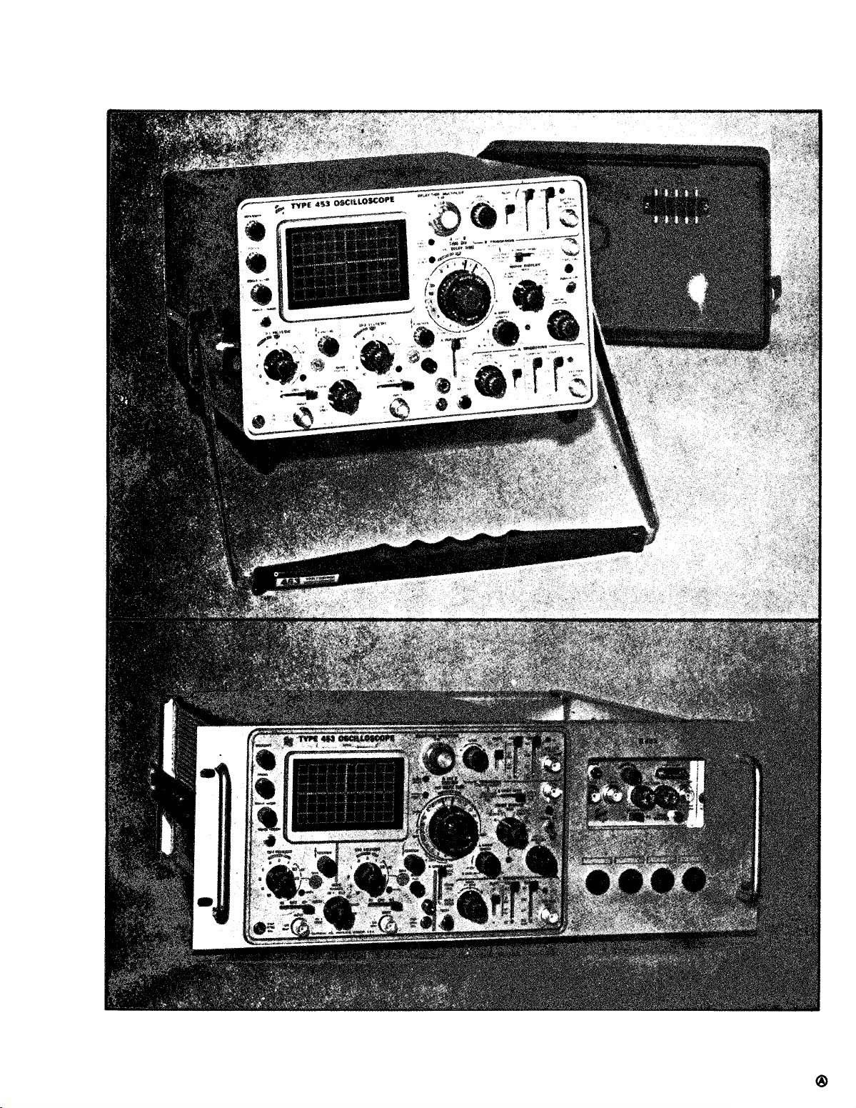
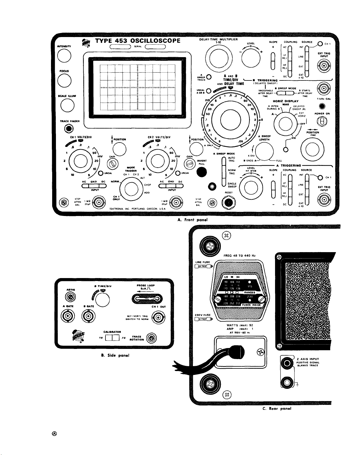
Fig. 1-1. Top; the Type 453 Oscilloscope. Bottom; the Type R453 Oscilloscope.
A-O
Page 6

Page 7

SECTION 0
INSTRUCTIONS
TM 11-6625-1722-15
0-1.
maintenance instructions.
Scope
This manual describes Oscilloscope
AN/USM-273 (fig. 1-1) and provides
Throughout this manual, the AN/USM-273 is re-
ferred to as the Tektronix Type 453 Oscilloscope. The maintenance allo-
cation chart appears in appendix C.
Repair parts and special tools lists
are contained in TM-6625-1722-24P.
0-2.
Indexes of Publications
a. DA Pam 310-4.
Refer to the latest issue of DA Pam 310-4 to deter-
mine whether there are new editions, changes, or additional publications
pertaining to the equipment.
DA Pam 310-7.
b.
Refer to DA Pam 310-7 to determine whether there
are modification work orders (MWO’S) pertaining to the equipment.
0-3.
Maintenance Forms, Records, and Reports
Reports of Maintenance and Unsatisfactory
a.
Equipment.
Department
of the Army forms and procedures used for equipment maintenance will be
those prescribed by TM 38-750, The Army Maintenance Management System.
Report of Packaging and Handling Deficiencies.
b.
Fill out and for-
ward DD Form 6 (Packaging Improvement Report) as prescribed in AR 700-58/
NAVSUPINST 4030.29/AFR 71-13/MCO P4030.29A, and DLAR 4145.8.
Discrepancy
c.
in Shipment Report (DISREP) (SF 361). Fill out and
forward Discrepancy in Shipment Report (DISREP) (SF 361) as prescribed in
AR 55-38/NAVSUPINST 4610.33B/AFR 75-18/MCO P4610.19C and DLAR 4500.15.
0-1
Page 8

TM 11-6625-1722-15
0-4.
us an EIR.
don’t like about your equipment.
design.
(Quality Deficiency Report).
and Electronics Materiel Readiness Command, ATTN:
Monmouth, NJ 07703.
0-5.
Reporting Equipment Improvement Recommendations (EIR)
If your Oscilloscope AN/USM-273 needs improvement, let us know.
You,
the user,
are the only one who can tell us what you
Send
Let us know why you don’t like the
Tell us why a procedure is hard to perform.
Put it on an SF 368
Mail it to Commander, US Army Communications
DRSEL-ME-MQ, Fort
We’ll send you a reply.
Administrative Storage
Administrative storage of equipment issued to and used by Army activi-
ties shall be in accordance with TM 740-90–1.
0-6
Destruction of Army Electronics Materiel
Destruction of Army electronics materiel to prevent enemy use shall be
in accordance with TM 750-244-2.
0-7.
Reporting Errors and Recommending Improvements
You can help improve this manual. If you find any mistakes or if you
know of a way to improve the procedures, please let us know. Mail your
letter or DA Form 2028 (Recommended Changes to Publications and Blank
Forms) to
Readiness Command, ATTN:
either case,
Commander, US Army Communications and Electronics Materiel
DRSEL-ME-MQ, Fort Monmouth, NJ 07703. In
a reply will be furnished direct to you.
0-2
Change 1
Page 9

SECTION 1
CHARACTERISTICS
TM 11-6625-1722-15
Introduction
The Tektronix Type 453 Oscilloscope is a transistorized
portable oscilloscope designed to operate in a wide range
of environmental conditions. The light weight of the Type
453 allows it to be easily transported, while providing the
performance necessary for accurate high-frequency measurements.
provides calibrated deflection factors from 5 millivolts to
10 volts/division. Channels 1 and 2 can be cascaded using
an external cable to provide a one millivolt minimum defection factor (both VOLTS/DIV switches set to 5 mV).
The trigger circuits provide stable triggering over the full
range of vertical frequency response. Separate trigger controls are provided to select the desired triggering for the A
and B sweeps. One of three sweep modes can be selected
for the A sweep; automatic, normal or single sweep. The
horizontal sweep provides a maximum sweep rate of 0.1
microsecond/division (10 nanosecond/division using 10X
magnifier) along with a delayed sweep feature for accurate
relative-time measurements.
can be made with Channel 2 providing the vertical deflection,
and Channel 1 providing the horizontal [deflection. (TRIGGER
switch set to CH 1 ONLY, HORIZ DISPLAY switch set to EXT
HORIZ). The regulated DC power supplies maintain con-
The dual-channel DC-to-50 MHz vertical system
Accurate X-Y measurements
ELECTRICAL CHARACTERISTICS
VERTICAL DEFLECTlON SYSTEM
stant output over a wide variation of line voltages and frequencies.
approximately 90 watts.
Information given in this instruction monual applies to the
Type R453 also unless otherwise noted. The Type R453 is
electrically identical to the Type 453 but is mechanically
adapted for mounting in a standard 19-inch rack. Rackmounting instructions, a mechanical parts list and a dimensional drawing for the Type R453 are provided in Section
10 of this manual.
The electrical characteristics which follow are divided
into two categories. Characteristics listed in the Performance
Requirement column are checked in the Performance Check
and Calibration sections of this manual. Items listed in the
Operational Information column are provided for reference
use and do not directly reflect the measurement capabilities of this instrument. The Performance Check procedure
given in Section 5 of this manual provides a convenient
method of checking the items listed in the Performance
Requirement column. The following electrical characteristics
apply over a calibration interval of 1000 hours at an ambient temperature range of -15°C to +55°C, except as
otherwise indicated. Warm-up time for given accuracy is
20 minutes.
Total power consumption of the instrument is
. .
Characteristic
Deflection Factor
Deflection Accuracy
Variable Deflection Factor
Bandwidth at Upper -3 dB
point (with or without P6010
Probe)
20 mV to 10 VOLTS/DIV
10 mV/DIV
5 mV/DIV
Channels land 2 cascaded
Risetime (calculated). With or
without P6010 Probe.
20 mV to 10 VOLTS/DIV
10 mV/DIV
5 mV/DIV
Channels 1 and 2 cascaded
Performance Requirement
5 millivolts/division to 10 volts/division in 11
calibrated steps for each channel. One millivolt/
division when Channel 1 and 2 are cascaded.
Within ±3Y% of indicated deflection with VARlABLE control set to CAL. Cascaded deflection
factor uncalibrated.
Uncalibrated deflection factor at least 2.5 times
the VOLTS/DIV switch indication. This provides
a maximum uncalibrated deflection factor of 25
volts/division in the 10 volts position.
DC to 50 MHz or greater
DC to 45 MHz or greater
DC to 40 MHz or greater
DC to 25 MHz or greater
Less than 7 nanoseconds
Less than 7.8 nanoseconds
Less than 8.75 nanoseconds
Less than 14 nanoseconds
Operational Information
Steps in 1-2-5 sequence
With gain correct at 20 mV
Driven from 25-ohm source
Measured at one millivolt/division
Risetime calculated from bandwidth
measurement using the formula:
Where:
= Risetime in nanoseconds.
t
r
BW = Bandwidth in megahertz.
1-1
Page 10

TM 11-6625-1722-15
Characteristic
Input RC Characteristics
Maximum lnput Voltage
lnput Coupling Modes
AC Low-Frequency Response
(lower -3 dB point)
Without probe
With P6010 Probe
Trace Shift Due to Input Gate
Current (at 25°C)
Vertical Display Modes
Chopped Repetition Rate
Attenuator Isolation
Common Mode Rejection Ratio
Linear Dynamic Range Useful
for Common-Mode Relection
in ADD Mode
Polarity Inversion
Signal Delay Line
Low-Frequency
Vertical Linearity
Trace Drift (after 20 minute
warm up)
20 mV to 10 VOLTS/DIV
10 mV/DIV
5 mV/DIV
VERTICAL (cont)
Performance Requirement
AC or DC, selected by front-panel switch
Negligible
Channel 1 only
Channel 2 only
Dual-troce, alternate between channels
Dual-trace, chopped between channels
Added algebraically
Approximately one-microsecond segments from
each channel dispiayed at repetition rate of 500
kHz, ±20%.
Greater than 10,000:1, DC to 20 MHz
Greater than 20:1 at 20 MHz for common-mode
signals less than eight times VOLTS/DIV switch
setting.
Signal on Channel 2 can be inverted
Less than 0.15 division compression or expansion
of two division signal when positioned to vertical
extremes of display area
Operational Information
Typically 1 megohm (±2%), paralleled
by 20 pF (±3%)
600 volts DC + peak AC (one kilohertz
or less). Peak-to-peak AC not to exceed
600 volts.
Typicaily 1.6 Hz, Input Coupling switch
set to AC
Typically 0.16 Hz
With optimum GAIN
frequency
Less than 10% incremental signal dis-
tortion for instantaneous input voltage
-10 or +10 times VOLTS/DIV
of
switch setting
Approximately 140 nanoseconds
Includes CRT linearity. Measured with
one-kilohertz square wave.
Time
Typically less than Typically less than
0.03 division/hour
Typically less than
0.05 division/hour
Typically less than
0.08 division/hour
adjustment at low
Temperature
0.0075 division/degree C
Typically less than
0.0125 division/degree C
Typically less than
0.02 division/de-
gree C
Source
Coupling
Polarity
1-2
TRIGGERING (A AND B SWEEP)
Internal from displayed channel or from Channel
1 only
Internal from AC power source
External
External divide by 10
AC
AC low-frequency reject
AC high-frequency reject
DC
Sweep can be triggered from positive-going or
negative-going portion of trigger signal
Page 11

TRIGGERING (cont)
TM 11-6625-1722-15
Characteristic
Internal Trigger Sensitivity
AC
LF REJ
HF REJ
DC
External Trigger Sensitivity
AC
LF REJ
HF REJ
DC
Auto Triggering (A sweep only)
Single Sweep (A sweep only)
Display Jitter
Maximum Input Voltage
External Trigger Input RC
Characteristics (approximate)
LEVEL Control Range
Performance Requirement
0.2 division of deflection, minimum, 30 Hz to 10
MHz; increasing to 1 division at 50 MHz
0.2 division of deflection, minimum, 30 Hz to 10
0.2 division of deflection, minimum, 30 kHz to 10
0.2 division of deflection, minimum, 30 Hz to 50
kHz
0.2 division of deflection, minimum, DC to 10
MHz; increasing to 1 division at 50 MHz
50 millivolts, minimum, 30 Hz to 10 MHz; increasing to 200 millivolts at 50 MHz
50 millivolts, minimum, 30 kHz to 10 MHz; increasing to 200 millivolts at 50 MHz
50 millivolts, minimum, 30 Hz to 50 kHz
50 millivolts, minimum, DC to 10 MHz; increas-
ing to 200 millivolts at 50 MHz
Stable display presented with signal amplitudes
given under Internal and External Trigger Sensitivity above 20 Hz. Presents a free-running sweep
for lower frequencies or in absence of trigger
signal.
A Sweep Generator produces only one sweep
when triggered. Further sweeps are locked out
until RESET button is pressed. Trigger sensitivity
same as given above.
Less than 1 nanosecond at 10 nanoseconds/division sweep rate (MAG switch set to X10)
At least ±2 volts, SOURCE switch in EXT position. At least ±20 volts, SOURCE switch in EXT
÷10 position
Operational Information
Typical -3 dB point, 16 Hz
Typical -3 dB point, 16 kHz
Typical -3 dB points, 16 Hz and 100
kHz
Typical -3 dB point, 16 Hz
Typical -3 dB point, 16 kHz
Typical -3 dB points, 16 Hz and 100
kHz
600 volts DC + peak AC (one kilohertz
or less). Peak-to-peak AC not to exceed
600 volts.
1 Megohm paralleled by 20 pF, except
in LF REJ
Sweep Rates
A Sweep
B sweep
Sweep Accuracy-A and B
Sweep
5 s to 0.1 s/DIV
50 ms to 0.1 µs/DIV
Variable Sweep Rate
HORIZONTAL DEFLECTION SYSTEM
A and B Sweep Generator
0.1 microsecond/division to 5 seconds/division in
24 calibrated stem
0.1 microsecond/division to 0.5 second/division
in 21 calibrated steps
0°C to +40°C
Within ±3% of indi- Within ±5% of indi-
cated sweep rate
Within ±3% of indi- Within ±4% of indi-
cated sweep rate
Uncalibrated sweep rate to at least 2.5 times the
TIME/DIV indication, or a maximum of at least
12.5 seconds/division in the 5 s position (B sweep,
maximum of 1.25 seconds/division in the .5 s
position.
-15°C to +55°C
cated sweep rate
cated sweep rate
A sweep is main and delaying sweep
B sweep is delayed sweep
A VARIABLE and B TIME/DiV VARlABLE controls set to CAL
1-3
Page 12
TM 11-6625-1722-15
A and B Sweep Generotor
Characteristic
Sweep Length
A sweep
B sweep
Sweep Hold-off-A sweep
5s to 10
Sweep Magnification
Magnified Sweep Accuracy 1% tolerance added to speclfled sweep accuracy
Magnified Sweep Linearity
Normal/Magnified Registration
Calibrated Delay Time Range
DELAY-TIME MULTIPLIER
Dial Range
Delay Time Accuracy
5s to 0.1 s/DIV
50 ms to 1
Incremental Multiplier Linearity
Delay Time Jitter
Variable from less than 4 divisions to 11.0, ±0.5
division
11.0 divisions, ±0.5 division
Less than one times the A TIME/DIV switch set-
ting
Less than 2.5 microseconds
Each sweep rate can be increased 10 times the Extends fastest sweep rate to 10 nano-
indicated sweep rate by horizontally expanding seconds/division
the center division of display
±1.5% for any eight division portion of the
total magnified sweep length (excluding first
and last 60 nanoseconds of magnified sweep)
±0.2 division, or less, trace shift at graticuie
center when switching MAG switch from X10
to OFF
Continuous from 50 seconds to 1 microsecond A VARIABLE control set to CAL for indi-
0.20 to 10.20
0°C to +40°C -15° C to +55° C
Within ±2.5% of indi-
cated delay cated delay Includes incremental multiplier linearity
Within ±1.5% of indi-
cated delay cated delay
±0.2%
Less than 1 part in 20,000 of 10 times A TIME/
DIV switch setting
Performance Requirement
Sweep Magnifier
Sweep Delay
Within ±3.5% of indi-
‘Within ±2% of indi-
±0.3%.
Operational Information
A TIME/DIV switch set to 1 ms
B TIME/DIV switch set to 1 ms
cated delay
Equal to 0.5 division, or less, with the A
TIME/DIV switch set to 1 ms and the B
TIME/DIV switch set to 1
Input to Channel 1 (TRIGGER
switch in CH 1 ONLY)
Deflection factor
Accuracy
X Bandwidth at Upper -3 dB
Point
Input RC characteristics
Phase difference between X
and Y amplifiers at 50 kHz
Input to EXT HORIZ Connector
Deflection factor
1-4
External Horizontal Amplifier
5 millivolts/division to 10 volts/division in 11 calibrated steps
0°C to +40°C
Within ±5% of indi- Within ±8% of indi-
cated deflection
5 MHz or greater
Less than 3°
B SOURCE switch in EXT; 270 millivolts/division,
±15%.
B SOURCE switch in EXT
±20%
cated deflection
Steps in 1-2-5 sequence.
Channel 1 VARIABLE control does not
affect horizontal deflection
With external horizontal gain correct
at 20 mV
Typically 1 megohm (±2%), paralleled
by 20 pF (±3%)
Page 13
External Horizontal Amplifier (cont)
X Bandwidth at Upper -3 5 MHz or greater
TM 11-6625-1722-15
Operational Information
—
Input RC characteristics
(approximate]
Phase difference between X
and Y amplifiers at 50kHz
CALIBRATOR
Waveshape
Polarity
Output Voltage
Output Current
Square wave
Positive going with baseline at zero volts
0.1 volt or 1 volt, peak to peak
5-milliamperes through PROBE LOOP on side
Repetition Rate
Voltage Accuracy
.Current Accuracy
Repetition Rate Accuracy
Risetime
Duty CycIe
±0.5%
Less than 1 microsecond
49% to 51%
Output Resistance
Z AXIS INPUT
Sensitivity
5 volt peak-to-peak signal produces noticeable
modulation
Usable Frequency Range DC to greater than 50 MHz
Input Resistance at DC
Input Coupling DC coupled
Polarity of Operation
1 megohm, paralleled by 20 pF
Less than 3°
Selected by CALIBRATOR switch on side
panel
±1.5%
Approximately 200 ohms in 1 V position.
Approximately 20 ohms in .1 V position.
Approximately 47 kilohms
Positive-going input signal decreases
trace intensity
Negative-going signal increases trace
Maximum Input Voltage
A and B Gate
Waveshape
Amplitude
Polarity
Duration
Output resistance
Vertical Signal Out (CH 1 only)
Output voltage
Bandwidth
Output coupling
Output resistance
OUTPUT SIGNALS
—
Rectangular pulse
Posltlve-going with baseline at about -0.7 volts.
I Same duration as the respective sweep
I
25 millivolts, or greater/division of CRT display
into 1 megohm load.
DC to 25 MHz or greater when cascaded with
Channel 2 or into 50-ohm load.
DC coupled
200 volts combined DC and peak AC
A GATE duration variable between
about 4 and 11 times the A TIME/DIV
switch setting
with the A SWEEP
LENGTH control.
Approximately 1.5 kilohms
Approximately 50 ohms
1-5
Page 14

TM 11-6625-1722-15
Characteristic
Line Voltage
Voltage Ranges (AC, RMS)
115-volts nominal
230-volts nominal
Line Frequency
Maximum Power Consumption
at 115 Volts, 60 Hz
Tube Type
Phosphor
Accelerating Potential
Graticule
Type
Area
Illumination
Unblinking
Raster Distortion
Trace Finder
POWER SUPPLY
Performance Requirement
115 volts nominal or 230 volts nominal
90 to 110 volts
104 to 126 volts
112 to 136 volts
180 to 220 volts
208 to 252 volts
224 to 272 volts
———
48 to 440 Hz
CATHODE-RAY TUBE (CRT)
I
Internal
Six divisions vertical by 10 divisions horizontal.
Each division equals 0.8 centimeter.
0.1 division or less total
Limits display within graticule area when pressed.
Operational Information
.—
Line voltage and range selected by Line
Voltage Selector assembly on rear
panel. Voltage ranges apply for waveform distortion which does not reduce
the peak line voltage more than 5%
below the true sine-wave peak value.
92 watts (105 volt-amperes)
Tektronix T4530-31-1 rectangular
P31 standard. Others available on
special order.
Approximately 10 kV total (cathode
potential -1.95 kV).
Variable edge lighting
Bias-type, DC coupled to CRT grid.
Adjustable with Geometry and Y Axis
Align adjustments.
Characteristic
Temperature
Operating
Non-operating
Altitude
Operating
Non-operating
Humidity
Non-operating
Vibration
Operating and
non-operating
Shock
Operating and
non-operating
ENVIRONMENTAL CHARACTERISTICS
The following environmental test limits apply when tested in accordance with the recommended test procedure. This instrument will meet the electrical characteristics given in this
section following environmental test.
including failure criteria, etc., may be obtained from Tektronix, Inc. Contact your local
Tektronix Field Office or representative.
Performance Requirement
-15°C to +55°c
-55° to +75°C
15,000 feet maximum
50,000 feet maximum
Five cycles (120 hours) of Mil-Std-202C, Method
106B
15 minutes along each of the three major axes
at a total displacement of 0.025-inch peak to peak
(4 g at 55 c/s) with frequency varied from 10-5510 c/s in one-minute cycles. Hold at 55 c/s for
three minutes on each axis.
Two shocks of 30 g, one-half sine, 11 millisecond
duration each direction along each major axis.
Complete details on environmental test procedures,
Supplemental Information
Fan at rear circulates air throughout instrument.
cutout protects instrument from overheating.
Derate maximum operating tempera-
ture by 1°C/1000 feet change in altitude
above 5000 feet.
Exclude freezing and vibration
Instrument secured to vibration platform
during test. Total vibration time, about
55 minutes.
Guillotine-type shocks.
Total of 12 shocks
Automatic resetting thermal
1-6
Page 15
ENVIRONMENTAL CHARACTERISTICS (cont)
TM 11-6625-1722-15
Characteristic
Transportation
Package vibration
Package drop
Type 453
Type R453
MECHANICAL CHARACTERISTICS
Characteristic
Construction
Chassis
Panel
Cabinet
Circuit boards
Overall Dimensions, Type
453 (measured ot maximum points)
Height
Width
Length
Overall Dimensions, Type
R453 (measured at maximum points)
Height
Performance Requirement
Meets National Safe Transit type of test when
packaged as shipped from Tektronix, Inc.
One hour vibration slightly in excess of 1 g.
30-inch drop on any corner, edge or flat surface.
18-inch drop on any corner, edge or flat surface.
Width
Information
Length
Aluminum alloy
Aluminum alloy with ano-
dized finish
Blue vinyl-coated aluminum
Glass-epoxy laminate
Connectors
Z AXIS INPUT
All other connectors
Net Weight
Type 453 (includes front
cover without accessor-
Type R453 (without ac-
handle positioned for carrying.
Standard accessories supplied with the Type 453 and R453
are listed on the last pullout page of the Mechanical Parts
List illustrations.
7 inches
Operational Information
Package should just leave vibration surface
19 inches
panel;
Binding post
BNC
Approximately 29 pounds.
ies)
Approximately 32 pounds.
cessories)
STANDARD ACCESSORIES
1-7
Page 16

Page 17
SECTION 2
OPERATING INSTRUCTIONS
General
O effectively use the Type 453, the operation and capa-
T
bilities of the instrument must be known. This section describes the operation of the front-, side- and rear-panel
controls and connectors, gives first time and general operating information and lists some basic applications for this
instrument.
Front Cover and Handle
The front cover furnished with the Type 453 provides a
dust-tight seal around the front panel. Use the cover to
protect the front panel when storing or transporting the
instrument. The cover also provides storage space for probes
and other accessories (see Fig. 2-1).
TM 11-6625-1722-15
Fig. 2-1. Accessory storage provided in front cover.
The handle af the Type 453 can be positioned for carrying
or as a tilt-stand for the instrument. To position the handle,
press in at both pivot points (see Fig. 2-2) and turn the
handle to the desired position. Several positions are provided for convenient carrying or viewing. The instrument
may also be set an the rear-panel feet for operation or
storage.
Operating Voltage
The Type 453 can be operated from either a 115-volt or
a 230-volt nominal line-voltage source. The Line Voltage
Fig. 2-2. Handle positioned to provide a stand for the instrument
Selector assembly on the rear panel converts the instrument
from one operating range to the other. In addition, this
assembly changes the primary connections of the power
transformer to allow selection of one of three regulating
ranges. The assembly also includes the two line fuses. When
the instrument is converted from 115-volt to 230-volt nominal
operation, or vice versa, the assembly connects or disconnects one of the fuses to provide the correct protection for
the instrument. Use the following procedure to convert this
instrument between nominal line voltages or regulating
ranges.
1. Disconnect the instrument from the power source.
2. Loosen the two captive screws which hold the cover
onto the voltage selector assembly; then pull to remove the
cover.
3. To convert from 115-volts nominal to 230-volts nominal line voltage, pull out the Voltage Selector switch bar
(see Fig. 2-3]; turn it around 180° and plug it back into the
remaining holes. Change the line-cord power plug to match
the power-source receptacle or use a 115- to 230-volt
adapter.
4. To change regulating ranges, pull out the Range
Selector switch bar (see Fig. 2-3); slide it to the desired
position and plug it back in. Select a range which is centered about the average line voltage to which the instrument is to be connected (see Table 2-1).
5. Re-install the cover and tighten the two captive screws.
6. Before applying power to the instrument, check that
the indicating tabs on the switch bars are protruding through
the correct holes for the desired nominal line voltage and
regulating range.
2-1
Page 18
TM 11-6625-1722-15
Fig. 2-3. Line Voltage Selector assembly on the rear panel (shown
with cover removed).
CAUTION
The Type 453 should not be operated with the
Voltage Selector or Range Selector switches in the
wrong positions for the line voltage applied.
Operation of the instrument with the switches in
the wrong positions may either provide incorrect
aperotion or damage the instrument.
TABLE 2-1
more frequently. The air filter should be cleaned occasion-
ally to aII
OW the maximum amount of cooling air to enter
the instrument. Cleaning instructions are given in Section 4.
The Type 453 can be operated where the ambient air
temperature is between
-15°C and +55°C. Derate the
maximum operating temperature 1°C for each additional
1000 feet of altitude above 5000 feet. This instrument can
be stored in ambient temperatures between –55°C and
+75°C. After storage at temperatures beyond the operating
limits, allow the chassis temperature to come within the
operating limits before power is applied.
Rackmounting
Complete information for mounting the Type R453 in a
cabinet rack is given in Section 10 of this manual.
CONTROLS AND CONNECTORS
A brief description of the function or operation
front-, side- and rear-panel controls and connectors
(see Fig. 2-4). More detailed information is given
of the
follows
in this
section under General Operating Information.
Cathode-Ray Tube
INTENSITY
FOCUS
Controls brightness of display.
Provides adjustment for a well-defined dis-
play.
SCALE ILLUM
TRACE FINDER
Controls graticule illumination.
Compresses display within graticule area
independent of display position or appli-
ed signals.
Operating Temperature
The Type 453 is cooled by air drawn in at the rear and
blown out through holes in the top and bottom covers. Adequate clearance on the top, bottom and rear must be provided to allow heat to be dissipated away from the instru-
ment. The clearance provided by the feet at the bottom and
rear should be maintained. If possible, allow about one
inch of clearance on the top. Do not block or restrict the air
flow from the air-escape holes in the cabinet.
A thermal cutout in this instrument provides thermal protection and disconnects the power to the instrument if the
internal temperature exceeds a safe operating level. Operation of the instrument for extended periods without the covers
may cause it to overheat and the thermal cutout to open
Vertical (both
VOLTS/DIV
VARIABLE
UNCAL
POSITION
GAIN
Input Coupling
(AC GND DC)
channels except as noted)
Selects vertical deflection factor (VARlABLE control must be in CAL position for
indicated deflection factor).
Provides continuously variable deflection
factor between the calibrated settings of
the VOLTS/DIV switch.
Light indicates that the VARIABLE control
is not in the CAL position.
Controls vertical position of trace.
Screwdriver adjustment to set gain of the
Vertical Preamp. Line between adjustment and 20 mV VOLTS/DIV position indicates that gain should be set with
VOLTS/DIV switch in this position.
Selects method of coupling input signal
to Vertical Deflection System.
AC: DC component of input signal is
blocked. Low frequency limit -3 dB
point) is about 1.6 hertz.
GND: Input circuit is grounded (does not
ground applied signal).
2-2
Page 19
TM 11-6625-1722-15
Fig. 2-4. Front-, side- and rear-panel controls and connectors.
2-3
Page 20

TM 11-6625-1722-15
DC: All components of the input signal are
passed to the Vertical Deflection System.
STEP ATTEN
BAL
INPUT
MODE
TRIGGER
INVERT (CH 2
only)
A and B Triggering (both where applicable)
EXT TRIG
INPUT
SOURCE
Screwdriver adjustment to balance Vertical Deflection System in the 5, 10 and 20
mV positions of the VOLTS/DIV switch.
Vertical input connector for signal.
Selects vertical mode of operation.
CH 1: The Channel 1 signal is displayed.
CH 2: The Channel 2 signal is displayed.
ALT: Dual trace display of signal on both
channels. Display switched at end of
each sweep.
CHOP: Dual trace display of signal on
both channels. Approximately one-microsecond segmerlts from each channel
displayed at a repetition rate of about
500 kilohertz.
ADD: Channel 1 and 2 signals are alge-
braically added and the algebraic sum
is displayed on the CRT.
Selects saurce of internal trigger signal
from vertical system.
NORM: Sweep circuits triggered from dis-
played channel(s). Channel 1 signal
available at CH 1 OUT connector.
CH 1 ONLY: Sweep circuits triggered only
from signal applied to the Channel 1
INPUT connector. No signal available
at CH 1 OUT connector. CH 1 lights,
located beside A and B SOURCE switches indicate when the TRIGGER switch is
in the CH 1 ONLY position.
Inverts the Channel 2 signal when pulled
out.
Input connector for external trigger signal.
Connector in B Triggering section of front
panel also serves as external horizontal
input when HORIZ DISPLAY switch is in
EXT HORIZ position and B SOURCE switch
is in EXT position.
Selects source of trigger signal.
INT: Internal trigger signal obtained from
Vertical Deflection System. When CH
1 light is on, trigger signal is obtained
only from the Channel 1 input signal;
when the light is off, the trigger signal
is abtained from the displayed chan-
nel(s). Source of internal trigger signal
is selected by the TRIGGER switch.
LINE: Trigger signal obtained from a sam-
ple of the line voltage applied to this
instrument.
EXT: Trigger signal obtained from an ex-
ternal signal applied to the EXT TRIG
INPUT connector.
nal approximately 10 times.
CH 1
COUPLING
SLOPE
LEVEL
HF STAB Decreases display jitter for high-frequency
(A Triggering only) sweep rates.
A and B Sweep
DELAY-TIME
MULTIPLIER
A SWEEP
TRIG’D
UNCAL A
OR B
A AND B
TIME/DIV
AND DELAY
TIME
Light indicates that the internal trigger signal is abtained only from the signal connected to the Channel 1 INPUT connector
(see TRIGGER switch).
Determines method of coupling trigger
signal to trigger circuit.
AC: Rejects DC and attenuates signals be-
low about 30 hertz. Accepts signals
between abaut 30 hertz and 50 megahertz.
LF REJ: Rejects DC and attenuates signals
below about 30 kilohertz. Accepts signals between about 30 kilohertz and 50
megahertz.
HF REJ: Accepts signals between about 30
hertz and 50 kilohertz; rejects DC and
attenuates signals outside the above
range.
DC: Accepts all trigger signals from DC to
50 megahertz or greater.
Selects portion of trigger signal which
starts the sweep.
+: Sweep can be triggered from positive-
going portion of trigger signal.
-: Sweep can be triggered from negativegoing portion of trigger signal.
Selects amplitude point on trigger signal
at which sweep is triggered.
signals. Has negligible effect at lower
Provides variable sweep delay between
0.20 and 10.20 times the delay time indi-
cated by the A TIME/DIV switch.
Light indicates that A sweep is triggered
and will produce a stable display with
correct INTENSITY and POSITION control
settings.
Light indicates that either the A or B
VARIABLE control is not in the CAL posi-
tion.
A TIME/DIV switch (clear plastic flange)
selects the sweep rate of the A sweep
circuit for A sweep only operatian and
selects the basic delay time (to be multi-
plied by DELAY-TIME MULTIPLIER dial
setting) for delayed sweep operation.
B TIME/DIV (DELAYED SWEEP) switch
selects sweep rate of the B sweep circuit
Attenuates external trigger sig-
2-4
Page 21

TM 11-6625-1722-15
A VARIABLE
B SWEEP
MODE
HORIZ
DISPLAY
MAG
A SWEEP
MODE
for delayed sweep operation only. VARlABLE controls must be in CAL positions for
calibrated sweep rates.
Provides continuously variable A sweep
rate to at least 2.5 times setting of the
A TIME/DIV switch. A sweep rate is calibrated when control is set fully clockwise
to CAL.
Selects B sweep operation mode.
TRIGGERABLE AFTER DELAY TIME: B
sweep circuit will not produce a sweep
until a trigger pulse is received following the delay time selected by the
DELAY TIME (A TIME/DIV) switch and
the DELAY-TIME MULTIPLIER dial.
B STARTS AFTER DELAY TIME: B sweep
circuit runs immediately following delay
time selected by the DELAY TIME switch
and DELAY-TIME MULTIPLIER dial.
Selects horizontal mode of operation.
A: Horizontal deflection provided by A
sweep.
B sweep inoperative.
A INTEN DURING B: Sweep rate deter-
mined by A TIME/DIV switch. An inten-
sified portion appears on the sweep
during the B sweep time. This position
provides a check of the duration and
position of the delayed sweep (B) with
respect to the delaying sweep (A).
DELAYED SWEEP (B): Sweep rate deter-
mined by B TIME/DIV switch with the
delay time determined by the setting of
the DELAY TIME (A TIME/DIV) switch
and the DELAY-TIME MULTIPLIER dial.
Sweep mode determined by B SWEEP
MODE switch.
EXT HORIZ: Horizontal deflection pro-
vided by an external signal.
Increases sweep rate to ten times setting
of A or B TIME/DIV switch by horizontally
expanding the center division of the display. Light indicates when magnifier is
on.
Determines the operating mode for A
sweep.
AUTO TRIG: Sweep initiated by the ap-
plied trigger signal using the A Trig-
gering controls when the trigger signal
repetition rate is above about 20 hertz.
For lower repetition rates or when there
is no trigger signal, the sweep free runs
at the sweep rate selected by the A
TIME/DIV switch to produce a bright
reference trace.
NORM TRIG: Sweep initiated by the ap-
plied trigger signal using the A Trig-
gering controls. No trace is displayed
when there is no trigger signal.
RESET
A SWEEP
LENGTH
POSITION
FINE
1 kHz CAL
POWER ON
Side Panel
ASTIG
B TiME/DIVVARIABLE
PROBE LOOP
A GATE
B GATE
CH 1 OUT
SINGLE SWEEP: After a sweep is display-
ed, further sweeps cannot be presented
until the RESET button is pressed. Display is triggered as for NORM operation using the A Triggering controls.
When the RESET button is pressed (SINGLE SWEEP mode), a single display will
be presented (with correct triggering) when
the next trigger pulse is received. RESET
light (inside RESET button) remains on
until a trigger is received and the sweep is
completed. RESET button must be pressed
before another sweep can be presented.
Adiusts length of A sweep. In the FULL
position (clockwise detent), the sweep is
about 11 divisions long. As the control is
rotated counterclockwise, the length of A
sweep is reduced until it is less than four
divisions long iust before the detent in
the fully-counterclockwise position is reached. In the B ENDS A position (counterclockwise detent), the A sweep is reset
at the end of the B sweep to provide the
fastest possible sweep repetition rate for
delayed sweep displays.
Controls horizontal position of trace.
Provides more precise horizontal position
adjustment.
Calibrator output connector.
Light: Indicates that POWER switch is
on and the instrument is connected to
a line voltage source.
Switch: Controls power to the instrument.
Screwdriver adjustment used in conjunction with the FOCUS control to obtain a
well-defined display. Does not require
readjustment in normal use.
Provides continuously variable sweep rate
to at least 2.5 times setting of B TIME/DIV
switch. B sweep rate is calibrated when
control is set fully clockwise to CAL.
Current loop providing five-milliampere
square-wave current from calibrator circuit.
Output connector providing a rectangular
pulse coincident with A sweep.
Output connector providing a rectangular
pulse coincident with B sweep.
Output connector providing a sample of
the signal applied to the Channel 1 lN-
PUT connector when the TRIGGER switch
is in the NORM position.
2-5
Page 22

TM 11-6625-1722-15
CALIBRATOR
TRACE
ROTATION
Rear Panel
Z AXIS INPUT
Line Voltage
Selector
The following steps will demonstrate the use of the controls and connectors of the Type 453. It is recommended
that this procedure be followed completely for familiarization with this instrument.
Setup Information
1. Set the front-panel controls as follows:
CRT Controls
INTENSITY
FOCUS
SCALE ILLUM Counterclockwise
Vertical Controls (both channels if applicable)
VOLTS/DIV 20 mV
VARIABLE
POSITION Midrange
INPUT COUPLING
MODE
TRIGGER
INVERT
Triggering Controls (both A and B if applicable)
LEVEL
SLOPE
COUPLING
SOURCE
Sweep Controls
DELAY-TIME
MULTIPLIER
A and B TIME/DIV
A VARIABLE
B SWEEP MODE
Switch selects output voltoge of Calibrator.
1-volt or 0.1-volt square wave available.
Screwdriver adjustment to align trace with
horizontal graticule lines.
Input connector for intensity modulation
of the CRT display.
Switching assembly to select the nominal
operating voltage and the line voltage
range.
line fuses.
Voltage Selector: Selects nominal operat-
Range Selector: Selects line voltage range
FIRST-TIME OPERATION
The assembly also includes the
ing voltage range (115V or 230V).
(low, medium, high).
Counterclockwise
Midrange
CAL
DC
CH 1
NORM
Pushed in
Clockwise (+)
+
AC
INT
0.20
.5 ms
CAL
B STARTS AFTER
DELAY TIME
HORIZ DISPLAY
MAG
POSITION
A SWEEP LENGTH
A SWEEP MODE
POWER
Side-Panel Controls
B TIME/DIV VARIABLE
CALIBRATOR
2. Connect the Type 453 to a power source that meets
the voltage and frequency requirements of the instrument.
If the available line voltage is outside the limits of the Line
Voltage Selector assembly position (on rear panel), see
Operating Voltage in this section.
3. Set the POWER switch to ON. Allow about five minutes
warmup so the instrument reaches a normal operating temperature before proceeding.
CRT Controls
4. Advance the INTENSITY control until the trace is at
the desired viewing level (near midrange).
5. Connect the 1 kHz CAL connector to the Channel 1
INPUT connector with a BNC cable.
6. Turn the A LEVEL control toward 0 until the display
becomes stable. Note that the A SWEEP TRIG’D light is on
when the display is stable.
7. Adiust the FOCUS control for a sharp, well-defined
display over the entire trace length. (If focused display can-
not be obtained, see Astigmatism Adjustment in this section.)
8. Disconnect the input signal and move the trace with
the Channel 1 POSITION control so it coincides with one of
the horizontal graticule lines.
the graticule line, see Trace Alignment Adjustment in this
section.
9. Rotate the SCALE ILLUM control throughout its range
and notice that the graticule lines are illuminated as the
control is turned clockwise (most obvious with mesh or smokegray filter installed). Set control so graticule lines are
illuminated as desired.
Vertical Controls
10. Change the CH 1 VOLTS/DIV switch from 20 mV to 5
mV. If the vertical position of the trace shifts, see Step
Attenuator Balance in this section.
11. Set the CH 1 VOLTS/DIV switch to 20 mV and set the
Channel 1 Input Coupling switch to AC. Connect the 1 kHz
CAL connector to both the Channel 1 and 2 INPUT connectors with two BNC cables and a BNC T connector.
If the BNC cables and BNC T connector are not
available, make the following changes in the procedure. Place the BNC jack post (supplied accessory) on the 1 kHz CAL connector and connect
A
OFF
Midrange
FULL
AUTO TRIG
OFF
CAL
.1 V
If the trace is not parallel with
NOTE
2-6
Page 23

TM 11-6625-1722-15
the Channel 1 and 2 INPUT connectors. Connect
the probe tips to the BNC jack post. Set the CALIBRATOR switch (on side-panel) to 1 V.
12. Turn the Channel 1 POSITION control to center the
display. The display is a square wave, five divisions in
amplitude with about five cycles displayed on the screen. If
the display is not five divisions in amplitude, see Vertical
Gain Adjustment in this section.
13. Set the Channel 1 Input Coupling switch to GND ond
position the trace to the center horizontal line.
14. Set the Channel 1 Input Coupling switch to DC. Note
that the baseline of the waveform remains at the center
horizontal line (ground reference).
15. Set the Channel 1 Input Coupling switch to AC. Note
that the waveform is centered about the center horizontal
line.
16. Turn the Channel 1 VARIABLE control throughout its
range. Note that the UNCAL light comes on when the VARl-
ABLE control is moved from the CAL position (fully clockwise). The deflection should be reduced to about two divisions. Return the VARIABLE control to CAL.
17. Set the MODE switch to CH 2.
18. Turn the Channel 2 POSITION control to center the
display. The display will be similar to the previous display
for Channel 1. Check Channel 2 step attenuator balance and
gain as described in steps 10 through 12. The Channel 2
input Coupling switch and VARIABLE control operate as
described in steps 13 through 16.
19. Set both VOLTS/DIV switches to 50 mV.
20. Set the MODE switch to ALT and position the Channel
1 waveform to the top of the graticule area and the Chan-
nel 2 waveform to the bottom of the graticule area. Turn
the A TIME/DIV switch throughout its range. Note that the
display alternates between channels at all sweep rates.
Triggering
25. Set the CALIBRATOR switch to 1 V. Rotate the A LEVEL
control throughout its range. The display free runs at the
extremes of rotation. Note that the A SWEEP TRIG'D light
is on only when the display is triggered.
26. Set the A SWEEP MODE switch to NORM TRIG. Again
rotate the A LEVEL control throughout its range. A display
is presented only when correctly triggered. The A SWEEP
TRIG'D light operates as in AUTO TRIG. Return the A SWEEP
MODE switch to AUTO TRIG.
27. Set the A SLOPE switch to -. The trace starts on the
negative part of the square wave. Return the switch to +;
the trace starts with the positive part of the square wave.
28. Set the A COUPLING switch to DC. Turn the Channel 1 POSITION control until the display becomes unstable
(only part of square wave visible). Return the A COUPLING
switch to AC; the display is again stable. Since changing
trace position changes DC level, this shows how DC level
changes affect DC trigger coupling. Return the display to
the center of the screen.
29. Set the MODE switch to CH 2; the display should be
stable. Remove the signal connected to Channel 1; the dis-
play free runs.
Set the TRIGGER switch to NORM; the dis-
play is again stable. Note that the CH 1 lights in A and B
Triggering go out when the TRIGGER switch is changed to
NORM.
30. Connect the Calibrator signal to both the Channel 2
INPUT and A EXT TRIG INPUT connectors. Set the A
SOURCE switch to EXT. Operation of the LEVEL, SLOPE
and COUPLING controls for external triggering are the same
as described in steps 25 through 28.
31. Set the A SOURCE switch to EXT
is the same as for EXT. Note that the A LEVEL control has
less range in this position, indicating trigger signal attenuation. Return the A SOURCE switch to INT.
32. Operation of the B Triggering controls is similar to
A Triggering.
21. Set the MODE switch to CHOP and the A TIME/DIV
Note the switching between channels as
shown by the segmented trace. Set the TRIGGER switch to
CH 1 ONLY; the trace should appear more solid, since it is
no longer triggered on the between-channel switching trans-
ients. Turn the A TIME/DIV switch throughout its range. A
dual-trace display is presented at all sweep rates, but unlike
ALT, both channels are displayed on each trace on a timesharing basis. Return the A TIME/DIV switch to .5 ms.
22. Set the MODE switch to ADD. The display should be
four divisions in amplitude. Note that either POSITION control moves the display.
23. Pull the INVERT switch. The display is a straight line
indicating that the algebraic sum of the two signals is zero
(if the Channel 1 and 2 gain is correct).
24. Set either VOLTS/DIV switch to 20 mV. The square-
wave display indicates that the algebraic sum of the two
signals is no longer zero.
Return the MODE switch to CH 1
and both VOLTS/DIV switches to .2 (if using 10X probes,
set both VOLTS/DIV switches to 20 mV). Push in the INVERT
switch.
Normal and Magnified Sweep
33. Set the A TIME/DIV switch to 5 ms and the MAG
switch to X10. The display should be similar to that obtained with the A TIME/DIV switch set to .5 ms and the MAG
switch to OFF.
34. Turn the horizontal POSITION control throughout its
range; it should be possible to position the display across
the complete graticule area. Now turn the FINE control. The
display moves a smaller amount and allows more precise
positioning. Return the A TIME/DIV switch to .5 ms, the
MAG switch to OFF and return the start of the trace to the
left graticule line.
Delayed Sweep
36. Pull the DELAYED SWEEP knob out and turn it to 50
(DELAY TIME remains at .5 ms). Set the HORIZ DISPLAY
switch to A INTEN DURING B. An intensified portion, about
one division in length, should be shown at the start of the
trace. Rotate the DELAY-TIME MULTIPLIER dial throughout
its range; the intensified portion should move along the display.
2-7
Page 24

TM 11-6625-1722-15
37. Set the B SWEEP MODE switch to TRIGGERABLE
AFTER DELAY TIME. Again rolate the DELAY-TIME MULTI-
PLIER dial throughout its range and note that the intensified
portion appears to jump between posltive slopes of the display. Set the B SLOPE switch to -;
begins on the negative slope.
the intensified portion
Rotate the B LEVEL control;
the intensified portion of the display disappears when the B
LEVEL control is out of the trlggerable range. Return the
B LEVEL control to 0.
38. Set the HORIZ DISPLAY switch to DELAYED SWEEP
(B). Rotate the DELAY-TIME MULTIPLIER dial througout its
range; about one-half cycle of the waveform should be
displayed on the screen (Ieading edge visible only at high
INTENSITY control setting). The display remains stable on
the screen, indicating that the B sweep is triggered.
39. Set the B SWEEP MODE switch to B STARTS AFTER
DELAY TIME. Rotate the DELAY-TIME MULTIPLIER dial
throughout its range; the display moves continously across
the screen as the control is rotated.
40. Rotate the DELAYTIME MIULTIPLIER dial fully counter-
clockwise and set the HORIZ DISPLAY switch to A INTEN
DURING B. Rotate the A SWEEP LENGTH control counter-
clockwise; the Iength of the display decreases. Set the con-
trol to the B ENDS A position; now the display ends after
the intensified portion. Rotate the DELAY-TIME MULTIPLIER
dial ond note that the sweep length increases as the display
moves across the screen. Return the A SWEEP LENGTH con-
trol to FULL and the HORIZ DISPLAY switch to A.
Single Sweep
41. Set the A SWEEP MODE switch to SINGLE SWEEP.
Remove the Calibrator signal from the Channel 2 INPUT
connector. Press the RESET button; the RESET light should
come on and remain on. Again apply the signal to the Channel 2 INPUT connector; a single trace should be presented
and the RESET light should go out. Return the A SWEEP
MODE switch to AUTO TRIG.
External Horizontal
42. Connect the Calibrator signal to both the Channel 2
INPUT and EXT HORIZ (B EXT TRIG lNPUT] connectors. Set
the B SOURCE switch to EXT, B COUPLING switch to DC
and the HORIZ DISPLAY switch to EXT HORIZ. lncrease the
INTENSITY control setting until the display is visible (two dots
displayed diagonally). The display should be five divisions
vertically and about 3.7 divisions horizontally. Set the B
10. The display should be reduced
ten times horizontally. The display can be positioned horizontally with the horizontal POSITION or FINE control and
vertically with the Channel 2 POSITION control.
43. Connect the Calibrator signal to both the Channel 1
and 2 INPUT connectors. Set the TRIGGER switch to CH 1
ONLY and the B SOURCE switch to INT.
44. The display should be five divisions vertically and
horizontally.
The display can be postioned horizontally
with the Channel 1 POSITION control and vertically with the
Channel 2 POSITION control.
45. Change the CH1 VOLTS/DIV switch to 5. The display
play is reduced to two divisions horizontally. Now set the
CH 2 VOLTS/DIV switch to 5. The display is reduced to two
divisions vertically.
Trace Finder
46. Set the CH 1 and CH 2 VOLTS/DlV switches to 10
mv. The display i
S not visible since it exceeds the scan area
of the CRT.
47. Press the TRACE FINDER button. Note that the disis returned to the display area. While holding the
play
TRACE FINDER button depressed, increase the vertical and
horizontal deflection factors until the display is reduced to
about two divisions vertically ond horizontally. Adjust the
Channel 1 and 2 POSITION controls to center the display
about the center lines of the graticule. Release the TRACE
FINDER and note that the display remains within the viewing
area. Disconnect the applied signal.
48. Reduce the INTENSITY control setting to normal, B
SOURCE switch to INT and set the HORIZ DISPLAY switch
to A.
Z-Axis Input
49. If an, External signal is available (five volts peak to
peak minimum] the function of tlhe Z AXIS INPUT circuit can
be demonstrated. Connect the external signal to both the
Channel 2 INPUT connector and the Z AXIS INPUT binding
posts. Set the A TIME/DIV switch to display about five
cycles of the waveform. The positive peaks of the waveform
should be blanked and the negative peaks intensified, indi-
cating intensify modulation.
50. This completes the basic operating procedure for the
Type 453. lnstrument operation not explained here, or operations which need further explanation are discussed under
General Operating Information.
CONTROL SETUP CHART
Fig. 2-5 shows the front, side and rear panels of the Type
453. This chart can, be reproduced and used as a test-setup
record for special measurements, applications or procedures,
or it may be used as a training aid for familiarization with
this instrument.
GENERAL OPERATING INFORMATION
Intensify Control
The setting of the INTENSITY control may affect the correct focus of the display. Slight readjustment of the FOCUS
control may be necessary when the intensity level is changed.
To protect the CRT phosphor, do not turn the INTENSITY
control higher than necessary to provide a satisfactory dis-
play. The light filters reduce the observed light output from
the CRT. When using these filters, avoid odvancing the
INTENSITY control to a setting that may bum the phosphor.
When Ihe highest intensity display is desired, remove the
filters and use the clear faceplate protector. Also, be careful that the INTENSITY control is not set too high when
changing the TIME/DlV switch front a fast to a slow sweep
rate, or when changing the HORIZ DISPLAY switch from EXT
HORIZ operation to the norrmal sweep mode.
Astigmatism Adjustment
If a well-defined trace cannot be obtained with the FOCUS
control, adjust the ASTIG adjustment (side panel) as fol-
lows.
2-8
Page 25
TM 11-6625-1722-15
Fig. 2-5. Control setup chart for the Type 453.
2-9
Page 26
TM 11-6625-1722-15
NOTE
To check for proper setting of the ASTIG adjustment, slowly turn the FOCUS control through the
optimum setting. If the ASTIG adjustment is cor-
rectly set, the vertical and horizontal portions
of the trace will come into sharpest focus at the
same position of the FOCUS control. This setting
of the ASTIG adjustment should be correct for any
display. However, it may be necessary to reset
the FOCUS control slightly when the INTENSITY
control is changed.
1. Connect a 1 V Calibrator signal to either channel and
set the VOLTS/DIV switch of that channel to present a twodivision display. Set the MODE switch to display the chan-
nel selected.
2. Set the TIME/DIV switch to .2 ms
3. With the FOCUS control and ASTIG adjustment set to
midrange, adjust the INTENSITY control so the rising portion
of the display can be seen.
4. Set the ASTIG adjustment so the horizontal and vertical portions of the display are equally focused, but not
necessarily well focused.
5. Set the FOCUS control so the vertical portion of the
trace is as thin as possible.
6. Repeat steps 4 and 5 for best overall focus. Make final
check at normal intensity.
Graticule
The graticule of the Type 453 is internally marked on the
faceplate of the CRT to provide accurate, no-parallax measurements. The graticule is marked with six vertical and 10
horizontal divisions. Each division is 0.8 centimeter square.
In addition, each major division is divided inta five minor
divisions at the center vertical and horizontal lines. The
vertical gain and horizontal timing are calibrated to the
graticule so accurate measurements can be made from the
CRT. The illumination of the graticule lines can be varied
with the SCALE ILLUM control.
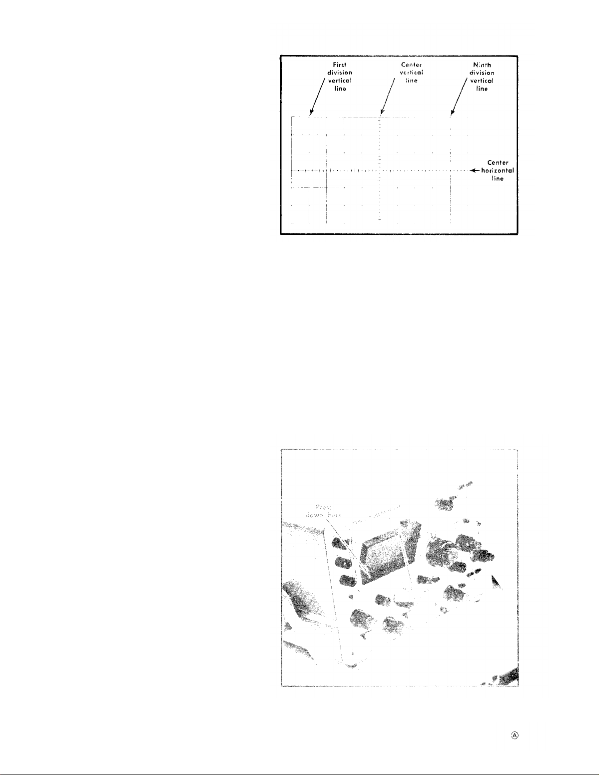
Fig. 2-6 shows the graticule of the Type 453 and defines
the various measurement lines. The terminology defined here
will be used in all discussions involving graticule measurements.
Fig. 2-6. Definition of measurement lines on Type 453 graticule.
remove the filter, press
down at the bottom of the frame
and pull the top of the filter away from the CRT faceplate
(see Fig. 2-7).
The tinted light filter minimizes light reflections from the
face of the CRT to improve contrast when viewing the display under high ambient light conditions. A clear plastic
faceplate protector is also provided with this instrument for
use when neither the mesh nor the tinted filter is used. The
clear faceplate protector provides the best display for waveform photographs. It is also preferable for viewing high
writing rate displays.
A filter or the faceplate protector should be used at all
times ta protect the CRT faceplate from scratches. The faceplate protector and the tinted filter mount in the same holder.
Trace Alignment Adjustment
If a free-running trace is not parallel to the horizontal
graticule lines, set the TRACE ROTATION adjustment as fol-
lows. Position the troce to the center horizontal line. Adjust
the TRACE ROTATION adjustment (side panel) so the trace
is parallel with the horizontal graticule lines.
Light Filter
The mesh filter provided with the Type 453 provides shielding against radiated EMI (electro-magnetic interference) from
the face of the CRT. It also serves as a light filter to make
the trace more visible under ambient light conditions. To
2-10
Fig. 2-7. Removing the filter or faceplate protector.
Page 27

TM 11-6625-1722-15
To remove the light filter or faceplate protector from the
holder, press it out to the rear. They can be replaced by
snapping them back into the holder.
Trace Finder
The TRACE FINDER provides a means af locating a display
which overscans the viewing area either vertically or horizontally. When the TRACE FINDER button is pressed, the
display is compressed within the graticule area. T
O locate
and reposition an overscanned display, use the following
procedure.
1. Press the TRACE FINDER button.
2. While the TRACE FINDER button is held depressed,
increase the vertical and horizontal deflection factors until
the vertical deflection is reduced to about two divisions and
the horizontal deflection is reduced to about four divisions
(the horizontal deflection needs to be reduced only when in
the external horizontal mode of operation).
3. Adjust the vertical and horizontal POSITION controls
to center the display about the vertical and horizontal cen-
ter lines.
4. Release the TRACE FINDER button; the display should
remain within the viewing area.
Vertical Channel Selection
Either of the input channels can be used for single-trace
displays. Apply the signal to the desired INPUT connector
and set the MODE switch to display the channel used. However, since CH 1 ONLY triggering is provided only in Chan-
nel 1 and the invert feature only in Channel 2, the correct
channel must be selected to take advantage of these features. For dual-trace displays, connect the signals to both
INPUT connectors and set the MODE switch to one of the
dual-trace positions.
Vertical Gain Adjustment
To check the gain of either channel, set the VOLTS/DIV
switch to 20 mV. Set the CALIBRATOR switch to .1 V and
connect the 1 kHz CAL connector to the INPUT of the chan-
nel used. The vertical deflection should be exactly five
divisions.
If not, adjust the front-panel GAIN adjustment
for exactly five divisions of deflection.
NOTE
If the gain of the two channels must be closely
matched (such as for ADD mode operation), the
ADJUSTMENT procedure given in the Calibration
section should be used.
The best measurement accuracy when using probes is provided if the GAIN adjustment is made with the probes installed (set the CALIBRATOR switch to 1 V). Also, to provide
the most accurate measurements, calibrate the vertical gain
of the Type 453 at the temperature at which the measurement
is to be made.
Step Attenuator Balance
To check the step attenuator balance of either channel,
set the Input Coupling switch to GND and set the A SWEEP
MODE swich to AUTO TRIG to provide a free-running trace.
Change the VOLTS/DIV switch from 20 mV to 5 mV. If the
trace moves vertically, adjust the front-panel STEP ATTEN
BAL adjustment as follows (allow at least 10 minutes warm
up before performing this adjustment].
1. With the Input Coupling switch set to GND and the
VOLTS/DIV switch set to 20 mV, move the trace to the center
horizontal line of the graticule with the vertical POSITION
control.
2. Set the VOLTS/DIV switch to 5 mV and adjust the
STEP ATTEN BAL adjustment to return the trace to the center
horizonal line.
3. Recheck step attenuator balance and repeat adjustment
until no trace shift occurs as the VOLTS/DIV switch is changed from 20 mV to 5 mV.
Signal Connections
In general, probes offer the most convenient means of connecting a signal to the input of the Type 453. The Tektronix
probes are shielded to prevent pickup of electrostatic interference. A 10X attenuator probe offers a high input impedance and allows the circuit under test to perform very close
to normal operating conditions. However, a 10X probe
also attenuates the input signal 10 times.
The Tektronix
P6045 Field Effect Transistor probe and accessory power
supply offer the same high-input impedance as the 10X
probes. However, it is particularly useful since it provides
wide-band operatian while presenting no attenuation (1X
gain) and a low input capacitance. To obtain maximum
bandwidth when using the probes, observe the grounding
considerations given in the probe manual. The probe-toconnector adapters and the bayonet-ground tip provide the
best frequency response. Remember that a ground strap
only a few inches in length can produce several percent of
ringing when operating at the higher frequency limit of this
system. See your Tektronix, Inc. catalog for characteristics
and compatibility of probes for use with this system.
In high-frequency applications requiring maximum overall
bandwidth, use coaxial cables terminated at both ends in
their characteristic impedance. See the discussion on coaxial cables in this section for more information.
High-level, low-frequency signals can be connected directly
to the Type 453 INPUT connectors with short unshielded
leads. This coupling method works best for signals below
about one kilohertz and deflection foctors above one volt/
division. When this method is used, establish a common
ground between the Type 453 and the equipment under test.
Attempt to position the leads away from any source of interference to avoid errors in the display. If interference is
excessive with unshielded leads, use a coaxial cable or a
probe.
Loading Effect of the Type 453
As nearly as possible, simulate actual operating conditions in the equipment under test. Otherwise, the equipment
under test may not produce a normal signal. The 10X
attenuator probe and field effect transistor probe mentioned
previously offer the least circuit loading. See the probe
instruction manual for loading characteristics of the individual probes.
2-11
Page 28

TM 11-6625-1722-15
When the signal is coupled directly to the input of the
Type 453, the input impedance is about one megohm
paralleled by about 20 pF. When the signal is coupled to
the input through a coaxial cable, the effeclive input capacitance depends upon the type and Iength of cable used.
See the following discussion for
inforrnation on obtaining
maximum frequency responspe with coaxial cables.
The signal cables used to connect the signal 10 the type
453 INPUT connectors have a Iarge effect on the accuracy
of the displayed high-frequency waveform.
To maitain the
high-frequency characteristics of the applied signal, highquality low-loss coaxial cable should be used. The cable
should be terminated at the Type 453 INPUT connector in its
characteristic impedonce.
with differing characteristic impedances,
If it is necessary to use cables
use suitable imped-
ance-matching devices to provide the correct transition, with
minimum loss, from one impedance to the other.
The characteristic impedance, velocity of propagation and
nature of signal lOSSeS in a coaxial cable are determined
by the physical and electrical characteristics of the cable.
Losses caused by energy dissipation in the dielectric are
proportional to the signal frequency. Therefore, much of
the high-frequency information in a fast-rise pulse can be
lost in only a few feet of interconnecting cable if it is not
the correct type. To be sure of the high-frequency response
of the system when using cables longer than about five feet,
observe the transient response of the Type 453 and the
interconnecting cable with a fast-rise
pulse generator (gen-
erator risetime Iess than 0.5 nanoseconds).
DC components. The pre-charging network incorporated
in this unit aII
OWS the input-coupling capacitor to charge to
the DC source voltage level when the Input Coupling switch
is set to GND. The procedure for using this feature is as
follows:
1. Before connecting the signal containing a DC component to the Type 453 INPUT connector, set the Input Coupling
switch to GND. Then connect the signal to the INPUT
connector.
2. Wait about one second for the coupling capacitor to
charge.
3. Set the Input Coupling switch to AC. The trace (display) will remain on the screen and the AC component of
the signal can be measured in the normal manner.
Deflection Factor
The amount of vertical deflection produced by a signal
is determined by the signal amplitude, the attenuation factor
of the probe (if used), the setting of the VOLTS/DIV switch
and the setting of the VARIABLE VOLTS/DIV control. The
calibrated deflection factors indicated by the VOLTS/DIV
switches apply only when the VARIABLE control is set to
the CAL position.
The VARIABLE VOLTS/DIV control provides variable
(uncalibrated) vertical deflection between the calibrated
settings of the VOLTS/DIV switch. The VARIABLE control
extends the maximum vertical deflection factor of the Type
453 to at least 25 volts/division (10 volts position).
Input Coupling
The Channel 1 and 2 lnput Coupling switches allow a
choice of input caupling. The type of display desired will
determine the coupling used.
The DC position can be used for most applications. However, if the DC component of the signal is much larger than
the AC component, the AC position vvill probably provide a
better display. DC coupling should be used to display AC
signals below about 16 heltz as they will be attenuated in
the AC position.
In the AC position, the DC component of the signal is
blocked by a capacitor in the input circuit. The low-frequency response in the AC position is about 1.6 hertz (–3 dB
point). Therefore,
some low-frequency distortion can be
expected near this frequency limit. Distortion will also
appear
in square waves which have low-frequency com-
ponents.
The GND position provides a ground reference at the
input of the Type 453. The signal applied to the input con-
nector is internally disconnected but not grounded. The
input circuit is held at ground potential, eliminating the need
to externally ground the input to establish a DC ground
reference.
The GND position can also be used to pre-charge the
coupling capacitor to the average voltage level of the signal
applied to the INPUT connector. This allows measurement
of only the AC component of signals having both AC and
Dual-Trace Operation
Alternate Mode. The ALT position of the MODE switch
produces a disploy which alternates between Channel 1 and
2 with each sweep of the CRT. Although the ALT mode
can be used at all sweep rates, the CHOP mode provides
a more satisfactory display at sweep rates below about 50
microseconds/division. At these slower sweep rates, alternate
mode switching becomes visually perceptible.
Proper internal triggering in the ALT mode can be ob-
tained in either the NORM or CH 1 ONLY positions of the
TRIGGER switch. When in the NORM position, the sweep is
triggered from the signal on each channel. This provides a
stable display of two unrelated signals, but does not indicate
the time relationship between the signals. In the CH 1 ONLY
position, the two signals are displayed showing true time
relationship. If the signals are not time related, the Channel
2 waveform will be unstable in the CH 1 ONLY position.
Chopped Mode. The CHOP position of the MODE switch
produces a display which is electronically switched between
channels. In general, the CHOP mode provides the best
display at sweep rates slower than about 50 microseconds/
division, or whenever dual-trace, single-shot phenomena are
to be displayed. At faster sweep rates the chopped switching becomes apparent and may interfere with the display.
Proper internal triggering for the CHOP mode is provided
with the TRIGGER switch set to CH 1 ONLY. If the NORM
position is used, the sweep circuits are triggered from the
between-channel switching signal and both waveforms will
2-12
Page 29

TM 11-6625-1722-15
be unstable. External triggering provides the same result as
CH 1 ONLY triggering.
Two signals which are time-related can be displayed in
the chopped mode showing true time relationship. If the
signals are not time-related, the Channel 2 display will
appear unstable. Two single-shot, transient, or random
signals which occur within the time interval determined by
the TIME/DIV switch (10 times sweep rate) can be compared
using the CHOP mode. To correctly trigger the sweep for
maximum resolution, the Channel 1 signal must precede the
Channel 2 signal. Since the signals show true time relation-
ship, time-difference measurements can be made.
Channel 1 Output and Cascaded Operation
If a lower deflection factor than provided by the VOLTS/
DIV switches is desired, Channel 1 can be used as a wideband preamplifier for Channel 2. Apply the input signal to
the Channel 1 INPUT connector. Connect a 50-ohm BNC
cable (18-inch or shorter cable for maximum cascaded fre-
quency response) between the CH 1 OUT (side panel) and
the Channel 2 INPUT connectors. Set the MODE switch to
CH 2 and the TRIGGER switch to NORM. With both VOLTS/
DIV switches set to 5 mV, the deflection factor will be less
than one millivolt/division.
To provide calibrated one millivolt/division deflection
factor, connect the .1 volt Calibrator signal to the Channel 1
INPUT connector. Set the CH 1 VOLTS/DIV switch to .1
and the CH 2 VOLTS/DIV switch to 5 mV. Adjust the Channel 2 VARIABLE VOLTS/DIV control to produce a display
exactly five divisions in amplitude. The cascaded deflection
factor is determined by dividing the CH 1 VOLTS/DIV switch
setting by 5 (CH 2 VOLTS/DIV switch and VARIABLE control
remain as set above). For example, with the CH 1 VOLTS/
DIV switch set to 5 mV the calibrated deflection factor will
be 1 millivolt/division; CH 1 VOLTS/DIV switch set to 10 mV,
2 millivolts/division, etc.
The following operating considerations and basic appli-
cations may suggest other uses for this feature.
1. If AC coupling is desired, set the Channel 1 Input
Coupling switch to AC and leave the Channel 2 Input
Coupling switch set to DC. When both Input Coupling
switches are set to DC, DC signal coupling is provided.
2. Keep both vertical POSITION controls set near mid-
range.
one of the POSITION controls being turned away from
midrange, correct operation can be obtained by keeping
the Channel 2 POSITION control near midrange and using
the Channel 1 POSITION control to position the trace near
the desired locatian. Then, use the Channel 2 POSITION
control far exact positioning. This method will keep both
Input Preamps operating in their linear range.
least 25 millivolts/division of CRT display in all CH 1 VOLTS/
DIV switch positions.
DIV control have no effect on the signal available at the
CH 1 OUT connector.
ance matching stage with or without voltage gain. The
If the input signal has a DC level which necessitates
3. The output voltage at the CH 1 OUT connectar is at
4. The MODE switch and Channel 1 VARIABLE VOLTS/
5. The Channel 1 Input Preamp can be used as an imped-
input resistance is one megohm and the output resistance is
about 50 ohms.
6. The dynamic range of the Channel 1 Input Preamp is
equal to about 20 times the CH 1 VOLTS/DIV setting. The
CH 1 OUT signal is nominally at 0 volt DC for a 0 volt DC
input level [Channel 1 POSITION control centered). The
Chanel 1 POSITION control can be used to center the output signal within the dynamic range of the amplifier.
7. If dual-trace operation is used, the signal applied to
the Channel 1 INPUT connector is displayed when Channel
1 is turned on. When Channel 2 is turned on, the amplified
signal is displayed. Thus, Channel 1 trace can be used to
monitor the input signal while the amplified signal is dis-
played by Channel 2.
8. In special applications where the flat frequency re-
sponse of the Type 453 is not desired, a filter inserted
between the CH 1 OUT and Channel 2 INPUT connector
allows the oscilloscope to essentially take on the frequency
response of the filter. Combined with method 7, the input can
be monitored by Channel 1 and the filtered signal displayed
by Channel 2.
9. By using Channel 1 as a 5X low-level voltage preamplifier (5 mV position), the Channel 1 signal available
at the CH 1 OUT connector can be used for any application
where a low-impedance preamplifier signal is needed.
Remember that if a 50-ohm load impedance is used, the
signal amplitude will be about one-half.
Algebraic Addition
General. The ADD position of the MODE switch can be
used to display the sum or difference of two signals, for
common-mode rejection to remove an undesired signal or for
DC offset (applying a DC voltage to one channel to offset
the DC component of a signal on the other channel).
The common-mode rejection ratio of the Type 453 is
greater than 20:1 at 20 megahertz for signal amplitudes up
to eight times the VOLTS/DIV switch setting. Rejection ratios
of 100:1 can typically be achieved between DC and 5 megahertz by careful adjustment of the gain of either channel
while observing the displayed common-mode signal.
Deflection Factor. The overall deflection in the ADD
position of the MODE switch when both VOLTS/DIV switches
are set to the same position is the same as the deflection
factor indicated by either VOLTS/DIV switch. The amplitude of an added mode display can be determined directly
from the resultant CRT deflection multiplied by the deflection factor indicated by either VOLTS/DIV switch. However, if the CH 1 and CH 2 VOLTS/DIV switches are set to
different deflection factors, resultant voltage is difficult to
determine from the CRT display. In this case, the voltage
amplitude of the resultant display can be determined accurately only if the amplitude of the signal applied to either
channel is known.
Precautions.
be observed when using the ADD mode.
1. Do not exceed the input voltage
453.
The following general
precautions should
rating of the Type
2-13
Page 30

TM 11-6625-1722-15
2. Do not apply signals that exceed on equivalent of
about 20 times the VOLTS/DIV switch setting. For example,
with a VOLTS/DIV switch setting of .5, the voltage applied
to that channel should not exceed about 10 volts. Larger
voltages may distort the display.
3. Use vertical POSITION control settings which most
nearly position the signal of each channel to mid-screen
when viewed in either the CH 1 or CH 2 positions of the
MODE switch. This insures the greatest dynamic range for
ADD mode operation.
4. For similiar response from each channel, set both Input
Coupling switches to the same position.
Trigger Source
INT. For most applications, the sweep can be triggered
internally. In the INT position of the Triggering SOURCE
switch, the trigger signal is obtained from the Vertical
Deflection System. The TRIGGER switch provides further
selection of the internal trigger signal; obtained from the
Channel 1 signal in the CH 1 ONLY position, or from the
displayed signal when in the NORM position. For singletrace displays of either channel, the NORM position provides the most convenient operation. However, for dualtrace displays special considerations must be made to provide
the correct display. Set Dual-Trace Operation in this section
for dual-trace triggering information.
LINE. The LINE position of the SOURCE switch connects
a sample of the power-line frequency to the Trigger Gen-
erator circuit. Line triggering is useful when the input signal
is time-related to the line frequency. It is also useful for
providing a stable display of a line-frequency component
in a complex waveform.
EXT. An external signal conected to the EXT TRIG INPUT
connector can be used to trigger the sweep in the EXT
position of the Triggering SOURCE switch. The external signal must be time-related to the displayed signal for a stable
display. An external trigger signal can be used to provide
a triggered display when the internal signal is too low in
amplitude for correct triggering, or contains signal components on which it is not desired to trigger. It is also useful
when signal tracing in amplifiers, phase-shift networks, waveshaping circuits, etc. The signal from a single point in the
circuit under test can be connected to the EXT TRIG INPUT
connector through a signal probe or cable. The sweep is
then triggered by the same signal at all times and allows
amplitude, time relationship or waveshape changes of
signals at various points in the circuit to be examined without resetting the trigger controls.
frequency components of the trigger signal which can trigger
the sweep.
AC. The AC position blocks the DC component of the
trigger signal. Signals with low-frequency components below
about 30 hertz are attenuated. In general, AC coupling can
be used for most applications. However, if the trigger signal
contains unwanted components or if the sweep is to be
triggered at a low repetition rate or a DC level, one of the
remaining COUPLING switch positions will provide a better
display.
The triggering point in the AC position depends on the
average voltage level of the trigger signal. If the trigger
signals occur in a random fashion, the average voltage level
will vary, causing the triggering point to vary also. This shift
of the triggering point may be enough so it is impossible to
maintain a stable display. In such cases, use DC coupling.
LF REJ. In the LF REJ position, DC is rejected and signals
below about 30 kilohertz are attenuated. Therefore, the
sweep will be triggered only by the higher-frequency com-
ponents of the signal. This position is particularly useful
for providing stable triggering if the trigger signal contains
line-frequency components. Also, in the ALT position of the
MODE switch, the LF REJ position provides the best display
at high sweep rates when comparing two unrelated signals
(TRIGGER switch set to NORM).
HF REJ. The HF REJ position passes all low-frequency
signals between about 30 hertz and 50 kilohertz. DC is
rejected and signals outside the given range are attenuated.
When triggering from complex waveforms, this position is
useful for providing stable display of low-frequency components.
DC. DC coupling can be used to provide stable triggering
with low-frequency signals which would be attenuated in
the AC position, or with low-repetition rate signals. The
LEVEL control can be adjusted to provide triggering at the
desired DC level on the waveform. When using internal
triggering, the setting of the Channel 1 and 2 POSITION
controls affects the DC trigger level.
DC trigger coupling should not be used in the ALT dualtrace mode if the TRIGGER switch is set to NORM. If used,
the sweep will trigger on the DC level of one trace and then
either lock out completely or free run on the other trace.
Correct DC triggering for this mode can be obtained with
the TRIGGER switch set to CH 1 ONLY.
Trigger Slope
same as described for EXT except that the external triggering
signal is attenuated 10 times. Attenuation of high-amplitude
external triggering signals is desirable to broaden the range
of the Triggering LEVEL control.
switch is set to LF REJ, attenuation is about 20:1.
Trigger Coupling
Four methods of coupling the
circuits can be selected with
switches. Each position permits
2-14
When the COUPLING
trigger signal to the trigger
the Triggering COUPLING
selection or rejection of the
The triggering SLOPE switch determines whether the trigger
circuit responds on the positive-going or negative-going
portion of the trigger signal. When the SLOPE switch is in
the + (positive-going) position, the display starts with the
positive-going portion of the waveform; in the - (negativegoing) position, the display starts with the negative-going
portion of the waveform (see Fig. 2-8]. When several cycles
of a signal appear in the display, the setting of the SLOPE
switch is often unimportant. However, if only a certain
portion of a cycle is to be displayed, correct setting of the
SLOPE switch is important to provide a display which starts
on the desired slope of the input signal.
Page 31

TM 11-6625-1722-15
Fig. 2-8. Effects of Triggering LEVEL control and SLOPE switch.
2-15
Page 32

TM 11-6625-1722-15
Trigger Level
The Triggering LEVEL control determines the voltage level
on the trigger signal at which the sweep is triggered. When
the LEVEL control is set in the + region, the trigger circuit
responds at a more positive point on the trigger signal.
When the LEVEL control is set in the - region, the trigger
circuit responds at a more negative point on the trigger
signal. Fig. 2-8 illustrates this effect with different settings
of the SLOPE switch.
set the LEVEL control, first select the Triggering
To
SOURCE, COUPLING and SLOPE. Then set the LEVEL
control fully counterclockwise ond rotate it clockwise until
the display starts at the desired point.
High-Frequency Stability
The HF STAB control (A only) is used to provide a stable
display of high-frequency signals. If a stable display cannot
be obtained using the A LEVEL control (trigger signal must
have adequate amplitude), adjust the HF STAB control for
minimum horizontal jitter in the display. This control has
little effect with low-frequency signals.
A Sweep Triggered Light
The A SWEEP TRIG’D Iight provides a convenient indication of the condition of the A Triggering circuit. If the A
Triggering controls are correctly adjusted with an adequate
trigger signal applied, the light is on. However, if the A
LEVEL control is misadjusted, the A COUPLING or A
SOURCE switches incorrectly set or the trigger signal too
low in omplitude, the A SWEEP TRIG’D light will be off.
This feature can be used as a general indication of correct
triggering. It is particularly useful when setting up the
trigger circuits when a trigger signal is available without a
trace displayed on the CRT and it al
So indicates that the A
sweep is correctly triggered when operating in the DELAYED
SWEEP (B) mode.
signals with repetition rates below about 20 hertz. This mode
provides an indication of an adequate trigger signal as well
as the correctness of trigger control settings, since there is
no display without proper triggering. Also, the A SWEEP
TRIG’D light is off when the A sweep is not correctly
triggered.
SINGLE SWEEP. When the signal to be displayed is not
repetitive or varies in amplitude, shape or time, a conventional repetitive display may produce an unstable presentation. To avoid this, use the single-sweep feature of the Type
453. The SINGLE SWEEP mode can also be used to photograph a non-repetitive signal.
To use the SINGLE SWEEP mode, first make sure the
trigger circuit will respond to the event to be displayed.
Set the A SWEEP MODE switch to AUTO TRIG or NORM
TRIG and obtain the best possible display in the normal
manner (for random signals set the trigger circuit to trigger
on a signal which is approximately the same omplitude and
frequency as the random signal). Then, set the A SWEEP
MODE switch to SINGLE SWEEP and press the RESET button.
When the RESET button is pushed, the next trigger pulse
initiates the sweep and a single trace will be presented on
the screen. After this sweep is complete, the A Sweep Generator is
"locked out" until reset. The RESET light located
inside the RESET button lights when the A Sweep Generator
circuit has been reset and is ready to produce a sweep;
it goes out after the sweep is complete. To prepare the
circuit for another single-sweep display, press the RESET
button again.
Selecting Sweep Rate
The A AND B TIME/DIV switches select calibrated sweep
rates for the Sweep Generators.
The A and B VARIABLE
controls provide continuously variable sweep rates between
the settings of the TIME/DIV switches. Whenever the UNCAL
A OR B light is on, the sweep rate of either A or B Sweep
Generator, or both, is uncalibrated. The light is off when
the A VARIABLE (front panel) and B TIME/DIV VARIABLE
(side panel) controls are both set to the CAL position.
A Sweep Mode
AUTO TRIG. The AUTO TRIG position of the A SWEEP
MODE switch provides a stable display when the A LEVEL
control is correctly set (see Trigger Level in this section] and
a trigger signal is available. The A SWEEP TRIG’D light
indicates when the A Sweep Generator is triggered.
When the trigger repetition rate is less then about 20
hertz, or in the absence of an adequate trigger signal, the
A Sweep Generator free runs to produce a reference trace.
When an adequate trigger signal is again applied, the
free-running condition ends and the A Sweep Generator is
triggered to produce a stable display (with correct A LEVEL
control setting.)
NORM TRIG. Operation in the NORM TRIG position
when a trigger signal is applied is the same as in the AUTO
TRIG position. However, when a trigger signal is not present,
the A Sweep Generator remains off and there is no display.
The A SWEFP TRIG’D light indicates when the A sweep is
triggered. The NORM TRIG mode can be used to display
2-16
The sweep rate of the A Sweep Generator is bracketed
by the two black lines on the clear plastic flange of the
TIME/DIV switch (see Fig. 2-9). The B Sweep Generator
sweep rate is indicated by the dot on the DELAYED SWEEP
knob. When the dot on the outer knob is set to the same
position as the lines on the inner knob, the two knobs lock
together and the sweep rate of both Sweep Generators is
changed at the same time.
However, when the DELAYED
SWEEP knob is pulled outward, the clear plastic flange is
disengaged and only the B Sweep Generator sweep rate is
changed. This allows changing the delayed sweep rate
wihout changing the delay time determined by the A Sweep
Generator.
When making time measurements from the graticule, the
area between the first-division and ninth-division vertical lines
provides the most linear time measurement (see Fig. 2-10).
Therefore, the first and last division of the display should not
be used for making accurate time measurements. Position
the start of the timing area to the first-division vertical line
and set the TIME/DIV switch so the end of the timing area
falls between the first- and ninth-division vertical lines.
Page 33

Fig. 2-9.
TM 11-6625-1722-35
Sweep Magnification
The sweep magnifier expands the sweep ten times. The
center division of the unmagnified display is the portion
visible on the screen in mognified form (see Fig. 2-11]. Equivalent length of the magnified sweep is about 100 divisions;
any 10 division portion may be viewed by adjusting the
horizontal POSITION control to bring the desired portion
onto the viewing area. The FINE position control is particularly useful when the magnifier is on, as it provides position-
ing in small increments for more precise control.
To use the magnified sweep, first move the portion of the
display which is to be expanded to the center of the graticule. Then set the MAG switch to X10. The FINE position
control can be adjusted to position the magnified display
Fig. 2-11. Operation of sweep magnifier.
as desired. The light located below the MAG switch is on
whenever the magnifier is on.
When the MAG switch is set to X10, the sweep rate is
determined by dividing the TIME/DIV switch setting by 10.
For example, if the TIME/DIV switch is set to
magnified sweep rate is 0.05 microsecond/division. The
magnified sweep rate must be used for all time measurements when the MAG switch is set to X10. The magnified
sweep rate is calibrated when the UNCAL A OR B light
is off.
Delayed Sweep (B)
The delayed sweep (B sweep) is operable in the A INTEN
DURING B and DELAYED SWEEP (B) positions of the HORIZ
DISPLAY switch. The A sweep rate along with the DELAY-
TIME MULTIPLIER dial setting determines the time that the
B sweep is delayed. Sweep rate of the delayed portion is
determined by the B TIME/DIV (DELAYED SWEEP) switch
setting.
In the A INTEN DURING B position, the display will
appear similar to Fig. 2-12A. The amount of delay time
between the start of A sweep and the intensified portion is
determined by the setting of the A TIME/DIV switch and the
DELAY-TIME MULTIPLIER dial.
Fig. 2-10. Area of graticule used for accurate time measurements.
For example, the delay indicated by the DELAY-TIME
MULTIPLIER dial setting shown in Fig. 2-13 is 3.55; this cor-
responds to 3.55 CRT divisions of A sweep. This reading
multiplied by the setting of the A TIME/DIV switch gives
the calibrated delay time before the start of the B sweep
(see B Sweep Mode which follows). The intensified portion
of the display is produced by the B sweep. The length of
2-17
Page 34

TM 11-6625-1722-15
B SWEEP MODE. The B SWEEP MODE switch provides
two modes of delayed sweep operation. Fig. 2-14 illustrates
the difference between these t
Wo modes. In the B STARTS
AFTER DELAY TIME position, the B sweep is presented immediately after the delay time (see Fig. 2-14A]. The B sweep
is triggered at a selected point on A sweep to provide the
delay time (B sweep essentially free running]. Since the delay
time is the same for each sweep,
the display appears stable
In the TRIGGERABLE AFTER DELAY TIME position, the B
sweep operates only when it is triggered (by Trigger Circuits)
after the selected delay time (see Fig. 2-14B). The B Triggring controls operate as described in this section.
Delayed Sweep Operation. To obtain a delayed sweep
display use the following procedure.
1. Obtain a stable display with the HORIZ DISPLAY
switch set to A.
2. Set the HORIZ DISPLAY switch to A INTEN DURING
B.
3. Set the B SWEEP MODE switch to the desired setting.
If TRIGGERABLE AFTER DELAY TIME is selected, correct B
Triggering is also necessary,
4. Set the delay time with the A TIME/DIV switch and
the DELAY-TIME MULTIPLIER dial.
Fig. 2-12. (A) A INTEN DURING B display (DELAY-TIME MULTIPLIER, 2.95; A TIME/DIV, .5 ms; B TIME/DIV, 50
SWEEP (B) display.
ps),
(B) DELAYED
this portion is about 10 times the setting of the B TIME/DIV
switch.
When the HORIZ DISPLAY switch is set to DELAYED
SWEEP (B), only the intensified portion as viewed in the A
INTEN DURING B position is displayed on the screen at
the sweep rate indicated by the B TIME/DIV switch (see
Fig. 2-12B).
Fig. 2-13. DELAY-TIME MULTIPLIER dial. Reading shown: 3.55.
5. Pull the DELAYED SWEEP (B TIME/DIV) knob out and
set to the desired sweep rate.
6. If the TRIGGERABLE AFTER DELAY TIME position is
used, check the display for an intensified portion. Absence
of the intensified zone indicates that B sweep is not correctly
triggered.
7. Set the HORIZ DISPLAY switch to DELAYED SWEEP (B).
The intensified zone shown in the A INTEN DURING B posi-
tion is now displayed at the sweep rate selected by the B
TIME/DIV switch.
Several examples using the delayed sweep feature are
given under Basic Applications in this section.
A Sweep Length.
The A SWEEP LENGTH control is
most useful when used with delayed sweep. As the control
is rotated counterclockwise from the FULL position, the length
of the A sweep decreases (sweep rate remains constant)
until it is about four divisions iong in the counterclockwise
position (not in B ENDS A detent). The B ENDS A position
produces a display which ends immediately following B
sweep if the B sweep ends before the normal end of A sweep.
The A SWEEP LENGTH control is used to increase the repetition rate of delayed sweep displays.
To use the A SWEEP LENGTH control, set the HORIZ
DISPLAY switch to A INTEN DURING B and set the delay
time and delayed sweep rate in the normal manner. Turn
the A SWEEP LENGTH control counterclockwise until the
sweep ends immediately following the intensified portion on
the display. Now set the HORIZ DISPLAY switch to DELAYED
SWEEP (B). This method provides the maximum repetition
rate for a given delayed sweep disp!ay. In the B ENDS A
position, the maximum delayed sweep repetition rate is
maintained automatically.
2-18
Page 35

TM 11-6625-1722-15
Fig. 2-14. Comparison of the delayed-sweep modes.
display the B sweep is delayed a selected amount of time by A sweep.
(A) B STARTS AFTER DELAY TIME, [B) TRIGGERABLE AFTER DELAY TIME. In each
NOTE
Jitter can be introduced into the display and incorrect displays produced through the wrong
usage of the A SWEEP LENGTH control. When
using this control first obtain the best possible
display in the FULL position. Then, set the control
for the desired A sweep length. If jitter is evident
in the display, readjust the Triggering controls or
change the A SWEEP LENGTH control to a position
that does not cause jitter.
External Horizontal Deflection
In some applications, it is desirable to display one signal
versus another (X-Y] rather than against time (internal sweep).
The EXT HORIZ position of the HORIZ DISPLAY switch
provides a means for applying an external signal to the
horizontal amplifier for this type of display.
Two modes of external horizontal operation are provided.
When the TRIGGER switch is set to CH 1 ONLY, the B
SOURCE switch to INT and the B COUPLING switch to DC,
the horizontal deflection is provided by a signal applied to
the Channel 1 INPUT connector. The CH 1 VOLTS/DIV
switch setting indicates the calibrated horizontal deflection
factor (Channel 1 VARIABLE control in-operative). Center
the horizontal POSITION control and use the Channel 1
POSITION control for horizontal positioning.
switch, external horizontal deflection is provided by a signal
2-19
Page 36

TM 11-6625-1722-15
applied to the EXT HORIZ input connector (B EXT TRIG
INPUT). The signal coupling provided by the B COUPLING
switch] can be used to select or reject components of the
external horizontal signal (all components of external horizontal signal accepted (in DC position). Using this mode of
operation, the horizontal deflection factor is uncalibrated.
External horizontal deflection factor is about 270 millivolts/
division in the EXT position of the B SOURCE switch and
about 2.7 volts/division in the EXT
A and B Gate
The A and B Gate output connectors (on side panel) provide a rectangular output pulse which is coincident with the
sweep time of the respective sweep generator. This rectangu-
lar pulse is about +12 volts in amplitude (into high-impedance loads) with pulse duration the same as the respective
sweep.
Intensity Modulation
Intensity (Z-axis) modulation can be used to relate a third
item of electrical phenomena to the vertical (Y-axis) and the
horizontal (X-axis) coordinates without changing the wave
shape. The Z-axis modulating signal applied to the CRT
circuit changes the intensity of the displayed waveform to
provide this display. "Gray scale" intensity modulation can
be obtained by applying signals which do not completely
blank the display. Large amplitude signals of the correct
polarity will completely blank the display; the sharpest display is provided by signals with a fast rise and fall. The
voltage amplitude required
depends upon tlhe setting of the INTENSITY control. At
normal intensity level, a five-volt peak-to-peak signal produces a visible change in brightness. When the Z AXIS
INPUT is not in use, keep the ground strap in place to pre-
vent changes in trace intensity due to extraneous noise.
Time markers applied to the Z AXIS INPUT connector
provide a direct time reference on the display. With uncalibrated horizontal sweep or external horizontal mode operation, the time markers provide a means of reading time
directly from the display. However, if the
time-related to the displayed waveform,
display should be used (for internal sweep
a stable display.
Calibrator
The one-kilohertz square-wave Calibrator
provides a convenient signal source for checking basic vertical gain and sweep timing. However, to provide maximum
measurement acuracy, the adjustment procedure given in the
Calibration section of this manual should be used. The
Calibrator output signal is also very useful for adjusting
probe compensation as described in the probe instruction
manual. In addition, the calibrator can be used as a convenient signal source for application to external equipment.
Voltage. The Calibrator provides accurate peak-to-peak
square wave voltages of 0.1 and 1 volt into a high impedance load. Voltage range is selected by the CALIBRATOR
switch on the side panel. Output resistance is about 200
ohms in the 1 V position and about 20 ohms in the 0.1 V
for visible trace modulation
markers are not
a single-sweep
only) to provide
of the Type 453
position. The actual voltage across an external load resistor
can be calculated in the same manner as with any series
resistor combination (necessary only if the load resistance
is less than about 50 kilohms).
Current. The current loop, located on the side panel,
provides a five milliampere peak-to-peak square-wave current which can be used to check and calibrate currentmeasuring probe systems. This current signal is obtained by
clipping the probe around the current loop. Current is
constant through the loop in either position of the Calibrator switch. The arrow above the PROBE LOOP indicates conventional current flow; i.e., from + to -.
Frequency. The Calibrator circuit uses frequency-stable
components to maintain accurate frequency and constant
duty cycle. Thus the Calibrator can be used for checking
the basic sweep timing of the horizontal system.
Wave shape. The square-wave output signal of the Cali-
brator can be used as a reference wave shape when check-
ing or adjusting the compensation of passive, high-resistance
probes. Since the square-wave output from the Calibrator
has a flat top, any distortion in the displayed waveform is
due to the probe compensation.
BASIC APPLICATIONS
General
The following information describes the procedure and
technique for making basic measurements with a Type 453
Oscilloscope. These applications are not described in detail
since each application must be adapted to the requirements
of the individual measurements. Familiarity with the Type
453 will permit these basic
wide variety of uses.
Peak-to-Peak Voltage
To make a peak-to-peak
following procedure:
1. Connect the signal to
2. Set the MODE switch to display the channel used.
3. Set the VOLTS/DIV switch to display about five divi-
sions of the waveform.
4. Set the Input Coupling switch to AC.
For low-frequency signals below about 16 hertz,
use the DC position.
5. Set the A Triggering controls to obtain a stable display. Set the TIME/DIV switch to a position that displays
several cycles of the waveform.
6. Turn the vertical POSITION control so the lower portion of the waveform coincides with one of the graticule
lines below the center horizontal line, and the top of the
waveform is an the viewing area. Move the display with
the horizontal POSITION control so one of the upper peaks
lies near the center vertical line (see Fig. 2-15).
techniques to be applied to a
Measurements-AC
voltage measurement, use the
either INPUT connector.
NOTE
2-20
Page 37

TM 11-6625-1722-15
7. Measure the divisions of vertical deflection from peak
to peak. Make sure the VARIABLE VOLTS/DlV control is in
the CAL position.
NOTE
This technique may also be used to make measure-
ments between two points on the waveform rather
than peak to peak.
8. Multiply the distance measured in step 7 by the VOLTS/
DIV switch setting. Also include the attenuation factor of
the probe, if any.
Example. Assume a peak-to-peak vertical deflection of
4.6 divisions (see Fig. 2-15) using a 10X attenuator probe
and a VOLTS/DIV switch setting of .5.
Using the formula:
Volts
Peak to Peak
vertical
= deflection X
(divisions)
VOLTS/DIV
setting
Substituting the given values:
Volts Peak to Peak = 4.6 X 0.5V X 10
The peak-to-peak voltage is 23 volts.
Do not move the vertical POSITION control after
this refer-
ence line has been established.
NOTE
To measure a voltage level with respect to a
voltage rather than ground, make the following
changes in step 6. Set the Input Coupling switch
to DC and apply the reference voltage to the lNPUT connector. Then position the trace to the reference line.
7. Set the Input Coupling switch to DC. The ground reference line can be checked at any time by switching to the
GND position (except when using a DC reference voltage).
8. Set the A Triggering controls to obtain a stable display.
Set the TIME/DIV switch to a setting that displays several
cycles of the signal.
9. Measure the distance in divisions between the reference
line and the point on the waveform at which the DC level
is to be measured. For example, in Fig. 2-16 the measure-
ment is made between the reference line and point A.
10. Establish the polarity of the signal. If the waveform
is above the reference line, the voltage is positive; below
the line, negative (when the INVERT switch is pushed in if
using Channel 2).
11. Multiply the distance measured in step 9 by the VOLTS/
DIV switch setting. Include the attenuation factor of the
probe, if any.
Fig. 2-15. Measuring peak-to-peak voltage of a waveform.
Instantaneous Voltage Measurements-DC
To measure the DC level at a given point on a waveform,
use the following procedure:
1. Connect the signal to either INPUT connector.
2. Set the MODE switch to display the channel used.
3. Set the VOLTS/DIV switch to display about five divi-
sions of the waveform.
4. Set the Input Coupling switch to GND.
5. Set the A SWEEP MODE switch to AUTO TRIG.
6. Position the trace to the bottom line of the graticule
or other reference line. If the voltage is negative with respect
to ground, position the trace to the top line of the graticule.
Example. Assume that the vertical distance measured is
4.6 divisions (see Fig. 2-16), the waveform is above the reference line, using a 10X attenuator probe and a VOLTS/
DIV setting of 2.
Using the formula:
vertical
distance X polarity X
(divisions]
VOLTS/DIV
setting
Substituting the given values:
Instantaneous
Voltage
=4.6 X +1 X 2V X 10
The instantaneous voltage is +92 volts.
Voltage Comparison Measurements
In some applications it may be necessary to establish a
set of deflection factors other than those indicated by the
VOLTS/DIV switch. This is useful for comparing signals to
a reference voltage amplitude. To establish a new set of
deflection factors based upon a specific reference amplitude,
proceed as follows:
1. Apply the reference signal of known amplitude to either
INPUT conector. Set the MODE switch to display the channel
used. Using the VOLTS/DIV switch and the VARIABLE control, adjust the display for an exact number of divisions.
Do not move the VARIABLE VOLTS/DIV control after obtaining the desired deflection.
2-21
Page 38

TM 11-6625-1722-15
Fig. 2-16. Measuring instantaneous DC voltage with respect to a
reference.
2. Divide the amplitude of the reference signal (volts) by
the product of the deflection in divisions (established in
step 1] and the VOLTS/DIV switch setting. This is the Deflec-
tion Conversion Factor.
Deflection
Conversion =
Factor
3. To establish an Adjusted Deflection Factor at any set-
ting of the VOLTS/DIV switch, multiply the VOLTS/DIV
switch setting by the Deflection Conversion Factor established
in step 2.
Adlusted
Deflection =
Factor
This Adjusted Deflection Factor applies only to the channel
used and is correct only if the VARIABLE VOLTS/DIV control is not moved from the position set in step 1.
4. To determine the peak to peak amplitude of a signal
compared to a reference, disconnect the reference and apply
the signal to the INPUT connector.
5. Set the VOLTS/ DIV switch to a setting that will provide
sufficient deflection to make the measurement. Do not re-
adiust the VARIABLE VOLTS/DIV control.
6. Measure the vertical deflection in divisions and deter-
mine the amplitude by the following formula:
Adjusted
Deflection = 10V X 1.5 = 15 volts/division
Factor
To determine the peak-to-peak amplitude
signal which produces a vertical deflection
of an applied
of 5 divisions,
use the Signal Amplitude formula (step 6):
Signal
Amplitude
=15V x 5 = 75 volts
Time-Duration Measurements
To measure time between two points on a
waveform, use
the following procedure.
1. Connect the signal to either INPUT connector.
2. Set the MODE switch to display the channel used.
3. Set the VOLTS/DIV switch to display about five divi-
sions of the waveform.
4. Set the A Triggering controls to obtain a stable display.
5. Set the TIME/DIV switch to the fastest sweep rate that
displays less than eight divisions between the time measure-
ment points (see Fig. 2-17). (See the topic entitled Selecting
Sweep Rate in this section concerning non-linearity of first
and last divisions of display.)
6. Adjust the vertical POSITION control to move the points
between which the time measurement is made to the center
horizontal line.
7. Adiust the horizontal POSITION control to center the
display within the center eight divisions of the graticule.
8. Measure the horizontal distance between the time
measurement points. Be sure the A VARIABLE control is set
to CAL.
9. Multiply the distance measured in step 8 by the setting
of the TIME/DIV switch. If sweep magnification is used,
divide this answer by 10.
Example.
Assume that the distance between the time
measurement points is 5 divisions (see Fig. 2-17) and the
TIME/DIV switch is set to .1 ms with the magnifier off.
Using the formula:
Time Duration =
Example. Assume a reference signal amplitude of 30
volts, a VOLTS/DIV setting of 5 and a deflection of 4 divisions. Substituting these values in the Deflection Conversion
Factor formula (step 2):
Deflection
Conversion =
Factor
Then, with a VOLTS/ DIV switch setting of 10, the Adjusted
Deflection Factor (step 3) is:
2-22
Substituting the given values:
Time Duration =
The time duration is 0.5 milliseconds.
Frequency Measurements
The time measurement technique can also be used to
measure the frequency of a signal. The frequency of a periodically-recurrent signal is the reciprocal of the time duration of one cycle.
Page 39

Fig. 2-17. Measuring the time duration between points on a waveform.
1. Measure the time duration of one cycle of the wave-
form as described in the previous application.
2. Take the reciprocal of the time duration to determine
the frequency.
TM 11-6625-1722-15
example, with a five-division display as shown in Fig. 2-18,
the 10% point is 0.5 division up from the start of the rising
portion.
9. Meosure the horizontal distance between the 10% and
90% points. Be sure the A VARIABLE control is set to CAL.
10. Multiply the distance measured in step 8 by the setting
of the TIME/DIV switch. If sweep magnification is used,
divide this answer by 10.
Example.
Assume that the horizontal distance between
the 10% and 90% points is four divisions (see Fig. 2-18)
and the TIME/DIV switch is set to 1 us with the MAG
switch set to X10.
Applying the time duration formula to risetime:
Example. The frequency of the signal shown in Fig. 2-17
which has a time duration of 0.5 milliseconds is:
Frequency =
Risetime Measurements
Risetime measurements employ
basically the same techniques as time-duration measurements. The main difference
is the points between which the measurement is mode. The
following procedure gives the basic method of measuring
risetime between the 10% and 90% points of the waveform.
Falltime can be measured in the same manner on the trailing
edge of the waveform.
1. Connect the signal to either INPUT connector.
2. Set the MODE switch to display the channel used.
3. Set the VOLTS/DIV switch and the VARIABLE control
to produce a display an exact number of divisions in ampli-
tude.
4. Center the display about the center horizontal line.
5. Set the A Triggering controls to obtain a stable dis-
play.
6. Set the TIME/DIV switch to the fastest sweep rate that
displays Iess than eight divisions between thel 10% and 90%
points on the waveform.
7. Determine the 10% and 90% points on the rising
portion of the waveform. The figures given in Table 2-2 are
for the points 10% up from the start of the rising portion
and 10% down from the top of the rising portion (90%
point).
8. Adiust the horizontal POSITION control to move the
10% point of the waveform to the first graticule line. For
Substituting the given values:
Risetime =
The risetime is 0.4 microsecond.
Fig. 2-18. Measuring risetime.
Time-Difference Measurements
The calibrated sweep rate and dual-trace features of the
Type 453 allow measurement of time difference between
two separate events. To meosure time difference, use the
following procedure.
2-23
Page 40

TM 11-6625-1722-15
1. Set the Input Coupling switches to the desired coupling
positions.
2. Set the MODE switches to either CHOP or ALT. In gen-
eral, CHOP is more suitable for low-frequency signals and
the ALT position is more suitable for high-frequency signals.
More information on determining the mode is given under
Dual-Trace Operation in this section.
3. Set the TRIGGER switch to CH 1 ONLY
4. Connect the reference signal to Channel 1 INPUT and
the comparison signal to Channel 2 INPUT. The reference
signal should precede the comparison signal in time. Use
coaxial cables or probes which have equal time delay to
connect the signals to the INPUT connectors.
5. If the signals are of opposite polarity, pull out the
INVERT switch to invert the Channel 2 display (signal may
be of opposite polarity due to 180° time difference; if so,
take into account in final calculation).
6. Set the VOLTS/DIV switches to produce four-or fivedivision displays.
7. Set the A LEVEL control for a stable display
8. If possible, set the TIME/DIV switch for a sweep rate
which shows three or more divisions between the two waveforms.
9. Adlust the vertical POSITION controls to center each
waveform (or the points on the display between which the
measurement is made) in relation to the center horizontal
line.
10. Adjust the horizontal POSITION control so the Channel 1 (reference) waveform crosses the center horizontal line
at a vertical graticule line.
11. Measure the horizontal difference between the Channel
1 wavefarm and the Channel 2 waveform (see Fig. 2-19).
12. Multiply the measured difference by the setting of the
TIME/DIV switch. If sweep magnification is used, divide
this answer by 10.
Example. Assume that the TIME/DIV switch is set to 50
the MAG switch to X10 and the horizontal difference
between waveforms is 4.5 divisions (see Fig. 2-19).
Using the formula:
Fig. 2-19. Measuring time difference between two pulses.
time difference from two different sources (dual-trace) or to
measure time duration of a single pulse. See Section 1 for
measurement accuracy.
1. Connect the signal to either INPUT connector. Set the
MODE switch to display the channel used.
2. Set the VOLTS/DIV switch to produce a display about
four divisions in amplitude.
3. Adjust the A Triggering controls for a stable display.
4. If possible, set the A TIME/DIV switch to a sweep rate
which displays about eight divisions between the pulses.
5. Set the HORIZ DISPLAY switch to A INTEN DURING B
and the B SWEEP MODE switch to B STARTS AFTER DELAY
TIME.
6. Set the B TIME/DIV switch to a
A TIME/DIV sweep rate. This produces
setting 1/100 of the
an intensified portion
about 0.1 division in length.
NOTE
Do not change the A LEVEL control setting or
the horizontal POSITION control setting in the
following steps as the measurement accuracy will
be affected.
Substituting the given values:
Time Delay =
The time delay is 22.5 microseconds.
Delayed Sweep Time Measurements
The delayed sweep mode can be used to make accurate
time measurements. The following measurement determines
the time difference between two pulses displayed on the
same trace.
This application may also be used to measure
2-24
7. Turn the DELAY-TIME MULTIPLIER dial to move the
intensified portion to the first pulse.
8. Set the HORIZ DISPLAY switch to DELAYED SWEEP
(B).
9. Adiust the DELAY-TIME MULTIPLIER dial to move the
pulse (or the rising portion) to the center vertical line. Note
the setting of the DELAY-TIME MULTIPLIER dial.
10. Turn the DELAY-TIME MULTIPLIER dial clockwise until
the second pulse is positioned to this same point (if several
pulses are displayed, return to the A INTEN DURING B
position to locate the correct pulse). Again note the dial
setting.
11. Subtract the first dial setting from the second and
multiply by the delay time shown by the A TIME/DIV switch.
This is the time interval between the pulses.
Page 41

TM 11-6625-1722-15
Example. Assume the first dial setting is 1.31 and the
second dial setting is 8.81 with the TIME/DIV switch set to
0.2 microsecond (see Fig. 2-20].
Using the formula:
Substituting the given values:
Time Difference = [8.81 – 1.31] X 0.2
The time difference is 1.5 microseconds.
ed display, use the Triggered Delayed Sweep Magnification
procedure.
1. Connect the signal to either INPUT connector. Set the
MODE switch to display the channel used.
2. Set the VOLTS/DIV switch to produce a display about
4 divisions in amplitude.
3. Adjust the A Triggering controls for a stable display.
4. Set the A TIME/DIV switch to a sweep rate which dis-
plays the complete waveform.
5. Set the HORIZ DISPLAY switch ta A INTEN DURING B
and the B SWEEP MODE switch to B STARTS AFTER DELAY
TIME.
6. Position the start of the intensified portion with the
DELAY-TIME MULTIPLIER dial to the part of the display ta
be magnified.
7. Set the B TIME/DIV switch to a setting which intensifies
the full portion to be magnified. The start of the intensified
trace will remain as positioned above.
8. Set the HORIZ DISPLAY switch to DELAYED SWEEP
(B].
9. Time measurements can be made from the display in
the conventional manner. Sweep rate is determined by the
setting of the B TIME/DIV switch.
10. The apparent sweep magnification can be calculated
by dividing the A TIME/DIV switch setting by the B TIME/DIV
switch setting.
Fig. 2-20. Measuring time difference using delayed sweep.
Delayed Sweep Magnification
The delayed sweep feature of the Type 453 can be used
to provide higher apparent magnification than is provided
by the MAG switch. The sweep rate of the DELAYED SWEEP
(B sweep) is not actually increased; the apparent magnifica-
tion is the result of delaying the B sweep an amount of time
selected by the A TIME/DIV switch and the DELAY-TIME
MULTIPLIER dial before the display is presented at the sweep
rate selected by the B TIME/DIV switch. The following
methods uses the B STARTS AFTER DELAY TIME position to
allow the delayed portion to be positioned with the DELAYTIME MULTIPLIER dial. If there is too much jitter in the delay-
Example: The apparent magnification of the display
shown in Fig. 2-21 with an A TIME/DIV switch setting of .1
ms and a B TIME/DIV switch setting of 1
Substituting the given values:
The apparent magnification is 100 times.
Triggered Delayed Sweep Magnification. The delayed
sweep magnification method just described may produce too
much jitter at high apparent magnification ranges. The
TRIGGERABLE AFTER DELAY TIME position of the B SWEEP
MODE switch provides a more stable display since the delayed display is triggered at the same point each time.
1. Set up the display as given in steps 1 through 7
described above.
2. Set the B SWEEP MODE switch to TRIGGERABLE
AFTER DELAY TIME.
3. Adiust the B LEVEL control so the intensified portion
on the trace is stable. (If an intensified portion cannot be
obtained, see step 4.)
4. Inability to intensify the desired portion indicates that
the B Triggering controls are incorrectly set or the signal
does not meet the triggering requirements. If the condition
cannot be remedied with the B Triggering controls or by
2-25
Page 42

TM 11-6625-1722-15
Fig. 2-21. Using delayed sweep for sweep magnification.
2.
Set the VOLTS/DIV switch
four
divisions in omplitude
Adjust the A Triggering controls for a stable display.
3.
4.
Set the A TIME/DIV switch to a sweep rate which dis-
to produce a display about
plays the complete waveform.
5. Set the HORIZ DISPLAY switch to A INTEN DURING B
and the B SWEEP MODE switch to B STARTS AFTER DELAY
TIME.
6. Position the start of the intensified portion with the
DELAY-TIME MULTIPLIER dial to the part of the display to be
magnified.
7. Set the B TIME/DIV switch to a setting which intensifies
the full portion to be magnified. The start of the intensified
trace will remain as positioned above.
8. Set the HORIZ DISPLAY switch to DELAYED SWEEP
(B).
9. Time measurements can be made from the display in the
conventional manner. Sweep rate is determined by the setting of the B TIME/DIV switch.
Example. Fig. 2-22 shows a complex waveform as displayed on the CRT. The circled portion of the waveform cannot be viewed in any greater detail because the sweep is
triggered by the larger amplitude pulses at the start of the
display and a faster sweep rate moves this area of the waveform off the viewing area. The second waveform shows the
area of interest magnified 10 times using Delayed Sweep.
The DELAY-TIME MULTIPLIER dial has been adjusted so the
delayed sweep starts just before the area of interest.
increasing the display amplitude (lower VOLTS/DIV setting),
externally trigger B sweep.
5. When the correct portion is intensified, set the HORIZ
DISPLAY switch to DELAYED SWEEP (B). Slight readjustment
of the B LEVEL control may be necessary for a stable dis-
play.
6. Measurement and magnification are as described above.
Displaying Complex Signals Using Delayed
Sweep
Complex signals often consist of a number of individual
events of differing amplitudes. Since the trigger circuits
are sensitive to changes in signal amplitude, a stable display
can normally be obtained only when the sweep is triggered
by the event(s) having the greatest amplitude. However, this
may not produce the desired display of a lower amplitude
event which follows the triggering event. The delayed sweep
feature provides a means of delaying the start of the B
sweep by a selected amount following the event which triggers the A Sweep Generator. Then, the part of the waveform which contains the information of interest can be displayed.
Use the following procedure:
1. Connect the signal to either INPUT connector. Set the
MODE switch to display the channel used.
Pulse Jitter Measurements
In some applications it is necessary to measure the amount
of jitter on the leading edge of a pulse, or jitter between
pulses.
Use the following procedure:
1. Connect the signal to either INPUT connector. Set the
MODE switch to display the channel used.
2. Set the VOLTS/DIV switch to display about four divi-
sions of the waveform.
3. Set the A TIME/DIV switch to a sweep rate which dis-
plays the complete waveform.
4. Set the A Triggering controls to obtain as stable a dis-
play as possible,
5. Set the HORIZ DISPLAY switch to A INTEN DURING
B and the B SWEEP MODE switch to B STARTS AFTER DELAY
TIME.
6. Position the start of the intensified portion with the
DELAY-TIME MULTIPLIER dial so the pulse to be measured
is intensified.
7. Set the B TIME/DIV switch to a setting which intensifies
the full portion of the pulse that shows jitter.
8. Set the B SWEEP MODE switch to TRIGGERABLE AFTER
DELAY TIME.
2-26
Page 43

TM 11-6625-1722-15
Fig. 2-23. Measuring pulse jitter.
Delayed Trigger Generator
The B GATE output signal can be used to trigger an external device at a selected delay time after the start of A
Sweep. The delay time of the B GATE output signal can be
selected by the setting of the DELAY-TIME MULTIPLIER dial
and A TIME/DIV switch.
Fig. 2-22. Displaying a complex signal using delayed sweep.
9. Adiust the B LEVEL control so the intensified portion is
as stable as possible.
10. Set the HORIZ DISPLAY switch to DELAYED SWEEP
(B). Slight readjustment of the B LEVEL control may be necessary to produce as stable a display as possible.
11. Pulse jitter is shown by horizontal movement of the
pulse (take into account inherent jitter of Delayed Sweep).
Measure the amount of horizontal movement. Be sure both
VARIABLE controls are set to CAL.
12. Multiply the distance measured in step 11 by the
B TIME/DIV switch setting to obtain pulse iitter in time.
Example.
Assume that the horizontal movement is 0.5
divisions (see Fig. 2-23), and the B TIME/DIV switch setting
Using the formula:
A Sweep Triggered Internally. When A sweep is triggered internally to produce a normal display, the delayed
trigger may be obtained as follows.
1. Obtain a triggered display in the normal manner.
2. Set the HORIZ DISPLAY switch to A INTEN DURING
B.
3. Select the amount of delay from the start of A Sweep
with the DELAY-TIME MULTIPLIER dial. Delay time can be
calculated in the normol manner.
4. Set the B SWEEP MODE switch to B STARTS AFTER
DELAY TIME.
5. Connect the B GATE signal to the external equipment.
6. The duration of the B GATE signal is determined by the
setting of the B TIME/DIV switch.
7. The external equipment will be triggered at the start
of the intensified portion if it responds to positive-going
triggers, or at the end of the intensified portion if it responds to negative-going triggers.
A Sweep Triggered Externally. This mode of operation
can be used to produce a delayed trigger with or without a
corresponding display. Connect the external, trigger signal
to the A EXT TRIG INPUT connector and set the A SOURCE
switch to EXT. Follow the operation given above to obtain
the delayed trigger.
Substituting the given value:
The pulse iitter is 0.25 microseconds.
Normal Trigger Generator
Ordinarily, the signal to be displayed also provides the
trigger signal for the oscilloscope. In some instances, it
may be desirable to reverse this situation and have the
oscilloscope trigger the signal source. This can be done
by connecting the A GATE signal to the input of the signal
source. Set the A LEVEL control fully clockwise, A SWEEP
2-27
Page 44

TM 11-6625-1722-15
MODE switch to AUTO TRIG and adjust the A TIME/DIV
switch for the desired display. Since the signal source is triggered by a signal that has a fixed time relationship to the
sweep, the output of the signal source can be displayed on
the CRT as though the Type 453 were triggered in the normal manner (this method does not allow selection of trigger
level or coupling).
Multi-Trace Phase Difference Measurements
Phase comparison between two signals of the same frequency can be made using the dual-trace feature of the
Type 453. This method of phase difference measurement can
be used up to the frequency limit of the vertical system. To
make the comparison, use the following procedure.
1. Set the Input Coupling switches to the same position,
depending on the type of coupling desired.
2. Set the MODE switch to either CHOP or ALT. In general, CHOP is more suitable for low-frequency signals and
the ALT position is more suitable for high-frequency signals.
More information on determining the mode is given under
Dual-Trace Operation in this section.
3. Set the TRIGGER switch to CH 1 ONLY.
4. Connect the reference signal to the Channel 1 INPUT
connector and the comparison signal to the Channel 2 INPUT
connector. The reference signal should precede the comparison signal in time. Use coaxial cables or probes which
have equal time delay to connect the signals to the INPUT
connectors.
5. If the signals are of opposite polarity, pull the INVERT
switch out to invert the Channel 2 display. (Signals may be
of opposite polarity due to 180° phase difference; if so, take
this into account in the final calculation.)
6. Set the CH 1 and CH 2 VOLTS/DIV switches and the
VARIABLE VOLTS/DIV controls so the displays are equal
and about five divisions in amplitude.
7. Set the triggering controls to obtain a stable display.
8. Set the TIME/DIV switch to a sweep rate which dis-
plays about one cycle of the waveform.
9. Move the waveforms to the center of the graticule with
the vertical POSITION controls.
10. Turn the A VARIABLE control until one cycle of the
reference signal (Channel 1) occupies exactly eight divisions
horizontally (see Fig. 2-24). Each division of the graticule
represents 45° of the cycle [360° ÷ 8 divisions = 45°/
division). The sweep rate con be stated in terms of degrees
as 45° /division.
11. Measure the horizontal difference between corresponding points on the waveforms.
Substituting the given values:
Phase Difference = 0.6 X 45°
The phase difference is 27°.
High Resolution Phase Measurements
More accurate dual-trace phase measurements can be
made by increasing the sweep rate (without changing the A
VARIABLE control setting). One of the easiest ways to increase
the sweep rate is with the MAG switch. Delayed sweep mag-
nification may also be used. The magnified sweep rate is
determined by dividing the sweep rate obtained previously
by the amount of sweep magnification.
Fig. 2-24. Measuring phase difference.
Example. If the sweep rate were increased 10 times with
the magnifier, the magnified sweep rate would be 45° /division ÷ 10 = 4.5° /division. Fig. 2-25 shows the same signals
as used in Fig. 2-24 but with the MAG switch set to X10.
With a horizontal difference of six divisions, the phase difference is:
horizontal
magnified
Phase Difference = difference X sweep rate
(divisions)
(degrees/div)
Substituting the given values:
Phase Difference = 6 X 4.5°.
The phase difference is 27°.
12. Multip!y the measured distance (in divisions) by 45°/
division (sweep rate) to obtain the exact amount of phase
difference,
Example. Assume a horizontal difference of 0.6 divisions
with a sweep rate of 45°/division as shown in Fig. 2-24.
Using the formula:
2-28
X-Y Phase Measurements
The X-Y phase measurement method can be used to meas-
ure the phase difference between the two signals of the same
frequency. This method provides an alternate method of
measurement for signal frequencies up to about 100 kilohertz. However, above this frequency the inherent phase
Page 45

TM 11-6625-1722-15
Fig. 2-26. Phase-difference measurement from an X-Y display.
Fig. 2-25. High resolution phase-difference measurement with increased sweep rate.
difference between the vertical and horizontal systems makes
accurate phase measurement difficult. In this mode, one of
the sine-wave signals provides horizontal deflection (X)
while the other signal provides the vertical deflection (Y).
The phase angle between the two signals can be determined
from the Iissajous pattern as follows.
1. Connect one of the sine-wave signals to both the Channel 1 INPUT and the Channel 2 INPUT connectors. (Note:
steps 1 through 5 measure inherent phase difference between
the X and Y amplifiers to provide a more accurate X-Y
phase measurement; not necessary below about 1 kHz).
2. Set the HORIZ DISPLAY switch to EXT HORIZ. Set the
TRIGGER switch to CH 1 ONLY and the B SOURCE switch
to INT.
3. Position the display to the center of the screen and
adjust the VOLTS/DIV switches to produce a display less
than 6 divisions vertically (Y) and less than 10 divisians horizontally (X). The CH 1 VOLTS/DIV switch controls the horizontal deflection (X) and the CH 2 VOLTS/DIV switch controls the vertical deflection (Y).
4. Center the display in relation to the vertical graticule
line. Measure the distances A and B as shown in Fig. 2-26.
Distance A is the horizontal measurement between the two
points where the trace crosses the center horizontal line.
Distance B is the maximum horizontal width of the display.
5. Divide A by B to obtain the sine of the phase angle
between the two signals.
The angle can then be obtained
from a trigonometric table. This is the inherent phase shift
of the instrument.
6. Connect the Y signal to Channel 2 INPUT connector.
Repeat steps 2 through 5 to measure phase angle. If the dis-
Fig. 2-27. Phase of lissajous display.
(A) 0° or 360°, (B) 30° or 330°, (C) 90° or 270°, (D) 150° or 210° and (E) 180°.
2-29
Page 46

TM 11-6625-1722-15
play appears as a diaganal straight line, the two signals are
either in phase (tilted upper right to lower left) or 180° out
of phase (tilted upper left to lower right). If the display is
a circle, the signals are 90° out of phase. Fig. 2-27 shows
the Iissajous displays produced between 0° and 360°. Notice
that above 180° phase shift, the resultant display is the same
as at some lower angle.
7. Substract the inherent phase shift from the phase angle
to obtain the actual phase difference.
Example. Assume an inherent phase difference of 2° with
a display as shown in Fig. 2-26 where A is 5 divisions and
B is 10 divisions.
Using the formula:
Substituting the given values:
From the trigonometric tables:
To adjust for the phase difference between X and Y amplifiers, subract the inherent phase shift.
Common-Mode Rejection
The ADD feature of the Type 453 can be used to display
signals which contain undesirable components. These undesirable components can be eliminated through commonmode rejection. The precautions given under Algebraic
Addition should be observed.
1. Connect the signal containing both the desired and
undesired information to the Channel 1 INPUT connector.
2. Connect a signal similar to the unwanted portion of
the Channel 1 signal to the Channel 2 INPUT connector. For
example, in Fig. 2-28 a line-frequency signal is connected
to Channel 2 to cancel out the line-frequency component of
the Channel 1 signal.
3. Set both Input Coupling switches to DC (AC if DC
component of input signal is too large).
4. Set the MODE switch to ALT. Set the VOLTS/DIV
switches so the signals are about equal in amplitude.
5. Set the TRIGGER switch to NORM
6. Set the MODE switch to ADD. Pull the INVERT switch
so the common-mode signals are of opposite polarity.
7. Adjust the CH 2 VOLTS/DIV switch and VARIA8LE con-
trol for maximum cancellation of the common-mode signal.
8. The signal which remains should be only the desired
portion of the Channel 1 signal. The undesired signal is
cancelled out.
Example. An example of this mode of operation is shown
Substituting the given value:
in Fig. 2-28. The signal applied to Channel 1 contains unwanted line-frequency components (Fig. 2-28A). A corresponding line-frequency signal is connected to Channel 2
(Fig. 2-28B). Fig. 2-28C shows the desired portion of the
signal as displayed when common-mode rejection is used.
Fig. 2-28. Using the ADD feature for common-mode rejection.
component, (B) Channel 2 signal contains line-frequency only, [C) CRT display using common-mode rejection.
(A) Channel 1 signal contains desired information along with line-frequency
2-30
Page 47

SECTION 3
CIRCUIT DESCRIPTION
TM 11-6625-1722-15
Introduction
This section of the manual contains a description of the
circuitry used in the Type 453 Oscilloscope. The description
begins with a discussion of the instrument using the basic
block diagram shown in Fig. 3-1. Then each circuit is
described in detail using a detailed block diagram to show
the interconnections between the stages in each major circuit
and the relationship of the front-panel controls to the individual stages.
A complete block diagram is located in the Diagrams
section at the rear of this manual. This block diagram shows
the overall relationship between all of the circuits. Complete schematics of each circuit are also given in the Diagrams section. Refer to these diagrams throughout the
following circuit description for electrical values and relationship.
BLOCK DIAGRAM
General
The following discussion is provided to aid in understanding
the overall concept of the Type 453 before the individual
circuits are discussed in detail. A basic block diagram of
the Type 453 is shown in Fig. 3-1. Only the basic interconnections between the individual blocks are shown on
this diagram. Each block represents a major circuit within
this instrument. The number on each block refers to the
complete circuit diagram which is located at the rear of
his manual.
Signals to be displayed on the CRT are applied to either
the Channel 1 INPUT and/or the Channel 2 INPUT con-
nectors. The input signals are then amplified by the Channel
1 Vertical Preamp and/or the Channel 2 Vertical Preamp
circuits.
circuit provides attenuation, or switches gain, to provide
the indicated deflection factor. Each Vertical Preamp circuit
also includes separate position, input coupling, gain, variable
attenuation and balance controls. A trigger-pickoff stage in
the Channel 1 Vertical preamp circuit supplies a sample of
the Channel 1 signal to the Trigger Preamp circuit or the
CH 1 OUT connector. The output of both Vertical Preamp
circuits is connected to the Vertical Switching circuit. This
circuit selects the channel(s) to be displayed. An output
signal from this circuit is connected to the Z Axis Amplifier
circuit to blank out the between-channel switching transients
when in the chopped mode af operation. A trigger-pickoff
stage at the output of the Vertical Switching circuit provides
a sample of the displayed signal(s) to the Trigger Preamp
circuit.
to the Vertical
The VOLTS/DIV switch in each Vertical Preamp
The output of
the Vertical Switching circuit is connected
Output Amplifier through the Delay-Line
Driver stage and the Delay Line. The Vertical Output Amplifier circuit provides the final amplification for the signal
before it is connected to the vertical deflection plates of
the CRT. This circuit includes the TRACE FINDER switch which
compresses the vertical and horizontal deflection within
the viewing area to aid in locating an off-secreen display.
The Trigger Preamp circuit provides amplification for the
internal trigger signal selected by the TRIGGER switch.
This internal trigger signal is selected from either the Channel
1 Vertical Preamp circuit or the Vertical Switching circuit.
Output from this circuit is connected to the A Trigger Gen-
erator circuit and the B Trigger Generator circuit.
The A and B Trigger Generator circuits produce an output
pulse which initiates the sweep signal produced by the A
or B Sweep Generator circuits. The input signal to the A
and B Trigger Generator circuits can be individually selected
from the internal trigger signal from the Trigger Preamp
circuit, an external signal applied to the EXT TRIG INPUT
connector, or a sample of the line voltage applied to the
instrument. Each trigger circuit contains level, slope, coupling
and source controls.
The A Sweep Generator circuit produces a linear saw-
tooth output signal when initiated by the A Trigger Generator circuit. The slope of the sawtooth produced by the
A Sweep Generator circuit is controlled by the A TIME/DIV
switch. The operating mode of the A Sweep Generator circuit is controlled by the A SWEEP MODE switch. In the
AUTO TRIG position, the absence of an adequate trigger
signal causes the sweep to free run. In the NORM TRIG
position, a horizontal sweep is presented only when correctly
triggered by an adequate trigger signal. The SINGLE
SWEEP position allows one (and only one) sweep to be
initiated after the circuit is reset with the RESET button.
The B Sweep Generator circuit is basically the same as
the A Sweep Generator circuit. However, this circuit only
produces a sawtooth output signal after a delay time determined by the A TIME/DIV switch and the DELAY-TIME
MULTIPLIER dial. If the B SWEEP MODE switch is set to
the B STARTS AFTER DELAY TIME position, the B Sweep
Generator begins to produce the sweep immediately following the selected delay time. If this switch is in the TRIG-
GERABLE AFTER DELAY TIME position, the B Sweep Generator circuit does not produce a sweep until it receives a
trigger pulse from the B Trigger Generator circuit after the
selected delay time.
The output of either the A or B Sweep Generator circuit
is amplified by the Horizontal Amplifier circuit to produce
horizontal deflection for the CRT in all positions of the
HORIZ DISPLAY switch except EXT HORIZ. This circuit con-
tains a 10 times magnifier to increase the sweep rate ten
times in any A or B TIME/DIV switch position. Other horizontal deflection signals can be connected to the Horizontal
3-1
Page 48

3-2
TM 11-6625-1722-15
Fig. 3-1
Page 49

TM 11-6625-1722-15
Amplifier by using the EXT-HORIZ mode of operation. When
the B SOURCE switch is set to INT, the X signal is connected
to the Horizontal Amplifier circuit through the CH 1 Vertical
Preamp circuit, the Trigger Preamp circuit and the B Trigger
Generator circuit (HORIZ DISPLAY switch set to EXT HORIZ,
B SOURCE switch set to INT and the TRIGGER switch set to
CH 1 ONLY). In the EXT or EXT ÷ 10 position of the B
SOURCE switch, the X signal is obtained from a signal connected to the B EXT TRIG INPUT or EXT HORIZ connector.
The Z Axis Amplifier circuit determines the CRT intensity
and blanking. The Z Axis Amplifier circuit sums the current
inputs from the INTENSITY control, Vertical Switching circuit
(chopped blanking), A and B Sweep Generator circuits
(unblinking) and the external Z AXIS INPUT binding post.
The output level of the Z Axis Amplifier circuit controls the
trace intensity through the CRT Circuit. The CRT Circuit
provides the voltages and contains the controls necessary for
he operation of the cathode-ray tube.
The Power Supply circuit provides the low-voltage power
necessary for operation of this instrument. This voltage is
distributed to all of the circuits in the instrument as shown
by the Power Distribution diagram. The Calibrator circuit
produces a square-wave output with accurate amplitude
and frequency which can be used to check the calibration
of the instrument and the compensation of probes. The
PROBE LOOP provides an accurate current source for calibration of current-measuring probe systems.
EXT HORlZ, B SOURCE switch set to INT and TRIGGER
switch set to CH 1 ONLY). The Channel 1 Vertical Preamp
circuit provides control of input coupling, vertical deflection
factor, balance, vertical position and vertical gain. It also
contains a stage to provide a sample of the Channel 1 input
signal to the Trigger Preamp circuit to provide internal triggering from the Channel 1 signal only. Fig. 3-2 shows a
detailed block diagram of the Channel 1 Vertical Preamp
circuit. A schematic of this circuit is shown on diagram 1 at
the rear of this manual.
Input
can be
Coupling
Input
signals applied to the Channel 1 INPUT connector
AC-coupled, DC-coupled or internally disconnected.
When the Input Coupling switch, SW1, is in the DC position,
the input signal is coupled directly to the Input Attenuator
stage. In the AC pasition, the input signal passes through
capacitor C1. This capacitor prevents the DC component of
the signal from passing to the amplifier. The GND position
opens the signal path and the input to the amplifier is connected to ground. This provides a ground reference without
the need to disconnect the applied signal from the INPUT
connector. Resistor R2, connected across the Input Coupling
switch, allows C1 to be precharged in the GND position so
the trace remains on screen when switched to the AC position with a high DC level applied.
CIRCUIT OPERATION
General
The following circuit analysis is written around
the detailed
block diagrams which are given for each major circuit. These
detailed block diagrams give the names of the individual
stages within the major circuits and show how they are
connected together. The block diagrams also show the
inputs and outputs for each major circuit and the relation-
ship of the front-panel controls to the individual stages. The
circuit diagrams from which the detailed block diagrams
are derived are shown in the Diagrams section of this man-
ual. The names assigned to the individual stages on the
detailed block diagrams are used throughout the following
discussion.
This section describes the electrical operation and relationship of the circuits in the Type 453. The theory of operation
for circuits which are used only in this instrument are
described in detail in this discussion. Circuits which are
commonly used in the electronics industry are not described
in detail. Instead, references are given to textbooks or other
source material which
describe the complete operation of
these circuits.
CHANNEL
1 VERTICAL PREAMP
General
Input signals for vertical deflection on the CRT can be
connected to the channel 1 INPUT connector. In the EXT
HORIZ mode of operation, this input signal provides the
horizontal (X-axis] deflection [HORIZ DISPLAY switch set to
Input Attenuator
The effective overall Channel 1 deflection factor of the
Type 453 is determined by the CH 1 VOLTS/DIV switch.
In all positions of the CH 1 VOLTS/DIV switch above 20 mV,
the basic deflection factor of the Vertical Deflection System
is 20 millivolts per division of CRT deflection. To increase
this basic deflection factor to the values indicated on the
front panel, precision attenuators are switched into the circuit.
In the 5 and 10 mV positions, input attenuation is not used.
Instead, the gain of the Feedback Amplifier is changed to
decrease the deflection factor (see Feedback Amplifier
discussion).
For the CH 1 VOLTS/DIV switch positions above 20 mV,
the attenuators are switched into the circuit singly or in pairs
to produce the vertical deflection factor indicated on the
front panel. These attenuators are frequency-compensated
voltage dividers. For DC and low-frequency signals, they
are primarily resistance dividers and the voltage attenuation
is determined by the resistance ratio in the circuit. The
reactance of the capacitors in the circuit is so high at low
frequencies that their effect is negligible. However, at,
higher frequencies, the reactance of the capacitors decreases
and the attenuator becomes primarily a capacitance voltage
divider.
In addition to providing constant attenuation at all frequencies within the bandwidth of the instrument, the Input
Attenuators are designed to maintain the same input RC
characteristics (one megohm X 20 pF) for each setting of
the CH 1 VOLTS/DIV switch. Each attenuator contains an
adjustable series capacitor to provide correct attenuation
at high-frequencies and an adjustable shunt capacitor to
provide correct input capacitance.
3-3
Page 50

TM 11-6625-1722-15
Input Stage
The Channel 1 signal from the Input Attenuator is con-
nected to the Input Stage through the network C17-C18-
C20-R16-R17-R18-R19-R20-R21. R16, R17 and R20 provide
the input resistance for this stage. These resistors are part
of the attenuation network at all CH 1 VOLTS/DIV switch
positions. Variable capacitor C17 adjusts the basic input
time constant for a nominal value of one megohm X 20pF.
The divider action of R16-R17-R20 allows about 98% of DC
and low-frequency signals to pass to the gate of FET (fieldeffect transistor) Q23A. C18 with the stray capacitance in
the circuit forms an AC divider which maintains this same
voltage division for high-frequency signals. R18 limits the
current drive to the gate of Q23A. Diode D18 protects the
circuit by clamping the gate of Q23A at about -12.5 volts
if a high-amplitude negative signal is applied to the Channel
1 INPUT connector. Over-voltage protection for high-amplitude positive signals is provided by forward conduction of
Q23A. The current path is through R23, L23, D36 ond D37.
FET Q23B is a constant current source for Q23A and also
provides temperature compensation for Q23A. The STEP
ATTEN BAL adjustment, R30, varies the gate level of Q23B
to provide a zero-volt level at the emitter of Q34 with no
signal applied. With a zero-volt level at the emitter of Q34,
the trace position will not change when switching between
the 5, 10 and 20 mV positions of the CH 1 VOLTS/DIV switch.
DC and Iow-frequency signals are connected from the
source of Q23A to the Feedback Amplifier through R23,
L23, Q33 ond R39.
L23 isolates the base of Q33 from the source of FET Q23A,
Diodes D34-D35 and D36-D37 limit the dynamic range of
the signal at the base of Q33 and prevent the following
stages from being damaged by a large voltage swing at
the source of Q23A. The signal path for high-frequency
signals is through C23, Q43 and C39. High-frequency signals
at the emitter of Q43 are connected to the base of Q33
through C38. This allows Q33 to be driven at high frequencies while preventing the base circuitry of Q33 from
capacitively loading the input FET, Q23A. C38 is selected
to provide the same amplitude AC and DC signal at the
hose of Q33. C24 couples high-frequency information to
the junction of R25-R26, thereby reducing the loading at the
base of Q43.
Feedback Amplifier
The Feedback Amplifier, Q34 and Q54, changes the overall gain of the Channel 1 Vertical Preamp to provide the cor-
rect deflection factor in the 5 and 10 mV positions of the CH
1 VOLTS/DIV switch. Gain of this stage is determined by the
ratio of R46-R50 to R43, R44 or R45. In the 5 mV position of
the CH 1 VOLTS/DIV switch, the network C43A-C43B-C43CC43D-C43E-L43A-R43A-R43C-R43E is connected into the emitter circuit of Q34. The ratio between R46-R50 and R43 provides a gain of obout 10. C43A, C43C, L43A and R43C are
adjustable to provide high-frequency peaking for the network. In the 10 mV position, conditions are the same ex-
cept that the network C44A-C44B-C44C-L44A-R44A-R44B-
R44C is connected into the circuit in place of the previous network. The ratio between R46-R50 and R44 provides a gain of
about 5 times in this CH 1 VOLTS/DIV switch position. C44A,
C44C and R44C provide high frequency peaking for this
network. In the 20 mV and higher CH 1 VOLTS/DIV switch
positions, the gain of the Feedback Amplifier is about 2.5
as established by the ratio between R46-R50 and R45. Ad-
justable capacitor C45A provides high-frequency peaking
for the Feedback Amplifier stage. C49 and R49 provide
high-frequency damping for the circuit. As mentioned previously, the STEP ATTEN BAL adjustment is set to provide
zero volts at the emitter of Q34 when the input is at zero
volts. Since there is no voltage difference across the emitter resistors, R43, R44 or R45, changing the value of the
resistance does not change the current in the circuit. Therefore, the trace position does not change when switching between the 5 mV, 10 mV and 20 mV positions of the CH 1
VOLTS/DIV switch if the STEP ATTEN BAL control is correctly adjusted.
Vertical position of the trcce is determined by the setting
of the POSITION control, R40. This control changes the current into the emitter of Q34, a Iow-lmpedance point, which
results in negligible voltage change at this point. However, the change in current from the POSITION control produces a resultant DC voltage at the output of the Feedback
Amplifier stoge to change the vertical position of the trace.
The CH 1 Position Center adjustment, R55, is adjusted to
provide a centered display when the Channel 1 POSITlON
control is centered (with a zero-volt DC input level).
Zener diode D53 provides a low-impedance source for
Q54. Variable capacitor C54 provides feedback from the
collector to the base of Q54 for amplifier stabtllzation.
The
output signal from the Feedback Amplifler stage is connected to the Paraphrase Amplifier stage and the Channel 1
Trigger Pickoff stage.
Channel 1 Trigger Pickoff
The signal at the collector of Q54 in the Feedback Amplifier stage is connected to the Channel 1 Trigger Pickoff
stage through D58 and R59. This sample of the Channel 1
input signal provides internal triggering from the Channel 1
signal or X-axis deflection for EXT HORIZ operation. Q63
is conneced as an emitter follower to provide isolation between the Trigger Preamp circuit and the Feedback Amplifier stage. It also provides
a minimum load for the Feedback Amplifier stoge and a low output impedance to the
Trigger Preamp circuit. D58 provides thermal compensation
for Q63. The CH 1 Trigger DC Level adjustment, R60, adjusts the DC level at the base of Q63 for a zero-volt DC
output level from the Trigger Preamp circuit when the Channel 1 trace is centered vertically. Output from the Channel 1
Trigger Pickoff stage is connected to the Trigger Preamp circuit through the TRIGGER switch, SW230B.
Paraphase Amplifier
The output signal from the Feedback Amplifier stage is
connected to the Paraphase Amplifier stage through the VAR-
IABLE control, R75. When the VARIABLE control is set to the
CAL position (fully clockwise), R75 is effectively by-passed
and maximum signal current reaches the base of Q84.
Switch SW75, ganged with the VARIA8LE control, is open
and the UNCAL neon bulb is disconnected. As the VARIABLE
control is rotated counterclockwise from the CAL detent,
SW75 is closed and the UNCAL light, B75, ignites to indicate that the vertical deflection is uncalibrated. The sig-
nal applied to the base of Q84 is continuously reduced as the
VARIABLE control is rotated counterclockwise.
3-4
Page 51

Fig. 3-2.
TM 11-6625-1722-15
3-5
Fig. 3-3.
Page 52

TM 11-6625-1722-15
Q84 and Q94 are connected as a common-emitter phase
inverter (paraphase amplifier)l to convert the single-ended
input signal to a push-pull output signal. Gain of this stage
is determined by the emitter degeneration. As the resistance
between the emitters of Q84 and Q94 increases, emitter de-
generation increases also to result in less gain through the
stage. The GAIN, adjustment, R90, varies the resistance be-
tween the emitters to control the overall gain of the Channel
1 Vertical Preamp.
CHANNEL 2 VERTICAL PREAMP
General
The Channel 2 Vertical Preamp circuit is basically the same
as the Channel 1 Vertical Preamp circuit. Only the differences between the two circuits are described here. Portions of this circuit not described in the following description
operate in the same manner as for the Channel 1 Vertical
Preamp circuit [corresponding circuit numbers assigned in the
100-199 range]. Fig. 3-3 shows a detailed block diagram
of the Channel 2 Vertical Preamp circuit. A schematic of
this circuit is shown in diagram 3 at the rear of this manual.
Feedback Amplifier
Basically, the Channel 2 Feedback Amplifier operates as
described for Channel 1. However, the Channel 2 Vertical
3
Lloyd P. Hunter (ed.),
second edition, McGraw-Hill, New York, pp. 11-94.
“Handbook of Semiconductor Electronics”,
Preamp circuit does not have a trigger pickoff stage. To provide a load at the collector of Q154 similar to the Ioc
the Channel 1 Trigger Pickoff stage provides at the collect
of Q54, C159 and R159 are connected into the circuit.
Paraphase Amplifier
The basic Channel 2 Paraphase Amplifier configuratic
and operation is the same as for Channel 1. However, the
INVERT switch, SW195, has been added in the Channel 2
circuit. This switch allows the displayed signal from Channel 2 to be inverted.
VERTICAL SWITCHING
General
The Vertical Switching circuit determines if the CH 1 and/
or the CH 2 Vertical Preamp output signal is connected to
the Vertical Output Amplifier circuit (through the Delay Line
Driver and Delay Line stages). In the ALT and CHOP positions of the MODE switch, both channels are alternately displayed on a shared-time basis. Fig. 3-4 shows a detailed
block diagram of the Vertical Switching circuit. A schematic
of this circuit is shown on diagram 5 at the rear of this man-
ual.
Diode Gates
The Diode Gates, consisting of four diodes each, can be
thought of as switches which allow either of the Vertical
3-6
Fig. 3-4.
Page 53

TM 11-6625-1722-15
Preamp output signals to be coupled to the Vertical Output
Amplifier. D201 through D204 control the Channel 1 output
and D206 through D209 control the Channel 2 output. These
diodes are in turn controlled by the Switching Multivibrator
for dual-trace displays, or by the MODE switch for singletrace displays.
CH 1. In the CH 1 position of the MODE switch, -12
volts is applied to the junction of D207-D208 in the Channel 2 Diode Gate through R227 (see simplified diagram in
Fig. 3-5]. This forward biases D207-D208 and reverse biases
D206-D209 since the input to the Delay-Line Driver stage is
at about -5.8 volts. D206-D209 block the Channel 2 signal
so it cannot pass to the Delay-Line Driver stage. At the
same time, in the Channel 1 Diode Gate, D202-D203 are cannected to ground through R212. D202-D203 are held reverse
biased while D201-D204 are forward biased. Therefore, the
Channel 1 signal posses to the Delay-Line Driver stage.
CH 2. In the CH 2 position of the MODE switch, the above
conditions are reversed. D202-D203 are connected to -12
volts through R217 and D207-D208 are connected to ground
through R222. The Channel 1 Diode Gate blocks the signal
and the Channel 2 Diode Gate allows it to pass.
Switching Multivibrator
ALT. In this mode of operation, the Switching Multivibra-
tor operates as a bistable multivibrator.
2
In the ALT position of the MODE switch, -12 volts is applied to the emitter
of the Alternate Trace Switching Amplifier stage, Q234 by
the MODE switch. Q234 is forward biased to supply current
to the "on" Switching-Multivibratar transistor through R235,
D235 and R218 or R228. For example if Q225 is conducting,
current is supplied to Q225 through R228. The current flow
through collector resistors R212 and R222 drops the D207D208 cathode level negative so the Channel 2 Diode Gate is
blocked as for Channel 1 only operation. The signal passes
through the Channel 1 Diode Gate to the Delay-Line Driver
stage.
The alternate trace sync pulse is applied to Q234 through
D231 at the end of each sweep. This negative-going sync
pulse momentarily interrupts the current through Q234 and
both Q215 and Q225 are turned off. When Q234 turns on
again after the alternate-trace sync pulse, the charge on
C218 determines whether Q215 or Q225 conducts. For example, when Q225 was conducting, C218 was charged negatively on the D228 side to the emitter level of Q225 and
positively on the D218 side. This charge is stored while Q234
is off and when current flow through Q234 resumes, this
stored charge holds the anode of D228 more negative than
the anode of D218. D218 is forward biased and the emitter
of Q215 is pulled more negative than the emitter of Q225
ta switch the multivibrator. The conditions described pre-
viously are reversed;
now the Channel 1 Diode Gate is
reverse biased and the Channel 2 signal passes through the
Channel 2 Diode Gate.
The Reference Feedback stage, Q253, provides commonmode voltage feedback from the Delay-Line Driver stage to
allow the diode gates to be switched with a minimum ampli-
tude switching signal. The emitter level of Q253 is connetted to the junction of the Switching Multivibrator collector
2
Jacob Millman and Herbert Taub,
Waveforms” McGraw-Hill, New York, 1965, pp. 362-389.
“Pulse, Digital and Switching
resistors, R211-R212 and R221-R222 through D213 or D223.
The collector level of the "on" Switching Multivibrator transistor is negative and either D213 or D223 is forward biased.
This clamps the cathode level of the forward-biased shunt
diodes in the applicable Diode Gate about 0.5 volts more
negative than the emitter level of Q253. The shunt diodes
are clamped near their switching level and therefore they
can be switched very fast with a minimum amplitude switching signal. The level at the emitter of Q253 follows the
average voltage level at the emitters of the Delay-Line
Driver stage. This maintains about the same voltage difference across the Diode Gate shunt diodes so they can be
switched with a minimum amplitude switching signal regardless of the deflection signal at the anodes of the shunt diodes.
CHOP. In the CHOP positian of the MODE switch, the
Switching Multivibratar free runs as an astable multivibrator
3
at about a 500-kHz rate. The emitters of Q215 and Q225
are connected to -12 volts through R218 and R228. At the
time of turn-on, one of the transistors begins to conduct; for
example, Q225. Q225 conducts the Channel 2 current and
prevents the Channel 2 signal from reaching the Delay-Line
Driver stage. Meanwhile, the Channel 1 Diode Gate passes
the Channel 1 signal to the Delay-Line Driver.
The frequency-determining components in the CHOP mode
are C218-R218-R228. Switching action occurs as follows:
When Q225 is on, C218 attempts to charge to -12 volts
through R218. The emitter of Q215 slowly goes toward -12
volts as C218 charges. The base af Q215 is held at a nega-
tive point determined by voltage divider R215-R224 between
-12 volts and the collector of Q225. When the emitter volt-
age of Q215 reaches a level slightly more negative than its
base, Q215 conducts. The collector level of Q215 goes
negative and pulls the base of Q225 negative also, through
divider R214-R225, to cut Q225 off. When Q215 turns on,
its emitter is pulled positive along with C218. This action
switches the Diode Gate stage to connect the opposite half
to the Delay-Line Driver stage. Again C218 begins to charge
towards -12 volts but this time through R228. The emitter
of Q225 slowly goes negative as C218 charges, until Q225
turns on. Q215 shuts off and the cycle begins again.
Diodes D218 and D228 have no effect in the CHOP mode.
Q253 operates the same in CHOP as in ALT, to allow the
Diode Gates to be switched with a minimum signal level.
The Chopped Blanking Amplifier stage, Q244, provides
an output pulse to the Z Axis Amplifier which blanks out
the transition between the Channel 1 trace and the Channel
2 trace. When the Switching Multivibrator changes states,
the current through T241 momentarily changes. A negative
pulse is applied to the base of Q244, to turn it off. The width
of the pulse at the base of Q244 is determined by R241 and
C241. Q244 clips the signal applied to its base, and the
positive-going output pulse, which is coincident with trace
switching, is applied to the Z Axis Amplifier circuit through
R245.
ADD. In the ADD position of the MODE switch, the Diode
Gate stage allows both signals to pass to the Delay-Line
Driver stage. The Diode Gates are both held on by –12
volts applied to their cathodes through R260 and R270. Since
both signals are applied to the Delay-Line Driver stage, the
output signal is the algebraic sum of the signals on both
Channel 1 and 2.
3
Ibid., pp. 438-451.
3-7
Page 54

TM 11-6625-1722-15
Fig. 3-5. Effect of Diode Gates on signal path (simplified Vertical Switching diagram). Conditions shown for CH 1 position of MODE
switch.
Delay-Line Driver
Output of the Diode Gate stage is applied to the Delay-
Line Driver stage, Q284 and Q294. Q284 and Q294 are
connected as operational amplifiers with feedback provided
by R268-R269 and R278-R279 and the delay-line compensation
network. The delay-line compensation network, C261-C262-
C263-C264-C265-C266-R261-R262-R264-R265, provides highfrequency compensation for the Delay Line. R289-C289 in
the collector circuit of Q284-Q294 improve the high-frequency reverse termination of the Delay
the Delay-Line Driver stage is connected to
Line. Output of
the Vertical Out-
General
The Vertical Output Amplifier circuit provides the final
amplification for the vertical deflection signal. This circuit
includes the Delay Line and the TRACE FINDER switch. The
TRACE FINDER switch compresses an overscanned display
within the viewing area when pressed in. Fig. 3-6 shows a
detailed block diagram of the Vertical Output Amplifier circuit. A schematic of this circuit is shown on diagram 6 at
the rear of this manual.
VERTICAL OUTPUT AMPLIFIER
put Amplifier through the Delay Line.
Delay Line
Normal Trigger Pickoff Network
The trigger signal for NORM trigger operation is obtained
from the collector of Q284. The Normal Trigger DC Level
adjustment, R285, sets the DC level of the normal trigger
output signal so the sweep is triggered at the zero-level of
The Delay Line provides approximately 140 nanoseconds
delay for the vertical signal to allow the Sweep Generator
circuits time to initiate a sweep before the vertical signal
reaches the vertical deflection plates. This allows the instrument to display the leading edge of the signal originating
the trigger pulse when using internal triggering.
the displayed signal when the Triggering LEVEL control is set
to 0. The normal trigger signal is connected to the Trigger
Preamp through SW230B. R294 and R295 provide the same
DC load for Q294 as provided to Q284 by the Normal Trig-
ger Pickoff Network.
Phase Equalizer Network
The Phase Equalizer Network is comprised of L301-L302L311-C301-C302-C311-C312. This network compensates for
3-8
Page 55

TM 11-6625-1722-15
Fig. 3-6. Vertical Output Amplifier detailed block diagram.
the phase distortion of the Delay Line. C303-R303 and C313R313 in series with the base-emitter resistance of Q304 and
Q314 provide the forward termination for the Delay Line.
Output Amplifier
Q304 and Q314 are connected as common-base ampli-
fiers to provide a low input impedance to properly terminate
the Delay Line (along with the Phase Equalizer Network). It
also provides isolation between the Delay Line and the following stages.
The output of Q304 and Q314 is connected to the bases
of Q324 and Q334. The network C326-C327-C328-C336R328 provides high-frequency peaking to compensate for the
capacitive loading of the deflection plates on the output
stage. C328, C336 and R328 are adjustable to provide opti-
mum response. The TRACE FINDER switch, SW330, reduces
the quiescent current of Q324 and Q334, when pressed, to
compress an off-screen display within the graticule area.
Normally, the collector current for Q324 and Q334 is supplied through R321, R322 and the parallel combination of
R323 and R333. When SW330 is pressed, -12-volts is connected to the collector circuit of Q324 and Q334 through
R332. This limits the dynamic range of Q324 and Q334 to
compress the display vertically within the graticule area.
Although the display is nonlinear, it provides a method of
locating a signal that is off screen vertically due to incorrect positioning or deflection factor.
Q344 and Q354 amplify the output of Q324 and Q334.
The signal at the collectors of Q344 and Q354 is applied
to the output transistors, Q364 and Q374, through R344,
R354 and T357. D344 and D354 prevent saturation of Q344
and Q354 (to improve the recovery of the Vertical Output
Amplifier circuit) when large signals deflect the display off
screen. T357 provides high-frequency balance for the Out-
put Amplifier stage. Q364 and Q374 provide the output sig-
nal voltage to drive the CRT vertical deflection plates. LR367
and LR377 provide damping for the leads connecting the
output signal to the deflection plates.
TRIGGER PREAMP
General
The Trigger Preamp circuit amplifies the internal trigger
signal to the level necessary to drive the A and B Trigger
Generator circuits. Input signal for the Trigger Preamp circuit is either a sample of the signal applied to Channel 1 or
a sample of the composite vertical signal from the Vertical
Switching circuit. Fig. 3-7 shows a detailed block diagram of
the Trigger Preamp circuit.
A schematic of this circuit is
shown in diagram 7 at the rear of this manual.
Input Circuitry
The internal trigger signal from the Vertical Deflection
System is connected to the Trigger Preamp through the
TRIGGER switch, SW230B. When the TRIGGER switch is
in the NORM position, the trigger signal is a sample
of the composite vertical signal in the Vertical Switching
circuit. This signal is obtained from the collector of Q284 and
is a sample of the displayed channel (or channels for dualtrace operation). Since the signal source follows the dualtrace switching stage, the NORM trigger signal also includes
the chopped switching transients when operating in the
CHOP mode. When the TRIGGER switch is in the NORM
position, the CH 1 lights, B400 and B401, are disconnected.
Also, the sample of the Channel 1 signal is connected to the
CH 1 OUT connector. This output signal can be used to
monitor Channel 1 or it can be used to cascade with Channel 2 to provide a one millivolt/division minimum deflection
factor (with reduced bandwidth).
In the CH 1 ONLY position of the TRIGGER switch, the
internal trigger signal is obtained from the emitter of Q63
in the CH 1 Vertical Preamp circuit. Now, the internal trigger signal is a sample of only the signal applied to the Channel 1 INPUT connector. The CH 1 lights are turned on to
indicate that the TRIGGER switch is in the CH 1 ONLY
position and the CH 1 OUT connector is disconnected from
the circuit.
R402, R403 and R404 terminate the coaxial cables from
the trigger pickoff stages to provide a constant load for
these stages. In the NORM position of the TRIGGER switch,
the NORM trigger signal (from the Vertical Switching circuit)
is terminated at the input to the amplifier by R404. The CH 1
ONLY trigger signal (from the CH 1 Vertical Preamp circuit) is
terminated at the CH 1 OUT connector by R402. In the CH
1 ONLY position, the CH 1 ONLY trigger signal is terminated at the input to the amplifier by R404 and the NORM
trigger signal is terminated by R403.
3-9
Page 56

TM 11-6625-1722-15
Fig. 3-7. Trigger Preamp detailed diagram
Amplifier Circuitry
The internal trigger signal selected by the TRIGGER switch
is connected to the base of Q404. Transistor Q404 converts
the trigger voltage signal at its base to a current drive for
the remainder of the Trigger Preamp. D408 in the emitter
circuit of Q404 provides thermal compensation for the
amplifier.
The signal current at the collector of Q404 is connected to
the base of Q414, Q413, Q414 and Q423 are connected as
a current driven, voltage output operational amplifier. The
amplified signal at the collector of Q414 is connected directly
to the base of Q413, and to the base of Q423 through zener
diode D421 This zener diode provides a DC voltage drop
while the signal is connected to the base of Q423 with minimum attenuation. Q413 and Q423 are connected as emitter
followers in the complementary symmetry amplifier
4
configuration. This configuration overcomes the basic Iimitation
of emitter followers; inability to provide equal response to
4
Lloyd P. Hunter, pp. 11-57—-11-62.
3-10
both positive- and negative-going portions of a signal. This
is remedied in this configuration by using an NPN transistor
for one emitter follower, Q413, and a PNP transistor for the
other emitter follower, Q423. Since Q413 is an NPN transistor, it responds best to positive-going signals and Q423,
being a PNP transistor responds best to negative-going signals. The result is a circuit which has equally fast response
to both positive- and negative-going trigger signals while
maintaining a low output impedance. Feedback from the
output of the Trigger Preamp circuit is connected to the base
of Q414 through R419. This feedback provides more linear
operation. Total overall gain of the Trigger Preamp is
about 10. The amplified internal trigger signal is connected
to the A and B SOURCE switches through R427 and R429.
A TRIGGER GENERATOR
General
The A Trigger Generator circuit produces trigger pulses
to start the A Sweep Generator circuit. These trigger pulses
Page 57

TM 11-6625-1722-15
Fig. 3-8.
A Trigger Generator detailed block diagram.
are derived either from the internal trigger signal from the
Vertical Deflection System, an external signal connected to
the EXT TRIG INPUT connector, or a sample of the line volt-
age applied to the instrument. Controls are provided in
this circuit to select trigger level, slope, coupling and source.
Fig. 3-8. shows a detailed block diagram of the A Trigger
Generator circuit. A schematic of this circuit is shown on
diagram 8 at the rear of this manual.
Trigger Source
The A SOURCE switch, SW430, selects the source of the
A trigger signal. Three trigger sources are ovailable; internal,
line and external. A fourth position of the A SOURCE switch
provides 10 times attenuation for the external trigger signal.
The internal trigger signal is abtained from the Vertical
Deflection System through the Trigger Preamp circuit. This
signal is a sample of the signal(s) applied to the Channel 1
and/or Channel 2 INPUT connectors. Further selection of the
internal trigger source is provided by the TRIGGER switch to
provide the internal trigger signal from both channels or
from Channel 1 only (see Trigger Preamp discussion for
details).
The line trigger is obtained from voltage divider R1104R1105 in the Power Supply circuit. This sample of the line
frequency, about 1.5 volts RMS, is coupled to the A Trigger
Generator in, the LINE position of the A SOURCE switch. The
A COUPLING switch should not be in the LF REJ position
when using this trigger source.
External trigger signals applied to the A EXT TRIG INPUT
connector can be used to produce a trigger in the EXT and
EXT ÷ 10 positions of the A SOURCE switch. Input resistance
(DC) is about one megohm in both external positions. However, in the LF REJ position of the A COUPLING switch, the
medium and high-frequency resistance drops to about 90
kilohms due to the addition of C436-R436 in the circuit. In
the EXT ÷ 10 position, a 10 times frequency compensated
attenuator is connected into the input circuit. This attenuator
reduces the input signal amplitude 10 times to provide more
A LEVEL control range while maintaining the one-megohm
X 20 pF input RC characteristics.
Trigger Coupling
The A COUPLING switch offers a means of accepting or
reiecting certain frequency components of the trigger signal.
In the AC and LF REJ positions, the DC component of the
trigger signal is blocked by coupling capacitors C435 or
C436. In the AC position, frequency components below
about 30 hertz are attenuated. In the LF REJ position, frequency components below about 30 kilohertz are attenuated.
The HF REJ position attenuates high-frequency components
of the triggering signal. The trigger signal is AC coupled to
the input, attenuating signals below about 30 hertz and
above about 50 kilohertz. The DC position provides equal
coupling for all signals from DC to 50 megahertz.
3-11
Page 58

TM 11-6625-1722-15
Input Stage
The trigger signal from the A COUPLING switch is connected to the Input Stage through the network C440-R438R439-R440-R441. R438-R439 provide the input resistance for
this stage. The voltage-divider action of R438-R439 allows
about 98% of DC or low frequency signals applied to R438
to be available at the junction of R438 and R439. C440
along
with the stray capacitance in the circuit forms an AC
divider which maintains about this same voltage division
for high-frequency signals. R440 limits the current drive to
the gate of FET Q443. Diode D441 protects the circuit by
clamping the gate of Q443 at about -12.5 volts if a high-
amplitude negative signal is applied to the EXT TRIG INPUT
connector. Over-voltage protection for high-amplitude positive signals is provided by the forward conduction of FET
Q443.
Q443 is connected as a source follower to provide a high
input impedance and a low output impedance. As a result,
this stage provides isolation between the A Trigger Generator circuit and the trigger signal source. The output signal
from Q443 is connected to the Slope Comparator stage
through emitter follower Q453. Diodes D449 and D459 pro-
vide protection for the Slope Comparator stage transistors,
Q454 and Q464.
Slope Comparator
Q454 and Q464 are connected as a difference amplifier
(comparator)
5
to provide selection of the slope and Ievel at
which the sweep is triggered. The reference voltage for the
comparator is provided by the A LEVEL control, R460, and
the A Trigger Level Center adjustment, R462. The A Trigger
Level Center adjustment sets the level at the base of Q464
so the display is triggered at the zero-volt DC level of the
incoming trigger signal when the A LEVEL control is centered.
The A LEVEL control varies the base level of Q464 to select
the point on the trigger signal where triggering occurs.
R458 establishes the emitter current of Q454 and Q464.
The transistor with the most positive base controls conduction of the comparator. For example, assume that the trigger
signal from the Input Stage is positive going and Q454 is
forward biased. The increased current flow through R458
produces a larger voltage drop and the emitters of both
Q454 and Q464 go more positive. A more positive voltage at
the emitter of Q464 reverse biases this transistor, since its
base is held at the voltage set by the A LEVEL control, and
its collector current decreases. At the same time, Q454 is forward biased and its collector current increases. Notice that
the signal currents at the collectors of Q454 and Q464 are
oppos~te in phase, The sweep can be triggered from either
the negative-going or positive-going slope of the input trigger signal by producing the trigger pulse from either the
signal at the collector of Q464 for - slope operation or
the signal at the collector of Q454 for + slope operation.
This selection is made by the SLOPE switch, SW455.
When the A LEVEL control is set to 0 (midrange], the base
of Q464 is at about one volt positive which corresponds to
a zero-volt level at the input to this circuit (with correct calibration]. The base-emitter drop af Q464 sets the common
emitter level of Q454-Q464 to about +0.3 volts. Since the
5Phillip Cutler,
York, pp. 365-372.
“Semiconductor Circuit Analysls”, McGraw-Hill, New
base of Q454 must be about 0.65 volts more positive than
the emitter before it can conduct, the comparator switches
around the zero-volt level of the trigger signal (zero-volt
level an the trigger signal corresponds to about one volt
positive at this point).
As the A LEVEL control is turned
clockwise toward +, the voltage at the base of Q464
becomes more positive.
This increases the current flow
through R458 to produce a more positive voltage on the
emitters of both Q454 and Q464. Now the trigger signal
must rise more positive before Q454 is biased on. The resultant CRT display starts at a more positive point on the displayed signal. When the A LEVEL control is in the - region,
the effect is the opposite to produce a resultant CRT display
which starts at a more negative point on the trigger signal.
The slope of the input signal which triggers the A sweep
is determined by the A SLOPE switch, SW455. When the A
SLOPE switch is set to the – position, the collector of Q454
is connected to the +12-volt supply through D456 and
R467. The anode of D466 is grounded and it is reverse
biased. Now the collector current af Q464 must flow through
D465, R459, the parallel combination D475 and R468-R469L469 and R467 to the + 12-volt supply (see Fig. 3-9). Since
the output pulse from the A Trigger Generator circuit is
derived from the negative-going portion af the signal applied
to the Trigger TD stage, the sweep is triggered on the negative-going portion of the input trigger signal (signal applied
to Trigger TD stage is in phase with the input signal for slope triggering). When the A SLOPE switch is set to +, conditions are reversed (see Fig. 3-10). Q464 is connected to the
+12-volt supply through D466 and R467. The anode of
D456 is grounded to divert the collector current of Q454
through the Trigger TD stage. The signal applied to the
Trigger TD stage is now 180° out of phase with the input
trigger signal so the sweep is triggered on the positive-going
portion of the input signal.
Trigger TD
The Trigger TD stage shapes the output of the Slope Comparator to provide a trigger pulse with a fast leading edge.
Tunnel diode D475
6
is quiescently biased so it operates in
its low-voltage state. The current from one of the transistors
in the Slope Comparator stage is diverted through the Trigger TD stage by the A SLOPE switch. As this current increases
due to a change in the trigger signal, tunnel diode D475
switches to its high-voltage state. L469 opposes the sudden
change in current which allows more current to pass through
D475 and switch it more quickly. As the current flow stabilizes, L469 again conducts the major part of the current.
However, the current through D475 remains high enough to
hold it in its high-voltage state. The circuit remains in this
condition until the current from the Slope Comparator stage
decreases due to a change in the trigger signal applied to
the input. Then, the current through D475 decreases and it
reverts to its low-voltage state.
Pulse Amplifier
The trigger signal from the Trigger TD stage is connected
to the base of the Pulse Amplifier, Q473, through R472. The
trigger pulse at this point is basically a negative-going pulse
with a fast rise. The width of the pulse depends upon the
‘Millman and Taub, pp.
452-455.
3-12
Page 59

TM 11-6625-1722-15
Fig. 3-9.
Trigger path for negative-slope triggering (simplified A Trigger Generator diagram).
waveshape of the input signal and the setting of the A
LEVEL control. Q473 is connected as an amplifier with the
primary of pulse transformer T474 providing the major collector load. The negative-going pulse at the base of Q473
drives it into heavy conduction and the resulting current
increase of Q473 flows through T474, R474, Q473, C473 and
C467. Due to the short time constant of the RC network involving C473, the current of Q473 quickly returns to the level
determined by R473. The resultant signal at the collector of
Q473 is a positive-going fast-rise pulse with the width determined by the time constants of the RC network in the circuit. T474 inverts the output pulse to produce a negativegoing trigger pulse which is coincident with the rise of the
output signal from the Trigger TD stage. This negative-going
trigger pulse is connected to the A Sweep Generator circuit through C476-R476. D474 limits the collector of Q473
from going more positive than about +0.5 volts. A simulaneous negative-going pulse with the same width as the
trigger pulse is available at the emitter of Q473. This pulse
is connected to the Auto Pulse Amplifier stage.
Auto Pulse Amplifier
The negative-going trigger pulse from the emitter of Q473
is connected to the base of Q484 through R481. This stage
is similar to the Pulse Amplifier stage. Inductor L484 provides the collector load for this stage. The positive-going
portion of the trigger pulse is coupled to the Auto Multivibrator stage through D484. D483 clamps the collector of
Q484 at about -0.5 volts to eliminate negative transients.
Auto Multivibrator
The basic configuration of the Auto Multivibrator stage is
a monostoble multivibrator
7
made up of Q485 and Q495.
This stage produces the control gate for the auto trigger
circuits located in the A Sweep Generator circuit. Under
quiescent conditions (no trigger signal), the base of Q495 is
‘Ibid., pp.
405-438.
3-13
Page 60

TM 11-6625-1722-15
Fig. 3-10.
Trigger path for positive-slope triggering (simplified A Trigger Generator diagram)
near zero volts. The base of Q485 is held at about -0.65
volts by the forward voltage drop of D484. Since the base of
Q495 is the most positive, it conducts and raises the emitter
level of Q485 positive enough to hold it off. C485 charges
to about +13 volts where it is clamped by D486 and D493.
The base of Q494 is clamped at about +12.6 volts by
D493 which reverse biases it. Since there is no current flow
through Q494, its collector level goes negative.
When a trigger signal is present, the positive-going pulses
from the Auto Pulse Amplifier stage turn Q485 on through
D484. The collector of Q485 goes negative and C485 discharges rapidly through Q485, R490 and R485. As C485 discharges, the current flow through R490 biases Q495 off.
When C485 is fully discharged, the current flow through
R490 ceases and Q495 comes back on to reset the multi-
vibrator. Now C485 begins to charge towards +75 volts
through R486. Current also flows through R494 and the base
of Q494 goes negative to bias it on. The collector level of
Q494 rises positive to produce the auto gate output for the
A Sweep Generator circuit.
3-14
For low-frequency signals (below about 30 hertz), C485
recharges to about +13 volts in about 85 milliseconds. Then
Q494 is biased off to end the auto gate (display free runs
or is unstable). However, if a repetitive trigger signal turns
Q485 on again before C485 has charged to +13 volts, C485
is discharged completely again and once more starts to
charge towards +75 volts. Since the base of Q494 remains
negative enough with a repetitive trigger signal to hold it
in conduction, the auto output level is continuous for a stable
display (with correct A LEVEL control setting).
A SWEEP GENERATOR
General
The A Sweep Generator circuit produces a sawtooth volt-
age which is amplified by the Horizontal Amplifier circuit
to provide horizontal sweep deflection on the CRT. This
output signal is generated on command (trigger pulse) from
the A Sweep Generator circuit. The A Sweep Generator cir-
Page 61

TM 11-6625-1722-15
Fig. 3-11.
A Sweep Generator detailed block diagram.
cuit also produces on unblanking gate to unblank the CRT
during A sweep time. In addition-this circuit produces several
control signals for other circuits within this instrument and
several output signals to the side-panel connectors. Fig. 3-11
shows a detailed block diagram of the A Sweep Generotor
circuit. A schematic of this circuit is shown on diagram 9 at
the rear of this manual.
The A SWEEP MODE switch allows three modes of operation. In the NORM TRIG position, a sweep is produced only
when a trigger pulse is received from the A Trigger Generator circuit. Operation in the AUTO TRIG position is much
the same as NORM TRIG except that a free-running trace
is disployed when a trigger pulse is not present. In the SINGLE SWEEP position, operation is also similar to NORM
TRIG except that the sweep is not recurrent. The following
circuit description is given with the A SWEEP MODE switch
set to NORM TRIG. Differences in operation for the other
two modes are then discussed later.
Normal Trigger Mode Operation
Sweep Gate. The negative-going trigger pulse generated
by the A Trigger Generator circuit is applied to the Sweep
Gate stage through D501. Tunnel diode D505 is quiescently
biased on in its low-voltage state. When the negative-going
trigger pulse is applied to its cathode, the current through
D505 increases and it rapidly switches to its high-voltage
state where it remains until reset by the Sweep Reset Multivibrator stage at the end of the sweep. The negative-going
level at the cathode of D505 is connected to the base of
Q504 through C503 and R503. Q504 is turned on and its
collector goes positive. This positive-going step is connected to the Disconnect Diode through C509-R509 and to
the Output Signal Amplifier through C506-R506.
Output Signal Amplifier. The positive-going gate pulse
from the Sweep Gate stage applied to the base of Q514 produces a negative-going pulse at its collector. This pulse is
connected to the Z Axis Amplifier circuit through R519 to
unblank the CRT during sweep time. It is also connected to
the Holdoff Capacitor through R517 and D517 to discharge it
completely at the beginning of each sweep.
The positive-going gate pulse at the base of Q514 is al
SO
coupled from the emitter of Q514 to the emitter of Q524.
The resulting positive-going signal at the collector of Q524
is coupled to the Vertical Switching circuit through C526 to
3-15
Page 62

TM 11-6625-1722-15
provide an alternate-trace sync pulse for dual-trace operation. It is also coupled to the A GATE output connector on
the side panel through R529. D528 and D-529 clamp the gate
signal so it does not go more than about 0.5 volts negative
and 12.5 volts positive.
Disconnect Diode. The Disconnect Diode, D533, is quiescently conducting current through R506, R508, R509, R530
and R531. The positive-going gate signal from Q504 reverse
biases D533 and interrupts the quiescent current flow. Now
the timing current through the Timing Resistor begins to
charge the Timing Capacitor, C530, so the Sawtaoth Sweep
Generator stage can produce a sawtooth output signal. The
pasitive-going gate signal also reverse biases D547 to disconnect the Sweep Start Amplifier. The Disconnect Diode is
a fast turn-off diode with low reverse leakage to reduce
switching time and improve timing linearity at the sfart of the
sweep,
Sawtooth Sweep Generator. The basic generator cir-
cuit is a Miller Integrator circuit.
8
When the current flow
through D533 is interrupted by the Sweep Gate signal, the
Timing Capacitor, C530, begins to charge through the Timing Resistor, R530, ond the A Sweep Cal Adjustment, R531.
The Timing Capacitor and Resistor are selected by the A
TIME/DIV switch to change sweep rate. The A Sweep Cal
adjustment allows calibration for accurate sweep timing. The
A VARIABLE control, R530Y (see Timing Switch diagram), pravides variable sweep rates by changing the charge time of
C530.
The pasitive-going voltage at the R530 side of C530 as
it charges toward +75 volts is connected to the gate of FET
Q533. This produces a positive-going output voltage which
is connected to the base of Q531 through R536. Q531 amplifies and inverts the voltage change at its base to produce a
negative-going sawtooth output. To provide a linear charging rate for the Timing Capacitor, the sweep output signal is
connected to the negative side of C530. This feedback provides a constant charging current for C530 which maintains
o constant charge rate to produce a lineor sawtooth output
signal. The output voltage continues to go negative until
the circuit is reset through the Sweep Reset Multivibrator
stage. The output signal from the collector of Q531 is con-
nected to the Horizontal Amplifier circuit through R538 and
the Delay Pickoff Comparator stage in the B Sweep Generator circuit through R532.
Sweep Reset Emitter Follower. The negative-going sawtooth voltage at the collector of Q531 is connected to the
base of the Sweep Reset Emitter Fallower stage, Q543. The
negative-going signal at the emitter of Q543 is coupled to
the Sweep Reset Multivibrator stage to determine sweep
Iength and to the Sweep Start Amplifier stage to set the starting point for the sweep. D542 connected to the base of
Q543 protects this stage during instrument warmup,
Sweep Start Amplifier. The signal at the emitter of Q543
goes negative along with the applied sawtooth signal. This
increases the forward bias on D543 which in turn decreases
the forward bias on D545 as the sawtooth goes negative,
When the anode of D543 reaches a level about one volt
more positive than the level on the base of Q544, it is
reverse biased to interrupt the current flow through Q544.
The circuit remains in this condition until
retrace is complete. As the voltage at the
returns to its original DC level at the end of
is again forward biased and Q544 conducts
after the sweep
emitter of Q543
the sweep, D545
through D547 to
set the quiescent current through the Disconnect Diode, D533.
This establishes the correct starting point for the sweep.
D546 clamps the collector of Q544 at about +0.5 volt. This
reduces the voltage swing at the collector of Q544 and improves the response time. The Sweep Start adjustment, R758
(in the B Sweep Generator circuit), sets the base voltage level
of Q544. The collector of Q531 is held at this same voltage
level through the feedback loop comprised of Q533 ond
Q531, thereby setting the starting point of the sawtooth output signal. The level established by the Sweep Start adjust-
ment is also connected to the B Sweep Start Amplifier so the
B sweep starts at the same voltage level as the A sweep.
Sweep Reset Multivibrator. The negative-going sawtooth signal at the emitter of Q543 is coupled to the cathodes
of D555 and D556. These diodes are quiescently reverse
biased at the start of the sweep. As the sawtooth voltage
at the cathode of D555 goes negative, D555 is forward biased at a level about 0.5 volts more negative than the base
level of Q575 (A SWEEP LENGTH cantrol in FULL position).
Then the negative-going sawtooth signal from the Sweep Reset Emitter Follower stage is connected to the base of Q575.
Q575 and Q585 are connected as a Schmitt bistable multivibratar
g
. Quiescently, at the start of the sweep, Q585 is
conducting and Q575 is biased off to produce a negative
level at its collector. This negative level allows the Sweep
Gate tunnel diode, D505, to be switched to produce a sweep
as discussd previously. When the negative-going sweep signal is connected to the base of Q575 through D555, Q575
is eventually biased on and Q585 is biased off by the emitter
coupling between Q575 and Q585. The collector of Q575
rises positive and D505 is switched back to its low-voltage
state through R502. D505 is held in its low-voltage state so
it cannot accept incoming trigger pulses until after the Sweep
Reset Multivibratar stage is reset. This ends the Sweep Gate
stage output and the Disconnect Amplifier stage is turned
on to rapidly discharge the Timing Capacitor and pull the
gate of Q533 rapidly negative to its original level to produce the retrace portion af the sawtooth signal. The Sawtooth Sweep Generator stage is now ready to produce
another sweep as soon as the Sweep Reset Multivibrator
stage is reset and another trigger pulse is received.
When Q575 is turned on to end the sweep, it remains in
conduction for a period of time to establish a holdoff period
and allow all circuits to return to their original conditions
before the next sweep is produced. The holdoff time is determined by the charge rate of the Holdoff Capacitor, C550. At
the start of the sweep, C550 is completely discharged by the
unblinking gate at the collector af Q514. It is held at this
level throughout the sweep time. When the Sweep Gate
output ends, Q514 is cut off and C550 begins to charge toward +75 volts through R552 and R551. The positive-going
voltage across he Holdoff Capacitor as it charges is connected to the base of Q575 through D552 and D559. When
the base of Q575 rises positive enaugh so it is reverse biased,
its collector level drops negative and Q585 comes back into
conduction. The bias on the Sweep Gate tunnel diode, D505,
returns to a level that allows it to accept the next trigger
pulse (D505 is enabled). The Holdoff Capacitor, C550, is
‘I bid., pp, 540-548.
3-16
‘Ibid., pp. 389-394,
Page 63

TM 11-6625-1722-15
changed by the A TIME/DIV switch for the various sweep
rates to provide the correct holdoff time. Diagram 12 shows
a complete diagram of the A TIME/DIV switch.
As the A SWEEP LENGTH control is rotated counterclock-
wise from the FULL position, R555 place as more positive
Level on the anode af D556 than is on the anode of D555
so D555 remains reverse biased. The Sweep Reset Multivibrator is reset as described for FULL sweep length opera-
tion at the point where D556 (instead of D555) is forward
biased. Since this occurs at a more positive level on the
negative-going sawtooth, the displayed sweep is shorter.
Thus, R555 provides a variable sweep length for the A Sweep
(from about 11 divisions in the FULL position to about four
divisions in the fully clockwise position-not in B ENDS A
detent). In the B ENDS A position (fully counterclockwise),
o negative-going pulse from the B Sweep Generator circuit
is connected to the base of Q575 through D575 at the end
of the B sweep time. If the A sweep is still running, this negative-going pulse turns Q575 on to end the A sweep also.
Since the A sweep ends immediately following the end of
the B sweep, this position provides the maximum repetition
rate (brightest trace) for Delayed Sweep mode operation.
The HF STAB control, R551, varies the charging rate af
the Holdoff Capacitor to provide a stable display at fast
sweep rates. This change in holdoff allows sweep synchronization for less display jitter at the faster sweep rates. The HF
STAB control has little effect at slow sweep rates.
Lamp Driver. The auto gate level from the Auto Multivibrator stage in the A Trigger Generatar circuit is connected to the Lamp Driver stage, Q594, through D591 and
D594. This gate level is coincident with the trigger pulse
generated by the A Trigger Generator circuit and is present
only when the instrument is correctly triggered. The positivegoing auto-gate level saturates Q594 and its collector goes
negative to about zero volts. This applies about 12 volts
across B596, A SWEEP TRIG'D light, and it comes on. This
light remains on as long as the auto-gate level is present.
When the auto-gate level goes negative because the instru-
ment is no longer triggered, D595 clamps the base level of
Q594 at about –0.5 volt and Q594 is reverse biased. The
collector of Q594 rises positive and B596 goes off.
Auto Trigger Mode Operation
Operation of the A Sweep Generator circuit in the AUTO
TRIG position of the A SWEEP MODE switch, is the same
as for the NORM TRIG position iust described when a trigger
pulse is applied. However, when a trigger pulse is not
present, a free-running reference trace is produced in the
AUTO TRIG mode. This occurs as follows:
The auto-gate level from the Auto Multivibrator stage in
the A Trigger Generator circuit is also connected to D592.
When the auto-gate level is positive (triggered), the current
flowing through D592 and R593 reverse biases D593 and the
Sweep Gate tunnel diode, D505, operates as previously
described for NORM TRIG operation. However, when the
instrument is not triggered, the auto-gate level drops negative and the reduction in current through D592 and R593
allow D593 to become forward biased. Now, when the
Sweep Reset Multivibratar stage resets at the end of the
holdoff period, the additional current from R593-D593
flows through D505 and is sufficient to automatically switch
the Sweep Gate tunnel diode back into its high-voltoge state.
The result is that the A Sweep Generator circuit is automatically retriggered at the end of each holdoff period
and a free-running sweep is produced. Since the sweep free
runs at the sweep rate of the A Sweep Generator circuit (as
selected by the A TIME/DIV switch), a bright reference trace
is produced even at fast sweep rates.
Single Sweep Operation
General. Operation of the Sweep Generator in the
SINGLE SWEEP position of the A SWEEP MODE switch is
similar to operation in the other modes. However, after one
sweep has been produced, the Sweep Reset Multivibrator
stage does not reset. All succeeding trigger pulses are locked
out until the RESET button is pressed.
In the SINGLE SWEEP position, the A SWEEP MODE
switch disconnects the charging current for the Holdoff
Capacitor. Now, Q575 remains on when it is forward biased
through D555 or D556 at the end of the sweep. With Q575
on, D505 is held in its low-voltage state to lock out any
incoming trigger pulses. The circuit remains in this condition
until reset by the Single-Sweep Reset Amplifier stage.
Single-Sweep Reset Amplifier. The Single-Sweep Reset
Amplifier, Q564, produces a pulse to reset the Sweep Reset
Multivibrator stage so another sweep can be produced in
the SINGLE SWEEP mode of operation. Quiescently, Q564
is biased off and the RESET switch is open. When the RESET
button is pressed, B568 ignites and the voltage at the base
of Q564 goes negative. Q564 saturates and produces a
positive-going output pulse. This pulse has sufficient amplitude to shut off Q575 and allow Q585 to conduct and enable
the Sweep Gate tunnel diode, D505. Now the A Sweep
Generator circuit can be triggered when the next trigger
pulse is received.
Lamp Driver. In the SINGLE SWEEP mode, the cathode of
D591 is connected to ground to block the incoming auto-gate
level. The A SWEEP TRIG'D light, B596 is disconnected from
the collector of Q594 and the RESET light, B597, is connected
into the circuit. The anode of D595 is also disconnected from
ground. Now the condition of Q594 is determined by the
Sweep Reset Multivibratar stage. When Q585 is off before
the RESET button is pressed, the collector level of Q585 is
negative. The current through R594-D595-R587-R588 sets the
base level of Q594 negative enough to bias it off. However, when the RESET button is pressed and Q585 turns on,
its collector goes positive. This positive level allows the
base of Q594 to go positive also and it is biased on. The
collector of Q594 goes negative and the RESET light comes
on. Q594 and the RESET light remain on until Q585 turns
off again at the end of the next sweep.
B
TRIGGER GENERATOR
General
The B Trigger Generatar circuit is basically
the A Trigger Generator circuit. Only the differences between the two circuits are discussed here. Portions of the
circuit not described in the following discussion operate in
the same manner as for the A Trigger Generator circuit
the same as
3-17
Page 64

TM 11-6625-1722-15
Fig. 3-12.
B Trigger Generator detailed block diagram
(corresponding circuit numbers are assigned in the 600-699
range). Fig. 3-12 shows a detailed block diagram of the B
Trigger Generator circuit. A schematic of this circuit is
shown on diagram 10 at the rear of this manual.
Input Stage
The B Input Stoge operotes in basically the same manner
as described for the A Trigger Generatar circuit. However,
in the B Trigger Generator circuit, the HORIZ DISPLAY
switch, SW801A and D638, block the B Trigger Generator
input signal in the modes where B triggering is not desired.
In the A position of the HORIZ DISPLAY switch, -12 volts
is connected to the cathode af D635 and it is forward biased.
Since the cathode of D638 is connected to +12 volts through
R638, D638 is reverse biased and it blocks the trigger signal.
In the A INTEN DURING B and DELAYED SWEEP (B) posiions, a second switch, B SWEEP MODE SW635 determines
whether the B trigger signal is blocked or passed to the
Slope Comparator stage. If the B SWEEP MODE switch is
in the B STARTS AFTER DELAY TIME position, the trigger
signal is blocked as in the A position. However, the B Sweep
Generator essentially free runs in this position as controlled
by another portion of the B SWEEP MODE switch located
in the B Sweep Generator circuit (see B Sweep Generator
discussion). In the TRIGGERABLE AFTER DELAY TIME position, -12 volts is connected to the cathode of D638 through
R639 rather than to D635. This forward biases D638 and
allows the B trigger signal to pass to the B Slope Comparator
stage.
In all positions of the HORIZ DISPLAY switch except EXT
HORIZ, D641 is back biased since it is connected to +12
volts through R641. In the EXT HORIZ position, D638 is
reverse biased because its cathode rises positive toward
+12 volts applied through R638. Therefore, the trigger
signal can not pass through D638. D641 is forward biased
by –12 volts connected to its cathode through R642 by
SW801A. The signal from the Input Stage is connected to
the Horizontal Amplifier through D641 and the External
Horizontal Gain Network, R644-R645-R646. Gain of the
External Horizontal circuit is set by R645, Ext Horiz Gain,
so a signal applied to the Channel 1 INPUT connector pro-
duces the indicated horizontal deflection.
The external horizontal signal can be obtained either
externally from the B EXT TRIG INPUT or EXT HORIZ con-
nector when the B SOURCE switch is set to EXT or EXT ÷
10, or internally from Channel 1 when the TRIGGER switch
is in the CH 1 ONLY position and the B SOURCE switch is
set to INT.
Pulse Amplifier
The Pulse Amplifier in the B Trigger Generator operates
much the same as in the A Trigger Generator. However,
since there is no Auto circuit in the B Trigger Generator, a
pulse is available only at the collector of Q684. The output
pulse is applied to the B Sweep Generator through T686
and R688-C688.
3-18
Page 65

TM 11-6625-1722-15
B SWEEP GENERATOR
General
The B Sweep Generator circuit is basically the same as
the A Sweep Generator circuit. Only the differences between the two circuits are discusssd here. The following
circuits operate as described for the A Sweep Generator
corresponding circuit numbers assigned in the 700-799
range): Sweep Gate [D705, Q704), Disconnect Diode (D742),
Sawtooth Sweep Generator (Q743 and Q741), Sweep Reset
Emitter Follower (Q753) and the Sweep Start Amplifier
(Q754). Fig. 3-13 shows a detailed block diagram of the B
Sweep Generator circuit. A schematic of this circuit is shown
on diagram 11 at the rear of this manual.
Output Signal Amplifier
Basically, the B Output Signal Amplifier is the same as
the corresponding circuit in the A Sweep Generator circuit.
Two unblanking gates are available from the collector of
Q714. An unblanking gate is connected to the Z Axis Amp-
lifier circuit through R717 and the HORIZ DISPLAY switch
to unblank the CRT to display the B sweep. For A INTEN
DURING B operation, additional unblinking current is added
to the A unblinking gate during the B sweep time. This
produces a display which is partially unblanked during A
sweep time and further unblanked during B sweep time to
produce a display which has an intensified portion coincident with the B sweep time.
Delay-Pickoff Comparator
The Delay-Pickoff Comparator stage allows selection of
the amount of delay from the start of the A sweep before
the B Sweep Generator is turned on. This stage allows the
start of B sweep to be delayed between 0.20 and 10.20 times
the setting of the A TIME/DIV switch. Then, the B Sweep
Generatar is turned on and operates at a sweep rate inde-
pendent of the A Sweep Generator (determined by setting of
B TIME/DIV switch).
Q764A and B are connected as a voltage comparator.
In this configuration, the transistor with the most positive
Fig. 3-13.
B Sweep Genercctor detailed block diagram.
3-19
Page 66

TM 11-6625-1722-15
base controls conduction. A dual transistor, Q764, and a
dual diode, D764, provide temperature stability for the
comparator circuit.
through the conducting transistor. Reference voltage for
the comparator circuit
MULTIPLIER control, R760. The voltage to this control is
filtered by R759-C759 to hold it constant and allow precise
delay pickoff. The instrument is calibrated so that the major
dial markings of R760 correspond to the major divisions
of horizontal deflection on the graticule.
if the DELAY-TIME MULTIPLIER dial is set to 5.00, the B
Sweep Generator is delayed five divisions of the A sweep
time before it can produce a sweep (B sweep delay time
equals five times setting of A TIME/DIV switch).
The output sawtooth from the A Sawtooth Sweep Generator stage is connected to the base of Q764A. The quiescent level of the A sawtooth biases Q764A on and its
collector is negative enaugh to hold Q772 in the Delay
Multivibrator stage in conduction. As the A sweep output
sawtooth begins to run down, the base of Q764A also goes
negative. When it goes more negative than Ihe level at
the base of Q764B (established by the DELAY-TIME Multiplier control), Q764B takes over conduction of the comparator and Q764A shuts off. This also switches the Delay
Multivibratar stage to produce a negative-going reset pulse
to the B Sweep Reset Multivibrator.
When the A sweep resets, Q764A is again returned to
conduction and Q764B is turned off. This also resets the
Delay Multivibrator to produce a positive-going output
pulse. If the B sweep is still running, this positive-going
pulse forces the B Sweep Reset Multivibrator to reset and end
the B sweep also.
Delay Multivibrator
The Delay Multivibrator, Q768 and Q772, provides a
lockout for the B Sweep Generator circuit during the A
Sweep Generator reset and holdoff time to allow accurate
delayed-sweep measurements when the DELAY-TIME Multi-
plier dial is set near 0. This stage prevents the B Sweep
Generator from being triggered before the A Sweep Gen-
erator is triggered (B Sweep Generator must always be
triggered after the A Sweep Generator is triggered). This
circuit also produces a pulse which resets the B Sweep Reset
Multivibrator stage after the delay period so the B Sweep
Gate tunnel diode can be enabled to produce a sweep.
Transistors Q768 and Q772 are connected as a Schmitt
bistable multivibrator. Quiescently, Q772 is held on by the
negative level at the collector of Q764A and Q768 remains
off. The circuit remains in this condition until the incoming
A Sweep switches the Delay-Pickoff Comparator (see DelayPickoff Comparator discussion). Then, the base of Q772
goes positive and it turns off. At the same time, the base of
Q768 is pulled negative by the collector level of Q764B
and it turns on. The collector of Q772 goes negative and a
negative-going output pulse is coupled to the B Sweep
Reset Multivibrator stage through C774. This pulse resets the
B Sweep Reset Multivibrator which in turn enables the B
Sweep Gate stage.
Sweep Reset Multivibrator
The basic B Sweep Reset Multivibra!or configuration and
operation is the same as for the A Sweep Generator. How-
Q769 maintains a constant current
is provided by the DELAY-TIME
For example,
ever, several differences do exist. The B Sweep Reset Multivibrator dos not have a sweep length network for variable
sweep length or a Holdoff Capacitor and associated circuit
to reset the B Sweep Reset Multivibrator after the retrace.
Instead, the negative-going sweep from the B Sweep Reset
Emitter Follower, Q753, is connected to the base of Q785
through D748. Diode D748 is forward biased when the
sweep voltage at the emitter of Q753 drops about 0.5 volts,
more negative than the level at the base of Q785 established
by voltage divider R784-R785 between +12 volts and the
collector of Q775. This negative-going sawtooth turns on
Q785 and its collector goes positive to switch the B Sweep
Gate tunnel diode, D705 to its low-voltage state, which resets
the B Sweep. Q785 remains on and holds the B Sweep
Gate tunnel diode locked out until the B Sweep Reset Multivibrator is reset by the Delay Multivibrator.
When the B Sweep Reset Multivibrator is reset by the Delay
Multivibrator, Q775 comes on and Q785 turns off. The
collector of Q785 goes negative and the B Sweep Gate
tunnel diode, D705, is enabled. The state in which D705
remains depends upon the B SWEEP MODE switch and the
HORIZ DISPLAY switch. When the B SWEEP MODE switch,
SW635, is set to the TRIGGERABLE AFTER DELAY TIME
position, D705 is biased so it can be switched to its highvoltage state by the next trigger pulse from the B Trigger
Generatar. However, if the B SWEEP MODE switch is set
to the B STARTS AFTER DELAY TIME position, the setting
of the HORIZ DISPLAY switch, SW801A, determines operation of the B Sweep Gate tunnel diode. In the A position, the
B trigger pulses are blocked in the B Trigger Generator
circuit so the B Sweep Generator cannot be triggered and
does not produce a sweep. In the A INTEN DURING B
and DELAYED SWEEP (B) position, -12 volts is connected
to the cathode of D705 through R786 and R789. This voltage
pulls the cathode of D705 negative enough so that it automatically switches to its high-voltage state after it is enabled
by the B Sweep Reset Multivibrator stage. This produces
a free-running B sweep Reset similar to the no trigger AUTO
TRIG mode in the A Sweep Generator. However, since
the B Sweep is reset (and automatically retriggered) at a
fixed point on the A sweep sawtooth, the display is relatively stable. The best delayed sweep stability is provided
in the TRIGGERABLE AFTER DELAY TIME position, since the
B sweep is triggered by the trigger signal in this mode.
B Ends A Pulse Amplifier
The positive-going voltage as the B unblanking gate ends
is coupled to the B Ends A Pulse Amplifier, Q734, through
C731 and D731. When the A SWEEP LENGTH control is
in the B ENDS A position, this pulse saturates Q734 to
produce a negative-going ouput pulse at its collector. This
negative-going pulse is connected to the A Sweep Reset
Multivibrator stage to reset the A sweep at the end of the
B sweep for maximum delayed sweep repetition rate.
HORIZONTAL AMPLIFIER
General
The Horizontal Amplifier circuit provides the output signal
to the CRT horizontal deflection plates. In all positions of
the HORIZ DISPLAY switch except EXT HORIZ, the horizontal deflection signal is a sawtooth from either the A
Sweep Generator circuit or the B Sweep Generator circuit.
3-20
Page 67

TM 11-6625-1722-15
Fig. 3-14.
Horizontal Amplifier dotalled block diagram.
In the EXT HORIZ position, the horizontal deflection signal
is obtained from the input Stage of the B Trigger Generator.
In addition, this circuit contains the horizontal magnifier
circuit and the horizontal positioning network. Fig. 3-14
shows a detailed block diagram of the Horizontal Amplifier
circuit. A schematic of this circuit is shown on diagram 13
at the rear of this manual.
Input Amplifiers
The input signal for the Horizontal Amplifier is selected
by the HORIZ DISPLAY switch, SW801A. In the A and A
INTEN DURING B positions of the HORIZ DISPLAY switch,
the sawtooth from the A Sweep Generator is connected to
the base of the - Input Amplifier, Q814, through R803. In
the DELAYED SWEEP (B) position, the B sawtooth is connected
to the base of Q814. Whichever sawtooth signal is connected to the base of Q814 produces a current change which
is amplified to produce a positive-going sawtooth voltage at
the collector. This positive-going sawtooth signal is connected ta the base af Q834 in the Paraphase Amplifier
stage.
In the EXT HORIZ position of the HORIZ DISPLAY switch,
the external horizontal signal from the B Trigger Generator
circuit is connected to the base of the + Input Amplifier,
Q824, through R821 The A and B sawtooth signals are
grounded by the HORIZ DISPLAY switch. The B SOURCE
switch selects either the internal signal from Channel 1
(TRIGGER switch set to CH 1 ONLY) or an external signal
connected to the EXT HORIZ connector. When the internal
signal is selected, the Channel 1 deflection factor as indicated by the CH 1 VOLTS/DIV switch applies as Horizontal
Volts/Division. More information on the external horizontal
circuitry is contained in the B Trigger Generator circuit
discussion.
Horizontal positioning is provided by the POSITION control, R805A, and the FINE control, R805B, connected to the
base of Q814. These controls vary the quiescent DC level
at the base of Q814 which in turn sets the DC level at the
horizontal deflection plates to determine the horizontal
position of the trace.
C804-RB04 eliminate common-mode
noise from the position controls.
Paraphase Amplifier
The output of the + and – Input Amplifier stages is
connected to the Paraphase Amplifier stage, Q834 and Q844.
This stage converts the single-ended input signal from either
3-21
Page 68

TM 11-6625-1722-15
Input Amplifier stage to a push-pull output signal which is
necessary to drive the horizontal deflection plates of the
CRT. In all positions of the HORIZ DISPLAY switch except
EXT HORIZ, a positive-going sawtooth signal is connected
to the base of Q834 through Q814. This produces a negative-going sawtooth valtage at the collector of Q834. At
the same time, the emitter of Q834 goes positive and this
change is connected to the emitter of Q844 through the
gain-setting network, R835-R836-R845-R846. In all positions
of the HORIZ DISPLAY switch except EXT HORIZ, no signal is
connected to the base of Q844 thraugh Q824 so that Q844
operates as the emitter-driven section of a paraphase amplifier. Then, the positive-going change at its emitter is amplified to produce a positive-gaing sawtooth signal at the
collector. Thus the single-ended input sawtooth signal has
been amplified and is available as a push-pull signal at the
collectors of Q834 and Q844.
In the EXT HORIZ position of the HORIZ DISPLAY switch,
the external horizontal deflection signal is connected to the
base of Q844 through Q824 and the sawtooth signal at
the base of Q814 is disconnected. Now, the circuit operates
much the same as just described with the sawtooth input.
A positive-going external horizontal deflection signal produces a negative-going change at the base of Q844 which
decreases the current flow through this transistor. The col-
lector of Q844 goes positive while the emitter-coupled signal
to Q834 produces a negative-going change at the collector
of Q834.
This stage also provides adjustment to set the normal and
magnified gain of the Horizontal Amplifier circuit, and the
MAG switch to provide a horizontal sweep which is mag-
nified 10 times. For normal sweep operation [MAG switch
set to OFF), R835 and R836 cantrol the emitter degeneration
between Q834 and Q844 to set the gain of the stage. R835,
Normal Gain, is adjusted to provide calibrated sweep rates.
When the MAG switch, SW801B, is set to the X10 position,
R845 and R846 are connected in parallel with R835 and
R836. This additional resistance decreases the emitter degen-
eration of this stage and increases the gain of the circuit
10 times. R845, Mag Gain, is adjusted to provide calibrated
magnified sweep rates. When the MAG switch is set to
X10, the MAG ON light, B849, is connected to the +150volt supply through R849. B849 ignites to indicate that the
sweep is magnified. In the EXT HORIZ position of the HORIZ
DISPLAY switch, the magnifier is connected into the circuit
so the horizontal gain is correct far external horizontal
operation regardless of the setting of the MAG switch.
However, both sides of B1049 are connected to ground so
it does not ignite.
Output Amplifier
The push-pull output of the Paraphase Amplifier is connected to the Output Amplifier. Each half of the Output
Amplifier can be considered as a single-ended, feedback
amplifier which amplifies the signal current at the input to
produce a voltage output to drive the horizontal deflection
plates of the CRT. The amplifiers have a low input imped-
ance and require very little voltage change at the input to
produce the desired output change. Diodes D851-D852 and
D861-D871 protect the amplifier from being overdriven by
excessive current swing at the collectors of Q834 and Q844.
Negative feedback is provided from the collectors of the
final transistors, Q884 and Q894, to the bases of the input
transistors through C882-R882 and C892-R892. C882 and
C892 adjust the transient response of the amplifier so it has
good linearity at fast sweep rates.
The Mag Register adjustment, R855, balances the quiescent
DC current to the base of Q863 and Q873 so a center-screen
display does not change position when the MAG switch is
changed from X10 to OFF.
The TRACE FINDER switch, SW330, reduces horizontal
scan by limiting the current available to Q884 and Q894.
Normally the collectors of these transistors are returned to
+150 volts. However, when the TRACE FINDER switch is
pressed in, the power from the unregulated +150-volt supply
is interrupted and the collector voltage for Q884 and Q894
is supplied from +75 volts through D884. Since the collectors
are returned to a lower potential, the output voltage swing
is reduced to limit the horizontal deflection within the graticule area.
Z AXIS AMPLIFIER
General
The Z Axis Amplifier circuit controls the CRT intensity
level from several inputs. The effect of these input signals
is to either increase or decrease the trace intensity, or to
completely blank portions of the display. Fig. 3-15 shows a
detailed block diagram of the Z Axis Amplifier circuit. A
schematic of this circuit is shown on diagram 16 at the
rear of this manual.
Input Amplifier
The input transistor, Q1014, in the Input Amplifier stage
is a current-driven, low-input impedance amplifier. It
provides termination for the input signals as well as isola-
tion between the input signals and the following stages.
The current signals from the various central sources are
connected to the emitter of Q1014 and the sum or difference of the signals determines the collector conduction
level. D1015 and D1016 in the collector provide limiting
protection at minimum intensity. When the INTENSITY control is set fully counterclockwise (minimum), the collector
current of Q1014 is reduced and its collector rises positive.
D1015 is reverse biased to block the control current at the
base of Q1023, and Q1016 is forward biased to protect
the circuit by clamping the collector af Q1014 about 0.5
volts more positive than the emitter level of Q1023. This
limiting action also takes place when a blanking signal is
applied. The clamping of D1016 allows Q1014 to recover
faster to produce a sharper display with sudden changes in
blanking level. At normal intensity levels, D1016 is reverse
biased and the signal from Q1014 is coupled to emitter
follower Q1023 through D1015.
The input signals vary the current drive to the emitter of
Q1014, which produces a collector level that determines the
brilliance of the display. The INTENSITY control sets the
quiescent level at the emitter of Q1014. When R1005 is
turned in the clockwise direction, more current from the
INTENSITY control is added to the emitter circuit of Q1014
which results in an increase in collector current to provide a
brighter trace. However, the vertical chopped blanking, Z
Axis Input and A and B unblanking signals determine whether
the trace is visible. The vertical chopped blanking signal
blanks the trace during dual-trace switching. This signal
3-22
Page 69

TM 11-6625-1722-15
Fig. 3-15. Z
Axis Amplifier detailed block diagram.
decreases the current through Q101 4 during the trace switch-
ing time to blank the CRT display. The external blanking
input allows an external signal connected to the Z AXIS
INPUT connector to change the trace intensity. A positivegoing signal connected to the Z AXIS INPUT connector
decreases trace intensity and a negative-going signal increases trace intensity. The A and B unblanking gate signals
from the A and B Sweep Generator circuits blank the CRT
during sweep retrace and recovery time so there is no display on the screen. When the Sweep Generator circuits are
reset and recovered, (see A and B Sweep Generator discussion for more information) the next trigger initiates the
sweep and an unblanking gate signal is generated in the
A ar B Sweep Generator circuit that goes negative to allow
the emitter current to reach the level established by the
INTENSITY control and the other blanking inputs.
Output Amplifier
The resultant signal produced from the various inputs by
the Input Amplifier stage is connected to the base of Q1024
through C1029 and to the base of Q1034 through R1024.
These transistors are connected as a collector-coupled complementary amplifier. This configuration provides a linear,
fast output signal with minimum quiescent power.
The Z Axis Amplifier circuit is a shunt-feedback operational
amplifier with feedback from the Output Amplifier stage to
the Input Amplifier stage through C1036-C1037-R1036. The
output voltage is determined by the input current times the
feedback resistor and is shown by the formula;
is R1036. The unblanking input current change
is approximately two milliamperes. Therefore, the output
adjusts the feedback circuit for optimum high-frequency response.
Zener diode D1043 connected between +75 volts and
+150 volts through D1044, R1044 and R1043 produces a
+90-volt level at the cathode of D1043. This voltage establishes the correct operating level for the Geometry adjust-
ment in the CRT Circuit ond establishes the correct collector
level for Q1043. D1045 connected from base to emitter of
Q1043 improves the response of Q1043 to negative-going
signals. When the base of Q1043 is driven negative to cutoff,
D1045 is forward biased and conducts the negative-going
portion of the unblanking signal. This provides a fast falling edge on the unblanking gate to quickly turn the display
off. The output unblanking gate at the emitter of Q1043
is connected to the CRT circuit through R1046.
CRT CIRCUIT
General
The CRT Circuit provides the high voltoge and control
circuits necessory for operation of the cathode-ray tube
(CRT). Fig. 3-16 shows a detailed block diagram of the CRT
Circuit. A schematic, of this circuit is shown on diagram 16
at the rear of this manual.
High-Voltage Oscillator
Q930 and associated circuitry comprise a class C oscilla-
10
to produce the drive for the high-voltage transformer,
tor
T930. When the instrument is turned on, the current through
R925 charges C913 positive and Q930 is forward biased.
‘“Lloyd P. Hunter, pp. 14-1 9—1 4-21.
3-23
Page 70

TM 11-6625-1722-15
Fig. 3-16.
CRT Circuit detailed block diagram.
The collector current of Q930 increoses and a voltage is
developed across the collector winding of T930. This produces a corresponding voltage increase in the feedback winding of T930 which is connected to the base of Q930, and it
conducts even harder. While Q930 is on, its base current
exceeds the current through R925 and C913 charges negatively. Eventually the rate of collector current increase in
Q930 becomes less than that required to maintain the voltage across the collector winding and the output voltage
drops. This turns off Q930 by way of the feedback voltage
to the base. The voltage waveform at the collector of Q930
is a sine wave at the resonant frequency of T930. Q930 remains off until a little less than one cycle later when C913
discharges sufficiently to raise the voltage at the base of
Q930 positive enough to bias Q930 into conduction again.
The cycle repeats at a frequency of 40 to 50 kilohertz. The
amplitude of sustained oscillation depends upon the average
current delivered to the base of Q930.
Fuse F937 protects the +12-volt Supply if the High-Voltage Oscillator stage is shorted. C937 and L937 prevent
the current changes at the collector of Q930 from affecting
the +12-volt regulator circuit.
High-Voltage Regulator
Feedback from the secondary of T930 is connected to the
base of Q914 through the voltage divider network R901R910. This sample of the output voltage is compared to
the -12-volt level at the emitter of Q914. It is then
amplified by Q914 and Q913 and applied to the base of
Q923. Amplitude of the oscillations at the collector of Q930
is determined by the average DC level at the emitter of
Q923.
Regulation takes place as follows: If the output voltage
at the -1950V test point starts to go positive (less negative),
a sample of this positive-going voltage is applied to the base
of Q914. Q914 is forward biased and it, in turn, forward
biases Q913 to increase the conduction of Q923. An increase in current through Q923 raises the average voltage
level of its emitter which is connected to the base of Q930
through the feedback winding of T930. A more positive
level at the base of Q930 increases the collector current to
produce a larger induced voltage in the secondary of T930.
This increased voltage appears as a more negative voltage
at the -1950V test point to correct the original positive-
going change. By sampling the output from the cathode
supply in this manner, the total output of the high-voltage
supply is held constant.
Output voltage level of the high-voltage supply is controlled by the High Voltage adjustment, R900, in the base
circuit of Q914. This adjustment sets the conduction level
of Q914 which controls the quiescent conduction of Q913,
Q923 and Q930 similar to the manner just described for a
change in output voltage.
High Voltage Rectifiers and Output
The high-voltage transformer, T930, has five output windings. Two of these windings provide filament voltage for
the rectifier tubes V952 and V962. A third low-voltage wind-
ing provides filament voltage for the cathode-ray tube. The
3-24
Page 71

TM 11-6625-1722-15
filament voltage can be supplied from the high-voltage
supply since the cathode-ray tube has a very low filament
current drain. Two high-voltage windings provide the nega-
tive and positive accelerating voltage and the CRT grid bias
voltage. All of these outputs are regulated by the HighVoltage Regulator stage in the primary of T930 to hold the
output voltage constant.
Positive accelerating potential is supplied by voltage doubler V952 and V962. Regulated voltage output is about +8
kilovolts. Ground return for this supply is through the resis-
tive helix inside the cathode-ray tube to pin 7 and then to
ground through R972.
The negative accelerating potential for the CRT cathode
is supplied by the half-wave rectifier D952. Voltage output
is about -1.95 kilovolts. A sample of this output voltage is
connected to the High-Voltage Regulator stage to provide a
regulated high-voltage output.
The half-wave rectifier D940 provides a negative voltage
for the control grid of the CRT. Output level is adjustable
by R940, CRT Grid Bias adjustment. The neon bulbs B973,
B974 and B975 provide protection if the voltage difference
between the control grid and cathode exceeds about 165
volts. The unblanking gate from the Z Axis Amplifier is
applied to the positive side of this circuit to produce a
change in output voltage to control CRT intensity, unblanking, dual-trace blanking and intensity modulation.
CRT Control Circuits
Focus of the CRT display is controlled by the FOCUS control, R967. Divider R963-R968 is connected between the CRT
cathode supply and ground. The voltage applied to the
focus grid is more positive (closer to ground level) than the
voltage on either the control grid or the CRT cathode. The
ASTIG adjustment, R985, which is used in conjunction with
the FOCUS control to provide a well-defined display, varies
the positive level on the astigmatism grid. The +90-volt
source for this control is provided by zener diode D1043 in
the Z Axis Amplifier circuit.
Geometry adjustment, R982, varies the positive level on
the horizontal deflection plate shields to control the overall
geometry of the display. Two adjustments control the trace
alignment by varying the magnetic fields around the CRT.
The Y Axis Align adjustment, R989, controls the current
through L989 which affects the CRT beam after vertical deflection but before horizontal deflection. The TRACE ROTATION adjustment, R980, controls the current through L980
and affects both vertical and horizontal rotation of the beam.
This configuration operates as a crossover network to provide
nearly constant intensity modulation from DC to 50 megahertz.
LOW-VOLTAGE POWER SUPPLY
General
The low-voltage Power Supply circuit provides the operat-
ing power for this instrument from three regulated supplies
and one unregulated supply. Electronic regulation
11
is used
to provide stable, low-ripple output voltages. Each regulated
supply contains a short-protection circuit to prevent instru-
ment damage if a supply is inadvertently shorted to ground.
The Power Input stage includes the Line Voltage Selector
assembly. This assembly allows selection of the nominal
operating voltage and regulating rcrnge for the instrument.
Fig. 3-17 shows a detailed block diagram of the Power
Supply circuit. A schematic of this circuit is shown on diagram 17 at the rear of this manual.
Power Input
Power is applied to the primary of transformer T1101
through the 115-volt line fuse F1101, POWER switch SW1101,
thermal cutout TK1101, Voltage Selector switch SW1102 and
Range Selector switch SW1103. The Voltage Selector switch
SW1102 connects the split primaries of T1101 in parallel for
115-volt nominal operation, or in series for 230-volt nominal
operation. A second line fuse, F1102, is connected into the
circuit when the Voltage Selector switch is set to the 230 V
position to provide the correct protection for 230-volt operation (F1102 current rating is one-half of F1101). The fan is
connected across one half of the split primary winding so it
always has about 115 volts applied to it.
The Range Selector switch, SW1103, allows the instrument
to regulate correctly on higher or lower than normal line
voltages. Each half of the primary has taps above and
below the 115-volt (230) nominal point. As the Range Selector switch, SW1103, is switched from LO to M to Hl, more
turns are effectively added to the primary winding and the
turns ratio is decreased. This provides a fairly constant voltage in the secondary of T1101 even through the primary
voltage has increased.
Thermal cutout TK1101 provides thermal protection for this
instrument. If the internal temperature of the instrument exceeds a safe operating level, TK1101 opens to interrupt the
applied power. When the temperature returns to a safe
level, TK1101 automatically closes to reapply the power.
External Z Axis Input
A signal applied to the Z AXIS INPUT connector (see Z
Axis Amplifier schematic) is applied to the CRT cathode
through C979-C976-R976. DC and low frequency Z-axis sig-
nals are blocked from the CRT circuit by C979. They are
connected to the Z Axis Amplifier circuit to produce an increase or decrease in intensity, depending upon polarity.
C976 and C979 couple high-frequency signals directly to the
CRT cathode to produce the same resultant display as the
Z Axis Amplifier circuit produces for low-frequency signals.
-12-volt Supply
The -12-Volt Supply provides the reference voltage for
the remaining supplies. The output from the secondary of
T1101 is rectified by bridge rectifier D112A-D. This voltage is
filtered by C1112 and then applied to the -12-Volt Series
Regulator stage to provide a stable output voltage. The
Series Regulator can be compared to a variable resistance
which is changed to control the output current. The current
through the Series Regulator stage is controlled by the Error
Amplifier to provide the correct regulated output voltage.
“~utler, pp.
559-625.
3-25
Page 72

TM 11-6625-1722-15
3-26
Fig. 3-17.
Power Supply
detailed block diagram.
Page 73

TM 11-6625-1722-15
The Error Amplifier is connected as a comparator. Reference voltage for the comparator is provided by zener diode
D1114 which sets the base of Q1114 at about –9 volts. The
base level of Q1124 is determined by voltage divider R1121R1122-R1123 between the output of this supply and ground.
R1122 is adjustable to set the output voltage of this supply
to -12 volts. R1119 is the emitter resistor for both com-
parator transistors and the current through it divides be-
tween Q1114 and Q1124. The output current of the Error
Amplifier stage controls the conduction of the Series Regulator stage (through Q1133). This output current changes to
provide a canstant, low-ripple –12-volt output level. This
occurs as follows: The -12-volt regulatar maintains equal
voltage at the bases of the Error Amplifier transistors Q1114
and Q1124. If the -12 Volts adjustment R1122, is turned
clockwise, the current through Q1124 increases (Q1124 base
tends to go more positive than the base of Q1114) and the
current through Q1114 decreases. Decreased current through
Q1114 produces less voltage drop across R1117 and the base
of Q1133 goes positive. The emitter of Q1133 pulls the base
of Q1137 positive to increase the current through the load,
thereby increasing the output voltage of the supply. This
places more voltage across divider R1121-R1122-R1123 and
the divider action returns the base of Q1124 to about -9
volts. A similar, but opposite, action takes place when R1122
is turned counterclockwise so the base of Q1124 is more
negative than the base of Q1114. The -12 Volts adjustment
R1122, is set to provide a -12-volt level at the output of
this supply.
The output voltage is regulated to provide a constant voltage to the load by feeding a sample of the output back to
the Series Regulator, Q1137. For example, assume that the
output voltage increases (more negative) because of a change
in load or an increase in line voltage. This negative-going
level at the output is applied across the voltage divider
R1121-R1122-R1123 and the base of Q1124 goes negative
also. This reduces the current flow through Q1124 which
allows Q1114 to conduct more and its collector goes negative. When the collector of Q1114 goes negative, the bias
on Q1133 is reduced, resulting in reduced current through
the Series Regulator, Q1137. Reduced current through Q1137
also means that there is less current through the load and
the output voltage decreases (less negative). In a similar
manner the Series Regulator and Error Amplifier stages compensate for output changes due to ripple.
The Short-Protection Amplifier stage, Q1129, protects the
-12-Volt Supply if the output is shorted. For normal opera-
tion, the emitter-base voltage of Q1129 is not enough to
bias it on. However, when the output is shorted, high current
is demanded from the -12-Volt Supply, and this current
flows through R1129. The voltage drop across R1129 becomes
sufficient to forward bias Q1129 and its collector current
produces an increased voltage drop across R1117. The
increased voltage drop across R1117 reduces the current flow
of both Q1133 and Q1137 to limit the output current.
R1151-R1152-R1153 between the regulated -12 volts and
the output of this supply. The -12 volts is held stable by the
–12-Volt Supply as discussed previously. If the +12-volt
output changes, a sample of this change appears at the
base of Q1154 as an error signal. Regulation of the output
voltage is controlled by the +12-Volt Series Regulator stage,
Q1167, in a similar manner to that described for the –12Volt Supply. The +12 Volts adjustment, R1152, sets the
output level to +12 volts. D1152 provides thermal compensation for the Error Amplifier. C1164 improves response
of the regulator circuit to AC changes at the output.
Shorting protection is provided by Q1159 and R1159. If
the output of this supply is shorted, Q1159 is biased on to
limit the conduction of the Series Regulator in the same manner as described for the -12-Volt Short-Protection Amplifier.
D1164 protects Q1154 when the output of this supply is
shorted.
+75-Volt Supply
D1172 A-D provides the rectified voltage for the +75-
Volt Supply. C1172 filters the rectified voltage which is connected to the +75-Volt Series Regulator. Reference voltage
for this supply is provided by voltage-divider R1181-R1182R1183 between the regulated -12 volts and the output of
this supply. Since the -12 volts is held stable by the -12Volt Regulator circuit, any change at the base of Error Amplifier Q1184 is due to change at the output of the +75Volt Supply. Regulation of the output voltage is controlled
by Error Amplifier Q1184-Q1193 and Series Regulator,
Q1197, in a manner similar to that described for the +12Volt Supply. The +75 Volts adjustment R1182, sets the
quiescent conduction level of the Error Amplifier stage to provide an output level of +75 volts. The output of the +150Volt Supply (unregulated) is connected to the Error Amplifier to provide the required collector supply for stable opera-
tion. Zener diode D1209 establishes a volage at its cathode
of about +108 volts. Then, R1186, zener diode D1185 and
R1185 drop this voltage to the correct level for the operation
of Q1184. D1182 provides thermal compensation for the
Error Amplifier.
Q1189 provides current limiting for this supply through
D1188. Quiescently, Q1189 is off and under normal operating conditions, D1189 is conducting and D1188 is reverse
biased. However, when the output is shorted, the increased
current flow thraugh R1187 biases Q1189 on and its collector
goes negative. This forward biases D1188 and reverse
biases D1189. Now Q1189 limits the collector current of
Q1197 through Q1193. F1172 also provides overload protection. D1198 protects the +75-volt supply from damage
if it is shorted to the -12-volt output.
+150-Volt Unregulated Supply
+12-Volt Supply
Rectified voltage for operation of the +12-Volt Supply is
provided by D1142 A-D. This voltage is filtered by C1142
and connected to the +12-Volt Supply Series Regulator and
to the High-Voltage Oscillator stage in the CRT Circuit. Reference voltage for this supply is provided by voltage divider
Rectifiers D1202 and D1212 provide the unregulated output for the +150-Volt Supply. The output of the +75-Volt
Supply is connected to the negative side of the +150-Volt
Supply to elevate the output level to +150 volts. Diodes
D1202 and D1212 are connected as a full-wave center-tapped
rectifier and the output is filtered by C1202-C1204-R1204 to
hold the output level at about +150 volts. Fuse F1204 protects this supply if the output is shorted.
3-27
Page 74

TM 11-6625-1722-15
6.3-Volt RMS AC Source
The 6.3-volt RMS secondary winding of T1101 provides
power for the POWER ON light, B1107, and the scale illumination lights, B1108 and B1109. The current through the
scale illumination lights is controlled by the SCALE ILLUM
control, R1108, to change the illumination of the graticule
line voltage to the A and B Trigger Generatar circuits for
line voltage to the A and B Trigger Generaar circuits for
internal triggering at the line frequency. C1105 reduces
noise on the line frequency signal.
VOLTAGE DISTRIBUTION
Diagram 17 also shows the distribution of the output volt-
ages from the Power Supply circuit to the circuit boards in
this instrument. The decoupling networks which provide decoupled operating voltages are shown on this Diagram and
are not repeated on the individual circuit diagrams.
CALIBRATOR
General
The Calibrator circuit produces a square-wave output with
accurate amplitude and frequency. This output is available
as a square-wave voltage at the 1 kHz CAL connector or
as a square-wave current through the side-panel PROBE
LOOP. Fig. 3-18 shows a detailed block diagram of the Calibratar circuit. A schematic of this circuit is shown on diagram 18 at the rear of this manual.
Oscillator
Q1255 and its associated circuitry comprise a tuned-col-
lector oscillator.
12
Frequency of oscillation is determined by
the LC circuit comprised of the primary of variable transformer T1255 in parallel with C1255. The accuracy and sta-
“Lloyd P. Hunterr pp. 14-3—1
4.7. square wave.
bility required to provide an accurate time and frequency
reference is obtained by using a capacitor and transformer
which have equal but opposite temperature coefficients.
The oscillations of the LC circuit, T1255-C1255, are sustained by the feedback winding of T1255 connected to the
base of Q1255. C1266 connects a sample of the output of
the LC circuit to the base of Q1265. The regenerative feedback from the emitter of Q1265 to the emitter of Q1255 produces fast changeover between Q1255 and Q1265 to provide a fast risetime on the output square wave. Frequency
of the output square wave can be adjusted by varying the
coupling to the feedback winding of T1255. The squarewave signal at the collector of Q1265 is connected to the
Output Amplifier.
Output Amplifier
The output signal from the oscillator stage saturates Q1274
to produce the accurate square wave at the output. When
the base of Q1274 goes positive, Q1274 is cut off and the
output signal drops negative to ground. When its base
goes negative, Q1274 is driven into saturation and the output signal rises positive to about +12 volts. The output of
the +12-Volt Supply is adjusted for an accurate one-volt
output signal at the 1 kHz CAL connector when the Calibrator switch is set to 1 V.
Output Divider
The Output Divider, R1275-R1276-R1277, provides two
output voltages from the Calibrator circuit. In the 1 V CALlBRATOR switch position, voltage is obtained from the calIector of Q1274 through R1274. In the .1 V CALIBRATOR
switch position, the output is obtained at the junction of
voltage divider R1275 and R1276-R1277 to provide one-tenth
of the previous output voltage.
Collector current of Q1274 flows through the PROBE
LOOP on the side panel. Output current is a five-millampere
3-28
Fig. 3-18.
Calibrator
detailed block diagram.
Page 75

SECTION 4
MAINTENANCE
TM 11-6625-1722-15
Introduction
This section of the manual contains maintenance information for use in preventive maintenance, corrective maintenance or troubleshooting of the Type 453.
Cover Removal
The top and bottom covers of the instrument are held in
place by thumb screws located on each side of the instrument. To remove the covers, loosen the thumb screws and
slide the covers off the instrument. The covers protect the
instrument from dust in the interior. The covers also direct
the flow of cooling air and reduce the EMI radiation from
the instrument.
PREVENTIVE MAINTENANCE
General
Preventive maintenance consists of cleaning, visual inspec-
on, lubrication, etc. Preventive maintenance performed on
a regulor basis may prevent instrument breakdown and will
improve the reliability of this instrument. The severity of the
environment to which the Type
the frequency of maintenance.
Cleaning
General. The Type 453 should be cleaned as aften os
operating conditions require. Accumulation of dirt in the
instrument can cause overheating and component breakdown.
Dirt on components acts as an insulating blanket and prevents
efficient heat dissipation. It also provides an electrical
conduction path.
CAUTION
Avoid the use of chemical cleaning agents which
might damage the plastics used in this instrument.
Avoid chemicals which contain benzene, toluene,
xylene, acetone or similar solvents.
The top and bottom covers provide protection against dust
n the interior of the instrument. Operation without the
covers in place necessitates more frequent cleaning. The
front cover provides dust protection for the front panel and
the CRT face. The front cover should be installed for storage or transportation. The plastic cover supplied with the
Type 453 provides protection for the outside of the instrument during transportation or storage. The pocket on the
side also provides a convenient place to carry this instruction manual.
453 is subjected determines
Air Filter. The air filter should be visually checked every
few weeks and cleaned or replaced if dirty. More frequent
inspections are required under severe operating conditions.
The following procedure is suggested for cleaning the filter.
1. Remove the filter by pulling it out of the retaining
frame on the rear panel. Be careful not to drop any of the
accumulated dirt into the instrument.
2. Flush the loose dirt from the filter with a stream of hot
water.
3. Place the filter in a solution of mild detergent and hot
water and let it soak for several minutes.
4.
Squeeze the filter to wash out any dirt which remains.
Rinse the filter in clear water and allow it to dry.
5.
Coat the dry filter with an air-filter adhesive,
6.
Let the adhesive dry thoroughly.
7.
Re-install the filter in the retaining frame.
8.
Exterior. Loose dust accumulated on the outside of the
Type 453 can be removed with a soft cloth or small paint
brush. The paint brush is particularly useful for dislodging
dirt on and around the front-panel controls. Dirt which remains can be removed with a soft cloth dampened in a mild
detergent and water solution. Abrasive cleaners should not
be used.
CRT. Clean the plastic light filter, faceplate protector and
the CRT face with a soft, lint-free cloth dampened with denatured alcohol. The CRT mesh fiiter can be cieaned in the
following manner.
1. Hold the filter in a vertical position and brush lightly
with a soft #7 water-color brush to remove light coatings of
dust or lint.
2. Greasy residues or dried-on dirt can be removed with
a solution of warm water and a neutral-pH liquid detergent. Use the brush to lightly scrub the filter.
3. Rinse the filter thoroughly in clean water and allow to
air dry.
4. If any lint or dirt remains, use clean low-pressure air
to remove. Do not use tweezers or other hard cleaning tools
on the filter, as the special finish may be damaged.
5. When not in use, store the mesh fiiter in a lint-free,
dust-proof container such as a plastic bag.
:
4-1
Page 76

TM 11-6625-1722-15
Interior. Dust in the interior of the instrument should be
removed occasionally due to its electrical conductivity under
high-humidity conditions. The best way to clean the interior
it to blow off the accumulated dust with dry, low-velocity
air. Remove any dirt which remains with a soft paint brush
or a cloth dompened with a mild detergent and water solution. A cotton-tipped applicator is useful for cleaning in
narrow spaces or for cleaning ceramic terminal strips and
circuit boards.
The high-voltage circuits, particularly parts located in
the high-voltage compartment and the area surrounding the
post-deflection anode connector, should receive special
attention. Excessive dirt in these areas may cause highvoltage arcing and result in improper instrument operation.
Lubrication
General. The reliability of potentiometers, rotary switches
and other moving parts can be maintained if they are kept
properly lubricated. Use a cleaning-type lubricant (e.g.,
Tektronix Part No. 006-0218-00) on switch contacts. Lubricate switch detents with a heavier grease (e.g., Tektronix
Part No. 006-0219-00). Potentiometers which are not permanently sealed should be lubricated with a lubricant which
does not affect electrical characteristics (e.g., Tektronix Part
No. 006-0220-00). The pot lubricant can also be used on
shaft bushings. Do not over-lubricate. A lubrication kit containing the necessary lubricants and instructions is available
from Tektronix, Inc. Order Tektronix Part No. 003-0342-00.
troubles may be revealed and/or corrected by recalibration.
TROUBLESHOOTING
Introduction
The following information is provided to facilitate troubleshooting of the Type 453. Information contained in other
sections of this manual should be used along with the following information to aid in locating the defective component. An understanding of the circuit operation is very help-
ful in locating troubles. See the Circuit Description section
for complete information.
Troubleshooting Aids
Diagrams. Circuit diagrams are given on foldout pages
in Section 9. The component number and electrical value of
each component in this instrument are shown on the diagrams. Each main circuit is assigned a series of component
numbers. Table 4-1 lists the main circuits in the Type 453 and
the series of component numbers assigned to each. Important voltages and waveforms are also shown on the diagrams.
The portions of the circuit mounted on circuit boards are
enclosed with a blue line.
TABLE 4-1
Fan. The fan-motor bearings are sealed and do not re-
quire lubrication.
Visual Inspection
The Type 453 should be inspected ossasionally for such
defects as broken connections, broken or damaged ceramic
strips, improperly seated transistors, damaged circuit boards
and heat-damaged parts.
The corrective precedure for most visible defects is obvi-
ous; however, particular care must be taken if heat-damaged
components are found. Overheating usually indicates other
trouble in the instrument; therefore, it is important that the
cause of over-heating be corrected to prevent recurrence of
the damage.
Transistor Checks
Periodic checks of the transistors in the Type 453 are not
recommended. The best check of transistor performance is
its actual operation in the instrument. More details on checking transistor operation is given under Troubleshooting.
Recalibration
To assure accurate measurements, check the calibration of
this instrument after each 1000 hours of operation or every
six months if used infrequently. In addition, replacement of
components may necessitate recalibration of the affected
circuits. Complete calibration instructions are given in the
Calibration section.
The calibration procedure can also be helpful in localiz-
ing cerain troubles in the instrument. In some cases, minor
Switch Wafer Identification. Switch wafers shown on
the diagrams are coded to indicate the position of the wafer
in the complete switch assembly. The numbered portion of
the code refers to the wafer number counting from the front,
or mounting end of the switch, toward the rear. The letters
F and R indicate whether the front or rear of the wafer performs the particular switching function. For example, a wafer
designated 2R indicates that the rear of the second wafer
from the front is used for this particular switching function.
Circuit Boards. Fig. 4-6 through 4-14 show the circuit
boards used in the Type 453. Fig. 4-5 shows the location
of each board within the instrument. Each electrical component on the boards is identified by its circuit number.
4-2
Page 77

TM 11-6625-1722-15
The circuit boards are also outlined on the diagrams with a
blue line. These pictures, used along with the diagrams, aid
in locating the components mounted on the circuit boards.
Wiring Color-Code. All insulated wire and cable used
in the Type 453 is color-coded to facilitate circuit tracing.
Signal carrying leads are identified with one or two colored
stripes. Voltage supply leads are identified with three stripes
to indicate the approximate voltage using the EIA resistor
color code. A white background color indicates a positive
voltage and a tan background indicates a negative voltage.
The widest color stripe identifies the first color of the code.
Table 4-2 gives the wiring color-code for the power-supply
voltages used in the Type 453.
TABLE 4-2
Power Supply Wiring Color Code
Resistor Color-Code. In addition to the brown com-
position resistors, some metal-film resistors and some wirewound resistors are used in the Type 453. The resistance
values of wire-wound resistors are printed on the body of
the component. The resistance values of composition resistors and metal-film resistors are color-coded on the components with EIA color-code (some metal-film resistors may have
the value printed on the body). The color-code is read starting with the stripe nearest the end of the resistor. Composition resistors have four stripes which consist of two signi-
ficant figures, a multiplier and a tolerance value (see Fig.
4-1). Metal-film resistors have five stripes consisting of three
significant figures, a multiplier and a tolerance value.
Capacitor Marking. The capacitance values of common
disc capacitors and small elecrolytics are marked in microfarads on the side of the component body. The white ceramic
capacitors used in the Type 453 are color coded in picofarads
using modified EIA code (see Fig. 4-1).
Diode Color Code. The cathode end of each glass-encased diode is indicated by a stripe, a series of stripes or a
dot. For most silicon or germanium diodes with a series of
stripes, the color-code also indicates the type of diode and
identifies the Tektronix Part Number using the resistor colorcode system (e.g., a diode color-coded blue-brown-graygreen indicates diode type 6185 with Tektronix Part Number
Fig. 4-1.
Celor cad. for resistars and ceramic capacitors.
4-3
Page 78

TM 11-6625-1722-15
Fig. 4-2.
Electrode configuration for semiconductors in this instrument.
152-0185-00). The cathode and anode end of metal-encased
diodes can be identified by the diode symbol marked on the
body.
Transistor Lead Configuration. Fig. 4-2 shows the lead
configurations of the transistors used in this instrument. This
view is as seen from the bottom of the transistors.
Troubleshooting Equipment
The following equipment is useful for troubleshooting the
Type 453.
1. Transistor Tester
Description: Tektronix Type 575 Transistor-Curve Tracer
or equivalent.
Purpose: To test the semiconductors used in this instrument.
2. Multimeter
Description: VTVM, 10 megohm input impedance and 0 to
500 volts range; ohmmeter, 0 to 50 megohms. Accuracy, within 3%. Test prods must be insulated to prevent accidental
shorting.
Purpose: To check voltages and for general troubleshoot-
ing in this instrument.
NOTE
A 20,000 ohms/volt VOM can be used to check
the voltages in this instrument if allowances are
made for the circuit loading of the VOM at highimpedance points.
3. Test Oscilloscope
Description: DC to 20 MHz frequency response. 5 milli-
volts to 10 volts/division deflection factor.
Use a 10X
probe.
Purpose: To check waveforms in this instrument.
Troubleshooting Techniques
This troubleshooting procedure is arranged in an order
which checks the simple possibilities before proceeding with
extensive troubleshooting. The first few checks assure proper
connection, operation and calibration. If the trouble is not
located by these checks, the remaining steps aid in locating
the defective component. When the defective component is
located, it should be replaced following the replacement pro-
cedures given under Corrective Maintenance.
4-4
Page 79

TM 11-6625-1722-15
1. Check Control Settings. Incorrect control settings can
indicate a trouble that does not exist. If there is any question
the page until a step is found which is not correct. Further
checks and/or the circuit in which the trouble is prabably
about the correct functian or operation of any control, see located are listed to the right of this step.
the Operating Instructions section of this manual.
2. Check Associated Equipment. Before proceeding with
troubleshooting of the Type 453, check that the equipment
used with this instrument is operating correctly. Check that
the signal is properly connected and that the interconnecting
cables are not defective. Also, check the power source.
3. Visual Check. Visually check the portion of the instru-
ment in which the trouble is located. Many troubles can be
located by visual indications such as unsoldered connections,
broken wires, damaged circuit boards, damaged components,
etc.
4. Check Instrument Calibration. Check the calibration
of this instrument, or the affected circuit if the trouble exists
in one circuit. The apparent trouble may only be a result of
misadjustment or may be corrected by calibration. Complete
calibration instructions are given in the Calibration section
After the defective circuit-has been located, proceed with
steps 6 through 8 to locate the defective component(s).
6. Check Circuit Board Interconnections. After the
trouble has been isolated to a particular circuit, check the
pin connectors on the circuit board for correct connection.
Figs. 4-8 through 4-16 show the correct connections for each
board.
The pin connectors used in this instrument also provide a
convenient means of circuit isolation. Far example, a short
in a power supply can be isolated to the power supply itself
by disconnecting the pin connectors for that voltage at the
remaining boards.
7. Check Voltage and Waveforms. Often the defective
component can be located by checking for the correct volt-
age or waveform in the circuit. Typical voltages and waveforms are given on the diagrams.
of this manual.
NOTE
5. Isolate Trouble to a Circuit. To isolate trouble to a
circuit, note the trouble symptom. The sympton often identifies the circuit in which the trouble is located. For example,
poor focus indicates that the CRT (includes high voltage)
circuit is probably at fault. When trouble symptoms appear
in more than one circuit, check affected circuits by taking
voltage and waveform readings. Also check for the correct
output signals at the side-panel output connectors with a
test oscilloscope. If the signal is correct, the circuit is working correctly up to that point. For example, correct amplitude and time of the A Gate out waveform indicates that
the A Trigger Generatar and A Sweep Gate circuits are
operating correctly.
Incorrect operation of all circuits often indicates trouble in
the power supply. Check first for correct voltage of the individual supplies. However, a defective component elsewhere
in the instrument can appear as a power-supply trouble
and may also affect the operation of other circuits. Table
4-3 lists the tolerances of the power supplies in this instru-
ment. [f a power-supply voltage is within the listed tolerance,
the supply can be assumed to be working correctly. If outside the tolerance, the supply may be misadjusted or operating incorrectly. Use the procedure given in the Calibration
section to adjust the power supplies.
TABLE 4-3
Power Supply Tolerance
Voltages and wavefarms given on the diagrams
are not absolute and may vary slightly between
instruments. To obtain operating conditions similar
to those used to take these readings, see the first
diagram page.
8. Check Individual Components. The following procedures describe methods of checking individual components
in the Type 453. Components which are soldered in place
are best checked by disconnecting one end. This isolates the
measurement from the effects of surrounding circuitry.
A. TRANSISTORS. The best check of transistor operation
is actual performance under aperating conditions.
transistor is suspected of being defective, it can best be
checked by substituting a new component or one which
has been checked previously. However, be sure that circuit
conditions are not such that a replacement transistor might
also be damaged. If substitute transistors are not available,
use a dynamic tester (such as Tektronix Type 575). Statictype testers are not recommended, since they do not check
operation under simulated operating conditions.
B. DIODES. A diode can be checked for an open or
shorted condition by measuring the resistance between
terminals.
With an ohmmeter scale having an internal
source of between 800 millivolts and 3 volts, the resistance
should be very high in one direction and very low when the
leads are reversed.
If a
lAd@ed
tion procedure.
for
eorreet
output from
the
Calibrator
circuit; see
Calibra-
Fig. 4-3 provides a guide to aid in locating a defective
circuit. This chart may not include checks for all possible
defects; use steps 6-8 in such cases. Start from the top
of the chart and perform the given checks on the left side of
CAUTION
Do not use an ohmmeter scale that has a high
internal current. High currents may damage the
diode. Do not measure tunnel diodes with an ohmmeter; use a dynamic tester (such as a Tektronix
Type 575 Transistor-Curve Tracer).
C. RESISTORS. Check the resistors with an ohmmeter.
Check the Electrical Parts List for the tolerance of the resistors used in this instrument. Resistors normally do not need
to be replaced unless the measured value varies widely from
the specified value.
4-5
Page 80

4-6
TM 11-6625-1722-15
Page 81

TM 11-6625-1722-15
4-7
Fig. 4-3.
Page 82

TM 11-6625-1722-15
D. INDUCTORS. Check for
continuity with an ohmmeter.
open inductors by checking
Shorted or partially shorted
inductors can usually be found by checking the waveform
response when high-frequency signals are passed through
the circuit. Partial shorting often reduces high-frequency
response (roll-off).
E. CAPACITORS. A leaky or shorted capacitor can best be
detected by checking resistance with an ohmmeter on the
highest scale. Do not exceed the voltage rating of the
capacitor. The resistance reading should be high after
initial charge of the capacitor. An open capacitor can best
be detected with a capacitance meter or by checking whether
the capacitor passes AC signals.
9. Repair and Readjust the Circuit. If any defective
parts are Iocated, follow the replacement procedures given
in this section. Be sure to check the performance of any cir-
cuit that has been repaired or that has had any electrical
components replaced.
CORRECTIVE MAINTENANCE
General
Corrective maintenance consists of component replacement
and instrument repair. Special techniques required to replace
components in this instrument are given here.
Soldering Techniques
WARNING
Disconnect the instrument from the power source
before soldering.
Circuit Boards. Use ordinary 60/40 solder and a 35- to
40-watt pencil type soldering iron on the circuit boards.
The tip of the iron should be clean and properly tinned for
best heat transfer to the solder joint. A higher wattage
soldering iron may separate the wiring from the base
material.
The following technique should be used to replace a
component on a circuit board. Most components can be
replaced without removing the boards from the instrument.
1. Grip the component lead with long-nose pliers. Touch
the soldering iron to the lead at the solder connection. Do
not lay the iron directly on the board.
2. When the solder begins to melt, pull the lead out
gently. This should leave a clean hole in the board. If not,
the hole can be cleaned by reheating the solder and placing
a sharp object such as a toothpick into the hole to clean it
out. A vacuum-type resoldering tool can also be used for
this purpose.
3. Bend the leads of the new component to fit the holes
in the board. If the component is replaced while the board
is mounted in the instrument, cut the leads so they will just
protrude through the board. Insert the leads into the holes
in the board so the component is firmly seated against the
board (or as positioned originally). If it does not seat properly, heat the solder and gently press the component into
place.
4. Touch the iron to the connection and apply a small
amount of solder to make a firm solder joint; do not apply
too much solder. To protect heat-sensitive components, hold
the lead between the component body and the solder joint
with a pair of long nose pliers or other heat sink.
5. Clip the excess lead that protrudes through the board.
6. Clean the area around the solder connection with a
flux-remover solvent. Be careful not to remove information
printed on the board.
4-8
Ceramic Terminal Strips.
Solder used on the ceramic
terminal strips should contain about 3% silver. Use a 40to 75-watt soldering iron with a
tip. Ordinary solder should not be used
on
the ceramic terminal strips.
If ordinary
solder is used repeatedly or if excessive heat is applied,
the solder-to-ceramic bond may be broken.
A sample roll of solder containing about 3% silver is
mounted on the rear subpanel of this instrument. Additional
solder of the same type should be available locally, or it
can be procured under FSN 3439-912-8698.
Page 83

Observe the following precautions when soldering to
ceramic terminal strips.
1. Use a hot iron for a shorT time. Apply only enough
heat to make the solder flow freely.
2. Maintain a clean, properly tinned tip.
3. Avoid putting pressure on the ceramic terminal strip.
4. Do not attempt to fill the terminal-strip notch with
solder; use only enough solder to cover the wires adequately.
5. Clean the flux from the terminal strip with a flux-
remover solvent.
Metal Terminals. When soldering metal terminals (e.g.,
switch terminals, potentiometers, etc), ordinary 60/40 solder
can be used. Use a soldering iron with a 40- to 75-watt
Observe the following precautions when soldering metal
terminals:
1. Apply only enough heat to make the solder flow
freely.
2. Apply only enough solder to form a solid connection.
Excess solder may impair the function of the part.
3. If a wire extends beyond the solder joint, clip off the
excess.
4. Clean the
flux from the solder joint with a flux-remover
solvent.
Component
Replacement
WARNING
Disconnect the instrument from the power source
before replacing components.
Removing the Rear Panel. The rear panel must be
removed for access to the rear subpanel. This panel can be
removed by removing the Z Axis ground strap and the four
screws located near the rear feet.
Swing-Out Chassis.
Some of the controls and connectors
are mounted on a swing-out chassis on the right side of this
instrument. To reach the rear of this chassis or the components mounted behind it, first remove the top cover from
the instrument. Then, loosen the captive securing screw so
the chassis can swing outward.
Ceramic Terminal Strip Replacement. A complete ceramic terminal strip assembly is shown in Fig. 4-4. Replacement strips (including studs) and spacers are supplied under
separate part numbers. However, the old spacers may be
re-used if they are not damaged. The applicable Tektronix
Part Numbers for the ceramic strips and spacers used in
this instrument are given in the Mechanical Parts List.
To replace a ceramic terminal strip, use the following
pracedure:
REMOVAL:
1. Unsolder all components and connections on the strip.
To aid ih replacing the strip, it may be advisable to mark
TM 11-6625-1722-15
Fig. 4-4. Troubleshooting
chart for
Type
453.
each lead or draw a sketch to show location of the com-
ponents and connections.
2. Pry or pull the damaged strip from the chassis. Be
careful not to damage the chassis.
3. If the spacers come out with the strip, remove them
from the stud pins for use on the new strip (spacers should
be replaced if they are damaged).
REPLACEMENT:
1. Place the spacers in the chassis holes.
2. Carefully press the studs of the strip into the spacers
until they are completely seated. If necessary, use a soft
mallet and tap lightly, directly over the stud, to seat the
strip completely.
3. If the stud extends through the spacers, cut off the
excess.
4. Replace all components and connections. Observe the
soldering precautions given under Soldering Techniques in
this section.
Circuit Board Replacement. If a circuit board is damaged beyond repair, either the entire assembly including all
soldered-on components, or the board only, can be replaced.
Part numbers are given in the Mechanical Parts List for either
the completely wired or the unwired board. Most of the
components mounted or, the circuit boards can be replaced
without removing the boards from the instrument. Observe
the soldering precautions given under Soldering Techniques
in this section. However, if the bottom side of the board must
be reached or if the board must be moved to gain access to
other areas of the instrument, only the mounting screws need
to be removed. The interconnecting wires on most of the
boards are long enough to allow the board to be moved out
of the way or turned over without disconnecting the pin
connectors.
GENERAL:
Most of the connections to the circuit boards are made
with pin connectors.
However, several connections are
soldered between the attenuators and Vertical Preamp board.
See the special removal instructions to remove these as a
unit.
Use the following procedure to remove a circuit board.
4-9
Page 84

TM 11-6625-1722-15
1. Disconnect all pin connectors
which come through holes
in the board.
2. Remove aII screws holding the board to the chassis.
3. The board may now be lifted for maintenance or access
to areas beneath the board.
4. To completely remove the board, disconnect the remain-
ing pin connectors.
5. Lift the circuit board out of the instrument. Do not
force or bend the board.
6. To replace the board, reverse the order of removal.
Correct location of the pin connectors is shown in Fig. 4-8
through 4-16. Replace the pin connectors (carefully so they
mate correctly with the pins. If forced into place incorrectly
positioned, the pin connectors may be damaged.
VERTICAL PREAMP UNIT REMOVAL:
Use the following procedure to remove the Vertical Pre-
amp board and the attenuators as a unit.
1. Remove the screw (mounted with a washer) which holds
the MODE-TRIGGER switch (rear of board) to the chassis.
The other screw may be left in place.
2. Remove the screw (with fiber washer) from the center
of the board.
3. Unsolder the connections on he MODE TRIGGER switch
which do not go to the Vertical Prearnp board.
4. Disconnect all pin connectors which lead off of the
Vertical Preamp board.
5. Remove the attenuator shield and remove the nuts (four)
located under this shield at each side of the INPUT connectors.
6. Remove the VARIABLE, CH 1 and CH 2 VOLTS/DIV,
POSITION, Input Coupling, TRIGGER and MODE knobs.
7. Remove the securing nuts on the VOLTS/DIV switches
and the STEP ATTEN BAL controls.
8. Remove the three screws at the rear of the board.
9. Lift up on the rear of the assembly and slide it out
of the instrument.
10. The board may now be removed from the Vertical
Preamp unit as follows:
a. Disconnect all pin connectors remaining on the
board.
b. Unsolder all connections on the rear side of the
board which connect between the attenuators and the
board. Observe the soldering precautions given in this
section.
c. Remove the remaining screw whichi holds the MODE-
TRIGGER switch to the board.
d. Remove the four screws holding the board to the
attenuators.
11. To replace the unit,
reverse the order of removal.
Be sure the GAIN and INVERT extensions are positioned
correctly in the corresponding front-panel holes.
be worn. Avoid striking it on any object which might cause
it to crock or implode. When storing a CRT, place it face
down
On a smooth surface with a protective cover or soft
mat under the faceplate to protect it from scratches.
The CRT shield should also be handled carefully. This
shield protects the CRT display from distortion due to magnetic interference. If the shield is dropped or struck sharply,
it may lose its shielding ability.
The following procedure outlines the removal and replace-
rnent of the cathode-ray tube:
A. REMOVAL:
1. Remove the top and bottom covers and rear panel as
described previously.
Remove the light filter or faceplate protector.
2.
Disconnect the CRT anode connector. Ground this lead
3.
the anode conection to discharge any stored charge.
and
4.
Unsolder the trace-rotation leads at the CRT shield.
5.
Unsolder the y-axis rotation leads at the Y Axis Align
control.
6. Disconnect the deflection-plate connectors. Be careful
not to bend the deflection-plate pins.
7. Remove the CRT socket.
8. Remove the two nuts (by the graticule iights) which
hold the front of the CRT shield to the subpanel.
9. Remove the graticule lights from the studs and position
them away from the shield.
10. Loosen the two hex-head screws inside the rear of the
CRT shield. Remove the shield angle clamps and mounting
screws.
11. Slide the CRT assembly to the rear of the instrument
until the faceplate clears the mounting studs. Then, lift the
front of the CRT assembly up and slide it out of the instrument.
12. Loosen the three screws on the CRT clamp inside the
CRT shield. Do not remove the screws.
13. Hold the left hand on the CRT faceplate and push
forward on the CRT base with the right hand. As the CRT
starts out of the shield, grasp it firmly with the left hand.
When the CRT is free of the clamp, slide the shield completely off the CRT. Be careful not to bend the neck pins.
B. REPLACEMENT:
1. Insert the CRT into the shield. Be careful not to bend
the neck pins. Seat the CRT firmly against the shield.
2. Tighten the bottom clamp screw-inside the CRT shield.
Recommended tightening torque: 4 to 7 inch-lbs. Do not
tighten the screws on the sides.
3. Place the light mask over the CRT faceplate.
4. Using a method similar to that for removal (step 11)
re-insert the CRT assembly into the instrument. Be sure the
faceplate seats properly in the subpanel.
CRT
Cathode-Ray Tube Replacement. Use care when han-
dling a CRT. Protective clothing and safety glasses should
4-10
Tighten the two remaining screws on the inside of the
5.
CRT
shield.
Page 85

TM 11-6625-1722-15
6.
Replace the shield angle clamps and mounting screws
on the rear subpanel. Tighten the two hex-head screws
inside the rear of the CRT shield.
7. Replace the graticule lights and securing nuts.
8.
Replace the CRT socket.
9.
Reconnect the anode connector. Align the jack on the
CRT and then plug in the connector and press firmly on the
insulated cover to snap the plug into place.
10. Reconnect the trace-rotation and y-axis leads.
11. Reconnect the deflection-plate connectors. Correct
location is indicated on the CRT shield.
12. Adiust the High Voltage, TRACE ROTATION, ASTIG,
Y-Axis Align and Geometry adjustment. Adjustment procedure is given in the Calibration sectian. Also check the basic
vertical and horizontal gain.
Transistor Replacement. Transistors should not be replaced unless actually defective. If removed from their
sockets during routine maintenance, return them to their
original sockets. Unnecessary replacement of transistors
may affect the calibration of this instrument. When transistors are replaced, check the operation of that part of the
instrument which may be affected.
CAUTION
POWER switch must be turned off before removing
or replacing transistors.
Replacement transistors should be of the original type
or a direct replacement. Fig. 4-2 shows the lead configuration of the transistors used in this instrument. Some plastic
case transistors have lead configurations which do not agree
with those shown here. If a transistor is replaced by a
transistor which is made by a different manufacturer than
the original, check the manufacturer’s basing diagram for
correct basing.
wired for the basing used for metal-case transistors. Transistors which have heat radiators or are mounted on the
chassis use silicone grease to increase heat transfer. Replace
the silicone grease when replacing these transistors.
Handle silicone grease with care. Avoid getting
silicone grease in the mouth or eyes. Wash hands
thoroughly after use.
Two transistors in both the Channel 1 and Channel 2 Preamp circuit (Vertical Preamp circuit board) are permanently
mounted in special temperature compensation blocks. These
transistors (along with the temperature compensation block)
must be replaced as a unit. When replacing the unit, place
it so the reference information faces the left side of the
instrument and the PNP transistor (labeled on side of unit) is
toward the front of the instrument.
Fuse Replacement. Table 4-4 gives the rating, location,
and function of the fuses used in this instrument.
Rotary Switches. Individual wafers or mechanical parts
of rotary switches are normally not replaceable. If a switch
is defective, replace the entire assembly. Replacement switch-
All transistor sockets in this instrument are
WARNING
es can be ordered either wired or unwired; refer to the
Parts List for the applicable part numbers.
When replacing a switch, tag the leads and switch termi-
nals with corresponding identification tags as the leads are
disconnected. Then, use the old switch as a guide for installing the new one. An alternative method is to draw a
sketch of the switch layout and record the wire color at each
terminal. When soldering to the new switch be careful that
TABLE 4-4
the solder does not flow beyond the rivets on the switch
terminals. Spring tension of the switch contact can be destroyed by excessive solder.
The swing-out chassis on the right side of the instrument
provides access to the side of the TIME/DIV and HORIZ
DISPLAY switches. The top and bottom of these switches
can be reached for easier repair or removal by removing the
B Sweep board (top) or the A Sweep board (bottom).
Power Transformer Replacement. The power transformer
in this instrument is warranted for the life of the instrument.
If the power transformer becomes defective, contact your
local Tektronix Field Office or representative for a warranty
replacement (see the Warranty note in the front of this manual). Be sure to replace only with a direct replacement Tektronix transformer.
When removing the transformer, tag the leads with the
corresponding terminal numbers to aid in connecting the new
transformer. After the transformer is replaced, check the
performance of the complete instrument using the Performance Check procedure.
Power Chassis. The power transistors and other heat
dissipating power-supply components are mounted below the
Low-Voltage Regulator board. Remove the Low-Voltage
Regulator board to reach these components. To reach the
underside of the chassis, remove the fan through the rear
subpanel.
High-Voltage Compartment. The components located in
the high-voltage compartment can be reached for maintenance or replacement by using the following procedure.
1. Remove the bottom cover of the instrument as described
in this section.
2. Remove the high-voltage
3. Remove the three screws
high-voltage compartment.
shield.
which hold the cover on the
4-11
Page 86

TM 11-6625-1722-15
4. To remove the complete wiring assembly from the high-
voltage compartment,
unsolder the post-deflection anode
Iead (heavily insulated lead at side of compartment). The
other leads are long enough to allow the ossembly to be
lifted out of the compartment to reach the parts on the
under side.
5. To replace the high-voltage compartment, reverse the
order of removal.
NOTE
All solder joints in the high-voltage compartment
should have smooth surfaces.
Any protrusions
may cause high-voltoge arcing at high altitudes.
Recalibration After Repair
After any electrical component has been replaced, the
calibratian of that particular circuit should be checked, as
well as the calibration of other closely related circuits. Since
the Iow-voltage supply affects all circuits, calibration of
the entire instrument should be checked if work has been
done in the low-voltage supply or if the power transformer
has been replaced. The Performance Check procedure in
Section 5 provides a quick and convenient means of checking instrument operation.
Instrument Repackaging
If the Type 453 is to be shipped for long distances by
commercial means of transportation, it is recommended that
the instrument be repackaged in the original manner for
maximum protection. The original shipping carton can be
saved and used for this purpose. Fig. 4-5 illustrates how to
repackage the Type 453 and gives the part number for the
packaging components if new items are needed. Fig. 4-6
illustrates how to repackage the Type R453 and the appli-
cable part numbers.
4-12
Fig. 4-5.
Repackaging the Type 453 for shipment.
Page 87

TM 11-6625-1722-15
Fig. 4-6.
Repackaging the Type R453 for shipment.
4-13
Page 88

TM 11-6625-1722-15
4-14
Fig. 4-7. Location of circuit boards in Type
453.
Page 89

TM 11-6625-1722-15
Fig. 4-8.
4-15
Page 90

TM 11-6625-1722-15
4-16
Fig. 4-9.
Partial Vertical
Preamp circuit
board.
Vertical
Switching
and partial Vertical
Preamp circuit shown.
Page 91

TM 11-6625-1722-15
Fig. 4-10.
4-17
Page 92

TM 11-6625-1722-15
4-18
Fig. 4-11.
Partial
A Sweep circuit board. A Sweep
Generatar
and
Calibrator
circuits
shown.
Page 93

TM 11-6625-1722-15
Fig. 4-12.
4-19
Page 94

TM 11-6625-1722-15
4-20
Fig. 4-13.
Partial B
Sweep circuit
Horizontal Amplifier and partial B
board.
Sweep
Generator
circuits shown.
Page 95

TM 11-6625-1722-15
Fig. 4-14.
4-21
Page 96

TM 11-6625-1722-15
4-22
Fig. 4-15. Z
Axis
Amplifier and High-Voltage Regulator
circuit
board.
Page 97

TM 11-6625-1722-15
Fig. 4-16.
4-23
Page 98

Page 99

SECTION 5
PERFORMANCE CHECK
TM 11-6625-1722-15
Introduction
This section of the manual provides a procedure for
rapidly checking the performance of the Type 453. This
procedure checks the operation of the instrument without
removing the covers or making internal adjustments. However, screwdriver adjustments which are located on the
front panel are adjusted in this procedure.
If the instrument does not meet the performance requirements given in this procedure, internal checks and/or adjustments are required. See the Calibration section of this
manual. All performance requirements given in this section correspond to those given in Section 1 of this manual.
NOTE
All waveforms shown in this section are actual
waveform photographs taken with a Tektronix
Oscilloscope Camera System unless noted other-
wise. Graticule lines have been photographically
retouched.
Recommended Equipment
The following equipment is recommended for a complete
performance check. Specifications given are the minimum
necessary to perform this procedure. All equipment is
assumed to be calibrated and operating within the given
specifications of the recommended equipment.
For the most accurate and convenient performance check,
special Tektronix calibration fixtures are used in this procedure. These special calibration fixtures are available
from Tektronix, Inc. Order by part number through your
local Tektronix Field Office or representative.
1. Time-mark generator. Marker outputs, five seconds to
10 nanoseconds; marker accuracy, within 0.1%. Tektronix
Type 184 Time-Mark Generator recommended.
2. Standard amplitude calibrator. Amplitude accuracy,
within 0.25%; signal amplitude, five millivolts to 50 volts;
output signal, one-kilohertz square wave and positive DC
voltage; must have mixed display feature. Tektronix calibration fixture 067-0502-00.
3. Square-wave generator. Frequency, one and 100 kilohertz; risetime, 12 nanoseconds or less from high-amplitude
output and one nanosecond or less from fast-rise output;
output amplitude, about 120 volts unterminated or 12 volts
into 50 ohms from high-amplitude output-50 to 500 millivolts from fast-rise output. Tektronix Type 106 Square-Wave
Generator recommended.
4. Constant-amplitude sine-wave generator. Frequency,
350 kilohertz to above 50 megahertz; reference frequency,
50 kilohertz;
output amplitude, variable from five millivolts
to five volts into 50 ohms or 10 volts maximum unterminated;
amplitude accuracy, within 3% at 50 kilohertz and from 350
kilohertz to above 50 megahertz. Tektronix Type 191 Constant Amplitude Signal Generator recommended.
5. Low-frequency sine-wave generator. Frequency 60 hertz
to one megahertz; output amplitude, variable from 0.5 volts
to 40 volts peak to peak; amplitude accuracy, within 3%
from 60 hertz to one megahertz. For example, General
Radio 1310-A Oscillator (use a General Radio Type 274QBJ
Adaptor to provide BNC output).
6. 10X probe with BNC connector. Tektronix P6010
Probe recommended.
7. Test oscilloscope. Bandwidth, DC to 50 megahertz;
minimum deflection factor, five millivolts/division; accuracy,
within 3%. Tektronix Type 453 Oscilloscope recommended.
8. Current-measuring probe with passive termination. Sen-
sitivity, two milliamperes/millivolt; accuracy, within 3%. Tektronix P6019 Current Probe with 011-0078-00 passive termination recommended.
9. Cable (two). Impedance, 50 ohms; type, RG-58/U;
length, 42 inches; connectors, BNC. Tektronix Part No.
012-0057-01.
10. BNC T connector. Tektronix Part No. 103-0030-00.
11. Cable. Impedance, 50 ohms; type, RG-58/U; length,
18 inches; connectors, BNC. Tektronix Part No. 012-0076-00.
12. Cable. Impedance, 50 ohms; type, RG-213/U; electrical length, five nanoseconds; connectors, GR874. Tektronix Part No. 017-0502-00.
13. In-1ine termination.
rating, two watts; accuracy, ±3%; connectors, GR874 input with BNC male output. Tektronix Part No. 017-0083-00.
14. Input RC normalizer. Time constant, 1 megohm X 20
pF; attenuation, 2X; connectors, BNC. Tektronix calibration
fixture 067-0538-00.
15. 5X attenuator. Impedance, 50 ohms; accuracy, ±3%;
connectors, GR874. Tektronix Part No. 017-0079-00.
16. Dual-input coupler. Matched signal transfer to each
input. Tektronix calibration fixture 067-0525-00.
17. Adapter. Adapts GR874 connector to BNC female
connector. Tektronix Part No. 017-0064-00.
18. Termination. Impedance, 50 ohms; accuracy, ±3%;
connectors, BNC. Tektronix Part No. 011-0049-00.
19. Adapter. Connectors, BNC female and two alligator
clips. Tektronix Part No. 013-0076-00.
20. Screwdriver. Three-inch shaft,
screws. Tektronix Part No. 003-0192-00.
Impedance, 50 ohms; wattage
5-1
Page 100

TM 11-6625-1722-15
PERFORMANCE CHECK PROCEDURE
General
In the following procedure, control settings or test equip-
ment connections should not be changed except as noted.
If only a partial check is desired, refer to the preceding
step(s). for setup information. Type 453 front-panel control
titles referred to in this procedure are capitalized (e.g.,
VOLTS/DIV).
The following procedure uses the equipment listed under
Recommended Equipment. If equipment is substituted, control settings or setup may need to be altered to meet the
requirements of the equipment used.
Preliminary Procedure
1. Connect the Type 453 to a power source which meets
the voltage and frequency requirements of this instrument.
2. Set the Type 453 controls as follows:
CRT controls
INTENSITY
FOCUS
SCALE ILLUM
Vertical controls (both channels if applicable)
VOLTS/DIV
VARIABLE
POSITION
Input Coupling
MODE
TRIGGER
INVERT
Triggering controls (both A and B if applicable)
LEVEL
SLOPE
COUPLING
SOURCE
Sweep controls
DELAY-TIME MULTIPLIER
A and B TIME/DIV
A VARIABLE
A SWEEP MODE
B SWEEP MODE
HORIZ DISPLAY
MAG
A SWEEP LENGTH
POSITION
POWER
Counterclockwise
Midrange
As desired
20 mV
CAL
Midrange
DC
CH 1
NORM
Pushed in
0
+
AC
INT
Fully counterclockwise
1 ms
CAL
AUTO TRIG
TRIGGERABLE AFTER
DELAY TIME
A
OFF
FULL
Midrange
off
Side-panel controls
B TIME/DIV VARIABLE
CALIBRATOR
3. Set the POWER switch to ON. Allow at least 20 min-
utes warm up before proceeding,
1. Check Trace Alignment
REQUIREMENT-Trace parallel to horizontal graticule
lines.
a. Advance the INTENSITY control until the trace is visi-
ble.
b. Turn the Channel 1 POSITION control to move the
trace to the center horizontal line.
c. Adiust the FOCUS control for as sharp a display as
possible.
d. CHECK-The trace should be parallel with the center
horizontal line.
e. If necessary, adiust the TRACE ROTATION adjustment
(on side panel) so the trace is parallel to the horizontal
graticule lines.
2. Check Astigmatism
REQUIREMENT-Sharp, well-defined display.
a. Connect the time-mark generator (Type 184) to the
Channel 1 INPUT connector with the 42-inch BNC cable.
b. Set the time-mark generator for output markers of 1
and 0.1 millisecond.
c. Set the CH 1 VOLTS/DIV switch so the large markers
extend beyond the bottom and top of the graticule area.
d. Set the A LEVEL control for a stable display.
e. CHECK-Markers should be well defined with optimum
setting of FOCUS control.
f. If necessary, adjust the FOCUS control and ASTIG
adjustment (on side panel) for best definition of markers.
3. Check Y Axis Alignment and Geometry
REQUIREMENT-Y axis alignment, markers parallel to
center vertical line within 0.1 division; geometry, bowing
or tilt of markers at left and right extremes of display 0.1
division or less.
a. Set the horizontal POSITION control to move a large
marker to the center vertical line.
b. CHECK-Markers parallel to the center vertical line
within 0.1 division (see Fig. 5-1).
c. Set the horizontal POSITION and A VARIABLE controls so a large marker coincides with each vertical graticule line.
d.
CHECK-Bowing and tilt of markers over entire dis-
area 0.1 division or less (see Fig. 5-1).
play
Disconnect all test equipment.
e.
CAL
1V
5-2
 Loading...