

Page 1

e
eratof
mual
perating
Publication Date: March 1991
Document Number: 3933A-900-01 Rev. A
nformation
Page 2

WARRANTY
Keithley Instruments, Inc. warrants this product to be free from defects in material and workmanship for a
period of 1 year from date of shipment.
Keithley Instruments, Inc. warrants the following items for 90 days from the date of shipment: probes, cables,
rechargeable batteries, diskettes, and documentation.
During the warranty period, we will, at our option, either repair or replace any product that proves to be defective.
To exercise this warranty, write or call your local Keithley representative, or contact Keithley headquarters in
Cleveland, Ohio. You will be given prompt assistance and return instructions. Send the product, transportation prepaid, to the indicated service facility. Repairs will be made and the product returned, transportation
prepaid. Repaired or replaced products are warranted for the balance of the original warranty period, or at
least 90 days.
LIMITATION OF WARRANTY
This warranty does not apply to defects resulting from product modification without Keithley’s express written consent, or misuse of any product or part. This warranty also does not apply to fuses, software, non-rechargeable batteries, damage from battery leakage, or problems arising from normal wear or failure to follow
instructions.
THIS WARRANTY IS IN LIEU OF ALL OTHER WARRANTIE S, EXPRESSED OR IMPLIED, INCLUDING
ANY IMPLIED WARRANTY
OF MERCHANTABILITY OR FITNESS FOR A PARTICULAR USE. THE
REMEDIES PROVIDED HEREIN ARE BUYERS SOLE AND EXCLUSIVE REMEDIES.
NEITHER KEITHLEY INSTRUMENT S, INC. NOR ANY OF ITS EMPLOYEES SHALL BE LIABLE FOR
ANY DIRECT, INDIRECT, SPECIAL, INCIDENTAL OR CONSEQ
UENTIAL DAMAGES ARISING OUT
OF THE USE OF ITS INSTRUMENTS AND SOFTWARE EVEN IF KEITHLEY INSTRUMENTS, INC., HAS
BEEN ADVISED IN ADVANCE OF THE POSSIBILITY OF SUCH DAMAGES. SUCH EXCLUDED DAMAGES SHALL INCLUDE, BUT ARE NOT LIMITED TO: COSTS OF REMOVAL AND INSTALLATION,
LOSSES SUSTAINED AS THE RESULT OF INJURY TO ANY PERSON, OR DAMAGE TO PROPERTY.
INSTRUMENTS
Instruments Division,
WEST GERMANY: KeithIey Instruments GmbH l Heiglhofsk. 5 l Munchen 70 l 089-71002-0
GREAT BRITAIN:
FRANCE KeitbIey Inskuments SARL -3 AlIee des Garays l BP. 60 l 91124 PaIaiseau/ZL l 1-6-OI15 155 l Telex M)O 933 l Fax l-6-0117726
NETHERLANDS:
SWITZERLAND: Keithley Inskunents SA l Kriebacbsk. 4 l 8600 Dubendorf
AUSTRIA: KeitbIey Inskuments GesmbH l Rosenbugelskasse 12 l A-1120 Vienna l (0222) 84 65 48 l Telex: 131677 l Fax (0222) S403597
ITALY: KeitbIey Instruments SRL l Vi&S. G~gnano 4/A l u)146 Milano l 02-4120360 or M-4156540 l Fax: 02-4121249
Keithley Instruments, Inc. l 28775 Aurora Road l Cleveland, Ohio 44139 l (216) 248-0400 l Fax: 248-6168
KeitbIey Instruments, Ltd. l The Minster l 58, Porknan Road l Reading, Berkshire RG 3 IFA -01144 734 575 666 l Fax: 01144 734 596 469
Keitbley Instruments BV l AveIingen West 49 l 4202 MS Gorinchem . P.0. Box559 l 4200 AN
.01-821-9444 l
l Telex 52-12160 l
Telex 828 472. Fax 0222-315366
Fax: 089-7100259
GorInchem .01830-35333 l
Telex: 24 684. Fax OlS30-30821
Page 3

Operator’s Manual
Model 3933A
Phase Shifter
01991, Keithley Instruments, Inc.
All Rights Reserved
Instruments Division
Cleveland, Ohio, U. S. A.
Document Number: 3933A-900-01
Page 4

All Keithley product names are trademarks or registered trademarks of Keithley Instruments, Inc.
Other brand and product names are trademarks or registered trademarks of their respective holders.
Page 5

Safety Precautions
The following safety precautions should be observed before using the Model 3933A Phase Shifter and any associated
instruments.
This instrument is intended for use by qualified personnel who recognize shock hazards and are familiar with the safety
precautions required to avoid possible injury. Read over this manual carefully before using the instrument.
Exercise extreme caution when a shock hazard is present at the test circuit. The American National Standards Institute
(ANSI) states that a shock hazard exists when voltage levels greater than 30V rms or 42.4V peak are present. A good
safety practice is to expect that hazardous voltage is present in any unknown circuit before measuring.
Inspect the connecting cables and test leads for possible wear, cracks, or breaks before each use.
For maximum safety, do not touch the test cables or any instruments while power is applied to the circuit under test.
Turn off the power and discharge any capacitors before connecting or disconnecting cables from the instrument.
Do not touch any object which could provide a current path to the common side of the circuit under test or power line
(earth) ground. Always make measurements with dry hands while standing on a dry, insulated surface capable of withstanding the voltage being measured.
Do not apply more than 42V peak between the outer shell of any BNC connector and chassis ground.
Instrumentation and accessories should not be connected to humans.
Page 6

Table of Contents
SECTION 1
1.1 SUMMARY
1.2 FEATURES.......................................~
1.3 WARRANTYINFORMATION
1.4 ~ALADDENDA
1.5
1.6 TJNPACKINGANDREPACKING
1.6.1 Unpacking
1.6.2 ShipmentContents..
1.6.3 InstructionManual
1.6.4
1.7
1.8
SECTION 2
2.1 INTRODUCTION....‘.
2.2 INSTALLATION
2.2.1 InstallationLocation..
2.2.2 Fan..
2.3 LINE POWER SUPPLY AND GROUNDING
2.3.1
2.3.2
2.4
2.5
2.5.1
2.5.2 TypicalTestConnections
2.5.3 OperatingExamples
- General Information
..................................................................
....................................................
..........................................................
SAFETYTERMSANDSMLlBOLS
.................................................................
.........................................................
...........................................................
Repacking For Shipment
OPTIONALACCESSORIES
SPECIFICATIONS
.............................................................
....................................................... l-2
......................................................
- Getting Started
.........................................................
..............................................................
........................................................
.....................................................................
LinePowerSupply
Grounding
HANDLINGPRECAUTIONS
BASICOPERATION
Front Panel Summary
.................................................................
...........................................................
.....................................................
............................................................
......................................................... 2-3
......................................................
..........................................................
..................................................
.................................................
...........................
..........................................
l-1
l-l
1-2
1-2
1-2
1-2
1-2
1-2
1-2
l-2
1-3
2-l
2-l
2-l
2-l
2-2
2-2
2-3
2-3
2-3
2-3
2-3
SECTION 3
3.1
3.2
3.2.1
3.2.2
3.2.3
3.2.4
3.2.5
3.2.6
3.3
3.4
3.4.1
LNTRODUCTION
FRONT PANEL AND REAR PANEL DESCRIPTION
Input and Output Connections
InputConnections
Output Connections
GPIB Bus (Input/output Connector)
FrontPanelDescription
RearPanelDescription
STARTUP
OPERATINGPROCEDURES
Setting Parameters Using Numeric Keys
- Operation
..............................................................
..................................................
...........................................................
..........................................................
..............................................
........................................................
........................................................
....................................................................
.....................................................
...................................
.........................................
; .
3-1
3-l
3-l
3-1
3-3
3-4
3-4
3-11
3-14
3-15
3-15
Page 7

3.4.2 Setting Parameters with the MODIFY Controls
3.4.3 ErrorCodes
3.4.4 Amplitude Units Conversion
3.4.5 Amplitude Programming
3.4.6
3.4.7 AC Amplitude and DC Offset Relational Restrictions
3.4.8 Waveform Selection, Square-Wave Duty Cycle, and Synchronous Output
3.4.9
3.5
3.5.1 Sweep Phase and Sweep Output Relationships
3.5.2
DC Offset Progr amming .......................................................
Mark, Span, and Phase Parameter Programming
SWEEPOPERATIONS..
OutputRangeMode..
.............................................
...................................................
......................................................
........................................................
.......................................................
......................................
................................. 3-25
..................................... 330
......................................
.
..................
..................
3-16
3-17
3-22
3-25
3-25
3-28
3-30
3-32
3-33
Page 8
List of Illustrations
SECTION 2
Figure 2-l
Figure 2-2
Figure 2-3
SECTION 3
Figure 3-1
Figure 3-2
Figure 3-3
Figure 3-4
Figure 3-5
Figure 3-6
Figure 3-7
Figure 3-8
Figure 3-9
Figure 3-10
- Getting Started
LineFilter ...............................................................
FrontPanelSummary
TypicalConnections
......................................................
.......................................................
- Operation
LogicInputCircuit ........................................................
AnalogInputCircuits ......................................................
Typical Digital I/O Interconnections
Sweep Marker and Sweep Synchronous Outputs
Waveform Synchronous Outputs
Model3933AFrontPanel ...................................................
Model3933ARearPanel ....................................................
Waveforms and Their Phase Definitions
Relational Range for Allowed AC Amplitude Voltage and DC Offset Voltage
Phase Relationship Between Waveform and Output
...........................................
..................................
.............................................
........................................
...............................
............
2-3
2-4
2-5
3-1
3-2
3-2
3-3
3-3
3-5
3-12
3-24
3-26
3-29
Page 9

List of Tables
SECTION
Table 2-l
SECTION
Table 3-l
Table 3-2
Table 3-3 AC + DC Minimum Amplitude, Resolution, and Accuracy (open load)
2 - Getting Started
Fuse Replacement . . . . . . . . . . . . . . . . . . . . . . . . . . . . . . . . . . . . . . . . . . . . . . . . . . . . . . . . .
3 - Operation
Main Synthesizer Amplitude Range When DC Offset is 0 Volts
DC-only Voltage Setting Range, Resolution, and Accuracy (open load, 18 to 28°C)
....................... 3-18
.................
2-3
......... 3-18
3-19
Page 10

SECTION
General Information
1 .l SUMMARY
The Model 3933A Phase Shifter is designed for use in conjunction with a Model 3930A Multifunction Synthesizer.
Together, Mode13933A and Model 3930A form a variable
phase, multi-phase oscillator with a phase setting range
from -360 to 360”. Phase resolution is 0.1”. The frequency
range is the same as the Model 3930A.
Five output waveforms,
available. Each waveform has a maximum output of 30V
p-p (no-load) and 15V p-p into 5OQ. Waveform and amplitude may be set independently of the Model 3930A or
another Model 3933A. Waveform output is isolated from
the Model 393OA, or another Model 3933A, allowing a
wide range of applications. Multiple 3933A units may be
combined with a single 3930A to create a multi-phase oscillator system.
Phase output is directly synthesized by a custom LSI digital IC, resulting in high accuracy and stability, and short
phase switching time.
In addition to phase sweep and amplitude modulation
(AM), variable square-wave duty cycle is also provided.
Parameter settings are easily made using either the front
panel keys and/or the modify knob.
$,2/,-rL,n,and\jare
The Model 3933A is equipped with a standard GPIB
(IEEE-488) interface, and can be programmed over the
bus to produce the same operating modes and parame-
ters that can be controlled from the front panel.
The Model 3933A uses a two-line, 40-character liquid
crystal display to indicate selected functions, parameters,
and pertinent messages.
1.2 FEATURES
Wide phase setting range: -360” to 360”, with resolution of 0.1”.
High output and high AC voltage accuracy: 30V p-p
(no load), 15V p-p into 5OQ ti.5% (-5OkHz, sine wave,
above 3V p-p).
A total of 5 units of Model 3933A may be combined
with a Model 3930A to provide up to a 6-phase oscillator system.
Two-line, 40-character liquid crystal display.
Five output waveforms:
Variable square wave duty cycle (5% to 95%, below
100 kHz).
Multiple phase sweep functions. Each setting digitally
synthesized according to input from the front panel
numeric keypad or the modify dial.
Low distortion ratio (<O.l%, 1OHz to lOOkI&, above
30.0mV p-p, AUTO output range mode).
Isolated waveform output.
Battery backed-up memory can retain up to 10 groups
of parameters. At power-on, it will automatically set
%,2/,l,n,and\l.
l-l
Page 11

SECTION 1
General Information
itself according to those parameters which were in effect immediately prior to the last power shut-off.
GPIB interface included as standard equipment.
Output mode switchable from automatic (AUTO) to
fixed (FXD).
A wide range of front and rear panel I/O interconnections to control or modify signal operations and parameters.
, .3 WARRANTY INFORMATION
Warranty information is located on the inside front cover
of this instruction manual. Should your Model 3933A require warranty service, contact the Keithley representative or authorized repair facility in your area for further
information. When returning the instrument for repair,
be sure to fill out, and include, the service form at the back
of this manual in order to provide the repair facility with
the necessary information.
1.4 MANUAL ADDENDA
1.6 UNPACKING AND REPACKING
1.6.1
After carefully unpacking the instrument from its shipping carton, inspect it for obvious signs of physical dam-
age. Report any such damage to the shipping agent im-
mediately. Save the original packing carton for storage or
possible reshipment.
1.6.2
The following items are included with every Model
3933A order:
l
Model 3933A Phase Shifter
l
Model 3933A Instruction Manual
l
Power Cord
l
Fuse 0.5A, WOV, 5.2 x 20mm (FU-96-2)
l
Digital I/O interconnection cable (CA-941
l
BNC to BNC signal cable (Keithley Model 7051-2, -5, or
-10)
l
Additional accessories as ordered
Unpacking
Shipment Contents
Any improvements or changes concerning the instrument or manual, will be explained in an addendum included with the unit. Be sure to note these changes and
incorporate them into the manual before using or servicing the unit.
1.5 SAFETY TERMS AND SYMBOLS
The following safety terms and symbols are found on the
instrument, or used in this manual.
The A 1 symbol on the instrument indicates that the
user should refer to the operating instructions.
The WARNING heading used in this manual explains
dangers that might result in personal injury or death. Always read the associated information carefully before
performing the indicated procedure.
1.6.3
Instruction Manual
If an additional instruction manual is required, order the
manual package, Keithley part number 3933A-901-00.
The manual package includes an instruction manual and
any pertinent addenda.
1.6.4
Repacking For Shipment
Should it become necessary to return the Model 3933A
for repair, carefully pack the unit in its original packing
carton or the equivalent. Be sure to use a cardboard box of
sufficient strength.
Include the following information:
l
Advise as to the warranty status of the instrument.
l
Write ATTENTION REPAIR DEPARTMENT on the
shipping label.
o Fill out and include the service form located at the back
of the manual.
The CAUTION heading used in this manual explains
hazards that could damage the instrument card. Such
damage may invalidate the warranty.
l-2
1.7 OPTIONAL ACCESSORIES
The following accessories are available for use with the
Model 3933A.
Page 12
General Information
SECTION 1
Models
3900-l and 3900-2 Rack Mounting Kits:
The
Model 3900-l mounts one Model 3933A in a standard 19
inch rack. The Model 3900-2 mounts two Model 3933A’s,
side by side, or one Model 3933A and one Model 3940A
side by side. Both kits include all necessary hardware for
proper rack mounting of the instruments.
Model 7007 Shielded IEEE-488 Cables:
The Model
7007-l (lm, 3.3ft.) and Model 7007-2 (2m, 6.6 ft.) can be
used to interface the Model 3940 to the IEEE-488 bus.
Model 7051-2 BNC-to-BNC Cable:
The Model 7051-2 is a
50 Ohm BNC-to-BNC cable (RG-58C), 2 feet (0.6m) in
length. The Model 7951-2 is terminated with male BNC
connectors at both ends.
Model 7051-5 BNC-to-BNC Cable: The Model 7051-5 is a
50 Ohm BNC-to-BNC cable (RG-58C), 5 feet (1.2m) in
length. The Model 7951-5 is terminated with male BNC
connectors at both ends.
Model 7051-10 BNC-to-BNC Cable:
The Model 7051-10
is a 50 Ohm BNC-to-BNC cable (RG-58C), 10 feet (2.4m)
in length. The Model 7951-10 is terminated with male
BNC connectors at both ends.
1.8 SPECIFICATIONS
Detailed Model 3933A specifications may be found in
Appendix A.
l-3
Page 13
SECTION 2
Getting Started
2.1 INTRODUCTION
This section contains basic information on installation
and power line connections. It also provides typical sim-
ple operating examples. The Model 3933A uses an in-line electrical noise filter, but
2.2 INSTALLATION
The following paragraphs discuss Model 3933A installa-
tion. Improper installation will adversely affect the life,
reliability, and safety of the unit.
The Model 3933A weighs about 10 pounds. Be careful
when carrying the unit or mounting it in a rack.
ment must be free of dust and vibration, and the Model
393314 must not be exposed to direct sunlight.
pulse noise or strong magnetic or electric fields may
cause incorrect operation of the unit. Do not install the
unit near a source of pulse noise or strong magnetic or
electric fields.
WARNING
The guards on the rear panel of the
designed to protect rear panel connectors
and should not be used as legs for installation. Do not stand the unit vertically on the
rear guards, because it may fall over, causing
instrument damage or personal injury.
unit are
2.2.1 Installation Location
The allowable ambient temperature and humidity
ranges for the Model 3933A are:
Operating: 0” to 4O”C, 10 to 9O%RH
Storage: -10” to 5O”C, 10 to 8O%RH.
2.2‘2
The Model 3933A is air-cooled by a fan. Insufficient air
flow may cause a component in the unit to fail. Follow the
instructions given below.
Fan
Be sure to install the unit in a location that satisfies these Observe
temperature and humidity conditions. Also, the environ-
vent damage to the unit:
CAUTION
the following precautions to pre-
2-l
Page 14

SECTION 2
Getting Started
An air intake port is provided on the rear
panel of the unit. Allow a space of at least
four inches between the rear panel and a
wall or other obstruction.
An exhaust port is provided on the bottom
panel of the unit. Install the unit on a rigid,
flat surface, and avoid installing it on soft
material, such as a cushion. Be careful not to
insert foreign material between the bottom
of the unit and the surface underneath. Another exhaust port is located on the top panel
of the unit. Be careful not to block the top
port by placing an object on top of the unit.
Avoid mounting two or more units vertically
(for example, when using two or more units
synchronously). Placing one unit on top of
another will obstruct the exhaust port.
Dust collecting in the fan filter will prevent
sufficient air flow. In a clean operating envi-
ronment, wash the filter with a mild detergent every three months. When operating
the unit in a dusty environment, wash the filter with a mild detergent at least once a
month.
Immediately turn off the power to the unit if
the fan ceases to operate. Operating the instrument with an inoperative fan may result
in damage to the instrument.
2.3
LINE POWER SUPPLY AND
GROUNDING
position. Wait at least five seconds before turning the
power back on after turning it off.
WARNING
Disconnect the power cord from the instrument before changing the supply voltage
setting.
CAUTION
Be sure to set the line voltage switch to the
correct position for the line power voltage to
be used. Operating the instrument on an incorrect voltage may cause damage to the unit.
LINE Receptacle Connection
Connect the supplied power cord to the rear panel LINE
receptacle and to a grounded AC power receptacle supplying the correct voltage.
WARNING
The Model 3933A is equipped with a 3-wire
power cord that contains a separate ground
wire and is designed to be used with
grounded outlets. When proper connections
are made, instrument chassis is connected to
the power line ground. If the AC outlet is not
grounded, the rear panel ground terminal
must be connected to safety earth ground using #lSAWG (or larger) wire before use.
2.3.1 Line Power Supply
The Model 3933A operates with lOOV, 12OV, 22OV, or
24OV, &lo%, 48 to 62Hz, single-phase AC power supply.
The power consumption is about 38 VA.
Line Voltage Selector Switch
The Line Voltage Selector switch on the rear panel allows
you to change the operating voltage of the power supply.
The standard setting of the switch is the same as the voltage in the country to which the unit is shipped.
To change the power supply voltage, first disconnect the
line cord, and set the supply voltage switch in the correct
2-2
LineFuse
The line fuse protects the instrument from over-current
situations. To replace the fuse, first disconnect the line
cord, then unscrew the center cap with a small screwdriver. Replace the blown fuse only with the type listed in
Table 2-1, then replace the fuse cap.
WARNING
Disconnect the line cord from the instrument before replacing the fuse.
CAUTION
* Use only a fuse of the rating listed in Table
2-1, or instrument damage may occur.
Page 15

SECTION2
Getting Starfed
Table 2-l. Fuse Replacement
220,240V
NOTE: Fuses are 5 x 20mm and have 25OV, normal blow ratings.
2.3.2
To prevent the possibility of electrical interference,
the Model 3933A using the grounding terminal
If the Model 3933A is not connected to a
grounded AC outlet, be sure to connect the
grounding terminal on the rear panel to
safety earth ground using minimum
#18AWG wire before use.
1 0.5A
Grounding
WARNING
1 FU-96-1
When the panel or case becomes dirty, clean it with a soft
cloth. If the panel or case is too dirty for cleaning with a
dry cloth, lightly dampen the cloth in mild detergent solution, and wipe the panel or case with the damp cloth.
Never use solvents such as thinner or benzene, or chemi-
cal dust cloths, as these
panel surfaces.
may
damage the case or front
2.5 BASIC OPERATION
The following paragraphs summarize front panel operating controls, give typical test connections, and discuss
typical operating examples for the Model 3933A.
2.5.1 Front Panel Summary
Figure 2-2 summarizes each front panel feature. For detailed information on each operating feature, refer to Section 3.
2.5.2
Typical Test Connections
The Model 3933A uses the line filter circuit shown in Figure 2-l. The maximum leakage current at 250V/60Hz is
1mA rms. Touching the metallic part of the chassis of the
unit may, therefore, cause an electric shock if the Model
3933A is not properly grounded.
I- II
1 -I-l*
-1 I
Power
inpur
Figure 2-1. Line Filter
transformer
2.4 HANDLING PRECAUTIONS
A flat keyboard, coated with a polyester film, forms the
control panel surface of the Model 3933A. Be careful not
to damage the keyboard surface by cutting it with a sharp
instrument or touching it with a hot object.
Figure 2-3 shows typical tests connections between the
Model 3933A Phase Shifter and a device under test. Note
that 50 ohm characteristic impedance cables, such as the
Model 7051, should be used for all signal connections.
2.5.3 Operating Examples
The following examples give step-by-step instructions
for setting basic Model 3933A operating parameters,
Example 1: Selecting the Waveform Type (Function)
The waveform type can be selected using the FCTN key,
of the ENTRY group, as follows:
1. Press FCTN and note that the instrument displays
the existing function and the available functions
(sine, triangular, square, sawtooth, DC).
2. Press the number key corresponding to the desired
function (O-5), or rotate the MODIFY knob until the
desired function number is displayed. For example,
press 3 to select the square wave function. The
waveform will immediately change to the selected
function.
3. Press DSPL to return to the normal display mode.
2-3
Page 16

SECTION 2
Getting Started
SYNC OUT
DISPLAY
,*I
MODIFY
Changes
parameters,
I--
selections
3
AM IN: Enables or
;;k$Ies AM
I s
SHIFT
Adds shifted function
to some other keys
I
2 DUTY FXDBO
t-i- DUTY: Allows setting squarewave -
duty cycle
FXDBO: Fixed 50% duty cycle
RUB OUT: Deletes current
L
1
ENTRY
PHASE: Sets phase parameters
AMPTD: Sets output amplitude
OFFSET: Sets DC offset (main only)
I
-1
J
FCTN: Sets waveform type
L
SWEEP
START. Programs start
STOP. Programs stop
CTR: Sets center
SPAN: Sets span
SWEEP FCTNI Sets function
SWEEP TIME: Sets time
SWEEP OFF: Cancels sweet mode
I
. S&marker
SWEEP OPR
START: Starts sinole or
caltinuous sweep
L
I
,
1
4 e STEP SIZE
Used with modify
keys to change
parameter values
1 DSPL 1
Returns display
to normal
Sets applicable units
definition value for
parameters set with
Figure 2-2.
2-4
Front Panel Summary
Page 17

SECTlON 2
Getting
Started
Model 3933A
Function
output
Figure 2-3. TypicaZ Connections
Example 2: Setting the Output Amplitude.
Use the AMPTD key, of the ENTRY group, to set the output voltage amplitude as follows:
Press AMPTD, and note that the instrument displays
1.
the existing amplitude and allowed amplitude
range.
2. To enter a completely new amplitude value in p-p
units, press the keys for the desired numeric value,
then press V or mV, as required. For example, to enter a 30mV p-p amplitude, press the following three
keys: 3 0 mV.
To simply modify the existing amplitude value, use
3.
the cursor keys and the MODIFY knob to set the
value as required.
Press DSPL to return to normal display.
4.
Example 3: Programming the DC Offset
The OFFSET key allows you to set the DC or average level
of the main synthesizer output waveform, as in the following example:
1. Press OFFSET and note that the instrument displays
the existing offset value and allowed range.
2. Either press the numeric keys for the desired offset
value, or use the MODIFY knob and/or cursor keys
to change the value.
3. Press DSPL to return to normal display.
Example 4: Setting Phase Shift
The PHASE key allows you to set the amount of phase
shift, in degrees, of the main synthesizer output wave-
form, as in the following example:
1. Press PHASE and note that the instrument displays
the existing phase value and the allowed range.
2. Enter the desired phase shift value, or use the MODIFY KNOB and/or cursor keys to change the existing
value.
3. Press DSPL to return to normal display.
2-5
Page 18

CTION 3
Operatio
3.1 INTRODUCTION
This section contains detailed information on front panel
and rear panel operation of the Model 3933A. For detailed GPIB (IEEE-488 bus) operation, refer to Section 4,
GPIB Operation, in the manual for the Model 3930A Multifunction Synthesizer.
3.2 FRONT PANEL AND REAR PANEL
DESCRIPTION
3.2.1
Input and Output Connections
CAUTION
Restrictions apply to input and output signal
levels and signal types. Adhere to signal
level and load characteristics as described
below. or the instrument may be seriously
damaged.
3933A: LOGIC and ANALOG. The specifications of the
input signals are given below.
BNC LOGIC INPUTS (Rear Panel)
Logic inputs include SWEEP SINGL START IN (singlesweep start input), and SWEEP HOLD IN (sweep hold
input). Important specifications for these inputs include:
Input voltage: TTL level
Allowable maximum input voltage: OV to +5V
Circuit: See Figure 3-1, Logic Input Circuits.
(SWEEP) SINGL START IN
(SWEEP) HOLD IN
3.2.2 Input Connections
Two types of input signals may be applied through the
front and rear panel BNC input connectors of the Model
1 Fiaure 3-l.
Loaic Invut Circuit
Page 19

SECTION 3
Operation
BNC ANALOG INPUT (Front Panel)
The AM IN BNC can be used to apply an external analog
input signal which controls the amplitude of the
waveform.
Input voltage range: -3V to +lV
Allowable maximum input voltage: rtl5V.
Input phase range: DC to 1OOkHz.
Input impedance: Approximately 1OkQ.
Signal ground: insulated from ground.
Circuit: See Figure 3-2, Analog Input Circuit.
+6.3V
AM IN
DIGITAL INPUT CONNECTOR (Rear Panel)
A third type of input is the DIGITAL INPUT. One digital,
36-pin, D-type input connector transfers MAIN SYNTHESIZER signals from a master Model 3930 to a Model
3933A slave unit, and between successive Model 3933A’s
in a chain of phase shifters. A jumper cable, CA-94 is required to interconnect units.
The main synthesizer signal from a Model 3930A (master
unit) is applied to the DIGITAL IN connector on the rear
panel of a Model 3933A (slave unit). If an additional
phase shifter unit is chained to provide multiple phase
operation, a second cable (CA-941 is connected from the
DIGITAL OTJT of the first slave, to the DIGITAL IN on
the rear panel of the second slave unit. This may be repeated until a maximum of 5 (five) slave units are tied to a
single master synthesizer. The DIGITAL IN and DIGITAL OUT signals at the rear panel of the slaves are identical to the master main synthesizer output signal.
Figure 3-2.
Analog Input Circuits
3930A
CA-94
3933A
Figure 3-3. Typical Digital I/O Interconnections
Cable
Interconnection details are shown below, in Figure 3-3.
,
3933A
I
\
Next
3933A
3-2
Page 20

SECTION 3
Operation
3.2.3 Output Connections
Five output signals are available from various BNC connectors on the Model 3933A. The specifications for the
output signals are given below.
CAUTION
Be careful not to connect an input signal to
an output connector, or instrument damage
may occur.
BNC LOGIC OUTPUTS (Rear Panel)
Logic outputs include the SWEEP SYNC OUT (sweep
synchronous output) and SWEEP MKR OUT (sweep
marker output). Specifications for these outputs are summarized below.
Output voltage: TTL level
Sweep MKR OUT and Sweep SYNC OUT are connected
to ground.
Circuits: See Figure 3-4.
Circuits: See Figure 3-5.
SYNC OUT
Figure 3-5.
DIGITAL OUTPUT CONNECTOR (Rear Panel)
Waveform Synchronous Outputs
One digital, 36-pin, D-type input connector transfers signals among several Model 3933A’s (up to 5) in a chain of
phase shifters. A jumper cable, CA-94 is required to interconnect units.
BNC ANALOG OUTPUT (Rear Panel)
Sweep X Drive Out (Sweep X
Axis
Drive Output)
Output voltage: OV to +lOV/no load
+5v
Figure 3-4.
9
Sweep Marker and Sweep Synchronous
SWEEP MKR OUT
SWEEP SYNC OUT
outputs
BNC LOGIC OUTPUT (Front Panel)
Waveform SYNC OUT (front panel synchronous output)
Output voltage: TTL level
Waveform SYNC OUT is electrically isolated from chassis ground.
Output impedance: 6OOQ
Recommended load impedance: lOkG! or more
BNC ANALOG OUTPUT (Front Panel)
Fctn Out (Waveform Output)
Maximum output voltage: &15V/no load, *7V/5OQ load
Output impedance: 50R
Recommended load impedance: 5OQ or more
OUTPUT CONSIDERATIONS
All logic outputs are driven by a 7400 family IC. Be careful not to connect a load that exceeds the drive capability
of this TTL IC. Also, do not use excessively long connecting cables; the resulting capacitance may have detrimental effects on the output signals.
The interconnection between the Model 3930A Waveform Synthesizer (master), and the Model 3933A Phase
3-3
Page 21

SECTION 3
Shifter (slave), requires the special cable CA-94. Chaining
multiple phase shifters requires the same cable.
The waveform synthesizer output impedance is 5OQ. To
maintain maximum amplitude across the entire bandwidth, and for maximum square-wave quality, use a 5OQ
coaxial cable for connections. Terminate the receiving
end of the cable with a 5OQ impedance. The actual output
voltage will be displayed by the Model 3933A if the out-
put amplitude display is set for 5Of2 loads.
3.2.4 GPIB Bus (Input/output
Connector)
A GPIB connector on the rear panel permits remote control of all parameters which are normally accessed
through phase shifter controls. The GPIB bus is both an
input and an output system. See Section 4, GPIB Operation, in the Model 393019 Multifunction Synthesizer manual, for details.
3.2.5
The Model 3933A front panel, shown in Figure 3-6, contains the following:
l
A two-line, 40-character liquid crystal display.
l
A front panel with a built-in flat keyboard.
l
3
0 A rotary knob to modify certain parameters.
l
A POWER ON/OFF button.
The liquid crystal display presents information useful for
the operation of the Model 3933A, such as the value of
each parameter and the range of permissible parameter
values.
The flat keyboard includes a SHIFT key, which gives cer-
tain other keys a secondary function. Any key which is
Front Panel Description
BNC I/O connectors.
shaded with the same background color as the SHIFT
key, requires that you press SHIFT first before accessing
the function of that particular key.
Most settings are maintained in battery backed-up memory. As a result, on power-up, the Model3933A automatically assumes the settings which were in effect immedi
ately prior to the last power shut-down.
Key Representations
This section uses special representations such as [SHIFI],
[MODIFYI, or [SIZE] in the explanation of certain keys.
For example, if &iODIFYl appears by itself, then it is the
only one that applies. If both [MODIFYI and [SIZE] are
shown, then both functions apply to that parameter.
These representations indicate the following:
[SHra
Press the SHIFT key, then press the
applicable key to access the shifted
key function. The liquid crystal display indicates “SHIFT” in the upper
left corner when the Model 3933A is
in the shift mode.
[MODIFY]
Enter the desired value using the
DATA keys or change a given parameter value with the MODIFY
knob. When WODIFYI alone applies, the up/down step size, while
incrementing or decrementing a
value, is fixed at 1, and the cursor position is also fixed.
[MODIFY] [SIZE]
Both lMODIFYj and [SIZE] functions apply to this parameter. Specify
the digit to be modified by placing
the cursor under the desired digit,
using 4 or b. Then change the modify up/down increment using the
STEP SIZE key.
3-4
Page 22

SECTION 3
Operation
Figure 3-6.
Detailed Descriptions
Each front panel feature is described below. The circled
number to the left of each description corresponds to the
appropriate number shown in Figure 3-6.
1
0
POWER ON/OFF
POWER controls AC power to the Model 3933A.
Press this switch once to turn power on. Press
POWER a second time to turn the power off. An
active display also indicates the instrument
power is turned on.
Model 3933A Front Panel
(Power switch)
2
0
3
0
L
Display
The two-line, 40-character display shows parameter values and other important information
during operation.
SWEEP
The various SWEEP keys are used to program
sweep functions such as start and stop phase,
center, marker, span phase, sweep function and
sweep time. The paragraphs below summarize
the operation of these keys. Refer to the specifications located in Appendix A for details on the
sweep range.
(Power Indicator)
(Phase sweep keys)
3-5
Page 23

SECTION 3
START PHASE (Start phase)
CMODIFYI BZEI
The START PHASE key allows you to set the
sweep start phase. You can specify a start phase
that is either higher or lower than the stop phase.
The relationship between the start and stop
phase values determines the sweep direction. If
the start phase is higher than the stop phase, the
sweep will be performed in a descending direction. If the start phase is lower than the stop
phase, the sweep will be performed in the ascending direction.
STOP PHASE (Stop phase)
[MODIFYI [SIZE]
The STOP PHASE key allows you to set the stop
phase of the phase sweep. You can specify a stop
phase that is either higher or lower than the start
phase. If the stop phase is higher than the start
phase, the sweep will be performed in ascending
order. If the stop phase is lower than the start
phase, the sweep will be performed in descending order.
SPAN (phase span)
MODIFY] NZ-J3
This key allows you to set the phase span of the
phase sweep. The relationship between the start
and stop phase values determines the sweep direction. If the phase span is changed, the start
and stop phase will be changed so that the sweep
range is determined by the new phase span and
the existing center phase. The existing center
phase will not change.
MKR (Marker phase)
[SHIFT], [MODIFYI BZEI
This key allows you to set the marker phase of
the phase sweep. Note that you can specify only
one marker phase. While the oscillation frequency is higher than the programmed marker
frequency during a sweep, the marker output
signal available at the rear panel MKR OUT jack
will be set low. The marker output signal at MKR
OUT will be set high at all other times.
SWEEP FCTN (Sweep function)
[MODIFY]
If the stop phase is changed, the sweep range will
be determined by the new stop phase and the existing start phase.
CTR (Center phase)
[MODIFY] iTSIZE
The CTR key allows setting of the center phase of
the sweep.
The relationship between the existing start and
stop phase values determines the sweep direction. If the center phase is changed, the start and
stop phase will be changed, but the span phase
will remain constant.
CTR 4 (Substitute ten ter phase for marker phase)
EHIFU
The CTR 4 key substitutes the center phase for
the marker phase. The sweep direction and span
phase are affected in the same manner as when
using the center phase setting. If the substituted
center phase is different than the marker phase,
the start and stop phase will change accordingly.
The SWEEP FCTN key allows you to select the
sweep function. Available sweep functions include: step (11, linear triangular wave and saw-
tooth wave (A or n ), and log triangular wave
or sawtooth wave (A or n >.
With the step sweep function, the output phase
simply changes between the start phase and stop
phase at intervals determined by the sweep time.
With the linear and log functions, the phase increases or decreases linearly or logarithmically,
respectively.
SWEEP TIME (Sweep time)
[MODIFY] HZEI
The SWEEP TIME key allows you to set the
sweep time, which is the time from the start
phase to the stop phase. The allowed sweep time
range is: 5msec to 9,999sec.
SWEEP
SlNGL START (Single start: singZe-sweep start)
This key starts a single sweep. Only one sweep
will be generated per key press.
OPR (Sweep Operation)
3-6
Page 24

SECTION 3
Oi7eruticm
CONT START (Continuous start: repeated sweep
sfart)
L3-F-U
This key starts repeated sweeps, which will be
generated continuously until halted with the
HOLD/RESM or SWEEP OFF keys.
SWEEP OFF (Sweep off)
SWEEP OFF cancels the sweep mode. The phase
will remain at the existing phase when this key is
pressed, and the MKR OUT, SWEEP SYNC
OUT, and X DRIVE OUT signals on the rear
panel are set to high level, high level, and OV, respectively.
START STATE (Sweep start state: start phase outpuf)
This key resets the sweep and sets the output
phase to the start phase.
5
0
Pressing HOLD/RESM while sweep is in pro-
gress will halt the sweep with the PHASE, MKR
OUT, SWEEP SYNC OUT, and X DRIVE OUT
signals present at that time maintained at their
present values. Pressing HOLD/RESM with the
sweep halted resumes the sweep, using the previous signal conditions.
ENTRY (Main parameter setting keys)
PHASE Phase)
[MODIFY] [SIZE]
Pressing PHASE allows you to set the output
phase of the unit. The allowed phase range is
from -360” to 360”. The amount of phase depends on the signal from the Model 3930A main
synthesizer. The phase difference between the
master Model 3930A signal and Model 3933A
slave signal is:
(Model 3933A phase setting) - (Model 3930A
start/stop phase setting)
When START STATE is pressed, the MKR OUT
and SWEEP SYNC OUT signals on the rear panel
will be set high. The X DRIVE OUT signal is set to
OV when the start phase is lower than the stop
phase; the X DRIVE OUT signal is set to 1OV
when the start phase is higher than the stop
phase. These signals can be used for scale adjustments of XY recorders.
STOP STATE (Sweep stop state: stop state)
[SHIW
STOP STATE performs the opposite function of
the START STATE key in that it sets the output
phase to the stop phase.
When STOP STATE is pressed, the MKR OUT
and SWEEP SYNC OUT signals on the rear panel
are set high. The X DRIVE OUT signal is set to OV
when the start phase is higher than the stop
phase; it is set to 1OV when the start phase is
lower than the stop phase.
If the Model 3930A’s start/stop phase is anything other than 0”, the difference between the
settings for both units does not change, regardless of the Model 3930A’s oscillation mode.
m (AmpIifude)
[MODIFYI [SIZE]
Pressing AMPTD
amplitude of the unit. The allowed amplitude
ranges from 0.30mV p-p/no load to 3O.OV p-p/
no load when the DC offset is OV and the output
range mode is AUTO. The range becomes
O.OOVp-p to 3O.OVp-p in the FXD mode. In other
cases, the upper and lower limits are restricted to
the range specified in Table 3-1. The values for
the amplitude setting are for no-load output conditions. The unit can be set to display either the
no-load or 5Ofi amplitude value (see below).
In the AUTO mode, amplitude setting may be set
to rms or dBV value, as well as p-p.
allows you to set the output
HOLD/RESM iHoZd/resumer kmpomry stop -und
resume)
This key alternately stops and resumes the
sweep.
Vmr ran cnnrihr thn sn7r\mnr;stn ,rn;tc hv ~VPCE-
L “- -. “r-“-J
ing the appropriate ENTER units key when entering the amplitude. Use mV or V for p-p values,
mVrms or Vrms for rms values, and dBm for dB
values.
CALL uyyL”yALuw. cuuca “J y’“as-
3-7
Page 25

SECTION 3
Operation
OFFSET (DC offset)
[MODIFY] [SIZE]
The OFFSET key enables DC offset voltage programming. The allowed offset is between -15V/
no load and 15V/no load for a DC waveform. For
other waveform types, the offset range is restricted to the values specified in Table 3-l. All
specified offset ranges are for no-load condi-
tiOIlS.
FCTN (Function: waveform)
MODIFY1
This key allows you to choose the output
waveform of the phase shifter. Available
waveforms include: DC, SIN Q (sine wave),
2/ (triangular wave), ll- (square wave), /l (as-
cending sawtooth wave), A (descending sawtooth wave).
If the output range is AUTO, and the waveform
changes, p-p amplitude values are set automati-
dY*
DATA (Numeric keys for parameter entry)
The DATA key set consists of numeric keys for
entering a value and ENTER (units) keys for setting the units of the entered value. The. (decimal
point) key and the +/- (sign inversion) key do
not affect parameters for which they have no
function.
Parameters which are selected with one numeric
character, such as waveform and oscillation
mode, do not require that any ENTER key be
pressed. Such parameters are set simply by entering one numeric character (or by rotating the
MODIFY knob as required).
For other parameters, enter the required value
with the numeric keys, then press the appropriate ENTER units key to enter the units (deg, V,
etc.>.
The display will indicate the entered values and
the cursor will flash beneath the least significant
whole number. The MODIFY knob will allow
you to change the value in the column indicated,
while the cursor is flashing. After you have made
any necessary modifications, press DSPL to return to the main parameter display and begin
operation of the Model 3933A under the new settings.
If, while using the DATA numeric keypad, you
enter an incorrect value, you will notice that the
cursor is not visible. This indicates the MODIFY
knob is not operational at this time.
For example, when changing PHASE, you want
to set a new phase of 124 degrees, via the DATA
keypad, but you erroneously enter “142”. Since
you haven’t pressed the “deg” key on the ENTER pad, you have several options for changing
the numeric input.
You can press the RUB OUT (delete) key. RUJ3
OUT deletes the numeric character or decimal
point from the rightmost position. Two strokes
on the RUB OTJT key will delete the Y”, then the
“4”, leaving the “1” next to the decimal point. At
this point, you simply enter Y”, then “4”, followed by the “deg” key. The display indicates
“124 deg”. Pressing DSPL completes the entry.
Keep in mind, RUB OUT only works prior to entering the parameter units (V, deg, etc.).
If you have already pressed one of the ENTER
keys, you will notice that the cursor is displayed
and is blinking. You now have the option of using the MODIFY knob and the cursor movement
keys (4 and b >. Place the cursor under the value
to be changed and turn the MODIFY knob
counter-clockwise to reduce the numeric value
indicated by the cursor. A clockwise rotation will
increase the value. The amount of increase or decrease depends on the setting of STEP SIZE (if
applicable).
Another option is to simply press PHASE again
(or any other appropriate ENTRY key), which
will wipe out all your existing entries in the pre-
sent display (other settings - AMPTD, OFFSET,
FCTN - remain unaffected). Now, re-enter the
proper numbers, plus “deg”, then DSPL.
Pressing any appropriate ENTER key will enter
the values for the MARK and SPAN waveform
cycles and phase parameters, where only one
type of unit is used. This also applies to the GPlB
address, which does not contain parameter
* units. The Model 3933A will automatically select
the appropriate unit value designation when
two unit types are identified on one keypad face.
For amplitude, where parameters can be entered
in different types of units, select the appropriate
3-8
Page 26

SECTlON 3
Ot7eration
7
0
units key from the ENTER key to complete entry
of the value.
The units keys also have a units conversion function. This feature is available for unit conversions such as amplitude p-p/rms/dBV/dBm
conversions. When the units key of the unit to be
changed is pressed with the present setting displayed, the display will be changed to reflect the
newly-selected units. Note, however, that the actual output remains unchanged.
0 (Oufput Range Mode)
[SHIFT] [MODIFY
The numeral “0” (zero) on the numeric key-pad
has a second function when used in conjunction
with the SHIFT key. An entry of [SHIFT] “0”
brings up the output range mode display. The
existing setting is displayed, with an option to
toggle between AUTO and FXD. The display
toggles between settings according to whether a
“1” (one) or “0” (zero) is pressed. See section
3.5.2, Output Range Mode for details.
MODIFY
In addition to using the numeric keys, you can
set any parameter, except the GPIB address, delimiter, and memory number, by using the
MODIFY knob.
(Modify operation knob)
8
0
clockwise, or multiply the parameter by 2 by
turning the knob clockwise.
Similarly, when the step size is x+10, you can divide or multiply the parameter by 10 by rotating
the knob counter-clockwise or clockwise respectively. Note that the cursor will not be displayed
when the step size is x+2 or x+10.
4 CL@ cursor)
This key moves the cursor to the left by one digit
each time it is pressed.
@ (Right cursor)
This key moves the cursor to the right by one
digit each time it is pressed.
STEP SIZE (UP/DOWN sfep size)
STEP SIZE changes the MODIFY knob UP/
DOWN step size value. For parameters with values that can be changed using variable step sizes,
the step size will cycle in the following order
each time this key is pressed: +l x+2 x-i-10 . . . rtl.
MISCELLANEOUS KEYS
LOCAL (Xefurn to local)
The MODIFY knob is operational under the following two conditions:
The Model 3933A is in the appropriate parame-
ter-entry mode.
And the displays indicates the present parame-
ter value.
MODIFY (Modify knob)
When the step size is 51, or &5, you can select the
digit to increase or decrease by placing the cursor
under the appropriate digit (use 4 or b ) and
turning the MODIFY knob to the right or left.
Each knob increment increases or decreases the
selected digit by a value of 1 (or 5).
When the step size is x+2, you can divide the selected parameter by 2 by turning knob counter-
LOCAL cancels remote, and returns the instrument to the local mode, when used over the
GPIB.
GPIE3 (GPIB Address: GPIB address, delimiter)
rsH=v
The GPIB key allows you to program the GPIB
primary address and the output delimiter used
when the Model 3933A is acting as a GPIB talker.
Only the numeric keys can be used for setting
these parameters (the MODIFY knob cannot be
used). The allowed range for the primary address is from 0 to 30, and the delimiter can be selected for CR/LF or CR (CR and LF or CR only).
The GLIB pAmary address is the integer part of
this parameter, and the delimiter is defined by
the fractional part. For example, a parameter of
2.0 indicates a primary address of 2 and defines
CR/LF as the delimiter. Similarly, a parameter of
3-9
Page 27

SECTION 3
Operation
4.1 indicates a primary address of 4 with CR as
the delimiter.
To change only the primary address, enter only
the integer part of the number; the delimiter will
remain unchanged. To change only the delimiter, enter the decimal point followed by the fraction (0 or 1); the primary address value will remain unchanged.
When programming the primary address and/
or delimiter, remember that you must press any
one of the ENTER keys to complete the entry
process.
Note: when using multiple units in remote GPIB
mode, it is necessary to program each unit with a
unique address. The default is 2.0, which allows
all units to acknowledge any GPIB command
sent over the IEEE-488 bus.
This programming is achieved by pressing
SHIFT, then pressing LOCAL/GPIB. When the
display shows the 2.0 address, modify the parameter with the MODIFY knob or the DATA
numeric keys to enter a unique address.
9
0
SHIET
The SHIFT key adds a secondary function to
many other front panel keys. Those keys which
have shifted functions are indicated by having a
brown background color that matches the color
of the SHIFT key. Keys with shifted functions include STOP STATE, CONT START, PRST, CTR
4, MKR, GPIB, FXD50, and 0.
When the SHIFT key is first pressed, the unit en-
ters the shift mode, and the liquid crystal display
indicates “SHIFT” in the upper left corner. The
shift mode is canceled when any key, including
the SHIFT key, is pressed. If a key with a shift
function is pressed, the unit enters that mode;
otherwise, it returns to the mode it was in before
SHIFT was pressed.
MEMORY
The MEMORY keys allow you to store and recall
instrument setups. Ten groups of memory settings, numbered 0 through 9, are available for
setup storage.
ST0 (Store: store sefup in memory)
(Memo y operation keys)
(Beep sound)
[SHIF--U, MODIFY]
This key controls the beep that sounds when you
press front panel keys and when errors occur.
You can tum the beep OFF (0) or ON (1).
DUTY (Square-wave Dufy Cycle)
[MODIFY] [SEE1
The DUTY key allows you to program the
square-wave duty cycle. The allowed duty cycle
ranges from 5.0% to 95.0%.
Two duty-cycle modes are available: 50% fixed
and variable. In the variable mode, the upper frequency limit is restricted to 1MHz even if the
duty cycle is set at 50%.
FXD50 (Fixed 50% Duty Cycle)
[Srn
This key fixes the square-wave duty cycle at 50%.
10
0
The ST0 key stores the displayed instrument setup parameters in the selected memory location
(O-9). You can use only numeric keys to store setups (the MODIFY knob cannot be used). Pressing the numeric key will immediately store the
existing parameter values in the selected memory location and erase the previous setup in that
sa,me memory 1ocat;on.
RCL (Recall: read sefup from memory)
RCL reads instrument setups from the desired
memory location (O-9) and displays them. Numeric keys are the only means of selecting memory locations to recall (the MODIFY knob cannot
be used). Pressing RCL, followed by a single numeric key will immediately read the contents of
the selected memory location into the display.
Previous instrument settings will change accordingly.
ADDITIONAL KEYS AND CONNECTORS
LOCK Uock out fionf panel keys)
This key allows you to disable most front panel
keys. Available modes are ON (1) and OFF (0).
3-10
Page 28
SECTION 3
Oaemtion
When the lock is ON, most front panel keys are
disabled, and the corresponding operating
modes cannot be changed. However, both
LOCK and FCTN OUT ON/OFF are still operational when the lock is ON. In addition, sweep
control inputs from appropriate BNC connectors
remain enabled.
Lock ON/OFF can also be programmed over the
GPIB with the “LCK” command, and GPIB programming is not disabled when the lock is on.
You can return the unit to local with the LOCAL
key even when the lock is ON. However, you
cannot return the instrument to local with the
LOCAL key when the GPIB LLO (Local Lockout)
command is in effect.
Existing parameter values, such as amplitude or
phase, can be displayed by pressing appropriate
keys when the lock is ON. The liquid crystal display will indicate “LOCK” in the position where
the modification step size is normally indicated.
Also, parameter names will not flash, and the
cursor will not be displayed.
11
0
FCTN OUT ON/OFF (Signal oufput ON/OFF)
FCTN OUT turns the Phase Shifter output off or
on. Each time this key is pressed, ON/OFF will
toggle to the opposite state.
When FCTN OUT is OFF, the FCTN OUT signal
will be open-circuited. The SYNC OTJT signal
will be identical to the output when FCTN OUT
is set ON.
The liquid crystal display will indicate “OFF” in
the upper left corner when the Model 3933A is in
the FCTN OUT OFF mode (except in the SHIFT
or REMOTE modes).
Note that the factory default setting for FCTN
OUT is ON at power on.
AM IN @NC
This BNC plug is for the Amplitude Input signal.
When the input signal is &l volt, the modulation
factor is 100%.
Connector)
PRST (Preset)
rsm1
The PRST key recalls the factory default preset
operating parameters. Refer to the specifications
in Appendix A for a summary of preset parameter settings.
DSPL (Display: Phase Shifier main parameter dis-
play)
DSPL displays the following Phase Shifter main
parameters simultaneously:
Signal output ON/OFF (blank for ON)
Phase shift
Amplitude
DC offset
Waveform
Oscillation mode
Sweep mode (blank for normal oscillation)
Note that parameters cannot be programmed
while the main parameter is displayed; you must
press the appropriate parameter keys before setting parameters.
12 SYNC
0
This BNC connector outputs the TTL level SYNC
OTJT waveform signal.
13
0
FCTN OUT
This BNC connector outputs an analog type signal from the waveform output. The maximum
output voltage range from this connector is rt15
volts/no load. The output impedance is 5OQ.
3.2.6
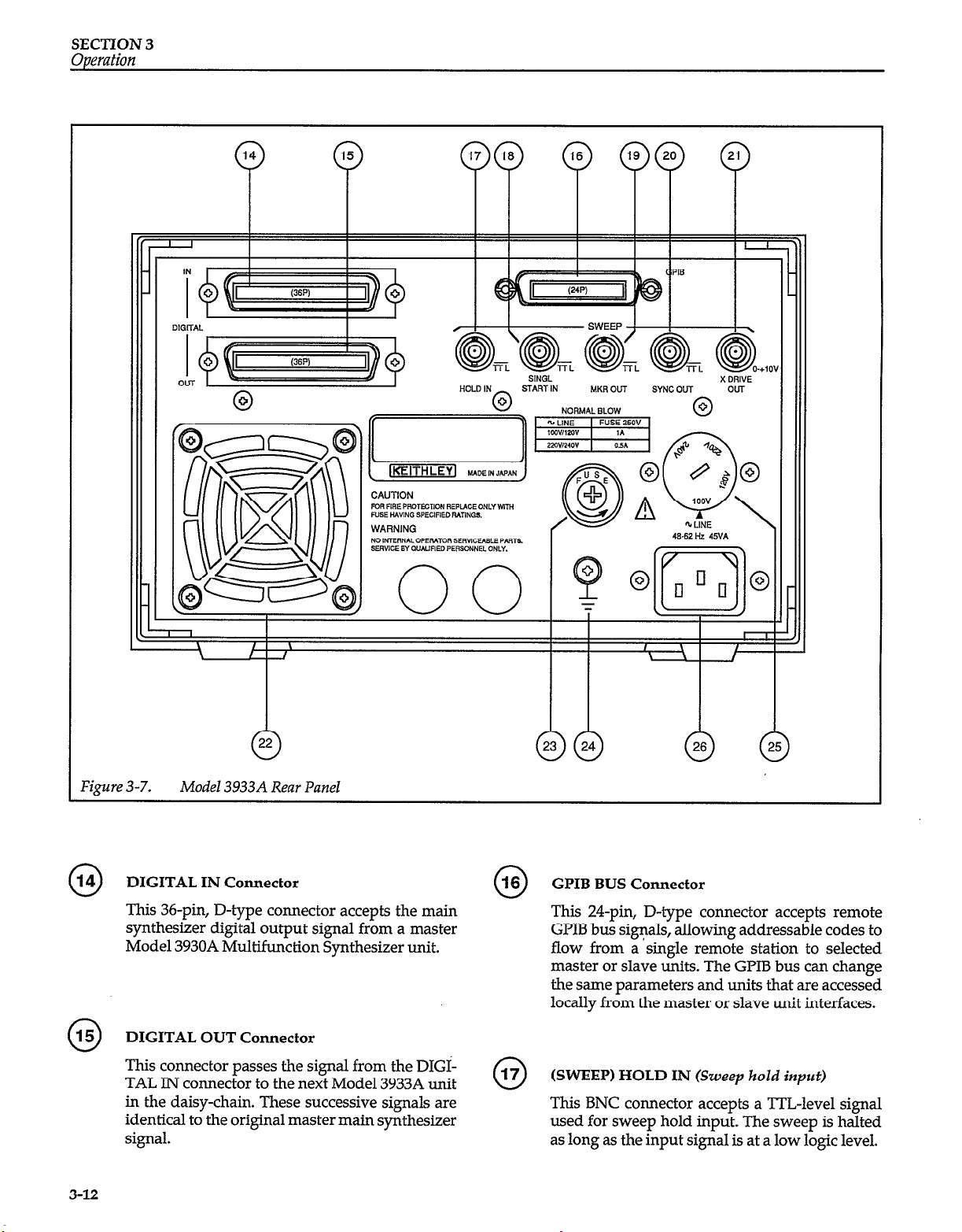
The Model 3933A rear panel contains five BNC connectors, two D-type connectors with 36 pins, and one D-type
connector with 24 pins. Four BNC’s are TTL level signals,
one BNC is analog, and the three D-types are digital signals. All BNC signals are directly associated with SWEEP
signals.
The following paragraphs describe, in detail, the connectors and other aspects of the Model 3933A rear panel,
which is shown in Figure 3-7.
OUT
(BNC Connector)
Connector
Rear Panel Description
3-11
Page 29
SECTION 3
Operation
IN
DIGKA
I
(3W
SINGL
X DRIVE
t
-+1ov
Figure 3-7.
14
0
Model 393314 Rear Panel
DIGITAL IN Connector
This 36-pin, D-type connector accepts the main
synthesizer digital output signal from a master
Model 3930A Muhifunction Synthesizer unit.
18
0
48-62 Hz 4SVA
I/,n,
GPIB BUS Connector
This 24-pin, D-type connector accepts remote
GPIB bus
flow from a single remote station to selected
master or slave units. The GPIB bus can change
the same parameters and units that are accessed
locally from the master or slave unit interfaces.
sipals,
allowing addressable codes to
15
0
3-12
DIGITAL OUT Connector
This connector passes the signal from the DIGITAL IN connector to the next Model 3933A unit
in the daisy-chain. These successive signals are
identical to the original master main synthesizer
signal.
17
0
(SWEEP) HOLD IN
This BNC connector accepts a TTL-level signal
used for sweep hold input. The sweep is halted
as long as the input signal is at a low logic level.
(Sweep hold input)
Page 30

SECTION 3
Operation
18
0
19
0
20
0
21
0
(SWEEP) SINGL START IN
start input)
This BNC connector accepts a TTL-level signal
used to start a single sweep. A single sweep
starts at the falling edge of the input signal.
(SWEEP) MKR OUT (Sweep
This BNC connector provides a TTL-level signal
used for sweep marker output. This signal goes
low when the frequency rises above the marker
frequency during a sweep. It remains high at all
other times.
(SWEEP) SYNC OUT (Sweep synchronous out-
put)
This BNC connector provides a TTL-level signal
for sweep synchronous output. This signal is at
low level while a sweep is progressing from the
start phase to the stop phase. It is at a high level at
all other times.
(SWEEP) X DRIVE OUT
output)
(SingZe-sweep
marker output)
(Sweep X-axis drive
CAUTION
Immediately turn off the power to the unit if
the fan ceases to operate. Be careful not to obstruct the exhaust ports on the upper and
lower panels. Failure to observe these precautions may result in instrument damage.
FUSE
23
0
24
0
0
If the Model 3933A is connected to an ungrounded AC outlet, connect the grounding
terminal to safety ground using #18AWG
minimum wire before use.
(Line Fuse)
The fuse holder cap can be removed with a
Philips screwdriver. Turn the cap counterclockwise to access the fuse. Always use a fuse with an
electrical rating that matches the input line voltage setting in use.
-L
(Grounding terminal)
The grounding terminal is connected to the chassis of the Model 3933A. To prevent interference
and for safety, be sure to ground this terminal.
WARNING
.
22
0
This BNC connector provides the signal for
sweep X-axis drive output. The output voltage
ranges from OV to lOV, and it increases and decreases according to the sweep direction, as the
sweep is generated. This output signal is intended for use as the X-axis drive for an oscilloscope or XY recorder.
AIR INTAKE PORT
An air intake port is on the rear panel for cooling.
Allow at least four inches of clearance behind the
port and any obstruction.
When the air filter becomes dirty, pull out on the
central plastic section of the air filter housing
cover and remove the filter element. Clean the
filter element with pressurized air or wash it
with a mild detergent. Make sure that the filter is
completely dry before re-installing it in the unit.
The filter should be cleaned at least once every
three months when used in a clean environment,
or at least once a month in a dirty environment.
25
0
26
0
LINE VOLTAGE SELECTOR
switch)
This switch sets the Model 3933A for the correct
line voltage. Using a flat-blade screwdriver, set
the switch in the proper position for the supply
voltage in your area.
WARNING
Disconnect the line cord before changing
setting the switch position.
CAUTION
Operating the Model 3933A on an incorrect
line voltage may result in instrument damage.
LINE
(Power input connector)
The LINE connector is used to connect the instrument to AC power.
(SuppZy voltage
3-13
Page 31

SECTION 3
Operation
WARNING
To avoid the possibility of electric shock,
connect the Model 3933A to grounded AC
outlet.
The fuse holder is located above, and to the left
of, the LINE connector. The fuse can be replaced
by disconnecting the line cord and unscrewing
the fuse holder cap with a screwdriver. Replace
only with the type indicated below.
Fuse Keithley
Line
Voltage
1 lOV, 120v 1A
220,240V
NOTE Fuses are 5 x 20mm and have 25OV, normal blow ratings.
Current Part
Rating Number
0.5A
c
I-
FU-96-2
F-U-96-1
3.3 STARTUP
1. Check that the supply voltage switch is set at the
proper position for the supply voltage. The allowable supply voltage range is flO% of the voltage at
which the supply voltage switch is set.
CAUTION
Operating the Model 3933A in an incorrect
line voltage may result in damage to the unit.
2. Make sure that the power is off, then plug the supplied power cable firmly into the LINE connector on
the rear panel of the Model 3933A. Insert the power
plug into a grounded AC power receptacle.
WARNING
To avoid the possibility of electric shock, use
only a grounded AC receptacle for the power
connection.
Turn on Model 3933A power by pressing in on the
front panel POWER switch. Power is ON when the
POWER switch button is depressed (in); power is
OFF when the POWER switch button is released
(out). When the power is turned on, the Model
3933A will begin normal operation, and the liquid
crystal display backlight will turn on.
3. When the power is first turned on, the Model 3933A
will return to the settings in effect prior to the last
power-off, and the unit will display the phase shif-
ter’s main parameters.
If the previous settings were not stored correctly, the
error code “Er MEMOll” message is displayed, fac-
tory preset parameters will be placed into effect and
displayed. At this point, parameters in effect prior to
the preceding power-off will be lost. This situation
occurs when the memory backup battery has insufficient charge, and memory data cannot be maintained.
A fully-charged battery can retain memory for approximately 60 days. This period, however, varies
slightly with ambient temperature and from one battery to another. Approximately 50 hours, with the
unit connected to line power, are required to fully
charge a dead battery.
When the battery no longer sustains sufficient
charge for practical use, contact your Keithley representative or the factory for information on obtaining
a replacement.
4. The backup battery may be discharged when the
Model 3933A is used for the first time after being
purchased, or if the unit has not been connected to
line power for a considerable length of time. Connect
the unit to line power for at least several hours to
charge the battery.
5. Sweep operation mode parameters are not stored
when the power is turned off. Therefore, turning the
power off during sweep operation, sweep hold, end
of single sweep, start phase output, or stop phase
output, will result in a loss of sweep state information the next time power is turned on. At next powerup, the LCD will, however, indicate the output
phase at the moment of previous shut-down.
Waveform output is not saved at shut-down and the
Model 3933A is shipped with waveform output set
to the “on” state during power-up sequencing. This
can be set to “off” via an internal jumper pin. See the
Model 3933A Service Manual for details.
6. If, at power-on, the phase shifter beeps and displays
error code “Er NODTW and the error message “NO
SYNTH DATA COMING”, there is a missing, or improper, digital signal at the rear panel of the slave
Model 3933A.
This situation can arise under the following condi-
tions:
0 Master Model 3930A power switch is in the “OFF”
position.
3-14
Page 32
SECTION 3
Operafion
.
A cable is not connected between the slave Model
3933A and a master Model 3930A.
0
A digital cable is missing, or disconnected, between
successive Model 3933A units in a phase shifter
chain.
7.
If, at power-on, the Model 3933A displays the error
code “ER FRDTO7”, it indicates:
0
The last time the power was turned off the waveform
setting was “variable-duty-cycle” square wave.
.
The master Model 3930’s frequency exceeded
lookH.z.
.
In this case, the setting will automatically change to
duty-cycle fixed 50%.
8.
If, at power on, the Model 3933A fails to operate in
one or more of the following conditions, contact
your Keithley representative or the factory to determine the correct course of action.
.
Unit does not power-up according to the mode and
settings in effect immediately before last power-off.
.
Unit does not power-up according to the preset operating modes.
0
Main display does not appear.
Note: After turning off Model 3933A, wait at least
five seconds before turning it on.
NOTE
For precise measurement applications, allow
the Model 3933A to warm up for at least 30
minutes to allow internal circuits to stabilize.
the unit is in the GPIB remote mode, or when the front
panel lock is enabled.
Some parameters, such as waveform, can be selected by
pressing a single numeric character. Changes are made
by simply pressing the numeric key corresponding to the
desired setting, as shown in the display. An error message will be displayed if the entered value is outside the
allowed range. Other displays and internal settings remain unchanged when an error occurs. Values may be
changed as many times as desired, without leaving the
present display. Pressing DSPL returns the display to the
main settings and the final change will be indicated.
Example: Changing the waveform type from the present
sine wave) to I-L (square wave) or to A (triangular
QC
wave).
Key Operation 1 Display Result
I
Press FCTN.
Press 3
Existing waveform selection
if
ed.
>3
(<SIN>11 will be displa
Waveform changes to <
(square wave).
Press 2
Waveform changes to < A >2
(triangle wave).
Press 3
Waveform changes back to <n >3
(square wave)
Press DSPL
Display indicates main settings,
including final choice CL >3
(square wave).
Parameters, such as amplitude and phase, which require
units (deg, V, dbV, etc.) can be changed as follows:
3.4 OPERATING PROCEDURES
3.4.1 Setting Parameters Using Numeric
Keys
When the appropriate parameter key such as FCTN,
AMPTD, OFFSET, or PHASE is pressed, the parameter
narne and the present parameter value will be indicated
in the upper part of the liquid crystal display. The allowed range of the parameter setting and useful help information will appear in the lower part of the liquid crystal display.
The parameter value can be changed when the parameter
name indicated in the upper part of the liquid crystal display is flashing. The parameter name will not flash when
l
Press appropriate ENTRY key to select the desired pa-
rameter.
l
Enter new numeric value (for phase or amplitude)
with the numeric keys.
l
Press appropriate ENTER key to add designator (V,
deg, mV, etc.).
While entering the new value, the existing parameter
value, unit display, and modification step size will disappear from the display,
and the new value will be dis-
played. To correct an entered value during the entry
process, press the RUB OUT key, which will delete one
character at the units position (immediate left of decimal
point) of the entered number. To re-enter the entire parameter value from the beginning, press the same parameter key to return to the corresponding parameter
setting.
3-15
Page 33

SECTION 3
Operation
For amplitude, which has several unit value options, select and press the appropriate units key to complete the
entry process. For phase and marker phase parameters,
which have only single parameter units, press any one of
the ENTER keys to complete entry.
Regardless of the number of digits for the entered value
and the size of the units (set, msec, V, mV, etc.), the predetermined number of digits, resolution, and units will
be properly adjusted and displayed. When values below
the display resolution are entered with the numeric keys,
a beep tone will sound, an error message will be displayed. and the display will return to the previous value.
Internal settings will remain unchanged when an error
condition occurs.
Example: Change amplitude from a existing value of
+178” to a new value, -98”, and then correct an erroneous
entry of “95.”
Key
Operation
Press PHASE
Press 9
Press 5
Press Phase
Press -I-
Press 9
Press 8
Press deg
Press DSPL
3.4.2
Setting Parameters with the
1 Display Presentation
I
Existing parameter, “178 deg”, will
be displayed.
The value of the key pressed, (9),
will appear.
The display now shows erroneous
figure: “95”.
The display again indicates the
original setting of “178 deg”.
Display indicates “-“. NOTE: This
key is a character toggle between
N+N and ‘,-Me
The display indicates “-9”.
The display indicates the desired
“-98”.
The display indicates the correct
value “-98 deg”.
Entry is complete, and display
shows main parameters, with
desired phase values.
MODIFY Controls
You can change parameter values with the MODIFY
knob and cursor keys in the following cases:
1. The name of the parameter to be changed is blinking
in the upper part of the liquid crystal display.
The parameter name indicated in the upper part of
the liquid crystal display will not flash when the unit
is in the GPIB remote, or when the keyboard lock is
on.
2. In the situation in step 1, the existing value specified
is displayed and the modification step size is presented in the upper right corner of the liquid crystal
display.
Modification step size will not be displayed during
numeric key input. Modification cannot be performed during numeric input.
For parameters which are selected with one numeric
character, such as waveform and oscillation mode, the
flashing cursor is fixed below the numeric character and
cannot be moved. The step size is fixed to H and cannot
be changed.
For parameters that require units, such as amplitude, the
step size can be changed by pressing the STEP SIZE key.
It is not necessary to use a units key when changing the
value with the MODIFY knob. When modifying an existing value, the modified value will automatically replace
the old parameter value, and the existing units will remain unchanged.
When the step size is indicated in the right-most position
of the liquid crystal display, each time the STEP SIZE key
is pressed the step size will change in the following order
fl x+2 x+10 rtl .
When the step size is rtl, you can specify the digit for UP/
DOWN adjustment by placing the flashing underline
cursor under the appropriate digit with the cursor keys,
and turning the MODIFY knob to the right or left. When
the step size is x+2 or x+10, the cursor will disappear, and
you can multiply or divide the entire value by two or ten.
Simply turn the MODIFY knob to the right or left. The
step size and the existing cursor position will be stored
with the respective parameters when those parameters
are stored in memory.
Changing a value by modification will never result in an
error because the modification process automatically
limits parameter adjustments to the maximum allowed
range for that particular parameter. The MODIFY keys
cannot be used to store or recall memory locations, or to
set the GPIB address and delimiter; only the numeric
keys can be used to program these operating modes.
3-16
Page 34

SECTION 3
Oueration
3.4.3
Error Codes
When an error occurs, the Model 3933A displays an error
code in the upper right corner of the liquid crystal display, and the unit generates a long beep sound (if the
beep sound setting is ON). The Model 3933A then displays the existing specified parameter value.
Displayed error codes and their meanings are summarized below. The error number at the end of each code
name corresponds to the GPIB error code.
Er GPIBOO
l
The Model 3933A received a non-recognizable programming or inquiry command over the GPIB.
Examples:
“ABC 2” Non-recognizable programming command.
“?ABC”: Non-recognizable inquiry command.
“123.4”: Parameter values without headers.
Er UNIT01
l
You attempted to specify an incorrect parameter unit.
Example:
You pressed the % or SEC key while setting the phase.
l
You attempted to select an unacceptable unit for other
settings.
Example:
You attempted to specify an amplitude value other than
p-p for a DC waveform type.
Er PHASE03
l
You attempted to set a phase value exceeding i360”.
l
You attempted to set values exceeding the allowable
range for sweep start, sweep stop, center, or marker
phase.
l
You attempted to set a sweep center or span phase
with a value exceeding the start or stop phase range.
l
The Model 3933A received a command that is not recognized in the existing mode.
Example:
Phase setting command is given during sweep operation.
l
The Model 3933A received a command string that is
beyond the capacity of the GPIB input buffer.
Er AMPT04
0 You attempted to specify an amplitude setting outside
the range specified in Tables 3-l and 3-2.
Er OFST05
l
You attempted to specify a DC offset value greater
than half the amplitude setting.
3-17
Page 35

SECTION 3
‘Operation
Table 3-l. Main Synthesizer Amplitude Range When DC Offset is 0 Volts
output
Range
Mode
AUTO
FXD
AC
(P-P)
3o.ov - 3.oov
2.99V - 300mV
299mV - 3O.OmV 105mV - 10.6mV
29.9mV - 0.30mV
3o.oov - o.oov
10.6V - 1.06V
1.05V - 106mV
10.5mV - O.llmV
(VP-p only)
2/n\
ITIllS
3o.ov - 3.oov
2.99’3 - 300mV
299mV - 3O.OmV
29.9mV - 0.3OmV
3o.oov - o.oov
l3llS
3o.ov - 3.oov
2.99V - 300mV
299mV - 3O.OmV
29.9mV - 0.30mV
3o.oov - o.oov
15.ov - 1.5ov
1.49V - 150mV
149mV - 15.OmV
14.9mV - 0.15mV
(V - on1 >
I
/L
I
I
II
dBV (v-v)
20.5 - 0.5
0.4 - -19.5
-19.6 - -39.5
-39.6 - -79.2
(VP-P only)
23.5 - 3.5
3.4 - 16.5
-16.6 - -36.5
-36.6 - -76.5
(VP-p only)
dBV
dBV
Hardware
Resolution
15mV
1.5mV
15o/.lv
15/L-v
15mV
Hardware
Resolution
(v-v)
Hardware
Resolution
(P-P)
15mV
1.5mV
15opv
15yv
15mV
output
Attenuator
NOTE 3
l/l
l/10
l/100
l/1000
l/l
I
output
Attenuator
NOTE 3
l/l
l/10
l/100
l/1000
l/l
3-18
Table 3-2. DC-only Voltage Setting Range, Resolution, and Accuracy
(open load, 18 to 28°C)
output
Range
Mode
Hardware
Resolution
Accuracy NOTE 3
f (0.1% + 8mV)
I!I (0.6% + 0.8mV) l/10
C(1%+8O/.tV) l/100
Not stipulated
f (0.1% + 8mV)
output
Attenuator
l/l
l/1000
l/l
Page 36

SECTION3
Operafion
Er ACDCOG
With a waveform other than DC and a non-zero DC offset
(in other words, the DC offset was to be added to the AC
waveform), you attempted to specify an invalid amplitude or DC offset value.
The following restrictions apply when adding DC offset
to the AC waveform:
Table 3-3. AC + DC Minimum Amplitude, Resolution, and Accuracy (open load)
Minimum AC Amplitude Hardware Hardware
Output Cumulative
Range Voltage
Mode
NOTE4
P-P rms
AUTO More than 286mV 1OlmV
2/
dbV Resolution Resolution Accuracy
-19.9
1.5v plitude setting
AC amplitude setting Ivp-PI + DC offset voltage setting
2
l
The amplitude setting must be equal to or larger than
[VP-PI45
volts.
the minimum AC amplitude determined by the sum
of the voltages above. In addition, the DC offset must
not be added to limit the above restrictions. See Table
3-3 and paragraph 3.4.7 for more details on these re-
strictions.
AC DC output
Amplitude Voltage DC Voltage Attenuator
NOTE 3
15mVp-p 7.3mV +(0.2% of AC am-
1/l
(p-p) +O.l% of DC
voltage setting
+8mV)
More than 28.6mV lO.lmV
-39.9 1.5mVp-p
73opv +(0.2% of AC am-
l/10
150mV plitude setting
(p-p) +0.6% of DC
voltage setting
+0.8mV)
More than 2.86mV l.OlmV -59.9 15opvp-p 73pv +(0.2% of AC am- l/100
15mV
plitude setting
(p-p) +1% of DC
voltage setting
+8Ot-tv)
Less than
0.3OmV O.llmV -79.2
15PVP-p
7.3pv
(Not stipulated) l/1000
15mV
Not related o.oov
Pip-p only>
15mVp-p 7.3mV +(0.2% of AC am-
1/l
to cumula- plitude setting
tive voltage (p-p) +O.l% of DC
voltage setting
+8mV)
3-19
Page 37

SECTION 3
Ot7erafinn
output
Range
Mode
AUTO
AC + DC Minimum Amplitude, Resolution, and Accuracy (open load).
Cumulative
Voltage
NOTE 4
More than
1.5v
More than
150mV
More than
15mV
Less than
15mV
T
Minim
P-P
286mV
28.6mV
2.86mV
0.30mV
n AC Amplitude
2//l\
82.5mV
8.25mV
0.83mV
0.09mV
dbV
-21.6
-41.6
-61.6
-80.9
-r
Hardware
AC
Amplitude
Resolution
15mVp-p
1.5mVp-p
15o/.l.vp-p
15FVP-P
Hardware
DC
Voltage
Resolution
7.3mV
73ojJv
73/.&v
7.3)lv
DC Voltage
Accuracy
+(0.2% of AC amplitude setting
(p-p) +O.l% of DC
voltage setting
+8mV)
+(0.2% of AC amplitude setting
(p-p) +0.6% of DC
voltage setting
+0.8mV)
f(0.2% of AC amplitude setting
(p-p) cl% of DC
voltage setting
+80/~V>
(Not stipulated)
(Cont.)
output
Attenuator
NOTE 3
1/l
l/10
l/100
l/1000
FXD
Not related
to cumulative voltage
o.oov
<VP-p only)
15mVp-p
7.3mV
+(0.2% of AC amplitude setting
(p-p) +O.l% of DC
voltage setting
+8mV)
l/l
3-20
Page 38

AC + DC Minimum Amplitude, Resolution, and Accuracy (open load) (Cont.)
SECTION3
Operation
Minimum AC Amplitude Hardware
Output Cumulative
Range Voltage . Amplitude Voltage DC Voltage
Mode
AUTO More than
NOTE 4
P-P
286mV 143mV -16.9 15mVp-p 7.3mV +_(0.2% of AC am-
ITIllS
n
dbV Resolution Resolution Accuracy
AC DC
Hardware
1.5v plitude setting
(p-p) +O.l% of DC
voltage setting
+8mV)
More than 28.6mV 104.3mV -69.9 1.5mVp-p 73oj.lv +(0.2% of AC am150mV
plitude setting
(p-p) +0.6% of DC
voltage setting
+OSmV)
More than 2,86mV 1.43mV -56.9 15o/.lvp-p
15mV
73pv
&(0.2% of AC am- l/100
plitude setting
(p-p) +l% of DC
voltage setting
+8OcLv)
Less than
0.3OmV 0.15mV -76.5
15lJVP-P
7.3pv (Not stipulated) 1 /lOOO
15mV
FXD
Not related
to cumulative voltage
o.oov
wp-p only)
15mVp-p
7.3mV +(0.2% of AC amplitude setting
(p-p) +O.l% of DC
voltage setting
+8mV)
output
Attenuator
NOTE 3
1/l
l/10
l/l
NOTE
3:
NOTE 4: Cumulative voltage = ACamplitude setting (p-p) $vid$ by 2 plus DC voltage setting 0.
NOTE 5: DC voltage accuracy is when frequency is about lkHz,f b , AM off, open load, 18 to 28 degreesc.
When switching the output attenuator, the waveform output goes off for a moment.
3-21
Page 39
SECTION 3
Operation
Er FRDT07
You tried to set the Model 3933A for a square wave
with variable duty cycle while the Model 3930A was
sweeping at, or set for, a frequency exceeding the
square wave limit of 1OOkHz.
The error is displayed and then the display indicates
main parameters.
The Model 3933A initiated a sweep exceeding the
Model 3930A limit of lOOkHz, or the Model 3933A was
making a square wave of variable duty cycle, while the
Model 3930A was set to a frequency value higher than
1ookHz.
Under these conditions, the duty cycle changes to
fixed 50% and, following the error display, the duty
cycle display appears.
You tried to turn on the Model 3933A, and set it for a
variable duty cycle square wave, while the Model
3930A was set for, or sweeping at, a frequency exceed-
ing the square wave limit of lOOkl!Iz.
In this case, the previous settings in memory are modi-
fied to produce a fixed 50% setting. Following the error display, the main parameters are displayed.
Er CNVTlO
o
The result of the units conversion sequence is outside
the allowed range of the given value.
Example:
You attempted to convert to an rms value when the
waveform is set to sine wave with an amplitude of
03OmVp-p. The Model 3933A automatically converts
this to O.lOmVrms, which is below the lower limit of
O.llmVrms.
Er MEMO11
A power-on error was found in the backup memory
for one or more parameter settings. If this error occurs,
preset values will be placed into effect, and you should
make any new value settings using the front panel
controls.
An error was found in the contents of the memory
while recalling parameters. Parameter settings will
not be changed, and the Model 3933A will return to the
prompt for the memory number to recall.
When the Model 3930A is set beyond the 1OOkHz
square wave limit, or it is sweeping beyond this limit,
you tried to set a variable duty cycle by recalling a
memory location containing that setting.
Under these conditions, the recalled setting for square
wave is changed to fixed 50%. Following the display of
the error message, the main display is turned on. The
actual data in that memory location is not altered.
Er SWPOS
l
You attempted to perform a sweep with a range of
zero degrees.
Er RNGE09
l
You attempted to specify a value outside the predeter-
mined range, resulting in a condition other than errors
02 through 08.
Examples:
You entered a value of 6 during waveform selection.
You attempted to set the sweep time to 3msec.
Er NODT12
The Model 3933A (slave unit) has detected a problem
between the Model 3930A (master unit) and itself, or a
problem exists somewhere in the chain of master and
slave units. A slave unit will not operate if the master
unit is not powered-up or if there is a break in the communications link (Digital In/Out cables) from one
slave to another, or between the master unit and a
slave unit.
If the slave unit detects that the power of the master
unit is off, the signal output will be turned off, and the
error display will appear. The Model 3933A slave unit
will not recognize further parameter settings until the
power of the master unit is turned on or the communications error condition is corrected.
3.4.4
Amplitude Units Conversion
Note that internal settings remain unchanged when the
units conversion is performed. The Model 3933A automatically displays the result of units conversion as the existing specified value, and you can modify the value using the converted units, if desired.
3-22
Page 40

SECTION 3
ODeration
p-p, rms to dBV:
p-p, dBV, to rms:
rms, dBV, to p-p:
Note that amplitude conversion units do not correlate 1
to 1 with the original base unit. Therefore, following units
conversion, rounding of units occurs with slight shift in
display units caused by internal resolution limits. Thus,
the system will never return to precisely the same set-
tings following a conversion.
Phase
Pressing the PHASE key displays the present phase settings and allows you to modify that parameter. The allowed phase range is from -360.0” to 360.0”, with 0.1”
resolution.
If the PHASE key is pressed during a sweep execution,
the display indicates actual phase angle being executed at
the instant the key is pressed. If the sweep is under
HOLD control, the display indicates the phase being executed at the moment HOLD took effect. Under these conditions, the setting cannot be changed.
Press the dBV key when the Model
3933A displays the p-p or rms value.
Press the Vrms or mVrms key when
the Model 3933A displays the p-p,
or dBV value.
Press the V or mVrms key when the
Model 3933A displays the rms or
dBV value.
If the step size is +l, a clockwise step of one detent of
the MODIFY knob will produce a modification factor
of +l at the numeric position indicated by the blinking
cursor. If the modification factor is &5, the change will
increase by five. A counterclockwise click will cause a
corresponding decrease in value.
A step size of x+2 or x+10 will react differently than the
above modifications. In this case, a click clockwise will
multiply by two or ten. A counterclockwise click will
divide by two or ten. However, under these conditions, the entire numeric entry, not just the indicated
numeric position, will be multiplied or divided. When
changes are made with these step sizes, the first modified value will be rounded upward by the internal system and the results will not be a one-to-one correlation
to the original value.
change will be mathematically correct.
Modification via the MODIFY knob will have no further effect when the next increase or decrease operation will exceed the allowable limits. Thus, if the existing phase value is 240”,
value via the MODIFY knob, while the step size is set
at x+2, the operation of the knob has no effect on the
numeric input.
The Model 3933A’s phase value is directly related to
the signal output from the Model 3930A. The phase
value is the offset from the master unit signal. The
Model 3930A phase is considered phase one. The first
Model 3933A, in any multiphase chain, is phase two.
The second successive Model 3933A is designated as
phase three, to the allowable maximum of six phases
(one Model 3930A and five slaves). Phase, amplitude,
offset and waveform may be set independently for
each unit in the chain. See Figure 3.3 for details in set-
ting up a multiphase system.
However, each successive
and you try to double that
Under other conditions, where the system allows phase
modification, the modifications can be made using either
the numeric keypad and/or the MODIFY knob. The numeric position designated by the blinking cursor can be
modified as follows:
The indicated value can be increased or decreased by
direct entry from the numeric keypad.
The indicated value can be increased or decreased by
the MODIFY knob, with each detent producing a specific stepped change in value.
The step size change produced with the MODIFY
knob is controlled by the STEP SIZE key. The value of
the change is in four possible settings: 51, f5, x+2, and
x+10.
The primary basis for all phases is the 0’ point of the first
phase (master unit phase one). This is not sent directly to
other units. This first phase is dependent on the start/
stop settings of the master unit and that is directly dependent on the sweep trigger source. When a Model
3930A (master unit) is used alone, the phase settings
work as start/stop parameters only when in burst and
gate modes. However, when the master unit is hooked
up to a Model 3933A slave unit, the master phase settings
work the same way as those in a Model 3933A slave unit.
The phase difference between the master phase one and
the Model 3933A phase is:
(Mode13933A phase) - (Model 3930A start/stop phase setting).
3-23
Page 41

SECTION 3
Operation
If the master phase is set to 0”, with no special limits, each
tit’s phase can be read directly.
Sine Wave
Phase
0’ 180' 3600
Square Wave
with Duty Ratio
Fixed at 50%
. .“““.
ti.3 deg. -$-+--
iif
Phase
I I
0” 180” 360" 0"
(Shaded area is the hysteresis region
wi~ich changes to high or low
depending on the phase history)
I I
! I 1
I I
+
I I
t
Phase definitions for the available waveforms are illustrated in Figure 3-8.
Triangular Wave
Phase
Phase
0" 180" 360"
Square Wave
with Variable Duty Ratio
?-?
I I
I
I
A
I
I
I
Q
360"
w
w
*
Figure 3-8.
3-24
Rising Sawtooth Wave Falling Sawtooth Wave
I
I
180" 360"
I
b
Phase
I
I
00
Waveforms and Their Phase Definitions
Phase
I
00 180" 360'
I
I
I
I
+
Page 42

SECTION 3
Operation
3.4.5 Amplitude Programming
Pressing AMPTD displays the existing amplitude setting
and enables amplitude programming.
When using numeric keys to set the amplitude, press the
appropriate units key to complete the entry process.
Press V or mV to enter p-p units, use Vrms or mVrms for
rms units, or press dBV for dB units.
The rms and dBV values are set on the assumption that
the average, or center level, of the peak-to-peak amplitude of the waveform is OV. Thus, these values do not depend on the DC offset value or square-wave duty cycle.
You can use the MODIFY keys to change the amplitude.
The AMPTD key sets the amplitude for AC waveforms
only; use the OFFSET key to set the DC output voltage of
the DC waveform type. When the DC waveform is selected, you still can program the AC amplitude, but that
value can be entered only in p-p units within the allowed
amplitude ranges from 2.OOmV p-p/no load to 2O.OV pp/no load. The specified value is stored, and it is used as
the given amplitude for the next selected AC waveform.
For AC waveforms with OV DC offset, you can specify
any value within the maximum and minimum allowed
amplitude limits without restrictions. If, however, the
programmed DC offset is not OV, certain restrictions con-
cerning the maximum allowable amplitude apply. Para-
graph 3.4.7 describes these restrictions in more detail.
With a DC waveform, the programmed offset voltage is
the DC voltage value that appears at the output jack.
Valid offset values are within the range of +lOV to -lOV.
For all AC waveforms, the DC offset is added to the average value of the peak-to-peak amplitude of the AC
waveform. Certain restrictions apply for amplitude-offset combinations, and some combinations of
values
may
cause an error (Er ACDC07) to occur. See paragraph 3.4.8
below for more details.
When a DC offset setting that causes a change in output
attenuators is programmed, the output may be turned off
for approximately 100msec during the switching period.
3.4.7 AC Amplitude and DC Offset
Relational Restrictions
AC amplitude and DC offset settings are subject to relational restrictions. See Table 3-3 (paragraph 3.4.3) and
Figure 3-9 for more details on the interaction between
these two parameters.
These restrictions are a result of the limitations in the
maximum output voltage of the output amplifier. When
the DC offset is added to the AC waveform, the output
voltage peak will be the sum of the DC offset voltage and
half of the AC waveform amplitude. This voltage is
known as the total voltage and is related as follows:
Set AC amplitude
(VP-P)
2
+ Set DC offset
voltage (VI
When the main synthesizer amplitude is changed, an offset voltage may appear at the output jack for less than
lmsec until the output stabilizes at its new value. In addition, an amplitude setting change, which causes output
attenuator switching, may cause the output to be turned
off for about 100msec during switching.
3.4.6
DC Offset Programming
Pressing the OFFSET key displays the existing DC offset
value and enables offset programming.
When using the numeric keys to set the offset, press the V
or mV key after entering the value to complete the entry
process. As with other parameters, you can also use
MODIFY key to change an existing offset value.
This voltage is limited by the maximum output voltage of
the output amplifier.
ExampIe:
An error will occur when you try to set the DC offset to
6V/no load when the amplitude is 1OV p-p/no load.
(The total voltage exceeds lOV/no load.)
Example:
An error will occur when you try to set the amplitude
to 1OOmV p-p/no load when the DC offset is 5V/no
load. (The minimum AC amplitude when the total
voltage is over lV/no load is 200mV p-p. The amplitude setting is below the
minimum amplitude value.)
3-25
Page 43

SECTION 3
Operation
M
1.5
0.15
0.1
15m
10m
15
10
1
PI
------
------_
10 1 0.1
I I
I I
I I
-
-
-
- - - -
-- -_ -- -_
- - -. - - -. - -
--- ---
ii
c:
i0m lm O.lm O.Olrr
-rr-ri
-I-
I-
I I I I I I I
I I I I I I I I I
-I- I- -I- I-
- I- - II I I I
- I- t- - I- t- -t -I -t -I
L-
I I
I I I
I I
+ -t I
I I
+ -t -I + -t -I
I- - I- -
- -
vl
-
I
I
I
I
I
ATT
111
I
I
I I I I
-1 -1
-I -I
ATT
l/l0
zc&:
All-
11100
4OdB:
-+ -I -+ -I
-
Hoc%
TOdB)
- -
%-h-=-P
- - L
-
-
- -
-
I I I
I I I
I I I
I I
I I
I I
I I
11
-1Om
-15n
-0.1
-0.15
-1
-1.5
-10
-15
I-
L
---_
- ---
---_
- - -
-
---
-
f
- .
-
I
Al-l1IlM:
‘40dB
--- -_
ATT
- -
- -
1110
2OdB:
-- ---
I
Output Range Mode AUTO
(settinp K?SOlUtioIl3 places
at ii 5 to fl mV)
---
-----
A77
i/i
WB)
I
- -
- -
I
Output Flange Mode FXD
(Setting resolution
fixed at 10 mV)
Figure 3-9A. Relational Range
3-26
for
Allowed AC Amplitude Voltage and DC Offset Voltage
Page 44
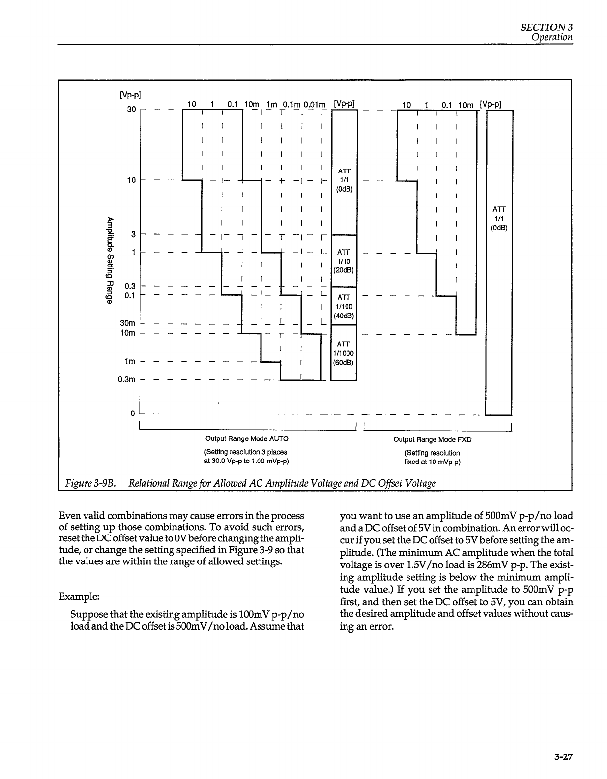
SECTION 3
Omrff fion
[VP-PI
30 --
r
10 --
I
30m - -
10m --
lm --
0.3m I - -
, 10 , 1 , 0.1 ,l0~,~m~.ln~~0,0lr1+
I I
I I
I I
I I
- II I
L L
-
-
------- ___
---
---- -I-
----
I I
I I
- I- 7
I
I
1 I I
I I I I
I I I I
I I I I
- + -I- II I I
I I I
I I I
- -
-r
-I- r
-l
I I
I I
-4
I I
-‘-7 I
-I- c
L - - IL.
--I- + -’
-----_
L; : I
- - - - - -~_.
I
I I
I I
- L
[VP-PI
Al-T
l/l
(OdB)
Al-i-
l/IO
(20dB)
ATT
l/100
(40dB)
A-IT
l/l 000
(60dB)
- -
- -
- -
, 10 , 1 , 0.1 ,lOm r[vP-PI
AlT
Ill
(OdB;
J
1
0 --
Figure 3-9B. Relafional Range@ Allowed AC Amplitude Voltage and DC Offset Volfage
Even valid combinations may cause errors in the process
of setting up those combinations. To avoid such errors,
reset the DC offset value to OV before changing the ampli-
tude, or change the setting specified in Figure 3-9 so that
the values are within the range of allowed settings.
Example:
Suppose that the existing amplitude is 1OOmV p-p/no
load and the DC offset is 500mV/no load. Assume that
-----------__
Output Range Mode AUTO
(Setting resolution 3 places
at 30.0 Vp-p to 1 .OO mVp-p)
- -.
-
----__
I
Output Range Mode FXD
(Setting resolution
fixed at IO mVp-p)
you want to use an amplitude of 500mV p-p/no load
and a DC offset of 5V in combination. An error will occur if you set the DC offset to 5V before setting the amplitude. (The minimum AC amplitude when the total
voltage is over 1.5V/no load is 286mV p-p. The existing amplitude setting is below the minimum amplitude value.) If you set the amplitude to 500mV p-p
first, and then set the DC offset to 5V, you can obtain
the desired amplitude and offset values without causing an error.
I
3-27
Page 45
SECTION 3
3.4.8
Waveform Selection, Square-Wave
Duty Cycle, and Synchronous Out-
put
Waveform Selection
Pressing the FCTN key displays the existing main syn-
thesizer waveform along with its corresponding number
and enables main synthesizer waveform selection. Avail-
able main synthesizer waveforms include: DC, SIN (Q >
i-L,r\l,&nd\.
To select a waveform with the numeric keys, simply
press the numeric key that corresponds to the desired
waveform. For example, press 1 to select a sine wave. The
waveform will change immediately when the corresponding key is pressed. It is not necessary to press a
units key.
When the Model 3933A displays the existing waveform,
and FUNCTION parameter selection is enabled, you can
change the waveform by turning the MODIFY knob.
Turning the knob clockwise increases waveform numbers, while turning the knob counterclockwise decreases
waveform numbers. The number changes by a value of
one for each detent. When the highest or lowest
waveform numbers are reached, the number will wrap
around to the lowest or highest selection. Allowable selections range from zero through five.
For all AC waveforms, the p-p value of the amplitude
will remain unchanged when you change the waveform.
If the output range mode is AUTO, and amplitude is
either rms or dBV, the amplitude will be converted to p-p
units when the waveform is changed.
expressed as a percentage. For example, a 1OkHz square
wave has a time period of 100psec. If the high portion of
the waveform has a period of 30pec, the duty cycle is
30/100x100=30%.
Two square-waveform duty cycle modes are available: a
duty cycle fixed at 50%, and one with a variable-duty-cycle. The duty cycle applies only to the square-wave function (waveform 31, although the duty cycle can be programmed while other waveforms are selected.
To change the duty cycle, press then DUTY key. When
the display indicates duty cycle, enter the new value
the numeric keypad, or modify the duty cycle with the
MODIFY knob. The allowable variable range is 5.0%
95.0%. If the Model 3933A is set to variable duty cycle, it
will remain in that mode even if you set the duty cycle to
50%. To select the fixed 50% duty cycle mode, press
SHIFT FXD50. In the duty cycle display mode, the Model
3933A displays “FXD” for the 50% fixed mode or “VAR”
for the variable duty cycle mode.
When the Model 3933A is in the variable duty cycle
mode, the upper-frequency limit is lMHz, and the maximum jitter is below 150nsec. The Model 3933A has a resolution of 0.1% for duty cycle display, but the hardware
resolution is 0.4% (8 bits). As a result, if you make a duty
cycle change lower than the hardware resolution factor,
only the displayed value will change, not the duty cycle
of the actual output.
Synchronous Output
via
to
Square-wave Duty Cycle
The duty cycle is the ratio of the waveform high-level du-
ration to one complete cycle of the waveform. This ratio is
3-28
Figure 3-10 illustrates the phase relationship between the
waveform and outputs at frequencies below IkHz. Typical jitter between the main synthesizer waveform output
and the main synthesizer synchronous output is about
9Snsec.
Page 46

SECTION 3
Overation
i-
NOTE: The x-axis is the lime axis, Indicating increasing time toward lhe right.
Figure 3-10. Phase Relationship Between Waveform and Oufpuf
3-29
Page 47

SECTION 3
3.4.9
Mark, Span, and Phase Parameter
Programming
Mark and Span Parameter Programming
Pressing the SPAN key displays the present span parameter and enables span parameter programming.
Similarly, pressing the SHIPI MKR key displays the present marker parameter and enables marker parameter
programming.
To program the MKR and SPAN parameters using the
numeric keys, enter the desired value, and press the appropriate ENTER key to complete the entry process.
When the Model 3933A displays the existing MKR or
SPAN value, and parameter entry is enabled, you can
change the MKR or SPAN value with the MODIFY knob.
When the step size is +l, you can specify the digit to mod-
ify by placing the flashing cursor under the appropriate
digit and turning the MODIFY knob to the right or left.
When the step size is x+2 or x+10, you can divide or mul-
tiply the value by the step size by turning the MODIFY
knob to the left or right.
phase setting. The (repeat) type moves from the start
phase through to the stop phase, instantly resets to the
start phase and, if required, begins another sequence. The
(step) type outputs the start phase signal, instantly
changes to the stop phase signal, then repeats the entire
cycle, as required.
Sweep time varies with the chosen sweep function. The
actual sweep time is shown below.
l
When chosen function is (recipro), actual sweep time
is
1. Execution time from start phase to stop phase.
2. Execution time from stop phase to start phase.
3. Half the execution time of a repeated continuous
sweep.
l
When chosen function is (repeat), actual sweep time is:
1. Execution time from start phase to stop phase.
2. Execution time of one continuous sweep.
l
When chosen function is (step), actual sweep time is:
1. Execution time for start phase signal in continuous
sweep.
2. Execution time for stop phase signal in continuous
sweep.
3. Half the execution time for a continuous sweep.
The relationship between START PHASE, STOP PHASE,
SPAN PHASE, CTR PHASE, and MKR PHASE is shown
in the following example.
You set the phase shifter to execute a START PHASE at
l
270”.
You set STOP PHASE at 129.5”.
l
0 The Model 3933A automatically sets the SPAN to
140.5”, and CTR becomes 199.7”.
The calculations are as follows:
SPAN = start phase - stop phase (270 - 129.5 = 140.5)
0
CTR = span phase - 2 + stop phase (140.5/2 = 70.25,
l
129.5 + 70.2 = 199.7; NOTE: 70.25 is rounded to 70.2)
Marker is not affected by this sequence.
SWEEP FUNCTION
There are three types of sweep functions available:
(recipro), (repeat), and (step). The (recipro) type starts
execution at the start phase, continuing through to the
stop phase, where it then reverses direction to the start
3.5 SWEEP OPERAlIONS
Starting a Continuous Sweep
Press SHIFT key, then CONT START key. The display in-
dicates phase values as they are executing, and the message: CONT SWEEP EXEC (EXIT: SWP OFF). The phase
parameters cannot be set during a continuous sweep operation.
Starting
Press the SINGL START key to initiate a single sweep.
During a single sweep, the Model 3933A displays the
sweep phase, and the following message: “SINGL
SWEEP EXEC (EXITSWEEP OFF)“. You cannot set the
phase with the PHASE key while the unit is generating a
single sweep.
When the Model 3933A terminates a single sweep, it displays the terminated sweep phase, along with the following message: “SINGL SWEEP END”. Once the sweep has
terminated, you can program the output phase with the
PHASE key. The MKR OUT and SWEEP SYNC OUT signals go high, and the X DRIVE OUT signal is set to OV at
the end of the sweep.
a Single Sweep
330
Page 48

SECTION 3
Operafion
Holding/Resuming a Sweep from the Front Panel
To temporarily halt execution of a continuous or single
sweep, press the HOLD/RESM key. The Model 3933A
stops the sweep operation immediately, and displays the
phase at which it stopped the sweep. The MKR OUT,
SWEEP SYNC OUT, and X DRIVE OUT signals maintain
their present values when the sweep is halted.
When a continuous sweep is paused, the Model 3933A
displays “CONT. SWEEP HOLD (EXITSWEEP OFF)“;
similarly the unit displays “SINGL SWEEP HOLD
(EXITSWBEP OFF)” when a single sweep is paused.
When the Model 3933A is in the sweep hold mode, you
cannot program the phase with the PHASE key.
To resume a sweep starting at the frequency at which you
stopped sweep operation, press the HOLD/RESM key
again.
Turning a Sweep Off to Enable Normal Phase Programming.
Press the SWEEP OFF key during a sweep or sweep hold
to turn off a sweep and enable normal PHASE key programming. The MKR OUT and SWEEP SYNC OUT signals will be set high, and the X DRIVE OUT signal will be
set to OV.
When the SWEEP OFF or PHASE keys are pressed at the
completion of a single sweep, during start phase output,
or during stop phase output, normal phase programming will be enabled. In addition, the MKR OUT and
SWEEP SYNC OUT signals will be set high, and the X
DRIVB OUT signal will be set to OV.
When the Model 3933A is in this mode, pressing the
PHASE key enables normal phase programming and sets
the X DRIVB OUT signal to OV.
Setting the Output to the Stop Phase
Press SHIRT STOP STATE to set the output waveform to
the programmed stop phase. While in this mode, the
Model 393314 displays the stop phase along with the following message: “SWEEP STOP STATE”. During the
sweep stop state, the MKR OUT and SWEEP SYNC OUT
signals are set high. X DRIVE OUT is set to 1OV if the start
phase is lower than the stop phase; it is set to OV if the
start phase is higher than the stop phase.
When the Model 3933A is in this mode, pressing the
PHASE key enables normal phase programming and sets
the X DRIVE OUT signal to OV.
Stopping Sweep Output to Enable Setting of Phase Parameters
If the Model 3933A is executing a sweep, or is under
HOLD control, you must press SWEEP OFF to enable
phase parameter modification. At this time, MKR output
and SWEEP SYNCHRONOUS output are set high, and X
DRIVE output is set to OV.
If SWEEP OFF or PHASE are pressed when single sweep
has terminated, or start phase and stop phase are in the
output state, phase programming is allowed. MKR and
SWEEP SYNCH outputs will be set high and X DRIVE
output is set to OV.
Starting a Single Sweep Using an External Signal
A TTL-level, falling-edge signal( % ), applied to the
SINGL START IN BNC connector, starts a single sweep.
This signal performs the same operation as pressing the
SINGL START key.
Setting the Output to the Start Phase
Press the START STATE key to set the output waveform
to the programmed start phase. During this mode, the
Model 3933A displays the start phase along with the following message: “SWEEP START STATE”. The MKR
OUT and SWEEP SYNC OUT signals also go high during
the start phase mode. The X DRIVE OUT signal is set to
OV if the start phase is lower than the stop phase; it is set
to 1OV if the start phase is higher than the stop phase.
SINGL START IN is internally pulled up to a high logic
level, and sweep operation is not affected when the this
connector is left disconnected from external signals.
Holding/Resuming a Sweep with an External Signal
A ‘ITL low level signal, applied to the SWEEP HOLD IN
BNC connector, places the Model 3933A in the sweep
3-31
Page 49

SECTION 3
Operation
hold mode. In the sweep execution mode, the Model
3933A halts the sweep as long as this input remains low.
If you attempt to start a sweep when this input is low, the
Model 3933A immediately enters the sweep hold mode.
Note that pressing HOLD/RESM does not resume
sweep operation with the hold signal held low; you must
set SWEEP HOLD IN high to resume the sweep.
SWEEP HOLD IN is internally pulled up to a high logic
level, and sweep operation is not affected when this connector is left disconnected from external signals.
3.5.1 Sweep Phase and Sweep Output
Relationships
Figure 3-10 illustrates how sweep PHASE, MKR OUT,
SWEEP SYNC OUT, and X DRIVE OUT signals change
with time.
The MKR OUT signal is low when the sweep phase is
higher than the marker phase. When the sweep function
is or, the high signal level is maintained even after a sin-
gle sweep is terminated.
Changing Settings During Sweep Operation
Because of processing execution time in the sweep execution mode, the Model 3933A may respond to the keys and
GPIB commands more slowly than in other modes. If you
change the sweep range, sweep time, or sweep function
with MODIFY while the Model 3933A is in the sweep
execution mode, the unit will recalculate the new parameters each time you change the setting, resulting in
slower response.
If you set the sweep range based on center and span
phases, an error may occur depending on the order of parameter selection, whether or not the Model 3933A is in
the sweep execution mode.
Example:
Assume CTRis set to 0”, SPAN is set to 180” and you wish
to change these values to 300 and 90, respectively. If you
try to set the CTR to 300, then the SPAN to 90, an error
will occur because the system sees this as an attempt to
set CTR to 390, which is out of range. It is necessary to set
SPAN to 90 first. Then set CTR to 300.
The SWEEP SYNC OUT signal goes low during the tran-
sition from the start phase to stop phase. When the sweep
function is, the phase changes at the center point of this
output signal.
The X DRIVE OUT jack supplies a voltage that varies be-
tween OV and 1OV in proportion to the lapse of sweep
time, and according to the direction of the sweep phase.
The X DRIVE OUT signal also varies linearly with time.
The X DRIVE OUT signal varies between OV and lOV,
corresponding directly to the change in direction of the
phase sweep.
Substituting Marker Phase for Center Phase
Press SI-IIFI CTR to set the center phase to the present
marker phase value. This operation produces the same
result as programming an identical phase with the nu-
meric keys. The marker phase is not affected by this op-
eration.
Number of Steps in a Sweep
Software controls the sweep in the Model 3933A. Therefore, instrument processing speed and phase shift resolution (12 bits) are the limiting factors in achieving a
smooth sweep curve, except, of course, in the case of a
stepped sweep operation.
The manner in which the sweep resolution is calculated is
shown below. The definition of “step quantity” is the
number of discrete steps between start phase and stop
phase, for the two linear functions (recipro), and (repeat).
Step width is derived from step quantity, as is shown in
the-following formula. - - -
Step Quantity =
Sweep Width (deg)
2
x 4096
or,
Sweep Time (set) x 2000
3-32
Page 50

SECTION3
Operafion
whichever results in better resolution.
Step Width =
Sweep Width (deg)
Step Quantity (de@
The MKR OUT signal is synchronous with the sweep
steps. With an ascending sweep, the MKR OUT signal is
low when the sweep phase is higher than the marker
phase. With a descending sweep, the marker output is
high when the sweep phase is lower than the marker
phase. The deviation between the set marker phase value
an8 the actual output in the MKR OLJT~signal is:
Marker Deviation (Maximum) = &Step Width (deg)
The X DRIVE OUT signal will also change synchronously
as the sweep progresses. Resolution of this output signal
is 8 bits. Therefore, when the sweep step quantity is below 255, the sweep step quantity and the X DRIVE output
step quantity are identical.
3.52 Output Range Mode
The Model 3933A amplitude control (waveform and DC
offset) is handled by a multiplying D/A circuit and an
output attenuator.
Amplitude and DC offset are combined such that the
cummulative value does not exceed 15 volts. However,
when these ratios become large, the one with the lower
voltage loses quality.
FXD MODE
When the output range mode is FXD, the output at-
tenuator is set to Odb. Thus, even if phase, amplitude and
DC offset are changed, the output reflects a smooth transition. However, the output does pause briefly for
waveform and AM on/off changes.
Amplituded and DC offset can be set independently, as
long as the cummulative voltage does not exceed the
range of rt15. Amplitude may be set to OVp-p, but Vrms
and dBV units may not be used.
Keep in mind, the amplitude setting is controlled only by
the D/A device, so the smaller the amplitude setting, the
fewer the a number of digits and the worse the resolution.
Also, even though amplitude can be set to OVp-p, the actual output is not truly zero. The greater the phase angle,
the more this tends to happen.
WAVEFORM QUALITY
AUTO MODE
In AUTO mode, amplitude and DC offset values control
the attenuator, while the output voltage is determined by
the multiplying D/A device and the attenuator. These
circuits allow a 3-place resolution for:
l
Amplitude (VP-p and Vrms setting)
l
DC offset
A O.ldBV resolution is provided for the dBV setting.
The use of an attenuator assures a quality waveform output (low distortion and noise, high precision) even when
the output signal is low.
AUTO mode is most effective where precise, low level
output is required, and in cases where changes involve a
wide range in uniform steps.
FXD mode is most effective with continuous output
(waveform and DC offset) or when large DC offsets are
added to low level waveforms, and where uniform
changes range from OV to full scale.
See Figure 3-9 for details concerning DC offset setting
range.
See Figure 3-9 for details concerning AC setting resolution.
3-33
Page 51

APPENDIX A
Typical Data
INTRODUCTION
Appendix A provides the typical performance data for
the Model 3933A.
This instrument was thoroughly tested and inspected
and certified as meeting its published specifications
when it was shipped from the factory. However, the typi-
cal data represents mean values of measurements for
each Model 3933A. Thus, measured performance of your
Model 3933A may be different than that indicated by the
typical data curves shown here.
A-l
Page 52

APPENDIX A
Typical Data
Amplitude
Figure A-l.
Total Harmonic
Distortion
Ratio (%)
t-4
0
-0.2
-0.4
-ik
Note: Voltage is set voltage, load 50 ohms,
1 kHz base
10k 1OOk
Frequency (Hz)
Sine Wave Amplitude-Frequency Characteristics
P
I
IM
0.2
0.1
Figure A-2.
Ik
Frequency (Hz)
Note: Amplitude setting 3OVp-p, load 50 ohms
Total Harmonic Distortion -Frequency Characteristics
10k IOOk
A-2
Page 53

Phase (degrees)
4
2
lk 10k 1OOk 1M
Note: Phase re 1930A when it’s two-phase
1930A’s start/stop phase: 0 degrees
1933A’s phase: 0 degrees
Both 1930A and 1933A have amplitude 30 Vp-p, waveform
sine, load 50 ohms.
APPENDIX A
Typical Data
Frequency (Hz)
Figure A-3.
Phase - Frequency Characteristics
A-3
Page 54

Model 3933A Specifications
B.l ELECTRICAL SPECIFICATIONS
I Waveforms
Oscillation Modes
Set by 3930A mode.
Frequency
Set by 3930A frequency.
Waveform and Frequency Range
Phase
Setting Range
Display
Accuracy (when 3930A is in
CONT mode)
2, , n (Duty cyde fixed at 50%)
$ ,/l ,U , 1 (Duty cycle varies
-360” to 360” (Value corresponding to 0” at 3930A’s start/stop phase)
Maximum 4 digits f resolution 0.1’ (futed)
o Set both 3930A and 3933A to these settings:
DC offset OV, AM off, 5OQ load, same waveform, 18°-280C.
o Waveform duty cycle is fixed or variable on both devices. (cycle is optional)
o Amplitude setting is between 3O.OmVp-p to 3O.OVp-p,
and can be set independently.
o When connecting in sequence, phase number n is per this diagram:
APPENDIX I3
O.lmHz to 1.2MHz
0.1mHz to lOOkH.2
from 5% to 95%)
3930Al 3933A [
n=l n=2 n=3
However, n < 6 (to max of 6 phases)
’ Accuracy corresponds to:
(3933A phase setting) - (3930A’s start/stop phase setting)
D = + 0, -(n-2) x 40ns
f-b ffO.1” + 12011.5) + D
rt
C KO.1” + 22011~) + D (while rising)
%
n (while falling)
\ (while rising)
Specifications subject to change without notice.
13933Al
When duty cycle is 50% (FXD)
. . . . . .
zt(O.5” + 12011s) + D
i(O.1” + 9Ons) + D
ic(O.1’ + 24011s) + D
Page 55

ELECTRICAL SPECIFICATIONS (CONT.)
Output Characteristics (Waveform Output)
(when 3930A is in CONT mode)
when 3930A is in CONT mode)
Total harmonic distortion lOH2 to lOOkH2
Page 56
ELECTRICAL SPECIFICATIONS (CONT.)
Output Characteristics (Waveform Output) (Cont.)
n Waveform Characteristics DC offset OV, AM off, 50R load, amplitude setting from 3O.OmVp-p to 3O.OVp-p (when output
range is FXD, more than 3.OOVp-p)
Rise. fall time I 150ns max
Over and undershoot
Duty cycle
(when 3930A is
in CONT mode)
Status at Power On
Output Impedance 50R flk, unbalanced (open when output is off)
Signal Ground
Connector BNC, front panel
Outnut is on.
Insulated from chassis (insulation breakdown voltage: below 150Vpeak/lOOHz)
50% fixed accuracy Period f0.3% (Up to 1OkHz)
When varied Setting range 5.0% to 95.0% (resolution 0.1%)
Accuracy Period fo.2% (Up to 1OkHz)
~5% of output p-p amplitude
Jitter below 150ns
sync output
Output Voltage
Signal Ground
Connector
AM Input
Gain
Input Voltage Range
Modulation Range
Modulation Signal Band
Carrier Signal
Input Impedance
Signal Ground
Connector
TTL Level (51R in series with 74ACO0 output)
Common with waveform output
BNC, front panel
At HV, 100% modulation. At OV, output is half of displayed value.
At -IV DC, carrier is suppressed.
-3v to +lV
2100%
DC to 1OOkHz
up to lOOkH2 (2/ )
1OkQ
Common with waveform output
BNC, front panel
Page 57
ELECTRICAL SPECIFICATIONS (CONT.)
Input
output
Other Functions
Digital I/O for Multi-Phasing
Digital In
Digital Out
characteristics
Input Voltage
Connector 36-pin, rear panel
Connection Connect 3930A’s or 3933A’s digital out with this device’s DIGITAL IN via a
Output Voltage TTL level
Connector 36-pin, rear
TTL level
special cable.
panel
Page 58

ELECTRICAL SPECIFICATIONS (CONT.)
Memory
Memory Contents
Main
Phase*, amplitude*, DC offset*, waveform
Sweep-Related
Start*, stop*, center*, span*, marker+, sweep time*, sweep function
Other
Square wave duty cycle*, AN on/off, beep sound (on/ofO, output range mode AUTO/FXD
Modify
Note: Parameters listed with * show cursor position and step size.
10 units
30 days or more after full charge (stored at room temperature)
1
1 Setting Protection When Power is Off I
Function Parameters in effect prior to power-off are stored and become effective at next power-on
(except for waveform output on/off).
Contents Protected
Battery Backup
I
( Same items as in Memory Contents, plus lock (on/off), GPIB address, delimiter.
1 Identical to Memory
Modify
Format \ Per cursor movement and MODIFY knob.
Up/Down Step Siie
Parameters that can’t be modified
fl 1 Increases or decreases cursor uosition value bv 1. I
L!z5
x4-2
x+10
Note: The above step sizes apply only to the parameters listed with * in Memory Contents. Others
change step size by rtl only, and cursor position is fiied.
Memory number, GLIB address, and delimiter
Increases or decreases cursor position value by 5.
Multiplies or divides entire value by 2.
Multiples or divides entire value by 10.
DistAav Function I
Synchronously displays waveform output on/off, frequency, amplitude, DC offset, waveform, oscillation mode, AM on/off,
and sweep state.
Lock
Disables most front panel key entries and operating condition changes. Current parameter values can be displayed. GPIB input and certain
BNC inuuts are enabled.
Page 59

ELECTRICAL SPECIFICATIONS (CONT.)
Preset
Sets the parameters listed below.
The modification step size is &l. The underline indicates the cursor position
Main
Phase
Amplitude
DC offset
Waveform
Sweep-Related
Start phase
Stop phase
Center phase
Span phase
Marker phase
Sweep time
Sweep function
Others
AM
n Duty cycle
Beep sound
Output range mode
Q.0 deg
Q.OOmVp-p fQ.OOVp-p)
Q.OOmV fQ.OOV,
‘L
-18Q.O deg
180.0 deg
0.0 deg
360.0 deg
Q.0 deg
1.000s
A
off
fixed 5Q.O%
on
AUTO
Display
Main parameter display status
B.2 GPIB INTERFACE
GPIB Interface
Functions
Data
Delimiter
Address
Output Driver
Local Key
Connector
1 SHl
SRl Full service request capability
RLl
Pro No parallel-polling function capability
DC1 Full device clear cauabilitv
DTO 1 No controller function capability
co 1 No controller function capability
IS0 7-bit code (ASCII code)
Transmission
Reception
0 - 30 (selected by numeric keys on the panel)
DIOl - DI08, NDAC, NRFD, SRQ
DAV, EOI
Switch for return-to-local function
IEEE-488 24pin GPIB connector, rear panel
Full remote local operation capability
1 CR or CR/LF, EOI also sent SimuItaneously
1, CR, CR/IF, CR + EOI, CR/U + EOI or EOI
pabilitv
1 Open collector
T&state
Page 60
B.3 GENERAL
Signal Ground
Power Source
Range of Ambient Temperature
and Humidity
External Siie
Weigth
Table B-l. AC Amplitude Setting Range for OV DC Offset
output
Range
Mode
AUTO
FKD
AC
(P-P)
3o.ov to 3.oov 10&V to 1.06V
2.99V to 300mV 1.05V to 106mV
299mV to 3O.OmV 105mV to 10.6mV
29.9mV to 0.30mV 10.5mV to O.llmV
3o.oov to o.oov
output
Range
Mode
AC
(P-P)
The grounding pins of all input/output connectors are connected to chassis except for waveform
output, synchronous output, and AM input.
Voltage
Frequency 48to62Hz
Power Consumption Approx. 38VA
Operating
Storage
Excluding Projections
Approx. 4.6kg (10 lbs.)
I-Ills
(VP-p only)
IYllS
100,120,220 or 240V AC rtlO% (25OV max.)
O”-400C, lo-90% RH (without condensation)
-10”6O”C, lo-80% RH (without condensation)
216 (W) x 132.5 (HI x 350 (D) mm, 8.5 (WI x 5-l/4 (HI x 133/4 (D) in.
‘L
dBV
20.5 to 0.5
0.4 to 19.5
-19.6 to -39.5
-39.6 to -79.2
(VP-p only)
2//l\
dBV
Hardware
Resolution
(P-P)
15mV
1.5mV
15oJ.lv l/100
15j.Lv l/1000
15mV
Hardware
Resolution
(P-P)
output
Attenuator
(See note)
l/l
l/l0
l/l
Output
Attenuator
(See note)
AUTO
FXD
output
Range
Mode
AUTO
FXD
Note: When switching the output attenuator, the instantaneous waveform goes off.
3o.ov to 3.oov
2.99V to 3OOmV
299mV to 3O.OmV
29.9mV to 0.3OmV
3o.oov to o.oov
AC
(P-P)
3o.ov to 3.oov
2.99V to 300mV
299mV to 3O.OmV
29.9mV to 0.3OmV
3o.oov to o.oov
8.66V to 866V
865V to 86.6mV
865mV to 8.66mV
8.65mV to 0.09mV
(VP-p only)
rt
IllI.
15.ov to 1.5ov 23.5 to 3.5
1.49V to 150mV
149mV to 15.OmV -16.6 to -36.5 15ouv l/100
14.9mV to 0.15mV
0-P omY)
18.8 to 1.2
-1.3 to -21.2
-21.3 to -41.2
41.3 to -80.9
cvp-p only)
3.4 to -16.5
-36.6 to -76.5
(VP-p only)
dBV
15mV l/l
1.5mV l/10
15ouv l/loo
15j.lv 1/1000
15mV
Hardware
Resolution Attenuator
(P-P)
15mV
1.5mV
15,uv
15mV
l/l
output
(See note)
l/l
l/10
l/1000
l/l
Page 61

Table B-2. DC Only Voltage Setting Range, Resolution, and Accuracy
(open load, 18’-28OC)
output
Range
Note: When switching the output attenuator, the instantaneous waveform ouptut goes off.
I
DC
Hardware Attenuator
output
Table B-3. AC + DC Minimum AC Amplitude, Resolution, and Accuracy (open load)
htput Cumulative Minimum AC Amplitude Hard. Hard. output
huge Voltage 2/
Mode (SeeNote2) p-p
UJTO More than 286mV 1OlmV -19.9 82.5mV -21.6 143mV -16.9 15mVp-p 7.3mV f(O.246 of ACamplitude l/l
1.5V setting (p-p) +O.l % of DC
More than
150mV
28.6mV lO.lmV -39.9 8.25mV -41.6 14.3mV -36.9 1.5mVp-p 73OpV -1(0.2% of ACamplitude l/10
IIllS
\A\
dBV rms dBV rms dBV Resl. ResL DC Voltage Accuracy (See Note 1
n
ACA DCV Atten.
voltage setting +8mV)
setting (p-p) +0.6% of DC
voltage setting +0.8mVI
More than
15mV
Less than 0.3OmV O.llmV -79.2 0.09mV -80.9 0.15mV -76.5 15pVp-p 7.3pV (Not specified)
15mV
FXD Not related o.oov 15mVp-p 7.3mV f(O.296 of AC amplitude l/l
to cumulative
voltage
Notes:
1. When switching the output attenuator, the waveform output goes off for a mom&.
2 Cumulative voltage = AC amplitude setting (p-p) divided by 2 plus IX voltage setting M.
3. LX voltage aonvacy is when frequency is about IkEk,% , Ah4 off, open load, 18==23”C
2.86mV l.OlmV 59.9 0.83mV -61.6 1.43mV 46.9 15Olivp-p 73pV f(0.2% of ACamplitude l/100
setting (p-p) +l% of DC
voltage setting -&OpV)
wp-p
only)
setting (p-p) +O.l% of DC
voltage setting +8mV)
l/1000
Page 62

Figure B-l. Outer Dimensions
of
the Model 39334
Page 63

SERVICE FORM
Model No.
Serial No.
Name and Telephone No.
Company
List all control settings, describe problem and check boxes that apply to problem.
q
q
q
Intermittent
q
IEEE failure
q
]Front panel operational
Display or output (circle one)
q
Drifts
q
Unstable
0 Overload
q
Calibration only
aData required
(attach any additional sheets ,as necessary.)
Analog output follows display
q
Obvious problem on power-up
q
All ranges or functions are bad
nUnable to zero
0 Will not read applied input
q
Certificate of Calibration required
Particular range or function bad; specify
q
Batteries and fuses are OK
q
Checked all cables
Date
Show a block diagram of your measurement system including all instruments connected (whether power is turned on or not).
Also, describe signal source.
Where is the measurement being performed? (factory, controlled laboratory, out-of-doors, etc.)
What power line voltage is used?
Relative humidity? Other?
Any additional information. (If special modifications have been made by the user, please describe.)
Ambient Temperature?
Be sure to include your name and phone number on this service form.
Page 64

Instruments Division, Keithley Instruments, Inc. l 28775 Aurora Road l Cleveland, Ohio 44139 l (216) 248-0400 l Fax: 248-6168
WEST GERMANY: KeithIey Instrumenk GmbH l Heiglhofstr. 5 l Munchen 70 l 089-7IOO2-0 l Telex: 52-12160 l Fax 089~7lOO259
GREAT BRITAIN: Keitbley Instruments, Ltd. l The Minster l 58, Portman Road l Reading, Berkshire RG 3 IEA -01144 734 575 666 l Fax: 01144 734 596 469
FRANCE Keitbky Instruments SARL -3 Allee des Garays l B.P. M) l 91124 PaIaiseau/ZL l I-60115 155 l Telex 600 933 l Fax: l-6-0117726
NETHERLANDS: Keitbky Instruments BV l Avelingen West 49 l 4202 MS Gorinchem l P.O. Box 559 l 4200 AN Gain&m l 01830-35333 l Telex: 24 684 l Fax: 01830-30821
SWITZERLAND: Keitbky Instruments SA . Kriesbachstr. 4 l 8600 Dubendorf l 01-821-9444 l Telex: 828 472 l Fax: 0222-315366
AUSTRIA: Keitbley Iwtmnenk GesmbH l Rosenhugektrasse 12 l A-1120 Vienna l (0222) 84 65 48 l Telex: 131677 l Fax: (0222) 8403597
ITALY: Keithley Instrumenk SRL . Vi&S, Gtmignano 4/A l 201% Milano l 02-412036Cl or 02-4156540 l Fax 024121249
 Loading...