

Page 1
ordains
Publication Date: June 1991
Document Number: 3910-900-01 Rev. A
perating
nformation
Page 2

WARRANTY
Keithley Instruments, Inc. warrants this product to be free from defects in material and workmanship for a
period of 1 year from date of shipment.
Keithley Instruments, Inc. warrants the following items for 90 days from the date of shipment: probes, cables,
rechargeable batteries, diskettes, and documentation.
During the warranty period, we will, at our option, either repair or replace any product that proves to be defective.
To exercise this warranty, write or call your local Keithley representative, or contact Keithley headquarters in
Cleveland, Ohio. You will be given prompt assistance and return instructions. Send the product, transportation prepaid, to the indicated service facility. Repairs will be made and the product returned, transportation
prepaid. Repaired or replaced products are warranted for the balance of the original warranty period, or at
least 90 days.
LIMITATION OF WARRANTY
This warranty does not apply to defects resulting from product modification without Keithley’s express written consent, or misuse of any product or part. This warranty also does not apply to fuses, software, non-rechargeable batteries, damage from battery leakage, or problems arising from normal wear or failure to follow
instructions.
THIS WARRANTY IS IN LIEU OF ALL OTHER WARRAN TIES, EXPRESSED OR IMPLIED, INCLUDING
ANY IMPLIED WARRANTY OF MERCHANTABILIIY OR FlTNESS FOR A PARTICULAR USE. THE
REMEDIES PROVIDED HEREIN ARE BUYERS SOLE AND EXCLUSIVE REMEDIES.
NEITHER KEITHLEY INSTRUMENTS, INC. NOR ANY OF ITS EMPLOYEES SHALL BE LIABLE FOR
ANY DIRECT, INDIRECT, SPECIAL, INCIDENTAL OR CONSEQUENTIAL DAMAGES ARISING OUT
OF THE USE OF ITS INSTRUMENTS AND SOFIWARE EVEN IF KEITHLEY INSTRUMENTS, INC., HAS
BEEN ADVISED IN ADVANCE OF THE POSSIBILITY OF SUCH DAMAGES. SUCH EXCLUDED DAMAGES SHALL INCLUDE, BUT ARE NOT LIMITED TO: COSTS OF REMOVAL AND INSTALLATION,
LOSSES SUSTAINED AS THE RESULT OF INJURY TO ANY PERSON, OR DAMAGE TO PROPERTY.
INSTRUMENTS
Instruments Division, Keithley Instruments, Inc. l 28775 Aurora
WEST GERMANY:
GREAT BRITAIN:
FRANCE Keithky Instruments SARL -3 Allee des Garays l B.P. 60.91124 P&iseau/Z.L l I-6-0115 155 l Telex: 600 933 l Fax: l-6-0117726
NEIXERLANDS: Keithley Instruments BV l Avehgen West 49 l 4202 MS Gorinchem l P.O. Box 559 l 4200 AN Gorinciwn l 01830-35333 l Telex: 24 684. Fax: 01830-30821
SWITZERLAND:
AUSTRIA: Keithley Instruments GesmbH L Rosenhugelstrasse 12 l A-1120 Vienna l (0222) CC4 65 48 l Telex: 131677 l Fax: (0222) 8403597
ITALY: Keithky Instruments SRL l Vi&S. Giiignano 4/A 0 20146 Milano l 02-4120360 or 02-4156540 l Fax M-4121249
Keithky Instruments GmbH l Landsbugers&. 65 l D-8034 Gemwring l 089-??49307-0 l Telex: 52-12160 l Fax: 089+?4930759
Keithky Instmments, Ltd. l The Mnster l 58, Portman Road l Reading, Berkshire RG 3 IEA l 01144 734 575 666 l Fax 01144 734 596 469
Keithky Instruments SA l Kriesbachstr. 4 l 8600 Dubendorf l 01-821-V444 l Telex: 828 472 l Fax: 0222-315366
Road l Cleveland, Ohio 44139 l (216) 248-0400 l Fax: 248-6168
Page 3

Operator’s Manual
Model 3910
Function Synthesizer
01991, Keithley Instruments, Inc.
All Rights Reserved
Instruments Division
Cleveland, Ohio, U. S. A.
document Number: 3910-900-01
Page 4

All Keithley product names are trademarks or registered trademarks of Keithley Instruments, Inc.
Other brand and product names are trademarks or registered trademarks of their respective holders.
Page 5

Safety Precautions
The following safety precautions should be observed before using the Model 3910 Function Synthesizer and any associated instruments.
This instrument is intended for use by qualified personnel who recognize shock hazards and are familiar with the safety
precautions required to avoid possible injury. Read over this manual carefully before using the instrument.
Exercise extreme caution when a shock hazard is present at the test circuit. The American National Standards Institute
(ANSI) states that a shock hazard exists when voltage levels greater than 30V rms or 42.4V peak are present. A good
safety practice is to expect that hazardous voltage is present in any unknown circuit before measuring.
Inspect the connecting cables and test leads for possible wear, cracks, or breaks before each use.
For maximum safety, do not touch the test cables or any instruments while power is applied to the circuit under test.
Turn off the power and discharge any capacitors before connecting or disconnecting cables from the instrument.
Do not touch any object which could provide a current path to the common side of the circuit under test or power line
(earth) ground. Always make measurements with dry hands while standing on a dry, insulated surface capable of withstanding the voltage being measured.
Instrumentation and
accessories
should not be connected to humans.
Page 6
Table of Contents
SECTION 1
1.1
1.2
1.3
1.4
1.5
1.6
1.6.1
1.6.2
1.63
1.6.4
1.7
1.8
- General Information
INTRODUCTION
FEATURES
WARRANTY INFORMATION
MANUALADDENDA
sAFETyTERMsANDsyMBoLs...........................................:
UNPACKlNGANDREPACKJNG
Unpacking
Shipment Contents
Operatofsb.nual
Repacking For Shipment
OPTIONALACCESSORIES
SPECIFICATIONS
...................................................................
.................................................................
SECTION 2 - Getting
2.1
2.2
2.2.1
2.2.2
2.3
2.3.1
2.3.2
2.3.3
2.4
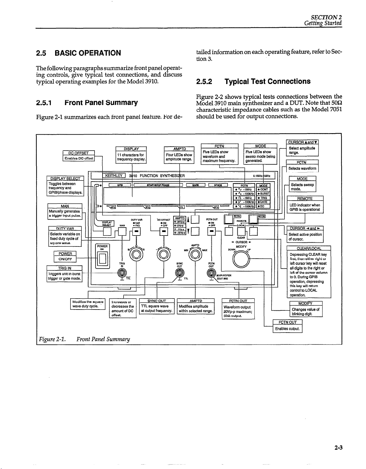
2.5
2.5.1
2.5.2
2.5.3
INTRODUCTION
INSTALLATION
Installation Location
cooling
LINEPOWERSUPPLY.................,...................~
LINE Voltage Selector Switch ...................................................
Line Receptacle Connection .....................................................
LineFuse
HANDLING PRECAUTIONS .....................................................
BASICOPERATION
Front Panel Summary .........................................................
Typical Test Connections ......................................................
OperatingExamples
....................................................................
..................................................................
..............................................................
....................................................
..........................................................
.................................................
...........................................................
...........................................................
.......................................................
......................................................
.............................................................
Started
..............................................................
..............................................................
..................
............................................................
..........................................................
..C .....................................
.....................
l-1
l-l
1-2
l-2
...... 1-2
1-2
1-2
1-2
1-2
l-2
1-3
l-3
2-1
2-l
2-l
2-l
2-2
2-2
2-2
2-2
2-2
2-3
2-3
2-3
2-4
SECTION 3
3.1
3.2
3.2.1
3.2.2
3.3
3.3.1
3.3.2
3.4
3.5
3.5.1
INTRODUCTION
FRONT PANEL AND REAR PANEL DESCRIPTION ...................................
Front Panel Description
RearPanelDescription
INPUT AND OUTPUT CONNECTIONS ............................................
InputConnection
OutputConnections
STARTUP
OPERATING PROCEDURES
ErrorCodes
- Operation
..............................................................
........................................................
........................................................
............................................................
..........................................................
....................................................................
.....................................................
................................................................
3-1
3-l
3-1
3-4
3-5
3-5
3-5
3-6
3-7
3-7
Page 7
’ 35.2 FrequencySetting
3.5.3 OutputAmplitude
3.5.4
3.5.5 Waveform Selection, Square-Wave Duty Cycle, and Synchronous Output
3.5.6 OscillationMode
3.5.7
DCOffset
Trigger Parameters
..................................................................
............................................................
...........................................................
.............................................................
........................................................... 3-11
..................
‘3-7
3-8
3-8
3-8
3-9
SECTION
4.1 INTRODUCTION
4.1.1 GPIBOverview
4.1.2 Major GPIB Specifications
4.1.3 Bus Line Signals and Operation
4.1.4 GPIBHandshaking
4.1.5
4.1.6
4.1.7 Basic Listener Functions
4.1.8 BasicControllerFunctions
4.1.9 Multi-line Interface Messages
4.2
4.2.1
4.2.2 Specifications
4.3 MODEL 3910 PROGRAM CODES
4.4 TYPICAL EXECUTION TIMES
4.5
4 - GPIB Interface
..............................................................
..............................................................
......................................................
...........................................................
Data Transfer Example
BasicTalkerFunctions
OVERVIEW OF MODEL 3910 GPIB INTERFACE
Introduction
SAMPLEPROGRAMS
................................................................
...............................................................
........................................................
.........................................................
.......................................................
......................................................
.................................................... 4-12
..........................................................
.................................................. 4-1
...................................................
......................................
..................................................
4-l
4-1
4-1
4-2
4-3
4-3
4-3
4-3
4-3
4-6
4-6
4-6
4-9
4-13
Page 8
List of Illustrations
SECTION 2 -
Figure 2-1
Figure 2-2
SECTION 3
Figure 3-1
Figure 3-2
Figure 3-3
Figure 3-4
Figure 3-5
Figure 3-6
Figure 3-7
Figure 3-8
SECTION 4
Figure 4-1
Figure 4-2 Handshake Timing Diagram
Figure 4-3
Figure 44
Getting Started
Frontpanelsummary...............................................,...... 2-3
TypicalConnections . . . . . . . . . . . . . . . . . . . . . . . . . . . . . . . . . . . . . . . . . . . . . . . . . . . . . . .
- Operation
Model 3910 Front Panel
Mode13910RearPanel
LogicInputCircuit
oLltputCircuit
Phase Relationship between FCTN OUT Waveform and SYNC OUT
Relationship between Trigger Signal and Oscillation in TRIG Mode
Relationship between Trigger Signal and Oscillation in GATE Mode
Definition of Phase of each Waveform
...........................................................
..................................................... 3-2
.....................................................
........................................................
- GPIB Interface
Interface Connector
Data Transfer Example
ProgramCodeSyntax ......................................................
.......................................................
.....................................................
2-4
3-4
3-5
3-6
...................
....................
................... 3-11
.......................................... 3-12
................................................. 4-3
3-9
3-10
4-2
4-4
4-8
Page 9
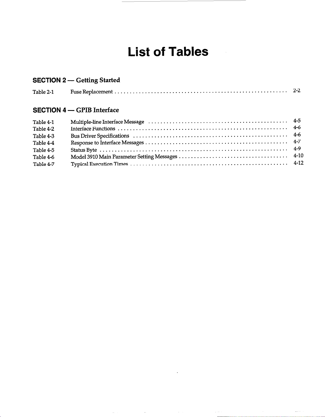
List of Tables
SECTION 2
Table 2-l
SECTION 4
Table 4-1
Table 4-2
Table 4-3
Table 4-4
Table 4-5
Table 4-6
Table 4-7
- Getting Started
Fuse Replacement . . . . . . . . . . . . . . . . . . . . . . . . . . . . . . . . . . . . . . . . . . . . . . . . . . . . . . . . .
- GPIB Interface
Multiple-line Interface Message
InterfaceFunctions..
BusDriverSpecifications
Response to Interface Messages
StatusByte..
Model 3910 Main Parameter Setting Messages
TypicalExecutionTimes
............................................................
......................................................
....................................................
..............................................
...................................................
...............................................
....................................
2-2
4-5
4-6
4-6
4-7
4-9
4-10
4-12
Page 10
SECTION 1
t General Information
1 .I INTRODUCTION
The Model 3910 Eunction Synthesizer can generate frequencies between O.lmHz and 1MHz. The Model 3910
can generate the entire band at a resolution of O.lmHz,
with a high-frequency accuracy of f30ppm.
Q 2/,squarelX,ris-
Five AC waveforms, sine
ing sawtooth/l, and falling sawtooth\ are available. A
maximum of tlOV DC can be added onto each output.
Maximum output voltage for all waveforms is 20V p-p/
no load or lOVp-p/5On load.
Since frequencies are synthesized directly by a custom
LSI digital IC, accuracy and stability are high, and the fre-
quencyswitching time is short. Another advantage is the
continuity of phase at frequency switchover.
In addition to continuous oscillation, burst oscillation,
trigger oscillation, and gate oscillation are available. The
Model 3910 also provides a continuous output of direct
current voltage. An external trigger input provides an external trigger signal during trigger or gate oscillation. The
square-wave duty cycle is also variable.
The Model 3910 uses a single line, ll-character LED display to display the values of oscillation frequency, pa-
, triangle
,
rameters, and other values. Settings are easily made using push-button keys and rotary knobs.
A GPIB (IEEE-488) interface is available as an option for
the Model 3910. With the exception of the AMPTD, amplitude setting; DC OFFSET, added quantity setting; and
DUTY VAR, duty ratio setting; a GPIB equipped Model
3910 can be programmed over the bus for the same operating modes and parameters that can be controlled from
the front panel.
1.2 FEATURES
l Wide bandwidth: O.lmHz to 1MHz (resolution
O.lmHz).
0 &30 ppm frequency accuracy.
l Phase continuity, at frequency switchover.
l Five ACwaveformsavailable: %,2/,n,n,andl
l The duty cycle can be set to values between 10% and
90% for frequencies up to 1OOkHz.
l High output: 2OVp-p/no load, lOVp-p/50Qload.
0 Low distortion: 0.3% or less (1OHz to IOOkHz).
l DC output voltages
fiV/5OQ load.
l Burst oscillation mode: Repeats oscillation of wave
number specified by mark wave (l-16) and space wave
number (l-16).
o Trigger oscillation and gate oscillation:
Trigger source: External by front panel BNC plug or
push-button key.
available: flOV/no load,
l-l
Page 11
SECTION 1
General Information
Start/stop phase: -360” to +360”.
Input voltage: ‘ITL level (pulls up 74HC14 input by
5.1K). Minimum pulse width ZOOnsec.
Trigger: Oscillates wave number specified by wave
number (l-16) by trigger signal.
Gate: Integral wave number oscillation by trigger
signal.
Waveform and frequency range:
Sine wave, square wave (duty fixed); O.lmHz to
IMHZ.
Triangle wave, square wave (duty variable), rising
sawtooth wave, falling sawtooth wave; O.lmHz to
lOOkHz, oscillation possible up to 1MHz.
Each parameter setting can be modified using the
MODIFY knob and the CURSOR keys. The single line,
11 character LED display, clearly displays all neces-
sary information; oscillation frequency, GPIB address
(when installed), start/stop phase, mark wave number, and space wave number.
Battery backed-up memory stores the configuration in
effect when power is turned off.
Optional GPIB interface allows the Model 3910 to be
programmed over the GPIB (IEEE-488 interface bus).
1.3 WARRANTY INFORMATION
Warranty information is located on the inside front cover
of this operator’s manual. Should your Model 3910 require warranty service, contact the Keithley representative or authorized repair facility in your area for further
information. When returning the instrument for repair,
be sure to fill out and include the service form at the back
of this manual in order to provide the repair facility with
the necessary information.
The WARNING heading used in this manual explains
dangers that might result in personal injtuy or death. Always read the associated information very carefully before performing the indicated procedure.
The
CAUTION
hazards that could damage the instrument. Such damage
may invalidate the warranty.
heading used in this manual explains
1.6 UNPACKING AND REPACKING
1.6.1 Unpacking
After carefully unpacking the instrument from its shipping carton, inspect it for any obvious signs of physical
damage. Report any such damage to the shipping agent
immediately. Save the original packing carton for storage
or possible future shipment.
1.62
The following items are included with every Model 3910
order:
l
Model 3910 Function Synthesizer
0 Model 3910 Operator’s Manual
l
Power Cord
l
Fuse (lA, 25OV, 5.2 x 2Omm)
l
BNC to BNC signal cable
l
Additional accessories as ordered.
Shipment Contents
1.4 MANUAL ADDENDA
Any improvement or changes concerning the instrument
or manual will be explained in an addendum included
with the unit. Be sure to note these changes and incorporate them into the manual before using the unit.
1.5 SAFETY TERMS AND SYMBOLS
The following safety terms and symbols are found on the
instrument or used in this manual.
A
The
user should refer to the operating instructions.
l-2
symbol on the instrument indicates that the
1.6.3 Operator’s Manual
If an additional manual is required, order the manual
package, Keithley part number 3910-900-00. The manual
package includes an operator’s manual and any pertinent addenda.
1.6.4 Repacking For Shipment
Should it become necessary to return the Model 3910 for
repair, carefully pack the unit in its original packing carton or the equivalent. If the original carton is not available
or damaged, be sure to use a cardboard box of sufficient
strength and room. Pad the empty spaces in the carton
with adequate packing material to hold the unit firmly in
place.
Page 12
General Information
SECTION 1
Include the following information:
l Advise to the warranty status of the instrument.
l Write ATTENTION REPAIR DEPARTMENT on the
shipping label.
o Fill out and include the service form located at the back
of this manual.
1.7 OPTIONAL ACCESSORIES
The following accessories are available for use with the
Model 3910.
Models 3900-l and 3900-2 Rack Mounting Kits: The
Model 3900-l mounts one Model 3910 in a standard
IPinch rack. The Model 3900-2 mounts two Model 3910s
side by side in a standard 19-inch rack. Both kits include
all necessary hardware for proper rack mounting of the
instruments.
Model 7007 Shielded IEEE-488 Cables:
7007-l (lm, 3.3ft.j and Model 7007-2 (2m, 6.6ft.j can be
used to interface the Model 3910 tothe IEEE-488 bus.
The Model
Model 7051-2 BNC-to-BNC Cable:
50R BNC to BNC cable (RG-58C) 2ft. (0.6m) in length.
The Model 7051-2 is terminated with male BNC connec-
tors on both ends.
Model 7051-5 BNC-to-BNC Cable:
5OQ
BNC to BNC cable (RG-58C) 5ft. (1.2m) in length.
The Model 7051-5 is terminated with male BNC connec-
tors on both ends.
Model 7051-10 BNC-to-BNC Cable:
is similar to the Models 7051-2 and 70516 except that it is
lOft..(2.4m) in length.
Model 7754-3 BNC-to-Alligator Cable:
7754-3 is a 3ft. (0.9m) 5Ofi cable (RGd8C), terminated
with a male BNC connector on one end and two alligator
clips on the other end.
Model 7755 5Oa Feed-Through Terminator:
7755 is a BNC to BNC adapter that is terminated with a
5OQ resistor. VSWR is ~1.1, DC to 25OMHz.
The Model 7051-2 is
The Model 7051-5 is
The Model 7051-10
The Model
The Model
Model 3911 IEEE-488 Interface:
tion a maximum of 15 Model 3910s can be connected on
the same bus, data line transfer uses a 3-line handshake
mefhod, enabling reliable data transfer between data
sending (talkers) and receivers (listeners) having differing data transfer rates.
With the Model 3911 op-
1.8 SPECIFICATIONS
Detailed Model 3910 specifications may be found in Appendix B.
l-3
Page 13

SECTION 2
Gettina Started
2.1 INTRODUCTION
This sections contains basic information on installation,
power line connections, and it also provides typical simple operating examples.
2.2 INSTALLATION
The following paragraphs discuss Model 3910 installation. In particular, use adequate care when installing the
unit. Improper installation will adversely affect the life,
reliability, and safety of the unit.
The Model 3910 weighs about 7 lbs; be careful when carrying the unit or mounting it in a rack.
2.2.1 installation Location
The allowable ambient temperature and humidity
ranges for the Model 3910 are.
Operating: 0 to 4O”C, 10 to 9O%RH
Storage: -10 to 5O”C, 10 to 8O%RH
Be sure to install the unit in a location that satisfies these
temperature and humidity conditions. Also the environ-
ment must be free of dust and vibration, and the Model
3910 must not be exposed to direct sunlight.
The Model 3910 uses a line filter, but pulse noise or strong
magnetic or electric fields may cause incorrect operation
of the unit. Do not install the unit near a source of pulse
noise or strong magnetic or electric fields.
The guard on the rear panel of the unit is designed to protect rear panel connectors and should not be used as a leg
for installation. Do not stand the unit vertically on the
rear guard because it may fall over, causing instrument
damage or personal injury.
2.2.2
The Model 3910 is ‘air-cooled by vents. Insufficient air
flow may cause a component in the unit to fail. Follow the
instructions given below.
l
Cooling
CAUTION
Observe the following precautions to prevent damage to the unit:
A vent is provided on the bottom panel of the
unit. Install the unit on a rigid, flat surface,
and avoid installing it on soft material such
as a cushion. Be careful not to insert foreign
2-l
Page 14

SECTION 2
Geffina Started
material between the bottom of the unit and
the surface underneath. Another vent is located on the top panel of the unit. Be careful
not to block the top vent by placing an object
on top of the unit.
l
Avoid mounting two or more units vertically. Placing one unit on top of another will
obstruct the vents.
2.3 LINE POWER SUPPLY
The Model 3910 operates with a lOOV, 12OV, 22OV, or
240.7 *lo%, 48 to 62Hk, single-phase AC power supply.
The power consumption is approximately 25VA.
2.3.1 LINE Voltage Selector Switch
The LINE voltage selector switch on the rear panel allows
you to change operating voltage of the power supply.
The standard setting of the switch is the same as the volt-
age available in the country to which the unit is shipped.
To change the power supply voltage, first disconnect the
line cord, and set the supply voltage switch in the correct
position. Wait at least five seconds before turning the
power back on after turning it off.
WARNING
The Model 3910 is equipped with a 3-wire
power cord that contains a separate ground
wire and is designed to be used with
grounded outlets. When proper connections
are made, instrument chassis is connected to
the power line ground. If the AC outlet is not
ounded, the rear panel ground terminal
=!= must be connected to safety earth
b
ground using #18AWG (or larger) wire before use.
2.3.3
The line fuse, which is integral with the power line receptacle, protects the instrument from over-current situations. To replace the fuse, first disconnect the line cord,
then pry out the fuse compartment (immediately to the
right of the FUSE marking) with a small screwdriver. A
spare fuse is located in the compartment with the fuse being used. Replace the blown fuse only with the type listed
in Table 2-1, then replace the fuse holder.
Line Fuse
WARNING
To avoid a shock hazard, disconnect the line
cord from the instrument before replacing
the fuse.
CAUTION
Use only a fuse of the rating listed in Table
2-1, or instrument damage may occur.
WARNING
To avoid a shock hazard, disconnect the
power cord from the instrument before
changing the supply voltage setting.
CAUTION
Be sure to set the line voltage switch to the
correct position for the line power voltage to
be used. Operating the instrument on an incorrect voltage may cause damage to the unit.
2.3.2
Connect the supplied power cord to the rear panel Line
receptacle and to a grounded AC power receptacle supplying the correct voltage.
Line Receptacle Connection
2-2
Table 2-1, Fuse Replacement
Fuse Current Keithley
Line Voltage
lOOV, 120v 1A
220,240v
NOTE: Fuses are 5 x2Omm and have UOV, normal blow ratings.
Rating Part No.
FU-96-2
ID-4
FU-96-1
2.4 HANDLING PRECAUTIONS
When the front panel or case becomes
a soft
cloth. If the panel or case is too dirty for cleaning
with a dry cloth, dampen the cloth in mild detergent, and
wipe the panel or case with the damp cloth. Never use
solvents such as thinner or benzene, or chemical dust
cloths to avoid damaging the case or front panel surfaces.
dirty, clean it with
Page 15
SECTION 2
Gettim?
Started
2.5 BASIC OPERATlON
The following paragraphs summarize front panel operat-
ing controls, give typical test connections, and discuss
typical operating examples for the Model 3910.
2.5.1 Front Panel Summary
Figure 2-l summarizes each front panel feature. For de-
tailed information on each operating feature, refer to Section 3.
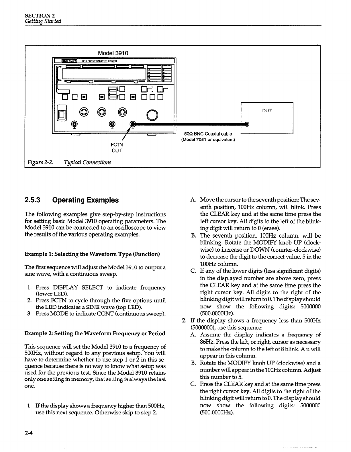
2.5.2
Typical Test Connections
Figure 2-2 shows typical tests connections between the
Model 3910 main synthesizer and a DTJT. Note that 5OL2
characteristic impedance cables such as the Model 7051
should be used for output connections.
%I I11111
LED indicator when
Figure 2-1.
Front Panel Summary
Depressing CLEAR key
first, then either right or
left cursor key will reset
all digits to the right or
left of the cursor column
to 0. Dudng GPIB
operation+ depressing
this key will return
control to LOCAL
mxxn+inn
2-3
Page 16
SECTION 2
Gettim Started
Model 3910
5052 BNC Coaxial cable
(Model 7051 or equivalent)
OUT
Figure 2-2.
Typical Connections
2.5.3 Operating Examples
The following examples give step-by-step instructions
for setting basic Model 3910 operating parameters. The
Model 3910 can be connected to an oscilloscope to view
the results of the various operating examples.
Example 1: Selecting the Waveform Type (Function)
The first sequence will adjust the Model 3910 to output a
sine wave, with a continuous sweep.
1. Press DISPLAY SELECT to indicate frequency
(lower LED).
2. Press FCTN to cycle through the five options until
the LED indicates a SINE wave (top LED).
3. Press MODE to indicate CONT (continuous sweep).
Example 2: Setting the Waveform Frequency or Period
This sequence will set the Model 3910 to a frequency of
5OOHz, without regard to any previous setup. You will
have to determine whether to use step 1 or 2 in this sequence because there is no way to know what setup was
used for the previous test. Since the Model 3910 retains
only one setting in memory, that setting is always the last
one.
1. If the display shows a frequency higher than 500Hz,
use this next sequence. Otherwise skip to step 2.
A. Move the cursor to the seventh position: The sev-
enth position, 1OOHz column, will blink. Press
the CLEAR key and at the same time press the
left cursor key. All digits to the left of the blinking digit will return to 0 (erase).
B. The seventh position, 1OOHz column, will be
blinking. Rotate the MODIFY knob UP (clockwise) to increase or DOWN (counter-clockwise)
to decrease the digit to the correct value, 5 in the
1OOHz column.
C. If any of the lower digits (less significant digits)
in the displayed number are above zero, press
the CLEAR key and at the same time press the
right cursor key. All digits to the right of the
blinking digit will return to 0. The display should
now show the following digits: 5000000
(5OO.OOOOHz).
2. If the display shows a frequency less than 5OOHz
(5000000), use this sequence:
A. Assume the display indicates a frequency of
86Hz. Press the left, or right, cursor as necessary
to make the column to the left of 8 blink. A u will
appear in this column.
B. Rotate the MODIFY knob UP (clockwise) and a
number will appear in the 1OOHz column. Adjust
this number to 5.
C. Press the CLEAR key and at the same time press
the right cursor key. All digits to the right of the
blinking digit will return to 0. The display should
now show the following digits: 5000000
(500.0000Hz).
2-4
Page 17
SECTION 2
Getting Sfarted
NOTE
The frequency may be increased quickly, using the above method, but no similar action is
available to rapidly reduce the frequency setting.
Example 3: Setting the Output Amplitude
This step sets the amplitude of the existing waveform to a
value of lOmVp-p:
Use the cursor down key to set the amplitude range so it
indicates O.O;?Vp-p (2OmVpp). RPotate the AMpTD knob
until the scope indicates lOmVp-p.
Example 4: Changing the Output to a Square Wave
This example changes the output to a square wave with
variable duty cycle, while maintaining the present frequency, in continuous mode.
1. Press FCTN twice to indicate a square wave output.
Note that the output waveform has equal time-on
and time-off.
2. Press DUTY VAR to allow variable duty cycle (LED
on). Rotate the associated knob below the key to cre-
ate square waves with different on- and off-times.
Leave the square wave in some extreme variable position; that is, an obviously unequal on- or off-time.
3. Press DUTY VAR key again. The scope presentation
reverts to a square wave with equal on- and offtimes.
4.
Press the DUTY VAR key again. The scope should
display the unequal duty cycle from the previous
step.
Example 5: Adjust the DC Offset
This step adjusts the DC offset value based on the center-
line (zero or average) voltage level of the existing
waveform.
1. Press the DC OF!ZSET key (LED on). Rotate the associated knob and note the vertical movement of CH A
on the scope. This movement corresponds directly
with the offset voltage applied by the rotation of the
knob. Leave the signal with a significant offset and
go to the next step.
2. Press DC OFFSET again (LED off). The scope presen-
tation reverts to the original value of zero offset.
Press the key again and the offset value re-appears
and the CH A display moves off zero. Press the key
once more to return the scope to zero offset (LED
off).
2-5
Page 18

SECTION 3
Operation
3.1 INTRODUCTION
This section contains detailed information on front panel
operation of the Model 3910. For detailed GPIB (IEEE488
bus) operation, refer to Section 4.
3.2
3.2.1
The front panel of the Model 3910 is shown in Figure 3-1.
The front panel is made up of a LED display and a control
panel with various push-button switches and knobs. The
FRONT PANEL AND REAR PANEL
DESCRIPTION
Front Panel Description
LED display presents information useful for the operation of the Model 3910, such as the value of each parameter and the range of permissible parameter values. Along
the bottom edge of the front panel are various input/output BNC connectors.
Most settings are maintained in battery backed-up memory. As a result, the Model 3910 automatically assumes
the previous settings when the power is first turned on.
Each front panel feature is described below. The circled
number to the left of each description corresponds to the
appropriate number shown in Figure 3-1.
3-l
Page 19

SECTION 3
Operation
Figure 3-1.
1
0
2
0
3
0
Model 3910 Front Panel
POWER ON/OFF (Power switch)
POWER controls AC power to the Model 3910.
Push this switch up to turn power on, and push
down to turn power off.
Display
The single-line 1 l-character display shows oscil-
lation frequency, parameter values, and other
important information during operation. An active display also indicates that instrument power
is turned on.
DISPLAY SELECT
Push-button key that selects the parameter dis-
played to either oscillation frequency or GPJB
address (only when GPIB option is installed),
start/stop phase, mark wave number, and space
4
0
wave number. When LED at the lower left of the
display is lit oscillation frequency is selected.
When LED at the upper left of the display is lit
GPIJ3 address, start/stop phase, and mark and
space wave numbers are selected.
DUTY VAR FXD, VAR (Square wave dufy
q&9
,Push-button key to select either variable duty or
fixed square wave output. When LED in center
of key is lit variable duty is selected.
111,111, r&VarlabZe duty ratio adjustment)
Rotating the variable duty adjustment knob allows you to program the square wave duty cycle.
The allowed duty cycle ranges from 5% to 95%
under lOkHz, and from 10% to 90% at 1OkHz to
1oOkHz. In the variable duty mode, the upper
frequency limit for square waves is restricted to
1ookHz.
3-2
Page 20

SECTION3
Operation
6
0
7
0
8
0
9
0
IO
0
11
0
12
0
13
0
+I- (DC offset value adjustment)
Rotating the DC offset value adjustment knob
sets the programmed offset voltage. The allowable DC offset to be added to a waveform is between -lOV and +lOV.
DC OFFSET ON, OFF
Push-button key to select whether or not DC offset is added to the waveform. When LED in center of the key is lit offset is selected.Use the +/offset value adjustment knob to add the determined amount of offset to the waveform.
AMPTD
LEDs light to display the selected amplitude
range. The allowed amplitude range is from
2mVp-p to 2OVp-p. The values for the amplitude
setting are for no-load (open) output conditions.When the output is terminated with a 500
terminal resistor, amplitude range is one half of
the selected range.
V(Amplitude range down key)
When the down cursor key is pressed the maxi-
mum value of the amplitude output signal is re-
duced.
A (Amplitude range up key)
When the up cursor key is pressed the maximum
value of the amplitude output signal is increased.
FCTN
This key allows you to choose the
waveform. Available waveforms include :
(sine wave), 2/ (triangular wave), 111 (square
wave), V(ascending sawtooth wave), 1 (descending sawtooth wave).
The selected waveform is displayed in the function LEDs.
FCTN
Refer to the lit LED to see which wave function
has been selected.
REMOTE
This lamp indicates the remote state when the
GPIB option is installed and listener is specified
from the controller.
(Amplitrrde range display)
(Function:
(Displays the selected function)
(Remote state display)
waveform)
out ut
4J
14
0
15
0
16
0
17
0
18
0
19
0
20
0
21
0
MODE
This key allows you to choose the oscillation
mode. Available modes include: CONT (continuous oscillation), BURST (burst oscillation),
TRIG (trigger oscillation), GATE (gate oscilla-
tion). In addition, it is also possible to select DC
for a continuous output of direct current voltage.
MODE
Refer to the lit LED to see which mode has been
selected.
MAN Manual trigger key)
This key allows the operator to manually gener-
ate a trigger input pulse during trigger or gate
mode of oscillation.
TRIG IN
This BNC connector is an input for external TTLlevel signals, which can be used to trigger the
Model 3910 in TRIG (trigger) and GATE modes
of operation. When this input goes from high
level to low level, it operates as a trigger signal.
SYNC OUT (Synchronous output)
This BNC jack provides a TIL-level signal at the
same frequency as the FCTN OUT output
waveform.
AMPTD MIN,
Turning this knob allows you to set the output
amplitude of the unit when the FCTN OUT key
has been activated. The allowed amplitude
ranges from 2mVp-p to 2OVp-p.
FCTN OUT
FCTN OUT turns the output waveform off or on
to the BNC plug of FCTN OUT. When the output
is off, the main output signal is turned off and
open-circuited. This can be shorted to ground by
switching an internal short plug. The current
status of this key can be determined by the LED
in the center of the key. If lit, FCTN OUT is on.
FCTN OUT
oufpft)
This BNC jack provides the waveform output
signal. The maximum output voltage range is
SOVp-p/open circuit, and the output impedance is 50&J.
(Oscillation mode)
(Displays the selected mode)
(Tuigger input)
MAX (Amplitude adjustment)
ON, OFF (Signal output ON/OFF)
(Function output:
waveform
3-3
Page 21

SECTION 3
Operation
22 4(Left Cursor)
0
This key moves the cursor one column to the left
each time it is pressed. If held continuously for
more than 0.3 seconds, the cursor will continue
moving to the left.
CLEAR (Local)
If this key is pushed first and then either the right
or left cursor key is pushed at the same time, all
digits to the right or left of this column will be reset to 0. In Gl?lB remote mode, this key is a return
to local control key.
24
0
MODIFY UP, DOWN (Modify knob)
This knob is used to increase or decrease the set
value of the display. Turning the knob clockwise
increases the value while turning the knob
counter-clockwise decreases the value. This
knob can be used to set the following parame-
ters: frequency, Gl?lB address (O-301, start/stop
phase (f360.0’), mark wave number (l-16), and
space wave number (1-16).
25 b(Righ t Cursor)
0
This key moves the cursor one column to the
right each time it is pressed. If held continuously
for more than 0.3 seconds,the cursor will continue moving to the right.
3.2.2
The rear panel of the Model 3910 is shown in Figure 3-2.
Each rear panel feature is described below. The circled
number to the left of each description corresponds to the
appropriate number shown in Figure 3-2.
Rear Panel Description
Figure 3-2.
3-4
Model
3920 Rear
Panel
Page 22

SECTTON 3
Operation
26
0
27
0
GPIB
(General Purpose Interface Bus (option))
This connector is the 24-pin connector used to
connect the Model 3911 option of the Model 3910
to the GPIB (IEEE488 bus). Shielded GPIB cables, such as the Model 7007, are recommended
for bus connectionsThe GPIB address is set by
first selecting the GPlB display. Rotate the MODIFY knob UP (clockwise) to increase or DOWN
(counter-clockwise) to decrease the GPIB address.
LINE Voltage Selector
This switch sets the Model 3910 for the correct
line voltage. Using a flat-blade screwdriver, set
the switch in the proper position for the supply
voltage in your area.
WARNING
To avoid a shock hazard, disconnect the line
cord before changing the switch position.
CAUTION
Operating the Model 3910 on an incorrect
line voltage may result in instrument damage.
(Supply voltage switch)
3.3 INPUT AND OUTPUT CONNECTIONS
3.3.1
One signal can be applied to the BNC connector of the
Model 3910. The specification of that input signal is given
below.
Logic Input
The logic input is TRIG IN (external trigger input).
Input name: TRIG IN (External trigger
Input voltage: TTL level
Allowable input voltage:
circuit: See Figure 3-3, Logic Input
Input Connection
CAUTION
Be careful no to exceed the maximum allowable input voltages, or instrument damage
may occur.
input) external trigger during TRIG, GATE operation
ov to +5.5v
circuit
28
0
@Q
LINE
(Power Input Connector)
The LINE connector is used to connect the instrument to AC power.
WARNING
To avoid the possibility of electric shock,
connect the Model 3910 to grounded AC outlet using the supplied 3-wire power cord or
the equivalent.
(Grounding Terminal)
The grounding terminal is connected to the chas-
sis of the Model 3910. To prevent interference
and for safety, be sure to ground this terminals
WARNING
If the Model 3910 is connected to an ungrounded AC outlet, connect the grounding
terminal to safety earth ground using
#18AWG minimum wire before use to avoid
the possibility of electric shock.
V V
1 Figure 3-3.
Figure 3-3. Logic Input Circuit
3.3.2
3.3.2
Two output signals are available from the BNC connec-
tors of the Model 3910. The specifications of the output
signals are given below.
Be careful not to connect an external signal to
an output connector, or instrument damage
may occur.
Logic
Input
Circuit
Output Connections
Output Connections
CAUTION
3-5
Page 23

SECTION 3
Analog Output
The analog output is FCTN OUT (main waveform out-
put)
Output n&e: FCTN OUT (Main
Waveform Output)
Maximum output voltage:
Output impedance:
Recommended Impedance: 50!2
Short circuit ljrotection See Figure 3-4, Output Circircuit: cuit
ZOVp-p/open,
lOVp-p/son
5on 32%
Analog Output Considerations
The FCTN OUT (main waveform output) impedance is
50!2. To maintain maximum amplitude across the entire
bandwidth, and for maximum square-wave quality, use
a 5OQ cable for connections, and terminate the opposite
end of the cable with a 5OQ impedance. Note that the
Model 3910 displays voltage amplitude for open circuit
conditions. The actual output voltage with a 5OQ termination is about half that for no-load conditions.
Logic Output Considerations
The SYNC OTJT (synchronous output) is driven by a
74LS type logic IC. The maximum load is about 25ksz. Be
careful not to connect a load that exceeds the drive capa-
bility of this type of TTL IC. Also, do not use excessively
long connecting cables, as the resulting capacitance may
have detrimental effects on the output signals.
The SYNC OUT impedance is matched at 5OQ at higher
frequencies. Relatively good waveforms will be obtained
if 5OQ coaxial cables are used; however, cables connected
to this output must not be terminated with a 5OQ impedance.
3.4 STARTUP
1. Check that the supply voltage switch is set at the
proper position for the supply voltage. The allowable supply voltage range is +lO% of the voltage at
which the supply voltage is set.
CAUTION
Operating the Model 3910 in an incorrect
line voltage may result in damage to the unit.
Logic Output
The logic output is SYNC OTJT (synchronous output).
Output name:
Output voltage:
circuit:
SYNC OUT
TTL level
See Figure 3-4, Output Circuit
Figure 3-4. Output Circuit
2. Make sure that the power is off, then plug the supplied power cable firmly into the LINE connector on
the rear panel of the Model 3910. Insert the plug into
a grounded AC power receptacle.
WARNING
To avoid the possibility of electric shock, use
only grounded AC receptacles for power
connections.
Turn on Model 3910 power by pushing the front
panel POWER switch. The power is on when the
POWER switch button is up; power is off when the
POWER switch is down. When the power is on, the
Model 3910 will begin normal operation, and the
LED display will be on.
3. When the power is first turned on, the Model 3910
will return to the previous settings effective prior to
power-off, and the unit will display the main parameters.
If the previous settings were not stored correctly, the
error code “ERR3” will be displayed. In this case, if
the CLEAR key is pushed, the machine goes to the
initial reset state and can be used normally, but the
3-6
Page 24

SECTION 3
Operation
settings prior to turning off the power are lost. This
situation occurs when the backup battery used to
maintain memory is drained and the stored data cannot be maintained or if the power is cut off while the
machine is being set. Fully charged batteries can retain memory for approximately 30 days. This time
period, however, varies slightly with ambient temperature and from one battery to another.
The backup batteries may be discharged when the
Model 3910 is used for the first time after being purchased. If “ERR 3” is displayed during initial operation, replace the batteries using the information provided in the service manual.
The FCTN OUT ON/OFF (function output) state is
not saved. The FCTN OUT ON/OFF setting depends on the setting of the internal short plug. The
factory default setting at power-on is function output on. Consult the service manual for details on setting the internal short plug.
If, at power on, the Model 3910 does not enter the
mode with settings that were effective immediately
before previous power-off (or the preset operating
modes), or if the main display does not appear, contact your Keithley representative or the factory to determine the correct course of action.
ERR2 (RAM error)
l Abnormality in internal RAM of the machine.
ERR3 (Memory backup error)
l Battery backup operation failure.
When “ERRl” and “ERR2” occur, try to turn the power
on again several times. If the error is still displayed, it is
probably a breakdown. Contact your Keithley representative or the factory to determine the correct courseof action.
When “ERR3” is displayed, replace the batteries inside
with new ones. Refer to the service manual for replacement information.
If the CLEAR key is pressed when “ERR3” is displayed,
the machine will be set to its default settings, and will
then go into the operating state, where it can be used normally. However, the settings prior to turning off the
power will be erased.
NOTES:
1. Wait at least five seconds before turning on the
Model 3910 after turning it off or it may not operate
normally.
2. For precise measurement applications, allow the
Model 3910 to warm up for at least 30 minutes to allow internal circuits to stabilize.
3.5 OPERATING PROCEDURES
3.51 Error Codes
When an error occurs, the Model 3910 displays an error
code on the left side of the numerical display.
Displayed error codes and their meanings are summarized below.
ERR1 (ROM error)
l Abnormality in internal ROM of the machine.
3.5.2
Frequency Setting
The frequency setting is used to set the cycles per second
of the waveform selected. To change the frequency setting, first ensure that the frequency display has been selected. To select the frequency display, depress the DISPLAY SELECT button so that the LED indicator is lit next
to MHz on the lower left of the display.
Once this action has been performed the Model 3910 can
now have the frequency set. To move the cursor to the position you wish to change, just use the4 key or the, key.
To change the frequency setting, turn the MODIFY knob
UP (clockwise) to increase the setting or DOWN
(counter-clockwise) to decrease the setting.
The allowed frequency range for the sine and square
waves (with 50% duty cycle) is from O.lmHz to IMHz; for
other waveforms, the upper limit is 1OOkHz for good
quality waveforms. Although waveform quality will be
of reduced quality, oscillations up to 1MHz can be set for
triangle (2/ >,
rising sawtooth (v >, falling sawtooth
(u ), and variable duty square wave (m >.
Page 25

SECTION 3
Operation
3.5.3
The amplitude setting establishes the output voltage
from the FCTN OUT BNC jack. The amplitude range display will display only the maximum possible output
value in the current setting.
To accurately set the output amplitude, first set the de-
sired range using the amplitude range keys. Then rotate
the AMPTD knob to fine tune the output. The output
value can be measured at the FCTN OUT BNC jack with a
voltmeter or by using an oscilloscope. However, take
note of the frequency characteristics of the voltmeter.
Amplitude setting can be performed by using both the
AMPTD knob and the amplitude range keys. The allowed amplitude range is 2mVp-p to 2OVp-p.
When the DC offset is OV, the allowed amplitude range is
2mVp-p to 2OVp-p. If, however, the DC offset is not OV,
the sum of the AC amplitude setting/2 and the DC offset
must not exceed the AC amplitude setting.
Output Amplitude
Using DC
the value that appears at the output jack. Valid offset values are within the range of +lOV to -lOV.
For all AC waveforms, the DC offset is added to the aver-
age
waveform. When adding DC offset to the output
waveform, set them so that the sum does not exceed that
of your AMPTD (amplitude range display). To prevent
errors from oc
offset combinations, first set the offset to OV, change the
AMPTD setting, then set the offset to the desired value.
Settings that exceed the range of the AMM’D are possible, but the waveform will be distorted or clipped. Check
the waveform with an oscilloscope.
3.5.5
as
a mode, the offset voltage is the voltage of
value of the peak-to-peak amplitude of the AC
curring while programming amplitude-
Waveform Selection, Square-Wave
Duty Cycle, and Synchronous Out-
put
Waveform Selection
Pressing the FCTN key advances the present waveform
function on the upper right of the front panel. Available
waveforms include: sine ( s ),tiangle ( 2/ >, s uare
6u ), rising sawtooth (A ), and falling sawtooth ( \ 1.
The variable range of the AMPTD knob is 20dB.
The AMl?TD knob can be used only on AC waveforms;
use the DC OFFSET knob to set the DC output voltage of
the DC waveform. When the DC waveform is selected,
you can still set the amplitude range by using the ampli-
tude range keys.
3.5.4 DC Offset
Pressing the DC OFFSET key selects whether or not DC
offset is added to the waveform. When the LED in the
center of the key is lit the DC offset is active. The current
DC offset setting cannot be observed from the Model
3910 display. The DC offset setting should be made using
a voltmeter or an oscilloscope.
To modify the DC offset, rotate the +/- offset value adjustment knob directly below the DC OFFSET key clockwise to increase the setting and counter-clockwise to decrease the setting.
For all AC waveforms, the p-p value of the amplitude
will remain unchanged when you change the waveform.
Square-Wave Duty Cycle
The duty cycle is the ratio of the time period of the
waveform high-level duration to the time period of one
complete cycle of the waveform expressed as a percentage. For example, assume a 1OkHz square wave has a
time period of 100psec. If the high portion of the
waveform has a period of 30pec, the duty cycle is
30/100x100=30%.
Two square-waveform duty cycles are available: one
with the duty cycle fixed at 50% and the second mode
with a variable duty cycle. The duty cycle applies only to
the square-wave function. When the Model 3910 is in the
variable duty-cycle mode, the upper frequency limit is
1OOkHz and the maximum jitter is 15011s.
To change the duty cycle, press the DUTY VAR FXD,
VAR key. If the LED is lit in the center of the key the vari-
3-8
Page 26

SECTION 3
Operafion
able duty
duty cycle, turn the (variable duty) knob directly below
the DUTY VAR key. The variable range of duty ratio is
between 5% and 95% for frequencies up to 1OkHz. For
frequencies up to 100 kHz, the variable range is between
10% and 90%. It can actually be set until the point where
the waveform is extinguished, but the waveform may become unstable. To select the fixed 50% duty cycle mode,
press the DUTY VAR FXD,VAR key so that the LED in
the center of the key is no longer lit.
Note that the duty cycle setting also changes the duty cycle of the sync out signal.
To extend the duty cycle range, use the trigger oscillation
mode and one square waveform cycle. Refer to paragraph 3.5.6 for details on setting the oscillation mode.
Synchronous Output
Figure 3-5 illustrates the phase relationships between the
FCTN OUT waveform and SYNC OUT (synchronous
output). Note that as the frequency increases, a substan-
range
has been selected. To modify the variable
tial phase differential will result between the waveform
output and the synchronous output signals.
3.5.6 Oscillation Mode
Oscillation Mode Selection
The oscillation mode setting is selected by the MODE
switch on the right side of the front panel. The present oscillation mode is displayed by the lit LED next to the selected mode. Each time the mode key is depressed the
mode is advanced by one. Available oscillation modes include CONT (continuous), BURST, TRIG (trigger), and
GATE. In addition, it is also possible to select DC for a
continuous output of direct current voltage.
CONT (continuous mode)
When the continuous mode is selected, the instrument
generates the selected waveform continuously. Triggering is not required, and the selected burst cycle and internal rate
waveform:
parameters
have no effect on the output
-
Sine wave
Rising sawtooth wave
Waveform
Triangular wave
Falling sawtooth wave
Figure 3-S. Phase Relationship between FCTN OUT Waveform and SYNC OUT
Square wave
Duty variable square wave
3-9
Page 27

SECTION 3
Operation
BURST
In the burst mode, the instrument generates the selected
waveform for the specified mark wave number and
space wave number. No trigger signal is required to initi-
ate the waveforms. The mark wave number and space
wave number can be set by first pressing the DISPLAY
SELECT button so that the LED is lit next to GPIB on the
upper left of the display. When the LED is lit next to
GPIB, the mark wave number and space wave number
can be found on the right side of the display. Then by us-
ing the 4 and b keys advance the cursor to either mark
wave number or space wave number. Turn the MODIFY
knob UP (clockwise) to increase the wave number or
DOWN (counter-clockwise) to decrease the wave num-
ber. The phase where oscillation starts can be set in 0.1”
from +360.0” to -360.0”.
TRIG (trigger)
In the trigger mode, the instrument generates the se-
lected waveform for the number of specified mark wave
numbers each time a trigger comes from the outside. The
trigger signal is effective only while oscillation is
stopped, and trigger signals prior to when the oscillation
finishes are ignored. To set the mark wave number first
press the DISPLAY SELECT button so that the LED is lit
next to Gl?lE on the upper left of the display. When the
LED is lit next to GPIB, the mark wave number can be
found on the right side of the display. Then use the4 and
b keys to advance the cursor to the mark wave number.
Turn the MODIFY knob UP (clockwise) to increase the
mark wave number or DOWN (counter-clockwise) to de-
crease the mark wave number. The phase where oscillation starts can be set in 0.1” units from +360.0” to -360.0”.
Triggering is performed by either using the TRIG IN (external trigger) BNC jack or by pressing the MAN (manual) key on the front of the unit.
Figure 3-6 shows the relationship between the trigger
signal and oscillation in TRIG mode.
GATE
In the GATE mode, the unit generates oscillations as long
as the gate signal (trigger signal) is on. When the gate signal turns oW, the Model 3910 will always stop oscillating
at the end of one complete cycle even if the gate signal
turns off at the mid point of a cycle. Thus, the Model 3910
always provides integral cycles of oscillation. The phase
where the oscillation starts can be set in 0.1” units from
+360.0” to -360.0”.
Triggering is performed by either using the TRIG IN (external trigger) BNC jack or by pressing the MAN (manual) key on the front of the unit.
Figure 3-7 demonstrates how the output waveform always completes the current cycle when the gate signal
turns off.
Ignored
Figure 3-6. Relationship between Trigger Signal and OsciZlation in TRIG Mode
3-10
Page 28

SECTION 3
Ozleration
Figure 3-7.
In the trigger or gate oscillation modes, if the
next trigger is applied at about the same time
the unit terminates oscillation, oscillation may
become unstable. In this situation, temporarily change the oscillation mode, then return
the unit to the original mode. Oscillation will
return to normal.
Relationship between Trigger Signal and Oscillation in GATE Mode
NOTE
DC Mode
DC is a mode in which oscillation from the synthesizer is
stopped. In this mode only a constant voltage is output.
When the MODE is set to DC, DC OFFSET ON/OFF
must be on (LED lit in center of DC OFFSET ON/OFF
key). To alter the output voltage, turn the +/- knob, directly below the DC OFFSET ON/OFF switch, clockwise
to increase the voltage or counter-clockwise to decrease
the voltage. The maximum voltage of the DC output is
HOV, and current is up to lOOmA. Short circuit protection
on the output has been installed.
play. When the LED is lit next to GPIB, the start/stop
phase setting can be found in the center of the display. To
change the current start/stop phase setting, move the
cursor to the start/stop phase by using the4 and, cursor
keys. Then set the start/stop phase by turning the
MODIFY knob UP (clockwise) to increase the setting or
DOWN (counter-clockwise) to decrease the setting. The
allowed range for the start/stop phase parameter is
-360.0” to +360.0” with 0.1” resolution.
The definitions of each waveform and its phase are
shown in Figure 3-8.
The Model3910 generates square waves with a fixed 50%
duty cycle by processing sine waves with a zero-crossing
comparator that has hysteresis.The level of the generated
square wave, therefore, alternates high and low at approximately 0”, +X30’, and &360” (within about ti.3’) depending on the past value of the phase. Thus, to set the
square-wave start/stop level high, set the phase to 90”.
Similarly, the phase should be set to -90” to set the
square-wave start/stop level low.
3.5.7 Trigger Parameters
Start/Stop Phase
The start/stop phase setting is the starting and finishing
position for waveform cycles. To set start/stop phase
press the DISPLAY SELECT button so that the LED indi-
cator light is lit next to GMB in the upper left of the dis-
The Model 3910 also generates the synchronous output
for the sine, triangle, and sawtooth waves by passing
each waveform through a zero-crossing comparator that
has hysteresis. As a result, the synchronous output level
changes at the same points as the square wave when the
phase is approximately 0”, +180’, or &360” for the sine or
triangle waves, or about +180” with the sawtooth wave.
3-11
Page 29

SECTION 3
Oaeration
Center of
waveform
amplitude
Phase O”
Duty ratio fixed square wave
Center of
00
Rising Sawtooth Wave
0 Not including this point
l
Including this point
Center of
waveform
amplitude
I
I I
I I
1800 36il”
Phase O”
Duty ratio variable square wave
Center of
waveform
amDlitude
, I
0" 180" 360”
180” 360”
Phase
Falling Sawtooth Wave
Center of
waveform
amplitude
180” 360”
o Not including this point
l
Including this point
0 Not including this point
Figure 3-8. Definition
3-12
of
Phase
180” 360”
of
each Waveform
Phase
0” 180” 360”
.
Page 30

SECTION 3
Otlerution
Mark Wave Number Setting
The mark wave setting is used to set the number of oscil-
lation cycles the unit generates each time it is triggered in
the BTJRST and TRIG oscillation modes. To set the mark
wave number, press the DISPLAY SELECT button so that
the LED is lit next to GPIB on the upper left of the display.
When the LED is lit next to GPIB, the mark wave number
setting can be found on the right side of the display. To
change the current mark wave number setting, move the
cursor using the 4 and @ cursor keys to the desired number. Then turn the MODIFY knob Ul? (clockwise) to increase the setting or DOWN (counter-clockwise) to decrease the setting. The allowable range for the mark wave
number setting is 1 to 16.
Space Wave Number Setting
The space wave setting is used to set the number of non-
oscillation cycles between each group of oscillation cycles
in the BURST mode. To set the desired space wave num-
ber, press the DISPLAY SELECT button so that the LED is
lit next to GPIB on the upper left of the display. When the
LED is lit next to GPIB, the space wave number can be
found on the far right side of the display. To change the
currents
ing the
turn the MODIFY knob UP (clockwise) to increase the
setting or DOWN (counter-clockwise) to decrease the
setting. The allowable range for the space wave number
is 1 to 16.
ace wave number setting, move the cursor us-
P
and b cursor keys to the desired number. Then
3-13
Page 31

SECTION 4
GPIB Interface
4.1 INTRODUCTllON
4.1 .I GPIB Overview
The GPIB interface is a general-purpose interface bus sys-
tem recognized by the IEEE (Institute of Electrical and
Electronics Engineers) in 1975 and is a method of stan-
dardizing data transfer between measuring instruments
and peripherals. By building each controller and periph-
eral device into an interface conforming to this standard,
it is possible to establish complete hardware compatibil-
ity among devices.
UP to 15 devices may be connected to a single interface
b&, and data transfer is performed by threghandshake
lines, enabling reliable data transfer between data senders (talkers) and receivers (listeners) having differing
data transfer rates.
4.1.2 Major GPIB Specifications
Overall cable length: 20m maximum
Cable lengths between devices: 4m maximum
Number of devices connectable
(including a controller): 15 maximum
Transfer method: 3-line handshake
Transfer rate: 1M bytes/set (maximum>
Data transfer: g-bit parallel
Signal lines:
Data Bus: 8 Lines
Control bus: 8 Lines
(including DAV, NRFD, and NDAC handshake lines
and ATN, REN, IFC, SRQ, and EOI control lines)
Signal/system grounds: 8 lines
Signal logic: Negative
True (low-level): 0.8V maximum
False (high-level): 2.OV minimum
4.1.3 Bus Line Signals and Operation
The GPIB bus consists of 24 lines, including eight data
lines, eight control lines, and eight signal/system ground
lines.
Data Bus (DIOl to DI08)
DIOl through DIO8 are data input/output lines, which
are used to transfer both address and command information (the type of data present on these lines is determined
by the ATN line). DIOl is the least significant bit (LSB).
4-l
Page 32

SECTION 4
GPIB Interface
Handshake Bus (DAV, NRFD, NDAC)
These three lines are handshake lines used to ensure reliable data transfer.
DAV @&a Yalid)
This line indicates that the data on the DIO lines sent
from a talker or the controller are valid.
NRFD &Jot &eady Zoraata)
This line indicates when the listeners are ready to accept
data over the data lines.
NDAC Uot Data Kcepted)
This line indicates the acceptance of data by listeners.
EOI and Qr Jdentify)
This line is used to indicate the end of a multiple-byte
transfer sequence or, in conjunction with ATN, to execute
a parallel poll operation.
4.1.4
GPIB handshaking is performed by checking the status of
all listeners and inhibiting the next data transfer until all
listeners have completed the reception of data, so that the
slowest device on the bus can perform data transfer reliably. The handshaking operations are executed by the
following handshake line logic levels:
NRFD=High level: Alllisteners are ready for accepting
data.
DAV=Low level: A talker has valid data on the data bus.
NDAC=High level: All listeners have completed data re-
ception.
GPIB Handshaking
Control Bus (ATN, REN, IFC, SRQ, EOII
ATN UeNtion)
This line is an output line from the controller, and it indi-
cates whether the information on the data bus is to be interpreted as data or commands.
REN @emote ENable)
This output line from the controller switches devices be-
tween remote control and local control.
IFC (Inter]Eace Q.lear)
This output line from the controller clears the interface of
active talkers and listeners.
SRQ @en&e &eQuest)
DlOl
0102
D103
D104
EOI
DAV
NRFD
NDAC
IFC
SRQ
ATN
SHIELD
. Cable
Receptacle Side
/
D105
D106
D107
D108
REN
DAV GROUND
NRFD GROUND
NDAC GROUND
IFC GROUND
SRQ GROUND
ATN GROUND
LOGIC GROUND
This control line is used by a device to request service
from the controller. The controller detects this signal and
usually executes a serial or parallel poll operation.
4-2
IEEE-488
1
Figure 4-l. Interface Connector
Page 33

SECTION 4
GPIB Inferface
NRFD
(Listener) --I,
DAV I I
(Talker)
NDAC
(Listener)
Data Bus
Signal
Valid Data
I 1
- Data bus disabled
Ready for next data byte.
Data bus enabled
Termination of
data reception
Data not received
(during data reception)
Figure 4-2. Handshake Timing Diagram
The handshaking timing diagram is in Figure 4-2. The
various timing points indicate the following:
4.1.5
Figure 4-3 shows a data transfer example using the threeline handshake process. In this example, the character
string “ABC” is sent, followed by the <CR> <LF> delimiter.
4.1.6
l Only one talker may exist on the GPIB at a time.
l Data is sent to the listeners when the controller ATN
line is high (false).
l Source handshaking is performed automatically.
l A service request (SRQ) is sent to the controller by
other devices.
l The talker function is available with both the local and
remote modes.
l The talker function is canceled by any of the following:
When the talk address of another device is received.
When the device is addressed as a listener.
When the untalk (UNT) command is received.
When the interface clear (IFC) command is received.
Data Transfer Example
Basic Talker Functions
1
0
2
0
3
0
4
0
5
0
6
0
7
0
8
0
Indicates that all listeners are waiting for data.
The talker places the data byte to be sent on the
data lines. Output may have already occurred.
The talker checks NRFD, and, if high, DAV is set
low to indicate to the listener that the data is
valid.
When DAV goes low, the listener reads data, and
NRFD is set low, indicating to the talker that data
processing is in progress. Each listener sets
NDAC high at the completion of data input. The
NDAC logic level is the result of ORing the
NDAC signals from each listener.
When all listeners have completed receiving
data, NDAC goes high, indicating to the talker
that data reception has been completed.
The talker sets DAV high, indicating to the lis-
tener that data on the bus is no longer valid.
The listener checks to see whether DAV is high
and sets NDAC low, completing the handshake.
Indicates that all listeners have completed data
input, and the bus is ready to transfer the next
data byte.
4.1.7 Basic Listener Functions
l Two or more listeners may exist on the GPIB at any
time.
l Data is received from a talker when the controller
ATN signal is high.
l The acceptor handshake is performed automatically.
l The listener function is canceled by any of the follow-
ing:
When the device is addressed to talk.
When the unlisten (UNL) command is received.
When the IFC command is received.
4.1.8 Basic Controller Functions
l Only one controller can be active on the GPIB.
l The controller sets the ATN signal to low to address
devices to listen and talk, and to transmit commands
such as DCL.
0 The controller sends single-line commands such as
IFC and REN.
4.1.9 Multi-line Interface Messages
A multi-line interface message is sent over the data lines
with ATN set low. Table 4-1 summarizes these messages.
4-3
Page 34

SECTION 4
GPIB Interface
DATA
ATN
DAV
NRFD
NDAC L
EOI
UNL Address
Talker
Listener
Address A 0
C CR
LF
Figure 4-3.
Data Transfer Example
4-4
Page 35

1
I
LISTENER ADDRESSES
ASSIGNED TO DEVICES
LISTENER ADDRESSES
ASSIGNED TO DEVICES
TALKERADDRESSES
ASSIGNED TO DEVICES
I I
I I
MEANING DEFINED BY PCG
I I
Page 36

SECTION 4
GPII?
Interface
4.2 OVERVIEW OF MODEL 3910 GPIB
INTERFACE
4.2.1 Introduction
The Model3910 GPIB interface has a wide variety of interfacing functions. These functions allow remote setting
of most of the parameters which can be set from the front
panel. Items that cannot be controlled from GPIB are
AMPTD, amplitude setting; DC offset, added quantity
setting; and DUTY VAR, duty ratio setting; which correspond to regulators other than the MODIFY dial on the
panel. The interface can also transfer setting data and
conditions to an external device, enabling the user to easily configure a sophisticated automatic measurement
system.
Setting data and conditions are sent to the controller as
character strings in ASCII format.
4.2.2
Interface Functions
Table 4-2 shows the interface functions of the Model
3910.
Specifications
Bus Driver
Table 4-3 gives the bus driver specifications.
Table 4-3. Bus Driver Specifications
DIOl to D108
NDAC, NRFD, SRQ
I
DAV
EOI
Codes
Codes which can be received by the Model 3910 in listener mode are in 7-bit ASCII format (bit 7 is ignored).
Codes can be sent using either lower-case or upper-case
letters. In either case, codes are interpreted and executed
identically. The space @OH), tab (09H), and semicolon
“;“(3BH) characters are ignored.
Talker (inquiry) mode transmission codes are also in ‘/bit
ASCII format. All letter characters are sent as upper-case
letters.
Open Collector
I
Three-state
Three-state
I
Table 4-2. Interface Functions
Function
Source Handshake SHl
Acceptor Handshake AH1
Talker T6
Listener
Service Request SRl
Remote/Local
Parallel Poll
Device Clear
Device Trigger DTO
Controller co
Subset Explanation
IA
RLl
PPO
DC1
Sending handshake all functions
Receiving handshake all functions
Basic talker, serial poll, talker cancel by MLA
Basic listener function, listener cancel by MLA
Service request all functions
Remote local all functions
No parallel poll functions
Device clear all functions
No device trigger functions
No controller functions
4-6
Page 37

GPIB Primary Address Program Codes
SECTTON 4
GPIB Interface
The GPIB address of the Model 3910 is set as follows:
On the front panel press the DISPLAY SELECT button so
that the red indicator light is on next to GPIB on the upper
left of the display. Then move the cursor by using the cursor arrow keys so that the cursor is now in the GPIB display. Set the GPIB address by rotating the MODEM knob
UP (clockwise) to increase the value and DOWN
(counter-clockwise) to decrease the value. Set values are
stored in battery backed-up memory when the power is
turned off.
Delimiter
The Model 3910 recognizes <CR>, <LF>, or <EOI> in any
combination as a delimiter for receiving code strings in
the listener mode.
The delimiter used when sending a response in the talker
mode is set from the front panel with the GPIB key. Only
<CR> or ccR>cLF> can be selected as an output delimiter, and EOI is sent simultaneously.
Program codes used for the various settings of the Model
3910 are temporarily stored in the input buffer of the machine. When a delimiter is received, they are interpreted
and executed in the order received. The input buffer can
store up to 14 characters (14 bytes). Note that space, tab,
and semicolons are not stored in the input buffer.
When more than 14 program code characters are received, the input buffer overflows. When an overflow occurs, the input buffer is cleared, and program codes
stored in the buffer are not executed.
In addition, the input buffer is cleared, and subsequent
program codes are not executed when an illegal header
or parameter is found during the interpretation of a program code.
When interpretation and execution are completed, the input buffer is cleared, and the unit is ready to receive the
next program code.
Response to Interface Messages
Table 4-4 summarizes Model 3910 responses to interface
messages.
Table e-4. Response to Interface Messages
IFC
DCL Clears GPIB input/output buffer.
and Clears error status.
SDC Releases SRQ transmission and resets SRQ
Initializes GPIB interface.
Releases specified listener and talker modes.
causes (unit’s operating modes do not
change).
Disables front panel (LOCAL) key.
Goes into local mode (front panel program-
As shown in Figure 4-4, program codes consists of a
header and a parameter. More than one program code
can be sent at a time, up to a maximurn of 14 characters.
Multiple program codes can be separated by a space or
semicolon (;> to improve readability.
There are two general types of program codes: parameter-setting messages and inquiry messages. Parametersetting messages are used for setting parameters or for
sending operating instructions. Inquiry
used for requesting state and parameter setting information from the instrument.
messages are
4-7
Page 38

SECTION 4
GPlB Interface
Fivure 4-4.
Prmvam Code Swntar
Parameter Setting Messages
The format of a basic setting message is shown below. In
this example, the start/stop phase is set to -120.0”, and
the waveform is set to a triangle wave.
P=ll&ZQ!J;~~
abc dac
a: Indicates the single letter alphabetic character header.
Either upper-case or lower-case letters can be used.
b: Indicates polarity and can only be used with start/
stop phase. When polarity is omitted, the plus sign (+I
is assumed.
c: Indicates the value of the parameter. If the range of
the parameter is exceeded, program codes thereafter
are ignored.
d: Indicates the semicolon used to separate program
codes for readability. There is no limit on the number
of semicolons, and the semicolon can be omitted. The
semicolon is also ignored and is not stored in the GPIB
input buffer.
For other settings
DorDD
Inquiry Messages
There are no inquiry messages in this instrument. When
the machine is specified as a talker, only a handshake is
performed, and the response is only <CR><LF>+<EOI>.
Service Request
The Model 3910 can request service from the controller
via the SRQ line under the following conditions:
l
FCTN OUT ON/OFF key was operated.
l Out-of-standard program codes, headers were re-
ceived.
When the controller detects SRQ and serial polling is performed, the machine sends a status byte to the controller,
and the SRQ signal is set to HIGH.
The status byte can be read by serial polling. If the status
byte is read, bits 2,5, and 6 are reset to 0.
Numeric Format of Parameter-setting Messages
NR1 Format
In the NRl format, numeric values are specified as integers. No decimal point is used in this format. The decimal
point is assumed to be at the end of the last character.
When setting frequency
DDDDDDDDDDD (maximum 11 digits)
When setting phase
*DDDD (maximum 4 digits) OUT.
4-8
Bits in the status byte can be masked so that those particular conditions will not cause an SRQ to occur. To mask
bits, set the corresponding bits to 1 by adding up the decimal bit values and sending them with the “K” program
code. For instance, to disable SRQ by masking the FCTN
OUT ON/OFF(4), send the command ‘KS (4 + 1). When
this bit is masked, an SRQ will not occur at FCTN OUT
ON/OFF.
Bit 0 changes each time according to the state of FCTN
Page 39

SECTIQN4
GPIB In terfuce
If SRQ is not masked, even in the local state, sending of
SRQ is performed if a cause is generated.
When service request is not used, “KO” is set.
Table 4-5. Status Byte
Bit
(M!SB)7 0
6
5
4
3
Description
Set (1) Condition
Always 0 (not used)
RQS
l When SRQ is issued.
Error (SRQ cause) l When out-of-standard program code l When DCL or SDC received
or parameter was received l When status byte was output
Not used Always 0 (not used) Always 0 (not used)
Not used Always 0 (not used) Always 0 (not used)
“KO” is set in the initial state when power is turned on,
and all SRQ causes are masked, and SRQ is not sent.
4.3 MODEL 3910 PROGRAM CODES
Reset (0) Condition
Always 0 (not used)
l When status byte output
l When DCL or SDC received
l When SRQ cause was eliminated
due to SRQ mask set
after SRQ sent
2
FCTNOTJT 0 When FCTN OUT ON/OFF key was l When DCL or SDC received
key was operated operated
(SRQ Cause)
1
Not used Always 0 (not used) Always 0 (not used)
(LSB) 0 State of
FCTN OUT
. FCTNOUTON
l
When status byte was output
after SRQ sent
. FCTNOUTOFF
4-9
Page 40

SECTION 4
GPIB
Interface
Function
Table 4-6. Model 3910 Main Parameter Setting Messages
Program Code
Header Parameter Operation and Setting Range
BRIpLlTUDE
!ZX=E
-FREQUENCY
A NRl AMPTD range settings
Range: 0 (-2OVp-p)
1 G2vp-p)
2 (-O2Vp-p)
3 (-o.O2Vp-p)
Ex: A2 (-O2Vp-p)
C
D NRl
F
K NIX1 SRQ mask settings
NJ31
NRl Frequency settings (frequency: Hz)
MARK wave number settings
Range: 1-16
Ex:
DC OFFSET ON/OFF settings
Range: 0 (off)
Ex: Dl (DC OFFSET on)
Range: 1 (O.lmHz) to 10000000000(1MHz)
Ex: FlOOOOOOO
Range: 0 (SRQ off)
Ex: K4 (SRQ sent when FCTN OUT ON/OFF key
C2 (MARK wave number 2 wave setting when
BURST, TRIG)
1 (on)
4 (FCTN OUT ON/OFF)
32 (error)
36 (FCTN OUT ON/OFF and error)
is operated)
MODE
FCTNQUT 0 NRl
4-10
M NRl MODE Settings
Range: 0 (CONT)
1 (BURST)
2 (TRIG)
3 (GATE)
4@c)
EX
FCTN OUT ON/OFF settings
Range: 0 (off)
MO (CONT)
1 (on)
Ex. 01 (on)
Page 41

Function
SECTION 4
GPIB Interface
Model 3910 Main Parameter Setting Messages (Cont.)
Program Code
Header Parameter Operation and Setting Range
START/STOP EHASE
SPACE
TRIG
DUTYYAR
WAVE w NRl FCTN switching
I?
S NRl SPACE wave number settings
T
V
NRl
NRl
NRl
Start/stop phase setting
Range: -3600 (-360.0”) to
+3600 (+360.0’)
Ex:
Range: 1 to 16
Ex:
Trigger signal from GPIB
Range: 0 (trigger off)
Ex: Set from TO + Tl + TO when trigger operated.
DUTY VAR on/off settings
Range: 0 (off)
Ex: Vl (on)
Range: 0 (sine wave)
Ex:
P-1200 (-120.0”)
S2 (SPACE wave number 2 wave setting when BTJR!3T>
1 (trigger on)
1 (on)
1 (triangle wave)
2 (square wave)
3 (rising sawtooth wave)
4 (falling sawtooth wave)
WO (sine
wave)
4-11
Page 42

SECTION4
GPIB
Interface
4.4 TYPICAL EXECUTION TIMES
The execution times shown in Table 4-7 are the times re-
quired from the reception of the command until execution is complete.
Table 4-7.
Typical Execution Times
It takes about lmsec/byte for the Model 3910 to receive a
command from the GPIB.
Start/Stop Phase
Space
Trig
Duty Var
Wave
P
S
T
V
W
4-12
Page 43

SECTION 4
GPIB Interface
4.5 SAMPLE PROGRAMS
This paragraph presents three sample programs to control the Model 3910 using an HI? 9816 (or equivalent> personal computer as the controller. The primary address of
the Model 3910 interface is assumed to be 2, and the delimiter is <CR> cLF>.
Sample program 1 allows you to type in program codes
and send them to the Model 3910.
sample Program 1
10
20 CLEAR 702
30
40
50
60 IF LEN(f%)=O THEN 100
70
80 WAIT 1
90 GOT0 50
100
OUTPUT KBD;CHR$(255);CHR$(75);
REMOTE 702
DIM A$[501
LINPUT "Command String:",A$ ! Prompt for and get command
OUTPUT 702;fl$
END
Sample program 2 sets the SRQ mask to generate an SRQ
on an error condition. An illegal command option is sent,
the Model 3910 is serial polled, and the serial poll byte is
displayed with the error bit (B5) set.
Sample program 3 includes subroutines for sending interface messages IFC, DCL, SDC, LLO, and GTL to the
Model 3910 and the subroutines to set REN true or false.
! Clear screen
! Clear GPIB
! Set
! Dimenaion string for input
!
! Send command
! Delay 1
I Repeat
for
Check for
GPIB communication
null
second
iample Program 2 and Results
10 REMOTE 702
20
30
40
50
60
70
80
90
100
110
87 B6 B5 84 B3 82 Bl B0
01100001
OUTPUT 702; "K32"
OUTPUT 702; "A4"
S=SPOLL(702)
IF NOT BIT(S,S) THEN 40
PRINT "B7 B6 B5 B4 B3 BZ
FOR I-7 TO 0 STEP -1 ! Loop 8
PRINT BIT(S,I);
NEXT I
PRINT
END
Bl
B0"
! Set
! Program for SRQ on error
! Try to program
! Serial poll
! Wait for SRQ to occur
! Label
for GPIB
the
bit positions
communication
invalid
the 3910
times
! Display the
bit
positions
option
4-13
Page 44

SECTION4
GPIB Interface
Sample Program 3
10 !
20 ! IFC
30 ABORT 7
40 RETURN
50 !
60 ! DCL
70 CLEAR 7
80 RETURN
90 !
100 ! SDC
110 CLEAR 702
120 RETURN
130 !
140 I LLO
150 LOCAL LOCKOUT 7
160 RETURN
170 !
180 ! GTL
190 LOCAL 702
200 RETURN
210 !
220 ! REN True
230 REMOTE 7
240 RETURN
250 !
260
270 LOCAL 7
280 RETURN
! REN False
4-14
Page 45

APPENDIX A
Typical Data
INTRODUCTION
Appendix A provides the typical performance data for
the Model 3910.
This instrument was thoroughly tested, inspected and
certified as meeting its published specifications when it
was shipped from the factory. However, the typical data
represents mean values of measurements for each Model
3910. Thus, measured performance of your Model 3910
may be different than that indicated by the typical data
curves shown here.
A-l
Page 46

APPENDIXA
lljpical Data
Amplitude
+l
0
-1
Figure A-l.
Amplitude
0.05
0.02 1
100 lk
Frequency (Hz)
Sine Wave Amplitude vs. Frequency Characteristics
I I I111111
Frequency (Hz)
I
100
I I I111111
I I I111111 I I I111111
1.k 10k
10k 1OOk 1M
Sine wave
AMPTD 10 V p-pl5OL-2
1 kHz standard, 50~2 load
I I I111111 I 1111111
I
I I
1OOk
Sinewave
AMPTD 10 V p-p/50&2
1 kHz standard, 5Of2 load
I 111111,”
1M
Figure A-2.
A-2
Tofal Harmonic Distorfion vs. Frequency Characferisfics
Page 47

Model 3910 and 391Wll Specifications
B.l ELECTRICAL SPECIFICATIONS
Waveforms
DConly,‘L ,il ,%,/l,\
Oscillation Modes
Continuous
Burst
Trigger
Gate GATE!
DC
1 CONT
j BURST
TRIG
DC
APPENDIX B
Continuous oscillation
Continually outputs an integer number of waveform cycles followed by an
integer number of gaps.
Upon receiving a trigger, will output an integer number of waveform cycles.
N-cycles generated while trigger signal is on (i.e. Logic Low). N is an integer.
Outputs a DC level.
Waveform and Frequency Range
Display
Accuracy 1 k30 x lo4 &3Oppm)
‘L , i-t
% ,/l ,U ,
Maximum 11 columns, resolution O.lmHz (constant)
(Duty fixed)
IL
Output Characteristics
Maximum Output
DC only
Amplitude Frequency
Characteristics
AMPTD Ranges
AMPTD Variable Adiustment
spectrum Purity
Square Wave Characteristics
Amplitude accuracy referenced to amplitude at lkHz, DC offset off, 5OQ load, lOVp-p output
Sine wave M.ldB @ 1OkHz
Triangle wave
Souare wave
(Dutyvariable)
flOV/open, i5V/5OQ load
f IdB, -3dB @ 1MHz
0.1mHz to 1MHz
1 o.hlH!z to 1DDkHz
Specifications subject to change without notice.
Page 48

ELECTRICAL SPECIFICATIONS (Cont.)
Output Characteristics (Cont.)
Power-up state Function output turns on. Can be switched off by changing internal jumper.
Output Impedance 5OQ ti%, unbalanced (open when function output is off, can be switched to short by changing
il.lmDer)
Connector BNC plug, front panel
sync output
Output Voltage
Connector
Trigger, Gate Oscillation
Trigger Source
Input Voltage
Start/Stop Phase
Memory
Parameters Stored in
Non-volatile Memorv
1 Number of Sets I Stores 1 set of uarameters.
Battery Backup
1 TTL level (5lQ in series with a 74LSO0 output)
1 BNC plug, front panel
External trigger only. Front panel BNC plug or push-button switch.
‘lTL level (74HC14 input with 5.lkQ pull-up resistor). Minimum pulse width 200~s.
Setting range -1-360.0” to -360.0”
Display
Jitter 15ons
Frequency, FCTN (function), Mode, AMM’D range, Duty var on/off, GPIB address, DC offset on/off.
Start/Stou chase, Mark wave number, Suace wave number.
30 days or more after full charge (stored at room temperature)
Maximum 4 digits + negative display, resolution 0.1” (constant)
I
1 Modify Method
1 Left/Eight Cursor Button and Modify Dial
Display Functions
7 Segment LED Oscillation frequency, GPIB address (only when GPIB option is installed), start stop phase,
mark wave number, space wave number.
Presets
If the non-volatile memory fails and the 3910 is cleared, the parameters will be set as follows:
Frequency 1.OOoMlookI-Iz FCTN OUT On (can be set to off by switching internal short plug)
AMFTD range
DC offset
Dutv var
Display select
FCTN (function)
GPIB Address
Mark Wave Number
Space Wave Number
Mode
Start Stop Phase ( 0’ (cursor is 0.1’ column)
-O.o2vp-p
/ Off
/ Fxd
1 Frequency display
I Sine
1 2 (3910/11 only)
I 1
/ 1
1 CONT.
Page 49

B.2 GPIB INTERFACE (3910/l 1 ONLY)
GPIB Interface
Functions
Data
Delimiter
Address
Output Driver
Local Key ) Return to local function
Connector IEEE-488 24 pin GPIB connector, rear panel
SHl, AHl, T6, L4, SRl, RLI, Pl’O, DCI, DTO, CO
ASCII (7-bit)
Reception 1 CR, CR/IS, CR + EOI, CR/LF + EOI, or EOI
0 - 30 (set by modify dial from panel face)
DIOl - DIOS, NDAC, NRFD, SRQ 1 Open collector
DAV, EOI I Three-state
B.3 GENERAL
Signal Ground
Power Supply
Ambient Temperature and
Humidity
External Dimensions
Weight
The grounding pins of all input/output connectors are connected to the chassis.
Voltage
Frequency
Power Consumption
Operating Range
When Storage
Excludine Proiections
1 ADDrOx.
3.2ke.. 6 lbs.. 12 oz.
AC lOOV, 12OV, 22OV, 24(fflO% switch, maximum voltage 250V.
48H.z - 62II.z
Approx. 25VA
0’ - 4O”C, 10 - 90% RH (no condensation)
-10” to 5O”C, 10% to 80% RH (no condensation)
216 0 x 132.5 (HI x 350 (D) mm
Page 50

7
Figure B-l. Outer Dimensions
of
fhe Model 3910
Page 51

Index
B
Basic Controller Functions, 4-3
Basic Listener Functions, 4-3
Basic Talker Functions, 4-3
Bus Driver, 4-6
Bus Line Signals, 4-l
burst mode, 3-10
C
Codes, 4-6
Cooling, 2-l
continuous mode, 3-9
D
DC mode, 3-11
DC Offset, 3-8
Delimiter, 4-7
Duty Cycle, 3-8
E
Error Codes, 3-7
G
GPIB Handshaking, 4-2
GPIB Overview, 4-l
GPIB Primary Address, 4-7
gate mode, 3-10
H
Handling Precautions, 2-2
I
Input Connection, 3-5
Inquiry Messages, 48
Installation, 2-l
Interface Functions, 4-6
L
LINE Voltage Selector Switch, 2-2
Line Fuse, 2-2
Line Power Supply, 2-2
Line Receptacle Connection, 2-2
N
Numeric Format, 4-8
0
Operating Examples, 2-4
Optional Accessories, l-3
Oscillation Mode Selection, 3-9
Output Amplitude, 3-8
output coMections,
3-5
P
Parameter Setting Messages, 4-8
Program Codes, 47,49
phase setting, 3-11
F
Features, 1-l
Frequency Setting, 3-7
Front Panel Description, 3-l
M
Major GPIB Specifications, 4-l
Manual Addenda, l-2
Multi-line Interface Messages, 4-3
mark wave setting, 3-13
R
Rear Panel Description, 3-4
Repacking, l-2
Response to Interface Messages, 47
Page 52

Safety Terms and Symbols, l-2
Sample Programs, 413
Service Request, 4-8
Square-Wave Duty Cycle, 3-8
Start/Stop Phase, 3-11
Startup, 3-6
Status Byte, 4-9
Synchronous Output, 3-9
space wave setting, 3-13
T
Trigger Parameters, 3-11
Typical Data, A-l
Typical Execution Times, 4-12
Typical Test Connections, 2-3
trigger mode, 3-10
u
Unpacking, l-2
v
vents, 2-l
W
Warranty, l-2
Waveform Selection, 3-8
Page 53

SERVICE FORM
Model No.
Serial No.
Name and Telephone No.
Company
List all control settings, describe problem and check boxes that apply to problem.
q
q
Intermittent
EIIJZE failure
q
Front panel operational
Display or output (circle one)
aDrifts
nunstable
q
overload
q
calibration only
0 Data required
(attach any additional sheets as necessary.)
q
Analog output follows display
q
Obvious problem on power-up
aAll ranges or functions are bad
nUnable to zero
q
Will not read applied input
q
Certificate of Calibration required
Particular range or function bad; specify
q
Batteries and fuses are OK
q
Checked all cables
Date
Show a block diagram of your measurement system including all instruments connected (whether power is turned on or not).
Also, describe signal source.
Where is the measurement being performed?
What power line voltage is used?
Relative humidity?
Any additional information. (If special modifications have been made by the user, please describe.)
(factory, controlled laboratory, out-of-doors, etc.)
Ambient Temperature?
Other?
“F
Be sure to include your name end phone number on this service form.
Page 54

Instruments Division, Keithley Instruments, Inc. l 28775 Aurora Road l Cleveland, Ohio 44139 l (216) 248-0400 * Fax: 248-6168
WEST GERMANY: Keitbky Instruments GmbH . Heiglhofstr. 5. Munchen 70 l 089-7lOOZ-0 l T&x: 57-12160 * Fax: 089-7100259
GREAT BRITAIN: Keitbley Instruments, Ltd. l The Mnster l 58, Portman Road l Reading, Berkshire RG 3 1F.A
FRANCE: Keitbky Instruments SARL -3 Allee ds Gays l E.P. 60 l 91124 Palaiseau/Z.L . I-6-0115 155 l Telex: 600 933 l Fax: I-6aI7726
NEIMERLANDS:
SWITZERLAND: Keitbky
AUSTRIA:
ITALY: Keitbley Instruments SRL . Vi&S. Gimignano 4/A -20146 Milan0 l 02-4120360 or 02-4156540 0 Fax: 02-4121249
Keitbky Instruments BV l Avelingen West 49 l 4202 MS Gorinchem l P.O. BOX 559 l 42W AN Gorinchem l 0X330-35333 l Telex 24 684 l Fax 0X30-30821
Instruments
Keithky Instruments GesmbH l Rosenhugelstrasse 12. A-1120 Vienna l LO222.J 84 65 48 l Telex: 131677 l Fax: (0222) 8403597
SA l Kriesbachstr. 4 l 8600 Dubendorf l 01-821-9444 l Telex: 828 4R l Fax: 0222-315366
l
01144 734 575 666 l Fax: 01144 734 596 469
 Loading...