

Page 1

TECHNICAL MANUAL
OPERATOR’S, ORGANIZATIONAL, DIRECT SUPPORT,
AND GENERAL SUPPORT MAINTENANCE MANUAL
LOGIC ANALYZER
TEKTRONIX MODELS 318/338
TM 11-6625-3145-14
HEADQUARTERS, DEPARTMENT OF THE ARMY
12 SEPTEMBER 1985
Page 2

TM 11-6625-3145-14
5
1
2
3
4
SAFETY STEPS TO FOLLOW IF SOMEONE IS THE VICTIM OF ELECTRICAL SHOCK
DO NOT TRY TO PULL OR GRAB THE INDIVIDUAL
IF POSSIBLE, TURN OFF THE ELECTRICAL POWER
IF YOU CANNOT TURN OFF THE ELECTRICAL POWER, PULL, PUSH, OR LIFT THE
PERSON TO SAFETY USING A DRY WOODEN POLE OR A DRY ROPE OR SOME OT HER
INSULATING MATERIAL
SEND FOR HELP AS SOON AS POSSIBLE
AFTER THE INJURED PERSON IS FREE OF CONTACT WITH THE SOURCE OF
ELECTRICAL SHOCK, MOVE THE PERSON A SHORT DISTANCE AWAY AND
5
IMMEDIATELY START ARTIFICIAL RESUSCITATION
A
Page 3

THE FOLLOWING SERVICING INSTRUCTIONS ARE FOR USE BY QUALIFIED
PERSONNEL ONLY. TO AVOID PERSONAL INJURY, DO NOT PERFORM ANY
SERVICING OTHER THAN THAT CONTAINED IN OPERATING INSTRUCTIONS
UNLESS YOU ARE QUALIFIED TO DO SO.
Copyright c 1984 Tektronix, Inc. All rights reserved. Contents of this publication
may not be reproduced in any form without the written permission of Tektronix, Inc.
Products of Tektronix, Inc. and its subsidiaries are covered by U.S. and foreign
patents and/or pending patents.
TEKTRONIX, TEK, SCOPE-MOBILE, and are registered trademarks of
Tektronix, Inc. TELEQUIPMENT is a registered trademark of Tektronix U.K. Limited.
Printed in U.S.A. Specification and price change privileges are reserved.
Tektronix, Inc.
Walker Road Industrial Park
P.O. Box 4600
Beaverton, Or. 97075
WARNING
WARNING
B
Page 4

The comm ercial manuals cited in paragraph la c ontain copyright material reproduced by perm ission of the T EKTRONIX,
INC., BEAVERTON, OR 97075
TM 11-6625-3145-14
TECHNICAL MANUAL ) HEADQUARTERS
) DEPARTMENT OF THE ARMY
No. 11-6625-3145-14 ) Washington, DC, 12 September 1985
OPERATOR’S, ORGANIZATIONAL,
DIRECT SUPPORT, AND GENERAL SUPPORT
MAINTENANCE MANUAL
LOGIC ANALYZER
TEKTRONIX MODELS 318/338
REPORTING ERRORS AND RECOMMENDING IMPROVEMENTS
You can help improve this manual. If you find any mistakes, or if you know of a
way to improve the procedures, please let us know. Mail your letter, DA Form 2028
(Recommended Change to Publications and Blank Forms), or DA Form 2028-2
located in the back of this manual direct to: Commander, US Army
Communications-Electronics Command and Fort Monmouth, ATTN: AMSEL-MEMP, Fort Monmouth, NJ 07703-5007.
In either case, a reply will be furnished direct to you.
i
Page 5

TM 11-6625-3145-14
TABLE OF CONTENTS
Section Page
0 INTRODUCTION
0-1 Scope....................................................................................................................................0-1
0-2 Consolidated Index of Army Publications and Blank Forms .................................................0-1
0-3 Maintenance Forms, Records and Reports ..........................................................................0-1
0-4 Reporting Equipment Improvement Recommendations (EIR)..............................................0-1
0-5 Administrative Storage..........................................................................................................0-1
0-6 Destruction of Army Electronics Material..............................................................................0-1
ii
Page 6

TM 11-6625-3145-14
MANUAL REVISION STATUS
PRODUCT: 318/338 Logic Analyzer Service Manual
This manual supports the following versions of this product: All
REV DATE DESCRIPTION
JAN 1984 Original Issue
NOV 1984 Revised Printing: Pages-X1, 1-3, 5-2,-15,-49,-50 and -51, Tab-Fig. 4 Accessories page, Fig. 9-11,
Electrical Parts List, Diagrams < 5>and <6>
iii/(iv blank)
Page 7

TM 11-6625-3145-14
TABLE OF CONTENTS
Page
LIST OF ILLUSTRATIONS........................................................................................................................................... xv
LIST OF TABLES.........................................................................................................................................................xix
OPERATOR’S SAFETY SUMMARY............................................................................................................................ xxi
SERVICE SAFETY SUMMARY...................................................................................................................................xxiii
Section 1 INTRODUCTION AND SPECIFICATIONS
INTRODUCTION...................................................................................................................................1-1
DESCRIPTION......................................................................................................................................1-1
MODES OF OPERATION.....................................................................................................................1-1
CONFIGURATIONS..............................................................................................................................1-2
RELATED DOCUMENTS......................................................................................................................1-2
STANDARD AND OPTIONAL ACCESSORIES....................................................................................1-3
Standard Accessories ...................................................................................................................1-3
Options..........................................................................................................................................1-3
Optional Accessories.....................................................................................................................1-3
SPECIFICATIONS................................................................................................................................. 1-4
Section 2 OPTIONS
Section 3 OPERATING INSTRUCTIONS
INTRODUCTION...................................................................................................................................3-1
INSTALLATION.....................................................................................................................................3-1
Power Requirements.....................................................................................................................3-1
Power Cord....................................................................................................................................3-1
MENU CHARACTERISTICS.................................................................................................................3-2
Power-Up Configuration Display...................................................................................................3-2
Menus and Submenus ..................................................................................................................3-2
Menu Default Displays...................................................................................................................3-2
Menu Fields and the Edit Cursor...................................................................................................3-2
Error Message and Acquisition Status Readout............................................................................3-3
Major Mode Selection Field...........................................................................................................3-3
Inputs During Acquisition...............................................................................................................3-3
MENU FUNCTIONS..............................................................................................................................3-3
Setup Menu...................................................................................................................................3-3
Threshold Menu ............................................................................................................................3-3
Trigger Menu.................................................................................................................................3-4
State Table Menu..........................................................................................................................3-4
Timing Diagram Menu (Parallel Only)...........................................................................................3-4
Character Menu (Serial Only) (318S1/338S1)...............................................................................3-4
Remote (RMT) Menu (318S1/338S1) ........................................................................................... 3-4
Non-Volatile (NVM) Menu (318S1/338S1)....................................................................................3-4
v
Page 8

TABLE OF CONTENTS (cont.)
Section 3 OPERATING INSTRUCTIONS (cont.)
DIAGNOSTICS....................................................................................................................................... 3-5
Power-Up Self Test ........................................................................................................................ 3-5
Diagnostics Menu........................................................................................................................... 3-6
User-Changeable Fields for Each Test’s Display........................................................................... 3-6
Diagnostic Test Descriptions.......................................................................................................... 3-8
KBD Test................................................................................................................................ 3-8
CRT Test................................................................................................................................ 3-8
CLK Test .............................................................................................................................. 3-10
WR Test ............................................................................................................................... 3-10
ACQ Test.............................................................................................................................. 3-11
SQRAM Test........................................................................................................................ 3-11
N&DLY Test ......................................................................................................................... 3-12
SEQ Test.............................................................................................................................. 3-12
THRSH Test......................................................................................................................... 3-13
External Clock Probe Compensation................................................................................... 3-13
P6107 Probe Assignment and Compensation for the
318S1 and 338S1 ........................................................................................................ 3-14
SER Test.............................................................................................................................. 3-15
RMT Test ............................................................................................................................. 3-16
NVM Test ............................................................................................................................. 3-17
TM 11-6625-3145-14
Section 4 THEORY OF OPERATION
SECTION ORGANIZATION................................................................................................................... 4-1
DIGITAL LOGIC CONVENTIONS.......................................................................................................... 4-1
GENERAL SYSTEM DESCRIPTION..................................................................................................... 4-1
Acquisition Module.................................................................................................................................. 4-2
Parallel Data Inputs (A01 AND A02).............................................................................................. 4-2
P6451 Parallel Data Probe..................................................................................................... 4-2
P6107 External Clock Probe.................................................................................................. 4-2
Data Buffers, Delay Lines, and First Lactches.......................................................................4-3
External Clock Circuit............................................................................................................. 4-3
Clock Selector........................................................................................................................ 4-3
Word Recognizer ................................................................................................................... 4-3
Threshold Circuit.................................................................................................................... 4-3
Acquisition Control Board (A03)............................................................................................................. 4-3
Qualifier Selector.................................................................................................................... 4-3
Strobe Generator.................................................................................................................... 4-3
Trigger Sequencer.................................................................................................................. 4-3
Event/Delay Counter.............................................................................................................. 4-3
Acquisition Memory Board (A04).................................................................................................... 4-3
100 MHz Oscillator................................................................................................................. 4-3
Sampled Data RAM and Glitch RAM ..................................................................................... 4-3
Acquisition Address Counter and Carry Flag F-F................................................................... 4-3
Output Multiplexer.................................................................................................................. 4-3
v
Page 9

TABLE OF CONTENTS (cont.)
Section 4 THEORY OF OPERATION (cont.)
Mainframe............................................................................................................................................... 4-4
ROM/Threshold Board (A05).......................................................................................................... 4-4
ROM....................................................................................................................................... 4-4
Threshold Circuit.................................................................................................................... 4-4
MPU/Display Board (A06).............................................................................................................. 4-4
Microprocessor....................................................................................................................... 4-4
RAMs...................................................................................................................................... 4-4
Display Controller and Character ROM.................................................................................. 4-4
Bus Buffer............................................................................................................................... 4-4
Key Control Logic................................................................................................................... 4-4
Mother Board (A08)........................................................................................................................ 4-4
Keyboard (A09) .............................................................................................................................. 4-4
CRT Board (A10)............................................................................................................................ 4-4
CRT ....................................................................................................................................... 4-4
CRT Circuit............................................................................................................................. 4-4
Power Supply (A11 AND A12)........................................................................................................ 4-5
Left-Side Panel............................................................................................................................... 4-5
318S1/338S1 (A07)........................................................................................................................ 4-5
Serial Input Comparator......................................................................................................... 4-5
Serial I/O Controller................................................................................................................ 4-5
DETAILED CIRCUIT DESCRIPTIONS FOR THE 318 .......................................................................... 4-5
318 A01 Input A Board <1> <2> A02 Input B Board <3> <4>............................................................... 4-5
Overview ....................................................................................................................................... 4-5
Address Decoder <2> .................................................................................................................... 4-6
External Clock Input <4>................................................................................................................ 4-6
External Clock Comparator <4>..................................................................................................... 4-6
Clock Selector <4>......................................................................................................................... 4-6
Glitch Control <2> <3> <4>............................................................................................................ 4-7
Pipeline Register <1> <3>.............................................................................................................. 4-7
Word Recognizer <1> <2> <3>...................................................................................................... 4-7
Data Threshold Buffer <4>............................................................................................................. 4-7
Probe Compensation <4> .............................................................................................................. 4-8
318 A03 ACQ Control Board <5> <6> <7>............................................................................................. 4-8
I/O Address Decoder <6>............................................................................................................. 4-10
Qualify/SQRAM Data Register <5>.............................................................................................. 4-11
Qualify Logic <5> <6>.................................................................................................................. 4-12
START/STOP Logic <6>.............................................................................................................. 4-12
Trigger Qualify Flip-Flop <6>........................................................................................................ 4-12
Retiming Clock <6>...................................................................................................................... 4-12
Clock Qualify Flip-Flop <6>.......................................................................................................... 4-12
Strobe Generator <6>................................................................................................................... 4-12
External or Glitch Trigger Circuit <7>........................................................................................... 4-13
Retiming Flip-Flop <6>................................................................................................................. 4-13
Address Buffer <7> ...................................................................................................................... 4-14
Trigger Sequencer RAM <7> ....................................................................................................... 4-14
TM 11-6625-3145-14
vii
Page 10

TABLE OF CONTENTS (cont.)
Section 4 THEORY OF OPERATION (cont.)
Trigger Sequencer Flag <7> ........................................................................................................ 4-14
N Flag Circuit........................................................................................................................ 4-14
TRIG’D Flag Circuit.............................................................................................................. 4-15
SUCCEED Flag Circuit......................................................................................................... 4-15
STOP Flag Circuit ................................................................................................................ 4-15
SQRAM Data/Word Recognizer Data Multiplexer <7>................................................................. 4-15
LSI-A A03U158 <7>..................................................................................................................... 4-15
Address Decoder.................................................................................................................. 4-15
N Register ............................................................................................................................ 4-16
DL Register .......................................................................................................................... 4-16
Mask Register ...................................................................................................................... 4-16
Event/Delay Counter............................................................................................................ 4-16
ACQ Status Logic................................................................................................................. 4-16
318 A04 ACQ Memory Board <8> <9>................................................................................................. 4-17
Acquisition Memory and ACQ Address Counter <8>................................................................... 4-17
Chip Select Latch................................................................................................................. 4-17
Acquisition Memory.............................................................................................................. 4-18
ACQ Address Counter and Carry Latch............................................................................... 4-18
Timebase and MPU Bus Interface <9>........................................................................................ 4-19
TTL-to-ECL Translator ......................................................................................................... 4-19
Address Decoder.................................................................................................................. 4-19
Oscillator .............................................................................................................................. 4-19
Divider, Timer, and Slow Clock Detector ............................................................................. 4-19
INTCLK Buffer...................................................................................................................... 4-19
Data Selector........................................................................................................................ 4-19
ECL-to-TTL Translator and TTL Bus Buffer.........................................................................4-19
Full Valid Flag Latch............................................................................................................. 4-20
LSI-B (A04U 140)................................................................................................................. 4-20
318/338 A05 ROM/Threshold Board --<10>......................................................................................... 4-24
ROM Circuitry............................................................................................................................... 4-24
Threshold Circuit .......................................................................................................................... 4-25
D/A Converter....................................................................................................................... 4-25
Analog Switches................................................................................................................... 4-25
318/338 A06 MPU/Display Board <11>................................................................................................ 4-27
MPU .....................................................................................................................................4-27
RAM .....................................................................................................................................4-27
Bus Drivers................................................................................................................................... 4-27
Keyboard and Keyboard Controller.............................................................................................. 4-27
Interrupt Gates ............................................................................................................................. 4-27
Display Controller......................................................................................................................... 4-27
318/338 A07 Serial, Non-Volatile Memory, RS-232C <17> <18>........................................................4-30
Serial Input <17>.......................................................................................................................... 4-30
Input Comparator ................................................................................................................. 4-30
Offset Adjust......................................................................................................................... 4-30
Clock-Level Translator . ....................................................................................................... 4-30
TM 11-6625-3145-14
viii
Page 11

TABLE OF CONTENTS (cont.)
Section 4 THEORY OF OPERATION (cont.)
Non-Volatile Memory <17>........................................................................................................... 4-30
Threshold Voltage Detector.................................................................................................. 4-30
Chip Select Controller .......................................................................................................... 4-30
Battery Switch....................................................................................................................... 4-31
Battery Voltage Checker ...................................................................................................... 4-31
Random Access Memory..................................................................................................... 4-31
Serial Data Acquisition <18>........................................................................................................ 4-32
Data Bus Buffer.................................................................................................................... 4-32
I/O Selector .......................................................................................................................... 4-32
Baud-Rate Selector.............................................................................................................. 4-32
External Trigger Latch and Data Polarity............................................................................. 4-33
Serial I/O Controller.............................................................................................................. 4-33
RS-232 Control <18>.................................................................................................................... 4-34
Baud-Rate Selector.............................................................................................................. 4-34
Level Converter.................................................................................................................... 4-34
Serial I/O Controller.............................................................................................................. 4-34
318/338 A10 CRT Board <14>............................................................................................................. 4-35
Z-Axis Amplifier ............................................................................................................................ 4-35
Horizontal Sweep Generator........................................................................................................ 4-36
Vertical Sweep Generator............................................................................................................ 4-37
318/338 A11 Power Supply <15> <16>................................................................................................ 4-37
Line Input <15>............................................................................................................................. 4-37
Inverter Start Network <15>......................................................................................................... 4-38
Inverter Control <16>.................................................................................................................... 4-39
Regulator.............................................................................................................................. 4-39
Dead Time Controller........................................................................................................... 4-39
Over/Under Voltage Protection <16>........................................................................................... 4-39
Low Voltage Rectifiers and Regulators <16>............................................................................... 4-39
+12 Volt and -12 Volt Supplies............................................................................................. 4-39
-3.3 Volt Supply.................................................................................................................... 4-39
+5 Volt Supply...................................................................................................................... 4-40
Fan Circuit and Fan <16>............................................................................................................. 4-40
DETAILED CIRCUIT DESCRIPTIONS FOR THE 338 ........................................................................ 4-40
338A01 Input A Board <19> <20> A02lnputBBoard <21> <22>......................................................... 4-40
Overview ..................................................................................................................................... 4-40
Address Decoder <20> ................................................................................................................ 4-40
Glitch Control (CH 0-7) <21>........................................................................................................ 4-41
Word Recognizer <19> <21>...................................................................................................... 4-42
Threshold Buffer <22>.................................................................................................................. 4-42
Probe Compensation <21> <22>................................................................................................. 4-42
338 A03 ACQ Control Board <5> <6> <7>........................................................................................... 4-42
I/O Address Decoder <6>............................................................................................................. 4-44
Qualify/SQRAM Data Register <5>.............................................................................................. 4-45
Qualify Logic <5>.......................................................................................................................... 4-46
TM 11-6625-3145-14
ix
Page 12

TABLE OF CONTENTS (cont.)
Section 4 THEORY OF OPERATION (cont.)
START/STOP Logic <6>.............................................................................................................. 4-46
Trigger Qualify Flip-Flop <6>........................................................................................................ 4-46
Retiming Clock <6>...................................................................................................................... 4-46
Clock Qualify Flip-Flop <6>.......................................................................................................... 4-46
Strobe Generator <6>................................................................................................................... 4-47
External or Glitch Trigger Circuit <7>........................................................................................... 4-47
Retiming Flip-Flop <6>................................................................................................................. 4-47
Address Buffer <7> ...................................................................................................................... 4-48
Trigger Sequencer RAM <7> ....................................................................................................... 4-48
Trigger Sequencer Flag <7> ........................................................................................................ 4-48
N Flag Circuit........................................................................................................................ 4-49
TRIG’D Flag Circuit.............................................................................................................. 4-49
SUCCEED Flag Circuit......................................................................................................... 4-49
STOP Flag Circuit ................................................................................................................ 4-49
SQRAM, Data/Word Recognizer, Data Multiplexer <7>............................................................... 4-49
LSI A A03U158 <7>...................................................................................................................... 4-49
Address Decoder.................................................................................................................. 4-50
N Register ............................................................................................................................ 4-50
DL Register .......................................................................................................................... 4-50
Mask Register ...................................................................................................................... 4-50
Event/Delay Counter............................................................................................................ 4-50
ACQ Status Logic................................................................................................................. 4-50
338 A04 ACQ Memory Board <8> <9>................................................................................................. 4-52
Acquisition Memory and ACQ Address Counter <8>................................................................... 4-52
Chip Select Latch................................................................................................................. 4-52
Acquisition Memory.............................................................................................................. 4-52
ACQ Address Counter and Carry Latch............................................................................... 4-53
Timebase and MPU Bus Interface <9>........................................................................................ 4-53
TTL-to-ECL Translator ......................................................................................................... 4-53
Address Decoder.................................................................................................................. 4-53
Oscillator .............................................................................................................................. 4-53
Divider, Timer, and Slow Clock Detector ............................................................................. 4-53
INTCLK Buffer...................................................................................................................... 4-53
Data Selector........................................................................................................................ 4-53
ECL-to-TTL Translator and TTL Bus Buffer.........................................................................4-55
Full Valid Flag Latch............................................................................................................. 4-55
LSI-B A04U140 .................................................................................................................... 4-55
TM 11-6625-3145-14
x
Page 13

TABLE OF CONTENTS (cont.)
Section 5 VERIFICATION AND ADJUSTMENT PROCEDURES
INTRODUCTION.................................................................................................................................... 5-1
318/338 MULTI-PROBE TEST FIXTURE .............................................................................................. 5-1
TEST SETUP INFORMATION............................................................................................................... 5-4
Suggested Test Instruments .......................................................................................................... 5-4
FUNCTIONAL CHECK PROCEDURES FOR THE 318......................................................................... 5-6
Index of Functional Checks............................................................................................................ 5-7
Mainframe and Parallel Analyzer.................................................................................................... 5-7
Check 1. Power-up Diagnostics............................................................................................ 5-7
Check 2. Keyboard................................................................................................................ 5-7
Check 3. CRT........................................................................................................................ 5-8
Check 4. Threshold Voltage.................................................................................................. 5-9
Check 5. Parallel Data Acquisition with Test Output........................................................... 5-11
Check 6. Glitch Data Acquisition with Test Output.............................................................. 5-18
Check 7. Serial State Analyzer Check for the 318.............................................................. 5-19
ADJUSTMENT PROCEDURES FOR THE 318................................................................................... 5-22
Introduction................................................................................................................................... 5-22
Index of Adjustment Steps ........................................................................................................... 5-23
Mainframe .................................................................................................................................... 5-23
Parallel Analyzer........................................................................................................................... 5-27
Serial State Analyzer.................................................................................................................... 5-39
PERFORMANCE CHECK FOR THE 318............................................................................................ 5-43
Index of Performance Checks...................................................................................................... 5-43
The Performance Checks ............................................................................................................ 5-43
Test 1. Threshold Voltages ................................................................................................. 5-43
Test 2. Parallel Data Acquisition Word Recognition and Trigger
Sequencer Check with External Clock Minimum Period...................................................... 5-47
Test 3. Glitch Data Acquisition and Glitch Trigger .............................................................. 5-55
Test 4. Start Output and Trigger Output Test...................................................................... 5-58
Test 5. External Trigger Input Test...................................................................................... 5-59
Test 6. Serial State Analyzer (318S1)................................................................................. 5-60
FUNCTIONAL CHECK PROCEDURES FOR THE 318....................................................................... 5-63
Index of Functional Checks.......................................................................................................... 5-63
Mainframe and Parallel Analyzer.................................................................................................. 5-64
Check 1. Power-up Diagnostics.......................................................................................... 5-64
Check 2. Keyboard.............................................................................................................. 5-64
Check 3. Crt ........................................................................................................................ 5-64
Check 4. Threshold Voltage................................................................................................ 5-66
Check 5. Parallel Analyzer Check with Test Output............................................................ 5-67
Check 6. Glitch Data Acquisition Using Test Output........................................................... 5-74
Check 7. Serial State Analyzer Check for the 338S1.......................................................... 5-75
ADJUSTMENT PROCEDURES FOR THE 338................................................................................... 5-77
Introduction................................................................................................................................... 5-77
Index of Adjustment Steps ........................................................................................................... 5-78
TM 11-6625-3145-14
xi
Page 14

TABLE OF CONTENTS (cont.)
Section 5 VERIFICATION AND ADJUSTMENT PROCEDURES (cont.)
Mainframe .................................................................................................................................... 5-79
1. Adjust Power Supplies .................................................................................................... 5-79
2. Adjust CRT Circuit........................................................................................................... 5-81
3. Adjust Threshold Voltages on the A05 ROM Board....................................................... 5-82
Parallel Analyzer........................................................................................................................... 5-84
4. Adjust Threshold Voltages on the A02 Input-B Board.................................................... 5-84
5. Probe Compensation for the P6107 External Clock Probe............................................. 5-86
6. Adjust Ext Clk ↑ and Ext Clk ↓ Delay............................................................................. 5-87
7. Adjust delay of RET CLK, WE, ADRS CLK and TRIG CLK............................................ 5-89
Serial State Analyzer.................................................................................................................... 5-93
8. Adjust Threshold Voltages on the A07 Board................................................................. 5-93
9. Adjust Input Capacitance and Serial Data Probe Compensation.................................... 5-95
10. Adjust Non-Volatile Memory Battery Backup Threshold............................................... 5-98
PERFORMANCE CHECK FOR THE 338........................................................................................... 5-98
Index of Performance Checks...................................................................................................... 5-98
Test 1 - Threshold Voltages......................................................................................................... 5-99
Setup.................................................................................................................................... 5-99
Threshold Level TTL .......................................................................................................... 5-101
Threshold Levels V1, V2, and V3....................................................................................... 5-101
Test 2 - Parallel Data Acquisition, Word Recognition, and Trigger
Sequencer Checks with External Clock Minimum Period .......................................................... 5-102
Test 3 - Glitch Data Acquisition and Glitch Trigger .................................................................... 5-111
Setup.................................................................................................................................. 5-112
Negative Glitch................................................................................................................... 5-114
Test 4 - Start Output and Trigger Output.................................................................................... 5-114
Test 5 - External Trigger Input.................................................................................................... 5-116
Test 6 - Serial State Analyzer (338S1)....................................................................................... 5-117
TM 11-6625-3145-14
Section 6 MAINTENANCE: GENERAL INFORMATION
TROUBLESHOOTING TREES .............................................................................................................. 6-1
TEST EQUIPMENT REQUIRED FOR MAINTENANCE........................................................................ 6-1
TOOLS REQUIRED FOR MAINTENANCE ........................................................................................... 6-1
MAINTENANCE PRECAUTIONS .......................................................................................................... 6-1
Soldering ........................................................................................................................................ 6-1
Light-Emitting Diodes (LEDs)......................................................................................................... 6-2
Static Precautions........................................................................................................................... 6-2
Lithium Battery Replacement......................................................................................................... 6-3
PREVENTIVE MAINTENANCE.............................................................................................................. 6-3
Exterior Cleaning............................................................................................................................ 6-3
Interior Cleaning............................................................................................................................. 6-4
Cleaning Guidelines....................................................................................................................... 6-4
Inspection....................................................................................................................................... 6-4
xii
Page 15

TABLE OF CONTENTS (cont.)
Section 6 MAINTENANCE: GENERAL INFORMATION (cont.)
CORRECTIVE MAINTENANCE............................................................................................................. 6-5
Obtaining Replacements................................................................................................................ 6-5
Acquisition Boards and Probes...................................................................................................... 6-5
Repairing Multi-Conductor Connectors.......................................................................................... 6-5
Circuit Board Pin Replacement...................................................................................................... 6-6
DISASSEMBLY/INSTALLATION PROCEDURES................................................................................. 6-7
General Disassembly Precautions................................................................................................. 6-7
Circuit Board Locations.................................................................................................................. 6-7
Component Locations .................................................................................................................... 6-7
Removing and Replacement Instructions....................................................................................... 6-8
Removing the Cabinet............................................................................................................ 6-9
Removing the Front Panel...................................................................................................... 6-9
Removing the Keyboard....................................................................................................... 6-10
Removing the Power Supply Circuit Boards........................................................................ 6-10
Removing the CRT Circuit Board......................................................................................... 6-12
Removing the Cathode-Ray Tube (CRT)............................................................................. 6-12
Section 7 MAINTENANCE: TROUBLESHOOTING
TM 11-6625-3145-14
318 DIAGNOSTIC TEST DESCRIPTIONS............................................................................................ 7-1
Index of 318 Diagnostic Test Descriptions..................................................................................... 7-1
318 Diagnostic Test Common Signal Paths................................................................................... 7-1
Mainframe ...................................................................................................................................... 7-3
1. Keyboard Test................................................................................................................... 7-3
2. CRT Test........................................................................................................................... 7-4
3. Jump Table ROM Test...................................................................................................... 7-6
4. Display RAM Test.............................................................................................................. 7-7
5. System RAM Test ............................................................................................................. 7-8
6. ROM Test.......................................................................................................................... 7-9
Parallel Analyzer........................................................................................................................... 7-11
7. Clock Test ....................................................................................................................... 7-11
8. Word Recognizer Test .................................................................................................... 7-13
9. Acquisition RAM Test...................................................................................................... 7-17
10. Sequence RAM Test..................................................................................................... 7-20
11. N & Delay Test.............................................................................................................. 7-23
12. Threshold Test .............................................................................................................. 7-26
13. SEQ Test....................................................................................................................... 7-28
318S1 Serial Analysis/RS232C/NVM........................................................................................... 7-29
14. Battery Test................................................................................................................... 7-29
15. Non-Volatile Memory Test............................................................................................. 7-30
16. RS-232 Test.................................................................................................................. 7-30
17. Serial Test..................................................................................................................... 7-32
Option I/O Function List................................................................................................................ 7-33
318 TROUBLESHOOTING TREES ..................................................................................................... 7-39
xiii
Page 16

TABLE OF CONTENTS (cont.)
Section 7 MAINTENANCE: TROUBLESHOOTING (cont.)
338 DIAGNOSTIC TEST DESCRIPTIONS.......................................................................................... 7-93
Index of 338 Diagnostic Test Descriptions................................................................................... 7-93
338 Diagnostic Test Common Signal Paths................................................................................. 7-93
Mainframe .................................................................................................................................... 7-95
1. Keyboard Test................................................................................................................. 7-95
2. CRT Test......................................................................................................................... 7-96
3. Jump Table ROM Test.................................................................................................... 7-98
4. Display RAM Test............................................................................................................ 7-99
5. System RAM Test ......................................................................................................... 7-100
6. ROM Test...................................................................................................................... 7-100
Parallel Analyzer................................................................................................................................. 7-104
7. Clock Test ..................................................................................................................... 7-104
8. Word Recognizer Test .................................................................................................. 7-106
9. ACQ RAM Test.............................................................................................................. 7-110
10. SQRAM Test............................................................................................................... 7-113
11. N & DELAY Test.......................................................................................................... 7-116
12. Threshold Test ............................................................................................................ 7-119
13. SEQ Test..................................................................................................................... 7-121
338S1 Serial Analysis/RS232C/NVM......................................................................................... 7-122
14. Battery Test................................................................................................................. 7-122
15. Non-Volatile Memory Test........................................................................................... 7-122
16. RS-232 Test................................................................................................................ 7-123
17. Serial Test................................................................................................................... 7-124
Option I/O Function List.............................................................................................................. 7-126
338 TROUBLESHOOTING TREES ................................................................................................... 7-133
TM 11-6625-3145-14
Section 8 REPLACEABLE ELECTRICAL PARTS................................................................................................ 8-1
Section 9 DIAGRAMS............................................................................................................................................ 9-1
Section 10 REPLACEABLE MECHANICAL PARTS............................................................................................. 10-1
Appendix A REFERENCES.......................................................................................................................................A-1
Appendix B INTRODUCTION....................................................................................................................................B-1
Appendix C ERROR AND ACQUISITION STATUS MESSAGES.............................................................................C-1
Appendix D MAINTENANCE ALLOCATION.............................................................................................................D-1
Appendix E ERROR CODES.....................................................................................................................................E-1
xiv
Page 17

TM 11-6625-3145-14
LIST OF ILLUSTRATIONS
Figure Page
3-1 Failure in the power-up Self Test .................................................................................................................. 3-6
3-2 Successful completion of the power-up Self Test ......................................................................................... 3-6
3-3 Diagnostics menu: first display...................................................................................................................... 3-7
3-4 Display sample with ALL/SINGLE and data entry fields................................................................................ 3-7
3-5 Display sample with LOOP and DISP fields.................................................................................................. 3-7
3-6 Display for KBD tests..................................................................................................................................... 3-8
3-7 CRT test: first display.................................................................................................................................... 3-8
3-8 CRT test: second display .............................................................................................................................. 3-9
3-9 CRT test: third display................................................................................................................................... 3-9
3-10 CRT test: fourth display................................................................................................................................. 3-9
3-11 Display for CLK tests..................................................................................................................................... 3-10
3-12 Display for word recognizer’s RAM tests....................................................................................................... 3-10
3-13 Display for acquisition’s RAM tests............................................................................................................... 3-11
3-14 Display for trigger sequencer’s RAM tests.................................................................................................... 3-11
3-15 Display for N counter or DLY counter tests................................................................................................... 3-12
3-16 Display for overall tests on parallel acquisition.............................................................................................. 3-12
3-17 Display for threshold tests............................................................................................................................. 3-13
3-18 Setup of probe compensation....................................................................................................................... 3-13
3-19 Display for probe compensation.................................................................................................................... 3-14
3-20 Setup for serial tests...................................................................................................................................... 3-15
3-21 Display for serial tests................................................................................................................................... 3-15
3-22 Setup for remote tests................................................................................................................................... 3-16
3-23 Display for remote tests................................................................................................................................. 3-16
3-24 Display for non-volatile memory tests........................................................................................................... 3-17
4-1 318 Input A and Input B block diagram......................................................................................................... 4-8
4-2 318 Simplified diagram of the ACQ control circuitry on schematics <5> and <6>........................................ 4-9
4-3 318 Simplified diagram of the ACQ control circuitry on schematic <7>........................................................ 4-10
4-4 318 SQRAM data register format.................................................................................................................. 4-11
4-5 318 Qualify register format............................................................................................................................ 4-11
4-6 318 Simplified diagram of the acquisition memory and ACQ address counter circuit .................................. 4-18
4-7 318 Simplified diagram of the timebase and MPU bus interface circuit........................................................ 4-23
4-8 318 Timing diagram of the slow-clock detector and timer circuit ..................................................................4-24
4-9 318/338 Simplified diagram of the ROM and threshold circuits.................................................................... 4-26
4-10 318/338 Simplified diagram of the MPU/Display board................................................................................. 4-29
4-11 318/338 Simplified diagram of the serial acquisition and RS-232C circuit.................................................... 4-31
4-12 318/338 Simplified diagram of the CRT circuit.............................................................................................. 4-35
4-13 318/338 Simplified diagram and waveform of the horizontal sweep generator............................................. 4-36
4-14 318/338 Simplified diagram of the power supply circuit................................................................................ 4-38
4-15 338 Input A and Input B block diagram......................................................................................................... 4-41
4-16 338 Simplified diagram of the ACQ control circuitry on schematics <5> and <6>........................................ 4-43
4-17 338 Simplified diagram of the ACQ control circuity on schematic <7>......................................................... 4-44
4-18 338 SQRAM data register format.................................................................................................................. 4-45
xv
Page 18

TM 11-6625-3145-14
LIST OF ILLUSTRATIONS (cont.)
Figure Page
4-19 338 Qualify register format............................................................................................................................ 4-45
4-20 338 Simplified diagram of the acquisition memory and ACQ address counter circuit .................................. 4-52
4-21 338 Simplified diagram of the timebase and MPU interface circuit............................................................... 4-54
4-22 338 Timing diagram of the slow-clock detector and timer circuit .................................................................. 4-55
5-1 Test fixture construction diagram.................................................................................................................. 5-2
5-2 Assembled test fixture................................................................................................................................... 5-3
5-3 318 Successful power-on diagnostic display................................................................................................. 5-7
5-4 318 Keyboard test display............................................................................................................................. 5-7
5-5 318 CRT test cross-hatch pattern ................................................................................................................. 5-8
5-6 318 CRT test white pattern............................................................................................................................ 5-8
5-7 318 CRT test parallel acquisition character fonts.......................................................................................... 5-8
5-8 318 CRT test serial acquisition character fonts............................................................................................. 5-8
5-9 318 Parallel data acquisition check setup..................................................................................................... 5-11
5-10 318 External trigger check setup................................................................................................................... 5-13
5-11 318 Trigger qualifier check setup.................................................................................................................. 5-16
5-12 318 Setup for serial data analysis................................................................................................................. 5-20
5-13 318 Setup for RS-232C control..................................................................................................................... 5-21
5-14 318 Power supply adjustment....................................................................................................................... 5-24
5-15 318 CRT adjustment..................................................................................................................................... 5-25
5-16 318 Threshold voltage adjustment on the ROM board (A05)....................................................................... 5-27
5-17 318 Threshold voltage adjustments on the Input B board (A02)................................................................... 5-29
5-18 318 Test equipment setup for the clock delay adjustment............................................................................ 5-32
5-19 318 EXT CLK and DLD CLK signal adjustment locations............................................................................. 5-33
5-20 318 RET CLK, WE, ADRS CLK, and TRIG CLK adjustments..................................................................... 5-38
5-21 318 Capacitor adjustment oscilloscope setup waveform.............................................................................. 5-38
5-22 318 Capacitor adjustment waveform............................................................................................................. 5-38
5-23 318 Serial analysis/RS-232C/NVM test points and adjustment locations..................................................... 5-39
5-24 318 Side view of A07, Serial analysis’RS-232C/,’NVM board....................................................................... 5-40
5-25 318 Input capacitance adjustment setup....................................................................................................... 5-42
5-26 318 Input capacitance waveform................................................................................................................... 5-42
5-27 318 Threshold voltage check setup............................................................................................................... 5-44
5-28 318 Parallel data acquisition test setup......................................................................................................... 5-48
5-29 318 Parallel data acquisition test waveform #1............................................................................................. 5-50
5-30 318 Parallel data acquisition test waveform #2............................................................................................. 5-50
5-31 318 Glitch data acquisition test setup............................................................................................................ 5-56
5-32 318 Glitch data acquisition test waveform #1................................................................................................ 5-57
5-33 318 Glitch data acquisition test waveform #2................................................................................................ 5-57
5-34 318 Serial state analyzer performance test setup......................................................................................... 5-61
5-35 338 Successful power-on diagnostic display................................................................................................. 5-64
5-36 338 Keyboard test display............................................................................................................................. 5-64
5-37 338 CRT test cross hatch display.................................................................................................................. 5-65
5-38 338 CRT test white pattern............................................................................................................................ 5-65
5-39 338 CRT test parallel acquisition character fonts.......................................................................................... 5-65
5-40 338 CRT test serial acquisition character fonts............................................................................................. 5-65
5-41 338 Parallel data acquisition check setup..................................................................................................... 5-69
xvi
Page 19

TM 11-6625-3145-14
LIST OF ILLUSTRATIONS (cont.)
Figure Page
5-42 338 External trigger check setup................................................................................................................... 5-71
5-43 338 Trigger qualifier check setup.................................................................................................................. 5-73
5-44 338 Setup for serial data analysis................................................................................................................. 5-76
5-45 338 Setup for RS-232C control..................................................................................................................... 5-77
5-46 338 Power supply adjustment....................................................................................................................... 5-80
5-47 338 CRT adjustment..................................................................................................................................... 5-81
5-48 338 Threshold voltage adjustment on the ROM board ................................................................................. 5-83
5-49 338 Threshold voltage adjustment on the (A02) Input B board..................................................................... 5-85
5-50 338 Test equipment setup for the clock delay adjustment............................................................................ 5-89
5-51 338 RET CLK, WE, ADRS CLK, and TRIG CLK adjustments...................................................................... 5-91
5-52 338 Capacitor adjustment oscilloscope setup waveform.............................................................................. 5-93
5-53 338 Capacitor adjustment waveform............................................................................................................. 5-93
5-54 338 Serial analysis/RS-232C/NVM test points and adjustment locations..................................................... 5-94
5-55 338 Side view of A07, Serial analysis/RS-232C/NVM board......................................................................... 5-95
5-56 338 Input capacitance adjustment................................................................................................................. 5-97
5-57 338 Input capacitance waveform................................................................................................................... 5-97
5-58 338 Threshold voltage check setup............................................................................................................... 5-100
5-59 338 Parallel data acquisition test setup......................................................................................................... 5-106
5-60 338 Parallel data acquisition test waveform #1............................................................................................. 5-106
5-61 338 Parallel data acquisition test waveform #2............................................................................................. 5-106
5-62 338 Glitch data acquisition test setup............................................................................................................ 5-112
5-63 338 Glitch data acquisition test waveform #1................................................................................................ 5-113
5-64 338 Glitch data acquisition test waveform #2................................................................................................ 5-114
5-65 338 Serial state analyzer performance test setup......................................................................................... 5-117
6-1 Multi-conductor terminal connectors ............................................................................................................. 6-6
6-2 Circuit board pin replacement ....................................................................................................................... 6-6
6-3 318/338 circuit board locations...................................................................................................................... 6-8
6-4 Cabinet removal............................................................................................................................................ 6-9
6-5 Power supply removal................................................................................................................................... 6-11
7-1 318 Keyboard test schematic........................................................................................................................ 7-4
7-2 318 CRT calibration and check..................................................................................................................... 7-5
7-3 318 Memory map .......................................................................................................................................... 7-6
7-4 318 MPU memory address assignment........................................................................................................ 7-7
7-5 318 A03 and A04 partial ACQ address assignment...................................................................................... 7-10
7-6 318 Clock test................................................................................................................................................ 7-13
7-7 318 Word recognizer test.............................................................................................................................. 7-16
7-8 318 ACQ memory test................................................................................................................................... 7-19
7-9 318 SQRAM test ........................................................................................................................................... 7-22
7-10 318 N and Delay counter test........................................................................................................................ 7-25
7-11 318 Threshold test......................................................................................................................................... 7-28
7-12 Troubleshooting Tree 1: Power On............................................................................................................... 7-39
7-13 Troubleshooting Tree 2: Startup Self Test.................................................................................................... 7-40
7-14 Troubleshooting Tree 3: Power Supplies A11, A12...................................................................................... 7-41
7-15 Troubleshooting Tree 4: CRT A10................................................................................................................ 7-43
7-16 Troubleshooting Tree 5: MPU A06................................................................................................................ 7-47
xvii
Page 20

TM 11-6625-3145-14
LIST OF ILLUSTRATIONS (cont.)
Figure Page
7-17 Troubleshooting Tree 6: Clock A04............................................................................................................... 7-52
7-18 Troubleshooting Tree 7: Word Recognizer (WR A01 A02)........................................................................... 7-54
7-19 Troubleshooting Tree 8: Data Acquisition (ACQ A01 A02)........................................................................... 7-57
7-20 Troubleshooting Tree 9: SQRAM A03........................................................................................................... 7-63
7-21 Troubleshooting Tree 10: N&DL A03............................................................................................................ 7-67
7-22 Troubleshooting Tree 11: SEQ A03.............................................................................................................. 7-69
7-23 Troubleshooting Tree 12: T/H A01, A02........................................................................................................ 7-73
7-24 Troubleshooting Tree 13: T/H A04................................................................................................................ 7-74
7-25 Troubleshooting Tree 14: SER A07 (TSTSR2)............................................................................................. 7-75
7-26 Troubleshooting Tree 15: RMT A07 (TSTRM2)............................................................................................ 7-79
7-27 Troubleshooting Tree 16: Non-Volatile Memory (NVM A07)......................................................................... 7-83
7-28 Troubleshooting Tree 17: Can’t Get Glitch.................................................................................................... 7-85
7-29 Troubleshooting Tree 18: Can’t Get Good Data............................................................................................ 7-86
7-30 Troubleshooting Tree 19: Diagnostics Pass Can’t Stop................................................................................ 7-88
7-31 Troubleshooting Tree 20: Can’t Get Glitch Trigger....................................................................................... 7-90
7-32 Troubleshooting Tree 21: Test Output - Doesn’t Work ................................................................................. 7-91
7-33 338 Keyboard test schematic........................................................................................................................ 7-96
7-34 338 CRT calibration and check..................................................................................................................... 7-97
7-35 338 Memory map .......................................................................................................................................... 7-98
7-36 338 MPU memory address assignment........................................................................................................ 7-101
7-37 338 A03 and A04 partial ACQ address assignment...................................................................................... 7-103
7-38 338 Clock test................................................................................................................................................ 7-105
7-39 338 Word recognizer test.............................................................................................................................. 7-109
7-40 338 ACQ memory test................................................................................................................................... 7-112
7-41 338 SQRAM test ........................................................................................................................................... 7-114
7-42 338 N and Delay counter test........................................................................................................................ 7-118
7-43 338 Threshold test......................................................................................................................................... 7-119
7-44 Troubleshooting Tree 1: Power On............................................................................................................... 7-133
7-45 Troubleshooting Tree 2: Self Test................................................................................................................. 7-134
7-46 Troubleshooting Tree 3: Power Supplies A11, A12...................................................................................... 7-135
7-47 Troubleshooting Tree 4: CRT A10................................................................................................................ 7-137
7-48 Troubleshooting Tree 5: MPU A06................................................................................................................ 7-141
7-49 Troubleshooting Tree 6: Clock A04 (CLK).................................................................................................... 7-146
7-50 Troubleshooting Tree 7: Word Recognizer (WR A01 A02)........................................................................... 7-148
7-51 Troubleshooting Tree 8: Data Acquisition (ACQ A01 A02)........................................................................... 7-152
7-52 Troubleshooting Tree 9: SQRAM A03........................................................................................................... 7-159
7-53 Troubleshooting Tree 10: NDL A03............................................................................................................... 7-163
7-54 Troubleshooting Tree 11: SEQ A03.............................................................................................................. 7-165
7-55 Troubleshooting Tree 12: T/H A01, A02........................................................................................................ 7-169
7-56 Troubleshooting Tree 13: T/H A04................................................................................................................ 7-170
7-57 Troubleshooting Tree 14: SER A07 TSTSR2 ............................................................................................... 7-171
7-58 Troubleshooting Tree 15: REMOTE A07 TSTRM2 (RMT) ........................................................................... 7-175
7-59 Troubleshooting Tree 16: Non-Volatile Memory (NVM A07)......................................................................... 7-179
7-60 Troubleshooting Tree 17. Can’t Get Glitch................................................................................................... 7-181
7-61 Troubleshooting Tree 18: Can’t Get Good Data............................................................................................ 7-182
7-62 Troubleshooting Tree 19: Diagnostics Pass Can’t Stop................................................................................ 7-184
7-63 Troubleshooting Tree 20: Can’t Get Glitch Trigger....................................................................................... 7-185
7-64 Troubleshooting Tree 21: Test Output Doesn’t Work ................................................................................... 7-186
xviii
Page 21

TM 11-6625-3145-14
LIST OF TABLES
Figure Page
1-1 318/338 Electrical Specifications................................................................................................................... 1-4
1-2 318/338 Environmental Specifications.......................................................................................................... 1-16
1-3 318/338 Physical Specifications.................................................................................................................... 1-17
4-1 318 LSI-A Input Signals................................................................................................................................. 4-16
4-2 318 LSI-A Output Signals.............................................................................................................................. 4-17
4-3 318 LSI-B (A04U140) Input Signals.............................................................................................................. 4-21
4-4 318 LSI-B (A04U140) Output Signals ........................................................................................................... 4-21
4-5 Internal Clock (INTCLK)................................................................................................................................ 4-22
4-6 Memory Map.................................................................................................................................................. 4-24
4-7 I/O Map.......................................................................................................................................................... 4-25
4-8 Data Bus Buffer Control ................................................................................................................................ 4-32
4-9 Option I/O Device Addressing and Function................................................................................................. 4-33
4-10 Programmable Bit-Rate Generator Outputs.................................................................................................. 4-34
4-11 338 LSI-A Input Signals................................................................................................................................. 4-50
4-12 338 LSI-A Output Signals.............................................................................................................................. 4-51
4-13 338 LSI-B (A04U140) Input Signals.............................................................................................................. 4-56
4-14 338 LSI-B (A04U140) Output Signals........................................................................................................... 4-56
4-15 338 Internal Clock (INTCLK)......................................................................................................................... 4-57
5-1 Equipment needed for the Adjustment Procedures and the Performance Check Procedures..................... 5-5
5-2 Minimum Specifications for Test Equipment................................................................................................. 5-6
5-3 318 Adjustable Power Supply Tolerances..................................................................................................... 5-24
5-4 318 Non-adjustable Power Supply Tolerances............................................................................................. 5-25
5-5 318 Clock Delay With Extender..................................................................................................................... 5-37
5-6 318 Clock Delay Without Extender................................................................................................................ 5-37
5-7 318 Voltage Levels for Testing TTL .............................................................................................................. 5-46
5-8 318 Voltage Levels for Testing V1, V2, and V3............................................................................................. 5-46
5-9 318 Parallel Data Test Conditions and Expectations.................................................................................... 5-51
5-10 318 Positive Glitch Pulse Generator Setup................................................................................................... 5-57
5-11 318 Negative Glitch Pulse Generator Setup................................................................................................. 5-58
5-12 318 Serial State Analyzer Test Setup............................................................................................................ 5-62
5-13 338 Adjustabale Power Supply Tolerances................................................................................................... 5-80
5-14 338 Non-adjustable Power Supply Tolerances............................................................................................. 5-80
5-15 338 Data Threshold DC Balance................................................................................................................... 5-86
5-16 338 Clock Delay With Extender..................................................................................................................... 5-92
5-17 338 Clock Delay Without Extender................................................................................................................ 5-93
5-18 338 Voltage Levels for Testing TTL.............................................................................................................. 5-101
5-19 338 Voltage Levels for Testing V1, V2, and V3............................................................................................. 5-102
5-20 338 Parallel Data Test Oscilloscope Setup................................................................................................... 5-105
5-21 338 Parallel Data Test Pulse Generator Setup............................................................................................. 5-105
5-22 338 Test Conditions and Expectations.......................................................................................................... 5-107
5-23 338 Parallel Data Test Conditions and Expectations.................................................................................... 5-107
5-24 338 Positive Glitch Pulse Generator Setup................................................................................................... 5-113
5-25 338 Negative Glitch Pulse Generator Setup................................................................................................. 5-114
5-26 338 Serial State Analyzer Test Setup............................................................................................................ 5-119
xix
Page 22

TM 11-6625-3145-14
LIST OF TABLES (cont.)
Figure Page
6-1 Relative Susceptibility of Semiconductors to Static Discharge Damage....................................................... 6-3
7-1 318 Diagnostic Test Common Signal Paths.................................................................................................. 7-2
7-2 318 Keyboard Test Key Code and Interrupt Assignment.............................................................................. 7-3
7-3 318 ROM Test Address Assignment............................................................................................................. 7-9
7-4 318 Clock Test Program Ranges.................................................................................................................. 7-12
7-5 318 Word Recognizer Test Port Addresses.................................................................................................. 7-14
7-6 318 ACQ Test Port Addresses...................................................................................................................... 7-17
7-7 318 SQRAM Test Port Addresses................................................................................................................. 7-21
7-8 318 SQRAM Test SQRAM Data Connections .............................................................................................. 7-21
7-9 318 SQRAM Test SQRAM Address Connections......................................................................................... 7-22
7-10 318 Threshold Test Data Values................................................................................................................... 7-27
7-11 318 RS-232C Test I/O Addresses................................................................................................................. 7-31
7-12 318 Serial Test I/O Addresses...................................................................................................................... 7-33
7-13 318 Serial Test Baud Select Bits................................................................................................................... 7-34
7-14 318 Diagnostic Test Failure Codes............................................................................................................... 7-36
7-15 338 Diagnostic Test Common Signal Paths.................................................................................................. 7-94
7-16 338 Keyboard Test Key Code and Interrupt Assignment.............................................................................. 7-95
7-17 338 ROM Test Address Assignment............................................................................................................. 7-101
7-18 338 Clock Test Program Ranges.................................................................................................................. 7-106
7-19 338 Word Recognizer Test Port Addresses.................................................................................................. 7-107
7-20 338 ACQ Test Port Addresses...................................................................................................................... 7-111
7-21 338 SQRAM Test Port Addresses................................................................................................................. 7-113
7-22 338 SQRAM Test SQRAM Data Connections.............................................................................................. 7-115
7-23 338 SQRAM Test SQRAM Address Connections......................................................................................... 7-115
7-24 338 Threshold Test Data Values................................................................................................................... 7-120
7-25 338 RS-232C Test I/O Addresses................................................................................................................. 7-124
7-26 338 Serial Test I/O Addresses...................................................................................................................... 7-126
7-27 338 Serial Test Baud Select Bits................................................................................................................... 7-127
7-28 338 Diagnostic Test Failure Codes............................................................................................................... 7-129
E-1 Error Codes in Self Test................................................................................................................................ E-1
E-2 Error Codes of Parallel Tests in Diagnostics Menu....................................................................................... E-2
E-3 Error Codes of Serial Tests in Diagnostics Menu ......................................................................................... E-3
E-4 Error Codes of Remote Tests in Diagnostics Menu...................................................................................... E-4
E-5 Error Codes of NVM Tests in Diagnostics Menu........................................................................................... E-5
xx
Page 23
TM 11-6625-3145-14
OPERATOR’S SAFETY SUMMARY
The general safety information in this summ ary is for both operator and s ervice personnel. Specif ic cautions and
warnings are found throughout the manual where they apply, but may not appear in this summary.
TERMS IN THIS MANUAL
CAUTION statements identify conditions or practices that could result in damage to the equipment or other
property.
WARNING statements identify conditions or practices that could result in personal injury or loss of life.
TERMS AS MARKED ON EQUIPMENT
CAUTION indicates a personal injur y hazard not immediately accessible as one r eads the m ark ing, or a hazard to
property including the equipment itself.
DANGER indicates a personal injury hazard immediately accessible as one reads the marking.
DANGER -High voltage.
3 Protective ground (earth) terminal.
ATTENTION - refer to manual.
xxi
Page 24

TM 11-6625-3145-14
GROUNDING THE PRODUCT
This product is intended to operate from a power source that does not apply more than 250 volts rm s between the
supply conductors or between either supply conductor and ground. This product is grounded through the
grounding conductor of the power cord. To avoid electrical shock, plug the power cord into a properly wired
receptacle before connecting to the produc t. A protec tive- ground c onnec tion by way of the grounding conductor in
the power cord is essential for safe operation.
DANGER ARISING FROM LOSS OF GROUND
Upon loss of the protective-ground connection, all ac cessible conductive parts (including k nobs and controls that
may appear to be insulating) can render an electric shock.
USE THE PROPER POWER CORD
Use only the power cord and connector specified for your product, and be sure it is in good condition.
Refer to the
USE THE PROPER FUSE
To avoid fire hazard, use only a fuse of the correct type, voltage rating, and current rating as spec ified in the parts
list for this product. Also, ensur e that the line selector s witch is in the proper position f or- the power sourc e being
used.
BATTERY REPLACEMENT
Refer lithium battery replacement to qualified service personnel.
DO NOT OPERATE IN EXPLOSIVE ATMOSPHERES
To avoid explosion. do riot operate this product in an explosive atmosphere unless it has been specifically
certified for such operation.
Operating Information
section of this manual for information on power cords and connectors.
xxii
Page 25

TM 11-6625-3145-14
SERVICE SAFETY SUMMARY
FOR QUALIFIED SERVICE PERSONNEL ONLY
Refer also to the Operator’s Safety Summary.
DO NOT SERVICE ALONE
Do not perform internal service or adjustment of this product unles s another person capable of render ing first aid
and resuscitation is present.
USE CARE WHEN SERVICING WITH POWER ON
Dangerous voltages exist at several points in this product. To avoid personal injury, do not touch exposed
connections and components while power is on. Dis connect power before removing protec tive panels, soldering,
or replacing components.
USE CAUTION WHEN SERVICING THE CRT
The CRT should be serviced only by qualified personnel familiar with CRT servicing procedures and precautions.
CRTs retain hazardous voltages for long periods of time after power-down. Before attem pting any work inside the
monitor, discharge the CRT by shorting the anode to chassis ground. W hen discharging the CRT, connect the
discharge path to ground and then the anode.
Use extreme caution when handling the CRT. Rough handling may cause it to implode. Do not nick or scr atch
the glass or subject it to undue pressure during removal or installation. W hen handling the CRT, wear safety
goggles and heavy gloves for protection.
REMOVE LOOSE OBJECTS
During disassembly or installation procedures, screws or other small objects may fall to the bottom of the
mainfram e. To avoid shorting out the power s upply, do not power up the instrument until such obj ects have been
removed.
LITHIUM BATTERY REPLACEMENT
To avoid personal injury, observe proper procedures for handling and disposal of lithium batteries. Improper
handling may cause fire, explosion, or severe bur ns. Don’t recharge, crush, disas semble, heat the battery above
212° F (100° C), incinerate, or expose contents of the battery to water. Dispose of battery in accordance with
local, state, and national regulations.
xxiii/(xxiv blank)
Page 26

TM 11-6625-3145-14
SECTION 0
INTRODUCTION
0-1. SCOPE
This manual describes Logic Analyzer, TEK Model 318/338 and provides instructions for operation and maintenance.
0-2. CONSOLIDATED INDEX OF ARMY PUBLICATIONS AND BLANK FORMS
Refer to the latest issue of DA. Pam 310-1 to determine whether there are new editions, changes or additional
publications pertaining to the equipment.
0-3. MAINTENANCE FORMS, RECORDS, AND REPORTS
a. Reports of Maintenance and Unsatisfactory Equipment
equipment maintenance will be those prescribed by DA Pam 738-750, as contained in Maintenance Management Update.
b. Report of Packaging and Handling Deficiencies
prescribed in AR 735-11-2/DLAR 4140.55/ NAVMATINST 4355.73A/AFR 400-54/MCO 4430-3F.
c. Discrepancy in Shipment Report (DISREP) (SF 361
(DISREP) (SF 361) as prescribed in AR 55-38/NAVSUPINST 4610.33C/AFR 75-18/MCO P4610.19D/DLAR 4500.15.
0-4. REPORTING EQUIPMENT IMPROVEMENT RECOMMENDATIONS (EIR)
If your Logic Analyzer, TEK Model 318/388 needs improvement, let us k now. Send us an EIR. You, the user , ar e the only
one who can tell us what you don’t like about your equipment. Let us know why you don’t like the design. Put if on an SF
368 (Quality Deficiency Report). Mail it to Commander, US Army Communications- Electronics Command and Fort
Monmouth, ATTN: AMSEL-ME-MP, Fort Monmouth, NJ 07703-5007. We’ll send you a reply.
0-5. ADMINISTRATIVE STORAGE
Administrative storage of equipment iss ued to and used by Army activities will have preventive maintenance per form ed in
accordance with the PMCS charts before s toring. W hen rem oving the equipment from adminis trative storage, the PMCS
should be performed to assur e operational readiness. Disassembly and repacking of equipm ent for shipment or lim ited
storage are covered in section 6.
0-6. DESTRUCTION OF ARMY ELECTRONICS MATERIEL
Destruction of Army electronics materiel to prevent enemy use shall be in accordance with TM 750-244-2.
. Fill out and forward SF 364 (Report of Discrepancy (ROD)) as
. Department of the Army forms and procedur es used for
). Fill out and forward Discrepancy in Shipment Report
0-1/(0-2 blank)
Page 27

TM 11-6625-3145-14
INTRODUCTION AND SPECIFICATIONS
INTRODUCTION
This manual will help you service both the Sony/Tektronix 318 Logic Analyzer and the Sony/Tektronix 338 Logic Analyzer.
The procedures and descriptions contained herein apply to both Instruments. Unless otherwise specified, all screen
displays have been developed from the 338S1. The 338S1 contains all the basic features of the standard 338 plus the
following additional features: serial state analysis, an RS-232C interface, and non-volatile memory.
DESCRIPTION
The Sony/Tektronix 318 and 338 are keyboard-controlled, multifunction, portable logic analyzers.
Each can operate as a parallel tim ing analyzer or a parallel state analyzer, and each is provided with composite video
output. The Sony/Tektronix 318S1 and 338S1 provide several additional features: serial state analysis, RS-232C
interface, and non-volatile memory.
The instruments ar e m enu-driven s ystems. T his m eans that all operations ar e set up via m enus that are displayed on the
monitor screen. There are three m enus for setting up parallel data acquisition, three menus for setting up serial data
acquisition, one menu for remote operation, one menu for non-volatile memory operation, and two menus for data display.
MODES OF OPERATION
When used as a parallel timing analyzer, the 318 provides a 16-channel-wide input, 50 MHz (maxim um ) clock speed, and
256 bits/channel memory for data. Glitches are captured on all 16 channels. The 338 provides a 32-channel-wide input,
20 MHz (maximum) clock speed, and 256 bits/channel m emor y for data. Glitches are captur ed on eight channels. T hree
word recognizers can be specified on all c hannels and used in several different triggering s equences. The digital delay
counts up to 65,000 clock cycles. In the 318, data before or after the occurrence of a spec ified trigger s equence can be
acquired and stored at sample intervals ranging from 20 ns to 500 ms with two lock and trigger qualif iers. In the 338, data
before or after the occurrence of a spec if ied tr igger s equenc e c an be acquir ed and s tored at s ample intervals ranging from
50 ns to 500 ms with four clock and trigger qualif iers. The s tored data can be displayed on the CRT sc reen in a timing or
state format.
A composite video output for har d-copy units or video terminals is provided. This feature allows doc umentation of test
results and operating parameters.
As a serial state analyzer, the 318S1/338S1 acquires serial data in five, six, seven, eight, or nine bits/character in
asynchronous or synchronous timing. Two continuous word recognizers provide triggering upon recognition of preset
words. The digital delay counts up to 65,000 words. Data before or after the occ urrence of a specif ied trigger sequence
can be acquired and stored at baud rates ranging from 50 to 19.2K baud. T he s tored data is dis played on the CRT scr een
in binary, octal, decimal, hexadecimal, ASCII, or EBCDIC format.
The RS-232C interface port allows the 318S1/338S1 to be link ed with terminal equipment through an asynchronous, fullduplex modem. In remote control mode, the 318S1/338S1 c an r eceive all c ontr ol commands, m emory control commands,
or reference mem ory data from the ter minal equipm ent instead of the keyboard. It can send the CRT display inform ation
or memory data to the terminal equipment via the RS-232C port.
1-1
Page 28

TM 11-6625-3145-14
Introduction & Specifications-318/338 Service
The non-volatile mem ory can retain three setups and one set of reference or ac quired data for about five years. Each
memory area is selectable f or the use of parallel or serial inform ation. The current setup of the instrum ent is stored by
keyboard control or control comm ands from the term inal. The stored setup inform ation is recalled in the same manner.
The data can be stored and recalled only by the 318S1/338S1 keyboard.
All functional parameters and operation of the instrument ar e programmable from the front panel or over the RS-232C
port.
CONFIGURATIONS
The Sony/Tektronix 318/338 is available in the following configurations:
• 318 Logic Analyzer
• 338 Logic Analyzer
• 318S1 Logic Analyzer (with serial analysis, RS-232C interface, and non-volatile memory). A standard 318 can be
upgraded to 318S1 status by installing the 318F1 package.
• 338S1 Logic Analyzer (with serial analysis, RS-232C interface, and non-volatile memory). A standard 338 can be
upgraded to 338S1 status by installing the 338F1 upgrade package.
318F1 Package: Optional field-installable circuit board, probe, and connectors that upgrade the 318 Logic
Analyzer to 318S1 status. The package adds serial analysis, an RS-232C interface, and non-volatile mem ory to
the basic 318 features.
338F1 Package: Optional field-installable circuit board, probe, and connectors that upgrade the 338 Logic
Analyzer to 338S1 status. The package adds serial analysis, an RS-232C interface, and non-volatile mem ory to
the basic 338 features.
RELATED DOCUMENTS
In addition to this service manual, the 318/338 Operator 's Manual, the 318/338
318/338 Logic Analyzer Workbook
will also help you understand and operate the 318/338.
1-2
Logic Analyzer Reference Guide
, and the
Page 29

TM 11-6625-3145-14
Introduction & Specifications-318/338 Service
STANDARD AND OPTIONAL ACCESSORIES
Standard Accessories:
016-0697-00 Accessory Pouch
070-4433-00
070-4435-00
070-7061-00
010-6107-03 P6107 Probe
010-6451-07 P6451 Probe
161-0104-00 Power Cord
Options:
A1-A5 Power Cords
318F1/338F1 Field-installable upgrade package; adds serial analysis, RS-232C interfac e, and non-volatile
318/338 Logic Analyzer Operator’s Manual
318/338 Logic Analyzer Reference Guide
318/338 Logic Analyzer Workbook
(1 probe with 318/338)
(2 probes with 318S1/338S1)
(2 probes with 318)
(4 probes with 338)
memory to standard 318/338.
Optional Accessories:
070-4434-00
067-1159-00 Service Maintenance Kit
012-0530-00 Null Modem Cable
013-0173-01 Self Test Adapter
175-1178-00 Trig in/out Cable
318/338 Logic Analyzer Service Manual
1-3
Page 30
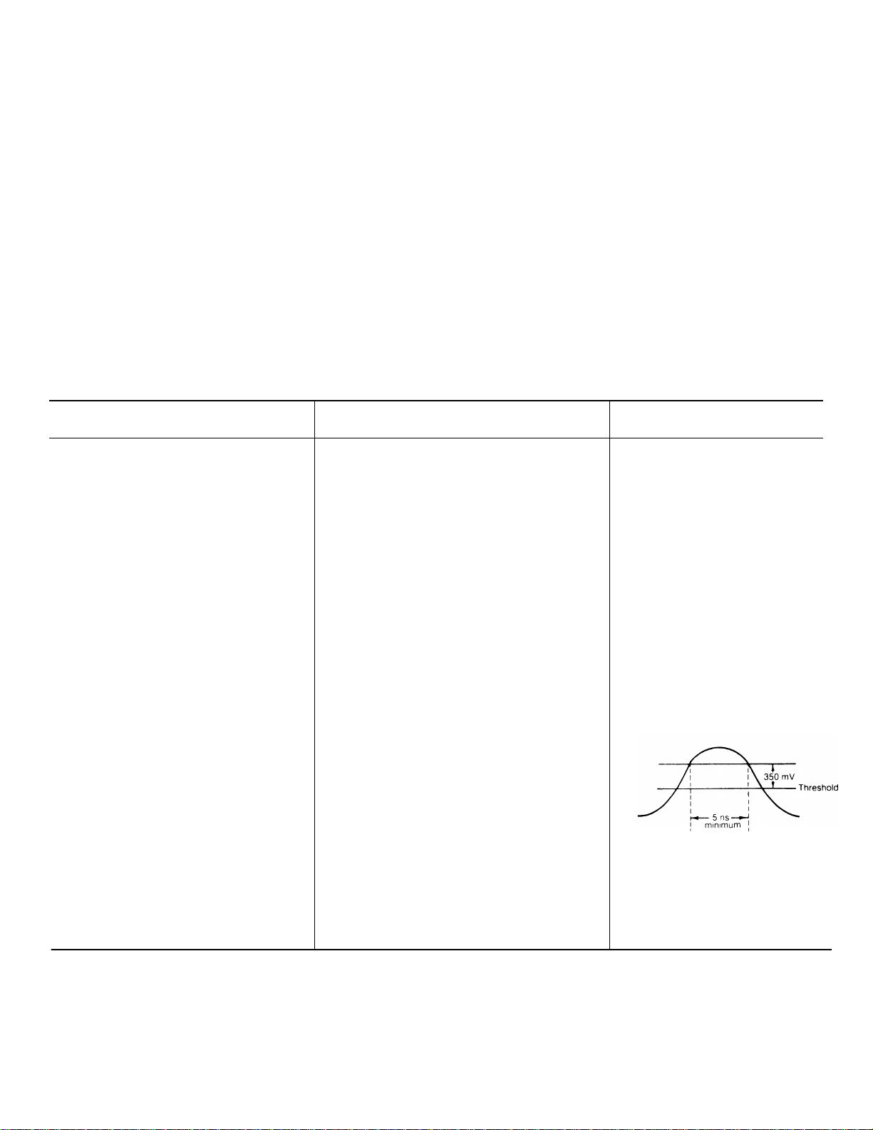
Tables 1-1 through 1-3 list the electrical, environmental, and physical characteristics of
the 318, 338, 318S1 ,and 338S1 logic analyzers. The electrical characteristic s are valid
for logic analyzers that have been adjusted as described in this manual (refer to the
Verification and Adjustment Procedures section). The instruments are adjusted at an
ambient temperature between +20° to +30°C (+68° to 68° F), and are designed to operate
in an ambient temperature between 0° to +50°C (+32° to +122°F) after having warmed up
for at least 15 minutes.
Characteristics Requirements Information
PARALLEL ANALYZER
FUNCTION
TM 11-6625-3145-14
Introduction & Specifications-318/338 Service
SPECIFICATIONS
Table 1-1.
318/338 ELECTRICAL SPECIFICATIONS
Performance Supplemental
Data Input (P6451 Probe) See P6451 literature for more
information.
Channels 318
16 channels. Glitch data is detected on all 16
channels.
338
32 channels. Glitch data is detected on loworder 8 channels (Pod A).
Input R and C 1 MΩ ± 5%, paralleled by approx. 5 pF
(without leads).
Minimum logic swing 500 mV p-p 4% of threshold voltage.
Maximum logic swing -15 V to threshold voltage plus 10 V.
Maximum non-destructive ± 40 V max.
Glitch data width 5 ns minimum with 350 mV overdrive from
threshold.
Threshold Voltage Accuracy
V1 (0.1 V step variable) -10 V to +10 V ±0.2 V
V2 (0.1 V step variable) -10 V to -+10 V ±0.2 V
V3 (V1 + V2) /2 ±0.2 V
TTL +1.4 V ±0.2 V
One of four levels is selectable
for each pod.
1-4
Page 31

TM 11-6625-3145-14
Introduction & Specifications-318/338 Service
Table 1-1 (cont.)
318/338 ELECTRICAL SPECIFICATIONS
Performance Supplemental
Characteristics Requirements Information
Sampling
Clock source internal or external
External clock mode Typically:
(using P6107 Probe) 318 338 318 338
Data setup time 13 ns min. 14 ns min. 8 ns 10 ns
Data hold time 0 ns max. 0 ns max. -3 ns -1 ns
Clock period, minimum 20 ns 50 ns
Clock pulse width
High-logic level 9 ns min. 15 ns min.
Low-logic level 9 ns min. 15 ns min.
External Clock
Input R and C 10 MΩ_ ± 3% paralleled by approx. 13 pF at 1.0 MΩ ±5% paralleled by ap-
probe tip. prox. 20 pF at BNC
.
Minimum logic swing 700 mV p-p centered on threshold voltage.
Maximum logic swing± +20 V peak.
Maximum non-destructive 400 V peak at probe tip.
40 V peak at BNC input connector.
Threshold Voltage Accuracy
V1 (0.1 V step variable) -10V to +10V ±0.23 V
V2 (0.1V step variable) -10 V to +10 V ± 0.23 V
V3 (V1 + V2) /2 ± 0.23 V
TTL +1.4 V ± 0.23 V
Clock polarity + or - edge
Internal clock mode 318 338
Sample interval 20 ns to 500 ms/ 50 ns to 500 ns/
sample in 1-2-5 sample in 1-2-5
sequence. sequence.
Crystal oscillator 100 MHz + 0.005 MHz
Data pulse width to 1 sample interval +5 ns
ensure sampling,
minimum
Maximum data skew be- 10 ns max. Typically: 5 ns
tween channels
1-5
Page 32

TM 11-6625-3145-14
Introduction & Specifications-318/338 Service
Table 1-1 (cont.)
318/338 ELECTRICAL SPECIFICATIONS
Performance Supplemental
Characteristics Requirements Information
Data Memory Depth
Acquisition memory 318 338
16 X 256 bits 32 X 256 bits
Reference memory 16 X 256 bits 32 X 256 bits
Glitch memory 16 X 256 bits 8 X 256 bits
Triggering
Trigger source internal, glitch, or external
Internal trigger Word trigger and glitch trigger
are OR’ed together.
Word recognizer Three: Word “A", Word “B", and Wor d “C” Selected channels are AND'ed
together.
Input All data input channels from P6451 data
acquisition probe.
Bit condition Logic 1, Logic 0, or X (don't care)
selection
Recognizer NXWA FLW'D BY
sequence THEN
OR
OFF
WB FLW'D BY
THEN
OR
RESET ON
OFF
WC
N: number of WA events, 65,000 max.
Glitch trigger Selected channels are OR'ed
together.
External trigger
External trigger input Mini-jack connector on the right side panel,
TTL compatible.
Threshold 1. 4 V nominal (TTL level)
Polarity + or - edge
Pulse width, min. 20 ns
1-6
Page 33

TM 11-6625-3145-14
Introduction & Specifications-318/338 Service
Table 1-1 (cont.)
318/338 ELECTRICAL SPECIFICATIONS
Performance Supplemental
Characteristics Requirements Information
Trigger position In delay mode, the trigger posi-
Begin word 7 tion is assigned by the user as
Center word 127 follows:
End word 247 Trigger position = (250 - delay
Delay word 250 (when delay value is set to 0) value).
Trigger position accuracy ± 1 clock External trigger only.
Trigger mode Immediately (first trigger) or After Memory If instrument does not complete
Full full memory acquisition before
the end of store, a fraction of
the display is indicated as "inva-
lid" data on data display.
Trigger output Initiated high when an internal trigger se-
quence, glitch trigger, or external trigger was
detected. Reset on next acquisition start.
Output level TTL 0.7 V or less for low level
output.
Voltage, maximum +6 V 2.4 V or more for high level
output.
Current, maximum
High-logic level -1 mA
Low-logic level 2 mA
Typical propagation delay 60 ns after the trigger event is clocked and
detected with internal clock.
80 ns after the trigger event is clocked and Measured from external clock
detected with external clock. input to trigger output.
± 1 clock interval when external trigger is Measured from external trigger
used. input to trigger output.
Qualifier
Input 9th channel of each P6451 probe is used as For more information, refer to
a qualifier input. P6451 literature.
Input R and C 1 MΩ ± 5%, paralleled by approx. 5 pF
(without leads).
Minimum logic swing 500 mV p-p centered on threshold voltage.
1-7
Page 34

TM 11-6625-3145-14
Introduction & Specifications-318/338 Service
Table 1-1 (cont.)
318/338 ELECTRICAL SPECIFICATIONS
Performance Supplemental
Characteristics Requirements Information
Maximum logic swing -15 V to threshold voltage plus 10 V.
Maximum non-destructive ±40 V max.
Threshold Threshold level for qualifier input
is same as data inputs.
Mode Each input is programmable for use as either All inputs chosen as clock qualifi-
a clock (clock + trigger) or trigger qualifier. ers are ANDed together to quali-
fy the clock. A11 inputs chosen
as
trigger qualifiers are ANDed to-
gether to qualify the trigger.
318 338
Setup time 14 ns max. 20 ns max.
Hold time 0 ns max. 0 ns max.
Polarity Selectable HI or LOW.
Data Display
Timing diagram mode
Number of channels Maximum of 8 channels present on the
screen at one time.
Window size 256 (requires fuzz character), 196 bits in mag
1, 98 bits in mag 2, 49 bits in mag 4.
Channel ordering Channel reordering is specified
on the timing data display. A sin-
gle channel need not be unique
within the timing display. Timing
channel reordering does not alter
the trigger characteristics.
Display page selection 318 338
2 pages 4 pages
Glitch display Glitch information can be displayed on timing
diagram as a bit-width transition edge.
CRT DISPLAY SYSTEM
CRT
Display area Approx. 6.8 cm (W) X 5.4 cm (H)
Phosphor P 31
1-8
Page 35

TM 11-6625-3145-14
Introduction & Specifications-318/338 Service
Table 1-1 (cont.)
318/338 ELECTRICAL SPECIFICATIONS
Performance Supplemental
Characteristics Requirements Information
Geometry 1 mm bow maximum on any
straight vertical or horizontal
line.
Linearity 1.4 times maximum or 0.9 times
minimum at the corner of display
area in comparison to same
character positioned at center
screen.
Accelerating voltage Approx. 6 KV
Deflection current
vertical Approx. 300 mA p-p
horizontal Approx. 1A p-p
Screen buffer memory size 1280 X 8 bits
Screen format 32 characters/row, 20
rows/screen
Refresh rate 60 frames/second, interlaced
Character generation
character matrix 5 X 7 character
7 X 10 block
character ROM size 2 K byte for parallel function
2 K byte for serial function
Composite video output 525-line interlaced 60 Hz composite video
V
: approx. 0.7 V with 75 Ω termination
glitch
Von: approx. 0.3 V with 75 Ω termination
V
: approx. 0 V with 75 Ω termination
off
V
: approx. -0.3 V with 75 Ω termination
sync
V
: 63.µs ±0.1 µS
sync
V
: 16.7 mS ± 0.1 ms
sync
Output impedance Approx. 75 Ω
1-9
Page 36

TM 11-6625-3145-14
Introduction & Specifications-318/338 Service
Table 1-1 (cont.)
318/338 ELECTRICAL SPECIFICATIONS
Performance Supplemental
Characteristics Requirements Information
TEST SIGNAL OUTPUT
Test Output
Output level TTL level 0.7 V or less for low-level
output.
2.4 V or more for high-level
output.
Voltage, maximum +6 V peak
Current, maximum
High-logic level -0.5 mA
Low-logic level 2 mA
Repetition rates C-10 µs G-GND
0-20 µs
1-40 µs These test signals may be ac2-80 µs cessed by P6451 data probe,
3-160 µs P6107 external clock probe, or
4-320 µs P6107 serial data probe.
5-640 µs
6-1.28 ms
7-2.56 ms
Start Output Generated when the instrument begins to
acquire data.
Output level TTL level 0.7 V or less for low-level
output.
2.4 V or more for high-level
output.
Voltage, maximum +6 V peak
Current, maximum
High-logic level -1 mA
Low-logic level 2 mA
Pulse width Approx. 650 ns
1-10
Page 37

TM 11-6625-3145-14
Introduction & Specifcations-318/338 Service
Table 1-1 (cont.)
318/338 ELECTRICAL SPECIFICATIONS
Performance Supplemental
Characteristics Requirements Information
POWER SUPPLY
Ranges of line voltages 90 V to 132 V AC or 180 V to 250 V AC,
48 Hz to 440 Hz, single phase
Power consumption 95 W max, 150 VA max.
DC supply voltages
+ 12 V Supply
Regulation ± 1 V max.
Ripple 50 mV p-p max.
Max. rated current 0.07A
Current limit point Three terminal regulator
-12 V Supply
Regulation ± 1 V
Ripple 50 mV p-p
Max. rated current 0.07A
Current limit point Three terminal regulator
+5 V Supply
Regulation ± 0.05 V max.
Ripple 50 mV p-p max.
Max. Rated current 1.5 A min., 2.6 A max.
Current limit point 110% - 200%
-5 V Supply
Regulation ± 0.05 V
Ripple 50 mV p-p max.
Max. rated current 4.0A min., 7.4 A max.
Current limit point 110% - 200%
-3.3 V Supply
Regulation ± 0.05 V
Ripple 4 0 mV p-p
Max. rated current 0.5 A min., 1.2 A max.
Current limit point 110% - 200%
-2 V Supply
Regulation ± 0.02 V max.
Ripple 40 mV p-p max.
Max. rated current1. 1.0A min., 2.6 A max.
Fan drive voltage Typically:
10V-11V at Ta =25°C
1-11
Page 38

TM 11-6625-3145-14
Introduction & Specifications-318/338 Service
Table 1-1 (cont.)
318/338 ELECTRICAL SPECIFICATIONS
Performance Supplemental
Characteristics Requirements Information
SERIAL STATE
ANALYZER FUNCTION
Data Input (Using P6107 Probe)
Input R and C 10 MΩ ± 3%, paralleled by approx. 13 pF at P6107 probe should be compen-
probe tip. sated for 40 pF input
capacitance.
1 MΩ ± 5%, paralleled by approx. 40 pF at
BNC.
Minimum logic swing 500 mV p-p centered on threshold voltage.
Maximum logic swing ± 30 V peak.
Maximum non-destructive 400 V peak at probe tip.
40 V peak at BNC input connector.
Threshold voltage Voltage at probe tip: Accuracy:
V1 (0.1 V step variable) -10 V to +10 V ±0.23 V
V2 (0.1 V step variable) -10 V to +10 V ±0.23 V
V3 (V1 + V2) /2 ± 0.23 V
TTL 1.4 V ± 0.23 V
One of four levels is selectable.
Sets threshold voltage at 0 V +
3 V for measurement of RS232C interface signal.
Sampling
Clock source internal or external
External clock input (using P6107 probe (the same probe as parallel)
P6107 probe)
External clock polarity + or -- edge
Data sampling rates
Internal clock for 50, 75, 110, 134.5, 150, 200, 300, 600, 16X sampling clock
asynchronous mode 1200, 1800, 2400, 4800, 9600 and 19200
bits per second
Accuracy of internal ± 0.02%, except 110-134.5 bits per second.
clock At these clock rates, the accuracy is relaxed
to 0.9%.
1-12
Page 39

Introduction & Specifications-318/338 Service
Table 1-1 (cont.)
318/338 ELECTRICAL SPECIFICATIONS
Performance Supplemental
Characteristics Requirements Information
External clock for Up to 19200 bits per second. 1X or 16X, 1X sampling clock
asynchronous mode selectable.
External clock for Up to 19200 bits per second.
synchronous mode
Setup and hold time for synchronous mode.
Setup time 3 µs maximum with respect to external clock
edge.
Hold time 3 µs maximum with respect to external clock
edge.
Stop bit (asynchronous Responds to one or more.
mode only)
TM 11-6625-3145-14
Trigger output The trigger output is initiated high when the
preset trigger words or external trigger was
detected. Reset on next acquisition start.
Data Display
State Table mode
Data format Hex, Binary, Octal, ASCII, EDCDIC radix.
Data table size 13 rows.
Parity error Parity error is indicated as "up in the error
display column adjacent to ASCII character
display column, if programmed.
Framing error Framing error point is indicated as "F" in the
(asynchronous error display column.
mode only)
Overrun error Overrun error point is indicated as "O" in the Overrun error occurs when the
error display column. data speed is faster than instru-
ment’s data-handling speed.
1-13
Page 40

TM 11-6625-3145-14
Introduction & Sp4clfications-318/338 Service
Table 1-1 (cont.)
318/338 ELECTRICAL SPECIFICATIONS
Performance Supplemental
Characteristics Requirements Information
RS-232C INTERFACE
Data transmission timing asynchronous only
Communication mode full duplex
Bits/Characters 8 bits with parity ASCII characters
Parity even
Stop bit Responds to one or more, sends one.
Remote echo selection ON or OFF
Data transfer rate 110, 150, 300, 600, 1200, 2400, 4800, 9600,
Baud.
Signal characteristics Meets RS-232C standard.
I/O connector 25-pin standard connector
Pin 1 protective ground GND
2 transmitted data to DCE
3 received data from DCE
4 request to send to DCE
5 clear to send from DCE
6 data set ready from DCE
7 signal ground GND
8 received line signal detector from DCE
20 data terminal ready to DCE
inputs: 3, 5, 6, 8
mark or OFF: -25 V to -3 V
space or ON: +3 V to +25 V
input impedance: 3 KΩ to 7 KΩ
outputs: 2, 4, 20
mark or OFF: -7.5 V maximum
space or ON: +7.5 V minimum
with load impedance: 3 KΩ minimum
1-14
Page 41

TM 11-6625-3145-14
Introduction & Specifications-318/338 Service
Table 1-1. (cont.)
318/338 ELECTRICAL SPECIFICATIONS
Performance Supplemental
Characteristics Requirements Information
NON-VOLATILE MEMORY
(Option 01)
Memory size 3 pages for setup parameters; 1 page for 8 X 2048 bits
ACQ or REF data.
Non-volatile period Approx. 5 years at room temperature.
Non-volatile Memory control From keyboard or RS-232 bus.
Battery Lithium battery (battery
capacity: 750 mAH or more)
Battery voltage check A check is performed of the battery at
power-up diagnostic.
1-15
Page 42

TM 11-6625-3145-14
Introduction & Specifications-318/338 Service
Table 1-2.
318/338 ENVIRONMENTAL SPECIFICATIONS
Characteristics Description
Temperature
Operating 0°C to +50°C
Storage -55°C to +75°C (but contents of non-volatile memory
may be lost with temperatures below -40°C)
Altitude
Operating To 4.5 km (15,000 feet). Maximum allowable ambient
temperature decreased by 1°C/1000 feet from 5000 feet
to 15,000 feet.
Storage To 15 km (50,000 feet).
Humidity Five cycles (120 hrs. total) with equipment tested at 90%
to 95% relative humidity. Tested non-operating at 600C
and operating to meet MIL-ST1-810C method 507.1
procedure 1 V, modified as specified in MIL-T-28800B
paragraph 4.5.5.1.2.
Vibration, Operating A 15-minute sweep along each of 3 major axes at a total
displacement of 0.025 inch p-p (3.9 g's at 55 Hz), with
frequency varied from 10 Hz to 55 Hz to 10 Hz. Hold 10
minutes at each major resonance, or if no major
resonance present, hold 10 minutes at 55 Hz.
Shock, Operating and Storage 50 g's 1/2 sine wave, 11 ms duration, 3 shocks per axis
in each direction for a total of 18 shocks.
Electromagnetic Interference Meets FCC part 15, subpart J, class A without probes.
(Compliance tests with probes in progress.)
1-16
Page 43

Table 1-3.
318/338 PHYSICAL SPECIFICATIONS
Characteristics Description
Weight
Net, without accessories about 5.1 Kg (about 12 lbs.)
Dimensions
Heights
without accessory pouch 12.0 cm (4.7 in)
with accessory pouch 17.4 cm (6.8 in)
Width with handle 23.7 cm (9.3 in)
Depth, handle not extended 40.9 cm (16.1 in)
Depth, handle extended 49.2 cm (19.4 in)
TM 11-6625-3145-14
Introduction & Specifications-318/338 Service
1-17/(1-18 blank)
Page 44

TM 11-6625-3145-14
OPTIONS
This section briefly describes the options available for a Sony/Tektronix 318 or 338 Logic Analyzer. Further inf ormation
regarding any option can be found in the manual section containing the type of inform ation desired. For instance, to find
information on the theory of operation of the non-volatile memory for 318S1/338S1, refer to the Theory of Operation
section.
318F1/338F1: SERIAL ANALYSIS, RS-232C INTERFACE, AND NON-VOLATILE MEMORY
The Sony/Tektronix 318F1/338F1 package is a field-installable kit that upgrades the basic 318/338 Logic Analyzers to
318S1/338S1 status. The package inc ludes a circuit board, Serial Data Probe, and the neces sary connectors to add the
following features to the the basic 318/338: Serial state analysis, an RS-232C remote communication interf ace, and nonvolatile memory. The same kit is used to modify both the 318 and the 338 Logic Analyzers.
2-1/(2-2 blank)
Page 45

TM 11-6625-3145-14
OPERATING INSTRUCTIONS
INTRODUCTION
The 318/338 is a menu-driven s ystem. This means that all operations are set up by means of menus displayed on the
monitor screen. Refer to the 318/338 Logic Analyzer Operator’s Manual for additional information on the general operation
and characteristics of the 318/338 menus.
INSTALLATION
Installation consists of selecting the appropriate operating voltage, c onnecting the 318/338 to a power input source, and
connecting the probe(s), as required, to the 318/338 and the circuit under test.
POWER REQUIREMENTS
The 318/338 operates from a nominal 115 or 230 V, 48 to 440 Hz, single-phase power input sour ce. Before c onnecting
the instrument to a power source, verify that the line-voltage indicator on the back of the instrument is displaying the
correct nominal voltage for the power input source to be used.
CAUTION
Before applying power to the instrument make sure the line- voltage indicator
shows the correct voltage for the power input source being used. The instrument
can be damaged if the line-voltage switch is in the wrong position for the voltage
being supplied. Adjust the red voltage selector switch on the back-end panel of
the instrument for the proper line-voltage. Make sure you are using the correct
power supply cord when connecting the 318/338. If you are unsure if either the
voltage selector switch is in the proper position, or if you have the appropriate
power cord, refer the instrument to qualified service personnel.
POWER CORD
This equipment has a 3-wire power cord with a 3-contact plug for connection to the power source and to protective ground.
The plug protective-ground contact connects (through the power cord protective-grounding c onductor) to the accessible
metal parts of the equipm ent. For electrical shoc k protection, ins ert this plug into a power input sourc e sock et that has a
securely grounded protective-ground contact. The power cor d is detachable. W hen not in use, it s hould be stored in the
accessory pouch. Instruments are usually factory equipped with a 115 V power cord unless otherwise ordered. For more
information on power cords, contact your Tektronix representative or your local Tektronix Field Office.
WARNING
Hazardous voltages may be present on the exposed mental surfaces of the
mainframe if the power source socket’s protective ground connection is not
securely grounded.
3-1
Page 46

TM 11-6625-3145-14
Operating Instructions-318/338 Service
MENU CHARACTERISTICS
There are certain characteristics and terms common to all menus. The following paragraphs discuss these common
characteristics and their im plications. More complete information is available in the 318/338 Logic Analyzer Operator’s
Manual, and as each menu is called later in this section.
POWER-UP CONFIGURATION DISPLAY
When the 318/338 is first powered up, it lists the configuration of the 318/338 and identifies option modules. It then shows
the results of the self test.
MENUS AND SUBMENUS
Each 318/338 menu is displayed on the monitor screen when you press its associated MENU key on the keyboard.
Some of the menus are comprised of several parts called subm enus. These submenus are individual screen displays
which may be selected only after the menu is entered. For exam ple, the parallel State Table menu has two submenus:
one for searching for data and one for comparing data. To display either of these submenus , you must first enter the
parallel State Table menu.
MENU DEFAULT DISPLAYS
On system power-up, the 318/338 assigns each menu default operating parameters. When you enter the menu, the menu
and its default parameters appear on the screen. This initial menu display is called the menu’s default display. If no
changes are made to the menu’s default display, the 318/338 will use the default parameters during the various
operations.
MENU FIELDS AND THE EDIT CURSOR
When a menu is displayed on the 318/338 screen, the m enu’s changeable parameters appear as reverse-video fields.
Before making any changes in a specific field, you must first move the blinking edit cur sor to that field. The edit cursor
moves from field to field, in any direction. It is controlled by these EDIT keys:
↑, ↓, ←
Once the edit cursor is loc ated in a specif ic field, you can change the field value. The c omm on keys used in m aking field
changes are:
, and →. They move the cursor one space up, down, left, or right.
• Data Entry keys - used in fields that have a string of numeric values.
• SELECT key - used in fields with predetermined values.
• INCR and DECR keys - used in fields that have specific incrementing or decrementing numerical values.
• CLEAR key - used in fields that allow a reset to zero.
NOTE
In some fields you must press the EXECUTE key after making any changes with the
SELECT key. In these cases, an error message will appear when you try t o move
the edit cursor to another field after pressing the SELECT key. Pressing SELECT
again will abort EXECUTE.
3-2
Page 47

TM 11-6625-3145-14
Operating Instructions-318/338 Service
ERROR MESSAGE AND ACQUISITION STATUS READOUT
The 318/338 has a comprehens ive set of err or and acquisition status mes sages. T hese mes sages appear on the bottom
line of the screen: the error m essage is at the lef t of the s creen and is dis played in blinking, highlighted video; acquisition
status is at the right hand of the screen and is displayed in blinking video.
A complete listing of error and acquisition status messages can be found in Appendix A of this manual.
MAJOR MODE SELECTION FIELD
The major mode (PRL/SER/KBD/RMT/NVM) selection field appears in the top left corner of the screen (except when
displaying the RS-232 Setup menu or the Non-Volatile Memory Setup menu). After mak ing any changes in this field, you
must press the EXECUTE key to access the selected mode.
INPUTS DURING ACQUISITION
Even when acquiring data (when waiting for a trigger or in REPEAT mode), the 318/338 c an accept any keys in any fields
except for those that generate the message: PRESS STOP. This capability allows you to change the delay value or
sample clock while looking at continuously acquired data, without pressing the STOP key.
MENU FUNCTIONS
SETUP MENU
The Setup menu (parallel) s erves two functions. F irst, it is used to s pecify the acquisition mode ( SINGLE, REPEAT , RPT
UNTIL ACQ = REF, RPT UNTIL ACQ ≠ REF) that will be used during acquisition.
The second function of the Setup m enu is to determ ine the way in which acquisition channels are organized for dis play. It
organizes the channels into logical groups. This inf ormation is then used by the Trigger m enu for organizing the word
recognizer channels, and by the State Table menu for organizing the data display. This channel organization is
independent of the order in which channels are connected to the system under test. The organization only aff ects the
display, not the actual acquisition. Changes can be made to the data display after the data has been acquired.
The Setup menu (serial) also s erves the following functions: comm unication mode (ASYNC/SYNC) selection, baud rate
selection, input polarity selection, bits/word selection, and parity selection.
THRESHOLD MENU
The function of the Threshold menu is to determine probe input thres holds (including data lines and the external clock
line).
3-3
Page 48

TM 11-6625-3145-14
Operating Instructions-318/338 Service
TRIGGER MENU
The Trigger m enu sets up the major acquisition parameters. First, it specifies which trigger mode (INT , EXT, or INT OR
EXT) will be used during acquisition. Then it specifies the acquisition clock (external or internal) and trigger position
(BEGIN, CENTER, END, or DELAY), and enables clock or trigger qualifier lines. T he T rigger m enu als o controls all word
recognition, triggering parameters, and glitch triggering. The T rigger m enu (serial) als o controls SYNC WORD and HUNT
WORD in synchronous mode.
STATE TABLE MENU
The State Table menu has two subm enus: SRCH (search) and CMPR (com pare). The SRCH (search) function is used
for searching through ACQ (acquisition) or REF (reference) memory for a specific data word or a word including a glitch. It
will show the number of occurrences of the specific data in the mem ory and it will also show the relative position of the
memory cursor to these data. T he CMPR (com pare) function is us ed in conjunction with REF (ref erence) m emor y. REF
memory is filled with a copy of ACQ memory when EXECUTE is pressed (edit cursor in the ACQ-REF field).
The CMPR displays then show differences between REF m emory contents and any later ACQ memory contents within the
CMPR WDO (window). The channel organization of the parallel state display is controlled by the Setup menu.
TIMING DIAGRAM MENU (PARALLEL ONLY)
The Timing Diagram m enu (parallel) has two submenus: SRCH (searc h) and ∆T (delta time). T he search function is the
same as in the parallel State Table m enu for displayed data or data on that page. The ∆T (delta time) f unction makes a
timing measurement between two given locations (∆T and C) in the waveform display.
CHARACTER MENU (SERIAL ONLY) (318S1/338S1)
The Character menu (serial) has two submenus: SRCH (search) and CMPR (compare). These are the same as
described for the State Table menu. This display shows 256 bytes of data on one screen in either ASCII or EBCDIC
format.
REMOTE (RMT) MENU (318S1/338S1)
The purpose of external com munication is to allow the user to store referenc e memories; to retrieve acquis ition, ref er enc e,
and glitch memories; to store and retrieve setups outside the 318/338; and to be able to control the 318/338 from an
external controller. You can select BAUD RATE and ECHO in the RMT mode.
NON-VOLATILE (NVM) MENU (318S1/338S1)
The values of setup param eters and acquisition or reference m emory can be stored in NVM memory. This m eans that
once the parameters and m emory are saved, they will not change (in the NVM) when the 318/338 is powered off and back
on again.
NOTE
When the NVM diagnostics test is run, all information stored in the NVM memory is
erased.
3-4
Page 49

TM 11-6625-3145-14
Operating Instructions-318/338 Service
DIAGNOSTICS
The 318/338 has internal diagnostics to help verify proper instrument performance. Some of the diagnostics occur
automatically whenever the 318/338 is powered on. Other diagnostics require that probes be pr operly attached to test
points or require an operator at the keyboard. Any error found during correc t operation of the diagnostics means that an
instrument failure has oc curred, has been detected, and that service is required. If an error occurs, r efer to
:
Maintenance
POWER-UP SELF TEST
When you press the POW ER switch, the internal diagnostic tests run automatically. These tests check out the major
hardware components and operating firmware.
During the first phase of self test, the 318/338 tests the major block s of s ystem RAMs and ROMs. Af ter RAM/ROM tests ,
the 318/338 is initialized. After several seconds, the dis play shows a configuration listing (see 3 in Figur e 3-1). At the top
of the screen (1 in Figure 3-1), the m essage SELF TEST VERSION X.X appears. O n the next line (2 in Figure 3-1), the
message IN PROGRESS appears.
Each listed menu is tested and then given a PASS or FAIL notation. (See 4 in Figure 3-1.) If errors are detected, error
messages also appear. ( See 5 in Figure 3-1.) PASS means that the test was successful; FAIL means that the test was
unsuccessful.
Troubleshooting
, of this manual for help in isolating and correcting the problem.
Section 7,
When all tests are finished, the m ess age COMPLET ED appears on the s creen. (See 2 in Figur e 3-1.) A prom pt m es sage
then appears at the bottom of the screen.
If no errors are found during self test, the screen will look like Figure 3-2.
You may now enter any menu and begin operation. If errors occurred dur ing self test, the s creen will look lik e Figure 3-1.
If the errors that occurred do not affect the operations you want to perform, press a MENU k ey. If you want to enter the
Diagnostics menu, press START.
NOTE
If neither of the displays shown in Figure 3-1 or Figure 3-2 appears on the screen
after several seconds, system errors have been detected. Refer to Section 7,
Maintenance: Troubleshooting, for help in isolating and correcting the problem.
3-5
Page 50

TM 11-6625-3145-14
Operating Instructions-318/338 Service
Figure 3-1. Failure in the power-up self test. Figure 3-2. Successful completion of the power-up Self
Test.
DIAGNOSTICS MENU
The Diagnostics menu of fers more levels of diagnostics. T he Diagnostics menu is only accessible when the power-up
tests show that a hardware component has failed. To enter the Diagnostics menu, press START.
To access the Diagnostics menu when no errors have been detected by the power-up tests, induce a power-up failure
from the keyboard by holding down any key (except STOP) from the time the 318 338 is turned on to the tim e the powerup self tests are completed (approximately 7 seconds).
When first entered, the screen should look like Figure 3-3. To begin testing, press a data entry key equal to a menu
number. Press X to return to Diagnostics menu. Press any MENU key to leave the Diagnostics menu and begin
operation.
USER-CHANGEABLE FIELDS FOR EACH TEST’S DISPLAY
LOOP and DISP (display) are the user-changeable fields in each tes t (except for the KBD, CRT, CLK, T /H, and N & DLY
tests). Some tests have more fields. such as the ALL or SING LE SELECTION field and the DATA ENTRY field. Ref er to
Figures 3-4 and 3-5 while reading the following paragraphs.
1 ALL OR SINGLE - Only some tests have this field. You may select either ALL or SINGLE. ALL causes all available
conditions to be tested. SINGLE causes a selected conditon to be tested. W hen the field is set to SINGLE, the DAT A
ENTRY field appears on the line below. During tests, the field m ay not be changed. If you wish to change fields, do so
after pressing STOP.
2 DATA ENTRY - Only some tests have this field. The tests are performed with the condition of the selected item or
entered data. The field may not be changed during tests. If you wish to change fields, do so after pressing STOP.
3-6
Page 51

TM 11-6625-3145-14
Operating Instructions-318/338 Service
Figure 3-3. Diagnostics menu: first display. Figure 3-4. Display sample with ALL/SINGLE and data
entry fields.
Figure 3-5. Display sample with LOOP and DISP fields.
3 LOOP - You can set this field to OFF, I/O, ERROR, or TEST by pressing SELECT. W hen the field is set to I/O, the
looping feature allows only I/O instructions to be run repeatedly. The I/O addr ess will appear on the s creen. W hen the
field is set to ERROR, the looping feature allows the tests in which an error is detected to be run r epeatedly. When the
field is set to TEST, the looping f eature allows one test or s equence of tests to be run continuously. W hen the f ield is s et
to OFF, the looping feature is not available and one test or sequence of tests runs once.
3-7
Page 52

TM 11-6625-3145-14
Operating Instructions-318/338 Service
When the field is set to I/O or ERROR, the prom pt mess age START T O ADVANCE appears at the bottom of the screen.
If START is pres sed during LOOP tests, the current loop of tests stops and the nex t loop of tests is started. You can
change fields during tests.
Use this feature for catching intermittent faults or for circuit tracing with an oscilloscope.
4 DISP (display) - This field m ay be set to ON or OFF. When the field is set to ON, tes t results appear within the status
area on the screen. When the field is set to OFF, no test results appear. You can change fields during tests.
5 DISPLAY AREA FOR RESULTS - This ar ea is used to display test results. You cannot move the cursor into the area
between the dotted lines. If the DISP field is set to OFF, no test results will appear here other than results of the I/O LOOP
test.
6 PROMPT M ESSAGES - Press ST ART to begin and to advance tests (exc ept for KDB test). ST O P TO CANCEL T EST
will appear under tests instead of START TO BEGIN TEST. Press X to retur n to the Diagnostics m enu for all tests ex cept
KBD. Press STOP to cancel tests. For KBD test, press STOP to cancel test and return to the Diagnostics menu.
DIAGNOSTIC TEST DESCRIPTIONS
KBD Test. To enter the keyboard test, press 0 while in the Diagnostics menu. The screen display simulates the
keyboard. When any key is pressed, its position on the s c reen blinks. If the corresponding sc r een position does not blink,
the key is open. If a screen position blinks without a key being pressed, that key is shorted closed. Refer to the
Diagnostics menu or to the troubleshooting trees in
Section 7
for details. Figure 3-6 illustrates the KBD test.
CRT Test. To enter this test, pr ess 1 while in the Diagnostic s menu. This test is f or the f oc us c heck and the CRT rotation
check. First, the cross-hatch pattern appears on the screen. Press START; the display will change continuously. Refer to
the Diagnostics menu or to the trouble-shooting tree in
Section 7
for details.
Figures 3-7, 3-8, 3-9, and 3-10 illustrate the CRT tests.
This key blinks when hit.
Figure 3-6. Display for KBD tests. Figure 3-7. CRT test: first display.
3-8
Page 53

TM 11-6625-3145-14
Operating Instructions-318/338 Service
Figure 3-8. CRT test: second display.
Figure 3-10. CRT test: fourth display.
Figure 3-9. CRT test: third display.
3-9
Page 54

TM 11-6625-3145-14
Operating Instructions-318/338 Service
CLK Test. To enter this test, press 2 while in the Diagnostics menu. This is a tes t of the internal timebase. It is not a
verification test; neither PASS nor FAIL will appear on the screen. If ALL is selected, the value of the clock interval being
tested will appear on the screen. You should use an oscilloscope to observe the operation of this test. Refer to the
Diagnostics menu or to the troubleshooting trees in
operation: Select ALL (default) or SINGLE by pressing SELECT. Press the START k ey. If you have selected ALL, the
value of the clock from 20 ns to 1 s will appear on the screen sequentially. Probe the timebase with an
oscilloscope to verify that the clock interval is c orrect. If you have selected SINGLE, the DATA ENTRY field
will appear on the next line. You can change the value in this field by pressing INCR or DECR. Pres s START
and use the oscilloscope to verify the timebase value you have selected. Nothing will appear on the screen.
WR Test. To enter this test, press 3 while in the Diagnostics m enu. This test is f or the word-recognizer RAM. Refer to
the Diagnostics menu or to the trouble-shooting tree in
operation: Press START to begin this test. The LOOP test and DISP ON/OFF functions are available here. The LO OP
test has four features: OFF, I/O, ERROR, and TEST. You can select these featur es by pressing SELECT
even during testing. DISP can also be selected during testing. If DISP is s et to OF F, no r es ults will appear on
the screen other than results of the I/O LOOP test. To exit this test, wait until the test finishes, or press STOP,
and then press X. If errors are detected in the test and DISP is ON, som e of the following err or codes will
appear on the screen.
Section 7
for details. Figure 3-11 illustrates the CLK test.
Section 7
for details.
Error codes: 20, 21, 22, 23 (Refer to
Figure 3-12 illustrates the WR test.
Figure 3-11. Display for CLK tests. Figure 3-12. Display for word recognizer RAM (WR) test.
Appendix B
for details.)
3-10
Page 55

TM 11-6625-3145-14
Operating Instructions-318/338 Service
ACQ Test. To enter this test, press 4 while in the Diagnostics m enu. This test is for acquisition RAM. Refer to the
Diagnostics menu or to the trouble-shooting tree in
Figure 3-13 illustrates the ACQ test.
operation: Press START to begin this test. The LOOP test and DISP ON/OFF functions are available here. The LO OP
test has four features: O FF, 1/0, ERROR, and TEST. You can select these features by press ing SELECT
even during testing. DISP can also be selected during testing. If DISP is s et to OF F, no r es ults will appear on
the screen other than results of the 1/0 LOOP test. To ex it this m enu, wait until the test is com plete, or press
STOP, and then press X.
If errors are detected in the test and DISP is ON, some of the following error codes will appear on the screen.
Section 7
for details.
Error codes: 30, 31, 32, 33 (Refer to
SQRAM Test. To enter this test, pr ess 5 while in the Diagnostics menu. This test is for the trigger sequencer RAM.
Refer to the Diagnostics m enu or to the trouble-shooting tree in
test.
operation: Press START to begin this test. The LOOP test and DISP ON/OFF functions are available here. The LO OP
test has four features: O FF, 1/0, ERROR, and TEST. These can be s elected by pressing SELECT even
during testing. DISP can also be selected during testing. If DISP is set to OF F, no results will appear on the
screen other than results of the I/O LOOP test. To exit this menu, press X after the test finishes or after
pressing STOP. If errors are detected in the test and DISP is ON, some of the following error codes will
appear on the screen.
Error codes: 40, 41 (Refer to
Appendix B
Appendix B
for details.)
for details.)
Section 7
for details. Figure 3-14 illus trates the SQRAM
Figure 3-13. Display for acquisition RAM (ACQ) test. Figure 3-14. Display for trigger sequencer RAM (SQRAM)
test.
3-11
Page 56

TM 11-6625-3145-14
Operating Instructions-318/338 Service
N&DLY Test. To enter this test, press 6 while in the Diagnostics m enu. This test verif ies that the N and DELAY counter
will run continuously. Refer to the Diagnostics menu or to the trouble- shooting tree in
illustrates the N&DLY test.
operation: Set the counter values in the N and DELAY fields. (Default: N = 1; DELAY = 0.) Press ST ART to begin the
test. This is not a verification test, so you should probe the LOAD N signal or the LOAD DL signal with an
oscilloscope to verify these counters. To exit this test, press STOP and then press X.
Section 7
for details. Figure 3-15
NOTE
In the case of N = O (or DLY = 0), the N counter (or the DELAY counter) will not run
at all. This status is correct.
SEQ Test. To enter this test, press 7 while in the Diagnostics menu. This is an overall test for parallel acquisition
components. Refer to the Diagnos tics m enu or to the trouble-s hooting tree in
the SEQ test.
operation: Press START to begin test. T he LOOP test and DISP O N/OFF functions are available here. T he LOO P test
has four features: OFF, I/O , ERROR, and TEST. These c an be selected by pressing SELECT even during
testing. DISP can also be selected during testing. If DISP is OFF, no results will appear on the sc reen other
than results of the I/O LOOP test. To exit this test, wait until the test finishes, or press STOP, and then pr ess
X. If errors are detected and DISP is ON, some of the following error codes will appear on the screen.
Section 7
for details. Figure 3-16 illustrates
Error codes: 50, 51, 52, 53 (Refer to
Appendix B
for details.)
Figure 3-15. Display for N counter or DLY counter tests. Figure 3-16. Display for overall tests on parallel acquisition
(SEQ test).
3-12
Page 57

TM 11-6625-3145-14
Operating Instructions-318/338 Service
THRSH Test. To enter this test, press 8 while in the Diagnostics menu. This test verifies that the sawtooth wave or
constant threshold level signal will be generated. Refer to the Diagnostic s menu or to the trouble-s hooting tree in
for details. Figure 3-17 illustrates the THRSH test.
7
operation: When you select ALL (default) and press START, the s awtooth wave will be generated. The threshold value
will then appear on the screen.
If SINGLE is selected, then DATA ENT RY field will appear on the screen as in Figure 3-17. Set the threshold value to be
observed and press START. The constant threshold level will be generated and nothing will appear on the screen. This is
not a verification test, so you should probe the signal with an oscilloscope to verify the threshold level. T o exit this test,
press the STOP key, and then X.
External Clock Probe Compensation. This test verifies that the External Clock Probe is properly compensated and
provides a way to correct any misadjustment. Note: two nearly identical P6107 probes are supplied with the 318S1/338S1,
one is called the External Clock Probe ( 20 pf compensation), and the other is c alled the Serial Data Input Probe ( 40 pF
compensation). Make sure you are using the probe marked External Clock.
To enter this menu, pres s 9 while in the Diagnostics menu. This test c alibr ates the P6107 External Clock probe by means
of the built-in pattern generator on the right side panel. First, set up pr obe as in Figure 3-18; the signals to be used ar e
specified to CH6 and G (ground). Figure 3-19 illustrates the External Clock Probe compensation display.
Section
Figure 3-17. Display for the threshold test (THRSH).
Figure 3-18. Setup of probe compensation.
3-13
Page 58

TM 11-6625-3145-14
Operating Instructions-318/338 Service
operation: Press START to bigin this tes t. Af ter s ever al se conds one of the following status messages will appear on the
screen:
UNDER: means undercompensated
OVER: means overcompensated
FIT: means properly compensated
Adjust the probe compensation by turning the screw located under the calibration seal in the P6107 External Clock Probe’s
compensation box; turn the screw according to the displayed status message. When FIT appears on the screen the probe
compensation is properly adjusted (20 pF).
The 318/338 will run continuously until STOP is pressed. The other keys are disabled during probe compensation. To exit
this menu, press STOP and then press X.
NOTE
If your setup does not match Figure 3-18 your equipment setup may be incorrect.
Figure 3-19. Display for External Clock Probe compensation.
P6107 Probe Assignment and Compensation for the 318S1 and 338S1. Two nearly identical P6107 probes are
supplied with 318S1 and 338S1 Logic Analyzers, however they must be compensated differently (Serial Data Acquis ition
Probe-40 pF; External Clock Probe--20 pF).
3-14
Page 59

TM 11-6625-3145-14
Operating Instructions-318/338 Service
When the probes are supplied with the instrum ent they will already be marked as the External Clock Probe and the Serial
Data Input Probe, and their compensations will be properly adjusted. If a r eplacement probe has been order ed it will not
be marked and the com pensation will be set at 40 pF. If you are replacing the Serial Data Input Probe no change in
compensation is necessary; simply mark the probe for identification purposes. If you are replacing the External Clock
Probe you must adjust the probe compensation to 20 pF according to the procedure described in the preceding
paragraphs. Be sure to mark the probe for identification purposes.
SER Test. This test is only available with the 318S1 and 338S1. It r equires the optional Self Test Adapter (013- 0173-01) .
Contact your Tektronix sales representative if you need assistance in ordering.
To begin this test, press A while in the Diagnostics menu. This test is for the SIO us ed in the s erial data ac quis ition mode.
Refer to the Diagnostics menu or to the trouble-shooting trees in
test.
operation: Your probe connection setup should match that in Figure 3-20 bef ore you begin this test. To begin the test,
press START. The LOOP test and DISP ON/OFF functions are available here. The LOOP test has four
features: OFF, I/O, ERROR, and TEST. These can be selec ted by pressing SELECT even during testing.
DISP can also be selected during testing. If DISP is OFF, no results will appear on the sc reen other than
results of the I/O LOOP test. T o exit this m enu, wait until the test finis hes, or press STOP, and then pres s X.
If errors are detected and DISP is ON, some of the following error codes will appear on the screen.
Section 7
for details. Figure 3-21 illustrates the serial SIO
Error codes: B4, B5, B6, B7, B8, B9, BA, BB, BC, BD, BE, BF, CO, C1, C2, C3 (Refer to
Figure 3-21. Display for Serial test (SER).
Figure 3-20. Probe connection setup for serial test (SER).
Appendix B
for details.)
3-15
Page 60

TM 11-6625-3145-14
Operating Instructions-318/338 Service
RMT Test. This test is available only with the 318S1/338S1. To begin this test pres s B while in the Diagnostics menu.
This test is for the SIO us ed by the remote mode. Refer to the Diagnostics m enu or to the trouble-shooting tree in
for details. Figure 3-23 illustrates the display for the remote SIO test.
7
operation: Your equipment setup should match that in Figure 3- 22 before you begin this test. To begin the test, press
START. The LOOP test and DISP ON/O FF functions are available here. The LOO P test has four features:
OFF, I/O, ERROR, and TEST. These can be selected by pressing SELECT, even while the test is in
progress. DISP can also be selected during testing. If DISP is OFF, no results will appear on the screen
other than results of the I/O LOOP tes t. To exit this test, wait until the test is c omplete, or pr ess STOP, and
then press X. If errors are detected and DISP is ON, some of the following error codes will appear on the
screen.
Error codes : 96, 97, 98, 99, 9A, 9B, 9C, 9D, 9E, 9F, A0, A1, A2, A3, A4, A5, A6, A7, A8, A9, AA, AB, AC, AD, AE, AF, BO,
B1, B2 (Refer to
Appendix B
for details.)
Section
NOTE
This test may take up to 40 seconds to complete.
Figure 3-22. Equipment setup for remote test (RMT).
Figure 3-23. Display for remote tests (RMT).
3-16
Page 61

TM 11-6625-3145-14
Operating Instructions-318/338 Service
NVM Test. T his test is only available for the 318S1 /338S1. ’to begin this test press C while in the Diagnostics m enu.
This is the non-volatile memory test. Refer to the Diagnostics menu or to the trouble-shooting trees in
details. Figure 3-24 illustrates the NVM test.
Section 7
for
NOTE
The NVM test will overwrite all non-volatile memory data previously saved.
operation: Press START to begin the test The LOOP test and DISP ON/OFF functions are available here. The LOOP
test has four features: OFF, I/O, ERROR, and TEST. These can be selected by pressing SELECT even
during testing. DISP can also be selected during testing. If DISP is OFF, no res ults will appear on the scr een
other than results of the I/O LOOP tes t. To exit this m enu, wait until the test is com plete, or press the STOP
key, and then press X. If errors ar e detected and DISP is ON, som e of the f ollowing error codes will appear
on the screen.
Error codes: C8, C9, CA, CB, CC, CD, CE, CF, D0, D1, D2, D3 (Refer to
Figure 3-24. Display for the non-volatile memory test (NVM).
3-17/(3-18 blank)
Appendix B
for details.)
Page 62

TM 11-6625-3145-14
Section 4-318/338 Service
THEORY OF OPERATION
SECTION ORGANIZATION
This section contains a functional description of the circuitry used in the 318 and 338 Logic Analyzers. It is divided into two
sub-sections:
schematics for the 318 and 338 are found in the tabbed
General System Description and Detailed Circuit Description
Diagrams
section at the rear of this manual.
. Block diagrams, wiring diagram s , and detailed
Use the 318/338 Block Diagrams in the
on the block diagrams correspond to sub- headings in the
conjunction with the
sub-headings by corresponding numbers in diamonds. This section and the block diagrams and schematics in the
Diagrams
information is presented in the
section may be valuable as a reference when troubleshooting system circuitry. Specific troubleshooting
Detailed Circuit Description
Maintenance. Troubleshooting
Diagrams
section with the
part of this section. Schematics are referenc ed to section headings and
General System Description
General System Description
section of this manual.
part of this section. Bloc ks
. Use the system schematic s in
NOTE
Unless otherwise specified, the text, tables, and figures in this section refer to both
the 318/318S1 and the 338/338S1. Differences are called out as they occur.
DIGITAL LOGIC CONVENTIONS
Digital logic techniques are used to perform most functions within this instrument. Function and operation of the logic
circuits are represented by standard logic symbols and terms. All logic f unctions are described using the positive logic
convention. Positive logic is a system of notation whereby the more positive of two levels is the true, or 1 state; and the
more negative level is the false, or 0 state.
In logic descriptions, the mor e positive of the two logic voltages is ref erred to as high, and the m ore negative s tate as low.
The specific voltages that constitute a high or low state vary between different electronic devices.
Whenever a line name on a schematic is ref er red to within the text, that line name may be overscor ed, SIGN AL, indicating
that the line is an active low. Line names without overscores are active high.
To best understand the circuitry, cross -reference the descr iptions in this section with the block diagrams in the
section. Refer to the Table of Contents at the front of this manual to locate individual circuit descriptions.
Diagrams
GENERAL SYSTEM DESCRIPTION
The following discussion provides an overall description of the 318/338 Logic Analyzer. Refer to the simplified block
diagrams in this section, and to the system block diagram s in the
these diagrams represents a maj or circuit within the instrument. T he numbered diam ond symbol on each block r efers to
the associated schematic diagram for that circuit (also located in the
The instrument can be divided into two sections:
• Acquisition Module
• Mainframe
4-1
Diagrams
Diagrams
section of this m anual. Each major block in
section).
Page 63

TM 11-6625-3145-14
Theory of Operation-318/338 Service
The acquisition module consists of:
• Parallel data inputs (Input A and Input B boards) (A01 & A02)
• Acquisition (ACQ) Control board (A03)
• ACQ Memory board (A04)
• Serial Analysis/RS-232/NVM Option 01 board (A07)
NOTE
The 318 and 338 have different acquisition circuitry; make sure you reference the
correct description for the instrument you are servicing.
The mainframe consists of:
• ROM/Threshold board (A05)
• MPU/Display board (A06)
• Mother board (A08)
• Keyboard (A09)
• CRT board (A10)
• Power supply (A11 & A12)
The mainframe is common to both the 318 and 338 Logic Analyzers; circ uit board assemblies are mark ed 318/338
AXX.
NOTE
The 318 has two unique circuit board assemblies marked 318 A01, and 318 A02; the
338 also has two unique circuit board assemblies, marked 338 A01, and 338A02.
Circuit boards that are common to both the 318 and 338 are marked 318/338. The
tabs in the Diagrams section of this manual are marked 318/338, 318, or 338 to
correspond to the circuit board assemblies used in the analyzer.
ACQUISITION MODULE
PARALLEL DATA INPUTS (A01 AND A02)
The Input-A (A01) and Input-B (A02) boards configure the parallel data inputs. These boards are mounted into connectors
J1 and J2, respectively, on the Mother board.
P6451 Parallel Data Probe. In the 318, two P6451 parallel data probes can be connected to the right-s ide panel. The
338 has four P6451 parallel data probes. Each probe ac cepts eight c hannels of data and one qualif ier channel f or either
trigger or clock qualifications. Thus, 16 channels of data and 2 channels of qualifiers are available for the 318, and 32
channels of data and 4 channels of qualifiers are available for the 338.
P6107 External Clock Probe. The P6107 external clock probe is identical to the serial data probe, but the input
capacitance compensation is s lightly different (20 pf f or the external cloc k probe, 40 pf for the ser ial data probe). See the
External Clock Probe Compensation
This probe receives an external clock signal when the 318/338 is operating in synchronous mode.
paragraph in
Section 3
for instructions on adjusting the probe compensation.
4-2
Page 64

TM 11-6625-3145-14
Theory of Operation-318/338 Service
Data Buffers, Delay Lines, and First Lactches. Data acquired by the P6451 probe is sent differentially to a data buffer.
The output of the data buffer is routed to a delay line which is used to adjust the setup/hold timings between data and
clock. This delayed data is latched by the first latch. Glitch recognition is also performed by the IC containing this latch.
External Clock Circuit. An external clock from the P6107 probe is buffered by the FET buff er and c onverted to ECL level
by the ultra-fast comparator. Clock delay is adjusted by a delay line with taps connected to the output of the comparator.
Clock Selector. The internal clock, or the external clock’s rising or falling edge, can be selected with this selector.
Word Recognizer. Three kinds of word recognition ( Word A, B, and C) are perf or med by the word recognizer (WR). T he
outputs of the first latches are supplied to these WRs.
Threshold Circuit. The ROM/Threshold boar d provides threshold levels for eac h of the parallel data probes and for the
external clock probe.
ACQUISITION CONTROL BOARD (A03)
This board controls all parallel data acquired through J3 on the Mother board.
Qualifier Selector. Qualifier signals from the parallel data inputs are selected by the qualifier selec tor as either a trigger
qualifier or a clock qualifier. Polarity is also selected by this circuit.
Strobe Generator. The strobe generator provides four timing clocks to control triggering and data writing. All timing
clocks are adjustable by tapped delay lines and variable capacitors. This generator is enabled by the clock qualifier signal.
Trigger Sequencer. The trigger sequencer perf orms complex triggering according to the data written in the Sequencer
RAM (SQRAM). Three outputs from the word rec ognizers, and the outputs from the glitch trigger are connected to the
SQRAM inputs. The trigger sequencer sets the various flags on each word recognition and, once the trigger combination
is satisfied, starts the delay counter.
Event/Delay Counter. LSI-A, specially developed by Sony/Tektronix, contains a 16- bit synchronous counter used as the
event/delay counter. This counter has two functions: trigger event counting and delay counting.
ACQUISITION MEMORY BOARD (A04)
100 MHz Oscillator. A 100 MHz crystal-controlled os cillator is used for as ynchronous parallel acquisition. T his clock is
divided by a 1-2-5 sequence with LSI-B (A04 U140), to produce a 20 ns to 500 ms range.
Sampled Data RAM and Glitch RAM. In the 318, a 32 X 256-bit high-speed RAM is used for storing both sampled data
and glitch data. In the 338, a 32 X 256-bit high-speed RAM is used f or sam pled data, and a separate 8 X 256-bit RAM is
used for glitch data.
Acquisition Address Counter and Carry Flag F-F. Two 4-bit synchronous counters are used as acquisition address
counters to provide addresses f or the sampled data RAM and glitch RAM. The c arry flag F-F holds the carr y condition
once the address counter is full.
Output Multiplexer. Data written in the sampled data RAM, the glitch RAM, and the acquisition status register can be
read by the MPU. This multiplexer selects the data to be sent to the MPU.
4-3
Page 65

TM 11-6625-3145-14
Theory of Operation-318/338 Service
MAINFRAME
ROM/THRESHOLD BOARD (A05)
The ROM/Threshold board is installed into J5 on the Mother board.
ROM. Six 16K X 8-bit mask ROMs and one 8K X 8-bit EPROM are mounted on the ROM/Thres hold board. Part of the
ROMs are configured into four pages, since only 64K bytes of the 112Kbyte total can be addressed at a time.
Threshold Circuit. The threshold circuit contains two latching digital-to-analog converters. T his circuit provides three
kinds of threshold levels: V1, V2, and V3 {(V1 +V2)/2} for both parallel and serial probes.
MPU/DISPLAY BOARD (A06)
The MPU board is plugged into the J06 card-edge c onnector on the Mother board. The MPU board contains a Z- 80A
microprocessor , RAMs, a display controller, a character ROM, bus buff ers, key control logic, and oscillators for the MPU
and TV timings.
Microprocessor. A Z-80A microprocessor controls all operations for diagnostics and data acquisition.
RAMs. Two 1K X 8-bit static RAMs are used by the MPU to store data and flags.
Display Controller and Character ROM. This integrated circuit, developed by Sony/Tektronix, controls the 318/338
display data stored in the display RAM. The display controller decodes control codes for inverse video, blink ing, other
special display codes, and letter codes by referring to the character ROM. It then generates control signals for the CRT.
Bus Buffer. All address buses and data buses are buffered to provide sufficient fan-out to drive several boards connected
to the bus through the Mother board.
Key Control Logic. Key signals from the keyboard are encoded by a priority encoder and are sent to the MPU as a key
code with an interrupt. All keys (except the STOP key) can be masked by the MPU with the keyboard mask bit.
MOTHER BOARD (A08)
The Mother board provides interconnection f or boards A01 through A07 through connectors J1 to J7. In addition, this
board routes power to all boards and has connectors for the keyboard and the CRT boards.
KEYBOARD (A09)
The keyboard serves as the operator’s interface. The operator selects the menu to be displayed and sets up the
instrument from the keyboard. All functions of the 318/338 can be controlled from this keyboard in the local mode.
Pressing any key will cause an interrupt to be sent to the MPU, along with the key code corresponding to the key pressed.
CRT BOARD (A10)
CRT. The CRT is a four-inch raster-scan type.
CRT Circuit. The CRT circuit pr ovides z-axis voltage and the horizontal and vertical deflection-curr ent outputs that are
used for the CRT. A flyback transformer in the horizontal deflection circuit provides the high voltage and other CRT
electrode voltages.
4-4
Page 66

TM 11-6625-3145-14
Theory of Operation-318/338 Service
POWER SUPPLY (A11AND A12)
The power supply provides dc voltages of -3.3 V, -12 V, + 12 V, -5 V, -2 V, and +5 V to operate the 318/338 circuitry. It
also supplies voltage for the fan motor. It operates in the line input range of either 90 to 132 V ac or 180 to 250 V ac at 48
Hz to 440 Hz single-phase.
LEFT-SIDE PANEL
A BNC connector for video-output is mounted on the lef t side panel. The BNC is connected to the MPU/Display board
through the Mother board. If option 01 is installed (318S1/338S1), a second BNC connector for the P6107 serial data
probe and a 25-pin male connector for the RS-232C port are added.
318S1/338S1 (A07)
The 318S1/338S1 Logic Analyzer has the I/O circuit board (A07) plugged into J7 of the Mother board. The 318S1/338S1
contains three added functions:
• Serial State Analysis
• RS-232C Interface (Remote)
• Non-Volatile Memory
Serial Input Comparator. Serial data from the P6107 serial data probe is supplied to the serial input com parator and is
converted to a TTL-level signal.
Serial I/O Controller. The Serial Input/Output (SIO) c ontroller handles serial-to-parallel conversions. T he SIO contains
two serial data transceivers, Port-A and Port-B. Port-A is used for serial data acquisition and Port-B is for RS-232C
control.
DETAILED CIRCUIT DESCRIPTIONS FOR THE 318
The following paragraphs contain theory of operation inform ation f or the 318 Logic Analyzer. For inform ation on the theory
of operation for the 338 Logic Analyzer, refer to the Table of Contents and following sections of this chapter.
318 A01 INPUT A BOARD <1> <2>
A02 INPUT B BOARD <3> <4>
The Input section consists of the Input A (A01) and the Input B (A02) boards. The block diagram for these boards is
shown in Figure 4-1. Since both of these boards share the same function, they are discussed as a unit in this description.
OVERVIEW
Refer to schematics <1> and <3>. T he acquisition stages consist of 16 discrete units that perf orm data sampling and
glitch recognition. Sixteen channels of data to be s ampled come into the unit from the P6451 parallel data probe. Eac h of
the acquisition stages feeds data to the acquisition RAM where it can be read by the MPU. The same data from the
parallel data probe is supplied to the glitch recognition lines, and the 16 glitch recognition outputs are combined and
applied to the glitch trigger circuits.
To help explain the operation of the data channels, we will trace the operation of channel 8. Refer to the schematic <3>.
4-5
Page 67

TM 11-6625-3145-14
Theory of Operation-318/338 Service
A02U202 receives ECL-level differential data fr om channel 8 of the par allel data probe. The data enters the c ircuit board
via pins 22 and 10 of J204, and connects to pins 10 and 9 of A02U202.
The data is applied to the differential inputs of a receiver. From the receiver, the data is sent through the delay line DL1
06A to enable the timing to meet its setup-and-hold-time specification. On the rising edge of each clock (entering
A02U202 at pin 1), data, glitch, and glitch trigger are clocked, then sent off from pins 8, 2, and 14, respectively.
Operation of channels A02U204, A02U206, A02U208, A02U210, A02U212, A02U214, A02U216, A02U100, A02U102,
A02U104, A02U106, A02U108, A02U110, A02U112, and A02U114 are the same as for channel 8 (A02U202).
The glitch output goes high if at least two data transitions occur between rising edges of the clock.
If the glitch recognizer off/on line (pin 15, GRC) Is low, the glitch rec ognizer out line (pin 14, GR) indicates the presenc e of
one or more glitches. (T he (GRC line is controlled by shift regis ters A02U118 and A02U218.) If the GRC line is high, the
output line from pin 14 is disabled. The glitch trigger outputs of the 16 M21 8s are wire-ORed together. so whenever any
channel detects a glitch, that line moves to high.
ADDRESS DECODER <2>
The address decoder circuit consists of A01 U130 and A01U132. A01U132 is a TTL-to-ECL-level converter. U130
decodes 1/0 addresses 00, 01, 02, and 03. 1/O address 00 (A01U130 pin 11) is used to write trigger word data into the
Word Recognizer mem ory from channel 0 to channel 15. I/O address 01 (A01U130 pin 10) is a clock selector port. I/O
address 02 (A01U130 pin 9) resets the word recognizer memory address counter. This port als o controls glitc h trigger on
and off. I/O address 03 (A01U130 pin 7) increments the word recognizer address counter.
EXTERNAL CLOCK INPUT <4>
The external clock input is a high input-impedance (1 M(2) buffer. Transistor A04Q108A is connected as a source
follower. Transistor Q108B maintains a constant current flow through A04Q108A. The dc balance adjustment, R234.
sets the dc offset voltage of the source follower to 0 V.
EXTERNAL CLOCK COMPARATOR <4>
A02U236A compares the input signal fr om the source follower with a reference voltage divided by A02R238, A02R239,
and A02R240. This circuitry multiplies one-fourth the CLK Thres hold level from the A05 ROM/Threshold board by twofifths to match the P6107 external clock probe attenuation (1/4 x 2/5 = 1/10). If the input signal level is more pos itive than
the reference voltage, A02U236 pin 1 is high and A02U236 pin 2 is low R239 com pensates for the Q108’s source-drain
resistor variation.
CLOCK SELECTOR <4>
Data from shift register A02U224 controls A02U222A, A02U226B, A02U226A, and A02U244A. The MPU sets one of
these gates to low (enabled); then EXT ↑, EXT ↓, or INT CLK is selected.
These gates have three outputs. One clock s eight M218s on the A02 Input-B board, another clock s eight M218s on the
A01 Input-A board, and the third is distributed to the A03 ACQ Control board.
4-6
Page 68

TM 11-6625-3145-14
Theory of Operation-318/338 Service
GLITCH CONTROL <2> <3> <4>
This circuit controls pin 15 of the M218s. M218’s pin 15 is used to control pin 14’s output. If pin 15 is for ced high, glitch
trigger output pin 14 is disabled (kept low): if pin 15 is low, pin 14 is enabled. T heref ore, if a glitc h tr igger on a c ertain line
is expected, the corresponding M218’s pin 15 must be low. Since all M218 pins 14 ar e wire-ORed, a glitch tr igger occ urs
when any of M218’s glitch trigger output moves to high. A01 U118 <2> and A02U218 <3> control M218’s pin 15; these
registers are written to serially; they output their data in parallel to their respective M218s. A02U240 <4> shifts the MPU
data and clock signals by --5 V, and shifts the TTL swing to match the M21 8’s special input level.
PIPELINE REGISTER <1> <3>
This circuit consis ts of latches A01U122, A01U128, and A01U134 <1>, and latches A02U228, A02U234, and A02U238
<3>. The sampled data and glitch from the M218s are applied to the inputs of the pipeline registers. The pipeline
registers synchronize the data for storage in the acquisition (ACQ) m em ory. Clock signals for the register are provided by
the SYSCLK 2 signal which is delayed by A01DL104 <2> (delayed SYSCLK 2 is called SYSCLK 3) and buffered by
A02U200C <4> . Each SYSCLK 2 pulse advances the data from the M218 to the register, where it is held for one c lock
cycle before being loaded into the ACQ memory.
WORD RECOGNIZER <1> <2> <3>
The W ord Recognizer (WR) consists of three 16-channel word recognizers with high-speed m emories. The 318 offers
three word recognizer functions where three differ ent words m ay be set simultaneous ly. They are nam ed tr igger words A,
B, and C. The MPU loads data into A01U120 <1 > and A02U220 <3>, according to the trigger word, us ing A01 U124 <2>,
A01 U126 <2>, A02U230 <3>, and A02U232 <3> (memory address counters). The MPU increm ents thes e counters one
by one and loads data for trigger word A, B, or C into A01 U120 and A02U220. Each W R RAM has 8 address lines and
three data lines. Data from the M218s is used as address f or the W R RAM. W ithin the WR RAM, data is only three bits
wide, corresponding to triggers A. B, and C.
The MPU writes data, according to the trigger word, into the WR memory and increments the address counters. T his
operation is repeated 256 times. For example, to set the trigger word 7638hex, the MPU writes 0 into the lower WR
memory where the address counter value is 38hex, and 0 is written to the higher WR where the counter value is 76hex . In
all the other addresses, the WR’s are filled with is.
During acquisition, data is supplied to A01U120 and A02U220 address inputs, and if a trigger word com es, A01U120 and
A02U220 (whose outputs are wired-ANDed) generate a trigger signal which is sent to the A03 Acquisition Control board.
DATA THRESHOLD BUFFER <4>
The currents from edge-c onnectors 38B and 39A ar e applied to the inverting inputs of A02U242B and A02U242A, (gain of
minus one) and the currents f rom A02J202 pins 4 and 5 and A02J204 are supplied to the non-inverting inputs of these
amplifiers to be summ ed. The input is divided down to 5/8 of the original value before it is sent to the non-inverting inputs
of A02U242A and A02U242B. The output current of these amplifiers is then supplied through A02R262 and A02R256 to
the parallel data probe.
4-7
Page 69

TM 11-6625-3145-14
Theory of Operation-318/338 Service
PROBE COMPENSATION <4>
In the probe compensation mode, an external clock is supplied to the ACQ memory as data through A02U244A and
A02U244B gates. Channel 8 of the acquired data is used as the trigger , and channel 9 is used for data (U228-6,7 <3>).
The MPU recognizes over- or under-compensation from the ac quired data of channel 9. (Channel 9 is the result of the
clock signal compared with Threshold A.)
4434-580
Figure 4-1. 318 Input A and Input B block diagram.
318 A03 ACQ CONTROL BOARD <5> <6> <7>
The A03 Acquisition Control board (parallel data) has two registers and mem ory that acquisition parameters are loaded
into before data acquisition. It also contains other c ircuitry that controls the trigger sequenc e and the acquisition m em ory.
Simplified block diagrams are shown is Figures 4-2 and 4-3.
Figure 4-2 shows a simplified version of all the circuitry on schem atics <5> and <6>. Figure 4-3 s hows a sim plif ied version
of schematic <7>.
4-8
Page 70

TM 11-6625-3145-14
Theory of Operation-318/338 Service
Figure 4-2. 318 Simplified diagram of the ACQ control circuitry on schematics <5> and <6>.
4-9
Page 71

TM 11-6625-3145-14
Theory of Operation-318/338 Service
Figure 4-3. 318 Simplified diagram of the ACQ control circuitry on schematic <7>.
I/O ADDRESS DECODER <6>
The I/O address decoder c onsists of A03U110 and A03U112. The circuit provides a single pulse, used to activate a
preselected device which then communicates with the MPU and controls the start logic and trigger sequencer circuits.
Device selection is made using the lowest three bits of the address bus during I/O instruction execution on the ACQ
Control board.
4-10
Page 72

TM 11-6625-3145-14
Theory of Operation-318/338 Service
QUALIFY/SQRAM DATA REGISTER <5>
The qualify/SQRAM data register consists of A03U106 and A03U108.
This register is shared by two separate functions. W hen loading par ameters into the SQRAM, A03U106 and A03U108 are
used as the data register. To provide data to the SQ RAM, the MPU writes the data into A03U106 and A03U108 at I/O
addresses 50
hex
and 51
, respectively. The data format is illus tr ated in Figure 4- 4. T he outputs of A03U106 and A03U108 are connected
hex
to the SQRAM inputs. The signal, LDSQRAM (A03U108 pin 14), is high when data is loaded from this data register into
the SQRAM.
During an acquisition, A03U106 and A03U108 are used as the qualify register. Qualify data and other control bits are
written to them at I/O addresses 50
and 51
hex
respectively. The format is illustrated in Figure 4-5.
hex
Figure 4-4. 318 SQRAM data register format.
Figure 4-5. 318 Qualify register format.
4-11
Page 73

TM 11-6625-3145-14
Theory of Operation-318/338 Service
QUALIFY LOGIC <5> <6>
The qualify logic circuit consists of A03U 118A, B, A03U1 16A, B. The qualifier signals QA, QB, QA, and QB come f rom
the A02 Input B board. Their signals are wire-ORed with the outputs of the Q ualify Register, A03U106 and A03U108, and
go to the EXOR gates A03U116 and A03U118 <5> where their polarities are selected according to the polarity selection
bits. Each output of the EXOR gates is wire-ANDed and thes e signals go to gates A03U126A and A03U126B <6> of the
start logic circuit.
START/STOP LOGIC <6>
The start/stop logic circuit consists of A03U124B, A03U126A,B. When data acquisition starts, the START1 pulse is
generated at I/O address 56
and goes to the clock input of A03U124B.
hex
The output signal of this flip-flop enables the trigger qualify and clock qualify signals. These signals pass through gates
A03U126A and A03U126B to the inputs of the trigger qualify and the clock qualify flip-flops.
To read the acquired data from the ACQ memory on the A04 board, START2 is issued at I/O addr ess 55
. START2
hex
enables ADRS CLK, which clocks the memory address counter. At the end of the data acquisition phase, the signal
STOP1 (A03U156A pin 2) is issued by the STOP flag output of A03U158. At the end of the read from ACQ memory
operation, MANUAL STOP is generated at 1/0 address 53
hex
.
TRIGGER QUALIFY FLIP-FLOP <6>
The trigger qualify flip-flop circuit is A03U128A. The TRIG QUAL signal is cloc k ed into the D-type flip-flop from A03U126A
every system clock cycle.
The output of A03U128A connects to one of the retiming flip-flops through delay line A03DL106B.
RETIMING CLOCK <6>
The retiming clock circuit consists of A03U 128B, A03C100, A03R136, A03DL102, A03U 134B, and A03U142C. The
pulse generated by A03U128B, A03C100, and A03R136 is called the retiming clock. This pulse tr avels through delay line
A03DL102 to the clock pin of A03U134B.
The pulse delay time is adjusted by selecting a tap of A03J200. The pulse is used as the retiming clock which regulates
when trigger data is latched into the retiming flip-flops.
CLOCK QUALIFY FLIP-FLOP <6>
The clock qualify circuit consists of A03U130A, A03DL100A,B, A03U142D, A03R130, and A03C102.
The pulse generated by A03U 130 and A03DL100B travels through A03DL100A and A03U 142D to the clock pins of
A03U130B, A03U132A, and A03U132B as the the trigger pulse for the strobe generators.
STROBE GENERATOR <6>
The strobe generator contains the write enable ( WE ) circ uit, the address clock (ADRSCLK) circ uit, and the trigger clock
(TRIGCLK1, TRIGCLK2) circuit.
4-12
Page 74

TM 11-6625-3145-14
Theory of Operation-318/338 Service
The write enable (WE) Clock circuit consists of A03U132B, A03R1 12B, A03R132, and A03C106. The output of
A03U132B is wire-ORed with the output of the STOP flag and goes to the write enable inputs of the ACQ mem or y devices
on the A04 board <8>.
During data acquisition, data acquired from the parallel data probes is written into memory at the location pointed to by the
address counter. At the end of the data acquisition phase, the output of the STOP flag pulls the W E signal line high, and
data acquisition stops.
The width of the WE pulse is determined by adjustable capacitor A03C106.
The address clock (ADRSCLK) circuit consists of A03U132A, A03R112A, A03R134, and A03C104. T he address clock
pulse generated by this circuit is applied to the clock inputs of addr ess counter A04U136 and A04U138 on the A04 board
<8>.
During data acquisition, the address clock pulse, ADRSCLK, is routed to the address counter , which supplies the location
for the ACQ memory on the A04 board.
In the data read mode, the address clock is generated by STEP CLOCK.
The width of the address clock is determined by A03C104 <6>.
The trigger clock circuit consists of A03U130B, A03DL104A, A03DL104B, A03U142A, and A03U142B. The pulse
generated by the A03U130B and A03DL104B travels through A03DL104A to the trigger sequencer flags, at A03U150 and
A03U148, and LSI-A <7>. TRIGCLK1 goes to LSI-A; TRIGCLK2 goes to the trigger sequencer flags.
The trigger sequencer advances at the rate of the TRIG Clock as events are recognized.
NOTE
Refer to Figure 4-3 for a simplified block diagram of the ACQ control circuitry on
schematic <7>.
EXTERNAL OR GLITCH TRIGGER CIRCUIT <7>
The external or glitch trigger circuit consists of A03U122A, A03U122B, A03U124A, and A03DL1 06A.
The external trigger polarity is selected by gates A03U122A and A03U122B.
The polarity data EXT ↑ and EXT ↓ come from qualify register A03U106 <5>.
The external trigger signal selected is fed into the clock input of A03U124A. The glitch tr igger is c onnected to the r es et pin
and the TRIG QUAL signal is connected to the set pin.
Flip-flop A03U124A is enabled while TRIG QUAL is low. T he output of EXT VG FLAG is connected to the input of one of
the retiming flip-flops (A03U138A).
RETIMING FLIP-FLOP <6>
The retiming flip-flops consist of A03U138A, A03U138B, A03U136A, A03U136B, and A03U134A.
The signals TRIG A, TRIG B, TRIG C, EXTVG FLAG, and T RIG Q UAL are latched into eac h flip- flop by the retiming cloc k
(RETIMING CLK).
4-13
Page 75

TM 11-6625-3145-14
Theory of Operation-318/338 Service
TRIG A, TRIG B, and TRIG C are issued from the word recognizer on the A01 and the A02 boards.
The outputs of these flip-flops are wire-ORed with the outputs of the address buffer (A03U140, A03U154B, and
A03U154C) and go to the address inputs of the SQRAM (A03U144).
ADDRESS BUFFER <7>
The address buffer consists of A03U140, A03U154 B, and A03U154C. Thes e gates can be enabled only while setting up
the SQRAM (A03U144). Their outputs are used as the address to the SQRAM when loading the trigger sequence table.
See Trigger Sequencer RAM, following.
The control signal of the gates comes from A03U108 <5> and is called LDSQRAM.
TRIGGER SEQUENCER RAM <7>
The trigger sequencer RAM (SORAM) is a 4-bit high-speed memory consisting of A03U144.
The memory can be operated in either read or write mode. Before acquisition, the m emory is operated in write mode.
During acquisition, the SQRAM is operated in read mode.
To provide a trigger sequencer table to the SQRAM, the MPU writes the data already set in data regis ters (A03U106 and
A03U108 <5>) into the SQRAM at I/O address 58
. The address to the SQRAM is supplied by the MPU data.
hex
The memory address is determined by the current status of the r etiming flip-flops. The data f r om the SQRAM is applied to
the trigger sequencer flags.
The data consists of four signals: CE , LOADL, LOADDN, and SUCCEED.
The signal CE enables the event delay counter in the LSI-A.
The LOADN signal indicates that the contents of the N register (which holds the N value in LSI-A) are loaded into the
event,/’delay counter at the ’rising edge of the trigger clock.
The LOADDL signal indicates that the contents of the DL register ( which holds the delay value in LSI-A) is loaded into the
event delay counter by the trigger clock.
The SUCCEED signal is used when the trigger sequence is in the s ucceed mode. T he trigger words mus t be satisfied
sequentially in order to generate the trigger.
TRIGGER SEQUENCER FLAG <7>
The trigger sequencer flag circuit consists of A03U150A, A03U150B, A03U148B, A03U148A, A03U152A, A03U152B,
A03U156C, A03U154A, A03U1566B, A03U154D, A03U156A, A03U156D, and A03U122C.
It contains four main flags: N flag, TRIG’D flag. SUCCEED flag, and STOP flag.
N Flag Circuit. The N flag circuit consists of A03U150B, A03U152B, and A03U152A.
The output of the carry flag of the event/delay Counter In LSI-A N-1 goes to low when word A has been counted N-1 times.
This bit is applied to the inputs of the N flag flip-flop (A03U150B).
4-14
Page 76

TM 11-6625-3145-14
Theory of Operation-318/338 Service
The flag is set high at the next word A and held high until trigger word B arrives.
When the reset word C comes before the trigger word B, the signal LOADN is issued f rom the SQRAM, and the N f lag is
reset.
TRIG’D Flag Circuit. The TRIG’D flag circuit consists of A03U150A and A03U156C. W hen the trigger word comes from
the parallel data probe, the LOAD DL signal (which is the output of the SQRAM) goes to high, and the T RIG ’D flag is set at
the rising edge of the trigger clock.
At the same time, the contents of the DL register are loaded into the event/delay counter and the delay count is started.
The trigger circuit is looped through A03U156, so the flag can not be reset until the acquisition phase is completed.
SUCCEED Flag Circuit. The SUCCEED flag circuit consists of A03U148B, A03U156B, and A03U154A.
This flag is used only when the trigger mode is a three-word s uccessive trigger sequence, such as "N*W A FLW ’D BY B
FLW’D BY C," or "N*W A THEN B T HEN C," or "N*W A FLW ’D BY B THEN C." In this mode, when tr igger word B arr ives
from the parallel data probe, the SUCCEED signal (which is output by the SQRAM) goes to high and the succ eed flag is
set at the rising edge of the trigger clock. T he TRIG’D flag follows the SUCCEED flag when word C is acquired. If the
acquired data could not form a successful trigger sequence, the LOADN signal is iss ued fr om A03U144 to reset the N f lag
and the SUCCEED flag.
STOP Flag Circuit. The stop flag circuit consists of A03U154D, A03U148A, A03U122C, A03U156A, and A03U156D.
The stop flag is set after the delay counter in LSI-A is counted out. It disables three circuits as follows:
1. Prohibits write operations to the ACQ memory by forcing the WE signal line high.
2. Disables the input clock by resettings the start flag flip-flop A03U124B <6>.
3. Disables the ACQ address counter (A04U136 and A04U138 <8>) on the A04 ACQ Memory board.
When data acquisition is restarted, the stop flag is reset by the RESET signal.
SQRAM DATA/WORD RECOGNIZER DATA MULTIPLEXER <7>
This circuit consists of A03U146. It is used only for the diagnostic test of the SQRAM and the word recognizer.
LSI-A A03U158 <7>
LSI-A is a bipolar LSI circuit designed by Sony/Tektronix. LSI-A includes an address decoder, 16- bit N register , 16-bit DL
register, 16-bit synchronous preloadable counter with fast-carry propagation logic, the m ask register, and the acquisition
status logic.
Address Decoder. The address decoder provides necessary pulses for the initialization and presetting of the above
circuits. Circuit selection is made using the three LSBs of the address bus from the MPU, while CS0X is low.
4-15
Page 77

TM 11-6625-3145-14
Theory of Operation-318/338 Service
N Register. The N register is a 16-bit regis ter that holds the N value as signed in the Trigger menu. The MPU writes the N
value into the N register at I/O addresses 41
and 42
hex
hex
.
DL Register. The DL register is a 16-bit regis ter that holds the DELAY value assigned in the Trigger m enu. The MPU
writes the DELAY value into the DL register at I/O addresses 43
and 44
hex
hex
.
Mask Register. The Mask register is a 5-bit register that holds mask bits for interrupts. T he MPU writes the mask data
into the mask register at I/O address 40
hex
.
Event/Delay Counter. The event/delay counter is a 16-bit synchronous preloadable c ounter with fast-carry propagation
logic.
The counter is controlled by three signals: CE, LOADN, and LOADDL which are des cribed in Table 4-A. The counter
includes carry detection Logic which generates the N-1 signal when it counts out.
ACQ Status Logic. The ACQ status consists of four flags (DTFLG, WAFLG, STFLG, and CRFLG) and the INT signal.
The MPU gets these signals (except INT ) by issuing RDSTS at I/O address 5D
hex
.
INT is caused by any state change of any flag, and each flag bit can be masked by the mask bit of the mask register.
The function of each signal in LSI-A is shown in Table 4-1.
Table 4-1.
318 LSI-A INPUT SIGNALS
Signal
Names Description
EN Active low; indicates that the MPU provides data on the data bus (DO-D7) to LSI-A.
CSox Active low; indicates that the MPU accesses the LSI-A.
AO-A2 The data for the address decoder located in the LSI-A.
DO-D7 The data bus. The MPU puts data for LSI-A on the bus.
TRIG CLK Active high; connected to the clock input of the event/delay counter. The counter increments or loads the contents
of the N register or the DL register according to the control signals.
CE Active low; the count enable signal. The counter increments at the rising edge of TRIG CLK if CE is low.
LOADN Active high; if high, the N value of the N register is loaded into the counter at the rising edge of TRIG CLK.
LOADDL Active high; if high, the DELAY value of the DL register is loaded into the counter at the rising edge of the TRIG CLK.
TIMER Timer from LSI-B (A04U140 <9>) occurs at a constant interval after it is cleared by the CLR INT signal at I/O address
5F
.
hex
4-16
Page 78

TM 11-6625-3145-14
Theory of Operation-318/338 Service
Table 4-1. (cont.)
318 LSI-A INPUT SIGNALS
Signal
Names Description
TRIG’D Active high; the output of the TRIG flag. It indicates that the Trigger sequencer is triggered.
RESET Clears the flip-flop in LSI-A that temporarily saves the TRIG’D signal.
N Active low; the output of the N flag. Indicates that NA in the Trigger sequence is completed.
STOP2 Active low; the output of the STOP flag. Indicates that data acquisition is complete.
CARRY Active low; set by the carry flip-flop on the A04 board, which detects a carry condition of the ACQ memory address
counter.
RDSTS Generated at I/O address 5D
by the MPU to request the status signals.
hex
Table 4-2.
LSI-A OUTPUT SIGNALS
Signal
Names Description
N-1 Active low; generated as a carry when the event/delay counter counts full.
INT Active low; the output of INT flag in LSI-A. The MPU receives INT when an interrupt in the ACQ status logic occurs.
INT is caused by any change of any status signal, and the flag is reset by RDSTS.
WAFLG Active low; read as NFLAG by the MPU issuing RDSTS. WAFLG is the output of the same latch which N is latched
into by the RDSTS signal.
DTFLG Active high; read as TRIG’D FLAG by the MPU issuing RDSTS. DTFLG is the output of the same latch which
TRIG’D is latched into by the RDSTS signal.
STFLG Active high; read as STOP FLAG by the MPU issuing RDSTS. STFLG is the output of the same latch which STOP2
is latched into by the RDSTS signal.
CAFLG Active high; CARRY is read as CARRY FLAG by the MPU issuing RDSTS. CAFLG is the output of the same latch
which CARRY is latched into by RDSTS.
318 A04 ACQ MEMORY BOARD <8> <9>
ACQUISITION MEMORY AND ACO ADDRESS COUNTER <8>
The acquisition memory and ACQ address counter circuit consists of data memories for parallel acquisition and an
address counter for these mem ories. A sim plified diagram of the ac quisition m emory and ACQ address c ounter is shown
in Figure 4-6.
Chip Select Latch. The chip select latch (A04U114) is used to enable each 8-bit pair of the ac quisition memor y and for
identifying instrument type. It is written by the MPU with the WRITE BS signal from the A03 ACQ Control board.
4-17
Page 79

TM 11-6625-3145-14
Theory of Operation-318/338 Service
Figure 4-6. 318 Simplified diagram of the acquisition memory and ACQ address counter circuit.
Acquisition Memory. The 256-word X 32-bit high-speed memory consists of RAMs A04U116, A04U118, A04U120,
A04U122, A04U124, A04U126, A04U128, and A04U130. The ACQ memory location of each data bit to be stored is
controlled by the address counter. These m em ories oper ate in either write or read m ode. In the write m ode, the low level
of the WE pulse, applied to pin 8 of each RAM, stores the input data in the location defined by the ACQ Address Counter.
During the write operation, a low on the CS0, CS1 , CS2, and CS3 lines enables the RAMs. When the RAMs are in the
read mode, a high on their WE input prevents them fr om accepting new data. Data in the RAMs can be sequentially read
by incrementing the ACQ address counter after each read operation. The outputs of the RAMs are connected to the data
selector (A04U142 and A04U144 <9>).
ACQ Address Counter and Carry Latch. The ACQ address counter designates the m emor y location of each data bit to
be stored. The counter, consis ting of A04U136 and A04U138, is a s ynchronous, 8-bit (divide by 256) binary counter which
is reset to zero by the RESET signal from the A03 ACQ Control board at the beginning of each acquisition.
The counter outputs Q0 through Q3 are connected to the address inputs of A04U116, A04U118, A04U120, U122,
A04U124, A04U126, A04U128, and A04U130.
Counter U138 provides a carry output to the carry latch (A04U139A). After one full mem ory cycle, the carry latch provides
a latched low-level signal on the output of A04U139A pin 2. It serves as the address counter CARRY signal.
4-18
Page 80

TM 11-6625-3145-14
Theory of uperation-318/338 Service
TIMEBASE AND MPU BUS INTERFACE <9>
The timebase and MPU bus interface circ uit consists of the frequenc y divider, timer, slow clock detector, INT CLK buffer,
data selector, full valid flag latch, TTL-to-ECL translater, ECL-to-TTL translator, and address decoder. A simplified
diagram of this circuit is given in Figure 4-7.
TTL-to-ECL Translator. T he TT L-to-ECL tr anslator consis ts of A04U100, A04U102, A04U104, A04U106, and A04U108.
It accepts a TTL-level signal from the MPU bus and translates it into a differential ECL-level signal.
Address Decoder. The address decoder consists of A04U112C and A04U110. It provides the chip-select and enable
signals which select the specific device needed to communicate with the MPU. This s elec tion is made by outputs from the
3-line-to-8-line decoder, A04U110. Gate A04U112C supplies the I/O enable signal, EN (which is an ORed signal of BRD
and BWR).
Oscillator. The oscillator circuit c onsists of A04U112A and A04U112B. Crystal A04Y100, and A04U112A form a 100
MHz crystal-controlled oscillator. The 100 MHz oscillator is buffered by A04U112B before being divided by A04U140
(LSI-B).
Divider, Timer, and Slow Clock Detector. The divider, timer, and slow clock detector are contained on LSI-B
(A04U140). More information about LSI-B is provided under the LSI-B (A04U140) paragraph later in this section.
The frequency divider provides the 20 ns to 500 ms clock output. A clock output is determined by the internal timebase
selection register. The selec ted internal cloc k s ignal is sent to the INT CLK buf fer A04U112D. The INT CLK s election data
is shown in Table 4-5.
The timer generates the s elected constant interval signal for an inter rupt to the MPU. This s ignal is reset by the RDSTS
signal.
The slow-clock detector circuit provides the capability to detect a slow sampling clock rate ( clock less than 25 m s) in the
external clock operation m ode. When the clock rate is s low, the CLKSLW signal holds a high state and the MPU dis plays
SLOW CLOCK on the screen. The timing diagram of the timer and the slow-clock detector circuit is shown in Figure 4-8.
INTCLK Buffer. The INTCLK buff er c ons is ts of A04U112D. It pr ovides a power boost and improves the waveform shape
for INTCLK signals on the bus.
Data Selector. The data selector consists of A04U142 and A04U144. It provides data selection of either acquisition
memory output or acquisition status output. This data selector is controlled by the READ ACQ DATA signal.
When the MPU reads the acquisition m emory data, it sets the SELECT input (pin 9, READ ACQ DATA signal) to high, and
connects the acquisition memory data to the data selector output. If the SELECT input is low, acquisition status is
selected, and the MPU reads acquisition status as data.
ECL-to-TTL Translator and TTL Bus Buffer. The ECL-to-TTL translator and TTL bus buffer consists of A04U146,
A04U148, A04U150, A04U156, and A04U152. The ECL-to-TTL translator r eceives ECL-level signals f rom data selec tors
A04U142 and A04U144. A04U146, A04U148, and A04U150 are ECL-to-TTL translators with totem-pole outputs.
A04U156 is a comparator with open-collector output for wired-AND capability. The TTL bus buff er, A04U152, provides
power boost with tri-state control for the I/O common bus. It is enabled by the RD and OE signals.
4-19
Page 81

TM 11-6625-3145-14
Theory of Operation-318/338 Service
Full Valid Flag Latch. The full valid flag latch consists of A04U139B. It provides the full valid data display mode. T his
latch is set by the SET F VALID signal and reset by the RESET signal from the A03 ACQ board.
LSI-B (A04U140). A04U140 is a Sony/Tektronix-designed hybrid chip that provides simplified circuit construction and
reduced circuit board space and power cons um ption. Its circ uity consists of an address decoder , divider, tim er, and s lowclock detector.
The address decoder circuit consists of four decoders that enable the MPU to select the sample interval, gate clock
interval, timer clock inter val, or step clock . T he address decoder pr ovides the necessar y pulses for the initialization and
presetting of these circuits. The selection is made by two bits of address and six bits of data f rom the MPU when CS1X is
low.
The divider circuit consis ts of a 7- stage decade c ounter, and divide-by-2 and divide-by-5 counters based on a r ing counter
circuit. The output of these counters is delivered as the INTCLK signal via the 1-2-5 sequence selector.
The timer circuit consists of an output latch which is reset by the RDSTS signal from the A03 ACQ Control board. It
generates a constant interval timing signal ranging from one to five multiples of the internally generated 100 ms clock.
The slow clock detector circuit c onsists of two shift registers and a c ontrol flip-flop. The CLKSLW signal is initialized to
high level by the RDSTS signal.
If the SYSCLK signal is either high or low for two or more consecutive puls es, the internal shift register s are not clocked,
and the low level at the input of the first shift register bit is not transferred to the second shift regis ter; this causes the
CLKSLW signal to be output.
When the SYSCLK is less than 25 ms (s low rate) the shift registers are cloc ked by SYSCLK. But the CLKSLW output is
not changed because a control gate of the shift register closes before the second rising edge of SYSCLK arrives.
When the SYSCLK rate is fast (above 25 ms), the low-level pulse provided is successfully transfered to the CLKSLW
output via the first and second shift registers.
The CLKSLW output’s four conditions (high, slow, low, and fast) must be read before the start of each gate timing,
because the CLKSLW signal is changed by the gated SYSCLK.
The function of each signal for the U140 is as follows:
4-20
Page 82

Theory of Operation-318/338 Service
Table 4-3.
318 LSI-B (A04U140) INPUT SIGNALS
Signal
Names Description
EN Generates data latch strobe. The data latch state is by this low-level signal.
CS1X Chip select for A04U140.
A1-A0 Address for data latch. (A1 = MSB, A0 = LSB)
EDBO-EDB5 Data for internal selector. (D5= MSB, D0= LSB)
10NCLK 10 ns period clock for internal divider.
SYSCLK System clock to be compareo with gate clock in slow-clock detector circuit.
RDSTS Read status for slow-clock detector circuit operation, trigger, and timer output reset.
Table 4-4.
318 LSI-B (A04U140) OUTPUT SIGNALS
TM 11-6625-3145-14
Signal
Names Description
INTCLK Selected internal clock (20 ns - 500 ms).
10USCLK 10 us period clock for the test output on the A01 Input-A board.
CLKSLW Compared result of slow-clock detector circuit. This signal condition is:
0 --- One period of SYSCLK is shorter than a half interval of gate clock.
1 --- One period of SYSCLK is longer than a half interval of gate clock.
TIMER Constant interval timer with reset by RDSTS.
4-21
Page 83

Theory of Operation-318/338 Service
Table 4-5.
INTERNAL CLOCK (INTCLK)
Input of A04U140 Selected internal clock
(EN, CS1X low) at of A04U140 pin 13
D5 D4 D3 D2 D1 D0
1 X 0 1 0 1 20ns
1 X 1 0 1 0 50ns
0 1 1 1 0 0 100ns
0 1 1 1 0 1 200ns
0 1 1 1 1 0 500ns
011000
011001
011010
010100
010101
010110
010000
010001
010010
µ
1
s
µ
2
s
µ
5
s
10µs
20µs
50µs
100µs
200µs
500µs
001100 1ms
001101 2ms
001110 5ms
0 0 1 0 0 0 100ms
0 0 1 0 0 1 20ms
0 0 1 0 1 0 50ms
0 0 0 1 0 0 100ms
0 0 0 1 0 1 200ms
0 0 0 1 1 0 500ms
0 X X X 1 1 * by CPU
TM 11-6625-3145-14
0 - Low, 1 - High, X - Don’t care
A1, A0 of U140 set to be 00
*Disable internal clock generated by the 100 MHz oscillator
hex
.
4-22
Page 84

TM 11-6625-3145-14
Theory of Operation-318/338 Service
Figure 4-7. 318 Simplified diagram of the timebase and MPU bus interface circuit.
4-23
Page 85

TM 11-6625-3145-14
Theory of Operation-318/338 Service
Figure 4-8. 318 Timing diagram of the slow-clock detector and timer circuit.
318/338 A05 ROM/THRESHOLD BOARD <5>
A simplified diagram of the ROM and the Threshold circuits is shown in Figure 4-9.
ROM CIRCUITRY
The 318/338 has 104 K-bytes of ROM and 8 K-bytes of RAM.
The address decoder cons ists of A05U1001, A05U005, and A05U150D. It provides the chip- select signal that determ ines
which specific device com municates with the MPU. This selection is deter mined by the output of the dual 2-line-to-4-line
decoders, A05U1001 and A05U005. Gate A05U150D supplies the MERQ (MEm or y ReQuest) s ignal f or eac h f etch cycle.
The memory map is shown in Table 4-6. T he I/O map is s hown in Table 4-7. A05U90 and A05U92 are used to decode
the I/O instructions on the A05 ROM/Threshold board.
Table 4-6.
MEMORY MAP
Page Address Range Capacity and Use
ALL 0000-3FFF ROM 1, 16K X 8; Utility 1
ALL 4000-7FFF ROM 2, 16K X 8; Utility 2
0 8000-BFFF ROM 3, 16K X 8; Setup
1 8000-BFFF ROM 4, 16K X 8; Timing
2 8000-BFFF ROM 5, 16K X 8; Data
3 8000-BFFF ROM 6, 16K X 8; Serial/RS-232
4-24
Page 86

Theory of Operation-318/338 Service
Table 4-6. (cont.)
MEMORY MAP
Page Address Range Capacity and Use
ALL C000-DFFF ROM 7, 8K X 8; Jump
Table
ALL E000-E7FF NVM RAM, 2K X 8
ALL E800-EFFF Display RAM, 2K X 8
ALL F000-F7FF RAM 1, 2K X 8
ALL F800-FFFF RAM 2, 2K X 8
Table 4-7.
I/O MAP
Address Range I/O Use Board #
00-1F INPUT A&B board A01 & A02
20-3F INPUT A&B board A01 & A02
40-5F ACQ A&B board A03 & A04
TM 11-6625-3145-14
60-7F ACQ A&B board A03 & A04
80-9F Option board A07
A0-BF No use
C0-DF No use
E0-FF Mainframe A05, A06, A09, A10
THRESHOLD CIRCUIT
The threshold circuit consists of a dual digital-to-analog (D/A) converter, analog switches, and an I/O decoder.
D/A Converter. The D/A converter consists of A05U70, A05U75, A05U80, A05U85, and A05U130B. A05U70 and
A05U80 are D/A converter ICs. A05U75 and A05U85 are dual-OP amplifiers, which convert double eneded to single
ended output. A05U130B supplies a reference standard voltage source (3.2 V).
Analog Switches. The analog switch consists of A05U100, A05U105, A05U110, A05U111, A05U112, A05U113,
A05U114, A05U120, A05U125, and A05U130A. A05U100 and A05U105 are 1/0 data latch circuits that perform three
different functions. T hey hold data that selects the type of threshold (T T L, V1, V2, or V3). T hey hold data that s elects the
page of the ROM; and they hold data that selects the CROM or the KBMASK. A05U110 to A05U114 are analog-switch
ICs that select the threshold voltage determ ined by the latched data from A05U100 and A05U105. A05U120, A05U125,
and A05U130A convert high-output impedance to low.
4-25
Page 87

TM 11-6625-3145-14
Theory of Operation-318/338 Service
Figure 4-9. 318/338 Simplified diagram of the ROM and threshold circuits.
4-26
Page 88

TM 11-6625-3145-14
Theory of Operation-318/338 Service
318/338 A06 MPU/DISPLAY BOARD <11>
A simplified diagram of the keyboard, the MPU circuits, and the display circuits is shown in Figure 4-10. The main
elements of these circuits are the MPU, the Display Controller, the Interrupt Gate stages, the RAMs, and the fr ont panel
keyboard controls.
MPU
The Z-80A microproc essor unit (A06U200) is the heart of the 318/338. All other stages of the c ircuitry either provide data
to the MPU and receive instructions from it, or they accept data from the MPU and issue instructions to it.
Due to the complexity of the MPU’s operation, a complete description of A06U200 is not pr ovided. If detailed inf ormation is
needed, refer to the Z80-CPU, Z80A-CPU Technical Manual published by Zilog.
RAM
Temporary storage of data and addres ses for the MPU, and storage of data ac quired from the probe input, is pr ovided by
RAMs A06U400 and A06U401.
BUS DRIVERS
The bus drivers consis t of A06U210, A06U212, A06U214, and A06U216, A06U210 and A06U212 ar e addres s bus dr ivers ,
A06U216 is a data bus transceiver, and A06U214 is an MPU control dr iver (inverted). These driver s send or receive the
MPU signals to or from other boards.
KEYBOARD AND KEYBOARD CONTROLLER
Control inputs from front-panel k eys (except for the STOP k ey) are encoded by A06U300 and A06U310. When a key is
pressed, X-axis lines (KBX0-KBX7) and Y-axis lines (KBY0-KBY7) supply a data matrix of the key pressed to A06U300
and A06U310.
A06U301 encodes eight X-axis lines to three binary lines; A06U300 encodes eight Y-axis lines to three binary lines. These
signals and the Key Push Acknowledge (KPA) signal are sent to the MPU data bus via tri-state bus buffer A06U320.
A06U320 is controlled by KB CS (MPU I/O address = EO read) from the A05 ROM/Threshold board<10>.
The KPA signal generates the key interrupt signal using A06R320, A06C320, and A06U220. A06R320 and C320 f orm an
integration circuit, which deletes KPA chattering. KPA without chattering is supplied to A06U220C pin 9.
A06U220 is a Quad 2-Input NAND Schmitt Trigger that controls the keyboard interrupt mask or unmask by KBMASK
(MPU I/O address = F2 bit 3 write) from the A05 board.
INTERRUPT GATES
The interrupt gates consist of A06U220 (Quad NAND Schmitt Trigger).
DISPLAY CONTROLLER
The display controller consists of A06U130, A06U134, A06U138, A06U500, A06U510, A06U515, A06U520, A06U525,
A06U530, A06U540, A06U542, and A06Q550.
4-27
Page 89

TM 11-6625-3145-14
Theory of Operation-318/338 Service
A06U 130 is the TV timing generator for the display control of the 318 and the 338. It generates C-SYNC (Composite
SYNC), HD (Horizontal Drive), VD (Vertical Drive), and CBL (Composite Blanking) from the output signal of A06U120B
(244.4 ns clock).
A06U134 gates A, B, and C generate the blinking clock signal (about 30 Hz) for A06U500. A06U500 is a display control IC;
it consists of a display counter, address bus multiplexer, Z-axis generator, and Z-axis controller. The display counter
determines the location of the FONT in the screen, and either blanks or unblanks the display.
The address bus multiplexer selects the output of either the display counter or the MPU address for the display RAM
(U515).
The Z-axis generator generates the Z-axis signal from the output of the character ROM ( A06U530). The Z-axis contr oller
controls the Z-axis signal (inverse, blank underscore, or blinking) and generates the trace edge for timing displays.
The data bus transceiver stage of the display controller consists of A06U510 and A06U525. This s tage controls the data
communication between the MPU and the display RAM, and allows the MPU to either write data into or read data from the
display RAM while the display RAM address is accessed by the MPU.
Character latch A06U520 latches the 8-bit data read-out f rom the display RAM. T he latched data is m aintained f or s even
display clock cycles to achieve seven dots of display per character. Data input to the character latch stage is pr ovided and
latched on the positive-going edge of the character latch clock.
Character ROM A06U530 provides the character fonts which allow a variety of displays. Each char acter f ont in this ROM
is composed of a 7 X 8-dot matrix and is selected by the 8-bit signal from the char acter latch stage and a 1-bit s ignal
(CROM) from the A05 board. The CROM bit selects either a parallel-mode character or a serial-mode character.
Each of the eight lines of a character font are selected by the line select signal fr om the display counter. T he seven dots
on each line of a character font ar e read out from the ROM when that character is addressed. The 7- bit parallel output
data is loaded into shift register A06U500 (Z- axis generator ) by the clock and is shif ted out in serial for mat to be used as a
Z-axis signal.
A06U505, A06U540, and A06Q550 comprise the video generator and CRT driver. T he video generator is a 2-bit ( 4-level)
Digital-to-Analog (DIA) converter.
The output level of the DIA converter is shown as follows:
Video Out
C-SYNC INV Z Glitch Volts
H X X -0.3
L L L 0.7
L L H 0.4
LH X0
4-28
Page 90

TM 11-6625-3145-14
Theory of Operation-318/338 Service
Figure 4-10. 318/338 Simplified diagram of the MPU/Display board.
4-29
Page 91

TM 11-6625-3145-14
Theory of Operation-318/338 Service
318/338 A07 SERIAL, NON-VOLATILE MEMORY, RS232C <17> <18>
SERIAL INPUT <17>
The serial input circuit consis ts of an input comparator, an of fset adjustor, and a clock level translator. It pr ovides serial
data and external clock signals for serial operation. A simplified diagram of the serial input circuit is shown in Figure 4-11.
Input Comparator. The input comparator cons ists of an FET input pre-amp (A07U100) and a comparator (A07U110).
Serial data applied to pin #3 of A07U100 is amplified two-and-one-half times and output on pin 6. Pin 6 is connected to pin
2 of A07U110. The threshold voltage is applied to pin 3 of A07U110. Comparator A07U110 compares the serial data
input at pin 2 with the threshold voltage input at pin 3. If the serial data input voltage is higher than the threshold voltage,
A07U110 issues a high TTL output at its pin 7.
Offset Adjust. The serial data offset is adj usted by one potentiometer, A07R23. Input serial data is monitor ed at TP10,
and threshold voltage is monitored at T P11. The data 0 volt level can be adjusted to equal the threshold 0 volt level by
tweaking A07R23.
Clock-Level Translator. The clock level translator is compar ator A07U111. The ECL-level external c lock signal from the
A02 Input B board connects to pin 2 of A07U111, and the input at pin 3 of A07U111 is set at -1.25 V. Comparator
A07U111 compares the external c lock signal at pin 2 with the -1.25 V at pin 3. If the external clock voltage is higher than -
1.25 V, A07U111 will issue a TTL output at pin 7.
NON-VOLATILE MEMORY <17>
The non-volatile memory circuit provides battery backup oper ation f or the non-volatile memory. It consists of the thres hold
voltage detector, the chip select controller, the battery switch, the battery voltage checker, and a random access memory.
Threshold Voltage Detector. The thr eshold voltage detector consists of com parator A07U120 and a 3-volt Zener diode,
A07VR100.
Comparator A07U120 com pares Vcc - 3 volts (2 volts at this point) at pin 3 with the threshold voltage at pin 2. If Vcc is
more than 4.6 volts A07U120 will output a low at pin 7. When Vcc is less than 4.6 volts , pin 3 is lower than the threshold
voltage, and A07U120 will output a at pin 7. When the output signal at pin 7 of comparator A07U120 is high, it indicates
that Vcc is low. If the output of A07U120 is not correct, adjust A07R101 using the adjustment procedure in Section 5.
Chip Select Controller. The chip select controller consists of A07U21C, A07Q120, and A07Q150, The Vc c LOW signal
is connected to the base of A07Q120. When system power starts to fail, the Vcc LOW signal changes to high and
A07Q120 turns OFF. Then, the input at pin 10 of A07U21 quic kly changes to low. W hen the system power com es back
up, the Vcc LOW signal falls to low and A07Q120 turns ON. Then the input at pin 10 of A07U21 becomes high, and pin 11
of A07U21 slowly rises to high.
The output at pin 8 of A07U21 is connected to the base of A07Q150. When Vcc is LO W , A07Q150 is OFF and pin 18 of
A07U7 (chip select) stays high. When Vcc voltage is normal (not LOW ) A07Q150 is controlled by the NVMCS (nonvolatile chip select) signal.
4-30
Page 92

TM 11-6625-3145-14
Theory of Operation-318/338 Service
Figure 4-11. 318/338 Simplified diagram of the serial acquisition and RS-232C circuit.
Battery Switch. The battery switch circuit consists of A07Q140, A07Q141, A07C160, and A07CR170. When the system
power comes up, A07Q140 and A07Q141 turn ON . Pin 18, connected through a 2K resistor, and pin 24 of A07U7 are
connected to the Vcc line. W hen the system power goes down, A07Q140 and A07Q141 tur n OFF. Pin 24 and pin 18 of
A07U7 are connected to the battery power. A07CR170 protects the battery from charging. A07C160 adjusts the switching
speed between two power sources.
Battery Voltage Checker. The battery voltage checker circuit c onsists of A07Q170 and A07U32D. A07Q170 c ompares
the battery voltage supplied to its base with the voltage at its emitter (2.90V). If the battery voltage is low (<2.2V), the input
at pin 9 of U32 is high. If the battery voltage is normal (>2.2V), A07U32 pin 9 is low. Pin 8 of A07U32 is tied to the CPU
via data bus line 7.
Random Access Memory. A07U1 is a 2040-byte random access mem ory. It uses a battery backup power source to
retain data when system power is off.
4-31
Page 93

TM 11-6625-3145-14
Theory of Operation-318/338 Service
SERIAL DATA ACQUISITION <18>
The serial data acquisition circuit consists of the data bus buffer, I/O selector, baud rate selector, external trigger latch, and
serial I/O controller. It provides the serial data acquisition function. A simplified iagram is shown in Figure 4-11.
Data Bus Buffer. Bidirectional bus transceiver A07U25, with tri-state outputs, serves as the data bus buffer, allowing data
transmission either f rom the A-side bus to the B-side bus or fr om the B-side bus to the A- side bus of the buff er. T he logic
level on the BRD line controls the direction of data transmission, and the I/O ENABLE line either enables or is olates the
entire transceiver.
The I/O ENABLE line is enabled when I/O addresses 80 through 9F
, or the NVMCS (Non-volatile Memory Chip Select),
hex
are asserted. These two conditions are selected by A07U21A and A07U13.
Control of the data transmission direction and bus isolation is accomplished as depicted in Table 4-8.
Table 4-8.
DATA BUS BUFFER CONTROL
I/O Enable RD Data Transmission
Low Low B side to A side
Low High A side to B side
High X (don’t care) Isolated
I/O Selector. The I/O selector A07U30 allows the MPU to address five I/O devices. A07U30 is enabled when the bus
BM1 signal is false (low), the BWR or BRD signal is true (low), and I/O addresses 80 through 93
are selected.
hex
The output of A07U30 is controlled by bus lines A4, A3, and A2, supplied to pins 3, 2, and 1, respectively.
The functions and addresses of selected I/O operations are shown in Table 4-9.
Baud-Rate Selector. The baud-rate selector circuit consists of a progr am m able bit rate generator (A07U6), and bus data
latches A07U31 and A07U22A. The programmable bit-rate generator A07U6 supplies the receiver clock signal to the
SlO’s PORT-A. The output clock rate of its pin 10 is determined by the logic input at its pins 11, 12, 13, and 14 (S3
through S0, respectively).
The output positive-going edge at pin 12 of I/O selec tor A07U30 allows A07U31 and A07U22A to latch data. T hat latched
data (D7, D6, D5, and D4) output is applied to inputs S3-S0 of A07U6.
Latched data from D4 has another function. It selects the clock used as input at pin 15 of A07U6 (either 19.2K baud or the
external clock). The chip select function operates when S1, S2, and S3 are low The clock select signal at A07U6 pin 15 is
called IM. Inverter A07U20A inverts and shapes the baud-rate c lock. Table 4-10 shows the 16 input combinations and the
corresponding output rates.
4-32
Page 94

TM 11-6625-3145-14
Theory of Operation-318/338 Service
External Trigger Latch and Data Polarity. Latched data D3 of A07U31 is applied to pin 10 of A07U1 2C. This signal is
used to select the external trigger polarity. If the polarity is positive, the external trigger’s positive-going edge sets
A07U22B. If polarity is negative, the external trigger’s negative-going edge sets A07U22B. A negative-going edge from
pin 14 of the I/O selector A07U30 resets A07U22B.
The MPU can read the status of A07U22B at pin 3 ( DO) of tri-s tate output buff er A07U32. The out- put s ignal at pin 15 of
I/O selector A07U30 controls the enable line of A07U32.
Latched data D2 from A07U31 is applied to pin 1 of A07U12A. This signal is used to select input data polarity.
Serial I/O Controller. The serial Input/Output controller (SIO, device A07U2) handles serial-to-parallel interfacing.
When receiving data, the SIO checks for stop bits, parity, sync characters, framing errors, and overrun errors. When
transmitting data, the SIO handles such tasks as sync character insertion, adding parity bits, and adding stop bits.
The Z-80A CPU supplies the CPU clock signal to SIO pin 20 as the control c lock (3.68 MHz). A07U12B and U32B adjust
the clock waveform before it reaches the SIO.
When the SIO generates an interrupt, it generates a low signal at pin 5 that ties to the bus INT line.
The SIO contains two serial data tranceivers : PORT-A rec eives data on pin #12 and a clock on pin 13, PORT- B receives
data on pin 28 and a clock on pin 27. PORT-A is used for serial data acquisition and PORT-B is used for RS-232 control.
The SIO contains two signal sets for modem control, but only one set is used for RS-232 modem control. The RS-232
modem control input signals (pins 22 and 23) and input data spin 28) are tied to the RS-232 receiver, A07U40. The
RS-232 modem control output signals (pins 24 and 25), and out-put data (pin 26) are tied to the RS-232 transmitter,
A07U41.
In this system, the SIO is mapped by I/O address. As s igned SIO addres s es are 90 and 91 f or PO RT - A, and 92 and 93 f or
PORT-B. The output at pin 11 of I/O selector A07U30 is tied to pin 35 of the SOG. Bus AB1 is tied to SIO pin 34, and bus
ABO is tied to pin 33. These three inputs control SIO addressing.
Table 4-9.
OPTION I/O DEVICE ADDRESSING AND FUNCTION
AB4 AB3 AB2 Address Function
L L L 80 - 83 Read status (external trigger, battery voltage, modem DSR).
L L H 84 - 87 Reset external trigger latch.
L H L 88 - 8B Set RS-232 bit rate generator.
L H H 8C - 8F Set SERIAL bit rate generator, data polarity, external trigger
polarity.
H L L 90 - 93 Select SIO.
H L H 94 - 97 Not used.
H H L 98 - 9B Not used.
H H H 9C - 9F Not used.
4-33
Page 95

TM 11-6625-3145-14
Theory of Operation-318/338 Service
RS-232 CONTROL <18>
The RS-232 control circuit consists of the baud-rate selector, level converter, and serial I/O controller. This circuit provides
the remote control operation. A simplified diagram of this stage is shown in Figure 4-11.
Baud-Rate Selector. The baud-rate selector circuit c onsists of a programm able bit-rate generator (A07U5), and a data
latch (A07U45).
Programmable bit-rate generator A07U5 supplies the receive and transmit clock signals to SIO PORT-B. This clock rate is
determined by the logic inputs on A07U5 pins 11, 12, 13, and 14 (S3 through S0, respectively).
The output positive-going edge at pin #13 of I/O selec tor A07U30 latches data at A07U45. This latched data (D7, D6, D5,
and D4) is supplied to the S3 through S0 inputs of A07U5.
The input clock rate f or A07U5 is the s am e as f or A07U6; 19.2K baud and external c lock for RS-232 are not us ed. (Ref er
to Table 4-10.)
Level Converter. The level converter stage consists of the RS-232 transmitter A07U41 and the RS-232 receiver A07U40.
Transmitter A07U41 converts TTL-level signals to RS-232 level, and receiver A07U40 converts RS-232 level signals to
TTL level.
RS-232 transmit signals (TXD, RTS, DTR) are controlled by SIO PORT-B. Receive signals (RXD, CTS, DSR, CD) are
controlled by the external device.
The DRS signal status appears at pin 11 of A07U32.
Serial I/O Controller. Refer to the Serial Acquisition section.
Table 4-10.
PROGRAMMABLE BIT-RATE GENERATOR OUTPUTS
S3 S2 S1 S0 Output Rate
L L L L EXTERNAL CLOCK
L L L H 19.2K baud
L L H L 50 baud
L L H H 75 baud
L H L L 134.5 baud
L H L H 200 baud
L H H L 600 baud
L H H H 2400 baud
H L L L 9600 baud
H L L H 4800 baud
H L H L 1800 baud
H L H H 1200 baud
H H L L 2400 baud
H H L H 300 baud
H H H L 150 baud
H H H H 110 baud
Input SERIAL-CLOCK is 2.4576 MHZ.
4-34
Page 96

TM 11-6625-3145-14
Theory of Operation-318/338 Service
318/338 A10 CRT BOARD <14>
The CRT circuit provides the horizontal and vertical deflection currents and electr ode voltages for the CRT. A sim plified
diagram is shown in Figure 4-12.
Z-AXIS AMPLIFIER
The Z-Axis amplifier stage (A10Q100, A10Q110, A10Q120, A10R245, and A10R247) c ontrols the beam current of CRT
V200 to create the display on the screen. The Z-axis signal at the bas e of A10Q100 is compared with the DC voltage
(+1.4V) at the base of A10Q110, and the inverted output from the collector of A10Q100 is supplied to the cathode of V200.
The GLITCH signal at the base of A07Q120 switches the current of the diff erential amplif ier (A07Q100 and A07Q110). If
the GLITCH signal is high, A07Q120 is turned on. W hen A07Q120 is on, A07R110 and A07R124 are connected in
parallel and the emitter current of A07Q100 increases. A less-positive voltage at the cathode brightens the display, while a
more-positive voltage blanks it. The voltage at G1 of V200, supplied from potentiometers A07R245 and A07R247,
controls the brightness of the display.
Figure 4-12. 318/338 Simplified diagram of the CRT circuit.
4-35
Page 97

TM 11-6625-3145-14
Theory of Operation-318/338 Service
HORIZONTAL SWEEP GENERATOR
The horizontal sweep generator stage consists of the horizontal amplif ier, damper, flyback transf ormer, and high-voltage
supply. Horizontal sweep current is generated by the combined operation of the horizontal amplif ier, dam per, and flyback
transformer.
To clarify this circuit’s operation, a simplif ied diagram and associated waveforms are shown in Figure 4-13. The CHD
(CRT Horizontal Drive) pulse is applied to the base of A10Q200, and the inverted CHD output is AC-coupled to the base of
A10Q220.
Figure 4-13. 318/338 Simplified diagram and waveform of the horizontal sweep generator.
4-36
Page 98

TM 11-6625-3145-14
Theory of Operation-318/338 Service
Assume that A10Q220 is conduc ting just before TO and that the current 11 is passing through A10Q220. A10Q220 is
turned off at TO by the inverted CHD pulse. The energy stored in L140 and L150 is discharged through A10C230, causing
current 12. Current 12 charges up A10C230 to about + 45 volts at T 1. The stored energy in A10C230 is discharged
during the time interval T1 to T 2. Discharging cur rent 13 charges L140 and L150, caus ing the A10Q220 collector voltage
to go negative. When the A10Q220 collector voltage goes negative to more than -5 volts at T2, diode A10CR230
conducts. The stored energy in L140 and L150 is then discharged through A10CR230, and, at the beginning of T3,
through A10Q220. The discharging current decreases to zero at T4. Therefore, L140 and L150 st op discharging and are
charged again in the opposite direction by charging current I1.
Current I1 increases until A10Q220 is turned off again. The A10Q220 collector waveform is shown in Figure 4-13 as the
ideal waveform; the actual waveform may contain more noise. The c ollector voltage at A10Q220 is applied to the prim ary
winding of T230. This transformer provides voltages f or G1, G 2, and the anode input of the CRT . It also pr ovides voltage
for the Z-axis amplifier. A high-voltage multiplier is included in the flyback transformer box.
VERTICAL SWEEP GENERATOR
The vertical sweep generator stage cons ists of IC A10U001 which produces the sawtooth current for ver tical deflection in
yoke L150. The VD (Vertical Drive) signal’s 0.572 ms pulse triggers this circuit every 16.6 ms.
IC A10U001 consists of a triggerable astable multivibrator, sawtooth generator, and output amplifier.
The astable multivibrator’s tim e-c ons tant is deter mined by A10R002, A10R005, and A10C005, and locked by the VD pulse
at 16.6 ms. The output signal of the multivibrator generates a s awtooth signal when A10R010, A10R015, A10C010, and
A10C015 charge and discharge. The sawtooth signal is AC-coupled to pin 7 on A10U001. Amplifier A10U001 drives the
vertical deflection yoke L1 50.
318/338 All POWER SUPPLY <15> <16>
The power supply circuit provides the operating power for this instrument from the ac line-voltage source.
Figure 4-14 is a simplified block diagram of the power supply circuit.
LINE INPUT <15>
Power is applied through the line filter FL1, line fuse F1, power switch A12S1, and thermal cutout switch S3. The line filter
is designed to keep power-line interference from entering the instrum ent and to keep the approximately 50-kHz inverter
signal from entering the power line.
Line voltage selector switch S2 allows the instrument to operate from either a 115 or 230 volt nom inal line voltage sourc e.
In the 115V position, rectifier A11CR1 01 operates as a full-wave voltage doubler with energy-storage capacitors A11C121
and A11C122. The voltage across the two capacitors in series is the approximate peak-to-peak value of the 115 volt line.
For 230 volt operation, A11CR101 is connected as a bridge, supplying approximately the peak value of the 230 volt line.
Thus, the dc voltage applied to the inverter stage is about the same for either 115 or 230 volt operation.
4-37
Page 99

TM 11-6625-3145-14
Theory of Operation-318/338 Service
Figure 4-14. 318/338 Simplified diagram of the power supply circuit.
Thermistors A11RT101 and A11RT102 limit the surge current when the power supply is first turned on. After the
instrument is in operation, the res istance of the thermis tors decreases so that they have little effec t on the circ uit. W hen
the instrument is turned off , the Inverter Control stage turns off the inverter, preventing it from discharging A11C121 and
A11C122; A11C121 and A11C122 discharge slowly, through A11R121 and A11R122, to allow for thermistor thermal
recovery. This ensures sufficient therm istor resistance to lim it the turn-on surge current to a saf e level. Since A11C121
and A11C122 discharge slowly, dangerous voltages exist within the power supply for several minutes af ter the POWER
switch is turned off.
Varistors A11VR101 and A11VR102 are surge voltage protectors. If a peak voltage greater than 240 volts is present on
the line, A11VR101 and A11VR102 will conduct and quickly open line fuse F1 to interrupt the input power before the
instrument can be damaged.
INVERTER START NETWORK <15>
Capacitor A11C132 is charged by a constant current source, made up of A11Q131, A11VR131, and A11R132. When the
charge of A11C132 reaches the voltage level set by A11VR135, A11CR138, and the base-emitter voltage of A1Q135,
transistors A11Q135, A11Q134, A11Q140, A11Q139, and switching transistor A11Q149 are turned on, A11C132 is
discharged, and energy-storage capacitor A11C155 for A12U21 <16> and A12U1 <16> is charged. W hen the charge on
A1C155 reaches the voltage level required to start A12U21, A12U21 charges A1C143 through A11T140. T his causes
transistor A11Q141 to turn on and A11Q131 to turn off. This disables the inverter start network after the instrument is on.
4-38
Page 100

TM 11-6625-3145-14
Theory of Operation-318/338 Service
INVERTER CONTROL <16>
The inverter control stage, made up primarily of A12U21, provides voltage regulation, a dead- time controller, and a cu rr ent
limiter. For regulation purposes, A12U21 varies the hold-off time of the Inverter Switching transistor. Under normal
operating conditions, only pin 2 of A12U21 controls the hold-off time. However, either the dead-time controller or the
current limiter can ffect the hold-off time, or stop the inverter operation altogether. The operation of each individual
function of the inverter control stage is described in the following paragraphs.
Regulator. A12U21 acts as a pulse width modulator to regulate the inverter circuitr y. It runs the inverter at a constant
frequency and regulates by changing the duty factor of the inverter signal. This is accomplished as follows:
At the beginning of the inverter cycle, A12U21 pins 9 and 10 go high, turning on A12Q34. This provides bas e drive for A1
1Q149 through A11T140. When A12U21 senses that the - 5 V supply has gone below -5 V (via divider network A12R17,
A12R18, and A12R23 to A12U21 pin 2) pins 9 and 10 go low, turning off A12Q32 and thus removing r emoving the base
drive to A11Q149 and stopping the inverter. A11Q149 stays off until the beginning of the next inverter cycle.
The rest of the power supplies have their own regulation circuitry, which are indirectly controlled by the inverter c ircuitry.
The -5 V supply is directly regulated by the inverter regulator; the -5 V supply then regulates the "unregulated" supplies f or
the rest of the voltages.
Dead Time Controller. The dead-time controller function of A12U21 protects the power-supply components from
damage due to excessive cur rent or voltage. During normal operation, the voltage at pin 4 of A12U21 remains at about
1.5 volts. If the Under/Over Voltage Stop stage turns on, A12U21 pin 4 voltage r ises to about 5 volts, and the inverter
stops. The inverter will remain off while A12C53 discharges through al 2Q58, k eeping A12VR58 and A12Q59 turned off.
This cycle repeats until the fault is corrected, with the inverter turned on for about 200 ms, and turned off for about 200 ms.
OVER/UNDER VOLTAGE PROTECTION <16>
Whenever the any of the regulated voltages goes out of its specified voltage window the output of A12U51C (for overly
positive voltages) or A12U51D (for overly negative voltages) goes low, causing a12U51 B pin 2 to go low. This c auses
A12U51 A pin 1 to go low, which turns off A12Q57, turns on A12Q32, and turns off A12Q 33. This allows A12U21 pin 4
(Dead Time) to go high, and thereby shuts off the inverter. A12Q58, A12Q59, and A12C58 hold the inverting input of Al
2U51 A (pin 6) high until the supply voltage is back within its voltage window. At this tim e, A12Q58 turns on, dis charging
the A12R58, A12C58 combination, which allows pin 6 of A12U51 A to go low, thus pulling A12U21 pin 4 (Dead T im e) low,
and thereby restarting the inverter.
LOW VOLTAGE RECTIFIERS AND REGULATORS <16>
+12 Volt and -12 Volt Supplies. The rectifier s and the filter c omponents ar e connected to secondary winding. Regulators
A12U91 and A12U92 provide rectified, regulated positive and negative voltage.
-3.3 Volt Supply. A12U71 is a regulator. If the -3.3 volt supply output is too high, the voltage at pin 5 of A12U71
decreases and the current at pin 9 of A12U71 dec reases; that is, the base c urrent of A12Q 73 decreases, thus the output
voltage of the -3.3 volt supply is decreased. Transistor A12Q71, A12R80, and A12R81 together form the current protector.
If the -3.3 volt supply is shorted, the voltage on A12R80 and A1 2R81 (over-current sensing r esistors) goes high; A12Q71
is turned on, and A12Q73 is turned off.
4-39
 Loading...