

Page 1
Model 302
Operator’s Manual
Contains Operating Instructions for the Model 302
Publication Date: May 5, 1983 Rev B.
Document Number: 29048
Page 2

WARRANTY
We warrant each of our products to be free from defects in material
and workmanship. Our obligation under this warranty is to repair
or replace any instrument or part thereof which, within a year after
shipment, proves defective upon examination. We will pay local
domestic surface freight costs.
To exercise this warranty, write or call your local Keithley representative, or contact Keithley headquarters in Cleveland, Ohio.
You will be given prompt assistance and shipping instructions.
REPAIRS AND
CALIBRATION
Keithley Instruments maintains a complete repair and calibration
service as well as a standards laboratory in Cleveland, Ohio.
A Keithley service facility at our Munich, Germany office is
available for our customers throughout Europe. Service in the
United Kingdom can be handled at our office in Reading. Addition-
ally, Keithley representatives in most countries maintain service
and calibration facilities.
To insure prompt repair or recalibration service, please contact
your local field representative or Keithley headquarters directly
before returning the instrument. Estimates for repairs, normal
recalibrations and calibrations traceable to the National Bureau of
Standards are available upon request.
Keithley Instruments, Inc./28775 Aurora Road/Cleveland, Ohio 44139/U.S.A./(216) 248~0400/Telex: 96-5469
WEST GERMANY: Keithley Instruments GmbtUHeiglhofstrasse 5/D-6000 Monchen 70/(069) 71440-65/T&x: 521 21 60
GREAT BRITAIN: Keithley Instruments. Ltd./l, Soulton Road/Reading, Berkshire RG2 ONLl(0734) 66 12 67/T&x: 647047
FRANCE: KeithleY Instruments SARL/Z Sis, Rue Ldon Slum/B.P. 60/91121 Palaiseau Cedex/(G) 011.51.55/Telex: 600933F
NETHERLANDS: Keithley Instruments SVlArkelsedijk 4/NL-4206 AC Gorinchem/(01630) 25577/T&x: 24 664
SWITZERLAND: Keithley Instruments SA/Kriesbachstr. 4/CH-8600 DUbendorfiOl 621 94 44/T&x: 57 536
AUSTRIA: Keithley Instruments Ges.m.b.H.ID6blinger Hauptstr. 32/A-1190 Wien/0222 314 269/T&x 13 45 00
Page 3
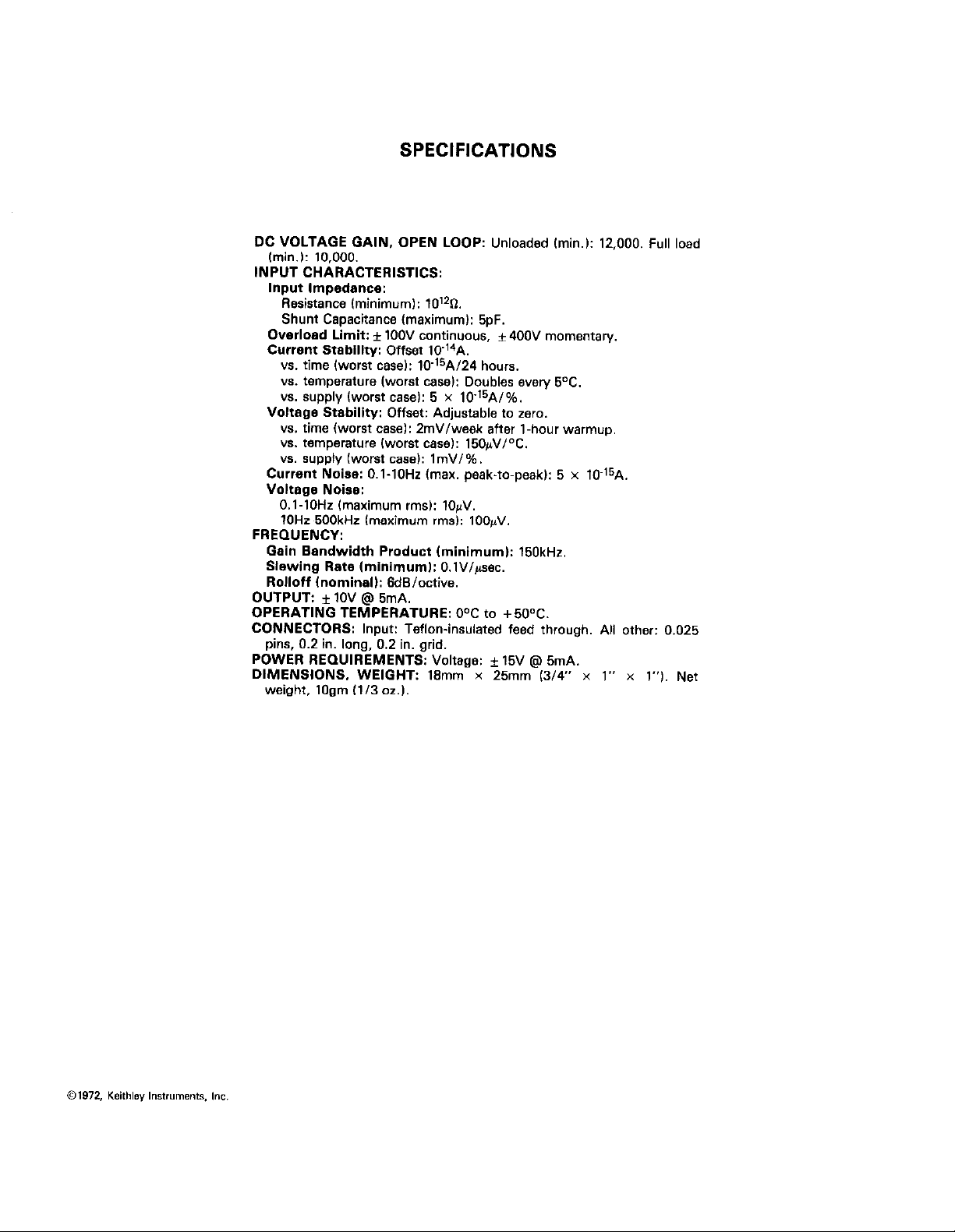
SPECIFICATIONS
DC VOLTAGE GAIN, OPEN LOOP: Unloaded (min.): 12.000. Full load
(min.): 10,000.
INPUT CHARACTERISTICS:
Input Impedance:
Resistance (minimum): 10’*3.
Shunt Capacitance (maximum): 5pF.
Overload Limit: f 1OOV continuous, f400V momentary.
Current Stability: Offset 10.‘4A.
vs. time Worst case): 10-‘5A124 hours.
vs. temperature hvorst case): Doubles every 5°C.
vs. supply (worst case): 5 x 10-‘5A/%.
Voltage Stability: Offset: Adjustable to zero.
vs. time (worst case): ZmVlweek after l-hour warmup.
YE. temperature hxst case): 15OfiVPC.
vs. supply iworst case): lmV/%.
Current Noise: 0.1.1OHz (max. peak-to-peak): 5 x 10~15A.
Voltage Noise:
0.1.1OHr (maximum rmsl: 1OuV.
lOHz-500kHz (maximum rmsi: lOOfiV,
FREQUENCY:
Gain Bandwidth Product bninimuml: 15OkHz
Slewing Rate (minimum): O.lV/pec.
Rolloff Inominel~: BdElloctive.
OUTPUT:.* jov~~;,n.. ~~~~~~~
OPERATING TEMPERATURE: O°C to +SO”C.
CONNECTORS: Input: Teflon-insulated feed through. All other: 0.025
pins, 0.2 in. long, 0.2 in. grid.
POWER REQUIREMENTS: Voltage: * 15V @I 5mA.
DIMENSIONS, WEIGHT: 1Smm x 25mm (3/4” x 1” x 1’7. Net
weight, 1Ogm (l/3 oz.).
Page 4

SECTION 1. GENERAL DESCRIPTION
1-l.
GENERAL.
state, operational amplifier.
single-ended amplifier intended for “se primarily as
a current amplifier.
l-2. MOUNTING.
are given in Figure 2.
which are suitable for soldered connections on a cus-
tom printed circuit board or plug-in connection to the
Keithley Model 3021 Accessory Socket. The pin locat-
ions are given in Figure 3.
TERMINAL IDENTIFICATION. The numbered terminals
l-3.
are identified in Table 2.
PIN NO.
1
2
the yodel 302 is a completely solid-
It is an inverting,
The over-all dimensions of the case
The case has nine terminals
Terminal Identification.
DESCRIPTION REMARKS
Input
Conlmon
TABLE 2.
This terminal is the high impedance input. It is
teflon insulated from the case.
This terminal is the low or common. The shield or
system ground should be connected to this point.
3
4
9
+v
COlllpellSatiO”
output
Not Used
-”
Zero
Since the Model 302 “tilizes an epoxy cemented enclosure, repairs should
not be attempted. If there is an apparent malfunction, check the external
components and connections. If possible, connect the amplifier as a voltage gain amplifier and check the gain in this mode of operation. Indicate
the exact natures of the difficulty if it is necessary to ret”rn the Model
302 for repair.
Refer to paragraph 2-5 for a discussion of frequency
compensation.
This terminal should be connected to the positive
“oltage supply.
cussion of power requirements.
Refer to paragraph 2-5.
This terminal is the voltage o”tp”t (inverted signal)
This terminal should be connected to the negative
voltage supply. Refer to paragraph 2-2 for a dis-
cussion of power requirements.
Refer to paragraph 2-6 for a discussion of zero con-
tro1.
NOTE
Refer to paragraph 2-2 for a dis-
2
Page 5

SECTION
2.
OPERATION
2-1. CONNECTIONS.
a. Model 3021 Accessory Socket. The Model 3021
permits quick connections to the Model 302. The socket has plated terminals which are easily soldered.
The 3021 provides a rigid shielded enclosure to mini-
mize noise pickup.
b. Printed Circuit. Connection. The Model 302 can
also be soldered directly to a printed circuit board.
When measuring very small currents, it is advisable
to directly solder the Input terminal (Pin 1) to the
current source.
be drilled in the PC board to facilitate a direct
soldered connection
POWER SUPPLY REqUIKEMENTS. The Model 302 bos
2-2.
been designed to operaCe from a + 15 volt, regulated
supply. The amplifier will operate however from any
supply voltage over the range 2 9 volts to 2 18 volts
with a resulting modification of certain specifica-
tions. The regulation of the supply will depend on
the stability requirements of the application. voltage
stability is specified as 1 millivolt/% change in
supply voltage.
peres for eat,, supply.
A clearance bole (.I25 dia) can
‘The current required is 5 milliam-
2-3. MODES OF OPERATION. The Model 302 cm be connected for use in several configurations or modes of
operation.
Linear Current Amplifier. When connected in
a.
this mode, the Model 302 can be used as a current
sensing amplifier. The gain of the amplifier i.n this
configuration is determined by the feedback resistance Rf.
Vo = I x Rf. Kefer to paragraph 2-4a for circuit
Connections.
b. Linear Current Amplifier
back. When connected in this made, the Model 302 can
be used as a current sensing amplifier. The gain of
the amplifier is determined by the feedback resistor
Rf @ the fractional feedback divider made up of ill
and R2.
“o = I x Rf x (Rl + R2)/K2. Refer CO paragraph 2-4b
for circuit connections.
c. Linear Current Amplifier With&&.ble Dampin&
When connected in ehis mode, the Model 302 can be
used as a current sensing amplifier with the overall
response varied tbmugh the use of a capacitor Cd and
resistive divider made up of R3 and R4. Reier to
paragraph 2-4~ for circuit connections. The value of
capacitance required to damp oscillations may be from
3 to 100 picofarads.
The outp”t voltage is given by the equation
wit,, Fractional Fe&
The output voltage is given by the equation
r”‘-I
T-
L tcte
1”
0.2"
T +I-++
1
cl
0.24
l tte
tttr
cc
(0.032"DIA)
FIGURE 3. Pin Identification.
Page 6

d. Logarithmic Current Amplifier. When connected
in this made, the Model 302 can be used as a current
amplifier with a logarithmic gain. The output voltage
is given by the equation Vo =-A lag I. Refer to para-
graph 2-4d for circuit connections.
For further information send for the Keithley
Product Note “Using the Model 300 Operational
Amplifier as a Logarithmic Current Amplifier.”
e. Current Integrator or Charge Amplifier. When
connected in this made, the Model 302 can be used as
charge or current sensing amplifier. As a current
integrator the output voltage is given by the equation
“, = l/Cf I dt. As a charge amplifier, the output
voltage is given by the equation V. = Q/Cf. Refer to
paragraph 2-4e for circuit connections.
f. Unity Gain Isolation Amplifier. When connected
in this mode, the Model 302 can be used as an impedance matching voltage amplifier where the output will
follow the input within 100 ppm. Refer to paragraph
2-4f far circuit connections.
g. Voltage Gain Isolation Amplifier. When connected
in this mode, the Model 302 can be used as a voltage
amplifier with the output low floating with respect
to the input low. The output voltage is given by the
equation V, = “1 (RI + R )/R2.
Refer to paragraph
2-4g for circuit connect ens. 3
FIGURE 4.
Linear Current Amplifier.
2-4. CIRCUIT CONNECTIONS.
a. Linear Current Amplifier. In this configuration,
the selected feedback resistor Rf is connected between
the Input (Pin 1) and the Output (Pin 6) as shown in
Figure 4. Since the maximum amplifier output is +I0
volts (nominally), the full range current is determined by the ratio 10/Q-. Since the offset current
for the Model 302 is approximately lo-l4 ampere,.=
feedback resistaWe of 1012 ohms is practical.
b. Linear Current Amplifier With Fractional Feed-
back. In this configuration, the feedback resistor
Rf is connected between the Input (Pin 1) and a div-
ider composed of RI and R2 as shown in Figure 5. The
value of R1 and R2 should be selected such that RI +
R2 is .Ol times the value of Rf (that is, the divider
current should be large compared to the current to
be measured). Since the output current must be limited to 5 milliamperee or less, the output load RL (in
parallel with RI + R2) should be 2kO or greater.
C. Linear Current Amplifier With Variable Damping.
In this configuration, a damping capacitor Cd is connected between the Input (Pin 1) and the Output (Pin
6) far fixed damping or through a fractional feedback
divider composed of R3 and R4 as shown in Figure 6.
FIGURE 5.
Linear Amplifier With Fractional Feedback.
Cd
I
II
Rf
0
INPUT
v/b
1
2
OUTPUT
R3
C v,
R4
FIGURE 6. Linear Amplifier With Variable Damping.
I
<
4
Page 7

Typical Performance Values far the Model 302 Used as
a Linear Current Amplifier. Offset, drift and rise
time are affected by the circuit used, but the table
b&low shows 80,ne of the Model 302’s capabilities.
“% Feedback” refers to fractional feedback equation
100% is with no fractional feedback.
TABLE 3.
% Feedback 100%
output Voltage
Input current 10-9A lo-l0A
ReSOl”tiO”
C”rre”e Offset,
% of output
Drift/Week
% Of output
Observed
Rise Time
d. Logarithmic Curre”t Amplifier. A logarithmic
levice such as a silicon diode or transistor ,u”ctio”
:a” be connected between the Input (Pi” 1) and Output
Pin 6) to provide up to 9 decades of logarithmic re-
;ponse.
6
lo): wrtormance. The leakage f”rre”C of the device
_
should be at least two mag”;eudes less than the cur=-
ent to be measured.
and/or fractional feedback can be used to establish
the magnitude of the scale factor “A”. See Figure 7.
Silicon NPN transistors are also useful as log elements where better response speed is needed. “sing the
basic circuie of Figure 8, positive currents can be
amplified by using a” NPN transistor in the feedback
loop. Negative c”rre”ts ca” be amplified by using a
PNP transistor in the feedback loop. the base of the
transistor is connected to ground. Connect the collec-
tor to the INPUT and ehe emitter to the OUTPUT.
The particular device used determines the
10 ” 10 ”
2.5 x 2.5 x
10-14A 10-14A
0.001% 0.01%
0.02%
LO 20 200 300
msec msec msec msec
10% 100%
10 ”
10-llA
10-14A 10-14A
0.1% 1%
0.2% 0.02%
The addition of sertes devices
10%
10 ”
10-12‘4
0.2%
FIGURE 7.
Logarithmic Current Amplifier
I
1. To zero the w~pue use a variable voltage between the log element in the feedback loop and the
output. This variable voltage can be achieved by
“se of a biasing network that consists of a potent<ameter connected as in Figure 7. Mount this “et-
work in aeries beewee” the log element and the o”tp”t.
Adjusting the potentiometer will provide the voltage needed to zero the o”tp”e. The resistance added
by this biasing network should be small compared to
the resistance of the diode network at maximum input
CUrrent.
2. An alternate approach is to supply a buckout
current to the input by means of a high megohm resistor and a potentiometer as shown in Figure 9. To
minimize the effect o” zero drift the resistance, R,
should be at least as large as the resistance of the
diode network at minimum inout current.
FIGURE 9.
.BOTi”OM VIEW
Oueput Zero Adjustment.
5
Page 8

e. Current Integrator or Charge Amplifier. I" this
configuration, a feedback capacitor Cf is connected
between the Input (Pi" 1) and the Output (Pi" 6). The
capacitor should be a low-leakage type such as polystyrene, mylar, or polycarbonate. Fractional feedback
can be used to vary the sensitivity without changing
capacitors.
Unity Gain Isolation Amplifier. In this con-
f.
figuration, the input voltage signal is applied between the Input (Pi" 1) and the Output (Pi" 6). The
unity gain voltage output is developed between the
Output (Pi" 6) and comma" (Pin 2). Since the common
terminal is isolated from the input M terminal, a
floating power supply and monitoring device must be
used.
supply return). See Figure 11.
g. Voltage Gain Isolation Amplifier.
figuration, a resistor divider is used
voieage gain while maintaining high input impedance.
The Input voltage signal is applied between the Input
(Pi" 1) and the divider network as shown in'Fig"re 12.
The o"tput voltage is developed between the Output
(Pi" 6) and C~mmo" (Pin 2).
is isolated from the i"p"t LO terminal, a floating
power supply and monitoring device must be used.
see Figure 10.
(The Common terminal (Pi" 2) is used for power
I" this con-
to
provide
Since the common terminal
Cf
I
INPUT 1
2
LO
> <
FIGURE 10. Current Integrator.
OUTPUT
COMPENSATION.
2-5.
ternal freq. camp. capacitor for stability. This can be
accomplished by connecting a comp.capacitor between Pi" 3
and Pi" 5.
picofarad, although the value may be adjusted slightly
to obtain optimum bandwidth. In some cases it may be
necessary to add a" additional damping capacitor Cd
as described in paragraph 2-4~. The typical value of
this capacitor should be 3 pF to 100 pF. The overall
frequency response of the amplifier can be described
by a voltage gain "ersua logarithm of frequency plot
known as a
off" at a slope of -6dB/oceave, the amplifier is G-
conditionally stable.
atid -lZdB/actave, the amplifier is conditionally
stable; that is, the amplifier may oscillate unless
additional damping is added. When the slope is great-
er than -12dB/actave, the amplifier is unstable for
gain greater than unity.
finitely required in this situation.
2-6. ZERO CONTROL.
adjusted to zero, an external control can be cannect-
ed as shown in Figure 3.
(Pi" 9) has a 1 megohm input resistance, the potent-
iometer should be less than 1 megohm.
supplies are + 15 volts, the" the zero control will
permit a variation of approximately + 150 millivolts
or .Ol times the bias voltage.
A nominal value for this capacitor is 150
"Bode" "lot. When the response "rolls-
The Model 302 may require a" ex-
When the slope is between -6
Additional damping is de-
See Figure 3.
When the voltage offset m"sf be
Since the Zero Terminal
If the power
1
FIGURE 11.
""icy Gain Amplifier.
FIGURE 12.
Voltage Gain Amplifier.
Page 9

SERVICE FORM
Model No.
Name
Company
Address
City
List all control settings and describe problem.
Show a block diagram of your measurement system including all instruments connected (whether power
is turned on or not). Also describe signal source.
Serial No.
State
P.O. No. Date
Phone
Zip
(Attach additional sheets as necessary.)
Where is the measurement being performed? (factory, controlled laboratory, out-of-doors, etc.)
What power line voltage is used?
Frequency?
Variation? OF. Rel. Humidity? Other?
Any additional information. (If special modifications have been made by the user, please describe below.)
*me sure to include your name and phone number on this service form
Ambient Temperature?
Variation?
OF.
Page 10

Keithley Instruments, Inc./28775 Aurora Road/Cleveland, Ohio 44139/U.S.A./(216) 248-0400/Telex: 98-5469
WEST GERMANY: Keithley Instruments GmbHlHeiglhofstrasse 5/D-6000 MUnchen 70/10891 7144065/T&x: 521 21 60
GREAT BRITAIN: Keithley Instruments, Ltd./l. Boulton Road/Reading, Berkshire RG2 ONL/107341 86 12 67/T&x: 847047
FRANCE: Keithley Instruments SARL/2 Bis, Rue Ldon Slum/B.P. 60191121 P&is&w Cedex/lG) 011.51.55iTelex: 600933F
NETHERLANDS: Keifhley Instruments FJV/Arkelsedijk 4/NL-4206 AC Gorincheml(018301 25577/T&x: 24 684
SWITZERLAND: Keithlev Instruments SA/Kriesbachstr. 4/CH-8600 DUbendorflOl 821 94 44iTelex: 57 536
AUSTRIA: Keithley Instruments Ges.m.b.H./Dbblinger Hauptstr. 32/A-1190 Wien/0222 314 269/T&x: 13 45 00
 Loading...