

Page 1

Service Manual
2715
Spectrum Analyzer
Volume 1
070-9096-06
This document supports firmware version
12.01.95 and above.
Warning
The servicing instructions are for use by qualified
personnel only. To avoid personal injury, do not
perform any servicing unless you are qualified to
do so. Refer to all safety summaries prior to
performing service.
www.tektronix.com
Page 2

Copyright © Tektronix, Inc. All rights reserved.
Tektronix products are covered by U.S. and foreign patents, issued and pending. Information in this publication supercedes
that in all previously published material. Specifications and price change privileges reserved.
Tektronix, Inc., P.O. Box 500, Beaverton, OR 97077
TEKTRONIX and TEK are registered trademarks of Tektronix, Inc.
Page 3

WARRANTY
Tektronix warrants that this product will be free from defects in materials and workmanship for a period of one (1) year
from the date of shipment. If any such product proves defective during this warranty period, Tektronix, at its option, either
will repair the defective product without charge for parts and labor, or will provide a repl acement in exchange for the
defective product.
In order to obtain service under this warranty, Customer must notify Tektronix of the defect before the expiration of t he
warranty period and make suitable arrangements for the performance of service. Customer shall be responsible for
packaging and shipping the defective product to the service center de signated by Tektronix, with shipping charges prepaid.
Tektronix shall pay for the return of the product to Customer i f the shipment is to a location within the country in which the
Tektronix service center is located. Custome r shall be responsible for paying all shipping charges, duties, taxes, and any
other charges for products returned to any other locations.
This warranty shall not apply to any defect, failure or damage caused by improper use or improper or inadequate
maintenance and care. Tektronix shall not be obligated to furnish service under this warranty a) to repair damage resulting
from attempts by personnel other than Tektronix representatives to install, repair or service the product; b) to repair
damage resulting from improper use or connection to incompatible equipment; or c) to service a product that has been
modified or integrated with other products when the effect of such modification or integration increases the time or
difficulty of servicing the product.
THIS W ARRANTY IS GIVEN BY TEKTRONIX WITH RESPECT TO THIS PRODUCT IN LIEU OF ANY
OTHER WARRANTIES, EXPRESSED OR IMPLIED. TEKTRONIX AND ITS VENDORS DISCLAIM ANY
IMPLIED WARRANTIES OF MERCHANTABILITY OR FITNESS FOR A PARTICULAR PURPOSE.
TEKTRONIX’ RESPONSIBILITY TO REPAIR OR REPLACE DEFECTIVE PRODUCTS IS THE SOLE AND
EXCLUSIVE REMEDY PROVIDED TO THE CUSTOMER FOR BREACH OF THIS W ARRANTY. TEKTRONIX
AND ITS VENDORS WILL NOT BE LIABLE FOR ANY INDIRECT, SPECIAL, INCIDENTAL, OR
CONSEQUENTIAL DAMAGES IRRESPECTIVE OF WHETHER TEKTRONIX OR THE VENDOR HAS
ADVANCE NOTICE OF THE POSSIBILITY OF SUCH DAMAGES.
Page 4

Page 5

Table of Contents
Specifications
Operating Information
General Safety Summary ix...................................
Service Safety Summary xi....................................
Preface xv...................................................
Electrical Characteristics 1-1..........................................
Instrument Description 2-1............................................
Conformance to Industry Standards 2-2..................................
Product Service 2-2..................................................
Instrument Construction 2-3...........................................
Installation and Preparation for Use 2-3..................................
Power Cord 2-3.....................................................
Replacing the Fuse 2-4...............................................
Selected Components 2-4.............................................
Assembly and Circuit Numbering 2-4...................................
Accessories 2-4.....................................................
Menus 2-4.........................................................
SWP/TRG Menu Structure 2-6.........................................
UTIL Menu Structure
(1 of 2) 2-7.....................................................
UTIL Menu Structure
(2 of 2) 2-8.....................................................
MRK/FREQ Menu Structure 2-8.......................................
CATV/APPL CATV Measurements Page 1 Menu Structure (1 of 3) 2-9........
CATV/APPL CATV Measurements Page 1 Menu Structure (2 of 3) 2-10........
CATV/APPL CATV Measurements Page 1 Menu Structure (3 of 3) 2-11........
CATV/APPL CATV Measurements Page 2 Menu Structure (1 of 2) 2-12........
CATV/APPL CATV Measurements Page 2 Menu Structure (2 of 2) 2-13........
CATV/APPL Applications Menu Structure 2-14............................
DEMOD Menu Structure 2-14..........................................
DSPL Menu Structure 2-15............................................
USER DEF Menu Structure 2-15........................................
INPUT Menu Structure 2-16...........................................
Theory of Operation
Block Diagram Description 3-1........................................
Center Frequency Control 3-5.........................................
1st LO Buffer 3-7...................................................
Sweep 3-7.........................................................
Display System 3-8..................................................
Circuit Description 3-9........................................
Attenuator and 1st Converter 3-9.......................................
RF Mother Board and Phase Locked 2nd LO 3-12..........................
2715 Spectrum Analyzer Service Manual
i
Page 6

Table of Contents
1st LO Interface, 1st LO, and 1st LO Buffer Amplifier 3-14..................
Reference Oscillator 3-16..............................................
Phase Lock Assembly (Center Frequency Control System) 3-21...............
Variable Resolution Module 3-33........................................
RF Options 3-35.....................................................
Log Amplifier 3-38...................................................
Display Storage 3-40..................................................
Microprocessor 3-60..................................................
GPIB, RS-232, Real Time Clock, NVRAM, and Gated Measurement Functions 3-74
Video Demodulator 3-78...............................................
Sweep 3-80.........................................................
Front Panel 3-83.....................................................
Power Supply (Primary and Secondary) 3-87..............................
Power Supply (Display) 3-91...........................................
Performance Verification
Incoming Inspection Test 4-1..........................................
Verification of Tolerance Values 4-1....................................
History Information 4-1..............................................
Equipment Required 4-2..............................................
Power-Up Procedure 4-3..............................................
Front Panel Operation 4-4.............................................
Performance Check Procedure 4-4......................................
Adjustment Procedures
Static Discharge Precautions 5-1.......................................
Recommended Test Equipment 5-2.....................................
Preparation 5-4.....................................................
Adjustments Requiring Flatness Correction 5-4...........................
Instrument Bottom View 5-5..........................................
Adjustments 5-6....................................................
Maintenance
Static Sensitive Components 6-1.......................................
Preventive Maintenance 6-2...........................................
Troubleshooting 6-6.................................................
Cal Debug Flags 6-8.................................................
Corrective Maintenance 6-13...........................................
Assembly Replacement Requiring Flatness Correction 6-17...................
Removing and Replacing Assemblies and Subassemblies 6-17................
Maintenance Adjustments 6-33.........................................
Options
Replaceable Electrical Parts
Diagrams
Replaceable Mechanical Parts
ii
2715 Spectrum Analyzer Service Manual
Page 7

List of Figures
Table of Contents
Figure 1-1: Typical Accuracy Limits for Carrier-to-Noise
Measurement 1-7..........................................
Figure 1-2: Typical Accuracy Limits for CTB Measurement 1-7......
Figure 1-3: Typical Accuracy Limits for Nongated CSO
Measurement 1-8..........................................
Figure 1-4: Typical Accuracy Limits for Gated CSO
Measurement 1-8..........................................
Figure 1-5: Typical ACL Measurement Limits for 2 dB Accuracy 1-9..
Figure 1-6: Typical D/U Measurement Range Limits for
2 dB Accuracy 1-9.........................................
Figure 1-7: Typical Digital Signal CSO Measurement Range Limit
for 2 dB Accuracy 1-10......................................
Figure 1-8: Typical Digital Signal CTB Measurement Range
Limit for 2 dB Accuracy 1-10.................................
Figure 2-1: 2715 Front Panel Keys 2-5............................
Figure 3-1: Main Block Diagram 3-2.............................
Figure 3-2: Display System Diagram 3-8..........................
Figure 3-3: Attenuator and 1st Converter Diagram 3-10..............
Figure 3-4: Equivalent Circuit for the Bandpass (4 Cavity)
Filter 3-11.................................................
Figure 3-5: Block Diagram of RF Mother Board 3-12................
Figure 3-6: 1st LO Interface and 1st LO Diagram 3-14...............
Figure 3-7: 1st LO Buffer Amplifier Diagram 3-15..................
Figure 3-8: Reference Oscillator Diagram 3-17......................
Figure 3-9: Crystal Heater and 15 V Regulation Circuit 3-18..........
Figure 3-10: Oscillator AC Equivalent 3-19........................
Figure 3-11: Oscillator DC Equivalent 3-20........................
Figure 3-12: Phase Lock Center Frequency Control
Configuration for Wide Spans (Unlocked, Sweep Main Coil) 3-28..
Figure 3-13: Phase Lock Center Frequency Control Configuration
for Moderate Spans (Unlocked, Sweep FM Coil) 3-29.............
Figure 3-14: Phase Lock Center Frequency Control Configuration
for Narrow Spans (Locked, Sweep VCO) 3-30...................
Figure 3-15: Variable Resolution Module Diagram 3-34..............
Figure 3-16: RF Options Diagram 3-36............................
2715 Spectrum Analyzer Service Manual
iii
Page 8

Table of Contents
Figure 3-17: Timing Diagram for a Typical Write to the Control
Register 3-50...............................................
Figure 3-18: Timing Diagram of a Typical Sweep for the Horizontal
Tracking A/D Converter 3-51.................................
Figure 3-19: Sequence of Events When Writing Data to the
Waveform Memory 3-54.....................................
Figure 3-20: How a Vertical Scan is Performed 3-56.................
Figure 3-21: The Display of a Single Vector of a Waveform 3-57.......
Figure 3-22: A Single Column of Character Dots 3-57................
Figure 3-23: Vertical Output Integrator 3-58.......................
Figure 3-24: Microprocessor Block Diagram 3-61...................
Figure 3-25: Microprocessor Counter System (CPU) 3-62.............
Figure 3-26: Front Panel Block Diagram 3-83......................
Figure 3-27: How the Debounce Circuit Reacts to Key Closure 3-85....
Figure 3-28: Power Supply Primary Block Diagram 3-88.............
Figure 3-29: Display Amplifiers Block Diagram 3-91................
Figure 4-1: 3rd Order IM Test Setup (25 MHz Separation) 4-17.......
Figure 4-2: Harmonic Distortion Test Equipment Setup 4-18..........
Figure 4-3: 1 dB Compression Point Test Setup 4-20.................
Figure 4-4: Accessory Connector (J103) 4-22.......................
Figure 4-5: Test Equipment Setup for Checking Return Loss 4-28.....
Figure 4-6: Test Signal on Video Line 17 4-32.......................
Figure 4-7: Video Gating Check Waveform (NTSC Illustrated) 4-34....
Figure 4-8: IF Gating Check Waveform (NTSC Illustrated) 4-35......
Figure 5-1: Instrument Bottom View 5-5..........................
Figure 5-2: Display Storage Board Adjustment Locations 5-13........
Figure 5-3: Properly Adjusted Checkerboard Pattern 5-14...........
Figure 5-4: Locked 2nd LO and 5 MHz Bandpass Filter
Adjustments 5-16...........................................
Figure 5-5: Phase Lock CFC Module Adjustment and Test Point
Locations 5-17.............................................
Figure 5-6: Log Board Adjustment and Test Point Locations 5-21.....
Figure 5-7: CAL Level Adjustment on Reference Oscillator Board 5-26.
Figure 5-8: RF Option Adjustment Locations 5-28..................
Figure 5-9: Variable Resolution Module Adjustment Locations 5-29....
Figure 5-10: Flatness adjustment test setup (all instruments
except Option 50) 5-34.......................................
iv
2715 Spectrum Analyzer Service Manual
Page 9

Table of Contents
Figure 5-1 1: Presetting the Flatness Adjustments on the
Log Board 5-35............................................
Figure 5-12: Gain Step Reference Test Setup 5-36...................
Figure 5-13: Internal Ref Ampltd Test Setup 5-38...................
Figure 5-14: SW410 on the Reference Oscillator Board 5-39..........
Figure 5-15: Adjustment and Test Point Locations on the
Sweep Board 5-41..........................................
Figure 5-16: Typical FM Adjustment Waveform 5-42................
Figure 5-17: HPF Tuning Criteria (at TP110M) 5-45.................
Figure 5-18: Typical Video Waveform 5-48.........................
Figure 5-19: Horizontal Sync Output 5-49.........................
Figure 5-20: Vertical Sync Output Waveform 5-50..................
Figure 5-21: E/O Output Waveform 5-51..........................
Figure 5-22: Test Equipment Characterization Using a Dual
Channel Power Meter for split75 5-59..........................
Figure 5-23: Test Equipment Characterization Using a
Single Channel Power Meter to Characterize the Power Meter
Output for split75 5-59......................................
Figure 5-24: Test Equipment Characterization Using a
Single Channel Power Meter to Characterize the DUT
Output for split75 5-59......................................
Figure 5-25: Test Equipment Characterization Using a Dual
Channel Power Meter for split50 5-60..........................
Figure 5-26: Test Equipment Characterization Using a
Single Channel Power Meter to Characterize the Power Meter
Output for split50 5-60......................................
Figure 5-27: Test Equipment Characterization Using a
Single Channel Power Meter to Characterize the DUT
Output for split50 5-60......................................
Figure 5-28: Flatness Test Setup (75 W) 5-62.......................
Figure 5-29: Flatness Test Setup (50 W) 5-62.......................
Figure 6-1: Main Extender and Secondary Extender 6-4............
Figure 6-2: Signal Steering Square Pins 6-5.......................
Figure 6-3: Surface Mounted Components Lead Configuration 6-14...
Figure 6-4: Top View of Assemblies and RF Deck 6-18...............
Figure 6-5: Assemblies Seen from the Bottom of the Spectrum
Analyzer 6-19..............................................
Figure 6-6: Removing the Front Panel 6-22........................
Figure 6-7: Locations of J510 and J550 on the Phase Lock
Assembly 6-23.............................................
2715 Spectrum Analyzer Service Manual
v
Page 10

Table of Contents
Figure 6-8: Connector Locations on the RF Deck 6-24...............
Figure 6-9: RF Deck Screws and Nuts 6-25.........................
Figure 6-10: Fan and Fan Mounting Springs Detail 6-29.............
Figure 6-11: Power Supply Assembly Removal (Bottom View) 6-31....
Figure 6-12: Removing Power Supply Attaching Nuts 6-32...........
Figure 6-13: Location of R602 on the Phase Lock CFC Board 6-34.....
Figure 7-1: Option 15 Installation 7-3............................
Figure 10-1: Cabinet 10-7.......................................
Figure 10-2: Front Panel 10-11....................................
Figure 10-3: Power Supply 10-15..................................
Figure 10-4: Chassis #1 10-18.....................................
Figure 10-5: Chassis #2 10-22.....................................
Figure 10-6: Accessories 10-25....................................
vi
2715 Spectrum Analyzer Service Manual
Page 11

List of Tables
Table of Contents
T able 1-1: CA TV Characteristics 1-2............................
Table 1-2: Frequency-Related Characteristics 1-11..................
Table 1-3: Frequency/Amplitude Related Characteristics 1-13........
T able 1-4: Amplitude-Related Characteristics 1-14..................
Table 1-5: Input/Output Signal Characteristics 1-17................
Table 1-6: Power Requirements 1-19.............................
Table 1-7: Supplementary Characteristics Due to Options 1-19.......
T able 1-8: General Characteristics 1-20...........................
Table 1-9: Environmental Characteristics 1-21.....................
Table 1-10: Physical Characteristics 1-22.........................
Table 1-11: Certifications and Compliances 1-23....................
Table 1-12: Safety Certification Compliance 1-24...................
Table 1-13: Safety Standards 1-24................................
Table 3-1: Input and Output Bit Definition 3-21....................
Table 3-2: Mode Control Register 1 3-41..........................
Table 3-3: Mode Control Register 2 3-42..........................
T able 3-4: Truth Table for the B,C-Save A Display Screen
Offset 3-43...............................................
T able 3-5: Truth Table for the Acquisition Modes 3-43..............
Table 3-6: Mode Control Register 2 3-43..........................
Table 3-7: Enhanced Mode MKRWFM[3..2] Bit Assignment 3-44.....
Table 3-8: Enhanced Mode MKRWFM[1..0] Bit Assignment 3-45....
Table 3-9: Display Control Register 3-45..........................
Table 3-10: Scroll Register 3-46..................................
Table 3-11: Memory Map for the Display Storage Board 3-48.........
Table 3-12: Control Register Latch and Tristate Buffer
Reference Designators and Microprocessor I/O Port
Address Location 3-49......................................
Table 3-13: Input Conditions Required to Write Either the
Max or Min Accumulators to Waveform Memory 3-53...........
Table 3-14: Page Number/Waveform Relation 3-55.................
Table 3-15: Interrupt Controller Input Connections 3-63............
Table 3-16: Configuration of Jumpers/Wires for Various
Memory IC Sizes 3-65......................................
Table 3-17: Definition of Software Jumpers 3-66....................
2715 Spectrum Analyzer Service Manual
vii
Page 12

Table of Contents
Table 3-18: Power Supply and Serial Bus Connector (J10)
Signal Names and Definitions 3-68............................
Table 3-19: Microprocessor Interface Connector (J550)
Signal Names and Definitions 3-69............................
T able 3-20: Microprocessor Counter Section Connector
Signal Names and Definitions 3-70............................
Table 3-21: Connectors and Signal Names for the Frequency
Counter Section 3-70.......................................
Table 3-22: Pinout for the 24-Pin DIN Connector (J10) Between the
Microprocessor Board, Power Supply Interconnect,
and Serial I/O 3-71.........................................
Table 3-23: Pinout for the Microprocessor Board Test
Connector (J150) 3-71......................................
Table 3-24: Pinout for the 50 Pin Connector (J550) Between
the Microprocessor, Display Storage, and Digital Options
Boards 3-73...............................................
Table 3-25: Real Time Clock Functions 3-75.......................
Table 4-1: Equipment Required 4-2.............................
Table 4-2: Settings for Shape Factor Check 4-5....................
Table 4-3: Settings for the Noise Sidebands Check 4-7..............
Table 4-4: Front Panel Span Accuracy Settings 4-8................
Table 4-5: Maximum Range in 10 dB/Div 4-11.....................
Table 4-6: Resolution Bandwidth Filter Display Dynamic
Range Settings 4-12........................................
T able 4-7: Sensitivity Settings at 110 MHz 4-13.....................
Table 4-8: Sensitivity Settings at 1800 MHz 4-14....................
T able 4-9: Sensitivity Settings at 2.15 GHz 4-15....................
Table 5-1: Test Equipment 5-2..................................
Table 5-2: Power Supply Tolerances 5-7..........................
Table 5-3: Power Supply Tolerances 5-10..........................
Table 5-4: Correction Bit Values 5-39.............................
Table 5-5: Television Channels 5-40..............................
Table 6-1: Relative Susceptibility to Static Discharge Damage 6-2....
Table 6-2: Cal Debug Messages and Meanings 6-9.................
Table 6-3: Servicing Tools for Boards With Surface
Mounted Components 6-15..................................
viii
2715 Spectrum Analyzer Service Manual
Page 13

General Safety Summary
Review the following safety precautions to avoid injury and prevent damage to
this product or any products connected to it. To avoid potential hazards, use this
product only as specified.
Only qualified personnel should perform service procedures.
While using this product, you may need to access other parts of the system. Read
the General Safety Summary in other system manuals for warnings and cautions
related to operating the system.
ToAvoidFireor
Personal Injury
Use Proper Power Cord. Use only the power cord specified for this product and
certified for the country of use.
Connect and Disconnect Properly. Do not connect or disconnect probes or test
leads while they are connected to a voltage source.
Ground the Product. This product is grounded through the grounding conductor
of the power cord. To avoid electric shock, the grounding conductor must be
connected to earth ground. Before making connections to the input or output
terminals of the product, ensure that the product is properly grounded.
Observe All Terminal Ratings. To avoid fire or shock hazard, observe all ratings
and marking on the product. Consult the product manual for further ratings
information before making connections to the product.
The common terminal is at ground potential. Do not connect the common
terminal to elevated voltages.
Do not apply a potential to any terminal, including the common terminal, that
exceeds the maximum rating of that terminal.
Do Not Operate Without Covers. Do not operate this product with covers or panels
removed.
Use Proper Fuse. Use only the fuse type and rating specified for this product.
Avoid Exposed Circuitry. Do not touch exposed connections and components
when power is present.
Wear Eye Protection. Wear eye protection if exposure to high-intensity rays or
laser radiation exists.
Do Not Operate With Suspected Failures. If you suspect there is damage to this
product, have it inspected by qualified service personnel.
Do Not Operate in Wet/Damp Conditions.
Do Not Operate in an Explosive Atmosphere.
2715 Spectrum Analyzer Service Manual
ix
Page 14

General Safety Summary
Keep Product Surfaces Clean and Dry.
Provide Proper Ventilation. Refer to the manual’s installation instructions for
details on installing the product so it has proper ventilation.
Symbols and Terms
Terms in this Manual. These terms may appear in this manual:
WARNING. Warning statements identify conditions or practices that could result
in injury or loss of life.
CAUTION. Caution statements identify conditions or practices that could result in
damage to this product or other property.
Terms on the Product. These terms may appear on the product:
DANGER indicates an injury hazard immediately accessible as you read the
marking.
WARNING indicates an injury hazard not immediately accessible as you read the
marking.
CAUTION indicates a hazard to property including the product.
Symbols on the Product. The following symbols may appear on the product:
WARNING
High Voltage
Protective Ground
(Earth) Terminal
x
CAUTION
Refer to Manual
Double
Insulated
2715 Spectrum Analyzer Service Manual
Page 15

Service Safety Summary
Only qualified personnel should perform service procedures. Read this Service
Safety Summary and the General Safety Summary before performing any service
procedures.
Do Not Service Alone. Do not perform internal service or adjustments of this
product unless another person capable of rendering first aid and resuscitation is
present.
Disconnect Power. To avoid electric shock, switch off the instrument power, then
disconnect the power cord from the mains power.
Use Caution When Servicing the CRT. To avoid electric shock or injury, use
extreme caution when handling the CRT. Only qualified personnel familiar with
CRT servicing procedures and precautions should remove or install the CRT.
CRTs retain hazardous voltages for long periods of time after power is turned off.
Before attempting any servicing, discharge the CRT by shorting the anode to
chassis ground. When discharging the CRT, connect the discharge path to ground
and then the anode. Rough handling may cause the CRT to implode. Do not nick
or scratch the glass or subject it to undue pressure when removing or installing it.
When handling the CRT, wear safety goggles and heavy gloves for protection.
Use Care When Servicing With Power On. Dangerous voltages or currents may
exist in this product. Disconnect power, remove battery (if applicable), and
disconnect test leads before removing protective panels, soldering, or replacing
components.
To avoid electric shock, do not touch exposed connections.
X-Radiation. To avoid x-radiation exposure, do not modify or otherwise alter the
high-voltage circuitry or the CRT enclosure. X-ray emissions generated within
this product have been sufficiently shielded.
2715 Spectrum Analyzer Service Manual
xi
Page 16

Service Safety Summary
xii
2715 Spectrum Analyzer Service Manual
Page 17

Preface
This manual contains service information for the 2715 Spectrum Analyzer. The
service information is located in two volumes. Volume 1 contains the maintenance procedures and parts lists. Volume 2 contains the component locators and
schematic diagrams.
This manual is divided into the following sections.
H Section 1: Specifications, contains characteristic tables detailing Electrical
Characteristics, Mechanical Characteristics, and Environmental Character-
istics.
H Section 2: Operating Information, contains information on how to install and
operate the product.
H Section 3: Theory of Operation, contains both a general and detailed circuit
description of the various modules that make up the instrument.
H Section 4: Performance Verification, is a procedure to ensure, when passed,
that the product operates properly and meets its advertised performance
levels.
H Section 5: Adjustment Procedures, is a procedure to ensure that, when
performed, the product can meet the performance levels for characteristics
listed in Section 1, Specifications.
H Section 6: Maintenance, contains instructions for removal and replacement
of internal modules or components.
H Section 7: Options, describes all options available for this instrument.
H Section 8: Replaceable Electrical Parts, is a list of replaceable assemblies
and electrical components.
H Section 9: Diagrams, Refer to the 2715 Spectrum Analyzer Service Manual
Volume 2.
H Section 10: Replaceable Mechanical Parts, is a list of replaceable assemblies
and mechanical components. Exploded-view illustrations are included to
relate assemblies to the parts list.
The following manuals are also available for the 2715 Spectrum Analyzer.
H 2715 User Manual provides information necessary to operate the 2715
Spectrum Analyzer.
H 2714 & 2715 Programmer Manual includes all GPIB commands, queries,
and responses for the instrument.
H The Cable TV RF Measurement Software Manual describes how to use the
Cable TR RF Measurements Software, a test system that measures cable TV
parameters.
2715 Spectrum Analyzer Service Manual
xiii
Page 18

Preface
Contacting Tektronix
Phone 1-800-833-9200*
Address Tektronix, Inc.
Department or name (if known)
14200 SW Karl Braun Drive
P.O. Box 500
Beaverton, OR 97077
USA
Web site www.tektronix.com
Sales support 1-800-833-9200, select option 1*
Service support 1-800-833-9200, select option 2*
Technical support Email: techsupport@tektronix.com
1-800-833-9200, select option 3*
6:00 a.m. -- 5:00 p.m. Pacific time
* This phone number is toll free in North America. After office hours, please leave a
voice mail message.
Outside North America, contact a Tektronix sales office or distributor; see the
Tektronix web site for a list of offices.
xiv
2715 Spectrum Analyzer Service Manual
Page 19

Specifications
This section lists the electrical, physical, and environmental characteristics of the
spectrum analyzer, specifies the performance requirements for those characteristics, and provides supplementary information.
Electrical Characteristics
Unless otherwise stated, the following tables of electrical characteristics and
features apply to the spectrum analyzer after a 15 minute warm-up period (within
the environmental limits) and after all normalization procedures have been
carried out.
Information in the Performance Requirement column of Tables 1--2 through 1--8
is guaranteed and verifiable unless otherwise noted. Supplemental Information is
intended to further explain a characteristic, its performance requirement, or to
describe characteristic performance that is impractical to verify. Supplemental
Information is not guaranteed and may not be supported by a performance check
procedure.
Changes to a characteristic because of the addition of an option are included in
Table 1--7.
2715 Spectrum Analyzer Service Manual
1- 1
Page 20

Specifications
Table 1- 1: CATV Characteristics
Characteristic Description
Input Configuration
All except Option 50 75 Ω Female F connector
Option 50 50 Ω Type N connector
Channel Selection The visual and aural carriers are displayed when the channel number is entered, or
either [ y ] or [ b ] next to [CHAN/FREQ] is pressed
Tune Configuration STD (73.603), HRC (73.605), IRC (73.612), and Custom
Channel Range 0to999
Frequency Range
(except Opt 50 and Opt 75)
Frequency Range
(Opt 50 and Opt 75)
Visual Carrier Frequency
Measurement
Method Internal Counter
Resolution 1Hz
Accuracy 5 × 10⁻⁷× Carrier Frequency ±10 Hz, ±1 Least Significant Digit
1
1MHzto1.8GHz2, Preamp limited to 600 MHz
1 MHz to 2.15 GHz2, Preamp limited to 600 MHz
Accuracy is dependent on the accuracy of the spectrum analyzer — see Frequency
Accuracy in Table 1--2.
@ 55.25 MHz (Ch 2) worst case is ±38 Hz
@ 325.25 MHz (Ch 41) worst case is ±173 Hz
@ 643.25 MHz (Ch 94) worst case is ±332 Hz
1
Visual-to-Aural Carrier Frequency Measurement Aural carrier measured relative to the visual carrier
Method Internal Counter
Difference Range 1 MHz to 10 MHz3for an amplitude difference of ≤30 dB and aural C/N ≥15 dB
(300 kHz RBW)
Resolution 1Hz
Accuracy ±15 Hz for visual-to-aural carrier difference ≤8MHz
Visual Carrier Peak Level Measurement Absol ute peak amplitude of visual carrier measured with PREAMP OFF
Accurate Frequency and
Amplitude
Visual carrier frequency measurement
Visual-to-aural carrier frequency measurement
Visual carrier peak level measurement
Visual-to-aural carrier level difference measurement
Accurate Amplitude Only Visual carrier peak level measurement
Visual-to-aural carrier level difference measurement
Fast Amplitude Only Carrier amplitudes are measured using marker values in 10 dB/div vertical scale
Amplitude Range --18 dBmV to +58.8 dBmV4for visual C/N ≥30 dB (300 kHz RBW)
1
Configured using Cable TV RF Measurements Software.
2
Dependent on selected channel table. Frequencies above 1.8 GHz are not supported by the Cable TV RF Measurements
Software.
3
Dependent on selected channel table.
4
Total input power (all signals included) cannot exceed +70 dBmV.
1- 2
2715 Spectrum Analyzer Service Manual
Page 21

Specifications
Table 1- 1: CATV Characteristics (Cont.)
Characteristic Description
Frequency Range 15 to 1015 MHz
Resolution 0.1 dB
Absolute Accuracy ±2.5 dB for visual C/N ≥30 dB (300 kHz RBW) and for FM signal C/N ≥33 dB (100
kHz RBW) assumes flatness corrections are present
Relative Accuracy ±0.5 dB relative to adjacent channel
±1.2 dB relative to all other channels
Visual-to-Aural Carrier Level
Difference Measurement
Difference Range 0 to 30 dB for aural C/N ≥15 dB (300 kHz RBW)
Resolution 0.1 dB
Accuracy ±0.75 dB for aural C/N ≥15 dB (300 kHz RBW)
Averaged Power (Typical) Averaged amplitude measured with preamp off
Accuracy ±2.5 dB for input levels above --30 dBmV, up to +37 dBmV (multichannel) or
Resolution 0.1 dB
Modulation Depth
Measurement (Typical)
AM Range 50% to 95%
Resolution 0.1%
Accuracy ±2% for visual C/N ≥40 dB (300 kHz RBW)
HUM/LFD Measurement (Typical) Power line frequency is measured on an unmodulated visual carrier, and low
AM Range 1% to 10% peak-to-peak
Resolution 0.1%
Accuracy ±1% for Hum ≤5% and visual C/N ≥25 dB (300 kHz RBW)
Carrier-to-Noise (C/N)
Measurement (Typical)
Optimum Input Range See Figure 1--1 on page 1--7
Maximum Range See Figure 1--1 on page 1--7
Resolution 0.3 dB
Accuracy See Figure 1--1 on page 1--7
In-Service C/N (typical) Noise density is measured at 2 MHz offset (by default) from visual carrier during
Optimum Input Range See Figure 1--1 on page 1--7
Maximum Range See Figure 1--1 on page 1--7
Resolution 0.3 dB
Aural carrier level measured relative to the visual carrier
+52 dBmV (preselector in use)
Percent AM measured from sync tip to lowest white level found in 10 sweeps (the
VITS line is used if it is defined in the channel table)
frequency disturbance (LFD) is measured on the modulated carrier
±2% for Hum <10% and visual C/N ≥25 dB (300 kHz RBW)
Default noise floor is a normalized 4 MHz bandwidth measured relative to the visual
carrier peak
quiet lines in the vertical interval, then normalized to 4 MHz BW and expressed as
dBc
2715 Spectrum Analyzer Service Manual
1- 3
Page 22

Specifications
Table 1- 1: CATV Characteristics (Cont.)
Characteristic Description
Accuracy See Figure 1--1 on page 1--7
Desired-to-Undesired Ratio (Typical) Channel averaged power is divided by total noise plus distortion in the channel
Resolution 0.1 dB
Accuracy ±2 dB within the limits shown in Figure 1--6 on page 1--9
CTB Measurement (Typical) Composite triple beat (CTB) is measured relative to the visual carrier peak according
to the NCTA recommended spectrum analyzer settings — SINGLE-SWEEP mode
does not use all the NCTA recommended settings
Maximum Range See Figure 1--2 on page 1--7
Resolution 0.3 dB
Accuracy See Figure 1--2 on page 1--7
Digital Channel CTB (Typical) Measured relative to the averaged power of the test channel
Resolution 0.3 dB
Accuracy ±2 dB within the limits shown in Figure 1 --8 on page 1 --10
CSO Measurement
(Typical)
Optimum Input Range See Figure 1--3 on page 1--8
Maximum Range See Figure 1--3 on page 1--8
Resolution 0.3 dB
Accuracy See Figure 1--3 on page 1--8
In-Service CSO (Typical) CSO products are measured per NCTA recommendations during quiet lines in the
Optimum Input Range See Figure 1--4 on page 1--8
Maximum Range See Figure 1--4 on page 1--8
Resolution 0.3 dB
Accuracy See Figure 1--4 on page 1--8
Digital Channel CSO (Typical) Measured relative to the averaged power of the test channel
Resolution 0.3 dB
Accuracy ±2.0 dB within the limits shown in Figure 1 --7 on page 1--10
Frequency Response
Measurement (Typical)
Reference Trace Storage
(Nonvolatile)
Range 5 dB/div, fixed
Resolution 0.2 dB
Trace Flatness Accuracy ±0.75 dB
Composite second order (CSO) is measured relative to the visual carrier peak
according to the NCTA recommended spectrum analyzer settings — SINGLESWEEP and CONTINUOUS modes do not use all the NCTA recommended settings
vertical interval, then expressed as dBc
For fixed-amplitude scrambling or no scrambling, system amplitude variations
(flatness) are measured relative to a reference trace (stored during the frequency
response reference setup)
Up to 10 traces with spectrum analyzer states
1- 4
2715 Spectrum Analyzer Service Manual
Page 23

Specifications
Table 1- 1: CATV Characteristics (Cont.)
Characteristic Description
Carrier Survey Absolute peak amplitude of each visual carrier measured and each associated aural
carrier level measured relative to the measured visual carrier for the selected
channels — characteristics are identical to the frequency (visual and aural) and level
measurements (frequency is counted only if ACCURATE FREQUENCY AND AMPL
is on)
Accurate Frequency and
Amplitude
Accurate Amplitude Only Visual carrier peak level measurement
Fast Amplitude Only Carrier amplitudes are measured using marker values in 10 dB/div vertical scale
Visual Carrier
Amplitude Range --18 dBmV to +58.8 dBmV5for C/N ≤30 dB (300 kHz RBW)
Frequency Range 15 MHz to 1015 MHz
Resolution 0.3 dB
Absolute Accuracy ±2.7 dB for visual C/N ≥30 dB (300 kHz RBW) and for FM signal C/N ≥33 dB (100
Relative Accuracy ±0.8 dB relative to adjacent channel
Aural Carrier
Difference Range 0to30dBforC/N≥15 dB (300 kHz RBW)
Resolution 0.3 dB
Accuracy ±1.1 dB for C/N ≥15 dB (300 kHz RBW)
Aural <FM> Deviation (Typical) Peak FM deviation measured for the selected channel
Range 10 kHz to 50 kHz, usable to 80 kHz
Accuracy ±4 kHz
Cross Modulation (Typical) The third order distortion at the horizontal sync frequency (AM) measured on the
Range 48 dB
Resolution 0.1 dB
Accuracy ±2 dB for cross modulation <36 dB
Listen (Typical) The aural carrier for the selected channel is demodulated
Output Speaker or headphones with volume control
Demodulation Type FM
Sweep Displays instantaneous peak FM deviation
5
Total input power (all signals included) cannot exceed +70 dBmV.
Visual carrier frequency measurement
Visual-to-aural carrier frequency measurement
Visual carrier peak level measurement
Visual-to-aural carrier level difference measurement
Visual-to-aural carrier level difference measurement
kHz RBW) assumes flatness corrections are present
±1.5 dB relative to all other channels
unmodulated visual carrier, as corrected to the NCTA recommended synchronous
square wave modulation procedure
±3 dB for cross modulation <48 dB
2715 Spectrum Analyzer Service Manual
1- 5
Page 24

Specifications
Table 1- 1: CATV Characteristics (Cont.)
Characteristic Description
View Picture (Typical) The visual carrier, NTSC or PAL format depending on the selected channel, is
demodulated
View Modulation (Field) (Typical) One video field of the selected channel video is displayed
View Modulation (Line) (Typical) The VITS line is displayed — if no VITS line is specified in the channel table, line 17
is displayed
TV Line Selection Selectable using the FREQ/M KRS knob during View Line Modulation function
Line Format NTSC or PAL
Line Range 1 to 525 (NTSC), 1 to 625 (PAL)
Sweep Time 10 s/div
In-Channel Response
Range ±3 dB (the auto test is run in 1 dB/div)
Resolution 0.1 dB
Accuracy ±0.5 dB, Auto mode
±0.8 dB, Interactive mode
Adjacent Channel Leakage (Typical) Averaged power in adjacent channel(s) is divided by averaged power for the test
channel
Resolution 0.1 dB
Accuracy ±2.0 dB within limits shown in Figure 1--5 on page 1--9
In-Service In-Channel Response (Typical) Standard vertical interval test signal (line sweep, ghost-canceller, multiburst) is
measured within gate which excludes active video; result is expressed as dB P-P
Resolution 0.2 dB
Accuracy ± 0.5 dB assuming test signal is flat at head end
1- 6
2715 Spectrum Analyzer Service Manual
Page 25
-- 9 0
-- 8 0
-- 7 0
Specifications
-- 6 0
Measurement
Minimum C/N
measurements
C/N
Limit (dBc)
for gated
-- 5 0
-- 4 0
-- 3 0
-- 2 0
-- 1 0
Minimum signal level for gated measurement (at 1000 MHz)
Minimum signal level for gated measurement (to 500 MHz)
0
-- 2 0
-- 3 0
--100 102030 4050 6070
VISUAL CARRIER PEAK (dBmV)
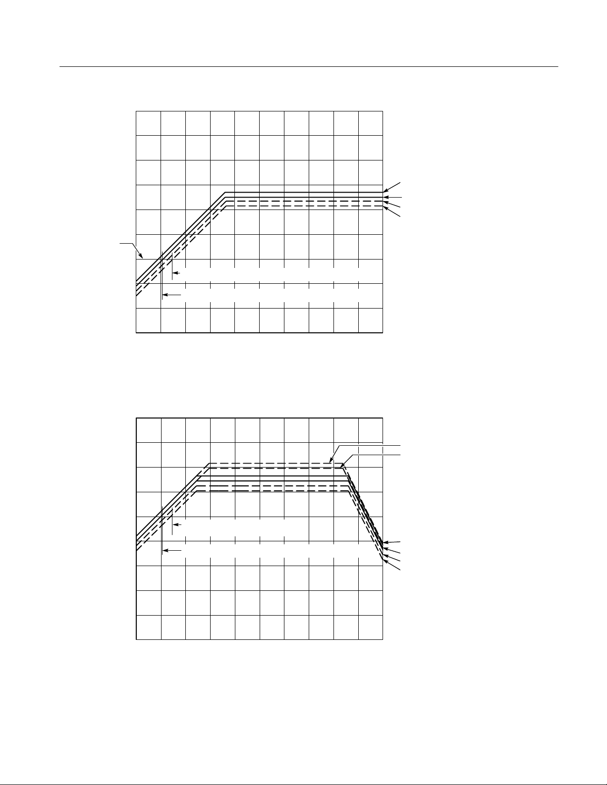
Figure 1- 1: Typical Accuracy Limits for Carrier-to-Noise Measurement
-- 9 0
-- 8 0
-- 7 0
± 4dBto500MHz
± 2dBto500MHz
± 4 dB at 1000 MHz
± 2 dB at 1000 MHz
Note: 60 channel
flat system
± 4dBto500MHz(Note1)
± 2dBto500MHz(Note1)
-- 6 0
CTB
Measurement
Limit (dBc)
-- 5 0
-- 4 0
-- 3 0
-- 2 0
-- 1 0
Minimum signal level for gated
measurement (at 1000 MHz)
Minimum signal level for gated measurement (to 500 MHz)
0
-- 2 0
-- 3 0
--100 102030 4050 6070
VISUAL CARRIER PEAK (dBmV)
Figure 1- 2: Typical Accuracy Limits for CTB Measurem ent
2715 Spectrum Analyzer Service Manual
± 4dBto500MHz(Note2)
± 2dBto500MHz(Note2)
± 4 dB at 1000 MHz (Note 2)
± 2 dB at 1000 MHz (Note 2)
Note 1
Approximate extended limits if
preselector is used and mixer input
level is set to --20 dBm.
Note 2
Normal limits without preselector and
mixer input level set to default setting
of --30 dBm in a 60 channel flat
system.
1- 7
Page 26

Specifications
-- 9 0
-- 8 0
-- 7 0
-- 6 0
CSO
Measurement
Limit (dBc)
-- 5 0
-- 4 0
-- 3 0
-- 2 0
-- 1 0
Minimum signal level for gated
measurement (at 1000 MHz)
Minimum signal level for gated measurement (to 500 MHz)
0
-- 2 0
-- 3 0
--100 102030 40506070
VISUAL CARRIER PEAK (dBmV)
Figure 1- 3: Typical Accuracy Limits for Nongated CSO Measurement
-- 9 0
-- 8 0
-- 7 0
± 4dBto500MHz(Note1)
± 2dBto500MHz(Note1)
± 4dBto500MHz(Note2)
± 2dBto500MHz(Note2)
± 4 dB at 1000 MHz (Note 2)
± 2 dB at 1000 MHz (Note 2)
Note 1
Approximate extended limits if
preselector is used and mixer
input level is set to --20 dBm.
Note 2
Normal limits without preselector
and mixer input level set to default
setting of --30 dBm. in a 60 channel
flat system
-- 6 0
CSO
Measurement
Limit (dBc)
-- 5 0
-- 4 0
-- 3 0
-- 2 0
-- 1 0
Minimum signal level for gated
measurement (at 1000 MHz)
Minimum signal level for gated measurement (to 500 MHz)
0
-- 2 0
-- 3 0
--100 102030 40506070
VISUAL CARRIER PEAK (dBmV)
Figure 1- 4: Typical Accuracy Limits for Gated CSO Measurement
1- 8
± 4dBto500MHz(Note1)
± 2dBto500MHz(Note1)
± 4dBto500MHz(Note2)
± 2dBto500MHz(Note2)
± 4 dB at 1000 MHz (Note 2)
± 2 dB at 1000 MHz (Note 2)
Note 1
Approximate extended limits if
preselector is used and mixer
input level is set to --20 dBm.
Note 2
Normal limits without preselector
and mixer input level set to default
setting of --30 dBm in a 60 channel
flat system.
2715 Spectrum Analyzer Service Manual
Page 27
-- 6 5
-- 5 5
Specifications
To 500 MHz
500 MHz to 1000 MHz
Measurement
Limit (dBc)
-- 4 5
-- 3 5
-- 2 5
-- 2 0
--10 0 1020 30 40 506070
INPUT LEVEL (dBmV) FOR SINGLE-SIGNAL TEST ENVIRONMENT
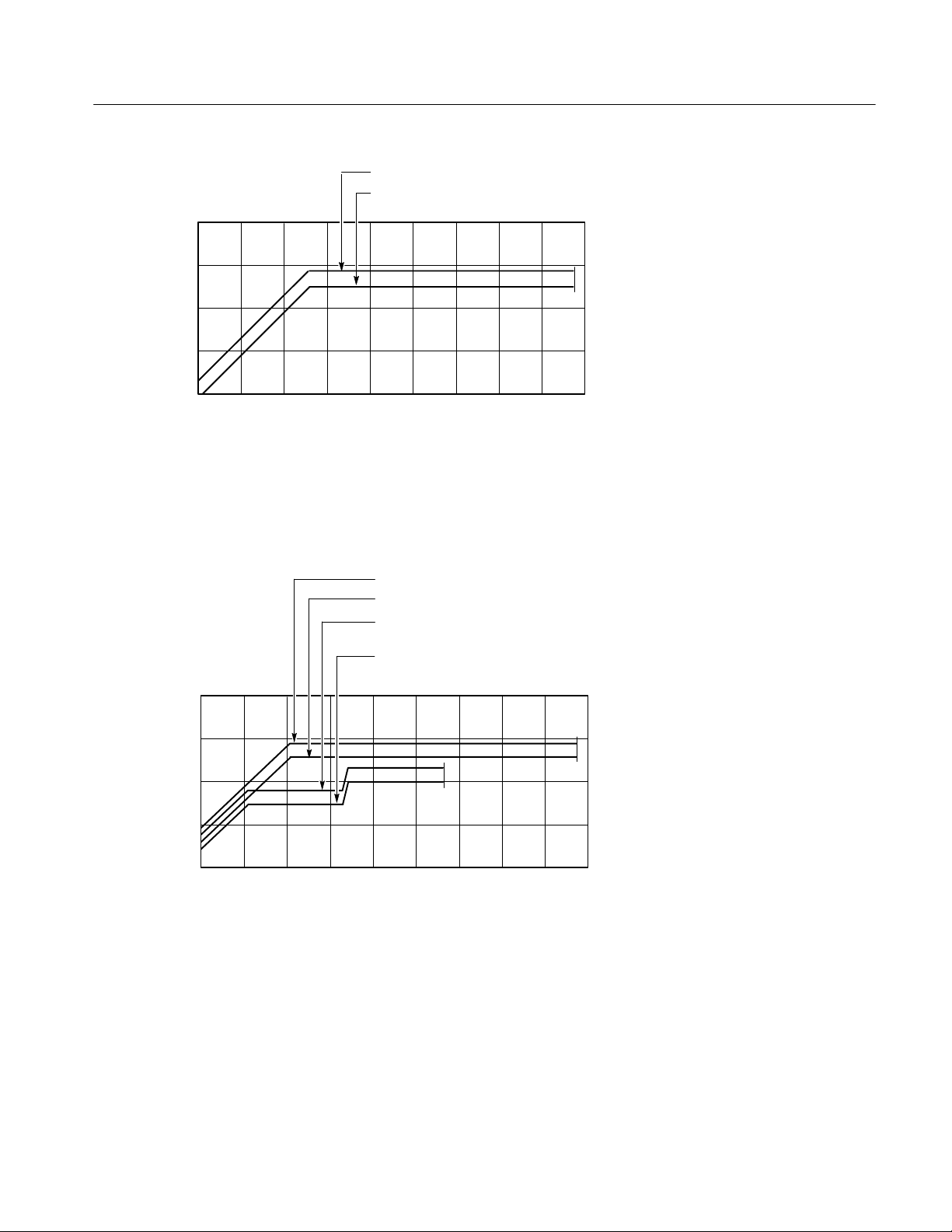
Figure 1- 5: Typical ACL Measurement Limits for 2 dB Accuracy
To 500 MHz using preselector
500 MHz to 1000 MHz using preselector
To 500 MHz in 60-channel flat system dominated by analog signals
10 dB stronger than average power of channel under test
500 MHz to 1000 MHz in 60-channel flat system dominated by analog
signals 10 dB stronger than average power of channel under test
65
55
Measurement
Limit (dB)
45
35
25
-- 2 0
--10 0 1020 30 40 506070
CHANNEL UNDER TEST INPUT LEVEL (dBmV)
Figure 1- 6: Typical D/U Measurement Range Limits for 2 dB Accuracy
2715 Spectrum Analyzer Service Manual
1- 9
Page 28
Specifications
To 500 MHz using preselector
500 MHz to 1000 MHz using preselector
To 500 MHz in 60-channel flat system dominated by analog signals
10 dB stronger than average power of channel under test
500 MHz to 1000 MHz in 60-channel flat system dominated by analog
signals 10 dB stronger than average power of channel under test
-- 6 5
-- 5 5
Measurement
Limit (dBc)
-- 4 5
-- 3 5
-- 2 5
-- 2 0
--10 0 1020 30 40 506070
INPUT LEVEL (dBmV)
Figure 1- 7: Typical Digital Signal CSO Measurement Range Limit for 2 dB Accuracy
To 500 MHz using preselector
500 MHz to 1000 MHz using preselector
To 500 MHz in 60-channel flat system dominated by analog signals
10 dB stronger than average power of channel under test
500 MHz to 1000 MHz in 60-channel flat system dominated by analog
signals 10 dB stronger than average power of channel under test
-- 6 5
-- 5 5
Measurement
Limit (dBc)
-- 4 5
-- 3 5
-- 2 5
-- 2 0
--10 0 1020 30 40 506070
INPUT LEVEL (dBmV)
Figure 1- 8: Typical Digital Signal CTB Measurement Range Limit for 2 dB Accuracy
1- 10
2715 Spectrum Analyzer Service Manual
Page 29

Specifications
Table 1- 2: Frequency-Related Characteristics
Characteristic Performance Requirement Supplemental Information
Channel Tuned with keypad, [CHAN/FREQ] [ y ],
or [CHAN/FREQ] [ b ],accordingtothe
selected channel table
Frequency
Range All except Option 50 and Option 75:
9 kHz to 1.8 GHz
Option 50 and Option 75: 9 kHz to
2.15 GHz
Accuracy 5 × 10
Drift
Long Term (One Year) ±2 PPM/year
Short Term (SPAN/DIV ≤20 kHz) All except Option 50 and Option 75:
Readout Resolution 1 kHz or 1 Hz (counter readout), menu
Frequency Span/Div
Range Using
Accuracy/Linearity Within 3% Measured over the center 8 divisions
Flatness
(Relative to the Reference Level at 100 MHz)
-- 7
of center frequency ±10 Hz ±1
least significant digit
≤400 Hz up to 1.8 GHz
Option 50 and Option 75: 500 Hz above
1.8 GHz
All instruments:
±2dB9KHzto1.8GHz
Option 50 and Option 75: ±3 dB above
1.8 GHz
Tuned with keypad, [CHAN/FREQ] [ y ],
[CHAN/FREQ] [ b ], FREQ/MARKERS
knob, UTIL menu, or MKR/FREQ menu
Assumes zero drift since last
normalization procedure
With frequency corrections enabled
selectable
[SPAN/DIV] [ y ] and [SPAN/DIV] [ b ]
buttons, selections in a 1--2--5 sequence
Using the keypad or UTIL menu,
select any value from
100 MHz/div to 1 kHz/div.
In MAXSPAN,
180 MHz/div (All except Option 50 and
Option 75) or
215 MHz/div (Option 50 and Option 75)
In ZERO SPAN, 0 Hz/div
Measured with 10 dB of RF Attenuation
and PREAMP off
Flatness is affected by:
H Input voltage standing-wave ratio
(VSWR)
H Gain variation
H Mixer conversion
2715 Spectrum Analyzer Service Manual
1- 11
Page 30

Specifications
Table 1- 2: Frequency-Related Characteristics (Cont.)
Characteristic Supplemental InformationPerformance Requirement
Residual FM
With SPAN/DIV ≤20 kHz All except Option 50 and Option 75:
≤100 Hz peak-to-peak total excursion in
20 ms up to 1.8 GHz
Option 50 and Option 75: ≤120 Hz
peak-to-peak total excursion in 20 ms
(above 1.8 GHz)
With SPAN/DIV >20 kHz All except Option 50 and Option 75:
≤2 kHz peak-to-peak total excursion in
20 ms up to 1.8 GHz
Option 50 and Option 75: ≤2.4 KHz
peak-to-peak total excursion in 20 ms
above 1.8 GHz
Resolution Bandwidth (6 dB down) Resolution bandwidth selections are:
Shape Factor (60 dB/6 dB) 7:1 or less for all resolution bandwidths
≤1MHz
Noise Sidebands All except Option 50 and Option 75:
≤--70 dBc at 30X Resolution Bandwidth
for all resolution bandwidths ≤100 kHz
Option 50 and Option 75: ≤–69 dBc at
30X Resolution Bandwidth for all
resolution bandwidths ≤100 kHz
Video Filter Reduces video bandwidth to about 1% of
Short term, after 1 hr warm-up, and with
PHASELOCK in AUTO mode
5 MHz, 1 MHz, 300 kHz, 100 kHz,
30 kHz, 10 kHz, 3 kHz, 1 kHz, and
300 Hz for the spectrum analyzer
the selected resolution bandwidth; or one
of 12 video filters (3 Hz, 10 Hz, 30 Hz,
100 Hz, 300 Hz, 1 kHz, 3 kHz, 10 kHz,
30 kHz, 100 kHz, 300 kHz, or WIDE) can
be selected from the UTIL menu
1- 12
2715 Spectrum Analyzer Service Manual
Page 31

Specifications
Table 1- 2: Frequency-Related Characteristics (Cont.)
Characteristic Supplemental InformationPerformance Requirement
Resolution Bandwidth (6 dB down) Resolution bandwidth selections are:
5 MHz, 1 MHz, 300 kHz, 100 kHz,
30 kHz, 10 kHz, 3 kHz, 1 kHz, and
300 Hz for the spectrum analyzer
Shape Factor (60 dB/6 dB) 7:1 or less for all resolution bandwidths
≤1MHz
Noise Sidebands ≤--70 dBc at 30X Resolution Bandwidth
for all resolution bandwidths ≤100 kHz
Video Filter Reduces video bandwidth to about 1% of
the selected resolution bandwidth; or one
of 12 video filters (3 Hz, 10 Hz, 30 Hz,
100 Hz, 300 Hz, 1 kHz, 3 kHz, 10 kHz,
30 kHz, 100 kHz, 300 kHz, or WIDE) can
be selected from the UTIL menu
Table 1- 3: Frequency/Amplitude Related Characteristics
Characteristic Performance Requirement Supplemental Information
Marker The frequency and amplitude values of
the marker position are displayed and
are preceded by the letter M
[MKR] [ ' ] and [MKR] [ a ] position the
marker to the next right or left signal
peak, respectively
Accuracy
Frequency Same as SPAN/DIV
Amplitude A function of the reference level, vertical
scale factor, and normalizations (see
Display Dynamic Range on page 1--15)
Also, flatness corrections while in CATV
mode for range of 15 MHz to 1.105 GHz
Delta Marker When activated, a second marker is
displayed at the same frequency as the
first marker. This is the “Reference
Marker”
Accuracy
Frequency 1 PPM ±10 Hz of the higher marker
frequency
Amplitude Same as Marker
The FREQ/MARKERS control may be
used to position the first marker; the
frequency and amplitude differences
between markers are readouts preceded
by the letter D
With both signals counted
2715 Spectrum Analyzer Service Manual
1- 13
Page 32

Specifications
Table 1- 3: Frequency/Amplitude Related Characteristics (Cont.)
Characteristic Supplemental InformationPerformance Requirement
Center Measure When activated, the signal nearest
center screen (or nearest marker if
marker is on) and above a preset
threshold level, is moved to center
screen
The frequency and amplitude values are
preceded by the letter C
Readout Resolution 1 kHz or 1 Hz Readout resolution is selectable
Signal Tracking When activated, the centered signal is
held at center screen
Signal tracking requires a signal strength
greater than the threshold level
If the strength of a signal being tracked
decreases below the threshold level, the
instrument displays the message NO
SIGNAL FOUND ABOVE THRESHOLD
Table 1- 4: Amplitude-Related Characteristics
Characteristic Performance Requirement Supplemental Information
Vertical Display Mode 10 dB/div, 5 dB/div, 1 dB/div, and Linear
Reference Level
Range Top of g r a t icul e
Log Mode --21.2 dBmV to +68.8 dBmV
(--41.2dBmVto+48.8dBmVwiththe
PREAMP enabled)
Linear Mode 10.83 V/div to 342.33 mV/div
(1.08 nV div to 34.23 mV/div with the
PREAMP enabled)
Steps
Log Mode 1dBor10dB
Linear Mode 1--2--5 sequence: 10.83 V/div to
342.33 mV/div
FINE REF LVL STEP Activated ≥0.2 division per increment
Accuracy Dependent on:
H Normalizations
H Calibrator accuracy
H Frequency response
1- 14
2715 Spectrum Analyzer Service Manual
Page 33

Table 1- 4: Amplitude-Related Characteristics (Cont.)
Characteristic Supplemental InformationPerformance Requirement
Specifications
Display Dynamic Range
Accuracy
10 dB/div Mode ±1.0 dB/10 dB to a maximum cumulative
5 dB/div Mode ±1.0 dB/10 dB to a maximum cumulative
1 dB/div Mode ±1 dB m aximum error over the 8 dB range
Linear Mode ±5% of full scale
RF Attenuator Range 0to50dBin2dBsteps
All except Option 50 and Option 75:
80 dB maximum (Log)
8 divisions (Linear)
error of ±2.0 dB over the 70 dB range and
a maximum cumulative error of ±4.0 dB
over the 80 dB range
error of ±2.0 dB over the 40 dB range
Log Mode Display Dynamic Range is
dependent upon the selected Resolution Bandwidth.
The accuracy specifications apply for
amplitude measurements done with the
marker only, since marker measurements are corrected for logging errors.
Option 50 and Option 75:
Baseline will rise to indicated value,
typically 10 dB to 20 dB below signal
level applied near frequency of
2.11 GHz.
Display Dynamic Range is reduced if
there is signal energy at or near
2.11 GHz.
10 dB/div accuracy and range is
affected by the signal-to-noise ratio of
the selected Resolution Bandwidth
filter. See following table for maximum
specified range.
Resolution
Bandwidth dB Down
5MHz 40
1MHz 40
300 kHz 50
100 kHz 50
30 kHz 60
10 kHz 60
3 kHz 80
1 kHz 80
300 Hz 80
2715 Spectrum Analyzer Service Manual
1- 15
Page 34

Specifications
q
p
1.8GHzrefertotheOption50and
Abov
fromapproximately10MHzto9kHz.
y
y
p
600MHz.
Table 1- 4: Amplitude-Related Characteristics (Cont.)
Characteristic Supplemental InformationPerformance Requirement
Sensitivity without Preamp Equivalent maximum input noise for
Resolution Bandwidth @110 MHz @ 1.8 GHz @ 2.15 GHz*
5MHz --36 dBmV --28 dBmV –26 dBmV
(--85 dBm) (--77 dBm) –75 dBm)
1MHz --43 dBmV --35 dBmV –33 dBmV
(--92 dBm) (--84 dBm) –82 dBm)
300 kHz --48 dBmV --40 dBmV –38 dBmV
(--97 dBm) (--89 dBm) –87 dBm)
100 kHz --53 dBmV --45 dBmV –43 dBmV
(--102 dBm) (--94 dBm) –92 dBm)
30 kHz --58 dBmV --50 dBmV –48 dBmV
(--107 dBm) (--99 dBm) –97 dBm)
10 kHz --63 dBmV --55 dBmV –53 dBmV
(--112 dBm) (--104 dBm) –102 dBm)
3 kHz --68 dBmV --60 dBmV –58 dBmV
(--117 dBm) (--109 dBm) –107 dBm)
1 kHz --73 dBmV --65 dBmV –63 dBmV
(--122 dBm) (--114 dBm) –112 dBm)
300 Hz --78 dBmV --70 dBmV –68 dBmV
(--127 dBm) (--119 dBm) –117 dBm)
Sensitivity with Preamp NOTE. Sensitivity with the Preamp
Resolution Bandwidth @110 MHz @ 1.8 GHz and 2.15 GHz
5MHz --48 dBmV Not Specified
(--95 dBm)
1MHz --55 dBmV Not Specified
(--104 dBm)
300 kHz --60 dBmV Not Specified
(--109 dBm)
100 kHz --65 dBmV Not Specified
(--114 dBm)
30 kHz --70 dBmV Not Specified
(--119 dBm)
10 kHz --75 dBmV Not Specified
(--124 dBm)
3 kHz --80 dBmV Not Specified
(--129 dBm)
1 kHz --85 dBmV Not Specified
(--134 dBm)
300 Hz --90 dBmV Not Specified
(--139 dBm)
each resolution bandwidth.
*Performance measurements above
1.8 GHz refer to the Option 50 and
Option 75 instruments only.
Sensitivity decreases linearly approximately 8 dB from 9 KHz to 1.8 GHz.
e 1.8 GHz sensitivitydecreases
linearly approximately 10 dB.
NOTE: Sensitivity degrades as the
FREQUENCY setting is decreased
Maximum loss in sensitivity is approximately 20 dB.
enabled is not specified above
1- 16
2715 Spectrum Analyzer Service Manual
Page 35

Specifications
Table 1- 4: Amplitude-Related Characteristics (Cont.)
Characteristic Supplemental InformationPerformance Requirement
Spurious Responses
Residual (no input signal) All except Option 50 and Option 75:
≤ --51 dBmV (≤--100 dBm) except at
1780 MHz where the spurious response is
≤--41 dBmV (≤--90 dBm).
Option 50 and Option 75: ≤--26 dBmV
(≤--75 dBm) at 2.0 GHz.
3rdOrder IM (Intermodulation) Products All except Option 50 and Option 75: ≤-- 7 0
dBcupto1.8GHz
Zero Frequency Spur ≤+39 dBmV (≤--10 dBm) Referenced to input with 0 dB RF
2ndHarmonic Distortion ≤--66 dBc Measured with 1stmixer input level of
LO (Local Oscillator) Emission All except Option 50 and Option 75: ≤ -- 7 0
≤--21 dBmV (≤--70 dBm)
With 0 dB RF attenuation
From any two on-screen signals within
any frequency span
Option 50 and Option 75:
Typically ≤--65 dBc at 2.15 GHz
attenuation
≤+9 dBmV
With 0 dB RF attenuation and preamp
off.
Option 50 and Option 75:
When frequency is below 90 MHz:
Typically <+29 dBmV (–20 dBm)
When frequency is above 350 MHz:
Typically ≤--21 dBmV (≤--70 dBm)
Table 1- 5: Input/Output Signal Characteristics
Characteristic Performance Requirement Supplemental Information
RF Input Type F male connector or
type N female connector
VSWR with RF Attenuation ≥10 dB 1.5:1 maximum Checked to 1 GHz
VSWR with 0 dB RF Attenuation All except Option 50 and Option 75:
2:1maximumupto1GHz
3.5:1 maximum up to 1.8 GHz
Option 50 and Option 75:
4:1maximumupto2.15GHz
Maximum Safe Input +70 dBmV (0.1 W or 2.2 V) continuous
peak
100 VDC blocking capacitor
Caution: Do not apply more than
100 VDC or 100V peak AC to the RF
Input
1 dB Compression Point (minimum) +34 dBmV (--15 dBm) With no RF Attenuation and 1stmixer at
+19 dBmV (--30 dBm )
2715 Spectrum Analyzer Service Manual
1- 17
Page 36

Specifications
Table 1- 5: Input/Output Signal Characteristics (Cont.)
Characteristic Supplemental InformationPerformance Requirement
Ext Trig (J102) BNC connector, 10 kΩ, DC coupled for
external trigger signals
Voltage Range
Minimum Typically at least 100 mV
1MHz
Maximum 50 V (DC + peak AC)
Pulse Width 0.1 s minimum
Accessory Connector (J103) DB-15 female connector
Pin 1: External Video Input Typically 100 ohm, DC coupled, 0 -
50 kHz, 0 -- 1.6 V (200 mV/div) signal
input for vertical deflection of the CRT
beam. The signal is processed through
the video filters and the 1 dB, 5 dB, and
10 dB scale factor circuits on the Log
board. Display storage may be bypassed.
Pin 2: Sweep Gate
+2.0 V minimum (high)
0.8 V maximum (low)
TTL-compatible signal that goes to a
logic high level while the CRT beam is
sweeping.
Pin 3: Chassis and Signal Ground
Pin 4: Sweep Output
+1.3 V
-- 1 . 3 V
Provides a nominal +1.3 V to --1.3 V
negative-going ramp, proportional to the
horizontal sweep (output impedance
≤50 Ω).
Pin 5: Log Video Output Provides 0 V to +1.6 V of video signal,
inversely proportional to the vertical
display amplitude. 0 V is the top of the
screen. Impedance is 1 kΩ.
Pin 6: CLK0 Output Clock output to Option 05 (External
Tracking Generator). CMOS logic levels
typically +3.5 V high, +1.5 V low.
Pin 7: Data I Input Data input from Option 05 (External
Tracking Generator). Typically +5 V high,
+0.1 V low.
Pin 8: Data O Output Data output to Option 05 (External
Tracking Generator). CMOS logic levels,
typically +3.5 V high, +1.5 V low.
Pin 9: ~EXTGLATCH Logic output to Option 05 (External
Tracking Generator). CMOS logic levels,
typically +3.5 V high, +1.5 V low.
Pin 10: 26.38 MHz Input Input from Option 05 (External Tracking
Generator); typically a 0.5 V
centered at +3.7 VDC.
,15Hzto
peak
p-p
sine wave
1- 18
2715 Spectrum Analyzer Service Manual
Page 37

Specifications
Table 1- 5: Input/Output Signal Characteristics (Cont.)
Characteristic Supplemental InformationPerformance Requirement
Pin 11: VLVL Output DC output to Option 05 (External
Tracking Generator); typically 9.5 V
with TG level set to ON.
Pin 12: SWPSLOPE Output Negative going ramp output to Option 05
(External Tracking Generator); typically
5 V with analyzer set to max span.
Pins 13 through 15 Not used
Digital Communications Port (J104) RS-232 or GPIB connector
Table 1- 6: Power Requirements
Characteristic Performance Requirement Supplemental Information
Input Voltage
Line Voltage Range 90 VAC to 250 VAC
Line Frequency Range 48 Hz to 63 Hz
Line Voltage Range 90 VAC to 132 VAC
Line Frequency Range 48 Hz to 440 Hz
Line Fuse 2ASlow-Blow
Input Power 90 W (1.2 A) for standard instrument
105 W (1.4 A) maximum with options
(115 W maximum at 90 V and 440 Hz)
Leakage Current 3.5 mA
At 115 V and 60 Hz
maximum or 5 mA
RMS
maximum
peak
Table 1- 7: Supplementary Characteristics Due to Options
Characteristic Performance Requirement Supplemental Information
Option 03 Provides a GPIB interface port at J104 to
replace RS-232
Option 08 Provides a RS-232 serial interface port at
J104 to replace GPIB
Option 15 Adda1stLO output
1stLO Output Level ≥+48.8 dBmV (≥0.0 dBm) At spectrum analyzer frequencies
≥100 kHz
2715 Spectrum Analyzer Service Manual
1- 19
Page 38

Specifications
Table 1- 8: General Characteristics
Characteristic Performance Requirement Supplemental Information
Sweep Normal, Single Sweep, and Manual Scan
Sweep Rate 1 s/div to 2 s/div in a 1--2--5 sequence
Accuracy ±10% over the center 8 divisions
Triggering Free Run, Internal, External, Line,
TV Line, and TV Field
Internal Trigger Level 1 division or more of signal
External Trigger Level See EXT TRIG in Table 1--5
Nonvolatile Memory (Battery-Backed Up) Instrument settings, waveforms, and
normalization results are stored in
NVRAM
Battery Life (Lithium)
At +55_ C Ambient Temperature 1to2years
At +25_ C Ambient Temperature At least 5 years
Temperature Range for Retaining Data -- 1 0 _ Cto+75_ C
Internal Calibrator Provides 100 MHz marker for amplitude
calibration and comb of 100 MHz
markers for frequency and span calibration
Amplitude and Accuracy +18.8 dBmV (--30 dBm), ±0.3 dB, at
100 MHz, ±2 kHz
Drift ±2 PPM/year
IF Gate Rise and Fall Times 7 s nominal
Off Isolation >60dB
1- 20
2715 Spectrum Analyzer Service Manual
Page 39

Specifications
Table 1- 9: Environmental Characteristics
Characteristic Description
The Description column describes how most characteristics were derived and a description of the characteristic. This instrument meets
MIL-T-28800E, Type III, Class 5, Style C Specifications.
Electromagnetic Interference (EMI)
Emissions: EN50081--1 Radiated Emissions, 30 MHz--1 GHz
EN55022 Class B (CISPR 22B)
Conducted Emissions, 150 kHz--30 MHz
EN55022 Class B (CISPR 22B)
Conducted Emissions, Power Line Harmonics, 0--2 kHZ
IEC 555-2/3
Immunity: EN50082--1 Electrostatic Discharge, 8 kV
IEC 801-2
Radiated Immunity, 27 MHz--500 MHz
IEC 801-3
Performance Requirement:
No responses above --90 dBm ina3V/meterfield
Fast Transients, Capacitive Clamp, 1 kV Power Leads,
500 V Control Leads
IEC 801-4
Power Line Surge, 1 kV Differential Mode,
2kVcommonmode
IEC 801-5
Temperature
Operating 0_ Cto+50_ C
Nonoperating
1
-- 5 5 _ Cto+75_ C
2
Humidity
Operating 95% RH ± 5% + 30_ C and below
75% RH ± 5% + 31_ C through + 40_ C
45% RH ± 5% + 41_ C through + 50_ C
Nonoperating Five cycles (120 hours) in accordance with MIL-STD-28800E, class 5
Altitude
Operating 15,000 ft (4.57 km)
Nonoperating 50,000 ft (15.24 km)
1
After storage at temperatures below - 15_ C, the instrument may not reset when power is first turned on. If this happens,
allow the instrument to warm up for at least 15 minutes, then turn power off for 5 seconds an back on.
2
NVRAM is lost below - 10_ C.
2715 Spectrum Analyzer Service Manual
1- 21
Page 40

Specifications
Table 1- 9: Environmental Characteristics (Cont.)
Characteristic Descri pti on
Vibration
Operating
(Instrument secured to a vibration
platform during test)
Shock (Operating and Nonoperating) Three guillotine-type shocks of 30 g, one-half sine, 11 ms duration each direction
Transit Drop (Free Fall) 8 in (203.2 mm), one per each of 5 faces and 4 corners (instrument is tested and
MIL-T-28800E, Method 514 Procedure X (modified) 15 minutes along each of 3
major axes at a total displacement of 0.015 in (0.38 mm) peak-to-peak (2.4 g at
55 Hz), with frequency varied from 10 Hz to 55 Hz in 1-minute sweeps
Hold for 10 minutes at 55 Hz
All major resonances must be above 55 Hz (resonance is defined as an excursion
greater than 2X the input displacement)
along each major axis, total of 18 shocks; no drops allowed on the front surface and
front corners
meets drop height of 12 in (304.8 mm)
Table 1- 10: Physical Characteristics
Characteristic Performance Requirement
Weight
With Standard Accessories 25 lbs (11.34 kg)
Without Standard Accessories 22.5 lbs (10.21 kg)
Dimensions
Height with Feet and Handle 5.4 in (137.16 mm)
Width
With Handle 14.2 in (360.68 mm)
Without Handle 12.9 in (327.66 mm)
Depth
With Front Panel Cover 17.5 in (444.50 mm)
Without Front Panel Cover 16.85 in (427.99 mm)
With Handle Extended 20.1 in (510.54 mm)
1- 22
2715 Spectrum Analyzer Service Manual
Page 41

Table 1- 11: Certifications and Compliances
Category Description
Specifications
EC Declaration of Conformity -EMC
EC Declaration of Conformity -Low Voltage
Approvals UL1244 -- Standard for Electrical and Electronic Measuring and Testing Equipment
Installation Category Descriptions Terminals on this product may have different installation category designations. The installation
Meets intent of Directive 89/336/EEC for Electromagnetic Compatibility. Compliance was
demonstrated to the following specifications as listed in the Official Journal of the European
Communities:
EN 50081-1 Emissions:
EN 55022 Class B Radiated and Conducted Emissions
EN 60555-2 AC Power Line Harmonic Emissions
EN 50082-1 Immunity:
IEC 801-2 Electrostatic Discharge Immunity
IEC 801-3 RF Electromagnetic Field Immunity
IEC 801-4 Electrical Fast Transient/Burst Immunity
IEC 801-5 Power Line Surge Immunity
Compliance was demonstrated to the following specification as listed in the Official Journal of the
European Communities:
Low Voltage Directive 73/23/EEC
EN 61010-1:1993 Safety requirements for electrical equipment for measurement,
control, and laboratory use
CAN/CSA C22.2 No. 231 – Safety Requirements for Electrical and Electronic Measuring and
Testing Equipment
categories are:
CAT III Distribution-level mains (usually permanently connected). Equipment at this level is
typically in a fixed industrial location
CAT II Local-level mains (wall sockets). Equipment at this level includes appliances, portable
tools, and similar products. Equipment is usually cord-connected
CAT I Secondary (signal level) or battery operated circuits of electronic equipment
2715 Spectrum Analyzer Service Manual
1- 23
Page 42

Specifications
Table 1- 12: Safety Certification Com pliance
Category Description
Temperature (operating) +5° Cto+50° C
Altitude (maximum operating) 2000 meters (6562 ft.)
Relative Humidity (maximum operating)
Equipment Type Test and Measuring
Safety Class Class I (as defined in IEC 1010-1, Annex H)—grounded product
Overvoltage Category Overvoltage Category II (as defined in IEC 1010-1, Annex J)
Pollution Degree Pollution Degree 2 (as defined in IEC 1010-1)
80% for temperatures up to 31° C, decreasing linearly to 50% at 40° C
Note: Rated for indoor use only.
Table 1- 13: Safety Standards
Category
U.S. Nationally Recognized
Testing Laboratory Listing
Canadian Certification CAN/CSA C22.2 No. 231 – Safety Requirements for Electrical and Electronic Measuring and Test
European Union Compliance Low Voltage Directive 73/23/EEC, as Amended by 93/68/EEC
Additional Compliance UL3 111-1 – Standard for Electrical Measuring and Test Equipment
UL1244 -- Standard for Electrical and Electronic Measuring and Testing Equipment
Equipment
EN61010-1/A1 – Safety Requirements for Electrical Equipment for
Measurement, Control, and Laboratory Use
IEC1010-1 – Safety Requirements for Electrical Equipment for
Measurement, Control, and Laboratory Use
Standards
1- 24
2715 Spectrum Analyzer Service Manual
Page 43

Operating Information
This section contains the following:
H Instrument description
H Conformance to industry standards
H Product service information
H Instrument construction
H Installation and preparation for use
H Power cord
H Fuse replacement
H Assembly and circuit numbering
H Accessories
H Menus
Instrument Description
This instrument is a compact and portable Spectrum Analyzer for the 9 kHz to
1.8GHzfrequencyrange(upto2.15GHzwithOption50orOption75
installed). Microprocessor control of most functions simplifies and enhances
operation.
The Spectrum Analyzer’s main features are:
H Precision Measurements Menu selectable routines provide directions for
normalizing the internal reference (calibrator signal) to external frequency
and amplitude references. After the internal reference is normalized, other
menu selections provide for normalizing any instrument measurement
parameter.
H Menu Operation Menu-selectable routines provide diagnostics, normaliza-
tion, adjustments, and setup of basic parameters such as center frequency,
frequency span, reference level, vertical scale factor, resolution bandwidth,
etc. These menus are described in Section 6: Spectrum Analyzers Menus of
the 2715 Spectrum Analyzer Users Manual.
2715 Spectrum Analyzer Service Manual
2- 1
Page 44

Operating Information
H Single and ∆ Markers A single marker can be enabled to show the
frequency and amplitude of a specific point on the display. Delta (∆)markers
show the difference frequency and amplitude between any selected two
points on the displayed waveform.
H Tracking Signal tracking holds a drifting signal to center screen.
H Center Measure When this function is activated, the instrument completes
the sweep and centers the signal nearest center screen or, with markers
activated, the signal nearest the marker. A readout of center frequency and
amplitude is displayed.
H Display In the Spectral mode, the numerical values of signals and setup
parameters are displayed. In the Menu mode, a menu with its selections and
prompts is displayed. Any error, warning, or information messages are
displayed in both modes.
Conformance to Industry Standards
Product Service
This Spectrum Analyzer conforms with the following industry safety standards
and regulatory requirements.
CAN/CSA C22.2, No. 231
UL 1244 (3rd Edition) Measuring Testing Equipment
To ensure adequate product service and maintenance for our instruments,
Tektronix has established Field Offices and Service Centers at strategic points
throughout the United States and in countries where our products are sold.
Several types of maintenance or repair agreements are available.
For example, for a fixed fee, a maintenance agreement program provides
maintenance and recalibration on a regular basis. Tektronix will remind you
when a product is due for recalibration and perform the service within a specified
time.
Contact your local Tektronix Service Center, representative, or sales engineer for
details regarding product service.
2- 2
2715 Spectrum Analyzer Service Manual
Page 45

Instrument Construction
Modular construction provides ready access to the major circuits. Each circuit
board containing RF sensitive circuits is mounted in a casting, with feed through
connectors through the compartment walls. Most boards and assemblies plug
onto a common interconnect board. Most adjustments and test points are
accessible while the instrument is operational and without need of a circuit board
extender.
Circuit board extenders are available in an optional Service Kit (see Maintenance
section under Fixtures and Tools for Maintenance on page 6--3). Most of the
modules or boards can be removed without affecting the structural or functional
integrity of other modules. The extender board allows any of the six circuit board
assemblies in the card cage to be positioned for service or adjustment. The
Sweep and Power Supply circuit boards are accessed by removing the instrument’s cabinet (and the Variable Resolution assembly in the case of the Power
Supply).
All other circuit boards are accessible by removing the instrument’s cabinet and
the shielding associated with each assembly.
Operating Information
NOTE. Disassembly of some modules may require special tools and procedures.
These procedures and a list of tools are located in the Maintenance section.
Most RF circuits are isolated in shielded compartments to obtain and maintain
the frequency stability, sensitivity, and EMI characteristics. While shielding
helps ensure a spurious free response, the closeness of the circuits reduces losses
and interactions with other functions. Interconnections between compartments
are made by feed through terminals rather than cables. If the compartments are
opened, be sure that the shields are properly reinstalled before operating.
Installation and Preparation for Use
Refer to Section 2: Getting Started of the 2715 Spectrum Analyzer User Manual
for unpacking, storage, repackaging for shipment, and installation information.
Power Cord
The power cord that is supplied with the instrument depends on the available
power source (see Section 1: Specifications). Power cord options are described in
Section F: Options.
2715 Spectrum Analyzer Service Manual
2- 3
Page 46

Operating Information
Replacing the Fuse
Replace the line fuse with a 2 A Slow Blow fuse.
Selected Components
Some components are specifically selected to meet Tektronix specifications.
These components are shown in the parts list.
Selected value components are identified in the parts list as a SEL value. The
component description lists either the nominal value or a range of values.
Assembly and Circuit Numbering
Each assembly and subassembly is assigned an assembly number. Generally,
each component is assigned a circuit number according to its geographic location
within an assembly. The Replaceable Electrical Parts list prefixes these circuit
numbers with the corresponding assembly and subassembly numbers.
Accessories
Menus
Example: R260 on assembly A14 becomes A14R260.
Example:U140 on subassembly A1 of assembly A19 is found in the
electrical parts list as A19A1U140.
The Replaceable Mechanical Parts section contains part numbers, descriptions,
and ordering information for all standard and optional accessories offered for this
Spectrum Analyzer.
Refer to Appendix F: Accessories & Options in the 2715 Spectrum Analyzer
User Manual for listings of standard and optional accessories.
Refer to Section 7: Options in this manual for information on accessories
associated with options.
The Accessories at the end of the Replaceable Mechanical Parts in this manual
contains information on all standard accessories currently available with this
Spectrum Analyzer.
2- 4
There are eight menus of selections that are used to invoke most of the setups,
operational modes, and applications.
2715 Spectrum Analyzer Service Manual
Page 47

Operating Information
A menu of selections may be displayed by pressing its front panel push button.
Menu push buttons are grouped together under the MENUS block. See Figure 2--1 and the Menu Structure beginning on the following page.
Figure 2- 1: 2715 Front Panel Keys
2715 Spectrum Analyzer Service Manual
2- 5
Page 48

Operating Information
0 FREE RUN
1 INTERNAL
2 EXTERNAL
3LINE
4TVLINE
5 TV FIELD
SWEEP MENU
6 SWEEP RATE
7 MANUAL SCAN
8 SYNC POLARITY
9 SETUP TABLE
SWP/TRG Menu Structure
HORIZONTAL LINE TRIGGERING
0 CONTINUOUS
1 KNOB SELECTABLE
2 KEYPAD ENTERED LINE
3 KEYPAD ENTRY
4 TV LINE STANDARD
2- 6
2715 Spectrum Analyzer Service Manual
Page 49

UTIL Menu Structure (1 of 2)
Operating Information
1 STORED SETTINGS / DISPLAYS
2 KEYPAD ENTERED SETTINGS
3 NORMALIZATIONS
4 SYSTEM CONFIGURATION
5 INSTR DIAGNOSTICS/ADJUSTMENTS
6 SERVICE REQUEST
9MORE
0 LAST POWER-DOWN
1 FACTORY DEFAULT POWER-UP
2 USER DEFINED POWER-UP
3 User Defined
4 User Defined
5 User Defined
6 User Defined
7 User Defined
8 User Defined
9MORE*
0 FREQUENCY
1 REFERENCE LEVEL
2 SPAN/DIV
3 RF ATTENUATION
4 RESOLUTION BW
5 VIDEO FILTER
6 VERTICAL SCALE
7 SWEEP RATE
0 ALL PARAMETERS
1 FREQUENCY ONLY
2 AMPLITUDE ONLY
0 COMMUNICATION PORT CONFIG
1 SCREEN PLOT CONFIGURATION
2 PRINTER CONFIGURATION
3 INSTRUMENT CONFIGURATION
4 REAL--TIME CLOCK SETUP
5 STORED SETTINGS PROTECT
6 FILE SYSTEM DIRECTORY
7 PROTECT FILE
9 INSTALLED OPTIONS DISPLAY
*
Expands to registers 10--18, 20--28
and 30--39.
0 AUTO
1 FIXED
0 AUTO
1 FIXED
0 LOG 1 DB/DIV
1 LOG 5 DB/DIV
2 LOG 10 DB/DIV
3 LINEAR
0 GPIB
2 RS--232
0 COMM PORT
1 PLOTTER LANGUAGE
2 PLOT SPEED*
3 PLOTS PER PAGE**
5 GRATICULE LINES ON PLOT
0 AUDIO ALERT
1 MINIMUM SIGNAL SIZE
2 WAVEFORM TO PRINTER
3 WAVEFORM OUTPUT FORMAT
4 PHASELOCK
5 FREQUENCY CORRECTIONS
6 SPECTRAL DISPLAY IN MENUS
7 SWEEP HOLDOFF
0 STATUS
1 GPIB ADDRESS
2 POWER ON SRQ
3 EOI/LF MODE
4 TALK ONLY MODE
0 STATUS
1 BAUD RATE
2DATABITS
3 PARITY
4EOL
5 FLOW CONTROL
6 ECHO
7 VERBOSE
2715 Spectrum Analyzer Service Manual
0 SET DAY
1 SET MONTH
2 SET YEAR
3 SET HOUR
4 SET MINUTE
5 SET SECONDS TO :00
6 DISPLAY DATE/TIME
**
Displayed when selected plotter
language is HPGL.
2- 7
Page 50
Operating Information
1 STORED SETTINGS / DISPLAYS
2 KEYPAD ENTERED SETTINGS
3 NORMALIZATIONS
4 SYSTEM CONFIGURATION
5 INSTR DIAGNOSTICS/ADJUSTMENTS
6 SERVICE REQUEST
9MORE
0 PRINT READOUTS
9MORE
UTIL Menu Structure (2 of 2)
0 DIAGNOSTICS
1 EXTENDED DIAGNOSTICS
2 MANUAL ADJUSTMENTS
3 DEBUG MENU
4 INTERNAL PARAMETERS
5 SERVICE NORMALIZATIONS
6 DIGITAL OPTIONS DIAGNOSTICS
8 CALIBRATION MODE
*
Factory troubleshooting aids: not
discussed in this manual.
*
*
*
1 DEFLECTION AMP CAL
2 DISPLAY STORAGE CAL
3 SWEEP CAL
*
4 CFCV1 ADJUSTMENTS
5 TOGGLE VD DAC LO/HI
6 VD DAC TO VIS CARR
7 AFC TOGGLE
8 GATE TOGGLE
9 QUERY LOCK STATUS
0 SETTINGS VERIFY
1 FILE SYSTEM MENU
2 YIG SETTLE DELAY
0 THRESHOLD
1 PROGRAMD TUNING INC
2 KNOB FUNCTION
3 MARKER TO REFERENCE LEVEL
4 MOVE MARKER TO NEXT PEAK
5 TRANSPOSE MARKERS
6 MARKER START/STOP
7 FREQUENCY START/STOP
8 TUNING INCREMENT
9 SETUP TABLE
MRK/FREQ Menu Structure
0 CENTER FREQ
1 MARKER FREQ
2 KEYPAD ENTRD INC
3 KEYPAD ENTRY
4 RETURN TO AUTO
0 FREQUENCY
1 MARKER
2 VIDEO LINE*
0 FREQ START ENTRY
1 FREQ STOP ENTRY
0 CENTER/START FREQ
1 COUNTER RESOLUTION
3 FREQ OFFSET
4 FREQ OFFSET MODE
*
Displayed only if KNOB SELECTABLE is se-
lected in the SWEEP MENU SETUP TABLE.
0 FREQUENCY NORMALIZATIONS
1 REFERENCE NORMALIZATIONS
2 AMPLITUDE NORMALIZATIONS
4 NORMALIZATION VALUES
5 PRINT ALL NORM VALUES
6 NORM DEBUG TO PRINTER
0 COUNTER OFF WHEN TRKG (1 HZ)
11HZ
2 1KHZ
2- 8
2715 Spectrum Analyzer Service Manual
Page 51

CATV/APPL CATV Measurements Page 1 Menu Structure (1 of 3)
0 RECENTER CHANNEL xx
1 CARRIER LEVEL --- AVG POWER
2 CARRIER SURVEY
3 MODULATION DEPTH
4 AURAL (FM) DEVIATION
5 CARRIER/NOISE -- DESIRED/UNDESIRED
6 HUM/LFD
7 FREQUENCY RESPONSE
8 CATV MEASUREMENTS SETUP
9MORE
0 RUN LEVELS - POWER
1 STORE CURRENT RESULTS
2 DISPLAY RESULTS
3 PRINT CURRENT RESULTS*
4 PRINT STORED RESULTS*
5 SET UP CARRIER LEVELS
6 EXTERNAL ATTEN/AMPL
9 LEAVE CARRIER LEVEL --- AVG PWR
0 RUN CARRIER SURVEY
1 STORE CURRENT RESULTS
2 DISPLAY RESULTS
3 PRINT CURRENT RESULTS*
4 PRINT STORED RESULTS*
5 SET UP CARRIER SURVEY
6 EXTERNAL ATTEN/AMPL
9 LEAVE CARRIER SURVEY
Operating Information
TEST MODES
0 ACCURATE FREQUENCY AND AMPL
1 ACCURATE AMPLITUDE ONLY
2 FAST AMPLITUDE ONLY
0ON/OFF
1 ATTEN/AMPL ENTRY
TEST MODES
0 ACCURATE FREQUENCY AND AMPL
1 ACCURATE AMPLITUDE ONLY
2 FAST AMPLITUDE ONLY
0 RUN MODULATION DEPTH
1 STORE CURRENT RESULTS
2 DISPLAY RESULTS
3 PRINT CURRENT RESULTS*
4 PRINT STORED RESULTS*
5 SET UP ADJUSTMENT MODE
6 ENTER ADJUSTMENT MODE
9 LEAVE MODULATION DEPTH
0 RUN FM DEVIATION
1 STORE CURRENT RESULTS
2 DISPLAY RESULTS
3 PRINT CURRENT RESULTS*
4 PRINT STORED RESULTS*
5 SET UP AURAL (FM) DEVIATION
6 ENTER ADJUSTMENT MODE
9 LEAVE AURAL (FM) DEVIATION
*
RS-232 only.
0ON/OFF
1 ATTEN/AMPL ENTRY
0 VIEW MODULATION MODE
1 TARGET LINE
2 CYCLE DELAY
3 TARGET LINE DURATION
TEST MODES
0 INTERACTIVE
1AUTO
5 MEASUREMENT TIME
2715 Spectrum Analyzer Service Manual
2- 9
Page 52

Operating Information
CATV/APPL CATV Measurements Page 1 Menu Structure (2 of 3)
0 RECENTER CHANNEL xx
1 CARRIER LEVEL -- AVG POWER
2 CARRIER SURVEY
3 MODULATION DEPTH
4 AURAL (FM) DEVIATION
5 CARRIER/NOISE -- DESIRED/UNDESIRED
6 HUM/LFD
7 FREQUENCY RESPONSE
8 CATV MEASUREMENTS SETUP
9MORE
0 RUN C/N -- D/U
1 STORE CURRENT RESULTS
2 DISPLAY RESULTS
3 PRINT CURRENT RESULTS
4 PRINT STORED RESULTS
5 SET UP CARRIER/NOISE
7 IN --SERVICE
9 LEAVE C/N --- D/U
0 RUN HUM/LFD
1 STORE CURRENT RESULTS
2 DISPLAY RESULTS
3 PRINT CURRENT RESULTS*
4 PRINT STORED RESULTS*
5 POWER LINE FREQ
9 LEAVE HUM/LFD
0 RUN FREQ RESP
CURRENT REFERENCE
5 SET UP FREQ RESP
9 LEAVE FREQUENCY RESPONSE
*
RS-232 only.
TEST MODES
0 INTERACTIVE
1 AUTO
2 AUTO (PAUSE FOR CARRIED OFF)
5 NOISE NORM’D BW
TEST MODES
0 ✱NO REF
1WITHREF
SWEEP RANGE
2 START FREQUENCY
3 STOP FREQUENCY
4 USE DEFAULT START/STOP
TEST MODES
0NOREF
1 ✱WITH REF
REFERENCE ACQUISITION
2 START FREQUENCY
3 STOP FREQUENCY
4 USE DEFAULT START/STOP
5 ACQUIRE NEW REFERENCE
6 STORED REFERENCE MENU
7 EDIT CURRENT REFERENCE NAME
2- 10
2715 Spectrum Analyzer Service Manual
Page 53

CATV/APPL CATV Measurements Page 1 Menu Structure (3 of 3)
0 RECENTER CHANNEL xx
1 CARRIER LEVEL -- AVG POWER
2 CARRIER SURVEY
3 MODULATION DEPTH
4 AURAL (FM) DEVIATION
5 CARRIER/NOISE -- DESIRED/UNDESIRED
6 HUM/LFD
7 FREQUENCY RESPONSE
8 CATV MEASUREMENTS SETUP
9MORE
To CATV/APPL
CATV Measurements Page 2
0 EXIT CATV MEASUREMENT MODE
1 CHANNEL TABLE
2 SKIP CHANNEL
3 ALL CHANNELS
4SITE
5 OPERATOR
6 REF LEVEL UNIT
7 EDIT CHANNEL TABLE
8 REMOVE ALL STORED RESULTS
9 LEAVE CATV MEASUREMENTS SETUP
1
Operating Information
0STD
1 HRC
2IRC
3 User Defined
4 User Defined
5 User Defined
6 User Defined
7 User Defined
8 User Defined
9 User Defined
1
Option 50 and Option 75 only
2715 Spectrum Analyzer Service Manual
2- 11
Page 54

Operating Information
CATV/APPL CATVMeasurements Page 2 Menu Structure (1 of 2)
0 ADJACENT CHANNEL LEAKAGE
1 VIEW MODULATION (FIELD)
2 VIEW MODULATION (LINE)
3 VIEW PICTURE
4LISTEN
5 CTB
6CSO
7 CROSS MODULATION
8 IN-CHANNEL RESPONSE
9MORE
0 RUN CTB
1 STORE CURRENT RESULTS
2 DISPLAY RESULTS
3 PRINT CURRENT LEVELS*
4 PRINT STORED RESULTS*
5 SET UP CTB
6 DIGITAL/ANALOG
9 LEAVE CTB
0 RUN CSO
1 STORE CURRENT RESULTS
2 DISPLAY RESULTS
3 PRINT CURRENT LEVELS*
4 PRINT STORED RESULTS*
5 SET UP CSO
6 DIGITAL/ANALOG
7 IN-SERVICE
9 LEAVE CSO
*
RS-232 only.
0 RUN ADJACENT CHANNEL LEAKAGE
1 STORE CURRENT RESULTS
2 DISPLAY RESULTS
3 PRINT CURRENT RESULTS*
4 PRINT STORED RESULTS*
5 MEASURE SIDE
9 LEAVE ACL
TEST MODES
0 INTERACTIVE
1 AUTO
2 AUTO (PAUSE FOR CARRIER OFF)
3 SINGLE-SWEEP
5 SET UP TEST FREQUENCIES**
TEST MODES
0 INTERACTIVE
1 AUTO
2 AUTO (PAUSE FOR CARRIER OFF)
3 SINGLE-SWEEP
4 CONTINUOUS
5 SET UP TEST FREQUENCIES AND
CONTINUOUS MODE PRMTRS**
TEST FREQUENCIES
0 User Defined
1 User Defined
2 User Defined (+0.00000HZ Default)
3 User Defined
4 User Defined
5 USE DEFAULT TEST FREQUENCIES
2- 12
TEST MODES IN-SERVICE
0 INTERACTIVE
1AUTO
5 SET UP TEST FREQUENCIES**
**
Not displayed in INTERACTIVE mode.
2715 Spectrum Analyzer Service Manual
TEST FREQUENCIES
0 User Defined (+1.25000MHZ Default)
1 User Defined (+750.000KHZ Default)
2 User Defined
3 User Defined (-750.000KHZ Default)
4 User Defined (-1.25000MHZ Default)
5 USE DEFAULT TEST FREQUENCIES
CONTINUOUS MODE PARAMETERS***
6 CARRIER FREQ***
7 TEST INTERVAL***
8 NORMALIZATION INTERVAL***
***
Displayed only if CONTINUOUS mode
is selected.
Page 55

0 ADJACENT CHANNEL LEAKAGE
1 VIEW MODULATION (FIELD)
2 VIEW MODULATION (LINE)
3 VIEW PICTURE
4LISTEN
5 CTB
6CSO
7 CROSS MODULATION
8 IN-CHANNEL RESPONSE
9MORE
To CATV/APPL
CATV Measurements Page 1
Operating Information
CATV/APPL CATV Measurements Page 2 Menu Structure (2 of 2)
0 RUN CROSS MODULATION
1 STORE CURRENT RESULTS
2 DISPLAY RESULTS
3 PRINT CURRENT RESULTS*
4 PRINT STORED RESULTS*
9 LEAVE CROSS MODULATION
0 RUN IN-CHAN RESP
1 STORE CURRENT RESULTS
2 DISPLAY RESULTS
3 PRINT CURRENT RESULTS*
4 PRINT STORED RESULTS*
5 SET UP IN-CHAN RESP
6 TEST SIGNAL LINE NUMBER**
7 IN-SERVICE
9 LEAVE IN-CHAN RESP
*
RS-232 only.
**
Displayed only when IN-SERVICE is On.
TEST MODES
0 INTERACTIVE
1 AUTO (PAUSE FOR SIGNAL ON)
TEST FREQUENCIES
2 User Defined (-500.000KHZ Default)
3 User Defined (+500.000KHZ Default)
4 User Defined (+1.25000MHZ Default)
5 User Defined (+2.00000MHZ Default)
6 User Defined (+3.00000MHZ Default)
7 User Defined (+3.75000MHZ Default)
8 USE DEFAULT TEST FREQUENCIES
2715 Spectrum Analyzer Service Manual
TEST MODES IN-SERVICE
0 INTERACTIVE
1 AUTO
TEST FREQUENCIES
2 User Defined (-500.000KHZ Default)
3 User Defined (+500.000KHZ Default)
4 User Defined (+1.25000MHZ Default)
5 User Defined (+2.00000MHZ Default)
6 User Defined (+3.00000MHZ Default)
7 User Defined (+3.75000MHZ Default)
8 USE DEFAULT TEST FREQUENCIES
2- 13
Page 56

Operating Information
0 BANDWIDTH MODE
1 CARRIER TO NOISE
2 NOISE NORM’D
3 SIGNAL SEARCH MENU
4 OCCUPIED BW
7 FM DEVIATION MODE
8 CATV MEASUREMENT MODE
9 SETUP TABLE
CATV/APPL Applications Menu Structure
0 BEGIN FREQ
1 END FREQ
2 START TEST
3 DISPLAY RESULTS
0 DB DOWN FOR BW MODE
1 NORM BW FOR C/N
2 NOISE NORM’DBW
3 PERCENT OCCUPIED BW
DEMOD Menu Structure
0OFF
1 AM DEMODULATOR
2 FM DEMODULATOR
3 BROADCAST (AM) VIDEO
9 VIDEO MONITOR SETUP 0 VIDEO DETECT MODE
1 SYNC POLARITY
2 VIDEO POLARITY
2- 14
2715 Spectrum Analyzer Service Manual
Page 57

0 DIGITAL/ANALOG
1 ENSEMBLE AVERAGING
2 B, C MINUS A
3 B, C MINUS A OFFSET TO
4 ACQUISITION MODE
5TITLEMODE
6 GRATICULE ILLUMINATION
7 DISPLAY SOURCE (AM)
8 DISPLAY LINE
9MINHOLD
Operating Information
DSPL Menu Structure
1 INITIATE AVERAGING
2 TERMINATE AVERAGING
3MAX
4 MEAN
5MIN
6 MAX/MIN
7 NUMBER OF AVERAGES
8 SAVE RESULTS IN DISPLAY
1TITLEMODE
2 TITLE MODE EDIT
3 PLOT LABELING
4 PLOT LABELING EDIT
0 User Defined
1 User Defined
2 User Defined
3 User Defined
4 User Defined
5 User Defined
6 User Defined
7 User Defined
8 User Defined
9 USER DEF PROGRAM UTILITIES
1ON/OFF
2 VALUE ENTRY
3 DISPLAY LINE TO MARKER
4 LIMIT DETECTOR
USERDEFMenuStructure
0 ACQUIRE KEY STROKES
1 TITLE EDIT
2 WAIT FOR END OF SWEEP
3 DISPLAY MESSAGE
4 PAUSE FOR “USER DEF” KEY
5 CONTINUOUS EXECUTION
6 STORE
7 DELETE
8 PROTECT
9 TIME DELAY SETUP
0 SET DAY
1 SET HOUR
2 SET MINUTE
3 REPEAT INTERVAL
4 RUN N TIMES
5 CLEAR TIME
2715 Spectrum Analyzer Service Manual
2- 15
Page 58

Operating Information
1 PREAMP
INPUTMenuStructure
3 REF LEVEL UNIT
4 1ST MXR INPUT LVL
5 RF ATTENUATION
6 EXTERNAL ATTEN/AMPL
9 CAL SIG @ 100MHZ 18.8DBMV
0DBM
1 DBMV
2DBV
3 DBUV
4 DBUW
5 DBUV/M IN WFM x
9 DBUV/M SETUP
0ON/OFF
1 ATTEN/AMPL ENTRY
0 EDIT ANTENNA TABLE
1 User Defined
2 User Defined
3 User Defined
4 User Defined
5 User Defined
6 MEASUREMENT DIST
7 SAVERESULTSINWFM
9 MARKER DISPLAY
0 BEGIN EDIT
1 TITLE EDIT
2STORE
3LOAD
4 DELETE
5 PRINT
6 ANTENNA SETUP
1 START FREQUENCY
2 STOP FREQUENCY
3 INC FREQUENCY
4 REFERENCE DISTANCE
2- 16
2715 Spectrum Analyzer Service Manual
Page 59

Theory of Operation
This section describes the 2715 circuitry. The section begins with a functional
description of the major circuit blocks. This is followed by more detailed
descriptions of the circuitry within each block. While reading these descriptions,
refer to the corresponding diagrams in Section 9: Diagrams.
Block Diagram Description
The Spectrum Analyzer block diagram contains the following major blocks:
H Attenuator and Low Pass Filter
H 1st Converter
H 2nd Converter
H RF Mother Board (3rd Converter)
H VR (Variable Resolution Module)
H Log Amplifier
H Display Storage board
H Center Frequency Control
H 1st LO Buffer
H Microprocessor
H Sweep
H Power Supply (Deflection)
This is a block diagram description of the Spectrum Analyzer. While reading this
description, refer to Figure 3--1.
NOTE. The power levels noted in the block diagram between the input and the
Log Amplifier assume a --30 dBm (+18.8 dBmV) input level.
The block diagram shows how the major sections in the instrument relate. It also
shows the paths of most major signals. Not explicitly shown are the interconnections between the Power Supply and the circuit blocks, interconnections between
the Sweep board and other major circuit blocks, and interconnections between
the Deflection System and other circuit blocks. (The Deflection System is
located on the Power Supply board.)
2715 Spectrum Analyzer Service Manual
3- 1
Page 60

Theory of Operation
A25Ω resistor within the RF INPUT connector assembly is placed in series
with the signal path. This transforms the connector to a 75 Ω impedance for
external signal connections. All RF signal connections within the 2715 (SMA
and SMB connectors) have a 50 Ω impedance. RF type signal connections
between modules are made using double shielded coaxial cables, while DC type
signal connections are made using either multipin jacks on the Power Supply
board (Power Supply, Log Amplifier, Display Storage, Microprocessor, and
Center Frequency Control boards) or small ribbon cables.
The Main Interconnect Diagram at the front of the Diagrams section provides a
chart of the interconnect system in addition to what is shown in Figure 3--1.
Block diagrams showing more detail of these main sections appear before the
appropriate schematics together with another description. Circuit schematic
diagrams follow the Main Interconnect Diagram.
3/
RF IN
9kHz-1.8GHz
+70 dBmV MAX,
75 Ω 100 VDC
Max
Calibrator
(100 MHz/
-- 22 dBm)
1
Attenuator
Reference
Oscillator
1st LO
Center
Frequency
Control
2110 MHz
1st
Converter
2.11 − 3.91 GHz
+11 dBm MIN
+14.5 dBm MAX
From 1st LO Buffer
6/
SWPSLOPE
10/
2nd LO
2
RF Mother
Board
2nd
Converter
2GHz100 GHz
110 MHz
Power Supply
with Deflection
System
Front Panel
Rear Panel
Controls &
Connector
COUNT10/
3rd
Converter
10 MHz
Log
Amplifier
Variable
Resolution
Module
10 MHz
-- 10 dBm
Log
Amplifier
Micro-
processor
RF
Options
Display
Storage
50/
Digital
Port
1
9 KHz – 2.15 GHz for Option 50 and Option 75
2
2.11 – 4.26 GHz for Option 50 and Option 75
Figure 3- 1: Main Block Diagram
3- 2
2715 Spectrum Analyzer Service Manual
Page 61

Theory of Operation
What It Does
How It Works
Attenuator and Low Pass
Filter
The Spectrum Analyzer accepts an electrical signal as its input and displays the
signal’s frequency components on a CRT. Signals are applied directly to the RF
INPUT.
The display of the input signal appears on the CRT as a graph where the
horizontal axis is frequency and the vertical axis is amplitude.
The Spectrum Analyzer operates as a variable bandwidth receiver. The CRT
beam moves horizontally as a range of frequencies is scanned. When a frequency
component of an input signal is detected, the beam is deflected vertically as a
function of input power at that frequency.
There are two selections for inputs to the Spectrum Analyzer: the RF INPUT at
the front panel and the internal calibrator signal.
The Attenuator adds attenuation to the input signal such that the level at the
input of the 1st mixer (1st Converter) is limited to no more than --30 dBm. This
would represent a full screen signal. Also, an amplifier can be inserted in the
signal path to improve sensitivity when small signals are applied to the RF
INPUT by invoking the Preamp mode. The Microprocessor sets the amount of
attenuation, depending on the user selected reference level, to maintain the
proper signal level.
st
Converter and
1
Bandpass Filter
nd
Converter
2
The signal is then routed to the 1st Converter through a Low Pass Filter. The
Low Pass Filter attenuates out-of-band signals and helps minimize 1st Local
Oscillator (LO) emission at the RF INPUT. When the Preamp mode is invoked,
the Microprocessor sets the appropriate amount of attenuation, or it sets the gain
of an internal amplifier (Variable Resolution) to maintain a calibrated display.
The input signal is converted to an intermediate frequency (IF) signal of
2110 MHz. This is accomplished by mixing the input signal with an LO signal
that varies over a range of 2.11 GHz to 3.91 GHz (4.26 GHz for Option 50 and
Option 75). The LO range corresponds to a range of 0 Hz to 1.8 GHz (2.15 GHz
for Option 50 and Option 75) at the RF INPUT. The output of the mixer is then
amplified to compensate for the conversion loss, and it is filtered to allow only
the difference frequency to pass. All other mixer products are attenuated.
The 2nd Converter down converts the 2110 MHz IF signal to 110 MHz, then
routes this 2nd IF to the RF Mother board.
2715 Spectrum Analyzer Service Manual
3- 3
Page 62

Theory of Operation
RF Mother Board
Assembly
Variable Resolution
Module
Log Amplifier
The RF Mother board assembly contains a 2 GHz 2nd LO, a 2nd Converter,
several gain stages, a 5 MHz resolution bandwidth filter, and a 3rd Converter.
The 2nd Converter down converts the 2110 MHz 1st IF to 110 MHz. The 3rd
Converter down converts the 110 MHz 2nd IF to a 10 MHz 3rd IF. This signal is
routed to the Variable Resolution module.
The Variable Resolution contains several selectable gain stages prior to the filters
and a compensation amplifier. One of the nine filters is selected. Each filter has
an attenuator pad associated with it to compensate for losses in the filter. The
system selects the appropriate amplification factor as each filter is selected.
The 10 MHz IF signal is processed through one of several Bandpass filters,
amplified once more, and then routed to the Log Amplifier board.
The Log Amplifier performs the logarithmic conversion, linear detection and
logarithmic detection of the incoming signal, and amplitude calibration. The log
display has scale factors of 10 dB/div, 5 dB/div, and 1 dB/div. The module also
contains an FM detector, an audio amplifier, an amplitude limited output for the
period counter, and an out-of-band signal clamp.
The detector produces a voltage that corresponds to the input signal strength in
decibels. The detector output is then vertically scaled and sent to the Display
Storage and Sweep boards.
Display Storage
The control processor uses three 8 bit shift registers to control the Log Amplifier.
The Display Storage board contains the circuitry for putting text and waveforms
onto the CRT display.
This board contains the following programmable functions:
H Waveform Storage — four 512 point waveforms
H Dot Markers — up to two intensified markers
H Text Storage — four 32 character by 16 lines of text
H Accumulator data — direct access to the output of the A to D converter
H Nonvolatile memory — 32 Kbytes total; 2 Kbytes used for waveforms;
2 Kbytes used for text; the rest is available for general use
When enabling the analog display, waveforms A, B, C, and D are turned on, but
not displayed. This results in a chopped blanking effect between the readout and
the analog display. The scanning alternates between the readout and the analog
display.
3- 4
2715 Spectrum Analyzer Service Manual
Page 63

The Display Storage board is capable of storing four waveforms of 512 bytes
each, four pages of text of 512 bytes each, and up to two markers. Any combination of waveforms and text may be displayed on the CRT. If any waveforms are
being displayed, the text portion of the display is limited to approximately 100
characters in order to avoid flicker.
Only one page of text may be displayed at any one time. The readout page is
limited to approximately 100 characters.
The waveforms and text displays are accessed through memory reads and writes.
When (DISPLAY) A, B, C, or D is selected, the stored waveforms in those
registers are displayed. When A, B, C, and D are deselected, the display reverts
to the real time (nondigitized) video waveform, and the readout is updated during
the readout cycle.
Center Frequency Control
The Center Frequency Control system provides 1st Local Oscillator (1st LO)
signal to the 1st Converter at the center frequency and span selected by the user.
In general, this is accomplished by a combination of setting, counting, and
resetting (as required) of the frequencies of various oscillators.
Theory of Operation
1stLO
The system is expected to control the frequency within a few Hz out of a total
operating range of approximately 2 GHz.
The principal elements of the frequency control system are as follows:
This is a YIG tuned oscillator that covers the range of 2.11 to 3.91 GHz or 2.11
to 4.26 GHz for Option 50 and Option 75 (YIG = Yttrium Iron Garnet.) Ideally,
its operating frequency is exactly proportional to the strength of an internal DC
magnetic field. This field is the combined field of two coils, one large (Main)
and one small (FM). In practice, the frequency is uncertain by up to a few MHz
due to problems such as temperature drift, slight nonlinearity, and magnetic
hysteresis. Also, the oscillator has some residual FM and phase noise sidebands
due to internal causes and external noise and drift from the driver circuit. The
remainder of the frequency control system maintains the oscillator (abbreviated
YIG) at the right frequency. Usually, it is sufficient to set the YIG, then
periodically check its frequency and make small adjustments as required.
However, in very narrow spans the YIG must be phase locked to a stable source
in order to maintain sufficient stability.
The 1st LO Interface provides drive signals for the main coil and FM coil, a
control signal for the main coil, and power for the gain stage.
2715 Spectrum Analyzer Service Manual
3- 5
Page 64

Theory of Operation
100 MHz Reference
Oscillator
Phase Gate
This is a precision, temperature controlled, quartz crystal oscillator that provides
the reference around which all instrument frequency related performance
revolves. It is designed for maximal frequency stability over temperature and
time, with absolute frequency accuracy being secondary. The instrument
firmware accounts for any frequency inaccuracy, producing a virtually perfect
reference.
The phase gate is a high speed sampling switch that takes a very brief sample of
the 1st LO waveform once during each cycle of the strobe frequency. (The strobe
is a control signal supplied to the phase gate from an external source.) These
samples are later averaged by a low pass filter to eliminate ripple at the strobe
frequency, and also to eliminate other undesirable components.
When the 1st LO is phase locked to any integer multiple of the strobe frequency,
the resulting output is a phase dependent DC voltage that is used as the error
voltage in a feedback loop to maintain phase lock.
When the 1st LO is not phase locked, the resulting output is a beat note
occurring at the difference frequency between the 1st LO frequency and the
nearest integer multiple of the strobe frequency. (Actually, many beat frequencies
are present at once, but the low pass filter eliminates all but the one of lowest
frequency.)
Phase Lock Center
Frequency Control
(PLCFC)
Firmware
This element is the focal point of the frequency control system hardware. It
accepts commands from the instrument microprocessor and then puts out
appropriate drive signals to the 1st LO as well as a suitable strobe signal to the
Phase Gate. The PLCFC module also uses the Phase Gate output. It also
provides counter signals and status information to the microprocessor. It requires
the 100 MHz reference signal in order to function.
Because of the variety of tasks that the Spectrum Analyzer is called upon to do,
it is essential to have an intelligent controller. This is especially true in the
frequency control context, because the required degree of control could not be
economically obtained with unassisted analog hardware.
Instrument firmware has the task (among many others) of commanding the
frequency control hardware, taking feedback from it, and making readjustments
as required to obtain the desired result.
The interface between the microprocessor system and the PLCFC module is
through a pair of serial data lines, some latch lines, and some clock signals.
3- 6
2715 Spectrum Analyzer Service Manual
Page 65

1stLO Buffer
Sweep
Theory of Operation
The 1st LO Buffer consists of a Leveled Amplifier and a Phase Gate Detector.
The Leveled Amplifier provides the LO input drive for the 1st Mixer. The Phase
Gate Detector logs 1st LO drift. That information is then used for frequency
corrections.
The Sweep board contains a microprocessor interface, horizontal sweep
generator, trigger circuitry, vertical sweep (raster scan) circuitry, video processing, video line triggering, and graticule illumination.
This board receives messages from the microprocessor regarding its operation,
but cannot send messages directly to the microprocessor.
Various combinations of resistors and capacitors yield the sweep speed selections.
The available trigger modes are Free Run, Internal, Line, External, TV Field, and
TV Line. When the video monitor mode is selected, the readout, display storage,
and video filter are turned off. In addition, the resolution bandwidth is set to
5 MHz, the Vertical display mode defaults to Lin, the span setting defaults to
Zero Span, and the sweep rate defaults to 5 s. The video monitor mode is
turned off from the trigger menu or by selecting another trigger mode.
TV Line Trigger mode causes the Spectrum Analyzer to trigger on the selected
video line. The selected line, and part of the next line, are displayed.
2715 Spectrum Analyzer Service Manual
3- 7
Page 66

Theory of Operation
Display System
The Display System consists of the Vertical Display circuit, Horizontal Display
circuit, and Z Axis circuit. See Figure 3--2.
The Display System has three possible display modes. The active spectrum
display mode displays the incoming signal. The static spectrum display mode
displays stored signals from memory. The video monitor mode displays live
video signals.
Part of Power Supply Board
Log
Amplifier
Display
Storage
Sweep
Front
Panel
LOGVIDEO
DSVER
DSHOR
SWP
VIDVERT
VIDZ
CRTINTS
To Ver tic al
Deflection Plates
To Horizontal
Deflection Plates
To Z Ax is
3- 8
Figure 3- 2: Display System Diagram
2715 Spectrum Analyzer Service Manual
Page 67

Circuit Description
The following sections provide detailed circuit descriptions and is arranged to
follow the input signal flow. While reading these descriptions, refer to the
corresponding diagrams in Section 9: Diagrams.
Attenuator and 1stConverter
The Attenuator and 1st Converter signal path consists of the following parts:
H Step Attenuator
H 1.8 GHz Low Pass Filter (2.2 GHz Low Pass Filter for Option 50 and Option
75)
H Mixer
Theory of Operation
Step Attenuator
H 4.5 GHz Low Pass Filter
H 2110 MHz Bandpass Filter
The Spectrum Analyzer input frequency range is 9 kHz to 1.8 GHz (2.15 GHz
for Option 50 and Option 75). The low end of the frequency range is determined
by a capacitor on the Attenuator board, the narrowest resolution filter in the
Variable Resolution assembly, and FM characteristics of the 1st LO (YIG
Oscillator).
The signal comes in at the front panel RF INPUT connector. The 75 Ω RF
INPUT connector is connected to a 0 to 50 dB step attenuator, capable of
stepping from 0 to 50 dB in 2 dB steps. The Attenuator consists of relay
controlled pads of 2, 4, 8, 16, and 20 dB. The instrument firmware controls the
relays to provide the necessary attenuation to maintain a calibrated reference
level.
2715 Spectrum Analyzer Service Manual
3- 9
Page 68

Theory of Operation
A relay switch at the input of the Step Attenuator selects the RF input signal or
the internal calibrator signal. See Figure 3--3. Since the calibrator signal comes
into the Step Attenuator assembly ahead of the attenuators, it can be used to
verify the accuracy of the Step Attenuator and other parameters. Selection is
made through the INPUT MENU.
RF IN
75 Ω
Calibrator
100 MHz/−22 dBm
3
2.2 GHz for Option 50 and Option 75
4
2.11 – 4.26 GHz for Option 50 and Option 75
Step Attenuator
Attenuator
Figure 3- 3: Attenuator and 1st Converter Diagram
Also, an amplifier with 18 to 20 dB of gain may be inserted in the signal path at
the output of the Step Attenuator. This is the Preamp mode, selectable through
the INPUT MENU. It is used to enhance sensitivity, when small signals are
applied to the input, by maintaining the same signal to noise ratio from the input
to the 2nd Converter. When a small signal is applied to the RF INPUT, and the
Preamp mode is activated, both the signal and the noise level are amplified an
equal amount. Any attenuation less than the gain of the preamp will then
attenuate both the signal and the noise. Thus, signal to noise ratio remains nearly
constant. In the meantime, the instrument makes corrections in the IF to maintain
a calibrated reference level.
PREAMP
1.8 GHz
3
1st Converter
RF
LO
2.11–3.91GHz
From 1st LO Buffer
2110 MHz4.5 GHz
IF
4
2110 MHz to 2nd Converter
3- 10
Low Pass Filter
The Low Pass Filter attenuates all out-of-band frequencies. It rejects all
frequencies above 1.8 GHz (above 2.2 GHz for Option 50 and Option 75),
preventing them from reaching the mixer input and creating unwanted images. It
also reduces emissions from internally generated frequencies above 1.8 GHz
(above 2.2 GHz for Option 50 and Option 75).
2715 Spectrum Analyzer Service Manual
Page 69
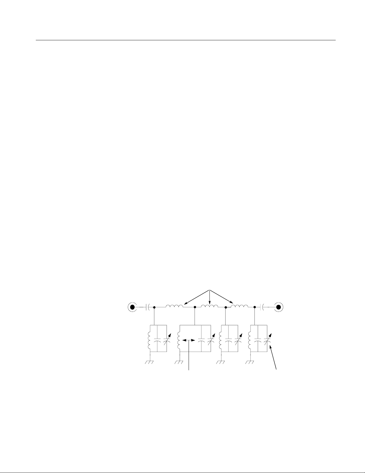
Theory of Operation
1stConverter
Bandpass Filter
The 1st Converter converts the incoming RF signals to the 1st IF. Input signals
are applied through the Step Attenuator and Low Pass Filter and through the 1st
LO Buffer Amplifier.
The 1st Converter receives the RF signal through the Low Pass Filter and a 1st
LO signal from the 1st LO Buffer Amplifier. These signals combine to produce
mixing products that are filtered to yield the 2110 MHz IF signal.
The mixer output is coupled to the input of a balanced amplifier where the signal
is split into two paths. The signals in the two paths are 90 degrees out of phase.
The signals are recombined at the output, yielding a gain of approximately
10 dB. Any reflections to the input are dissipated in a 50 Ω termination. The
output is also terminated in 50 Ω to assure a match at the output port.
The Bandpass Filter (a four cavity filter) is a low loss, narrow band filter that
only passes the 2110 MHz IF signal to the 2nd Converter. Any other frequencies
are reflected back to the 1st Converter and dissipated in the termination. In
addition, the filter prevents the 2nd Converter LO and mixer products from
feeding back into the 1st Converter.
Each end resonator is capacitively coupled to external circuits through a coupling
hat plugged into a 3 mm connector. Inter cavity coupling is provided by coupling
loops that protrude from the machined filter top. The resonant frequency of each
cavity is determined primarily by the depth of a gap in the underside of the filter
top and is fine tuned with a tuning screw on the side of each cavity. When
properly tuned, the filter return loss is >25 dB from either end (in a 50 Ω
system). Figure 3--4 shows the equivalent electrical circuit.
RF Input
Figure 3- 4: Equivalent Circuit for the Bandpass (4 Cavity) Filter
2715 Spectrum Analyzer Service Manual
Cavity 1
Coupling Loops
Cavity 2 Cavity 3 Cavity 4
Cavity L and C
Tuning Screw
3- 11
Page 70

Theory of Operation
RF Mother Board and Phase Locked 2nd LO
This section contains a detailed description of the RF Mother board and Phase
Locked 2nd Local Oscillator.
Overview
RF Mother Board
Block Diagram
The RF Mother board converts the 1st IF frequency to 10 MHz in two frequency
conversions. The first conversion (2nd mixer) mixes the 2.11 GHz 1st IF with
the 2 GHz 2nd LO to create a 110 MHz second IF. The 2 GHz LO is generated
on the board and is phase locked to the 100 MHz crystal reference. The 110 MHz
2nd IF is amplified (with variable gain) and filtered by a 5 MHz bandpass filter.
A portion of the 2nd IF signal is sent to the sweep board for use by the satellite
demodulator. The 3rd conversion mixes the 2nd IF with the 100 MHz reference
to produce the 3rd IF frequency of 10 MHz. This signal is amplified and sent to
the variable resolution module.
This section provides a block diagram description of the RF Mother board as
illustrated in Figure 3--5.
R
2110 MHz IF
100 MHz
I
110 MH z
Sample
L
BPF
PIN
3- 12
R
IL
10 MHz IF
Figure 3- 5: Block Diagram of RF Mother Board
The RF Mother board converts the 1st IF frequency (2.11 GHz) down to
110 MHz by mixing it with a 2 GHz LO. This LO is created by phase locking a
VCO to the 100MHz reference frequency. This reference is provided by the
Reference Oscillator module.
2715 Spectrum Analyzer Service Manual
Page 71

Theory of Operation
The 110 MHz 2nd IF is amplified and divided along two paths. One path is
through a buffer amplifier to the sweep board where the signal is available to the
satellite demodulator. The second path is through a PIN attenuator which sets the
gain of the module. The signal then passes through a second amplifier stage then
a 110 MHz Bandpass filter. This filter has a 3 dB bandwidth of 5 MHz which
sets the widest resolution bandwidth of the instrument. After the 5 MHz filter,
the signal is again amplified and applied to the 3rd converter.
The 3rd IF is created by mixing the 2nd IF with the 100 MHz reference to create
the 3rd IF frequency of 10 MHz. The mixer output is filtered to reduce the 2nd
harmonic level, and then amplified before being applied to the VR module.
Detailed Circuit
Descriptions
This section describes specific elements of the RF Mother board.
2 GHz Phase locked LO. The 2nd local oscillator is formed by Q112 and C204. In
this configuration, the VCO oscillates into a 50 Ω load. The resonator ensures
that this frequency will be close to 2 GHz. The VCO is tuned by varying the
emitter base voltage, which causes that junction to act as a varactor.
A sample of the 2 GHz signal is divided by 4 (U424) and sent to a mixer/phase
detector (U511). The mixer is driven by the 100 MHz reference, so the DC mixer
output is created by the divide-by-4 sample and the 5th harmonic of the
100 MHz reference. This signal is integrated (U444) and connected to the Q112
emitter, closing the loop.
U230A provides a clean --8 V bias to Q223. If the loop is unlocked U230B
causes the control loop to oscillate, sweeping over its full range until lock
occurs. C323 (10F) and related circuitry insures start up by pulling the control
voltage high at turn on.
2nd Mixer. This single balanced mixer is formed by CR223. The 2 GHz 2nd LO
is applied to the diodes through amplifier (Q322), and the 2.11 GHz input and
110 MHz 2nd IF are separated by a filter.
110 MHz Amplifiers. These IF amplifiers consist of common emitter transistors
(Q130, Q140, and Q150) with both series and parallel feedback. The 1:1 transformers (T130, T140, and T150) provide lower output impedance for better
intermodulation distortion performance.
PIN Attenuator. CR369 and CR367 are PIN diodes and are used to adjust the gain
of the module. PIN diodes behave like resistors at RF frequencies, with the value
being dependent on current flowing in the diode. (High current, low resistance;
low current, high resistance). Current through CR369 decreases attenuation and
current through CR367 increases attenuation. R200 adjusts the current through
the PIN diodes and has a range of approximately 15dB attenuation.
2715 Spectrum Analyzer Service Manual
3- 13
Page 72
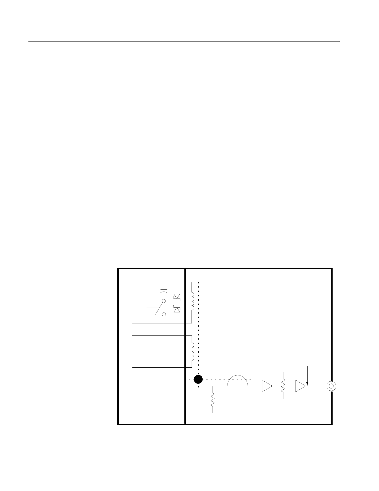
Theory of Operation
110 MHz Bandpass Filter. This filter is a 5th order, shunt resonator Butterworth
filter.
3rd Mixer. U665 and its associated circuitry make up the 3rd mixer.
Output Amplifier. This IF amplifier consists of a common emitter transistor
(Q670) with both series and parallel feedback. The 1:1 transformer (T670)
provides lower output impedance for better intermodulation distortion performance. The resistive attenuator at the output is used to match the load to the
variable resolution. It also provides some high frequency roll off.
1stLO Interface, 1stLO, and 1stLO Buffer Amplifier
This section contains a detailed description of the 1st LO Interface, 1st LO and
1st Buffer Amplifier.
1stLO Interface
st
and 1
LO
The 1st LO has a tuning range of 2.11 to 3.91 GHz (2.11 to 4.26 GHz for Option
50 and 75). The oscillator assembly includes the interface circuit board that
couples operating and tuning voltages from the Center Frequency Control board.
Two Zener diodes on the Interface board clamp transient voltages from the main
coil. See Figure 3--6.
1st LO1st LO Interface
+Main
SWP Main
−Main
+FM
1st LO Out to 1st LO
−FM
YIG Sphere
Buffer Amplifier
3- 14
−V
Figure 3- 6: 1st LO Interface and 1st LO Diagram
2715 Spectrum Analyzer Service Manual
Page 73

Theory of Operation
When the FM coil is used to sweep the oscillator, the relay on the Interface board
closes and couples a large capacitor (two capacitors in parallel) across the main
coil. The capacitors lower the noise bandwidth of the main coil driving circuit
while the FM coil is in operation. The heater provides temperature stability.
The rest of the circuitry on the Interface board provides operating voltages for
the two amplifiers in the 1st LO assembly.
The output of the 1st LO drives the 1st LO Buffer Amplifier.
1stLO Buffer Amplifier
1st LO In
The 1st LO Buffer Amplifier consists of the following:
H Automatic Level Controlled (ALC) Amplifier
H Strobe Driver
H Sampling Gate
ALC Amplifier. The A LC Amplifier is composed of a wide band amplifier with
impedance matching transmission lines at the input and output, a directional
coupler, a detector, a level comparator, and active bias. See Figure 3--7.
Detector
-- V R E F
1st LO Out
ALC Amplifier
Terminator
replaced by
semi-rigid cable
when Option 15
is installed
Reserved for Options
STROBE from Center
Frequency Control Board
(25.7325 MHz to 26.05 MHz)
Figure 3- 7: 1st LO Buffer Amplifier Diagram
2715 Spectrum Analyzer Service Manual
Strobe Driver
Beat Note to Phase
Lock CFC Module
Sampling
Gate
3- 15
Page 74

Theory of Operation
The directional coupler couples approximately --15 dBm of the amplified LO
signal to the detector. The coupled signal is then amplitude detected, and the
resultant DC level fed to the noninverting input of a comparator, where it is
compared to a reference DC level. (The reference DC level is connected to the
inverting input.) The output of the comparator then controls the active bias
tending to hold the amplifier’s output at a constant level.
Strobe Driver. A Strobe signal from the Center Frequency Control assembly is
coupled to the Strobe Driver. The Strobe Driver is a transformer coupled gain
stage. The Strobe Driver’s output is coupled to the Sampling Gate.
Sampling Gate. A power divider at the input of the amplifier routes 50% of the
1st LO’s output to another power divider. One port of the second divider is
reserved for Option 15 and is terminated in 50 Ω. The other port is coupled to the
Sampling Gate.
If the output frequency of the 1st LO were stable, LO sampling would occur at
the same level since the rate at which the LO output is sampled is constant.
However, the LO output has a tendency to drift slightly under certain conditions,
such as unstable ambient temperature. Consequently, sampling occurs at different
levels, resulting in a beat note. Thus, the BEAT NOTE signal is a measure of the
1st LO’s drift.
Reference Oscillator
The output of the Sampling Gate is routed to the Phase Lock Center Frequency
Control (PLCFC) module.
The Reference Oscillator board provides a 100 MHz frequency reference and
amplitude reference for the Spectrum Analyzer. The frequency reference enables
the high counter accuracy.
Firmware based routines use the Amplitude Calibrator output as a reference for
calibrating internal gain settings.
The Reference Oscillator consists of the following blocks of circuitry:
H Power Supply Regulation
H Heater
H Oscillator
H Distribution
H Amplitude Calibrator
3- 16
H Microprocessor Interface
2715 Spectrum Analyzer Service Manual
Page 75
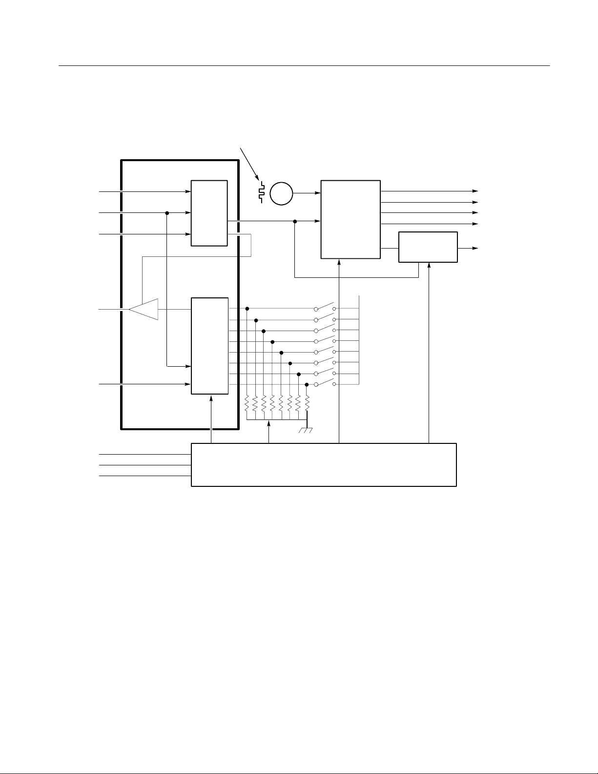
Theory of Operation
Figure 3--8 is a block diagram of the Reference Oscillator section.
Heater
DATA0
RFLATCH
CLK0
DATAI
CLKI
Microprocessor
Interface
Output
Buffer
>
Input
Buffer
Output
Buffer
100 MHz
Oscillator
~
CAL Enable
Distribution
CAL Enable
+5 V
Amplitude
Calibrator
RF
UP
CFC
Spare
100 MHz
@--22 dBm
+10 V
+5 V
−11 V
Figure 3- 8: Reference Oscillator Diagram
Power Supply Regulation. The Oscillator and the Amplitude Calibrator are
furnished with stringent, on board, power supply regulation to minimize power
supply ripple. Otherwise, both the Oscillator and the Amplitude Calibrator
would produce FM sidebands proportional to power supply ripple amplitude and
frequency.
Crystal Heater. The Crystal Heater maintains the oscillator crystal’s case
temperature within a 3° window of the crystal’s operating temperature (near
70° C) over the instrument’s operating temperature range. The crystal leads sink
heat such that the crystal inside the case operates at temperatures below the case
temperature.
Power Supply Regulation
2715 Spectrum Analyzer Service Manual
3- 17
Page 76

Theory of Operation
The heater circuit maintains a constant 15 V potential across the heater element
regardless of power supply ripple. The circuit is shown in Figure 3--9.
+5 V
10 kΩ
22.1 kΩ
−11 V
10 kΩ
+
−
22.1 kΩ
27.4 kΩ
6.91 kΩ
−11 V
+
−
10 kΩ
1kΩ
+5.2 V
2.5 Ω
Heater
-- 1 1 V
Figure 3- 9: Crystal Heat er and 15 V Regulation Circuit
Oscillator. The oscillator generates the 100 MHz reference frequency that is used
by the instrument firmware to enhance frequency accuracy. Figure 3--10 shows
the AC equivalent for the oscillator. At resonance, the tank inductor and
capacitor Lt and Ct exhibit an open circuit condition, and the LC equivalent of
the crystal (Lm and Cm) exhibit a short circuit condition. Thus, at resonance, the
open loop gain is calculated as:
3- 18
R
A =
(re1+ re2+ rs)
t
This gain must be greater than unity to ensure oscillation.
2715 Spectrum Analyzer Service Manual
Page 77
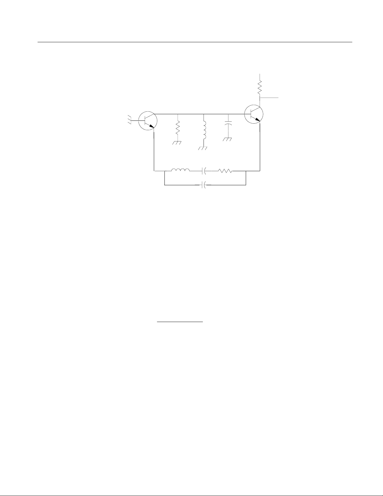
Q1
re1≈ 8.3Ω
R
t
82.5 Ω
Theory of Operation
+5 V
221 Ω
Q2
C
t
L
t
re2=5.7Ω
L
m
C
rs=50Ω
m
C
p
Figure 3- 10: Oscillator AC Equivalent
At oscillation, the loop gain is unity and the phase 0°. If the phase delay of Q1,
Q2, or the tank changes, the operating frequency must also change to maintain a 0°
loop phase shift. Because of this phase/frequency shift dependency, the Q of the
parallel tank circuit is made as low as possible to minimize the tank phase change
as the values of Lt and Ct drift.
The component values of the tank circuit are determined by the voltage swing at
the collector of Q2 (Figure 3--11). The collector of Q2 drives an ECL line receiver.
Therefore, the collector voltage should swing 1 V peak to peak about 3.8 VDC
(3.8 V being the ECL Vbb bias voltage). The gain of Q2 is calculated as:
R
A =
(re1+ re2+ rs)
t
= 3
2715 Spectrum Analyzer Service Manual
3- 19
Page 78

Theory of Operation
0.1 f
−8.8 V
3.92 kΩ
47.5 Ω
3.92 kΩ
Q1
1kΩ
r
≈ 8.3 Ω
e1
R
t
82.5Ω
20 nH
rs<50 Ω
47.5 Ω
82 pf
r
e2
+5 V
≈ 5.7 Ω
Q2
1.5 kΩ
−8.8 V
−8.8 V
Figure 3- 11: Oscillator DC Equivalent
The voltage swing required across the tank circuit must be at least equal to the
ratio of 1 V to the calculated gain, which is 0.3 V. If the bias current available in
Q1 is 3.6 mA, then the tank resistance required is calculated to be:
0.3 V
3.6 mA
= 83 Ω
Distribution. The distribution circuit represents an ECL line receiver. This circuit
receives the 100 MHz signal from the Oscillator and steers it to the following
circuits at --4 dBm.
H RF Mother Board (2nd and 3rd LOs)
H Microprocessor (Counter Section)
H CFC Board (1st LO Phase Lock)
H Port reserved for future option
3- 20
H Amplitude Calibrator on the Reference Oscillator board
Amplitude Calibrator. The Amplitude Calibrator receives a 100 MHz signal from
the distribution circuit. The level of the 100 MHz signal is adjusted, and the
resultant calibrator signal is then routed to a switch on the Step Attenuator board.
When enabled by the Microprocessor, a differential pair of transistors switch a
carefully controlled current on and off across a 56.2 Ω resistor. The resulting
signal, with a --22 dBm level, is routed to the calibrator port through an 8 dB
pad.
2715 Spectrum Analyzer Service Manual
Page 79

Theory of Operation
Microprocessor Interface. The Microprocessor Interface is used by the Microprocessor board to communicate with the Reference Oscillator board. An 8 bit input
shift register controls the operation of the board, and an 8 bit output shift register
contains frequency correction bits for indicating the Oscillator frequency. The
microprocessor clocks (CLKO) eight bits of serial data (DATAO) into the input
serial register, and it then latches the serial contents (RFLATCH--) to the parallel
outputs. The microprocessor clocks data out of the output register by setting bit 7
of the input register low to enable the Buffer (see Figure 3--8 on page 3--17) and
using CLKI-- to clock serial DATAI out. Refer to Table 3--1 for the bit mapping
of the registers.
Bit 0 of the input register is the last bit to leave the microprocessor, and bit 0 of
the output register is the last bit to reach the microprocessor.
Bit 0 of the input register enables the calibrator signal when high and disables it
when low. Bit 7 of the input register allows the microprocessor to read the
contents of the output register when set low, and it tristates the output buffer
when set high.
Table 3- 1: Input and Output Bit Definition
Input Register Output Register
Bit Function Bit Function
0 Cal Enable 0 CB0 1
1 None 1 CB1 2
2 None 2 CB2 4
3 None 3 CB3 8
4 None 4 CB4 16
5 None 5 CB5 32
6 None 6 CB6 64
7 Output Enable 7 CB7 128
The output register has 8 bits available to represent the Oscillator frequency. The
microprocessor can then read the Oscillator frequency through these bits to
within 10 Hz. The possible values are 1 through 254. The microprocessor
interprets a value of 128 as a frequency of 100 MHz, 127 as 99,999,990 Hz, 129
as 100,000,010 Hz, and so forth.
Values 0 (all bits low) and 255 (all bits high) are used to send a hardware failure
message to the microprocessor.
Phase Lock Assembly (Center Frequency Control System)
There are three major operating areas of the frequency control system:
2715 Spectrum Analyzer Service Manual
3- 21
Page 80

Theory of Operation
In wide spans (5.1 MHz/div or greater), the center frequency is set coarsely by
setting a suitable bias current in the main coil. Fine increments of the center
frequency are set by appropriate currents to the FM coil. In this mode, sweeping
over the span is accomplished by summing a suitably scaled analog sweep signal
with the drive to the main coil. The strobe signal is not even turned on except
briefly when needed to assist in verifying the exact 1st LO frequency by
counting the beat frequency.
In moderate spans (50 kHz/div through 5 MHz/div), sweeping is done by
summing the scaled sweep signal with the drive to the FM coil. Additionally, a
noise suppressing low pass filter is inserted into the main coil circuit to reduce
residual FM and phase noise due to noise from the main coil driver. Otherwise,
the setup is the same as for wide spans. In this mode, the strobe is unused except
when counting the 1st LO frequency.
When operating in narrow spans (20 kHz/div and less), the 1st LO is phase
locked to a harmonic of the strobe frequency. Coarse control of the center
frequency is effected by choosing which harmonic of the strobe frequency is
used (by setting an appropriate main coil current before commanding the
hardware to lock). Sweeping and fine control of center frequency are done by
controlling the strobe frequency. When phase locked, the FM coil is used by the
loop to adjust the 1st LO to zero phase error.
Power Supply Regulation
PLCFC Module Functional Blocks. The Phase Lock Center Frequency Control
(PLCFC) module circuitry can be grouped into the following functional areas:
H Power Supply Regulation
H 1st LO Coil Drivers for the Current Source
H Strobe Frequency Generator (VCO Module)
H 1st Phase Lock Loop and Beat Note Processor
H Signal Path and Switching Summary
H Digital to Analog Conversion
H Digital Interface
There are six regulated supplies on the PLCFC circuit board and two additional
regulators in the VCO module.
- 5 V Reference Supply (- 5 VREF). This is a precision reference supply for those
circuit applications where a critical frequency is directly dependent on a voltage
or current.
3- 22
2715 Spectrum Analyzer Service Manual
Page 81

Theory of Operation
This supply consists of VR160, U166, U174, Q170, Q674, and associated
components. VR160 is a temperature compensated reference diode that defines
the output voltage. U166 and Q170 constitute a buffered scaling amplifier to
provide the desired --5 V output at sufficient current. C660 makes the closed loop
bandwidth very low to minimize noise from the reference diode on the output.
U174 and Q674 convert --5 V to +10 V to provide stable low noise current to the
reference diode through R171. The +8.5 V path through CR175 is used to
guarantee start up of the supply. CR175 disconnects the potentially noisy start up
source once the emitter of Q674 goes sufficiently positive.
- 5 V Supply. This supply is not to be confused with the --5 V Reference Supply.
This supply is regulated by U470 and serves solely as a reference for the
remaining four supplies on the board. U470 is a programmable shunt regulator
whose output voltage is defined by an internal reference and by R472 and R473.
+8.5 V Supply. U282A and Q781 constitute a buffered operational amplifier used
in the inverting configuration to provide +8.5 V from an input of --5 V. (Note that
Q781 provides a phase inversion, so the polarities of the operational amplifier IC
input pins have to be reversed from the usual practice.)
1stLO Coil Drivers
Current Source
+15 V Supply. U380B and Q880 operate in the same fashion as the corresponding
parts in the +8.5 V regulator.
- 8.5 V Supply. U282B and Q780 serve as a buffered operational amplifier in the
non inverting configuration to provide --8.5 V.
+5 V Supply. U380A and Q881 serve as a buffered operational amplifier used in
an inverting configuration to provide +5 V. (Note that Q881 is used in noninverting fashion, so that the normal polarities of the operational amplifier IC
terminals apply here.)
The regulators in the VCO module will be discussed later in this section on
page 3--25.
It is desirable to drive the 1st LO coils from high impedance sources so that
temperature dependent changes in winding resistance have negligible effect on
stability.
Main Coil Driver. U921 and Q521 constitute a buffered operational amplifier used
in an inverting configuration. Inputs to the summing junction are from a number
of sources and all pass through Q920. R900 (a current sense resistor in the return
lead of the main coil) develops a voltage proportional to main coil current.
2715 Spectrum Analyzer Service Manual
3- 23
Page 82

Theory of Operation
This voltage across R926 defines the feedback current to the summing junction
of the operational amplifier. This circuit forces 1st LO main coil current to be
proportional to the sum of the currents from the various control sources, which is
described later. The normal operating current range of the main coil is from
approximately 135 mA to 255 mA.
Q920 is a switch that is normally conducting and consequently has no significant
impact on circuit operation as described. However, it is sometimes necessary to
momentarily set the main coil current to zero in order to standardize frequency
errors due to hysteresis in the 1st LO magnetic structure. When this is desired,
the microprocessor asserts the DEGAUSS line HIGH (by way of the digital
interface circuits), which causes Q931 and Q930 to pull the gate of Q920 to
--8.5 V. This opens the switch, disconnecting the normal input and feedback
paths of the circuit. R929 provides a slight negative feedback in this situation,
ensuring that the main coil current goes to zero instead of to some undefined
value.
The main coil current is the sum of at least two items. First, there is a large fixed
bias current stemming from the reference supply and R923 (trimmed by R931
and U920) to set the 1st LO at 3.01 GHz in the absence of other inputs. Second,
there is a current induced by DAC U950A (and subsequent circuits), which is
used to steer the 1st LO over the range from 2.11 to 3.91 GHz (2.11 to 4.26 GHz
for Option 50 and Option 75). This current is normally a steady state value
selected by the microprocessor to coarsely set the center frequency. Third, if the
instrument is set to a span greater than 5 MHz/div, there is a sawtooth sweep
waveform summed into the main coil current through switch U830A. This
corresponds to the wide span operating mode discussed earlier in the Block
Diagram description.
3- 24
FM Coil Driver. U811 and U810 together form a buffered operational amplifier
used in the inverting configuration. Input currents to the summing junction come
from a variety of sources, to be described later. R905 is the current sense resistor
for the FM coil. The voltage developed across it results in the current fed back to
the summing junction through R815. Thus, this circuit forces a current through
the FM coil proportional to the sum of the various control currents put into the
summing junction. The normal current range for the FM coil is from approximately --120 mA to +120 mA.
Q910 and Q911 serve as a low resistance switch. When closed (gates held
several volts positive), the FM coil driver operates as described above. When
open (gates held several volts negative), the driver is disconnected and the FM
coil gets its current from R714, which is the situation when the instrument is
phase locked. Control of the switch state is through Q703 and Q800 from the
signal PLLCON--. This signal is LOW when the instrument is phase locked.
Several other switches are also controlled by the same command. R812 keeps
U811 out of saturation when the switch is open.
2715 Spectrum Analyzer Service Manual
Page 83

Theory of Operation
When the FM coil driver is in use (instrument not phase locked) there are two
potential signal sources summed into the driver circuit. One that is always
present is induced by DAC U850A and subsequent circuits. It is steered into
U821 by switch U757A, and serves to finely set the center frequency. The other
is selected only in moderate spans. It is the sawtooth sweep waveform used to
sweep the 1st LO over spans ranging from 50 kHz/div through 5 MHz/div.
Strobe Frequency
Generator (VCO Module)
Functionally, this module is a voltage controlled frequency source. It has an
output frequency range from 25.73 MHz through 26.05 MHz in response to a
tuning voltage range of approximately 4 V to 12.5 V. There is also a switch to
select which of two signals is counted by the microprocessor, and there are
means to turn off the output.
The strobe frequency comes from a VCO that ranges from 102.9 MHz through
104.2 MHz and whose output frequency is divided by four to yield the desired
strobe frequency. Its frequency is controlled by phase locking it (with a 100 MHz
offset) to 1/4 the frequency of a free running VCO (the LFVCO) that operates
over a frequency range of 11.68 MHz through 16.84 MHz. It is this LFVCO that
is actually tuned by the incoming tuning voltage referred to earlier, and this
phase locked loop within the VCO module is called the inner loop. The strobe
signal is generated in this manner in order to control close in phase noise and to
provide a countable signal (the LFVCO output) whose frequency is not
condensed into a very narrow range that would require long times to count to
adequate resolution.
The LFVCO consists of Q426, T430, varactors CR532 and CR540, and
associated components. Output (from the collector of Q422) is made available
for external counting through selector switch U240. The LFVCO output
frequency is also divided by four through U410, and the result is the reference
frequency for the inner loop. U512 and U510 serve as a phase/frequency detector
for the inner loop. The differential output of the phase detector is passed through
error amplifier U435 and becomes the tuning voltage for the HFVCO.
The HFVCO consists of Q522, L610, varactor CR511, trim capacitor C611, and
associated parts. Output is taken from a tap on L610, then split through a pair of
isolation amplifiers (Q400 and Q410 plus Q316). Output from Q400 is divided
by four in U300, providing the useful strobe frequency output of the module.
HFVCO output from Q316 is applied to one input of mixer U320, whose other
input is supplied with 100 MHz energy from the Reference Oscillator. The useful
output of the mixer is the difference frequency between the HFVCO (for
example, 103 MHz) and the 100 MHz reference, or 3 MHz. This signal is
amplified (by Q310, Q312, and so forth.) and applied to the remaining input of
the phase/frequency detector, thus closing the inner loop.
U240 serves two functions; both controlled by the logic signals CNTSELA and
CNTSELB. First, it allows turning the HFVCO on or off by means of Q425.
When the oscillator is turned off, Q101 is turned on at the same time to shut
2715 Spectrum Analyzer Service Manual
3- 25
Page 84

Theory of Operation
down the strobe driver amplifier in the 1st LO BUFFER module.
Also, U240 serves as a count selector switch. It selects either the LFVCO signal
or the 1st LO beat signal (from the PLCFC board) for counting by the microprocessor. R241 is part of a TTL to ECL level shifter, the remainder of which is
located on the microprocessor board.
U510B provides a lock status indicator for the inner loop so that a lock failure
can interrupt the microprocessor through circuitry on the PLCFC board.
The HFVCO receives supplementary power supply regulation by means of
U122.
The LFVCO receives supplementary power supply regulation by means of U123,
Q223, and associated parts.
1stLO Phase Lock Loop
(Outer Loop) and Beat
Note Processor
The output of the phase gate in the 1st LO Buffer module may either be a beat
note (when loop is unlocked) or a phase error voltage for maintenance of lock.
Thus, the output of the phase gate is split into two paths.
Beat signals in the range of approximately 3 kHz through 11 MHz are passed
through a chain including U614, a low pass filter, U723, and U720. They drive a
Schmitt trigger circuit (Q630 through Q633), which produces a clean rectangular
wave at TTL levels. The desired beat note, noise, and one or more weak,
extraneous beat notes arising from 1st LO harmonics mixing with other
harmonics of the strobe frequency, will normally be within the pass band of the
low pass filter. The level control, R620, sets the overall signal level so that only
the desired beat note is strong enough to overcome the hysteresis designed into
the Schmitt trigger. The Schmitt trigger output may be routed to the microprocessor through a selector switch on the VCO module.
Phase error information from DC through a few hundred kHz is passed through
U606 and switch U700D (when phase lock is invoked) to error amplifier U713.
The output of U713 is applied to the FM coil through R714. When phase lock is
invoked by setting PLLCON to high, U700D is closed and U700C is opened,
closing the outer loop. Nominally, the loop bandwidth is set to 20 kHz. It may
vary considerably from this value due to frequency dependent variations in the
output level and slope of the phase gate. R709 provides for a known drift
direction of the 1st LO tuning when the loop is first closed, but the initial
frequency is away from lock. The instrument firmware purposely sets up a
significant frequency offset in the direction that allows the loop to drift into lock,
as a way of dealing with uncertainties in starting conditions.
3- 26
The outer loop has a holding range of approximately ±2.5 MHz before U713
saturates. U650A and U650B form a window comparator that generates logic
signals (either INCR MAIN or DCR MAIN) when the loop approaches a range
limit so that the microprocessor can take corrective action (for example,
changing the main coil current in the appropriate direction to recenter the loop).
2715 Spectrum Analyzer Service Manual
Page 85

Theory of Operation
This allows for 1st LO drift or user changes to the center frequency setting
without having to drop and reacquire lock for every change.
If Q652 is turned on by the signal UNLKIND (signifying that the inner loop is
unlocked), both INCR MAIN and DCR MAIN are turned on simultaneously.
This is a unique condition that the microprocessor interprets as a hardware
failure in the VCO module.
Summary of Outer Loop Lock Acquisition. When the instrument is placed into a
situation calling for phase lock operation, several things are done by the
firmware to arrange for a lock at the correct frequency.
The N number (that is, the harmonic order of the strobe to which the 1st LO will
lock) is calculated, and the strobe and corresponding VCO frequencies needed
are calculated. The sweep is disconnected, the FM coil DAC is set to mid range
(FM coil current to nominal zero), and the main coil DAC is set to the value that
will place the 1st LO as close as possible to the desired 1st LO frequency (it can
be several hundred kHz off because of the coarseness of the main coil DAC
steps). Now the VCO is tuned by trial and error so that the strobe line, at a
frequency of N X F
strobe, is approximately 100 kHz above the actual 1st LO
frequency (that is, the measured beat frequency is 100 kHz on the correct side of
zero beat). Then, lock is invoked by setting PLLCON high. Due to the intentional offset provided by R709, the 1st LO drifts rapidly into lock. After a suitable
delay, acquisition of lock is verified by checking the states of both lock limit
comparators and by checking that the beat frequency is zero.
Signal Path and Switching
Summary
At this point the loop is locked, but in the wrong spot. Now the microprocessor
proceeds to tune the VCO (and consequently, the strobe and 1st LO) to the
correct frequency by repeatedly tuning and counting the VCO. The sweep is then
switched into the VCO tuning voltage, and the instrument is now scanning the
desired spectrum range.
Wide Span Operation (5.1 MHz/div and Higher Spans). TheMaincoilisdrivenbya
fixed bias summed with DAC U950A output and a sweep signal (routed through
U830A).
The FM coil is driven with VCFC FM arising from DAC U850A only (routed
through U757A). Current is routed through Q910 and Q911 to the FM coil. See
Figure 3--12.
2715 Spectrum Analyzer Service Manual
3- 27
Page 86

Theory of Operation
Analog Sweep In
VOFS
Summing
and Fixed
Scaling
Summing
and Fixed
Scaling
Summing
and Fixed
Scaling
VOFS
Main Coil
Driver
FM Coil
Driver
MAIN
FM
FSTROBE
1st LO
Harm GenVCO Module
1st LO to 1st Converter
1st LO
Phase Gate
1st LO Beat to
Counter
Serial In
Serial Out
Microprocessor
DIG
DIG
DIG
DIG
SWP
DAC
Main
DAC
FM
DAC
PLL
DAC
Decade
Atten
DIG
VREF
Figure 3- 12: Phase Lock Center Frequency Control Configuration for Wide Spans (Unlocked, Sweep Main Coil)
The VCO is not used except intermittently for frequency corrections, and it is
tuned by a fixed bias summed with VCFCU arising from DAC U950B.
Moderate Span Operation (50 kHz/div through 5 MHz/div Span). The Main coil is
driven by a fixed bias plus a DAC output (U950A).
The FM coil is driven with VCFC FM arising from DAC U850A (routed
through U757A) summed with the sweep signal (routed through U830B). Total
current is routed through Q910 and Q911 to FM coil. See Figure 3--13.
3- 28
2715 Spectrum Analyzer Service Manual
Page 87
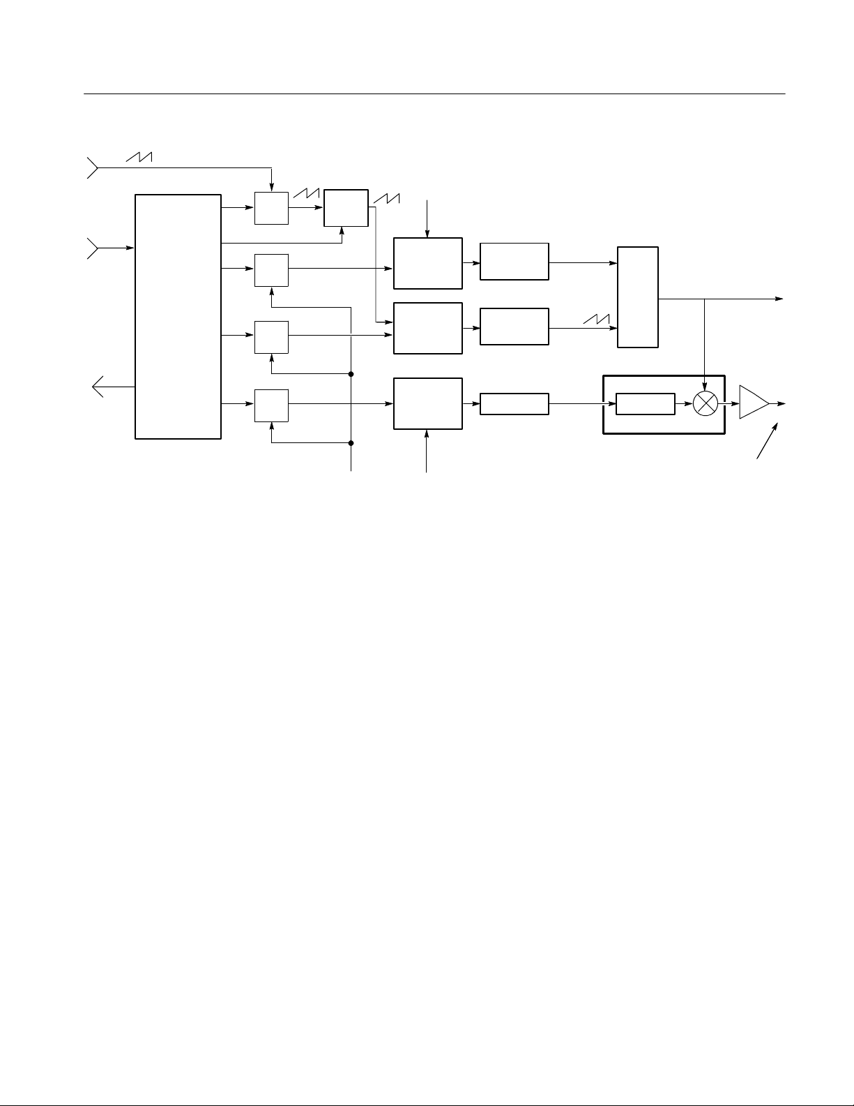
Analog Sweep In
Theory of Operation
VOFS
Summing
and Fixed
Scaling
Summing
and Fixed
Scaling
Summing
and Fixed
Scaling
VOFS
Main Coil
Driver
FM Coil
Driver
MAIN
FM
FSTROBE
1st LO
Harm GenVCO Module
1st LO to 1st Converter
1st LO
Phase Gate
1st LO Beat to
Counter
Serial In
Serial Out
Microprocessor
DIG
DIG
DIG
DIG
SWP
DAC
Main
DAC
FM
DAC
PLL
DAC
Decade
Atten
DIG
VREF
Figure 3- 13: Phase Lock Center Frequency Control Configuration for Moderate Spans (Unlocked, Sweep FM Coil)
The VCO is not used except intermittently for frequency corrections and is tuned
by a fixed bias summed with VCFCU arising from DAC U950B.
Narrow Span Operation (20 kHz/div and Smaller Spans). The instrument is phase
locked.
The Main coil is driven with a fixed bias summed with DAC U950A output. See
Figure 3--14.
2715 Spectrum Analyzer Service Manual
3- 29
Page 88

Theory of Operation
Analog Sweep In
VREF
Summing
and Fixed
Scaling
Summing
and Fixed
Scaling
VREF
Main Coil
Driver
VCO Module
(Strobe Gen)
Lock Limits
Comparator
Main
FM
FSTROBE
1st LO
Harm Gen
Phase Gate
Error Amp &
Loop Filter
1st LO to 1st Converter
N-F Strobe
1st LO
Serial In
Serial Out
Microprocessor
DIG
DIG
DIG
DIG
SWP
DAC
Main
DAC
FM
DAC
PLL
DAC
Decade
Atten
DIG
VREF
Figure 3- 14: Phase Lock Center Frequency Control Configuration for Narrow Spans (Locked, Sweep VCO)
The FM coil is driven with the output of the phase lock error amplifier, U713,
only.
1st LO Beat to
Counter for Lock
Verification
Phase
Error
Voltage
Digital to Analog
Conversion
The VCO is active continuously and is tuned by a fixed bias summed with
VCFCU from DAC U950B, VCFC L from DAC U850A (routed through
U757D), and sweep voltage VSWP PLL (routed through U757B).
The PLCFC board has four 12 bit DACs in two IC packages, U850 and U950.
On the digital side, each package has four data lines, three address lines, and two
control lines. The DACs contain internal registers for the 12 bit words associated
with each analog output and, therefore, the microprocessor must write multiple
4 bit words to a package in order to set up a new output.
These are multiplying DACs. Each delivers an output current that is the product
of an analog voltage (called the reference) and the 12 bit digital word. These
units can correctly deal with either polarity of reference voltage. Three of them
(U850A, U950A, and U950B) are supplied fixed reference voltages and serve
simply as computer controlled DC sources.
DAC U850A is called the FM DAC but serves two roles. In non phase locked
spans, its output ultimately ends up fine tuning the 1st LO center frequency
through the FM coil.
3- 30
2715 Spectrum Analyzer Service Manual
Page 89

Theory of Operation
In phase locked spans, its output is used to fine tune the VCO frequency. In
either case its output passes through U852, which has an output range of 0 to
+5 V. U845 sums that with an offset and provides gain so that the output of U845
ranges from --5 V to +5 V. This signal is called VCFC (L/FM) and is routed to
the appropriate destination by U757A and U757D.
Main Coil DAC U950A output passes through U952 and U940. U940 provides
gain such that the output of U845 ranges from --5 V to +5 V, and the result is
summed with the other components of the main coil current. Its function is
coarse tuning of the 1st LO center frequency, in steps of approximately 400 kHz.
U950B is the PLL DAC. Its function is coarse tuning of the VCO frequency. Its
output is converted to the --5 V to +5 V range by U954 and U941 before being
summed with the other components of the VCO tune voltage.
Unlike the other DACs, U850B’s reference input is supplied with the analog
sweep waveform SWP (from the Sweep board through U565) and serves as a
microprocessor controlled gain control to determine span/div. Its output passes
through U854 to a decade attenuator composed of U831 and associated
components. The output of the decade attenuator is then routed to the desired
destination by switches U830A, U830B, and U757B. In wide spans, this signal
sweeps the 1st LO main coil. In moderate spans, it sweeps the 1st LO FM coil.
In phase locked spans, it is used to sweep the VCO frequency.
Digital Interface
This circuitry links the phase lock hardware with the microprocessor. The link is
bidirectional. Commands and DAC setting data are sent to the PLCFC module,
and lock status information is sent back to the microprocessor. In addition, there
is provision to loop input data back to the microprocessor to verify integrity of
the interface circuitry .
The path into the PLCFC module is through a 24 bit shift register composed of
U361, U460, and U560. Serial data on the DATAO line is shifted into the
register by the clock signal CLKO. When all 24 bits have been shifted in,
CFLATCH-- is used to latch data simultaneously from all shift register stages to
parallel output registers. The resulting 24 bit parallel word is used to control
switches, set DACs, and do a number of other things on the module. A listing of
the 24 lines and their functions appears later in Table 3--22 on page 3--71.
CFCLATCH-- also triggers U372 causing a delayed pulse on the WR-- line,
latching data into internal registers of the DACs.
U370 is an 8 bit shift register used for transferring data from the module back to
the microprocessor. Serial data is shifted out on the DATAI line by the clock
CLKI--, which is gated into the clock input of the register by U270C as
controlled by CFCACK--. Data may be serially loaded into this register through
the EXAM line coming from the tail end of the 24 bit input register. In this
situation the data is clocked into the register by a derivative of CLKO, which is
gated by LOADEXM through U270D.
2715 Spectrum Analyzer Service Manual
3- 31
Page 90

Theory of Operation
This is the loop back path referred to earlier for checking the interface. This
register may also be loaded with up to eight bits of parallel data for subsequent
serial transfer to the microprocessor. Only three bits are used. Bits 7 and 8 are the
signals (INCR MAIN and DCR MAIN) from the lock limits comparator, and bit
5 is wired to logic 1 as a board identity.
The gating of CLKI-- and CLKO into the output shift register (by CFCACK-and LOADEXM, respectively) is partly a matter of source selection and is also
necessary because both clock signals are used by other boards in the system at
some times.
Any transition on either INCR MAIN or DCR MAIN (or both) will load the new
states of those lines into the output shift register. (The various sections of U360
serve as edge detectors to generate the load command to the shift register.)
Further, if LKINTEN is high at the time, U471B will end up SET, interrupting
the microprocessor by way of CFCREQ--. The line READEXM provides a direct
method of setting the interrupt, if desired. Any transition on LKINTEN will also
cause the shift register to be loaded, providing a forced means for checking the
status of the lock lines at any time. The microprocessor uses CFCACK-- to clear
U471 of the interrupt (in addition to the gating function mentioned above).
Summary of Digital
Control Lines on Phase
Lock Center Frequency
Control Module
READEXM. Low to high transition forces CFC interrupt.
LOADEXM. High level gates CLKO into output shift register clock input.
DEGAUSS. High level forces 1st LO main coil current to zero.
CNTSELA and CNTSELB. These signals are decoded to set state of selector
switch in VCO module. Both high is strobe OFF. CNTSELA high and
CNTSELB low is count VCO. CNTSELA low and CNTS ELB high is count beat
frequency. Both low is strobe ON but no count selected.
PLLCON. High level commands phase lock configuration.
LKINTEN. High level enables interrupt on transition of either lock limit
comparator line.
CAPCON. High level connects noise reduction capacitor across 1st LO main
coil.
SWDECA. A and B are decoded to select setting of sweep decade attenuator .
Both low is straight through. A high and B low is divide by 10. A low and B
high is divide by 100. Both high is disconnect sweep.
SWSELA. A and B are decoded in U274 to operate switches that direct sweep
waveform to proper destination.
3- 32
SWSELB. Both low is sweep main coil. A high and B low is sweep FM coil. A
low and B high is sweep VCO. Both high is no sweep.
2715 Spectrum Analyzer Service Manual
Page 91

A0, A1, and A2. Address lines for DAC internal register selection and control.
UPD. Used for simultaneous transfer to DAC output registers.
DB0’,dB1’,dB2’, and dB3’. Data lines for DAC U950 (A and B).
DB0, dB1, dB2, and dB3. Data lines for DAC U850 (A and B).
Variable Resolution Module
This section contains a detailed description of the Variable Resolution module.
Theory of Operation
Input Amplifier
The input amplifier used is a transformer feedback stage that provides approximately 12 dB of gain with 10 dB of reverse isolation. See Figure 3--15. The
match at each port with the other terminated is better than 15 dB at 10 MHz. The
noise figure is less than 3 dB and, with 12 mA flowing in the device, the output
intercept is approximately +30 dBm. The match at each port is highly sensitive
to a proper termination being presented to the other port.
2715 Spectrum Analyzer Service Manual
3- 33
Page 92

Theory of Operation
10 MHz/−20 dBm from RF Mother Board
10
RF OPTIONS
1 MHz, 100 kHz, 10 kHz, 1 kHz,
and 300 Hz Filters
10
1010
1dBStep
PIN Diode
Attenuator
10
10
10 MHz/−10 dBm
to Log Amp
5MHz
0
300 kHz
2
30 kHz
4
6
8
3kHz
Figure 3- 15: Variable Resolution Module Diagram
PIN Attenuator
The PIN attenuator design is based upon a pair of matched pin diodes used in a
tee configuration. This configuration maintains the impedance match at each end,
providing the product of the PIN diode resistances is equal to the square of the
end terminations. This can be approximated if the sum of the currents in the PIN
diodes is equal to a constant. The DAC has complementary current outputs
whose total is set by an adjustment. The attenuation range is approximately
12 dB with a 1 dB minimum loss. The worst case return loss at the end points is
15 dB. The step size for an 8 bit DAC is 0.04 dB steps in the center of its range.
3- 34
2715 Spectrum Analyzer Service Manual
Page 93

Theory of Operation
10 dB Gain Step Amplifier
1 dB Gain Step Amplifier
Routing Switches
The 10 dB gain step stages incorporate a transformer feedback amplifier. These
stages have approximately 0.5 dB of loss or 9.5 dB of gain, for a net difference
of 10 dB. When the gain step is selected, the signal is routed through the
amplifier for a gain of approximately 11.5 dB. A pad of approximately 1.5 dB is
added to trim the gain down to 10 dB. The signal is then routed through a switch
that has approximately 0.5 dB of loss. When the amplifier is deselected, the
signal is routed around the amplifier, thus preserving noise figure and intercept
point. A total of five step gain stages are used.
The 1 dB gain step amplifier is the last amplifier before the filter switching tree.
The amplifier is composed of a class AB, three stage, feedback amplifier. The
gain is adjusted in 2 dB steps for a total of 10 dB. The 1 dB steps are done by
shunting part of the signal to ground. This is controlled by Q246, located at the
input of this amplifier. This configuration allows the entire 10 dB gain sequence
to be contained within one step gain stage.
The routing switches are used to route RF signals to various areas. They are
composed of a transistor in heavy saturation that has relatively large charge
storage characteristics. The topology used is a shunt series configuration. These
switches are used on both the input and output of each filter including the
external filter connection.
RF Options
The RF Options is a system of additional resolution bandwidth filters that
enhance the measurement capability of the instrument. See Figure 3--16.
2715 Spectrum Analyzer Service Manual
3- 35
Page 94
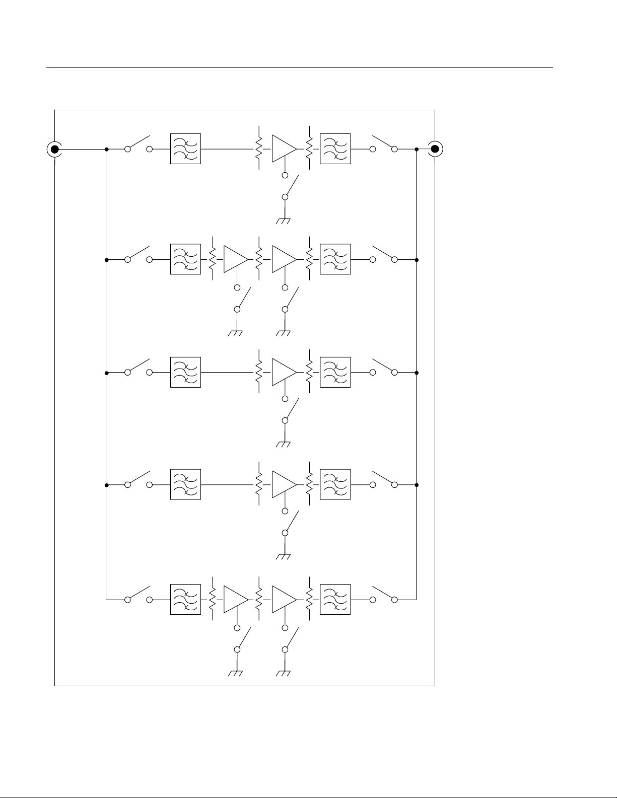
Theory of Operation
10 MHz IF
from VR
1 MHz Filter 11.5 dB
100 kHz Filter 11.5 dB 11.5 dB
10 kHz Filter 11.5 dB
10 MHz IF
to VR
1 kHz Filter 11.5 dB
300 Hz Filter 11.5 dB 11.5 dB
Figure 3- 16: RF Options Diagram
3- 36
2715 Spectrum Analyzer Service Manual
Page 95

Theory of Operation
The board provides the resolution bandwidths used to fill in between filter values
installed within the Variable Resolution module. The bandwidth range is 1 MHz
to 1 kHz in decade steps, and 300 Hz. Each filter path consists of a switchable
amplifier and bandpass filter combination.
Control System Interface
Bandwidth Control
Identification Bit
Gain Stage
Routing Switches
The control of the RF Options by the microprocessor is through one 8 bit shift
register. Data is shifted serially in one 8 bit word.
The variable bandwidth section consists of a switching tree to select one of five
filters. Available bandwidth filters, in addition to those already in place in the
Variable Resolution module, are 1 MHz, 100 kHz, 10 kHz, 1 kHz, and 300 Hz.
A resistor is installed between either pin 12 (d6) or pin 13 (d5) of shift register
U390 and the base of Q396 to complete a path for an identification bit for the
Microprocessor. This allows the Microprocessor to determine that the 300 Hz
filter is installed on the RF Options board.
The gain stage used is a transformer feedback stage that provides approximately
11.5 dB of gain. In the case of the 100 kHz and 300 Hz filters, two gain stages
are used. The impedance match at one port of the Gain Stage is highly sensitive
to a proper termination being presented to the other port.
The routing switches are used to route RF signals to the selected bandwidth
filter. They are composed of a transistor in heavy saturation that has relatively
large charge storage characteristics. The topology used is a shunt series
configuration. These switches are used on both the input and output of each
filter. That is, the filters are switched in and out at both the input and the output
so that when a filter is not being used it is effectively out of the circuit.
Each bandwidth filter is composed of a double tuned circuit (a two pole
Butterworth filter section), an amplifier to provide gain correction and isolation,
and another double tuned circuit. The intermodulation performance of the
amplifier is less critical because the amplifier is placed after the filter. The noise
power generated by the stage is reduced by placing a filter of equal bandwidth
after the gain stage.
Diagnostics
2715 Spectrum Analyzer Service Manual
The identification bit can provide useful information on the proper configuration
of the instrument.
3- 37
Page 96

Theory of Operation
Log Amplifier
The Log Amplifier system is a high performance, intermediate amplifier system
that provides display laws of linear detection and logarithmic detection of the
incoming signal. The log display has scale factors of 10 dB/div, 5 dB/div, and
1 dB/div. The linear mode has the ability to magnify the top portion of the
waveform to enhance the measurement capability. The module also contains an
FM detector, which, when used with the built in audio amplifier, can be used to
monitor the modulated input signal for enhanced signal identification. The audio
amplifier can also be used to monitor the output of the displayed waveform
regardless of the video source. There is an alternate audio input for the push
button clicks generated by the system controller. This audio signal is also used
for the vertical amplitude reference, to check the sweep speed, and for internal
triggers. An amplitude limited output is available for the period counter for
determining the actual frequency of the signal present in the IF system. External
video inputs are provided for the use of external detectors and the rear panel. A
provision is made for clamping the display when the 1st LO is tuned out-ofband. Frequency dependent amplitude (flatness) correction is also performed on
this board.
Hardware
Flatness Error Correction
Noise Filter
The Log Amplifier system is configured by using a 4.5 by 8.75 circuit board
mounted in the card cage. The Microprocessor interface is through three 8 bit
shift registers.
The signal level at the Log Amplifier board (J190) for full screen deflection is
--10 dBm. The first stage of the Log Amplifier is an amplifier that provides gain
between 18 dB and 24 dB, depending on the frequency of the 1st LO. The
amplifier is adjusted such that the gain is 18 dB at low frequencies and is up to
24 dB at the high end of the frequency range, because the frequency dependent
amplitude error is always greater at the higher frequencies. The feedback is
adjusted by changing the amount of current flowing through PIN diodes CR290
or CR291. The correction voltage, SWPSLOPE, reflects the frequency of the 1st
LO. Provision for a second correction voltage from a future Digital Signal
Processing module is included. This second correction voltage, which provides
an interpolated voltage, will be derived from a flatness table. At present, only
SWPSLOPE is used.
The output of the first stage, a gain slope amplifier, is then fed to a two pole
noise filter to limit the noise to 5 MHz and to provide two more poles of 5 MHz
bandwidth resolution filtering. The output of this filter is then sent to the log
stages through a set of jumpers so the signal can be broken for calibration
purposes and buffer amplifier Q170 (in a common base configuration) to form an
auxiliary IF output.
3- 38
2715 Spectrum Analyzer Service Manual
Page 97

Theory of Operation
Logarithmic Amplifier
Stages
Synchronous Detector
Ripple Filter
The core of the logging stage is a pair of AD640s. The AD640 uses five
cascaded limiting amplifiers to approximate a logarithmic response to an input
signal of wide dynamic range and wide bandwidth. The two AD640s are used in
a parallel/summing operation. The input signal to one AD640 is amplified by
25 dB with the CLC501. This is a current feedback operational amplifier that has
a clamping circuit used to limit the output to a value set by an external voltage
divider. The other AD640 is fed through a 25 dB attenuator. The difference in
input amplitude for small signals is then 50 dB. There is not enough gain in the
75 dB path to cause the AD640 to limit on the input noise of the CLC501. Thus,
the full dynamic range of both parts is realized. This topology eliminates the
need for a narrow bandwidth noise filter.
In Lin mode, the signal envelope is extracted from the RF carrier by the use of a
synchronous detector. This detector is basically a multiplier. Detection is
accomplished by feeding a limited signal into one input and a sample of the RF
signal into the other. Since the limited input is always considered equal to plus or
minus one unit, only the polarity is important. The sample RF is then multiplied
by plus or minus one. Since the RF is always in phase with the limited input, the
product is always positive. Thus, demodulation is achieved.
The ripple filter is a six pole elliptic filter with a finite transmission zero at the
10 MHz IF frequency and another at approximately 19 MHz. The purpose is to
remove any of the remaining 10 MHz component that may still exist. Because of
the full wave rectification provided by the synchronous detector and the log
cells, the 10 MHz component is attenuated by approximately 30 dB. This greatly
reduces the requirements of the ripple filter. However, the signal is not always at
10 MHz. The widest bandwidth is 5 MHz, so there is still a significant requirement for ripple reduction as low as 5 MHz.
Video Filter/Scale Factor
2715 Spectrum Analyzer Service Manual
After the Ripple Filter, the signal is offset before being amplified to bring the
equivalent of a full screen signal in log mode or linear mode to correspond to
0 V output. The out-of-band clamp is also done at this time to deflect the CRT
beam into the bottom of the screen when the display is outside the frequency
limits of the Spectrum Analyzer. Next, the video filter selector is chosen. The
bandwidth of the vertical chain is approximately 5 MHz. Therefore, when a
video filter path is chosen, the maximum bandwidth drops to approximately
1 MHz. This switching tree also multiplexes in the external signals from the rear
panel or the FM Detector.
3- 39
Page 98

Theory of Operation
Immediately following the Video Filters is the Scale Factor amplifier. The gain
of the Scale Factor amplifier can be set to 1.1, 2.2, 5.5, or 11 corresponding to
10 dB/div, 5 dB/div, 2 dB/div, or 1 dB/div. The linear function is done with the
gain set to 1.1.
FM Detector
Period Counter Signal
Audio Amplifier
Video Amplitude
Calibrator
System Reset
The AD834 (U350) is a four quadrant multiplier that is used as a quadrature
detector for demodulation of FM signals. The audio output is sent to the audio
amplifier selector and to the video input selector.
The limited output of one of the log cells is used to drive an isolation buffer
(U630A). This signal is used to drive the period counter on the Microprocessor
board for frequency measurements.
The TDA1013A is used as the audio amplifier for monitoring purposes, and as a
means of providing feedback to the user from the microprocessor.
Microprocessor audio appearing at pin 22 of J7 is used to provide feedback to
the operator for push button clicks and out of range or uncalibrated conditions.
This signal is also used to provide a signal for calibrating the video amplifier and
display storage. The sweep triggers are also tested by this signal.
At power on, the system reset line SYSRST-- on pin 4 of J7 goes low until the
Microprocessor resets it. During this time, the control latch’s output enable line
is held false and the outputs are in a high impedance state. This is used only by
the mute bit. The pull up resistor will force a mute condition during this time,
thus disallowing any extraneous noise from the speaker.
Display Storage
3- 40
The Display Storage board digitizes both vertical (LOGVID) and horizontal
(SWP) signals and places this digitized information in nonvolatile RAM
(NVRAM). Various state machines on the board then take this digitized data
from the NVRAM and generate the horizontal and vertical signals which are sent
to the deflection circuitry on the Power Supply board. In addition to displaying
the digitized data, the Display Storage board also is used to display the readouts
and place markers on the CRT .
The major features of the Display Storage board are:
H Digitize the LOGVID signal from the Log Board (8 bits)
H Digitally track the SWP signal from the Sweep Board (9 bits)
H Acquire and store up to four waveforms in RAM
2715 Spectrum Analyzer Service Manual
Page 99

Theory of Operation
H Provides for the ability to place up to two markers on a displayed waveform
H Implement and display a B,C--Save A waveform
H Display readout information on the screen
H Provide up to 28 Kbytes of nonvolatile storage area
H Provide two different waveform acquisition modes: Max Peak and Min/Max
H Provide a Max Hold function
Control System Interface
The following sections show the bit maps for each of the control registers on the
Display Storage board.
Mode Control Register 1. Mode Control Register 1 is located in I/O space, at
location 0x0FA00. Mode Control Register 1 is a read/write register. Table 3--2
describes the Mode Control Register.
Table 3- 2: Mode Control Register 1
Bit
Number
7 DSON_L Low Display Storage On
6 DISP--A_L Low Enables B,C--Save A Display
5 MAXHLD_L Low Enables max hold function
4 PEAKDIS_L Low Enables max peak function
3 HLF/FLL_L High Selects location of B,C--Save A display
2 ACQ_ON High Enables the acquisition system
1 RDZEN High Not used
0 DS_PROTECT High Not used
Mnemonic
Activity
Level
Description
DSON_L. Enables the Display Storage board to display the digitized waveforms
when low. When this signal is high, the analog trace is drawn on the CRT.
DISP--A_L. Invokes the B,C--Save A display on the CRT when low.
MAXHLD_L. Invokes the Max Hold algorithm for A and B waveforms when
low. In this mode a given bin will only be updated when the new vertical data is
greater than the stored vertical data.
2715 Spectrum Analyzer Service Manual
3- 41
Page 100

Theory of Operation
PEAKDIS_L. In the Normal Mode this bit selects one of the two acquisition
modes. Either the Max Peak, when low, or the Min/Max algorithm when high. In
the Enhance Mode this bit is used in conjunction with the ACQM0 bit of Mode
Control Register 2 to invoke Sample and Min Peak algorithms. See Table 3--3
below.
HLF/FLL_L. In the Normal Mode this bit selects one of two positions on the
CRT screen to normalize the B,C--Save A display. When this bit is low, the
B,C--Save A display will be normalized to the top of the CRT screen. When this
bit is high, the B,C--Save A display will be normalized to the middle of the
screen. In the Enhanced Mode this bit is used in addition to the POS1 bit in
Mode Control Register 2. See Mode Control Register 2 below for more details.
ACQ_ON. This bit asynchronously enables/disables the storing of vertical data
into the waveform memory. When this bit is high, the vertical data will be stored
in waveform memory. When this bit is low, the vertical data will not be stored in
waveform memory. It is important to understand that the A/D converter is still
running and the vertical data processing sections are still running. All that this
bit does is control the ability to store the vertical data after being processed.
RDZEN. This bit is not used in the Display Storage board.
DS_PROTECT. This bit is not used in the Display Storage board.
Mode Control Register 2. Mode Control Register 2 is located in I/O space, at
location 0x0FA04. Mode Control Register 2 is a read/write register.
In order to write to this register, it must first be enabled by setting the MCREG2
bit (bit 7) of the Scroll Register high. If at any time the MCREG2 bit is cleared
(set low) Mode Control Register 2 will be cleared and disabled.
Table 3- 3: Mode Control Register 2
Bit
Number
7 Not used
6 Not used
5 Not used
4 Not used
3 Not used
2 ENB2715 High Enables features available in 2715 instrument
Mnemonic
Activity
Level
Description
3- 42
1 POS1 High MSB of B,C--Save A waveform position
0 ACQM0 High LSB of acquisition mode control
ENB2715. This bit, when high, enables the Enhanced Mode of the board.
2715 Spectrum Analyzer Service Manual
 Loading...