

Page 1

MODELS 108, 109 AMPLIFIERS
CONTEXTS
TABLE OF CONTENTS
Section
GENERAL DESCRIPTION . . . . . . .
1.
l-l. General . . . . . . .
1-2.
l-3.
1-4.
l-5. Accessories . . . . . .
l-6. Equipment Shipped . . . .
OPERATION . . . . . . . .
2.
2-1. Terminals . . . . . . . .
2-2.
2-3.
2-4.
2-5.
2-6.
2-7.
2-8.
2-9.
Z-10.
CIRCUIT DESCRIPTION
3.
3-1.
3-2.
Models 108, 109 Differences
Specifications. . . . . . .
Applications. . . , . .
Operating Procedures. . . .
Cascading . . . . . . . . .
Gains Other Than 10, 100
1000 and 10,000. . . . . .
Open Circuit Operation. . .
Amplifier Noise . . . . . .
Rise Time . . . . . . . . .
Delay Time. . . . . . . . .
Ground Loops. . . , . . .
Stray Fields. . . . . . . .
.......
General
Amplifier Design.
..........
.....
Page
. 1
. 1
. 1
. 2
.3
.3
.3
.5
. 5
. 5
. 5
. 6
. 6
. 6
. 6
. 6
. 7
7
. 9
. 9
. 9
Section
5-3.
5-4.
5-5.
5-6. Low-Frequency Response
6. ACCESSORIES. . . . 19
6-l.
6-2.
6-3.
REPLACEABLE PARTS. . . . . . . . . 21
7.
7-l.
7-2. How to Order Parts . . . . . 23
Models 108,
Calibration . . . 14
Model 108 High-Frcqurnc)
Calibration . . . 14
Model 109 High-Frequency
Calibration . . .
Check........... 16
Model 1081 Power Supply 19
Model 1042 Accessory Kit . . 19
Model 1082 Mounting Plate . 20
Replaceable Parts List . . . 23
Models 108, 109 Replaceable
Parts List. . . . . . . . . 24
Model 1081 Replaceable Parts
List. . . . . . . . . . . . 26
Models 108, 109 Schematic
Diagram 17971D. . . . . . . 29
Model 1081 Schematic Diagram
17966C. . . . . . . . . . 30
109 Lo\<-Frequency
Page
15
SERVICING
4.
4-1. General
4-2.
4-3.
4-4.
CALIBRATION
5.
5-l. General
5-2.
0266R
............
..........
Servicing Schedule.
Parts Replacement
Troubleshooting
...........
..........
Calibration Schedule.
.....
......
....
...
. 11
. 11
. 11
. 11
. 11
. 13
. 13
. 14
+ Change Notice
3~ Yellow Change Notice sheet is
included only for instrument
modifications affecting the
Instruction Manual.
Last Page
Page 2

Page 3

MODELS 108, 109 AMPLIFIERS
GENERAL DESCRIP'IIOS
SECTION 1.
l-l.
The Model 108 is tuned for a wideband frequency response;
response.
GENERAL.
(See Figures 9 and 10 for illustrations of the two responses.)
The Keithley Models 108 and 109 are small, 12-ounce Xl0 gain amplifiers.
GENERAL DESCRIPTION
the Model 109 is tuned ior pulse
Both
?lodels require an external power supply, preferably the Keithley Model 1081 Power Supply, which
can drive up to three of these units at one time.
a. The Model 108 bandwidth is from 1 kc to 180 MC (-3db).
150 MC is flat 20.5 db.
Voltage gain is 10 (20 db) when terminated
Response Erom 2.5 kc to
into a 50-ohm load.
Up to four Model 108 Amplifiers may be cascaded for gains to 10,000, or one may be used
with other amplifiers to increase total gain by 10.
The input impedance is 50 ohms.
Noise is less than 30 microvolts rms referred to the input.
The Model 109 Pulse Amplifier has a rise time of less than 3 nanoseconds (10:: to
b.
90%). Overshoot is less than 2%, pulse width for a 10% droop is 30 microseconds.
specifications are the same as for the Model 108. Four Pulse Amplifiers may be
for gains to 10,000,
l-2.
MODELS 108, 109 DIFFERENCES.
a. The Models 108 and 109 differ only in their tuning.
identical. Most of the Instruction Manual applies to both
or one may be used with other amplifiers to increase total gain
The circuits and the parts are
units.
Where there are differ-
Other
cascaded
by
ences - such as application suggestions and calibration - the models are identified.
10.
Specifications and operations in this
b.
PO
‘Wer
Supply to power the Amplifier. It is recommended that this Power Supblv be used to
ob
tai
.n the maximum benefit from the Amp
fier.
Manual
assume using the Keithley Model 1081
10s
PULSE
AMPLIi=,ER
I :IGLlRE 1. Keithley Instruments
t lode1 108 Wideband Amplifier.
0465R
i”‘Lb”KL L. nelr”Ley ~“strumenrs
Model 109 Pulse Amplifier.
1
Page 4

GENERAL DESCRIPTION
MODELS 108, 109 AMPLIFIERS
1-3.
Frequencyl:
Rise Time* (10% to 90%)
Overshoot3
Pulse Width for 10% Droop:
Input Impedance:
Voltage Gain (into 50-ohm
characteristic impedance)
Maximum rms Noise4:
Maximum Output (into 50-ohm
characteristic impedance)
Maximum Overload:
SPECIFICATIONS.
-3db
?0.5db
Model 108 (when powered by
the Model 1081 Power Supply)
1 kc and 180 MC
2.5 kc to 150 MC
Less than 3 nanoseconds
-
-
50 ohms
10 (20 db)
?2% at 10 kc
30 microvolts (7 db)
1.4 volts peak-to-peak
20 volts peak5
ac,
2.5 volts
dc,
Model 109 (when powered by
the Model 1081 Power Supply)
Less than 3 nanoseconds
Less than 2%
30 microseconds
50 ohms
10 (20 db)
i-2% at 10 kc
30 microvolts (7 db)
1.4 volts peak-to-peak
20 volts peak5
ac,
2.5 volts
dc ,
Overload Recovery6
Delay Time'
Change in Output Amplitude
for a 10% Line Voltage Change
(when powered by Model 1081):
1) db variations add when amplifiers are cascaded.
Maximum rise time for 3 amplifiers in cascade is less than 4 nanoseconds.
2)
3) Overshoot for amplifiers in cascade is 3% or less.
4) Noise referred to input measured from 10 cps to 100 MC. Noise of cascaded amplifiers is equal to noise of first amplifier only.
5) Continuous input power should not exceed l/8 watt.
6) Using a 100X overload test pulse 100 nanoseconds wide with 5-nanosecond fall
time to within 1% of base line.
or less overload shortens recovery time.
7) Delay times add when amplifiers are cascaded.
CONNECTORS: Input and Output:
POWER: +16 volts.dc and -12 volts dc; or 28 volts dc floating; ?5% accuracy; 50 milliam-
peres current (1.4 watts); +O.l% stability; Z-millivolt peak-to-peak maximum ripple; lOOmicrofarad filter from each power terminal to ground.
Less than 50 nanoseconds
Less than 5 nanoseconds
Less than 20.1%
A shorter pulse duration, a slower fall time
n type.
Power:
Amphenol 126-214
Less than 50 nanoseconds
Less than 5 nanoseconds
Less than *O.l%
DIMENSIONS, WEIGHT:
ACCESSORIES SIIPPLIED:
2
3 inches high x 2-l/4 inches wide x 3-3/4 inches deep; net weight, 12 oi
Mating power connector; mating input and output connectors.
0565R
Page 5

MODELS 108, 109 AMPLIFIERS
1-4. APPLICATIONS.
The Model 108 Wideband Amplifier is used as a general Laboratory pre-amplifier in
a.
audio, radar, IF, TV and VHF work.
low noise permits amplification of signals in the microvolt region at low and high Irequev
ties. Because of its small size,
b. The Model 109 Pulse Amplifier is designed co amplify non-sinusoidal wave corms :.:ith
a fast rise time,
with oscilloscopes, high-speed counters,
L-5. ACCESSORIES. Refer to Section 6 for complete descriptions of the following Ampli-
fier accessories.
minimum overshoot and minimum ringing.
It can be used with all types of oscilloscopes. 11s
it can be designed into other equipment.
Common applications include use
pulse-height analyzers and phoro multipliers.
GmERAL DESCRIP~l'IO!;
Model 1081 Power Supply can power one,
a.
The POWer Supply operates from 105-125 or 210-250 Volt, 50-400 cps line sources; pocrr
rating is 12 watts. Its dimensions are the same as the hmplifi.ers; net weight is l-l,'?
pounds.
b. Model 1042 Accessory Kit provides useful adapters,
the Amplifier. The Kit accessories,
tion 6.
Model 1082 Mounting Plate adapts the Amplifiers and the Hodel LO81 for mounting LO
c.
another surface.
d. Model 1083 Cable allows using the filodels 108 and 109 with the Keicbley l$z,dcA1s lO(, ilnd
107 Amplifiers.
contained in a convenient case,
two or three Model 108 or 109 Amplifiers.
terminations and tee for use with
art‘ described in Scc-
FIGURE 3.
will power 1, ?
02h6R 3
>lodrl 1081 Power Supply Used twiti> 'Three Elodel 109 I'ulsc Amplifiers.
or 3 Amplifiers.
See Scdtior 6 ior the Power Supply description.
Tltc suppl)
Page 6

GENERAL DESCRIPTION
MODELS 108, 109 AMPLIFIERS
1-6.
EQUIPMENT SHIPPED. The Models 108 and 109 are factory-calibrated and are shipped
with all components in place.
contains the Instruction Manual,
plugs.
All units are shipped for bench use. The shipping carton
a mating power connector and mating input and output
0266
Page 7

MODELS 108, 109 AMPLIFIERS
OPERATIOX
SECTION 2. OPERATION
2-1.
cles are n-type. Input impedance is 50 ohms.
TERMINALS.
INPUT and OUTPUT Receptacles. INPUT (front panel) and OUTPlJ'~ (rear panel) Recepr;i-
a.
N-type connectros are used for their bccter
impedance characteristics and less leakage at higher frequencies than other popular connectors.
POWER Socket. The POWER Socket is a 4-pin connector.
b.
power cable supplied with the Model 1081 Power Supply.
It is compatible with the
Schematic Diagram 1797LD shows
the pin connections and voltages (refer to 5103).
2-2.
OPERATING PROCEDURES.
a. No control settings or preliminary adjustments are needed to operate either Ampli-
fier.
Both can be used immediately after they are connected to the ~lodel 1081 Power Suppl)
NOTE
The Amplifiers have n-type receptacles (Mil. No. 680/U). The Model 1042
Accessory Kit contains adapters to connect other type plugs to the Amplifier.
Section 6 describes the Kit.
Connect the Power Supply and associated equipment, such as an oscilloscope, on the
b.
same power line to avoid ac ground Loops.
may tend to be modulated by the ground Loops.
Otherwise,
the output signal from the Amplifi~cr
To further minimize ground loops, it may be
necessary to use isolation plugs on power line plugs of the Power Supply and the associa-
ted equipment. If a power supply other than the Model LO81 is used, put 100-,lf filter
capacitors from + and - to ground.
Use coaxial cables for connections,
c.
especially if working above 1 MC. Up to six
feet of coaxial cable may be used on the
Amplifier input and up to 12 feet on the out-
put,
50 ohms.
if the output cable is terminated with
Longer cables may be used, but the
Amplifier may not meet the flatness or over-
shoot specifications.
All cables used must
have a 50-ohm characteristic impedance.
NOTE
The Model LO9 has no phase reversal
on pulse.
at the input,
output,
input,
^ _
2-3.
a.
CASCfi"ING.
Up to four AmpliTiers may be cascaded
If the pulse is positive
it is positive at the
If it is negative at the
it is negative at the output.
0'6611
Keithley
Input: - AMI'LI- -Output:
6 feet
max.
source A
FIGURE 4.
FIER
Amplifier Cable Connections.
12 feet
max.
- 50-r:
Load
Maximum recommended cable length to input
is six feet; from output, 12 feet. If
longer cables arc used, the specified
ness
or overshoot may not be achieved. USC
flnt-
only coaxial cables.
3
Page 8
OPERATION
MODELS 108, 109 AMPLIFIERS
together for gains of 100, 1000, or 10,000.
1.4 volts peak-to-peak into a 50-ohm load.
plifier stages and distortions will result.
gain hookups to reduce the noise level.
When using the 108 or 109 with the 106 or 107,
into the 106 and 107 power outlet.
Use the n-type male-to-male adapter from the Model 1042 Kit to cascade Amplifiers
b.
directly to each other. The Model 108 may also be used in cascade with the Keithley
Models 104 and 106 Amplifiers.
105 and 107 Amplifiers.
2-4. GAINS OTHER THAN 10, 100, 1000 AND 10,000.
"se attenuator pads in series with the Amplifier.
the attenuator pad on the last Amplifier OUTPUT Receptacle for input signals below 15
millivolts peak-to-peak for the best signal-to-noise ratio.
rms input signal is amplified 20 times (26 db)
Amplifier output.
the last output is 3 millivolts rms.
14-db pad, its level is 0.6 millivolt rms.
If the 14-db attenuator pad were used at the first Amplifier input, the output noise would
be 3 millivolts rms.
worse than previously.
Maximum input noise of each amplifier is 30 microvolts rms.
Signal-to-noise ratio would be approximately 6:1, or four times
The Model 109 may also be used in cascade with the Models
When the noise is attenuated five times through the
The final Amplifier output should not exceed
Higher outputs exceed the limits of the am-
A bandpass filter is recommended for lO,OOO-
NOTE
"se the 1083 cable for connection
For gains in between the cascaded values,
When two Amplifiers are cascaded, use
For example, a l-millivolt
using a 14-db attenuator pad on the last
Noise at
Signal-to-noise ratio is approximately 28:l.
2-5. OPEN CIRCUIT OPERATION.
gain changes for an open circuit.
megacycles, increasing as the frequency increases.
gain into an open circuit is approximately 10.5 to 11.
increases to approximately 18 (25 db) at 150 megacycles. The Amplifier will not oscillate
into an open circuit at any frequency, although standing waves become apparent at the
higher frequencies. The magnitude of the waves depends directly on cable length and
frequency.
2-6. AMPLIFIER NOISE. The main sources of noise are the transistors and any power supply
ripple. Since all noise is referred to the
input,
fier input noise times the amplifier gain (10).
The noise is measured at the output and referred back to the input. When two Amplifiers are cascaded,
amplifier is not significant because noise adds
as the square root of the sum of the squares.
2-7.
a. The rise time is defined as the time
needed for a signal to rise from 10% to 90%
of its final value.
amplifiers,
for the amplifier to go from 10% to 90%
of the final value of the input signal
the output noise will be the ampli-
the noise of the second
RISE TIME.
Specifically, for
rise time is the time needed
The specified Amplifier gain is into a 50-ohm load.
Output impedance is approximately five ohms below 10
Below 10 megacycles, therefore, the
Above 10 megacycles, the gain
IO%
G; /
28%
9
: ~-1
lli
FIGURE 5.
The gain linearity falls within the limits
shown above from 2.5 kc to 150 Mc.
GAlY LIWEI~II" _ YlllMUY GAIN mo* OK! IHL
I
I
1ow 1oow. I"/ 1011 10011 I", ,ou ,ool ,6,
Models 108 and 109 Gain Linearity
DlwM RAW 01 IM LYPllllER
1
1 I
I"IPUtK"
1 I
I
I
I
The
6
0266R
Page 9

MODELS 108. 109 AMF'LIFIERS
OPCRATION
times the amplifier gain.
faster than the amplifier's, When amplifiers are cascaded,
Rise time is measured only with a pulse whose rise time is
the rise times add in qundra-
ture (square root of the sum of the squares).
The slight overshoot of a very high frequency pulse can be eliminated in Lhf >lodcl
b.
108 by detuning the high-frequency response slightly.
gain flatness for a continuous signal.
The Model 109 is already tuned lor
The Model 108 is tuned for msximum
minimum
ovcr-
shoot.
2-8. DELAY 'TIME.
Delay time is the transit time taken by a signal to go from the amplifier input to output. Because delay times are a physical constant, they add for cascaded
amplifiers.
2-9.
loops.
GROUND LOOPS.
This is a current - line or other frequency - flowing in a ground lead impedance
A common source of errors when amplifying Low-lcvcl signals is ground
which results in a voltage in addition to the desired signal voltage appearing ac tllc
input terminals of the amplifier.
Although the origin and mechanism of ground loops nrc
difficult to explain and trace, their effects can be reduced in several ways.
Make all ground lead impedances as low as possible.
a.
Employ only coaxial hookups wherever possible.
b.
Z-10.
STRAY FIELDS.
Stray fields can induce unwanted emf's in the test system.
'The in-
accuracies due to these fields become more significant as measurements become more scan-
sitivc. Induced emf's may be reduced by using coaxial cable having
minimum
loop area and
by using cables of minimum length.
0266R
7
Page 10

Page 11

MODELS 108, 109 AMPLIFIERS
CIKCUIT DESCRIPTION
SECTION 3.
3-1.
back.
epitaxial mesa transistors with a. l-gigacycle ft.
mizes lead inductance. Silver plating on the chassis eliminates ground loops and reduces
resistance due to skin effect at high frequencies.
ically sealed tantalum capacitors and metal film resistors insures excellent stabilit)
and long. trouble-free operation.
3-2. AMPLIFIER DESIGN.
es three high-frequency transistors, two in
cormnon emitter cascade configuration and
the third being an emitter follower for the
output. A high negative feedback loop is
used for gain stability.
GENERAL.
Both Amplifiers are of conventional RC-coupled cascade design, using negative fccd-
a.
There is no inductive peaking.
Careful circuit design allows for maximum performance. Point-to-point wiring mini-
b.
Refer to Schematic Diagram 1797LD at the back of the Manual for circuit
designations.
Each Amplifier us-
CIRCUIT DESCRIPTION
The wide bandwidth is achieved by using selected
Using solid-state components, hermet-
NOTE
The input is shunted by a 50-ohm me-
tay'film resistor (RlOZ), compensated for
a nominal 50-ohm input impedance across the
band.
sistor QlOl.
plify the signal and apply it to the emitter
f"ll"Wer, transistor Q103, which provides
low output impedance and higher power capabilities than the amplifier stages.
b.
fier stages is through resistor Rll6 and
capacitor CllO. The output of transistor
9102 is divided by resistor Rll6 and the
network, resistors R109, RllO and Rlll.
Potentiometer Rlll adjusts the gain at the
lower frequencies. Trirmners C103, C112,
Cl15 and Cl18 adjust the feedback at higher
frequencies, since the divider becomes pri-
marily capacitive.
stage, transistor QlOl, consists of two resistors, R105 and R106. Capacitor Cl05 is at
the midpoint between the two 2,2-kilobm resistors to eliminate ac feedback. Resistors
R114 and R115 and capacitor Cl08 provide the same function for transistor Ql02.
The input signal is applied to tran-
Transistors QlOl and 4102 am-
The feedback loop for the two ampli-
Each stage uses dc feedback from collector to base. The feedback loop for the first
c.
gram shows the stage design used in the 2-
stage amplifier.
the collector bias
bias voltage divider, which stabilizes the
base voltage. Resistor Rl supplies dc feedback. To eliminate degeneration caused by
the ac feedback, Rl is divided into two
parts, Rla and Rl
ses the ac from tie midpoint to ground.
Resistors Rl and R2 and
voltage drop provide a
Capacitor Cbp bypas-
.
P
0465R
9
Page 12

Page 13

MODELS 108, 109 AMPLIFIERS
SECTION 4. SERVICING
4-l.
Models LO8 and 109.
specifications.
4-2.
the normal care required of high-quality electronic equipment.
frequency or pulse response of the Amplifier should show the need for any ;ld~justocnL.
part should need frequent replacement under ordinary use.
4-3.
Amplifiers.
meet the specifications.
replaced.
Order these parts only from Keithley Instruments, Inc.,
4-4. TROUBLESHOOTING.
GENERAL.
SERVICING SCHEDULE.
PARTS REPLACMENT.
The Replaceable Parts List in Section 7 describes the electrical components of the
a.
The transistors are selected for parameters which allow wide frequency response.
b.
Physical location of components greatly affects high frequency response. Put
replaced parts and their leads in their exact previous position.
Section 4 contains the maintenance and troubleshooting procedures for the
Follow these as closely as possible to maintain the instrument's
The Models 108 and 109 require no periodic maincennncc beyond
Occasional C~CCKS 3s the
Replace components only as necessary.
Check the frequency or pulse response after any transiscar is
NOTE
Use only reliable replacements which
or its representatives.
SO
The procedures which follow give instructions for repairing troubles which might
a.
occur in the ModeLs 108 and 109. Use the procedures outlined and use only speciiied replacement parts.
recommended for troubleshooting. If the trouble cannot be located or repaired, contact
the nearest Keithley representative.
Keithley Instruments Model 121 True RMS
Voltmeter
Keithley Model 153 DC Microvolt-Ammeter,
3% accuracy,
Simpson Models 260 and 650 Transistor
Beta Testers
Tektronix Type 504 Oscilloscope, passband
dc to 450 kc
TABLE 1.
equivalents.
Equipment Recommended for Troubleshooting. Use these instruments or their
Make sure the external circuits are checked. Table 1 lists equipment
Instrument Use
Measures ac voltages
Measure dc voltages
20 megohm input resistance
Check transistors
Observe wave forms
0266R 11
Page 14

SERVICING
MODELS 108. 109 AMPLIFIERS
Trouble
Amplifier will not operate
Probable Cause
Remedy
Faulty transistor Check QlOl, Ql02, Ql03; replace
if faultv
Noise with Amplifier
exceeds 30 microvolts rms
Faulty
Excessive ripple from
power supply
transistor Check QlOl, QlO2, Q103; replace
if faulty
Check power supply. Check
filters ClOl, C106, Cl16, C122,
Cl23 and C124.
Gain is more or less than 10 Potentiometer Rlll out Adjust Rlll per paragraph 5-3
of adjustment
Model 108 frequency
response not flat within
Amplifier out of cali- Calibrate per paragraph 5-4
bration
specifications
Model 109 exceeds over- Amplifier out of cali-
Calibrate per paragraph 5-5
shoot specification bration
Rise time of Amplifier
not within swcification bration
Amplifier out of cali-
I
Adjust Model 108 per paragraph
5-4. Model 109 oer oaraaarah 5-:
I
Input impedance not
50 ohms
TABLE 2. Models 108 and 109 Troubleshooting.
Faulty R102 or Cl02
I
Check R102 and ClO2; replace
I
if fault-v
Refer to paragraph 4-4, b, before trouble-
shooting the Amplifier.
Before troubleshooting the Amplifier, check the external circuits, especially the
b.
power supply. Make sure the Amplifier output is terminated into a good 50-ohm load.
the coaxial cables and connections.
other instruments.
put results in a poor
(The Amplifier will faithfully amplify any signal fed to it; a poor in-
output.)
Make
to-peak. If the external circuits are good,
Table 2 contains troubles which might occurs with the instrument. If the repairs
c.
indicated in the table do not clear up the trouble,
by-circuit check.
Refer to the circuit description in Section 3 to find the more crucial
Check the performance of the signal generator and
sure
the
output signal does
not exceed 1.4 volts peak-
check the Amplifier itself.
continue to search through a circuit-
Check
components and to determine their function in the circuit. The complete circuit schematic
diagram, 17971D, is in Section 7.
If the instrument will not operate, check the power source.
d.
If it is satisfactory,
continue to isolate the trouble.
'The Schematic Diagram indicates
e.
the
transistor terminal voltages referenced to chas-
sis ground. Measure the dc voltages to zlO% of indicated value with a dc voltmeter.
12
0665R
Page 15
MODELS 108, 109 AMPLIFIERS
CALIBRATIOII‘
SECTION 5.
CALIBRATION
5-l. GENERAL.
The following procedures are recommended for calibrating and adjusting the >lodels
a.
108 and 109. Use the equipment recommended in Table 3.
available or if difficulty is encountered,
contact Keithley Instruments, inc., or its
If propcr facilities arc not
representative to arrange for factory calibration.
b. Three calibrations are in the procedures:
cy wideband calibration and pulse calibration.
low-frequency calibration, higlr-frequen-
In addition, paragraph 5-6 outlines test
procedures to check response.
If the instrument is not within specifications after the calibration, follow the
c.
troubleshooting procedures or contact Keithley Instruments, Inc.,
Instrument
General Radio GR-874 type attenuators,
High frequency calibration
3 db, 6 db, 10 db and 20 db
General Radio CR-874-WM50 50-ohm termin- Amplifier termination
ation (also found in Keithley Instruments
Model 1042 Accessory Kit)
or its representative.
Use
Hewlett-Packard Model 202A Audio Oscillator,
20 cps to 40 kc, 22%
Jarrold Electronics Model 900-B Sweep Signal Generator (includes Model D50 Detec-
to=),
500 kc to 1200 MC
Keithley Instruments Model 121 True RMS
Signal generator for low-frequency cali-
bration
Signal generator for Model 108 band
response
Measure ac voltages
Voltmeter
Tee and adapters (found
in
Keithley Instru-
Hook up calibration circuits
ments Model 1042 Accessory Kit)
Tektronix Type 111 Pulse Generator, 0.5-nsec
Check Model 109 pulse response
rise time, 2 to 20-nsec pulse duration
Tektronix Type 504 Oscilloscope, passband
from dc to 450 kc
Tektronix Type 561A Oscilloscope, with dual
Check wave form during tuning and view
sweep display of Model 108
View Model 109 pulse response
trace plug-in sampling units, 0.4-nsec rise
time
TABLE 3. Equipment Recommended for Models 108 and 109 Calibration.
or their equivalents.
Use these instruments
0565R
13
Page 16
CALIBRATION
MODELS 108, 109 AMPLIFIERS
5-2.
plifier response yearly or when transistors
are changed. Refer to paragraph 5-4 (Model
108) or S-5 (Model 109) for procedures; recalibrate completely if the response is not
correct. Always recalibrate the high-fre-
quency gain if the low-frequency gain is
adjusted.
5-3. MODELS 108, 109 LOW-FREQUENCY CALI-
BRATION
ing the four screws.
to the Model 1081 Power Supply.
nal for 50 millivolts rms at 10 kc.
scope and 50-ohm termination to the Amplifier OUTPUT.
millivolts rms *lo millivolts.
this output.
CALIBRATION SCHEDULE. Check the Am-
Low Frequency
I
TABLE 4.
The Table lists all internal controls, the
Remove the Amplifier cower by remov-
a.
Connect the Amplifier
Connect the Model 202A Oscillator to the Amplifier INPUT.
b.
Connect the Model 121 Voltmeter, Type SO4 Oscillo-
Adjust potentiometer Rlll (Figure 14), if necessary, for
Monitor the output signal on the oscilloscope and check for distortion.
c.
figure picturing the location, and the
paragraph describing the adjustment.
5-4 (108)
Rlll 1 14 1 5-3 1
I
Models 108, 109 Internal Controls.
Adjust the oscillator sig-
The output signal should be 500
I
The low-frequency calibration establishes the base for the high-frequency re-
SpO*Se.
it at the low frequencies.
5-4.
1081 Power Supply. Connect the Model 900-B Sweep Generator to the Amplifier INPUT directly.
megacycles. Adjust the oscilloscope for a vertical display of 5%/cm.
I
MODEL 108 HIGH-FREQUENCY CALIBRATION.
Remove the Amplifier by removing the four screws.
a.
See Figure 7.
Adjust the generator signal to 50 millivolts rms and center the frequency at 100
b.
Therefore, tune the Amplifier at the high frequencies after tuning
Connect the Amplifier to the Model
Connect the Amplifier OUTPUT to the Model D50 Detector.
Model 900-B
Generator
ver
I
?
I
FIGURE 7.
equipment.
14
Block Diagram for Model 108 High-Frequency Calibration.
Refer to Table 3 for
0565R
Page 17
MODELS 108, 109 AMPLIFIERS
Use only an insulated alignment tool in adjusting the trimmers. DC biases
are present across trimmer C118,
ses and possibly damage transistor Q102.
CALIBRATION
NOTE
and a screwdriver would short out the bia-
The low-frequency gain should be previously set (paragraph 5-3).
c.
Cl12 and Cl15 (Figure 14) to their minimum values.
mum by noting when the lowest high-frequency response curve appears on the oscilloscope.
Set trimmer Cl15 to approximately l/3 of maximum to keep the Amplifier from oscillatin>:
into an open circuit at higll frequencies.
Cl12 to approximately l/2 maximum. The response should rise at about 50 to 100 NC.
d. Increase trimmer C118, watching the response curve on the oscilloscope.
response looks like a straight line - either rising or descending - stop adjusting C118.
Adjust trimmer Cl12 to bring the high end up or down to the proper gain level.
mid-range gain (between 50 and 100 MC) is not flat,
Cl18 until the response is flat.
end in perfectly.
Insert a 3-db pad and re-adjust the oscilloscope for a vertical of X/cm.
e.
a response of 5%.
on a reference line. Remove the 3-db pad.
previously set reference l.ine.
5-5. MODEL 109 HIGII-FREQUENCY CALIBRATION,
Remove the Amplifier cover by removing the four screws. Connect the Amplifier to the
a.
Model 1081 Power Supply.
Connect the Type 111 Pulse Generator to the Sampling Oscilloscope.
b.
(approximately 26 db) to adjust for a 0.7-volt peak pulse on the oscilloscope, Use the
delay cable on the pulse generator to adjust the pulse width to approximately 20 nanoseconds.
ity to 200 millivolcslcm.
to synchronize the oscilloscope.
se's leading edge.
Set the oscilloscope horizontal sweep to 5 nanoseconds/cm and the vertical sensitiv-
Response should be flat to at least 150 MC (refer to Figure 9).
Using the oscilloscope vertical position control, put the display trace
If necessary,
If necessary,
Note the amount of: overshoot and the shape on the pul-
Set trimmer Cl03 near its maxiorunr.
The 180-megacycle point should bc above the
use the pretriggcr output of chc pulse generator
Set trimmer Cl18 (Figure 12) to mini-
alternate ad.justing trimmers CL03 and
i-e-adjust trimmer Cl12 to bring the high
Set trimmers C103,
Set trimmer
wl'hcn tile
If till?
Check for
use attenuators
The Amplifier is being calibrated at maximum output.
pulses than specified. This will cause overshooting and result in an improperly calibrated amplifier.
c. Add a tee (included in the Model 1042 Kit) and 20.db attenuator; connect the pulse
generator to the Amplifier INPUT.
oscilloscope's other vertical input.
which terminates the Amplifier output.
Use only an insulated alignment tool to adjust tile trimmers. DC biases are
present across trimmer Cll8,
possibly damage transistor Q102.
06651~
Set Figure 8.
Note the oscilloscope has 50-011111 input impedance,
NOTE
nnd a screwdriver would short out tile hiascs anti
Connect the Amplifier OUTPUT Co the
Do not put in larger
15
Page 18
CALIBRATION
MODELS 108, 109 AMPLIFIERS
Dual Channel
Sampling
Oscilloscope
Type 111
Pulse
Generator
AMPLIFIER
ver
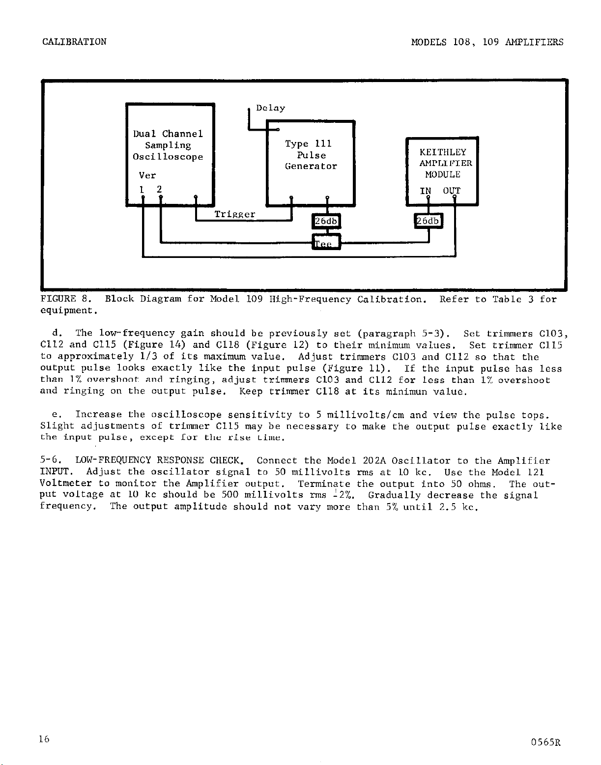
FIGURE 8. Block Diagram for Model 109 High-Frequency Calibration.
Refer to Table 3 for
equipment.
The low-frequency gain should be previously set (paragraph 5-3).
d.
Cl12 and Cl15 (Figure 14) and Cl18 (Figure 12) to their minimum values.
to approximately l/3 of its maximum value.
output pulse looks exactly like the input pulse (Figure 11).
Adjust trinuners Cl03 and Cl12 so that the
If the input pulse has less
Set trimmers ClO3,
Set trimmer Cl15
than 1% overshoot and ringing, adjust trimmers Cl03 and Cl12 for less than 1% overshoot
and ringing on the output pulse.
Increase the oscilloscope sensitivity to 5 millivolts/cm and view the pulse tops.
e.
Keep trimmer Cl18 at its minimun value.
Slight adjustments of trimmer Cl15 may be necessary to make the output pulse exactly like
the input pulse,
except for the rise time.
5-6.
INPUT.
Voltmeter to monitor the Amplifier output.
LOW-FREQUENCY RESPONSE CHECK.
Connect the Model 202A Oscillator to the Amplifier
Adjust the oscillator signal to 50 millivolts rms at 10 kc.
Terminate the output into 50 ohms.
put voltage at 10 kc should be 500 millivolts rms ?2%.
frequency.
The output amplitude should not vary more than 5% until 2.5 kc.
16
Use the Model 121
The out-
Gradually decrease the signal
0565R
Page 19

MODELS 108, 109 AMPLIFIERS
CALIBRATION
FIGURE 9.
Models 108 and 109 Bandwidth
Characteristics. The Model 108 is widkband tuned; the Model 109, pulse tuned.
The response is from 0 cps (extreme left)
to 240 MC; each pip represents 10 MC.
Display signal of 50 mv rms is from a
sweep generator. The excellent flatness
of the wideband amplifier is gained at the
expense of overshoot and ringing on pulses.
FIGURE 11. Pulse Fidelity of Model
109 Pulse Amplifier. Note bow the
output pulse follows the input pulse.
FIGURE 10. Models 108 and 109 Overshoot
Characteristics. The Model 108 is wide-
band tuned;
the Model 109, pulsf tuned.
The oscilloscope is set far 5 nscc/cm
horizontal, 0.2 v/cm vertical. The pulse
amplifier has minimum pulse distortion at
the expense of flatness (see Figure 9).
0665R
17
Page 20
CALIBRATION
MODELS 108, 109 AMPLIFIERS
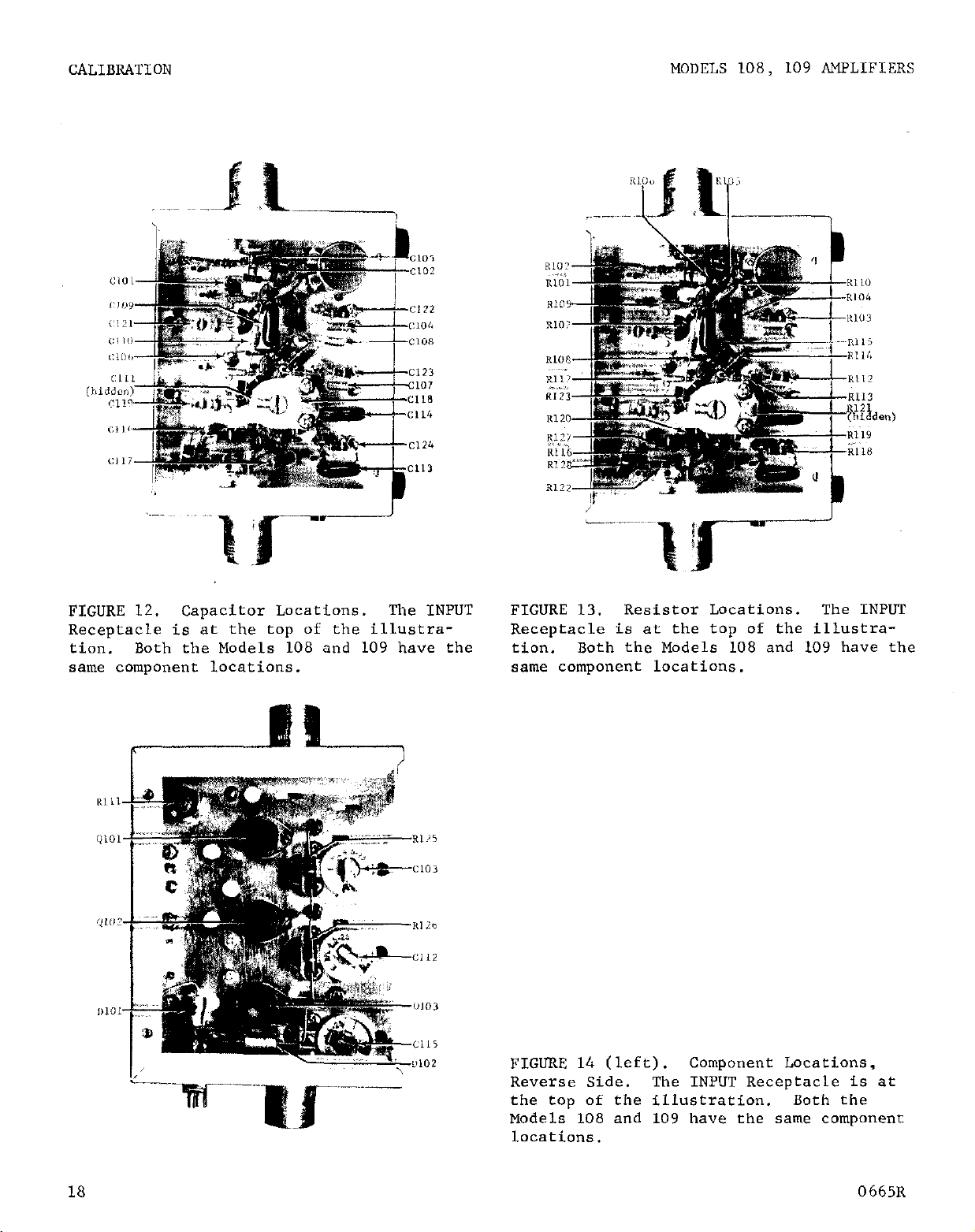
FIGURE 12.
capacitor Locations. The INPUT
Receptacle is at the top of the illustra-
tion. Both the Models 108 and 109 have the
same component locations.
FIGURE 13. Resistor Locations. The INPUT
Receptacle is at the top of the illustra-
tion.
Both the Models 108 and 109 have the
same component locations.
FIGURE 14 (left).
Reverse Side.
the top of the illustration.
Component Locations,
The INPUT Receptacle is at
Both the
Models 108 and 109 have the same component
locations.
18
0665R
Page 21
MODELS 108, 109 AMPLIFIERS
ACCESSORIES
SECTION 6. ACCESSORIES
6-1.
two or three Models 108 and 109 Amplifiers. No adjustment is necessary. Refer to Section
7 for the Power Supply Replaceable Parts List and Schematic Diagram.
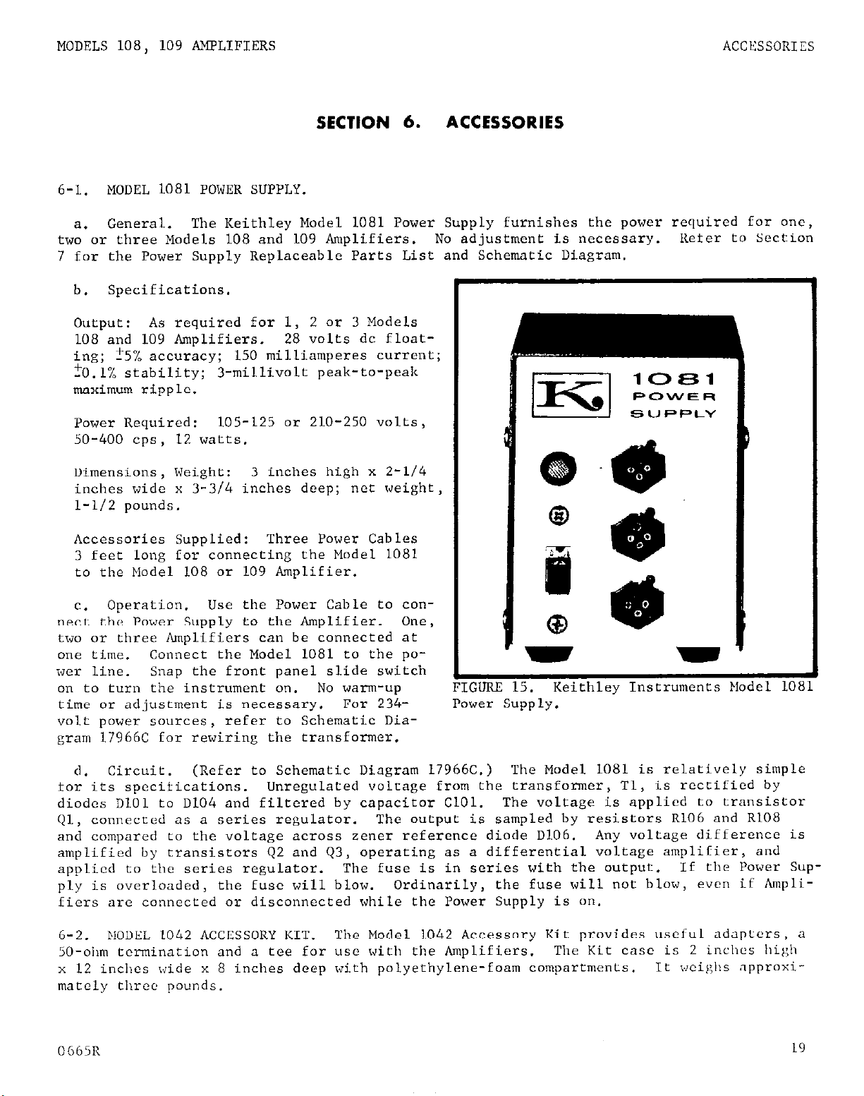
MODEL 1081 POWER SUPPLY.
GfZ"C2Xll.
a.
Specifications.
b.
Output: As required for 1, 2 or 3 Models
108 and 109 Amplifiers.
?5% accuracy; 150 milliamperes current;
ing;
fO.l% stability; 3-millivolt peak-to-peak
maximum ripple.
Power Required: 105-125 or 210-250 volts,
50-400 cps, 12 watts.
Dimensions, Weight: 3 inches high x 2-l/4
inches wide x 3-3/4 inches deep; net weight,
l-1/2 pounds.
Accessories Supplied: Three Power Cables
3 feet long for connecting the Model 1081
to the Model 108 or 109 Amplifier.
The Keithley Model 1081 Power Supply furnishes the power required for one,
28 volts dc float-
Operation. Use the Power Cable to con-
c.
nect the Power Supply to the Amplifier.
two or three Amplifiers can be connected at
one time. Connect the Model 1081 to the power line.
on to turn the instrument on.
time or adjustment is necessary.
volt power sources, refer to Schematic Diagram 17966C for rewiring the transformer.
Circuit. (Refer to Schematic Diagram 17966C.) The Model 1081 is relatively simple
d .
for its specifications. Unregulated voltage from the transformer, Tl, is rectified by
diodes DI.01 to D104 and filtered by capacitor ClOl.
connected as a series regulator. The output is sampled by resistors R106 and R108
Ql ,
and compared to the voltage across zener reference diode D106.
amplified by transistors Q2 and Q3, operating as a differential voltage amplifier, and
applied to the series regulator. The fuse is in series with the output. If the Power supply is overloaded, the fuse will blow. Ordinarily,
fiers arc connected or disconnected while the Power Supply is on.
6-2. ?lODEL 1042 ACCESSORY KIT.
50-ohm termination and a tee for USC with the Amplifiers.
x 12 inches wide x 8 inches deep with polyethylene-foam compartments.
matcly tlircc pounds.
Snap the front panel slide switch
No warm-up GIJW 15. Keithley Instruments Model 101
For 234- wer Supply.
The Model 1042 Accessory Kit provides useful adapters, n
One,
The voltage is applied to transistor
Any voltage difference is
the fuse will not blow, even if Ampli-
The Kit cast is 2 inches high
It ireiglis npprosi-
0665R
19
Page 22

ACCESSORIES MODELS 108, 109 AMPLIFIERS
6-3. MODEL 1082 MOUNTING PLATE. (Refer to Figure 16 for dimensions).
The Model 1082 enables a Model 108, 109 or 1081 to be installed in a system. It
a.
provides a,mounting surface for 0. E. M. applications.
To mount an instrument on the Plate, remove the four feet from the Amplifier or
b.
Power Supply.
sure the screw heads are flush with the Plate to avoid interference. The Plate and instru-
ment may be mounted to another surface in any desired position.
Attach the Plate to the instrument with the No. 4 flathead screws. Make
Item
?ig. 15
1
2
3
4 Adapter, male n to male n
5
6
7
8
9
10
50-ohm Termination, General Radio Type 874
Adapter, male n to female uhf
Adapter, male n to female bnc
Adapter, male n to General Radio Type 874
Adapter, n-type tee
Adapter, male n to General Radio Type 874
Adapter, male n to male n
Adapter, male n to female bnc
Adapter, male n to female uhf
TABLE 5. Contents of Model 1042 Accessory Kit.
Description
Keithley
Part No.
cs-159
cs-114
CS-116
cs-158
cs-109
cs-157
cs- 109
CS-158
CS-116
cs-114
20
FIGURE 15.
plodcl 1042 Accessory Kit.
See Table 5 for contents.
0665R
Page 23

MODELS 108, 109 AMPLIFIERS
ACCESSORIES
FIGURE 16.
Dimensions of the Model 1082 Mounting Plate.
0266
21
Page 24

Page 25

MODELS 108, 109 AMPLIFIERS
REPLACWBLE PARTS
SECTION 7. REPLACEABLE PARTS
7-1. REPLACEABLE PARTS LIST. The Replaceable Parts List describes the components of the
Models 108 and 109 Amplifiers and the Model 1081 Power Supply.
same components. The List gives the circuit designation, the part description, a suggested
manufacturer, the manufacturer's part number and the Keithley Part Number.
umn indicates the figure picturing the part. The name and address of the manufacturers
listed in the "Mfg. Code" column are in Table 7.
Both Amplifiers "se the
'Tllf last col-
7-2.
Part Number,
HOW TO ORDER PARTS.
For parts orders,
a.
the circuit designation and a description of the part.
include the instrument's model and serial number, the Kcithlc!
All structural parts
and those parts coded for Keithley manufacture (80164) must be ordered from Kcithley
Instruments, Inc., or its representive. In ordering a part not listed in the Replaceable
Parts List, completely describe the part, its function and its location.
Order parts through your nearest Keithley representative or Sales Service Department,
b.
Keithley Instruments, 1~.
CerT
CerTr
Comp
compv
DCb
ETB
ETT
f
Fig.
FT
k
Ceramic, 'Tubular
Ceramic Trimmer
Composition
Composition Variable
Deposited Carbon
Electrolytic, Tubular
Electrolytic, 'Tantalum
farad
Figure
Feed 'Through
kilo (103)
M or meg
m
Mfg.
Mil. No.
MtF
MY
P
Ref.
I!
”
Var
mfga (106) or megohms
milli (10‘3)
Maanufacturcr
Nilitary Type Number
Metal Film
Mylar
pica (10“')
Refcrcnce
micro (10-6)
volt
Variable
0565R
TABLE 6.
w
Abbreviations and Symbols.
watt
Page 26

REPLACEABLE PARTS
(Refer to Schematic Diagram 17971D for circuit designations.)
MODELS 108, 109 AMPLIFIERS
MODELS 108, 109 REPLACEABLE PARTS LIST
CAPACITORS
Circuit
Desig.
Cl01 500 pf
Cl02
Cl03 4.5-25 pf
Cl04 1.2 pf
Value Rating
500 " FT
1.2 Qf
20 "
500 v CerTr 71590 822AZ
20 v ETT 05397
Cl05 1.2 vf 20 "
Cl06 500 pf
Cl07
1.2 I.lf
Cl08 1.2 pf
500 v FT 71590 MFTSOO
20 v
20 v ETT 05397 KlR2J2OK
Cl09 0.1 pf 50 v
TYPO
ETT
ETT 05397 KlRZJ20K
ETT
MY
Mfg. Mfg.
Code Part No.
71590 MFTSOO
05397
05397 KlR2J20K
84411 601PE C41-O.lM 12
Cl10 1.2 uf 20 v ETT 05397
Cl11 1.2 pf
20 v ETT
05397
KlR2J20K
KlR2J2OK C80-1.2M 12
KlR2J2OK C80-1.2M
KlR2J20K C80-1.2M
Keithley
Part
No.
c15-5OOP
C80-1.2M
C76-4.5/25P
CBO-1.2M
c15-SOOP
C80-1.2M
CBO-1.2M
Cl12 4.5-25 pf 500 v CerTr 71590 822AZ C76-4.5/25P
Cl13
0.1 ,if
Cl14 0.1 Llf
50 v
50 "
MY
MY
84411 6OlPE C41-O.lM
84411 6OlPE C41-O.lM
Cl15 4.5-25 pf 500 v CerTr 71590 822AZ C76-4.5/25P
Cl16
Cl17
Cl18
Cl19
Cl20
500 pf
4.7 ,lf
1.5-3 pf
10 pf
10 pf
500 "
20 "
500 "
600 v
600 v
FT
ETT
CerTr
CerT
CerT
71590
05397
71590
71590
71590
MFTSOO
K4R732OK C80-4.7M
822DZ C76-1.5/3P
TCZ c77-1OP
TCZ c77-1OP
c15-SOOP
Fig.
Ref.
12
12
14
12
12
12
12
12
12
14
12
12
14
12
12
12
12
Cl21
Cl22
Cl23
Cl24
10 pf
500 pf
500 pf
500 pf
600 v
500 v
500 v
500 v
Circuit
Desig.
TYPO
DlOl Silicon
D102
Silicon
Circuit
Des&. Description
JlOl
Receptacle, n, INPUT, Mil.
No. 82-811)
5102
Receptacle, n,
OUTPUT, Mil.
No. 82-811)
CerT
FT
FT
FT
71590
71590
71590
71590
TCZ
MFT500
MFT500 c15-SOOP
MFTSOO c15-SOOP
DIODES
Keithley
Number
Mfg.
Code Part No.
lN3253 02735 RF-20
lN3253 02735 RF-20
CONNECTORS
Mfg.
Code
No.
W-680/U (Mfg.
02660
No.
UG-680/U (Mfg.
02660
c77-1OP 12
c15-SOOP
12
12
12
Fig.
Ref.
14
14
Keithley
Fig.
Part No. Ref.
cs-95
cs-95
24
0165
Page 27
MODELS 108, 109 AMPLIFIERS
RCPLACEABLI: PARTS
CONNECTORS (Cont'd)
Circuit
Mfg.
Keithlc) Fig.
Desig. Description Code Part No. Ref.
-
(F)Plug, n, Mate of .I101 and 5102, Mil. No.
UG-536/U (Mfg. No. 309-34000) 02660 E-96
JlO3
-
Receptacle, POWER
. Locking Ring (Mfg. No. 126-1430)
. Receptacle (Mfg. No. 126-1429) 02660
Body (Mfg. No. 126-1425)
(F)&ug, Mate of J103 (Mfg. No. 126-1427)
02660
~~-165
(X-163
02660 CS-163
02660 CS-162
RESISTORS
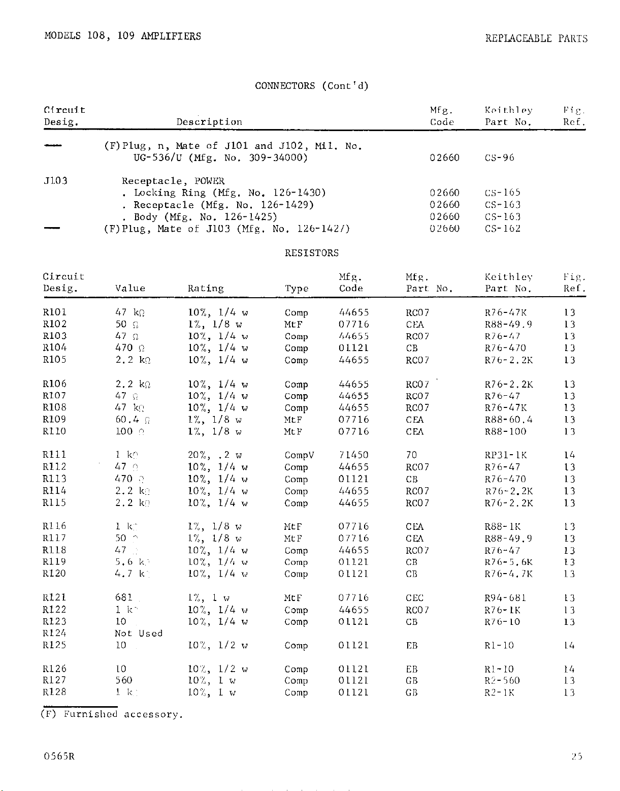
Circuit
Desig. Value
RlOl 47 kn
R102 50 i:
R103 47 n
Rating
lO%, l/4 w
l%, l/8 w
lO%, l/4 w
R104 470 (1 lO%, l/4 w
R105 2.2 kr?
lO%, l/4 w
R106 2.2 ki? lO%, l/4 w
R107 47 i
R108 47 k!l
R109 60.4 G
RllO 100 ?
lO%, l/4 w camp 44655
lO%, l/4 w Comp 44655
l%, l/8 w
l%, l/8 w MtF 07716
Mfg.
TYPO
Code
Comp 44655
MtF 07716
Comp
Comp
camp
44655
01121
44655
Comp 44655
MtF 07716
Mfg.
Part No. Part No. Ref.
RC07 R76-47K
CL% 1~88-49.9
RC07
CB
RC07
RC07
RC07 R76-47
RC07 R76-47K
CL4 R88-60.4
CrA R88-100
Kcithle) l:ig.
13
13
R76-47
R76-470
R76-2.2K
R76-2.2K
13
13
13
13
13
1, 3
13
13
Rlll 1 k?
R112 47 !~J
R113 470 ,?
R114 2. 2 k?
R115 2. 2 I<!?
Rll6 1 I<~~
R117 50 '~'
R118 47
R119 5. 6 I<~'#
R120 4.7 I<~
R121 681
R122
1 k ~'
R123 10
Rl24 Not Used
R125 10
R126 10
R127 560
R128 1 I<'
(I:) Furnished accessor)
20 % )
.2 w
lO%, l/4 w
lO%, l/4 w
lO%, l/4 w
lo%, l/4 w
l%, l/8 w
1x, l/8 w
10x, l/4 w
lO%, l/4 w
lO%, l/4 Xi'
1 % , 1 14
lO%, l/4 Iii
lO%, l/4 w
10x, l/2 r\'
lo'%, l/2 w
10 % ) 1 w
1.0 % ) 1 w
CompV
71450
44655
01121
COIlI;
Comp
44655
44655
MtF 07716
MtF 07716
Comp 44655
Comp 01121
Comp 01121
MtF 07716
Comp
44655
Comp 01121
Comp
C'Xllp
Comp
Comp
01121
01121
01121
01121
70 KI'31-1K
RC07 R76-47
CD
R76-470
RC07 R70-2.2K
RC07 R76-2.2K
CEA R88-IK
C&l
R&-49.9
RC07 R76-47
CB
R76-5.6K
CB RI&4.7K
CEC
RC07
R94-681
R76-1K
CB R76-10
EB Rl-1~0
CB RIG- 10
GB
I(?-560
GB R2-Ii;
14
13
13
13
13
13
13
13
13
13
13
13
13
1~ 4
14
13
13
0565R
? 5
Page 28

REPLACEABLE PARTS
MODELS 108, 109 AMPLIFIERS
TRANSISTORS
Circuit
Desig.
QlOl (108)
QlOl (109)
4102
Q103 (108)
4103 (109)
Number
SM492-1
SM492-1
SM492-1
SM492-1
SM492-1
(Refer to Schematic Diagram 17966C for circuit designations.)
Circuit
Desig.
Cl01
Cl02
Cl03
Cl04
Cl05
Value
75 I-if
75 pf
0.1 ,lf
2.2 lif
10 jlf
Rating
100 "
100 "
50 "
20 v
35 v ETT 05397 KlOJ35KS Cal-1OM
Cl06 100 jlf 25 v
Cl07
100 uf
25 v ETT 05079
Mfg.
Code Part No. Ref.
80164
80164
80164
80164
80164
MODEL 1081 REPLACEABLE PARTS LIST
CAPACITORS
Mfg.
TYPO
Code
ETB 56289
ETB
MY
56289
84411
Mfg. Keithley Fig.
Part No. Part No. Ref.
TEL4
TEL4
601PE C41-O.lM
ETT 05397 K2R2J20K C80-2.2M
ETT
05079
WlOO-25C2Ul
WlOO-25C2Ul C96-100M
Keithley Fig.
TG-17-5 14
TG-17-3 14
TG-17-3 14
TG-17-6 14
TG-17-3 14
CbO-75M
C60-75M
C96-100M
Circuit
Desig.
DlOl
D102
D103
D104
D105
Dl06
Circuit
Desig.
DSl
Fl (117 v)
Fl (234 v)
JlOl, 3102,
5103
DIODES
Keithley
Part No.
RF-20
RF-20
RF-20
RF-20
DZ-21
DZ-7
TYPO
Silicon
Silicon
Silicon
Silicon
zener
zener
Mfg.
Number Code
lN3253
02735
lN3253 02735
lN3253 02735
lN3253 02735
lN709 12954
lN935 04713
MISCELLANEOUS PARTS
Mfg. Keithley
Description
Neon Pilot Lamp (Mfg.
No.
2190)
Code Part No.
91802 PL-28
Fuse, quick acting, .2 amp, 8 AG (Mfg. No. 361.200) 75915
Fuse Holder (Mfg. No. 372001)
Socket
75915 FH-8
80164
Fig.
Ref.
Fig.
Ref.
FU-24
cs-135
26
0565R
Page 29

MODELS 108, 109 AMPLIFIERS
REPLACEABLE PARTS
MISCELLANEOUS PARTS (Con't)
Circuit
Desig.
---
Pl
--Sl
Tl
Cables for JlOl
(F)
Cord Set,
Cable Clamp (Mfg. No. SR-5P-1)
Slide Switch, Power (Mfg. No. G326)
Transformer
(F) Furnished Accessory
Circuit
Desig.
RlOl
R102
R103
R104
R105
Value
47 k!?
1.5 k;~!
15 c
3.3 kil
2. 2 1~3
Description
6 feet (Mfg. No. 4638-13)
RESISTORS
Rating
lO%, l/2 w
lO%, l/2 w
l%, l/4 w
'
lO%, l/2 w
lO%, l/2 w
TYPO
Comp 01121
Comp 01121
ww 01686
Comp 01121
Comp 01121
Keithle)
Part No.
184778
CO- 5
cc-4
SW45
TR-84
Keithlc)
Mfg.
Mfg.
COdC
80164
93656
28510
79727
80164
Mfg.
Code Part No. Part No.
ED
Rl~-47K
ED RI-1.5K
7009 R96-15
EB Rl-3.3K
EB Rl-2.2K
Fig.
Ref.
Fig:.
Ref.
R106
R107
R108
R109
l%, l/2 w
lO%, l/2 w
l%, l/2 w
10%. l/2 w
Circuit
Desig. Number
Ql
92
u3
2N1183A 02735 TG-31
2Nl377 01295 TG-30
2N1381
Description
Modified Connector, 2 required
Connector, Body
4
Pin blale Receptacle, mate of CS-163
4
Pin Female Receptacle, mate ni CS-162
DCb 79727
Comp 01121
DCb 79727
Comp 01121
TRANSISTORS
Mfg.
Code
01295 TG-8
MODEL 1083 REPLACEABLE PARTS LIST
Kcithlcy Part No.
CFE-15
R12-2.2K
ED Ill-33K
CFE-15
Rl?-1K
EB R76-47K
Keithley
Part No.
18493h
cs-191
CS-162
CS-1~63
Fig
Ref.
0266R
27
Page 30

REPLACEABLE PARTS
MODELS 108, 109 AMPLIFIERS
MODEL 1083 REPLACEABLE PARTS LIST (can't)
Description
Locking Ring, 2 required
Shielded Cable
01121 Allen-Bradley Corp.
Milwaukee, Wis.
01295 Texas Instruments, Inc.
28520 Heyman Mfg. Co.
44655 Ohmite Mfg. Co.
Keithley Part No.
~~-165
SC-25
Kenilworth, N. J.
Semiconductor-Components Division Skokie, Ill.
Dallas, Texas
56289 Sprague Electric Co.
01686 RCL Electronics, Inc.
North Adams, Mass.
Riverside, N. J.
71450 CTS Corp.
02660 Amphenol-Borg Electronics Corp. Elkhart, Ind.
Broadview, Chicago, Illinois
71590 Centralab Division of
02735 Radio Corp. of America Globe-Union, Inc.
Commerical Receiving Tube and
Milwaukee, Wis.
Semiconductor Division
Somerville, N. J.
72982 Erie Technological Products, Inc.
Erie, Pa.
04713 Motorola, Inc.
Semiconductor Products Division 75915
Littelfuse,
Inc.
Phoenix, Arizona Des Plaines, Ill.
05397 Union Carbide Corp.
Linde Division
Kemet Dept.
Cleveland, Ohio
07716 International Resistance Co.
Burlington, Iowa
12954 Dickson Electronics Corp.
Scottsdale, Ariz.
14655 Cornell-Dubilier Electric Corp.
Newark, N. J.
TABLE 7. Code List of Suggested Manufacturers.
facturers, Cataloging Handbook H4-1,)
79727 Continental-Wirt Electronics Corp.
Philadelphia, Pa.
80164 Keithley Instruments, Inc.
Cleveland, Ohio
84411 Good-All Electric Mfg. Co.
Ogallala, Nebr.
91802 Industrial Devices, Inc.
Edgewater, N. J.
93656 Electric Cord Co.
Caldwell, N. J.
(Based on Federal Supply Code for Manu-
0266R
Page 31

Page 32

Page 33
Page 34

Page 35
---- ------- ---___-- ---- ------- ---___-4 4
% %
&i &i
\9 \9
?g ?g
b\ b\
“C
v v
a +“! a +“!
<TN ;1\ <TN ;1\
&I &I
I’+ I’+
- -
Page 36

 Loading...