

Page 1

INSTRUCTION MANUAL
MODEL 103A
NANOVOLT AMPLIFIER
0 COPYRIGHT 1974 0 COPYRIGHT 1974
KEITHLEY INSTRUMENTS. KEITHLEY INSTRUMENTS.
20775 AURORA ROAD CLEVELAND. OHIO R413Y ,216, 24~~0400 20775 AURORA ROAD CLEVELAND. OHIO R413Y ,216, 24~~0400
TELEX~ 98~5469 TELEX~ 98~5469
PRlNTED IN “.SA. PRlNTED IN “.SA.
CAOLE KEITHLEY CAOLE KEITHLEY
I NC. I NC.
Page 2

CONTENTS
Page 3

ILLUSTRATIONS
Fig. NO.
1
2
3
4
5
6
7a
7b
8
9
10
11
12
13a
13b
14
15
16
17
18
19
20
21
22
23
24
25
26
27
28
29
30
31
32
33
34
Ti,tle
Front Panel, wadcl, 103*.
Front Panel Controls and Terininal~s.
Rear Panel - Models 103A and 1031*.
overall Block ILt@-am.
Single-Ended Mode.
Uifferenrinl Mode.
Power Rcceptncle.
Power Ilqmfi connection.
Johnson Noise/ Hz Versus Source Resistance.
cain/Phnse vs. Frequency for R-C Type Filter.
Equivalent circuit Far Noise Analysis.
use Of Model 1037 Transformer.
Noise Bandwidth.
Noise CoDtoUr Single-Ended Mode.
Noise Contour Oiiferential Mode.
use as an cmill.oscope Preamplifier.
"se in System 84 Lockin Amplifier.
Model 2000 Rack Mounring.
Model 100, Dual Kack Mounting.
Overall Block r1i.ap,ram.
Non-inverting Stage "A".
Non-inverting stage '93".
Single-ended Mode.
"ifferenfisl Mode.
Nan-inverting stage "I?".
Nan-inverting Stage “F”.
High-Law cut Filter.
DC Offset Adjustment.
t18" Power supply.
camponent Layout, K-293.
component Layout, PC-294 (Mother Board).
Component Layout, PC-295 (Model 1031A Power Supply).
Component l.uyout, PC-261 (Model 1031A Regulator).
Tese Set-q For Frequency Response Check.
Chassis Assembly, Exploded View.
Bottom cover Assembly.
,‘URC
1
3
3
4
4
4
5
5
6
9
10
10
11
11
12
12
13
14
16
16
16
17
17
17
17
18
18
19
19
20
21
22
24
29
29
Page 4

Page 5

SPECIFICATIONS
SPECIFICATIONS
0371
I<l3,‘?‘EIL.~-#
103A NANOVOLT AMPLIFIER
Page 6

SECTION 1. GENERAL DESCRIPTION
l-l.
GENERAL. The Model 103A Nanovolt Amplifier is
an ac amplifier intended for use in high-gain low-
noise applications.
MODEL 103A AMPLIFIER
b. Adjustable frequency Sesponse. A combination of
high cut and low cut filter sections permit selection
of optimum irequency bandwidth.
C. Overload Indication.
An automaeic overload indication circuit detects overloads under various operating conditions.
1-2. FEATURES.
d. High Output Level.
The full scale weput is ten
a. Selectable Input Mode. The input mode can be voles pk-to-pk (d-c coupled) to easily drive a recorder,
set far either single-ended or differential configura-
amplifier, or oscill~oscope without further amolification.
Front Panel Controls and Terminals
Control or Terminal
INPOT Switch (S201B)
A-B Input
-B Input
O"ERLO*o RESET Swiech (S201A)
3 dB FREO HZ Switch Sets overall amplifier frequency response.
HIGH Filter (S3"lA)
LOW Filter (S301B)
GAIN Switch CS302)
GAIN ADJUST Control (X306,
sets inpue “ode as follo”s:
“Ffferential Mode.
Single Ended Mode.
Activates overload reset circuitry.
Sets High Cue
sets LO" Cut
sets overall gain. in 20 dB steps.
Adjusts gain over 2” dS span.
Funceianal oescripekm
Paragraph
2-4, a
2-4, a
2-4, a
2-4, a
2-4, a
2-4, a
INPUT A cJ202~
INPUT B (5201~
HIGH "UT (53011
LOW "UT (53021
“vERL”A” Lamp toslol~
Control or Terminal
POWER INPUT (P301)
DC OUTPUT ADJ.
Control ii1 (R312)
Control 112 (R311)
2
Non-inverting
Inverting Input receptacle.
Input receptacle.
High output receptacle.
LOW output
receptacle.
Indicates overload condition.
Resr Panel Controla and Terminals
TABLE l-2.
Functional OescriptFon
Input receptacle for 518” power.
Adjusts dc oueput offsets.
2-2, a
2-2, a
2-2, b
2-2, b
2-5,
Paragraph
2-2, c
2-5, i
d
0371
Page 7

INPUT MODE SELECTION
r
A-8 -J ""CRI."*D
INPIJC INPUT
5201
5201
%T
GENERAL DESCRIPTION
GAIN
ADJtJST SWiLCh
R306 s302
GAIN
INPUT
A
INPUT
""EilLOA"
B
FIGURE 2. Front Panel Controls and Terminals.
Lamp
LOW
FRCQ
HIGH
FREQ
5301 J-301
L."W
0 ,rr
IIICI,
"LT
"272
FIGURE 3. Rear Panel - Models 103A and 103ln
3
Page 8

OPERATION
MODEL 103A AMPLIFIER
SECTION 2.
2-1. THEORY OF "PEKATION.
a. General. The Model 10311 Nanovolt hmplifier is
a high gain voltage amplifier designed for use with
single ended or differential inputs. 'The amplifier is
essentially composed of two high impedance inpue am-
plifiers, a summing amplifier, a combination high-l.ow
c,,t filter section, two stages of X10 gain, and an
output buffer amplifier as she"" in Figure 4.
b. Single-Ended Mode (-B INPUT). In this mode the
input amplifiers are connected together to form a
single-ended inverting amplifier as shown in Figure 5.
The signal at INPUT H will be amplified and inverted.
The signal at INPLTI A is not connected. Amplifiers
"A" and "s" are summed co provide very low noise characteristics.
Differential Mode (A-B INPUT). In this mode the
C.
input amplifiers are conneceed as separate amplifiers
which are summed differentially as shown in Figure 6.
The oueput is a funceion of A-B times the gain of the
amplifier.
OPERATION
2-2. C”NNIICTI”NS.
Input. 'I‘he
a.
designated "INPUT A" and "INPUT il". 'These receptacles
(5201 and 5202) at-2 BNC types which mate with coaxial
cables such as Keithlcy Models 8201 and 8202 coaxial
cables. 'he inner coneact of each receptacle is the
circuit high. The outer shell ia the circuit low
which is floati,"g wit,, respect co the Model l"3h chas-
sis. Only INPUT B should be used for single-ended
input operation. For differential operation both inputs should be used.
modes is given in Section 2-5.
b. output.
cles designated "LOW "UT" and "HIGH "UT". These re-
ceptacles (5301 and 5302) are BNC types which mate
with coaxial cables such as Keithley Models 8201 and
8202
coaxial cables. The inner ConfaCt of "LOW am@'"
receptacle is at ci.rcuit low (the same as the outer
shell of INPUT A and INPUT B). The inner contact of
"HIGIl OUT" is the amplified output. me outer shell
of each ""UT" connectc,r is at chassis ground. There
Model 103A has two input receptacles
A complete discussion of input
the b,odel 103A has two oueput recepce-
INPUT6
INPUTA
“A”
FIGURE 4.
Overall Block Diagram.
FIGURE 6. Diffcrcntial Mode
4
“371
Page 9

CHASSIS
INPUT E
+1t3v 8 D -18V
@
c
P301
LOW
INPUT A
Page 10

,,.
,,,~;
;..,,
OPERATION
2.
Flicker noise (l/f). 'this noise has a characteristic of constant energy per percent bandwidth.
Random noise such as generated by tubes and trans-
istors shows a low frequency characteristic or l/f
relafionship.
3. oiscrete Frequency Noise. This is noise gen-
erated by various discrete frequency sources such
as power lines, radio frequency generators, etc.
b. Shielding.
1. Electric Fields.
Shielding is usually necessary when the instrument is in the presence of very
large ac fields or when very sensitive measurements
are being made. The shields of the measurement circuit and leads should be connected together to ground
at only one point.
This provides a "tree" configura-
tion, which minimizes ground loops.
2. Magnetic Fields. Magnetic shielding is useful
where very large magnetic fields are present. Shield-
ing, which is available in the form of plates, foil
or cables, can be used to shield the measuring cir-
cuit, the lead wires, or the instrument itself.
c. Grounding. The Model 103A has been designed to
operate with either the Model 1031A Power Supply or
the Model 840 Amplifier. The circuit low is isolated
from chassis ground by a 10 ohm resisror in the power
supply. For best results, no other connection should
be made between circuit low and chassis ground. Since
the yodel 103.4
chassis is connected to earth ground
through the accessory power cable, it is not necessary
to connect the Model 10% chassis to ground.
when the
yodel 103~ is connected to the yodel 840 differential
inouc (as shown in FFrwre 15). the m!xR of the Model
840 minimizes the effects of ground loops.
a. Front Panel.
1. INPUT Switches (52018). These switches are
pushbutton types wit,, two "orma configurations. The
switch posi~i.ons are designated as "A-B" and "-U".
'These two pushbuttons are interlocked so that depressing one will release the Other automatically. H0C.T"~~
it is
possible
to depress both or have
both buttons
released but these conditions are not useable modes
Of operation.
2. O"EKLOA,l RESET Switch (S2Olh). This switch is
a momentary contact pushbutton type. The overload
reset circuit is activared only when the pushbutton
is depressed. When the OVERLOA" lndicaeor light goes
off the reset has been accomplished.
3dn FKEQ Hz (5301).
3.
concenrric type.
filter in ten positions from 10 11% co 300 k"Z.
'l'he inner dial sets the "IlIGil Cut"
This switch is a dual-
me
outer dial sets the "LOW Cut" filter in nine posi-
tions from 0.1 to 10 kllz.
4. GAIN.
Gain is set by use of a dual-concentric
GAIN switch 5302 and GAIN ADJUST control R306. The
GAIN hD.JUST control has a "CAL" position when set
to fully clockwise.
b. Rear Panel.
1. DC OUTPUT AOJ "1" (R312).
These controls adjust
the dc output offset.
6
FIGURE 9. Gain/Phase Vs. Frequency For R-C Type Filter.
0371
Page 11

0371
7
Page 12

MODEL 103A AMPLIFIER
Gain settings of Model l”3A
TABLE 2-3.
CAIN switch GAIN AD.J”ST
Overall Gain
setting setting (C) Possible
Of the IIICII-LOW cut filter which may not cause an
overload at the ourpuc. since a &refilter oVerload
may occur due t" large amplirude noise signals, the
overload is sensed and the OVERLOAD indicator is
lighted whenever an overload condition is present.
However, prefilter overloads above 100 km may not
be detected.
the output stages due tc’ saturation.
put will saturate when drive" beyond 10 volts &peak-
d. Overloads. Although clle Model 103A aaplifier is
ac coupled to the input, rtle amplifier has been designed
to have a very low frequency response. Therefore the
internal circuits have very long time constants. me
long time COnSrantS affect the operation of the Model
103A under input overloads and power turn-on
Three types of overloads must be considered in this
discussion.
conditions.
ra-peak, the OVERLOAD indicaror will be lighted as
long as t,,i.s canditian cxiscs.
lOad condition, the GAIN setting can be reduced, the
input signal can be attenuated, or fil~Lered through
the use of the HIGH-LOW cut filters. The O"CRI.oAD
K1:SF.T button can be used t0 restablish normal bias
conditions in the amplifier.
Calibrated
(Yes or NO)
wefilter ""erloads. Overloads can occur ahead
2.
3. Steady-state Overloads.
Overloads can occur in
Since the WC-
TO remove ibe "Ye=-
0371
Page 13

Page 14
“opt =
Eq. 6a
MODEL1037
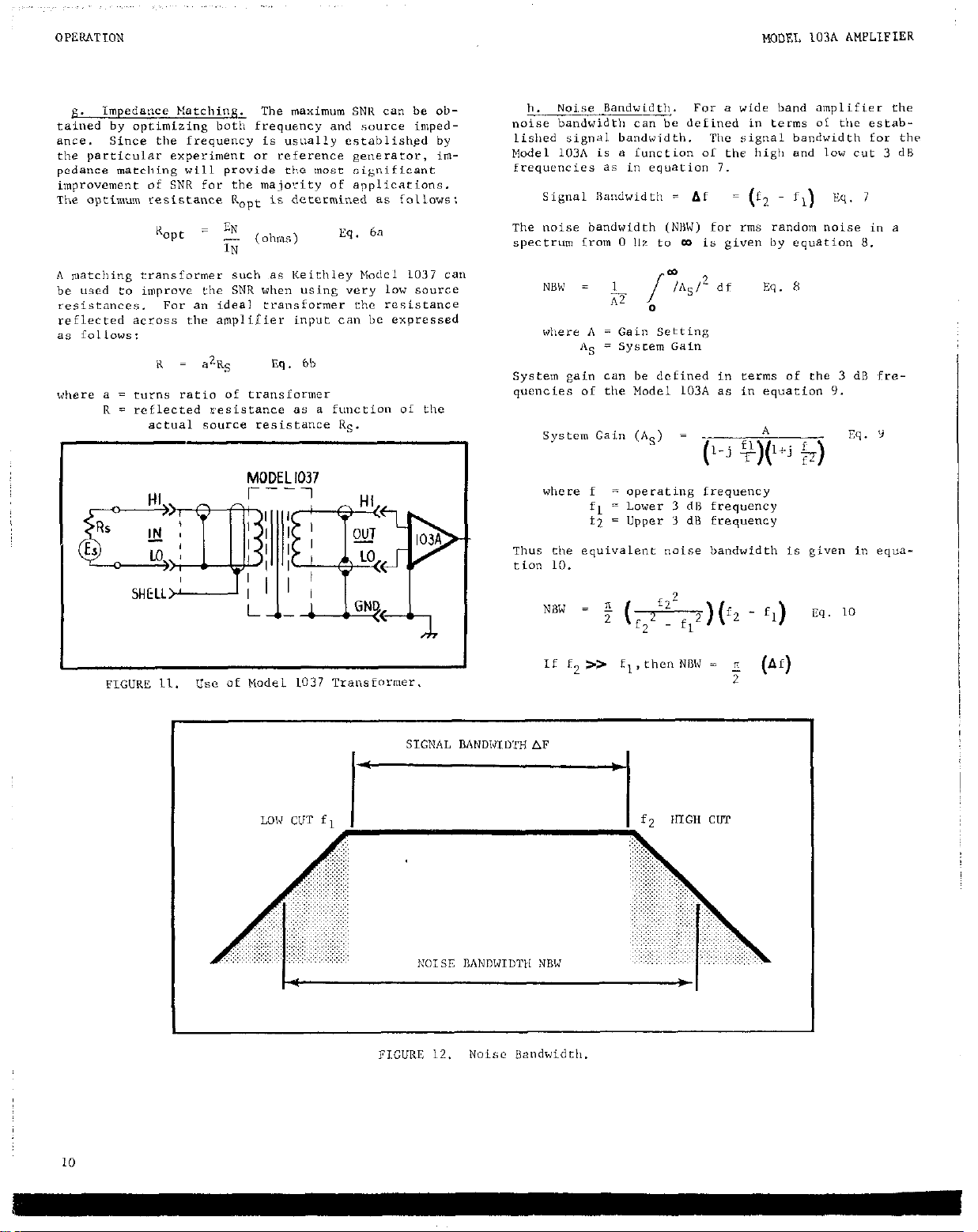
Thus the equivalent noise bandwidth is given in equation 10.
10
Page 15

OPERATION
0371
Page 16

APPLICATIONS
MODEL 1038 AMPLIFIER
SECTION 3.
3-1.
GENERAL. AlthouSh the Model 103A can be used as
El general purpose insfrument, a few specific applica-
tions Can more fully illustrate the important features.
3-2.
TYPICAL APPLICATIONS.
a. Oscilloscope Preamplifier. men used as a preamplifier for a dull input oscilloscope the Model 103A
CB” be connected as shown in Figure 14.
scope chassis should be conneceed to earth ground directly. The Model 10%. out,,uts can be connect differ-
entially or single-ended if necessary.
ing the Model 103A output to a single input oscilloscope, the NIGH OUT receptacle should be used.
the Model 103A low is isolated by 10 ohms above chassis
ground when powered by the Model 1031A, no other connection is required. If another power supply is used
such as batteries, it is necessary to connect a 10 ohm
resistor between low and chassis.
b. Lock-in.System Preamplifier. When used with a
phase-sensitive detector such as the Keithley Model
840 the Model 103A can be connected as shown in Figure
15. In this application the Model 103A outputs mate
with the differential input of the Model 840 thereby
minimizing ehc effects of ground loop connections.
this application
input “ode.
pr.ovides law and ground as well as +I8 volts, it is
not necessary to connect the Model 103A chassis to
earth Sround.
the Model 840 should be set for “01~~”
Since the Model 840 accessory power outpx,t
me oscillo-
men c”nnect-
Si”CC
For
APPLICATIONS
F10Lnuz 14.
FIGURE 15. “se in System 84 Lockin Amplifier.
Use as an Oscilloscope Preamplifier.
OSCILLOSCOPE
POWER GND
Page 17

MODEL 10% AMPLIFIER
ACCESSORIES
SECTION 4. ACCESSORIES
The
GENERAL.
4-l.
be used with the Model 103h to provide additional convenience and versatility.
the Model 2000 is a rack mounting kit which converts
any half-rack, Style M instrument irom bench mounting
to rack mounting in a standard 19-inch rsck. The
dimensions are 3-l/2” high x 19” wide. The hardware
included in this kit consists of B blank panel which
can be mounted on either side of a half-rack instrurent.
following
Keithlcy
accessories
Model 2000 Rack Mounting Kit
can L-2. OPNATING INSTKUCTIONS.
Manual is supplied with each accessory giving c~mpluie
A sepvracc 1nser,,ctio,,
operating information.
FIGURE 16. Model 2000 rack pouncing
Models 8201, 8202 Coaxial Cables
Description:
These cables are coaxial types with BNC ConneCtorS an
each end. The wade1 8201 cable is 10 inches long
while the Model 8202 is 20 inches.
Application:
These cablc2s mate with the RNC receptacles On the
Models 103A and 840.
Page 18

..,,..,
.,
,,~
~,
,~,
,,,,
.~.
.,.
,,,,.
ACCESSORIES
MODEL 103.4 AMPLIFIER
Description:
The Model 1007 is dual rack mounting kit with overall dimensions 3-l/2” high and 19” wide. The hard-
ware included in this kit consists of two Angle
Brackets, one Mounting clamp, and extra mounting
screws.
Application:
The Model 1007 converts any half-rack, style M instru-
ment from bench mounting to rack mounting in a standard 19-inch rack.
Installation:
a. Before assembling the rack kit, determine the
position of each instrument. Since the instruments
can be mounted in either location, their position
should be determi”ed by the user’s measurement. The
following instructions refer to instruments “A”
and “B” positioned as shown in Figure 17.
b. Once the position of each instrumenr has been
determined, the “side dress” panels (Item 11) on
adjacent sides should be removed. Removal is *ccomplished by loosening the socket head screws (Item 24)
in two places.
Slide the “side dress” panels to the
rear of the instrument to remove.
c. The “mouneing clamp” (Item 23) is installed on
instrument “A” using the original hardware (Item 24).
With the socket heed screws removed, insert Lhe “mounting clamp” behind the “corner bracket” (Item 7) and
replace the screwy to hold the mounting clamp in place.
Parts List:
Item
NO.
Description
21 Angle Bracket
22 Screw, #6-32x5/8, Phillips
23 Mounting Clamp
24 Screw, #6-32x1./2, FH Socket
WY
Req’d Pare No.
2
4
1
4
Keithley
24783h
24798B
(original hardware)
25 Screw, #6-32x1x1/8, Phillips
26 Kep Nut, #6-32
1
1
d. Tighten the socket head screw (Item 24) on
instrument “B”.
Insert the “mounting clamp” behind
the “corner bracket” on i”str”ment “B” as show”.
e. When mounting instruments having the same depth,
a screw (Item 25) and kep “UC (Item 26) are required
to secure the Tao instruments together.
f. Attach an “angle bracket” (Item 21) o” each
instrument using hardware (Item 22) in place of the
original hardware (Item 24).
g. The bottom cover feet and tilt bail assemblies
may be removed if necessary.
h. The original hardware, side dress panels, feet
and tilt bail assemblies should be retained for future
conversion back to bench mounting.
FIGURE 17. Model 1007 Dual Rack Mounting.
Page 19

Page 20

SECTION 5.
CIRCUIT DESCRIPTION
The overload and fil,ter circuits are located 0” the
"Overload Board", PC-293.
COMMON
MODE
OVERLOAD
PREFILTER
OVERLOAD
INPUT4
Fotentiometer R244 adjusts bias current through resis
tars K213 and R214.
OUTPUT
OVERLOAD
0371
Page 21

stage “C”.
C.
graced circuit QAZOlA and various gain set resistors
which are connected for either single-ended or differ-
ential mode.
1. Single-Ended Mode.
“A” and “B” are connected as sunming i,,,,,uts to
amplifier “C” as shown in Figure 21.
amplifier “C” is deLermined by resistors K247, R248,
and R249 as foll~ows:
This amplifier is composed of inte-
liar this made mplifiers
The gain of
R248
I
FIGrn 21.
d. Stape ‘9”. This amplifier stage is a unity-gain
buffer amplifier composed of Qh301. Thi., amplifier is
a self-contained voltage follower integrated circuit
package.
Stage “E”. This amplifi~cr stage is composed of
e.
integrated circuit QA302.A connected as a non-inverting
amplifier as shown in Figure 23. Gain is sef by re-
sistors R308 and K313, where:
Single-ended Mode.
I
Page 22

fL (3 dill = I
2T!RC = c
10
where c = value in UT.
HIGH CUT FILTER
LOW CUT FILTER
r-----l m
c313
T"
+ R311 -
v
a. blather Hoard.
provided by separate transformer windings and bridge
rectifiers as shown on schematic 24.8080.
Power for the 5’8” supplies is
18
Page 23

L
Page 24

1~‘~
~.~
~.~
..,,,.,..
,,~
.,
~,~
COMPONENT LAYOUTS
;; j
t
1;
MODEL 103A AMPLIFIER
20
FIGURE 29. Component Layout, PC-294 (Mother Board)
0371
Page 25

COMPONENT LAYOUTS MODEL
103A
AMPLIFIER
6
A J201
T 201
FIGURE 30.
Component Layout, PC-295 (Model 1031A l'owcr Supply)
21
Page 26

j’
,.~
~,
,~~
,.
COMPONENT LAYOUTS
MODEL 103A AMPLIFIER
FIGURE 31. Component Layout,
PC-261 (Model 1031A Regulator)
0371
Page 27

CALIBRATION
SECTION 6.
REQUIRE” TEST Eq”IPMI(N1‘. Test equipment need-
6-2.
ed for calibrating rhc M”del~ 103A is described in
Table 6-l.
AD.J"STMENT AND CALIlw.ATION FROCED"RE.
6-3.
procedure should be used whenever ie is necessary to
calibrate the Model 103.4 to emure chat it meets
published specifications.
This
CALIBRATION
Initial Turn ON.
a.
1. Place shorting caps on both INPUT A and "
and set INPUT switch (5201) to A-".
2. set both the LOW FRZQ. and IIICH PKI:Q. SWiLCh
(S301) to the 1K position and set the GUN t:o 100
and the ADJUST pot (R306) full CW (CAL).
3. connect the power cable from one of the *ea*
pane1 outputs Of the Model 103111 (ItaIl I) to the
POWER INPUT cOnneCtor (P301) on the rear pane1 of
the Model 1031\ and turn the Model 1031A on.
4. hfter about 5 to 10 seconds, the O"ERLOnU
Lam iDS101) should be liehted and after iibout 1
b. Bias Adjustment.
1. Set the Model 10% INFUT to A-ii and connect
the DC Voltmeter (item B) between TF-201~ and 'TX'-203.
DC Voltmeter must be floating.
0874
23
Page 28

MODEL 103A
3. Adjust the 300kHZ trlmlller capacitor (C311)
far 1.4 volts peak-to-peak at the Mode1 103A OUTPUT (-3dR).
6-4. CUECK-OUT PKOCl?D"RE.
a. Gain Check.
1. ConneCt Potentiometer (Item II) to the Signal
Generator output, connect the Potentiometer output
to the input of the AC Ratio Standard. "sing the
Signal Generator variable-attenuator and the Paten-
tiometer (Item It), set the signal at the AC Ratio
Standard input for loom" t lOOIl" RMS at 100 HZ as
monitored on the AC Voltmeter.
2. Connect the output of the AC Ratio Standard
to the -B INPUT of the 1o3A and set the 1o3A conrro1s as follo"s:
LO cut - 0.1 NZ
Hi Cut - 300/.&
Gain - 100
3.
Connect the OUTPUT of the Mode1 103A f~ the
input of the AC "oltmeter and set the AC Voltmeter
Controls as follows:
Flange Full. Scale - 5 Volts
Null Full Scale - loom"
Function - AC
Dials - 1.0000
4.
see the AC Ratio standard dials as follows:
10-l 10-2 10-3
1 0 0 0 0
The AC "oltmeter should read 1.0000 volts ? 101""
KMS.
10-4 10-5 10-6 10-7
0 0
5. set the AC Ratio standard dials as follows:
lo-1 10-2 lo-3 10-4 lo-5 10-6 10-7
0
1 0 0
and eet the 103A gain to 1k.
6. The AC "oltmerer should rend 1.0000 vole i
lh" KM.
7. Set the AC Ratio Standard dials as follars:
10-l m2 10-3 IO-~ 10-5 10-6 10-7
0
0 1
and set the 103A gain to 10k.
8. The AC Voltmeter should read 1.0000 volt *
lOIn" RMS.
9. Turn the Mode1 103A GAIN ADJUST (~006) full
ax.
The AC Voltmeter shauld now read less than
loom".
b. Frequency Response.
1. Connect the Signal Generator CO the 20 dB pads
and 50 ohm termination as shown in Figure 35 and set
the Signal Generator for 35,"" t 35011" at the 50 ohm
termination as monitored on the AC Voltmeter.
2. Set the Sijyal Generator frrquency to ISkHz,
the 103A GAIN to 100 and connect the test set UD as
shown in Figure 35.
3.
set the hC "oltmeeer conrro1s as follows:
Range Full Scale - 5 volts
Null Full Scale - loom"
Polarity
Dials
AC
- 3.5000
0 0 0
0 0 0 0
TEE
CONNECTOR
r--,
SIGNAL
GENERATOR _
24 0874
20 08
PAD
FIGURE 32.
20 rJ8
PAD .
Test Set-up for Frequency Respxwe Check.
I I
I
L---J
500
TERM.
I
MODEL
103A
Page 29

0874
_’ ‘i
Page 30

Page 31

SECTION 7. REPLACEABLE PARTS
7-4. HOW TO ORDER IaRTS
a. Replaceable parts may be ordered through the
Mother iioilrd, Part 1
Mother I3oard, Part 2
Filter & Overload
Regulator (103LA)
Power Supply (1031,A)
I
I
Page 32

2
3
1”
11
4
i
%
4
4
2
2
14
15
16
17
i
4
4
4
Page 33

)DEL 103A
REPLACEAULE PARTS
0874
F%GUIW 33.
Chassis Assembly - i:xplodcd View.
Page 34

Cl04
Cl”5
MODEL 103A AMPLIFIER
Cl06
c1.07
Cl08
Cl09
Cl10
Clll
OlOl
“102
“103
0104
010.5
25 v
25 ”
25 ”
2” v
25 v
25 ”
20 ”
25 ”
EM.
EAL
EAL
ETT
ML
E/IL
ETT
I:AL
29109 JC810025"F
29309
29309 IC81002.581'
17554
29309
17554
29309 JCR10025RP
JC1250025HF
TSD1-20-I",,F
JC8100258P
TSD1-2"-1",,F
2”
28
28
28
28
28
28
28
Page 35

Kill 10 kn
R112 10 kfl
K113 10 kfl
K114 560 12
R115 10 0
lO’X, l/4 w
LO%, 114 w
lO%, l/4 w
IO%, 112 w
lo%, l/4 w
44655
44655
44655
01121
44655
Gil-560-10%
CD-loo-10%
~116
RI17 1 1‘0
I<118 10 ki,
R119 100 ki?
R120 1 kfl
K121 1 kfl
R122 100 kfl
R123 10 kll
R124 1 kn
R125 1 kcl
KU6 100 n
KU7
QlOl
4102
Q103
Q104
Q105 Silicon, NPN, case TO-92
QlO6
Q107
10" n
1 k0
Silicon, NW, Case 'X-106
Silicon, PNP, Case K-110
SilLcon, NPN, Case TO-106 07263 2N3565 K-39 28
Silicon, NW, Case TO-92
si.licoLl, PNF
Silicon, FNF
lO%, l/4 w
lo%, 114 w
1'L, l/B w
I%, I~/8 w
lo%., l/4 w
I"%, l/4 w
If, l/8 w
I,%, 1/a w
LO%, l/4 w
lo%, l/4 w
lo%, l/4 w
LO%, l/4 w
44655
44655
07716
07716
44655
44655
07716
07716
44655
44655
44655
44655
TRANSIST”RS
Mfr. Mfr.
07263 2N3565 K-39 28
07263 517638 'K-33 28
04713 2N5089 K-62 28
04713 2N3904 TG - 4 7 28
04713 ZN3906 'X-84 28
04713 IN3906 'X-84 28
CEA-lOOK-1%
CEA-lOK-1%
CB-102-10%
L(eithley
Fig,.
CI~79-1OM
C47-.1M
600 "
20" v
C206 1.00 WF
C207
C2”8
C209
C210
c211 7-25 pl> 300 " var 72982 538-037 C175-7/25P 29
c212 .0022 Ifi 1000 v CcrD 72982 81100OXSF0222K C22-.0022H 29
C213 .0022 Iii‘ 1000 v CerD 72982 811000X5F02%2K C22-.0022M 29
C214 100 $lF 15". 10% I:TT 06751 TS"SI5107h C205-lOON 29
C215 100 @F I"", 10% ETT 06751 TSD515107A C205-100&f 29
0874
I,00 pF
470 pP
470 pF
.OOl p
15", 10%
15", 10%
100" v
1000 v
1000 "
72982 801-Z5UO-472M
13050 SMlh-0. lUF
06751 TSD515107h
06751 TSD515107A
56289 m-471-10% C64-47OP
56289 m-471-10% C64-470P
72982 8o1ooox5Po
C22-.0047N
C47-.lM
c205-100M
C205-lOOEI
C64-.OOiEf 29
29
29
29
29
29
29
29
29
31
Page 36

CEA-1%-l%
CEA-15K-1%
CEA-LOOK-1%
WA-lOOK-1%
ma-15K 29
R88-15K 29
K88-1”OK 29
R88-10°K 29
K12-10M 29
R211
II212
R213
R214
K215
cmnp
MtF
camp
MtF
MC
MLF
MC
MU
MCF
MCF
75042
07716
75042
“7716
1137.10’) 29
CI‘A-IOK-1%
CEA-K-l%
CCA-301-I%
m-1/8-200
MMF-l/K-1.8K
CI:A-,~OK-I%
CC/I-IK-1%
Page 37

11226
R227
1R228
11229
R23”
KEPLVCEABU FAKTS
II231
11232
11233
K234
K?35
R236
R237
N238
11239
R240
K241
11242
I<243
R244
R245
R251
R252
R253
R254
R255
R256
R257
1”
1” kR
1”
WA-IOK-, %
CF.&?OK--L%
CEA-49.9&l%
CIFF-l/R-*I(
MFF-l/X-1OK
MW-l/II-X
“7716
CC*-9.76K-l%
“7716 CEA-IOK- I%
91637
37942 MTC-1.4
n
n
44655
446i5
0,716
44655
!4FF-l,/&IK
CII-330-l"%
CD-100-l”%
CEA-l”K-I%
CR-102-l”%
1K76-33
K/6-33
K88-1°K
K76-I”
QT"l
Q202
9203
4204
4205
Q206
Q207
9208
q209
Q21"
Q211
q212
Q213
Q214
0874
"4713
17856
"4713
“4713
"4713
"4713
Page 38

REPLACEABLE PARTS
""DEL 103A AMPLIFIER
C306
c307
C308
c309
C31"
c311
c312
C313
C314
C315
C316
C317
C318
c319
C32"
1”
1
.33 pF
.I s
."33 p
.Ol pF
.0033 p.F
,001 pJ
33" @
82 pF
7-25 pF
1" liF
100 p
1"
I
$
.33 p.F
.I pF
,033 @
.Ol pF
.a033 pF
20 ”
2" "
2" "
100 "
200 v
1""" "
2"" "
100" v
1""" "
300 v
20 "
15 v
20 "
2" "
20 "
1"" v
20" "
i.00" v
""Wm AMPLIFIER,
CAPACITORS
"300" SERIES PC-294
Mfr.
-
Code
17554
17554
17554
TSDl-2”-1”UF
C179-1"M
TSDl-ZO-1llF C2"4-lM
TSDL-20-0.33UF C2"4-.33M
29
29
29
"
84171
14659
84171
72982
72982
72982
17554
"6751
17554
17554
17554
8848"
"4171
14659
3FR3331E
ZPJ-"."I!JF
loss-"33
C146-."33M
Cl"8-."*M
C64-,""33M
2P.h0."01!JF Cl"R-."OlM
831000X5F
Cbb-3301'
831"""X5F C64-3301'
538-037 C175-7/25P
TSD1-20-10VF c179-LO?,
TsD515-100,~P C205-1""M
TS"l-2"-l"L!F C2"4-I",!
TsDl-z"-l,~F
C2"4-1EI
TSDl-ZO-0.33uF C2"4-.33W
3F113331F
2P.L"."lvF
Clbb-.0333
C1"8-."lM
1055-033 C64-.0"33M
29
29
29
29
29
29
29
29
29
29
29
29
29
29
29
C321
c322
C323
C324
c325
C326
C32,
msig.
QA301
QA302
QA303
Circuit
mstg.
5301
5302
5303
5304
P301
8301
5302
D301
no5
5306
,001 pF
.01
1"
.Ol
$
1" UF
1"
10
20" "
6"" "
2" v
60" "
2" v
2" "
20 "
Type
Operational Amplifier
Integraeed circuit, (Dual)
"pera~ional Amplifier
Type Code Part NO. Part NO. Kef.
Receptacle, RNC
Recepracle, RNC
connector, Housing
conrlector, Housing
Receptacle, Male, 4 Pins
Switch, Rotary, "Lo/in CUT"
Switch, Rotary, "CAIN"
Diode
Not Used
Keceptaclc, 22 Pins
84171
72982
17554
72982
17554
17554
17554
ZPJ-"."olUF
871-25U"G103?1 c22-."I
TSDI-2"-I",,F
871-25""-103x c22-."1
'TSD1-*a-1"UF
TSDl-*"-l"uF
TSD1-2"-1"uF
C1"8-.""1?1
C179-IO?,
C179-lot.1
c174-10%
C179-1"M
Mfr. Keichley
Code
1204"
"7263
1204"
Part NO.
LM31OH IC-18 29
"6E7739393 IC-28
LEL3101, IC-18
Fart NO.
MlSCELLANE""S
Mfr. Mfr. Keithley Fig.
95712 6672NT34 CS-15
95712 6672NT34 CS-15
22526 20370 CS-251
22526 2037"
CS-251
"266" 126-1427 CS-162
80164
SW-342
SW-342
801.64 SW-341 SW-341
"1295
09922
lN914 RF-28
PSC4SS2212
cs-182
29
2')
29
29
29
29
29
Fig.
Ref.
29
29
Page 39

MDEL 103A AMPLIFIER
REPlACEABLE PARTS
44655
07716
11306
R307
R308
R319
K320
R321
R322
K323
15
I
1
k0
20x, *
kR “.l%,
0
0
R
lo%, l//i w
102,
IO%,
1” 0 1m,
kc2
2
I/.,
1” n 10%.
1 ICI7
I.“%, l/2 hr
1” n lo%,
l/8
w
l/8
W
l/4
w
11637
l/4
w
114
w
114
l/4
W
w
w
MODEL
"7716
l"31A
IIEG"TAIT"K ""AK", "10"" SI:RIliS,
7145"
91637
"7716
91637
91637
44655
44655
91637
44655
44655
44655
“1121
44655
POWER SUPPLY
PC-261
iNP74-5°K
RF71.-50x
29
29
CL"1
Cl02
CL"3
Cl"4
Cl"5
Cl"6
1" m
47"
pF
2" "
1""" v
10 pF 2" v ryr
1" fl
47"
PF
2" " ETT
10"" " Cer"
1" ILF 20 " ETT 17ss4 TS",-2" c 17 9 - 1 ON
ETT
ccro 72982 801000x5F" C64-1,701'
Circuit
hsig.
QlOl
Q102
QAlOl
QAlOl Inregrated Circuit, Rcl-crence Amplifier
J101
J102 Test Jack
J103 Test Jack
x04 ‘rest Jack
"874
Type
‘Trnnsistor, NFN, Power) case TO-66
Transistor, NW, Power, case w-66
Integrated CiTC”it, Xeferencr Aaplirier
No,- Used
17554
17554 TSDI-2"
17554
72982 8"1O""S5F" C64-4701'
'L'S"l-2" Cl,9-L"E, 31
Cl79i"? 31
TSUl-20 CL79-1°F
Mfr.
Code
"2735
02735
"7263
"7263
_-
8333"
8333"
8333"
31
31
31
31
:is
Page 40

REPLACEABLE PARTS
""DEL 103A AMPLIFIER
REG"L/IT"R BOARD, "1""" SSRIES. PC-261
RESISTORS
CiX"it
lksig.
Xl”1 845 n
rt102 3.0 n
it103 2 kn
K104
2"" n 75w
K105 1.3 k0
Rating
1%, l/8 W
5%, l/2 w C"lllP
I~%, l/8 w
l%, 1;s w
Kl"6 845 S l%, l/8
11107 3." 0 5%, l/2
K108 2 k&l l%, l/8
II109
Rll" 1.3 kn
20" R .75w
I%, l/8 w MLF "7716
CiXUit
Desig.
c201
CZ"2
C203
C204
Value
200 pJ
200 $lF
20" pF
2"" LIZ
rating
35 v
35 v
35 "
35 v
Mfr. Mfr.
Code
MtF
07716
01121
MtF
Camp
MtF
"7716
80294
"7716
w MtF 07716
w Camp 01121
W MtF 07716
camp
80294
MODEL 1031A POWER SUPPLY
MOTHER lS"AKD ,
"200" SERIES, N-295.
CAPACITORS
Mfr. Mfr.
Type
EN.
EAL
EAL
EilL
Code Part NO.
90201 MT"200N35
90201
90201 MT"200N35
90201 MT"200N35
Part NO. Pare NO.
Keithley
CEA-R45-1%
m-3.0-5%
CEA-‘X-IX
3009P
CEA-1.3K-1%
R88-845
R19-3
RV-2K
KPR9-ZOO
R88-1.3K
rig.
Ref.
CEA-845-l% K88-845 31
E&3.0-5% 1119-3 31
CCA-2K-1% RS8-2K 31
3009P
CEA-1.3G1%
RP89-200
KSS-1.3K
Keithley
Part NO.
31
31
Fig.
Ref.
C177-2""M 3"
HT"200N35
Cl,,-2"OM
C177-2"OM
C177-ZOOM
30
30
3"
Circuit
De2Sisx..
"201
D202
"203
"204
circuit
Desig.
It201
R202
5201
5202
5203
3204
.I205
5206
T201
"S201
5201
5202
F201
P201
5207
5208
5209
36
Type
Full.-wave Rridge, 2A, 100"
Silicon
Full-wave Bridge, ZA, 100"
SiliCO"
Type
Resistor, 100, lo"/., lW, Camp.
Resistor, lO"krl, l"%, 1/m, camp.
Connector, lo-Pi"
connector, 5-Pi"
connector, IO-Pin
Receptacle, 15-Pin
Socket (for "5201)
Connector, 5-Pin
Transformer
Pilot Lamp
Switch, "LINE"
Switch, "POWER ON"
Fuse, Slo-Blo, l/8 A, 3 AC
Power Cord
Receptacle, 4-Fin
Receptacle, 4-Pin
Receptacle, 4-Pin
Mfr.
Mfr.
Code Part NO. Part NO.
83701 PI)-10
01295
IN645
83701 P"-10
01295 IN645
MISCELLANE”“S
Mfr.
Code
"1121
01121
22526
22526
22526
"9922
72619
22526
Mfr.
Part NO.
cB-I~Oi<-lo%
EB-104-l”%
20052
2037"
20052
PSC4SS1512
7538XP5"
2037"
80164
"3797
80164
CC03iiCSN11"
SW-151.
80164
7140"
70903
"2660
"2660
"2660
Mm-1IRA
172585
126-1429
126-1429
126-1429
KeiLhley
Fig.
Ref.
W-36
RF-14
RF-36
RF-14
30
30
3"
3"
Keith&y Fig.
Part No. Ref.
KZ-10 30
Rl-10°K 3"
CS-237 3"
CS-251
3"
m-237 30
CS-175
SO-58
30
30
cs-251 3"
T&i;6 3"
FL-52 3
SW-151 3
SW-271
m-20 3
CO-6 3
CS-163
CS-163
CS-163
3
3
3
OS74
Page 41

Page 42

I. .-
Page 43

SCHEMATIC DIAGRAMS
Page 44

j:
”
! -
Page 45

Page 46

E
!
7’
Y
i
:
Page 47

.KT ‘OW.+
--
-
-
n
-
-
-
-
L
Page 48

AAAhAhhhhA- AAA
Page 49

[
KEITHLEY INSTRUMENTS. INC.
28775 AURORA ROAD
CLEVELAND, OHIO 44139
SERVICE FORM
MODEL NO.
NAME
COMPANY
ADDRESS
m
Describe problem and symptoms using quantitative data whenever possible (enclose
readings, chart recordings, etc.)
Show a block diagraln of your measurement system including all instruments connected
El
(whether power is turned on or not). Also describe signal source.
SERIAL NO. P.O. NO. DATE
PHONE
CITY STATE
(Attach additional sheets as necessary).
ZIP
List the positions of all controls and switches on both front and rear panels of
' the instrument.
Describe input signal source levels, frequencies, etc.
El
pJ
List and describe all cables used in the experiment (length, shielding, etc.).
List and describe all other equipment used in the experiment. Give control settings
@ for each.
a Environment:
Where is the measurement being performed? (Factory, controlled laboratory,
out-of-doors, etc.)
What power line voltage is used?
Ambient teniperature?
_..._.
@
Additional Information.
please describe below.)
-
Variation? Frequency?
"F.
Variation? "F.
(If special modifications have been [made by the user,
Rel. Humidity?
Page 50

._
I
!5
”
.-
u
+
Page 51

q
-.
.-
v,
t
I
I
Page 52

-El-
0302
0303
hl
V
3
' 5
I
I
I 3
1)
4, j>’
Page 53

l 5”
J306
D
1
RJO4
4Aw
IO
fS
1
I
 Loading...