

Page 1
COMMITTED TO EXCELLH~CE
Tektronix, Inc ..
P.O. Box
Beaverton, Oregon 97077
070-3986-00
Product Group 20
500
PLEASE CHECK FOR CHANGE INFORMATION
AT THE REAR OF THIS
MANUAL
067-1 039-00
PATTERN
GENERAT R
INSTRUCTION MANUAL
Serial Number ______ _
First Printing JUL 1982
Page 2
1982Tektronix, Inc. All rights reserved.
Copyright©
Contents of this publication may not be reproduced in
any form without the written permission of Tektronix, Inc.
Products of Tektronix, Inc. and its subsidiaries are
covered by U.S. and foreign patents and/or pending
patents.
1981,
TEKTRONIX, TEK, SCOPE-MOBILE, and
registered trademarks of Tektronix, Inc. TELEQUIPMENT is a registered trademark of Tektronix U.K.
Limited.
Printed in U.S.A. Specification and price change
privileges are reserved.
~
are
Page 3
067-1039-00
TABLE OF CONTENTS
LIST OF ILLUSTRATIONS
OPERATORS SAFETY
Section 1
GENERAL INFORMATION AND
SUMMARY •••••••••••••• , • • • • • • • • • • • • • • • • • • • • • • • • •
SPECIFICATIONS
INTRODUCTION
OVERVIEW
OPERATORS PART
SERVICING PART
ST AND ARDS
SPECIFICATION •
ELECTRICAL
CHARACTERISTICS •••••••••••••••••••••••••••
ENVIRONMENTAL CHARACTERISTICS ••••••••••••••••••••••••
PHYSICAL CHARACTERISTICS •••••••••••••••••••••••••••••
Section
2
OPERATING INSTRUCTIONS
INTRQDUCTIQN
ABOUT THE PATTERN GENERATOR ••••••••••••••••••••••••••
INSTALLATION •
REPACKAGING
FUNCTIONS OF THE CONTROLS AND CONNECTORS
Controls
Indicators
Connectors
OPERATORS
CHECKOUT PROCEDURE•••••••••••••••••••••••••
USING THE PATTERN GENERATOR TO CHECK
6 9QSR: MAINFRAME
@ •
e e s
4l G
@
;ii
Ell
@ •
e c
0 • 0 0 e,
o
@
e
\!I w
oeoee@oet1eeoai@fleeoelillae@ot1eeeeoseeeeee
s,
e •
41 •
o o
10
o
G
@
e e " e e e e "
®
@
e e
Q
o.
e o e
II
o a • • ,. u
e
ei •
s e e e o e e e
o o es
,sc
e.
9IIIIII00GGCIEIO@eeeoe61eGIIOGlll811CG8e@6eeeeQIIGeee
Ill.
8 9 0 0 G Cl
II
o
ei •
o o a o e e e • e e s e • • e o o e e •
a
9@
<!I
(ll
ea e e e
ti
e • • e •
a e
<J
Cl
1:11
o e • e e o
e
O O Cl Cl
o
<!ii •
41
u
@
11
QI
e,
II
o o • o o o
g
@
e • •
e
@
11 •
e e e • e
8
Q
8
e
1111
o
III
e a c
l!il
o
,s
e
Q
e
,a •
@
~
ei
G
,a
41
c
,a
e e o o a
ai
Cl •
e • e • • • e e e o o •
<11
c,
61 6
Q
11!1
'5
a
THE
@ •
Q
e- e • • • o
ll II
6i!I
o
e
e
O Cl
o
I'll
G 11 •
111 0
Q
e
6 G
11 •
~
e o
e
6 S 411 0
G
<Ill
e
e e •
s
ie
0
«i
e • e
@ •
<lil
Q
o»
c • • • e o
fl
~
•
0 •
e
fl
Q •
0
G
e
111
e
18 9 8
o • •
e s
o e
Ill •
«1
e
0
V
vi
1-1
1-2
1-2
1-2
1-3
1-4
1-4
1-6
1-7
2-1
2-1
2-1
2-2
2-2
2-3
2-5
2-5
2-6
2-8
i
Page 4
067-1039-00
WARNING
FOLLOWING SERVICING INSTRQCTIONS ARE FOR USE BY
THB
QUALIFIED PERSONNEL
NOT
OPERATING
PERFORM ANY
INSTRUCTIONS UNLESS YOU ARE QUALIFIED TO DO
ONLY. TO AVOID PERSONAL INJURY, DO
SERVICING OTHER THAN THAT CONTAINED IN
I
so.
SERVICING SAFETY SUMMARY•••••••••••••••••••••••••••••••••••••••• S-1
Section 3 THEORY OF OPERATION
HORIZONTAL SYNC GENERATOR (Diagram 1) •••••••••••••••• 3-1
Horizontal Oscillator ••••••••••••••••••••••••••••• 3-1
Vertical Line Generator ••••••••••••••••••••••••••• 3-1
Vertical Bar Generator••••·•••••••·••••·•·•·••·•·· 3-2
Horizontal Interval Timing••••···••·•··•••••···••• 3-2
2H (Interlace) Generator••••••••·••••••••••••••••• 3-3
H Sync Output Buffers••••·•··••··•••····•···•··••• 3-4
Power Supplies
VIDEO LOGIC AND DRIVERS (Diagram 2) •••••••••••••••••• 3-5
Power Supplies••••·•••··•••··•••·•·•··•··•·•·••••· 3-5
Video Logic••••••••••••·•••••·•••·••····••••·•··•·
Video Output Drivers·•••••••••••··••·····••·••···• 3-5
HORIZONTAL LINE GENERATOR (Diagram 3) •••••••••••••••• 3-8
Current State Registers and Remainder Up-Counter •• 3-8
Line Spacing Increment and Line Spacing Reset ••••• 3-9
Line Spacing Memory••••••••••··•·•···••••••••••••• 3-10
Scan Line Counter and White Line Generator·••••••• 3-10
H Bar Generator and Staircase Generator•·•••·••••• 3-11
Bounce Generator and Program Logic •••••••••••••••• 3-13
VERTICAL SYNC, POWER SUPPLY (Diagram 4) •••••••••••••• 3-13
Power Supply••••••••••••·····•••···•···••••••••••• 3-14
End-of-Field Pulse Generator••••··•••·•····•••••·• 3-15
Vertical Blanking Generator•••••••••••·•···••••··· 3-15
Composite Sync Driver·•·••••·••···••····••••••·•·• 3-16
External Video Input••••·•••••••••··•••••••••••••• 3-17
·•••••····••·····••••·•·••••••·•••••-3-4
3-5
ii
Page 5
067-1039-00
r
i
Section 4
PERFORMANCE CHECK AND ADJUSTMENT
INTRODUCTION•••••••••••••••••••••••••••••••••••••••••
HISTORY INFORMATION••••••••••••••••••••••••••••••••••
RECOMMENDED TEST EQUIPMENT•••••••••••••••••••••••••••
PERFORMANCE CHECK ••••••••••••••••••••••••••••• ; ••••••
INCOMING INSPECTION••••••••••••••••••••••••••••••••••
PRELIMINARY PREPARATION••••••••••••••••••••••••••••••
PERFORMANCE CHECK PROCEDURE••••••••••••••••••••••••••
Check White Level•••••••••••••••••••••••••••••••••
Check
Check
Check
Check
Check
Check
Check
Check
Check
Check
Check Interlace
ADJUSTMENT ••••••••••••••••••••••••••••••••••••••• • • • •
PRELIMINARY PREPARATION••••••••••••••••••••••••••••••
Adjust Power Supply··••••·•·•·•••••••••··•••••••••
Adjust Horizontal Active Time•••••••·•··•·••••••·•
Adjust Internal Horizontal Timing·•••·•·•••••••••·
Ajust Levels••••·····•••·•·•··•·••••••······••••·•
Adjust Staircase•·•••·••·••••···••••••··•·••••·••·
Adjust Crosshatch Width•••·••••·•••··•··••••••···•
Adjust Interlace•·•••••··••••••·····••••••·•••••••
Grey Level·•••••····••••••••••······•···•·••
Blanking Level ..............................
Blanking Level Shift••••••••••••••••••••••••
Sync Level·•••••···••••········•••·····••••·
Staircase Steps••·•···••••·••·····•••••••···
Horizontal Active Time••··•···•••·•·····••••
Horizontal Blanking Time·•·•······••••••····
Horizontal Sync Width •••••••••••••••••••••••
TTL White Level•••••••••••••••••••••••••••••
TTL Black Level•••••••••••••••••••••••••••••
...................................
4-1
4-1
4-1
4-3
4-3
4-3
4-3
4-3
4-4
4-5
4-5
4-5
4-5
4-5
4-6
4-7
4-7
4-8
4-9
4-11
4-12
4-13
4-14
4-14
4-15
4-16
4-16
4-16
r
iii
Page 6
067-1039-00
Section 5
MAINTENANCE
PREVENTIVE MAINTENANCE
Cleaning
••••e•••••••eoo•o••aie0oeaee&eoel$easo@0e11ee
Lubrication
Adjustment
TROUBLESHOOTING AIDS
Theory of Operation
Diagrams
eeeaa,•••••••••••eeeeeeooeeeeaoacieoee•ea<&&;i
•••••••••••••efilo~•o•o"61eooee•ee11,1Q@
··········••oeeeeeee•••oeSOQ@OG
Circuit Board Illustrations
Component and Wiring Color Codes ••••••••••••••••••
Testing Equipment
•••••••••eoeooeeooeooe@filGtieeooee@
TROUBLESHOOTING TECHNIQUES •••••••••••••••••••••
Control Settings
Visual Check
Static-Sensitive Components
•••• ., ........... lll41419.tllG0$80090~$1i11a0
eeee<1seeeoai11eoe('leeeea<11eeeeega90Q@O
oe@eoeoooeeeee®aiao@c@eo
Test Equipment
Circuit Isolation
Voltages and Waveforms
Component Checking
Transistors and Integrated Circuits
Diodes
Resistors
Circuit Board Removal
••••••Q••••e••••o•••
e e,eve e e o ••• o •me
o
e e
PARTS ORDERING AND REPLACING
Ordering
USING THE REAR INTERFACE
Input
Output
•••••••••••••••••••••eee111eaa111e@eoeC1oesooee
CONNECTOR
e
0880 O
,a
e
00 O O O O GI Cl O Ge 9 89 e 9 O
•••e•••••••••••••••••oeeeeos1teG8e$eaie0111&oee1a
!I
e e El S
Iii
&11
e
!Iii
&
e
(110
Q
O 9 9 0 GI eeo gee
5-1
5-1
5-1
5-1
5-2
5-2
5=2
5-2
5-2
5-2
5-3
5-3
5-3
5-4
5-5
5=5
5-6
5-6
5-6
5-8
5-8
a•
11
5-8
5-9
5-9
5-10
5-10
5-10
Section 6
Section
REPLACEABLE ELECTRICAL PARTS
7
DIAGRAMS
CHANGE INFORMATION
iv
Page 7
067-1039-00
LIST OF ILLUSTRATIONS
f
Fig. 1-1
Fig. 2-1
Fig. 2-2
Fig. 3-1
Fig. 4-1
Fig. 4-2
Fig. 4-3
Fig. 4-4
Fig. 4-5
Fig. 4-6
Fig. 4-7
Fig. 4-8
Fig. 4-9
Fig. 4-10
Fig. 4-11
Fig.
5-1
PATTERN GENERATOR•••••••••••••••••••••••••••••••• ix
PATTERN GENERATOR Controls and Connectors••••••••
PATTERN GENERATOR Connections
Monitor with Video Decoder Module •••••••••••• 2-8
Field Rate Staircase Signal•·•••••••••••••••••••· 3-7
Test Equipment Setup for Performance Checks •••••• 4-4
Horizontal Active Time·(70 us) ••••••••••••••••••• 4-6
Horizontal Active Times (10 us) •••••••••••••••••• 4-6
Horizontal Blanking Time•••••••••••••••••••·••··• 4-7
Horizontal Sync Width•••••••••···••·••••••••••··· 4-7
TV to TTL Signal Level Adjustment•••••··•··•·•••• 4-8
Interlace••••·•••••·•••·•·••·•••••••••••••••··••· 4-9
Test Equipment Setup for Adjustment Procedure •••• 4-12
+15 V Adjustment Locations on the Vertical
Sync Generator Board•••••••••·••••••·•••••••· 4-13
Test points and Adjustments Locations on the
Horizontal Sync Generator Board••••·••••••••• 4-15
Adjustments on the Horizontal Line
Generator Board••••••••••·•••·•••·••···•··••· 4-17
Semiconductor Components Basing••••••••••••·••••· 5-7
to
Display
2-4
l
l
l
V
Page 8

Page 9
067-1039-00
OPERATORS SAFETY SUMMARY
The general safety information in this part of the summary is for
both operating and service personnel. Specific warnings and cautions
will be found throughout the manual where they apply, but may not
appear in this summary.
TERMS
In This Manual
CAUTION statements identify conditions or practices that could result
in damage to the equipment or other property.
l
I
l
WARNING statements identify conditions or practices that could result
in personal injury or loss of life.
A1 Marked on lquipment
CAUTION indicates a personal injury hazard not immediately accessible
as one reads the marking, or a hazard to property including the
equipment itself.
DANGER indicates a personal injury hazard immediately accessible as
one reads the marking.
SYMBOLS
In This Manual
This symbol indicates where applicable
cautionary or other information is to
be found.
vii
Page 10
067-1039-00
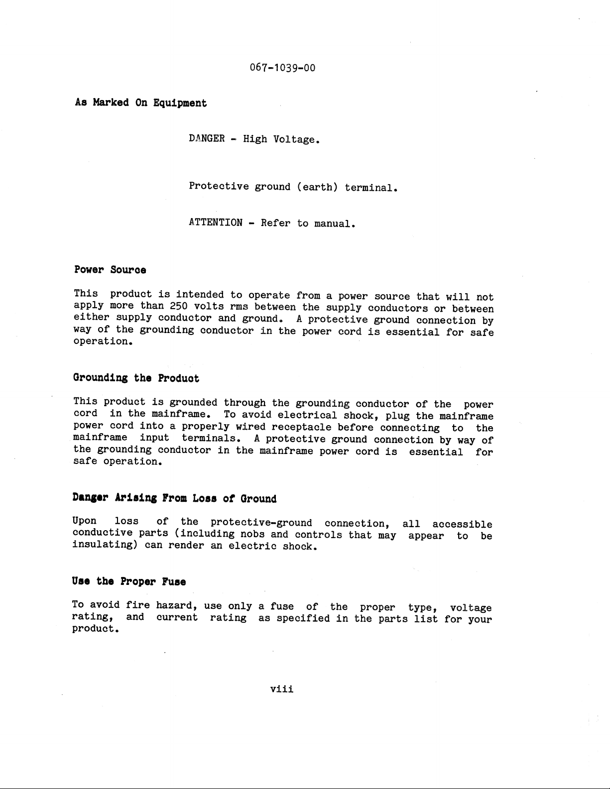
As Marked On Equipment
DANGER - High Voltage.
Protective ground (earth) terminal.
ATTENTION - Refer to manual.
Power Souroe
This product is intended to operate from a power source that will not
apply more than 250 volts rms between the supply conductors or between
either supply conductor and ground. A protective ground connection by
way of the grounding conductor in the power cord is essential for safe
operation.
Grounding the Produot
This product is grounded through the grounding conductor of the power
cord in the mainframe. To avoid electrical shock, plug the mainframe
power cord into a properly wired receptacle before connecting to the
mainframe input terminals. A protective ground connection
the grounding conductor in the mainframe power cord is essential for
safe operation.
by way
of
na111•r Al'iai111 rrom Losa ot Ground
Upon loss of the protective-ground connection,
conductive parts (including nobs and controls that may
insulating) can render an electric shock.
all accessible
appear to be
Uae the Proper Fuse
To avoid fire hazard, use only a fuse of the proper type, voltage
rating, and current rating as specified in the parts list for your
product.
viii
Page 11
067-1039-00
Do Not
To avoid explosion, do not operate this product in an atmosphere of
explosive gases unless it has been specifically certified for such
operation.
Do Hot Remove Covers or Panels
To avoid personal injury, do not remove the product covers or panels.
Do not operate the product without the covers and panels properly
installed.
Operate
In Explosive Atmospheres
r
ix
Page 12
067-1039-00
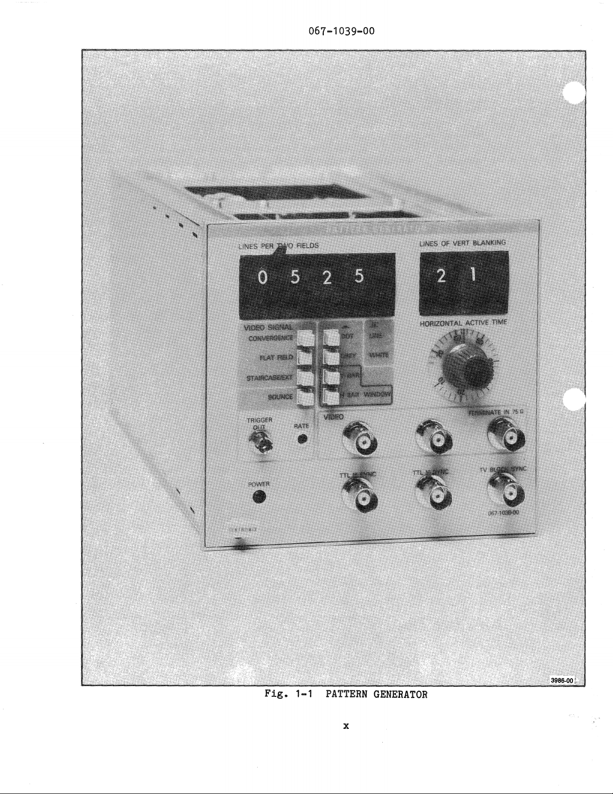
Fig.
1-1 PATTERN GENERATOR
X
Page 13

Section1 - 067-1039-00
GENERAL INFORMATION AND SPECIFICATIONS
INTRODUCTION
The 067-1039-00 PATTERN GENERATOR provides a series of video test
signals required to calibrate a multi-rate display monitor (such as
the 690SR Color Display Mainframe). The 690SR can be used with
computer display or television signal sources that use a wide variety
of scanning systems. The PATTERN GENERATOR emulates these scan
systems and provides a selection of test signals for calibrating the
display monitor.
r
l
l
f
l
The PATTERN GENERATOR has three front panel controls that allow it
to emulate the line and field rates of many scan systems, present or
future. The Horizontal Active Time adjustment varies the interval
between the horizontal blanking periods (blanking itself is nominally
6.75 us); the Lines per Two Fields is set to the number of scan lines
of the chosen standard (an odd number generates 2:1 interlace, an even
number is non-interlaced); and the Lines of Vertical Blanking is set
to the number of blanked lines in each field. The Frame Period is
(6.75 us+ Horizontal Active Time) times Lines per Two Fields.
There are
operation of the display monitor. These switches generate the
following patterns:
1. Flat Field (White). Tests purity and colorimetry.
2. Flat Field (Grey). Tests low light level calibration.
3. Convergence (Lines/Dots). Tests convergence, geometry,
linearity, and video amplifier pulse response.
4. Vertical Bar. Tests the video amplifier for line time
distortion and integrity of step response.
5. Horizontal Bar. Tests high voltage supply regulation.
8 pushbutton switches that provide patterns to test the
r
6. Window. Tests crt purity error due to shadow mask heating.
7. Staircase. Tests color balance, nonlinear
video amp limiting. With an external ohrominanoe
differential
gain and differential phase.
1-1
distortion, and
signal, tests
Page 14
General Information - 067-1039-00
8. Bounce. Tests video clamp response and feedback stability in
the beam feedback loop.
OVERVIEW
The Operators part of this manual is intended to help the user
obtain maximum performance from the PATTERN GENERATOR. This part
covers General Information, Specifications, and Operating
Instructions.
The Service Part of this manual covers the Theory of Operation,
the Performance Check and Adjustment section, the Maintenance section,
and. other service information, including the block and schematic
diagrams of the PATTERN GENERATOR.
The eight sections of the manual are:
OPERATORS PART
Section 1 - General Information and Specifications; contains the
instrument description and a listing of the PATTERN GENERATOR
Characteristics and Performance Requirements.
Section 2 - Operating Instructions; introduces the user to the
PATTERN GENERATOR/Display Monitor system and demonstrates the
functions of the front panel controls.
SERYICIIG PART
Section
the PATTERN GENERATOR.
Section 4 - Calibration, Part 1: Performance Check; this
subsection is used to verify all of the Performance Requirements in
the Specification, and to determine the need for recalibration
(adjustment) of the PATTERN GENERATOR.
Section
Procedure; this subsection is used to return the PATTERN GENERATOR to
conformance with the Performance Requirements. The procedure is
arranged in functional blocks to facilitate referencing from the
Performance Check and the Maintenance Instructions.
3 -
Theory of Operation; describes all major circuits of
4 -
Performance Check and Adjustment, Part 2: Adjustment
1-2
Page 15
l
General Information - 067-1039-00
Section 5 - Maintenance Instructions; describes routine and
corrective maintenance with detailed instructions for replacing
assemblies, subassemblies, and individual components.
Section 6 - Replaceable Electrical Parts; provides information
necessary to order replaceable parts and assemblies related to the
electrical functions of the instrument.
Section 7 - Diagrams; provides functional block diagram and
circuit schematics.
Section 8 - Replaceable Mechanical Parts; provides information
necessary to order mechanical parts that are being replaced. The list
is cross-referenced to replaceable electrical parts where appropriate.
The Exploded Diagram shows the assembly sequence and identifies the
assemblies. The Accessories page lists the standard and optional
accesories. (Not present in the interim manual.)
Changes and Corrections; provides updating information for the
manual in the form of inserts. These inserts are incorporated into
the manual text and diagrams when the manual is revised.
r
l
l
l
STANDARDS
The abbreviations
diagrams are based on
Y32.14-1973 (American
Street, New York, N.
and graphic symbols
ANSI Y1.1-1972, ANSI
National Standards
Y. 10017)
used in the
Y32.2 1970,
Institute, 345
text and
and ANSI
East 47
1-3
Page 16
Specification - 067-1039-00
SPECIFICATION
The following specifications apply to the 067-1039-00 PATTERN
GENERATOR. Allow 30 minutes warmup. Items listed in the Performance
Requirements column are verifed by completing the Performance Check in
Section 4 of this manual. Items listed in the Supplemental
Information column may not be verified in this manual; they are either
exlanatory notes or performance characteristics for which no limits
are specified.
Table 1-1
ELECTRICAL CHARACTERISTICS
Characteristics
I Performance Requirement I Supplemental Information
====================l=========================I============================
Video Outputs I I
Impedance I I 75 ohms with all outputs
I I terminated in 75 ohms
------------------+-------------------------+----------------------------
Levels
White
----------------+-------------------------+----------------------------
Grey
----------------+-------------------------+----------------------------
Blanking
----------------+-------------------------+----------------------------
Blanking Level
Shift
----------------+-------------------------+----------------------------
Sync
----------------+-------------------------+----------------------------
Staircase Steps
------------------+-------------------------+----------------------------
Risetime (Except
Staircase)
I
I 700 mV +/- 7mV
I 70 mV +/-7 mV
I O V +/- 7 mV
I Less than 3 mV from 0
I to 100 % APL
I -300 mV +/- 7 mV
87.5 mV +/-2% (8 steps
from blanking to white)
[(Peak White)-(Blanking),
divided by 8] staircase
luminance nonlinear
distortion less than 2%
I Less than 2 ns
I
------------------+-------------------------+----------------------------
Falltime (Except
Staircase)
------------------+-------------------------+----------------------------
Ringing
1-4
I Less than 3 ns
I
I (8 ns before and after 50%
I of step) less than 5% peak
Page 17
Specification - 067-1039-00
Table 1-1 (cont)
Characteristics I Performance Requirement I Supplemental Information
====================l=========================I======== ===========-=~=====
TTL Video Outputs
Impedance
I I
Greater than 10,000 ohms.
I
[
l
------------------+-------------------------+----------------------------
White Level
(into 50 or
75 ohms)
------------------+-------------------------+---------------------------~
Black Level
(into 50 or
75 ohms)
------------------+-------------------------+----------------------------
Risetime and
Fall time
--------------------+-------------------------+----------------------------
Bounce
Trigger Output
Levels
------------------+-------------------------+----------------------------
Rate
--------------------+-------------------------+----------------------------
Scan Rate Selection
Number of Lines
in 2 Fields
------------------+-------------------------+----------------------------
Number of Vertical!
Blanking Lines
Logic 1 greater than
I
2.5 V
I
Logic O less than 0.8 V Output Current= 0
I
I Maximum output current
I greater than 50 mA
I
Less than 7 ns
I
I
I
TTL (Logic 1 = Black
I
Video Output)
I
Adjustable from 0.2 Hz to
I
Hz
2
I
I
21 to 1999 lines
I
I
3 to 99 lines
I
2 settings result in 3
I
lines)
I
(O,
'
1, and
I
[
------------------+-------------------------+----------------------------
Vertical Sync
Width
------------------+-------------------------+----------------------------
Horizontal Active
Time
------------------+-------------------------+----------------------------
Horizontal
Blanking Time
------------------+-------------------------+----------------------------
Horizontal Sync
Width
------------------+-------------------------+----------------------------
Front Porch Width
Blanking Time
10 to 70 us+/- 3% of
I
full scale
I
6.75 us +/-0.2 us
I
I
us +/-0.1 us
I 3
I
1 us +/-0.05 us
l
I
3 lines (fixed)
I
Internally adjustable
I
from 4.5 us to 12 us
I
Internally adjustable
I
from 2 us to 4.5 us
I
Internally adjustable
I
from 0.7 us to 1.5 us
I
~--------------------------------------------------------------------------
1-5
Page 18
Specification -
Table 1-1 (cont)
067-1039-00
Characteristics
I
Performance Requirement
I
Supplemental Information
====================l=========================I============================
Interlace Accuracy
--------------------+-------------------------+----------------------------
Oscillator
Stability
--------------------+-------------------------+----------------------------
Oscillator Jitter
------------------+-------------------------+----------------------------
Line-to-line
Jitter
--------------------+-------------------------+----------------------------
Sync Outputs
TTL H Sync
------------------+-------------------------1
TTL V Sync
------------------+-------------------------+----------------------------
TV Block Sync
I
50
%
H
period
I I
I I
I I
I I
I I
+/-5
%
H
I
Better than
10
minutes
Less than
I
Less than
I
TTL levels, logic
sync time
-4 V
Hand
Block Sync equals
TTL V Sync OR TTL H Sync
into
V
+/-0.005%
20
ns over
5
JlS
peak-to-peak
1
75
ohms during
sync time; TTL
over
500
during
ps
Table
ENVIRONMENTAL CHARACTERISTICS
---------------------------------------------------------------------------
Characteristic
I
1-2
'
Description
===========================I=====~=========================================
Temperature Range
Operating
-------------------------+------------------~----------------------------
Non-Operating
---------------------------+-----------------------------------------------
Humidity
---------------------------+-----------------------------------------------
Altitude Range
Operating
I
I
Oto
I
-55
I
Up to
I
I
To
+50
to
90%
4.5
degrees C
+75
degrees C
to
km
(15,000
95%
relative humidity
ft)
-------------------.-------+-----------------------------------------------
Non-Operating
---------------------------+-----------------------------------------------
Shock and Vibration
I
To
15
km
I
30
G (half-sinewave),
I
displacement
1-6
(50,000
ft)
0.38
mm
(0.015
inches)
Page 19
Specification - 067-1039-00
Table 1-3
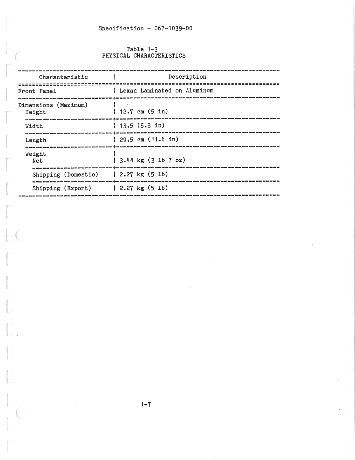
PHYSICAL CHARACTERISTICS
Characteristic
------------------------------~--------------------------------------------
---------------------------------------------------------------------------
Front Panel Lexan Laminated on Aluminum
---------------------------+-----------------------------------------------
Dimensions (Maximum)
(5
Height 12.7
--------------------=----+-----------------------------------------------
Width
-------------------------+-----------------------------------------------
Length 29.5
-------------------------+-----------------------------------------------
Weight
Net
-----------------------+-----------------------------------------------
Shipping (Domestic) 2.27 kg (5 lb)
-----------------------+-----------------------------------------------
Shipping (Export)
I
cm
13.5 (5.3 in)
(11.6 in)
cm
(3
kg
3.44
2.27 kg (5 lb)
Description
in)
oz)
7
lb
1-7
Page 20

Page 21
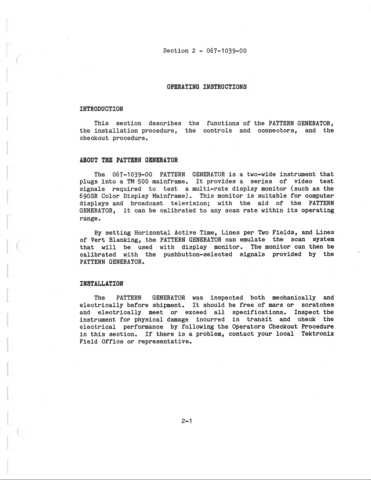
Section 2 - 067-1039-00
OPERATING INSTRUCTIONS
INTRODUCTION
This section describes the functions of the PATTERN GENERATOR,
the installation procedure, the controls and connectors, and the
checkout procedure.
ABOUT THE PATTERN GENERATOR
f
r
l
l
The 067-1039-00 PATTERN GENERATOR is a two-wide instrument that
plugs into a TM 500 mainframe. It provides a series of video test
signals required to test a multi-rate display monitor (such as the
690SR Color Display Mainframe). This monitor is suitable for computer
displays and broadcast television; with the aid of the PATTERN
GENERATOR, it can be calibrated to any scan rate within its operating
range.
By setting Horizontal Active Time, Lines per Two Fields, and Lines
of Vert Blanking, the PATTERN GENERATOR can emulate the scan system
that will be used with display monitor. The monitor can then be
calibrated with the pushbutton-selected signals provided by the
PATTERN GENERATOR.
INSTALLATION
The PATTERN GENERATOR was inspected both mechanically and
electrically before shipment. It should be free of mars or scratches
and electrically meet or exceed all specifications. Inspect the
instrument for physical damage incurred in transit and check the
electrical performance by following the Operators Checkout Procedure
in this section. If there is a problem, contact your local Tektronix
Field Office or representative.
I
2-1
Page 22

Operating Instructions - 067-1039-00
NOTE
If the PATTERN GENERATOR is used with a NTSC display
monitor, the Horizontal Blanking Time should be changed
from 6.75 .usec. to 11.1 ..usec. This is an internal
adjustment and should be performed by a qualified
technician. Refer to Section 4 for the °Calibrate
Internal Horizontal Timing
0
procedure.
REPACKAGING
Save and re-use the PATTERN GENERATOR shipping container. If the
original container is not available or is damaged, repackage the
PATTERN GENERATOR as follows:
1. Attach a tag to the PATTERN GENERATOR that shows: name and
address of the firm, name of the person responsible for the PATTERN
GENERATOR, serial number, and a description of the service required.
2. Obtain a shipping container made of heavy corrugated cardboard
or wood. To allow for cushioning, make sure that the inside
dimensions are no less than 12 by 12 by 18 inches (300 by 300 by 450
mm). This container should have a carton test strength of no less
than 275 pounds (605 kg).
3. To protect the finish of the PATTERN GENERATOR, wrap it in
heavy· paper or polyethylene. Protect the front panel with urethane
foam or strips of cardboard.
4. Cushion the PATTERN GENERATOR by tightly packing urethane foam
or dunnage between the PATTERN GENERATOR and the shipping container.
Allow at least
5. Seal the container with shipping tape or an industrial
stapler.
If there are any questions, contact the nearest Tektronix Field
Office or representative.
FUNCTIONS OF CONTROLS, INDICATORS, AND CONNECTORS
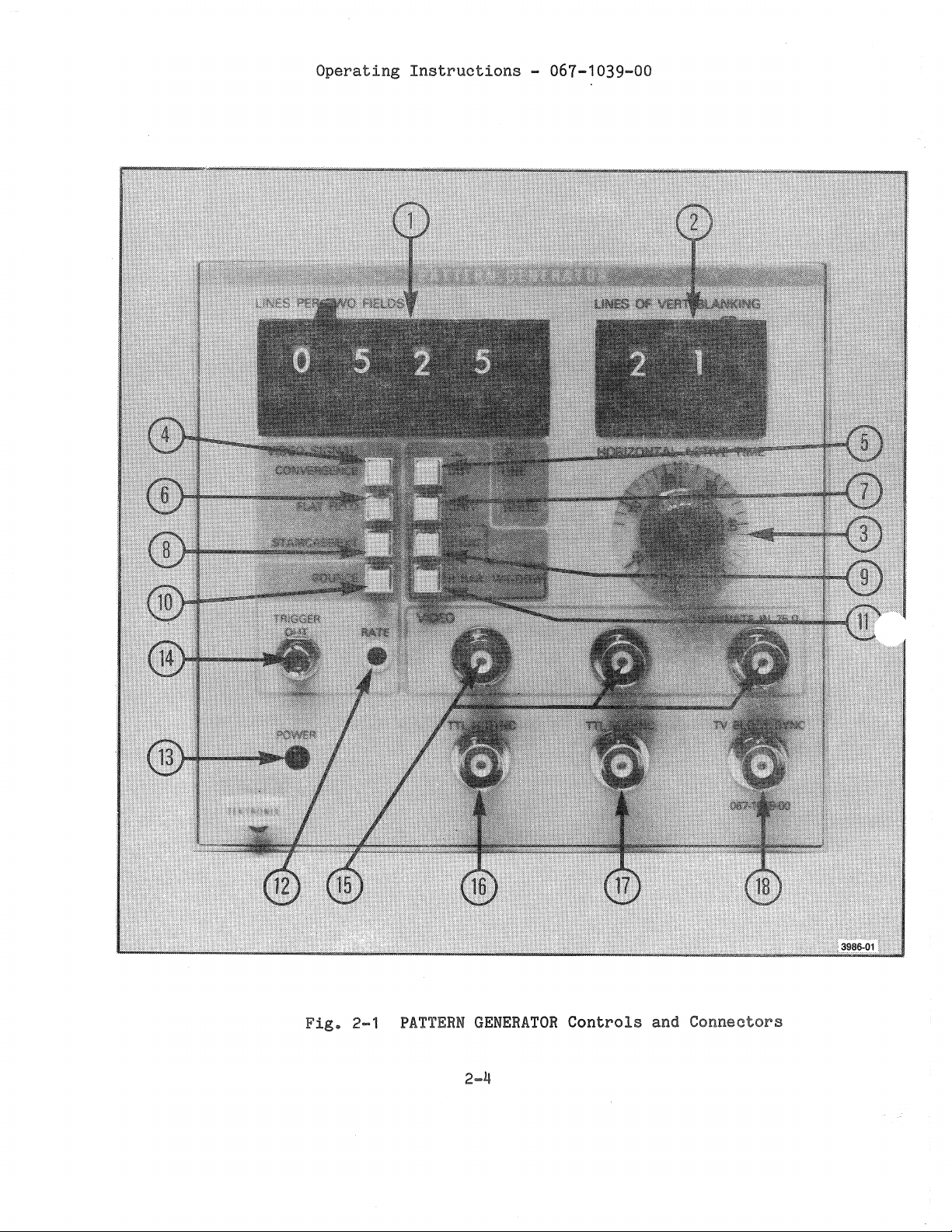
The front panel controls and connectors are shown in Fig. 2-1 and
numbered to match the text.
3 inches (75 mm) on all sides.
2-2
Page 23
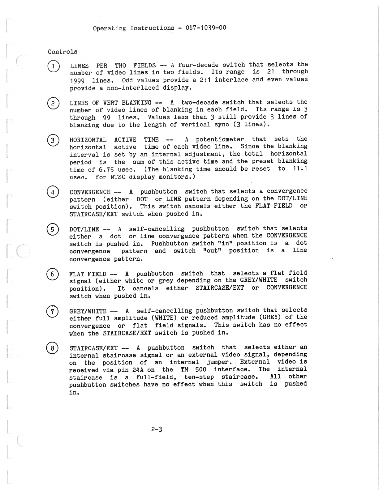
Controls
Operating Instructions - 067-1039-00
f
0
0
0
©
LINES PER TWO FIELDS -- A four-decade switch that
number of video lines in two fields. Its range is
1999 lines. Odd values provide a 2:1 interlace and
provide a non-interlaced display.
LINES OF VERT BLANKING -- A two-decade switch that selects the
number of video lines of blanking in each field. Its range is 3
through 99 lines. Values less than 3 still provide 3 lines of
blanking due to the length of vertical sync (3 lines).
HORIZONTAL ACTIVE TIME A potentiometer that sets the
horizontal active time of each video line. Since the blanking
interval is set by an internal adjustment, the total horizontal
period is the sum of this active time and the preset blanking
time of 6.75 usec. (The blanking time should be reset to 11.1
usec. for NTSC display monitors.)
CONVERGENCE -- A pushbutton switch that selects a convergence
pattern (either DOT or LINE pattern depending on the DOT/LINE
switch position). This switch cancels either the FLAT FIELD or
STAIRCASE/EXT switch when pushed in.
DOT/LINE -- A self-cancelling pushbutton switch that selects
either a dot or line convergence pattern when the CONVERGENCE
switch is pushed in. Pushbutton switch "in" position is a dot
convergence pattern and switch "out" position is a line
convergence pattern.
selects the
21 through
even values
l .
i
t
l
©
0
0
FLAT FIELD -- A pushbutton switch that selects a flat field
signal (either white or grey depending on the GREY/WHITE switch
position). It cancels either STAIRCASE/EXT or CONVERGENCE
switch when pushed in.
GREY/WHITE -- A self-cancelling pushbutton switch that selects
either full amplitude (WHITE) or reduced amplitude (GREY) of the
convergence or flat field signals. This switch has no effect
when the STAIRCASE/EXT switch is pushed in.
STAIRCASE/EXT -- A pushbutton switch that selects either an
internal staircase signal or an external video signal, depending
on the position of an internal jumper. External video is
received via pin 24A on the TM 500 interface. The internal
staircase is a full-field, ten-step staircase. All other
pushbutton switches have no effect when this switch is pushed
in.
2-3
Page 24
Operating Instructions - 067-1039-00
Fig. 2-1 PATTERN GENERATOR Controls and Connectors
2-4
Page 25
V BAR A self-cancelling pushbutton switch that inserts a
vertical bar into the convergence-pattern signal or adds a
vertical bar to
STAIRCASE/EXT switches in the "out" position). When both the
BAR and
resulting signal is a WINDOW signal.
@
@
@
Indicators
H BAR
horizontal bar in the same manner as the
BOUNCE
video pattern to be periodically blanked to black with a 50
squarewave whose period (RATE) is adjustable from 0.2
Hz. This switch does not affect the video pattern when the
STAIRCASE/EXT switch is in the "in" position.
RATE (BOUNCE)
varies the bounce rate from 0.2
Operating Instructions - 067-1039-00
black pattern (CONVERGENCE, FLAT FIELD, and
a
BAR switches are depressed at the same time, the
H
self-cancelling pushbutton switch that inserts a
A
self-cancelling pushbutton switch that causes the
A
front-panel screwdriver adjustment that
A
2 Hz.
to
Hz
BAR switch.
V
Hz
to
V
%
2
@
Connectors
@
@
POWER
whenever power is applied to the instrument.
TRIGGER OUT -- A probe tip output connector that provides a TTL
signal that is synchronous with the bounce transition. This
signal is used to trigger a test oscilloscope so that the clamp
response and beam current feedback stability of the 690SR can be
easily measured.
VIDEO -- Three bnc output connectors driven at TTL or composite
video levels depending on the position of an internal jumper.
Each connector is intended to drive a 75 ohm load, and all three
connectors are driven by a common driver to eliminate any timing
errors. Source-termination resistors provide proper reflection
termination when each connector is terminated in 75 ohms.
These connectors are provided to drive RGB monitors. Monitors
with only one input would use one of the output connectors with
the other two output connectors terminated in 75 ohms.
red light-emitting dioe (LED) that illuminates
A
NOTE
The unit receives its power from any TM 500 mainframe.
2-5
Page 26
Operating Instructions - 067-1039-00
@
@
OPERATOR'S CHECKOUT PROCEDURE
follows:
TTL H SYNC -- A bnc output connector that provides a horizontal
sync-timing signal with TTL levels (logic 1 during horizontal
sync sync time).
TTL V SYNC -- A bnc output connector that provides a vertical
sync-timing signal with TTL levels (logic 1 during vertical sync
time).
TV BLOCK SYNC -- A bnc output connector that provides a timing
signal with both horizontal and vertical sync timing information
at standard video-sync drive levels (-4V p-p into 75 ohms). No
serration or equalizer pulses are provided.
Prepare the PATTERN GENERATOR/Display Monitor combination as
1. Check that the TM 500 mainframe is OFF. Insert the PATTERN
GENERATOR into a TM 500 mainframe. Turn the mainframe ON.
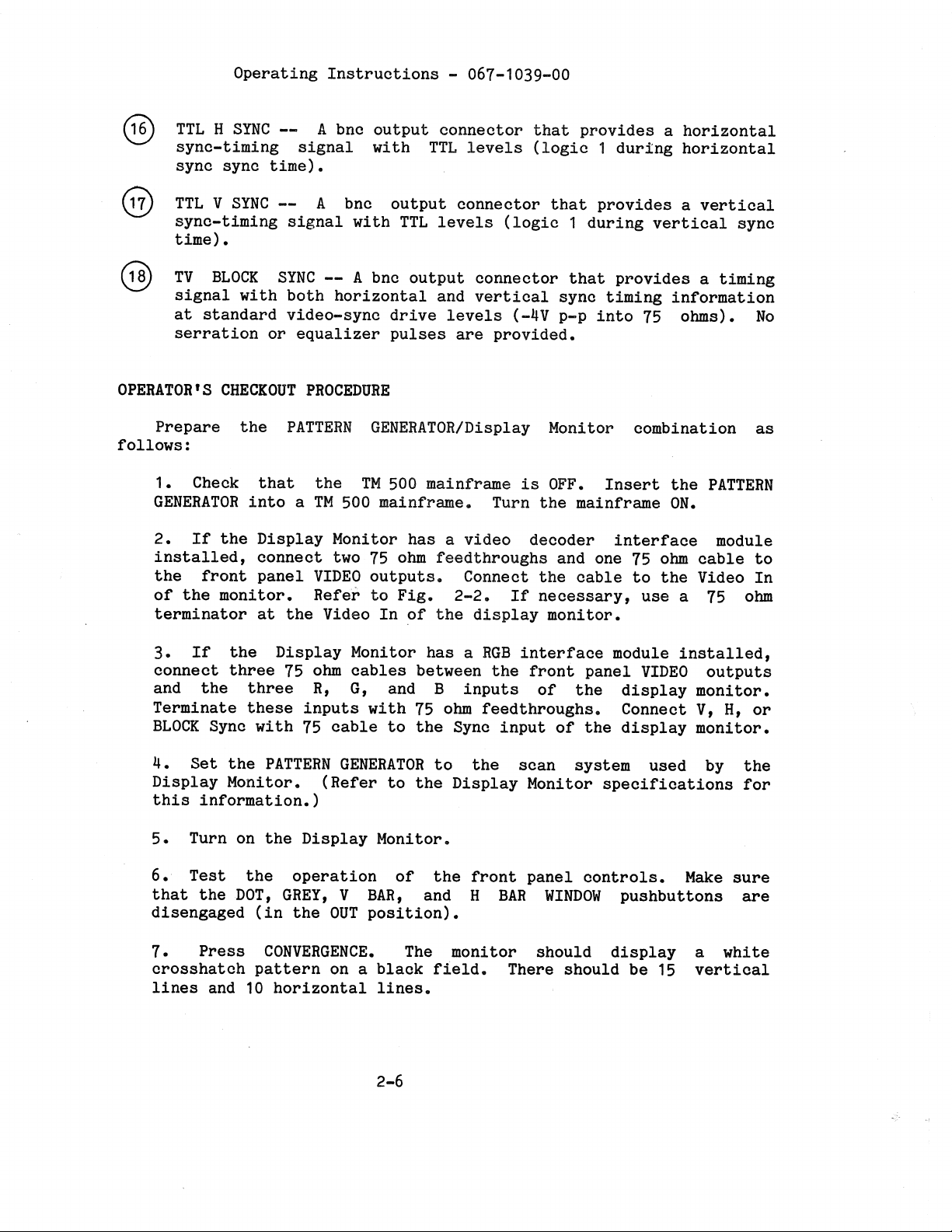
2. If the Display Monitor has a video decoder interface module
installed, connect two 75 ohm feedthroughs and one 75 ohm cable to
the front panel VIDEO outputs. Connect the cable to the Video In
of the monitor. Refer to Fig. 2-2. If necessary, use a 75 ohm
terminator at the Video In of the display monitor.
3.
If the Display Monitor has a RGB interface module installed,
connect three 75 ohm cables between the front panel VIDEO outputs
and the three R, G, and B inputs of the display monitor.
Terminate these inputs with 75 ohm feedthroughs. Connect V, H, or
BLOCK Sync with 75 cable to the Sync input of the display monitor.
4. Set the PATTERN GENERATOR to the scan system used by the
Display Monitor. (Refer to the Display Monitor specifications for
this information.)
5. Turn on the Display Monitor.
6.
Test the operation of the front panel controls. Make sure
that the DOT, GREY, V BAR, and H BAR WINDOW pushbuttons are
disengaged (in the OUT position).
7.
crosshatch pattern on a black field. There should be 15 vertical
lines and 10 horizontal lines.
Press CONVERGENCE. The monitor should display a white
2-6
Page 27

Operating Instructions - 067-1039-00
Press DOTS. The crosshatch should change into a pattern of
8.
dots. Disengage DOTS.
Press
9.
crosshatch pattern.
10. Press
center of the crosshatch pattern. Disengage
horizontal bar should appear across the crosshatch pattern.
Disengage
11. Press FLAT FIELD. The monitor should display a flat field at
white level (700 mV).
12. Press GREY. The monitor should display a grey field (10% or
70 mV). Disengage GREY.
13. Press BOUNCE. The monitor should display an alternating
black and white field at a rate controlled by the RATE adjustment.
The adjustment covers a range of 0.2 Hz to 2 Hz. Disengage
BOUNCE.
14. Press STAIRCASE/EXT. A full-field monochrome staircase
should appear on the monitor.
This completes the Operators Checkout Procedure. For further
information on calibrating the Display Monitor with these test
signals, consult the manual of the Display Monitor.
V BAR. A
H BAR
BAR WINDOW.
H
white vertical bar should appear across the
white window should appear in the
WINDOW.
A
V BAR;
a white
2-7
Page 28
Operating Instructions - 067-1039-00
11
PATTERN
GENERATOR
'=I
~ID
1
CID
,_, &l
@
©
H SYNC
Fig. 2-2 PATTERN GENERATOR Connections
@
•.J.~UJ~,.&'I~ 0
~b..A..i'
A Vici@@
0 0
0 0
VIDEO
DECOD~R
MODULE
to
ifl!)Ut
Display Monitor with
Video Decoder Module
USING THE PATTERN GENERATOR TO CHECK THE
690SR MAINF'RAME
The 067-1039-00 PATTERN GENERATOR, when plugged into a TEKTRONIX
TM 500 mainframe, provides the necessary video signals to test the
690SR
Color Monitor. The crosshatch pattern from the generator is
used with the Tektronix Linearity Graticule 067-1034-00 to check the
sizep centering, and linearity of the mm1itor's raster. Therefore,
is
necessary
to set the PATTERN GENERATORWs controls to operate at the
it
desired horizontal and vertical scan rates and to obtain a crosshatch
pattern that fills the raster properly.
3986-02
Page 29

Operating Instructions - 067-1039-00
NOTE
Simply setting the PATTERN GENERATOR controls to provide
signals that are equivalent to the user's system may not
permit checking the 690SR mainframe performance
properly.
The PATTERN GENERATOR front-panel control settings given in the
equipment setup illustrations are set to generate a 31.5 kHz scan rate
and a 60.6 Hz field rate. The Horizontal Active Time control is set
to 25 .,us since 25 JJ.S active time plus 6. 75 .J.IS horizontal blanking time
horizontal period to generate a 31.5 kHz scan
is equal to 31.75
.JlS
rate. (The PATTERN GENERATOR blanking time is factory set at 6.75 .).ls
to match the 690SR raster blanking time.) The Lines of Vertical
Blanking switch is set to obtain approximately 600 J.lS vertical
blanking time. (The 18 lines chosen times 31.75.J.ls is equal to 572
ps.) The Lines Per Two Fields switch is set to obtain an approximate
60 Hz field rate and at the same time produce full top and bottom
crosshatch lines that coincide with the top and bottom edges,
respectively, of the raster.
NOTE
If the Lines Per Two Fields switch is set to an odd
number; for example, 1039, the display may appear to
flicker because the display is interlaced. To obtain a
non-interlaced display, set the switch to an even
number. When preparing this manual, the Lines Per Two
Fields switch was set to 1040.
If the 690SR mainframe is being operated at a horizontal and/or
vertical scan rate other than 31.5 kHz and approximately 60 Hz
respectively, or if the horizontal blanking time is not 6.75.JJ.s, then
use the following procedure as an aid for setting the PATTERN
GENERATOR controls to properly check the 690SR mainframe.
Measure the vertical scan period, the horizontal scan period,
1.
and horizontal blanking time of the monitor's intended signal
source or obtain their specification.
Compute the horizontal active time
2.
blanking time from the H scan period.
by subtracting
For example:
the H
31.75JlS - 6.75JlS: 25.)J.S.
2-9
Page 30
Operating Instructions - 067-1039-00
a. Set the Horizontal Active Time control on the PATTERN
GENERATOR to the computed horizontal active time value.
b. If the H blanking time is other than 6.75,J.ls and precise
linearity adjustment is required, recalibrate the PATTERN
GENERATOR's horizontal blanking time. (Refer to step 11
in the Adjustment Procedure of this 690SR manual.) (For
quick monitor setups when the linearity requirement is
less critical, the horizontal blanking time need not be
recalibrated. Instead, use 6.75Jls during the Performance
Check Procedure. Then, readjust the 690SR H Size control,
R925, on A8A1 after completing the Performance Check
Procedure so the displayed picture from the monitor's
intended signal source will be the proper width.)
3. Calculate the number of Lines of Vertical Blanking that the
PATTERN GENERATOR should be set to
after the decimal point in the number calculated from the
following formula.
600
J.lS
B
------
=
Hp
by
ignoring the fraction
For example:
B
Hp
B
Lines of Vertical
=
Horizontal Scan Period
=
600
)lS
---------
=
31. 75 ..us
=
18.89
Blanking
18
=>
2-10
Page 31

Operating Instructions - 067-1039-00
4. Calculate the approximate number of Lines Per Two Fields that
the PATTERN GENERATOR should be set to by using the following
formula.
(Vp)
2
LA
=
------
Hp
r
f
f_
l
LA
Vp
Hp
For example:
LA
5. Find the exact number of Lines Per Two Fields that the PATTERN
GENERATOR should be set to by first setting Lin the formula
below or equal to LA that was calculated previously. Then,
increment L up or down one digit at a time until the
calculated value for x becomes a whole number.
L - 2B - 24
X: ----------
x
=
Must be a whole number (i.e., an integer) to
obtain a full screen display so that the last
horizontal crosshatch. line is at the bottom of
the raster. The whole number is the number of
black horizontal scan- ning lines between any
two white horizontal lines of the displayed
crosshatch pattern.
The approximate Lines Per Two Fields
=
setting (truncate this
Vertical Scan Period
=
Horizontal Scan
=
2(16.67 ms)
=
-----------
31.75
20
J.l.S
=
Period
1050.08
number)
=>
1050
L
B
For example:
x
Hence, L
=
=
Lines Per Two Fields
=
Lines of Vertical Blanking
1040 - 2(18) - 24
= ----------------- =
1040
20
2-11
49 lines
Page 32

Page 33

Page 34

Page 35

r
•
067-1039-00
SERVICING SAFETY SUMMARY
FOR QUALIFIED SERVICE PERSONNEL ONLY
Refer also to the preceding Operators Safety Summary
Do Not Service Alone
Do not perform internal service or adjustment of this product unless
another person capable of rendering first aid and resuscitation is
present.
Use Care When Servicing With Power On
Dangerous voltages exist at several points in this product. To avoid
personal injury, do not touch the exposed connections and components
while power is on.
Disconnect power before removing protective panels, soldering, or
. replacing components.
r
I -
Power Source
This product is intended to operate from a power source that does not
apply more than 250 volts rms between the supply conductors or between
either supply conductor and ground. A protective ground connection by
way of the grounding conductor in the power cord is essntial for safe
operation.
S-1
Page 36

Page 37

Section 3
=
067-1039-00
THEORY OF OPERATION
HORIZONTAL SYNC GENERATOR
<!)
Horizontal Oscillator
The ACTIVE TIME control R682 varies
source consisting of
current
is
ramp (on pin 1
toggles
charges
compared
to a low
holding capacitor C684 to generate a ramp@
to a de level on pin 2 of U580,
of
U580)
state
Q680 into saturation and
One-shot
generates
approximately
before it starts charging up again. The output at pin
drives a
circuit block.
While the ramp
the input of
The comparison voltage at the input of
at the input of
a
binary
0580,
multivibrator
pulse
80
nse
counter,
it is also compared
U580.
Q688, Q685,
crosses that threshold voltage, pin
and
resets the ramp
discharging
U575A
at
output
This ensures that
U564
signal
on
C684 is
and the associated circuitry. The
is
pin
in the Horizontal Interval Timing
the current out of a current
a comparator. When the
by
causing
U670A
C684 ..
triggered
·7
which keeps
being compared to a de level at
to a
U587
at
the
same time, and
Q680
C684
de level at pin
is slightly less than that
is fully discharged
That
5
6
2
ramp
of
U580
to drive
iron" for
of U575A
of
0587.
Since the ramp is positive-going,
Horizontal Oscillator resets the ramp, and then remains in that state
as
long
voltage at the input. This results in a pulse at the outputs of U587.
The width of this pulse is determined
amplitude of the ramp signal exceeds the comparison voltage. As the
frequency of the Horizontal Oscillator changes and the slope of the
ramp changes, the width of the output pulse remains a constant
percentage of the horizontal period. As a result, this vertical line
pulse appears to have a constant spatial width even as the horizontal
scan rate is varied. On the schematic diagram, this pulse is labelled
as the amplitude of the ramp signal exceeds the comparison
U587 toggles just before the
by
the amount of time that the
V Linee
The pulse at the output of U587 is used to generate the effective
address on the crt of a display monitor from left to right. For
example, the vertical bar
signal
is determined
by
counting the number
3-1
Page 38

Theory of Operation - 067-1039-00
of vertical lines that have occurred since the start of that
particular horizontal line.
Vertical Bar Generator
Counter U462 and the logic associated with
Vertical Bar Generator. It counts vertical lines
combined with an "EXCLUSIVE OR" gate, resulting in
width is approximately six vertical lines. Logic
U556C, and U556D form an "EXCLUSIVE OR" gate.
If this bar signal were displayed on a picture monitor, the crt
would display a light bar extending from the top to the bottom and
dark at the left and right sides.
Horizontal Interval
The output of the Horizontal Oscillator's one-shot multivibrator
U575A is counted by U564, and when the count reaches 14 (pins 11, 12,
and 13 all high; pin 14 low), the output of U670B triggers another
one-shot multivibrator U575B which controls the horizontal hold-off
and blanking times. The output of U575B is clocked by V Line to
generate the horizontal blanking time (labeled H Blank at the output
of U457D).
The output of U670C (pin 8) forces the Horizontal Oscillator ramp
at C684 to be clamped to ground, stopping the Horizontal Oscillator
during the horizontal interval hold-off time. Horizontal blanking
time is equal to the sum of the horizontal interval hold-off time and
the Horizontal oscillator period.
Timing
it constitutes the
and its outputs are
a bar signal whose
gates U457A, U457B,
The output of U670C (inverted output of U575B) is fed to a
circuit which determines the front porch timing and sync timing. The
output of that circuit is horizontal sync. The circuit consists of
two cascaded one-shot multivibrators, U552A and U552B together with the associated circuitry. The first multivibrator, U552A, determines
the offset of the horizontal sync leading edge from the start of the
blanking time which is the front porch time. The second
multivibrator, U552B, determines the width of the horizontal sync
pulse, and that output pulse (pin 10 of U552B) is fed to the 2H
(Interlace) Generator circuit block and to several buffer circuits.
3-2
Page 39

Theory of Operation - 067-1039-00
2H (Interlace) Generator
The heart of this circuit is a constant-amplitude ramp generator.
It generates a ramp which starts at the end of one horizontal sync
pulse, ramps up until the next horizontal sync pulse comes along,
resets and starts up again. A comparator is used to compare this ramp
with a de level whose amplitude is automatically adjusted to one half
the peak amplitude of the ramp. Each time the ramp amplitude crosses
that threshold voltage, the output of the comparator changes states.
This results in a square wave output that has a transition halfway
between the two horizontal sync pulses. This transition is then used
to generate a pulse occuring midway between the two horizontal sync
pulses; and the pulse and the horizontal sync pulses are combined
with a "NAND" gate to produce a signal having twice the frequency of
the horizontal sync signal. This is the 2H signal that is used to
generate interlace.
Operational amplifier 0420, C420, Q420, and R422 comprise the
ramp generator. Operational amplifier 0420 is connected as an
integrator. A constant de level applied to R422 supplies a constant
current to C420, charging it up until a reset pulse from 0328A turns
Q420 "on" to discharge C420. The slope of the ramp is- determined by
the de level that is applied to R422, and that voltage is determined
by sampling the output of the ramp generator. The sampled output of
the ramp generator is peak-detected through CR425 and C533, and
coupled to the non-inverting input of 0530. Capacitor C523 together
with 0530 form a much slower integrator, essentially making 0530 a
power source.
i
l
A horizontal sync signal from pin 10 of 0552B drives one-shot
multivibrator 0328A. One-shot multivibrator 03~8A produces horizontal
at the output.
rate pulses with a duration of approximately 0.5
These pulses are are used to momentarily turn "on" Q420 in order to
discharge C420. That is, the output of 0328A resets the ramp
generator.
The inverting input of 0530
temperature-stabilized power supply.
temperature compensation for CR425.
If the peak amplitude of the ramp gets too high at the output of
U420, the signal coupled back to pin 3 of 0530 gets bigger. That
drives the output level at pin 6 higher than it was before. The de
level at pin 6 of 0530 is normally negative, and this de level is made
more positive. Consequently, less current flows through R422,
resulting in a ramp at the output of 0420 that has a lower slope.
That is, a lower ramp peak amplitude results. The signal being fed
back to pin 3 of 0530 will reach a steady state (equilibrium)
ramp's sampled peak amplitude equals the de level at pin 2 of 0530.
3-3
is connected
The diode CR525
JlS
'
to a
provides
when
the
Page 40

Theory of Operation - 067-1039-00
This constant
discharged.
Comparator U330 compares the ramp at the input with a de level
whose amplitude is equal to one half the peak amplitude of the ramp.
Potentiometer R332 (2H Interlace) is used to set the comparison
voltage at pin 2 of U330. When the ramp crosses this threshold
voltage, the output of U330 changes states resulting in a transition
midway between two horizontal sync pulses. This transition is used to
trigger one-shot multivibrator U328B. The result at the output of
U328B, is a signal with pulses occuring midway between horizontal sync
pulses. That is, a pulse occurs once every line in the middle of the
horizontal line with a duration of approximately 3)1s.
The output of U328B and the horizontal sync signal from pin 10 of
U552B are combined with a "NAND" gate U234B which acts like an "OR"
gate. The output of U234B is the 2H signal, and is routed to the
Vertical Sync Generator board.
amplitude is independent of how often C420 is
H S1no output Butters
The Horizontal Sync Output Buffers consist of two "NAND" gates
connected as inverters. An inverted horizontal sync signal from U552B
drives U538A, resulting in a normal polarity signal at the output.
This signal is available at the front panel as TTL H SYNC.
Depending on the position of the jumper for J542, U538B may be
driven with a normal polarity or inverted horizontal sync signal from
U552B. The output (TTL H Sync) is available at pins 26A and 28A at
the TM500 interconnect jack.
Power Supplies
Power
Generator
diagram 1, VR474 and VR647
respectively.
provides power to 0552.
supply inputs
board are shown in schematic
DC
supply
and
are used
+5
regulators on the Horizontal
vc
to
provides power
diagram
derive
2.
On schematic
vc
+5
to U575 and +5 VD
and
+5
Sync
VD
3-4
Page 41

Theory of Operation - 067-1039-00
VIDBO LOGIC AND DRIVERS 0
This schematic diagram consists of Power Supplies, Video Logic,
and Video Drivers.
Power Supplies
The Power Supplies provide the following de voltages: +15 V, +12
V, +11.7 V, +10 V, +5 VA, +5 VB, -10 V, -12 V, and -15 V.
f
[
l
[
The +15 V and -15 V supplies together with a +8 V supply provided
by the TM500 host mainframe are used to derive the rest of the
supplies.
The +12 V, +5 VA, +5 VB, and -12 V supplies are obtained through
the use of 1% regulators. The rest of the supplies are obtained by
placing the appropriate zener diodes across the proper de busses, with
the exception of the +15 V and -15 V.
Video Logic
The Video Logic circuitry combines a number of video signals
generated in other parts of the Horizontal Sync Generator board, and
other video signals from the Horizontal Line Generator and Vertical
Sync Generator boards. These signals consist of the Vertical Bar;
Horizontal Blanking; Vertical Blanking; Bounce (alternate "on" and
"off" blanking signal); V Line, and signals resulting from the
positions of the program switches (front panel controls) such as V Bar
Enable (labeled GG), V Line Enable (labeled AA), Horizontal Video
(labeled VV); and External Video. These signals are combined with a
series of gates resulting in a drive signal at the output of U355C.
A Vertical Sync signal from U238A on the Vertical Sync Generator
board is buffered by U495B resulting in TTL V SYNC available at the
front panel.
The output of the Video Logic circuit (pin 8 of U355C) drives the
Video Output Drivers.
L
l
Video Output Drivers
This circuitry consists of a TTL video driver (U495A, Q396, and
Q398) and a television video driver.
3-5
Page 42

Theory of Operation - 067-1039-00
The
TTL
video drives
5 V
11
ones
11
and "zeros".
It
has no sync,
just the video with blanking. The TTL video is amplified by a pair of
VMOS
transistors,
Q396
and Q398. These two transistors are connected
in parallel in order to produce enough current to drive three 50 ohm
loads at the video outputs on the front panel. This circuit is
enabled when pins 1 and 2, and pins 3 and 4 of J394 are jumpered;
that is, by moving the jumper for J390 to J394. Jumper pins for J390
and J394 are installed side-by-side on the Horizontal Sync Generator
board. Either one or the other set of pins is jumpered at any one
time, but never both. Therefore, either the TTL video or the
television video is available at any one time by placing a jumper on
J394 or J390 respectively.
The television video driver consists of one fast and three very
fast current sources. The circuit associated with Q188 is the fast
white current source; the circuitry associated with R270 (Grey Level
adjustment) is the grey current source; the circuitry associated with
R178 (Black Level adjusment) is the black current source; and the
circuitry associated with R486 (Sync Level adjustment) is the sync
current source. The white current source is normally "on" all the
time, and sets the output to
terminated
in
75
ohms, and the other current sources are normally
700
mV when all three video outputs are
"off".
The grey current source is turned
11
on" in order to obtain a grey
output level, and most of the current from the white source that would
normally go to the output is diverted to the grey current source
circuit. That is, the current from the white source now divides
between the output load and the grey current source. This is
accomplished by turning
"on". Transistor
cathode of
CR276
Q276
(activating the GREY button on the front panel).
Q276
"off" which causes Q286 and
may be turned
11
off
11
Q288
by applying ground to the
to turn
The black current source operates in the same manner as the grey
currrent source. It robs additional current from the white current
source whenever a black level is desired. During that time, both the
grey current source and the black current source circuits are "on".
Thus, the sum of the grey current source output and the black current
source output is equal to the white current source output. That
leaves no current for the output load, and the voltage at the output
is zero.
The sync level is
accomplished by sinking additional current in
the sync current source circuit. Since the white current cannot
provide any more current, this current is drawn from the output load,
and in
thi.s
way the output is brought down to -300 mV.
3-6
Page 43

Theory of Operation - 067-1039-00
In the case of the staircase signal, the video output is set to a
condition that would normally produce a black flat field, essentially
sync pulses and no video. However, the staircase circuit on the
Horizontal Line Generator is enabled and the resulting signal
modulates the current produced by the white current source. The
staircase drive signal biases the base of Q188 more negative, causing
Q188 to produce additional current. This additional current is sent
to the output load instead of being sunk to -12 Vin the grey, black,
and sync current sources. The staircase drive signal is a result of a
digital-to-analog conversion which is proportional to the horizontal
line scan number, and as it goes down the field, the current in the
white current source undergoes step changes resulting in the staircase
signal at the output. See Fig. 3-1.
-2
2V
~
-
-
-
-
-
-
~
-F""
--
"
"
Staircase Signal
(Field)
Fig. 3-1 Field Rate Staircase Signal
.
3986-14,
3-1
Page 44

Theory of Operation - 067-1039-00
HORIZONTAL LINE GENERATOR
The main input signals are H Sync and V Blank. A horizontal
line-generating circuit comprises most of the circuit board. This
circuit produces a white line in the raster which will be a horizontal
line when displayed. The circuit guarantees that there will be eleven
white lines from the top to the bottom of a crosshatch display. Since
the Vertical Line Generator on the Horizontal Line Generator board
generates fifteen vertical lines, the crosshatch display will be an
11 X 15 pattern. The 11 X 15 pattern is guaranteed regardless of the
number of horizontal scan lines the circuit uses. There is circuitry
which automatically adjusts the spacing between these white lines to
guarantee that there will be fifteen lines that fit the best in that
number of scan lines.
The main output from the line generating circuit is H Line. It is
available at the output of U665 pin 13. The H Line signal and the
H Bar signal (which is a result of that generator as well) are
combined with the control panel switch settings to produce three
signals namely VV (H Video), AA (V Line Enable, and GG (V Bar Enable).
The three signals are routed to the Horizontal Sync Gnererator board.
Another circuit located on the Horizontal Line Generator board is
the Bounce Generator which is a timer whose rate is adjustable from
the control panel. Its output acts as an additional blanking signal
to the video, and is routed to the Horizontal Sync board where it is
combined with vertical and horizontal blanking signals to produce a
blanking signal that varies slowly with time.
0
A third circuit located on this circuit board is the Staircase
Generator.
Current State Registers
The current state number is CBA where C is U145, Bis U265A, and
A is U265B. Inputs to the registers are V Blank, H Sync, and All
White Lines generated signals.
Register C, a field discriminator, is a divide-by-two T flip-flop
[Q
output equals zero for Field O (1) and one for Field 1 (2)]. Its
outputs change states at the end of each vertical blanking period
(beginning
(U265A).
Register B, clocked vertical blanking, is a J-K flip-flop
connected to appear as a D-Type flip-flop. The J-K inputs are V
Blanking and inverted V Blanking respectively, and the clock input is
of pattern). It is clocked by the Q output of register B
and Remainder Up-Counter
3-8
Page 45

l
J
Theory of Operation - 067-1039-00
H Sync. The clocked V Blanking signal eliminates the one half line
offset which may be present when the number of lines per two fields is
odd. This guarantees that the white lines will never start in the
middle of a horizontal. line. The Q output of U265A is high during
clocked
in one field have been displayed. The
White Lines pulse that occurs after the last white line in the field,
and has a pulse duration of approximately
transition of the clock pulse sets the
input pulse comes along and resets the flip-flop. During the time
that the
analyzed.
line is generated. It then counts the number of scan lines remaining
in the pattern ,that is, until
lines have been counted in both fields that would allow the pattern to
enlarge, the counter sends out a pulse that may be used to increase
the spacing between white lines by one. If the spacing is increased,
the remainder counter is cleared and the remainder-counting is
resumed.
V
Blanking.
The
Q
output of register A (U265B) is high after all white lines
J
input is driven with an All
3:ps.
Q
output high (one) until a
Q
output is high, the remainder of the scan lines are
The Remainder Up-Counter, U255, is enabled after the last white
V
Blanking starts. Each time enough
The negative-going
K
r
r.
[
[_
l
L
Line Spacing Increment and Line Spacing Reset
(Pattern Too Small and Pattern Too Big)
Logic gates U375A, U375B, U375C, U375D, U575A, and U575B comprise
the Line Spacing Increment circuit; and U365A, U365B, U365C, U365D,
U355B, U355C, U355D, U275A, and U275B comprise the Line Spacing Reset
circuit. Logic gates U375B and U375C form one set-reset flip-flop
hereinafter referred to as FF1; and U355B and U355C form another
set-reset flip-flop referred to as FF2.
The Line Spacing Increment logic increments the line spacing
memory when the pattern is too small. The Remainder Up-Counter (U255)
informs the Line Spacing Increment logic with the number of remaining
dark lines at the end of the pattern (after the last white line) that
it is large enough to increment the Spacing Counter for the pattern
field just scanned. (For the 11 white lines, each 10 remaining lines
may be distributed into the pattern, one per space between white
lines.)
The Line Spacing Memory is
fields agree that the pattern is
when the Q output for register C
Counter signals •pattern too
incremented
too small.
(U145) is
small", the
only if both pattern
During pattern field zero
zero and the Remainder
decision is remembered by
3-9
Page 46

Theory of Operation - 067-1039-00
setting FF1 to 1, but the Remainder Counter is not incremented.
During pattern field 1, when the Remainder Counter signals
"pattern too small" and FF1 is set, the Line Spacing Memory is
incremented each time the signal is received.
Flip-flop FF1 is reset during vertical blanking at the end of
pattern field 1.
The Line Spacing Reset logic clears the Line Spacing Memory when
the pattern is too big. The pattern is too big when the start of
vertical blanking occurs before the last white line is generated in
both fields. This condition occurs when the number of LINES PER TWO
FIELDS swith is decreased by more than- [2(Remainder)].
Flip-flop FF2 remembers if the pattern in field zero was too big.
If V Blanking starts before the last white line is generated in
field 1 and FF2 is se~, the Line Spacing Memory is cleared. The
correct spacing is then set by the Line Spacing Increment circuit.
Flip-flop FF2 is cleared whenever all white lines have been
output (A= 1).
Line Spacing Memory
The Line Spacing Memory is an eight-bit binary up-counter
consisting of U555 and U545. It contains the number of dark scan
lines between white lines. For example, if the memory contains the
number 10 and scan line number (i
number (i
+ 11) is also a white line.
+ 1) is a white line, then scan line
Soan Line Counter and White Line Generator
This circuit consists of an eight-bit binary up-counter (U775 and
U565), an eight-bit comparator (U655), a set-reset flip-flop (U675B
and U675C, and another eight-bit comparator (White Line Generator
U665).
The Scan Line Counter is reset to zero during vertical blanking
or after the last white line of the current field has been generated.
When not reset, the Scan Line Counter counts up from zero each
horizontal scan line until the counter value equals the Line Spacing
Memory. These two values are compared by U655. The output pin 13 of
this comparator goes to a high state when the counter equals the Line
Spacing Memory and sets the set-reset flip-flop U675B and U675C. The
3-10
Page 47

f
Theory of Operation - 067-1039-00
flip-flop resets the Scan Line Counter to zero, a white line is
generated, and the sequence repeats until either the last white line
is generated or vertical blanking occurs. Either of these conditions
sets the Strobe-NOT pin 11 of 0655 to a high state, which forces the
output high, holding the set-reset flip-flop set, the Scan Line
Counter reset, and disabling the White Line Generator.
The flip-flop is reset one line after vertical blanking ends,
that is, at the start of the next pattern field.
The White Line Generator generates a "high" each time the Scan
Line Counter is equal to zero during the pattern time (last white line
not yet generated and no vertical blanking). The H Sync signal on pin
23 of 0665 gates the signal "low" during sync time.
H Bar Generator and Staircase Generator
Integrated circuits 0455 and 0465C comprise a white line counter.
The counter (0455) is enabled during pattern time, and counts the
number of white lines generated in the current field. When eleven
white lines have been counted, the Max/Min output goes to a high state
signaling the end of pattern time. This signal sets register A
(0265B) high. The white line counter value is used to generate the
Bar and staircase signals.
H
l
f
r
I
l
E,
Bar Generator circuit consists of 0465B,
H
The
0475A, B, and C. The white line counter value is used to
horizontal bar which is centered vertically in the display.
ten vertical sections between the eleven white lines. The
bar occupies the middle six sections (states 7 through 12).
3-1.
D,
0675A,
F,
generate a
There are
horizontal
See Table
l
3-11
Page 48

Theory of Operation -
067-1039-00
Table 3-1
Counter States
Number of Counter
White Lines
Counted
-----------------------------------------------------
-----------------------------------------------------
0
1
2
3
4
5
6
7
8
9
10
11
-----------------------------------------------------
-----------------------------------------------------
Value
D C B A
0
0
0
0
1
1
1
1
1
1
1
0
1
0
1 0
1
0
1 1
1 1
1
0 0 0
0 0
1 1
0
1
0
0
1 1
1
0
0
1
0
1
1
0 0 0
1
1
1 1
C D
0
A B D A B D H Bar
0 0 0
0 0 0 0
0
0
1
1
1
0
0
0
0 0 0
0
0
0
0
0
1
0 0
0
1 1
0
0
0
0
0
0 0
0 0
1
1
1
1
1
0
H Bar= CD+ AB D +AB D
The rest of the circuitry in this circuit block comprises the
Staircase Generator and a staircase amplfier, 0595.
The value of the white line counter is used to generate an
eight-level, analog staircase signal. States 6 through 13 of counter
0455 enable the inputs to a digital-to-analog converter (D/A) 0685
when
the STAIRCASE/EXT control is pushed in and the St En (2) signal
line is logic high. Binary adder 0385 increments the state value so
that the input to the D/A varies from 7 through 14 (the D/A input is
equal to 15 for all other states).
An inverted staircase signal is present at pin 2 of 0685. Note
that pin 2 of U685 (lout-NOT) is equal to zero when the input to the
D/A is 15 since the other four input bits are also high.
Pin
2 of
0685 is at maximum negative amplitude when the input to the D/A is
equal to 7. Potentiometer R789 (Staircase Amplitude) is used to
adjust this amplitude, which sets the overall staircase amplitude.
Pin 2 of 0685 equals zero when the STAIRCASE/EXT control is not
activated.
Operational amplifier
non-inverting amplifier. It
in the Video Output Drivers
board (diagram 2). The
U595 (staircase amplifier) is a
modulates the white current source (Q188)
circuit on the Horizontal Sync Generator
negative-going staircase causes the white
3-12
Page 49

r
Theory of Operation - 067-1039-00
current to further increase, moving the video signal closer to white.
If the white current source was not varied during the staircase
signal, a black flat field would be displayed because the grey and
black current source are "on" while the staircase is being generated.
For signals other than a staircase, 0595 sets the white current
to a constant value determined by R791 (White Level).
Bounce Generator and Program Logic
The Bounce Generator circuit consists of 0552, U435A, and the
associated circuitry. The output of 0552, a timer, is a square wave
signal whose period is determined by R516, the parallel combination of
R514 and R518, and C626. This signal is buffered by U435A and is
available at the control panel as the BOUNCE TRIGGER. The output of
the buffer (U435A) is al~o routed to the Video Logic circuit on the
Horizontal Sync Generator board. BOUNCE RATE control (R514 accessible
on the control panel) is used to set the bounce rate.
The Program Logic consists of control panel switches and a series
of logic gates. This circuit combines signals and switching logic to
produce signals which control the video combination logic on the
Horizontal Sync Generator board. Outputs from this circuit are:
i
l.
[
VV H Rate Video (H Line+ Flat Field+ H Bar)
AA V Line Enable
GG V Bar Enable
Note that the WHITE/GREY signal is not combined.
VERTICAL SYNC, POWER SUPPLY
The main input signals to the Vertical Sync Generator board are
2H and Composite Sync. The output signals are block sync, V Blank,
and V Sync "NOT". The block sync signal is available at the control
panel as TV BLOCK SYNC.
The 2H signal is used to generate the Vertical Sync and Vertical
Blank signals. It is counted up by counters and compared to the value
of digital switches on the control panel. The digital switches select
LINES PER TWO FIELDS or LINES OF VERTical BLANKING.
0
3-13
Page 50

Theory of Operation - 067-1039-00
The Composite Sync signal is amplified and routed to the TV BLOCK
SYNC connector on the control panel.
Power Supply
The power Supply circuit block provides primary supplies from
which the rest of the supply voltages are derived. The primary
supplies are +15 V, -15 V, and +8 V.
The +15 V supply is developed by rectifying 25VAC provided by the
host mainframe. The divider network composed of R272 and (R275 +
R279) is such that the de level at pin 2 of 0375 will be equal to the
de level at pin 3 only when the output voltage at TP170 is +15 V. If
the output voltage at TP170 tries to exceed +15 V, the de level at pin
2 will tend to increase above the reference zener voltage while pin 3
is held to the zener reference, pin 6 of 0375 will tend to become less
positive, Q283 and the series regulator transistor in the host
mainframe will tend to be biased "off", and the output load will be
deprived of the excess current d emanded by the higherr output
voltage. The exact opposite is also true. If the output load demands
more current (because of variations in the load), the voltage drop
across R177 increases and turns Q282 "on" harder. This tends to turn
Q283 and the series transistor "off", thereby inhibiting excessive
current to the output load. Resistor R177 is the current-sense
resistor.
The +15 V supply provides power for the three circuit boards and
is used to derive all the positive supplies with the exception of some
+5
V
supplies which are developed from +8 V through 5
V
regulators.
The -15 V supply operates in much the same manner as the +15
supply. Pin 2 of 0478, which is the junction of R370 and R371
resistors), will be at
O
V when the output voltage at TP174 is at -15
(1%
V. Note that if pin 6 of 0478 tries to become too negative causing
the output voltage to exceed -15 V, the de level at pin 2 becomes
negative causing output pin 6 to become more positive and holding the
output de level at -15 V. Resistor R377 is the current-sense
resistor. The -15 V supply is used to derive -12 V de by 0189, a -12
V regulator, and is routed to the Horizontal Sync Generator and
Horizontal Line Generator boards.
The +8
derive +5
V
supply is provided by the host mainframe and is used
V
de.
to
3-14
V
Page 51

[
Theory of Operation - 067-1039-00
Ind-ct-Field Pulse Generator
This circuit is made up of five sections with some peripheral
circuitry. These five sections are: the LINES PER TWO FIELDS switch,
S100A through S100i:>; an inverting buffer consisting of U445A through
U445F, U458A through U458F, and U245D; a digital comparator
consisting of U245A, U245B, U450, and U465; a 13-bit counter
consisting of U345, U350, U358, and U365; and a set-reset (RS)
flip-flop consisting of U250C and U250A.
The 13-bit counter counts 2H pulses. The counter state is then
compared with the value of the LINES PER TWO FIELDS switch settings by
the digital comparator. When the counter matches the count in the
LINES PER TWO FIELDS switch, a reset signal is generated by U250B.
Logic gate U250B is driven by the comparator (pin 9 of U465, pin 9 of
U450, and pin 6 of U245B). When all three comparator outputs are set
high, pin 6 of U250B is set low and resets the RS flip-flop (U250 C
and U250A). That indicates the end of the field, and starts the
vertical blanking interval counter.
Note the implicit divide-by-two condition achieved. For example,
if the LINES PER TWO FIELDS swith number is odd with the switch set
for lines per two fields and the input signal being 2H, the count
equals the number of 2H pulses reached at the end of one field when
the flip-flop is reset. The number of lines from the start of the
field to the end of the field will not be a whole number. It will
have a half line in it. In this
way,
interlace is generated.
I
L
l
Vertical Blanking Generator
This circuit is made up of eight sections with some peripheral
circuitry. These eight sections are: LINES OF VERT BLANKING switch,
S101A and B; a buffer consisting of U430A through U430F, U225D, and
U225E; a digital comparator consisting of U438 and U425; an
eight-bit counter consisting of U330 and U338 (vertical blanking
interval counter); a differentiator consisting of U265A through
U265D; a counter enable RS flip-flop consisting of U258C and U258D;
and a vertical blanking counter consisting of U238B (a flip-flop} and
an RS flip-flop (U325B and U325A); and a vertical sync generator
consisting of U225B (a divide-by-six counter) and a flip-flop (U238B).
The 8-bit counter counts 2H pulses during the vertical blanking
interval. The counter state is then compared
LINES OF VERT BLANKING switch settings by the digital comparator.
When the counter matches the count in the LINES OF VERT BLANKING
switch, a set signal is generated by U325C. Logic gate U325C is
of U425, pin
driven by the comparator (pin
comparator outputs are set high (counter matches the LINES OF VERTICAL
9
3-15
with
9
the value of the
of U438). When the
Page 52

Theory of Operation - 067-1039-00
BLANKING switch), pin 8 of U325C is set low and sets the RS flip-flop
(U325B and U325A) which clears the 8-bit counter.
Flip-flop U238B and differentiator 0265 A through D effectively
doubles the number of 2H pulses counted by the counter so that the
full number of lines of vertical blanking are counted. This prevents
an implicit divide-by-two condition as in the LINES PER TWO FIELDS
circuit, since 2H pulses are counted. After the counter is set to
zero, it begins counting up again to the value of the LINES OF VERT
BLANKING switch.
The V Blanking Reset "NOT" signal is available at pin 3 of U325A
11
and it toggles U238B. The Q
11
NOT
output of U238B is fed to a
differentiator (one-shot circuit) which is composed of four gates
(U265A through U265D). The differentiator provides a low short pulse
when it receives a low-to-high transition, otherwise its output
remains high. The output of this differentiator, pin 8 of U265C, is
normally high. It realizes the function (A.A "NOT"). When this
circuit is fed a transition which goes from zero to one, it takes a
while for that transition to reach pin 10 of U265C. Thus, for the
delay time that it takes to get from the input (pins 1 and 2 of U265A)
to nearly the output (pin 10 of U265C), the inputs to the NANDS gate
U265C look like they are both ones because it has taken a while for
the zero to get to pin 10. Therefore, this circuit produces a pulse
at the output only on a zero-to-one transition at the output of U238B.
This pulse resets the counter enable flip-flop (U258C and U258D) and
stops the counter the second time a V Blank reset signal is generated.
The first time, the output of U238B went from one to zero and the
output of U265C remained high.
Thus, at the beginning of the field, the blanking counter is
enabled; flip-flop U238B is cleared; and the
Q
"NOT" output of U238B
is one. Thus, the first time that the 8-bit counter state equals the
value of of the LINES OF VERT BLANKING switch, the output of U238B is
toggled from a one to zero and does not stop the counter becuase the
one-to-zero transition at the input of the differentiator does not
change the output (pin 8 of U265C). However, the 8-bit counter has
been reset and it counts up again until U238B clocked again. This
time, the output of U238B will be a transition from zero to one and
results in a pulse at the output of U265C. This pulse resets RS
flip-flop U265C and U265D which disables the 8-bit counter.
Composite Sync
Driver
The Composite Sync Driver is an amplifier consisting of Q220,
Q317, Q417, and the associated cirtuitry. The amplifier provides a
current drive to the TV BLOCK SYNC output connector on the control
panel. It amplifies and shapes composite sync (a combination of
3-16
Page 53
Theory of Operation - 067-1039-00
horizontal sync and vertical sync with no serration or equalizing
pulses).
The maximum peak-to-peak amplitude of the output signal is
determined by the zener diodes at the base of Q417 to approximately 6
V (unterminated). In normal usage, the output is terminated in 75
ohms and the amplitude of the output signal is 4 V peak-to-peak.
f
,~
I
r
l
External
with the associated circuitry. The external video signal drives the
base of Q183 through the host mainframe edge connector pin 24A. This
signal is available at control panel VIDEO output connectors when the
STAIRCASE/EXT switch is pushed in and J445 pins are jumpered (J443
pins not jumpered). This external signal switches the video output
between black and white during the active (non-blanking) time.
Video Input
The External Video Input circuit consists of a transistor, Q183
l -
3-17
Page 54

Page 55

Section 4 - 067-1039-00
PERFORMANCE CHECK AND ADJUSTMENT
INTRODUCTION
Calibration consists of a Performance Check and an Adjustment
Procedure. The Performance Check describes procedures to verify that
the instrument is performing properly and meets the specifications
listed in Section 1. The Adjustment part provides instructional steps
required to to recalibrate the instrument circuits. After adjustment,
the performance should checked by the procedure described under the
Performance Check part. We recommend only adjusting those circuits
that do not meet performance specificationse
The limits, tolerances, and waveform illustrations
cailbrate the instrument and are not intended as
specifications.
are aids to
performance
HISTORY INFORMATION
The instrument and manual are periodically evaluated and revised.
If modifications require changes in the calibration procedure, history
applicable to earlier instruments is included as a deviation within a
step or as a sub-part to a step.
RECOMMENDED TEST EQUIPMENT
The table below lists the test equipment recommended for the
Perfomance Check and Adjustment Procedure. The characteristics
specified are the minimum required for the checks. Equipment that is
substituted must meet or exceed these characteristics. See Table 4-1.
4-1
Page 56

Performance Check and Adjustment - 067-1039-00
Table 4-1
RECOMMENDED TEST EQUIPMENT
- Performance Check -
Recommendation and Use
Equipment
I
Characteristics
I
======================l============================I===========================
Oscilloscope
Mainframe Bandwidth 200
I
or more
I
MHzl
TEKTRONIX 7104, 7904,
7912, 7834, or 7854
I
)----------------------------+---------------------------
Plug-in Differential
I
Amplifier Comparator
I
1----------------------------+---------------------------
Plug-in Time Base with
I
Delayed Sweep
I
----------------------+----------------------------+---------------------------
DC Voltmeter
----------------------+----------------------------+--------------------------~
TM 500 Power Module
----------------------+----------------------------+---------------------------
10X Probe
----------------------+----------------------------+---------------------------
Feed through
Terminators
----------------------+----------------------------+---------------------------
Coaxial Cable
Oto 50 V Range
I
I
Capable of providing power
I
to the PATTERN GENERATOR
I
or greater bandpass! TEKTRONIX P6061, P612
MHz
200
I
I I
75 ohm (3)
I
I
1----------------------------+---------------------------
50 ohm (3)
I
I
75 ohm (1)
I
I
1----------------------------+---------------------------
50 ohm (1)
I
I
TEKTRONIX 7A13
I
TEKTRONIX 7B53A, Option 05
I
or 7B92A, 7B80, 7B85, 7B10
I
TEKTRONIX DM 501A, DM 502A
I
DM 502A, or DM 505
I
TEKTRONIX TM 503
I
I
P6053B, or P6063B
Tektronix Part .No.
I
011-0055-00
I
Tektronix Part No.
I
011-0049-01
I
Tektronix Part No.
I
012-0014-oo
I
Tektronix Part No.
I
012-0057-01
I
----------------------+----------------------------+---------------------------
Plug-In Extender for
TM 500 Instruments
- Adjustments All of the items listed above as well as the following are required
for the Adjustment Procedure.
-------------------------------------------------------------------------------
Oscilloscope plug-in
Amplifier with a Bandwidth
I
or greater.
of 225
I
MHz
Tektronix Part No.
I
067-0645-01
I
TEKTRONIX 7A11, 7A16A,
I
7A19, or 7A24
I
-------------------------------------------------------------------------------
4-2
Page 57

Performance Check Procedure -
067-1039-00
INTRODUCTION
the
The
PATTERN GENERATOR0 The following procedures require the use of the
test equipment listed in the Equipment Required table. If a
specification is not met, turn to the Adjustment Procedure part of
this section@
Performance Check is
used
to confirm the performance
of
INCOMING INSPECTION
PATTERN GENERATOR to a display monitor and perform the
Connect
Operators Checkout Procedure described in Section
Instructions. This check is recommended for incoming inspections
because
performing
instrument specifications and requires sophisticated equipment as well
as technical expertise to perform~
the
Operating
2,
provides a reliable indication that the instrument
it
properlye The Performance Check procedure checks all
is
PBELIMIHARY
1.
Trig In
75
two
outputs of the PATTERN GENERATOR connect the cable to a
feedthrough connected to the+ Input of the the
to Fig.
2. Press the FLAT FIELD button of the PATTERN GENERATOR. Leave
the LINES PER TWO FIELDS, LINES OF VERT BLANKING, and HORIZONTAL
ACTIVE TIME in the settings used in the Operators Checkout Procedure
(these controls may be adjusted to match the standard of the intended
picture monitor).
PUPARATIOB
Connect the
of the oscilloscope timebase using
ohm
4-1..)
feedthrough terminators and a
TTL H
SYNC of the PATTERN GENERATOR to the Main
a 50
75
ohm cable. Connect
ohm cable to the VIDEO
ohm
75
7A13
plug-in. (Refer
PERFORMANCE CHECK PROCEDURE
1 .. Check White Level
mV)
7
(700 mV
ae
+0.700
Position control to center the trace. Adjust the timebase to display
one H line.
+/-
Set the
V. Select Gnd for both(+), and (-) inputs and adjust the
7A13
Volts/Div to 5 mV and Comparison Voltage to
Page 58

Performance Check Procedure - 067-1039-00
PATTERN
GENERATOR
7000
SERIES
•
1 I I I I I
o :
o :
0
0
0
0
1 1 1 1
o
I ID
D
[][J
,_, .. @
0
CJ
Fig. 4-1 Test Equipment Setup for Performance Checks
VIDEO
@
@ @
50 0 Cable
10 :
.. .
~
u .. .
0
3986-03
b. DC-couple the + input. Set the - input to VC (Voltage
Compare). Check that the trace does not shift by more than+/- 7
minor divisions(+/- 7 mV).
2. Check Grey Level
(70 mV +/- 7 mV)
a. Retain the connections used in the previous step. Press the
GREY button on the PATTERN GENERATOR.
b. Rotate the 7A13 Comparison Voltage to+ 0.070 V.
c. Check that the trace is no further than+/- 7 minor divisions
from the center(+/- 7 mV).
4-4
Page 59

Performance Check Procedure - 067-1039-00
Check Blanking Level
7 mV)
+/-
(0 V
a. Press Gnd on the - input of the 7A13. The trace should be
minor divisions of the center(+/- 7 mV).
within+/-
Check Blanking Level Shift
4 ..
(<3
7
from Oto 100 APL)
mV
a. Set HORIZONTAL ACTIVE TIME on the PATTERN GENERATOR to 70
.,usec. Disengage the GREY/WHITE button, leaving it out (WHITE). Push
the BOUNCE button.
Check that the back porch (on the right side of the sync
b.
pulse) does not shift more than
minor divisions(+/-
3
mV) with the
3
bouncing APL.
Disengage BOUNCE on PATTERN GENERATOR.
c.
5 .. Check Sync Level
(-300
a. Set Comparison Voltage on 7A13 to - 0.300
mV
V.
Press VC
mV)
7
+/-
(Voltage Compare) on the - input.
b. Check that sync tip level is within+/- 7 minor divisions (7
mV) of center screen.
6 .. Check Staircase Steps
(87.5
mV
2%)
+/-
a. Press STAIRCASE/EXT on the PATTERN GENERATOR.
b. Set Comparison Voltage on the 7A13 to+ 0.700 V.
c. Check that the top trace is within+/- 14 minor divisions of
center(+/- 14 mV).
Cheak Horizontal lotive
'f.,
( 10 to 70
JlSec.
+/-
Tiae
of Full Scale)
3%
a. Press FLAT FIELD on the PATTERN GENERATOR; confirm that
HORIZONTAL ACTIVE TIME is set precisely to 70psec.
4-5
Page 60

Performance Check Procedure - 067-1039-00
b. Set the oscilloscope timebase to 10 JlSec/div. Set the 7A13
Volts/Div to 0.2 V, the - input to Gnd.
c. Measuring from the 50% point of the active line, check that
the white pulse is 7 major divisions (70..usec.) wide, +/-1 minor
division (2.usec.). Refer to Fig. 4-2.
d. Set the PATTERN GENERATOR HORIZONTAL ACTIVE TIME to 10.)lsec.
e. Reset the oscilloscope timebase to 2...usec/div. Measuring from
the bottom of the active line, check that the white pulse is 5 major
divisions (10 .J1sec.) across with a tolerance of
(+/-2...usec.}. Refer to Fig. 4-3.
lilV
20t.
1~~
.......
..
+/-1
major division
...
-
Fig. 4-2 Horizontal Active Time
Cheok
8.
(6.75...usec.
a. Set the timebase to display 1 ..usec/div.
timebase and adjust the delay time multiplier to
similar to Fig. 4-4.
b. The 50% point of the rise- and fall-time of the upper trace
should be 6.75...usec, with a tolerance of 1 minor division. If the
PATTERN GENERATOR is set up for a NTSC display monitor, the horizontal
blanking time should be 11 • 1 JlSec.
ACTIVE TIME----
.
"·
...
3986-04
(70 .us)
Horizontal Blanking Time
0.2Jlsec.)
+/-
-
3986-05
Fig. 4-3 Horizontal Active Time
..us)
( 10
Activate the delayed
produce a display
4-6
Page 61

Performance Check Procedure - 067-1039-00
Check Horizontal Sync Width
9.
(3 ..usec. +/- 0.1 ..usec.)
a. Set the timebase to display 500 nsec/div.
timebase and adjust the delay time multiplier to
similar to Fig. 4-5.
-
--
--i--
--
Fig. 4-4 Horizontal Blanking Time
~-· ~··
.,,
J
3986-06
--
...
Fig. 4-5 Horizontal Sync Width
Activate the delay
produce a display
3986-07
i
l
b. The 50% point of the rise- and fall-time of the lower trace
should be 6 divisions wide. The tolerance is+/- 1 minor division.
10. Check TTL White Leyel
(Logic 1 greater than 2.5 V)
a. Disconnect the cables from the PATTERN GENERATOR and turn off
the power to the TM 500 mainframe. Remove the PATTERN GENERATOR from
the mainframe, remove the cover from the left side, and change the
jumper near the front of the instrument from TV to TTL (from J390 to
J394). Refer to
the PATTERN GENERATOR in the TM 500 mainframe. Restore power.
b. Change the two terminators
feedthroughs. Change the cable
change the feedthrough on the 7A13
TTL H SYNC output to the Main
Fig. 4-6. Replace the left-side cover and replace
on the VIDEO output to 50 ohm
to the 7A13 to a 50 ohm cable and
to a 50 ohm type. Reconnect the
In of the oscilloscope time base.
Trig
4-7
Page 62

Performance Check Procedure - 067-1039-00
4-6 TV to TTL Signal Level Selection
Fig.
c. Set the oscilloscope Volts/Div to 1V, the - input to Gnd, and
adjust the timebase to display one H line.
V.
d. Check that the white level is greater than
11. Check TTL Black Level
(Logic o less than o.8 V)
a. Check that the black level is less than 0.8
b. Disconnect the cables from PATTERN GENERATOR and turn off the
power to the'TM 500 mainframe. Remove the PATTERN GENERATOR from the
mainframe, remove the cover from the left side, and change the jumper
near the front of the instrument from TTL to TV (from J394 to J390).
Change the three 50 ohm feedthroughs to 75 ohm feedthroughs; change
the 50 ohm cable back to 75 ohm cable.
2.5
v.
4-8
Page 63

Performance Check Procedure - 067-1039-00
12. Cheak Interlace
(50% H Period+/- 5%)
a. Connect the plug-in extender between the rear connector of the
PATTERN GENERATOR and the TM 500 mainframe socket. Replace the cable
going to the+ input of 7A13 with a 10X probe; connect the 10X probe
to test point TP132 on the left side of the PATTERN GENERATOR.
(TP132 is towards the rear of the Horizontal Sync Board; refer to Fig.
4-6.) Reconnect the cable from TTL H SYNC to the Main Trig Input of
the oscilloscope time base.
b. Set the HORIZONTAL ACTIVE TIME control on the PATTERN GENERATOR
to 10 JlSec.
c. Set the 7A13 Volts/Div to 1V. Set the time base to 1 .).lsec.
and adjust the Variable Sweep control so that the first and third
positive-going edges of the waveform are ten divisions apart at the
2.4 V point (refer to
Fig.
Ii-
--------10
4-7).
DIVISIONS-----
ll
...
-
I
'
f
2nd Positive-going edge
Fig. 4-7 Interlace
d. The second positive-going
major division of the center graticule{+/- 5%).
Set the HORIZONTAL ACTIVE TIME to 70)1sec.
e.
Setting the time base to 5Jlsec., repeat steps •c• and "d".
f.
,
,,
.',
•
•
edge
should be within +/- half a
..
,,,
I
'
''
ill,.
.·--
..
it
3986-09
l
4-9
Page 64

Performance Check Procedure - 067-1039-00
g. Turn off the TM 500 mainframe, disconnect the plug-in extender
and scope probe, and replace the cover for the left side of the
PATTERN GENERATOR. Replace the PATTERN GENERATOR in the TM 500
mainframe.
This concludes the Performance Check part of the Calibration
Procedure. If any specifications are not met, refer to the Adjustment
Procedure that follows.
4-10
Page 65

Adjustment Procedure - 067-1039-00
ADJUSTMENT
f
r
If the PATTERN GENERATOR is out of tolerance for a particular
specification, determine the cause, repair if necessary, then use the
appropriate adjustment procedure to return the instrument to
specification. After any adjustment, repeat the Performance Check to
verify operation.
Allow the instrument to warm up for at least 30 minutes in ambient
air of +20 degrees C to +30 degrees C before performing an adjustment.
Adjustment steps that interact are noted, arid reference is made
within the procedure to the affected circuit or steps.
~
STATIC DISCHARGE CAN DAMAGE MANY
COMPONENTS USED IN THIS INSTRUMENT.
Many semiconductors, especially MOS types, can be damaged by
static discharge. Damage may not be catastrophic and therefore not
immediately apparent. It usually appears as a 'weakening' of the
semiconductor characteristics. Devices that are particularly
susceptible are: MOS, CMOS, JFETS, and high impedance operational
amplifiers. Damage can be significantly reduced by observing the
following precautions.
SEMICONDUCTOR
l
I
r
1. Handle static-sensitive components or circuit assemblies on a
static-free surface. Work station areas should contain a static-free
bench cover or work plane such as conductive polyethylene sheeting and
a grounding wrist strap. The work plane should be connected to earth
ground.
2. All test equipment, accessories, and soldering tools should be
connected to earth ground.
Minimize handling by keeping the components in their original
3.
containers until ready for use. Minimize the removal and installation
of semiconductors from their circuit boards.
Hold the IC devices by their body rather than the terminals.
4.
5. Use containers made of conductive material or filled with
conductive material for storage and transportation. Avoid using
ordinary plastic containers. Any static sensitive part or assembly
that is returned to Tektronix, Inc., should· be packaged in its
original container or one with anti-static packaging material.
4-11
Page 66

Adjustment Procedure - 067-1039-00
PRELIMINARY PREPARATION
To prepare the PATTERN GENERATOR for adjustment, perform the
following:
1. Disconnect all cables and turn off power to the TM 500
mainframe.
2. Remove the PATTERN GENERATOR from the mainframe and remove the
left and right side panels.
Connect the plug-in extender cable between the mainframe
3.
socket and the PATTERN#GENERATOR card edge.
4. Connect two 75 ohm feedthroughs and a 75 ohm cable to the
VIDEO outputs. Connect the cable to a 75 ohm feedthrough
connected to the oscilloscope amplifier plug-in. The plug-in
response should equal or exceed 225 MHz.
5. Connect the TTL H SYNC output to the Main Trig In of the
oscilloscope using a 50 ohm cable. Refer to Fig. 4-8. Press the
FLAT FIELD button on the PATTERN GENERATOR.
PATTERN
GENERATOR
7000
SERIES
•
I I I I I I
i
o
I D
O
[]IJ
,_, • © ©
•
CJ
HSYNC
Fig. 4-8 Test Equipment Setup for Adjustment Procedure
VIDEO
500Cable
o :
VERTICAL
AMPLIFIER
0
0
0
0
I I I lo :
o
0
...
...
0
TIMEBASE
3988-10
4-12
Page 67

Adjustment Procedure - 067-1039-00
6. Turn on the TM 500 mainframe and allow a 30-minute warmup.
ADJUSTMENT PROCEDURE
1. Adjust Power Supply
r
'
r
r
a. Connect a 1X probe to the digital voltmeter. Clip the probe
to TP174 on the Vertical Sync Generator board on the right side of the
instrument (see Fig. 4-9).
b. Adjust R275 to obtain a meter reading of +15 V
c. Disconnect probe from TP174.
+/- 0.01 V.
r
Fig. 4-9 Adjustment Locations on the Vertical Sync Generator Board
4-13
Page 68

Adjustment Procedure - 067-1039-00
NOTE
All adjustments and test points
Horizontal Sync Generator Board A1
noted.
2. Adjust Horizontal Active Time
a. Place the PATTERN GENERATOR left-side up, revealing the
Horizontal Sync Generator board.
b. Set the jumper at location J394 to TTL (refer to Fig. 4-10
for this and the following steps). This produces a TTL level video
output at the VIDEO output bnc connectors.
c. Set the front panel HORIZONTAL ACTIVE TIME to 20 )lsec.
Adjust R688 (AT/H) to produce a trace with a Horizontal Active Time
(high level) of 20 psec.
d. Set the HORIZONTAL ACTIVE TIME to 70.,usec. Adjust R692 (AT/L)
to produce a trace with a Horizontal Active Time (high level) of 70
psec.
e. Repeat
interaction.
steps
"c" and "d" to correct the effects of
are located on the
unless specifically
3.
Adjust Internal Horizontal Timing
a. Set the jumper to TV at location J390 (refer to Fig. 4-10 for
this and the following steps). This produces a composite video level
output at the VIDEO bnc connectors. Set the oscilloscope input to ac
coupled.
b. Adjust R659 (Front Porch) for Front Porch width of
c. Adjust R656 (Sync) for a Horizontal Sync width of 3 JJsec.
d. Adjust R475 (H Blanking) for a Horizontal Blanking Width of
6.75.,usec. If the PATTERN GENERATOR is to be used with a NTSC display
monitor, adjust the Horizontal Blanking Width for 11.1 .,usec.
4-14
1
J1sec.
Page 69

l
Adjustment Procedure - 067-1039-00
[
L
i
L
L
l
{
Fig. 4-10 Test Points and Adjsutment Locations on the
Horizontal Sync Generator Board
Adjust Levels
4.
a. Change oscilloscope input to de coupling.
b. Adjust R791 {Wht) on the Horizontal Line Generator board A2 so
the White Level is +700 mV. Refer to Fig. 4-11.
c. Press the GREY/WHITE button on the front panel. This produces
a grey level flat field.
d. Adjust R270 {Grey) so the Grey Level is +70 mV. Refer to Fig.
4-10.
4-15
Page 70

Adjustment Procedure - 067-1039-00
e. Adjust R178 (Black) so the Blanking Level is O V.
f. Adjust R486 (Sync) so the Sync Level is -300 mV.
g. Disengage the GREY/WHITE button on the front panel. This
produces a white level flat field. Repeat steps "b" through "e" to
remove the effects of control interaction.
Adjust Staircase
5.
a. Set Ste/Ext jumper to J443 (Ste). Press the STAIRCASE/EXT
button on the front panel.
b. Set top step of staircase to 700 mV by adjusting R789 on the
rear of the Horizontal Line Generator Board A2. Refer to Fig. 4-11.
6. Adjust Crosshatch Width
a. Press the CONVERGENCE button the front panel; confirm that the
GREY/WHITE button is out. Set the HORIZONTAL ACTIVE TIME control to
70 .JlSec. Adjust the oscilloscope to view a single vertical
convergence pulse.
b. Adjust
5 nsec.
+/-
nsec
Adjust Interlace
7.
a. Connect a probe to the oscilloscope input; clip the probe to
test point TP132 on the Horizontal Sync Generator board (refer to Fig.
4-10).
b. Adjust R332 (2H) so the positive-going edge of the 2H pulse is
centered between the positive-going edges of the H rate pulses.
R695 (V Lin) for a half-amplitude line width of 87.5
Refer to Fig. 4-10 for control location.
4-16
Page 71

Adjustment Procedure - 067-1039-00
l
[
l
Fig. 4-11 Adjustment Locations on the Horizontal Line
Generator Board
This concludes the Adjustment Procedure. Refer to the appropriate
Performance Check to verify the specifications.
4-17
Page 72

Page 73

Section 5 - 067-1039-00
MAINTENANCE
PRIVINTIVE MAINTENANCE
Preventive maintenance steps performed on a regular basis will
improve the reliability of the PATTERN GENERATOR. However, checks of
the semiconductors in the absence of a malfunction are not recommended
as a maintenance measures. The recommended time for performing
preventative maintenance is just before instrument adjustment.
Cleaning
~
Do not use acetone, MEK, MIBK, Benzene, toluene,
carbon tetrachloride, trichloroethylene, methyl
alcohol, methylene chloride, sulphuric acid, or
Freon compounds for cleaning the PATTERN GENERATOR.
Use only clean water and mild detergent.
Exterior - Loose dust may be removed with a soft cloth or dry brush.
Water and a mild detergent may be used; however, abrasive cleaners
should never be used.
Interior - Cleaning the interior of the unit should precede adjustment
!'
~---
since the cleaning process could alter the settings of calibration
adjustments. Use low-velocity compressed air to blow off accumulated
dust. Hardened dirt can be removed with a soft dry brush,
cotton-tipped swab, or a cloth dampened in a solution of water and
mild detergent.
Lubrioation
Push button switches and decade switches should receive occasional
spray applications of "No Noise" lubricant and cleaner to the gold
areas of the switch and circuit board.
Adjustment
After cleaning or repairs, do the performance check as described
5-1
Page 74

Maintenance - 067-1039-00
in Section 4
specification,
specifications
Section 4.
of this manual. If all functions
no adjustment is needed. If one or
are not met, calibrate the instrument as
are within
more of the
directed in
TROUBLESHOOTING AIDS
Theory of Operation
Section 3 of this manual explains circuit operation in detail.
The section is a troubleshooting aid when used in conjunction with the
circuit diagrams.
Diagrams
A block diagram and detailed circuit diagrams are located on
foldout pages in the Diagram section. The circuit diagrams show the
component values and assigned circuit reference numbers of each
component The first page of the Diagram section defines the circuit
symbols and reference designators used in the manual. Important
waveforms and voltages are shown within the diagrams.
Cirouit Board Illustrations
To identify electrical components when troubleshooting, turn to
the Parts Location Grid that is located on the back of a foldout page
at the left ot the related circuit diagrams. Component values,
descriptions, and ordering data are given in the Replaceable
Electrical Parts list.
Component and Wiring Color Codes
Colored strips or dots on electrical components signify electical
values, tolerances, etc., according to EIA standards. Components not
color coded ususally have information printed on the body. Some
wiring coding follow the same EIA standards.
Testing Equipment
A wideband oscilloscope
plug-ins and a DVM are required
for diagnostic purposes. The
Performance Check Procedure and
(200 MHz or more) with the specified
perform waveform and voltage checks
same equipment is used to perform the
Adjustment Procedure.
5-2
Page 75

Maintenance - 067-1039~00
TROUBLISHOOTINO TICHHIQUES
This troubleshooting procedure is arranged in an order that checks
the simple trouble possibitites before proceeding to extensive
troubleshooting.
Control Settings
Incorrect control settings can appear to be an equipment problem.
If there is any question about the correct function or operation of
any control, see the operation instructions in Section 2.
Check for proper interconnections between the TM 500 mainframe and
the plug-in module. Check that the signal is properly connected and
that the interconnecting cables and signal source are not defective.
Check the power source.
If the TM 500 mainframe is suspected, move the PATTERN GENERATOR
to the other compartments to determine if the trouble is confined to
one compartment or is common to all of them. If the trouble persists,
try substituting another PATTERN GENERATOR known to be good into the
power module.
I
i
I '
l
L
Visual Cheok
Remove the covers from the PATTERN GENERATOR and look for broken
wires, loose or unsoldered connections, or damage to the circuit
board. If components damaged from overheating are found, determine
the cause of overheating before replacing the component; otherwise,
the new component may also be damaged.
l
5-3
Page 76

Maintenance - 067-1039-00
Static-Sensitive
Components
~
Static discharge can damage any
component in this instrument.
This instrument contains electrical components that are
susceptible to damage from static discharge. See Table 5-1 for
relative susceptibility of various classes of semiconductors. Static
voltages of 1 kV to 30 kV are common in unprotected environments.
Observe the following precautions to avoid damage:
1. Minimize handling of static-sensitive components.
2. Transport and store static-sensitive components or assemblies
in their original containers, on a metal rail, or on
conductive foam. Label any package that contains
static-sensitive assemblies or components.
3.
Discharge the static voltage from your body by wearing a
grounded wrist strap while handling these components.
Servicing static-sensitive assemblies or components should be
performed only at a static-free workstation by qualified
service personnel.
semiconductor
4. Nothing capable of generating or holding a static charge
should be allowed on the work station surface.
5. Keep the component leads shorted together whenever possible.
6. Pick up components by the body, never by the leads.
7. Do not slide the components over any surface.
8. Avoid handling components in areas that have a floor or work
surface covering capable of generating a static charge.
9.
Use a soldering iron that is connected to earth ground.
10. Use only special antistatic suction type or wick type
desoldering tools.
5 .. 4
Page 77

l
Maintenance - 067-1039-00
Table 5-1
RELATIVE SUSCEPTIBILITY TO
STATIC DISCHARGE DAMAGE
I
Relative
I
Susceptibility
Semiconductor Classes
----------------------------+-----------------
Microcircuits with MOS
inputs (most sensitive)
----------------------------+-----------------
Schottky TTL
----------------------------+-----------------
High-frequency bipolar
transitors
----------------------------+-----------------
Linear microcircuits
----------------------------+-----------------
Low-power Schottky TTL
----------------------------+-----------------
TTL (least sensitive)
I
Levels'
1
2
3
4
5
6
[
[
l
1
=
100 to 500 V
2
=
500 V
3
=
400 to 500 V
(Voltage discharged from a 100 pF capacitor
through a resistance of 100 ohms.)
Teat lquipment
Before using any test equipment to make measurements on
static-sensitive components or assemblies, be certain that any voltage
or current supplied by the test equipment does not exceed the limits
of the component to be tested.
Cirouit Isolation
Note the symptom. It often identifies the circuit in which the
trouble is located. When trouble symptoms appear in more than one
circuit, check the affected circuits by making waveform and voltage
measurements.
4
=
400 to 1000 V (est.)
5
=
900 V
6
=
1200 V
5-5
Page 78

Maintenance - 067-1039-00
Incorrect operating of all circuits often means trouble in power
supplies. Using a multimeter, check first for correct voltages of the
individual regulated supplies according to the circuit diagrams and
adjustment procedures. Then check the unregulated supplies of the
power modules. Defective components elsewhere in the instruments can
appear as power supply problems. In these instances, suspected
circuits should be disconnected from apparently bad power supplies one
at a time to narrow the search.
Voltages and
Often defective components can be located by using waveform and
voltage indications when they appear on the circuit diagram and in the
theory of operation sections. Such waveforms and voltage labels are
typical indications and will vary between instruments.
Waveforms
Component Checking
If a component cannot be disconnected from its circuit, the
effects of the associated circuitry must be considered when evaluating
the measurement. Except for soldered-in transistors and integrated
circuits, most components can be unsoldered and lifted at one end from
the circuit board.
Transistors and Integrated Circuits {IC)
Turn the power switch off before removing or replacing any
semiconductor. See Fig. 5-1 for semiconductor basing.
A good check of transistor operation is actual performance under
operating conditions. A transistor can most effectively be checked by
substituting a new component for it (or one which has been checked
previously). However, be sure that circuit conditions are not such
that a replacement transistor might also be damaged. If substitute
transistors are not available, use a dynamic tester. Static-type
testers are not recommended since they do not check operation under
simulated operating conditions. An antistatic suction-type
desoldering tool can be used to remove soldered-in transistors; see
component replacement procedure for details.
Integrated circuits can be checked with. a voltmeter, test
oscilloscope, or by direct substitution. A good understanding of the
circuit description is essential to troubleshooting circuits
containing integrated circuits. Operating waveforms, logic levels,
and other operating information for the integrated circuits are given
in the circuit description information. Use care when checking
5-6
Page 79

Maintenance - 067-1039-00
r
f
r
r
L
l
L__
B
METAL-CASED TRANSISTORS __ ...,
INTEGRATED CIRCUITS MOUNTING
5
B
13
__J
REGULATOR
L
9
_J
8
7
r
8
4
..__ _____________ INTEGRATED CIRCUITS INDEXING _____________ ___.
Fig. 5-1 Semiconductor Components Basing
5-7
10
3643-19
Page 80

Maintenance - 067-1039-00
voltages and waveforms around the integrated circuits so that adjacent
leads are not shorted together. A convenient means of clipping a test
probe to the
integrated circuit test clip.
Replacement semiconductors should be of the original type or a
direct replacement. Figure
semiconductors used in this instrument system.
Diodes
Ordinary signal diodes may be checked for an open or shorted
condition by measuring the resistance between the terminals. With the
ohmmeter set to the Rx 1000 scale, the resistance should be very high
in one direction and very low when the leads are reversed.
14-
and 16-pin in-line integrated circuits is with an
5-1
shows the lead configuration of the
Resistors
Check resistors with an ohm-meter. Resistor tolerances are given
in the Replaceable Electrical Parts list. Replace if value falls
outside of marked tolerance.
Cirouit Board Removal
NOTE
Tag or note the locations of all leads and
plugs for reassembly reference.
To remove the Horizontal Sync Generator board (A1), the Horizontal
Line .Generator board (A2), or the Vertical Sync Generator board (A3)
from the PATTERN GENERATOR follow these steps.
1. Remove the two side covers; grasp the cover at the rear of the
PATTERN GENERATOR and pull away from the chassis.
2. Remove the top and bottom covers; there are screws holding
each of the covers.
3. Remove the back panel; four screws and two locating posts hold
the back panel.
5-8
Page 81

1
Maintenance - 067-1039-00
4. Remove the nut block screws; at the top and bottom of the
PATTERN GENERATOR chassis. Leave the nut blocks themselves
on the boards. The Horizontal Sync Generator (A1) and the
Vertical Sync Generator boards have four nut blocks each;
the Horizontal Line Generator board has five nut blocks.
5. Remove the interconnect cables; both coaxial and ribbon wire.
6. Slide the boards out the back using the guide rails.
PARTS ORDERING AND REPLACING
Ordering
Standard Parts - All electrical and mechanical replacement parts can
be obtained through the local Tektronix Field Office or
representative. However, many of the standard electronic components
can be obtained locally. Before purchasing or ordering replacement
parts, check the Replaceable Parts lists for value, tolerance, rating,
and description. When selecting replacement parts, it is important to
remember that the physical size and shape of the component may affect
its performance in an instrument. All replacement parts should be
direct replacements unless it is known that a different component will
not adversely affect the instrument performance.
r
l
i
f
Special Parts - Some parts are manufactured or selected by Tektronix,
Inc., to satisfy particular requirements, or are manufactured for
Tektronix Inc., to our specifications. Most of the mechanical parts
used in this system have been manufactured by Tektronix Inc. Order
all special parts directly from the local Tektronix Field Office or
representative.
Ordering Procedure - When ordering replacement parts from Tektronix,
Inc., please include the following mini~um information:
1. Instrument type (067-1039-00
2. Instrument serial number (for example, B010165).
3.
A description of the part (if electrical, include the circuit
number).
4. Textronix part number.
A listing of Tektronix Field
Representatives can be found in the
Supplements.
PATTERN GENERATOR).
Offices,
Tektronix
Service
Product
Centers,
Catalog
and
and
l
5-9
Page 82

Maintenance - 067-1039-00
USING THE REAR INTERFACE CONNECTOR (See Table 5-2)
Input
The STAIRCASE/EXT switch provides either an internally generated
monochrome staircase or an external signal. Jumper J445 on the
Horizontal Sync Generator board (A1) selects the TTL external signal,
which is applied to Pin 24A on the edge connector. The ground for
this signal is Pin 23A.
One 25 volt ac supply is connected to Pins 1A and 1B. This is
fused with a 2 amp fast-blow fuse.
A second 25 volt ac supply is connected to Pins 13A and 13B.
This is fused with a 2 amp fast-blow fuse.
A +11.5 volt unregulated de supply is connected to Pins 2A and 2B
and fused with a 5 amp medium-blow fuse.
The power supply grounds are connected to Pins 3A, 3B, 4A, 4B,
25A, and 27A.
Output
The H Sync TTL output is applied to Pins 26A and 28A. The
Staircase Analog output (0.7 v p-p high impedance) is applied to Pin
28B.
5-10
Page 83

Maintenance - 067-1039-00
Table 5-2
REAR INTERFACE CONNECTOR ASSIGNMENTS
VERTICAL SYNC GENERATOR BOARD A3
B PINI A
i
i
J
25 Vac Fuse-protected
+11.5 Vdc Fuse-protected
Power Supply Ground
Power Supply Ground
25 Vac Fuse-protected
Staircase Analog Output
-.
.
01 25 Vac Fuse protected •1
02 +11.5 Vdc Fuse-protected •2
03 Power Supply Ground
04 Power Supply Ground
NC
05 NC
NC
06 NC
NC
07 NC
NC
08 NC
NC
09 NC
NC
10 NC
NC
11 NC
NC
12 NC
13 25 Vac Fuse-protected •1
NC
14 NC
NC
15 NC
NC
16 NC
NC
17 NC
NC
18 NC
NC
19 NC
NC
20 NC
NC
21 NC
NC
22 NC
NC
23 External TTL Video In Ground
NC
24 External TT.L Video In Signal
NC
25 Ground
NC
26 H Sync TTL Output
NC
27 Ground
28
H
Sync TTL Output
-------------------------------------------------------------
•1
Uses 2A Fast-blow
•2 Uses 5A Medium-blow
5-11
Page 84

Maintenance - 067-1039-00
Table 5-3
MAINTENANCE AIDS
(Items required for some maintenance
procedures in this instrument)
Description Specifications
---------------------+--------------------+--------------------
1. Solderi~g Iron
---------------------+--------------------+--------------------
2. Screwdrivers I Phillips 11 tip
---------------------+------~-------------+--------------------
3. Nutdrivers
---------------------+--------------------+--------------------
4. Open End Wrench I 3/16", 1/4", 7/16" I General
---------------------+--------------------+--------------------
5. Solder Wick
---------------------+--------------------+--------------------
6. Spray Cleaner
---------------------+--------------------+--------------------
7. Vacuum I Antistatic
Desoldering Tooll
I 15 Watt
I
I Phillips 12 tip
I 3/16", 3/8" I General
I No Noise
I
I General soldering
I and unsoldering
I Assembly and
I disassembly
I Unsolder_ing
All push button
I
I switches
I General
I
Use
5-12
Page 85

Section 6- Replaceable Electrical Parts-067-1039-00
REPLACEABLE
ELECTRICAL PARTS
PARTS ORDERING INFORMATION
f
l
Replacement parts are available from or through your local
Tektronix, Inc. Field Office or representative.
Changes to Tektronix instruments are sometimes made to
accommodate improved components as they become available,
and to give you the benefit of the latest circuit improvements
developed in our engineering department. It is therefore important, when ordering parts, to include the following information in
your order: Part number, instrument type or number, serial
number, and modification number if applicable.
If a part you have ordered has been replaced with a new or
improved part, your local Tektronix, Inc. Field Office or represen-
will contact you concerning any change in part number.
tative
Change informatibn, if any, is located at the rear of this
manual.
LIST OF ASSEMBLIES
A list of assemblies can be found at the beginning of the
Electrical Parts List. The assemblies are listed in numerical order.
When the complete component number of a part is known, this list
will identify the assembly in which the part is located.
CROSS INDEX-MFR. CODE NUMBER TO
MANUFACTURER
The Mfr. Code Number to Manufacturer index for the
Electrical Parts List is located immediately after this page. The
Cross Index provides codes, names and addresses of manufacturers of components listed in the Electrical Parts List.
Only the circuit number will appear on the diagrams and
circuit board illustrations. Each diagram and circuit board
illustration is clearly marked with the assembly number.
Assembly numbers are also marked on the mechanical exploded
views located in the Mechanical Parts List. The component
number is obtained by adding the assembly number prefix to the
circuit number.
The Electrical Parts List is divided and arranged by
assemblies in numerical sequence (e.g., assembly A1 with its
subassemblies and parts, precedes assembly A2 with Its subassemblies and parts).
Chassis-mounted parts have no assembly number prefix
and are located at the end of the Electrical Parts List.
TEKTRONIX PART NO. (column two of the
Electrical Parts List)
Indicates part number to be used when ordering replace-
ment part from Tektronix.
SERIAL/MODEL NO. (columns three and four
of the Electrical Parts List)
Column three (3) indicates the serial number at which the
part was first used. Column four (4) indicates the serial number at
which the part was removed. No serial number entered indicates
part is good for all serial numbers.
l
r
t
l
ABBREVIATIONS
Abbreviations conform to American National Standard Y1.1.
COMPONENT NUMBER (column one of the
Electrical Parts List)
A numbering method has been used to identify assemblies,
subassemblies and parts. Examples of this numbering method
and typical expansions are illustrated by the following:
Example a. component number
A23R1234 A23 R1234
,--,..___
~~
Read: Resistor 1234 of Assembly 23
Example b.
A23A2R1234 A23 A2 R1234
Assembly
~
Read: Resistor 1234 of Subassembly 2 of Assembly 23
~
component number
Subassembly
L,__ number
Circuit
number
NAME & DESCRIPTION (column five of the
Electrical Parts List)
In the Parts List, an Item Name is separated from the
description by a colon(:). Because of space limitations, an Item
Name may sometimes appear as incomplete. For further Item
Name identification, the U.S. Federal Cataloging Handbook HS-1
can be utilized where possible.
MFR. CODE (column six of the Electrical Parts
List)
Indicates the code number of the actual manufacturer of the
part. (Code to name and address cross reference can be found
immediately after this page.)
MFR. PART NUMBER (column seven of the
Electrical Parts List)
Indicates actual manufacturers part number.
6-1
Page 86

Replaceable Electrical Parts-067-1039-00
CROSS INDEX-MFR. CODE NUMBER TO MANUFACTURER
Mfr. Code
00853
01121
01295
02111
04222
04713
05397
07126
07263
14433
16546
24546
27014
32997
50434
54473
55680
56289
72982
73138
75042
75915
80009
91637
95275
Manufacturer
SANGAMO ELECTRIC CO., S, CAROLINA DIV.
ALLEN-BRADLEY COMPANY
TEXAS INSTRUMENTS, INC., SEMICONDUCTOR
GROUP
SPECTROL ELECTRONICS CORPORATION
AVX CERAMICS, DIVISION OF AVX CORP.
MOTOROLA, INC., SEMICONDUCTOR PROD. DIV.
UNION CARBIDE CORPORATION, MATERIALS
SYSTEMS DIVISION
DIGITRAN CO.
FAIRCHILD SEMICONDUCTOR, A DIV. OF
FAIRCHILD CAMERA AND INSTRUMENT CORP.
ITT SEMICONDUCTORS
GLOBE UNION INC. USCC/CENTRALAB
ELECTRONICS DIV.
CORNING GLASS WORKS, ELECTRONIC
COMPONENTS DIVISION
NATIONAL SEMICONDUCTOR CORP.
BOURNS, INC., TRIMPOT PRODUCTS DIV.
HEWLETT-PACKARD COMPANY
MATSUSHITA ELECTRIC, CORP. OF AMERICA
NICHICON/AMERICA/CORP.
SPRAGUE ELECTRIC CO.
ERIE TECHNOLOGICAL PRODUCTS, INC.
BECKMAN INSTRUMENTS, INC., HELIPOT DIV.
TRW ELECTRONIC COMPONENTS, IRC FIXED
RESISTORS, PHILADELPHIA DIVISION
LITTELFUSE, INC.
TEKTRONIX, INC.
DALE ELECTRONICS, INC.
VITRAMON, INC.
Address
PO BOX 128
1201 2ND STREET SOUTH
PO BOX 5012, 13500 N CENTRAL
EXPRESSWAY
17070 EAST GALE AVENUE
PO BOX 867, 19TH AVE. SOUTH
5005 E MCDOWELL RD,PO BOX 20923
11901 MADISON AVENUE
855 SOUTH ARROYO PARKWAY
464 ELLIS STREET
3301 ELECTRONICS WAY
PO BOX 3049
4561 COLORADO
550 HIGH STREET
2900 SEMICONDUCTOR DR.
1200 COLUMBIA AVE.
640 PAGE MILL ROAD
1 PANASONIC WAY
6435 N PROESEL AVENUE
87 MARSHALL ST.
644 W. 12TH ST.
2500 HARBOR BLVD.
401 N. BROAD ST.
800 E. NORTHWEST HWY
PO BOX 500
P. 0, BOX 609
P O BOX 544
City, State, Zip
PICKENS, SC 29671
MILWAUKEE, WI 53204
DALLAS, TX 75222
CITY OF INDUSTRY, CA 91745
MYRTLE BEACH, SC 29577
PHOENIX, AZ 85036
CLEVELAND, OH 44101
PASADENA, CA 91105
MOUNTAIN VIEW, CA 94042
WEST PALM BEACH, FL 33402
LOS ANGELES, CA 90039
BRADFORD, PA 16701
SANTA CLARA, CA 95051
RIVERSIDE, CA 92507
PALO ALTO, CA 94304
SECAUCUS, NJ 07094
CHICAGO, IL 60645
NORTH ADAMS, MA 01247
ERIE, PA 16512
FULLERTON, CA 92634
PHILADELPHIA, PA 19108
DES PLAINES, IL 60016
BEAVERTON, OR 97077
COLUMBUS, NE 68601
BRIDGEPORT, CT 06601
6-2
Page 87

~eplaceable Electrical Parts-067-1039-00
f -
I
t
l
l
I
i
Tektronix
Component No.
Al
A2 670-7243-00
A3 670-7242-00
Al
AlCllO 290-0778-00
AlC167 281-0775-00
A1Cl76 283-0615-00
AlC213 290-0950-00
AlC215 290-0950-00
AlC222 290-0846-00
AlC225 281-0775-00
AlC228 281-0775-00
AlC238 281-0775-00
AlC256 281-0775-00
AlC270 281-0775-00
A1C314 290-0950-00
AlC315 290-0778-00
AlC319
AlC320 283-0616-00
AlC324 283-0594-00
AlC332 281-0775-00
AlC356
AlC364 281-0775-00
AlC366
AlC382 281-0775-00
AlC416 290-0770-00
AlC420 283-0689-00
AlC432
AlC436
AlC438
AlC462
AlC475 281-0775-00
AlC482 290-0770-00
AlC485 281-0775-00
AlC497 290-0771-00
AlC498 281-0775-00
AlC512
AlC522 281-0775-00
AlC523 290-0778-00
AlC524 281-0775-00
AlC525
AlC526 290-0950-00
AlC529
AlC533
AlC542 281-0775-00
AlC552
AlC565 290-0846-00
AlC570
AlC580
AlC584 283-0649-00
AlC586
AlC587 283-0353-00
AlC590
AlC597
AlC612
Part No.
670-7244-00 CKT BOARD ASSY:HORIZONTAL SYNC GENERATOR 80009 6 70-7244-00
-----
-----
290-0950-00
281-0775-00
281-0775-00
283-0660-00
281-0775-00
281-0775-00
283-0353-00
290-0770-00
281-0775-00
281-0775-00
283-0203-00
283-0353-00
290-0770-00
283-0353-00
290-0770-00 CAP.,FXD,ELCTLT:100UF,+50-10%,25V
281-0775-00
290-0770-00
290-0770-00
Serial/Model No.
Eff
Dscont
Name
&
Description
CKT BOARD ASSY:HORIZONTAL LINE GENERATOR
CKT BOARD ASSY:VERTICAL SYNC GENERATOR
CKT BOARD ASSY:HORIZONTAL SYNC GENERATOR
CAP.,FXD,ELCTLT:1UF,+50-10%,50V
CAP.,FXD,CER DI:0.1UF,20%,50V
CAP.,FXD,MICA D:33PF,5%,500V
CAP.,FXD,ELCTLT:100UF,+50-10%,50V
CAP.,FXD,ELCTLT:100UF,+50-10%,50V
CAP.,FXD,ELCTLT:47UF,-10+75%,35 WVDC
CAP.,FXD,CER DI:0.1UF,20%,50V
CAP.,FXD,CER DI:0.1UF,20%,50V
CAP.,FXD,CER DI:0.1UF,20%,50V
CAP.,FXD,CER DI:0.1UF,20%,50V
CAP.,FXD,CER DI:0.1UF,20%,50V
CAP.,FXD,ELCTLT:100UF,+50-10%,50V
CAP.,FXD,ELCTLT:1UF,+50-10%,50V
CAP.,FXD,ELCTLT:100UF,+50-10%,50V
CAP.,FXD,MICA D:75PF,5%,500V
CAP.,FXD,MICA D:O.OOlUF,1%,lOOV
CAP.,FXD,CER DI:0.1UF,20%,50V
CAP.,FXD,CER DI:0.1UF,20%,50V
CAP.,FXD,CER DI:0.1UF,20%,50V
CAP.,FXD,CER DI:0.1UF,20%,50V
CAP.,FXD,CER DI:0.1UF,20%,50V
CAP.,FXD,ELCTLT:100UF,+50-l0%,25V
CAP.,FXD,MICA D:550PF,0.5%,300V
CAP.,FXD,MICA D:510PF,2%,500V
CAP.,FXD,CER DI:0.1UF,20%,50V
CAP.,FXD,CER DI:0.1UF,20%,50V
CAP.,FXD,CER DI:0.1UF,10%,50V
CAP.,FXD,CER DI:0.1UF,20%,50V
CAP.,FXD,ELCTLT:100UF,+50-10%,25V
CAP.,FXD,CER DI:0.1UF,20%,50V
CAP.,FXD,ELCTLT:220UF,+50-10%,10VDC
CAP.,FXD,CER DI:0.1UF,20%,50V
CAP.,FXD,ELCTLT:100UF,+50-10%,25V
CAP.,FXD,CER DI:0.1UF,20%,50V
CAP.,FXD,ELCTLT:1UF,+50-10%,50V
CAP.,FXD,CER DI:0.1UF,20%,50V
CAP.,FXD,CER DI:0.1UF,20%,50V
CAP.,FXD,ELCTLT:100UF,+50-10%,50V
CAP.,FXD,CER DI:0.1UF,20%,50V
CAP. ,FXD,CER DI:.0.47UF ,20%,50V
CAP.,FXD,CER DI:0.1UF,20%,50V
CAP.,FXD,CER DI:0.1UF,10%,50V
CAP.,FXD,ELCTLT:47UF,-10+75%,35 WVDC
CAP.,FXD,ELCTLT:100UF,+50-10%,25V
CAP.,FXD,CER DI:0.1UF,10%,50V
CAP.,FXD,MICA D:105PF,1%,300V
CAP.,FXD,CER DI:0.1UF,10%,50V
CAP.,FXO,CER DI:0.1UF,20%,50V
CAP.,FXD,ELCTLT:100UF,+50-10%,25V
CAP.,FXD,ELCTLT:100UF,+50-l0%,25V
Mfr
Code Mfr Part Number
80009 670-7243-00
80009 670-7242-00
54473 ECE-A50Nl
72982 8005D9AABZ5Ul04M
00853 D155E330JO
55680 50ULB100VA-T
55680
54473 ECE-A35V47LU
72982 8005D9AABZ5Ul04M
72982 8005D9AABZ5Ul04M
72982 8005D9AABZ5Ul04M
72982
72982 8005D9AABZ5Ul04M
55680 50ULB100VA-T
54473
55680 50ULB100VA-T
00853
00853 D151Fl02FO
72982
72982
72982 8005D9AABZ5Ul04M
72982 8005D9AABZ5Ul04M
72982 8005D9AABZ5Ul04M
56289 502D230
00853 D153F551EO
00853 D155F511GO
72982
72982
95275
72982
56289
72982
54473
72982
56289
72982 8005D9AABZ5Ul04M
54473
72982 8005D9AABZ5Ul04M
72982
55680
72982
72982
72982
95275
54473
56289 5020230
95275 VJ1210Y104K-H
00853 D153F1050FO
56289 502D230
95275 VJ1210Y104K-H
72982 8005D9AABZ5Ul04M
56289
56289
50ULB100VA-T
8005D9AABZ5Ul04M
ECE-A50Nl
D155E750JO
8005D9AABZ5Ul04M
8005D9AABZ5Ul04M
8005D9AABZ5Ul04M
8005D9AABZ5Ul04M
VJ1210Yl04K-H
8005D9AASZ5Ul04M
502D230
8005D9AABZ5Ul04M
ECE-Al0V220L
8005D9AABZ5Ul04M
502D230
ECE-A50Nl
8005D9AABZ5Ul04M
50ULB100VA-T
8005D9AABZ5Ul04M
8131N075E474M
8005D9AABZ5Ul04M
VJ1210Yl04K-H
ECE-A35V47LU
502D230
502D230
6-3
Page 88

Replaceable Electrical Parts-067-1039-00
Tektronix Serial/Model No.
Component No. Part No. Eff Dscont Name
AlC614
AlC620
A1C626
A1C646
AlC648
AlC650
AlC652
A1C654
A1C662
A1C666
A1C667
A1C672
AlC673
AlC684
AlC688
AlC692
A1C694
A1C698
A1CR164
AlCR175
A1CR188
A1CR244
A1CR256
A1CR262
A1CR264
AlCR267
AlCR268
A1CR280
A1CR347
AlCR360
A1CR362
AlCR374
A1CR377
A1CR382
A1CR424
AlCR425
AlCR453
A1CR454
AlCR466
AlCR479
AlCR525
A1CR547
A1CR550
AlCR554
AlCR560
A1CR658
AlCR677
Al.Ql78
290-0770-00
290-0950-00
281-0775-00
290-0846-00
283-0353-00
283-0252-00
283-0338-00
283-0353-00
283-0353-00
283-0397-00
283-0353-00
283-0416-00
281-0775-00
283-0597-00
283-0177-00
283-0353-00
283-0353-00
290-0846-00
152-0141-02
152-0141-02
152-0141-02
152-0141-02
152-0141-02
152-0141-02
152-0322-00
152-0322-00
152-0322-00
152-0322-00
152-0141-02
152-0141-02
152-0141-02
152-0322-00
152-0141-02
152-0141-02
152-0141-02
152-0246-01
152-0141-02
152-0141-02
152-0141-02
152-0141-02
152-0246-01
152-0141-02
152-0141-02
152-0141-02
152-0141-02
152-0141-02
152-0141-02
151-0712-00
CAP.,FXD,ELCTLT:100UF,+50-10%,25V
CAP.,FXD,ELCTLT:lOOUF,+50-10%,50V
CAP.,FXD,CER Dl:0.1UF,20%,50V
CAP.,FXD,ELCTLT:47UF,-10+75%,35 WVDC
CAP.,FXD,CER Dl:0.1UF,10%,50V
CAP.,FXD,CER Dl:1000PF,10%,50V
CAP.,FXD,CER Dl:330PF,10%,lOOV
CAP.,FXD,CER Dl:0.1UF,10%,50V
CAP.,FXD,CER Dl:0.1UF,10%,50V
CAP.,FXD,CER Dl:1160PF,2%,100V
CAP.,FXD,CER Dl:0.1UF,10%,50V
CAP.,FXD,CER Dl:47PF,5%,100V
CAP.,FXD,CER Dl:0.1UF,20%,50V
CAP.,FXD,MICA D:470PF,10%,300V
CAP.,FXD,CER Dl:1UF,+80-20%,25V
CAP.,FXD,CER Dl:0.1UF,10%,50V
CAP.,FXD,CER Dl:0.1UF,10%,50V
CAP.,FXD,ELCTLT:47UF,-10+75%,35 WVDC
SEMICOND DEVICE:SILICON,30V,150MA
SEMICOND DEVICE:SILICON,30V,150MA
SEMICOND DEVICE:SILICON,30V,150MA
SEMICOND DEVICE:SILICON,30V,150MA
SEMICOND DEVICE:SILICON,30V,150MA
SEMICOND DEVICE:SILICON,30V,150MA
SEMICOND DEVICE:SILICON,15V,HOT CARRIER
SEMICOND DEVICE:SILICON,15V,HOT CARRIER
SEMICOND DEVICE:SILICON,15V,HOT CARRIER
SEMICOND DEVICE:SILICON,15V,HOT CARRIER
SEMICOND DEVICE: SILICON, 30V ,_150MA 01295
SEMICOND DEVICE:SILICON,30V,150MA
SEMICOND DEVICE:SILICON,30V,150MA
SEMICOND DEVICE:SILICON,15V,HOT CARRIER
SEMICOND DEVICE:SILICON,30V,150MA
SEMICOND DEVICE:SILICON,30V,150MA
SEMICOND DEVICE:SILICON,30V,150MA
SEMICOND DEVICE:SILICON,SW,40V,200MA,TEST
SEMICOND DEVICE:SILICON,30V,150MA 01295
SEMICOND DEVICE:SILICON,30V,150MA 01295
SEMICOND DEVICE:SILICON,30V,150MA 01295
SEMICOND DEVICE:SILICON,30V,150MA 01295 1N4152R
SEMICOND DEVICE:SILICON,SW,40V,200MA,TEST 80009 152-0246-01
SEMICOND DEVICE:SILICON,30V,150MA 01295 1N4152R
SEMICOND DEVICE:SILICON,30V,150MA 01295
SEMICOND DEVICE:SILICON,30V,150MA 01295
SEMICOND DEVICE:SILICON,30V,150MA 01295 1N4152R
SEMICOND DEVICE:SILICON,30V,150MA
SEMICOND DEVICE:SILICON,30V,150MA
TRANSISTOR:SILICON,NPN
Description
&
Mfr
Mfr Part Number
Code
56289 502D230
55680
72982 8005D9AABZ5Ul04M
54473 ECE-A35V47LU
95275
04222 ULA105Cl02K2T60
16546 Nl00CJ331K
95275 VJ1210Yl04K-H
95275 VJ1210Yl04K-H
04222 3430100All60PFG
95275 VJ1210Yl04K-H
05397 Cl005C470JlGAH
72982
00853 Dl53E471KO
56289
95275 VJ1210Yl04K-H
54473 ECE-A35V47LU
01295 1N4152R
01295
01295
01295
01295
01295 1N4152R
50434
50434 5082-2672
50434 5082-2672
50434 5082-2672
01295 1N4152R
50434 5082-2672
01295 1N4152R
01295 1N4152R
01295 1N4152R
80009 152-0246-01
01295 1N4152R
50ULB100VA-T
VJ1210Yl04K-H
8005D9AABZ5Ul04M
273C5
95275 VJ1210Y104K-H
1N4152R
1N4152R
1N4152R
1N4152R
5082-2672
1N4152R
01295 1N4152R
1N4152R
1N4152R
1N4152R
1N4152R
1N4152R
01295 1N4152R
04713 SPS8223
AlQ188
AlQ276
AlQ282
A1Q286
A1Q288
A1Q290
A1Q372
AlQ396 151-1120-00
A1Q398
151-0220-00
151-0712-00
151-0367-01
151-0367-01
151-0367-01
151-0367-01
151-0712-00
151-1120-00
6-4.
TRANSISTOR:SILICON,PNP. 07263 S036228
TRANSISTOR:SILICON,NPN
TRANSISTOR:SILICON,NPN,SEL 01295 SKC0536
TRANSISTOR:SILICON,NPN,SEL 01295 SKC0536
TRANSISTOR:SILICON,NPN,SEL 01295
TRANSISTOR:SILICON,NPN,SEL
TRANSISTOR:SILICON,NPN
TRANSISTOR:FE,P CHANNEL,Sl,VP-3,T0-92 80009 151-1120-00
TRANSISTOR:FE,P CHANNEL,SI,VP-3,T0-92 80009 151-1120-00
04713 SPS8223
SKC0536
01295 SKC0536
04713 SPS8223
Page 89

Replaceable Electrical Parts----067-1039-00
r
I
I
~
Tektronix
Component No.
AlQ420 151-0302-01 TRANSISTOR:SILICON,NPN,SEL
AlQ680
AlQ685
AlQ688 151-0216-02
A1Rll5 307-0093-00
A1Rll9 307-0093-00
A1Rl36 315-0101-00
AlR154 321-0184-00
A1Rl55 315-0102-00
AlR156 315-0102-00
AlR158
AlR175
AlR176
AlR177 321-0232-00
AlR178 311-1943-00
A1Rl84 315-0470-00
AlR186 315-0223-00
AlR188 321-0193-00
AlR192 321-0110-00
AlR212
AlR217
AlR225
AlR226
AlR227 315-0112-00
AlR228
AlR233
AlR235 315-0104-00
AlR238 315-0112-00
AlR255 315-0102-00
AlR256
AlR260 321-0253-00
AlR266
AlR268
AlR269
AlR270 311-1175-00
AlR272
AlR274
AlR276
AlR278 315-0470-00
AlR282 315-0101-00
AlR284 321-0154-00
AlR286
AlR287 315-0131-00
AlR289
AlR298
AlR320
AlR325
AlR330
AlR332
AlR339
AlR345
AlR346
AlR348 315-0102-00
AlR362 321-0184-00
AlR364
AlR366
AlR369
Part No.
151-0424-03 TRANSISTOR:2N5769,SCREENED 80009 151-0424-03
151-0216-02
315-0102-00
315-0752-00 RES.,FXD,CMPSN:7.5K OHM,5%,0.25W
315-0470-00
307-0093-00
307-0093-00
315-0102-00
315-0102-00
315-0472-00
315-0112-00
315-0102-00
315-0470-00
321-0135-00
321-0184-00
321-0227-00
315-0470-00
315-0470-00
321-0154-00
315-0101-00
315-0101-00
315-0682-00
321-0289-00
315-0472-00
311-1944-00
321-0256-00
315-0102-00
315-0472-00
321-0253-00
321-0253-00
315-0112-00
Serial/Model No.
Eff Dscont
Name
&
Description
TRANSISTOR:PNP,SI PRESTRESSED
TRANSISTOR:PNP,SI PRESTRESSED
RES.,FXD,CMPSN:1.2 OHM,5%,0.50W
RES.,FXD,CMPSN:1.2 OHM,5%,0.50W
RES.,FXD,CMPSN:100 OHM,5%,0,25W
RES.,FXD,FILM:806 OHM,1%,0.125W
RES.,FXD,CMPSN:lK OHM,5%,0.25W
RES.,FXD,CMPSN:lK OHM,5%,0.25W
RES.,FXD,CMPSN:lK OHM,5%,0.25W
RES.,FXD,CMPSN:47 OHM,5%,0.25W
RES.,FXD,FILM:2.55K OHM,1%,0.125W
RES.,VAR,NONWIR:lOK OHM,10%,0.50W
RES. ,FXD,CMPSN:4_7 OHM,5%,0.25W
RES.,FXD,CMPSN:22K OHM,5%,0.25W
RES.,FXD,FILM:lK OHM,1%,0.125W
RES.,FXD,FILM:137 OHM,1%,0.125W
RES.,FXD,CMPSN:1.2 OHM,5%,0.50W
RES.,FXD,CMPSN:1.2 OHM,5%,0.50W
RES.,FXD,CMPSN:lK OHM,5%,0.25W
RES.,FXD,CMPSN:lK OHM,5%,0.25W
RES.,FXD,CMPSN:l.lK OHM,5%,0.25W
RES.,FXD,CMPSN:4.7K OHM,5%,0.25W
RES.,FXD,CMPSN:l.lK OHM,5%,0.25W
RES.,FXD,CMPSN:lOOK OHM,5%,0.25W
RES.,FXD,CMPSN:l.lK OHM,5%,0.25W
RES.,FXD,CMPSN:lK OHM,5%,0.25W
RES.,FXD,CMPSN:lK OHM,5%,0.25W
RES.,FXD,FILM:4.22K OHM,1%,0.125W
RES.,FXD,CMPSN:47 OHM,5%,0.25W
RES.,FXD,FILM:249 OHM,1%,0.125W
RES.,FXD,FILM:806 OHM,1%,0.125W
RES.,VAR,NONWIR:100 OHM,10%,0.50W
RES.,FXD,FILM:2.26K OHM,1%,0.125W
RES.,FXD,CMPSN:47 OHM,5%,0.25W
RES.,FXD,CMPSN:47 OHM,5%,0.25W
RES.,FXD,CMPSN:47 OHM,5%,0.25W
RES.,FXD,CMPSN:100 OHM,5%,0.25W
RES.,FXD,FILM:392 OHM,1%,0.125W
RES.,FXD,FILM:392 OHM,1%,0.125W
RES.,FXD,CMPSN:130 OHM,5%,0.25W
RES.,FXD,CMPSN:100 OHM,5%,0.25W
RES.,FXD,CMPSN:100 OHM,5%,0.25W
RES.,FXD,CMPSN:6,8K OHM,5%,0.25W
RES.,FXD,FILM:lOK OHM,1%,0.125W
RES.,FXD,CMPSN:4.7K OHM,5%,0.25W
RES.,VAR,NONWIR:lK OHM,10%,0.SOW
RES.,FXD,FILM:4.53K OHM,1%,0.125W
RES.,FXD,CMPSN:lK OHM,5%,0.25W
RES.,FXD,CMPSN:4.7K OHM,5%,0.25W
RES.,FXD,CMPSN:lK OHM,5%,0.25W
RES.,FXD,FILM:806 OHM,1%,0.125W
RES.,FXD,FILM:4.22K OHM,1%,0.125W
RES.,FXD,FILM:4.22K OHM,1%,0.125W
RES.,FXD,CMPSN:l.lK OHM,5%,0.25W
Mfr
Mfr Part Number
Code
80009
&
TESTED 80009 151-0216-02
&
TESTED
80009 151-0216-02
01121 EB12G5
01121 EB12G5
01121 CB1015
91637
01121
01121
01121 CB1025
01121 CB7525
01121
91637
73138 68-10-0
01121 CB4705
01121 CB2235
91637
91637
01121 EB12G5
01121
01121 CB1025
01121 CB1025
01121 CB1125
01121 CB4725
01121 CB1125
01121 CB1045
01121 CB1125
01121 CB1025
01121
91637
01121
91637
91637
73138 68WR100
91637
01121 CB4705
01121
01121
01121
91637
91637
on21 CB1315
01121
01121
01121 CB6825
91637
01121 CB4725
32997
91637
01121
01121 CB4725
01121 CB1025
91637
91637
91637
01121 CB1125
151-0302-01
MFF1816G806ROF
CB1025
CB1025
CB4705
MFF1816G25500F
MFF1816Gl0000F
MFF1816Gl37ROF
EB12G5
CB1025
MFF1816G42200F
CB4705
MFF1816G249ROF
MFF1816G806ROF
MFF1816G22600F
CB4705
CB4705
CB1015
MFF1816G392ROF
MFF1816G392ROF
CB1015
CB1015
MFF1816Gl0001F
3299W-R27-102
MFF1816G45300F
CB1025
MFF1816G806ROF
MFF1816G42200F
MFF1816G42200F
6-5
Page 90

• Replaceable Electrical Parts-067-1039-00
Tektronix
Component No. Part No.
AlR372
AlR379
AlR380
AlR385
AlR399
AlR412
AlR414
AlR422
AlR424
AlR430
AlR432
AlR434
AlR452
AlR453
AlR456
AlR458
AlR459
AlR465
AlR468
AlR475
AlR480
AlR484
AlR486
AlR488
AlR490
AlR491
AlR492
A1R494
AlR514
AlR515
AlR516
AlR523
AlR524
AlR532
AlR542
AlR543
AlR545
AlR548
AlR549
AlR562
AlR568
AlR572
AlR574
AlR575
AlR576
AlR577
AlR578
AlR592
AlR593
AlR594
AlR596
AlR597
AlR598
AlR599
A1R612
AlR622
AlR645
321-0165-00
303-0151-00
321-0160-00
315-0101-00
321-0.039-00
315-0472-00
315-0104,-00
321-0338-00
315-0105-00
321-0256-00
315-0472-00
321-0228-00
315-.0112.-00
315-0102-00
315-0112-00
315-0472-00
315-0472-00
315-0112-00
315-0472-00
311-1897-00
321-0192-00
321-0227-00
311-1175-00
315-0472-00
315-0181-00
308-0710-00
315-0181-00
32i-0039-00
307-0093-00
323-0112-00
323-0119-00
315-0472-00
315-0224-00
321-0418-00
315-0472-00
315-0112-00
315-0112-00
315-0112-00
315-0472-00
315-0112-00
321-0296-00
315-0472-00
315-0821-00
321-0385-00
315-0821-00
~15-0472-00
321-0231-00
321-0039-00
315-0472-00
315-0104-00
321-0303-00
321-0289-00
321-0249-00
321-0261-00
307-0093-00
315-0202-00
303-0151-00
Serial/Model No. Mfr
& Description Code Mfr Part Number
Eff Dscont
RES.,FXD,FILM:511 OHM,1%,0.125W
RES.,FXD,CMPSN:150 OHM,5%,lW
RES.,FXD,FILM:453 OHM,1%,0.125W
RES.,FXD,CMPSN:100 OHM,5%,0.25W
RES.,FXD,FILM:24.9 OHM,1%,0.125W
RES.,FXD,CMPSN:4.7K OHM,5%,0.25W
RES.,FXD,CMPSN:lOOK OHM,5%,0.25W
RES.,FXD,FILM:32.4K OHM,1%,0.125W
RES.,FXD,CMPSN:lM OHM,5%,0.25W
RES.,FXD,FILM:4.53K OHM,1%,0.125W
RES.,FXD,CMPSN:4.7K OHM,5%,0.25W
RES.,FXD,FILM:2.32K OHM,1%,0.125W
RES.,FXD,CMPSN:l.lK OHM,5%,0.25W
RES.,FXD,CMPSN:lK OHM,5%,0.25W 01121
RES.,FXD,CMPSN:l.lK OHM,5%,0.25W
RES.,FXD,CMPSN:4.7K OHM,5%,0.25W
RES.,FXD,CMPSN:4.7K OHM,5%,0.25W
RES.,FXD,CMPSN:l.lK OHM,5%,0.25W
RES.,FXD,CMPSN:4.7K OHM,5%,0.25W
RES.,VAR,NONWIR:25K OHM,10%,0.50W
RES.,FXD,FILM:976 OHM,1%,0.125W
RES.,FXD,FILM:2.26K OHM,1%,0.125W
RES.,VAR,NONWIR:100 OHM,10%,0.SOW
RES.,FXD,CMPSN:4.7K OHM,5%,0.25W
RES.,FXD,CMPSN:180 OHM,5%,0.25W
RES.,FXD,WW:0.27 OHM,10%,lW 75042
RES.,FXD,CMPSN:180 OHM,5%,0.25W
RES.,FXD,FILM:24.9 OHM,1%,0.125W
RES.,FXD,CMPSN:1.2 OHM,5%,0.50W
RES. ,FXD,FILM: 143 OHM,1%,0. 5·ow
RES.,FXD,FILM:169 OHM,1%,0.50W
RES.,FXD,CMPSN:4.7K OHM,5%,0.25W
RES.,FXD,CMPSN:220K OHM,5%,0.25W
RES.,FXD,FILM:221K OHM,1%,0.125W
RES.,FXD,CMPSN:4.7K OHM,5%,0.25W
RES.,FXD,CMPSN:l.lK OHM,5%,0.25W
RES.,FXD,CMPSN:l.lK OHM,5%,0.25W
RES.,FXD,CMPSN:l.lK OHM,5%,0.25W
RES.,FXD,CMPSN:4.7K OHM,5%,0.25W 01121
RES.,FXD,CMPSN:l.lK OHM,5%,0.25W
RES.,FXD,FILM:ll.8K OHM,1%,0.125W
RES.,FXD,CMPSN:4.7K OHM,5%,0.25W
RES.,FXD,CMPSN:820 OHM,5%,0.25W
RES.,FXD,FILM:lOOK OHM,1%,0.125W
RES.,FXD,CMPSN:820 OHM,5%,0.25W
RES.,FXD,CMPSN:4.7K OHM,5%,0.25W
RES.,FXD,FILM:2.49K OHM,1%,0.125W
RES.,FXD,FILM:24.9 OHM,1%,0.125W
RES.,FXD,CMPSN:4.7K OHM,5%,0.25W 01121
RES.,FXD,CMPSN:lOOK OHM,5%,0.25W
RES.,FXD,FILM:14K OHM,1%,0.125W 91637 MFF1816Gl4001F
RES.,FXD,FILM:lOK OHM,1%,0.125W
. RES. ,FXD,FILM:3.83K OHM,1%,0.125W
RES.,FXD,FILM:5.llK OHM,1%,0.125W
RES.,FXD,CMPSN:1.2 OHM,5%,0.SOW
RES.,FXD,CMPSN:2K OHM,5%,0.25W
RES.,FXD,CMPSN:150 OHM,5%,lW 01121 GB1515
Name
91637
01121 GB1515
91637
01121
91637 MFF1816G24R90F
01121 CB4725
01121
91637 MFF1816G32401F
01121 CB1055
91637
01121 CB4725
91637 MFF1816G23200F
01121 CB1125
01121 CB1125
01121 CB4725
01121 CB4725
01121 CB1125
01121
32997
91637
91637 MFF1816G22600F
73138 68WR100
01121
01121 CB1815
01121 CB1815
91637 MFF1816G24R90F
01121 EB12G5
75042 CECT0-1430F
75042
01121 CB4725
01121 CB2245
91637 MFF1816G22102F
01121 CB4725
01121 CB1125
01121
01121 CB1125
01121 CB1125
91637 MFF1816Gll801F
01121 CB4725
01121 CB8215
91637 MFF1816Gl0002F
01121
01121 CB4725
91637 MFF1816G24900F
91637 MFF1816G24R90F
01121 CB1045
91637
91637 MFF1816G38300F
91637 MFF1816G51100F
01121
01121 CB2025
MFF1816G511ROF
MFF1816G453ROF
CB1015
CB1045
MFF1816G45300F
CB1025
CB4725
3299W-l-253
MFF1816G976ROF
CB4725
BW20-R2700J
CECT0-1690F
CB1125
CB4725
CB8215
CB4725
MFF1816Gl0001F
EB12G5
6-6,
Page 91

Replaceable Electrical Parts-067-1039-00
Tektronix
Component No.
AlR652
AlR654 321-0260-00
A1R656
A1R657
AlR658
AlR659
A1R662
AlR670 315-0112-00
A1R674 315-0271-00
AlR676
AlR682
AlR688
AlR690 315-0202-00
AlR692
AlR694 321-0179-00
AlR695
AlR697
AlTP116
AlTP127
AlTP132
AlTP133
AlTP134 214-0579-00 TERM,TEST POINT:BRS CD PL
AlTP136
AlTP142 214-0579-00 TERM,TEST POINT:BRS
AlTP158 214-0579-00 TERM, TEST POINT:BRS CD PL 80009 214-0579-00
AlTP174
AlTP313
AlTP358 214-0579-00 TERM, TEST POINT:BRS CD PL
AlTP416
AlTP418
AlTP432 214-0579-00 TERM,TEST POINT:BRS CD PL
AlTP510 214-0579-00 TERM,TEST POINT:BRS CD PL
AlTP536 214-0579-00 TERM,TEST POINT:BRS CD PL
AlTP572
AlTP620 214-0579-00 TERM,TEST POINT:BRS CD PL 80009
AlTP630 214-0579-00 TERM,TEST POINT:BRS CD PL
AlTP673 214-0579-00
AlTP687 214-0579-00
AlTP691 214-0579-00
AlU234 156-0180-04
AlU242 156-0180-04
AlU248
Part No. Eff
321-0260-00
311-1897-00
315-0821-00
315-0821-00
311-1943-00 RES.,VAR,NONWIR:lOK OHM,10%,0.SOW 73138 68-10-0
315-0ll2-00
315-0821-00
321-0385-00
311-1895-00
311-1895-00
311-1944-00
315-0101-00 RES.,FXD,CMPSN:100 OHM,5%,0.25W 01121 CB1015
214-0579-00 TERM,TEST POINT:BRS CD PL 80009 214-0579-00
214-0579-00
214-0579-00 TERM,TEST POINT:BRS CD PL 80009 214-0579-00
214-0579-00 TERM,TEST POINT:BRS CD PL
214-0579-00
214-0579-00
214-0579-00 TERM,TEST POINT:BRS CD PL 80009 214-0579-00
214-0579-00
214-0579-00
214-0579-00
156-0413-02
Serial/Model No.
Dscont
Name
Mfr
&
Description
RES.,FXD,FILM:4.99K OHM,1%,0.125W
RES.,FXD,FILM:4.99K OHM,1%,0.125W
RES.,VAR,NONWIR:25K OHM,10%,0.SOW
RES.,FXD,CMPSN:820 OHM,5%,0.25W 01121
RES.,FXD,CMPSN:820 OHM,5%,0.25W 01121 CB8215
RES.,FXD,CMPSN:l.lK OHM,5%,0.25W
RES.,FXD,CMPSN:l.lK OHM,5%,0.25W 01121
RES.,FXD,CMPSN:270 OHM,5%,0.25W 01121 CB2715
RES.,FXD,CMPSN:820 OHM,5%,0.25W 01121 CB8215
RES.,FXD,FILM:lOOK OHM,1%,0.125W 91637 MFF1816Gl0002F
RES.,VAR,NONWIR:2K OHM,10%,0.50W
RES.,FXD,CMPSN:2K OHM,5%,0.25W 01121 CB2025
RES.,VAR,NONWIR:2K OHM,10%,0.50W 32997 3299W-R27-202
RES.,FXD,FILM:715 OHM,1%,0.125W
RES.,VAR,NONWIR:lK OHM,10%,0.SOW 32997 3299W-R27-102
TERM,TEST POINT:BRS
TERM,TEST POINT:BRS
TERM,TEST
TERM,TEST
TERM,TEST POINT:BRS CD PL 80009 214-0579-00
TERM,TEST POINT:BRS CD PL
TERM, TEST POINT:BRS CD PL
TERM,TEST POINT:BRS CD PL
TERM,TEST POINT:BRS CD PL
MICROCIRCUIT,DI:QUAD 2
MICROCIRCUIT,DI:QUAD 2
MICROCIRCUIT,DI:QUAD 2 INP
POINT:BRS
POINT:BRS CD PL
CD PL
CD PL
CD PL 80009 214-0579-00
CD PL 80009
INP NANO GATE 01295
INP
NANO
GATE
SCMIT TRIGGER
Code Mfr Part Number
91637
91637
32997
01121 CB1125
32997 3299W-R27-202
91637 MFF1816G715ROF
80009
80009 214-0579-00
80009
80009 214-0579-00
80009 214-0579-00
80009 214-0579-00
80009 214-0579-00
80009 214-0579-00
80009 214-0579-00
80009 214-0579-00
80009 214-0579-00
80009 214-0579-00
80009 214-0579-00
80009 214-0579-00
01295 SN74SOONP3
01295 SN74Sl32
MFF1816G49900F
MFF1816G49900F
3299W-1-253
CB8215
CB1125
214-0579-00
214-0579-00
214-0579-00'
214-0579..:00
SN74S00NP3
AlU252
AlU328 156-1195-01
AlU330 156-0251-01
AlU355 156-0321-02
AlU420 156-0742-02
AlU457
AlU462
AlU495 156-0419-02
AlU530 156-0067-13
AlU538 156-0419-02
AlU552 156-1195-01 MICROCIRCUIT,DI:DUAL RETRIG/RESET 80009 156-1195-01
AlU556 156-0690-03 MICROCIRCUIT,DI:QUAD 2 INP NOR GATE,BURN IN
AlU564 156-1198-01
AlU575
AlU580
156-0690-03
156-0180-04
156-1198-01
156-1195-01
156-0251-01
MICROCIRCUIT,DI:QUAD 2 INP NOR GATE,BURN
MICROCIRCUIT,DI:DUAL RETRIG~RESET
MICROCIRCUIT,LI:HIGH SPEED COMPTR,BURN-IN
MICROCIRCUIT,DI:TRIPLE 3 INP NANO GATE
MICROCIRCUIT, LI: _OPERATIONAL AMPLIFIER, SEL
MICROCIRCUIT,DI:QUAD 2 INP NANO GATE
MICROCIRCUIT,DI:SYNCHRONOUS 4BIT CNTR
MICROCIRCUIT,DI:DUAL 4 INP NANO LINE DRVR
MICROCIRCUIT,LI:OPNL AMPL,SELECTED
MICROCIRCUIT,DI:DUAL 4 INP NANO LINE
MICROCIRCUIT,DI:SYNCHRONOUS
MICROCIRCUIT,DI:DUAL RETRIG/RESET
MICROCIRCUIT,LI:HIGH SPEED COMPTR,BURN-IN
4BIT
CNTR
IN 01295
DRVR 07263 74S140
SN74S02
80009
27014 LM361H/A+
01295
01295
01295
01295
07263 74S140
04713
01295 SN74S02
01295 SN74S163J4
80009
27014
156-1195-01
SN74S10
LM318P3
SN74SOONP3
SN74S163J4
MC1741CUDS
156-1195-01
LM361H/A+
6-7
Page 92

\ Replaceable Electrical Parts-067
~
1039-00
Component No.
AlU587
AlU670
AlVR263
AlVR376
AlVR474
AlVR482
AlVR527
AlVR528
AlVR625
AlVR647
AlVR697
Tektronix Serial/Model No.
Part No.
156-0251-01
156-0047-02
152-0461-00
152-0461-00
152-0662-00
152-0461-00
152-0120-00
152-0647-00
152-0120-00
152-0662-00
152-0589-00
Eff Dscont Name & Description Code Mfr Part Number
Mfr
MICROCIRCUIT,LI:HIGH SPEED COMPTR,BURN-IN
MICROCIRCUIT,DI:TPl 3 INP,NAND GATE
SEMICOND DEVICE:ZENER,0.4W,6.2V,5%
SEMICOND DEVICE:ZENER,0.4W,6.2V,5%
SEMICOND DEVICE:ZENER,0.4W,5V,1%
SEMICOND DEVICE:ZENER,0.4W,6.2V,5%
SEMICOND DEVICE:ZENER,lW,lOV,5%
SEMICOND DEVICE:ZENER,0.4W,6.8V,5%
SEMICOND DEVICE:ZENER,lW,lOV,5%
S~MICOND DEVICE:ZENER,0.4W,5V,1% 04713
SEMICOND DEVICE:ZENER,0.4W,ll.7V,5%
27014 LM361H/A+
27014 DM7410NA+ OR JA+
04713
04713 1N821
04713 SZG195
04713 1N821
80009
80009 152-0647-00
80009
80009 152-0589-00
1N821
152-0120-00
152-0120-00
SZG195
6-8.
Page 93

Replaceable Electrical
Parts-067-1039-00
Tektronix
Component No.
A2
A2Cl49 281-0775-00
A2Cl52 283-0772-00 CAP.,FXD,MICA D:497PF,1%,500V
A2C237 281-0775-00 CAP.,FXD,CER DI:0.1UF,20%,50V 72982 8005D9AABZ5Ul04M
A2C240 281-0775-00
A2C258
A2C268
A2C278 281-0775-00
A2C284
A2C292 281-0504-00
A2C296 290-0846-00 CAP.,FXD,ELCTLT:47UF,-10+75%,35 WVDC
A2C297 281-0504-00 CAP.,FXD,CER DI:10PF,+/-1PF,500V 72982
A2C336
A2C348
A2C358
A2C368
A2C374 281-0775-00
A2C388 281-0775-00 CAP.,FXD,CER DI:0.1UF,20%,50V
A2C436 281-0775-00
A2C439 281-0775-00
A2C458
A2C462
A2C477 281-0775-00 CAP.,FXD,CER DI:O.lUF,20%,SOV
A2C488
A2C496 283-0648-00
A2C546
A2C556 281-0775-00
A2C566
A2C572 281-0775-00
A2C588 281-0775-00 CAP.,FXD,CER DI:0.1UF,20%,50V
A2C596
A2C597 281-0775-00
A2C598 281-0775-00 CAP.,FXD,CER DI:0.1UF,20%,50V
A2C616 281-0775-00
A2C620 281-0773-00
A2C626 290-0846-00
A2C645 281-0775-00 CAP.,FXD,CER DI:0.1UF,20%,50V
A2C677 281-0775-00
A2C684 281-0773-00
A2C686 281-0775-00
A2C695 281-0775-00
A2C765 281-0775-00
Part No.
----- -----
281-0775-00 CAP.,FXD,CER DI:0.1UF,20%,50V
281-0775-00 CAP.,FXD,CER DI:0.1UF,20%,50V 72982 8005D9AABZ5Ul04M
281-0775-00 CAP.,FXD,CER DI:0.1UF,20%,50V 72982
281-0775-00 CAP.,FXD,CER DI:0.1UF,20%,50V
281-0775-00
281-0775-00
281-0775-00 CAP.,FXD,CER DI:0.1UF,20%,50V
281-0775-00
281-0775-00
281-0775-00
281-0775-00
281-0775-00
281-0775-00 CAP.,FXD,CER DI:0.1UF,20%,50V
Serial/Model No.
Eff
Dscont
Name
Mfr
&
Description
CKT
BOARD ASSY:HORIZONTAL LINE
CAP.,FXD,CER DI:0.1UF,20%,50V
CAP.,FXD,CER DI:0.1UF,20%,50V 72982 8005D9AABZ5Ul04M
CAP.,FXD,CER DI:0.1UF,20%,50V
CAP.,FXD,CER DI:10PF,+/-1PF,500V
CAP.,FXD,CER DI:0.1UF,20%,50V
CAP.,FXD,CER DI:0.1UF,20%,50V
CAP.,FXD,CER DI:0.1UF,20%,50V
CAP.,FXD,CER DI:0.1UF,20%,50V
CAP.,FXD,CER DI:0.1UF,20%,50V
CAP.,FXD,CER DI:0.1UF,20%,50V
CAP.,FXD,CER DI:0.1UF,20%,50V
CAP.,FXD,CER DI:O.lUF,20%,SOV
CAP.,FXD,MICA D:lOPF,5%,lOOV
CAP.,FXD,CER DI:0.1UF,20%,50V
CAP.,FXD,CER DI:0.1UF,20%,50V
CAP.,FXD,CER DI:0.1UF,20%,50V
CAP.,FXD,CER DI:0.1UF,20%,50V
CAP.,FXD,CER DI:0.1UF,20%,50V
CAP.,FXD,CER Dl:0.1UF,20%,50V
CAP.,FXD,CER DI:O.OlUF,10%,lOOV
CAP.,FXD,ELCTLT:47UF,-10+75%,35 WVDC
CAP.,FXD,CER DI:0.1UF,20%,50V
CAP.,FXD,CER DI:O.OlUF,10%,lOOV
CAP.,FXD,CER DI:0.1UF,20%,50V
CAP.,FXD,CER DI:0.1UF,20%,50V
CAP.,FXD,CER DI:0.1UF,20%,50V
GENERATOR
Code Mfr Part Number
72982
00853 D15-5F4970FO
72982 8005D9AABZ5Ul04M
72982 8005D9AABZ5Ul04M
72982 301-055COG0100F
54473 ECE-A35V47LU
72982 8005D9AABZ5Ul04M
72982 8005D9AABZ5Ul04M
72982 8005D9AABZ5Ul04M
72982 8005D9AABZ5Ul04M
72982 8005D9AABZ5Ul04M
72982 8005D9AABZ5Ul04M
72982 8005D9AABZ5Ul04M
72982 8005D9AABZ5Ul04M
72982
72982
72982
72982
00853
72982
72982 8005D9AABZ5Ul04M
72982
72982
72982 8005D9AABZ5Ul04M
72982 8005D9AABZ5Ul04M
72982
72982
72982
04222 GC70-1Cl03K
54473
72982
72982
04222 GC70-1Cl03K
72982
72982
72982
8005D9AABZ5Ul04M
8005D9AABZ5Ul04M
301-055COG0100F
8005D9AABZ5Ul04M
8005D9AABZ5Ul04M
8005D9AABZ5Ul04M
8005D9AABZ5Ul04M
D151Cl00D0
8005D9AABZ5Ul04M
8005D9AABZ5Ul04M
8005D9AABZ5Ul04M
8005D9AABZ5Ul04M
8005D9AABZ5Ul04M
8005D9AABZ5Ul04M
ECE-A35V47LU
8005D9AABZ5Ul04M
8005D9AABZ5Ul04M
8005D9AABZ5Ul04M
8005D9AABZ5Ul04M
8005D9AABZ5Ul04M
A2C777 281-0775-00
A2C780 281-0775-00
A2C785 281-0775-00
A2Rl50 315-0472-00
A2Rl52 321-0294-00
A2Rl98 315-0100-00
A2R252 315-0472-00
A2R272
A2R295 315-0100-00
A2R299
A2R322 315-0472-00 RES.,FXD,CMPSN:4.7K OHM,5%,0.25W
A2R324 315-0472-00 RES.,FXD,CMPSN:4.7K OHM,5%,0.25W
A2R328 315-0472-00
A2R392
A2R393
315-0472-00
315-0103-00
315-0472-00
321-0666-00
CAP.,FXD,CER DI:0.1UF,20%,50V
CAP.,FXD,CER DI:0.1UF,20%,50V
CAP.,FXD,CER DI:0.1UF,20%,50V
RES.,FXD,CMPSN:4.7K OHM,5%,0.25W
RES. ,FXD,FILM: 1L3K OHM, 1%,0.125W
RES.,FXD,CMPSN:10 OHM,5%,0.25W
RES.,FXD,CMPSN:4.7K OHM,5%,0.25W
RES.,FXD,CMPSN:4.7K OHM,5%,0.25W
RES.,FXD,CMPSN:10 OHM,5%,0.25W
RES.,FXD,CMPSN:lOK OHM,5%,0.25W
RES.,FXD,CMPSN:4.7K OHM,5%,0.25W
RES.,FXD,CMPSN:4.7K OHM,5%,0.25W
RES.,FXD,FILM:3.04K OHM,0.5%,0,125W
72982
72982
72982
01121 CB4725
91637
01121 CB1005
01121 CB4725
01121 CB4725
01121 CB1005
01121 CB1035
01121 CB4725
01121 CB4725
01121 CB4725
01121 CB4725
91637
8005D9AABZ5Ul04M
8005D9AABZ5Ul04M
8005D9AABZ5Ul04M
MFF1816Gll301F
MFF1816D30400D
6-9
Page 94

Replaceable Electrical Parts-067-1039-00
Tektronix
Component No.
A2R396
A2R422
A2R424
A2R452
A2R493
A2R514
A2R515
A2R516
A2R518
A2R532
A2R534
A2R536
A2R538
A2R552
A2R557
A2R562
A2R624
A2R630
A2R632
A2R636
A2R638
A2R656
A2R668
A2R692
A2R700
A2R780
A2R781
A2R782 321-0268-00
A2R783
A2R787
Part No.
321-0242-00
315-0472-00
315-0472-00
315-0472-00
315-0101-00 RES.,FXD,CMPSN:100 OHM,5%,0.25W 01121 CB1015
311-1336-00
321-0193-00 RES.,FXD,FILM:lK OHM,1%,0.125W
32i-0289-00
321-0481-00 RES.,FXD,FILM:lM OHM,1%,0.125W 24546 NA4Dl004F
315-0472-00 RES.,FXD,CMPSN:4.7K OHM,5%,0.25W 01121 CB4725
315-0472-00 RES.,FXD,CMPSN:4.7K OHM,5%,0.25W 01121 CB4725
315-0472-00 RES.,FXD,CMPSN:4.7K OHM,5%,0.25W 01121 CB4725
315-0472-00 RES.,FXD,CMPSN:4.7K OHM,5%,0.25W 01121 CB4725
315-0472-00
315-0472-00
315-0472-0Q RES.,FXD,CMPSN:4.7K OHM,5%,0.25W
315-0472-00 RES.,FXD,CMPSN:4.7K OHM,5%,0.25W 01121 CB4725
315-0472-00
315-'0472-00 RES.,FXD,CMPSN:4.7K OHM,5%,0.25W 01121 CB4725
315-0472-00 RES.,FXD,CMPSN:4.7K OHM,5%,0.25W
315-0103-00 RES.,FXD,CMPSN:lOK OHM,5%,0.25W
315-0222-00 RES.,FXD,CMPSN:2.2K OHM,5%,0.25W 01121 CB2225
315-0222-00 RES.,FXD,CMPSN:2.2K OHM,5%,0.25W 01121 CB2225
321-0216-00
315-0221-00 RES.,FXD,CMPSN:220 OHM,5%,0.25W
321-0251-00 RES.,FXD,FILM:4.02K OHM,1%,0.125W 91637 MFF1816G40200F
321-0178-00 RES.,FXD,FILM:698 OHM,1%,0.125W 91637 MFF1816G698ROF
321-0242-00 RES.,FXD,FILM:3.24K OHM,1%,0.125W 91637
315-0472-00 RES. ,FXD,CMPSN:4. 7K OHM,5%,0.25W 01121 CB4725
Serial/Model Nci.
Eff
Dfcont
Mfr
Description
&
Name
RES.,FXD,FILM:3.24K OHM,1%,0.125W
RES.,FXD,CMPSN:4.7K OHM,5%,0.25W
RES.,FXD,CMPSN:4.7K OHM,5%,0.25W 01121 CB4725
RES.,FXD,CMPSN:4.7K OHM,5%,0.25W 01121 CB4725
RES.,VAR,NONWIR:lOOK OHM,0.50W 02111
RES.,FXD,FILM:lOK OHM,1%,0.125W 91637
RES.,FXD,CMPSN:4.7K OHM,5%,0.25W 01121 CB4725
RES.,FXD,CMPSN:4.7K OHM,5%,0.25W 01121 CB4725
RES.,FXD,CMPSN:4.7K OHM,5%,0.25W 01121 CB4725
RES.,FXD,FILM:l.74K OHM,1%,0.125W 91637
RES.,FXD,FILM:6.04K OHM,1%,0.125W
Code Mfr Part Number
91637 MFF1816G32400F
01121 CB4725
43Pl04T672
91637 MFF1816Gl0000F
MFF1816Gl0001F
01121
01121 CB4725
01121 CB1035
01121 CB2215
91637 MFF1816G60400F
CB4725
MFF1816Gl7400F
MFF1816G32400F
A2R789
A2R791
A2R793
A2S315
A2S317
A2S318
A2S415
A2S418
A2TP132
A2TP134
A2TP135
A2TP137
A2TP139
A2TP152
A2TP164
A2TP248
A2TP448
A2TP567
A2Ul45
A2U235
A2U245
A2U255
A2U265
A2U275
A2U285
A2U335
A2U345
311-1860-00 RES.,VAR,NONWIR:TRMR,lOK OHM,0.50W
311-1860-00 RES.,VAR,NONWIR:TRMR,lOK OHM,0.50W
321-0261-00
263-0010-00
263-0093-00 SW PB ASSY:3 LATCH,l PUSH-PUSH,7.5MM,8 CONT 80009 263-0093-00
263-0010-00 SWITCH PB ASSY:l PUSH,7.5MM,W/2 CONTACTS 80009 263-0010-00
263-0010-00 SWITCH PB ASSY:l PUSH,7.5MM,W/2 CONTACTS 80009 263-0010-00
263-0010-00 SWITCH PB ASSY:l PUSH,7.5MM,W/2 CONTACTS 80009 263-0010-00
214-:0579 ... QO
214-0579-00
214-0579-00 TERM,TEST POINT:BRS
214-0579-00 TERM,TEST POINT:BRS CD PL 80009 214-0579-00
214-0579-00 TERM,TEST POINT:BRS CD PL
214-0579-00
214-0579-00 TERM,TEST POINT:BRS CD PL
214-0579-00
214-0579-00 TERM,TEST POINT:BRS CD PL
214-0579-00
156-0387-02
156-0464-02
156-0479-02
156-0422-02
156-0387-02
156-0480-02
156-0721-02
156-0382-02
156-0480-02
RES.,FXD,FILM:5.llK OHM,1%,0.125W 91637 MFF1816G51100F
SWITCH PB ASSY:l PUSH,7.5MM,W/2 CONTACTS
TERM,TEST POINT:BRS CD PL
TERM,TEST POINT:BRS CD PL 80009 214-0579-00
TERM,TEST POINT:BRS CD PL
TERM,TEST POINT:BRS CD PL
TERM,TEST POINT:BRS
MICROCIRCUIT,DI:DUAL J-K FF,BURN IN
MICROCIRCUIT,DI:DUAL 4 INP NANO GATE 80009
-MICROCIRCUIT,DI:QUAD 2-INP ORGATE 01295 SN74LS32NP3
MICROCIRCUIT,DI:UP/DOWN SYN BINARY CNTR
MICROCIRCUIT,DI:DUAL J-K FF,BURN IN
MICROCIRCUIT,DI:QUAD 2 INP
MICROCIRCUIT,DI:QUAD 2-IN NANO SCHMITT TRI 04713 SN74LS132NDS
MICROCIRCUIT,DI:QUAD 2-INP NANO GATE
MICROCIRCUIT,DI:QUAD 2 INP
CD PL 80009 214-0579-00
CD PL
GATE 01295
&
GATE
&
32997 3299X-R27-103
32997 3299X-R27-103
80009 263-0010-00
80009 214-0579-00
80009 214-0579-00
80009 214-0579-00
80009 214-0579-00
80009 214-0579-00
80009 214-0579-00
80009 214-0579-00
80009 156-0387-02
01295 SN74LS191
80009
01295 SN74LSOO
01295 SN74LS08NP3
156-0464-02
156-0387-02
SN74LS08NP3
6-10.
Page 95

Replaceable Electrical Parts-067-1039-00
f
Component No.
A2U355
A2U365
A2U375
A2U385
A2U435
A2U445
A2U455
A2U465
A2U475
A2U485
A2U525
A2U545
A2U555
A2U565
A2U575
A2U585
A2U595
A2U655
A2U665
A2U675
A2U685
A2U775
Tektronix
Part No.
156-0382-02
156-0480-02
156-0382-02
156-0679-01
156-0480-02
156-0480-02
156-0422-02
156-0385-02
156-0386-02
156-0386-02
156-0402-02
156-0646-02
156-0646-02
156-0646-02
156-0480-02
156-0479-02
156-0742-02
156-0537-01
156-0537-01
156-0382-02
156-1255-01
156-0646-02
Serial/Model No. Mfr
Eff
Dscont Name
MICROCIRCUIT,DI:QUAD
MICROCIRCUIT,DI:QUAD
MICROCIRCUIT,DI:QUAD 2-INP NAND GATE
MICROCIRCUIT,DI:4 BIT BINARY ADDER,BURN-IN
MICROCIRCUIT,DI:QUAD 2 INP
MICROCIRCUIT,DI:QUAD 2 INP
MICROCIRCUIT,DI:UP/DOWN SYN
MICROCIRCUIT,DI:HEX INVERTER
MICROCIRCUIT,DI:TRIPLE 3 INP NAND GATE
MICROCIRCUIT,DI:TRIPLE 3 INP NAND GATE
MICROCIRCUIT,LI:TIMER,CHIC
MICROCIRCUIT,DI:4 BIT
MICROCIRCUIT,DI:4 BIT
MICROCIRCUIT,DI:4 BIT
MICROCIRCUIT,DI:QUAD 2 INP
MICROCIRCUIT,DI:QUAD 2-INP ORGATE
MICROCIRCUIT,LI:OPERATIONAL AMPLIFIER,SEL
MICROCIRCUIT,DI:10 BIT COMPARATOR,SCREENED
MICROCIRCUIT,DI:10 BIT COMPARATOR,SCREENED
MICROCIRCUIT,DI:QUAD 2-INP NAND GATE
MICROCIRCUIT,LI:DA CONVERTER,BURN-IN
MICROCIRCUIT,DI:4 BIT
&
Description Code Mfr Part Number
2-INP NAND GATE
2 INP
&
GATE
&
GATE
&
GATE
BINARY
BINARY
BINARY
BINARY
&
BINARY
CNTR
COUNTER
COUNTER
COUNTER
GATE
COUNTER
01295
01295
01295
04713
01295
01295
01295
01295 SN74LS04
01295
01295
27014 S134829/A+
01295 SN74LS93
01295 SN74LS93
01295 SN74LS93
01295 SN74LS08NP3
01295 SN74LS32NP3
01295 LM318P3
80009
80009
01295 SN74LSOO
80009 156-1255-01
01295
SN74LSOO
SN74LS08NP3
SN74LSOO
SN74LS283NDS
SN74LS08NP3
SN74LS08NP3
SN74LS191
SN74LS10NP3
SN74LS10NP3
156-0537-01
156-0637-01
SN74LS93
r
f
f
l
6-11
Page 96

• Replaceable Electrical Parts-067-1039-00
Tektronix
Component No.
A3 ----- -----
A3Cl22 281-0775-00
A3Cl70 290-0950-00
A3Cl73 290-0950-00
A3Cl77 290-0816-()Q
A3Cl84 290-0778-00
A3Cl86 290-0920-00 CAP. ,FXD,ELCTLT: 33PF+50 ,10%,35V
A3C235
A3C240 281-0775-00
A3C242 281-0775-00
A3C250 281-0775-00
A3C255 281-0775-00
A3C262 281-0523-00
A3C265
A3C277
A3C334 281-0775-00
A3C340 281-0775-00
A3C347 281-0775-00
A3C353 281-0775-00
A3C362
A3C368
A3C377 290-0816-00
A3C383 290-0770-00
A3C384 290-0770-00 CAP.,FXD,ELCTLT:100UF,+50-10%,25V
A3C389 290-0778-00
A3C408 290-0920-00 CAP.,FXD,ELCTLT:33UF,+50-10%,35V 55680 55ULB33V-T
A3C411 290-0770-00
A3C425
A3C428
A3C429 281-0775-00
Part No.
281-0775-00
281-0775-00
290-0816-00
281-0775-00
281-0775-00
281-0775-00 CAP.,FXD,CER DI:0.1UF,20%,50V 72982 8005D9AABZ5Ul04M
281-0775-00 CAP.,FXD,CER DI:0.1UF,20%,50V 72982
Serial/Model Nci.
Eff Dscont
Name
& Description
CKT
BOARD ASSY:VERTICAL SYNC GENERATOR
CAP.,FXD,CER DI:0.1UF,20%,50V
CAP.,FXD,ELCTLT:100UF,+50-10%,50V 55680 50ULB100VA-T
CAP.,FXD,ELCTLT:100UF,+50-10%,50V 55680 50ULB100VA-T
CAP.,FXD,ELCTLT:400UF,+75-10%,50V 56289 39D985
CAP.,FXD,ELCTLT:1UF,+50-10%,50V 54473
CAP.,FXD,CER DI:0.1UF,20%,50V 72982 8005D9AABZ5Ul04M
CAP.,FXD,CER DI:0.1UF,20%,50V
CAP.,FXD,CER DI:0.1UF,20%,50V 72982 8005D9AABZ5Ul04M
CAP.,FXD,CER DI:0.1UF,20%,50V
CAP.,FXD,CER DI:0.1UF,20%,50V 72982 8005D9AABZ5Ul04M
CAP.,FXD,CER DI:100PF,+/-20PF,500V 72982 301-000U2M0101M
CAP.,FXD,CER DI:0.1UF,20%,50V 72982 8005D9AABZ5Ul04M
CAP.,FXD,ELCTLT:400UF,+75-10%,50V
CAP.,FXD,CER DI:0.1UF,20%,50V
CAP.,FXD,CER DI:0.1UF,20%,50V
CAP.,FXD,CER DI:0.1UF,20%,50V
CAP.,FXD,CER DI:0.1UF,20%,50V
CAP.,FXD,CER DI:0.1UF,20%,50V
CAP.,FXD,CER DI:0.1UF,20%,50V 72982 8005D9AABZ5Ul04M
CAP.,FXD,ELCTLT:400UF,+75-10%,50V 56289 39D985
CAP.,FXD,ELCTLT:100UF,+50-10%,25V
CAP.,FXD,ELCTLT:1UF,+50-10%,50V 54473 ECE-A50Nl
CAP.,FXD,ELCTLT:100UF,+50-10%,25V 56289 502D230
CAP.,FXD,CER DI:0.1UF,20%,50V 72982
Mfr
Code Mfr Part Number
72982 8005D9AABZ5Ul04M
ECE-A50Nl
55680
72982 8005D9AABZ5Ul04M
72982 8005D9AABZ5Ul04M
56289 39D985
72982 8005D9AABZ5Ul04M
72982 8005D9AABZ5Ul04M
72982 8005D9AABZ5Ul04M
72982 8005D9AABZ5Ul04M
72982 8005D9AABZ5Ul04M
56289 502D230
56289 502D230
35ULB33V~T
8005D9AABZ5Ul04M
8005D9AABZ5Ul04M
A3C438
A3C442 281-0775-00 CAP.,FXD,CER DI:0,1UF,20%,50V
A3C450
A3C455
A3C465
A3C477 290-0816-00
A3C481 290-0778-00
A3C484
A3CR120
A3CR168
A3CR175
A3CR177
A3CR180
A3CR380
A3CR408
A3CR409
A3CR469
A3CR471
A3CR480
A3F378
A3F478 159-0208-00 FUSE WIRE LEAD:2A,125V,5 SEC
A3F489
A3Ql83 151-0127-00
A3Q220
A3Q282
A3Q283 151-0190-05
A3Q317
281-0775-00 CAP.,FXD,CER DI:0.1UF,20%,50V 72982 8005D9AABZ5Ul04M
281-0775-00 CAP.,FXD,CER DI:0.1UF,20%,50V 72982 8005D9AABZ5Ul04M
281-0775-00 CAP.,FXD,CER DI:0.1UF,20%,50V 72982 8005D9AABZ5Ul04M
281-0775-00
290-0770-00
152-0141-02
152-0066-00
152-0066-00
152-0141-02
152-0141-02
152-0488-01
152-0141-02
152-0141-02 SEMICOND DEVICE:SILICON,30V,150MA
152-0141-02
152-0141-02
152-0488-01
159-0208-00 FUSE WIRE LEAD:2A,125V,5 SEC
159-0152-00 FUSE,WIRE LEAD:5A,125V,FAST BLOW
151-0127-00
151-0190-05 TRANSISTOR:SILICON,NPN
151-0221-00
CAP.,FXD,CER DI:0.1UF,20%,50V
CAP.,FXD,ELCTLT:400UF,+75-10%,SOV 56289 39D985
CAP.,FXD,ELCTLT:1UF,+50-10%,50V 54473 ECE-A50Nl
CAP.,FXD,ELCTLT:100UF,+50-10%,25V 56289 502D230
SEMICOND DEVICE:SILICON,30V,150MA 01295 1N4152R
SEMICOND DEVICE:SILICON,400V,750MA 14433 LG4016
SEMICOND DEVICE:SILICON,400V,750MA 14433 LG4016
SEMICOND DEVICE:SILICON,30V,150MA
SEMICOND DEVICE:SILICON,30V,150MA
SEMICOND DEVICE:SILICON,200V,0.5A;SEL
SEMICOND DEVICE:SILICON,30V,150MA
SEMICOND DEVICE:SILICON,30V,150MA
SEMICOND DEVICE:SILICON,30V,150MA 01295
SEMICOND DEVICE:SILICON,200V,0.5A;SEL 80009
TRANSISTOR:SILICON,NPN
TRANSISTOR:SILICON,NPN 07263 S006075
TRANSISTOR:SILICON,NPN
TRANSISTOR:SILICON,PNP
72982 8005D9AABZ5Ul04M
72982 8005D9AABZ5Ul04M
01295 1N4152R
01295 1N4152R
80009 152-0488-01
01295 1N4152R
01295 1N4152R
01295 1N4152R
80009
80009 159-0208-00
75915 275-005
07263
80009 151-0190-05
1N4152R
152-0488-01
159-0208-00
S006075
80009
04713 SPS246
151-0190-05
1
6-12
Page 97

Replaceable Electrical Parts-067-1039-00
r
L
l
f
Tektronix
Component No. Part No.
A3Q381
A3Q407
A3Q417
A3Q480
A3Rll5
A3Rll7
A3Rl62
A3Rl76
A3Rl77
A3Rl78
A3Rl79
A3R218
A3R238
A3R245
A3R272
A3R275
A3R277
A3R279
A3R280
A3R315
A3R317
A3R370
A3R371 321-0289-00
A3R373
A3R374
A3R376
A3R377
A3R386
A3R400 323:..0085-oo
A3R402
A3R405
A3R407
A3R416
A3R417 323-0085-00
A3R430
A3R431
A3R438
A3R447
A3R455
A3R462
A3R470
A3R471
151-0188-03
151-0127-00
151-0127-00
151-0188-03
315-0511-00
315-0511-00
315-0100-00
315-0102-00
308-0755-00
315-0102-00
315-0203-00
315-0271-00
315-04 72-00
315-0472-00
321-0261-00
311-1417-00
315-0202-00
321-0269-00
308-0710-00
321-0222-00
315-0221-00
321-0289-00
315-0432-00
315-0100-00
315-0470-00
308-0755-00
307-0093-00
323-0085-00
323-0106-00
323-0106-00
315-0330-00
307-0650-01
315-0103-00
307-0650-01
315-0103-00
307-0650-01
315-0103-00
315-0332-00 RES.,FXD,CMPSN:3.3K OHM,5%,0.25W
315-0152-00
Serial/Model No.
Eff
Dscont
Mfr
& Description Code Mfr Part Number
Name
TRANSISTOR:SILICON,PNP,SEL
TRANSISTOR:SILICON,NPN
TRANSISTOR:SILICON,NPN
TRANSISTOR:SILICON,PNP,SEL
RES.,FXD,CMPSN:510 OHM,5%,0.25W
RES.,FXD,CMPSN:510 OHM,5%,0.25W
RES.,FXD,CMPSN:10 OHM,5%,0.25W
RES.,FXD,CMPSN:lK OHM,5%,0.25W
RES.,FXD,WW:0.75 OHM,5%,2W
RES.,FXD,CMPSN:lK OHM,5%,0.25W
RES.,FXD,CMPSN:20K OHM,5%,0.25W
RES.,FXD,CMPSN:270 OHM,5%,0.25W
RES.,FXD,CMPSN:4.7K OHM,5%,0.25W
RES.,FXD,CMPSN:4.7K OHM,5%,0.25W
RES.,FXD,FILM:5.llK OHM,1%,0.125W
RES.,VAR,NONWIR:2.5K OHM,10%,0.25W
RES.,FXD,CMPSN:2K OHM,5%,0.25W
RES.,FXD,FILM:6.19K OHM,1%,0.125W
RES.,FXD,WW:0.27 OHM,10%,lW
RES.,FXD,FILM:2K OHM,1%,0.125W 91637
RES.,FXD,CMPSN:220 OHM,5%,0.25W 01121 CB2215
RES.,FXD,FILM:lOK OHM,1%,0.125W 91637 MFF1816Gl0001F
RES.,FXD,FILM:lOK OHM,1%,0.125W 91637 MFF1816Gl0001F
RES.,FXD,CMPSN:4.3K OHM,5%,0.25W
RES.,FXD,CMPSN:10 OHM,5%,0.25W 01121
RES.,FXD,CMPSN:47 OHM,5%,0.25W 01121
RES.,FXD,WW:0.75 OHM,5%,2W
RES.,FXD,CMPSN:1.2 OHM,5%,0.50W
RES.,FXD,FILM:75 OHM,1%,0.50W
RES.,FXD,FILM:75 OHM,1%,0.50W
RES.,FXD,FILM:124 OHM,1%,0.50W
RES.,FXD,FILM:124 OHM,1%,0.50W
RES.,FXD,CMPSN:33 OHM,5%,0.25W
RES.,FXD,FILM:75 OHM,1%,0.50W
RES.,NTWK,FXD,FI:9,2.7K OHM,5%,0.15W CHK
RES.,FXD,CMPSN:lOK OHM,5%,0.25W
RES.,NTWK,FXD,FI:9,2.7K OHM,5%,0.15W CHK 80009 307-0650-01
RES.,FXD,CMPSN:lOK OHM,5%,0.25W 01121 CB1035
RES.,NTWK,FXD,Fl:9,2.7K OHM,5%,0.15W CHK 80009 307-0650-01
RES.,FXD,CMPSN:lOK OHM,5%,0.25W 01121 CB1035
RES.,FXD,CMPSN:l.5K OHM,5%,0.25W 01121 CB1525
80009
07263
07263 S006075
80009
01121
01121
01121 CB1005
01121 CB1025
75042 BWH-R7500J
01121 CB1025
01121 CB2035
01121 CB2715
01121 CB4725
01121 CB4725
91637 MFF1816G51100F
73138
01121 CB2025
91637 MFF1816G61900F
75042 BW20-R2700J
01121 CB4325
75042 BWH-R7500J
01121 EB12G5
91637 MFF1226G75ROOF
91637 MFF1226G75ROOF
91637 MFF1226Gl24ROF
91637 MFF1226Gl24ROF
01121 CB3305
91637 MFF1226G75ROOF
80009
01121
01121 CB3325
151-0188-03
S006075
151-0188-03
CB5115
CB5115
72-58-0
MFF1816G20000F
CB1005
CB4705
307-0650~01
CB1035
f
l
l
A3R472
A3R474
A3R476 315-0202-00
A3R477
A3R479 308-0710-00
A3R486 307-0093-00
A3TP170
A3TP174
A3U225
A3U230
A3U238
A3U245
A3U250
A3U258 156-0382-02 MICROCIRCUIT,DI:QUAD 2-INP NANO GATE
A3U265
315-0102-00
315-0100-00 RES.,FXD,CMPSN:10 OHM,5%,0.25W
315-0470-00 RES.,FXD,CMPSN:47 OHM,5%,0.25W
214-0579-00 TERM,TEST POINT:BRS CD PL 80009 214-0579-00
214-0579-00 TERM,TEST POINT:BRS CD PL
156-0385-02
156-1108-02
156-0387-02
156-0381-02
156-0386-02
156-0382-02 MICROCIRCUIT,DI:QUAD 2-INP NANO GATE
RES.,FXD,CMPSN:lK OHM,5%,0.25W
RES.,FXD,CMPSN:2K OHM,5%,0.25W 01121 CB2025
RES. ,FXD,WW:0.27 OHM,10%,lW 75042 BW20-R2700J
RES.,FXD,CMPSN:1.2 OHM,5%,0.50W
MICROCIRCUIT,DI:HEX INVERTER
MICROCIRCUIT,DI:DIVIDE BY 12 COUNTER,SCRN
MICROCIRCUIT,DI:DUAL J-K FF,BURN IN
MICROCIRCUIT,DI:QUAD 2-INP EXCL OR GATE
MICROCIRCUIT,DI:TRIPLE 3 INP NANO GATE
01121 CB1025
01121 CB1005
01121 CB4705
01121 EB12G5
80009 214-0579-00
01295
80009 156-1108-02
80009
01295 SN74LS86
01295 SN74LS10NP3
01295 SN74LSOO
01295 SN74LSOO
SN74LS04
156-0387-02
6-13
Page 98

Replaceable Electrical Parts-067 -1039-00
Tektronix Serial/Model No. Mfr
Component No. Part No.
A3U325
A3U330
A3U338
A3U345
A3U350
A3U358
A3U365
A3U375
A3U425
A3U430
A3U438
A3U445
A3U450
A3U458
A3U465
A3U478
A3VR372
A3VR407
156-0382-02
156-0656-02
156-0656-02
156-0656-02
156-0656-02
156-0656-02
156-0656-02
156-0067-13
156-0845-02
156-0385-02
156-0845-02
156-0385-02
156-0845-02
156-0385-02
156-0845-02
156-0067-13
152-0166-00
152-0647-00
Eff
Dscont
Description Code Mfr Part Number
&
Name
MICROCIRCUIT,DI:QUAD 2-INP NAND
MICROCIRCUIT,DI:DECADE COUNTER,BURN-IN
MICROCIRCUIT,DI:DECADE COUNTER,BURN-IN
MICROCIRCUIT,DI:DECADE COUNTER,BURN-IN
MICROCIRCUIT,DI:DECADE COUNTER,BURN-IN
MICROCIRCUIT,DI:DECADE COUNTER,BURN-IN
MICROCIRCUIT,DI:DECADE COUNTER,BURN-IN
MICROCIRCUIT,LI:OPNL AMPL,SELECTED
MICROCIRCUIT,DI:6 BIT COMPARATOR,BURN-IN
MICROCIRCUIT,DI:HEX INVERTER
MICROCIRCUIT,DI:6 BIT COMPARATOR,BURN-IN
MICROCIRCUIT,DI:HEX INVERTER
MICROCIRCUIT,DI:6 BIT COMPARATOR,BURN-IN
MICROCIRCUIT,DI:HEX INVERTER
MICROCIRCUIT,DI:6 BIT COMPARATOR,BURN-IN
MICROCIRCUIT,LI:OPNL AMPL,SELECTED
SEMICOND DEVICE:ZENER,0.4W,6.2V,5%
SEMICOND DEVICE:ZENER,0.4W,6.8V,5%
GATE
01295
80009
80009 156-0656-02
80009
80009
80009
80009
04713 MC1741CUDS
80009
01295
80009 156-0845-02
SN74LSOO
156-0656-02
156-0656-02
156-0656-02
156-0656-02
156-0656-02
156-0845-02
80009 156-0845-02
01295
80009 156-0845-02
01295 SN74LS04
04713 MC1741CUDS
04713 SZll 738
80009 152-0647-00
SN74LS04
SN74LS04
6-14
Page 99

Replaceable Electrical Parts---067-1039-00
Component No.
DS724
R682
S100
S101
Ul89
U210
U389
U410
U489
U510
U610
Tektronix
Part No.
150-1001-02
311-0536-01
260-2002-01
260-1351-00
156-0872-02
156-0872-02
156-0277-01
156-0285-02
156-0277-01
156-0277-01
156-0277-01
Serial/Model No.
Eff Dscont
Description
&
Name
CHASSIS PARTS
LT EMITTING DIO:RED,660NM,50MA MAX
RES.,VAR,WW:PNL,lOK OHM,2.7W
SWITCH,LEVER:4 SECT,10 POSN,BCD
SWITCH,LEVER:2 SECT,10 POSN,BCD OUT
MICROCIRCUIT,LI:VOLTAGE REGULATOR,SCRN
MICROCIRCUIT,LI:VOLTAGE REGULATOR,SCRN
MICROCIRCUIT,LI:POSITIVE VOLTAGE REG
MICROCIRCUIT,LI:VOLTAGE REGULATOR
MICROCIRCUIT,LI:POSITIVE VOLTAGE REG
MICROCIRCUIT,LI:POSITIVE VOLTAGE REG
MICROCIRCUIT,LI:POSITIVE VOLTAGE REG
CODING
Mfr
Code Mfr Part Number
80009
02111
07126
80009
80009
80009
27014
80009
80009
80009
07126
150-1001-02
132-103
28SOl-4
28501-2
156-0872-02
156-0872-02
156-0277-01
LM340T-12
156-0277-01
156-0277-01
156-0277-01
6-15
Page 100

 Loading...