

Page 1
COMMITTED
TO
EXCELLENCE
Tektronix,
P.O. Box 500
Beaverton, Oregon 97077
MANUAL
061-2393-00
Inc.
PART NO.
067-1002-99
POWER SUPPLY
CALIBRATION
(for
Universal Load
INSTRUCTION MANUAL
FIXTURE
Unit)
First Printing FEB 1981
Page 2
Copyright © 1981 by Tektronix, Inc., Beaverton, Oregon.
Printed in the
Contents of this
form without permission of Tektronix,
United States of America. All rights reserved.
publication may not be reproduced in any
Inc.
This instrument,
or more
Information provided
in
U.S.
whole or
or foreign patents or patent applications.
in
on
request by Tektronix, Inc.,
500, Beaverton, Oregon 97077.
TEKTRONIX
is a registered trademark of Tektronix, Inc.
part, may
be
protected by one
P.O.
Box
Page 3
MANUAL REVISION STATUS
PRODUCT:
067-1002-99
Calibration
Fixture
This manual supports the following versions of this product:
REV. DATE
@
FEB 1981
Original Issue
DESCRIPTION
067-1002-99
067-1002-99
FIXTURE
@
Page 4
CONTENTS
Page
Section
Section
Section
1
INTRODUCTION
About
Description
2
SPECIFICATIONS
Physical
Electrical
Environmental
Cable
The
......................................
remaining
Contents
that
ages.
fied
3
expose
These
service
POWER
Safety
General
Equipment
Pre
par
Procedures
This
lists
Manual
of
...................................
.................................
I
portion
..........................
the
Module
.........................•....
WARNING
of
servicing
personnel
to
instructions
personnel
SUPPLY
Summary
....................................
at
ion
PERFORMANCE
.............................
Required
...........•....................
.................•...............
only.
............•............
..................
l
this
instructions
hazardous
are
Table
for
CHECK
1-1
1-2
2-1
2-2
2-7
2-7
of
volt-
quali-
3-1
3-2
3-3
3-4
3-7
067-1002-99
To
adjust
adjustment
manual
supply
FIXTURE
for
is
DC
Supplies
Line
INIT-0
the
power
procedure
the
product
installed.
..........
Voltages
and
PWRFL-0
NOTE
supply,
in
in
..........•...•............
......................
@
refer
the
service
which
·
...................
the
to
the
3-7
3-17
3-18
ii
Page 5
Section
4
REPLACEABLE
ELECTRICAL
PARTS
Section
Seotion
5
DIAGRAMS
6
REPLACEABLE
AND
SCHEMATICS
MECHANICAL
PARTS
iii
@
067-1002-99
FIXTURE
Page 6
ILLUSTRATIONS
Figure
1-1 The
3-
1 -Remote S w i t c h . . . . . . . . . . . . . . . . . . . . . . . . . . . . . . 3 - 3
3-2
3-3
3-4
3-5
3-6
3-7
3-8
067-1002-99
Performance
Connecting
Power
Supply
Connecting
Power
Supply
Measuring
Measuring
the
the
40
60
Power-Up Waveform
Power-Down Waveform
Description
Calibration
Check
Load
Set-Up
Unit
...................
to
...............................
Trigger
to
the
...............................
kHz
Hz
Ripple
Ripple
....................
.....................
................
.................
Fixture
the
--
........
..........
~
......
TABLES
Table
2-1
2-2
2-3
3-1
Physical
Specification
Electrical
Interconnect
Performance
Specification
Description
........
Cable
Pin-Out
Check Summary
~
............
...................
.................
..................
Page
v
3-4
3-6
3-8
3-10
3-15
3-19
3-20
Page
2-1
2-3
2-7
3-12
067-1002-99
FIXTURE
@
iv
Page 7
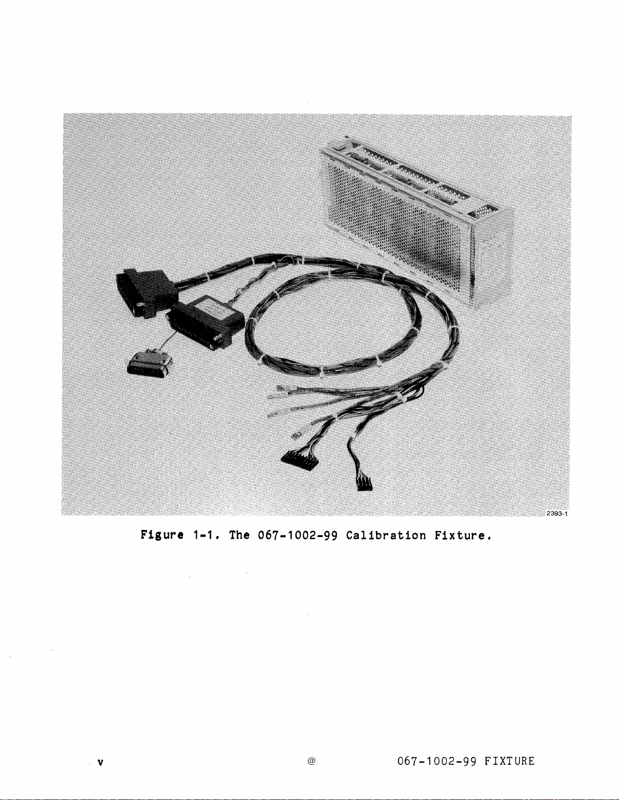
Figure
1-1.
The
067-1002-99
Calibration
Fixture.
v
@
067-1002-99
FIXTURE
Page 8

Page 9
Section
1
INTRODUCTION
ABOUT
This
(Figure
Voltage
The
manual
•
•
•
• The
following
•
•
THIS
MANUAL
describes
1-1)
Power
Specifications
Cable
Parts
supply.
067-0883-99
Refer
tions
theory
620-0295-00
Refer
parts
operation.
dure
properly
also
procedure
and
Supply.
and
list
performance
documents
to
and
to
lists,
to
contains
its
schematic
this
for
of
operation.
this
bring
or
for
the
067-1002-99
use
in
The
manual
check
contain
Universal
manual
the
calibration
Low
Voltage
manual
maintenance
The
Maintenance
up
supplies
which
have
an
abbreviated
use
in
servicing
includes:
diagrams
procedure
related
Load
for
general
Power
for
power
procedures,
which
been
the
field.
Calibration
of
the
for
information:
Unit
section
repaired.
Instruction
operating
fixture
Supply
supply
are
performance
620-0295-00
the
power
(plug-in)
Service
schematics,
and
theory
contains
not
operating
The
check
Fixture
Manual.
instruc-
Manual.
a
proce-
manual
Low
of
067-1002-99
When a Universal
the
performance
manual
the
vice
FIXTURE
should
procedure
manual.
be used
in
NOTE
Load
check
the
@
Unit
is
procedure
in
preference
power
supply
available,
in
this
to
ser-
1-1
Page 10
INTRODUCTION
• The
power
supply,
manual.
DESCRIPTION
The
calibration
• A
• A
The
plug-in
a
circuit
connects
set
of
channel.
equations
manual.
A
chart
for
each
to
the
parallel
personality
Load
cable
board.
it
resistors
These
given
on
the
supply.
+5
V
to
service
supply
refer
OF
THE
fixture
Unit
harness
assembly
An
with
supply,
the
the
which
resistors
in
front
Channels
+55
manual
is
installed.
to
the
MODULE
includes
plug-in
consists
edge
the
and
V
connector
load
program
were
appendix
of
the
Channels
supply.
unit.
1
for
the
adjustment
for
of
The
two
selected
to
plug-in
and
2
5 and 6
product
To
two
assemblies:
the
a
metal
at
circuit
load
the
lists
are
in
adjust
procedure
TEKTRONIX
the
levels
in
load
connected
the
framework
rear
board
accordance
unit
the
voltage
are
connected
which
power
in
Universal
of
the
includes
for
instruction
in
the
this
enclosing
board
a
each
with
range
parallel
in
The
cable
supply
assembly
under
test.
connects
the
load
unit
to
the
power
1-2
@
067-1002-99
FIXTURE
Page 11
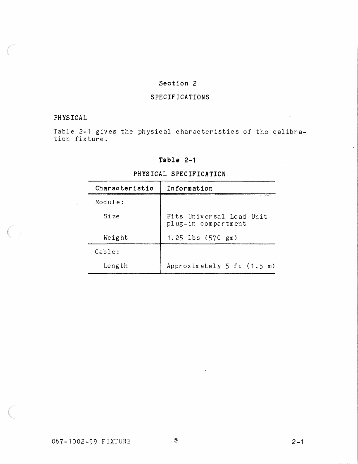
PHYSICAL
Section
2
SPECIFICATIONS
Table
tion
2-1
gives
fixture.
Characteristic
rv;odule:
Cable:
the
Size
Weight
Length
physical
Table
PHYSICAL
Information
Fits
plug-in
1.25
Approximately
characteristics
2-1
SPECIFICATION
Univ
er
sa 1 Lo
compartment
lbs
(570
gm)
5
ft
ad
of
(1.5
the
Unit
calibra-
m)
067-1002-99
FIXTURE
@
2-1
Page 12
SPECIFICATIONS
ELECTRICAL
Table
channel.
headings.
Characteristic:
2-2
gives
The
the
following
Property
specifications
definitions
of
Performance Requirement: A
characteristic
in
limit
form.
Supplemental
mance
The
following
requirements
~erformance
environmental
• The
properly
Load
The
•
mental
in
quantitative
Information:
or
reqtiirements
calibration
functioning
Unit
ULU
(ULU).
is
operating
limits.
that
limits:
fixture
equipment.
statement
terms
Statements
provide
are
valid
is
TEKTRONIX
within
for
each
explain
that
of
performance,
that
reference
only
properly
067-0883-99
its
specified
load
the
column
defines
explain
information.
within
seated
unit
a
usually
perfor-
the
in
a
Universal
environ-
2-2
@
067-1002-99
FIXTURE
Page 13
SPECIFICATIONS
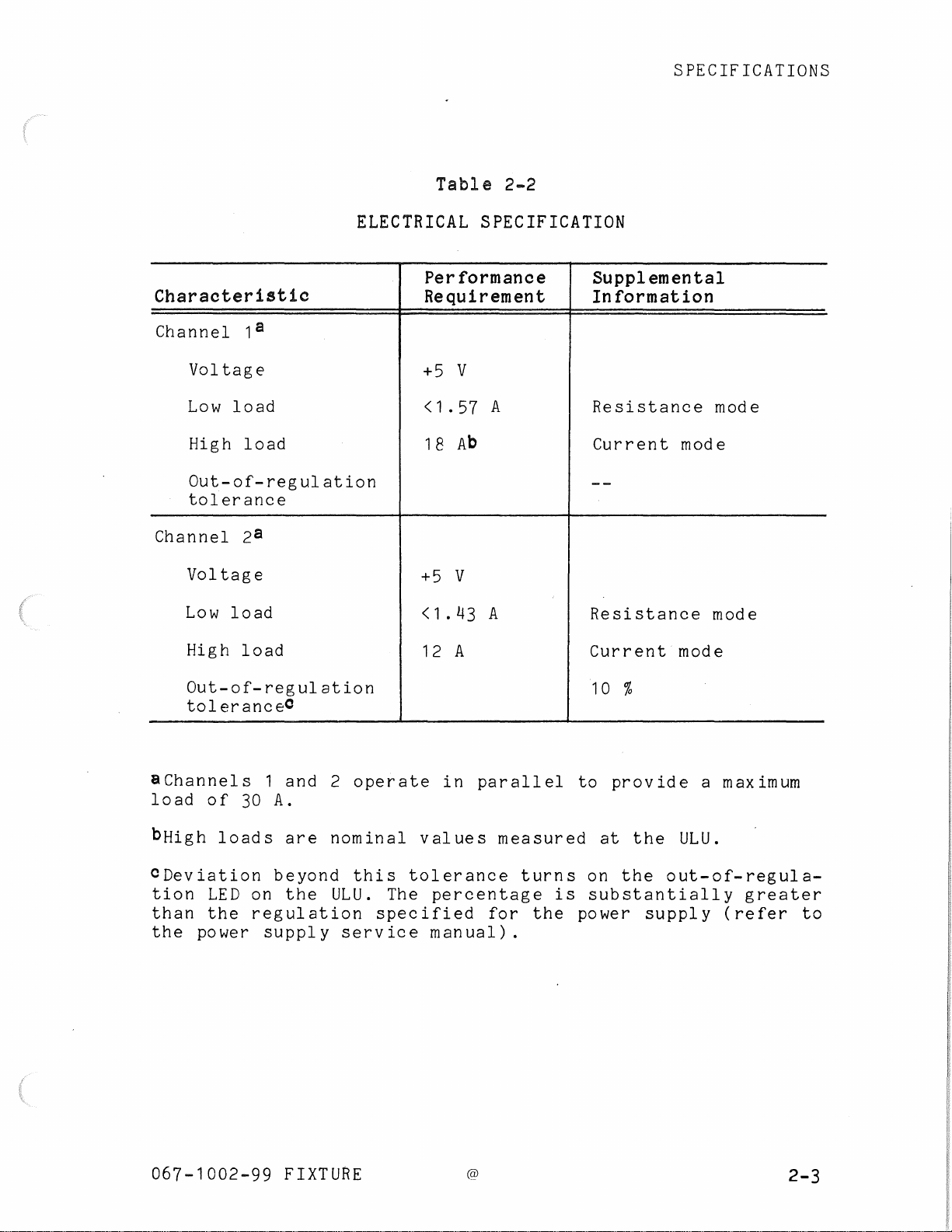
Characteristic
Channel
Voltage
Low
High
Out-of-regulation
tolerance
Channel
Voltage
Low
1 a
load
load
2a
load
Table
ELECTRICAL
Performance
Requirement
+5 v
<
1.
57
18
Ab
+5 v
<1.43
2-2
SPECIFICATION
Supplemental
In
formation
A
A
Resistance
Current
Resistance
mode
mode
mode
High
Out-of-regulation
toleranceO
achannels
load
bHigh
CDeviation
tion
than
the
load
of
30
loads
LED
the
power
on
regulation
1
and
A.
are
beyond
the
supply
2
operate
nominal
this
ULU.
The
specified
service
12 A
in
parallel
values
tolerance
percentage
manual).
measured
turns
for
the
Current
10
%
to
provide
at
on
the
is
substantially
power
mode
a maximum
the
ULU.
out-of-regula-
supply
greater
(refer
to
067-1002-99
FIXTURE
@
2-3
Page 14
SPECIFICATIONS
Characteristic
Channel
Voltage
Low
High
Out-of-regulation
tolerance
Channel
Voltage
Low
High
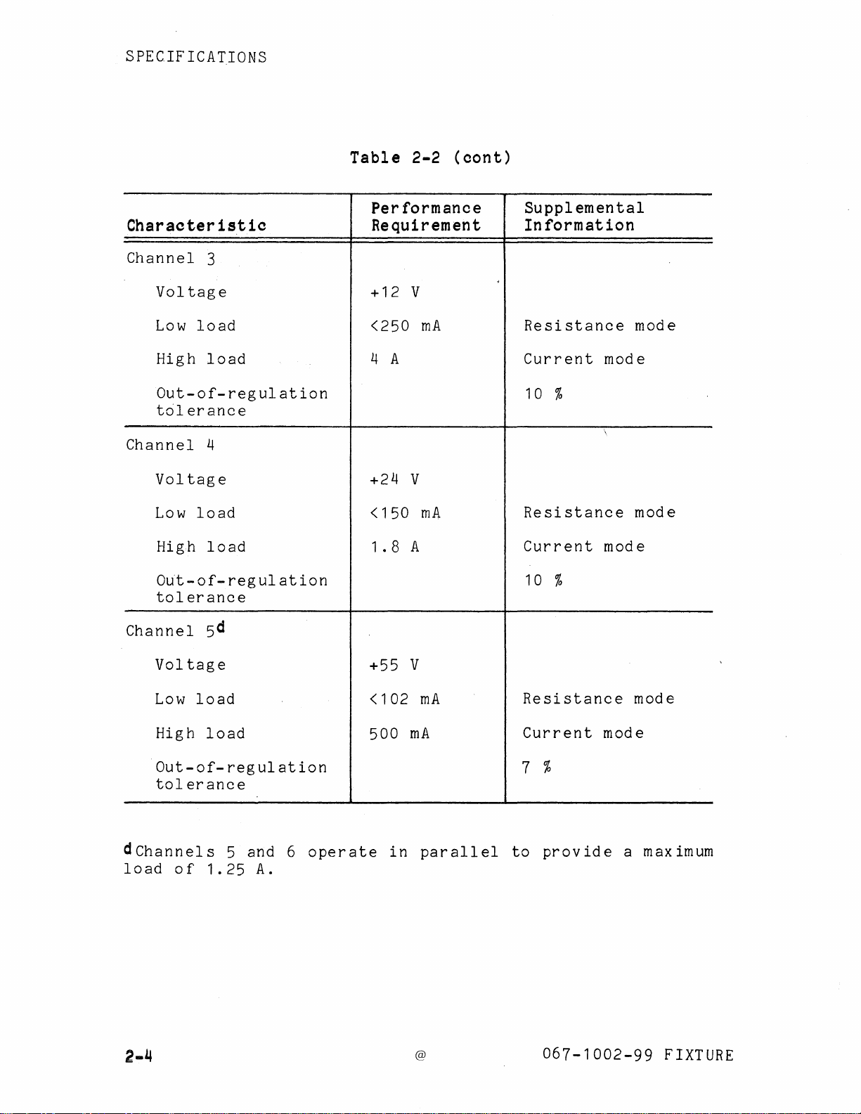
3
load
load
4
load
load
Table
2-2
Performance
Requirement
+12 v
<250
4 A
+24 v
<150
1.
mA
mA
8 A
(cont)
Supplemental
Information
Resistance
Current
10
%
Resistance
Current
mode
mode
mode
mode
Out-of-regulation
tol
er
anc
Channel
Voltage
Low
High
Out-of-regulation
tolerance
dchannels
load
of
5d
load
load
1.25
e
5 and 6
A.
operate
+55 v
<102
500
mA
in
mA
parallel
10
%
Resistance
Current
7 %
to
provide
mode
mode
a maximum
2-4
@
067-1002-99
FIXTURE
Page 15
SPECIFICATIONS
Characteristic
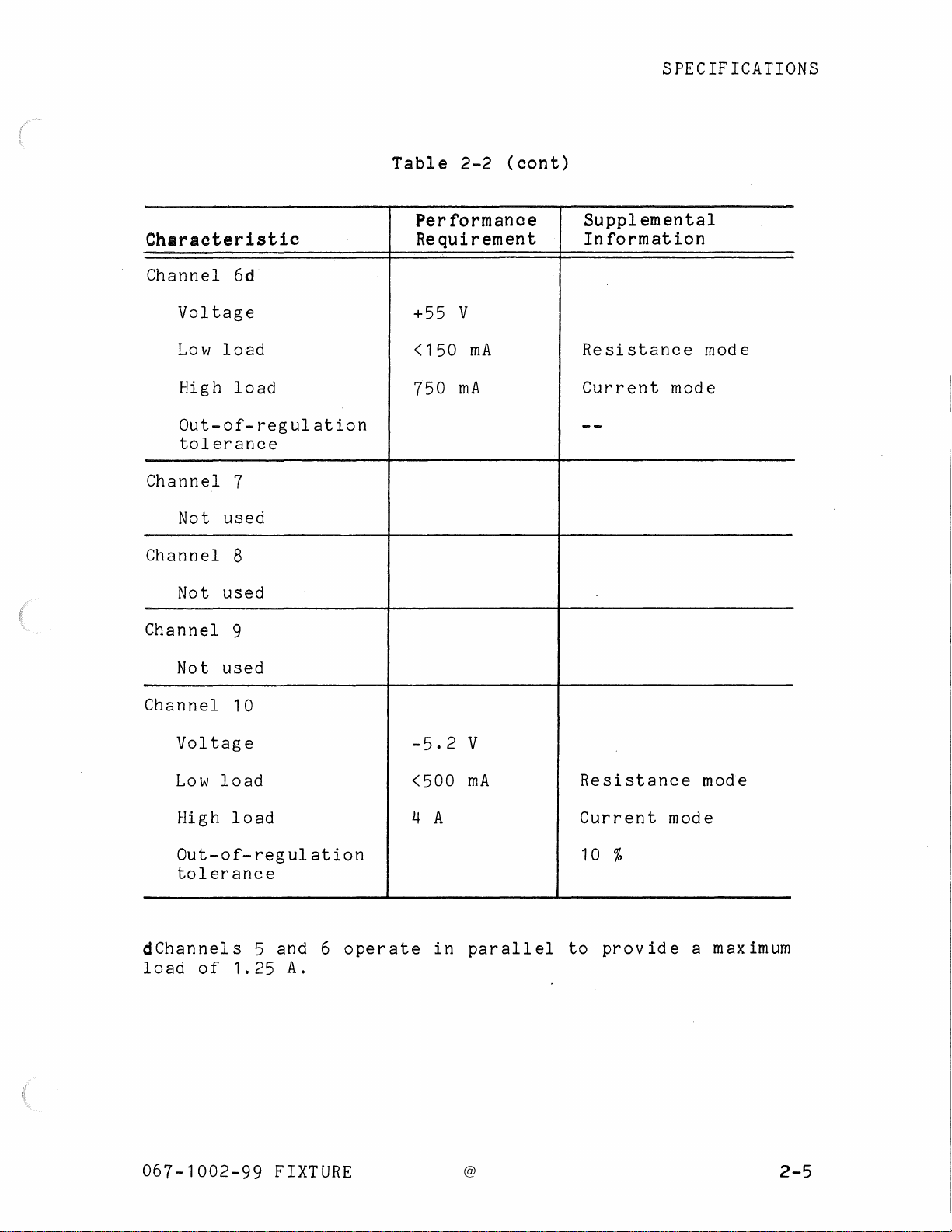
Channel
Voltage
Low
High
Out-of-regulation
tolerance
Channel
Not
Channel
Not
6d
load
load
7
used
8
used
Table
2-2
Performance
Requirement
+55 v
<150
750
mA
mA
(cont)
Supplemental
In
formation
Resistance
Current
mode
mode
Channel
Not
Channel
Voltage
Low
High
Out-of-regulation
tolerance
dChannels
load
of
9
used
10
load
load
1.25
5 and 6
A.
operate
-5.2
<500
4 A
in
v
mA
parallel
Resistance
Current
10
%
to
provide
mode
mode
a maximum
067-1002-99
FIXTURE
@
2-5
Page 16
SPECIFICATIONS
Characteristic
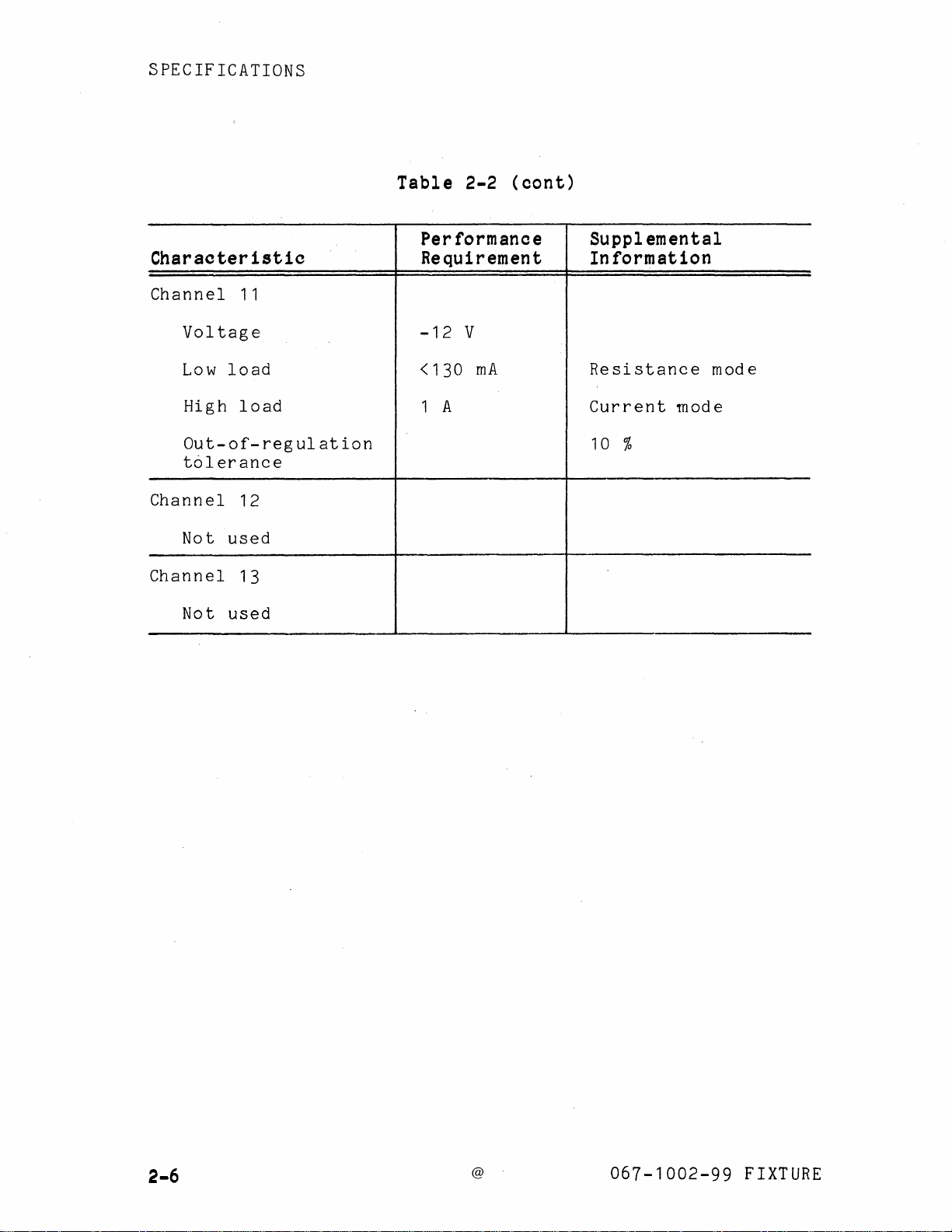
Channel
Voltage
Low
High
Out-of-regulation
tolerance
Channel
Not
Channel
Not
11
load
load
12
used
13
used
Table
2-2
Per formanoe
Requirement
-12
v
<130
1 A
mA
(cont)
Supplemental
In
formation
Resistance
Current
10
%
mode
mode
2-6
@
067-1002-99
FIXTURE
Page 17
ENVIRONMENTAL
SPECIFICATIONS
R e f e r
Load
CABLE
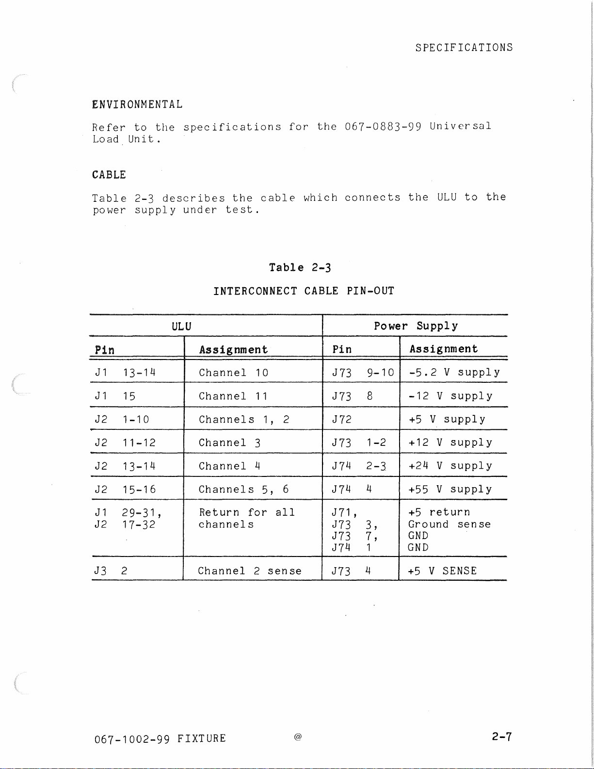
Table
power
Pin
J1
13-14
J1
15
to
Unit.
2-3
supply
th
e s
pe
describes
under
ULU
c i f i c a t i o n s f o r
the
cable
test.
Table
INTERCONNECT
Assignment
Channel
Channel
1 0
1 1
th
e 0 6 7 - 0 8 8 3 - 9 9 U n i v e r s a 1
which
connects
the
2-3
CABLE
PIN-OUT
Pin
J73
J73
Power
9·-10
8
Supply
Assignment
-5.
2 V
-12
ULU
V
supply
to
sup
the
ply
J2
J2
J2
J2
J1
J2
J3
1-10
11-12
13-14
15-16
2
9-3
17-32
2
1 '
Channels
Channel
Channel
Channels
Return
channels
Channel
3
4
for
2
1 '
5,
all
sense
2
6
J72
J73
J74
J74
J
71
J73
J73
J74
J73
'
1-2
2-3
4
3'
7 '
1
4
+5
V
+12 v
v
+24
v
+55
+5
return
Ground
GND
GND
+5
v
supply
supply
supply
supply
sense
SENSE
067-1002-99
FIXTURE
@
2-7
Page 18

Page 19

Section
3
SAFETY
Do
Do
unless
resuscitation
Wear
SUMMARY
Not
Service
not
perform
another
Safety
POWER
The
VOE
Filter,
and
Inverter
directly
ry
by
to
electrical
transformer
vicing
of
Alone
service
person
is
present.
Glasses
SUPPLY
boards
the
should
these
or
capable
PERFORMANCE
WARNING
Line
AC
lines.
shock
I
Voltage
are
connected
an
be used
boards.
adjustment
of
rendering
CHECK
Selector,
To
avoid
isolation
during
of
the
inju-
ser-
power
first
supply
aid
and
Some
transistors
injury
power
Use
Dangerous
supply.
connections
Disconnect
ing,
After
the
are
067-1002-99
internal
to
supply.
Care
To
or
replacing
the
Inverter
present
or
your
When
voltages
avoid
or
power
power
board
in
FIXTURE
fault
other
eyes
conditions
primary
wear
Servicing
exist
personal
components
before
components.
has
been
indicates
the
filter
may
components
safety
glasses
With Power
at
several
injury
while
removing
disconnected,
capacitors.
@
do
the
that
cause
to.
On
points
not
touch
power
protective
the
dangerous
the
explode.
while
in
is
neon
switching
servicing
the
exposed
on.
panels,
flasher
voltages
To
power
solder-
still
avoid
the
on
3-1
Page 20

PERFORMANCE
I
Power
The
that
supply
ground.
ing
Source
power
does
conductor
supply
not
conductors
A
protective
operation.
GENERAL
The
procedures
power
Specification
The
for
supply
conditions
the
electrical
CHECK
is
apply
in
the
in
with
section
listed
intended
more
or
between
than
ground
power
this
the
section
electrical
of
the
in
that
requirements
to
operate
250
either
connection
cord
is
compare
requirements
power
section
to
volts
supply
by
essential
the
supply
must
be
valid.
from
rms
a
between
conductor
way
for
performance
service
be
met
power
of
the
safe
given
source
the
and
ground-
of
in
the
manual.
in
order
a
These
procedures
operating
bring
up
Maintenance
If
the
performance
and
c~nnot
the
entire
properly.
supplies
section
be
adjusted,
performance
are
which
on
for
use
For
troubleshooting
have
in
the
power
any
test
repair
check.
on
been
does
the
supplies
repaired,
supply
not
power
which
assistance
refer
service
meet
the
supply
appear
or
to
the
manual.
requirement
and
repeat
to
to
be
3-2
@
067-1002-99
FIXTURE
Page 21

PERFORMANCE
CHECK
EQUIPMENT
•
TEKTRONIX
equivalent)
nated)
oscilloscope
PWRFL-0
•
TEKTRONIX
•
TEKTRONIX
•
Isolation
•
Variable
115 V
90
•
AC
(may
• Remote
(Figure
substituted.)
REQUIRED
465
or
probe
waveforms.)
067-0883-99
067-1002-99
transformer.
autotransformer
or
3 A
to
132 V
voltmeter,
be
part
switch
3-1)
and
is
at
or
±5%
of
to
dual
180
with
trace
matching
tip
adapter
helpful
230
V,
to
from
autotransformer).
five-pin
fit
J63.
oscilloscope
BNC
to
and
in
checking
Universal
Calibration
capable
output
264
V.
90
to
132 V
'
harmonica
(A
two-pin
BNC
1X
probe.
Load
Fixture.
of
variable
or
(or
cable
the
INIT-0
Unit
at
least
from
180
connector
jumper
(untermi(A
storage
and
(ULU).
6 A
at
least
to
264 V
may
be
at
•
Flat
blade
1/8-inch
Figure
3-1.
screwdriver.
Remote
Switch.
067-1002-99
FIXTURE
@
3-3
Page 22

PERFORMANCE
CHECK
PREPARATION
This
the
performance
section
describes
check
connection
set-up
of
diagram,
the
Figure
equipment
3-2.
shown
in
3-4
Figure
3-2.
Performance Check
@
Set-Up.
067-1002-99
FIXTURE
Page 23

1.
2.
3.
4.
5.
6.
Remove
Turn
rocker
Connect
Leave
Connect
the
Install
front
Connect
rear
avoid
off
power
panel
the
power
AC
power
switch.
the
autotransformer
the
power
the
power
off.
the
067-1002-99
panel
improper
compartment
the
cable
of
supply
to
the
off.
supply
harness
the
ULU.
connection.
from
to
Calibration
of
These
ULU
by
to
the
the
to
the
connectors
the
PERFORMANCE
product.
using
the
autotransformer.
ULU.
three
its
isolation
Fixture
connectors
are
rear
panel
transformer.
Leave
into
keyed
the
on
to
CHECK
the
067-1002-99
FIXTURE
@
3-5
Page 24

PERFORMANCE
7.
Connect
8.
board
a.
b.
c.
d.
Connect
Inverter
on
Connect
Connect
Connect
J71 (5 RTN).
Connect
J72
(+5V).
CHECK
other
the
the
the
the
the
the
board.
end
power
10-pin
4-pin
spade
spade
remote
Leave
of
the
supply
harmonica
harmonica
lugs
lugs
switch
the
cable
(see
on
on
to
switch
harness
Figure
to
the
the
J63
to
four
four
on
off.
to
3-3):
J73.
J74.
GRAY-BLACK
GRAY-RED
the
the
power
Regulator
wires
wires
supply
to
to
Figure
3-6
3-3.
Connecting
the
Load
@
Unit
to
the
067-1002-99
Power
Supply.
FIXTURE
Page 25

PROCEDURES
OC
Supplies
PERFORMANCE
CHECK
This
and
Table
1.
Set
procedure
current
3-1
summarizes
The
dure
They
mation
the
MAX/MIN
LOAD
VOLTAGE/CURRENT
CUR
OVER
checks
limiting
ripple
are
are
ULU
controls
SELECT
RENT
VOLTAGE
the
point
the
figures
not
provided
of
the
Switches
ADJUST
TEST
voltage
for
each
steps.
NOTE
given
performance
solely
service
as
follows:
to
person.
12
levels,
portion
in
requirements.
for
MIN
IND
VOLTAGE
Midrange
OFF·
this
the
maximum
proce-
infor-
and
current,
of
the
SWITCHED
and
"in"
supply.
067-1002-99
FIXTURE
@
3
..
7
Page 26

PERFORMANCE
2.
Set
up
the
a.
Connect
(Figure
b.
Connect
an
unterminated
c.
Set
the
CHECK
oscilloscope:
Channel
3-4).
Channel
controls
between
2
to
BNC
as
RIPPLE
cable
follows:
C476 and
OUT
(+)
or
a
1X
Pin
on
probe
3
the
and
of
ULU,
U575
using
adapter.
TIME/DIV
VERT
CH
MODE
1 VOLTS/DIV
CH 1 COUPLING
CH
2 VOLTS/DIV
CH 2 COUPLING
TRIGGER
TRIGGER
TRIGGER
TRIGGER
TRIGGER
20
MHz
(if
SOURCE
COUPLING
MODE
SLOPE
LEVEL
BANDWIDTH
available)
10
µs
CH
2
2
v
DC
10-mV
DC
CH
1
AC
AUTO
+
Midrange
Activated
(pull
out)
Figure
3-8
HERE PIN
3-4.
3,U575
Connecting
the
Trigger
@
to
the
067-1002-99
Power
2393-5
Supply.
FIXTURE
Page 27

PERFORMANCE
CHECK
Turn on
3.
4.
Turn
120
Turn on
5.
jumper.
6.
Select
board
ULU
7.
Adjust
MODE
+5 V
Channel
this
Supply
supply.
the
the
on
v.
the
Channel
(Figure
meter.
the
to
CH
The
each
1 and
ULU.
autotransformer
5 on
3-3)
supply
the
for
LEVEL
procedure
channel.
2
on
power
TRIGGER
2.
following
active
Channel
using
ULU.
a
reading
if
NOTE
the
and
adjust
the
Adjust
of
necessary
is
repeated
ULU
form
the
remote
R591
55.1
and
a
parallel
voltage
switch
on
the
V ±100
return
for
to
or
Inverter
mV
on
VERT
load
for
the
1.
2.
3.
Select
Set
Verify
Table
Channel
VOLTAGE/CURRENT
that
3-1.
the
1 on
voltage
the
ULU.
to
VOLTAGE.
is
within
the
limits
given
in
067-1002-99
FIXTURE
@
3-9
Page 28

PERFORMANCE
4.
Measure
est
part
caused
by
TRIGGER SOURCE: CH 1
CHECK
the
peak-to-peak
of
the
60
Hz
trace
ripple.
40 kHz
(Figure
Ignore
10
ripple
3-5).
noise
~
IGNORE NOISE
./
from
The
spikes.
.......
the
lighter
.
brightband,
is
5.
6.
7.
8.
9.
1
Figure 3-5. Measuring
Select
ripple.
Set
Recheck
Set
For
current
Channel
MAX/MIN
the
VOLTAGE/CURRENT
each
channel
given
mV
2 on
to
MAX
voltage
verify
in
the
for
and
to
Table
40
ULU.
both
ripple
CURRENT.
that
Verify
Channel
the
3-1.
for
kHz
the
1
Channel
ULU
2393-6
Ripple.
voltage
and
is
Channel
drawing
1
and
and
2.
2.
the
3-10
@
067-1002-99
FIXTURE
Page 29

10.
push
for
Select
foldback
The
power
sound
This
If
the
the
Channel
point
supply
when
is
normal
current
in
CURRENT
channel(s)
2 on
as
in
the
..
limit
the
follows:
NOTE
may
emit a buzzing
current
circuit
ADJUST
to
MIN.
ULU
and
limiting
and
verify
latches
set
PERFORMANCE
mode,
up,
MAX/MIN
the
current
CHECK
11.
12.
Pull
outer
for
circuit
OUT
the
Table
drawn
power
1
Reset
Set
Channel
out
an
OF
highest
im
it.)
MAX/MIN
the
inner
knob
3-1.
by
supply
CURRENT
To
next
of
knob
cw
to
abrupt
when
REGULATION
Channel
drop.
the
current
This
specifications.
ADJUST
avoid
test,
CURRENT
after
to
2.
knob
add
current
This
supply
LEDs
value,
1,
also
is
less
when
meets
to
E3
invalid
always push
ADJUST
verifying
MAX
measurements
for
Channel
of
CURRENT
while
drop
enters
midrange
is
should
than
added
the
requirement
(Step
in
and
center
the
ADJUST.
watching
caused
the
limiting
come
the
value
to
the
9
tested
and
"in."
on
the
inner
the
foldback
1
and
to
by
on.
fixed
given
the
knob
outer
point.
MIN
Turn
the
the
mode.
Verify
given
the
for
the
ammeter
foldback
The
that
in
current
in
the
lower
067-1002-99
FIXTURE
@
3-11
Page 30

PERFORMANCE
CHECK
Supply
+5 v
+12
v
+24
v
arr a
drop
power
Select
Channel
1
2
3
4
voltage
in
the
supply
reading
cable
output.
PERFORMANCE
Voltage
Range a
85
15
15
to
v
to
v
to
v
to
v
4.
5.
4.85
5.
11 . 64
12.36
23.28
24.72
falls
to
the
ULU
Table
CHECK
Rippleb
(
p-p)
100
mV
100
mV
mV
20
mV
20
below
by
measuring
3-1
the
SUMMARY
Approx.
Current
at
MAX
0
Load
A
1 8
12 A
4 A
A
1.
8
range,
consider
the
Fold
Point
Do
not
test
<19 A
<6
A
<2.8
voltage
back
A
voltage
at
Leave
Load
Switch
MAX
MIN
MIN
MIN
the
bThe
ripple
provided
noise
Figure
CThe
supply
given
draw
to
approximately
MAX.
solely
spikes.
3-6
in
this
figures
Refer
for
should
column.
for
the
are
the
to
Figure
+55 V
meet
The
the
current
not
performance
information
3-5
supply.
the
other
personality
listed
requirements.
of
for
the
all
service
supplies
specifications
insert
when
the
person.
and
at
programs
load
They
also
the
the
is
switched
are
Ignore
to
current
ULU
to
3-12
@
067-1002-99
FIXTURE
Page 31

PERFORMANCE
CHECK
Supply
+55 v
-5.2
-12
v
v
Seleot
Channel
5
6
10
1 1
Volta1e
Ranges
53.90
56.
10
53.90
56.
10
-4.99
-5.
41
-11 .
64
-12.36
Table
to
v
to
3-1
(cont)
Rippleb
(
p-p)
25
mV
@ 60 Hz;
50
mV
@ 40
25
kHz
mV
v @ 60 Hz;
50
mV
to
@ 40
100
kHz
mV
v
20
to
mV
v
Approx.
Current
at
MAX
Load1°
500
mA
750
mA
4 A
A
1
Foldbaok
Point
<850
Do
test
<4.8
<1. 5
mA
not
A
A
Leave
Load
Switch
MIN
MIN
MIN
MIN
aif
a
voltage
drop
power
~The
provided
noise
Figure
OThe
given
draw
to
in
supply
ripple
spikes.
supply
in
approximately
MAX.
the
solely
3-6
this
reading
cable
output.
figures
Refer
for
should
column.
for
the
to
the
are
the
to
+55 V
meet
the
falls
Figure
The
current
below
ULU
not
performance
information
supply.
the
other
personality
by
measuring
3-5
listed
the
range,
the
requirements.
of
the_
service
for
all
supplies
specifications
insert
when
the
consider
voltage
person.
and
at
programs
load
voltage
at
They
also
the
the
is
switched
the
are
Ignore
to
current
ULU
to
067-1002-99
FIXTURE
@
3-13
Page 32

PERFORMANCE
CHECK
+12 V
1.
2.
Supply
Select
Set
VOLTAGE/CURRENT
Table
3. Compare
4.
Set
MAX/MIN
ripple.
5.
Set
VOLTAGE/CURRENT
drawing
6.
Pull
fdldback
with
7.
Reset
for
+24 V
out
Tab 1 e 3
Channel
Supply
Channel
3-1.
the
ripple
for
the
current
CURRENT
point
-1
CURRENT
3
3 on
with
Channel
ADJUST
is
reached.
.
ADJUST
to
MIN.
the
to
VOLTAGE.
the
3
to
CURRENT.
given
and add
to
midrange
ULU.
to
in
Compare
value
MAX.
Table
Verify
in
Recheck
Verify
3-1.
current
the
and
the
Table
that
until
highest
"in."
reading
3-1.
the
voltage
the
the
Set
with
ULU
is
reading
MAX/MIN
and
1.
Select
2.
Set
VOLTAGE/CURRENT
Table
3. Compare
4.
Set
MAX/MIN
ripple.
5.
Set
VOLTAGE/CURRENT
drawing
6.
with
7.
for
Pull
foldback
Reset
out
the
Channel
Channel
3-1.
the
ripple
for
the
current
CURRENT
point
value
CURRENT
4
4 on
with
Channel
ADJUST
is
reached.
given
ADJUST
to
MIN.
the
ULU.
to
VOLTAGE.
the
4
to
CURRENT.
given
and
in
Table
to
midrange
value
to
MAX.
in
Table
add
Compare
3-1.
Verify
in
Recheck
Verify
3-1.
current
the
and
the
Table
that
until
highest
"in."
reading
3-1.
the
voltage
the
the
Set
with
ULU
is
reading
MAX/MIN
and
3-14
@
067-1002-99
FIXTURE
Page 33

+55
V
Supply
PERfORMANCE
CHECK
Channels
1.
Select
2.
Set
VOLTAGE/CURRENT
Table
3. Compare
4.
Select
ripple.
5.
Set
MAX/MIN
voltage
6.
Change
7.
Reset
8.
Measure
peak-to-peak
3-6.
Steps
5 and 6
Channel
3-1.
the
Channel
and
the
MAX/MIN
the
The
band
3
and
load
this
5 on
ripple
6 on
for
ripple
with
both
for
oscilloscope
TIME/DIV
TRIGGER
for
60
Channels
Hz
ripple
SOURCE
displacement
is
the
4.
supply
the
ULU.
to
VOLTAGE.
the
the
ULU.
channels
each
settings
for
40 kHz
in
value
Check
to
channel.
5 and 6
each
of
the
ripple
parallel.
Verify
in
the
MAX.
as
follows:
5
LINE
to
channel
band
which
the
Table
voltage
Recheck
ms
MIN.
by
as
shown
you
reading
3-1.
and
the
reading
in
checked
with
the
Figure
in
TRIGGER SOURCE: LINE
100·
. . . . . . . . . . . . . . . . . . . .
I
90----1-.---+----l------l---+-----+-----+---+------l-----l
ure
3-6.
Measuring
s
...
60Hz
RIPPLE
2393-7
60
Hz
Ripple.
067-1002-99
FIXTURE
@
3-15
Page 34

PERFORMANCE
9.
Set
MAX/MIN
ripple
10.
Set
11.
Measure
ULU
12.
Select
current
highest
value,
meets
specifications.
13.
Re
set
for
14.
Reset
on
VOLTAGE/CURRENT
is
drawing
Channel
when
the
CURRENT
Channel
the
CHECK
for
each
the
current
until
reading
requirement
the
added
ADJUST
5 and 6
oscilloscope
each
channel.
to
on
the
current
5.
Pull
foldback
with
to
to
channel
CURRENT.
each
out
the
value
the
current
given
to
"in"
MIN.
as
follows:
to
MAX.
channel
given
CURRENT
point
in
a.nd
in
is
given
drawn
the
mid
Recheck
and
verify
Table
ADJUST
reached.
in
Table
by
power
range.
60
3-1.
and add
Compare
3-1.
Channel
supply
Set
Hz
that
the
the
This
6,
MAX/MIN
...
5.2
1.
Select
2.
Set
Table
3.
Compare
4.
Set
and
5.
Set
drawing
6.
Verify
pull
clockwise
reached.
Table
TIME/DIV
TRIGGER
V
Supply
Channel
VOLTAGE/CURRENT
3-1.
the
ripple
MAX/MIN
ripple.
VOLTAGE/CURRENT
that
out
for
the
current
the
CURRENT
to
add
Compare
3-1.
SOURCE
10
on
the
to
with
Channel
to
given
CURRENT
ADJUST
current
the
highest
ULU.
VOLTAGE.
the
value
10
t6
MAX.
CURRENT.
in
Table
ADJUST
and
turn
until
reading
Compare
in
Recheck
Verify
3-1.
knobs
the
the
foldback
10
µs
CH
1
the
Table
that
are
outer
with
reading
3-1.
the
voltage
the
centered,
knob
point
the
value
with
ULU
is
then
counter-
is
in
7.
Reset
for
3-16
CURRENT
Channel
ADJUST
10
to
MIN.
to
"in"
@
and
midrange.
067-1002-99
Set
MAX/MIN
FIXTURE
Page 35

-12 V Supply
19
2.
Set
Table
3.
Compare
4.
Set
and
5.
Set
Select
Channel
VOLTAGE/CURRENT
3-1.
MAX/MIN
ripple.
VOLTAGE/CURRENT
drawing
6.
Pull
out
clockwise
reached.
Table
3-1.
the
ripple
for
the
current
CURRENT
to
add
Compare
11
on
to
with
Channel
to
given
ADJUST
current
the
the
ULU.
VOLTAGE.
the
11
CURRENT.
in
and
until
highest
value
to
MAX.
Table
turn
reading
Compare
in
Recheck
Verify
3-1.
the
the
foldback
PERFORMANCE
the
reading
Table
3-1.
the
that
outer
the
knob
point
with
the
voltage
ULU
counter-
value
CHECK
with
is
is
in
7.
Reset
for
Line
Channel
Vol
tag
CURRENT
The maximum
slightly
1.
Set
more
the
VOLTAGE/CURRENT
CURRENT
OVER
2.
Turn on
3. Turn on
4.
Adjust
115 V
the
nominal;
ADJUST
11
to
es
load
configuration
than
controls
LOAD
MAX/MIN
1,
3,
SELECT
Switches
2,
5,
4,
6,
ADJUST
VOLTAGE
the
ULU.
the
power
autotransformer
180 V
MIN.
350 W
on
the
10
and
TEST
supply
for
to
"in"
through
load
11
using
230 V
and
used
the
unit
IND
MAX
MIN
VOLTAGE
midrange
OFF
the
to
low
nominal).
midrange.
in
this
power
as
and
cord.
follows:
SWITCHED
and
remote
line
voltage
Set
test
"in"
switch.
MAX/MIN
draws
(90 V for
067-1002-99
FIXTURE
@
3
...
17
Page 36

PERFORMANCE
5.
For
each
the
voltage
6.
7.
Adjust
for
For
the
the
115 V
each
voltage
CHECK
channel
is
(1
within
autotransformer
nominal;
channel
is
(1
within
through
the
264 V
through
the
6,
limits
to
for
6,
limits.
10,
given
high
230 V
10,
and
11),
in
line
voltage
nominal).
and
11),
verify
Table
verify
3-1.
(132
that
V
that
INIT-0
1.
Set
2.
S~t
3.
Turn
4.
Verify
voltage
5.
Turn
and
the
LOAD
on
on
PWRFL-0
oscilloscope
TIME/DIV
VERT
CH
1 VOLTS/DIV
CH 1 COUPLING
CH
2 VOLTS/DIV
CH 2 COUPLING
TRIGGER
TRIGGER
TRIGGEij
TRIGGER
TRIGGER
SELECT
the
ULU.
that
(132
the
the
or
power
as
follows:
MODE
SOURCE
COUPLING
MODE
SLOPE
LEVEL
to
LOW.
autotransformer
264
V)
from
supply
using
the
·the
10
ms
CHOP
2 v
DC
2 v
DC
CH
1
AC
AUTO
+
Midrange
is
set
to
preceding
remote
the
high
test.
switch.
line
6.
7.
8.
3-18
Test
to
the
+5
trigger
Fasten
Connect
Position
the
screen
one
division
trigger
V
SENSE
on
the
Channel
the
(J73-4).
contact,
probe
2
Channel
and
position
above
level
adjust
to
+5
to
the
by
If
V SENSE.
INIT
1
ground
the
bottom.
@
touching
the
oscilloscope
TRIGGER
(J73-6).
reference
Channel
the
Channel
LEVEL
and
at
2
ground
067-1002-99
1
does
repeat.
the
center
reference
probe
not
of
FIXTURE
Page 37

9.
10.
Set
Turn
TRIGGER
off
the
MODE
power
to
supply
SINGLE
SWEEP.
and
then
PEl-H'ORMANCE
turn
it
back
CHECK
on.
11.
·12.
13.
14.
Compare
INIT-0
SENSE
reaches
Change
Set
the
180
V).
Set
LOAD
switches
preceding
MAX;
Move
Channels
the
trigger
removing
the
probe
Fasten
the
waveform
should
remain
its
the
oscilloscope
TIME/DIV 5
TRIGGER
TRIGGER
autotransformer
SELECT
should
line
Channel
level
it.
is
the
probe
to
be
voltage
3,
4,
1
by
touching
If
the
removed,
to
with
low
lower
margin
settings
MODE
SLOPE
to
IND
and
in
the
test:
6,
and
probe
to
oscilloscope
adjust
PWRFL-0.
that
for
shown
at
of
the
low
SWITCHED.
same
position
Channels
11
on
PWRFL-0
the
probe
TRIGGER
least
4.85
as
MIN.
does
in
50
V.
follows:
ms
AUTO
line
The
1,
(J73-5).
to
the
not
LEVEL
Figure
ms
after
voltage
channel
as
in
2,
5,
Test
pin
trigger
and
3-7.
+5
(90 V or
load
the
and
the
and
when
repeat.
V
10 on
+5
SENSE
J73-4
067-1002-99
ov
INIT-0
J73-6
ov
FIXTURE
21~
....
!11
O·
• • •
I
r-
90
......
-
4.85V
1 I
,
-
~
-
-
10
I
. . . .
OX·
• • •
21'
Figure
JOmS
I
50ms
MINIMUM
.
. . .
....
. . . . .
..
. . . . . . . . .
...
3-7. Power-Up Waveform.
@
. . . .
2393-8
Page 38

PERFORMANCE
15.
Turn
should
off
trigger
CHECK
the
power.
the
This
simulates
oscilloscope.
a
power
failure
and
Compare
PWRFL-0
PWRFL-0
J73-5
INIT-0
J73-6'-liii~ili
the
waveform
should
IOO·
I
90---+--r-----+----+-------+~--+---+-----+---+-----------i
ov
go
• • •
1-"-'-P-_.._._-..l,
ov
... ,
1
low
with
at
least
11 ms
MINIMUM
that
iiiliiiiliiiiiliiiiliiiiiliiiiiiiiiliiiii
Figure 3-8.
Power-Down
shown
11
ms
in
before
Waveform.
Figure
23
9
i9i3-i
ll
3-8.
INIT-0.
This
completes
the
performance
check.
3-20
@
067-1002-99
FIXTURE
Page 39

ELECTRICAL
PARTS
PARTS ORDERING
Replacement parts are available
or
representative.
Changes to
components
improvements developed in
ordering
type
or
number, serial number, and
If a part
Tektronix, Inc. Field
number.
Change
Tektronix
as
they become available, and to give you the benefit
parts, to
include
you have ordered has been replaced
Office
information,
SPECIAL NOTES AND SYMBOLS
XOOO
OOX
In
the Parts List,
Because
further
utilized where possible.
of
space limitations,
Item Name
an
identification,
INFORMATION
from
or
through
your
local
Tektronix,
instruments are sometimes made to
our
engineering department.
the
following
or
representative will
if
any, is located at the rear
Item Name is separated from the description
information
modification
Part first added at this serial
Part removed
ITEM NAME
an
Item Name may sometimes appear
the U.S. Federal Cataloging
contact
after
in
your
number
with a new
you concerning
of
this serial
accommodate
It
is
therefore important, when
order: Part number,
if applicable.
or
improved part,
this manual.
number
number
Handbook
Inc. Field
of
the latest
any
change in
by a colon
as
incomplete.
H6-1 can be
Office
improved
circuit
instrument
your
local
part
(:).
For
067-1
002-99
FIXTURE
ACTR
ASSY
CAP CAPACITOR
GER CERAMIC
CKT
COMP
CONN
ELCTLT
ELEC
INCAND
LED
NONWIR NON WIREWOUND
ACTUATOR
ASSEMBLY
CIRCUIT
COMPOSITION
CONNECTOR
ELECTROLYTIC SENS SENSITIVE
ELECTRICAL
INCANDESCENT
LIGHT
EMITT-ING DIODE
ABBREVIATIONS
PLSTC PLASTIC
QTZ
RECP RECEPTACLE
RES
RF
SEL SELECTED
SEMICOND
VAR
WW WIREWOUND
XFMR TRANSFORMER
XTAL CRYSTAL
@
QUARTZ
RESISTOR
RADIO FREQUENCY
SEMICONDUCTOR
VARIABLE
4-1
Page 40

REPLACEABLE ELECTRICAL PARTS
Mfr.
01121
01295
04713
07263
24546
55210
80009
91637
Code
Manufacturer
ALLEN-BRADLEY
TEXAS
iNSTRUMENTS,
GROUP
MOTOROLA,
FAIRCHILD
FAIRCHILD
CORNING
COMPONENTS
GETTIG
TEKTRONIX,
DALE
INC.,
SEMICONDUCTOR,
CAMERA
GLASS
DIVISION
ENG.
AND
INC.
ELECTRONICS,
CROSS
COMPANY
WORKS,
INDEX-MFR.
INC.,
SEMICONDUCTOR
SEMICONDUCTOR
AND
MFG.
INC.
A DIV.
INSTRUMENT
ELECTRONIC
COMPANY
PROD.
OF
CORP.
CODE
DIV.
NUMBER
Address
1201
2ND
STREET
BOX
MCDOWELL
HIGH
BOX
85,
BOX
0.
BOX
5012,
STREET
STREET
500
609
P 0
EXPRESSWAY
5005 E
464 ELLIS
550
PO
P 0
P.
TO
MANUFACTURER
SOUTH
OFF
13500 N
ROUTE
RD,PO
CENTRAL
BOX
45
20923
City,
State,
MILWAUKEE,
DALLAS,
PHOENIX,
MOUNTAIN
BRADFORD,
SPRING
BEAVERTON,
COLUMBUS,
TX
AZ
VIEW,
MILLS,
WI
75222
85036
PA
OR
NE
Zip
53204
CA
16701
PA
97077
68601
94042
16875
4-2
(cy
067-1002-99
FIXTURE
Page 41

REPLACEABLE ELECTRICAL PARTS
Component
CHOlRDES
CHOlRFL
CHOlRPH
CH02RCOMP
CH02RDES
CH02RFL
CH02RPH
CH03RCOMP
CH03RDES
CH03RFL
CH03RPH
CH04RCOMP
CH04RDES
CH04RFL
CH04RPH
CH05RCOMP
CH05RDES
CH05RFL
CH05RPH
CH06RDES
CH06RFL
CH06RPH
CH07RDES
CH08RDES
CH09RDES
CHlORCOMP
CHlORDES
CHlORFL
CHlORPH
CHllRCOMP
CHllRDES
CHllRFL
CHllRPH
CH12RDES
CH13RCOMP
No.
Tektronix
Part
No.
131-0566-00
321-0376-00
321-0302-00
321-0816-00
321-0318-00
321-0380-00
321-0320-00
321-0297-00
321-0268-00
321-0452-00
321-0327-00
321-0959-03
321-0259-00
321-1628-02
321-1623-02
321-0360-00
321-02
77-00
321-1484-03
321-0924-02
131-0566-00
321-0469-04
321-0330-00
131-0566-00
131-0566-00
131-0566-00
321-1701-04
321-0312-00
321-0640-00
321-0327-00
321-0297-00
321-0268-00
321-0701-00
321-0318-00
131-0566-00
131-0566-00
Serial/Model
Eff
Dscont
No.
Name & Description
BUS
CONDUCTOR:DUMMY
RES.,FXD,FILM:80.6K OHM,1%,0.125W
RES.,FXD,FILM:l3.7K OHM,1%,0.125W
RES.,FXD,FILM:5K OHM,1%,0.125W
RES.,FXD,FILM:20K OHM,1%,0.125W
RES.,FXD,FILM:88.7K OHM,1%,0.125W
RES.,FXD,FILM:21K OHM,1%,0.125W
RES.,FXD,FILM:l2.1K OHM,1%,0.125W
RES.,FXD,FILM:6.04K OHM,1%,0.125W
RES.,FXD,FILM:499K OHM,1%,0.125W
RES.,FXD,FILM:24.9K OHM,1%,0.125W
RES.,FXD,FILM:24.0K OHM,0.25%,0.125W
RES.,FXD,FILM:4.87K OHM,1%,0.125W
RES.,FXD,FILM:l.644M OHM,0.5%,0.125W
RES.,FXD,FILM:55.5K OHM,0.5%,0.125W
RES.,FXD,FILM:54.9K OHM,1%,0.125W
RES.,FXD,FILM:7.5K OHM,1%,0.125W
RES.,FXD,FILM:l.09M OHM,0.25%,0.125W
RES.,FXD,FILM:40K OHM,0.5%,0.125W
BUS
CONDUCTOR:DUMMY
RES.,FXD,FILM:750K OHM,0.1%,0.125W
RES.,FXD,FILM:26.7K OHM,1%,0.125W
BUS
CONDUCTOR:DUMMY
BUS
CONDUCTOR:DUMMY
BUS
CONDUCTOR:
RES.,FXD,FILM:5.22K OHM,0.1%,0.125W 91637
RES.,FXD,FILM:17.4K OHM,1%,0.125W 91637
RES.,FXD,FILM:l06K OHM,1%,0.125W 91637
RES.,FXD,FILM:24.9K OHM,1%,0.125W 91637
RES.,FXD,FILM:l2.1K OHM,1%,0.125W 91637
RES.,FXD,FILM:6.04K OHM,1%,0.125W
RES.,FXD,FILM:l87K OHM,0.25%,0.125W 91637
RES.,FXD,FILM:20K OHM,1%,0.125W 91637
BUS
CONDUCTOR:DUMMY
BUS
CONDUCTOR:DUMMY
DUMMY
RES,2.375,22
RES,2.375,22
RES,2.375,22
RES,2.375,22
RES,2.375,22
RES,2.375,22
RES,2.375,22
AWG
AWG
AWG
AWG
AWG
AWG
AWG
Mfr
Code
Mfr
Part
Number
55210
91637 MFF1816G80601F
91637
24546
91637
91637
91637
91637 MFF1816Gl2101F
91637
91637
91637
91637
91637
91637 HFF188Dl6443D
91637
91637
91637 MFF1816G75000F
91637
24546
55210
91637
91637
55210
55210
55210
91637
55210
55210
L-2007-1
MFF1816Gl3701F
NA55D5001F
MFF1816G20001F
MFF1816G88701F
MFF1816G21001F
MFF1816G60400F
MFF1816G49902F
MFF1816G24901F
CMF110216D24010C
MFF1816G48700F
MFF1816D55501D
MFF1816G54901F
HFF188Dl0903C
NC55C4002D
L-2007-1
MFF1816D75002B
MFF1816G26701F
L-2007-1
L-2007-1
L-2007-1
MFF1816D52200B
MFF1816G17401F
MFF1816Gl0602F
MFF1816G24901F
MFF1816Gl2101F
MFF1816G60400F
MFF1816C18702C
MFF1816G20001F
L-2007-1
L-2007-1
CR5001
CR5002
CR5005
CR5006
CR5010
CR5011
CR5015
CR5016
CR5020
CR5021
CR5025
CR5026
CR5030
CR5031
CR5035
CR5036
CR5040
CR5041
CR5045
CR5046
CR5050
CR5051
CR5055
CR5056
067-1002-99
152-0141-02
152-0141-02
152-0141-02
152-0141-02
152-0141-02
152-0141-02
152-0141-02
152-0141-02
152-0141-02
152-0141-02
152-0141-02
152-0141-02
152-0141-02
152-0141-02
152-0141-02
152-0141-02
152-0141-02
q2-0l41-02
152-0141-02
152-0141-02
152-0141-02
152-0141-02
152-0141-02
152-0141-02
FIXTURE
SEMICOND
SEMICOND
SEMICOND
SEMICOND
SEMICOND
SEMICOND
SEMI
CO
ND
SEMICOND
SEMICOND
SEMICOND
SEMICOND
SEMICOND
SEMICOND
SEMICOND
SEMICOND
SEMICOND
SEMICOND
SEMICOND
SEMICOND
SEMICOND
SEMICOND
SEMICOND
SEMICOND
SEMICOND
@
DEVICE:SILICON,30V,150MA
DEVICE:SILICON,30V,150MA 01295
DEVICE:SILICON,30V,150MA 01295
DEVICE:SILICON,30V,150MA 01295
DEVICE:SILICON,30V,150MA 01295
DEVICE:SILICON,30V,150MA
DEVICE:SILICON,30V,150MA 01295
DEVICE:SILICON,30V,150MA 01295
DEVICE:SILICON,30V,150MA
DEVICE:SILICON,30V,150MA 01295
DEVICE:SILICON,30V,150MA 01295
DEVICE:SILICON,30V,150MA 01295
DEVICE:SILICON,30V,150MA 01295
DEVICE:SILICON,30V,150MA 01295
DEVICE:SILICON,30V,150MA 01295
DEVICE:SILICON,30V,150MA
DEVICE:SILICON,30V,150MA 01295
DEVICE:SILICON,30V,150MA
DEVICE:SILICON,30V,150MA
DEVICE:SILICON,30V,150MA
DEVICE:SILICON,30V,150MA
DEVICE:SILICON,30V,150MA 01295 1N4152R
DEVICE:SILICON,30V,150MA 01295
DEVICE:SlLICON,30V,150MA 01295
01295
01295
01295
01295
01295
01295
01295
01295
1N4152R
1N4152R
1N4152R
1N4152R
1N4152R
1N4152R
1N4152R
1N4152R
1N4152R
1N4152R
1N4152R
1N4152R
1N4152R
1N4152R
1N4152R
1N4152R
1N4152R
1N4152R
1N4152R
1N4152R
1N4152R
1N4152R
1N4152R
4-3
Page 42

REPLACEABLE ELECTRICAL PARTS
Component
Q5011
Q5012
Q5013
Q5014
Q5015
Q5016
Q5017
Q5018
Q5021
Q5022
Q5023
Q5024
Q5025
Q5026
Q5027
Q5028
Q5031
Q5032
Q5033
Q5034
Q5035
Q5036
Q5037
Q5038
Q5041
Q5042
Q5043
Q5044
Q5045
Q5046
No.
Tektronix
Part
No.
151-0188-00
151-0188-00
151-0190-00
151-0190-00
151-0443-00
151-0443-00
151-0444-00
151-0444-00
151-0188-00
151-0188-00
151-0190-00
151-0190-00
151-0443-00
151-0443-00
151-0444-00
151-0444-00
151-0188-00
151-0188-00
151-0190-00
151-0190-00
151-0443-00
151-0443-00
151-0444-00
15l-c0444-00
151-0188-00
151-0188-00
151-0190-00
151-0190-00
151-0433-00
151-0433-00
Serial/Model
Eff
Dscont
No.
Name & Description
TRAN818TOR:8ILICON,PNP 04713
TRAN818TOR:8ILICON,PNP 04713 8P86868K
TRAN818TOR:8ILICON,NPN
TRAN818TOR:8ILICON,NPN
TRAN818TOR:8ILICON,PNP 80009
TRAN818TOR:8ILICON,PNP
TRAN818TOR:8ILICON,NPN
TRAN818TOR:8ILICON,NPN 80009
TRAN818TOR:8ILICON,PNP
TRAN818TOR:8ILICON,PNP 04713
TRAN818TOR:8ILICON,NPN
TRAN818TOR:8ILICON,NPN
TRAN818TOR:81LICON,PNP 80009
TRAN818TOR:8ILICON,PNP 80009
TRAN818TOR:8ILICON,NPN
TRAN818TOR:8ILICON,NPN
TRAN818TOR:8ILICON,PNP
TRAN818TOR:8ILICON,PNP
TRAN818TOR:8ILICON,NPN
TRAN818TOR:8ILICON,NPN
TRAN818TOR:8ILICON,PNP 80009
TRAN818TOR:8ILICON,PNP
TRAN818TOR:8ILICON,NPN 80009
TRAN818TOR:8ILICON,NPN
TRAN818TOR:8ILICON,PNP 04713
TRAN818TOR:8ILICON,PNP 04713
TRAN818TOR:8ILICON,NPN 07263
TRAN818TOR:8ILICON,NPN 07263
TRAN818TOR:8ILICON,NPN 80009
TRAN818TOR:8ILICON,NPN 80009
Code
07263
07263
80009
80009
04713
07263
07263
80009
80009
04713
04713
07263 80326
07263
80009
80009
Mfr
Mfr
Part
Number
8P86868K
8032677
8032677
151-0443-00
151-0443-00
151-0444-00
151-0444-00
8P86868K
8P86868K
8032677
8032677
151-0443-00
151-0443-00
151-0444-00
151-0444-00
8P86868K
8P86868K
77
8032677
151-0443-00
151-0443-00
151-0444-00
151-0444-00
8P86868K
8P86868K
8032677
8032677
151-0433-00
151-0433-00
Q5047
Q5048
Q5051
Q5052
Q5053
Q5054
Q5055
Q5056
Q5057
Q5058
Q5061
Q5062
Q5063
Q5064
Q5065
Q5066
Q5067
Q5068
Q5071
Q5072
Q5073
Q5074
Q5075
Q5076
Q5077
Q5078
Q5081
151-0444-00
151-0444-00
151-0188-00
151-0188-00
151-0190-00
151-0190-00
151-0433-00
151-0433-00
151-0444-00
151-0444-00
151-0188-00
151-0188-00
151-0190-00
151-0190-00
151-0433-00
151-0433-00
151-0444-00
151-0444-00
151-0188-00
151-0188-00
151-0190-00
151-0190-00
151-0444-00
151-0444-00
151-0433-00
151-0433-00
151-0188-00
TRAN818TOR:8ILICON,NPN 80009
TRAN818TOR:8ILICON,NPN 80009
TRAN818TOR:8ILICON,PNP 04713
TRAN818TOR:8ILICON,PNP 04713
TRAN818TOR:8ILICON,NPN 07263
TRAN818TOR:8ILICON,NPN 07263
TRAN818TOR:8ILICON,NPN 80009
TRAN818TOR:8ILICON,NPN 80009
TRAN818TOR:8ILICON,NPN 80009
TRAN818TOR:81LICON,NPN
TRAN818TOR:8ILICON,PNP 04713
TRAN818TOR:8ILICON,PNP 04713
TRAN818TOR:8ILICON,NPN 07263
TRAN818TOR:8ILICON,NPN 07263
TRAN818TOR:8ILICON,NPN
TRAN818TOR:8ILICON,NPN 80009
TRAN818TOR:8ILICON,NPN 80009
TRAN818TOR:8ILICON,NPN
TRAN818TOR:8ILICON,PNP
TRAN818TOR:8ILICON,PNP
TRAN818TOR:8ILICON,NPN
TRAN818TOR:8ILICON,NPN
TRAN818TOR:8ILICON,NPN
TRAN818TOR:8ILICON,NPN
TRAN818TOR:8ILICON,NPN
TRAN818TOR:8ILICON,NPN
TRAN818TOR:8ILICON,PNP
80009
80009
80009
04713
04713
07263
07263
80009
80009
80009
80009
04713
151-0444-00
151-0444-00
8P86868K
8P86868K
8032677
8032677
151-0433-00
151-0433-00
151-0444-00
151-0444-00
8P86868K
8P86868K
8032677
80326
77
151-0433-00
151-0433-00
151-0444-00
151-0444-00
8P86868K
8P86868K
8032677
80326
77
151-0444-00
151-0444-00
151-0433-00
151-0433-00
8P86868K
4-4
@ 067-1
002-99
FIXTURE
Page 43

REPLACEABLE ELECTRICAL PARTS
Component
Q5082
Q5083
Q5084
Q5085
Q5086
Q5087
Q5088
Q5091
Q5092
Q5093
Q5094
Q5095
Q5096
Q5097
Q5098
Q5101
Q5102
Q5103
Q5104
Q5105
Q5106
Q5107
Q5108
Q5111
Q5112
Q5113
Q5114
Q5115
Q5116
Q5117
Q5118
Q5121
Q5122
Q5123
Q5124
Q5125
Q5126
Q5127
Q5128
R5001
R5002
R5003
R5004
R5005
R5007
R5008
R5009
R5010
R5012
R5014
R5015
R5016
R5017
R5018
RS019
RS020
R5022
No.
Tektronix
Part
No.
151-0188-00
151-0190-00
151-0190-00
151-0444-00
151-0444-00
151-0443-00
151-0443-00
151-0188-00
151-0188-00
151-0190-00
151-0190-00
151-0444-00
151-0444-00
151-0443-00
151-0443-00
151-0188-00
151-0188-00
151-0190-00
151-0190-00
151-0444-00
151-0444-00
151-0443-00
151-0443-00
151-0188-00
151-0188-00
151-0190-00
151-0190-00
151-0444-00
151-0444-00
151-0443-00
151-0443-00
151-0188-00
151-0188-00
151-0190-00
151-0190-00
151-0444-00
151-0444-00
151-0443-00
151-0443-00
321-0289-00
321-0289-00
321-0200-00
321-0220-00
315-0822-00
315-0202-00
321-0222-00
321-0280-00
315-0103-00
315-0103-00
315-0102-00
315-0563-00
315-0562-00
315-0511-00
321-0289-00
321-0289-00
321-0200-00
321-0220-00
Serial/Model
Eff
Dscont
No.
Name & Description
TRANSISTOR:SILICON,PNP
TRAN818TOR:81LICON,NPN
TRAN818TOR:81LICON,NPN
TRAN818TOR:8ILICON,NPN
TRAN818TOR:8ILICON,NPN
TRAN818TOR:81LICON,PNP
TRAN818TOR:8ILICON,PNP
TRAN818TOR:81LICON,PNP
TRAN818TOR:8ILICON,PNP
TRAN818TOR:8ILICON,NPN
TRAN818TOR:8ILICON,NPN
TRAN818TOR:81LICON,NPN
TRAN818TOR:8ILICON,NPN
TRAN818TOR:8ILICON,PNP
TRAN818TOR:8ILICON,PNP
TRAN8I8TOR:81LICON,PNP
TRAN818TOR:81LICON,PNP
TRAN818TOR:81LICON,NPN
TRAN818TOR:81LICON,NPN
TRAN818TOR:8ILICON,NPN
TRAN818TOR:81LICON,NPN
TRAN818TOR:8ILICON,PNP
TRAN818TOR:81LICON,PNP
TRAN818TOR:8ILICON,PNP
TRAN818TOR:81LICON,PNP
TRAN818TOR:81LICON,NPN
TRAN818TOR:81LICON,NPN
TRAN8I8TOR:81LICON,NPN
TRAN818TOR:81LICON,NPN
TRAN818TOR:8ILICON,PNP
TRAN818TOR:8ILICON,PNP
TRAN818TOR:81LICON,PNP
TRAN818TOR:81LICON,PNP
TRAN818TOR:81LICON,NPN
TRAN818TOR:8ILICON,NPN
TRAN8I8TOR:81LICON,NPN
TRAN8I8TOR:81LICON,NPN
TRAN818TOR:81LICON,PNP
TRAN818TOR:8ILICON,PNP
RE8.,FXD,FILM:lOK OHM,1%,0.125W
RE8.,FXD,FILM:l0K OHM,1%,0.125W
RE8.,FXD,FILM:l.18K OHM,1%,0.125W
RE8.,FXD,FILM:l.91K OHM,1%,0.125W
RES.,FXD,CMP8N:8.2K
RE8.,FXD,CMP8N:2K
RES.,FXD,FILM:2K OHM,1%,0.125W
RE8.,FXD,FILM:8.06K OHM,1%,0.125W
RES.,FXD,CMP8N:lOK
RE8.,FXD,CMP8N:lOK
RE8.,FXD,CMP8N:lK
RE8.,FXD,CMP8N:56K
RE8.,FXD,CMP8N:5.6K
RES.,FXD,CMP8N:510
RE8.,FXD,FILM:lOK OHM,1%,0.125W
RES.,FXD,FILM:lOK OHM,1%,0.125W
RE8.,FXD,FILM:l.18K OHM,1%,0.125W
RES.,FXD,FILM:l.91K OHM,1%,0.125W
OHM,5%,0.25W
OHM,5%,0.25W
OHM,5%,0.25W
OHM,5%,0.25W
OHM,5%,0.25W
OHM,5%,0.25W
OHM,5%,0.25W
OHM,5%,0.25W
Mfr
Code
04713
07263
07263
80009
80009
80009
80009
04713
04713
07263
07263
80009
80009
80009
80009
04713
04713
07263
07263
80009
80009
80009
80009
04713
04713
07263
07263
80009
80009
80009
80009
04713
04713
07263
07263
80009
80009
80009
80009
91637
91637
91637
91637
01121
01121
91637
91637
01121
01121
01121
01121
01121
01121
91637
91637
91637
91637
Mfr
Part
Number
SPS6868K
8032677
8032677
151-0444-00
151-0444-00
151-0443-00
151-0443-00
8P86868K
8P86868K
8032677
8032677
151-0444-00
151-0444-00
151-0443-00
151-0443-00
8P86868K
8P86868K
8032677
8032677
151-0444-00
151-0444-00
151-0443-00
151-0443-00
8P86868K
8P86868K
8032677
8032677
151-0444-00
151-0444-00
151-0443-00
151-0443-00
8P86868K
8P86868K
8032677
8032677
151-0444-00
151-0444-00
151-0443-00
151-0443-00
MFF1816Gl0001F
MFF1816Gl0001F
MFF1816Gll800F
MFF1816Gl9100F
CB8225
CB2025
MFF1816G20000F
MFF1816G80600F
CB1035
CB1035
CB1025
CB5635
CB5625
CB5115
MFF1816Gl0001F
MFF1816Gl0001F
MFF1816Gll800F
MFF1816Gl9100F
067-1
002-99
FIXTURE
@
4-5
Page 44

REPLACEABLE ELECTRICAL PARTS
Component
R5023
RS024
R5025
R5027
R5028
R5030
R5031
R5032
R5035
R5036
R5037
R5039
R5040
R5041
R5042
R5044
R5045
R5047
R5048
R5049
R5051
R5052
R5053
R5054
R5055
R5056
R5057
R5059
R5060
R5062
R5063
R5064
R5066
R5067
R5068
R5069
R5070
R5071
R5072
R5074
R5075
R5077
No.
Tektronix
Part
No.
315-0822-00
315-0202-00
321-0222-00
321-0280-00
315-0103-00
315-0103-00
315-0102-00
315-0563-00
321-0289-00
321-0289-00
321-0200-00
321-0220-00
315-0822-00
315-0202-00
321-0222-00
321-0280-00
315-0103-00
315-0103-00
315-0102-00
315-0563-00
321-0289-00
321-0289-00
321-0200-00
321-0220-00
315-0822-00
315-0202-00
321-0222-00
321-0280-00
315-0103-00
315-0103-00
315-0102-00
315-0563-00
321-0289-00
321-0289-00
321-0200-00
321-0220-00
315-0822-00
315-0202-00
321-0222-00
321-0280-00
315-0103-00
315-0103-00
Serial
Eff
/Model
Os
No.
cont
Mfr
Name & Description
RES.,FXD,CMPSN:8.2K OHM,5%,0.25W
RES.,FXD,CMPSN:2K OHM,5%,0.25W
RES.,
FXD,
FILM:
2K
OHM,
1%,
0
RES.,FXD,FILM:8.06K OHM,1%,0.125W
RES.,FXD,CMPSN:lOK OHM,5%,0.25W
RES.,FXD,CMPSN:lOK OHM,5%,0.25W
RES.,FXD,CMPSN:lK OHM,5%,0.25W
RES.,FXD,CMPSN:56K OHM,5%,0.25W
RES.,FXD,FILM:lOK OHM,1%,0.125W
RES.,FXD,FILM:lOK OHM,1%,0.125W
RES.,FXD,FILM:l.18K OHM,1%,0.125W 91637 MFF1816Gl1800F
RES.,FXD,FILM:l.91K OHM,1%,0.125W 91637 MFF1816Gl9100F
RES.
,FXD,CMPSN:8.2K
RES.,FXD,CMPSN:2K OHM,5%,0.25W
RES.,FXD,FILM:2K OHM,1%,0.125W 91637 MFF1816G20000F
RES.
,FXD,FILM:8.06K OHM,U,0.125W 91637 MFF1816G80600F
RES.,FXD,CMPSN:lOK OHM,5%,0.25W
RES.,FXD,CMPSN:lOK OHM,5%,0.25W 01121
RES.,
FXD,
CMPSN:
lK
lOK
l .18K
1.
91K
2K
OHM,
8.
06K
lOK
OHM,
OHM,
RES.,FXD,CMPSN:56K OHM,5%,0.25W 01121 CB5635
RES.
,FXD,FILM:lOK OHM,1%,0.125W
RES.,FXD,FILM:lOK OHM,1%,0.125W 91637 MFF1816Gl0001F
RES.,FXD,FILM:l.18K OHM,1%,0.125W 91637 MFF1816Gl1800F
RES.,FXD,FILM:l.91K OHM,1%,0.125W 91637
RES.,FXD,CMPSN:8.2K OHM,5%,0.25W 01121
RES.,FXD,CMPSN:2K OHM,5%,0.25W
RES.,FXD,FILM:2K OHM,1%,0.125W 91637 MFF1816G20000F
RES.,FXD,FILM:8.06K OHM,1%,0.125W 91637 MFF1816G80600F
RES.,FXD,CMPSN:lOK OHM,5%,0.25W 01121
RES.,FXD,CMPSN:lOK OHM,5%,0.25W 01121
RES.,FXD,CMPSN:lK OHM,5%,0.25W
RES.,FXD,CMPSN:56K OHM,5%,0.25W
RES.,FXD,FILM:lOK OHM,1%,0.125W 91637 MFF1816Gl0001F
RES.,
FXD,
RES.,
RES.,
RES.,FXD,CMPSN:8.2K OHM,5%,0.25W 01121
RES.,FXD,CMPSN:2K OHM,5%,0.25W
RES.
RES.
RES.,FXD,CMPSN:lOK OHM,5%,0.25W 01121
RES.,
FILM:
FXD,
FILM:
FXD,
FILM:
,FXD,FILM:
,FXD,
FILM:
FXD,
CMPSN:
.125W
OHM,5:~,0.25W
5%,
0.
25W
1%, 0 .125W
OHM,
11~,
0
11~,
..
11~,
5%
"0.
.125W
0
.125W
125W
0
.125W
25W
OHM,
1%,0
OHM,
OHM,
Code
Mfr
Part
Number
01121
01121
91637 MFF1816G20000F
91637 MFF1816G80600F
01121
01121 CB1035
01121
01121
91637
91637 MFF1816Gl0001F
01121
01121
01121
01121
91637
01121
01121
01121
91637
91637
91637 MFF1816Gl9100F
01121
91637 MFF1816G20000F
91637 MFF1816G80600F
01121
CB8225
CB2025
CB1035
CB1025
CB5635
MFF1816Gl0001F
CB8225
CB2025
CB1035
CB1035
CB1025
MFF1816Gl0001F
MFF1816Gl9100F
CB8225
CB2025
CB1035
CB1035
CB1025
CB5635
MFF1816Gl0001F
MFF1816Gll800F
CB8225
CB2025
CB1035
CB1035
R5078
R5079
R5081
R5082
R5083
R5084
R5085
R5086
R5087
R5089
R5090
R5092
RS093
R5094
R5096
4-6
315-0102-00
315-0563-00
321-0289-00
321-0289-00
321-0200-00
321-0220-00
315-0822-00
315-0202-00
321-0222-00
321-0280-00
315-0103-00
315-0103-00
315-0102-00
315-0563-00
308-0643-00
RES.
,FXD,CMPSN:lK OHM,5%,0.25W 01121
RES.,FXD,CMPSN:56K OHM,5%,0.25W 01121
RES.
,FXD,FILM:lOK OHM,1%,0.125W 91637
RES.,FXD,FILM:lOK OHM,1%,0.125W
RES.,FXD,FILM:l.18K OHM,1%,0.125W 91637 MFF1816Gll800F
RES.,FXD,FILM:l.91K OHM,1%,0.125W
RES.,FXD,CMPSN:8.2K OHM,5%,0.25W 01121
RES.,FXD,CMPSN:2K OHM,5%,0.25W 01121
RES.,FXD,FILM:2K OHM,1%,0.125W 91637
RES.,FXD,FILM:8.06K OHM,1%,0.125W 91637 MFF1816G80600F
RES.,FXD,CMPSN:lOK OHM,5%,0.25W 01121
RES.,FXD,CMPSN:lOK OHM,5%,0.25W
RES.,FXD,CMPSN:lK OHM,5%,0.25W
RES.,FXD,CMPSN:56K OHM,5%,0.25W 01121
RES.,FXD,WW:0.1
@
OHM,3%,3W
01121
01121
91637
CB1025
CB5635
MFF1816Gl0001F
91637 MFF1816Gl0001F
91637 MFF1816Gl9100F
CB8225
CB2025
MFF1816G20000F
CB1035
CB1035
CB1025
CB5635
RS2B-ER1000H
067
-1002-99
FIXTURE
Page 45

Component
R5100
R5101
R5102
R5104
R5105
R5106
No.
Tektronix
Part
No.
315-0103-00
315-0103-00
315-0302-00
315-0202-00
315-0302-00
321-0200-00
Serial
Eff
/Model
Dscont
No.
Name & Description
RES.,FXD,CMPSN:iOK
RES.,FXD,CMPSN:lOK OHM,5%,0.25W
RES.,FXD,CMPSN:3K OHM,5%,0.25W
RES.,FXD,CMPSN:2K OHM,5%,0.25W
RES.,FXD,CMPSN:3K OHM,5%,0.25W
RES.,FXD,FILM:l.18K OHM,1%,0.125W
REPLACEABLE ELECTRICAL PARTS
OHM,5%,0.25W
Mfr
Code
Mfr
Part
01121 CB1035
01121
01121
01121
01121
91637
CB1035
CB3025
CB2025
CB3025
MFF1816Gl1800F
Number
R5107
R5108
R5109
R5111
R5112
R5114
R5116
R5117
R5118
R5120
R5121
R5122
R5123
R5124
R5125
R5127
R5128
R5130
R5132
R5133
R5134
R5136
R5137
R5138
R5139
R5140
R5141
R5143
R5144
R5146
R5148
R5149
R5150
R5152
R5153
R5154
R5155
R5156
R5157
R5159
R5160
R5162
R5164
R5165
R5166
R5168
R5169
R5170
R5171
R5172
R5173
315-0912-00
321-0220-00
321-0289-00
321-0289-00
315-0102-00
315-0563-00
315-0103-00
315-0103-00
315-0302-00
315-0202-00
315-0302-00
321-0200-00
315-0912-00
321-0220-00
321-0289-00
321-0289-00
315-0102-00
315-0563-00
315-0103-00
315-0103-00
315-0302-00
315-0202-00
315-0302-00
321-0200-00
315-0912-00
321-0220-00
321-0289-00
321-0289-00
315-0102-00
315-0563-00
315-0103-00
315-0103-00
315-0302-00
315-0202-00
315-0302-00
321-0200-00
315-0912-00
321-0220-00
321-0289-00
321-0289-00
315-0102-00
315-0563-00
315-0103-00
315-0103-00
315-0302-00
315-0202-00
315-0302-00
321-0200-00
315-0912-00
321-0220-00
321-0289-00
RES.,FXD,CMPSN:9.1K
RES.,FXD,FILM:l.91K OHM,1%,0.125W
RES.,FXD,FILM:lOK OHM,1%,0.125W
RES.,FXD,FILM:lOK OHM,1%,0.125W
RES.,FXD,CMPSN:lK OHM,5%,0.25W 01121
RES.,FXD,CMPSN:56K OHM,5%,0.25W 01121
RES.,FXD,CMPSN:lOK
RES.,FXD,CMPSN:lOK OHM,5%,0.25W 01121
RES.,FXD,CMPSN:3K OHM,5%,0.25W 01121
RES.,FXD,CMPSN:2K OHM,5%,0.25W
RES.,FXD,CMPSN:3K OHM,5%,0.25W 01121
RES.,FXD,FILM:l.18K OHM,1%,0.125W 91637
RES.,FXD,CMPSN:9.1K OHM,5%,0.25W
RES.,FXD,FILM:l.91K OHM,1%,0.125W 91637
RES.,FXD,FILM:lOK OHM,1%,0.125W 91637
RES.,FXD,FILM:lOK OHM,1%,0.125W 91637
RES.,FXD,CMPSN:lK OHM,5%,0.25W
RES.,FXD,CMPSN:56K OHM,5%,0.25W
RES.,FXD,CMPSN:lOK OHM,5%,0.25W
RES.,FXD,CMPSN:lOK OHM,5%,0.25W
RES.,FXD,CMPSN:3K OHM,5%,0.25W
RES.,FXD,CMPSN:2K OHM,5%,0.25W
RES.,FXD,CMPSN:3K OHM,5%,0.25W
RES.,FXD,FILM:l.18K OHM,1%,0.125W
RES.,FXD,CMPSN:9.1K OHM,5%,0.25W
RES.,FXD,FILM:l.91K OHM,1%,0.125W 91637
RES.,FXD,FILM:lOK OHM,1%,0.125W
RES.,FXD,FILM:lOK OHM,1%,0.125W
RES.,FXD,CMPSN:lK OHM,5%,0.25W 01121
RES.,FXD,CMPSN:56K
RES.,FXD,CMPSN:lOK
RES.,FXD,CMPSN:lOK
RES.,FXD,CMPSN:3K
RES.,FXD,CMPSN:2K OHM,5%,0.25W
RES.,FXD,CMPSN:3K OHM,5%,0.25W
RES.,FXD,FILM:l.18K OHM,1%,0.125W
RES.,FXD,CMPSN:9.1K
RES.,FXD,FILM:l.91K OHM,1%,0.125W
RES.,FXD,FILM:lOK OHM,1%,0.125W
RES.,FXD,FILM:lOK OHM,1%,0.125W
RES.,FXD,CMPSN:lK OHM,5%,0.25W
RES.,FXD,CMPSN:56K
RES.,FXD,CMPSN:lOK
RES.,FXD,CMPSN:lOK
RES.,FXD,CMPSN:3K
RES.
,FXD,CMPSN:2K
RES.,FXD,CMPSN:3K OHM,5%,0.25W
RES.,FXD,FILM:l.18K OHM,1%,0.125W
RES.,FXD,CMPSN:9.1K
RES.,FXD,FILM:l.91K OHM,1%,0.125W
RES.,FXD,FILM:lOK OHM,1%,0.125W
OHM,5%,0.25W
OHM,5%,0.25W
OHM,5%,0.25W
OHM,5%,0.25W
OHM,5%,0.25W
OHM,5%,0.25W
OHM,5%,0.25W
OHM,5%,0.25W
OHM,5%,0.25W
OHM,5%,0.25W
OHM,5%,0.25W
OHM,5%,0.25W
OHM,5%,0.25W
01121
91637
91637
91637
01121
01121
01121
01121
01121
01121
01121
01121
01121
01121
91637
01121
91637
91637
01121
01121
01121
01121
01121
01121
91637
01121
91637
91637
91637
01121
01121
01121
01121
01121
01121
01121
91637
01121
91637
91637
CB9125
MFF1816G19100F
MFF1816Gl0001F
MFF1816Gl0001F
CB1025
CB5635
CB1035
CB1035
CB3025
CB2025
CB3025
MFF1816Gl1800F
CB9125
MFF1816G19100F
MFF1816Gl0001F
MFF1816Gl0001F
CB1025
CB5635
CB1035
CB1035
CB3025
CB2025
CB3025
MFF1816Gll800F
CB9125
MFF1816Gl9100F
MFF1816Gl0001F
MFF1816G10001F
CB1025
CB5635
CB1035
CB1035
CB3025
CB2025
CB3025
MFF1816Gll800F
CB9125
MFF1816Gl9100F
MFF1816Gl0001F
MFF1816Gl0001F
CB1025
CB5635
CB1035
CB1035
CB3025
CB2025
CB3025
MFF1816Gll800F
CB9125
MFF1816Gl9100F
MFF1816Gl0001F
067-1002-99
FIXTURE
\CV
4-7
Page 46

REPLACEABLE ELECTRICAL PARTS
Serial
Eff
Component
R5175
R5176
R5178
R5178
R5180
R5181
No.
Tektronix
Part
No.
321-0289-00
315-0102-00
315-0912-00
315-0563-00
315-0103-00
315-0103-00
/Model
Dscont
No.
Name & Description
RES.,FXD,FILM:lOK OHM,1%,0.125W
RES.,FXD,CMPSN:lK OHM,5%,0.25W
RES.,FXD,CMPSN:9.1K OHM,5%,0.25W
RES.,FXD,CMPSN:56K OHM,5%,0.25W
RES.,FXD,CMPSN:lOK OHM,5%,0.25W
RES.,FXD,CMPSN:lOK OHM,5%,0.25W
Mfr
Code
Mfr
Part
Number
91637 MFF1816Gl0001F
01121
01121
01121
01121 CB1035
01121 CB1035
CB1025
CB9125
CBS635
R5182
R5184
R5185
R5186
R5188
R5189
R5191
R5192
R5194
315-0302-00
315-0202-00
315-0302-00
321-0200-00
321-0220-00
321-0289-00
321-0289-00
315-0102-00
315-0563-00
RES.,FXD,CMPSN:3K OHM,5%,0.25W
RES.,FXD,CMPSN:2K OHM,5%,0.25W
RES.,FXD,CMPSN:3K OHM,5%,0.25W
RES.,FXD,FILM:l.18K OHM,1%,0.125W
RES.,FXD,FILM:l.91K OHM,1%,0.125W
RES.,FXD,FILM:lOK OHM,1%,0.125W
RES.,FXD,FILM:lOK OHM,1%,0.125W
RES.,FXD,CMPSN:lK OHM,5%,0.25W
RES.,FXD,CMPSN:56K OHM,5%,0.25W
01121 CB3025
01121 CB2025
01121 CB3025
91637 MFF1816Gl1800F
91637 MFF1816G19100F
91637
91637 MFF1816Gl0001F
01121 CB1025
01121
MFF1816Gl0001F
CB5635
4-8
@
067-1002-99
FIXTURE
Page 47

Section
5
I
Symbols
Electrical
Graphic
Logic
function
Abbreviations
Other
The
A
AT
B
BT
c
CB
CR
DL
OS
E Spark Gap, Ferrite bead
F Fuse R
FL
and Reference Designators
components
symbols
symbology
performed
are based
ANSI
standards
y 1 4, 1 5 I
Y14.2,
Y10.5,
1966
1973
1968
following
Assembly, separable or repairable
(circuit
Attenuator, fixed or
Motor
Battery
Capacitor, fixed or variable
Circuit breaker
Diode, signal or rectifier
Delay line
Indicating device (lamp) Q
Filter
prefix
bpard, etc)
shown
on
the
and
class
designation
is
based
on
ANSI
and
may
differ
on
ANSI
that
are used in
Drafting
Line
Letter
Practices.
Conventions
Symbols
Electrical Engineering.
letters
are used as
variable
diagrams
Capacitors=
Resistors=
Y32.14-1973
from
Y1
for
letters
the
.1-1972.
the
preparation
and
Quantities
reference
MS
manufacturer's
AND SCHEMATICS
are in
the
Values
Values less
Ohms
are based
in
terms
of
following
one
(Q).
on
of
diagrams
units
unless
noted
or
greater
than
ANSI
are in
one
are in
Standard
microfarads
Y32.2-1975.
positive logic. Logic
data.
by
Tektronix,
picofarads
Inc. are:
otherwise:
symbols
(pF).
(µF).
depict
the
logic
Lettering.
Used in Electrical
designators
Heat dissipating device (heat sink,
H
heat radiator, etc)
Heater
HR
HY Hybrid circuit
Connector, stationary portion
K Relay (integrated circuit, etc.)
Inductor, fixed or variable
L
Meter
M
p
Connector, movable portion
Transistor
rectifier
Resistor, fixed
RT
Thermistor
to
or
silicon-controlled
or
identify
variable
Science
components
and
or
assemblies
s
T Transformer
TC
TP Test point
u
v
VR
w
y
z Phase shifter
on
the
diagrams.
Switch
or
contactor
Thermocouple
Assembly, inseparable
Electron tube
Voltage regulator (zener diode, etc.)
Wirestrap or cable
Crystal
or
non-repairable
The
following
Functional Block /
Outline
Board Name - -
Board No.
special
Strap
or
Link
Switch
Cam
Chart
Closure
(Dot indicates I
switch
closure)~
SEL Value Selected o
at Factory
Test Voltage
Internal
Screwdriver
Adjustment
~
067-1002-99
symbols
may
appear
~
i
•
•
I
+l'Z.V
:
~/)
on
'=>
l
iornv
z.o
SO
I
":J
the
diagrams:
Wl<o
Rl4
SEL
+l'Z.V
TPl'Z.
----•(4-1)
m!H+-
--------.....
~MPL
~VE.R.TICA-L
Co70-XXXX-XX
FIXTURE
R.IOJ
100
VE.RT\
H
CAL
A.MPLI FIE.R.
@
~-----~
------
_..-
~-~
-------
'-------Board
- Outlined in Black
Coaxial Connector
Shielding
Heat Sink
Decoupled
Voltage
Etched Circuit Board
Schematic Name
Sheet No.
and Assembly
or
Sequence
Filtered
No.
No.
5-1
Page 48

DIAGRAMS AND SCHEMATICS
1. TRUE HIGH and TRUE LOW Signals
Signal
names on the schematics are followed by
and a TRUE LOW signal is indicated by
-0.
-1
or
-0.
A TRUE HIGH signal is indicated by
-1,
SIGNAL-1
SIGNLA-0
2. Cross-References
Schematic cross-references (from/to information) are included
reference only indicates the signal "source," and the
is used. All from/to information will be enclosed in parentheses.
From
J350
board
1,
sheet
= TRUE HIGH
= TRUE LOW
pin 6
and
5
"to"
reference lists all loads where the signal
To
board
etc.
/
(J350-6, 1-5)
/
From
board
sheet
6
3.
Component Number Example
(1-6)
1,
X-1
Y-1
---.----t
INPUT
(TRUE
SIGNAL
HIGH)
on
the schematics. The
1,
sheet
5,
\
OUTPUT
(TRUE
SIGNAL
LOW)
"from"
5-2
A23
Assembly
Number
Chassis-mounted
prefix-see
'T~Schematic
__J
end
Component
A2
Subassembly
Number
(if
components
of
Replaceable
@
Number
R1234
L '
used)
have
no
Assembly
Electrical
Circuit
Number
Number
Parts
List.
067-1002-99
FIXTURE
Page 49

C~
I~
2
CH
3 [
CH 4 [
CH 5 4 G [
RETURN
-
P2
I
2
3
4
5
(g
7
8
9
10
II
12
13
14
15
IG
17.
18
19
20
21
22
23
24
25
2G
27
28
29
30
31
32
-
~
~
~
~
-·
-·
-
-
-
-
-
-
_J
-
---4
-·
~·
~·
~~
~D
~
~
'----
8-2
8-2
8-0
8-0
2-1
2-1
2-3
2-3
2-4
0-N
0-N
0-N
-
c::::J
c::J
c::::J
c::::J
P74
-
2
3
4
I
__fTI
I
2
3
7
l J 72
J J
71
+24
+24
+55
GND
]+12
G
SENSE
GND
CH
CH
2 SENSE
067-1002-99
_il__
10
CH
RTN
13
[
14
15
II
29
30
[
31
-
P3
2
35
ITJ=J
FIXTURE
7-0
7-0
7-
I
n
_J
INTERCONNECT CABLE DIAGRAM
0-N
2-0
--
10
9
8
4
J-s.2
-12
+ 5
SENSE
Page 50

2393-10
Program
Board
Component
Location.
067-1002-99
FIXTURE
Page 51

-11.FrfLI~===--
r-""'11
a
5..
•o
A A~ A A A
...
'
~
~
<)
~
~~~~'"'
f?/.f/
LOW
S£AIS£
c_;~;::..~-...-+--_-,+-,,_-"e--'te:rs
'--,--+-,t.--i----+---i--~T
VSENSI.
CHAN I
PARTIAL
INTERCONNECT
<.bb
~~
""'"
.....................................
+12VB
li'5001
tO.OK
CR5Dtll
"IR0b 0
/l~t:JOB
t,OIJJC
~-------<(>-<>")
~
Roes
01
5
3
G5014
f\t)
~
•0K10
1
r -12.V_
RcoAtP
,,--.
C)
50
11
"'12J!Y
BD
I
JIO-l.
~.~.3"'•c;Bc---:.V'::c"'o:!'M':'P":--<(=R=R.i>".:",
~
•
3
P;~
p
9R
r---i
JIO-/
~
,.
P3-31
H C
p..
!OR t
w I
31A
1'1
I
..,
9
~:.-'-"---,,y"--,~-
98
C~q~a~-L~S~
ii
•
=HIIW-===Ilffi~~=
3
I~
Qso12
~SO/S
-~
-12v B
VSUPPL'(
I.s
Qsot• LOW ICSOZ5 R,5027
'U._ SEN.SE
--Y
'-.::;:;; 1 g
- 1?50121
~
10.:: +t2VB
R5014
IK
Q5018
CH
13
..
---1
filETU"""
_
_.J
R50'16
:1·.i
BIE
8 8 8 6
VS£1f.U
/i!S0'-16---~1-~0-----'
5.~K
C!-iAN
li!,S0/1
.SIO
l
fil-LOAV
--'
1
C,AIW
1<5DJ8
/0.0K
CR5005
~Qso21~
R5DZO
1.181<
loOOK
8·061(
teD£s
2
EOGE
CONNcCTIO/VS
""'
1<51)1?
1().01<
CRSOOO
1?5022
l.'lfK
-
&so~•
llFll
(\I
(}!)01.S
\I
J_
ie~oze -~
/OK
9'-'M.--+-V..'V-.
~.E'a>l.IP
"?
tr(soz1
.~
~~"~'I
-12va
j
K5030
/OK
I /i/50.3£
FH
Q
so
* R-cAR.
= :
-00-
: SOLDE:R PAD.S
RFL
0.502~
~
l
I
I
//(
is
P!IN£L
USER
13iiir.4"'
Bil
8 8
CONNECTOI?
SE'LE'CTED
II
CHAN
===II~====IIfrf.Pd~=
R5035
10.0K
3
·'-"-
'------------'
CHANNEL
RFL
RfH
RPI.-
RPI-I
RcOMP
RoES
R1.cMO
RRE6
L{ALL
~
17
Blti
I z 3
13.7
21./J
- !5
(II
Ll.
2¢
VALUES IN
IS
! B B
24.9
IZ.I
6-111-f
H
Z-1.0i/.ZS'lr.
KoHMS
/l.5051
10.0lc
C~SOlS
.+
55.5
4.87
UNl.ESS
liPH
CRSO" z
RSOSZ
10.0IC.
]"
nl
,...,
(}$Hl~)Q5o4Z
R50!._1
4
.9/K
5 6
"lfll
26.7
:;"1.9
-
1.5
JJ{.n.
OTHERWISE
8
7
- - s.zz
11.n.
Pin.
NOTED
9
111.n
"In~"
==='
II
fl
A A A A A A A A A
fl:JOf,7
10.()K.
CR5021
.e~glf
~p
Q5os'',=>'-'~~~~6i/,sose
/C501'1
!Sfi,K
THE
FOLLOWffllG
()5052
1
..-.w.--++-R"'s.0"'1~1
f
!OK
I k
-1
VB
z.
3 7
+5
+•z
ll.A
'IA
CHANNEL5 ARC
1/1
ltl•
17.'t
11
187
12.f
6.(1"1
R50hlo
JO.OK
Cfil50ZO
VSENS€
8
-itv
fil0E5
'--------i/?-{~
CHAN 5
12.
13
CHANNEL
- -
fl}n.
~n.
{1fn
pJn.
'<:;jf_
·~
01·
..
+z~
I.SA
"U
:u
0
IO)
:u
>
IIHW-~=PAl?.=TIAL
I
ii:n
MI~"
5"
1
VS£/IS€
'
6
CHAN
8
+55 +55
.5A
.15A -
NOT
USED:
7J8191fZ~13
1NT.=c1CCONNEC==::::...T
9
to
11
rz
-
-5.2
-12
-
'IA
IA
-
Rl'N
BD
l
i::
m
0
>
:u
c
V .SEN:JE
~OMP
0~7-1llJ/IJ2
-
.99
li!5/0(J
/OK
Ciso1•
teSIO/ I
/OK
RSll4
5
....
LOW
SENS€
Roc5
Qsoaz
(/r:,
()so
&sos•
R5116
flS/17
I
/OK
/OK
·
VSEN5e'
as
I
~
"'-S130
I
56K
+12\l'B
()50"
rlfffJ
~tf..J33
I
V~£NSE
ecOMP
RS/48
/OJI! IOftt.
(}5/06
fl514-?
I/SENSE
0
g
LOWSE'N.SE
~/66
31<-
Q511z
Qs11s
~I
I
~I
3K
Qs11b
~12va
!
V
Lowst:Nse
31<
R-otrs
Qs122
Qs1z1
~
SCllSE'
R518Z
"''k"J:;;
~r'61
PROGRAM
()s1Z•
R5180
R518/ I
/OK. I K.
{)51251
~
RS/85
_
3/(
+l~V8
PLUG·IN
MODULE
BOARD~
RE.V
C
,.7p
Page 52

Jf5001
JO.OK
CR500t
RSOOJ
l.t8K
LOW
SENSl
ll.5018
tt1.0K
CR5/JOS
"""
~Qso21~
RSOZ.0
/,,/BK
RSOl5
z.ooK
CRSIJO<J
ieS022
1.'ifl<.
1<5()1?
10.01<
RSD35
10.0K
Cll.5010
!e5031
/.181<
C~SOlS
"J.0,5,{
R505t
10.otc
Rs
1./81<
R/:
on
5
'r.;.
~
Clso4'3
_Gs~
R506fo
ID.OK
CRS020
R!J061
10.l)K.
LOW R 5061
5ENSl
t..OOI(
'i~f'.~
(\_i
..,.voio~
~
PARTIAL
CHAN I
INTERCONNECT
<$'.b
JI0-2.
~
~
•
P;~3p
/9:..
~?I<
•
A
'e-'
Jw-i
P3-31
IOR.
~
h
+--4
t (
I I
___
&so•zr,i\l
Q5011
~h
V.S£11:J€
"t_O_J.S-£:-NS_€_:
!eS/02.
3K
125104-~
~-
VSEN.U
C/-fAN
Z
le5017
510
BD I
.31
8
VcoMP
31A
VSUPPL'(
1'+1..::;..:.;_....:..::='""'-C-H_/_:.3
?A
ls
+-q"'e'--v::.:=.~E-ru-,,,-.,---+--T_J
<'-q:.:R:__L.:..s=="'r"--"""'-__J
.....
__
Q_s~o1s
I~
RS/00
/OK
R
R.£G
__
R5096
·'-"-
Gso1•
RS/01 I
IOK
I
~
R-LOAV
ARFH
~
~
3/.!
-
R5114
s•1<
+12va
........
/l!.503£
1'"':::'
QSD26
* /i!.€/IR.
= :
-00-
:
//(
P!IN<L
USER
SOLDER
CONNECTOR
SE"Lli'CTED
PAO.S
CHANNEL
Roes
RLo.t.O
RREO
L{AU-
VSCNSl'
CHAN
4
j 2 3
8~.6
88.7
13.7
21./J
!5
2¢
VALUES
IN
~L-O-<IV0-5£-,,S.-E-4._
....
<199
I.
6"1'4M ljlfPjl
24.9
55,5
12.1
24.oy'.2~
6.Ji;/
4.87
Kot-IMS UNLESS
Rot_s
__
Ri:t°
Qs102
o--+-----'--'--
5 6
7!ftl
4111
26.7
54_9
7-5
_,,__
(/,
- - -
- - - -
~.n.
r;J.n.
OTtlE~WtSE
__
tJ_s_t~
1
I~
/9S04tJ
8
fin
NOTED
R5/4-8
9
CZl.n
/OK
7
I~
RFH
li!SIS3
3K
-
+1'2Vs
1'1
,,,.
Z"'l-9
s.22
17.4
(}s106
R5fff
IOltt!.
11
187
Z/d
12.1
6.(14
12.
- -
- -
psn.
I/SENSE
0
0
LOW
K.5166
31<.
CHAN
13
r1n.
¢.a.
¢a.
SE'NSE
.__
Qsnz
5
__
CHANNEL
__.,_
{)
1
THE
__
RCiJMP
Qs11s
-1
VB
f
z 3
+s
IZA
FOLLOWING
~
+:
+1z
+z~
<IA
/.8A
CHANNl!fLS ARE
V.S€/lf.SE'
s 6 7 8
+55 +55
I
.SA
.?SA
NOT
R518Z
31<
''"k"j:;;.
~r~1
CHAN
USED:
6
9
-
-
- <IA
7,8,9,IZ,13
Os121
to
-s.2
500
......
-
II
-fZ
110
,..A
fA
llcoMP
IZ
-
-
-
&51Z6
R5/8D
R5181 I
/OK. J'K..
+-11-VB
PLUG-IN
PROGRAM
MODULE
BOARD~
REV C '·79
Page 53

i
PARTS ORDERING
Replacement parts are available
Tektronix,
accommodate
and
developed in
important,
information
number, serial
improved
representative will
number.
manual.
numbers
Inc. Field
Changes
to
improved
to
give
you
when
in
number,
If a part
you have ordered has been replaced
part,
Change
information,
SPECIAL
XOOO
oox
FIGURE
Items in this
to
the illustrations.
Office
Tektronix
the
benefit
our
engineering
ordering
your
order: Part
and
your
local
contact
NOTES
Part first added at
Part removed
AND
section
or
representative.
instruments
components
of
the latest
department.
parts,
number,
modification
Tektronix,
you
concerning
if any,
is
AND
after
INDEX
are referenced
from
or
through
are
sometimes
as
they
become
circuit
improvements
It
is
to
include
the
instrument
number
if
applicable.
with a new
Inc. Field
any
change
located at the rear
SYMBOLS
this
serial
number
this
serial
number
NUMBERS
by
figure
your
local
made
to
available,
therefore
following
type
or
or
Office
or
in part
of
this
and index
INDENTATION
This
mechanical
relationships.
used in the
1 2 3 4 5
Assembly
Attaching
Attaching
the item it mounts,
Indented items are
indentation.
attaching
Attaching
Following
description
Detail
Part
Attaching
Parts
Attaching
The
parts.
parts
and/or
parts
of
Parts always
separation
must
parts list
is
an
column.
Component
for
Assembly
of
Assembly
parts
for
Detail
Detail
Part
parts
for
while
the detail parts are indented to the right.
part
of, and
symbol
be
purchased
SYSTEM
is
indented
example
appear
of
Name &
and/or
and/or
Component
Part
Parts
of
Detail
in the same
included
- - - * - - - indicates
separately, unless
specified.
ITEM NAME
In the Parts List, an Item Name is separated
description
Name
Name
can be
by a
colon
may
sometimes appear
identification,
(:). Because
the U.S. Federal
utilized where possible.
of
space limitations, an Item
as
incomplete.
Cataloging
to
the
indentation
Description
Component
Part
indentation
with,
the
For
Handbook
indicate
next
the
otherwise
from
further
item
system
as
higher
end
of
the
Item
H6-1
#
ACTA
ADPTR
ALIGN
AL
ASS EM
ASSY
ATTEN
AWG
BO
BRKT
BRS
BRZ
BSHG
CAB
CAP
GER
CHAS
CKT
COMP
CONN
GOV
CPLG
CRT
DEG
DWR
067-1002-99
INCH
NUMBER
SIZE
ACTUATOR
ADAPTER ELEM
ALIGNMENT
ALUMINUM
ASSEMBLED
ASSEMBLY
ATTENUATOR
AMERICAN
BOARD
BRACKET
BRASS
BRONZE
BUSHING
CABINET
CAPACITOR
CERAMIC
CHASSIS
CIRCUIT
COMPOSITION
CONNECTOR
COVER
COUPLING
CATHODE
DEGREE
DRAWER
WIRE
RAY
GAGE
TUBE
ELCTRN
ELEC
ELCTLT
EPL
EOPT
EXT
FIL
FLEX
FLH
FLTR
FR
FSTNR
FT
FXD
GSKT
HDL
HEX
HEX
HEX
HLCPS
HLEXT
HV
IC
ID
IDENT
IMPLR
FIXTURE
ELECTRON
ELECTRICAL
ELECTROLYTIC
ELEMENT
ELECTRICAL
EQUIPMENT
EXTERNAL
FILLISTER
FLEXIBLE
FLAT
FILTER
FRAME
FASTENER
FOOT
FIXED
GASKET
HANDLE
HEXAGON
HEXAGONAL
HD
HEXAGONAL
SOC
HELICAL
HELICAL
HIGH
INTEGRATED
INSIDE
IDENTIFICATION
IMPELLER
ABBREVIATIONS
IN
INCAND
INSUL
INTL
@
LPHLDR
MACH
MECH
MTG
NIP
NON
WIRE
OBD
OD
OVH
PH
BRZ
PL
PLSTC
PN
PNH
PWR
RCPT
RES
RGD
RLF
RTNR
SCH
SCOPE
SCR
PARTS LIST
HEAD
HEAD
or
FRONT
HEAD
SOCKET
COMPRESSION
EXTENSION
VOLTAGE
CIRCUIT
DIAMETER
INCH
INCANDESCENT
INSULATOR
INTERNAL
LAMPHOLDER
MACHINE
MECHANICAL
MOUNTING
NIPPLE
NOT
WIRE
ORDER
OUTSIDE
OVAL
PHOSPHOR
PLAIN
PLASTIC
PART
PAN
POWER
RECEPTACLE
RESISTOR
RIGID
RELIEF
RETAINER WI
SOCKET
OSCILLOSCOPE
SCREW
WOUND
BY
DESCRIPTION
DIAMETER
HEAD
BRONZE
or
PLATE T
NUMBER
HEAD
HEAD
SE
SECT
SEMICOND
SHLD
SH LOR
SKT
SL
SL FL
KG
SLVG
SPR
so
SST
STL
SW
TERM
THO
THK
TNSN
TPG
TRH
v
VAR
WSHR
XFMR
XSTR
SINGLE
END
SECTION
SEMICONDUCTOR
SHIELD
SHOULDERED
SOCKET
SLIDE
SELF-LOCKING
SLEEVING
SPRING
SQUARE
STAINLESS
STEEL
SWITCH
TUBE
TERMINAL
THREAD
THICK
TENSION
TAPPING
TRUSS
VOLTAGE
VARIABLE
WITH
WASHER
TRANSFORMER
TRANSISTOR
STEEL
HEAD
6-1
Page 54

REPLACEABLE MECHANICAL PARTS
Mfr.
OOOFW
00779
02660
22526
22599
59730
70485
71590
78189
80009
83385
87308
93907
95987
Code
Manufacturer
WESTERN
AMP,
BUNKER
BERG
ESNA,
THOMAS
ATLANTIC
CENTRALAB
GLOBE-UNION,
ILLINOIS
SHAKEPROOF
TEKTRONIX,
CENTRAL
N.
DIV.
TEXTRON
WECKESSER
SINTERING
INC.
RAMO
ELECTRONICS,
DIV.
AND
INDIA
ELECTRONICS,
TOOL
SCREW
L.
INDUSTRIES,
INC.
CO., INC.
CROSS
CORP.,
OF
AMERACE
BETTS
COMPANY
RUBBER
INC.
WORKS,
DIVISION
INC.
CO.
CAMCAR
INDEX-MFR.
CO
INC.
CONNECTOR
INC.
CORPORATION
WORKS,
DIV.
INC.
INC.,
SOUTHERN
DIV
DIVISION
INC.
OF
SCREW
CODE
2620
P 0
2801 S
YOUK
16150
36
5
P 0
ST.
P 0
2530
P.
600
4444
NUMBER
Address
STEVENS
BOX
3608
25TH
EXPRESSWAY
STAGG
BUTLER
71
W.
POLK
BOX
858
CHARLES
BOX
500
CRESCENT
0.
BOX
18TH
AVE
WEST
TO
MANUFACTURER
DRIVE
AVENUE
STREET
ST.
ST.
ROAD
DR.
1360
IRVING
PARK
RD.
City,
State,
RICHLAND,
HARRISBURG,
BROADVIEW,
NEW
VAN
ELIZABETH,
CHICAGO,
FORT
ELGIN,
BEAVERTON,
BROADVIEW,
STATESVILLE,
ROCKFORD,
CHICAGO,
WA
CUMBERLAND,
NUYS,
CA
IL 60607
DODGE,
IL 60120
IL 61101
IL
Zip
99352
PA
17105
IL 60153
PA
91409
NJ
07207
IA
50501
OR
97077
IL 60153
NC
28677
60641
17070
6-2
(ciJ
067-1002-99
FIXTURE
Page 55

Fig.
Index
No.
&
Tektronix
Part
No.
Serial/Model
Eff
Dscont
No.
Qty
1 2 3 4 5
REPLACEABLE
Name & Description
MECHANICAL
Mfr
Mfr
Code
Part
PARTS
Number
1-1
-2
-3
-4
-5
-6
-7
-8
-9
-10
-11
-12
-13
-14
-15
-16
-17
-18
-19
-20
-21
-22
-23
-24
-25
-26
-27
-28
-29
-30
-31
-32
-33
-34
-35
-36
-37
-38
-39
-40
-41
-42
-43
-44
333-1367-00
334-3663-01
214-1095-00
366-1058-00
105-0076-02
214-1280-00
348-0235-00
386-1447-47
213-0192-00
386-1402-04
213-0192-00
386-3657-01
426-0505-07
220-0547-01
211-0105-00
214-1061-00
426-0499-07
220-0547-01
211-0105-00
214-1054-00
105-0075-00
337-1064-04
-----
-----
211-0116-00
179-2806-00
131-0097-00
-----
-----
-----
-----
213-0264-00
166-0025-00
200-0551-00
131-0293-00
----- -----
-----
-----
348-0004-00
131-0792-00
352-0200-00
-----
-----
-----
-----
352-0206-00
-----
-----
-----
-----
131-1563-00
----- -----
343-0549-00
346-0128-00
-----
-----
212-0023-00
210-0458-00
343-0006-00
212-0023-00
210-0863-00
210-0458-00
PANEL,
1
1
1
1
1
1
1
1
4 SCR,TPG,THD
FRONT:
MARKER,IDENT:MARKED
PIN,SPG,SPLIT:0.094
KNOB:LATCH
REL
BAR,LATCH:PLUG-IN
SPRING,HLCPS:0.14
SHLD
GSKT,ELEC:4.734
SUBPANEL,FRONT:
OD X 1.126"L,0.16"DIA
(ATTACHING
FOR:6-32 X
CHANNEL
OD X 0.187
- - - * - - -
PANEL,
REAR:
3 SCR,TPG,THD
1
SUPPORT,
FOR:6-32 X
PLUG
(ATTACHING
IN:
- - - * - - -
FR
SECT,PLUG-IN:TOP
3
NUT,BLOCK:0.38 X
3
SCREW,MACHINE:4-40 X
(ATTACHING
0.25 X 0.282"0A
- - - *
SPRING,GROUND:FLAT
FR
SECT,PLUG-IN:BOTTOM
3
NUT,BLOCK:0.38 X
3
SCREW,MACHINE:4-40 X
(ATTACHING
0.25 X 0.282"0A
- - - * - - -
SPRING,FLAT:0.825 X
BOLT,LATCH:7A &
2
SHIELD,ELEC:SIDE
1
CKT
BOARD
ASSY:PROGRAM
6
SCR,ASSEM
WSHR:4-40 X
0.322,SST
7B
SER
PLUG-IN
(ATTACHING
- - - * - - -
WIRING
2 CONNECTOR,RCPT,:32
4
2 SPACER,SLEEVE:0.25 L X
2
1
12
1
4
25
1
2
4
4
HARNESS:MAIN
(Pl,P2
SCREW,TPG,TC:4-24 X
COVER,PL-IN
CONNECTOR,
(P3
GROMMET,RUBBER:0.281
CONNECTOR,TERM:l8-20
HLDR,TERM
(P74
HLDR,TERM
(P73
TERM,QIK
(2,8-0
STRAP,TIEDOWN:0.091 W X
STRAP,TIE
STRAIN
SCREW,MACHINE:8-32 X
NUT,PL,ASSEM
CONNECT
UNIVERSAL
CONNECTS
LOAD
UNIT)
CONNECTS
REGULATOR
CONNECTS
REGULATOR
DlSC.:FEMALE
TO
J71;8-2
DOWN:O.lW X 8.0"
RELIEF
TO
LOAD
PLUG,
CONN:4
BOARD)
CONN:lO
BOARD)
Jl,J2
UNIT)
EXT:3.895 X 2.125 X 0.987
:36
TO
J3
WIRE
TO
J74
WIRE
TO
J73
TO
(ATTACHING
WA:8-32 X
- - - * - - -
CLAMP,LOOP:0.50
SCREW,MACHINE:8-32 X
WSHR,LOOP
NUT,PL,ASSEM
INCH
(ATTACHING
CLAMP:FOR
WA:8-32 X
- - - * - - -
VOLTAGE
INCH
UNIT
INCH
LONG
PARTS)
0.50
INCH,PNH
PARTS)
0.50
INCH,PNH
PARTS)
0.188"100
0.188"100
PL-IN
0.312
CONTACT,FEMALE
0.625,TYPE
PIN
ON
REAR
ID X 0.563
AWG,CU
BLACK
ON
ON
ACCOM
J72)
0.375
DlAMETER,PLSTC
0.375
0.50"
DEG,FLH
PARTS)
DEG,FLH
UNITS
PARTS)
INCH,PNH
ON
REAR
OF
0.125
CABLE
4112
BLACK
4112
3.62
PARTS)
0.344
PARTS)
0.344
BT,PNH
ID,AL
PLUG,MALE
OF
UNIVERSAL
INCH
BE
GOLD
PS
PS
0.25
INCH
LONG,NYLON
INCH,PNH
INCH,STL
INCH,
PNH
WIDE
CLAMP,STL
INCH,STL 78189
LONG
x
0.037
LONG
STL
STL
BRS
PL
STL
STL
STL
STL
OD
W
80009
22599
80009
80009
80009
80009
80009
87308
80009
87308
93907
80009
OOOFW
83385
80009
80009
OOOFW
83385
80009
80009
80009
83385
80009
02660
71590
80009
02660
70485 763
22526 46221
80009
80009
00779
59730
59730
83385
78189
95987
83385
95987
333-1367-00
52-022-094-0187
366-1058-00
105-0076-02
214-1280-00
348-0235-00
386-1447-47
OBD
386-1402-04
OBD
OBD
426-0505-07
OBD
OBD
214-1061-00
426-0499-07
OBD
OBD
214-1054-00
105-0075-00
337-1064-00
OBD
179-2806-00
26-190-32
P07608-51
200-0551-00
57-30360
352-0200-00
352-0206-00
61198-1
TY23M
TY-232M
OBD
511-081800-00
l-2-6B
0130
Cl91
511-081800-00
067-1002-99
FIXTURE
(a)
6-3
Page 56

REPLACEABLE
Fig.
&
Index
No.
1-45
-46
-47
-48
Tektronix
Part
No.
343-0001-00
212-0023-00
210-0863-00
210-0458-00
MECHANICAL
Serial/Model
Eff
PARTS
No.
Os
cont
Qty
1 2 3 4 5
CLAMP,LOOP:0.15
SCREW,MACHINE:8-32 X 0.375
WSHR,LOOP
NUT,PL,ASSEM
(ATTACHING
CLAMP:FOR
WA:8-32 X
Name
& Description
INCH
DIA,PLASTIC
PARTS)
0.50"
0.344
- - - * - - -
INCH,PNH
WIDE
CLAMP,STL
INCH,STL
STL
Mfr
Code
95987
83385
95987 Cl91
78189
Mfr
l-8-6B
OBD
511-081800-00
Part
Number
061-2393-00
STANDARD
1
MANUAL,TECH:INTRIM,INSTR
ACCESSORIES
80009
061-2393-00
6-4
@
067-1002-99
FIXTURE
Page 57

!::
,,
6
c
m
c
<
~
@
-----
'
@~-----,I
067-1002-99
FIXTURE
 Loading...