

Page 1

COMMITTED
TO
EXCELLENCE
Tektronix,
P.O.
Beaverton,
061-2213-00
Product Group 45
Box
Inc.
500
Oregon
97077
PLEASE
AT
THE REAR
CHECK
OF THIS MANUAL.
UNIVERSAL
LOAD UNIT
067
INSTRUCTION
FOR
CHANGE INFORMATION
-0883-99
MANUAL
Serial
Number
_____
First Printing
Revised MAR
_
AUG 1979
1982
Page 2

The
Universal
Load
Unit
non-supported
a
is
Tektronix
product.
*
Although
guarantees against
otherwise, of any kind arising from misinterpretation or misuse of the
are subject
Copyright©
and foreign
U.S.A.
TEKTRONIX
the
change
to
1979 by Tektronix,
and TEK are registered trademarks of Tektronix,
*
material
typographical
without
TEKTRONIX
* * *
in this manual
or human errors.
notice.
Inc.,
products covered by
has been
Beaverton, Oregon.
thoroughly
Also,
*
edited and checked
Tektronix assumes no responsibility or
Printed in the
and foreign patents and/or patents pending.
U.S.
Inc.
*
material
United
*
for
in this manual. The contents of this
States of America.
*
accuracy, Tektronix,
*
makes no
Inc.,
liability, consequential
rights reserved.
All
or
manual
Page 3

UNIVERSAL
LOAD
UNIT
SECTION
Introduction
Description
Electrical
Environmental
Accessories
SECTION
Front
Rear
Initial
Operational
THE
QUALIFIED
NOT
OPERATING
1-
GENERAL
Characteristics
2 -
OPERATION
Panel
Panel
FOLLOWING
PERFORM
Controls
Controls & Connectors
Turn
On
Notes
PERSONNEL
ANY
INSTRUCTIONS
LE
INFORMATION
Characteristics
WARNING
SERVICING
SERVICING
INSTRUCTIONS
ONLY.
UNLESS
F CONTENTS
I
ARE
FOR
USE
BY
TO
AVOID
OTHER
YOU
PERSONAL
THAN
THAT
ARE
INJURY,
CONTAINED
QUALIFIED
TO
DO
IN
DO
1-1
1-1
1-1
1-3
1-5
1-5
2-1
2-1
2-4
2-7
2-7
SO.
SECTION
Block Diagram
Circuit
SECTION
SECTION
SECTION
APPENDIX
3 -
THEORY
Description,
High
Medium
Low
Digital
Program Board
Power
4 -
Required Equipment
Verification
Calibration
5 -
6 -
A -
Program
Safe
Replaceable
Diagrams
Current
Current
CALIBRATION
REPLACEABLE
DIAGRAMS & CIRCUIT
PROGRAMMING
Operating
OF
Description
Current
Cells
Multimeter
Supplies
Procedure
Resistor
Parts
OPERATION
Cells
Procedure
Cells
TEST & PROCEDURE
List
PARTS
BOARD
PLUG-IN
Selection
Area Curves
List
ILLUSTRATIONS
MODULE
3-1
3-1
3-4
3-4
3-4
3-5
3-5
3-8
3-8
4-1
4-1
4-2
4-4
A-1
A-2
A-10
A-13
A-18
i
Page 4

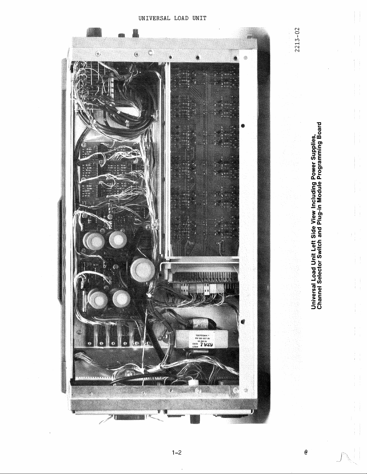
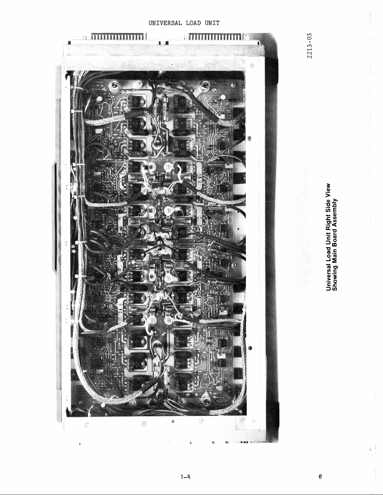
2213-01
Universal
Load Unit
Page 5

UNIVERSAL
LOAD
UNIT
Introduction
The
Universal
provide a convenient
supplies
verify
under
Programming
into
in
proper
variable
the
Load
several
voltage
load
plug-in
Unit
Description
The
Universal
and one
can
varied
The
Units
an
out-of-tolerance
driven,
is
used
of
the
be
set
given
resistor,
module
can be programmed by
channel
and
limits
programmed
passive
be
concurrently
by an
voltage
front
12
up
power
supports
equivalent
for
internal
or
current
panel
front
to
(See Appendix A).
panel
connect
active
to
provide a .resistive
supply
current
load
the
ULU's
with
channel
digital
cells.
amplifier
12
two
GENERAL
Load
through
Load
the
output.
active
Unit
method
Tektronix
regulation
conditions.
modules
its
Unit
through
loaded.
pulse
in a selected
multi-meter.
condition.as
LED's.
the
resistances
comparator
fixed
The
ULU
controls
As
selected,
Each
and 1
installation
The
resistors.
SECTION
(ULU)
of
that
includes
The
generator
and
resistors
is
performance
instruments.
of
The
are
front
which
current
indicated
thirteen
load
active
cell
passive
and
circuitry.
1
INFORMATION
a bench
single
ULU
is
temporarily
panel.
twelve
up
to
through
to
provide
channel
Also,
position
and
output
each
or a constant
load
protection
channel.
of
six
select
establish
top
checking
It
may
and
multiple
used
active
thirteen
may
each
by one
monitoring
active
cell
user
high
nominal
The
passive
in
any
circuitry.
testing
the
be used
conjunction
installed,
load
output
active
transient
be
displayed
channel
of
thirteen
CHANNEL
load
current
includes a current
All
twelve
selected
or
device
internal
to
output
one
cells
voltage
channel
response
is
SELECTOR
circuits
cell
voltages
or
Each
resistors
.low
current
channel
load
active
test
supplies
with
at a time,
(channels)
on
the
monitored
comparator-
channel
for
programming/load
and
(13)
that
will
power
and
levels
is
testing.
Load
switch
to
each
can
a
sensing
channels
per
levels
tolerance
is
for
·Each programming module
in a specific
Tektronix
is
used
instrument
and
1-1
to
test
will
the
internal
be
separately
power
part
supplies
numbered.
Page 6
UNIVERSAL
LOAD
UNIT
1-2
@
Page 7

UNIVERSAL
LOAD
UNIT
Input
less
fuse.
conforming
Load
given
AC
The
than
The
Cells
in
Current:
ULU
the
Power
may
watts
80
power
cord
NEMA
with
(Channels)
following
Channels
Channels
Channels
Channel
operated
be
during
is
#5-15.
1,
3,4,9,10
5,6,11,12
13
Electrical
normal
detachable
(Two-pole,
Maximum
tabular
8
7'
2,
115
at
listing.
and
Characteristics
VAC
230
or
operation.
will
and
three
minimum
Max
24.A
10A
2A
1A
(48
uses
It
plug
wire
input
Fused
30A
15A
5A
HZ)
67
to
amp
a 1
into
a female
grounding).
voltages
requires
and
standard
receptacle
currents
and
Accuracy
0.5%
±
±5%
0.
±
±5%
±5%±0.5%FS
3AG
5%
are
FS
FS
*
or
500
Voltage:
Channels
Channels
Channels
Channels
Channels
Channels
Channels
Power
Channels
Channels
Channels
Channel
watts
total
1,2
7,8
3,4
10
9'
5,6
'12
11
13
1,2,7,8
3,4,9,
5,6,11,12
13
input
10
power,
Max
50V
-50V
100V
-100V
160V 180V
-160V
350V
channels.
all
Trip
(Crowbar)
-55V
11
-110V
180V
none
Maximum
120W
Voltage
55V
ov
80W
80W
10W
•
Saturation
(minimum)
15A
@
S.2V
15A
@
S.2V
@
@
@
@
@
2A
2A
1A
S.4.5V
S.4.5V
S.8V
S.8V
S.1V
max.
max.
10A
10A
max.
max.
max.
Amps
max.
max.
1-3
Page 8
UNIVERSAL
LOAD
UNIT
1-4
Page 9

UNIVERSAL
LOAD
UNIT
Operational
All.
Chop
and
Indicators:
(DMM)
5
thermal
display
ULU
The
categories:
tests
Modes:
Chop
Chop
Chop
and
Ranges:
DMM
Accuracy:
DMM
Accuracy:
LED
has
shake,
Rate:
Cycle:
Duty
Rise/Fall
ULU
The
10
been
(limited
includes
ULU
The
96
50%
time:
includes
Out-of-Regulation
2v,2ov,2oov,2ooov
±0.1%
±5%
Environmental
tested
shock,
to
and
transportation,
0
c
o
_5-
indicating
two
Voltage
counts
± 2
deviation
verified
50°c
to
operational
two
nominal
Hz
nominal
(10%-90%)
µS
10
devices
LED's.
200A,20A,
1%
from programmed
Characteristics
operable
bench
with
instrument
modes;
a
-
Current
counts
± 6
value
the
in
handling
on).
Chop
digital
multimeter
2A
following·
abbreviated
and
individual
class
and
listed
Standard.
following
the
Mating
Mating
AC
Packing
Foam
Pad
Optional.
items:
Unprogrammed
7612D
7612D
7912AD
7912AD
Accessories
listed
Connectors
Connector,
Power Cord
Box
Pad
Set
Optional
Programming
Programming
Programming
Programming
for
items:
P1
P3
Accessories
Plug-in
Plug-in
Plug-in
Plug-in
Plug-in
Accessories
include
ULU
the
(2)
P2
&
for
Connector
&
Inst.
Inst.
ULU
the
Set
Manual
Manual
this
include
manual
(061-2213-00)
131-0097-00
131-0293-00
161-0066-00
004-0766-00
004-0281-00
004-1092-00
following
the
067-0919-99
067-0921-99
061-2214-00
067-0920-99
061-2213-00
@
1-5
Page 10

Page 11
UNIVERSAL
SECTION 2
OPERATION
LOAD
UNIT
FRONT
PANEL
CHANNEL
of
the
13
including:
to
indicators
and
to
the
switches
OVER
of-rotation
divider
in
rotation
supply
is
but
Also,
ULU's
under
under
remote
the
OFF
if
crowbar
test
CONTROLS
SELECT
channels
CURRENT
including:
External
the
AC
VOLTAGE
switch
series
increases
test.
sensed.
(detented)
the
supply
may
or
both.
to
ADJUST,
Input
output
TEST
that
with
the
Note
Caution
under
be
Control.
other
CURRENT
Digital
Amplifier.
voltage
Control.
inserts
the
remote
magnitude
that
is
position
test
initiated
This
Universal
LIMIT,
Multimeter
available
The
(or
sense
of
'the
this
control
indicated
may
does
causing
13
position
Load
Unit
CHOP/SWITCH,
The
CHANNEL
at
OVER
excludes)
line
output
will
in
that
cause
not
damage
have an
an open
rotary
front
switch
panel
OVER
and
OUT-OF-REGULATION
SELECT
the
RIPPLE
VOLTAGE
an
internal
of
the
voltage
function
using
to
control
OUT
TEST
control
selected
of
only
this
the
supply
over-voltage
fuse,
damage
connects
controls
VOLTAGE
(+)
connector.
75K
resistive
channel.
the
selected
if
control
under
limit,
to
the
Lights
also
is
the
in
one
TEST,
an
end-
CW
output
any
test.
the
supply
CURRENT
push-pull
the
current
pulled
current
Note
out,
level
that
channels
is
set
with
in).
CURRENT
push
button
draw
its
programmed
magnitudes
internal
ADJUST
switch
and
adjust
CW
rotation
(in
positive
CURRENT
7-12.
the
ADJUST
In
the
CURRENT
LIMIT
switch.
maximum
safe
current
are a function
protection
Control.
dual
function;
increases
control
individual
ADJUST
Control.
Pushing
current.
and
the
of
circuitry.
The
CURRENT
potentimeter.
pushing
and
Pulling
in
disengages
CCW
channels 1 through
rotations
chop mode,
potentiometer
The
CURRENT
this
setting
the
switch
The
channel
causes
CURRENT
of
the
number,
ADJUST
out
rotation
6)
to
are
reversed
the
transition
(with
LIMIT
control
the
LIMIT
switch
CURRENT
its
control
on
this
it.
With
decreases
the
the
push-pull
selected
overrides
ADJUST
voltage
is a combination
full
for
control
the
the
cell
negative
level
engages
control
programmed
current.
current
switch
is
a momentary
channel
to
both
control.
and
Current
its
contact
2-1
Page 12

UNIVERSAL
LOAD
UNIT
HI/LOW/IND
three
a
is
active
active
all
(IND)
CHOP/SWITCH
switch
the
arid
SELECT
LOAD
channel
position
With
CHOP/SWITCH
clock
a
at
time,
a
(located
These
plug-in
position
cells
cells
enables
(S2111).
CHOP/SWITCH
then
is
of
the
rate
determined
as
on
jumpers
module removed.
LOAD
set
are
are
CHOP/SWITCH
the
Control.
With
switches
set
corresponding
its
HI/LOW/IND
control
96
of
backside
the
accessible
are
SELECT
toggle
their
to
to
set
HI/LOW/IND
the
control
(S2001
its
to
LOAD
(CHOP
up
hertz,
the
by
of
Control.
switch
their
The
down,
through
programmed
position)
the
positions
the
with
(S2110).
load
high
low
control.
CHOP/SWITCH
(SWITCH
MAX/MIN
SELECT
Chop
Load
ULU's
The
current.
load
LOAD
S2012)
high
switch.
switch
the
mode
of
Select
left
HI/LOW/IND
upper
its
In
its
In
current.
control
SELECT
position)
are
low
or
in
Chop
performs
two programming
Toggle
side
The
is
switch
the
enabled.
current
IND
its
mode
is
two
Switches
cover
LOAD
SELECT
position
position
mid
lower
a two
in
position
position
its
indiviual
12
Each
enabled.
functions,
off
individual
value
jumpers
circuit
and Programming/Load
control
(HI)
position
position
IND
the
by
the
and
Operating
one
on P2119
board).
all
(LOW)
toggle
MAX/MIN
at
the
With
mode
Chop
SELECT
switch
information
value
MAX/MIN
the
corresponding
current
CURRENT
(temporarily)
desired
the
nature
current
DMM
mode
ALL
simultaneously
values.
irregardless
is
control
must be pushed
effect
in
value
ADJUST
the
of
With
the
is
Note
P2119
selected
is
INDividual
programming
during
pulling
value
DMM
(while
P2119
selected.
that
of
jumpers
chopped
is
available
the
when
controls.
as
and
chopping)
jumpers
switched
all
positions
the
which
in
or
to
in
at
SYNC
LOAD
resistor
SYNC
the
The
the
out
on
read
50
the
the
In
between
channels
connecting
the
only
loaded.
step
enable
the
output
SELECT
output
magnitude
the
percent
to
connecting
Chop
the
SYNC
switch
value
CURRENT
DMM
the
be
All
their
high
are
their
of
pins
channel
Note
chopping
output
in
is
for
(in
high
TTL
this
of
ADJUST
CURRENT
in
cycle
duty
average
pins
mode
high
at
respective
to
2 and
to
1
selected
that
action.
connector.
BNC
low
TTL
a
that
plug-in
the
state
value
switch
mode. Note
of
of
3
to
2
active
all
and low programmed
once and
4
by
CURRENT
the
Chopper
state
channel
module).
that
is
can be
adjusting
and
chopper
the
two
the
channels
then
to
all
and 5
MAX/MIN
The
is
(cell)
that
switched
switches.
the
5,
the
cell
that
set
set
cause
the
5,
current
low
are
INDividual
CHANNEL
ADJUST
state
current
by
set
the
and
cell
The
the
by
by
to
it
averaging
the
the
levels.
Chop
once
at
2-2
Page 13

UNIVERSAL
LOAD
UNIT
Universal
The
instrument
chopped
circuits.
concurrently
switches
high
and
switches.
toggle
to
current).
"V"
for
at
MAX/MIN
(S2001
low
or
HI/LOW/IND
the
VOLTAGE/CURRENT
switch
select
illuminated
is
CURRENT
the
power
once
Damage
chopped.
Switch
load
located
type
the
switch
Each
Load
supplies
without
occur
may
Array.
through
current
LOAD
Control.
to
measurement
of
position
for
position.
includes
Unit
that
activating
to
The
S2012).
each
for
SELECT
right
the
VOLTAGE
the
cannot
some
MAX/MIN
These
active
switch
The
displayed
monitored
is
two chop modes
tolerate
their
power
of
switch
internal
supplies
Switch
switches
channel.
will
VOLTAGE/CURRENT
the
all
Array
are
override
Digital
the
on
by a
position
when
Both
Multimeter.
corresponding
accomodate
to
their
fault
used
Multimeter
and
outputs
or
all
consists
to
the
individual
the
control
'I'
being
protection
outputs
SPST
of
select
CHOP
is
is
either
ALL
two
a
is
It
(voltage
LED
illuminated
those
are
toggle
(mode)
MAX/MIN
position
used
or
indicator.
DIGITAL
numerical
used
is
current
of
light
supply
acceptance
establish
for
female
connector
decreased
or
corresponds
cells
load
12, a
current.
to
on a
OUT-OF-REGULATION
red
13
per
voltage
supplies
the
EXTernal
connector.
through
1
current
negative
MULTI-HETER.
display
indicate
lights
channel
limits.
the
causes
to
indicator
selected
mounted
and
associated
proper
to
INput
Applying a
the
proportion
in
approximately
6,
while
voltage
polarity
the
channei.
Indicators.
in
when
Selected
comparison
monitored.
be
Connector.
current
positive
a
negative
a
increases
Digital
The
a
with
and
group
a
illuminated,
that
with
resistors
voltages
EXTernal INput
voltage
the
in
applied
the
to
percent
100
voltage
voltage
and a
Multi-Meter
four
and a
numerical
The
the
on
each
channel
on
and
the
to
selected
of
increases
decreases
positive
(DMM)
digit
half
value
OUT-OF-REGULATION,
upper
indicates
has
program
the
the
center
channel
voltage.
rated
voltage
of
front
deviated
board
allowable
designates
conductor
ten
A
channel
absolute
the
For
it.
is
readout.
DC
panel.
that
fom
(1-12)
volt
current.
cells
decreases
auto-ranging,
an
voltage
indicators
There
particular
the
programmed
the
used
are
tolerance
front
a
this
of
be
to
level
value
through
7
DMM
The
or
consist
one
is
to
margins
panel
increased
For
of
the
BNC
the
load
2-3
Page 14
UNIVERSAL
LOAD
UNIT
RIPPLE
female
BNC
coupled
connector's
the
that
TTL
when
REAR
switch
(via
power
SYNC
used
is
loads
the
PANEL
POWER
used
OUT
connectors.
the
center
supply
Connector.
output
to
is
and
operated
is
ULU
CONTROLS
SWITCH.
apply
to
&
(+)
The
selected
conductor
under
used
test.
SYNC
TTL
to
AND
The
or
Connectors.
(-)
connector's
(+)
channel)
(shell)
designates
level
provide
chop mode.
in
CONNECTORS
POWER
remove
SWITCH
AC
the
to
is
a
signals.
oscilloscope
an
is
power.
RIPPLE
power
connected
front
The
two-position
a
OUT
center
panel
SYNC
designates
conductor
supply
return
to
BNC
output
external
is
under
(ON-OFF)
test.
(ground)
female
can
trigger
front
two
capacitively
The
of
connector
drive
standard
signal
rocker
panel
(-)
230V-115V
slider
standard
and
input
designates
12. These
(Amphenol
Tables
switch
FUSE/FUSEHOLDER.
designed
is
Pl
connector
1-1 and
SWITCH.
used
fuse.
NEGATIVE/P2
the
32-pin
P/N
to
fuseholder
The
for
for
voltage/current
male
26-190-32).
1-2.
The
select
The
type
3AG
POSITIVE
positive
connectors
Pin/function
230V-115V
input
AC
is
fuses.
channels
AC
power
located
CONNECTORS.
input
mate
switch
voltage.
fuse
for
just
(cells)
connector
with
Tektronix
lists
is
the
above
POSITIVE
P2
through
1
for
for
two-position,
a
a 1
is
ULU
AC
the
is
6.
negative
P/N 131-0097-00
P2
and
P1
flush
amp/250
power
the
P1
are
receptacle
voltage/current
NEGATIVE
cells
7
given
mounted
volt
through
in
2-4
Page 15

UNIVERSAL
LOAD
UNIT
Table
Pins
1,2,3,4,5
6,7,8,9,10
12
11'
14
13'
15
16
17, 18,
19,20,21
22,23,24,25,26
27,28
29,30
31
32
2-1.
P1
NEGATIVE
Function
Channel
Channel
Channel
Channel
Channel
Channel
Channel
Channel
Channel
Channel
Channel
Channel
Pin/Function
high
7,
high
8'
med
9,
10'
'
11
12, low
high
7,
high
8,
med
9,
10'
'
11
12, low
med
low
med
low
I
I
I
I
I -
I -
I
I
I -
I
I
I -
-
-
-
-
-
-
-
-
List
return
return
return
Table
Pins
1,2,3,4,5
6,7,8,9,10
12
'
11
14
13'
15
16
21
20'
19'
18'
17'
22,23,24,25,26
27,28
29,30
31
32
2-2.
POSITIVE
P2
Pin/Function
Function
Channel
Channel
Channel
Channel
Channel
Channel
Channel
Channel
Channel
Channel
Channel
Channel
1 '
2,
3,
4'
5,
6,
1 '
2,
3,
4,
5,
6'
high
high
med
med
low I
low
high
high
med
med
low
low
I
I
I
I
I
I
I
I
I
+
+
+
+
I
I
+
+
+
+
List
+
+
return
+
return
+
return
return
return
return
2-5
Page 16

SENSE
P3
P3
input
connector
Tektronix
shown
in
SENSE
PIN
Table
remote
the
is
cell
for
131-0293-00,
2-3~
UNIVERSAL
sense
This
13.
Amphenol
LOAD
connector
P/N
female
57-30360.
36-pin
UNIT
for
cells
all
connector
pin/function
A
is
and
mates
the
with
list
power
is
Table
Pin
2
3
4
5
6
7
8
9
10
11
12
13
14
15
16
17
18
1
19
1
20
1
21
1
22
1
23
1
24
1
25
1
26
21*
2a*
29*
30*
31
32
33
34
35
36
2-3.
Voltage
Voltage
Voltage
Voltage
Voltage
Voltage
Voltage
Voltage
Voltage
Voltage
Voltage
Voltage
Channel
Not Used
Not Used
interlock
Fan
Used
Not
Used
Not
Voltage
Voltage
Voltage
Voltage
Voltage
Voltage
Voltage
Voltage
Voltage
Voltage
Voltage
Voltage
Channel
Not Used
Used
Not
interlock
Fan
Voltage
Voltage
P3
Function
remote
remote
remote
remote
remote
remote
remote
remote
remote
remote
remote
remote
(Passive
13
remote
remote
remote
remote
remote
remote
remote
remote
remote
remote
remote
remote
(passive
13
sense
sense
SENSE
sense,
sense,
sense,
sense,
sense,
sense,
sense,
sense,
sense,
sense,
sense,
sense,
jumper
sense,
sense,
sense,
sense,
sense,
sense,
sense,
sense,
sense,
sense,
sense,
sense,
jumper
return
return
Pin/Function
Channel
high,
Channel
high,
Channel
high,
Channel
high,
Channel
high,
Channel
high,
Channel
high,
Channel
high,
Channel
high,
Channel
high,
Channel
high,
Channel
high,
high
HV)
Channel
low,
Channel
low,
Channel
low,
Channel
low,
Channel
low,
Channel
low,
Channel
low,
Channel
low,
Channel
low,
Channel
low,
Channel
low,
Channel
low,
return
HV)
all
common
common
to
to
all
List
2
3
4
5
6
7
8
9
10
11
12
2
3
4
5
6
7
8
9
10
11
12
channels
channels
1
Not
currently
used
2-6
Page 17

UNIVERSAL
LOAD
UNIT
SENSE
P3
When
the
cabinet.
electrical
exhaust
When
continuously
also
connection
are
fans
these
whenever
P3-16
whenever
programmed
is
maximum
high
watts
96
any medium
for
cooling
temperature
before
provides
controlled
pins
2
the
and·P3-34
one
power
current
(80%
watts
64
fans
the
interlock
made
is
by a
not
are
turned
is
ULU
NOTE
must
more)
(or
80%
to
rating;
120W)
low
are
current
X
cells
X
or
(80%
running
overstresses
cycle
fans
capability
between
pin
thermal
connected,
on.
connected
be
not
active
or
i.e.,
more
of
whenever any
programmed
more,
or
cell
more. With
or
BOW)
continuously,
which might
will
on,
for
and
16
switch
both
cell
load
its
for
whenever
or
programmed
is
peak
avoided.
be
both
pin
internal
exhaust
the
occur
exhaust
of
34
to
fans
fans.
P3
the
will
SENSE,
ULU
run
the
1.
2.
3.
4.
power
Turn
The
to
The
installed.
All
A
Initial
Before
voltage
properly
the
Operational
When
1.
current
levels.
On
applied
power
be
AC
rear
is
120-230
used.
line
panel
VAC
fuse
Programming
supplies
in
Notes
testing
to
switch
the
is
cables
Plug-in
specific
a
Tektronix
ULU.
the
the
on
correct
securely
are
module
instrument
7912AD
verify
panel
rear
value
connected.
configured
has
power
supplies,
that:
(1
to
been
set
is
amp.
program
match
to
std.)
is
the
installed.
not
do
intact
ULU
chop
the
to
high
line
and
test
with
@
CAUTION
2.
side
its
Hazardous
-
covers
removed.
voltages
2-7
are
present
when
the
ULU
operated
is
Page 18

Page 19
UNIVERSAL
LOAD
UNIT
A
simplified
Fig.
3-1.
connected
When
the
rear
between
the
ULU
cells.
fixed
its
CHANNEL
controls
The
resistors
The
diagram
to
ULU
the
output
panel
output
SELECT
and
thirteenth
THEORY
Block
block
controls
connectors
and one
switch.
output
between ground and
diagram
illustrates
from a power
monitoring
switch
and
indicators.
P1,
P2
or
more
This
position
Diagram
SECTION
OF
OPERATION
of
the
as
typical
supply
and P3,
of
the
thirteen
circuits
connects
the
3
Description
Universal
one
under
continuity
position
power
active
to
supply
test
each
one
Load
of
the
has
can
cells
wafer
of
or
under
Unit
twelve
been
be
within
switch
the
two
is
shown
active
connected
established
the
connects
twelve
user
test.
selected,
in
cells
ULU
via
active
to·
The
and
current
referenced.
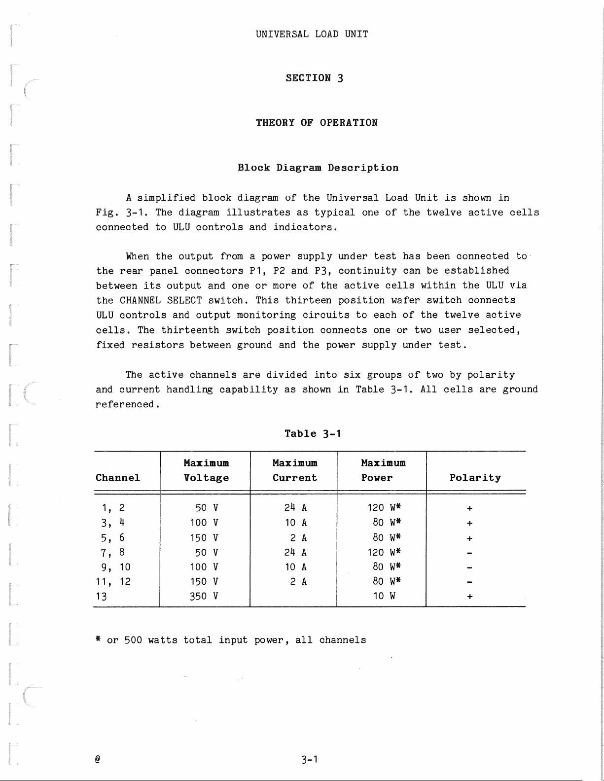
Channel
2
1 '
4
3,
6
5,
8
7,
10
9,
12
11
'
13
*
or
500
active
handling
watts
channels
capability
Maximum
Voltage
50
v
100
v
v
150
50
v
100 v
150
v
350 v
total
input
are
power,
divided
as
Table
Maximum
Current
24
10
2 A
24
10
2 A
all
into
shown
A
A
A
A
channels
3-1
six
in
groups
Table
Maximum
Power
120
W*
80
W*
80
W*
120
W*
Bo
W*
80
W*
10
w
3-1.
of
All
two by
cells
Polarity
polarity
are
+
+
+
-
-
-
+
ground
3-1
Page 20

S)tNC
Output
EXTen1ci/
IN
put
@------'
CURRENT
ADJUST
/VVVV\
G:;:;NT
LIMIT
(pushhuttofl}
S£LFCTED
C€LL
CONTROL
CUR12£NT
!3US~
LO~D
1-11
LOW
I o
INDiv'td1.1al
OllE:RVOL
rEST
SELECT
I
0
TAG£
WIN.DO~b
COM
PARA
CELL
PROTECTION
TOR1----'-v
1
OUT
(One
OF
R€GULtJ710N
LED
fer
c.ell)
r------1f<EMOTE
OUTPUT
SENS€
HIGH
HIGH
RIPPLE OUT
RIPPLE
ourc->@:-----------1
OG7-0883-93
(t-)@
AUTORIJNG
DIGITAL
MULTI-METER
Volto.9e G
ING
Cunel'lt
~
VOLTAG£"
CURRENT
COMMON
.S[IVS E
S€NSE
SENSE
P/o
CHllNN£L
S£LECTOR
SWITCH
3-2
PLUG-IN
CABLE
ASSY
Agure
UNIVERSAL
3-1.
FOWER
UNDER TEST
OUTPUT
12£MOT£
BLDCk
LOAD
DIAGRAM
UNIT
SUPPLY
LOW
SENSE
LOW
Page 21

UNIVERSAL
LOAD
UNIT
Outputs
connectors
resistors
other
the
altered
If
limits,
indicated
load
that
The
to
up
EXTernal INput
(See
Voltage
displayed
measurement
When
chop mode,
between
resistors)
control.
output
oscilloscope.
toggle
in
input
by
the
this
by
cell.
current
plus
on
the
its
The
BNC
between
the
of
P2
and
P1
Programming
the
a
of
other
output
or
at
the
preset
and
connector
ULU
voltage
condition
illumination
the
magnitude
minus
current
or
digital
the
front
two
Load (Chop)
Step
control
value
that
toggling
Alternatively,
their
power
cell's
controls.
10
connector
value
and
programmed min-max
supply
one
to
detected
is
volts
from
multimeter.
panel
current
(set
induced
rate,
may
current
being
may
96
under
inputs
the
of
Plug-in
tested
by a window
the
of
varied
be
the
to
de
description
power
the
jacks
Generator
input
the
by
by
is
Hz
be used
chop-all
the
routed
are
test
active
an
of
Module
amplifier.
Out-Of-Regulation
front
supply
Power
RIPPLE
to
programming
the
available
to
determine
deviates
applying
by
panel
Section
in
supply
OUT
activated
is
selected
the
setting
trigger
mode
values.
This
beyond
comparator
under
ripple
and
+
plug-in
of
the
at
the
causes
through
load
the
current
indicator
voltage
a
connector
BNC
2.)
test
RIPPLE
in
load
the
front
time
all
rear
cell.
current
level
predetermined
circuit
can be
available
is
OUT
individual
the
cell
selectable
CURRENT
panel
base
active
Selected
fed
can be
and
(LED)
level
EXT
alternatively
-.
toggled
is
ADJUST
SYNC
an
of
cells
panel
to
for
of
IN.
for
external
to
3-3
Page 22

UNIVERSAL
LOAD
UNIT
High
have
typical
to
three
current
positive
(four
input
both
provides a voltage
approximation
volts.)
Current
Each
identically
high
drive a voltage
parallel
(Ip)
input
terminal,
of
the
second
A
current
Cells
of
the
current
sets
develops a control
of
.03
op-amp.
operational
through
to a constant
four
high
structured
cell
follower
of
current
the
op-amp.
ohm)
the
derated
CIRCUIT
current
circuits
includes a current
transistor
The
Kelvin
amplifier
cell
and
current
power
DESCRIPTION
cells
as
gain
transistor
voltage
average
sense
connected
voltage
limit.
curve
that
resistors
with
(1
and 2
illustrated
amplifier
provides
stages.
across
voltage
a 249-ohm
as a comparator
across
(This
derating
break
positive,
on
the
developed
is
fed back
it.
This
points
7 and 8
diagram
(op-amp)
base
The
programming
resistor
across
to
comparator
is
a two segment
at
5.1 and
negative)
~·
connected
drive
the
monitors
for
on
three
inverting
A
the
then
16
A
30
amp
fuse
nominal
provide
Medium
are
negative
a
FET
connected
voltage
a 6.2K-ohm
a
lower
develops a control
positive
.01
input
Current
As
of
similar
input
ohm,
op-amp.
trip
point
circuit
illustrated
construction
(9 and
operational
darlington
to
be
divided
divider
voltage
input
Kelvin
of
protection
10).
(approximately
sense
and
of
Ce1ls
on
resistor
voltage
the
SCR
crowbar
57
volts.
in
diagram
with
The
input
amplifier.
transistors.
across
op-amp.
resistor
the
allow
across
provide
The
same
the
event
<rY'
two
stage
This
The
transistors.
the
4.5
volts).
a 100-ohm
The
voltage
is
fed
over-voltage
fuse
of
each
positive
for a typical
op-amp
series
medium
back
and a
polarity
of
the
channels
drives a set
connection
Three
current
The
programming
resistor
developed
to
the
protection
diode
reversal.
four
medium
(3 and 4) and two
medium
diodes
cells
across a four
inverting
current
allows
(R317
(CR103
current
of
series
the
in
series
to
operate
current
typical)
input
with
typical)
cells
cell
terminal,
of
is
applied
with
at
(Ip)
on
the
the
a
3-4
Page 23
Connected
derated
constant
limit.
power
a
as
The
curve
UNIVERSAL
comparator,
derating
with
break
LOAD
a second op-amp
a two segment
curve
is
points
at
UNIT
and
10
provides
approximation
volts.
30
voltage-current
a
to
a
The
the
blow
ground
to
Current
Low
shown on diagram
As
12
and
11
operational
monolithic
applied
15K-ohm
a
to
control
a
positive
.1
op-amp.
to
maximum
linear
senses
voltage
operate
Kelvin
ohm)
A second
provide
current
derating
only
voltage
over
fuse.
amp
15
fuse
one
at
Cells
negative)
amplifier
transistor
across
resistor
approximately
at
voltage
input
of
sense
operational
voltage/current
a
range
of
voltages
SCR
Reverse
terminal
are
drives
sets.
across
across
op-amp.
the
resistor
of
current
above
crowbar
~'
similar
both
the
the
amplifier
the
with
51
will
polarity
(CR303
four
the
the
to
series
two
series
The
transistor
transistor
volts.
4.5
200-ohm
voltage
The
routed
is
derating
current
low
voltage
volts.
trip
protection
typical).
low
medium
connected,
connection
sets.
sets
Programming
input
functions
limit.
resistor
developed
the
to
channels
used.
is
approximately
at
is
current
current
zener
A
allow
inverting
as
Due
cells
power
serves
the
current
(R512
across
protective
a
the
to
(0.2
The
provided
(5 and 6
cells.
darlington,
divide
to
diode
protection
in
current
low
(Ip)
typical)
a
input
relatively
2.0
to
volts
111
by a
An
(four
comparator
amps)
diode
positive,
input
the
series
of
with
cells
develops
on
terminal,
the
small
only
comparator
and
the
The
amp
5
the
adjacent
Digital
The
sub-circuits:
four
display
the
over-voltage
fuse.
diode
Reverse
(CR504
Multimeter
Digital
circuit
Multimeter
crowbar
SCR
polarity
typical).
auto-ranging
an
and a
crystal
will
protection
function
controlled
trip
diagrammed
attenuator,
3-5
volts
161
at
given
is
on<Y
analog-to-digital
oscillator.
by
nominal and open
and an
fuse
the
can be
divided
converter,
into
Page 24

UNIVERSAL
LOAD
UNIT
Auto-Ranging
analog
harmonica
R4004
Input
from
K4002, K4003,
form an
outputs
condition
over
An
D3
or
detected
is
Outputs
OR'ed by
pulses
four
amplifiers
input
Once
an
range
strobe
from
for
relay
during
under
is
U4011A
U4012
coils
to
Attenuator
signals
K4004
attenuator.
each measurement
range
indicated
condition
interval
U4009A
by
these
to
are
(K4002
auto-range
to
connector
K4005
and
an
or
by a
is
during
(or
while
detectors
generate
to
fed
through
the
displayed
be
P4002
are
via
connected
cycle,
both
range
clock
range
from
by a
an
signal
intervals).
R-S
over
pulse
indicated
over
drive
a
Decade Decoder
K4005)
input
attenuator.
are
S4001D.
U4003
signal
13
pin
pulse
detected
is
flip-flop
for
U4013.
four
via
input
The
segments
the
to
(part
from
during
from
The
by
range
Outputs
corresponding
resistor
to
relay
the
of
13.
pin
D1
the
13
pin
under
U4009C
U4009B/D
counter
from
network
contacts
R4004
of
A-to-D
under
An
strobe
during
range
Q4005/Q4006.
via
are
and
U4012.
U4013
buffer
of
to
converter)
range
interval.
D2
the
condition
also
Clocking
drive
Analog-to-Digital
analog-to-digital
The
and
by a
U4001
(pins
auto
control
pins
on
DMM
each
display
four
contains
15
zero
1,
U4004,
Display
The
with
segment
Q4014.
provided
is
sign
the
strobe
five
and 1)
buffer
circuitry
13, 16,
2,
the
DMM
its
driven
is
lines
Q4014
on
bit
intervals
Display
is
strobe.
Converter
one-half
the
digit
analog
integrator
filter
and
U4001.
for
and
17
Seven Segment
consists
decimal
own
the
lines
X-Y
BCD
on by
from
by an
from
turned
six
These
with
conversion
converter
circuitry
(pins
9 and 11)
(pins
U4003
Binary
and
18
Decoder IC.
four,
of
point
indicator,
matrix.
decoder
U4021
U4003
lines
six
D5
and
S
process
consisting
including
comparator
13).
and
12
also
provides
Coded
seven
and one
information
X
U4004
and a
and one
logic
consisting
sequentially
are
(U4003-13 and
input
of
of
switched
the
U4003
digit
Decimal
segment
+1
is
decimal
decoder
five
of
-16)
signals
U4001
IC's
(pins
provides
strobe
data
display
LED
display.
LED
provided
point
circuit.
digit
pulsed
concurrent.
is
and
input
and 14) and
11
the
pulses
four
to
by
line
Y
strobes
one
in
completed
U4003.
buffer
digital
from
pins
units,
LED
The
seven
from
information
and
of
3-6
Page 25

UNIVERSAL
LOAD
UNIT
Crystal
unit
oscillator.
Clock
Q4004
by
Step
a low
toggle
description
the
of
false
Q4024
of
output
directly
Panel
stages
SYNC.
DMOS
of
by S4067,
and
set
is
Controlled
circuits
IC
Y4001
IC
Generator
The
frequency
the
DMM
DMM
The
from
board
Q4017
The
switch
buffer/driver
the
to
U4002B,
associated
and
operating
Its
U4008.
and
Step
indications.
divide
which
and one
second
the
CHOP
The
applied
(Chop)
square
current
Section
in
clock
by
in
U4019
(9.
and
Q4021
CURRENT
(refer
to
via
The
Q4020,
circuit,
Oscillator
+10
as
Generator
wave. In
the
of
ensure
output
100
drives
turn
drives
the
first
with
ADJUST
circuit
to
and D
C
circuit
frequency,
output
clock
a
power
The
1).
that
two
Chop
amplifier
provides
consisting
+12V
a
diagram
operate
components
U4008
of
input
circuit
Chop
supply
Step
of
decade
separate
Individual/Chop
switch.
is
Generator
generator
U4008
output
an
-12V
to
applied
in
2.4576
(pins
U4003-8.
to
illustrated
mode,
under
is
counter
transistor
circuit,
Q4018
of
square
Note
only
(9).
conjunction
form a
to
applied
is
MHz
3 and 12)
on
square
this
test
induced
transformer
U4019.
to
that
(see
operated
is
transients
amplifier
jumper (P2119 on Lower
All
consisting
front
the
Q4019,
and
wave.
+5VB
the
when
the
with
crystal
to
level
is
diagram
wave
CHOP/SWITCH
coupled
96
A
Q4021
CHOP/SWITCH
is
at
square
Hz
circuits;
buffer/driver
of
panel
drives
is
supply
quartz
pin
(S>
sub-harmonic
a
do
to
BNC
paralled
to
crystal
controlled
of
4
shifted
generates
to
used
Control
cause
not
base
the
wave
one
connector
gate
the
U4019
control
External
Electrical
External
the
to
input,
associated
class
virtual
The
determined
in
via
transconductance
amplifiers.
B
ground
op-amp
appropriate
the
CHANNEL
the
Input
components. Both
then
by
.Amplifier
signals
Input
A
the
at
forces
input
signal
transistor
SELECT
(buffer)
signal
inverting
a
switch.
applied
amplifier.
amplifier
Q4022
applied
voltage
polarity.
which
the
to
comprises
and
to
input
swing
This
is
3-7
front
Q4023
of
across
routed
panel
Diagrammed on
U4020, Q4022,
are
R4071
operational
voltage
jack
connected
causes
emitter
swing
the
to
IN
EXT
(S>,
Q4023
to
current
a
amplifier
R4077
input
or
causes
of
are
this
operate
1
and
flow
U4024-2.
R4079
current
a
load
a
routed
megohm
as
into
as
cell
Page 26

UNIVERSAL
LOAD
UNIT
Program
The
circuits,
active
Each
RDES'
specific
input
current
current
cell
a power
current
volts
RpL
supply
resistor).
and
RFH
voltage
then
RpH
to
are
Board
program
one
cell
RcoMP)
power
and
RFL
and
into
draws a
resistor.
and
source
appear
chosen
(where
board
each
for
includes
that
supply.
designate
RFL
the
and
equals
cell
the
current
designate
RpL
transistors.
across
provide
to
equals
RpH
shown on
twelve
of
six
selected
are
the
input
low
the
is
that
proportional
the
emitter
its
a
the
diagram
active
programming
to
resistors
typical
a
to
current
proportional
emitter
conducting,
When
resistor.
constant
high
current
0
cells
resistors
facilitate
that
cell
resistor).
the
to
resistors
current
and
includes
and one
are
(where
the
to
applied
each
Resistor
load
RPL
thirteen
passive
equals
RFH
voltage.
voltage
switched
two
values
specific
a
the
RFH'
(RFL'
operational
installed
These feed a
applied
for
transistor
for
equals
separate
circuit.
RPL'
tests
between
the
control
acts
and
constant
causes
RpH
for
power
current
low
RPH'
for
the
high
The
10
and
a
as
RcoMP
upper
the
standard
a
to
limits.
RDES
used
be
may
Power
schematic
filter
the
T3001.
voltage
supplies
Digital
throughout
Supplies
The
assembly
110/220
T3001
to
Multimeter.
(comparison)
a
half
power
of
determine
to
(desensitizing)
desensitize
to
supplies
diagrams~
LF3001,
SELECTOR
VAC
includes
three
+12VA,
the
rectifier
-12VA
ULU.
designates
voltage
divider.
if
designates
or
used
and~·
line
the
switch
three
and
The
secondary
circuits
+5VA
supplies
B
the
broaden
in
the
fuse
to
are
resistor
a
The
applied
resistor
a
the
Universal
Input
F3001,
primaries
the
windings
yielding
used
(+12VB,
each
in
Load
is
the
6
-12VB
of
in
supplied
POWER
of
that
separate
and
output
voltage
comparator
power
exclusively
this
within
is
each
circuit
Unit
power
provide
for
+5VB)
cell
that
divider
active
are
through
SWITCH
transformer
voltages.
the
are
supplies
compared
is
prescribed
cell
"window".
shown on
S3001
stepped
front
distributed
that
ac
and
down
Floating
panel
line
3-8
@
Page 27

UNIVERSAL
LOAD
UNIT
CR3002
+12VA
base
-12VA
Q3007
for
become
potentiometers.
-12VB,
voltage
supply
and
is
4,
and
voltage
supply
and
both
CR3003
CR3001
+5VB
is
pass
used
An
Calibration.
developes
the
pass
the
and
the
+5VA
developes
and
for
pass
regulated
transistor
to
adjust
adjustment
-12VA
for
pass
is
regulated
transistor
+12VA
CR3004
supply.
-12VB
transistor
the
+21
VDC
output
transistor
by
Q3008.
and
-12VA
develop
Neither
+21
VDC
supplies.
by
U3003
Q3004.
-12VB
procedure
and -21
to
the
U3005
supplies.
a de
the
and -21
Voltage
Q3001
operating
R3005
supply.
for
DMM
Q3005
operating
R3018
voltage
+5VA
VDC
to
regulate
is
used
ULU
power
VDC
that
Voltage
to
regulate
is
used
that
or
-5VB
that
regulator
in
conjunction
to
adjust
supplies
are
regulated
regulator
the
in
conjunction
to
adjust
is
supplies
are
regulated
U3003
the
+12VB
the
U3004
+12VA
the
regulated
have
sets
supply.
with
Q3002,
+12VB
is
included
to
become
sets
supply.
with
Q3006,
output
by
U3006
adjustment
to
become
the
base
The
supply.
in
the
the
The
voltage
to
the
-12VB
Q3003
R3010
Section
Power
The
with
follows:
the
F3002
F3003
F3004
F3005
F3006
Exhaust
As
FM3002
The
rear
both
and -34
AC
2-3
path
power
fans.
for
in
Supply
ULU
side
protects
Fans
shown
is
via
panel
When
the
are
is
Section
Fuses
power
covers
on
schematic~'
four
connector
a jumper
coil
not
connected,
applied
2.)
supply
removed. Fuse numbers and
the
pins
of
K3002
to
includes
+12VB
-12VB
+12VA
-5VA
-12VA
of
P3
is
the
and
+5VB
supply
supply
supply
supply
AC
J8 and
SENSE
installed
is
the
Universal
through
also
completed
exhaust
five,
power
between P3-16 and
Load
1
amp
supplies
to
both
two
provides
to
thermal
fans
will
Unit.
fuses
associated
sets
interlock
(See
that
exhaust
of
switch
run
continuously
note
are
supplies
fans
contacts
capability
P3-34,
S3002.
preceding
accessable
are
FM3001
in
the
When
and
K3002.
for
current
P3-16
whenever
Table
as
3-9
Page 28

Page 29

UNIVERSAL
LOAD
UNIT
The
first
Unit
procedure
Unit
calibration.
Description
Digital
one, a verification
(U.L.U.)
The
or
to
Multimeter
Voltage
following
used
following
verify
accuracy: 5 1/2
is
in
to
procedure
align
equipment
that
(DMM)
CALIBRATION
consists
test
calibration.
the
U.L.U.
REQUIRED
is
it
is
operational
digit
SECTION
4
TEST & PROCEDURE
of
two
is
performed
The
second
to
part
EQUIPMENT
required
- 0.02%
to
calibrate
without
self-contained
see
if
the
is
an
actual
LIST
the
performing a full
Suggestion
Fluke 3875A,
HP
3490A,
parts.
Universal
calibration
Universal
or
or
equivalent
In
Load
Load
the
Digital
Current
Variable
Must
at
32
Pin
Must
rear
36
Pin
Must
improved
Multimeter
accuracy: 4 1/2
regulated
float
1 ampere.
Female
Male
Connector
fit
P1
panel
Connector -Optional
fit
P3
signal
(DMM)
DC
power
and
produce
NEGATIVE
connectors
SENSE
Caution
potentials
at
cooling
and
rear
access
the
the
digit
supply
up
and
panel
should
are
power
fans,
relay
- 0.3%
to
20
volts
P2
POSITIVE
connector
CAUTION
be used wherever
present.
switch
the
for
and
power
turning
line
120
VAC
is
line
transformer
the
fuse,
fans
TEK
DM501A
or
equivalent
TEK
PS503A,
TEK
131-0097-00 ·
(Amphenol,
TEK
131-0293-00
(Amphenol, 57-30360)
present
the
primary,
on.
or
DM502,
or
equivalent
26-190-32)
4-1
Page 30
UNIVERSAL
LOAD
UNIT
Introduction
following
The
calibration
and
Calibration
the
in
which
they
Procedure
Set
1.
Test
POWER
SUPPLY
of
Procedures
are
Up:
Up
Set
procedure
Universal
the
given.
test
The
diagram,
VERIFICATION
designed
is
Load
which
equipment shown
follow
Figure
(Amps)
4-1.
DMM
DMM
(Volts)
PROCEDURE
verify
to
Unit
(U.L.U.).
should
in
or
be
the
P1
P2
P3
overall
the
this
If
performed
Verification
*
UNIVERSAL
LOAD
UNIT
*
operability
test
the
in
fails,
order
2.
Refer
for
each
the
of
Fig.
To:
Jack
the
4-1.
Table
and
Verification
4-1,
Pin
CHANNEL
Verification
numbers
SELECT
Test
the
of
positions.
*See tables
Set-up
Test,
inputs
specific pins
for
associated
with
4-2
Page 31

UNIVERSAL
LOAD
UNIT
Channel
2
3
4
5
6
7
8
9
10
11
12
13
Apply
Floating
Between:
(+)
P2-3
P2-8
P2-11 P2-27
P2-13
P2-15
P2-16
P1-19 P1-3
P1-24 P1-8
P1-27
P1-29 P1-13
P1-31
P1-32
P3-13 P3-31
Table
P2-19
P2-24
P2-29
P2-31
P2-32
P1-11
P1-15
P1-16
4-1,
(-)
Verification
10
VDC
Test
Measure
Voltage
P3-1
P3-2
P3-3
P3-4
P3-5
P3-6
P3-7
P3-8
P3-9
P3-10
P3-11
P3-12
P3-13
•
Difference
I
amp
1
(@
02
to
to
to
to
-0.02
-0.02
-0.02
-0.
-0.015
-0.015
.02
to
to
to
to
-0.02
-0
-0.02
-0.02
-0.015
-0.015
applicable)
(Not
only)
0.
0.
0.035A
+0.035A
+0.015A
to
+0.015A
to
+0.
0.
0.035A
0.035A
+0.015A
to
+0.015A
to
4
H
130A
130A
130A
130A
*
With
**
Difference
I
NOTE:
for
respect
Difference
V
channels.
all
Connect:
3.
Tek
and
(Amphenol
facilitate
Set:
4.
230V/115V
OVER
CHOP/SWITCH
CURRENT
both
(i.e.,
Power
P3-35
to
Int.
I
=
V
=
female
A
131-0097-00)
disconnect
57-30360,
connecting
Universal
The
switch
VOLTAGE
TEST
control
ADJUST
both
and
markings
ON.
COARSE
Switch
common
a
as
- I
DMM
Int.DMM
pin
32
the
to
test
the
Tek
test
Load
the
to
control
in
push-pull
controls
FINE
at
return
DMM
Ext.
- V
Ext.
DMM
connector
indicated
leads.
Also
131-0293-00)
leads.
Unit
controls
appropriate
CCW,
SWITCH
switch
in
(down)
in,
set
of
top
the
connection.
~Above
±0.012
~
(Amphenol
Jacks
to
connect
the
to
follows:
as
position,
detent,
OFF
position,
rotation
mid
at
rotation),
Tabulated
VDC
26-190-32,
make
it
a male
SENSE
P3
and
Values.
easier
pin
36
connector
the
connect
to
connector
to
4-3
Page 32
UNIVERSAL
LOAD
UNIT
Note:
The
positions
consequence.
5.
Turn
as
measured by
6.
(Before
push
Adjust:
measured on
7.
(For
to
those
positions
CHANNEL
external
readings
8.
(After
(before
the
CURRENT
and
the
Remove
any Program
of
On: The power
the
each
pull
The
each
on
SELECT
each
it
COARSE
measurement)
switch.
CURRENT
the
external
measurement)
the
external
of
the
VOLTAGE/CURRENT
switch.
(voltage)
should
be
measurement)
is
disconnected
ADJUST
and
the
HI/LOW/IND
supply
external
ADJUST
DMM
the
push-pull
FINE
Plug-in
and
DMM.
Pull
control
(series)
which
and
adjust
Out:
Compare: The
meters,
The
U.L.U.
reading
values
in
switch,
to
indicated
Reset:
and
moved
switch
controls
both
MAX/MIN
it
The
for
DMM.
both
Panel
within
The
to
to
its
to
may
be
installed.
controls
for
10.0±0.1
Current
1.00±0.05
readings
the
"Voltage"
for
positions
Meter
±0.012
in
external
the
their
should
the
Verification
next
"in"
mid-rotation
are
VDC
Adjust
Amps
on
the
agree
VDC.
The
power
channel),
position,
of
as
U.L.U.
and
"Current"
1
thru
with
current
supply
no
Panel
12
of
the
Test
position.
to
Table.
OFF,
DMM
the
Set
Up
1. Remove: The
2.
Set:
position
3.
Use:
Power
specified
Refer:
which
The
Pin
Supply
To
are
U.L.U.'s
LINE
SELECT
and
the
probes
Calibration,
plugs
Figure
called
CALIBRATION
1.
Power
side
switch
POWER
to
and
out
reach
pins.
4-2
in
switch
the
for
Table
PROCEDURE
Supply
covers
(on
to
signals
entering
the
locations
4-2.
and any
the
back)
the
"On"
called
from
plug-in.
to
position.
out
the
rear
of
the
the
appropriate
in
of
plugs
Table
the
and
4-2,
pots
4-4
Page 33

UNIVERSAL
LOAD
UNIT
J2
R3018
J6
Fig.
4-2.
R3010
Power
Supply
R3005
J11
Board.
Supply
On
Measure
P6-3 and
P6-1
P2-1
Supply
On
A:
between
P6-2
and P6-2
and P6-2
B:
Measure
P 11-1 and P 11-2
11-3 and P 11-2
P
Table
4-2,
Power
Required
+11.9
-11.9
+4.8
to
to
to
+5.2
Required
+12.000VDC
-12.000
VDC
Supply
Voltage
+12.1
-12.1
VDC
Voltage
VDC
VDC
Calibration
Adjust
R3018
Note:
R3018
Adjust
R3005
R3010
Compromise
both
w/
attain
to
R3018
and P11-2 +4.8
P2-2
to
+5.2
4-5
VDC
Page 34

UNIVERSAL
LOAD
UNIT
Calibration
Set:
1.
the
SELECT
Verify:
Loosen:
2.
U.L.U.
removed
Power
Tilt:
to
Refer:
and
Short:
3.
Adjust:
panel
procedure
VOLTAGE/CURRENT
The
CHOP/SWITCH
switch
That
four
The
Assembly
DMM
first
Supply
The
following
the
adjustment
meter.
Calibration
U.L.U.
Figure
To
P4002-1 and
R4022
Digital
2.
switch
position
to
"Voltage"
the
screws
in
gain
to
DMM
measurement
4-3
points.
P4002-4
(Voffset)
Multimeter
switch
the
to
"13".
LED
(through
place.
access,
Procedure.)
Assembly
the
for
together
for
to
"Switch"
is
the
(The
were
out
points.
locations
reading
a
Board
"Voltage"
the
position,
illuminated.
sides)
covers,
side
taken
and
off
down
of
firmly.
0.0000
of
the
position,
the
and
which
as
to
hold
which must be
of
part
allow
following
on
VDC
CHANNEL
the
the
access
measurement
the
Re•ove·:
4.
Apply:
Adjust
DMM
Apply:
5.
Verify:
to
Readjust
this
Apply:
6.
Verify:
it
within
+1.70±0.01
:
within
to
-1.70±0.001
within
value
17
should,
. 1
0
short
The
4016
R
±0.0001
That
the
±0.0002
(if
and
VDC,
the
That
and
% •
between
across
VDC
to
ma.ke
U.L.U.
the
VDC.
VDC
VDC.
necessary):
requirement
the
20.00
and
decimal
the
that
P4002-1 and
P4002-1(+)
L.
U.
P4002-1 and
to
meter
R4022
to
VDC
point
U.L.U.
DMM
U.
agrees
for
Step
of
the
shifts
and
DMM
P4002-4.
P4002-4.
and
the
external
compromise between
VDC.
right
the
best
±0.0002
3
the
to
the
with
external
agree
P4002-4(common).
with
a
input.
external
DMM
as
agree
DMM
4-6
Page 35

UNIVERSAL
LOAD
UNIT
P4002
R4016
R4005
R4007
R4022
7.
8.
9.
10.
Set:
Short:
Adjust:
U.L.U.
Apply:
Adjust:
10x
Apply:
Adjust:
10x
and
Apply:
The
VOLTAGE/CURRENT
P4002-2 and P4002-3
R4005
DMM.
0.170±0.001
R4007
the
input
-.17
R4005
agreement
the
requirement
Successively,
P4002-2 and P4002-3.
Verify:
should
to
within
That
and
0 .
Fig.
signal
± 0.01
between
the
that
1%.
4-3.
(!offset)
VDC
(Igain)
as
VDC
(!offset)
of
decimal
the
U.L.U.
Digital
switch
together
for a reading
across
until
P4002-2
the
measured on
across
P4002-2 and
for a best
the
U.L.U.
step
7.
1.7
VDC,
point
DMM
and
Multimeter
to
the
Board.
"Current"
firmly.
of
0.0000
(+)and
U.L.U.
the
DMM
indicates
external
P4002-3(+).
compromise between
DMM
and
the
17
VDC
and
20.0+
shifts
the
to
the
external
position.
ADC
P4002-3.
DMM
external
VDC
right
DMM
on
the
a
voltage
±0.001
DMM
across
as
it
agree
VDC.
±0.002
VDC
4-7
Page 36
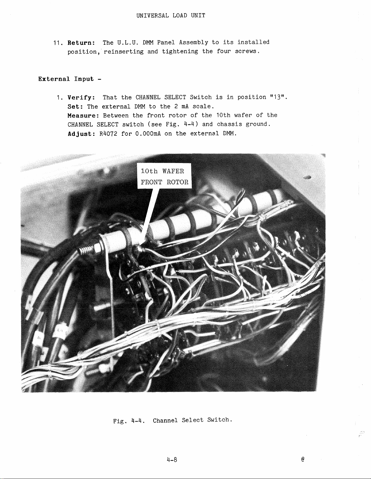
11.
Return:
position,·
U.L.U.
The
reinserting
UNIVERSAL
Panel
DMM
tightening
and
LOAD
UNIT
Assembly
the
to
its
four
installed
screws.
External
1.
Input
Verify:
Set:
Measure:
The
CHANNEL
Adjust:
-
That
external
Between
SELECT
R4072
CHANNEL
the
DMM
the
switch
O.OOOmA
for
to
front
(see
SELECT
2
the
rotor
Fig.
the
on
Switch
scale.
mA
of
4-4)
externa.l
the
and
in
is
wafer
10th
chassis
DMM.
position
of
ground.
"13".
the
Fig.
4-4.
Channel
4-8
Select
Switch.
@
Page 37

The
adjustment
2.
Apply:
(with
Measure:
10th
Check:
3.
Apply:
Measure:
10th
Check:
1.
Set:
and
Apply:
+10.00±0.01
respect
Between
wafer
wafer
of
The
-10.00±0.01
Between
of
The
3.
procedure
The
VOLTAGE/CURRENT
the
CHOP/SWITCH
No
to
chassis
the
meter
meter
external
for
the
for
Channel
which
UNIVERSAL
VDC
to
ground)
chassis
CHANNEL
VDC
chassis
CHANNEL
switch
voltage
SELECT
an
indication
to
SELECT
an
indication
Offset
follows
LOAD
UNIT
the
EXT.
ground and
switch
the
EXT.
ground and
switch
Null
is
the
switch
to
the
or
to
"Switch"
signal.
IN
center
the
front
(see
Fig.
of
between
IN
center
the
front
(see
Fig.
of
between
Adjustments
same
the
for
"Current"
position.
conductor.
rotor.
of
4-4).
+1.92
conductor.
rotor
mA
of
4-4).
-1.92
all
mA
cells:
position
the
and
the
and
+2.08
-2.08
mA.
mA.
2.
3.
4.
5.
(Before
to
the
(For
Figure
(For
reading
Note:
to
(After
these
the
each
each
"hunt"
beginning
each
next
4-5
of
The
adjusting
adjustments
adjustment)
position
position)
for
the
position)
0.000
high
or
"jitter"
of
(of
Use:
channel
Adjust:
± 2
counts
current
every
by
performing
this
Switch:
positions
The
being
in
positions
within
channel)
Section.
Null
The
the
this
the
The
1
through
Offset
adjusted.
indicated
least
(1,2,7,8)
tolerance.
Verify:
Verification
CHANNEL
significant
The
12).
Pot
pot
may
SELECT
indicated
be
results
Test
for
a U.L.U.
digit.
expected
at
switch
in
DMM
of
4-9
Page 38

7
CHAN
R712 R913
CHAN
8
10
12
11
9
CHAN
Rllll
CHAN
R1211
CHAN
R1013
CHAN
R812
..i=
I
~
0
-,~
r.:
~
~
{;,~
Ii
~ ~
~I'
h ,
~
~
~
@"'~
@+
@®
®--~~
~
_06.~.·~
~
Ii
~
~
®
~~
~·e
---
'.~
~
V "
·.
Fl
i~.~.'
~\,~~·
~
ij
~
JIU'
~~
,
F_
J
.
~
g~
~
~,i')
i
~$1111;11,
~
\1111.i'
~·
i~~$
.J,..,...
,~
~~
V
'"·@
..
~~ ~~
~~~~
'
-fZlll-'.
..
~--(81ZD-
it~;:Ji.J
'
l,.l"'Br·
"~_)
~L·
:~'
·
~ ~
r~:;
1~~7~
~
·1~'
U7Z
i
~Iii§
~
~l
~·~ii'~@~
~~
·
,'~
~.~·~
V
~q~.·Qn.
~
-@)~~1S®¥~
+~t§~.~
~8
~~~~;!ji~i:f;
~'~·
1
1
J·
~
~["~~
~BCJl:T
!:(liQ[J-
~@·~'•·i~
~
~
~:
~
~
~
CJ
•
~
~~1;11)',
!~~e~
~
H
V
I~
/~~)'\
~~~
J
.....
I'
a'
~~
1
}~~.-~~ri~::~'ir~
~
)
1;11;'.~~
~~
~
H
~~
~Md~~~~~rn~~t;'~~~~
n---
· ·
..
r.
Q.llZ·.~ia~.
..
~
~.
r::l.·
..
~
V~7V
...
H
I~
~:~N:~:~r:~
~
,~?./1~i
H
H
~
--=-~
r
Fl
~
~
·~·
H ,
i
~
~
__,_1
~-
a~~~~
V
"V
..
:·'
l~
;.
~
c1;1~'.
1
~~~~~
r
~~
~
®L~~l@i~~-
+@r
~
.~.
~ ~
~
J
·1
1
I
~
,,
;•.--~-~~{a
l'
R~~
~8~~~8~£
:;:s~~
~~.
~
s.~@~.
;~_!,·1
®
~
~.
·
..
;.,
......
~~8~1
0
1
~~
j
~~~.
~[·
~
,
..
.
~
b
I
I ,·
1
-~....
~Jgi@\
;®®:!~.
"'
~gl.~i)
§@
§
'f
~l
I~
J
....
~
~
~~~;
1
~~
t~
:)
JfJl·Jr
~
n
~
~
-.i{.l'I]-
..
·
'
'
...
'
~~·~i@+
@o~
~~~~~!~.~~
~~
~~~•J'J~~
ij
~
~,
5
1
·1~~
~('i~;
~
1
i
·w11··,
1,
, '
~
::..
'
l--~-
~
~
~
~
H
•~
~~·
~
~~
~f.!-1
W
-@
§
~~
H
..
8 .••
~~,
~(·~;~!-\
!
~
§
...
r
~
'
.;.i
"II(
~I
"'~
~
.
1
••
~
"i!
1
~
/i~
~110
ur::
ij~
,
~
V W
. '
2~
.
~
~.r
• I
~
~~··~~~~
..
~
~·
~
;~·
11
·1,J
·'1··
I I .
I•"
~1-
~~
~
~-)
~g
~
I~~~
~'t(.~'.~
~
-~-
_,_,~.:
~
~
~~~;~
~
~~.
~--@
~
~
FB'
2-
- •
~
~
s
~~c7:
~.
~J~~:~)
·
~
~
~
~~)
l"l"i· ·"'
1
.•.
_I
"""
~
+@
®@
..
f!!J
~
O
~A~
~ ~
w~~J
2
~ ~
1
4
!"\
(Q)
·-·/
..
~
@
CHAN
Rll2
I I
R212
CHAN
@
2
@
CHAN
Locations
R611
CHAN
~
6
I I
,r
1
@
,,
R313 R511
3
CHAN
~
Figure
CHAN
5
4-5.
Main
Board
Adjustment
@
R412
4
~
Page 39

UNIVERSAL
LOAD
UNIT
REPLACEABLE PARTS
PARTS ORDERING
Replacement parts are
representative.
or
Tektronix
Changes
components
improvements
ordering
or
type
If
Tektronix,
number.
to
become
they
as
developed
include
to
parts,
number,
a part you have ordered has been
serial number, and
Inc. Field
Office
SECTION
5
INFORMATION
through
available from
instruments are sometimes made to
available,
engineering department.
our
in
following
the
representative
or
or
and to give you
information
modification
replaced
will
your
in
number
with a
contact
your
new
you
Tektronix,
local
accommodate
benefit
the
therefore
It is
order: Part number,
applicable.
if
improved
or
concerning
Inc. Field
the
of
important,
part,
any change in
Office
improved
circuit
latest
instrument
your
when
local
part
Change
In
Because
further
utilized
ACTR
ASSY
CAP
CER
CKT
COMP
CONN
ELCTLT
ELEC
INCAND
LED
NONWIR
information,
SPECIAL NOTES AND SYMBOLS
XOOO
OOX
the Parts List,
space limitations, an
of
identification,
Name
Item
possible.
where
ACTUATOR
ASSEMBLY
CAPACITOR
CERAMIC
CIRCUIT
COMPOSITION
CONNECTOR
ELECTROLYTIC
ELECTRICAL
INCANDESCENT
EMITT-ING DIODE
LIGHT
NON WIREWOUND
if any, is
an
Item
located
Part first added at this
Part removed after this
ITEM
Name is separated from
Name may sometimes appear
Item
U.S. Federal
the
ABBREVIATIONS
manual.
this
at the rear
NAME
of
number
serial
number
serial
description
the
Cataloging
PLSTC
QTZ
RECP
RES
RF
SEL
SEMICOND
SENS SENSITIVE
VAR
WW
XFMR
XTAL
comma
a
by
incomplete. For
as
Handbook
PLASTIC
QUARTZ
RECEPTACLE
RESISTOR
RADIO
SELECTED
SEMICONDUCTOR
VARIABLE
WI
TRANSFORMER
CRYSTAL
H6-1 can be
FREQUENCY
REWOUND
.
5-1
Page 40

Circuit No.
UNIVERSAL
LOAD
UNIT
ELECTRICAL PARTS LIST
INSTRUMENT CHASSIS ASSEMBLY
Part of
Tektronix
Part No.
067-0883-99
Description
J1,J2
J3
03001,3004
3005,3008
650-0138-00
670-6048-00
670-6050-00
670-6051-00
670-6049-00
179-2718-00
179-2719-00
179-2720-00
179-2721-00
179-2722-00
179-2723-00
179-2724-00
179-2725-00
179-2726-00
131-0096-00
131-0294-00
151-0373-00
ECB, Main Board Assembly
ECB, Digital
Lower
ECB,
Interconnect
ECB,
ECB, Power
CABLE,
CABLE,
CABLE,
CABLE, Negative Metering
CABLE, Positive Metering
CABLE, Negative Program
CABLE, Positive Program
CABLE,
CABLE, Power
CONNECTOR,
CONNECTOR, 36 Pin,
TRANSISTOR, MJE2901, Power, PNP,
Multimeter
Panel
Supply
Interconnect
Connector
Connector
AC
Pin,
32
No. 1
No. 2
Male
Male
Si.
S7002
T3001
U3001,3006
260-1960-00
120-1257-00
156-0277
-00
SWITCH, Rotary,
TRANSFORMER, AC Power
IC, uA7805UC,
CHANNEL
Linear
5-2
SELECT
@
Page 41
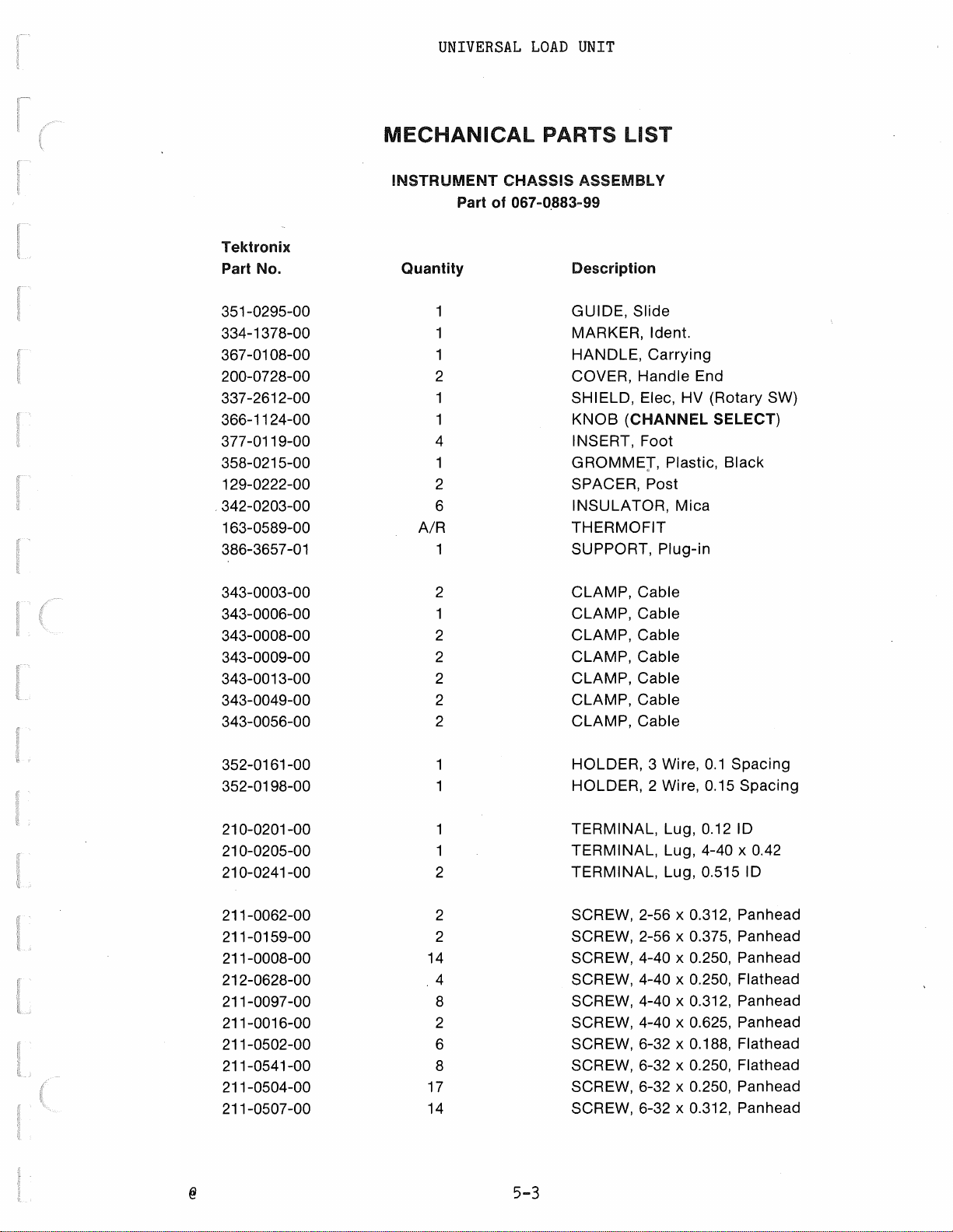
UNIVERSAL
LOAD
UNIT
Tektronix
Part No.
351-0295-00
334-1378-00
367-0108-00
200-0728-00
337-2612-00
366-1124-00
377-0119-00
358-0215-00
129-0222-00
342-0203-00
.
163-0589-00
386-3657-01
MECHANICAL
INSTRUMENT CHASSIS ASSEMBLY
of
Part
Quantity
2
1
4
2
6
A/R
1
PARTS LIST
067-0.883-99
Description
GUIDE, Slide
MARKER,
HANDLE, Carrying
COVER, Handle
SHIELD, Elec, HV (Rotary
KNOB
INSERT,
GROMMEJ, Plastic, Black
SPACER,
INSULATOR,
THERMO FIT
SUPPORT, Plug-in
(CHANNEL SELECT)
Foot
ldent.
End
SW)
Post
Mica
343-0003-00
343-0006-00
343-0008-00
343-0009-00
343-0013-00
343-0049-00
343-0056-00
352-0161-00
352-0198-00
210-0201-00
0-0205-00
21
210-0241-00
211-0062-00
211-0159-00
211-0008-00
212-0628-00
211-0097-00
211-0016-00
211-0502-00
211-0541-00
211-0504-00
211-0507-00
14
.4
17
14
2
2
2
2
2
2
2
2
2
8
2
6
8
CLAMP, Cable
CLAMP,
CLAMP, Cable
CLAMP, Cable
CLAMP,
CLAMP,
CLAMP,
HOLDER,
HOLDER,
TERMINAL,
TERMINAL,
TERMINAL,
SCREW,
SCREW,
SCREW,
SCREW,
SCREW,
SCREW,
SCREW,
SCREW,
SCREW,
SCREW,
Cable
Cable
Cable
Cable
Wire,
3
Wire,
2
Lug,
Lug,
Lug,
2-56
2-56
4-40
4-40
4-40
4-40
6-32
6-32
6-32
6-32
0.312,
x
0.375,
x
0.250,
x
0.250,
x
0.312,
x
0.625,
x
0.188,
x
0.250,
x
0.250,
x
0.312,
x
Spacing
0.1
0.15
0.12
4-40
0.515
Spacing
ID
0.42
x
ID
Panhead
Panhead
Panhead
Flathead
Panhead
Panhead
Flathead
Flathead
Panhead
Panhead
5-3
Page 42
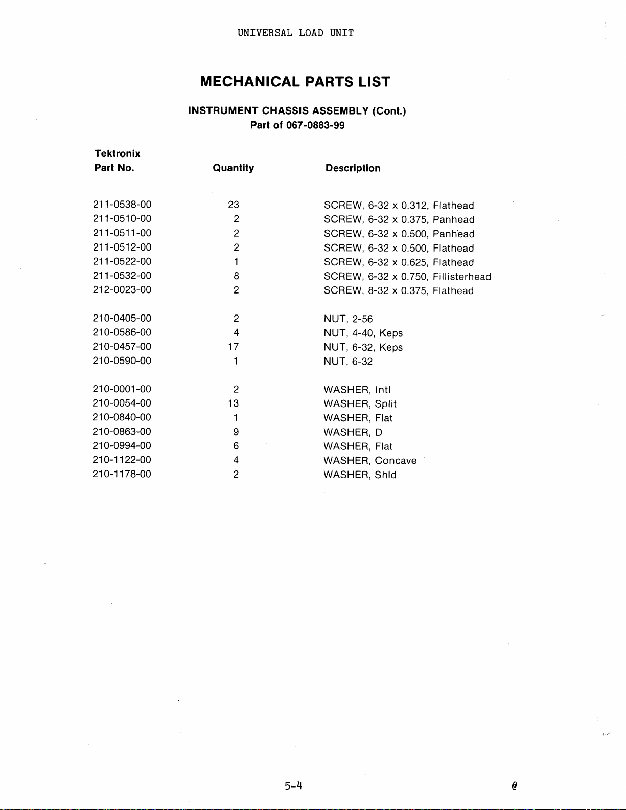
UNIVERSAL
LOAD
UNIT
MECHANICAL PARTS LIST
Tektronix
Part No.
211-0538-00
211-0510-00
211-0511-00
211-0512-00
211-0522-00
211-0532-00
212-0023-00
21
0-0405-00
21
0-0586-00
21
0-045
7 -00
210-0590-00
210-0001-00
210-0054-00
21
0-0840-00
21
0-0863-00
21
0-0994-00
210-1122-00
210-1178-00
INSTRUMENT
Part of 067-0883-99
Quantity
23
2
2
2
1
8
2
2
4
17
2
13
1
9
6
4
2
CHASSIS ASSEMBLY
Description
SCREW, 6-32 x 0.312,
SCREW, 6-32 x 0.375, Panhead
SCREW, 6-32 x 0.500, Panh'ead
SCREW, 6-32 x
SCREW, 6-32 x 0.625,
SCREW, 6-32 x
SCREW, 8-32 x 0.375,
NUT,
2-56
NUT,
4-40, Keps
NUT, 6-32, Keps
NUT, 6-32
WASHER,
WASHER,
WASHER,
WASHER, D
WASHER,
WASHER,
WASHER,
(Cont.)
Flathead
0.500, Flathead
Flathead
0.750, Fillisterhead
Flathead
Intl
Split
Flat
Flat
Concave
Shld
5-4
Page 43

Circuit
No.
UNIVERSAL
LOAD
UNIT
ELECTRICAL PARTS LIST
FRONT PANEL ASSEMBLY
of
Part
Tektronix
Part No.
667-0883-00
Description
J4001, 4002,
4003, 4004
R602
R4067
R4068
R4080
R601
S4010
670-6048-00
670-6050-00
131-0106-02
311-2070-00
311-2053-00
315-0123-00
315-0154-00
321-0097-00
260-0247-00
ECB, Digital
ECB,
Lower
CONNECTOR, BNC, [EXT IN
RIPPLE
VARIABLE RESISTOR, 75k,
OVER VOLTAGE TEST
VARIABLE RESISTOR, Dual (w/switch), 5k,
1 /2W,
RESISTOR, 12k, 1/4W,
RESISTOR, 150k, 1/4W,
RESISTOR, 100 ohm, 1 /8W, 1 %
SWITCH, SPST, Push, CURRENT
20%,
Multimeter
Panel
OUT(+),
Linear, CURRENT
RIPPLE
2W,
5%
5%
:!-1
OV,
SYNC,
OUT(-)]
10%, Linear
ADJUST
LIMIT
@
5-5
Page 44

UNIVERSAL
LOAD
UNIT
Tektronix
Part No.
333-2526-00
333-2525-00
386-41 07 -00
386-41 06-00
331-0314-00
426-0916-00
366-1077 -00
366-1173-00
366-1189-00
211-0022-00
211-0159-00
211-0008-00
211-0101-00
MECHANICAL
FRONT
Quantity
6 SCREW, 2-56 x 0.188, Panhead
2 SCREW, 2-56 x 0.375, Panhead
4
4 SCREW, 4-40 x 0.250, Flathead
Part
PANEL
of
PARTS LIST
ASSEMBLY
667-0883-00
Description
PANEL, Front,
PANEL, Front,
SUB-PANEL, Front,
SUB-PANEL, Front,
WINDOW, Readout
FRAME, Readout
KNOB,
KNOB,
KNOB, OVER VOLTAGE TEST
SCREW, 4-40 x 0.250, Panhead
CURRENT
CURRENT
Top
Lower
Window
ADJUST,
ADJUST, Inner
Top
Lower
Outer
21
0-0583-00
220-0449-00
21
0-0046-00
210-0905-00
21
0-0940-00
210-0255-00
21
0-0269-00
3
4
1 WASHER, Lock,
4
17
4 TERMINAL, Lug,
NUT, 6-32
NUT, Sleeve, 4-40
WASHER, Flat, 0.256 ID
WASHER, Flat, 0.25 ID
TERMINAL, Lug, 0.257 ID
0.261
0.391
ID
ID
5-6
Page 45
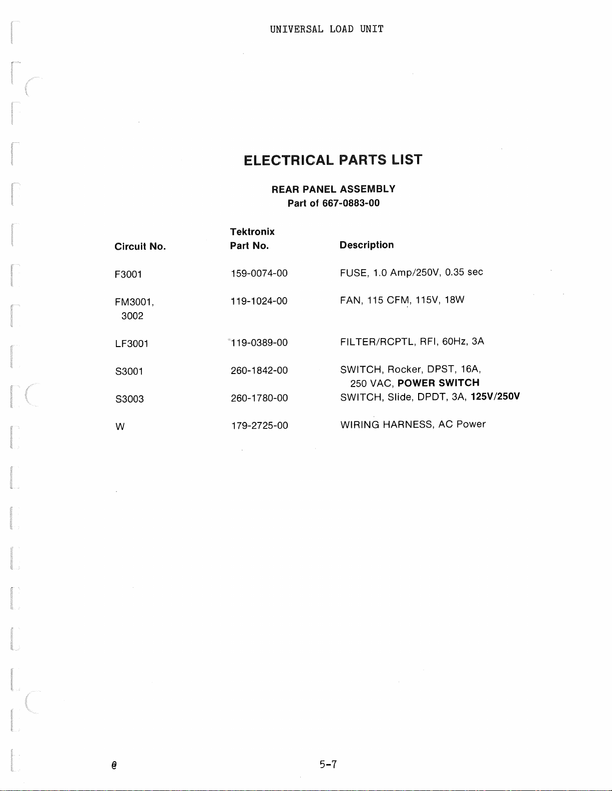
UNIVERSAL
LOAD
UNIT
ELECTRICAL PARTS LIST
Circuit
F3001
FM3001,
3002
LF3001
S3001
S3003
w
No.
REAR PANEL
Tektronix
Part No.
159-007 4-00
119-1024-00
119-0389-00
260-1842-00
260-1780-00
179-2725-00
Part
ASSEMBLY
667-0883-00
of
Description
FUSE, 1.0 Amp/250V, 0.35
FAN, 115 CFM, 115V, 18W
TER/RCPTL,
FIL
SWITCH,
250
SWITCH, Slide,
WIRING HARNESS, AC
Rocker,
VAC, POWER SWITCH
RFI, 60Hz,
DPST, 16A,
DPDT, 3A,
Power
sec
3A
125V/250V
5-7
Page 46
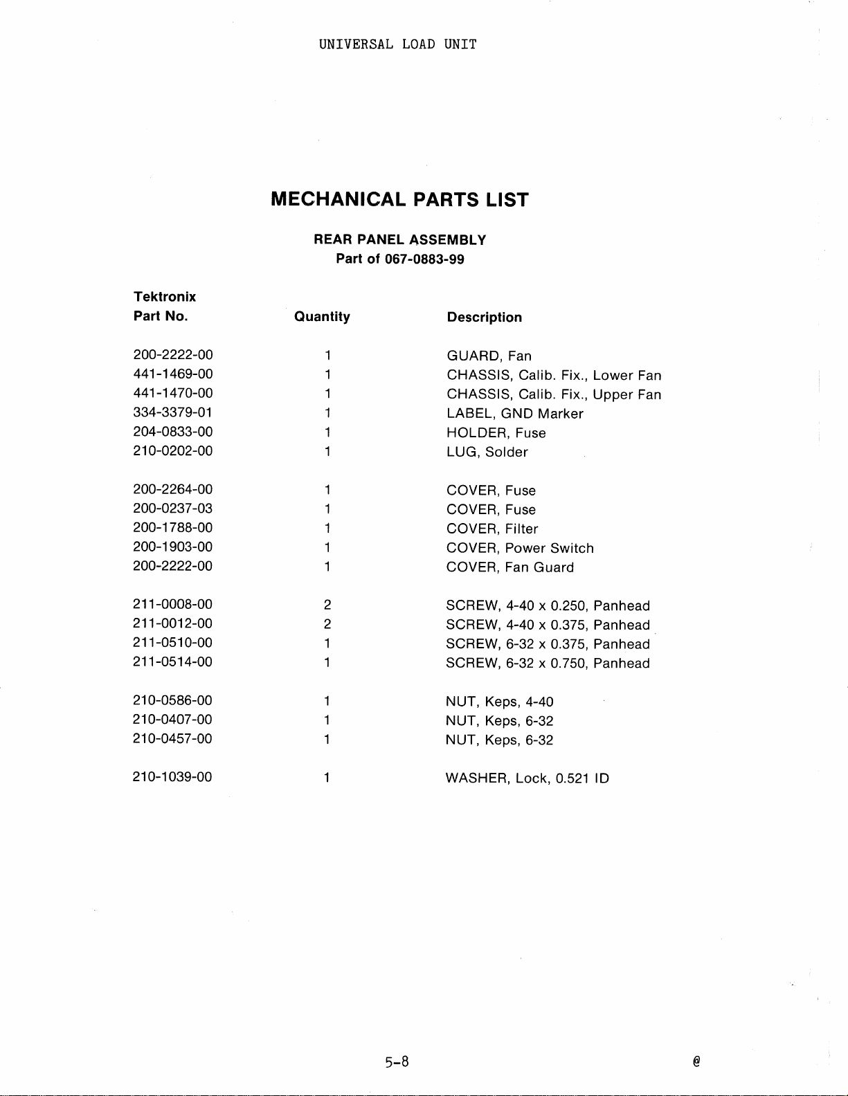
UNIVERSAL
LOAD
UNIT
MECHANICAL PARTS LIST
Tektronix
Part No.
200-2222-00
441-1469-00
441-1470-00
334-3379-01
204-0833-00
210-0202-00
200-2264-00
200-0237-03
200-1788-00
200-1903-00
200-2222-00
211-0008-00
211-0012-00
211-0510-00
211-0514-00
REAR PANEL
Part of
Quantity Description
1
1 CHASSIS, Calib.
1
1 LABEL,
1
1
1
2 SCREW,
2 SCREW,
1 SCREW, 6-32 x 0.375, Panhead
1 SCREW, 6-32 x
ASSEMBLY
067-0883-99
GUARD, Fan
CHASSIS, Calib.
HOLDER, Fuse
LUG,
COVER,
COVER,
COVER, Filter
COVER, Power Switch
COVER,
GND
Solder
Fuse
Fuse
Fan Guard
4-40
4-40
Fix.,
Fix.,
Marker
x 0.250,
x 0.375, Panhead
0.750,
Lower
Upper
Panhead
Panhead
Fan
Fan
210-0586-00
210-0407 -00
210-045 7-00
210-1039-00
1 NUT,
1
1 WASHER, Lock,
NUT,
NUT,
Keps,
4-40
Keps, 6-32
Keps, 6-32
5-8
0.521
ID
@
Page 47
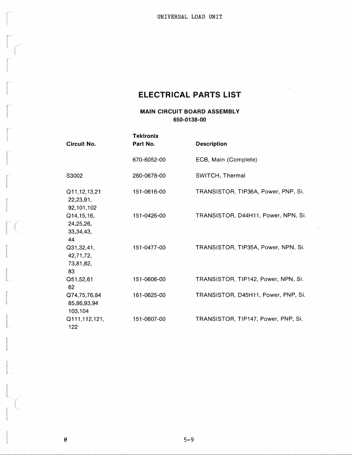
Circuit
No.
UNIVERSAL
LOAD
UNIT
ELECTRICAL PARTS LIST
MAIN
CIRCUIT
Tektronix
Part No.
BOARD
650-0138-00
Description
ASSEMBLY
S3002
011,12,13,21
22,23,91,
92,101,102
014,15,16,
24,25,26,
33,34,43,
44
031,32,41,
42,71,72,
73,81,82,
83
051,52,61
62
074,75,76,84
85,86,93,94
103,104
0111,112,121,
122
670-6052-00
260-0678-00
151-0616-00
151-0426-00
151-0477-00
151-0606-00
161-0625-00
151-0607-00
ECB, Main (Complete)
SWITCH, Thermal
TRANSISTOR, TIP36A, Power, PNP, Si.
TRANSISTOR, D44H11, Power, NPN, Si.
TRANSISTOR, TIP35A, Power, NPN, Si.
TRANSISTOR, TIP142, Power, NPN, Si.
TRANSISTOR, D45H11, Power, PNP, Si.
TRANSISTOR, TIP147, Power, PNP, Si.
5-9
Page 48

UNIVERSAL
LOAD
UNIT
Tektronix
Part No.
214-2864-00
386-41 08-00
342-0354-00
129-0285-00
210-0201-00
211-0511-00
211-0007 -00
211-0097 -00
211-0061-00
210-0054-00
210-1002-00
210-1178-00
21
0-0004-00
MECHANICAL
MAIN
CIRCUIT
PARTS LIST
BOARD
ASSEMBLY
650-0138-00
Quantity
20
11
2
6 SCREW, 6-32 x 0.500, Panhead
11
50
11
59 WASHER,
48
12 WASHER, Shld
11
Description
HEAT
SUPPORT, Heat Sink
INSULATOR
SPACER, Post
LUG,
SCREW, 4-40 x 0.188, Panhead
SCREW, 4-40 x 0.312, Panhead
SCREW, 4-40 x 0.500, Fillisterhead
WASHER, Flat
WASHER, ltl.
SINK
Solder
Split
5-10
Page 49
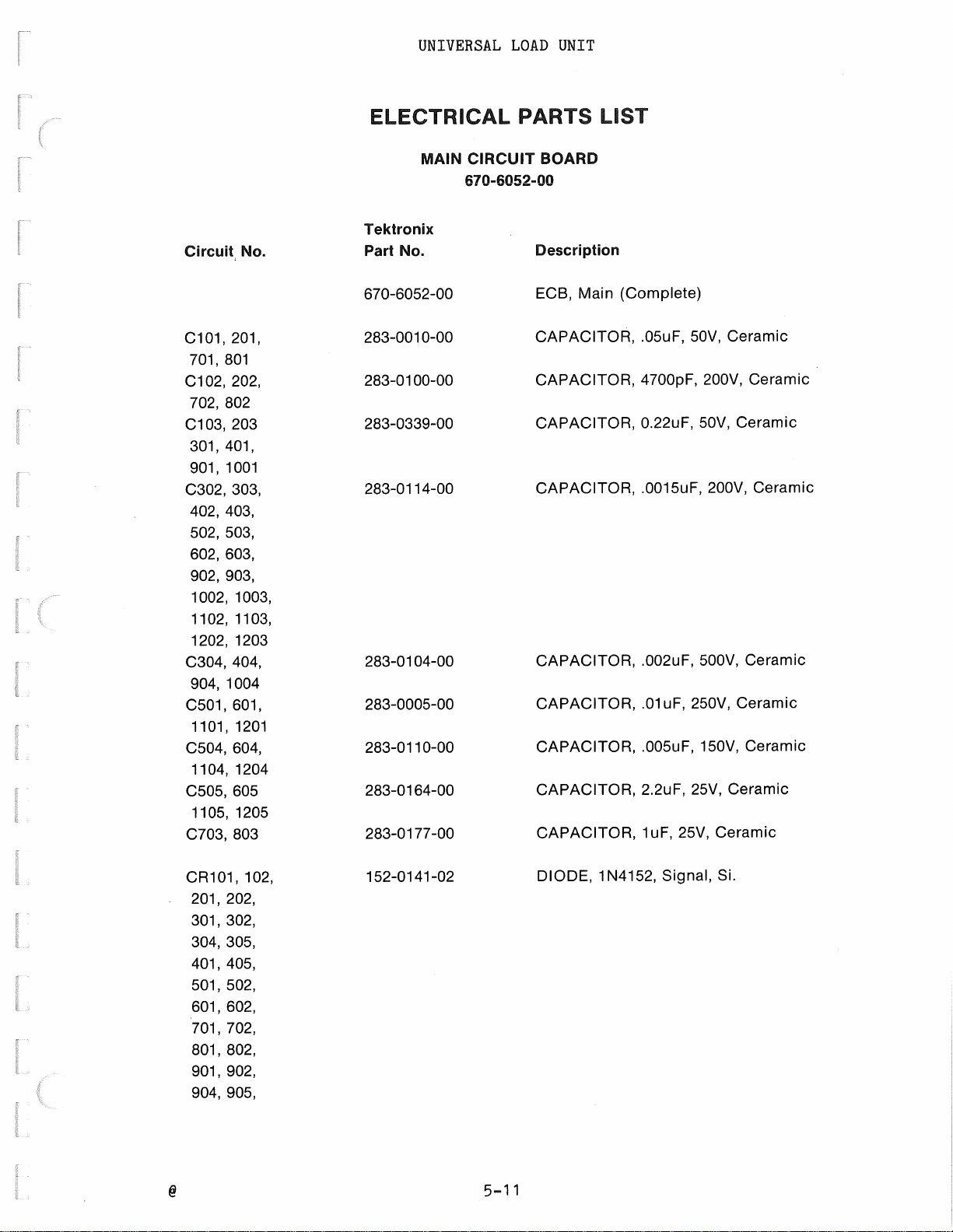
UNIVERSAL
LOAD
UNIT
ELECTRICAL PARTS LIST
Circuit
C101, 201,
701,
C102, 202,
702, 802
C103, 203
301, 401,
901,
C302, 303,
402, 403,
502, 503,
602, 603,
902, 903,
1002, 1003,
1102, 1103,
1202, 1203
C304, 404,
904, 1004
C501, 601,
1101,
C504, 604,
1104, 1204
C505, 605
1105, 1205
C703, 803
No.
801
1001
1201
MAIN
Tektronix
Part No.
670-6052-00
283-0010-00
283-0100-00
283-0339-00
283-0114-00
283-0104-00
283-0005-00
283-0110-00
283-0164-00
283-0177-00
CIRCUIT
BOARD
670-6052-00
Description
ECB, Main
CAPACITOR, .05uF, 50V,
CAPACITOR, 4700pF, 200V,
CAPACITOR, 0.22uF, 50V,
CAPACITOR, .0015uF, 200V,
CAPACITOR, .002uF, 500V, Ceramic
CAPACITOR,
CAPACITOR, .005uF, 150V, Ceramic
CAPACITOR,
CAPACITOR,
(Complete)
Ceramic
Ceramic
uF, 250V, Ceramic
.01
2.2uF, 25V, Ceramic
1 uF, 25V, Ceramic
Ceramic
Ceramic
CR101, 102,
201, 202,
301, 302,
304, 305,
401, 405,
501, 502,
601, 602,
701, 702,
801, 802,
901, 902,
904, 905,
152-0141-02
5-11
DIODE,
1 N4152,
Signal, Si.
Page 50

UNIT
UNIVERSAL
LOAD
ELECTRICAL PARTS LIST
Circuit No.
1001, 1002,
CR
1004, 1005,
1101, 1102,
1201, 1202
CR303, 403,
504, 604,
903, 1003,
1104, 1204
8
7,
2,
F1,
10
9,
4,
F3,
11, 12
6,
FS,
27
017,
78,
28,
018,
88
53,
45,
035,
63
54,
46,
036,
64, 96, 106,
114, 124
87
077,
113,
105,
095,
MAIN
CIRCUIT
BOARD {Cont.)
Part of 670-6052-00
Tektronix
Part No. Description
152-0141-02
152-0676-00
159-0162-00
159-0038-00
159-0014-00
151-0103-00
151-0526-00 TRANSISTOR,
151-0347-00 TRANSISTOR,
151-0521-00 TRANSISTOR,
151-0134-00 TRANSISTOR, 2N2905A, Signal,
151-0350-00
DIODE,
DIODE,
FUSE, 30A,
FUSE,
FUSE,
TRANSISTOR,
TRANSISTOR, 2N5401, Signal,
1N4152,
1 N5625, Rectifier, Si.
SA,
1
SA,
Signal,
Medium
Medium
Fast
2N2219A,
2N3896,
2N5551,
C1228,
Si.
Signal,
Thyrister
Signal, NPN, Si.
Thyristor
NPN, Si.
PNP, Si.
PNP, Si.
R101, 201,
801
701,
R102,
R103, 104,
117,
217,
202,
717,
702,
817
802,
105, 203,
204, 205,
503, 603,
703, 704,
705, 803,
804, 805,
1103, 1203
321-1295-01 RESISTOR, 11.7k, 1/8W,
321-0135-00 RESISTOR,
321-0164-00 RESISTOR, 499 ohm, 1/8W,
249 ohm, 1/8W,
.5%,
5-12
Mtl. Flm.
Mtl. Flm.
1%,
Mtl. Flm.
1%,
\•--._j
Page 51

UNIVERSAL
LOAD
UNIT
ELECTRICAL PARTS LIST
Circuit
R106, 206,
706, 806
R107, 207,
707, 807
R108, 109,
110,
208, 209,
210,
308, 408,
509,
609,
708, 709,
710,
808, 809,
810,
907, 1007,
1107,
1207, 1213
R111, 115,
211, 215,
307,
407,
507, 606,
714, 715,
814, 815,
910,
1010, 1011,
1109, 1209
R112, 212,
313, 413,
511, 611,
712, 812,
913, 1013,
1111,
No.
114,
214,
513,
613,
711,
811,
1113,
311,
411,
911,
1211
MAIN
Tektronix
Part No.
321-0290-00
321-0310-00
315-0201-00
315-0200-00
311-1557-00
CIRCUIT
Part
of
670-6052-00
BOARD (Cont.)
Description
RESISTOR, 10.2k, 1 /8W, 1
RESISTOR,
RESISTOR, 200
RESISTOR, 20
VARIABLE RESISTOR,
16.5k, 1/8W,
ohm, 1/4W,
ohm, 1/4W,
%,
Mtl. Flm.
1%,
Mtl. Flm.
5%,
5%,
Carbon
25k, 1 /2W,
Carbon
Linear
@
5-13
Page 52

UNIVERSAL
LOAD
UNIT
ELECTRICAL PARTS LIST
Circuit No.
R113, 213,
713, 813
R116, 216,
716, 816
R118, 218,
718, 818
R119,219,
508, 514,
608, 614,
719, 819,
1108, 1114,
1208, 1214
R120, 122,
124, 220,
222, 224,
720, 722,
724, 820,
822, 824
R121, 123,
125, 221,
223, 225,
721, 723,
725, 821,
823, 825
R301, 401,
1001
901,
R302, 402,
902, 1002
R303, 403,
903, 1003
R304, 404,
904, 1004
R305, 317,
405, 417,
905, 917,
1005, 1017
MAIN
Tektronix
Part No.
301-0101-00
315-0302-00
315-0560-00
315-01 00-00
308-0769-00
321-0001-00
321-1646-03
321-0102-00
321-0333-00
321-0337-00
315-0097 -00
CIRCUIT
BOARD (Cont.)
Part of 670-6052-00
Description
RESISTOR, 100 ohm, 1 /4W,
RESISTOR, 3k, 1 /4W,
RESISTOR, 56 ohm, 1/4W,
RESISTOR, 10 ohm, 1/4W,
RESISTOR,
RESISTOR, 10.0 ohm, 1/8W,
RESISTOR, 11.87k, 1/8W, .25%, Mtl. Flm. ·
RESISTOR, 113. ohm, 1/8W,
RESISTOR, 28.7k, 1/8W,
RESISTOR, 31.6k, 1/8W,
RESISTOR, 100. ohm, 1/8W,
.1
ohm, 3W,
5%,
5%,
Carbon
5%,
5%,
.1%,
1%,
1%,
1%,
Mtl. Flm.
1%,
Mtl. Flm.
1%,
Carbon
Carbon
Carbon
WW.
Mtl. Flm.
Mtl. Flm.
Mtl. Flm.
5-14
Page 53

UNIVERSAL
LOAD
UNIT
ELECTRICAL PARTS LIST.
Circuit
R309, 315,
318, 409,
415, 418,
506, 515,
607, 615,
908, 915,
918, 1008,
1015, 1018,
1106, 1115,
1206, 1215
R310, 316,
410, 416,
909, 916,
1009, 1016
R312, 412,
510, 610,
912, 1012,
1110, 1210
R320, 420,
920, 1020
R501, 601,
1101,
R502, 602,
1102, 1202,
R504, 604,
1104, 1204
R505, 516,
605, 616,
1105, 1116,
1205, 1216
R512, 612,
1112, 1212
R517, 617,
1117, 1217
No.
1201
MAIN
Tektronix
Part No.
315-0102-00
315-0331-00
321-0414-00
308-0815-00
321-0296-00
321-0129-00
321-0431-00
301-0153-00
321-0126-00
308-0769-00
CIRCUIT
Part
of
670-6052-00
BOARD {Cont.)
Description
RESISTOR, 1
RESISTOR, 330 ohm, 1/4W,
RESISTOR, 200.k, 1/8W,
RESISTOR,
RESISTOR, 11.8k, 1/8W,
RESISTOR, 215. ohm, 1/8W,
RESISTOR, 301.k, 1/8W,
RESISTOR, 15k, 1/2W,
RESISTOR, 200. ohm, 1/8W,
RESISTOR,
.01
.1
k,
1 /4W,
ohm,
ohm,
5%,
SW,
3W,
1%,
.25%,
1%,
1%,
5%,
.1
Carbon
5%,
Mtl. Flm.
WW
Mtl. Flm.
1%,
Mtl. Flm.
Carbon
1%,
%,
WW
Carbon
Mtl. Flm.
Mtl. Flm.
5-15
Page 54

UNIVERSAL
LOAD
UNIT
ELECTRICAL PARTS LIST
Circuit
U11, 12,
22,
81, 82
U31, 41,
61, 91, 101,
111,
VR101, 201,
VR102, 202,
VR103, 203,
VR301, 401,
VR302, 402,
VR303, 403,
VR306, 406,
VR501, 601,
VR503, 603,
No.
21,
71, 72,
51,
121
701,
801
702, 802
703, 803
502, 602,
901, 1001,
1201
1101,
902, 1002
903, 1003
505, 605,
906, 1006,
1105, 1205
1102, 1202
1103, 1203
MAIN
Tektronix
Part No.
156-1156-00
156-1191-00
152-0195-00
152-0571-00
152-0268-00
152-0149-00
152-0282-00
152-0287-00
152-0395-00
152-024 7 -00
152-0255-00
CIRCUIT
Part
BOARD
of
670-6052-00
{Cont.)
Description
IC, LF356N, Op
IC, TL072CP, Op
ZENER DIODE, 1N751A, 5.1V, .4W
ZENER DIODE, 1N966B, 16V, .4W
ZENER DIODE, 1 N979B, 56V, .4W
ZENER DIODE, 1
ZENER DIODE, 1 N972B, 30V, .4W
ZENER DIODE, 1 N986B, 110V, .4W
ZENER DIODE, 1N749A, 4.3V, .4W
ZENER DIODE, 1 N989B, 150V, .4W
ZENER DIODE, 1 N978B,
Amp
Amp
N961
B,
10V, .4W
51
V,
.4W
136-0514-00
131-0589-00
131-0608-00
131-1687-00
131-1816-00
5-16
SOCKET, Dual-In-Line, 8
TERMINAL,
TERMINAL,
TERMINAL,
TERMINAL,
Pin
Pin
Quick
Quick
Disconn.
Disconn.
contact
@
Page 55

UNIVERSAL
LOAD
UNIT
Tektronix
Part No.
0-0455-00
21
0-0586-00
21
162-0684-00
211-0008-00
MECHANICAL
MAIN
Quantity
4
24
1.167 feet
24
CIRCUIT
670-6052-00
PARTS LIST
BOARD
Description
NUT, .25-28 (1/4)
Keps, 4-40
NUT,
SLEEVING, Elec,
SCREW, 4-40 x .250, Panhead
16 AWG
5-17
Page 56

UNIVERSAL
LOAD
UNIT
ELECTRICAL
DIGITAL
MULTIMETER
PARTS LIST
BOARD
067-6048-00
Tektronix
Circuit
C4001, 4002, 290-0573-00 CAPACITOR,
4003, 4004,
4005, 4006,
4014, 4016
C4007 285-1050-00 CAPACITOR,
C4008 283-0666-00
C4009 281-0812-00 CAPACITOR,
C4010 290-0534-00 CAPACITOR,
C4012 283-0604-00
C4013 285-1056-00
C4017 283-0635-00 CAPACITOR,
C4018 281-0773-00 CAPACITOR,
C4020
C4021, 4022
C4023, 4024
No.
Part No. Description
Digital
670-6048-00
283-0054-00 CAPACITOR,
283-0687
283-0158-00 CAPACITOR,
-00
ECB,
CAPACITOR,
CAPACITOR,
CAPACITOR,
CAPACITOR,
Multimeter
2.7uF,
uF,
.1
890pF, 1
.001
uF,
1
304pF,
uF,
1
pf,
51
uF, Ceramic
.01
150pF,
560pF,
1.0pF,
(Complete)
50V, Electr.
200V, Mtl'd
OOV,
100V, Ceramic
uF,
Electr.
35V,
300V,
50V, Mtl'd Polycarb.
100V, Mica
500V,
300V,
50V,
Mylar
Mica
Mica
Ceramic
Mica
Ceramic
CR4002, 4003,
6001, 6002,
6003, 6004,
6005, 6006,
6007, 6008,
6009, 6010,
6011, 6012,
6013
CR4004, 4005 152-0324-00 DIODE,
CR4007, 4008 152-0141-02 DIODE,
DS4014, 4015, 150-1 048-00 LED DISPLAY,
4016, 4017
DS4018
K4001 148-0079-00
K4002, 4003, 148-0079-00
4004, 4005
04001, 4002, 151-0254-00 TRANSISTOR, 2N5308,
150-1001-00
150-1 066-00
LED, MV5024, Red
TD55125, Signal, Si.
Signal, Si.
MAN4605, 7
28VDC
DISPLAY,
LED
RELAY,
RELAY,
1 N4152,
DIP,
DIP, 100VDC
Seg
7
Seg
Signal, NPN,
Si.
5-18
Page 57

UNIVERSAL
LOAD
UNIT
ELECTRICAL PARTS LIST
Circuit
04003, 4011,
4012, 4013,
4023
04004, 4007,
4008, 4009,
4019, 4020,
04005, 4006,
4010, 4014,
4015, 4016,
4017, 4018
04021
04022
04024
R4001
R4002, 4003
R4004
R4005
R4006
R4007, 4072
R4008, 4009,
.
4011
R4010
R4012
R4013, 4065
R4014
R4015
R4016
R4017
R4018, 4019
R4020,
R4021
R4022
R4023, 4041,
4042, 4043,
4045, 4046,
4047, 4064
No.
4091
DIGITAL
Tektronix
Part No.
151-0254-00
151-0188-00
151-0190-00
151-1103-00
151-0435-00
151-0424-00
315-0682-00
315-0391-00
307-1015-00
311-1231-00
321-1686-07
311-1223-00
321-0385-00
321-0396-00
315-04 73-00
315-0104-00
307-01 03-00
321-0193-00
311-1466-00
321-0309-00
315-0360-00
315-04 72-00
315-0752-00
311-1235-00
315-01 03-00
MUl
TIMETER BOARD (Cont.)
Part
of
067-6048-00
Description
TRANSISTOR, 2N5308, Signal, NPN, Si.
TRANSISTOR, 2N3906, Signal, PNP, Si.
TRANSISTOR, 2N3904, Signal, NPN, Si.
TRANSISTOR, SD210, MOS FET,
TRANSISTOR, MPSA65, Signal, PNP, Si.
TRANSISTOR, 2N5769
RESISTOR, 6.8k, 1/4W,
RESISTOR, 390 ohm, 1/4W,
RESISTOR NETWORK, 9M, 900k, 90k, 9k, 900 ohm,
90
ohm, 10 ohm; DIP
VARIABLE RESISTOR, 25k, 1/2W,
RESISTOR, 10.97k, 1/8W,
VARIABLE RESISTOR, 250 ohm, 1/2W, 10%, Linear
RESISTOR, 100.k, 1/8W,
RESISTOR, 130.k, 1 /8W, 1
RESISTOR, 47k, 1/4W,
RESISTOR, 100k, 1/4W,
RESISTOR, 2.7 ohm, 1/4W,
RESISTOR, 1.00k, 1 /8W, 1
VARIABLE RESISTOR, 2k, 1/2W,
RESISTOR, 16.2k, 1/8W,
RESISTOR, 36 ohm, 1/4W,
RESISTOR, 4.7k, 1/4W,
RESISTOR, 7.5k, 1/4W,
VARIABLE RESISTOR, 100k, 1/2W,
RESISTOR, 10k, 1/4W,
5%,
1%,
5%,
5%,
1%,
5%,
5%,
5%,
Carbon
5%,
.1%,
Mtl. Flm.
%,
Mtl. Flm.
Carbon
Carbon
5%,
%,
Mtl. Flm.
Mtl. Flm.
5%,
Carbon
Carbon
Carbon
N-Ch
Carbon
10%,
Mtl. Flm.
Carbon
10%,
Carbon
10%,
Linear
Linear
Linear
5-19
Page 58

UNIT
UNIVERSAL
LOAD
ELECTRICAL PARTS LIST
Circuit
R4024, 4025,
4026, 4027
4028
R4029, 4030,
4031, 4032,
4090
R4033
R4034, 6004,
6010, 6016,
6022, 6028,
6034, 6040,
6046, 6052,
6058, 6064,
6070, 6076
R4035, 4039
R4036
R4037, 4040
R4044, 4060
R4048, 4049,
4050, 4051,
4052, 4053,
4054, 4081,
4082, 4083,
4084, 4085,
4088
R4058
R4059
R4062
R4063
R4069
R4070, 4073
R4071, 407
4075
R4076, 4078
R4077, 4079
R4086, 4087,
No.
4,
DIGITAL MULTIMETER BOARD
Part of
067-6048-00
Tektronix
No.
Part
315-0203-00
315-0102-00
315-0182-00
315-0122-00
315-0331-00
315-0681-00
315-0751-00
315-0202-00
315-0510-00
315-0241-00
315-0150-00
315-0561-00
315-0161-00
315-0243-00
321-0289-00
321-0481-00
315-0302-00
321-0260-00
315-0272-00
Description
RESISTOR, 20k,
RESISTOR,
RESISTOR,
RESISTOR,
RESISTOR, 330
RESISTOR, 680
RESISTOR, 750
RESISTOR,
RESISTOR,
RESISTOR, 240
RESISTOR,
RESISTOR, 560
RESISTOR, 160
RESISTOR,
RESISTOR, 10.0k,
RESISTOR, 1.00M,
RESISTOR,
RESISTOR,
RESISTOR,
(Cont.)
1 /4W,
1/4W,
k,
1
1.8k, 1/4W,
1.2k, 1 /4W,
ohm, 1/4W,
ohm, 1/4W,
ohm, 1/4W,
2k, 1/4W,
ohm, 1/4W,
51
ohm, 1/4W,
15 ohm, 1/4W,
ohm, 1/4W,
ohm, 1.4W,
24k, 1/4W,
3k, 1/4W,
4.99k, 1 /8W, 1
2.7k, 1/4W,
5%,
5%,
1/8W,
1/8W,
5%,
5%,
Carbon
5%,
5%,
Carbon
5%,
1%,
1%,
%,
5%,
Carbon
Carbon
Carbon
Carbon
5%,
Carbon
5%,
Carbon
5%,
Carbon
5%,
Carbon
5%,
Carbon
5%,
Carbon
5%,
Carbon
5%,
Carbon
Mtl. Flm.
Mtl. Flm.
Carbon
Mtl. Flm.
Carbon
5-20
Page 59

UNIT
UNIVERSAL
LOAD
ELECTRICAL PARTS LIST
Circuit
S4001
T4001
U4001
U4002
U4003
U4004
U4006
U4008
U4009, 4022
U4010
U4011, 4023
U4012
U4013
U4019
U4020
U4021
No.
DIGITAL
Tektronix
Part No.
260-1840-00
120-1276-00
156-1306-00
156-0385-00
156-1305-00
156-0886-00
156-0783-00
156-091 0-00
156-0382-00
156-0383-00
156-0386-00
156-0422-00
156-0736-00
156-1172-00
1 56-11 56-00
156-0465-00
MULTIMETER
Part
067-6048-00
of
BOARD
Description
SWITCH, Toggle, 4PDT,
TRANSFORMER,
IC, LD120,
IC, 74LS04,
LD121,
IC,
74C48,
IC,
LM399H, 6.95V Reg.
IC,
IC, 74LS390,
74LSOO,
IC,
IC, 74LS02,
IC, 74LS10,
74LS191, TTL,
IC,
74LS42, TTL,
IC,
74LS393, TTL,
IC,
IC,
IC, 74LS30,
(Cont.)
Analog A to D
TTL, Hex-Inverter
Digital A to D
CMOS,
TTL, Quad
TTL, Quad
TTL,
LF356, Op
TTL, Single
Line Freq
BCD to 7
Dual-Decade
TTL,
Triple
Syn.
BCD
Dual 4-bit Binary'
Amp
VOLTAGE/CURRENT
Decoder
Seg.
2-lnput
2-lnput
3-lnput
4-bit Up/Own
to Deci.
8-lnput
NANO
NOR
NANO
Binary
Decoder
NANO
VR4001
VR4009, 4010
Y4001
152-0195-00
152-0149-00
158-0124-00
136-0260-02
136-0269-02
136-0494-00
136-0514-00
136-0670-00
136-0338-00
136-0352-00
131-0608-00
131-1343-00
5-21
ZENER DIODE,
ZENER DIODE, 1
CRYSTAL, 2.4576MHz,
SOCKET, Dual In-Line,
SOCKET,
SOCKET, Dual In-Line,
SOCKET, Dual In-Line,
SOCKET, Dual In-Line,
SOCKET, Spring
SOCKET, Spring
TERMINAL, Pin
TERMINAL
1N751A, 5.1V, .4W
N961
In-Line,
Dual
SET PIN
.4W
OV,
1
B,
.05%
16 Contact
14 Contact
Contact
14
Contact
8
Contact
18
Page 60
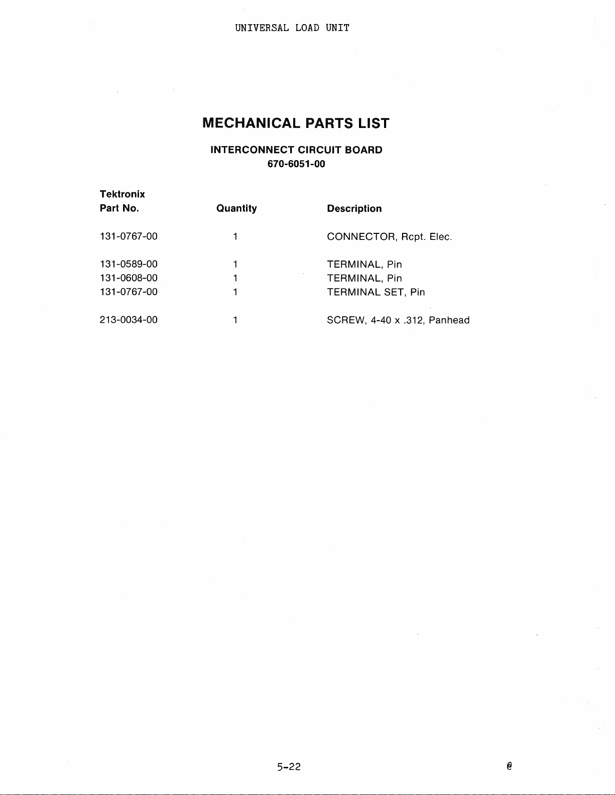
UNIVERSAL
LOAD
UNIT
Tektronix
Part No.
131-0767-00
131-0589-00
131-0608-00
131-0767-00
213-0034-00
MECHANICAL
INTERCONNECT
670-6051-00
Quantity
PARTS LIST
CIRCUIT
BOARD
Description
CONN
TERMINAL, Pin
TERMINAL, Pin
TERMINAL
SCREW, 4-40 x .312, Panhead
ECTOR, Rcpt. Elec.
SET, Pin
5-22
@
Page 61
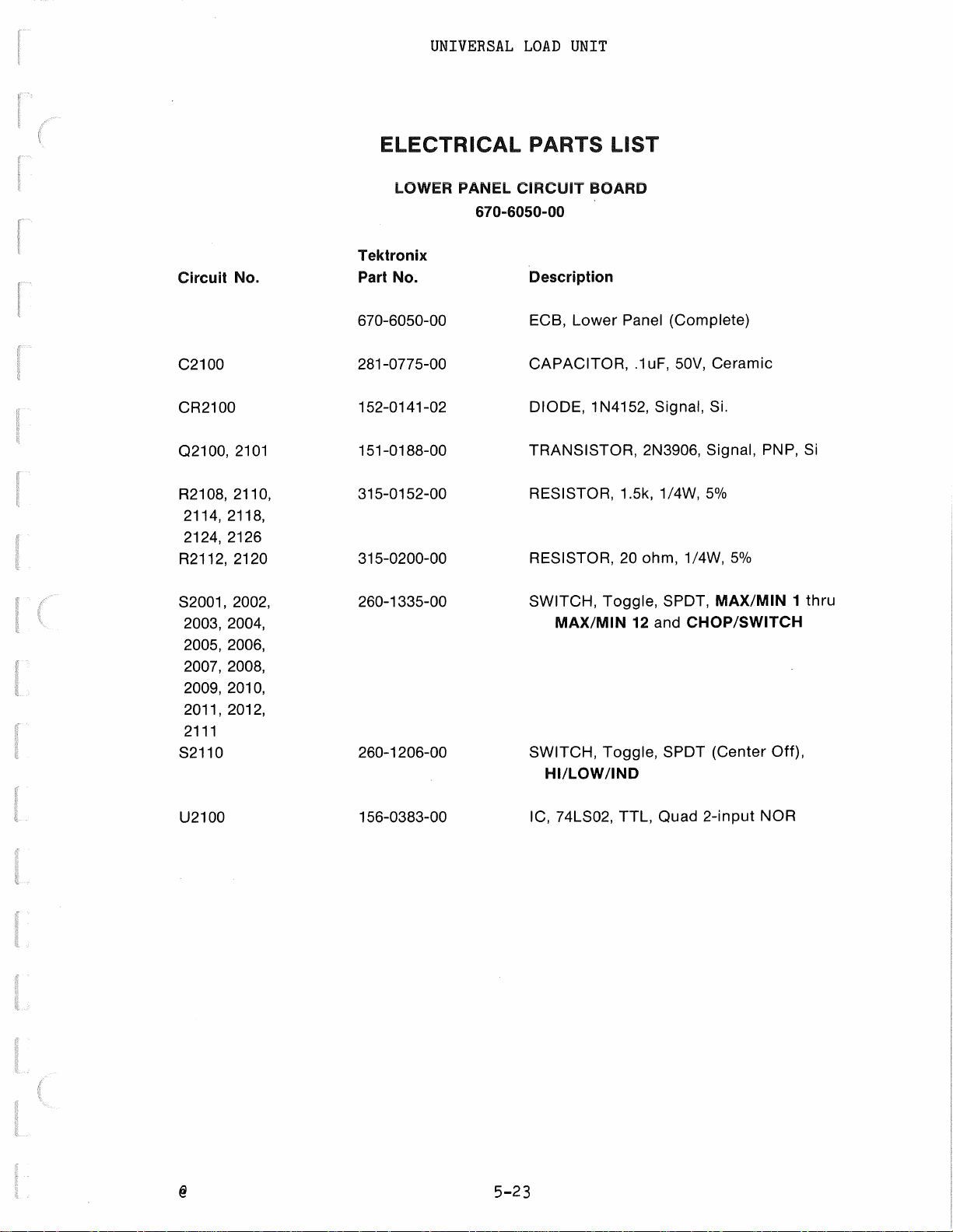
UNIT
UNIVERSAL
LOAD
ELECTRICAL PARTS LIST
Circuit
C2100
CR2100
02100,
R2108,
2114, 2118,
2124, 2126
R2112,
S2001, 2002,
2003, 2004,
2005, 2006,
2007, 2008,
2009, 2010,
2011, 2012,
2111
S2110
No.
2101
2110,
2120
LOWER PANEL
Tektronix
Part No.
670-6050-00
281-0775-00
152-0141-02
151-0188-00
315-0152-00
315-0200-00
260-1335-00
260-1206-00
CIRCUIT
670-6050-00
Description
ECB,
CAPACITOR,
DIODE,
TRANSISTOR,
RESISTOR,
RESISTOR, 20
SWITCH, Toggle, SPOT,
MAX/MIN
SWITCH, Toggle, SPOT (Center
HI/LOW/IND
BOARD
Lower
1N4152,
Panel (Complete)
Ceramic
50V,
uF,
.1
Signal,
2N3906, Signal,
1.5k, 1/4W,
ohm, 1/4W,
12 and
Si.
5%
5%
MAX/MIN
CHOP/SWITCH
PNP, Si
thru
1
Off),
U2100
156-0383-00
5-23
74LS02, TTL, Quad
IC,
2-input
NOR
Page 62

UNIVERSAL
LOAD
UNIT
ELECTRICAL
POWER
Tektronix
Circuit
C3000, 3003 283-0111-00
3006,
3015, 3019
C3001, 3020 290-07 46-00
C3002, 3008, 290-0583-00
3010, 3014
C3004, 3009, 290-07 45-00
3013, 3017
C3005, 3012 283-0114-00
C3007, 3016
C3018 290-0506-00
No.
3011,
Part No.
670-6049-00
283-0299-00
PARTS LIST
SUPPLY
670-6049-00
BOARD
Description
ECB,
CAPACITOR,
CAPACITOR,
CAPACITOR,
CAPACITOR,
CAPACITOR,
CAPACITOR,
CAPACITOR,
Power
Supply
.1
47uF, 16V, Electr.
3000uF,
22uF, 25V, Electr.
1500pF, 200V, Electr.
51
9600uF, 30V, Elactr.
(Complete)
uF,
50V, Ceramic
35V,
pf,
500V, Electr.
Electr.
CR3001, 3002 152-0488-00
CR3003, 3004, 152-0066-00 DIODE,
3005
F3002, 3003, 159-0022-00
3004, 3005,
3006
K3002 148-0022-00
03001,
3005, 3008
03002,
03003,
R3001, 3008, 315-0301-00
3011, 3015,
3022, 3023
R3002, 3012 308-0755-00
R3003, 3017
3004, 151-0373-00
3006
3007
151-0462-00 TRANSISTOR, Power,
151-0188-00 TRANSISTOR, Signal,
315-0512-00 RESISTOR,
DIODE
FUSE,
RELAY, 12 VDC, Armature, 2 Form
TRANSISTOR,
RESISTOR, 300
RESISTOR,
RECTIFIER,
1
N4004G, Rectifier,
1
A,
Fast,
. 75 ohms, 3W,
5.1k, 1/4W,
KBP02,
250V
Power, MJE2901, PNP,
ohms, 1/4W,
Bridge
Si.
C
TIP30C, PNP,
2N3906, PNP, Si.
5%
10%
5%
Si.
Si.
R3004, 3016
R3005, 3018
R3006,
3013,
321-0282-00
311-1 7
321-0268-00 RESISTOR, 6.04k, 1 /8W, 1 %
49-00
RESISTOR,
VARIABLE
8.45k, 1 /8W, 1 %
RESISTOR,
1.5k, 1 /2W,
5-24
20%
Page 63

UNIT
UNIVERSAL
LOAD
ELECTRICAL PARTS LIST
Circuit
R3007, 3020
R3009,
R3010
R3014, 3024
R6001, 6006,
6007, 6012,
6013, 6018,
6019, 6024,
6025, 6030,
6031, 6036,
6037, 6042,
6043, 6048,
6049, 6054,
6055, 6060,
6061, 6066,
6067, 6072,
6073, 6078
R6002, 6005,
6008, 6011,
6014, 6017,
6020, 6023,
6026, 6029,
6032, 6035,
6038, 6041,
6044, 6047,
6050, 6053,
6056, 6059,
6062, 6065,
6068, 6071,
6074, 6077
R6003, 6009,
6015, 6021,
6027, 6033,
6039, 6045,
6051, 6057,
6063, 6069,
6075
No.
3021
POWER SUPPLY BOARD
Tektronix
Part No.
321-0299-00
315-0302-00
311-1567
308-0677-00
321-0296-00
321-0143-00
321-0297-00
-00
Part
670-6052-00
of
Description
RESISTOR,
RESISTOR,
VARIABLE
RESISTOR,
RESISTOR,
RESISTOR,
RESISTOR,
(Cont.)
12.7k, 1/8W,
3k, 1 /4W,
RESISTOR, 100
1 ohm, 2W,
11.8k, 1 /8W, 1 %
301
12.1k, 1/8W,
5%
ohms, 1/8W,
1%
ohms, 1/2W,
5%
1%
1%
20%
5-25
Page 64

UNIVERSAL
LOAD
UNIT
ELECTRICAL PARTS LIST
Circuit No.
U3001, 3006
U3002, 3004
U3003, 3005
U6001, 6002,
6003, 6004,
6005, 6006,
6007
POWER SUPPLY
Part of
Tektronix
Part No.
156-0277-00
156-0071-00
156-0105-00
156-0411-00
388-6546-01
136-0394-00
136-0269-02
136-0514-00
ECB (Cont.)
670-6049-00
Description
IC, uA7805UC,
IC,
uA723DC,
IC, LM301
IC,
LM339N,
ECB,
SOCKET, Relay
SOCKET, Relay,
SOCKET, Relay, 8 pin
AN,
w/o
components
Linear
Linear
Op
Amp
Linear
14 pin
131-0589-00
131-0608-00
344-0154-00
TERMINAL,
TERMINAL,
HOLDER, Fuse
Pin
Pin
5-26
Page 65
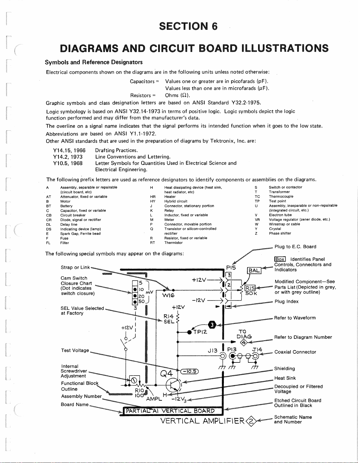
SECTION
6
L -
DIAGRAMS
Symbols
Electrical
Graphic
Logic
function
The
Abbreviations
Other
The
A
AT
B
BT Battery
c
CB
CR
DL
DS
E
F Fuse
FL
The
and Reference Designators
components shown on the diagrams
symbols
symbology
performed
overline
Y14.15, 1966
Y14.2, 1973
Y10.5,
following
following
on a signal name indicates
are
standards
ANSI
1968
prefix
Assembly, separable
(circuit board, etc)
Attenuator, fixed or
Motor
Capacitor, fixed or
Circuit breaker
signal or rectifier
Diode,
Delay line
Indicating
Spark
Filter
Cam Switch
Closure
(Dot indicates
SEL
device
Gap, Ferrite bead
special symbols
Link
or
Strap
Chart
closure) •
switch
Value Selected 3
at Factory
Voltage
Test
AND
designation
class
and
may
on
that
repairable
ANSI
differ
ANSI
used in the preparation
are
Practices.
Symbols
Engineering.
used
are
may
+12.V:
6 )
/
based on
is
and
based
Drafting
Line Conventions and
Letter
Electrical
letters
or
variable
variable
(lamp)
------15
CIRCUIT
in
are
Capacitors=
Resistors =
are
letters
Y32.14-1973
the
from
that
.1-1972.
Y1
Quantities
for
reference designators
as
appear
in
manufacturer's data.
signal
the
Lettering.
H Heat dissipating device (heat sink,
HR
HY Hybrid circuit
K
L
M Meter
p
Q
R Resistor, fixed
RT
diagrams:
the
on
l
e
e
.---a=""-4..._-------~
10
2.0
mV
WI~
soJ
I
I
/
BOARD
unless
following
the
one
Values
less
Values
(.Q).
ms
Oh
on
based
of
terms
performs its intended
diagrams
of
in
Used
heat radiator, etc)
Heater
Connector, stationary portion
Relay
fixed or
Inductor,
Connector,
Transistor
Thermistor
Rl
SEL
or
rectifier
+1'2.V
4
-----------D~
units
greater
or
than one
Standard
ANSI
positive logic.
by
Electrical
identify
to
variable
portion
movable
silicon-controlled
variable
or
~
V
+l2.
---:::
-12.V
J
in
are
microfarads (µF).
in
are
Logic
Tektronix,
Science and
components
jf31
[jl'""I
/I
2
1
It
(.._I
~
Pl3
I
13
ILLUSTRATIONS
noted otherwise:
picofarads (pF).
Y32.2-1975.
logic
the
symbols
function
Inc.
I
I
>
TO
depict
goes
it
when
are:
assemblies
or
Switch
s
T Transformer
Thermocouple
TC
Test point
TP
Assembly, inseparable
u
(integrated circuit, etc.)
Electron
v
Voltage regulator
VA
Wirestrap or
w
y
Crystal
Phase shifter
z
TAL
~
K
so
-
_Refer
Jl4
low
the
to
the diagrams.
on
or contactor
tube
(zener diode, etc.)
cable
Board
E.C.
to
Plug
Identifies Panel
I
lsox
Controls, Connectors and
Indicators
Modified
Parts List (Depicted in grey,
or
Plug Index
Refer to Waveform
Coaxial
Component-See
with grey
outline)
to Diagram Number
Connector
state.
or non-repairable
VERTICAL
~\
---~~Shielding
Heat Sink
Filtered
in
or
Black
Decoupled
Voltage
Etched Circuit Board
Outlined
BOARD
Page 66

Page 67

Component
Location
Diagram
MAIN
BOARD
670-6052-00
Page 68

1"!2V8
~
ill
~
Ir)
~
Qi
0-
~
I(
~
Ull
R/2f0
SK
-l'Z.VB
R//8
56
C/02
.0047
3K.
+nva
Rift.
-12.V~
C.'ft
ii;'//'I
10
/fl07
VRIOI
F
s.1v
t--+----+--+---..----..-_.----.--.....--~--.~..-~-----
R/08
zoo
16.SK.
VR/02
,,I/
~10'9
zoo
6111
CHANNEL
P/o
P2.
REAR
PANEL
q,I:'.~
I
@tJ
A~
P/o
PIO/
~~i:S
~I
18
1
'l.C%
. I P/o
at.iP2.0I
d3~
'0A38
R717
24'1
R718
56
C702
.004-7
+llVB
~C703
1.0
/271"1
10
P/o
REAR
Pf
PANEL
R714
CMANNEL
R.125
10.0
q~~
~P/o
f:_
~
~
P701
.437
~
~l]
~
V.r'R7&3
zo
18
7
9F<?/
P/o
3 P801
0
P/o
P705
PARTIAL
Ai
f?Z/1
Z49
+12Vl!l
R'Z.18
56
C202
.00.,.1
MAIN
-12VB
BOARD
CZ03
.22
RZl'l
10
CHANNEL
R607
Jl302
/6.SK
l/RB02
lloV
+12v6
-1?.VB
R813
JOo,v
..
w
{)_87
R815
20
____
~~Z4-
-4T
CHANNEL
:r
RB25
10,0
PARTIAL
2
R8/7
R818
5~
ZH
ceo:z
.0047
PIO 6 70-013,8
-oo
+12VB
G803
1.0
RBI'!
10
----G
R820
,o;,
R82.I
-4T
IO,O
R8'Z2
.03
-4T
Je8Z
IO.O
"'-·
3
8
Ai
MAIN
BOARD
O<D7-0tJ83-
99
Hl6H
CURRENT
CHANNELS
REV D '7-79
Page 69

~305
//)().,O
+12VB
'IF~
P/o
r.;-:i
P301
L!t;-J
I--,
%>
1312.
rI:b
1
P/o
P30S
P/o
132.8
-1'1
~30
P905
311
i,J
P/o
Pl
REAR
PANEL
fe903
<8.71<
I
+12.VB
VR90I
c.<toz.
C'f<X3
i-0015
IOV-c
.oo/S
1?911
"2.0
R104-
3!.!ok
Vte<;Oi!.
30Vz.
1.c<€>
P/o
~P901
/\
:J
~
~
~
;b
~
:J
->
P/o
P905
1?~17
100.0
+l'ZVB
/€405
100.0
lf"/8
II<
C~4-
.oo:z.
-12VB
+IZllfJ
R4-0I
//.fl71<
RfjZ
~
R40.3
Z8.
71>
VR~OI
IOVE
C402
.0015
C.403
·0015
IC4fl
20
~<l-04-
31.f.k
VR40'2.
.30Va
CHANNEL
CR403
3
?F<@
(}::;\}
L~
~
P/o
P4-0/
~
131''7
2
P/o
P405
k..823
~825
-----"A''--"'
!e''/1'1
100.0
-12va
tc/o'.t1
@•
R'118
I
k.
C'f04
,002.
RIOOS
i()().O
+12V8
7
2
-12va
::13
25
K
i
C/002
.0015
C/003
.001s
R/01/
20
R/005
(,,.,,.zk:
Vz.W
C/'?'?04
CR'105
V/:1'106
VRIOOZ
30V<:
R915
II<
R'/20
.01
-4T
()/OZ.
H
CHANNEL
3
9F<@
l!AJ
P/o
PtOOI
~·
PA'R.TIAL IA
0~1-0BB3-
.,_
__
MAIN
/!NIZ ·+rZV8
:zoo.oK.
Gt
...,
-IZV8
R4tB
11<
C404
.002
BOARD
.99
f
/IC41~
~SK
R420
.01
-4T
CHANNEL
-12VB
RI0/2.
+t2VB
RI0/7
100.0
200.0k: l lf/013
fll
f
25F:
-12va
RI0/8
II<
croo<f.
.ooz
4
P/o
670-0138-00
CR.!004
c,e1oos
VR/006
1?!015
lk
RIO
330
MEDIUM
lb
RI0'2.o
.01
-4T
0101.
OIAN!YEL
PARTIAL
CURRENT
10
IA
Ml/IN
CHANNELS
REV
BOARD
<£!)
C
9-20-79
Page 70

. +12V8
-;;~o
___
:'&.2a
Cli!GO/
+IZVB
+/2VB
__..,,..·
....,.._
2000 t RSI/·
2.Sk.
0
-12VB
!!lY~
CS0-1
.oos
1-12
1'/2VB
\IB
/i?tCOI
/1,8/C
RSOI
If.BJ<
_RS02
215
R<002
2.15
R614
10
CG.OS
2..2
C502
.0-015
C503
.0015
RS08
10
C602
.0015
CI003
.0015
Rf.08
10
R5/.5
i
R615
R50fl.
30/k.
VR503
.SIV
IK
R'-04
-:-01/C
VR<;0,3
SIV
IK
R.517
.1.ri.
-4-T
Rll/7
.1..0.
-41
R6/<.
1s1<,
VRtC05
Y-z_w
REAfl..
P/o
REAR
P/o
PANEL
P2
P2.
PANEL
FS
5,q
CflANN£L
~32.
CHANNEL
~313
c--~
CR504
5
I
P/o
-IZV8
--r12V8
-12ve
+12.\16
f?tZll
Riii/
25K
25k
Rl/01
JJ.8K.
R/102
215
Rl/14
10
C/105
2.Z
Rl214
/0
Cl'2.05
2.2
Cl/OZ
.oors
C/103
.0015
!i</108
10
CIZ(lZ
.oms
cn.03
.0015
RIW8
10
f
v
R/115
11<
IC!Z04
T
v
R/2/S
IK
R/104
30//<
VRl/03
.SIV
30/k
V1<-1203
5/V
1<1211
R.1117:
•
/11..
-4T
•
/.IL
-4T
/?.I/lb
15/<,
Vzw
,Vte//05
Rl'l/6
15k)
Y21-v
VR120S
,,,/&
P/o
PSOI
LlAJ
F--J
~
()54
9F<€>
P/o
D:\J
P60/
CJ
~
6
~
At2
ab
L'.J
>
$)
Al7
Eh
:i=J
~
P/o
P505
P/o
P605
A28
~
A30
~An
A
25
P/o
~
P/105
1
_II
R//03
499
-12V8
R.1110 f
200.ok:
,,__
__
~"""""
~·
~!:Jgj
Rll/2.
1?1113
200.0
2.00
f/2.118
-12\IB
f'!.l'l/0
zoo.OK f
111---~-'\NV-7'
0
-11.VB
Rl'l.1'3
2.00
j_
C/1.0q
.oo5
R.EAR
REA.R
P/o
P1
Pl•Nn
P1
PANE"L
-
--/
-s
31
I~
--1
c~
~
F°/f
""°'~h
5A
CRll04
CHANNEL
~
3z
If
~
Rl/07
2.00
VR//01
/OV
VR/102
1sov, 1w
RllO'f
zo
9F1>
£_
:J
~
P/o
P/101
AZ'f
9F<€>
rrh
t{~OI
,___
J
R/207
200
\/JC
IZOI
/OV
VR/202
1sov,1w
R.1209
20
~
J/202-
F/2
SA
CHANNEL
CRl'l04
12
<$
~
£]
~
A24
<$>
_L
ITT)
c~
P/"
P//05
P/o
P/205
OtiJ7-0BB3-99
LOW
CURl2ENT
CHANNELS
REV C
9-20-79
Page 71

I
S2.007
@~@
moszooa
@
@~@
~·@
s
.t009
0397
0397
~
-
~
m
~2
"
r
S.tOO'
@~@
S.200!'
@~@
.S.to
o4
@~@
D3'7
0397
1)34';>
t__.9
........
~-•
.......
c ........ z.....;.1
©@©©©©'23
0397
~
UltOO
@@@©©©©
s-6-01-11-z1-c1-r1
Component
LOWER
Loaction
PANEL
BD.
670-6050-00
Diagram
Page 72

+ 5
RZ.112.
Vo--.--i2\/\0N----;t:
R2114
/,SK
Q2/00
LOAD
SELECT
HI/LOW/IND
1€2110
/,5K
:s
a110
NI
...-------mB"'ll
OLfYW
ruo
P2121
R2118
·/SK.
670-
6050-00
(
HIGH
3.
S20)2
!?AIL
9 v
r---l---+------1----+----t----n
;:;;
<t
-<(
IQ
(\,!
~
<!)
'ID
<\I
I!:)
~
<!l
~
~
<c;
<§>
If)
.....
""{
~
'
~
~
<:?)
~
(!)
-.J...·---
It')
o:i
It)
~
0(;,
7-0B!!!J3-
.
,,;
!j9
LOW£R.
PANEL
REV
BOARD
3-
13
79
Page 73

J7-EJ[SJ[]
~
-
CJ
D
D
D
D
P"'l
h__,,J
>
J8
...
0
JIOQ
D
Component
POWER
SUPPLY
Location
BD. 6 70-6049-00
oi,agram
Page 74

F.300'Z
l?OJR.
PAN
EL
LINE
FILTER
LF3001
LINE
N£11TltltL
S300/
8-14
B-2.
PIO
670-604
53003
(REAR
PANEL)
+
to::
c-:,002
3000
Or(cHA.SSIS)
T30
BR.OWN
L
AC
-t
CR
J
....
I
-
...
-
300/
-04-08
~-
I
I
<X!1Jlif)
lC
+ + C
"cg
3002
-~
+
C3008
3000
,
IA
F3003
3010
3000
NA<k
BROWN
WHITE
,--0----4!1~_,nc
_BROWN
IA
F3004
'J
R3003r-
S./K?
GOOG
,/
sov
...-------41'-l
_L
'"'
~
C30//
·'
IZ.
U
5
72::JC
-0071
14
P!NDIP
Ls
1~--"-'V'v--..!'....~~
II,___
300Z
4-l---~----0--3,_.,
13
1<3008
;;JOO
Lra
6 7 1
I
R3ors
300
r
~
~:,°i7
I 2
G
i_;5~--+7
I
U.3004
7Z3
-0011
!4PIN
10 2
"
DIP
__
__J
C3005
l
!500pf
c
3007
~0~5
"'I<
/e3014
IJL,/'W
31-
Al~
-.-~I.SI<
13L.:J;J5g5
t
Slpf
h 31<
U3003
C1LlL)
U3001 f l/3006,
Q3008
ARE
Pl-{YSICAUY
POWER
/f!30/tD
8.451<'.
R30/8
,,
,,,
1<3020
/Z.71<.
R3004
8.4SI<
R3o05
I.SOK
R3007
12.71<
~3009
.J
~
SUPPLY
R301'f
,,041<
Q-300/,
l-/t:A7SUNk.
-
l~~04
,_
25V
,,
C300?
2Z
25V
FROM
LOCATl:D
CHASSIS,
+
C3013
Z2
COMM01'
11-Z.
R30D6
6.Mk
t=;
t±
R3010
100
BllL
R3Dl3
6.041<
-~
.__:..
~
~
Jl/-3
Q3004
670-6049-00
'
~
I
Q3003
ON
N/C
uBZ.6'-,
.J12&J
PZ/20
P"1007-8
!V/C
J825
J/25
P4007-<f
820
THE
-2.
\.//'
J~
~
f
~I
w.
%:>
~
~
P"'f-007-1
~
S3001
Oro
7-088..3-99
(~CAR
PANEL)
SHIE:l.D
flLAC
-i:::;
K3002
___
(MAIN
S.3002
~
liJ_
SD
Pio
P3
ASSY)
(REAR
ORANGE
..-<>-
YcLL~W
'--,;-0R
PANtn)
--c-+•N
__
l
__
i;,e..._lElc;o1a
-,
CR3003
-ooc;,"
cR.30_°'1
-
-~~.,
~600
1""3005
IA
Pl
la'.!
':'l°''I
·~
Z
P0w€R
L J
R3025
~,O~
9-00
SUPPLY
R£V
0
P40o7-5
~
'7-79
Page 75

~Z7
1-l'Z.VB
~PIS
A.35
JIS
Rt00?.5
/{,13/,(
+12V.6
.A.311
Az.'2
A
!&
'330
132Z
25
Z.7
.S25
8<:
f
I
+12V6
R'-OOS
30/
R'Oll
30/
!e'6'012.
1/.81<
-nve
+12va
~013
1(-lJI(
l<'GOl4
301
l?!D017
30/
'f,~0,k_8
-IL.VS
-t-12.VB
A.:ia,
835
8.38.
6
1'2<0016
1.21>~
CRtOOO?
AIB
Al'I
<
<
s·
•
f4M
JJ!Q
CRG.010
Al3
A14.
R6o3/
/I.BK
RG03'2
301
R6035
301
RIOOi36
11,(JK.
-12vs
prj.OD3
"--___;;"'-"'J
-t-1ive
818
81'1
S<.~~-1-~~_.
A3
I
i<;
z.
A
B2
111>-~-"AA.-
Ota
7-
0883-
9~
-11.va
P/o
--NOTE--
two
la.st
Indicate
channel
-00
-6043
670
CR
of
d1g1ts
correspond1n3
number.
number
LED/
-12.V8
POWER
.'5UPPL '(
f2TJAL
PA
BOARD
POWEi?
REV
SU
C,
PPLV
6-79
<$>
·
Page 76

Component
Location
Diagram
DIGITAL
MULTI-METER
670-6043-00
BOARD
Page 77

_f,,?.rl~/
8k
-sv
II
/?4001
·'"
tHOP
F
eNl/13L€
-t-12VB
i3CD
01.JTPUT
LINES
-
PIJV 4 U4-0ll
Pllll
10
c
U4022
+-SVA
~-...~~~~
A
C4016
+,~
C4017
S'ff
r----
y·400~
451',
,o
ml.fa
.
+5V
1t..
245,7<0
U4ooe
?4LS3fO
CLOCK.
KHz
4V
-~
If
u+oo-3
LP
(tBPIN
11-D
CONV€RTEiEcs
121
DIP)
s/u/o "
15
'"
4
3
G;
I
I·
U4023A
11.5V I
1n1
n
~I~
067-0883-.99
£XTERNAL
INPUT
llMPLJFIEI<
+IZVB
DIGITAL
BOARD
MUlTl-MtfEI?<
REV
C
7-
0
79
Page 78

CARD
€OGE
CONNcC7WNS
PA/i?.TIAL INTE'RCOJVNECT B.D
---II~---
CHAN
R501e
/O.OK
Cfe5()()5
6/50.52
v .S€/'l.SG:
{<SOit.
5,(.1(
I
fC'5017
510
IC
R.1Z6
R50'16
.IA
CHAN
R-LOAO
2
~12v
13
*
R.E~R..
cC:::b
-00-
Pf.INEt.
:
U:JER.
= S OLDE:R.
CONNfECTO!f
StLtCiE!D
PAD.S
CHAN
-12.VB
CHAN
4
CHAN
5
R5085
8.2kt
CHAN
R.5081
/0,()K
C/c.5025
RSOB(,
21<
6
lONS('NSe
CHAN
V
s£NSt:
LOW
SENSE:
V
:SFN.SE
D
D
LOW.St:NSE
7
Roe;
-1-/'ZV
R.5178
56K.
13
l'1
A A A A
ZZ242521 2
PLUG-IN
PROGRAM
+IZ.VS
MODULE£
BOARD~
Page 79

FR.OM
91"
R()TO/e
V's
~IC()M
:1F
~0101e
VRS11
fl-{;02,.
75K.
aw
(;/('OlJ/llJ;)
Fil.OM
LUG UNDER.
CURRENT
PU.:SHSUTTON
LIMIT
ro
ADJUST
tJ/v
POT
(HI END)
ro
MS
M6--o
hf7--0
M8--o
---0
V,sJ
o---<
V:s4
o---<
Vs.7
o---<
<!>o
301-1
J
0b
.J~()l-2
<!>o..
J101-,,
Jll
b1J
P4002.-3
S4010
P400b-4
(+IZ.Ve,)
P<400#i-t;
0
0
0
0
0
M9--o
10---0
M
Mil
12---0
M
13---0
M
---0
Ofi
0883-99
7-
Vs/0
0---C:::
0b
JIOOH
·o---<
A!/C.
13
Ls
o---<
Ls
o---<
Lsl?.
o---<
<i)b-
JO
/00/
,j
<!>c
11
JllOl•S
0c
J/201-.3
CHANNEL
0
0
P-1006-8
(-12Vc;
\.
P400f>•I
'-"._._,_CT (
TEST
J
((i;llO)
SlJ!TCHE5
REV
8
6-l'J
Page 80

Page 81

ULU
PROGRAMMING
PLUG-IN
MODULE
General
The
following
(unprogrammed)
the
Universal
This
module
a
circuit
pull-to-release
from
when
The
to
facilitate
instrument.
precision
resistor
board.
the
rear
the
plug-in
Programming
resistors
selection
This
PROGRAMMING
paragraphs
Tektronix
Load
Unit.
is
a 2.48" X 4.54" X 13.5"
The
module's
handle.
of
the
module and
is
installed
Plug-in
performance
modification
for
with
describe
part
The edge
each
specific
number 067-0919-99,
front
into
module
checking
process
supply
APPENDIX
PLUG-IN
the
surface
connector
is
used
the
Universal
may
the
power
includes
to
be
examples
A
MODULE
Programming
metal
is
on
the
as
the
electrical
be
modified
supplies
the
tested.
is
given
plug-in
that
is
framework box
featureless
circuit
Load
Unit.
to
program a Load
in a specific
selection
A
guide
in
the
module
included
enclosing
except
board
mating
to
following
protrudes
connector
of
four
prog~am
with
for
a
Unit
Tektronix
pages.
This
diagram
appendix
and a
also
complete
includes
parts
list
a
schematic
of
the
diagram,
Programming
a component
Plug-in
module.
location
A-1
Page 82

ULU
PROGRAMMING
PLUG-IN
MODULE
Introduction
Each
associated
Desensitizing
indicators,
on
the
SELECT
switches.
power
resistors
be
selected
be used
resistive
of
Each
channel
positions
control,
Depending on
supply
(but
in
load
the
with
resistors
while
loading
in
the
PROGRAM
twelve
it
the
is
of
and
not
the
same
were
both)
active
four
same mode, however.
selectable
control
High and
programmed
the
CHOP/SWITCH
(in
the
whether
are
desired,
are
channnel
desired.
INDividual
RESISTOR
channels
precision
the
operation
Low
resistors
to
produce a high
control,
the
Constant
either
selected.
if a high
SELECTION
of
the
resistors.
of
control
the
position)
Current
the
Rp
The
High and
For
example, an
constant
Universal
the
or
HI/LOW/INDividual
the
or
the
current
Load
The
Comparison and
OUT-OF-REGULATION
the
loading
low
load,
individual
or
Resistive
RF
High and
Low
resistors
RpH
and an
load
and a low
Unit
has
levels.
depending
LOAD
MAX/MIN
modes
Low
need
RFL
of
not
may
Channel
Comparison and R-Load.
determined
Rcomp
have a positive
Equations
which
is
The
provide
13
only
by
dividing
the
same
input.
following
input
%
Roes =
as
equations
to
Tolerance
has
RLoad
the
in
the
%
two
selectable
is a direct
power
the
other
OUT-OF-REGULATION
(nominal)
Tol.-
govern
30
30
supply
twelve
the
=
-
2.5
~~
resistors
load
resistor
voltage
channels,
operation
indicators:
30
+
2.5
vs
associated
by
the
except
of
the
with
whose
desired
value
that
Comparator
load
it
it,
is
current.
must
circuits
R-
Vs
,j
A-2
Page 83

PROGRAMMING
ULU
PLUG-IN
MODULE
Where:
Low
and
desired
the
High
following
The
resistor
Current
equations
values,
High and
Cells
-
Low
Rcomp
Supply
=
Vs
Tolerance
%
Roes
the
load
=
define
voltage
currents:
RP
Rf
Comparator
=
Voltage
Nominal
Desensitizing
relationships
the
the
of
k ohms)
(in
k ohms)
(in
Resistor
Tolerance
%
=
Resistor
power
supply
249
=
Is
24.9(--
=
betweeen
being
Vs
-
Is
with
.01)
"Roes"
no
High
the
loaded
used
and
Medium
Current
Low
Channel
Current
Cells
-
13
Cells
-
100
-
RP
Rf
RP
Rf(
RLoad
(in
(in
(in
in
k ohms)
k ohms)
k ohms)
k ohms)
ohms)
(in
=
=
=
=
10(--
2(--
=
20
Is
Is
Vs
Is
Vs
Is
Vs
Is
-
- .
.
01)
1)
A-3
Page 84

PROGRAMMING
ULU
PLUG-IN
MODULE
Where:
Getting
When
with
as
those
they
To
Safe
Operating
illustrate
handle
Started
programming a
which
generally
ascertain
Area Curve
which
without
exceeding
Resistor
=
RP
Resistor
=
Rf
RLoad
Vs
I
=
=·Supply
Desired
=
8
Universal
require
pose
the
the
biggest
the
limitations
(at
combinations
its
value
value
Resistor
voltage
load
Load
largest
of
end
the
current
of
power
for
for
value
for
current
Unit
or
load
problems.
given
a
this
of
and
dissipation
constant
a
constant
a
channel
multiple
for
which have
cell,
consult
procedure).
voltage
capacity.
current
resistance
13
supplies,
the
These
given
a
load
highest
appropriate
the
graphs
cell
load
start
voltages,
can
no
If
achieve
to
Paralleling
Before
exist:
both
operated
is
It
operating
are
Also,
must be
if
allowed
connector
The
will
total
only
position,
be
cell's
it
the
will
cell
the
Two
two
cells
within
also
at
cell
any
cause
to
rotary
necessary
current
function
handle
can
desired
Cells
cells
must be
permissible
the
important
about
to
is
run
to
the
switch
senses
but
to
for
in
the
load.
paralleled,
be
may
the
of
attempt
to
same
the
operated
be
time.
full
run
to
fan
will
sense
current
the
add
that
power
conjuntion
desired
same
regions
to
percentage
above
(Remove
constantly).
same
the
only
currents
supply.
with
the
current
least
at
polarity
their
of
share
of
80%
the
total
that
for
measured
OVER
The
one
alone,
two
and
Safe
load
the
their
its
of
jumper
applied
individual
for
VOLTAGE
cell
cells
conditions
both
Operating
so
full
capacity,
the
at
each
which
may
cells
that
power
P3
voltage
cell.
cell
TEST
being
is
paralleled
be
must
must be
Area
both
Curves.
cells
capability.
fans
the
sense
either
in
Hence,
find
to
control
sensed.
A-4
Page 85

PROGRAMMING
ULU
PLUG-IN
WARNING
MODULE
Channel
13
Channel
less
is
Operating
maximum
Example
An
than
Area Curve
power
hypothetical
A
requirements:
Supply
Voltage
13
350
is
should
1
parallel
not
Do
voltage
The
on
not
but
can
lead
to
instruments
only
for
I
It
the
supply
volts.
OW.
power
Low
(Amps)
remote
sensed
be
may
both.
Failure
catastrophic
involved.
be used
with
must be used
current
low
the
has
High
(Amps)
to
on
lines.
either
heed
sense
failure
positive
a
when
cell.
Maximum
following
I
this
of
supplies
supply
outputs
line,
warning
the
exceeds
current
Mode
and
whose
the
is
load
output
Safe
and
1A
+15.0
+50.0
2
-5.
+130
The
the
has
Curve
current
Amps.
32.4
cells,
current
high
current
Medium
volts,
at
120W
172W.
20.8
-5.2
largest
for
at
we
volt
high
5.2
consulting
By
learn
current
current
Volts
that
cell,
5.2
cell
at
current
current
while
5.2
We
high
volts.
need 5.2V x 32.4A
0
1 .
0.39
0.022
supply
requirement.
cells,
about
is
the
will
but
Volts.
cells
total
The
should
we
23
Safe
the
remaining
within
fit
have a
cells
maximum
have a
power
168.5W. Each
=
3.0
0.8
32.4
attract
Consulting
that
find
Amps,
while
Operating
Amps
9.4
the
maximum
capacity
attention
our
maximum
the
we
Area Curve
will
Amps
10
power
current
available
cell
Safe
the
not
to
require
need
available
capacity
should
Constant
Constant
Resistive
Resistive
first
because
Operating
operating
safe
able
be
medium
for
an
in
52W
of
capacity
volts
5.2
at
be
then
I
I
Area
handle
to
current
additional
a medium
5.2
at
about
of
is
operated
it
then
at
A-5
Page 86

ULU
PROGRAMMING
PLUG-IN
MODULE
about
22.4
of
necessitate
continuous
Cell
Cell
the
8,
9,
98%
amps
power.
High
Medium
of
capacity
through
This
the
cooling
Current:
Rns
R fh8
R
fl
9
=
=
Current:
=
the
represents
removal
fan
24.9(--
24
· 9
(--
1
0
(---
(168.5/172).
high
current
100%
of
the
jumper between P3-16 and P3-36
operation.
Vs
-
.on=
- .
- .
01)
The
01)
=
Putting
cell
and
relevant
24.9(
=
24. 9
1
0
(---
is
97%
10
an
capacity
20.8
5.2
(--
22.4
5.2
5.0
amps
in
adequately
respectively,
equations
5.2
-
.on=
- .
- .
01
)
01
=
the
)
1
0
medium
equal
to
follow:
5.98k
=
5 . 5 3k
.
3k
cell
division
and
provide
and
will
R
fh
9
Comparison
Out-of-Regulation
For
satisfactory.
entitled
Resistors:
Rcomp8
%
Tol (no
now,
let
When
"Desensitizing".
=
10
(---
=
Rcomp9
Tolerance:
RDes)
us
it
Vs
Is
assume
is
not,
- • 01)
=
vs
30
=
--
that
=
5.2k
this
refer
5.2
=
10
(--
+
2.
5
OUT-OF-REGULATION
to
the
=
10
--
-
.
30
5.2
section
01)
+
2.
=
5
of
5.
1 k
=
8.
3%
tolerance
this
appendix
is
(below)
A-6
@
Page 87

PROGRAMMING
ULU
PLUG-IN
MODULE
Returning
voltage
should
Low
their
at
however, and
current
Specifically,
Expressed
and low
be examined
Current
limit
accuracy
Current
Current
Current
as
Current
%
our
to
current
Cells
a
discloses
160
of
may
this
follow:
Accuracy
Accuracy
our
in
Accuracy
percentage
Accuracy
example,
next.
volts.
require
(low
(high
case:
(low
the
power
=
supply,
Examination
that
and
cell)
of
0.00522
these
requirement
Our
different
a
medium
current
=
desired
the
----
0.022A
may
of
cells)
cells)
±
=
volt
require
the
cells
analysis.
current
24%
+130
±(0.022A
supply,
Safe
can
is
=
±
=
1%)
x
special
Operating
supply
only
The
1.0%
±
±
1.0%
±(0.25%
this
a
as
a
0.022
for
equations
0.25%
±
0.5% x
is:
relatively
treatment
Area Curve
0.2
!cell
2A)
of
amps,
Icell
x
=
for
+
load
x
high
and
for
amps
max
max
0.00522A
At
we
and
a low
The
current
high
the
that
load.
current
such
would be
current
Therefore,
low
Rcomp13
volt
+15
requirement
requirement
form:
Rpl3
currents
better
cell.
=
supply
we
100 100
--
=
Is
the
using
off
Substituting
Is
130k
=
Vs
will
exceeds
a
for
is
substituting
will
be
= =
0
1.
percentage
simple
a
the
into
130
--
=
.022
the
100k
a medium
capacity
require
constant
accuracy
direct
channel
5909
=
current,
into
has
load
equations,
13
ohms
current
a low
of
rather
equations
become
resistor
cell,
current
than
the
of
intolerable
rather
have:
we
since
resistive,
a
its
cell.
constant
than
Note
A-7
Page 88
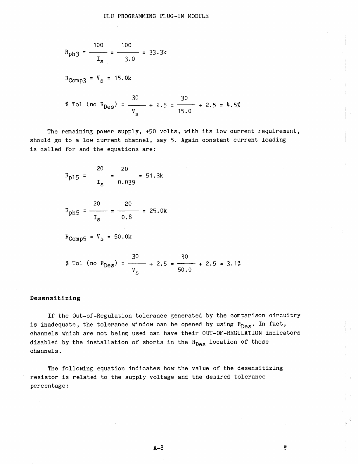
PROGRAMMING
ULU
PLUG-IN
MODULE
The
should
called
is
Rph3
Rcomp3
Tol
%
remaining
to
go
for
Rpl5
Rph5
=
=
(no Rnes)
a low
and
=
=
100
Is
vs
=
power
current
equations
the
20
Is
20
Is
100
= =
3.0
15.0k
30
=
vs
supply,
channel,
are:
20
= =
0.039
20
=
0.8
=
33.3k
2.5
+
volts,
+50
say
51.3k
25.0k
=
5.
30
15.0
with
Again
2.5
+
low
its
constant
=
4.5%
current
current
requirement,
loading
Rcomp5
%
Desensitizing
the
If
inadequate,
is
The
which
by
following
is
channels
disabled
channels.
resistor
percentage:
vs
=
Tol
(no Rnes)
Out-of-Regulation
the
are
installation
the
related
50.0k
=
=
tolerance
being
not
equation
the
to
30
2.5
+
vs
tolerance
window can be opened by
used can have
shorts
of
indicates
supply
how
voltage
30
=
50.0
generated
their
the
in
the
and
Rnes
value
the
2.5
+
the
by
using
OUT-OF-REGULATION
location
of
desired
%
1
3.
=
comparison
Rnes·
of
desensitizing
the
tolerance
those
circuitry
fact,
In
indicators
A-8
@
Page 89

In
circuitry
that
to
would
substitute
Rnes
example above
the
channel
in
volt
+50
Rnes5
ULU
=
%
five
supply,
those
=
PROGRAMMING
30
Tol.
the
was
and a
values
30
nominal
calculated
tolerance
obtain:
to
30
----------
10
30
50.0
PLUG-IN
2.5
percentage
to
of
2.5
-
MODULE
tolerance
3.1%.
be
were
10%
4.35k
=
that
If
desired
the
of
were
instead,
comparison
inappropriate
we
A-9
Page 90
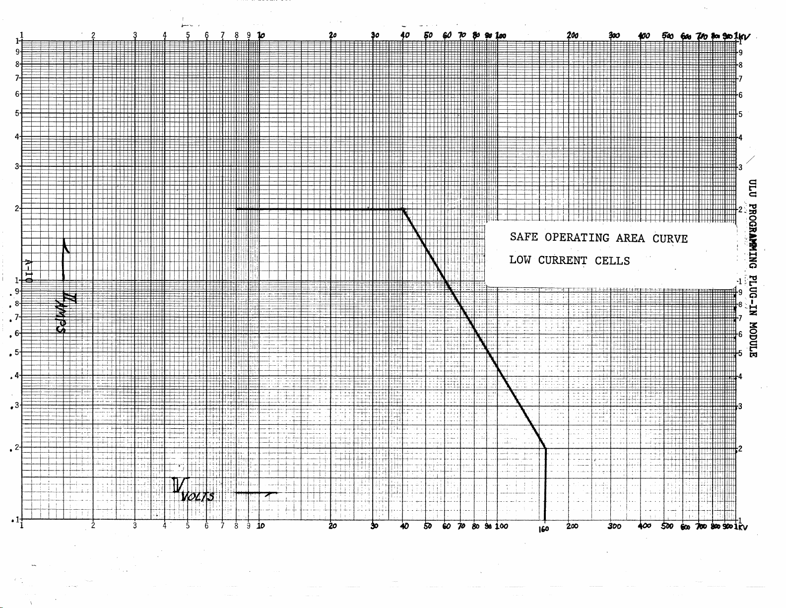
1 2
,__
7
9
8
2
1
1 1
11
1
~
r r
iD
~
~
r
~
~
~
1
~
1 1
~
1
~
~1111111111111111111111111111111111111111111111111111111111111111111111111111111111111111111111111111111111111111•1111111111111111~
61
51
4
3
I
'1
Iii
I
llllllllllllllllllll!lllllllllllillll!llll!llll1illl
I I I I I I I I I I I
11111111111111111111111111111111111111111111111111111111111111111111111111111111111111111111111111111111111111111111111-+wm1111111111111111111111111111111111111111r
I I I I I I I I I I I I
1111111111111111111
:
I I I I I
111111111111
I
11111111111111111111111111111
I I I I I I I I
1111
ITFTTTFI
1111111111
I
111111
I I I I I I I I I I I
I I I I
Ii
TTrrr
illlllll1lllllllllll!lllllllllllllllllllillil!ll,i!I
1111111111111111111
I I I I I I I
11111111111111
I
1111111111111-111111111111:111
I I I I I I I
!
11111111
N
' liliilil1lif11
,
+-H-H'NTii
''
!
11111111
1111
I
I'
,I''
,rr
1
i
lt!I:
m11~1tl
:w:
'.rtl
'1iT:
10:
~_;_
I
I I
I I I
I
ll11T1111lil!!ill1111llllll1llllllllllllllllllllllll6
I I I I I I I I I I
i:
I I I I
;
I I I I I I
,=fi-'-
m+
H+tff1T~-
SAFE
OPERATING
1111111111111111111
I
1
I I I I I
1111
'
_Li_!
tm
AREA
I
111111111111111111111111111115
11111111
I I I I I I I
I
111111111111111111111113
CURVE
/
"~~~!
IE-l-++--::-:t-~~-IT$,-:-
=r=rn=c-+:=µ"
'lE'
•
11
'
i
lltf..'.._;_®•
tLL
_ · :
~--
1
I I
>-+·-i=i_-=;_J_l_L~~~-1-~l_~~tjsrl~~
i
__
~_Lf--
·~~'
...
.,__:
i--:--~-,-
'1-t~!tmµ':fit.~
,---
!
I I :
Tij_
!
I
-i-.~ffi'
-s0
i-~~
:;
I I
l
':
!
-·~_:_
~-~~
~:c-"-
J
___
~_
2 3 4 . 5 6
-~!±:ff;JBf!~f~1:~~~1:~~~=~~r-H~-f-£:~~~:-w:~?#>~~fi~r~,
~_,
-.,---t··
~r-~·
_,Tr"
•~-'-t
L_,
·-
_,
I
'
: : ' I
'
I .
' :
:
I
t
I I I
' '
I
I
:
I I
.:_~·'
:'
'._\
.....
m-~T~-~-
:]
1
~-;:~:1~+1'.
~l~;
--~--~:~~--ti
!~--~
!1,
1!'
: I
-+
l~-c-Lf-
,L,OO'i''
It~
;l~n
,j1
l
11
j
11
:1
r:
i
tll~:
fr::*·
,~Ji,:~
i "
:~--'.
+
7
--L--,_._,.--r-·
'
!
I
:
I
---t-·f-1-~---1-w,_·
:~.
:=
.B-t=~
1
1,
,.
I
!
I
l
IL:...
...
.,.
8
·--;-T+iiffr't·
~
..
:
-----~-L-:-
..
::.
...
~-
-
~-+
9
.10
--'-------
I
-~·--
~=R~
I
--LL----
--~-L.
-~
-··
I
I
I
i
'
i
;_t-'.=trr'
-rrttr--
I
I
I
I:
i.J..L
~~-~--f~~J;:~]~
L
-~
11-.j:-.
20
·-•
i :
~
I
'
I
I
I
I
-----
:-.
·+'-:~L.
30
F~~r-~-.
;--1
""'
I
',
I
,_
..
~1-:+-·1·
:-:~-1~:.::1::
-
~
..
-
-
....
: ' '
--
--
«>
,.
--~
--.,.·r·:
'!
':
-~
~
60
_.
.......
',
7D
:1::::1
,
.
80
96
-1-
·.~.--
..
\'
..
100
:
•
_,
'
200
l
I
:-
:
:
~
.
300
''°
:~2t~~~l?-tfJffil±MIB3
,-
tt-l:±J-f-!·H
--~.:_-::=-tt.;_;_j_j..w+;.
-·----1-r-
~
400
+
•~+++l+l+H
_(~~
F++++++tt+t+H
1,
M
+"J
I
1
>~L!~,11.111
'1'
ltli
I
!·
Ir»
....
90D
l(V
Page 91

...
j
9
.2
.3
.ey
.9.?.?.91
2 4
5 6 7 8 9
JD
8
7·
6
20
3<l
"'°
S'8
•o
10
t•
91
8
7
1-6
sl
I I I I I I I I
llllllllllllllllllllllllllllllllllllllllllllllllllll
I I I I I I I I
lllllllllllllllllllllllll!ll!llllllllllllllWl1l
I I l)tmttllllllllllllllllllllllllllllllllllllllllllll
4 I I I I I I I
-+---
3
'
':
t)
-t-H--'---j!T
I I I I I I I I I I I I I I
: : : : : : : : : : : : : : :
I I I I I I I I I I I
2
I I I I I I I I I I l : ' I I I I I I I I I : I ' I
I I I I I I I I I I I I I I I I I I I I I I I
I'
11
11
I I I
1
1
-:""
··9==+-
.,8,___,____._..
,___
--+-+
7
I
J--
>---
• 6 >----
-·
>----
5
1-----+--+--+--+-__._.+-'--+,-I~
•
----r-1-
4
•
--~1-
--t--+-t----1--~
,_.,__._____._-+---1-----1-----i----- _-.'_,_
I
I ! - i i I
=r~_:-
;r
~~
• , ++,, ' :di:i_'
' ' '
; I '
I I ! I ' ' :
I I I
I ' ! I I '
.3
=ri=-t+===~-~-r
11
1
i , !
---I-
~~T--·-
·-
1->---j--
I
+--r- : ' i - >
~-1-t-h--
---::::--=-~-~
-t-__:
~--,.-
·-·
11
I I I I I
I:
l·I
11
: : : ' :
I I I I I I I
11 I 111
111
If
1'
I I I I I I I I I I ! I i I i i - J I . i I I ! I
1tT1
I : I 1 i
11
;~:;;::·~-=
-
-~
t--+
_J.,
,--+
-t-+l._~--
~
-r-·-t--'-
+--++-+
--r-
H-1tt
f-+
1
! I I I ' '
Ii
-'-
~-~-:---:
U
'i
__,____::
_;
.L+
:-:
~--
-"--
.,,J
J1J
~::i:;~-
-C
: I I : : : : : : I __LJ I - I : : : ;
i I I
I 1 I : i
,µ_w_
ill
I
111 i 11
I!
I'
I.
1
j ; i I
1
I
Ii
I:
1
1:
I 1111
!l:i
I
111,1,
1 lil-J-:ll l 1t
!
It'
I
+4i
i ! I
ILi
!j_w
J;,;
11
I I I · I I ! : I I I i ! ' . : - I I ; ! I
i : I : : ; :
I I
,:~~:~r--H;:
tc-
j_l
+
+ -+----; ! ,
iU
ii
+7:
•-----"
>-
+ '
1-f,17
I ! ' I
r12-:p:+tc:c2·
·''
H-"-t+-
•111"t>7L
-----
~l=---;..--:
-+--:-+---
+--:-.:,_
~---=--~:...~-==
,--;--J""
~-~--
,__:_J-+:j:
-i---1-----;-
1
~
-·
II
!
I''
·----~-
·-·---'"
-t------_;_
--f--·-•·-+
•----·
--·-
-·
·-.,---
-j
:--:
'
-·-----
--==
-. -: : :
-~:----=-~:~:_::::::-:
.,·+:-~-:·:
1
: : : I I ;
I I : I I I I i T I I ! i I
•I
I
i!i
:1
I~
~~
-~~::~~t~"·-~r_~l>~~~~~~:~;:
"T'.:':"..t'.
'·-+.
-+---d-·+;
r-•
-r-
I-~
re-•
_:-::~·
:·::;
:.·::.:
1
:~
:~::~
-H-
+-
I I ! I I I I I
I.
1
~
1
1
----++· _ .,
•
~_:.-f-__
-
:-·
::._
;_
;:_r
----~---JC
f
t-r
:_i_
T
MEDIUM
-7"'~~-1
,_
I
'.::_.r:~:~:
1
.:f:
-1:-~---~u~:l>:f::l·
I I J • i ' 111:-f-, l
__
; : : : : : : : ;
-+
: : : : : : : I
I I I ' , i ' I ' ' '
111
I!:
11
I I I i i :
i !
'._
"
~---1----
:-
1--<-
.c.
":
Ii
1
1 I i : I I I • : ' m - - r
1
I
:,
I::,~~-:+
1
'I~--~=
1
!
''
··t-t--·-~:·~;,:···
·-"-'·
:r~.
".t:.,,_
--:-~~-
_
7-:-:
_ ~ •--·
,~;·'
SAFE OPERATING
______
'.t':_·:l''.'.'_.
i ! I ' I I
. I I I
1
r-·-
CURRENT
--1---
i:
: :
:J ~ --
I:
Ii.
I :
I'
~
-
t-':-,-.
II
:
'i
I--'-
,__
·-
.....
:-
-- : -
....
..
--·--
•
~;··•
···-1::::··
Ff'-~
I j :
I l I
- L
• 2 -
-,
-+_L
·-
J
!
_
,..
AREA
-•
·-;-'
I~
"'Iii
""
+
~
•-+-+:~~-
-+
-~
-+
~
I :
f---:-:_L
+--
H---!--;
1-:
--
_I_ I _I
·-:
_L_i
;~-'
--
' I I
CELLS
1
:
5
I
I.
I
~
·-
- 3
-H---t
..
: : :
j
l 1 I !
'.
!
:n-,-:
i-T
;:
'Ill. : I
~_i_JJJ
-;
I
' _ j L
-,-
,_
~J]
~~
t-+-f-H~--111!1---H-t+-H-1-:-i-,-+-++-++++t-+--t-++t+++t+t+Ht--ttttt
' ! i ,
--
_L
,_
,,
: I
1--c
" , _ 1 i
1
I I I ' I i ; i
.:~,_~:~:!~;~~-:
~
·-~.r
·-
-~_:!·~·+~-
=-~~-Lt!::j
I • I 1 1
1
: I
CURVE
·"t:
___
:''f-"'.'l.'.'"f"F'f
1·
::\~,-lj___]f:
-i-;<---l--t-j-
+H
• :
llli!
-f
:•
~-f-
I I ? d
~
1-1-1
~
I '
~
- 8
:l'liri
1'
__
I'~
I
~..
I
I 2
~"
,:,,,rn
f 8 Q
-1-1 6
-----
I -
--~-
< I l -
I:
I I -
---:·T
-T-
,--
r-L
-r
f-r+It-h,-HH-+tt+++
I 1
. I 4
4
d
~
.-.,
11't9
::u
"'
i:
t;!
1 Cl
9,~·
1
7 H
2:
i
3:
' 0
.._,
- ?
11>"18
3
tttiiill
2
,
~-:<------
__ : __
~l-
:~----
.
-·
--+--'---~~---<-:·--.--
.
:1
,--
. '
• 2
···:I---:~-~-~,.;
----·
""
-·-
---:
·::·
~~-
,3
• 4
._:t~-cr
'------~--'-ii'.
<---
·-:
,5
~:~:w·-·
- -
i
·-
·-1
.6
.7
.,8
~
-
:---:
..
--·
----·----
-;-: ' '
.9
.
1~-~:
·-
---
---
: . . -. --. - .
·-----
-
-'
2
.3
4 6 3
~1-
. . . .
·-
:i·
5
I I .
9 1C
2.o
30
-40
&J
-··:1:1;_
---
_,;,
·t.
io
7o
::
... :.
:::
so
!o'-1ao
Page 92
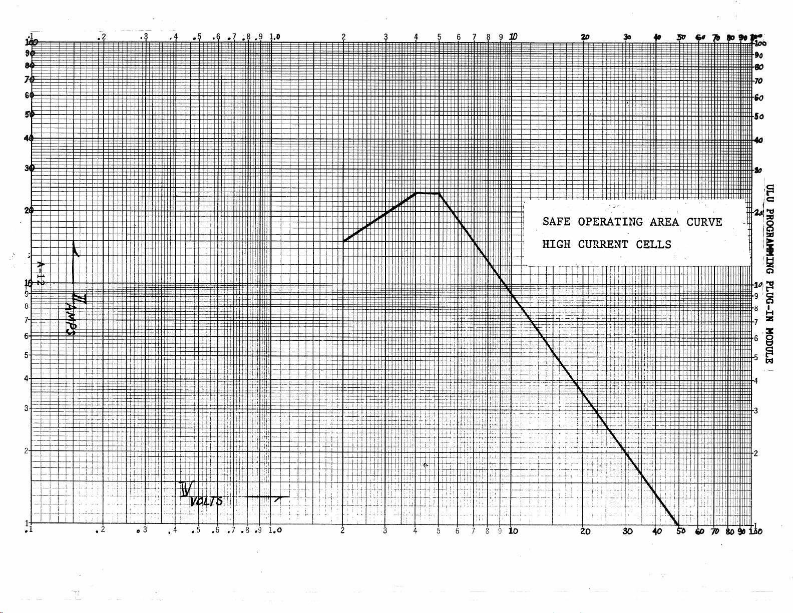
..
·1-
.2
• 6
•
7 •
~
•
9
l.O
2 4
9
l
sfml----l-~tttt+--+-+---+-+!
5'0
I I I I I I I
l-f-t-11
I
!
I I II II I
l-+--+-+l
I
l-+++-111
1-IH+
111
IH+++l
I I I
II
1111111111111
+++-1-1111
+-+-+-111
II II I
++-HI
111-++-HI
I I
I-++++!
I I I
+++++-11111
H+l++-11111
II
11111111111111111111111
IH+-l
II
+--+-I
I
--+-+I
1-+-+-I
I I I I I I I I I I
l--+-t-11
++--+I
I l-+++l I
II
II I
l+++-111
+-+++I
I I I
II
1111111111111
l-++-l-+l
I I I
l+H+-1111
5
+-+-+-111
++-HI
I I
I II I I
6 7
IH-++-111
H+HI
1111-+++HI
I I I
l++-H+l
II
111111111111111111
9
I I I I
ll-l+H-1111
1D
-+-41
11--+-I
+-l-1 I
2D
-+-+-l#+--++l
l-+-++l
I
l.++-+-111
3o
sm·H-++'
++++++-111111
.fo
3t1
\lUTl
I I I I I I I I I I I I I I I I I I I I I
~
7IJ
fD
..
Ill
rioo
I I
II
to
80
·70
'°
50
...
e
j
•
~
1--1-.
l - .
l
r
,
6
5
1
2
~
I
.ttlill
I I I I I I
~
~
_;:
1
1
1 1 1 ·
1
i
-+-f-r-.-'-~-++~
1
'
1
1 1 1
11111111·111
1 , 1 1
~.rt._:
..
·
,:1
·
_tlf±ftr
1
1 1 1 1
11
1
11.J..W..l-l-l.1.i+ttttt+r-++-1
1
~.I
;
,_j.
t
I
:ff_
'\_,~_::t:.·t=_W
,
~ilii1~1r~F~1=llu
'-'.::
-m+t"_,·~
llllllllllilllllllllllll!lllll!,tlllllllllllil'l\ililll
1
1 1 1 1
1
1 1 1
1+++++1:11:
I
+1:
!
. '
1
·
----f-
f-j-,-l-Tt-t-'-'-i+
"""
H
111111
1 1
'-lHf.flP-i:t±tj
ru~~~=r.....
H++++T+ffit~'v
~w,-IfF;;FT~::r--~·
r:~mr1H=R~ffJ.~t~tr~f:;f:~~;::
ii
....,
+-~~-+-
··1"'-~~
• I
1~
-:_-:
.
~-
SAFE
HIGH
I
rrrr
+-+-.~+++t--ct
1--:::t:
-~
,..:..,..._~::.i=-+----~~·-'·~-·~f-
~T-'+.
t=t:
-~-=i==+-:.::±-"
+.
-c---1--~f---+
.J
'\t.:
-'
, - •. -
j-~=-i::.
-,..
,.
-~t=r-L'~·--
1
~
1
I
:--:-:i---:-L:
__
~~f':
OPERATING
CURR.E~T
rin~~:rrn
-+
i-+·
:~·····r-r++T
t-
-··
f--
...
.::t:.:f--
~:-:.:·
--
~-
r--'-'-
·-,---+
f
.•
: '
t
t'
rt
~t-
-~
'..,l:·Ei~=lr~i1fa~~++tOOmtHt1itR+Jtm++ttH
rn
I
I
I_
I
; .
c-'-f-L+
·"+-'
't-++'
c--i-'
-·-
e-+-
'-·+
_j~
---+..!.
~i-
d
_1-:-~_Ll~t~
!I~''
~~t
c.ljttt:t::""F.'lf'
AREA
CELLS
.
;i~
I\
I
I I
~
+H-
1+11 ..
tc.!:tH·
·;-::i-t-++++++++++++
1
J.
1
:
F
1
r-++rn+ITTtrnml1T11
CURVE
·
1
11
1 1
111111111111
.,
Jo
'C:
:t"'4
~·~
11
r
1z1
Cl
l"I
toU
c-4
9
I
c:
·
-
·8
I
L...I
r--1
7
:ZS
,.:r:
6
0
t:1
~
2
~
1--t--+-+-L+
1
.1
!
·--·--~-
i
.
'
.
•-•-'·
·r"·-'-•
.q,
,i::l!iljr.1!'f;'}
1
,
-
~'
-+-''
1
~;:'
j
Lu
0
3
I
4
'1
·.
it
I'
'-,.
.....
I'
1"'/i:1'm
:
ril
H
.7
.6
.8
.5
1,'
.9
:
l,O
--+-··-
,
I
: : \
-
ft'fj
'j'
'
2
4
3
5
7
6
8
9
10
20
30
~o
S-0
io
7D
io
9o
ilo
Page 93

Tektronix
No.
Part
PROGRAMMING
Quantity
PROGRAMMING
ULU
PLUG-IN
MODULE
REPLACEABLE PARTS LIST
PLUG-IN
(UNPROGRAMMED) CHASSIS ASSEMBLY
067-0919-99
Description
670-6047-00
131-0097 -00
131-0293-00
200-0551-00
333-1367 -00 1
386-1447-47
386-1402-04 1
386-3657-01 1
426-0499-07
426-0505-07
064-04
-1
337
348-0235-00 2
058-00
366-1
105-0075-00
105-0076-02
095-00
214-1
214-1280-00
054-00
214-1
214-1061-00
211-0105-00
211-0116-00
213-0192-00
220-0547-01
334-3663-01
334-1378-00
004-07 48-00
004-0241-00
004-0243-00
004-0242-00
1
2
1
1
1
1
2
1 BOLT,
6
1
1
1
1
1
1
1
6
7
6
1
1
1
2
1
1
ECB, Programming plug-in, Unprogrammed
(Complete)
Contact
CONNECTOR, Female,
CONNECTOR, Male,
COVER, Plug-in ext,
PANEL, Front
SUBPANEL,
SUBPANEL,
SUPPORT, Plug-in
FRONT SECTION, Plug-in,
FRONT SECTION, Plug-in,
SHIELD, Elec, Plug-in Side
SHIELD GASKET, Elec.
KNOB,
RELEASE
PIN, Spring, 0.187
SPRING, Helical,
SPRING, Flat
CONTACT,
SCREW, 4-40
SCREW, 4-40
SCREW,
NUT, 4-40
MARKER,
MARKER,
BOX, Shipping, 19.55 x 9.0
CUSHION
CUSHION
CUSHION
Front
Rear
0.625
Gray,
Latch
BAR, Latch
Elec,
0.188, Flathead
x
x 0.312, Double Sems
6-32 x
0.500, Fillisterhead
l.D.
l.D., Ser.
MATL, Pkg, 1/2
MATL, Pkg, End Cap, Front
MATL, Pkg, End Cap, Rear
32
Contact
36
Plastic
Top
x 0.485
0.255
x
OD, Stl-Cd-PI
0.1
L x
Music Wire
Cu-Be
No.
x 9.55 in.
Bottom
in.
@
A-13
Page 94

PROGRAMMING
ULU
PLUG-IN
MODULE
Circuit
CR5001, 5002,
5005, 5006,
5010,
5015, 5016,
5020,
5025, 5026,
5030,
5035, 5036,
5040, 5041,
5045, 5046,
5050,
5055, 5056
No.
5011,
5021,
5031,
5051,
ELECTRICAL
PROGRAMMING
Tektronix
Part No.
670-604 7-00
152-0141-02
CIRCUIT
670-604 7-00
PARTS
BOARD
Description
ECB, Programming
(Complete)
DIODE,
LIST
(UNPROGRAMMED)
1 N4152,
plug-in,
Signal, Si.
Unprogrammed
00011,
5021, 5022,
5031,
5041, 5042,
5051, 5052,
5061, 5062,
5071, 5072,
5081, 5082,
5091, 5092,
5101, 5102,
5111, 5112,
5121, 5122
05013, 5014,
5023, 5024,
5033, 5034,
5043, 5044,
5053, 5054,
5063, 5064,
5073, 5074,
50~3.
5093, 5094,
5103, 5104,
5013, 5014,
5012,
5032,
5084,
151-0188-00
151-0190-00
TRANSISTOR,
TRANSISTOR,
2N3906,
2N3904, Signal, NPN,
Signal, PNP,
Si.
Si.
A-14
Page 95

ULU
PROGRAMMING
PLUG-IN
MODULE
Circuit
5123, 5124
05015, 5016,
5025, 5026,
5035, 5036,
5045, 5046,
5055, 5056,
5065, 5066,
5077, 5078,
5087, 5088,
5097, 5098,
5107, 5108,
5117, 5118,
5127, 5128
05017, 5018,
5027, 5028,
5037, 5038,
5047, 5048,
5057, 5058,
5067, 5068,
5075, 5076,
5085, 5086,
5095, 5096,
5105, 5106,
5115, 5116,
5125, 5126
No.
ELECTRICAL
PROGRAMMING
Tektronix
Part No.
151-0443-00
151-0444-00
CIRCUIT
PARTS
BOARD
670-604 7-00
(UNPROGRAMMED}
Description
TRANSISTOR, MPSA92, Signal, PNP, Si.
TRANSISTOR, MPSA42, Signal, NPN, Si.
LIST
(Cont.}
R5001, 5002,
5018, 5019,
5035, 5036,
5051, 5052,
5066, 5067,
5081, 5082,
5109, 5111,
5125, 5127,
5141, 5143,
5157, 5159,
5173, 5175,
5189,
5191
321-0289-00
RESISTOR, 10.0K, 1/8W,
A-15
1%,
Mtl. Flm.
Page 96
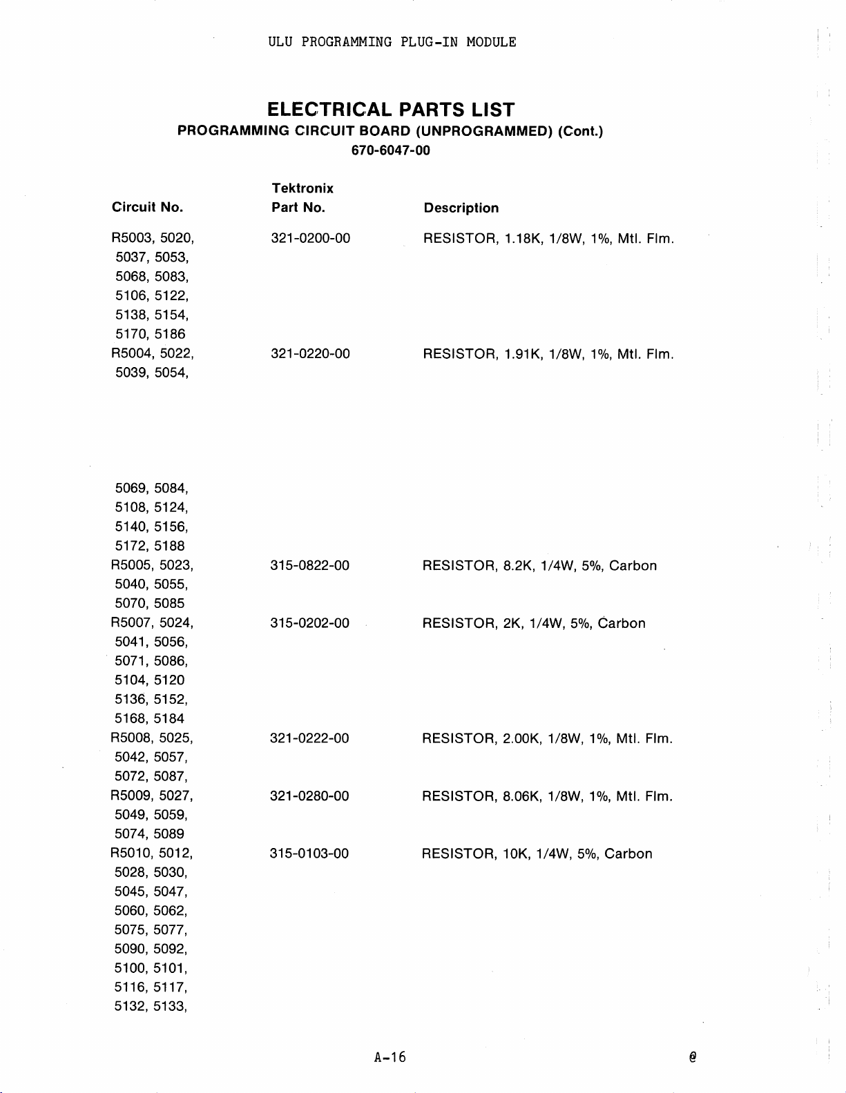
Circuit No.
ULU
ELECTRICAL PARTS LIST
PROGRAMMING
Tektronix
Part No.
PROGRAMMING
CIRCUIT
BOARD {UNPROGRAMMED)
670-604 7-00
PLUG-IN
Description
MODULE
{Cont.)
R5003, 5020,
5037, 5053,
5068, 5083,
5106,
5122,
5138, 5154,
5170,
5186
R5004, 5022,
5039, 5054,
5069, 5084,
5108, 5124,
5140,
5156,
5172, 5188
R5005, 5023,
5040, 5055,
5070, 5085
R5007, 5024,
5041, 5056,
5071, 5086,
5104, 5120
5136, 5152,
5168, 5184
R5008, 5025,
5042, 5057,
5072, 5087,
R5009, 5027,
5049, 5059,
5074, 5089
R5010, 5012,
5028, 5030,
5045, 5047,
5060, 5062,
5075, 5077,
5090, 5092,
5100, 5101,
5116, 5117,
5132, 5133,
321-0200-00
321-0220-00
315-0822-00
315-0202-00
321-0222-00
321-0280-00
315-01 03-00
RESISTOR,
RESISTOR,
RESISTOR,
RESISTOR,
RESISTOR, 2.00K,
RESISTOR,
RESISTOR, 10K,
1.18K, 1/8W,
1.91K, 1/8W,
8.2K, 1 /4W,
2K, 1/4W,
8.06K, 1/8W,
1/8W,
1/4W,
5%,
5%,
5%,
1%,
Mtl. Flm.
1%,
Mtl. Flm.
Carbon
Carbon
1%,
Mtl. Flm.
1%,
Mtl. Flm.
Carbon
A-16
Page 97

PROGRAMMING
Circuit
5148, 5149,
5164, 5165,
5180,
R5014, 5031,
5048, 5063,
5078, 5093,
5112, 5128,
5144,
5176, 5192
R5016
R5017
R5032, 5049,
5064, 5079,
5094,
5130,
5162, 5178,
5194, 5015
R5096
No.
5181
5160,
5114,
5146,
ULU
PROGRAMMING
PLUG-IN
MODULE
ELECTRICAL PARTS LIST
CIRCUIT
Tektronix
Part
No.
315-0102-00
315-0562-00
315-0511-00
315-0563-00
308-0643-00
BOARD
670-6047-00
(UNPROGRAMMED)
Description
RESISTOR,
RESISTOR,
RESISTOR, 510, 1/4W,
RESISTOR,
RESISTOR,
1
5.6K, 1 /4W,
56K, 1 /4W,
.1
K,
ohm,
(Cont.)
1/4W,
3W,
5%,
5%,
5%,
5%,
Carbon
Carbon
Carbon
Carbon
3%,
WW
R5102, 5105,
5118, 5121,
5134, 5137,
5150,
5166, 5169,
5182, 5185
R5107,
5139, 5155,
5171, 5178
@
5153,
5123,
315-0302,;,00
315-0912-00
A-17
RESISTOR,
RESISTOR,
3K, 1/4W,
9.1k, 1/4W,
5%,
5%,
Carbon
Carbon
Page 98

Page 99

CHANNEL 7
CHANNEL
8
CHANNEL 9
CHANNEL
10
CHANNEL
11
CHANNEL
12
CHANNEL
~).
1
CHANNEL
2
CHANNEL 3
CHANNEL4
CHANNEL 5
Component
PROGRAM
6
70-6418-00
Location
BOARD
CHANNEL
670-6047-00,
& 6
70-6419.-00
6
Diagram
 Loading...