

Page 1
TEK-CPCI-1000
CompactPCI Single Board Computer
TECHNICAL REFERENCE MANUAL
NOTE:
This manualis for reference purpose only.
Reproduction in whole or in part is authorized provided
TEKNOR INDUSTRIAL COMPUTERS INC. is cited as
the original source.
VERSION 2.1
May 1998
ref.: M1000_2.1
Page 2

READ ME FIRST
EXERCISE CAUTION WHILE REPLACING LITHIUM BATTERY
WARNING
Danger of explosion if battery is incorrectly r eplaced.
Replace only with th e same or equivalent type recommended by the manufacturer.
Dispose of used batteries according to the manufacturer's instructions.
ATTENTION
Il y a dan ger d’explosion s’il y a remplacement incorrect de la batterie.
Remplacer un iquement avec une batterie du même type ou d’un type équivalent
recommandé par le constructeur. Mettre au rebut les batteries usagées
conformément aux instruction s du fabriquant.
ACHTUNG
Explosionsgefahr bei falschem Batteriewechsel.
Verwenden Sie nur die empfohlenen Batterietypen des Herstellers. Entsorgen Sie
die verbrauchten Batterien laut Gebrauchsanweisung des Herstellers.
ATENCION
Puede explotar si la pila no este bien reemplazada.
Solo reemplazca la pila con tipas equivalentes segun las instrucciones del
manifacturo. Vote las pilas usadas segun las instrucciones del manifacturo.
Read Me First 1
Page 3

TABLE OF CONTENTS
PART 1
1. PRODUCT OVERVIEW.............................................................................. 1-1
2. ONBOARD SUBSYSTEMS........................................................................2-2
2.1 CONNECTOR LOCATION............................................................................2-2
2.2 ONBOARD CONNECTORS..........................................................................2-2
2.3 REAR-PANEL CONNECTORS.....................................................................2-2
2.4 FRONT PLATE CONNECTORS...................................................................2-2
3. COMPATIBILITY WITH TEKNOR PRODUCTS.........................................3-2
4. UNPACKING..............................................................................................4-2
5. SAFETY PRECAUTIONS ..........................................................................5-2
5.1 STATIC ELECTRICITY.................................................................................5-2
5.2 STORAGE ENVIRONMENT.........................................................................5-2
5.3 POWER SUPPLY.........................................................................................5-2
i
Page 4

TEK -CPCI-1000 Technical Reference Manual
PART 2
6. CUSTOMIZING THE BOARD....................................................................6-2
6.1 PROCESSOR AND FAN.............................................................................. 6-2
6.2 INSTALLING MEMORY................................................................................6-2
6.3 ENABLING MEMORY CACHE......................................................................6-2
6.4 CONFIGURING THE BOARD.......................................................................6-2
6.5 BIOS BOOT OPTIONS.................................................................................6-2
6.6 INSTALLING SUPERVISOR UTILITIES........................................................ 6-2
6.7 INSTALLING THE BOARD INTO A BAY.......................................................6-2
7. CONNECTING DEVICES...........................................................................7-2
7.1 SUPPLYING POWER ON THE TEK-CPCI-1000...........................................7-2
7.2 CONNECTOR LOCATION............................................................................7-2
7.3 SERIAL PORTS CONNECTORS (J4)...........................................................7-2
7.4 PS/2 MOUSE CONNECTOR (J8).................................................................7-2
7.5 KEYBOARD CONNECTOR (J9) ...................................................................7-2
7.6 USB CONNECTOR (J7) ...............................................................................7-2
7.7 PARALLEL PORT CONNECTOR (J3) ..........................................................7-2
7.8 10BASE-T CONNECTOR (J12).................................................................... 7-2
7.9 MULTI -FUNCTION CONNECTOR (J 2) .........................................................7-2
7.10 MISCELLANEOUS DEVICES.......................................................................7-2
7.11 CONNECTING STORAGE DEVICES...........................................................7-2
7.12 BATTERY BACKUP CIRCUIT.......................................................................7-2
8. INSTALLING VIDEO..................................................................................8-2
9. CONFIGURING DMA & IRQ ......................................................................9-2
9.1 ALLOCATING DMA CHANNELS..................................................................9-2
9.2 ALLOCATING IRQ LINES............................................................................9-2
10. SETTI NG JUMPERS ...............................................................................10-2
10.1 JUMPER LOCATION..................................................................................10-2
10.2 CPU MODEL SELECTION; W1 AND W2....................................................10-2
10.3 JUMPERS W3-W 7.....................................................................................10-2
10.4 JUMPERS W8-W 13 ...................................................................................10-2
10.5 JUMPERS W14-W19 .................................................................................10-2
ii
Page 5

Table of Contents
PART 3
11. POWERING UP THE SYSTEM................................................................11-2
11.1 POWER UP...............................................................................................11-2
11.2 TROUBLESHOOTING................................................................................11-2
12. SOFTWARE SETUP................................................................................12-2
12.1 AWARD SETUP PROGRAM ......................................................................12-2
12.2 VIP-UP PROGRAM....................................................................................12-2
13. VFLASH SOFTWARE..............................................................................13-2
13.1 INTRODUCTION........................................................................................13-2
13.2 RUNNING VFLASH....................................................................................13-2
13.3 OUTPUT SELECTION................................................................................13-2
13.4 FILE SELECTION.......................................................................................13-2
13.5 FILE TRANSFER........................................................................................13-2
13.6 BATCH MODE ...........................................................................................13-2
14. FLASH FILE SYSTEM II.........................................................................14-2
14.1 INTRODUCTION........................................................................................14-2
14.2 SETTING UP CONFIG. SYS FOR FLASH FILE SYSTEM............................14-2
14.3 CREATING & FORMATTING A MS-FLASH PARTITION............................. 14-2
15. UPDATING THE BIOS WITH UBIOS.......................................................15-2
15.1 INTRODUCTION........................................................................................15-2
15.2 UBIOS - INTERACTIVE MODE ..................................................................15-2
15.3 UBIOS - BATCH MODE..............................................................................15-2
16. V T100 MODE........................................................................................... 16-2
16.1 VT100 REQUIREMENTS............................................................................16-2
16.2 VT100 SETUP & CONFIGURATION...........................................................16-2
16.3 RUNNING WI THOUT A TERMINAL ...........................................................16-2
iii
Page 6

APPENDICES
PART 4
A. BOARD SPECIFICATIONS .......................................................................... A-1
B. MEMORY & I/O MAPS .................................................................................B-1
B.1 MEMORY MAP DIAGRAM .............................................................................B-1
B.2 I/O MAPPING.................................................................................................B-1
BOARD DIAGRAMS ............................................................................................ C-1
C.1 MECHANICAL SPECIFICATIONS .................................................................C-1
C.2 ASSEMBLY - TOP DIAGRAM........................................................................C-1
C.3 ASSEMBLY - BOTTOM DIAGRAM ................................................................C-1
D. CONNECTOR PINOUTS.............................................................................. D-1
D.1 MULTI-FUNCTION CONNECTOR - (J2)........................................................D-1
D.2 PARALLEL PORT CONNECTOR (J3) - STANDARD MODE.........................D-1
D.3 PARALLEL PORT CONNECTOR (J3) - EPP MODE .....................................D-1
D.4 PARALLEL PORT CONNECTOR - ECP MODE (J3) .....................................D-1
D.5 COM1 - RS-232 (J4A) .................................................................................... D-1
D.6 COM2 - RS-232 (J4B) .................................................................................... D-1
D.7 COM2 - RS-422/RS-485 MODE (J4B)............................................................D-1
D.8 PS/2 MOUSE CONNECTOR (J6)...................................................................D-1
D.9 USB CONNECTOR (J7).................................................................................D-1
D.10 KEYBOARD CONNECTOR (J9).....................................................................D-1
D.11 FAN CONNECTOR (J10)...............................................................................D-1
D.12 ETHERNET 10/100 BASE-TX RJ-45 CONNECTOR (J12) ............................D-1
D.13 CPCI-BUS CONNECTOR ..............................................................................D-1
D.14 CPCI-I/O CONNECTOR.................................................................................D-1
v
Page 7

E. BIOS SETUP ERROR CODES..................................................................... E-1
E.1 POST BEEP...................................................................................................E-1
E.2 POST MESSAGES.........................................................................................E-1
E.3 ERROR MESSAGES......................................................................................E-1
E.4 POST CODES................................................................................................E-1
F. EMERGENCY PROCEDURE........................................................................F-1
F.1 EMERGENCY PROCEDURE.........................................................................F-1
F.2 GENERATE AN EMERGENCY FLOPPY DISKETTE:....................................F-1
G. LIST OF APPROVED VENDORS.................................................................G-1
G.1 DRAM (U18,19,20,22)....................................................................................G-1
G.2 INTERFACE CONNECTORS.........................................................................G-1
vi
Page 8

PRODUCT DESCRIPTION
1. PRODUCT OVERVIEW
2. ONBOARD SUBSYSTEMS
3. COMPATIBILITY WITH TEKNOR PRODUCTS
4. UNPACKING
5. SAFETY PRECAUTIONS
Page 9

1. PRODUCT OVERVIEW
The TEK-CPCI-1000 CompactPCI board represents the most advanced computer
architecture in the Single Board Computer world. The TEK-CPCI-1000 is based on
INTEL Pentium and AMD K6 processors, and is 100% electrically compatible with
INTEL’s PCI bus specifications.
The board is a 6U mechanical form factor (Eurocard format). It complies with the
CompactPCI design specification and takes advantages of the existent enclosures, cardcages, and fixtures widely used in applications such as: communications, military, or
medical.
CompactPCI is a practical extension to the common PCI local bus. It is dedicated to a
robust industrial grade computer ar ch itecture an d provides up to 132MB/sec of tran sfer
rate.
The TEK-CPCI-1000 board is fully compatible with existing application software and
operating systems available for desktop PCI: PC and MS-DOS
Windows
95, Windows NT, OS/2 Warp, QNX, NOVELL, UnixWare.
1-1
, Windows 3.1,
Page 10
TEK -CPCI-1000 Technical Reference Manual
CompactPCI Connectors
According to the PICMG 2.0 R2.1 CompactPCI
specification, CompactPCI connectors
are located at the rear of the board. They are defined as a 2mm pitch, shielded connectors
with a 5x47 arr a y of pin for signals and 2 rows of 47 pins for shielding.
If required, a coding key may be in stalled to ensur e a correct mating when connecting the
boar d to a CompactPCI backplane.
CompactPCI
Supported Processors
The TEK-CPCI-1000 supports: INTEL Pentium
200MHz
MMX
connector is also known as 2mm Hard Metric connector.
100, 120, 133, 150, 166 and
INTEL VRT Pentium
INTEL MMX
Pentium 166, 200, and 233Mh z
100, 120, 133, an d 150MHz
AMD K6 166, 200, and 233MHz
is for Multi Media eXtension, and VRT is for Voltage Reduced Techn ology.
1-2
Page 11

Product Over view
Environ ment
The TEK-CPCI-1000 SBC is provided for r ack-mounted syst ems which offer th e highest
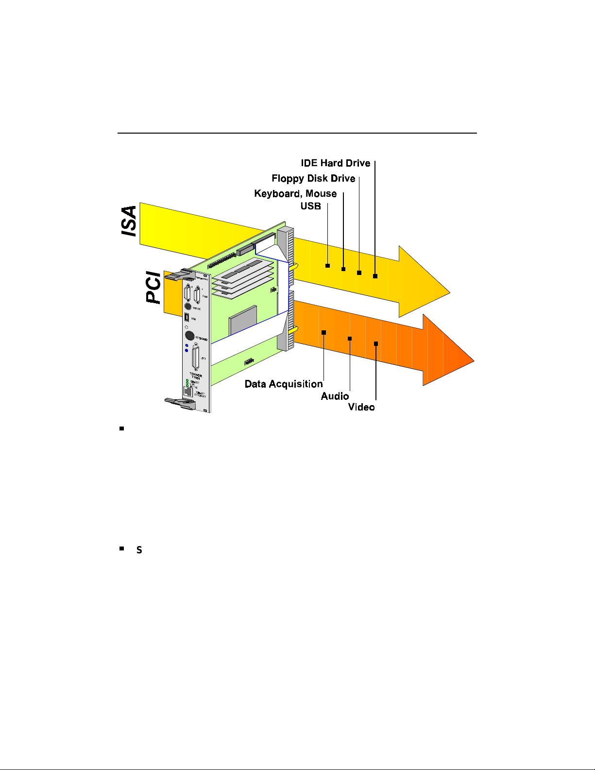
modularity for applications. The TEK-CPCI-1000 supports four CompactPCI connectors:
PCI
ISA
System memory
P1, P2 - System connectors: output the 32-bit PCI signals and provides
arbitration, clock distribution, and reset functions for th e periph eral slots of the
PCI segment. This segment will support up to seven CompactPCI sub-systems
(four bus master devices – with Ethernet disabled - and three slaves) such as:
Audio, Video, acquisition boards...
P4, P5 - I/O connectors: provide both ISA and IDE signals to support
connections of hard drives, floppy disk dr ives, mouse and keyboar d thr ough the
backplane. USB communication signals are also provided through this I/O
segment. The signal assignation on these connectors is defined by TEKNOR.
When connectin g the boar d to a backpl ane, en sure th e ba ckplane is capa bl e of
supporting these signals and of making th em available on separate local headers.
Such a backplane is provided by TEKNOR and is referred as TEK1101
CompactPCI Backplane.
A complete CompactPCI system (TEK-CPCI-1201) is also available from
TEKNOR.
Memory
: the TEK-CPCI-1000 supports from 8MB to 512MB vertical
DRAM on four 72-pin SIMM sockets (FPM or E DO). Par ity an d
ECC are supported.
Internal cache
External cache
: 8KB CPU-internal L1 cach e with Pentium processors.
16KB with MMX processor s.
32KB with K6 processors.
: 256 or 512KB (L2) pipelined burst cache is implemented to
enhance the processor operations by eliminating wait states on
cache accesses.
1-3
Page 12
TEK -CPCI-1000 Technical Reference Manual
TEK-CPCI-1000
'
''
+
*
*
+%
CompactPCI
*&
- Block Diag ram
%
/
&
(
*+
%+ (%,
!" #$ %!
& "!
'(
*
(
-.&
-.&
"
"
)
)
%! "
(
(%
%
*
1-4
Page 13

2. ONBOARD SUBSYSTEMS
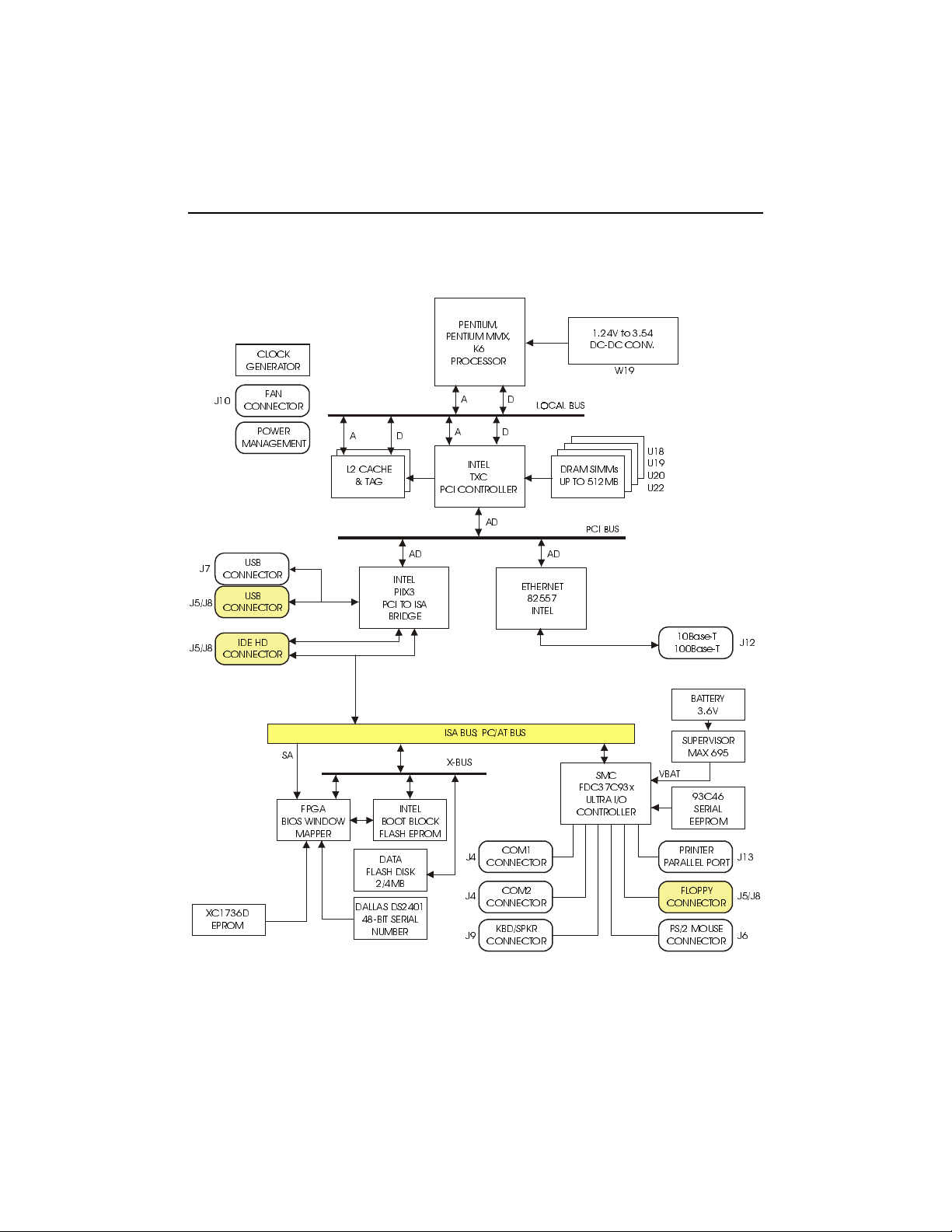
The TEK-CPCI-1000 sys te m board is built around a single c hip host -to -PCI br idge (430HX
from INTEL) which makes the PCI bus accessible through 2mm Hard Metric connectors
for up to 7 loads: 4 masters, including the onboard Ethernet, and 3 slaves.
The 430HX interfaces with the onboard processor host bus and a dedicated memory data
bus, and provides second level cache (L2) and DRAM control functions.
The DRAM controller supports up to 512MB of main memory. Both Fast Page Mode
(FPM) and Extended Data Output (EDO) memory technology are supported. The PCI-toDRAM interface transfer rate can go up to 112MB/sec for read and 121MB/sec for write.
The 430HX allows the processor to sustain the highest possible bandwidth to the graphics
frame buffer at all frequencies. To conform with “modular” oriented environment, the
board does not provide video function. Video will be supported using a CompactPCI
video module connected directly on the PCI bus (Order T EK-1002 from TEKNOR).
Ethernet subsystem is directly connected to the PCI bus. As PCI target, this configuratio n
allows all accesses to the internal registers to be automatically mapped into free memory
and I/O space upon initialization of the system. The Ethernet controller chip operates as a
master and a slave on the PCI bus. As a master, it interacts with the system memory to
access data for transmission or deposit received data. As a slave, some internal control
structures are accessed by the CPU for read and write operations.
The Ethernet chip provides 3Kbyte FIFO for receive and 3Kbyte FIFO for transmit which
prevent data overruns or underruns while waitin g for access to the PCI bus. While the chip
provides independent Receive and Command units, the TEK-CPCI-1000 can process
communication commands and receive incomi ng frame simultaneously without real-time
CPU intervention.
The TEK-CPCI-1000 also provides a PCI-to-ISA bridge ( PIIX3) along with other fea tures
such as fast IDE interface, and USB.
2-1
Page 14
TEK-CPCI-1000 Technical Reference Manual
U18J8J4J1
J2B1J
3
J7J9J10S1U19U20U22J5J11J8
J13
J12
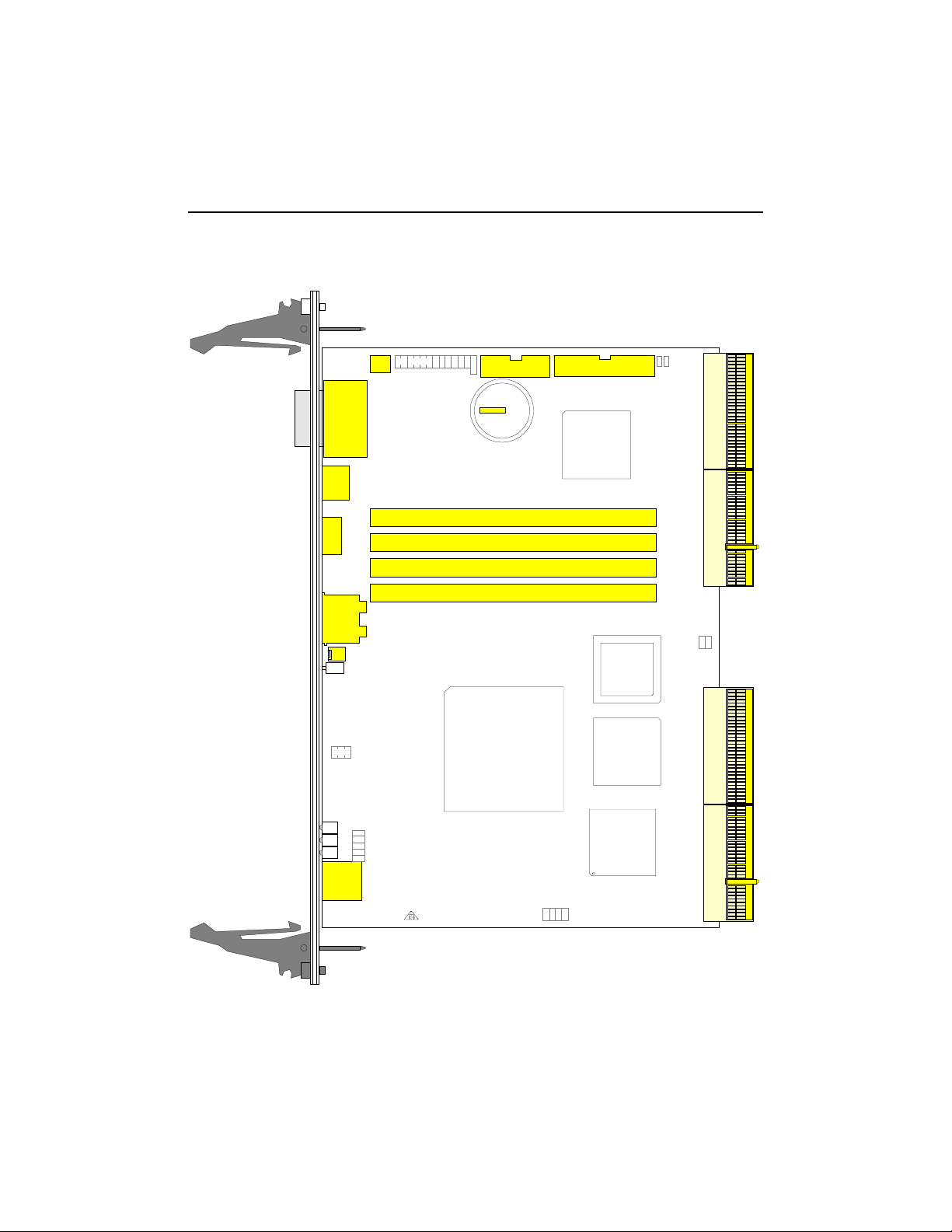
2.1 CONNECTOR LOCATION
W3 W4 W5
W7 W9
W6 W8 W10
W2
W11
W1
W12
W13
W18
DS1
DS2
W19
DS3
W15
W17
W16
W14
2-2
Page 15

Onboard Subsystems
2.2 ONBOARD CONNECTORS
Two connectors are used to drive various signals to the front plate:
Parallel Port (J3)
onboard connector to a standard 25-pin DSUB connector mounted on the front plate.
The Parallel Port is compliant with Standard, EPP and ECP modes.
Multi-function connector (J2)
hard disk activity functions are available through the J2 connector.
Features are described as follows:
- A flat cable is required to output the parallel signals from the
- Speaker, keyboard inhibit, download, reset, and
Speaker
Keyboard inhibit
Download
Reset
Hard disk activity
System Memory
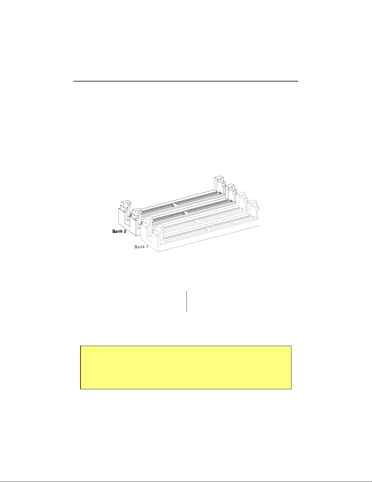
to support from 8MB to 512MB of DRAM system memory. The memory is divided
into two banks referred as Bank 0 and Bank 1.
Each bank can be populated separately, but must be populated with the same memory
capacity.
An 8ohm speaker can be directly connected. The power
stage is integrated onboard.
Keyboard inhibit function is used to enable or disable the
keyboard.
Download function is used to transfer information from a
remote computer to the Flash disk through a serial link.
A normally open push button can be used to reset the board.
Reset interface is open drain, thus external logic is not
required.
LED can be used to indicate read and write operations on
the hard disk.
- The TEK-CPCI-1000 provides four 72 -pi n ve rtic al SIM M so cke t s
2-3
Page 16
TEK-CPCI-1000 Technical Reference Manual
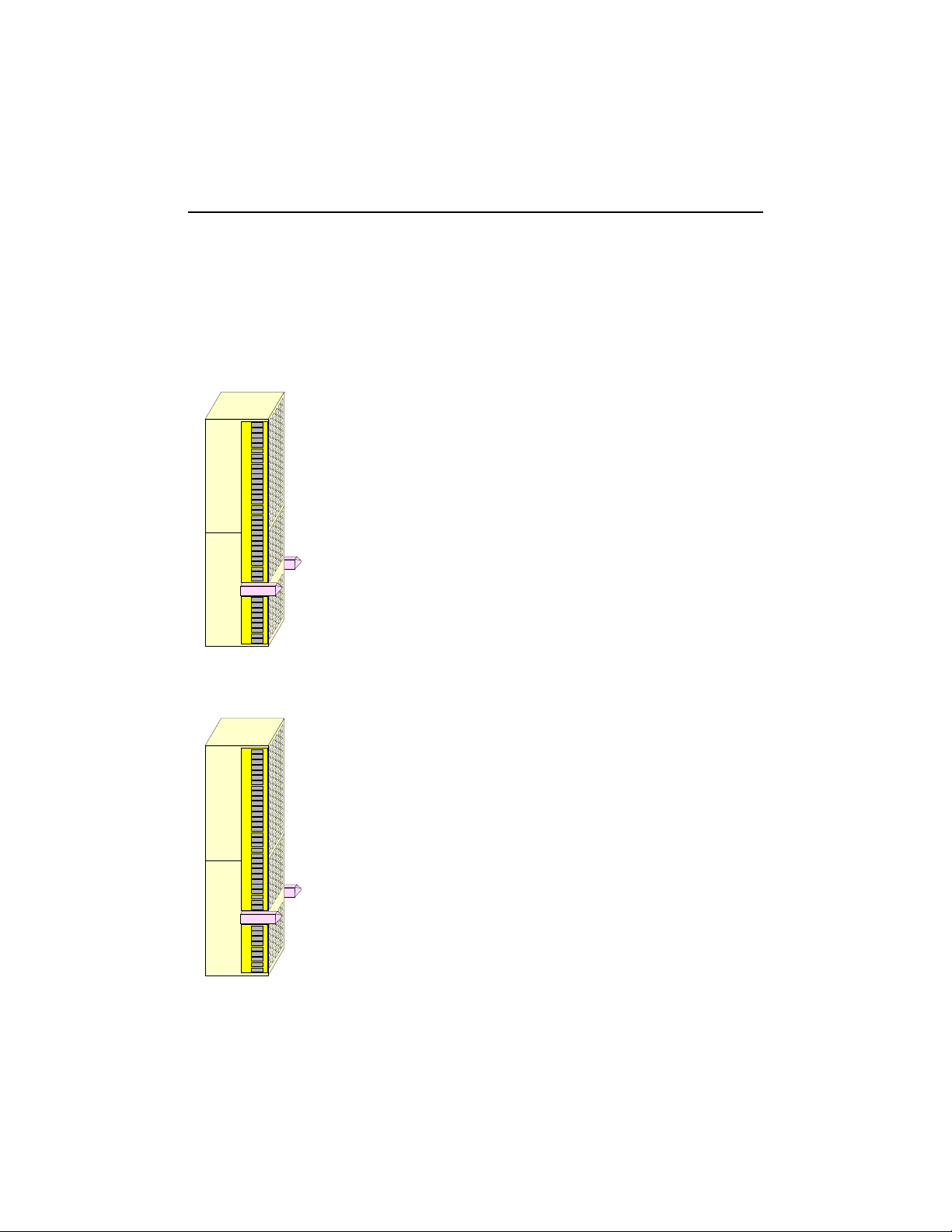
2.3 REAR-PANEL CONNECTORS
Rear panel connectors consist of two 2mm Hard Metric connectors. The lower one is
dedicated to the PCI signals while the upper one is reserved to I/O signals.
2.3.1 I/O connector (J5/J8): CPCI P4/P5
Speaker signal
onboard multi-function connector (J2).
Enhanced IDE interface
provides an interface for both Primary/Secondary and
Master/Slave IDE devices (HD, CD-ROM).
ISA I/O
USB
One USB port is available t hrough this connector, a second one is
available on the front plate.
Floppy Disk
PS/2 Mouse
mouse interrupt is provided throug h IRQ12 to the CPU. A PS/2
mouse connector is also available on the front plate.
- Fully ISA bus compatible interface.
- The onboard USB controller supports up to two USB ports.
and Keyboard Signals.
. When the mouse interrupt function is enabled, the
2.3.2 PCI connector (J11/J13):
Hard Metric Connector
PCI Bus
Bus Performance
Hot swap - capabilities for peripheral connections
– compliant with PICMG 2.0 specification
- The speaker signal is also available on the
- Accelerates PIO data transfers and
- 2mm pitch
- up to 132MB/sec
Up to seven loads on the PCI segment
2-4
Page 17

Onboard Subsystems
2.3.3 CompactPCI Connectors – Logical Identification
According to the PICMG 2.0 R2.1 specification, Co mpactPCI connectors are also logically
referred as:
P1 32-bit PCI signals: physically J13 on the board
P2 64-bit PCI signal extension: physically J11 on the board
I/O application signals are defined by TEKNOR through:
P4 IDE and I/O signals physically J8 on the board
P5 ISA signals physically J5 on the board
2-5
Page 18
TEK-CPCI-1000 Technical Reference Manual
2
4
2
4
2
4
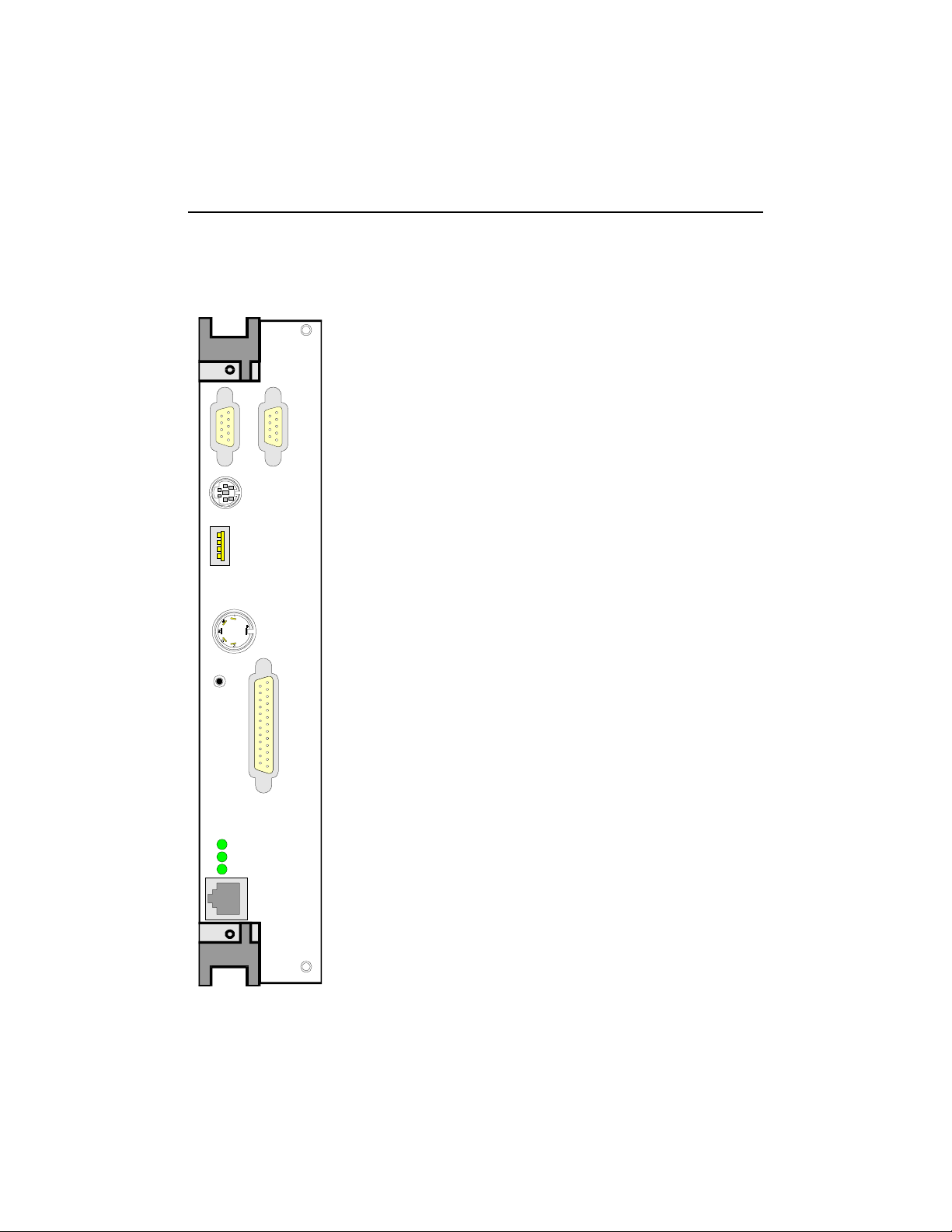
2.4 FRONT PLATE CONNECTORS
The front plate supports various connectors, functions and LEDs:
CompactPCI
COM
21
426
1
35
1
2
3
4
KEYBOARD
MOUSE
USB
COM1/2
J4 - RS-232 standard support on COM1 and
COM2.
COM2 may also be set as RS-422 or RS-485.
Both are standard 9-pin DSUB male connectors.
Mouse
USB
J8 - PS/2 mouse connector.
J7 - Universal Serial Bus port with d ifferential data
signals available on data pair. A second USB port
is available on the rear-panel I/O connector.
1
1
1
6
6
6
LPT1
25
25
25
TEK-CPCI T1000
100BASE-TX
LINK
ACTIVE
10BASE-T
100BASE-TX
Keyboard
Reset
LPT1
Ethernet
J9 - Standard 5-pin DIN connector.
S1 - Recessed reset button.
Parallel port. Supports Standard mode, EPP and
ECP modes depending on the BIOS setup.
Connector is DSUB 25-pin standard.
J12 - Operates directly on the PCI bus.
10Base-T and 100Base-T compatible on RJ-45
connector.
Auto detection and switching for 10Mbps or
100Mbps depending on the network speed.
Full and half-duplex capabilities at 10Mbps and
100Mbps.
Active, Link and 100Base-T LEDs.
2-6
Page 19

3. COMPATIBILITY WITH TEKNOR PRODUCTS
The TEK-CPCI-1000 CPU Single Board Computer is a member of the TEKNOR
CompactPCI product family. The board is fully compliant with the PICMG 2.0 R2.1
CompactPCI specification for the PCI bus segment.
When buildin g a basic environment around the TE K-CPCI-1000, the system may comprise
the foll o wing devices:
TEK-CPCI-1000 6U system board
TEK-CPCI-1002 3U VGA module
TEK-CPCI-1101 (or 1100) CompactPCI backpl ane
3U and 6U CompactPCI devices
6U form factor enclosur e
A CompactPCI Development Platform is available from TEKNOR and is referred to as
TEK-CPCI-1002.
3-1
Page 20

4. UNPACKING
Follow these recommendations whil e unpacking:
1. After opening the box, save it and the packing material for possible futur e shipment.
2. Remove the boar d from its a ntist a tic wrap pi ng and p lace it on a grounde d surface .
3. Inspect the board for damage. If there is any damage, or items are missing, notify
TEKNOR immediatel y.
Contents
When unpacking you will find:
1. One TEK-C PCI-1000, Pentium/ K 6 Single Board Computer
2. One Techni cal Reference Manual.
3. A set of cables
4-1
Page 21

5. SAFETY PRECAUTIONS
5.1 ST ATIC ELECTRICITY
Since static electricity can damage a board, the followin g precautions should be taken:
1. Keep the board in its antistatic package, until you are ready to install it.
2. Touch a ground ed sur face or wea r a gr oundi ng wr ist st rap bef ore r emovi ng th e boa rd
from its package; this will discharge any static electricity that may have built up in
your body.
3. Handle th e board by the edges.
5.2 STO R AGE ENVIRONMENT
Electronic boards are sensitive devices. Do not handle or store devices near strong
electr ostatic, electromagnetic, magnetic or radioactive fields.
5.3 POWER SUPPLY
Befor e an y in sta lla ti on or s etu p, en sur e th at th e boa rd i s un plug ged fr om power sou rc es or
subs yst ems.
5-1
Page 22

PRODUCT DESCRIPTION
6. CUSTOMIZING THE BOARD
7. CONNECTING DEVICES
8. INSTALLING VIDEO
9. CONFIGURING DMA & IRQ
10. SETTI NG JUMPERS
Page 23
6. CUSTOMIZING THE BOARD
6.1 PROCESSOR AND FAN
Your board will be installed with one of the available Pentium, Pentium MMX or K6
processors, and its adequate cooling fan. However, it may be necessary to reinstall or
reconfigure your board with new devices.
6.1.1 Installing Microprocessor
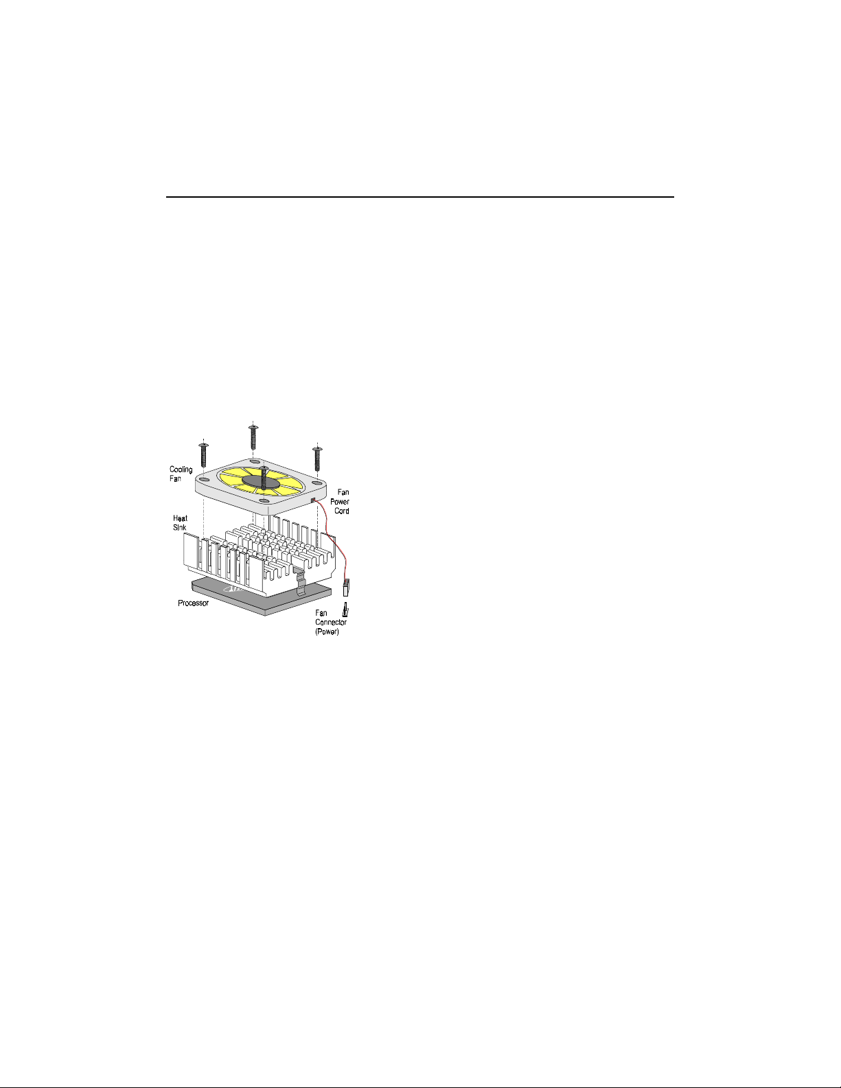
Depending on the processor and the system in which
the board is integrated, fan and/or heater may be
required.
A +12V voltage is available through the J10 connector
to supply the fan (The connector’s pinout appears in
Appendix-C).
Please refer to your processor specifications for more
information.
When installing a processor, its type, core voltage, clock speed multiplier, and Core/Bus
ratio value must be configur ed according to your CPU model.
Six jumpers are relat ed to the processor:
W12-W13 Define the intern al CPU clock speed multiplier.
W14-W15 Define the Core/Bus clock ratio.
W18 Selects the CPU type from Sp lit-plane or S in g le-plane.
W19 Selects the core voltage (Vcore).
6-1
Page 24
TEK-CPC I-1000 Technical Reference Manual
6.1.2 Processor Characteristics
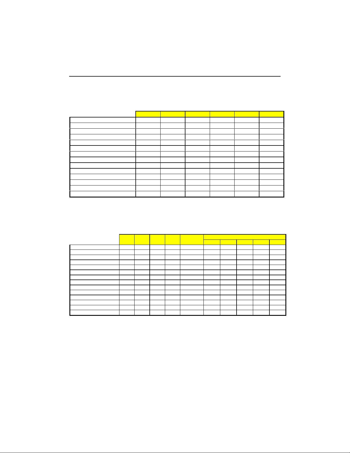
Processor characteristics are summarized below:
Intel Pentium 90 90 60 30 1.5 Single 3.34V
FCore BCLK PCLK Ratio Type VCore
Intel Pentium 100 100 66 33 1.5 Single 3.34V
Intel Pentium 120 120 60 33 2.0 Single 3.34V
Intel Pentium 133 133 66 33 2.0 Single 3.34V
Intel Pentium 150 150 50 25 3.0 Single 3.34V
Intel Pentium 150 150 60 30 2.5 Single 3.34V
Intel Pentium 166 166 66 33 2.5 Single 3.34V
Intel Pentium 200 200 66 33 3.0 Single 3.34V
Inte l Pentium 166-MMX 166 66 33 2.5 Split 2.84V
Inte l Pentium 200-MMX 200 66 33 3.0 Split 2.84V
Inte l Pentium 233-MMX 100 66 33 1.5 Split 2.84V
AMD K6-166 166 66 33 2.5 Split 2.94V
AMD K6-200 200 66 33 3.0 Split 2.94V
AMD K6-233 100 66 33 1.5 Split 3.24V
Careful attention should be taken when installing a processor. Faulty jumper settings may
definitely damage your board.
W12 W13 W15 W14 W18 W19
Intel Pentium 90 Off On Off Off 1-3 / 2-4 On Off On On Off
Intel Pentium 100 On On Off On 1-3 / 2-4 On Off On On Off
Intel Pentium 120 Off On Off On 1-3 / 2-4 On Off On On Off
Intel Pentium 133 On Off Off On 1-3 / 2-4 On Off On On Off
Intel Pentium 150 On On On Off 1-3 / 2-4 On Off On On Off
Intel Pentium 150 Off On On On 1-3 / 2-4 On Off On On Off
Intel Pentium 166 On Off On On 1-3 / 2-4 On Off On On Off
Intel Pentium 200 On Off On Off 1-3 / 2-4 On Off On On Off
Intel Pentium 166-MMX On Off On On 3-5 / 4-6 Off Off Off On Off
Intel Pentium 200-MMX On Off On Off 3-5 / 4-6 Off Off Off On Off
Intel Pentium 233-MMX On Off Off Off 3-5 / 4-6 Off Off Off On Off
AMD K6-166 On Off On On 3-5 / 4-6 On Off Off On Off
AMD K6-200 On Off On Off 3-5 / 4-6 On Off Off On Off
AMD K6-233 On Off Off Off 3-5 / 4-6 Off Off On On Off
1-2 3-4 5-6 7-8 9-10
For complete details on jumper settin g description, please refer to Section 9.
6-2
Page 25
Customizing the Board
6.2 INSTALLING MEMORY
6.2.1 Installing DRAM
The TEK-CPCI-1000 supports FPM and EDO system memory. Memory type is singlesided or double-sided vertical SIMMs, 5V, 70ns/60ns, and can be configur ed from 8MB up
to 512MB, using 32-bit or 36-bit modules.
The memor y sockets consist of four 72-pin vertical SIMM (Single In-line Memory Module)
sockets divided into two banks labeled: Bank 0 (U20 and U22) and Bank 1 (U18 and U19).
At least 8 MB of system memory (2 SIMMs or 4 ) must be inst all ed on the board for pr oper
operation. Each ve rtical 72-pin SIMM sockets supports the following modules:
2M x 32-bit / 36-bit = 8MB module 16M x 32-bit / 36-bit = 64MB module
4M x 32-bit / 36-b it = 16MB module 32M x 32-bit / 36-b i t = 128MB module
8M x 32-bit / 36-b it = 32MB module
NOTE
The me mor y bank s can be p opul ate d sep ara tely or joi ntl y. E ach ba nk
must be populated with the same SIMM capacity, however, the
capacity used in one bank may be of a different capacity from the
other.
6-3
Page 26
TEK-CPC I-1000 Technical Reference Manual
60ns maximum access time EDO DRAM devices are recommended.
The following table shows examples of recommended DRAM devices supported by the
board. Many other models are also a vaila ble and fun ction equally well. User s are encouraged
to check with their local distributors for comparabl e substitut es.
DIMM VENDOR PART NUMBER
2M*72 (ED0) - 16MB modules
(SPD EPROM, ECC)
4M*72 (SDRAM) - 32MB mod ules ROCKY MOUNTAIN RAM 4x72CQ2x8S4E
ROCKY MOUNTAIN RAM 2x72CEQ
4M*72 (ED0) - 32MB modules
(SPD EPROM, ECC)
8M*72 (ED0) - 64MB modules
(SPD EPROM, ECC)
16M*72 (SDRAM) – 128MB modules ROCKY M OUNTAIN RAM 16x 72CQ8x8S4E
16M*72 (ED0) - 128MB mo dules
(SPD EPROM, ECC)
ROCKY MOUNTAIN RAM 4x72CEQ
ROCKY MOUNTAIN RAM 8x72CEQ
ROCKY MOUNTAIN RAM 16x72CEQ
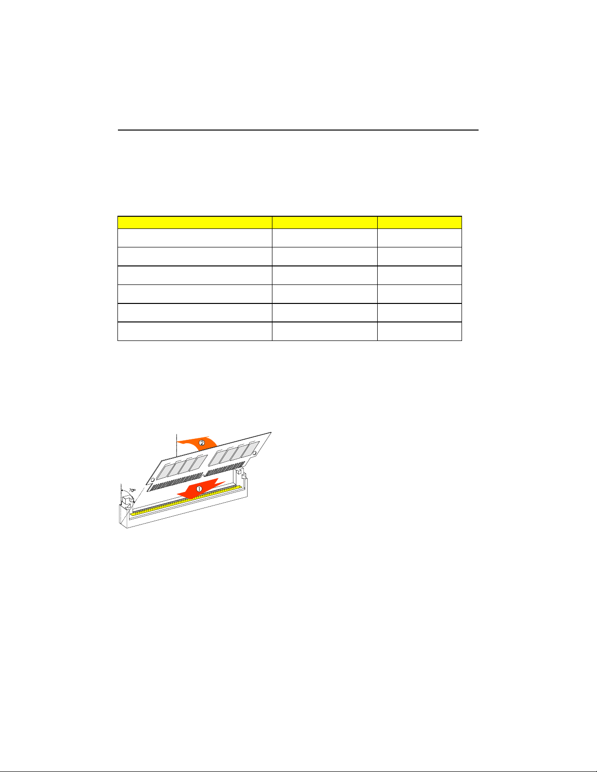
6.2.2 SIMM Installation
To install the SIMMs in the sockets, proceed a s follo ws:
1. With the board flat on the table, turn it so that
the front plate is on th e left.
2. Hold the module with the notch on the bottom
right facing you, and insert the fingers into the
socket at a 70° angle from the board. Alwa ys
start inserting the mod ul e in th e s ock et n ear est
the top edge of the board
3. Snap the module to a vertical position in the
socket. The module is fully in serted when the
retaining pegs snap int o the holes at each end
of the module.
4. Work your way by inserting the other
module s, on e by one, towards the l ower edge
of the board.
To remove the SIMMs from the sockets, pull o n the retaining pegs located on each s ide of the
SIMM socket. Once the m odul e has snapped out of the socket, pull gentl y on it.
6-4
Page 27

Customizing the Board
The following table describes which SIMM configurations may be implemented on the
board, using 72-pin v ertical SIMM s:
SYSTEM U18 U19 U20 U22
MEMORY BANK 1 BANK 0
8MB 4MB (1Mx36) 4MB (1Mx36) -- --
8MB -- -- 4MB (1Mx36) 4MB (1Mx36)
16MB 4MB (1Mx36) 4MB (1Mx36) 4MB (1Mx36) 4MB (1Mx36)
16MB 8MB (2Mx36) 8MB (2Mx36) -- -16MB -- -- 8MB (2Mx36) 8MB (2Mx36)
24MB 8MB (2Mx36) 8MB (2Mx36) 4MB (1Mx36) 4MB (1Mx36)
24MB 4MB (1Mx36) 4MB (1Mx36) 8MB (2Mx36) 8MB (2Mx36)
32MB 8MB (2Mx36) 8MB (2Mx36) 8MB (2Mx36) 8MB (2Mx36)
32MB 16MB (4Mx36) 16MB (4Mx36) -- -32MB -- -- 16MB (4Mx36) 16MB (4Mx36)
40MB 16MB (4Mx36) 16MB (4Mx36) 4MB (1Mx36) 4MB (1Mx36)
40MB 4MB (1Mx36) 4MB (1Mx36) 16MB (4Mx36) 16MB (4Mx36)
48MB 16MB (4Mx36) 16MB (4Mx36) 8MB (2Mx36) 8MB (2Mx36)
48MB 8MB (2Mx36) 8MB (2Mx36) 16MB (4Mx36) 16MB (4Mx36)
64MB 16MB (4Mx36) 16MB (4Mx36) 16MB (4Mx36) 16MB (4Mx36)
64MB 32MB (8Mx36) 32MB (8Mx36) -- -64MB -- -- 32MB (8Mx36) 32MB (8Mx36)
72MB 32MB (8Mx36) 32MB (8Mx36) 4MB (1Mx36) 4MB (1Mx36)
72MB 4MB (1Mx36) 4MB (1Mx36) 32MB (8Mx36) 32MB (8Mx36)
80MB 32MB (8Mx36) 32MB (8Mx36) 8MB (2Mx36) 8MB (2Mx36)
80MB 8MB (2Mx36) 8MB (2Mx36) 32MB (8Mx36) 32MB (8Mx36)
96MB 32MB (8Mx36) 32MB (8Mx36) 16MB (4Mx36) 16MB (4Mx36)
96MB 16MB (4Mx36) 16MB (4Mx36) 32MB (8Mx36) 32MB (8Mx36)
128MB 32MB (8Mx36) 32MB (8Mx36) 32MB (8Mx36) 32MB (8Mx36)
128MB 64MB (16Mx36) 64MB (16Mx36) -- -128MB -- -- 64MB (16Mx36) 64MB (16Mx36)
136MB 64MB (16Mx36) 64MB (16Mx36) 4MB (1Mx36) 4MB (1Mx36)
136MB 4MB (1Mx36) 4MB (1Mx36) 64MB (16Mx36) 64MB (16Mx36)
144MB 64MB (16Mx36) 64MB (16Mx36) 8MB (2Mx36) 8MB (2Mx36)
144MB 8MB (2Mx36) 8MB (2Mx36) 64MB (16Mx36) 64MB (16Mx36)
160MB 64MB (16Mx36) 64MB (16Mx36) 16MB (4Mx36) 16MB (4Mx36)
160MB 16MB (4Mx36) 16MB (4Mx36) 64MB (16Mx36) 64MB (16Mx36)
192MB 64MB (16Mx36) 64MB (16Mx36) 32MB (8Mx36) 32MB (8Mx36)
192MB 32MB (8Mx36) 32MB (8Mx36) 64MB (16Mx36) 64MB (16Mx36)
256MB 64MB (16Mx36) 64MB (16Mx36) 64MB (16Mx36) 64MB (16Mx36)
256MB 128MB (16Mx36) 128MB (16Mx36) -- -256MB -- -- 128MB (16Mx36) 128MB (16Mx36)
512MB 128MB (16Mx36) 128MB (16Mx36) 128MB (16Mx36) 128MB (16Mx36)
36-bit modules are shown, however 32-bit modules are supported.
6-5
Page 28

TEK-CPC I-1000 Technical Reference Manual
6.3 ENABLING MEMORY CACHE
Th ere are two sepa ra t e ca ch es i n t he h ost s ub sys tem : i nt er na l ca ch e an d ex t er na l ca ch e. T he
ca ch e in s i d e th e proce ss or ( i n t ern a l cache) i s r e fer red to a s t h e fi r st l e ve l ca che (al s o p r im a ry
ca che or L1).
Th e exter nal ca che (c alled syst em cach e in th is man ual) compr ises t he S ystem Contr oll er’s
cache control circuitry and associated external memory array; it is r eferred to as the second
le v el cache (als o s econdary cache or L2). The second le vel cac he is unified, which means that
both CPU data and instructions are stored in the cache.
System ca ch e must be ena bled an d con fig ur ed u sing t he A war d BIO S s etup pr ogra m ( detail s
in Sect ion 12 - Software Setup).
6-6
Page 29

Customizing the Board
6.4 CONFIGURING THE BOARD
Ninet een jumpers are provided to setup the board. They are l is ted below:
Jumper Description
W1, W2
W3 I/O Base Address - Selects the I/O base address from: 190h, 290h or 390h.
W4 Extended BIOS mode - Use this jumper to setup th e following featur es :
W5
W6-W7 RS-232/RS-485 ter min ati on r es ist or - connect t er mi n ati on resistor for RS-2 32 or
W8 Battery - Enables or disables the battery on the board.
W9 Power Fail detection - when installed, en ab l es Power Fail Detect ion.
W10 Watchd og - enables o r disables the watchdog.
W11 Power Fail source - when inst alled, enabl es the B attery voltage or an external
W12-W13 Clock Speed Multiplier - Selects the internal CPU Clo ck Speed Multiplier.
W14-W15 CPU Core/Bus Ratio - Sel ects t he rat ion between the CP U C ore Cloc k and the
W16 External Cache size - not used while the cache is auto-detected by the BIOS.
W17 DRAM refresh rate - selects from 60 or 66Mhz rat e.
W18 CPU type - selects the CPU type (Single -Plane or Split-Plane).
W19 VCORE - selects the CP U core voltage.
Hard driv e installat ion setup - Us e these jumpers t o install hard drives on the
EIDE bus or t h e PCI bus
1.
download mode
the Flash EPROM
2.
VT100 mode
terminal
3.
TEKNOR Extension
VT100, b oot from F lash, save C MOS in fl as h, SRAM d evices..., (for more
information see Software Setup Section)
4.
Ethernet
Boot Mode se le cti on - When set t o em er g ency, it offers the abili t y to upgrad e the
onboard BIO S f r om an emergenc y dis k.
RS-485 op eration mode on S erial Port 2.
user volt age to be monitored by th e p ower Fail Detecti on c ontroller.
CPU Bus Clock.
- to download s er i ally informati on from a remote computer t o
- to communicate with the board using a VT100 or ANSI
- when en ab l ed, au thorizes TEKN O R’s featur es s uch as
- enables or dis ab l e the Et h er n et interface.
Please refer to the Sect i on 1 0 –
Setting Jumpers
6-7
to config ure each jumper.
Page 30

TEK-CPC I-1000 Technical Reference Manual
6.5 BIOS BOOT OPTIONS
By default, the board boots with the BIOS contained in the Boot Block Flash. The Boot
Block Fla sh consists of a flash memor y d evi ce with verificati on and protection feat ures. It
merges th e entire BIOS co de and a protected emer gency c ode.
The Boot Block Fla sh appe ars as the easi est way to upgrad e the board’ s BIOS as it s ver sion
changes, or in case of a programming error or a data corruption.
The board pr ovi des an emer gen cy boot j umper (W 5) in t he cas e of a BIOS corruption: when
it is enable d (jumper W5 sh orted), an emerg ency procedur e is exec uted to upda te the BIOS
code from a DOS file located on an emergency disk.
NOTE
A BIOS corruption is one of the symp toms of a non-f unc tion al b oard:
it may be caused by an electrical shutdown that occurs before a BIOS
upd a te operation is completed.
The complete procedure to execute an emergency boot is described in Section F.2
(Emergency Procedure).
6.6 INSTALLING SUPERVISOR UTILITIES
6.6.1 Supervisor I/O Registers
Super visor I/O register s are provided to confi gure an d contr ol speci al feat ures of th e boar d
such as: wat chdog, Flash, RS-422/RS-485 mode, and power fail output. These register s are
two 8-bit registers locatable at three different I/O addresses, 190h/193h, 290h/293h or
390h/393h, using the W3 jumper.
6-8
Page 31
Customizing the Board
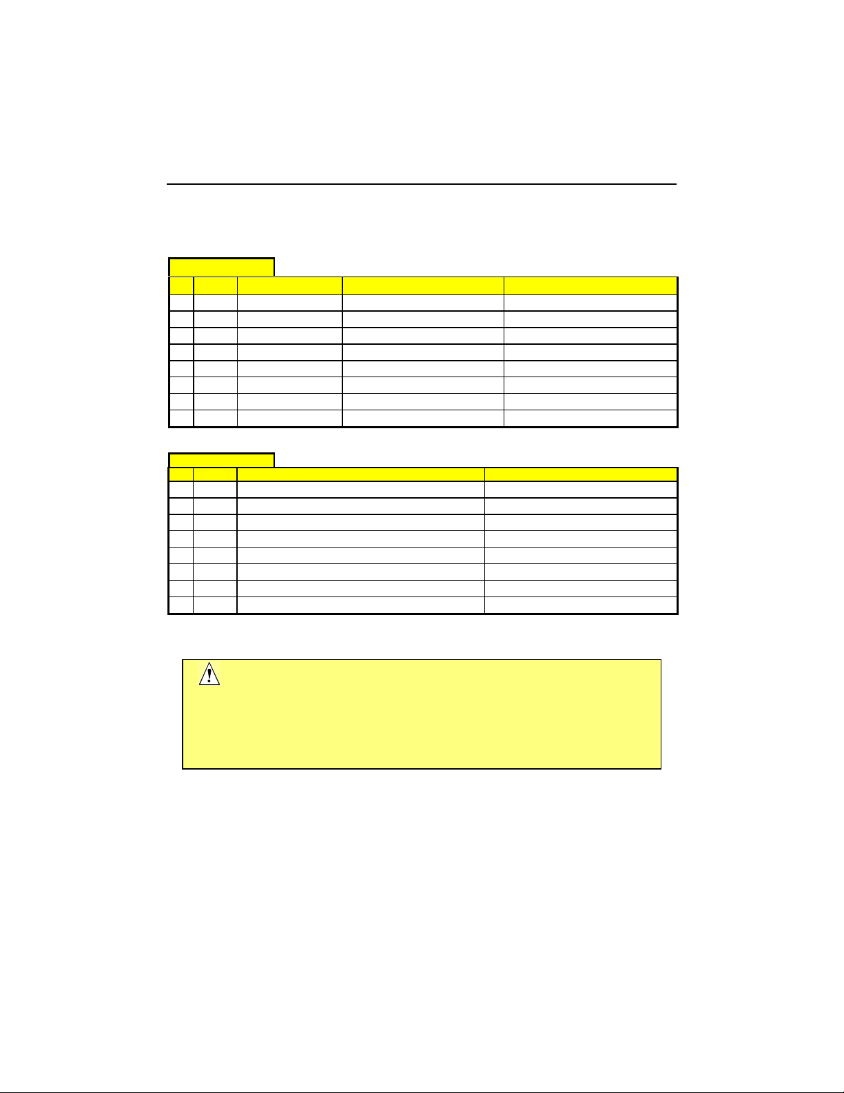
Each register is bit read and write accessible, however, some are reserved for internal
requirements. They are described as fol lows:
Register #1
Bit Default Function WRI TE Operation: READ Operation:
0 0 Enable Watchdog 1=Enable / 0= Disable* Same
1 1 Watchdog pulse write 1- 0 alternat ely to refresh Same
2 0 Flash programming 1= Enable / 0= Disable (+12V) Same
3 0 RS-485 direction 1= Read only / 0= Write only Powe r Dete ct. or Batt. Low o utput
4 0 Reserved W4 (7-8) Status (Ethernet)
5 0 Reserved W4 (5-6) Stat us (TEKNOR BIOS)
6 1 Reserved W4 (3-4) Status (VT100 mode)
7 0 Reserved W4 (1-2) Status (Serial download)
Register #2
Bit Default WRITE Operation: READ Operation:
0 0/1 Reserved * R/W Reserved
1 0/1 Reserved * R/W Reserved
2 1 Data output for serial number device Same
3 1 Enable Ethernet (1 = Enable ; 0=Disable) Ethernet Status
4 0 Reserve d Not Used
5 0 Reserved I/O base address W3 (1-2)
6 0/1 Reserved I/O base address W3 (3-4)
7 0 Reserved* R/W Emergency jumper (W5) status
* Read and m ask before changing bi ts
CAUTIONS:
1. Not all bits are R/W. Therefore, be certain t o kee p a mirror image of
the register when programming it.
2. All bits ar e 0 after a hardwa r e RESET or power up condit ion.
As the supervisor I/O registers provide features associated to the TEKNOR Extension, the
TEKNOR Extension mode must be enabled by setting the W4 jumper that controls the
extended BIOS mode s of the bo a rd ( refer to Sec t ion 10 -
6-9
Setting Jumpers
).
Page 32

TEK-CPC I-1000 Technical Reference Manual
6.6.2 Power Fail Monitor ing
A power failure condition may b e detected if a low back up battery condition occurs, o r a +5 V
monitored power supply (user defined) falls below 4.75V.
When power failure is enabl ed, a power failure condition i s detected if eith er of the two
above conditions occurs. To enable power fail monitoring, the W9 jumper cap must be
installed.
To select wheter to monitor the low battery or the user defined power supply voltage, use the
W11 jumper.
Jumper location a nd configura tion are described in Section 10 -
Setting Jumpers
.
6.6.3 Watchdog
The watchdog is used to monitor the CPU inactivity. After a specified duration of inactivity,
the CPU will be reset.
To generate a RESET wh en the watchdog times out, use the W10 jumper.
Working with the Watchdog
The watchdog must be enabled and refreshed by software. To enable the watchdog by
softwar e, fir st wri t e "1" in the bit 0 of the I/O Regi st er # 1 (s ee S ecti on 6. 6.1 -
Registers
When ena bled, the wat chdog must be re freshe d by the process or by writin g altern ativel y "0"
and "1" to the bit 1 of the I/O Regist er #1, once ever y 1.6 seconds to veri fy proper soft ware
execution. If a hardware or software failure occurs such that the watchdog is not r efreshed, a
reset pulse is generated by the watchdog to restart the processor.
Following a reset, the watchdo g is always disabled.
).
CAUTION
Supervisor I/O
The us er pro gram must firs t confi gure t he I/O Re gist er #1 ( set a t base
the address 190h, 290h or 390h, according to the W3 jumper setting),
and must also include a refresh routine. Be certain to keep a mirror
image of this register when pr ogramming it. This is necessary since the
register is a write-only user regis ter and, as a result, is not used by the
syst em BIOS .
6-10
Page 33

Customizing the Board
6.7 INSTALLING THE BOARD INTO A BAY
The TEK-CPCI-1000 is a mechanical Euroc ard fo rm factor board and takes advantages of the
IEEE1101.10 specifications that ensure mechanical interchangeability of plug-in elements in
sub-racks.
Due to the high-density pinout of the Hard Metric conn ector, some precautions must be taken
when connecting or disconnecting a bo ard to/from a backplane:
1. Rail guides must be installed on the enclosure to slide the board to the backplane.
2. The board insertion must not be forced if there is any mechanical resistance.
Compact
into an incompatible backplane slot. If you are having problems inserting the board,
make sure the keys installed on the board and the backplane are of the same color.
3. Screw the front plate to the enclosure to firmly attach the board to its enclosure.
4. Use the extractor handles to disco nnect the board and extract it from its enclosure.
PCI specifies a keying mechanism that pr event s a board from being inserted
6-11
Page 34
TEK-CPC I-1000 Technical Reference Manual
6.7.1 Connector Keying
The CompactPCI connector supports guide lugs located on the board (system board and
peri pherals) an d the backplan e connector s to ensure a correct polarized mating. A proper
mating is enhanced by the use of coding keys for 3.3V and 5V operation.
Coding keys prevent inadvertent installation of a 5V board in a 3.3V slot. The TEK-CPCI1000 provides 3.3V signals. The PCI bus does not require to be keyed. Backplane
conn ectors must alwa ys be keyed accordin g to the signalin g l evel .
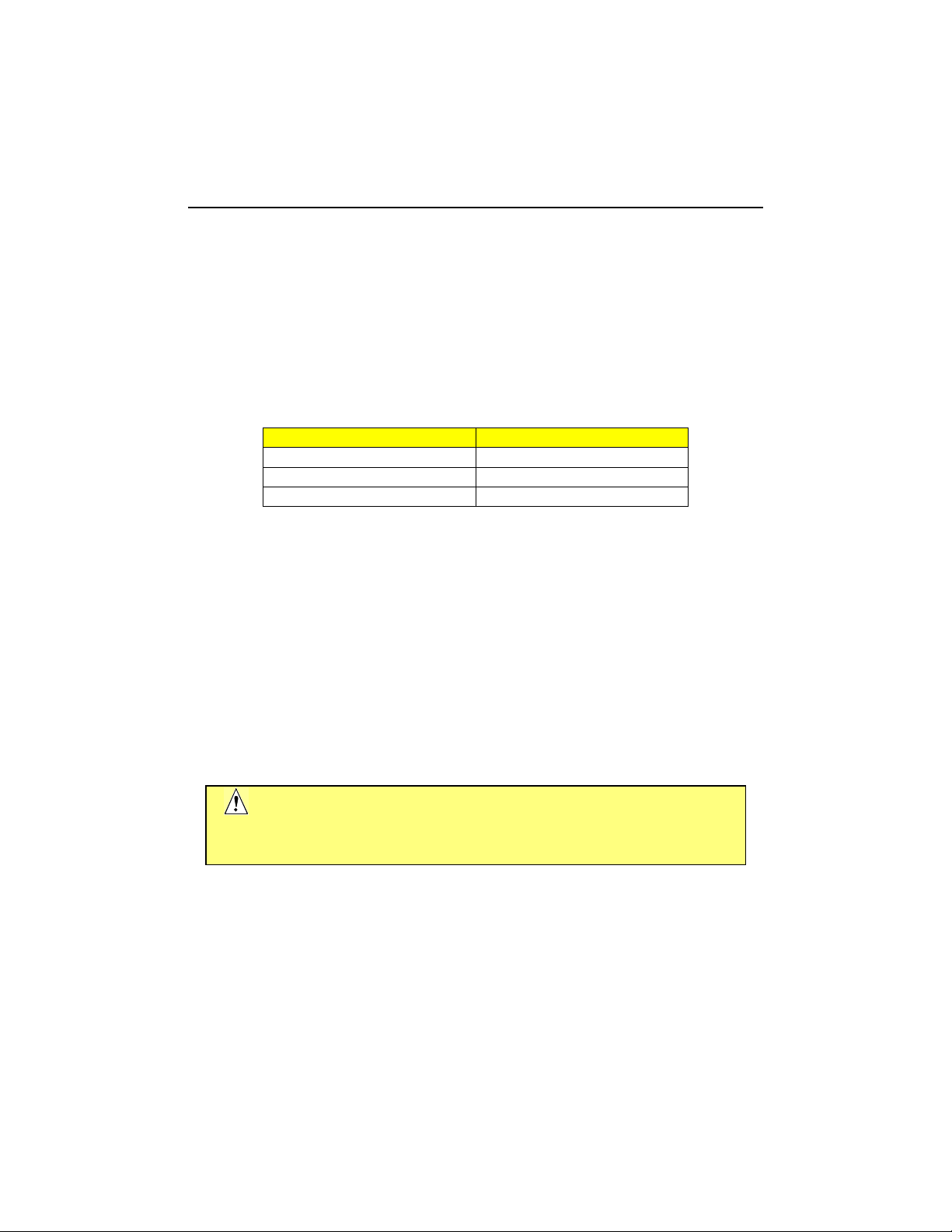
Coding Key Colors are defined as follows:
Signaling Voltage Key Color
3.3V Cadmium Yellow
5V Brilliant Blue
Universal board (5V and 3.3V) none
6.7.2 Bus Mastering
The TEK-CPCI-1000 provides four pairs of REQ/GNT arbitration signals. Th is means the
board is capable of interfacing up to four peripheral modules with PCI Bus Master
capabilities.
When connecting the board to a backplane, be aware that one REQ/GNT pair may be
already assigned to the onboard Ethernet feature.
CAUTION
With the onboard Ethernet enabled only three PCI Bus Master devices
are supported .
6-12
Page 35
Customizing the Board
6.7.3 Connection
To install the TEK-CPCI-1000 board in t o a bay, proceed as follows:
1. Power off your CompactPC I system
2. Choose the 6U system slot
3. Remove the fr ont plate of the slot wher e you intend to in sert the TEK-CPCI-1000
4. Ensure the module is properly aligned with the guide-rails an d slide it gently until it
touch es the backplane con nector
WARNING
1. Some mechanical parts of the guide-rail are fragile (shield contacts and
clips). Do not use f orce to insert and connect a CompactPCI module.
2. If there is any mechanical resistance while you insert a module, first
ensure there is no mec hanical obstacle and check for the alignment of
all parts.
5. To enga ge the board ’s connect ors int o the backplan e connect or, si multan eously pr ess
on th e fron t plate and lift up th e handle until th e r etaining clip hooks to the chassi s.
6. Fasten the module using the fellow-plate fixing screw to secure the module to the
system chassis.
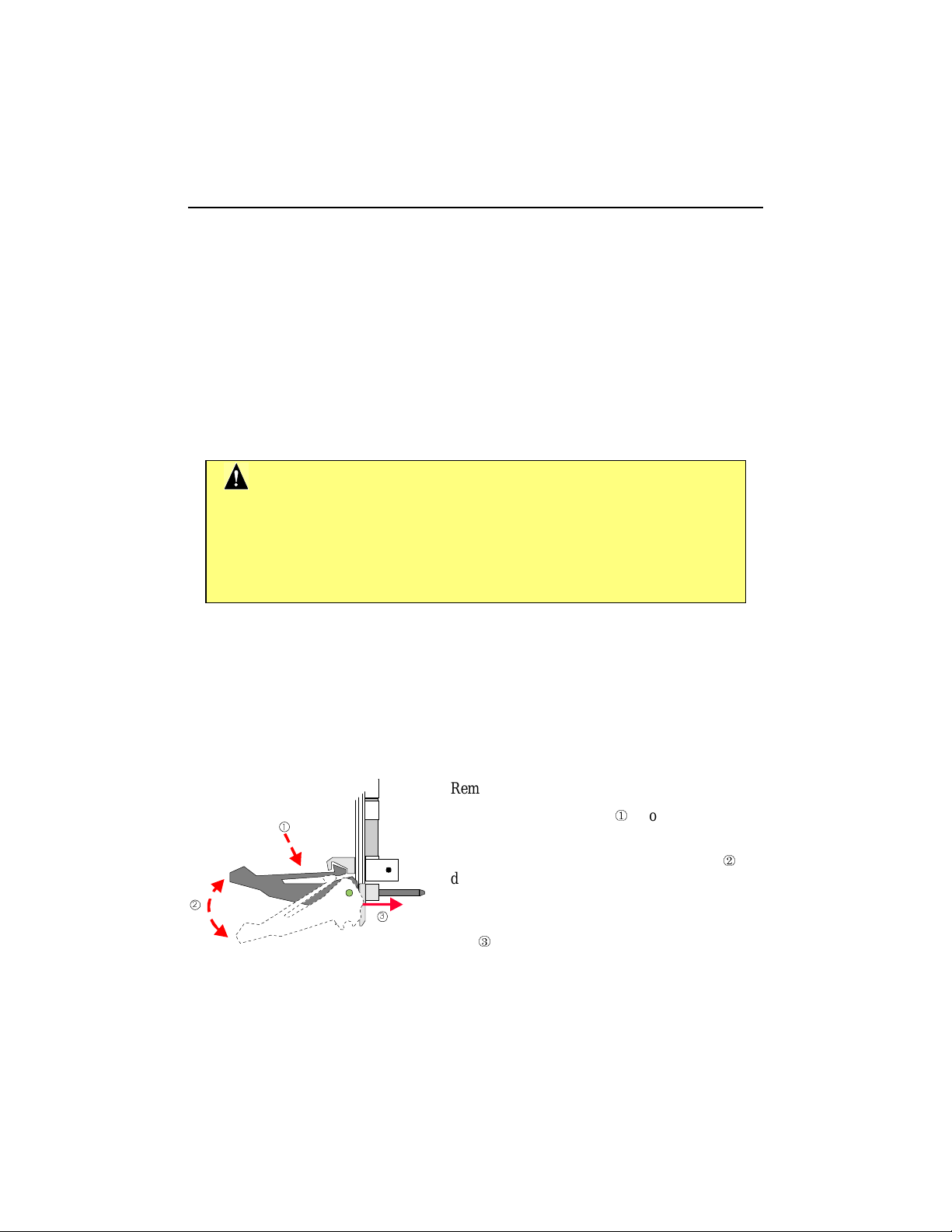
To remove the module from the chassis, pr oceed as follows:
Remove the fixin g screws of the fron t plate.
Press the handle (see ) to disengage the
retaining clip.
Press the handle to act as a lever (see ) to
disengage the CompactPCI connector from the
backpl ane connector .
Pull on the handle and gently remove the board
(see ).
6-13
Page 36

7. CONNECTING DEVICES
7.1 SUPPLYING POWER ON THE TEK-CPCI-1000
All voltages required to supply the TEK-CPCI-1000 board must be provided by the
backplane, through the rear-panel PCI connector (J11, J13).
The pin assignation for the different voltages appears as follows:
+5V (VCC) A1, A25, B2, B24, D3, D23, F1, F25
+12V D1
GND B4, B6, B8, B10, B16, B18, B20, B22, B26, B28, B30,
B32, B34, B36, B38, B40, D5, D7, D9, D11, D15, D17,
D19, D29, D31, D33, D35, D37, D39, D41, B42
For more information please refer to Section D – Connector Pinouts.
7-1
Page 37
TEK-CPCI-1000 Technical Reference Manual
U18J8J4J1
J2B1J
3
J7J9J10S1U19U20U22J5J11J8
J13
J12
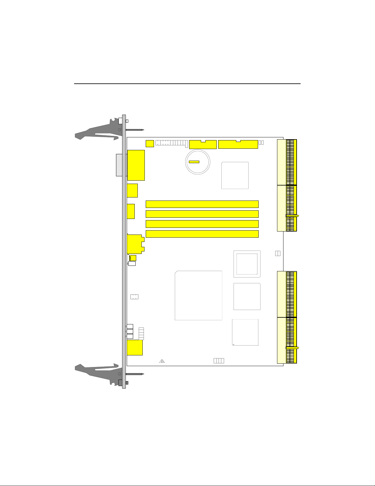
7.2 CONNECTOR LOCATION
W3 W4 W5
W7 W9
W6 W8 W10
W2
W11
W1
W12
W13
W18
DS1
DS2
W19
DS3
W15
W17
W16
W14
7-2
Page 38
Connecting Devices
7.3 SERIAL PORTS CONNECTORS (J4)
Two serial ports are provided on the board. They are 16C550 compatible and support 16-byte
FIFO buffers. Serial Port 1 is buffered for RS-232 operations, while Serial Port 2 may be set
for RS-232 or RS-422/RS- 485.
The J4 connector is a dual Serial Port connector that provides two communication ports
configured as COM1 and COM2. Both act as DTE.
For information on the programming of serial ports with the use of FIFO buffers, ask for
Application Note # AN93007 from TEKNOR’s Technical Su pport department.
7.3.1 Using COM 1
The COM1 port is buffered directly on the board for RS-232 operations. COM1 is 100%
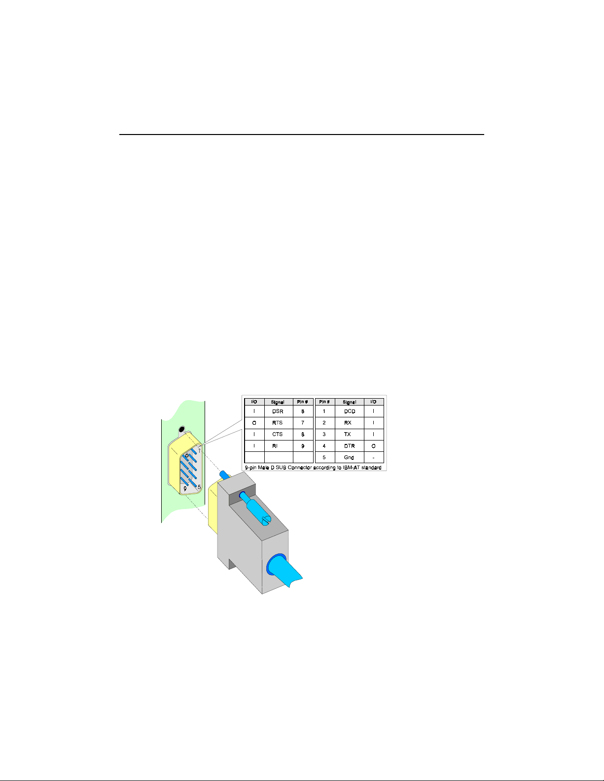
compatible with the IBM-AT serial port, it is provided through a 9-pin female D-SUB
connector mounted on the front plate of the TEK-CPCI-1000.
COM1 signals are output as follows:
7-3
Page 39
TEK-CPCI-1000 Technical Reference Manual
7.3.2 Using COM 2
The Serial Port COM2 supports RS-232, RS-422 and RS-485 operation modes. COM2 is
100% compatible with the IBM-AT serial port in RS-232 mode. Signals are provided
through a 9-pin female D-SUB connector mounted on the front plate of the TEK-CPCI-
1000.
To configure the COM2 communication mode use the VIP-UP setup program (See Section
12.2 -
VIP-UP Program
7.3.2.1 COM2 in RS-232 mode
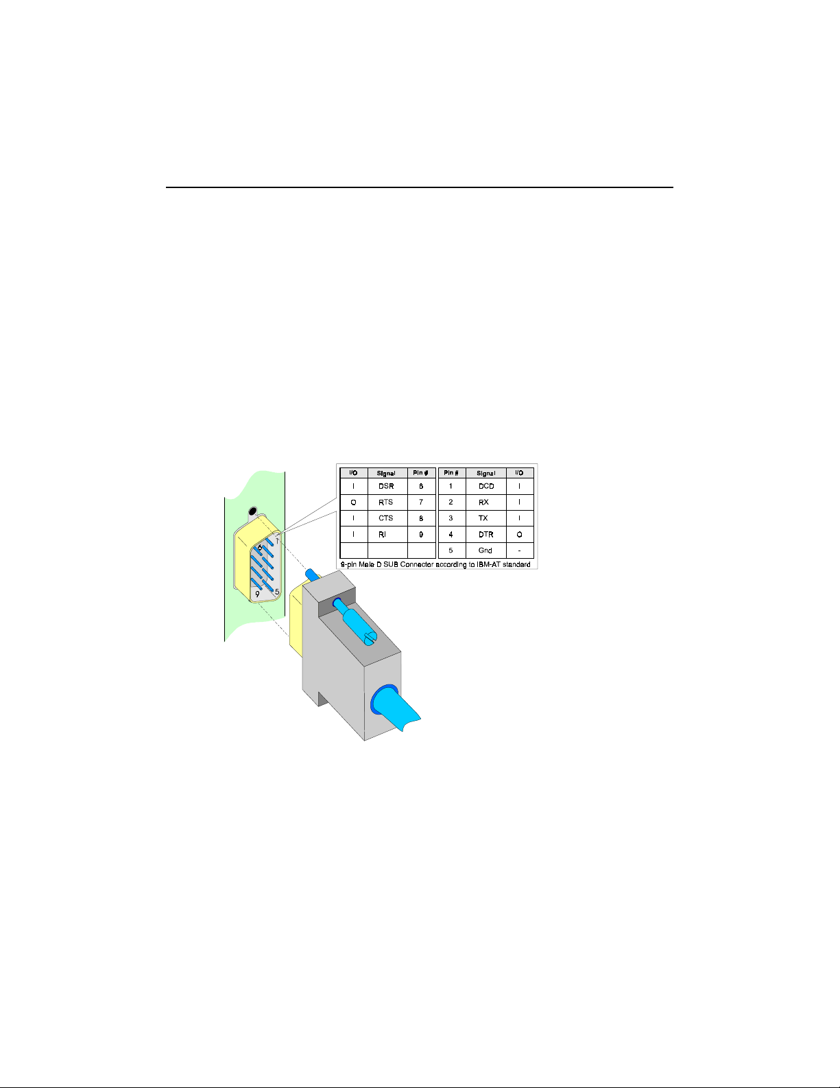
When configured for RS-232 operations, COM2 provides the same signal pin assignation
than COM1:
).
7-4
Page 40
Connecting Devices
7.3.2.2 COM2 in RS-422/RS-485 mode
RS-422 and RS-485 modes allow communication using differential signals through one pair
of wires (RS-485) or two (RS-422). For a better noise rejection, the use of twisted pair cable
is highly recommended.
Communicating in differential mode offers some advantages such as increased speed over
longer distances or improved reliability over similar RS-232 setups. RS-422 or RS-485
operation mode may be selected by software, using the VIP-UP setup program.
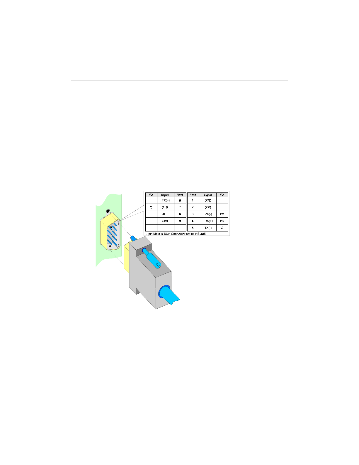
When set for RS-422/RS-485 operat i ons th e communi cati on port pin out appears as foll ows:
In RS-485 mode only the RX- and RX+ signals are used to interconnect the transmission
lines. To change the direction of the buffer in RS-485 mode, use the RTS line.
7-5
Page 41
TEK-CPCI-1000 Technical Reference Manual
SERIALPORT210-PINHEADER
1122LOWLOGICLEVELLOWLOGICLEVEL7766334
4
RS-422 Protocol:
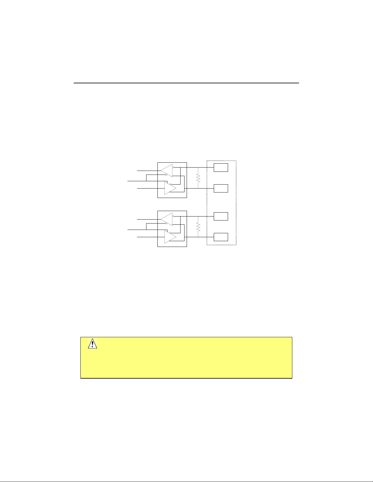
The RS-422 protocol (Full Duplex) uses both RX and TX lines during a communication
session. Upon a power-up or reset, the Serial Port 2 interface circuits are automatically
configured for full duple x operation: pins 3 and 4 of Serial Port 2 act as receiver lines while
pins 5 and 6 act as transmitter lines.
Internal circuit may be represented as follows:
GND
VCC
TXD
RXD2
X
X
120 ohms
120 ohms
3
4
5
6
RX-
RX+
TX-
TX+
There are no user software restrictions except that software must not attempt to use the
handshake line because they are not connected. However, handshaking by software only
(XON-XOFF) may be used.
CAUTION
When working in RS-422 protocol, W6 a nd W7 jumper caps must be
installed to connect the 120 ohms termination resistors (See Section 10 Jumper Settings).
7-6
Page 42
Connecting Devices
SERIALPORT210-PINHEADER
12763
4
RS-485 Protocol:
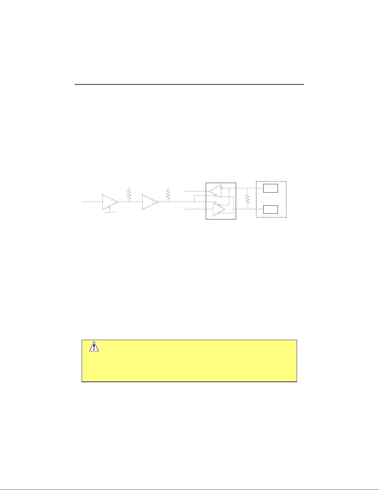
The RS-485 protocol (Half Duplex) also uses differential signals during a communication
session. It differs from the RS-422 mode as it offers the ability to transmit and receive over
the same pair of wires, and allows sharing of the communication l ine by multiple stations.
This config uration (al so known as Pa rty Line) a llows o nly one s ystem to t ake the co ntrol of
the communication line at the time.
The electrical circuit is described below:
VCC
ENABLE
VCC
RXD2
TXD2
120 ohms
3RX-
4RX+
In RS-485 mode, the RX lines (pins 3 and 4) are used as the transceiver lines, and the RTS
signal is used to control the direction of the RS-485 buffer. Upon power-up or reset, the
transceiver is by default in receiver mode to prevent unwanted perturbation on the line.
Party line operation mode requires termination resistors to be installed at both ends of the
network.
CAUTION
When installing the TEK-CPCI-1000 at one end of the network, W6
and W7 jumper caps must be installed to connect the 120 ohms
termination resistors (See Section 10 - Jumper Settings).
7-7
Page 43

TEK-CPCI-1000 Technical Reference Manual
7.3.3 Softw are Configuration
By default, serial ports are configured for RS-232 operations. Each port must be designated
by a logical COM port and a matching address using the AWARD BIOS setup program.
Available features are: Disabled, Auto, COM1/3F8h, and COM2/2F8h
To select the operation mode of COM2 (RS-232, RS-422, or RS-485), use the VIP-UP setup
program (See Section 12.2:
The bit 3 (RTS) of the Supervisor I/O Register #1 is reserved to control the transmission
operations of Serial Port 2 when set as RS-485. Writing "1" to bit 3 of the Supervisor I/O
Register #1 (at 190h, 290h or 390h base address, depending on W3 jumper) allows the
transceiver (pins 3 and 4 of J4) to be control l ed by th e RTS sig nal.
Upon power-up or reset, the transceiver is by default in "receiver mode" to avoid unwanted
perturbation on the line.
VIP-UP Program
).
7.4 PS/2 MOUSE CONNECTOR (J8)
The TEK-CPCI-1000 supports PS/2 standard mouse directly through the J8 connector
located on the front plate. Mouse signals are also available through the CPCI backplane
connector.
Important
manufacturer) is installed.
: when connecting a PS/2, make sure the adequate mouse driver (provided by its
7.5 KEYBOARD CONNECTOR (J9)
A standard AT keyboard may be connected directly through the J9 sta ndard 5-pin DIN male
connector. Keyboard signals are also available through the I/O CPCI backplane connector.
7-8
Page 44
Connecting Devices
7.6 USB CONNECTOR (J7)
USB is a fast bi-directional, isochronous/asynchronous, Plug and Play capable
communication bus that allows up to 127 logical connections to run on a computer.
The TEK-CPCI-1000 board fully supports the standard universal host controller interface
(UHCI) and uses standard software drivers that are UHCI-compatible.
This bus has been developed to bring plug and play configuration o f computer peripherals
outside the box, eliminating the need to install cards into dedicated computer slots and
reconfigure them. USB allows peripherals to be automatically attached, configured and
detached, without reboot or setup run.
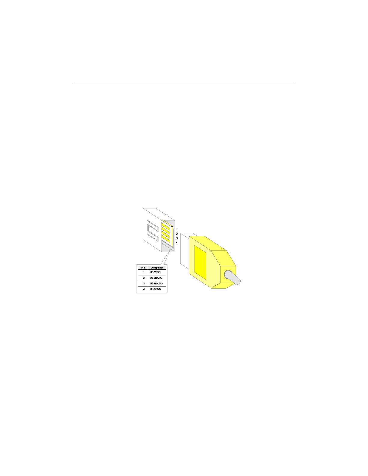
USB devi ces connect directly through the J7 connector located on the front plat e.
USB signals are also available through th e CPCI backplane conn ector.
7-9
Page 45
TEK-CPCI-1000 Technical Reference Manual
7.7 PARALLEL PORT CONNECTOR (J3)
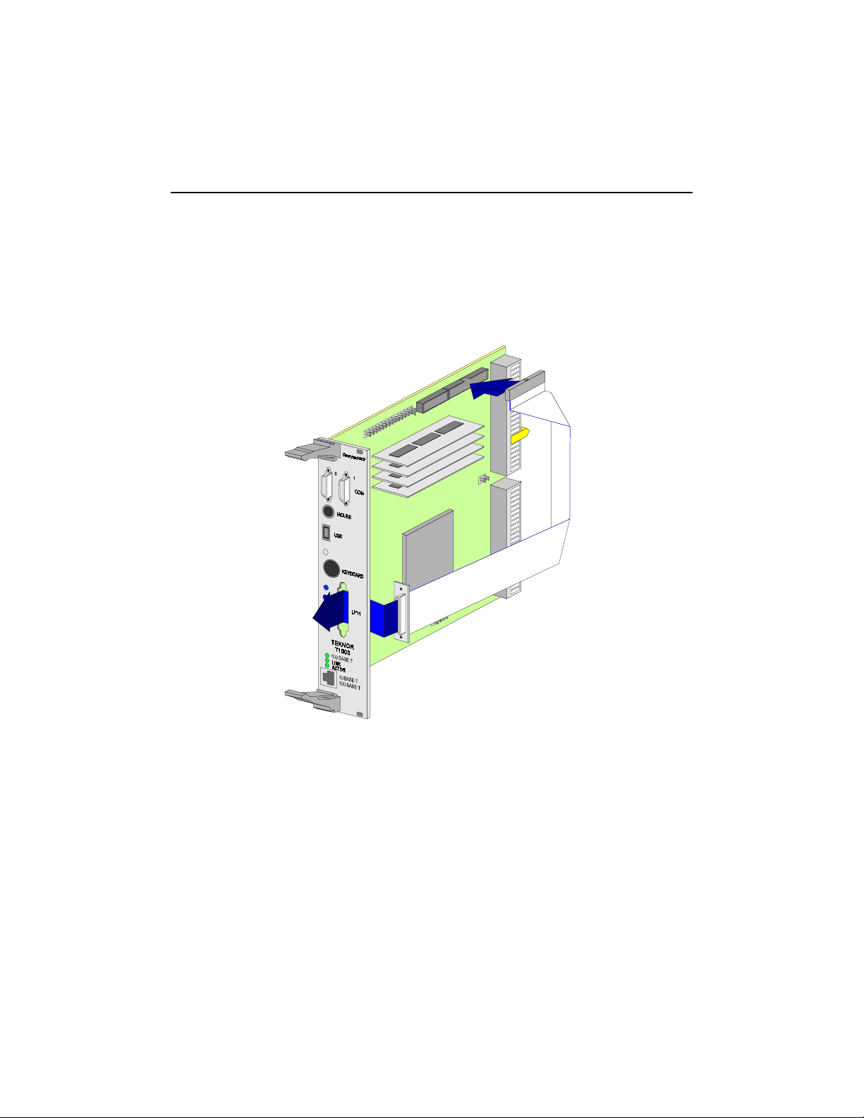
The onboard Parallel Port connector is a 26-p in male header located at the top right side of
the board. A 26 pin to pin flat cable is req uired to output the signals from the board to the
front plate.
The following list includes approved vendors for th e J3 conn ect or’s mating parts :
Amp 746285-6 [optional strain relief: 499252- 3],
Robinson Nugent IDS-C26PK-TG,
Thomas & Betts 622-2630 [option al st rain reli ef: 622-2641].
(Polarized IDC female socket connector).
7-10
Page 46
Connecting Devices
7.7.1 Parallel Port Modes
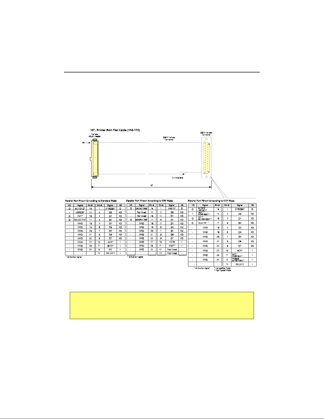
The parallel port is bi-directional. It is compatible with PC/XT, AT, PS/2, EPP and ECP
modes.
The differences between the three modes appear in the pin assignation:
NOTE
To operate in EPP or ECP mode, ensure t he peripheral is designed to
operate in this mode and the BIOS setup is configured to support it.
7-11
Page 47

TEK-CPCI-1000 Technical Reference Manual
7.7.2 Standard Mode
The Standard mode is an unidirectional p arallel port. It is used fo r its compatibilit y with the
IBM PC standard.
7.7.3 EPP Mode
The EPP (Enhanced Parallel Port) mode consists of a hardware independent method of
accessing a parallel port configured as EPP. It provides support for single I/O cycle as well
as the high performance block I/O transfers. The EPP mode always uses the most optimum
method for I/O transfers. For example, if the hardware supports it, EPP mode will perform
32-bit I/O block transfers.
EPP mode assumes that the parallel port can be used to connect more than one peripheral
device using Multiplexor or Daisy Chain configurations.
Multiplexor is an external device that permits up to eight parallel port devices to share a
single parallel port.
A Daisy Chain device has two port: input and output. The input port is connected either to
the host parallel port or the daisy chain de vice in front of it. T he output is used to co nnect
the next peripheral device to the daisy c hain. The last device, however, can be one without
daisy chain support.
7.7.4 ECP Mode
ECP (Extended Capabilities Port) works the same as EPP mode, but it will take precedence
over the EPP mode whe n addressing multiple logical devices in a single physical product.
While the EPP mode may intermix read and write operations without any overhead or
protocol handshaking, the ECP mode negotiates data transfers using a request from the host
and an acknowledgment from the peripheral.
NOTE
For more information on the ECP protocol, please refer to the
Extended Capabilities Port Protocol and ISA Interface Standard
(available from Microsoft Corporation) or contact our Technical
Support department.
7-12
Page 48
Connecting Devices
7.8 10BASE-T CONNECTOR (J12)
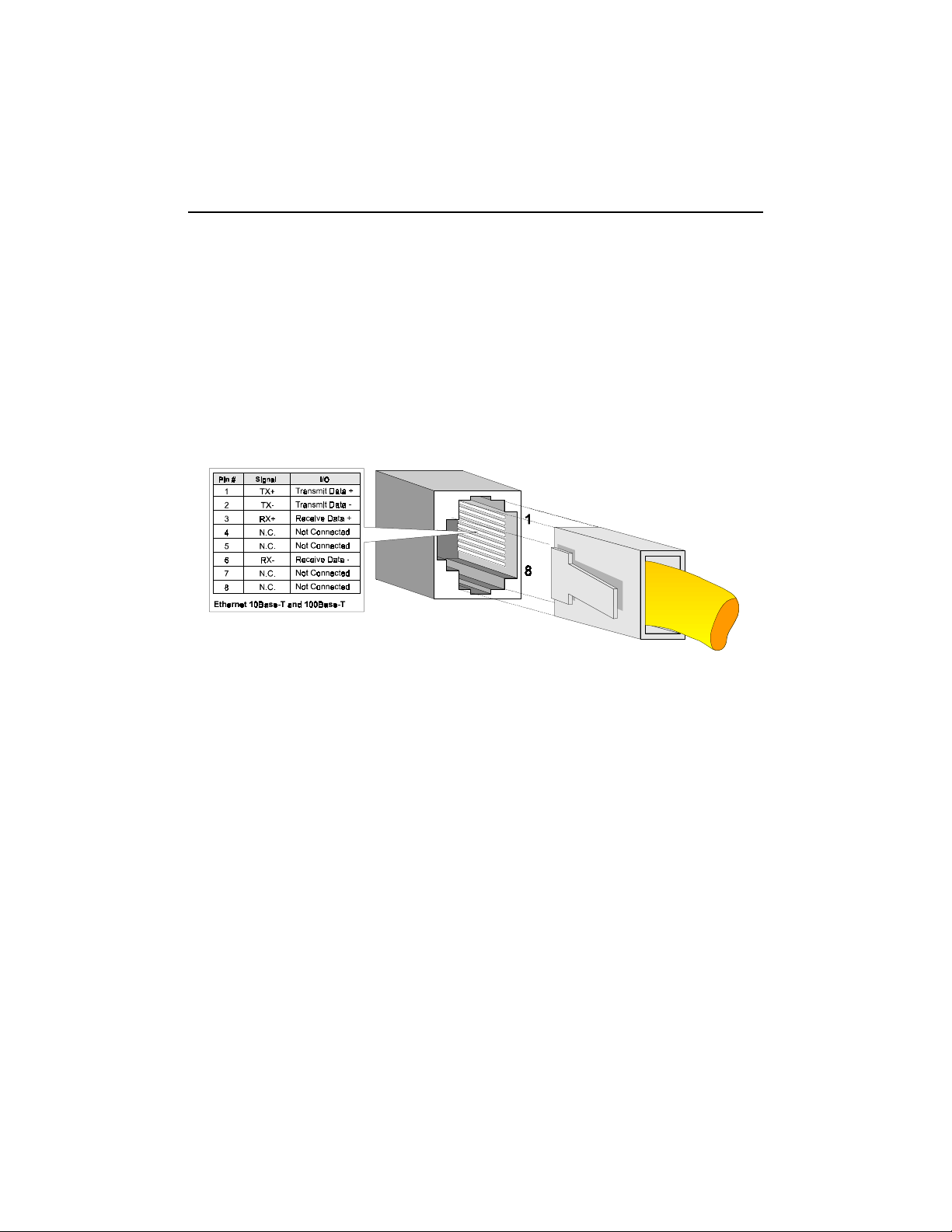
The TEK-CPCI-1000 supports both 10Base-T and 100Base-T on the same RJ-45 front plate
connector. 10Mbps and 100Mbps network speed is automatically detected and switched.
The 10Base-T interface uses UTP (Unshielded Twisted Pair) cables, category 5, 4 or 3 (5 is
better), while the 100Base-T cable must comply with the IEEE 802.3 100Base-T standard
for 2 pairs Category 5 UTP cable.
This connection type allows links up to 100m over both shielded twisted pair and data
grade (Cat. 5) unshielded twisted pair or equivalent.
The Ethernet controller resides on the PCI bus and is therefore Plug and Play by default. No
manual configuration is required. A diskette entitled “Network Drivers for IN82557” is
included with the Ethernet option. This diskette contains several operating system network
drivers.
To install the drivers, run the “setup.exe” program.
For other operating system drivers and installation instructions, contact TEKNOR’s
Technical Support department.
7-13
Page 49
TEK-CPCI-1000 Technical Reference Manual
(
)
(
)
7.9 MULTI-FUNCTION CONNECTOR (J2)
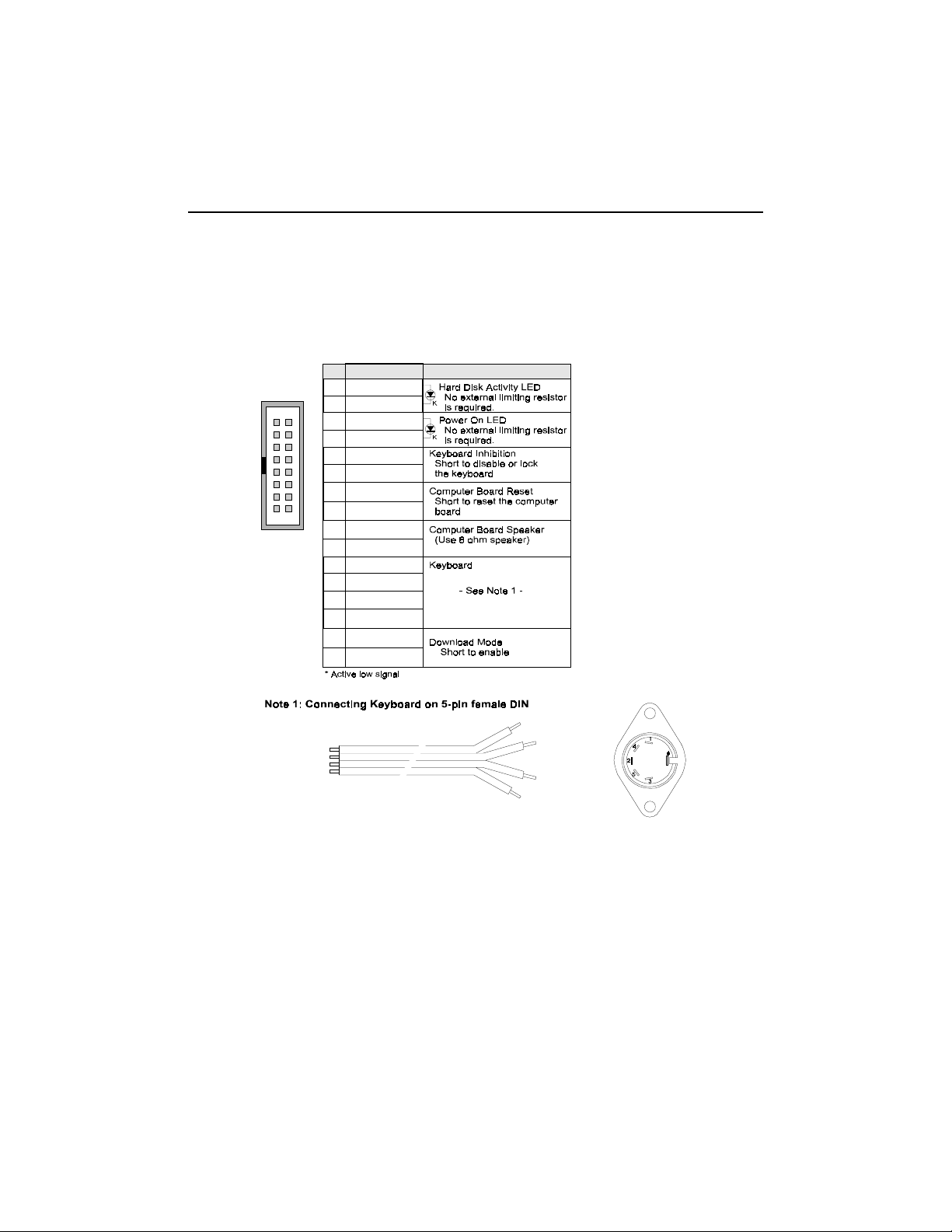
The connector J2 provides all the necessary signals to o utput keyboard, speaker, reset, and
keylock interface signals on a front plate, an interconnection module or a backplane.
It is described as follows:
Signals Nam e Des cription
VCC (+5V)
16
ACT1*
1152
15
VCC (+5V)
6
GND
4
9
KBINH
10
GND
13
PBRES*
14
7
8
1
3
2
5
11
12
GND
SPKR
VCC (+5V)
KCLK
KDAT
GND
VCC (+5V)
DOWN LD*
GND
16
To P in #1
KCLK
KDAT
GND
VCC
+5V
To Pin #2
To Pin #4, 6
To P in#5
Connector back view
The following list includes approved vendors for th e J2 conn ect or’s mating parts :
Amp 746285-3 [optional strain relief: 499252- 8],
Robinson Nugent IDS-C16PK-TG,
Thomas & Betts 622-1630 [option al st rain reli ef: 622-1641].
(16-pin flat cable connector).
7-14
Page 50

Connecting Devices
Each function is specified as follows:
Function Description
Speaker
Keyboard inhibit
Download
Reset
Hard disk activity
An 8 ohm speaker can be directly connected. The power stage is
incorporated onboard.
Keyboard inhibit function is used to switch the keyboard on or off.
Download function is used to transfer information to t he Flash disk using
a serial link connected to COM1 serial port.
A normally open push button can be used to reset the board. Reset
interface is open drain, thus external logic is not required.
LED can be used to signal read and write operations on the hard disk.
7.10 MISCELLANEOUS DEVICES
7.10.1 RESET Button on the Front Plate
Use a small tool to press the Reset butto n to restart the board. Reset function ge nerates a
hardware reset and reboots the board.
7.10.2 Ethernet LEDs on the Front Plate
100BASE-T
LINK
ACTIVE
Indicates 100Mbps operations when lit.
The LED is off when communicating at 10Mbps.
Indicates good link status for 10Mbps and 100Mbps operations.
Indicates the presence of transmit or receive activi ty for 10Mbps or 100Mbps
operations.
The LED is driven through a monostable function which ensures that even the
minimum size packet generates adequate LED ON time to be visible.
7-15
Page 51
TEK-CPCI-1000 Technical Reference Manual
7.11 CONNECTING STORAGE DEVICES
7.11.1 Connecting Hard Disks
The TEK-CPCI-1000 supports two configurati ons of hard disk connect ion:
Through the I/O connector
backplane through this connector (J5-J8). In such configuration, the backplane must be
designed to receive these signals and make them available through a standard 40-pin dual
row male connector for standard applications (with standard 40-pin header flat cables).
Through the PCI connector
directly to the PCI bus.
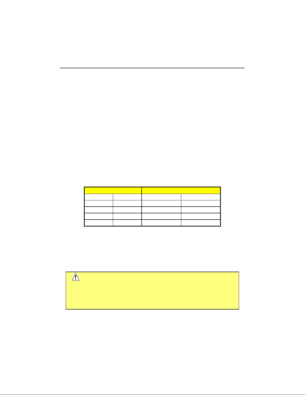
Primary/Secondary and Master/Slave configuratio ns are supported. To setup yo ur hard disk
installation, use the W1 an d W2 jumpers and, conform to the following table:
Jumpers HD Allocation
W1 W2 Primary HD Secondary HD
Off Off IDE bus IDE bus
Off On PCI bus IDE bus
On Off IDE bus PCI bus
On On PCI bus PCI bus
- Enhanced IDE signals are output from the board to a
- CompactPCI hard drive modules may be connected
CAUTION
Please be aware that Primary a nd Secondary hard dr ives must not be
allocated and installed on both PCI and IDE buses at the same time.
Such a configuration will generate a hardware conflict.
7-16
Page 52

Connecting Devices
7.11.2 Connecting Floppy Disk Drives
AT floppy disk drive signals are output from the board to a backplane through the I/O rearpanel connector (J5-J8). The backplane must be designed to receive these signals and make
them available through a standard 34-p in dual row male connector for standard applications
(with standard 34-pin header flat cables).
The onboard disk controller is IBM PC XT/AT compatible (single and double density), and
supports Enhanced Floppy mode (2.88MB). It ha ndles 3.5’’ and 5.25’’, low and high density
drives. Up to two drives can be supported in any combination.
7.11.3 Setting the BIOS
Hard disk and floppy disk drive s specification must be declared using the Award BIOS setup
program.
BIOS options and settings are described in Section 11.1.4 -
Standard CMOS Setup
.
7-17
Page 53
TEK-CPCI-1000 Technical Reference Manual
7.12 BATTERY BACKUP CIRCUIT
The TEK-CPCI-1000 come s with a 350mA/h TL5186 TADIRAN battery with a shelf life
of approximately 10 years (under "no-load" conditions).
CAUTIONS
1. Removing jumper W10 will cause the set-up and real-time clock
information to be lost.
2. The actual voltage supplied by the battery is 3.6 volts. This can be
verified at pins 16-32 on the SRAM device using a stand ard voltm eter.
The actual life of the battery depends on the a mount of time the DC power is no t applied
and on the environmental (temperature) conditions. The TADIRAN TL5186 has an
operating range of -55
0
to 750C and discharge characteristics vary with temperature.
The TADIRAN TL5186 is U.L. recognized. Its U.L. component recognition is MH12193.
WARNING
Danger of explosion if the battery is incorrectly replaced
.
Replace only with the same or equivalent type recommended by the
manufacturer. Dispose of used batteries according to the
manufacturer’s instructions
7-18
Page 54

8. INSTALLING VIDEO
The TEK-CPCI-1000 does not support onboar d video capabilities.
TEKNOR provides a 3U CompactPCI VGA module (TEK-CPCI-1002) that connects
directly to the PCI bus through the backplane. The module is built over the high
performance of the CL-GD5446 video controller chip from Cirrus Logic. It offers the
following specifications:
32-bit CompactPCI data bus
3U format, mech anically compliant with CompactPCI
64-bit DRAM based with BitBLT (Bit Block Transfer) hardware acceleration
Video pl ayback and video capture to fram e buff er
V-Port; VMI host and Feature Co nnector
VIPerVision TEK-380 interface modu le
136MHz dot clock
1280 x 1024 x 256 colors non-interlaced
Standard CRT DB-15 connector
1 or 2Mbytes of FPM or EDO video memory
For more information, please contact the Technical Support Department at TEKNOR.
8-1
Page 55

9. CONFIGURING DMA & IRQ
9.1 ALLOCATING DMA CHANNELS
The board implements the functionality of two 8237 DMA controllers. Eight DMA
channels are available.
According to Plug and Play standards, the system BIOS automatically allocates DMA
Channel 1 or 3 for the parallel port's ECP mode. Channel 2 is reserved for the floppy
controller and Channel 4 is used to cascade Channels 0 through 7 to the microprocessor.
DMA channels are assigned as follow:
DMA 0 Available
DMA 1 PnP available (ECP)
DMA 2 Floppy controller
DMA 3 PnP available (ECP or Ethernet)
DMA 4 Cascade controller # 1
DMA 5 PnP available (Ethernet)
DMA 6 PnP available (Ethernet)
DMA 7 PnP available (Ethernet)
NOTE
The DMA Channel for the Plug and Play Ethernet device is
automatically allocated by the system BIOS among those available
(Channel 3, 5, 6 or 7).
9-1
Page 56

TEK-CPCI-1000 Technical Reference Manual
9.2 ALLOCATING IRQ LINES
Two 8259 interrupt controllers handle the interrupts as follows:
1. Seven interrupt lines are directly linked to the keyboard controller, floppy controller,
timer, the real-time clock, both serial ports and the mouse.
2. The system BIOS automatically allocates IRQ5 or IRQ7 to the Parallel Port’s IRQ
line, depending on the settings i n the AWARD BIOS. When the Parallel Port is set to
278h or 3BCh, IRQ5 is assigned. When set to 378h IRQ7 is assigned. When set to
Auto IRQ5 or IRQ7 is assigned. When Disabled, IRQ5 and IRQ7 are available for
onboard and external PCI/PnP devices, or for external non-PnP devices (see note 1
below).
3. Primary and Secondary IDE controllers are configured with the AWARD BIOS
(Peripheral Setup option). IRQ 14 is linked to the primary IDE when the optio n is set
to Primary or Both. IRQ 15 is linked to the secondary IDE when t he option is set to
Secondary or Both. IRQ 14 and IRQ 15 are available for on board/external PCI/PnP
devices or external non-PnP devices (see note 1 below), when the option is set to
Disabled.
4. The on board Plug and Play Ethernet is automatically allocated with an IRQ line b y the
system BIOS among the available PCI/PnP IRQ lines.
DMA channels are assigned as follow:
Controller # 1 Controller # 2
IRQ 0 Timer 0 IRQ 8 Real-time clock
IRQ 1 Keyboard IRQ 9 Available
IRQ 2 Cascade controller # 2 IRQ 10 Available
IRQ 3 COM 2 * I RQ 11 Availabl e
IRQ 4 COM 1 * IRQ 12 PS/2 Mouse Interface
IRQ 5 LPT2 * or available
IRQ 6 Floppy controller * IRQ 14 P rimary IDE * or available
IRQ 7 LPT1 * or available
* All functions marked with an asterisk (*) can be disabled or reconfigured.
1
Available lines service on board and external PCI/PnP devices (when set to PCI/PnP in
AWARD BIOS PCI/PnP Setup screen) or an external non-PnP device (when set to ISA/EISA in
AWARD BIOS PCI/PnP Setup screen).
1
1
IRQ 13 Coproc essor Error
IRQ 15 S econdary IDE * or available
9-2
1
1
1
1
1
Page 57

10. Setting Jumpers
To configure the TEK-CPCI-1000 according to your application, nineteen jumpers are
available:
Jumper Description
W1, W2
W3 I/O Base Address - Selects the I/O base address from: 190h, 290h or 390h.
W4 Extended BIOS mode - Use this jumper to setup the following features:
W5
W6-W7 RS-232/RS-485 termination resistor - connect termination resistor for RS-232 or RS-
W8 Battery - Enables or disables the battery on the board.
W9 Power Fail detection - when installed, enables Power Fail Detection.
W10 Watchdog - enables or disables the watchdog.
W11 Power Fail source - when installed, enables the Battery voltage or an external user
W12-W13 Clock Speed Multiplier - Selects the internal CPU Clock Speed Mult iplier.
W14-W15 CPU Core/Bus Ratio - Selects the ration between the CPU Core Clock and the CPU
W16 External Cache size - not used while the cache is auto-detected by the BIOS.
W17 DRAM refresh rate - selects from 60 or 66Mhz rate.
W18 CPU type - selects the CPU type (Single -Plane or Split-Plane).
W19 VCORE - selects the CPU core voltage.
Hard drive installation setup - Use these jumpers to install hard drives on the EIDE
bus or the PCI bus.
Download mode
1.
Flash EPROM
VT100 mode
2.
TEKNOR Extension
3.
VT100, boot from Flash, save CMOS in flash, SRAM devic es..., (for more information
see Software Setup Section)
Ethernet
4.
Boot Mode selection - When set to emergency, it offers the ability to upgrade the
onboard BIOS from an emergency disk.
485 operation mode on Serial Port 2.
voltage to be monitored by the power Fail Detection controller.
Bus Clock.
- to download serially information from a remote computer to the
- to communicate with the board using a VT100 or ANSI terminal
- when enabled, authorizes TEKNOR’s features such as
- enables or disable the Ethernet interface.
10-1
Page 58
TEK-CPCI-1000 Technical Reference Manual
U18J8J4J1
J2B1J
3
J7J9J10S1U19U20U22J5J11J8
J13
J12
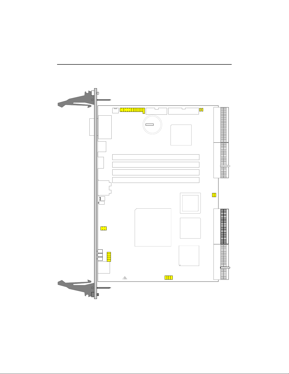
10.1 JUMPER LOCATION
W3 W4 W5
W7 W9
W6 W8 W10
W2
W11
W1
W12
W13
W18
DS1
DS2
W19
DS3
W15
W17
W16
W14
10-2
Page 59
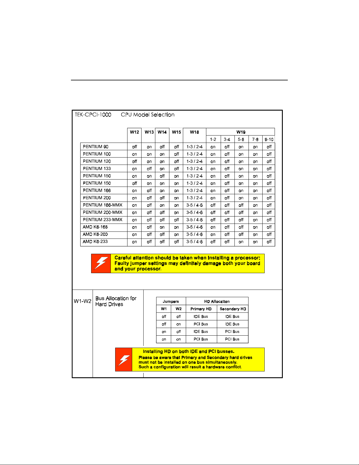
10.2 CPU MODEL SELECTION; W1 AND W2
Setting Jumpers
10-3
Page 60
TEK-CPCI-1000 Technical Reference Manual
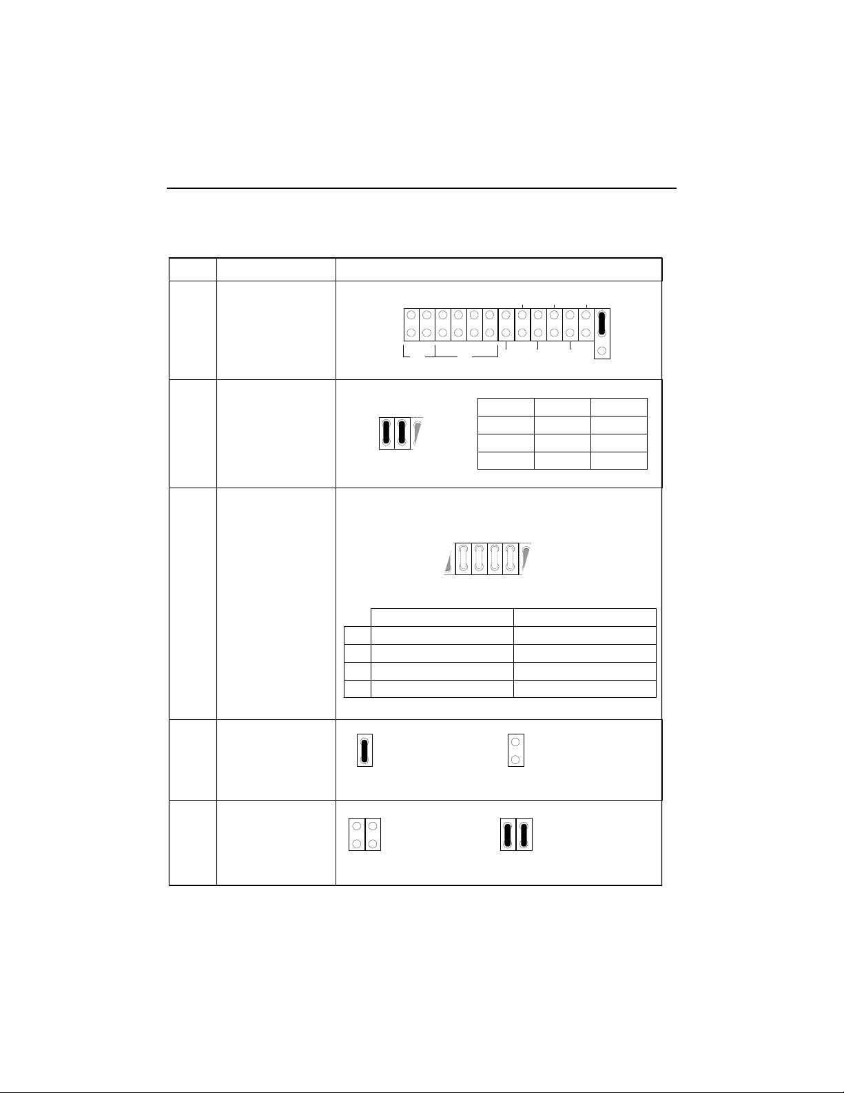
10.3 JUMPERS W3-W7
NAME FUNCTION CONFIGURATION (INITIAL SETTING: * )
I/O Base Address
W3
Extended BIOS
W4
Modes
:
: :
:::::
I/O
Base A ddress
190h *
290h
390h
1-2
on
on
off
:
:
3-4
on
off
x
These Jum pers are configured separately even though they
are grouped together
:
Jumper ON
Serial Download M ode
1-2
VT-100 Mode
3-4
Disable TEKN OR Extension
5-6
Ethernet Enabled
7-8
Jumper REMOVED *
Normal M ode
Standard Mode
Enable TEKNOR Extension
Ethernet D isabled
W5
W6-W7
Boot Mode
Selection
Termination
Resistors for
RS-422/RS -485
Modes
Emergency
Disconnected * Connected
: :: :
10-4
Nornal *
Page 61
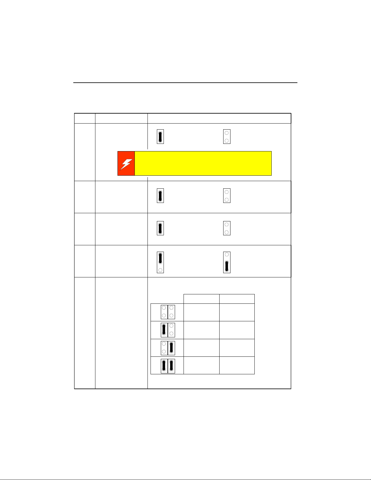
10.4 JUMPERS W8-W13
NAME FUNCTION CONFIGURATION (INITIAL SETTING: * )
Battery
W8
Danger of explosion if battery is incorrectly replaced.
Replace only with the same or equivalent type recommended
by the manufacturer. Dispose of used batteries according to the
manufacturer's instructions .
Connected
Disconnected *
Setting Jumpers
W9
W10
W11
:
:
Power Fail
Detection
Watchdog
Power Fail Source
Internal CPU
Clock Speed
Multiplier
Enabled
Enabled
User defined VBAT (3.08V) *
CPU Bus Clock
W12
W12
W12
W12
W13
W13
W13
W13
n/a
66MHz
60MHz
50MHz
Disabled *
Disabled *
PCI Clock
n/a
33MHz
30MHz
25MHz
10-5
Page 62
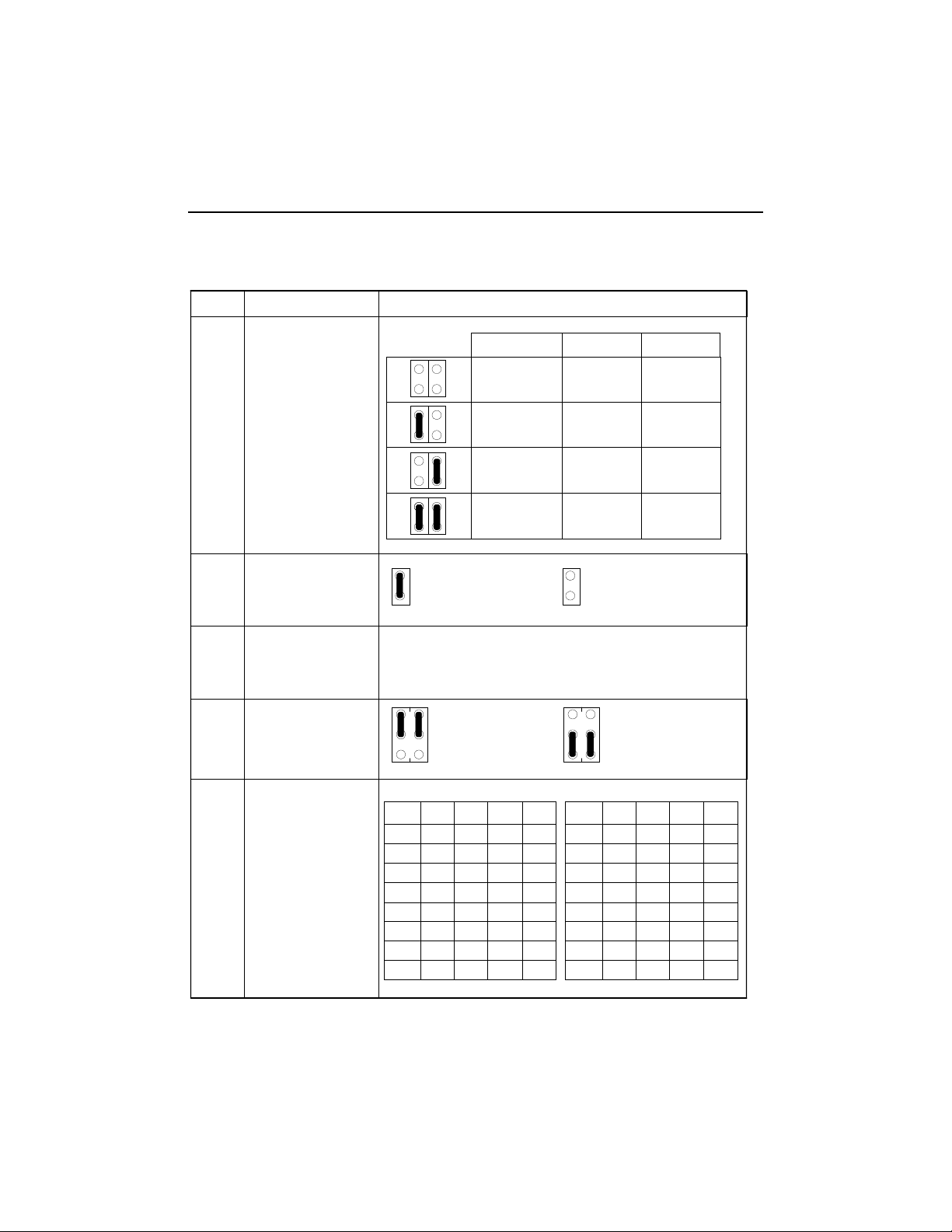
TEK-CPCI-1000 Technical Reference Manual
10.5 JUMPERS W14-W19
NAME FUNCTION CONFIGURATION (INITIAL SETTING: * )
:
:
:
:
:
CPU Core Clock /
CPU Bus Clock
Ratio
256KB External
Cache
DRAM Refresh
Rate
CPU Type
Selection
W14 W15
W14 W15
W14 W15
W14 W15
Enabled
Core / Bus Ratio
3/2
2/1
3/1
5/2
50MHz 60MHz
75MHz 100MHz
100MHz 133MHz
150MHz 200MHz
125MHz 166MHz
Disabled
Not used while the cache is auto-detected by the BIOS
Single-Plane Split-Plane
:
CPU Core Voltage
Selection
VCore
1.24
2.14
2.24
2.34
2.44
2.54
2.64
2.74
7-8
off
off
off
off
off
off
off
off
5-6
off
off
off
off
on
on
on
on
10-6
3-4
off
off
on
on
off
off
on
on
1-2
off
on
off
on
off
on
off
on
VCore
2.84
2.94
3.04
3.14
3.24
3.34
3.44
3.54
7-8
on
on
on
on
on
on
on
on
5-6
off
off
off
off
on
on
on
on
3-4
off
off
on
on
off
off
on
on
1-2
off
on
off
on
off
on
off
on
Page 63

PRODUCT DESCRIPTION
11. POWERING UP THE SYSTEM
12. SOFTWARE SETUP
13. VFLASH SOFTWARE
14.
15. UPDATING THE BIOS WITH UBIOS
16. VT 100 M ODE
FLASH FILE SYSTEM
II
Page 64

11. POWERING UP THE SYSTEM
11.1 POWER UP
Once you are r eady to power up your system:
1. Insert a bootable diskette in the drive A to start your system with DOS.
2. Hit the DELETE key before or when this message appears near the bottom of the
screen:
″Press DEL to enter SETUP″. The main menu appears on the screen.
- In Standard Setup, set the date and tim e.
- In other menu choices, set other options (if necessary).
3. From the m ain menu, press the F10 key. Type “Y” to save your setup. The system will
continue the boot procedu re.
4. Once the boot procedure is completed, reboot the system to make sure everything
works properl y.
11.2 TROUBLESHOOTING
If you shoul d en c ounter a problem, first verify the following it em s:
1. Make sure that all connectors are connected properly. On the standard flat ribbon
cable used for the floppy connector, pin 1 is indicated by small red stripe. Verify that
this red stripe is located on the appropriate side of the connector.
2. Veri fy your boot di sket te. It mu st be a syst em disk and it m ust be in prop er wor kin g
order.
3. If th e system still does not start up properly, you should try booting your system with
only th e power cord and video monitor connected (this is the minimum required to see
if the boa rd i s working).
4. If you still are not able to get your board up and running, contact our Technical
Support departmen t for assistance.
11-1
Page 65

12. SOFTWARE SETUP
12.1 AWARD SETUP PROGRAM
The TEK-CPCI-1000 uses the AWARD BIOS setup program to configure data in the CMOS
RAM. This program is EEPROM located and may be accessed by pressing the DELETE key
at the appropriate time during system boot.
CAUTION
Before modifying CMOS setup parameters, insure that the W8 jumper
(battery) is installed to enable the CMOS backup.
(See Section 10 - Setting Jumpers)
To run the AWARD Setup program, proceed as follows:
2. Turn on or reboot the system.
3. Hit the DELETE key before or when the message - "PRESS DEL TO ENTER
SETUP" appears near the bottom of the screen.
4. The main menu appears on the screen.
ROM PCI/ISA BIOS
CMOS SETUP UTILITY
AWARD SOFTWARE, INC.
STANDARD CMOS SETUP
BIOS FEATURES SETUP
CHIPSET FEATURES SETUP
POWER MANAGEMENT SETUP
PNP/PCI CONFIGURATION
LOAD BIOS DEFAULTS
LOAD SETUP DEFAULTS
Esc : Quit
F10 : Save & Exit Setup
Time, Date, Hard Disk Type...
INTEGRATED PERIPHERALS
SUPERVISOR PASSWORD
USER PASSWORD
PASSWORD SETTING
IDE HDD AUTO DETECTION
4DD LOW LEVEL FORMAT
SAVE & EXIT SETUP
EXIT WITHOUT SAVING
↑ ↓ → ← : Select Item
(Shift)F2 : Change Color
12-1
Page 66

TEK-CPCI-1000 Technical Reference Manual
12.1.1 Using the AWARD BIOS Setup
All key functions are listed below:
Up/Down arrows Move to previous/next item.
Left/Right arrows Move to the item in the left/r ight hand.
Esc key In Main Menu: Quit settings (Answer ‘Y’ to save changes into CMOS).
In sub-menus: Exit and return to Main Menu.
PgUp/ PgDn keys Increase/ Decrease the numeric value or make changes.
+/- keys Increase/ Decrease the numeric value or make changes.
F1 key Display the information associated to the selected field.
F2 and
Shift F2 keys
F5 key In sub-menu: Restore the previous setup values from BIOS Default Table.
F6 key In sub-menu: Load the default setup values from BIOS Default Table.
F7 key In sub-menu: Load the setup values from the Setup Default Table .
F4, F8, F9 keys Reserved.
F10 key When in Main Menu: Save all the CMOS changes.
Change color from total 16 colors: F2 to select color forward, Shift F2 to select
color backward.
12.1.2 Save & Exit Operations
Use one of the following options available from the Main Menu:
Save & Exit
Exit Without
Saving
Use this option to save the configuration stored in the CMOS
RAM after a setup modificatio n. This option will not cha nge the
values saved in Flash EPROM. To update values in the Flash, use
the VIP-UP program and perform a save operation (F10).
Use this option to exit the AWARD setup without saving the
configuration to the CMOS RAM.
12-2
Page 67

12.1.3 Setting Features
The main menu provides the following options:
Software Setup
Standard CMOS
Setup
BIOS Features
Setup
Chipset Features
Setup
Power Management
Setup
PnP/PCI
Configuration
Integrated
Peripherals
Supervisor/User
Password Setting
IDE HDD Auto
Detection
HDD Low Level
Format
Provides all the AT-com patible BIOS standard options.
Provides all special enhanced features of the BIOS.
Provides all the features related to the chipset (Intel 430HX).
Sets the power conservation options.
Sets Plug and Play, and PC I Local Bus configuration options.
I/O susbsystems that depend on the integrated peripherals controller
in your system.
Use this option to change, set, or disable a password. It allows access
limitation to the system and the Setup, or just to the Setup.
Automatically detects and configures hard disk parameters. This
ability is included in the e vent you are uncertain o f your hard dis k’s
parameters.
This option does not appear in many BIOS versions. Most
manufacture rs of IDE hard drives str ongl y reco mmend that yo u do
not run a low-level format on their drives, because o f the danger
that the bad-track table may be over-written. Award s upplies this
utility for service personnel only.
If you need to run a low-level format on your hard drive, contact
your drive manufacturer for instructions
!
Load BIOS Defaults
Load Setup Defaults
The BIOS defaults are minimum settings requir ed for your system to
operate.
The chipset default settings are provided for a maximum system
performance.
12-3
Page 68

TEK-CPCI-1000 Technical Reference Manual
Whenever you are not sure about a certain setting, you may refer to the list of default values
provided in the eve nt that a value has bee n changed and one wis hes to set this option to it s
original value. Loading the BIOS or SETUP defaults will affect all the options and will reset
options previously altered.
The BIOS default set tings co nsist o f the sa fest set o f para meters. Use t hem if the syste m
is behaving erratically. They should always work but do not provide optimal system
performance.
The SETUP default values provide optimum performance settings for all devices and
system features.
CAUTION
These parameters have been pro vided to give control over t he system.
However, the values for these options should be changed only if the user
has a full understanding of the timing relationships involved.
12.1.4 Standard CMOS Setup
This part of the setup allows you to set the time, date, hard disk type, types of floppy drives
and video type.
Date/Time
The current values for each category are displayed. Enter new
values through the keyboard.
Hard Disks
Two IDE controllers are supported (Primary and Secondary),
each can have two disks: Master Disk (bootable) or Slave Disk.
Drive A / Drive B
Identifies the types of floppy disk drive (A or drive B) that have
been installed.
Video
Halt on
Specifies the basic type of video adapter installed in the system.
Specifies the type of error s that will stop the s ystem during the
BIOS booting procedure.
Memory
This display-only option summarizes the amount of Base,
Extended and other types of mem ory ins t alle d in the sy st em.
12-4
Page 69

Software Setup
12.1.5 BIOS Features
Option
Virus Warning Dis. Dis. En., Dis. When Enabled, displays a warning message if a program (usually, a
CPU Internal Cache Dis. En. En., Dis. Enables or Disables the CPU Internal Cache.
CPU External Cache Dis. En. En., Dis. Enables or Disables the CPU external Cache.
Quick Power On Self
Test
Boot Sequence A, C C, A
Swap F loppy Drive Dis. Dis. En., Dis. Effective only in systems with two FD. Select Enabled to assign
Boot Up Floppy Seek En. Dis. En., Dis.
Boot Up NumLock
Status
Boot Up Syste m Speed High High Low, High Sel ect High to boot at the default CPU speed; select Low to boot at
Typematic Rate Setting Dis. Dis. En., Dis. When Disabled, the following two item s (Typematic Rate and
Typematic Rate
(Chars/Sec)
Typematic Delay
(Msec)
Security Option Setup Setup Setup, System
OS Select For
DRAM>64MB
BIOS
Default
Setup
Default
Dis. En. En., Dis. Select Enabled to reduce the amount of time to run the power-on self
Off Off On, Off
30 30 6, 8, 10, 12,
250 250
Non-
Non-
OS2
OS2
Possible
Settings
(A,C) ; (C,A) ;
(C, CD, A);
(CD, C, A)
15, 20, 24, 30
char./second
250, 500, 750,
1000 ms
Non-OS/2,
OS/2
virus) attempts to write to the boot sector or the partiti on table of the
HDD. You should then run an anti-virus program. Keep in mind that
this feature protects only the boot sector, not the entire hard drive.
Note: Many disk diagnostic programs and operating system
installation that access the boot sector table can trigger the virus
warning message. If you plan to run such a program, first disable the
virus warning.
test (POST). A quick POST skips certain steps. In normal disabl e
quick POST.
Selects the boot source drive that supports the operating system
(floppy disk, hard disk, or CDROM).
physical drive B to logical drive A, and physical drive A to logical
drive B.
When Enabled, the BIOS tests (seeks) floppy drives to determine
whether they have 40 or 80 tracks. Only 360KB floppy drives have
40 tracks; drives with 720KB, 1.2MB, and 1.44MB capacity all have
80 tracks. Because very few modern PCs have 40 track floppy
drives, we recommend that you set this field to “Disabled” to save
time.
Toggle On/Off to control the state of the NumLock key at the bootup.
When On, the numeric keypad generates numbers instead of
controlling cursor operations.
the speed of the AT bus. Some add-in peripherals or old software
(such as old games) may require a slow CPU speed.
Typematic Delay) are irrelevant. Keystrokes repeat at a rate
determined by the keyboard controller in your system. When
Enabled, you can select a typematic rate and a typematic delay.
When the typematic rate setting is Enabled, you can select a
typematic rate (the rate at which characters repeat when you hold
down a key) of 6, 8, 10, 12, 15, 20, 24 or 30 characters per second.
When Enabled, you can select a typematic delay (the del ay before
key strokes begin to repeat) of 250, 500, 750 or 1000 milliseconds.
If you have set a password, select whether the password is required
every time the system boots, or only when you enter Setup.
Select OS2 only if you are running an OS/2 operating syste m with
greater than 64MB of RAM.
Description
12-5
Page 70

TEK-CPCI-1000 Technical Reference Manual
BIOS Features (continued)
Option
Video BIOS Shadow Dis. En. En., Dis. Software that resides in a read-only memory (ROM) chip on a device
CC000-CFFFF
Shadow
D0000-D3FFF Shadow Dis. Dis. En., Dis.
D4000-D7FFF Shadow Dis. Dis. En., Dis.
D8000-DBFFF Shadow Dis. Dis. En., Dis.
DC000-DFFFF
Shadow
BIOS
Default
Setup
Default
Dis. Dis. En., Dis. such as the system BIOS, video BIOS, and similar operating
Dis. Dis. En., Dis. Video BIOS shadows into memory area C0000-CBFFF. The
Possible
Settings
called firmware. The Award BIOS allows shadowing of firmware
instructions that come with some expansion peripherals (for
example, a
SCSI adaptor). Shadowing copies of firmware from ROM into system
RAM, where the CPU can read it through the 16-bit or 32-bit DRAM
bus.
Firmware not shadowed must be read by the system through the 8bit X-bus. Shadowing improves the performance of the system
BIOS and similar firmware for expansion peripherals, but it also
reduces the amount of high memory (640KB to 1MB) available for
loading device drivers, etc. Enable shadowing into each section of
memory separately. Many system designers hardwire shadowing of
the system BIOS and eliminate a System BIOS Shadow option.
remaining areas shown on the BIOS Features Setup screen may be
occupied by other expansion card firmware. If an expansion
peripheral in your system contains ROM-based firmware, you need
to know the address range the ROM occupies to shadow it into the
correct area of RAM.
Description
12-6
Page 71

Software Setup
12.1.6 Chipset
Option
Auto Configurati on En. En. En., Dis. Auto Configuration selects predetermined optimal values of chipset
DRAM Timing 70ns 70ns 70ns, 60ns The value in this field depends on performance para meters of the
DRAM RAS#
Precharge Time
DRAM R/W Leadoff
Timing
Fast RAS# to CAS#
Delay
DRAM Read Burst
(EDO/FPM)
DRAM Write Burst
Timing
Turbo Read Leadoff Dis. Dis. En., Dis. Select Enabled to shorten the leadoff cycles and optimize
DRAM Speculative
Leadoff
Turn-Around Insertion Dis. Dis. En., Dis. When Enabled, the chipset inserts one extra clock to the turn-around
ISA Clock PCI
System BIOS
Cacheable
Video BIOS Cacheable Dis. En. En., Dis.
8 Bit I/O Recovery
Time
BIOS
Default
x444/x
Setup
Default
4 4 4, 3 Select the number of CPU clocks al located for the Row Address
7/6 7/6 7/6, 6/5 Select the combination of CPU clocks the DRAM on your board
3 3 3, 2 W hen DRAM is refreshed, both rows and columns are addressed
x444/x
444
444
x444 X444
Dis. Dis. En., Dis.
CLK/4
PCI
CLK/4
Dis. En. En., Dis. Selecting Enabled allows caching of the system BIOS ROM at
3 1 1, 2, 3, 4, 5, 6,
Possible
Settings
x444/x444,
x333/x444,
x222/x333
x444, x333,
x222
PCI CLK/4,
PCI CLK/3
7, 8, NA
parameters. When Disabled, chipset parameters revert to setup
information stored in CMOS. Many fields in this screen are not
available when Auto Configuration is Enabled.
installed memory chips (DRAM). Do not change the value from the
factory setting unless you install new memory that has a different
performance rating than the original DRAMs.
Strobe (RAS#) signal to accumulate its charge before the DRAM is
refreshed. If insufficient time is allowed, refresh may be incomplete
and data lost.
requires before each read from or write to the memory. Changing the
value from the setting determined by the board designer for the
installed DRAM may cause memory errors.
separately. This setup item allows you to determine the timing of the
transition from RAS to Column Address Strobe (CAS).
Sets the timing for reads from EDO (Extended Data Output) or FPM
(Fast Page Mode) memory. The lower the number, the faster the
system addresses memory. Selecting timing numbers lower than the
installed DRAM is able to support can result in memory errors.
Sets the timing for writes to memory. The lower the timing numbers,
the faster the system addresses memory. Selecting timing numbers
lower than the installed DRAM is able to support can result in
memory errors.
performance in cacheless, 50-60 MHz, or one-bank EDO DRAM
systems.
A read request from the CPU to the DRAM controller includes the
memory address of the desired data. When Enabled, Speculative
Leadoff lets the DRAM controller pass the read command to memory
sightly before it has fully decoded the address, thus speeding up the
read process.
of back-to-back DRAM cycles.
You can set the speed of the AT bus at one-third or one-fourth of the
CPU clock speed.
F0000h-FFFFFh, resulting in better system performance. However, if
any program writes to this memory area, a system error may occur.
Selecting Enabled allows caching of the video BIOS ROM at C0000h
to C7FFFh, resulting in better video performance. However, in any
program writes to this memory area, a system error may occur.
The I/O recovery mechanism adds bus clock cycles between PCIoriginated I/O cycles to the ISA bus. This delay takes place because
the PCI bus is so much faster than the ISA bus.
These two fields let you add recovery time (in bus clock cycles) for
16-bit and 8-bit I/O.
Description
12-7
Page 72

TEK-CPCI-1000 Technical Reference Manual
Chipset (continued)
Option BIOS
16 Bit I/O Recovery
Time
Peer Concurrency En. En. En., Dis.
Chipset S p e c ial
Features
DRAM ECC/PARITY
Select
Memory Parity/ECC
Check
Single Bit Error Report En. En. En., Dis. If ECC is enabled, selecting Enabled here tells the system to report
L2 Cache Cacheable
Size
Chipset NA# Asserted
Pipeline Cache Timing Faster Faster Faster, Fastest
Passive Release En. En. En., Dis. When Enabled, CPU to PCI bus accesses are allowed during
Delayed Transaction Dis. En. En., Dis.
Memory Hole Location None None
Default
Setup
Default
2 1 1, 2, 3, 4, NA
En. En. En., Dis.
Parity Parity ECC, Parity
Auto Auto En., Dis., Auto In Auto mode, the BIOS enables memory checking automatically
64MB 64MB 64MB, 512MB Select 512MB only if your system RAM is greater than 64MB.
En. En. En., Dis. Selecting Enabled allows pipelining, in which the chipset signals the
Possible
Settings
512K-640K,
15M-16M
Description
Peer concurrency means that more than one PCI device can be
active at a time.
When Disabled, the chipset behaves as if it were the earlier Intel
82430FX chipset.
Set this option according to the type of DRAM installed in your
system: error-correcting code (ECC) or parity (default).
when it detects the presence of ECC or parity DRAM.
an error when a correctable single-bit error occurs.
CPU for a new memory address before all data transfers for the
current cycle are complete, resulting in faster performance.
For a secondary cache of 256KB (one bank), select Faster. For a
secondary cache of 512KB (two banks), the system designer must
select Fast (3-1-1-1, 2-1-1-1) or Faster (3-1-1-1, 1-1-1-1). Cache
timing 3-1-1-1 is at the CPU access speed. It requires special
SRAMs because the 3-1-1-1 timing is at the CPU clock rate.
passive release, otherwise the arbiter only accepts another PCI
master access to local DRAM.
The chipset has an embedded 32-bit posted write buffer to support
delay transactions cycles. Select Enabled to support compliance with
PCI specifications version 2.1.
You can reserve this area of system memory for ISA adapter ROM.
When this area is reserved, it cannot be cached. The user
information of peripherals that need to use this area of system
memory usually discusses their memory requirements.
12-8
Page 73

Software Setup
12.1.7 Power Management
Option
Power Management Dis. Dis. Min Saving,
PM Control by APM Yes Yes Yes, No If Advanced Power Management (APM) is installed, select Yes for
Video Off Method V/H
Modem Use IRQ 3 3
Doze Mode Dis. Dis. 1, ... , 40 mins,
Standby Mode Dis. Dis.
Suspend Mode Dis. Dis. 1, ... , 40 mins,
HDD Power Down Dis. Dis. 1, 2, 3, (...), 15
Thernal Management Dis. Dis. En., Dis. Enable this option to monitor the CPU temperature. Whenever the
Wake Up Events
IRQ3
IRQ4
IRQ8
IRQ12
BIOS
Default
SYNC
+
Blank
Off
Off
Off
Off
Setup
Default
V/H
SYNC
+
Blank
On
On
On
On
Possible
Settings
Max Saving,
User Define,
Dis.
V/H SYNC +
Blank, DPMS,
Blank Screen
NA, 3, 4, 5, 7,
9, 10, 11
1 hour, Dis.
1, ... , 40 mins,
1 hour, Dis.
1 hour, Dis.
mins
On, Off
This option allows you to select the type (or degree) of power saving
for Doze, Standby, and Suspend modes.
Max Saving
in each mode.
Min Saving
each mode (except the hard drive).
User Define
the PM Timers section (see below).
better power savings.
Determines the manner in which the monitor is blanked.
V/H SYNC + Blank
synchronization ports and writes blanks to the video buffer.
DPMS Support
VESA Display Power Management Signaling (DPMS) standard.
Use the software suppli ed for your video subsytem to select video
management values.
Blank Screen
Assignes an IRQ line to the modem (if any) on your system. Activity
on the selected IRQ always awakens the system.
After the selected period of system inactivity (1 minute to 1 hour), the
CPU clock runs at lower speed while all other devices still operate at
full speed.
After the selected period of system inactivity (1 minute to 1 hour), the
fixed disk drive and the video shut off while all other devices still
operate at full speed.
After the selected period of system inactivity (1 minute to 1 hour), all
devices except the CPU shut off.
After the selected period of drive inactivity (1 to 15 min), the hard
disk drive powers down while all other devices remain active.
CPU overheats, it slows down to lower the temperature.
When the system is in Doze or Standby mode, you may disable
activity monitoring of some common interrupt requests so they do
not wake up the system.
The default wake-up event is keyboard activity. In these wake-up
event fields, you can turn On or Off four commonly used interrupts.
For example, if you have a modem on IRQ3, you can turn on IRQ3
as a wake-up event, so an interrupt from the modem can wake up
the system. Or you may wish to turn Off IRQ12 (the P S/2) mouse as
a wake-up event, so accidentally brushing the mouse does not
awaken the system.
: Maximum power savings. Inactivity period is 1 minute
: Minimum power savings. Inactivity period is 1 hour in
: Set each mode individually. Select time-out periods in
: Select this option if your monitor supports the
: System only writes blanks to the video buffer.
Description
: System turns off vertical and horizontal
12-9
Page 74

TEK-CPCI-1000 Technical Reference Manual
Power Management (continued)
Power Down and Resume
Events
IRQ3 (COM 2) Off On
IRQ 4 (COM 1) Off On
IRQ 5 (LPT2) Off On
IRQ 6 (Floppy Disk) Off Off
IRQ 7 (LPT 1) Off On
IRQ 8 (RTC Alarm) Off Off
IRQ 9 (IRQ 2 Redir) Off On
IRQ 10 (Reserved) Off On
IRQ 11 (Reserved) Off On
IRQ12 (PS/2 Mouse) Off On
IRQ 13 (Coprocessor) Off On
IRQ 14 (Hard Disk) Off On
IRQ 15 (Reserved) Off On
On, Off
You may disable monitoring of common interrupt requests so
they do not reset activity timers.
12-10
Page 75

Software Setup
12.1.8 PnP/PCI
Option
Resources ControlledByAuto Man. Auto, Manual The Award Plug and Play BIOS can automatically configure all the
Reset Configuration
Data
IRQ n Assigned To
n = 3, 4
n = 5, 7, 9, 10, 11, 12,
14, 15
DMA n Assigned To
n = 0, 1, 3, 5, 6, 7
PCI IRQ Activated By Level Level Level, Edge
PCI IDE IRQ Map To
Primary IDE INT#
Secondary IDE INT#
Used Mem Base
Address
Used Mem Length 8K 8K
BIOS
Default
Setup
Default
Dis. Dis. En., Dis. Normally, you leave this field Disabled. Select Enabled to reset
PCI/ISA
PnP
PCI/
ISA
PnP
PCIAuto
Leg.
ISA
PCI/IS
A PnP
PCI/
ISA
PnP
PCIAuto
A
A
B
B
NA NA
Possible
Settings
PCI/ISA PnP,
Legacy ISA
PCI/ISA PnP,
Legacy ISA
PCI-Auto, ISA,
PCI-SLOT1,
PCI-SLOT2,
PCI-SLOT3,
PCI-SLOT4
A, B, C, D
NA, C800,
CC00, D000,
D400, D800,
DC00
-, 8K, 16K,
32K, 64K
boot and Plug and Play-compatible devices. If you select Auto, all
the interrupt requests (IRQs) and DMA assignment fields disappear,
as the BIOS automatically assigns them.
Extended System Configuration Data (ESCD) when you exit Setup if
you have installed a new add-on and the system reconfiguration has
caused such a serious conflict that the operating system cannot
boot.
When resources are controlled manually, assign each system
interrupt as one of the following types, depending on the type of
device using the interrupt:
Legacy ISA Devices compliant with the original PC AT bus
specification, requiring a specific interrupt (such as IRQ4 for serial
port 1).
PCI/ISA PnP Devices compliant with the Plug and Play standard,
whether designed for PCI or ISA bus architecture.
When resources are controlled manually, assign each system D MA
channel as one of the following types, depending on the type of
device using the interrupt:
Legacy ISA Devices compliant with the original PC AT bus
specification, requiring a specific DMA channel.
PCI/ISA PnP Devices compliant with the Plug and Play standard,
whether designed for PCI or ISA bus architecture.
Leave the IRQ trigger set at Level unless the PCI device assigned to
the interrupt specifies Edge-triggered interrupts.
This field lets you select PCI IDE IRQ mapping or PC AT (ISA)
interrupts. If your system does not have one or two PCI IDE
connectors on the system board, select values according to the type
of IDE interface(s) installed in your system (PCI or ISA). Standard
ISA interrupts for IDE channels are IRQ14 for primary and IRQ15 for
secondary.
Each PCI peripheral connection is capable of activating up to four
interrupts: INT# A, INT# B, INT# C and INT# D. By default, a PCI
connection is assigned INT# A. Assigning INT# B has no meaning
unless the peripheral device requires two interrupt services rather
than just one. Because the PCI IDE interface in the chipset has two
channels, it requires two interrupt services. The primary and
secondary IDE INT# fields default to values appropriate for two PCI
IDE channels, with the primary PCI IDE channel having a lower
interrupt than the secondary.
Select a base address for the memory area used by any peripheral
that requires high memory.
Select a length for the me mory area specified in the previous field.
This field does not appear if no base address is specified.
Description
12-11
Page 76

TEK-CPCI-1000 Technical Reference Manual
12.1.9 Integrated Peripherals
Option
IDE HDD Block Mode Dis. En. En., Dis. Block mode is also called block transfer, multiple commands, or
PCI Slot IDE 2nd
Channel
On-Chip
Primary/Secondary
PCI IDE
IDE
Primary/Secondary
Mast./Slave PIO
USB Controller and
Keyboard
Onboard FDC
Controller
Onboard
Serial Port 1/2
UART2 Mode Stand
Duplex Select Half Half Half, Full Half for one communication at a time, Full for simultaneous
TxD, RxD Active Hi/Lo Hi/Lo Hi/Hi, Hi/Lo,
Onboard Parallel Port 378/IRQ7378/IRQ7378/IRQ7,
Parallel Port Mode Nornal
ECP Mode Use DMA 3 3 1, 3 Select a DMA channel for the port.
BIOS
Default
Setup
Default
En. En. En., Dis.
En. En. En., Dis.
Auto Auto
Dis. Dis. En., Dis. Select Enabled if your system contains an Universal Serial Bus
En. En. En., Dis. Select Enabled if your system has a floppy disk controller (FDC)
Auto Auto Dis.,
Stand
ard
ard
ECP+
EPP1.
9
Possible
Settings
Mode 0, Mode
1, Mode 2,
Mode 3, Mode
4, Auto
COM1/3F8,
COM2/2F8,
COM3/3E8,
COM4/2E8,
Auto
Standard,
IrDA, ASK-IR
Lo/Hi, Lo/Lo
278/IRQ5,
3BC/IRQ7,
Dis.
ECP+EPP1.9,
Normal,
EPP1.7+SPP,
ECP+EPP1.7,
SPP,
EPP1.9+SPP,
ECP
multiple sector read/write. If your IDE hard drive supports block
mode (most new drives do), select Enabled for automatic detection
of the optimal number of block read/ writes per sector the drive can
support.
You may separately disable the second channel on an IDE interface
installed in a PCI expansion slot.
The integrated peripheral controller contains an IDE interface with
support for two IDE channels. Select Enabled to activate each
channel separately.
The four IDE PIO (Programmed Input/Output) fields let you set a PIO
mode (0-4) for each of the four IDE devices that the onboard IDE
interface supports. Modes 0 through 4 provide successively
increased performance. In Auto mode, the system automatically
determines the best mode for each device.
(USB) controller and you have USB peripherals.
installed on the system board and you wish to use it. If you install an
add-in FDC or the system has no floppy drive, select Disabled in this
field.
Select a logical COM port name and matching address for the first
and second serial ports.
Select a communication protocol for Serial Port 2: Standard for
normal operation, IrDA or ASK-IR for infra-red operation.
communication.
Determines whether the transmit signal (TxD) and the receive signal
(RxD) are active high (Hi) or active low (Lo).
Select a logical LPT port name and matching address for the
physical parallel (printer) port.
Select an operating mode for the onboard parallel port. Select ECP
or EPP unless yo u are certain both your hardware and soft ware
does not support EPP or ECP mode.
Description
12-12
Page 77

Software Setup
12.2 VIP-UP PROGRAM
12.2.1 Running the VIP-UP Program
The VIP-UP program is TEKNOR's own setup program for enabling, disabling, and
relocating various hardware features.
During boot-up, hit the CTRL and V keys simultaneously, before or when you see the
message "Press CT RL-V to enter TE KNOR VIP-UP" at the top of the screen ( CTRL-V will
work, even if the message display is disabled in VIP-UP). The VIP-UP program is also
provided on the utility disk.
At the DOS prompt, type "VIP-UP" and press ENTER.
TEKNOR MICROSYSTEMS INC --- TEK SETUP
TEKNOR BIOS Extension Address
TEKNOR BIOS Window Address
BIOS Interrupt 13h Configuration
Flash Disk Support
On Board Ethernet
Enter VIP-UP Message
VT100 & Serial Download Speed
VT100 & Serial Download Serial Port
Use Flash To Store CMOS RAM SETUP
CC000H-CFFFFH
E0000H-E3FFFH
Disabled
Not Installed
Enabled
Displayed 3 seconds
19200 BPS
COM1: 3F8H
No
COM2 Operation Mode
↑ ↓ to select options
PgDn(+), PgUp(-) to change an option
RS-232
ESC - Quit without saving
F10 - (U)pdate Flash BIOS
1. Use ↑ and ↓ keyboard keys to mo ve up and down the screen, and on to subsequent or
preceding screens. As you do, the value of the selected field is highlighted.
2. Press PgDn or the "+" key to increase a value.
3. Press PgUp or the "-" key to decrease a value.
NOTE
Press F10 to save the current configuration and exit (type "U" in
VT100 mode). The configuration is not saved until F10 is pressed or
"U" is typed. Press ESC to exit without saving the setup.
12-13
Page 78

TEK-CPCI-1000 Technical Reference Manual
12.2.2 Description
The VIP-UP options are:
TEKNOR BIOS
addresses
BIOS Interrupt 13h
Configuration
On Board Ethernet
Controller/BIOS
Enter VIP-UP
Message
VT100 & Serial
Download
Use Flash To Store
CMOS RAM SETUP
Defines the addresses of the TEKNOR BIOS extension and the
TEKNOR BIOS window.
When enabled, this option allows the following Flash Disk Support
configurations: Not Installed (default setting), Installed Bootable
(Flash disk is assigned to C:\, while other disks are assigned to
subsequent drive letters: D:\, E:\, ...), or Installed (the hard disks are
assigned first, then the Flash disk; for example two hard disks and
one Flash disk: C:\ and D:\ for hard disks, and E:\ for Flash disk).
Enable or disable Ethernet on the board
Enable or disable the message "Press CTRL-V to enter TEKNOR
VIP-UP" at the boot-up.
Select VT100 & Serial Download Speed option to select the
communication speed through either COM2 or COM1.
When enabled ("Yes"), the CMOS RAM Setup will be restored from
Flash during each power up, as long as the battery is good. If the
battery fails, the system returns to the power on default
configuration. However, when the battery is replaced, the CMOS
RAM Setup is restored from Flash (only the time and date could be
lost).
NOTES
Modifying and saving the CMOS RAM Setup in AWARD Setup
does not change the Flash copy;
To update the Flash, return to the VIP-UP Setup and update it while
"Use Flash To Store CMOS RAM SETUP" is set to "Yes".
COM2 Operation
Mode
Select whether Serial Port 2 will be configured for RS-232 mode or
RS-485/RS-422 mode.
12-14
Page 79

13. VFLASH SOFTWARE
13.1 INTRODUCTION
VFLASH is TEKNOR's Flash EPROM transfer utility program designed for TEKNOR’s
SBC. Its main function is to download DOS files to the Flash EPROM disk (also referred to
as data Flash).
A Flash EPROM disk created with VFLASH is very much lik e a hard disk. A partition is
created and data is stor ed in files, just like on a hard disk. The main difference between the
two is that this Flash disk is a read-only drive. Therefore, in order to write software to this
Flash disk, you must use the VFLASH Transfer Utility .
Howeve r , with the FLASH FILE SY STE M II so ftwar e fr om Micr os oft, Flash EPR OM disk s
are read/write and may be accessed via DOS commands (this utility is covered Section 12).
Depending on your parti cular con figuration, VFLASH may be used to transfer in formation to
a Flash disk by one of two modes:
1. Directly, fr om your local board hard disk or floppy drive to the local FLASH EPROM
disk.
2. Remotely, from a remote computer running the VFLASH program to a local FLASH
EPROM disk via a serial COM port (1 or 2).
When operating a serial down load, th e board must be initiated consequently using the W4
jumper. In this mode, the TEK-CPCI-1000 board is set to wait for signals from the remot e
comput er 's VFLASH program.
The a bove secti on s expl ain how t o r un th e pr ogram in int era ctive m od e via m enus. It i s a l so
possible to r un th e program without menus by using a comma nd that specifies options, and
files and parameters.
This mode is called batch mode and is described in Section 13.6.
13-1
Page 80

TEK-CPC I-1000 Technical Reference Manual
13.1.1 Types of FLASH EPROM
With VFLASH, you ca n cre ate tw o types o f Fl ash EPR OM disks:
Bootable Flash
Disk
Non-Bootable
Flash Di sk:
This type of Flash EPROM d isk mu st start from the first block and
is recognized by the BIOS. Like a hard disk, an active Flash
EPROM disk can boot your syst em. A typical s ystem setup wou ld
contain a CONFIG.SYS file to start device drivers, an
AUTOEXEC.BAT file to start your software, plus all driver files
required (e.g., EMM386.EXE, a MOUSE driver, etc).
To boot from Flash EPROM four conditions m ust be met:
1. 2MB or 4MB Flash EPROM mu st be in sta lled.
2. The bootable Flash EPROM partition must start from the first
block.
3. The VIP-UP option “BIOS Interrupt 13h Configuratio n” must
be enabled.
4. The Flash disk must be configured in the VIP-UP Setup as
“Installed Bootable” (Available settings are: Disabled,
Installed Bootable and Installe d).
Unlike bootable Flash disks which must begin at the first Flash
block, n on-bootable disk s can begin anywhere. When installed as a
non- bootable Flash Di sk, the disk will be assigned a dr ive letter
afte r your last physical har d drive insta lled.
To use Flash EPROM as a non-bootable Flash disk, two conditions
must be met:
The VIP- UP option “BIOS Inter rupt 13h Con figuration” m ust be
set to Enabled.
The Flash disk must be configured in the VIP-UP Setup as
“Installed”.
13-2
Page 81

VFLASH Software
13.1.2 VFLASH Requirements
VFLASH is designed to operate in an IBM DOS compatible environment.
The MS-DOS operating system has been successfully tested with VFLASH; MS-DOS
compatible operating systems such as DR-DOS and PC-DOS should therefore support
VFLASH. Operating systems such as QNX and OS-9000 are not supported by VFLASH
(other utility programs are available for such operating systems; please contact our Technical
Support department for more information).
If you intend to directly program the onboard Flash device, VFLASH must be running on the
board.
If you need a remote computer to program the onboard Flash device (host), the board must be
configured in Download Mode and VFLASH must be running on the remote computer. A
serial cable must be conn ected between the rem ote computer and either the Serial Port 1 or
Serial Port 2, as it would be in VT100 mode (the remote computer is cabled like a VT100
terminal, see Sec tion 15 -
NOTE
To run VFLASH properly, you ne ed at lea st one fl o ppy dri ve, 1 MB of
DRAM, MS-DOS® or PC-DOS (version 2 or higher) or DR-DOS
(version 3. 41 or higher).
VT100 Mode
).
13.2 RUNNING VFLASH
To run VFLASH, simply typ e "VFLASH" at th e DOS prompt and press ENTER. Once the
front screen is passed, the main sc reen appears.
Use t h e up and down keys to h ighlight the o ption and then press ENTER to select an option.
On board Flash
Devices
External Flash
Devices via a Serial
Link
Use th is option wh en VFLASH i s r un on a board wi th Flash
EPROM to be pr ogra mmed directly on the board.
Use this option when VFLASH is run from a remote computer,
or when your board has no floppy or hard disks, or simply
because the data to tran sfer is on a differ ent comput er th an th e
boa rd and Flash EPROM di sk. Th e trans fer tak es pla ce via a
serial link on Serial Port 1 (3F8h) or Serial Port 2 (2F8h) fr om
the remote computer to the board.
13-3
Page 82
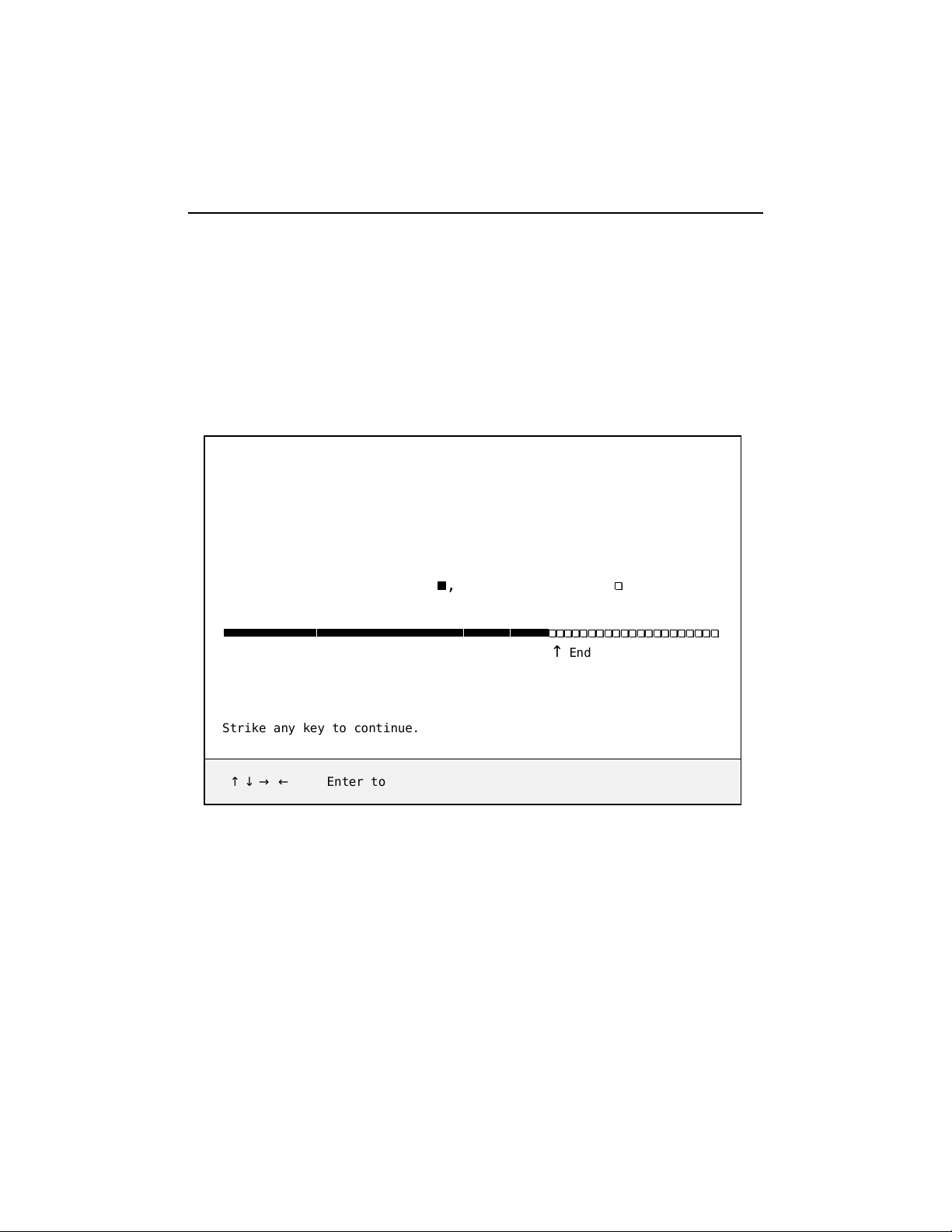
TEK-CPC I-1000 Technical Reference Manual
13.3 OUTPUT SELECTION
Select the FLASH location, then press the ENTER key. The program di splays the am ount of
available F LASH me mory.
Press the ENTER key to accept th e listed amount or press the "S" key to customize the
amount.
OUTPUT SELECTION FOR THE TRANSFER
Output selected: External FLASH device via serial link
Choose the size of the disk using the arrow keys:
Legend: se le cte d blo ck
unselected block =
,
=
Strike any key to continue.
↑ ↓ → ← Enter to select option Special disk
13-4
↑
End
Page 83

VFLASH Software
13.4 FILE SELECTION
Once the output is selected, a file selec tion screen appears.
This menu allows the user t o choose the files that will eventuall y ma ke up the Flash disk.
Files can b e chosen from th e v arious drives on the system.
The top line in this menu gives size information about the Flash partition. Selected Files
indicates how many files have been chosen up to this poin t. Free Space to copy in dicates the
availab le Flash space f o u nd, minus th e sp ace used up by th e selected files.
Use the arrow key s to highlight a nd mark a fi le for copy i ng to Flash devices.
When selecting a subdirectory, the first t wo entries are: ". <DIR>" and ".. <DIR>". As with
DOS, ". " refers to the current d ire ctory and " . ." to the pare nt di rectory. Thus, if y ou e nter a
"Newdi r" c ommand o n t he ".. <DIR> ". you will return to the pre vious directory.
Entries marked as "Drive A:" or "Drive B:" allow you to change drives/directories or to select
fil e s. "DR IVE A/ B : TO C HOO SE FI LE S" i s us ed t o sel ec t fi l es. " D RIVE A/ B: COMP LET E
COPY" is used to make an exact copy of a floppy disk to Flash. This last function r esembles
a DOS DISKCOPY command. When this mode of transfer is chosen, no other files can be
sent along with the diskette files.
Selected files (max 240):0; Free Space to copy: 522240 bytes
DRIVE A: COMPLETE COPY
DRIVE B: COMPLETE COPY
DRIVE C:
DRIVE E:
DOS <DIR>
QAPLUS <DIR>
TEMP <DIR>
TP <DIR>
VENTURA <DIR>
ATTR2 PAS 569 1-04-91 9:32
AUTOEXEC BAT 74 2-14-91 16:12
BOOTDIR PAS 6508 3-03-91 13:31
COMMAND COM 25308 2-02-91 12:25
CONFIG SYS 128 1-01-91 14:42
DRIVE A: TO CHOOSE FILES
DRIVE B: TO CHOOSE FILES
DRIVE D:
BIOS 700 <DIR>
PCAD <DIR>
SKEY <DIR>
TEST <DIR>
TYPESET <DIR>
WIN <DIR>
AUTOEXEC BAK 59 2-14-91 16:11
BOOT_DIR PAS 158 1-25-91 16:58
CHOIXMED PAS 19797 3-06-91 1:11
COMMANDE PAS 6110 2-21-91 15:57
CONFIG SYS 128 1-23-91 17:45
21 Files, D:\*.*
(Tag Untag New dir) or Enter Block Make bootable Done Esc to quit
↑ ↓ → ←
Home PgUp PgDn Volume label
The lower area of the screen serves as a reminder.
13-5
Page 84

TEK-CPC I-1000 Technical Reference Manual
13.4.1 Menu Commands
TAG
UNTAG
BLOCK
MAKE BOOTABLE
Use this fun ction to select a file fr om the above file li st. Move
the cursor over the desired field and pr ess T on your keyboard.
The file will then be highlighted - indicating it was selected.
Press T agai n , to deselect the file.
This function is used to desele ct a chosen file from the above list
of files. To use this function, simply move the cursor over the
desired file and press U.
This function is used to mark a group of files for select ion or
deselection. Move the cursor to the beginning of the first file
you wish t o sel ect an d press on the B ke y (a "" symbol wil l be
displayed after "Block" in the command area to remind you th at
a block has been entered ). Then, move the cursor t o the la st fil e
of the group a nd press B aga in (a "" will appear next to the
"" indicating that a block definition is now complete). The
block of outlined files are now ready to be "Tagged" or
"Untagged".
Choose th is function to move file s you wish t o ma ke bootable
into the FILE SELECTION area (to appear in the LIST OF
SELECTED FILES screen). The system will th en prompt you
for the drive which contains the system files (Note that the
source should not be a Flash disk, since these ar e read-only and
write protected). Once the selected files are found, the "Make
Bootable" command will be changed to "BOOT ABLE DISK".
This confirms that the Flash di s k will be bootable.
NEWDIR
This function lets you enter or exit a drive or directory. To
change directories, place the cursor at the desired entry and press
N. The listing wil l automatically change to the new director y' s
content.
13-6
Page 85

VFLASH Software
ENTER
DONE
ESC
VOLUME LABEL
Press ENTER to either tag, untag, or cha nge directory. Wh en the
cursor is on a directory, ENTER is equivalent to "Newdir".
When the cursor is on a file, pressing ENTER will tag/untag it.
Use this function when the file selection is terminated. Press D
and the next screen will appear (LIST OF SELECTED FILES).
Press the ESC key to abort VFLASH without modifying any
information in the Flash devices. The system will prompt you
before exiting to DOS.
Use this function t o in clu de a di sk volume label for the Flash
EPR OM d isk. Pres s V to display the followi ng message:
Volume is xxxxxxxxxxx
Volume label (11 characters , EN TER fo r none)?
The same operating system limitations on volume label names
apply.
The cursor can be m oved within the FILE SELECTI ON screen by using the ↑
PAGE UP, PAGE DOWN and HOME keys.
13-7
, ↓, →, ←,
Page 86

TEK-CPC I-1000 Technical Reference Manual
13.4.2 List of Selected Files
Th e LIST OF SELE CTED FI LES scr een sh ows you th e list of fil es th at th e Fla sh di sk will
contain.
LIST OF SELEC TE D FIL ES
Disk volume label: xxxxxxxxxxx
AFIRST.ASM
ASECOND.BAK
BOOTDIR.BAK
COMM.OBJ
COPYXAC.BAK
Program Change Selection Esc to quit
↑ ↓ PgUp PgDn Home
AFIRST.BAK
ASECOND.OBJ
BOOTDIR.PAS
COMMANDE.PAS
COPYXAC.BAK
AFIRST.OBJ
ATTR2.PAS
COMM.ASM
COPYXB.BAK
COMMBAK.ASM
The list of previously selected files ap p ears in the center of the scr een.
You can br owse th r ough t he l ist by u si ng th e
↑ , ↓ , PAGE UP, P AGE DOW N and HOME
keys.
The following commands are also available:
CHANGE
SELECT I ON
PROGRAM
This option allows you to return to the FILE SELECTION screen by
pressing C.
Press P to enter the Pr ogramming (TRANSFER STATUS ...) screen.
This will begin programming the Flash devices - according to the
transfer mode selected (on board or external Flash).
ASECOND.ASM
BOOTDIR.BAK
COMM.BAK
COMMBAK.BAK
ECRANSFX.DOC
ESC
This allows you to abort VFLASH and exit to DOS without modifying
the contents of the Flash devices .
13-8
Page 87

VFLASH Software
13.4.3 Duplicate Files Menu
If duplicate files are found, the DUPLICATE FILES MENU section appears below the list of
selected files. This section will appear only if two or more files with the same name are
found. When this occurs, a m enu will automatically appear in the bottom section to solve the
conflict:
LIST OF SELEC TE D FIL ES
Disk volume label: xxxxxxxxxxx
AFIRST.ASM
ASECOND.BAK
BOOTDIR.BAK
COMM.OBJ
COPYXAC.BAK
================== DUPLICATE FILES MENU ==================
E:\BOOTDIR.BAK
E:\TP\BOOTDIR.BAK
1:Rename duplicate(s) (file.ext,file1.ext,etc)
2:Rename or erase duplicate(s)
3:Erase remaining duplicates
Esc to quit Select list
AFIRST.BAK
ASECOND.OBJ
BOOTDIR.PAS
COMMANDE.PAS
COPYXAC.BAK
AFIRST.OBJ
ATTR2.PAS
COMM.ASM
COPYXB.BAK
COMMBAK.ASM
ASECOND.ASM
BOOTDIR.BAK
COMM.BAK
COMMBAK.BAK
ECRANSFX.DOC
Make a selection by choosing the corresponding number. Choosing:
1. Will force a rename by appending a numeral at the end of the file name.
2. Will erase or renam e files manually.
3. Will erase all dup licates.
When the final selection has been made and the final li sting is displayed, the Flash di sk can
then be written.
13-9
Page 88

TEK-CPC I-1000 Technical Reference Manual
13.5 FILE TRANSFER
13.5.1 Transfer Status of Onboard FLASH Programming Screen
This screen displays each of the transfer operations in progress:
1. First, th e Flash devices ar e erased. This operation can take some time to complete. Only
the Flash devices of the actual disk to be programmed will be erased, h owever.
2. The base sys t em information is then transferred. This is followed by the file data itself.
3. The tran sfer in progres s is displayed by X X. X %, a nd the actual file being c opied is also
shown (unless a complete diskette copy i s performed).
TRANSFER STATUS OF ONBOARD FLASH PROGRAMMING
Erasing of all Flash devices installed, please wait. . .
Erasing nth device. . .
Erase completed
Creating a bootable flash disk
Transferring the BOOT sector, FAT and root DIR . . .
Completed
Copying selected files. . .
Transfer completed: XX. X%
Transferring: FILENAME
Transfer complete
Restart the syst em if the disk is to be r ecogniz ed by th e TEKNOR BIO S exten si on. Alth ough
rebooting is n ot necessary if Flash dis ks were n ot created, it i s a r ecommended pr ocedure in
all circumstances.
13-10
Page 89

VFLASH Software
13.5.2 Transfer Status of External FLASH Programming Screen
When using a serial link, a control screen displays the transfer operation status and shows
each step in progress:
TRANSFER STATUS OF EXTERNAL FLASH PROGRAMMING
Erasing of all Flash devices installed, please wait . . .
Erase completed
Creating a bootable flash disk
Transferring the BOOT sector, FAT and root DIR . . .
Completed
Copying selected files. . .
Transfer completed: XX. X%
Transferring: FILENAME
Elapsed time: Xmin XXsec
Transfer complete
1. The devices ar e erased (this may take some time).
2. The base system information is tran sferred, followed by the file data itself.
3. The data progr ess is displayed by XX% up to 100%. The actual file being sent is also
shown (unless a complete diskette cop y is per formed). In addition, the elapsed time of
the transfer is displ ayed .
If an err or occurs during tr ansfer, the system be eps twice to warn the user.
To sign al the end of a successful transfer , a s ingle beep is hear d.
NOTE
The transfer operation can be time consuming in Serial Mode due to the
serial tr an s f er speed and protocol.
4. When the transfer is 100% complete, the following me s s ag e is d is p layed:
Do you want to Reset the receiving system?
This software command is made available to r estart the r eceiving system by remote. In
order for a new Flash disk to be recogniz ed by the BIOS and DOS, th e system must be
rebo oted.
13-11
Page 90

TEK-CPC I-1000 Technical Reference Manual
The recei vi ng system can be put in Download Mod e by any of the following options:
1. Short Pins 1 and 2 on jumper W4. Thi s for c e s Download Mode at boot up.
2. Download Mode is automatically enabled when the VT100 Mode is activated (by
shorting pins 3 and 4 on jumper W4). In this case, the communications port will
recognize the Download Mode commands and ac tivate it.
NOTE
Reset is the only way to exit from Download Mode which is forced on
at setup by the W4 (1-2) jumper. If Download Mode was entered by
recognition of the code sequence, you can simply exit Download Mode
and c o ntinue pro c essing.
13-12
Page 91

VFLASH Software
13.6 BATCH MODE
While files can be manually selected using the Interactive Mode, automatic transfers of a
predefined area (a sub-directory or preferably a diskette) can be achieved through Batch
Mode.
In Batch Mode, a user or field technician with no previous knowledge of the system can
easily effect a transfer to the Flash disk. This can be done either by calling a batch fi le (*.bat)
or by simply i ss uing the proper command line parameters direc t ly from DOS.
When the transfer is complete, r eset the system. This allows the BIOS and DOS to recognize
the new F l ash disk.
Keep in mind that Batch Mode can be called directly from a floppy or hard disk, from a
remote computer, or from a portable computer. In each case, the selected files can be
downloaded to the Flash devices.
Batch Mode returns error codes (err orlevel) that can be r ead by a DOS batch file or by a high
level language program.
13.6.1 Batch Mode Command Line Parameters
The command line format is as follows:
VFLASH [drive:] [\directory] [destination] [op tions]
where:
[
drive
:] is the source drive from which a complete copy will be made if no
direct ory is specified .
[\
directory
] is the path used to show from which directory the source files will be
taken and transferred to the Flash or EPROM files. If you do not speci fy a
dir ect or y ( for e xam p le, VFL ASH B: \), on l y th e fi l es i n t he r o ot di r ect or y
will be transferred to the Flash disk. Also, if the Flash disk is to be
bootable, the /B option must be used.
13-13
Page 92

TEK-CPC I-1000 Technical Reference Manual
13.6.2 Batch Mode Command Line Options
Each option or switch starts with a '/' character followed by one or more lett ers. These letters
are in uppercase and are used by VFLASH to identify a specific option.
A colon ':' or pound '#' character is also a necessary part of the switch. Lowercase letters
represent a variable field that must be en tered. Ea ch switch may be separated by a space if
you so choose .
The switches may be written in random order except for switches that are linked together. For
example a /S must be followed by either /#order or /sizeK or both . Thus, a command line
such as VFLASH B: /M /S/#2/128K is valid, however, VFLASH B: /S/M/#2/128K is n ot.
The following list of options provides complete descr iptions.
The first three options listed are not r equired t o execute a disk. They can be used either in
Interactive Mode or Batch Mode.
[
options
/G:group
]
Specifies how many Flash blocks will be grouped together as a cluster. The
Group Factor will set the smallest disk size availabl e. Va lid group values
are defined as 1, 2, 4, 8, 16... and so on.
/M
Instructs VFLASH to use a monochr ome display pattern. This option is
useful with LCDs since it ma y be difficult to distinguish color s with such
displays.
/VT100
This option allows a visual m onit oring of the tran s fer operation in progress
while in VT100 mode. Us e this switch when you make an onboard Flash
disk.
To get a summary of th e Batch Mode options fr om VFLASH, simply run VFLASH with th e
command line '/?' or '/HE LP' (type 'VFLASH/?' or 'VFLASH/HELP'). Either command will
display a Batch op tions summary and some examples of vali d VFLASH command lines. The
same help information will also be displayed each time VFLASH detects an error in the
command line.
13-14
Page 93

VFLASH Software
The following options identify disk or file parameters to be executed in BATCH mode.
/B/bootdrive
/E
/rate
/COM2
/R
/S
/#order
/sizeK
/V:volume label
Makes the disk bootable by transferring the bootable files from the
'bootdr i ve' spe ci fied. Note that the sour c e shoul d n ot be a Fla s h disk , sin ce
these are read-only and write pro tected.
Performs an external transfer by serial link to the remote system. This
switch must be present in order to use any of the next three options
(/RATE, /COM2 and /R).
The value entered corresponds to the desired baud rate for transfer. Any
one of the fol l owing can be u sed: 30 0, 1 200, 24 00, 9 600, 1920 0, 3 840 0. It
is set at 19200 by default.
This option instructs COM2 to be used ins tead of the default value COM1.
Instructs VFLASH to reset the board upon completion of download
operation. This is valid only in VT100 Mode. In Download Mode, the
remote system is always reset.
Used to create a special di sk or partition. This op tion precedes the startin g
device number opt ion (/#orde r) or the disk size optio n (/sizeK), o r both.
Specifies the Flash block to be used as the starting point for a disk partition
(default setting is #1).
Specifies a special disk size, in KB, for the Flash di sk. The default settin g
is the largest disk size following the d esignated starting disk as selected in
the /#order option.
This switch specifi es a volum e la bel for the disk to be creat ed.
This option will report an invalid comman d line error if it is used while
transferring a complete copy of a floppy disk. Since it is acceptable to have
spaces in a volume label, do not place this switch before [drive:],
[\directory] or [destination] since VFLASH would not be able to determine
when the label ends and when these options begins.
13-15
Page 94

TEK-CPC I-1000 Technical Reference Manual
13.6.3 Batch Mode Error Codes
The following er ror messa ges are returned by the VFLASH Batch Mode function. They can
be detected with a DOS Err orl evel condition.
ERROR NUMBER DESCRIPTION
(HEX) (DECIMAL)
0 0 No error
11Bad command line
2 2 Invalid drive choice for recovering boot information
3 3 Unable to establish communication (serial download mode only)
4 4 No Flash memory found (verify jumper)
5 5 Mixed memory types detected in Flash bank
6 6 Unable to find system files on specifie d disk
7 7 Specified output file already exists
8 8 Error reading transfer source drive
9 9 Insufficient data or directory spac e to copy all desired files
A 10 Bad checksum (problem with seria l link)
B 11 Non Hex code received (problem with serial link)
C 12 Error transferring data. Unusable Flash drive
D 13 No files to transfer in sel ected directory
E 14 Un able to open a fil e t o b e c op ied
F 15 Media not yet supported
10 16 Communications or device error while transferring files/
11 17 Unable to read transfer source drive
12 18 Insufficient Flash space to store files
13 19 Unrecognized Flash device type
14 20 Programming failure on devices
15 21 Cannot select any file from actual Flash disk
16 22 Unable to find source files
17 23 Cannot specify starting device o n remote system
18 24 Cannot find starting Flash bank a ddress
19 25 Communication error while reading Flash bank content
Unusable flash drive
13-16
Page 95

VFLASH Software
ERROR NUMBER DESCRIPTION
(HEX) (DECIMAL)
1A 26 External device cannot be erased properly
1B 27 Unsupported se rial download function
1C 28 Flash content does not verify with source
1D 29 No device found in specified starting socket
1E 30 Canno t create a Flash disk of specified size
1F 31 Communication error when reading Flash identification code
20 32 Cannot use 8086 or 8088 CPU with Fla sh memory
21 33 No serial port or card attached for transfer
22 34 /S switch not supported with this BIOS
23 35 /G:group value on command line is invalid
24 36 Insufficient Flash or EPROM space to includ e the volume label
entry
25 37 Cannot make EPROM with same [source] and [destination] path
26 38 EPRO M filename already exist
27 39 EPROM filename pa th not found
28 40 Selected drive for EPROM files no t ready
29 41 Invalid EPROM filename or disk erro r
2A 42 Not enough disk space to copy EPROM files
2B 43 Not enough memory for data buffer
2C 44 Command line option "/TEKXXX" is invalid
2D 45 486SLC internal registers are differe nt from BIOS setup
2E 46 The 486SLC cache is not disabled over the Flash device(s)
2F 47 Unable to erase the nth device
30 48 No BIOS found
31 49 The source diskette must be DOS Ve rsion 4 and up
32 50 Flash ID command to BIOS or data Flash must be issued first
13-17
Page 96

14. FLASH FILE SYSTEM
II
14.1 INTRODUCTION
With FLASH FILE SYST EM II, a read/write MS-Flas h partition can b e created in the 2MB
or 4MB Flash EPROM device. Such a partition can be accessed via the DOS commands.
Section 12 - VFLASH Soft ware - explains how a read-only Flash partition is created with
VFLASH and how data can be stored in files with the VFLASH Transfer Utility.
The 2MB or 4MB user or data Flash device can be configured in one of fou r ways:
1. As one read-only partition, created by VFLASH. This partition can be created as a
bootable or non-bootable disk. See Section 12 for more inf orm ati on.
2. As one read/write MS-Flash partition created by FLASH FILE SYSTEM II.
3. As a combination of the above t wo: one read-only V FLASH partition, followed by one
MS-Flash read/write partitio n. The system will set up bot h as a differe nt drive, with the
MS-Flash disk always the last. For example, VIP-UP can set up the VFLASH disk as
“Installed Bootable” (C:), other physical hard disks as D: and E:, while the MS-Flash
disk, in this case, would automatically be set up as the next drive letter, that is F:.
Another example could be only one hard disk, with the following setup: hard disk (C:),
VFLASH disk “Installed” (D:) and MS-Flash disk (E:).
4. The fourth possible configuration is similar to the previous one except that spac e (one or
more memory blocks) is left betwee n the VFLASH disk and the MS-Flash disk. This
non-partitioned space can be used by special applications to store data; this can only be
done safely if one knows the exact address of these memory blocks.
FLASH FILE SYSTEM II can be purchased from TEKNOR and is not part of the standard
package and utilities.
14-1
Page 97

TEK-CPCI-1000 Technical Reference Manual
14.2 SETTING UP CONFIG.SYS FOR FLASH FILE SYSTEM
Two lines must be included in your CONFIG.SYS file in order to set up the MS-Flash
partition and to install the Microsoft FLASH FILE SYSTEM on your computer.
The first line differs depending on whether the Flash device has a VFLASH partition or not:
1. If there is only the one MS-Flash partition on the device, these two lines must be
included in CONFIG.SYS:
device=FFS_VIP.EXE
device=MS-FLASH.SYS
2. If there is a VFLASH partition a s well a s a n MS -Flas h pa rtitio n o n t he de vice, these two
lines must be included in CONFIG.SYS:
device=FFS_VIP.EXE /start=X
device=MS-FLASH.SYS
where X can be replaced by the appropriate number o f blocks which must be skipped
from the beginning of the device. For example, the user may have already created a
bootable disk using VFLASH in the first four blocks of the Flash device; the size of each
block is 64 KB. This leave s twelve 64-KB blocks for an MS -Flash partition which will
begin at the fifth block. The two lines to add in CONFIG.SYS are therefore:
device=FFS_VIP.EXE /start=4
device=MS-FLASH.SYS
By default, the system uses start=0, meaning no blocks are skipped and the MS-Flash
partition begins at the first block. That is why the /start switch is not needed if there is one
MS-Flash partition on the Flash device.
14-2
Page 98

FLASH File System II
14.3 CREATING & FORMATTING A MS-FLASH PARTITION
FLASH FILE SYSTEM II allo ws only one MS-Flash re ad/write partition on the data Flash
device.
The MEMCARD software is used to create and format an MS-Flash partition. The program
can be used in one of two ways; either:
1. Run the program interactively and make selections in the menus, o r
2. Execute the command from the DOS prompt with switches to specify the drive letter
and volume label of the drive you want to format or to check the Flash device for
errors.
CAUTION
Prior to creating a new or expanded MS-Flash partition, you must
erase any non MS-Flas h section it will occupy. To do this, select
option 5 - Erase entire memory card - in the MEMCARD program.
This erases the whole partitio n that will be use d by FLASH FIL E
SYSTEM, not the whole Flash disk. For example, if one had
specified FFS_VIP /START=10 in CONFIG.SYS, only the 384KB
used by this partition will be erased.
14-3
Page 99

TEK-CPCI-1000 Technical Reference Manual
14.3.1 Using MEMCARD Menu Options
To use the MEMCARD program with the menu options, follow these steps:
1. Type MEMCARD at the command prompt. The main menu appears as follows:
PC Memory Card Setup Program Version 2.00
1991-1992 Microsoft Corporation
Memcard Options
Current memory card slot: 1 of 2 slots
Choose one of the following:
1. Create and format a new partition
2. Format an existing partition
3. Delete a partition
4. Display partition information
5. Erase entire memory card
6. Check memory card and fix errors
7. Select next memory card slot
Enter your choice. [4]
To quit Memcard, press ESC.
If your computer includes only one memory card slot, option 7 will not appear on the
main menu.
To choose a menu option, type its number then press ENTER. When you choose menu
options 1 through 6, another menu appears. To return to the main menu, press ESC. To
quit MEMCARD, return to the main menu and press ESC.
2. To create and format an MS-Flash read/write partition, select 1 from the me nu. A Create
and Format a New Partition screen such as the following appears:
Current memory card slot: 1
Letter Type Status Size
------------------------------------------------------ D MS-Flash Formatted 2048K
14-4
Page 100

FLASH File System II
If the card already has one M S-Flash partitio n, the followin g message appears at the botto m
of the screen:
This card has already been formatted.
Creating a partition will destroy all the data on the card.
Do you want to continue? (Y/N) [N]
Create a new partitio n only if you have backed up all the data that you want to save. To
continue, type "Y" and th en press ENTER.
3. If the card is unformatted or has one large partition, the following message appears:
Do you want to use the entire card for MS-Flash? (Y/N) [Y]
To create and format one lar ge partitio n, type "Y" and then pres s ENTER; to create and
format a partition that occ upies only part of a memory card, type " N" and then press
ENTER.
4. This step is only required if you are creating a partition that will occup y only part o f the
Flash device: Specify the size of the partition you want to create, and then press ENTER.
The minimum size depends on the amount of free space available on the memory card.
The number that appears on your screen is the largest amount of available space.
5. Specify the number of spare blocks that MS-Flash should reserve for memory card
cleanup, and then pre ss ENTER. The default is 1. Although reserving extra blocks may
speed up the memory card slightly, you will not be able to use the reserved blocks for
files. The default is recommended.
6. Specify a volume label for the partition, and th en press ENTER. If you d o not want to
specify a volume label, leave the field blank, and press ENTER.
14-5
 Loading...