

Page 1

TEK-AT4LVG
(TEK735)
INDUSTRIAL SINGLE BOARD COMPUTER
TECHNICAL REFERENCE MANUAL
VERSION 2.0, DECEMBER 1996
TEKNOR INDUSTRIAL COMPUTERS INC.
616 Cure Boivin
Boisbriand, Quebec
J7G 2A7 CANADA
NOTE:
This manual is for reference purposes only.
Reproduction in whole or in part is authorized
provided TEKNOR INDUSTRIAL COMPUTERS
INC. is cited as the original source.
ref: M735S_2-0
Page 2

FOREWORD
The information in this document is provided for reference purposes only. TEKNOR does
not assume any liability for application of the information or use of the products described
herein.
This document may contain or reference information and products protected by the
copyrights or patents of others and does not convey any license under the patent right of
TEKNOR, nor the rights of others.
Printed in Canada.
Copyright 1996 by TEKNOR INDUSTRIAL COMPUTERS INC., Boisbriand, Qc, J7G
2A7.
Foreword III
Page 3

TABLE OF CONTENTS
Foreword III
List of Diagrams X
List of Tables XI
PART ONE
PRESENTATION OF THE TEK-AT4LVG
1 THE MANUAL 1-1
1.01 How the Manual is Organized 1-1
2 PRODUCT SPECIFICATIONS 2-1
2.01 Product Description 2-2
2.01.1 General 2-2
2.01.2 System Characteristics 2-3
2.01.3 IDE/Floppy/SCSI Devices 2-5
2.01.4 Serial and Parallel Ports 2-5
2.01.5 Flash Disk and Utilities 2-6
2.01.6 Video Components 2-7
2.01.7 Power Management 2-8
2.01.8 VT100 and Download Modes 2-8
2.02 Compatibility With Other TEKNOR Single Board Computers
2-9
2.03 Board Specifications 2-10
List of Tables V
Page 4

PART TWO
QUICK INSTALLATION
3 INSTALLING SYSTEM MEMORY 3-1
3.01 Static Electricity Precautions
3-3
3.02 72-Pin SIMM Configuration and Location 3-4
3.03 30-Pin SIMM Configuration and Location 3-6
3.04 SIMM Installation 3-8
4 SETTING JUMPERS
4-1
4.01 Connecting the Battery 4-3
4.02 Jumper Settings 4-4
4.03 Jumper Location With Default Settings
4-10
5 CONNECTING AND POWERING UP THE BOARD
5-1
5.01 Installing TEK-AT4LVG in Passive Backplane
5-3
5.02 Connecting a Floppy Disk 5-4
5.03 Connecting Interface Devices (Keyboard, Speaker, Reset, LED) 5-5
5.04 Connectiong a Mouse
5-6
5.05 Connecting a Monitor
5-7
5.06 Powering Up the System 5-8
6 SOFTWARE SETUP
6-1
6.01 The AWARD Setup Program 6-3
6.02 The VIP-UP Program
6-15
List of Tables VI
Page 5

PART THREE
ADVANCED INSTALLATION AND SETUP
7 INSTALLING ANG WORKING WITH THE SYSTEM COMPONENT
7-1
7.01 Location of System Components
7-2
7.02 Fan Connector 7-5
7.03 Cache Memory 7-6
7.04 Boot Selection 7-7
7.05 Supervisor Circuit
7-8
7.06 PS/2 Mouse Connector 7-13
7.07 Power Connector 7-14
7.08 ISA Bus Connector 7-15
8 INSTALLING IDE, FLOPPY AND SCSI DEVICES 8-1
8.01 IDE Devices 8-3
8.02 Floppy Devices 8-8
8.03 SCSI Devices 8-13
9 INSTALLING PERIPHERALS 9-1
9.01 Serial Ports 9-2
9.02 Parallel Port 9-8
10 INSTALLING VIDEO 10-1
10.01 Location of Video Components 10-2
10.02 CRT VGA Controller
10-3
10.03 Feature Connector 10-6
11 SETTING POWER MANAGEMENT MODES 11-1
11.01 Power Management Modes 11-2
List of Tables VII
Page 6

PART FOUR
SPECIAL SOFTWARE AND ONBOARD UTILITIES
12 VFLASH SOFTWARE 12-1
12.01 Introduction 12-3
12.02 Running VFLASH 12-7
12.03 Output Selection 12-8
12.04 File Selection 12-10
12.05 File Transfer 12-16
12.06 Batch Mode 12-20
13 FLASH FILE SYSTEM II 13-1
13.01 Introduction 13-3
13.02 Setting Up CONFIG.SYS for Flash File System II 13-4
13.03 Creating and Formatting an MS-Flash Partition 13-5
14 UPDATING BIOS WITH UBIOS 14-1
14.01 Introduction 14-3
14.02 UBIOS - Interactive Mode 14-4
14.03 UBIOS - Batch Mode 14-9
15 VT MODE 15-1
15.01 VT100 Requirements 15-3
15.02 VT100 Setup and Configuration 15-4
15.03 Running Without a Terminal 15-6
16 DOWNLOAD MODE 16-1
List of Tables VIII
Page 7

PART FIVE
ADDITIONAL INFORMATION
17 TROUBLE SHOOTING 17-1
18 APPENDICES 18-1
18.01 Memory and I/O Map 18-3
18.02 Assembly Diagram 18-7
18.03 Configuration Diagram 18-9
18.04 Mechanical Specifications 18-11
18-05 Diagram Block 18-13
18.06 List of Approved Vendors 18-15
18.07 BIOS Setup Error Codes 18-18
18.08 Connector Locations and Pinouts 18-29
List of Tables IX
Page 8

LIST OF DIAGRAMS
3-1 72-Pin SIMM Sockets Location
3-2 30-Pin SIMM Sockets Location
4-1 Jumper Locations With Default Settings
5-1 Floppy Connector Location
5-2 Floppy Disk Cable
5-3 Multi-Function Connector Location
5-4 Mouse Connector Location
5-5 VGA Connector Location
7-1 System Components Location
7-2 ISA Bus Connector Location
8-1 IDE Connectors Location
8-2 Floppy Connector Location
8-3 Floppy Disk Cable
9-1 Serial Ports Location
9-2 Parallel Port Location
10-1 Video Components Location
15-1 VT100 Full Setup
15-2 VT100 Partial Setup
18-1 Memory Map
18-2 TEK-AT4LVG Assembly
18-3 TEK-AT4LVG Configuration
18-4 TEK-AT4LVG Mechanical Specifications
18-5 TEK-AT4LVG Block Diagram
18-6 Connector Locations
3-5
3-7
4-11
5-4
5-4
5-5
5-6
5-7
7-3
7-15
8-3
8-9
8-11
9-3
9-8
10-2
15-5
15-5
18-3
18-7
18-9
18-11
18-13
18-27
List of Tables X
Page 9

LIST OF TABLES
3-1 72-Pin SIMM Configuration
3-2 30-Pin SIMM Configuration
4-1a Jumper Settings: W1-W2, W27-W28, W32, W34-W36
4-1b Jumper Settings: W3-W15
4-1c Jumper Settings: W16-W19, W23
4-1d Jumper Settings: W20-W22, W24-W26
4-1e Jumper Settings: W29-W31, W39-W40, J13
7-1 Fan Connector (J1) - Pinout
7-2 Emergency BIOS Boot (J13) - Pinout
7-3 Register 190H, 290H or 390H
7-4 Watchdog Timer Register
7-5 PS/2 Mouse Connector (J10) - Pinout
7-6 External Power Connector (J12) - Pinout
7-7a ISA Bus Connector (A,B) - Pinout
7-7b ISA Bus Connector (C,D) - Pinout
7-8 8237 DMA Controllers
7-9 8259 Interrupt Controllers
8-1a Hard Disk Connector #1 (J3) - Pinout
8-1b Hard Disk Connector #2 (J8) - Pinout
8-2 Floppy Disk Connector (J4) - Pinout
8-3 Common SCSI Target IDs
8-4 SCSI Connector (J2) - Pinout
9-1a Serial Port 1 (J6) RS-232 - Pinout
9-1b IBM 9-Pin DSUB Standard - Pinout
3-5
3-7
4-5
4-6
4-7
4-8
4-9
7-5
7-7
7-8
7-12
7-13
7-14
7-16
7-17
7-18
7-18
8-4
8-5
8-10
8-15
8-18
9-4
9-4
List of Tables XI
Page 10

LIST OF TABLES (Continued)
9-2a Serial Port 2 (J7) RS-232 - Pinout
9-2b IBM 9-Pin DSUB Standard - Pinout
9-3 Serial Port 2 (J7) RS-485 - Pinout
9-4 Parallel Port Connector (J15) - Standard Mode - Pinout
9-5 Parallel Port Connector (J15) - EPP Mode - Pinout
9-6 Parallel Port Connector (J15) - ECP Mode - Pinout
10-1 VGA Connector (J14) - Pinout
10-2 Video Feature Connector (J9) - Pinout
18-1 Memory Map
18-2 I/O Map
9-5
9-5
9-6
9-9
9-10
9-11
10-5
10-6
18-4
18-5
List of Tables XII
Page 11

PART ONE
PRESENTATION OF THE TEK-AT4LVG
1 THE MANUAL
2 PRODUCT SPECIFICATIONS
Page 12

1 THE MANUAL
1.01 HOW THE MANUAL IS ORGANIZED
The TEK-AT4LVG TECHNICAL REFERENCE MANUAL is divided as follows:
Part One PRESENTATION OF THE TEK-AT4LVG
describes the different features and gives technical information about the
board.
Part Two QUICK INSTALLATION
includes essential information to get your TEK-AT4LVG up and running
quickly.
Part Three ADVANCED INSTALLATION AND SETUP
divides the TEK-AT4LVG PC/AT Single Board Computer according to
functional units; it includes detailed information on the board's hardware
and software features, and on installation and setup procedures.
Part Four SPECIAL SOFTWARE AND ONBOARD UTILITIES
describes, in detail, special software and utilities that come with the TEKAT4LVG board.
Part Five ADDITIONAL INFORMATION
contains several appendices which comprise information you can consult
when you need it.
The sections of this manual group the various aspects of the TEK-AT4LVG board, with
special emphasis put on installation and setup procedures.
The sections have been organized in a chronological order with respect to the steps that
would be taken to install and set up the board. Certain sections or sub-sections which deal
with devices or peripherals that one wants to install can be studied in greater detail, while
those describing devices that do not apply can be skimmed or skipped.
The Manual 1-1
Page 13

2 PRODUCT SPECIFICATIONS
2.01 Product Description...............................................................................................2-2
2.01.1 General .......................................................................................................... 2-2
2.01.2 System Characteristics....................................................................................2-3
2.01.3 IDE/Floppy/SCSI Devices ..............................................................................2-5
2.01.4 Serial And Parallel Ports ................................................................................2-5
2.01.5 Flash Disk and Utilities..................................................................................2-6
2.01.6 Video Components.........................................................................................2-7
2.01.7 Power Management........................................................................................2-8
2.01.8 VT100 and Download Modes.........................................................................2-8
2.02 Compatibility With Other TEKNOR Single Board Computers ..............................2-9
2.03 Board Specifications............................................................................................2-10
Product Specifications 2-1
Page 14

2.01 PRODUCT DESCRIPTION
2.01.1 GENERAL
The TEK-AT4LVG (also called the TEK735) is a multi-purpose computer board:
• It can be used as a single board computer in conjunction with a passive backplane;
• Or as part of a stand-alone system with no backplane;
• It can also operate without any mechanical disks by performing disk operations on
solid state disks (Flash EPROM).
The board is ideal for industrial applications; it is designed to operate in environments
where a sturdy and compact system is essential with features like:
• Watchdog Timer;
• SMM (System Management Mode) support and full SMI (System Management
Interrupt) interface for power management;
• Power failure detector;
• Low battery detector;
• Shadow RAM BIOS support for fast execution;
• Flash EPROM boot;
• Real-Time Clock (RTC) with battery backup;
• Solid state disks (optional): 2 or 4 MB of user Flash EPROM.
Product Specifications 2-2
Page 15

2.01.2 SYSTEM CHARACTERISTICS
MICROPROCESSORS
SUPPORTED
SYSTEM MEMORY • Standard 5V, 70 ns single sided or double sided SIMMs.
CACHE MEMORY • Write -Through Internal Cache.
SUPERVISOR
UTILITIES
REAL TIME CLOCK • MC146818 compatible.
• Intel: 486 DX2-66MHz ; DX4-100MHz.
• AMD: DX2-66MHz ; DX4-100MHz ; DX5-133MHz.
- Two 72-pin SIMM sockets support memory configurations
from 1 to 64 MB using 1MB, 2MB, 4MB, 8MB, 16MB
and 32MB SIMM modules.
OR
- Four 30-pin SIMM sockets support memory
configurations from 1 to 16 MB using 256KB, 1MB and
4MB SIMM modules.
• Write-Back/Write-Through System Cache available as 0KB,
128KB, 256KB or 512KB.
• Watchdog Timer.
• Power fail/low battery detector circuit.
• 128 bytes battery backup CMOS RAM.
BUS STANDARD
SUPPORT
• High-drive buffers to support up to 20 slots.
• Standard 16-bit PC/AT ISA bus (P996 standard).
Product Specifications 2-3
Page 16

BIOS • System
BIOS:
• Video BIOS: From Cirrus Logic for the video controller.
Includes the AWARD Setup program, a
utility in ROM which is used to set
configuration data in CMOS RAM.
MULTI-FUNCTION
CONNECTOR
ULTRA I/O
CONTROLLER
• TEKNOR
BIOS
• Provides all the necessary signals for connecting the
keyboard, speaker, reset button and hard disk LED.
• Supports the Plug and Play standard and has a Serial
EEPROM onboard for Plug and Play compatibility and
configuration storage.
- Includes VIP-UP, TEKNOR's own
Setup program for enabling /disabling /
relocating various hardware features on
the Single Board Computer.
- Also includes Flash disk and Flash
BIOS support.
Product Specifications 2-4
Page 17

2.01.3 IDE/FLOPPY/SCSI DEVICES
FLOPPY DISKS • Software compatible with N82077.
• Enhanced super Floppy controller which supports two Floppy
disk drives of up to 2.88MB each, 16 bytes of FIFO buffering
and a 48 mA drive buffer.
IDE (HARD DISKS) • Includes a local bus IDE hard disk interface for a high
performance disk subsystem.
• Support for two IDE channels for up to four IDE drives.
SCSI • Adaptec AIC-6360 supports up to seven SCSI peripherals
and the Fast SCSI II standard.
• Passive Terminations.
• Fast SCSI II, 8-bit bus.
• 10MB/s synchronous transfers.
• 5MB/s asynchronous transfers.
• Can co-exist with other hard disk/controller combinations:
such as ST-506, RLL, ESDI and IDE.
2.01.4 SERIAL AND PARALLEL PORTS
SERIAL PORTS • Two 16550 compatible serial ports with internal 16-byte
FIFO buffers can be defined as two of the following: COM1,
COM2, COM3 or COM4.
• Serial Port 1 is configurable as RS-232.
• Serial Port 2 is configurable as RS-232 or RS-485.
• Support for VT100 mode through Serial Port 1 or 2.
PARALLEL PORTS • One bi-directional port (LPT1).
• Multi-mode parallel port supporting the following modes:
- Standard Parallel Port (SPP): This mode is IBM XT/AT
compatible and PS/2 compatible (bi-directional);
- Enhanced Parallel Port (EPP);
- Extended Capabilities Port (ECP).
Product Specifications 2-5
Page 18

2.01.5 FLASH DISK AND UTILITIES
SOLID STATE DISKS
(optional)
FLASH FILE
SYSTEM II SUPPORT
VFLASH
SOFTWARE
UBIOS SOFTWARE • Utility that allows taking BIOS files from a disk and update
• 2 or 4 MB of user Flash EPROM.
• Used to create a read/write MS-Flash partition in the 2MB or
4MB Flash EPROM device. Such a partition can be accessed
via the DOS commands.
• TEKNOR's Flash EPROM transfer utility program for single
board computers. Its main function is to download DOS files
to the 2 or 4 MB Flash EPROM disk, also referred to as data
Flash.
the Flash BIOS EPROM with them. It also allows the reverse
operation - to copy the contents of the Flash BIOS to files on
disk
Product Specifications 2-6
Page 19

2.01.6 VIDEO COMPONENTS
• Cirrus Logic GD5430, GD5434 or 5440 video processor chip.
• The local bus SVGA video controller is from Cirrus Logic and provides high
resolution CRT display. The board also comes with 1MB or 2MB of video memory
(DRAM), and a feature connector for overlay and color keying.
• Enhanced GUI and Video accelerator with a 32/64-bit BitBLT engine (5430 and
5434).
• 32-bit direct-connect VL-Bus interface:
- Zero-wait-state write buffer for CPUs up to 33 MHz.
• 32/64-bit DRAM display memory interface:
- 1MB/2MB display memory support (5430 and 5434).
• Integrated 24-bit DAC.
• Hardware and BIOS compatible with IBM VGA display standard.
• Multimedia ready:
- VESA Feature-Connector (VFC) support.
• Resolutions supported with 1MB of Video DRAM:
- 640 x 480 (up to 16 Million colors).
- 800 x 600 (up to 64000 colors).
- 1024 x 768 (up to 256 colors).
- 1280 x 1024 (up to 16 colors).
• Resolutions supported with 2MB of Video DRAM.
- 640 x 480 (up to 16 Million colors).
- 800 x 600 (up to 16 Million colors).
- 1024 x 768 (up to 65536 colors).
- 1280 x 1024 (up to 256 colors).
Product Specifications 2-7
Page 20

2.01.7 POWER MANAGEMENT
• Supports Stand-by and Suspend modes for the System Power Management.
STAND-BY • System Controller’s first level of power management. In this
mode, the CPU clock frequency is reduced.
Also, if the VIDEO ON/OFF CONTROL is enabled, the
video monitor will be deactivated.
SUSPEND • System Controller’s second level of power management. In
this mode, the CPU clock frequency is stopped.
• Supports Stand-by mode for the Hard Disk Power Management.
STAND-BY • In this mode, the Hard Disk is powered off. It is reactivated by
the next disk access operation.
2.01.8 VT100 AND DOWNLOAD MODES
VT100 MODE • Enables your single board computer to run without a local
keyboard or screen. That is, operation can be controlled via a
remote terminal supporting VT100 Mode or a computer with a
terminal emulation program.
DOWNLOAD MODE • Information can be downloaded to the Flash EPROM disk on
the board by running VFLASH on a remote computer and using
a serial link.
Product Specifications 2-8
Page 21

2.02 COMPATIBILITY WITH OTHER TEKNOR SINGLE BOARD
COMPUTERS
Compatibility with former TEKNOR board designs is maintained at the driver level. The
following features and devices have been taken from other TEKNOR products and
integrated into the TEK-AT4LVG:
• The Ultra I/O Controller is the same as the one used on the VIPer806.
• The Flash File and Emergency BIOS are mapped like the TEK930 (PCI-930).
Product Specifications 2-9
Page 22

2.03 BOARD SPECIFICATIONS
Electrical
ù Conforms to the electrical specifications in the IEEE P996 Bus Specification
(PC/AT).
ù Supply Current:
TABLE 2-1: Supply Current
SUPPLY
CURRENT *
+5V Typical 2.1A 2.0A 2.2A
+5V Suspend 1.5A 1.5A 1.6A
+12V/-12V 10mA 10mA 10mA
DX2-66 DX4-100 DX4-133
* Measured with 8MB DRAM, 256k Cache, 2MB Video DRAM, keyboard, floppy, and one hard disk installed.
Mechanical
ù Conforms to the mechanical specifications in the IEEE P996 Bus Specification
(PC/AT).
ù Dimensions: 13.330in. x 4.80in. / 339mm x 122mm.
ù Weight:
Environmental
ù Operating Temperature: 0 to 70ºC (heatsink and fan), calculated with typical
power consumption.
ù Storage Temperature: Ambient temperature range of -30ºC to +85ºC.
ù Noncondensing Relative Humidity: 5% - 95%.
Reliability
ù MTBF (Mean Time Between Failure): Estimated at 100 000 hours.
Product Specifications 2-10
Page 23

PART TWO
QUICK INSTALLATION
3 INSTALLING SYSTEM MEMORY
4 SETTING JUMPERS
5 CONNECTING AND POWERING UP THE BOARD
6 SOFTWARE SETUP
Page 24

3 INSTALLING SYSTEM MEMORY
3.01 Static Electricity Precautions.................................................................................3-3
3.02 72-Pin SIMM Configuration and Location ............................................................3-4
3.03 30-Pin SIMM Configuration and Location ............................................................3-6
3.04 SIMM Installation................................................................................................. 3-8
Installing System Memory 3-1
Page 25

3.01 STATIC ELECTRICITY PRECAUTIONS
Static electricity can damage a board ; the following precautions should be taken
whenever you handle the TEK-AT4LVG:
• Keep the board in its anti-static package, until you are ready to install it.
• Touch a grounded surface before removing the board from its package or wear a
grounding wrist strap; this will discharge any static electricity that may have built
upon your body.
• Handle the board by the edges.
• When handling the board, touch a grounded surface often or wear a grounding wrist
strap.
Installing System Memory 3-3
Page 26

3.02 72-PIN SIMM CONFIGURATION AND LOCATION
The location of the two 72-pin vertical SIMM sockets appears on Diagram 3-1 ; they are
labeled U22 and U23.
At least 1MB of system memory must be installed on the TEK-AT4LVG for proper
operation. Memory can be configured from 1 to 64 MB on the TEK-AT4LVG board using
36-bit SIMM devices.
Each of the 72-pin SIMM sockets on the board can accept the following 36-bit modules:
256K x 36-bit = 1MB module 2M x 36-bit = 8MB module
512K x 36-bit = 2MB module 4M x 36-bit = 16MB module
1M x 36-bit = 4MB module 8M x 36-bit = 32MB module
SIMM modules can be installed in either one of two 72-pin sockets (U22 and U23). If you
install one SIMM, it must be located in socket U23.
FF If you are installing 72-pin SIMMs, do not install any 30-pin SIMMs.
Consult Table 3-1 on the following page to see which SIMM configurations are supported
by the TEK-AT4LVG with 72-pin vertical SIMMs.
DRAM devices with parity bit and page mode at 70ns maximum access time are
recommended. Consult the following list for examples of recommended DRAM devices.
Users are encouraged to check with their local distributors for compatible substitutes.
256K*36 MICRON
NEC
SAMSUNG
512K*36 MICRON MT18D51236M-7 4M*36 NEC
1M*36 MICRON
NEC
SAMSUNG
TOSHIBA
MT10D25636M-7
MC-42256A36B-70
KMM536256C-7
MT9D136M-7
MC-4210000A36B-70
KMM5361000B-7
THM361020AS-70
2M*36 MICRON
SAMSUNG
TOSHIBA
SAMSUNG
TOSHIBA
8M*36 HITACHI
TOSHIBA
Installing System Memory 3-4
MT18D236M-7
KMM5362000B-7
THM362040AS-70
MC-424000A36BH-70
KMM5364100-7
THM3640205-70
HB56D836BR-70A
THM368020SG-70
Page 27
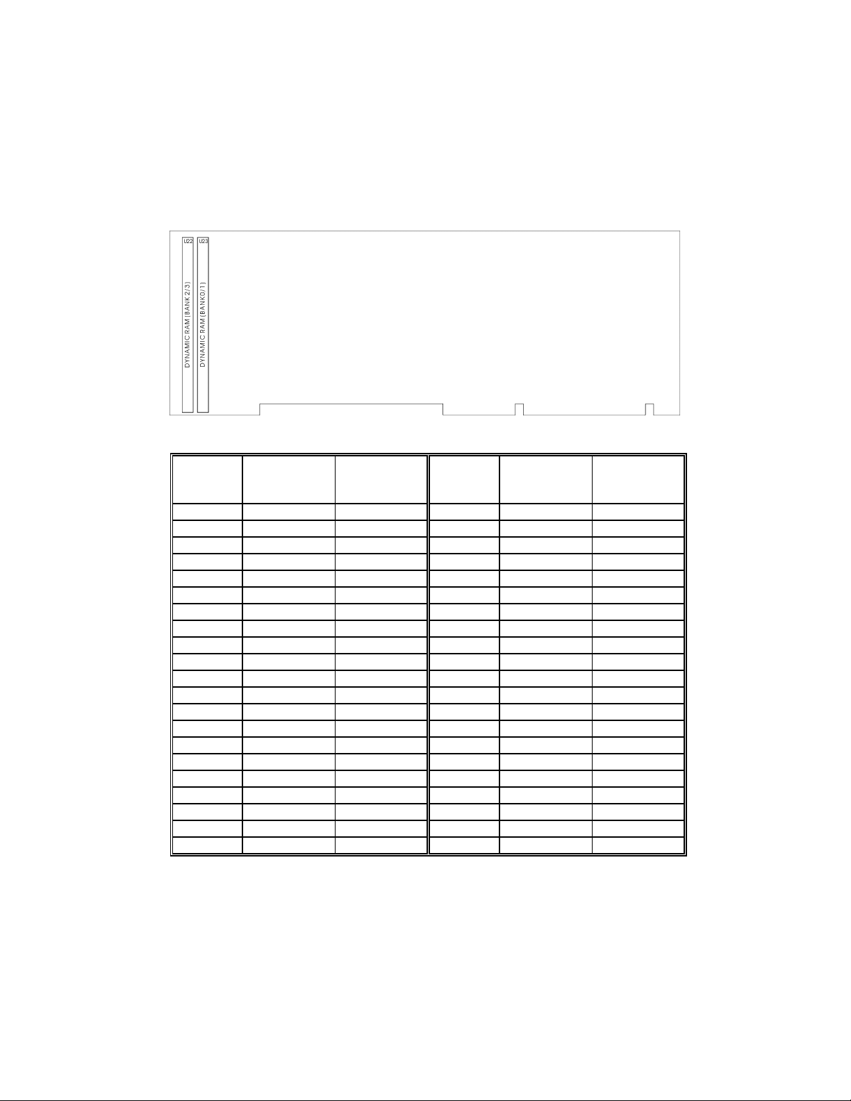
DIAGRAM 3-1: 72-Pin SIMM Sockets Location
TABLE 3-1: 72-Pin SIMM Configuration
TOTAL
SYSTEM
MEMORY
1MB 1MB (256Kx36) -- 17MB 16MB (4Mx36) 1MB (256Kx36)
2MB 1MB (256Kx36) 1MB (256Kx36) 17MB 1MB (256Kx36) 16MB (4Mx36)
2MB 2MB (512Kx36) -- 18MB 16MB (4Mx36) 2MB (512Kx36)
3MB 2MB (512Kx36) 1MB (256Kx36) 18MB 2MB (512Kx36) 16MB (4Mx36)
3MB 1MB (256Kx36) 2MB (512Kx36) 20MB 16MB (4Mx36) 4MB (1Mx36)
4MB 2MB (512Kx36) 2MB (512Kx36) 20MB 4MB (1Mx36) 16MB (4Mx36)
4MB 4MB (1Mx36) -- 24MB 16MB (4Mx36) 8MB (2Mx36)
5MB 4MB (1Mx36) 1MB (256Kx36) 24MB 8MB (2Mx36) 16MB (4Mx36)
5MB 1MB (256Kx36) 4MB (1Mx36) 32MB 16MB (4Mx36) 16MB (4Mx36)
6MB 4MB (1Mx36) 2MB (512Kx36) 32MB 32MB (8Mx36) -6MB 2MB (512Kx36) 4MB (1Mx36) 33MB 32MB (8Mx36) 1MB (256Kx36)
8MB 4MB (1Mx36) 4MB (1Mx36) 33MB 1MB (256Kx36) 32MB (8Mx36)
8MB 8MB (2Mx36) -- 34MB 32MB (8Mx36) 2MB (512Kx36)
9MB 8MB (2Mx36) 1MB (256Kx36) 34MB 2MB (512Kx36) 32MB (8Mx36)
9MB 1MB (256Kx36) 8MB (2Mx36) 36MB 32MB (8Mx36) 4MB (1Mx36)
10MB 8MB (2Mx36) 2MB (512Kx36) 36MB 4MB (1Mx36) 32MB (8Mx36)
10MB 2MB (512Kx36) 8MB (2Mx36) 40MB 32MB (8Mx36) 8MB (2Mx36)
12MB 8MB (2Mx36) 4MB (1Mx36) 40MB 8MB (2Mx36) 32MB (8Mx36)
12MB 4MB (1Mx36) 8MB (2Mx36) 48MB 32MB (8Mx36) 16MB (4Mx36)
16MB 8MB (2Mx36) 8MB (2Mx36) 48MB 16MB (4Mx36) 32MB (8Mx36)
16MB 16MB (4Mx36) -- 64MB 32MB (8Mx36) 32MB (8Mx36)
U23
Bank 0/1
U22
Bank 2/3
TOTAL
SYSTEM
MEMORY
U23
Bank 0/1
U22
Bank 2/3
Installing System Memory 3-5
Page 28

3.03 30-PIN SIMM CONFIGURATION AND LOCATION
The TEK-AT4LVG is equipped with an alternate means of implementing DRAM. 30-pin
SIMM socket are included on the board for customers who wish to use their 30-pin
devices.
Since this SBC is targeted for use in upgrade application, the overall cost of the upgrade is
reduced by allowing reuse of older DRAM technology.
The location of the four 30-pin SIMM sockets is illustrated in Diagram 3-2. They are
labeled U24, U25, U26 and U27.
At least 1MB of system memory must be installed on the TEK-AT4LVG for proper
operation. Memory can be configured from 1 to 16 MB on the TEK-AT4LVG board using
9-bit SIMM devices.
The four SIMM sockets accept either 256KB, 1MB or 4MB modules.
SIMM modules must be installed in all four 30-pin sockets: U24, U25, U26 and U27.
FF If you are installing 30-pin SIMMs, do not install 72-pin SIMMs.
Note that all SIMMs installed must be of the same capacity.
Consult Table 3-2 on the following page to see which 30-pin SIMM configurations are
supported by the TEK-AT4LVG.
DRAM devices with parity bit and page mode at 70ns maximum access time are
recommended. Consult the following list to see examples of recommended DRAM
devices. Users are encouraged to check with their local distributors for compatible
substitutes.
256K*9 MOZEL
OKI
1M*9 MOTOROLA
NEC
OKI
SAMSUNG
4M*9 HITACHI
OKI
TI
TI
V104BJ9S-70
MSC2331A-70YS3-R
MCM91430S70
MC-421000A9BA-70
MSC23109B-70DS3B
KMM591000AN-70
HB56A49BR7B
MSC23409-70DS9
TM4100EAD9-70
TM497EU9-70
Installing System Memory 3-6
Page 29
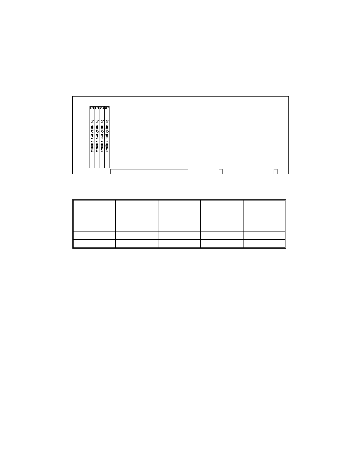
DIAGRAM 3-2: 30-Pin SIMM Sockets Location
TABLE 3-2: 30-Pin SIMM Configuration
TOTAL
SYSTEM
MEMORY
1MB 256KB 256KB 256KB 256KB
4MB 1MB 1MB 1MB 1MB
16MB 4MB 4MB 4MB 4MB
U24 U25 U26 U27
Installing System Memory 3-7
Page 30

3.04 SIMM INSTALLATION
When you are ready to install the SIMMs in the sockets, follow the steps outlined below.
• With the board flat on the table, turn it so that the sockets are at the end of the board
farthest from you.
• Hold the module with the notch on the bottom left facing you, and insert the SIMM
Module into the socket at a 70° angle from the board. Always start inserting the
module in the socket nearest the center of the board. Then work your way by inserting
the other modules, one by one, towards the exterior edge of the board.
• Snap the module to a vertical position in the socket. The module is fully inserted when
the retaining pegs snap into the holes at each end of the module.
To remove the SIMMs from the sockets, pull on the retaining clips, located on each side
of the SIMM socket. Once the module has snapped out of the socket, pull gently on it.
Installing System Memory 3-8
Page 31

4 SETTING JUMPERS
4.01 Connecting the Battery.......................................................................................... 4-3
4.02 Jumper Settings.....................................................................................................4-4
4.03 Jumper Locations With Default Settings................................................................4-9
Setting Jumpers 4-1
Page 32

4.01 CONNECTING THE BATTERY
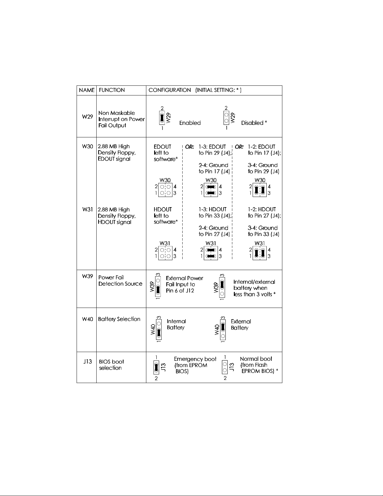
A battery can be connected on the board using the jumper W40:
. an Internal Battery is set with pins 1-2 shorted
. an External Battery is set with pins 2-3 shorted
Please refer to Table 4-1e to set W40.
Removing the W40 jumper has the same effect as putting the battery in storage; TEKNOR
always ships its board with the battery jumper removed in order to increase the life of the
battery.
Setting Jumpers 4-3
Page 33

4.02 JUMPER SETTINGS
The following pages show the TEK-AT4LVG jumpers and their initial setting. These
jumpers are labeled from W1 to W36, W39, W40 and J13.
For jumper location, see Diagram 4-1 on page 4-11 (fold-out).
Setting Jumpers 4-4
Page 34
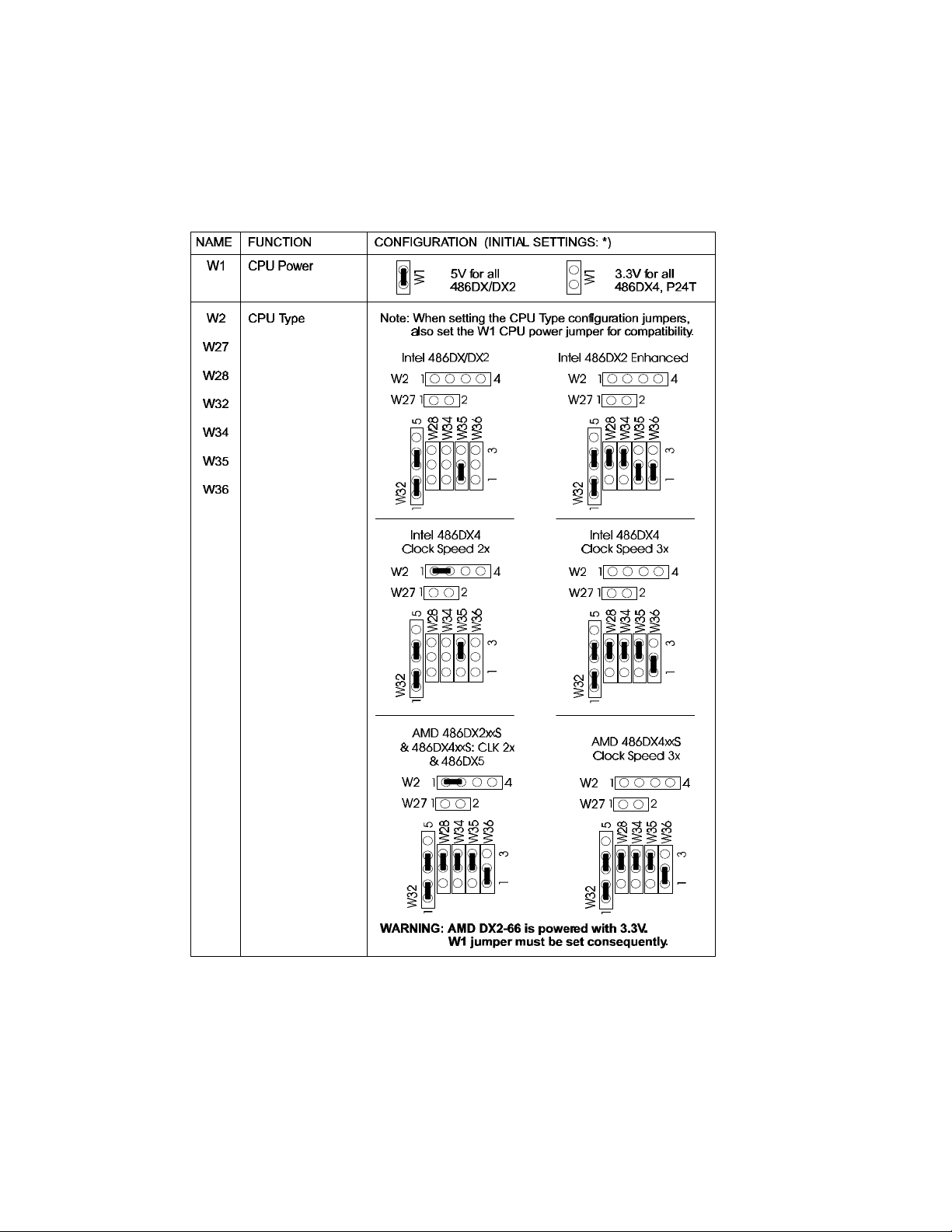
TABLE 4-1a: Jumper Settings: W1-W2, W27-W28, W32, W34-W36
Setting Jumpers 4-5
Page 35
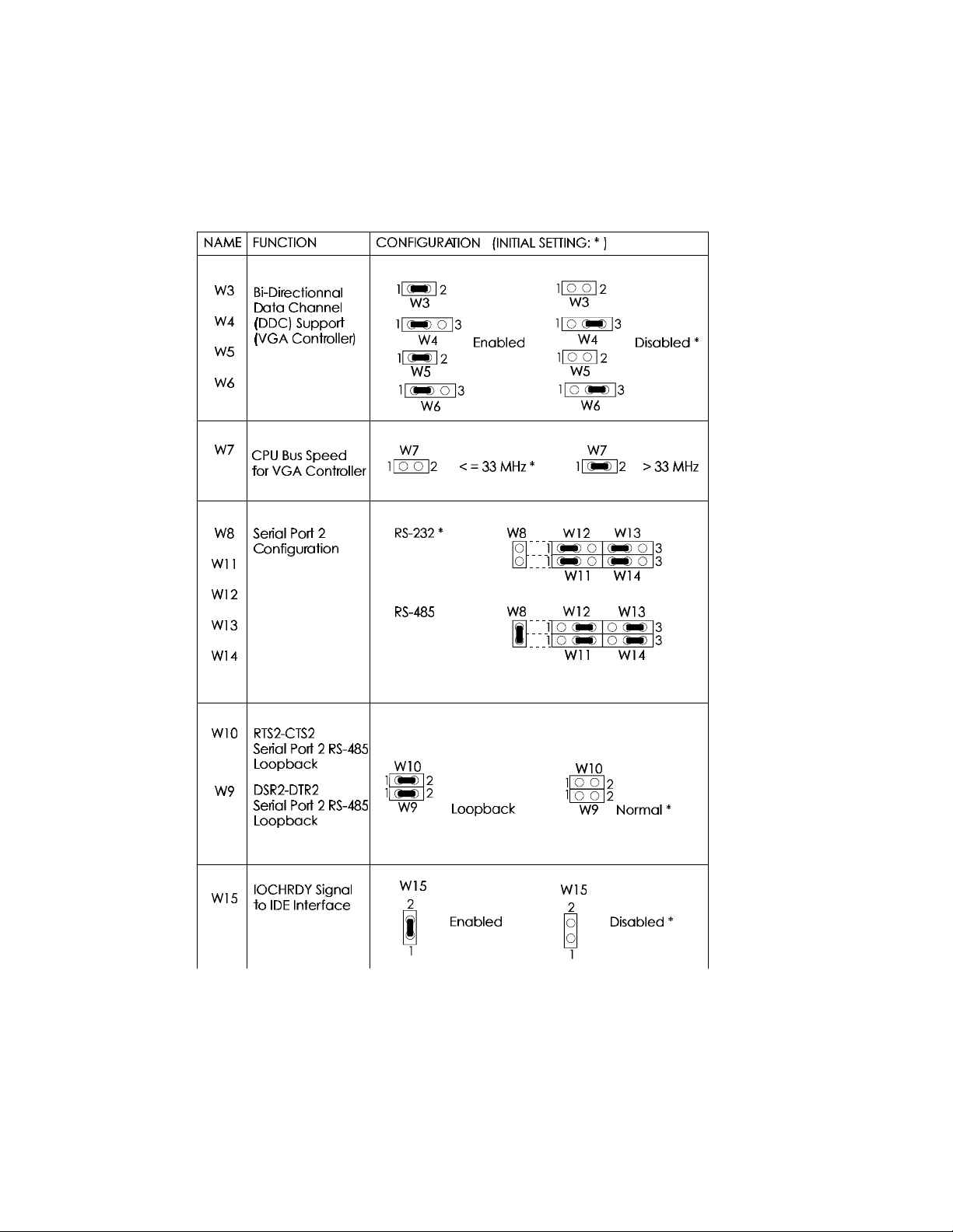
TABLE 4-1b: Jumper Settings: W3-W15
TABLE 4-1c: Jumper Settings: W16-W19, W23
Setting Jumpers 4-6
Page 36
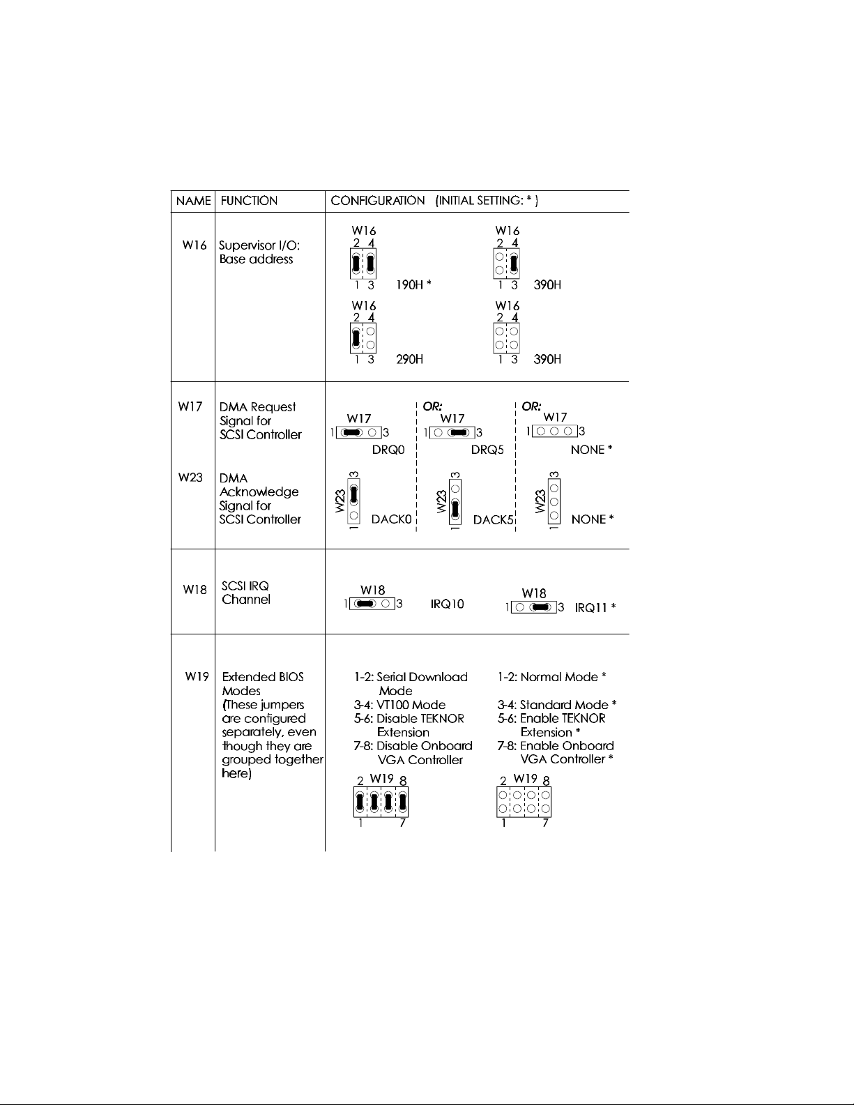
TABLE 4-1d: Jumper Settings: W20-W22, W24-W25
Setting Jumpers 4-7
Page 37
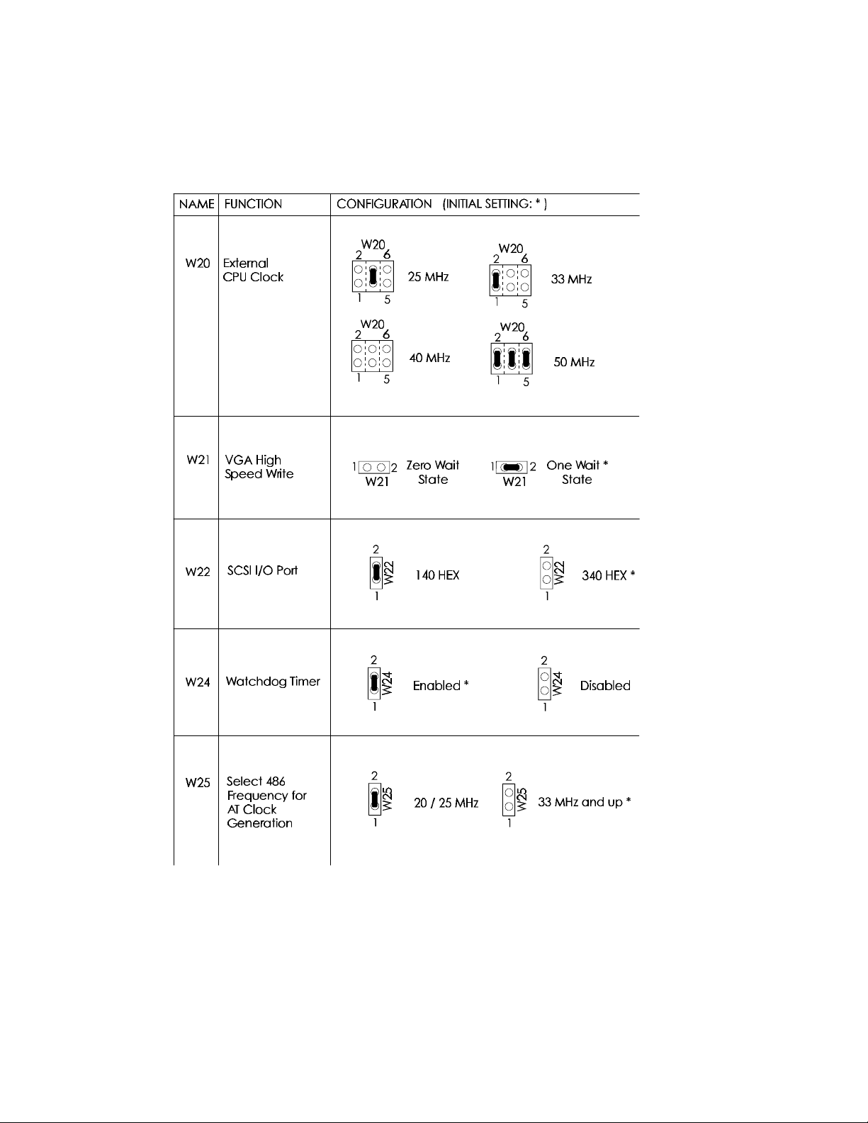
TABLE 4-1e: Jumper Settings: W29-W31, W39-W40, J13
Setting Jumpers 4-8
Page 38
4.03 JUMPER LOCATIONS WITH DEFAULT SETTINGS
Setting Jumpers 4-9
Page 39

Diagram 4-1 on page 4-11 shows the jumper locations on the board. The jumpers appear
as rectangular boxes containing small circles which represent the pin numbers.
The small black marks indicate the default setting for the jumpers. No black mark means
that the jumper has no default setting.
The jumpers are labeled on the board as well. That way, it will be possible to locate each
pin with its number.
Setting Jumpers 4-10
Page 40
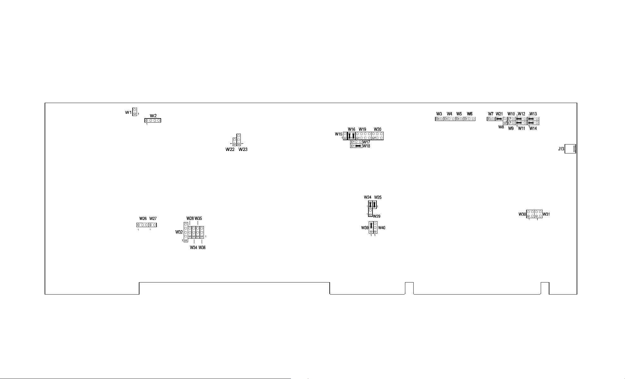
DIAGRAM 4-1: Jumper Locations With Default Settings
Setting Jumpers 4-11
Page 41

5 CONNECTING AND POWERING UP THE BOARD
5.01 Installing TEK-AT4LVG in Passive Backplane.....................................................5-3
5.02 Connecting a Floppy Disk..................................................................................... 5-4
5.03 Connecting Interface Devices (Keyboard, Speaker, Reset, LED) ............................ 5-5
5.04 Connecting a Mouse..............................................................................................5-6
5.05 Connecting a Monitor ...........................................................................................5-7
5.06 Powering Up the System .......................................................................................5-8
Connecting and Powering Up the Board 5-1
Page 42

5.01 INSTALLING TEK-AT4LVG IN PASSIVE BACKPLANE
The TEK-AT4LVG AT Single Board Computer will work with any standard ISA passive
backplane. For more information on the installation procedure, please consult the passive
backplane’s documentation.
Note that the installation into a passive backplane is optional. The TEK-AT4LVG can be
used as a stand-alone board. In this case, the board must be connected to an external
power source through the External Power Connector (J12).
The following list includes approved vendors for the J12 connector’s mating parts:
Leoco 2530 S060013 (housing),
Leoco 2533 TCB00A0 (pins);
Molex 22-01-2065 (housing),
Molex 08-50-114 (pins).
Connecting and Powering Up the Board 5-3
Page 43
5.02 CONNECTING A FLOPPY DISK
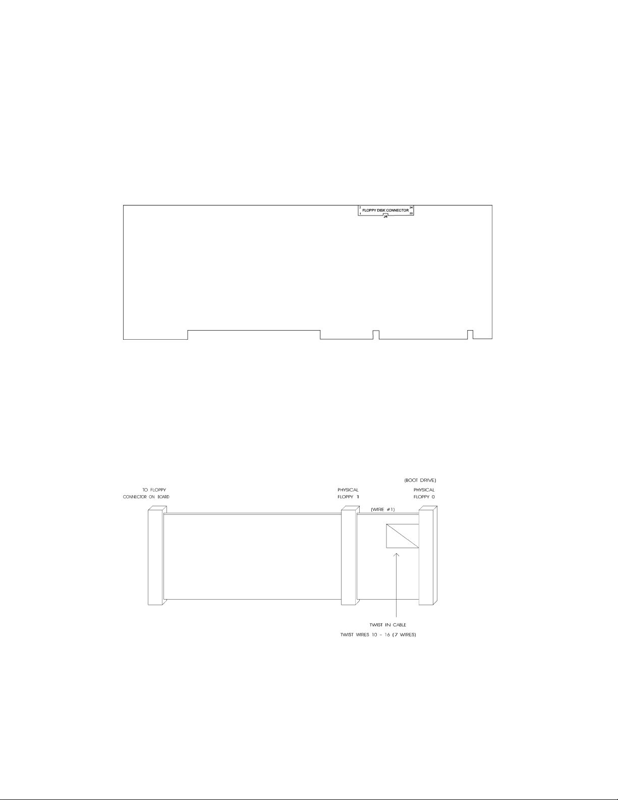
The Floppy connector appears on Diagram 5-1 at J4.
DIAGRAM 5-1: Floppy Connector Location
The installation of the floppy drives is done via a standard IBM 34-pin flat ribbon cable
that connects to J4.
The following list includes approved vendors for the J4 connector’s mating parts:
Amp 746285-8 [optional strain relief: 499252-6],
Robinson Nugent IDS-C34PK-TG,
Thomas & Betts 622-3430 [optional strain relief: 622-3441].
(34-pin flat cable connector).
DIAGRAM 5-2: Floppy Disk Cable
Connecting and Powering Up the Board 5-4
Page 44

5.03 CONNECTING INTERFACE DEVICES
(KEYBOARD, SPEAKER, RESET, LED)
Connector J5 provides all the necessary signals for connecting the keyboard, speaker,
reset, and keylock interface devices. The Multi-Function connector appears on Diagram 53 at J5.
DIAGRAM 5-3: Multi-Function Connector Location
The following list includes approved vendors for the J5 connector’s mating parts:
Amp 746285-3 [optional strain relief: 499252-8],
Robinson Nugent IDS-C16PK-TG,
Thomas & Betts 622-1630 [optional strain relief: 622-1641].
(16-pin flat cable connector).
The following functions are available on the J5 Connector:
• Speaker: An 8 ohm speaker can be directly connected to pins 7 and 8 of
J5. All necessary drivers are on the board.
• Keyboard Disable: The keyboard can be disabled or locked up by shorting pins 9
and 10 of J5.
• Hard Disk LED: The onboard IDE interface activates an external LED.
The LED‘s anode must be connected to pin 16 (J5) and
cathode to pin 15 (J5). No external current limiting resistor is
required since one is already present on the board.
• Reset: Manually reset the system by driving PBRES* to low state
(< 0.8 V).
Connecting and Powering Up the Board 5-5
Page 45
5.04 CONNECTING A MOUSE
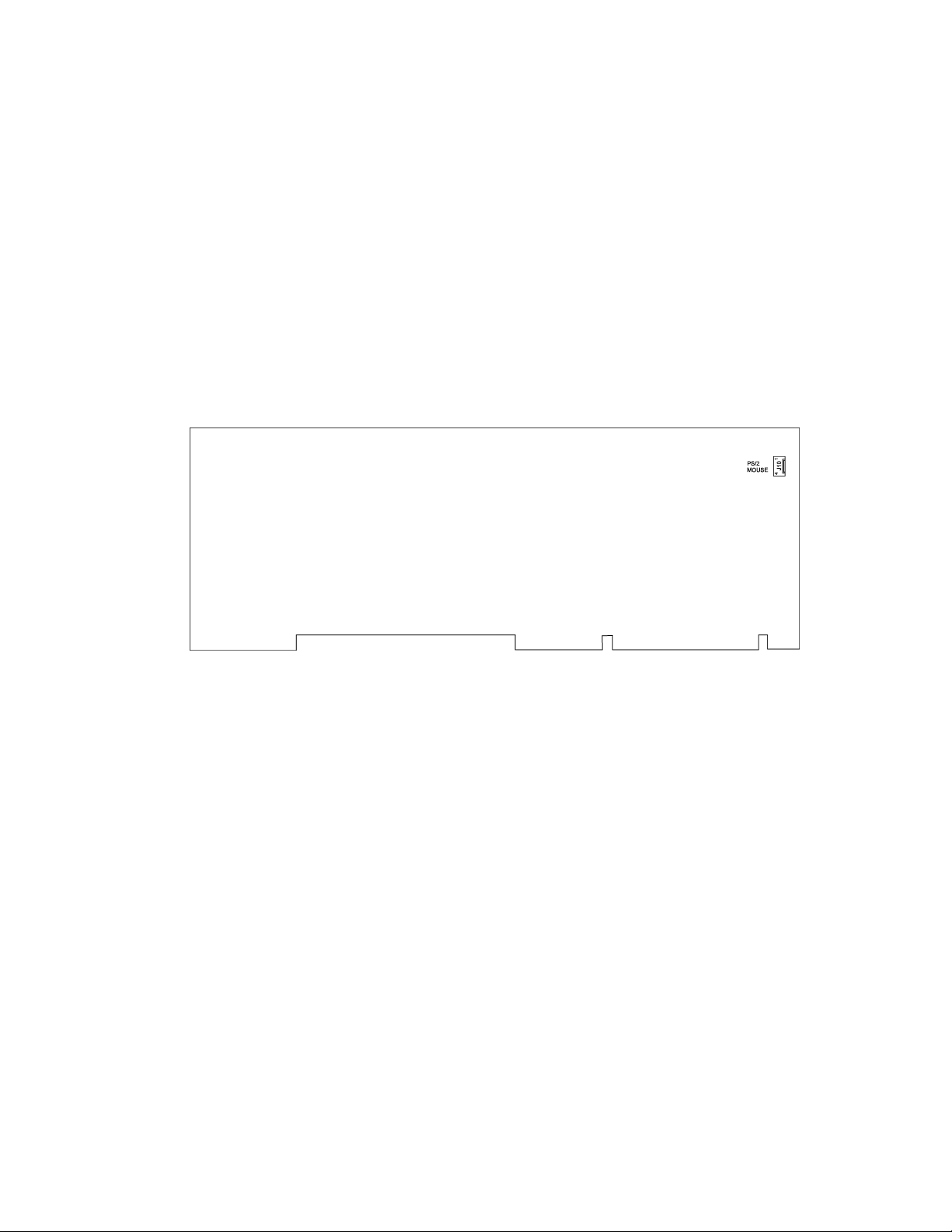
The board supports a PS/2 mouse, via the J10 connector. The PS/2 Mouse Cable (available
from TEKNOR), is compatible with the standard IBM PS/2 mouse. The cable may be
ordered by contacting our Sales department.
To use the mouse, the driver provided by the mouse manufacturer must be installed.
The Mouse connector appears on Diagram 5-4 at J10.
DIAGRAM 5-4: Mouse Connector Location
The following list includes approved vendors for the J10 connector’s mating parts:
Molex 22-01-3047 (connector),
Molex 08-50-0114 (crimp).
Connecting and Powering Up the Board 5-6
Page 46

5.05 CONNECTING A MONITOR
Connecting CRT video to the TEK-AT4LVG is simple. Plug the standard VGA DB15
male connector to the board’s J14 high density, right angle, female connector, and secure
with the connector screws.
See Diagram 5-5 for the location of J14.
DIAGRAM 5-5: VGA Connector Location
Connecting and Powering Up the Board 5-7
Page 47

5.06 POWERING UP THE SYSTEM
Before powering up your system, make sure that the battery jumper is intalled (Section
4.01).
1. Insert a bootable diskette in drive A to start your system with DOS.
2. Hit the DELETE key before or when this message appears near the bottom of the
screen: ″PRESS DEL TO ENTER SETUP″. This will bring you to CMOS setup.
- In Standard Setup, set the date and time.
- In other menu choices, set other options (if necessary).
3. Exit CMOS setup. The system will continue the boot procedure.
4. Once the boot procedure is completed, reboot the system to make sure everything
works properly.
If you should encounter a problem, verify the following items:
• Make sure that all connectors are properly connected. On the standard flat ribbon
cable used for the floppy connector, pin 1 is indicated by small red stripe. Verify that
this red stripe is located adjacent to pin 1 of the connector (On soldering side of the
board, connector pin 1 is designated by a square pad instead of being round).
• Verify your boot diskette. It must be a system disk and it must be in proper working
order.
• If the system still does not start up correctly, remove all the connectors except the
power cord and the video monitor, and try again (this configuration is the minimum
required to see if the board is working).
• If you still are not able to get your board up and running, contact our Technical
Support department for assistance.
Connecting and Powering Up the Board 5-8
Page 48

6 SOFTWARE SETUP
6.01 The Award Setup Program....................................................................................6-3
6.01.1 Accessing the Award Setup Program..............................................................6-3
6.01.2 Using Award Setup ........................................................................................6-5
6.01.3 Saving Configurations & Exiting Award Setup...............................................6-7
6.01.4 Standard CMOS Setup ................................................................................... 6-8
6.01.5 BIOS Features Setup ......................................................................................6-9
6.01.6 Chipset Features Setup ................................................................................. 6-11
6.01.7 Power Management Setup ............................................................................ 6-13
6.02 The VIP-UP Program..........................................................................................6-15
6.02.1 Accessing the VIP-UP Program....................................................................6-15
6.02.2 VIP-UP First Screen..................................................................................... 6-16
6.02.3 VIP-UP Second Screen................................................................................. 6-17
Software Setup 6-1
Page 49

6.01 THE AWARD SETUP PROGRAM
6.01.1 ACCESSING THE AWARD SETUP PROGRAM
The TEK-AT4LVG uses the AWARD Setup program, a setup utility in ROM that is
accessed by pressing the DELETE key at the appropriate time during system boot. This
utility is used to set configuration data in CMOS RAM.
F Before modifying CMOS setup parameters, insure that the W40 BAttery Selection
jumper is installed to enable the CMOS battery back-up (Short pin 1-2 for Internal
Battery, pin 2-3 for External Battery)
To run the AWARD Setup program incorporated in the ROM BIOS:
1. Turn on or reboot the system.
2. Hit the DELETE key before or when the message - "PRESS DEL TO ENTER
SETUP" appears near the bottom of the screen.
3. The main menu appears on the screen.
Software Setup 6-3
Page 50

An example of the main menu screen appears below:
ROM PCI/ISA BIOS (2A4IB000)
CMOS SETUP UTILITY
AWARD SOFTWARE, INC.
STANDARD CMOS SETUP
BIOS FEATURES SETUP
CHIPSET FEATURES SETUP
POWER MANAGEMENT SETUP
LOAD BIOS DEFAULTS
LOAD SETUP DEFAULTS
Esc : Quit
F10 : Save & Exit Setup
Time, Date, Hard Disk Type...
PASSWORD SETTING
IDE HDD AUTO DETECTION
SAVE & EXIT SETUP
EXIT WITHOUT SAVING
↑ ↓ → ← : Select Item
(Shift)F2 : Change Color
Software Setup 6-4
Page 51

6.01.2 USING AWARD SETUP
The arrow keys (↑ ↓ → ←) are used to highlight items on the menu and the PageUp and
PageDown keys are used to change the entry values for the highlighted item. To select an
entry, press the Enter key. Also, you can press the F1 key to obtain help information or the
Esc key to leave an option, close a menu or to quit the program.
Table 6-1 provides more details on how to navigate in the Setup program:
Table 6-1
Up arrow (↑)
Down arrow (↓)
Left arrow (←)
Right arrow (→)
Esc key In Main Menu: Quit settings (Answer ‘Y’ to save changes into
PgUp key Increase the numeric value or make changes.
PgDn key Decrease the numeric value or make changes.
+ key Increase the numeric value or make changes.
- key Decrease the numeric value or make changes.
F1 key General help.
F2 and
Shift F2 keys
F4 key Reserved.
F5 key In sub-menu: Restore the previous setup values from BIOS Default
F6 key In sub-menu: Load the default setup values from BIOS Default
F7 key In sub-menu: Load the setup values from the Setup Default Table .
F8 key Reserved.
F9 key Reserved.
F10 key When in Main Menu: Save all the CMOS changes.
Move to previous item.
Move to next item.
Move to the item in the left hand.
Move to the item in the right hand.
CMOS).
In sub-menus: Exit and return to Main Menu.
Change color from total 16 colors: F2 to select color forward,
Shift F2 to select color backward.
Table.
Table.
Software Setup 6-5
Page 52

The Main Menu includes the following categories:
Standard CMOS
Setup
BIOS Features
Setup
Chipset Features
Setup
Power Management
Setup
Load Bios
Defaults
Load Setup
Defaults
Password Setting
IDE HDD Auto
Detection
This Setup page includes all the items in a standard, AT-compatible
BIOS.
This Setup page includes all the items of AWARD’s special enhanced
features.
This Setup page includes all the items of the chipset’s special features.
This Setup page sets power conservation options.
The BIOS defaults represent settings which provide the minimum
requirements for your system to operate.
The chipset defaults are settings which provide for maximum system
performance.
Change, set, or disable password. It allows you to limit access to the
system and the Setup, or just to the Setup.
Automatically detect and configure hard disk parameters. This ability
is included in the event you are uncertain of your hard disk’s
parameters.
Save & Exit
Exit Without Saving
Software Setup 6-6
Save CMOS value changes to CMOS and exit Setup.
Abandon all CMOS value changes and exit Setup.
Page 53

6.01.3 SAVING CONFIGURATIONS & EXITING AWARD SETUP
Use one of the following options available from the Main Menu:
Save & Exit
Exit Without Saving
After having modified the AWARD Setup, you can save the
configuration in CMOS RAM, by selecting this option. This
option will not change the values saved in Flash EPROM. To
update the values in Flash, enter the VIP-UP program and
perform a save (F10).
This option is used to exit AWARD Setup without saving the
configuration to CMOS RAM.
Software Setup 6-7
Page 54

6.01.4 STANDARD CMOS SETUP
This part of the setup allows you to set the time, date, hard disk type, types of floppy
drives and video type.
Date/Time
The current values for each category are displayed. Enter new values through the
keyboard.
Hard Disks
Two IDE controllers are defined on the TEK-AT4LVG board (Primary and Secondary),
each can have two disks: Master Disk (bootable) or Slave Disk.
Drive A / Drive B
Select the category identifying the types of floppy disk drive A or drive B that have been
installed in the computer.
Video
This option specifies the basic type of display adapter card installed in the system.
Halt on
This option specifies the type of errors that will stop the system during the BIOS booting
procedure. The settings are All errors, No errors, All but keyboard (default setting), All
but diskette and All but disk/key.
Memory
This display-only option determines the amount of Base, Extended and other types of
memory installed in the system.
Software Setup 6-8
Page 55

6.01.5 BIOS FEATURES SETUP
This part of the setup handles options and features such as boot sequence, NUM LOCK,
security options, shadowing, ...
Whenever you are not sure about a certain setting, you may refer to the list of default
values. The list of defaults is provided in the event that a value has been changed and one
wishes to set this option to its original value. Loading the BIOS or SETUP defaults will
affect all the options and will reset options previously altered.
The BIOS default settings consist of the safest set of parameters. Use them if the system is
behaving erratically. They should always work but do not provide optimal system
performance.
The SETUP default values provide optimum performance settings for all devices and
system features.
Software Setup 6-9
Page 56

The scroll list displays these options:
OPTIONS BIOS
DEFAULTS
CPU Internal Cache Enabled Enabled
External Cache Enabled Enabled
Quick Power On Self Test Disabled Disabled
Boot Sequence A, C A, C
Swap Floppy Drive Disabled Disabled
Boot Up Floppy Seek Enabled Enabled
Boot Up NumLock Status On On
Boot Up System Speed High High
IDE HDD Block Mode Disabled Disabled
Memory Parity Check Disabled Disabled
Typematic Rate Setting Disabled Disabled
Typematic Rate (Chars/Sec) 6 6
Typematic Delay (Msec) 250 250
Security Option Setup Setup
Video BIOS Shadow Enabled Enabled
C8000-CBFFF Shadow Disabled Disabled
CC000-CFFFF Shadow Disabled Disabled
D0000-D3FFF Shadow Disabled Disabled
D4000-D7FFF Shadow Disabled Disabled
D8000-DBFFF Shadow Disabled Disabled
DC000-DFFFF Shadow Disabled Disabled
E0000-E3FFF Shadow Disabled Disabled
E4000-E7FFF Shadow Disabled Disabled
E8000-EBFFF Shadow Disabled Disabled
EC000-EFFFF Shadow Disabled Disabled
SETUP
DEFAULTS
Software Setup 6-10
Page 57

6.01.6 CHIPSET FEATURES SETUP
This part of the setup allows you to define chipset-specific options and features.
Whenever you are not sure about a certain setting, you may refer to the list of default
values. The list of defaults is provided in the event that a value has been changed and one
wishes to set this option to its original value. Loading the BIOS or SETUP defaults will
affect all the options and will reset options previously altered.
The BIOS default settings consist of the safest set of parameters. Use them if the system is
behaving erratically. They should always work but do not provide optimal system
performance.
The SETUP default values provide optimum performance settings for all devices and
system features.
F These parameters have been provided to give control over the system. However,
the values for these options should be changed only if the user has a full
understanding of the timing relationships involved.
Software Setup 6-11
Page 58

The scroll list displays these options:
OPTIONS BIOS
DEFAULTS
Auto Configuration Enabled Disabled
AT Bus Clock (486) CLK/2 or CLK/4 CLK/2 or CLK/4
Cache Scheme Write Back Write Back
SRAM Read Burst 4333 Burst 3111 Burst
SRAM Write WS 1 WS 1 WS
Special DRAM WR Mode Disabled Disabled
F000 Cacheable Disabled Disabled
C000 Cacheable Disabled Disabled
Cacheable Range 0-128M 0-128M
DRAM Page Mode Fast Page Mode Fast Page Mode
DRAM Write WS 1 WS 1 WS
DRAM Read WS 3 WS 1 WS
RAS Precharge Time 3 SYSCLK 3 SYSCLK
RAS to CAS Delay 1 SYSCLK 2 SYSCLK
Hidden Refresh Enabled Enabled
15M-16M Access Normal Normal
Master IOCHRDY Disabled Disabled
Onboard FDD Controller Enabled Enabled
Onboard IDE Controller Secondary Secondary
Onboard Parallel Mode ECP+EPP1.9 ECP+EPP1.9
Onboard Parallel Port 3BCh 3BCh
Onboard Serial Port 1 COM1/3F8h COM1/3F8h
Onboard Serial Port 2 COM2/2F8h COM2/2F8h
Serial Port 1 Interrupt COM1/3=>IRQ4 COM1/3=>IRQ4
Serial Port 2 Interrupt COM2/4=>IRQ3 COM2/4=>IRQ3
SETUP
DEFAULTS
Software Setup 6-12
Page 59

6.01.7 POWER MANAGEMENT SETUP
This part of the setup sets power conservation options.
Whenever you are not sure about a certain setting, you may refer to the list of default
values. The list of defaults is provided in the event that a value has been changed and one
wishes to set this option to its original value. Loading the BIOS or SETUP defaults will
affect all the options and will reset options previously altered.
The BIOS default settings consist of the safest set of parameters. Use them if the system is
behaving erratically. They should always work but do not provide optimal system
performance.
The SETUP default values provide optimum performance settings for all devices and
system features.
Software Setup 6-13
Page 60

The scroll list displays these options:
OPTIONS BIOS
DEFAULTS
Power Management Disable Disable
Video On/Off Control Disable Disable
HDD Standby Timer Disable Disable
System Standby Timer 7 Sec 7 Sec
System Suspend Timer 14 Sec 14 Sec
Keyboard Detection Enable Enable
Serial Port Detection Disable Disable
Parallel Port Detection Disable Disable
Hard Disk I/O Detection Disable Disable
DMA/ISA Master Detection Disable Disable
Non Motherboard Memory Disable Disable
Video Memory (Block A,B) Enable Enable
I/O Address Detection Disable Disable
VESA Master Detection Disable Disable
SETUP
DEFAULTS
Software Setup 6-14
Page 61

6.02 THE VIP-UP PROGRAM
6.02.1 ACCESSING THE VIP-UP PROGRAM
The VIP-UP program is TEKNOR's own Setup program for enabling / disabling /
relocating various hardware features on the TEK-AT4LVG.
During boot-up, hit the CTRL and V keys simultaneously, before or when you see the
message "Press CTRL-V to enter TEKNOR VIP-UP" at the top of the screen (CTRL-V
will work, even if the message display is disabled in VIP-UP).
At the DOS prompt, type "VIP-UP" and press ENTER. This program is available on the
utility disk.
There are two screens in the VIP-UP program. The values appearing on the right side of
each screen can be modified. Follow the instructions found at the bottom of the screen to
select another value.
Use the ↑ and ↓ keyboard keys to move up and down the screen, and on to subsequent or
preceding screens. As you do, the value of the selected field is highlighted. If you press the
↓ key when the last field of the screen is highlighted, the next screen is displayed.
Pressing the ↑ key when the first field is highlighted will display the first field of the
preceding screen; in this way you can move quickly from screen to screen.
Once a field value is highlighted, you can change it by pressing PgDn or typing "+" on the
keyboard (in VT100 mode, only "+" will work); this will usually display a higher value.
You can also press the PgUp key or type "-" ("-" in VT100 mode), which will usually
display a lower value.
Press F10 to save the current configuration and exit (type "U" in VT100 mode). The
configuration is not saved until F10 is pressed or "U" is typed. Press ESC to exit without
saving the setup.
Software Setup 6-15
Page 62

6.02.2 VIP-UP FIRST SCREEN
TEKNOR MICROSYSTEMS INC --- VIPer SETUP
TEKNOR BIOS Extension Address
TEKNOR BIOS Window Adress
On Board SCSI BIOS
SCSI BIOS Address
SCSI Base I/O Address (W22)
SCSI ID Select
SCSI IRQ Channel (W18)
SCSI DMA Channel (W17 & W23)
SCSI Parity
SCSI Disconnect
SCSI Synchronous Negociation
SCSI Floptical Drive Support
SCSI Compatibility Mode
↑↓ to select options
PgDn(+), PgUp(-) to change an option
C8000H-CBFFFH
CC000H-CFFFFH
Enabled
D8000H-DBFFFH
340H (Default BIOS)
ID7 (Default)
IRQ11
DMA 0
Enabled
No Disconnect
Respond Only
Enabled
6360 Features
ESC - Quit without saving
F10 - (U)pdate Flash BIOS
There are two parts to the screen:
1. Selection of TEKNOR BIOS addresses: The addresses of the TEKNOR BIOS
extension and the TEKNOR BIOS window are set in the top part of the screen.
2. On Board SCSI BIOS: This option allows the user to enable or disable the on board
SCSI controller. Once the controller is enabled, all other SCSI options can be defined
by associating to them the desired value.
Software Setup 6-16
Page 63

6.02.3 VIP-UP SECOND SCREEN
TEKNOR MICROSYSTEMS INC --- VIPer SETUP
BIOS Interrupt 13h Configuration
Flash Disk Support
Enter VIP-UP Message
VT100 & Serial Download Speed
VT100 & Serial Download Serial Port
Use Flash To Store CMOS RAM SETUP
↑↓ to select options
PgDn(+), PgUp(-) to change an option
Disabled
Not Installed
Displayed 3 seconds
19200 BPS
COM1: 3F8H
No
ESC - Quit without saving
F10 - (U)pdate Flash BIOS
There are four parts to the screen:
1. BIOS Interrupt 13h Configuration: To configure the Flash Disk in VIP-UP, proceed as
follows:
. set the ‘BIOS Interrupt 13h Configuration’ option to ‘Enabled’
. set the ‘Flash Disk Support’ option to ‘Installed’ or ‘Installed Bootable’
For more information , please refer to Section 12.01.2.
2. Enter VIP-UP message: This option allows the user to enable or disable the message
"Press CTRL-V to enter TEKNOR VIP-UP" at the top of the screen upon boot-up.
3. VT100 & Serial Download: The VT100 & Serial Download Speed option is for
selecting the desired speed for the VT100 and Download modes. The VT100 & Serial
Download Serial Port option allows the use of either COM2 or COM1 for the
VT100/Serial Download Mode hookup.
4. Use Flash To Store CMOS RAM SETUP: When this option is set to "Yes", the CMOS
RAM Setup will be restored from Flash during each power up, as long as the battery is
good. If the battery fails, the system returns to the power on default configuration.
However, when the battery is replaced, the CMOS RAM Setup is restored from Flash
(only the time and date could be lost).
Please note that modifying and saving the CMOS RAM Setup in AWARD Setup does
not change the Flash copy; to update Flash, you must return to the VIP-UP Setup and
update it while "Use Flash To Store CMOS RAM SETUP" is set to "Yes".
Software Setup 6-17
Page 64

PART THREE
ADVANCED INSTALLATION AND SETUP
7 INSTALLING AND WORKING WITH SYSTEM COMPONENTS
8 INSTALLING IDE, FLOPPY & SCSI DEVICES
9 INSTALLING PERIPHERALS
10 INSTALLING VIDEO
11 SETTING POWER MANAGEMENT MODES
Page 65

7 INSTALLING AND WORKING WITH SYSTEM COMPONENTS
7.01 Location of System Components............................................................................7-2
7.02 Fan Connector.......................................................................................................7-5
7.03 Cache Memory ...................................................................................................... 7-6
7.03.1 System Cache.................................................................................................7-6
7.04 Boot Selections......................................................................................................7-7
7.05 Supervisor Circuit................................................................................................. 7-8
7.05.1 Field Programmable Gate Array..................................................................... 7-8
7.05.2 Onboard Power Detection...............................................................................7-9
7.05.3 Power Fail Detection Circuit.........................................................................7-10
7.05.4 Watchdog Timer ..........................................................................................7-11
7.06 PS/2 Mouse Connector........................................................................................ 7-13
7.07 Power Connector ................................................................................................. 7-14
7.08 ISA Bus Connector .............................................................................................7-15
Installing and Working With System Components 7-1
Page 66

7.01 LOCATION OF SYSTEM COMPONENTS
Diagram 7-1 shows the location of the system components described in sections 7.02 to
7.09.
System components are numbered in Diagram 7-1. The following list shows which
components these numbers correspond to, as well as the sub-section in which they are
explained:
# COMPONENT SUB-SECTION
1 Fan Connector 7.02 - FAN CONNECTOR
2 Field Programmable Gate Array 7.05 - SUPERVISOR CIRCUIT
3 PS/2 Mouse Connector 7.06 - PS/2 MOUSE CONNECTOR
4 Power connector 7.07 - POWER CONNECTOR
5 Flash EPROM BIOS (Emergency) 7.04 - BOOT SELECTIONS
6 EPROM BIOS 7.04 - BOOT SELECTIONS
7 Cache Memory 7.03 - CACHE MEMORY
Installing and Working With System Components 7-2
Page 67
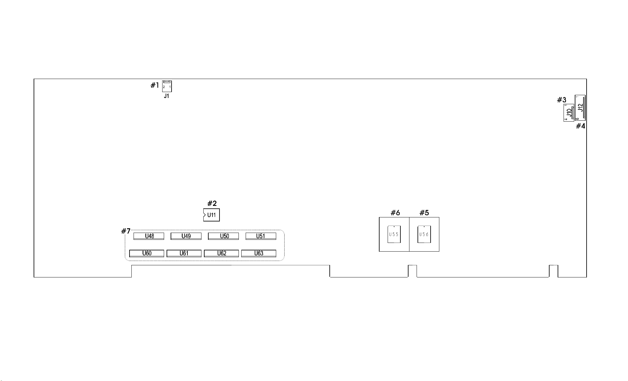
DIAGRAM 7-1: System Components Location
Installing and Working With System Components 7-3
Page 68

7.02 FAN CONNECTOR
The #1 component on Diagram 7-1 is for connecting a CPU fan. Its pinout is as follows:
TABLE 7-1: Fan Connector (J1) - Pinout
Pin Number Signal
1 +12V
2 GND
The following list includes approved vendors for the J1 connector’s mating parts:
Leoco 2530 S020013 (housing),
Leoco 2533 TCB00A0 (crimp);
Molex 22-01-3027 (housing),
Molex 08-50-0114 (crimp).
Installing and Working With System Components 7-5
Page 69

7.03 CACHE MEMORY
There are two separate Caches in the Host subsystem: Internal Cache and External Cache.
The Cache inside the processor (Internal Cache) is referred to as the first level Cache (also
primary Cache). The External Cache (called System Cache in this manual) comprises the
System Controller’s Cache control circuitry and associated external memory array; it is
referred to as the second level Cache (also secondary Cache). The second level Cache is
unified, which means that both CPU data and instructions are stored in the Cache.
7.03.1 SYSTEM CACHE
System Cache is located at U48, U49, U50, U51, U60, U61, U62 and U63 (#7) on
Diagram 7-1; it accepts 0KB, 128KB, 256KB or 512KB of standard asynchronous
SRAMs. The tag RAM is external to the System Controller and is situated at U36.
System Cache copies the most recently accessed data and places it in an area of high speed
memory called SRAM (Static RAM). Cache SRAM is positioned between System Memory
(DRAM) and the CPU. Data is transferred from System Memory to Cache and then from
Cache to the CPU.
Since most program executions are sequential and repetitive, the likelihood is great that
the CPU will find data already stored in either Cache. When the CPU retrieves data from
Cache, a Cache hit occurs. On the other hand, when the CPU must access data from
System Memory, a Cache miss occurs.
System Cache is enabled in the AWARD Setup program.
1. From AWARD’s Main Menu, select the BIOS Features Setup option.
2. In the BIOS Features Setup Menu:
- Select the CPU Internal Cache option, or
- Select the External Cache option.
In both cases, you will have the option to choose between Disabled and Enabled
(Disabled is the default value).
Installing and Working With System Components 7-6
Page 70
7.04 BOOT SELECTIONS
The Flash EPROM BIOS and the EPROM BIOS are factory installed. The Flash EPROM
BIOS appears on Diagram 7-1 at U56 (#5) and the EPROM BIOS at U55 (#6).
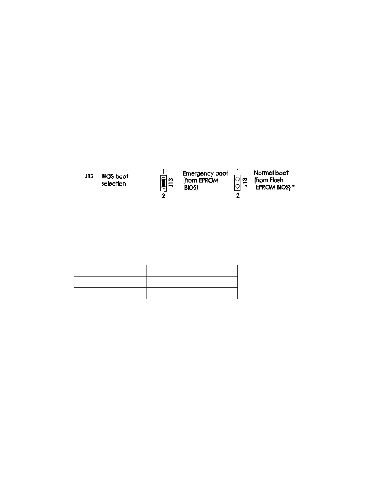
By default the TEK-AT4LVG boots from the Flash EPROM BIOS. This is set by the J13
Emergency BIOS boot selection jumper, as follows:
• J13 : Selects the BIOS to boot from:
* Default setting
The pinout for J13 appears below:
TABLE 7-2: Emergency BIOS Boot (J13) - Pinout
Pin Number Signal
1 EMER*
2 GND
* Active low signal
Installing and Working With System Components 7-7
Page 71

7.05 SUPERVISOR CIRCUIT
7.05.1 FIELD PROGRAMMABLE GATE ARRAY
Component #2 on Diagram 7-1 is defined as Field Programmable Gate Array (FPGA);
this memory device contains registers, one of which is described below.
TEKNOR computers utilize address space 190H, 290H or 390H (depending on the setting
of W16 jumper for I/O base address) to enable special features (see Table 7-3 below).
TABLE 7-3: Register 190H, 290H or 390H
Bit # Bit Value
(Default)
0 0 Enable Watchdog
1 1 Watchdog activate
2 0 Flash VPP enable Same
3 0 Enable direction control RS-485
4 0 Reserved, ENWF W19 (7-8) Status
5 0 Reserved, ENWB W19 (5-6) Status
6 1 Reserved, B64/16 W19 (3-4) Status
7 0 Reserved W19 (1-2) Status
Function:
WRITE READ
1=enable, R/W bit
1-0-1 to toggle, R/W bit
1=enable RS-485 only, write only
Same
Same
Power Detection Output or
Battery Low output
F Not all bits are R/W. Therefore, be certain to keep a mirror image of the register
when programming it.
F All bits are 0 after a hardware RESET or power up condition.
F Write the values shown in the "Bit Value (Default)" column if you are unsure.
Installing and Working With System Components 7-8
Page 72

7.05.2 ONBOARD POWER DETECTION
An onboard device which is part of the reset circuit constantly monitors the voltage which
powers the board. Normally, the board is powered with 5V. If the supply voltage drops
below 4.65V (a typical threshold), the onboard circuitry will reset the board and the
system. This reset has the same effect on the system as the reset button.
Installing and Working With System Components 7-9
Page 73

7.05.3 POWER FAIL DETECTION CIRCUIT
The Power Failure Detector monitors:
• The backup battery to warn of a low battery condition, and
• The +5V power supply to detect when it falls below 4.75V.
If either of the two above conditions occur, the PFO (Power Fail Output signal) goes low.
In turn, the PFO is connected to the IOCHK* line to generate a non-maskable interrupt
(NMI).
Power fail monitoring is enabled by using the W29 jumper. W29 is described in Section 49 (Setting Jumpers).
Installing and Working With System Components 7-10
Page 74

7.05.4 WATCHDOG TIMER
The Watchdog Timer is extremely useful in embedded systems where human supervision
is not required.
The Jumper Watchdog is set by using W24 jumper. Its setting is given in Section 4-8
(Jumper Settings).
The Watchdog must also be enabled and refreshed by software. To enable the Watchdog
by software, first write "1" in bit "0" at address 190H (or at 290H or 390H depending on
the W16 jumper setting).
When enabled, the microprocessor must refresh the Watchdog. This is done by writing
alternatively "0" and "1" to bit 1 at address 190H (or at 290H or 390H), once every 1.6
seconds (or less) to verify proper software execution.
Following a reset, the Watchdog is always disabled.
If a hardware or software failure occurs such that the Watchdog is not refreshed, a reset
pulse is generated by the Watchdog to restart the processor.
F The user program must provide the first access to address 190H (or at 290H or
390H depending on the W16 jumper setting), and must also include the refresh
routine. In addition, be certain to keep a mirror image of register 190H (or 290H
or 390H) when programming it. This is necessary since the register is a writeonly user register and, as a result, is not used by the system BIOS.
Installing and Working With System Components 7-11
Page 75

TABLE 7-4: Watchdog Timer Register
ADDRESS REGISTER
190H, 290H OR 390H:
Bit 0 Read/Write Watchdog enable
190H, 290H OR 390H:
Bit 1 Read/Write Watchdog refresh
The default timeout is 1.6 seconds; however the timeout period can be changed. Shorting
C138 and leaving R152 opened changes the timeout to 100 ms. Shorting R152 and
installing a capacitor at C138 will change the timeout period according to the following
formulae:
Timeout (milliseconds) = (400/47pF) * C
or
C138 = (Timeout (milliseconds) * 47pF) / 400ms.
For instance, an external capacity of 100pF will lengthen the timeout to 851 ms and a
1000pF will bring it to 8.5 seconds.
Installing and Working With System Components 7-12
Page 76

7.06 PS/2 MOUSE CONNECTOR
The board supports a mouse, through the PS/2 connector at J10 (#3 on Diagram 7-1).
With the PS/2 Mouse Cable (available from TEKNOR), this feature is compatible with the
standard IBM PS/2 mouse. The cable may be ordered by contacting our Sales department.
To use the mouse, the driver provided by the mouse manufacturer must be installed.
TABLE 7-5: PS/2 Mouse Connector (J10) - Pinout
Pin Number Signal
1 MCLK
2 GND
3 MDATA
4 VCC (+5V)
The following list includes approved vendors for the J10 connector’s mating parts:
Molex 22-01-3047 (connector),
Molex 08-50-0114 (crimp).
Installing and Working With System Components 7-13
Page 77

7.07 POWER CONNECTOR
The TEK-AT4LVG board is powered from one of two sources:
Ÿ Power connector (J12): Stand-alone systems are powered from an outside power
supply through the J12 connector (#4 on Diagram 7-1).
Ÿ ISA (AT) bus: When the board is in a passive backplane system, it is
powered through the ISA bus.
The pinout for the J12 power connector is shown in the table below:
TABLE 7-6: External Power Connector (J12) - Pinout
Pin Number Signal
1 VCC (+5V)
2 GND
3 GND
4 +12V
5 -12V
6 PD (Power Fail Detection Input)
The following list includes approved vendors for the J12 connector’s mating parts:
Leoco 2530 S060013 (housing),
Leoco 2533 TCB00A0 (pins);
Molex 22-01-2065 (housing),
Molex 08-50-114 (pins).
Installing and Working With System Components 7-14
Page 78
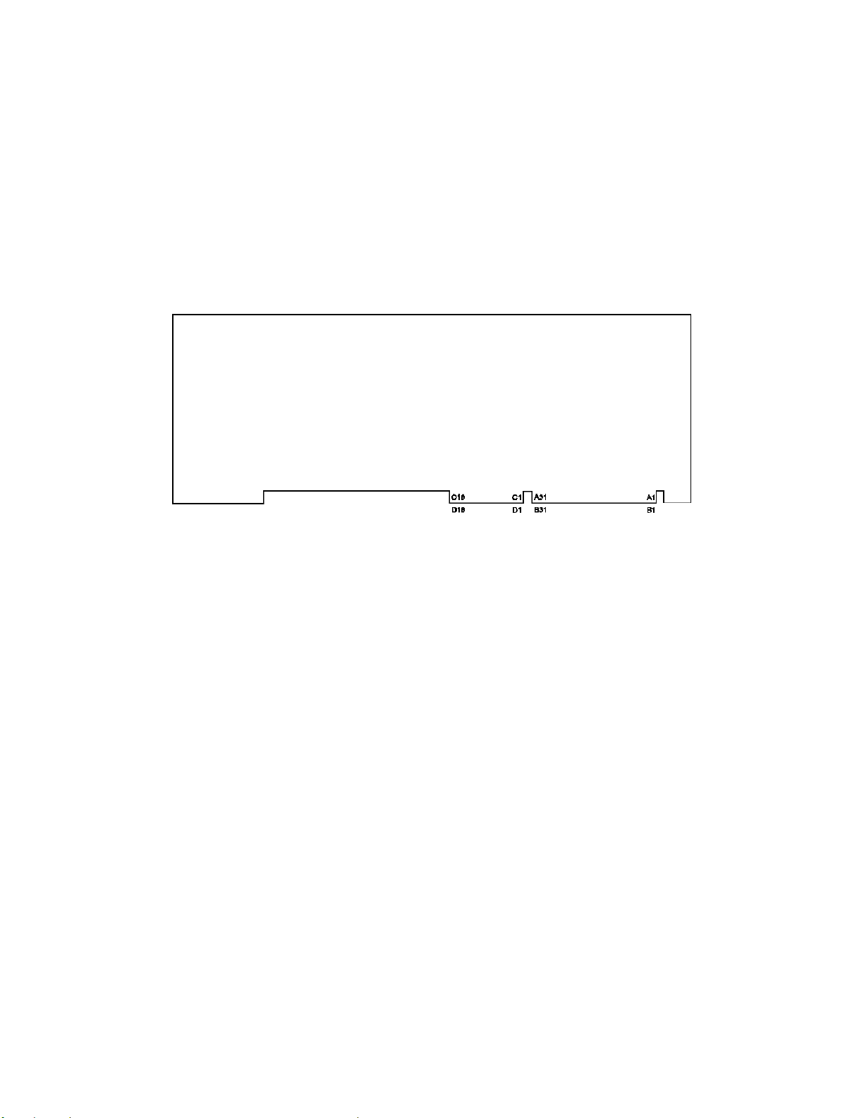
7.08 ISA BUS CONNECTOR
The ISA bus connector appears on the Diagram 7-2.
DIAGRAM 7-2: ISA Bus Connector Location
Installing and Working With System Components 7-15
Page 79

TABLE 7-7a: ISA Bus Connector (A, B) - Pin-Out
A SIDE B SIDE
I/O PIN Signal Name I/O I/O PIN Signal Name I/O
A1
A2
A3
A4
A5
A6
A7
A8
A9
A10
A11
A12
A13
A14
A15
A16
A17
A18
A19
A20
A21
A22
A23
A24
A25
A26
A27
A28
A29
A30
A31
IOCHK*
SD7
SD6
SD5
SD4
SD3
SD2
SD1
SD0
IOCHRDY
AEN
SA19
SA18
SA17
SA16
SA15
SA14
SA13
SA12
SA11
SA10
SA9
SA8
SA7
SA6
SA5
SA4
SA3
SA2
SA1
SA0
I/O
I/O
I/O
I/O
I/O
I/O
I/O
I/O
I/O
I/O
I/O
I/O
I/O
I/O
I/O
I/O
I/O
I/O
I/O
I/O
I/O
I/O
I/O
I/O
I/O
I/O
I/O
I/O
I
I
O
B1
B2
B3
B4
B5
B6
B7
B8
B9
B10
B11
B12
B13
B14
B15
B16
B17
B18
B19
B20
B21
B22
B23
B24
B25
B26
B27
B28
B29
B30
B31
GND
RESET DRV
VCC (+5V)
IRQ9
-5 V
DRQ2
-12V
OWS*
+12V
GND
SMEMW*
SMEMR*
IOW*
IOR*
DACK3*
DRQ3
DACK1*
DRQ1
REFRESH*
SYSCLK
IRQ7
IRQ6
IRQ5
IRQ4
IRQ3
DACK2*
T/C
BALE
VCC (+5V)
OSC
GND
-
O
I
I
I
-
O
O
I/O
I/O
O
I
O
I
I/O
O
I
I
I
I
I
O
O
O
-
O
-
* Active low signal
Installing and Working With System Components 7-16
Page 80

TABLE 7-7b: ISA Bus Connector (C, D) - Pin-Out
C Side D Side
I/O PIN Signal Name I/O I/O PIN Signal Name I/O
C1
C2
C3
C4
C5
C6
C7
C8
C9
C10
C11
C12
C13
C14
C15
C16
C17
C18
* Active low signal
SBHE*
LA23
LA22
LA21
LA20
LA19
LA18
LA17
MEMR*
MEMW*
SD08
SD09
SD10
SD11
SD12
SD13
SD14
SD15
I/O
I/O
I/O
I/O
I/O
I/O
I/O
I/O
I/O
I/O
I/0
I/O
I/O
I/O
I/O
I/O
I/O
I/O
D1
D2
D3
D4
D5
D6
D7
D8
D9
D10
D11
D12
D13
D14
D15
D16
D17
D18
MEMCS16*
IOCS16*
IRQ10
IRQ11
IRQ12
IRQ15
IRQ14
DACK0*
DRQ0
DACK5*
DRQ5
DACK6*
DRQ6
DACK7*
DRQ7
VCC (+5V)
MASTER*
GND
I
I
I
I
I
I
I
O
I
O
I
O
I
O
I
I
-
Installing and Working With System Components 7-17
Page 81

The ISA Bus Interface on the TEK-AT4LVG board integrates the functionality of two
8237 DMA Controllers (see Table 7-8), two interrupt controllers (see Table 7-9) and one
8254 Counter/Timer.
TABLE 7-8: 8237 DMA Controllers
DMA 0 Available
DMA 1 Available (ECP)
DMA 2 Floppy controller
DMA 3 Available (ECP)
DMA 4 Cascade controller # 1
DMA 5 Available
DMA 6 Available
DMA 7 Available
The parallel port's ECP mode can be configured to use DMA Channel 1 or 3. Channel 2 is
reserved for the Floppy controller and Channel 4 is used to cascade Channels 0 through 7
to the microprocessor.
TABLE 7-9: 8259 Interrupt Controllers
Controller # 1 Controller # 2
IRQ 0 Timer 0 IRQ 8 Real-time clock
IRQ 1 Keyboard IRQ 9 Available
IRQ 2 Cascade controller # 2 IRQ 10 Available or SCSI
IRQ 3 COM 2 * IRQ 11 Available or SCSI
IRQ 4 COM 1 * IRQ 12 PS/2 Mouse Interface
IRQ 5 Available (LPT2)* IRQ 13 Coprocessor Error
IRQ 6 Floppy controller * IRQ 14 Primary IDE * or available
IRQ 7 LPT1* IRQ 15 Secondary IDE * or available
* All functions marked with an asterisk (*) can be disabled or reconfigured.
Installing and Working With System Components 7-18
Page 82

8 INSTALLING IDE, FLOPPY & SCSI DEVICES
8.01 IDE Devices..........................................................................................................8-3
8.01.1 IDE Connectors Location & Pinout ................................................................8-3
8.01.2 IDE Hook-Up.................................................................................................8-6
8.01.3 Jumper Setting ............................................................................................... 8-6
8.01.4 IDE Software Setup........................................................................................8-7
8.02 Floppy Devices...................................................................................................... 8-8
8.02.1 Floppy Jumpers ..............................................................................................8-8
8.02.2 Floppy Connectors Location & Pinout ............................................................8-9
8.02.3 Floppy Hook-Up........................................................................................... 8-11
8.02.4 Floppy Software Setup .................................................................................. 8-12
8.03 SCSI Devices ...................................................................................................... 8-13
8.03.1 Installing a Fixed SCSI Hard Disk................................................................ 8-14
8.03.2 Installing Other SCSI Devices...................................................................... 8-16
8.03.3 Removable Termination Resistors.................................................................8-17
8.03.4 SCSI Connector............................................................................................ 8-18
8.03.5 SCSI Software Setup .................................................................................... 8-19
Installing IDE, Floppy & SCSI Devices 8-1
Page 83
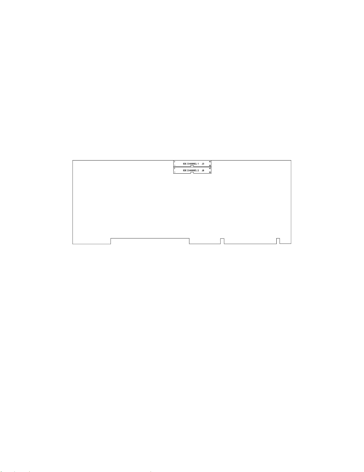
8.01 IDE DEVICES
8.01.1 IDE CONNECTORS LOCATION & PIN-OUT
The IDE connectors appear on Diagram 8-1 at J3 and J8.
The IDE Connectors’ pin-outs appear in Tables 8-1a and 8-1b.
DIAGRAM 8-1: IDE Connectors Location
Installing IDE, Floppy & SCSI Devices 8-3
Page 84

TABLE 8-1a: Hard Disk Connector #1 (J3) - Pin-Out
Pin
Number
1
3
5
7
9
11
13
15
17
19
21
23
25
27
29
31
33
35
37
39
Signal
Flow
I
I/O
I/O
I/O
I/O
I/O
I/O
I/O
I/O
O
I
I
O
O
O
I
I
I
O
* Active low signal
Signal Pin
RESET*
SD7
SD6
SD5
SD4
SD3
SD2
SD1
SD0
GND
REQ A
IOW*
IOR*
IOCHRDY*
DACK A*
IRQ14
SA1
SA0
CS0 A*
ACTIVE*
Number
2
4
6
8
10
12
14
16
18
20
22
24
26
28
30
32
34
36
38
40
Signal
Flow
I/O
I/O
I/O
I/O
I/O
I/O
I/O
I/O
-
-
-
-
-
O
I
O
-
Signal
GND
SD8
SD9
SD10
SD11
SD12
SD13
SD14
SD15
Not Used
GND
GND
GND
Not Used
GND
IOCS16*
Not Used
SA2
CS1 A*
GND
Installing IDE, Floppy & SCSI Devices 8-4
Page 85

TABLE 8-1b: Hard Disk Connector #2 (J8) - Pin-Out
Pin
Number
1
3
5
7
9
11
13
15
17
19
21
23
25
27
29
31
33
35
37
39
Signal
Flow
I
I/O
I/O
I/O
I/O
I/O
I/O
I/O
I/O
O
I
I
O
O
O
I
I
I
O
* Active low signal
Signal Pin
RESET*
SD7
SD6
SD5
SD4
SD3
SD2
SD1
SD0
GND
REQ B
IOW*
IOR*
IOCHRDY*
DACK B*
IRQ15
SA1
SA0
CS0 B*
ACTIVE*
Number
2
4
6
8
10
12
14
16
18
20
22
24
26
28
30
32
34
36
38
40
Signal
Flow
I/O
I/O
I/O
I/O
I/O
I/O
I/O
I/O
-
-
-
-
-
O
I
O
-
Signal
GND
SD8
SD9
SD10
SD11
SD12
SD13
SD14
SD15
Not Used
GND
GND
GND
Not Used
GND
IOCS16*
Not Used
SA2
CS1 B*
GND
Installing IDE, Floppy & SCSI Devices 8-5
Page 86
8.01.2 IDE HOOK-UP
For hooking up either IDE connector, a 40-pin dual row header signal connector is
required. This connector handles all command, data and status I/O lines. Its recommended
maximum cable length is 18-24 inches. It connects directly with the onboard 40-pin male
header connector at J3 or J8.
The following list includes approved vendors for the J3 and J8 connectors’ mating parts:
Amp 746285-9 [optional strain relief: 499252-1],
Robinson Nugent IDS-C40PK-TG,
Thomas & Betts 622-4030 [optional strain relief: 622-4041].
(40-pin flat cable connector).
The drive itself can be mounted on any horizontal or vertical plane.
8.01.3 JUMPER SETTING
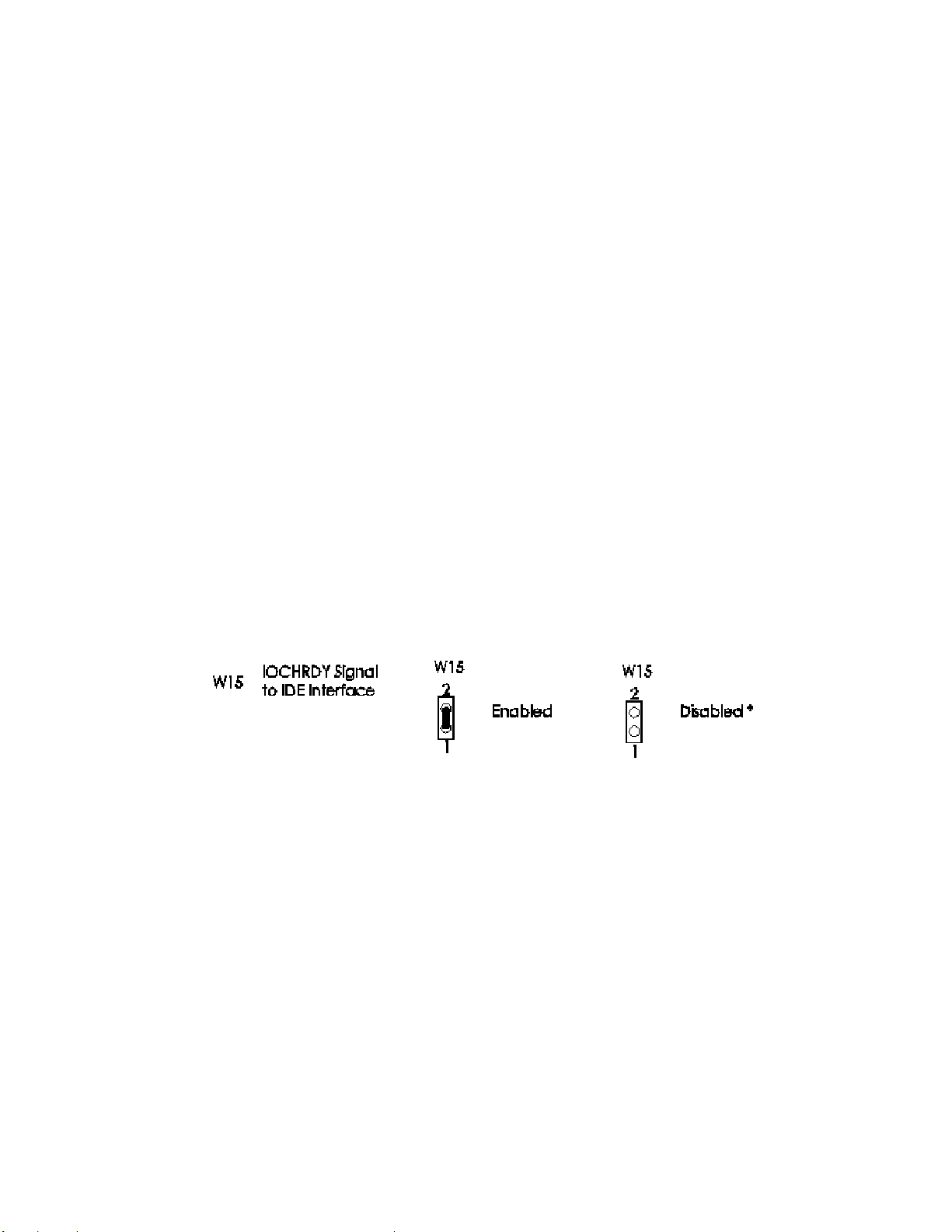
The W15 jumper, when set to Enabled will extend the current cycle on IDE
READ/WRITE transfers. Its setting appears below:
• W15: IOCHRDY Signal to IDE Interface:
* Default setting
Installing IDE, Floppy & SCSI Devices 8-6
Page 87

8.01.4 IDE SOFTWARE SETUP
AWARD Setup
There are two ways to configure hard disk parameters: use IDE hard disk auto detection
(available from the main menu), or enter the parameters in the Standard CMOS Setup.
The following explains how to enter the parameters in the Standard CMOS Setup:
• From the Main Menu, select the Standard CMOS Setup option.
• In the Standard CMOS Setup menu, use the arrow keys to highlight the Primary
Master:, Primary Slave:, Secondary Master:, or Secondary Slave: option (depending on
the installation of your hard drive).
• Use the PgUp or PgDn keys to select the desired value for each item associated to your
hard drive setup:
− There are 46 predefined types and a user definable type. Type 1 to Type 46 are
predefinable and Type USER is user-definable.
− Press PgUp or PgDn to select a numbered hard disk type or type the number and
press Enter. Note that the specifications of your drive must match with the drive
table. The hard disk will not work properly if you enter improper information for
this category. If your hard disk drive type is not matched or listed, you can use
Type USER to define your own drive type manually
− If you select Type USER, you will need to know the information listed below.
Enter the information directly from the keyboard and press Enter. This
information should be included in the documentation from your hard disk vendor.
CYLS Number of cylinders
HEADS Number of heads
PRECOMP Starting write precomp. cylinder
LANDZONE Landing zone
SECTORS Number of sectors
− If a hard disk has not been installed, select NONE and press <Enter>.
Once hard disk parameters are configured, you can enable/disable multiple sector
reads/writes for IDE drives, as follow:
• Return to the Main Menu and select the BIOS Features Setup option.
• In the BIOS Features Setup menu, select the IDE HDD Block Mode option and set this
option to Enabled or Disabled.
Installing IDE, Floppy & SCSI Devices 8-7
Page 88

8.02 FLOPPY DEVICES
8.02.1 FLOPPY JUMPERS
The TEK-AT4LVG supports the 2.88MB High Density Floppy. The W30 and W31
jumpers EDOUT and HDOUT signals. The ettings are as follows:
1- HDOUT and EDOUT left to sotware (default setting).
OR
2- HDOUT to Pin 33 (J4), and Ground to Pin 27 (J4), with
EDOUT to Pin 29 (J4), and Ground to Pin 17 (J4).
OR
3- HDOUT to Pin 27 (J4), and Ground to Pin 33 (J4), with
EDOUT to Pin 17 (J4), and Ground to Pin 29 (J4).
Please refer to Section 4 for information and about settings and location of these jumpers.
Note: Please notice that these jumpers are optional.
Since the software is smart enough to detect the different types of floppy drive,
your 2.88MB Floppy Drive will operate correctly if 2.88MB is indicated in the
BIOS Setup.
Not installing these jumpers will work for all floppy disk drives, as long as the
proper floppy type is indicated in AWARD Setup. For proper operation, we
recommend you not to install these jumpers.
Please refer to Table 4-1e to setup the W30 and W31 jumpers.
Installing IDE, Floppy & SCSI Devices 8-8
Page 89
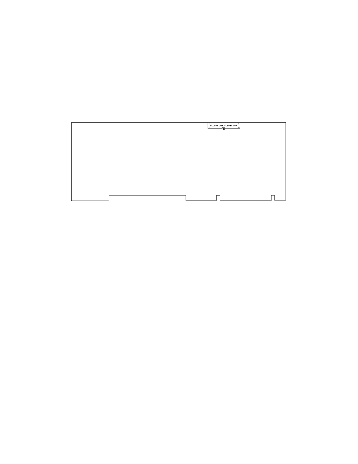
8.02.2 FLOPPY CONNECTORS LOCATION & PIN-OUT
The Floppy connector appears on Diagram 8-2 at J4.
DIAGRAM 8-2: Floppy Connector Location
Installing IDE, Floppy & SCSI Devices 8-9
Page 90

The Floppy Connector’s pin-out appears in Table 8-2.
TABLE 8-2: Floppy Disk Connector (J4) - Pin-Out
Pin
Number
1
3
5
7
9
11
13
15
17
19
21
23
25
27
29
31
33
* Active low signal
1
By default, these pins are not connected; however, by installing the W30 and W31
Signal
Flow
-
-
-
-
-
-
-
-
-
-
-
-
-
-
-
-
-
Signal Pin
GND
GND
GND
GND
GND
GND
GND
GND
1
N. C.
GND
GND
GND
GND
1
N. C.
1
N. C.
GND
1
N. C.
Number
2
4
6
8
10
12
14
16
18
20
22
24
26
28
30
32
34
Signal
Flow
O
-
I
O
O
O
O
O
O
O
O
I
I
I
O
I
Signal
RPM/LC
Not Used
Not Used
INDEX*
MOTOR ON 0,1*
DRIVE SELECT B
DRIVE SELECT A
MOTOR ON 2*
DIR CONTROL
STEP*
WRITE DATA*
WRITE ENABLE*
TRACK0*
WRITE PROTECT*
READ DATA*
HEAD SELECT
DSKCHG
jumpers, these configurations are possible:
17 - GND Or: 17 I EDOUT (2.88MB)
27 - GND 27 I HDOUT (2.88MB)
29 I EDOUT (2.88MB) 29 - GND
33 I HDOUT (2.88MB) 33 - GND
Installing IDE, Floppy & SCSI Devices 8-10
Page 91
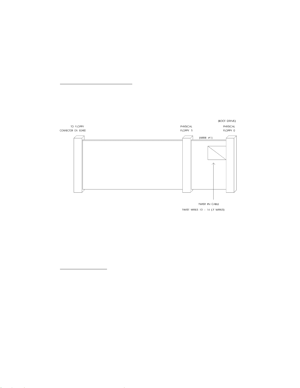
8.02.3 FLOPPY HOOK-UP
Mechanical Floppy Disk Installation:
The installation of the Floppy drives is done via a standard IBM 34-pin flat ribbon cable
that connects to J4.
DIAGRAM 8-3: Floppy Disk Cable
The following list includes approved vendors for the J4 connector’s mating parts:
Amp 746285-8 [optional strain relief: 499252-6],
Robinson Nugent IDS-C34PK-TG,
Thomas & Betts 622-3430 [optional strain relief: 622-3441].
(34-pin flat cable connector).
Enhanced Floppy Mode:
In order to connect your 2.88MB Floppy drive, simply indicate the proper Floppy disk
drive in the AWARD Setup program. It is not necessary to set the HDOUT and EDOUT
media detection signal jumpers, explained in the following pages.
Installing IDE, Floppy & SCSI Devices 8-11
Page 92

8.02.4 FLOPPY SOFTWARE SETUP
AWARD Setup
Starting from the AWARD Setup program’s main menu, use the following procedure to
complete the setup:
• From the Main Menu, select the Standard CMOS Setup option.
• In the Standard CMOS Setup menu, use the arrow keys to highlight the Drive A: or
Drive B: option (depending on the installation of your Floppy drive).
− Select the category identifying the types of Floppy disk drive A or drive B that have
been installed in the computer.
None No Floppy drive installed.
360KB, 5.25 in. 5-1/4 inch PC-type standard drive; 360KB capacity.
1.2MB, 5.25 in. 5-1/4 inch AT-type high-density drive; 1.2MB capacity.
720KB, 3.5 in. 3-1/2 inch double-sided drive; 720KB capacity.
1.44MB, 3.5 in. 3-1/2 inch double-sided drive; 1.44MB capacity.
2.88MB, 3.5 in. 3-1/2 inch double-sided drive; 2.88MB capacity.
Installing IDE, Floppy & SCSI Devices 8-12
Page 93

8.03 SCSI DEVICES
The SCSI Controller is optional equipment on the TEK-AT4LVG board.
The TEK-AT4LVG board provides an interface between a host or peripheral device, and
the Small Computer System Interface (SCSI) bus.
You can obtain more information regarding the SCSI Controller, SCSI devices and their
drivers in the SCSI manual available through TEKNOR's Sales or Technical Support
department.
Installing IDE, Floppy & SCSI Devices 8-13
Page 94
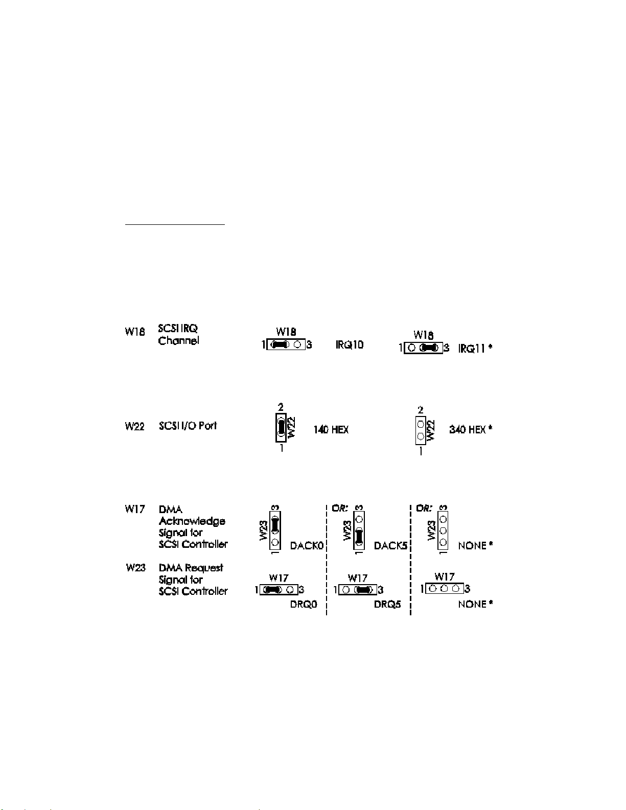
8.03.1 INSTALLING A FIXED SCSI HARD DISK
No additional hardware or drivers are necessary if no more than two IDE/SCSI hard disks
will be present in your system.
1 - Jumpers (Power Off)
Power off your computer.
The board's initial jumper settings should be kept in most cases, unless there is a conflict
with other devices you have installed. SCSI jumpers are shown below:
W18: Selects the SCSI IRQ Channel:
W22: Sets up the SCSI I/O Port Address:
W17 & W23: Selects the DMA channel for the SCSI Controller:
* Default setting
Installing IDE, Floppy & SCSI Devices 8-14
Page 95

2 - Connect SCSI Cable (Power Off)
Make certain that both ends of the SCSI cable are terminated and that all devices in
between the ends are non-terminated. The SCSI connector on the TEK-AT4LVG board is
terminated.
The following list includes approved vendors for the J2 connector’s mating parts:
Robinson Nugent IDS-C50PK-TG,
Amp 1-746285-0 [optional strain relief: 499252-4],
Thomas & Betts 622-5030 [optional strain relief: 622-55041].
(50-pin flat cable connector).
Attach one end of the SCSI cable to the J2 SCSI 50-pin connector. Make sure line 1 of the
cable is matched with pin 1 of connector J2.
Attach the other end to your SCSI device, making sure line 1 is matched with pin 1 on
your device.
You must also install a cable from your power supply to your device.
3 - Follow Specific Device Installation Instructions (Power On)
Follow installation instructions provided with your SCSI peripheral device to install it in
the host.
FF Each device being installed must be assigned a unique identifier called a SCSI
Target ID. The lower the ID, the lower the priority level of the device in the
SCSI sub-system. The host adapter is usually assigned the highest priority
level (i.e. 7). Table 8-3 lists common SCSI Target IDs.
TABLE 8-3: Common SCSI Target IDs
SCSI Device Commonly Used IDs
Host Adapter 7
Hard Disks 0,1,2,3
CD-ROM 4,5
Tape drive 5,6
Installing IDE, Floppy & SCSI Devices 8-15
Page 96

8.03.2 INSTALLING OTHER SCSI DEVICES
To install any of the following: CD-ROM, Magneto-Optical/Removable Disk Drive, Tape
Drive, Write Once Read Many (WORM) and scanners, you must use the EZ-SCSI
software utilities diskette which came with your board. The diskette includes a README
file in ASCII and WORD formats which contains setup and installation information. The
diskette also includes any device driver you may need.
Installing IDE, Floppy & SCSI Devices 8-16
Page 97

8.03.3 REMOVABLE TERMINATION RESISTORS
The TEK-AT4LVG has three termination resistors around the SCSI controller labeled
RN12, RN21 and RN22 on the board. These red-colored resistors are removable. It is
recommended that you remove them if your board is not located at the end of the SCSI
cable.
FF RN12, RN21 and RN22 Termination Resistors should be removed when your
board is not connected at either end of the SCSI cable.
Installing IDE, Floppy & SCSI Devices 8-17
Page 98

8.03.4 SCSI CONNECTOR
TABLE 8-4: SCSI Connector (J2) - Pin-Out
Pin Number Signal Pin Number Signal
1
3
5
7
9
11
13
15
17
19
21
23
25
27
29
31
33
35
37
39
41
43
45
47
49
GND
GND
GND
GND
GND
GND
GND
GND
GND
GND
GND
GND
Term Power
GND
GND
GND
GND
GND
GND
GND
GND
GND
GND
GND
GND
2
4
6
8
10
12
14
16
18
20
22
24
26
28
30
32
34
36
38
40
42
44
46
48
50
SCSI D0
SCSI D1
SCSI D2
SCSI D3
SCSI D4
SCSI D5
SCSI D6
SCSI D7
SCSI DP*
GND
GND
GND
Term Power
GND
GND
ATN*
GND
BSY*
ACK*
RESET*
MSG*
SEL*
C/D*
REQ*
I/O*
* Active low signal
Installing IDE, Floppy & SCSI Devices 8-18
Page 99

8.03.5 SCSI SOFTWARE SETUP
VIP-UP Setup
From the VIP-UP Setup program’s first screen, you can control the following options:
SCSI options Values available
On Board SCSI BIOS Disabled / Enabled
SCSI BIOS Address D8000H-DBFFFH / 0C000-DFFFFH
SCSI Base I/O Address 340H (Default BIOS) / 140H (Special BIOS)
SCSI ID Select ID0 / ID1 / ID2 / ID3 / ID4 / ID5 / ID6 / ID7
SCSI IRQ Channel IRQ11 / IRQ10
SCSI DMA Channel DMA0 / DMA5
SCSI Parity Enabled / Disabled
SCSI Disconnect No Disconnect / Allow Disconnect
SCSI Synchronous Negociation Respond Only / Initiate Negociation
SCSI Floptical Drive Support Enabled / Disabled
SCSI Compatibility Mode 6360 Features / 6260 Compatibility
Installing IDE, Floppy & SCSI Devices 8-19
Page 100

9 INSTALLING PERIPHERALS
9.01 Serial Ports ...........................................................................................................9-2
9.01.1 Serial Port Jumpers ........................................................................................9-2
9.01.2 Serial Ports Location & Pinouts......................................................................9-3
9.01.3 Serial Ports Software Setup.............................................................................9-7
9.02 Parallel Port.......................................................................................................... 9-8
9.02.1 Parallel Port Location & Pinout......................................................................9-8
9.02.2 Parallel Port Software Setup.........................................................................9-12
Installing Peripherals 9-1
 Loading...