

Page 1

PCI-934
MULTIMEDIAPENTIUMBOARD
TECHNICALREFERENCEMANUAL
NOTE:
Thismanualisforreferencepurposeonly.
Reproductioninwholeorinpartisauthorizedprovided
TEKNORINDUSTRIALCOMPUTERSINC.iscitedas
theoriginalsource.
VERSION1.2
August1998
ref.:M934_1-2
Page 2

FOREWORD
The information in this document is provided for reference purposes only. TEKNOR does
not assume any liability for the application of information or the use of products described
herein.
This document may contain information or refer to products protected by the copyrights or
patents of others and does not convey any license under the patent rights of TEKNOR, nor
the rights of others.
Printed in Canada.
Copyright 1998 by TEKNOR INDUSTRIAL COMPUTERS INC., Boisbriand, QC J7G 2A7.
Page 3
READ ME FIRST
EXERCISE CAUTION WHILE REPLACING LITHIUM BATTERY
WARNING
There is a danger of explosion if the battery is incorrectly replaced.
Replace the battery only with the same or equivalent type recommended by the
manufacturer. Dispose of used batteries according to the manufacturer's
instructions.
ATTENTION
Il y a danger d’explosion s’il y a remplacement incorrect de la batterie.
Remplacer uniquement avec une batterie du même type ou d’un type équivalent
recommandé par le constructeur. Mettre au rebut les batteries usagées
conformément aux instructions du fabriquant.
ACHTUNG
Explosionsgefahr bei falschem Batteriewechsel.
Verwenden Sie nur die empfohlenen Batterietypen des Herstellers. Entsorgen Sie
die verbrauchten Batterien laut Gebrauchsanweisung des Herstellers.
ATENCION
Puede explotar si la pila no este bien reemplazada.
Solo reemplazca la pila con tipas equivalentes segun las instrucciones del
manifacturo. Vote las pilas usadas segun las instrucciones del manifacturo.
Read Me First 1
Page 4
PCI-934 Technical Reference Manual
IMPORTANT INFORMATION
Before operating your Single Board Computer, please note the following:
Battery Configuration
Your computer board is equipped with a standard non-rechargeable lithium
battery. To preserve the useful life of the battery, the jumper which enables the
battery is not installed when you receive the board. If you need a jumper cap, we
suggest you use the one on the Watchdog Timer jumper since it is rarely needed; if
you wish to purchase jumper caps, you can contact TEKNOR’s Sales department
to order them.
Connecting Flat Panel Video Display
The PCI-934 board supports many different types of Flat Panel displays. TEKNOR has
fully tested a number of these panels and provides all the BIOS software support and the
technical information needed.
If you have access to the Internet, many video BIOS files in a binary format and related
interconnection charts in a PDF format are available on our web site. You can download
these files, if you are a customer of TEKNOR and have a password from TEKNOR. If
you do not have your password, contact TEKNOR’s Technical Support to obtain it.
To download a video BIOS file or its interconnection chart file, follow this procedure:
1. Access the TEKNOR web site. Our address is http://www.teknor.com .
2. Go to the Support & Services section.
3. Scroll down the list of products until you find the name of your board and click on it.
This selection is a link to the board’s support area.
4. Click on the Video BIOS link.
5. The list of tested Flat Panel displays appears. If you find your particular display, you
can then ask to download the associated BIOS or interconnection chart files by
clicking the appropriate link.
6. A pop-up window appears. You must enter your password (case sensitive) and click
the SUBMIT button. Entering your e-mail address is optional. Follow the
instructions in subsequent pop-ups to download the file.
If you do not have access to our web site, or if you do not see the name of your Flat
Panel, then you need to contact TEKNOR’s Technical Support department. Since we are
always testing new flat panels, it is possible that we have tested your particular type of
panel display. Even if we have not tested it, TEKNOR’s Technical Support can do it for
you and supply the video BIOS and the technical information you need.
Read Me First 2
Page 5

Read Me First
Preventing Viruses
TEKNOR INDUSTRIAL COMPUTERS takes every precaution against computer
viruses. For your protection, we have safety sealed all utility diskettes. If the seal
is broken, do not use the diskette. Destroy the diskette immediately and contact
our Technical Support department for further instructions at (450) 437-5682
(Canada) or at +49 811 / 600 15-0 (Germany).
To safeguard against computer viruses in general, do not freely lend your utility
diskettes and regularly perform virus scans on all your computer systems.
Read Me First 3
Page 6

TABLE OF CONTENTS
PART ON E – Product description
1. PRODUCT OVERVIEW..............................................................................1-1
2. FEATURES................................................................................................2-1
3. COMPATIBILITY WITH TEKNOR PRODUCTS ..........................................3-1
4. SAFETY PRECAUTIONS...........................................................................4-1
1.1 S
1.2 S
1.3 P
TATIC ELECTRICITY
TORAGE ENVIRONMENT
OWER SUPPLY
............................................................................ 4-1
...................................................................... 4-1
................................................................................... 4-1
5. UNPACKING..............................................................................................5-1
PART TWO – Hardware Installation
6. INSTALLING AND WORKING WITH SYSTEM COMPONENTS................ 6-1
6.1 PROCESSOR AND FAN...................................................................6-1
6.1.1 Processor Characteristics..................................................................6-2
6.2 INS TAL L ING MEMOR Y.....................................................................6-3
6.2.1 System Memory (SDRAM)................................................................6-3
6.2.2 C ac h e Me mory.................................................................................6-6
6.3 BACKUP MEMORY...........................................................................6-6
6.4 SUPERVISION FEATURES...............................................................6-7
6.4.1 WATCHDOG....................................................................................6-7
6.4.2 POWER FAILURE DETECTION .......................................................6-9
6.4.3 THERMAL MA N AGEMENT...............................................................6-9
6.4.4 I/O REG ISTER ADDRESSES ...........................................................6-9
I
Page 7

PCI-934 T echnical Reference M anual
7. INSTALLING STORAGE DEVIC ES...........................................................7-1
7.1 FLOPPY DISKS DRIVES...................................................................7-1
7.2 EIDE DEVICES..................................................................................7-2
7.3 COMPACTFLASH DISK....................................................................7-3
7.3.1 INSTALLING COMPACTFLASH MODULE........................................7-3
7.3.2 WORKING WITH A COMPACTFLASH DISK.....................................7-4
8. INSTALLING PERIPHERA LS....................................................................8-1
8.1 VID EO...............................................................................................8-1
8.2 SERIAL PORTS.................................................................................8-1
8.2.1 SERIAL PORT 1 (J6) RS-232............................................................8-2
8.2.2 SERIAL PORT 2 (J7)........................................................................8-3
8.3 PARALLEL PORT..............................................................................8-6
8.3.1 STANDARD MODE ..........................................................................8-7
8.3.2 EPP MODE ......................................................................................8-7
8.3.3 ECP MODE......................................................................................8-7
8.4 PS/2 MOUSE.....................................................................................8-7
MULTI I/O C ON N E C T OR............................................................................8-8
8.6 USB PORTS......................................................................................8-9
9. ETHERNET................................................................................................9-1
10. PC/104 -P LU S FE ATURES.......................................................................10-1
11. SETTING JUMPERS................................................................................11-1
II
Page 8

Table of Contents
PART THREE – Multimedia Features
12. EXPLORING THE MULTIMEDIA CAPABILITIES OF THE BOARD......... 12-1
12.1 VIDEO FEATURES ......................................................................... 12-3
12.1.1 FLAT PANEL DISPLAY .................................................................. 12-3
12.1.2 CRT DISPLAYS .............................................................................12-6
12.1.3 PANELLINKTM INTERFACE............................................................12-7
12.1.4 NTSC.............................................................................................12-8
12.1.5 VGA INTERRUPT ..........................................................................12-8
12.1.6 V-PORT.........................................................................................12-9
12.2 AUDIO FEATURES....................................................................... 12-10
12.2.1 LINE IN ........................................................................................ 12-10
12.2.2 LINE OUT .................................................................................... 12-10
12.2.3 MIC IN ......................................................................................... 12-11
12.2.4 CD IN...........................................................................................12-11
12.2.5 AUDIO I/O CONNECTOR.............................................................12-12
12.2.6 SPEAKER TO LINE OUT ............................................................. 12-12
PART FOUR – Software Setups
13. BIOS SETUPS......................................................................................... 13-1
13.1 USING THE BIOS SETUP PROGRAM............................................ 13-2
13.2 SAVING CONFIGURATIONS & EXITING AWARD SETUP ............. 13-4
13.3 STANDARD CMOS SETUP.............................................................13-4
13.4 BIOS FEATURE SETUP..................................................................13-5
13.5 CHIPSET FEATURES SETUP ........................................................ 13-7
13.6 POWER MANAGEMENT SETUP.................................................... 13-9
13.7 PNP/PCI SETUP............................................................................ 13-11
13.8 INTEGRATED PERIPHERALS SETUP ......................................... 13-12
III
Page 9

PCI-934 T echnical Reference M anual
PART FOUR – Software Setups (Continued)
14. UPDATING THE BIOS WITH UPGBIOS ..................................................14-1
14.1 UP D ATING THE BI OS.....................................................................14-1
14.2 CPLD U
PGRADE AFTER A
BIOS U
15. VT 100 MODE ...........................................................................................15-1
1.4 REQUIREMENTS............................................................................15-1
1.5 SETUP & CONFIGURATION...........................................................15-1
1.6 RUNNING WITHOUT A TERMINAL.................................................15-2
PDATE
.............................................14-2
IV
Page 10

APPENDIX
A. PRODUCT SPECIFICATIONS.................................................................. A-1
B. BOARD DIAGRAMS................................................................................. B-1
C. CONNECTOR PINOUTS ..........................................................................C-1
C.1 XVGA CONNECTOR - J1........................................................... C-1
C.2 PANELLINK CONNECTOR - J2.................................................. C-1
C.3 EIDE CHANNEL 1 CONNECTOR - J3........................................ C-2
C.4 FLOPPY DISK CONNECTOR - J4..............................................C-3
C.5 MULTIFUNCTION CONNECTOR - J5........................................ C-3
C.6 SERIAL PORT 1 CONNECTOR - J6........................................... C-4
C.7 SERIAL PORT 2 CONNECT OR (RS-232) - J7............................C-4
C.8 SERIAL PORT 2 CONNECT OR (RS-422/RS-485) - J 7............... C-4
C.9 FAN CONNECTOR - J8.............................................................. C-4
C.10 FLAT PANEL CONNECTOR - J9.................................................C-5
C.11 EIDE CHANNEL 2 CONNECTOR - J10 ...................................... C-6
C.12 V-PORT CONNECTOR - J11...................................................... C-6
C.13 NTSC OUT CONNECTOR - J12.................................................. C-7
C.14 PARALLEL PORT CONNECTOR - J13........................................C-7
C.15 USB CONNECTOR - J14.............................................................C-7
C.16 PS/2 MOUSE CONNECTOR - J15...............................................C-8
C.17 I
C.18 CD IN CONNECTOR - J17...........................................................C-8
C.19 AUDIO I/O CONNECTOR - J18................................................... C-8
C.20 FLASH DISK CONNECTOR - J19...............................................C-9
C.21 CRT VGA
C.22 LINE OUT CONNECTOR - J21...................................................C-9
C.23 MIC IN CONNECTOR - J22...................................................... C-10
C.24 LINE IN CONNECTOR - J23..................................................... C-10
C.25 ETHERNET CONNECTOR - J24.............................................. C-10
C.26 PC/104-PLUS CONNECTOR - J25........................................... C-11
C.27 P C/104 CONNECTORS - P1 A ND P 2....................................... C-12
2
S CONNECTOR (NO MPEG) - J16............................................ C-8
CONNECTOR - J20....................................................C-9
V
Page 11

PCI- 934 Technical Refer ence Manual
D. MEMORY AND I/O MAPS.........................................................................D-1
D.1 M
EMORY MAP DIAGRAM
D.2 I/O M
APPING
.................................................................................D-2
..................................................................D-1
E. BIOS SETUP ERROR CODES ................................................................. E-1
E.1 POST MESSAGES...................................................................... E-1
E.2 POST BEEP ................................................................................ E-1
E.3 ERROR MESSAGES................................................................... E-2
E.4 POST CODES............................................................................. E-5
F. EMERGENCY PROCEDURES...................................................................F-1
F.1 SYMPTOMS.................................................................................F-1
F.2 MAKING AN EMERGENCY DISKETTE........................................F-2
F.3 EMERGENCY PRO CEDURE ........................................................F-3
VI
Page 12

PRODUCT DESCRIPTION
1. PRODUCT OVERVIEW
2. FEATURES
3. COMPATIBILITY WITH TEKNOR PRODUCTS
4. SAFETY PRECAUTIONS
5. UNPACKING
Page 13

1. PRODUCT OVERVIEW
What is multimedia?
Multimedia is turning out to be one of the most appealing capabilities of a computer.
Running a multimedia application means that a huge amount of hardware and software is
trying to run at the same time, competing for the attention of all system resources. For
example, the hardest thing a PC can do when proceeding tests is to run multimedia
applications.
Sub-systems that make multimedia applications possible are the sound system, CD-ROM
and hard disk drives, speaker, enhanced local-bus video graphics, big screen color monitor,
plenty of memory and finally, the processor.
Working with multimedia requires a computer capable of working fast, smoothly and
reliably. The PCI-934 single board computer meets all these conditions.
1-1
Page 14

PCI-934 T echnical Reference M anual
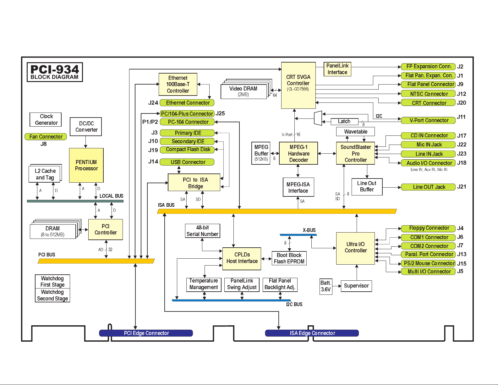
The PCI-934 is a full-length PC/AT-PICMG form factor single board computer (SBC). It is
built around a powerful computing core that characterizes the PCI-9xx board family,
associated with high performance multimedia features:
MPEG-1 hardware decoder implemented to process MPEG coded audio/video
stream in real time.
2MB EDO DRAM, 64-bit graphics performance LCD/CRT controller with V-Port
capabilities.
SoundBlaster Pro compatible controller with MIDI interface that connects to a
MIDI wavetable synthesizer for CD-quality sound output, compatible with WSS
(Windows Sound System) audio subsystem.
TV/Composite video output support using an external PAL/NTSC encoder.
Such a configuration allows the board to playback full motion MPEG sequences from
standard IDE devices.
The PCI-934 integrates the hottest multimedia features to make it a powerful stand-alone
system with direct peripheral connections capabilities:
Flat panel interface supporting active and passive color display, from VGA to
XGA.
PanelLink interface that drives remote 64-bit accelerated LCD panel over
several meters of copper (up to 10 meters / 30 feet).
UXGA CRT interface (1280x1024 resolution).
V-Port int erfa ce th at allows r eal -ti m e video over l a y from an ex t ernal vid eo sou r ce
(VIPer Vision TEK-380).
Stan dard CD connect or input.
Compa ctFlash d isk interfa ce configu red as a stan dard IDE d isk on th e second ary
IDE channel.
PC/104-Plus (embedded PCI) stackable module interface.
1-2
Page 15
PCI-934
BLOCK DIAGRAM
Clock
Generator
Fan Connector
J8
L2 Cache
and Tag
D
A
DC/DC
Converter
PENTIUM
Processor
A
D
LOCAL BUS
A
D
J24
P1/P2
J3
J10
J19
J14
Ethernet
100Base-T
Controller
Ethernet Connector
PC/104-Plus Connector
PC-104 Connector
Primary IDE
Secondary IDE
Compact Flash Disk
USB Connector
PCI to ISA
Bridge
SA SD
ISA BUS
J25
Video DRAM
(2MB)
MPEG
Buffer
(512KB)
64
8
CRT SVGA
Controller
(CL-GD7556)
V-Port 16
MPEG-1
Hardware
Decoder
MPEG-ISA
Interface
PanelLink
Interface
Latch
I2C
8
Wavetable
SoundBlaster
Pro
Controller
Line Out
SA
SA
SD
Buffer
8
FP Expansion Conn.
Flat Pan. Expan. Con.
Flat Panel Connector
NTSC Connector
CRT Connector
V-Port Connector
CD IN Connector
Mic IN Jack
Line IN Jack
Audio I/O Connector
Line IN, Aux IN, Mic IN
Line OUT Jack
J2
J1
J9
J12
J20
J11
J17
J22
J23
J18
J21
DRAM
(8 to 512MB)
PCI BUS
Watchdog
First Stage
Watchdog
Second Stage
PCI
Controller
AD 32
48-bit
Serial Number
Temperature
Management
CPLDs
Host Interface
PanelLink
Swing Adjust
8
Boot Block
Flash EPROM
Flat Panel
Backlight Adj.
I2C BUS
ISA Edge ConnectorPCI Edge Connector
X-BUS
Batt.
3.6V
Ultra I/O
Controller
Supervisor
Floppy Connector
COM1 Connector
COM2 Connector
Paral. Port Connector
PS/2 Mouse Connector
Multi I/O Connector
J4
J6
J7
J13
J15
J5
Page 16

2. FEATURES
VIDEO CAPABILITIES
Video capabilities are built around the CL-GD7556 high-performance 64-bit video and
graphics accelerated LCD/ C RT con troller, from Cirrus Logi c.
The controller provides features such as:
GUI and true 64-bit accelerations
32-bit PCI V2.1 interface
Accelerati on of MPEG-1
V-Port support for the implementation of built-in MPEG video playback, and external TV
tuner , vi d eo c onferen cing, and tel econferen cing.
The video controller provides a high memory bandwidth, up to 80MHz, which allows the
board to support V-Port applications at a resolution of 1024x768.
Video capabilities are as follows:
Video memory: 2MB EDO 64-bit RAM
CRT display: 1280 x 1024 x 256, 1024 x 768 x 64K, 800 x 600 x 16M,
640 x 480 x 16M.
Flat panel: up to 1024 x 768 – 64K colors Dual-Panel, Dual-Drive, STN
and TFT panels
V-Port Interface: The V-port interfaces video data directly from the MPEG-1
decoder or an extern al video device th rough the J1 1 connect or.
The video stream is transferred directly into the display
memory, bypassing the CPU.
The V-Port appears as a multimedia solution that requires no
external video processing hardware and additional display
memory. The V-port offers high-quality low-cost multimedia
options such as live-video preview and capture, TV-in-awindow, h ardwar e ass isted MPEG an d vid eo conferencing.
The video controller provides all the signals necessary to drive flat-panel (1024x768 max.)
and CRT monitor simultaneously. It supports up to 16.8M colors in most VGA and video
formats.
The multimedia capabilities include acceleration of video playback, video capture, livevideo presentation and other video applications - all with continuous upscaling to
resolution up to 1024x768.
2-1
Page 17

PCI-934 T echnical Reference M anual
SYSTEM MEMORY
Four vertical 72-pin SIMM sockets support both FPM and EDO DRAM memory
configuration s fr om 8 to 512M B.
Uses standard 5V, 70ns/60ns single-sided or double-sided 72-pin SIMMs.
Supports 1, 2, 4, 8, 16, 32M – 32/36-bit modules.
STORAGE DEVICES
Optional Flash Disk: when using the T069 daughter board, a standard CompactFlash ™
flash disk can be connected. Contact TEKNOR for available capacity.
Enhanced IDE interface: Enhanced IDE controller can drive up to four IDE devices with
transfer rates up to 22MB/s. The PCI-934 includes two separate IDE data bus and
control signals.
ETHERNET
100Base-TX or 10Base-T interface is implemented with Intel’s 82558 Ethernet
Controller. The IC resides on the PCI bus, which allows very high transfer rates to and
from the DRAM.
BUS SUPPORT
ISA Bus (IEEE P966 Specification). High -drive buffers let the PCI-934 drive up to 20
slots.
PCI Local Bu s Sp e ci fication, Revision 2.1.
2-2
Page 18

Features
PICMG INTERFACE
PICMG 2.0 Bus Specification which defines the ISA bus and the PCI bus.
The PCI-934 can support memory data streaming up to 112MB/sec. (read) and
121MB/sec. (write)
The PCI-934 provides concurrent PCI master and CPU/DRAM operations. It also
implements “delayed transaction” to increase the availability of the PCI bus.
OPERATING SYSTEM
Runs all op erating systems developed for x86 processors: DOS, Windows 3.1, OS/2,
Windows 95, Windows NT, UNIX, QNX and NOVELL 4.10, etc.
BIO S AND LICENCE
Award CPU BI OS, Cirrus Logic Vide o BIO S.
2-3
Page 19

3. COMPATIBILITY WITH TEKNOR PRODUCTS
The board supports Pentium MMX processors at speed of up to 233MHz. The major
difference between the PCI-934 and other products of the PCI-9xx familly, is its high
multimedia capabilities, the 100Base-TX Ethernet, and the PanelLink
panel.
The PCI-934 meets these specifications while using the same form factor as the PCI-933
(i.e., PC/AT and PICMG). The assembly includes an onboard switching regulator to supply
the pr ocessor, whi ch r es u lts in a more effici ent use of power.
The boa rd i s design ed to pl ug into a standa rd pass ive ISA ba ckpl ane, or in to an in dustr y
standard PICMG passi ve backplane.
The PCI-934 may be provided with an optional power connector that makes the board
being capable to be integrated as a stand-alone single board computer system.
TM
interface for flat
3-1
Page 20

4. SAFETY PRECAUTIONS
4.1 STATIC ELECTRICITY
Since static electricity can damage a board, the following precautions should be taken:
1. Keep the board in its antistatic package, until you are ready to install it.
2. Touch a groun ded sur face or wear a groun ding wr is t stra p befor e rem ovin g the boa rd
from its package; this will discharge any static electricity that may have built up in
your body.
3. Handle the board by the edges.
4.2 STORAGE ENVIRONMENT
Electronic boards are sensitive devices. Do not handle or store devices near strong
electrostatic, electromagnetic, magnetic or radioactive fields.
4.3 POWER SUPPLY
Before any hardware installation or setup, ensure that the board is unplugged from power
sources or subsystems.
4-1
Page 21

5. UNPACKING
Follow these recomm endation s while unpack ing:
1. After opening the box, save it and the packing material for possible future shipment.
2. Remove the board from its antis tati c wr apping and p lace it on a grounded s urface .
3. Inspect the board for damage. If there is any damage, or items are missing, notify
TEKNOR immediatel y.
Contents
When unpacking you will find:
1. One PCI-934 Single Board Com puter
2. One Techn ical Reference Manual.
3. A set of cables
4. Diskettes, and drivers on a CD-ROM.
5-1
Page 22

HARDWARE INSTALLATION
6. INSTALLING AND WORKING WITH SYSTEM
COMPONENTS
7. INSTALLING STORAGE DEVICE S
8. INSTALLING PERIPHERALS
9. ETHERNET
10. PC/104-PLUS FEATURES
11. SETTING JUMPERS
Page 23
CONNECTOR LOCATION
6. Installing and Working with System Components
Page 24
6. INSTALLING AND WORKING WITH SYSTEM
(Pow er)
COMPONENTS
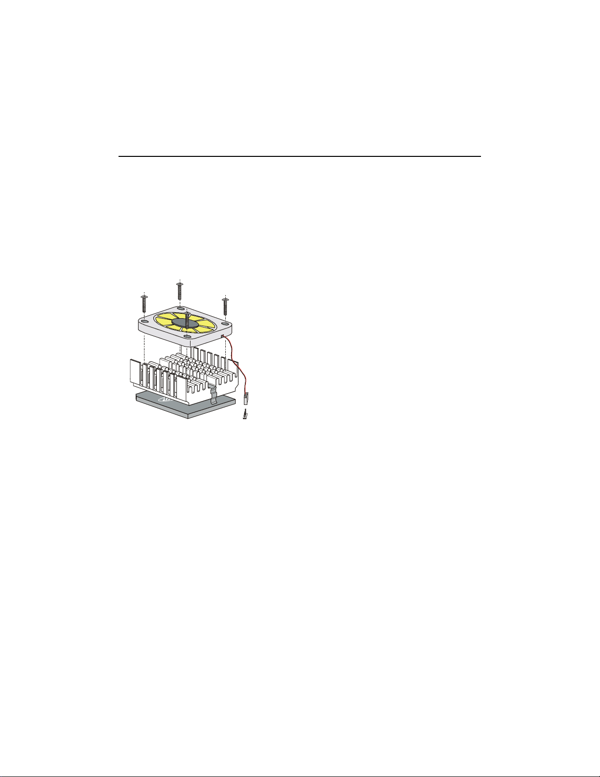
6.1 PROCESSOR AND FAN
The processor and its cooling system are is installed according to the user configuration.
A +12V DC voltage is available through the J18 connector to supply the fan (the
connector’s pinout appears in Appendix-C).
Installing Microprocessor
A fan is required when working with the PCI-934
board.
Cooling
Fan
Heat
Sink
Fan
Power
Cord
A +12V voltage is available through the J8
connector to supply the fan (The connector’s
pinout appears in Appendix-C).
Please refer to your processor specifications for
more information.
Processor
Fan
Con nector
voltage, clock speed multiplier, and Core/Bus
ratio value must be configured according to your
CPU model.
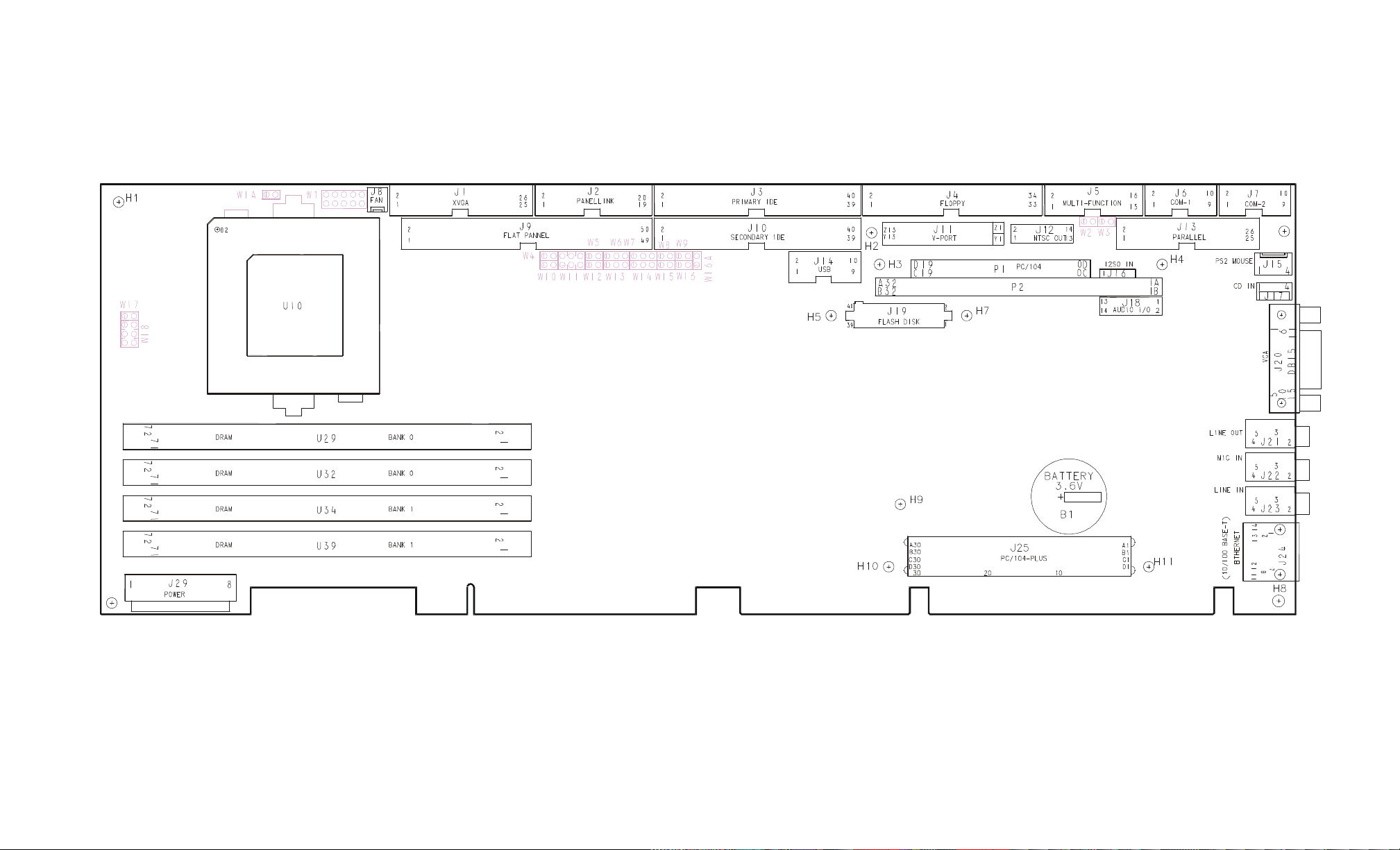
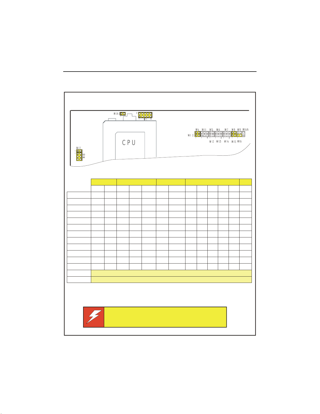
Six jumpers are related to the processor:
W1 Selects the core voltage (Vcore).
W1A-W4-W10 Defines the Core/Bus clock ratio.
W8-W15 Defines the CPU bus clock.
W16 Deter mines the DRAM r efresh rate.
W17-W18 Selects the CPU type within split-plane or single-plane.
6-1
When installing a processor, its type, core
Page 25
PCI-934 T echnical Reference M anual
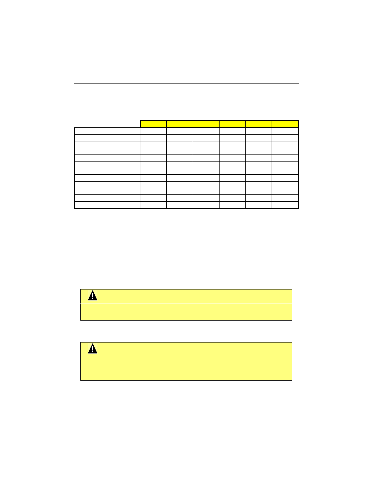
6.1.1 Processor Characteristics
Processor characteristics are summarized below:
Fcore PCLK BCLK Ratio Type VCore
Intel Pentium 100 100 66 33 1.5 Sing le 3.3V
Intel Pentium 120 120 60 30 2.0 Sing le 3.3V
Intel Pentium 133 133 66 33 2.0 Sing le 3.3V
Intel Pentium 150 150 60 30 2.5 Sing le 3.3V
Intel Pentium 166 166 66 33 2.5 Sing le 3.3V
Intel Pentium 200 200 66 33 3.0 Sing le 3.3V
Inte l Pentium 166-MMX 166 66 33 2.5 Split 2.8V
Inte l Pentium 200-MMX 200 66 33 3.0 Split 2.8V
Inte l Pentium 233-MMX 233 66 33 3.5 Split 2.8V
AMD K6-166 ALR 166 66 33 2.5 Split 2.9V
AMD K6-200 ALR * 200 66 33 3.0 Split 2.9V
AMD K6-233 ANR * 233 66 33 3.5 Split 3.2V
To setup jumpers according to your CPU model please refer to Section 11 -
Jumpers
.
WARNING
* The new version of the AMD K6 supports a differe nt core voltage
(Vcore).
WARNING
Careful attention should be taken when installing a processor and
set ting its conf ig urat ion j umper s. Fa ult y jump er se tti ngs ma y defi nite ly
damage both the board and the processor.
Setting
6-2
Page 26
6.2 INSTALLING MEMORY
6.2.1 System Memory (SDRAM)
Installing and Working w ith System Component s
The
PCI-934
board supports FPM and EDO memory types.
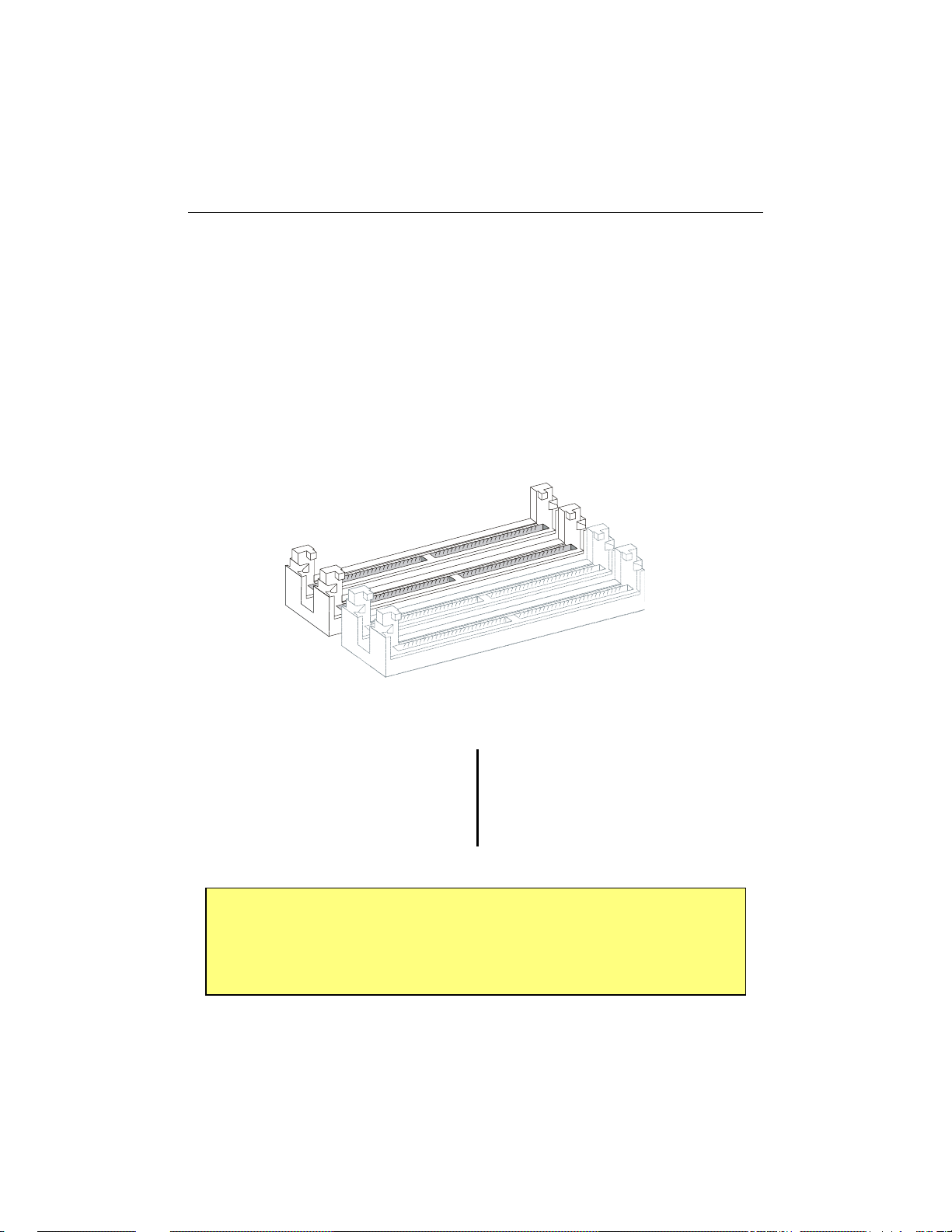
Memory specifications are as follows: vertical SIMMs (Single In-line Memory Module),
single-sided or double-sided, 5V, 32/36-bit, 70ns/60ns, Error Checking and Correction
(ECC) or parity with 36-bit SIMMs.
The memory sockets consist of four 72-pin vertical SIMM sockets divided into two banks
labeled: Bank 0 (U29 and U32) and Bank 1 (U34 and U39).
Bank 0
Bank 1
At least 8 MB of system memory (2 SIMMs of 4 MB) must be insta ll ed for pr oper operati on.
Memory can be configured from 8 MB to 512 MB using the following modules:
1M x 32-bit / 36-bit = 4MB module 8M x 32-bit / 36-bit = 32MB module
2M x 32-bit / 36-bit = 8MB module 16M x 32-bit / 36-bit = 64MB module
4M x 32-bit / 36-bit = 16MB module 32M x 32-bit / 36-bit = 128MB mo dule
NOTE
The memory ba nks can be po pulated separately or jointly. Each bank
must be installed with the same SIMM capacity, however the SIMM
capacity used in one bank may be of a different capacity from the
other bank.
6-3
Page 27
PCI-934 T echnical Reference M anual
Recommended DRAM devices are listed below. Many other models are also a vailable and
function equally well. Please check with your local distributors for comparable substitutes.
SIMM VEN DOR PART # SIMM VENDOR PART #
1M*36 (FPM)
4MB modules Centon CTK1MX36-70SMT 16MB modules Centon CTK4MX32-60EST
2M*32 (EDO)
8MB modules Micron MT4D232DM-6X Nec MC-424000A36BJ-70
2M*36 (FPM)
8MB modules Hitachi HB56D236BW-7B 32MB modules Micron MT16D832DM-6X
Centon CXCGF6JF1XS283T
Hyundai HYM536120AW-60 Micron MT8D432DM-6X
Micron MT9D136M-7 Unigen 4X32NEC6KBT2EDO
Nec MC-421000A36B-70 Unigen UG8M43222KBT-6
Samsung KMM5361000B-7 Unigen UG8M43222KBN-6
Texas Inst. TM124MBK36R-70
Toshiba THM361020AS-70 16MB modules Centon CTK4MX36-60SMT
Unigen UG12M13600DBT-6 Hyundai HYM536410AM-70
Centon CTK2MX32-60EST Nec MC-424000A36BH-70
Unigen 2X32NEC6KBT2EDO Samsung KMM5364100-7
Unigen UG16M23220DBT-6 Toshiba THM364020S-70
Centon CTK2MX36-60SMT
Hitachi HB56D236B2-7C Unigen 8X32NEC6KBT2EDO
Hitachi HB56D236BS-7BC Unigen UG16M83222KBT-6
Hitachi HB56D236BW-7C
Hyundai HYM536220W-70 32MB modules Hitachi HB56D836BR-60A
Hyundai HYM536220AW-60 AA Toshiba THM368020SG-60
Micron MT18D236M-7 Toshiba THM368020S-70
Nec MC422000A36B-70 Unigen UG18M83602KBT-6
Samsung KMM5362000B-7
Toshiba THM362040AS-60 64MB modules
Toshiba THM362040AS-70
4M*32 (EDO)
4M*36 (FPM)
8M*32 (EDO)
8M*36 (FPM)
16M*32 (EDO)
32M*32 (EDO)
128MB modules Unigen UG232E3264HKT-6
Abbacom Log 112-01643244-S6T
Centon CKEGH6TF2XS121T
Mitsubishi MH4M36ANXJ-7
Unigen UG9M43602KBT-6
Centon CTK8MX32-60EST
Hitachi HB56D836BR-70A
Unigen UG216E3254HKT-6
Unigen UG232E3244HKT-6
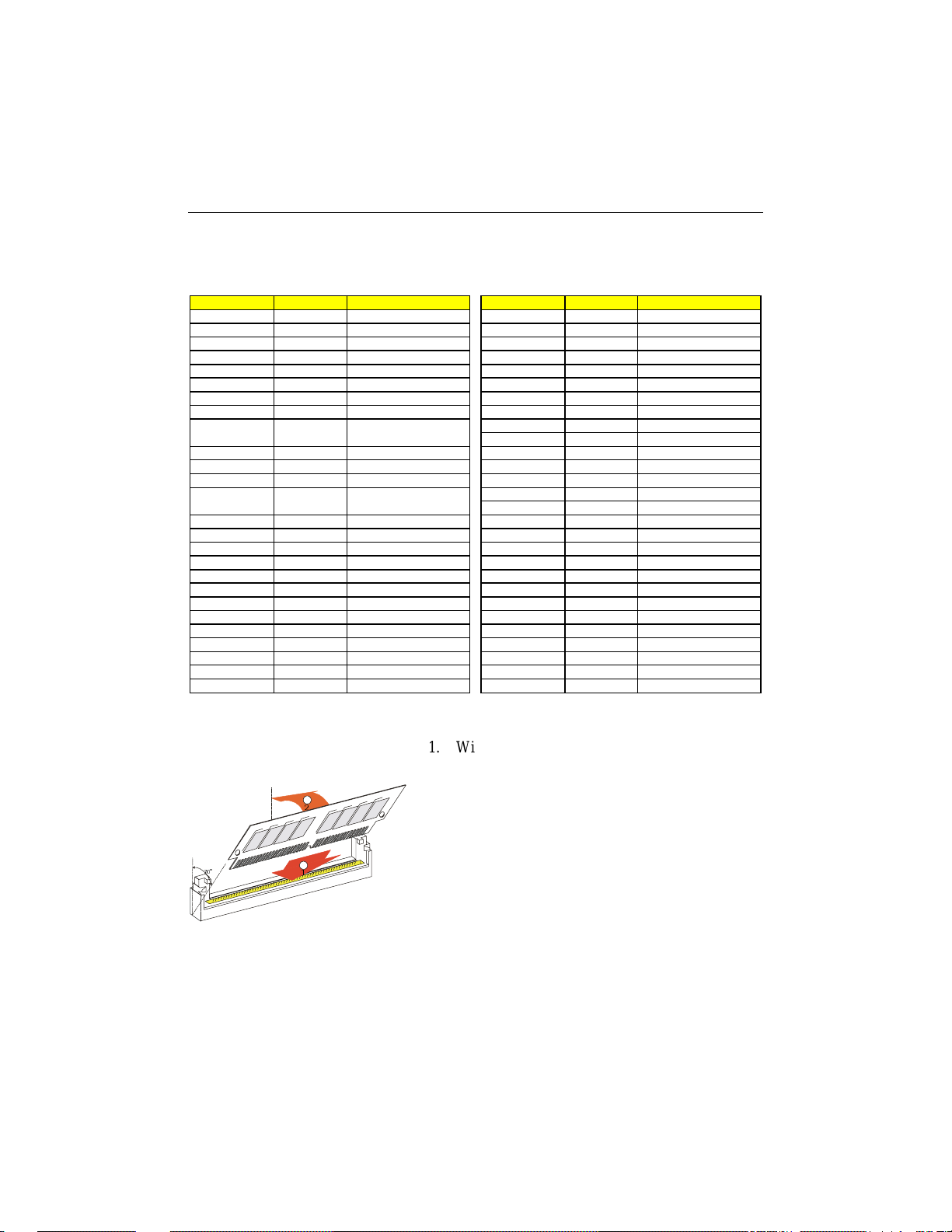
To install the SIMMs in the sockets, proceed a s follo ws:
1. With the board flat on the table, turn it so that
the br acket is on the right.
2. Hold the module with the notch on the bottom
right facing you, and insert the fingers into the
socket at a 70° angle from the board. Always
start inserting the module in the socket nearest
the top edge of the board
3. Snap the module to a vertical position. It is fully
installed when the retaining pegs snap into the
holes at each end of th e mod u le.
4. Work your way by inserting the other modules,
one by one, towards th e l ower edg e of the board.
To remove SIMMs from sockets, pull on the retaining pegs located on each side of the
socket. Once the module has snap ped out, pull gently on it.
6-4
Page 28

Installing and Working w ith System Component s
The following table describes which SIMM configurations may be implemented on the
board, using 72-p i n vertical SIMMs:
SYSTEM U34 U39 U29 U32
MEMORY BANK 1 BANK 0
8MB 4MB (1Mx36) 4MB (1Mx36) -- --
8MB -- -- 4MB (1Mx36) 4MB (1Mx36)
16MB 4MB (1Mx36) 4MB (1Mx36) 4MB (1Mx36) 4MB (1Mx36)
16MB 8MB (2Mx36) 8MB (2Mx36) -- -16MB -- -- 8MB (2Mx36) 8MB (2Mx36)
24MB 8MB (2Mx36) 8MB (2Mx36) 4MB (1Mx36) 4MB (1Mx36)
24MB 4MB (1Mx36) 4MB (1Mx36) 8MB (2Mx36) 8MB (2Mx36)
32MB 8MB (2Mx36) 8MB (2Mx36) 8MB (2Mx36) 8MB (2Mx36)
32MB 16MB (4Mx36) 16MB (4Mx36) -- -32MB -- -- 16MB (4Mx36) 16MB (4Mx36)
40MB 16MB (4Mx36) 16MB (4Mx36) 4MB (1Mx36) 4MB (1Mx36)
40MB 4MB (1Mx36) 4MB (1Mx36) 16MB (4Mx36) 16MB (4Mx36)
48MB 16MB (4Mx36) 16MB (4Mx36) 8MB (2Mx36) 8MB (2Mx36)
48MB 8MB (2Mx36) 8MB (2Mx36) 16MB (4Mx36) 16MB (4Mx36)
64MB 16MB (4Mx36) 16MB (4Mx36) 16MB (4Mx36) 16MB (4Mx36)
64MB 32MB (8Mx36) 32MB (8Mx36) -- -64MB -- -- 32MB (8Mx36) 32MB (8Mx36)
72MB 32MB (8Mx36) 32MB (8Mx36) 4MB (1Mx36) 4MB (1Mx36)
72MB 4MB (1Mx36) 4MB (1Mx36) 32MB (8Mx36) 32MB (8Mx36)
80MB 32MB (8Mx36) 32MB (8Mx36) 8MB (2Mx36) 8MB (2Mx36)
80MB 8MB (2Mx36) 8MB (2Mx36) 32MB (8Mx36) 32MB (8Mx36)
96MB 32MB (8Mx36) 32MB (8Mx36) 16MB (4Mx36) 16MB (4Mx36)
96MB 16MB (4Mx36) 16MB (4Mx36) 32MB (8Mx36) 32MB (8Mx36)
128MB 32MB (8Mx36) 32MB (8Mx36) 32MB (8Mx36) 32MB (8Mx36)
128MB 64MB (16Mx36) 64MB (16Mx36) -- -128MB -- -- 64MB (16Mx36) 64MB (16Mx36)
136MB 64MB (16Mx36) 64MB (16Mx36) 4MB (1Mx36) 4MB (1Mx36)
136MB 4MB (1Mx36) 4MB (1Mx36) 64MB (16Mx36) 64MB (16Mx36)
144MB 64MB (16Mx36) 64MB (16Mx36) 8MB (2Mx36) 8MB (2Mx36)
144MB 8MB (2Mx36) 8MB (2Mx36) 64MB (16Mx36) 64MB (16Mx36)
160MB 64MB (16Mx36) 64MB (16Mx36) 16MB (4Mx36) 16MB (4Mx36)
160MB 16MB (4Mx36) 16MB (4Mx36) 64MB (16Mx36) 64MB (16Mx36)
192MB 64MB (16Mx36) 64MB (16Mx36) 32MB (8Mx36) 32MB (8Mx36)
192MB 32MB (8Mx36) 32MB (8Mx36) 64MB (16Mx36) 64MB (16Mx36)
256MB 64MB (16Mx36) 64MB (16Mx36) 64MB (16Mx36) 64MB (16Mx36)
256MB 128MB (16Mx36) 128MB (16Mx36) -- -256MB -- -- 128MB (16Mx36) 128MB (16Mx36)
512MB 128MB (16Mx36) 128MB (16Mx36) 128MB (16Mx36) 128MB (16Mx36)
36-bit modules are shown, however 32-bit modules are supported.
6-5
Page 29

PCI-934 T echnical Reference M anual
6.2.2 Cache Memory
Internal Cache
The internal cache memory, also known as L1, is CPU integrated. The L1 memory size
depends on the CPU model:
- 8K, 8K separated data and instructions L1, for Pentium processors
- 16K, 16K separated data and instructions L1, for Penti um MMX processors
- 32K, 32K separated data and instructions L1, for K6 processors
External Cache
The external cache memory, also known as L2 cache, is implemented with 512KB
Synchronous Pi p elined SRAM. Th is feature enh ances the oper ation of the circuit by
eliminating wait states on cache ac c esses.
6.3 BACKUP MEMORY
An onboard 3.6V lithium battery is provided to backup BIOS setup values and the real time
clock (RTC).
When r ep lacing, the ba ttery must be connected a s fol lows:
3.6V
Lith i um Ba ttery
Positive Pin
(centered pin)
Positive Contact
Onboard Battery
Negative Pin
(outer pin)
Negative Contact
WARNING
- Danger of explosion if battery is incorrectly replaced -
Replace only with the same or equivalent type recommended by the
manufacturer. Dispose of used batteries according to the
manufacturer's instructions.
6-6
Page 30

Installing and Working w ith System Component s
6.4 SUPERVISION FEATURES
6.4.1 WATCHDOG
The PCI-934 provides a two-stage watchdog to monitor the CPU inactivity. The function of
the watchd og is to genera te a f ailure sig n al if the process or is not able to genera te a 0-1- 0 data
toggle for longer than the watchdog timeout period. The feature is useful in embedded
syste ms where human supervision is not required or im possible.
The watchdog configuration may be selected between Dual-Stage, Single-Stage, or disabled,
using the W6 jumper (see Section11 –
The default timeout period is 1.6 seconds for each stage; however, the timeout period can
be changed. Shorting C380/C353 and leaving R249/R230 opened changes the timeout to
100ms. Shorting the resistor and installing a capacitor will change the timeout period of the
watchdog according to the following formula:
Setting Jumpers
).
Timeout (milliseconds) = or
400ms
xC C=
47pF
For instance, an external capacity of 100pF will lengthen the watchdog timeout to 851ms
and a 1000pF will bring it to 8.5 seconds.
CAUTION
Modifying the Watchdog timeout period will also modify the value of
the Reset period according to the following formula:
(200ms/47pF) x C
Timeout(ms)x 47pF
400ms
6-7
Page 31

PCI-934 T echnical Reference M anual
Single-Stage Watchdog
In a single-stage configuration, the first watchdog detector monitors the output of the
first stage watchdog time-out.
To operat e the wat chdog, th e proces sor drives the wat chdog i nput (WDI) with an I/O
line. It toggles WDI once every 1.6 seconds (typical) to verify the proper software
execution. If a hardware or softwar e failure occurs such that WDI is n ot toggl ed, the
watchdog output (WDO) will go low after 1.6 second, and reset the CPU. If the
proces sor can cont inu e to run a 0- 1-0 t oggle r outine, WDO wil l be s et high by the n ext
transition of WDI.
In dual stage configur ation, the WDO signal indicates the second stage watchdog when a
failure occurs. Followi ng a re set, the wa tchdog is always di sabled.
Dual Stage Watchdog
The dual-stage watchdog consists of a second watchdog in cascad e with the fir st one: in
the event the first watchdog failed to toggle, the second stage is set.
Before th e se c ond stage watchd og re s et s the system, the fir st watchdog output can be t ied
to the ISA’s IOCHK line to generate an NMI to the CPU, while the two watchdog values
are stor ed. Th ese values may be used to determin e the cause of the system’s re set.
CAUTION
The user program must provide the first access to address 190H (or
290H o r 390H de pendi ng on the I/O addr ess sel ecte d in C MOS se tup),
and must also include the refresh routine.
Watchdog Flags
The watchdog status can be readout from two bits of the system register located at the
address 191h, 291h or 391h (depending on the I/O address selected in CMOS setup).
These bits are descr ibed as follo ws:
x91 - Bit 5: WDO, indicates th at th e la st system r eset was ca used by a wat chdog
timeout.
x91 - Bit 6: WDO1#, when goes low, indicates that the first level watchdog
timed out.
For more information on system registers, please refer to Page 6-10
6-8
Page 32

Installing and Working w ith System Component s
6.4.2 POWER FAILURE DETECTION
A power failure may be detected if a low battery condition occurs (battery voltage drops
below 3V). The power failure detector status can be readout from one bit of the system
register located at the address 191h, 291h or 391h (depending on the I/O address selected in
CMOS setup).
This bit is described as follows:
x91 - Bit 0: PFO#, when goes low, indicates that a power failure condition .
For more information on system registers, please refer to Page 6-10
6.4.3 THERMAL MANAGEMENT
The thermal management is built around a digital temperature sensor and a thermal
watchdog. The device can be programmed to set its output when the temperature of the
process or ex ceeds a pr ogram mable hi gh limi t, and res et its ou tput wh en the tem pera ture is
under a programmable low limit. A special routine will throttle the CPU clock until the
temperature falls below the programmed low limit.
6.4.4 I/O REGISTER ADDRESSES
Three sup ervisor I/O registers (Register #1, Register #2, and Register #3) are provided to
configure and control special features of the board such as: watchdog control, RS-422/RS485 mode, and power fail outp ut . T hese registers are two 8-bit r egisters which can be located
at three different I/O base addresses, 190h 290h or 390h.
When setting Register #1 at one base address (190h , 290h, or 390h), Register #2 and Register
#3 are located respectively at the Base Address plus one and Base Address plus two.
6-9
Page 33
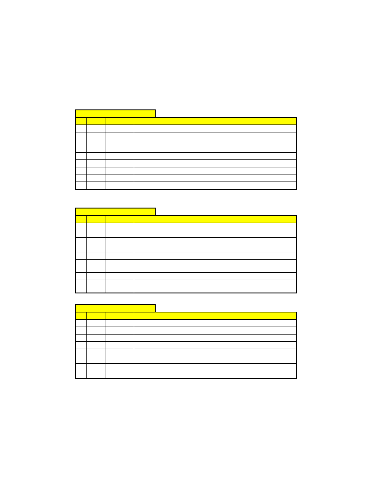
PCI-934 T echnical Reference M anual
To select one base address, use th e BIOS s et up program –
Register #1 (190h, 290h or 390h)
Bit Access Ref. Function
0 R/W EN WD Enable/Di sable External Watchdog Circuit (1: En / 0: Dis)
1 R/W CWD Watchdog Control. To be toggled to activate the external WD circuit when
2 R/W ST1 Enable/Disable RTS Output for RS-485 (Serial Port 2)
3 R/W* RS232 Enable/Disable RS-232 Operation (Serial Port 2)
4 R/W* RS485 Enable/Disable RS-485 Operation (Serial Port 2)
T
5R/W*
6 R/W* ENSMI# Enable External SMI
7 R/W* DIS_LAN# Enable/Di sable Ethernet Controller (1: En / 0: Dis)
OUT_ACK
ENWD bit is high.
Acknowledge Temperature Alarm
Chips e t Featur e Se tup
.
* Do not change this bit since it is used by the BIOS
Register #2 (191h, 291h or 391h)
Bit Access Ref. Function
0 R PFO# Reads the External Power Fail Flag
1R
2 R x Reserved
3 R x Reserved
4 R x Reserved
5 R WDO When high, indicates that the last system reset was caused by a watchdog
6 R WDO1# When lo w, indicates that the first level watchdog timed o u t
7 R PBRES When high, in dicates that the last system reset was caused by a push
TOUT_ACK
Status of Temperature Controller Alarm (1: temp. alarm / 0: normal)
time out
button reset switch
Register #3 (192h, 292h or 392h)
Bit Access Ref. Function
0 R/W CLRHIS# Clears WDO and PBRES status bits (0: clear ; 1: n ormal)
1R/W*
2 R/W* LOCK Reserved
3R Reserved
4 R/W VP_OI_1 General purpose output for V-Port control
5 R/W VP_OI_2 General purpose input for V-Port control
6R/W*
7 R/W EN_CAM# Controls V-Port buffer (0: external; 1: MPEG)
EN_MPEG#
EN_IRQ_MPEG
Enable M-PEG decoder (1: Disab le ; 0: Enable)
Reserved
* Do not change this bit since it is used by the BIOS
6-10
Page 34
7. INSTALLING ST ORAGE DEVICES
7.1 FLOPPY DISKS DRIVES
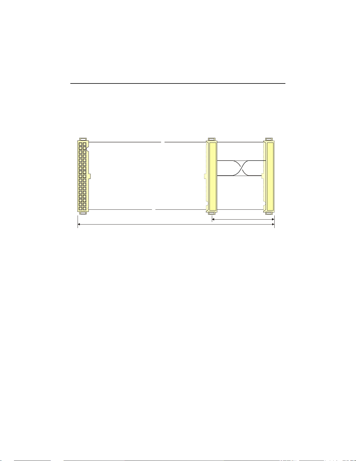
Floppy disk drives connect to the board using a standard IBM 34-pin flat ribbon cable
through the J4 onboard head er .
Female
34-pin Head er
Floppy 1:
Fem ale 3 4-pin Head er
Wire 10 Wire 16
Wire 16 Wire 10
Fem ale 3 4-pin Head er
Floppy 0:
18''
4''
The following list inclu des approved ven dors for the J2 connect or’s mating parts:
Amp 74 6285-8 [optional strain relief: 499252- 6],
Robinson Nugent IDS-C34PK-TG,
Thoma s & Betts 622 -3430 [optiona l strain relie f: 622-3441].
(34-pin flat cable connector).
The J4 floppy connector’s pinout is given in Appendix-C – Connector Pinouts.
7-1
Page 35
PCI-934 T echnical Reference M anual
7.2 EIDE DEVICES
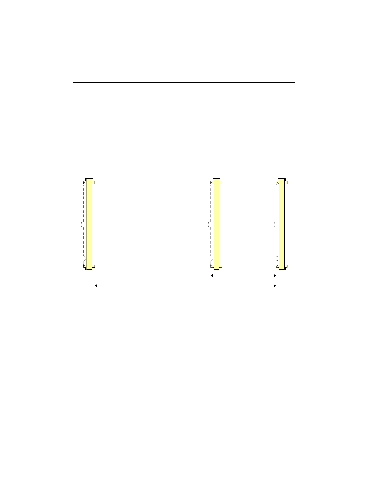
To install En hanced IDE ha rd disk drives, use t wo sta ndard I BM 40 -pin flat r ibbon ca ble that
connect to J3 and J10: J3 is reserved for Primar y EIDE devices while J10 is reser ved for
Secondary EIDE devices.
Each cable supports directly two IDE devices (Master and Slave). Its recommended
maximum length is 18 inches from the IDE device to the board connector). A complete
configuration allows a total of four EIDE devices to be connected.
''
Fem ale
40-pin He ader
40-pin H eader
4.00''
Female
40-pin He ader
18'', Hard Disk Flat Cable (150-259)
The following is a list of approved vendors for the mating 40-pin flat cable connector:
AMP 746285-9 [optional strain relief: 499252-1],
Robinson Nugent IDS-C40PK-TG,
Thomas & Betts622-4030 [optional strain relief: 622-4041].
Fem ale
The J3 hard disk connector’s pinout is given in Appendix-C – Connector Pinouts.
7-2
Page 36
Installi ng Storage Devices
7.3
OMPACTFLASH DISK
C
The board supports a IDE compatible flash disk by using the TEK-069 CompactFlash
daughterboard. CompactFlash (C-Flash) disks are the world’s smallest resident industrystandard ATA/IDE subsystem for application, data, image, and audio storage. They have
the same functionality and capabilities as intelligent disk drives, but with the advantages of
being very compact, rugged (typical M.T.B.F. is 1,000,000 hours) and low power.
Available capacities are up to 24MB. 40 and 80MB modules will be supported when
available.
The C-Flash disk connects on the PCI-934 via the onboard Flash Disk Connector J19 (J19
connector pinout is provided in Appendix-C).
7.3.1 INSTALLING COMPACTFLASH MODULE
Follow this procedure to install a C-Flash module on the TEK-069 and to install the TEK069 on the board:
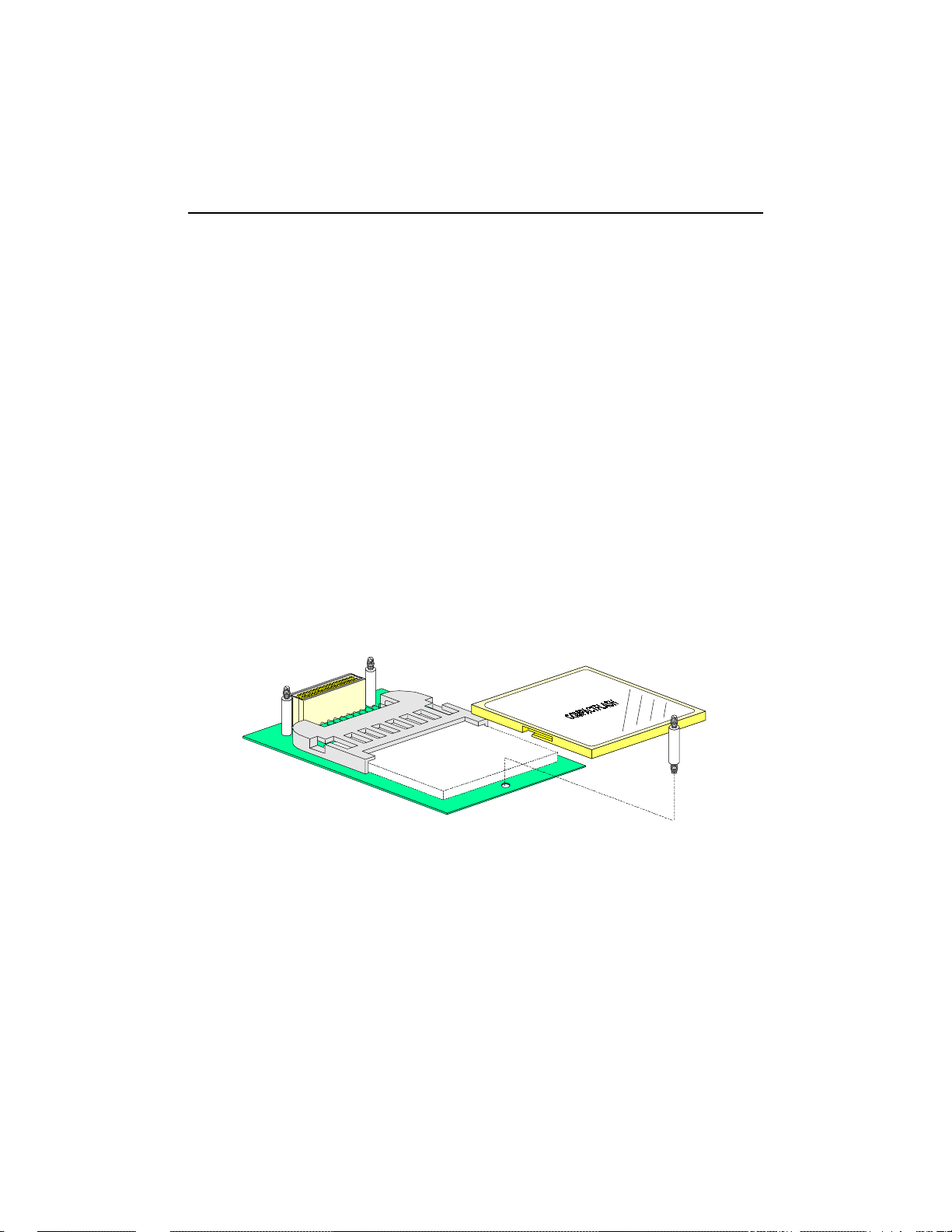
1. Slid e the C-Flash module into its r ecep tacle and press gentl y to ensur e a good ins ertion
and connection.
Com pact Flash
Modu le
Spacer
Compact Flash
Daughterboard
2. Clip the spacers into their mounting holes: two are located close to the interface
connector, a third one is located at the bottom of the module. The spacer located near
the C-Flash module acts as a retention mechanism and prevents it from accidently
sliding.
7-3
Page 37
PCI-934 T echnical Reference M anual
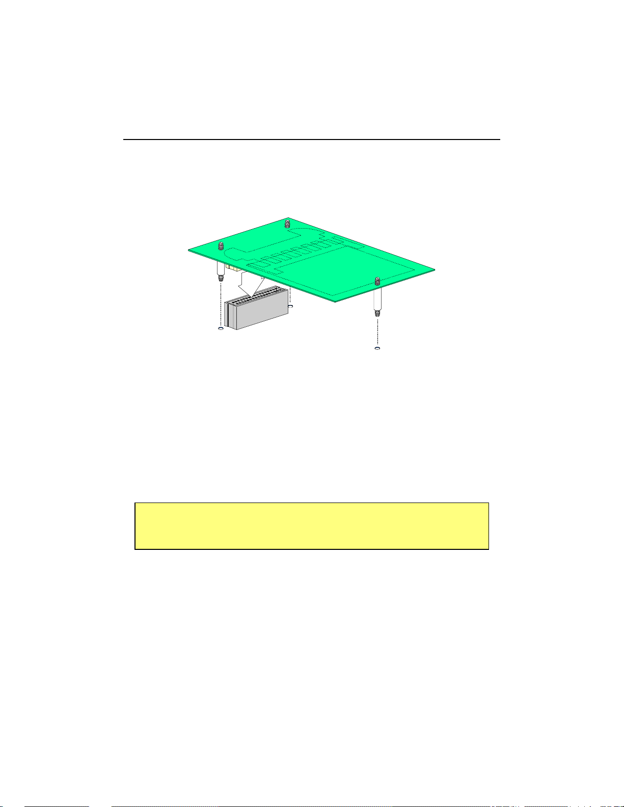
3. To conn ect the da ughter doar d to the SBC, lin e up th e J1 9 conn ector and th e in terfa ce
connector, then press firmly the daughterboard into the Single Board Computer’s
connector to engage the connector and the spacers.
Compact Flash
Daughterboard
Onboard
Compact Flash
Connector
7.3.2 WORKING WITH A
COMPACTFLASH
DISK
The CompactFlash module conn ects direct ly on the S econdar y EIDE interface. It must be
decl ared the same way as a standa rd har d disk using the BIOS s e tup pr ogram.
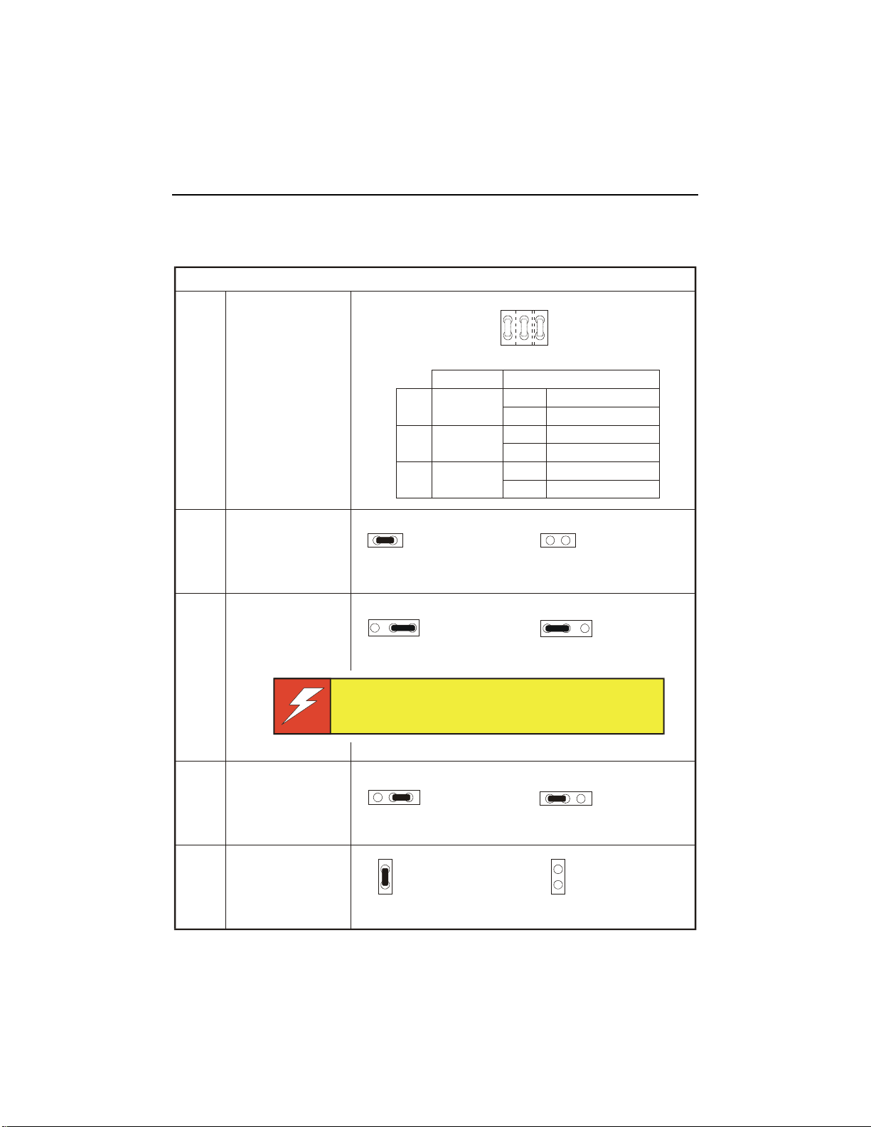
To setup the CompactFlash disk for Master or Slave configuration, use the W11 (1-2)
jumper to select one configuration. To locate and install W11, please refer to Section 11 –
Setting Jumpers.
NOTE
Since data is accessed like it would on an IDE drive, no specific flash
disk driver is requires for various operating systems.
7-4
Page 38

8. INSTALLING PERIPHERALS
8.1 VIDEO
Please refer to Section 12 - Exploring the Multimedia Capabilities of the Board.
8.2 SERIAL PORTS
Two serial ports ar e a vailable on the TEK-934. T hey are 16C550 compatible and provide 16byte internal FIFO buffers for more efficient data transfers, enabling communication speed up
to 115.2KBPS
The Serial P ort 1 is buffered for RS -232 operations, while the Seri a l Port 2 may be s e t a s RS232 or RS-422/RS-485.
The foll owin g list in clud es appr oved ven d ors for the CO M1 (J6) and COM2 ( J7) conn ect or s’
mating parts:
Amp 74 6285-1 [optional strain relief: 499252- 5],
Robinson Nugent IDS-C10PK-TG,
Thoma s & Betts 622 -1030 [optiona l strain relie f: 622-1041].
(10-pin flat cable connector).
For information on the programming of serial ports with the use of FIFO buffers, ask for
Application No te # AN93 00 7 f rom TE KNOR’s Technical Support department.
8-1
Page 39
PCI-934 T echnical Reference M anual
''
8.2.1 SERIAL PORT 1 (J6) RS-232
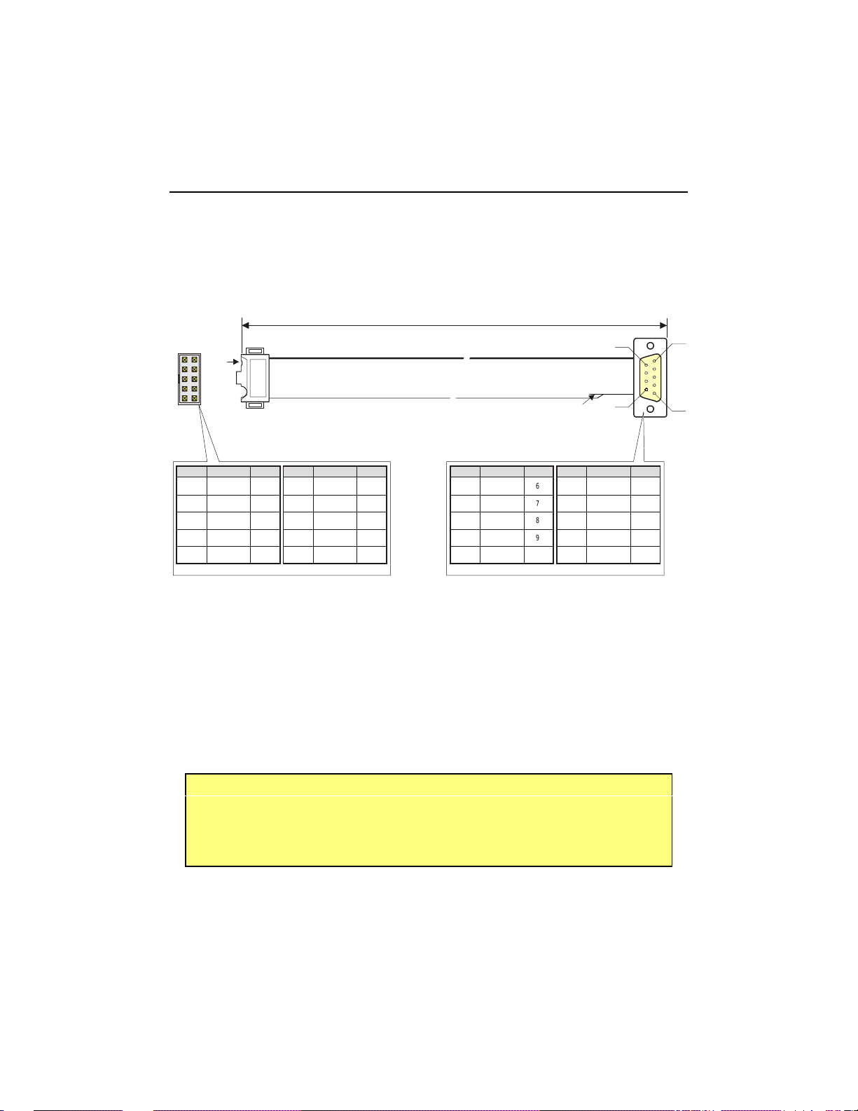
The Serial P ort 1 is confi gured as RS-232. With th e I BM 9 -pi n DSUB Stan da rd, Serial P ort 1
is 100% compatible with the IBM-AT serial port.
18
Onboard
10-pin Header
192
10
I
I
O
O
-
Pin 1
DCD
RX
TX
DTR
GND
Female
10-pin Header
1
3
5
7
9
RS-232 Serial Port Flat Cable (150-019)
SignalSignal
2
DSR
4
RTS
6
CTS
8
RI
10
N.C.
I
O
I
I
-
DSR
I
RTS
O
CTS
I
RI
I
9-pin Male D SUB Connector according to IBM-AT standardOnboard Serial Port Connector
Pin #Pin #
6
7
8
9
Cut Wire #10
Pin #Pin # I/OI/O I/OI/O
1
2
3
4
5
SignalSignal
DCD
RX
TX
DTR
Gnd
6
9
I
I
O
O
-
1
5
TEKNOR offer s a 10-pin head er to 9-pin DSUB cabl e for IBM- AT compati bility. Th is can
be pu rchas ed from TE KNOR or a ca ble can be made wi th a fla t cable, a 10- pin fla t cabl e
crimp header and a 9-pin DSUB flat cable crimp connector.
NOTE
The use of Taïwanese adapter cables is not recommended, since t he
pinout is often incorrect. The direct crimp design offered by
TEKNOR allows the simplest cable assembly. All these cables are
available from TEK NO R by c o ntacting the Sales Depa rtmen t.
8-2
Page 40
Installing Peripherals
''
8.2.2 SERIAL PORT 2 (J7)
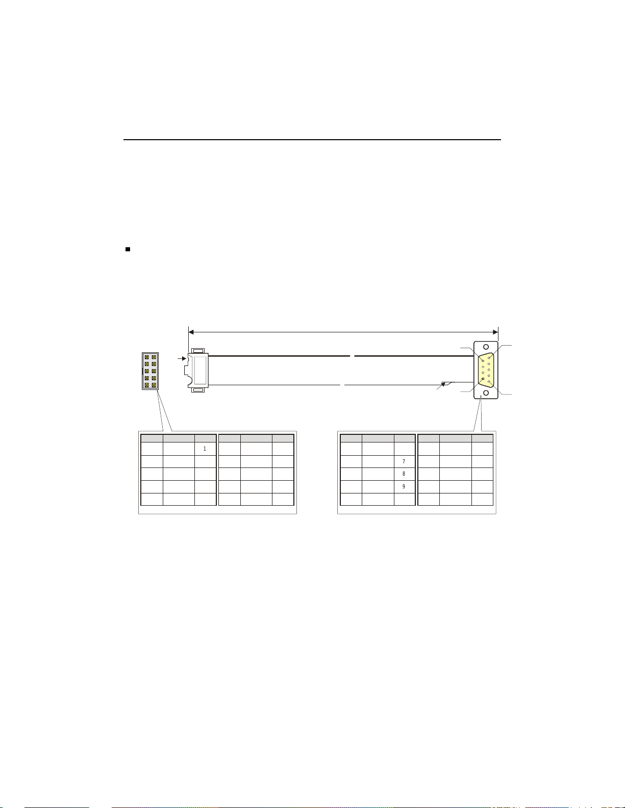
By default the Serial Port 2 is set as RS-232. In this configurati on, it function s the same way
as Serial Port 1, wit h the same pinout. However , the Seri al P ort 2 may be set for RS- 422/RS485 operations, using the BIOS Setup program.
RS-232 Mode
As a RS-232 port, and with the IBM 9-pin DSUB Standard, Serial Port 2 is 100%
compatible with the IBM-AT serial port. To output RS-232 signals from the 10-pin
onboard connector to a 9-pin DSUB connector, please refer to the following diagram:
18
Onboard
10-pin Header
192
10
Pin 1
Female
10-pin Header
RS-232 Serial Port Flat Cable (150-019)
Cut Wire #10
6
9
1
5
Pin #Pin #
SignalSignal
1
DCD
I
RX
I
TX
O
DTR
O
GND
-
2
DSR
3
4
RTS
5
6
CTS
7
8
RI
9
10
N.C.
I
O
I
I
-
DSR
I
RTS
O
CTS
I
RI
I
9-pin Male D SUB Connector according to IBM-AT standardOnboard Serial Port Connector
Pin #Pin # I/OI/O I/OI/O
SignalSignal
6
1
DCD
7
2
RX
8
3
TX
9
4
DTR
5
Gnd
I
I
O
O
-
TEKNOR offers a 10-pin header to 9-pin DSUB cable for IBM-AT compatibility. This can
be purchased from TEKNOR or a cable can be made with a flat cable, a 10-pin flat cable
crimp header and a 9-pin DSUB flat cable crimp connector. The direct crimp design
offered by TEKNOR allows the simplest cable assembly. All these cables are available
from TEKNOR by contacting the Sales department.
8-3
Page 41
PCI-934 T echnical Reference M anual
+
SERIALPORT2
RS-422/RS-485 Mode
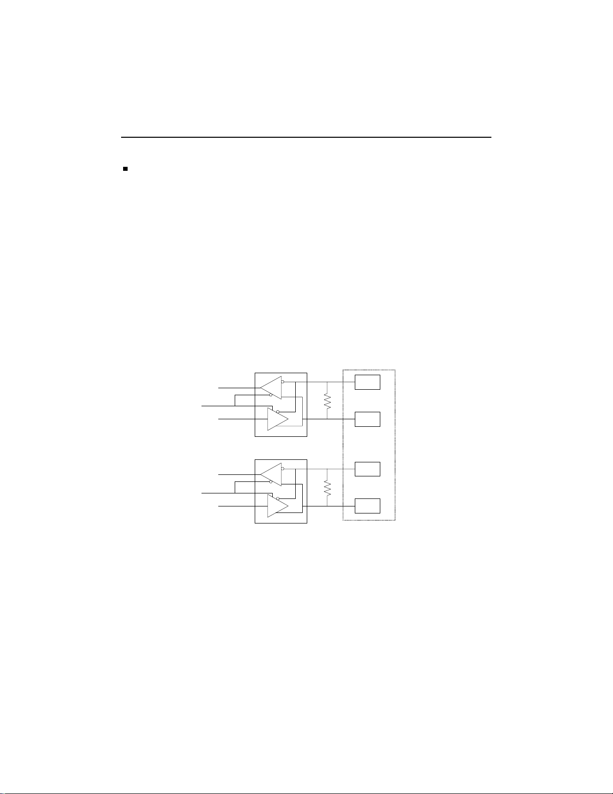
When configured for RS-422/RS-485 operation, the Serial Port 2 can transmit and
receive differential signals, in either full-duplex or party line communication.
Communicating with differential signals requires one pair of wires for the transmission
and a pair of wires for the reception (RS-422). For a better noise rejection, the use of
twisted pair ca ble is highly recommended. Th is will enable fa ster serial transmi ssions
over grea ter distance s than with the common RS-232 protocol.
RS-422 - Full Duplex Oper ation
: The RS-422 pr otocol us es both RX and TX li ne s
during a communication session. Upon power-up or reset, the Serial Port 2 interface
circuit s are aut omatica lly confi gured for full d uplex operati on: pins 3 and 4 of J7 a ct as
the receiver lines and pins 5 and 6 act as the transmitter lines.
10-PIN HEADER
120 ohm s
RXD2
GND
X
LOW LOGIC LEVEL
LOW LOGIC LEVEL
X
VCC
TXD
1
2
3
4
1
2
3
4
7
6
120 ohm s
7
6
3
4
5
6
RX-
RX
TX-
TX+
In RS-422 mode, software should not use the handshake signals (e.g. DSR or DTR) since
they a re not conne cted. Howev e r, so ftware handshaking (e .g . X ON-XOFF) can be used.
8-4
Page 42
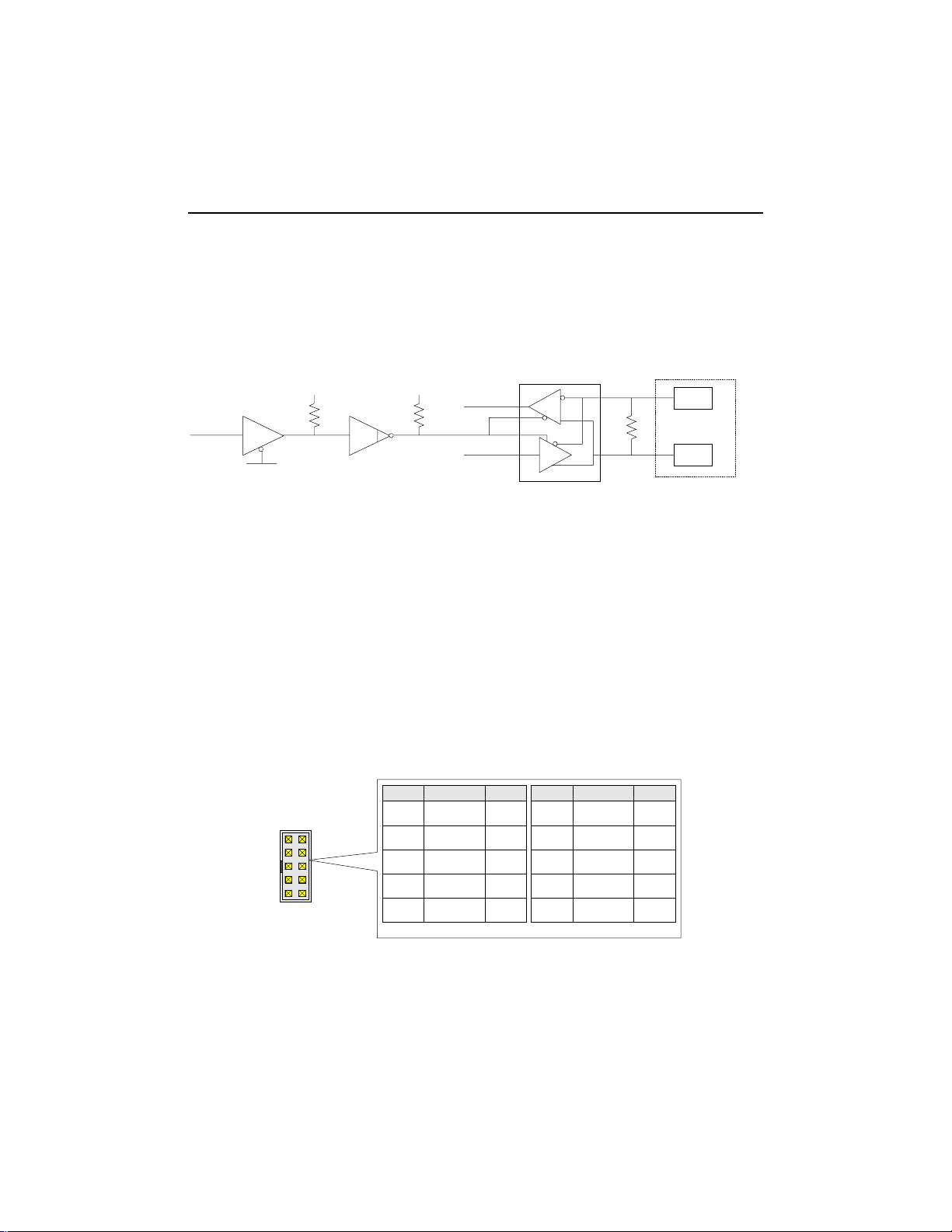
Installing Peripherals
+
SERIALPORT2
RS-485 - Party Line Operation
: The RS-485 offers the ability to transmit and
receive over the same pair of wires (RX outputs: pins 3 and 4), and share the same
communication line with multiple stations. To ensure this con figurati on, only one system
takes the control of the communication line at the time.
10-PIN HEADER
3RX-
4RX
ENAB LE
VCC
VCC
RXD2
TXD2
120 ohms
1
2
3
4
7
6
The RS-485 protocol offers some advantages such as increased speed over long
distances, improved reliability over similar RS-232 setups, ability to share the
transmission line, less cabling requirements th an RS-4 22 protocol.
Upon power-up or reset, the transceiver is by default in "receiver mode" to prevent
undesired perturbation on the line.
In RS-485 mode, only both ends of the network must be terminated (120 Ohms
resistors). Termination resistors are available: If the board is installed at one end of the
network, these resistors may be installed using the W2 and W3 jumpers.
Pinout:
When configured for RS-422/485 communication mode, the pin assignation for
the onboar d S er i a l Port 2 (J7) appears as follows:
Onboard
10-pin Header
1
2
9
10
Signal
DCD
I
RX (-)
I/O
TX(-)
O
DTR
O
GND
-
Onb oard S erial P ort Connector set as RS -485
Pin #
1
3
5
7
9
8-5
Pin # I/OI/O
10
Signal
2
DSR
4
RX(+)
6
TX(+)
8
RI
N.C.
I
O
I
I
-
Page 43
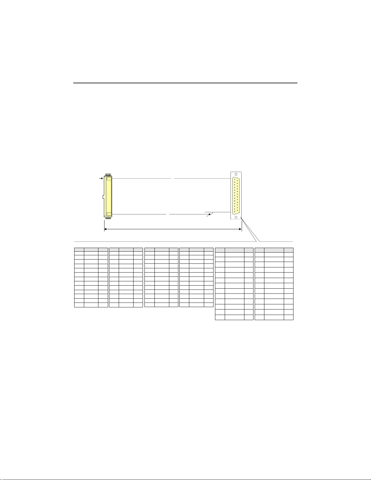
PCI-934 T echnical Reference M anual
10'
',Pri
F
latCab
le(15
0-172
)
8.3 PARALLEL PORT
The PCI-934 provides a bi-directional parallel port, compatible with PC/XT, AT, PS/2,
EPP and ECP modes.
To operate in EPP or ECP mode, the peripheral must be designed to operate in this mode
and the BIOS setup must be configured to support it. The differences between the thr ee
modes appear in their pin assignation.
nterPort
Female
26-pin H eade r
Pin 1
ParallelPort PinoutAccording to Standard Mode
O
I
O
O
-
-
-
-
-
-
-
-
* Active low signal
AUTOFD*
ERROR*
INIT*
SELECTIN*
GND
GND
GND
GND
GND
GND
GND
GND
Pin# Pin# I/OSignalSignalI/O
14
1
15
16
17
18
19
20
21
22
23
24
25
STROBE*
2
D0
3
D1
4
D2
5
D3
6
D4
7
D5
8
D6
9
D7
10
ACK*
11
BUSY
12
PE
13
SELECT
10''
Pa ralle l Po rt P in o u t Ac co rdin g t o E P P M od e
O
O
I/O
-
-
I/O
O
I/O
I/O
-
-
I/O
-
I/O
-
I/O
I/O
-
-
I
-
I
I
-
I
* Active low signal
DATASTRB*
Not Used
Not Used
ADDRSTRB
GND
GND
GND
GND
GND
GND
GND
GND
Pin # Pin # I/OSignalSignalI/O
14
15
16
17
*
18
19
20
21
22
23
24
25
1
2
3
4
5
6
7
8
9
10
11
12
13
DB25 Female
Connector
WRITE*
D0
D1
D2
D3
D4
D5
D6
D7
INTR
WAIT*
Not Used
Not Used
Cut Wire#26
O
I/O
I/O
I/O
I/O
I/O
I/O
I/O
I/O
I
I
-
-
DB25 Female
Connector
1
14
25
13
Paralle l Po rt P in out A c c o rdin g to EC P M o de
AUTOFD*
O
HOSTACK
FAULT*
I
PERIPHRQST*
INI T*
O
REVERSERQ ST*
SELECTIN*
O
-
-
-
-
-
-
-
-
* Active l ow signal
1
GND
GND
GND
GND
GND
GND
GND
GND
Pin #SignalI/O
Pin # I/OSignal
14
15
2
16
17
18
19
20
21
22
23
24
25
1
CompatibleMode
2
HighSpeed Mode
1
2
3
4
5
6
7
8
9
10
11
12
13
.
2
1
2
1,2
STROBE *
D0
D1
D2
D3
D4
D5
D6
D7
ACK*
BUS Y
PER IPH A C K
PERROR
ACKREVERSE
SELECT
O
I/O
I/O
I/O
I/O
I/O
I/O
I/O
I/O
I
I
2
2
I
I
The parallel port connector (J13) is a male 26-pin header located at the top right side of the
board.
The following list includes approved vendors for the J13 connector’s mating parts:
Amp 74 6285-6 [optional strain relief: 499252- 3],
Robinson Nugent IDS-C26PK-TG,
Thoma s & Betts 622 -2630 [optiona l strain relie f: 622-2641].
(Polarized IDC female socket connector).
8-6
Page 44
Installing Peripherals
8.3.1 STANDARD MODE
The Standard mode is an unidirectional parallel port. It is used for its compatibilit y with the
IBM PC s t andard.
8.3.2 EPP MODE
The EPP (Enhanced Parallel Port) mode consists of a hardware independent method of
accessing a parallel port configured as EPP. It provides support for single I/O cycle as well
as the high per formance block I/O transfers. The EPP mode always uses the most optimum
method for I/O transfers. For example, if the hardware supports it, EPP mode will perform
32-bit I/O block transfers.
8.3.3 ECP MODE
While the EPP mode may intermix read and write operations without any overhead or
protocol handshaking, the ECP mode negotiates data transfers using a request from the host
and an a cknowledgment from the per ipheral.
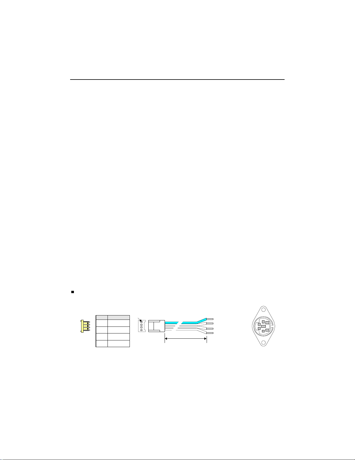
8.4 PS/2 MOUSE
The boa rd provi d es a PS/ 2 m ou se hea d er ( J1 5) t o out p ut th e m ou se cl oc k an d d at a si gn a l s.
An adapter cable is required to make these signals available on a 6-pin PS/2 standard
connector: The cable must provide a 4-pin female header at one end, and a 6-pin female
PS/2 standard connector at the other end:
Connection
Pin 1
Fem ale
4-pin Head er
8-7
17.10''
1
2
3
4
to Pin #4
to Pin #1
to Pin #3
to Pin #5
6
4
2
1
35
(Conn ec tor back view)
1
MOUCLK
2
KBMOUGND
3
MOUDATA
4
KBMOUVCC
DesignationPin #
1
Page 45
PCI-934 T echnical Reference M anual
(
)
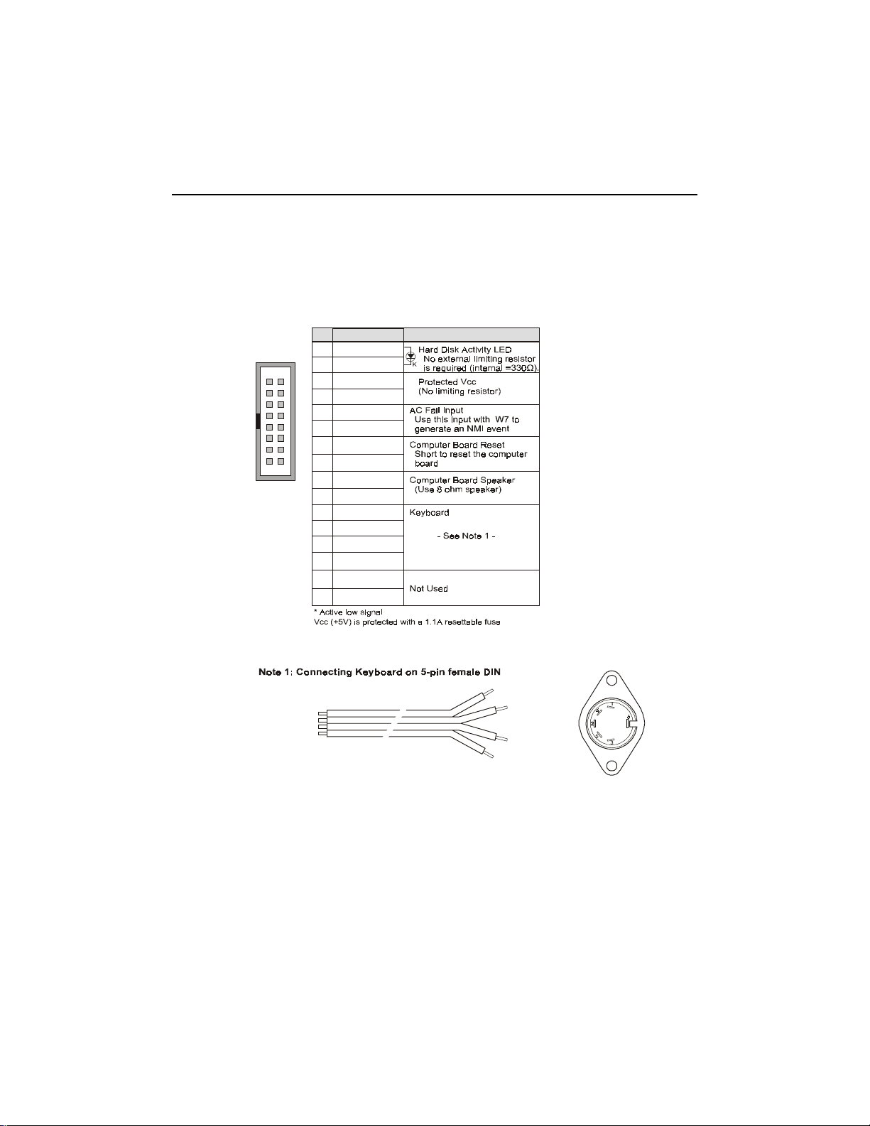
8.5 MULTI I/O CONNECTOR
The onboard multi I/O connector (J5) provides all the necessary signals for connecting
keyboard, spe a ker, rese t , a nd keylo ck interface devices. It is described as follows :
Signals Name Description
FVCC (+5V)
16
ACT1*
1152
15
VCC (+5V)
6
GND
4
9
ACFAIL*
10
GND
13
PBRES*
14
7
8
1
3
2
5
11
12
GND
SPKR
VCC (+5V)
KCLK
KDAT
GND
VCC (+5V)
GND
16
To Pin #1
KCLK
KDAT
GND
VCC (+5V)
To Pin #2
To Pin #4, 6
To P i n # 5
Conne ctor back v iew
The following list inclu des approved ven dors for the J5 connect or’s mating parts:
Amp 74 6285-3 [optional strain relief: 499252- 8],
Robinson Nugent IDS-C16PK-TG,
Thoma s & Betts 622 -1630 [optiona l strain relie f: 622-1641].
(16-pin flat cable connector).
8-8
Page 46
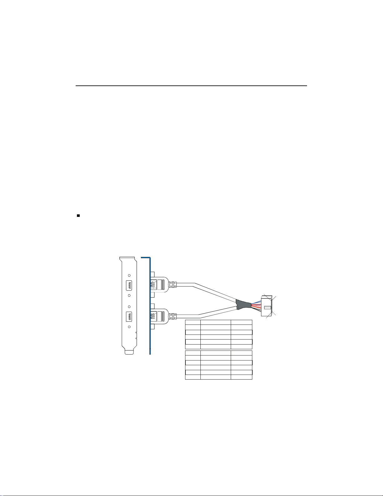
Installing Peripherals
8.6 USB PORTS
USB is becoming the new essential peripheral interface. The USB strengths are as follows:
the ability to daisy chain as many as 127 devices, a 12Mbps transfer rate, and the
standardization of peripheral interfaces into a single format.
USB support Plug and Play and hot swapping operations (OS level) which is the most user
friendly feature, since this means that the system will support a new USB device
inst allation without rebooting.
Because of the very low technology barri er, keyboards, mice, speakers, are some of th e
first peripherals to adopt the USB standard. Sophisticated USB products, like camera,
scanners, and printers are becoming available. Monitors are likely to become the main hub
for system USB connections.
Connections
The onboard USB capacities are built around the PIIX3 chipset from Intel. Two USB
ports are available. Connections are available through J14 - Dual USB header.
External USB connections must be provided as follows:
USB 1
USB 2
1
2
3
4
Dual USB Bracket - 150-316
1
2
3
4
USB 1
1
2
3
4
SHELL
USB 2
1
2
3
4
SHELL
SIGNAL
VC C
P0 P0 +
Ground
Ground
SIGNAL
VC C
P1 P1 +
Ground
Ground
USB Header
USB Header
USB Header
1
2
10
9
1
3
5
7
9
2
4
6
8
10
8-9
Page 47
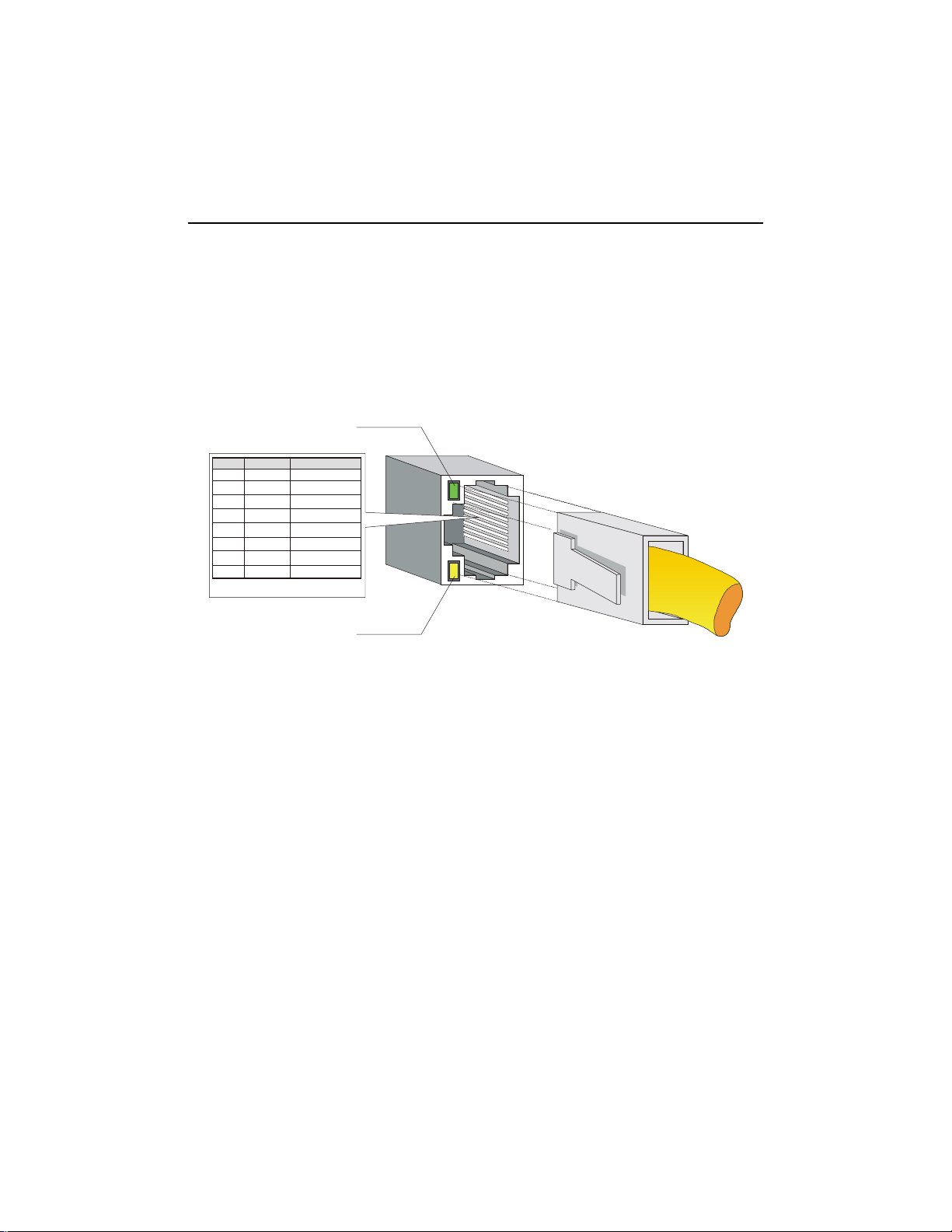
9. ETHERNET
GREEN:
Link Integrity - If the link is good in either
activity (lights O N )
The board supports both 10Base-T and 100Base-TX on the same RJ-45 edge bracket
connector. 10Mbps and 100Mbps network speed is automatically detected and switched.
The onboard Ethernet interface may be set for 10Base-T or 100Base-TX operation modes:
The 10Base-T interface uses UTP (Unshielded Twisted Pair) cables, category 5, 4 or 3 (5 is
better ), while th e 100Base-TX ca bl e must use categ ory 5.
10 or 100M b ps, the LE D lights ON.
Pin # I/OSignal
1
2
3
4
5
6
7
8
Ethernet 10B ase- T and 100Base-T X
TX+
TXRX+
N.C.
N.C.
RXN.C.
N.C.
Trans m it D a ta +
Trans m it D a ta Receive Data +
Not Connected
Not Connected
Receive Data Not Connected
Not Connected
AMBER:
Activity - Ind ica tes eith e r trans m it or re ce ive
1
8
This connection type allows links up to 100m over both shielded twisted pair and data
grade (Cat. 5) unshielded twisted pair or equivalent.
The Ethernet controller resides on the PCI bus and is therefore Plug and Play by default. No
manual configuration i s required. A set up program is pr ovided on the dr iver CD-RO M t o
configure the Ethern et controller according t o your OS requirements (refer t o the OS list on
the CD-ROM – File.txt. The CD-ROM provides several operating system network drivers.
To install the drivers, run the “Setup.exe” program.
For other operating system drivers and inst al latio n ins t ruc tions, contact TEKNOR’s
Technical Support department.
9-1
Page 48
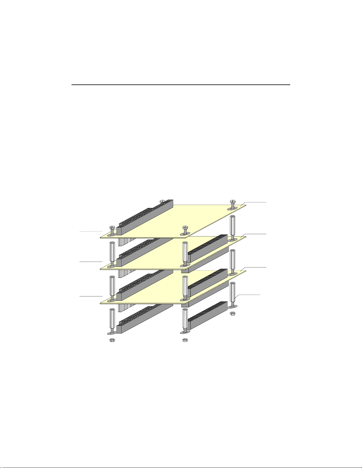
10. PC/104-PLUS FEATURES
S
The onboard PC/104-Plus interface is a PCI extension of the PC/104 ISA standard. It
consis ts of thr ee conn ector s referr ed as P1, P 2 and J25, and is pr ovided t o r eceive PC /10 4
form factor modules to increase the I/O capabi lities of th e board.
P1 and P2 are assigned to the ISA bus while J25 is assigned to the PCI bus. All sign als ar e
provided in the same order as on the edge-card connector, but transformed to the
corresponding connector pins.
The maximum number of PC/104-Plus modules depends on the total number of loads
installed on the PCI bus. The bus supports four PCI loads, plus the PCI-934 board itself.
A typical module stack may be represented as follows:
tackthrough
PC/104 m odule
Slot 2 (CLK2)
Slot 1 (CLK1)
Slot 0 (CLK0)
SBC o nboard
PC/104-Plus connectors
Stackthrough
PC/104-Plus m odule
Stackthrough
PC/104-Plus m odule
0.6 in. (15 mm ) Sp acer
The onboard PC/104-Plus interface complies with PC/104-PLUS V1.0 and PCI V2.1
standards. Connector pinouts are provided in Appendix C-26 and C-27.
10-1
Page 49
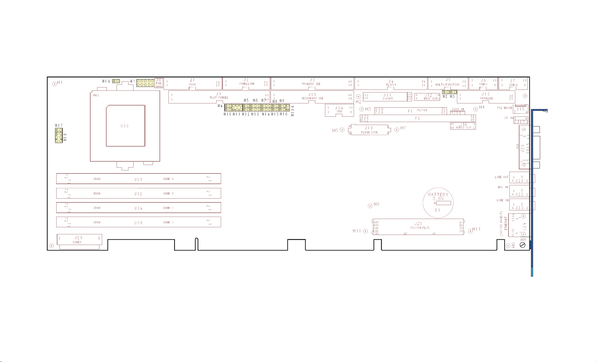
JUMPER LOCATION
11. Setting Jumpers
Page 50

11. SETTING JUMPERS
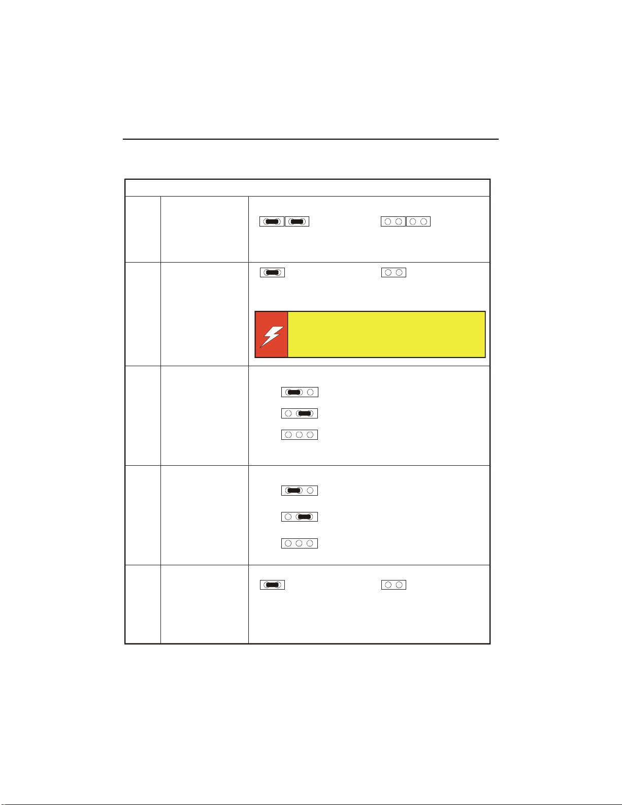
The jumpers available on the board are summarized below:
Jumper Description
W1 CPU core voltage setup
W1A Bus / Core Frequency ratio selection
W2, W3 RS-422 / RS-485 termination type selection (on serial port 2)
W4 Bus / Core Frequency ratio selection
W5 Battery connection
W6 Watchdog setup
W7 IOCHK signal source selection
W8 Main C l ock frequency selecti on
W9 VGA interrupt setup (PCI)
W10 Bus / Core Frequency ratio selection
W11 Flash Disk assig nation; Signal settings for PanelLink interface
W12 VGA interrupt setup (Master)
W13 Flat panel supply level
W14 Flat panel Clock-Shift signal polarity
W15 Main Cl oc k frequenc y s elec t i on
W16 DRAM refresh rate selection
W16A Enables/Disables vid eo on the board
W17, W18 CPU type
11-1
Page 51
PCI-934 T echnical Reference M anual
Jumper Settings 1/ 3
CPU Related Jumpers
CPU Model
Selection
P 100
P 120
P 133
P 150
P 166
P 200
P 166-MM X
P 200-MM X
P 233-MM X
K6-166 (1)
K6-200 (1)
K6-233 (2)
K6-266
K6-300
CPU
Clock Mul. Bus/Core Freq. Ratio CPU Type W1 - V Core Refr.
W15
OFF
ON
OFF
ON
OFF
OFF
OFF
OFF
OFF
OFF
OFF
OFF
W8
ON
OFF
ON
OFF
ON
ON
ON
ON
ON
ON
ON
ON
W10
OFF
ON
ON
ON
ON
OFF
ON
OFF
OFF
ON
OFF
OFF
W4
OFF
OFF
OFF
ON
ON
ON
ON
ON
OFF
ON
ON
OFF
W17
W1A
ON
OFF
ON
OFF
ON
OFF
ON
OFF
ON
OFF
ON
OFF
OFF
OFF
OFF
OFF
OFF
OFF
OFF
OFF
OFF
OFF
OFF
OFF
Contact TE KN O R
Contact TEKNOR
W18
1-3 / 2-4
1-3 / 2-4
1-3 / 2-4
1-3 / 2-4
1-3 / 2-4
1-3 / 2-4
3-5 / 4-6
3-5 / 4-6
3-5 / 4-6
3-5 / 4-6
3-5 / 4-6
3-5 / 4-6
1-2
ON
ON
ON
ON
ON
ON
OFF
OFF
OFF
ON
ON
OFF
3-4
OFF
OFF
OFF
OFF
OFF
OFF
OFF
OFF
OFF
OFF
OFF
OFF
5-6
ON
ON
ON
ON
ON
ON
OFF
OFF
OFF
OFF
OFF
ON
7-8
ON
ON
ON
ON
ON
ON
ON
ON
ON
ON
ON
ON
9-10
OFF
OFF
OFF
OFF
OFF
OFF
OFF
OFF
OFF
OFF
OFF
OFF
W16
ON
OFF
ON
OFF
ON
ON
ON
ON
ON
ON
ON
ON
(1) ALR suffix: 2.9V core voltage
(2) ANR suffix: 3.2V core voltage
Careful attention should be taken when installing a processor:
Faulty jumper settings may damage definitely both your
processor and your board.
11-2
Page 52
Jumper Settings 2/ 3
Single-Stage Wa tchdog*
W7
IOC HK Sign al
Source Selection
Fr o m A CFAIL In pu t
From First Stage Wa tch do g
Danger of explosion if battery is incorrectly replaced.
NAME FUNCTION CONFIGURATION (INITIAL SETTING : * )
Setting Jumpers
W2
W3
W5
W6
RS-422/RS-485
Termination
Resistors
VBAT
Inte rn a l B a tter y
Watchdog
W2 W3 W2 W3
Wi th Term i n a t io n
Ba tte ry ON
Rep lace only with the same or equivalent type recom m en ded
by the manufacturer. D ispose of used batteries according to the
manufacturer's instruction s .
1
1
1
1
3
3
3
3
Dual-Stage Watchdog
Watchdog D isabled
With out Te r mina t io n *
Battery Disabled *
W9
VGA Interrupt
(PCI)
1
1
Enab led
11-3
3
3
Disabled *
Disabled *
Page 53
PCI-934 T echnical Reference M anual
Normal *
Master
Signal Settings for
152
3.3 volt *
Power Selection
Careful attention should be taken when installing a flat panel:
Jumper Settings 3/ 3
NAME FUNCTION CONFIGURATION (INITIAL SETTING: * )
6
W11
FLASH Disk
Assignation
&
W11
W12
W13
PanelLink
Inte r fac e
VGA Interrupt
Flat Panel
SettingsFeatures
Set as Master
1-2
3-4
5-6
Disabled *
1
Flash Disk
M ast./Slave
PanelLink
Control Edge
PanelLink
Data Edge
3
ON *
OFF
ON *
OFF
ON *
OFF
Enabled
1
Set as Slave
La t c hed on fa llin g
Latched on rising
La t c hed on fa llin g
Latched on rising
3
5 volt
Faulty power selection may dam age definitely both your flat
panel and your board.
W14
Flat Panel
Clock Shift
W 16A
Video
13
Inverted
Enabled *
11-4
13
Disabled
Page 54

MULTIMEDIA FEATURES
12. EXPLORING THE MULTIMEDIA CAPABILITY OF
THE BOARD
Page 55
12. EXPLORING THE MULTIMEDIA CAPABIL IT IES OF
PENTIUM
Processor
SoundBlaster
2MB Video DRAM
MP EG F ile o n ID E CD-ROM or H D D
Audio
THE BOARD
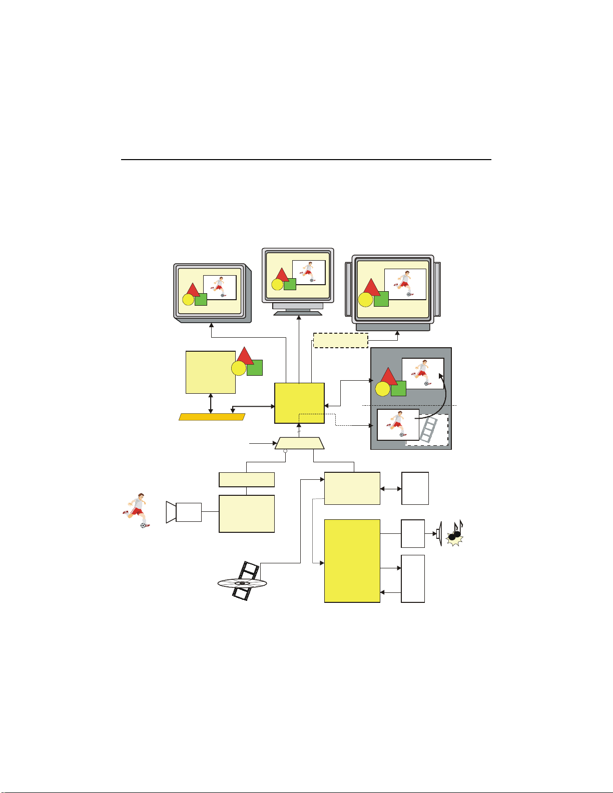
The purpose of the multimedia core is the coordination of sound, video stream, and
computer graphics with the mouse, touchscreen, and the keyboard input. The board
supports specialized sub-systems and connections designed to provide the multimedia
delivery of all this information coming from different sources.
Flat Panel
System Stream Source Se lection
Register #3 - bit 1 and bit 7
Extern al V ideo Sourc e
V-Port Connect.
Video
Inter fac e
(VI P e r -3 8 0)
VGA-RGB
Video
Controller
V-Port
NT S C In terfa c e
(Optional)
Onboard MPEG
MPEG-1
Hardware
Decoder
Pro
Controller
NTSC
MPEG
Buffer
(512KB)
Line
Out
Wavetable
VGA-RGB
Display
Memory
Off Screen
Memory
12-1
Page 56

PCI-934 T echnical Reference M anual
Software Applications
These are data (text, picture, sound from games, MPEG software decoding, ...)
provided by an application running on the computer.
Softwa re applica tions are under the supervi sion of the process or. The mor e there are
appli cations running, the more the process or is busy and s ystem resources d ecrease.
Video Stream
Thanks to the onboard MPEG hardware decoder, running a multimedia stream through
this path would not take up more than 20% of the CPU bandwidth. During this time,
the MPE G decod er receives in formation from the IDE device, decompresses and splits
off the audio and video data that is sent to the SoundBlaster™ Pro controller and to the
video control ler.
Sound Controller
It is built around the AD1816-SoundPort
sound stream through a serial path (I
state digital wavetable that enables the PCI-934 to provide CD-quality audio output.
®
controll er. Th e M PEG decod er tran sfer s th e
2
S). The sound controller is associated to a solid
The wavetable provides a MIDI interpreter, synthesis engine, effect processor, with
1MB sample ROM. It features general MIDI samples set including 128 melodic
instruments and 47 percussion sounds. The synthesis engine can generate up to 32
simultaneous notes. Digital reverberation and chorusing effects are included.
V-Port Support
The implementation of the V-Port interface allows the board to provide live-video
previ ew/cap ture, TV-in -a-window, video c onferencin g, or extern al hardwar e-assisted
MPEG. This interface allows off-loads video bandwidth from the PCI bus by
transferring the video stream directly into the display memory, bypassing the CPU.
The vid eo data source may be selected fr om the onboard MPEG decoder or an external
video source through the Register #3 - bit 1 and bit 7 (See Section 13.3 I/O
Addresses).
12-2
Page 57
Exploring the Multimedia Capabilities of the Board
PCI-934SB
C
12.1 VIDEO FEATURES
12.1.1 FLAT PANEL DISPLAY
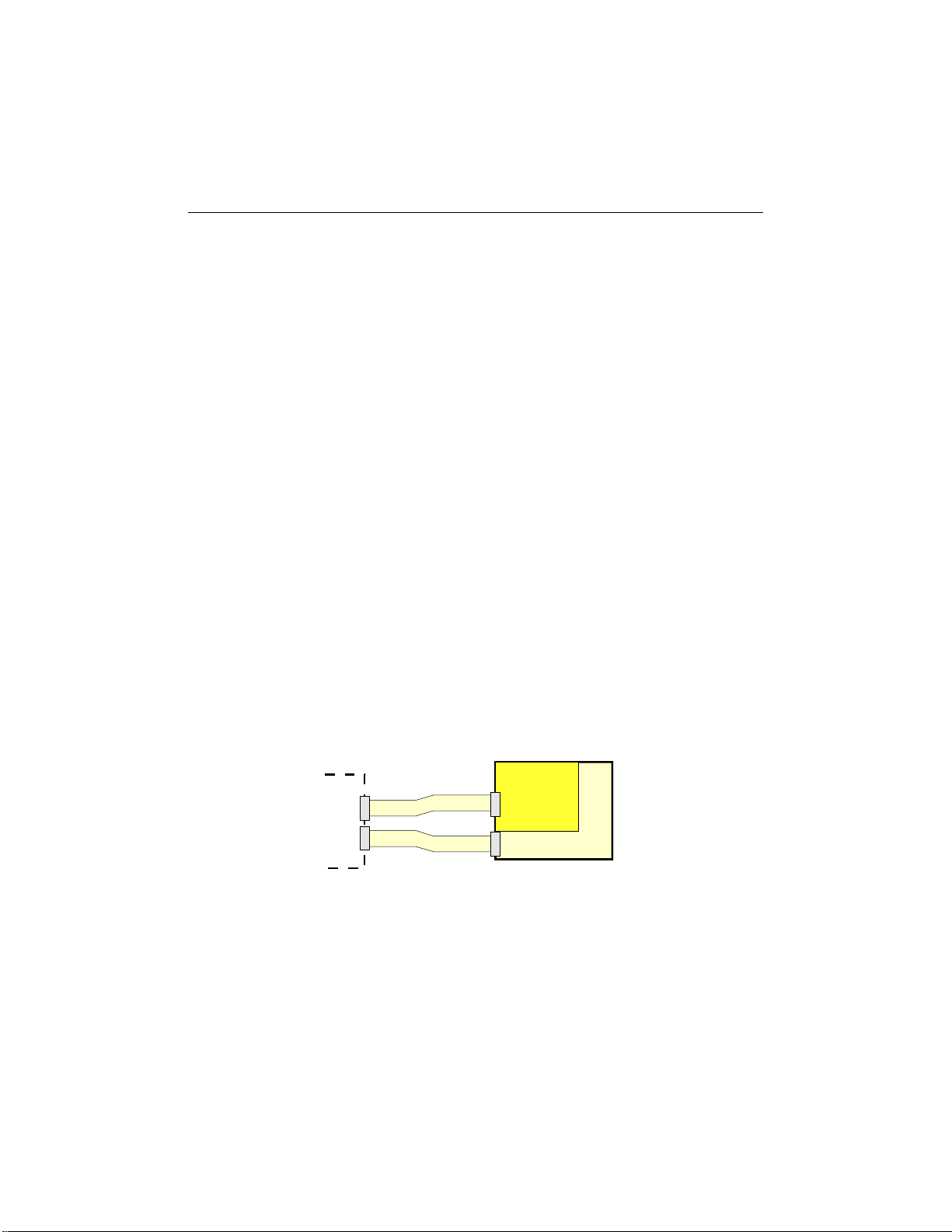
The onboard flat panel interface provides two connectors which output digital data to drive
panels up to 1024x768 pixels (XGA). The two connectors are described below:
J9 Provides direct connection for 18 and 24 bits TFT and DSTN flat panels
(640x480 and 800x600 display modes).
J1 When used simultaneously with J9, this connector provides direct connection
for 36 bits TFT and DSTN flat panels (1024x768 display mode).
§ Characteristics
Supported display modes are:
640x480 - VGA: TFT and DSTN flat panel types at up to 16M colors
800x600 - SVGA: TFT and DSTN flat panel types at up to 16M colors
1024x768 - XGA: TFT and DSTN flat panel types at up to 64K colors
§ Connection
640x480 and 800x600 flat panel connects directly to J9, using an 18 inches maximum
length flat cable with a 50-pin female header at one end, and an adequate connector,
adapted to the flat panel model at the other end.
1024x768 flat panel requires an additional cable connected to J1. This extra cable must
be 18 inches maximum length, and provide a 26-pin dual-row female header at one
end, and an adequate connector, adapted to connector of the flat panel model at the
other end.
Standard Connection for VGA and SV GA Display
J20
J1
Extra Connection for X GA Displa y
VGA
SVGA
&
XGA
The PCI-934 board supports many different types of Flat Panel displays. TEKNOR has
fully tested a number of these panels and provides all the BIOS software support and
the technical information needed to properly interface your PCI-934 board with your
selected Flat Panel display.
12-3
Page 58

PCI-934 Technical Reference Manual
§ Downloading Files From the TEKNOR Web Site
If you have access to the Internet, many video BIOS files in a binary format and
related interconnection charts in a PDF format are available on our web site. You can
download these files, if you are a customer of TEKNOR and have a password from
TEKNOR. If you do not have your password, contact TEKNOR’s Technical Support
to obtain it.
To download a video BIOS file or its interconnection chart file, follow this procedure:
1. Access the TEKNOR web site. Our address is http://www.teknor.com .
2. Go to the Support & Services section.
3. Scroll down the list of products until you find the name of your board and click on
it. This selection is a link to the board’s support area.
4. Click on the Video BIOS link.
5. The list of tested Flat Panel displays appears. If you find your particular display,
you can then ask to download the associated BIOS or interconnection chart files
by clicking the appropriate link.
6. A pop-up window appears. You must enter your password (case sensitive) and
click the SUBMIT button. Entering your e-mail address is optional. Follow the
instructions in subsequent pop-ups to download the file.
§ More Available From TEKNOR
If you do not have access to our web site, or if you do not see the name of your Flat
Panel display on our site for your specific TEKNOR board, then you need to contact
TEKNOR’s Technical Support department. Since we are always testing new flat
panels, it is possible that we have tested your particular type of panel display. Even if
we have not tested it, TEKNOR’s Technical Support can do it for you and supply the
video BIOS and the technical information you need.
12-4
Page 59

Exploring the Multimedia Capabilities of the Board
§ BIOS File
The BIOS files are self-extracting files (VXX_XXX.EXE), each including two files:
the flat panel BIOS file (VXX_XXX.BFP) and a DOS text file (VXX_XXX.DOC) for
the BIOS update utility program.
The letters which form the BIOS name are made up of the following parts:
V XX _ XX X
Video Video Version Revision
BIOS Controller
Once you have the correct video BIOS file, you need to copy the video BIOS file to
your board’s Flash BIOS device. This is done with the BIOS update utility program;
see Section 14 to learn how to perform a video BIOS file update with this TEKNOR
utility.
§ Technical Information File
The related technical information file, which includes the interconnection chart, is a
PDF (Portable Document Format) file. The name of this file identifies the Flat Panel
and the TEKNOR board with its video controller.
Note:
The column labeled EXTERNAL in the Display Interconnection table of the PDF file
refers to the external circuitry or supplies which are needed in certain cases. This is
usually an external power supply or an inverter frequently used in the clock circuit
“SHFCLK” (in the case of V
LCD
and V
, consult the manufacturer’s flat panel data
ADJ
sheet for the actual voltage). An inverter is shown as . When no special
circuits are shown in this column, connections are direct.
12-5
Page 60

PCI-934 Technical Reference Manual
12.1.2 CRT DISPLAYS
The PCI-934 board supports VGA (16M colors), SVGA (16M colors), and XGA (64K
colors) standards, and 1280x1024 (256 colors) resolution mode display.
The CRT display connects directly to the standard D-SUB 15-pin male connector located at
the edge bracket of the board.
§ CRT only Display Mode
To setup your system for CRT display only configuration, set the CRT & LCD option
to “CRT Only” in the Standard CMOS Setup screen.
§ Flat Panel Only Display Mode
To setup your system for flat panel display only configuration, set the CRT & LCD
option to “LCD Only” in the Standard CMOS Setup screen.
§ Simultaneous Display Mode
CRT and flat panel displays may be used simultaneously when enabling this mode
using the BIOS setup program.
The only restriction when using this mode: both the CRT and the flat panel must be at
the same resolution (1024x768 max.).
To setup your system to use both flat panel and CRT displays, set the CRT & LCD
option to “Both” in the Standard CMOS Setup screen.
12-6
Page 61
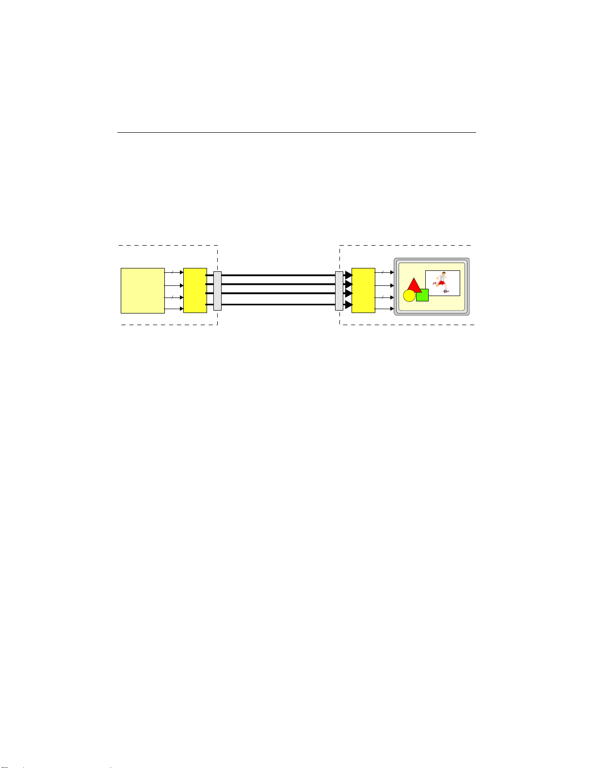
Exploring the Multimedia Capabilities of the Board
FlatPanelDisplayPCI-934SB
C
12.1.3 PANELLINKTM INTERFACE
The board provides a low voltage differential signal (LVDS) implemented through the
PanelLinkTM technology. The major advantage of this high-speed interface is to enable a
flat panel display to be connected at up to 30 feet from the board using a 3 data pairs and a
clock pair cable.
The onboard Panel Link interface may be represented as follows:
LCD Display
Video
Controller
PanelLink
Transmitter
Data
24
DE
Ctrl
6
Clk Clk
J2
Data 3 pairs
Clock 1 pairs
PanelLink
Receiver
DE
Data
24
Ctrl
6
§ Characteristics
The Panel Link is capable of supporting true colors XGA Active Matrix Liquid Crystal
Display panels. DSTN with VGA and SVGA resolutions is also possible.
The transmitter takes parallel video/graphics data from the video controller and
transmits it serially to a PanelLink receiver at 195MB/sec.
Full color (up to 16.7M colors/pixel for 640x480 and 800x600 resolutions), highresolution (64K colors for 1024x768 resolution) Active matrix liquid crystal displays
at 65MHz pixel clock are supported.
§ Connection
Connecting a flat panel through the Panel Link connector (J2) requires a Panel Link
receiver interface. This interface decodes the serial data and transmit it in parallel to
the flat panel, through an 8-pair cable and a 20-pin dual-row female header at one end,
and an adequate connectors at the other end for the flat panel display connection.
The cable length is 6 feet with twisted flat cable, and can be increase to 30 feet using
high performance individually shielded-pair cable.
§ Settings
The amplitude of the differential signal is adjusted using the BIOS setup program
(BIOS Feature Setup – PanelLink Adjustment option). Higher amplitude provides a
better noise immunity but generates more EMI.
The parameter (0-15) should be adjusted to the smallest acceptable value.
12-7
Page 62

PCI-934 Technical Reference Manual
12.1.4 NTSC
Video signals are provided to support a future TV-OUT extension for a connection to a
CRT monitor via a composite encoder module.
§ Characteristics
Due to the differences in the standard between PC displays and CRT monitors, the
NTSC output depends on of the PAL/NTSC encoder. It may not work in all graphic
modes.
Please refer to your encoder documentation
§ Connection
Please contact the Technical Support Department for more information.
12.1.5 VGA INTERRUPT
The video controller can generate an interrupt request (INTR) signal to indicate that the
controller has reached the end of an active field (VSYNC pulse to the CRT monitor).
The interrupt can be connected to and available on the PCI bus INTB line for any PCI
devices connected on the bus, or the interrupt can generate an ISA interrupt request.
§ Settings
To enable the VGA interrupt, install the jumper W12.
To connect the interrupt request to the PCI INTB line, install the jumper W9.
12-8
Page 63

Exploring the Multimedia Capabilities of the Board
12.1.6 V-PORT
The V-Port provides a dedicated video path to the display memory. It is intended to support
either a source of live video incoming from an external video source or a MPEG play back
from the onboard MPEG decoder.
§ Characteristics
The interface supports AccuPack or compressed YUV color space format when
bandwidth of display memory is limited. The compression/decompression is
transparent to the application software. The video data rate through the V-Port path is
independent from the surrounding video graphics. Normally, any video loaded through
the V-Port is on the top of the surrounding graphics but color key support allows the
graphics to occlude the video window with insignificant or loss of video performance.
The V-Port accepts video data at the rate of the original video data and stores it in
display memory either in compressed format or directly. As the data transfer rate can
be different (and typically lower) that the rate at which the display device is operating,
the data can be simultaneously read out from the frame buffer and displayed at the
display device rate with real time decompression and transparently to the application
software.
§ Connection
The V-Port interface is available through the J11 connector. This connector is located
so it can be combined with the PC/104 connectors (P1/P2) to receive a stackable 8-bit
interface for PC/104 form factor products.
A Video Camera Interface PC-104 module is provided by TEKNOR for live video
inputs (NTSC, PAL, or S-video formats). It is referred to as TEK-380.
12-9
Page 64

PCI-934 Technical Reference Manual
12.2 AUDIO FEATURES
Audio features are provided by the SoundPort chip (AD1816A from Analog Devices),
plug and play multimedia audio subsystem, implemented to process multiple digital
streams of 16-bit stereo audio requirements.
The chip maintains full legacy compatibility with applications written for SoundBlaster and
AdLib, while servicing Microsoft PC 97 application requirements.
Provided features are:
12.2.1 LINE IN
§ Characteristics
Stereo analog input (left/right): each channel can be independently gained or
attenuated from +12dB to -34.5dB in 1.5dB steps. The left and right Line In signals
can be mixed in the analog domain with left and right Line Out signals.
§ Connection
Line In signals connect directly through the J23 Jack connector located on the edge
bracket.
12.2.2 LINE OUT
§ Characteristics
The analog stereo output can be post mixed with any of the analog input signals (Line
In, CD, Mic In). The summed analog signal enters the volume stage where each
channel of the Line Out can be muted or attenuated from 0dB to -46.5dB in 1.5dB
steps.
§ Connection
Line Out signals are available through the J21 Jack connector located on the edge
bracket. The same signals are also available on the Audio I/O connector (J18, pins 13
and 14).
12-10
Page 65

Exploring the Multimedia Capabilities of the Board
12.2.3 MIC IN
§ Characteristics
Mono microphone input: Electret type are supported by default, for dynamic
microphone utilization, please refer to the factory. The analog signal can be either line
level (Line In) or -20dB attenuated from line level, the difference is made up through a
software controlled -20dB gain stage.
The microphone input may be processed for conversion or gained/attenuated from
+12dB to 34.5dB in 1.5dB steps then mixed with left and right Line Out signals before
the volume stage.
§ Connection
The microphone connects directly to the board through the J22 Jack connector located
on the edge bracket. The microphone signal can also be input via the Audio I/O
connector (J18, pin 9).
12.2.4 CD IN
§ Characteristics
Stereo CD-ROM input: each analog channel can be independently gained or attenuated
from +12dB to -34.5dB in 1.5dB steps. The left and right CD In signals can be mixed
in the analog domain with left and right Line Out signals.
§ Connection
The CD-ROM connects directly to the board through the J17 onboard connector.
The board provides a standard 4-pin male connector. To connect a CD-ROM use the
CD-ROM manufacturer cable.
12-11
Page 66

PCI-934 Technical Reference Manual
12.2.5 AUDIO I/O CONNECTOR
§ Characteristics
The Audio I/O connector provides extra multimedia inputs and outputs connections:
AUX1 Stereo audio connector for a video input: left and right signals can be
gained and attenuated from +12dB to -34.54dB in 1.5dB steps and mixed
with the Line Out signals.
AUX2 Stereo audio input: left and right signals can be gained and attenuated from
+12dB to -34.54dB in 1.5dB steps and mixed with the Line Out signals.
OUT Stereo audio output: same signals as the Line Out signals provided on the
J21 Jack connector.
MIC Mono microphone input: same signal as the Mic In signal provided on the
J22 Jack connector.
§ Connection
This connector is provided for customized implementation. The cable must be adapted
to the system configuration: It must provide a 14-pin dual-row female header at one
end and the adequate connectors, adapted to each device connector.
12.2.6 SPEAKER TO LINE OUT
By default, system PC speaker sounds are provided on both the Multi-I/O connector (J5)
and the audio Line Out jack (J21).
To output system PC speaker sounds through the Multi-I/O connector only, use the BIOS
setup program to disable this option.
The stereo sound path still remains available for multimedia applications.
12-12
Page 67
SOFTWARE DESCRIPTION
13. BIOS SETUPS
14. UPDATING THE BIOS WITH UPGBIO S
15. VT100 MODE
Page 68
13. BIOS SETUPS
The PCI-934 uses the AWARD Setup program, a setup utility in EEPROM that is accessed
by pressin g the DELETE key at th e appr opriat e time dur ing system boot. Th is utili ty is used
to set configuration data in CMOS RAM.
CAUTION
Before modifying CMOS setup parameters, insure that both the battery
and W5 battery jumper are installed. Otherwise use the option ‘Save
CMOS in Flash’ (BIOS Feature Setup screen).
To install the battery jumper, please refer to Section 11 - Setting
Jumpers.
To run the BIOS setup program incor porated in the ROM BIOS:
Turn on or reboot the syste m.
Hit th e DELETE key before or when the m ess age - "PRESS DEL TO ENTER SETUP"
appears near the bott om of the scr een.
The main menu appears on the screen:
ROM PCI/ISA BIOS
CMOS SETUP UTILITY
AWARD SOFTWARE, INC.
STANDARD CMOS SETUP
BIOS FEATURES SETUP
CHIPSET FEATURES SETUP
POWER MANAGEMENT SETUP
PNP/PCI CONFIGURATION
LOAD BIOS DEFAULTS
LOAD SETUP DEFAULTS
Esc : Quit
F10 : Save & Exit Setup
Time, Date, Hard Disk Type...
INTEGRATED PERIPHERALS
SUPERVISOR PASSWORD
USER PASSWORD
IDE HDD AUTO DETECTION
HDD LOW LEVEL FORMAT
SAVE & EXIT SETUP
EXIT WITHOUT SAVING
↑ ↓ → ← : EXIT WITHOUT SAVING
(Shift)F2 : Change Color
13-1
Page 69

PCI-934 T echnical Reference M anual
13.1 USING THE BIOS SETUP PROGRAM
The arrow keys (↑ ↓ → ←) ar e used to h ighl ight i tem s on th e menu and t he Pa geUp and
Pag eDown k eys ar e us ed to chan ge the en try val ues for th e highl ighte d it em. To se lect an
entry, press the Enter key. Also, you can press the F1 key to obtain help information or the
Esc k ey to leave an option, close a menu or to quit the p rogram.
The following table provides more details on how to navigate in the Setup program:
Up arrow (↑)
Down a rrow (↓)
Left arrow (←)
Right arr ow (→)
Esc key In Main Menu: Quit settings (Type ‘Y’ to save changes into CMOS).
PgUp key Increase the numeric value or make changes.
PgDn key Decrease the numeric value or make changes.
+ key Increase the numeric value or make changes.
- key Decrease the numeric value or make changes.
F1 key General help.
F2 and
Shift F2 keys
F4 key Reserved.
F5 key In sub-menu: Restore the previous setup values from BIOS Default
F6 key In sub-menu: Load the default setup values from BIOS De fault Table .
F7 key In sub-menu: Load the setup values from the Setup Default Table .
F8 key Reserved.
F9 key Reserved.
F10 key When in Main Menu: Sa ve all the CMOS changes.
Move to previous item.
Move to next item.
Move to the item in the left hand .
Move to the item in the right h and .
In sub-menus: Exit and return to Main Menu.
Change color from total 16 colors: F2 to select color forward, Shift F2
to select color backward.
Table.
13-2
Page 70

The Main Menu includes the following categories:
BIOS Setups
Standard CMOS
Setup
BIOS Features
Setup
Chipse t Features
Setup
Power Ma na gement
Setup
PnP/PCI
Confi guration
Integ r ated
Peri pherals
Supervisor/User
Password Setting
IDE HDD Au to
Detection
HDD Low Level
Format
This Setup page includes all the items in a standard, ATcompatible BIOS.
This Setup page includes all the items of AWARD’s special
enhanced features.
This Setup page includes all the items of the chipset’s special
features.
This Setup pa ge sets power cons ervation opti ons.
This Setup page sets Plug and Play and PCI Local Bus
configuration options.
I/O sub-systems that depend on the integrated peripherals
controller in your system.
Change, set, or disable password. It allows you to limit access to
the system and the Setup, or just to the Setup .
Automatically detect and configure hard disk parameters. This
ability is included in the event you are uncertain of your hard
disk’s parame ters.
This option does not appear in many BIOS versions. Most
manuf ac t urers of IDE hard drives strong ly recommend that you
do not run a low-level format on their drives, be cause of the
danger that the bad-track table may be over-written. Award
supplies this utili ty for service p ersonnel only .
Load BIOS
Defaults
Load Se tup
Defaults
If you feel you need to run a low-level format on your hard
drive, contact your drive manufacturer for instructions!
The BIOS defaults represent settings that pr ovide the minimum
req uir ement s f o r your system to operate.
The chipset defaults are settings that provide for maximum
system performance.
13-3
Page 71

PCI-934 T echnical Reference M anual
13.2 SAVING CONFIGURATIONS & EXITING AWARD SETUP
Use one of the following options available from the Main Menu:
Save & Exit
Use this option to save the configuration in CMOS RAM. Value
changes are not saved in the Flash EPROM. To update the Flash
memor y, u s e the ‘ BIO S S etu p F eature/Save CMO S in Fla sh ’ option.
Exit Without
Saving
Use this option to exit AWARD Setup without saving the
configuration to CMOS RAM.
13.3 STANDARD CMOS SETUP
This part of the setup allows you to set th e time, da te, h ard dis k type, types of flopp y dri ves
and video type.
Date/Time
Hard Disks
Drive A / Drive B
Video
CRT & LCD
Setup date and time values through the keyboard.
Two IDE controllers are defined: Primary and Secondary. Each
can support two d isks: Master Disk (boo table) or Slave Disk.
Identifies floppy disk types (drive A or B) connected to the board.
Specifies the type of the display adapter card installed in the
system.
Use this option to select within CRT display mode only, Flat panel
mode only, or both CRT and flat panel display.
Halt on
Memory
This option specifies the type of errors that will stop the system
during the BIOS booting procedure. Settings are All errors, No
errors, All but keyboard (default setting), All but diskette and All
but disk/key.
This opti on summarize s the amount of Base, Ext ended an d other
types of memo ry installed in t he system .
13-4
Page 72

BIOS Setups
13.4 BIOS FE ATURE SETUP
BIOS
Option
Virus Warning Dis. Dis. Dis. ; En. When Enabled, occurs a warning message if a program (specifically,
CPU Internal Cache En. En. Dis. ; En. Enables or Disables the CPU Internal Cache.
External Cache Dis. En. Dis. ; En. Enables or Disables the CPU external Cache.
Quick Power On Self
Test
Boot Sequence A, C A, C
Swap Floppy Drive Dis. Dis. Dis. ; En.
Boot Up Floppy Seek Dis. Dis. Dis. ; En. When Enabled, the BIOS tests (seeks) floppy drives to determine
Boot Up NumLock
Status
Boot Up System Speed High High Low ; High Select High to boot at the default CPU speed; select Low to boot at
Typematic Rate Setting Dis. Dis. Dis. ; En. When Disabled, the following two items (Typematic Rate and
Typematic Rate
(Chars/Sec)
Typematic Delay
(Msec)
Security Option Setup Setup Setup ; System If you have set a password, select whether the password is required
OS Select For
DRAM>64MB
Setup
Default
Default
Dis. Dis. Dis. ; En. Select Enabled. to reduce the amount of time required to run the
Off Off On ; Off Toggle between On or Off to control the state of the NumLock key
6 6 6 to 30 char.
250 250 250 ; 500 ; 750
Non-
Non-
OS/2
OS2
Possible
Settings
C, A, SCSI ; C,
CDROM, A ;
CDROM, C, A ; D,
A SCSI ; E, A,
SCSI ;
F, A, SCSI ; SCSI,
A, C ; SCSI, C, A ;
C only ; A, C,
SCSI
per second
; 1000 ms
Non-OS/2 ;
OS/2
Description
a virus ) attem pts to wri te t o th e bo ot s ect or o r th e pa rtiti on t able of
the hard disk drive. This feature protects only the boot sector, not the
entire hard drive.
Note: Many disk diagnostic programs that access the boot
sector table can trigger the virus warning message. If you plan
to run such a program, we recommend that you first disable the
virus warning.
power-on self test (POST). A quick P OST skips certain s teps. We
recommend that yo u normally disable quick POST. It is better to find
a proble m dur i ng POST than lose da ta during your wor k.
The original IBM PCs load the DOS operating system from drive A
(floppy disks), so IBM PC-compatible systems are designed to
search for an opera tin g system fir st on dr iv e A, then on driv e C (hard
disk). However, modern computers usually load the operating
system from th e hard drive, an d ma y e ven lo ad i t fr om a CD -ROM
drive.
This fie ld is eff e ctive only in sy st e ms wi th two f lo ppy dr iv es . Se lect ing
Enabled assigns physical drive B to logical drive A, and physical
drive A to lo g i cal drive B.
whether they have 40 or 80 tracks. Only 360KB floppy drives have
40 tracks; drives with 720KB, 1.2MB, and 1.44MB capacity all have
80 tracks. Because very few modern PCs have 40 track floppy
dri ves, we recommend that you set this fiel d to “Disable d” to save
time.
when the system boots. When toggled On, the nume ric keypad
generates numbers instead of controlling cursor operations.
the speed of the AT bus. Some add-in peripherals or old software
(such as ol d games ) ma y requi re a slow CPU speed. The d efault
setting is High.
Typematic Delay) are irrelevant. Keystrokes repeat at a rate
determined by the keyboard controller in your system. When
Enabled, you can select a typematic rate and a typematic delay.
When the typematic rate setting is Enabled, you can select a
typematic rate (the rate at which characters repeat when you hold
down a key i n a sec on d).
When the typematic rate setting is Enabled, you can select a
typemat i c de lay (t h e de lay bef ore key stro ke s beg i n to re pe at) .
every ti me th e sy s te m bo ot s , or on ly wh en yo u en ter Se tu p.
Select OS2 only if you are running an OS/2 operating system with
greater than 64MB of RAM.
...
13-5
Page 73
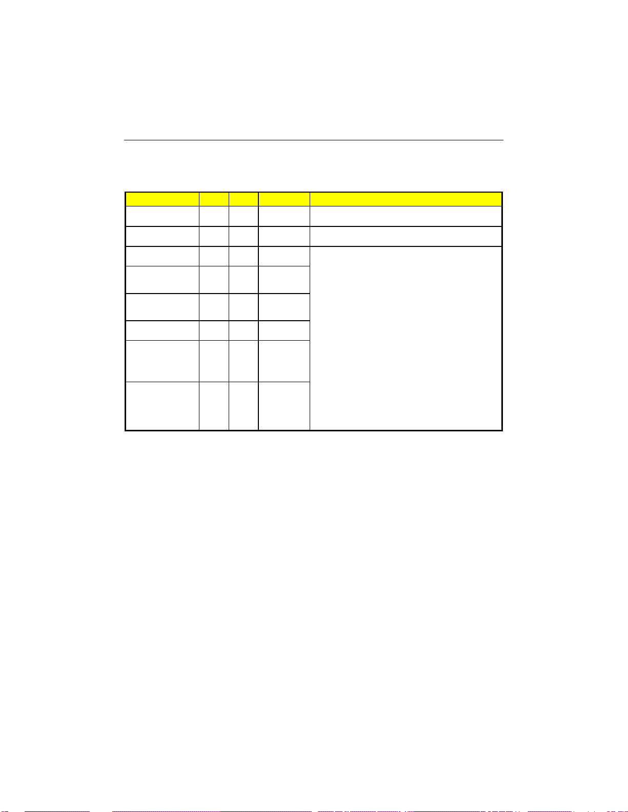
PCI-934 T echnical Reference M anual
BIOS FEATURES SETUP (Continued)
BIOS
Option
Save CM O S also in
Flash
PanelL in k Ad ju st me n t 7 7 0 to 15
Video BIOS Shadow En. En. Dis. ; En. Software that resides in a read-only memory (ROM) chip on a device
CC000-CFFFF
Shadow
D0000-D3FFF Shadow Dis. Dis. Dis. ; En.
D4000-D7FFF Shadow Dis. Dis. Dis. ; En.
D8000-D BF FF Sha do w Dis. Dis. Dis. ; En. BIOS and similar firmware for expansio n peripher al s , but it also
DC000-DFFFF
Shadow
Setup
Default
Default
En. E n. D is. ; E n. W hen enabled , saves the CMOS pa rameters in the Flas h memo ry
Dis. Dis. Dis. ; En.
Dis. Dis. Dis. ; En. Video BIOS shadows into memory area C0000-CBFFF. The
Possible
Settings
Description
which makes them available in the case of a battery failure.
Use this option to control the voltage drive of the PanelLink interface.
Increa se the value to ob ta i n a hi gh er dr iv e v olta ge .
called
such as the system BIOS, video BIOS, and similar operating
instructions that come with some expansion peripherals (for
example, a
SCSI adaptor). Shadowing copies of firmware from ROM into system
RAM, where the CPU can read it through the 16-bit or 32-bit DRAM
bus.
Firmware not shadowed must be read by the system through the 8bit X-bus. Shadowing improves the performance of the system
reduc es t he am ount of high mem ory (640 KB to 1MB ) avail able f or
loadin g de vice dri vers , e tc. E nable s had owing i nto eac h s ecti on of
memory separately. Many system designers hardwire shadowing of
the syst e m BIO S an d e limi n at e a Sy st e m BI OS S ha do w op ti on .
remaining areas shown on the BIOS Features Setup screen may be
occupied by other expansion card firmware. If an expansion
perip he ral i n you r s ys tem c on ta ins ROM -b ase d firmw are, you ne ed
to know the ad d ress ra ng e th e ROM occ up ies t o s ha dow i t i n to t he
correc t are a of R AM.
. The Award BI O S al l o ws sha do wi n g of fir mwa r e
firmware
13-6
Page 74

BIOS Setups
13.5 CHIP SET FEATURES SETUP
BIOS
Option
Auto Configuration En. En. En. ; Dis. Auto Configuration selects predetermined optimal values of chi pset
DRAM Timing 70 ns 70ns 70 ns, 60ns The value in this field depends on performance parameters of the
DRAM RAS
Precharge Time
DRAM R/W Leadoff
Timing
Fast RAS# to CAS#
Delay
DRAM Read Burs t
(EDO/FPM)
DRAM Write Bur st
Timing
Turbo Read Leadoff Dis. Dis. En. ; Dis. Select Enabled to shorten the leadoff cycles and optimize
DRAM Speculative
Leadoff
Turn-Around Insertion Dis. Dis. En. ; Dis. When Enabled, the chipset inserts one extra clock to the turn-around
ISA Clock PCI
System BIOS
Cacheable
Video BIOS Cacheable Dis. En. En., Dis. Selecting Enabled allows caching of the video BIOS ROM at C0000h
8 Bit I/O Recovery
Time
16 Bit I/O Recovery
Time
#
x444/x
Setup
Default
Default
4 4 4 ; 3 S elect the number of CPU clocks allocated for the R ow Address
7/6 7/6 7/6 ; 6/5
3 3 3 ; 2 W hen DRAM is refreshed , both rows an d columns are address ed
x444/x
444
444
x444 x444
Dis. Dis. En. ; D is. A re ad request from the CPU to th e DRAM contr oller inc ludes the
CLK/4
PCI
CLK/4
Dis. En. En., Dis. Selecting Enabled allows caching of the system BIOS ROM at
3 1 1 ; 2 ; 3 ; 4 ; 5 ;
2 1 1 ; 2 ; 3 ; 4 ;
Possible
Settings
x444/x444 ;
x333/x444 ;
x222/x333
x444 ; x333 ;
x222
PCICLK/4 ;
PCICLK/3
6 ; 7 ; 8 ; NA
NA
Description
parameters. When Disabled, chipset parameters revert to setup
info rmation stored in CMOS. Many fields i n this screen are not
available when Auto Configuration is Enabled.
inst alled memor y chips (DRAM) . Do not chang e the valu e from th e
factory setting unless you install new memory that has a different
performance rating than the original DRAMs.
St rob e (RA S#) signal t o ac cum ul at e i ts cha rge before t he DRAM is
refres hed. If i nsuf fici ent time i s a llow ed, ref resh m ay be i ncompl et e
and data lost.
Select the combinatio n of CPU clocks the DRAM o n your board
requires before each read from or write to the memory. Changing t he
valu e from the s etting de termined b y the boar d design er for the
instal l ed DRA M may cause memo r y er rors.
separately. Use this item to determine the transition timing from RAS
to Col u mn A d dress Strobe (CAS).
Sets the timing for reads from EDO (Extended Data Output) or FPM
(Fast Page Mode) memory. The lower the timing numbers, the faster
the syst e m addr e s ses me mory . Se l ect in g ti mi ng number s lower than
the insta l led D R A M is ab l e to supp or t can r e su lt in me mory er r ors.
Sets the timing for writes to memory. The lower the timing numbers,
the faster the system addresses memory. Selecting timing numbers
lower than the installed DRAM is able to support can result in
memory errors.
performance in cacheless, 50-60 MHz, or one-bank EDO DRAM
systems.
memo ry address o f the des ired dat a. When E nabled , Specula tive
Leadof f lets the DRAM co ntroller pa ss the rea d co m ma nd to me mor y
sightly before it has fully decoded the address, thus speeding up the
read process.
of back-to-back DRAM cycles.
You can set the speed of the AT bus at one-third or one-fourth of the
CPU clock speed.
E0000h-FFFFFh, resulting in better system performance. However,
if any program writes to this memory area, a system error may occur.
to C8FFFh, resulting in better video performance. However, in any
progra m wr it e s to th is me mor y area, a syst e m err or may o ccur.
The I/O recover y mechan ism adds bus cl ock c ycles betwee n PCIoriginated I/O cycles to the ISA bus. This delay takes place because
the PCI bus is so much faster than the ISA bus. These two fields let
you add re cov ery t i me (i n bu s clo c k cyc le s) for 16 - b it and 8-b it I/O .
...
13-7
Page 75

PCI-934 T echnical Reference M anual
CHIPSET FEATURES SETUP (Continued)
BIOS
Option
Peer Concurrency En. En. En. ; Dis. Peer concurrency means that more than one PCI device can be
Chipset Special
Features
DRAM ECC/PARITY
Select
Memory Parity/ECC
Check
Single Bit Error Report En. En. En. ; Dis. If ECC is enabled, selecting Enabled here tells the system to report
L2 Cache Cacheable
Size
Chipset NA# Asserted
Pipeline Cache Timing Faster Faster Faster ;
Passive Release En. En. En. ; Dis. Select Enabled, to allow CPU to PCI bus accesses during passive
Delayed Transaction Dis. Dis. En. ; Dis. The chipset has an embedded 32-bit posted write buffer to support
Memory Hol e Lo c at i on None None
Supervisor I/O Base
Addr.
Setup
Default
Default
Dis. En. En. ; Dis. When Disa bled, the c hipset beh aves as i f it we re the e arlier Intel
Parity Parity ECC ; Parity Set this option according to the type of DRAM installed in your
Auto Auto En. ; Dis. ;
64MB 64MB 64MB ; 512MB Select 512MB only if your system RAM is greater than 64MB.
En. E n. En. ; Dis. Selecting Enabled allows pipelining, in which the chipset signals the
190h 190h 190h ; 290h ;
Possible
Settings
Auto
Fastest
512K-64 0 K ;
15M-16M ;
None
390h
Description
activ e at a time .
82430FX ch ip se t.
system: error-correcting code (ECC) or parity (default).
In Auto mode, the BIO S enables memory ch ecking aut omatically
when it detects the presence of ECC or parity DRAM.
an error (NMI) when a correctable single-bit error occurs.
When dis a ble d, a single-bi t e rro r w ill be correct ed but not reported.
Use this option if your operating system does not support ECC error
scrubing.
CPU for a new memory address before all data transfers for the
current cyc l e are co mp l et e, res u lt ing i n fa s ter per f or ma nc e.
For a secondary cache of 256KB (one bank), select Faster. For a
seco ndary cach e of 512KB (two ba nks ), selec t Fast (3-1- 1-1, 2 -1-1 -
1) or Fastest (3-1-1-1, 1-1-1-1). Cache timing 3-1-1-1 is at the CPU
access speed. It requires special SRAMs because the 3-1-1-1 timing
is at the CPU clock rate.
release otherwise the arbiter only accepts another PCI master
access to local DRAM.
delay transactions cycles. Select Enabled to support compliance with
PCI versio n 2. 1.
You can reserve this area of system memory for ISA adapter ROM.
When this area is reserved, it cannot be cached. The user
information of peripherals that need to use this area of system
memory usually discusses their memory requirements.
This pa rameter must reflect the j umper set tings for TEKNOR I/ O
Base Po r t.
13-8
Page 76

BIOS Setups
13.6 POWER MANAGEMENT SETUP
BIOS
Option
Power Management Dis. Dis. Min Saving ;
PM Control by APM Yes Yes Yes ; No
Video Off Method V/H
Modem Use I RQ NA NA NA ; 3 ; 4 ; 5 ;
PM Timers The fol lowin g modes are Green P C pow er s aving funct ions. The y
Doze Mode Dis. Dis. 1 - 40 min
Standby Mode Dis. Dis. 1 - 40 min
Suspend Mode Dis. Dis. 1 - 40 min
HDD Power Do wn Dis. Dis. 1 - 15 min After the selec te d period of drive inactiv ity (1 to 15 min), the hard
Thermal Management Dis. Dis.
CPU Low Temp. 58 58
CPU Overheat 64 64
CPU Temperature varies varies
SYNC
Default
+
Blank
Setup
Default
V/H
SYNC
+
Blank
Possible
Settings
Max Saving ;
User Define,
Dis.
V/H SYN C +
Blank ;
DPMS ;
Blank Screen
7 ; 9 ; 10 ; 11
1 hour ; Dis .
1 hour ; Dis .
1 hour ; Dis .
En. ; Dis. When enabl ed, CP U temp era ture is monito red . Whene ver the CP U
30 to 60 The CPU will run at full speed when it is at the selected temperature
40 to 70 The CPU will be slowed down when it reaches the selected
varies Display the current CPU temperature, when Thermal Management
This option allows you to select the type (or degree) of power saving
for Doze, Standby, and Suspend modes.
Max Saving: Maximum power savings. Inactivity period is 1 minute in
each mode .
Min Saving: Minimum power savings. Inactivity period is the
maximum settin g in each mo de (1 hour f or Doze, Sta ndby and
Suspend).
User Define : Set eac h mo de in divi duall y. S elec t ti me -out p erio ds in
the PM Timers section (see b elow).
If Advanced Powe r Mana gem en t (APM ) is i ns talled on yo ur s ys tem ,
selecting Yes gives better power savings. This enables power
manage me nt co ntr o l by an ex ternal progr a m (g en era l ly the oper at i ng
system).
Determines the manner in which the monitor is blanked.
V/H SYNC + Blank: System turns off vertical and horizontal
synchronization ports and writes blanks to the video buffer.
DPMS Support: Select this option if your monitor supports the
Display Power Management Signaling (DPMS) standard of the
Video Electronics Standards Association (VESA). Use the
software supplied for your video subsytem to select video
management values.
Blank Screen: System only writes blanks to the video buffer.
Assignes the IRQ line to the modem (if any) on your system. Activity
of the selected IRQ always awakens the system.
are user-configurable only during User Defined Power Management
mode.
After the selected period of system inactivity (1 minute to 1 hour), the
CPU clock runs at lower speed while all other devices still operate at
full speed.
After entering Doze mode, when the selected period of system
inacti vity p rior to Stand by mode (1 mi nute t o 1 ho ur) has elaps ed,
the fixed disk drive and the video shut off while all other devices still
operate at full speed.
Afte r enteri ng Sta ndby m ode, w hen the selec ted pe riod of s ystem
inac tivity prior to Suspen d m ode (1 minute to 1 hour) has elapsed, all
devices except the CPU shut off.
disk driv e po wers down wh il e a ll ot her devices re ma in ac t ive.
overheats, it slows down to lower the temperature
or lower.
temperature or higher. Full speed will be resumed when the
tempera ture come s down t o th e sel e ct ed ‘C PU Low Temp.’.
option i s en ab led and after the system has be en re bo ot e d.
Description
...
13-9
Page 77
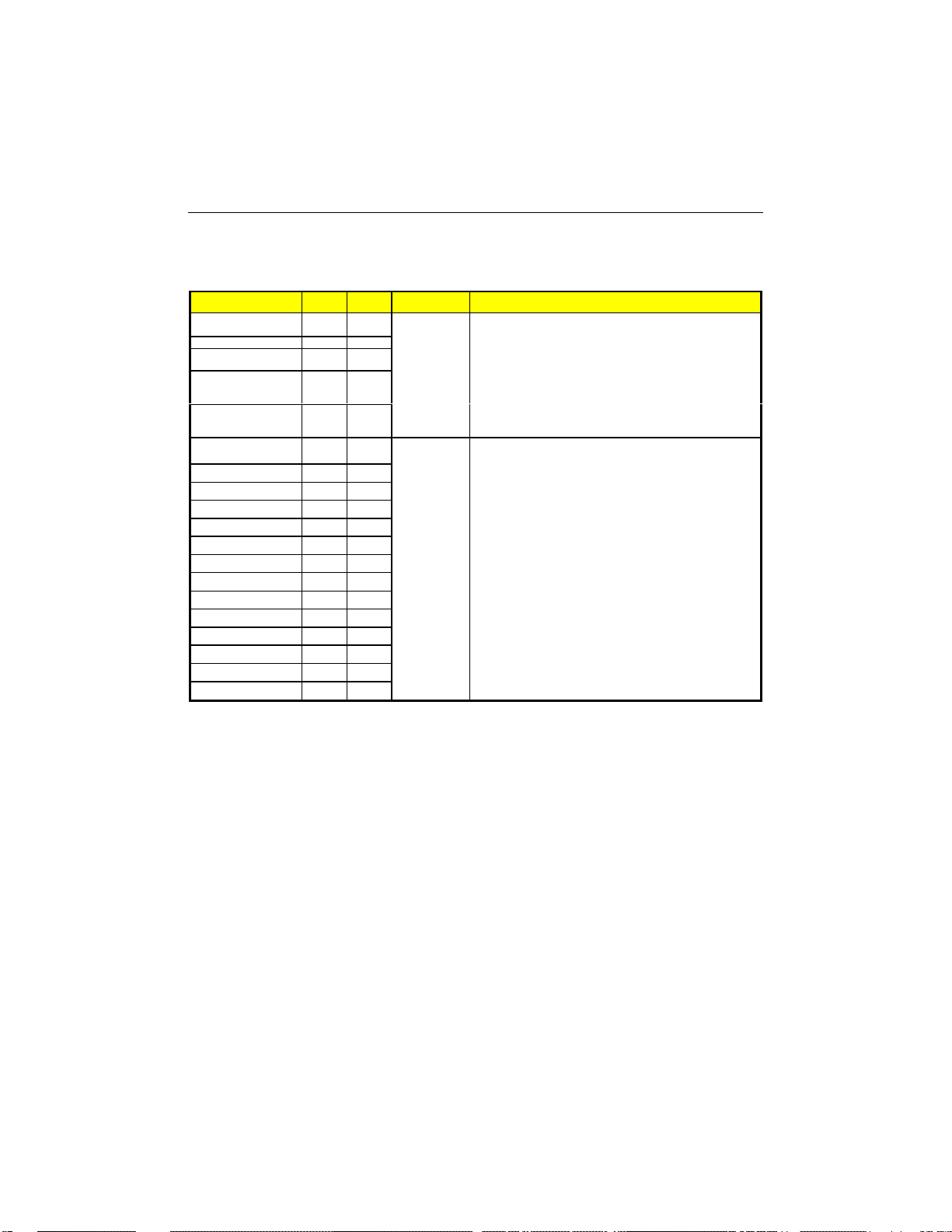
PCI-934 T echnical Reference M anual
POWER MANAGEMENT SETUP (Continued)
BIOS
Option
Wake Up Events
IRQ3 Off On system.
IRQ4 Off On The default wake-up event is keyboard activity. In these wake-up
IRQ8 Off On F or exam ple, if you have a modem on IR Q3, you ca n tur n on IRQ 3
IRQ12 Off On system. Or you may wish to turn Off IRQ12 (the PS/2) mouse as a
Power Down and
Resume Ev ent s
IRQ3 (COM 2) Off On
IRQ 4 (COM 1) Off On
IRQ 5 (LPT2) Off On
IRQ 6 (Floppy Disk) Off Off
IRQ 7 (LPT 1) Off On
IRQ 8 (RTC Alarm) Off Off
IRQ 9 (IRQ 2 Redir) Off On
IRQ 10 (Reserved) Off On
IRQ 11 (Reserved) Off On
IRQ12 (
IRQ 13 (Coproc.) Off On
IRQ 14 (Hard Disk) Off On
IRQ 15 (Reserved) Off On
PS/2 Mouse
)
Default
Off On
Setup
Default
Possible
Settings
On, Of f In Doze or Standby mode, you may disabl e activity monitoring of
On, Off You may disable monitoring of common interrupt requests so they
some common interrupt requests so they do not wake up the
event fie l d s, you can turn On or Off f our co mmo nly used interrupts.
as a wake -up event , so an i nt errup t f rom th e mo dem c an wake up
the
wake-up event, so accidentally brushing the mouse does not
awaken the system.
do not reset activity timers.
Description
13-10
Page 78

BIOS Setups
13.7 PNP/PCI SETUP
BIOS
Option
PNP OS Installed No No Yes ; No If the operating system (OS) is Plug-and-Play, select ‘Yes’ if you
Resources ControlledByAuto Man. A uto ; Manual The Award Plug and Play BIOS can automatically configure all the
Reset Co nf iguration
Data
IRQ n Assigned To
(n=0, 1, 3, 5, 6, 7)
DMA n Assigned To
(n=3, 4, 5, 7, 9, 11, 12,
13, 14, 15)
PCI IRQ Act iv at ed By Level Level Level ; Edge
PCI IDE IRQ Map To PCI-
Primary IDE INT
Secondary IDE INT
Used Mem Base
Address
Used Mem Length - - 4K, 16K, 32K,
#
#
Setup
Default
Default
Dis. Dis. En. ; Dis. Normally, you leave this field Disabled. Sele ct En. to reset Extended
PCI-
Auto
Auto
A A A ; B ; C ; D Each PCI peripheral connection is capable of activating up to four
N/A N/A
Possible
Settings
PCI/ISA PnP ;
Legacy ISA
PCI/ISA PnP ;
Legacy ISA
PCI- Auto; ISA;
PCI-SLOT1;
PCI-S LO T2 ;
PCI-S LO T3;
PCI-S LO T4
NA ; C800 ; CC00
; D000 ;
D400 ; D800 ;
DC00
64K
Description
want the OS to allocate resources according to PnP standards, or
‘No’ if you want th e same r esou rce all ocati on at e very s ystem bootup. Sele ct ‘No ’ when the O S is no t P nP (f or example DOS ).
boot and Plug an d Play-com patible devi ces. If you select Aut o, all
the interrupt reques ts (IRQs) and DMA assig nment fields disappear,
as the BIOS automatically assigns them.
System Co nf ig u rati o n Data (ES CD ) wh en yo u e xit Set up if you ha ve
instal led a new add-on and th e syst em recon figurati on has ca used
such a serious conflict that the operating system cannot boot.
When resources are controlled manually, assign each system
interrupt as one of the following types, depending on the type of
device using the interrupt:
Legacy ISA
speci fication , requirin g a specific interrup t (such as IRQ 4 for serial
port 1).
PCI/ISA
whether de s i gn ed for PCI or ISA bus ar chi te c tur e.
When r eso u rces a r e c on t roll ed m an ually, assi gn e ach system DMA
chann el as one of the f ollowing ty pes, depend ing on the type of
device using the interrupt:
Legacy ISA
specification, requiring a specific DMA channel.
PCI/ISA
whether de s i gn ed for PCI or ISA bus ar chi te c tur e.
Leave the IRQ trigger set at
the inter ru pt spe c if ie s E dg e-triggere d i nt errupts.
This fi eld lets you select P CI IDE IR Q mapping or PC AT (ISA)
interrupts. If your system does not have one or two PCI IDE
connectors on the system board, select values according to th e type
of IDE interface(s) installed in your system (PCI or ISA). Standard
ISA interrupts for IDE channe l s are IRQ1 4 for primar y and IRQ1 5 for
secondary.
inte rrupts : INT# A, INT# B, INT# C and INT# D. B y defaul t, a P CI
connection is assigned INT# A. Assigning INT# B has no meaning
unles s the peri pheral d evice re quires tw o inter rupt se rvices r ather
than just one. Because the PCI IDE interface in the chipset has two
channels, it requires two interrupt services. The primary and
seco ndary IDE IN T# fields default to values appropriate for two PCI
IDE c hannels, w ith the pr imary PCI IDE channe l having a lower
interrupt than the secondary.
Select a base address for the memory area used by any peripheral
that requires high memory.
Select a length for the memory area specified in the previous field.
This field does not appear if no base address is specified.
Devices compliant with the original PC AT bus
PnP Devices compliant with the Plug and Play standard,
Devices compliant with the original PC AT bus
PnP Devices compliant with the Plug and Play standard,
unless the PCI device assigned to
Level
13-11
Page 79

PCI-934 T echnical Reference M anual
13.8 INTEGRATED PERIPHERALS SETUP
BIOS
Option
IDE HDD Block Mode Dis . En. En. ; Di s. Bl ock mode is also call ed block transfe r, multipl e comm ands, or
PCI Slot IDE 2nd
Channel
On-Chip
Primary / Sec o nd ar y PCI
IDE
IDE
Primary / Sec o nd ar y,
Master/Slave PIO
USB Co ntroller En. En. En. ; Dis.
Onboard FDC
Controller
Onboar d Ser i a l Por t s 1
and 2
Serial Port 2 mode
VT100 Mo de on Ser i a l
Port
Onboard Parallel Port
Parallel Port Mode
ECP Mode Use DMA 3 3 1, 3 Select a DMA channel for the port.
RS-232 RS-232 RS-232 ; RS-422 ;
378/IRQ7378/IRQ
EPP 1.9
Setup
Default
Default
En. En. En. ; Dis.
En. En. En. ; Dis.
Auto Auto Mode 0, 1, 2,
En. En. En. ; Dis.
Auto Auto Dis. ;
ECP+
ECP+
EPP1.9
7
Possible
Settings
3, 4, Auto
3F8/IRQ4 ;
2F8/IRQ3 ;
3E8/IRQ 4 ;
2E8/IRQ 3 ;
Auto
RS-485
1 ; 2 Select a se rial por t to communi cate in V T100 m ode wi th a remote
378h/I RQ 7 ;
278h/I RQ 5 ;
3BCh/IRQ7 ;
Dis.
ECP+EPP1.9 ;
Normal,
EPP1.7 + SPP ;
ECP+EPP1.7 ;
SPP ;
EPP1.9 + SPP ;
ECP
Description
multiple sector read/write. If your IDE hard drive supports block
mode (m ost new dri ves do ), selec t En abl ed f or au toma tic detec ti on
of the optimal number of block read/writes per sector the drive can
support.
You may separately disable the second channel on an IDE interface
instal led in a PCI expansion sl ot .
The i ntegrat ed pe ripher al cont roller contai ns a n ID E int erface wit h
support for two IDE channels. Select Enabled to activate each
channel se par at e ly .
The four IDE PIO (Pr ogr a mme d Inp ut/Output) field s let yo u set a PIO
mode (0-4) for each of the four IDE devices that the onboard IDE
interface supports. Modes 0 through 4 provide successively
increased performance. In Auto mode, the system automatically
determines the best mode for each device.
Select Enabled if your system contains a Universal Serial Bus (USB)
controller and you have USB peripherals.
Select Enabled if your system has a floppy disk controller (FDC)
installed on the system board and you wish to use it. If you install an
add-in FDC or the system has no floppy drive, select Disabled in this
field.
Select a logical COM port name and matching address for the first
and second serial ports.
Communication mode selection for Serial Port 2.
computer. See VT10 0 Mo de se ction.
Select a logical LPT port name and matching address for the
physical parallel (printer) port.
Select an operating mode for the onboard parallel port. Select ECP
or EPP unless you are certain bo th your hardware and softw are
does not su pp ort EPP or EC P mode .
13-12
Page 80

14. UPDATING THE BIOS WITH UPGBIOS
14.1 UPDATING THE BIOS
UPGBIOS is an utility that allows you to take BIOS files from a disk and update the Boot
Block Fla sh BIOS with them.
The command line format is as follows:
UPGBIOS [/ALL filename] • [/VGA VGA_filename] • [/?]
[/h]
where:
filename
is the name of the 256KB BIOS file containing all BIOS files.
The .BIN extension is used for all BIOS files in a single file.
VGA_filename
or
?
h
Please note that the UPGBIOS utility pr ogram is presently in development. A complete
version of UPGBIOS is upcoming.
is the na m e of the 64KB file (or less) cont a i ning the vi deo
BIOS.
It will accept various extensions: .VGA, .BFP (flat panel), ...
displays instructions on using the UPGBIOS program.
14-1
Page 81
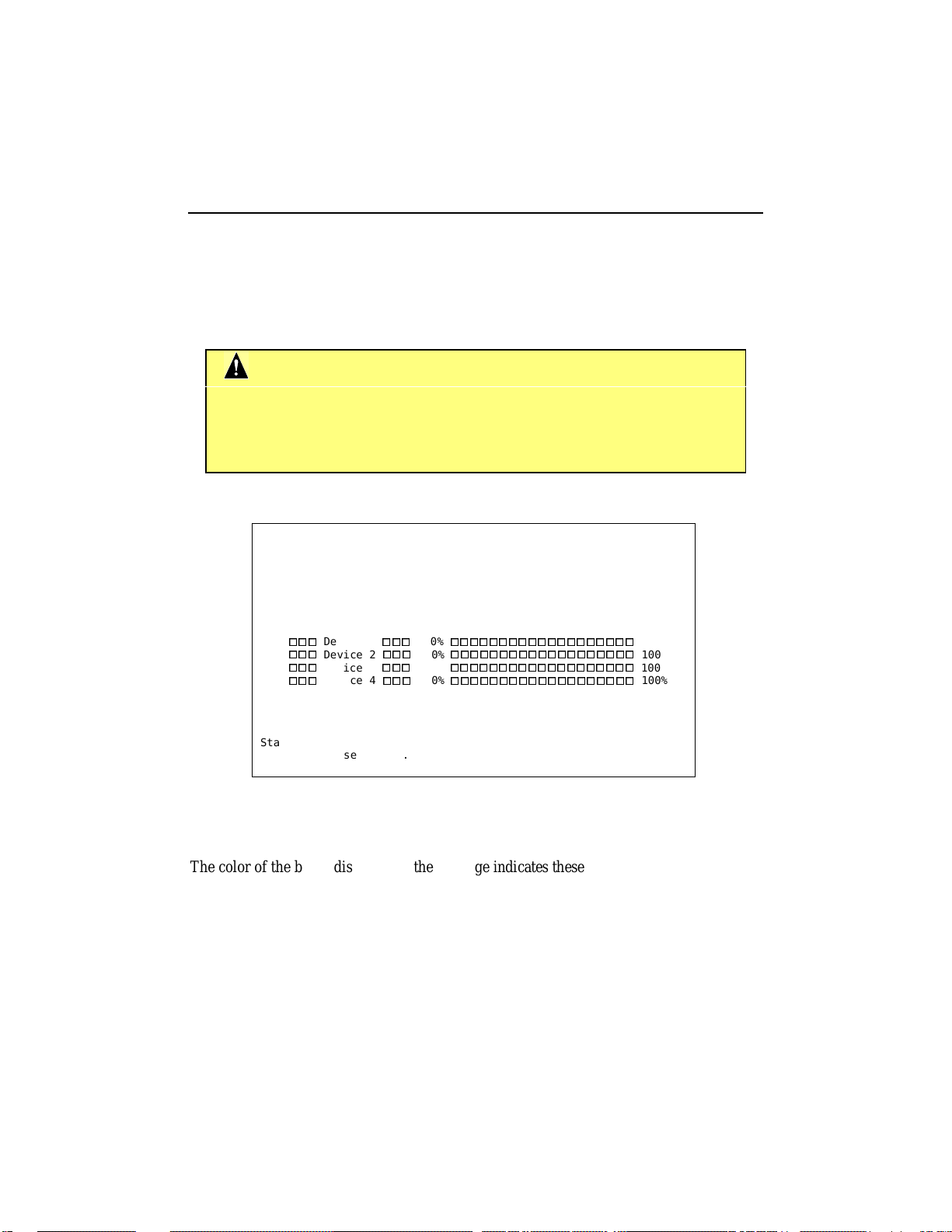
PCI-934 T echnical Reference M anual
14.2 CPL D UPGRADE AFTER A BIOS UPDATE
During the first system bootup after you update the Boot Block Flash BIOS with the
UPGBIOS utility, the BIOS may need to upgrade the CPLD devices.
WARNING
Whenever the BIOS performs a CPLD hardware upgrade, do not
interrupt the system in any way (power down, reset, mouse or keyboard
functions). The devices will be damaged and your board rendered
ino pe rati ve if you di sturb the update process!
The foll o wing messag e appears on th e screen when th e BI OS writes to th e devices:
A hardware upgrade will be performed on some CPLDs. Follow the
instructions below with special care. Do not disturb the process.
DO NOT RESET OR POWER DOWN THE BOARD!!!
Device 1
Device 2
Device 3
Device 4
Status :
Please wait...
0%
0%
0%
0%
100%
100%
100%
100%
The color of the boxes di s p layed in th e mes sage indicates these functions:
Device OK Green
Device bus y Blue
Device will be updated Red
14-2
Page 82

Updating the BIOS with UBIOS
If your d evi ce u p grade was su cces sful, th e following mes sage is displ ayed under th e
“Status:” line prior to rebooting:
Update complete successfully, wait for the automatic reboot.
Rebooting in 5 second(s).
If the update is not successful, the following message appears under the “Status:”
line:
ERROR: general failure programming CPLDs!
Please contact Teknor Industrial Computers technical support.
You must contact TEKNOR’s technical support for further instructions.
14-3
Page 83

15. VT100 MODE
The VT100 operating mode allows remote setups of the board. This configuration requires
a remote terminal that must be connected to the board through a serial communication link.
1.4 REQUIREMENTS
The terminal should emulate a VT100 or ANSI terminal. Terminal emulation programs such
as Telix or Pr oc omm can also be used.
NOTE
Some strange characters may appear on the screen. This occurs
because the VT100 recognizes some control characters, and causes
them to perform a specific function, for example, screen erase, cursor
position, and so on .
1.5 SETUP & CONFIGURATION
Follow these steps to set up the VT100 mode:
1. Connect a mo ni tor and a keyboard to your board and turn on the power
2. Enter into the CMOS Setup program.
3. Select the VT100 mode and the appropriate COM port and save your setup.
4. Connect the communications cable as show n in the next page.
Note: If you do not require a full cable for your terminal, you can set up a partial
cable by using only the TXD and RXD lines. To ignore contr ol lines simply loop
them back as shown in VT100 Partial Setup cable diagram.
5. Configure your terminal to communicate using 8 bits, no parity. The following
speeds are available: 2400, 9600, 19200, 38400, 57600, 115200BPS.
6. Use the remote keyboard and display to setup the BIOS
7. Sa ve th e set up , exi t , an d di scon n ect t he r em ot e co mp ut er fr om th e bo ar d t o op er at e
in stand-alone configuration.
15-1
Page 84
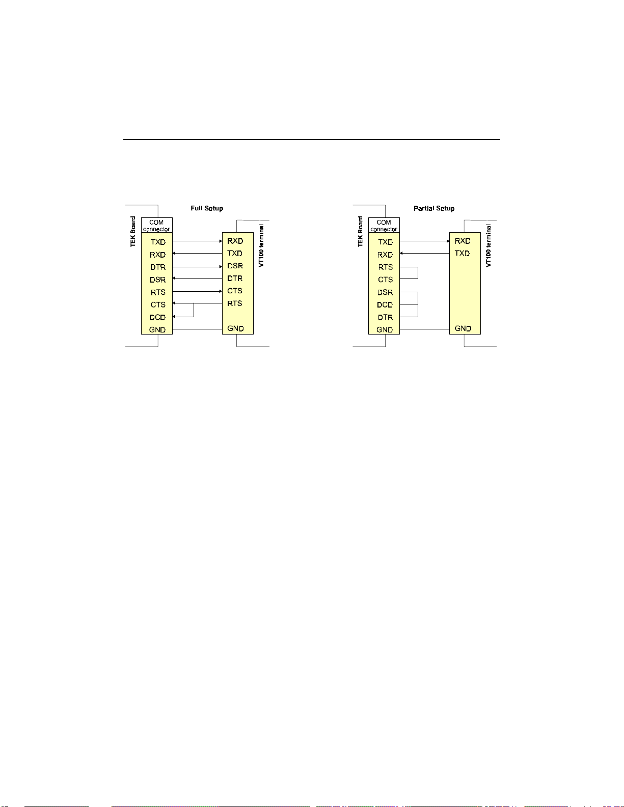
PCI-934 T echnical reference Manual
VT100 Full Setup VT100 Partial Setup
1.6 RUNNING WIT HOUT A TERMINAL
The boa rd can boot up with out a screen or term inal attach ed. However, i f VT100 Mod e is
desired, but the terminal is to be disconnected, you must ensure the control lines ar e in an
active state. Failing this, the system may "hang" while waiting for the control lines to become
active. Wiring the system according to the Partial Setup allows th e lines to remain active.
This does not apply if the VT100 mode is disabled.
Furthermore, you can run without any console at all by simply not enabling VT100 Mode and
by disabli ng the onboard vid e o function.
15-2
Page 85
APPENDIX
A. BOARD SPECIFICATIONS
B. MEMORY AND I/O MAPS
C. BOARD DIAGRAMS
D. CONNECTOR PINOUTS
E. BIOS S E TUP ERROR CODES
Page 86

A. PRODUCT SPECIFICATIONS
PCI-934 DESCRIPTION
Overview Multimedia Pentium MMX System Board.
Supported
Microprocessors
Intel Pentium
Intel Pentium MMX
AMD K6
®
166MHz, 200MHz.
TM
166MHz, 200MHz, 233MHz.
Contact TEKNOR.
Bus Interface PICMG 2.0, PCI Rev. 2.1 ; 121MB/s PC I burst write, 112MB/s PCI bur st
Data Path 64-bit on CPU and video memo ry bus, 32-bit on PCI bus, 16-bit on ISA bus.
System Memory
Cache Memory
Flash Disk
Serial Number
I/Os
read.
IBM PC/AT mechanical format.
ISA: high bus drive capability.
PC/104 ; PC/104-Plus compatible.
Up to 512MB EDO or FPM DRAM, through four 72-pin SIMMS sockets.
Level 1: 32 KB (CPU).
Level 2: 512KB, write-back with extended cacheability, 15ns pipelined burst.
Up to 80MB using CompactFlash device.
Unique silicon serial number in EEPROM.
Serial
USB
Parallel
Hard Disk
Floppy
Keyboard
Mouse
Ethernet
2 serial ports. Serial Port 1 configured as RS-232.
Serial Port 2 configurable a s RS-232,
RS-422 or RS-485.
2 Universal Se rial Bus (USB) ports.
1 multimode parallel port with support of PC /XT, AT, PS/2,
EPP and ECP operations.
Two Enhanced IDE interfaces for up to 4 devices in
Master/Slave configuration.
The secondary channel interfaces to CompactFlash disk.
Two floppy disks (1.2MB or 1.44MB).
Standard AT keyboard
Standard PS/2 mouse
10/100Base-TX interface
A-1
Page 87

PCI- 934 Technical Refer ence Manual
PCI-934 DESCRIPTION
Features
Connectors
BIOS
Power
Management
Thermal
Clock
Supervisory
Utilities
CRT
Ethernet
Line In
Line Out
Mic In
Floppy
EIDE
Flat Panel (FP)
FP Expansion
PanelLink
Kbd, spk, rst
Serial
Parallel
USB
V-Port 26-pin onboard
CD In 4-pin locking onboard
Mic In, AUX1 In,
Award BIOS in Boot Block Flash (256KB) for instant
configuration recovery
Auto configuration, extended setup, PnP tables
Programmable CPU and memory wait states
BIOS shadowing in RAM
Extension for diskless, keyboardless and videoless
operations
Ability to boot MS-DOS and user applications from the
CompactFlash disk
Save CMOS in Flash
Doze, Standby, Suspend, HDD Power Down
SMI/SMM Power Manage ment support
APM 1.2 compatible
CPU temperature management with low temperature and
overheat alarm levels.
Real time clock with ba ttery backup
Two-stage watchdog timer
Power failure / Low battery detector
DB-15 I/O bracket
RJ-45 ; link/activity L EDs I/O bracket
3.5mm audio jack I/O bracket
3.5mm audio jack I/O bracket
3.5mm audio jack I/O bracket
34-pin shrouded onboard
40-pin shrouded (2) onboard
50-pin shrouded onboard
26-pin shrouded onboard
20-pin shrouded onboard
16-pin combo shrouded onboard
10-pin shrouded (2) onboard
26-pin shrouded onboard
10-pin shrouded onboard
10-pin onboard
AUX2 In, Line Out
I2S Digital Audio
PS/2 Mouse
CPU Fan
PC/104 Plus Expansion header
4-pin onboard
4-pin locking onboard
2-pin locking onboard
onboard
A-2
Page 88

PCI-934 DESCRIPTION
Connector P inouts
Electrical/Mechanical
Characteristics
Conforms to IEEE P996 PC/AT bus, PCI Rev.2.1, PICMG 2.0, and
PC/104-Plus Rev .1.0 specifications.
Dimensions 13.3 x 4.80 x 0.062 inches
338 x 122 x 1.57 mm
Operating System
Compatibility
Audio, MPEG-1 and
VIPerVision API
PC and MS-DOS®Windows® 3.X Windows® 95
Windows
QNX
PC and MS-DOS
®
NT NOVELL
TM
UnixWare
®
, Windows® 95, Windows® NT, (MPEG-1 pending for
Windows NT)
support
Power Requirements
Supply Voltage
Pentium MMX
ICC typ. * +5V 3.79A 4.04A 2.26A
ICC suspend * +5V 2.19A 2.22A 2.26A
+12V 250mA 250mA 250mA
* Measured with 16MB DRAM, floppy and Hard disk
Reliability
MTBF
Agency Approvals
USB ank keyboard current protected by self-resetting fuses
Environnemental
Conditions
Operating Temperature
Storage Temperature
Humidity
TM
TM
OS/2® WA RP
SCO UNIX
TM
Vcc=+5V ±5% / =+12V ±5%
Dual DC/DC for split voltag e Pentium.
166 200 233
Over 90,000 hours (MIL-HDBK-217F)
FCC 47 CFR Part 15 ; Level A,
CE Mark to CISPR 22 Class B
0 to 60°C (w/airflow) - 5 to 95% RH
-20 to 70°C - 0 to 95% RH
5% to 95% RH
A-3
Page 89

B. BOARD DIAGRAMS
B-1
Page 90
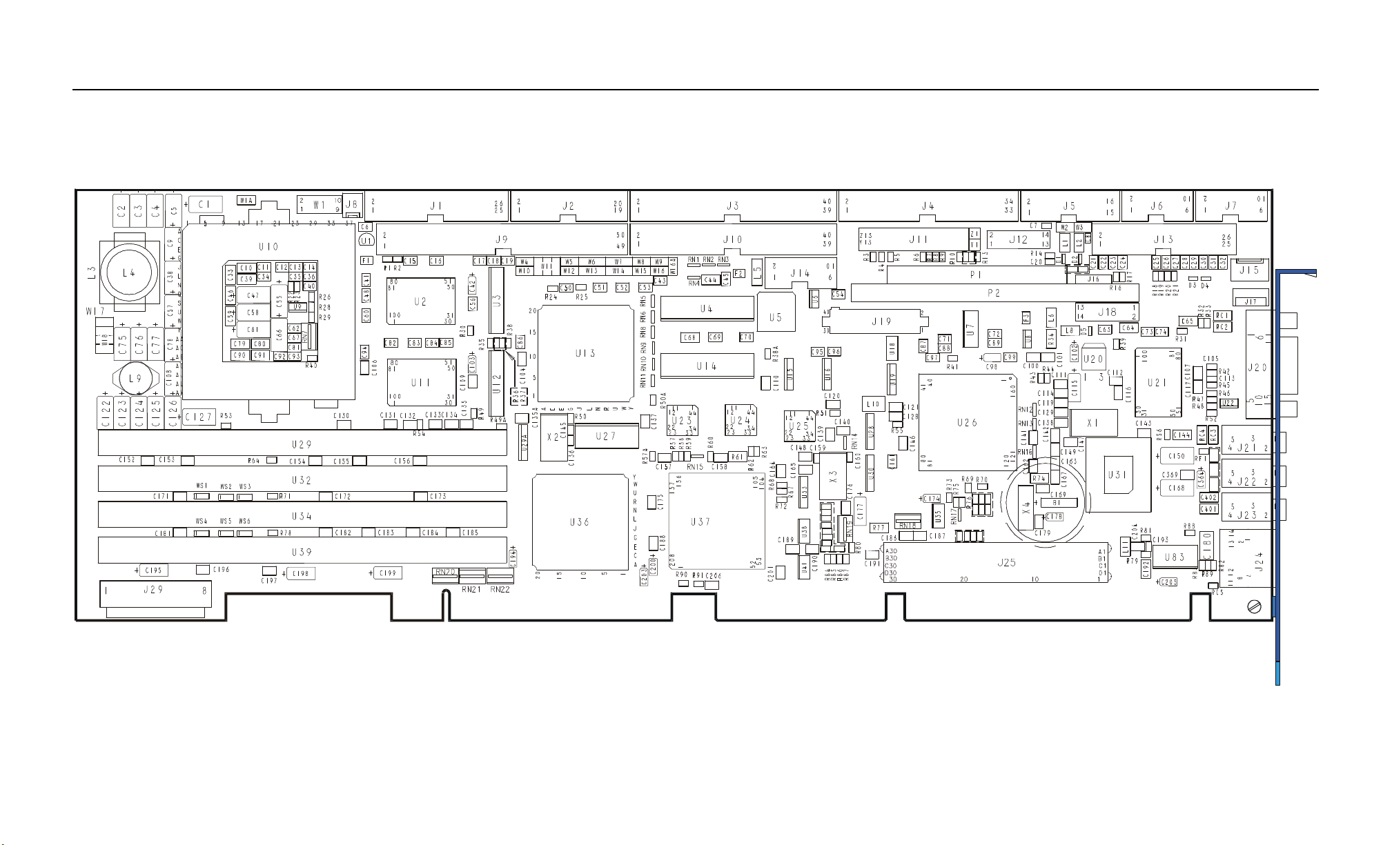
B-1 PCI-934 – ASSEMBLY DIAGRAM (TOP)
Board Diagrams
B-3
Page 91
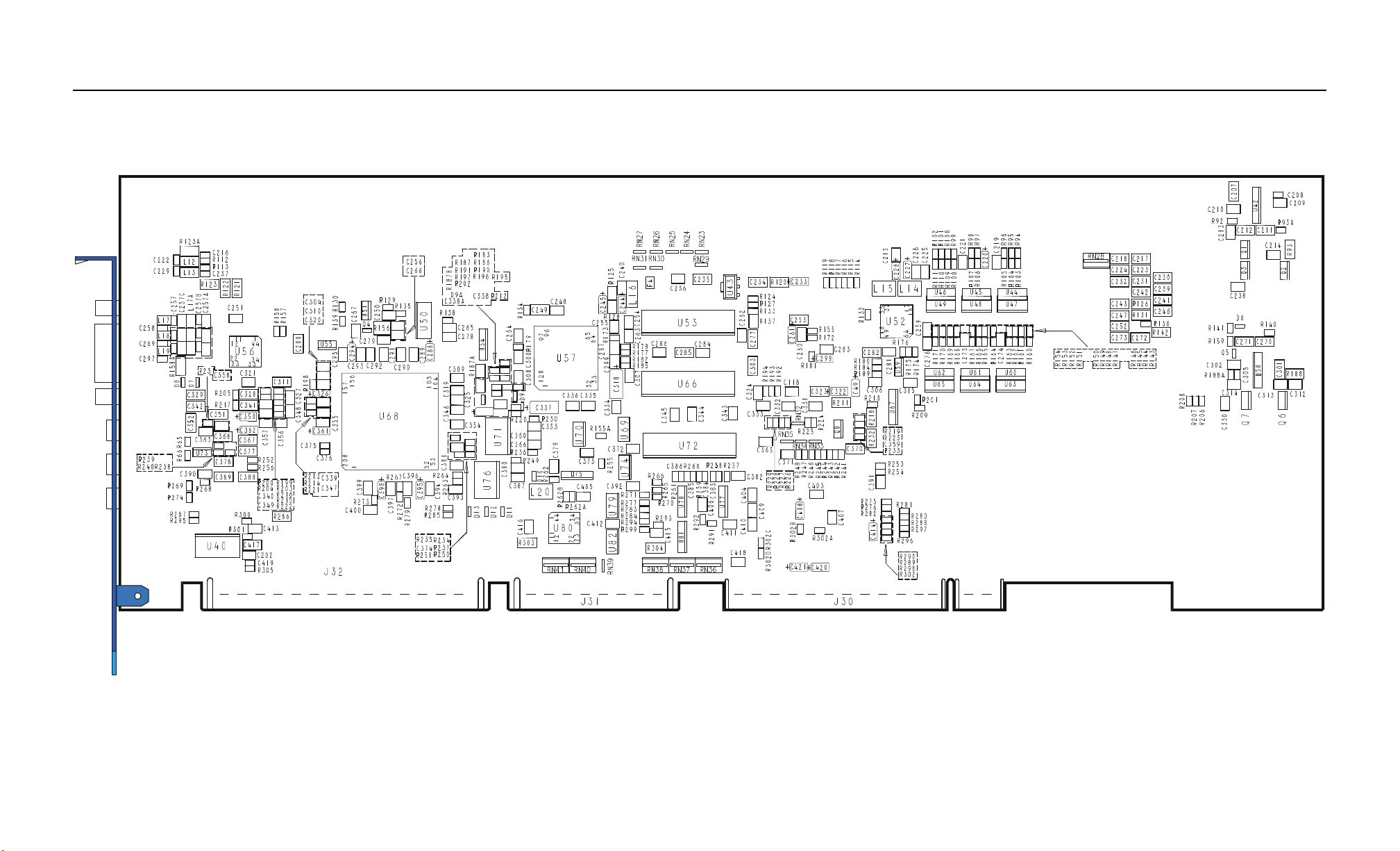
B-2 PCI-934 – ASSEMBLY DIAGRAM (BOTTOM)
Board Diagrams
B-5
Page 92
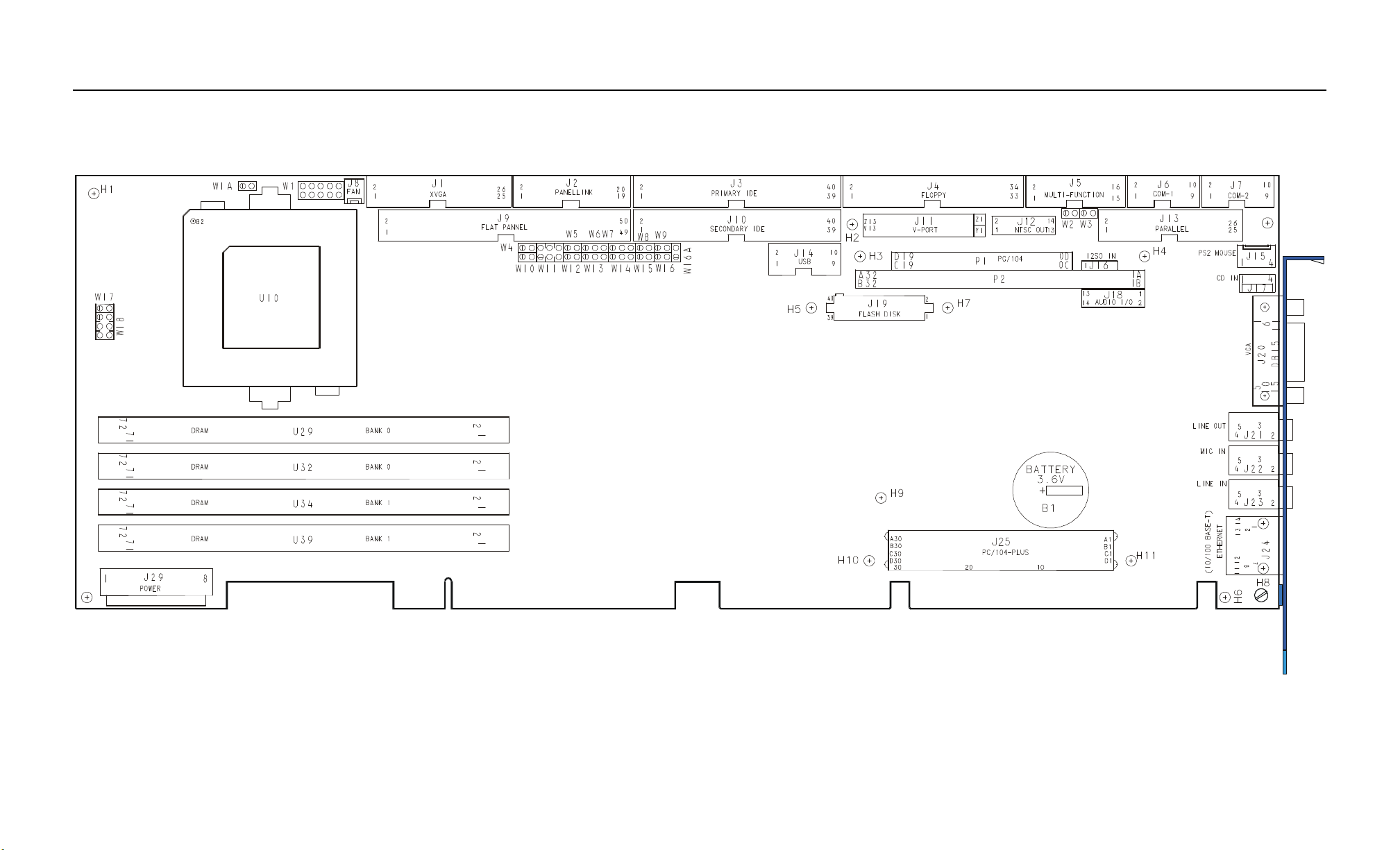
B-3 PCI-934 – CONFIGURATION DIAGRAM
Board Diagrams
B-7
Page 93
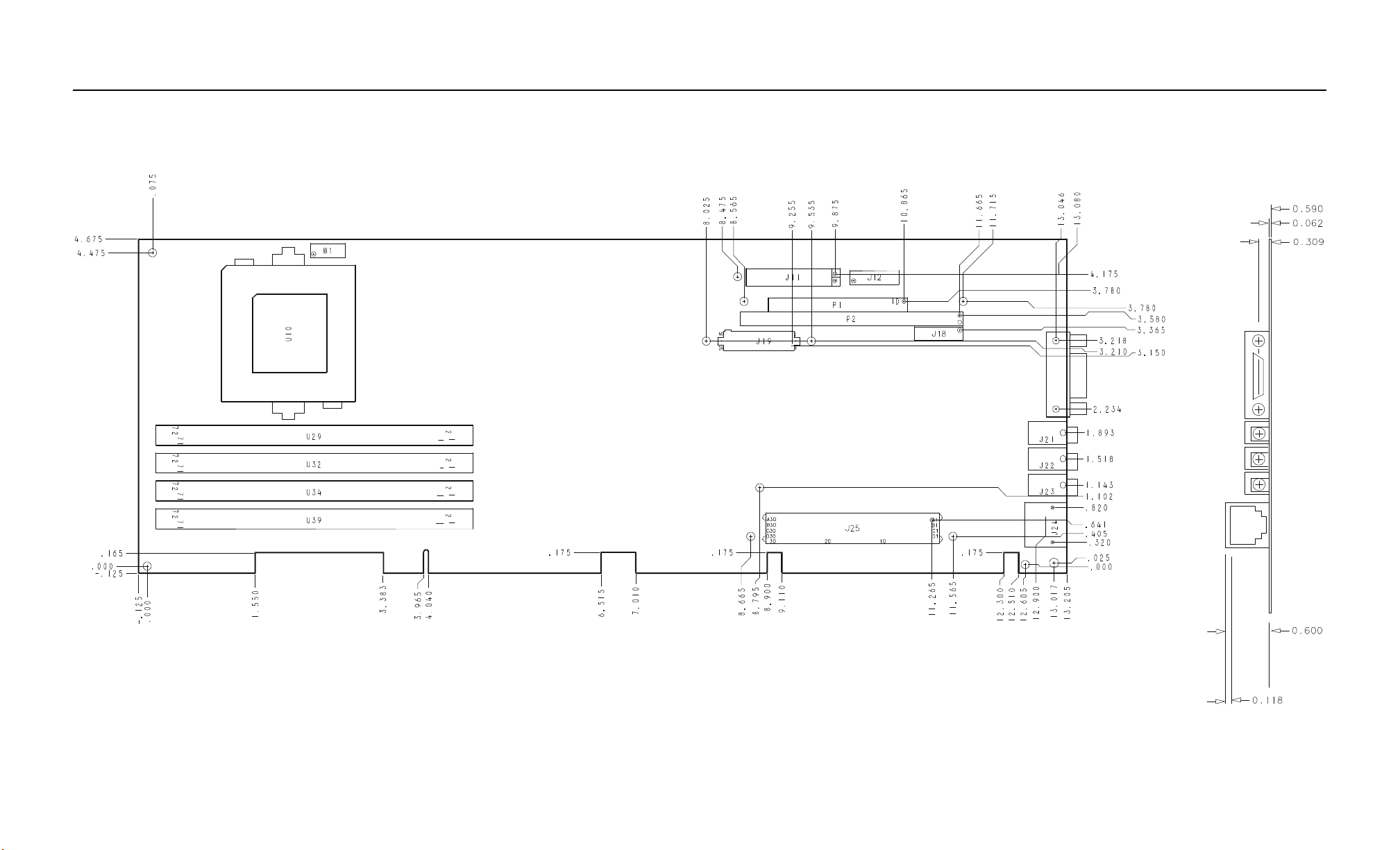
B-4 PCI-934 – MECHANICAL DIAGRAM
Board Diagrams
B-9
Page 94
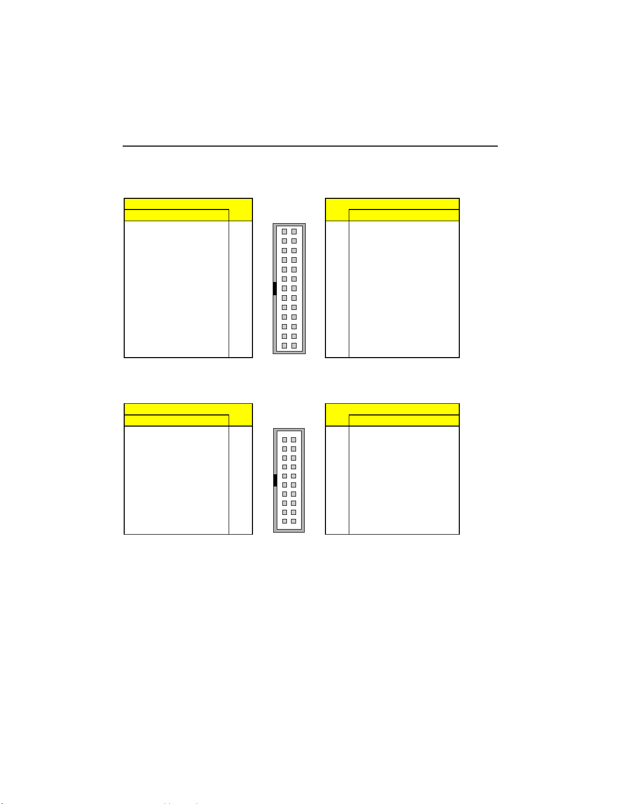
C. CONNECTOR PINOUTS
C.1 XVGA CONNECTOR - J1
Pin Number
Signal Signal
BFP20
BFP21
BFP22
BFP23
BFP26
BFP27
BFP28
BFP29
BFP32
BFP33
BFP34
BFP35
POT_HI
1
3
5
7
9
11
13
15
17
19
21
23
25
C.2 PANELLINK CONNECTOR - J2
Pin Number
Signal Signal
GP0
GP1
GP2
VCC
TXC-
VCC3
TX0TX1TX2-
FPVCC_SW
1
3
5
7
9
11
13
15
17
19
Top View
1252
26
Top View
1192
20
Pin Number
2
4
6
8
10
12
14
16
18
20
22
24
26
Pin Number
2
4
6
8
10
12
14
16
18
20
GND
GND
GND
GND
GND
GND
GND
GND
GND
FPVCC_SW
FPVCC_SW
VCON
POT_LO
+12V
GND
GND
VCC
TXC+
VCC3
TX0+
TX1+
TX2+
PD
C-1
Page 95
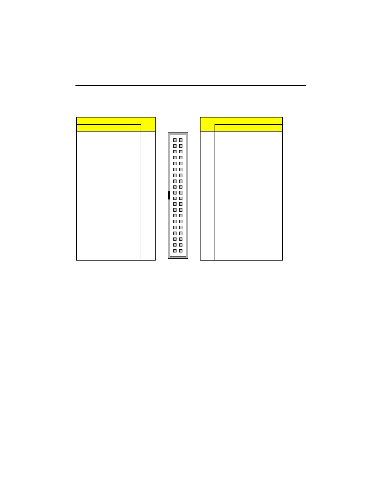
PCI- 934 Technical Refer ence Manual
C.3 EIDE CHANNEL 1 CONNECTOR - J3
Top View
1392
Pin Number
2
4
6
8
10
12
14
16
18
20
22
24
26
28
30
32
34
36
40
38
40
# Active Low Sig n al
Pin Number
Signal Signal
RESET#
D7
D6
D5
D4
D3
D2
D1
D0
GND
DRQ0
IOW#
IOR#
IORDY
DAK0
IRQ
A1
A0
CS1#
ACT#
1
3
5
7
9
11
13
15
17
19
21
23
25
27
29
31
33
35
37
39
GND
D8
D9
D10
D11
D12
D13
D14
D15
Not Connected
GND
GND
GND
PU
GND
IOCS16#
GND
DA2
CS3#
GND
C-2
Page 96
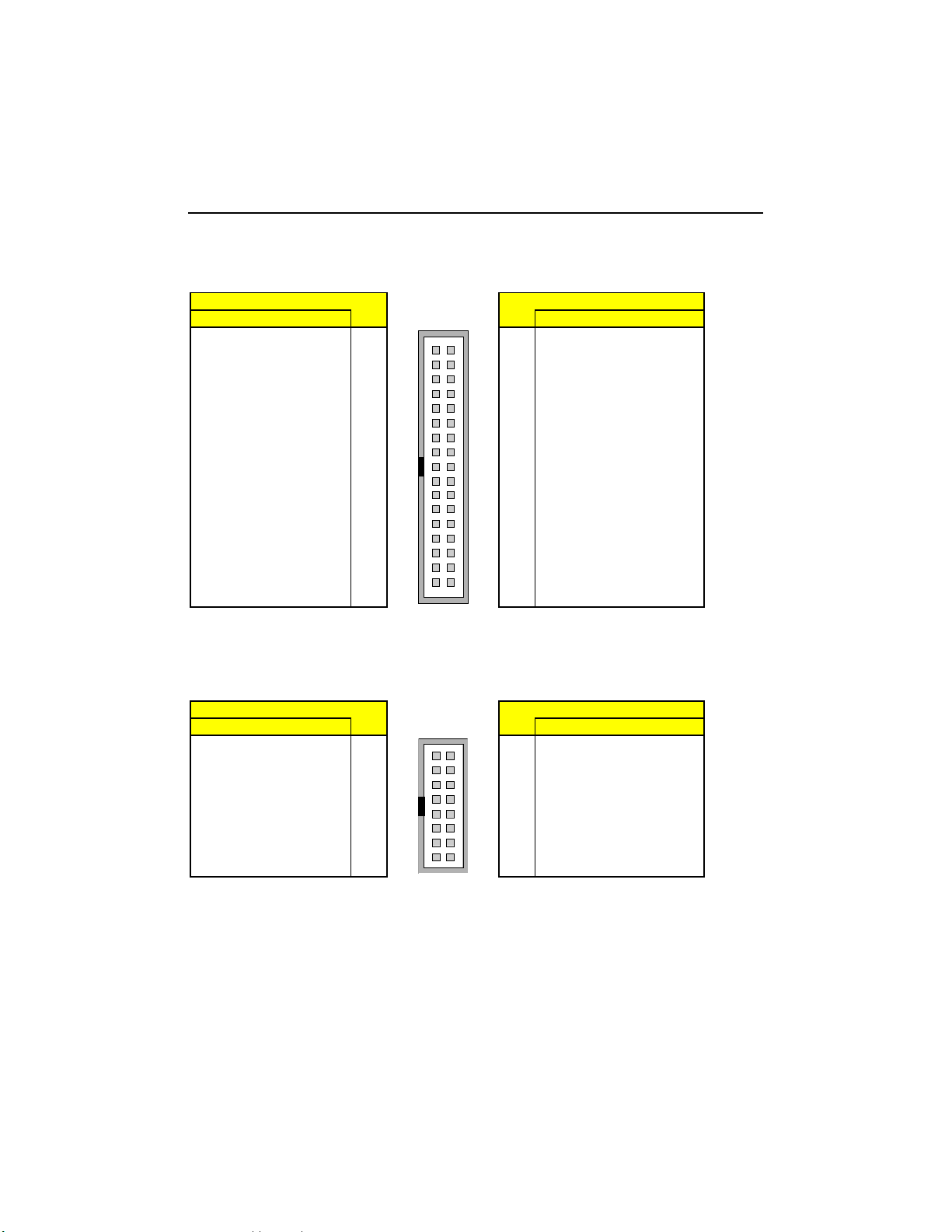
C.4 FLOPPY DISK CONNECTOR - J4
11521
6
Top View
1352
2
4
6
8
10
12
14
16
18
20
22
24
26
28
30
36
32
34
Not Connected
Not Connected
Not Connected
Not Connected
# Active Low Sig n al
Pin Number
Signal Signal
GND
GND
GND
GND
GND
GND
GND
GND
1
3
5
7
9
11
13
15
17
GND
GND
GND
GND
19
21
23
25
27
29
GND
31
33
Connector P inouts
Pin Number
DRVEND#
Not Connected
Not Connected
INDEX#
MTR0#
FPDS1#
FPDS0#
MTR1#
FPDIR#
STEP#
WDATA#
WGATE#
TRK0#
WRTPRT#
RDATA#
HDSEL#
DSKCHG#
C.5 MULTIFUNCTION CONNECTOR - J5
Top View
Pin Number
2
4
6
8
10
12
14
16
C-3
ACFAIL#
Not Used
HDACT#
# Active Low Sig n al
Pin Number
Signal Signal
KCLK
KDAT
VCC
SPKR
1
3
5
7
9
11
PBRES#
13
15
GND
GND
VCC
VCC
GND
GND
GND
VCC
Page 97
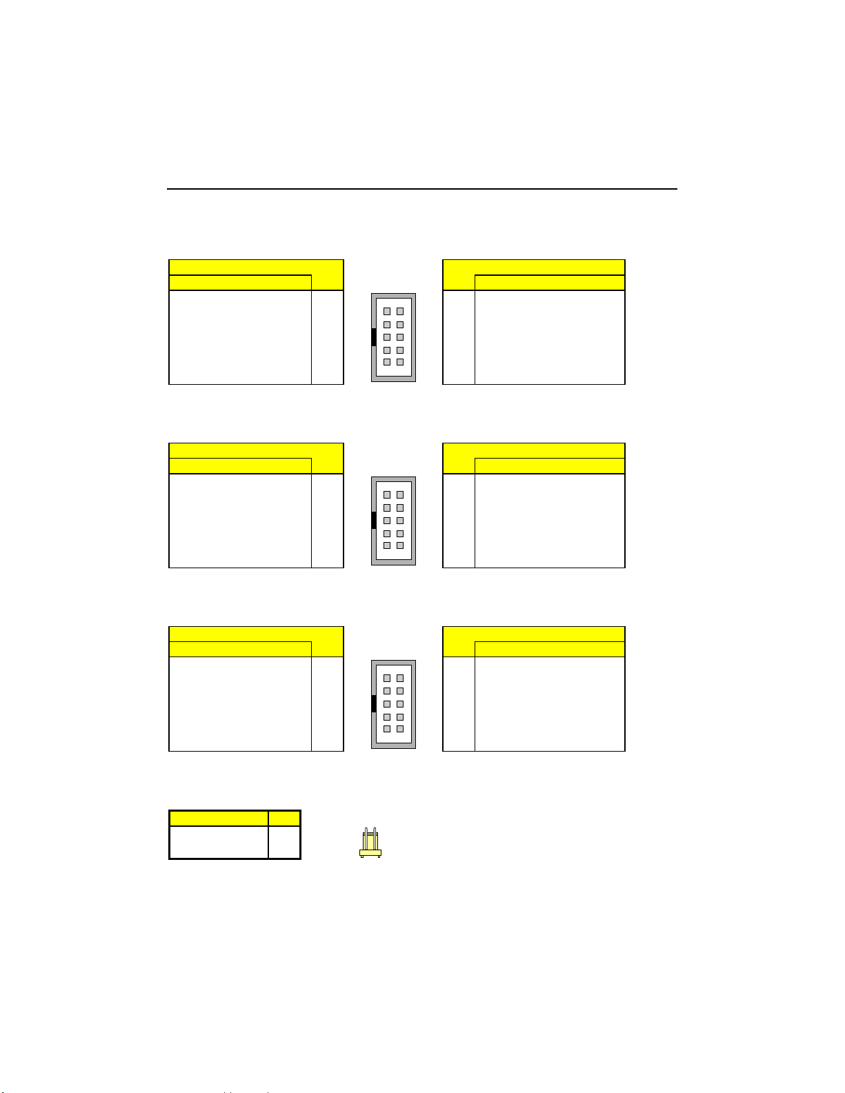
PCI- 934 Technical Refer ence Manual
C.6 SERIAL PORT 1 CONNECTOR - J6
Pin Number
Signal Signal
Top View
Pin Number
DCD#
RXD
TXD
DTR#
GND
1
3
5
7
9
192
DSR
2
RTS#
4
CTS#
6
RI#
10
10
8
Not Connected
# Active Low Sig n al
C.7 SERIAL PORT 2 CONNECTOR (RS-232) - J7
Top View
192
Pin Number
DSR
2
RTS#
4
CTS#
6
RI#
10
10
8
Not Connected
# Active Low Sig n al
Pin Number
Signal Signal
DCD#
RXD
TXD
DTR#
GND
1
3
5
7
9
C.8 SERIAL PORT 2 CONNECTOR (RS-422/RS-485) - J7
Top View
192
Pin Number
DSR
2
RX(+)
4
TX(+)
6
RI#
10
10
8
Not Connected
# Active Low Sig n al
Pin Number
Signal Signal
DCD#
RX(-)
TX(-)
DTR#
GND
1
3
5
7
9
C.9 FAN CONNECTOR - J8
Signal
+12V
GND
1
2
Front View
1
C-4
Page 98
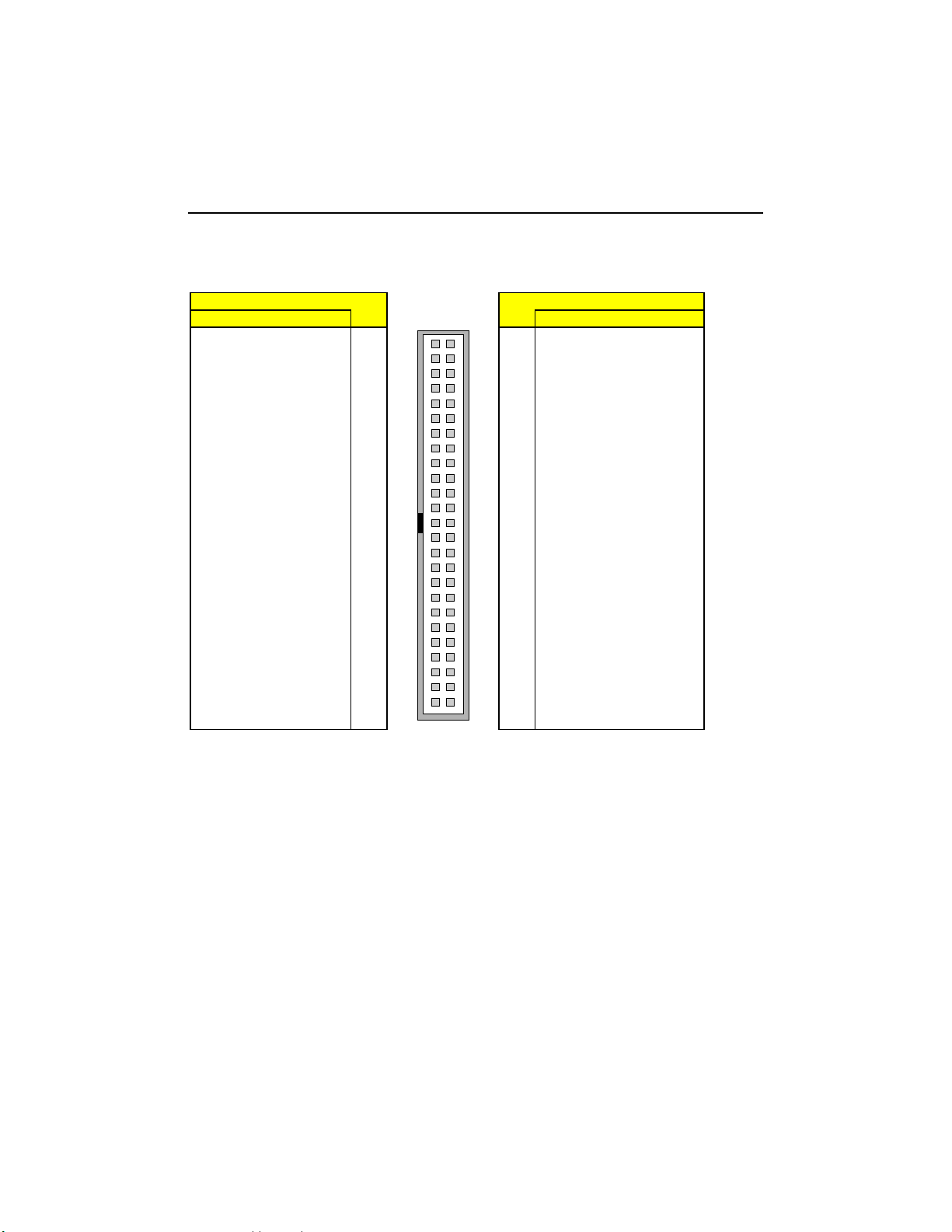
C.10 FLAT PANEL CONNECTOR - J9
Top View
1492
10
12
14
16
18
20
22
24
26
28
30
32
34
36
38
40
42
44
46
50
48
50
STANDBY#
FPVCC_SW
# Active Low Sig n al
Pin Number
Signal Signal
BFP2
BFP4
BFP8
BFP10
BFP13
BFP7
BFP17
BFP15
GND
GND
GND
BFP1
GND
GND
BFP24
GP1
BFPVEE
BLLCLK
BFPVEE
BFP0
1
3
5
7
9
11
13
15
17
19
21
23
25
27
29
31
33
35
37
39
41
BFP19
ACTI
43
45
47
+12V
49
Pin Number
2
4
6
8
Connector P inouts
BFP3
BFP5
BFP9
BFP11
BFP12
BFP6
BFP16
BFP14
BFPVDCLK
BFP25
BLF5
BFP18
BFPDE
GND
GP0
GND
GND
GND
BFPVCC
GP2
BFP30
BFP31
FPDECTL
FPVCC_SW
+12V
C-5
Page 99
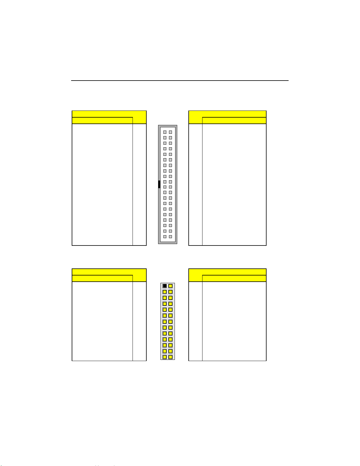
PCI- 934 Technical Refer ence Manual
Z
1
Y
1
C.11 EIDE CHANNEL 2 CONNECT OR - J10
Pin Number
Signal Signal
RESET#
D7
D6
D5
D4
D3
D2
D1
D0
GND
DRQ1
IOW#
IOR#
IORDY
DAK1
IRQ0
A1
A0
CS1#
ACT#
1
3
5
7
9
11
13
15
17
19
21
23
25
27
29
31
33
35
37
39
Top View
1392
Pin Number
GND
2
D8
4
D9
6
D10
8
10
12
14
16
18
20
22
24
26
28
30
32
34
36
40
38
40
D11
D12
D13
D14
D15
Not Connected
GND
GND
GND
PU
GND
IOCS16#
GND
A2
CS3#
GND
C.12 V-PORT CONNECTOR - J11
Top View
Z13
Y13
C-6
I2C_DATA
VP_VSYNC
EN_CAM#
# Active Low Sig n al
Pin Number
Signal Signal
GND
GND
GND
Z1
Z2
Z3
Z4
Z5
Z6
VCC
GND
GND
GND
GND
ZVPCLK
VACTI
Z7
Z8
Z9
Z10
Z11
Z12
Z13
Y1
Y2
Y3
Y4
Y5
Y6
Y7
Y8
Y9
Y10
Y11
Y12
Y13
Pin Number
VPC0
VPC1
VPC2
VPC3
VPC4
VPC5
VPC6
VPC7
I2C_CLK
VP_HSYNC#
VP_IO_1
VP_IO_2
GND
Page 100
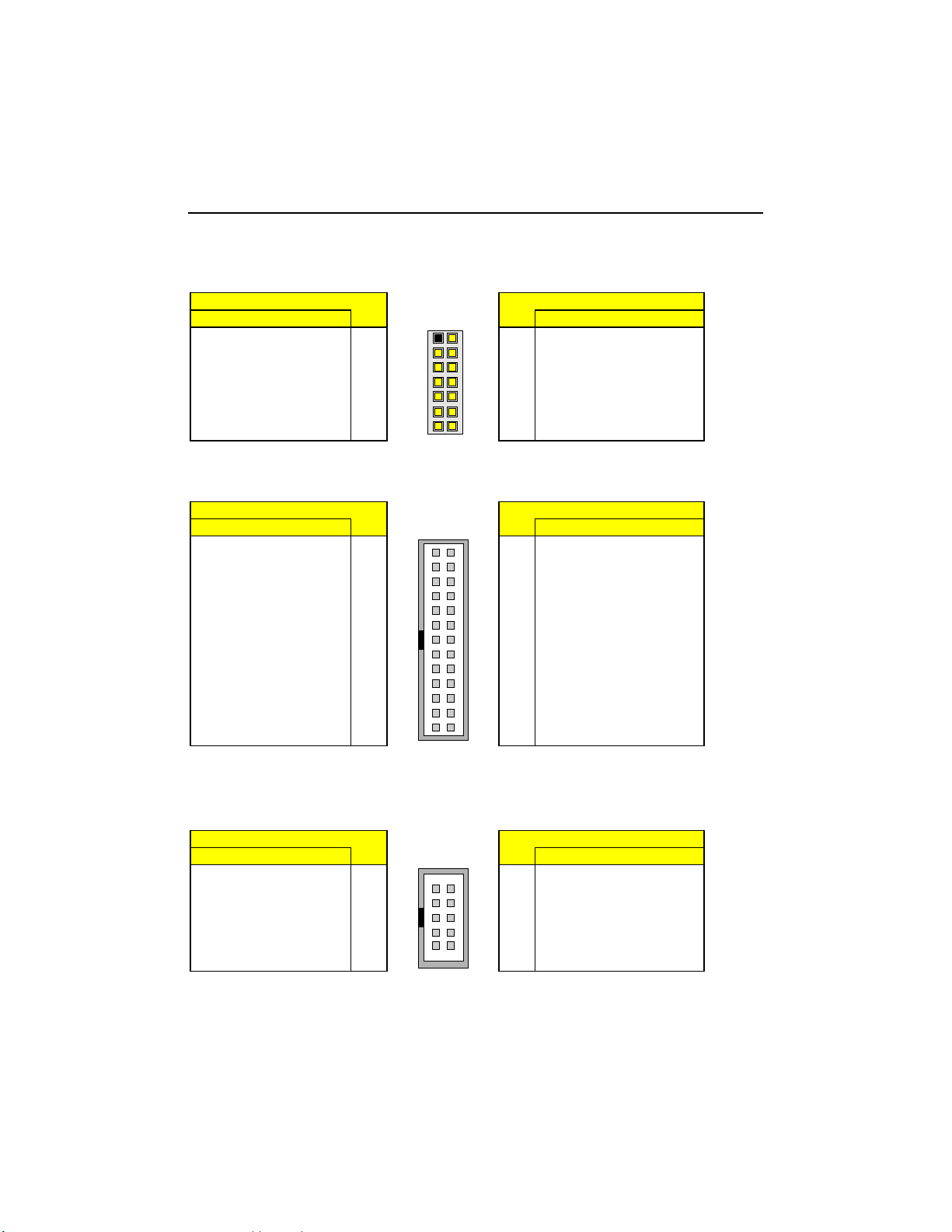
C.13 NTSC OUT CONNECTOR - J12
1
1
321
4
Pin Number
Signal Signal
RED
GREEN
BLUE
CSYNC
TVON
NTSC_PAL
HSYNC
1
3
5
7
9
11
13
Top View
Pin Number
2
4
6
8
10
12
14
GND
GND
GND
GND
GND
GND
VSYNC
C.14 PARALLEL PORT CONNECTOR - J13
Top View
1252
Pin Number
ALF#
2
ERR#
4
INIT#
6
SLCTIN#
8
10
12
14
16
18
20
22
26
24
26
GND
GND
GND
GND
GND
GND
GND
GND
GND
# Active Low Sig n al
Pin Number
Signal Signal
STB#
PD0
PD1
PD2
PD3
PD4
PD5
PD6
PD7
ACK#
BUSY
PE
SLCT
1
3
5
7
9
11
13
15
17
19
21
23
25
Connector P inouts
C.15 USB CONNECTOR - J14
Pin Number
Signal Signal
SVB0
SBP0-
SBP0+
GND
GND
1
3
5
7
9
Top View
192
Pin Number
SVB1
2
SBP1-
4
SBP1+
6
GND
10
10
8
GND
C-7
 Loading...