

Page 1

TEK-AT4L PLUS
486SX/DX/DX2SINGLEBOARDCOMPUTER
TECHNICALREFERENCEMANUAL
VERSION1.1
May1997
NOTE:
Thismanualisforreferencepurposeonly.
Reproductioninwholeorinpartisauthorizedprovided
TEKNORINDUSTRIALCOMPUTERSINC.iscitedas
theoriginalsource.
Page 2

FOREWORD
The information in this document is provided for reference purposes only. TEKNOR does
not assume any liability for application of the information or use of the products described
herein.
This document may contain or reference information and products protected by the
copyrights or patents of others and does not convey any license under the patent right of
TEKNOR, nor the rights of others.
Printed in Canada.
Copyright 1996 by TEKNOR INDUSTRIAL COMPUTERS INC., Boisbriand, Qc, J7G
2A7.
Foreword III
Page 3

TABLE OF CONTENTS
1. PRODUCT OVERVIEW ........................................................................................ 1-1
2. ONBOARD SUBSYSTEMS...................................................................................2-1
2.1 PASSIVE BACKPLANE............................................................................................2-1
2.2 USER INTERFACE..................................................................................................2-1
2.3 STAND-ALONE OPERATION...................................................................................2-2
2.4 DISKLESS OPERATION........................................................................................... 2-2
3. UNPACKING...........................................................................................................3-1
3.1 UNPACKING .........................................................................................................3-1
3.2 CONTENTS...........................................................................................................3-1
4. SAFETY PRECAUTIONS.......................................................................................4-1
4.1 STATIC ELECTRICITY............................................................................................4-1
4.2 STORAGE ENVIRONMENT......................................................................................4-1
4.3 POWER SUPPLY .................................................................................................... 4-1
5. CUSTOMIZING THE BOARD...............................................................................5-1
5.1 INSTALLING MICROPROCESSOR AND FAN...............................................................5-1
5.2 INSTALLING MEMORY ..........................................................................................5-1
5.3 MEMORY AND I/O MAPPING.................................................................................5-3
5.3.1 Memory Mapping.........................................................................................5-3
5.4 EXPANDED AND EXTENDED MEMORY ...................................................................5-4
5.4.1 Expanded Memory........................................................................................5-4
5.4.2 Extended Memory.........................................................................................5-4
5.5 MEMORY MODE...................................................................................................5-4
5.6 SHADOW RAM.....................................................................................................5-4
5.7 CONFIGURING THE TEK-AT4LPLUS.................................................................... 5-5
5.8 SW1 - CONFIGURATION JUMPERS .........................................................................5-5
5.8.1 SW1 (1-2) Selecting BIOS Boot Option.........................................................5-5
5.8.2 SW1(3-4) Selecting COM1/COM2 for VT00 or Download Mode...................5-6
5.8.3 SW1(5-6) Enabling VT100 Mode ..................................................................5-6
5.8.4 SW1(7-8) Enabling Serial Download Mode...................................................5-7
5.9 INSTALLING SUPERVISOR UTILITIES.......................................................................5-8
5.9.1 Special Note on Register 201h ...................................................................... 5-8
5.9.2 Watchdog Timer...........................................................................................5-8
5.9.3 Power Failure Detector (PFD) .....................................................................5-9
5.9.4 Low Battery Detection................................................................................5-10
5.10 ATTACHING THE AT4LPLUS TO ENCLOSURE.................................................... 5-10
Page 4

6. INSTALLING DEVICES.........................................................................................6-1
6.1 CONNECTING POWER SUPPLY ...............................................................................6-1
6.1.1 Supplying Power Using the ISA-AT Bus ........................................................ 6-1
6.1.2 Supplying Power Using the Power Connector (J5)........................................6-1
6.2 CONNECTING HARD DISK (J1)............................................................................... 6-5
6.3 CONNECTING FLOPPY DISK DRIVE (J2).................................................................. 6-6
6.4 PS/2 MOUSE CONNECTOR (J3A)...........................................................................6-6
6.5 MULTI-FUNCTION CONNECTOR (J3)......................................................................6-7
6.6 SERIAL PORT #2 CONNECTOR (J4) ........................................................................6-7
6.6.1 COM1(J6) ....................................................................................................6-7
6.6.2 COM2 (J4) ...................................................................................................6-8
6.7 PARALLEL PRINTER PORT CONNECTOR (J7)...........................................................6-8
6.8 INSTALLING SOLID STATE DISKS...........................................................................6-9
6.8.1 Writing To Flash Disks.................................................................................6-9
6.8.2 SRAM Disk...................................................................................................6-9
6.8.3 Battery Backup Circuit...............................................................................6-10
7. INSTALLING VIDEO DEVICES ............................................................................7-1
7.1 USING STANDARD VIDEO ADAPTER BOARD...........................................................7-1
7.2 USING VIDEO MEZZANINE BOARD.........................................................................7-1
7.2.1 Installing Mezzanine Board..........................................................................7-1
8. SETTING JUMPERS............................................................................................. 8-1
9. CONFIGURING DMA AND IRQ............................................................................9-1
9.1 DMA CHANNELS ALLOCATION ............................................................................9-1
9.2 ALLOCATING IRQ LINES ......................................................................................9-1
10. TEK-AT4LPLUS BIOS ............................................... Error! Bookmark not defined.
10.1 OVERVIEW AND FEATURES......................ERROR! BOOKMARK NOT DEFINED.
10.2 ERROR HANDLING......................................ERROR! BOOKMARK NOT DEFINED.
Page 5

TABLE OF CONTENTS
1. PRODUCT OVERVIEW ........................................................................................ 1-1
2. ONBOARD SUBSYSTEMS................................................................................... 2-1
2.1 PASSIVE BACKPLANE............................................................................................2-1
2.2 USER INTERFACE..................................................................................................2-1
2.3 STAND-ALONE OPERATION...................................................................................2-2
2.4 DISKLESS OPERATION........................................................................................... 2-2
3. UNPACKING...........................................................................................................3-1
3.1 UNPACKING .........................................................................................................3-1
3.2 CONTENTS...........................................................................................................3-1
4. SAFETY PRECAUTIONS.......................................................................................4-1
4.1 STATIC ELECTRICITY............................................................................................4-1
4.2 STORAGE ENVIRONMENT......................................................................................4-1
4.3 POWER SUPPLY .................................................................................................... 4-1
5. CUSTOMIZING THE BOARD...............................................................................5-1
5.1 INSTALLING MICROPROCESSOR AND FAN...............................................................5-1
5.2 INSTALLING MEMORY ..........................................................................................5-1
5.3 MEMORY AND I/O MAPPING.................................................................................5-3
5.3.1 Memory Mapping.........................................................................................5-3
5.4 EXPANDED AND EXTENDED MEMORY ...................................................................5-4
5.4.1 Expanded Memory........................................................................................5-4
5.4.2 Extended Memory.........................................................................................5-4
5.5 MEMORY MODE...................................................................................................5-4
5.6 SHADOW RAM.....................................................................................................5-4
5.7 CONFIGURING THE TEK-AT4LPLUS.................................................................... 5-5
5.8 SW1 - CONFIGURATION JUMPERS .........................................................................5-5
5.8.1 SW1 (1-2) Selecting BIOS Boot Option.........................................................5-5
5.8.2 SW1(3-4) Selecting COM1/COM2 for VT00 or Download Mode...................5-6
5.8.3 SW1(5-6) Enabling VT100 Mode ..................................................................5-6
5.8.4 SW1(7-8) Enabling Serial Download Mode...................................................5-7
5.9 INSTALLING SUPERVISOR UTILITIES.......................................................................5-8
5.9.1 Special Note on Register 201h ...................................................................... 5-8
5.9.2 Watchdog Timer...........................................................................................5-8
5.9.3 Power Failure Detector (PFD) .....................................................................5-9
5.9.4 Low Battery Detection................................................................................5-10
5.10 ATTACHING THE AT4LPLUS TO ENCLOSURE.................................................... 5-10
Page 6

APPENDICES
A. PRODUCT SPECIFICATION
A.1 TEK-AT4LPLUS - PRODUCT SPECIFICATIONS .................................................. A-1
B. BOARD DIAGRAMS
B.1 TEK-AT4LPLUS - ASSEMBLY DIAGRAM (TOP VIEW) .......................................B-1
B.2 TEK-AT4LPLUS - MOUNTING HOLES.............................................................B-3
B.3 TEK-AT4LPLUS - MECHANICAL SPECIFICATIONS ............................................B-5
C. CONNECTOR PINOUTS
C.1 J1 - IDE #1 CONNECTOR................................................................................. C-1
C.2 J2 - FLOPPY DISK DRIVE CONNECTOR .............................................................. C-1
C.3 J3 - MULTI-FUNCTION CONNECTOR ................................................................. C-2
C.4 J3A - MOUSE CONNECTOR............................................................................... C-2
C.5 J4- SERIAL PORT #2 CONNECTOR.....................................................................C-2
C.6 J5 - POWER CONNECTOR ................................................................................. C-3
C.7 J6 - SERIAL PORT #1 CONNECTOR....................................................................C-3
C.8 J7 - PARALLEL PORT CONNECTOR.................................................................... C-4
C.9 J8 - MEZZANINE ISA AT BUS CONNECTOR ...................................................... C-5
C.10 J9 - MEZZANINE ISA AT EXTENSION BUS CONNECTOR .................................... C-6
C.11 J10 - FAN CONNECTOR .................................................................................... C-6
C.12 J14 - ISA BUS EXTENSION CONNECTOR............................................................ C-7
GLOSSARY
INDEX
GETTING HELP
Page 7

PRODUCT DESCRIPTION
1. PRODUCT OVERVIEW
2. ONBOARD SUBSYSTEMS
Page 8

1. PRODUCT OVERVIEW
The TEK-AT4LPLUS is a high performance PC/AT type computer on a single-slot card
format (13.3" x 4.7"). It provides all the basic functions available on standard IBM AT
computers such as a hard disk interface and floppy disk controller, serial ports, keyboard,
and mouse.
This Single Board Computer (SBC) is designed to operate in environments where a sturdy
and compact system is essential. It provides a watchdog timer, solid state disks, and a
power failure detector and can be installed in the most extreme industrial applications.
CMOS technology makes the TEK-AT4LPLUS consume very little power (less than 7.5W
with 33MHz processor version).
The TEK-AT4LPLUS offers a high level of versatility. It can be installed in a standard PC
passive backplane or, thanks to its small size, it can be installed as a stand-alone
controller, using the four standard mounting holes and separate power connector.
To top it off, a 93-pin, AT expansion header accommodates TEKNOR's series of
mezzanine display controllers or other optional expansion cards.
Product Overview 1-1
Page 9
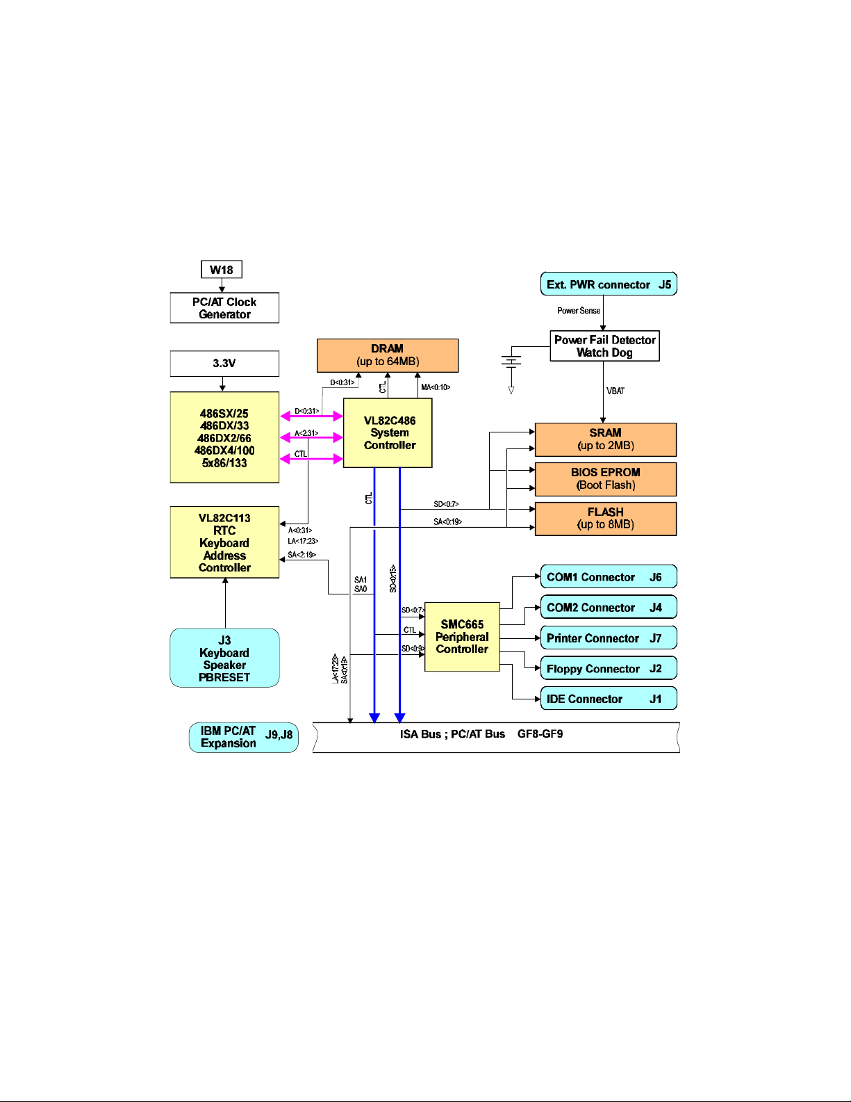
TEK-AT4LPLUS - Block Diagram
Product Overview 1-2
Page 10

2. ONBOARD SUBSYSTEMS
The TEK-AT4LPLUS provides the following features:
• PC/AT bus or stand alone operation
• 486SX/25MHz
486DX/33MHz
486DX2/66MHz
486DX4/100MHz
5x86/133MHz
• 1 to 64MB of system memory with DRAM
support
• Up to 8MB of user Flash EPROM
• Up to 2MB user SRAM with battery backup
• Supports Shadow RAM BIOS for fast
execution
• Flash EPROM boot
• Real-time clock with battery backup
• AT keyboard and speaker port
• One parallel printer port (LPT1)
• Two serial ports with COM2 as
RS-232 or RS-485
• Watchdog Timer
• Power Fail Detector
• Low Battery Circuit Detector
• Onboard floppy controller:
drives two floppies
• Onboard IDE hard disk interface
• Sleep Mode support
• CMOS technology for low power
• Two years warranty
• Supports Teknor mezzanine boards
The TEK-AT4LPLUS single board computer is a versatile board that will function either
on a passive backplane or as a stand-alone controller, with or without disks, keyboard and
monitor.
2.1 Passive Backplane
The TEK-AT4LPLUS can be installed on a PC/AT passive backplane in conjunction with
any PC/AT and XT compatible cards. Power is drawn directly from the PC Bus, and is
provided by the backplane. Video cards may be used but are not a prerequisite for
operation.
2.2 User Interface
The TEK-AT4LPLUS will operate with any PC Bus compatible display card. When standalone mode is required, a TEKNOR Mezzanine SVGA card may be used.
A VT100 terminal (or a PC emulating VT100) may be used as an inexpensive alternative
to a display and keyboard. Refer to Section 5, Using VT100 Mode for more details on this
mode.
Onboard Subsystems 2-1
Page 11

2.3 Stand-Alone Operation
An alternate power connector is available to supply the necessary voltages to the TEKAT4LPLUS board. This is useful in situations where a passive backplane system is not
appropriate.
With TEKNOR’s Mezzanine card, it is possible to assembly a complete computer in a
13.3" x4.7" x 1.25" area - without ever using any passive backplane system.
And when your applications call for it, the TEK-AT4LPLUS is fully operational without
any user interfaces at all - able to run without disks, keyboard, and video.
2.4 Diskless Operation
The TEK-AT4LPLUS can operate without mechanical drives in any basic mode of
operation. A Flash disk can be configured as a bootable disk and temporary data may be
securely stored on SRAM disks.
In essence, the TEK-AT4LPLUS is an industrial controller withstanding shock, vibration,
and temperature variations - all major concerns in industrial environments.
Onboard Subsystems 2-2
Page 12

INSTALLATION
3. UNPACKING
4. SAFETY PRECAUTIONS
5. CUSTOMIZING THE BOARD
6. INSTALLING DEVICES
7. INSTALLING VIDEO DEVICES
8. SETTING JUMPERS
9. CONFIGURING DMA AND IRQ
10. TEK-AT4L PLUS BIOS
Page 13

3. UNPACKING
3.1 Unpacking
Follow these recommendations while unpacking:
F After opening the box, save it and the packing material for possible future shipment.
F Remove the board from its antistatic wrapping and place it on a grounded surface.
F Inspect the board for damage. If there is any damage, or items are missing, notify
TEKNOR immediately.
3.2 Contents
When unpacking you will find:
F one TEKAT4LPLUS AT Single Board Computer
F one Technical Reference Manual.
F Cables
Unpacking 3-1
Page 14

4. SAFETY PRECAUTIONS
4.1 Static Electricity
Since static electricity can damage a board, the following precautions should be taken:
F Keep the board in its antistatic package, until you are ready to install it.
F Touch a grounded surface or wear a grounding wrist strap before removing the
board from its package; this will discharge any static electricity that may have built
up in your body.
F Handle the board by the edges.
4.2 Storage Environment
Electronic boards are sensitive devices. Do not handle or store devices near strong electrostatic,
electromagnetic, magnetic or radioactive fields.
4.3 Power Supply
Before any installation or setup, ensure that the board is unplugged from power sources or
subsystems.
Safety Precautions 4-1
Page 15
5. CUSTOMIZING THE BOARD
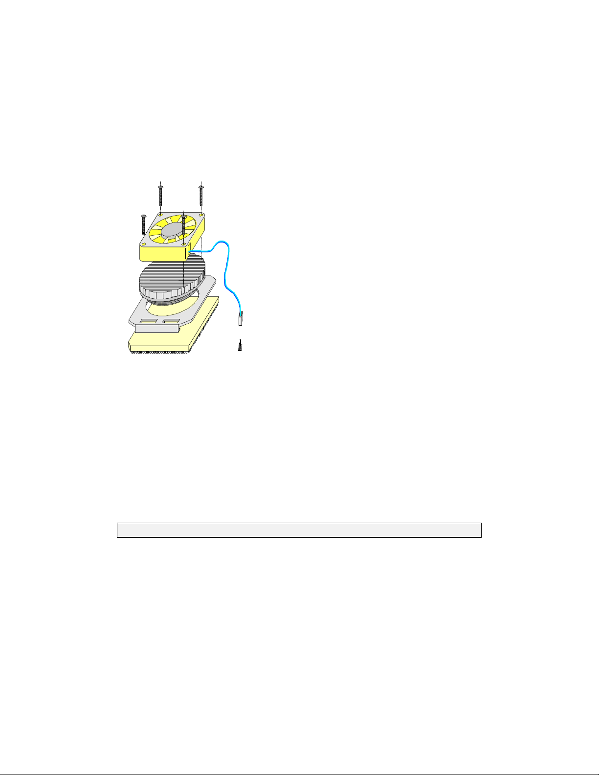
5.1 Installing Microprocessor and Fan
PowerSupply
Fan
Cord
486SX/25MHz 486DX/33MHz
486DX2/66MHz 486DX4/100MHz
5x86/133MHz
The following microprocessors are supported:
Heater
Depending on the processor and the system
Heater
Socket
environment, fan and/or heater may be installed on it.
Please refer to your processor specifications for more
Microprocessor
Fan Connector
(Power)
information.
5.2 Installing Memory
The TEK-AT4LPLUS supports from 1 to 64 Megabytes of DRAM with parity check for
system memory. The memory must be installed on 30-pin (U3, 4, 5, 6) or 72-pin (U7, 8)
SIMM sockets.
At least 1MB of system memory must be installed for proper operation.
Total System Memory can be configured as follows depending on the memory type:
. 4 or 16MB using 9-bit SIMM devices (modules: 1 or 4 MB).
. from 1 to 64MB using 36-bit SIMM devices (modules: 1, 2, 4, 8, 16, 20, 32 and 64
MB).
WARNING: 9-bit and 36-bit SIMM devices must never be installed together.
DRAM devices with page mode at 70ns maximum access time is recommended.
Customizing The Board 5-1
Page 16

Follow the steps outlined below to install the memory:
• With the board flat on the table, turn it so that the end of the board with the sockets is
near you.
• Hold the module with the notch on the bottom right facing you, and insert the
connector into the socket at a 70° angle from the board (pin 1 on the module lines up
with pin 1 on the socket).
• Snap the module forward to a vertical position in the socket. The module is fully
inserted when the retaining pegs snap into the holes at each end of the module.
Customizing The Board 5-2
Page 17
5.3 Memory and I/O Mapping
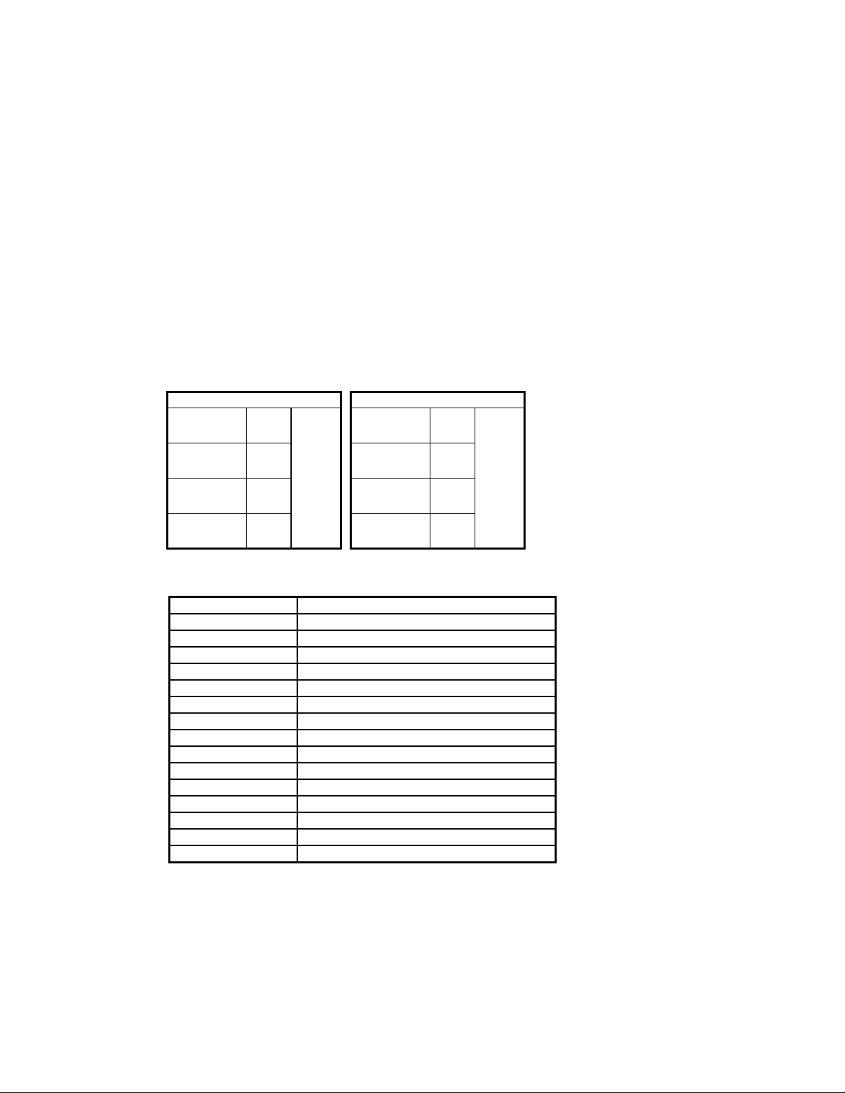
5.3.1 Memory Mapping
You also have room for up to 10 MB of Solid State Disks (SSDs):
U10 allows up to 128KB of EPROM for the BIOS.
Up to 8MB of FLASH EPROM can be installed on U19 and U20.
Up to 2MB of battery-backed SRAM disk can be installed on U27/28/35/36.
TABLE 5-1: Memory Map
600000 to 7FFFFF: SRAM 800000 to FFFFFF: Flash
600000
67FFFF
680000
6FFFFF
700000
77FFFF
780000
7FFFFF
TABLE 5-2: Onboard Decoded I/O Map
ADDRESS FUNCTION
000-00F DMA controller 1
020-03F Interrupt controller 1
040-05F Timer
060-06F Keyboard & Mouse
070-07F Real-time clock, NMI mask
080-09F DMA page register
0A0-0BF Interrupt controller 2
0C0-0DF DMA controller 2
0F0-0FF Math coprocessor
1F0-1F7 Hard disk
201 Watchdog timer, PDO, user
378-37A LPT1
2F8-2FF COM2
3F2-3F7 Floppy disk
3F8-3FF COM1
U36
U28
SRAM
U35
U27
800000
9FFFFF
A00000
BFFFFF
C00000
DF0000
E00000
FFFFFF
U19
U19
Flash
U20
U20
Customizing The Board 5-3
Page 18

5.4 Expanded and Extended Memory
Memory on the board consists of two areas: memory below 1 MB (0-640KB) referred to as
the standard or base memory, and memory located above 1 MB which is either Expanded
or Extended memory (memory located between 640KB and 1 MB is reserved for
shadowing. This is described later in this section).
Expanded and Extended memory refer to the mapping scheme that is used to access
memory above 1 MB in real mode. Since DOS requires real mode to operate, different
techniques are available. The TEK-AT4LPLUS offers the following options:
5.4.1 Expanded Memory
In Expanded memory mode, hardware is used to remap a defined area of memory. This
mode is driven by standard software commonly referred to as the LIM Standard or EMS.
A hardware-specific device driver (supplied with your single board computer) is loaded in
the CONFIG.SYS file to setup the software in order for it to access memory above 1 MB.
5.4.2 Extended Memory
In Extended memory mode, the CPU's own protected mode is used to access the memory
above 1 MB. This mode requires that the software jump into protected mode, perform the
transfer and return back to real mode. This is available through the BIOS using INT 15h
function 87h.
5.5 Memory Mode
Above 1MB can be defined either as EMS or Extended.
If EMS is used, the EMS hardware must be enabled, and the EMS driver loaded.
. EMS is enabled by entering SETUP at boot up
. Type the following command (or its equivalents) in the CONFIG.SYS file:
DEVICE=EMM386.EXE
5.6 Shadow RAM
As previously mentioned, memory between 640KB and 1MB is used for Shadow RAM or
Shadowing. This is simply the process of copying EPROM based code, such as the BIOS
and BIOS extensions, into DRAM (which is located in the same physical memory map).
Shadowing allows your code to run faster.
WARNING: If Shadow RAM is enabled, the RAM memory used for shadowing is no
longer available as EMS or Extended memory.
Customizing The Board 5-4
Page 19

5.7 Configuring the TEK-AT4LPLUS
Configuring your board is purely a matter of the application at hand. As an example, a
2MB system can be defined as 640KB base + 384KB shadow + 1 MB extended memory,
or, 640KB base + 384KB shadow + 512KB extended + 512KB EMS and so on. The user
is free to adapt the configuration to his particular needs.
5.8 SW1 - Configuration Jumpers
The TEK-AT4LPLUS supports an onboard BIOS extension which controls certain
functions of the BIOS related to industrial applications. The extended BIOS reads the
settings of the SW1 jumpers and acts accordingly.
Upon system start-up, the BIOS automatically determines how much ROM/RAM disk
memory is available to the system, and what equipment is connected to the system.
Jumpers
WARNING: The RAM disk is automatically detected and installed upon booting.
The beginning of the disk is checked and reformatted if it is found to be
corrupt or if data is unrecognizable.
SW1 are to be set by the user as needed.
5.8.1 SW1 (1-2) Selecting BIOS Boot Option
If SW1(1-2) is installed (booting MS-DOS from Flash EPROM), then Drive A: is the
Flash Disk (assuming jumper W14 is installed). Drive B: is Floppy 1 (if installed) or the
next available drive according to the following list of priorities:
1- Floppy 1
1- Flash Disk if not already installed as A:
1- RAM Disk (if installed)
1- Hard Disk (if installed)
Subsequent logical drives are installed following the above priority list.
If SW1(1-2) is not installed (booting operating system from Floppy/Hard drives), then
Drive A: is Floppy 0. Drive B:, and subsequent drives follow the priority list above.
Customizing The Board 5-5
Page 20

The following table describes drive assignments according to the installed devices:
TABLE 5-3: Physical Devices Installed & Drive AssignmentsTable
Configuration and
Physical
Devices Installed
DRIVE NAME:
A: Floppy 0 Floppy 0 Flash Floppy 0 Flash Flash
B: Floppy 1 Floppy 1 Floppy 1 Flash Floppy 1 Available
C: Available Flash Available Available Available Available
D: Available Available Available Available Available Available
NOTES: The indication "FLASH DISK" assumes at least one Flash device is installed at U19 with a valid DOS
content. "Floppy 0" specifies the physical drive connected to the twisted end of the flat cable. "Floppy 1" specifies the
physical drive connected to the untwisted end of the flat cable. "Jumper" specifies configuration Jumper SW1(1-2).
All other drives are installed following the above assignments in this manner: RAM Disk, and then Hard Disk.
Therefore, with a full configuration, RAM Disk is "D" and the Hard Disk is "E".
Jumper/No Jumper
Floppy 0
Floppy 1
No Flash Disk
No Jumper
Floppy 0
Floppy 1
Flash Disk
Jumper
Floppy 0 Or
No Floppy 0
Floppy 1
Flash Disk
No Jumper
Floppy 0
Flash Disk
Jumper
Floppy 1
Flash Disk
Jumper
Flash Disk
5.8.2 SW1(3-4) Selecting COM1/COM2 for VT00 or Download Mode
You can run VT100 mode or Serial Download mode from either COM1 or COM2.
Installing this jumper selects COM2, removing it selects COM1 (default).
5.8.3 SW1(5-6) Enabling VT100 Mode
The TEK-AT4LPLUS supports VT100 mode to enable the board to run without a local
keyboard or screen. That is, operation can be controlled via a remote terminal or a
computer with a terminal emulation program.
Requirements
The board must be supplied with +/-12 volts to support VT100 mode, (required by the RS232 drivers).
The connected terminal should emulate a VT100 or ANSI terminal. Although this is not
an absolute requirement, strange characters may appear on screen if it does not. This
occurs because the VT100 recognizes these control characters, and causes them to perform
a specific function. For example, screen erase, cursor position, and so on.
Customizing The Board 5-6
Page 21
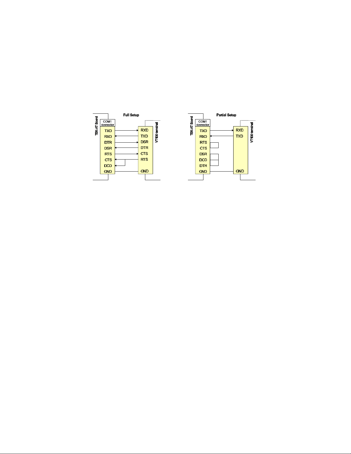
Follow these steps to setup VT100 mode:
• Install SW1(5-6) to enable VT100 mode.
• Setup the communications cable as follows:
Full cable configuration with all control lines can
be used to connect a VT100 terminal to COM1
or COM2.
If a full cable is not required, a partial cable using
only the TXD and RXD lines can be used. The
control lines are ignored by looping as shown
above.
• Boot up your terminal and set it up with the following parameters:
19200 Baud / 8 Bits / No Parity / Echo off (or full duplex)
F Use CTRL-R to configure your system in VT100 mode.
Running Without a Terminal
To disconnect the VT100 terminal or to run without a terminal, ensure the control lines
are in an active state. Failing this, the system may "hang" while waiting for the control
lines to become active. Refer to partial cabling to remain the lines active.
Disabling VT100 mode allows the board to run without any console, then video card is not
necessary.
5.8.4 SW1(7-8) Enabling Serial Download Mode
Installing this jumper, enables Serial Download Mode; removing it disables Serial
Download Mode (default).
Customizing The Board 5-7
Page 22

5.9 Installing Supervisor Utilities
5.9.1 Special Note on Register 201h
IBM PCs use address 201h as the game port. TEKNOR computers utilize this address to
give industrial PC users the greatest amount of I/O addressing space possible. This
ultimately renders the game port unusable.
Hence, some problems may occur with various test software packages that intentionally
write to the game port and leave it with unknown values.
The following table illustrates how TEKNOR computers utilize I/O Register 201h:
TABLE 5-4: Register 201h
Bit Function
0 Enable Watchdog (1=enable, R/W bit)
1 Watchdog activate (1-0-1 to toggle, R/W bit)
2 Flash VPP enable (1=VPP 12v, 0=VPP 5v, R/W bit)
3 Enable direction control RS-485
(1=enable RS-485 only, write only)/(Read=PDO* Status)
4 Make printer 8 data bits read only
(1=input, 0=output, write only)
5 Select alternate SW1/SW2 (TEK-AT4L+, TEK-AT3L, TEK-AT4L+) (1=select
SW2, read only)
6 Not used
7 Not used
WARNING: Not all bits are R/W. Therefore, be certain to keep a mirror image of
register 201(hex) when programming it. All bits are 0 after a hardware
RESET or power up condition.
5.9.2 Watchdog Timer
The Watchdog Timer is extremely useful in embedded systems where human supervision
is not required. Following a reset, the Watchdog is always disabled. The Watchdog is
enabled once "1" is written in bit 0 at address 201h the first time. When enabled, the
microprocessor must refresh the Watchdog. This is done by writing alternatively "0" and
"1" to bit 1 at address 201h, once every 1.6 seconds to verify proper software execution.
Customizing The Board 5-8
Page 23
If a hardware or software failure occurs such that the Watchdog is not refreshed, a reset
pulse is generated by the Watchdog to restart the processor.
WARNING: The user program must provide the first access to address 201h, and
must also include the refresh routine. In addition, be certain to keep a
mirror image of register 201h when programming it. This is necessary
since register 201h is a write-only user register and, as a result, is not
used by the BIOS.
TABLE 5-5: Watchdog Timer Register
ADDRESS REGISTER
201 bit 0 read/write Watchdog enable
201 bit 1 read/write Watchdog refresh
Jumper W12 must be installed to enable activation of the Watchdog. If jumper W12 is
removed, the Watchdog is disabled.
5.9.3 Power Failure Detector (PFD)
The PFD, which generates a non-maskable interrupt (NMI) when a failure occurs,
provides a 1.25V threshold for DC power fail warning, low battery detection W7(2-3), or
when monitoring a power supply other than +5VDC W7(1-2). The Power Detection
Output (PDO) of the power failure detection circuit is connected to IOCHECK (NMI).
Jumper W13 allows the user to disable this feature. However, the PDO status is still
available by reading I/O address 201h bit 3.
The detection circuit generates a non-maskable interrupt when a power failure occurs.
The status of the PDO is available at I/O address 201h bit D3. For example, if it reads 0,
the circuit has detected a low power warning from the power detect pin on 6, connector
J5.
Pin 6 on connector J5 is used for the power detection input. This input can only accept
DC voltage. The line is monitored via two user-defined external resistors, R19 and R18,
which are connected to the power failure input (Note: R19 is a surface mount resistor and
R18 is fixed to 1KB). The user should position the resistors according to the monitoring
level desired. If the voltage level supplied to this line drops below 1.3V typical, a Power
Fail status is detected and directed to the NMI line.
Customizing The Board 5-9
Page 24

Example:
Assume the TEK-AT4LPLUS is powered by a 9V DC battery and it is required that the
battery be monitored for a low battery warning at 7.5V DC. In this case, R19=4700Ω and
R18=1000Ω.
So, if the battery voltage goes below 7.5V, it will generate a non-maskable interrupt
(NMI) and the status can be read at address 201 bit D3. If bit D3 is 0, a low battery is
indicated.
Bear in mind that R19 and R18 should be tailored to fit your specific application. The
values for these two resistors can be identified by using the following formula:
R18 / ( R19+R18) x 7.5V < 1.3V
where: R19 = 1000 x Vmon -1300 / 1.3
Please contact our Technical Support department if more details are needed.
WARNING: All TEK-AT boards are equipped with an onboard detection circuit
which is activated when +5V drops below 4.75V. When this occurs, the
system is reset disabling access to SRAM, DRAM, and so on.
5.9.4 Low Battery Detection
The Low Battery Voltage detection uses the same circuit as the Power Failure Detector,
and thus, both cannot be used at the same time.
The Low Battery Detector generates an NMI when the battery voltage drops below 3 volts.
To monitor a Low Battery Voltage, install jumper W7(2-3) and jumper W13. The status
of PDO can be read back at I/O port 201 hex D3.
WARNING: Although the Low Battery Detector uses the same circuit as the Power
Failure Detector, J5-6, R19 and R18 are not utilized. Instead, we have
added two other resistors for this function: R14 and R17.
5.10 Attaching the AT4LPLUS to Enclosure
Four mounting holes are available on the board to ensure an optimal mechanical fixing. It
is highly recommended to use all the mounting holes when attaching the TEK-AT4LPLUS
to its enclosure.
Precise mounting holes location is given in the Appendices: TEK-AT4LPLUS - Mounting
Holes .
Customizing The Board 5-10
Page 25
6. INSTALLING DEVICES
6.1 Connecting Power Supply
Power can be drawn on the TEK-AT4LPLUS using the onboard power connector (J5), or
the ISA-AT bus power capabilities when the board is connected in a backplane.
WARNING: Both power supply must not be connected together. While using one, the
other must be disconnected.
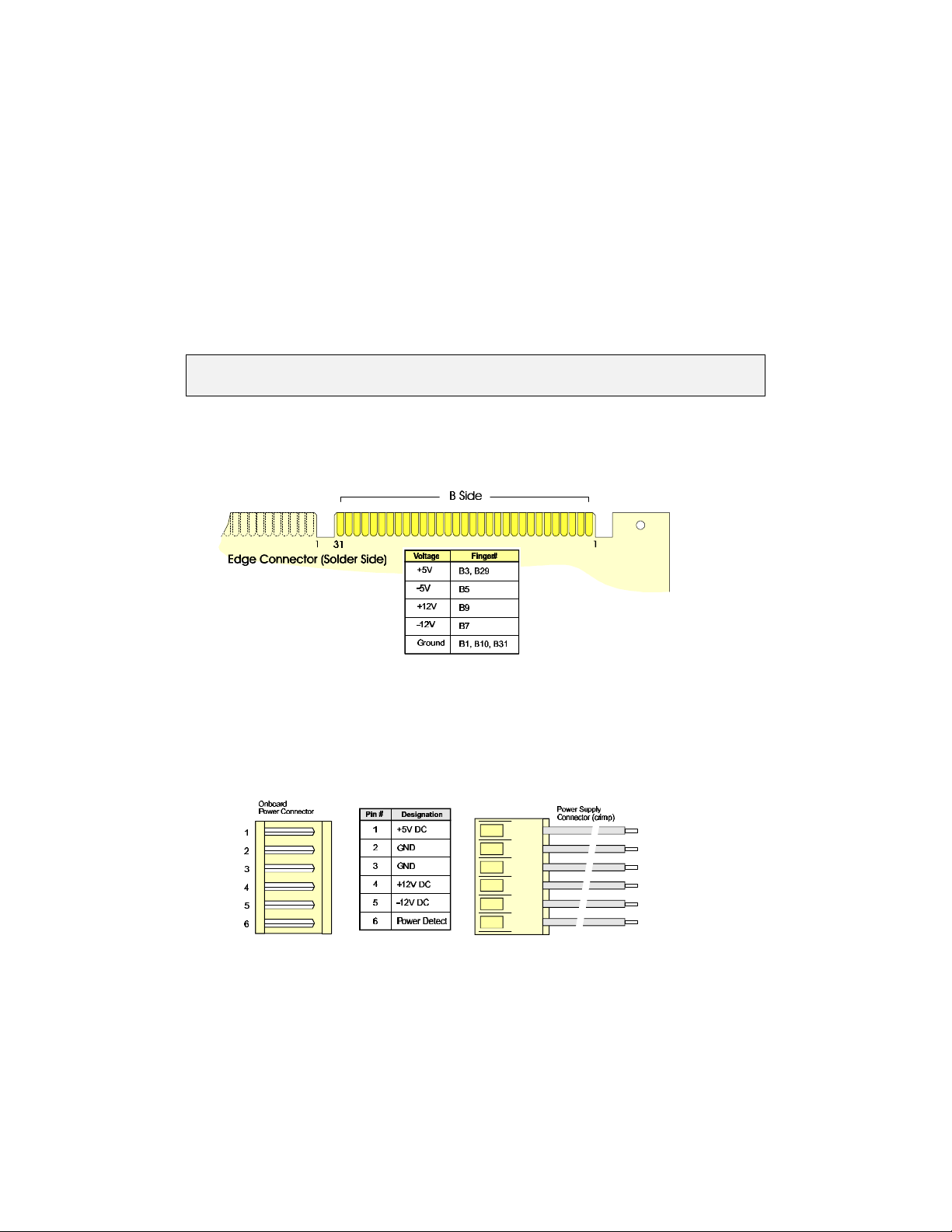
6.1.1 Supplying Power Using the ISA-AT Bus
+5V, -5V, +12V, -12V and ground voltages are routed on the edge connector as follows:
Note: The complete description of the edge connector is given in the appendix E - Board Connectors and Pinout.
6.1.2 Supplying Power Using the Power Connector (J5)
The Power Supply is drawn on the Backplane using the 6-pin J5 connector.
Installing Devices 6-1
Page 26
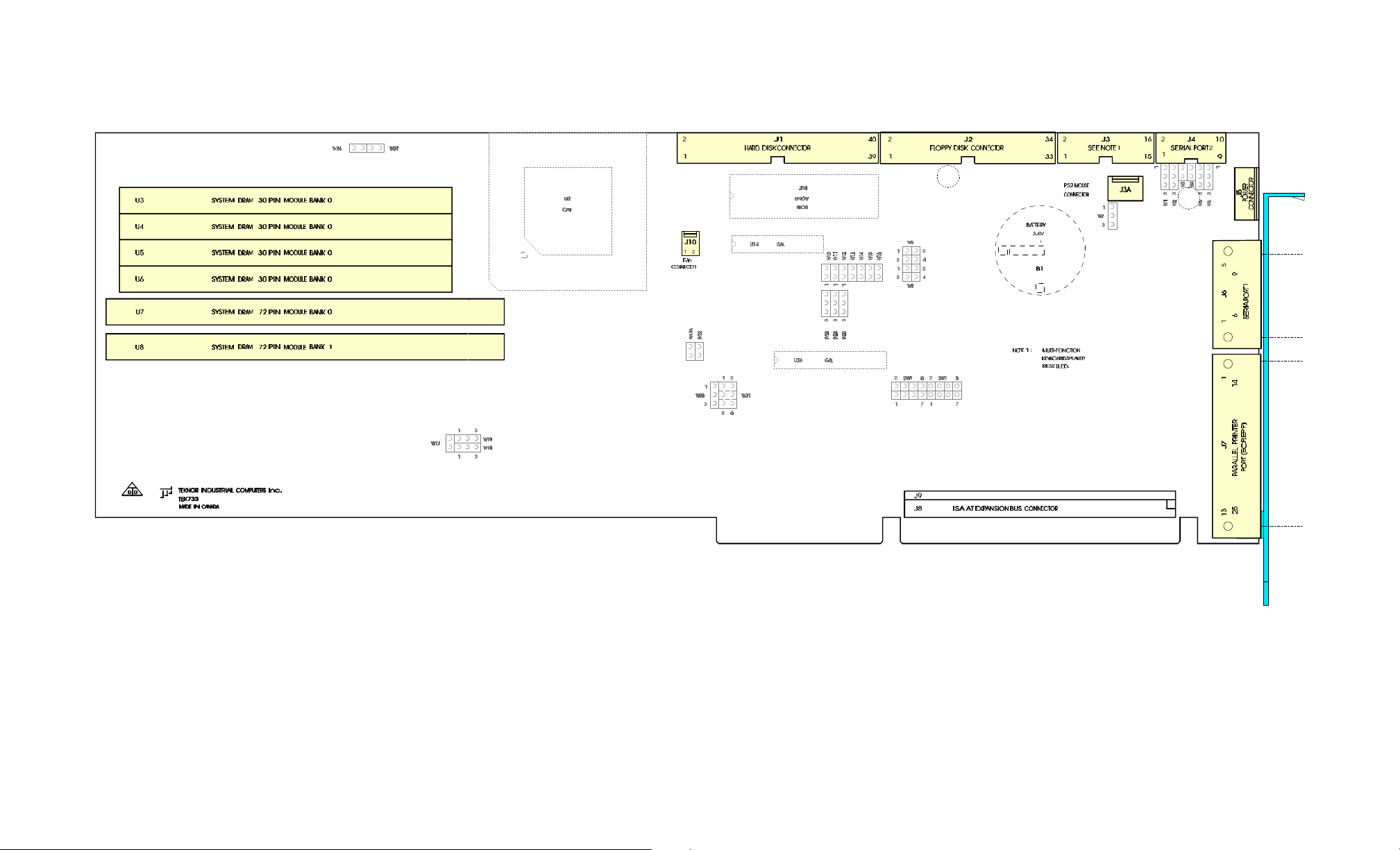
CONNECTOR LOCATION
Installing Devices 6-3
Page 27
6.2 Connecting Hard Disk (J1)
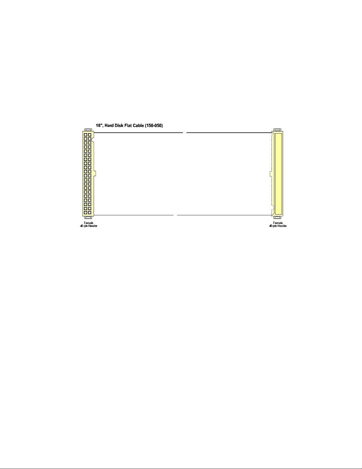
IDE connections use standard 40-pin header flat cables. This connector handles all
command, data, and status I/O lines. Recommended maximum cable length is 18-24
inches.
The drive can be mounted in any horizontal or vertical plane. The hard drive and its type
must be specified in the CMOS setup (number of cylinders, heads, sectors per track,
landing zone, and write precompensation). The specification can be done by selecting a
standard drive type listed in the setup screen or by using a user defined drive type (type
48), whereby the user can enter the required parameters.
Please refer to your drive manufacturer to obtain this information.
Hard disk interface can be disabled using J11 jumper. Please refer to Section 9 - Setting
Jumpers.
Using Solid State Disk (SSD): Solid State Disks have no moving parts and are far less
susceptible to dirt, moisture, vibration and temperature variations than mechanical disk
drives. Two types of SSDs are available: Static-RAM (SRAM) and Flash EPROM. The
TEK-AT4LPLUS supports up to 2MB of SRAM and 8MB of Flash EPROM.
Solid State Disks installation is described at the end of this section.
Installing Devices 6-5
Page 28
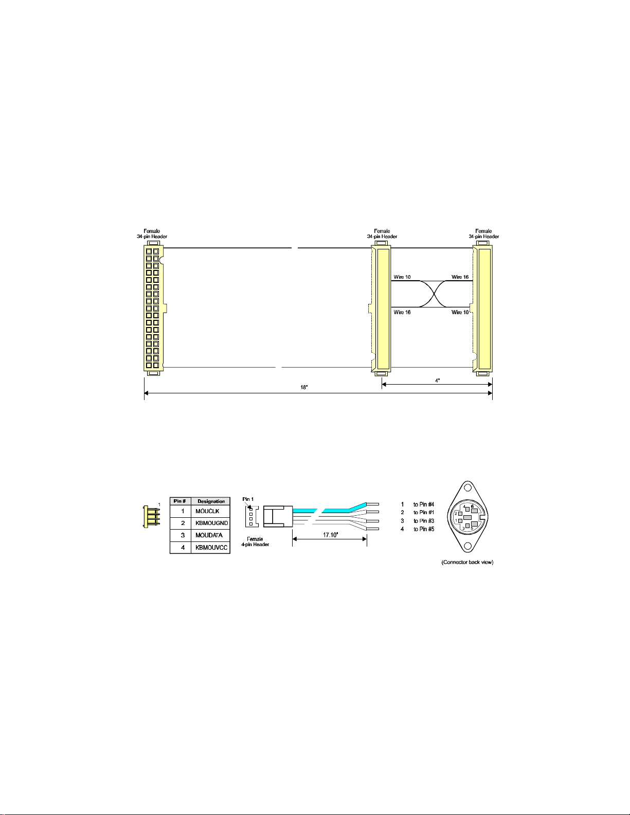
6.3 Connecting Floppy Disk Drive (J2)
Floppy Drive connections use standard 34-pin header flat cables. The disk controller is
IBM PC XT/AT compatible (single and double density), and supports Enhanced Floppy
Mode (2.88MB). It handles 3.5’’ and 5.25’’, low and high density drives. Up to two drives
can be supported in any combination.
6.4 PS/2 Mouse Connector (J3A)
The TEK-AT4LPLUS supports PS/2 standard mouse through the J3A connector.
Important: make sure the PS/2 mouse driver (provided by its manufacturer) is installed.
Note: This cable is available from TEKNOR - referenced as 150-052.
Installing Devices 6-6
Page 29
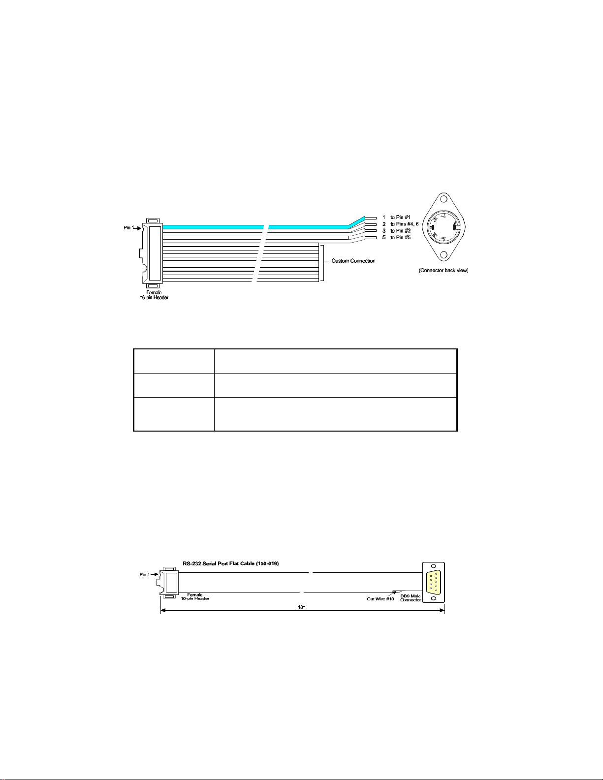
6.5 Multi-Function Connector (J3)
The TEK-AT4LPLUS offers a 16-pin header to support keyboard, speaker, Reset button,
and LED devices. To output the signals, the cable must be built as follows:
Note: This cable is available from TEKNOR - referenced as 150-018.
Devices are described as follows:
Speaker an 8 ohm speaker can be directly connected to pins 7 and 8. All
Reset a Normally Open Push button can be connected to reset the TEK733
Hard Disk LED the onboard IDE interface drives an external LED during the drive
necessary drivers are installed.
(electrical short between pin 13 and 14).
activity. Anode must be connected to pin 16. No external current
limiting resistor is required since one is already present.
6.6 Serial Port #2 Connector (J4)
The TEK-AT4LPLUS features two UARTs which are functionally equivalent to the
NS16450. Both are configured as DTE.
6.6.1 COM1(J6)
The COM1 port is buffered directly on the board for RS-232 operations. COM1 is 100%
compatible with the IBM-AT serial port.
Note: This cable is available from TEKNOR - referenced as 150-019.
Installing Devices 6-7
Page 30

6.6.2 COM2 (J4)
The Serial Port COM2 supports both RS-232 and RS-485 standard via J4 connector
(standard male DB9 connector at the edge of the board).
COM2 pinouts (RS-232 and RS-485) are given in Appendix E - Board Connectors and
Pinout.
When configured for RS-485 the TEK-AT4LPLUS supports either full-duplex or party line
communication.
Full Duplex Operation
Upon power-up or reset, the RS-485 interface circuits are automatically
configured for full duplex operation. J4(3,4) act as the receiver lines and J4(5,6)
as the transmitter lines.
Party Line Operation
In order to enable party line operation, the user must first write "1" to bit 3 at I/O
address 201h. This allows the transceiver (J4 3,4) to be controlled by the RTS
signal. Upon power-up or reset, the transceiver is by default in "receiver mode"
in order to prevent unwanted perturbation on the line.
In party line operation, termination resistors R9 and R10 must be installed only
on the boards at both ends of the network.
6.7 Parallel Printer Port Connector (J7)
The Parallel Printer Port (J7) provides the necessary control signals for Centronicscompatible parallel interface. The connection is done through a standard female DB25
connector located at the edge of the board. Its pinout is given in Appendix E - Board
Connectors and Pinout.
The port is set to output 8-bit data by default. It can be changed to input data simply by
writing 10h to address 201h (set bit 4).
WARNING: Port 201h is also used to control the Watchdog Timer. Therefore, it is
highly recommended you keep a mirror image of port 201h in memory
Installing Devices 6-8
Page 31

6.8 Installing Solid State Disks
The TEK-AT4LPLUS Single Board Computer supports 2, 4 or 8MB Flash EPROM Disk.
The Flash EPROM is surface mounted component option which must be sized and
ordered by the customer.
6.8.1 Writing To Flash Disks
To create a Flash disk (i.e. writing information to it), use the XFLASH utility found on
the utilities diskette which came with the board.
The XFLASH software utility allows you to choose files from floppy and hard disks and
write them to the Flash disks.
Information can be transferred to the Flash disk by directly running XFLASH on the
TEK-AT4LPLUS computer, or remotely - by using a serial link. The second option is
referred to as Download Mode and is enabled by installing jumper SW1(7-8).
In addition, the Flash disk can be made to boot simply by installing SW1(1-2). This
function causes the Flash disk to replace floppy disk 0 from the "A" position - leaving the
mechanical floppy unused. Floppy 0 must then be physically moved to the floppy 1
position where it becomes the "B" drive. Please refer to the Physical Devices Table (see
Page 5-7) for more information.
The only difference between the two drive types is that Flash disks are read only. Hence,
whenever an attempt is made to write to the Flash disk, a write-protect error is generated.
Writing to Flash disks is explained below and in detail in Teknor's XFLASH User's
Manual.
WARNING: In order for the AT4LPLUS to recognize the Flash disk, Jumper W14
must be installed.
6.8.2 SRAM Disk
The TEK-AT4LPLUS supports from 512KB to 2MB SRAM. The SRAM is surface
mounted component option which must be sized and ordered by the customer.
Please refer to Section 9 - Setting Jumpers to enable SRAM on the board (if installed).
WARNING: SRAM power consumption is usually less than 5mA in 3V backup mode.
So files transferred to battery-backed SRAM disks typically stay
resident for two years. Actual life, however, is dependent on the actual
consumption of the SRAM devices installed.
Installing Devices 6-9
Page 32

6.8.3 Battery Backup Circuit
The board comes with a 350mA/h lithium battery. If the TEK-AT4LPLUS is strapped to
be powered by the battery back-up, the RAMs will retain their information after a power
down.
Please refer to Section 9- Jumper Settings to locate and set Battery Backup Circuit (W10).
WARNING: Removing jumper W10 will cause the set-up and real-time clock
information to be lost.
The TEK-AT4LPLUS comes with a 350mA/h TL5186 TADIRAN battery with a shelf life
of approximately 10 years (under "no-load" conditions).
TEK-AT4LPLUS draws approximately 24mA typical. This means the battery will last 1.6
years if no power is applied to the board. Remember, when the 5V is supplied, the battery
is electronically disconnected. Virtually as if it were on the shelf.
The actual life of the battery depends on the amount of time DC power is not applied and
on environmental (temperature) conditions. The TADIRAN TL5186 has an operating
range of -550 to 750C and discharge characteristics vary with temperature.
The TADIRAN TL5186 is U.L. recognized. Its U.L. component recognition is MH12193.
WARNING: The actual voltage supplied by the battery is 3.6 volts. This can be
verified at pins 16-32 on the SRAM device using a standard voltmeter.
Installing Devices 6-10
Page 33
7. INSTALLING VIDEO DEVICES
7.1 Using Standard Video Adapter Board
When using a passive backplane, the video adapter board can be installed directly in one
slot. The video adapter board depends on the display to be connected to the system. The
display must be connected directly to the Video Adapter onboard connector.
7.2 Using Video Mezzanine Board
With TEKNOR’s mezzanine board, it is possible to assembly a complete computer
without passive backplane. When stand-alone mode is required, a mezzanine board may
be used.
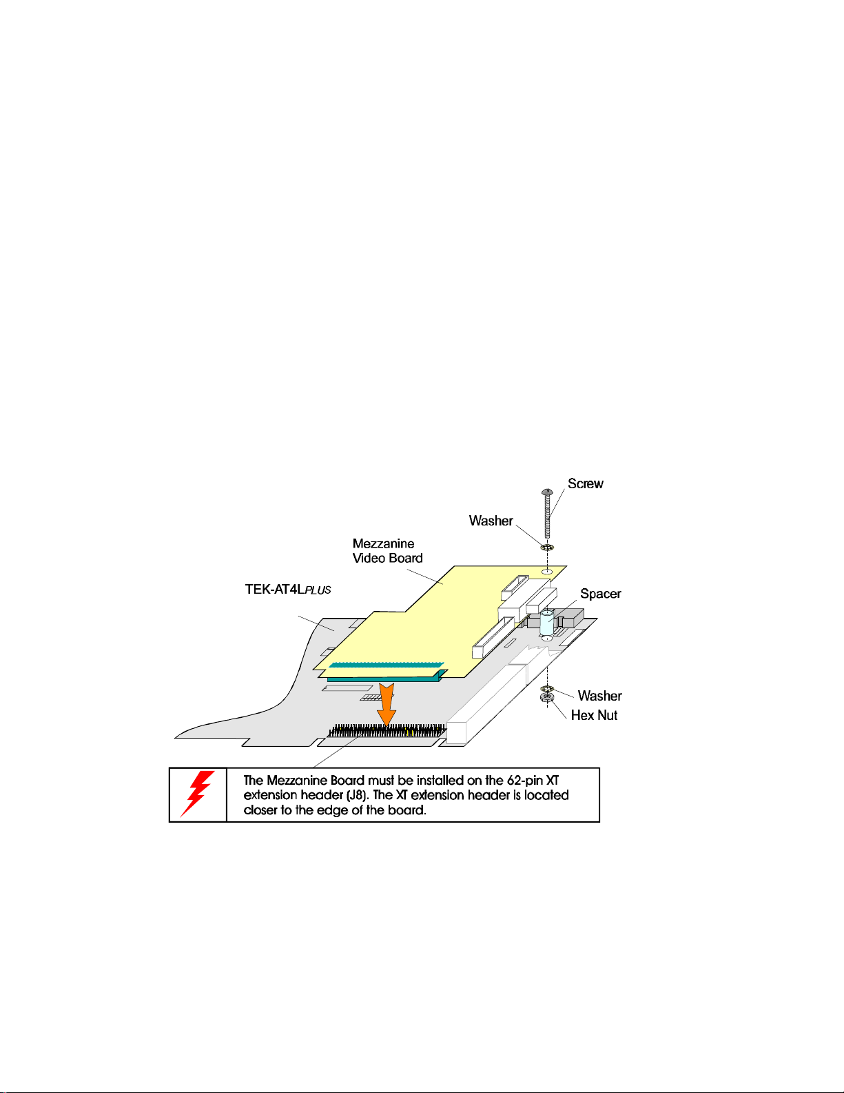
7.2.1 Installing Mezzanine Board
Proceed as follows to connect a mezzanine board to the TEK-AT4LPLUS:
The Mezzanine Video Board provides connectors for CRT and Flat Panel display. Please
refer to its User’s Manual for more information on display connecting.
Installing Video Devices 7-1
Page 34
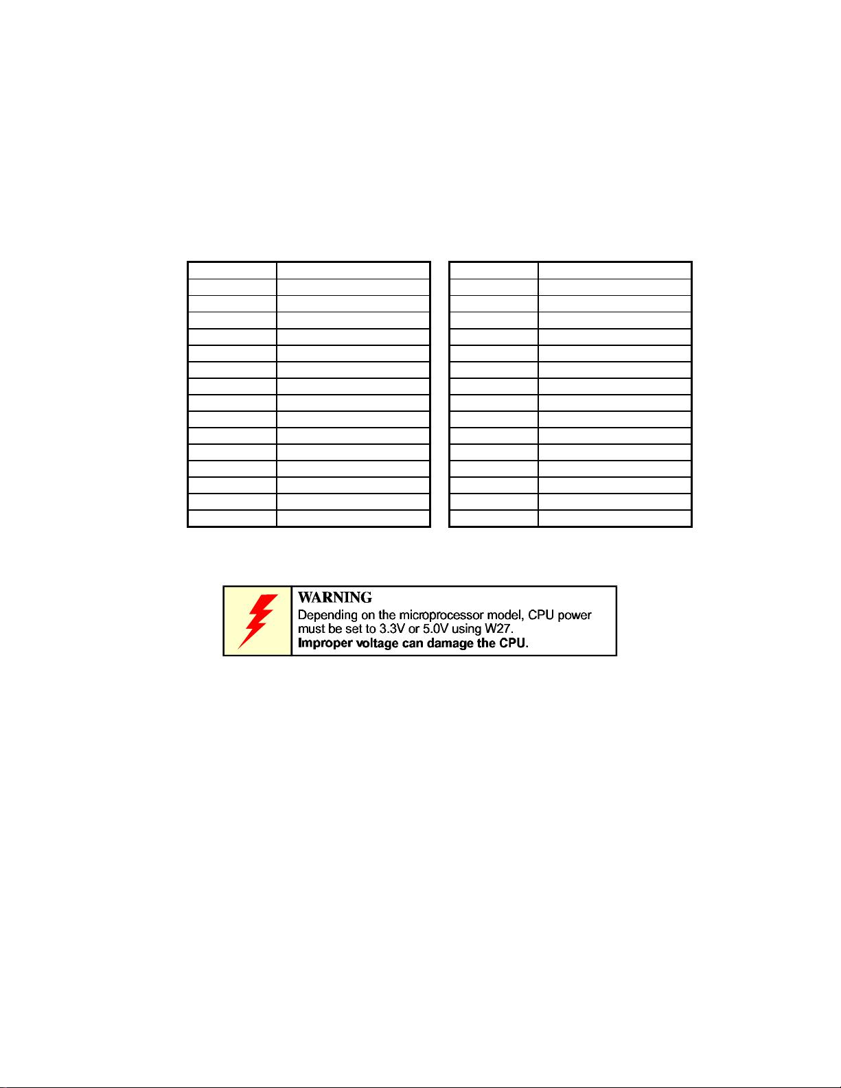
8. SETTING JUMPERS
The TEK-AT4LPLUS is designed to allow for minimal hardware configuration.
The following is a list of the basic configuration jumpers available on the board:
Jumper Function Jumper Function
W1 Serial In 2 (SIN2) W15 BIOS Boot Flash
W2 Request To Send 2 (RTS2) W16 TEKNOR Extension
W3 CTS2 to RTS2 W17-19, W26 CPU Type Selection
W4 DTR2 to DSR2 W19A PS/2 Mouse
W5 Serial Out 2 (SOUT2) W20 Bus Clock Signal Selection
W6 CTS2 W21 CPU Clock Selection
W7(1-2) Power Fail Detection W22 Graphic Mode Selection
W7(3-4) Low Battery Detection W23-W24 DMA Channel Selection
W8 EDOUT (Floppy) W25 Parallel Port Interrupt
W9 DHOUT (Floppy) W26 CLKMUL Enable
W10 SRAM Battery Backup W27 CPU power (3.3V or 5V)
W11 IDE Hard Disk Interface SW1(1-2) Boot from Flash
W12 Watchdog Timer SW1(3-4) COM1/COM2 Selection
W13 Power Monitoring SW1(5-6) Selects VT100 as Console
W14 Flash EPROM Write SW1(7-8) Download Mode
Setting Jumpers 8-1
Page 35
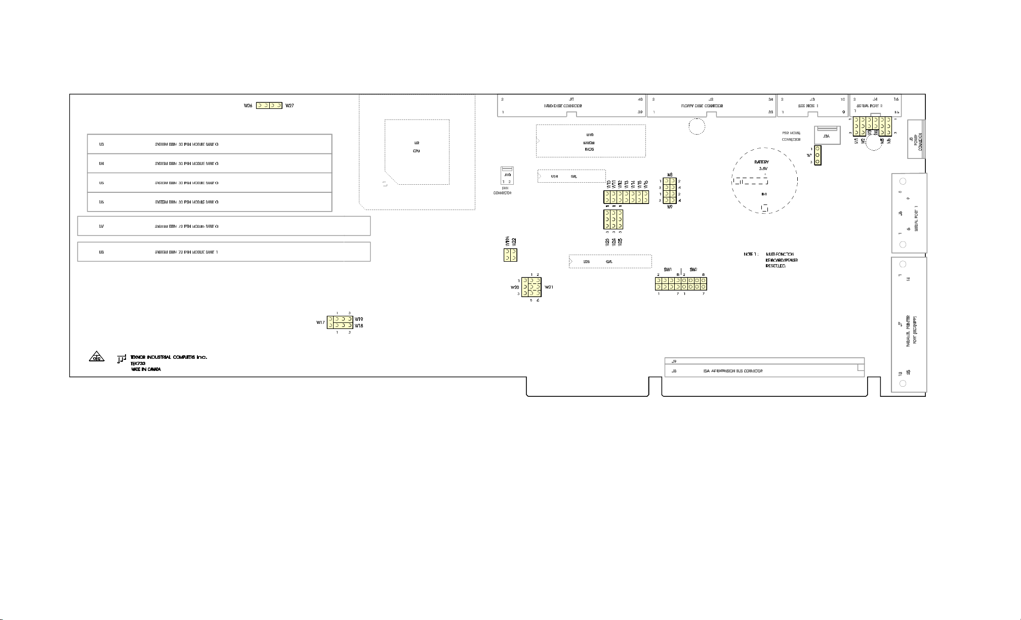
JUMPER LOCATIONS
Setting Jumpers 8-3
Page 36
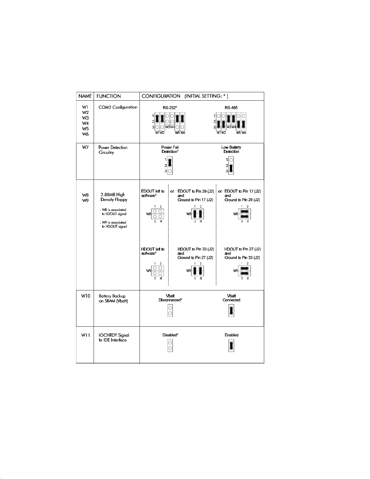
TABLE 8-1: Jumper Settings (W1-W11)
Setting Jumpers 8-5
Page 37
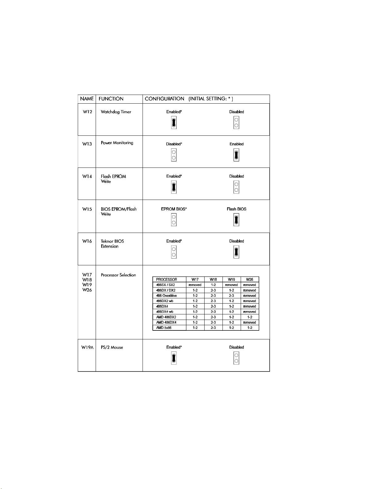
TABLE 8-2: Jumper Settings (W12-W19, W26)
Setting Jumpers 8-6
Page 38
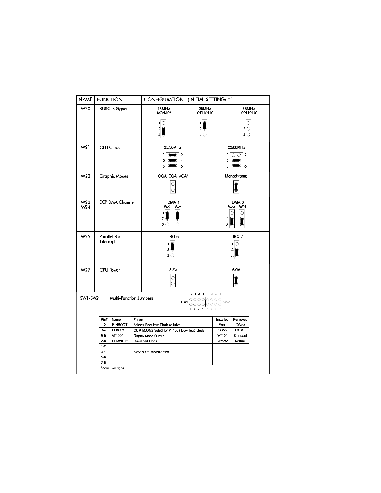
TABLE 8-3: Jumper Settings (W20-W25, SW1, SW2)
Setting Jumpers 8-7
Page 39

9. CONFIGURING DMA and IRQ
9.1 DMA Channels Allocation
The TEK-AT4LPLUS supports seven Direct Memory Access channels: Channel 0 is
reserved for the DRAM refresh. Channel 4 is used to cascade channels 0 through 7 to the
microprocessor, and Channel 2 is reserved for the floppy controller.
TABLE 9-1: 8237 Controller Table
DMA 0 Refresh
DMA 1 Available
DMA 2 Floppy controller
DMA 3 Available
DMA 4 Cascade controller # 1
DMA 5 Available
DMA 6 Available
DMA 7 Available
9.2 Allocating IRQ Lines
Two 8259 interrupt controllers handle the interrupts on the TEK-AT4LPLUS. Six
interrupt lines are directly linked to the keyboard controller, timer, the real-time clock,
both serial ports and the parallel port. A seventh interrupt line (IRQ12) is used for the
PS/2 MOUSE but the mode can be made available by the W19A jumper.
TABLE 9-2: 8259 Controller Table
CONTROLLER # 1 CONTROLLER # 2
IRQ 0 Timer 0 IRQ 8 Real-time clock
IRQ 1 Keyboard IRQ 9 Available
IRQ 2 Cascade controller # 2 IRQ 10 Available
IRQ 3 COM 2
IRQ 4 COM 1
IRQ 5 Available IRQ 13 Available
IRQ 6 Floppy controller IRQ 14 Fixed disk
IRQ 7 LPT 1
* All functions marked with an asterisk (*) can be disabled.
*
*
*
IRQ 11 Available
IRQ 12 PS/2 Mouse/Available
IRQ 15 Available
Configuring DMA and IRQ 9-1
*
*
Page 40

10. TEK-AT4LPLUS BIOS
10.1 OVERVIEW AND FEATURES
The TEK-AT4L PLUS uses the American Megatrends INC. PC/AT BIOS. This BIOS
provides a software interface between the MS-DOS operating system and the hardware of
the Single Board Computer. The interface provided by the BIOS is 100% IBM AT
compatible. That is, all functions accept similar inputs and provide the same results as
IBM, although the program code itself is different.
10.2 ERROR HANDLING
Teknor BIOS can be configured to handle errors differently . Two possibilities exist:
Stop: The BIOS will stop the booting process if an error is detected and request the user
to press F1.
WARNING: The BIOS will display an error message but will continue the booting
procedure
The following lists the error sources and their default values.
[ Warning ] Diskette
[ Warning ] Fixed Disk
[ Warning ] Keyboard
[ Warning ] Video
[ Warning ] Memory size
[ Warning ] CMOS checksum
[ Warning ] Real-Time Clock
[ Warning ] POST configuration
[ Warning ] Coprocessor
[ Warning ] Other
TEK-AT4LPlus BIOS 10-1
Page 41

APPENDICES
A. PRODUCT SPECIFICATIONS
B. BOARD DIAGRAMS
C. CONNECTOR PINOUTS
Page 42

A. PRODUCT SPECIFICATIONS
A.1 TEK-AT4LPLUS - Product Specifications
TEK-AT4LPLUS DESCRIPTION
Overview PC AT Single Board Computer
Supported
Microprocessors
Memory
I/O Connectors . ISA available on expansion headers
Power Supply ISA Bus +5V, -5V, +12V and -12V DC through ISA Bus from backplane
Supply Current 5x86 DX4 DX2
Operating Temperature 0oC to 70oC* - 5% to 95% Non-condensing Relative Humidity
M.T.B.F. Over 200.000 hours
PCB Characteristics Four layers: Signal/Ground/Power/Signal
Outline Dimensions 13.300” x 4.700” (337.80mm x 119.40mm) - without bracket
Order Guide Use the following part number : TEK733, AT4LPLUS Single Board Computer
486SX/25MHz 486DX/33MHz
486DX2/66MHz 486DX4/100MHz
5x86/133MHz
. System Memory: 1 to 64 MB - DRAM
. Up to 8MB of user Flash EPROM (option)
. Up to 2MB user SRAM with battery backup (option)
. Supports Shadow RAM BIOS for fast execution
. IDE AT standard, available on a standard 40-pin connectors
. Floppy Disk available on a standard 34-pin connector
. Multi-Function connector :
Keyboard - keyboard, speaker, reset and LED on a 16-pin connector
. Serial Ports
COM1 - RS-232 on a DB9 male connector
COM2 - RS-232 or RS-485 on a 10-pin connector
. Parallel Port DB25 male connector
. Mouse IBM PS/2 mouse compatible (4-pin header)
Auxilary +5V, -5V, +12V and -12V DC on standard 6-pin header
Icc (+5V) 1.7A 2.1A 2.0A
Ipp(+12V/-12V) 5/10mA 5/10mA 5/10mA
Test Conditions: 2MB Flash, 1MB SRAM, 8MB DRAM
* (requires cooling)
Designed to minimize EMI
Total thickness: 0.093” ±0.005” (2.36mm ±0.12mm)
Product Specifications A-1
Page 43
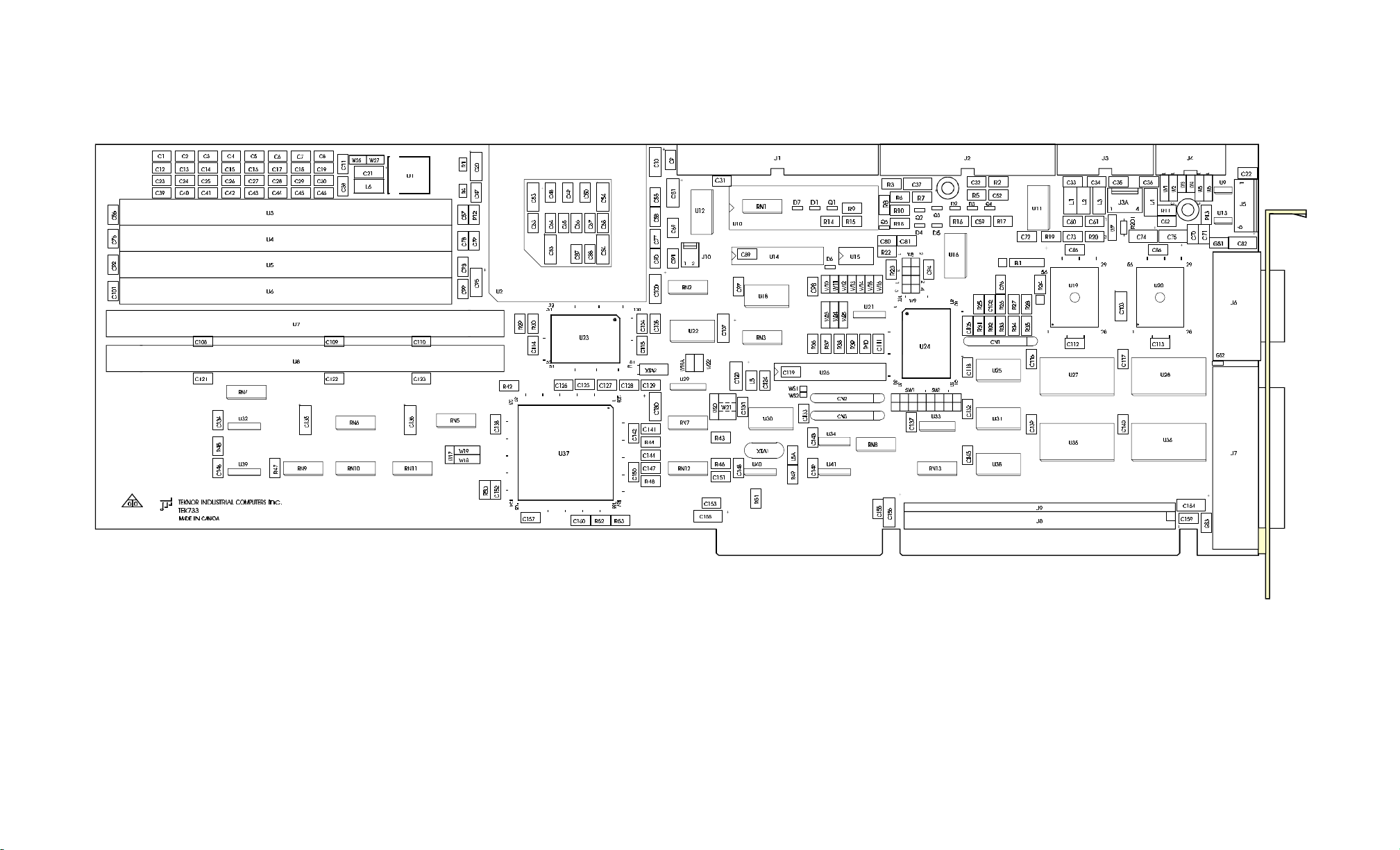
B.1 TEK-AT4LPLUS - Assembly Diagram (Top View)
Board Diagrams B-1
Page 44
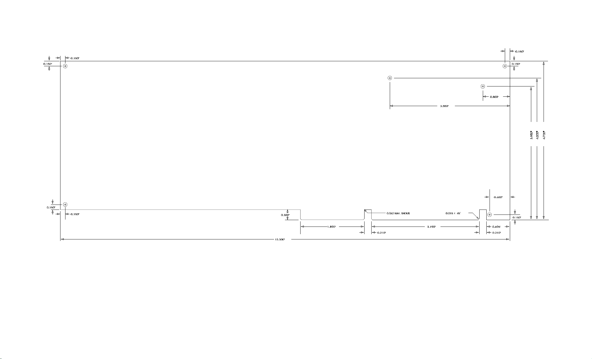
B.2 TEK-AT4LPLUS - Mounting Holes
Board Diagrams B-3
Page 45
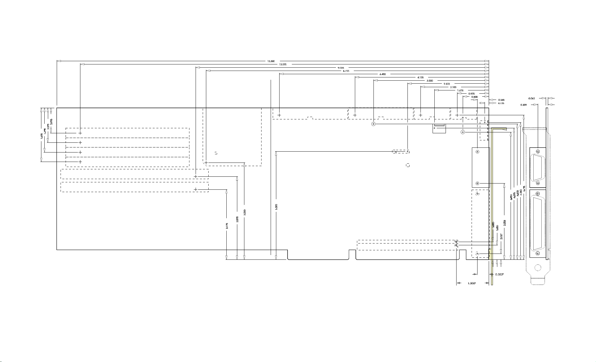
B.3 TEK-AT4LPLUS - Mechanical Specifications
Board Diagrams B-5
Page 46
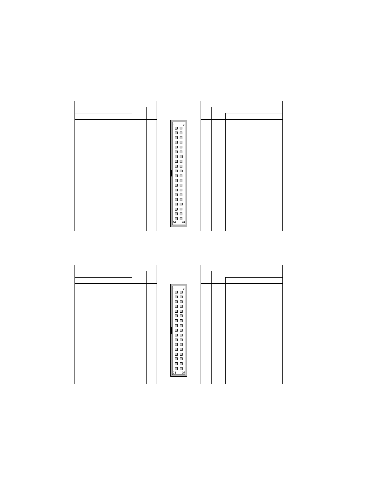
C.1 J1 - IDE #1 Connector
Pin Number Pin Number
Signal Flow Top View Signal Flow
Signal Signal
RST#
SD7
SD6
SD5
SD4
SD3
SD2
SD1
SD0
GND
Not Connected
IOW#
IOR#
IOCHRDY
DACK#
IRQ14
SA1
SA0
CS0#
ACTIVE#
# Active Low Signal
1
3
5
7
9
11
13
15
17
19
21
23
25
27
29
31
33
35
37
39
2
4
6
8
10
12
14
16
18
20
22
24
26
28
30
32
34
36
38
40
GND
SD8
SD9
SD10
SD11
SD12
SD13
SD14
SD15
Not Connected
GND
GND
GND
BALE
GND
IOCS16#
Not Connected
SA2
CS1#
GND
C.2 J2 - Floppy Disk Drive Connector
Pin Number Pin Number
Signal Flow Top View Signal Flow
Signal Signal
GND
GND
GND
GND
GND
GND
GND
GND
GND
GND
GND
GND
GND
GND
GND
GND
GND
-
1
-
3
-
5
-
7
-
9
-
11
-
13
-
15
17
-
19
-
21
-
23
-
25
-
27
-
29
-
31
-
33
2
O
-
-
I
O
O
O
O
O
O
O
O
I
I
I
O
I
RPM/LC
Not Connected
Not Connected
INDEX*
MOTOR ENABLE A*
DRIVE SELECT B
DRIVE SELECT A
MOTOR ENABLE B*
DIR CONTROL*
STEP*
WR_DATA*
WRITE ENABLE*
TRACK0*
WRITE PROTEC*
RD_DATA*
HEAD SELECT
DSKCHG
4
6
8
10
12
14
16
18
20
22
24
26
28
30
32
34
* Active Low Signal
Connector Pinouts C-1
Page 47
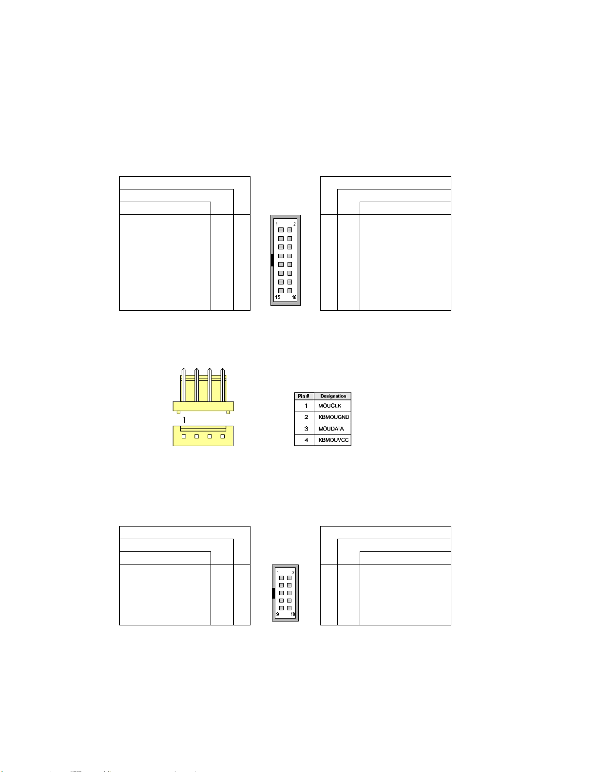
C.3 J3 - Multi-Function Connector
Pin Number Pin Number
Signal Flow Top View Signal Flow
Signal Signal
KBCLK
KBDAT
VCC (Keyboard)
SPEAKER
KBDINH
DOWNL*
PBRES*
HDACT*
* Active Low Signal
I/O
I/O
1
3
-
5
O
7
-
9
-
11
-
13
-
15
2
-
GND
4
-
GND
6
-
VCC (Power on LED)
8
-
VCC
10
-
GND
12
-
GND
14
-
GND
16
-
VCC
C.4 J3A - Mouse Connector
C.5 J4- Serial Port #2 Connector
RS-232 Mode
Pin Number Pin Number
Signal Flow Top View Signal Flow
Signal Signal
DCD
RX
TX
DTR
GND
Connector Pinouts C-2
I
1
I
3
O
5
O
7
-
9
2
I
DSR
4
O
RTS
6
I
CTS
8
I
RI
10
-
Not Used
Page 48
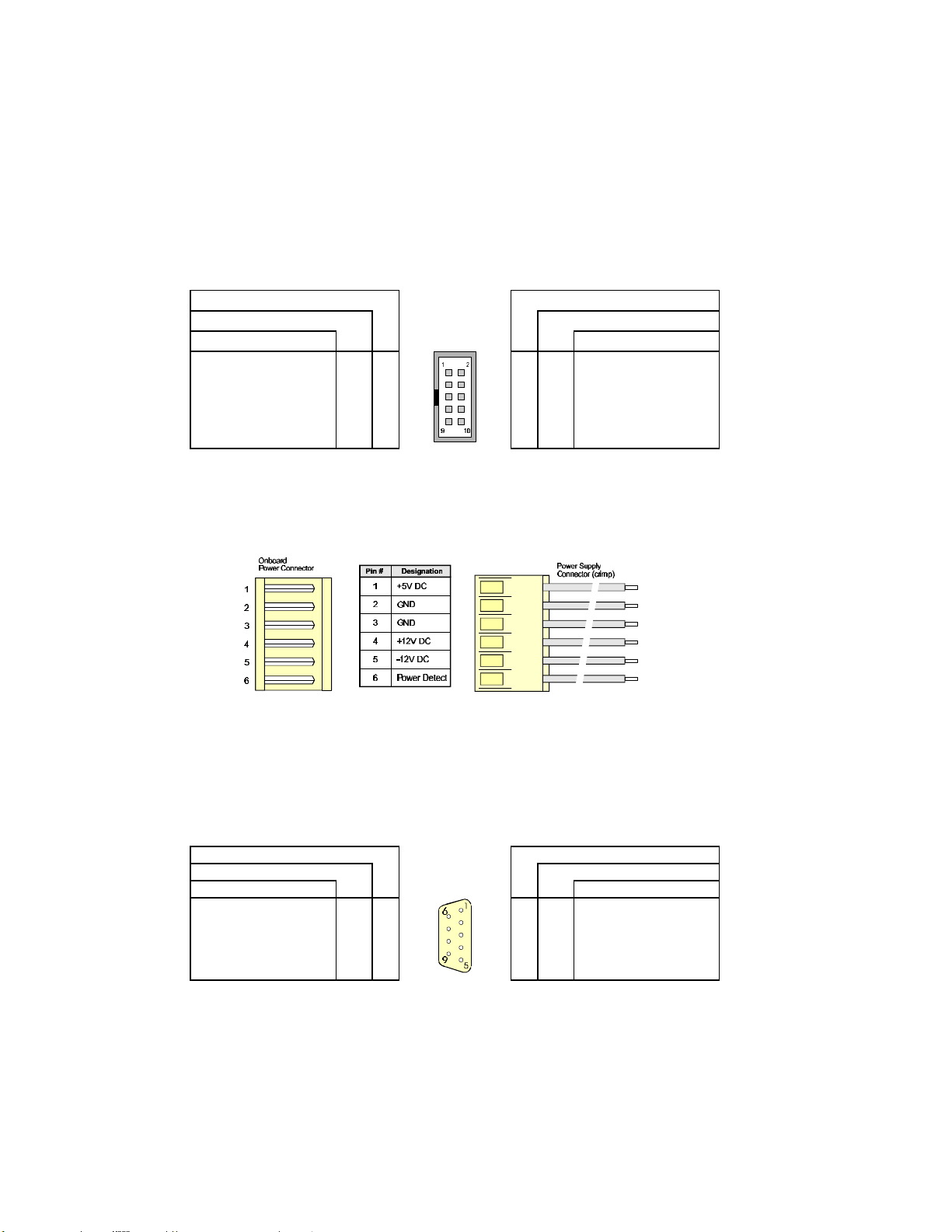
J4- Serial Port #2 Connector (Continued)
RS-485 Mode
Pin Number Pin Number
Signal Flow Top View Signal Flow
Signal Signal
Reserved
RXD(-)
TXD(-)
Not Connected
GND
I/O
-
1
3
O
5
O
7
I
9
2
I
Not Connected
4
I/O
6
8
10
I
I
-
RXD(+)
TXD(+)
Not Connected
Not Used
C.6 J5 - Power Connector
C.7 J6 - Serial Port #1 Connector
RS-232 Mode
Pin Number Pin Number
Signal Flow Front View Signal Flow
Signal Signal
1
I
CTS
DTR
GND
O
6
O
RI
7
I
8
-
9
2
3
4
5
DCD
I
DSR
I
RX
O
RTS
O
TX
Connector Pinouts C-3
Page 49
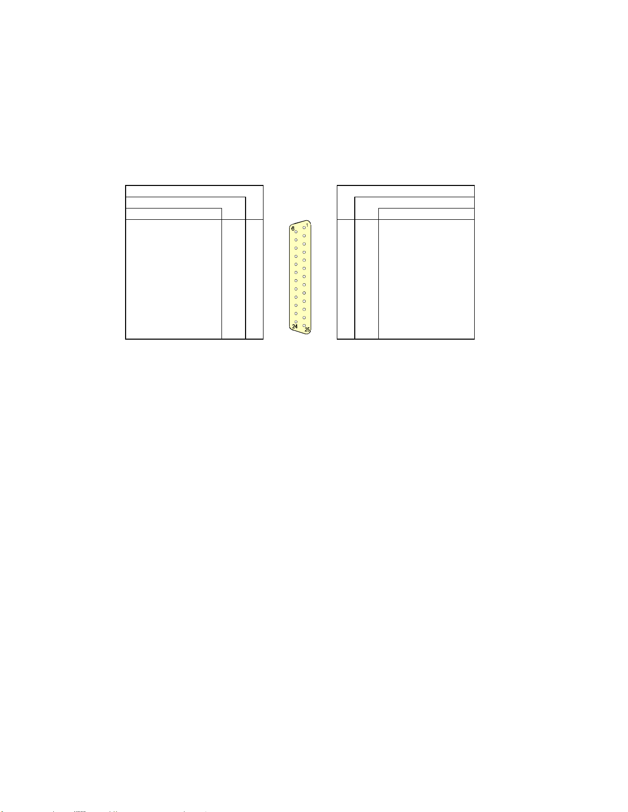
C.8 J7 - Parallel Port Connector
Pin Number Pin Number
Signal Flow Front View Signal Flow
Signal Signal
1
O
P0
P2
P4
P6
ACK*
PE
AFD*
INIT*
GND
GND
GND
GND
I/O
I/O
I/O
I/O
2
4
6
8
I
10
I
12
O
14
O
16
-
18
-
20
-
22
-
24
3
I/O
5
I/O
7
I/O
9
I/O
11
13
15
17
19
21
23
25
STB*
P1
P3
P5
P7
I
BUSY
I
SLCT
I
ERR*
O
SLIN*
-
GND
-
GND
-
GND
-
GND
Connector Pinouts C-4
Page 50
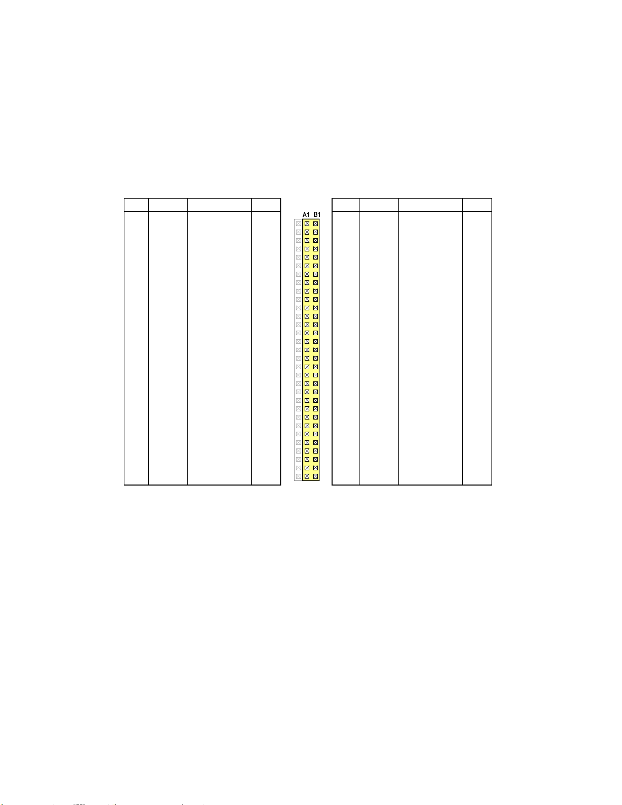
C.9 J8 - Mezzanine ISA AT Bus Connector
A Side B Side
I/O PIN Signal Name I/O
1
A1
3
A2
5
A3
7
A4
9
11
13
15
17
19
21
23
25
27
29
31
33
35
37
39
41
43
45
47
49
51
53
55
57
59
61
A5
A6
A7
A8
A9
A10
A11
A12
A13
A14
A15
A16
A17
A18
A19
A20
A21
A22
A23
A24
A25
A26
A27
A28
A29
A30
A31
I/O CH CK*
SD7
SD6
SD5
SD4
SD3
SD2
SD1
SD0
I/O CH RDY*
AEN
SA19
SA18
SA17
SA16
SA15
SA14
SA13
SA12
SA11
SA10
SA9
SA8
SA7
SA6
SA5
SA4
SA3
SA2
SA1
SA0
I/O
I/O
I/O
I/O
I/O
I/O
I/O
I/O
I/O
I/O
I/O
I/O
I/O
I/O
I/O
I/O
I/O
I/O
I/O
I/O
I/O
I/O
I/O
I/O
I/O
I/O
I/O
I/O
Top View
I
I
O
I/O PIN Signal Name I/O
2
4
6
8
10
12
14
16
18
20
22
24
26
28
30
32
34
36
38
40
42
44
46
48
50
52
54
56
58
60
62
B1
B2
B3
B4
B5
B6
B7
B8
B9
B10
B11
B12
B13
B14
B15
B16
B17
B18
B19
B20
B21
B22
B23
B24
B25
B26
B27
B28
B29
B30
B31
GND
RESET DRV
+5 Vdc
IRQ9
-5 Vdc
DRQ2
-12 Vdc
OWS
+12 Vdc
GND
SMESW*
SMEMR*
IOW*
IOR*
DACK3*
DRQ3
DACK1*
DRQ1
REFRESH*
IRQ7
IRQ6
IRQ5
IRQ4
IRQ3
DACK2*
BALE
+5 Vdc
OSC
GND
CLK
T/C
-
O
I
I
I
-
O
O
I/O
I/O
O
I
O
I
I/O
O
I
I
I
I
I
O
O
O
-
O
-
Connector Pinouts C-5
Page 51
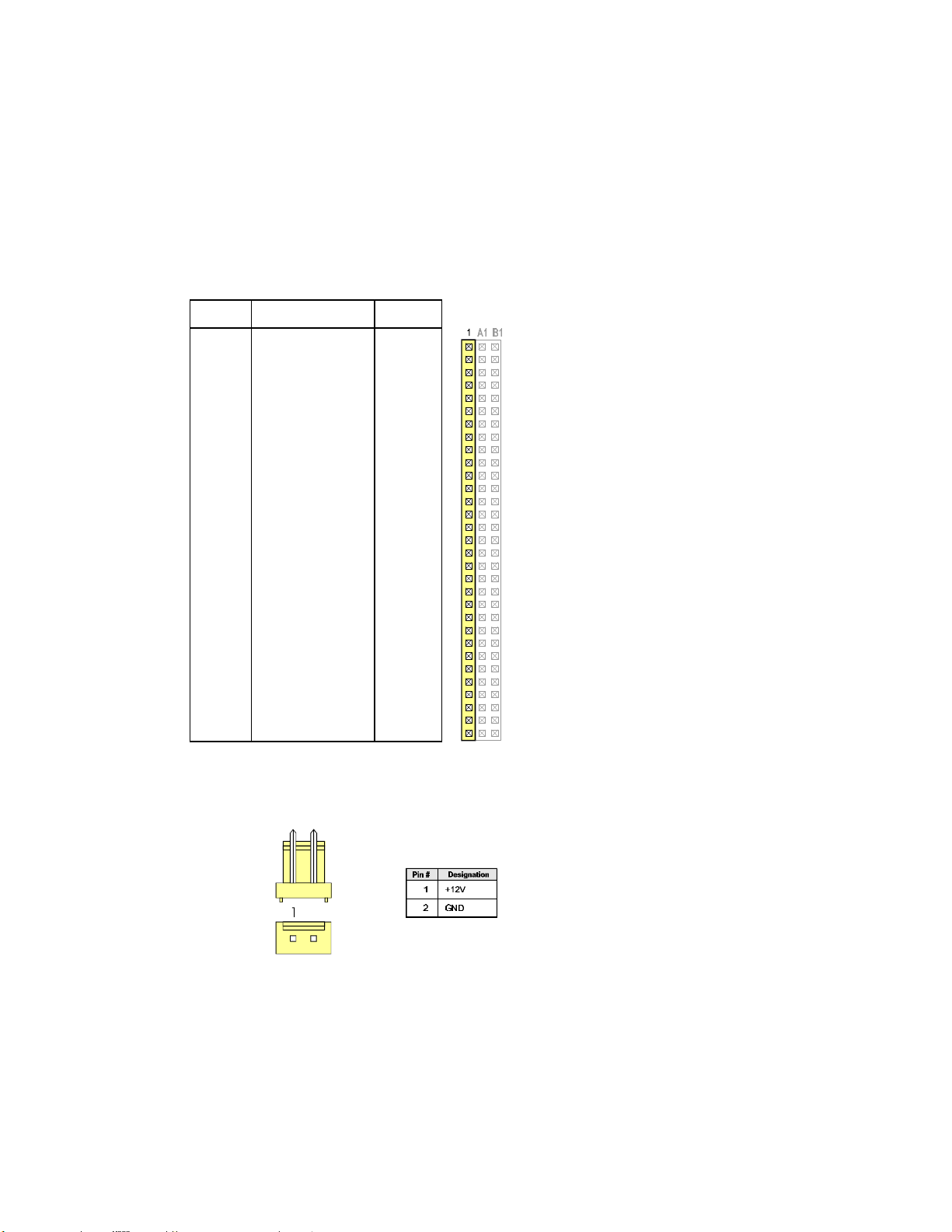
C.10 J9 - Mezzanine ISA AT Extension Bus Connector
I/O PIN SIGNAL NAME I/O
1
2
3
4
5
6
7
8
9
10
11
12
13
14
15
16
17
18
19
20
21
22
23
24
25
26
27
28
29
30
31
SBHE*
LA23
LA22
LA21
LA20
LA19
LA18
LA17
SD08
SD09
SD10
SD11
SD12
SD13
SD14
SD15
MEM CS16*
I/O CS16*
IRQ10
IRQ11
IRQ12
IRQ15
MASTER*
MEMR*
MEMW*
DACK5*
DRQ5
DACK6*
DRQ6
DACK7*
DRQ7
I/O
I/O
I/O
I/O
I/O
I/O
I/O
I/O
I/O
I/O
I/O
I/O
I/O
I/O
I/O
I/O
I/O
I/O
I/O
I/O
I/O
I/O
I/O
I/O
I/O
I/O
I/O
I/O
I/O
I/O
I/O
C.11 J10 - Fan Connector
Connector Pinouts C-6
Page 52
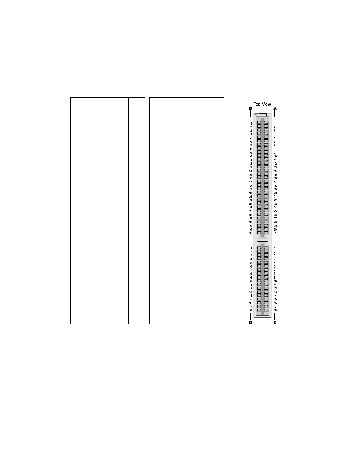
C.12 J14 - ISA Bus Extension Connector
PIN Signal Name I/O PIN Signal Name I/O
A Side
A1
A2
A3
A4
A5
A6
A7
A8
A9
A10
A11
A12
A13
A14
A15
A16
A17
A18
A19
A20
A21
A22
A23
A24
A25
A26
A27
A28
A29
A30
A31
C Side
C1
C2
C3
C4
C5
C6
C7
C8
C9
C10
C11
C12
C13
C14
C15
C16
C17
C18
IOCHK#
SD7
SD6
SD5
SD4
SD3
SD2
SD1
SD0
IOCHRDY
AEN
SA19
SA18
SA17
SA16
SA15
SA14
SA13
SA12
SA11
SA10
SA9
SA8
SA7
SA6
SA5
SA4
SA3
SA2
SA1
SA0
-------------------------------SBHE#
LA23
LA22
LA21
LA20
LA19
LA18
LA17
MEMR#
MEMW#
SD08
SD09
SD10
SD11
SD12
SD13
SD14
SD15
---------
C Side
I
I/O
I/O
I/O
I/O
I/O
I/O
I/O
I/O
I
O
I/O
I/O
I/O
I/O
I/O
I/O
I/O
I/O
I/O
I/O
I/O
I/O
I/O
I/O
I/O
I/O
I/O
I/O
I/O
I/O
I/O
I/O
I/O
I/O
I/O
I/O
I/O
I/O
I/O
I/O
I/0
I/O
I/O
I/O
I/O
I/O
I/O
I/O
B1
B2
B3
B4
B5
B6
B7
B8
B9
B10
B11
B12
B13
B14
B15
B16
B17
B18
B19
B20
B21
B22
B23
B24
B25
B26
B27
B28
B29
B30
B31
D Side
D1
D2
D3
D4
D5
D6
D7
D8
D9
D10
D11
D12
D13
D14
D15
D16
D17
D18
GND
RESET DRV
+5Vdc
IRQ9
-5Vdc
DRQ2
-12Vdc
ENDXFR#
+12Vdc
GND
SMEMW#
SMEMR#
IOW#
IOR#
DACK3#
DRQ3
DACK1#
DRQ1
REFRESH#
SYSCLK
IRQ7
IRQ6
IRQ5
IRQ4
IRQ3
DACK2#
T/C
BALE
+5Vdc
OSC
GND
-------------------------------MEMCS16#
IOCS16#
IRQ10
IRQ11
IRQ12
IRQ15
IRQ14
DACK0#
DRQ0
DACK5#
DRQ5
DACK6#
DRQ6
DACK7#
DRQ7
+5Vdc
MASTER#
GND
-
O
I
I
I
-
O
O
I/O
I/O
O
I
O
I
I/O
O
I
I
I
I
I
O
O
O
-
O
-
--------I
I
I
I
I
I
I
O
I
O
I
O
I
O
I
I
-
# Active Low Signal
Connector Pinouts C-7
Page 53

GLOSSARY
ANSI (AMERICAN NATIONAL STANDARD INSTITUTE)
A group of committees formed to establish voluntary commercial and government standard. ANSI is a member of
ISO.
AT BUS
The AT bus is the ISA bus. It is a 16-bit electronic path containing active signals and power lines to interface with
compatible interfaces or adapter cards for the transfer of data. Data is exchanged 8 or 16-bit at a time (per access) in
parallel.
BIOS (BASIC INPUT/OUTPUT SYSTEM)
BIOS is permanent built-in firmware that controls accesses to devices that are connected to the computer, such as the
memory, the monitor, the disk drives, the serial communications port, etc. In TEKNOR single board computer, this
may include video BIOS, TEKNOR's BIOS extension, main BIOS and Flat Panel BIOS.
CMOS (COMPLEMENTARY METAL-OXIDE SEMICONDUCTOR)
A computer chip that allows many components to be packed together in a very small area. CMOS uses a very small
electric current, thereby generating very little heat, making it suitable for very-large-scale integration (VLSI). CMOS
are nonvolatile, meaning they retain their information even after the power is switched off. In a few words CMOS is a
digital logic family that is characterized by high density, low-to-medium power, and medium-to-high speeds.
DEVICE DRIVER
Software that tells the computer how to connect to a peripheral device, for instance a printer. It acts as an interface
between the operating system and the hardware attached to a computer, to allow applications to communicate in an
orderly fashion.
DIP (DUAL IN-LINE PACKAGE)
A method of packaging semiconductor chips that was omnipresent until the 1980s. Since then, it is being replaced
with small outline packages for devices with low or medium pin counts and pin grid arrays or plastic quad flatpack for
devices with high pin counts.
DMA (DIRECT MEMORY ACCESS)
A method of transferring blocks of data directly between a masse-storage device and memory, with no intervention
from the CPU. To transfer data from a non-storage devices (terminals) to a destination (memory), the CPU must
intervene in the transfer of each byte. The DMA interface is typically incorporated into the device controller.
Glossary 1
Page 54

DRAM (DYNAMIC RANDOM ACCESS MEMORY)
A memory technology that is characterized by extremely high density, low power and low cost. It must be refreshed
often (every one thousandth of a second) to avoid loss of data. This type of memory is used as the system memory in
many personal computers. DRAM can be configured using 36-bit or 9-bit SIMMs (Single In-line Modules), and is
the only type of memory that can be installed by the user.
EPROM (ERASABLE PROGRAMMABLE READ-ONLY MEMORY)
EPROM is a chip with a glass window that is useful for storing firmware. It can be erased by removing the protective
cover from the chip package and exposing the semiconductor material to ultraviolet light. It can then be reprogrammed.
EXPANDED MEMORY SPECIFICATION (EMS)
Personal computers using DOS have a RAM limitation of 640 KB, not enough for applications like spreadsheets and
multiple program loading. The EMS is a technique that establishes a set of rules for organizing and accessing
extended memory, for use as conventional DOS memory. Up to 32 MB of extended memory can be accessed through
the 64 KB window in conventional memory, divided into four 16 KB memory pages.
EXTENDED MEMORY SPECIFICATION (XMS)
In an industry-standard computer, any amount of memory above the base configuration supplied by the manufacturer.
It is the memory above 1 MB accessible only in protected mode. Microsoft Windows, Xenix, and Unix can access it
but, DOS and ordinary applications programs cannot because they must use real mode.
FLASH MEMORY
A type of EEPROM, only at a much lower cost, that can be re-programmed by the computer or peripheral device to
which it is connected. Flash memory is nonvolatile and as a result, it eliminates the risk of losing valuable data
updates. Flash memory offers major advantages in applications like automated factories, remote systems, portable
equipment and similar environments.
IDE (INTEGRATED DRIVE ELECTRONICS)
A hard disk drive standard/protocol characterized by the integration of the controller circuitry onto the drive itself; this
reduces interface costs and allows easy implementation of a drive within a computer system.
INTERRUPT
Interrupt is a signal that stops what the computer system is currently doing, caused by a deliberate instruction to the
microprocessor. This allows the system to perform a higher priority task. After the interrupt is serviced, the
suspended microprocessor task can be resumed at the point where it stopped.
The interrupt channel is designated for receiving and transmitting interrupts, so that input/output or other operations
can take place. See IRQ.
Glossary 2
Page 55

I/O MAP
An I/O (Input/Output ports) map is a list of all special hardware circuits used by the computer to communicate with
external devices. They are simply a special type of memory location that can be accessed only by means of the IN and
OUT instructions. It is possible to have up to 65 536 different I/O devices attached to the system since the I/O port
addresses are 16-bit numbers. Actually, most I/O devices (disk drive controller, video display controllers, etc.) require
more than one I/O port to control them.
IRQ (INTERRUPT REQUEST)
Hardware channels over which devices such as I/O ports, disk drives, and the keyboard can send interrupts to the
processor. They are built into the computer’s internal hardware and are assigned different priority levels so the
processor can determine the relative importance of incoming requests for service. There are 16 IRQs in ISA systems.
See Interrupt.
ISA (INDUSTRY STANDARD ARCHITECTURE)
In reference to IBM PC AT compatible computers, it is the definition of the standard bus. In other words ISA is the
Industrial Standard Architecture expansion bus built into the IBM PC AT computer.
MEMORY MAP
A technical reference that shows the entry point and marks the blocks of memory that are reserved for specific
functions.
MEZZANINE CARD - MEZZANINE BOARD
A peripheral card which uses the PC/104 or the 62-pin XT extension header connectors on TEKNOR boards.
Mezzanine Board allows to assembly a complete computer without passive backplane.
PASSIVE BACKPLANE
A Printed Circuit Board (PCB) populated mostly with passive electronic components (connectors, resistors...)
equipped with connectors that accept different types of Plug-in Electronic boards (SBC, Video Board, I/O Board...).
The main purpose of the Passive Backplane is to serve as an interconnection medium for the different Plug-in boards
installed in a computer system. The backplane is also generally used to supply power to the different Plug-in boards.
REAL-TIME CLOCK (RTC)
It is needed for software compatibility and it has no direct relationship with the ISA bus. It provides time and date
information.
RS-232 OR RS-232C
A standard which defines the physical and electrical serial interface used to connect data communications equipment.
This is the most commonly used interface, especially between modems and computers.
There are two interfaces : DTE (Data Terminal Equipment), used by computers, and DCE (Data Communications
Equipment), used by modems.
Glossary 3
Page 56

RS-485
Electrical interconnection standard. This standard specifies a differential data transmission protocol that allows data
rates of up to 10 MB/second over line lengths up to 4000 ft. The standard also establishes a means of implementing
multi-drop interconnection for up to 32 users.
SBC (SINGLE BOARD COMPUTER)
A term generally used for a computer in which all of the functions (processor, memory, I/O, peripherals, etc.) are
contained on a single board. All of TEKNOR's processor boards are examples of SBC's.
SHADOW RAM BIOS
This is installed to boost overall system speed by copying the system BIOS and VGA BIOS directly into system RAM
at the time the system is booted. RAM runs two to three times faster than the ROM that holds the BIOS, so, as a
result, the system’s response to all BIOS calls is much quicker.
SHADOWING
To make a copy of a program from a slower memory (like ROM) to a faster one (like RAM), in order for the program
to run faster.
SOLID STATE DISK (SSD)
A secondary storage peripheral that uses semiconductor memory as its storage medium, rather than a magnetic disk,
providing performance 10 to 30 times better than that of a magnetic disk. SSDs have no moving parts and are less
susceptible to dirt, moisture, vibration and temperature variations than mechanical Floppy disks. The Flash EPROM
and SRAM disks are types of SSDs available on TEKNOR boards.
SRAM (STATIC RANDOM ACCESS MEMORY)
As opposed to DRAM, SRAM is memory that does not need to be refreshed by a controller and holds its information
as long as the power is on.
VGA (VIDEO GRAPHICS ARRAY)
VGA offers improved graphics and text resolution and an expanded number of available colors for both text and
graphics while maintaining software compatibility with most CGA and EGA applications. It has a maximum screen
resolution of 640x480 or 720x400 pixels, where each character is formed in a 9 x16 pixel matrix. A maximum of
256 colors can be displayed at once, from an overall selection of 256 000 colors.
VT100 MODE
A mode which allows a single board computer to run without a local keyboard or screen. The operation can be
controlled via a remote terminal supporting VT100 Mode or a computer with a terminal emulation program (for
example, Telix, Procomm).
WATCHDOG TIMER
A device that watches for CPU inactivity and then resets the CPU after a specified duration of inactivity. It is
extremely useful in embedded systems where human supervision is not required.
Glossary 4
Page 57

INDEX
ANSI, 5-7
A
B
Flash Disks
Writing, 6-10
XFLASH, 6-10
FLASH EPROM, 5-3
Floppy controller, 2-1
Full Duplex Operation, 6-9
Battery Backup Circuit, 6-11
BIOS, 5-4, 10-1
Boot Option, 5-5
Error Handling, 10-1
C
CMOS Technology, 2-1
COM2, 2-1
Connector
COM1 - J6. See
Floppy Disk Drive J2, 6-6
Hard Disk Connector J1, 6-5
Multi-Function - J3, 6-7
Parallel Printer Port - J7, 6-9
Power Supply Connector J5, 6-1
PS/2 Mouse - J3A, 6-6
Serial Port 2 - J4, 6-7
D
DB25, 6-9
DMA
Controller Table, 9-1
DMA and IRQ, 9-1
DRAM, 5-5
E
EPROM, 5-3, 5-5
H
Hard Disk, 5-6
Installation, 6-5
Hard Drive
Write Precompensation, 6-5
I
I/O Map, 5-3
IDE hard disk interface, 2-1
IOCHECK
Power Detection Output, 5-10
IRQ
Controller Table, 9-1
ISA-AT, 6-1
Supplying Power, 6-1
J
Jumper
Battery Backup Circuit, 6-11
Download Mode - Flash Disk Boot SW1,
6-10
Hard Disk J11, 6-5
W12 Watchdog Timer, 5-10
W13 Power Failure Detector, 5-10
JUMPER LOCATIONS, 8-3
JUMPERS
Functions, 8-1
Flash Disk, 5-6
F
Low Battery Circuit Detector, 2-1
L
Page 58

M
S
Magnetic, 4-1
Memory
Expanded and Extended, 5-4
Flash-EPROM, 2-1
I/O and Mapping, 5-3
Installing, 5-1
Shadow-RAM, 2-1
SIMM
DRAM, 5-1
SRAM, 2-1
System Memory, 2-1
Memory Map, 5-3
Memory Mode, 5-4
Mezzanine SVGA, 2-2
Microprocessor and Fan
Installing, 5-1
Microprocessors
486 Family and 586 133 MHz, 2-1
Multi-Function
16-pin header, 6-7
O
Operation
Diskless, 2-3
Stand-Alone, 2-3
Safety Precautions, 3-1, 4-1
Shadow RAM, 5-5
Sleep Mode, 2-1
Solid State Disk
Static-RAM and Flash EPROM, 6-5
Solid State Disks, 5-3
Installing, 6-10
SRAM, 5-3
SRAM Disk, 6-10
Static Electricity, 4-1
Supervisor Utilities
Low Battery Detection, 5-12
Power Failure Detector (PFD), 5-10
Register 201h, 5-9
Watchdog Timer, 5-9
T
TEK-AT4Lplus
Configuring, 5-5
TEK-AT4LPLUS
Onboard Subsystems, 2-1
U
User Interface, 2-2
P
Party Line Operation, 6-9
Power Detection Input
Connector J5, 5-10
Power Fail Detector, 2-1
Power Supply, 4-1
Power Supply Connector, 4-1
R
Radioactive, 4-1
RAM Disk, 5-6
RS-232, 5-7
RS-232 or RS-485, 2-1
RS-485, 6-9
V
Video Cards, 2-1
VIDEO DEVICES
Video Adapter Board, 7-1
Video Mezzanine Board, 7-1
Voltage, 5-7
VT100, 5-7
W
Watchdog Timer, 2-1
Page 59

GETTING HELP
At TEKNOR we take great pride in our customer's successes. We strongly believe in
providing full support at all stages of your product development.
If at any time you encounter difficulties with your application or with any of our products,
or if you simply need guidance on system setups and capabilities, you may contact our
Technical Support department at:
CANADIAN HEADQUARTERS EUROPEAN REGIONAL OFFICE
Tel.: (450) 437-5682 Tel.: +49 811 / 600 15-0
Fax: (450) 437-8053 Fax: +49 811 / 600 15-33
If you have any questions about TEKNOR, our products or services, you may reach us at
the above numbers or by writing to:
TEKNOR INDUSTRIAL
COMPUTERS INC.
616 Cure Boivin
Boisbriand, Quebec
J7G 2A7 CANADA
LIMITED WARRANTY
TEKNOR INDUSTRIAL COMPUTERS INC. ("the seller") warrants its products to be
free from defects in material and workmanship for a period of two (2) years commencing
on the date of shipment. The liability of the seller shall be limited to replacing or
repairing, at the seller's option, any defective units. Equipment or parts which have been
subject to abuse, misuse, accident, alteration, neglect, or unauthorized repair are not
covered by this warranty. This warranty is in lieu of all other warranties expressed or
implied.
TEKNOR INDUSTRIAL
COMPUTERS INC.
Zeppellin Str. 4
D-85399 Hallbergmoos
GERMANY
Getting Help
Page 60

Returning Defective Merchandise
If your TEKNOR product malfunctions, please do the following before returning any
merchandise:
1) Call our Technical Support department in Canada at (514) 437-5682 or in Germany at
+49 811 / 600 15-0. Make certain you have the following at hand: the TEKNOR
Invoice #, your Purchase Order #, and the Serial Number of the defective unit.
2) Give the serial number found on the back of the card and explain the nature of your
problem to a service technician.
3) If the problem cannot be solved over the telephone, the technician will further instruct
you on the return procedure.
4) Prior to returning any merchandise, make certain you receive an RMA # from
TEKNOR's Technical Support and clearly mark this number on the outside of the
package you are returning. To request a number, follow these steps: make a copy of the
request form on the following page, fill it out and fax it to us.
5) When returning goods, please include the name and telephone number of a person
whom we can contact for further explanations if necessary. Where applicable,
always include all duty papers and invoice(s) associated with the item(s) in
question.
6) When returning a TEKNOR card:
i) Make certain that the card is properly packed: Place it in an antistatic plastic bag
and pack it in a rigid cardboard box.
ii) Ship prepaid to (but not insured, since incoming units are insured by TEKNOR):
TEKNOR INDUSTRIAL
COMPUTERS INC.
616 Cure Boivin
Boisbriand, Quebec
J7G 2A7 CANADA
Getting Help
TEKNOR INDUSTRIAL
COMPUTERS INC.
Zeppelin Str. 4
D-85399 Hallbergmoos
GERMANY
Page 61

RETURN TO MANUFACTURER
AUTHORISATION REQUEST
Contact Name :
Company Name :
Street Address
City : Province / State :
Country : Postal / Zip Code
Phone Number : Fax Number:
Serial
Number
Fax this form to TEKNOR’s Technical Support department
in Canada at (514) 437-8053 or in Germany at +49 811 / 600 15-33
Failure or Problem Description P.O. #
(if not under
warranty)
 Loading...