

Page 1

TEK-AT1
80C286 AT SINGLE-BOARD COMPUTER
HARDWARE REFERENCE MANUAL
VERSION 3.1, JULY 1994
TEKNOR MICROSYSTEMS INC.
616 Cure Boivin
Boisbriand, Quebec
J7G 2A7 CANADA
NOTE
This manual is for reference purposes
only. Reproduction in whole or in
part is authorized provided TEKNOR
MICROSYSTEMS INC. is cited as the
original source.
ref: M700_3-1
Page 2

INTRODUCTION 1
INTRODUCTION SECTION 1
The TEK-AT1 is a high performance PC/AT type
computer on a half-card format (7" x 4.7"). It integrates
all the basic functions available on an IBM AT - like a
hard disk interface and a floppy disk controller.
Best of all, the TEK-AT1 is designed to operate in
environments where a sturdy and compact system is
essential. So elements such as a watchdog timer, solid
state disks, and a power failure detector were added to
make the TEK-AT1 perform even in the most extreme
industrial applications.
Built using CMOS technology, the TEK-AT1 consumes
very little power. Typically, less than 4 watts. The
TEK-AT1 is also a versatile board. It can be installed in a
PC passive backplane or, because of its small size, it can
be used as a stand-alone controller by utilizing the four
standard mounting holes and separate power connector.
And to top it off, an XT expansion header accommodates
TEKNOR's series of display controllers or other optional
expansion cards.
Page 3

2 TEK-AT1 REFERENCE MANUAL
Here are more exciting features found on the TEK-AT1
single board computer:
• PC/AT bus or
stand alone
operation
• 80C286 @ 16Mhz
• 512K, 1, 2, or 4
Mbytes of system
memory with
mixed DRAM
support
• Up to 1M of
user
EPROM/Flash
EPROM
• Up to 1M user
RAM with battery
backup
• Supports Shadow
RAM BIOS for
fast execution
• Flash EPROM
boot
• Real-time clock
with battery
backup
• Optional 80287
coprocessor
support
• AT keyboard and
speaker port
• One parallel
printer port
(LPT1)
• Two serial
ports with COM2 as
RS232 or RS485
• Watchdog Timer
• Power Fail
Detector
• Onboard floppy
controller: drives
two floppies
• Onboard IDE hard
disk interface
• CMOS technology
for low power
• Two year warranty
Page 4

CONFIGURATION 7
CONFIGURATION SECTION 2
JUMPERS
The TEK-AT1 was designed to allow for minimal
hardware configuration.
The following Jumpers can be configured by using
shorting jumpers.
JUMPER STATE FUNCTION * as shipped
RAM Battery Back-up
1
W0 Open* NC
W0 Closed Vbatt
Watchdog Timer
W1 Open Disable
W1 Closed* Enable
Flash EPROM
W2 Open No Flash
W2 Closed* Flash Installed
RAM Disk Memory Type
W3(1-2) 32K x 8, 128K x 8 SRAM
W3(2-3) 256K x 8, 512K x 8 SRAM
1 Vbatt must be installed to save configuration
information at power down.
Page 5

8 TEK-AT1 REFERENCE MANUAL
Power Monitoring
W4 Open* Disable
W4 Closed Enable
Hard Disk Interface
W5 Open* IDE Enabled
W5 Closed IDE Disabled
Boot From Flash EPROM
SW1(1-2) Open* Boot From Drives
SW1(1-2) Closed Boot From Flash
Color/Monochrome
SW1(3-4) Open* Mono, EGA, VGA
SW1(3-4) Closed Color CGA Only
Console Is VT100 Terminal
SW1(5-6) Open* Standard Display Mode
SW1(5-6) Closed VT100 Mode
Remote Download
SW1(7-8) Open* Normal
SW1(7-8) Closed Serial Download Mode
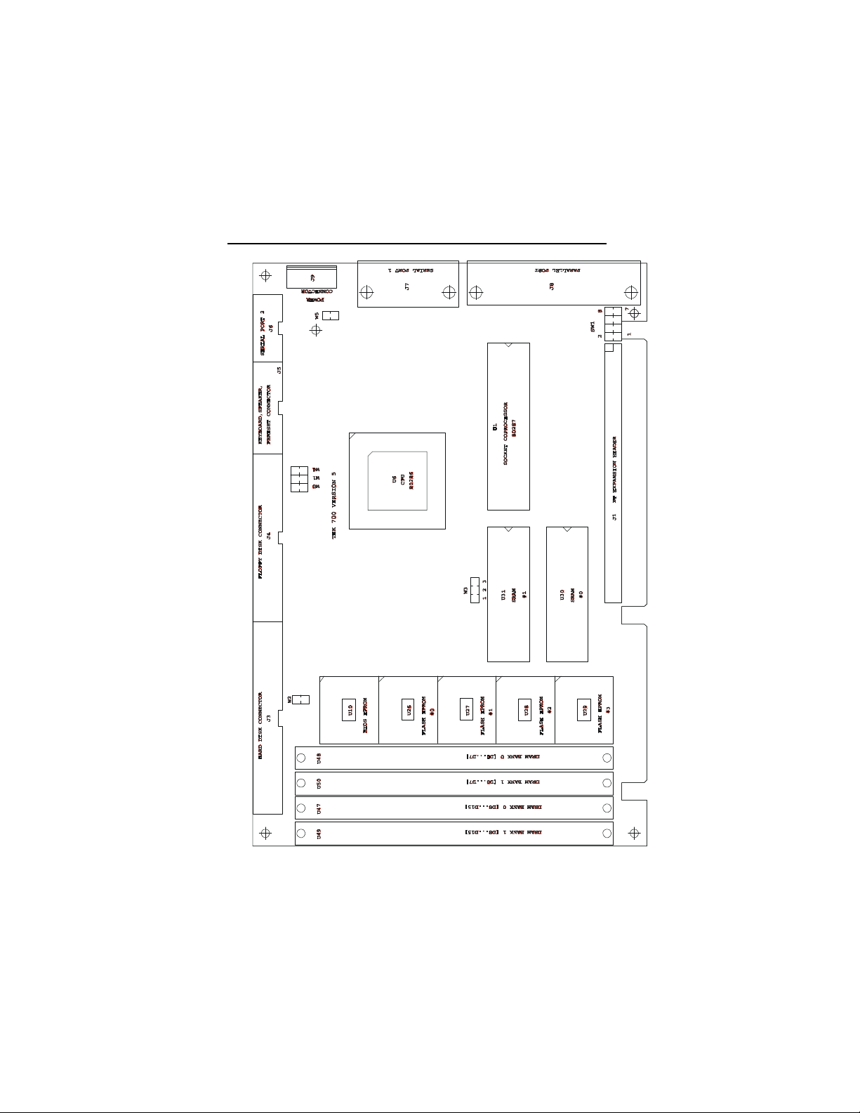
Refer to Diagram 2-1 and Table 2-1 for exact jumper
locations.
Page 6

CONFIGURATION 9
BIOS SETUP
The TEK-AT1 is fully software configurable. The setup
program allows for minimal hardware configuration.
SETUP UTILITY
The SETUP program is located within the BIOS and can
be activated at boot time by pressing <CTRL-ALT-S>
in Standard Display Mode, or <CTRL-R> in VT100
Mode, at the configuration prompt during the power up
sequence. Once the SETUP screen is displayed you can
modify the date, time, or other setup information
contained in the clock CMOS RAM. The system will
reboot on exit from SETUP. The SETUP program
should only be activated when all information in the
computer has been properly saved.
Use the arrow keys to select the item you want to change.
When the item is selected, press <+> or <-> keys to
change an entry.
Press <F10> to save the current configuration (press "Q"
in VT100 Mode) and to exit. The configuration, with the
exception of the time and date, is not saved until <F10>
is pressed. Press <ESC> to exit without saving the
setup.
Page 7

10 TEK-AT1 REFERENCE MANUAL
USER'S SETUP CONFIGURATION INFORMATION
The SETUP program can set the following:
Time of day and Date
Floppy disk configuration
Fixed disk configuration
System memory size
Extended memory size
EMS memory size
Video type
Execute BIOS from RAM or ROM Shadow
Wait state selection
Initial CPU speed
TABLE 2-1 CONFIGURATION JUMPERS
Jumper Function
W0 RAM Battery Backup
W1 Watchdog Timer
W2 Flash EPROM (VPP)
W3(1-2)
W3(2-3)
W4 Power Monitoring
W5 Hard Disk Interface
SW1(1-2)
SW1(3-4)
SW1(5-6)
SW1(7-8)
SRAM Memory Type: 32kx8, 128kx8
SRAM Memory Type: 256kx8, 512kx8
Boot From Flash EPROM
CGA/MGA, EGA, VGA
Boot From VT100
Remote Download
Page 8
CONFIGURATION 11
DIAGRAM 2-1 JUMPER LOCATIONS
Page 9

SPECIFICATIONS 57
Std PC/AT Application
Embedded App.
Icc typ.
980mA
850mA
Icc stby.
300mA
300mA
Ipp +12V
10mA
10mA
Ipp -12V
5mA
5mA
SPECIFICATIONS SECTION 7
DC CHARACTERISTICS
Supply VoltageVcc min.: 4.75V
Vcc max.: 5.25V
+12V: +/-5%
-12V: +/-5%
Supply Current
This current was measured with 4 Mbytes of DRAM, 1 Mbyte of User Flash EPROM,
256K SRAM, along with hard disk, floppy disk, keyboard and monitor installed.
This current was measured with 4 Mbytes of DRAM, 1 Mbyte of User Flash EPROM,
and 256K SRAM only.
5
6
Page 10

58 TEK-AT1 REFERENCE MANUAL
ENVIRONMENTAL SPECIFICATIONS
Operating Temperature:
00C to 700C
-400C to +850C Available
Non-Condensing relative humidity:
5% to 95%
Page 11
SPECIFICATIONS 59
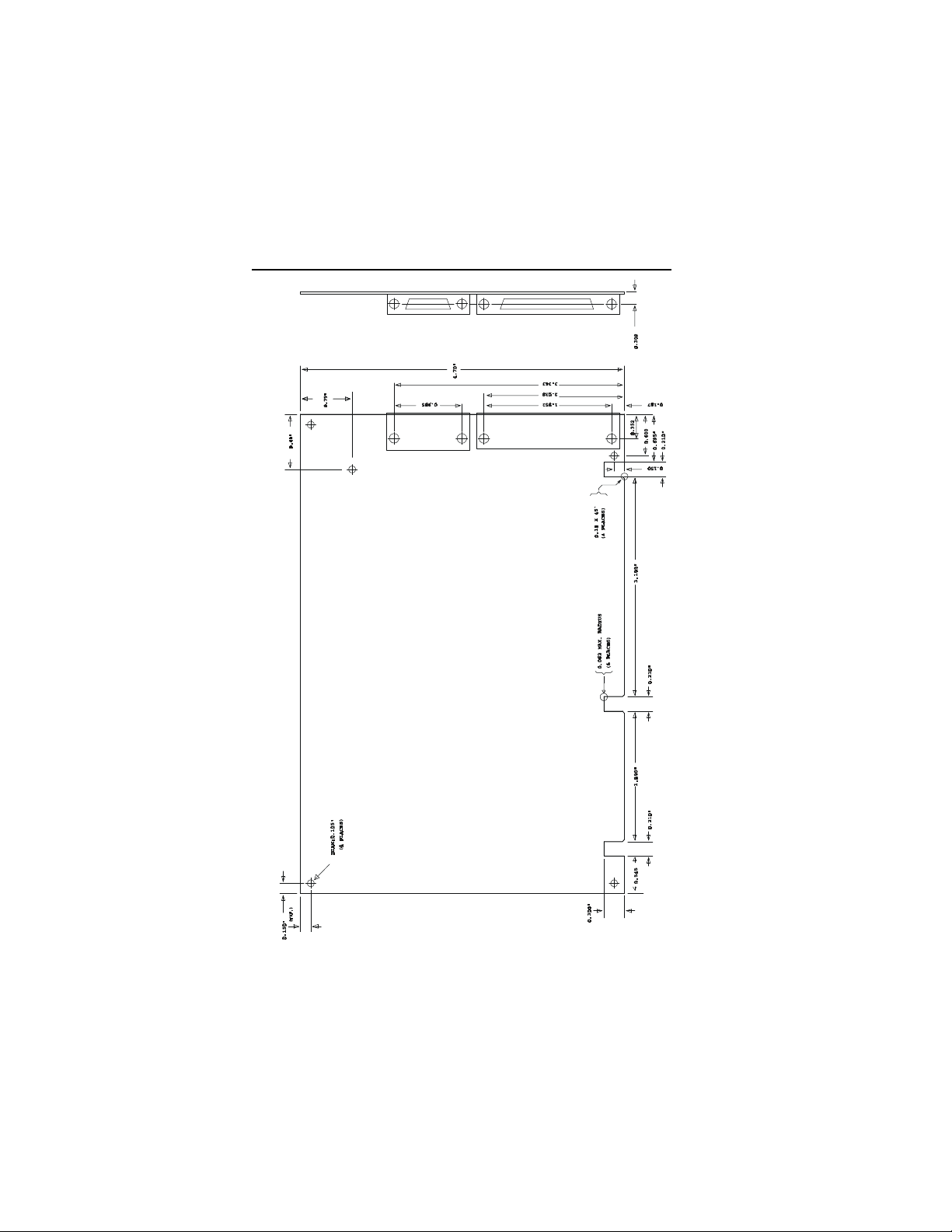
DIAGRAM 7-1 MECHANICAL SPECIFICATIONS
Page 12
60 TEK-AT1 REFERENCE MANUAL
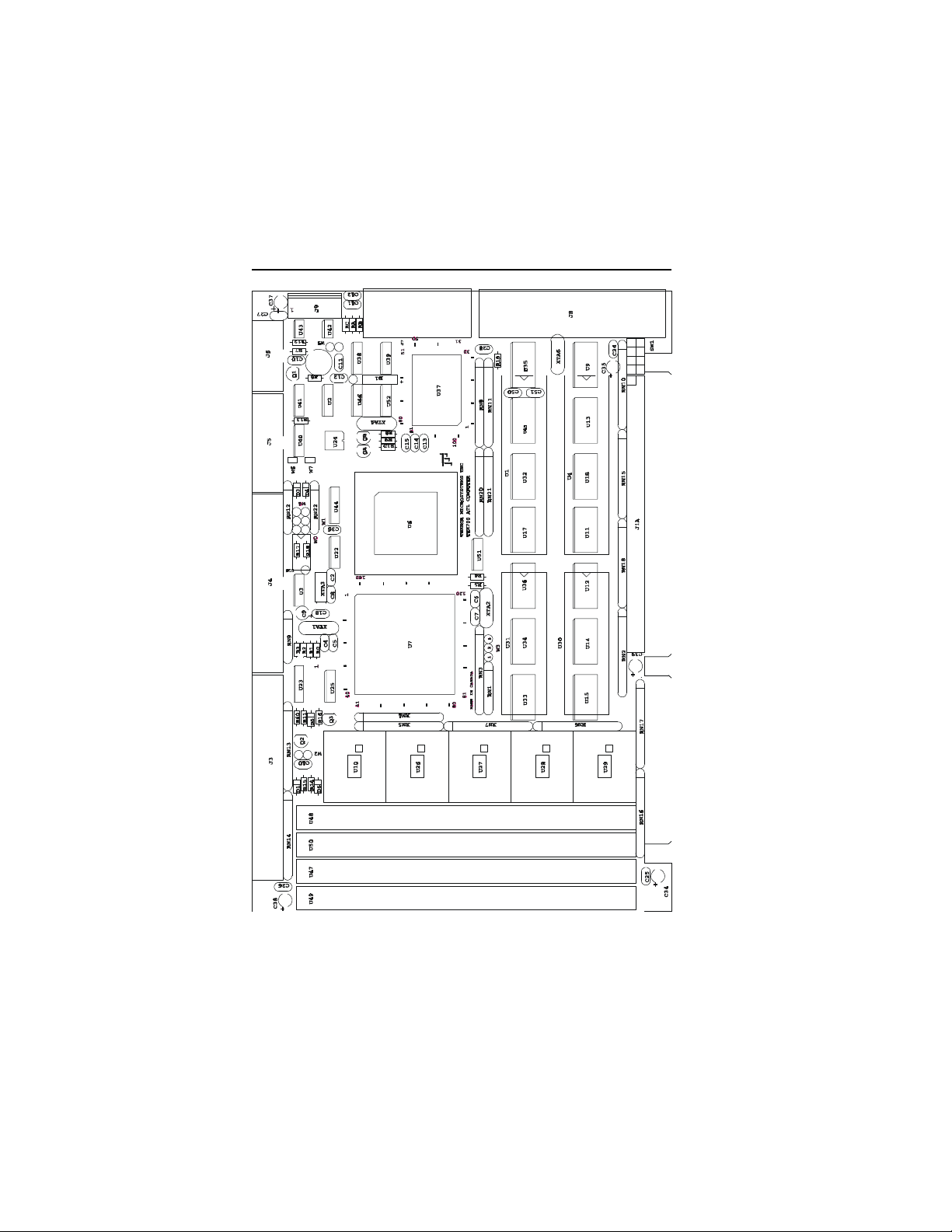
DIAGRAM 7-2 ASSEMBLY
Page 13
SPECIFICATIONS 61
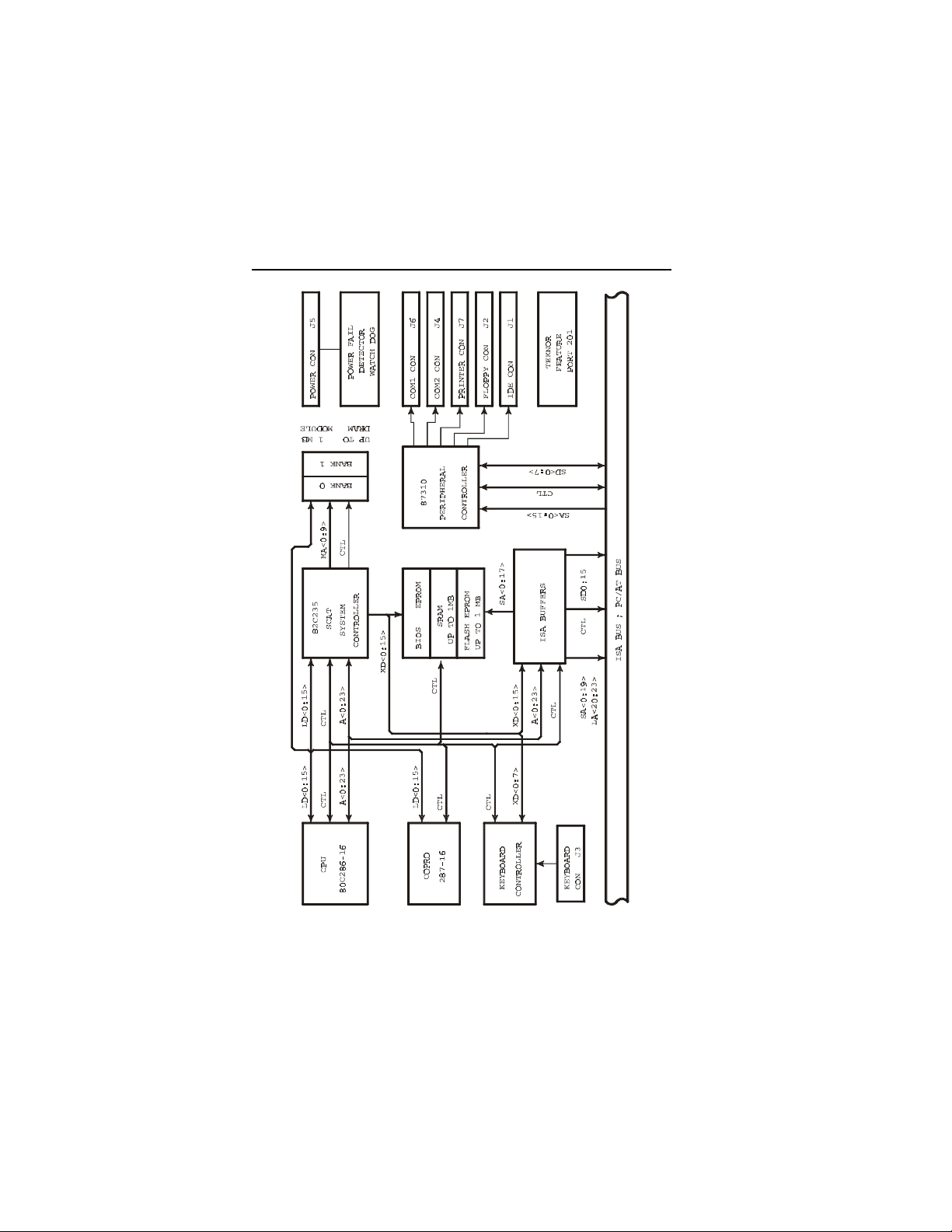
DIAGRAM 7-3 BLOCK DIAGRAM
Page 14
62 TEK-AT1 REFERENCE MANUAL
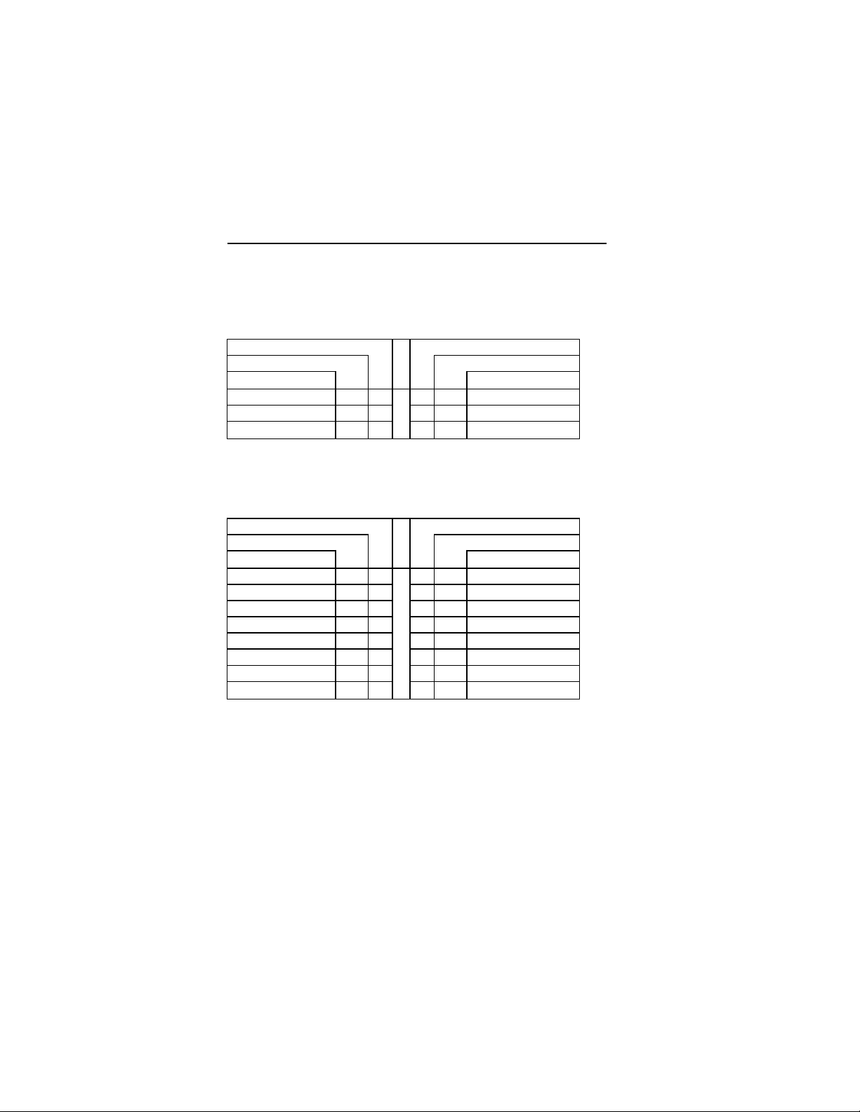
CONNECTOR OVERVIEW
J9 POWER CONNECTOR
PIN NUMBER PIN NUMBER
SIGNAL FLOW SIGNAL FLOW
SIGNAL SIGNAL
VCC - 1 2 - GND
GND - 3 4 - +12V
-12V - 5 6 - PD
J5 KEYBOARD CONNECTOR
PIN NUMBER PIN NUMBER
SIGNAL FLOW SIGNAL FLOW
SIGNAL SIGNAL
KBDCLK O 1 2 - GND
KBDDATA O 3 4 - GND
VCC - 5 6 - VCC
SPKR O 7 8 - VCC
KBDINH I 9 10 - GND
AUTO* I 11 12 - GND
PBRES* I 13 14 - GND
ACT* O 15 16 - VCC
Page 15
SPECIFICATIONS 63
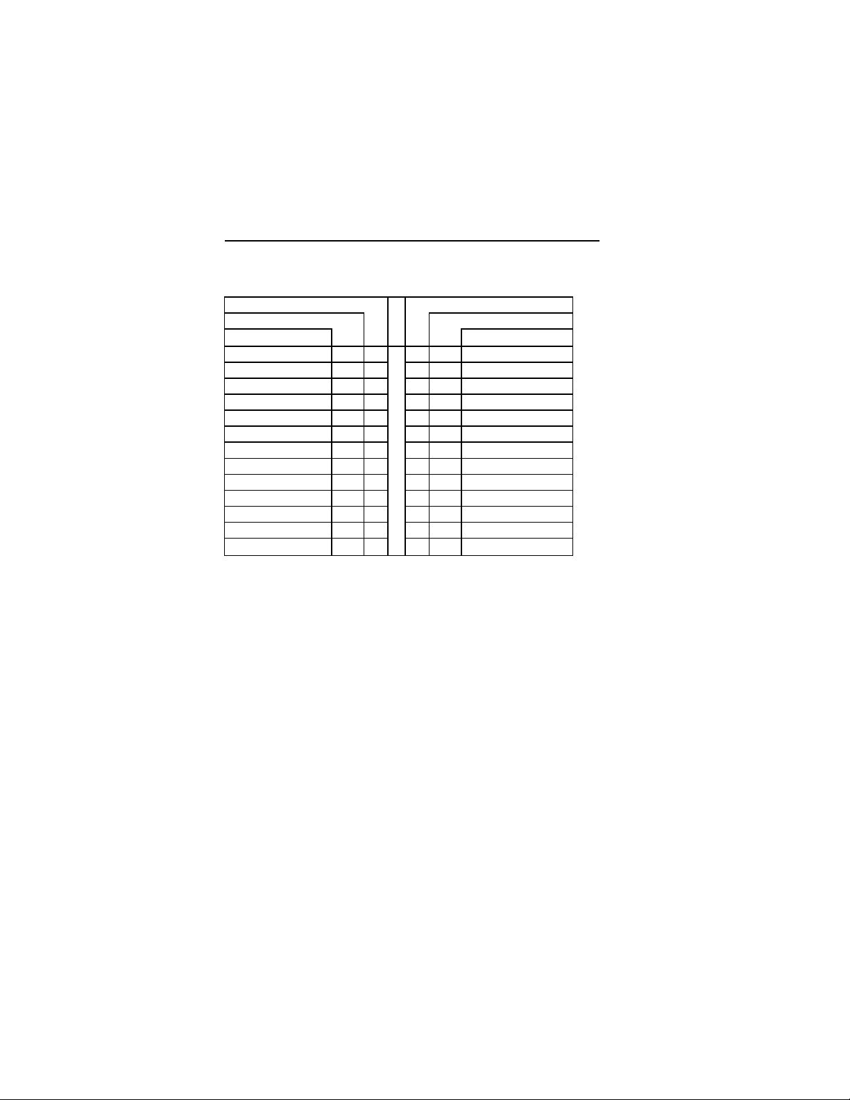
J8 LPT1 PRINTER CONNECTOR
PIN NUMBER PIN NUMBER
SIGNAL FLOW SIGNAL FLOW
SIGNAL SIGNAL
STB* O 1 2 I/O P0
P1 I/O 3 4 I/O P2
P3 I/O 5 6 I/O P4
P5 I/O 7 8 I/O P6
P7 I/O 9 10 I ACK*
BUSY I 11 12 I PE
SLCT I 13 14 O AFD*
ERR* I 15 16 O INIT*
SLIN* O 17 18 - GND
GND - 19 20 - GND
GND - 21 22 - GND
GND - 23 24 - GND
GND - 25
Page 16
64 TEK-AT1 REFERENCE MANUAL
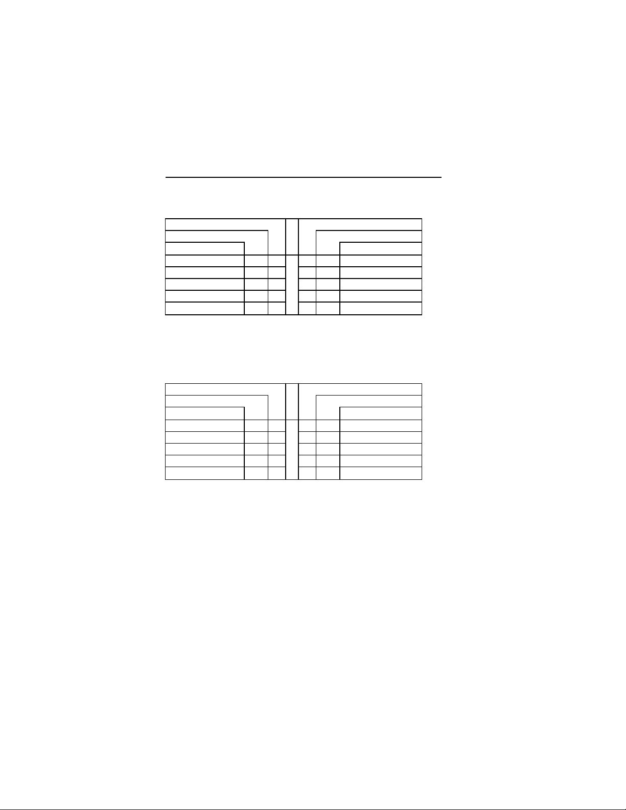
J7 COM1 CONNECTOR
PIN NUMBER PIN NUMBER
SIGNAL FLOW SIGNAL FLOW
SIGNAL SIGNAL
DCD I 1 2 I RX
TX O 3 4 O DTR
GND O 5 6 I DSR
RTS O 7 8 I CTS
RI I 9
J6 COM2 CONNECTOR/RS232
PIN NUMBER PIN NUMBER
SIGNAL FLOW SIGNAL FLOW
SIGNAL SIGNAL
DCD I 1 2 I DSR
RX I 3 4 O RTS
TX O 5 6 I CTS
DTR O 7 8 I RI
GND - 9
Page 17
SPECIFICATIONS 65
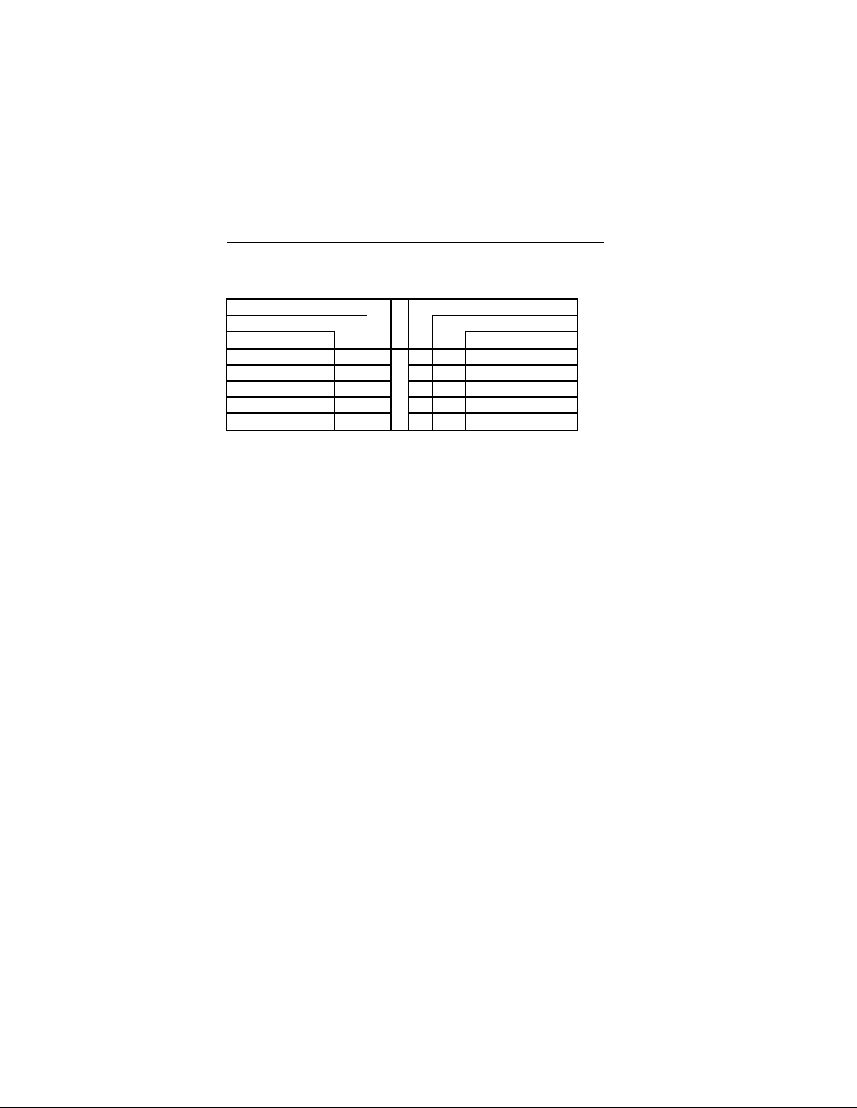
J6 COM2 CONNECTOR/RS485
PIN NUMBER PIN NUMBER
SIGNAL FLOW SIGNAL FLOW
SIGNAL SIGNAL
RESERVED - 1 2 I NC
RXD(-) I/O 3 4 I/O RXD(+)
TXD(-) O 5 6 I TXD(+)
NC O 7 8 I NC
GND I 9
Page 18
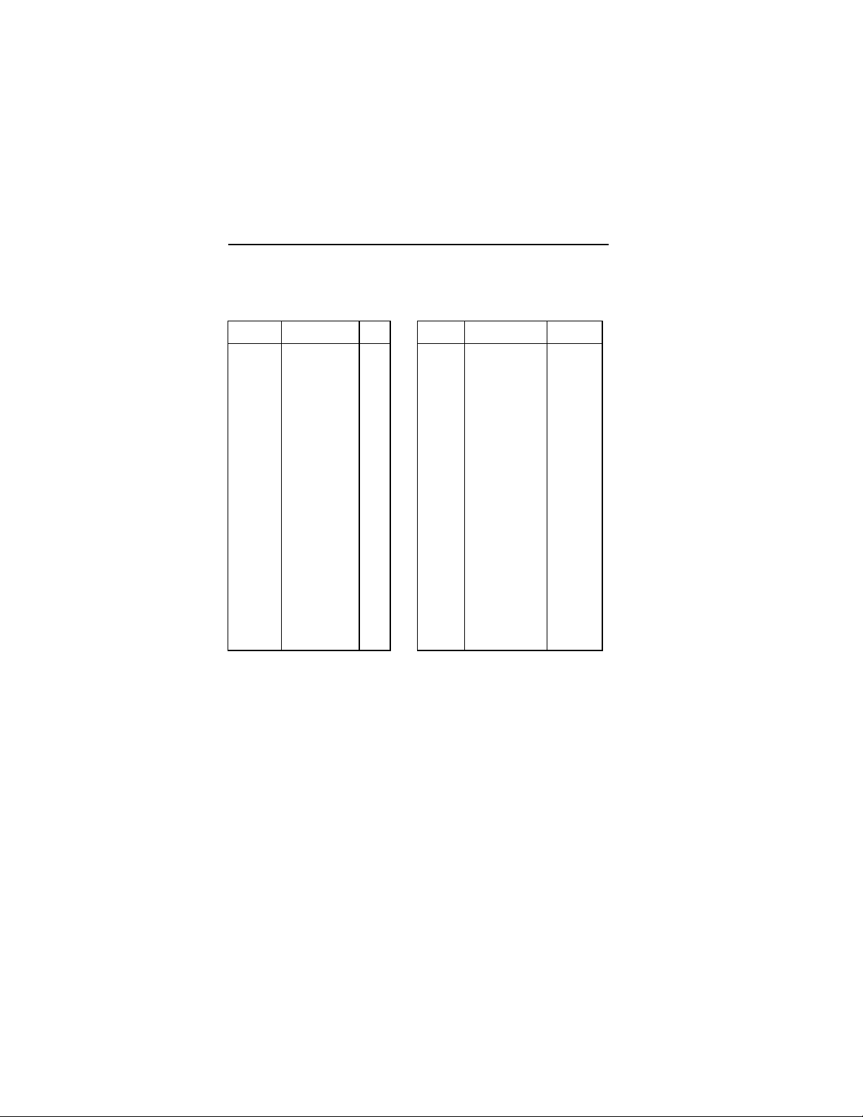
66 TEK-AT1 REFERENCE MANUAL
J1-J2 PC BUS CONNECTOR
A Side B Side
I/O PIN
A1
A2
A3
A4
A5
A6
A7
A8
A9
A10
A11
A12
A13
A14
A15
A16
A17
A18
A19
A20
A21
A22
A23
A24
A25
A26
A27
A28
A29
A30
A31
Signal Name I/O
I/O CH CK*
SD7
SD6
SD5
SD4
SD3
SD2
SD1
SD0
I/O CH RDY*
AEN
SA19
SA18
SA17
SA16
SA15
SA14
SA13
SA12
SA11
SA10
SA9
SA8
SA7
SA6
SA5
SA4
SA3
SA2
SA1
SA0
I/O
I/O
I/O
I/O
I/O
I/O
I/O
I/O
I/O
I/O
I/O
I/O
I/O
I/O
I/O
I/O
I/O
I/O
I/O
I/O
I/O
I/O
I/O
I/O
I/O
I/O
I/O
I/O
I
I
O
I/O PIN
B1
B2
B3
B4
B5
B6
B7
B8
B9
B10
B11
B12
B13
B14
B15
B16
B17
B18
B19
B20
B21
B22
B23
B24
B25
B26
B27
B28
B29
B30
B31
Signal Name I/O
GND
RESET DRV
+5 Vdc
IRQ9
-5 Vdc
DRQ2
-12 Vdc
OWS
+12 Vdc
GND
SMESW*
SMEMR*
IOW*
IOR*
DACK3*
DRQ3
DACK1*
DRQ1
REFRESH*
CLK
IRQ7
IRQ6
IRQ5
IRQ4
IRQ3
DACK2*
T/C
BALE
+5 Vdc
OSC
GND
Ground
O
Power
I
Power
I
Power
I
Power
Ground
O
O
I/O
I/O
O
I
O
I
I/O
O
I
I
I
I
I
O
O
O
Power
O
Ground
Page 19
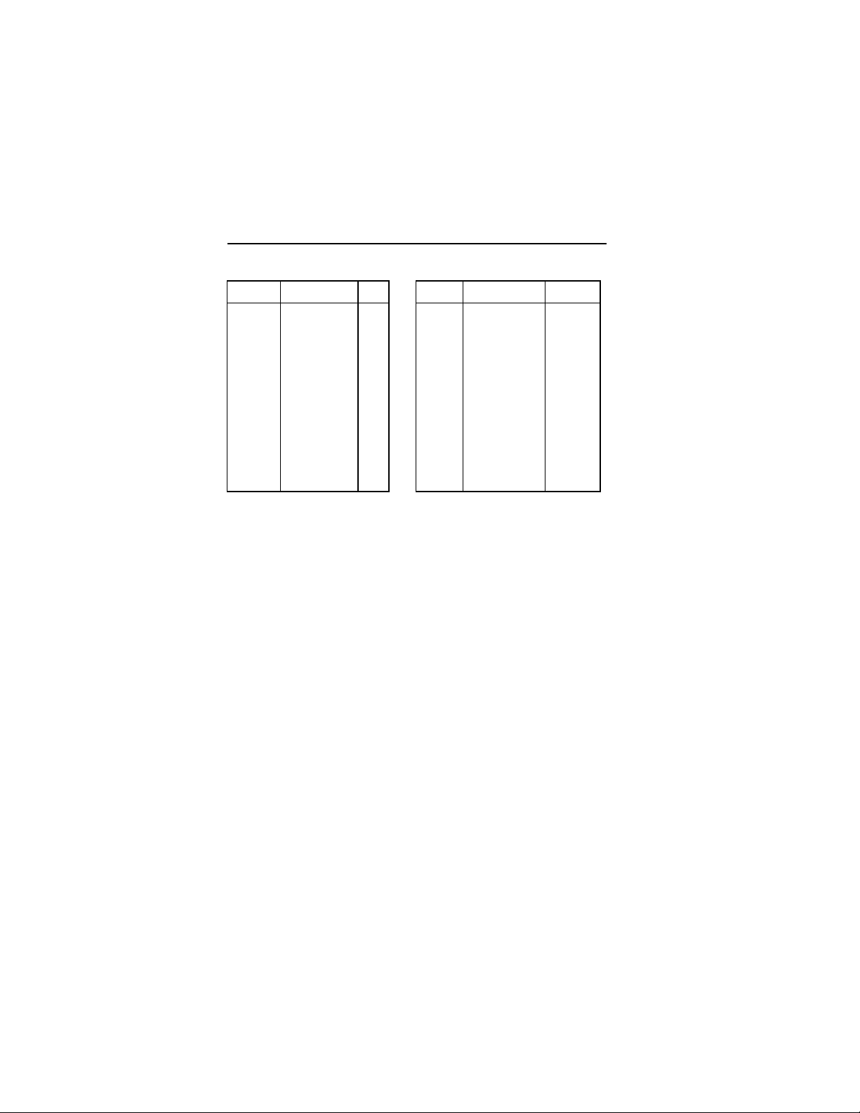
C Side D Side
I/O PIN
C1
C2
C3
C4
C5
C6
C7
C8
C9
C10
C11
C12
C13
C14
C15
C16
C17
C18
Signal Name I/O
SBHE
LA23
LA22
LA21
LA20
LA19
LA18
LA17
MEMR*
MEMW*
SD08
SD09
SD10
SD11
SD12
SD13
SD14
SD15
I/O
I/O
I/O
I/O
I/O
I/O
I/O
I/O
I/O
I/O
I/0
I/O
I/O
I/O
I/O
I/O
I/O
I/O
SPECIFICATIONS 67
I/O PIN
D10
D11
D12
D13
D14
D15
D16
D17
D18
Signal Name I/O
D1
D2
D3
D4
D5
D6
D7
D8
D9
MEM CS16*
I/O CS16*
IRQ10
IRQ11
IRQ12
IRQ15
IRQ14
DACK0*
DRQ0
DACK5*
DRQ5
DACK6*
DRQ6
DACK7*
DRQ7
+5Vdc
MASTER*
GND
I
I
I
I
I
I
I
O
I
O
I
O
I
O
I
POWER
I
Ground
Page 20
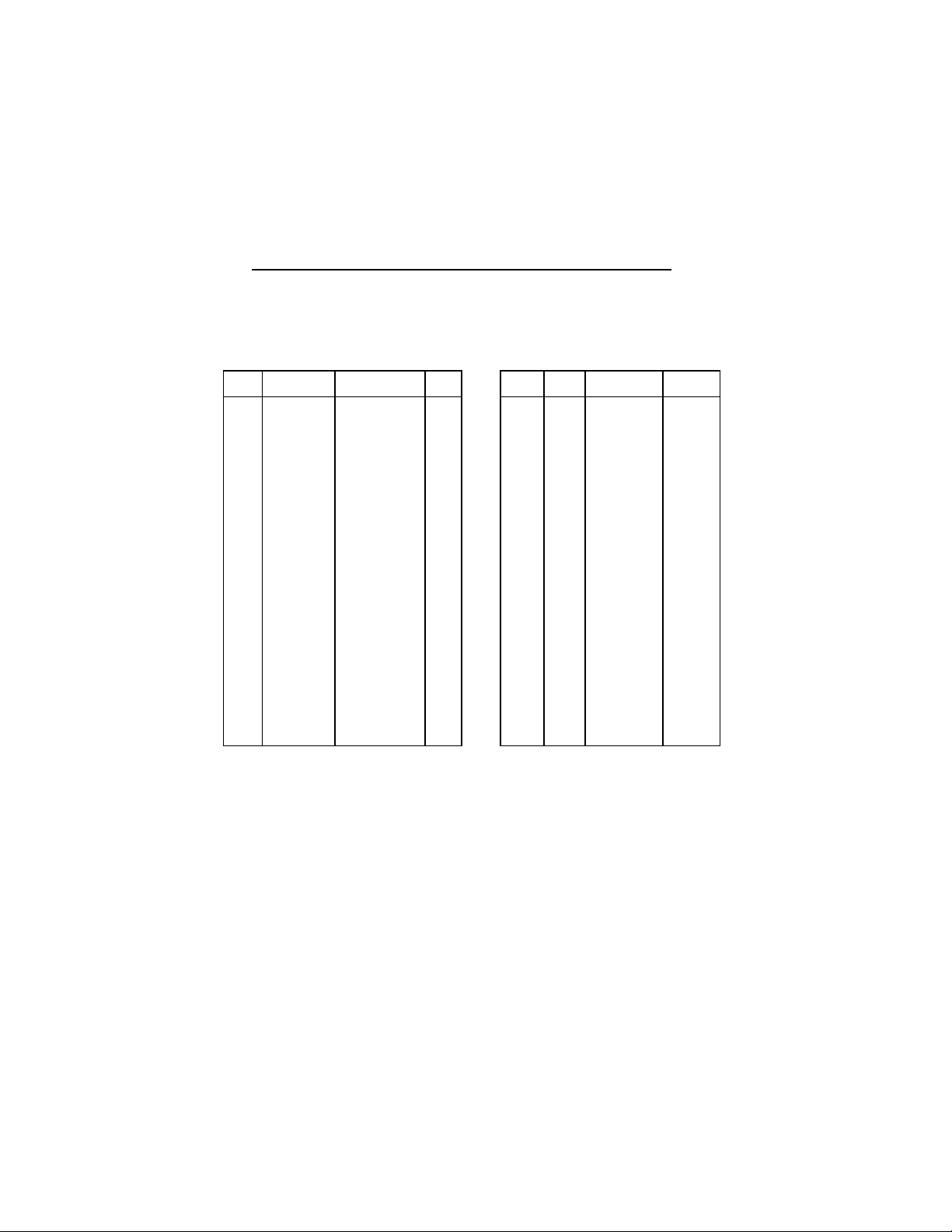
68 TEK-AT1 REFERENCE MANUAL
J1A MEZZANINE CARD CONNECTOR
A Side B Side
I/O PIN Signal Name
1
3
5
7
9
11
13
15
17
19
21
23
25
27
29
31
33
35
37
39
41
43
45
47
49
51
53
55
57
59
61
A1
A2
A3
A4
A5
A6
A7
A8
A9
A10
A11
A12
A13
A14
A15
A16
A17
A18
A19
A20
A21
A22
A23
A24
A25
A26
A27
A28
A29
A30
A31
I/O CH CK*
SD7
SD6
SD5
SD4
SD3
SD2
SD1
SD0
I/O CH RDY*
AEN
SA19
SA18
SA17
SA16
SA15
SA14
SA13
SA12
SA11
SA10
SA9
SA8
SA7
SA6
SA5
SA4
SA3
SA2
SA1
SA0
I/O
I/O
I/O
I/O
I/O
I/O
I/O
I/O
I/O
I/O
I/O
I/O
I/O
I/O
I/O
I/O
I/O
I/O
I/O
I/O
I/O
I/O
I/O
I/O
I/O
I/O
I/O
I/O
I/O
I/O
I
I
O
PIN Signal Name
2
B1
4
B2
6
B3
8
B4
10
B5
12
B6
14
B7
16
B8
18
B9
20
B10
22
B11
24
B12
26
B13
28
B14
30
B15
32
B16
34
B17
36
B18
38
B19
40
B20
42
B21
44
B22
46
B23
48
B24
50
B25
52
B26
54
B27
56
B28
58
B29
60
B30
62
B31
GND
RESET DRV
+5 Vdc
IRQ9
-5 Vdc
DRQ2
-12 Vdc
OWS
+12 Vdc
GND
SMESW*
SMEMR*
IOW*
IOR*
DACK3*
DRQ3
DACK1*
DRQ1
REFRESH*
CLK
IRQ7
IRQ6
IRQ5
IRQ4
IRQ3
DACK2*
T/C
BALE
+5 Vdc
OSC
GND
I/O
Ground
O
Power
I
Power
I
Power
I
Power
Ground
O
O
I/O
I/O
O
I
O
I
I/O
O
I
I
I
I
I
O
O
O
Power
O
Ground
Page 21

SPECIFICATIONS 69
J4 FLOPPY DISK CONNECTOR PIN OUT
Pin Number Signal Flow Signal
2
4
6
8
10
12
14
16
18
20
22
24
26
28
30
32
34
1-33 (ODD)
O
-
I
O
O
O
O
O
O
O
O
I
I
I
O
I
-
RPM/LC
N.C.
N.C.
INDEX*
MOTRENA*
DRIVESB*
DRIVESA*
MOTRENB*
DIRC*
STEP*
WRITE DATA*
WRITE ENABLE*
TRACK0*
WRITE PROTECT*
READ DATA*
HEAD SELECT*
DCHG
GND
Page 22

70 TEK-AT1 REFERENCE MANUAL
J3 HARD DISK CONNECTOR PIN OUT
Pin Number Signal Flow Signal
3
4
5
6
7
8
9
10
11
12
13
14
15
16
17
18
1
23
25
33
35
36
37
38
31
32
39
20
21
34
2,19,22,24
26,30,40
I/O
I/O
I/O
I/O
I/O
I/O
I/O
I/O
I/O
I/O
I/O
I/O
I/O
I/O
I/O
I/O
O
O
O
O
O
O
O
O
I
I
I
-
-
-
-
SD7
SD8
SD6
SD9
SD5
SD10
SD4
SD11
SD3
SD12
SD2
SD13
SD1
SD14
SD0
SD15
RST*
IOW*
IOR*
SA1
SA0
SA2
CS0*
CS1*
IRQ14
I/OCS16*
ACTIVE*
KEY (NOT CONNECTED)
RESERVED (NOT
CONNECTED)
PDIAG
GND
 Loading...