

Page 1

Page 2

FOREWORD
The information in this document is provided for reference purposes only. TEKNOR does
not assume any liability for the application of information or the use of products described
herein.
This document may contain information or refer to products protected by the copyrights or
patents of others and does not convey any license under the patent rights of TEKNOR, nor
the rights of others.
Printed in Canada.
Copyright 1998 by TEKNOR INDUSTRIAL COMPUTERS INC., Boisbriand, Qc J7G 2A7.
Page 3

READ ME FIRST
EXERCISE CAUTION WHILE REPLACING LITHIUM BATTERY
WARNING
Danger of explosion if battery is incorrectly replaced.
Replace only with the same or equivalent type recommended by the manufacturer.
Dispose of used batteries according to the manufacturer's instructions.
ATTENTION
Il y a danger d’explosion s’il y a remplacement incorrect de la batterie.
Remplacer uniquement avec une batterie du même type ou d’un type équivalent
recommandé par le constructeur. Mettre au rebut les batteries usagées
conformément aux instructions du fabriquant.
ACHTUNG
Explosionsgefahr bei falschem Batteriewechsel.
Verwenden Sie nur die empfohlenen Batterietypen des Herstellers. Entsorgen Sie
die verbrauchten Batterien laut Gebrauchsanweisung des Herstellers.
ATENCION
Puede explotar si la pila no este bien reemplazada.
Solo reemplazca la pila con tipas equivalentes segun las instrucciones del
manifacturo. Vote las pilas usadas segun las instrucciones del manifacturo.
Read Me First 1
Page 4

PCI-942 Technical Reference Manual
WARNING
Please heed the following warning concering the PCI-942 board:
Connectors’ Pin Distribution Has Changed
Compared to previous PCI-9xx SBC boards, such as the PCI-935 and PCI-936, all
connectors besides those on the I/O bracket are rotated 180 degrees. The result is
that pin 1 is now on the upper right of dual row headers rather than on the lower
left, or on the right of single row headers rather than on the left.
Make sure you connect mating connectors properly: Line up pin 1 of the onboard
header with pin 1 of the mating connector. Improper connections may cause
damage to the board and your devices.
See diagram below which shows the connectors’ pin distribution on the board.
Read Me First 2
Page 5

IMPORTANT INFORMATION
Before operating your Single Board Computer, please note the following:
Adapter Cables
When connecting Serial Ports, the use of Taïwanese adapter cables is not
recommended, since the pinout is often incorrect. The direct crimp design offered
by TEKNOR allows the simplest cable assembly. All these cables are available
from TEKNOR by contacting the Sales department.
AMIBIOS Boot Sector Virus Protection Limitation
You should not enable the Boot Sector Virus Protection in AMIBIOS Setup when
formatting a hard drive.
AMIBIOS Defaults
AMIBIOS Fail Safe and Optimal default values have been provided to give control
over the system. However, the values for the AMIBIOS Setup options should be
changed only if the user has a full understanding of the timing relationships
involved.
Read Me First
Preventing Viruses
TEKNOR INDUSTRIAL COMPUTERS takes every precaution against computer
viruses. For your protection, we have safety sealed all utility diskettes. If the seal
is broken, do not use the diskette. Destroy the diskette immediately and contact
our Technical Support department for further instructions at (450) 437-5682
(Canada) or at +49 811 / 600 15-0 (Germany).
To safeguard against computer viruses in general, do not freely lend your utility
diskettes and regularly perform virus scans on all your computer systems.
Read Me First 3
Page 6

TABLE OF CONTENTS
READ ME FIRST
PART 1 - PRODUCT DESCRIPTION
1. PRODUCT OVERVIEW................................................................................ 1-1
2. FEATURES................................................................................................... 2-1
3. COMPATIBILITY WITH TEKNOR SBC PRODUCTS...................................3-1
PART 2 - HARDWARE INSTALLATION & CONNECTIONS
4. STATIC ELECTRICITY PRECAUTIONS......................................................4-1
5. UNPACKING ................................................................................................ 5-1
6. SETTING JUMPERS....................................................................................6-1
7. INSTALLING SYSTEM MEMORY................................................................7-1
7.1 168-PIN SOCKETS LOCATION............................................................... 7-1
7.2 SUPPORTED SYSTEM MEMORY CONFIGURATIONS ......................... 7-2
7.3 DIMM INSTALLATION............................................................................. 7-5
8. INSTALLING PCI-942 BOARD IN A BACKPLANE ...................................... 8-1
i
Page 7

PCI-942 Technical Reference Manual
9. INSTALLING & CONNECTING STANDARD I/O DEVICES
(KEYBOARD, SPEAKER, RESET, HD LED, MOUSE) .................................. 9-1
9.1 P5A COMBO I/O CONNECTION
(KEYBOARD, KEYLOCK, SPEAKER, RESET)......................................... 9-1
9.1.1 COMBO I/O JUMPERS.................................................................................9-2
9.1.2 P5A COMBO I/O CABLE CONNECTION......................................................9-3
9.2 P4 / P4A KEYBOARD & P2 KEYLOCK CONNECTIONS ......................... 9-4
9.2.1 P4 / P4A KEYBOARD & P2 KEYLOCK CABLE CONNECTIONS...................9-4
9.3 P5 SPEAKER CONNECTION.................................................................. 9-6
9.3.1 P5 SPEAKER CABLE CONNECTION...........................................................9-6
9.4 P10 RESET BUTTON CONNECTION..................................................... 9-7
9.4.1 P10 EXTERNAL RESET CABLE CONNECTION...........................................9-7
9.5 P12 HARD DISK LED CONNECTION...................................................... 9-8
9.5.1 P12 HARD DISK LED CABLE CONNECTION...............................................9-8
9.6 P9 / P9A PS/2 MOUSE CONNECTION................................................... 9-9
9.6.1 PS/2 MOUSE JUMPER ................................................................................ 9-9
9.6.2 P9 & P9A PS/2 MOUSE CABLE CONNECTIONS.......................................9-10
10. INSTALLING & CONNECTING STORAGE DEVICES
(FLOPPY, IDE, SCSI)................................................................................ 10-1
10.1 P3 FLOPPY CONNECTION ................................................................ 10-1
10.1.1 P3 FLOPPY CABLE CONNECTION .......................................................... 10-2
10.2 P11 & P11A IDE HARD DISK CONNECTIONS ................................... 10-4
10.2.1 P11 & P11A IDE CABLE CONNECTIONS.................................................10-5
10.3 P13 SCSI CONNECTION.................................................................... 10-8
10.3.1 SCSI TERMINATION JUMPER.................................................................10-9
10.3.2 SCSI CABLE CONNECTION................................................................... 10-10
11. INSTALLING & CONNECTING VIDEO .................................................... 11-1
11.1 CRT TYPE JUMPER ........................................................................... 11-2
11.2 VIDEO CABLE CONNECTION............................................................ 11-2
12. INSTALLING & CONNECTING OTHER PERIPHERALS
(SERIAL, PARALLEL, USB) ..................................................................... 12-1
12.1 P6 / P7 SERIAL PORT CONNECTION................................................ 12-1
12.1.1 P6 / P7 SERIAL PORT CABLE CONNECTION..........................................12-2
12.2 P8 PARALLEL PORT CONNECTION.................................................. 12-3
12.2.1 P12 PARALLEL PORT CABLE CONNECTION.......................................... 12-4
12.2.2 PARALLEL PORT MODES.......................................................................12-5
12.3 P17 USB PORT CONNECTION .......................................................... 12-8
12.3.1 USB PORT CABLE CONNECTION........................................................... 12-9
ii
Page 8

Table of Contents
13. INSTALLING & CONNECTING ETHERNET ............................................ 13-1
13.1 P16 ETHERNET CONNECTION.......................................................... 13-1
13.1.1 P16 ETHERNET CABLE CONNECTION................................................... 13-2
14. INSTALLING SUPERVISOR UTILITIES................................................... 14-1
14.1 POWER FAIL DETECTION................................................................. 14-1
14.1.1 +5V POWER FAIL (ONBOARD)................................................................14-1
14.1.2 +3.3V POWER FAIL (BACKPLANE)..........................................................14-1
14.2 WATCHDOG TIMER........................................................................... 14-2
14.3 VOLTAGE / TEMPERATURE / FAN SPEED MONITORING SYSTEM 14-3
15. POWERING UP THE SYSTEM & TROUBLESHOOTING ........................ 15-1
15.1 POWER SOURCE FOR THE PCI-942................................................. 15-1
15.2 POWER UP PROCEDURE.................................................................. 15-1
15.3 TROUBLESHOOTING ......................................................................... 15-1
PART 3 - SOFTWARE & ONBOARD UTILITIES
16. SOFTWARE SETUP................................................................................. 16-1
16.1 THE AMIBIOS SETUP PROGRAM...................................................... 16-2
16.1.1 ACCESSING THE AMIBIOS SETUP PROGRAM ...................................... 16-2
16.1.2 USING AMIBIOS SETUP..........................................................................16-3
16.1.3 STANDARD CMOS SETUP......................................................................16-4
16.1.4 ADVANCED CMOS SETUP...................................................................... 16-5
16.1.5 ADVANCED CHIPSET SETUP.................................................................. 16-7
16.1.6 POWER MANAGEMENT SETUP............................................................ 16-11
16.1.7 PCI / PLUG AND PLAY SETUP .............................................................. 16-13
16.1.8 PERIPHERAL SETUP ............................................................................. 16-15
16.1.9 AUTO-DETECT HARD DISKS................................................................. 16-17
16.1.10 CHANGE PASSWORDS ....................................................................... 16-18
16.1.11 LOADING OPTIMAL & FAIL SAFE SETTINGS ...................................... 16-22
16.1.12 SAVING CONFIGURATIONS & EXITING AMIBIOS SETUP .................. 16-23
16.2 THE SCSISELECT CONFIGURATION UTILITY .................................. 16-24
17. INSTALLING DRIVERS............................................................................ 17-1
17.1 SCSI DRIVERS ................................................................................... 17-1
17.2 VIDEO DRIVERS................................................................................. 17-1
17.3 ETHERNET DRIVERS......................................................................... 17-1
18. UPDATING OR RESTORING BIOS IN FLASH ........................................ 18-1
iii
Page 9

PCI-942 Technical Reference Manual
PART 4 - APPENDIXES
A. BOARD SPECIFICATIONS ..........................................................................A-1
A.1 ELECTRICAL..........................................................................................A-1
A.2 MECHANICAL.........................................................................................A-1
A.3 ENVIRONMENTAL .................................................................................A-1
A.4 RELIABILITY...........................................................................................A-1
B. BOARD DIAGRAMS .................................................................................... B-1
B.1 PCI-942 BLOCK DIAGRAM.....................................................................B-1
B.2 PCI-942 CONFIGURATION DIAGRAM...................................................B-3
B.3 PCI-942 MECHANICAL SPECIFICATIONS DIAGRAM ...........................B-5
C. CONNECTOR LOCATION & PINOUTS.......................................................C-1
C.1 LOCATION OF CONNECTORS ON THE PCI-942..................................C-1
C.2 CONNECTOR PINOUTS ........................................................................ C-2
D. LIST OF APPROVED VENDORS ................................................................D-1
D.1 RECOMMENDED DRAM DEVICES........................................................D-1
D.2 INTERFACE CONNECTORS..................................................................D-2
E. I/O MAP........................................................................................................E-1
F. MEMORY MAP.............................................................................................F-1
G. IRQ LINES.................................................................................................. G-1
H. DMA CHANNELS.........................................................................................H-1
I. BIOS SETUP ERROR CODES....................................................................... I-1
I.1 BEEP CODES...........................................................................................I-2
I.2 ERROR MESSAGES................................................................................. I-3
I.3 POST CODES...........................................................................................I-6
GETTING HELP
iv
Page 10

PRODUCT DESCRIPTION
1. PRODUCT OVERVIEW
2. FEATURES
3. COMPATIBILITY WITH TEKNOR SBC PRODUCTS
Page 11

1. PRODUCT OVERVIEW
The PCI-942 PCI-ISA single board computer features a flush-mounted Intel Pentium II
(Slot 1) processor, the Intel 440LX chipset and the Cirrus Logic GD5465 Accelerated
Graphics Port (AGP) video interface.
The PCI-942 board provides a flush-mounted design that allows you to use all your ISA
backplane slots (whether or not all your PCI slots can be used will depend on your
particular PICMG PCI-ISA backplane). Flush-mounting withstands higher shocks and
vibration and has better thermal characteristics than the usual edge mounted design.
AGP video interfaces are designed to off-load the PCI bus by allowing graphics data to
move directly from system memory.
This high performance SBC plugs into a PICMG PCI-ISA passive backplane and provides
100% PC compatibility for system expansion slots.
The SBC and backplane assembly is used as a substitute for the standard PC motherboard,
and in general includes all of the standard interfaces and peripherals that are normally
included in a top of the line PC. This compact solution allows an industrial user the
possibililty of designing a system that uses standard x86 software and peripherals, but in
an industrial environment where reliability, integration and service are of major concern.
The full-featured PCI-942 provides 2MB Rambus video DRAM, up to 256MB SDRAM or
512MB EDO DRAM (two 168-pin DIMM sockets), 512KB L2 cache, floppy controller,
dual EIDE (Ultra DMA/33) interface, PCI Ultra Wide SCSI controller, PCI
10Base-T/100Base-T Ethernet controller, USB 1.0 interface (two ports supported with
optional cable/assembly bracket), two serial ports, parallel port, speaker port, mouse port
and keyboard port.
1-1
Page 12

2. FEATURES
The PCI-942 includes the following features:
Microprocessor Support: The Intel Pentium II processor at 233, 266, 300 and 333 MHz
(maximum internal CPU clock speeds).
Chipset: The Intel Pentium II 440LX chipset with PCI bandwidth greater than
100MB/second.
Internal Secondary Cache: 512 KB, 64-bit wide, non-blocking.
System Memory :
- Two vertical 168-pin DIMM sockets support SDRAM (Synchronous DRAM)
memory configurations from 8 to 256 MB and EDO (Extended Data Out) DRAM
from 8 to 512 MB.
- Uses 3.3V, single-sided or double-sided 168-pin DIMMs.
- Supports 8MB, 16MB, 32MB, 64MB, 128MB and 256MB (EDO only) DIMM
modules (64-bit and 72-bit).
- Error Checking and Correction (ECC) and parity supported with 72-bit modules.
Floppy Interface: Supports two floppy disk drives from 360KB to 2.88MB.
Enhanced IDE Ultra DMA/33 Interface: Can drive up to four type 4 enhanced IDE
devices. Supports synchronous DMA mode and transfer rates up to 33MB per second.
PCI SCSI Interface: PCI Ultra Wide SCSI controller - Adaptec AIC-7880 - supports
data transfers up to 40MB per second and bursts data to the host at full PCI speeds.
Active termination provided with terminator voltage protected by self-resetting fuses. A
SCSISelect Configuration Utility is available. Software drivers are supported for the most
popular operating systems.
PCI Ethernet Interface: Supports 10Base-T and 100Base-T Ethernet interface options
via an RJ-45 connector on the board’s I/O bracket. The port supports two operational
modes (MII and SYM modes) and is capable of functioning in a full-duplex environment
for the MII/SYM and 10Base-T port. TX and RX LED indicators are supported on the
I/O bracket. Software drivers are supported for the most popular operating systems.
Bus Support:
- ISA Bus (IEEE P966 Specification).
- PCI Local Bus Specification, Revision 2.1: supports five PCI Bus masters, pipelined
snoop ahead feature and improved PCI to DRAM write-back policy. Concurrent PCI
maximizes system performance with simultaneous CPU, PCI and AGP Bus
activities. It includes multitransaction timing, enhanced write performance, a passive
release mechanism and support for PCI 2.1 compliant delayed transactions.The PCI
Local Bus interface to the backplane is compliant with the PCI Industrial Computer
Manufacturers Group (PICMG) 2.0 Specification.
2-1
Page 13

PCI-942 Technical Reference Manual
AGP Super VGA Interface : The video system includes t he Cirrus Logic GD5465 CRT
video controller with 2 MB video memory (Rambus DRAM) . The controller is an
Accelarated Graphics Port (AGP) device with both 3D and 2D capabilities. The interface
supports pixel resolutions up to 1280 x 1024 non-interlaced and 16.8 million colors at
resolutions up to 1024 x 768. The onboard Rambus memory provides a high-bandwidth
solution and supports 500MB per second data transfers. Software drivers for enhanced
performance and resolution are available for the most popular operating systems.
Serial Ports: Supports two RS-232 serial ports, 16C550 compatible with internal 16byte FIFO buffers for more efficient data transfers.
Parallel Port: Supports multiple modes (Standard, EPP and ECP).
Universal Serial Bus (USB): Supports two USB 1.0 ports (optional cable/assembly
bracket available from TEKNOR) with serial transfers at 12 or 1.5Mbit per second. The
USB is an interface allowing for connectivity to many standard PC peripherals via an
external port.
I/O Ports: AT keyboard, PS/2 mouse, and speaker. Keyboard voltage and mouse
voltage are protected with self-resetting fuses.
Watchdog Timer: The software controlled watchdog timer monitors system activity and
generates a reset pulse in the event of a time-out.
Power Fail Detection: A hardware reset is issued when the onboard +5V voltage drops
below 4.75V. Also, when JU15 is jumpered, a reset is generated whenever the
backplane’s +3.3V voltage drops below tolerance.
Hardware Monitoring System: A system hardware circuit monitors all system
voltages, ambient temperature and fan speeds. Based on National Semiconductor’s
LM80 and LM75.
Battery: A built-in lithium battery is provided, for ten years of data retention for CMOS
memory.
Operating Systems : Supports all operating systems developed for x86 and Pentium
processors: DOS, Windows 3.1, OS/2, Windows 95, Windows NT, UNIX, QNX, Novell
4.10, etc.
Boot Block Flash BIOS: The boot block flash device contains all the board’s BIOSs and
it is used for storing the nonvolatile configuration required for Plug and Play. Protected
boot block section allows for reprogramming of BIOS. The BIOS may be upgraded by
following the procedure detailed in Section 18. The main BIOS is a Hi-Flex AMIBIOS
with built-in advanced CMOS setup for system parameters, peripheral management for
configuring onboard peripherals, PCI-to-PCI bridge support and PCI interrupt steering.
Shadow RAM Support: Increases system speed and performance.
2-2
Page 14

3. COMPATIBILITY WITH TEKNOR SBC PRODUCTS
The PCI-942 board has the same form factor as the full size PCI-ISA SBC boards from
TEKNOR.
New features include the Intel Pentium II processor, Intel 440LX chipset,
SDRAM/EDO DIMM support, Ultra DMA/33 EIDE interface and AGP Super VGA
interface.
PCI SCSI is also supported on the PCI-933, PCI-935 and PCI-936, however not with
the same chip as the one found on the PCI-942. Similarly PCI Ethernet 10BaseT/100Base-T is supported on the PCI-936, but with another chip.
Like the PCI -935, the PCI-942 does not support flat panels and comes with Rambus
video DRAM. Like the PCI-933, the PCI-942 does not support user Flash.
3-1
Page 15

HARDWARE INSTALLATION &
CONNECTIONS
4. STATIC ELECTRICITY PRECAUTIONS
5. UNPACKING
6. SETTING JUMPERS
7. INSTALLING SYSTEM MEMORY
8. INSTALLING PCI-942 BOARD IN A BACKPLANE
9. INSTALLING & CONNECTING STANDARD I/O DEVICES
(KEYBOARD, SPEAK ER, RESET, HD LED, MOUSE)
10. INSTALLING & CONNECTING STORAGE DEVICES
(FLOPPY, IDE, SCSI)
11. INSTALLING & CONNECTING VIDEO
12. INSTALLING & CONNECTING OTHER PERIPHERALS
(SERIAL, PARALLEL, USB)
13. INSTALLING & CONNECTING ETHERNET
14. INSTALLING SUPERVISOR UTILITIES
15. POWERING UP THE SYSTEM & TROUBLESHOOTING
Page 16

4. STATIC ELECTRICITY PRECAUTIONS
Since static electricity can damage a board, the following precautions should be taken
whenever you handle the PCI-942:
Keep the board in its antistatic package, until you are ready to install it.
Touch a grounded surface before removing the board from its package or wear a
grounding wrist strap; this will discharge any static electricity that may have built
up on your body.
Handle the board by the edges.
4-1
Page 17

5. UNPACKING
Follow these recommendations while unpacking:
Observe the Static Electricity Precautions (Section 4).
After opening the box, save it and the packing material for possible future shipment.
Remove the board from its antistatic wrapping and place it on a grounded surface.
Inspect the board for damage. If there is any damage, or items are missing, notify
TEKNOR immediately.
5-1
Page 18

6. SETTING JUMPERS
Diagram 6-1 shows the jumper locations on the PCI-942 board. On this diagram,
jumpers appear as rectangular boxes containing small circles which represent the pins.
The jumpers are numbered on the diagram, as well as on the board.
The jumpers are shown with default settings (the black strips over the pins indicate that
those pins are shorted by jumper caps).
DIAGRAM 6- 1: Jumper Locations With Default Settings
Tables 6-1 and 6-2 on the following pages show all jumper settings (default settings are
indicated with an *).
✎ NOTE
When you want to install jumper JU12 - CMOS Clear - or JU8 - Password
Clear, we suggest you temporarily use the jumper cap on JU7 - Combo I/O
Speaker Connect.
6-1
Page 19

PCI-942 Technical Reference Manual
TABLE 6-1: Jumper Settings: JU7 - JU13, JU15
6-2
Page 20

TABLE 6-2: Jumper Settings: JU16 - JU18, W3, W5 - W6
Setting Jumpers
6-3
Page 21

7. INSTALLING SYSTEM MEMORY
7.1 168-PIN SOCKETS LOCATION
The location of the two 168-pin vertical DIMM (Dual In-line Memory Module) sockets
appears on Diagram 7-1 and they are labeled Bank 1 and Bank 0.
DIAGRAM 7- 1: DIMM Sockets Location
7-1
Page 22

PCI-942 Technical Reference Manual
7.2 SUPPORTED SYSTEM MEMORY CONFIGURATIONS
The DRAM interface is a 64/72-bit path that supports up to 256MB of Synchronous
DRAM (SDRAM) or up to 512MB of Extended Data Out (EDO) memory. Memory
can be installed in one or both DIMM sockets. The System BIOS automatically detects
memory type, size and speed and these characteristics can vary between sockets. The
following SDRAM and EDO DIMM modules are supported: 8MB (1Mx64 or 1Mx72),
16MB (2Mx64 or 2Mx72), 32MB (4Mx64 or 4Mx72), 64MB (8Mx64 or 8Mx72) and
128MB (16Mx64 or 16Mx72); additionaly 256MB (32Mx64 or 32Mx72) EDO DRAM
DIMM modules are supported.
The PCI-942 supports the following DIMMs:
3.3V only, single-sided or double-sided, must have gold fingers.
Synchronous DRAM (SDRAM) and Extended Data Out (EDO).
Unbuffered 4-clock 100MHz (SDRAM); 60ns (EDO).
Serial Presence Detect (SPD) EPROM.
64-bit and 72-bit DIMMs.
Error Checking and Correction (ECC) or parity bit, with 72-bit DIMMs.
JEDEC MO-161 compliant.
TABLE 7-1: PCI-942 System Memory Configuration: 8MB - 512MB
SYSTEM MEMORY BANK 0 BANK 1
8MB 8MB (1Mx64/72) 8MB - 8MB (12Mx64/72)
16MB 8MB (1Mx64/72) 8MB (1Mx64/72)
16MB 16MB (2Mx64/72) 16MB - 16MB (2Mx64/72)
24MB 8MB (1Mx64/72) 16MB (2Mx64/72)
24MB 16MB (2Mx64/72) 8MB (1Mx64/72)
32MB 16MB (2Mx64/72) 16MB (2Mx64/72)
32MB 32MB (4Mx64/72) 32MB - 32MB (4Mx64/72)
40MB 8MB (1Mx64/72) 32MB (4Mx64/72)
40MB 32MB (4Mx64/72) 8MB (1Mx64/72)
48MB 16MB (2Mx64/72) 32MB (4Mx64/72)
48MB 32MB (4Mx64/72) 16MB (2Mx64/72)
7-2
Page 23

Installing System Memory
TABLE 7-1: PCI-942 System Memory Configuration: 8MB - 512MB (Continued)
SYSTEM MEMORY
64MB - 64MB (8Mx64/72)
64MB 64MB (8Mx64/72) 64MB 32MB (4Mx64/72) 32MB (4Mx64/72)
72MB 8MB (1Mx64/72) 64MB (8Mx64/72)
72MB 64MB (8Mx64/72) 8MB (1Mx64/72)
80MB 16MB (2Mx64/72) 64MB (8Mx64/72)
80MB 64MB (8Mx64/72) 16MB (2Mx64/72)
96MB 32MB (4Mx64/72) 64MB (8Mx64/72)
96MB 64MB (8Mx64/72) 32MB (4Mx64/72)
128MB 64MB (8Mx64/72) 64MB (8Mx64/72)
128MB - 128MB (16Mx64/72)
128MB 128MB (16Mx64/72) 136MB 8MB (1Mx64/72) 128MB (16Mx64/72)
136MB 128MB (16Mx64/72) 8MB (1Mx64/72)
144MB 16MB (2Mx64/72) 128MB (16Mx64/72)
144MB 128MB (16Mx64/72) 16MB (2Mx64/72)
160MB 32MB (4Mx64/72) 128MB (16Mx64/72)
160MB 128MB (16Mx64/72) 32MB (4Mx64/72)
192MB 64MB (8Mx64/72) 128MB (16Mx64/72)
192MB 128MB (16Mx64/72) 64MB (8Mx64/72)
256MB - 256MB (64Mx64/72) EDO only
256MB 256MB (64Mx64/72) EDO only 256MB 128MB (16Mx64/72) 128MB (16Mx64/72)
264MB 256MB (64Mx64/72) EDO only 8MB (1Mx64/72)
264MB 8MB (1Mx64/72) 256MB (64Mx64/72) EDO only
272MB 256MB (64Mx64/72) EDO only 16MB (2Mx64/72)
272MB 16MB (2Mx64/72) 256MB (64Mx64/72) EDO only
288MB 256MB (64Mx64/72) EDO only 32MB (4Mx64/72)
288MB 32MB (4Mx64/72) 256MB (64Mx64/72) EDO only
320MB 256MB (64Mx64/72) EDO only 64MB (8Mx64/72)
320MB 64MB (8Mx64/72) 256MB (64Mx64/72) EDO only
384MB 256MB (64Mx64/72) EDO only 128MB (16Mx64/72)
384MB 128MB (16Mx64/72) 256MB (64Mx64/72) EDO only
512MB 256MB (64Mx64/72) EDO only 256MB (64Mx64/72) EDO only
BANK 0 BANK 1
7-3
Page 24

PCI-942 Technical Reference Manual
Consult Table 7-2 to see examples of recommended DIMM devices on the PCI-942. Many
other models are available and function equally well. Users are encouraged to check with
their local distributors for comparable substitutes.
TABLE 7-2: Recommended DIMM Devices
DIMM VENDOR PART NUMBER
2M*72 (ED0)
16MB modules
(SPD EPROM, ECC)
4M*72 (SDRAM)
32MB modules
4M*72 (ED0)
32MB modules
(SPD EPROM, ECC)
8M*72 (ED0)
64MB modules
(SPD EPROM, ECC)
16M*72 (SDRAM)
128MB modules
16M*72 (ED0)
128MB modules
(SPD EPROM, ECC)
ROCKY MOUNTAIN RAM 2x72CEQ
ROCKY MOUNTAIN RAM 4x72CQ2x8S4E
ROCKY MOUNTAIN RAM 4x72CEQ
ROCKY MOUNTAIN RAM 8x72CEQ
ROCKY MOUNTAIN RAM 16x72CQ8x8S4E
ROCKY MOUNTAIN RAM 16x72CEQ
7-4
Page 25

Installing System Memory
7.3 DIMM INSTALLATION
When you are ready to install the DIMMs in the sockets, follow the steps outlined
below:
1. With the board flat on the table, turn it so that the sockets are at the end of the board
farthest from you.
2. Hold the module vertically and turn it so that one of the two bottom connector keys
is on the right. Insert the connector into the socket (Bank 0 or Bank 1, depending on
the configuration chosen - see Table 7-1), aligning the keys on the module with the
socket’s key inserts.
3. Snap the retaining clips on each side of the socket to a vertical position to lock the
module into place. Repeat steps 2 and 3 if you are populating the other socket.
To remove a DIMM from a socket, pull on the retaining clips situated on each side of
the socket, to release the module. Pull the module upward to remove.
7-5
Page 26

8. INSTALLING PCI-942 BOARD IN A BACKPLANE
The PCI-942 will work on any PCI-ISA passive backplane, provided it complies with
the PCI INDUSTRIAL COMPUTER MANUFACTURERS GROUP (PICMG),
Revision 2.0 specification. For example, the board may be installed on the PCI-950
PCI-ISA passive backplane from TEKNOR: This backplane has three PCI slots, five
ISA slots and one PCI-ISA connector where you can insert the PCI-942.
Since the PCI-942 is also fully IBM AT compatible, it can also be installed on any
standard ISA passive backplane, if PCI expansion slots are not needed.
8-1
Page 27

9. INSTALLING & CONNEC TING STANDARD I/O
DEVICES (KEYBOARD, SPEAKER, RESET,
HD LED, MOUSE)
In this Section, we will look at how to make the following basic I/O connections on the
PCI-942 board: keyboard and keylock, speaker, reset button, hard disk LED and PS/2
mouse.
9.1 P5A COMBO I/O CONNECTION (KEYBOARD, KEYLOCK,
SPEAKER, RESET)
The P5A header allows connections for the standard AT keyboard, keylock interface,
speaker port and reset button.
✎ NOTE
The keyboard, keylock, speaker and reset also have individual connectors on
the PCI-942. You cannot use both the P5A combo I/O connector and the
following individual connectors: P4 keyboard, P4A keyboard, P2 keylock, P5
speaker and P10 reset.
The P5A combo I/O connector is an 8-pin single row header. Its location appears below
in Diagram 9-1.
DIAGRAM 9- 1: P5A Combo I/O Connector Location
9-1
Page 28
PCI-942 Technical Reference Manual
9.1.1 COMBO I/O JUMPERS
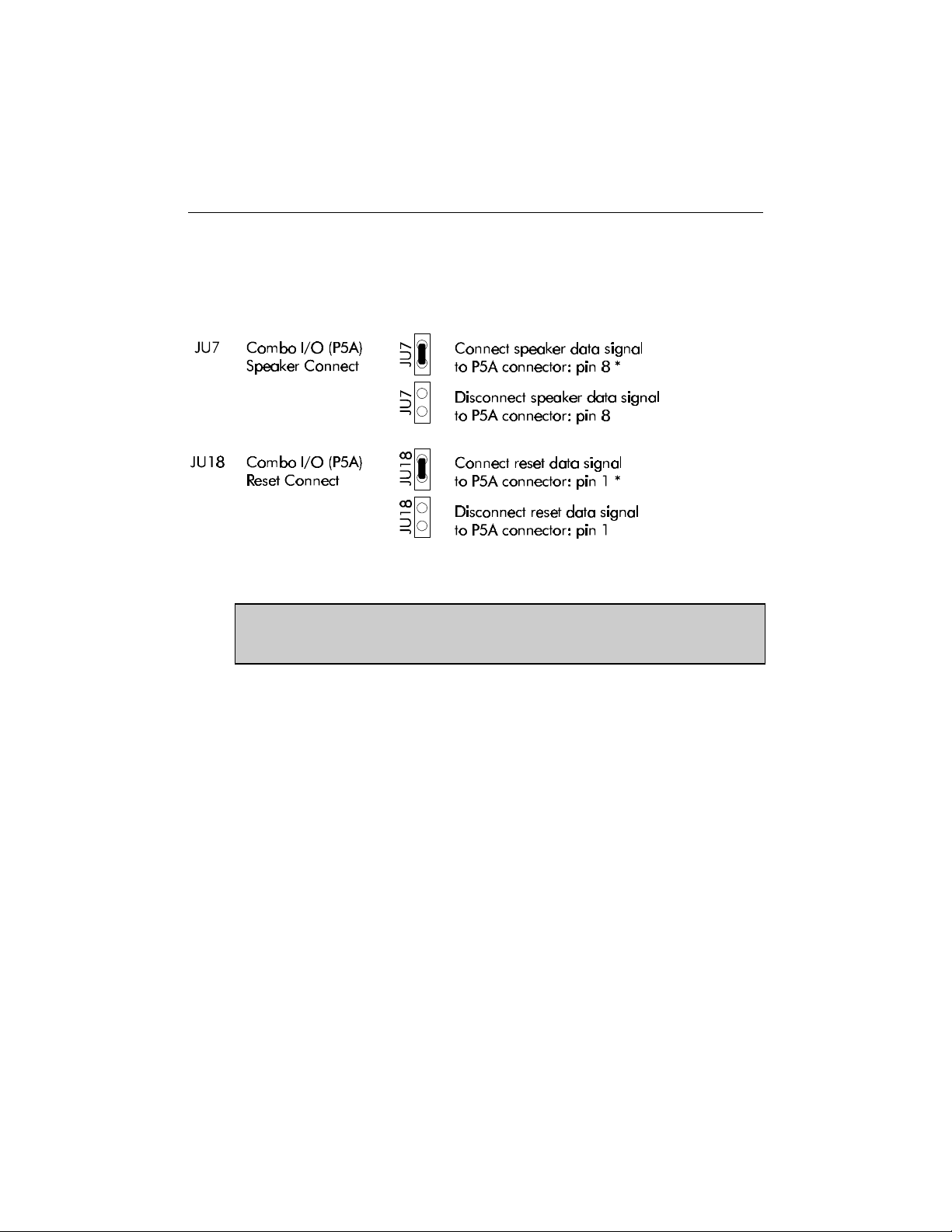
The following jumpers are related to the P5A combo I/O connector: JU7 Combo I/O
Speaker Connect and JU18 Combo I/O Reset Connect. JU7 and JU18 jumper settings
appear below (* = initial settings):
✎ NOTE
If you use the P5A combo I/O connectors, you need to short jumper JU7 to
connect the reset data signal to pin 1of P5A and short jumper JU18 to connect
the speaker data signal to pin 8 of P5A.
9-2
Page 29

Installing & Connecting Standard I/O Devices (Keyboard, Speaker, Reset, HD LED, Mouse)
9.1.2 P5A COMBO I/O CABLE CONNECTION
The cable needed for the P5A combo I/O header is an 8-pin flat ribbon cable.
You may want to create your own cable. The following are recommended for the
mating connector:
Molex 09-50-3081 (connector),
Molex 08-050-0114 (crimp).
The pinout for the P5A combo I/O header appears below in Table 9-1.
TABLE 9-1: Combo I/O Header (P5A) - Pinout
Pin Number Signal Flow Signal
1 I RESET
2 - GND
3 - Not Connected
4 I/O KBD CLOCK
5 I/O KBD DATA
6 I KBD LOCK DATA
7 - KBD POWER
8 O SPEAKER DATA
(+5V fused)
9-3
Page 30

PCI-942 Technical Reference Manual
9.2 P4 / P4A KEYBOARD & P2 KEYLOCK CONNECTIONS
The P4 keyboard connector is a 6-pin mini DIN connector (PS/2 keyboard) located on
the board’s I/O bracket. The P4A keyboard header and the P2 keylock header are both
5-pin single row headers. The location of these connectors appears below in Diagram 9-
2.
DIAGRAM 9- 2: P4 / P4A Keyboard & P2 Keylock Connector Location
9.2.1 P4 / P4A KEYBOARD & P2 KEYLOCK
CABLE CONNECTIONS
9.2.1.1 P4 PS/2 Keyboard
If you use the P4 keyboard mini DIN connector on the I/O bracket, no additional
cabling is needed. Simply connect your PS/2 keyboard cable to the P4 connector.
The pinout for the P4 keyboard connector appears below in Table 9-2.
TABLE 9-2: PS/2 Keyboard Connector (P4) - Pinout
Pin Number Signal Flow Signal
1 I/O KBD DATA
2 - Reserved
3 - GND
4 - KBD POWER
5 I/O KBC CLOCK
6 - Reserved
(+5V fused)
9-4
Page 31

Installing & Connecting Standard I/O Devices (Keyboard, Speaker, Reset, HD LED, Mouse)
9.2.1.2 P4A Keyboard Header
If you use the P4A keyboard header, a 5-pin flat ribbon cable with mating connector is
needed. It is available from TEKNOR: part number 150-3535-00.
You may want to create your own cable for the P4A keyboard header. The following
are recommended for the mating connector:
Leoco 2530 S050013 (connector),
Leoco 2533 TCB00A0 (crimp).
The pinout for the P4A keyboard header appears below in Table 9-3.
TABLE 9-3: Keyboard Header (P4A) - Pinout
Pin Number Signal Flow Signal
1 I/O KBC CLOCK
2 I/O KBD DATA
3 - KEY
4 - KBD GND
5 - KBD POWER
(Not Connected)
(+5V fused)
9.2.1.3 P2 Keylock Header
If you use the P2 keylock header, a 5-pin flat ribbon cable with mating connector is needed.
You may want to create your own cable for the P2 keylock header. The following are
recommended for the mating connector:
Leoco 2530 S050013 (connector),
Leoco 2533 TCB00A0 (crimp).
The pinout for the P2 keylock header appears below in Table 9-4.
TABLE 9-4: Keylock Header (P2) - Pinout
Pin Number Signal Flow Signal
1 - LED POWER
2 - KEY
3 - GND
4 I KEYLOCK DATA
5 - GND
(Not Connected)
9-5
Page 32
PCI-942 Technical Reference Manual
9.3 P5 SPEAKER CONNECTION
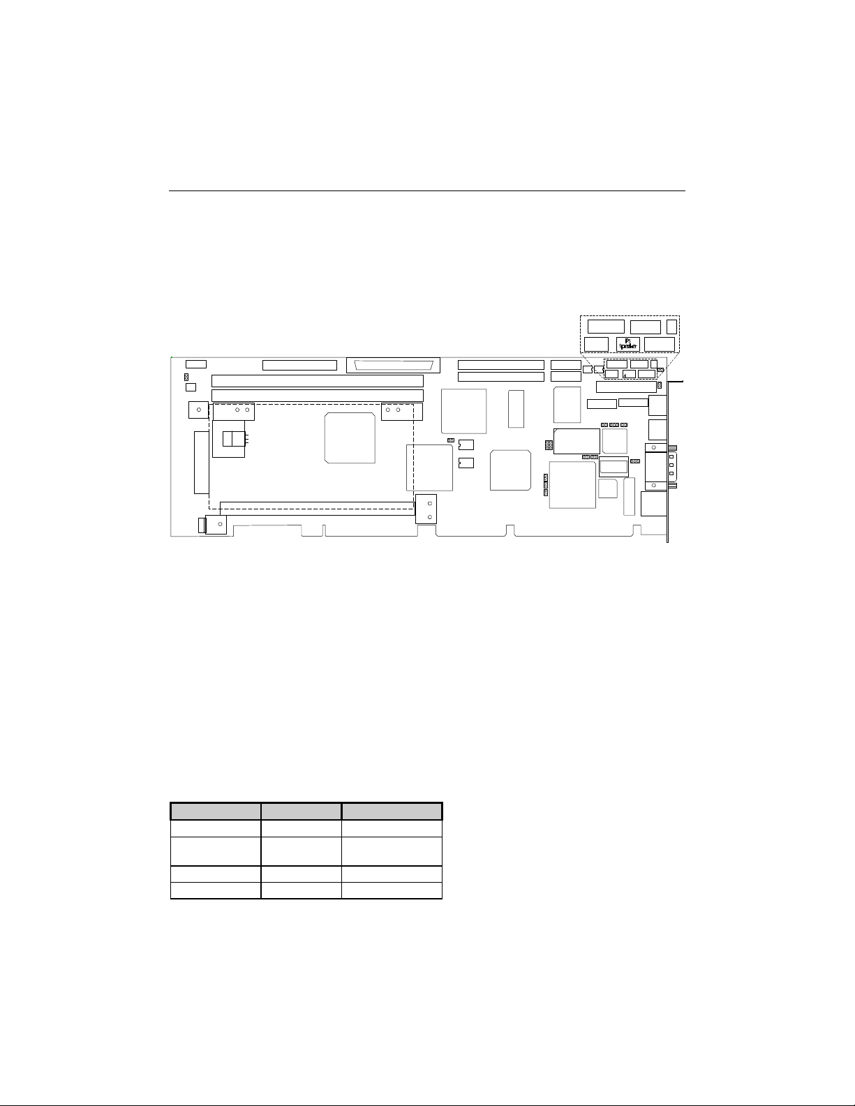
The P5 speaker connector is an 8-pin single row header. Its location appears below in
Diagram 9-3.
DIAGRAM 9- 3: P5 Speaker Connector Location
9.3.1 P5 SPEAKER CABLE CONNECTION
The cable needed for the P5 speaker header is a 4-pin flat ribbon cable with mating
connector.
You may want to create your own cable. The following are recommended for the
mating connector:
Molex 22-01-3047 (connector),
Molex 08-50-0114 (crimp).
The pinout for the P5 speaker header appears below in Table 9-5.
TABLE 9-5: Speaker Header (P5) - Pinout
Pin Number Signal Flow Signal
1 O SPEAKER DATA
2 - KEY
3 - GND
4 - +5V
(Not Connected)
9-6
Page 33

Installing & Connecting Standard I/O Devices (Keyboard, Speaker, Reset, HD LED, Mouse)
9.4 P10 RESET BUTTON CONNECTION
The P10 external reset connector is a 2-pin single row header. Its location appears
below in Diagram 9-4.
DIAGRAM 9- 4: P10 External Reset Connector Location
9.4.1 P10 EXTERNAL RESET CABLE CONNECTION
The cable needed for the P10 reset header is a 2-pin flat ribbon cable with mating
connector.
You may want to create your own cable. The following are recommended for the
mating connector:
Leoco 2530 S020013 (housing),
Leoco 2533 TCB00A0 (crimp).
Molex 22-01-3027 (housing),
Molex 08-050-0114 (crimp).
The pinout for the P10 external reset header appears below in Table 9-6.
TABLE 9-6: External Reset Header (P10) - Pinout
Pin Number Signal Flow Signal
1 I EXT RESET*
2 - GND
* Active low signal
9-7
Page 34
PCI-942 Technical Reference Manual
9.5 P12 HARD DISK LED CONNECTION
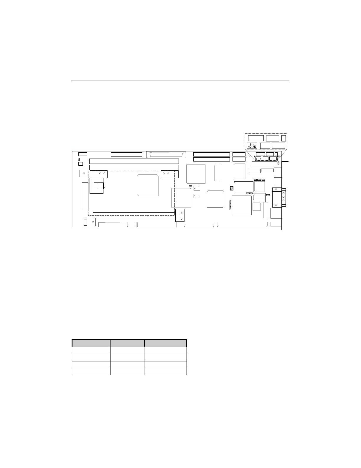
The P12 hard disk LED connector is a 4-pin single row header. Its location appears
below in Diagram 9-5.
DIAGRAM 9- 5: P12 Hard Disk LED Connector Location
9.5.1 P12 HARD DISK LED CABLE CONNECTION
The cable needed for the P12 hard disk LED header is a 4-pin flat ribbon cable with
mating connector.
You may want to create your own cable. The following are recommended for the
mating connector:
Molex 22-01-3047 (connector),
Molex 08-50-0114 (crimp).
The pinout for the P12 hard disk LED header appears below in Table 9-7.
TABLE 9-7: Hard Drive LED Header (P12) - Pinout
Pin Number Signal Flow Signal
1 - +5V Pull-up
2 O HD LED
3 O HD LED
4 - +5V Pull-up
9-8
Page 35

Installing & Connecting Standard I/O Devices (Keyboard, Speaker, Reset, HD LED, Mouse)
9.6 P9 / P9A PS/2 MOUSE CONNECTION
The P9 PS/2 mouse connector is a 6-pin mini DIN. The P9A PS/2 mouse header is a 6pin single row header. The location of these connectors appears below in Diagram 9-6.
DIAGRAM 9- 6: P9 & P9A PS/2 Mouse Connector Location
9.6.1 PS/2 MOUSE JUMPER
Prior to connecting a PS/2 mouse, configure jumper JU17, as shown below (* = initial
setting).
✎ NOTE
The JU17 jumper must be installed to use a PS/2 mouse on the PCI-942 board.
9-9
Page 36

PCI-942 Technical Reference Manual
9.6.2 P9 & P9A PS/2 MOUSE CABLE CONNECTIONS
9.6.2.1 P9 PS/2 Mouse Connector
If you use the P9 mini DIN connector on the I/O bracket, no additional cabling is
needed. Simply connect your PS/2 mouse cable to the P9 connector.
The pinout for the P9 PS/2 mouse connector appears below in Table 9-8.
TABLE 9-8: PS/2 Mouse Connector (P9) - Pinout
Pin Number Signal Flow Signal
1 I/O MOUSE DATA
2 - Reserved
3 - GND
4 - KBD POWER
5 I/O MOUSE CLOCK
6 - Reserved
9.6.2.2 P9A Mouse Header
If you use the P9A PS/2 mouse header, a 6-pin flat ribbon cable with mating connector
is needed. It is available from TEKNOR: part number 150-3555-00. This cable also
includes a serial DB-9 connector on a bracket.
(+5V fused)
You may want to create your own cable for the P9A mouse header. The following are
recommended for the mating connector:
Molex 90331-0002 (connector),
Molex 08-50-0114 (crimp).
The pinout for the P9A PS/2 mouse header appears below in Table 9-9.
TABLE 9-9: Mouse Header (P4A) - Pinout
Pin Number Signal Flow Signal
1 I/O MOUSE DATA
2 - Reserved
3 - KBD GND
4 - KBD POWER
5 I/O MOUSE CLOCK
6 - Reserved
(+5V fused)
9-10
Page 37

10. INSTALLING & CONNECTING STORAGE
DEVICES (FLOPPY, IDE, SCSI)
10.1 P3 FLOPPY CONNECTION
The P3 floppy drive connector is a 34-pin dual row header. Its location appears below
in Diagram 10-1.
DIAGRAM 10-1: P3 Floppy Drive Connector Location
✎ NOTE
When all the hardware connections are completed on the PCI-942, you will
need to setup onboard controllers and installed devices by software. For the
floppy controller and devices, software setup includes:
1. Ensuring that the onboard floppy controller is enabled in AMIBIOS
2. Other AMIBIOS Setup for the floppy drives includes defining the floppy
Peripheral Setup (described in section 16.1.8). By default, the onboard
floppy is automatically enabled by the BIOS (Auto setting). The Auto
setting will first search the ISA bus for an offboard floppy controller and if
it finds one, it will enable it.
type in the Standard CMOS Setup (described in section 16.1.3) and setting
the floppy access control in the Advanced CMOS Setup (described in
section 16.1.4).
10-1
Page 38

PCI-942 Technical Reference Manual
10.1.1 P3 FLOPPY CABLE CONNECTION
The installation of the floppy drives is done via a standard IBM 34 -pin flat ribbon
cable. This cable allows the installation of two floppy devices on the P3 header.
An 18” floppy disk cable is available from TEKNOR: part number 150-051.
Diagram 10-2 shows a floppy disk cable with the floppy 1 and floppy 0 mating
connectors. Note that wire 10 to wire 16 are twisted between the floppy 1 and floppy 0
connectors.
DIAGRAM 10-2: Floppy Disk Cable
You may want to create your own cable for the P3 floppy header. The following are
recommended for the mating connectors:
Amp 746285-8 [optional strain relief: 499252-6],
Robinson Nugent IDS-C34PK-TG,
Thomas & Betts 622-3430 [optional strain relief: 622-3441].
(34-pin flat cable connector).
10-2
Page 39

Installing & Connecting Storage Devices (Floppy, IDE, SCSI)
The pinout for the P3 floppy connector appears below in Table 10-1.
TABLE 10-1: Floppy Drive Connector (P3) - Pinout
Pin
Number
1
3
5
7
9
11
13
15
17
19
21
23
25
27
29
31
33
* Active low signal
Signal
Flow
-
-
-
-
-
-
-
-
-
-
-
-
-
-
-
-
-
Signal Pin
GND
GND
GND
GND
GND
GND
GND
GND
GND
GND
GND
GND
GND
GND
GND
GND
GND
Number
2
4
6
8
10
12
14
16
18
20
22
24
26
28
30
32
34
Signal
Flow
O
-
I
O
O
O
O
O
O
O
O
I
I
I
O
I
Signal
DRV DENS. SEL. 0*
Not Connected
Not Connected
INDEX*
MOTOR ON 0,1*
DRIVE SELECT B*
DRIVE SELECT A*
MOTOR ON 2*
DIR CONTROL*
STEP*
WRITE DATA*
WRITE ENABLE*
TRACK 0*
WRITE PROTECT*
READ DATA*
HEAD SELECT*
DSKCHG*
10-3
Page 40

PCI-942 Technical Reference Manual
10.2 P11 & P11A IDE HARD DISK CONNECTIONS
The P11 primary IDE hard drive connector and the P11A secondary IDE hard drive
connector are both 40-pin dual row headers. The location of the P11 and P11A
connectors appears below in Diagram 10-3.
DIAGRAM 10-3: Enhanced IDE Connectors (P11, P11A) Location
✎ NOTE
When all the hardware connections are completed on the PCI-942, you will
need to setup the installed devices by software. For the IDE hard disks, software
setup includes:
1. Configuring the disks with the AMIBIOS Standard CMOS Setup
(explained in section 16.1.3) or by performing a hard disk auto-detect from
the AMIBIOS Main Menu (explained in section 16.1.9).
2. Selecting the onboard IDE channels in the AMIBIOS Peripheral Setup
(explained in section 16.1.8).
10-4
Page 41

Installing & Connecting Storage Devices (Floppy, IDE, SCSI)
10.2.1 P11 & P11A IDE CABLE CONNECTIONS
The P11 and P11A connectors allow up to four enhanced IDE devices with flat ribbon
cables and mating connectors, as shown below.
DIAGRAM 10-4: IDE Connectors and Devices
The cable needed to hook up the IDE connectors is a 40-pin flat ribbon cable. This 40pin cable handles all command, data and status I/O lines. Its recommended maximum
length is 18 inches from the IDE device to the 40-pin connector. This cable is available
from TEKNOR: part number 150-259.
10-5
Page 42

PCI-942 Technical Reference Manual
Diagram 10-5 shows an IDE hard disk cable.
DIAGRAM 10-5: IDE Hard Disk Cable
You may want to make your own cable with a 40-pin flat ribbon cable and 40-pin flat
cable mating connectors. Following is a list of approved vendors for the mating
connectors:
AMP 746285-9 [optional strain relief: 499252-1],
Robinson Nugent IDS-C40PK-TG,
Thomas & Betts 622-4030 [optional strain relief: 622-4041].
(40-pin flat cable connector).
10-6
Page 43
Installing & Connecting Storage Devices (Floppy, IDE, SCSI)
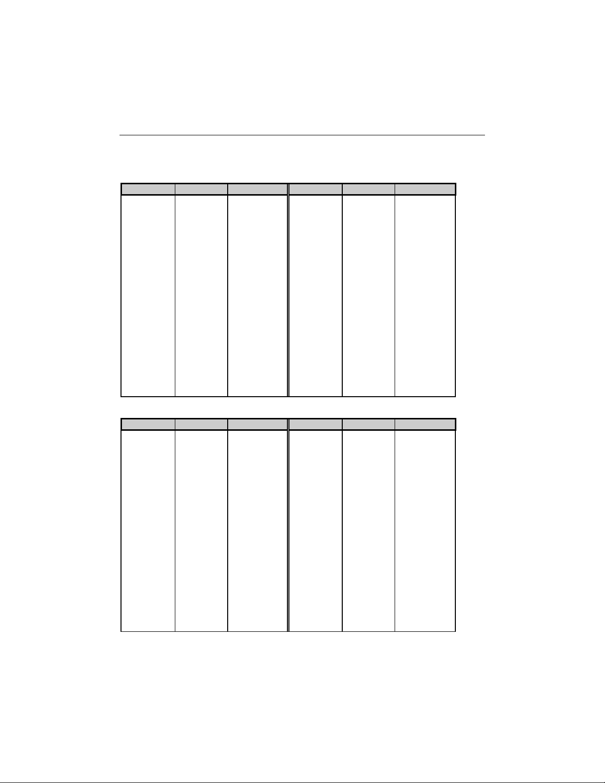
The pinouts for the P11 primary and P11A secondary IDE connectors appear below.
TABLE 10-2: Primary Enhanced IDE Connector (P11) - Pinout
Pin Number Signal Flow Signal Pin Number Signal Flow Signal
1
3
5
7
9
11
13
15
17
19
21
23
25
27
29
31
33
35
37
39
O
I/O
I/O
I/O
I/O
I/O
I/O
I/O
I/O
I
O
O
I
O
I
O
O
O
I
RESET
DATA 7
DATA 6
DATA 5
DATA 4
DATA 3
DATA 2
DATA 1
DATA 0
GND
DRQ 0
IOW
IOR
IORDY
DACK 0
IRQ 14
ADD 1
ADD 0
CS 1P
IDEACTP
2
4
6
8
10
12
14
16
18
20
22
24
26
28
30
32
34
36
38
40
I/O
I/O
I/O
I/O
I/O
I/O
I/O
I/O
-
-
-
-
-
-
-
O
O
-
GND
DATA 8
DATA 9
DATA 10
DATA 11
DATA 12
DATA 13
DATA 14
DATA 15
Not Connected
GND
GND
GND
+5V
GND
IOCS16
GND
ADD 2
CS 3P
GND
TABLE 10-3: Secondary Enhanced IDE Connector (P11A) - Pinout
Pin Number Signal Flow Signal Pin Number Signal Flow Signal
1
3
5
7
9
11
13
15
17
19
21
23
25
27
29
31
33
35
37
39
O
I/O
I/O
I/O
I/O
I/O
I/O
I/O
I/O
I
O
O
I
O
I
O
O
O
I
RESET
DATA 7
DATA 6
DATA 5
DATA 4
DATA 3
DATA 2
DATA 1
DATA 0
GND
DRQ 1
IOW
IOR
IORDY
DACK 1
MIRQ 0
ADD 1
ADD 0
CS 1S
IDEACTS
2
4
6
8
10
12
14
16
18
20
22
24
26
28
30
32
34
36
38
40
I/O
I/O
I/O
I/O
I/O
I/O
I/O
I/O
-
-
-
-
-
-
-
O
O
-
GND
DATA 8
DATA 9
DATA 10
DATA 11
DATA 12
DATA 13
DATA 14
DATA 15
Not Connected
GND
GND
GND
+5V
GND
IOCS16
GND
ADD 2
CS 3S
GND
10-7
Page 44
PCI-942 Technical Reference Manual
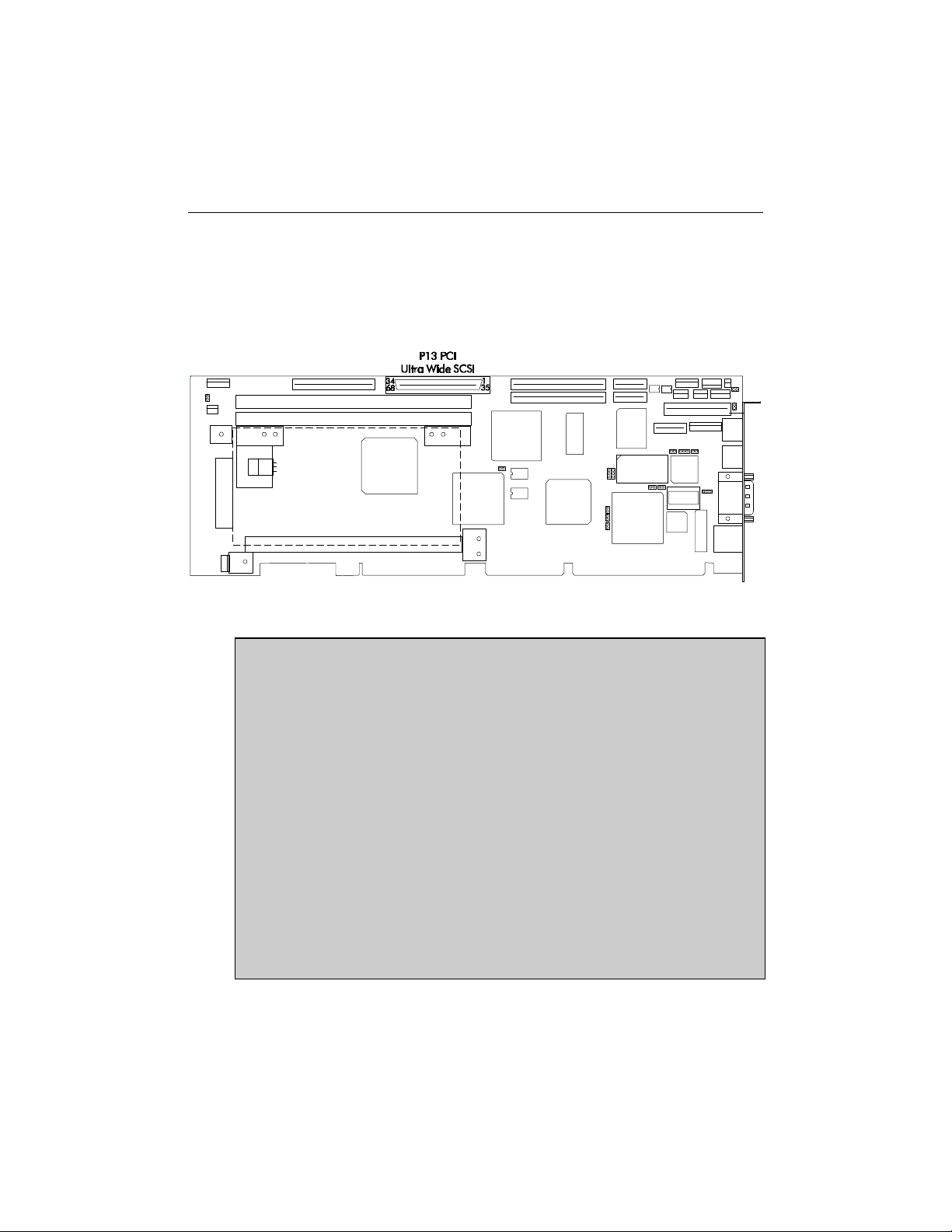
10.3 P13 SCSI CONNECTION
The P13 PCI Ultra Wide SCSI Controller Connector is a 50/68 high density SCSI
connector. Its location appears below on Diagram 10-6.
DIAGRAM 10-6: P13 SCSI Connector Location
✎ NOTE
When all the hardware connections are completed on the PCI-942, you will
need to setup onboard controllers and installed devices by software. For the
SCSI controller and devices, software setup includes:
1. Ensuring that the onboard SCSI controller is enabled in AMIBIOS PCI /
Plug and Play Setup Setup (described in section 16.1.7). By default, the
onboard SCSI is enabled, however, it may be disabled if an external SCSI
card is required for testing or other purposes.
2. If you want your SCSI device to be the boot device, this must be defined in
the AMIBIOS Advanced CMOS Setup (described in section 16.1.4).
However, you should not install your SCSI hard disk in AMIBIOS Setup
(only your IDE hard disks).
3. The Adaptec SCSISelect Configuration Utility allows you to view and/or
change the default configuration settings for the Ultra Wide SCSI adapter.
Assigning SCSI target IDs for installed SCSI devices is also done with the
SCSISelect utility (explained in section 16.2).
4. The EZ-SCSI software allows you to install the appropriate driver for your
specific operating system (more detail in Section 17).
10-8
Page 45

Installing & Connecting Storage Devices (Floppy, IDE, SCSI)
10.3.1 SCSI TERMINATION JUMPER
Make sure the JU13 jumper is properly configured. The JU13 jumper determines
whether the PCI-942 board is terminated. The settings are (* = initial setting):
✎ NOTE
Make sure that both ends of the SCSI cable are terminated and that all devices
in between the ends are not terminated. If the PCI-942 board is located at the
end of the SCSI cable, it should be terminated by leaving the JU13 jumper open
(no jumper cap).
10-9
Page 46

PCI-942 Technical Reference Manual
10.3.2 SCSI CABLE CONNECTION
Connect your SCSI device cable to the P13 SCSI connector.
The pinout of the P13 SCSI connector appears below in Table 10-4.
TABLE 10-4: PCI Ultra Wide SCSI Interface Connector (P13) - Pinout
Pin Number Signal Pin Number Signal
1
2
3
4
5
6
7
8
9
10
11
12
13
14
15
16
17
18
19
20
21
22
23
24
25
26
27
28
29
30
31
32
33
34
GND
GND
GND
GND
GND
GND
GND
GND
GND
GND
GND
GND
GND
GND
GND
GND
Term Power
Term Power
Not Connected
GND
GND
GND
GND
GND
GND
GND
GND
GND
GND
GND
GND
GND
GND
WIDEPS
35
36
37
38
39
40
41
42
43
44
45
46
47
48
49
50
51
52
53
54
55
56
57
58
59
60
61
62
63
64
65
66
67
68
SDB12
SDB13
SDB14
SDB15
SDBPH
SDB0
SDB1
SDB2
SDB3
SDB4
SDB5
SDB6
SDB7
SDBP
GND
GND
Term Power
Term Power
Not Connected
GND
SATN
GND
SBSY
SACK
SRST
SMSG
SSEL
SCD
SREQ
SIO
SDB8
SDB9
SDB10
SDB11
10-10
Page 47

11. INSTALLING & CONNECTING VIDEO
The P15 SVGA interface connector is a standard 15-pin high density, right angle VGA
connector. Its location is on the I/O bracket and appears below on Diagram 11-1.
DIAGRAM 11-1: P15 Video Connector Location
✎ NOTE
When all the hardware connections are completed on the PCI-942, you will
need to setup onboard controllers and installed devices by software. For the
video controller and display, software setup includes:
1. Ensuring that the onboard video controller is enabled in AMIBIOS PCI /
Plug and Play Setup (described in section 16.1.7). By default, the onboard
video is enabled, however, it may be disabled if an external video card is
required for testing or other purposes.
2. The software setup also includes defining the display type in the AMIBIOS
Advanced CMOS Setup (described in section 16.1.4).
3. The Video Controller has specific video drivers for various operating
systems and software. To install these drivers, you must use the Utility Disk
containing the video drivers for your operating system (more detail in
Section 17).
11-1
Page 48

PCI-942 Technical Reference Manual
11.1 CRT TYPE JUMPER
Make sure the JU9 jumper is configured for your CRT display type: monochrome or
color.
* = Initial setting
11.2 VIDEO CABLE CONNECTION
Connecting a CRT video display to the PCI-942 is simple. Merely connect the display
cable’s standard VGA DB15 male connector to the PCI-942’s P15 female connector
(on the I/O bracket) .
The pinout for the onboard VGA connector appears in Table 11-1.
TABLE 11-1: PCI SVGA Interface Connector (P15) - Pinout
Pin
Number
1 O RED 6 - ANALOG
2 O GREEN 7 - ANALOG
3 O BLUE 8 - ANALOG
4 - Not
5 - GND 10 - GND 15 O I2CCLK
Signal
Flow
Signal Pin
Number
9 - Not
Connected
Signal
Flow
Signal Pin
GND
GND
GND
Connected
11-2
Number
11 - Not
12 O I2CDATA
13 O RHSYNC
14 O RVSYNC
Signal
Flow
Signal
Connected
Page 49

12. INSTALLING & CONNEC TING OTHER
PERIPHERALS (SERIA L, PARALLEL, USB)
12.1 P6 / P7 SERIAL PORT CONNECTION
The P6 Serial Port 1 and P7 Serial Port 2 connectors are both 10-pin dual row headers.
The location for these serial ports appears below on Diagram 12-1.
DIAGRAM 12-1: Serial Ports Location
✎ NOTE
When all the hardware connections are completed on the PCI-942, you will
need to setup installed devices by software. For the serial ports, software setup
includes configuring serial port 1 and serial port 2 in AMIBIOS Peripheral
Setup (described in section 16.1.8).
12-1
Page 50

Installing & Connecting Other Peripherals (Serial, Parallel, USB)
12.1.1 P6 / P7 SERIAL PORT CABLE CONNECTION
With the IBM 9-pin DSUB Standard, the P6 and P7 serial ports are 100% compatible
with the IBM-AT serial port.
To connect devices on the P6 or P7 serial port, you need a 10-pin header to 9-pin DSUB
cable. This cable is available from TEKNOR: part number 150-019. You can also make your
own cable with a 10-pin flat ribbon cable, a 10-pin mating connector and a 9-pin DSUB.
The following list includes approved vendors for the mating connector:
Amp 746285-1 [optional strain relief: 499252-5],
Robinson Nugent IDS-C10PK-TG,
Thomas & Betts 622-1030 [optional strain relief: 622-1041].
(10-pin flat cable crimp header).
The P6 / P7 serial port cable with the mating connector and DSUB, including pinouts,
appear in Diagram 12-2.
DIAGRAM 12-2: P6 / P7 Serial Port Cable and Connector Pinouts
CAUTION
The use of Taïwanese adapter cables is not recommended, since the pinout is
often incorrect. The direct crimp design offered by TEKNOR allows the
simplest cable assembly. All these cables are available from TEKNOR by
contacting the Sales department.
12-2
Page 51

Installing & Connecting Other Peripherals (Serial, Parallel, USB)
12.2 P8 PARALLEL PORT CONNECTION
The P8 Parallel Port connector is a 26-pin dual row header. Its location is shown below
on Diagram 12-3.
DIAGRAM 12-3: Parallel Port Location
✎ NOTE
When all the hardware connections are completed on the PCI-942, you will
need to setup installed devices by software. For the parallel port, software setup
includes configuring the port in AMIBIOS Peripheral Setup (described in
section 16.1.8).
12-3
Page 52
Installing & Connecting Other Peripherals (Serial, Parallel, USB)
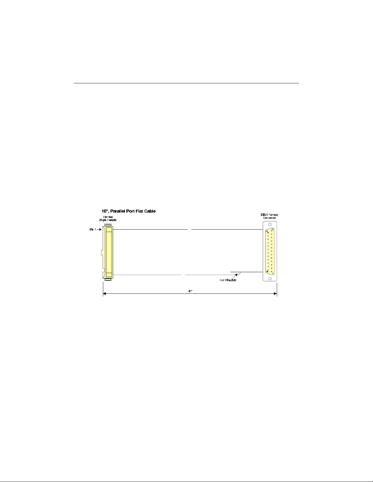
12.2.1 P12 PARALLEL PORT CABLE CONNECTION
Before connecting a device, you will need a 26-pin flat ribbon cable, a mating
connector and a DB25 connector. This parallel port cable is available from TEKNOR:
part number 150-172. You can also make your own cable.
The following list includes approved vendors for the flat cable mating connector:
Amp 746285-6 [optional strain relief: 499252-3],
Robinson Nugent IDS-C26PK-TG,
Thomas & Betts 622-2630 [optional strain relief: 622-2641].
(26-pin polarized IDC female socket connector)
The P8 parallel port cable with the mating connector and DB25 connector appears in
Diagram 12-4.
DIAGRAM 12-4: P8 Parallel Port Cable
12-4
Page 53

Installing & Connecting Other Peripherals (Serial, Parallel, USB)
12.2.2 PARALLEL PORT MODES
12.2.2.1 Standard Mode
The Standard Mode is an unidirectional parallel port. It is used for compatibility with
the IBM PC standard.
The following table shows the pinout for the P8 connector when it is in Standard mode:
TABLE 12-1: Parallel Port Header (P8) - Standard Mode
Pin
Number
1 O STROBE 2 O AUTO FEED XT
3 I/O DATA BIT 0 4 I ERROR
5 I/O DATA BIT 1 6 O INIT
7 I/O DATA BIT 2 8 O SELECT IN
9 I/O DATA BIT 3 10 - GND
11 I/O DATA BIT 4 12 - GND
13 I/O DATA BIT 5 14 - GND
15 I/O DATA BIT 6 16 - GND
17 I/O DATA BIT 7 18 - GND
19 I ACK 20 - GND
21 I BUSY 22 - GND
23 I PAPER END 24 - GND
25 I SELECT 26 - Not Connected
Signal
Flow
Signal Pin
Number
Signal
Flow
Signal
12-5
Page 54

Installing & Connecting Other Peripherals (Serial, Parallel, USB)
12.2.2.2 EPP (Enhanced Parallel Port) Mode
To operate in EPP mode, the peripheral must be designed to operate in this mode and
the BIOS setup must be configured to support it.
The EPP mode consists of a hardware independent method of accessing a parallel port.
It provides support for single I/O cycle as well as high performance block I/O transfers.
The following table shows the pinout for the P8 connector when it is in EPP mode:
TABLE 12-2: Parallel Port Connector (P8) - EPP Mode
Pin
Number
1 O WRITE 2 O DATASTB
3 I/O DATA BIT 0 4 - Not Connected
5 I/O DATA BIT 1 6 - Not Connected
7 I/O DATA BIT 2 8 O ADDRSTRB
9 I/O DATA BIT 3 10 - GND
11 I/O DATA BIT 4 12 - GND
13 I/O DATA BIT 5 14 - GND
15 I/O DATA BIT 6 16 - GND
17 I/O DATA BIT 7 18 - GND
19 I INTR 20 - GND
21 I WAIT 22 - GND
23 - Not Connected 24 - GND
25 - Not Connected 26 - Not Connected
Signal
Flow
Signal Pin
Number
Signal
Flow
Signal
12-6
Page 55

Installing & Connecting Other Peripherals (Serial, Parallel, USB)
12.2.2.3 ECP (Extended Capabilities Port) Mode
To operate in ECP mode, the peripheral must be designed to operate in this mode and
the BIOS setup must be configured to support it.
While the EPP mode may intermix read and write operations without any overhead or
protocol handshaking, the ECP mode negotiates data transfers using a request from the
host and an acknowledgement from the peripheral.
The following table shows the pinout for the P8 connector when it is in ECP mode:
TABLE 12-3: Parallel Port Connector (P8) - ECP Mode
Pin Number Signal
1 O STROBE 2 O AUTO FEED XT,
3 I/O DATA BIT 0 4 I FAULT1,
5 I/O DATA BIT 1 6 O INIT1,
7 I/O DATA BIT 2 8 O SELECT IN
9 I/O DATA BIT 3 10 - GND
11 I/O DATA BIT 4 12 - GND
13 I/O DATA BIT 5 14 - GND
15 I/O DATA BIT 6 16 - GND
17 I/O DATA BIT 7 18 - GND
19 I ACK 20 - GND
21 I BUSY,
23 I PERROR,
25 I SELECT 26 - Not Connected
1
Compatible Mode
2
High Speed Mode
Flow
Signal Pin
PERIPHACK
ACKREVERSE
2
Number
22 - GND
24 - GND
2
Signal
Flow
Signal
HOSTACK
PERIPHRQST
REVERSERQST
✎ NOTE
2
2
2
1,2
For more information on the ECP protocol, please refer to the Extended
Capabilities Port Protocol and ISA Interface Standard (available from Microsoft
Corporation) or contact our Technical Support department.
12-7
Page 56

Installing & Connecting Other Peripherals (Serial, Parallel, USB)
12.3 P17 USB PORT CONNECTION
The Universal Serial Bus (USB) connector on the PCI-942 is a 10-pin dual row header
which permits the direct connection of two USB connectors with an external hub. The
location of the P17 USB port is shown below in Diagram 10-9.
DIAGRAM 12-5: P17 USB Port Location
✎ NOTE
When all the hardware connections are completed on the PCI-942, you will
need to setup installed devices by software. For the USB port, software setup
includes configuring the port in AMIBIOS Advanced Chipset Setup (described
in section 16.1.5).
12-8
Page 57

Installing & Connecting Other Peripherals (Serial, Parallel, USB)
12.3.1 USB PORT CABLE CONNECTION
Before connecting a USB device, you need to install special cabling and a bracket to
the P17 connector. A USB cable/bracket assembly is available from TEKNOR: part
number 150-316. This cable assembly appears below in Diagram 10-6. The diagram
also shows the connections between the P17 10-pin header and the two external USB
connectors.
DIAGRAM 12-6: USB Cable / Bracket Assembly
The P17 connector has the following pinout.
TABLE 12-4: USB Header (P17) - Pinout
Pin
Number
1 - +5V-USB0 2 - +5V-USB1
3 I/O USB0- 4 I/O USB15 I/O USB0+ 6 I/O USB1+
7 - GND-USB0 8 - GND-USB1
9 - SHIELD GND 10 - SHIELD GND
Signal
Flow
Signal Pin
Number
12-9
Signal
Flow
Signal
Page 58

13. INSTALLING & CONNECTING ETHERNET
13.1 P16 ETHERNET CONNECTION
The P16 10Base-T/100Base-T Ethernet interface connector is an 8-pin shielded RJ-45
connector. Its location is on the I/O bracket and appears below on Diagram 13-1.
DIAGRAM 13-1: P16 Ethernet Connector Location
✎ NOTE
When all the hardware connections are completed on the PCI-942, you will
need to setup onboard controllers and installed devices by software. The
Ethernet controller on the PCI-942 resides on the PCI bus and is therefore Plug
and Play by default. No manual configuration is required. For the Ethernet
interface, software setup includes:
1. Ensuring that the onboard Ethernet controller is enabled in AMIBIOS PCI /
Plug and Play Setup (described in section 16.1.7). By default, the onboard
Ethernet is enabled, however, it may be disabled if an external LAN card is
required for testing or other purposes.
2. The Ethernet controller has specific drivers for various operating systems
and software. To install these drivers, you must use the Utility Disk
containing the Ethernet drivers for your operating system (more detail in
Section 17).
13-1
Page 59

PCI-942 Technical Reference Manual
13.1.1 P16 ETHERNET CABLE CONNECTION
The cable connection is made directly on the P16 RJ-45 connector on the I/O bracket.
The 10Base-T interface uses UTP (Unshielded Twisted Pair) cables, category 5, 4 or 3
(5 is better).
The 100Base-T interface uses only UTP cables category 5 and it must comply with the
IEEE 802.3 10Base-T standard for two pairs.
The pinout for the 10Base-T/100Base-T RJ-45 connector appears in Table 13-1.
TABLE 13-1: Ethernet 10Base-T/100Base-T RJ-45 Connector (P16) - Pinout
Pin
Number
1 O TD+ 2 O TD3 I RX+ 4 - Not Connected
5 - Not Connected 6 I RX7 - Not Connected 8 - Not Connected
Signal
Flow
Signal Pin
Number
Signal
Flow
Signal
TX and RX LED indicators are supported on the I/O bracket.
13-2
Page 60
14. INSTALLING SUPERVISOR UTILITIES
14.1 POWER FAIL DETECTION
14.1.1 +5V POWER FAIL (ONBOARD)
A hardware reset is issued when onboard +5V voltage drops below 4.75 volts.
14.1.2 +3.3V POWER FAIL (BACKPLANE)
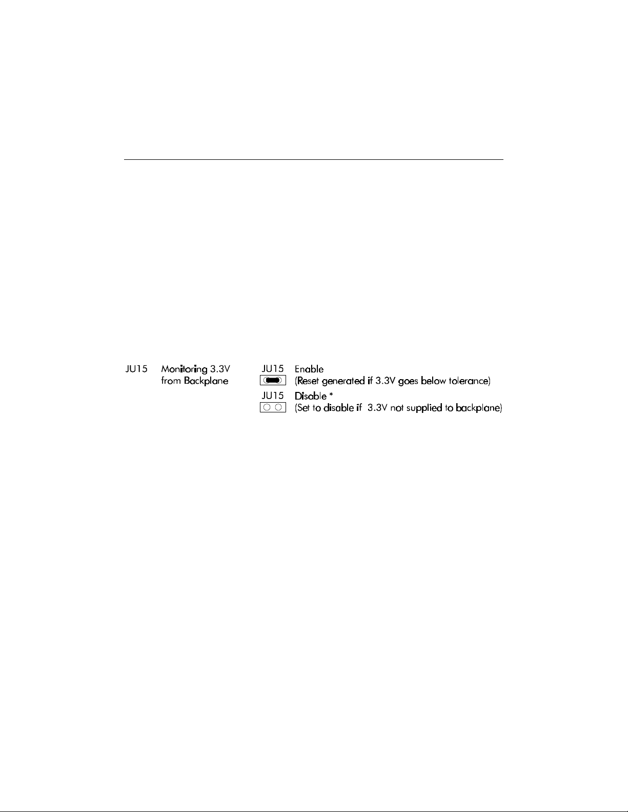
Jumper JU15, when shorted with a jumper cap, monitors the 3.3V power plane of the
backplane. This voltage is routed to the processor board via the PCI connector. The
monitor generates a reset to the processor board if 3.3V is below tolerance. If your
system does not supply 3.3V to the backplane, this jumper must be removed (disabled).
JU15 jumper settings appear below (* = initial setting).
14-1
Page 61

PCI-942 Technical Reference Manual
14.2 WATCHDOG TIMER
The Watchdog Timer is a hardware timer which resets the PCI-942 board if the timer is
not refreshed by software periodically. The timer is typically used to restart a system in
which an application becomes hung on an external event. When the application is hung,
it no longer refreshes the timer. The Watchdog Timer then times out and resets the
single board computer.
The Watchdog Timer is extremely useful in embedded systems where human
supervision is not required.
To enable and refresh the Watchdog Timer, follow these steps:
Hardware Enable Watchdog Timer: Set the JU16 jumper to enable Watchdog
Timer Operation by shorting the middle and right pins. This will enable all the
hardware needed.
The JU16 settings are shown below (* = initial setting):
Software Enable Watchdog Timer: In a software routine (user application) enable
the Watchdog by writing “0” to bit 7 of I/O port 437h (hex). Be aware that you need
to refresh the timer within 1.5 seconds or the timer times out, causing the board to
reset.
Refresh the Watchdog Timer: In order to refresh the timer, you need to write “1”
and then immediately write “0” to bit 7 of I/O port 437h (still in a software routing).
You need to repeat this step every 1.5 seconds to refresh the timer or your board
will reset.
14-2
Page 62

Installing Supervisor Utilities
14.3 VOLTAGE / TEMPERATURE / FAN SPEED
MONITORING SYSTEM
The system hardware monitor system monitors all system voltages, ambient
temperature and fan speeds.
Connections are made via the P18 system hardware monitor connector. This connector
is a 6-pin single row header. Its location is shown below in Diagram 14-1.
DIAGRAM 14-1: P18 System Hardware Monitor Connector
The circuitry is based on National Semiconductor's LM80 and LM75. The LM80 monitors
seven system voltages, two fan speeds and the board ambient temperature. The LM80's
interface to the companion LM75 temperature sensor monitors the temperature of the
ambient between the Pentium II cartridge and the processor board. All of the voltages, fan
speeds and temperature measurements have associated programmable watchdog limits.
When any of these programmed limits are exceeded, a system management interrupt (SMI)
occurs to notify the processor. In addition to SMI generation, the externally available OS#
signal can be used to notify external hardware of any over-temperature condition.
Fan speed monitoring can be configured to monitor two system fans or one system fan
and the onboard Pentium II cooling fan with optional tach output.
The LM80 also monitors an external chassis intrusion switch via the P18 system hardware
monitor connector. The state of this input can also be used to generate an SMI interrupt.
A general purpose output (GPO) is also provided at the system hardware monitor
connector. This signal can be used to provide a user-defined function.
14-3
Page 63

PCI-942 Technical Reference Manual
The following system voltages are monitored by the LM80:
-12 volts.
3.3 volts from onboard voltage regulator.
3.3 volts from backplane.
+5 volts.
+12 volts.
VCC_CORE voltage provided by onboard voltage regulator.
1.5 volt VTT voltage used by processors GTL+ bus.
The pinout of the system hardware monitor connector appears below:
TABLE 14-1: System Hardware Monitor Header (P18) - Pinout
Pin Number Signal
1 GND
2 GPO (General Purpose Output)
3 CI (Chassis Intrusion Input)
4 FAN2 (Fan 2 Tachometer Input)
5 FAN1 (Fan 1 Tachometer Input)
6 OS# (Temperature Sense Output)
14-4
Page 64

15. POWERING UP THE SYS TEM
& TROUBLESHOOTING
15.1 POWER SOURCE FOR THE PCI-942
The PCI-942 Single Board Computer is powered via the ISA bus when it is installed on
a passive backplane.
15.2 POWER UP PROCEDURE
You are now ready to power up your system.
1. Insert a bootable diskette in drive A to start your system with DOS.
2. Hit the DELETE key before or when this message appears near the bottom of the
screen: “Hit <DEL> if you want to run SETUP”. This will bring you to the Main
Menu of the AMIBIOS Setup program. Use the arrow keys to select among the
items and press ENTER to accept.
- Select “Standard CMOS Setup” to set the date and time.
More detail on the AMIBIOS Setup is given in Section 16 of this manual.
- Select “Save Settings and Exit” from the Main Menu . The screen displays the
message: “Save current settings and exit (Y/N)?”. Type “Y” and press
ENTER to save the system parameters and continue with the boot procedure.
3. Once the boot procedure is completed, reboot the system to make sure everything
works properly.
15.3 TROUBLESHOOTING
If you should encounter a problem, verify the following items:
Make sure that all connectors are connected properly. On the standard flat ribbon
cable used for the floppy connector, pin 1 is indicated by small red stripe. Verify
that this red stripe is located on the appropriate side of the connector.
Verify your boot diskette. It must be a system disk and it must be in proper working
order.
If the system still does not start up properly, you should try booting your system
with only the video monitor connected to the board (this is the minimum required to
see if the board is working).
If you still are not able to get your board up and running, contact our Technical
Support department for assistance.
15-1
Page 65

SOFTWARE & ONBOARD UTILITIES
16. SOFTWARE SETUP
17. INSTALLING DRIVERS
18. UPDATING OR RESTORING BIOS IN FLASH
Page 66

16. SOFTWARE SETUP
Normally the software setup will follow all system hardware connections in order to
configure controllers and installed devices.
Also, software setup should come before any operating systems and drivers are
installed.
✎ NOTE
Make sure you setup the AMIBIOS and the SCSISelect Configuration software
prior to installing your operating system and your drivers.
This Section is organized as follows:
Section 16.1 will describe the AMIBIOS Setup program.
Section 16.2 will describe the SCSISelect Configuration Utility program.
16-1
Page 67

PCI-942 Technical Reference Manual
16.1 THE AMIBIOS SETUP PROGRAM
16.1.1 ACCESSING THE AMIBIOS SETUP PROGRAM
The system BIOS (Basic Input Output System) provides an interface between the operating
system and the hardware of the PCI-942 single board computer. The interface provided by
AMIBIOS is 100% IBM AT compatible. All functions accept similar inputs as IBM and
provide the same results, although the program code itself is different.
The PCI-942 uses the AMIBIOS Setup program, a setup utility in ROM that is accessed
by pressing the DELETE key at the appropriate time during system boot. This utility is
used to set configuration data in CMOS RAM.
To run the AMIBIOS Setup program incorporated in the ROM BIOS:
1. Turn on or reboot the system.
2. Hit the DELETE key before or when the message "Hit <DEL> if you want to run
SETUP" appears near the top of the screen (DELETE will work, even if the message
display is disabled in AMIBIOS SETUP).
3. The main menu appears on the screen.
AMIBIOS HIFLEX SETUP UTILITY - VERSION X.XX
(C)1996 American Megatrends, Inc. All Rights Reserved
Standard CMOS Setup
Advanced CMOS Setup
Advanced Chipset Setup
Power Management Setup
PCI / Plug and Play Setup
Peripheral Setup
Auto-Detect Hard Disks
Change User Password
Auto Configuration with Optimal Settings
Auto Configuration with Fail Safe Settings
Standard CMOS Setup for changing time, date, hard disk type, etc.
ESC:Exit ↑↑ ↓↓:Sel F2/F3:Color F10:Save & Exit
Change Supervisor Password
Save Settings and Exit
Exit Without Saving
16-2
Page 68

Software Setup
16.1.2 USING AMIBIOS SETUP
Table 16-1 provides details on how to navigate in the Setup program:
TABLE 16-1: Using AMIBIOS Setup Program
Key Function
↑ ↓ ← →
TAB Move to the next field.
PAGEUP or + Increment numeric value or change value.
PAGEDOWN or - Decrement numeric value or change value.
ENTER Select the current item.
ESC When in the Main Menu: Exit program (Answer ‘Y’ to save changes into CMOS).
F2 / F3 Change background or foreground colors.
F10 Save all changes made to Setup and exit from Setup program.
Sections 16.1.3 to 16.1.12 describe all parts of the Setup program, following the order
given in the Main Menu.
The sections on the Advanced CMOS Setup, Advanced Chipset Setup, Power
Management Setup, PCI / Plug and Play Setup, and Peripheral Setup include a list of
the options for each setup screen, their Optimal default settings, Fail Safe default
settings, available settings and description.
Move to the next field in the desired direction.
When in other screens: Exit screen and return to Main Menu.
Whenever you are not sure about a certain setting, you may refer to the list of default
values. The list of defaults is provided in the event that a value has been changed and
one wishes to set this option to its original value. Loading the Optimal or Fail Safe
defaults will affect all the options and will reset options previously altered.
The Fail Safe default settings consist of the safest set of parameters. Use them if the
system is behaving erratically. They should always work but do not provide optimal
system performance.
The Optimal default values provide optimum performance settings for all devices and
system features. If CMOS RAM is corrupted, the Optimal settings are loaded automatically.
CAUTION
These default values have been provided to give control over the system.
However, the values for these options should be changed only if the user has a
full understanding of the timing relationships involved.
16-3
Page 69

PCI-942 Technical Reference Manual
16.1.3 STANDARD CMOS SETUP
This part of the setup allows you to set the time, date, hard disk type, types of floppy
drives and video type.
Date/Time
Floppy Drive A
Floppy Drive B
Hard Disks
Boot Sector Virus
Protection
The current values for each category are displayed. Enter new
values through the keyboard.
Select the type of floppy disk installed for drive A and drive B.
Two IDE controllers are defined on the PCI-942 board
(Primary and Secondary). The Primary controller can have
two disks: Master Disk and Slave Disk. The Secondary can
have two disks: Master Disk and Slave Disk.
The hard disk drives can be detected automatically by
AMIBIOS if they are IDE drives. There are two ways to
perform an automatic detection of a drive:
1) Select Auto-Detect Hard Disks from the Main Menu
(explained in section 12.1.9) to have AMIBIOS automatically
detect the type and parameters of each IDE hard drive in your
system. The parameters are reported on the Standard CMOS
Setup screen. The detected values can then be saved in the
CMOS.
2) Set the drive type to “Auto” to have AMIBIOS detect the
drive each time the system boots up. The drive type will not
be displayed on the Standard CMOS Setup screen, but will
be displayed on the System Configuration screen which
appears after a successful bootup.
When enabled, AMIBIOS issues a warning when a program
or virus issues a disk format command or attempts to write to
the boot sector of the hard disk drive.
CAUTION
You should not enable the Boot Sector Virus Protection in AMIBIOS Setup
when formatting a hard drive.
16-4
Page 70

Software Setup
16.1.4 ADVANCED CMOS SETUP
Option Optimal Defaults Fail Safe Defaults Available Settings Description
Quick Boot Enabled Disabled Disabled, Enabled This option allows you to have the AMIBIOS boot quickly when the computer is powered on or go through more complete testing.
1st Boot Device IDE-0 FLOPPY Disabled, IDE-0, IDE-1, IDE-2, IDE-3,
FLOPPY, FLOPTICAL, CDROM, SCSI,
NETWORK
2nd Boot Device FLOPPY IDE-0 Disabled, IDE-0, FLOPPY,
FLOPTICAL, CDROM
3rd Boot Device CDROM CDROM
Try Other Boot Devices Yes Yes No, Yes If set to Yes, BIOS will try to boot from other boot devices when devices selected in 1st Boot Device, 2nd Boot Device and 3rd Boot
Initial Display Modes BIOS BIOS BIOS, Silent This option specifies the initial display mode when the system boots.
Display Mode at Add-On ROM Init Force BIOS Force BIOS Force BIOS, Keep Current This option specifies the system display mode which is set at the time the AMIBIOS post routines initialize an optional option ROM.
Floppy Access Control Read-Write Read-Write Read-Write, Read-Only This option specifies the read/write access which is set when booting from a floppy or hard disk drive.
Hard Disk Access Control Read-Write Read-Write This option will be effective only if the floppy or hard disk device is accessed through the BIOS.
S.M.A.R.T. for Hard Disks Disabled Disabled Disabled, Enabled This option allows AMIBIOS to use the SMART (System Management and Reporting Technologies) protocol for reporting server
BootUp Num-Lock Off Off Off, On This option enables you to turn off the Num-Lock option on the enhanced keyboard when the system is powered on. If Num-Lock is
PS/2 Mouse Support Enabled Enabled Disabled, Enabled When enabled, indicates that a PS/2 type mouse is supported.
Primary Display VGA/EGA VGA/EGA Absent, VGA/EGA, CGA40x25,
CGA80x25, Mono
Password Check Setup Setup Setup, Always This option determines when a password is required for access to the system.
Boot To OS/2 No No No, Yes When there is more than 64MB system memory and one wishes to boot with OS/2 operating system, this option must be set to
L1/L2 Cache WriteBack WriteBack Disabled, WriteThru, WriteBack With this option, you may specify the caching algorithm used for L1/L2 cache.
System BIOS Cacheable Enabled Disabled Disabled, Enabled The system BIOS, which is in F000H memory segment, is automatically shadowed to RAM for faster execution. This option
C000, 16k, Shadow Cached Disabled Disabled, Enabled, Cached Video or Adapter ROM Shadow (xxxx, 16k Shadow) is a technique in which BIOS code is copied from slower ROM to faster RAM.
C400, 16k, Shadow Cached Disabled The BIOS is then executed from the RAM. Each option allows for a segment of 16KB to be shadowed. If one of these options is
C800, 16k, Shadow Disabled Disabled enabled and there is BIOS code present in that particular segment, the BIOS is shadowed.
CC00, 16k, Shadow Disabled Disabled Video BIOS shadowing may be done at C000H and C400H.
D000, 16k, Shadow Disabled Disabled Select Enabled to write the contents of the specified ROM area to the same address in system memory (RAM) for faster execution.
D400, 16k, Shadow Disabled Disabled Select Cached to write the contents of the specified ROM area to the same address in system memory (RAM), if an adapter ROM
D800, 16k, Shadow Disabled Disabled is using the ROM area. This also indicates that the contents of the RAM area can be read from and written to cache memory.
DC00, 16k, Shadow Disabled Disabled Select Disabled if you do not want to copy the specified ROM area to RAM. The contents of the video ROM cannot be read from or
When Disabled, AMIBIOS: tests all system memory, waits 40 seconds for a READY signal from IDE drive, waits .5 seconds after
sending a RESET signal to IDE drive, checks whether user has pressed DELETE key and runs AMIBIOS Setup if it has.
When Enabled, AMIBIOS: checks only the first 1MB of system memory, does not configure IDE drive if a READY signal is not
received immediately, and does not wait .5 seconds after sending a RESET signal to IDE drive.
1st Boot Device, 2nd Boot Device and 3rd Boot Device sets the sequence of boot drives that the AMIBIOS attempts to boot from
after AMIBIOS POST completes.
Device failed to boot. If set to No, BIOS will try to boot only from devices selected in 1st, 2nd and 3rd Boot Device options.
Select BIOS to have the messages which AMIBIOS displays before booting the system appear on the system monitor.
Select Silent if you do not want the messages to appear on the system monitor.
system information over a network.
turned off, the arrow keys on the numric keypad can be used, as well as the other set of arrow keys on the enhanced keyboard.
This option specifies the type of display in the system. The Absent setting can be used for network file servers.
Select Setup to have the password prompt appear only when an attempt is made to enter the AMIBIOS Setup program.
Select Always to have the password prompt appear each time the system is powered on.
See page 12-16 for more details on password checking function and the above settings.
“Yes”.
indicates that this memory segment can be read from or written to L2 secondary cache memory.
written to cache memory.
16-5
Page 71

Software Setup
16.1.5 ADVANCED CHIPSET SETUP
Option Optimal Defaults Fail Safe Defaults Available Settings Description
USB Function Disabled Disabled Disabled, Enabled This option allows you to enable the Universal Serial Bus (USB). If this option is set to Disabled, the USB KB/Mouse Legacy
USB KB/Mouse Legacy Support Enabled Enabled Disabled, Enabled This option allows you to enable support for older keyboards and mouse devices. If the USB Function option is set to Disabled, this
EDO DRAM Speed (ns) Auto Auto Auto, Manual, 50, 60 This option allows you to select the RAS access time in nanoseconds for the EDO DRAM system memory being used in the SBC.
EDO Read Burst Timing x333 x333 x333, x222 This option specifies the timings for EDO DRAM system memory for read operations in burst mode. This option is only available for
EDO Write Burst Timing x333 x333 x333, x222 This option specifies the timings for EDO DRAM system memory for write operations in burst mode. This option is only available
EDO RAS Precharge 4 Clks 4 Clks 4 Clks, 3 Clks This option specifies the length of the RAS precharge portion of the DRAM system memory access cycle when EDO DRAM
EDO RAS to CAS 3 Clks 3 Clks 3 Clks, 2 Clks This option specifies the length of the delay inserted between RAS and CAS signals of the DRAM system memory access cycle
MA Wait State Slow Slow Slow, Fast This option specifies the length of the delay inserted between MA signals. This option is only available for modification if EDO
SDRAM Timing Latency Auto Auto Manual, Auto This option specifies the latency for the Synchronous DRAM (SDRAM) system memory signals. The following two options (RAS to
RAS to CAS 3 Clks 3 Clks 3 Clks, 2 Clks This option specifies the length of the delay inserted between the RAS and CAS signals of the DRAM system memory access cycle.
RAS Precharge 3 Clks 3 Clks 3 Clks, 2 Clks This option specifies the length of the RAS precharge portion of the DRAM system memory access cycle. This option is only
VGA Frame Buffer USWC Disabled Disabled Disabled, Enabled This option allows you to enable the VGA video frame buffer using Uncacheable, Speculatable, Write-Combined (USWC) memory.
PCI Frame Buffer USWC Disabled Disabled Disabled, Enabled This option allows you to enable the USCW memory attribute to improve video performance when a PCI video adapter is installed.
DRAM Integrity Mode Non ECC Non ECC Non ECC, EC only, ECC This option allows you to set the type of system memory checking used in your system:
Fixed Memory Hole Disabled Disabled Disabled, 512KB-640KB, 15MB-16MB This option may be used to specify an area in memory which cannot be addressed on the ISA bus.
TypeF DMA Buffer Control1 Disabled Disabled Channel-0, Channel-1, Channel-2,
Channel-3, Disabled, Channel-5,
TypeF DMA Buffer Control2 Disabled Disabled Channel-6, Channel-7
DMA-0 Type Normal ISA Normal ISA Normal ISA, PC/PCI, Distributed The DMA-# Type options specify the bus on which the specified DMA channel can be used.
DMA-1 Type Normal ISA Normal ISA
DMA-2 Type Normal ISA Normal ISA
DMA-3 Type Normal ISA Normal ISA
DMA-4 Type Normal ISA Normal ISA
DMA-5 Type Normal ISA Normal ISA
DMA-6 Type Normal ISA Normal ISA
DMA-7 Type Normal ISA Normal ISA
Support option is not available.
option is not available for modification.
The following five options (EDO Read Burst Timing, EDO Write Burst Timing, EDO RAS Precharge, EDO RAS to CAS, and MA
Wait State) are only available for modification if this option is set to Manual.
modification if EDO DRAM Speed (ns) option is set to Manual.
for modification if EDO DRAM Speed (ns) option is set to Manual.
memory is installed in your system. This option is only available for modification if EDO DRAM Speed (ns) option is set to Manual.
when EDO DRAM memory is installed in your system. This option is only available for modification if EDO DRAM Speed (ns)
option is set to Manual.
DRAM Speed (ns) option is set to Manual.
CAS, RAS Precharge) are only available if this option is set to Manual.
This option is only available for modification if SDRAM Timing Latency option is set to Manual.
available for modification if SDRAM Timing Latency option is set to Manual.
Older ISA VGA card drivers may not behave correctly if this option is set to Enabled.
However, VGA card drivers may not behave correctly when this option is set to Enabled.
Non ECC - No error checking or error reporting is done.
EC only - Multibit errors are detected and reproted as parity errors. Single-bit errors are corrected by chipset. Corrected bits of data
from memory are not written back to DRAM system memory.
ECC - Multibit errors are detected and reported as parity errors. Single-bit errors are corrected by the chipset and are written back to
DRAM system memory.
These options specify the DMA channels where Type F buffer control is implemented.
16-7
Page 72

ADVANCED CHIPSET SETUP (Continued)
Option Optimal Defaults Fail Safe Defaults Available Settings Description
AGP Aperture Size 64MB 64MB 4 MB, 8 MB, 16MB, 32MB, 64MB,
128MB, 256MB
System Type Auto Auto Auto, DP, UP This option sets the system type.
USWC Write I/O Post Auto Auto Auto, Disabled, Enabled Select Auto to have AMIBIOS automatically determine if USWC posted writes to I/O should be enabled.
PAC Bus SERR# Enabled Enabled Disabled, Enabled This option allows you to enable the SERR# signal on the PAC bus.
AGP Common SERR# Enabled Enabled Disabled, Enabled This option allows you to use a common SERR# signal for the AGP bus and standard PC bus.
AGP System Error Forwarding Enabled Enabled Disabled, Enabled This option allows AGP system errors to be forwarded.
AGP Parity Error Response Enabled Enabled Disabled, Enabled This option enables AGP parity error response.
IRQ 12 Auto Auto Auto, Standard, Mouse This option specifies how IRQ12 is used.
PIIX4 SERR# Disabled Disabled Disabled, Enabled This option enables the SERR# signal for the Intel PIIX4 chip.
USB Passive Release Enable Enabled Enabled Disabled, Enabled This option enables passive release for the Universal Serial Bus (USB).
PIIX4 Passive Enabled Enabled Disabled, Enabled This option enables passive release for the Intel PIIX4 chip.
PIIX4 Delayed Transaction Enabled Enabled Disabled, Enabled This option enables delayed transactions for the Intel PIIX4 chip.
Master Lat. Timer 40H 40H 00H through F8H in increments of 8H This option specifies the latency for the timer.
MTT 20H 00H 00H through F8H in increments of 8H
This option specifies the amount of system memory which can be used by the Accelerated Graphics Port (AGP).
Select Disabled to disable USWC posted writes to I/O.
Select Enabled to enable USWC posted writes to I/O.
Select Auto to have AMIBIOS automatically determine how IRQ12 should be allocated.
Select Standard to make IRQ12 available for use on the ISA bus.
Select Mouse to use IRQ12 for the PS/2 mouse.
Software Setup
16-9
Page 73

Software Setup
16.1.6 POWER MANAGEMENT SETUP
Option Optimal Defaults Fail Safe Defaults Available Settings Description
ACPI Aware O/S No No No, Yes
Power Management/APM Disabled Disabled Disabled, Enabled This option allows you to enable Advanced Power Management (APM) on your system. If this option is disabled, you cannot change any
Power Button Function On/Off On/Off Suspend, On/Off This option specifies how the power button mounted externally on the computer chassis is used.
Instant On Support Disabled Disabled Disabled, Enabled This option enables AMIBIOS support for the Intel InstantOn specification. The InstantOn allows your system to go to full power-on mode
Green PC Monitor Power State Stand By Stand By Stand By, Suspend, Off This option specifies the power management state that the Green PC-compliant video monitor enters after the specified period of display
Video Power Down Mode Disabled Disabled Disabled, Stand By, Suspend If the video subsystem remains inactive for a specified period of time, AMIBIOS conserves power by placing the subsystem into the power
Hard Disk Power Down Mode Disabled Disabled Disabled, Stand By, Suspend If the hard disk drive remains inactive for a specified period of time, AMIBIOS conserves power by placing the drive into the power
Hard Disk Time Out (Minute) Disabled Disabled Disabled,
1 through 15, in increments of 1 minute
Standby/Suspend Timer Unit 4 min 4 min 32 secs, 4 msec, 4 min, 4 sec This option specifies the unit of time used for the Standby and Suspend timeout periods.
Standby Time Out Disabled Disabled Disabled,
32 through 4064, in increments of 32 (if
the Standby/Suspend Timer Unit option is
set to 32 secs)
4 through 508, in increments of 4 minutes
(if Standby/Suspend Timer Unit option is
set to 4 msec, 4 min or 4 sec)
Suspend Time Out Disabled Disabled Disabled,
32 through 4064, in increments of 32 (if
the Standby/Suspend Timer Unit option is
set to 32 secs)
4 through 508, in increments of 4 minutes
(if Standby/Suspend Timer Unit option is
set to 4 msec, 4 min or 4 sec)
Slow Clock Ratio 50-62.5% 50-62.5% 0-12.5%, 12.5-25%, 25-37.5%,
37.5-50%, 50-62.5%, 62.5-75%,
75-87.5%
Display Activity Ignore Ignore Ignore, Monitor This option enables event monitoring on the video display. If the option is set to Monitor and the computer is in a power-saving mode,
Device 6 (Serial port 1) Ignore Monitor Ignore, Monitor These options allow you to enable event monitoring for your peripherals and hard disk drives. If the option is set to Monitor and the
Device 7 (Serial port 2) Ignore Ignore computer is in a power-saving mode, AMIBIOS watches for activity on the hardware interrupt request line (IRQ) for the specified
Device 8 (Parallel port) Ignore Ignore device. If any activity occurs, the computer enters the full power-on mode. AMIBIOS then restarts the Standby and Suspend timeout
Device 5 (Floppy disk) Ignore Ignore timers.
Device 0 (Primary master IDE) Ignore Ignore
Device 1 (Primary slave IDE) Ignore Ignore
Device 2 (Secondary master IDE) Ignore Ignore
Device 3 (Secondary slave IDE) Ignore Ignore
other options on the Power Management Setup screen, except the ACPI Aware O/S.
Select Suspend to use the power button to place the computer into Suspend mode or Full On power mode.
Select On/Off to use the power button to turn the computer on or off.
when leaving a power-conserving state. This feature is available only if it is supported by the computer hardware (e.g., the video monitor).
inactivity has expired. The period of inactivity before a monitor enters Standby mode is specified in the Standby Time Out option; the
period of inactivity for Suspend mode is specified in the Suspend Time Out option.
management state specified in this option. The period of inactivity before the subsystem enters Standby mode is specified in the Standby
Time Out option; the period of inactivity for Suspend mode is specified in the Suspend Time Out option.
management state specified in this option. The period of inactivity before the drive is powered down is specified in the Hard Disk Time
Out option.
This option specifies the length of time the AMIBIOS waits before turning off power to the hard disk drive if the drive remains inactive.
When this period expires, the hard disk drive enters the power-conserving mode specified in the Hard Disk Power Down Mode option
described above.
This option specifies the length of the period of system inactivity when the computer is in full power-on mode before the computer is
placed in Standby mode. In Standby mode, some power use is curtailed.
This option specifies the length of the period of system inactivity when the computer is already in Standby mode before the computer is
placed in Suspend mode. In Suspend mode, nearly all power use is curtailed.
This option specifies the speed at which the system clock runs when the system is in Standby power saving mode. The settings are
expressed as a percentage between the normal CPU clock speed and the CPU clock speed when the system is in the power-conserving state.
AMIBIOS watches for display activity. If any activity occurs, the computer enters the full power-on mode and AMIBIOS restarts the
Standby and Suspend timeout timers.
16-11
Page 74

Software Setup
16.1.7 PCI / PLUG AND PLAY SETUP
Option Optimal Defaults Fail Safe Defaults Available Settings Description
On Board LAN Enabled Enabled Disabled, Enabled The onboard Ethernet controller can be disabled to allow the use of an offboard LAN card.
On Board Video Enabled Enabled Disabled, Enabled The onboard video controller can be disabled to allow the use of an offboard video card.
On Board SCSI Enabled Enabled Disabled, Enabled The onboard SCSI controller can be disabled to allow the use of an offboard SCSI card.
Plug and Play Aware O/S No No No, Yes This option indicates whether the operating system installed in the computer is Plug and Play-aware. AMIBIOS only detects and enables
PCI Latency Timer (PCI Clocks) 64 64 32, 64, 96, 128, 160, 192, 224, 248 This option sets the latency of all PCI devices on the PCI Local Bus. The settings are in units equal to PCI clocks.
PCI VGA Palette Snoop Disabled Disabled Disabled, Enabled Palette snooping allows multiple VGA devices operating on different buses to handle data from the CPU on each set of palette registers on
PCI IDE BusMaster Disabled Disabled Disabled, Enabled This option specifies whether the IDE controller on the PCI Local Bus has bus mastering capability. AMIBIOS can perform bus master
OffBoard PCI IDE Card Auto Auto Auto, Slot1, Slot2, Slot3, Slot4, Slot5,
Slot6
OffBoard PCI IDE Primary IRQ Disabled Disabled Disabled, INTA, INTB, INTC, INTD, These options specify the PCI interrupts used by the primary and secondary IDE channels on the offboard PCI IDE controller.
OffBoard PCI IDE Secondary IRQ Disabled Disabled Hardwired If the OffBoard PCI IDE Card option described above is set to Auto, these options are not available.
DMA Channel 0 Pnp Pnp Pnp, ISA/EISA These options allow you to specify the bus type used by each DMA channel.
DMA Channel 1 Pnp Pnp
DMA Channel 3 Pnp Pnp
DMA Channel 5 Pnp Pnp
DMA Channel 6 Pnp Pnp
DMA Channel 7 Pnp Pnp
IRQ5 PCI/Pnp PCI/Pnp PCI/Pnp, ISA/EISA These options indicate whether or not the specified interrupt request (IRQ) is available for use by the system for PCI/Plug and Play
IRQ9 PCI/Pnp PCI/Pnp features or is reserved for use by option cards on the ISA Bus. This allows you to specify IRQs for use by legacy ISA adapter cards.
IRQ10 PCI/Pnp PCI/Pnp The IRQ setup options indicate whether AMIBIOS should remove an IRQ from the pool of available IRQs passed to BIOS
IRQ11 PCI/Pnp PCI/Pnp configurable devices. The available IRQ pool is determined by reading the ESCD NVRAM. If more IRQs must be removed from the
IRQ15 PCI/Pnp PCI/Pnp pool, you can set the IRQ option to ISA/EISA. Onboard I/O is configurable by AMIBIOS; the IRQs used by onboard I/O are configured as
Reserved Memory Size Disabled Disabled Disabled, 16k, 32k, 64k This option specifies the size of the memory area reserved for legacy ISA adapter cards.
Reserved Memory Address C8000 C8000 C0000, C4000, C8000, CC000, D0000,
D4000, D8000, DC000
PnP ISA adapter cards which are required for system boot. The Windows 95 operating system is PnP-aware and detects and enables all
other PnP-aware adapter cards. Set the option to No if the operating system (such as DOS, OS/2, Windows 3.x) does not use PnP.
NOTE: You must set this option correctly or PnP-aware adapter cards installed in your computer will not be configured properly.
every video device, e.g., if there are two VGA devices in your system (one PCI and one ISA). Bit 5 of the command register in the PCI
device configuration space is the VGA Palette Snoop bit (0 is disabled).
This option must be set to Enabled if any ISA adapter card installed in the system requires VGA palette snooping.
When set to Disabled, data read and written by the CPU is only directed to the PCI VGA device’s palette registers.
When set to Enabled, data read and written by the CPU is directed to both the PCI VGA device’s palette registers and the ISA VGA
device’s palette registers, permitting the palette registers of both devices to be identical.
transfers using scatter/gather DMA on the PCI IDE interface. No special drivers are needed, but the IDE drive must support PCI bus
mastering.
This option specifies the PCI expansion slot on the processor board where the offboard PCI IDE controller is installed, if any. If an
offboard PCI IDE controller is used, the onboard IDE controller on the processor board is automatically disabled.
If Auto is selected, AMIBIOS automatically determines the correct setting for this option.
This option forces IRQ14 and IRQ15 to PCI slots on the PCI Local Bus. This is necessary to support non-compliant PCI IDE adapter cards.
If this option is set to Auto, the OffBoard PCI IDE Primary IRQ and OffBoard PCI IDE Secondary IRQ options may not be modified.
PCI/PnP.
NOTE: If the OnBoard IDE option on the Peripheral Setup screen is set to Secondary or Both, IRQ15 is assigned by the system and is not
available to the user.
If this option is set to Disabled, the Reserved Memory Address option is not available for modification.
This option specifies the beginning address (in hexadecimal) of the ROM memory area reserved for use by legacy ISA adapter cards.
If the Reserved Memory Size option is set to Disabled, this option is not available for modification.
16-13
Page 75

Software Setup
16.1.8 PERIPHERAL SETUP
The AMIBIOS allows automatic or manual setup of peripheral devices. The floppy drive controller, serial port, parallel port and IDE controller options on the Peripheral Management screen can each be set to
Auto, which causes AMIBIOS to configure the peripherals automatically. When you set these options to values other than Auto, the values you set up manually are used by AMIBIOS when booting the
system. AMIBIOS reports any I/O conflicts after displaying the BIOS Configuration Summary screen.
Option Optimal Defaults Fail Safe Defaults Available Settings Description
OnBoard FDC Auto Auto Auto, Disabled, Enabled The onboard floppy drive controller may be enabled or disabled using this option.
OnBoard Serial Port1 Auto Auto Auto, Disabled, 3F8H, 2F8H, 3E8H, Each of these options enables the specified serial port on the processor board and establishes the base I/O address for the port.
OnBoard Serial Port2 Auto Auto 2E8H When this option is set to Auto, AMIBIOS also attempts to avoid address conflicts. If the offboard serial ports are configured to
Receiver Polarity Non-Inverted Non-Inverted Non-Inverted, Inverted If the OnBoard Serial Port2 option is set to Disabled, this option is not available for modification.
Transmitter Polarity Non-Inverted Non-Inverted Non-Inverted, Inverted If the OnBoard Serial Port2 option is set to Disabled, this option is not available for modification.
OnBoard Parallel Port Auto Auto Auto, Disabled, 378, 278, 3BC This option enables the parallel port on the processor board and establishes the base I/O address for the port.
Parallel Port Mode EPP Normal Normal, EPP,ECP This option specifies the parallel port mode. ECP and EPP are both bidirectional data transfer schemes which adhere to the IEEE
EPP Version 1.9 N/A N/A, 1.9, 1.7 This option specifies the Enhanced Parallel Port (EPP) specification number which is used in the system. It is only available if the
Parallel Port IRQ Auto Auto Auto, 5, 7 This option specifies the interrupt request (IRQ) which is used by the parallel port.
Parallel Port DMA Channel N/A Auto Auto, 0, 1, 3 This option sets the DMA channel used by the parallel port. It is only available if the Parallel Port Mode option is set to ECP.
OnBoard IDE Both Both Disabled, Primary, Secondary, Both This option specifies the onboard integrated drive electronics (IDE) controller channel(s) to be used.
When this option is set to Auto, AMIBIOS attempts to enable any floppy drive controller on the ISA Bus. If no floppy controller is
found on the ISA Bus, the onboard floppy controller is enabled.
specific starting I/O ports via jumper settings, AMIBIOS configures the onboard serial ports to avoid conflicts.
AMIBIOS checks the ISA Bus for serial ports. Any offboard serial ports found on the ISA Bus are left at their assigned addresses.
Serial Port1, the first onboard serial port, is configured with the first available address and Serial Port2, the second onboard serial
port, is configured with the next available address. The default address assignment order is 3F8H, 2F8H, 3E8H, 2E8H. Note that this
same assignment order is used by AMIBIOS to place the active serial port addresses in lower memory (BIOS data area) for
configuration as logical COM devices.
After all addresses have been assigned, any remaining onboard serial ports are disabled.
For example, if there is one offboard serial port on the ISA Bus and its address is set to 2F8H, Serial Port1 is assigned address 3F8H
and Serial Port2 is assigned address 3E8H. Configuration is then as follows: COM1 - Serial Port1 (at 3F8H), COM2 - offboard serial
port (at 2F8H), COM3 - Serial Port2 (at 3E8H).
If the OnBoard Serial Port2 option is set to Disabled, the Receiver Polarity and Transmitter Polarity options are not available for
modification.
The interrupt used by the Parallel Port may be assigned by a jumper setting.
When this option is set to Auto, AMIBIOS checks the ISA Bus for offboard parallel ports. Any parallel ports found on the ISA Bus
are left at their assigned addresses. The onboard Parallel Port is automatically configured with the first available address not used by
an offboard parallel port. The default address assignment order is 3BCH, 378H, 278H. Note that this same assignment order is used
by AMIBIOS to place the active parallel port addresses in lower memory (BIOS data area) for configuration as logical LPT devices.
P1284 specifications.
Normal uses normal parallel port mode.
EPP allows the parallel port to be used with devices which adhere to the Enhanced Parallel Port (EPP) specification. EPP uses the
existing parallel port signals to provide asymmetric bidirectional data transfer driven by the host device.
ECP allows the parallel port to be used with devices which adhere to the Extended Capabilities Port (ECP) specification. ECP uses
the DMA protocol to achieve transfer rates of approximately 2.5MB/second. ECP provides symmetric bidirectional communication.
Parallel Port Mode option is set to EPP.
NOTE: If this option is set to Secondary or Both, the system assigns interrupt request 15 (IRQ15).
16-15
Page 76

Software Setup
16.1.9 AUTO-DETECT HARD DISKS
Select Auto-Detect Hard Disks from the Main Menu to have AMIBIOS automatically
detect the type and parameters of each IDE hard drive in your system. The parameters
are reported on the Standard CMOS Setup screen.
AMIBIOS searches first for the primary master and slave hard disk drives, then for the
secondary master and slave drives. If it can access a drive, it reads the disk parameters.
It then searches the AMIBIOS drive type table for matching parameters to determine
the disk type and displays both the type and parameters on the screen. If no matching
parameters are found in the table, AMIBIOS specifies the type as "User" and fills in the
parameter values it found on the drive. If it cannot access the drive or if it is not an IDE
drive, AMIBIOS times out and specifies that the disk drive is "Not Installed."
✎ NOTE
The auto detect feature displays disk parameter values as established by the
drive manufacturer. If the drive has been formatted using any other values,
accepting the auto detect values will cause erratic behavior. You must either
reformat the drive to meet the manufacturer's specifications or use Standard
CMOS Setup to enter parameters which match the current format of the drive.
If you do not want to accept the hard disk type and its associated parameters as reported
by AMIBIOS or if the drive is "Not Installed," you may use Standard CMOS Setup to
set up the correct parameters for the drive.
Once the parameters are correct for all of the drives, you may exit from the Standard
CMOS Setup screen and save the settings in the CMOS.
16-17
Page 77

PCI-942 Technical Reference Manual
16.1.10 CHANGE PASSWORDS
The Change Supervisor Password and Change User Password options on the AMIBIOS
Setup Main Menu allow you to establish passwords, change the current passwords or
disable the password prompts by entering null passwords. The passwords are stored in
CMOS RAM.
Null passwords are the system default and are in effect if a password has not been
assigned or if the CMOS has been corrupted. When null passwords are in effect, the
password prompt is bypassed when you boot the system.
When a supervisor password or both supervisor and user passwords have been established,
a current password is required (supervisor or user) each time the system boots or whenever
an attempt is made to enter AMIBIOS Setup (depending on the setting of the Password
Check option in the Advanced CMOS Setup). The following message is displayed:
Enter CURRENT Password: _
If an incorrect password is entered, the following screen displays:
Enter CURRENT Password: X
Enter CURRENT Password:
You may try again to enter the correct password. If you enter the password incorrectly
three times, the system responds in one of two different ways, depending on the value
specified in the Password Check option on the Advanced CMOS Setup screen:
1. If the Password Check option is set to Setup, the system does not let you enter Setup,
but does continue the booting process.
2. If the Password Check option is set to Always, the system locks and you must reboot.
After rebooting, you will be requested to enter the password. Once the password has
been entered correctly, you are allowed to continue.
16-18
Page 78

Software Setup
16.1.10.1 Change Supervisor Password
If you have signed on under the user password, you cannot change the supervisor password.
If you select the Change Supervisor Password option for the first time, or if null
passwords are in effect, the following window displays:
Enter new supervisor password: _
If a password has already been established, you are asked to enter the current password
before being prompted to enter the new password.
Type the new password and press ENTER. The password cannot exceed six (6)
characters in length. The screen does not display the characters as you type them.
After you have entered the new password, the following window displays:
Retype new supervisor password: _
Retype the new password.
If the password confirmation is miskeyed, AMIBIOS Setup displays the following message:
Incorrect password, press any key to continue
No retries are permitted; you must restart the procedure from the AMIBIOS Setup Main
Menu.
If the password confirmation is entered correctly, the following message displays:
New supervisor password installed, press any key to continue
When you press any key, the screen returns to the AMIBIOS Setup Main Menu screen,
which allows you to save the password change or exit from Setup without saving the
new password. To save the new password in CMOS memory, be sure to select Save
Settings and Exit.
If you save the changes when you exit AMIBIOS Setup, the password is stored in
CMOS RAM. The next time the system boots, you are prompted for the password.
Be sure to keep a record of the new password each time it is changed. If you forget it,
use the Password Clear jumper to reset it to the default (null password). See Section 6.2
of this manual for jumper settings.
16-19
Page 79

PCI-942 Technical Reference Manual
16.1.10.2 Change User Password
The Change User Password function is accessible only if the supervisor password has been
established previously.
If you select the Change User Password, the following window displays:
Enter new user password: _
Type the new password and press ENTER. The password cannot exceed six (6) characters
in length. The screen does not display the characters as you type them.
After you have entered the new password, the following window displays:
Retype new user password: _
Retype the new password.
If the password confirmation is miskeyed, AMIBIOS Setup displays the following
message:
Incorrect password, press any key to continue
No retries are permitted; you must restart the procedure from the AMIBIOS Setup Main
Menu.
If the password confirmation is entered correctly, the following message displays:
New user password installed, press any key to continue
When you press any key, the screen returns to the AMIBIOS Setup Main Menu screen,
which allows you to save the password change or exit from Setup without saving the new
password. To save the new password in CMOS memory, be sure to select Save Settings
and Exit.
If you save the changes when you exit AMIBIOS Setup, the password is stored in CMOS
RAM. The next time the system boots, you are prompted for the password.
Be sure to keep a record of the new password each time it is changed. If you forget it, use
the Change Supervisor Password function to reset passwords to the default (null
passwords), as explained in the following section.
16-20
Page 80

Software Setup
16.1.10.3 Disabling the Passwords
A supervisor password allows disabling of the supervisor and the user password (or
only the user password), while an user password allows disabling of only the user
password.
To disable supervisor password (and user password):
You may create null passwords using the Change Supervisor Password function. This
will disable password checking so that the password prompt does not appear under any
circumstances.
When prompted for the current supervisor password, enter the password and press
ENTER. You will be asked for the new supervisior password: Press ENTER and the
following message displays:
Supervisor password disabled, press any key to continue
When you press any key, the screen displays the following :
User password disabled, press any key to continue
When you press any key, the screen returns to the AMIBIOS Setup Main Menu, which
allows you to save the password change or exit from Setup without saving the null
password. To save the null passwords in CMOS memory, be sure to select Save
Settings and Exit.
To disable only the user password:
Use the Change User Password function. You will be asked for the new user password:
Press ENTER and the following message displays:
User password disabled, press any key to continue
When you press any key, the screen returns to the AMIBIOS Setup Main Menu. To
save the null password in CMOS memory, be sure to select Save Settings and Exit.
16-21
Page 81

PCI-942 Technical Reference Manual
16.1.11 LOADING OPTIMAL & FAIL SAFE SETTINGS
Each AMIBIOS Setup option has two default settings (Optimal and Fail Safe). These
settings can be applied to all AMIBIOS Setup options when you select the appropriate
auto configuration option from the AMIBIOS Setup Main Menu.
16.1.11.1 Auto Configuration with Optimal Settings
This option allows you to load the Optimal default settings. These settings are best-case
values which should provide the best performance characteristics. If CMOS RAM is
corrupted, the Optimal settings are loaded automatically.
If you select the Auto Configuration with Optimal Settings option, the following window
displays:
Load high performance settings (Y/N) ? N
You have two options:
Type “N” and press ENTER to leave the current values in effect.
Type “Y” and press ENTER to load the Optimal default settings.
16.1.11.2 Auto Configuration with Fail Safe Settings
This option allows you to load the Fail Safe default settings when you cannot boot your
computer successfully. These settings are more likely to configure a workable computer.
They may not provide optimal performance, but are the most stable settings. You may use
this option as a diagnostic aid if your system is behaving erratically. Select the Fail Safe
settings and then try to diagnose the problem after the computer boots.
If you select the Auto Configuration with Fail Safe Settings option, the following window
displays:
Load failsafe settings (Y/N) ? N
You have two options:
Type “N” and press ENTER to leave the current values in effect.
Type “Y” and press ENTER to load the Fail Safe default settings.
16-22
Page 82

Software Setup
16.1.12 SAVING CONFIGURATIONS & EXITING AMIBIOS
SETUP
You must exit the AMIBIOS Setup from the Main Menu. You can select Save Settings
and Exit to store your changes in the CMOS and exit AMIBIOS Setup, or you can
select Exit Without Saving to exit the Setup program without writing any changes to
the CMOS.
16.1.12.1 Save Settings and Exit
The features selected and configured in the Setup screens are stored in the CMOS when
this option is selected. The CMOS checksum is calculated and written to the CMOS.
Control is then passed back to the AMIBIOS and the booting process continues, using
the new CMOS values.
If you select the SAVE SETTINGS AND EXIT option, the following window displays:
Save current settings and exit (Y/N) ? Y
You have two options:
Type “N” and press ENTER to return to the AMIBIOS Setup Main Menu.
Type “Y” and press ENTER to save the system parameters and continue with the
booting process.
16.1.12.2 Exit Without Saving
This option passes control back to AMIBIOS without writing any changes to the
CMOS.
If you select the EXIT WITHOUT SAVING option, the following window displays:
Quit without saving the current settings (Y/N) ? N
You have two options:
Type “N” and press ENTER to return to the AMIBIOS Setup Main Menu.
Type “Y” and press ENTER to continue with the booting process without saving
any system parameters.
16-23
Page 83

PCI-942 Technical Reference Manual
16.2 THE SCSISELECT CONFIGURATION UTILITY
When you power on and boot your system, if the Adaptec SCSISelect Configuration
Utility is available, the following screen displays after the system completes the memory
test and other post routines:
Press <Ctrl><A> for SCSISelect (TM) Utility!
Press CTRL + A to invoke the SCSISelect Configuration Utility.
The Adaptec SCSISelect Configuration Utility allows you to view and/or change the
default configuration settings for the Ultra Wide SCSI adapter.
Follow the installation instructions provided with your SCSI peripheral device to install it
in the host.
.. NOTE
You should not “install” your SCSI hard disk type in AMIBIOS Setup (only your
IDE hard disk).
.. NOTE
Each device being installed must be assigned a unique identifier called a SCSI
Target ID (this is done through the SCSISelect Configuration Utility). The lower
the ID, the lower the priority level to the device in the SCSI subsystem. The host
adaptor is usually assigned the highest priority level (i.e. 7). Table 16-2 lists
common SCSI Target IDs.
TABLE 16-2: Common SCSI Target IDs
SCSI Devices Common Used IDs
Host Adaptor 7
Hard Disks 0,1,2,3
CD-ROM 4,5
Tape Drive 5,6
16-24
Page 84

17. INSTALLING DRIVERS
17.1 SCSI DRIVERS
The EZ-SCSI software available on the SCSI Utility Disk 1 allows you to install the
appropriate driver for your specific operating system.
17.2 VIDEO DRIVERS
The Video Controller has specific video drivers for various operating systems and
software. To install these drivers, you must use the Utility Disk containing the video
drivers for your operating system. With the Utility Disk in your floppy drive, run the
installation program found on the diskette (e.g., SETUP or INSTALL).
17.3 ETHERNET DRIVERS
The Ethernet controller has specific drivers for various operating systems and software.
To install these drivers, you must use the Utility Disk containing the Ethernet drivers
for your operating system. With the Utility Disk in your floppy drive, run the
installation program found on the diskette (e.g., SETUP or INSTALL).
The Ethernet controller on the PCI-942 resides on the PCI bus and is therefore Plug and
Play by default. No manual configuration is required.
Once the proper Ethernet driver is installed, the onboard Plug and Play BIOS and the
driver automatically allocate resources for the Ethernet device.
✎ NOTE
To install Win95 drivers for Ethernet, you can also follow the procedure given
in the README.TXT file on the “PCI-942 Ethernet & Utilities” diskette.
✎ NOTE
For other operating system drivers and installation instructions, or for more
information, contact TEKNOR’s Technical Support department.
17-1
Page 85

18. UPDATING OR RESTORING BIOS IN FLASH
The BIOS chip is a boot block Flash device. The Boot-Block Flash device contains a
non-erasable boot-strap loader which can reprogram the device with a BIOS file from a
floppy drive diskette.
All PCI-942 BIOSs are stored in the Boot-Block Flash device. If you need to update or
restore the PCI-942 BIOSs in the Boot-Block Flash, follow this procedure:
1. Copy the BIOS file B942_xx.rom to a floppy diskette. To get the BIOS file, you
only have to access TEKNOR’s website (http://www.teknor.com) into support and
services and select your product (TEK942).
2. Rename the BIOS file named B942_xx.rom to AMIBOOT.ROM.
3. Insert the floppy diskette into drive A of the system you are upgrading with the
BIOS file.
4. Power on the system and immediately press the CTRL-HOME keys in combination
and keep them down. The computer should begin reading the floppy diskette
immediately. No normal self-test occurs while it copies AMIBOOT.ROM to the
flash BIOS chip. When finished copying, release the CTRL-HOME keys (this step
should take only a few seconds).
5. Boot-up will proceed. Remove the diskette from drive A and power down the
system.
6. Short jumper JU12 (CMOS Clear) with a jumper cap (we suggest you temporarily
use the one on JU7). With JU12 jumpered, power on the system for a few seconds,
which causes the CPU to initialize CMOS memory.
7. Power off the system. Remove JU12 (put it back on JU7, if that is were it was) and
power on the system.
8. The new BIOS will force you into AMIBIOS Setup.
9. You must at least restore the date and time, plus any other changes you normally
make from the default settings.
10. Exit from AMIBIOS Setup using the F10 key and save the changes.
11. When you finally boot, the new BIOS file will be active.
18-1
Page 86

APPENDIXES
A. BOARD SPECIFICATIONS
B. BOARD DIAGRAMS
C. CONNECTOR LOCATION & PINOUTS
D. LIST OF APPROVED VENDORS
E. I/O MAP
F. MEMORY MAP
G. IRQ LINES
H. DMA CHANNELS
I. BIOS SETUP ERROR CODES
Page 87

A. BOARD SPECIFICATIONS
A.1 ELECTRICAL
Conforms to the electrical specifications in the IEEE P996 Bus Specification
(PC/AT) and the PCI Local Bus Specification Revision 2.1.
Supply Current:
TABLE A-1: Supply Current
Supply Current * Pentium II
233MHz
+5V Typical 8A 8.5A 9.25A
-12V Typical 100mA 100mA 100mA To be determined
+12V Typical 340mA 350mA 360mA
* Measured with 32MB System DRAM memory and 512KB cache memory.
Pentium II
266MHz
Pentium II
300MHz
Pentium II
333MHz
A.2 MECHANICAL
Please refer to Mechanical Specifications in Appendix B.3.
Dimensions: 13.33 in. x 4.80 in. / 338.5 mm x 121.9 mm.
A.3 ENVIRONMENTAL
Operating Temperature: 0 to 60 C (heatsink and fan), calculated with typical power
consumption.
Storage Temperature: Ambient temperature range of -40 C to +70 C.
Maximum Noncondensing Relative Humidity: 90%.
A.4 RELIABILITY
To be announced.
A-1
Page 88

B. BOARD DIAGRAMS
B.1 PCI-942 BLOCK DIAGRAM
DIAGRAM B - 1: PCI-942 Block Diagram
B-1
Page 89

B.2 PCI-942 CONFIGURATION DIAGRAM
DIAGRAM B - 2: PCI-942 Configuration Diagram
Board Diagrams
B-3
Page 90

B.3 PCI-942 MECHANICAL SPECIFICATIONS DIAGRAM
DIAGRAM B - 3: PCI-942 Mechanical Specifications
Board Diagrams
B-5
Page 91
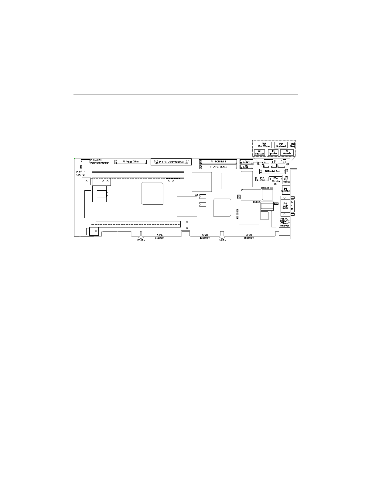
C. CONNECTOR LOCATION & PINOUTS
C.1 LOCATION OF CONNECTORS ON THE PCI-942
Diagram C-1 shows the connector locations on the PCI-942.
DIAGRAM C - 1: PCI-942 Connector Locations
C-1
Page 92

PCI-942 Technical Reference Manual
C.2 CONNECTOR PINOUTS
TABLE C-1: Keylock Connector (P2) - Pinout
Pin Number Signal Flow Signal
1 - LED POWER
2 - KEY
3 - GND
4 I KEYLOCK DATA
5 - GND
TABLE C-2: Floppy Disk Connector (P3) - Pinout
(Not Connected)
Pin
Number
1
3
5
7
9
11
13
15
17
19
21
23
25
27
29
31
33
* Active low signal
Signal
Flow
-
-
-
-
-
-
-
-
-
-
-
-
-
-
-
-
-
Signal Pin
GND
GND
GND
GND
GND
GND
GND
GND
GND
GND
GND
GND
GND
GND
GND
GND
GND
Number
2
4
6
8
10
12
14
16
18
20
22
24
26
28
30
32
34
Signal
Flow
O
-
I
O
O
O
O
O
O
O
O
I
I
I
O
I
Signal
DRV DENS. SEL. 0*
Not Connected
Not Connected
INDEX*
MOTOR ON 0,1*
DRIVE SELECT B*
DRIVE SELECT A*
MOTOR ON 2*
DIR CONTROL*
STEP*
WRITE DATA*
WRITE ENABLE*
TRACK 0*
WRITE PROTECT*
READ DATA*
HEAD SELECT*
DSKCHG*
C-2
Page 93

TABLE C-3: Keyboard Connector (P4) - Pinout
Pin Number Signal Flow Signal
1 I/O KBD DATA
2 - Reserved
3 - GND
4 - KBD POWER
(+5V fused)
5 I/O KBC CLOCK
6 - Reserved
TABLE C-4: Keyboard Header (P4A) - Pinout
Pin Number Signal Flow Signal
1 I/O KBC CLOCK
2 I/O KBD DATA
3 - KEY
(Not Connected)
4 - KBD GND
5 - KBD POWER
(+5V fused)
Connector Location & Pinouts
C-3
Page 94

PCI-942 Technical Reference Manual
TABLE C-5: Speaker Port Header (P5) - Pinout
Pin Number Signal Flow Signal
1 O SPEAKER DATA
2 - KEY
3 - GND
4 - +5V
(Not Connected)
TABLE C-6: Combo I/O Header (P5A) - Pinout
Pin Number Signal Flow Signal
1 I RESET
2 - GND
3 - Not Connected
4 I/O KBD CLOCK
5 I/O KBD DATA
6 I KBD LOCK DATA
7 - KBD POWER
8 O SPEAKER DATA
(+5V fused)
C-4
Page 95
TABLE C-7: Serial Port 1 - (P6) RS-232 - Pinout
Pin Number Pin Number
Signal Flow Signal Flow
Signal Signal
DCD 1* I 1 2 I DSR 1*
RXD 1* I 3 4 O RTS 1*
TXD 1 O 5 6 I CTS 1*
DTR 1* O 7 8 I RI 1*
GND - 9 10 - Not Connected
* Active low signal
TABLE C-8: Serial Port 2 - (P7) RS-232 - Pinout
Pin Number Pin Number
Signal Flow Signal Flow
Signal Signal
DCD 2* I 1 2 I DSR 2*
Connector Location & Pinouts
RXD 2* I 3 4 O RTS 2*
DTR 2* O 7 8 I RI 2*
* Active low signal
TXD 2 O 5 6 I CTS 2*
GND - 9 10 - Not Connected
C-5
Page 96

PCI-942 Technical Reference Manual
TABLE C-9: Parallel Port Header (P8) - Standard Mode
Pin
Number
1 O STROBE 2 O AUTO FEED XT
3 I/O DATA BIT 0 4 I ERROR
5 I/O DATA BIT 1 6 O INIT
7 I/O DATA BIT 2 8 O SELECT IN
9 I/O DATA BIT 3 10 - GND
11 I/O DATA BIT 4 12 - GND
13 I/O DATA BIT 5 14 - GND
15 I/O DATA BIT 6 16 - GND
17 I/O DATA BIT 7 18 - GND
19 I ACK 20 - GND
21 I BUSY 22 - GND
23 I PAPER END 24 - GND
25 I SELECT 26 - Not Connected
Signal
Flow
Signal Pin
Number
Signal
Flow
Signal
TABLE C-10: Parallel Port Connector (P8) - EPP Mode
Pin
Number
1 O WRITE 2 O DATASTB
3 I/O DATA BIT 0 4 - Not Connected
5 I/O DATA BIT 1 6 - Not Connected
7 I/O DATA BIT 2 8 O ADDRSTRB
9 I/O DATA BIT 3 10 - GND
11 I/O DATA BIT 4 12 - GND
13 I/O DATA BIT 5 14 - GND
15 I/O DATA BIT 6 16 - GND
17 I/O DATA BIT 7 18 - GND
19 I INTR 20 - GND
21 I WAIT 22 - GND
23 - Not Connected 24 - GND
25 - Not Connected 26 - Not Connected
Signal
Flow
Signal Pin
Number
Signal
Flow
Signal
C-6
Page 97

TABLE C-11: Parallel Port Connector (P8) - ECP Mode
Connector Location & Pinouts
Pin Number Signal
Flow
Signal Pin
Number
Signal
Flow
Signal
1 O STROBE 2 O AUTO FEED XT,
HOSTACK
3 I/O DATA BIT 0 4 I FAULT1,
PERIPHRQST
5 I/O DATA BIT 1 6 O INIT1,
REVERSERQST
7 I/O DATA BIT 2 8 O SELECT IN
9 I/O DATA BIT 3 10 - GND
11 I/O DATA BIT 4 12 - GND
13 I/O DATA BIT 5 14 - GND
15 I/O DATA BIT 6 16 - GND
17 I/O DATA BIT 7 18 - GND
19 I ACK 20 - GND
21 I BUSY,
PERIPHACK
23 I PERROR,
ACKREVERSE
2
22 - GND
24 - GND
2
25 I SELECT 26 - Not Connected
1
Compatible Mode
2
High Speed Mode
✎ NOTE
2
2
2
1,2
For more information on the ECP protocol, please refer to the Extended
Capabilities Port Protocol and ISA Interface Standard (available from Microsoft
Corporation) or contact our Technical Support department.
C-7
Page 98

PCI-942 Technical Reference Manual
TABLE C-12: PS/2 Mouse Connector (P9) - Pinout
Pin Number Signal Flow Signal
1 I/O MOUSE DATA
2 - Reserved
3 - GND
4 - KBD POWER
5 I/O MOUSE CLOCK
6 - Reserved
(+5V fused)
TABLE C-13: PS/2 Mouse Header (P9A) - Pinout
Pin Number Signal Flow Signal
1 I/O MOUSE DATA
2 - Reserved
3 - KBD GND
4 - KBD POWER
5 I/O MOUSE CLOCK
6 - Reserved
(+5V fused)
TABLE C-14: External Reset Header (P10) - Pinout
Pin Number Signal Flow Signal
1 I EXT RESET*
2 - GND
* Active low signal
C-8
Page 99

Connector Location & Pinouts
TABLE C-15: Primary Enhanced IDE Connector (P11) - Pinout
Pin Number Signal Flow Signal Pin Number Signal Flow Signal
1
3
5
7
9
11
13
15
17
19
21
23
25
27
29
31
33
35
37
39
O
I/O
I/O
I/O
I/O
I/O
I/O
I/O
I/O
I
O
O
I
O
I
O
O
O
I
RESET
DATA 7
DATA 6
DATA 5
DATA 4
DATA 3
DATA 2
DATA 1
DATA 0
GND
DRQ 0
IOW
IOR
IORDY
DACK 0
IRQ 14
ADD 1
ADD 0
CS 1P
IDEACTP
2
4
6
8
10
12
14
16
18
20
22
24
26
28
30
32
34
36
38
40
I/O
I/O
I/O
I/O
I/O
I/O
I/O
I/O
-
-
-
-
-
-
-
O
O
-
GND
DATA 8
DATA 9
DATA 10
DATA 11
DATA 12
DATA 13
DATA 14
DATA 15
Not Connected
GND
GND
GND
+5V
GND
IOCS16
GND
ADD 2
CS 3P
GND
TABLE C-16: Secondary Enhanced IDE Connector (P11A) - Pinout
Pin Number Signal Flow Signal Pin Number Signal Flow Signal
1
3
5
7
9
11
13
15
17
19
21
23
25
27
29
31
33
35
37
39
O
I/O
I/O
I/O
I/O
I/O
I/O
I/O
I/O
I
O
O
I
O
I
O
O
O
I
RESET
DATA 7
DATA 6
DATA 5
DATA 4
DATA 3
DATA 2
DATA 1
DATA 0
GND
DRQ 1
IOW
IOR
IORDY
DACK 1
MIRQ 0
ADD 1
ADD 0
CS 1S
IDEACTS
2
4
6
8
10
12
14
16
18
20
22
24
26
28
30
32
34
36
38
40
I/O
I/O
I/O
I/O
I/O
I/O
I/O
I/O
-
-
-
-
-
-
-
O
O
-
GND
DATA 8
DATA 9
DATA 10
DATA 11
DATA 12
DATA 13
DATA 14
DATA 15
Not Connected
GND
GND
GND
+5V
GND
IOCS16
GND
ADD 2
CS 3S
GND
C-9
Page 100

PCI-942 Technical Reference Manual
TABLE C-17: Hard Drive LED Header (P12) - Pinout
Pin Number Signal Flow Signal
1 - +5V Pull-up
2 O HD LED
3 O HD LED
4 - +5V Pull-up
C-10
 Loading...