

Page 1
PCI-935
1
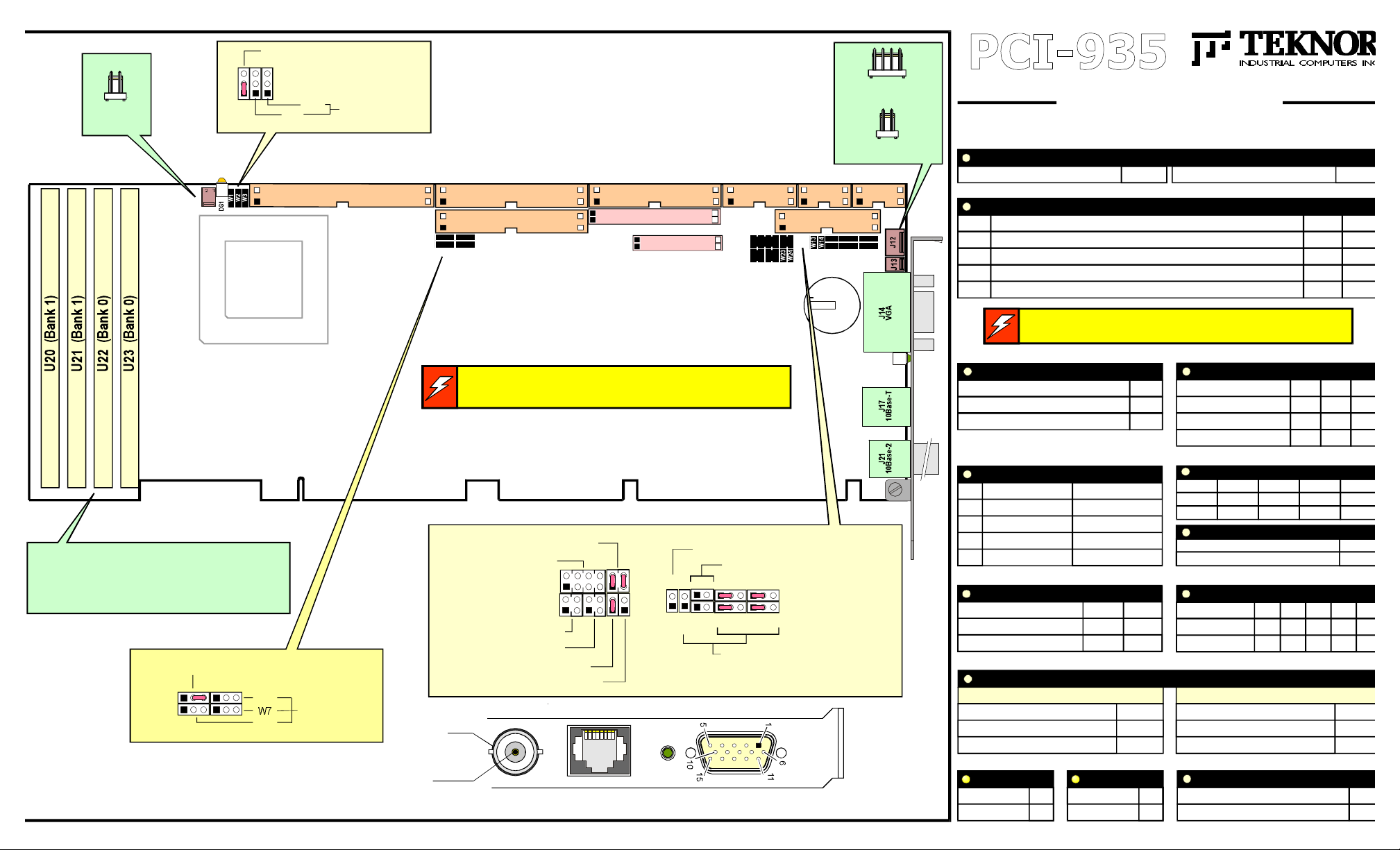
J1-CPUFan
DS1-SCSILED
W1:FirstLevelCache
3
1
3
1
W3
CPUClockSpeed
MultiplierW2
1
PCI-ISAINDUSTRIALSBC
J12-PS/2Mouse
QUICKREFERENCE
1
JUMPERSETTINGS (*:InitialSetting)
J13-BIOSBoot
Y20
Z20
Y13
2 16
J5
Keyboard
1 15
W8
W21 W22
2 210 10
J6
Serial1
1 19 9
2 26
J10-ParallelPort
1 25
W15
W9
B1
W16
BATTERY
3.6V
W18
W17
+
J7
Serial2
W20
W19
DS2-LinkOK
(LAN)
J1
2 50
1 49
J2-SCSI
2 40
J3-IDE1(Primary)
1 39
2 40
J8-IDE2(Secondary)
1 39
W6W4
W7W5
2 34
J4-FloppyDisk
1 33
Y1
J9-VMIHost
Z1
Y1
J11-V-PORT
Z1 Z13
Dangerofexplosionifthebatteryisincorrectlyreplaced.Replaceonly
withthesameorequivalenttype.
Disposeofusedbatteriesaccordingtothemanufacturer'sinstructions.
W1-FirstLevelCache
1-2 2-3Write-Back* Write-Through
W2,W3-InternalCPUClockSpeedMultiplier
InternalCPUSpeed/BusClock
1.5x
2.5x
75MHz/50MHz;90MHz/60MHz;100MHz/66MHz
120MHz/60MHz;133MHz/66MHz
2x
150MHz/60MHz;166MHz/66MHz
200MHz/66MHz
3x
Carefulattentionshouldbetakenwheninstallingaprocessor:
Faultyjumpersettingsmaydamagebothyourprocessorandyourboard.
W4-SCSITermination
ControlledbySoftware
DisabledbyHardware
ControlledbyHardware*(Boardisterminated)
W2
W3
1-2
1-2
1-2
2-3
2-3
2-3
2-3
1-2
W5,6,7-CPU/BusClock
W6
1-2
off
2-3
50MHz
60MHz
66MHz
W5
1-2
1-2
2-3
W7
2-3
2-3
1-2
1-2
1-2
2-3
Four72-pinSIMMsocketsavailableDRAM:
Upto 512MBusing32-bitor36-bitSIMM
.
EDOorFPMtypes(70msmaxrecommended)
.
PopulateBank0,Bank1orBank0andBank1
W4:SCSITermination
1
113
3
1
3
3
W9-SupervisorI/O(BaseAddress)
1-2
3-4
190h*
on
on
290h
390h
off
on
on
off
W13-NMIonPowerFailOutput
Enabled
Disabled*
W14,17,18,19,20-SerialPort2Setup
(configurejointly)
RS-232*
RS-422/485
W14
W17
W18
1-2
off
on
1-2
2-3
2-3
W19
1-2
2-3
390h
off
off
on
off
W20
1-2
2-3
W9:SupervisorI/O:BaseAddress
W8:ExtendedBIOSModes
2
1
W21:EDOUTSignalControl
W22:H DOUTSignalControl
W8-ExtendedBIOSModes
on off
1-2
SerialDownload
3-4
VT100Mode
5-6
NMIonPowerFailOutput
28
42
W13
31
3
3
W14
W15,16:SerialPort2,RS-485Setup
W18 W20
W15
W16
3
3
W17 W19
3
3
DisableTEK.Extension
7-8
DisableOnboardVGA
W15,W16-SerialPort2,RS-485Setup
(RS-422/485modeonly)
RTS2-CTS2
W15:
W16:
NornalMode*
StandardMode*
EnableTEK.Extension*
EnableOnboardVGA*
Loopback
Normal*
on
off
on
offDSR2-DTR2
W14,17,18,19,20:SerialPort2Mode
W23:WatchdogTimer
W24:OnboardBattery
W6
W5
GND
CPU/BusClock
8
1
LinkOK
Signal
10Base-2Ethernet
BNC
10Base-TEthernet
RJ-45
VGACRT
QR-935/01-9809-01
W21,W22-SerialPort2,RS-485Setup(Configurejointly)
W21: 2.88MBHighDensityFloppy,EDOUTSignal W22: 2.88MBHighDensityFloppy,HDOUTSignal
EDOUTlefttosoftware*
EDOUTtopin29(J4);GNDtopin17(J4)
EDOUTtopin17(J4);GNDtopin29(J4)
W23-Watchdog W24-BoardBatt.
Enabled*
Disabled
Enabled
on
Disabled*
off
none
1-3;2-4
1-2;3-4
HDOUTlefttosoftware*
HDOUTtopin33(J4);GNDtopin27(J4)
HDOUTtopin27(J4);GNDtopin33(J4)
J13-BIOSBootSelection
on
Normal(fromFlashEPROMBIOS)*
off
Emergency(fromEPROMBIOS)
1-3;2-4
1-2;3-4
none
off
on
Page 2
CONNECTORPINOUTS PCI-935TECHNICALSPECIFICATIONS
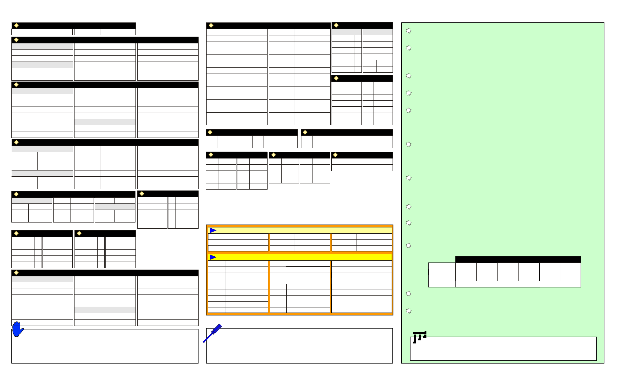
J1-CPUFan
1 2+12V GND
J2-FASTSCSIIIInterface
OddPinNumber
1-23;27-49
EvenPinNumber
2-16
J3-EnhancedIDE(Primary)
OddPinNumber
3-17
J4-FloppyDisk
OddPinNumber
1-15;19-25;31
17;27;29;33
EvenPinNumber
4;6
J5-Keyboard
OddPinNumber
1
3
5
DCD2
DTR2
J8-EnhancedIDE(Secondary)
OddPinNumber
3-17
25
18
1
19
21
23
25
27
2
KBCLK
KBDATA
VCC(+5V)
RX2
TX2
GND
1
19
21
23
25
27
GND
NotConnected
[D0-D7]
DP*
RESET*
[HD7-HD0]
GND
REQA
IOW*
IOR*
DRDY*
GND
N.C.bydefault
(orseeW24/W25setups)
RPM/LC
N.C.
1
2
DSR2
3
4
RTS2
5
6
CTS2
7
8
RI2
9
10
N.C.
RESET*
[HD7-HD0]
GND
REQB
IOW*
IOR*
DRDY*
20-24;28-30
26
32
34
36
38
29
31
33;35
37
39
EvenPinNumber
2;22-26
4-18
8
10
12
14
16
18
20
7
SPKROUT
9
KBDINH
11
DOWNLD*
13
PBRES*
J7-SerialPort2/RS-485J7-SerialPort2/RS-232
DCD2
RX(-)
TX(-)
DTR2
GND
29
31
33;35
37
39
EvenPinNumber
2;22-26
4-18
GND
TermPower
ATN
GND
BSY*
ACK*
DACKA*
IRQ14
SA1;SA0
CS1A*
ACTIVE*
GND
[HD8-HD15]
INDEX*
MOTORON0,1*
DRIVESEL.B
DRIVESEL.A
MOTORON2*
DIRCONTROL*
STEP*
*ActiveLowSignal
15
6-8;16
1
2
3
4
5
6
7
8
9
10
DACKB*
IRQ15
SA1;SA0
CS1A*
ACTIVE*
GND
[HD8-HD15]
ACT*
GND
VCC(+5V)
DSR2
RX(+)
TX(+)
RI2
N.C.
EvenPinNumber
2-4;10-14
*ActiveLowSignal
40
RST*
42
MSG*
44
SEL*
46
C/D*
48
REQ*
50
I/O*
*ActiveLowSignal
20
N.C.
28
N.C.
30
GND
32
PullUp
34
N.C.
36
SA2
38
CS3A*
40
GND
*ActiveLowSignal
22
WDATA*
24
WENABLE*
26
TRACK0*
28
WPROTECT*
30
RDATA*
32
HEADSELECT*
34
DSKCHG
J6-SerialPort1/RS-232
1
DCD1
RX1
TX1
DTR1
GND
20
28
30
32
34
36
38
40
2
DSR1
3
4
RTS1
5
6
CTS1
7
8
RI1
9
10
N.C.
*ActiveLowSignal*ActiveLowSignal
N.C.
N.C.
GND
PullUp
GND
SA2
CS3B*
GND
J9-VMIHost *ActiveLowSignal
Y1
Y2
Y3,Y4
Y5,Y6
Y7,Y8
Y9
Y10
Y11
Y12
Y13
Y14
Y15
Y16
Y17-Y18
Y19-Y20
VCC(+5V)
J17-10Base-T Ethernet
TXD+
1
TXD-
2
RXD+
3
N.C.
4
HD0
GND
HD2,HD4
HD5,HD7
HA0,HA2
VCC
LRESET*
GND
R/W*
DTACK*
INTVID*
N.C.
VCC3
P12-P13
P14-P15
1
2
5
6
7
8
EMER*
GND
N.C.
RXDN.C.
N.C.
MCLK
GND
RED
GREEN
BLUE
N.C.
GND
+12V
HD1
GND
HD3
VCC
HD6
OSC14M
HA1,HA3
GND
DS*
RD*
VCC3
N.C.
P8-P9
P10-P11
6-8
12
13
14
15
34MDATA
A_GND
SDA
HSYNC
VSYNC
SCL
Z1
Z2
Z3
Z4
Z5,Z16
Z6
Z7
Z8,Z9
Z10
Z11
Z12
Z13
Z14,Z15
Z17-Z18
Z19-Z20
J12-PS/2Mouse J13-BIOSBoot
1
2
J14-VGA
1
2
3
4;9;11
5;10
TheTechnicalReferenceManualcanbedownloaded
fromTEKNORWEBsiteat
www.teknor.com
ToorderaTechnicalReferenceManualhardcopy,pleasecontact
CustomerServiceDepartmentat
MEMORYMAPPING
00000-9FFFF
A0000-BFFFF
C0000-CBFFF
I/OMAPPING
000-00F
020-03F
040-043
060-064
070-071
080-09F
0A0-0BF
0C0-0DF
0EC-0EF
0-640KBDRAM
VideoDRAM
VideoBIOS
DMAcontroller1
Interruptcontroller1
Timer
Keyboard(8742)
RTC,NMImask
DMAPageRegister
Interruptcontroller2
DMAcontroller2
Configurationregisters
CC000-CFFFF
D0000-D3FFF
D4000-D7FFF
0F0-0FF
170-177;376
190-197
1F0-1F7;3F6
278-27A
290-297
2E8-2EF
2F8-2FF
370-377
TEK.BIOSExtension
FlashWindow
TEKBIOSExt.(option)
Mathcoproc.config.reg
SecondaryIDE
TEKNORControlPort
PrimaryIDE
ParallelPort
(option)
TEKNORCtrlPort
COM4
COM2
FloppyDisk(option)
(option)
J10-ParallelPort(Stdmode)
OddPinNumber
STROBE*
[PD0-PD7]
ACK*
BUSY
PE
SELECT
J11-VideoFeature
GND
FCEVID*
FCESYNC*
N.C.
GND
GND
FCVCLK
J21-10Base-2Ethernet
Center
Shield
(450)437-5682
D8000-DFFFF
E0000-FFFFF
100000totop
378-37A
390-397
3BC-3BE
3E8-3EF
3F0-3F7
3F8-3FF
3C0-3CF,
3D0-3DF,
3B0-3BB
EvenPinNumber
1
2
AUTOFD*
3-17
4
ERROR*
19
6
INIT*
21
8
SELECTIN*
23
10-18
25
20-26
Z13
Z1-3
Z4
Z5
Z6-7
Z8-9
Z10-11
Z12
Y1-8
Y9
Y10
Y11
Y12
Y13
OVRW*
FCP0-7
FCDCLK
FCBLANK*
FCHSYNC
FCVSYNC
GND
Signal
GND
SystemDRAM
SystemBIOS
1MBtotopofRAM
ParallelPort(LPT1)
TEKNORCtrlPort
ParallelPort
(option)
COM3
FloppyDisk
COM1
Graphicscontroller
GND
GND
(option)
CPUTYPESPEED
&
Pentium100,120,133,150,166AND200MHz
SYSTEMMEMORY
DRAM:upto256MB;72-pinSIMMsonfoursockets
FPMorEDO
Cache:256KBstandardor512option;write-through/write-back
FlashDisk:2or4MBoptional;4KBSerialNOVRAM
BUSINTERFACE
PICMG:PCIrev2.1compliant;ISA:drivesupto20slots;IBMPC/ATmechanicalformat
DATAPATH
64-bitonCPUbus;32-bitonPCIbus;16-bitonISAbus
VIDEO
CirrusLogicCL-GD5462graphicsprocessorwithPCIlocalbus;2MBvideomemory(standard)
24-bitperpixeltruecolorDAC
;GUIandvideoacceleration
SVGAresolutionupto1600x1200x256Kcolors;VMIconnectors
500MHzdatatransferrateusingRambusDRAM
I/O
SERIAL:twoRS-232portscon figurableasCOM1-4withRS-485availableonSerialPort2
PARALLEL:1bi-directionalport(LPT1)withPC/XT,AT,PS/2,EPPandECPmodes
HARDDISK:2EnhancedIDEchannels;driveupto4harddisks
FLOPPYDISK:interfacefor21.44or2.88MBfloppydrives
SCSI
SymbiosRISCEngine;Activeterminations;PCIFastSCSIII,8-bitbus;
Synchronoustransfersupto10MB/s;Asynchronoustransfersupto5MB/s
FullPCI-speeddatatransferstohost
ETHERNET
10Base-Tor10Base-2;BusmastermodewithDMAburst;PnPcompatible;remotebootsupport
BIOS
AMIBIOS:PCIBridgeAware;EmergencyBIOS;BIOSinFlashEPROM;shadowinginRAM
Auto-configuration;extendedsetup;programmablebusandI/Ospeeds;PowerManagement
POWERSUPPLY
VOLTAGE:+5V±5%;+12V±5%IPPCURRENT(+12V/-12V):5mA/10mA
PENTIUM
Proc.Speed
ICCtyp.
ICCSusp.
100MHz
4.0A
1.89A
120MHz
4.25A
2.03A
133MHz
3.91A
1.85A
150MHz
3.96A
1.82A
Setup 16MBDRAM,512KBcache,2MBVideoRDRAM,SCSI,kbd,FD,HD
OPERATINGCONDITIONS
0°Cto70°Cwithairflow;Tcase:85°;R.H.:5%to95%;MTBF:>100,000hours(MIL-HDBK-217F)
ELECTRICAL/MECHANICAL
Boarddimensions:4.8in.by13.33in./121.9mmby338.5mm
ConformstoIEEEP996PC/ATbusspec.;PCIRev.2.1spec.;PICMGRev.2.0
166MHz
4.02A
1.88A
200MHz
4.50A
1.92A
BeforePoweringONtheBoard
1.Ensurethepowersupplyconnectorisconnectedproperly(+5V,+12V,-12V)
2.Makesureallcablesareconnectedtotherightconnectors
3.Whenusingaflatpanel,makesurethepropervideoBIOSisinstalled
FirstLevelDebugging
1.Removeallperipheralboardsfromthebackplane.KeeponlytheSBC.
2.RemoveallcablesfromtheSBCexceptthevideocable
3.Makesurethememoryisworkingwelland properlyinserted
ContactTEKNORINC.forTechnicalSupport
1.2.Tel
:(800)354-4223
Fax
:(450)437-8053
3.4.Internet
E-Mail
:www.teknor.com
:[email protected]
 Loading...